Embed Size (px)
Citation preview
LTC3871
13871f
For more information www.linear.com/LTC3871
TYPICAL APPLICATION
FEATURES DESCRIPTION
Bidirectional PolyPhase® Synchronous Buck or Boost Controller
The LTC®3871 is a high performance bidirectional buck or boost switching regulator controller that operates in either buck or boost mode on demand. It regulates in buck mode from VHIGH-to-VLOW and boost mode from VLOW-to-VHIGH depending on a control signal, making it ideal for 48V/12V automotive dual battery systems. An accurate current programming loop regulates the maximum current that can be delivered in either direction. The LTC3871 allows both batteries to supply energy to the load simultaneously by converting energy from one battery to the other.
Its proprietary constant-frequency current mode architecture enhances the signal-to-noise ratio enabling low noise operation and provides excellent current matching between phases. Additional features include discontinuous or continuous mode of operation, OV/UV monitors, independent loop compensation for buck and boost operation, accurate output current monitoring and overcurrent protection.APPLICATIONS
n Unique Architecture Allows Dynamic Regulation of Input Voltage, Output Voltage or Current
n VHIGH Voltages Up to 100V n VLOW Voltages Up to 30V n Synchronous Rectification: Up to 97% Efficiency n LTC-Proprietary Advanced Current Mode Control n ±1% Voltage Regulation Accuracy Over Temperature n Accurate, Programmable Output Current Monitoring
and Regulation for Both Buck and Boost Operation n Selectable Buck and Boost Current Sense Limits n Programmable DRVCC/EXTVCC Optimizes Efficiency n Programmable VHIGH UV and OV Thresholds n Programmable VLOW OV Threshold n Phase-Lockable Frequency: 60kHz to 460kHz n Multiphase/Multi-ICs Operation Up to 12 Phases n Selectable CCM/DCM Modes n Thermally Enhanced 48-Lead LQFP Package
n Automotive 48V/12V Dual Battery Systems n Backup Power Systems
L, LT, LTC, LTM, Linear Technology, the Linear logo, μModule, PolyPhase and OPTI-LOOP are registered trademarks of Linear Technology Corporation. All other trademarks are the property of their respective owners. Protected by U.S. Patents, including 5481178, 5705919, 5929620, 6177787, 6580258, 6100678, 6144154, 6304066.
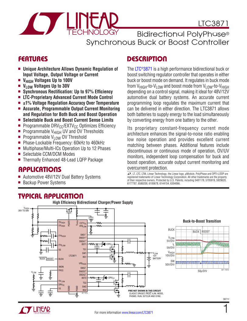
Buck-to-Boost Transition
High Efficiency Bidirectional Charger/Power Supply
SW50V/DIV
3871 TA01b
IL5A/DIV
VLOW5V/DIV
BUCK
VHIGH10V/DIV
50μ/DIV
BOOSTBUCK
VHIGH26V TO 58V
VLOW12VBATTERY
DRVCC
VLOW
PGAT
E
DRVCC
V5
PGND
BG2SGND
SNSA2+
IMON
SNSD2+
TG2
V HIG
H
SW2
SS
UVHIGH VFBLOW
EXTVCC
OVLOW
OVHIGH
ITHLOW
ITHHIGH
FREQ
BUCK
BST2
SNS2–
BG1
VFBHIGH
TG1
SW1
BST1SNSA1+
SNS1–
SNSD1+
LTC3871
DRVCC
PINS NOT SHOWN IN THIS CIRCUIT: CLKOUT, DRVSET, FAULT, ILIM, MODE, PHSMD, RUN, SETCUR AND SYNC.
3871 TA01a
BUCK BOOST
LTC3871
23871f
For more information www.linear.com/LTC3871
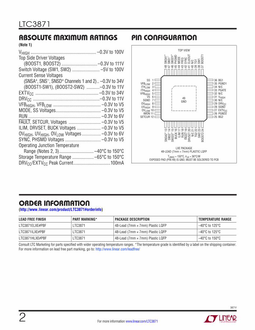
PIN CONFIGURATIONABSOLUTE MAXIMUM RATINGS
VHIGH ....................................................... –0.3V to 100V Top Side Driver Voltages
(BOOST1, BOOST2) .............................. –0.3V to 111VSwitch Voltage (SW1, SW2) ....................... –5V to 100VCurrent Sense Voltages (SNSA+, SNS–, SNSD+ Channels 1 and 2) .. –0.3V to 34V (BOOST1-SW1), (BOOST2-SW2) ...........–0.3V to 11V EXTVCC ..................................................... –0.3V to 34V DRVCC ........................................................–0.3V to 11VVFBHIGH, VFBLOW ........................................ –0.3V to V5MODE, SS Voltages ...................................... –0.3V to V5RUN ............................................................. –0.3V to 6VFAULT, SETCUR, Voltages ........................... –0.3V to V5ILIM, DRVSET, BUCK Voltages .................... –0.3V to V5OVHIGH, UVHIGH, OVLOW Voltages ................ –0.3V to 6VSYNC, PHSMD Voltages .............................. –0.3V to V5Operating Junction Temperature
Range (Notes 2, 3) ............................. –40°C to 150°CStorage Temperature Range .................. –65°C to 150°CDRVCC/EXTVCC Peak Current ...............................100mA
(Note 1)
123456789
101112
363534333231302928272625
SSVFBLOWITHLOWITHHIGHVFBHIGH
V5SGND
OVHIGHUVHIGHOVLOW
IMONSETCUR
13 14 15 16 17 18 19 20 21 22 23 24
SNSA
2+
SNS2
–
SNSD
2+
BUCK
ILIM
RUN
FAUL
TDR
VSET N/C
TG2
SW2
BOOS
T2
48 47 46 45 44 43 42 41 40 39 38 37
SNSA
1+
SNS1
–
SNSD
1+
PHSM
DM
ODE
FREQ
SYNC
CLKO
UTN/
CTG
1SW
1BO
OST1
BG1PGND1N/CPGATEN/CVHIGHN/CDRVCCSGNDEXTVCCPGND2BG2
TOP VIEW
LXE PACKAGE48-LEAD (7mm × 7mm) PLASTIC LQFP
49GND
TJMAX = 150°C, θJA = 36°C/W
EXPOSED PAD (PIN 49) IS GND, MUST BE SOLDERED TO PCB
ORDER INFORMATION
LEAD FREE FINISH PART MARKING* PACKAGE DESCRIPTION TEMPERATURE RANGE
LTC3871ELXE#PBF LTC3871 48-Lead (7mm × 7mm) Plastic LQFP –40°C to 125°C
LTC3871ILXE#PBF LTC3871 48-Lead (7mm × 7mm) Plastic LQFP –40°C to 125°C
LTC3871HLXE#PBF LTC3871 48-Lead (7mm × 7mm) Plastic LQFP –40°C to 150°C
Consult LTC Marketing for parts specified with wider operating temperature ranges. *The temperature grade is identified by a label on the shipping container. For more information on lead free part marking, go to: http://www.linear.com/leadfree/
(http://www.linear.com/product/LTC3871#orderinfo)
LTC3871
33871f
For more information www.linear.com/LTC3871
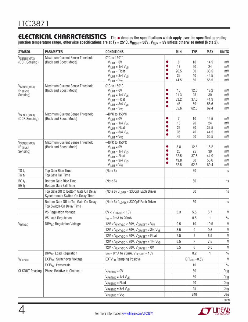
ELECTRICAL CHARACTERISTICS The l denotes the specifications which apply over the specified operating junction temperature range, otherwise specifications are at TA = 25°C, VHIGH = 50V, VRUN = 5V unless otherwise noted (Note 2).
SYMBOL PARAMETER CONDITIONS MIN TYP MAX UNITS
VHIGH VHIGH Supply Voltage Range 5 100 V
VLOW VLOW Supply Voltage Range VHIGH > 5V 1.2 30 V
VLOW Regulated Feedback Voltage (Note 4); ITHLOW Voltage = 1.5V l 1.188 1.200 1.212 V
VHIGH Regulated Feedback Voltage (Note 4); ITHHIGH Voltage = 0.5V l 1.185 1.200 1.215 V
VLOW EA Feedback Current (Note 4) –115 –200 nA
VHIGH EA Feedback Current (Note 4) –115 –200 nA
Reference Voltage Line Regulation (Note 4); VHIGH = 7V to 80V 0.02 0.2 %
VLOW/VHIGH Voltage Load Regulation Measured in Servo Loop; ∆ITH Voltage = 1V to 1.5V
0.01 0.2 %
Measured in Servo Loop; ∆ITH Voltage = 1V to 0.5V
–0.01 –0.2 %
gm-buck Transconductance Amplifier gm-buck (Note 4); ITHLOW = 1.5V; Sink/Source 5µA 2 mmho
gm-boost Transconductance Amplifier gm-boost (Note 4); ITHHIGH= 0.5V; Sink/Source 5µA 1 mmho
IQ VHIGH DC Supply Current (Note 5) 8 14 mA
Shutdown (VHIGH) VRUN = 0V; VHIGH = 50V 140 µA
Undervoltage Lockout V5 Ramping Down 3.7 4.15 4.5 V
Undervoltage Hysteresis 0.5 V
RUN Pin On Threshold VRUN Rising 1.1 1.22 1.35 V
RUN Pin On Hysteresis 80 mV
RUN Pin Source Current VRUN < 1.2 l 1 2 µA
RUN Pin Source Current VRUN > 1.3 l 3 6.5 µA
ISS Soft-Start Charging Current VSS = 1.2V 0.9 1.25 1.7 µA
ISNSA+ 1,2 Current Sensing Pins Current 0.1 ±1 µA
ISNSD+ 1,2 Current Sensing Pins Current 0.01 ±1 µA
ISNS– 1,2 Current Sensing Pins Current 1.5 mA
Total DC Sense Signal Gain DCR Configuration 5 V/V
ILIM Pin Input Resistance 100 kΩ
ISETCUR Current to Program Initial Current Limit l 6.75 7.5 8.25 µA
IMON Current Proportional to VLOW at Max Current
VILIM = Float; RSENSE = 3mΩ ±10 %
IMON Zero Current Voltage 1.225 1.25 1.275 V
Sense Pin to IMON Gain VILIM = 0V, 1/4 VV5, Float 38 V/V
VILIM = 3/4 VV5, VV5 19 V/V
TG Pull-Up On-Resistance 5 Ω
TG Pull-Down On-Resistance 2.5 Ω
BG Driver Pull-Up On-Resistance 5 Ω
BG Driver Pull-Down On-Resistance 2.5 Ω
Total DC Sense Signal Gain RSENSE Configuration 4 V/V
Maximum Duty Cycle Buck Mode Boost Mode
96 98 92
% %
LTC3871
43871f
For more information www.linear.com/LTC3871
SYMBOL PARAMETER CONDITIONS MIN TYP MAX UNITS
VSENSE(MAX) (DCR Sensing)
Maximum Current Sense Threshold (Buck and Boost Mode)
0°C to 150°C VILIM = 0V VILIM = 1/4 VV5 VILIM = Float VILIM = 3/4 VV5 VILIM = VV5
l
l
l
l
l
8
17 26.5 36
44.5
10 20 30 40 50
14.5 24
33.5 44.5 55.5
mV mV mV mV mV
VSENSE(MAX) (RSENSE Sensing)
Maximum Current Sense Threshold (Buck and Boost Mode)
0°C to 150°C VILIM = 0V VILIM = 1/4 VV5 VILIM = Float VILIM = 3/4 VV5 VILIM = VV5
l
l
l
l
l
10
21.3 33.2 45
55.6
12.5 25
37.5 50
62.5
18.2 30
41.9 55.6 69.4
mV mV mV mV mV
VSENSE(MAX) (DCR Sensing)
Maximum Current Sense Threshold (Buck and Boost Mode)
–40°C to 150°C VILIM = 0V VILIM = 1/4 VV5 VILIM = Float VILIM = 3/4 VV5 VILIM = VV5
l
l
l
l
l
7
16 26 35 42
10 20 30 40 50
14.5 24
33.5 44.5 55.5
mV mV mV mV mV
VSENSE(MAX) (RSENSE Sensing)
Maximum Current Sense Threshold (Buck and Boost Mode)
–40°C to 150°C VILIM = 0V VILIM = 1/4 VV5 VILIM = Float VILIM = 3/4 VV5 VILIM = VV5
l
l
l
l
l
8.8 20
32.5 43.8 52.5
12.5 25
37.5 50
62.5
18.2 30
41.9 55.6 69.4
mV mV mV mV mV
TG tr TG tf
Top Gate Rise Time Top Gate Fall Time
(Note 6) 60 ns
BG tr BG tf
Bottom Gate Rise Time Bottom Gate Fall Time
(Note 6) 60 ns
Top Gate Off to Bottom Gate On Delay Synchronous Switch-On Delay Time
(Note 6) CLOAD = 3300pF Each Driver 60 ns
Bottom Gate Off to Top Gate On Delay Top Switch-On Delay Time
(Note 6) CLOAD = 3300pF Each Driver 60 ns
V5 Regulation Voltage 6V < VDRVCC < 10V 5.3 5.5 5.7 V
V5 Load Regulation IV5 = 0mA to 20mA 0.5 1 %
VDRVCC DRVCC Regulation Voltage 12V < VEXTVCC < 30V, VDRVSET = VV5 9.5 10 10.5 V
12V < VEXTVCC < 30V, VDRVSET = 3/4 VV5 8.5 9 9.5 V
12V < VEXTVCC < 30V, VDRVSET = Float 7.5 8 8.5 V
12V < VEXTVCC < 30V, VDRVSET = 1/4 VV5 6.5 7 7.5 V
12V < VEXTVCC < 30V, VDRVSET = 0V 5.5 6 6.5 V
DRVCC Load Regulation ICC = 0mA to 20mA, VEXTVCC = 10V 0.2 1 %
VEXTVCC EXTVCC Switchover Voltage EXTVCC Ramping Positive DRVCC –0.5V V
EXTVCC Hysteresis 10 %
CLKOUT Phasing Phase Relative to Channel 1 VPHSMD = 0V 60 Deg
VPHSMD = 1/4 VV5 60 Deg
VPHSMD = Float 90 Deg
VPHSMD = 3/4 VV5 45 Deg
VPHSMD = VV5 240 Deg
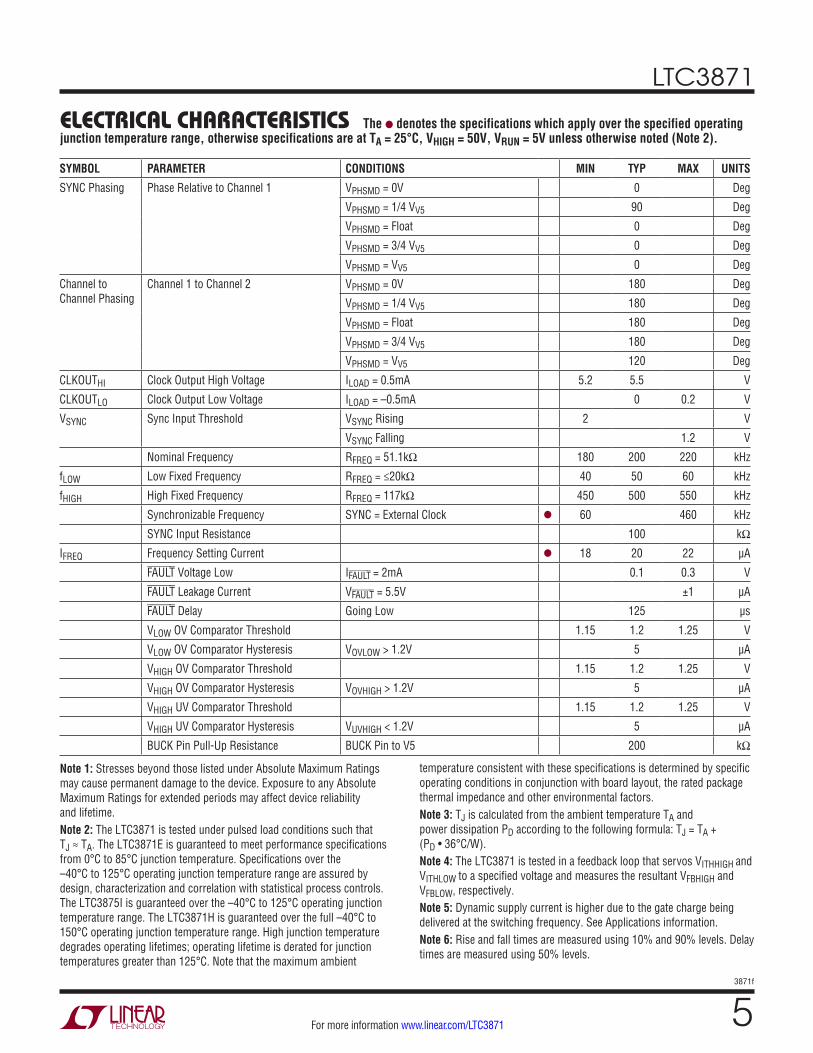
ELECTRICAL CHARACTERISTICS The l denotes the specifications which apply over the specified operating junction temperature range, otherwise specifications are at TA = 25°C, VHIGH = 50V, VRUN = 5V unless otherwise noted (Note 2).
LTC3871
53871f
For more information www.linear.com/LTC3871
SYMBOL PARAMETER CONDITIONS MIN TYP MAX UNITS
SYNC Phasing Phase Relative to Channel 1 VPHSMD = 0V 0 Deg
VPHSMD = 1/4 VV5 90 Deg
VPHSMD = Float 0 Deg
VPHSMD = 3/4 VV5 0 Deg
VPHSMD = VV5 0 Deg
Channel to Channel Phasing
Channel 1 to Channel 2 VPHSMD = 0V 180 Deg
VPHSMD = 1/4 VV5 180 Deg
VPHSMD = Float 180 Deg
VPHSMD = 3/4 VV5 180 Deg
VPHSMD = VV5 120 Deg
CLKOUTHI Clock Output High Voltage ILOAD = 0.5mA 5.2 5.5 V
CLKOUTLO Clock Output Low Voltage ILOAD = –0.5mA 0 0.2 V
VSYNC Sync Input Threshold VSYNC Rising 2 V
VSYNC Falling 1.2 V
Nominal Frequency RFREQ = 51.1kΩ 180 200 220 kHz
fLOW Low Fixed Frequency RFREQ = ≤20kΩ 40 50 60 kHz
fHIGH High Fixed Frequency RFREQ = 117kΩ 450 500 550 kHz
Synchronizable Frequency SYNC = External Clock l 60 460 kHz
SYNC Input Resistance 100 kΩ
IFREQ Frequency Setting Current l 18 20 22 µA
FAULT Voltage Low IFAULT = 2mA 0.1 0.3 V
FAULT Leakage Current VFAULT = 5.5V ±1 µA
FAULT Delay Going Low 125 µs
VLOW OV Comparator Threshold 1.15 1.2 1.25 V
VLOW OV Comparator Hysteresis VOVLOW > 1.2V 5 µA
VHIGH OV Comparator Threshold 1.15 1.2 1.25 V
VHIGH OV Comparator Hysteresis VOVHIGH > 1.2V 5 µA
VHIGH UV Comparator Threshold 1.15 1.2 1.25 V
VHIGH UV Comparator Hysteresis VUVHIGH < 1.2V 5 µA
BUCK Pin Pull-Up Resistance BUCK Pin to V5 200 kΩ
ELECTRICAL CHARACTERISTICS The l denotes the specifications which apply over the specified operating junction temperature range, otherwise specifications are at TA = 25°C, VHIGH = 50V, VRUN = 5V unless otherwise noted (Note 2).
Note 1: Stresses beyond those listed under Absolute Maximum Ratings may cause permanent damage to the device. Exposure to any Absolute Maximum Ratings for extended periods may affect device reliability and lifetime. Note 2: The LTC3871 is tested under pulsed load conditions such that TJ ≈ TA. The LTC3871E is guaranteed to meet performance specifications from 0°C to 85°C junction temperature. Specifications over the –40°C to 125°C operating junction temperature range are assured by design, characterization and correlation with statistical process controls. The LTC3875I is guaranteed over the –40°C to 125°C operating junction temperature range. The LTC3871H is guaranteed over the full –40°C to 150°C operating junction temperature range. High junction temperature degrades operating lifetimes; operating lifetime is derated for junction temperatures greater than 125°C. Note that the maximum ambient
temperature consistent with these specifications is determined by specific operating conditions in conjunction with board layout, the rated package thermal impedance and other environmental factors.Note 3: TJ is calculated from the ambient temperature TA and power dissipation PD according to the following formula: TJ = TA + (PD • 36°C/W).Note 4: The LTC3871 is tested in a feedback loop that servos VITHHIGH and VITHLOW to a specified voltage and measures the resultant VFBHIGH and VFBLOW, respectively.Note 5: Dynamic supply current is higher due to the gate charge being delivered at the switching frequency. See Applications information.Note 6: Rise and fall times are measured using 10% and 90% levels. Delay times are measured using 50% levels.
LTC3871
63871f
For more information www.linear.com/LTC3871
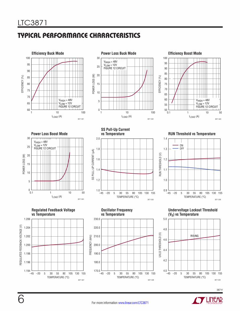
TYPICAL PERFORMANCE CHARACTERISTICS
Power Loss Boost ModeSS Pull-Up Current vs Temperature RUN Threshold vs Temperature
Regulated Feedback Voltage vs Temperature
Oscillator Frequency vs Temperature
Undervoltage Lockout Threshold (V5) vs Temperature
Efficiency Buck Mode Power Loss Buck Mode Efficiency Boost Mode
TEMPERATURE (°C)–45 –20 5 30 55 80 105 130 155
1.0
1.2
1.4
1.6
1.8
2.0
SS P
ULL-
UP C
URRE
NT (μ
A)
3871 G05
ONOFF
TEMPERATURE (°C)–45 –20 5 30 55 80 105 130 155
0.9
1.0
1.1
1.2
1.3
1.4
RUN
THRE
SHOL
D (V
)
3871 G06
TEMPERATURE (°C)–45 –20 5 30 55 80 105 130 155
1.194
1.196
1.198
1.200
1.202
1.204
1.206
REGU
LATE
D FE
EDBA
CK V
OLTA
GE (V
)
vs Temperature
3871 G07TEMPERATURE (°C)
–45 –20 5 30 55 80 105 130 155170.0
180.0
190.0
200.0
210.0
220.0
230.0
FREQ
UENC
Y (k
Hz)
3871 G08TEMPERATURE (°C)
–45 –20 5 30 55 80 105 130 1554.0
4.2
4.4
4.6
4.8
5.0
UVLO
THR
ESHO
LD (V
)
3871 G09
RISING
ILOAD (A)1 10 100
60
65
70
75
80
85
90
95
100
EFFI
CIEN
CY (%
)
Efficiency Buck Mode
3871 G01
VHIGH = 48VVLOW = 12VFIGURE 12 CIRCUIT
ILOAD (A)1 10 100
0
5
10
15
20
25
30
POW
ER L
OSS
(W)
Power Loss Buck Mode
3871 G02
VHIGH = 48VVLOW = 12VFIGURE 12 CIRCUIT
ILOAD (A)0.1 1 10 50
50
55
60
65
70
75
80
85
90
95
100
EFFI
CIEN
CY (%
)
Efficiency Boost Mode
3871 G03
VHIGH = 48VVLOW = 12VFIGURE 12 CIRCUIT
ILOAD (A)0.1 1 10 50
0
5
10
15
20
25
30
POW
ER L
OSS
(W)
Power Loss Boost Mode
3871 G04
VHIGH = 48VVLOW = 12VFIGURE 12 CIRCUIT
LTC3871
73871f
For more information www.linear.com/LTC3871
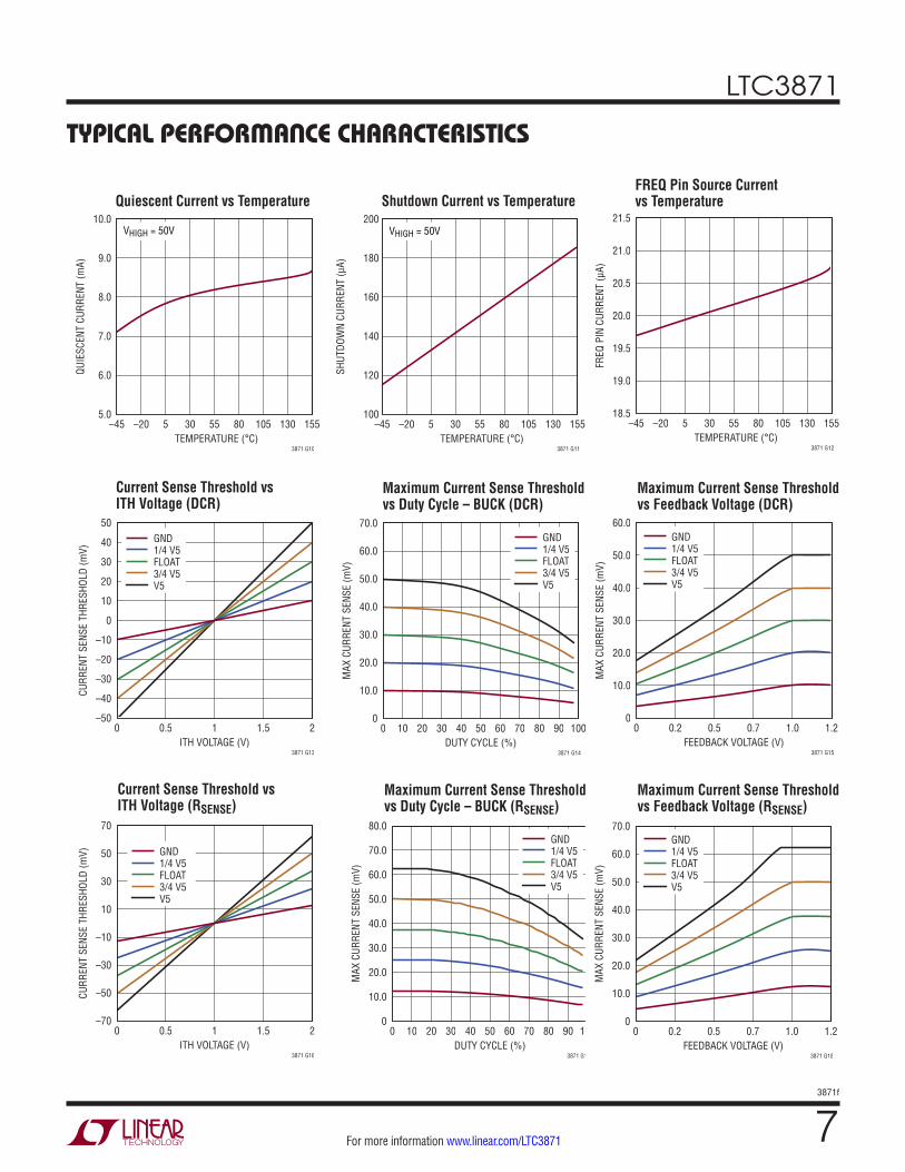
TYPICAL PERFORMANCE CHARACTERISTICS
Quiescent Current vs Temperature Shutdown Current vs TemperatureFREQ Pin Source Current vs Temperature
Maximum Current Sense Threshold vs Duty Cycle – BUCK (DCR)
Maximum Current Sense Threshold vs Feedback Voltage (DCR)
Current Sense Threshold vs ITH Voltage (DCR)
TEMPERATURE (°C)–45 –20 5 30 55 80 105 130 155
5.0
6.0
7.0
8.0
9.0
10.0
QUIE
SCEN
T CU
RREN
T (m
A)
3871 G10
VHIGH = 50V
TEMPERATURE (°C)–45 –20 5 30 55 80 105 130 155
100
120
140
160
180
200
SHUT
DOW
N CU
RREN
T (μ
A)
3871 G11
VHIGH = 50V
TEMPERATURE (°C)–45 –20 5 30 55 80 105 130 155
18.5
19.0
19.5
20.0
20.5
21.0
21.5
FREQ
PIN
CUR
RENT
(μA)
vs Temperature
3871 G12
GND1/4 V5FLOAT3/4 V5V5
ITH VOLTAGE (V)0 0.5 1 1.5 2
–50
–40
–30
–20
–10
0
10
20
30
40
50
CURR
ENT
SENS
E TH
RESH
OLD
(mV)
3871 G13DUTY CYCLE (%)
0 10 20 30 40 50 60 70 80 90 1000
10.0
20.0
30.0
40.0
50.0
60.0
70.0
MAX
CUR
RENT
SEN
SE (m
V)
vs Duty Cycle (BUCK Mode)
3871 G14
GND1/4 V5FLOAT3/4 V5V5
FEEDBACK VOLTAGE (V)0 0.2 0.5 0.7 1.0 1.2
0
10.0
20.0
30.0
40.0
50.0
60.0
MAX
CUR
RENT
SEN
SE (m
V)
3871 G15
GND1/4 V5FLOAT3/4 V5V5
Maximum Current Sense Threshold vs Duty Cycle – BUCK (RSENSE)
Maximum Current Sense Threshold vs Feedback Voltage (RSENSE)
Current Sense Threshold vs ITH Voltage (RSENSE)
GND1/4 V5FLOAT3/4 V5V5
ITH VOLTAGE (V)0 0.5 1 1.5 2
–70
–50
–30
–10
10
30
50
70
CURR
ENT
SENS
E TH
RESH
OLD
(mV)
ITH Voltage (RSENSE)
3871 G16DUTY CYCLE (%)
0 10 20 30 40 50 60 70 80 90 1000
10.0
20.0
30.0
40.0
50.0
60.0
70.0
80.0
MAX
CUR
RENT
SEN
SE (m
V)
vs Duty Cycle (BUCK) (RSENSE)
3871 G17
GND1/4 V5FLOAT3/4 V5V5
FEEDBACK VOLTAGE (V)0 0.2 0.5 0.7 1.0 1.2
0
10.0
20.0
30.0
40.0
50.0
60.0
70.0
MAX
CUR
RENT
SEN
SE (m
V)
3871 G18
GND1/4 V5FLOAT3/4 V5V5
LTC3871
83871f
For more information www.linear.com/LTC3871
PIN FUNCTIONSSS (Pin 1): Soft-Start Input. The voltage ramp rate at this pin sets the voltage ramp rate of the regulated voltage. A capacitor to ground accomplishes soft-start in buck mode. This pin has a 1.25µA pull-up current.
VFBLOW (Pin 2): VLOW Voltage Sensing Error Amplifier Inverting Input.
ITHLOW/ITHHIGH (Pins 3 and 4): Current Control Thresh-old and Error Amplifier Compensation Point. The current comparator’s threshold varies with the ITH control voltage.
VFBHIGH (Pin 5): VHIGH Voltage Sensing Error Amplifier Inverting Input.
V5 (Pin 6): Internal 5.5V Regulator Output. The control circuits are powered from this voltage. Bypass this pin to SGND with a minimum of 4.7µF low ESR tantalum or ceramic capacitor.
SGND (Pins 7 and 28): Signal Ground Pins.
OVHIGH (Pin 8): VHIGH Overvoltage Threshold Set Pin. A resistor divider from VHIGH is needed to set this thresh-old. When the voltage on this pin rises past the 1.2V trip point, a 5µA current is sourced out of the pin to provide externally adjustable hysteresis. When OVHIGH voltage is above 3V, the controller stops switching.
UVHIGH (Pin 9): VHIGH Undervoltage Threshold Set Pin. A resistor divider from VHIGH is needed to set this threshold. This pin also controls the state of the PGATE pin. When the voltage on this pin falls below the 1.2V trip point, a 5µA current is sunk into the pin to provide externally adjustable hysteresis.
OVLOW (Pin 10): VLOW Overvoltage Threshold Set Pin. A resistor divider from VLOW is needed to set this threshold. When the voltage on this pin rises past the 1.2V trip point, a 5µA current is sourced out of the pin to provide externally adjustable hysteresis.
IMON (Pin 11): The voltage on this pin is directly propor-tional to the average inductor currents of the 2 channels. 1.25V indicates zero average inductor current per phase.
SETCUR (Pin 12): This pin sets the maximum average inductor current in buck or boost mode. This pin sources 7.5µA.
SNSA1+/SNSA2+ (Pins 13 and 48): AC Positive Current Sense Comparator Inputs. These inputs amplify the AC portion of the current signal to the IC’s current comparator.
SNS1–/SNS2–(Pins 14 and 47): Negative Current Sense Comparator Inputs. The negative input of the current comparator is normally connected to VLOW.
SNSD1+/SNSD2+(Pins 15 and 46): DC Positive Current Sense Comparator Inputs. These inputs amplify the DC portion of the current signal to the IC’s current comparator.
BUCK (Pin 16): The voltage on this pin determines if the IC is regulating the VLOW or VHIGH voltage/current. Float or tie this pin to V5 for buck mode operation. Ground this pin for boost mode operation.
ILIM (Pin 17): Current Comparator Sense Voltage Limit Selection Pin. The input impedance of this pin is 100kΩ.
RUN (Pin 18): Enable Control Input. A voltage above 1.22V turns on the IC. There is a 2µA pull-up current on this pin. Once the RUN pin rises above the 1.22V threshold the pull-up current increases to 6µA.
FAULT (Pin 19): Fault Indicator Output. Open-drain output that pulls to ground during a fault condition.
DRVSET (Pin 20): The voltage setting on this pin programs the DRVCC output voltage. The input impedance of this pin is 100kΩ.
NC (Pins 21, 30, 32, 34, 40): No Connect Pins.
TG1/TG2 (Pins 22 and 39): Top Gate Driver Outputs. This is the output of the floating driver with a voltage swing equal to DRVCC superimposed on the SW voltage.
SW1/SW2 (Pins 23 and 38): Switch Node Connections to the Inductors. Voltage swing at this pin is from a Schottky diode (external) voltage drop below ground to VHIGH.
BOOST1/BOOST2 (Pins 24 and 37): Boosted Floating Driver Supplies. The (+) terminal of the bootstrap capacitor connects to this pin. This pin swings from a diode drop below DRVCC up to VHIGH+DRVCC.
LTC3871
93871f
For more information www.linear.com/LTC3871
BG1/BG2 (Pins 25 and 36): Bottom Gate Driver Outputs. This pin drives the gate(s) of the bottom N-channel MOSFET(s) between PGND and DRVCC.
PGND1/PGND2 (Pins 26 and 35): Power Ground Pin. Connect this pin closely to the source(s) of the bottom N-channel MOSFET(s), the (–) terminal of CDRVCC and (–) terminal of CVHIGH.
EXTVCC (Pin 27): External Power Input to an Internal LDO Connected to DRVCC. When the voltage on this pin is greater than the DRVCC LDO setting minus 500mV, this LDO bypasses the internal LDO powered from VHIGH.
DRVCC (Pin 29): Gate Driver Current Supply LDO Output. The voltage on this pin can be set from 6V to 10V in 1V increments. Bypass this pin to PGND with a minimum of 4.7µF low ESR tantalum or ceramic capacitor.
VHIGH (Pin 31): Main VHIGH supply. Bypass this pin to PGND with a capacitor (0.1µF to 1µF)
PGATE (Pin 33): Gate Drive for Input Short Protection.If a UVHIGH fault is detected, PGATE drives the gate of an external PMOS in series with the VHIGH rail high. Signal swings is from VHIGH to VHIGH –15V.
CLKOUT (Pin 41): Clock Output Pin. Use this pin to syn-chronize multiple LTC3871 ICs. Signal swing is from V5 to ground.
SYNC (Pin 42): Applying a clock signal to this pin causes the internal PLL to synchronize the internal oscillator to the clock signal. The PLL compensation network is integrated onto the IC. This pin has a 100k internal resistor to ground.
FREQ (Pin 43): Frequency Set Pin. A resistor between this pin and SGND sets the switching frequency.
MODE (Pin 44): Tying this pin to SGND enables forced continuous mode in buck or boost modes. Floating this pin results in discontinuous mode when in buck mode and forced continuous mode in boost mode. Tying this pin to V5 enables discontinuous mode in buck mode and non-synchronous operation in boost mode. The input impedance of this pin is 50kΩ.
PHSMD (Pin 45): Phase Mode Pin. This pin selects CH1 – CH2 and CH1 – CLKOUT phasing.
GND (Exposed Pad Pin 49): Ground. Must be soldered to PCB ground for rated thermal performance. Connect this pin closely to the sources of the bottom N-channel MOSFETs and negative terminal of VHIGH, DRVCC, V5 bypass capacitors. All small signal components and compensa-tion components should connect here. Signal ground pin should be connected to this exposed pad.
PIN FUNCTIONS
LTC3871
103871f
For more information www.linear.com/LTC3871
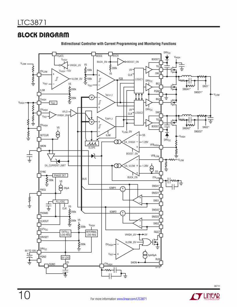
BLOCK DIAGRAMBidirectional Controller with Current Programming and Monitoring Functions
+–
+–
+–
+–
–
+
–
+
–
+
–
+
–
–
+
EA_VHIGH
–
+
+
EA_VLOW
LOGIC2
VREF
INTERNALLDO REG
EXTVCCLDO REG
ITHHIGH
PGND
DRVCC
DRVSET
EXTVCC
6V TO 10V
CLKOUT
PHSMD
FREQ
SYNC
IMON
SETCUR
OVHIGH
UVHIGH
VHIGH
ILIM
OVLOW
PHASE DET
PLL/OSC
CLKICMP2
ICMP1
EA_CURRENT LIMIT
VHIGH_UVVREF
VFLD
VHIGH
VLOW VHIGH_UV
VLOW_OV
PGATE MODE
VREF VREF
BUCK_EN
BUCK
BOOST_EN
IREV1,2
ICMP1,2
ILIM
BOOST_EN
SLOPE
BUCK_EN
VHIGH_UV
VLOW_OV
VREF
VHIGH
OVHIGH
UV
SHDNRUN
FAULT
SNS2–
SNSD2+
SNSA2+
SNS1–
SNSD1+
SNSA1+
SS
ITHLOW
VFBLOW
VFBHIGH
DRVCC
DRVCC
CLK
UV
CLK
UV
FCB
VLOW_OVSS
1.20V
1.20V
2µA/6µA
BOOST1
TG1
BG1
BG2
SW1
TG2
SW2
BOOST2
+5V LDO
V5
–
+
100k
PGND
VLOW
LOGIC1
DRVCC
VHIGH
DRVCC
SNSA2+ SNS2–
SNSD2+
SNSA1+SNS1–
SNSD1+VLOW
VHIGH
V5
V5
20µA
V5
200k
200k
SGND
VHIGH
VHIGH –15V200k
200k
200k
V5
200k
200k
V5
BUSV5
3871 BD
100k
100k
V5
LTC3871
113871f
For more information www.linear.com/LTC3871
OPERATIONMain Control Loop
The LTC3871 is a bidirectional, constant-frequency, current mode step-down controller with two channels operating 180° or 120° out of phase. The LTC3871 is capable of delivering power from VHIGH to VLOW as well as from VLOW back to VHIGH. When power is delivered from VHIGH to VLOW, the LTC3871 operates as a peak-current mode constant-frequency buck regulator; and when power delivery is reversed, it operates as a valley current mode constant-frequency boost regulator. Four control loops, two for current and two for voltage, allow control of volt-age or current on either VHIGH or VLOW. The LTC3871 uses an LTC-proprietary current sensing, current mode architecture. During normal buck mode operation, the top MOSFET is turned on every cycle when the oscillator sets the RS latch, and turned off when the main current comparator, ICMP, resets the RS latch. The peak inductor current at which ICMP resets the RS latch is controlled by the voltage on the ITH pin, which is the output of the error amplifier, EA. The error amplifier receives the feedback signal and compares it to the internal 1.2V reference. When the load current increases, it causes a slight change in the feedback pin voltage relative to the 1.2V reference, which in turn causes the ITH voltage to change until the induc-tor’s average current equals the new load current. After the top MOSFET has turned off, the bottom synchronous MOSFET is turned on until the beginning of the next cycle.
The main control loop is shut down by pulling the RUN pin low. Releasing RUN allows an internal 2µA current source to pull-up the RUN pin. When the RUN pin reaches 1.22V, the main control loop is enabled and the IC is powered up and the pull-up current increases to 6.5µA. When the RUN pin is low, all functions are kept in a controlled shutdown state.
Current Sensing with Low DCRThe LTC3871 employs a unique architecture to enhance the signal-to-noise ratio with low current sense offsets. That enables it to operate with a small current sense signal of a very low value inductor DCR to improve power efficiency, and reduce jitter due to switching noise which could cor-rupt the signal. The LTC3871 uses two positive current sense pins, SNSD+ and SNSA+, to acquire signals and process them internally to provide the response equivalent
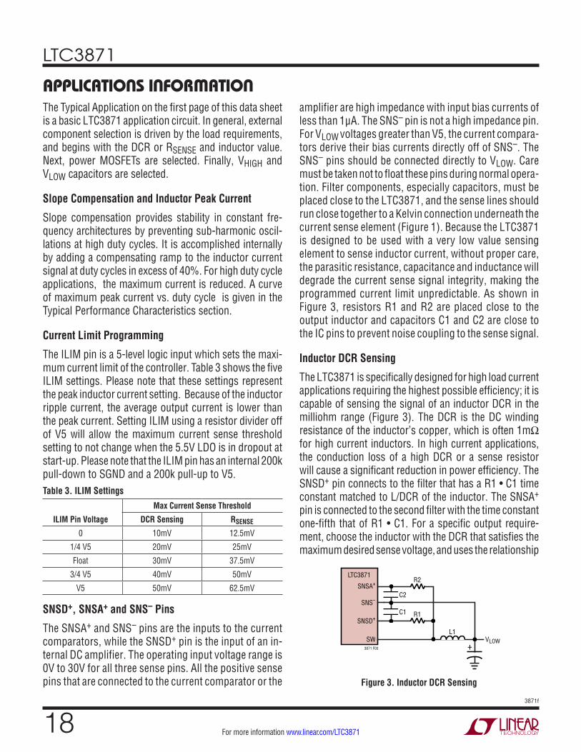
to a DCR sense signal that has a 14dB (5 times) signal-to-noise ratio. Accordingly, the current limit threshold is still a function of the inductor peak-current and its DCR value, and can be accurately set from 10mV to 50mV in 10mV steps with the ILIM pin. The filter time constant, R1 • C1, of the SNSD+ pin should match the L/DCR of the output inductor, while the filter at SNSA+ pin should have a bandwidth of five times larger than SNSD+, R2 • C2 equals R1 • C1/5 (refer to Figure 3).
Current Sensing with Low Value RSENSE
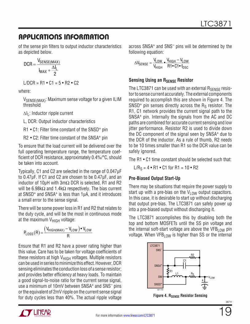
The LTC3871 can also be used with an external low value RSENSE resistor for increased accuracy. To accomplish this, the SNSA+ pin needs a filter time constant R2 • C2 that has a bandwidth that is four times larger than the L/(RSENSE). The SNSD+ pin is now connected to the RSENSE resistor as shown in Figure 1. A small filter cap may be used to filter out high frequency noise (refer to Figure 4).
Figure 1. Sense Lines Placement with Sense Resistor
COUT
TO SENSE FILTER LOCATEDNEXT TO THE CONTROLLER
3871 F01
DRVCC/EXTVCC/V5 Power
Power for the top and bottom MOSFET drivers is derived from the DRVCC pin. The DRVCC voltage can be set to any-where from 6V to 10V in 1V steps using the DRVSET pin. When the EXTVCC pin is left open or tied to a voltage less than (DRVCC – 1V), an internal linear regulator supplies DRVCC power from VHIGH. When EXTVCC is taken above (DRVCC – 500mV), the internal regulator between DRVCC and VHIGH is turned off, and a second internal regulator is turned on between EXTVCC and DRVCC. Each top MOSFET driver is biased from a floating bootstrap capacitor, which normally recharges during each off cycle through an ex-ternal diode when the top MOSFET turns off. If the input voltage, VHIGH, decreases to a voltage close to VLOW, the loop may enter dropout and attempt to turn on the top MOSFET continuously. The dropout detector detects this and forces the top MOSFET off for about one-twelfth of the clock period plus 100ns every fifth cycle to allow the bootstrap capacitor to recharge.
LTC3871
123871f
For more information www.linear.com/LTC3871
Most of the internal circuitry is powered from the V5 rail that is generated by an internal linear regulator from DRVCC. The V5 pin needs to be bypassed with a 2.2µF to 10µF external capacitor between V5 and SGND. This pin provides a 5.5V output that can supply up to 20mA of current. See the Application section for more details.
Soft-Start (Buck Mode)
By default, the start-up of the VLOW voltage is normally controlled by an internal soft-start ramp. The internal soft-start ramp represents a non-inverting input to the error amplifier. The VFBLOW pin is regulated to the lower of the error amplifier’s three non-inverting inputs (the internal soft-start ramp, the SS pin or the internal 1.2V reference). As the ramp voltage rises from 0V to 1.2V over approximately 1ms, the VLOW voltage rises smoothly from its pre-biased value to its final set value. Certain ap-plications can require the start-up of the converter into a non-zero load voltage, where residual charge is stored on the VLOW capacitor at the onset of converter switching. In order to prevent the VLOW from discharging under these conditions, the top and bottom MOSFETs are disabled until soft-start is greater than VFBLOW.
Soft-Start (Boost Mode)
The same internal soft-start capacitor and external soft-start capacitor are also active if the controller starts with boost mode of operation. The error amplifier for boost mode also tries to regulate to the lowest reference during start-up. However, the topology of the boost converter limits the effectiveness of this soft-start mechanism until the boost output voltage reaches its input voltage level. Therefore, it is recommended that the controller starts in buck mode of operation.
Shutdown and Start-Up (RUN and SS Pins)
The LTC3871 can be shut down using the RUN pin. Pulling the RUN pin below 1.14V shuts down the main control loop for the controller and most internal circuits, including the DRVCC and V5 regulators. Releasing the RUN pin allows an internal 2µA current to pull-up the pin and enable the controller. Alternatively, the RUN pin may be externally pulled up or driven directly by logic. Be careful not to ex-ceed the absolute maximum rating of 6V on this pin. The
start-up of the controller’s VLOW voltage is controlled by the voltage on the SS pin. When the voltage on the SS pin is less than the 1.2V internal reference, the LTC3871 regu-lates the VFBLOW voltage to the SS pin voltage instead of the 1.2V reference. This allows the SS pin to be used to program a soft-start by connecting an external capacitor from the SS pin to GND. An internal 1.25µA pull-up current charges this capacitor, creating a voltage ramp on the SS pin. As the SS voltage rises linearly from 0V to 1.2V (and beyond), the VLOW voltage, rises smoothly from zero to its final value. When the RUN pin is pulled low to disable the controller, or when V5 drops below its undervoltage lockout threshold of 4.15V, the SS pin is pulled low by an internal MOSFET. When in undervoltage lockout, the controller is disabled and the external MOSFETs are held off. External circuitry can be added to discharge the soft-start capacitor during fault conditions to ensure a soft-start when the faults are cleared.
Frequency Selection and Phase-Locked Loop (FREQ and SYNC Pins)
The selection of switching frequency is a trade-off between efficiency and component size. Low frequency opera-tion increases efficiency by reducing MOSFET switching losses, but requires larger inductance and/or capacitance to maintain low output ripple voltage.
If the SYNC pin is not being driven by an external clock source, the FREQ pin can be used to program the control-ler’s operating frequency from 50kHz to 500kHz. There is a precision 20µA current flowing out of the FREQ pin so that the user can program the controller’s switching frequency with a single resistor to SGND. A curve is pro-vided later in the Applications Information section showing the relationship between the voltage on the FREQ pin and switching frequency (Figure 7).
A phase-locked loop (PLL) is available on the LTC3871 to synchronize the internal oscillator to an external clock source that is connected to the SYNC pin. The PLL loop filter network is integrated inside the LTC3871. The phase-locked loop is capable of locking any frequency within the range of 60kHz to 460kHz. The frequency setting resistor should always be present to set the controller’s initial switching frequency before locking to the external
OPERATION
LTC3871
133871f
For more information www.linear.com/LTC3871
clock. The controller operates in the user selected mode when it is synchronized.
Multiphase Operation
For output loads that demand high current, multiple LTC3871s can be daisy chained to run out of phase to provide more output current without increasing input and output voltage ripple. The SYNC pin allows the LTC3871 to synchronize to the CLKOUT signal of another LTC3871. The CLKOUT signal can be connected to the SYNC pin of the following LTC3871 stage to line up both the frequency and the phase of the entire system. Tying the PHSMD pin to V5, GND or floating, generates a phase difference (between CH1 and CLKOUT) of 240°, 60° or 90° respec-tively, and a phase difference (between CH1 and CH2) of 120°, 180° or 180°. Tying PHSMD to 1/4 or 3/4 of V5 generates a phase difference of 60° or 45° between CH1 and CLKOUT. Figure 2 shows the PHSMD connections necessary for 3-, 4-, 6-, 8- or 12-phase operation. A total of 12 phases can be daisy chained to run simultaneously out of phase with respect to each other. When paralleling multiple ICs, please be aware of the input impedance of pins connected to the same node.
Undervoltage Lockout
The LTC3871 has two functions that help protect the controller in case of undervoltage conditions. A precision UVLO comparator constantly monitors the V5 voltage to ensure that an adequate voltage is present. It locks out the switching action when V5 is below 4.15V. To prevent oscillation when there is a disturbance on the V5, the UVLO comparator has 500mV of precision hysteresis.
Another way to detect an undervoltage condition is to moni-tor the VHIGH supply. Because the RUN pin has a precision turn-on reference of 1.22V, one can use a resistor divider to VHIGH to turn on the IC when VHIGH is high enough. An extra 4.5µA of current flows out of the RUN pin once the RUN pin voltage passes 1.22V. The RUN comparator itself has about 80mV of hysteresis. Additional hysteresis for the RUN comparator can be programmed by adjust-ing the values of the resistive divider. For accurate VHIGH undervoltage detection, VHIGH needs to be higher than 5V.
Fault Flag (FAULT, OVHIGH, OVLOW and UVHIGH Pins)
The FAULT pin is connected to the open-drain of an internal N-channel MOSFET. It can be pulled high with an external resistor connected to a voltage up to 6V, such as V5 or an external bias voltage. The FAULT pin is pulled low when:
a. The RUN pin is below its turn on threshold.
b. When V5 is below its UVLO threshold.
c. Any of the three OV/UV comparators have been tripped.
d. During a startup sequence until the SS pin charges up past 1.2V.
The OVLOW and OVHIGH thresholds are set using an external resistor dividers off of VLOW and VHIGH, respectively. When the voltage at the pin exceeds the comparator threshold of 1.2V, a 5µA hysteresis current is sourced out of the respective pin and the FAULT signal goes low after a 125µs delay. The UVHIGH threshold is also set using an external resistor divider off VHIGH. When the voltage at the pin falls below the comparator threshold of 1.2V, a 5µA hysteresis current is sunk in to the UVHIGH pin and the FAULT signal goes low after a 125µs delay. The amount of hysteresis can be adjusted by changing the total impedance of the resistor divider, while the resistor ratio sets the UV/OV trip point.
Besides flagging the FAULT pin, the UV/OV comparators also affect the operation of the controller, as shown in Table 1.
When the OVLOW comparator crosses its 1.2V threshold:
a. In buck mode, the controller stops switching.
b. In boost mode, the controller continues to switch.
c. ITH and SS are unaffected in both buck and boost modes. Whenever a fault is detected, discharge the SS pin as needed externally.
When the OVHIGH comparator crosses its 1st threshold of 1.2V:
a. The controller stops switching in both buck and boost modes.
b. ITH and SS are unaffected in both buck and boost modes. Whenever a fault is detected, discharge the SS pin as needed externally.
OPERATION

LTC3871
143871f
For more information www.linear.com/LTC3871
LTC3871
3871 F02a
SYNC
PHSMD
+240CLKOUT
LTC3871
0,120 240,60
SYNC
PHSMD
CLKOUT
V5
LTC3871
3871 F02b
SYNC
PHSMD
+90CLKOUT
LTC3871
0,180 90,270
SYNC
PHSMD
CLKOUT
LTC3871
SYNC
PHSMD
+60CLKOUT
LTC3871
0,180 60,240
SYNC
PHSMD
CLKOUT
3871 F02c
+60
LTC3871
120,300
SYNC
PHSMD
CLKOUT
LTC3871
3871 F02d
SYNC
PHSMD
+90CLKOUT
LTC3871
135,315
LTC3871
SYNC
PHSMD3/4 V5
+45CLKOUT
90,270
LTC3871
SYNC
PHSMD
+90CLKOUT
0,180 225,45
SYNC
PHSMD
CLKOUT
OPERATION
Figure 2a. 3-Phase Operation Figure 2b. 4-Phase Operation
Figure 2c. 6-Phase Operation
Figure 2d. 8-Phase Operation
Figure 2. 12-Phase Operation
LTC3871
SYNC
PHSMD
+60CLKOUT
LTC3871
0,180 60,240
SYNC
PHSMD
CLKOUT+60
LTC3871
120,300
SYNC
PHSMD
CLKOUT
LTC3871
SYNC
PHSMD1/4 V5
+60CLKOUT
LTC3871
150,330 210,30
SYNC
PHSMD
CLKOUT
3871 F02e
+60
LTC3871
270,90
SYNC
PHSMD
CLKOUT
LTC3871
153871f
For more information www.linear.com/LTC3871
OPERATIONWhen the OVHIGH comparator crosses its 2nd threshold of 3V:
a. The controller stops switching in both buck and boost modes.
b. Both ITH and IMON pins are driven into high impedance. This feature allows the users to isolate one LTC3871 from a multiphase system in the case a fault is detected on one particular IC.
c. The SS pin is unaffected.
When the UVHIGH comparator crosses its 1.2V threshold:
a. In buck mode, the controller stops switching after a 125μsec delay and disconnects VHIGH from VLOW with an external P-channel MOSFET via the PGATE pin.
b. In boost mode, the controller continues to switch, but it disconnects VHIGH from VLOW with an external P-channel MOSFET after a 125μsec delay. The voltage at the source side of the P-channel MOSFET is still regulated.
c. ITH and SS are unaffected in both buck and boost modes. Whenever a fault is detected, discharge the SS pin as needed externally.
Input Disconnect (PGATE Pin)
In a typical boost controller, the synchronous diode or the body diode of the synchronous MOSFET conducts current from the input to the output until the output is a diode drop below the input. As a result an output (VHIGH) short will drag the input (VLOW) down without a blocking diode or MOSFET to block the current. The LTC3871 uses an external low RDS(ON) P-channel MOSFET for input short-circuit protection when VHIGH is shorted to ground.
The PGATE pin drives the gate of an external MOSFET between VIN and VHIGH–15V—this pin is internally clamped to VHIGH–15V to protect the gate oxide of the external MOSFET. In normal operation, the P-channel MOSFET is always on, with its gate-source voltage clamped to 15V maximum. When the UVHIGH pin voltage goes below its 1.2V threshold, FAULT goes low 125µs later. At this point, the PGATE pin voltage transitions from VHIGH–15V to VHIGH, turning off the external P-channel MOSFET. The MOSFET needs to be connected such that its body diode will block the current path from VLOW to VHIGH. In buck mode, the switching action stops when PGATE is off and a fault con-dition is reported; In boost mode, the controller will still switch and regulate the programmed boost voltage on the source side of the PGATE. Output cap should be present at the source side of the PGATE. A fault condition is also reported in this case. The external P-channel MOSFET remains disconnected until VHIGH rises high enough to un-trip the UVHIGH comparator.
Current Monitoring and Regulation (IMON, SETCUR Pins)
The inductor current can be sensed using either its DCR or a RSENSE resistor. The current monitoring pin, IMON, outputs a voltage that is proportional to the average induc-tor current of the two channels sensed by the LTC3871. The operational range of IMON is 0.5V to 2.5V. When the average inductor current is zero, the IMON pin voltage rests at 1.25V. As the inductor current increases in buck mode, the IMON voltage proportionally increases. The cur-rent sense signal to IMON gain is 38 for the 10mV, 20mV and 30mV ILIM settings, and 19 for the 40mV and 50mV ILIM settings. An external voltage can be applied to the SETCUR pin to regulate the average output current. Because
Table 1: OV/UV Faults
FAULT MODE SWITCHING ITH PINS IMON SS PGATE PIN
OVLOW 1.2V Threshold
Buck Stops No Effect No Effect No Effect Low
Boost Continues No Effect No Effect No Effect Low
OVHIGH 1.2V Threshold
Buck Stops No Effect No Effect No Effect Low
Boost Stops No Effect No Effect No Effect Low
OVHIGH 3V Threshold
Buck Stops Hi-Z Hi-Z No Effect Low
Boost Stops Hi-Z Hi-Z No Effect Low
UVHIGH 1.2V Threshold
Buck Stops No Effect No Effect No Effect High
Boost Continues No Effect No Effect No Effect High
LTC3871
163871f
For more information www.linear.com/LTC3871
SETCUR and IMON are the two inputs to the current loop gain amplifier with SETCUR acting as the reference, as the IMON pin voltage approaches SETCUR, the ITH pin control is taken over by the current regulation error amplifier from the voltage loop error amplifier.
In boost mode, the inductor current polarity is reversed, so the corresponding IMON and SETCUR ranges are 1.25V to 0.5V with 0.5V being the maximum boost current. The SETCUR pin sources an accurate 7.5µA current in both modes, allowing this voltage to be set with a single resistor for convenience. The SETCUR value defaults to the zero current value internally if the SETCUR pin sees a voltage that is out of range for the selected mode. The valid range of SETCUR is 1.25V to 2.5V for buck mode and 1.25V to 0.5V for boost mode. Therefore, if SETCUR voltage is set below 1.25V in buck mode, the internal SETCUR voltage is forced at 1.25V. If SETCUR voltage is set above 1.25V in boost mode, the internal SETCUR voltage is also forced at 1.25V. For battery charging applications, SETCUR can be programmed dynamically on-the-fly to set the charg-ing currents to the batteries in either buck or boost mode. SETCUR can be used at start-up to limit the in-rush current in both buck mode and boost mode.
Use the following equation to calculate the voltages on IMON:
VIMON = VZERO + K • IOUT • RSENSE/m; Buck Mode
VIMON = VZERO – K • IOUT • RSENSE/m; Boost Mode
Where:
VIMON, the phase current voltage appears on IMON pin;
VZERO, the IMON voltage when average output current is zero; VZERO = 1.25V typically
K = 38 if ILIM = 10mV; 20mV; or 30mV
K = 19 if ILIM = 40mV; or 50mV
IOUT, the total average output current,
RSENSE, the current sensing element value;
m, the number of phases.
To defeat the current programming operation, tie the SETCUR pin to V5 in buck mode and ground the SETCUR pin in boost mode.
Buck and Boost Modes (BUCK Pin)
The LTC3871 can be dynamically and seamlessly switched from buck mode to boost mode and vice versa via the BUCK pin. Tie this pin to V5 to select buck mode and to ground to select boost mode operation. This pin has an internal pull up resistor that defaults to buck mode if left floating. There are two separate error amplifiers for VHIGH or VLOW regulation. Having two error amplifiers allows fine tuning of the loop compensation for the buck and boost modes independently to optimize transient response. When buck mode is selected, the corresponding error amplifier is enabled, and ITHLOW voltage controls the peak inductor current. The other error amplifier is disabled and ITHHIGH is parked at its zero current level. In boost mode, ITHHIGH is enabled while ITHLOW is parked at its zero current level. During a buck to boost or a boost to buck transition, the internal soft-start is reset. Resetting soft-start and parking the ITH pin at the zero current level ensures a smooth transition to the newly selected mode. Refer to Table 2 for a summary.
To further minimize any transients, SETCUR can be programmed to 1.25V or zero current level before switching between boost and buck modes.
Buck Mode Light Load Current Operation (DCM/CCM)
In buck mode, the LTC3871 can be enabled to enter discon-tinuous conduction mode or forced continuous conduction mode. To select forced continuous operation, tie the MODE
OPERATION
Table 2: ITH PIN Parking ConditionsPIN MODE PARKED COMMENTS
ITHHIGH Buck Parked OVHIGH 3V Threshold Overrides Park
Boost Parked in Prebias OVHIGH 3V Threshold Overrides Park
ITHLOW Buck Parked in Prebias OVLOW and OVHIGH 3V Threshold Overrides Park
Boost Parked OVLOW and OVHIGH 3V Threshold Overrides Park
LTC3871
173871f
For more information www.linear.com/LTC3871
pin to GND. To select discontinuous conduction mode of operation, tie the MODE pin to V5 or float it.
In forced continuous operation, the inductor current is allowed to reverse at light loads or under large transient conditions. The peak inductor current is determined by the voltage on the ITHLOW pin, just as in normal operation. In this mode, the efficiency at light loads is lower than in DCM mode operation. However, continuous mode has the advantages of lower output ripple and less interference with audio circuitry.
When the MODE pin is connected to V5 or left floating, the LTC3871 operates in discontinuous conduction mode at light loads. At very light loads, the current comparator, ICMP, may remain tripped for several cycles and force the external top MOSFET to stay off for the same number of cycles (i.e., skipping-pulses). The inductor current is not allowed to reverse (discontinuous operation). This mode, like forced continuous operation, exhibits low output ripple as well as low audio noise and reduced RF interference. It provides higher low current efficiency than forced con-tinuous mode.
Boost Mode Light Load Current Operation (DCM/CCM)
In boost mode, the LTC3871 can be enabled to enter constant-frequency discontinuous conduction mode or forced continuous conduction mode. To select forced-continuous operation, tie the MODE pin to GND or float
it. To select discontinuous conduction mode of operation, tie the MODE pin to V5.
In forced continuous operation, the inductor current is allowed to reverse at light loads or under large transient conditions. The inductor current valley is determined by the voltage on the ITHHIGH pin, just as in normal opera-tion. In this mode, the efficiency at light loads is lower. However, continuous mode has the advantages of lower output ripple.
When the MODE pin is connected to V5, the LTC3871 oper-ates with the synchronous N-channel MOSFET disabled, using the body diode of the MOSFET as the synchronous diode to reduce switching losses, and prevent reverse current. To reduce the MOSFET heat dissipation in this mode, parallel Schottky diodes are recommended.
Thermal Shutdown
The LTC3871 has a temperature sensor integrated on the IC, to sense the die temperature near the gate driver circuits. When the die temperature exceeds 175°C, all switching actions stop, and the driver gate pins are held low, thus turning off all external MOSFETs. At the same time, the channels are disconnected from the IMON pins, and SS and ITHHIGH/ITHLOW pins continue to function normally, so as not to interfere with other LTC3871 chips that may reference the common pins. When the temperature drops 10°C below the trip threshold, normal operation resumes.
OPERATION
LTC3871
183871f
For more information www.linear.com/LTC3871
The Typical Application on the first page of this data sheet is a basic LTC3871 application circuit. In general, external component selection is driven by the load requirements, and begins with the DCR or RSENSE and inductor value. Next, power MOSFETs are selected. Finally, VHIGH and VLOW capacitors are selected.
Slope Compensation and Inductor Peak Current
Slope compensation provides stability in constant fre-quency architectures by preventing sub-harmonic oscil-lations at high duty cycles. It is accomplished internally by adding a compensating ramp to the inductor current signal at duty cycles in excess of 40%. For high duty cycle applications, the maximum current is reduced. A curve of maximum peak current vs. duty cycle is given in the Typical Performance Characteristics section.
Current Limit Programming
The ILIM pin is a 5-level logic input which sets the maxi-mum current limit of the controller. Table 3 shows the five ILIM settings. Please note that these settings represent the peak inductor current setting. Because of the inductor ripple current, the average output current is lower than the peak current. Setting ILIM using a resistor divider off of V5 will allow the maximum current sense threshold setting to not change when the 5.5V LDO is in dropout at start-up. Please note that the ILIM pin has an internal 200k pull-down to SGND and a 200k pull-up to V5.Table 3. ILIM Settings
ILIM Pin Voltage
Max Current Sense Threshold
DCR Sensing RSENSE
0 10mV 12.5mV
1/4 V5 20mV 25mV
Float 30mV 37.5mV
3/4 V5 40mV 50mV
V5 50mV 62.5mV
SNSD+, SNSA+ and SNS– Pins
The SNSA+ and SNS– pins are the inputs to the current comparators, while the SNSD+ pin is the input of an in-ternal DC amplifier. The operating input voltage range is 0V to 30V for all three sense pins. All the positive sense pins that are connected to the current comparator or the
amplifier are high impedance with input bias currents of less than 1μA. The SNS– pin is not a high impedance pin. For VLOW voltages greater than V5, the current compara-tors derive their bias currents directly off of SNS–. The SNS– pins should be connected directly to VLOW. Care must be taken not to float these pins during normal opera-tion. Filter components, especially capacitors, must be placed close to the LTC3871, and the sense lines should run close together to a Kelvin connection underneath the current sense element (Figure 1). Because the LTC3871 is designed to be used with a very low value sensing element to sense inductor current, without proper care, the parasitic resistance, capacitance and inductance will degrade the current sense signal integrity, making the programmed current limit unpredictable. As shown in Figure 3, resistors R1 and R2 are placed close to the output inductor and capacitors C1 and C2 are close to the IC pins to prevent noise coupling to the sense signal.
Inductor DCR Sensing
The LTC3871 is specifically designed for high load current applications requiring the highest possible efficiency; it is capable of sensing the signal of an inductor DCR in the milliohm range (Figure 3). The DCR is the DC winding resistance of the inductor’s copper, which is often 1mΩ for high current inductors. In high current applications, the conduction loss of a high DCR or a sense resistor will cause a significant reduction in power efficiency. The SNSD+ pin connects to the filter that has a R1 • C1 time constant matched to L/DCR of the inductor. The SNSA+ pin is connected to the second filter with the time constant one-fifth that of R1 • C1. For a specific output require-ment, choose the inductor with the DCR that satisfies the maximum desired sense voltage, and uses the relationship
Figure 3. Inductor DCR Sensing
VLOW
L1
LTC3871
SNS–
SNSD+
SW
SNSA+ R2
R1C1
C2
+3871 F03
APPLICATIONS INFORMATION
LTC3871
193871f
For more information www.linear.com/LTC3871
across SNSA+ and SNS– pins will be determined by the following equation:
∆VSENSE =
VLOWVHIGH
•VHIGH – VLOWR1• C1• fOSC
Sensing Using an RSENSE Resistor
The LTC3871 can be used with an external RSENSE resis-tor to sense current accurately. The external components required to accomplish this are shown in Figure 4. The SNSD+ pin senses directly across the RS resistor. The R1, C1 network provides the current signal path to the SNSA+ pin. Internally the signals from the AC and DC paths are combined for accurate current sensing and low jitter performance. Resistor R2 is used to divide down the DC component of the signal seen by SNSA+ due to the DCR of the inductor. As a rule of thumb, R2 needs to be 10 times smaller than R1 so the DCR value can be safely ignored.
The R1 • C1 time constant should be selected such that:
L/RS = 4 • R1 • C1 for R1 = 10 • R2
Pre-Biased Output Start-Up
There may be situations that require the power supply to start up with a pre-bias on the VLOW output capacitors. In this case, it is desirable to start up without discharging that output pre-bias. The LTC3871 can safely power up into a pre-biased output without discharging it.
The LTC3871 accomplishes this by disabling both the top and bottom MOSFETs until the SS pin voltage and the internal soft-start voltage are above the VFBLOW pin voltage. When VFBLOW is higher than SS or the internal
APPLICATIONS INFORMATION
Figure 4. RSENSE Resistor Sensing
VLOW
L1
LTC3871
SNSA+
SW
SNSD+
SNS–
RSR1
+
R2
C1
3871 F04
of the sense pin filters to output inductor characteristics as depicted below.
DCR =VSENSE(MAX)
IMAX + ∆IL2
L/DCR = R1 • C1 = 5 • R2 • C2
where:
VSENSE(MAX): Maximum sense voltage for a given ILIM threshold
∆IL: Inductor ripple current
L, DCR: Output inductor characteristics
R1 • C1: Filter time constant of the SNSD+ pin
R2 • C2: Filter time constant of the SNSA+ pin
To ensure that the load current will be delivered over the full operating temperature range, the temperature coef-ficient of DCR resistance, approximately 0.4%/°C, should be taken into account.
Typically, C1 and C2 are selected in the range of 0.047μF to 0.47μF. If C1 and C2 are chosen to be 0.47μF, and an inductor of 10μH with 3mΩ DCR is selected, R1 and R2 will be 6.98kΩ and 1.4kΩ respectively. The bias current at SNSD+ and SNSA+ is less than 1μA, and it introduces a small error to the sense signal.
There will be some power loss in R1 and R2 that relates to the duty cycle, and will be the most in continuous mode at the maximum VHIGH voltage:
PLOSS R( ) =
VHIGH(MAX) – VLOW( ) • VLOW
R
Ensure that R1 and R2 have a power rating higher than this value. Care has to be taken for voltage coefficients of these resistors at high VHIGH voltages. Multiple resistors can be used in series to minimize this effect. However, DCR sensing eliminates the conduction loss of a sense resistor; and provides better efficiency at heavy loads. To maintain a good signal-to-noise ratio for the current sense signal, use a minimum of 10mV between SNSA+ and SNS– pins or the equivalent of 2mV ripple on the current sense signal for duty cycles less than 40%. The actual ripple voltage
LTC3871
203871f
For more information www.linear.com/LTC3871
APPLICATIONS INFORMATIONsoft-start voltage, the error amp output is parked at its zero current level. Disabling both top and bottom MOS-FETs prevents the pre-biased output voltage from being discharged. When SS and the internal soft-start both cross 1.32V or VFB, whichever is lower, both top and bottom MOSFETs are enabled.
Buck Mode Overcurrent Fault
When the output of the power supply is loaded beyond its preset current limit, the regulated output voltage will collapse depending on the load. The VLOW rail may be shorted to ground through a very low impedance path or it may be a resistive short, in which case the output will collapse partially, until the load current equals the preset current limit. The controller will continue to source current into the short. The amount of current sourced depends on the ILIM pin setting and the VFBLOW voltage as shown in the Current Foldback graph in the Typical Performance Characteristics section.
Upon removal of the short, VLOW soft starts using the internal soft-start, thus reducing output overshoot. In the absence of this feature, the output capacitors would have been charged at current limit, and in applications with minimal output capacitance this may have resulted in output overshoot. Current limit foldback is not disabled during an overcurrent recovery. The load must drop below the folded back current limit threshold in order to restart from a hard short.
Boost Mode Overcurrent Fault
When in boost mode, if the overcurrent situation persists and discharges VHIGH below the preset UVHIGH trip point, The PGATE pin turns off the external disconnect P-channel MOSFET, preventing VLOW from getting discharged via the top MOSFET body diode. For both buck and boost mode of operation, current regulation loop can be used to limit the current by forcing a voltage on SETCUR pin. The zero average inductor current can be obtained by forcing 1.25V on SETCUR. If the SETCUR voltage is set to an invalid range for the selected mode of operation, the effective SETCUR voltage is internally set to 1.25V.
One way of protecting against an input VHIGH soft short in boost mode is to monitor the IMON voltage. If the IMON
voltage indicates excessive current, an external circuit can be added to simulate an UV condition at the input and turn off PGATE.
Inductor Value Calculation
Given the desired input and output voltages, the inductor value and operating frequency, fOSC, directly determine the inductor’s peak-to-peak ripple current:
IRIPPLE =
VLOWVHIGH
VHIGH – VLOWfOSC •L
Lower ripple current reduces core losses in the inductor, ESR losses in the output capacitors, and output voltage ripple. Thus, highest efficiency operation is obtained at low frequency with a small ripple current. Achieving this, however, requires a large inductor.
A reasonable starting point is to choose a ripple current that is about 40% of the maximum inductor current. Note that the largest ripple current occurs at the highest VHIGH voltage. To guarantee that ripple current does not exceed a specified maximum, the inductor should be chosen according to:
L ≥
VHIGH – VLOWfOSC •IRIPPLE
•VLOWVHIGH
Inductor Core Selection
Once the inductance value is determined, the type of in-ductor must be selected. Core loss is independent of core size for a fixed inductor value, but it is very dependent on inductance selected. As inductance increases, core losses go down. Unfortunately, increased inductance requires more turns of wire and therefore copper losses will increase.
Ferrite designs have very low core loss and are preferred at high switching frequencies, so design goals can con-centrate on copper loss and preventing saturation. Ferrite core material saturates “hard,” which means that induc-tance collapses abruptly when the peak design current is exceeded. This results in an abrupt increase in inductor ripple current and consequent output voltage ripple. Do not allow the core to saturate!
LTC3871
213871f
For more information www.linear.com/LTC3871
APPLICATIONS INFORMATIONPower MOSFET and Schottky Diode (Optional) Selection
At least two external power MOSFETs need to be selected: One N-channel MOSFET for the top switch and one or more N-channel MOSFET(s) for the bottom switch. The number, type and on-resistance of all MOSFETs selected take into account the voltage step-down ratio as well as the actual position (main or synchronous) in which the MOSFET will be used. A much smaller and much lower input capacitance MOSFET should be used for the top MOSFET in applications that have an VLOW that is less than one-third of VHIGH. In applications where VHIGH >> VLOW, the top MOSFETs’ on-resistance is normally less important for overall efficiency than its input capacitance at operating frequencies above 300kHz. MOSFET manufacturers have designed special purpose devices that provide reasonably low on-resistance with significantly reduced input capacitance for the main switch application in switching regulators.
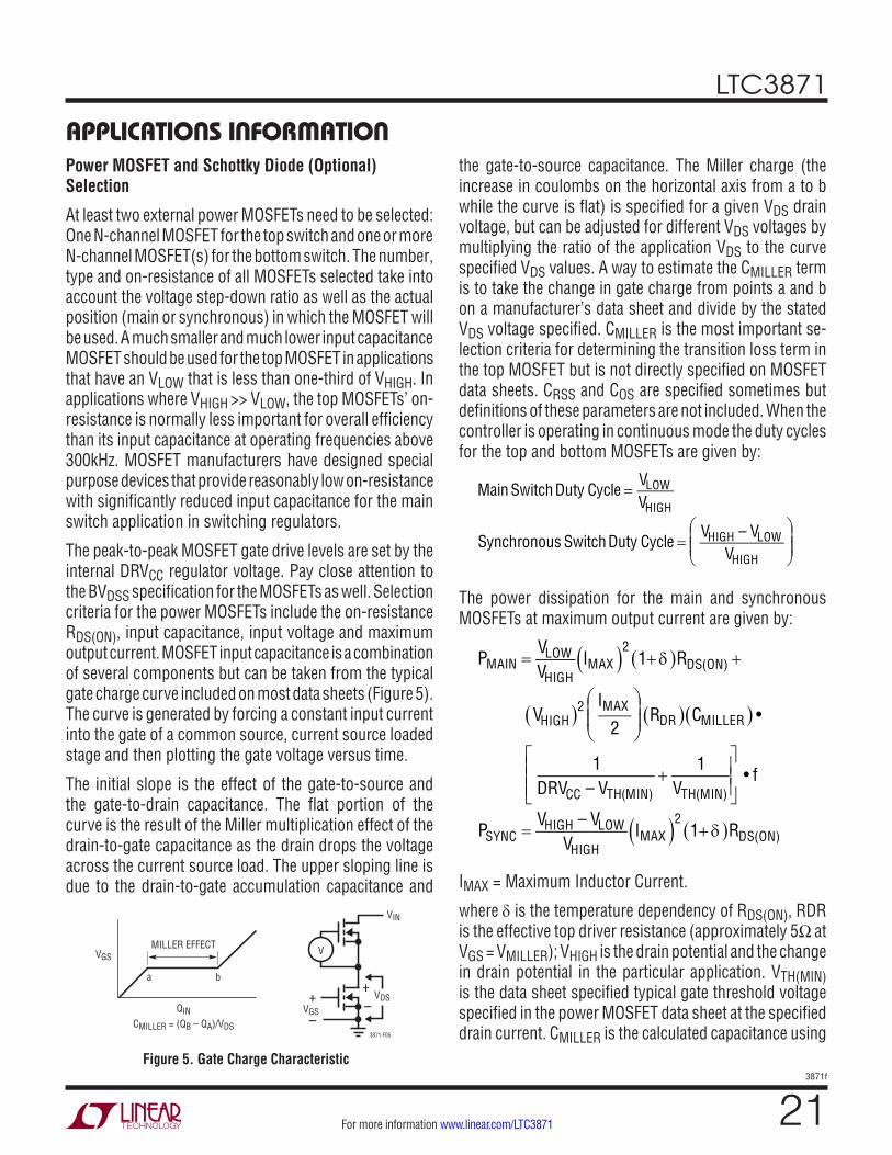
The peak-to-peak MOSFET gate drive levels are set by the internal DRVCC regulator voltage. Pay close attention to the BVDSS specification for the MOSFETs as well. Selection criteria for the power MOSFETs include the on-resistance RDS(ON), input capacitance, input voltage and maximum output current. MOSFET input capacitance is a combination of several components but can be taken from the typical gate charge curve included on most data sheets (Figure 5). The curve is generated by forcing a constant input current into the gate of a common source, current source loaded stage and then plotting the gate voltage versus time.
The initial slope is the effect of the gate-to-source and the gate-to-drain capacitance. The flat portion of the curve is the result of the Miller multiplication effect of the drain-to-gate capacitance as the drain drops the voltage across the current source load. The upper sloping line is due to the drain-to-gate accumulation capacitance and
the gate-to-source capacitance. The Miller charge (the increase in coulombs on the horizontal axis from a to b while the curve is flat) is specified for a given VDS drain voltage, but can be adjusted for different VDS voltages by multiplying the ratio of the application VDS to the curve specified VDS values. A way to estimate the CMILLER term is to take the change in gate charge from points a and b on a manufacturer’s data sheet and divide by the stated VDS voltage specified. CMILLER is the most important se-lection criteria for determining the transition loss term in the top MOSFET but is not directly specified on MOSFET data sheets. CRSS and COS are specified sometimes but definitions of these parameters are not included. When the controller is operating in continuous mode the duty cycles for the top and bottom MOSFETs are given by:
Main SwitchDuty Cycle =VLOWVHIGH
Synchronous SwitchDuty Cycle =VHIGH – VLOW
VHIGH
The power dissipation for the main and synchronous MOSFETs at maximum output current are given by:
PMAIN =VLOWVHIGH
IMAX( )21+ δ( )RDS(ON) +
VHIGH( )2 IMAX
2
RDR( ) CMILLER( ) •
1DRVCC – VTH(MIN)
+1
VTH(MIN)
• f
PSYNC =VHIGH – VLOW
VHIGHIMAX( )2
1+ δ( )RDS(ON)
IMAX = Maximum Inductor Current.
where δ is the temperature dependency of RDS(ON), RDR is the effective top driver resistance (approximately 5Ω at VGS = VMILLER); VHIGH is the drain potential and the change in drain potential in the particular application. VTH(MIN) is the data sheet specified typical gate threshold voltage specified in the power MOSFET data sheet at the specified drain current. CMILLER is the calculated capacitance using
Figure 5. Gate Charge Characteristic
+–
VDS
VIN
3871 F05
VGS
MILLER EFFECT
QIN
a b
CMILLER = (QB – QA)/VDS
VGSV
+
–
LTC3871
223871f
For more information www.linear.com/LTC3871
APPLICATIONS INFORMATIONthe gate charge curve from the MOSFET data sheet and the technique described above.
Both MOSFETs have I2R losses while the topside N-channel equation includes an additional term for transition losses, which peak at the highest input voltage. The bottom MOS-FET losses are greatest at high VHIGH voltage when the top switch duty factor is low or during a VLOW short-circuit when the bottom switch is on close to 100% of the period.
The term (1 + δ) is generally given for a MOSFET in the form of a normalized RDS(ON) vs temperature curve, but δ = 0.005/°C can be used as an approximation for low voltage MOSFETs.
An optional Schottky diode across the bottom MOSFET conducts during the dead time between the conduction of the two large power MOSFETs in buck mode. This pre-vents the body diode of the bottom MOSFET from turning on, storing charge during the dead time and requiring a reverse-recovery period which could cost as much as sev-eral percent in efficiency. A 2A to 8A Schottky is generally a good compromise for both regions of operation due to the relatively small average current. Larger diodes result in additional transition loss due to their larger junction capacitance.
An optional Schottky diode across the top MOSFET is also recommended for Boost DCM operation. This will increase efficiency and reduce heat dissipation for large output currents.
CHIGH and MOSFETs Selection (on VHIGH and VLOW)
In continuous mode, the source current of the top MOSFET is a square wave of duty cycle (VLOW)/(VHIGH). To prevent large voltage transients, a low ESR capacitor sized for the maximum RMS current of one channel must be used. In the following discussion, it is assumed that CIN is CHIGH, COUT is CLOW, VIN is VHIGH, and VOUT is VLOW. The maximum RMS capacitor current is given by:
CIN Required IRMS ≈
IMAXVIN
VOUT( ) VIN – VOUT( )
1/2
This formula has a maximum at VIN = 2VOUT, where IRMS = IOUT/2. This simple worst-case condition is commonly used for design because even significant deviations do not
offer much relief. Note that capacitor manufacturers’ ripple current ratings are often based on only 2000 hours of life.
This makes it advisable to further de-rate the capacitor, or to choose a capacitor rated at a higher temperature than required. Several capacitors may be paralleled to meet size or height requirements in the design. Ceramic capacitors can also be used for CIN. Always consult the manufacturer if there is any question.
Ceramic capacitors are becoming very popular for small designs but several cautions should be observed. X7R, X5R and Y5V are examples of a few of the ceramic materials used as the dielectric layer, and these different dielectrics have very different effect on the capacitance value due to the voltage and temperature conditions applied. Physically, if the capacitance value changes due to applied voltage change, there is a concomitant piezo effect which results in radiating sound! A load that draws varying current at an audible rate may cause an attendant varying input voltage on a ceramic capacitor, resulting in an audible signal. A secondary issue relates to the energy flowing back into a ceramic capacitor whose capacitance value is being reduced by the increasing charge. The voltage can increase at a considerably higher rate than the constant current being supplied because the capacitance value is decreasing as the voltage is increasing! Nevertheless, ceramic capacitors, when properly selected and used, can provide the lowest overall loss due to their extremely low ESR.
A small (0.1μF to 1μF) bypass capacitor, CIN, between the chip VIN pin and ground, placed close to the LTC3871, is also suggested. A 2.2Ω to 10Ω resistor placed between CIN and VIN pin provides further isolation.
The selection of COUT at VOUT is driven by the required effective series resistance (ESR). Typically once the ESR requirement is satisfied the capacitance is adequate for filtering. The steady-state output ripple (∆VOUT) is deter-mined by:
∆VOUT ≈ ∆IRIPPLE ESR+ 1
8fCOUT
where f = operating frequency, COUT = output capacitance and ∆IRIPPLE = ripple current in the inductor. The output ripple is highest at maximum input voltage since ∆IRIPPLE
LTC3871
233871f
For more information www.linear.com/LTC3871
APPLICATIONS INFORMATIONincreases with input voltage (VHIGH). The output ripple will be less than 50mV at maximum VIN with ∆IRIPPLE = 0.4IOUT(MAX) assuming:
COUT required ESR < N • RSENSE
and
COUT > 1
8f( ) RSENSE( )
The emergence of very low ESR capacitors in small, surface mount packages makes very small physical implementa-tions possible. The ability to externally compensate the switching regulator loop using the ITH pin allows a much wider selection of output capacitor types. The impedance characteristic of each capacitor type is significantly differ-ent than an ideal capacitor and therefore requires accurate modeling or bench evaluation during design. Manufacturers such as Nichicon, Nippon Chemi-Con and Sanyo should be considered for high performance through-hole capacitors. The OS-CON semiconductor dielectric capacitors available from Sanyo and the Panasonic SP surface mount types have a good (ESR)(size) product.
Once the ESR requirement for COUT has been met, the RMS current rating generally far exceeds the IRIPPLE(P-P) require-ment. Ceramic capacitors from AVX, Taiyo Yuden, Murata and TDK offer high capacitance value and very low ESR, especially applicable for low output voltage applications.
In surface mount applications, multiple capacitors may have to be paralleled to meet the ESR or RMS current handling requirements of the application. Aluminum electrolytic and dry tantalum capacitors are both available in surface mount configurations. New special polymer surface mount capacitors offer very low ESR also but have much lower capacitive density per unit volume. In the case of tantalum, it is critical that the capacitors are surge tested for use in switching power supplies. Several excellent choices are the AVX TPS, AVX TPSV, the KEMET T510 series of surface mount tantalums or the Panasonic SP series of surface mount special polymer capacitors available in case heights ranging from 2mm to 4mm. Other capacitor types include Sanyo POSCAP, Sanyo OS-CON, Nichicon PL series and Sprague 595D series. Consult the manufacturers for other specific recommendations.
CHIGH Capacitor Selection for Boost Operation
Contributions of ESR (equivalent series resistance), ESL (equivalent series inductance) and the bulk capacitance must be considered when choosing the correct combina-tion of output capacitors for a boost converter application.
The choice of component(s) begins with the maximum acceptable ripple voltage (expressed as a percentage of the output voltage), and how this ripple should be divided between the ESR step and the charging/discharging ∆V. For the purpose of simplicity we will choose 2% for the maximum output ripple, to be divided equally between the ESR step and the charging/discharging ∆V. This percent-age ripple will change, depending on the requirements of the application, and the equations provided below can easily be modified.
One of the key benefits of multiphase operation is a reduc-tion in the peak current supplied to the output capacitor by the boost diodes. As a result, the ESR requirement of the capacitor is relaxed. For a 1% contribution to the total ripple voltage, the ESR of the output capacitor can be determined using the following equation:
ESR
VICOUT
OUT
D PEAK≤
0 01. •
( )
where:
I
n
I
DD PEAKO MAX
MAX( )
( )• •–
= +
11
2 1χ
The factor n represents the number of phases and the factor χ represents the percentage inductor ripple current.
For the bulk capacitance, which we assume contributes 1% to the total output ripple, the minimum required ca-pacitance is approximately:
C
I
n V fOUTO MAX
OUT≥ ( )
. • • •0 01
For many designs it will be necessary to use one type of capacitor to obtain the required ESR, and another type to satisfy the bulk capacitance. For example, using a low ESR ceramic capacitor can minimize the ESR step,
LTC3871
243871f
For more information www.linear.com/LTC3871
while an electrolytic capacitor can be used to supply the required bulk C.
The voltage rating of the output capacitor must be greater than the maximum output voltage, with sufficient derating to account for the maximum capacitor temperature.
Because the ripple current in the output capacitor is a square wave, the ripple current requirements for this capacitor depend on the duty cycle, the number of phases and the maximum output current. In order to choose a ripple current rating for the output capacitor, first establish the duty cycle range, based on the output voltage and range of input voltage.
The output ripple current is divided between the various capacitors connected in parallel at the output voltage. Although ceramic capacitors are generally known for low ESR (especially X5R and X7R), these capacitors suffer from a relatively high voltage coefficient. Therefore, it is not safe to assume that the entire ripple current flows in the ceramic capacitor. Aluminum electrolytic capacitors are generally chosen because of their high bulk capacitance, but they have a relatively high ESR. As a result, some amount of ripple current will flow in this capacitor. If the ripple cur-rent flowing into a capacitor exceeds its RMS rating, the capacitor will heat up, reducing its effective capacitance and adversely affecting its reliability. After the output capacitor configuration has been determined using the equations provided, measure the individual capacitor case temperatures in order to verify good thermal performance.
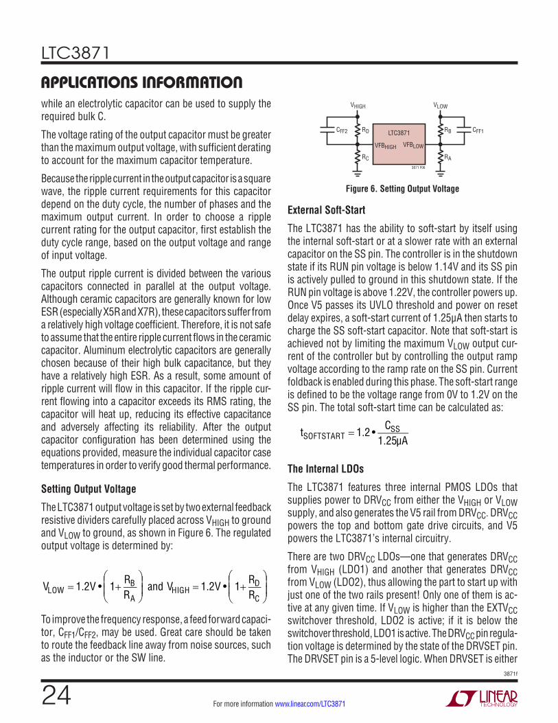
Setting Output Voltage
The LTC3871 output voltage is set by two external feedback resistive dividers carefully placed across VHIGH to ground and VLOW to ground, as shown in Figure 6. The regulated output voltage is determined by:
VLOW = 1.2V • 1+
RBRA
and VHIGH = 1.2V • 1+
RDRC
To improve the frequency response, a feed forward capaci-tor, CFF1/CFF2, may be used. Great care should be taken to route the feedback line away from noise sources, such as the inductor or the SW line.
External Soft-Start
The LTC3871 has the ability to soft-start by itself using the internal soft-start or at a slower rate with an external capacitor on the SS pin. The controller is in the shutdown state if its RUN pin voltage is below 1.14V and its SS pin is actively pulled to ground in this shutdown state. If the RUN pin voltage is above 1.22V, the controller powers up. Once V5 passes its UVLO threshold and power on reset delay expires, a soft-start current of 1.25μA then starts to charge the SS soft-start capacitor. Note that soft-start is achieved not by limiting the maximum VLOW output cur-rent of the controller but by controlling the output ramp voltage according to the ramp rate on the SS pin. Current foldback is enabled during this phase. The soft-start range is defined to be the voltage range from 0V to 1.2V on the SS pin. The total soft-start time can be calculated as:
tSOFTSTART = 1.2 •
CSS1.25µA
The Internal LDOs
The LTC3871 features three internal PMOS LDOs that supplies power to DRVCC from either the VHIGH or VLOW supply, and also generates the V5 rail from DRVCC. DRVCC powers the top and bottom gate drive circuits, and V5 powers the LTC3871’s internal circuitry.
There are two DRVCC LDOs—one that generates DRVCC from VHIGH (LDO1) and another that generates DRVCC from VLOW (LDO2), thus allowing the part to start up with just one of the two rails present! Only one of them is ac-tive at any given time. If VLOW is higher than the EXTVCC switchover threshold, LDO2 is active; if it is below the switchover threshold, LDO1 is active. The DRVCC pin regula-tion voltage is determined by the state of the DRVSET pin. The DRVSET pin is a 5-level logic. When DRVSET is either
APPLICATIONS INFORMATION
Figure 6. Setting Output Voltage
VHIGH
RDCFF2
RC
LTC3871
VFBLOW
VLOW
RB CFF1
RA3871 F06
VFBHIGH
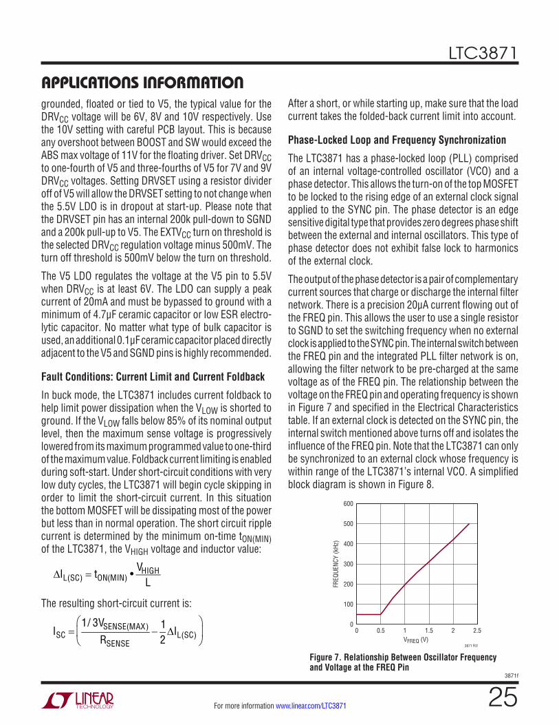
LTC3871
253871f
For more information www.linear.com/LTC3871
grounded, floated or tied to V5, the typical value for the DRVCC voltage will be 6V, 8V and 10V respectively. Use the 10V setting with careful PCB layout. This is because any overshoot between BOOST and SW would exceed the ABS max voltage of 11V for the floating driver. Set DRVCC to one-fourth of V5 and three-fourths of V5 for 7V and 9V DRVCC voltages. Setting DRVSET using a resistor divider off of V5 will allow the DRVSET setting to not change when the 5.5V LDO is in dropout at start-up. Please note that the DRVSET pin has an internal 200k pull-down to SGND and a 200k pull-up to V5. The EXTVCC turn on threshold is the selected DRVCC regulation voltage minus 500mV. The turn off threshold is 500mV below the turn on threshold.
The V5 LDO regulates the voltage at the V5 pin to 5.5V when DRVCC is at least 6V. The LDO can supply a peak current of 20mA and must be bypassed to ground with a minimum of 4.7μF ceramic capacitor or low ESR electro-lytic capacitor. No matter what type of bulk capacitor is used, an additional 0.1μF ceramic capacitor placed directly adjacent to the V5 and SGND pins is highly recommended.
Fault Conditions: Current Limit and Current Foldback
In buck mode, the LTC3871 includes current foldback to help limit power dissipation when the VLOW is shorted to ground. If the VLOW falls below 85% of its nominal output level, then the maximum sense voltage is progressively lowered from its maximum programmed value to one-third of the maximum value. Foldback current limiting is enabled during soft-start. Under short-circuit conditions with very low duty cycles, the LTC3871 will begin cycle skipping in order to limit the short-circuit current. In this situation the bottom MOSFET will be dissipating most of the power but less than in normal operation. The short circuit ripple current is determined by the minimum on-time tON(MIN) of the LTC3871, the VHIGH voltage and inductor value:
∆IL(SC) = tON(MIN) •
VHIGHL
The resulting short-circuit current is:
ISC =
1/ 3VSENSE(MAX)
RSENSE− 1
2∆IL(SC)
APPLICATIONS INFORMATIONAfter a short, or while starting up, make sure that the load current takes the folded-back current limit into account.
Phase-Locked Loop and Frequency Synchronization
The LTC3871 has a phase-locked loop (PLL) comprised of an internal voltage-controlled oscillator (VCO) and a phase detector. This allows the turn-on of the top MOSFET to be locked to the rising edge of an external clock signal applied to the SYNC pin. The phase detector is an edge sensitive digital type that provides zero degrees phase shift between the external and internal oscillators. This type of phase detector does not exhibit false lock to harmonics of the external clock.
The output of the phase detector is a pair of complementary current sources that charge or discharge the internal filter network. There is a precision 20μA current flowing out of the FREQ pin. This allows the user to use a single resistor to SGND to set the switching frequency when no external clock is applied to the SYNC pin. The internal switch between the FREQ pin and the integrated PLL filter network is on, allowing the filter network to be pre-charged at the same voltage as of the FREQ pin. The relationship between the voltage on the FREQ pin and operating frequency is shown in Figure 7 and specified in the Electrical Characteristics table. If an external clock is detected on the SYNC pin, the internal switch mentioned above turns off and isolates the influence of the FREQ pin. Note that the LTC3871 can only be synchronized to an external clock whose frequency is within range of the LTC3871’s internal VCO. A simplified block diagram is shown in Figure 8.
Figure 7. Relationship Between Oscillator Frequency and Voltage at the FREQ Pin
VFREQ (V)0 0.5 1 1.5 2 2.5
0
100
200
300
400
500
600
FREQ
UENC
Y (k
Hz)
Oscillator Fequency vs Vosc
3871 F07
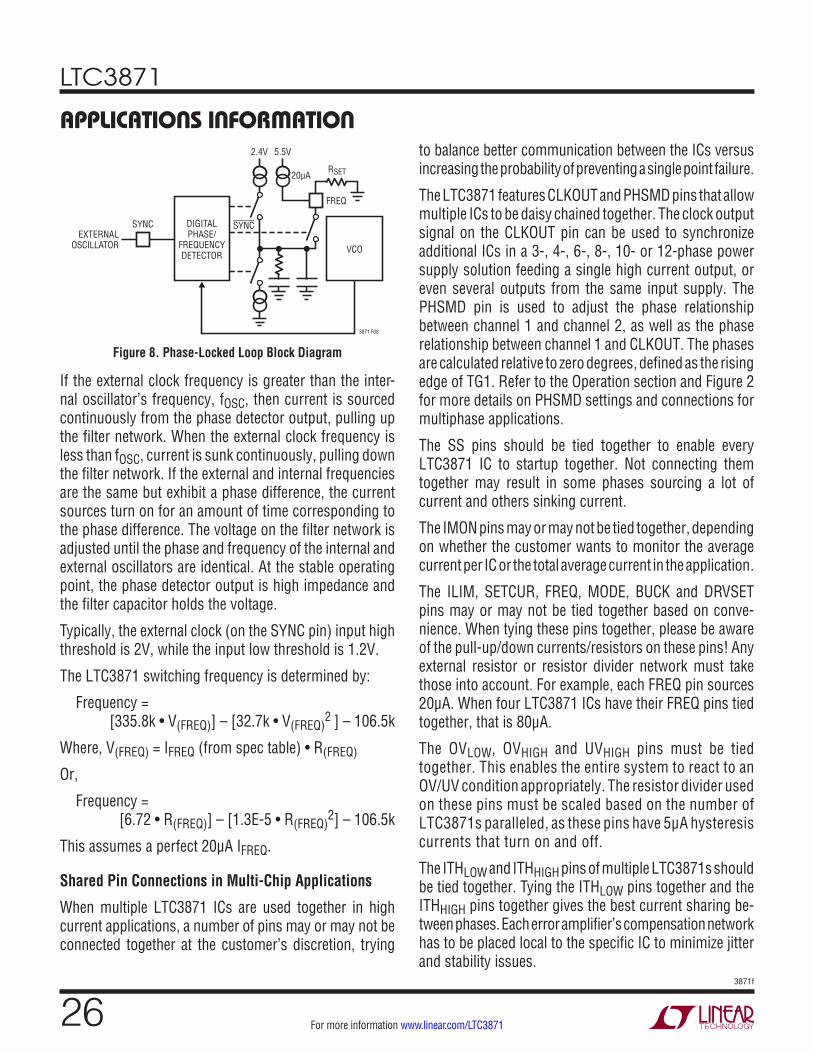
LTC3871
263871f
For more information www.linear.com/LTC3871
If the external clock frequency is greater than the inter-nal oscillator’s frequency, fOSC, then current is sourced continuously from the phase detector output, pulling up the filter network. When the external clock frequency is less than fOSC, current is sunk continuously, pulling down the filter network. If the external and internal frequencies are the same but exhibit a phase difference, the current sources turn on for an amount of time corresponding to the phase difference. The voltage on the filter network is adjusted until the phase and frequency of the internal and external oscillators are identical. At the stable operating point, the phase detector output is high impedance and the filter capacitor holds the voltage.
Typically, the external clock (on the SYNC pin) input high threshold is 2V, while the input low threshold is 1.2V.
The LTC3871 switching frequency is determined by:
Frequency = [335.8k • V(FREQ)] – [32.7k • V(FREQ)
2 ] – 106.5k
Where, V(FREQ) = IFREQ (from spec table) • R(FREQ)
Or,
Frequency = [6.72 • R(FREQ)] – [1.3E-5 • R(FREQ)
2] – 106.5k
This assumes a perfect 20μA IFREQ.
Shared Pin Connections in Multi-Chip Applications
When multiple LTC3871 ICs are used together in high current applications, a number of pins may or may not be connected together at the customer’s discretion, trying
to balance better communication between the ICs versus increasing the probability of preventing a single point failure.
The LTC3871 features CLKOUT and PHSMD pins that allow multiple ICs to be daisy chained together. The clock output signal on the CLKOUT pin can be used to synchronize additional ICs in a 3-, 4-, 6-, 8-, 10- or 12-phase power supply solution feeding a single high current output, or even several outputs from the same input supply. The PHSMD pin is used to adjust the phase relationship between channel 1 and channel 2, as well as the phase relationship between channel 1 and CLKOUT. The phases are calculated relative to zero degrees, defined as the rising edge of TG1. Refer to the Operation section and Figure 2 for more details on PHSMD settings and connections for multiphase applications.
The SS pins should be tied together to enable every LTC3871 IC to startup together. Not connecting them together may result in some phases sourcing a lot of current and others sinking current.
The IMON pins may or may not be tied together, depending on whether the customer wants to monitor the average current per IC or the total average current in the application.
The ILIM, SETCUR, FREQ, MODE, BUCK and DRVSET pins may or may not be tied together based on conve-nience. When tying these pins together, please be aware of the pull-up/down currents/resistors on these pins! Any external resistor or resistor divider network must take those into account. For example, each FREQ pin sources 20μA. When four LTC3871 ICs have their FREQ pins tied together, that is 80μA.
The OVLOW, OVHIGH and UVHIGH pins must be tied together. This enables the entire system to react to an OV/UV condition appropriately. The resistor divider used on these pins must be scaled based on the number of LTC3871s paralleled, as these pins have 5μA hysteresis currents that turn on and off.
The ITHLOW and ITHHIGH pins of multiple LTC3871s should be tied together. Tying the ITHLOW pins together and the ITHHIGH pins together gives the best current sharing be-tween phases. Each error amplifier’s compensation network has to be placed local to the specific IC to minimize jitter and stability issues.
APPLICATIONS INFORMATION
Figure 8. Phase-Locked Loop Block Diagram
DIGITALPHASE/
FREQUENCYDETECTOR
VCO
2.4V 5.5V
20µARSET
3871 F08
FREQ
SYNCEXTERNAL
OSCILLATOR
SYNC
LTC3871
273871f
For more information www.linear.com/LTC3871
It is often useful to analyze individual losses to determine what is limiting the efficiency and which change would produce the most improvement. Percent efficiency can be expressed as:
%Efficiency = 100% – (L1 + L2 + L3 + ...)
where L1, L2, etc. are the individual losses as a percent-age of input power.
Although all dissipative elements in the circuit produce losses, four main sources usually account for most of the losses in LTC3871 circuits: 1) IC VHIGH current, 2) MOSFET driver current, 3) I2R losses, 4) topside MOSFET transition losses.
1. The VHIGH current is the DC supply current given in the Electrical Characteristics table. VHIGH current typically results in a small (<0.1%) loss.
2. The MOSFET driver current results from switching the gate capacitance of the power MOSFETs. Each time a MOSFET gate is switched from low to high to low again, a packet of charge dQ moves from the driver supply to ground. The resulting dQ/dt is a current out of the driver supply that is typically much larger than the control cir-cuit current. In continuous mode, IGATECHG = f(QT + QB), where QT and QB are the gate charges of the topside and bottom side MOSFETs.
3. I2R losses are predicted from the DC resistances of the fuse (if used), MOSFET, inductor and current sense re-sistor. In continuous mode, the average output current flows through L and RSENSE, but is chopped between the topside MOSFET and the synchronous MOSFET. If the two MOSFETs have approximately the same RDS(ON), then the resistance of one MOSFET can simply be summed with the resistances of L and RSENSE to obtain I2R losses. For example, if each RDS(ON) = 10mΩ, RL = 10mΩ, RSENSE = 5mΩ, then the total resistance is 25mΩ. This results in losses ranging from 0.6% to 3% as the output current increases from 3A to 15A for a 12V output.
Efficiency varies as the inverse square of VLOW for the same external components and output power level. The combined effects of increasingly lower output voltages and higher currents required by high performance digital
APPLICATIONS INFORMATIONThe RUN pins must be tied together – this is very critical for boost mode operation. In boost mode, when multiple LTC3871 have their RUN pins connected together, care must be taken to ensure that the logic signal on the RUN pin is a clean fast rising/falling signal so all ICs are enabled at the same instant. If a resistor divider is used on the RUN pin, then the part must be started up in buck mode. Using a resistor divider on the RUN pin off VHIGH, set for a start-up voltage higher than the UVHIGH set point allows the part to soft start cleanly after a UVHIGH fault is cleared.
Minimum On-Time Considerations
Minimum on-time, tON(MIN), is the smallest time duration that the LTC3871 is capable of turning on the top MOSFET. It is determined by internal timing delays, power stage timing delays and the gate charge required to turn on the top MOSFET. Low duty cycle applications may approach this minimum on-time limit and care should be taken to ensure that:
tON(MIN) <
VLOWVHIGH f( )
If the duty cycle falls below what can be accommodated by the minimum on-time, the controller will begin to skip cycles. The output voltage and current will continue to be regulated, but the voltage ripple and current ripple will increase. The minimum on-time for the LTC3871 is approximately 150ns, with good PCB layout, minimum 30% inductor current ripple and at least 2mV ripple on the current sense signal or equivalent 10mV between SNSA+ and SNS– pins.
The minimum on-time can be affected by PCB switching noise in the voltage and current loop. As the peak sense voltage decreases, the minimum on-time gradually in-creases. This is of particular concern in forced continuous applications with low ripple current at light loads. If the duty cycle drops below the minimum on-time limit in this situation, a significant amount of cycle skipping can occur with correspondingly larger current and voltage ripple.
Efficiency Considerations
The percent efficiency of a switching regulator is equal to the output power divided by the input power times 100%.
LTC3871
283871f
For more information www.linear.com/LTC3871
systems is not doubling but quadrupling the importance of loss terms in the switching regulator system!
4. Transition losses apply only to the topside MOSFET(s), and become significant only when operating at high input voltages (typically 15V or greater). Transition losses can be estimated from:
Transition Loss = (1.7) VHIGH2 • IO(MAX) • CRSS • f
IO(MAX) = Maximum Load on VLOW
Other hidden losses such as copper trace and internal battery resistances can account for an additional 5% to 10% efficiency degradation in portable systems. It is very important to include these system level losses during the design phase. The internal battery and fuse resistance losses can be minimized by making sure that CHIGH has adequate charge storage and very low ESR at the switch-ing frequency. Other losses including Schottky conduction losses during dead time and inductor core losses generally account for less than 2% total additional loss.
Checking Transient Response
The regulator loop response can be checked by looking at the load current transient response. Switching regulators take several cycles to respond to a step in DC (resistive) load current. When a load step occurs, VLOW shifts by an amount equal to ∆ILOAD • ESR, where ESR is the effective series resistance of COUT at VLOW. ∆ILOAD also begins to charge or discharge COUT generating the feedback error signal that forces the regulator to adapt to the current change and return VLOW to its steady-state value. During this recov-ery time VLOW can be monitored for excessive overshoot or ringing, which would indicate a stability problem. The availability of the ITH pin not only allows optimization of control loop behavior but also provides a DC-coupled and AC-filtered closed-loop response test point. The DC step, rise time and settling at this test point truly reflects the closed-loop response. Assuming a predominantly second order system, phase margin and/or damping factor can be estimated using the percentage of overshoot seen at this pin. The bandwidth can also be estimated by examining the rise time at the pin. The ITH external components shown
in the Typical Application circuit will provide an adequate starting point for most applications. The ITH series RC-CC filter sets the dominant pole-zero loop compensation. The values can be modified slightly (from 0.5 to 2 times their suggested values) to optimize transient response once the final PC layout is done and the particular output ca-pacitor type and value have been determined. The output capacitors need to be selected because the various types and values determine the loop gain and phase. An output current pulse of 20% to 80% of full-load current having a rise time of 1μs to 10μs will produce output voltage and ITH pin waveforms that will give a sense of the overall loop stability without breaking the feedback loop. Placing a power MOSFET directly across the output capacitor and driving the gate with an appropriate signal generator is a practical way to produce a realistic load step condition. The initial output voltage step resulting from the step change in output current may not be within the bandwidth of the feedback loop, so this signal cannot be used to determine phase margin. This is why it is better to look at the ITH pin signal which is in the feedback loop and is the filtered and compensated control loop response. The gain of the loop will be increased by increasing RC and the bandwidth of the loop will be increased by decreasing CC. If RC is increased by the same factor that CC is decreased, the zero frequency will be kept the same, thereby keeping the phase shift the same in the most critical frequency range of the feedback loop. The output voltage settling behavior is related to the stability of the closed-loop system and will demonstrate the actual overall supply performance. A second, more severe transient is caused by switching in loads with large (>1μF) supply bypass capacitors. The discharged bypass capacitors are effectively put in parallel with CLOW, causing a rapid drop in VLOW. No regulator can alter its delivery of current quickly enough to prevent this sudden step change in output voltage if the load switch resistance is low and it is driven quickly. If the ratio of CLOAD to COUT is greater than 1:50, the switch rise time should be controlled so that the load rise time is limited to approximately 25 • CLOAD. Thus a 10μF capacitor would require a 250μs rise time, limiting the charging current to about 200mA.
APPLICATIONS INFORMATION
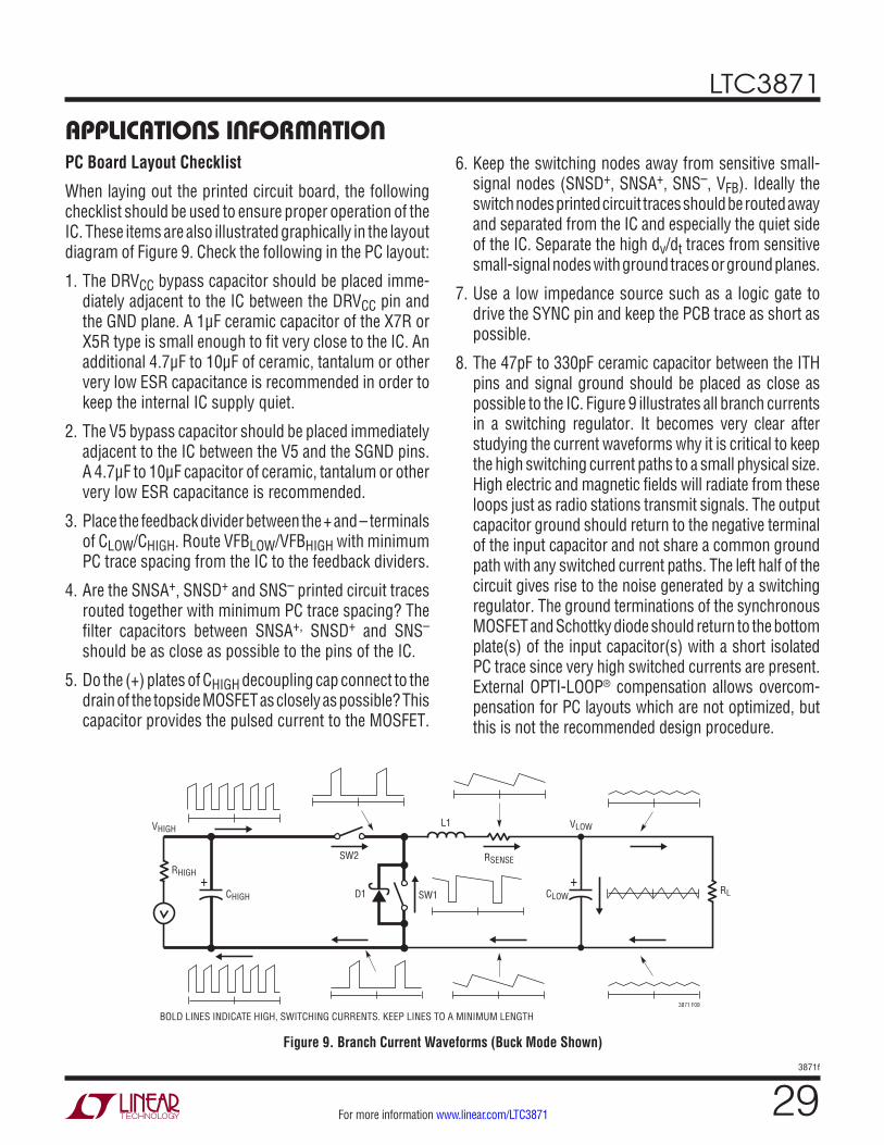
LTC3871
293871f
For more information www.linear.com/LTC3871
Figure 9. Branch Current Waveforms (Buck Mode Shown)
+RHIGH
VHIGH VLOW
CHIGH
+CLOWD1
SW2
SW1
L1
RSENSE
RL
3871 F09
BOLD LINES INDICATE HIGH, SWITCHING CURRENTS. KEEP LINES TO A MINIMUM LENGTH
PC Board Layout Checklist
When laying out the printed circuit board, the following checklist should be used to ensure proper operation of the IC. These items are also illustrated graphically in the layout diagram of Figure 9. Check the following in the PC layout:
1. The DRVCC bypass capacitor should be placed imme-diately adjacent to the IC between the DRVCC pin and the GND plane. A 1μF ceramic capacitor of the X7R or X5R type is small enough to fit very close to the IC. An additional 4.7μF to 10μF of ceramic, tantalum or other very low ESR capacitance is recommended in order to keep the internal IC supply quiet.
2. The V5 bypass capacitor should be placed immediately adjacent to the IC between the V5 and the SGND pins. A 4.7μF to 10μF capacitor of ceramic, tantalum or other very low ESR capacitance is recommended.
3. Place the feedback divider between the + and – terminals of CLOW/CHIGH. Route VFBLOW/VFBHIGH with minimum PC trace spacing from the IC to the feedback dividers.
4. Are the SNSA+, SNSD+ and SNS– printed circuit traces routed together with minimum PC trace spacing? The filter capacitors between SNSA+, SNSD+ and SNS– should be as close as possible to the pins of the IC.
5. Do the (+) plates of CHIGH decoupling cap connect to the drain of the topside MOSFET as closely as possible? This capacitor provides the pulsed current to the MOSFET.
APPLICATIONS INFORMATION6. Keep the switching nodes away from sensitive small-
signal nodes (SNSD+, SNSA+, SNS–, VFB). Ideally the switch nodes printed circuit traces should be routed away and separated from the IC and especially the quiet side of the IC. Separate the high dv/dt traces from sensitive small-signal nodes with ground traces or ground planes.
7. Use a low impedance source such as a logic gate to drive the SYNC pin and keep the PCB trace as short as possible.
8. The 47pF to 330pF ceramic capacitor between the ITH pins and signal ground should be placed as close as possible to the IC. Figure 9 illustrates all branch currents in a switching regulator. It becomes very clear after studying the current waveforms why it is critical to keep the high switching current paths to a small physical size. High electric and magnetic fields will radiate from these loops just as radio stations transmit signals. The output capacitor ground should return to the negative terminal of the input capacitor and not share a common ground path with any switched current paths. The left half of the circuit gives rise to the noise generated by a switching regulator. The ground terminations of the synchronous MOSFET and Schottky diode should return to the bottom plate(s) of the input capacitor(s) with a short isolated PC trace since very high switched currents are present. External OPTI-LOOP® compensation allows overcom-pensation for PC layouts which are not optimized, but this is not the recommended design procedure.
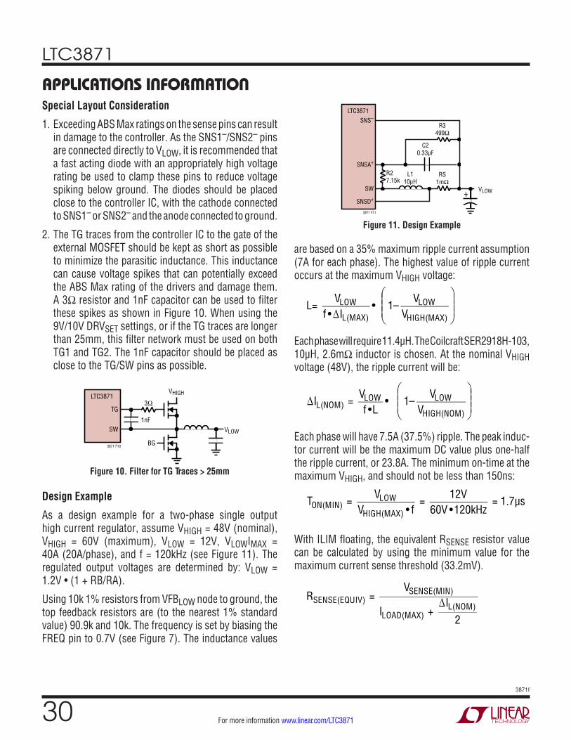
LTC3871
303871f
For more information www.linear.com/LTC3871
Special Layout Consideration
1. Exceeding ABS Max ratings on the sense pins can result in damage to the controller. As the SNS1–/SNS2– pins are connected directly to VLOW, it is recommended that a fast acting diode with an appropriately high voltage rating be used to clamp these pins to reduce voltage spiking below ground. The diodes should be placed close to the controller IC, with the cathode connected to SNS1– or SNS2– and the anode connected to ground.
2. The TG traces from the controller IC to the gate of the external MOSFET should be kept as short as possible to minimize the parasitic inductance. This inductance can cause voltage spikes that can potentially exceed the ABS Max rating of the drivers and damage them. A 3Ω resistor and 1nF capacitor can be used to filter these spikes as shown in Figure 10. When using the 9V/10V DRVSET settings, or if the TG traces are longer than 25mm, this filter network must be used on both TG1 and TG2. The 1nF capacitor should be placed as close to the TG/SW pins as possible.
APPLICATIONS INFORMATION
Figure 11. Design Example
are based on a 35% maximum ripple current assumption (7A for each phase). The highest value of ripple current occurs at the maximum VHIGH voltage:
L=
VLOWf • ∆IL(MAX)
• 1–VLOW
VHIGH(MAX)
Each phase will require 11.4µH. The Coilcraft SER2918H-103, 10µH, 2.6mΩ inductor is chosen. At the nominal VHIGH voltage (48V), the ripple current will be:
∆IL(NOM) =
VLOWf •L
• 1–VLOW
VHIGH(NOM)
Each phase will have 7.5A (37.5%) ripple. The peak induc-tor current will be the maximum DC value plus one-half the ripple current, or 23.8A. The minimum on-time at the maximum VHIGH, and should not be less than 150ns:
TON(MIN) = VLOW
VHIGH(MAX) • f =
12V60V •120kHz
= 1.7µs
With ILIM floating, the equivalent RSENSE resistor value can be calculated by using the minimum value for the maximum current sense threshold (33.2mV).
RSENSE(EQUIV) = VSENSE(MIN)
ILOAD(MAX) + ∆IL(NOM)
2
VLOW
L110μH
LTC3871
SNSA+
SW
SNSD+
SNS–
RS1mΩ
R27.15k
+
R3499Ω
C20.33μF
3871 F11
Figure 10. Filter for TG Traces > 25mm
LTC3871
SW
TG3Ω
1nF
BG
VLOW
3871 F10
VHIGH
Design Example
As a design example for a two-phase single output high current regulator, assume VHIGH = 48V (nominal), VHIGH = 60V (maximum), VLOW = 12V, VLOWIMAX = 40A (20A/phase), and f = 120kHz (see Figure 11). The regulated output voltages are determined by: VLOW = 1.2V • (1 + RB/RA).
Using 10k 1% resistors from VFBLOW node to ground, the top feedback resistors are (to the nearest 1% standard value) 90.9k and 10k. The frequency is set by biasing the FREQ pin to 0.7V (see Figure 7). The inductance values
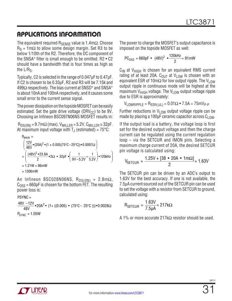
LTC3871
313871f
For more information www.linear.com/LTC3871
The equivalent required RSENSE value is 1.4mΩ. Choose RS = 1mΩ to allow some design margin. Set R3 to be below 1/10th of the R2. Therefore, the DC component of the SNSA+ filter is small enough to be omitted. R2 • C2 should have a bandwidth that is four times as high as the L/RS.
Typically, C2 is selected in the range of 0.047µF to 0.47µF. If C2 is chosen to be 0.33μF, R2 and R3 will be 7.15k and 499Ω respectively. The bias current at SNSD+ and SNSA+ is about 10nA and 100nA respectively, and it causes some small error to the current sense signal.
The power dissipation on the topside MOSFET can be easily estimated. Set the gate drive voltage (DRVCC) to be 9V. Choosing an Infineon BSC097N06NS MOSFET results in:
RDS(ON) = 9.7mΩ (max), VMILLER = 5.2V, CMILLER ≅ 32pF. At maximum input voltage with TJ (estimated) = 75°C:
PMAIN =
12V48V
•(20A)2 •(1 + 0.005(75°C– 25°C))•0.0097Ω
+ (48V)2 •23.8A
2•2Ω • 32pF •
19V – 5.2V
+1
5.2V
•120kHz
= 1.21W + 96mW = 1306mW
An Infineon BSC028N06NS, RDS(ON) = 2.8mΩ, COSS = 660pF is chosen for the bottom FET. The resulting power loss is:
PSYNC = 48V –12V
48V•20A2 • (1+ ((0.005) • (75°C– 25°C )))•0.0028Ω
PSYNC = 1.05W
The power to charge the MOSFET’s output capacitance is imposed on the topside MOSFET as well:
PCOSS = 660pF • (48V)2 •
120kHz2
= 91mW
CIN at VHIGH is chosen for an equivalent RMS current rating of at least 20A. COUT at VLOW is chosen with an equivalent ESR of 10mΩ for low output ripple. The VLOW output ripple in continuous mode will be highest at the maximum VHIGH voltage. The VLOW output voltage ripple due to ESR is approximately: VLOWRIPPLE = RESR(∆IL) = 0.01Ω • 7.5A = 75mVP-P
Further reductions in VLOW output voltage ripple can be made by placing a 100µF ceramic capacitor across CLOW.
If the output load is a battery, the voltage loop is first set for the desired output voltage and then the charge current can be regulated using the current regulation loop – via the SETCUR and IMON pins. Selecting a maximum charge current of 20A, the desired SETCUR pin voltage is calculated using:
VSETCUR =
1.25V + [38 • 20A • 1mΩ]2
= 1.63V
The SETCUR pin can be driven by an ADC’s output to 1.63V for the best accuracy. If one is not available, the 7.5μA current sourced out of the SETCUR pin can be used to set the voltage with a resistor from SETCUR to ground, calculated using:
RSETCUR =
1.63V7.5µA
= 217kΩ
A 1% or more accurate 217kΩ resistor should be used.
APPLICATIONS INFORMATION
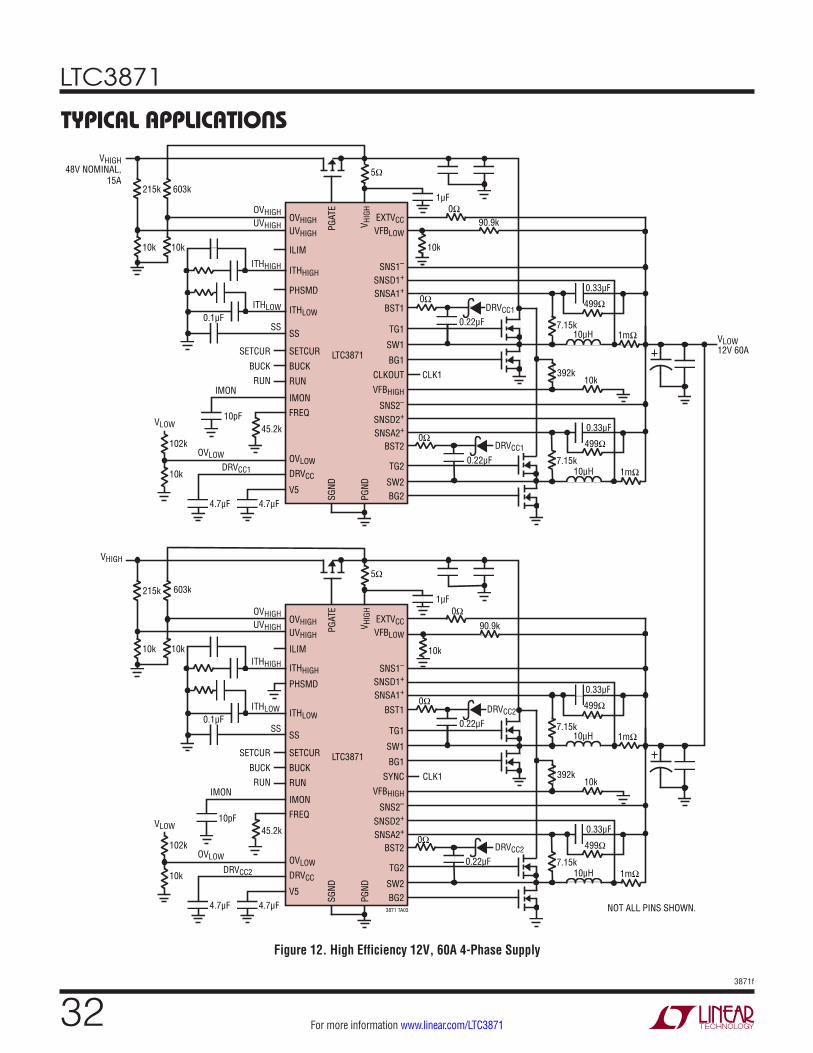
LTC3871
323871f
For more information www.linear.com/LTC3871
Figure 12. High Efficiency 12V, 60A 4-Phase Supply
TYPICAL APPLICATIONS
VLOW 12V 60A
DRVCC1
VLOW
PGAT
E
DRVCC
V5
PGND
BG2SGND
SNSA2+
IMON
SNSD2+
TG2
V HIG
H
SW2
VFBLOW
EXTVCC
OVLOW
FREQ
BUCK
SETCUR
RUN
BUCK
SETCUR
RUN
BST2
SNS2–
BG1
VFBHIGH
TG1
SW1
BST1
SNSA1+
SNS1–
SNSD1+
LTC3871
DRVCC1
102k
10k
45.2k
4.7μF 4.7μF
1μF
5Ω
0.33μF
499Ω
499Ω
7.15k10μH 1mΩ
7.15k10μH 1mΩ
392k10k
0.33μF
IMON
OVLOW
0Ω
VHIGH
DRVCC2
VLOW
PGAT
E
DRVCC
V5
PGND
BG2SGND
SNSA2+
IMON
SNSD2+
TG2
V HIG
H
SW2
SS
UVHIGH VFBLOW
EXTVCC
OVLOW
OVHIGHUVHIGH
OVHIGH
ITHLOW
ITHHIGH
SS
ITHLOW
ITHHIGH
FREQ
BUCK
SETCUR
RUN
BUCK
SETCUR
RUN
BST2
SNS2–
BG1
SYNC CLK1
VFBHIGH
TG1
SW1
BST1
SNSA1+
SNS1–
SNSD1+
LTC3871
ILIM
DRVCC2
603k215k
10k10k
0.1μF
102k
10k
45.2k
4.7μF 4.7μF
1μF
5Ω
0.33μF
499Ω
499Ω
7.15k10μH 1mΩ
7.15k10μH 1mΩ
392k10k
0.33μF
IMON
OVLOW
0Ω
SS
UVHIGH
OVHIGHUVHIGH
OVHIGH
ITHLOW
ITHHIGH
SS
ITHLOW
ITHHIGH
603k215k
10k10k
0.1μF
10pF
0Ω
0Ω
0.22μF
0.22μF
90.9k
10k
90.9k
10k
0.22μF
0.22μF
0Ω
0Ω
10pF
ILIM
CLKOUT CLK1
PHSMD
PHSMD
DRVCC2
VHIGH48V NOMINAL,
15A
DRVCC1
NOT ALL PINS SHOWN.3871 TA03
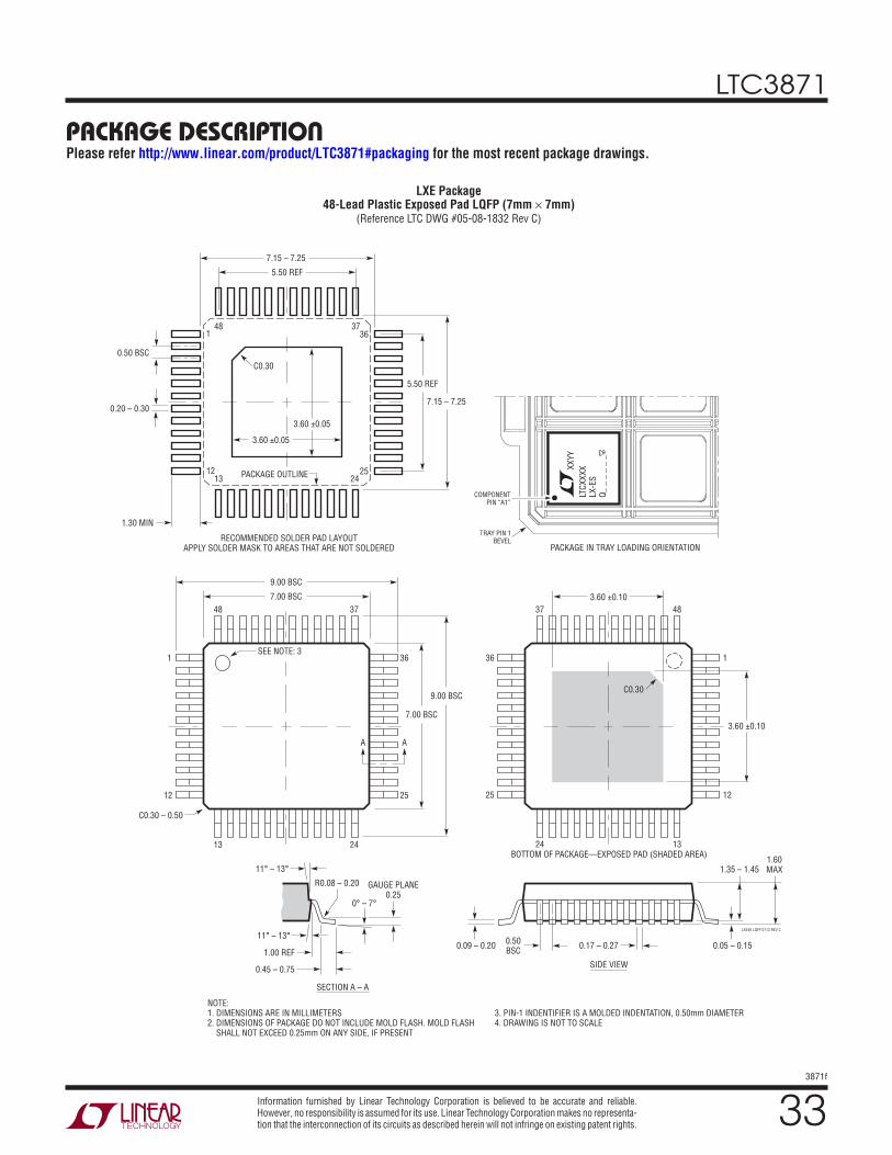
LTC3871
333871f
For more information www.linear.com/LTC3871
Information furnished by Linear Technology Corporation is believed to be accurate and reliable. However, no responsibility is assumed for its use. Linear Technology Corporation makes no representa-tion that the interconnection of its circuits as described herein will not infringe on existing patent rights.
PACKAGE DESCRIPTIONPlease refer http://www.linear.com/product/LTC3871#packaging for the most recent package drawings.
LXE48 LQFP 0113 REV C
0° – 7°
11° – 13°
0.45 – 0.75
1.00 REF
11° – 13°
1
48
1.60MAX1.35 – 1.45
0.05 – 0.150.09 – 0.20 0.50BSC 0.17 – 0.27
GAUGE PLANE0.25
NOTE:1. DIMENSIONS ARE IN MILLIMETERS2. DIMENSIONS OF PACKAGE DO NOT INCLUDE MOLD FLASH. MOLD FLASH SHALL NOT EXCEED 0.25mm ON ANY SIDE, IF PRESENT
3. PIN-1 INDENTIFIER IS A MOLDED INDENTATION, 0.50mm DIAMETER4. DRAWING IS NOT TO SCALE
R0.08 – 0.20
7.15 – 7.25
5.50 REF
1 36
2512
5.50 REF
7.15 – 7.25
48
13 24
37
C0.30
PACKAGE OUTLINE
RECOMMENDED SOLDER PAD LAYOUTAPPLY SOLDER MASK TO AREAS THAT ARE NOT SOLDERED
BOTTOM OF PACKAGE—EXPOSED PAD (SHADED AREA)
SIDE VIEW
SECTION A – A
0.50 BSC
0.20 – 0.30
1.30 MIN
9.00 BSC
A A
7.00 BSC
1
12
7.00 BSC 3.60 ±0.10
3.60 ±0.10
9.00 BSC
48 37
1324
37
13 24
36 36
2525
SEE NOTE: 3
C0.30 – 0.50
3.60 ±0.05
3.60 ±0.05
C0.30
LXE Package48-Lead Plastic Exposed Pad LQFP (7mm × 7mm)
(Reference LTC DWG #05-08-1832 Rev C)
12
e3
LTCX
XXX
LX-E
SQ_
_ _
_ _
_
XXYY
TRAY PIN 1BEVEL
PACKAGE IN TRAY LOADING ORIENTATION
COMPONENTPIN “A1”
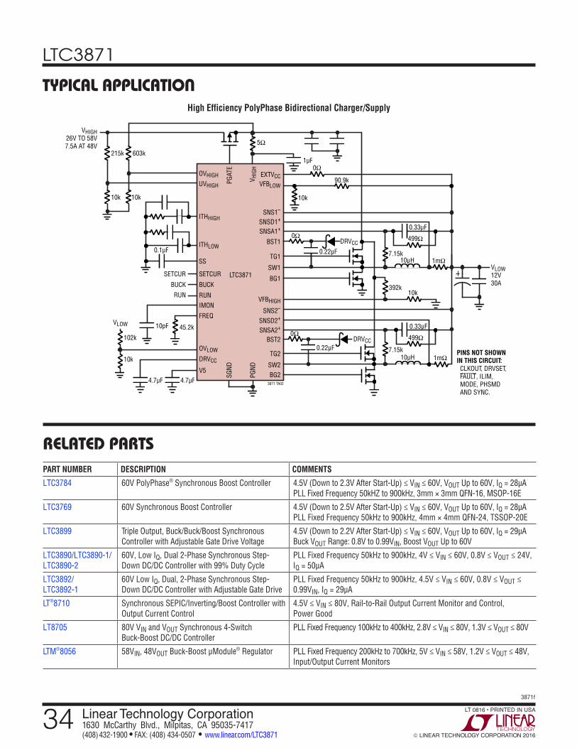
LTC3871
343871f
For more information www.linear.com/LTC3871 LINEAR TECHNOLOGY CORPORATION 2016
LT 0816 • PRINTED IN USALinear Technology Corporation1630 McCarthy Blvd., Milpitas, CA 95035-7417(408) 432-1900 FAX: (408) 434-0507 www.linear.com/LTC3871
RELATED PARTS
TYPICAL APPLICATION
PART NUMBER DESCRIPTION COMMENTS
LTC3784 60V PolyPhase® Synchronous Boost Controller 4.5V (Down to 2.3V After Start-Up) ≤ VIN ≤ 60V, VOUT Up to 60V, IQ = 28µA PLL Fixed Frequency 50kHZ to 900kHz, 3mm × 3mm QFN-16, MSOP-16E
LTC3769 60V Synchronous Boost Controller 4.5V (Down to 2.5V After Start-Up) ≤ VIN ≤ 60V, VOUT Up to 60V, IQ = 28µA PLL Fixed Frequency 50kHz to 900kHz, 4mm × 4mm QFN-24, TSSOP-20E
LTC3899 Triple Output, Buck/Buck/Boost Synchronous Controller with Adjustable Gate Drive Voltage
4.5V (Down to 2.2V After Start-Up) ≤ VIN ≤ 60V, VOUT Up to 60V, IQ = 29µA Buck VOUT Range: 0.8V to 0.99VIN, Boost VOUT Up to 60V
LTC3890/LTC3890-1/ LTC3890-2
60V, Low IQ, Dual 2-Phase Synchronous Step-Down DC/DC Controller with 99% Duty Cycle
PLL Fixed Frequency 50kHz to 900kHz, 4V ≤ VIN ≤ 60V, 0.8V ≤ VOUT ≤ 24V, IQ = 50µA
LTC3892/ LTC3892-1
60V Low IQ, Dual, 2-Phase Synchronous Step-Down DC/DC Controller with Adjustable Gate Drive
PLL Fixed Frequency 50kHz to 900kHz, 4.5V ≤ VIN ≤ 60V, 0.8V ≤ VOUT ≤ 0.99VIN, IQ = 29µA
LT®8710 Synchronous SEPIC/Inverting/Boost Controller with Output Current Control
4.5V ≤ VIN ≤ 80V, Rail-to-Rail Output Current Monitor and Control, Power Good
LT8705 80V VIN and VOUT Synchronous 4-Switch Buck-Boost DC/DC Controller
PLL Fixed Frequency 100kHz to 400kHz, 2.8V ≤ VIN ≤ 80V, 1.3V ≤ VOUT ≤ 80V
LTM®8056 58VIN, 48VOUT Buck-Boost μModule® Regulator PLL Fixed Frequency 200kHz to 700kHz, 5V ≤ VIN ≤ 58V, 1.2V ≤ VOUT ≤ 48V, Input/Output Current Monitors
High Efficiency PolyPhase Bidirectional Charger/Supply
VHIGH26V TO 58V7.5A AT 48V
VLOW12V30A
DRVCC
VLOW
PGAT
E
DRVCC
V5
PGND
BG2SGND
SNSA2+
IMON
SNSD2+
TG2
V HIG
H
SW2
VFBLOW
EXTVCC
OVLOW
FREQ
BUCK
SETCUR
RUN
BUCK
SETCUR
RUN
BST2
SNS2–
BG1
VFBHIGH
TG1
SW1
BST1
SNSA1+
SNS1–
SNSD1+
LTC3871
DRVCC
PINS NOT SHOWNIN THIS CIRCUIT: CLKOUT, DRVSET, FAULT, ILIM, MODE, PHSMD AND SYNC.
102k
10k
45.2k
4.7μF 4.7μF
1μF
5Ω
90.9k
10k
0.33μF
499Ω
499Ω
7.15k10μH 1mΩ
7.15k10μH 1mΩ
392k10k
0.33μF
0Ω
SS
UVHIGH
OVHIGH
ITHLOW
ITHHIGH
603k215k
10k10k
0.1μF
10pF0Ω
0.22μF
0.22μF
0Ω
3871 TA02

Mouser Electronics
Authorized Distributor
Click to View Pricing, Inventory, Delivery & Lifecycle Information: Analog Devices Inc.:
LTC3871ELXE#PBF LTC3871HLXE#PBF LTC3871ILXE#PBF