Embed Size (px)
Citation preview
Oldervoll Mars 2009 IKT 1
Materials and basic processes in microelectronics
Frøydis
OldervollSINTEF ICT
Instrumentation department
Oldervoll Mars 2009 IKT 2
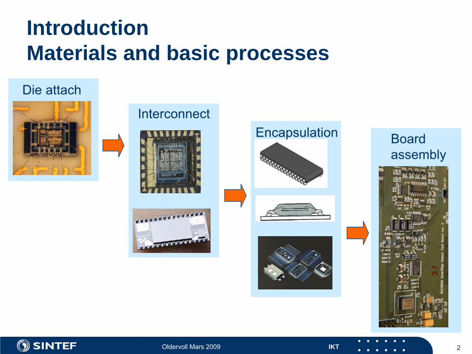
Introduction Materials and basic processes
Die attach
InterconnectEncapsulation Board
assembly
Oldervoll Mars 2009 IKT 3
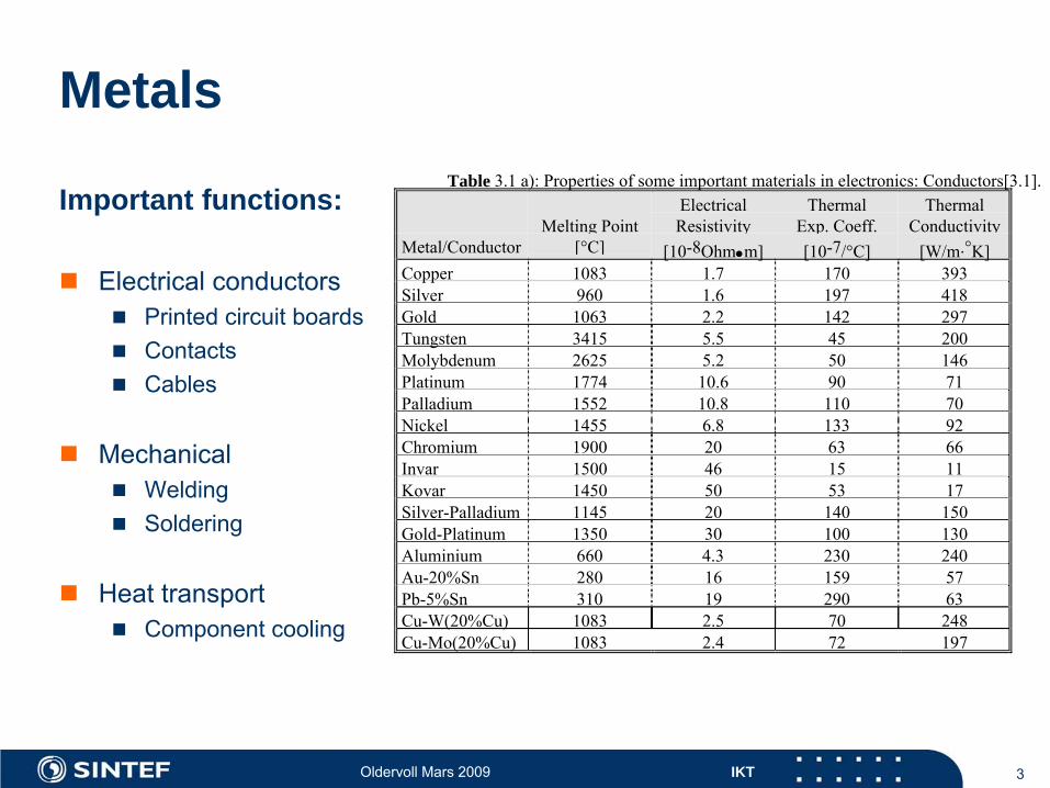
Metals
Important functions:
Electrical conductors
Printed circuit boards
Contacts
Cables
Mechanical
Welding
Soldering
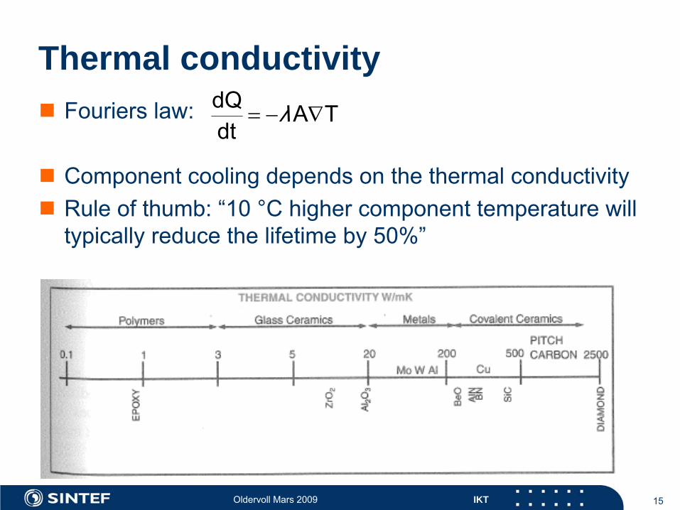
Heat transport
Component cooling
Table 3.1 a): Properties of some important materials in electronics: Conductors[3.1].
Melting PointElectricalResistivity
ThermalExp. Coeff.
ThermalConductivity
Metal/Conductor [°C] [10-8Ohmm] [10-7/°C] [W/m.°K]Copper 1083 1.7 170 393Silver 960 1.6 197 418Gold 1063 2.2 142 297Tungsten 3415 5.5 45 200Molybdenum 2625 5.2 50 146Platinum 1774 10.6 90 71Palladium 1552 10.8 110 70Nickel 1455 6.8 133 92Chromium 1900 20 63 66Invar 1500 46 15 11Kovar 1450 50 53 17Silver-Palladium 1145 20 140 150Gold-Platinum 1350 30 100 130Aluminium 660 4.3 230 240Au-20%Sn 280 16 159 57Pb-5%Sn 310 19 290 63Cu-W(20%Cu) 1083 2.5 70 248Cu-Mo(20%Cu) 1083 2.4 72 197
Oldervoll Mars 2009 IKT 4
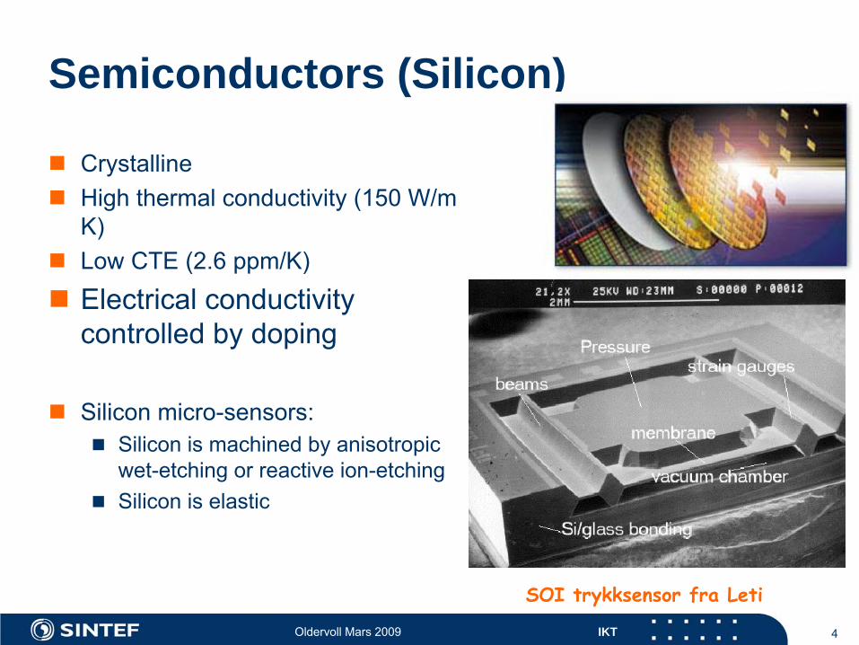
Semiconductors (Silicon)
Crystalline
High thermal conductivity (150 W/m K)
Low CTE (2.6 ppm/K)
Electrical conductivity controlled by doping
Silicon micro-sensors:
Silicon is machined by anisotropic wet-etching or reactive ion-etching
Silicon is elastic
SOI trykksensor
fra
Leti
Oldervoll Mars 2009 IKT 5
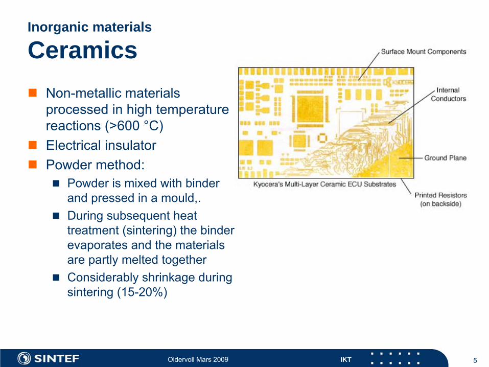
Inorganic materials
Ceramics
Non-metallic materials processed in high temperature reactions (>600 °C)
Electrical insulator
Powder method:
Powder is mixed with binder and pressed in a mould,.
During subsequent heat treatment (sintering) the binder evaporates and the materials are partly melted together
Considerably shrinkage during sintering (15-20%)
Oldervoll Mars 2009 IKT 6
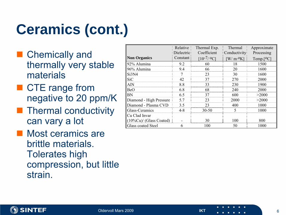
Ceramics (cont.)
Chemically and thermally very stable materials
CTE range from negative to 20 ppm/K
Thermal conductivity can vary a lot
Most ceramics are brittle materials. Tolerates high compression, but little strain.
Non Organics
RelativeDielectricConstant
Thermal Exp.Coefficient[10-7/ oC]
ThermalConductivity[W/ m.oK]
ApproximateProcessingTemp.[oC]
92% Alumina 9.2 60 18 150096% Alumina 9.4 66 20 1600Si3N4 7 23 30 1600SiC 42 37 270 2000AlN 8.8 33 230 1900BeO 6.8 68 240 2000BN 6.5 37 600 >2000Diamond - High Pressure 5.7 23 2000 >2000Diamond - Plasma CVD 3.5 23 400 1000Glass-Ceramics 4-8 30-50 5 1000Cu Clad Invar(10%Cu)/ (Glass Coated) - 30 100 800Glass coated Steel 6 100 50 1000
Oldervoll Mars 2009 IKT 7
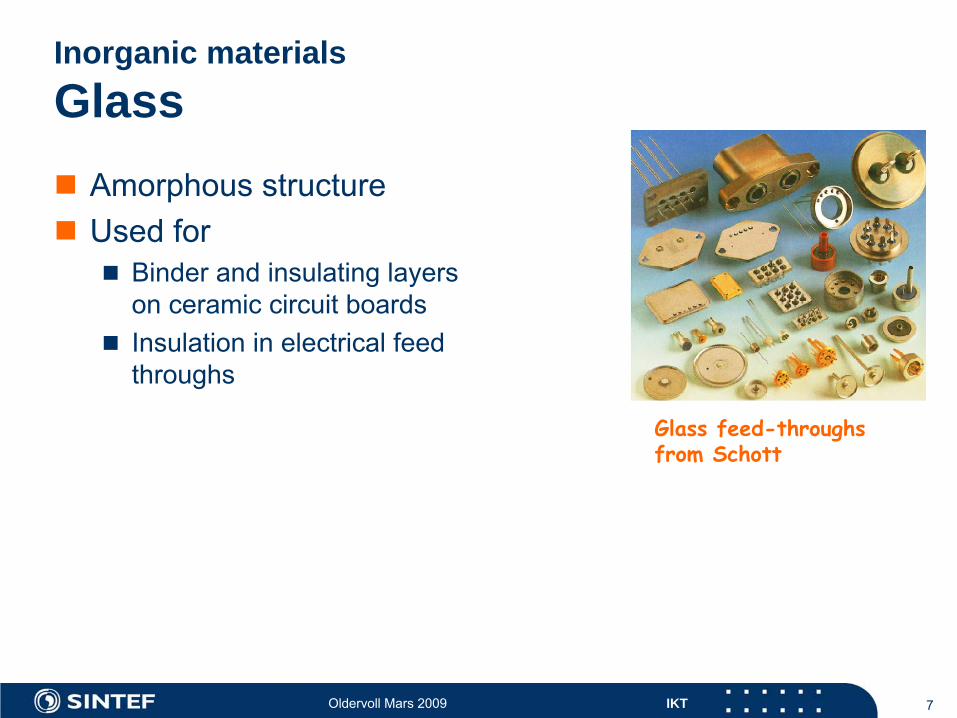
Inorganic materials Glass
Amorphous structure
Used for
Binder and insulating layers on ceramic circuit boards
Insulation in electrical feed throughs
Glass feed-throughs from Schott
Oldervoll Mars 2009 IKT 8
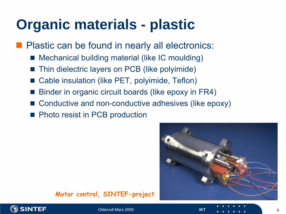
Organic materials - plastic
Plastic can be found in nearly all electronics:
Mechanical building material (like IC moulding)
Thin dielectric layers on PCB (like polyimide)
Cable insulation (like PET, polyimide, Teflon)
Binder in organic circuit boards (like epoxy in FR4)
Conductive and non-conductive adhesives (like epoxy)
Photo resist in PCB production
Motor control, SINTEF-project
Oldervoll Mars 2009 IKT 9
Important properties of plastics
High electrical resistivity, high breakdown strength, low dielectric loss, low dielectric constant
CTE is often higher than for metals or semiconductors
Plastic with high mechanical strength or soft and flexible properties are available
Adhesion -
many plastics have good adhesion to other materials, but not all (like Teflon)
Easy to process
A certain water absorption takes place, little influence on material properties.
Cheap raw material and production
Oldervoll Mars 2009 IKT 10
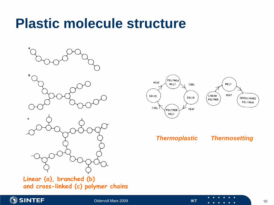
Plastic molecule structure
Linear (a), branched (b) and cross-linked (c) polymer chains
Thermoplastic Thermosetting
Oldervoll Mars 2009 IKT 11
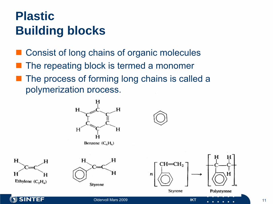
Plastic Building blocks
Consist of long chains of organic molecules
The repeating block is termed a monomer
The process of forming long chains is called a polymerization process.
Oldervoll Mars 2009 IKT 12
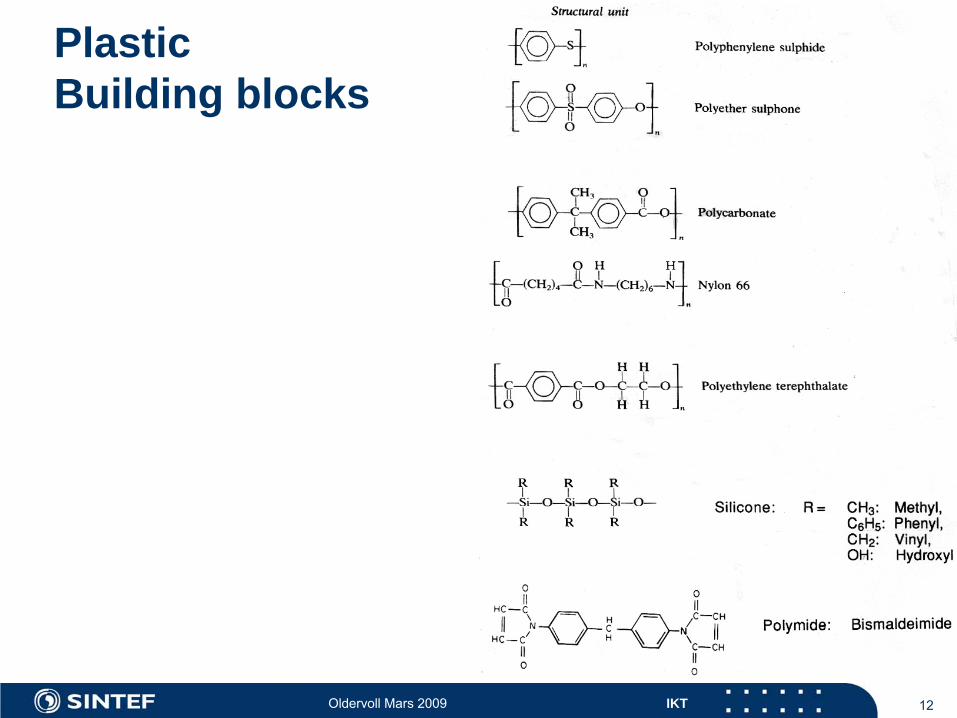
Plastic Building blocks
Oldervoll Mars 2009 IKT 13
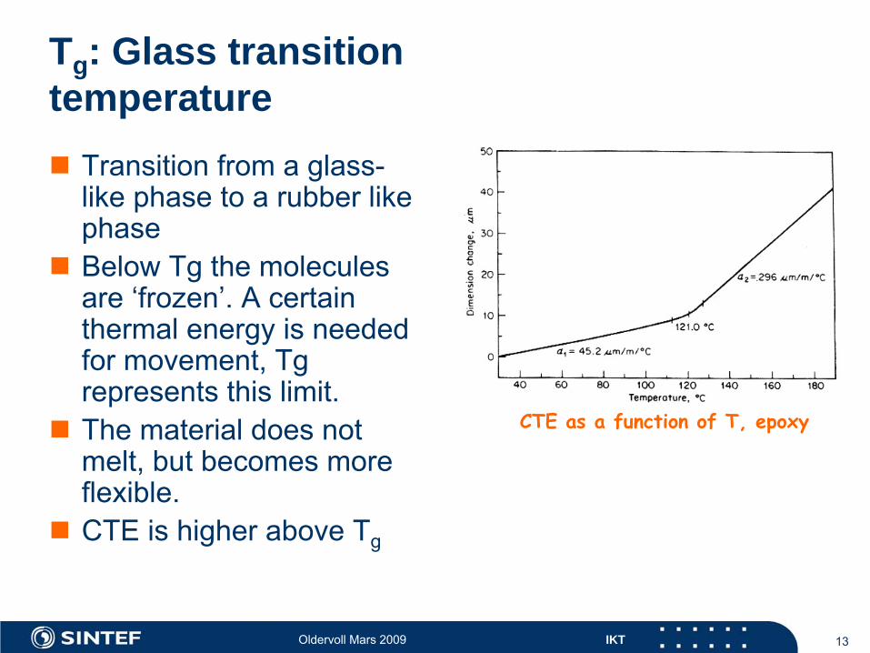
Tg : Glass transition temperature
Transition from a glass-
like phase to a rubber like phase
Below Tg
the molecules are ‘frozen’. A certain thermal energy is needed for movement, Tg
represents this limit.
The material does not melt, but becomes more flexible.
CTE is higher above Tg
CTE
as a function of T, epoxy
Oldervoll Mars 2009 IKT 14
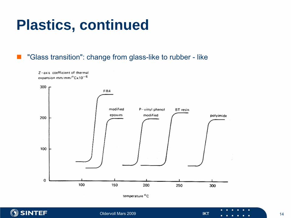
Plastics, continued
"Glass transition": change from glass-like to rubber -
like
Oldervoll Mars 2009 IKT 15
Thermal conductivity
Fouriers
law:
Component cooling depends on the thermal conductivity
Rule of thumb: “10 °C higher component temperature will typically reduce the lifetime by 50%”
TAdtdQ
λ
Oldervoll Mars 2009 IKT 16
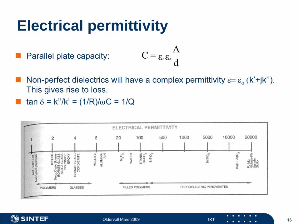
Electrical permittivity
Parallel plate capacity:
Non-perfect dielectrics will have a complex permittivity
k’+jk’’). This gives rise to loss.
tan
= k’’/k’
= (1/R)/C = 1/Q
dA
εεC or
Oldervoll Mars 2009 IKT 17
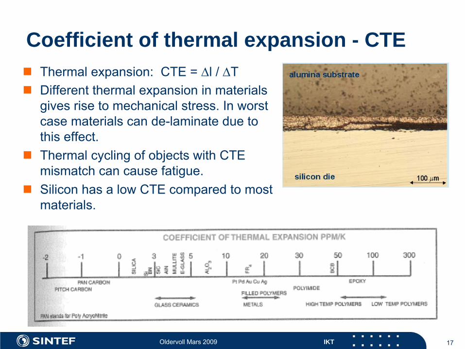
Coefficient of thermal expansion - CTE
Thermal expansion: CTE = l / T
Different thermal expansion in materials gives rise to mechanical stress. In worst case materials can de-laminate due to this effect.
Thermal cycling of objects with CTE mismatch can cause fatigue.
Silicon has a low CTE compared to most materials.
Oldervoll Mars 2009 IKT 18
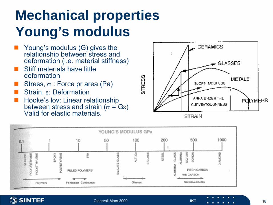
Mechanical properties Young’s modulus
Young’s modulus (G) gives the relationship between stress and deformation (i.e. material stiffness)
Stiff materials have little deformation
Stress,
: Force pr area (Pa)
Strain, : Deformation
Hooke’s lov: Linear relationship between stress and strain (
= G)
Valid for elastic materials.
Oldervoll Mars 2009 IKT 19
Important processes in microelectronics
Photo lithography
Screen printing
Etching
Plating
Sputtering
Vacuum sputtering
RF and DC sputtering
Methods for electrical and mechanical interconnect:
Soldering
Gluing
Wire-bonding
Flip-chip bonding
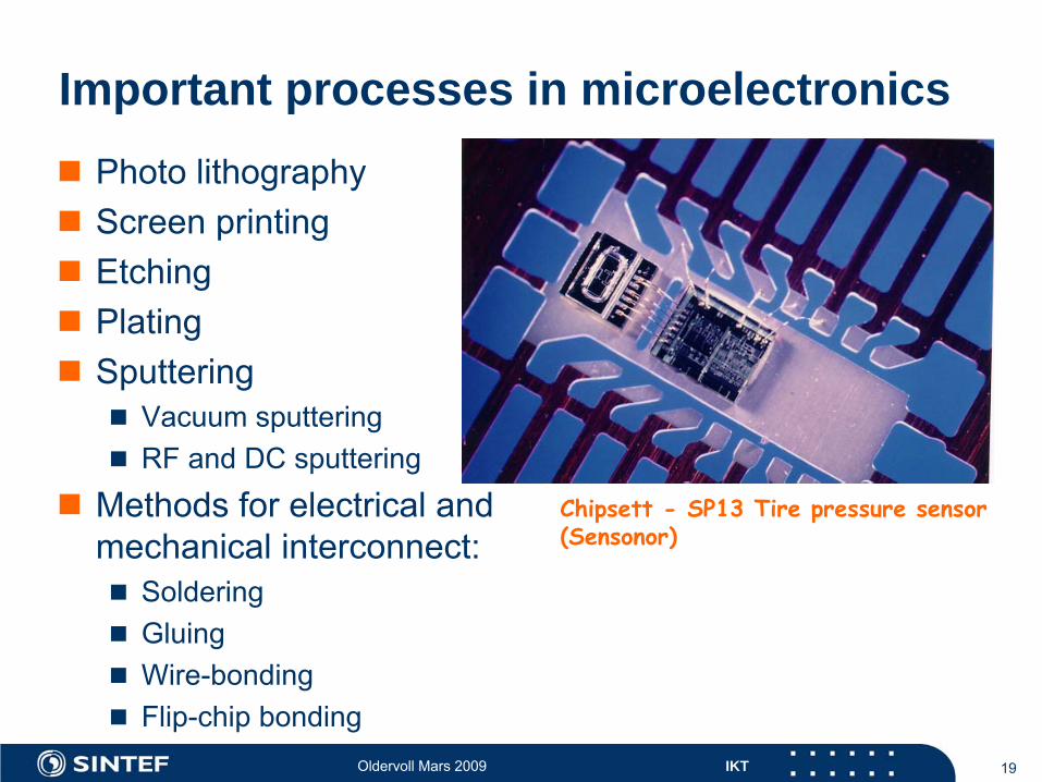
Chipsett
-
SP13 Tire pressure sensor(Sensonor)
Oldervoll Mars 2009 IKT 20
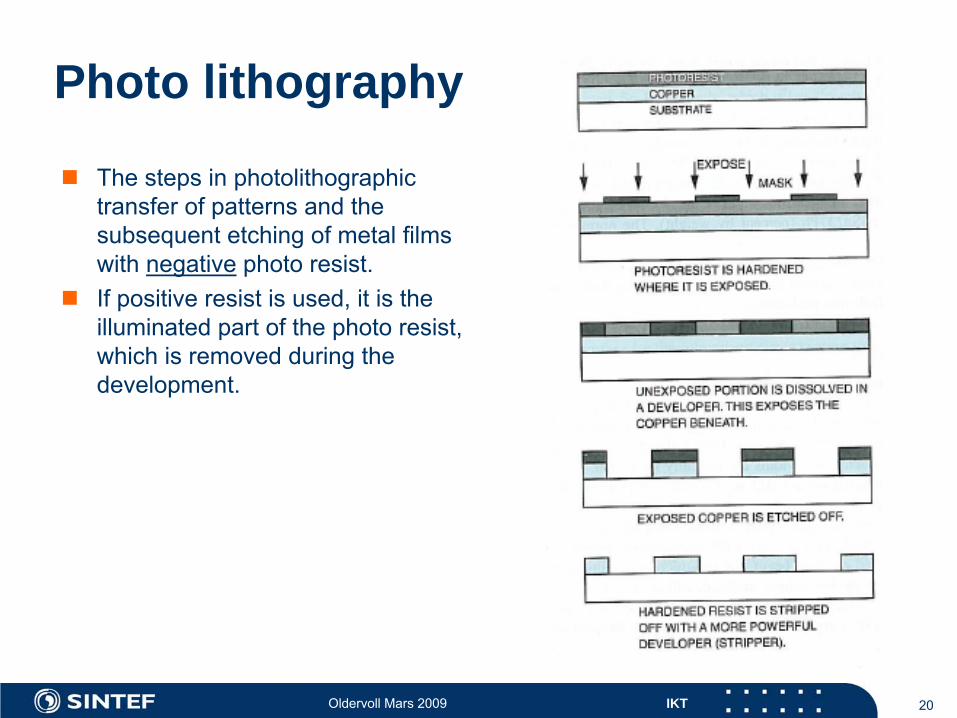
Photo lithography
The steps in photolithographic transfer of patterns and the subsequent etching of metal films with negative
photo resist.
If positive resist is used, it is the illuminated part of the photo resist, which is removed during the development.
Oldervoll Mars 2009 IKT 21
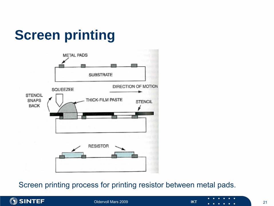
Screen printing
Screen printing process for printing resistor between metal pads.
Oldervoll Mars 2009 IKT 22
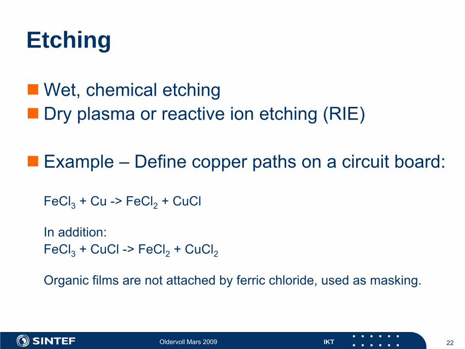
Etching
Wet, chemical etching Dry plasma or reactive ion etching (RIE)
Example –
Define copper paths on a circuit board:
FeCl3
+ Cu -> FeCl2
+ CuCl
In addition:FeCl3
+ CuCl
-> FeCl2
+ CuCl2
Organic films are not attached by ferric chloride, used as masking.
Oldervoll Mars 2009 IKT 23
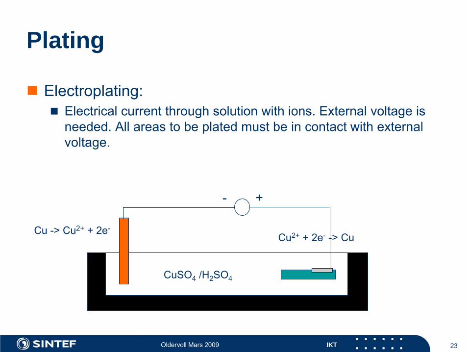
Plating
Electroplating:
Electrical current through solution with ions. External voltage is needed. All areas to be plated must be in contact with external voltage.
CuSO4
/H2
SO4
Cu
-> Cu2+
+ 2e-Cu2+
+ 2e-
-> Cu
- +
Oldervoll Mars 2009 IKT 24
Plating
Electroless
or chemical plating
No external current/voltage
Must be utilized when plating non-conductive surfaces
Areas not to be plated is masked by photo resist.
Is often performed before electroplating to make all areas conductive.
Oldervoll Mars 2009 IKT 25
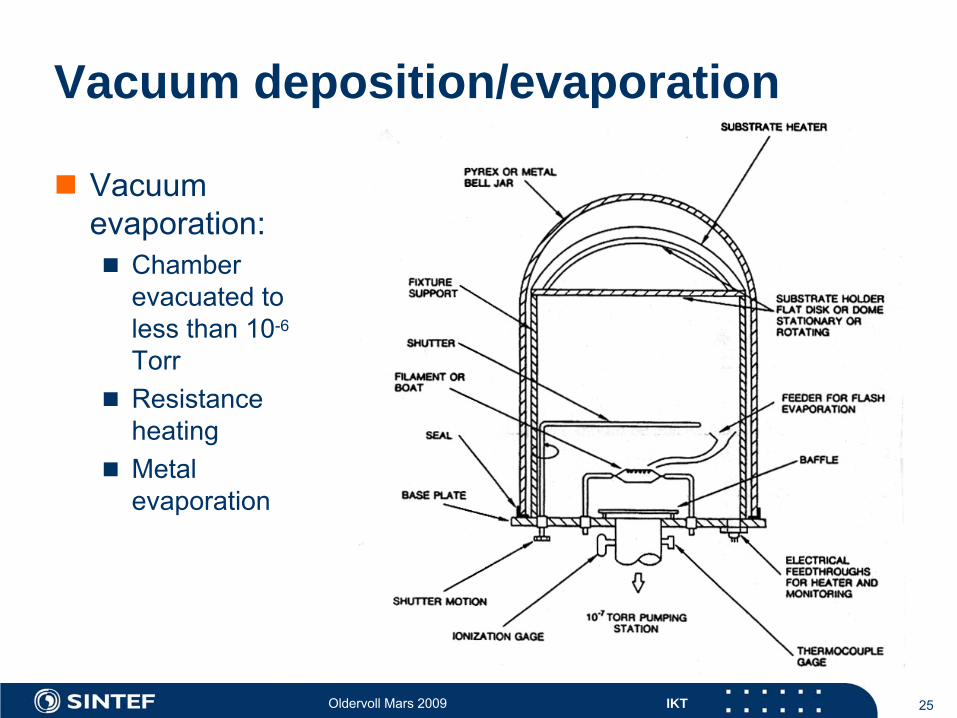
Vacuum deposition/evaporation
Vacuum evaporation:
Chamber evacuated to
less than 10-6
Torr
Resistance heating
Metal evaporation
Oldervoll Mars 2009 IKT 26
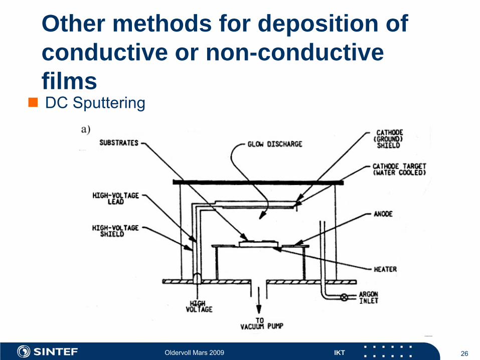
Other methods for deposition of conductive or non-conductive films
DC Sputtering
Oldervoll Mars 2009 IKT 27
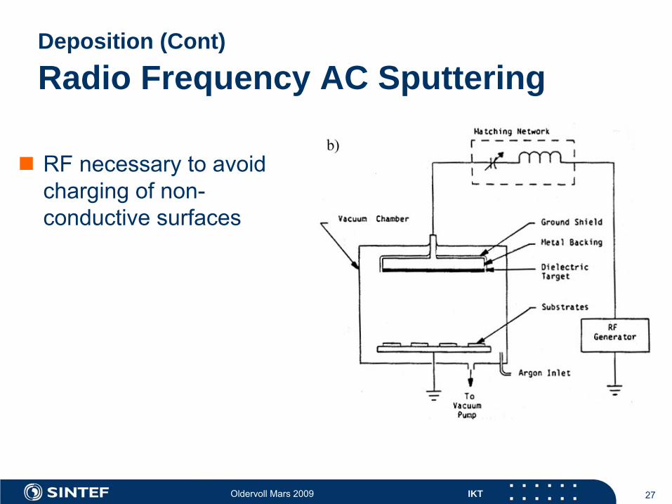
Deposition (Cont)
Radio Frequency AC Sputtering
RF necessary to avoid charging of non-
conductive surfaces
Oldervoll Mars 2009 IKT 28
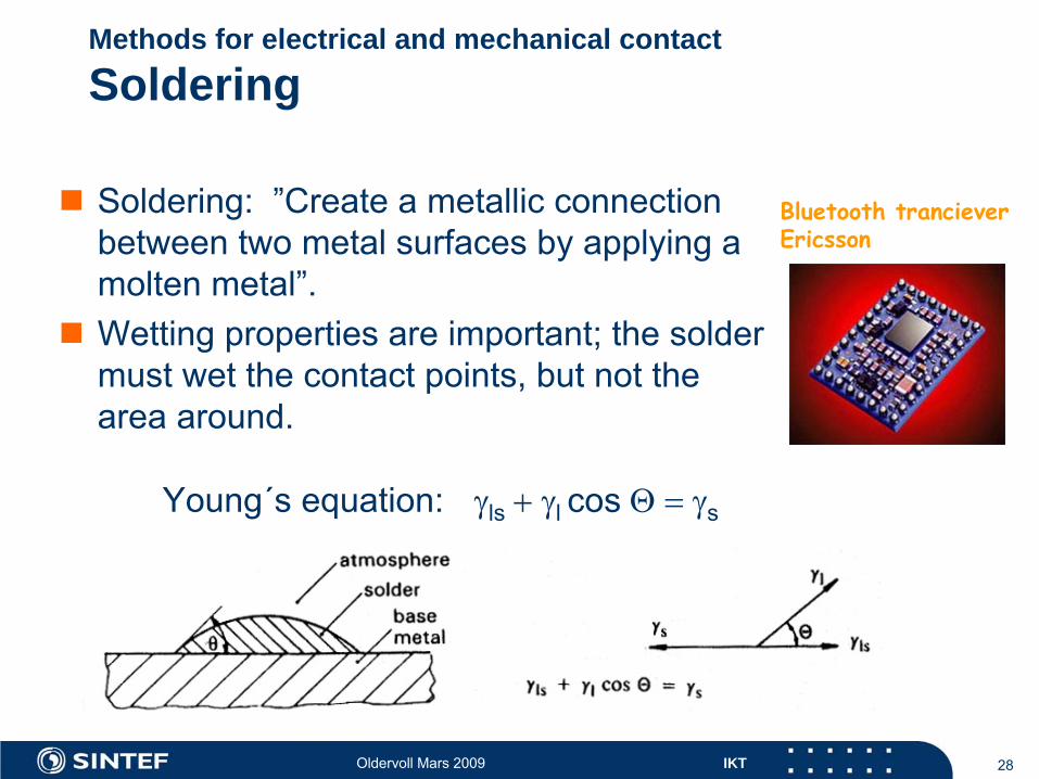
Methods for electrical and mechanical contact
Soldering
Soldering: ”Create a metallic connection between two metal surfaces by applying a molten metal”.
Wetting properties are important; the solder must wet the contact points, but not the area around.
Young´s
equation:
ls
l
cos
s
Bluetooth trancieverEricsson
Oldervoll Mars 2009 IKT 29
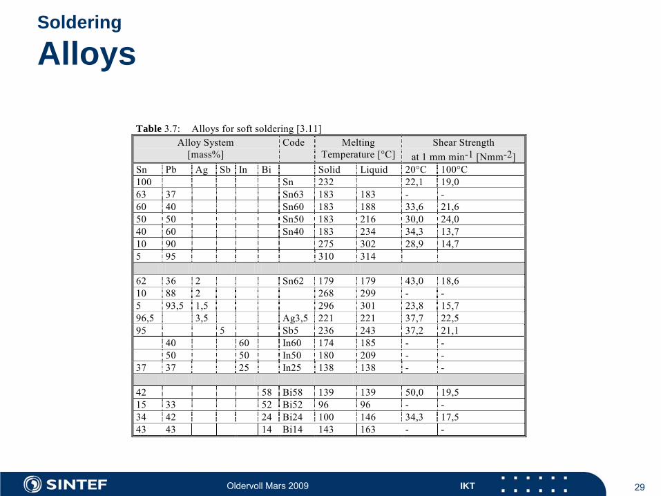
Soldering
Alloys
Table 3.7: Alloys for soft soldering [3.11] Alloy System
[mass%] Code Melting
Temperature [°C] Shear Strength
at 1 mm min-1 [Nmm-2] Sn Pb Ag Sb In Bi Solid Liquid 20°C 100°C 100 Sn 232 22,1 19,0 63 37 Sn63 183 183 - - 60 40 Sn60 183 188 33,6 21,6 50 50 Sn50 183 216 30,0 24,0 40 60 Sn40 183 234 34,3 13,7 10 90 275 302 28,9 14,7 5 95 310 314 62 36 2 Sn62 179 179 43,0 18,6 10 88 2 268 299 - - 5 93,5 1,5 296 301 23,8 15,7 96,5 3,5 Ag3,5 221 221 37,7 22,5 95 5 Sb5 236 243 37,2 21,1 40 60 In60 174 185 - - 50 50 In50 180 209 - - 37 37 25 In25 138 138 - - 42 58 Bi58 139 139 50,0 19,5 15 33 52 Bi52 96 96 - - 34 42 24 Bi24 100 146 34,3 17,5 43 43 14 Bi14 143 163 - -
Oldervoll Mars 2009 IKT 30
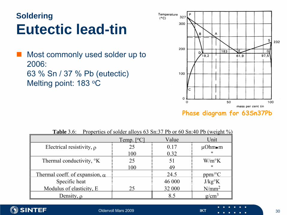
Soldering
Eutectic lead-tin
Most commonly used solder up to 2006: 63 % Sn
/ 37 % Pb
(eutectic)
Melting point: 183 oC
Table 3.6: Properties of solder alloys 63 Sn:37 Pb or 60 Sn:40 Pb (weight %)Temp. [oC] Value Unit
Electrical resistivity, 25100
0.170.32
µOhmm"
Thermal conductivity, °K 25100
5149
W/m°K"
Thermal coeff. of expansion, 24.5 ppm/°CSpecific heat 46 000 J/kg°K
Modulus of elasticity, E 25 32 000 N/mm2
Density, 8.5 g/cm3
Phase diagram for 63Sn37Pb
Oldervoll Mars 2009 IKT 31
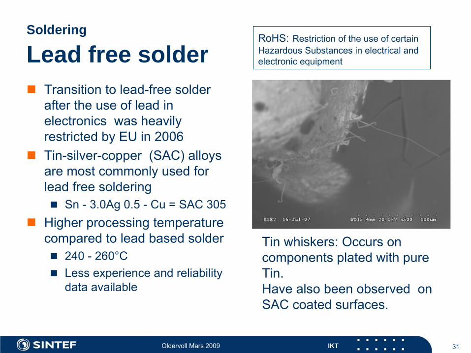
Soldering
Lead free solder
Transition to lead-free solder after the use of lead in electronics was heavily restricted by EU in 2006
Tin-silver-copper (SAC) alloys are most commonly used for lead free soldering
Sn
-
3.0Ag 0.5 -
Cu = SAC 305
Higher processing temperature compared to lead based solder
240 -
260°C
Less experience and reliability data available
Tin whiskers: Occurs on components plated with pure Tin.Have also
been
observed
on
SAC coated
surfaces.
RoHS:
Restriction of the use of certain Hazardous Substances in electrical and electronic equipment
Oldervoll Mars 2009 IKT 32
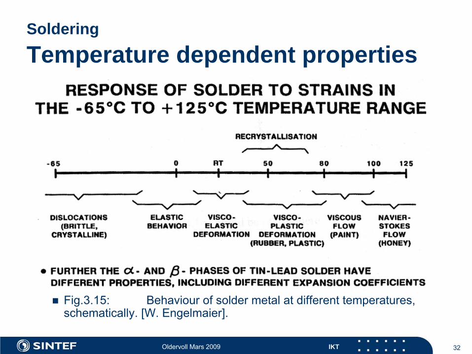
Soldering
Temperature dependent properties
Fig.3.15:
Behaviour
of solder metal at different temperatures, schematically. [W. Engelmaier].
Oldervoll Mars 2009 IKT 33
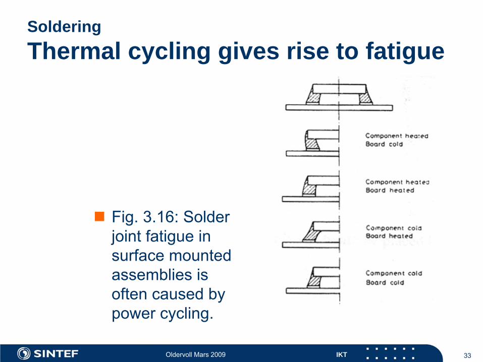
Soldering Thermal cycling gives rise to fatigue
Fig. 3.16: Solder joint fatigue in surface mounted assemblies is often caused by power cycling.
Oldervoll Mars 2009 IKT 34
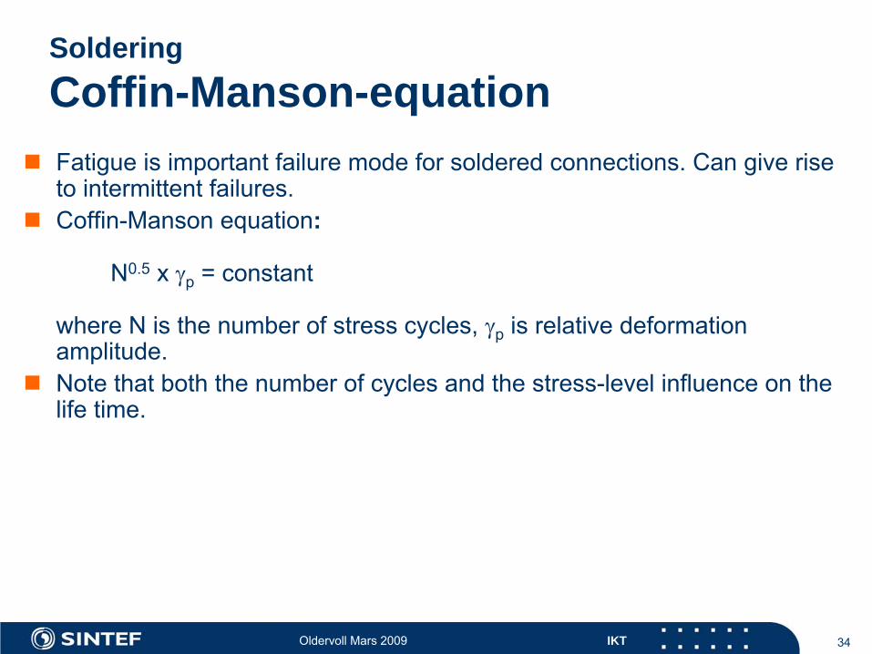
Soldering Coffin-Manson-equation
Fatigue is important failure mode for soldered connections. Can give rise to intermittent failures.
Coffin-Manson equation:
N0.5
x p
= constant
where N is the number of stress cycles, p
is relative deformation amplitude.
Note that both the number of cycles and the stress-level influence on the life time.
Oldervoll Mars 2009 IKT 35
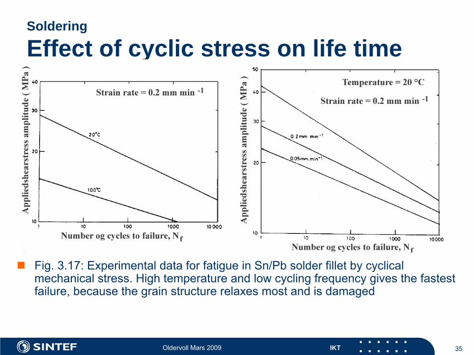
Soldering
Effect of cyclic stress on life time
Fig. 3.17: Experimental data for fatigue in Sn/Pb
solder fillet by cyclical
mechanical stress. High temperature and low cycling frequency gives the fastest failure, because the grain structure relaxes most and is damaged
Oldervoll Mars 2009 IKT 36
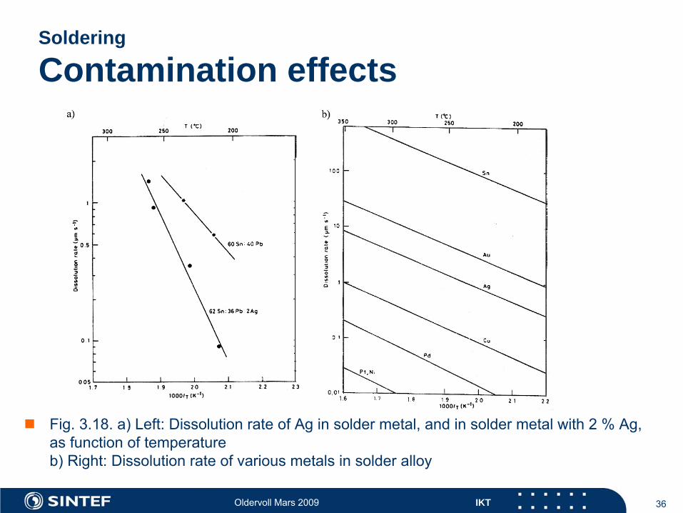
Soldering
Contamination effects
Fig. 3.18. a) Left: Dissolution rate of Ag in solder metal, and in solder metal with 2 % Ag, as function of temperature
b) Right: Dissolution rate of various metals in solder alloy
Oldervoll Mars 2009 IKT 37
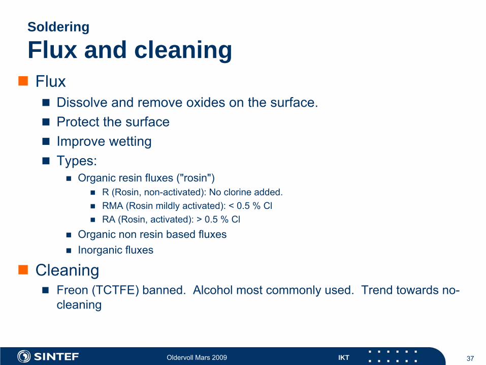
Soldering
Flux and cleaning
Flux
Dissolve and remove oxides on the surface.
Protect the surface
Improve wetting
Types:
Organic resin fluxes ("rosin")
R (Rosin, non-activated): No clorine
added.
RMA (Rosin mildly activated): < 0.5 % Cl
RA (Rosin, activated): > 0.5 % Cl
Organic non resin based fluxes
Inorganic fluxes
Cleaning
Freon (TCTFE) banned. Alcohol most commonly used. Trend towards no- cleaning
Oldervoll Mars 2009 IKT 38
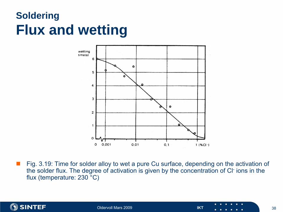
Soldering Flux and wetting
Fig. 3.19: Time for solder alloy to wet a pure Cu surface, depending on the activation of the solder flux. The degree of activation is given by the concentration of Cl-
ions in the flux (temperature: 230 °C)
Oldervoll Mars 2009 IKT 39
Adhesives in electronics
Why?
Mechanical interconnect
Electrical interconnect
Thermal interconnect
Adhesive matrix:
Epoxy, acrylic, phenolic, polyimide, glass
Additives
Metal particles for conductivity
= 1 -
10 x 10 -6
ohm m
Metal or ceramic particles for thermal conductivity:
≈
1 -
3 W /m x oC
Ceramic particles for matched thermal expansion
Oldervoll Mars 2009 IKT 40
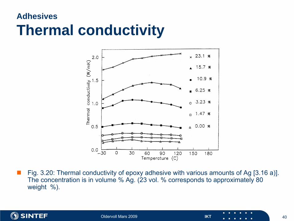
Adhesives
Thermal conductivity
Fig. 3.20: Thermal conductivity of epoxy adhesive with various amounts of Ag [3.16 a)]. The concentration is in volume % Ag. (23 vol. % corresponds to approximately 80 weight %).
Oldervoll Mars 2009 IKT 41
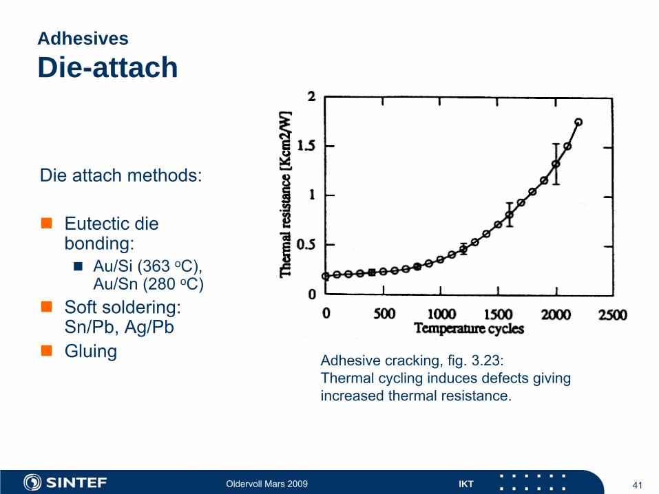
Adhesives
Die-attach
Die attach methods:
Eutectic die bonding:
Au/Si (363 oC), Au/Sn
(280 oC)
Soft soldering: Sn/Pb, Ag/Pb
Gluing Adhesive cracking, fig. 3.23: Thermal
cycling
induces
defects
giving
increased
thermal
resistance.
Oldervoll Mars 2009 IKT 42
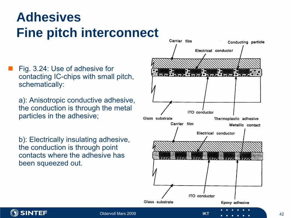
Adhesives Fine pitch interconnect
Fig. 3.24: Use of adhesive for contacting IC-chips with small pitch, schematically:
a): Anisotropic conductive adhesive, the conduction is through the metal particles in the adhesive;
b): Electrically insulating adhesive, the conduction is through point contacts where the adhesive has been squeezed out.
Oldervoll Mars 2009 IKT 43
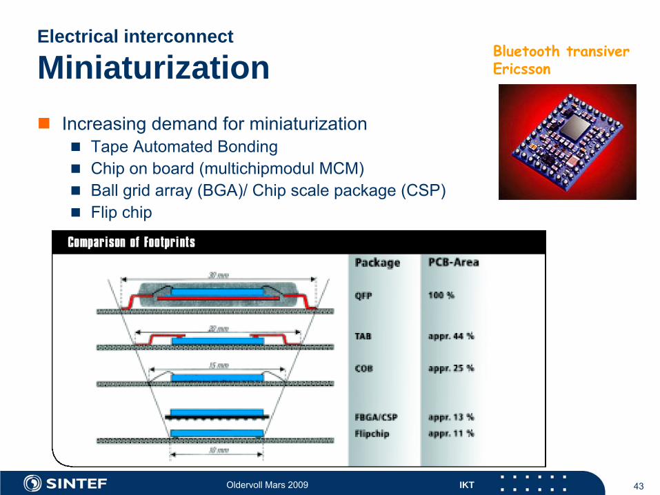
Electrical interconnect
Miniaturization
Increasing demand for miniaturization
Tape Automated Bonding
Chip on board (multichipmodul
MCM)
Ball grid array (BGA)/ Chip scale package (CSP)
Flip chip
Bluetooth transiverEricsson
Oldervoll Mars 2009 IKT 44
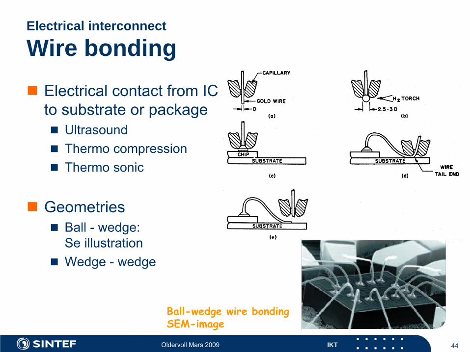
Electrical interconnect
Wire bonding
Electrical contact from IC to substrate or package
Ultrasound
Thermo compression
Thermo sonic
Geometries
Ball -
wedge:
Se illustration
Wedge -
wedge
Ball-wedge wire bonding SEM-image
Oldervoll Mars 2009 IKT 45
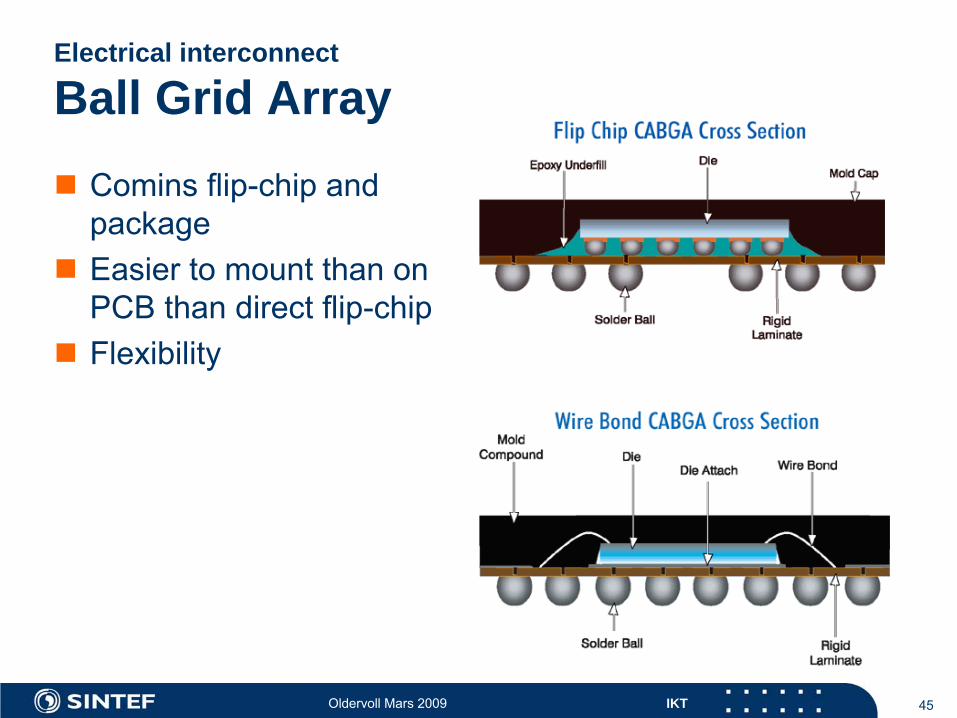
Electrical interconnect
Ball Grid Array
Comins
flip-chip and
package
Easier to mount than on PCB than direct flip-chip
Flexibility
Oldervoll Mars 2009 IKT 46
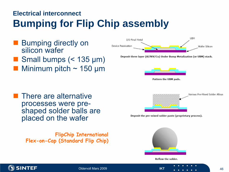
Electrical interconnect
Bumping for Flip Chip assembly
Bumping directly on silicon wafer
Small bumps (< 135 µm)
Minimum pitch ~ 150 µm
There are alternative processes were pre-
shaped solder balls are placed on the wafer
FlipChip
InternationalFlex-on-Cap (Standard Flip Chip)
Oldervoll Mars 2009 IKT 47
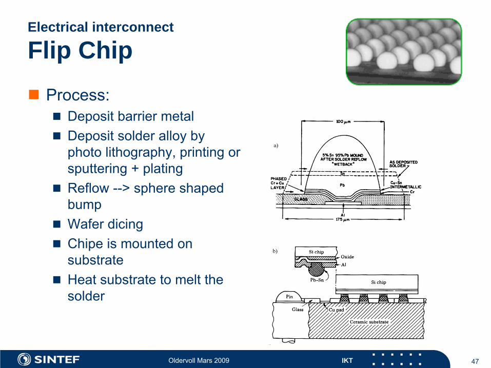
Electrical interconnect
Flip Chip
Process:
Deposit barrier metal
Deposit solder alloy by photo lithography, printing or sputtering + plating
Reflow --> sphere shaped bump
Wafer dicing
Chipe
is mounted on
substrate
Heat substrate to melt the solder
Oldervoll Mars 2009 IKT 48
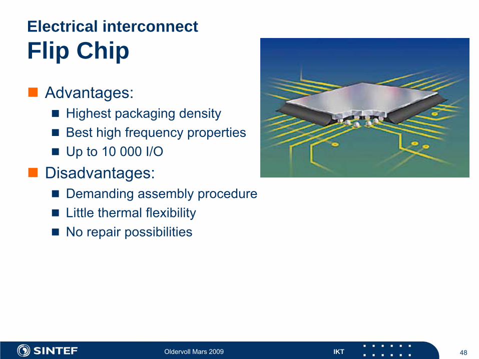
Electrical interconnect Flip Chip
Advantages:
Highest packaging density
Best high frequency properties
Up to 10 000 I/O
Disadvantages:
Demanding assembly procedure
Little thermal flexibility
No repair possibilities
Oldervoll Mars 2009 IKT 49
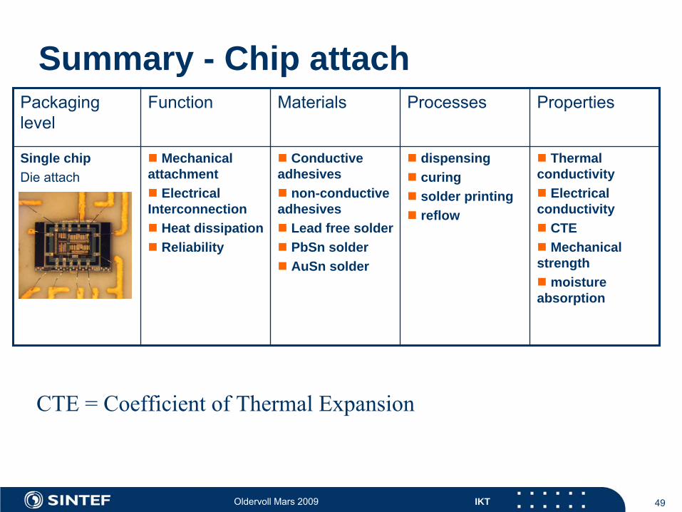
Packaging level
Function Materials Processes Properties
Single chipDie attach
Mechanical attachment
Electrical Interconnection Heat dissipation Reliability
Conductive adhesives
non-conductive adhesives Lead free solder PbSn solder AuSn solder
dispensing curing solder printing reflow
Thermal conductivity
Electrical conductivity CTE
Mechanical strength
moisture absorption
CTE
= Coefficient of Thermal Expansion
Summary - Chip attach
Oldervoll Mars 2009 IKT 50
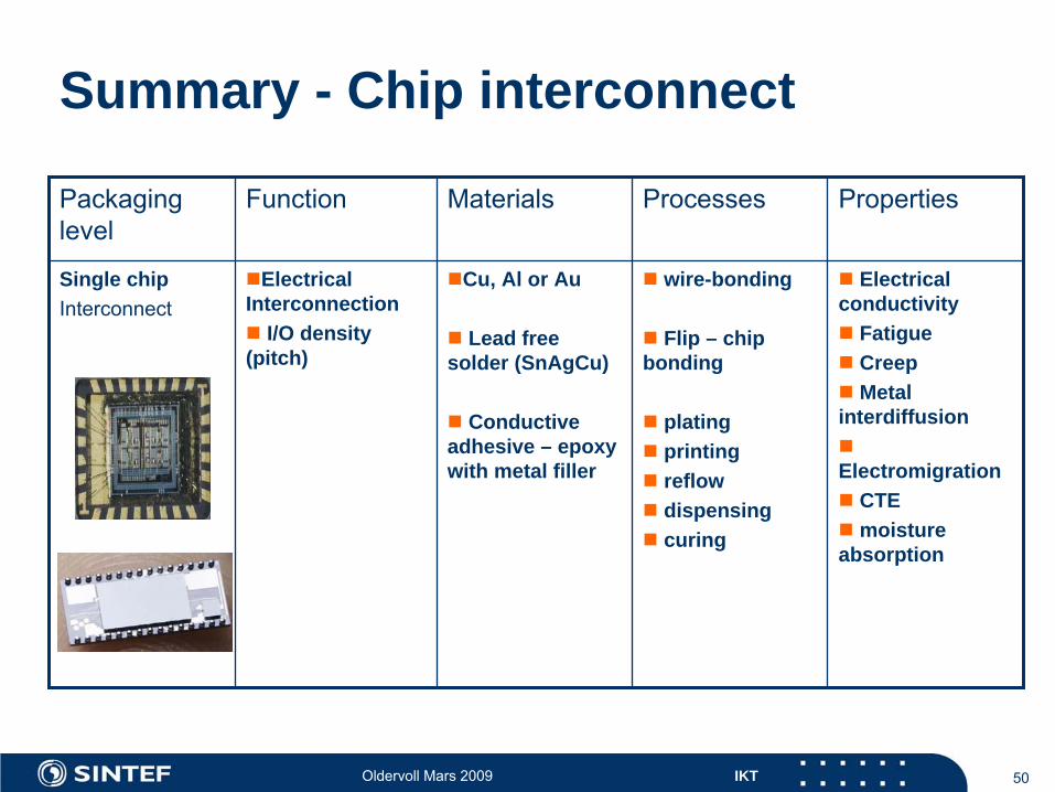
Summary - Chip interconnect
Packaging level
Function Materials Processes Properties
Single chipInterconnect
Electrical Interconnection
I/O density (pitch)
Cu, Al or Au
Lead free solder (SnAgCu)
Conductive adhesive – epoxy with metal filler
wire-bonding
Flip – chip bonding
plating printing reflow dispensing curing
Electrical conductivity Fatigue Creep
Metal interdiffusion
Electromigration CTE
moisture absorption
Oldervoll Mars 2009 IKT 51
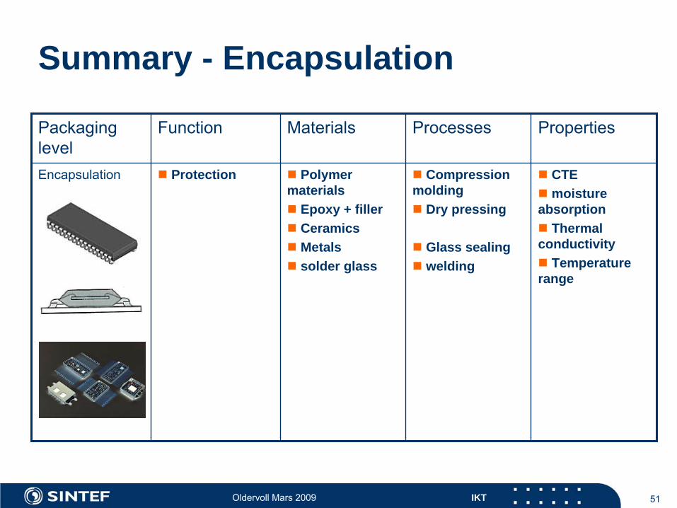
Summary - Encapsulation
Packaging level
Function Materials Processes Properties
Encapsulation Protection
Polymer materials Epoxy + filler Ceramics Metals solder glass
Compression molding Dry pressing
Glass sealing welding
CTE
moisture absorption
Thermal conductivity
Temperature range
Oldervoll Mars 2009 IKT 52
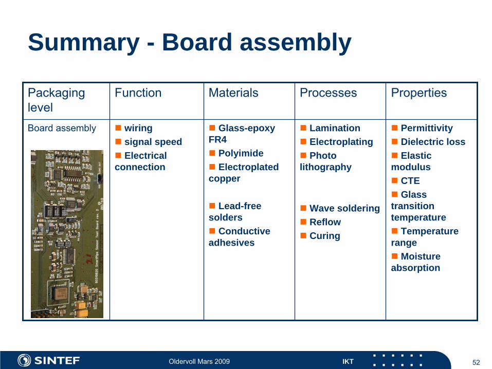
Summary - Board assembly
Packaging level
Function Materials Processes Properties
Board assembly wiring signal speed
Electrical connection
Glass-epoxy FR4 Polyimide
Electroplated copper
Lead-free solders
Conductive adhesives
Lamination Electroplating
Photo lithography
Wave soldering Reflow Curing
Permittivity Dielectric loss
Elastic modulus CTE
Glass transition temperature
Temperature range
Moisture absorption