Embed Size (px)
Citation preview
M
EZ
Pa
b
a
ARRA
KVZPV
1
ubeiZrfien[mttfnhtZ
G
0d
Materials Chemistry and Physics 122 (2010) 18–22
Contents lists available at ScienceDirect
Materials Chemistry and Physics
journa l homepage: www.e lsev ier .com/ locate /matchemphys
aterials science communication
ffect of ZnO seed layer on the catalytic growth of vertically alignednO nanorod arrays
.K. Giri a,b,∗, Soumen Dharaa, Ritun Chakrabortya
Department of Physics, Indian Institute of Technology Guwahati, Guwahati 781039, IndiaCentre for Nanotechnology, Indian Institute of Technology Guwahati, Guwahati 781039, India
r t i c l e i n f o
rticle history:eceived 25 August 2009eceived in revised form 25 January 2010ccepted 19 February 2010
eywords:ertically aligned nanorods
a b s t r a c t
We have grown vertically aligned ZnO nanorods and multipods by a seeded layer assistedvapor–liquid–solid (VLS) growth process using a muffle furnace. The effect of seed layer, substrate tem-perature and substrate material has been studied systematically for the growth of high quality alignednanorods. The structural analysis on the aligned nanorods shows c-axis oriented aligned growth byhomoepitaxy. High crystallinity and highly aligned ZnO nanorods are obtained for growth temperatureof 850–900 ◦C. Depending on the thickness of the ZnO seed layer and local temperature on the substrate,
nOhotoluminescenceLS
some region of a substrate show ZnO tetrapod, hexapods and multipods, in addition to the verticallyaligned nanorods. Raman scattering studies on the aligned nanorods show distinct mode at ∼438 cm−1,confirming the hexagonal wurtzite phase of the nanorods. Room temperature photoluminescence studiesshow strong near band edge emission at ∼378 nm for aligned nanorods, while the non-aligned nanorodsshow only defect-emission band at ∼500 nm. ZnO nanorods grown without the seed layer were found to
f mucssed.
be non-aligned and are oaligned nanorods is discu
. Introduction
ZnO nanostructures have attracted lots of interest due to itsnique features such as wide band-gap (3.37 eV) and large excitoninding energy (60 meV) [1,2] and wide applications in nanosizelectronic, optics, sensors and optoelectronic devices [3–6]. ZnOs one of the key materials in nanotechnology and nanosystems.nO have the capability to crystallize into many configurationsesulting in diverse growth morphologies such as nanocrystallinelms, rods, wires, springs, combs, belts, helixes, prisms, tetrapods,tc. [7–15]. Several techniques have been used to grow ZnOanowires. For example, thermal evaporation and condensation16], metalorganic chemical vapor deposition (MOCVD) [17] and
olecular beam epitaxy (MBE) [18] have been employed. Amonghem, the vapor–liquid–solid (VLS) deposition method involvinghe vapor-transfer process and thermal evaporation is the mostrequently used method. For the production of high quality ZnO
anowires/nanorods, catalysts, such as Au, Cu and NiO, etc. [19–21]ave been most commonly used. The catalysts can improve the con-rollable growth of ZnO nanostructures. Catalyst free growth of onlynO tripods [22] or tetrapods [15] has been reported. To our knowl-∗ Corresponding author at: Department of Physics, Indian Institute of Technologyuwahati, Guwahati 781039, India. Fax: +91 361 2690762.
E-mail address: [email protected] (P.K. Giri).
254-0584/$ – see front matter © 2010 Elsevier B.V. All rights reserved.oi:10.1016/j.matchemphys.2010.02.027
h inferior quality. Possible growth mechanism for the seeded layer grown
© 2010 Elsevier B.V. All rights reserved.
edge there was no such report on ZnO seed layer assisted growthof ZnO multipods (tetrapods and hexapods). Different groups havereported effect of ZnO seed layer for catalyst free growth of ZnOnanorods and its morphology, crystallinity and diameter by differ-ent methods [23–25]. The crystalline quality of the ZnO seed layerstrongly controlled the structural quality of the nanorods. In most ofthe cases synthesized nanorods were not aligned, hence have lim-ited applications in nanosize electronic and optoelectronic devices.Therefore, it is crucial to have controlled and well aligned growthof ZnO nanorod arrays. Ultra thin layer and uniform distributionof ZnO seed in the ZnO layer are the key factors for well alignedvertical growth of ZnO nanorods. Zhao et al. have reported hightemperature growth of vertically aligned ZnO nanorods on Si bywith a thin ZnO seed layer [26]. However, effects of growth tem-perature, substrate material and overall quality of the nanorodshave not been studied. Here, we report the effect of pre-depositingZnO seed layer on the structure, morphology and optical proper-ties of gold catalytic grown vertically aligned ZnO nanorods arraysat different temperatures.
In this work, we have grown vertically aligned ZnO nanorodsand multipods by a seeded layer growth techniques, using the VLS
process. The effect of ZnO seed layer along with an Au catalyst layerand the growth temperature in the growth of vertically alignedZnO nanorods are studied using structural and optical tools. Resultsare compared with the nanorods grown without the ZnO seedlayer.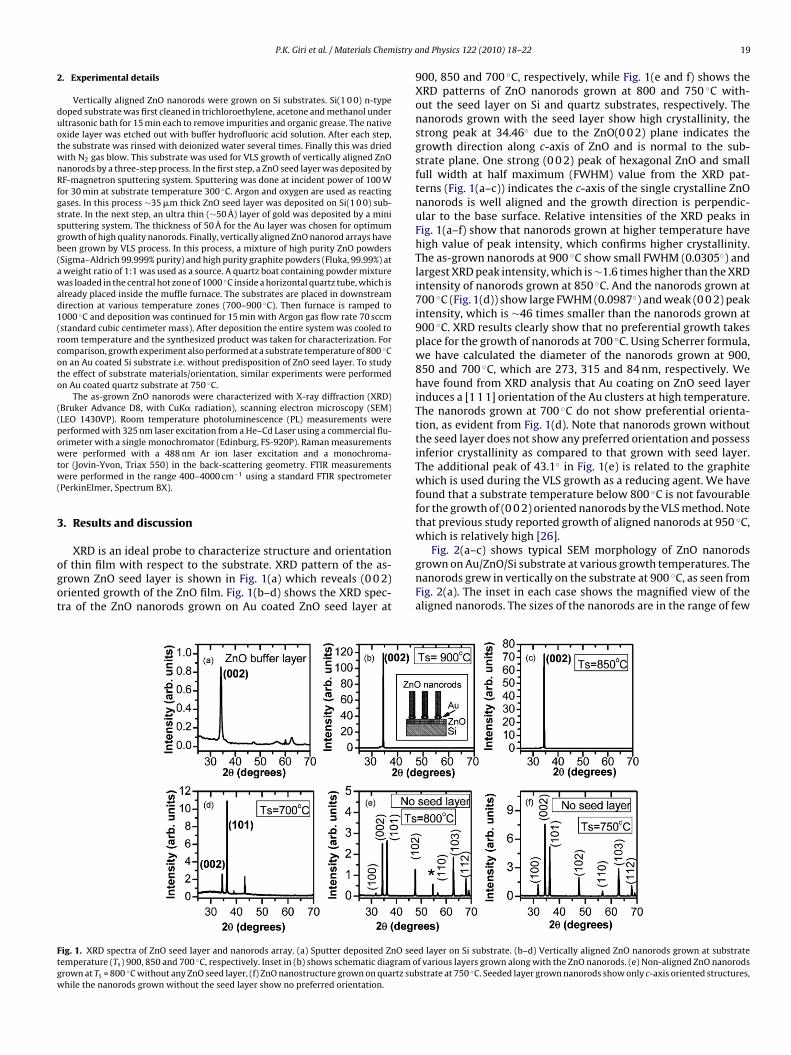
istry a
2
duotwnRfgssgb(awad1(rcoto
((powtw(
3
ogot
Ftgw
P.K. Giri et al. / Materials Chem
. Experimental details
Vertically aligned ZnO nanorods were grown on Si substrates. Si(1 0 0) n-typeoped substrate was first cleaned in trichloroethylene, acetone and methanol underltrasonic bath for 15 min each to remove impurities and organic grease. The nativexide layer was etched out with buffer hydrofluoric acid solution. After each step,he substrate was rinsed with deionized water several times. Finally this was driedith N2 gas blow. This substrate was used for VLS growth of vertically aligned ZnOanorods by a three-step process. In the first step, a ZnO seed layer was deposited byF-magnetron sputtering system. Sputtering was done at incident power of 100 W
or 30 min at substrate temperature 300 ◦C. Argon and oxygen are used as reactingases. In this process ∼35 �m thick ZnO seed layer was deposited on Si(1 0 0) sub-trate. In the next step, an ultra thin (∼50 Å) layer of gold was deposited by a miniputtering system. The thickness of 50 Å for the Au layer was chosen for optimumrowth of high quality nanorods. Finally, vertically aligned ZnO nanorod arrays haveeen grown by VLS process. In this process, a mixture of high purity ZnO powdersSigma–Aldrich 99.999% purity) and high purity graphite powders (Fluka, 99.99%) atweight ratio of 1:1 was used as a source. A quartz boat containing powder mixtureas loaded in the central hot zone of 1000 ◦C inside a horizontal quartz tube, which is
lready placed inside the muffle furnace. The substrates are placed in downstreamirection at various temperature zones (700–900 ◦C). Then furnace is ramped to000 ◦C and deposition was continued for 15 min with Argon gas flow rate 70 sccmstandard cubic centimeter mass). After deposition the entire system was cooled tooom temperature and the synthesized product was taken for characterization. Foromparison, growth experiment also performed at a substrate temperature of 800 ◦Cn an Au coated Si substrate i.e. without predisposition of ZnO seed layer. To studyhe effect of substrate materials/orientation, similar experiments were performedn Au coated quartz substrate at 750 ◦C.
The as-grown ZnO nanorods were characterized with X-ray diffraction (XRD)Bruker Advance D8, with CuK� radiation), scanning electron microscopy (SEM)LEO 1430VP). Room temperature photoluminescence (PL) measurements wereerformed with 325 nm laser excitation from a He–Cd Laser using a commercial flu-rimeter with a single monochromator (Edinburg, FS-920P). Raman measurementsere performed with a 488 nm Ar ion laser excitation and a monochroma-
or (Jovin-Yvon, Triax 550) in the back-scattering geometry. FTIR measurementsere performed in the range 400–4000 cm−1 using a standard FTIR spectrometer
PerkinElmer, Spectrum BX).
. Results and discussion
XRD is an ideal probe to characterize structure and orientationf thin film with respect to the substrate. XRD pattern of the as-rown ZnO seed layer is shown in Fig. 1(a) which reveals (0 0 2)riented growth of the ZnO film. Fig. 1(b–d) shows the XRD spec-ra of the ZnO nanorods grown on Au coated ZnO seed layer at
ig. 1. XRD spectra of ZnO seed layer and nanorods array. (a) Sputter deposited ZnO seeemperature (Ts) 900, 850 and 700 ◦C, respectively. Inset in (b) shows schematic diagram orown at Ts = 800 ◦C without any ZnO seed layer, (f) ZnO nanostructure grown on quartz subhile the nanorods grown without the seed layer show no preferred orientation.
nd Physics 122 (2010) 18–22 19
900, 850 and 700 ◦C, respectively, while Fig. 1(e and f) shows theXRD patterns of ZnO nanorods grown at 800 and 750 ◦C with-out the seed layer on Si and quartz substrates, respectively. Thenanorods grown with the seed layer show high crystallinity, thestrong peak at 34.46◦ due to the ZnO(0 0 2) plane indicates thegrowth direction along c-axis of ZnO and is normal to the sub-strate plane. One strong (0 0 2) peak of hexagonal ZnO and smallfull width at half maximum (FWHM) value from the XRD pat-terns (Fig. 1(a–c)) indicates the c-axis of the single crystalline ZnOnanorods is well aligned and the growth direction is perpendic-ular to the base surface. Relative intensities of the XRD peaks inFig. 1(a–f) show that nanorods grown at higher temperature havehigh value of peak intensity, which confirms higher crystallinity.The as-grown nanorods at 900 ◦C show small FWHM (0.0305◦) andlargest XRD peak intensity, which is ∼1.6 times higher than the XRDintensity of nanorods grown at 850 ◦C. And the nanorods grown at700 ◦C (Fig. 1(d)) show large FWHM (0.0987◦) and weak (0 0 2) peakintensity, which is ∼46 times smaller than the nanorods grown at900 ◦C. XRD results clearly show that no preferential growth takesplace for the growth of nanorods at 700 ◦C. Using Scherrer formula,we have calculated the diameter of the nanorods grown at 900,850 and 700 ◦C, which are 273, 315 and 84 nm, respectively. Wehave found from XRD analysis that Au coating on ZnO seed layerinduces a [1 1 1] orientation of the Au clusters at high temperature.The nanorods grown at 700 ◦C do not show preferential orienta-tion, as evident from Fig. 1(d). Note that nanorods grown withoutthe seed layer does not show any preferred orientation and possessinferior crystallinity as compared to that grown with seed layer.The additional peak of 43.1◦ in Fig. 1(e) is related to the graphitewhich is used during the VLS growth as a reducing agent. We havefound that a substrate temperature below 800 ◦C is not favourablefor the growth of (0 0 2) oriented nanorods by the VLS method. Notethat previous study reported growth of aligned nanorods at 950 ◦C,which is relatively high [26].
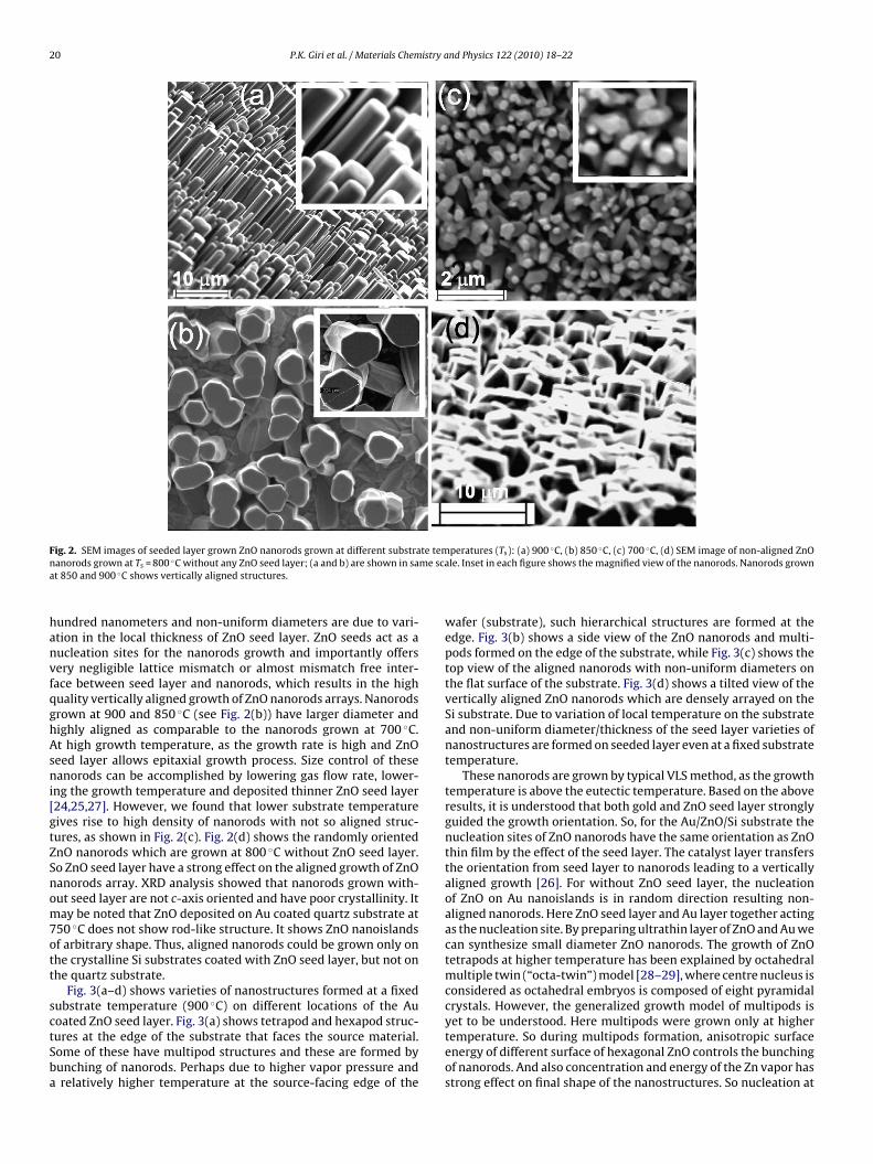
Fig. 2(a–c) shows typical SEM morphology of ZnO nanorodsgrown on Au/ZnO/Si substrate at various growth temperatures. Thenanorods grew in vertically on the substrate at 900 ◦C, as seen fromFig. 2(a). The inset in each case shows the magnified view of thealigned nanorods. The sizes of the nanorods are in the range of few
d layer on Si substrate. (b–d) Vertically aligned ZnO nanorods grown at substratef various layers grown along with the ZnO nanorods. (e) Non-aligned ZnO nanorodsstrate at 750 ◦C. Seeded layer grown nanorods show only c-axis oriented structures,
20 P.K. Giri et al. / Materials Chemistry and Physics 122 (2010) 18–22
F te temn me scaa
hanvfqghAsni[gtZSnom7ott
sctSba
ig. 2. SEM images of seeded layer grown ZnO nanorods grown at different substraanorods grown at Ts = 800 ◦C without any ZnO seed layer; (a and b) are shown in sat 850 and 900 ◦C shows vertically aligned structures.
undred nanometers and non-uniform diameters are due to vari-tion in the local thickness of ZnO seed layer. ZnO seeds act as aucleation sites for the nanorods growth and importantly offersery negligible lattice mismatch or almost mismatch free inter-ace between seed layer and nanorods, which results in the highuality vertically aligned growth of ZnO nanorods arrays. Nanorodsrown at 900 and 850 ◦C (see Fig. 2(b)) have larger diameter andighly aligned as comparable to the nanorods grown at 700 ◦C.t high growth temperature, as the growth rate is high and ZnOeed layer allows epitaxial growth process. Size control of theseanorods can be accomplished by lowering gas flow rate, lower-
ng the growth temperature and deposited thinner ZnO seed layer24,25,27]. However, we found that lower substrate temperatureives rise to high density of nanorods with not so aligned struc-ures, as shown in Fig. 2(c). Fig. 2(d) shows the randomly orientednO nanorods which are grown at 800 ◦C without ZnO seed layer.o ZnO seed layer have a strong effect on the aligned growth of ZnOanorods array. XRD analysis showed that nanorods grown with-ut seed layer are not c-axis oriented and have poor crystallinity. Itay be noted that ZnO deposited on Au coated quartz substrate at
50 ◦C does not show rod-like structure. It shows ZnO nanoislandsf arbitrary shape. Thus, aligned nanorods could be grown only onhe crystalline Si substrates coated with ZnO seed layer, but not onhe quartz substrate.
Fig. 3(a–d) shows varieties of nanostructures formed at a fixedubstrate temperature (900 ◦C) on different locations of the Au
oated ZnO seed layer. Fig. 3(a) shows tetrapod and hexapod struc-ures at the edge of the substrate that faces the source material.ome of these have multipod structures and these are formed byunching of nanorods. Perhaps due to higher vapor pressure andrelatively higher temperature at the source-facing edge of theperatures (Ts): (a) 900 ◦C, (b) 850 ◦C, (c) 700 ◦C, (d) SEM image of non-aligned ZnOle. Inset in each figure shows the magnified view of the nanorods. Nanorods grown
wafer (substrate), such hierarchical structures are formed at theedge. Fig. 3(b) shows a side view of the ZnO nanorods and multi-pods formed on the edge of the substrate, while Fig. 3(c) shows thetop view of the aligned nanorods with non-uniform diameters onthe flat surface of the substrate. Fig. 3(d) shows a tilted view of thevertically aligned ZnO nanorods which are densely arrayed on theSi substrate. Due to variation of local temperature on the substrateand non-uniform diameter/thickness of the seed layer varieties ofnanostructures are formed on seeded layer even at a fixed substratetemperature.
These nanorods are grown by typical VLS method, as the growthtemperature is above the eutectic temperature. Based on the aboveresults, it is understood that both gold and ZnO seed layer stronglyguided the growth orientation. So, for the Au/ZnO/Si substrate thenucleation sites of ZnO nanorods have the same orientation as ZnOthin film by the effect of the seed layer. The catalyst layer transfersthe orientation from seed layer to nanorods leading to a verticallyaligned growth [26]. For without ZnO seed layer, the nucleationof ZnO on Au nanoislands is in random direction resulting non-aligned nanorods. Here ZnO seed layer and Au layer together actingas the nucleation site. By preparing ultrathin layer of ZnO and Au wecan synthesize small diameter ZnO nanorods. The growth of ZnOtetrapods at higher temperature has been explained by octahedralmultiple twin (“octa-twin”) model [28–29], where centre nucleus isconsidered as octahedral embryos is composed of eight pyramidalcrystals. However, the generalized growth model of multipods is
yet to be understood. Here multipods were grown only at highertemperature. So during multipods formation, anisotropic surfaceenergy of different surface of hexagonal ZnO controls the bunchingof nanorods. And also concentration and energy of the Zn vapor hasstrong effect on final shape of the nanostructures. So nucleation at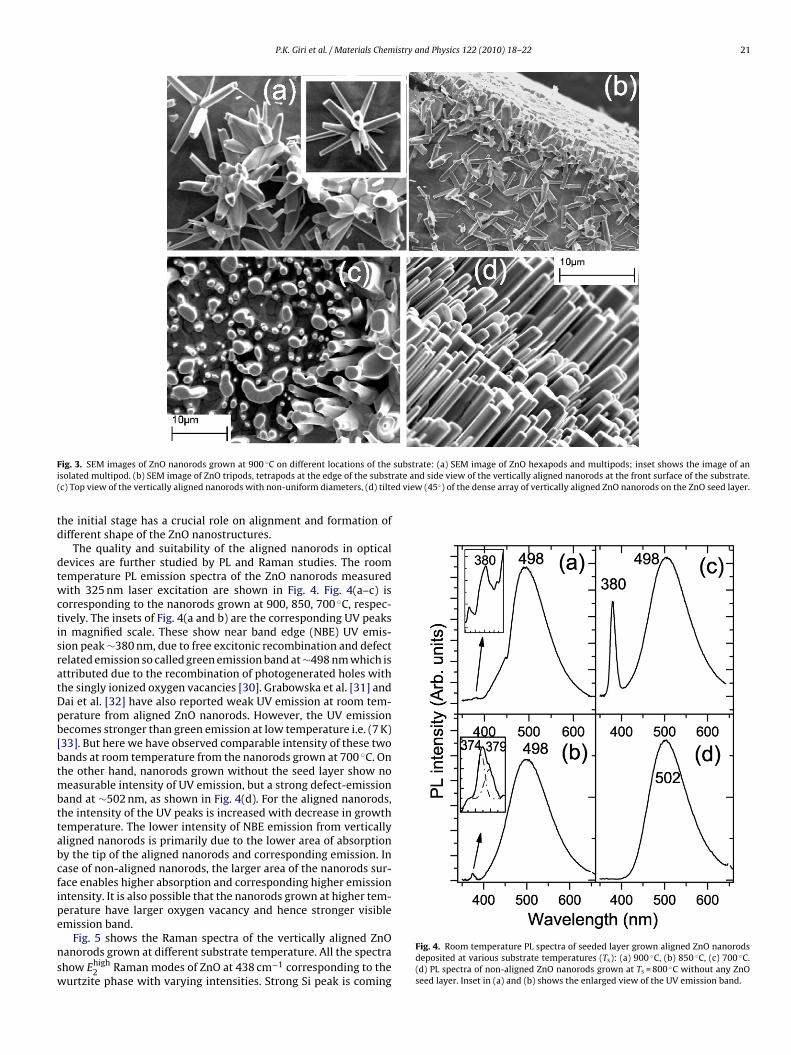
P.K. Giri et al. / Materials Chemistry and Physics 122 (2010) 18–22 21
F substrate: (a) SEM image of ZnO hexapods and multipods; inset shows the image of ani rate and side view of the vertically aligned nanorods at the front surface of the substrate.( d view (45◦) of the dense array of vertically aligned ZnO nanorods on the ZnO seed layer.
td
dtwctisratDpb[btmbttabcfipe
nsw
ig. 3. SEM images of ZnO nanorods grown at 900 ◦C on different locations of thesolated multipod. (b) SEM image of ZnO tripods, tetrapods at the edge of the substc) Top view of the vertically aligned nanorods with non-uniform diameters, (d) tilte
he initial stage has a crucial role on alignment and formation ofifferent shape of the ZnO nanostructures.
The quality and suitability of the aligned nanorods in opticalevices are further studied by PL and Raman studies. The roomemperature PL emission spectra of the ZnO nanorods measuredith 325 nm laser excitation are shown in Fig. 4. Fig. 4(a–c) is
orresponding to the nanorods grown at 900, 850, 700 ◦C, respec-ively. The insets of Fig. 4(a and b) are the corresponding UV peaksn magnified scale. These show near band edge (NBE) UV emis-ion peak ∼380 nm, due to free excitonic recombination and defectelated emission so called green emission band at ∼498 nm which isttributed due to the recombination of photogenerated holes withhe singly ionized oxygen vacancies [30]. Grabowska et al. [31] andai et al. [32] have also reported weak UV emission at room tem-erature from aligned ZnO nanorods. However, the UV emissionecomes stronger than green emission at low temperature i.e. (7 K)33]. But here we have observed comparable intensity of these twoands at room temperature from the nanorods grown at 700 ◦C. Onhe other hand, nanorods grown without the seed layer show no
easurable intensity of UV emission, but a strong defect-emissionand at ∼502 nm, as shown in Fig. 4(d). For the aligned nanorods,he intensity of the UV peaks is increased with decrease in growthemperature. The lower intensity of NBE emission from verticallyligned nanorods is primarily due to the lower area of absorptiony the tip of the aligned nanorods and corresponding emission. Inase of non-aligned nanorods, the larger area of the nanorods sur-ace enables higher absorption and corresponding higher emissionntensity. It is also possible that the nanorods grown at higher tem-erature have larger oxygen vacancy and hence stronger visible
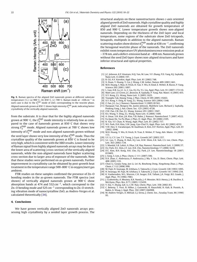
mission band.Fig. 5 shows the Raman spectra of the vertically aligned ZnOanorods grown at different substrate temperature. All the spectrahow Ehigh
2 Raman modes of ZnO at 438 cm−1 corresponding to theurtzite phase with varying intensities. Strong Si peak is coming
Fig. 4. Room temperature PL spectra of seeded layer grown aligned ZnO nanorodsdeposited at various substrate temperatures (Ts): (a) 900 ◦C, (b) 850 ◦C, (c) 700 ◦C.(d) PL spectra of non-aligned ZnO nanorods grown at Ts = 800 ◦C without any ZnOseed layer. Inset in (a) and (b) shows the enlarged view of the UV emission band.
22 P.K. Giri et al. / Materials Chemistry a
Fig. 5. Raman spectra of the aligned ZnO nanorods grown at different substratete
Ac
fgps
i
tcvotnctita
bsaZic
4
s
[[
[[[[[[[
[
[[
[[[
[[
[
[[[
[McGlynn, Phys. Rev. B 71 (2005) 115439.
[32] Y. Dai, Y. Zhang, Q.K. Li, C.W. Nan, Chem. Phys. Lett. 358 (2002) 83.[33] C. Bekeny, T. Voss, B. Hilker, J. Gutowski, R. Hauschild, H. Kalt, B. Postels, A.
Bakin, A. Waag, J. Appl. Phys. 102 (2007) 044908.[34] M. Andres-Verges, A. Mifsud, C.J. Serna, J. Chem. Soc., Faraday Trans. 86 (1990)
95.
emperature (Ts); (a) 900 ◦C, (b) 850 ◦C, (c) 700 ◦C. Raman mode at ∼438 cm−1 inach case is due to the Ehigh
2 mode of ZnO, corresponding to the wurzite phase.
ligned nanorods grown at 850 ◦C shows high intensity Ehigh2 peak, indicating better
rystallinity of the vertically aligned nanorods.
rom the substrate. It is clear that for the highly aligned nanorodsrown at 900 ◦C, the Ehigh
2 mode intensity is relatively low as com-ared to the case of nanorods grown at 850 ◦C that shows verytrong Ehigh
2 mode. Aligned nanorods grown at 700 ◦C shows low
ntensity of Ehigh2 mode and non-aligned nanorods grown without
he seed layer shows very low intensity of the Ehigh2 mode. Thus the
rystalline quality of the nanorods grown at 850 ◦C is found to beery high, which is consistent with the XRD results. Lower intensityf Raman signal from highly aligned nanorods arrays may be due tohe lower area of scattering (cross-section) of the vertically alignedanorods, while the non-aligned nanorods have higher scatteringross-section due to larger area of exposure of the nanorods. Notehat these studies were performed on as-grown nanorods. Furthermprovement in crystallinity can be obtained by post-growth heatreatment in the temperature range 500–800 ◦C in oxygen/inert gasmbient.
FTIR studies on these samples confirmed the presence of Zn–Oonding modes in the as-grown nanorods. The FTIR spectra (nothown) of vertically aligned nanorods grown at 900 ◦C showbsorption bands at 474 and 532 cm−1, which correspond to then–O bending mode and 525 cm−1 corresponding to Zn–O stretch-ng vibration mode of nanocrystalline ZnO, as Andres-Verges et al.alculated theoretically [34].
. Conclusions
We have grown vertically aligned ZnO nanorods arrays pos-essing high crystallinity by a seeded layer growth process. The
nd Physics 122 (2010) 18–22
structural analysis on these nanostructures shows c-axis orientedaligned growth of ZnO nanorods. High crystalline quality and highlyaligned ZnO nanorods are obtained for growth temperature of850 and 900 ◦C. Lower temperature growth shows non-alignednanorods. Depending on the thickness of the ZnO layer and localtemperature, some regions of the substrate show ZnO tetrapods,hexapods, multipods in addition to the aligned nanorods. Ramanscattering studies show distinct Ehigh
2 mode at 438 cm−1, confirmingthe hexagonal wurtzite phase of the nanorods. The ZnO nanorodsexhibit room temperature UV photoluminescence emission peak at∼378 nm, and a defect-emission band at ∼498 nm. Nanorods grownwithout the seed ZnO layer shows non-aligned structures and haveinferior structural and optical properties.
References
[1] J.C. Johnson, K.P. Knutsen, H.Q. Yan, M. Law, Y.F. Zhang, P.D. Yang, R.J. Saykally,Nano Lett. 4 (2004) 197.
[2] B. Gil, A.V. Kavokin, Appl. Phys. Lett. 81 (2002) 748.[3] X. Duan, Y. Huang, Y. Cui, J. Wang, C.M. Lieber, Nature 409 (2001) 661.[4] M.H. Huang, S. Mao, H. Feick, H. Yan, Y. Wu, H. Kind, E. Weber, R. Russo, P. Yang,
Science 292 (2001) 1897.[5] L. Liao, H.B. Lu, J.C. Li, C. Liu, D.J. Fu, Y.L. Liu, Appl. Phys. Lett. 91 (2007) 173110.[6] Matt Law, L.E Green, J.C. Jhonson, R. Saykally, P. Yang, Nat. Mater. 4 (2005) 455.[7] X.Y. Kong, Z.L. Wang, Nano Lett. 3 (2003) 1625.[8] Youngho Tak, Kijung Yong, J. Phys. Chem. B 109 (2005) 19263.[9] X.Y. Kong, Y. Ding, R. Yang, Z.L. Wang, Science 303 (2004) 1348.10] Z. Fan, J.G. Lu, J. Nanosci. Nanotechnol. 5 (2005) R1561.11] Haoquan Yan, Rongrui He, Justin Johnson, Matthew Law, Richard J. Saykally,
Peidong Yang, J. Am. Chem. Soc. 125 (2003) 4728.12] Z.W. Pan, Z.R. Dai, Z.L. Wang, Science 291 (2001) 1947.13] R.S. Wang, Y. Ding, Z.L. Wang, Nano Lett. 4 (2004) 1309.14] A. Umar, S.H. Kim, J.H. Kim, Y.B. Hahn, J. Nanosci. Nanotechnol. 7 (2007) 4522.15] Fa-Quan He, Ya-Pu Zhao, J. Phys. D: Appl. Phys. 39 (2006) 2105.16] B. Yao, Y.F. Chan, N. Wang, Appl. Phys. Lett. 81 (2002) 757.17] W.I. Park, D.H. Kim, S.W. Jung, Gyu-Chul Yi, Appl. Phys. Lett. 82 (2002) 4232.18] Y.W. Heo, V. Varadarajan, M. Kaufman, K. Kim, D.P. Norton, Appl. Phys. Lett. 81
(2002) 3046.19] M.H. Huang, Y. Wu, H. Feick, N. Tran, E. Weber, P. Yang, Adv. Mater. 13 (2001)
113.20] S.Y. Li, C.Y. Lee, T.Y. Tseng, J. Cryst. Growth 247 (2003) 357.21] S.C. Lyu, Y. Zhang, H. Ruh, H.J. Lee, H.W. Shim, E.K. Suh, C.S. Lee, Chem. Phys.
Lett. 363 (2002) 134.22] S. Mandal, S.K. Lahiri, A. Dhar, S.K. Ray, Nanosci. Nanotechnol. Lett. 1 (2009) 57.23] D.J. Park, D.C. Kim, J.Y. Lee, H.K. Cho, Nanotechnology 17 (2006) 5238.24] D.C. Kim, B.H. Kong, H.K. Cho, D.J. Park, J.Y. Lee, Nanotechnology 18 (2007)
015603.25] J. Song, S. Lim, J. Phys. Chem. C 111 (2007) 596.26] D.X. Zhao, C. Andreazza, P. Andreazza, J. Ma, Y. Liu, D. Shen, Chem. Phys. Lett.
408 (2005) 335.27] Chun Li, Guojia Fang, Jun Li, Lei Ai, Binzhong Dong, Xingzhong Zhao, J. Phys.
Chem. C 112 (2008) 990.28] M. Fujii, H. Iwanaga, M. Ichihara, S. Takeuchi, J. Cryst. Growth 128 (1993) 1095.29] H. Iwanaga, M. Fujii, M. Ichihara, S. Takeuchi, J. Cryst. Growth 141 (1994) 234.30] K. Vanheusden, W.L. Warren, C.H. Seager, D.K. Tallant, J.A. Voigt, B.E. Gnade, J.
Appl. Phys. 79 (1996) 7983.31] J. Grabowska, A. Meaney, K.K. Nanda, J.-P. Mosnier, M.O. Henry, J.-R. Duclère, E.