Embed Size (px)
Citation preview
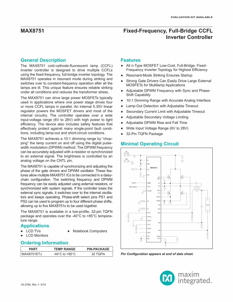
General DescriptionThe MAX8751 cold-cathode-fluorescent lamp (CCFL) inverter controller is designed to drive multiple CCFLs using the fixed-frequency, full-bridge inverter topology. The MAX8751 operates in resonant mode during striking and switches over to constant-frequency operation after all the lamps are lit. This unique feature ensures reliable striking under all conditions and reduces the transformer stress.The MAX8751 can drive large power MOSFETs typically used in applications where one power stage drives four or more CCFL lamps in parallel. An internal 5.35V linear regulator powers the MOSFET drivers and most of the internal circuitry. The controller operates over a wide input-voltage range (6V to 28V) with high power to light efficiency. The device also includes safety features that effectively protect against many single-point fault condi-tions, including lamp-out and short-circuit conditions.The MAX8751 achieves a 10:1 dimming range by “chop-ping” the lamp current on and off using the digital pulse-width modulation (DPWM) method. The DPWM frequency can be accurately adjusted with a resistor or synchronized to an external signal. The brightness is controlled by an analog voltage on the CNTL pin.The MAX8751 is capable of synchronizing and adjusting the phase of the gate drivers and DPWM oscillator. These fea-tures allow multiple MAX8751 ICs to be connected in a daisy-chain configuration. The switching frequency and DPWM frequency can be easily adjusted using external resistors, or synchronized with system signals. If the controller loses the external sync signals, it switches over to the internal oscilla-tors and keeps operating. Phase-shift select pins PS1 and PS2 can be used to program up to four different phase shifts, allowing up to five MAX8751s to be used together.The MAX8751 is available in a low-profile, 32-pin TQFN package and operates over the -40°C to +85°C tempera-ture range.Applications
LCD TVs LCD Monitors
Notebook Computers
Features All n-Type MOSFET Low-Cost, Full-Bridge, Fixed-
Frequency Inverter Topology for Highest Efficiency Resonant-Mode Striking Ensures Startup Strong Gate Drivers Can Easily Drive Large External
MOSFETs for Multilamp Applications Adjustable DPWM Frequency with Sync and Phase-
Shift Capability 10:1 Dimming Range with Accurate Analog Interface Lamp-Out Detection with Adjustable Timeout Secondary Current Limit with Adjustable Timeout Adjustable Secondary Voltage Limiting Adjustable DPWM Rise and Fall Time Wide Input Voltage Range (6V to 28V) 32-Pin TQFN Package
Pin Configuration appears at end of data sheet.
19-3784; Rev 1; 5/14
PART TEMP RANGE PIN-PACKAGEMAX8751ETJ -40°C to +85°C 32 TQFN
MAX8751
CCFL
VIN7V TO 24V
GND
GH2
LX2
BST2
BST1
LX1
GH1
GL1
IN
IFB
VFB
GL2
BRIGHTNESS
ON/OFF
ISEC
CNTL
LF
PGND2
VCC
GND
VCC
PS1
PS2
HFCK
LFCK
PSCK
DPWM
T1
PGND1
LSYNC
HSYNC
PCOMP
SEL
COMPTFLT
HF
3A
SHDN
MAX8751 Fixed-Frequency, Full-Bridge CCFLInverter Controller
Minimal Operating Circuit
Ordering Information
EVALUATION KIT AVAILABLE
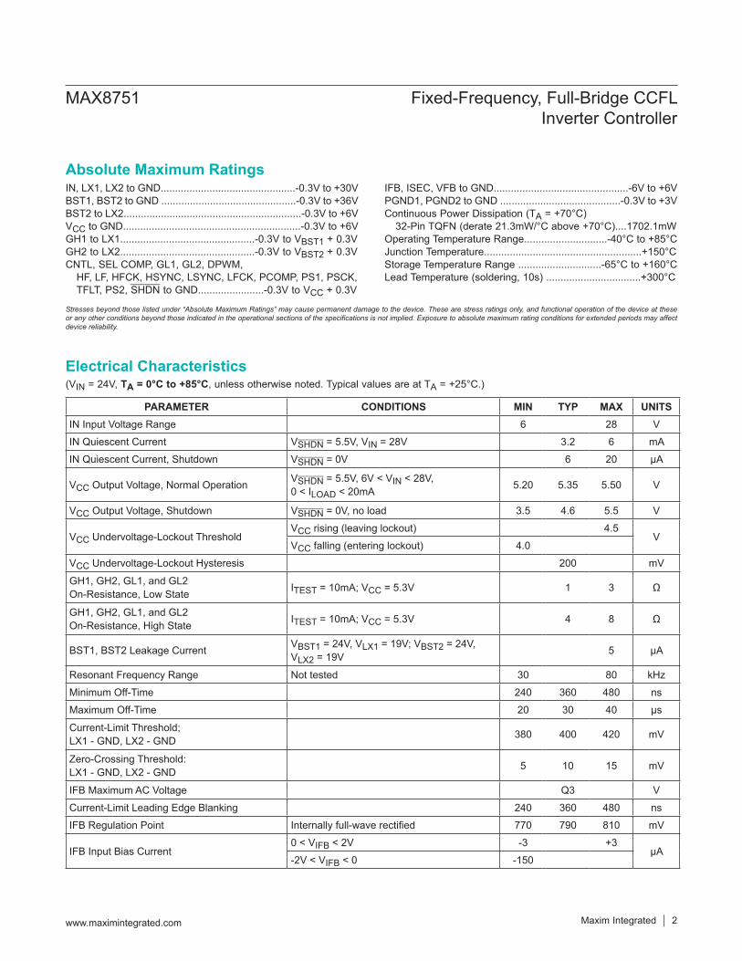
IN, LX1, LX2 to GND...............................................-0.3V to +30VBST1, BST2 to GND ...............................................-0.3V to +36VBST2 to LX2..............................................................-0.3V to +6VVCC to GND..............................................................-0.3V to +6VGH1 to LX1...............................................-0.3V to VBST1 + 0.3VGH2 to LX2...............................................-0.3V to VBST2 + 0.3VCNTL, SEL COMP, GL1, GL2, DPWM,
HF, LF, HFCK, HSYNC, LSYNC, LFCK, PCOMP, PS1, PSCK, TFLT, PS2, SHDN to GND.......................-0.3V to VCC + 0.3V
IFB, ISEC, VFB to GND...............................................-6V to +6VPGND1, PGND2 to GND ..........................................-0.3V to +3VContinuous Power Dissipation (TA = +70°C)
32-Pin TQFN (derate 21.3mW/°C above +70°C)....1702.1mWOperating Temperature Range.............................-40°C to +85°CJunction Temperature.......................................................+150°CStorage Temperature Range .............................-65°C to +160°CLead Temperature (soldering, 10s) .................................+300°C
(VIN = 24V, TA = 0°C to +85°C, unless otherwise noted. Typical values are at TA = +25°C.)
PARAMETER CONDITIONS MIN TYP MAX UNITSIN Input Voltage Range 6 28 V
IN Quiescent Current VSHDN = 5.5V, VIN = 28V 3.2 6 mA
IN Quiescent Current, Shutdown VSHDN = 0V 6 20 µA
VCC Output Voltage, Normal Operation VSHDN = 5.5V, 6V < VIN < 28V,0 < ILOAD < 20mA 5.20 5.35 5.50 V
VCC Output Voltage, Shutdown VSHDN = 0V, no load 3.5 4.6 5.5 V
VCC Undervoltage-Lockout ThresholdVCC rising (leaving lockout) 4.5
VVCC falling (entering lockout) 4.0
VCC Undervoltage-Lockout Hysteresis 200 mV
GH1, GH2, GL1, and GL2 On-Resistance, Low State ITEST = 10mA; VCC = 5.3V 1 3 Ω
GH1, GH2, GL1, and GL2 On-Resistance, High State ITEST = 10mA; VCC = 5.3V 4 8 Ω
BST1, BST2 Leakage Current VBST1 = 24V, VLX1 = 19V; VBST2 = 24V, VLX2 = 19V 5 µA
Resonant Frequency Range Not tested 30 80 kHz
Minimum Off-Time 240 360 480 ns
Maximum Off-Time 20 30 40 µs
Current-Limit Threshold; LX1 - GND, LX2 - GND 380 400 420 mV
Zero-Crossing Threshold: LX1 - GND, LX2 - GND 5 10 15 mV
IFB Maximum AC Voltage Q3 V
Current-Limit Leading Edge Blanking 240 360 480 ns
IFB Regulation Point Internally full-wave rectified 770 790 810 mV
IFB Input Bias Current0 < VIFB < 2V -3 +3
µA-2V < VIFB < 0 -150
MAX8751 Fixed-Frequency, Full-Bridge CCFLInverter Controller
www.maximintegrated.com Maxim Integrated 2
Absolute Maximum Ratings
Stresses beyond those listed under “Absolute Maximum Ratings” may cause permanent damage to the device. These are stress ratings only, and functional operation of the device at these or any other conditions beyond those indicated in the operational sections of the specifications is not implied. Exposure to absolute maximum rating conditions for extended periods may affect device reliability.
Electrical Characteristics

(VIN = 24V, TA = 0°C to +85°C, unless otherwise noted. Typical values are at TA = +25°C.)
PARAMETER CONDITIONS MIN TYP MAX UNITSIFB Lamp-Out Threshold Reject 1µs glitches 730 780 830 mV
IFB-to-COMP Transconductance 1V < VCOMP < 2.5V 100 µS
COMP Output Impedance 10 MΩ
COMP Discharge Current During Overvoltage or Overcurrent Fault VIFB = 800mV, VISEC = 2.5V 1200 µA
COMP Discharge Current During DPWM Off-Time CNTL = GND, VCOMP = 1.5V 100 µA
ISEC Input Bias Current -0.3 +0.3 µA
ISEC Overcurrent Threshold 1.18 1.22 1.26 V
VFB Input Bias Current -4V < VVFB < +4V -25 +25 µA
VFB Overvoltage Threshold 2.10 2.25 2.40 V
Main Oscillator Frequency RHF = 100kΩ 52.2 53.8 55.4 kHz
Main Oscillator Frequency Range 20 100 kHzHF, LF, HFCK, LFCK Input-Low Voltage Slave mode, VCNTL = VCC 0.8 VHF, LF, HFCK, LFCK Input-High Voltage Slave mode, VCNTL = VCC 2.1 VHF, LF, HFCK, LFCK Input Hysteresis Slave mode, VCNTL = VCC 100 mVHF, LF, HFCK, LFCKInput Bias Current Slave mode, VCNTL = VCC -1 +1 µA
HF Input-Frequency Range Slave mode, VCNTL = VCC 20 100 kHz
HF, LF, HFCK, LFCKInput Rise and Fall Time Slave mode, VCNTL = VCC 200 ns
HSYNC, LSYNC Input-Low Voltage 0.8 V
HSYNC, LSYNC Input-High Voltage 2.1 V
HSYNC, LSYNC Input Hysteresis 100 mV
HSYNC, LSYNC Input Bias Current -1 +1 µA
HSYNC Input Frequency Range 190 460 kHz
HSYNC, LSYNC Input Rise and Fall Time 200 ns
DPWM Chopping Frequency RLF = 150kΩ 202 208 214 Hz
DPWM Chopping Frequency Range 80 300 Hz
MAX8751 Fixed-Frequency, Full-Bridge CCFLInverter Controller
www.maximintegrated.com Maxim Integrated 3
Electrical Characteristics (continued)
(VIN = 24V, TA = 0°C to +85°C, unless otherwise noted. Typical values are at TA = +25°C.)
PARAMETER CONDITIONS MIN TYP MAX UNITSLF Input Frequency Range Slave mode, VCNTL = VCC 80 300 Hz
LSYNC Input Frequency Range RLF = 150kΩ 120 280 Hz
HFCK Input Frequency Range Slave mode, VCNTL = VCC (Note 1) 120 600 kHz
HFCK, LFCK, PSCK, DPWM Output On-Resistance ITEST = 1mA 2.4 kΩ
LFCK Input Frequency Range Slave mode, VCNTL = VCC 10.24 38.40 kHz
CNTL Minimum Duty-Cycle Threshold 0.21 0.23 0.26 V
CNTL Maximum Duty-Cycle Threshold 1.9 2.0 2.1 V
CNTL Input Current 0 < VCNTL < 2V -0.1 +0.1 V
CNTL Input Threshold Slave mode 4.2 4.5 4.9 V
DPWM Dimming Resolution Guaranteed monotonic 7 Bits
SEL, PS1, PS2Input-Low Voltage 0.8 V
SEL, PS1, PS2Input-High Voltage 2.1 V
SEL, PS1, PS2Input Hysteresis 100 mV
SHDN Input-Low Voltage 0.8 mV
SHDN Input-High Voltage SEL, PS1, PS2 input-high voltage 2.1 V
SEL, PS1, PS2 Input Bias Current SEL, PS1, PS2 input hysteresis -1 +1 µA
SHDN Input Bias Current -1 +1 µA
TFLT Charging Current
VISEC < 1.25 and VIFB < 790mV,VFLT = 2.0V 0.95 1.00 1.05
µAVISEC < 1.25 and VIFB < 790mV,VFLT = 2.0V -1
VISEC < 1.25 and VIFB < 790mV,VFLT = 2.0V 126
TFLT Trip Threshold 3.85 4.00 4.15 V
MAX8751 Fixed-Frequency, Full-Bridge CCFLInverter Controller
www.maximintegrated.com Maxim Integrated 4
Electrical Characteristics (continued)

(VIN = 24V, TA = -40°C to +85°C, unless otherwise noted. Typical values are at TA = +25°C.)
PARAMETER CONDITIONS MIN TYP MAX UNITSIN Input Voltage Range 6 28 V
IN Quiescent Current VSHDN = 5.5V, VIN = 28V 6 mA
IN Quiescent Current, Shutdown VSHDN = 0 20 µA
VCC Output Voltage, Normal Operation VSHDN = 5.5V, 6V < VIN < 28V,0 < ILOAD < 20mA 5.20 5.50 V
VCC Output Voltage, Shutdown VSHDN = 0, no load 3.50 5.50 V
VCC Undervoltage-Lockout ThresholdVCC rising (leaving lockout) 4.5
VVCC falling (entering lockout) 4.0
GH1, GH2, GL1, and GL2On-Resistance, Low State ITEST = 10mA, VCC = 5.3V 3 Ω
GH1, GH2, GL1, and GL2On-Resistance, High State ITEST = 10mA, VCC = 5.3V 8 Ω
Minimum Off-Time 240 480 ns
Maximum Off-Time 20 40 µs
Current-Limit Threshold: LX1 - GND, LX2 - GND 380 420 mV
Zero-Crossing Threshold: LX1 - GND, LX2 - GND 5 15 mV
Current-Limit Leading-Edge Blanking 240 480 ns
IFB Lamp-Out Threshold Reject 1µs glitches 730 830 mV
IFB Regulation Point 755 820 mV
ISEC Overcurrent Threshold 1.16 1.26 V
VFB Overvoltage Threshold 2.10 2.40 V
Main Oscillator Frequency RHF = 100kΩ 51.7 55.9 kHz
MAX8751 Fixed-Frequency, Full-Bridge CCFLInverter Controller
www.maximintegrated.com Maxim Integrated 5
Electrical Characteristics
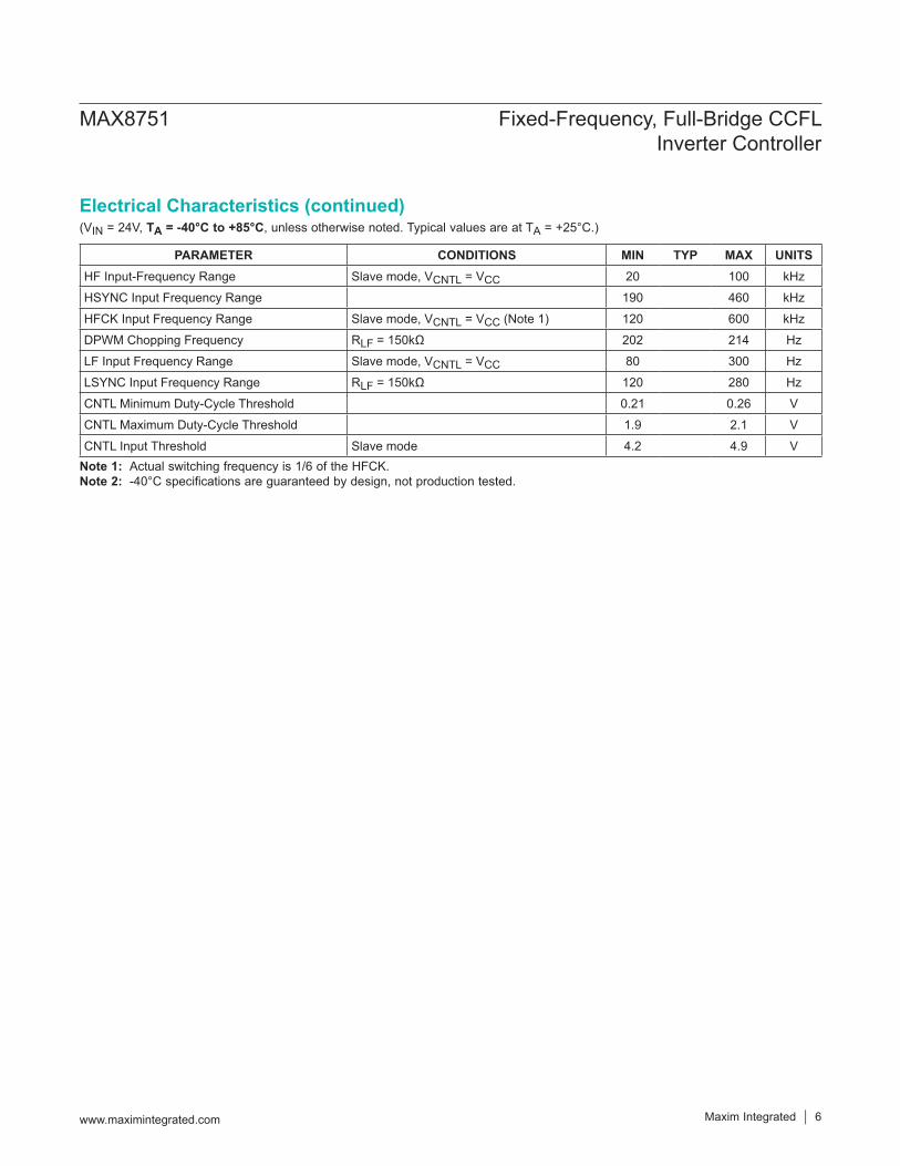
Note 1: Actual switching frequency is 1/6 of the HFCK.Note 2: -40°C specifications are guaranteed by design, not production tested.
(VIN = 24V, TA = -40°C to +85°C, unless otherwise noted. Typical values are at TA = +25°C.)
PARAMETER CONDITIONS MIN TYP MAX UNITSHF Input-Frequency Range Slave mode, VCNTL = VCC 20 100 kHz
HSYNC Input Frequency Range 190 460 kHz
HFCK Input Frequency Range Slave mode, VCNTL = VCC (Note 1) 120 600 kHz
DPWM Chopping Frequency RLF = 150kΩ 202 214 Hz
LF Input Frequency Range Slave mode, VCNTL = VCC 80 300 Hz
LSYNC Input Frequency Range RLF = 150kΩ 120 280 Hz
CNTL Minimum Duty-Cycle Threshold 0.21 0.26 V
CNTL Maximum Duty-Cycle Threshold 1.9 2.1 V
CNTL Input Threshold Slave mode 4.2 4.9 V
MAX8751 Fixed-Frequency, Full-Bridge CCFLInverter Controller
www.maximintegrated.com Maxim Integrated 6
Electrical Characteristics (continued)

(Circuit of Figure 1. VIN = 12V, TA = +25°C, unless otherwise noted.)
MINIMUM BRIGHTNESS STARTUP WAVEFORM (VCNTL = 0)
MAX8751 toc02
2ms/div
A
B
A: COMP, 500mV/divB: IFB, 2V/divC: VFB, 1V/div
C
MINIMUM BRIGHTNESS DPWM OPERATION (VCNTL = 0)
MAX8751 toc03
1ms/s
A
B
A: COMP, 500mV/divB: IFB, 2V/divC: VFB, 1V/div
C
50% BRIGHTNESS STARTUP WAVEFORMMAX8751 toc04
2ms/div
A
B
A: COMP, 500mV/divB: IFB, 2V/divC: VFB, 1V/div
C
50% BRIGHTNESS DWPM WAVEFORM(VCNTL = 1V)
MAX8751 toc05
1ms/div
A
B
A: COMP, 500mV/divB: IFB, 2V/divC: VFB, 1V/div
C
DPWM SOFT-STARTMAX8751 toc06
100µs/div
A
B
A: COMP, 1V/divB: IFB, 1V/divC: VFB, 1V/div
C
NORMAL OPERATIONMAX8751 toc01
20µs/div
A
B
A: VFB, 1V/divB: LX1, 10V/divC: LX2, 10V/divD: IFB, 2V/div
C
D
MAX8751 Fixed-Frequency, Full-Bridge CCFLInverter Controller
Maxim Integrated 7www.maximintegrated.com
Typical Operating Characteristics
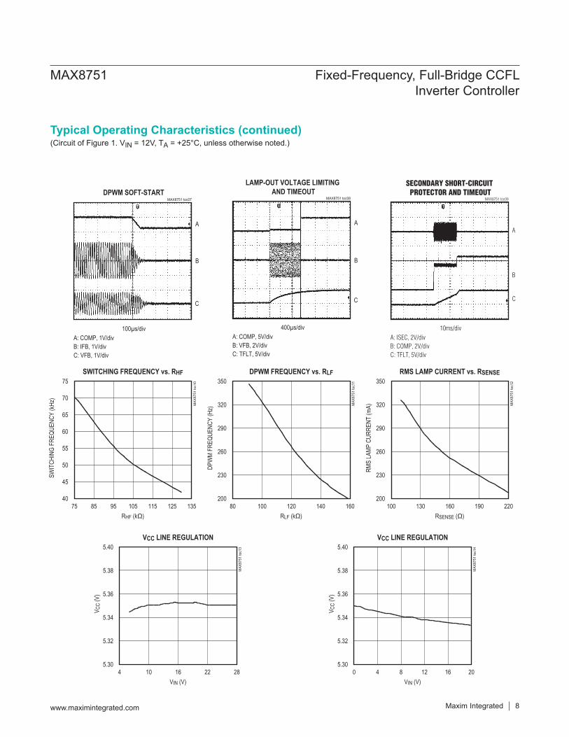
(Circuit of Figure 1. VIN = 12V, TA = +25°C, unless otherwise noted.)
DPWM SOFT-STARTMAX8751 toc07
100µs/div
A
B
A: COMP, 1V/divB: IFB, 1V/divC: VFB, 1V/div
C
LAMP-OUT VOLTAGE LIMITING AND TIMEOUT
MAX8751 toc08
400µs/div
A
B
A: COMP, 5V/divB: VFB, 2V/divC: TFLT, 5V/div
C
SECONDARY SHORT-CIRCUIT PROTECTOR AND TIMEOUT
MAX8751 toc09
10ms/div
A
B
A: ISEC, 2V/divB: COMP, 2V/divC: TFLT, 5V/div
C
SWITCHING FREQUENCY vs. RHF
MAX
8751
toc1
0
RHF (kΩ)
SWIT
CHIN
G FR
EQUE
NCY
(kHz)
1251151059585
45
50
55
60
65
70
75
4075 135
DPWM FREQUENCY vs. RLF
MAX
8751
toc1
1
RLF (kΩ)
DPW
M FR
EQUE
NCY
(Hz)
140120100
230
260
290
320
350
20080 160
RMS LAMP CURRENT vs. RSENSE
MAX
8751
toc1
2RSENSE (Ω)
RMS
LAMP
CUR
RENT
(mA)
190160130
230
260
290
320
350
200100 220
VCC LINE REGULATION
MAX
8751
toc1
3
VIN (V)
V CC
(V)
221610
5.32
5.34
5.36
5.38
5.40
5.304 28
VCC LINE REGULATION
MAX
8751
toc1
4
VIN (V)
V CC
(V)
161284
5.32
5.34
5.36
5.38
5.40
5.300 20
MAX8751 Fixed-Frequency, Full-Bridge CCFLInverter Controller
Maxim Integrated 8www.maximintegrated.com
Typical Operating Characteristics (continued)

(Circuit of Figure 1. VIN = 12V, TA = +25°C, unless otherwise noted.)
VCC vs. TEMPERATUREM
AX87
51 to
c15
TEMPERATURE (°C)
V CC
(V)
161284
5.32
5.34
5.36
5.38
5.40
5.300 20
VIN = 12VNOT SWITCHING
DPWM PHASE SHIFT (90°)MAX8751 toc16
2ms/div
A
B
A: MASTER DPWM, 5V/divB: SLAVE DPWM, 5V/div
SWITCHING FREQUENCY PHASE SHIFT (90°)
MAX8751 toc17
4ms/div
A
B
A: MASTER PSCK, 5V/divB: SLAVE PSCK, 5V/div
LF SYNCHRONIZATIONMAX8751 toc18
2ms/div
A
B
A: LSYNC, 5V/divB: COMP, 500mV/div
HF SYNCHRONIZATIONMAX8751 toc19
4µs/div
A
B
C
A: HSYNC, 5V/divB: HFCIC, 5V/divC: IFB, 2V/div
MAX8751 Fixed-Frequency, Full-Bridge CCFLInverter Controller
Maxim Integrated 9www.maximintegrated.com
Typical Operating Characteristics (continued)
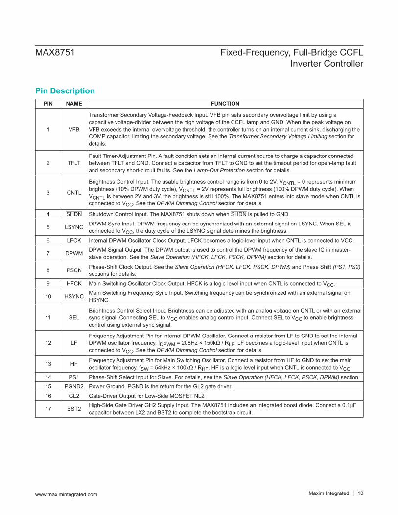
PIN NAME FUNCTION
1 VFB
Transformer Secondary Voltage-Feedback Input. VFB pin sets secondary overvoltage limit by using a capacitive voltage-divider between the high voltage of the CCFL lamp and GND. When the peak voltage on VFB exceeds the internal overvoltage threshold, the controller turns on an internal current sink, discharging the COMP capacitor, limiting the secondary voltage. See the Transformer Secondary Voltage Limiting section for details.
2 TFLTFault Timer-Adjustment Pin. A fault condition sets an internal current source to charge a capacitor connected between TFLT and GND. Connect a capacitor from TFLT to GND to set the timeout period for open-lamp fault and secondary short-circuit faults. See the Lamp-Out Protection section for details.
3 CNTL
Brightness Control Input. The usable brightness control range is from 0 to 2V. VCNTL = 0 represents minimum brightness (10% DPWM duty cycle), VCNTL = 2V represents full brightness (100% DPWM duty cycle). When VCNTL is between 2V and 3V, the brightness is still 100%. The MAX8751 enters into slave mode when CNTL is connected to VCC. See the DPWM Dimming Control section for details.
4 SHDN Shutdown Control Input. The MAX8751 shuts down when SHDN is pulled to GND.
5 LSYNC DPWM Sync Input. DPWM frequency can be synchronized with an external signal on LSYNC. When SEL is connected to VCC, the duty cycle of the LSYNC signal determines the brightness.
6 LFCK Internal DPWM Oscillator Clock Output. LFCK becomes a logic-level input when CNTL is connected to VCC.
7 DPWM DPWM Signal Output. The DPWM output is used to control the DPWM frequency of the slave IC in master-slave operation. See the Slave Operation (HFCK, LFCK, PSCK, DPWM) section for details.
8 PSCK Phase-Shift Clock Output. See the Slave Operation (HFCK, LFCK, PSCK, DPWM) and Phase Shift (PS1, PS2) sections for details.
9 HFCK Main Switching Oscillator Clock Output. HFCK is a logic-level input when CNTL is connected to VCC.
10 HSYNC Main Switching Frequency Sync Input. Switching frequency can be synchronized with an external signal on HSYNC.
11 SELBrightness Control Select Input. Brightness can be adjusted with an analog voltage on CNTL or with an external sync signal. Connecting SEL to VCC enables analog control input. Connect SEL to VCC to enable brightness control using external sync signal.
12 LFFrequency Adjustment Pin for Internal DPWM Oscillator. Connect a resistor from LF to GND to set the internal DPWM oscillator frequency. fDPWM = 208Hz × 150kΩ / RLF. LF becomes a logic-level input when CNTL is connected to VCC. See the DPWM Dimming Control section for details.
13 HF Frequency Adjustment Pin for Main Switching Oscillator. Connect a resistor from HF to GND to set the main oscillator frequency. fSW = 54kHz × 100kΩ / RHF. HF is a logic-level input when CNTL is connected to VCC.
14 PS1 Phase-Shift Select Input for Slave. For details, see the Slave Operation (HFCK, LFCK, PSCK, DPWM) section.
15 PGND2 Power Ground. PGND is the return for the GL2 gate driver.
16 GL2 Gate-Driver Output for Low-Side MOSFET NL2
17 BST2 High-Side Gate Driver GH2 Supply Input. The MAX8751 includes an integrated boost diode. Connect a 0.1µF capacitor between LX2 and BST2 to complete the bootstrap circuit.
MAX8751 Fixed-Frequency, Full-Bridge CCFLInverter Controller
www.maximintegrated.com Maxim Integrated 10
Pin Description
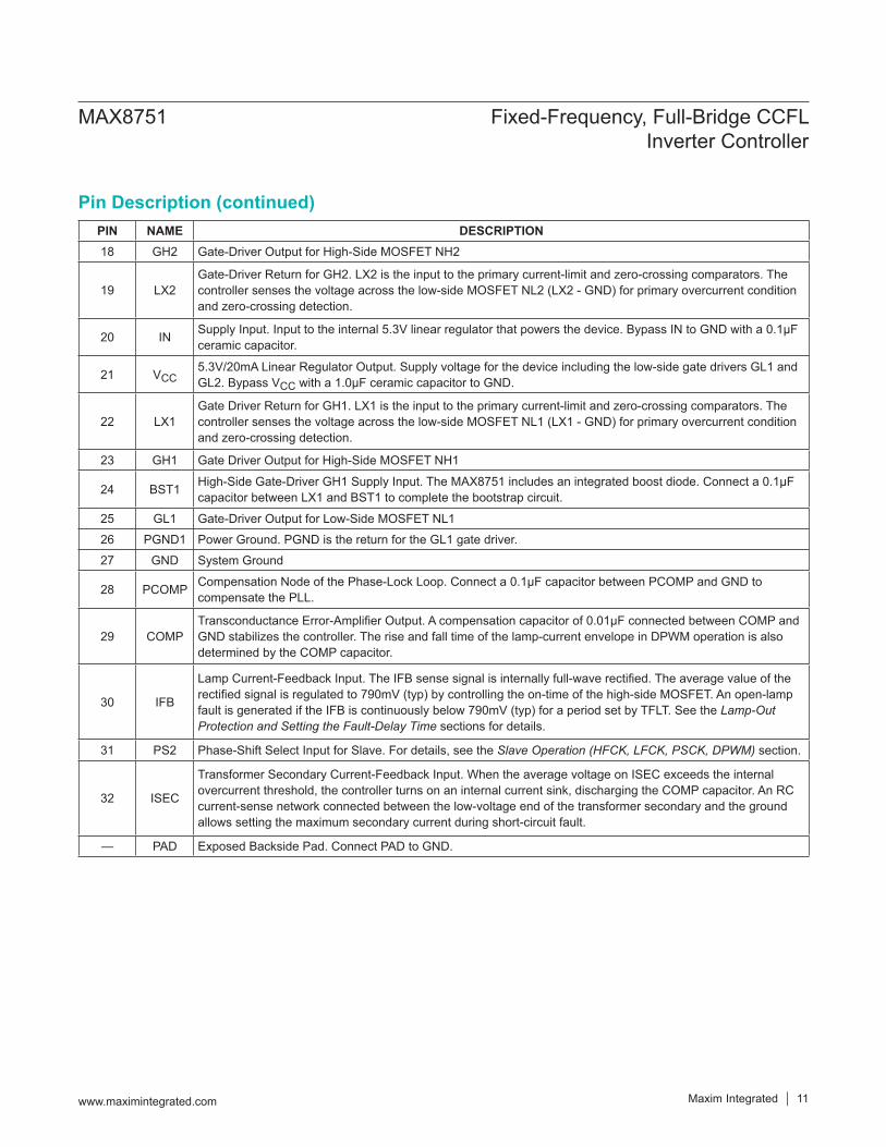
PIN NAME DESCRIPTION18 GH2 Gate-Driver Output for High-Side MOSFET NH2
19 LX2Gate-Driver Return for GH2. LX2 is the input to the primary current-limit and zero-crossing comparators. The controller senses the voltage across the low-side MOSFET NL2 (LX2 - GND) for primary overcurrent condition and zero-crossing detection.
20 IN Supply Input. Input to the internal 5.3V linear regulator that powers the device. Bypass IN to GND with a 0.1µF ceramic capacitor.
21 VCC5.3V/20mA Linear Regulator Output. Supply voltage for the device including the low-side gate drivers GL1 and GL2. Bypass VCC with a 1.0µF ceramic capacitor to GND.
22 LX1Gate Driver Return for GH1. LX1 is the input to the primary current-limit and zero-crossing comparators. The controller senses the voltage across the low-side MOSFET NL1 (LX1 - GND) for primary overcurrent condition and zero-crossing detection.
23 GH1 Gate Driver Output for High-Side MOSFET NH1
24 BST1 High-Side Gate-Driver GH1 Supply Input. The MAX8751 includes an integrated boost diode. Connect a 0.1µF capacitor between LX1 and BST1 to complete the bootstrap circuit.
25 GL1 Gate-Driver Output for Low-Side MOSFET NL1
26 PGND1 Power Ground. PGND is the return for the GL1 gate driver.
27 GND System Ground
28 PCOMP Compensation Node of the Phase-Lock Loop. Connect a 0.1µF capacitor between PCOMP and GND to compensate the PLL.
29 COMPTransconductance Error-Amplifier Output. A compensation capacitor of 0.01µF connected between COMP and GND stabilizes the controller. The rise and fall time of the lamp-current envelope in DPWM operation is also determined by the COMP capacitor.
30 IFB
Lamp Current-Feedback Input. The IFB sense signal is internally full-wave rectified. The average value of the rectified signal is regulated to 790mV (typ) by controlling the on-time of the high-side MOSFET. An open-lamp fault is generated if the IFB is continuously below 790mV (typ) for a period set by TFLT. See the Lamp-Out Protection and Setting the Fault-Delay Time sections for details.
31 PS2 Phase-Shift Select Input for Slave. For details, see the Slave Operation (HFCK, LFCK, PSCK, DPWM) section.
32 ISEC
Transformer Secondary Current-Feedback Input. When the average voltage on ISEC exceeds the internal overcurrent threshold, the controller turns on an internal current sink, discharging the COMP capacitor. An RC current-sense network connected between the low-voltage end of the transformer secondary and the ground allows setting the maximum secondary current during short-circuit fault.
— PAD Exposed Backside Pad. Connect PAD to GND.
MAX8751 Fixed-Frequency, Full-Bridge CCFLInverter Controller
www.maximintegrated.com Maxim Integrated 11
Pin Description (continued)
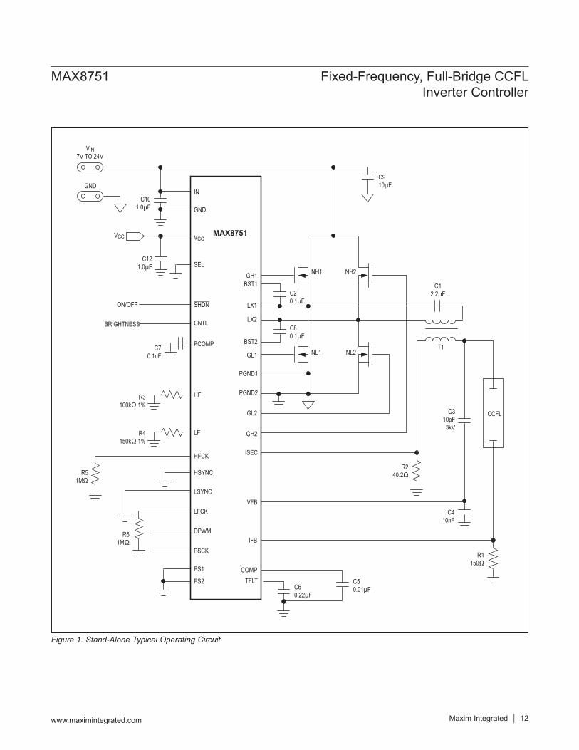
Figure 1. Stand-Alone Typical Operating Circuit
HFCK
MAX8751
CCFL
VIN7V TO 24V
GND
GH2
LX2
BST2
BST1
LX1
GH1
GL1
IN
IFB
VFB
GL2
BRIGHTNESS
ON/OFF
ISEC
CNTL
LF
PGND2
VCC
SHDN
GND
VCC
PS1
PS2
LFCK
PSCK
DPWM
T1
PGND1
LSYNC
HSYNC
PCOMP
SEL
COMPTFLT
C121.0µF
C70.1uF
HF
C20.1µF
C80.1µF
C910µF
C310pF
3kV
C410nF
C12.2µF
C101.0µF
C60.22µF
NH1 NH2
NL1 NL2
R3100kΩ 1%
R4150kΩ 1%
C50.01µF
R1150Ω
R240.2Ω
R61MΩ
R51MΩ
MAX8751 Fixed-Frequency, Full-Bridge CCFLInverter Controller
www.maximintegrated.com Maxim Integrated 12
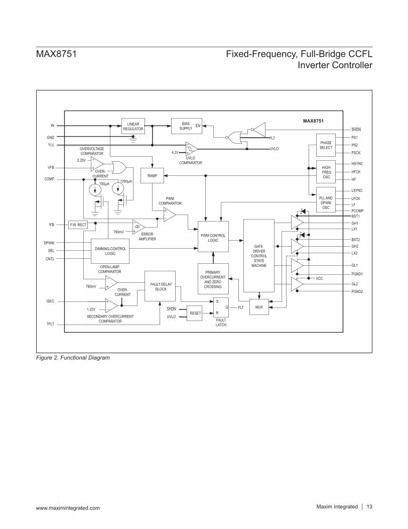
Figure 2. Functional Diagram
MAX8751
MUX
DIMMING CONTROLLOGIC
LINEARREGULATOR
BIASSUPPLY EN
FLT
S
RQSHDN FLT
BST1
BST2
GH1LX1
LX2
VCC
GL1
GH2
GL2
PGND1
PGND2
IN
VCC
VFB
2.25V
OVERVOLTAGECOMPARATOR
PWMCOMPARATOR
ERRORAMPLIFIER
IFB
DPWM
SEL
CNTL
780mV
1.22V
ISEC
OPEN-LAMPCOMPARATOR
SECONDARY OVERCURRENTCOMPARATOR
GATE DRIVER
CONTROLSTATE
MACHINE
FAULTLATCH
RESET
790mV
COMP
OVER-CURRENT
UVLOCOMPARATOR
4.2V
PWM CONTROLLOGIC
RAMP
PRIMARYOVERCURRENT
AND ZEROCROSSINGFAULT-DELAY
BLOCK
TFLT
UVLO
UVLO
SHDN
1200µA100µA
OVER-CURRENT
GND
F.W. RECT
PHASESELECT
PS1
PS2
PSCK
HIGH-FREQOSC
HSYNC
HFCK
HF
PLL ANDDPWMOSC
LSYNC
LFCKLFPCOMP
MAX8751 Fixed-Frequency, Full-Bridge CCFLInverter Controller
www.maximintegrated.com Maxim Integrated 13

Detailed DescriptionFigure 1 shows the Stand-Alone Typical Operating Circuit and Figure 2 shows the Functional Diagram of the MAX8751. The circuit in Figure 1 consists of a fullbridge inverter, which converts unregulated DC input voltage into a nearly sinusoidal high-frequency, AC output for powering CCFLs. The MAX8751 is biased from an inter-nal 5.35V linear regulator with UVLO comparator that ensures stable operation and clean startup characteris-tics. The MAX8751 includes several layers of fault-pro-tection circuitry, consisting of comparators for detecting primary-side current limit, secondary-side overvoltage, secondary short circuit, and open-lamp faults. A logic block arbitrates the comparator outputs by making sure that a given fault persists for a minimum duration before registering the fault condition. A separate block provides dimming control based upon analog or DPWM inputs. Finally, a dedicated logic circuit provides synchronization and phase-control functions for daisy-chaining up to five MAX8751s without phase overlap.The MAX8751 operates in resonant mode during striking and switches over to constant-frequency operation after the IFB voltage rises above the open-lamp threshold. Reliable striking of all lamps is ensured by using individual transformer secondary winding for each lamp, or by using ballast capacitors if multiple lamps are driven by single transformer secondary. The constant-frequency archi-tecture supported by the MAX8751 can be synchronized and phase shifted for daisy-chained applications. Multiple lamps can also be driven in parallel within a single stage. The MAX8751 has sufficient gate drive strength to drive the largepower MOSFETs needed when one power stage drives four or more CCFL lamps in parallel.The MAX8751 provides accurate lamp-current regula-tion. A primary-side current sense provides cycle-bycycle current limit and zero-crossing detection, while the lamp current is sensed with a separate loop that provides fine adjustment of the lamp current with an external resistor. The MAX8751 controls lamp brightness by turning the CCFL on and off using a DPWM method, while maintain-ing approximately constant lamp current. The brightness set point can be adjusted with an analog voltage on the CNTL pin, or with an external PWM signal.The MAX8751 has a single compensation input (COMP), which also establishes the soft-start and softstop timing characteristics. Control logic changes the available drive current at COMP based on the operating mode to adjust the inverter’s dynamic behavior.
Constant-Frequency OperationThe MAX8751 operates in constant-frequency mode in normal operation. There are two ways to set the switching frequency:1) The switching frequency can be set with an external
resistor connected between HF and GND. The switch-ing frequency is given by the following equation:
SWHF
100kf 54kHzR
Ω= ×
The adjustable range of the switching frequency is between 20kHz and 100kHz (RHF is between 270kΩ and 54kΩ).2) The switching frequency can be synchronized by an
external high-frequency signal. Connect HF to GND through a 100kΩ resistor and connect HSYNC to the external high-frequency signal. The resulting switching frequency (fSW) is 1/6 the frequency of the external signal (fSYNC):
SYNCSW
ff6
=
The frequency range of the external signal should be between 120kHz and 600kHz, resulting in a switching frequency range between 20kHz and 100kHz.Figure 3 is the timing diagram of constant-frequency operation, showing the primary current, internal oscilla-tor, and gate signals. At the beginning of the positive half cycle, switches NH1 and NL2 are ON (see Figure 1), and the primary current ramps up. The controller turns off NH1 when the primary current reaches it peak, which is set by the COMP voltage. The primary current continues to flow through the freewheeling body diode of NL1. Next, the low-side switch NL1 is turned on under zero-voltage switching (ZVS) conditions. Now the primary current starts ramping down. The falling edge of the internal oscil-lator turns off NL2 and turns on NH2, starting the negative half cycle. The fixed-frequency operation continues with the inverter controlling the fullbridge MOSFETs to produce near the sinusoidal lampcurrent waveform.
Resonant StartupThe MAX8751 operates in resonant mode during startup. In the resonant mode, the switching frequency is synchro-nized with the natural resonant frequency of the resonant tank circuit. The synchronization and phaseshift functions are disabled during startup. Figure 4 is the timing diagram of the resonant operation showing the primary current and gate signals. In the resonant mode, at the beginning of the
MAX8751 Fixed-Frequency, Full-Bridge CCFLInverter Controller
www.maximintegrated.com Maxim Integrated 14

Figure 3. Fixed-Frequency Timing Diagram
Figure 4. Resonant Operation Timing Diagram
PRIMARY CURRENT
DH1
DH2
DL1
DL2
INTERNAL OSCILLATOR
PRIMARY CURRENT
DH1
DH2
DL1
DL2
MAX8751 Fixed-Frequency, Full-Bridge CCFLInverter Controller
www.maximintegrated.com Maxim Integrated 15
positive half cycle, NH1 and NL2 turn on and the primary current starts ramping up. The controller turns off NH1 as the primary current reaches its peak value. The primary current continues to flow in the same direction, which forward biases the body diode of NL1, ramping down the primary current. When the primary current reaches zero, NL2 is turned off and NH2 is turned on, starting the nega-tive half cycle.
Lamp-Current RegulationThe MAX8751 uses a lamp-current control loop to regu-late the current delivered to the CCFL. The heart of the control loop is a transconductance error amplifier in Figure 2. The AC lamp current is sensed with a sense resistor connected in series with the low-voltage terminal of the lamp. The voltage across this resistor is fed to the IFB input and is internally full-wave rectified. The transcon-ductance error amplifier compares the rectified IFB volt-age with a 790mV (typ) internal reference to generate an error current. The error current charges and discharges a capacitor connected between the error amplifier’s output (COMP) and ground to create an error voltage (VCOMP). VCOMP is then compared with an internal ramp signal to control the high-side MOSFET switch on-time (tON).
Transformer Secondary Voltage LimitingThe MAX8751 reduces the voltage stress on the trans-former’s secondary winding by limiting the secondary voltage during startup and open-lamp condition. The AC voltage across the transformer secondary winding is sensed through a capacitive voltage-divider. The volt-age across the low-side capacitor of the divider is fed to the VFB pin of the MAX8751. An overvoltage compara-tor compares the VFB voltage with 2.25V (typ) internal threshold. If the sensed voltage exceeds the overvoltage threshold, the MAX8751 turns on an internal 1200μA cur-rent source, which discharges the COMP capacitor. The high-side MOSFET’s on-time shortens as the COMP volt-age decreases, hence reducing the transformer’s second-ary peak voltage below the threshold set by the capacitive voltage-divider.
Lamp StartupA CCFL is a gas-discharge lamp that is normally driven in the avalanche mode. To start ionization in a nonion-ized lamp, the applied voltage (striking voltage) must be increased to the level required for the start of avalanche. For example, the normal running voltage of a typical CCFL is approximately 650VRMS, but the striking voltage can be as high as 1800VRMS.
The MAX8751’s unique resonant startup method ensures reliable striking. Before the lamp is ionized, the lamp impedance is infinite. The transformer secondary leak-age inductance and the high-voltage parallel capacitor determine the unloaded resonant frequency. Since the unloaded resonant circuit has a high Q, the inverter keeps increasing the secondary voltage until either the lamp is struck or the controller activates the secondary overvolt-age protection.Upon power-up, VCOMP slowly rises, increasing the duty cycle of the high-side MOSFET switches and providing a measure of soft-start. In addition, the MAX8751 pulls up VFB to the overvoltage threshold (2.25V, typ) imme-diately after the device is enabled. The DC voltage on VFB is gradually discharged through an internal resistor during startup. This feature is equivalent to slowly rais-ing the overvoltage threshold during startup, so it further improves the soft-start behavior. The MAX8751 automati-cally switches over to constant-frequency operation after the IFB voltage rises above open-lamp threshold.
Feed-Forward Control and Dropout OperationThe MAX8751 is designed to maintain tight control of the lamp current under all transient conditions. The feed-forward control instantaneously adjusts the ontime for changes in input voltage (VIN). This feature provides immunity to input-voltage variations and simplifies loop compensation over wide-input voltage ranges. The feed-forward control also improves the line regulation for short DPWM on-times and makes startup transients less dependent on the input voltage.Feed-forward control is implemented by increasing the internal voltage ramp rate for higher VIN. This has the effect of varying tON as a function of the input voltage while maintaining almost the same signal levels at VCOMP. Since the required voltage change across the compensa-tion capacitor is minimal, the controller’s response to input voltage change is essentially instantaneous.
DPWM Dimming ControlThe MAX8751 controls the brightness of the CCFL by “chopping” the lamp current on and off using a low-frequency (between 80Hz and 300Hz) DPWM signal either from the internal oscillator or from an external signal source. In the DPWM operation, COMP controls the rise and fall of the lamp current. At the beginning of the DPWM on-cycle, the lamp current is zero; VCOMP linearly rises due to charging from transconductance error amplifier, and tON increases gradually, increasing the lamp current slowly, providing soft-start. The lamp current
MAX8751 Fixed-Frequency, Full-Bridge CCFLInverter Controller
www.maximintegrated.com Maxim Integrated 16
stabilizes after it reaches the regulation point. At the end of the DPWM on-cycle, the dimming control logic turns on a 100μA internal current source, thus discharging the COMP capacitor linearly, gradually decreasing tON and bringing lamp current to zero, thus providing soft-start. The dimming control for the CCFL is provided by chang-ing the duty ratio of the low-frequency DPWM signal.
Using the Internal OscillatorWhen the MAX8751 is not using an external synchroni-zation signal, the DPWM signal is generated using an internal oscillator. The frequency of the internal DPWM oscillator is adjustable through a resistor connected between LF and GND. The DPWM frequency is given by the following equation:
DPWMLF
208Hz 150kfR× Ω
=
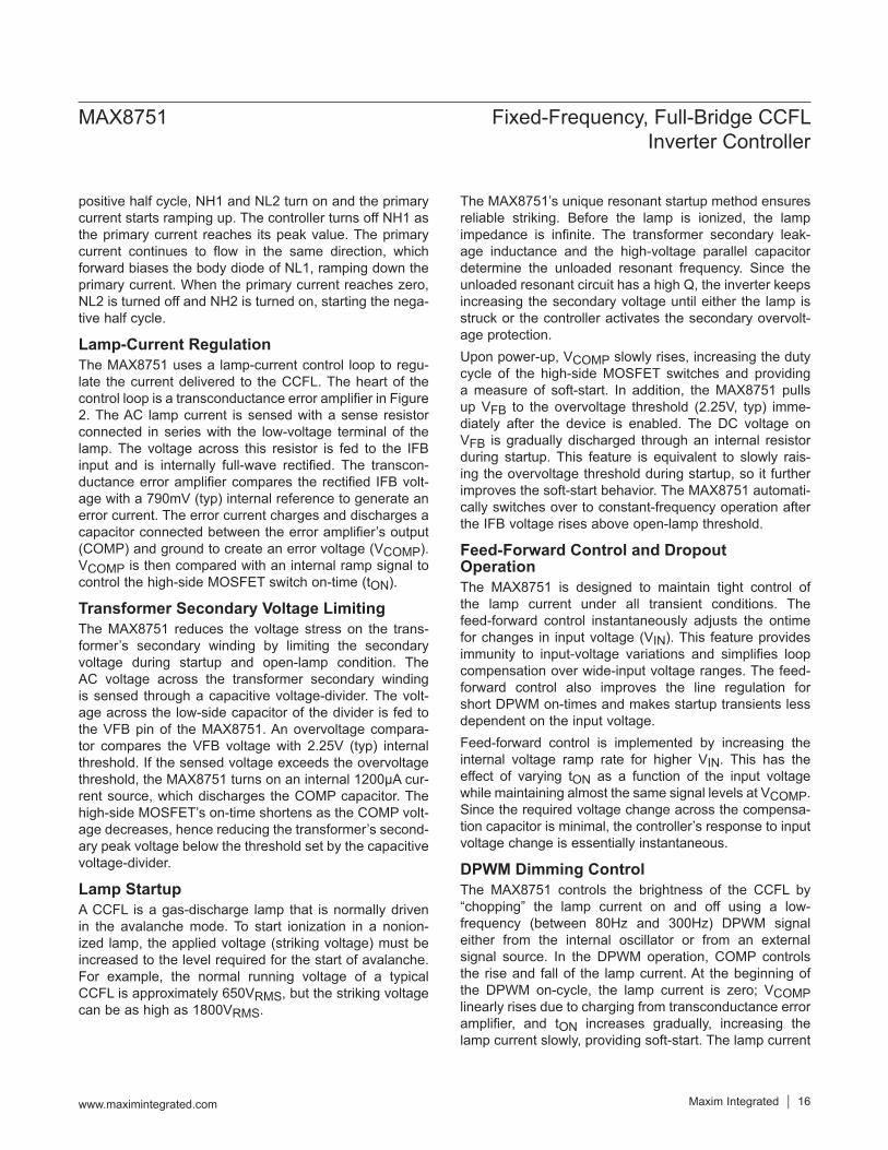
The adjustable range of the DPWM frequency is between 80Hz and 300Hz (RLF is between 390kΩ and 104kΩ).The CCFL brightness is proportional to the DPWM duty cycle, which can be adjusted from 10% to 100% through the CNTL pin. CNTL is an analog input with a usable input voltage range between 0 and 2000mV, which is digitized to select one of 128 brightness levels. As shown in Figure 5, the MAX8751 ignores the first 13 steps, and the first 13 steps (VCNTL between 0 and 203mV) all represent 10% brightness. When VCNTL is above 203mV, a 15.625mV change on CNTL results in a 0.78% change in the DPWM duty cycle. When VCNTL is equal to or above 2000mV, the DPWM duty cycle is always 100%.
Using the External DPWM SignalTo use the external DPWM signal to control the bright-ness, connect SEL to VCC and connect LSYNC to the external signal source. The frequency range of the exter-nal signal is within ±40% of the internal oscillator frequen-cy set by RLF. In this mode, the brightness control input CNTL is disabled, and the brightness is proportional to the duty cycle of the external signal. When the duty cycle of the external signal is 100%, the CCFL reaches full bright-ness. If the duty cycle of the external signal is less than 10%, the CCFL brightness stays at 10%.
Lamp-Out ProtectionFor safety, the IFB pin on MAX8751 monitors the lamp current to detect faulty or open CCFL lamps. As described in the Lamp-Current Regulation section, the voltage on IFB is internally full-wave rectified. If the rectified IFB voltage is below 790mV, the MAX8751 charges the TFLT capacitor with a 1μA current source. The fault latch is set if the voltage on TFLT exceeds 4V. Unlike normal shutdown mode, the linear regulator out (VCC) remains at 5.35V. Toggling SHDN or cycling the input power reac-tivates the device.During the fault delay period, the current-control loop tries to maintain the lamp-current regulation by increas-ing the on-time of high-side MOSFETs. Because the lamp impedance is very high when it is open, the transformer secondary rises as a result of the high-Q factor of the resonant tank. Once the secondary voltage exceeds the overvoltage threshold, the MAX8751 turns on a 1200μA internal current source that discharges the COMP capac-itor. The on-time of the high-side MOSFETs is reduced, lowering the secondary voltage, as the COMP voltage decreases. Therefore, the peak voltage of the transform-er secondary winding never exceeds the limit during the lamp-out delay period.
Primary Overcurrent ProtectionThe MAX8751 provides cycle-by-cycle primary over-current protection. A current-sense amplifier monitors the drain-to-source voltages of both the high-side and low-side switches when the switches are conducting. If the voltage exceeds the internal current-limit threshold (400mV typ), the regulator turns off the high-side switch at the opposite side of the primary to prevent the transformer primary current from increasing further.
Figure 5. Brightness vs. CNTL Voltage
CNTL VOLTAGE (mV)16001200400 8000 2000
BRIG
HTNE
SS (%
)
10
20
30
40
50
60
70
80
90
100
0
MAX8751 Fixed-Frequency, Full-Bridge CCFLInverter Controller
www.maximintegrated.com Maxim Integrated 17

Secondary Current Limit (ISEC)The secondary current limit provides fail-safe protection in case of short circuit or leakage from the high-voltage terminal to ground. ISEC monitors the voltage across a sense resistor placed between the transformer’s lowvolt-age secondary terminal and ground. The ISEC voltage is continuously compared to the ISEC regulation threshold (1.22V, typ). Any time the ISEC voltage exceeds the threshold, a controlled current is drawn from COMP to reduce the on-time of the bridge’s highside switches. At the same time, the MAX8751 charges the TFLT capacitor with a 126μA current. The MAX8751 latches off when the voltage on TFLT exceeds 4V.
Unlike the normal shutdown mode, the linear regulator output (VCC) remains at 5.35V. Toggling SHDN or cycling the input power reactivates the device.
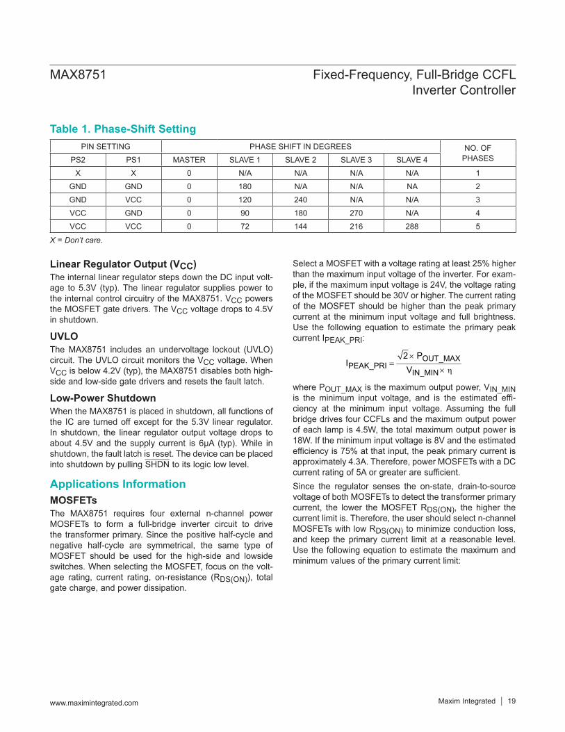
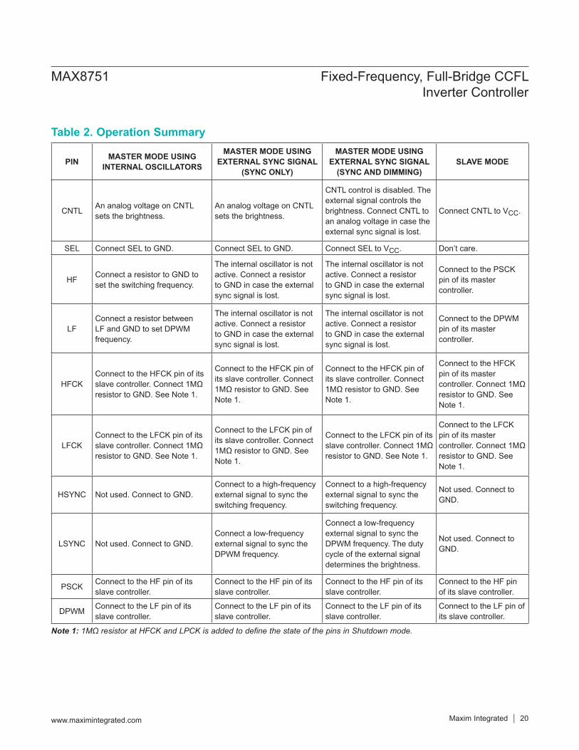
Slave Operation (HFCK, LFCK, PSCK, DPWM)The MAX8751 supports master-slave operation. Up to five MAX8751s can be connected in a daisy-chain configura-tion as shown in Figure 6. The same device can be used either as a master IC or as a slave IC. Each MAX8751 is the master of the next IC in the chain and at the same time, it is also the slave of the previous IC in the chain.Connecting CNTL to VCC enables the slave mode. In the slave mode, the switching frequency and DPWM frequen-cy are synchronized with the previous MAX8751 in the chain. To synchronize the switching frequency, connect the HFCK pins of the slave IC and master IC together, and connect the PSCK pin of the master IC to the HF pin of the slave IC. To synchronize the DPWM frequency, connect the LFCK pins of the slave IC and master IC together, and connect the DPWM pin of the master IC to the LF pin of the slave IC. The CNTL brightness control is disabled in the slave mode. The master directly con-trols the brightness setting of the slave by connecting the DPWM pin of master to LF pin of slave.
Phase Shift (PS1, PS2)The MAX8751 provides phase shift for both the DPWM operation and switching of MOSFETS when connected in a daisy-chain configuration. This phase shift reduces input ripple current, hence significantly reducing input RMS cur-rent. This reduction of input RMS current reduces the input capacitor requirement, hence the size of capacitor. The phase shift can be programmed using two logic input pins (PS1 and PS2). These two pins combined together give four choices of phase shift: 72°, 90°, 120°, and 180°. The selection of the phase shift is based on the number of MAX8751s used in the daisy-chain. Use the following equation to determine the appropriate phase shift:
Phase shift = 360° / number of phasesTable 1 gives the suggested selection of phase shift for different number of phases. All master and slave ICs should use the same setting for PS1 and PS2.Table 2 summarizes the MAX8751’s operation in all modes.
Figure 6. Master-Slave Operation
ON/OFF
DIMMING
LF
HF
SHDN
CNTL
LFCK DPWM
PSCKHFCK
LF
HF
SHDN
CNTL
LFCK DPWM
PSCKHFCK
LF
HF
SHDN
CNTL
LFCK DPWM
PSCKHFCK
LF
HF
SHDN
CNTL
LFCK DPWM
PSCKHFCK
MASTER
SLAVE 1
SLAVE 2
SLAVE N
VCC
MAX8751 Fixed-Frequency, Full-Bridge CCFLInverter Controller
www.maximintegrated.com Maxim Integrated 18
Linear Regulator Output (VCC)The internal linear regulator steps down the DC input volt-age to 5.3V (typ). The linear regulator supplies power to the internal control circuitry of the MAX8751. VCC powers the MOSFET gate drivers. The VCC voltage drops to 4.5V in shutdown.
UVLOThe MAX8751 includes an undervoltage lockout (UVLO) circuit. The UVLO circuit monitors the VCC voltage. When VCC is below 4.2V (typ), the MAX8751 disables both high-side and low-side gate drivers and resets the fault latch.
Low-Power ShutdownWhen the MAX8751 is placed in shutdown, all functions of the IC are turned off except for the 5.3V linear regulator. In shutdown, the linear regulator output voltage drops to about 4.5V and the supply current is 6μA (typ). While in shutdown, the fault latch is reset. The device can be placed into shutdown by pulling SHDN to its logic low level.
Applications InformationMOSFETsThe MAX8751 requires four external n-channel power MOSFETs to form a full-bridge inverter circuit to drive the transformer primary. Since the positive half-cycle and negative half-cycle are symmetrical, the same type of MOSFET should be used for the high-side and lowside switches. When selecting the MOSFET, focus on the volt-age rating, current rating, on-resistance (RDS(ON)), total gate charge, and power dissipation.
Select a MOSFET with a voltage rating at least 25% higher than the maximum input voltage of the inverter. For exam-ple, if the maximum input voltage is 24V, the voltage rating of the MOSFET should be 30V or higher. The current rating of the MOSFET should be higher than the peak primary current at the minimum input voltage and full brightness. Use the following equation to estimate the primary peak current IPEAK_PRI:
OUT_MAXPEAK_PRI
IN_MIN
2 PI
V η
×=
×
where POUT_MAX is the maximum output power, VIN_MIN is the minimum input voltage, and is the estimated effi-ciency at the minimum input voltage. Assuming the full bridge drives four CCFLs and the maximum output power of each lamp is 4.5W, the total maximum output power is 18W. If the minimum input voltage is 8V and the estimated efficiency is 75% at that input, the peak primary current is approximately 4.3A. Therefore, power MOSFETs with a DC current rating of 5A or greater are sufficient.Since the regulator senses the on-state, drain-to-source voltage of both MOSFETs to detect the transformer primary current, the lower the MOSFET RDS(ON), the higher the current limit is. Therefore, the user should select n-channel MOSFETs with low RDS(ON) to minimize conduction loss, and keep the primary current limit at a reasonable level. Use the following equation to estimate the maximum and minimum values of the primary current limit:
X = Don’t care.
Table 1. Phase-Shift SettingPIN SETTING PHASE SHIFT IN DEGREES NO. OF
PHASESPS2 PS1 MASTER SLAVE 1 SLAVE 2 SLAVE 3 SLAVE 4
X X 0 N/A N/A N/A N/A 1
GND GND 0 180 N/A N/A NA 2
GND VCC 0 120 240 N/A N/A 3
VCC GND 0 90 180 270 N/A 4
VCC VCC 0 72 144 216 288 5
MAX8751 Fixed-Frequency, Full-Bridge CCFLInverter Controller
www.maximintegrated.com Maxim Integrated 19
Note 1: 1MΩ resistor at HFCK and LPCK is added to define the state of the pins in Shutdown mode.
Table 2. Operation Summary
PIN MASTER MODE USING INTERNAL OSCILLATORS
MASTER MODE USING EXTERNAL SYNC SIGNAL
(SYNC ONLY)
MASTER MODE USING EXTERNAL SYNC SIGNAL
(SYNC AND DIMMING)SLAVE MODE
CNTL An analog voltage on CNTL sets the brightness.
An analog voltage on CNTL sets the brightness.
CNTL control is disabled. The external signal controls the brightness. Connect CNTL to an analog voltage in case the external sync signal is lost.
Connect CNTL to VCC.
SEL Connect SEL to GND. Connect SEL to GND. Connect SEL to VCC. Don’t care.
HF Connect a resistor to GND to set the switching frequency.
The internal oscillator is not active. Connect a resistor to GND in case the external sync signal is lost.
The internal oscillator is not active. Connect a resistor to GND in case the external sync signal is lost.
Connect to the PSCK pin of its master controller.
LFConnect a resistor between LF and GND to set DPWM frequency.
The internal oscillator is not active. Connect a resistor to GND in case the external sync signal is lost.
The internal oscillator is not active. Connect a resistor to GND in case the external sync signal is lost.
Connect to the DPWM pin of its master controller.
HFCKConnect to the HFCK pin of its slave controller. Connect 1MΩ resistor to GND. See Note 1.
Connect to the HFCK pin of its slave controller. Connect 1MΩ resistor to GND. See Note 1.
Connect to the HFCK pin of its slave controller. Connect 1MΩ resistor to GND. See Note 1.
Connect to the HFCK pin of its master controller. Connect 1MΩ resistor to GND. See Note 1.
LFCKConnect to the LFCK pin of its slave controller. Connect 1MΩ resistor to GND. See Note 1.
Connect to the LFCK pin of its slave controller. Connect 1MΩ resistor to GND. See Note 1.
Connect to the LFCK pin of its slave controller. Connect 1MΩ resistor to GND. See Note 1.
Connect to the LFCK pin of its master controller. Connect 1MΩ resistor to GND. See Note 1.
HSYNC Not used. Connect to GND.Connect to a high-frequency external signal to sync the switching frequency.
Connect to a high-frequency external signal to sync the switching frequency.
Not used. Connect to GND.
LSYNC Not used. Connect to GND.Connect a low-frequency external signal to sync theDPWM frequency.
Connect a low-frequency external signal to sync the DPWM frequency. The duty cycle of the external signal determines the brightness.
Not used. Connect to GND.
PSCK Connect to the HF pin of its slave controller.
Connect to the HF pin of its slave controller.
Connect to the HF pin of its slave controller.
Connect to the HF pinof its slave controller.
DPWM Connect to the LF pin of its slave controller.
Connect to the LF pin of its slave controller.
Connect to the LF pin of its slave controller.
Connect to the LF pin of its slave controller.
MAX8751 Fixed-Frequency, Full-Bridge CCFLInverter Controller
www.maximintegrated.com Maxim Integrated 20

LIM_MINDS(ON)_MAX
LIM_MAXDS(ON)_MIN
380mV
420mV
MOSFETs must be able to dissipate the conduction losses plus the switching losses at both VIN_MIN and VIN_MAX. Calculate both terms. Ideally, the losses at VIN(MIN) should be roughly equal to the losses at VIN(MAX), with lower losses in between. If the losses at VIN(MIN) are significantly higher than the losses at VIN(MAX), consider increasing the size of the MOSFETs. Conversely, if the losses at VIN(MAX) are significantly higher than the losses at VIN(MIN), consider choosing MOSFETs with lower parasitic capacitance. If VIN does not vary over a wide range, the minimum power dis-sipation occurs where the conduction losses equal the switching losses.Calculate the total conduction power dissipation of the two MOSFETs using the following equation:
2CONDUCT DS(ON)PRIPD I R= ×
where IPRI is the primary current calculated using the fol-lowing equation:
OUT_MAXPRI
IN
PI
V=
η×
The low-side MOSFETs turn on with ZVS. If the switching frequency is close to resonant frequency, turn-on power loss associated with high-side MOSFETs can be ignored. However, the current is at peak when the MOSFET is turned off. Calculate the turn-off switching power dissipa-tion of the MOSFET using the following equation:
2RSS SW PRIINSWITCH
GATE
2 C V f IPD
I
× × × ×=
where CRSS is the reverse transfer capacitance of the MOSFETs and IGATE is the peak gate-drive sink current when the MOSFET is being turned off.
Setting the Lamp CurrentThe MAX8751 senses the lamp current flowing through resistor R1 (Figure 1) connected between the low-voltage terminal of the lamp and ground. The voltage across R1 is fed to IFB and is internally full-wave rectified. The MAX8751 controls the desired lamp current by regulating the average of the rectified IFB voltage. To set the RMS lamp current, determine R1 as follows:
LAMP(RMS)
790mVR12 2 I
π×=
×
where ILAMP(RMS) is the desired RMS lamp current and 790mV is the typical value of the IFB regulation point speci-fied in the Electrical Characteristics table. To set the RMS lamp current to 6mA, the value of R1 should be 148Ω. The closest standard 1% resistors are 147Ω and 150Ω. The precise shape of the lamp-current waveform depends on lamp parasitics. The resulting waveform is an imperfect sinusoid waveform, which has an RMS value that is not easy to predict. A high-frequency true RMS current meter (such as Yokogawa 2016) should be used to measure the RMS current and make final adjustments to R1. Insert this meter between the sense resistor and the lamp’s low-voltage terminal to measure the actual RMS current.
Setting the Secondary Voltage LimitThe MAX8751 limits the transformer secondary voltage during startup and lamp-out faults. The secondary voltage is sensed through the capacitive voltage-divider formed by C3 and C4 (Figure 1). The voltage of VFB is propor-tional to the CCFL voltage. The selection of the parallel resonant capacitor C1 is described in the Selecting the Resonant Components section. Smaller values for C3 result in higher efficiency due to lower circulating current. If C3 is too small, the resonant operation is affected by the panel parasitic capacitance. Therefore, C3 is usually chosen to be between 10pF and 18pF. After the value of C3 is set, select C4 based on the desired maximum RMS secondary voltage VLAMP(RMS)_MAX:
LAMP(RMS)_MAX2 VC4 C3
2.32V×
= ×
where the 2.34V is the typical value of the VFB peak volt-age when the lamp is open. To set the maximum RMS secondary voltage to 1800V with C3 selected to be 12pF, C4 must be less than or equal to 13nF.
MAX8751 Fixed-Frequency, Full-Bridge CCFLInverter Controller
www.maximintegrated.com Maxim Integrated 21

Setting the Secondary Current LimitThe MAX8751 limits the secondary current even if the IFB sense resistor is shorted or transformer secondary current finds its way to ground without passing through R1. ISEC monitors the voltage across the sense resistor R2 connected between the low-voltage terminal of the transformer secondary winding and ground. Determine the value of R2 using the following equation:
SEC(RMS)_MAX
1.26VR22 I
=×
where ISEC(RMS)_MAX is the desired maximum RMS transformer secondary current during fault conditions, and 1.26V is the typical value of the ISEC peak voltagewhen the secondary is shorted. To set the maximum RMS secondary current in the circuit of Figure 1 to 22mA, set R2 = 40.2Ω.
Transformer Design and Resonant Component SelectionThe transformer is the most important component of the resonant tank circuit. The first step in designing the trans-former is to determine the transformer turns ratio. The ratio must be high enough to support the CCFL operating voltage at the minimum supply voltage. The transformer turns ratio N can be calculated as follows:
LAMP(RMS)
IN(MIN)
VN
0.90 V≥
×
where VLAMP(RMS) is the maximum RMS lamp voltage in normal operation, and VIN(MIN) is the minimum DC input voltage. If the maximum RMS lamp voltage in normal operation is 800V and the minimum DC input voltage is 7V, the turns ratio should be greater than 120 turns.The next step to design the resonant tank for CCFL is to design the resonant frequency of the tank close to the switching frequency set by the HF resistor. The resonant frequency is determined by: the primary winding series capacitor Cs, the secondary parallel capacitor Cp, the transformer secondary leakage inductance L, and the CCFL lamp operating resistance RL.The simplified CCFL inverter circuit is shown in Figure 7(a). The full-bridge power stage is simplified and repre-sented as a square-wave AC source. The resonant tank circuit can be further simplified to Figure 7(b) by remov-ing the transformer. CS’ is the capacitance of the primary capacitive divider reflected to the secondary and N is the transformer turns ratio.
Figure 8 shows the frequency response of the resonant tank’s voltage gain under different load conditions. The primary series capacitor is 1μF, the secondary parallel capacitor is 15pF, the transformer turns ratio is 1:93, and the secondary leakage inductance is 260mH. Notice that there are two peaks, fS and fP, in the frequency response. The first peak, fS, is the series resonant peak determined by the secondary leakage inductance (L) and the series capacitor reflected to the secondary (Cs’):
S1f
2 LCs'=
π
The second peak, fP, is the parallel resonant peak deter-mined by the secondary leakage inductance (L), the par-allel capacitor (CP), and the series capacitance reflected to the secondary (C’S):
PPP
1fCs'C2 L
Cs' C
=π
+
The actual resonant frequency is between these two resonant peaks. When the lamp is off, the operating point of the resonant tank is close to the parallel resonant peak due to the lamp’s infinite impedance. The circuit displays the characteristics of a parallel-loaded resonant converter. While in parallel-loaded resonant operation, the inverter behaves like a voltage source to generate the necessary striking voltage. Theoretically, the output volt-age of the resonant converter increases until the lamp is ionized or until it reaches the IC’s secondary voltage limit. Once the lamp is ionized, the equivalent-load resistance decreases rapidly and the operating point moves toward the series-resonant peak. While in series-resonant opera-tion, the inverter behaves like a current source.The leakage inductance of the CCFL transformer is an important parameter in the resonant tank design. The leakage inductance values can have large tolerance and significant variations among different batches. It is best to work directly with transformer vendors on leakage inductance requirements. The series capacitor Cs sets the minimum operating frequency, which is approximately two times the series resonant peak frequency. The series capacitor Cs can be chosen as below:
MAX8751 Fixed-Frequency, Full-Bridge CCFLInverter Controller
www.maximintegrated.com Maxim Integrated 22

2S 2 2
MIN
NC4 f L
≤π × ×
where fMIN is the minimum operating frequency range. In the circuit of Figure 1, the transformer’s turns ratio is 120 and its secondary leakage inductance is 200mH. To set the minimum resonant frequency to 30kHz, use 2.2μF capacitor for CS.The parallel capacitor CP sets the maximum operating frequency, which is also the parallel resonant peak fre-quency. The capacitance CP can be chosen as below:
SP 2 2 2
MAX S
CC4 f L C N
>π × × × −
In the circuit of Figure 1, to set the maximum resonant frequency to 95kHz; use 15pF for CP.The transformer core saturation should also be consid-ered when selecting the operating frequency. The primary winding should have enough turns to prevent transformer saturation under all operating conditions. Use the follow-ing expression to calculate the minimum number of turns N1 of the primary winding:
MAX IN(MAX)
S MIN
D VN1
B S f×
>× ×
where DMAX is the maximum duty cycle (approximately 0.4) of the high-side switch, VIN(MAX) is the maximum DC input voltage, BS is the saturation flux density of the core, and S is the minimal cross-section area of the core.
COMP Capacitor SelectionThe COMP capacitor sets the speed of the current-regulation loop that is used during startup, maintaining lamp-current regulation, and during transients caused by changing the input voltage. To maintain stable operation, the COMP capacitor (CCOMP) needs to be at least 3.3nF.As discussed in the DPWM Dimming Control section, the COMP capacitor also limits the dynamics of the lamp-current envelope in DPWM operation. At the end of the DPWM ON cycle, the MAX8751 turns on a 100μA internal current source to linearly discharge the COMP capacitor. Use the following equation to set the fall time:
FALLCOMP
COMP
100µA tCV
×=
where tFALL is the fall time of the lamp-current envelope and VCOMP is the dynamic COMP voltage determined by resonant tank. At the beginning of the DPWM ON cycle, the COMP capacitor is charged by transconductance error amplifier, so the charge current is not constant. Because the average charge current is around 30μA, the rise time is about three times longer than the fall time.
Figure 7. Simplified CCFL Inverte r Circuit
Figure 8. Frequency Response of the Resonant Tank
CCFLCP
CP
1:N
L
RLAC
SOURCE
ACSOURCE
L
(b)
(a)
CS
Cs' = Cs'/N2
FREQUENCY (kHz)0 20 40 60 80 100
VOLT
AGE
GAIN
(V/V
)
1
2
3
4
RL INCREASING
MAX8751 Fixed-Frequency, Full-Bridge CCFLInverter Controller
www.maximintegrated.com Maxim Integrated 23
Setting the Fault Delay TimeThe TFLT capacitor determines the delay time for both the open-lamp fault and secondary short-circuit fault. The MAX8751 charges the TFLT capacitor with a 1μA current source during an open-lamp fault and charges the TFLT capacitor with a 126μA current source during a secondary short-circuit fault. Therefore, the secondary short-circuit fault delay time is approximately 100 times shorter than that of the open-lamp fault. The MAX8751 sets the fault latch when the TFLT voltage reaches 4V. Use the fol-lowing equations to calculate the open-lamp fault delay (TOPEN_LAMP) and secondary short-circuit fault delay (TSEC_SHORT):
TFLTOPEN_LAMP
TFLTSEC_SHORT
C 4VT1µA
C 4VT126µA
×=
×=
Bootstrap CapacitorsThe high-side gate drivers are powered using two boot-strap circuits. The MAX8751 integrates the bootstrap diodes so only two 0.1μF bootstrap capacitors are needed. Connect the capacitors between LX1 and BST1 and between LX2 and BST2 to complete the bootstrap circuits.
Layout GuidelinesCareful PC board layout is important to achieve stable operation. The high-voltage section and the switching section of the circuit require particular attention. The high-voltage sections of the layout need to be well separated from the control circuit. Follow these guidelines for good PC board layout.
1) Keep the high-current paths short and wide, especially at the ground terminals. This is essential for stable, jitter-free operation and high efficiency.
2) Use a star-ground configuration for power and analog grounds. The power and analog grounds should be completely isolated—meeting only at the center of the star. The center should be placed at the analog ground pin (GND). Using separate copper islands for these grounds can simplify this task. Quiet analog ground is used for VCC, COMP, HF, LF, and TFLT.
3) Route high-speed switching nodes away from sensi-tive analog areas (VCC, COMP, HF, LF, and TFLT). Make all pin-strap control input connections to analog ground or VCC.
4) Mount the decoupling capacitor from VCC to GND as close as possible to the IC with dedicated traces that are not shared with other signal paths.
5) The current-sense paths for LX_ to GND must be made using Kelvin-sense connections to guarantee the current-limit accuracy. With 8-pin MOSFETs, this is best done by routing power to the MOSFETs from the out-side using the top copper layer, while connecting GND and LX_ inside (underneath) the 8-pin SO package.
6) Ensure the feedback connections are short and direct. To the extent possible, IFB, VFB, and ISEC connec-tions should be far away from the high-voltage traces and the transformer.
7) To the extent possible, high-voltage trace clearance on the transformer’s secondary should be widely separat-ed. The high-voltage traces should also be separated from adjacent ground planes to prevent lossy capaci-tive coupling.
8) The traces to the capacitive voltage-divider on the transformer’s secondary need to be widely separated to prevent arcing. Moving these traces to opposite sides of the board can be beneficial in some cases.
MAX8751 Fixed-Frequency, Full-Bridge CCFLInverter Controller
www.maximintegrated.com Maxim Integrated 24

PACKAGE TYPE
PACKAGE CODE
OUTLINE NO.
LAND PATTERN NO.
32 TQFN T3255-4 21-0140 90-0012
TQFN 5mm x 5mm
TOP VIEW
29
30
28
27
12
11
13
TFLT
SHDN
LSYN
C
LFCK
DPW
M
14
VFB
GH1
V CC INBST1
LX2
GH2
1 2
PCOMP
4 5 6 7
2324 22 20 19 18
COMP
IFB
PS1
HF
LF
SEL
CNTL
LX1
3
21
31 10PS2 HSYNC
32 9ISEC HFCK
GND
26 15 PGND2PGND1
25 16 GL2
PSCK
BST2
8
17
GL1
MAX8751ETJ
MAX8751 Fixed-Frequency, Full-Bridge CCFLInverter Controller
www.maximintegrated.com Maxim Integrated 25
Chip InformationTRANSISTOR COUNT: 7743PROCESS: BiCMOS
Pin Configuration
Package InformationFor the latest package outline information and land patterns (footprints), go to www.maximintegrated.com/packages. Note that a “+”, “#”, or “-” in the package code indicates RoHS status only. Package drawings may show a different suffix character, but the drawing pertains to the package regardless of RoHS status.
REVISIONNUMBER
REVISION DATE DESCRIPTION PAGES
CHANGED
0 5/14 No /V OPNs; removed automotive reference from Applications section 1
Maxim Integrated cannot assume responsibility for use of any circuitry other than circuitry entirely embodied in a Maxim Integrated product. No circuit patent licenses are implied. Maxim Integrated reserves the right to change the circuitry and specifications without notice at any time. The parametric values (min and max limits) shown in the Electrical Characteristics table are guaranteed. Other parametric values quoted in this data sheet are provided for guidance.
Maxim Integrated and the Maxim Integrated logo are trademarks of Maxim Integrated Products, Inc.
MAX8751 Fixed-Frequency, Full-Bridge CCFLInverter Controller
© 2014 Maxim Integrated Products, Inc. 26
Revision History
For pricing, delivery, and ordering information, please contact Maxim Direct at 1-888-629-4642, or visit Maxim Integrated’s website at www.maximintegrated.com.