Embed Size (px)
Citation preview
Maximum Power Point Tracking (MPPT) Of Solar Cell Using Buck-Boost
Converter
Sunil Kumar Mahapatro Asst. Prof., E.E.E. dept.
Gandhi Institute For Technology
Bhubaneswar, Odisha, India
Abstract:
The need for renewable energy sources is on the rise
because of the acute energy crisis in the world today.
India plans to produce 20 Gigawatts Solar power by
the year 2020, whereas we have only realized less
than half a Gigawatt of our potential as of March
2010. Solar energy is a vital untapped resource in a
tropical country like ours. The main hindrance for the
penetration and reach of solar PV systems is their low
efficiency and high capital cost. In this paper
utilization of a buck-boost converter for control of
photovoltaic power using Maximum Power Point
Tracking (MPPT) control mechanism is presented.
For the main aim of the project the boost converter is
to be used along with a Maximum Power Point
Tracking control mechanism. The MPPT is
responsible for extracting the maximum possible
power from the photovoltaic and feed it to the load
via the buck-boost converter which steps up the
voltage to required magnitude. The main aim will be
to track the maximum power point of the
photovoltaic module so that the maximum possible
power can be extracted from the photovoltaic. In this
thesis, we examine a schematic to extract maximum
obtainable solar power from a PV module and use the
energy for a DC application. This project investigates
in detail the concept of Maximum Power Point
Tracking (MPPT) which significantly increases the
efficiency of the solar photovoltaic system.
1. Introduction
1.1 The need for Renewable Energy
Renewable energy is the energy which comes from
natural resources such as sunlight, wind, rain, tides
and geothermal heat. These resources are renewable
and can be naturally replenished. Therefore, for all
practical purposes, these resources can be considered
to be inexhaustible, unlike dwindling conventional
fossil fuels [1]. The global energy crunch has
provided a renewed impetus to the growth and
development of Clean and Renewable Energy
sources. Clean Development Mechanisms (CDMs)
[2] are being adopted by organizations all across the
globe.
Apart from the rapidly decreasing reserves of fossil
fuels in the world, another major factor working
against fossil fuels is the pollution associated with
their combustion. Contrastingly, renewable energy
sources are known to be much cleaner and produce
energy without the harmful effects of pollution unlike
their conventional counterparts.
1.2 Different sources of Renewable Energy
1.2.1 Wind power
Wind turbines can be used to harness the energy [3]
available in airflows. Current day turbines range from
around 600 kW to 5 MW [4] of rated power. Since
the power output is a function of the cube of the wind
speed, it increases rapidly with an increase in
available wind velocity. Recent advancements have
led to aerofoil wind turbines, which are more
efficient due to a better aerodynamic structure.
1.2.2 Solar power
The tapping of solar energy owes its origins to the
British astronomer John Herschel [5] who famously
used a solar thermal collector box to cook food
during an expedition to Africa. Solar energy can be
utilized in two major ways. Firstly, the captured heat
can be used as solar thermal energy, with applications
in space heating. Another alternative is the
conversion of incident solar radiation to electrical
energy, which is the most usable form of energy. This
can be achieved with the help of solar photovoltaic
cells [6] or with concentrating solar power plants.
1.2.3 Small hydropower
Hydropower installations up to 10MW are considered
as small hydropower and counted as renewable
energy sources [7]. These involve converting the
potential energy of water stored in dams into usable
electrical energy through the use of water turbines.
Run-of-the-river hydroelectricity aims to utilize the
kinetic energy of water without the need of building
reservoirs or dams.
1.2.4 Biomass
Plants capture the energy of the sun through the
process of photosynthesis. On combustion, these
plants release the trapped energy. This way, biomass
International Journal of Engineering Research & Technology (IJERT)
Vol. 2 Issue 5, May - 2013ISSN: 2278-0181
www.ijert.org
IJERT
IJERT
1810
works as a natural battery to store the sun’s energy
[8] and yield it on requirement.
1.2.5 Geothermal
Geothermal energy is the thermal energy which is
generated and stored [9] within the layers of the
Earth. The gradient thus developed gives rise to a
continuous conduction of heat from the core to the
surface of the earth. This gradient can be utilized to
heat water to produce superheated steam and use it to
run steam turbines to generate electricity. The main
disadvantage of geothermal energy is that it is usually
limited to regions near tectonic plate boundaries,
though recent advancements have led to the
propagation of this technology [10].
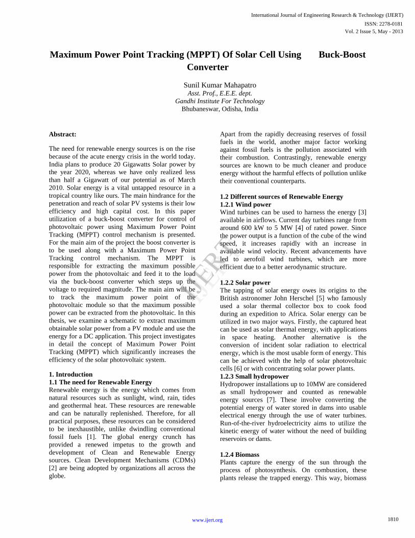
1.3 Renewable Energy trends across the globe
The current trend across developed economies tips
the scale in favour of Renewable Energy. For the last
three years, the continents of North America and
Europe have embraced more renewable power
capacity as compared to conventional power
capacity. Renewable accounted for 60% of the newly
installed power capacity in Europe in 2009 and
nearly 20% of the annual power production [7].
Figure 1:Global energy consumption in year 2011
As can be seen from the figure-1, wind and biomass
occupy a major share of the current renewable energy
consumption. Recent advancements in solar
photovoltaic technology and constant incubation of
projects in countries like Germany and Spain have
brought around tremendous growth in the solar PV
market as well, which is projected to surpass other
renewable energy sources in the coming years.
By 2009, more than 85 countries had some policy
target to achieve a predetermined share of their
power capacity through renewables. This was an
increase from around 45 countries in 2005. Most of
the targets are also very ambitious, landing in the
range of 30-90% share of national production through
renewables. Noteworthy policies are the European
Union’s target of achieving 20% of total energy
through renewables by 2020 and India’s Jawaharlal
Nehru Solar Mission, through which India plans to
produce 20GW solar energy by the year 2022.
2. Solar Cell
2.1 Operating principle
Solar cells are the basic components of photovoltaic
panels. Most are made from silicon even though other
materials are also used.
Solar cells take advantage of the photoelectric effect:
the ability of some semiconductors to convert
electromagnetic radiation directly into electrical
current. The charged particles generated by the
incident radiation are separated conveniently to
create an electrical current by an appropriate design
of the structure of the solar cell, as will be explained
in brief below.
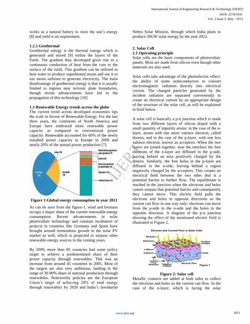
A solar cell is basically a p-n junction which is made
from two different layers of silicon doped with a
small quantity of impurity atoms: in the case of the n-
layer, atoms with one more valence electron, called
donors, and in the case of the p-layer, with one less
valence electron, known as acceptors. When the two
layers are joined together, near the interface the free
electrons of the n-layer are diffused in the p-side,
leaving behind an area positively charged by the
donors. Similarly, the free holes in the p-layer are
diffused in the n-side, leaving behind a region
negatively charged by the acceptors. This creates an
electrical field between the two sides that is a
potential barrier to further flow. The equilibrium is
reached in the junction when the electrons and holes
cannot surpass that potential barrier and consequently
they cannot move. This electric field pulls the
electrons and holes in opposite directions so the
current can flow in one way only: electrons can move
from the p-side to the n-side and the holes in the
opposite direction. A diagram of the p-n junction
showing the effect of the mentioned electric field is
illustrated in Figure 2.
Figure 2: Solar cell
Metallic contacts are added at both sides to collect
the electrons and holes so the current can flow. In the
case of the n-layer, which is facing the solar
International Journal of Engineering Research & Technology (IJERT)
Vol. 2 Issue 5, May - 2013ISSN: 2278-0181
www.ijert.org
IJERT
IJERT
1811

irradiance, the contacts are several metallic strips, as
they must allow the light to pass to the solar cell,
called fingers.
The structure of the solar cell has been described so
far and the operating principle is next. The photons of
the solar radiation shine on the cell. Three different
cases can happen: some of the photons are reflected
from the top surface of the cell and metal fingers.
Those that are not reflected penetrate in the substrate.
Some of them, usually the ones with less energy, pass
through the cell without causing any effect. Only
those with energy level above the band gap of the
silicon can create an electron-hole pair. These pairs
are generated at both sides of the p-n junction. The
minority charges (electrons in the p-side, holes in the
n-side) are diffused to the junction and swept away in
opposite directions (electrons towards the n-side,
holes towards the p-side) by the electric field,
generating a current in the cell, which is collected by
the metal contacts at both sides. This can be seen in
the figure above, Figure 2. This is the light-generated
current which depends directly on the irradiation: if it
is higher, then it contains more photons with enough
energy to create more electron-hole pairs and
consequently more current is generated by the solar
cell.
2.2 Equivalent circuit of a solar cell
The solar cell can be represented by the electrical
model shown in Figure 3. Its current voltage
characteristic is expressed by the following equation:
(1)
Where I and V are the solar cell output current and
voltage respectively, I0 is the dark saturation current,
q is the charge of an electron, A is the diode quality
(ideality) factor, k is the Boltzmann constant, T is the
absolute temperature and RS and RSH are the series
and shunt resistances of the solar cell. RS is the
resistance offered by the contacts and the bulk
semiconductor material of the solar cell. The origin
of the shunt resistance RSH is more difficult to
explain. It is related to the non ideal nature of the p–n
junction and the presence of impurities near the edges
of the cell that provide a short-circuit path around the
junction [4]. In an ideal case RS would be zero and
RSH infinite. However, this ideal scenario is not
possible and manufacturers try to minimize the effect
of both resistances to improve their products.
Figure 3: Equivalent circuit of a solar cell
Sometimes, to simplify the model, the effect of the
shunt resistance is not considered, i.e. RSH is
infinite, so the last term in equation (1) is neglected.
2.3 Open circuit voltage, short circuit current and
maximum power point
Two important points of the current-voltage
characteristic must be pointed out: the open circuit
voltage VOC and the short circuit current ISC. At
both points the power generate is zero. VOC can be
approximated from (1) when the output current of the
cell is zero, i.e. I=0 and the shunt resistance RSH is
neglected. It is represented by equation (2). The short
circuit current ISC is the current at V = 0 and is
approximately equal to the light generated current IL
as shown in equation (3).
(2)
(3)
The maximum power is generated by the solar cell at
a point of the current-voltage characteristic where the
product VI is maximum. This point is known as the
MPP and is unique, as can be seen in Figure 3, where
the previous points are represented.
Figure 4: Important points in the characteristic
curves of a solar panel.
2.4 Fill Factor
Using the MPP current and voltage, IMPP and
VMPP, the open circuit voltage (VOC) and the short
circuit current (ISC), the fill factor (FF) can be
defined as:
(4)
International Journal of Engineering Research & Technology (IJERT)
Vol. 2 Issue 5, May - 2013ISSN: 2278-0181
www.ijert.org
IJERT
IJERT
1812
It is a widely used measure of the solar cell overall
quality. It is the ratio of the actual maximum power
(IMPPVMPP) to the theoretical one (ISCVOC),
which is actually not obtainable. The reason for that
is that the MPP voltage and current are always below
the open circuit voltage and the short circuit current
respectively, because of the series and shunt
resistances and the diode depicted in Figure 2. The
typical fill factor for commercial solar cells is usually
over 0.70.
2.5 Temperature and irradiance effects
Two important factors that have to be taken into
account are the irradiation and the temperature. They
strongly affect the characteristics of solar modules.
As a result, the MPP varies during the day and that is
the main reason why the MPP must constantly be
tracked and ensure that the maximum available
power is obtained from the panel.
The effect of the irradiance on the voltage-current (V-
I) and voltage-power (V-P) characteristics is depicted
in Figure 4, where the curves are shown in per unit,
i.e. the voltage and current are normalized using the
VOC and the ISC respectively, in order to illustrate
better the effects of the irradiance on the V-I and V-P
curves. As was previously mentioned, the photo-
generated current is directly proportional to the
irradiance level, so an increment in the irradiation
leads to a higher photo-generated current. Moreover,
the short circuit current is directly proportional to the
photo-generated current; therefore it is directly
proportional to the irradiance. When the operating
point is not the short circuit, in which no power is
generated, the photo-generated current is also the
main factor in the PV current, as is expressed by
equations (1). For this reason the voltage-current
characteristic varies with the irradiation. In contrast,
the effect in the open circuit voltage is relatively
small, as the dependence of the light generated
current is logarithmic, as is shown in equation (4).
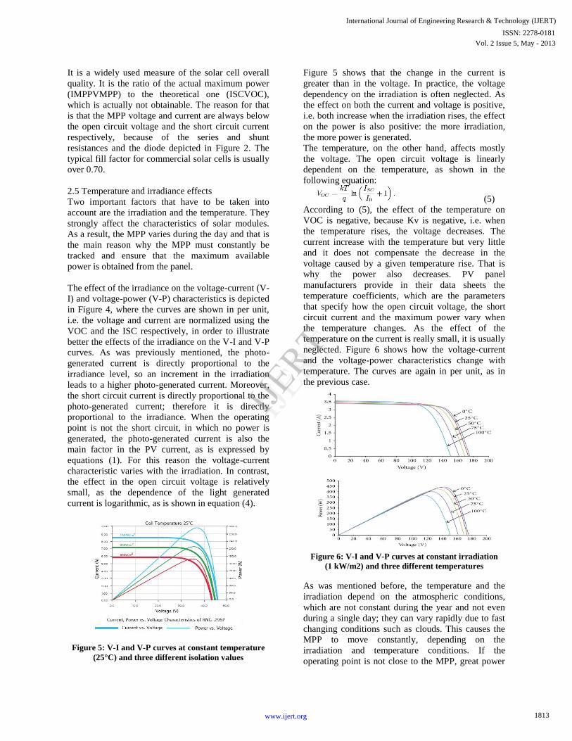
Figure 5: V-I and V-P curves at constant temperature
(25°C) and three different isolation values
Figure 5 shows that the change in the current is
greater than in the voltage. In practice, the voltage
dependency on the irradiation is often neglected. As
the effect on both the current and voltage is positive,
i.e. both increase when the irradiation rises, the effect
on the power is also positive: the more irradiation,
the more power is generated.
The temperature, on the other hand, affects mostly
the voltage. The open circuit voltage is linearly
dependent on the temperature, as shown in the
following equation:
(5)
According to (5), the effect of the temperature on
VOC is negative, because Kv is negative, i.e. when
the temperature rises, the voltage decreases. The
current increase with the temperature but very little
and it does not compensate the decrease in the
voltage caused by a given temperature rise. That is
why the power also decreases. PV panel
manufacturers provide in their data sheets the
temperature coefficients, which are the parameters
that specify how the open circuit voltage, the short
circuit current and the maximum power vary when
the temperature changes. As the effect of the
temperature on the current is really small, it is usually
neglected. Figure 6 shows how the voltage-current
and the voltage-power characteristics change with
temperature. The curves are again in per unit, as in
the previous case.
Figure 6: V-I and V-P curves at constant irradiation
(1 kW/m2) and three different temperatures
As was mentioned before, the temperature and the
irradiation depend on the atmospheric conditions,
which are not constant during the year and not even
during a single day; they can vary rapidly due to fast
changing conditions such as clouds. This causes the
MPP to move constantly, depending on the
irradiation and temperature conditions. If the
operating point is not close to the MPP, great power
International Journal of Engineering Research & Technology (IJERT)
Vol. 2 Issue 5, May - 2013ISSN: 2278-0181
www.ijert.org
IJERT
IJERT
1813
losses occur. Hence it is essential to track the MPP in
any conditions to assure that the maximum available
power is obtained from the PV panel. In a modern
solar power converter, this task is entrusted to the
MPPT algorithms.
3. Buck-Boost Converter
The basic schematic of a buck-boost converter. Two
different topologies are called buck–boost converter.
Both of them can produce an output voltage much
larger (in absolute magnitude) than the input voltage.
Both of them can produce a wide range of output
voltage from that maximum output voltage to almost
zero.
The inverting topology – The output voltage
is of the opposite polarity as the input
A buck (step-down) converter followed by– boost
(step-up) converter. The output voltage is of the same
polarity as the input, and can be lower or higher than
the input. Such a non-inverting buck-boost converter
may use a single inductor that is used as both the
buck inductor and the boost inductor.
Figure 7: Buck-Boost Converter
This page describes the inverting topology. The
buck–boost converter is a type of that has an output
voltage magnitude that is either greater than or less
than the input voltage magnitude. It is a switched-
mode power supply with a similar circuit topology to
the boost converter and the buck converter. The
output voltage is adjustable based on the duty cycle
of the switching transistor. One possible drawback of
this converter is that the switch does not have a
terminal at ground; this complicates the driving
circuitry. Also, the polarity of the output voltage is
opposite the input voltage. Neither drawback is of
any consequence if the power supply is isolated from
the load circuit (if, for example, the supply is a
battery) as the supply and diode polarity can simply
be reversed. The switch can be on either the ground
side or the supply side.
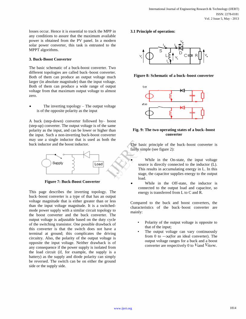
3.1 Principle of operation:
Figure 8: Schematic of a buck–boost converter
Fig. 9: The two operating states of a buck–boost
converter
The basic principle of the buck–boost converter is
fairly simple (see figure 2):
While in the On-state, the input voltage
source is directly connected to the inductor (L).
This results in accumulating energy in L. In this
stage, the capacitor supplies energy to the output
load.
While in the Off-state, the inductor is
connected to the output load and capacitor, so
energy is transferred from L to C and R.
Compared to the buck and boost converters, the
characteristics of the buck–boost converter are
mainly:
• Polarity of the output voltage is opposite to
that of the input;
• The output voltage can vary continuously
from 0 to (for an ideal converter). The
output voltage ranges for a buck and a boost
converter are respectively 0 to and to .
International Journal of Engineering Research & Technology (IJERT)
Vol. 2 Issue 5, May - 2013ISSN: 2278-0181
www.ijert.org
IJERT
IJERT
1814
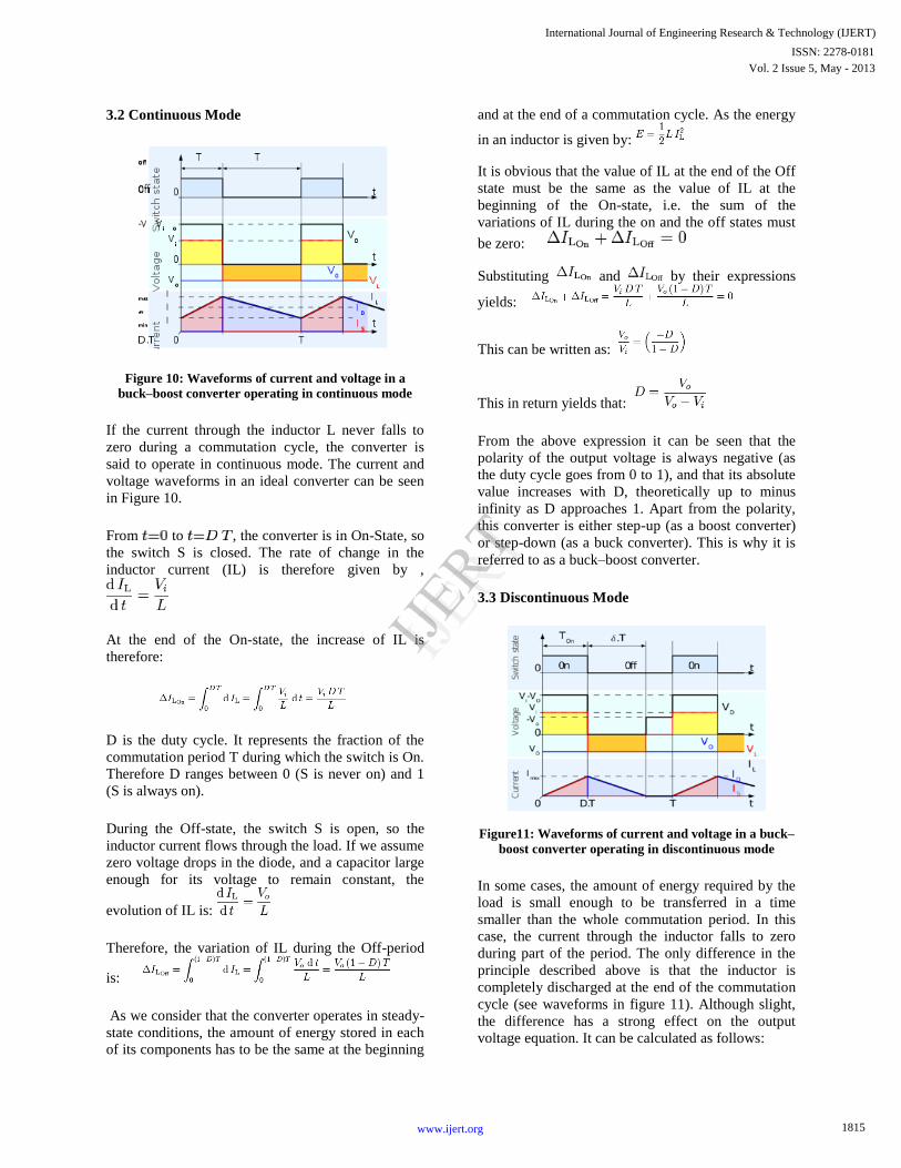
3.2 Continuous Mode
Figure 10: Waveforms of current and voltage in a
buck–boost converter operating in continuous mode
If the current through the inductor L never falls to
zero during a commutation cycle, the converter is
said to operate in continuous mode. The current and
voltage waveforms in an ideal converter can be seen
in Figure 10.
From to , the converter is in On-State, so
the switch S is closed. The rate of change in the
inductor current (IL) is therefore given by ,
At the end of the On-state, the increase of IL is
therefore:
D is the duty cycle. It represents the fraction of the
commutation period T during which the switch is On.
Therefore D ranges between 0 (S is never on) and 1
(S is always on).
During the Off-state, the switch S is open, so the
inductor current flows through the load. If we assume
zero voltage drops in the diode, and a capacitor large
enough for its voltage to remain constant, the
evolution of IL is:
Therefore, the variation of IL during the Off-period
is:
As we consider that the converter operates in steady-
state conditions, the amount of energy stored in each
of its components has to be the same at the beginning
and at the end of a commutation cycle. As the energy
in an inductor is given by:
It is obvious that the value of IL at the end of the Off
state must be the same as the value of IL at the
beginning of the On-state, i.e. the sum of the
variations of IL during the on and the off states must
be zero:
Substituting and by their expressions
yields:
This can be written as:
This in return yields that:
From the above expression it can be seen that the
polarity of the output voltage is always negative (as
the duty cycle goes from 0 to 1), and that its absolute
value increases with D, theoretically up to minus
infinity as D approaches 1. Apart from the polarity,
this converter is either step-up (as a boost converter)
or step-down (as a buck converter). This is why it is
referred to as a buck–boost converter.
3.3 Discontinuous Mode
Figure11: Waveforms of current and voltage in a buck–
boost converter operating in discontinuous mode
In some cases, the amount of energy required by the
load is small enough to be transferred in a time
smaller than the whole commutation period. In this
case, the current through the inductor falls to zero
during part of the period. The only difference in the
principle described above is that the inductor is
completely discharged at the end of the commutation
cycle (see waveforms in figure 11). Although slight,
the difference has a strong effect on the output
voltage equation. It can be calculated as follows:
International Journal of Engineering Research & Technology (IJERT)
Vol. 2 Issue 5, May - 2013ISSN: 2278-0181
www.ijert.org
IJERT
IJERT
1815
As the inductor current at the beginning of the cycle
is zero, its maximum value (at ) is
During the off-period, IL falls to zero after δ.T:
Using the two previous equations, δ is:
The load current Io is equal to the average diode
current (ID). As can be seen on figure 11, the diode
current is equal to the inductor current during the off-
state. Therefore, the output current can be written as:
Replacing and δ by their respective
expressions yields:
Therefore, the output voltage gain can be written as:
Compared to the expression of the output voltage
gain for the continuous mode, this expression is much
more complicated. Furthermore, in discontinuous
operation, the output voltage not only depends on the
duty cycle, but also on the inductor value, the input
voltage and the output current.
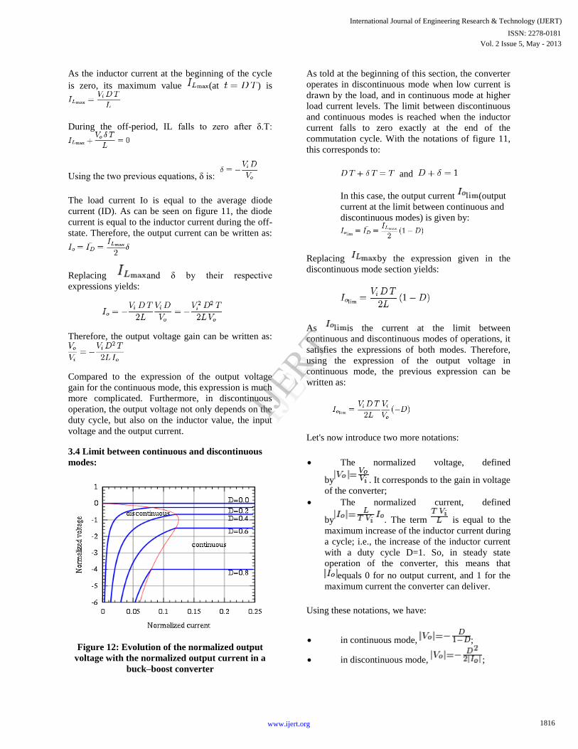
3.4 Limit between continuous and discontinuous
modes:
Figure 12: Evolution of the normalized output
voltage with the normalized output current in a
buck–boost converter
As told at the beginning of this section, the converter
operates in discontinuous mode when low current is
drawn by the load, and in continuous mode at higher
load current levels. The limit between discontinuous
and continuous modes is reached when the inductor
current falls to zero exactly at the end of the
commutation cycle. With the notations of figure 11,
this corresponds to:
and
In this case, the output current (output
current at the limit between continuous and
discontinuous modes) is given by:
Replacing by the expression given in the
discontinuous mode section yields:
As is the current at the limit between
continuous and discontinuous modes of operations, it
satisfies the expressions of both modes. Therefore,
using the expression of the output voltage in
continuous mode, the previous expression can be
written as:
Let's now introduce two more notations:
The normalized voltage, defined
by . It corresponds to the gain in voltage
of the converter;
The normalized current, defined
by . The term is equal to the
maximum increase of the inductor current during
a cycle; i.e., the increase of the inductor current
with a duty cycle D=1. So, in steady state
operation of the converter, this means that
equals 0 for no output current, and 1 for the
maximum current the converter can deliver.
Using these notations, we have:
in continuous mode, ;
in discontinuous mode, ;
International Journal of Engineering Research & Technology (IJERT)
Vol. 2 Issue 5, May - 2013ISSN: 2278-0181
www.ijert.org
IJERT
IJERT
1816
The current at the limit between continuous and
discontinuous mode
is . Therefore
the locus of the limit between continuous and
discontinuous modes is given by .
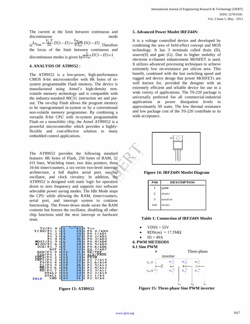
4. ANALYSIS OF AT89S52 :
The AT89S52 is a low-power, high-performance
CMOS 8-bit microcontroller with 8K bytes of in-
system programmable Flash memory. The device is
manufactured using Atmel’s high-density non-
volatile memory technology and is compatible with
the industry-standard 80C51 instruction set and pin-
out. The on-chip Flash allows the program memory
to be reprogrammed in-system or by a conventional
non-volatile memory programmer. By combining a
versatile 8-bit CPU with in-system programmable
Flash on a monolithic chip, the Atmel AT89S52 is a
powerful microcontroller which provides a highly-
flexible and cost-effective solution to many
embedded control applications.
The AT89S52 provides the following standard
features: 8K bytes of Flash, 256 bytes of RAM, 32
I/O lines, Watchdog timer, two data pointers, three
16-bit timer/counters, a six-vector two-level interrupt
architecture, a full duplex serial port, on-chip
oscillator, and clock circuitry. In addition, the
AT89S52 is designed with static logic for operation
down to zero frequency and supports two software
selectable power saving modes. The Idle Mode stops
the CPU while allowing the RAM, timer/counters,
serial port, and interrupt system to continue
functioning. The Power-down mode saves the RAM
contents but freezes the oscillator, disabling all other
chip functions until the next interrupt or hardware
reset.
Figure 13: AT89S52
5. Advanced Power Mosfet IRFZ44N:
It is a voltage controlled device and developed by
combining the area of field-effect concept and MOS
technology. It has 3 terminals called drain (D),
source(S) and gate (G). Due to higher mobility of
electrons n-channel enhancement MOSFET is used.
It utilizes advanced processing techniques to achieve
extremely low on-resistance per silicon area. This
benefit, combined with the fast switching speed and
rugged zed device design that power MOSFETs are
well known for, provided the designer with an
extremely efficient and reliable device for use in a
wide variety of applications. The T0-220 package is
universally preferred foe all commercial-industrial
applications at power dissipation levels to
approximately 50 watts. The low thermal resistance
and low package cost of the T0-220 contribute to its
wide acceptance.
Figure 14: IRFZ44N Mosfet Diagram
Table 1: Connection of IRFZ44N Mosfet
VDSS = 55V
RDS(on) = 17.5MΩ
ID = 49A
6. PWM METHODS
6.1 Sine PWM
Three-phase
inverter
Figure 15: Three-phase Sine PWM inverter
International Journal of Engineering Research & Technology (IJERT)
Vol. 2 Issue 5, May - 2013ISSN: 2278-0181
www.ijert.org
IJERT
IJERT
1817
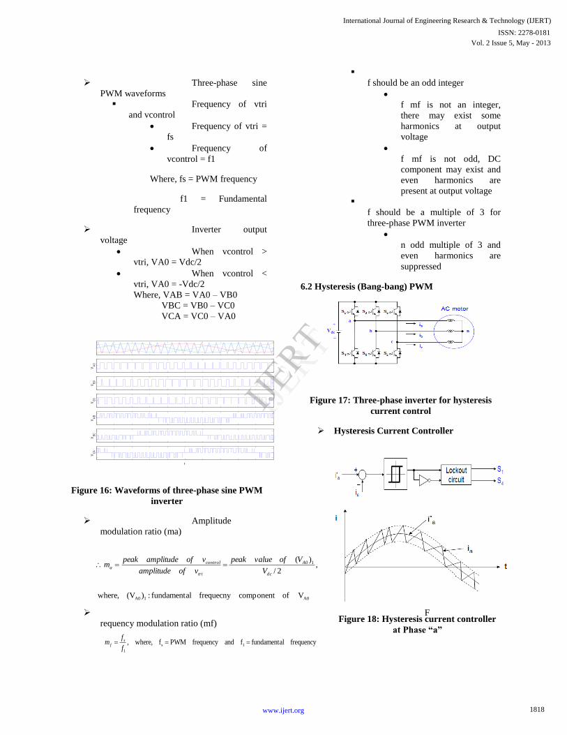
Three-phase sine
PWM waveforms
Frequency of vtri
and vcontrol
Frequency of vtri =
fs
Frequency of
vcontrol = f1
Where, fs = PWM frequency
f1 = Fundamental
frequency
Inverter output
voltage
When vcontrol >
vtri, VA0 = Vdc/2
When vcontrol <
vtri, VA0 = -Vdc/2
Where, VAB = VA0 – VB0
VBC = VB0 – VC0
VCA = VC0 – VA0
VA
0V
B0
VC
0V
AB
VB
CV
CA
t
Figure 16: Waveforms of three-phase sine PWM
inverter
Amplitude
modulation ratio (ma)
F
requency modulation ratio (mf)
m
f should be an odd integer
i
f mf is not an integer,
there may exist some
harmonics at output
voltage
i
f mf is not odd, DC
component may exist and
even harmonics are
present at output voltage
m
f should be a multiple of 3 for
three-phase PWM inverter
A
n odd multiple of 3 and
even harmonics are
suppressed
6.2 Hysteresis (Bang-bang) PWM
Figure 17: Three-phase inverter for hysteresis
current control
Hysteresis Current Controller
Figure 18: Hysteresis current controller
at Phase “a”
A01A0
10
Vofcomponentfrequecnylfundamenta:)(Vwhere,
,2/
)(
dc
A
tri
controla
V
Vofvaluepeak
vofamplitude
vofamplitudepeakm
frequencylfundamentafandfrequencyPWMfwhere,, 1s
1
f
fm s
f
International Journal of Engineering Research & Technology (IJERT)
Vol. 2 Issue 5, May - 2013ISSN: 2278-0181
www.ijert.org
IJERT
IJERT
1818
Characteristics of hysteresis Current Control
A
Advantages
E
Excellent dynamic
response
L
Low cost and easy implementation
D
Drawbacks
L
Large current ripple in
steady-state
V
Variation of switching
frequency
N
No intercommunication
between each hysteresis
controller of three phases
and hence no strategy to
generate zero-voltage
vectors. As a result, the
switching frequency
increases at lower
modulation index and the
signal will leave the
hysteresis band whenever
the zero vector is turned
on.
T
The modulation process
generates sub-harmonic
component
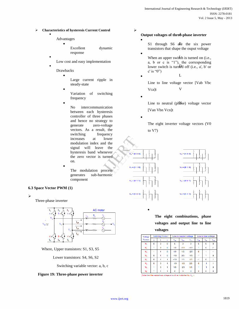
6.3 Space Vector PWM (1)
T
Three-phase inverter
Where, Upper transistors: S1, S3, S5
Lower transistors: S4, S6, S2
Switching variable vector: a, b, c
Figure 19: Three-phase power inverter
O
Output voltages of three-phase inverter
S
S1 through S6 are the six power
transistors that shape the ouput voltage
W
When an upper switch is turned on (i.e.,
a, b or c is “1”), the corresponding
lower switch is turned off (i.e., a', b' or
c' is “0”)
L
Line to line voltage vector [Vab Vbc
Vca]t
L
Line to neutral (phase) voltage vector
[Van Vbn Vcn]t
T
The eight inverter voltage vectors (V0
to V7)
T
The eight combinations, phase
voltages and output line to line
voltages
International Journal of Engineering Research & Technology (IJERT)
Vol. 2 Issue 5, May - 2013ISSN: 2278-0181
www.ijert.org
IJERT
IJERT
1819
7. SIMULATION:
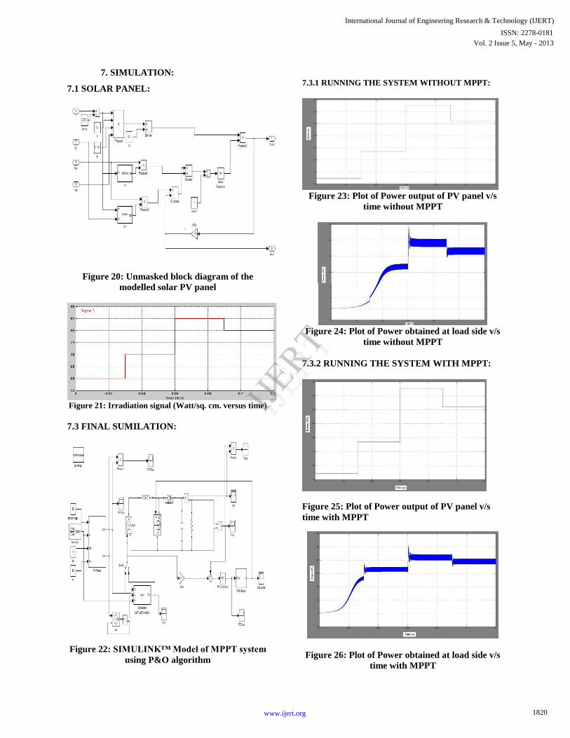
7.1 SOLAR PANEL:
Figure 20: Unmasked block diagram of the
modelled solar PV panel
Figure 21: Irradiation signal (Watt/sq. cm. versus time)
7.3 FINAL SUMILATION:
Figure 22: SIMULINK™ Model of MPPT system
using P&O algorithm
7.3.1 RUNNING THE SYSTEM WITHOUT MPPT:
Figure 23: Plot of Power output of PV panel v/s
time without MPPT
Figure 24: Plot of Power obtained at load side v/s
time without MPPT
7.3.2 RUNNING THE SYSTEM WITH MPPT:
Figure 25: Plot of Power output of PV panel v/s
time with MPPT
Figure 26: Plot of Power obtained at load side v/s
time with MPPT
International Journal of Engineering Research & Technology (IJERT)
Vol. 2 Issue 5, May - 2013ISSN: 2278-0181
www.ijert.org
IJERT
IJERT
1820

8. CONCLUSION
A renewable energy system, like the one
implemented here, is suitable for residential and/or
industrial applications. The results suggest that, on
the basis of maximum power point tracking
efficiency, the perturb-and-observe method, already
by far the most commonly used algorithm in
commercial converters, has the potential to be very
competitive with other methods if it is properly
optimized for the given hardware.
Thus a system such as this can be deployed easily
with little concern about adapting a home or
business's electrical wiring to take advantage of solar
energy. Many areas allow surplus energy generated
by systems such as this to be sold to the utility grid in
a policy known as "net metering."
After accomplishing the model of PV modules, the
models of DC-DC buck-boost converter and MPPT
systems are combined with it to complete the PV
simulation system with the MPPT function. The
accuracy and execution efficiency for each MPPT
algorithm can then be simulated under different
weather voltage.
Therefore, it was seen that using the Perturb &
Observe MPPT technique increased the efficiency of
the photovoltaic system by approximately 126% from
an earlier output power.
REFERENCES
1. Dylan D .C. Lu , R.H. Chu, S. sathiakumar
& V.G Agilides , “A Converter with simple
Maximum Power Point Tracking for Power
Electronics Education On Solar Energy
System” in IEEE transs. On power
electronics
2. S. B. Kjaer, J. K. Pedersen, and F.
Blaabjerg, “A Review of Single-Phase Grid-
Connected Inverters for Photovoltaic
Modules,” in IEEE Transs. on Power
Electron., Vol. 41, No. 5, pp. 1292–1306,
Sep. /Oct. 2005
3. Power Electronics: Circuits, Devices and
Operations (Book) - Muhammad H. Rashid
4. Power Electronics (Book) –Dr. P.S.
Bimbhra
5. Resource and Energy Economics - C
Withagen - 1994 – Elsevier
6. Advanced Algorithm for control of
Photovoltaic systems - C. Liu, B. Wu and R.
Cheung
Webpage:
http://en.wikipedia.org/wiki/buck-boost
Webpage:
http://en.wikipedia.org/wiki/solarcell
International Journal of Engineering Research & Technology (IJERT)
Vol. 2 Issue 5, May - 2013ISSN: 2278-0181
www.ijert.org
IJERT
IJERT
1821