Embed Size (px)
DESCRIPTION
A Quarterly Publication of the Microelectronics Packaging & Test Engineering Council
Citation preview
A Quarterly Publication of The Microelectronics Packaging & Test Engineering Council Volume 17, Number 2
SPRING 2011 MEPTEC Report 3
-INSIDE THIS ISSUE
15 Heathcare revolution – MEMS can be used in varying places around the body for precise data tracking. 28
MEMS firms need to leverage proven materials solutions that are market-ready and tested. 30
SnAg solder capped Cu pillar bumps emerge as alternative to C4 solder bumps. 34
Medical MEMS Technology indus-try’s interest in healthcare grows exponentially.
Located and part of Lorain County Community College in Elyria, Ohio, the Richard Desich SMART Center develops manufacturable packaging integration solutions for cus-tomers developing next generation microsystem products.page 17
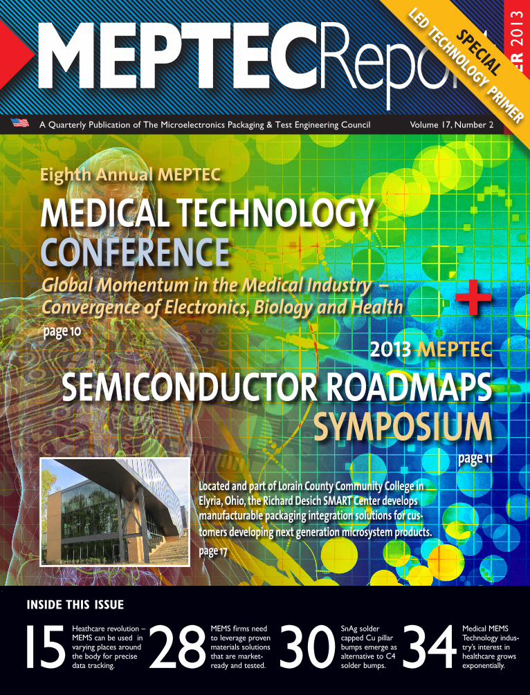
+2013 MEPTEC
SEMICONDUCTOR ROADMAPS SYMPOSIUM
page 11
SUM
MER
201
3
SPECIAL
LED TECHNOLOGY PRIMER
Eighth Annual MEPTEC
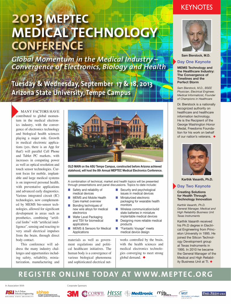
MEDICAL TECHNOLOGY CONFERENCE Global Momentum in the Medical Industry –Convergence of Electronics, Biology and Healthpage 10
C
M
Y
CM
MY
CY
CMY
K
ASE_AD_8x10.5in_05102013.pdf 1 13/5/10 下午7:23
TECHNICAL SYMPOSIUMS ARE AN important part of the MEPTEC organiza-tional structure with over 50 days of events to date and typically four events per year, covering a range of topics in electronics packaging and test. The direct extensive experience base of the MEPTEC Advisory Board Members and a diverse network of industry relationships in state-of-the-art technology has made reviews of Sympo-sium Agendas very interesting. Review of the MEPTEC Web Site Symposium Proceedings (and CD Library) is literally a timeline for technologies and a significant indicator of their associated industry trends. It was late in 1999, December 31st at 11:59 PM to be exact, with the organization having nearly 20 years of history with the MEPTEC Report publication and regional Luncheons, as the tech world held its breath and wine glasses, the computer clocks turned to 2000! Fortunately, within days, the advisory board focus was able to move from the “non-event” to an agenda for the first MEPTEC Symposium on Lead Free Solder Materials held in June. After the inaugural event in 2000, there were three Symposiums in 2001 with the big buzz in Opto-Electronics based on technology and investment capital. With the “Opto” indus-try event seen trending downward in 2002, events on Wafer Thinning, Wafer Level Packaging and Packaging Systems rounded out the four symposiums of the year, the new benchmark. With events on RF Packaging and the cross-over between Component & Board Levels, 2003 was the year MEPTEC also presented events on MEMS Technology and Packaging Roadmaps (on a wide arrange of packaging topics), with both events continu-ing to be held on an annual basis. The con-
Medical event attendee reception, started in 2012, will be held again this year to showcase ASU SBHSE Student Projects, as they are involved in new product design and develop. On behalf on the Advisory Board, your participation and feedback on Symposiums is appreciated, with these and other prior events including Solar, Known-Good-Die and 2.5D & 3D now in review. I look for-ward to meeting you at the Medical event to discuss current and future industry trends, as well as the “next trending tech-nology”, positioning new MEPTEC events for key market visibility.
tinued interest and growth in both of these events is clearly an industry indicator. In particular, the technology and topics within the MEMS event continue to gain momen-tum based on product commercialization and expansion into other industries. Much in the way the Packaging Roadmaps event covers the range of packaging technologies, the MEMS technologies can be found in computing, communications, automotive, military, aerospace and medical industries. Receiving this issue of the MEPTEC Report will mean you are now able to access the CD’s on the 11th Annual MEMS Sympo-sium and plan participation and registration for upcoming Packaging Roadmaps event, as I am also planning on attending. With the responsibility as General Chairman for the Thermal Technologies Symposium, which was initiated in 2005, it was very interesting to see this event transi-tion to a co-location with IEEE SemiTherm and continuing on a positive trend based on the impact of heat on products. Transition of the Thermal event committee, in prior years, allowed for my complete focus on the Medical Symposium, initiated in September 2006 and held on the Arizona State Uni-versity campus in Tempe, Arizona. Medical industry momentum and increasing support from the ASU School of Biological Health Systems Engineering (SBHSE), gave way to expansion in 2011 for a two-day sym-posium. This issue of the MEPTEC Report will be distributed to medical, electronic and biomedical industry experts attending, exhibiting and sponsoring the 8th Annual MEPTEC Medical Technology Conference. Committee members, speakers and sponsors are invited to the pre-symposium evening reception, which has become part of all the MEPTEC Symposium agendas. The
BOARD LETTER
MEPTEC Symposiums – Forwarding Visions and Predicting Industry Trends: Medical, MEMS and Packaging RoadmapsNicholas Leonardi, Director of Business Development, Premier Semiconductor ServicesMEPTEC Advisory Board Member MEPTEC Medical Technology Conference, General ChairmanASU / SBHSE, Advisory Board Member
SUMMER 2013 MEPTEC REPORT 3meptec.org
NICK LEONARDI brings over twenty five years of electronics industry expe-rience into his position as Director of Business Development for Premier Semiconductor Services. With current focus on new business development, previous key roles in engineering development, applications and sales management, with companies such as AMD, LSI Logic and GE. Primary areas of business development include the Counterfeit IC Detection Programs and the Lead Free Solder Conversion for BGA’s and other package types. Industry affiliations and participation include; MEPTEC Advisory Board Member and Regional Co-Chairman, with support of other organizations including the FSA, SEMI, IEEE, IMAPS and SMTA. Nick received his B.S. Degree in Materials Engineering from Alfred University, New York.
ON THE COVER
10 & 11 MEPTEC will present two events in September. The Eigth Annual MEPTEC “Medical Technology
Conference” will be held on Tuesday & Wednesday September 17 & 18, 2013 at the Arizona State University Tempe Campus. The 2013 MEPTEC “Semiconductor Roadmaps Symposium” will be held the following week, on Tuesday, September 24, 2013, at the Biltmore Hotel in Santa Clara, California.
MEPTEC Report Vol. 17, No. 2. Published quarterly by MEPCOM LLC, P. O. Box 222, Medicine Park, OK 73557. Copyright 2013 by MEPTEC/MEPCOM LLC. All rights reserved. Materials may not be reproduced in whole or in part without written permission. MEPTEC Report is sent without charge to members of MEPTEC. For non-members, yearly subscriptions are available for $75 in the United States, $80US in Canada and Mexico, and $95US elsewhere. For advertising rates and information contact Gina Edwards at 408-858-5493, Fax Toll Free 1-866-424-0130.
A Quarterly Publication of The Microelectronics Packaging & Test Engineering Council Volume 17, Number 2
15 ANALYSIS – When it comes to the human body and the environ-ment, there are dozens of sensors that can potentially be used
to improve healthcare. There are acoustic sensors, chemical sensors, humidity or moisture sensors, navigation sensors, position sensors, opti-cal sensors, pressure sensors, temperature sensors, proximity sensors, etc. Depending on the market, these sensors will be placed on different parts of the body, and different metrics will be used to determine the quality of movement and if a behavior change should or can be enacted.
BY MICHELL PRUNTY SEMICO RESEARCH CORPORATION
21 SPECIAL – LED Technology, Packaging & Test Primer. Worldwide, there is a push to replace conventional energy inef-
ficient light sources with solid state lighting. Considering incandescent bulbs alone, the EU, Switzerland, and Australia started to phase them out in 2009. Likewise, other nations are implementing new energy stan-dards: Argentina, Russia, and Canada in 2012, and the US in 2014. The solid state lighting revolution based on LED technology holds incredible promise to reshape the lighting landscape.
BY SAI ANKIREDDI SORAA INC.
17 PROFILE – The Richard Desich SMART Commercialization Cen-ter for Microsystems (“Desich SMART Center”) is a microsystem
packaging, assembly, and test development foundry. Located and part of Lorain County Community College in Elyria, Ohio, the Desich SMART Center develops manufacturable packaging integration solutions for customers developing next-generation microsystem products by lever-aging world-class facilities and a highly experienced engineering team to accelerate product time to market.
DESICH SMART CENTER MEMBER COMPANY PROFILE
DEPARTMENTS 3 Board Letter 5 Member News
12 Industry Insights Column 13 Coupling & Crosstalk Column
28 Henkel News30 Dow Electronic Mtls. 34 Opinion
The MEPTEC Report is a Publication of the Microelectronics Packaging & Test
Engineering Council
P. O. Box 222, Medicine Park, OK 73557Tel: (650) 714-1570 Email: [email protected]
Publisher MEPCOM LLC
Editor Bette Cooper
Art Director/Designer Gary Brown
Sales Manager Gina Edwards
MEPTEC Advisory Board
Board Members
Ivor Barber Xilinx, Inc.
Jeanne Beacham Delphon Industries
Joel Camarda Amonix, Inc.
Jeff Demmin
Douglass Dixon Henkel Corporation
Farshad Ghahghahi LSI Corporation
Nikhil Kelkar Exar Corporation
Nick Leonardi Premier Semiconductor Services
Phil Marcoux PPM Associates
Bhavesh Muni Dow Chemical Corp.
Kumar Nagarajan Maxim Integrated
Raj Pendse STATS ChipPAC
Rich Rice ASE (US) Inc.
Jim Walker Gartner
John Xie Altera Corporation
Special Advisors
Bance Hom Consultech International, Inc.
Ron Jones N-Able Group International
Mary Olsson Gary Smith EDA
Mike Pinelis MEMS Journal, Inc.
Honorary Advisors
Seth Alavi Sunsil
Gary Catlin Plexus
Rob Cole
Skip Fehr
Anna Gualtieri Elle Technology
Marc Papageorge Semiconductor Outsourcing
Contributors
Sai Ankireddi Soraa Inc.
Sam Bierstock, MD Champions in Healthcare
Ira FeldmanFeldman Engineering Corp.
Shashi GuptaHenkel Electronic Materials, LLC
Ron Jones N-Able Group International
Nicholas Leonardi Premier Semiconductor Services
Michell Prunty Semico Research Corp.
SUMMER 2013 MEPTEC REPORT 15meptec.org
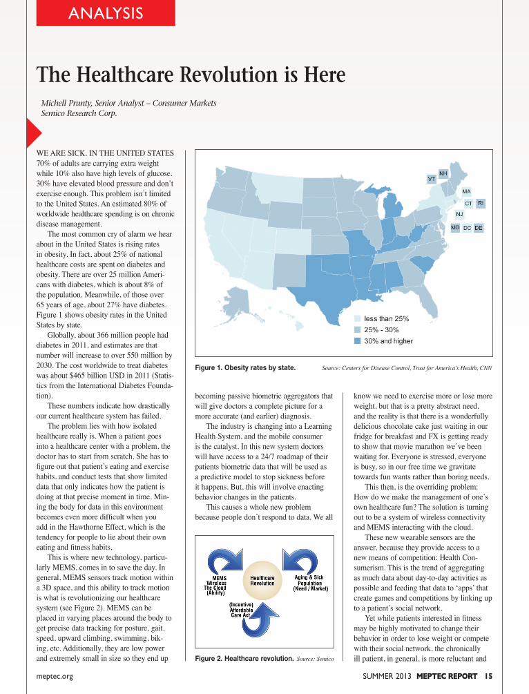
We are sick. in the United states 70% of adults are carrying extra weight while 10% also have high levels of glucose. 30% have elevated blood pressure and don’t exercise enough. this problem isn’t limited to the United states. an estimated 80% of worldwide healthcare spending is on chronic disease management. the most common cry of alarm we hear about in the United states is rising rates in obesity. in fact, about 25% of national healthcare costs are spent on diabetes and obesity. there are over 25 million ameri-cans with diabetes, which is about 8% of the population. Meanwhile, of those over 65 years of age, about 27% have diabetes. Figure 1 shows obesity rates in the United states by state. Globally, about 366 million people had diabetes in 2011, and estimates are that number will increase to over 550 million by 2030. the cost worldwide to treat diabetes was about $465 billion Usd in 2011 (statis-tics from the international diabetes Founda-tion). these numbers indicate how drastically our current healthcare system has failed. the problem lies with how isolated healthcare really is. When a patient goes into a healthcare center with a problem, the doctor has to start from scratch. she has to figure out that patient’s eating and exercise habits, and conduct tests that show limited data that only indicates how the patient is doing at that precise moment in time. Min-ing the body for data in this environment becomes even more difficult when you add in the hawthorne effect, which is the tendency for people to lie about their own eating and fitness habits. this is where new technology, particu-larly MeMs, comes in to save the day. in general, MeMs sensors track motion within a 3d space, and this ability to track motion is what is revolutionizing our healthcare system (see Figure 2). MeMs can be placed in varying places around the body to get precise data tracking for posture, gait, speed, upward climbing, swimming, bik-ing, etc. additionally, they are low power and extremely small in size so they end up
ANALYSIS
The Healthcare Revolution is Here Michell Prunty, Senior Analyst – Consumer Markets Semico Research Corp.
becoming passive biometric aggregators that will give doctors a complete picture for a more accurate (and earlier) diagnosis. the industry is changing into a Learning health system, and the mobile consumer is the catalyst. in this new system doctors will have access to a 24/7 roadmap of their patients biometric data that will be used as a predictive model to stop sickness before it happens. But, this will involve enacting behavior changes in the patients. this causes a whole new problem because people don’t respond to data. We all
know we need to exercise more or lose more weight, but that is a pretty abstract need, and the reality is that there is a wonderfully delicious chocolate cake just waiting in our fridge for breakfast and FX is getting ready to show that movie marathon we’ve been waiting for. everyone is stressed, everyone is busy, so in our free time we gravitate towards fun wants rather than boring needs. this then, is the overriding problem: how do we make the management of one’s own healthcare fun? the solution is turning out to be a system of wireless connectivity and MeMs interacting with the cloud. these new wearable sensors are the answer, because they provide access to a new means of competition: health con-sumerism. this is the trend of aggregating as much data about day-to-day activities as possible and feeding that data to ‘apps’ that create games and competitions by linking up to a patient’s social network. Yet while patients interested in fitness may be highly motivated to change their behavior in order to lose weight or compete with their social network, the chronically ill patient, in general, is more reluctant and
Figure 1. Obesity rates by state. Source: Centers for Disease Control, Trust for America’s Health, CNN
Figure 2. Healthcare revolution. Source: Semico
A Quarterly Publication of The Microelectronics Packaging & Test Engineering Council Volume 17, Number 2
SPRING 2011 MEPTEC Report 3
-INSIDE THIS ISSUE
15 Heathcare revolution – MEMS can be used in varying places around the body for precise data tracking. 28
MEMS firms need to leverage proven materials solutions that are market-ready and tested. 30
SnAg solder capped Cu pillar bumps emerge as alternative to C4 solder bumps. 34
Medical MEMS Technology indus-try’s interest in healthcare grows exponentially.
Located and part of Lorain County Community College in Elyria, Ohio, the Richard Desich SMART Center develops manufacturable packaging integration solutions for cus-tomers developing next generation microsystem products.page 17
+2013 MEPTEC
SEMICONDUCTOR ROADMAPS SyMpOSiuM
page 11
SUM
MER
201
3
SPECIAL
LED TECHNOLOGY PRIMER
Eighth Annual MEpTEC
MEDICAL TECHNOLOGY CONFERENCE Global Momentum in the Medical Industry –Convergence of Electronics, Biology and Healthpage 10
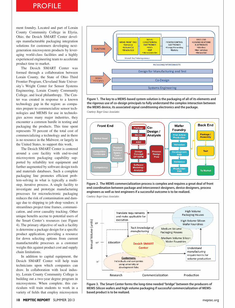
ince the early days starting in the 1960’s, MEMS (Microelec-tromechanical Systems) were virtually stand-alone devices
and were attached/inserted into custom designed mechanical or standard IC pack-ages. More recently however, MEMS are truly becoming systems (as the “S” in MEMS connotes). The integration of MEMS devices into packages of various shapes, sizes and materials along with sig-nal conditioning electronics, power sources and networking (both wireless and con-nected) communications IC’s are now con-sidered to be the true application solution (see Figure 1). The role of packaging/assembly and test (P/A/T) in the overall successful com-mercialization of MEMS (see Figure 2) has historically taken a back seat to device development. More recently however, the MEMS community is taking note of the importance and the value of P/A/T in the
ford, University of California Berkeley and University of Michigan as well as at the scores of commercial foundries world-wide. However… what was needed was a mechanism to package the output of the foundries i.e. Silicon wafers into products that could be tested. The weak link here was the mechanism to do this work in a developmental format and thus provide the designer with a convenient and full-service facility to package, assemble and test the MEMS device. The Richard Desich Smart Commercialization Center for Microsys-tems (SMART) serves this highly needed and critical ”bridge” function in the com-mercialization of a MEMS-based solution (see Figure 3).
OVERVIEW The Richard Desich SMART Com-mercialization Center for Microsystems (“Desich SMART Center”) is a microsys-tem packaging, assembly, and test develop-
PROFILE
creation of MEMS-based solutions. Addi-tionally, it is well known that the packag-ing/assembly and test (P/A/T) of a MEMS-based solution can be as much as 60% or more of the total cost of the solution. This fact makes the consideration of the packaging strategy a very important and early part of the solution design process to achieve optimum cost and performance. Here we are, approximately a half-century later from the early days of MEMS pack-aging and many of the same materials and packaging strategies are still in favor by many suppliers. Additionally, the MEMS community had traditionally focused on the estab-lishment of an infrastructure to design and manufacture Silicon devices espe-cially including the creation of MEMS Silicon foundries. It was relatively easy for MEMS developers to have their devices manufactured in foundries including those of research universities e.g. Cornell, Stan-
SUMMER 2013 MEPTEC REPORT 17meptec.org
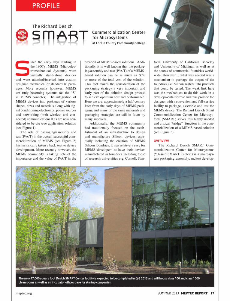
The new 47,000 square foot Desich SMART Center facility is expected to be completed in Q-3 2013 and will house class 100 and class 1000 cleanrooms as well as an incubator office space for startup companies.
SUMMER 2013 MEPTEC REPORT 21meptec.org
TECHNOLOGY
substrate on which several epitaxial lay-ers are grown. Generally speaking, such layers are no more than a few atoms thick. Numerous processing steps later, the die wafer is ready for singulation. Wafer scribe-and-break or traditional wafer saw are common techniques used to separate the dies. The resulting dies either have lat-eral terminals (interconnect pads) or top-and-bottom contacts.
today. InGaN or Indium-Gallium-Nitride is used for violet, blue and green LEDs and InGaAlP (Indium Gallium Aluminum Phosphide) is used for green, yellow, orange or red LEDs. Other combinations from the III-V semiconductor family are also possible, as Figure 4 shows.
3. LED Packaging
Fabrication of an LED begins with a
LED Technology, Packaging & Test: A Primer
1. Introduction A LED, short for Light Emitting Diode, is a semiconductor P-N junction light source. Nicholas Holonyak, Jr. (b. 1928) is generally credited with creating the world’s first usable LED in 1962 while working as a Consulting Scientist for General Elec-tric. Since then, LED technology has seen numerous significant advances. The earliest commercial deployments of LEDs were in watches, calculators and signage- i.e. in indicator applications. Light output from these LEDs was very low and unsuited for general lighting. In the 1990s high power LED technology was developed by several research teams across the world, and ush-ered in the era of solid state lighting. Table 1 summarizes historical develop-ments in LEDs and their applications over the years. Figure 1 shows a roadmap/forecast pro-jection for packaged LEDs from Yole [1,2]. By 2020, global packaged LED revenues are expected to reach US$27B, of which General Lighting is roughly three times the size of all other categories together.
2. How Do LEDs Emit Light?
LEDs are formed by bringing two ‘oppositely’ doped semiconductor regions together to create a p-n junction. In the p-n junction, the n side has an excess of nega-tive charge carriers (electrons) while the p- side has an excess of positive charge car-riers (also known as holes). These regions are separated by a thin zone called the depletion zone. When a LED is forward biased, i.e. the p- junction is connected to a positive voltage potential and the n- junc-tion to ground, electrons move from the n-side to the p-side while holes move from the p-side to the p-side and combine in the depletion zone. These combinations and recombinations are radiative and result in the generation of light (see Figure 2). The color of light (i.e. the wavelength) emitted by a diode is dictated by the band-gap energy. Figure 3 shows band-gap energies and wavelengths for two common semiconductor materials in use
Sai Ankireddi, Director of LED Product DevelopmentSoraa Inc.
1962 First (Red) LED General Electric (N. Holonyak, Jr.)
1971 First LED powered calculator Mostek, Texas Instruments
1972 Yellow, Red, Red-Orange LEDs Monsanto Chemical Company (M. G. Craford)
1975 First LED Calculator Watch Hamilton Pulsar
1977 First LED Display Screen R & D, James Mitchell
1993 First Blue LED Nichia (Shuji Nakamura)
1990s LEDs replace incandescent bulbs in flashlights
1999 First optical LED Mouse for PCs Microsoft
2000s High Flux packages for automotive, Philips Lumileds, Cree, Nichia backlight applications
2012 Organic LED HDTV LG
2012 60W & 100W Incandescent Replacement Philips Lumileds/ Osram Sylvania
Table 1. LED History
Figure 1. Global Packaged LED Revenues. [1,2]
SUM
MER
201
3
EV GROUP (EVG) HAS introduced the latest version of its EVG®120 automated resist processing system. Incorporating new features and improved productivity in an ultra-small footprint design, the EVG120 system supports coating and devel-oping applications for a variety of markets, includ-ing microelectromechanical systems (MEMS), advanced packaging and compound semiconductors. The flexible
significantly with the addition of Enpirion’s power technolo-gies.” Enpirion’s key enabling power technologies – high-frequency switching, magnet-ics and packaging – are engi-neered into complete power system-on-chip products.Enpirion’s portfolio of DC-DC converter PowerSoCs with integrated inductors enable the industry’s small-est solution footprints and are recognized for their high efficiency, low noise, excep-tional thermal performance, high reliability and ease-of-
MEMBER NEWS
AMKOR APPOINTS STEVE KELLEY PRESIDENT AND CEOAmkor Technology has
announced that Stephen D.
Kelley has been appointed
to serve as President and
Chief Executive Officer and
as a director of the Com-
pany. Mr. Kelley succeeds
Ken Joyce, who previously
announced his intention to
retire. Mr. Kelley’s appoint-
ment follows a compre-
hensive, six month search
process conducted by the
Board of Directors with the
professional assistance of
a global executive recruit-
ing firm.
www.amkor.com
LSI RANKED NO. 1 LSI Corporation has
announced it achieved the
No. 1 position in worldwide
solid state drive (SSD)
controller revenues for
2012, according to figures
recently released by For-
ward Insights, a leading
IC market research firm.
According to the report,
LSI grew its revenue share
in 2012 to 38 percent,
nearly twice the share of
the closest competitor.
www.lsi.com
DONATED FINE-TECH DIE BONDER INSTALLED AT PENN STATE UNIVERSITYFinetech, as part of the
company‘s 20th anniver-
sary last year, held a dona-
tion drawing for a $100,000
high-accuracy bonding
system that was open to
universities and colleges.
Penn State was the ran-
domly selected winner out
of nearly 400 entries. A
FINEPLACER® pico bonder
has now been installed at
SUMMER 2013 MEPTEC REPORT 5meptec.org
ALTERA CORPORATION has announced it has signed a definitive merger agreement to acquire Enpirion, Inc., the industry’s leading provider of high-efficiency, integrated power conversion products known as PowerSoCs (power system-on-chip). The combi-nation of Altera’s FPGAs with Enpirion’s PowerSoCs will offer customers higher perfor-mance, lower system power, higher reliability, smaller footprint and faster time-to-market. “Power is increasingly a strategic choice for product differentiation in communica-tions, computing and enter-prise, and industrial applica-tions,” said John Daane, president, CEO and chairman of Altera. “By adding a power group to Altera, we will bring even more value to system-level designs. Altera’s FPGA roadmap will be enhanced
use. Unlike discrete power products, Enpirion’s turnkey solutions give designers complete power systems that are fully simulated, character-ized, validated and production qualified. Find out more about Altera FPGAs, SoCs, CPLDs, and ASICs at Altera.com. Enpirion, Inc. is a private-ly-held, analog semiconductor company with expertise in highly integrated power con-version solutions. Enpirion is headquartered in Hampton, NJ. Visit enpirion.com for more information.
Altera to Deliver Breakthrough Power Solutions for FPGAs with Acquisition of Power Technology Innovator Enpirion Industry’s Most Integrated Power Solutions Reduce Power, Provide Smallest Form Factor and Simplify System Design
EV Group Rolls Out Next-Generation EVG120 Automated Resist Processing System for Micro- and Nano-Electronics Production
tool can be configured with combined spin and spray coating modules – a unique feature that maximizes pro-ductivity and optimizes cost of ownership. The EVG120 automated resist processing system features a new robot with dual arms for fast wafer swapping and additional processing chambers, which result in enhanced throughput and overall productivity. To further optimize throughput and overall productivity, the new EVG120 runs the same EVG CIM Framework soft-ware as EVG’s high-end XT Frame systems and offers full software integration with SECS/GEM standards. Two customizable wet processing
bowls are complemented by 10 stacked modules for vapor prime, soft and hard bake, and chill processes. Like its pre-decessor, the EVG120 system can accommodate wafers up to 200 mm in diameter. Further improved service-ability and low CoO make the EVG120 system a versatile, high-quality production tool for an entry-level budget. The EVG120 system is ide-ally suited for a wide variety of markets and applications, including: high-topography coating and spray coating for MEMS; thick-film resists and bumping for advanced pack-aging; and passivation, dielec-trics and thick-film processing. More information is avail-able at www.EVGroup.com.
MEMBER NEWS
the MEMS Nanoscale and
Devices Group at Penn
State. This was Finetech‘s
way of giving back to the
university R&D segment of
its business.
mnd.ee.psu.edu/index.asp
STATS CHIPPAC SINGAPORE GRAND OPENINGSTATS ChipPAC Ltd. has
celebrated the grand open-
ing of its new building in
Singapore with more than
150 distinguished guests,
including Singapore Deputy
Prime Minister and Coordi-
nating Minister for National
Security & Minister for
Home Affairs, Mr. Teo Chee
Hean. STATS ChipPAC has
invested approximately
US$1.7 billion in Singa-
pore to date to expand its
technology offerings and
manufacturing capacity.
Singapore has become the
Company’s global hub for
advanced wafer level tech-
nology R&D and wafer level
packaging centre of excel-
lence for advanced mobile
devices.
www.statschippac.com
AMD UNLEASHES FIRST-EVER 5 GHZ PROCESSORAMD has unveiled its most
powerful member of the
legendary AMD FX family
of CPUs, the world’s first
commercially available
5 GHz CPU processor,
the AMD FX-9590. These
8-core CPUs deliver new
levels of gaming and mul-
timedia performance for
desktop enthusiasts. AMD
FX-9000 Series CPUs will
be available initially in PCs
through system integrators.
The new 5 GHz FX-9590
and 4.7 GHz FX-9370
feature the “Piledriver”
6 MEPTEC REPORT SUMMER 2013 meptec.org
ASE’s Profit Beats Expectations ADVANCED SEMICONDUCTOR ENGI-NEERING INC. (ASE) has reported a better-than-expected first-quarter net profit as cus-tomers’ inventory digestion ended earlier than expected. While net profit fell 49 percent to NT$2.23 billion (US$75.07 million) last quarter, from NT$4.37 billion in the fourth quarter last year, it was up 8.79 percent from NT$2.06 billion in the same period last year. The figure is also bet-ter than the NT$1.78 billion estimated by Credit Suisse analyst Randy Abrams. “Revenue only dropped 10 percent sequen-tially in the first quarter, which is better than our estimate of a decline of 10 to 13 percent. Customers completed their inventory digestion in January or February,” ASE chief financial official Joseph Tung told investors. For this quarter, ASE expects its packaging and testing business to grow between 11 percent and 14 percent from last quarter, Tung said. Growth in the communications segment, pri-marily smartphone clients, would outpace that of computing and consumer sectors, Tung said. ASE generated more than half of its revenue of NT$31.32 billion from the communications segment last quarter. ASE’s guidance generated a lot of discussion at the investor conference as the growth figure was higher than the estimates of most analysts, including Abrams, after Qualcomm Inc., one of ASE’s major clients, projected a 6 percent
sequential decline in shipments this quarter. Abrams expected ASE’s revenue to grow about 12 percent sequentially in the current quar-ter. He has an “outperform” rating on ASE, with a price target of NT$27.20. “Our forecast is based on what we’ve heard from our customers,” Tung said. He attributed the bigger-than-expected growth to customer diversification and market share gains. Gross margin for chip packaging and testing services, which dipped to 19.9 percent last quar-ter, is expected to recover and surpass the 23.2 percent recorded in the fourth quarter last year, boosted by a favorable foreign exchange rate, a potential decline in gold prices and lower depre-ciation expense, Tung said. The company expects the price of gold to slide about 11 percent to US$1,520 per ounce, from US$1,673 per ounce last quarter. Every US$50 decline in the gold price would boost ASE’s gross margin by as much as 0.15 percent-age points, Tung said. Factory utilization for its advanced packaging service, mostly for smartphone chips, would rise to 85 percent this quarter from 79 percent last quarter, while the utilization rate for its testing equipment would increase to above 80 percent from 75 percent, he added. ASE has retained its projected capital spend-ing for this year at between US$600 million and US$700 million.
INVENSENSE, INC., THE leading provider of Motion-Tracking™ devices, has announced the MPU-6521 MEMS SoC, which is the world’s smallest, lowest pro-file, and lowest power 6-axis solution. The slim profile MPU-6521 is targeted for the next-generation of smart-phones, tablets, gaming de-vices, motion-based remote controls, and wearable sen-sors. At 6.1mW, the MPU-6521 consumes 60% less power than competing solutions. To enable the precision required for pedestrian navigation and
wearable sensor applications, the MPU-6521’s integrated gyroscope achieves low noise performance of 0.01 dps/vHz. The MPU-6521 MEMS SoC includes the patented Digital Motion Processor™ (DMP) with integrated MotionFu-sion™, run-time calibration, and system-level power opti-mization features. “InvenSense is enabling the thinnest consumer elec-tronics on the market. By leveraging our patented tech-nology platform, InvenSense enables lower profile designs while at the same time deliv-ering the performance that
InvenSense® Unveils World’s Lowest Profile 6-Axis MotionTracking DeviceMPU-6521 Integrated Gyroscope and Accelerometer in a 3 x 3 x 0.8mm Package
competitors can not achieve with their legacy MEMS manufacturing processes,” said Ali Foughi, Vice Presi-dent of Marketing and Bus-iness Development at Inven-Sense. “With the MPU-6521, we are setting a new industry standard and extending our market leadership.” The MPU-6521 will be sampled to select customers in Q2’13. For additional informa-tion and data sheets, please visit www.invensense.com or contact InvenSense Sales at [email protected].
SUMMER 2013 MEPTEC REPORT 7meptec.org
MEMBER NEWS
architecture, are unlocked
for easy overclocking and
pave the way for enthusi-
asts to enjoy higher CPU
speeds and related perfor-
mance gains.
The new AMD FX CPUs
will be available from system
integrators globally begin-
ning this summer.
www.amd.com
ULTRATAPE MOVES TO A NEW FACILITY UltraTape Industries, a
division of Delphon, and
the premier supplier of
Cleanroom tapes and
labels has moved to its
new 22,000 square foot
facility. Located in Wilson-
ville Oregon, this larger
state-of-the-art facility
increases UltraTape’s
capacity and expands
the company’s Class 100
cleanroom manufacturing
capabilities.
www.cleanroomtape.com
CORRECTIONThe Spring 2013 issue of
the MEPTEC Report con-
tained an error in the Anal-
ysis article by Jim Walker
and Mark Stromberg of
Gartner. An incorrect total
appears in Table 1 for the
year 2010 Revenue. The
total should have been
23,592, not 25,593.
The Analysis article in
the Winter 2012 issue of
the MEPTEC Report con-
tained a production error
in Figure 1. The values of
the red and blue bars in
the chart were shown in
reverse order. The correct
image is shown below.
Mühlbauer and NovaCentrix are pleased to announce the establishment of a formal collaboration to bring to market advanced new RFID antenna manufacturing tech-nology. Under the agreement, Mühlbauer will develop, produce and market scalable antenna production systems “APS” for RFID inlay/label manufacturers incorporating NovaCentrix’ state-of-the-art PulseForge photonic curing tools and optimized for use of NovaCentrix’ low-cost, high-performance Metalon ICI cop-per oxide reduction inks. With this step Mühlbauer is finally completing its long-term strategy to provide a complete turn-key solution for realizing the most flex-ible, fully integrated and cost efficient RFID factory includ-ing antenna production, inlay assembly, label converting and personalization. “We are committed to providing our customers the most suitable technologies for all production steps to be successful in RFID inlay and label manufacturing,” said Thomas Betz, Member of the Management Board for Müh-lbauer. “Based on our careful evaluation of the PulseForge tools and Metalon ICI inks, we believe partnering with the NovaCentrix team is in thelong-term best interests of Mühlbauer and our customers for realizing the most efficient RFID antenna manufactur-ing – directly before attaching the chip.” The first version of the reel to reel antenna manufacturing line, “APS 20000”, will be designed to provide a capacity of 100 million antennas per year. Bigger versions will be available upon market request. The system consists of mod-ules for printing, drying,
An Enterprise Software Solution for Managing The Cold Chain
NOLIMITS
Any location.Any time.Any users.
M A R A T H O N P R O D U C T S
800-858-6872 www.marathon products.comDon’t ship without us®
Temperature Data LoggersOperating ranges: -80°C to 72°C. Our devices are programmed in English, Japanese, French, German, Spanish, Mandarin, and Portuguese to support globalization. Make c\temp your last Q.C. gate of product validation prior to accept- ance of critically- sensitive materials for manufacturing.
Marathon Products, Inc. headquartered in San Leandro, CA is a global supplier of investigative temperature recording devices used to validate shipments of epoxies, laminates and other critical materials used in the manufacture of integrated circuits.
An Enterprise Software Solution for Managing The Cold Chain
Mühlbauer and Novacentrix Enter Long-Term Collaboration for Developing a Flexible and Cost Effective RFID Antenna Printing Technology
$50
$0
$10
$20
$30
$40
US
$ B
illio
ns
2004 2005 2006 2007 2008 2009 2010 2011 2012F 2013F
11.95 12.77 15.54 17.59 18.32 17.51 21.8 23.67 24.24 25.02
16.86 18.17 21.7 25.08 24.19 17.75 23.05 24.19 24.35 25.72FAB
Totals may not add due to rounding.
$28.81$30.94
$42.67 $42.52
$35.26
$44.84
$47.86 $48.59 $50.74
$37.25
PACKAGING
photonic curing, and quality control. Other processes can be integrated on request. The goal of this highly flexible and scalable concept is to further increase the competi-tive advantages of the RFID inlay and label manufacturers by enabling them to produce their antennas in house with very short reaction times and to achieve further cost reduction by a significantly improved cost of ownership, especially for antennas on paper substrates. The PulseForge® family of tools uses the patented photonic curing process to heat functional inks and thin films in milliseconds without heating underlying or adjacent substrates. The tools are used to dry, sinter, or anneal thin-film materials
on substrate materials such as polymers and paper. Unlike traditional oven technolo-gies, the transient nature of the process heats thin films to a high temperature on low-temperature substrates without causing damage. The low-cost Metalon ICI series of inks are formulated with copper-oxide nanoparticles along with a reduction agent, in water. After the ink is printed, a PulseForge tool is used to drive a reduction reac-tion thereby converting the copper oxide into a thin film of highly conductive copper. Importantly, this process is performed in ambient air on low temperature substrates at speeds exceeding 30 meters/minute. For more information visit www.muehlbauer.de and www.novacentrix.com.
8 MEPTEC REPORT SUMMER 2013 meptec.org
Underfi ll for Your Current and Future Requirements
NAMICS is a leading source for high technology underfi lls, encapsulants, coatings and specialty adhesives used by producers of semiconductor devic-es. Headquartered in Niigata, Japan with subsidiaries in the USA, Europe, Singapore and China, NAMICS serves its worldwide customers with enabling products for leading edge applica-tions.
For more information visit our website or call 408-516-4611
www.namics.co.jp
www.masterbond.com
Hackensack, NJ 07601 USA+1.201.343.8983 • [email protected]
of good
MasterSil 151Med • Low viscosity
silicone
• Meets USP Class VI specifications
• Optically clear
Tough, Flexible Potting/Encapsulation Compound
a world
1013LK_2.25x4.60_MasterSil_151Med.indd 1 4/29/13 11:09 PM
AFTER 2009 BEING THE WORST depression since the Great Depression in the 1930s through the mid-1940s, the inte-grated circuit (IC) industry had a boom in the second half of 2010. 2011 began well on the heels of this boom, but a slowdown in the market in the second half of that year caused a negative growth rate, a pat-tern that repeated in 2012. The inventory corrections in these two years did not alter the fact that both 2011 and 2012 still had near-record-breaking unit and revenue figures. And of course the growth rates of 2010, with revenue growing 40 percent over 2009 and units 35.5 percent, were not sustainable. Sales of tablets, smart phones, and automobiles are going well, and they are carrying the rest of the economy forward into recovery. Apple Computer had one blockbuster product after another, with the iPod, iPad, and iPhone. Apple, once the most valuable company in the world, is now number two behind Samsung. Produc-ing portable electronic gadgets that con-nect people electronically with the world around them is clearly a good business model. Even in the depths of the recession of 2009, electronic gadgets that connected people via the Internet and sold for under $400 did well.
IC Revenue Figure 1 illustrates IC revenue growth for the entire IC chip market. Revenue growth will be a steady increase through 2017, a similar trend to unit growth, and will have a 5.2 percent CAGR. The pack-aging revenue percent of IC revenue is
shown at the bottom of this figure. The packaging revenue percent of IC revenue is displayed as well. Though it varies greatly by device type, overall packaging con-sumes slightly more than 15 percent of the total chip revenue and will rise to slightly more than 16 percent. For more in depth forecasts on IC packaging, please refer to New Venture Research’s newly published report, The Worldwide IC Packaging Market, 2013 Edition. This report presents forecasts for each semiconductor product type, and seg-ments these products by package family and I/O count range. Packaging revenue figures are displayed for each segment, based on prices charged in the outsourced assembly and test (OSAT) market. The package families are then rolled up by I/O count and semiconductor product. In doing so, the report generates the total value of the IC packaging industry. Next, the report presents NVR’s con-tinuing, extensive coverage of the OSAT market. OSATs will continue to assume a larger share of the world’s IC packaging business. The report breaks the OSAT mar-ket down by package families and major product categories providing units and rev-enue for each category. To further assess this group of companies, the report profiles the activities of the world’s largest OSAT companies and the packages they offer. For more information on how to obtain this report, please contact Karen Williams at [email protected], Tel: (408) 244-1100, or Sandra Winkler at [email protected], (650) 299-9365.
2013 IC Packaging and Economic Outlook
Figure 1. IC and Packaging Revenue Forecast and Percent of Packaging of Total, 2011-2017.
MANY FACTORS HAVE contributed to global momen-tum in the medical electron-ics industry, with the conver-gence of electronics technology and biological health sciences playing a major role. Growth in medical electronic applica-tions (yes, there is an App for that!) will parallel Cell Phone and Tablet PC markets, with increases in computing power as well as optical resolution and touch sensor technologies. Cur-rent focus for mobile, implant-able and large medical systems is on improved personal health, with preventative applications and advanced early diagnostics. Various integrated circuit (IC) technologies, now complement-ed by MEMS bio-sensor tech-nologies, allowed for significant development in areas such as prosthetics, combining “artifi-cial limbs” with “artificial intel-ligence”, sensing and reacting to very small electrical impulses from the brain, through direct body contact. This conference will ad-dress the many industry chal-lenges and opportunities includ-ing safety, reliability, minia-turization, manufacturing and
materials as well as govern-ment regulations and politi-cal healthcare initiatives. The human body is a convergence of various biological phenomena and sophisticated electrical net-
works controlled by the brain, with the health sciences and medical electronics technolo-gies converging to meet strong global demand.
2013 MEPTEC MEDICAL TECHNOLOGY CONFERENCEGlobal Momentum in the Medical Industry – Convergence of Electronics, Biology and Health
Tuesday & Wednesday, September 17 & 18, 2013 Arizona State University, Tempe Campus
In Association With Corporate Sponsors
OLD MAIN on the ASU Tempe Campus, constructed before Arizona achieved statehood, will host the 8th Annual MEPTEC Medical Electronics Conference.
Day One KeynoteMEMS Technology and the Healthcare Industry: The Convergence of Timelines and the Perfect Storm
Sam Bierstock, M.D., BSEEPhysician, Electrical Engineer, Medical Informaticist, Founder of Champions in Healthcare
Dr. Bierstock is a nationally recognized authority on healthcare and healthcare information technology. He is the Recipient of the George Washington Honor Medal, Freedoms Founda-tion for his work on behalf of our nation’s veterans.
Day Two KeynoteCreating Solutions for Health Through Technology Innovation
Karthik Vasanth, Ph.D.General Manager, Medical and High Reliability Business UnitTexas Instruments
Karthik Vasanth received his Ph.D degree in Electri-cal Engineering from Princ-eton University in 1995. He joined the Silicon Technol-ogy Development group at Texas Instruments in 1995. In 2010 he became the General Manager of the Medical and High Reliabil-ity Business Unit at TI.
KEYNOTES
Karthik Vasanth, Ph.D.
Sam Bierstock, M.D.
REGISTER ON LI N E TODAY AT WWW.MEPTEC.ORG
A combination of technical, market and health topics will be presented through presentations and panel discussions. Topics to-date include:
n Safety and reliability of medical devicesn MEMS and Mobile Health Care market overviewn Bonding techniques of new wire alloys for medical electronicsn Wafer Level Packaging and TSV for biomedical applicationsn MEMS & Sensors for Medical Applications
n Security and psychological issues in medical devicesn Miniaturized electronic packaging for wearable health monitors n Wireless communication/solid state batteries in miniature implantable medical devicesn Designing more reliable medical productsn “Fantastic Voyage” meets medical device design
2013 MEPTEC SEMICONDUCTOR ROADMAPS
SYMPOSIUMA Collaborative Update from
Standards Bodies, Industry Groups, and Large OEMS
September 24, 2013 • Biltmore Hotel, Santa Clara, CA
Over the years, MEPTEC’s popular Roadmaps events have been attended by high level managers, CEOs, and CTOs, looking for validation and in-sight into technology and busi-ness directions for their compa-nies, for their suppliers and, in some cases even their custom-ers. At past events they, and their competitors who were present-ing their own roadmaps, were looking for strategic help and
metrics of progress. During its long and success-ful existence, MEPTEC has rec-ognized the need for one essen-tial ingredient above all others in achieving success with any semiconductor industry road-maps: collaboration. First, collaboration among trade associations, standards groups, OEMs, providers of analytic and design software, sub-contract service providers, and suppliers throughout the supply chain is increasingly critical to success. Second, as distinctions among semicon-ductor processing, packaging and assembly technologies, and design/testing protocols are dis-appearing manufacturers have greater need for collaboration. The MEPTEC Roadmap event will bring together stan-dards groups, industry groups and consortia, industry experts, device manufactures, and rep-resentatives of the large OEMS to update their roadmaps and development activities, which may include 2.5D/3D as well as other driving factors pertinent to their business segments. Join us for this first-of-a-kind collabora-tive event!
In the spirit of collabora-tion, this event will con-sist entirely of panel dis-cussions, rather than tra-
ditional presentations. This will allow for more interac-tion among the speakers and attendees, so that the synergies, gaps, and differ-ences of opinion can be explored more thoroughly. A day full of panel discus-sions will also allow repre-sentatives of more compa-nies, including device man-ufacturers and large OEMs, and industry and standards organizations, to present their views. Join us for this first-of-a-kind collaborative event!
Media Sponsors
REGISTER ON LI N E TODAY AT WWW.MEPTEC.ORG
Symposium Topics will include:
n Market Drivers – the current and future products that contin-ue to drive semiconductor packaging down the road of “smaller, faster, and cheaper” – logic, memory, power, other (including MEMs and sensors)
n Packaging needs expressed by the major device manufactur-ers (ODMs), the end customers (OEMs), and the assembly and test suppliers (OSATs and EMS) Non-mechanical performance needs including interconnections, transmission speeds, switching protocols, new reliability requirements.
n Non-mechanical performance needs including interconnec-tions, transmission speeds, switching protocols, new reliability requirements.
n Status of efforts of various Consortiums, Standards groups and trade organizations to support their members and to help establish infrastructure.
The Biltmore Hotel is conveniently located at 2151 Laurelwood Road in Santa Clara, CA in close proximity to the San Jose Airport.
12 MEPTEC REPORT SUMMER 2013 meptec.org
utilizes two-dimensional processing. After more than 50 years of building transistors into the surface of the wafer, enter the FinFET in various configura-tions. These multigate transistors are built on the surface of a wafer. They offer advantages in reduced leakage cur-rent and power dissipation. As we move forward, there will likely be other struc-tures, involving things such as nanotubes that will be built on top of the wafer. Though these are built on the surface, they still generally involve processing in two dimensions with wafers and photo-masks. Many challenges face the fab folks beyond just building the structures as they must characterize the devices and develop in line measurement tools to control the processes. In many cases, the metrology tools and characterization tools don’t exist today to control this 3D world. As we move to the assembly area, things are beginning to get much more 3 dimensional in processing. Most of what I’m talking about is stacking die on top of each other. 3D involves stacking die directly on top of die, through there are a number of different configurations. 2.5D utilizes an interposer layer between that aids in mating the two die. Compared to packages many years ago that were standard with specs that lasted for years, many of the advanced schemes today utilize a number of dif-ferent assembly technologies and IP to construct a package this is custom for a particular end product. We utilize TSV’s (through silicon vias), myriad bump-ing technologies, substrates of varying composition, layers and form factors to cobble together a solution. One of the issues this “custom pack-age” creates is operating and reliability characterization of a complex intercon-nected system. Fortunately, we have many well characterized building blocks that minimize the risk. We have good characterization tools for electrical and power modeling in two dimensions, but limited tools for characterization in 3 dimensions. This will need to improve over time. As you begin to stack more and more die, the probability of a weak link or incompatibility issue rises. This would be less critical if rework was easy, but in many cases, it is impossible to rework a stack to replace in interposer or chip in the stack. One defect can mean scrap all. Die stacking is an approach that still
COLUMN
THE EARLY BEGINNINGS OF the semiconductor industry were in three dimensions. Transistors were manufac-tured typically from germanium or sili-con as 3 dimensional devices in various configurations. They involved tiny pieces of semiconducting material handled individually, not manufactured in wafer form. Over time, wafer processing was introduced, but transistor structures were built above the surface which limited mass production. The jump to a two-dimensional world occurred when Dr. Jean Hoerni, one of the Fairchild Traitor-ous Eight, developed the planar Process in 1959. The transistor structures were built into the surface of a wafer, thus enabling mass production. The ensuing 50 years is pretty much a two-dimensional story for chips. The move from transistors to monolithic inte-grated circuits in the 60’s drove the need to interconnect various transistors and resistors on the surface of the IC chip. This metal was placed on the surface of the wafer instead of built into the sur-face but all processing was in 2 dimen-sions. As the complexity of integrated circuits moved from a few transistors on a chip to 10’s of billions today, there was a need for many more interconnect layers. As they were above the surface, the metal on each layer created a bump on the surface. As multiple layers were applied, the surface would become increasingly bumpy causing problems with accurate patterning. To avoid this problem, we introduced chemical-mechanical polishing (CMP). After each metal layer is patterned, a thin non-conductive material is applied to the surface of the wafer. The CMP process grinds down the non-conductive layer until the metal is exposed, thus providing a flat surface to the wafer. The move from aluminum metallization to copper facilitates this as copper is a much harder material and easier to detect when reached. Though the metal layers are applied in a vertical direction, CMP
That Other Dimension
INDUSTRYINSIGHTSBy Ron Jones
has physical limitations. Just as we went to TSOP’s and then chip scale pack-ages to fit in thin form factor products, so we have height limitations on many of today’s smart phones, tablets, etc. Though you may be able to reliably and cost effectively stack 8 memory chips on top of each other, the product may not be able to accept this height. There are many companies and industry segments (foundries, OSAT’s, 3rd party processors, IP licensors, etc.) that are active in the space, all trying to carve out a significant place. As I’ve said before, there is not going to be one big winner, either company or segment. One thing you can be sure of is that we will take the challenges in stride and find new, reliable, cost effective solutions that enable increasingly more complex end products.
RON JONES is CEO and Founder of N-Able Group International. Visit www.n-ablegroup.com or email Ron at [email protected] for more information.
1635 McCarthy Blvd.Milpitas, CA 95035
408.321.6404
www.corwil.com
The premier, US-based IC assembly and test subcontractor
IC Assembly I SIP & MCMMIL/Aerospace
Wafer Thinning & DicingEnvironmental & Electrical Test
Engineering
Excellent Quality and Superior Service
SUMMER 2013 MEPTEC REPORT 13meptec.org
COLUMN
Electronic coupling is the transfer of energy from one circuit or medium to another. Sometimes it is intentional and sometimes not (crosstalk). I hope that this column, by mixing technology and general observations, is thought provok-ing and “couples” with your thinking. Most of the time I will stick to technology but occasional crosstalk diversions like this one may deliver a message closer to home.
WHAT’S IN A NAME? A LOT! A name itself might not mean much but it can trigger expectations and stereotypes. In the United States we have red states and blue states depending on which political party has the majority vote. Similarly, when someone labels them-selves on the basis of their political party affiliation (Republican, Democrat, Lib-ertarian, Independent, etc.) others make assumptions how they think about the topical issues of the day. Names are constructs that enable humans to characterize and build mental constructs and models about our world. Yes, they often lead to (over) simplifica-tion however without them the world might be too complex for one to compre-hend. If you have been in the electronic industry long enough, you probably have an opinion on “KGD”. It is not a term widely known outside the world of semi-conductors. I’ve heard others think it is a sister organization to the feared Komitet gosudarstvennoy bezopasnosti (KGB). The concept of obtaining known good die (KGD) probably strikes as much fear and loathing in a test engineer or product manager as the KGB did for Soviet dis-sidents. There has been plenty of discussion on how to best obtain KGD over the years at test and integrated circuit related conferences. The annual Known Good Die Workshop started in 1994 to focus on the need for KGD driven mainly by the needs of multi chip modules (MCM) at that time. The KGD event is now man-aged by MEPTEC and was last produced in 2012 where the greater focus was on
KGD for 2.5 and 3D integrated circuit (IC) packaging. Hopefully after a hiatus this year, it will be back next year for the 20th anniversary. Some may argue that true KGD are as mythical as unicorns. They are so elusive that finding a good definition is difficult. (What? There is no Wikipedia entry for KGD? Correct, only a passing mention in the Wafer Testing entry. Please feel free to create an entry.) For argument’s sake, I will offer up my own definition: A known good die (KGD) is a singu-lated (diced) integrated circuit that:
1. Has been tested and burned-in to a quality level that is sufficient to “know” the die meets all product specifications.
AND
2. There is a sufficient confidence will operate correctly and not cause fail-ures when assembled, often irreversibly or without rework/repair possibilities, in a subassembly (MCM, 2.5/3D package, etc.).
Needless to say there are several ele-ments of this definition that are subjec-tive. And an experienced engineer should immediately understand why the quest for KGD is extremely challenging if not downright frustrating. In the late 1980’s and early 1990’s the KGD user community was a small group typically focused on high performance or high reliability applications such as supercomputing, military or space, implantable medical devices, and auto-mobile safety systems. In our current era of More than Moore applications enabled by advanced 2.5D and 3D packaging, KGD is again a hot topic since the chal-lenge is to integrate bare die and die stacks from multiple suppliers. Neither the integrator (packaging entity) nor the die suppliers want to cause the failure of the entire 2.5D/3D package therefore everyone will claim to ship KGD or known good (sub-)stacks (KGS). The biggest change since the 1980’s is the demise of vertically integrated electronic supply chains and most sup-pliers are focused on one part of the sup-ply chain which requires them to obtain material from others. Business models for 2.5D/3D packaging may contain some version of the “blame game”: if your part caused the entire subsystem to fail you need to pay for the cost of all the materials, assembly, and test. With con-
Name Calling
COUPLING & CROSSTALKBy Ira Feldman
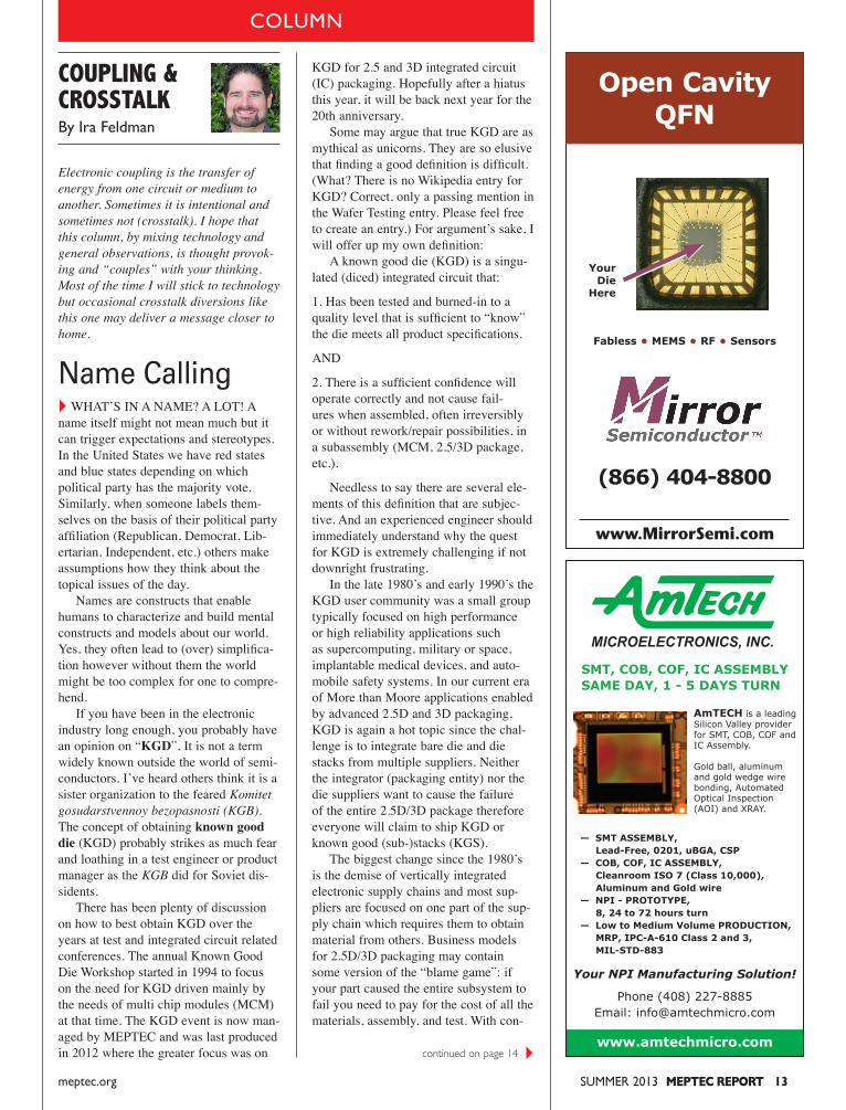
SMT, COB, COF, IC ASSEMBLYSAME DAY, 1 - 5 DAYS TURN
— SMT ASSEMBLY, Lead-Free, 0201, uBGA, CSP— COB, COF, IC ASSEMBLY, Cleanroom ISO 7 (Class 10,000), Aluminum and Gold wire— NPI - PROTOTYPE, 8, 24 to 72 hours turn— Low to Medium Volume PRODUCTION, MRP, IPC-A-610 Class 2 and 3, MIL-STD-883
Your NPI Manufacturing Solution!
Phone (408) 227-8885Email: [email protected]
AmTECH is a leadingSilicon Valley providerfor SMT, COB, COF andIC Assembly.
Gold ball, aluminumand gold wedge wirebonding, AutomatedOptical Inspection(AOI) and XRAY.
www.amtechmicro.com
(866) 404-8800
www.MirrorSemi.com
Open CavityQFN
YourDie
Here
Fabless • MEMS • RF • Sensors
continued on page 14
14 MEPTEC REPORT SUMMER 2013 meptec.org
COLUMN
“Time Critical” Organic Substrates
BGA, CSP, Flip Chip, High Frequency, High Speed, Rigid, Cavity and
Flex Packages- 15µm Lines and Spaces -
ACL is the onlyNorth American company
focusing exclusively on the fabrication of
High Density Interconnects.ITAR Registered
Phone: 408.327.0200 Email: [email protected]
www.aclusa.com
AdvancedComponentLabs, Inc.
Silicon Valley’s Packaging Foundrywww.promex-ind.com
IC Assembly
Advanced Packaging
ISO 13485:2003 Medical Certified ITAR Registered IPC-A-610 Class 3 Assembly Class 100 Clean Room
QFN’s, Leaded Packages, Modules, SiP’s2, 2.5 & 3D Advanced Packaging
Quick Turns, Development, NPI, Production
IC AssemblyAdvanced Packaging
Silicon Valley’s Packaging Foundrywww.promex-ind.com
QFN’s, Leaded Packages Modules, SiP’s
2, 2.5 & 3D Advanced Packaging
Quick Turns, Development, NPI, Production
ISO 13485:2003 Medical Certified ITAR RegisteredIPC-A-610 Class 3 Assembly Class 100 Clean Room
repair as system complexity continues to increase. This may sound like a new paradigm for integrated circuits, however dynamic random access memory (DRAM) sup-pliers have been operating with internal repair for many years. Modern DRAM would have a very low yield (some designs will intrinsically yield no parts) due to defect density versus the size of the die area and the very small feature size of the memory cell. Therefore, DRAMs are tested in the factory and defective bits are switched with spare memory cells using laser or electri-cal repair. This allows almost all of the DRAM die on a wafer to be used unless there are significant defects. Even though Not Known Bad Die (NKBD) is a mouthful, it really is more descriptive and should prompt improved system thinking that con-siders the challenges of developing advanced semiconductors and systems. Let’s clean up our language to communi-cate today’s reality! Our job as designers, test engineers, product managers, and managers is to work with what we have – even if imperfect – not what we wished we had. Want to throw out some names or add to this discussion? As always, I encour-age your comments on my blog http://hightechbizdev.com.
stantly shrinking gross margins, a sup-plier certainly doesn’t want to absorb the cost of their “failing” part let alone reim-burse others therefore the emphasis on claiming KGD/KGS status. And the cost of the integrator or end product com-pany to perform the root cause analysis (RCA) to determine fault is neither trivial nor inexpensive. In some cases, the RCA may be inconclusive or the cost exceed the value of the failing material. Since KGD are not only elusive but problematic, what can be done to enable electronics to advance? This is a topic that I have discussed often with my colleagues in the Test & Test Equipment Technology Working Group (TWG) of the International Technology Roadmap for Semiconductors (ITRS). We are con-sidering a change in the upcoming road-map to be published at the end of this year. Though only the roadmap as pub-lished by the ITRS is the official opinion of the ITRS team, I feel it is worthwhile to share this thinking. The change under considered is to replace the term “Known Good Die” with “Not Known Bad Die” (NKBD) or perhaps “Probably Good Die” (PGD). This is intended to be more than a sematic change and to force a change in thinking. Today the downstream user of a die believes it is good, based upon the previous testing. In reality it is very difficult to exhaustively and eco-nomically test the die to the full range of specifications. Sometimes the only way to completely test a die is through destructive testing. What typically hap-pens is that a given device passes all the reasonable (and often economical) tests and is shipped having not been found to be bad. With this shift in terms, the down-stream user – die stack integrator, assembler of multichip modules, system designer, etc. – needs to consider how to build subsystems and systems that can be diagnosed for both materials (bad die) and assembly issues. These (sub)systems need to be re-workable, repairable, or disposable (assuming the costs are low enough) in the factory and/or in the field since it cannot be guaranteed that all die are good or will remain so over their life. At the same time it would be well advised to consider how to build systems with greater fault tolerance and self-
IRA FELDMAN ([email protected]) is the Principal Consultant of Feldman Engineering Corp. which guides high technol-ogy products and services from concept to commercialization. He follows many “small technologies” from semiconductors to MEMS to nanotechnology engaging on a wide range of projects including product generation, marketing, and business development.
COUPLING & CROSSTALK continued from page 13
SUMMER 2013 MEPTEC REPORT 15meptec.org
WE ARE SICK. IN THE UNITED STATES 70% of adults are carrying extra weight while 10% also have high levels of glucose. 30% have elevated blood pressure and don’t exercise enough. This problem isn’t limited to the United States. An estimated 80% of worldwide healthcare spending is on chronic disease management. The most common cry of alarm we hear about in the United States is rising rates in obesity. In fact, about 25% of national healthcare costs are spent on diabetes and obesity. There are over 25 million Ameri-cans with diabetes, which is about 8% of the population. Meanwhile, of those over 65 years of age, about 27% have diabetes. Figure 1 shows obesity rates in the United States by state. Globally, about 366 million people had diabetes in 2011, and estimates are that number will increase to over 550 million by 2030. The cost worldwide to treat diabetes was about $465 billion USD in 2011 (Statis-tics from the International Diabetes Founda-tion). These numbers indicate how drastically our current healthcare system has failed. The problem lies with how isolated healthcare really is. When a patient goes into a healthcare center with a problem, the doctor has to start from scratch. She has to figure out that patient’s eating and exercise habits, and conduct tests that show limited data that only indicates how the patient is doing at that precise moment in time. Min-ing the body for data in this environment becomes even more difficult when you add in the Hawthorne Effect, which is the tendency for people to lie about their own eating and fitness habits. This is where new technology, particu-larly MEMS, comes in to save the day. In general, MEMS sensors track motion within a 3D space, and this ability to track motion is what is revolutionizing our healthcare system (see Figure 2). MEMS can be placed in varying places around the body to get precise data tracking for posture, gait, speed, upward climbing, swimming, bik-ing, etc. Additionally, they are low power and extremely small in size so they end up
ANALYSIS
The Healthcare Revolution is Here Michell Prunty, Senior Analyst – Consumer Markets Semico Research Corp.
becoming passive biometric aggregators that will give doctors a complete picture for a more accurate (and earlier) diagnosis. The industry is changing into a Learning Health System, and the mobile consumer is the catalyst. In this new system doctors will have access to a 24/7 roadmap of their patients biometric data that will be used as a predictive model to stop sickness before it happens. But, this will involve enacting behavior changes in the patients. This causes a whole new problem because people don’t respond to data. We all
know we need to exercise more or lose more weight, but that is a pretty abstract need, and the reality is that there is a wonderfully delicious chocolate cake just waiting in our fridge for breakfast and FX is getting ready to show that movie marathon we’ve been waiting for. Everyone is stressed, everyone is busy, so in our free time we gravitate towards fun wants rather than boring needs. This then, is the overriding problem: How do we make the management of one’s own healthcare fun? The solution is turning out to be a system of wireless connectivity and MEMS interacting with the cloud. These new wearable sensors are the answer, because they provide access to a new means of competition: Health Con-sumerism. This is the trend of aggregating as much data about day-to-day activities as possible and feeding that data to ‘apps’ that create games and competitions by linking up to a patient’s social network. Yet while patients interested in fitness may be highly motivated to change their behavior in order to lose weight or compete with their social network, the chronically ill patient, in general, is more reluctant and
Figure 1. Obesity rates by state. Source: Centers for Disease Control, Trust for America’s Health, CNN
Figure 2. Healthcare revolution. Source: Semico
16 MEPTEC REPORT SUMMER 2013 meptec.org
confused about what their goals should be, so their motivation and inspiration is often lacking. This creates an additional oppor-tunity for OEMs to create a dashboard that inspires consumers to actively use their products. This market will evolve to a point where these mobile health devices will continu-ously measure and report biometrics to the cloud in a way that is completely passive to the user with minimal to no upkeep, while the patient interacts with their data via a dashboard on their smartphone. One of the ways that these products are going to come to market is through Crowd Sourcing. The most popular Crowd Sourc-ing options are Kickstarter and Indeigogo, two websites that enable new technology to come to market with a known user base. In 2012 over 18,000 projects were funded on Kickstarter, with $320m USD pledged by 2.2 million people. The most successful launch on Kickstarter in 2012 was the Pebble, which raised $10.3 million. Pebble is an e-paper watch that can run fit-ness apps (it comes with an accelerometer), is waterproof, and uses Bluetooth 4.0 to connect to a smartphone (see Figure 3). When it comes to the human body and the environment, there are dozens of sen-sors that can potentially be used to improve healthcare. There are acoustic sensors (hearing aid improvement), chemical sen-sors (air quality indicators), electric sensors (magnetometers), humidity or moisture or weather sensors (bedwetting alarms, rain sensors), navigation sensors (gyroscopes), position and angle sensors (accelerometers, tilt, fall sensors), optical sensors (indoors or outdoors), pressure sensors (basketball game improvement), temperature sensors, proximity sensors (motion detection), etc. Each of these could be used to assist in day-to-day living for Aging in Place, improving a user’s movement precision to assist in sports, or even improve a user’s mental
health. Depending on the market, these sen-sors will be placed on different parts of the body, and different metrics will be used to determine the quality of movement and if a behavior change should or can be enacted. This is the technology behind Big Data, one of those key terms being thrown around lately, but in the Healthcare Industry every-thing relies on MEMS being able to collect as much data as possible and turning it into something useful.
AutomAted precision mAchiningAt Treske, we specialize in the impossible: efficiency in low volume, high mix runs with critical tolerances. Our robotic cell-manufacturing process leverages 30 years’ of semiconductor expertise, while real-time quality control ensures predictable results.
• Prototype and Production machining
• Electromechanical assembly• Welded fabrication
Call today to realize an entirely new way of precision machining!
(503) 625.2821 | treske.comISO9001:2008 | AS9100C (April 2013) | ITAR
innovAtionFigure 4. Fitness/Activity and Mobile Wellness growth. Source: Semico Research
Figure 3. Pebble e-paper watch. Source: Pebble
Healthcare is a critical issue worldwide. There are 860 million people suffering from chronic diseases, 400 million suffering from obesity, and 600 million suffering from aging-related issues. These numbers repre-sent a large potential market for healthcare devices. For more information on the healthcare market, read Semico’s new report, Mobile Healthcare: New Technology for a Healthy Lifestyle at semico.com.
ANALYSIS
ince the early days starting in the 1960’s, MEMS (Microelec-tromechanical Systems) were virtually stand-alone devices
and were attached/inserted into custom designed mechanical or standard IC pack-ages. More recently however, MEMS are truly becoming systems (as the “S” in MEMS connotes). The integration of MEMS devices into packages of various shapes, sizes and materials along with sig-nal conditioning electronics, power sources and networking (both wireless and con-nected) communications IC’s are now con-sidered to be the true application solution (see Figure 1). The role of packaging/assembly and test (P/A/T) in the overall successful com-mercialization of MEMS (see Figure 2) has historically taken a back seat to device development. More recently however, the MEMS community is taking note of the importance and the value of P/A/T in the
ford, University of California Berkeley and University of Michigan as well as at the scores of commercial foundries world-wide. However… what was needed was a mechanism to package the output of the foundries i.e. Silicon wafers into products that could be tested. The weak link here was the mechanism to do this work in a developmental format and thus provide the designer with a convenient and full-service facility to package, assemble and test the MEMS device. The Richard Desich Smart Commercialization Center for Microsys-tems (SMART) serves this highly needed and critical ”bridge” function in the com-mercialization of a MEMS-based solution (see Figure 3).
OVERVIEW The Richard Desich SMART Com-mercialization Center for Microsystems (“Desich SMART Center”) is a microsys-tem packaging, assembly, and test develop-
PROFILE
creation of MEMS-based solutions. Addi-tionally, it is well known that the packag-ing/assembly and test (P/A/T) of a MEMS-based solution can be as much as 60% or more of the total cost of the solution. This fact makes the consideration of the packaging strategy a very important and early part of the solution design process to achieve optimum cost and performance. Here we are, approximately a half-century later from the early days of MEMS pack-aging and many of the same materials and packaging strategies are still in favor by many suppliers. Additionally, the MEMS community had traditionally focused on the estab-lishment of an infrastructure to design and manufacture Silicon devices espe-cially including the creation of MEMS Silicon foundries. It was relatively easy for MEMS developers to have their devices manufactured in foundries including those of research universities e.g. Cornell, Stan-
SUMMER 2013 MEPTEC REPORT 17meptec.org
The new 47,000 square foot Desich SMART Center facility is expected to be completed in Q-3 2013 and will house class 100 and class 1000 cleanrooms as well as an incubator office space for startup companies.
PROFILE
18 MEPTEC REPORT SUMMER 2013 meptec.org
ment foundry. Located and part of Lorain County Community College in Elyria, Ohio, the Desich SMART Center devel-ops manufacturable packaging integration solutions for customers developing next-generation microsystem products by lever-aging world-class facilities and a highly experienced engineering team to accelerate product time to market. The Desich SMART Center was formed through a collaboration between Lorain County, the State of Ohio Third Frontier Program, Cleveland State Univer-sity’s Wright Center for Sensor Systems Engineering, Lorain County Community College, and local philanthropy. The Cen-ter was created in response to a known technology gap in the region: as compa-nies prepare to commercialize sensor tech-nologies and MEMS for use in technolo-gies across many major industries, they encounter a common hurdle in testing and packaging the products. This time spent represents 70 percent of the total cost of commercializing a technology and in there is no resource in the Midwest, or largely in the United States, to support this work. The Desich SMART Center is centered around a core facility with end-to-end microsystem packaging capability sup-ported by reliability test equipment and further augmented by software design tools and materials databases. Such a complete packaging line promotes efficient prob-lem-solving in what is typically a multi-step, iterative process. A single facility to investigate and prototype manufacturing processes for microelectronic packaging reduces the risk of contamination and dam-age due to shipping to job shop vendors; it streamlines project time frames, communi-cation, and error causality tracking. Other unique benefits accrue to potential users of the Smart Center’s resources (see Figure 4). The primary objective of such a facility is determine a package design for a specific product application, providing a resource for down selecting options from current manufacturable processes as a customer weighs this against product cost and supply chain limitations. In addition to capital equipment, the Desich SMART Center will help train technicians upon which companies can draw. In collaboration with local indus-try, Lorain County Community College is building out a two-year degree program in microsystems. When complete, this cur-riculum will train students to work in a variety of fields that employ microsystem
Figure 2. The MEMS commercialization process is complex and requires a great deal of front end coordination between package and interconnect designers, device designers, process engineers as well as test engineers if a successful outcome is to be realized. Courtesy: Roger Grace Associates
Figure 3. The Smart Center forms the long-time needed “bridge” between the producers of MEMS Silicon wafers and high volume packaging if successful commercialization of MEMS-based product is to be realized.
Figure 1. The key to a MEMS-based system solution is the packaging of all of its elements and the rigorous use of co-design principals to fully understand the complex interaction between the MEMS device, its associated signal conditioning electronics and the package. Courtesy: Roger Grace Associates
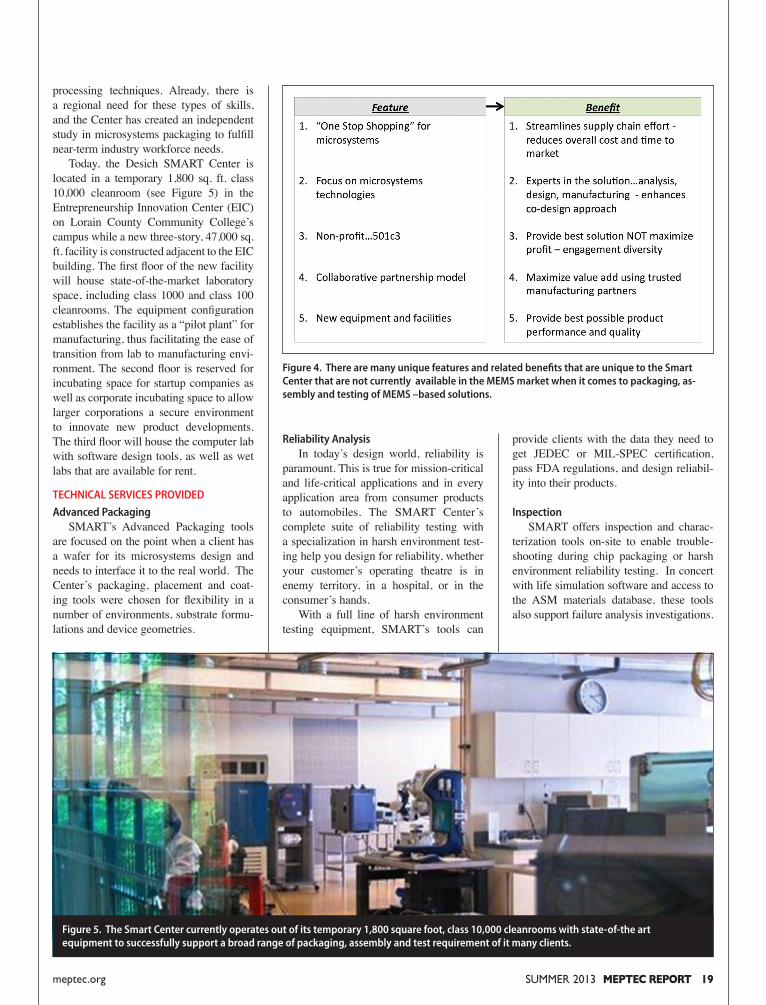
processing techniques. Already, there is a regional need for these types of skills, and the Center has created an independent study in microsystems packaging to fulfill near-term industry workforce needs. Today, the Desich SMART Center is located in a temporary 1,800 sq. ft. class 10,000 cleanroom (see Figure 5) in the Entrepreneurship Innovation Center (EIC) on Lorain County Community College’s campus while a new three-story, 47,000 sq. ft. facility is constructed adjacent to the EIC building. The first floor of the new facility will house state-of-the-market laboratory space, including class 1000 and class 100 cleanrooms. The equipment configuration establishes the facility as a “pilot plant” for manufacturing, thus facilitating the ease of transition from lab to manufacturing envi-ronment. The second floor is reserved for incubating space for startup companies as well as corporate incubating space to allow larger corporations a secure environment to innovate new product developments. The third floor will house the computer lab with software design tools, as well as wet labs that are available for rent.
TECHNICAL SERVICES PROVIDED
Advanced Packaging SMART’s Advanced Packaging tools are focused on the point when a client has a wafer for its microsystems design and needs to interface it to the real world. The Center’s packaging, placement and coat-ing tools were chosen for flexibility in a number of environments, substrate formu-lations and device geometries.
provide clients with the data they need to get JEDEC or MIL-SPEC certification, pass FDA regulations, and design reliabil-ity into their products.
Inspection SMART offers inspection and charac-terization tools on-site to enable trouble-shooting during chip packaging or harsh environment reliability testing. In concert with life simulation software and access to the ASM materials database, these tools also support failure analysis investigations.
Reliability Analysis In today’s design world, reliability is paramount. This is true for mission-critical and life-critical applications and in every application area from consumer products to automobiles. The SMART Center’s complete suite of reliability testing with a specialization in harsh environment test-ing help you design for reliability, whether your customer’s operating theatre is in enemy territory, in a hospital, or in the consumer’s hands. With a full line of harsh environment testing equipment, SMART’s tools can
Figure 4. There are many unique features and related benefits that are unique to the Smart Center that are not currently available in the MEMS market when it comes to packaging, as-sembly and testing of MEMS –based solutions.
Figure 5. The Smart Center currently operates out of its temporary 1,800 square foot, class 10,000 cleanrooms with state-of-the art equipment to successfully support a broad range of packaging, assembly and test requirement of it many clients.
SUMMER 2013 MEPTEC REPORT 19meptec.org
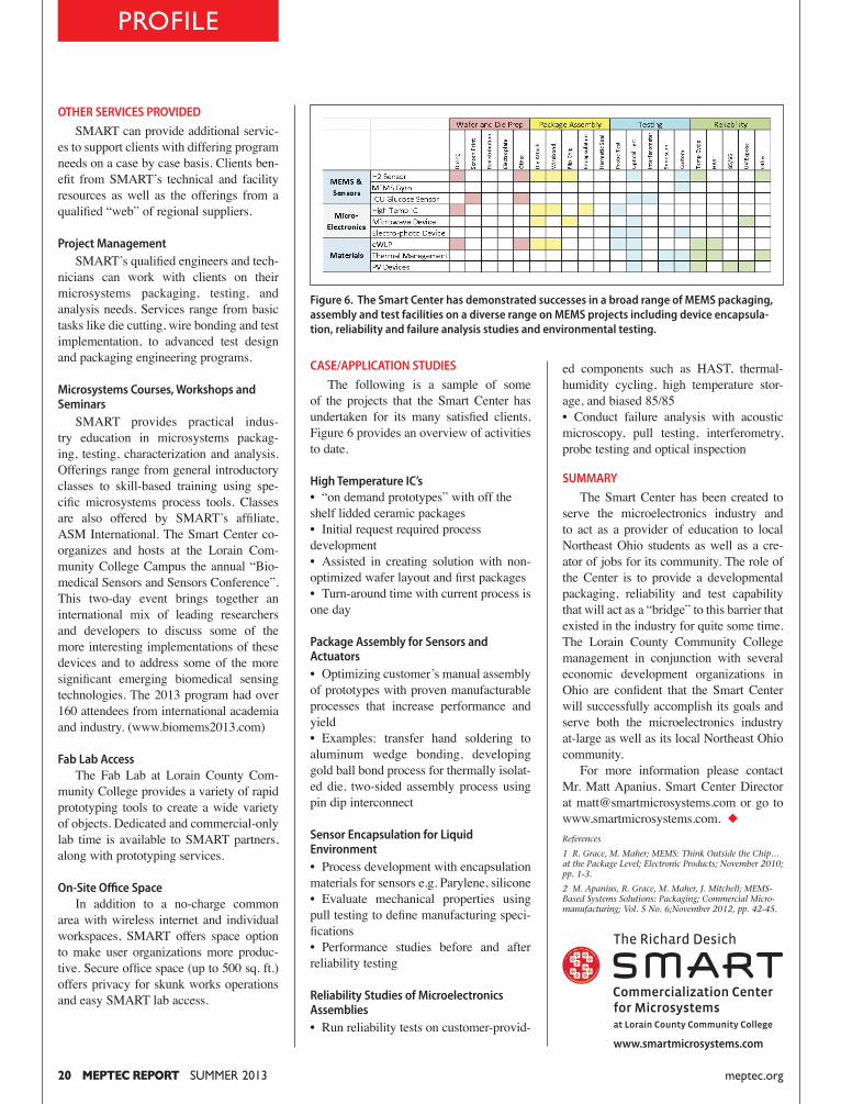
OTHER SERVICES PROVIDED
SMART can provide additional servic-es to support clients with differing program needs on a case by case basis. Clients ben-efit from SMART’s technical and facility resources as well as the offerings from a qualified “web” of regional suppliers.
Project Management SMART’s qualified engineers and tech-nicians can work with clients on their microsystems packaging, testing, and analysis needs. Services range from basic tasks like die cutting, wire bonding and test implementation, to advanced test design and packaging engineering programs.
Microsystems Courses, Workshops and Seminars SMART provides practical indus-try education in microsystems packag-ing, testing, characterization and analysis. Offerings range from general introductory classes to skill-based training using spe-cific microsystems process tools. Classes are also offered by SMART’s affiliate, ASM International. The Smart Center co-organizes and hosts at the Lorain Com-munity College Campus the annual “Bio-medical Sensors and Sensors Conference”. This two-day event brings together an international mix of leading researchers and developers to discuss some of the more interesting implementations of these devices and to address some of the more significant emerging biomedical sensing technologies. The 2013 program had over 160 attendees from international academia and industry. (www.biomems2013.com)
Fab Lab Access The Fab Lab at Lorain County Com-munity College provides a variety of rapid prototyping tools to create a wide variety of objects. Dedicated and commercial-only lab time is available to SMART partners, along with prototyping services.
On-Site Office Space In addition to a no-charge common area with wireless internet and individual workspaces, SMART offers space option to make user organizations more produc-tive. Secure office space (up to 500 sq. ft.) offers privacy for skunk works operations and easy SMART lab access.
CASE/APPLICATION STUDIES
The following is a sample of some of the projects that the Smart Center has undertaken for its many satisfied clients. Figure 6 provides an overview of activities to date.
High Temperature IC’s• “on demand prototypes” with off the shelf lidded ceramic packages• Initial request required process development• Assisted in creating solution with non-optimized wafer layout and first packages• Turn-around time with current process is one day
Package Assembly for Sensors and Actuators• Optimizing customer’s manual assembly of prototypes with proven manufacturable processes that increase performance and yield• Examples: transfer hand soldering to aluminum wedge bonding, developing gold ball bond process for thermally isolat-ed die, two-sided assembly process using pin dip interconnect
Sensor Encapsulation for Liquid Environment• Process development with encapsulation materials for sensors e.g. Parylene, silicone• Evaluate mechanical properties using pull testing to define manufacturing speci-fications • Performance studies before and after reliability testing
Reliability Studies of Microelectronics Assemblies• Run reliability tests on customer-provid-
ed components such as HAST, thermal-humidity cycling, high temperature stor-age, and biased 85/85• Conduct failure analysis with acoustic microscopy, pull testing, interferometry, probe testing and optical inspection
SUMMARY
The Smart Center has been created to serve the microelectronics industry and to act as a provider of education to local Northeast Ohio students as well as a cre-ator of jobs for its community. The role of the Center is to provide a developmental packaging, reliability and test capability that will act as a “bridge” to this barrier that existed in the industry for quite some time. The Lorain County Community College management in conjunction with several economic development organizations in Ohio are confident that the Smart Center will successfully accomplish its goals and serve both the microelectronics industry at-large as well as its local Northeast Ohio community. For more information please contact Mr. Matt Apanius, Smart Center Director at [email protected] or go to www.smartmicrosystems.com. References
1 R. Grace, M. Maher; MEMS: Think Outside the Chip…at the Package Level; Electronic Products; November 2010; pp. 1-3.
2 M. Apanius, R. Grace, M. Maher, J. Mitchell; MEMS-Based Systems Solutions: Packaging; Commercial Micro-manufacturing; Vol. 5 No. 6;November 2012, pp. 42-45.
Figure 6. The Smart Center has demonstrated successes in a broad range of MEMS packaging, assembly and test facilities on a diverse range on MEMS projects including device encapsula-tion, reliability and failure analysis studies and environmental testing.
20 MEPTEC REPORT SUMMER 2013 meptec.org
PROFILE
www.smartmicrosystems.com
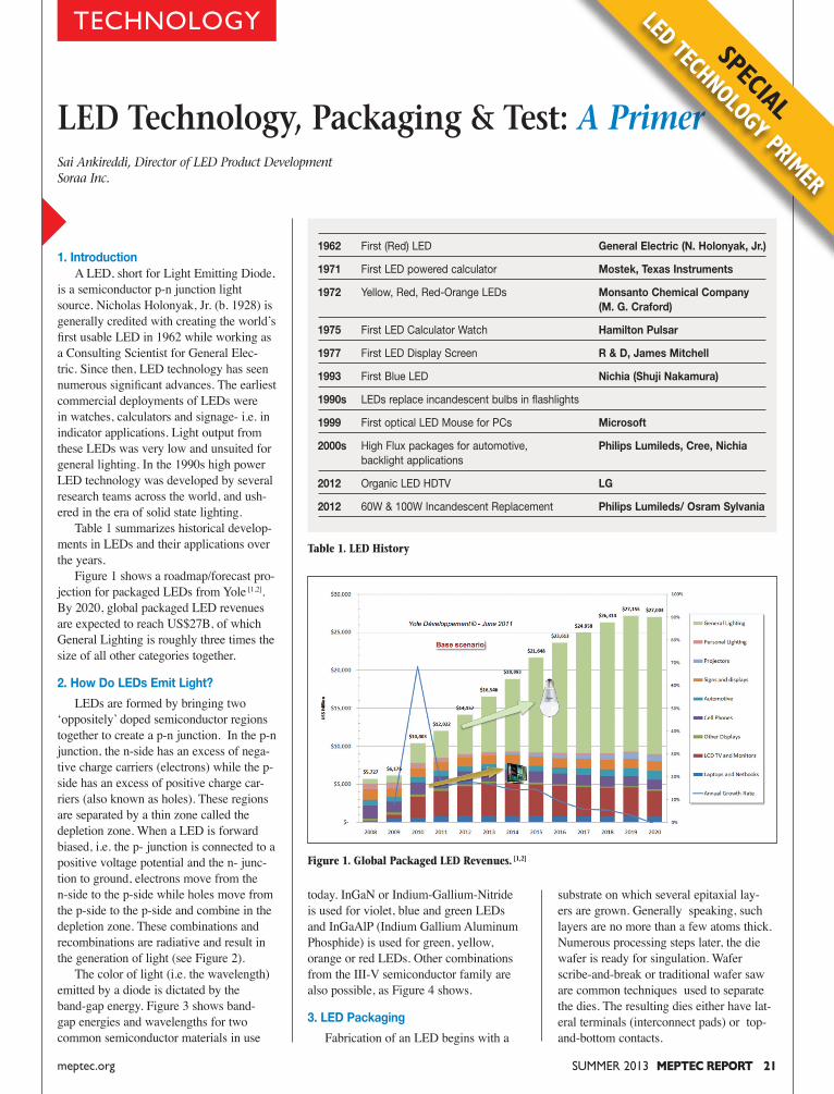
SUMMER 2013 MEPTEC REPORT 21meptec.org
TECHNOLOGY
substrate on which several epitaxial lay-ers are grown. Generally speaking, such layers are no more than a few atoms thick. Numerous processing steps later, the die wafer is ready for singulation. Wafer scribe-and-break or traditional wafer saw are common techniques used to separate the dies. The resulting dies either have lat-eral terminals (interconnect pads) or top-and-bottom contacts.
today. InGaN or Indium-Gallium-Nitride is used for violet, blue and green LEDs and InGaAlP (Indium Gallium Aluminum Phosphide) is used for green, yellow, orange or red LEDs. Other combinations from the III-V semiconductor family are also possible, as Figure 4 shows.
3. LED Packaging
Fabrication of an LED begins with a
LED Technology, Packaging & Test: A Primer
1. Introduction A LED, short for Light Emitting Diode, is a semiconductor p-n junction light source. Nicholas Holonyak, Jr. (b. 1928) is generally credited with creating the world’s first usable LED in 1962 while working as a Consulting Scientist for General Elec-tric. Since then, LED technology has seen numerous significant advances. The earliest commercial deployments of LEDs were in watches, calculators and signage- i.e. in indicator applications. Light output from these LEDs was very low and unsuited for general lighting. In the 1990s high power LED technology was developed by several research teams across the world, and ush-ered in the era of solid state lighting. Table 1 summarizes historical develop-ments in LEDs and their applications over the years. Figure 1 shows a roadmap/forecast pro-jection for packaged LEDs from Yole [1,2]. By 2020, global packaged LED revenues are expected to reach US$27B, of which General Lighting is roughly three times the size of all other categories together.
2. How Do LEDs Emit Light?
LEDs are formed by bringing two ‘oppositely’ doped semiconductor regions together to create a p-n junction. In the p-n junction, the n-side has an excess of nega-tive charge carriers (electrons) while the p- side has an excess of positive charge car-riers (also known as holes). These regions are separated by a thin zone called the depletion zone. When a LED is forward biased, i.e. the p- junction is connected to a positive voltage potential and the n- junc-tion to ground, electrons move from the n-side to the p-side while holes move from the p-side to the p-side and combine in the depletion zone. These combinations and recombinations are radiative and result in the generation of light (see Figure 2). The color of light (i.e. the wavelength) emitted by a diode is dictated by the band-gap energy. Figure 3 shows band-gap energies and wavelengths for two common semiconductor materials in use
Sai Ankireddi, Director of LED Product DevelopmentSoraa Inc.
1962 First (Red) LED General Electric (N. Holonyak, Jr.)
1971 First LED powered calculator Mostek, Texas Instruments
1972 Yellow, Red, Red-Orange LEDs Monsanto Chemical Company (M. G. Craford)
1975 First LED Calculator Watch Hamilton Pulsar
1977 First LED Display Screen R & D, James Mitchell
1993 First Blue LED Nichia (Shuji Nakamura)
1990s LEDs replace incandescent bulbs in flashlights
1999 First optical LED Mouse for PCs Microsoft
2000s High Flux packages for automotive, Philips Lumileds, Cree, Nichia backlight applications
2012 Organic LED HDTV LG
2012 60W & 100W Incandescent Replacement Philips Lumileds/ Osram Sylvania
Table 1. LED History
Figure 1. Global Packaged LED Revenues. [1,2]
SPECIAL
LED TECHNOLOGY PRIMER
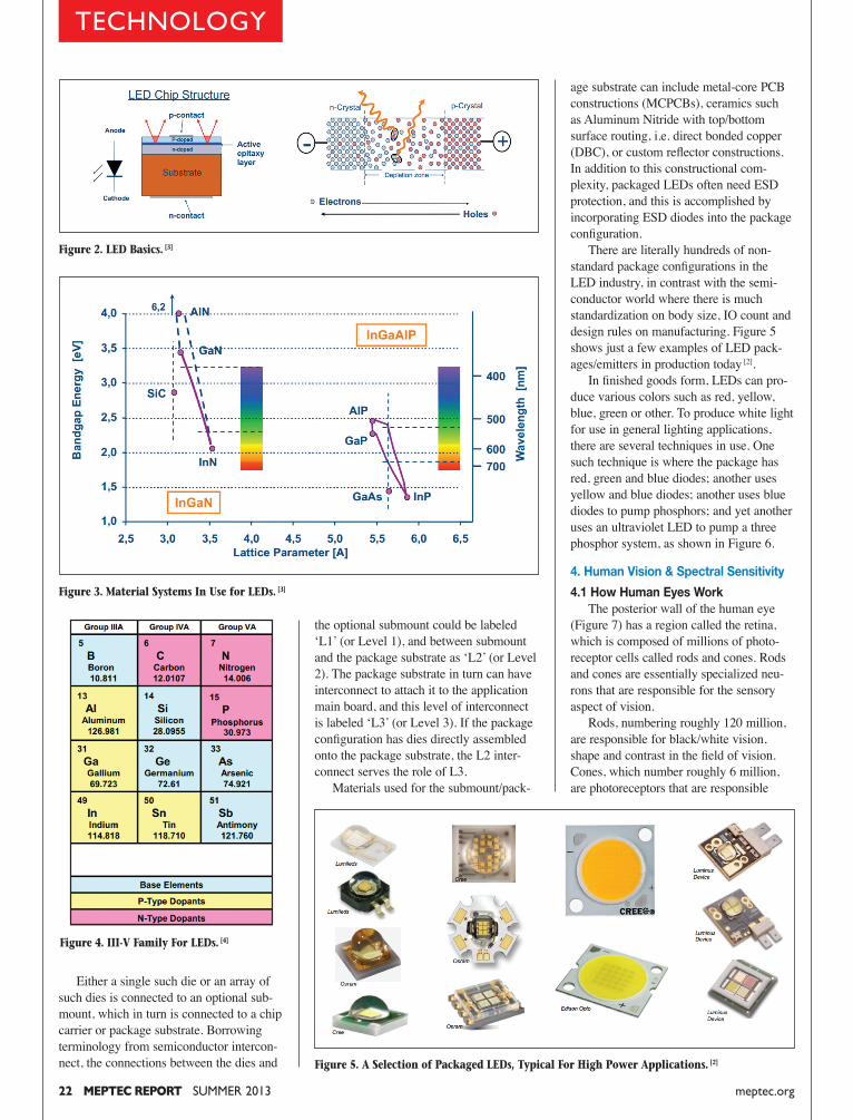
22 MEPTEC REPORT SUMMER 2013 meptec.org
Either a single such die or an array of such dies is connected to an optional sub-mount, which in turn is connected to a chip carrier or package substrate. Borrowing terminology from semiconductor intercon-nect, the connections between the dies and
age substrate can include metal-core PCB constructions (MCPCBs), ceramics such as Aluminum Nitride with top/bottom surface routing, i.e. direct bonded copper (DBC), or custom reflector constructions. In addition to this constructional com-plexity, packaged LEDs often need ESD protection, and this is accomplished by incorporating ESD diodes into the package configuration. There are literally hundreds of non-standard package configurations in the LED industry, in contrast with the semi-conductor world where there is much standardization on body size, IO count and design rules on manufacturing. Figure 5 shows just a few examples of LED pack-ages/emitters in production today [2]. In finished goods form, LEDs can pro-duce various colors such as red, yellow, blue, green or other. To produce white light for use in general lighting applications, there are several techniques in use. One such technique is where the package has red, green and blue diodes; another uses yellow and blue diodes; another uses blue diodes to pump phosphors; and yet another uses an ultraviolet LED to pump a three phosphor system, as shown in Figure 6.
4. Human Vision & Spectral Sensitivity
4.1 How Human Eyes Work The posterior wall of the human eye (Figure 7) has a region called the retina, which is composed of millions of photo-receptor cells called rods and cones. Rods and cones are essentially specialized neu-rons that are responsible for the sensory aspect of vision. Rods, numbering roughly 120 million, are responsible for black/white vision, shape and contrast in the field of vision. Cones, which number roughly 6 million, are photoreceptors that are responsible
the optional submount could be labeled ‘L1’ (or Level 1), and between submount and the package substrate as ‘L2’ (or Level 2). The package substrate in turn can have interconnect to attach it to the application main board, and this level of interconnect is labeled ‘L3’ (or Level 3). If the package configuration has dies directly assembled onto the package substrate, the L2 inter-connect serves the role of L3. Materials used for the submount/pack-
TECHNOLOGY
Figure 3. Material Systems In Use for LEDs. [3]
Figure 4. III-V Family For LEDs. [4]
Figure 5. A Selection of Packaged LEDs, Typical For High Power Applications. [2]
Figure 2. LED Basics. [3]
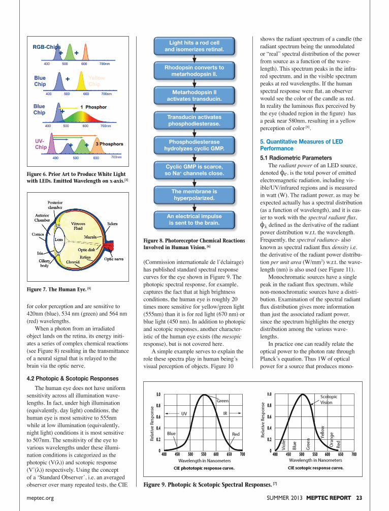
shows the radiant spectrum of a candle (the radiant spectrum being the unmodulated or “real” spectral distribution of the power from source as a function of the wave-length). This spectrum peaks in the infra-red spectrum, and in the visible spectrum peaks at red wavelengths. If the human spectral response were flat, an observer would see the color of the candle as red. In reality the luminous flux perceived by the eye (shaded region in the figure) has a peak near 580nm, resulting in a yellow perception of color [8].
5. Quantitative Measures of LED Performance
5.1 Radiometric Parameters The radiant power of an LED source, denoted φe, is the total power of emitted electromagnetic radiation, including vis-ible/UV/infrared regions and is measured in watt (W). The radiant power, as may be expected actually has a spectral distribution (as a function of wavelength), and it is eas-ier to work with the spectral radiant flux, φλ defined as the derivative of the radiant power distribution w.r.t. the wavelength. Frequently, the spectral radiance- also known as spectral radiant flux density i.e. the derivative of the radiant power distribu-tion per unit area (W/mm2) w.r.t. the wave-length (nm) is also used (see Figure 11). Monochromatic sources have a single peak in the radiant flux spectrum, while non-monochromatic sources have a distri-bution. Examination of the spectral radiant flux distribution gives more information than just the associated radiant power, since the spectrum highlights the energy distribution among the various wave-lengths. In practice one can readily relate the optical power to the photon rate through Planck’s equation. Thus 1W of optical power for a source that produces mono-
SUMMER 2013 MEPTEC REPORT 23meptec.org
(Commission internationale de l’éclairage) has published standard spectral response curves for the eye shown in Figure 9. The photopic spectral response, for example, captures the fact that at high brightness conditions, the human eye is roughly 20 times more sensitive for yellow/green light (555nm) than it is for red light (670 nm) or blue light (450 nm). In addition to photopic and scotopic responses, another character-istic of the human eye exists (the mesopic response), but is not covered here. A simple example serves to explain the role these spectra play in human being’s visual perception of objects. Figure 10
for color perception and are sensitive to 420nm (blue), 534 nm (green) and 564 nm (red) wavelengths. When a photon from an irradiated object lands on the retina, its energy initi-ates a series of complex chemical reactions (see Figure 8) resulting in the transmittance of a neural signal that is relayed to the brain via the optic nerve.
4.2 Photopic & Scotopic Responses
The human eye does not have uniform sensitivity across all illumination wave-lengths. In fact, under high illumination (equivalently, day light) conditions, the human eye is most sensitive to 555nm while at low illumination (equivalently, night light) conditions it is most sensitive to 507nm. The sensitivity of the eye to various wavelengths under these illumi-nation conditions is categorized as the photopic (V(λ)) and scotopic response (V’(λ)) respectively. Using the concept of a ‘Standard Observer’, i.e. an averaged observer over many repeated tests, the CIE
Figure 6. Prior Art to Produce White Light with LEDs. Emitted Wavelength on x-axis.[3]
Figure 7. The Human Eye. [5]
Figure 9. Photopic & Scotopic Spectral Responses. [7]
Figure 8. Photoreceptor Chemical Reactions Involved in Human Vision. [6]
Light hits a rod celland isomerizes retinal.
Rhodopsin converts tometarhodopsin ll.
Metarhodopsin llactivates transducin.
Transducin activatesphosphodiesterase.
Phosphodiesterasehydrolyzes cyclic GMP.
Cyclic GMP is scarce,so Na+ channels close.
The membrane ishyperpolarized.
An electrical impulseis sent to the brain.
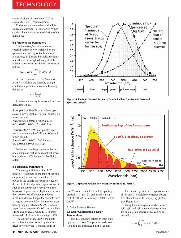
24 MEPTEC REPORT SUMMER 2013 meptec.org
chromatic light of wavelength 630 nm equates to 3.2 x 10¹⁸ photons/sec. Radiometric characteristics of a light source are absolute, i.e. unaffected by per-ceptive characteristics or modulation of the human eye.
5.2 Photometric Parameters The luminous flux of a source is its spectral radiant power, weighted by the (photopic) sensitivity of the human eye. It is measured in Lumen. Formally, the lumi-nous flux is the weighted integral of the radiant power over the visible spectrum, as below:
A related parameter is the luminous intensity, which is the intensity of light emitted in a particular direction, formally defined as:
Luminous intensity is measured in Can-dela, denoted cd.
Example 1: A 10 mW laser pointer oper-ates at a wavelength of 700 nm. What is its lumen output?Answer: 683 x 0.010 x V(700nm) = 683 x 0.010 x 0.004102 = 0.03 Lm
Example 2: A 5 mW laser pointer oper-ates at a wavelength of 550 nm. What is its lumen output?Answer: 683 x 0.005 x V(550nm) = 683 x 0.005 x 0.995 = 3.4 Lm
Notice that the laser source in the sec-ond example is half as much optical power, but produces 100X lumen (visible light) output.
5.3 Efficiency Parameters The energy efficiency of an LED, termed η, is defined as the ratio of the opti-cal power (i.e. wattage equivalent of the power in the visible spectrum) divided by the input electrical power. Figures of merit such as the energy efficiency give a firm basis to compare various light sources from their conversion efficiency standpoint: most incandescent lamps, for example have η ranging between 4-5%, fluorescent tubes have η ranging between 27-29%, sodium vapor lamps between 30-40%, and the blue LEDs used to create white LED sources measured cold have η in the range >50%. The efficacy of an LED is the photo-metric flux it emits divided by the elec-trical power driving it, and has units of
The human eye has three types of cones (S, M and L) which have different absorp-tion characteristics for impinging photons (see Figure 12). Using these absorption spectra, termed r(λ), g(λ) and b(λ) three unique quantities for an emission spectrum I(λ) can be cal-culated, viz.,
Lm/W. As an example, if an LED package produces 80 lm at 3V and at a drive cur-rent of 200 mA, its efficacy is 80/0.6 = 133 Lm/W.
6. Color Science Basics
6.1 Color Coordinates & Color Temperature Two key concepts related to solid state lighting, i.e. Color Temperature and Color Rendition are introduced in this section.
TECHNOLOGY
Figure 10. Photopic Spectral Response, Candle Radiant Spectrum & Perceived Spectrum. After [8].
Figure 11. Spectral Radiant Power Density for the Sun. After [9].
Φν = 683 380
780ΦeV(λ)dλ
I = dΦνdΩ
Ro = 380
780I(λ)r(λ)dλ
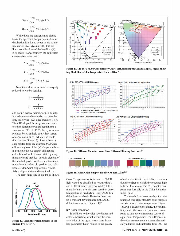
of color rendition in the irradiated medium (i.e. the object on which the produced light falls or illuminates). The CIE denotes this parameter formally as the Color Rendition Index, or CRI. The standard test color method for color rendition uses eight standard color samples and size special color samples (see Figure 15). For a given color sample, the chroma-ticity under the source in question is com-pared to that under a reference source of equal color temperature. The difference in the color measurement is then mathemati-cally adjusted and subtracted from 100 (the
SUMMER 2013 MEPTEC REPORT 25meptec.org
Color Temperatures- for instance a 3000K light would be classified as ‘warm white’, and a 8000K source as ‘cool white’. LED manufacturers also bin parts based on color temperature in production, using ANSI bin definitions as a basis. However there can be significant deviations from the ANSI definitions also (see Figure 14) [4].
6.2 Color Rendition In addition to the color coordinates and color temperature, which define the char-acteristics of the light source, there is one key parameter that is related to the quality
While these are convenient to charac-terize the spectrum, for purposes of stan-dardization it is found better to use stimu-lant curves x(λ), y(λ) and z(λ) that are linear combinations of the baseline r(λ), g(λ) and b(λ). Accordingly, the equivalent characteristic terms are:
Now these three terms can be uniquely reduced to two by defining:
and noting that by defining a ‘z’ similarly, it is adequate to characterize the color by only specifying (x,y) since then z = 1-x-y. The CIE adopted this (x,y) nomenclature of color designation/quantification into a standard in 1931. In 1976, this system was replaced by an entirely equivalent system of coordinates (u’,v’) which is in use to this day (see Figure 13). Shown there in exaggerated form are example MacAdam ellipses- regions of the (u’,v’) space where in principle the eye cannot distinguish color. In modern LED/solid state lighting manufacturing practice, one key element of the finished goods is color consistency, and manufacturers often bin product into color zones 3-MacAdam ellipse wide, 4-Mac-Adam ellipse wide etc during final sort. The right hand side of Figure 13 shows
Figure 12. Cone Absorption Spectra in the Human Eye. After [10].
Figure 13. CIE 1976 (u’,v’) Chromaticity Chart: Left, showing MacAdam Ellipses, Right: Show-ing Black Body Color Temperature Locus. After [11].
Figure 14. Different Manufacturers Have Different Binning Practices. [4]
Figure 15. Panel Color Samples for the CRI Test. After [12].
Go = 380
780I(λ)g(λ)dλ
Bo = 380
780I(λ)b(λ)dλ
X = 380
780I(λ)x(λ)dλ
Y = 380
780I(λ)y(λ)dλ
Z = 380
780I(λ)z(λ)dλ
x = XX+Y+Z
y = YX+Y+Z
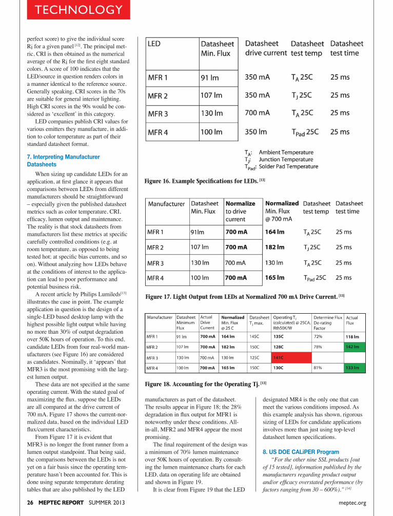
26 MEPTEC REPORT SUMMER 2013 meptec.org
perfect score) to give the individual score Ri for a given panel [12]. The principal met-ric, CRI is then obtained as the numerical average of the Ri for the first eight standard colors. A score of 100 indicates that the LED/source in question renders colors in a manner identical to the reference source. Generally speaking, CRI scores in the 70s are suitable for general interior lighting. High CRI scores in the 90s would be con-sidered as ‘excellent’ in this category. LED companies publish CRI values for various emitters they manufacture, in addi-tion to color temperature as part of their standard datasheet format.
7. Interpreting Manufacturer Datasheets
When sizing up candidate LEDs for an application, at first glance it appears that comparisons between LEDs from different manufacturers should be straightforward – especially given the published datasheet metrics such as color temperature, CRI, efficacy, lumen output and maintenance. The reality is that stock datasheets from manufacturers list these metrics at specific carefully controlled conditions (e.g. at room temperature, as opposed to being tested hot; at specific bias currents, and so on). Without analyzing how LEDs behave at the conditions of interest to the applica-tion can lead to poor performance and potential business risk. A recent article by Philips Lumileds[13] illustrates the case in point. The example application in question is the design of a single-LED based desktop lamp with the highest possible light output while having no more than 30% of output degradation over 50K hours of operation. To this end, candidate LEDs from four real-world man-ufacturers (see Figure 16) are considered as candidates. Nominally, it ‘appears’ that MFR3 is the most promising with the larg-est lumen output. These data are not specified at the same operating current. With the stated goal of maximizing the flux, suppose the LEDs are all compared at the drive current of 700 mA. Figure 17 shows the current-nor-malized data, based on the individual LED flux/current characteristics. From Figure 17 it is evident that MFR3 is no longer the front runner from a lumen output standpoint. That being said, the comparisons between the LEDs is not yet on a fair basis since the operating tem-perature hasn’t been accounted for. This is done using separate temperature derating tables that are also published by the LED
designated MR4 is the only one that can meet the various conditions imposed. As this example analysis has shown, rigorous sizing of LEDs for candidate applications involves more than just using top-level datasheet lumen specifications.
8. US DOE CALiPER Program “For the other nine SSL products [out of 15 tested], information published by the manufacturers regarding product output and/or efficacy overstated performance (by factors ranging from 30 – 600%).” [14]
manufacturers as part of the datasheet. The results appear in Figure 18; the 28% degradation in flux output for MFR1 is noteworthy under these conditions. All-in-all, MFR2 and MFR4 appear the most promising. The final requirement of the design was a minimum of 70% lumen maintenance over 50K hours of operation. By consult-ing the lumen maintenance charts for each LED, data on operating life are obtained and shown in Figure 19. It is clear from Figure 19 that the LED
TECHNOLOGY
Figure 16. Example Specifications for LEDs. [13]
Figure 17. Light Output from LEDs at Normalized 700 mA Drive Current. [13]
Figure 18. Accounting for the Operating Tj. [13]
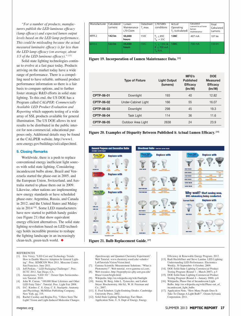
SUMMER 2013 MEPTEC REPORT 27meptec.org
“For a number of products, manufac-turers publish the LED luminous efficacy (lamp efficacy) and expected lumen output levels based on the LED lamp performance. This could be misleading because the actual measured luminaire efficacy is far less than the LED lamp efficacy (on average, about 1/3 of the LED luminous efficacy).” [15]
Solid state lighting technologies contin-ue to evolve at a fast pace today. Products arriving on the market today have a wide range of performance. There is a compel-ling need to have reliable, unbiased product performance information so there is a fair basis to compare options, and to further foster strategic R&D efforts in solid state lighting. To this end, the US DOE has a Program called CALiPER: Commercially Available LED Product Evaluation and Reporting which supports testing of a wide array of SSL products available for general illumination. The US DOE allows its test results to be distributed in the public inter-est for non-commercial, educational pur-poses only. Additional details may be found at the CALiPER website, http://www1.eere.energy.gov/buildings/ssl/caliper.html.
9. Closing Remarks
Worldwide, there is a push to replace conventional energy inefficient light sourc-es with solid state lighting. Considering incandescent bulbs alone, Brazil and Ven-ezuela started the phase-out in 2005, and the European Union, Switzerland, and Aus-tralia started to phase them out in 2009. Likewise, other nations are implementing new energy standards or have scheduled phase-outs: Argentina, Russia, and Canada in 2012, and the United States and Malay-sia in 2014 [16]. Some LED manufacturers have now started to publish handy guides (see Figure 21) that show equivalent energy efficient alternatives. The solid state lighting revolution based on LED technol-ogy holds incredible promise to reshape the lighting landscape in an increasingly clean-tech, green-tech world.
Figure 19. Incorporation of Lumen Maintenance Data. [13]
Figure 21. Bulb Replacement Guide. [17]
REFERENCES[1]. Eric Virrey, “LED Cost and Technology Trends: How to Enable Massive Adoption In General Light- ing”. Proc. SEMICON West 2011, Moscone Center, San Francisco, June 2011.[2]. Jeff Perkins, “ LED Packaging Challenges”. Proc. ECTC 2012, San Diego, CA.[3]. Anonymous, “LED 101”. Osram Opto Semiconduc- tors Tutorial, 2010.[4]. John W. Curran, “100,000 Hour Lifetimes and Other LED Fairy Tales”. Tutorial, Proc. Light Fair 2008.[5]. D.C. Kimber, C. E. Gray, C. E. Stackpole. Anatomy and Physiology. McMillan Publishing Company, New York, pg. 335.[6]. Rachel Casiday and Regina Fey. “I Have Seen The Light! Vision and Light-Induced Molecular Changes
Efficiency & Renewable Energy Program, 2012.[13]. Rudi Hechfellner and Steve Landau. LED Lighting: Understanding LED Performance. Electronics Weekly, 30 September- 6 October, 2009.[14]. DOE Solid-State Lighting Commercial Product Testing Program (Round 1—March 2007), p.5[15]. DOE Solid-State Lighting Commercial Product Testing Program (Round 4—January 2008), p.6[16]. Wikipedia, Phase-Out of Incandescent Light Bulbs. http://en.wikipedia.org/wiki/Phase-out_of_ incandescent_light_bulbs[17]. Application Note, “How Many People Does It Take To Change A Light Bulb?”. Osram Sylvania Corporation, 2011.
(Spectroscopy and Quantum Chemistry Experiment)”. Web Tutorial, www.chemistry.wustl.edu/~edudev/ LabTutorials/Vision/Vision.html. [7]. Gamma Scientific Measurement Solutions, “What is Photometry?”. Web tutorial, www.gamma-sci.com.[8]. Web resource, http://hyperphysics.phy-astr.gsu.edu/ hbase/vision/bright.html[9]. Wikipedia, http://en.wikipedia.org/wiki/Sunlight [10]. Jeremy M. Berg, John L. Tymoczko, and Lubert Stryer. Biochemistry. 6th Ed., W. H. Freeman and Co., 2007.[11]. E. Fred Schubert. Light-Emitting Diodes. Cambridge University Press, 2002.[12]. Solid-State Lighting Technology Fact Sheet. Application Note, U. S. Dept of Energy, Energy
Figure 20. Examples of Disparity Between Published & Actual Lumen Efficacy. [15]
MFG’s DOE Type of Fixture Light Output Published Measured (lumens) Efficacy Efficacy (lm/W) (lm/W)
CPTP-06-01 Downlight 193 40 12.82
CPTP-06-02 Under-Cabinet Light 166 55 16.07
CPTP-06-03 Downlight 298 45 19.3
CPTP-06-04 Task Light 114 36 11.6
CPTP-06-05 Outdoor Area Light 2638 24 23.9
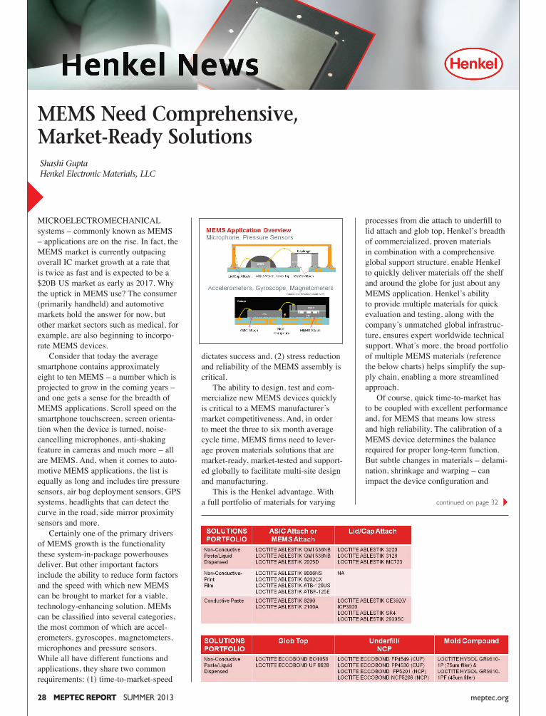
MICROELECTROMECHANICAL systems – commonly known as MEMS – applications are on the rise. In fact, the MEMS market is currently outpacing overall IC market growth at a rate that is twice as fast and is expected to be a $20B US market as early as 2017. Why the uptick in MEMS use? The consumer (primarily handheld) and automotive markets hold the answer for now, but other market sectors such as medical, for example, are also beginning to incorpo-rate MEMS devices. Consider that today the average smartphone contains approximately eight to ten MEMS – a number which is projected to grow in the coming years – and one gets a sense for the breadth of MEMS applications. Scroll speed on the smartphone touchscreen, screen orienta-tion when the device is turned, noise-cancelling microphones, anti-shaking feature in cameras and much more – all are MEMS. And, when it comes to auto-motive MEMS applications, the list is equally as long and includes tire pressure sensors, air bag deployment sensors, GPS systems, headlights that can detect the curve in the road, side mirror proximity sensors and more. Certainly one of the primary drivers of MEMS growth is the functionality these system-in-package powerhouses deliver. But other important factors include the ability to reduce form factors and the speed with which new MEMS can be brought to market for a viable, technology-enhancing solution. MEMs can be classified into several categories, the most common of which are accel-erometers, gyroscopes, magnetometers, microphones and pressure sensors. While all have different functions and applications, they share two common requirements: (1) time-to-market-speed
processes from die attach to underfill to lid attach and glob top, Henkel’s breadth of commercialized, proven materials in combination with a comprehensive global support structure, enable Henkel to quickly deliver materials off the shelf and around the globe for just about any MEMS application. Henkel’s ability to provide multiple materials for quick evaluation and testing, along with the company’s unmatched global infrastruc-ture, ensures expert worldwide technical support. What’s more, the broad portfolio of multiple MEMS materials (reference the below charts) helps simplify the sup-ply chain, enabling a more streamlined approach. Of course, quick time-to-market has to be coupled with excellent performance and, for MEMS that means low stress and high reliability. The calibration of a MEMS device determines the balance required for proper long-term function. But subtle changes in materials – delami-nation, shrinkage and warping – can impact the device configuration and
dictates success and, (2) stress reduction and reliability of the MEMS assembly is critical. The ability to design, test and com-mercialize new MEMS devices quickly is critical to a MEMS manufacturer’s market competitiveness. And, in order to meet the three to six month average cycle time, MEMS firms need to lever-age proven materials solutions that are market-ready, market-tested and support-ed globally to facilitate multi-site design and manufacturing. This is the Henkel advantage. With a full portfolio of materials for varying
MEMS Need Comprehensive, Market-Ready Solutions Shashi Gupta Henkel Electronic Materials, LLC
28 MEPTEC REPORT SUMMER 2013 meptec.org
continued on page 32
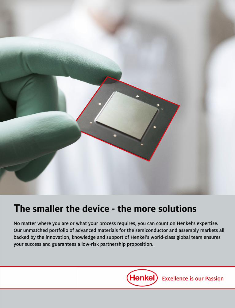
The smaller the device - the more solutionsNo matter where you are or what your process requires, you can count on Henkel‘s expertise. Our unmatched portfolio of advanced materials for the semiconductor and assembly markets all backed by the innovation, knowledge and support of Henkel‘s world-class global team ensures your success and guarantees a low-risk partnership proposition.
The smaller the device - the more solutionsNo matter where you are or what your process requires, you can count on Henkel‘s expertise. Our unmatched portfolio of advanced materials for the semiconductor and assembly markets all backed by the innovation, knowledge and support of Henkel‘s world-class global team ensures your success and guarantees a low-risk partnership proposition.
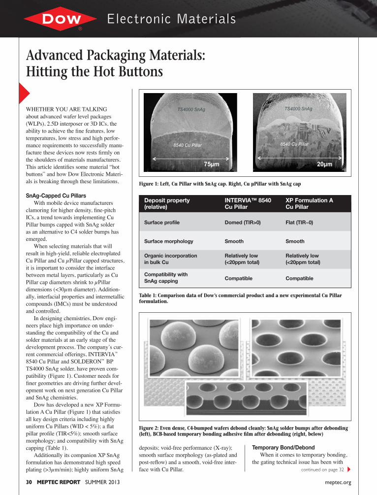
WHETHER YOU ARE TALKING about advanced wafer level packages (WLPs), 2.5D interposer or 3D ICs, the ability to achieve the fine features, low temperatures, low stress and high perfor-mance requirements to successfully manu-facture these devices now rests firmly on the shoulders of materials manufacturers. This article identifies some material “hot buttons” and how Dow Electronic Materi-als is breaking through these limitations.
SnAg-Capped Cu Pillars With mobile device manufacturers clamoring for higher density, fine-pitch ICs, a trend towards implementing Cu Pillar bumps capped with SnAg solder as an alternative to C4 solder bumps has emerged. When selecting materials that will result in high-yield, reliable electroplated Cu Pillar and Cu µPillar capped structures, it is important to consider the interface between metal layers, particularly as Cu Pillar cap diameters shrink to µPillar dimensions (<30µm diameter). Addition-ally, interfacial properties and intermetallic compounds (IMCs) must be understood and controlled. In designing chemistries, Dow engi-neers place high importance on under-standing the compatibility of the Cu and solder materials at an early stage of the development process. The company’s cur-rent commercial offerings, INTERVIA™
8540 Cu Pillar and SOLDERON™ BP TS4000 SnAg solder, have proven com-patibility (Figure 1). Customer needs for finer geometries are driving further devel-opment work on next generation Cu Pillar and SnAg chemistries. Dow has developed a new XP Formu-lation A Cu Pillar (Figure 1) that satisfies all key design criteria including highly uniform Cu Pillars (WID < 5%); a flat pillar profile (TIR<5%); smooth surface morphology; and compatibility with SnAg capping (Table 1). Additionally its companion XP SnAg formulation has demonstrated high speed plating (>3µm/min); highly uniform SnAg
Advanced Packaging Materials: Hitting the Hot Buttons
30 MEPTEC REPORT SUMMER 2013 meptec.org
Figure 1: Left, Cu Pillar with SnAg cap. Right, Cu µPillar with SnAg cap
Table 1: Comparison data of Dow’s commercial product and a new experimental Cu Pillar formulation.
Surface profile Domed (TIR>0) Flat (TIR~0)
Surface morphology Smooth Smooth
Organic incorporation Relatively low Relatively low in bulk Cu (<20ppm total) (<20ppm total)
Compatibility with Compatible Compatible SnAg capping
Deposit property INTERVIA™ 8540 XP Formulation A (relative) Cu Pillar Cu Pillar
Figure 2: Even dense, C4-bumped wafers debond cleanly: SnAg solder bumps after debonding (left), BCB-based temporary bonding adhesive film after debonding (right, below)
continued on page 32
deposits; void-free performance (X-ray); smooth surface morphology (as-plated and post-reflow) and a smooth, void-free inter-face with Cu Pillar.
Temporary Bond/Debond When it comes to temporary bonding, the gating technical issue has been with
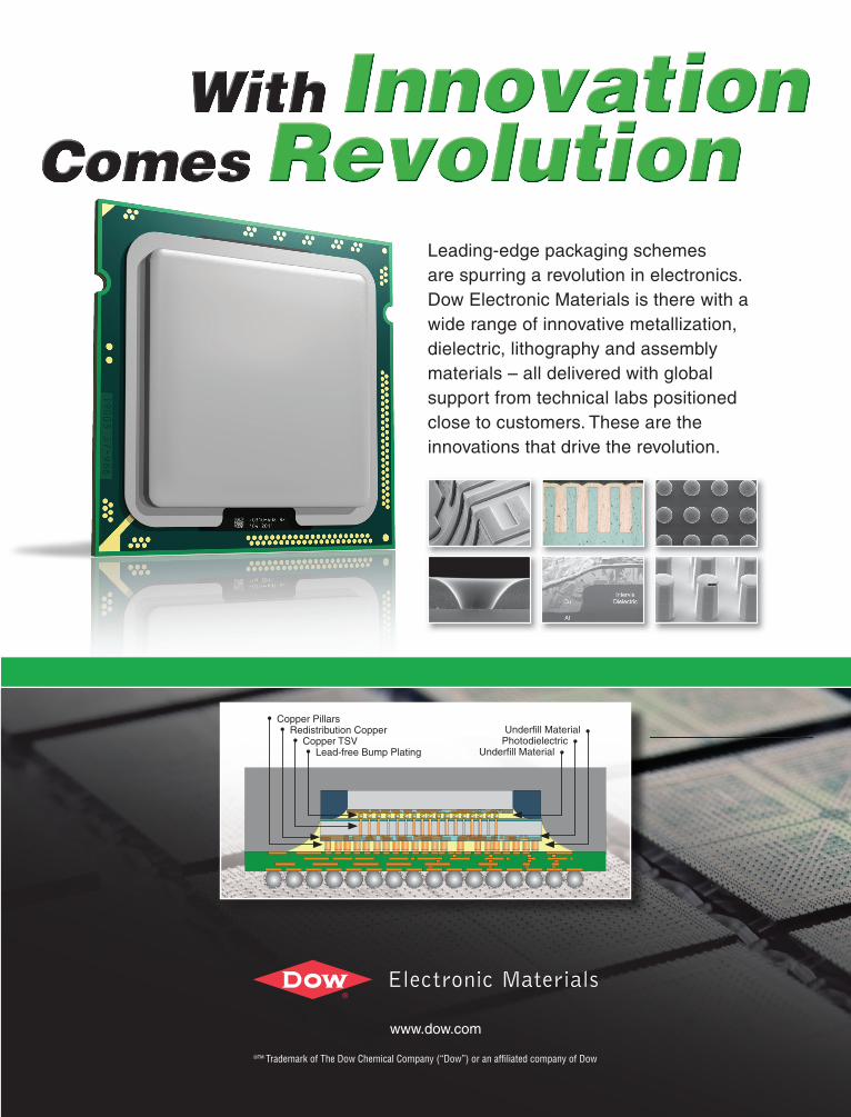
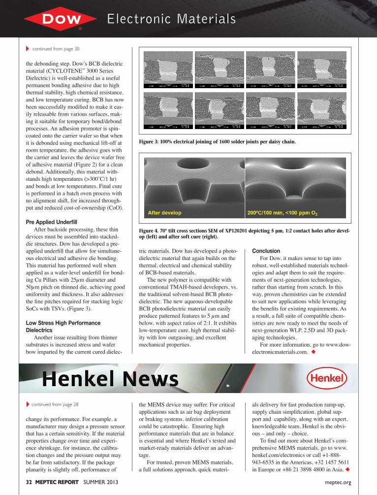
32 MEPTEC REPORT SUMMER 2013 meptec.org
change its performance. For example, a manufacturer may design a pressure sensor that has a certain sensitivity. If the material properties change over time and experi-ence shrinkage, for instance, the calibra-tion changes and the pressure output may be far from satisfactory. If the package planarity is slightly off, performance of
continued from page 28 the MEMS device may suffer. For critical applications such as air bag deployment or braking systems, inferior calibration could be catastrophic. Ensuring high performance materials that are in balance is essential and where Henkel’s tested and market-ready materials deliver an advan-tage. For trusted, proven MEMS materials, a full solutions approach, quick materi-
als delivery for fast production ramp-up, supply chain simplification, global sup-port and capability, along with an expert, knowledgeable team, Henkel is the obvi-ous – and only – choice. To find out more about Henkel’s com-prehensive MEMS materials, go to www.henkel.com/electronics or call +1-888-943-6535 in the Americas, +32 1457 5611 in Europe or +86 21 3898 4800 in Asia.
tric materials. Dow has developed a photo-dielectric material that again builds on the thermal, electrical and chemical stability of BCB-based materials. The new polymer is compatible with conventional TMAH-based developers, vs. the traditional solvent-based BCB photo-dielectric. The new aqueous-developable BCB photodielectric material can easily produce patterned features to 5 µm and below, with aspect ratios of 2:1. It exhibits low-temperature cure, high thermal stabil-ity with low outgassing, and excellent mechanical properties.
Conclusion For Dow, it makes sense to tap into robust, well-established materials technol-ogies and adapt them to suit the require-ments of next-generation technologies, rather than starting from scratch. In this way, proven chemistries can be extended to suit new applications while leveraging the benefits for existing requirements. As a result, a full suite of compatible chem-istries are now ready to meet the needs of next-generation WLP, 2.5D and 3D pack-aging technologies. For more information, go to www.dow-electronicmaterials.com.
the debonding step. Dow’s BCB dielectric material (CYCLOTENE™ 3000 Series Dielectric) is well-established as a useful permanent bonding adhesive due to high thermal stability, high chemical resistance, and low temperature curing. BCB has now been successfully modified to make it eas-ily releasable from various surfaces, mak-ing it suitable for temporary bond/debond processes. An adhesion promoter is spin-coated onto the carrier wafer so that when it is debonded using mechanical lift-off at room temperature, the adhesive goes with the carrier and leaves the device wafer free of adhesive material (Figure 2) for a clean debond. Additionally, this material with-stands high temperatures (>300˚C/1 hr) and bonds at low temperatures. Final cure is performed in a batch oven process with no alignment shift, for increased through-put and reduced cost-of-ownership (CoO).
Pre Applied Underfill After backside processing, these thin devices must be assembled into stacked-die structures. Dow has developed a pre-applied underfill that allow for simultane-ous electrical and adhesive die bonding. This material has performed well when applied as a wafer-level underfill for bond-ing Cu Pillars with 25µm diameter and 50µm pitch on thinned die, achieving good uniformity and thickness. It also addresses the fine pitches required for stacking logic SoCs with TSVs. (Figure 3). Low Stress High Performance Dielectrics Another issue resulting from thinner substrates is increased stress and wafer bow imparted by the current cured dielec-
continued from page 30
Figure 3: 100% electrical joining of 1600 solder joints per daisy chain.
Figure 4. 70º tilt cross sections SEM of XP120201 depicting 5 μm, 1:2 contact holes after devel-op (left) and after soft cure (right).
46th InternationalSymposium on
Microelectronics
46th InternationalSymposium on
MicroelectronicsSeptember 29-October 3, 2013
Orlando, FloridaIMAPS2013.org
September 29-October 3, 2013Rosen Centre Hotel • www.rosencentre.com
Photo courtesy of Rosen Centre Hotel Photo courtesy of Rosen Centre Hotel
OPINION
AS HEALTHCARE HAS BEEN THRUST into the digital world, and as the Medical MEMS Technology industry’s interest in healthcare grows exponentially, many issues pertaining to the accumulation of healthcare data have come to light. These include privacy and confidentiality, shar-ing of data, use of accumulated data for epidemiological purposes, development of quality of care issues, protocols and guidelines, etc. While the ability of MEMS devices to deliver data is of great value to analysis and quality of care determinations, it is important to define the additional value offered for clinical decision making. Anyone entering the Medical MEMS Technology arena must have a clear understating of the best use of the data to be generated and to whom it will be most useful. Generating reports is one thing. Receiving, analyzing, selecting key ele-ments and basing decisions on a constant stream of data is something else. Clini-cians are busy, pressured and constantly multitasking. While non-clinicians may gain some insight into physician workflow, unless you have been in the trenches of clinical care delivery, it is not possible to understand physician “Thoughtflow™”. I first defined clini-cal Thoughtflow™ a decade ago as the process by which physicians and other clinicians access, assess, prioritize and act upon data. Thoughtflow™ differs by specialty and indeed, by individual. A cardiac surgeon has little analysis to do when receiving an alert from an intel-ligent coronary artery stent indicating a drop in flow through the device. On the other hand, an internist may have to take a fair amount of time to review a report with a cascading stream of blood glucose levels over a lengthy period of time, and relate the results to eating and medication patterns for a diabetic patient. The risk
It is also an industry that wallows in what it has to deal with at any given moment. Spending money on what may be coming is rarely on the radar. Knowing how to position a medi-cal MEMS device so as to highlight the value of its data-generating capa-bility and its clinical pertinence is of paramount importance to success. This requires an intimate understanding of the issues that keep C-level decision makers awake at night, of healthcare practices, of clinical decision-making, of current policy-shaping legislative mandates, and of the fiscal pressures to which providers are subjected at every level. The health-care industry is like no other industry, and the side of the road to gaining a foot-hold is littered with the failed remnants of businesses of all sizes — from start-up companies to multi-billion dollar cor-porate entities — who thought that their conventional “business smarts” would assure success.
of overwhelming the clinician in such an instance is substantial. While the MEMS technology indus-try has clearly found the Healthcare Industry, the reverse is not true. The mainstream medical informatics world is just beginning to grasp what is out there — and when a full comprehension of MEMS capabilities is achieved, the demand for medical MEMS devices will be staggering. The medical and research communities are highly creative, and the request for function-specific medical MEMS devices is likely to soon outpace the industry’s ability to produce them. The FDA is likely to make the process of meeting demand even slower — espe-cially for implantable wireless devices. As a medical informaticist with more than 30 years in the informatics world, I am still stunned by how few of my col-leagues even know what MEMS devices are. But I have seen this movie. I tried to convince people about the potential for Internet-based medi-cal records and the need for security of private healthcare information in the mid-1990’s, but it took another 10 years for information to begin to move on to the Internet and into the cloud. I tried to convince a major (and then very young) cell phone manufacturer of the enormous potential for hand-held devices in health-care in 1998. I was thanked and wished a good day. Healthcare is a sluggish indus-try, steeped in stagnation and inertia, and deeply immobilized by the endless crises of the moment. It has a difficult time dif-ferentiating fads from trends. Millions are spent and made on fads. Positioning for trends rarely extends to what is com-ing next — let alone what is coming after what is coming next. Governmental regulation and reimbursement challenges make maneuvering for survival a neces-sary primary priority.
Medical MEMS – Understanding the Healthcare Industry
34 MEPTEC REPORT SUMMER 2013 meptec.org
Sam Bierstock, MD, BSEEPhysician (Internal Medicine and Ophthalmic Surgery), Electrical Engineer, Medical Informaticist Founder, Champions in Healthcare
Reprinted with permission from Sam Bierstock from www.championsinhealthcare.com, MEMS Forum. For information on Dr. Bierstock visit www.sambier-stock.com.
SAM BIERSTOCK, MD, BSEE is a Physician (Internal Medicine and Ophthalmic Surgery), Electrical Engineer, and Medical Informaticist. Dr. Bierstock is a nationally recog-nized authority on healthcare and healthcare information technology, author of 4 books, more than 100 published professional articles, and international lecturer. He is the Recipient of the George Washington Honor Medal, Freedoms Foundation for his work on behalf of our nation’s veterans. For more information on Dr. Bierstock visit www.sambierstock.com.
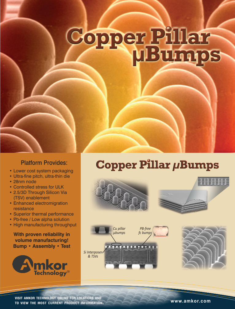
Platform Provides:•Lowercostsystempackaging•Ultra-finepitch,ultra-thindie•28nmnode•ControlledstressforULK•2.5/3DThroughSiliconVia (TSV)enablement•Enhancedelectromigration resistance•Superiorthermalperformance•Pb-free/Lowalphasolution•Highmanufacturingthroughput
www.amkor.com
Cu pillarµbumps
PB-freefc bumps
Si Interposer& TSVs
With proven reliability involume manufacturing!
Bump • Assembly • Test
visit amkor technology online for locations and to view the most current product information.
Copper Pillar Full Page Large Bumps.indd 1 5/1/2012 5:07:48 PM
Perfection Products Inc.1320 S. Indianapolis Ave. • Lebanon, IN 46052Phone: (765) 482-7786 • Fax: (765) 482-7792
Check out our Website: www.perfection-products.comEmail: [email protected]
Grip Ring Shippers
I. C. Trays - Multi-Channel
Lead Frame Magazines - F.O.L./E.O.L.
Film Frame Magazines
Film Frames Film Frame Shippers
TO Tapes & Magazines
Magazines and Carriers for Process Handling Solutions
Accept Nothing Less.
Substrate Carrier Magazines
Stack Magazines - E.O.L.
Wafer Carriers
Process Carriers (Boats)
Boat Magazines
Grip Rings
Miscellaneous Magazines
I. C. Tubes and Rails
Grip Ring Magazines