Embed Size (px)
Citation preview
A
cm
Tp
uw©
K
1
wlac
rb
cdti
tam
f
0d
Journal of Materials Processing Technology 191 (2007) 149–152
Microstructural analysis of AISI 304 bars welded withhigh speed pulsed discharges
G. Casalino a,∗, F.W. Panella b
a DIMeG, Politechnic of Bari, Viale Iapigia,186 Bari, Italyb Department of Innovation Technology, University of Lecce, via Monteroni, 73100 Lecce, Italy
bstract
In a way similar to the resistance welding the high speed pulsed welding exploits the power of elevated discharging current through an electricalircuit, which contains the two parts to be welded. During welding edges profile interact with the process parameters to determine both the weldicrostructure and mechanical strength.In this paper, the welding profiles at the opposite surfaces was machined so to have linear contacts instead of a classic single protrusion contact.
he effect of this multilinears contact geometry was a weld that was in the midway between the capacitor discharge welding (CDW) and therojection welding (PW).
Pulsed welding experiments were performed using AISI 304 cylindrical bars in butt configuration. The welded microstructures were studiedsing an optical microscope and image analysis software. The Vickers microhardness tests were performed to a better characterization of theelding microstructures. 2007 Elsevier B.V. All rights reserved.
lysis
rd
r
dba
2
cit
o
eywords: High speed pulsed welding; 304 steel butt joint; Microstructural ana
. Introduction
High speed pulse welding (HSPW) is a form of resistanceelding but is achieved within milliseconds at very high current
evels by utilizing capacitor-stored energy. Therefore, a soundutogenously joint can be achieved by discharging a very highurrent pulse at low voltage over a short welding time.
While parts are pressed together with high force the high cur-ent pulse is released through the parts and a fine-grain diffusionond forms with low total energy input [1].
The energy for the pulse is derived totally from chargedapacitors which is why HSPW is sometimes called capacitorischarge (or CD) welding, which are the most known weldingechniques that use the power of high current discharge storedn capacitors [2].
It is able to produce butt welded joints at cooling rates greater
han 106 K/s. Therefore, extremely narrow heat affected zonesre produced as well as rapidly solidified welds without losingetastable crystalline structures, good grain refinements and∗ Corresponding author.E-mail addresses: [email protected] (G. Casalino),
[email protected] (F.W. Panella).
rrawo
dbo
924-0136/$ – see front matter © 2007 Elsevier B.V. All rights reserved.oi:10.1016/j.jmatprotec.2007.03.067
educed segregation [3]. It is also worth to point out that theeformations induced by this process are negligible [4,5].
More benefits from HSPW are related to the high productionates that can be achieved with this welding technique.
The welding together of different materials such as pow-er metals higher carbon steels, brass, copper and others toe welded together HSPW opens up many potential joiningpplications [6,7].
. Experimental procedure
The pulse welding process can be described as follows. Immediately after theapacitor discharge is initiated the components begin to fuse. The weld energys focused into the interface region by appropriate projection (tip) design andhe material in this region heats up rapidly.
Due to the high surface pressure the resulting plasticized material is squeezedut from the contact area and the components migrate together (upset) and theesulting contact area is forge welded together. Due to the low heat input andapid cooling rates in HSPW, the heat affected zone is extremely small (0.5 mmnd lower) relative to other welding processes. This localized heating enableselding near heat sensitive materials and results in no weld zone discoloration
r part distortion.The welding energy taken from the capacitor battery remains uniform duringischarge. The capacitors are charged at voltages up to 3.200 V (controlled toetter than 1% variation), and are fed by a high power thyristor to the primary sidef a specially designed impulse transformer. The impulse transformers convert
150 G. Casalino, F.W. Panella / Journal of Materials Processing Technology 191 (2007) 149–152
e((
eArtacc
Tmdc
tflsz
wit
gtbreow
m
3
we
wp
o
am
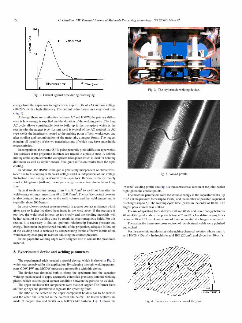
Fig. 2. The taylormade welding device.
“h
tdl
4b
and etched.For the austenitic stainless steels the etching chemical solution whose is nitric
acid HNO3 (10 cm3), hydrochloric acid HCl (20 cm3) and glycerine (30 cm3).
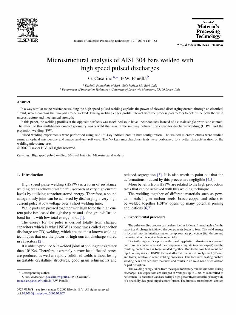
Fig. 1. Current against time during discharging.
nergy from the capacitors to high current (up to 100s of kA) and low voltage10–20 V) with a high efficiency. The current is discharged in a very short timeFig. 1).
Although there are similarities between AC and HSPW, the primary differ-nce is how energy is supplied and the duration of the welding pulse. The longC cycle allows considerable heat to build up in the workpiece which is the
eason why the nugget type (fusion) weld is typical of the AC method. In ACype welds the interface is heated to the melting point of both workpieces andfter cooling and recombination of the materials, a nugget forms. The nuggetontains all the alloys of the two materials, some of which may have undesirableharacteristics.
In comparison, the short, HSPW pulse generally yields diffusion-type welds.he surfaces at the projection interface are heated to a plastic state. A definiteixing of the crystals from the workpieces takes place which is ideal for bonding
issimilar as well as similar metals. Fine-grain diffusion results from the rapidooling.
In addition, the HSPW technique is practically independent of ohmic resis-ance due to its coupling with preset voltage and it is independent of line voltageuctuation since energy is derived from capacitors. Because of the extremelyhort welding times (4–8 ms), the output energy is concentrated onto the weldingone.
Typical steels require energy from 4 to 8 J/mm3 to melt but hereafter theeld energy settings range from 80 to 200 J/mm3. The surface contact pressure
s also designed in proportion to the weld volume and the weld energy and isypically about 200 N/mm3.
In theory, lower contact pressure results in greater contact resistance whichives rise to higher localized heat input in the weld zone. If the pressure isoo low, the weld head follows up too slowly and the welding materials wille hurled out of the welding zone by rotational electromagnetic fields. For thiseason, it is necessary to find an optimum relationship between pressure andnergy. To contain the plasticized material of the projection, adequate follow-upf the welding head is achieved by compensating for the effective inertia of theeld head by changing its mass or adjusting the contact pressure.
In this paper, the welding edges were designed also to contain the plasticizedaterial.
. Experimental device and welding parameters
The experimental trials needed a special device, which is shown in Fig. 2,hich was conceived for this application. By selecting the right welding param-
ters CDW, PW and MCDW processes are possible with this device.The device was designed both to clamp the specimens into the capacitor
elding machine and to apply accurately controlled pressures onto the weldingieces, which assured good contact condition between the parts to be welded.
The upper and lower flat components were made of copper. The former leansn four springs and permitted to regulate the upsetting force.
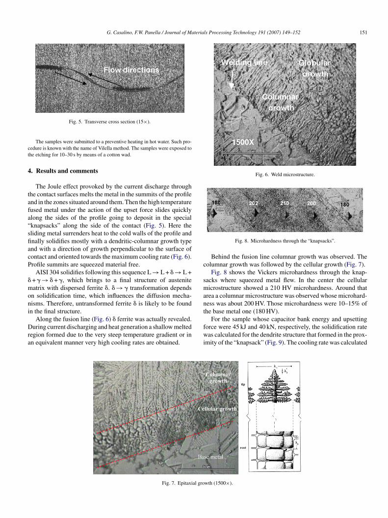
The tube at the center of the upper component holds a bar to be weldednd the other one is placed in the co-axial site below. The lateral features areade of copper also and works in a bellows like fashion. Fig. 3 shows the
Fig. 3. Waved profile.
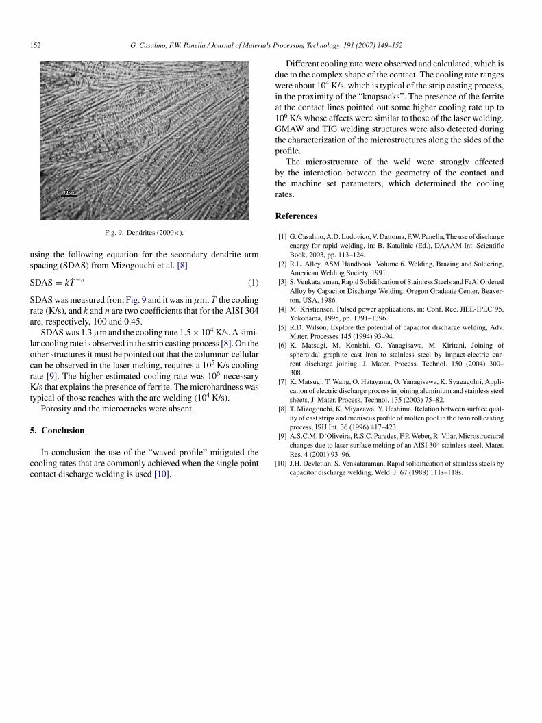
waved” welding profile and Fig. 4 a transverse cross section of the joint, whichighlighted the contact points.
The machine parameters were the storable energy in the capacitor banks (upo 45 kJ) the pressure force (up to 45 kN) and the number of possible sequentialischarges (up to 5). The welding cycle time (t) was in the order of 10 ms. Theargest peak current was 200 kA.
The use of upsetting forces between 20 and 40 kN and stored energy between0 and 45 kJ produced current peaks between 75 and 90 kA and discharging timesetween 10 and 12 ms. A maximum of three sequential discharges were used.
Thereafter the transverse cross section of the obtained welds were polished
Fig. 4. Transverse cross section of the joint.
G. Casalino, F.W. Panella / Journal of Materials Processing Technology 191 (2007) 149–152 151
ct
4
tafa“sfiacP
�moni
Dra
Fig. 6. Weld microstructure.
c
smant
Fig. 5. Transverse cross section (15×).
The samples were submitted to a preventive heating in hot water. Such pro-edure is known with the name of Vilella method. The samples were exposed tohe etching for 10–30 s by means of a cotton wad.
. Results and comments
The Joule effect provoked by the current discharge throughhe contact surfaces melts the metal in the summits of the profilend in the zones situated around them. Then the high temperatureused metal under the action of the upset force slides quicklylong the sides of the profile going to deposit in the specialknapsacks” along the side of the contact (Fig. 5). Here theliding metal surrenders heat to the cold walls of the profile andnally solidifies mostly with a dendritic-columnar growth typend with a direction of growth perpendicular to the surface ofontact and oriented towards the maximum cooling rate (Fig. 6).rofile summits are squeezed material free.
AISI 304 solidifies following this sequence L → L + � → L ++ � → � + �, which brings to a final structure of austeniteatrix with dispersed ferrite �. � → � transformation depends
n solidification time, which influences the diffusion mecha-isms. Therefore, untransformed ferrite � is likely to be foundn the final structure.
Along the fusion line (Fig. 6) � ferrite was actually revealed.uring current discharging and heat generation a shallow melted
egion formed due to the very steep temperature gradient or inn equivalent manner very high cooling rates are obtained.
fwi
Fig. 7. Epitaxial gro
Fig. 8. Microhardness through the “knapsacks”.
Behind the fusion line columnar growth was observed. Theolumnar growth was followed by the cellular growth (Fig. 7).
Fig. 8 shows the Vickers microhardness through the knap-acks where squeezed metal flew. In the center the cellularicrostructure showed a 210 HV microhardness. Around that
rea a columnar microstructure was observed whose microhard-ess was about 200 HV. Those microhardness were 10–15% ofhe base metal one (180 HV).
For the sample whose capacitor bank energy and upsettingorce were 45 kJ and 40 kN, respectively, the solidification rateas calculated for the dendrite structure that formed in the prox-
mity of the “knapsack” (Fig. 9). The cooling rate was calculated
wth (1500×).
152 G. Casalino, F.W. Panella / Journal of Materials P
us
S
Sra
locrKt
5
cc
dwia1Gtp
btr
R
Fig. 9. Dendrites (2000×).
sing the following equation for the secondary dendrite armpacing (SDAS) from Mizogouchi et al. [8]
DAS = kT−n (1)
DAS was measured from Fig. 9 and it was in μm, T the coolingate (K/s), and k and n are two coefficients that for the AISI 304re, respectively, 100 and 0.45.
SDAS was 1.3 �m and the cooling rate 1.5 × 10⁴ K/s. A simi-ar cooling rate is observed in the strip casting process [8]. On thether structures it must be pointed out that the columnar-cellularan be observed in the laser melting, requires a 105 K/s coolingate [9]. The higher estimated cooling rate was 106 necessary/s that explains the presence of ferrite. The microhardness was
ypical of those reaches with the arc welding (104 K/s).Porosity and the microcracks were absent.
. Conclusion
In conclusion the use of the “waved profile” mitigated theooling rates that are commonly achieved when the single pointontact discharge welding is used [10].
[
rocessing Technology 191 (2007) 149–152
Different cooling rate were observed and calculated, which isue to the complex shape of the contact. The cooling rate rangesere about 104 K/s, which is typical of the strip casting process,
n the proximity of the “knapsacks”. The presence of the ferritet the contact lines pointed out some higher cooling rate up to06 K/s whose effects were similar to those of the laser welding.MAW and TIG welding structures were also detected during
he characterization of the microstructures along the sides of therofile.
The microstructure of the weld were strongly effectedy the interaction between the geometry of the contact andhe machine set parameters, which determined the coolingates.
eferences
[1] G. Casalino, A.D. Ludovico, V. Dattoma, F.W. Panella, The use of dischargeenergy for rapid welding, in: B. Katalinic (Ed.), DAAAM Int. ScientificBook, 2003, pp. 113–124.
[2] R.L. Alley, ASM Handbook. Volume 6. Welding, Brazing and Soldering,American Welding Society, 1991.
[3] S. Venkataraman, Rapid Solidification of Stainless Steels and FeAl OrderedAlloy by Capacitor Discharge Welding, Oregon Graduate Center, Beaver-ton, USA, 1986.
[4] M. Kristiansen, Pulsed power applications, in: Conf. Rec. JIEE-IPEC’95,Yokohama, 1995, pp. 1391–1396.
[5] R.D. Wilson, Explore the potential of capacitor discharge welding, Adv.Mater. Processes 145 (1994) 93–94.
[6] K. Matsugi, M. Konishi, O. Yanagisawa, M. Kiritani, Joining ofspheroidal graphite cast iron to stainless steel by impact-electric cur-rent discharge joining, J. Mater. Process. Technol. 150 (2004) 300–308.
[7] K. Matsugi, T. Wang, O. Hatayama, O. Yanagisawa, K. Syagagohri, Appli-cation of electric discharge process in joining aluminium and stainless steelsheets, J. Mater. Process. Technol. 135 (2003) 75–82.
[8] T. Mizogouchi, K. Miyazawa, Y. Ueshima, Relation between surface qual-ity of cast strips and meniscus profile of molten pool in the twin roll castingprocess, ISIJ Int. 36 (1996) 417–423.
[9] A.S.C.M. D’Oliveira, R.S.C. Paredes, F.P. Weber, R. Vilar, Microstructuralchanges due to laser surface melting of an AISI 304 stainless steel, Mater.Res. 4 (2001) 93–96.
10] J.H. Devletian, S. Venkataraman, Rapid solidification of stainless steels bycapacitor discharge welding, Weld. J. 67 (1988) 111s–118s.