Embed Size (px)
Citation preview
Creating Embedded Systems
miriac SBC-S32V234
User Manual
V 1.0
miriac SBC-S32V234 User Manual V 1.0 2/40 © MicroSys Electronics GmbH 2018
1 General Notes
Copyright MicroSys Electronics GmbH, December 2018
All rights reserved. All rights in any information which appears in this document
belong to MicroSys Electronics GmbH or our licensors. You may copy the
information in this manual for your personal, non-commercial use.
Copyrighted products are not explicitly indicated in this manual. The absence of the
copyright (©) and trademark (TM or ®) symbols does not imply that a product is not
protected. Additionally, registered patents and trademarks are similarly not
expressly indicated in this manual.
1.1 Warranty
To the extent permissible by applicable law all information in this document is
provided without warranty of any kind, whether expressed or implied, including but
not limited to any implied warranty of satisfactory quality or fitness for a particular
purpose, or of non-infringement of any third party’s rights. We try to keep this
document accurate and up-to-date but we do not make any warranty or
representation about such matters. In particular we assume no liability or
responsibility for any errors or omissions in this document.
MicroSys Electronics GmbH neither gives any guarantee nor accepts any liability
whatsoever for consequential damages resulting from the use of this manual or its
associated product.
MicroSys Electronics GmbH further reserves the right to alter the layout and/or
design of the hardware without prior notification and accepts no liability for doing
so.
1.2 Links
We make no warranty about any other sites that are linked to or from this
document, whether we authorize such links or not.
1.3 Liability
To the extent permissible by applicable law, in no circumstance, including (but not
limited to) negligence, shall we be liable for your reliance on any information in this
document, nor shall we be liable for any direct, incidental, special, consequential,
indirect or punitive damages nor any loss of profit that result from the use of, or the
inability to use, this document or any material on any site linked to this document
even if we have been advised of the possibility of such damage. In no event shall
our liability to you for all damages, losses and causes of action whatsoever,
whether in contract, tort (including but not limited to negligence) or otherwise
exceed the amount, if any, paid by you to us for gaining access to this document.
MicroSys Electronics GmbH
Muehlweg 1
82054 Sauerlach
Germany
Phone: +49 8104 801-0
Fax: +49 8104 801-110
miriac SBC-S32V234 User Manual V 1.0 3/40 © MicroSys Electronics GmbH 2018
1.4 Offer to Provide Source Code of Certain Software
This product contains copyrighted software that is licensed under the General
Public License (“GPL”) and under the Lesser General Public License Version
(“LGPL”). The GPL and LGPL licensed code in this product is distributed without
any warranty. Copies of these licenses are included in this product.
You may obtain the complete corresponding source code (as defined in the GPL)
for the GPL Software, and/or the complete corresponding source code of the LGPL
Software (with the complete machine-readable “work that uses the Library”) for a
period of three years after our last shipment of the product including the GPL
Software and/or LGPL Software, which will be no earlier than December 1, 2010,
for the cost of reproduction and shipment, which is dependent on the preferred
carrier and the location where you want to have it shipped to, by sending a request
to:
MicroSys Electronics GmbH
Muehlweg 1
82054 Sauerlach
Germany
In your request please provide the product name and version for which you wish to
obtain the corresponding source code and your contact details so that we can
coordinate the terms and cost of shipment with you.
The source code will be distributed WITHOUT ANY WARRANTY and licensed
under the same license as the corresponding binary/object code.
This offer is valid to anyone in receipt of this information.
MicroSys Electronics GmbH is eager to duly provide complete source code as
required under various Free Open Source Software licenses. If, however you
encounter any problems in obtaining the full corresponding source code we would
be much obliged if you give us a notification to the email address
[email protected], stating the product and describing the problem (please do NOT
send large attachments such as source code archives etc. to this email address)
miriac SBC-S32V234 User Manual V 1.0 4/40 © MicroSys Electronics GmbH 2018
1.5 Symbols, Conventions and Abbreviations
1.5.1 Symbols
Throughout this document, the following symbols will be used:
Information marked with this symbol MUST be obeyed to avoid the risk of severe injury, health danger, or major destruction of the unit and its environment
Information marked with this symbol MUST be obeyed to avoid the risk of possible injury, permanent damage or malfunction of the unit.
Information marked with this symbol gives important hints upon details of this manual, or in order to get the best use out of the product and its features.
Table 1 Symbols
1.5.2 Conventions
Symbol explanation
# denotes a low active signal
← denotes the signal flow in the shown direction
→ denotes the signal flow in the shown direction
↔ denotes the signal flow in both directions
→ denotes the signal flow in the shown direction with additional logic /
additional ICs in the signal path
I/O denotes a bidirectional pin
Input denotes an input pin
matched denotes the according signal to be routed impedance controlled and length matched
Output denotes an output pin
Pin 1 refers to the numeric pin of a component package
Pin a1 refers to the array position of a pin within a component package
XXX- denotes the negative signal of a differential pair
XXX+ denotes the positive signal of a differential pair
XXX denotes an optional not mounted or fitted part
Table 2 Conventions
miriac SBC-S32V234 User Manual V 1.0 5/40 © MicroSys Electronics GmbH 2018
2 Introduction Thank you for choosing the MicroSys MPX-S32V234 module. This manual should
help you to get the best performance and details out all of its features.
2.1 Safety and Handling Precautions
ALWAYS use the correct type and polarity of the power
supply!
DO NOT exceed the rated maximum values for the power
supply! This may result in severe permanent damage to
the unit, as well as possible serious injury.
ALWAYS keep the unit dry, clean and free of foreign
objects. Otherwise, irreparable damage may occur.
Parts of the unit may become hot during operation. Take care not to touch any parts of the circuitry during operation to avoid burns, and operate the unit in a well-ventilated location. Provide an appropriate cooling solution as required.
ALWAYS take care of ESD-safe handling!
Many pins on external connectors are directly connected to the CPU or other ESD sensitive devices.
Make or break ANY connections ONLY while the unit is switched OFF.
Otherwise, permanent damage to the unit may occur, which is not covered by warranty.
There is no separate SHIELD connection.
All the metal sheaths of shielded connectors are connected to GND.
Also, all mounting holes of the carrier board are connected to GND.
The module’s mounting holes are not connected to GND
Take this into account when handling and mounting the unit.
Table 3 Safety and Handling Precautions
miriac SBC-S32V234 User Manual V 1.0 6/40 © MicroSys Electronics GmbH 2018
2.2 Short Description
The miriac MPX-S32V234 is a member of the MPX module family, based on NXP’s
S32V234 vision processing MPU
It targets the evaluation of the main interfaces of the S32V234 processor
2.3 Ordering Information
The MPX-S32V234 System-on-Module (SoM) is available in the following configu-
rations:
Part No. Title Description
854901 miriac MPX-S32V234 SoM NXP S32V234@1GHz CPU, 2GB DDR3L, standard temp 0C to +70C
854902 miriac MPX-S32V234 SoM same as 854901, but with extended temp -40C to +70C
854903 miriac MPX-S32V234 SoM same as 854901, except CPU contains Cryptographic Service Engine
2.4 Board Preparation
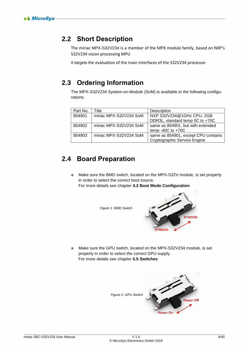
■ Make sure the BMD switch, located on the MPX-S32V module, is set properly
in order to select the correct boot source.
For more details see chapter 4.2 Boot Mode Configuration
■ Make sure the GPU switch, located on the MPX-S32V234 module, is set
properly in order to select the correct GPU supply.
For more details see chapter 5.5 Switches
Figure 1: BMD Switch
Figure 2: GPU Switch
miriac SBC-S32V234 User Manual V 1.0 7/40 © MicroSys Electronics GmbH 2018
2.5 Software
When ordering MPX-S32V234 SoMs they are delivered with a version of U-Boot in the onboard eMMC which was used in the factory to test the module on MicroSys' CRX-32V carrier. Assuming you are intending to mount the module on your own carrier, then you will need to modify U-Boot accordingly. The SBC-S32V234 (which is the MPX-S32V234 module mounted on the CRX-32V carrier) is supported by NXP's automotive Linux BSP for S32. You can download the latest Linux BSP from: https://source.codeaurora.org/external/autobsps32/auto_yocto_bsp/ This should serve as your starting point for modifying U-Boot and Linux. NXP has a release cadence of once every 3 months. As of December 2018, the current release is BSP 19.0
miriac SBC-S32V234 User Manual V 1.0 8/40 © MicroSys Electronics GmbH 2018
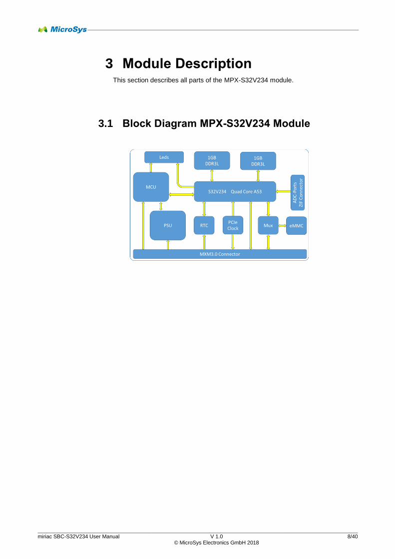
3 Module Description This section describes all parts of the MPX-S32V234 module.
3.1 Block Diagram MPX-S32V234 Module
miriac SBC-S32V234 User Manual V 1.0 9/40 © MicroSys Electronics GmbH 2018
3.2 Feature Overview
Feature Type Description
CPU NXP S32V234
Core Clock 1GHz
Quad-Cortex®-A53
Single-Cortex®-M4
SDRAM Dual 32-bit DDR3L
interface
2 x up to 1GByte
up to 1066MT/s
Mass Storage 8-bit eMMC 16 GByte
PCI Express via MXM Connector Rev.2.0
5Gbps
Lane x1
RC/EP
100MHz Clock Source
I2C support
Removable Media via MXM Connector For microSD cards
4/8-bit support
Ethernet via MXM Connector RGMII
Grahics Output via MXM Connector Parallel 24-bit
Video Input MIPI-CSI-A 4 Lanes + Clock
MIPI-CSI-B 4 Lanes + Clock
Serial Interfaces via MXM Connector UART0
via MXM Connector UART1
CAN Interface via MXM Connector CAN0
via MXM Connector CAN1
RTC Time/Date PCF85263A
external backup
Board Control S9KEAZN64A Voltage supervision
Reset logic
Boot configuration
Status LED
Switches Sliding Swicthes RCON/Serial Select
GPU Power ON/Off
Indicators LEDs MCU Status
Reset Status
User GPIO1
User GPIO2
Connectors Module Connectors ADC Channel 0-7
MCU Programming Port
314-pin MXM Conncetor
miriac SBC-S32V234 User Manual V 1.0 10/40 © MicroSys Electronics GmbH 2018
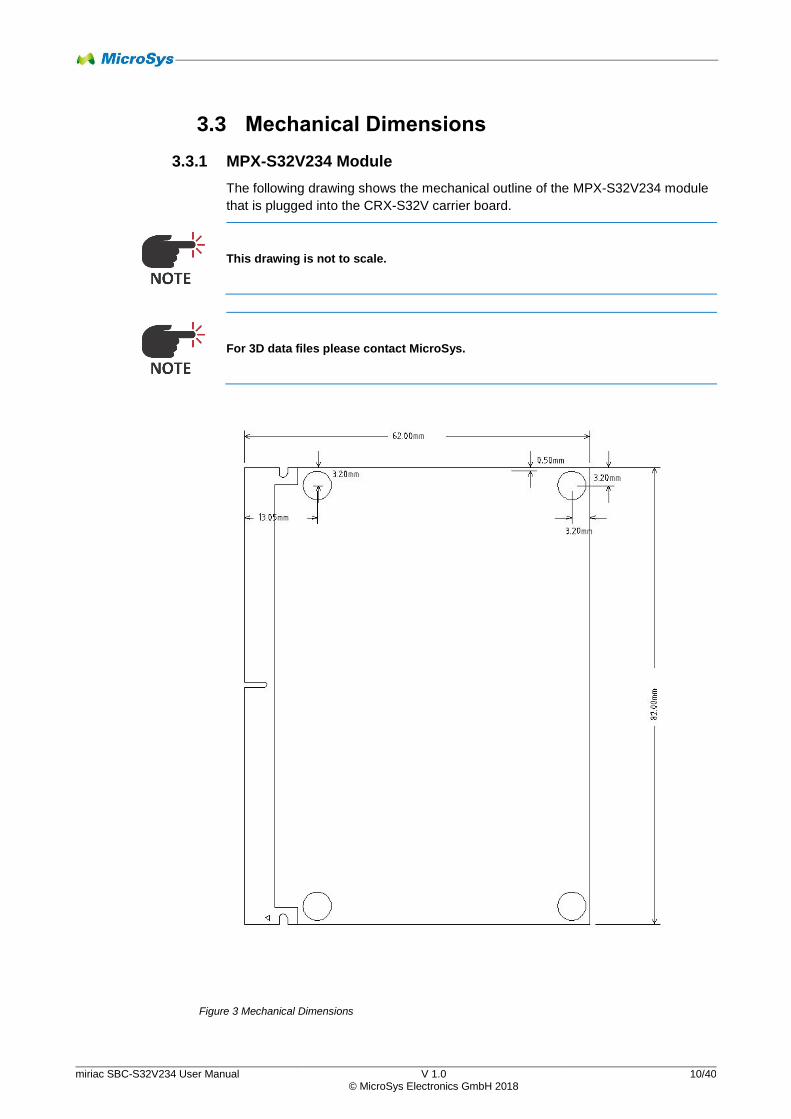
3.3 Mechanical Dimensions
3.3.1 MPX-S32V234 Module
The following drawing shows the mechanical outline of the MPX-S32V234 module
that is plugged into the CRX-S32V carrier board.
This drawing is not to scale.
For 3D data files please contact MicroSys.
Figure 3 Mechanical Dimensions
miriac SBC-S32V234 User Manual V 1.0 11/40 © MicroSys Electronics GmbH 2018
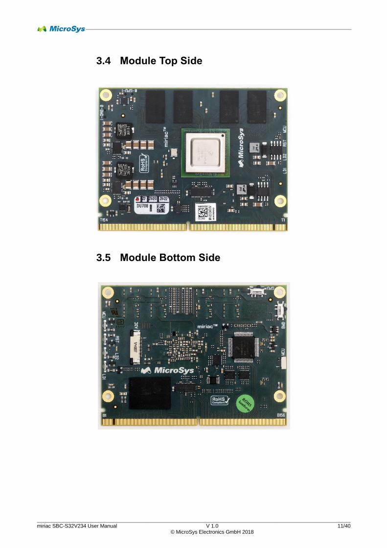
3.4 Module Top Side
3.5 Module Bottom Side
miriac SBC-S32V234 User Manual V 1.0 12/40 © MicroSys Electronics GmbH 2018
3.7 System Environment
3.7.1 Temperature Ratings
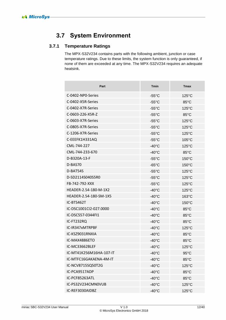
The MPX-S32V234 contains parts with the following ambient, junction or case
temperature ratings. Due to these limits, the system function is only guaranteed, if
none of them are exceeded at any time. The MPX-S32V234 requires an adequate
heatsink.
Part Tmin Tmax
C-0402-NP0-Series -55°C 125°C
C-0402-X5R-Series -55°C 85°C
C-0402-X7R-Series -55°C 125°C
C-0603-226-X5R-Z -55°C 85°C
C-0603-X7R-Series -55°C 125°C
C-0805-X7R-Series -55°C 125°C
C-1206-X7R-Series -55°C 125°C
C-EEEFK1H331AQ -55°C 105°C
CML-744-227 -40°C 125°C
CML-744-233-670 -40°C 85°C
D-B320A-13-F -55°C 150°C
D-BAS70 -65°C 150°C
D-BAT54S -55°C 125°C
D-SD2114S040S5R0 -55°C 125°C
FB-742-792-XXX -55°C 125°C
HEADER-2.54-180-M-1X2 -40°C 125°C
HEADER-2.54-180-SM-1X5 -40°C 163°C
IC-BTS462T -40°C 150°C
IC-DSC1001CI2-027.0000 -40°C 85°C
IC-DSC557-0344FI1 -40°C 85°C
IC-FT232RQ -40°C 85°C
IC-IR347xMTRPBF -40°C 125°C
IC-KSZ9031RNXIA -40°C 85°C
IC-MAX4886ETO -40°C 85°C
IC-MC33662BLEF -40°C 125°C
IC-MT41K256M16HA-107-IT -40°C 95°C
IC-MTFC16GAKAENA-4M-IT -40°C 85°C
IC-NCV8715SQ50T2G -40°C 125°C
IC-PCA9517ADP -40°C 85°C
IC-PCF85263ATL -40°C 85°C
IC-PS32V234CMN0VUB -40°C 125°C
IC-REF3030AIDBZ -40°C 125°C
miriac SBC-S32V234 User Manual V 1.0 13/40 © MicroSys Electronics GmbH 2018
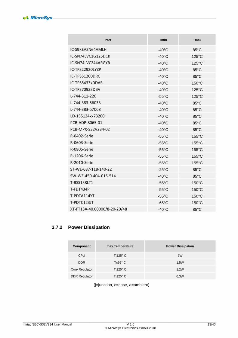
Part Tmin Tmax
IC-S9KEAZN64AMLH -40°C 85°C
IC-SN74LVC1G125DCK -40°C 125°C
IC-SN74LVC244ARGYR -40°C 125°C
IC-TPS22920LYZP -40°C 85°C
IC-TPS51200DRC -40°C 85°C
IC-TPS5433xDDAR -40°C 150°C
IC-TPS70933DBV -40°C 125°C
L-744-311-220 -55°C 125°C
L-744-383-56033 -40°C 85°C
L-744-383-57068 -40°C 85°C
LD-155124xx73200 -40°C 85°C
PCB-ADP-8065-01 -40°C 85°C
PCB-MPX-S32V234-02 -40°C 85°C
R-0402-Serie -55°C 155°C
R-0603-Serie -55°C 155°C
R-0805-Serie -55°C 155°C
R-1206-Serie -55°C 155°C
R-2010-Serie -55°C 155°C
ST-WE-687-118-140-22 -25°C 85°C
SW-WE-450-404-015-514 -40°C 85°C
T-BSS138LT1 -55°C 150°C
T-FDT434P -55°C 150°C
T-PDTA114YT -55°C 150°C
T-PDTC123JT -65°C 150°C
XT-FT13A-40.00000/8-20-20/48 -40°C 85°C
3.7.2 Power Dissipation
Component max.Temperature Power Dissipation
CPU Tj125° C 7W
DDR Tc95° C 1.5W
Core Regulator Tj125° C 1.2W
DDR Regulator Tj125° C 0.3W
(j=junction, c=case, a=ambient)
miriac SBC-S32V234 User Manual V 1.0 14/40 © MicroSys Electronics GmbH 2018
3.8 Power Supply
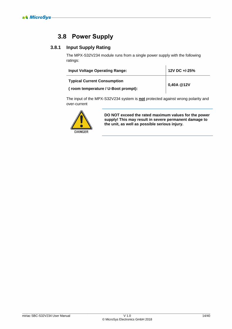
3.8.1 Input Supply Rating
The MPX-S32V234 module runs from a single power supply with the following
ratings:
Input Voltage Operating Range: 12V DC +/-25%
Typical Current Consumption
( room temperature / U-Boot prompt): 0,40A @12V
The input of the MPX-S32V234 system is not protected against wrong polarity and
over-current
DO NOT exceed the rated maximum values for the power supply! This may result in severe permanent damage to the unit, as well as possible serious injury.
miriac SBC-S32V234 User Manual V 1.0 15/40 © MicroSys Electronics GmbH 2018
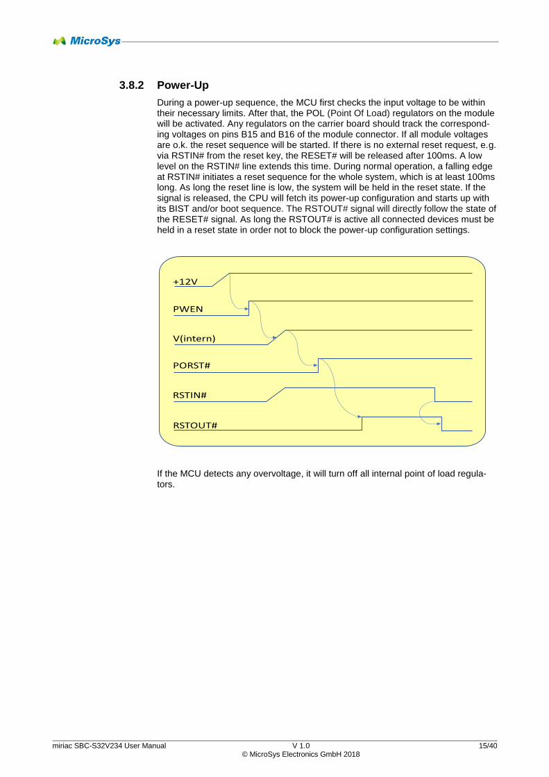
3.8.2 Power-Up
During a power-up sequence, the MCU first checks the input voltage to be within their necessary limits. After that, the POL (Point Of Load) regulators on the module will be activated. Any regulators on the carrier board should track the correspond-ing voltages on pins B15 and B16 of the module connector. If all module voltages are o.k. the reset sequence will be started. If there is no external reset request, e.g. via RSTIN# from the reset key, the RESET# will be released after 100ms. A low level on the RSTIN# line extends this time. During normal operation, a falling edge at RSTIN# initiates a reset sequence for the whole system, which is at least 100ms long. As long the reset line is low, the system will be held in the reset state. If the signal is released, the CPU will fetch its power-up configuration and starts up with its BIST and/or boot sequence. The RSTOUT# signal will directly follow the state of the RESET# signal. As long the RSTOUT# is active all connected devices must be held in a reset state in order not to block the power-up configuration settings.
+12V
PWEN
V(intern)
RSTIN#
RSTOUT#
PORST#
If the MCU detects any overvoltage, it will turn off all internal point of load regula-tors.
miriac SBC-S32V234 User Manual V 1.0 16/40 © MicroSys Electronics GmbH 2018
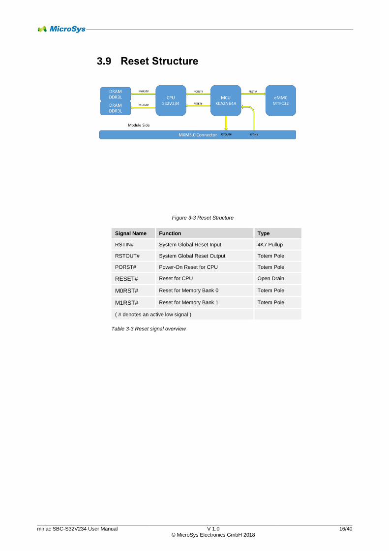
3.9 Reset Structure
Signal Name Function Type
RSTIN# System Global Reset Input 4K7 Pullup
RSTOUT# System Global Reset Output Totem Pole
PORST# Power-On Reset for CPU Totem Pole
RESET# Reset for CPU Open Drain
M0RST# Reset for Memory Bank 0 Totem Pole
M1RST# Reset for Memory Bank 1 Totem Pole
( # denotes an active low signal )
Table 3-3 Reset signal overview
Figure 3-3 Reset Structure
miriac SBC-S32V234 User Manual V 1.0 17/40 © MicroSys Electronics GmbH 2018
4 System Core, Boot Configuration
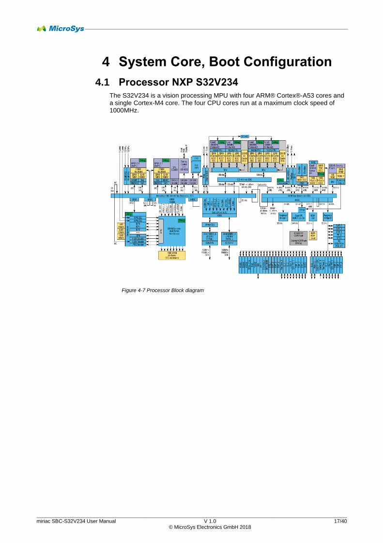
4.1 Processor NXP S32V234 The S32V234 is a vision processing MPU with four ARM® Cortex®-A53 cores and a single Cortex-M4 core. The four CPU cores run at a maximum clock speed of 1000MHz.
Figure 4-7 Processor Block diagram
miriac SBC-S32V234 User Manual V 1.0 18/40 © MicroSys Electronics GmbH 2018
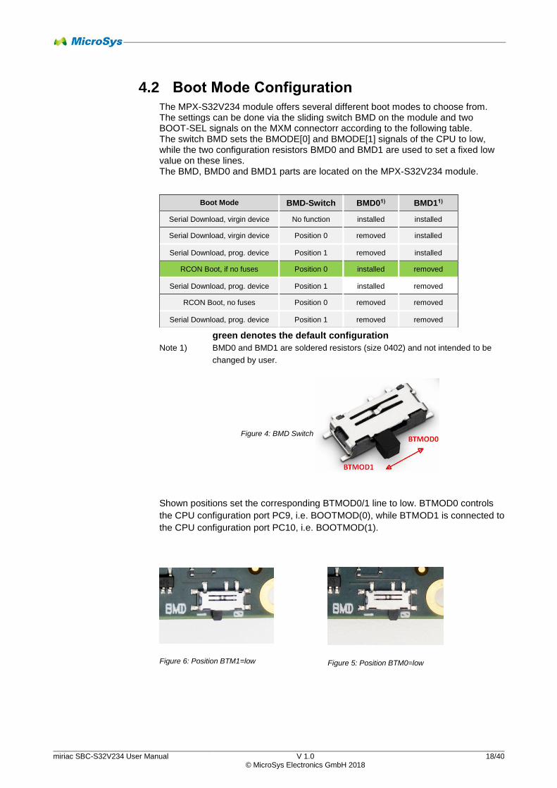
4.2 Boot Mode Configuration
The MPX-S32V234 module offers several different boot modes to choose from. The settings can be done via the sliding switch BMD on the module and two BOOT-SEL signals on the MXM connectorr according to the following table. The switch BMD sets the BMODE[0] and BMODE[1] signals of the CPU to low, while the two configuration resistors BMD0 and BMD1 are used to set a fixed low value on these lines. The BMD, BMD0 and BMD1 parts are located on the MPX-S32V234 module.
green denotes the default configuration
Note 1) BMD0 and BMD1 are soldered resistors (size 0402) and not intended to be
changed by user.
Shown positions set the corresponding BTMOD0/1 line to low. BTMOD0 controls
the CPU configuration port PC9, i.e. BOOTMOD(0), while BTMOD1 is connected to
the CPU configuration port PC10, i.e. BOOTMOD(1).
Boot Mode BMD-Switch BMD01) BMD11)
Serial Download, virgin device No function installed installed
Serial Download, virgin device Position 0 removed installed
Serial Download, prog. device Position 1 removed installed
RCON Boot, if no fuses Position 0 installed removed
Serial Download, prog. device Position 1 installed removed
RCON Boot, no fuses Position 0 removed removed
Serial Download, prog. device Position 1 removed removed
Figure 4: BMD Switch
Figure 6: Position BTM1=low Figure 5: Position BTM0=low
miriac SBC-S32V234 User Manual V 1.0 19/40 © MicroSys Electronics GmbH 2018
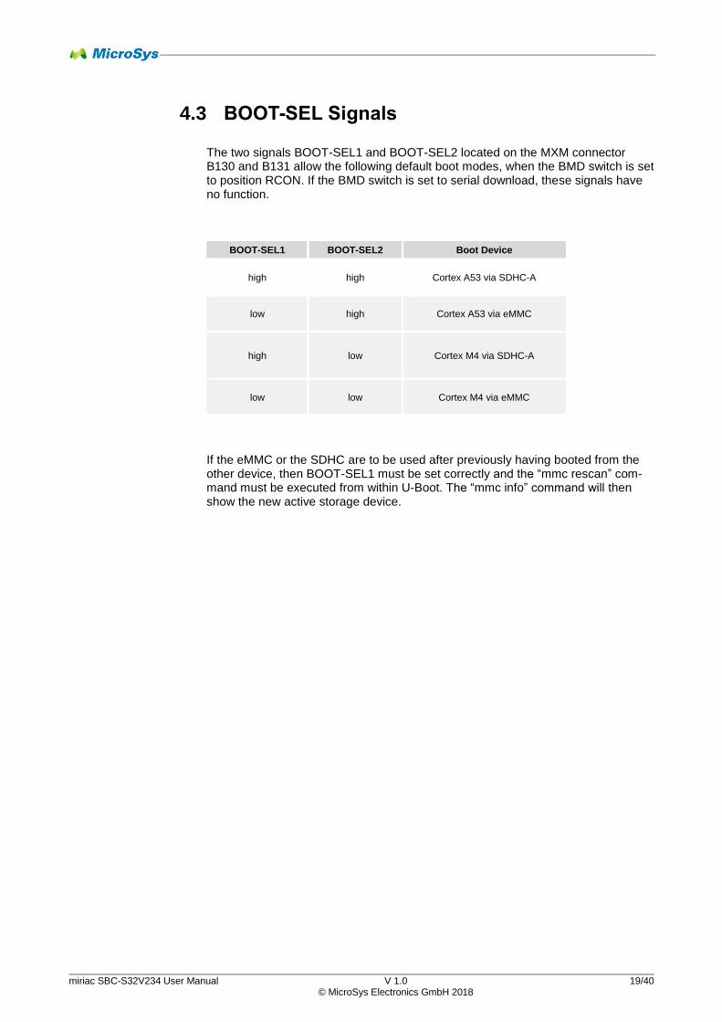
4.3 BOOT-SEL Signals
The two signals BOOT-SEL1 and BOOT-SEL2 located on the MXM connector B130 and B131 allow the following default boot modes, when the BMD switch is set to position RCON. If the BMD switch is set to serial download, these signals have no function.
If the eMMC or the SDHC are to be used after previously having booted from the other device, then BOOT-SEL1 must be set correctly and the “mmc rescan” com-mand must be executed from within U-Boot. The “mmc info” command will then show the new active storage device.
BOOT-SEL1 BOOT-SEL2 Boot Device
high high Cortex A53 via SDHC-A
low high Cortex A53 via eMMC
high low Cortex M4 via SDHC-A
low low Cortex M4 via eMMC
miriac SBC-S32V234 User Manual V 1.0 20/40 © MicroSys Electronics GmbH 2018
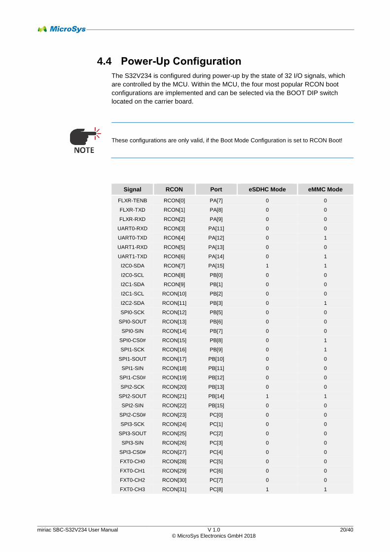
4.4 Power-Up Configuration
The S32V234 is configured during power-up by the state of 32 I/O signals, which
are controlled by the MCU. Within the MCU, the four most popular RCON boot
configurations are implemented and can be selected via the BOOT DIP switch
located on the carrier board.
These configurations are only valid, if the Boot Mode Configuration is set to RCON Boot!
Signal RCON Port eSDHC Mode eMMC Mode
FLXR-TENB RCON[0] PA[7] 0 0
FLXR-TXD RCON[1] PA[8] 0 0
FLXR-RXD RCON[2] PA[9] 0 0
UART0-RXD RCON[3] PA[11] 0 0
UART0-TXD RCON[4] PA[12] 0 1
UART1-RXD RCON[5] PA[13] 0 0
UART1-TXD RCON[6] PA[14] 0 1
I2C0-SDA RCON[7] PA[15] 1 1
I2C0-SCL RCON[8] PB[0] 0 0
I2C1-SDA RCON[9] PB[1] 0 0
I2C1-SCL RCON[10] PB[2] 0 0
I2C2-SDA RCON[11] PB[3] 0 1
SPI0-SCK RCON[12] PB[5] 0 0
SPI0-SOUT RCON[13] PB[6] 0 0
SPI0-SIN RCON[14] PB[7] 0 0
SPI0-CS0# RCON[15] PB[8] 0 1
SPI1-SCK RCON[16] PB[9] 0 1
SPI1-SOUT RCON[17] PB[10] 0 0
SPI1-SIN RCON[18] PB[11] 0 0
SPI1-CS0# RCON[19] PB[12] 0 0
SPI2-SCK RCON[20] PB[13] 0 0
SPI2-SOUT RCON[21] PB[14] 1 1
SPI2-SIN RCON[22] PB[15] 0 0
SPI2-CS0# RCON[23] PC[0] 0 0
SPI3-SCK RCON[24] PC[1] 0 0
SPI3-SOUT RCON[25] PC[2] 0 0
SPI3-SIN RCON[26] PC[3] 0 0
SPI3-CS0# RCON[27] PC[4] 0 0
FXT0-CH0 RCON[28] PC[5] 0 0
FXT0-CH1 RCON[29] PC[6] 0 0
FXT0-CH2 RCON[30] PC[7] 0 0
FXT0-CH3 RCON[31] PC[8] 1 1
miriac SBC-S32V234 User Manual V 1.0 21/40 © MicroSys Electronics GmbH 2018
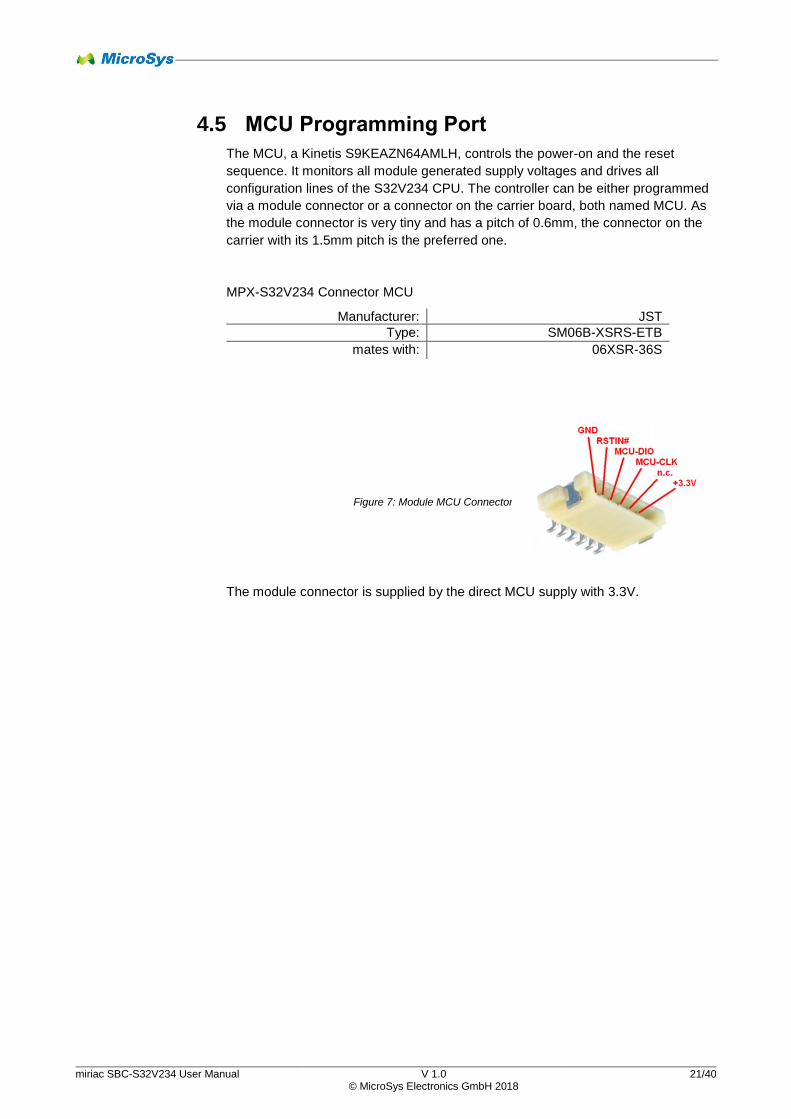
4.5 MCU Programming Port
The MCU, a Kinetis S9KEAZN64AMLH, controls the power-on and the reset
sequence. It monitors all module generated supply voltages and drives all
configuration lines of the S32V234 CPU. The controller can be either programmed
via a module connector or a connector on the carrier board, both named MCU. As
the module connector is very tiny and has a pitch of 0.6mm, the connector on the
carrier with its 1.5mm pitch is the preferred one.
MPX-S32V234 Connector MCU
Manufacturer: JST
Type: SM06B-XSRS-ETB
mates with: 06XSR-36S
The module connector is supplied by the direct MCU supply with 3.3V.
Figure 7: Module MCU Connector
miriac SBC-S32V234 User Manual V 1.0 22/40 © MicroSys Electronics GmbH 2018
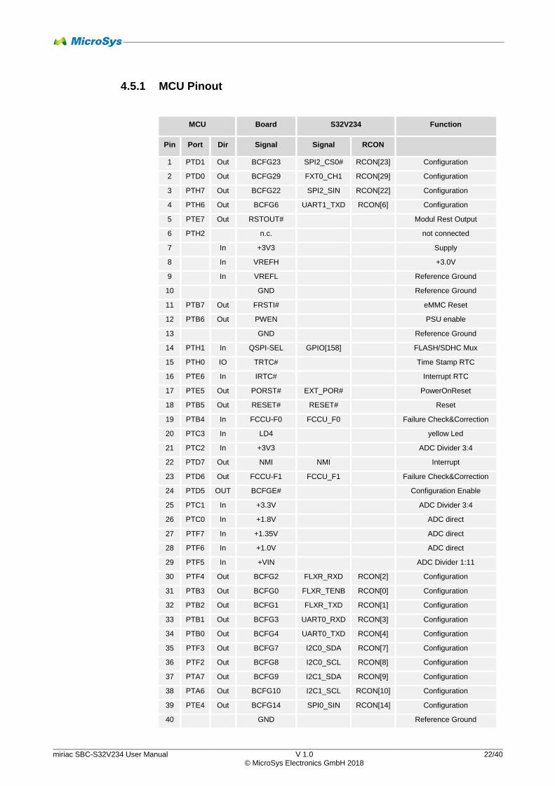
4.5.1 MCU Pinout
MCU Board S32V234 Function
Pin Port Dir Signal Signal RCON
1 PTD1 Out BCFG23 SPI2_CS0# RCON[23] Configuration
2 PTD0 Out BCFG29 FXT0_CH1 RCON[29] Configuration
3 PTH7 Out BCFG22 SPI2_SIN RCON[22] Configuration
4 PTH6 Out BCFG6 UART1_TXD RCON[6] Configuration
5 PTE7 Out RSTOUT# Modul Rest Output
6 PTH2 n.c. not connected
7 In +3V3 Supply
8 In VREFH +3.0V
9 In VREFL Reference Ground
10 GND Reference Ground
11 PTB7 Out FRSTI# eMMC Reset
12 PTB6 Out PWEN PSU enable
13 GND Reference Ground
14 PTH1 In QSPI-SEL GPIO[158] FLASH/SDHC Mux
15 PTH0 IO TRTC# Time Stamp RTC
16 PTE6 In IRTC# Interrupt RTC
17 PTE5 Out PORST# EXT_POR# PowerOnReset
18 PTB5 Out RESET# RESET# Reset
19 PTB4 In FCCU-F0 FCCU_F0 Failure Check&Correction
20 PTC3 In LD4 yellow Led
21 PTC2 In +3V3 ADC Divider 3:4
22 PTD7 Out NMI NMI Interrupt
23 PTD6 Out FCCU-F1 FCCU_F1 Failure Check&Correction
24 PTD5 OUT BCFGE# Configuration Enable
25 PTC1 In +3.3V ADC Divider 3:4
26 PTC0 In +1.8V ADC direct
27 PTF7 In +1.35V ADC direct
28 PTF6 In +1.0V ADC direct
29 PTF5 In +VIN ADC Divider 1:11
30 PTF4 Out BCFG2 FLXR_RXD RCON[2] Configuration
31 PTB3 Out BCFG0 FLXR_TENB RCON[0] Configuration
32 PTB2 Out BCFG1 FLXR_TXD RCON[1] Configuration
33 PTB1 Out BCFG3 UART0_RXD RCON[3] Configuration
34 PTB0 Out BCFG4 UART0_TXD RCON[4] Configuration
35 PTF3 Out BCFG7 I2C0_SDA RCON[7] Configuration
36 PTF2 Out BCFG8 I2C0_SCL RCON[8] Configuration
37 PTA7 Out BCFG9 I2C1_SDA RCON[9] Configuration
38 PTA6 Out BCFG10 I2C1_SCL RCON[10] Configuration
39 PTE4 Out BCFG14 SPI0_SIN RCON[14] Configuration
40 GND Reference Ground
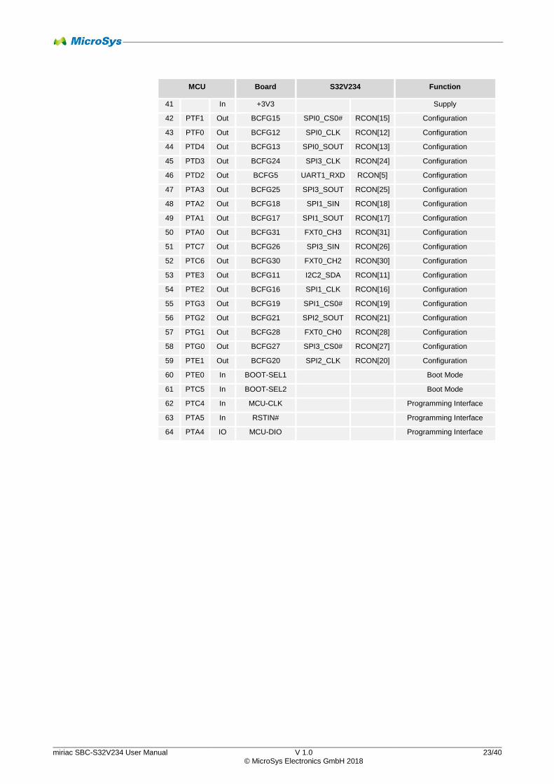
miriac SBC-S32V234 User Manual V 1.0 23/40 © MicroSys Electronics GmbH 2018
MCU Board S32V234 Function
41 In +3V3 Supply
42 PTF1 Out BCFG15 SPI0_CS0# RCON[15] Configuration
43 PTF0 Out BCFG12 SPI0_CLK RCON[12] Configuration
44 PTD4 Out BCFG13 SPI0_SOUT RCON[13] Configuration
45 PTD3 Out BCFG24 SPI3_CLK RCON[24] Configuration
46 PTD2 Out BCFG5 UART1_RXD RCON[5] Configuration
47 PTA3 Out BCFG25 SPI3_SOUT RCON[25] Configuration
48 PTA2 Out BCFG18 SPI1_SIN RCON[18] Configuration
49 PTA1 Out BCFG17 SPI1_SOUT RCON[17] Configuration
50 PTA0 Out BCFG31 FXT0_CH3 RCON[31] Configuration
51 PTC7 Out BCFG26 SPI3_SIN RCON[26] Configuration
52 PTC6 Out BCFG30 FXT0_CH2 RCON[30] Configuration
53 PTE3 Out BCFG11 I2C2_SDA RCON[11] Configuration
54 PTE2 Out BCFG16 SPI1_CLK RCON[16] Configuration
55 PTG3 Out BCFG19 SPI1_CS0# RCON[19] Configuration
56 PTG2 Out BCFG21 SPI2_SOUT RCON[21] Configuration
57 PTG1 Out BCFG28 FXT0_CH0 RCON[28] Configuration
58 PTG0 Out BCFG27 SPI3_CS0# RCON[27] Configuration
59 PTE1 Out BCFG20 SPI2_CLK RCON[20] Configuration
60 PTE0 In BOOT-SEL1 Boot Mode
61 PTC5 In BOOT-SEL2 Boot Mode
62 PTC4 In MCU-CLK Programming Interface
63 PTA5 In RSTIN# Programming Interface
64 PTA4 IO MCU-DIO Programming Interface

miriac SBC-S32V234 User Manual V 1.0 24/40 © MicroSys Electronics GmbH 2018
5 MPX Module The MPX-S32V234 miriac module has a 314-pin MXM connector and must be
mounted with a heatsink. It can be fixed with M2.5 screws through four 2.7mm
holes in the PCB.
MPX-S32V234 MXM Connector
Manufacturer: JAE
Type: MM70-314-310-B1-1
mates with: PCB Edge Connector
5.1 Mounting/Unmounting
The mounting or unmounting of the module should only be made in a static free
area with full ESD precautions, i.e. as a minimum, a grounded dissipative work
surface of sufficient size and a grounded skin contact wrist strap are necessary.
Make sure, that all parts, the carrier, the module and the heatsink are placed on the
same static free area to avoid any discharges between them during assembly.
To mount the MPX-S32V234 module, make sure that the carrier is disconnected
from any power or other IO interfaces. Both connector surfaces of the module must
be clean as well as the carrier connector should be checked for bent or dirty
contacts. Check the module and the carrier for foreign or loose parts, which do not
belong to the boards. The screws should have clean threads and be tightened with
a maximum torque of 30Ncm.
Insert or remove the MPX-S32V234 module always by an angle of about 25° as
shown in the following figure.
The thermal conduction between cooler and CPU must be performed via a thermal
pad. Make sure that this thermal pad has the correct thickness and is placed over
the CPU package before mounting the heatsink.
For the removal of the module, first unplug all connections to the system. Remove the inner screws, then the outer ones. The thermal pad may cause the heatsink to stick to the module, so take care when pulling them apart to avoid damaging any part of the module. Lift the module to about 25°and remove it from the connector. Store the parts on a static free area.
miriac SBC-S32V234 User Manual V 1.0 25/40 © MicroSys Electronics GmbH 2018
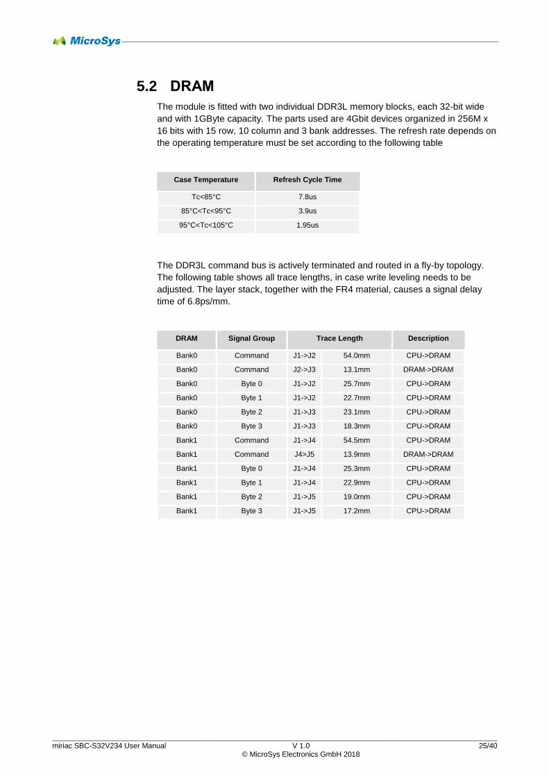
5.2 DRAM
The module is fitted with two individual DDR3L memory blocks, each 32-bit wide
and with 1GByte capacity. The parts used are 4Gbit devices organized in 256M x
16 bits with 15 row, 10 column and 3 bank addresses. The refresh rate depends on
the operating temperature must be set according to the following table
Case Temperature Refresh Cycle Time
Tc<85°C 7.8us
85°C<Tc<95°C 3.9us
95°C<Tc<105°C 1.95us
The DDR3L command bus is actively terminated and routed in a fly-by topology.
The following table shows all trace lengths, in case write leveling needs to be
adjusted. The layer stack, together with the FR4 material, causes a signal delay
time of 6.8ps/mm.
DRAM Signal Group Trace Length Description
Bank0 Command J1->J2 54.0mm CPU->DRAM
Bank0 Command J2->J3 13.1mm DRAM->DRAM
Bank0 Byte 0 J1->J2 25.7mm CPU->DRAM
Bank0 Byte 1 J1->J2 22.7mm CPU->DRAM
Bank0 Byte 2 J1->J3 23.1mm CPU->DRAM
Bank0 Byte 3 J1->J3 18.3mm CPU->DRAM
Bank1 Command J1->J4 54.5mm CPU->DRAM
Bank1 Command J4>J5 13.9mm DRAM->DRAM
Bank1 Byte 0 J1->J4 25.3mm CPU->DRAM
Bank1 Byte 1 J1->J4 22.9mm CPU->DRAM
Bank1 Byte 2 J1->J5 19.0mm CPU->DRAM
Bank1 Byte 3 J1->J5 17.2mm CPU->DRAM
miriac SBC-S32V234 User Manual V 1.0 26/40 © MicroSys Electronics GmbH 2018
5.3 eMMC
The local boot device of the MPX-S32V234 module is realized as an eMMC. The
MTFC16GAKAENA-4M-IT from Micron uses the 8-bit wide data bus, provided by
the µSDHC module of the S32V234. This interface is shared between the external
storage devices on the carrier board and the local eMMC. The selection can be
either made by the setting of a CPU GPIO pin or via the MCU. Per default, the
multiplexing is done through the MCU by the setting of the boot mode switch.
The reset input of the eMMC device is connected to port PTB7 of the MCU. In case
this port is not configured, the FRSTI# signal is tied to +3.3V by a pullup resistor.
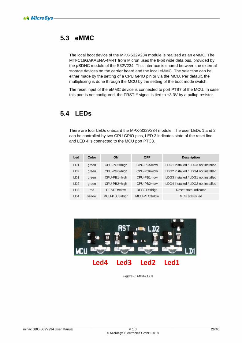
5.4 LEDs
There are four LEDs onboard the MPX-S32V234 module. The user LEDs 1 and 2
can be controlled by two CPU GPIO pins, LED 3 indicates state of the reset line
and LED 4 is connected to the MCU port PTC3.
Led Color ON OFF Description
LD1 green CPU-PG5=high CPU-PG5=low LDG1 installed / LDG3 not installed
LD2 green CPU-PG6=high CPU-PG6=low LDG2 installed / LDG4 not installed
LD1 green CPU-PB1=high CPU-PB1=low LDG3 installed / LDG1 not installed
LD2 green CPU-PB2=high CPU-PB2=low LDG4 installed / LDG2 not installed
LD3 red RESET#=low RESET#=high Reset state indicator
LD4 yellow MCU-PTC3=high MCU-PTC3=low MCU status led
Figure 8: MPX-LEDs
miriac SBC-S32V234 User Manual V 1.0 27/40 © MicroSys Electronics GmbH 2018
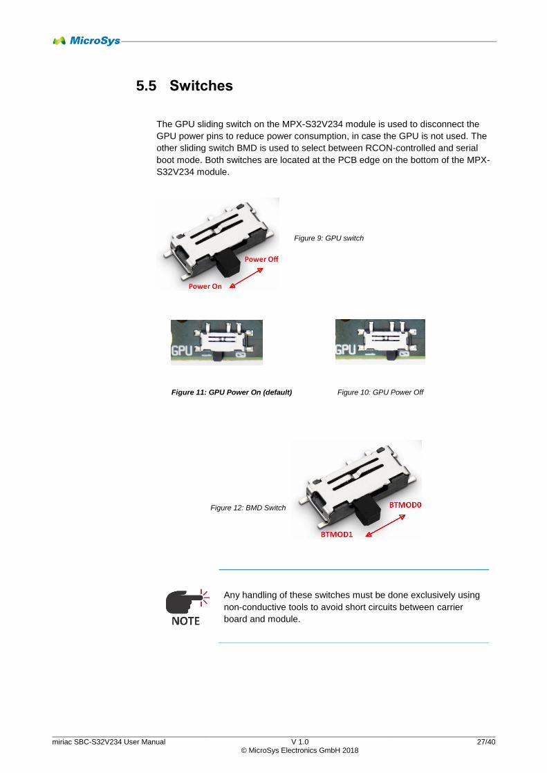
5.5 Switches
The GPU sliding switch on the MPX-S32V234 module is used to disconnect the
GPU power pins to reduce power consumption, in case the GPU is not used. The
other sliding switch BMD is used to select between RCON-controlled and serial
boot mode. Both switches are located at the PCB edge on the bottom of the MPX-
S32V234 module.
Any handling of these switches must be done exclusively using
non-conductive tools to avoid short circuits between carrier
board and module.
Figure 9: GPU switch
Figure 12: BMD Switch
Figure 11: GPU Power On (default) Figure 10: GPU Power Off
miriac SBC-S32V234 User Manual V 1.0 28/40 © MicroSys Electronics GmbH 2018
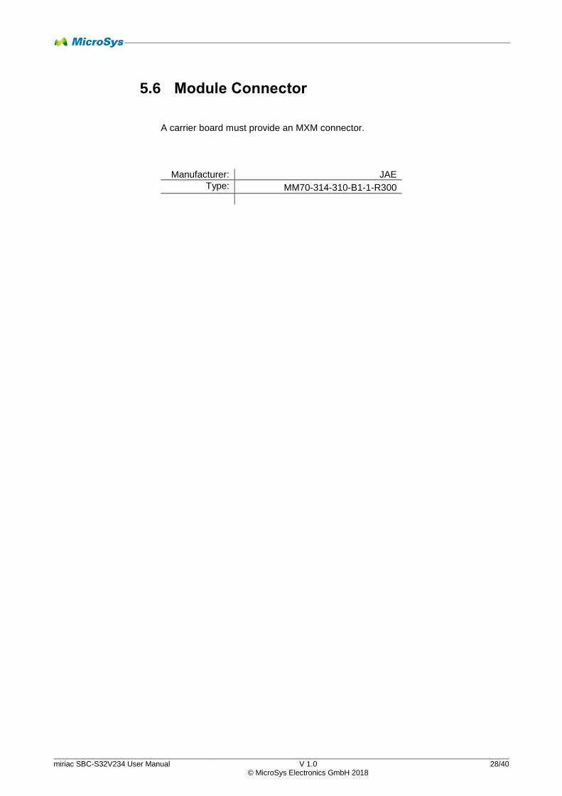
5.6 Module Connector
A carrier board must provide an MXM connector.
Manufacturer: JAE
Type: MM70-314-310-B1-1-R300
miriac SBC-S32V234 User Manual V 1.0 29/40 © MicroSys Electronics GmbH 2018
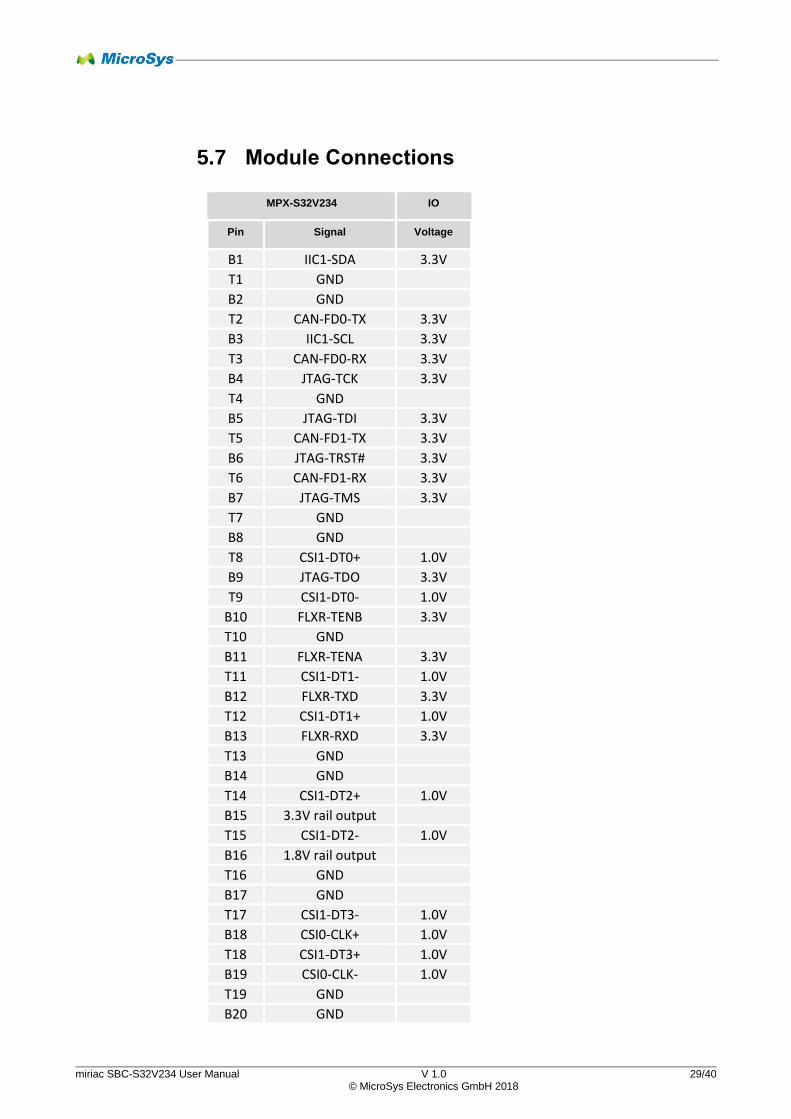
5.7 Module Connections
MPX-S32V234 IO
Pin Signal Voltage
B1 IIC1-SDA 3.3V
T1 GND
B2 GND
T2 CAN-FD0-TX 3.3V
B3 IIC1-SCL 3.3V
T3 CAN-FD0-RX 3.3V
B4 JTAG-TCK 3.3V
T4 GND
B5 JTAG-TDI 3.3V
T5 CAN-FD1-TX 3.3V
B6 JTAG-TRST# 3.3V
T6 CAN-FD1-RX 3.3V
B7 JTAG-TMS 3.3V
T7 GND
B8 GND
T8 CSI1-DT0+ 1.0V
B9 JTAG-TDO 3.3V
T9 CSI1-DT0- 1.0V
B10 FLXR-TENB 3.3V
T10 GND
B11 FLXR-TENA 3.3V
T11 CSI1-DT1- 1.0V
B12 FLXR-TXD 3.3V
T12 CSI1-DT1+ 1.0V
B13 FLXR-RXD 3.3V
T13 GND
B14 GND
T14 CSI1-DT2+ 1.0V
B15 3.3V rail output
T15 CSI1-DT2- 1.0V
B16 1.8V rail output
T16 GND
B17 GND
T17 CSI1-DT3- 1.0V
B18 CSI0-CLK+ 1.0V
T18 CSI1-DT3+ 1.0V
B19 CSI0-CLK- 1.0V
T19 GND
B20 GND
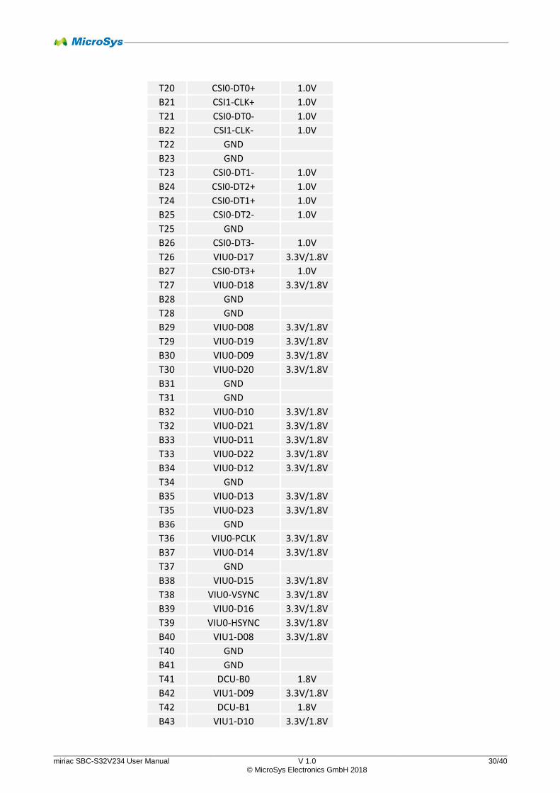
miriac SBC-S32V234 User Manual V 1.0 30/40 © MicroSys Electronics GmbH 2018
T20 CSI0-DT0+ 1.0V
B21 CSI1-CLK+ 1.0V
T21 CSI0-DT0- 1.0V
B22 CSI1-CLK- 1.0V
T22 GND
B23 GND
T23 CSI0-DT1- 1.0V
B24 CSI0-DT2+ 1.0V
T24 CSI0-DT1+ 1.0V
B25 CSI0-DT2- 1.0V
T25 GND
B26 CSI0-DT3- 1.0V
T26 VIU0-D17 3.3V/1.8V
B27 CSI0-DT3+ 1.0V
T27 VIU0-D18 3.3V/1.8V
B28 GND
T28 GND
B29 VIU0-D08 3.3V/1.8V
T29 VIU0-D19 3.3V/1.8V
B30 VIU0-D09 3.3V/1.8V
T30 VIU0-D20 3.3V/1.8V
B31 GND
T31 GND
B32 VIU0-D10 3.3V/1.8V
T32 VIU0-D21 3.3V/1.8V
B33 VIU0-D11 3.3V/1.8V
T33 VIU0-D22 3.3V/1.8V
B34 VIU0-D12 3.3V/1.8V
T34 GND
B35 VIU0-D13 3.3V/1.8V
T35 VIU0-D23 3.3V/1.8V
B36 GND
T36 VIU0-PCLK 3.3V/1.8V
B37 VIU0-D14 3.3V/1.8V
T37 GND
B38 VIU0-D15 3.3V/1.8V
T38 VIU0-VSYNC 3.3V/1.8V
B39 VIU0-D16 3.3V/1.8V
T39 VIU0-HSYNC 3.3V/1.8V
B40 VIU1-D08 3.3V/1.8V
T40 GND
B41 GND
T41 DCU-B0 1.8V
B42 VIU1-D09 3.3V/1.8V
T42 DCU-B1 1.8V
B43 VIU1-D10 3.3V/1.8V
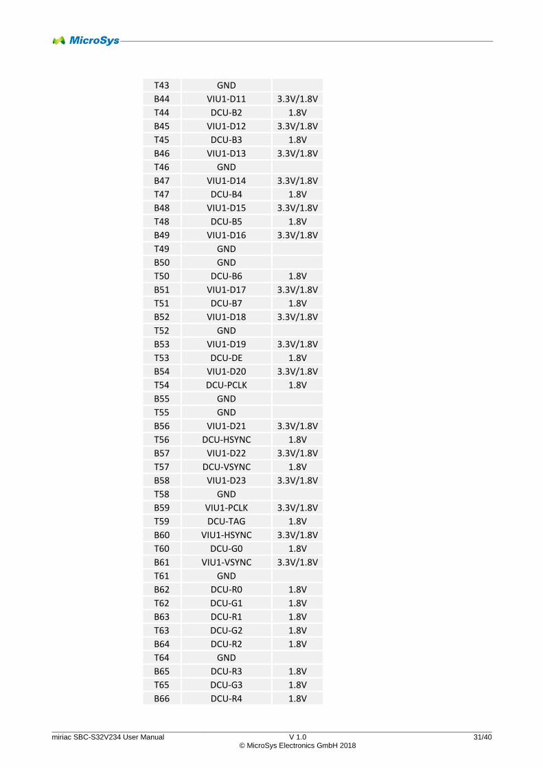
miriac SBC-S32V234 User Manual V 1.0 31/40 © MicroSys Electronics GmbH 2018
T43 GND
B44 VIU1-D11 3.3V/1.8V
T44 DCU-B2 1.8V
B45 VIU1-D12 3.3V/1.8V
T45 DCU-B3 1.8V
B46 VIU1-D13 3.3V/1.8V
T46 GND
B47 VIU1-D14 3.3V/1.8V
T47 DCU-B4 1.8V
B48 VIU1-D15 3.3V/1.8V
T48 DCU-B5 1.8V
B49 VIU1-D16 3.3V/1.8V
T49 GND
B50 GND
T50 DCU-B6 1.8V
B51 VIU1-D17 3.3V/1.8V
T51 DCU-B7 1.8V
B52 VIU1-D18 3.3V/1.8V
T52 GND
B53 VIU1-D19 3.3V/1.8V
T53 DCU-DE 1.8V
B54 VIU1-D20 3.3V/1.8V
T54 DCU-PCLK 1.8V
B55 GND
T55 GND
B56 VIU1-D21 3.3V/1.8V
T56 DCU-HSYNC 1.8V
B57 VIU1-D22 3.3V/1.8V
T57 DCU-VSYNC 1.8V
B58 VIU1-D23 3.3V/1.8V
T58 GND
B59 VIU1-PCLK 3.3V/1.8V
T59 DCU-TAG 1.8V
B60 VIU1-HSYNC 3.3V/1.8V
T60 DCU-G0 1.8V
B61 VIU1-VSYNC 3.3V/1.8V
T61 GND
B62 DCU-R0 1.8V
T62 DCU-G1 1.8V
B63 DCU-R1 1.8V
T63 DCU-G2 1.8V
B64 DCU-R2 1.8V
T64 GND
B65 DCU-R3 1.8V
T65 DCU-G3 1.8V
B66 DCU-R4 1.8V
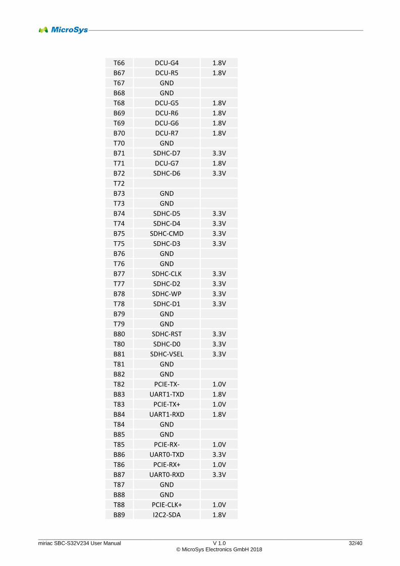
miriac SBC-S32V234 User Manual V 1.0 32/40 © MicroSys Electronics GmbH 2018
T66 DCU-G4 1.8V
B67 DCU-R5 1.8V
T67 GND
B68 GND
T68 DCU-G5 1.8V
B69 DCU-R6 1.8V
T69 DCU-G6 1.8V
B70 DCU-R7 1.8V
T70 GND
B71 SDHC-D7 3.3V
T71 DCU-G7 1.8V
B72 SDHC-D6 3.3V
T72
B73 GND
T73 GND
B74 SDHC-D5 3.3V
T74 SDHC-D4 3.3V
B75 SDHC-CMD 3.3V
T75 SDHC-D3 3.3V
B76 GND
T76 GND
B77 SDHC-CLK 3.3V
T77 SDHC-D2 3.3V
B78 SDHC-WP 3.3V
T78 SDHC-D1 3.3V
B79 GND
T79 GND
B80 SDHC-RST 3.3V
T80 SDHC-D0 3.3V
B81 SDHC-VSEL 3.3V
T81 GND
B82 GND
T82 PCIE-TX- 1.0V
B83 UART1-TXD 1.8V
T83 PCIE-TX+ 1.0V
B84 UART1-RXD 1.8V
T84 GND
B85 GND
T85 PCIE-RX- 1.0V
B86 UART0-TXD 3.3V
T86 PCIE-RX+ 1.0V
B87 UART0-RXD 3.3V
T87 GND
B88 GND
T88 PCIE-CLK+ 1.0V
B89 I2C2-SDA 1.8V
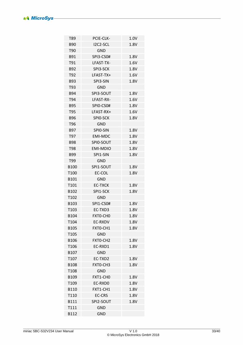
miriac SBC-S32V234 User Manual V 1.0 33/40 © MicroSys Electronics GmbH 2018
T89 PCIE-CLK- 1.0V
B90 I2C2-SCL 1.8V
T90 GND
B91 SPI3-CS0# 1.8V
T91 LFAST-TX- 1.6V
B92 SPI3-SCK 1.8V
T92 LFAST-TX+ 1.6V
B93 SPI3-SIN 1.8V
T93 GND
B94 SPI3-SOUT 1.8V
T94 LFAST-RX- 1.6V
B95 SPI0-CS0# 1.8V
T95 LFAST-RX+ 1.6V
B96 SPI0-SCK 1.8V
T96 GND
B97 SPI0-SIN 1.8V
T97 EMI-MDC 1.8V
B98 SPI0-SOUT 1.8V
T98 EMI-MDIO 1.8V
B99 SPI1-SIN 1.8V
T99 GND
B100 SPI1-SOUT 1.8V
T100 EC-COL 1.8V
B101 GND
T101 EC-TXCK 1.8V
B102 SPI1-SCK 1.8V
T102 GND
B103 SPI1-CS0# 1.8V
T103 EC-TXD3 1.8V
B104 FXT0-CH0 1.8V
T104 EC-RXDV 1.8V
B105 FXT0-CH1 1.8V
T105 GND
B106 FXT0-CH2 1.8V
T106 EC-RXD1 1.8V
B107 GND
T107 EC-TXD2 1.8V
B108 FXT0-CH3 1.8V
T108 GND
B109 FXT1-CH0 1.8V
T109 EC-RXD0 1.8V
B110 FXT1-CH1 1.8V
T110 EC-CRS 1.8V
B111 SPI2-SOUT 1.8V
T111 GND
B112 GND
miriac SBC-S32V234 User Manual V 1.0 34/40 © MicroSys Electronics GmbH 2018
T112 EC-RXER 1.8V
B113 SPI2-SCK 1.8V
T113 EC-TXER 1.8V
B114 SPI2-SIN 1.8V
T114 GND
B115 GND
T115 EC-RXD3 1.8V
B116 SPI2-CS0# 1.8V
T116 EC-TXEN 1.8V
B117 ENET-T0 1.8V
T117 GND
B118 ENET-T1 1.8V
T118 EC-RXD2 1.8V
B119 ENET-T2 3.3V
T119 EC-TXD0 1.8V
B120 TRACE-D00 1.8V
T120 GND
B121 TRACE-D02 1.8V
T121 EC-RXCK 1.8V
B122 TRACE-D04 1.8V
T122 EC-TXD1 1.8V
B123 TRACE-D06 1.8V
T123 GND
B124 GND
T124 TRACE-CLK 1.8V
B125 TRACE-D08 1.8V
T125 TRACE-D01 1.8V
B126 TRACE-D10 1.8V
T126 GND
B127 TRACE-D12 1.8V
T127 TRACE-D03 1.8V
B128 TRACE-D14 1.8V
T128 TRACE-D05 1.8V
B129 GND
T129 GND
B130 BOOT-SEL1 3.3V
T130 TRACE-D07 1.8V
B131 BOOT-SEL2 3.3V
T131 TRACE-D09 1.8V
B132 RSTIN# 3.3V
T132 GND
B133 VRTC 3.3V
T133 TRACE-D11 1.8V
B134 GND
T134 TRACE-D13 1.8V
B135 I2C0-SCL 3.3V
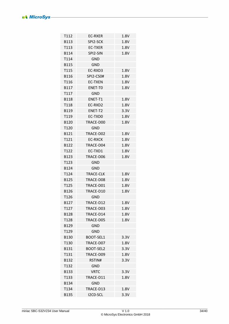
miriac SBC-S32V234 User Manual V 1.0 35/40 © MicroSys Electronics GmbH 2018
T135 TRACE-D15 1.8V
B136 I2C0-SDA 3.3V
T136 RSTOUT# 3.3V
B137 MCU-DIO 3.3V
T137 GND
B138 MCU-CLK 3.3V
T138 GND
B139 GND
T139 GND
B140 GND
T140 GND
B141 GND
T141 GND
B142 GND
T142 GND
B143 GND
T143 GND
B144 GND
T144 GND
B145 GND
T145 GND
B146 GND
T146 +VIN
B147 GND
T147 +VIN
B148 +VIN
T148 +VIN
B149 +VIN
T149 +VIN
B150 +VIN
T150 +VIN
B151 +VIN
T151 +VIN
B152 +VIN
T152 +VIN
B153 +VIN
T153 +VIN
B154 +VIN
T154 +VIN
B155 +VIN
B156 +VIN
miriac SBC-S32V234 User Manual V 1.0 36/40 © MicroSys Electronics GmbH 2018
6 JTAG Chain
6.1.1 JTAG Devices
The JTAG chain of the MPX-S32V234 only includes the S32V234 processor. The
JTAG port is directly connected to the MXM connector.
miriac SBC-S32V234 User Manual V 1.0 37/40 © MicroSys Electronics GmbH 2018
7 ADC
7.1.1 ADC Channles
The ADC converter contained in the S32V234 processor has 8 multiplexed single-
ended channels. They can be directly accessed via the 18-pin ZIF connector ADC
on the bottom side of the module.
There is no protection on any ADC line against
overvoltage or wrong polarity. Refer to the S32V234
datasheet for maximum ratings
miriac SBC-S32V234 User Manual V 1.0 38/40 © MicroSys Electronics GmbH 2018
8 I²C Structure The MPX-S32V234 operates three different I²C busses.
I²C Bus 0 and 1 are not used onboard the MPX-S32V234.
I²C Bus 2 controls all devices on the module.
8.1.1 Bus Map
I²C Bus 0:
Address Reference Device Function
0x00-0x7F --- --- External devices
Table 4 I²C0 bus map
I²C Bus 1:
Address Reference Device Function
0x00-0x7F --- --- External devices
Table 5 I²C1 bus map
I²C Bus 2:
Address Reference Device Function
0x51 J25 PCF85263A Real Time Clock
Table 6 I²C2 bus map
8.1.2 I²C Devices
8.1.2.1 RTC
The RTC PCF85263A provides year, month, day, weekday, hours, minutes,
seconds and 100th seconds. It can be protected against data loss by the backup
battery located on the CRX-S32V carrier.
It is accessible via I²C Bus 2 at the 7-bit address 0x51. It offers a time stamp input
and an interrupt output, which are both connected to the MCU.
8.1.2.2 RTC Backup Battery
The battery back can be accessed via the MXM connector on pin B133. It should
not exceed a maimum voltage of 3.3V. The battery type should have a nominal
voltage of 3.0V. The backup is necessary to keep time and date of the real-time
clock on the MPX-S32V234 module.
miriac SBC-S32V234 User Manual V 1.0 39/40 © MicroSys Electronics GmbH 2018
9 Appendix
9.1 Acronyms
These acronyms are being used within the document; note that this list does not
claim to be complete or exhaustive:
ADAS ........................................................................Advanced Driver Assistance Systems
ARM ............................................................................................ Advanced RISC Machine
BaseT .................................................................... Ethernet over twisted pair technologies
BIST .......................................................................................................... Built In Self-Test
CAN-FD .................................................... Controller Area Network with Flexible Data rate
CEC ..................................................................................... Consumer Electronics Control
Cortex-M4 ...................................................................................... ARMv7E-M architecture
CPU ............................................................................................... Central Processing Unit
CR2032 ......................................................................................... IEC standard button cell
CSI ................................................................................................ Camera Serial Interface
DDC .................................................................................................. Display Data Channel
eMMC ...................................................................................... embedded Multimedia Card
ESD ................................................................................................ Electrostatic Discharge
FR4 ........................................................................................................... flame retardant 4
GND ........................................................................................................................ Ground
GPIO ................................................................................................... General Purpose IO
GPL ................................................................................................ General Public License
GPU .............................................................................................. Graphic Processing Unit
HDMI .......................................................................... High-Definition Multimedia Interface
I²C .................................................................................................... Inter-Integrated Circuit
JTAG .............................................................................................. Joint Test Action Group
Kinetis ............................................................................................ ARM® Cortex-M0+ core
LAN ...................................................................................................... Local Area Network
LED ..................................................................................................... Light Emitting Diode
LIN ............................................................................................ Local Interconnect Network
MCU ..................................................................................................... Microcontroller Unit
MIPI ........................................................................... Mobile Industry Processor Interface
MPX ............................................................................................... MicroSys miriac Module
MXM ........................................................................................ Mobile PCI-Express Module
POL ............................................................................................................. Point Of Load
PPTC ............................................................. Polymeric Positive Temperature Coefficient
RCON .................................................................................................. Reset Configuration
RJ45 ..................................................................................................... Registered Jack 45
RTC ........................................................................................................... Real Time Clock
SBC ................................................................................................ Single Board Computer
SOM ......................................................................................................System On Module
TFTP ...................................................................................... Trivial File Transfer Protocol
TVS ...................................................................................... Transient Voltage Suppressor
UART .......................................................... Universal Asynchronous Receiver Transmitter
U-Boot ...................................................................................... The Universal Boot Loader
USB ..................................................................................................... Universal Serial Bus
miriac SBC-S32V234 User Manual V 1.0 40/40 © MicroSys Electronics GmbH 2018
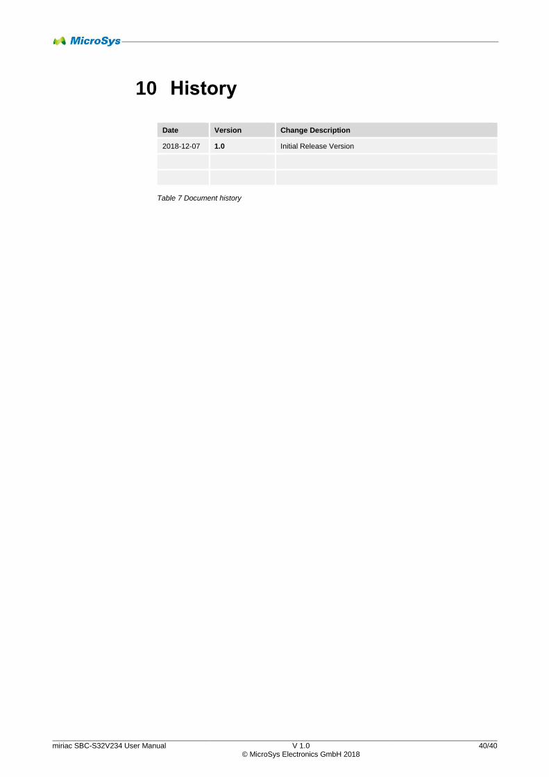
10 History
Date Version Change Description
2018-12-07 1.0 Initial Release Version
Table 7 Document history


![LIABILITY FOR NEGLIGENCE IN THE AUSTRALIAN FITNESS … · 2018-07-18 · [2.0] Sources of Negligence Law [2.1] Introduction to the Civil Liability Acts The elements of the tort of](https://img.pdfslide.net/doc/110x75/5e850f21800e992a5f3a1038/liability-for-negligence-in-the-australian-fitness-2018-07-18-20-sources-of.jpg)