Embed Size (px)
Citation preview
The contents of this document are owned or controlled by S3 Group and are protected under applicable copyright and/or
trademark laws. The contents of this document may only be used or copied in accordance with a written contract with S3 Group or
with the express written permission of S3 Group. All trademarks contained herein (whether registered or not) and all associated
rights are recognized.
Mixed Signal Design & Verification Methodology for Complex SoCs
White Paper
Nov 12 Mixed Signal Design & Verification Methodology for Complex SoCs 2
Copyright The contents of this document are owned or controlled by S3 Group and are
protected under applicable copyright and/or trademark laws. The contents of this
document may only be used or copied in accordance with a written contract with S3
Group or with the express written permission of S3 Group.
All trademarks contained herein (whether registered or not) and all associated rights
are recognized.
Document Owner: S3 Group, Silicon Business
Document Title: Mixed Signal Design & Verification Methodology for Complex S0Cs
Version: 1.0
Publication Date: Dec 2013
Authors:
Donnacha O’Riordan, Director of Services Strategy
Cormac O’Sullivan, RF Technical Lead
© S3 Group 2008 - 2013
Email: [email protected]
Web: http://www.s3group.com/silicon
Feb-11 Mixed Signal Design & Verification Methodology for Complex SoCs 3
Table of Contents
1 ABSTRACT ....................................................................................................................... 4
2 INTRODUCTION ............................................................................................................... 5
3 DESIGN ENVIRONMENT ................................................................................................. 7
3.1 Process Framework ....................................................................................................................................... 7
3.2 Problem setting and solution......................................................................................................................... 7
3.3 Design Flow ..................................................................................................................................................... 8
3.3.1 Designing the model ................................................................................................................................................9
3.4 Calibration ...................................................................................................................................................... 10
3.5 System Level Testbench ............................................................................................................................. 11
3.5.1 A note on wreal use in System Level Verification .............................................................................................12
4 CHALLENGES ................................................................................................................ 14
5 CASE STUDY – LESSONS LEARNED ......................................................................... 15
5.1 Communication ............................................................................................................................................. 15
5.2 Respect the differences in the signal flow or domain .............................................................................. 15
5.3 Design/Verification is Iterative .................................................................................................................... 15
5.4 Reuse of the digital verification environment ............................................................................................ 16
6 CONCLUSIONS .............................................................................................................. 17
7 REFERENCES ................................................................................................................ 18

Mixed Signal Design & Verification Methodology for Complex SoCs 4
1 Abstract
This paper describes the design & verification methodology used on a recent large mixed signal
System on a Chip (SoCs) which contained radio frequency (RF), analog, mixed-signal and digital
blocks on one chip. We combine a top-down functional approach, based on early system-level
modelling, with a bottom-up performance approach based on transistor level simulations, in an
agile development methodology. We look at how real valued modelling, using the Verilog-AMS wire
that carries a real value (wreal) data type, achieves shorter simulation times in large SoCs with high
frequency RF sections, low bandwidth analogue base-band sections and appreciable digital
functionality including filtering and calibration blocks. We obtain further system level verification
and confirmation of block design through periodic S parameter analysis, which can allow
simulation of certain performance parameters (e.g., noise figure and gain) for a full analogue chain.
We discuss the importance of sub-block analogue co-simulation, along with the importance of
correlation between behavioural models and transistor level schematics to ensure representative
behaviour for the blocks. We use a recent complex SoC design as a Test Case to provide a practical
illustration of the problems that were encountered and the solutions employed to overcome these
problems.
Mixed Signal Design & Verification Methodology for Complex SoCs 5
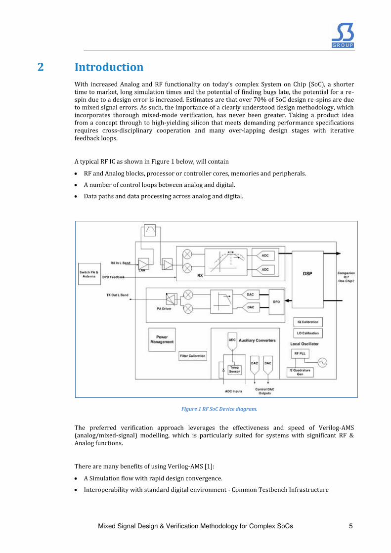
2 Introduction With increased Analog and RF functionality on today’s complex System on Chip (SoC), a shorter
time to market, long simulation times and the potential of finding bugs late, the potential for a re-
spin due to a design error is increased. Estimates are that over 70% of SoC design re-spins are due
to mixed signal errors. As such, the importance of a clearly understood design methodology, which
incorporates thorough mixed-mode verification, has never been greater. Taking a product idea
from a concept through to high-yielding silicon that meets demanding performance specifications
requires cross-disciplinary cooperation and many over-lapping design stages with iterative
feedback loops.
A typical RF IC as shown in Figure 1 below, will contain
RF and Analog blocks, processor or controller cores, memories and peripherals.
A number of control loops between analog and digital.
Data paths and data processing across analog and digital.
Figure 1 RF SoC Device diagram.
The preferred verification approach leverages the effectiveness and speed of Verilog-AMS
(analog/mixed-signal) modelling, which is particularly suited for systems with significant RF &
Analog functions.
There are many benefits of using Verilog-AMS [1]:
A Simulation flow with rapid design convergence.
Interoperability with standard digital environment - Common Testbench Infrastructure

Mixed Signal Design & Verification Methodology for Complex SoCs 6
Analog interface and connectivity of both analog and digital modules derived directly from a “Golden” top level schematic. Comprehensive system-level simulations and simulation of the digital/analog interface with a
self-checking mechanism e.g., An Ultrasim™ simulation of one analog subsystem took 3 weeks –
Verilog-AMS took 3 hours.
The next sections introduce the design and verification methodology used on a recent large mixed
signal SoC containing RF, analog, mixed-signal and digital blocks, followed by some of the
challenges typically faced in these type of designs and lessons learned illustrated by a case study.
Mixed Signal Design & Verification Methodology for Complex SoCs 7
3 Design Environment
3.1 Process Framework
We use a mature and proven process framework to guide projects to a successful end, utilizing the
most up-to-date process management models. Our framework incorporates CMMI (Capability
Maturity Model Integration) [2], an approach that provides a collection of best practices which
ensures continual process improvement.
We also follow PMBOK (A Guide to the Project Management Body of Knowledge [3]) as reference
models to guide our development of processes and practices for both project management and
product development.
All of our management processes are ISO 9001 standards compliant. This promotes the adoption of
a process approach to enhance customer satisfaction by meeting customer requirements. All S3
Group design centres are independently assessed and certified as meeting the requirements of ISO
9001.
3.2 Problem setting and solution
The challenge is to verify the design of mixed signal functions which are too complex for either a
digital simulator or too large circuit simulator. The use of behavioural models with Verilog-AMS for
verification reduces the probability of device defects caused by human error and allows rapid co-
simulation of complex analog and digital systems.
Digital simulators differ from analog simulation engines in that they are event driven and clocked,
they model signals from the initial input to response. As a result, no actual voltage or current
measurements are produced, but an output that is a 0, 1 or X. As the digital simulator functions in
real time, the power system algorithms are quickly calculated, producing an output that represents
conditions in a real system. In the analog domain, simulators calculate the state or operating point
of a complete circuit. It is a static, matrix calculation that is then repeated over small increments in
an attempt to model continuous time. At any given time, the output, voltage and current are known.
So then, the analog domain is contiguous while the digital is a discrete, event driven domain.
Verilog-AMS is a mixed domain language combining digital & analog constructs & statements run
within the Cadence® Incisive-AMS™ platform. In Verilog-AMS, both analog and digital domains are
partitioned, and co-simulated with their respective solvers. Interface elements are automatically
placed between analog and digital blocks when simulated. All analog and mixed-signal modules
require that ports and nodes associated with respective behavioural code have disciplines declared
for them.
Mixed Signal Design & Verification Methodology for Complex SoCs 8
The digital and analog sections interact by sharing data and controlling each other’s events. This allows for event-driven analog blocks. Verilog can be extended to support real value nets (wreal),
discussed further in Section 3.5.1.
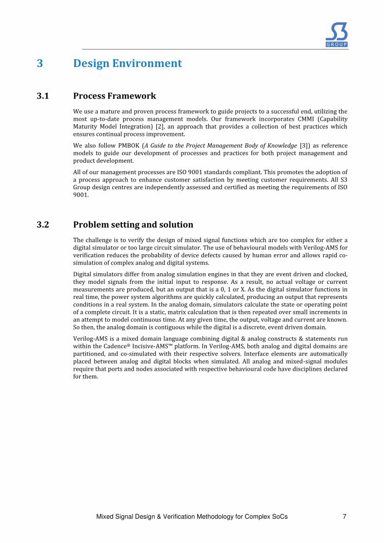
3.3 Design Flow
At a top level, the design flow appears like a traditional waterfall model, beginning with the System
Architecture, moving to the Block Design and ending with System Verification, as in Figure 2.
Figure 2 Traditional Design flow summary.
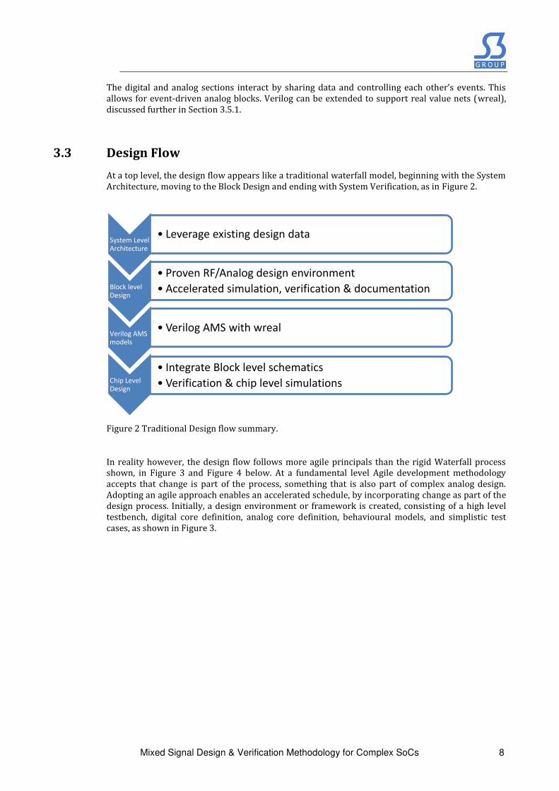
In reality however, the design flow follows more agile principals than the rigid Waterfall process
shown, in Figure 3 and Figure 4 below. At a fundamental level Agile development methodology
accepts that change is part of the process, something that is also part of complex analog design.
Adopting an agile approach enables an accelerated schedule, by incorporating change as part of the
design process. Initially, a design environment or framework is created, consisting of a high level
testbench, digital core definition, analog core definition, behavioural models, and simplistic test
cases, as shown in Figure 3.
System Level Architecture
• Leverage existing design data
Block level Design
• Proven RF/Analog design environment
• Accelerated simulation, verification & documentation
Verilog AMS models
• Verilog AMS with wreal
Chip Level Design
• Integrate Block level schematics
• Verification & chip level simulations
Mixed Signal Design & Verification Methodology for Complex SoCs 9
Figure 3 S3 Group Design flow Iteration 1
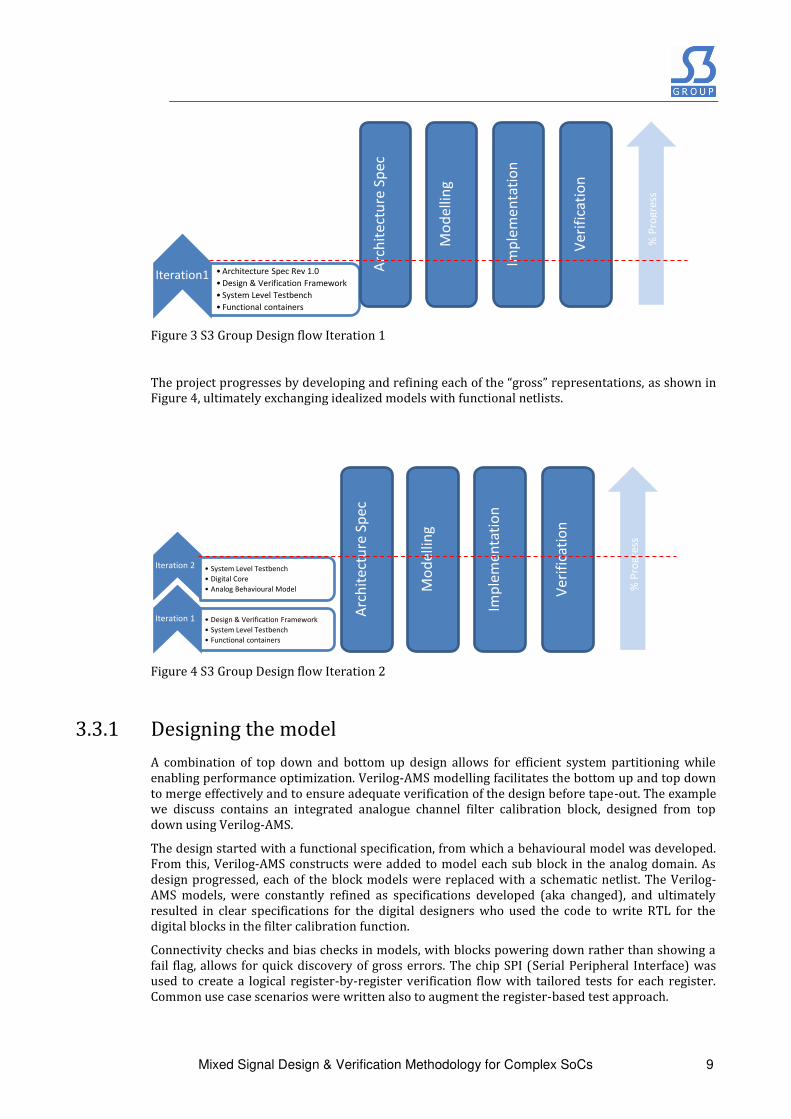
The project progresses by developing and refining each of the “gross” representations, as shown in
Figure 4, ultimately exchanging idealized models with functional netlists.
Figure 4 S3 Group Design flow Iteration 2
3.3.1 Designing the model A combination of top down and bottom up design allows for efficient system partitioning while
enabling performance optimization. Verilog-AMS modelling facilitates the bottom up and top down
to merge effectively and to ensure adequate verification of the design before tape-out. The example
we discuss contains an integrated analogue channel filter calibration block, designed from top
down using Verilog-AMS.
The design started with a functional specification, from which a behavioural model was developed.
From this, Verilog-AMS constructs were added to model each sub block in the analog domain. As
design progressed, each of the block models were replaced with a schematic netlist. The Verilog-
AMS models, were constantly refined as specifications developed (aka changed), and ultimately
resulted in clear specifications for the digital designers who used the code to write RTL for the
digital blocks in the filter calibration function.
Connectivity checks and bias checks in models, with blocks powering down rather than showing a
fail flag, allows for quick discovery of gross errors. The chip SPI (Serial Peripheral Interface) was
used to create a logical register-by-register verification flow with tailored tests for each register.
Common use case scenarios were written also to augment the register-based test approach.
Iteration1 •Architecture Spec Rev 1.0
•Design & Verification Framework
• System Level Testbench
• Functional containers
Iteration 2 • System Level Testbench
• Digital Core
• Analog Behavioural Model
Iteration 1 • Design & Verification Framework
• System Level Testbench
• Functional containers
Ve
rifi
cati
on
Arc
hit
ect
ure
Sp
ec
Mo
de
llin
g
Imp
lem
en
tati
on
% P
rog
ress
Ve
rifi
cati
on
Arc
hit
ect
ure
Sp
ec
Mo
de
llin
g
Imp
lem
en
tati
on
% P
rog
ress
Mixed Signal Design & Verification Methodology for Complex SoCs 10
Block analog model development followed these general guidelines [1]:
Use top-down design.
Model at the appropriate level, beginning with behavioural Verilog models
Create Verilog-AMS from behavioural views, viewed directly from the symbol. This ensures
correct pin names and port order. Use the on-line editor for code syntax checking.
Calibrate. Perform block level testbench work within chosen verification tool, this allows use of
the same testbench as the schematic i.e., Verilog-AMS view is verified with circuit level
simulator. Keep external analog components technology independent.
Complexity. Model all core functionality and test modes.
Chip convergence, digital control signals could be x or z at start up – accessing an x or z in an
analog process is an error.
Minimize the use of connect modules, used to connect analog & digital domains, to lower
simulation overhead for high-speed signals.
Avoid hard-coding values, use variables and parameters. Use parameters to vary test case
operating conditions.
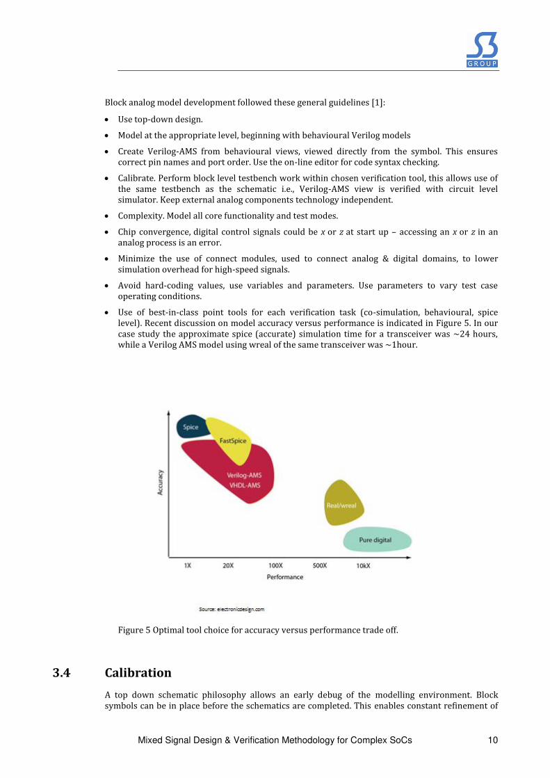
Use of best-in-class point tools for each verification task (co-simulation, behavioural, spice
level). Recent discussion on model accuracy versus performance is indicated in Figure 5. In our
case study the approximate spice (accurate) simulation time for a transceiver was ~24 hours,
while a Verilog AMS model using wreal of the same transceiver was ~1hour.
Figure 5 Optimal tool choice for accuracy versus performance trade off.
3.4 Calibration
A top down schematic philosophy allows an early debug of the modelling environment. Block
symbols can be in place before the schematics are completed. This enables constant refinement of
Mixed Signal Design & Verification Methodology for Complex SoCs 11
each model, as the representation progresses from high level models to a final netlist. This early
approach is vital to allow adequate validation of control loops, including automatic gain control
(AGC), digital pre-distortion (DPD) and local oscillator (LO) feed-through calibration.
3.5 System Level Testbench
The system level testbench re-uses the digital core testbench, with a “containers” for digital & analog cores. Simulations require a System Verilog/Verilog testbench, and use of high-level
constructs of the language to monitor responses and data generation. Coupled with the design, the
test bench creates a simulation model used by a simulation engine. Part of the Cadence Verification
tool suite, Simvision™ is used as the waveform viewer [4, 5]. Operating Simvision™ in 64-bit mode
is a more robust approach for the large simulation databases that often result from top-level
simulations.
A stable & central database allows consistency and avoids test cases failing on incremental changes,
or on bugs already addressed. The testbench contains all of the necessary components for
verification. The SoC is attached to the testbench, which provides inputs to drive the device while
the output is monitored [6].
Verilog parameters are constants, typically used to specify the width of variables and time delays,
declared within the module structure. The assigned values define a set of attributes for the module;
these characterize its behaviour as well as its physical representation. Changes to module
parameters are made with defparam statements. For example, to speed up simulation time for test
cases that do not require realistic power up sequences, a variable can be changed to allow blocks
power up more quickly for simulation purposes, as shown below.
`ifdef AMS
defparam funcdigital_tb.AMS_TB.car_freq = 161.48e6;
`endif
`ifdef AMS
defparam
funcdigital_tb.AMS_TB.DUT.I_funcanaloguetop.I_funcanalogue_core.I_S3ADIQ19M14BC18_1.I_S3ADIQ19M14BC1
8_1.trPWD = 60e-6;
defparam
funcdigital_tb.AMS_TB.DUT.I_funcanaloguetop.I_funcanalogue_core.I_S3ADIQ19M14BC18_2.I_S3ADIQ19M14BC1
8_1.trPWD = 60e-6;
`endif
A probe is a branch, at any location within the module, which is without an assigned value for either
the potential or the flow. Probing certain sub-block levels such as an analogue core assists
debugging, as not all required signals are known in advance:
probe -create funcdigital_tb.AMS_TB.DUT.I_funcanaloguetop.I_funcanalogue_core –all
For low signal levels, such as in a low noise amplifier (LNA) using wreal simulations, connect libs
may need to be modified to show accurate behaviour:
Mixed Signal Design & Verification Methodology for Complex SoCs 12
It is possible to edit the connect libs for a particular block, where small signals (<1mv) are used. To
customize connect libs for a block; we need to write an amscf.scs file, with the following example
showing how the vdelta (accuracy of wreal signal) can be changed for the LNA.
“ie vsup=1.8” applies to all block and loads the default connect libs.
“ie vsup=1.8 vdelta=1.8/64/100 cell="funcrxlna_top"” is applied to the LNA.
*AMS control file
amsd {
ie vsup=1.8
ie vsup=1.8 vdelta=1.8/64/100 cell="funcrxlna_top"
}
3.5.1 A note on wreal use in System Level Verification
Mixed-signal SoCs combine digital and analog circuitry on one chip. These circuits can be simulated,
but non-event-driven instructions are not practical when simulating mixed-signal devices. A
solution is the application of a real value (wreal) data type. Using wreal signals helps to bridge the
divide between pure analog simulation and full-chip analog/mixed signal (AMS) simulation. This is
necessary for two reasons: AMS simulation must account for the preponderance of digital content,
and the size of these chips means that higher simulation performance is needed than would be
remotely possible if you tried to simulate the entire chip at an analog level. With a wreal signal, you
can take a voltage or current (but not both) between modules of the full chip, enabling operation in
a signal-flow fashion thereby behaving more like a digital signal.
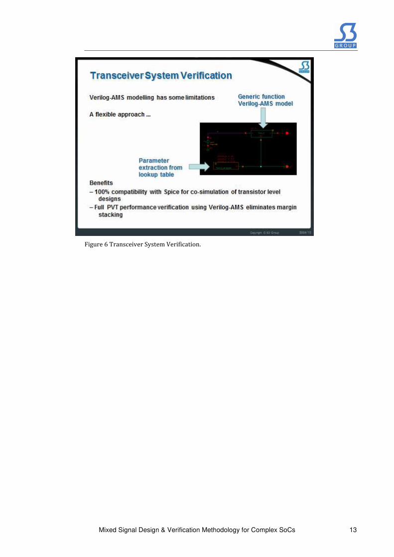
There are some limitations which at a block level can have significant system level implications, for
example specifying block models so that a worst case of block A works with worst case block B and
so on, which can lead to significant system overdesign. Our approach, shown in Figure 6, cascades
blocks for all corners using abstraction, which can improve efficiency by ~1dB per cascaded block.
A standard results format is preconfigured in the block verification environment. All key
performance specifications are stored for later use, in tables indexed by independent variables such
as external conditions (process, temperature and supply voltage) and also by control signals (gain
control or frequency tuning). This enables seamless migration from block level to system level
verification with minimal loss of information. The result is an environment which enables full chain
performance simulations over process voltage and temperature with very acceptable run-times.
Mixed Signal Design & Verification Methodology for Complex SoCs 13
Figure 6 Transceiver System Verification.
Mixed Signal Design & Verification Methodology for Complex SoCs 14
4 Challenges
To verify SoC power, functionality and timing there are a host of common challenges and errors
that all SoC designers have to overcome.
Specific challenges are laid out here and include:
There are usually at least two teams (analog and digital) designing the system and
communications between the teams is essential for a positive result. Code errors occur for
example, where one team assumes a specific encoding and the other assumes something
different. Problems may also occur when clear and consistent naming on IC architecture
and interface signals is lacking.
Flows are disconnected and inherently different. Analog signals are continuous, digital
signals are not. The verification process must simulate many types of circuit behaviour
including analog to digital interactions among nested analog and digital blocks, register-
transfer, gate and transistors.
A significant amount of focus goes into optimizing low level analog circuits, and block level functionality. Much less so at the analog “top-level”. Late changes. This is a problem which is not unique to analog/digital design but one that is
certain to occur in this discipline. The nature of the system dictates that the design of the
digital controller block cannot be completed until analog block is designed.
Other common problems encountered in mixed signal design include:
The models used in the design process must be testable, ready to run when the design
phase of the project is complete and must be able to support a modelling language, which is
not always the case.
A verification process must have the performance and capacity to insure accuracy within a
reasonable amount of time.
Inversion of control bits may occur when signal integrity analysis indicates a need for
additional buffering and the resulting logic is not verified appropriately.
If an analog block is part of the reset scheme of the system, then its output value may be
critical for the reset of any other blocks dependent on its output.
Mixed Signal Design & Verification Methodology for Complex SoCs 15
5 Case Study – Lessons Learned
As outlined in the previous section the specific challenges encountered include:
Analog and digital team communications,
Analog and digital flows are disconnected and inherently different,
Late changes
Efficient reuse of the digital verification environment.
5.1 Communication
Problem
Analog and digital teams: different worlds, different mind-sets, different terminology.
Solutions
Single team with a single team leader, ideally a technical lead engineer who is well-versed in both systems and who acts as a “liaison” between the teams, ensure cross-functional
communications.
Start the project with clear and consistent naming rules for the IC architecture and interfaces.
Development of a high level functional/architecture specification.
A focus on Use Cases and a common technological language.
5.2 Respect the differences in the signal flow or domain
Problem
Flows are disconnected and inherently different.
Solutions:
Use the appropriate tool or view for a given task e.g., modelling trade-off accuracy vs. speed.
Implement small digital macros for non-critical analog routing e.g., for the configuration bus or
decoders.
Use uniform data formats in analog and digital standalone environments, especially when a 3rd
party tool is involved e.g., Matlab data generators or files.
5.3 Design/Verification is Iterative
Problem
Late Changes in the project schedule. A digital controller design cannot be completed until the
associated analog block is designed & verified. However, to remain on what are normally tight
Mixed Signal Design & Verification Methodology for Complex SoCs 16
schedules, some degree of digital design work is necessary in parallel. In addition to design
sequencing challenges, is a constrained physical implementation, and the discovery of overall
performance issues outside the design specifications. These often require functional modifications
(e.g., in the power architecture or filtering changes).
Solutions
Adopt an Agile development methodology
Use simplified behavioural models for the analog blocks initially, developing Verilog-AMS
models as the design develops, eventually replacing AMS models with completed schematic
netlists.
Create a behavioural representation of digital blocks rather than creating the RTL in the early
stages of development.
Implement the digital controller core functionality and structural parts (state machine, interval
timers), while the analog blocks are under development.
Run several implementation iterations, each step requiring consistent views. The final
implementation will just configure the soft core RTL. This requires multiple runs of a full digital
flow RTL2-GDS2 tool set that is important for change impact analysis (area, power, routing).
Continuous reworking of the top-level schematic – co-simulation on netlist with “dummy” views. 5.4 Reuse of the digital verification environment
Problem
Digital standalone verification covers the majority of analog scenarios, but with some it may result
in questionable data.
Solutions
Build a test environment for digital standalone verification with an awareness of analog content
(constrain meaningful data for Use-Cases, Min-Mid-Max VGA code, ADC start-up, etc.)
Digital verification techniques like assertions and coverage are directly applicable to analog
design.
Interface monitors can be re-connected from digital boundary to analog blocks instances.
Design top-level mixed mode verification to be a rerun of the existing digital test.
A UVM based digital verification environment is easily reconfigurable for a co-simulation
environment.
Mixed Signal Design & Verification Methodology for Complex SoCs 17
6 Conclusions
Full chip verification of large RF & mixed signal SoCs, is a specialized discipline requiring
proportionally more of overall project effort as complexity grows. Complex dependencies and
interactions between analog and digital domains, can lead to performance and even functional
issues in silicon, resulting in re-spins the cost of which may run to millions of dollars, not just in
tapeout costs, but also in missed market opportunities.
Mixed mode design and verification requires team work, and effective communications are
essential in what is an iterative rather than linear process. A common language for RF, Analog &
digital design and verification engineers is critical for improving communications and
understanding between different roles on a team.
The application of agile development methods where appropriate, enables on-going changes in
specification or requirements be incorporated with minimal impact to schedule. In mixed signal
SoC verification change is a matter of course, where it’s the rule rather than the exception.
The analyses of interdependent RF, analog and digital data path loops – an essential capability
when targeting first-time-right silicon in advanced communication SoC design – is enabled by a
common test bench infrastructure with self-checking capability for analog, RF and digital signals.
Full chip verification of large RF/mixed signal SoCs, is a specialized discipline requiring a complex
mix of dedicated flows & methodology approaches and experience to be successful. Experience counts, where “it’s the magician, not the wand”, which enables first-time right silicon, on time, on
budget.
Mixed Signal Design & Verification Methodology for Complex SoCs 18
7 References
Design and Verification of Nanometer SoCs using AMS Designer.
Tony Blake, S3 Group, 2005.
http://www.cdnusers.org/community/virtuoso/resources/tp_CDNlive2005_1235_daire.pdf.
Accessed December 18, 1012
[2] CMMI Product Team (CMMI) 2010, CMMI for Development, Version 1.3 (Technical Report
CMU/SEI-2010-TR-033). Pittsburgh: Software Engineering Institute, Carnegie Mellon University.
http://www.sei.cmu.edu/library/abstracts/reports/10tr033.cfm Accessed December 10, 2012.
[3] American National Standard Institute/Project Management Institute (ANSI/PMI) 2004, A Guide
to the Project Management Body of Knowledge, (PMBOK Guide), 3rd edition, ANSI/PMI
99/001/2004.
[4] Creating Analog Behavioural Models: Verilog-AMS Analog Modelling, February 2003.
http://w2.cadence.com/appnotes/CDN_Creating_Analog_Behavioral_Models.pdf accessed
December 12, 2012.
[5] Cadence Analog/Mixed-Signal Design Methodology: Overview
http://www.cadence.com/rl/Resources/overview/ams_methodology_ov.pdf. Accessed December
17, 2012.
[6] Designers Guide Consulting: Analog, Mixed-Signal & RF Verification. Verification of Complex
Analog Integrated Circuits. Ken Kundert and Henry Chang, 2005. http://www.designers-
guide.com/docs/cicc06-dgc.pdf Accessed December 18, 2012

Mixed Signal Design & Verification Methodology for Complex SoCs 19
8 About Author
Donnacha has over 17 years’ experience in the semiconductor industry and is currently the
Director of Services Strategy at S3 Group where he is responsible for strategic, technical and
marketing aspects of all Services in the portfolio, ensuring alignment of Services, IP and
Product roadmaps and the development of strategic relationships across the whole silicon
value chain.
Cormac has over 12 years’ experience in RF design and is currently the RF & Mixed Signal Engineering team lead at S3 Group, where he is responsible for the Architecture & Design of RF
products & services, from concept and system partitioning through to Silicon validation and production support. His technical interests are in the field of low-power analog CMOS circuits,
RF IC, and RF system design and he has patented advanced technology in the area of RF
transmitter design and PLLs.
About S3 Group:
S3 Group delivers IP and professional services to OEMs, system vendors and semiconductor
companies. The company is the longest serving independent service provider in the industry,
building a wealth of experience and engineering expertise over the last 25 years. In addition to
design services the company has a comprehensive portfolio of RF and mixed-signal IP. The IP
portfolio includes high performance ADC and DAC converters, PLLs, Analog Front Ends (AFEs),
Power Management, RF Transceivers and other miscellaneous circuits which have been silicon
proven at a number of silicon foundries (TSMC, GlobalFoundries, UMC, SMIC, IBM, Tower) at
nodes ranging from 180nm to 40nm and below. Global end markets served by S3 Group clients
include Wireless and Wireline Communications, Digital Broadcasting, Imaging, Solar, Green
Energy and Industrial. Founded in 1986, S3 Group, headquartered in Dublin, Ireland, focuses on
three business areas: Semiconductor, TV Technology and Telehealth, and has development
centers in Ireland, Poland, the Czech Republic and Portugal with sales offices and
representatives worldwide.
For further information please visit:
www.s3group.com/silicon
and
www.twitter.com/S3Group_Silicon


![UNIVERSAL VERIFICATION METHODOLOGY BASED VERIFICATION ... · UNIVERSAL VERIFICATION METHODOLOGY BASED VERIFICATION ENVIRONMENT FOR PCIE DATA LINK LAYER Dr.T.C.Thanuja[1] , Akshata[2]](https://img.pdfslide.net/doc/110x75/5e769b33e234ad4a136bda09/universal-verification-methodology-based-verification-universal-verification.jpg)