Embed Size (px)
Citation preview

1
CHAPTER 1
Mixed-Signal Design Trends and ChallengesMladen Nizic
IntroductionWhat is mixed-signal design? There may be as many different answers as people asked. Most would agree that mixed-signal is a combination of analog and digital circuitry. This chapter will look at some basic characteristics of analog and digital signals and their differences.
Analog signals are continuous in time and amplitude. In other words, analog signals can take an infinite number of levels within a given range at any point in time. Light, temperature, sound and pressure are all analog quantities. Digital signals take a limited number of pre-defined levels, which can change only at discrete time steps. Analog behavior is described by a set of mathematical equations; digital by Boolean relations.
Analog circuits are composed of basic devices such as transistors, resistors, capacitors and inductors. Typically, digital circuits are designed using pre-defined and pre-designed building elements (commonly referred to as “logic gates” or just “gates”) enabling designers to work at higher levels of abstraction required for large-scale integrated circuits.
For the purpose of this book, mixed-signal is defined to be a design that contains both analog circuits and digital gates that require a combination of analog and digital methodologies for verification and implementation.
Success in today’s electronics marketplace requires highly integrated, low-cost solutions for wireless, consumer, computer, and automotive applications. At the same time, advanced process nodes now make it possible to manufacture analog and Radio Frequency (RF) circuits at 45nm and below. Consequently, System-on-Chip (SoC) devices, that in the past contained mostly
2
Mixed-Signal Methodology Guide
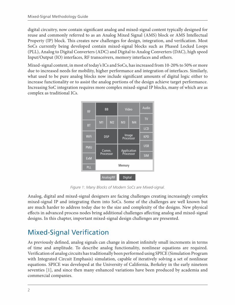
digital circuitry, now contain significant analog and mixed-signal content typically designed for reuse and commonly referred to as an Analog Mixed Signal (AMS) block or AMS Intellectual Property (IP) block. This creates new challenges for design, integration, and verification. Most SoCs currently being developed contain mixed-signal blocks such as Phased Locked Loops (PLL), Analog to Digital Converters (ADC) and Digital to Analog Converters (DAC), high speed Input/Output (IO) interfaces, RF transceivers, memory interfaces and others.
Mixed-signal content, in most of today’s ICs and SoCs, has increased from 10-20% to 50% or more due to increased needs for mobility, higher performance and integration of interfaces. Similarly, what used to be pure analog blocks now include significant amounts of digital logic either to increase functionality or to assist the analog portions of the design achieve target performance. Increasing SoC integration requires more complex mixed-signal IP blocks, many of which are as complex as traditional ICs.
RF
M1 M2 M3 M4
BB Video
Comm.Processor
ApplicationProcessor
DSP ImageProcessor
BT
WiFi
PMU
ExM
Analog/RF Digital
PLL
Audio
TV
LCD
KPD
SIM
USB
Memory
Figure 1: Many Blocks of Modern SoCs are Mixed-signal.
Analog, digital and mixed-signal designers are facing challenges creating increasingly complex mixed-signal IP and integrating them into SoCs. Some of the challenges are well known but are much harder to address today due to the size and complexity of the designs. New physical effects in advanced process nodes bring additional challenges affecting analog and mixed-signal designs. In this chapter, important mixed-signal design challenges are presented.
Mixed-Signal VerificationAs previously defined, analog signals can change in almost infinitely small increments in terms of time and amplitude. To describe analog functionality, nonlinear equations are required. Verification of analog circuits has traditionally been performed using SPICE (Simulation Program with Integrated Circuit Emphasis) simulation, capable of iteratively solving a set of nonlinear equations. SPICE was developed at the University of California, Berkeley in the early nineteen seventies [1], and since then many enhanced variations have been produced by academia and commercial companies.
Mixed-Signal Design Trends and Challenges
3
The behavior of digital circuits is described using Boolean relations. Digital simulators execute much faster because they operate at higher levels of abstraction. When operating in an event driven mode, evaluations are only performed when logic states change and do not require an iterative nonlinear equation solver. Simulating the behavior of a mixed-signal design requires both analog and digital simulators to work in parallel, synchronized and today, tightly integrated mixed-signal simulators are commercially available [2].
The basic verification task involves creating a verification plan, test bench development, simulation, post processing of results including measurements and comparison with the specification. The analog and digital parts of mixed-signal designs must be verified separately, but this is not adequate to ensure that the entire design will function properly. Malfunction of interfaces between the analog and digital parts is a common problem in mixed-signal design. To address this mixed-signal verification, engineers have a few choices:
• Simulatetheentiremixed-signaldesignusingaSPICEtypesimulatoratthetransistorlevel.Asdesign size increases this approach is inadequate since a single simulation run could take days even with the fastest simulator.
• Simplifyandmodel theanalogpartas logicanduseadigital simulator.Althoughsufficientto verify connectivity of the mixed-signal design, this approach is inaccurate for verifying interaction among analog and digital components.
•Usemixed-signalsimulationwithanalogatthetransistorlevelanddigitalatthegatelevel.Thisapproach is much faster than SPICE, but the analog solver limits performance for large designs.
•Modelanalogusingabehaviorallanguageandsimulatetogetherwithdigitallogicmodeledatthe Register Transfer Level (RTL), or even higher levels of abstraction. This approach enables simulation of the entire design as a system and solves simulation performance issue. The only drawback is the required investment in analog behavioral modeling.
To properly verify today’s complex mixed-signal designs, a combination of all the above simulation approaches is required. Moreover, modern simulators allow a combination of different levels of abstraction, from transistor to RTL or even higher, for different parts of the design in the same simulation run.
The main challenge verifying mixed-signal designs that have increasing size, complexity, and modes of operation is that traditional direct test verification methods are becoming much harder to apply. Analog simulation, as a component of the mixed-signal verification, is a major bottleneck. Advancements in SPICE simulation, such as Fast-SPICE, provide additional speed and capacity while sacrificing some accuracy. In addition, distributed computing engines have further increased capacity and performance limits, but not enough to keep up with growing size and complexity of the mixed-signal designs.
4
Mixed-Signal Methodology Guide
SPICE/fast-SPICE not fast enough
Transistor-gate co-simulation slow
Creating and validating behavioral models
Lack of verification modelsfor AMS IP
Creating test vectors for target coverage
Modeling and verifiying power intent
Language support for behavioral simulation
Verifying connectivity
Relative Importance Sour
ce: C
aden
ce, 5
01 re
spon
ses
by20
11 W
orld
-wid
e M
S se
min
ar a
tten
dant
s
VHW/SW co-verification
Other
Figure 2: Mixed-signal Verification Challenges
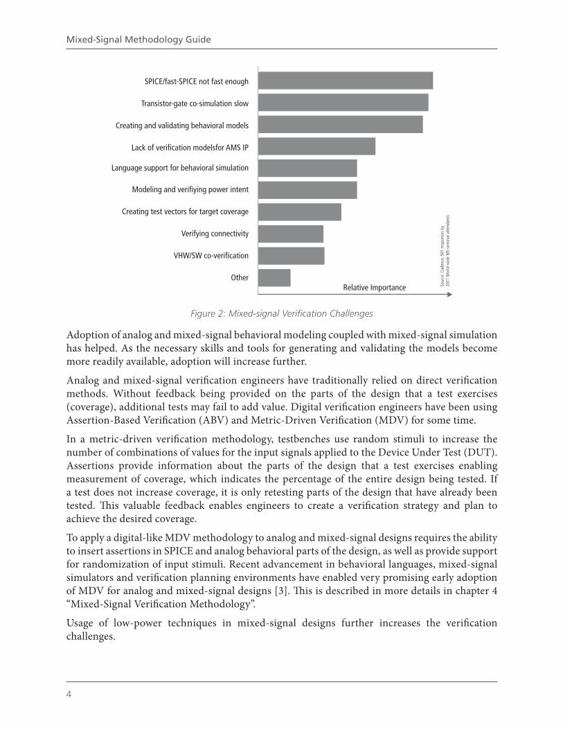
Adoption of analog and mixed-signal behavioral modeling coupled with mixed-signal simulation has helped. As the necessary skills and tools for generating and validating the models become more readily available, adoption will increase further.
Analog and mixed-signal verification engineers have traditionally relied on direct verification methods. Without feedback being provided on the parts of the design that a test exercises (coverage), additional tests may fail to add value. Digital verification engineers have been using Assertion-Based Verification (ABV) and Metric-Driven Verification (MDV) for some time.
In a metric-driven verification methodology, testbenches use random stimuli to increase the number of combinations of values for the input signals applied to the Device Under Test (DUT). Assertions provide information about the parts of the design that a test exercises enabling measurement of coverage, which indicates the percentage of the entire design being tested. If a test does not increase coverage, it is only retesting parts of the design that have already been tested. This valuable feedback enables engineers to create a verification strategy and plan to achieve the desired coverage.
To apply a digital-like MDV methodology to analog and mixed-signal designs requires the ability to insert assertions in SPICE and analog behavioral parts of the design, as well as provide support for randomization of input stimuli. Recent advancement in behavioral languages, mixed-signal simulators and verification planning environments have enabled very promising early adoption of MDV for analog and mixed-signal designs [3]. This is described in more details in chapter 4 “Mixed-Signal Verification Methodology”.
Usage of low-power techniques in mixed-signal designs further increases the verification challenges.

Mixed-Signal Design Trends and Challenges
5
Behavioral ModelingA key component in a mixed-signal verification methodology is behavioral modeling. Bringing analog and mixed-signal blocks to a higher level of abstraction enables more effective mixed-signal simulation. However, this is not a simple task, and there are a number of challenges:
•The scope and purpose of themodelmust be well understood and the appropriatemodeltemplate/architecture carefully chosen. In a top-down methodology, models are developed beforecircuitsareavailableandasimplermodelmightbesufficientforfunctionalverificationat the system level. In bottom-up approach, the model might need to match an already implemented block for performance verification, and thus a more accurate model is used.
•Themodelmustbevalidatedtoensurethatitrepresentthecircuitorspecificationwithrequiredaccuracy.
•Themodelmustbeupdatedtokeepitinsyncwithchangesmadeinthecircuitorspecification.
•Themodel needs to bewritten in away that does not cause convergence problems duringsimulation.
•Writingmodelsrequiresmulti-disciplinaryskills.Modelingrequiresagoodunderstandingofanalog and mixed-signal design techniques and circuits, coding, debugging and automation skills, and an understanding of analog and mixed-signal simulation algorithms. Modeling is hard to automate and typically requires specialized engineering talent that can be hard to find.
Despite the challenges, behavioral modeling continues to make inroads into mixed-signal simulation and verification thanks to the standardization of behavioral languages, development of skills and improvements in automation. A better recognition of the advantages that behavioral modeling offers is convincing increasing numbers of design teams to make the initial investment necessary for the methodology shift, which then provides a return in the form of productivity improvements. See chapter 3 “AMS Behavioral Modeling”.
Low Power VerificationDigital designers have been using low-power techniques to minimize power for some time. With greater integration of digital logic into analog designs, optimizing power is becoming a requirement for many mixed-signal designs as well. Today, low-power design techniques, [4] such as multi-power domains, use of devices with different threshold voltages and back biasing, voltage scaling, power gating and power shut-off, are found in many mixed-signal designs. These techniques add significant difficulties to traditional simulation.Designswithmultiple powerdomains operate in several modes (normal, stand-by, test, etc.) and the number of simulations required to verify each of the modes increases dramatically. Furthermore, some low-power techniques, such as power shut-off, require special care at signal crossings between the analog and digital domains. Typically a mixed-signal simulator is not able to handle this without additions to the specifications. Although required to analyze some electrical aspects (for example rush currentandturn-ontime),dynamicverificationusingsimulationis inefficient fora thoroughfull-chip low-power verification, and in some cases it is even not able to discover structural errors related to low-power intent.

6
Mixed-Signal Methodology Guide
In digital design, formal verification methodologies have emerged for verifying low-power intent, and are applied to design transformations from RTL development through physical implementation. The methodology uses static checks to ensure that the design complies with specified design intent under all conditions. Modern mixed-signal design requires a combined approach of dynamic and static methods for thorough low-power intent verification. Capturing and sharing low-power intent for an analog or mixed-signal blocks is particularly challenging and recent standardization of low-power specification formats, with macro-modeling capabilities, are very promising.
Design for Test (DFT)For many SoCs, the cost of test exceeds the cost of silicon. A common requirement is that the chip be testable on a commercial tester, regardless of the I/O or internal speed and regardless of the functions and mixed-signal content. To ensure testability, the device must include built in test circuitry, often increasing chip size by 10%, and in many cases includes redundancy for self-repair.
To test analog and mixed-signal portions of the design, the chip must include signal generators and measuring circuitry. Consequently, the verification task increases considerably. Test cannot be an afterthought and planning for test from the very beginning of the design process must be part of the design methodology, particularly for mixed-signal.
Chip PlanningMixed-signal SoCs require very careful consideration of the floorplan. To make the right decisions regarding placement of blocks and I/Os, the chip architect needs to take into account the sensitivity of analog, mixed-signal and RF blocks, as well as routing, power, timing, noise, package and other constraints. This is necessary to minimize chip area, avoid problems causing siliconre-spinsandavoiddifficultiesduringphysicalimplementation.
For example, in designs requiring special routing for sensitive signals at the top level (buses, high-speed digital, analog, RF), blocksmust be placed optimally to enable sufficient routingresources, avoid routing congestion and signal interference problems. Similarly, special care needs to be given to placement of sensitive analog blocks because noise from digital switching can propagate through the package or substrate and impact the performance of the blocks or cause their complete malfunction. The conservative approach to chip planning, by increasing spacing, leads to increased chip area and reduced yield and profits.
Chip planning often has to start before all of the blocks are finalized in order to meet product schedule. In this case, the chip architect derives an optimal floorplan from an understanding of the signal flow and uses estimated sizes for the soft blocks. The floorplan is adjusted as the soft blocks harden. This offers additional opportunities for area reduction since shape, area and pin location can be concurrently optimized during top and block implementation. In addition to signal flow, chip architects need to plan power domains and power routing and overlay them on the preliminary floorplan to properly estimate voltage drop due to Interconnect Resistance (IR) and supply noise. Package impact must be included as well. This is particularly challenging when analog and mixed-signal blocks are involved because it is hard to obtain accurate estimates
Mixed-Signal Design Trends and Challenges
7
without simulation. Early power planning enables designers to forecast the location and area required for decoupling cells, which ensure proper power distribution and isolation throughout the chip.
Complex SoCs contain dozens, and sometimes hundreds, of digital, analog and mixed-signal blocks. Designers must use an advanced methodology to explore different configurations and to make trade-offs. The methodology includes automated block placement that provides consideration for constraints, timing, congestion and power. High levels of automation allow quick exploration of different floorplan alternatives, followed by selection and refinement of the best alternative.
Chip planning for a complex mixed-signal SoC is a delicate task and involves members from every discipline within the design team. During the chip planning and integration process, the chip architect needs to collaborate with analog, digital, I/O, package designers and physical implementation engineers. In a large, geographically distributed organization, this may represent the biggest challenge.
AMS IP ReuseHighly integrated SoCs are built using large and complex AMS IP blocks. A typical AMS block may contain thousands of transistors for implementing analog and RF functions and a couple hundred thousand logic gates, tightly integrated together. Although some of the AMS blocks may be newly designed, the majority of the blocks need to be re-used, ideally without alterations, to achieve the necessary productivity and schedule targets. This is important for internal IP developers, and even more so for independent AMS IP providers, since the cost of customizing IP for every integration would have a significant impact on their business models.
To achieve a high level of reuse, AMS blocks must be designed not just to meet nominal specifications when verified standalone, but to perform robustly within specifications when integrated in different chip configurations. To achieve this, AMS IP designers use many techniques, such as:
• Implementthefunctionalityusingcircuittopologieswithhigherimmunitytovariations.Forexample, when possible, use comparators instead of operational amplifiers. This because it saves power, and also the threshold of a comparator is much easier to control than the gain of an operational amplifier [5].
•GuardsensitivecircuitryintheAMSIPfromexternalinfluences.Typically,physicalstructuressuch as guard rings and triple-wells are used to isolate AMS IP from possible noise aggressors on the chip. The penalty for this is increased area.
•ProvideasetofintegrationconstraintsfortheAMSIP.Thiscouldincludepin,spacing,routing,IR drop, noise and other constraints. Communicating the constraints to SoC designers, and enforcing them, is often a challenge.
Provide different physical implementations of the same IP so that the SoC designer can chose based on integration requirements. For example, the AMS IP developer may provide variations of the same IP with different levels of isolation, and the SoC designer can chose the one with best isolation/area tradeoff for the chip.
8
Mixed-Signal Methodology Guide
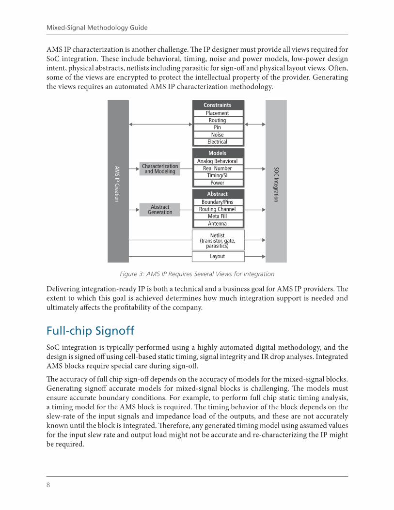
AMS IP characterization is another challenge. The IP designer must provide all views required for SoC integration. These include behavioral, timing, noise and power models, low-power design intent, physical abstracts, netlists including parasitic for sign-off and physical layout views. Often, someoftheviewsareencryptedtoprotecttheintellectualpropertyoftheprovider.Generatingthe views requires an automated AMS IP characterization methodology.
AMS IP Creation
SOC Integration
ConstraintsPlacement
RoutingPin
NoiseElectrical
ModelsAnalog Behavioral
Real NumberTiming/SI
Power
Characterizationand Modeling
Abstract
Netlist(transistor, gate,
parasitics)
Layout
Boundary/PinsRouting Channel
Meta FillAntenna
AbstractGeneration
Figure 3: AMS IP Requires Several Views for Integration
Delivering integration-ready IP is both a technical and a business goal for AMS IP providers. The extent to which this goal is achieved determines how much integration support is needed and ultimately affects the profitability of the company.
Full-chip SignoffSoC integration is typically performed using a highly automated digital methodology, and the design is signed off using cell-based static timing, signal integrity and IR drop analyses. Integrated AMS blocks require special care during sign-off.
The accuracy of full chip sign-off depends on the accuracy of models for the mixed-signal blocks. Generating signoff accuratemodels formixed-signal blocks is challenging.Themodelsmustensure accurate boundary conditions. For example, to perform full chip static timing analysis, a timing model for the AMS block is required. The timing behavior of the block depends on the slew-rate of the input signals and impedance load of the outputs, and these are not accurately known until the block is integrated. Therefore, any generated timing model using assumed values for the input slew rate and output load might not be accurate and re-characterizing the IP might be required.
Mixed-Signal Design Trends and Challenges
9
Sign-off for signal integrity is even more challenging. If the AMS block is a “black-box”, crosstalk caused by coupling between the nets close to the block boundaries will not be accounted for. The conservative approach is to prohibit top-level routing near mixed-signal block boundaries to avoid coupling but at the penalty of increased chip area.
To overcome signoff challenges, the limitations of a black-box methodology must be removed by providing visibility into the block and incorporating the necessary elements into accurate full-chip sign-off.
Substrate NoiseIn a mixed-signal chip, analog and digital circuits reside on the same silicon substrate. Fast, simultaneously switching digital circuits inject noise into the substrate through the coupling between the substrate and the power/ground grid. The injected noise propagates through the substrate and raises the voltage at the bulk nodes of transistors in an analog circuit. This changes the performance of the analog circuit and can cause the entire chip to fail.
The substrate noise phenomenon is well studied and understood, but remains a major concern to mixed-signal designers. Tight integration of an increasing number of digital gates close to analog circuits and large logic clusters that exhibit simultaneous switching increase the substrate noise injection. There is no simple solution. The impact of substrate noise cannot be completely isolated from other noise effects such as power and cross talk noise. To simulate the impact accurately, a huge number of parasitic elements are required, even for a small mixed-signal circuit.
Designers use a methodology based on substrate noise analysis and prevention. The analysis helps them understand noise injection and propagation based on test structures. Further steps include modeling noise injection in real circuits, noise propagation to analog circuits and sensitivity analysis. Because this involves transistor-level simulation, the analysis is limited by the capacity and performance of the simulator and the ability of designers to pinpoint possible aggressors so that the size of the parasitic involved can be reduced. For prevention, designers increase spacing, and use guard rings and triple wells to isolate sensitive analog circuits.
IC/Package Co-DesignThe integration of the silicon die into a package is a challenge with pin counts often exceeding one thousand,highI/OfrequencyintheGHzrange,andhighpowersupplycurrentsoftensofAmps.Although single die-in-package is still a cost attractive alternative for very high volume SoCs, the approach caries substantial technical and business risks and other integration alternatives are being considered.
Partitioning the design onto multiple dies is particularly attractive for mixed-signal designs. Multiple dies in the same package integrated as a Multi-Chip Module (MCM) are often used for integrating RF and digital functionality. The MCM requires careful partitioning and considerable care of the electrical and physical aspects of the integration to avoid undesired coupling between

10
Mixed-Signal Methodology Guide
RF, digital and package components. In another approach, multiple dies are placed on a silicon interposer and connected using Through-Silicon Vias (TSVs). This is generally known as a 3-D IC, which also includes stacking dies on the top of each other.
Both MCM and 3D IC approaches, enable integration of dies manufactured in different process technologies. This offers flexibility, but requires an integrated design methodology supporting multi-technology simulation, verification, implementation and sign-off.
Design Collaboration and Data ManagementIn a traditional mixed-signal design, analog and digital teams work separately. For example, if an analog layout designer is in charge of a floorplan, the locations of analog objects are decided, an area is carved out for the digital part of the chip, pin locations are determined and then this information is handed over to the digital designer. After implementing logic in the given area, the digital designer returns the block layout for chip integration. The hand-off was well defined, and this “over the wall” approach worked for many mixed-signal applications.
Increased analog and digital integration requires much closer collaboration between design teams. At the early stage, trade-offs are made with respect to package and I/O design, die size and area allocation, verification strategy, timing and power budgets, noise and other physical and electrical constraints. Designers must be able to exchange requirements and explore different alternatives in a collaborative approach. Similarly, at the chip integration stage, designers need to collaborate on achieving design closure, handling any Engineering Change Orders (ECOs) and sign-off.
An effective design methodology must provide flexibility and support for global design teams in this collaborative approach throughout the design process. Because many designers are concurrently working on a design, managing and maintaining the integrity of the design database is not a simple task. To avoid unintended changes or corruption, a data management system is required, covering all data involved in the process. Using a data management system, enforcing guidelines and naming conventions, and using checking utilities to verify completeness and data integrity are all important steps in enabling global design teams to work concurrently and collaboratively on the mixed-signal projects. See chapter 10 “Data Management for Mixed-Signal Designs”.
References1. University of California, Berkeley SPICE webpage: http://bwrc.eecs.berkeley.edu/classes/
icbook/spice/
2. Cadence Virtuoso AMS Designer, http://www.cadence.com/products/cic/ams_designer/pages/default.aspx
3. Bishnupriya Bhattacharya et al., Advanced Verification Topics, lulu.com 2012
4. APracticalGuidetoLowPowerDesign,http://www.si2.org/?page=1061
5. Hae-Seung Lee and Charlie Sodini. Invited paper: Analog-to-Digital Converters – Digitizing the Analog World, Proceedings of the IEEE, Feb., 2008.

Go to http://goo.gl/nWUZs to purchase a copy of the Mixed-Signal Methodology Guide.
Order before August 31st to receive a 40% discount!


![[CRISIL] Literature review on insider trading and insider ... · Literature review on Insider Trading and Insider Trading Regulation Abstract Views on insider trading and its effects](https://img.pdfslide.net/doc/110x75/5ad077037f8b9a71028de0eb/crisil-literature-review-on-insider-trading-and-insider-review-on-insider.jpg)