Embed Size (px)
Citation preview
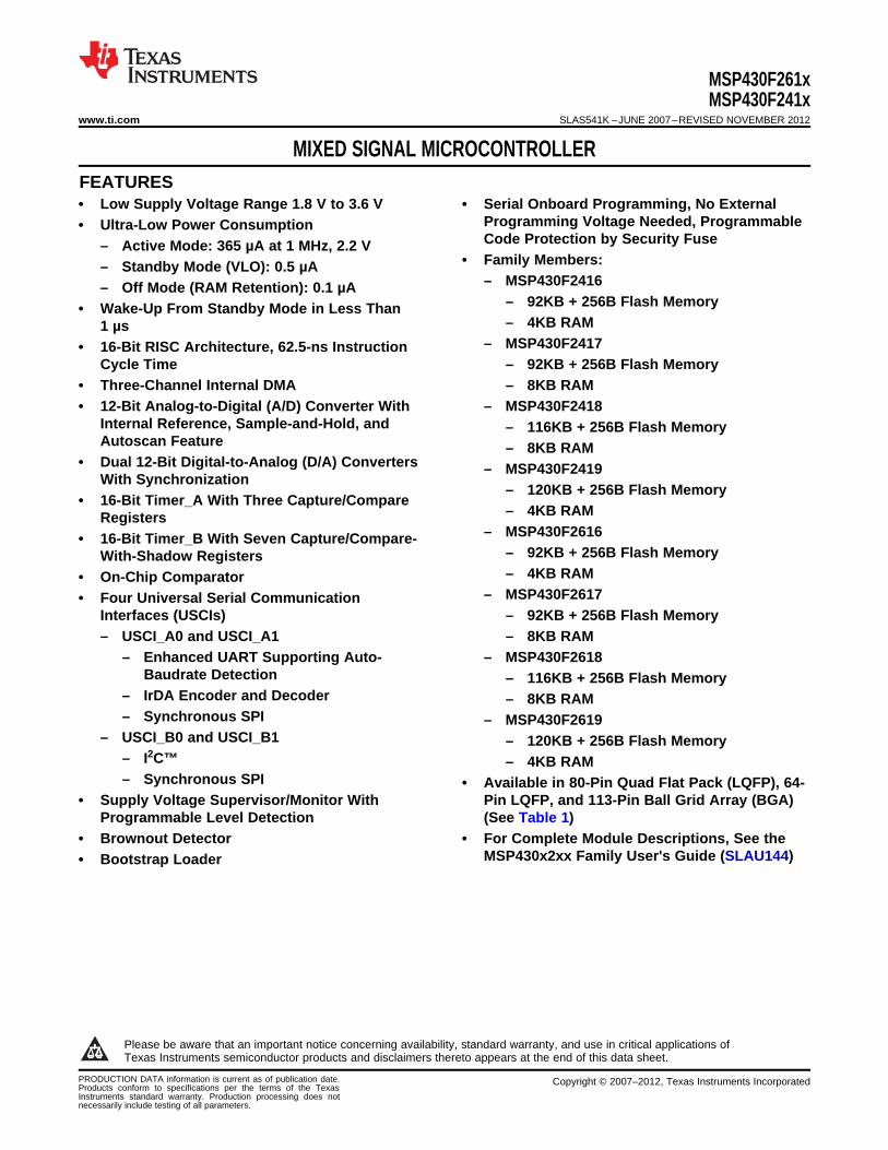
MSP430F261xMSP430F241x
www.ti.com SLAS541K –JUNE 2007–REVISED NOVEMBER 2012
MIXED SIGNAL MICROCONTROLLER1FEATURES• Low Supply Voltage Range 1.8 V to 3.6 V • Serial Onboard Programming, No External
Programming Voltage Needed, Programmable• Ultra-Low Power ConsumptionCode Protection by Security Fuse– Active Mode: 365 µA at 1 MHz, 2.2 V
• Family Members:– Standby Mode (VLO): 0.5 µA– MSP430F2416– Off Mode (RAM Retention): 0.1 µA
– 92KB + 256B Flash Memory• Wake-Up From Standby Mode in Less Than– 4KB RAM1 µs
– MSP430F2417• 16-Bit RISC Architecture, 62.5-ns InstructionCycle Time – 92KB + 256B Flash Memory
• Three-Channel Internal DMA – 8KB RAM• 12-Bit Analog-to-Digital (A/D) Converter With – MSP430F2418
Internal Reference, Sample-and-Hold, and – 116KB + 256B Flash MemoryAutoscan Feature – 8KB RAM
• Dual 12-Bit Digital-to-Analog (D/A) Converters – MSP430F2419With Synchronization
– 120KB + 256B Flash Memory• 16-Bit Timer_A With Three Capture/Compare
– 4KB RAMRegisters– MSP430F2616• 16-Bit Timer_B With Seven Capture/Compare-
– 92KB + 256B Flash MemoryWith-Shadow Registers– 4KB RAM• On-Chip Comparator
– MSP430F2617• Four Universal Serial CommunicationInterfaces (USCIs) – 92KB + 256B Flash Memory– USCI_A0 and USCI_A1 – 8KB RAM
– Enhanced UART Supporting Auto- – MSP430F2618Baudrate Detection – 116KB + 256B Flash Memory
– IrDA Encoder and Decoder – 8KB RAM– Synchronous SPI – MSP430F2619
– USCI_B0 and USCI_B1 – 120KB + 256B Flash Memory– I2C™ – 4KB RAM– Synchronous SPI • Available in 80-Pin Quad Flat Pack (LQFP), 64-
• Supply Voltage Supervisor/Monitor With Pin LQFP, and 113-Pin Ball Grid Array (BGA)Programmable Level Detection (See Table 1)
• Brownout Detector • For Complete Module Descriptions, See theMSP430x2xx Family User's Guide (SLAU144)• Bootstrap Loader
1
Please be aware that an important notice concerning availability, standard warranty, and use in critical applications ofTexas Instruments semiconductor products and disclaimers thereto appears at the end of this data sheet.
PRODUCTION DATA information is current as of publication date. Copyright © 2007–2012, Texas Instruments IncorporatedProducts conform to specifications per the terms of the TexasInstruments standard warranty. Production processing does notnecessarily include testing of all parameters.
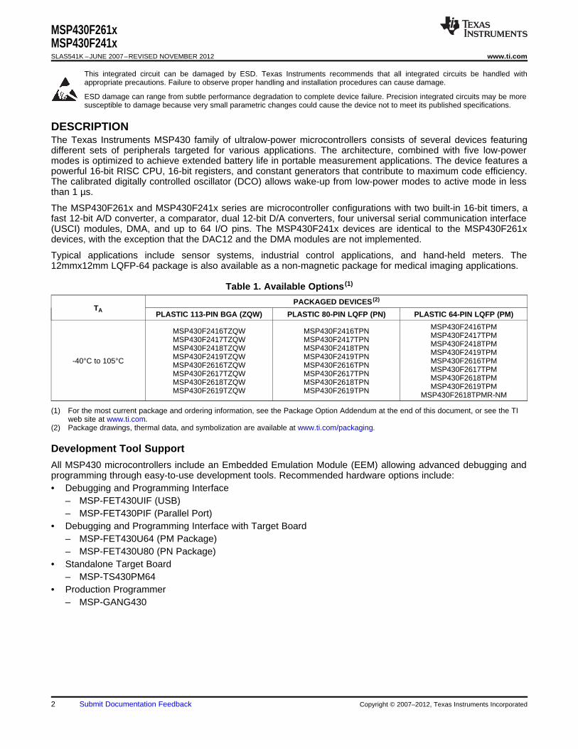
MSP430F261xMSP430F241xSLAS541K –JUNE 2007–REVISED NOVEMBER 2012 www.ti.com
This integrated circuit can be damaged by ESD. Texas Instruments recommends that all integrated circuits be handled withappropriate precautions. Failure to observe proper handling and installation procedures can cause damage.
ESD damage can range from subtle performance degradation to complete device failure. Precision integrated circuits may be moresusceptible to damage because very small parametric changes could cause the device not to meet its published specifications.
DESCRIPTIONThe Texas Instruments MSP430 family of ultralow-power microcontrollers consists of several devices featuringdifferent sets of peripherals targeted for various applications. The architecture, combined with five low-powermodes is optimized to achieve extended battery life in portable measurement applications. The device features apowerful 16-bit RISC CPU, 16-bit registers, and constant generators that contribute to maximum code efficiency.The calibrated digitally controlled oscillator (DCO) allows wake-up from low-power modes to active mode in lessthan 1 µs.
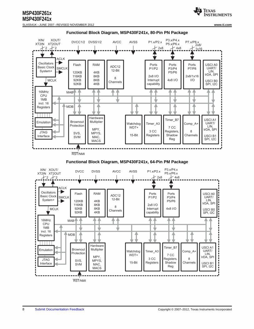
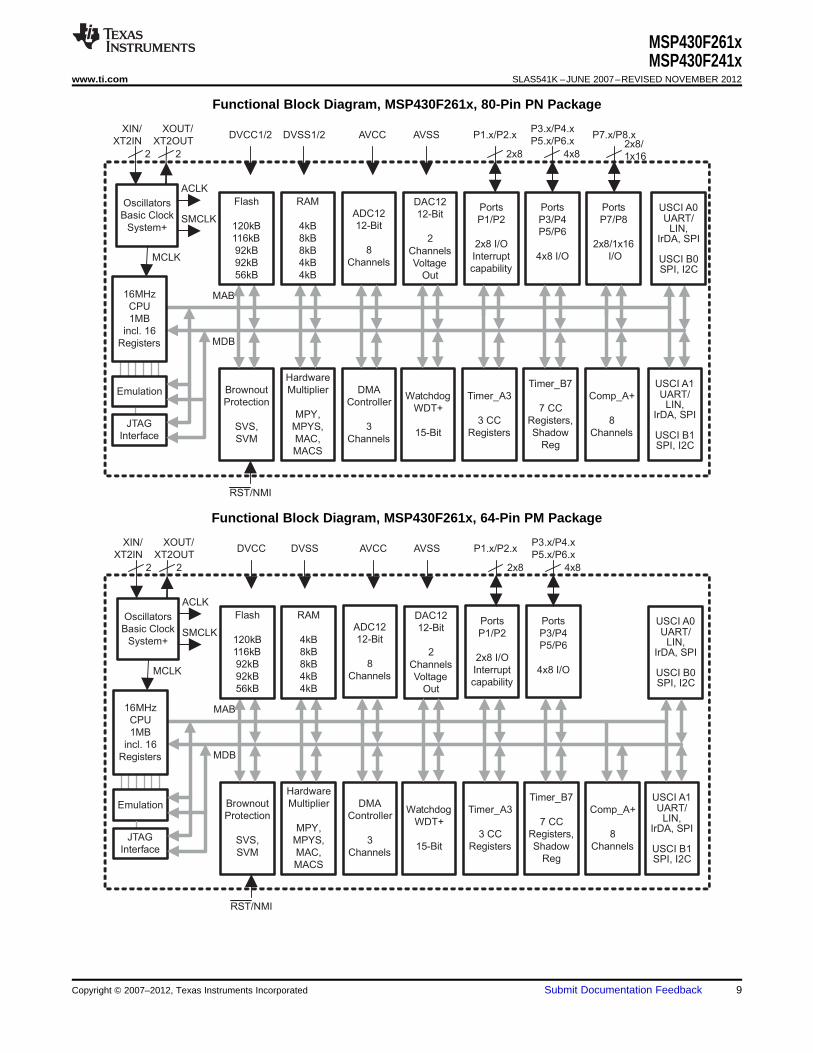
The MSP430F261x and MSP430F241x series are microcontroller configurations with two built-in 16-bit timers, afast 12-bit A/D converter, a comparator, dual 12-bit D/A converters, four universal serial communication interface(USCI) modules, DMA, and up to 64 I/O pins. The MSP430F241x devices are identical to the MSP430F261xdevices, with the exception that the DAC12 and the DMA modules are not implemented.
Typical applications include sensor systems, industrial control applications, and hand-held meters. The12mmx12mm LQFP-64 package is also available as a non-magnetic package for medical imaging applications.
Table 1. Available Options (1)
PACKAGED DEVICES (2)
TAPLASTIC 113-PIN BGA (ZQW) PLASTIC 80-PIN LQFP (PN) PLASTIC 64-PIN LQFP (PM)
MSP430F2416TPMMSP430F2416TZQW MSP430F2416TPN MSP430F2417TPMMSP430F2417TZQW MSP430F2417TPN MSP430F2418TPMMSP430F2418TZQW MSP430F2418TPN MSP430F2419TPMMSP430F2419TZQW MSP430F2419TPN-40°C to 105°C MSP430F2616TPMMSP430F2616TZQW MSP430F2616TPN MSP430F2617TPMMSP430F2617TZQW MSP430F2617TPN MSP430F2618TPMMSP430F2618TZQW MSP430F2618TPN MSP430F2619TPMMSP430F2619TZQW MSP430F2619TPN MSP430F2618TPMR-NM
(1) For the most current package and ordering information, see the Package Option Addendum at the end of this document, or see the TIweb site at www.ti.com.
(2) Package drawings, thermal data, and symbolization are available at www.ti.com/packaging.
Development Tool Support
All MSP430 microcontrollers include an Embedded Emulation Module (EEM) allowing advanced debugging andprogramming through easy-to-use development tools. Recommended hardware options include:• Debugging and Programming Interface
– MSP-FET430UIF (USB)– MSP-FET430PIF (Parallel Port)
• Debugging and Programming Interface with Target Board– MSP-FET430U64 (PM Package)– MSP-FET430U80 (PN Package)
• Standalone Target Board– MSP-TS430PM64
• Production Programmer– MSP-GANG430
2 Submit Documentation Feedback Copyright © 2007–2012, Texas Instruments Incorporated
80-PINPN PACKAGE(TOP VIEW)
DVCC1 60
59P6.3/A3
P6.4/A4
P6.5/A5
P6.6/A6
P6.7/A7/SVSIN
VREF+
XIN
XOUT
VeREF+
VREF-/VeREF-
P1.0/TACLK/CAOUT
P1.1/TA0
P1.2/TA1
P1.3/TA2
P1.4/SMCLK
P2.1
/TA
INC
LK
/CA
3
P2
.2/C
AO
UT
/TA
0/C
A4
P2.3
/CA
0/T
A1
P2.4
/CA
1/T
A2
P2.5
/RO
SC/C
A5
P2.7
/TA
0/C
A7
P3
.0/U
CB
0S
TE
/UC
A0C
LK
P3
.1/U
CB
0S
IMO
/UC
B0
SD
A
P3
.2/U
CB
0S
OM
I/U
CB
0S
CL
P3
.3/U
CB
0C
LK
/UC
A0S
TE
P3.4
/UC
A0T
XD
/UC
A0S
IMO
P4.5/TB5
P4.6/TB6
P4.7/TBCLK
P5.4/MCLK
AV
CC
DV
SS
1
AV
SS
P6
.2/A
2
P6
.1/A
1
P6
.0/A
0
RS
T/N
MI
TC
K
TM
S
TD
I/T
CL
K
TD
O/T
DI
P5.5/SMCLK
58
57
56
55
54
53
52
51
50
49
48
47
46
45
1
2
3
4
5
6
7
8
9
10
11
12
13
14
15
16
63 62 61
P3.5
/UC
A0R
XD
/UC
A0S
OM
I
44
43
42
41
P1.5/TA0
P1.6/TA1
P1.7/TA2
P2.0/ACLK/CA2
17
18
19
20
P4
.0/T
B0
P4.1
/TB
1
P4.2
/TB
2
P4.3
/TB
3
P4.4
/TB
4
P3.6
/UC
A1T
XD
/UC
A1S
IMO
P3.7
/UC
A1R
XD
/UC
A1S
OM
I
P5.0/UCB1STE/UCA1CLK
P5.1/UCB1SIMO/UCB1SDA
P5.2/UCB1SOMI/UCB1SCL
P5.3/UCB1CLK/UCA1STE
P7.0
P7.1
P7.2
P7.3
P7.4
P7.5
P7.6
P7
.7
P8
.0
P8
.1
P8
.2
P8
.3
P8
.4
P8
.5
DVCC2
DVSS2
P5.7/TBOUTH/SVSOUT
P5.6/ACLK
P8
.6/X
T2O
UT
P8
.7/X
T2IN
P2.6
/AD
C1
2C
LK
/CA
6
80 79 78 77 76 75 74 73 72 71 70 69 68 67 66 65 64
38 39 4021 22 23 24 25 26 27 28 29 30 31 32 33 34 35 36 37
MSP430F261xMSP430F241x
www.ti.com SLAS541K –JUNE 2007–REVISED NOVEMBER 2012
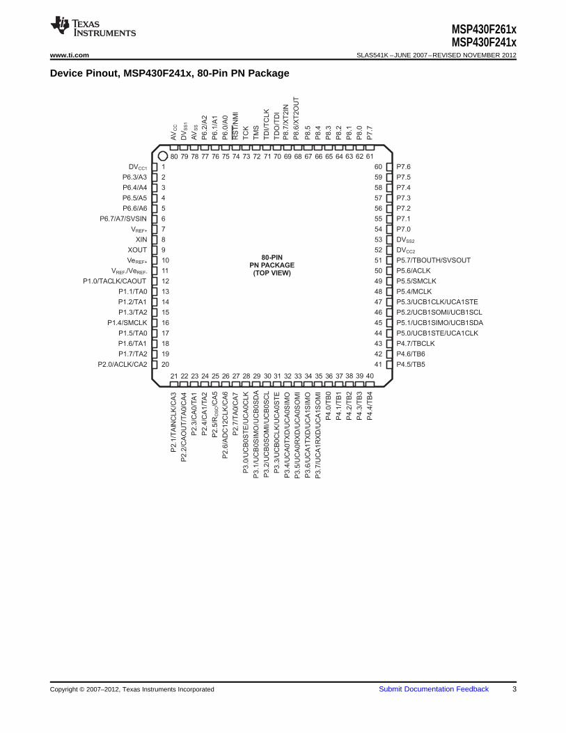
Device Pinout, MSP430F241x, 80-Pin PN Package
Copyright © 2007–2012, Texas Instruments Incorporated Submit Documentation Feedback 3

DVCC1 48
47
64
P6.3/A3
P6.4/A4
P6.5/A5
VREF+
XIN
XOUT
VeREF+
VREF-/VeREF-
P1.0/TACLK/CAOUT
P1.1/TA0
P1.2/TA1
P1.3/TA2
P1.4/SMCLK
P1.5
/TA
0
P1.6
/TA
1
P1.7
/TA
2
P2.0
/AC
LK
/CA
2
P2.1
/TA
INC
LK
/CA
3
P2
.2/C
AO
UT
/TA
0/C
A4
P2.3
/CA
0/T
A1
P2.4
/CA
1/T
A2
P2.5
/RO
SC/C
A5
P2
.6/A
DC
12C
LK
/CA
6
P2.7
/TA
0/C
A7
P4.0/TB0
P4.1/TB1
P4.2/TB2
P4.3/TB3
P4.4/TB4
P4.5/TB5
P4.6/TB6
P4.7/TBCLK
AV
CC
DV
SS
1
AV
SS
P6
.2/A
2
P6
.1/A
1
P6
.0/A
0
RS
T/N
MI
TC
K
TM
S
TD
I/T
CL
K
TD
O/T
DI
XT
2IN
XT
2O
UT
46
45
44
43
42
41
40
39
38
37
36
35
34
33
1
2
3
4
5
6
7
8
9
10
11
12
13
14
15
16
P3.6/UCA1TXD/UCA1SIMO
P3.7/UCA1RXD/UCA1SOMI
P5.0/UCB1STE/UCA1CLK
P5.1/UCB1SIMO/UCB1SDA
P5.2/UCB1SOMI/UCB1SCL
P5.4/MCLK
P5.5
/SM
CL
K
P5.3/UCB1CLK/UCA1STE
P5.7
/TB
OU
TH
/SV
SO
UT
P5.6
/AC
LK
P6.6/A6
P6.7/A7/SVSIN
64-PINPM PACKAGE
(TOP VIEW)
P3
.0/U
CB
0S
TE
/UC
A0C
LK
P3
.1/U
CB
0S
IMO
/UC
B0
SD
A
P3
.2/U
CB
0S
OM
I/U
CB
0S
CL
P3
.3/U
CB
0C
LK
/UC
A0S
TE
P3.4
/UC
A0
TX
D/U
CA
0S
IMO
P3.5/UCA0RXD/UCA0SOMI
63 62 61 60 59 58 57 56 55 54 53 52 51 50 49
17 18 19 20 21 22 23 24 25 26 27 28 29 30 31 32
MSP430F261xMSP430F241xSLAS541K –JUNE 2007–REVISED NOVEMBER 2012 www.ti.com
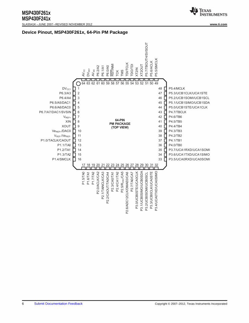
Device Pinout, MSP430F241x, 64-Pin PM Package
4 Submit Documentation Feedback Copyright © 2007–2012, Texas Instruments Incorporated

80-PINPN PACKAGE(TOP VIEW)
DVCC1 60
59P6.3/A3
P6.4/A4
P6.5/A5/DAC1
P6.6/A6/DAC0
P6.7/A7/DAC1/SVSIN
VREF+
XIN
XOUT
VeREF+/DAC0
VREF-/VeREF-
P1.0/TACLK/CAOUT
P1.1/TA0
P1.2/TA1
P1.3/TA2
P1.4/SMCLK
P2.1
/TA
INC
LK
/CA
3
P2
.2/C
AO
UT
/TA
0/C
A4
P2.3
/CA
0/T
A1
P2.4
/CA
1/T
A2
P2.5
/RO
SC/C
A5
P2.7
/TA
0/C
A7
P3
.0/U
CB
0S
TE
/UC
A0
CLK
P3
.1/U
CB
0S
IMO
/UC
B0
SD
A
P3
.2/U
CB
0S
OM
I/U
CB
0S
CL
P3
.3/U
CB
0C
LK
/UC
A0
ST
E
P3.4
/UC
A0
TX
D/U
CA
0S
IMO
P4.5/TB5
P4.6/TB6
P4.7/TBCLK
P5.4/MCLK
AV
CC
DV
SS
1
AV
SS
P6
.2/A
2
P6
.1/A
1
P6
.0/A
0
RS
T/N
MI
TC
K
TM
S
TD
I/T
CL
K
TD
O/T
DI
P5.5/SMCLK
58
57
56
55
54
53
52
51
50
49
48
47
46
45
1
2
3
4
5
6
7
8
9
10
11
12
13
14
15
16
P3.5
/UC
A0
RX
D/U
CA
0S
OM
I
44
43
42
41
P1.5/TA0
P1.6/TA1
P1.7/TA2
P2.0/ACLK/CA2
17
18
19
20
P4
.0/T
B0
P4.1
/TB
1
P4.2
/TB
2
P4.3
/TB
3
P4.4
/TB
4
P3.6
/UC
A1
TX
D/U
CA
1S
IMO
P3.7
/UC
A1
RX
D/U
CA
1S
OM
I
P5.0/UCB1STE/UCA1CLK
P5.1/UCB1SIMO/UCB1SDA
P5.2/UCB1SOMI/UCB1SCL
P5.3/UCB1CLK/UCA1STE
P7.0
P7.1
P7.2
P7.3
P7.4
P7.5
P7.6
P7
.7
P8
.0
P8
.1
P8
.2
P8
.3
P8
.4
P8
.5
DVCC2
DVSS2
P5.7/TBOUTH/SVSOUT
P5.6/ACLK
P8
.6/X
T2O
UT
P8
.7/X
T2IN
P2
.6/A
DC
12C
LK
/DM
AE
0/C
A6
63 62 6180 79 78 77 76 75 74 73 72 71 70 69 68 67 66 65 64
38 39 4021 22 23 24 25 26 27 28 29 30 31 32 33 34 35 36 37
MSP430F261xMSP430F241x
www.ti.com SLAS541K –JUNE 2007–REVISED NOVEMBER 2012
Device Pinout, MSP430F261x, 80-Pin PN Package
Copyright © 2007–2012, Texas Instruments Incorporated Submit Documentation Feedback 5
DVCC1 48
47P6.3/A3
P6.4/A4
P6.5/A5/DAC1
VREF+
XIN
XOUT
VeREF+/DAC0
VREF-/VeREF-
P1.0/TACLK/CAOUT
P1.1/TA0
P1.2/TA1
P1.3/TA2
P1.4/SMCLK
P1.5
/TA
0
P1.6
/TA
1
P1.7
/TA
2
P2
.0/A
CL
K/C
A2
P2.1
/TA
INC
LK
/CA
3
P2
.2/C
AO
UT
/TA
0/C
A4
P2.3
/CA
0/T
A1
P2.4
/CA
1/T
A2
P2.5
/RO
SC/C
A5
P2
.6/A
DC
12C
LK
/DM
AE
0/C
A6
P2.7
/TA
0/C
A7
P3
.0/U
CB
0S
TE
/UC
A0C
LK
P3
.1/U
CB
0S
IMO
/UC
B0
SD
A
P3
.2/U
CB
0S
OM
I/U
CB
0S
CL
P3
.3/U
CB
0C
LK
/UC
A0S
TE
P3.4
/UC
A0
TX
D/U
CA
0S
IMO
P3.5/UCA0RXD/UCA0SOMI
P4.0/TB0
P4.1/TB1
P4.2/TB2
P4.3/TB3
P4.4/TB4
P4.5/TB5
P4.6/TB6
P4.7/TBCLK
AV
CC
DV
SS
1
AV
SS
P6
.2/A
2
P6
.1/A
1
P6
.0/A
0
RS
T/N
MI
TC
K
TM
S
TD
I/T
CL
K
TD
O/T
DI
XT
2IN
XT
2O
UT
46
45
44
43
42
41
40
39
38
37
36
35
34
33
1
2
3
4
5
6
7
8
9
10
11
12
13
14
15
16
P3.6/UCA1TXD/UCA1SIMO
P3.7/UCA1RXD/UCA1SOMI
P5.0/UCB1STE/UCA1CLK
P5.1/UCB1SIMO/UCB1SDA
P5.2/UCB1SOMI/UCB1SCL
P5.4/MCLK
P5.5
/SM
CLK
P5.3/UCB1CLK/UCA1STE
P5.7
/TB
OU
TH
/SV
SO
UT
P5.6
/AC
LK
P6.6/A6/DAC0
P6.7/A7/DAC1/SVSIN
64
64-PINPM PACKAGE
(TOP VIEW)
63 62 61 60 59 58 57 56 55 54 53 52 51 50 49
17 18 19 20 21 22 23 24 25 26 27 28 29 30 31 32
MSP430F261xMSP430F241xSLAS541K –JUNE 2007–REVISED NOVEMBER 2012 www.ti.com
Device Pinout, MSP430F261x, 64-Pin PM Package
6 Submit Documentation Feedback Copyright © 2007–2012, Texas Instruments Incorporated
A1
B1
C1
D1
E1
F1
G1
H1
J1
K1
L1
M1
A2
B2
C2
D2
E2
F2
G2
H2
J2
K2
L2
M2
A3 A4 A5 A6 A7 A8 A9 A10
E5 E6 E7 E8
A11
B11
C11
D11
E11
F11
G11
H11
J11
K11
L11
M11
A12
B12
C12
D12
E12
F12
G12
H12
J12
K12
L12
M12M3 M4 M5 M6 M7 M8 M9 M10
L3 L4 L5 L6 L7 L8 L9 L10
B3 B4 B5 B6 B7 B8 B9 B10
H5 H6 H7 H8
D4 D5 D6 D7 D8 D9
E4
F4
G4
H4
F5
G5
F8
G8
E9
F9
G9
H9
C3
J4 J5 J6 J7 J8 J9
MSP430F261xMSP430F241x
www.ti.com SLAS541K –JUNE 2007–REVISED NOVEMBER 2012
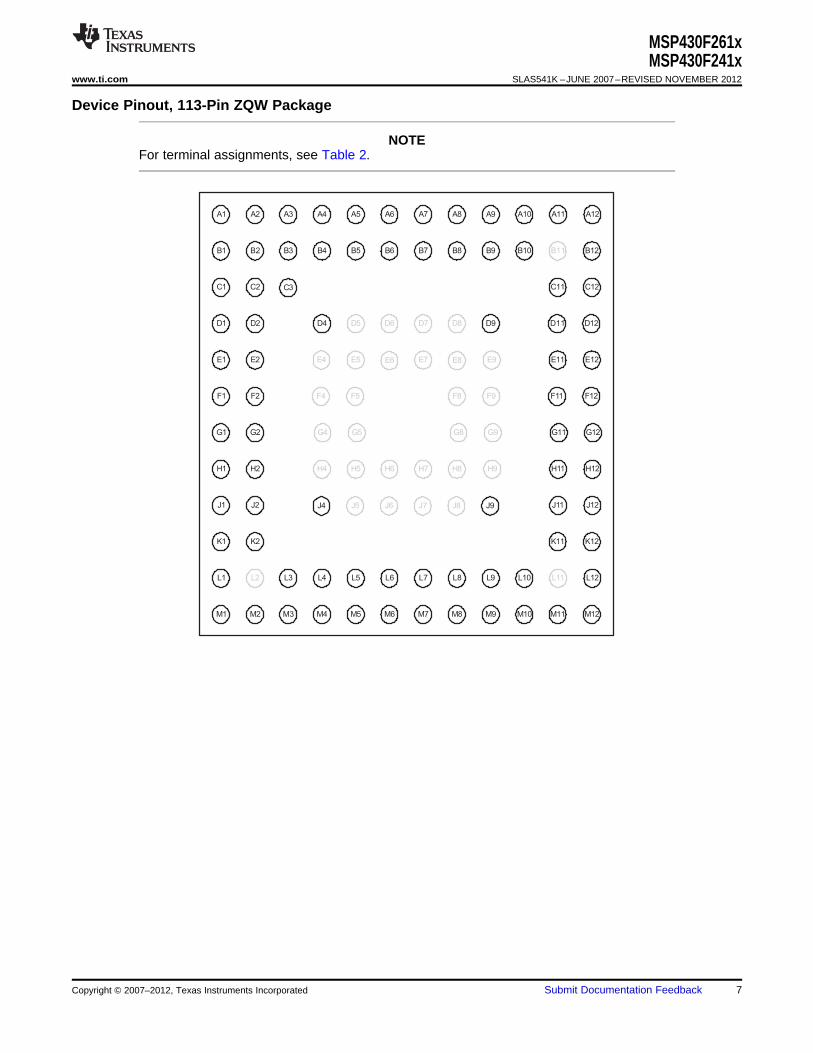
Device Pinout, 113-Pin ZQW Package
NOTEFor terminal assignments, see Table 2.
Copyright © 2007–2012, Texas Instruments Incorporated Submit Documentation Feedback 7
Oscillators
Basic Clock
System+
RAM
4KB
8KB
8KB
4KB
Brownout
Protection
SVS,
SVM
RST/NMI
DVCC DVSS
MCLK
Watchdog
WDT+
15-Bit
Timer_A3
3 CC
Registers
16MHz
CPU
1MB
incl. 16
Registers
Emulation
XOUT/
XT2OUT
JTAG
Interface
Ports
P1/P2
2x8 I/O
Interrupt
capability
Comp_A+
8
Channels
Flash
120KB
116KB
92KB
92KB
Hardware
Multiplier
MPY,
MPYS,
MAC,
MACS
Timer_B7
7 CC
Registers,
Shadow
Reg
ADC12
12-Bit
8
Channels
Ports
P3/P4
P5/P6
4x8 I/O
AVCC AVSS P1.x/P2.x
2x8
P3.x/P4.x
P5.x/P6.x
4x8
SMCLK
ACLK
MDB
MAB
XIN/
XT2IN
22
USCI A1UART/
LIN,IrDA, SPI
USCI B1SPI, I2C
USCI A0UART/
LIN,IrDA, SPI
USCI B0SPI, I2C
Oscillators
Basic Clock
System+
Brownout
Protection
SVS,
SVM
RST/NMI
DVCC1/2 DVSS1/2
MCLK
Watchdog
WDT+
15-Bit
Timer_A3
3 CC
Registers
16MHz
CPU
1MB
incl. 16
Registers
Emulation
JTAG
Interface
Ports
P1/P2
2x8 I/O
Interrupt
capability
USCI A1UART/
LIN,IrDA, SPI
USCI B1SPI, I2C
Comp_A+
8
Channels
Hardware
Multiplier
MPY,
MPYS,
MAC,
MACS
Timer_B7
7 CC
Registers,
Shadow
Reg
ADC12
12-Bit
8
Channels
Ports
P3/P4
P5/P6
4x8 I/O
AVCC AVSS P1.x/P2.x
2x8
P3.x/P4.x
P5.x/P6.x
4x8
SMCLK
ACLK
MDB
MAB
XIN/
XT2IN
22
XOUT/
XT2OUT
RAM
4KB
8KB
8KB
4KB
Flash
120KB
116KB
92KB
92KB
Ports
P7/P8
2x8/1x16
I/O
P7.x/P8.x2x8/
1x16
USCI A0UART/
LIN,IrDA, SPI
USCI B0SPI, I2C
MSP430F261xMSP430F241xSLAS541K –JUNE 2007–REVISED NOVEMBER 2012 www.ti.com
Functional Block Diagram, MSP430F241x, 80-Pin PN Package
Functional Block Diagram, MSP430F241x, 64-Pin PM Package
8 Submit Documentation Feedback Copyright © 2007–2012, Texas Instruments Incorporated
USCI A0UART/
LIN,IrDA, SPI
USCI B0SPI, I2C
Oscillators
Basic Clock
System+
Brownout
Protection
SVS,
SVM
RST/NMI
DVCC DVSS
MCLK
Watchdog
WDT+
15-Bit
Timer_A3
3 CC
Registers
16MHz
CPU
1MB
incl. 16
Registers
Emulation
JTAG
Interface
Ports
P1/P2
2x8 I/O
Interrupt
capability
Comp_A+
8
Channels
Hardware
Multiplier
MPY,
MPYS,
MAC,
MACS
Timer_B7
7 CC
Registers,
Shadow
Reg
ADC12
12-Bit
8
Channels
Ports
P3/P4
P5/P6
4x8 I/O
AVCC
2x8
P3.x/P4.x
P5.x/P6.x
4x8
SMCLK
ACLK
MDB
MAB
DAC12
12-Bit
2
Channels
Voltage
Out
DMA
Controller
3
Channels
XIN/
XT2IN
22
XOUT/
XT2OUT
RAM
4kB
8kB
8kB
4kB
4kB
Flash
120kB
116kB
92kB
92kB
56kB
USCI A1UART/
LIN,IrDA, SPI
USCI B1SPI, I2C
AVSS P1.x/P2.x
Oscillators
Basic Clock
System+
Brownout
Protection
SVS,
SVM
RST/NMI
DVCC1/2 DVSS1/2
MCLK
Watchdog
WDT+
15-Bit
Timer_A3
3 CC
Registers
16MHz
CPU
1MB
incl. 16
Registers
Emulation
JTAG
Interface
Ports
P1/P2
2x8 I/O
Interrupt
capability
Comp_A+
8
Channels
Hardware
Multiplier
MPY,
MPYS,
MAC,
MACS
Timer_B7
7 CC
Registers,
Shadow
Reg
ADC12
12-Bit
8
Channels
Ports
P3/P4
P5/P6
4x8 I/O
AVCC AVSS P1.x/P2.x
2x8
P3.x/P4.x
P5.x/P6.x
4x8
SMCLK
ACLK
MDB
MAB
DAC12
12-Bit
2
Channels
Voltage
Out
Ports
P7/P8
2x8/1x16
I/O
P7.x/P8.x2x8/
1x16
DMA
Controller
3
Channels
XIN/
XT2IN
22
XOUT/
XT2OUT
RAM
4kB
8kB
8kB
4kB
4kB
Flash
120kB
116kB
92kB
92kB
56kB
USCI A1UART/
LIN,IrDA, SPI
USCI B1SPI, I2C
USCI A0UART/
LIN,IrDA, SPI
USCI B0SPI, I2C
MSP430F261xMSP430F241x
www.ti.com SLAS541K –JUNE 2007–REVISED NOVEMBER 2012
Functional Block Diagram, MSP430F261x, 80-Pin PN Package
Functional Block Diagram, MSP430F261x, 64-Pin PM Package
Copyright © 2007–2012, Texas Instruments Incorporated Submit Documentation Feedback 9
MSP430F261xMSP430F241xSLAS541K –JUNE 2007–REVISED NOVEMBER 2012 www.ti.com
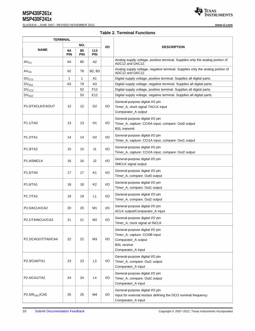
Table 2. Terminal Functions
TERMINAL
NO. I/O DESCRIPTIONNAME 64 80 113
PIN PIN PIN
Analog supply voltage, positive terminal. Supplies only the analog portion ofAVCC 64 80 A2 ADC12 and DAC12.
Analog supply voltage, negative terminal. Supplies only the analog portion ofAVSS 62 78 B2, B3 ADC12 and DAC12.
DVCC1 1 1 A1 Digital supply voltage, positive terminal. Supplies all digital parts.
DVSS1 63 79 A3 Digital supply voltage, negative terminal. Supplies all digital parts.
DVCC2 52 F12 Digital supply voltage, positive terminal. Supplies all digital parts.
DVSS2 53 E12 Digital supply voltage, negative terminal. Supplies all digital parts.
General-purpose digital I/O pinP1.0/TACLK/CAOUT 12 12 G2 I/O Timer_A, clock signal TACLK input
Comparator_A output
General-purpose digital I/O pinP1.1/TA0 13 13 H1 I/O Timer_A, capture: CCI0A input, compare: Out0 output
BSL transmit
General-purpose digital I/O pinP1.2/TA1 14 14 H2 I/OTimer_A, capture: CCI1A input, compare: Out1 output
General-purpose digital I/O pinP1.3/TA2 15 15 J1 I/OTimer_A, capture: CCI2A input, compare: Out2 output
General-purpose digital I/O pinP1.4/SMCLK 16 16 J2 I/OSMCLK signal output
General-purpose digital I/O pinP1.5/TA0 17 17 K1 I/OTimer_A, compare: Out0 output
General-purpose digital I/O pinP1.6/TA1 18 18 K2 I/OTimer_A, compare: Out1 output
General-purpose digital I/O pinP1.7/TA2 19 19 L1 I/OTimer_A, compare: Out2 output
General-purpose digital I/O pinP2.0/ACLK/CA2 20 20 M1 I/OACLK output/Comparator_A input
General-purpose digital I/O pinP2.1/TAINCLK/CA3 21 21 M2 I/OTimer_A, clock signal at INCLK
General-purpose digital I/O pin
Timer_A, capture: CCI0B inputP2.2/CAOUT/TA0/CA4 22 22 M3 I/O Comparator_A output
BSL receive
Comparator_A input
General-purpose digital I/O pinP2.3/CA0/TA1 23 23 L3 I/O Timer_A, compare: Out1 output
Comparator_A input
General-purpose digital I/O pinP2.4/CA1/TA2 24 24 L4 I/O Timer_A, compare: Out2 output
Comparator_A input
General-purpose digital I/O pinP2.5/ROSC/CA5 25 25 M4 I/O Input for external resistor defining the DCO nominal frequency
Comparator_A input
10 Submit Documentation Feedback Copyright © 2007–2012, Texas Instruments Incorporated
MSP430F261xMSP430F241x
www.ti.com SLAS541K –JUNE 2007–REVISED NOVEMBER 2012
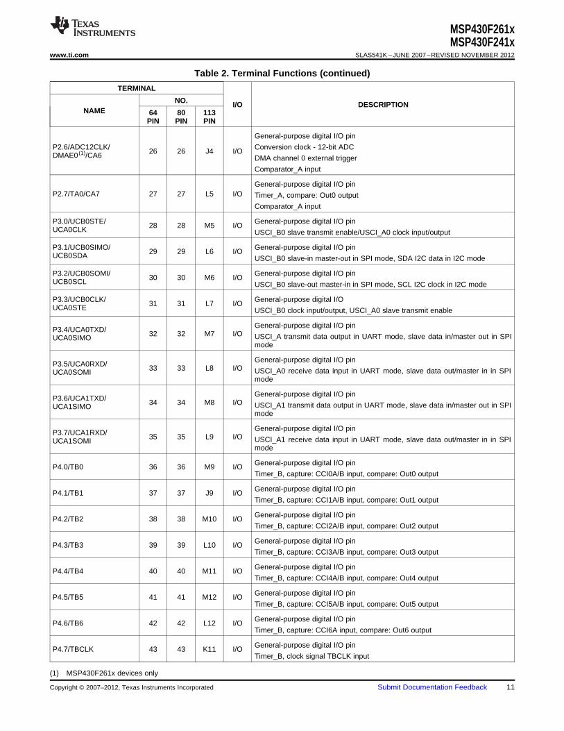
Table 2. Terminal Functions (continued)
TERMINAL
NO. I/O DESCRIPTIONNAME 64 80 113
PIN PIN PIN
General-purpose digital I/O pin
P2.6/ADC12CLK/ Conversion clock - 12-bit ADC26 26 J4 I/ODMAE0 (1)/CA6 DMA channel 0 external trigger
Comparator_A input
General-purpose digital I/O pinP2.7/TA0/CA7 27 27 L5 I/O Timer_A, compare: Out0 output
Comparator_A input
P3.0/UCB0STE/ General-purpose digital I/O pin28 28 M5 I/OUCA0CLK USCI_B0 slave transmit enable/USCI_A0 clock input/output
P3.1/UCB0SIMO/ General-purpose digital I/O pin29 29 L6 I/OUCB0SDA USCI_B0 slave-in master-out in SPI mode, SDA I2C data in I2C mode
P3.2/UCB0SOMI/ General-purpose digital I/O pin30 30 M6 I/OUCB0SCL USCI_B0 slave-out master-in in SPI mode, SCL I2C clock in I2C mode
P3.3/UCB0CLK/ General-purpose digital I/O31 31 L7 I/OUCA0STE USCI_B0 clock input/output, USCI_A0 slave transmit enable
General-purpose digital I/O pinP3.4/UCA0TXD/ 32 32 M7 I/O USCI_A transmit data output in UART mode, slave data in/master out in SPIUCA0SIMOmode
General-purpose digital I/O pinP3.5/UCA0RXD/ 33 33 L8 I/O USCI_A0 receive data input in UART mode, slave data out/master in in SPIUCA0SOMImode
General-purpose digital I/O pinP3.6/UCA1TXD/ 34 34 M8 I/O USCI_A1 transmit data output in UART mode, slave data in/master out in SPIUCA1SIMOmode
General-purpose digital I/O pinP3.7/UCA1RXD/ 35 35 L9 I/O USCI_A1 receive data input in UART mode, slave data out/master in in SPIUCA1SOMImode
General-purpose digital I/O pinP4.0/TB0 36 36 M9 I/OTimer_B, capture: CCI0A/B input, compare: Out0 output
General-purpose digital I/O pinP4.1/TB1 37 37 J9 I/OTimer_B, capture: CCI1A/B input, compare: Out1 output
General-purpose digital I/O pinP4.2/TB2 38 38 M10 I/OTimer_B, capture: CCI2A/B input, compare: Out2 output
General-purpose digital I/O pinP4.3/TB3 39 39 L10 I/OTimer_B, capture: CCI3A/B input, compare: Out3 output
General-purpose digital I/O pinP4.4/TB4 40 40 M11 I/OTimer_B, capture: CCI4A/B input, compare: Out4 output
General-purpose digital I/O pinP4.5/TB5 41 41 M12 I/OTimer_B, capture: CCI5A/B input, compare: Out5 output
General-purpose digital I/O pinP4.6/TB6 42 42 L12 I/OTimer_B, capture: CCI6A input, compare: Out6 output
General-purpose digital I/O pinP4.7/TBCLK 43 43 K11 I/OTimer_B, clock signal TBCLK input
(1) MSP430F261x devices only
Copyright © 2007–2012, Texas Instruments Incorporated Submit Documentation Feedback 11
MSP430F261xMSP430F241xSLAS541K –JUNE 2007–REVISED NOVEMBER 2012 www.ti.com
Table 2. Terminal Functions (continued)
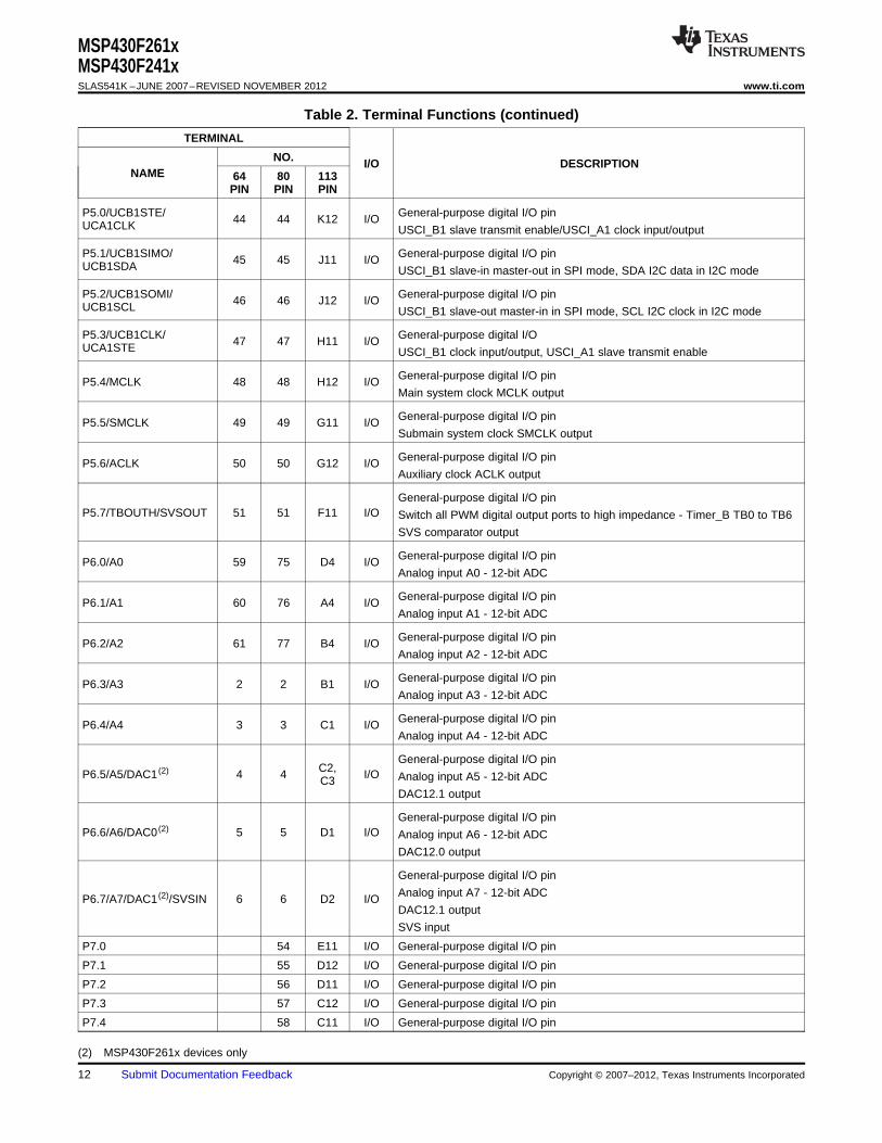
TERMINAL
NO. I/O DESCRIPTIONNAME 64 80 113
PIN PIN PIN
P5.0/UCB1STE/ General-purpose digital I/O pin44 44 K12 I/OUCA1CLK USCI_B1 slave transmit enable/USCI_A1 clock input/output
P5.1/UCB1SIMO/ General-purpose digital I/O pin45 45 J11 I/OUCB1SDA USCI_B1 slave-in master-out in SPI mode, SDA I2C data in I2C mode
P5.2/UCB1SOMI/ General-purpose digital I/O pin46 46 J12 I/OUCB1SCL USCI_B1 slave-out master-in in SPI mode, SCL I2C clock in I2C mode
P5.3/UCB1CLK/ General-purpose digital I/O47 47 H11 I/OUCA1STE USCI_B1 clock input/output, USCI_A1 slave transmit enable
General-purpose digital I/O pinP5.4/MCLK 48 48 H12 I/OMain system clock MCLK output
General-purpose digital I/O pinP5.5/SMCLK 49 49 G11 I/OSubmain system clock SMCLK output
General-purpose digital I/O pinP5.6/ACLK 50 50 G12 I/OAuxiliary clock ACLK output
General-purpose digital I/O pinP5.7/TBOUTH/SVSOUT 51 51 F11 I/O Switch all PWM digital output ports to high impedance - Timer_B TB0 to TB6
SVS comparator output
General-purpose digital I/O pinP6.0/A0 59 75 D4 I/OAnalog input A0 - 12-bit ADC
General-purpose digital I/O pinP6.1/A1 60 76 A4 I/OAnalog input A1 - 12-bit ADC
General-purpose digital I/O pinP6.2/A2 61 77 B4 I/OAnalog input A2 - 12-bit ADC
General-purpose digital I/O pinP6.3/A3 2 2 B1 I/OAnalog input A3 - 12-bit ADC
General-purpose digital I/O pinP6.4/A4 3 3 C1 I/OAnalog input A4 - 12-bit ADC
General-purpose digital I/O pinC2,P6.5/A5/DAC1 (2) 4 4 I/O Analog input A5 - 12-bit ADCC3
DAC12.1 output
General-purpose digital I/O pinP6.6/A6/DAC0 (2) 5 5 D1 I/O Analog input A6 - 12-bit ADC
DAC12.0 output
General-purpose digital I/O pin
Analog input A7 - 12-bit ADCP6.7/A7/DAC1 (2)/SVSIN 6 6 D2 I/ODAC12.1 output
SVS input
P7.0 54 E11 I/O General-purpose digital I/O pin
P7.1 55 D12 I/O General-purpose digital I/O pin
P7.2 56 D11 I/O General-purpose digital I/O pin
P7.3 57 C12 I/O General-purpose digital I/O pin
P7.4 58 C11 I/O General-purpose digital I/O pin
(2) MSP430F261x devices only
12 Submit Documentation Feedback Copyright © 2007–2012, Texas Instruments Incorporated
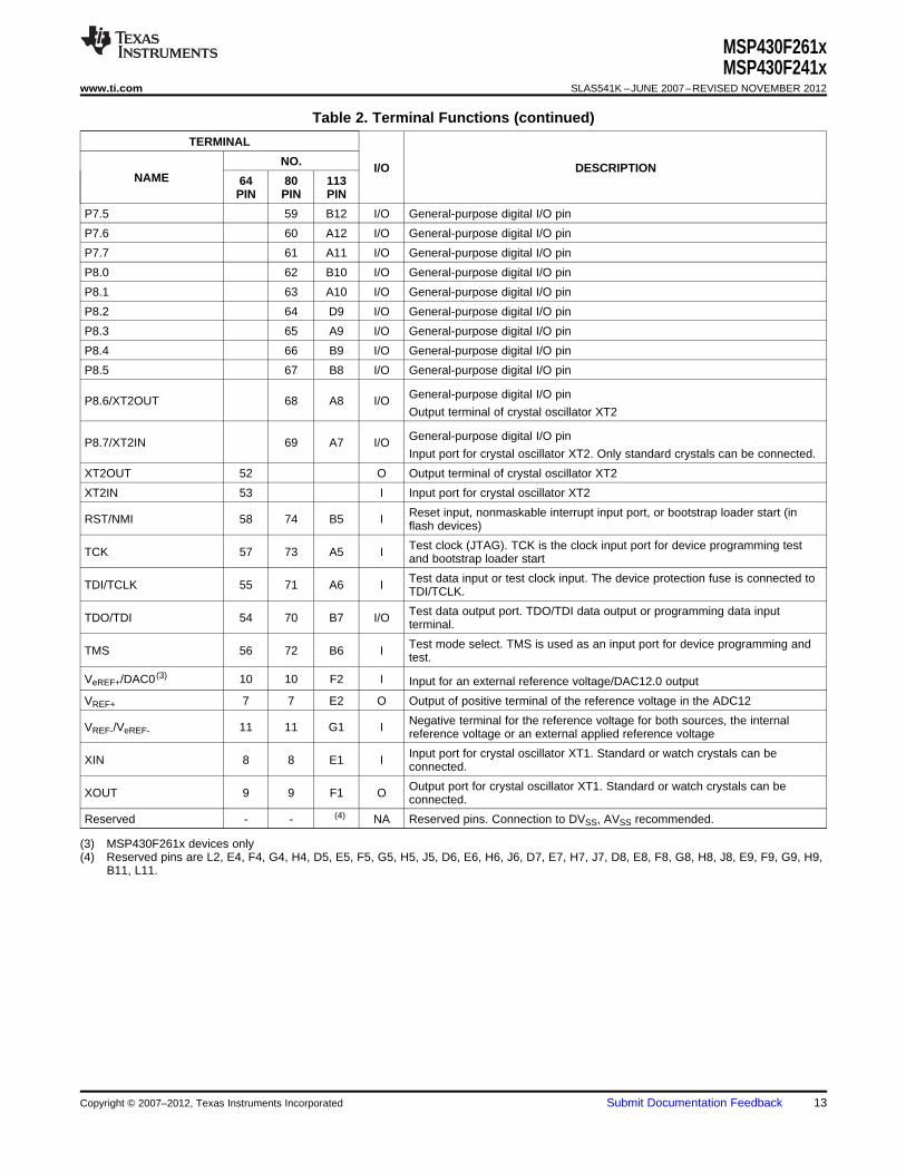
MSP430F261xMSP430F241x
www.ti.com SLAS541K –JUNE 2007–REVISED NOVEMBER 2012
Table 2. Terminal Functions (continued)
TERMINAL
NO. I/O DESCRIPTIONNAME 64 80 113
PIN PIN PIN
P7.5 59 B12 I/O General-purpose digital I/O pin
P7.6 60 A12 I/O General-purpose digital I/O pin
P7.7 61 A11 I/O General-purpose digital I/O pin
P8.0 62 B10 I/O General-purpose digital I/O pin
P8.1 63 A10 I/O General-purpose digital I/O pin
P8.2 64 D9 I/O General-purpose digital I/O pin
P8.3 65 A9 I/O General-purpose digital I/O pin
P8.4 66 B9 I/O General-purpose digital I/O pin
P8.5 67 B8 I/O General-purpose digital I/O pin
General-purpose digital I/O pinP8.6/XT2OUT 68 A8 I/OOutput terminal of crystal oscillator XT2
General-purpose digital I/O pinP8.7/XT2IN 69 A7 I/OInput port for crystal oscillator XT2. Only standard crystals can be connected.
XT2OUT 52 O Output terminal of crystal oscillator XT2
XT2IN 53 I Input port for crystal oscillator XT2
Reset input, nonmaskable interrupt input port, or bootstrap loader start (inRST/NMI 58 74 B5 I flash devices)
Test clock (JTAG). TCK is the clock input port for device programming testTCK 57 73 A5 I and bootstrap loader start
Test data input or test clock input. The device protection fuse is connected toTDI/TCLK 55 71 A6 I TDI/TCLK.
Test data output port. TDO/TDI data output or programming data inputTDO/TDI 54 70 B7 I/O terminal.
Test mode select. TMS is used as an input port for device programming andTMS 56 72 B6 I test.
VeREF+/DAC0 (3) 10 10 F2 I Input for an external reference voltage/DAC12.0 output
VREF+ 7 7 E2 O Output of positive terminal of the reference voltage in the ADC12
Negative terminal for the reference voltage for both sources, the internalVREF-/VeREF- 11 11 G1 I reference voltage or an external applied reference voltage
Input port for crystal oscillator XT1. Standard or watch crystals can beXIN 8 8 E1 I connected.
Output port for crystal oscillator XT1. Standard or watch crystals can beXOUT 9 9 F1 O connected.
Reserved - - (4) NA Reserved pins. Connection to DVSS, AVSS recommended.
(3) MSP430F261x devices only(4) Reserved pins are L2, E4, F4, G4, H4, D5, E5, F5, G5, H5, J5, D6, E6, H6, J6, D7, E7, H7, J7, D8, E8, F8, G8, H8, J8, E9, F9, G9, H9,
B11, L11.
Copyright © 2007–2012, Texas Instruments Incorporated Submit Documentation Feedback 13
General-Purpose Register
Program Counter
Stack Pointer
Status Register
Constant Generator
General-Purpose Register
General-Purpose Register
General-Purpose Register
PC/R0
SP/R1
SR/CG1/R2
CG2/R3
R4
R5
R12
R13
General-Purpose Register
General-Purpose Register
R6
R7
General-Purpose Register
General-Purpose Register
R8
R9
General-Purpose Register
General-Purpose Register
R10
R11
General-Purpose Register
General-Purpose Register
R14
R15
MSP430F261xMSP430F241xSLAS541K –JUNE 2007–REVISED NOVEMBER 2012 www.ti.com
SHORT-FORM DESCRIPTION
CPU
The MSP430 CPU has a 16-bit RISC architecturethat is highly transparent to the application. Alloperations, other than program-flow instructions, areperformed as register operations in conjunction withseven addressing modes for source operand and fouraddressing modes for destination operand.
The CPU is integrated with 16 registers that providereduced instruction execution time. The register-to-register operation execution time is one cycle of theCPU clock.
Four of the registers, R0 to R3, are dedicated asprogram counter, stack pointer, status register, andconstant generator respectively. The remainingregisters are general-purpose registers.
Peripherals are connected to the CPU using data,address, and control buses, and can be handled withall instructions.
Instruction Set
The instruction set consists of 51 instructions withthree formats and seven address modes. Eachinstruction can operate on word and byte data.Table 3 shows examples of the three types ofinstruction formats; Table 4 shows the addressmodes.
Table 3. Instruction Word Formats
INSTRUCTION FORMAT EXAMPLE OPERATION
Dual operands, source-destination ADD R4,R5 R4 + R5 -> R5
Single operands, destination only CALL R8 PC ->(TOS), R8-> PC
Relative jump, un/conditional JNE Jump-on-equal bit = 0
Table 4. Address Mode Descriptions
ADDRESS MODE S (1) D (1) SYNTAX EXAMPLE OPERATION
Register MOV Rs,Rd MOV R10,R11 R10 -> R11
Indexed MOV X(Rn),Y(Rm) MOV 2(R5),6(R6) M(2+R5)-> M(6+R6)
Symbolic (PC relative) MOV EDE,TONI M(EDE) -> M(TONI)
Absolute MOV &MEM,&TCDAT M(MEM) -> M(TCDAT)
Indirect MOV @Rn,Y(Rm) MOV @R10,Tab(R6) M(R10) -> M(Tab+R6)
M(R10) -> R11Indirect autoincrement MOV @Rn+,Rm MOV @R10+,R11 R10 + 2-> R10
Immediate MOV #X,TONI MOV #45,TONI #45 -> M(TONI)
(1) S = source, D = destination
14 Submit Documentation Feedback Copyright © 2007–2012, Texas Instruments Incorporated
MSP430F261xMSP430F241x
www.ti.com SLAS541K –JUNE 2007–REVISED NOVEMBER 2012
Operating Modes
The MSP430 has one active mode and five software-selectable low-power modes of operation. An interruptevent can wake the device from any of the five low-power modes, service the request, and restore back to thelow-power mode on return from the interrupt program.
The following six operating modes can be configured by software:• Active mode (AM)
– All clocks are active• Low-power mode 0 (LPM0)
– CPU is disabled– ACLK and SMCLK remain active– MCLK is disabled
• Low-power mode 1 (LPM1)– CPU is disabled– ACLK and SMCLK remain active. MCLK is disabled– DCO's dc-generator is disabled if DCO not used in active mode
• Low-power mode 2 (LPM2)– CPU is disabled– MCLK and SMCLK are disabled– DCO's dc-generator remains enabled– ACLK remains active
• Low-power mode 3 (LPM3)– CPU is disabled– MCLK and SMCLK are disabled– DCO's dc-generator is disabled– ACLK remains active
• Low-power mode 4 (LPM4)– CPU is disabled– ACLK is disabled– MCLK and SMCLK are disabled– DCO's dc-generator is disabled– Crystal oscillator is stopped
Copyright © 2007–2012, Texas Instruments Incorporated Submit Documentation Feedback 15
MSP430F261xMSP430F241xSLAS541K –JUNE 2007–REVISED NOVEMBER 2012 www.ti.com
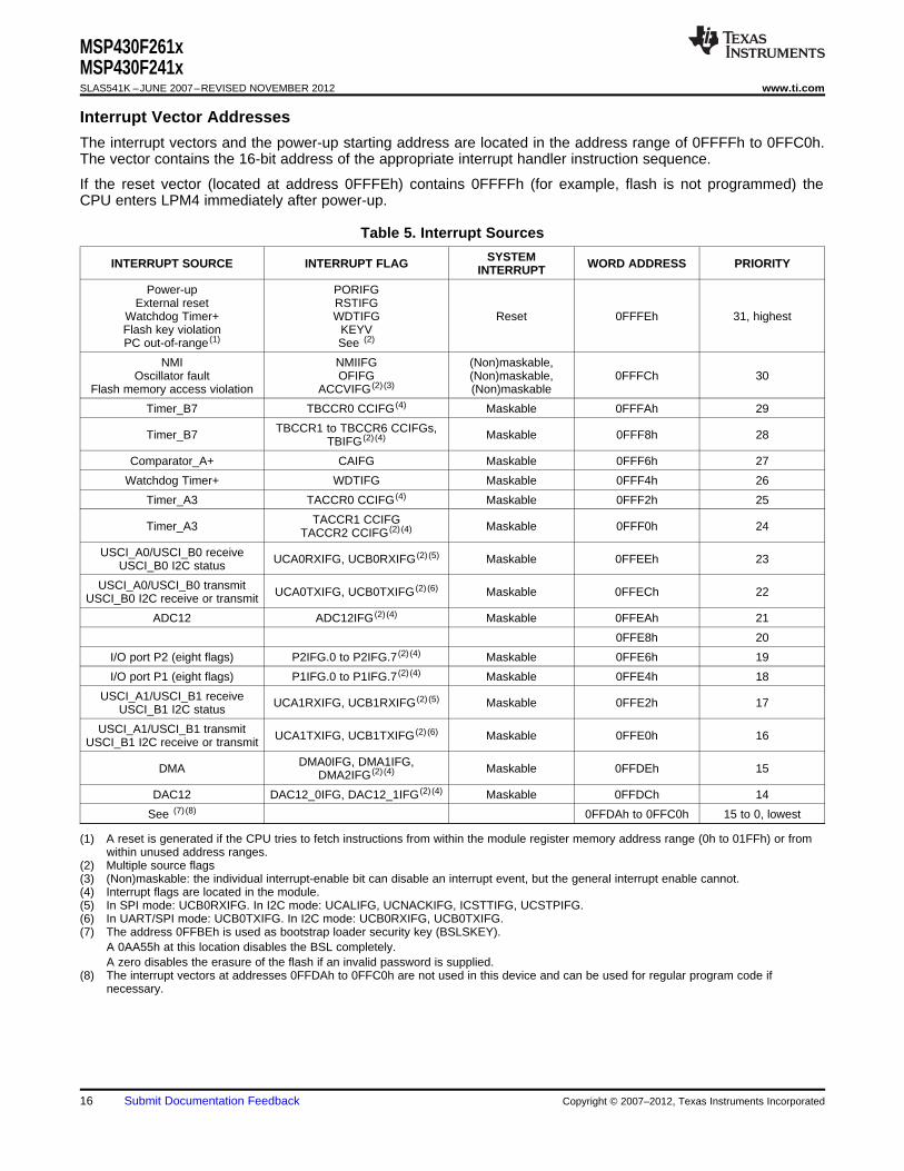
Interrupt Vector Addresses
The interrupt vectors and the power-up starting address are located in the address range of 0FFFFh to 0FFC0h.The vector contains the 16-bit address of the appropriate interrupt handler instruction sequence.
If the reset vector (located at address 0FFFEh) contains 0FFFFh (for example, flash is not programmed) theCPU enters LPM4 immediately after power-up.
Table 5. Interrupt Sources
SYSTEMINTERRUPT SOURCE INTERRUPT FLAG WORD ADDRESS PRIORITYINTERRUPT
Power-up PORIFGExternal reset RSTIFG
Watchdog Timer+ WDTIFG Reset 0FFFEh 31, highestFlash key violation KEYVPC out-of-range (1) See (2)
NMI NMIIFG (Non)maskable,Oscillator fault OFIFG (Non)maskable, 0FFFCh 30
Flash memory access violation ACCVIFG (2) (3) (Non)maskable
Timer_B7 TBCCR0 CCIFG (4) Maskable 0FFFAh 29
TBCCR1 to TBCCR6 CCIFGs,Timer_B7 Maskable 0FFF8h 28TBIFG (2) (4)
Comparator_A+ CAIFG Maskable 0FFF6h 27
Watchdog Timer+ WDTIFG Maskable 0FFF4h 26
Timer_A3 TACCR0 CCIFG (4) Maskable 0FFF2h 25
TACCR1 CCIFGTimer_A3 Maskable 0FFF0h 24TACCR2 CCIFG (2) (4)
USCI_A0/USCI_B0 receive UCA0RXIFG, UCB0RXIFG (2) (5) Maskable 0FFEEh 23USCI_B0 I2C status
USCI_A0/USCI_B0 transmit UCA0TXIFG, UCB0TXIFG (2) (6) Maskable 0FFECh 22USCI_B0 I2C receive or transmit
ADC12 ADC12IFG (2) (4) Maskable 0FFEAh 21
0FFE8h 20
I/O port P2 (eight flags) P2IFG.0 to P2IFG.7 (2) (4) Maskable 0FFE6h 19
I/O port P1 (eight flags) P1IFG.0 to P1IFG.7 (2) (4) Maskable 0FFE4h 18
USCI_A1/USCI_B1 receive UCA1RXIFG, UCB1RXIFG (2) (5) Maskable 0FFE2h 17USCI_B1 I2C status
USCI_A1/USCI_B1 transmit UCA1TXIFG, UCB1TXIFG (2) (6) Maskable 0FFE0h 16USCI_B1 I2C receive or transmit
DMA0IFG, DMA1IFG,DMA Maskable 0FFDEh 15DMA2IFG (2) (4)
DAC12 DAC12_0IFG, DAC12_1IFG (2) (4) Maskable 0FFDCh 14
See (7) (8) 0FFDAh to 0FFC0h 15 to 0, lowest
(1) A reset is generated if the CPU tries to fetch instructions from within the module register memory address range (0h to 01FFh) or fromwithin unused address ranges.
(2) Multiple source flags(3) (Non)maskable: the individual interrupt-enable bit can disable an interrupt event, but the general interrupt enable cannot.(4) Interrupt flags are located in the module.(5) In SPI mode: UCB0RXIFG. In I2C mode: UCALIFG, UCNACKIFG, ICSTTIFG, UCSTPIFG.(6) In UART/SPI mode: UCB0TXIFG. In I2C mode: UCB0RXIFG, UCB0TXIFG.(7) The address 0FFBEh is used as bootstrap loader security key (BSLSKEY).
A 0AA55h at this location disables the BSL completely.A zero disables the erasure of the flash if an invalid password is supplied.
(8) The interrupt vectors at addresses 0FFDAh to 0FFC0h are not used in this device and can be used for regular program code ifnecessary.
16 Submit Documentation Feedback Copyright © 2007–2012, Texas Instruments Incorporated
MSP430F261xMSP430F241x
www.ti.com SLAS541K –JUNE 2007–REVISED NOVEMBER 2012
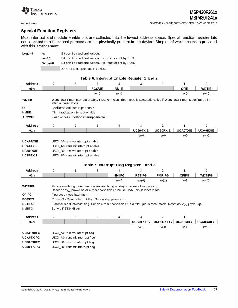
Special Function Registers
Most interrupt and module enable bits are collected into the lowest address space. Special function register bitsnot allocated to a functional purpose are not physically present in the device. Simple software access is providedwith this arrangement.
Legend rw: Bit can be read and written.
rw-0,1: Bit can be read and written. It is reset or set by PUC.
rw-(0,1): Bit can be read and written. It is reset or set by POR.
SFR bit is not present in device.
Table 6. Interrupt Enable Register 1 and 2Address 7 6 5 4 3 2 1 0
00h ACCVIE NMIIE OFIE WDTIE
rw-0 rw-0 rw-0 rw-0
WDTIE Watchdog Timer interrupt enable. Inactive if watchdog mode is selected. Active if Watchdog Timer is configured ininterval timer mode.
OFIE Oscillator fault interrupt enable
NMIIE (Non)maskable interrupt enable
ACCVIE Flash access violation interrupt enable
Address 7 6 5 4 3 2 1 0
01h UCB0TXIE UCB0RXIE UCA0TXIE UCA0RXIE
rw-0 rw-0 rw-0 rw-0
UCA0RXIE USCI_A0 receive interrupt enable
UCA0TXIE USCI_A0 transmit interrupt enable
UCB0RXIE USCI_B0 receive interrupt enable
UCB0TXIE USCI_B0 transmit interrupt enable
Table 7. Interrupt Flag Register 1 and 2Address 7 6 5 4 3 2 1 0
02h NMIIFG RSTIFG PORIFG OFIFG WDTIFG
rw-0 rw-(0) rw-(1) rw-1 rw-(0)
WDTIFG Set on watchdog timer overflow (in watchdog mode) or security key violation.Reset on VCC power-on or a reset condition at the RST/NMI pin in reset mode.
OFIFG Flag set on oscillator fault.
PORIFG Power-On Reset interrupt flag. Set on VCC power-up.
RSTIFG External reset interrupt flag. Set on a reset condition at RST/NMI pin in reset mode. Reset on VCC power-up.
NMIIFG Set via RST/NMI pin
Address 7 6 5 4 3 2 1 0
03h UCB0TXIFG UCB0RXIFG UCA0TXIFG UCA0RXIFG
rw-1 rw-0 rw-1 rw-0
UCA0RXIFG USCI_A0 receive interrupt flag
UCA0TXIFG USCI_A0 transmit interrupt flag
UCB0RXIFG USCI_B0 receive interrupt flag
UCB0TXIFG USCI_B0 transmit interrupt flag
Copyright © 2007–2012, Texas Instruments Incorporated Submit Documentation Feedback 17
MSP430F261xMSP430F241xSLAS541K –JUNE 2007–REVISED NOVEMBER 2012 www.ti.com
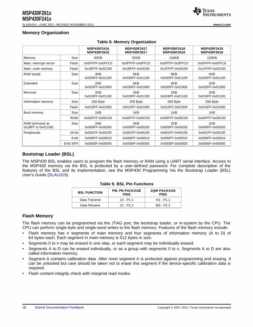
Memory Organization
Table 8. Memory Organization
MSP430F2416 MSP430F2417 MSP430F2418 MSP430F2419MSP430F2616 MSP430F2617 MSP430F2618 MSP430F2619
Memory Size 92KB 92KB 116KB 120KB
Main: interrupt vector Flash 0x0FFFF-0x0FFC0 0x0FFFF-0x0FFC0 0x0FFFF-0x0FFC0 0x0FFFF-0x0FFC0
Main: code memory Flash 0x18FFF-0x02100 0x19FFF-0x03100 0x1FFFF-0x03100 0x1FFFF-0x02100
RAM (total) Size 4KB 8KB 8KB 4KB0x020FF-0x01100 0x030FF-0x01100 0x030FF-0x01100 0x020FF-0x01100
Extended Size 2KB 6KB 6KB 2KB0x020FF-0x01900 0x030FF-0x01900 0x030FF-0x01900 0x020FF-0x01900
Mirrored Size 2KB 2KB 2KB 2KB0x018FF-0x01100 0x018FF-0x01100 0x018FF-0x01100 0x018FF-0x01100
Information memory Size 256 Byte 256 Byte 256 Byte 256 Byte
Flash 0x010FF-0x01000 0x010FF-0x01000 0x010FF-0x01000 0x010FF-0x01000
Boot memory Size 1KB 1KB 1KB 1KB
ROM 0x00FFF-0x00C00 0x00FFF-0x00C00 0x00FFF-0x00C00 0x00FFF-0x00C00
RAM (mirrored at Size 2KB 2KB 2KB 2KB0x18FF to 0x01100) 0x009FF-0x00200 0x009FF-0x00200 0x009FF-0x00200 0x009FF-0x00200
Peripherals 16-bit 0x001FF-0x00100 0x001FF-0x00100 0x001FF-0x00100 0x001FF-0x00100
8-bit 0x000FF-0x00010 0x000FF-0x00010 0x000FF-0x00010 0x000FF-0x00010
8-bit SFR 0x0000F-0x00000 0x0000F-0x00000 0x0000F-0x00000 0x0000F-0x00000
Bootstrap Loader (BSL)
The MSP430 BSL enables users to program the flash memory or RAM using a UART serial interface. Access tothe MSP430 memory via the BSL is protected by a user-defined password. For complete description of thefeatures of the BSL and its implementation, see the MSP430 Programming Via the Bootstrap Loader (BSL)User's Guide (SLAU319).
Table 9. BSL Pin Functions
PM, PN PACKAGE ZQW PACKAGEBSL FUNCTION PINS PINS
Data Transmit 13 - P1.1 H1 - P1.1
Data Receive 22 - P2.2 M3 - P2.2
Flash Memory
The flash memory can be programmed via the JTAG port, the bootstrap loader, or in-system by the CPU. TheCPU can perform single-byte and single-word writes to the flash memory. Features of the flash memory include:• Flash memory has n segments of main memory and four segments of information memory (A to D) of
64 bytes each. Each segment in main memory is 512 bytes in size.• Segments 0 to n may be erased in one step, or each segment may be individually erased.• Segments A to D can be erased individually, or as a group with segments 0 to n. Segments A to D are also
called information memory.• Segment A contains calibration data. After reset segment A is protected against programming and erasing. It
can be unlocked but care should be taken not to erase this segment if the device-specific calibration data isrequired.
• Flash content integrity check with marginal read modes
18 Submit Documentation Feedback Copyright © 2007–2012, Texas Instruments Incorporated
MSP430F261xMSP430F241x
www.ti.com SLAS541K –JUNE 2007–REVISED NOVEMBER 2012
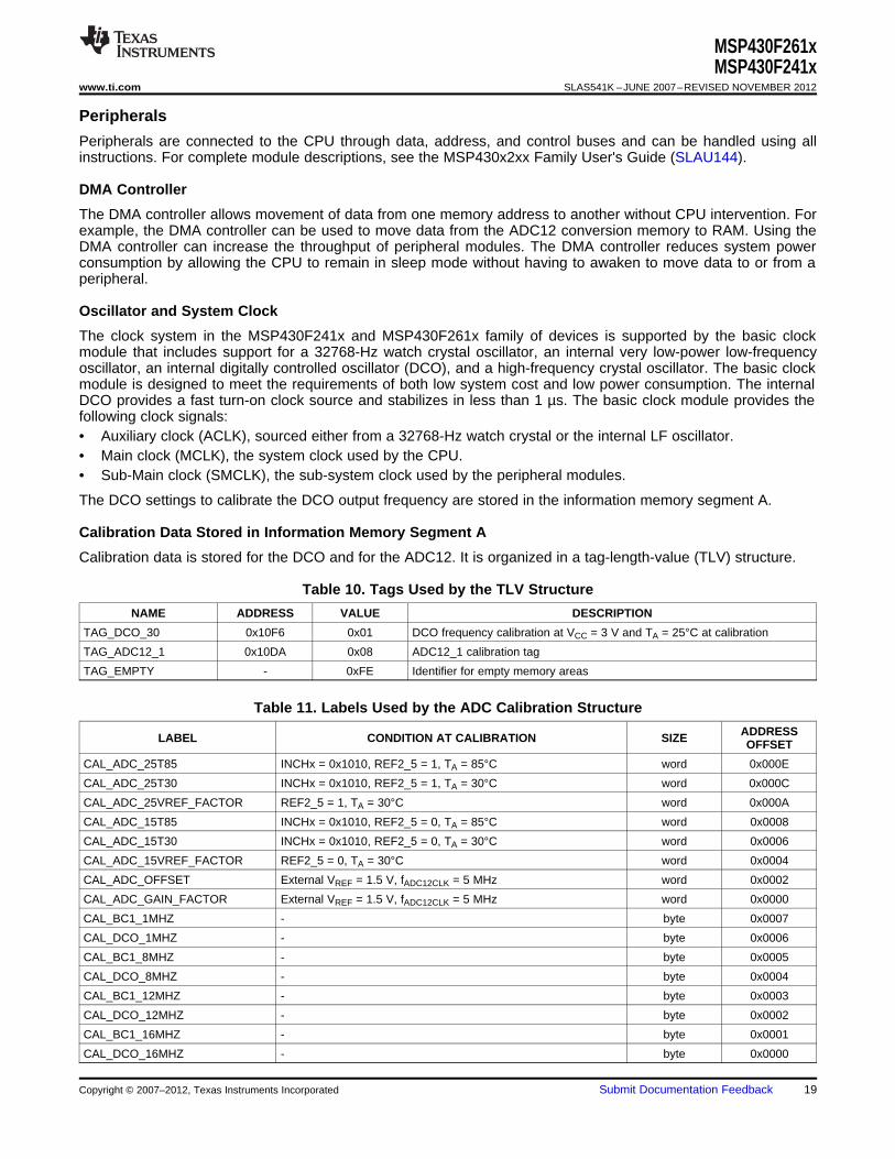
Peripherals
Peripherals are connected to the CPU through data, address, and control buses and can be handled using allinstructions. For complete module descriptions, see the MSP430x2xx Family User's Guide (SLAU144).
DMA Controller
The DMA controller allows movement of data from one memory address to another without CPU intervention. Forexample, the DMA controller can be used to move data from the ADC12 conversion memory to RAM. Using theDMA controller can increase the throughput of peripheral modules. The DMA controller reduces system powerconsumption by allowing the CPU to remain in sleep mode without having to awaken to move data to or from aperipheral.
Oscillator and System Clock
The clock system in the MSP430F241x and MSP430F261x family of devices is supported by the basic clockmodule that includes support for a 32768-Hz watch crystal oscillator, an internal very low-power low-frequencyoscillator, an internal digitally controlled oscillator (DCO), and a high-frequency crystal oscillator. The basic clockmodule is designed to meet the requirements of both low system cost and low power consumption. The internalDCO provides a fast turn-on clock source and stabilizes in less than 1 µs. The basic clock module provides thefollowing clock signals:• Auxiliary clock (ACLK), sourced either from a 32768-Hz watch crystal or the internal LF oscillator.• Main clock (MCLK), the system clock used by the CPU.• Sub-Main clock (SMCLK), the sub-system clock used by the peripheral modules.
The DCO settings to calibrate the DCO output frequency are stored in the information memory segment A.
Calibration Data Stored in Information Memory Segment A
Calibration data is stored for the DCO and for the ADC12. It is organized in a tag-length-value (TLV) structure.
Table 10. Tags Used by the TLV Structure
NAME ADDRESS VALUE DESCRIPTION
TAG_DCO_30 0x10F6 0x01 DCO frequency calibration at VCC = 3 V and TA = 25°C at calibration
TAG_ADC12_1 0x10DA 0x08 ADC12_1 calibration tag
TAG_EMPTY - 0xFE Identifier for empty memory areas
Table 11. Labels Used by the ADC Calibration Structure
ADDRESSLABEL CONDITION AT CALIBRATION SIZE OFFSET
CAL_ADC_25T85 INCHx = 0x1010, REF2_5 = 1, TA = 85°C word 0x000E
CAL_ADC_25T30 INCHx = 0x1010, REF2_5 = 1, TA = 30°C word 0x000C
CAL_ADC_25VREF_FACTOR REF2_5 = 1, TA = 30°C word 0x000A
CAL_ADC_15T85 INCHx = 0x1010, REF2_5 = 0, TA = 85°C word 0x0008
CAL_ADC_15T30 INCHx = 0x1010, REF2_5 = 0, TA = 30°C word 0x0006
CAL_ADC_15VREF_FACTOR REF2_5 = 0, TA = 30°C word 0x0004
CAL_ADC_OFFSET External VREF = 1.5 V, fADC12CLK = 5 MHz word 0x0002
CAL_ADC_GAIN_FACTOR External VREF = 1.5 V, fADC12CLK = 5 MHz word 0x0000
CAL_BC1_1MHZ - byte 0x0007
CAL_DCO_1MHZ - byte 0x0006
CAL_BC1_8MHZ - byte 0x0005
CAL_DCO_8MHZ - byte 0x0004
CAL_BC1_12MHZ - byte 0x0003
CAL_DCO_12MHZ - byte 0x0002
CAL_BC1_16MHZ - byte 0x0001
CAL_DCO_16MHZ - byte 0x0000
Copyright © 2007–2012, Texas Instruments Incorporated Submit Documentation Feedback 19
MSP430F261xMSP430F241xSLAS541K –JUNE 2007–REVISED NOVEMBER 2012 www.ti.com
Brownout, Supply Voltage Supervisor (SVS)
The brownout circuit is implemented to provide the proper internal reset signal to the device during power on andpower off. The SVS circuitry detects if the supply voltage drops below a user selectable level and supports bothsupply voltage supervision (the device is automatically reset) and supply voltage monitoring (SVM) (the device isnot automatically reset).
The CPU begins code execution after the brownout circuit releases the device reset. However, VCC may not haveramped to VCC(min) at that time. The user must ensure that the default DCO settings are not changed until VCCreaches VCC(min). If desired, the SVS circuit can be used to determine when VCC reaches VCC(min).
Digital I/O
There are up to eight 8-bit I/O ports implemented—ports P1 through P8:• All individual I/O bits are independently programmable.• Any combination of input, output, and interrupt condition is possible.• Edge-selectable interrupt input capability for all the eight bits of port P1 and port P2.• Read and write access to port-control registers is supported by all instructions.• Each I/O has an individually programmable pullup or pulldown resistor.• Ports P7 and P8 can be accessed word-wise.
Watchdog Timer (WDT+)
The primary function of the watchdog timer (WDT+) module is to perform a controlled system restart after asoftware problem occurs. If the selected time interval expires, a system reset is generated. If the watchdogfunction is not needed in an application, the module can be disabled or configured as an interval timer and cangenerate interrupts at selected time intervals.
Hardware Multiplier
The multiplication operation is supported by a dedicated peripheral module. The module performs 16x16, 16x8,8x16, and 8x8 bit operations. The module is capable of supporting signed and unsigned multiplication as well assigned and unsigned multiply and accumulate operations. The result of an operation can be accessedimmediately after the operands have been loaded into the peripheral registers. No additional clock cycles arerequired.
Universal Serial Communication Interface (USCI)
The USCI modules are used for serial data communication. The USCI module supports synchronouscommunication protocols such as SPI (3 pin or 4 pin) or I2C, and asynchronous combination protocols such asUART, enhanced UART with automatic baudrate detection (LIN), and IrDA.
The USCI_A module provides support for SPI (3 pin or 4 pin), UART, enhanced UART, and IrDA.
The USCI_B module provides support for SPI (3 pin or 4 pin) and I2C
20 Submit Documentation Feedback Copyright © 2007–2012, Texas Instruments Incorporated
MSP430F261xMSP430F241x
www.ti.com SLAS541K –JUNE 2007–REVISED NOVEMBER 2012
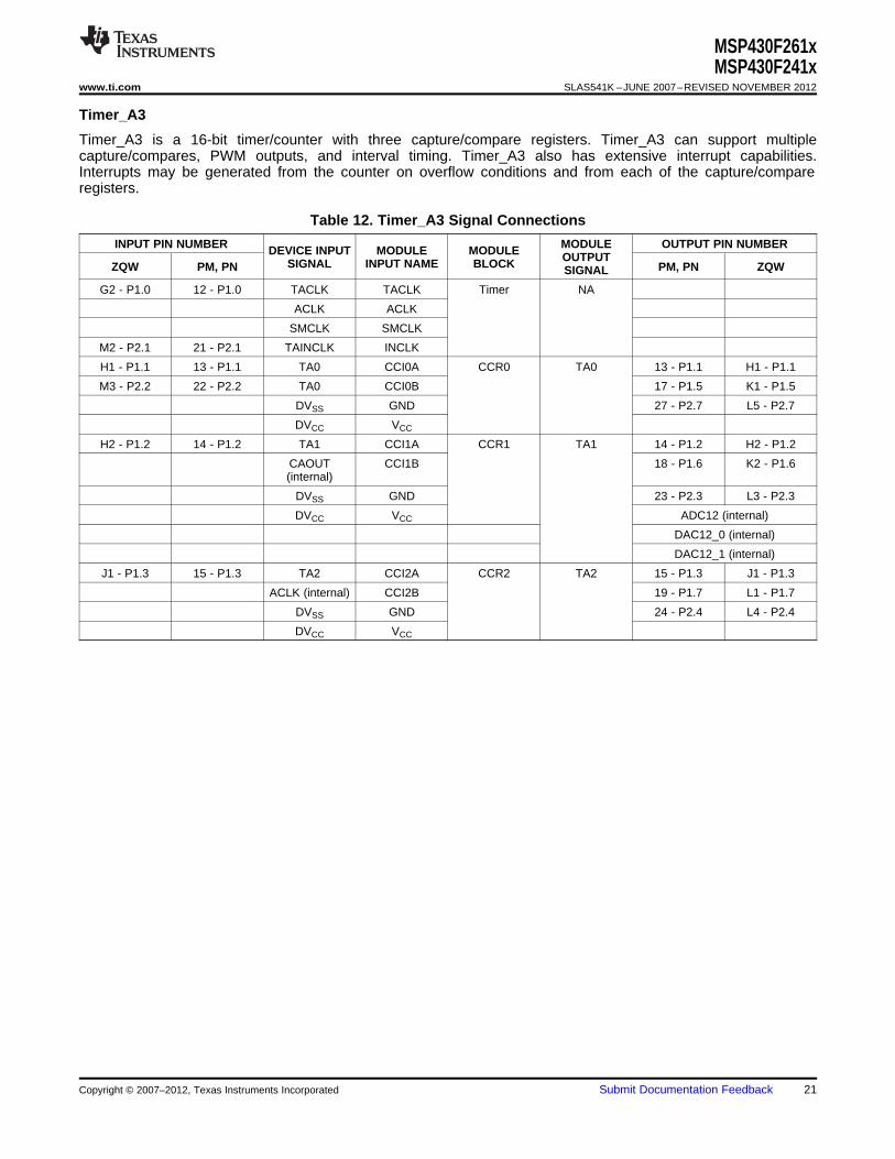
Timer_A3
Timer_A3 is a 16-bit timer/counter with three capture/compare registers. Timer_A3 can support multiplecapture/compares, PWM outputs, and interval timing. Timer_A3 also has extensive interrupt capabilities.Interrupts may be generated from the counter on overflow conditions and from each of the capture/compareregisters.
Table 12. Timer_A3 Signal Connections
INPUT PIN NUMBER MODULE OUTPUT PIN NUMBERDEVICE INPUT MODULE MODULE OUTPUTSIGNAL INPUT NAME BLOCKZQW PM, PN PM, PN ZQWSIGNAL
G2 - P1.0 12 - P1.0 TACLK TACLK Timer NA
ACLK ACLK
SMCLK SMCLK
M2 - P2.1 21 - P2.1 TAINCLK INCLK
H1 - P1.1 13 - P1.1 TA0 CCI0A CCR0 TA0 13 - P1.1 H1 - P1.1
M3 - P2.2 22 - P2.2 TA0 CCI0B 17 - P1.5 K1 - P1.5
DVSS GND 27 - P2.7 L5 - P2.7
DVCC VCC
H2 - P1.2 14 - P1.2 TA1 CCI1A CCR1 TA1 14 - P1.2 H2 - P1.2
CAOUT CCI1B 18 - P1.6 K2 - P1.6(internal)
DVSS GND 23 - P2.3 L3 - P2.3
DVCC VCC ADC12 (internal)
DAC12_0 (internal)
DAC12_1 (internal)
J1 - P1.3 15 - P1.3 TA2 CCI2A CCR2 TA2 15 - P1.3 J1 - P1.3
ACLK (internal) CCI2B 19 - P1.7 L1 - P1.7
DVSS GND 24 - P2.4 L4 - P2.4
DVCC VCC
Copyright © 2007–2012, Texas Instruments Incorporated Submit Documentation Feedback 21
MSP430F261xMSP430F241xSLAS541K –JUNE 2007–REVISED NOVEMBER 2012 www.ti.com
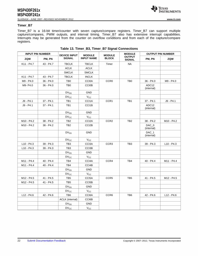
Timer_B7
Timer_B7 is a 16-bit timer/counter with seven capture/compare registers. Timer_B7 can support multiplecapture/compares, PWM outputs, and interval timing. Timer_B7 also has extensive interrupt capabilities.Interrupts may be generated from the counter on overflow conditions and from each of the capture/compareregisters.
Table 13. Timer_B3, Timer_B7 Signal Connections
INPUT PIN NUMBER MODULE OUTPUT PIN NUMBERDEVICE INPUT MODULE MODULE OUTPUTSIGNAL INPUT NAME BLOCKZQW PM, PN PM, PN ZQWSIGNAL
K11 - P4.7 43 - P4.7 TBCLK TBCLK Timer NA
ACLK ACLK
SMCLK SMCLK
K11 - P4.7 43 - P4.7 TBCLK INCLK
M9 - P4.0 36 - P4.0 TB0 CCI0A CCR0 TB0 36 - P4.0 M9 - P4.0
M9- P4.0 36 - P4.0 TB0 CCI0B ADC12(internal)
DVSS GND
DVCC VCC
J9 - P4.1 37 - P4.1 TB1 CCI1A CCR1 TB1 37 - P4.1 J9 - P4.1
J9 - P4.1 37 - P4.1 TB1 CCI1B ADC12(internal)
DVSS GND
DVCC VCC
M10 - P4.2 38 - P4.2 TB2 CCI2A CCR2 TB2 38 - P4.2 M10 - P4.2
M10 - P4.2 38 - P4.2 TB2 CCI2B DAC_0(internal)
DVSS GND DAC_1(internal)
DVCC VCC
L10 - P4.3 39 - P4.3 TB3 CCI3A CCR3 TB3 39 - P4.3 L10 - P4.3
L10 - P4.3 39 - P4.3 TB3 CCI3B
DVSS GND
DVCC VCC
M11 - P4.4 40 - P4.4 TB4 CCI4A CCR4 TB4 40 - P4.4 M11 - P4.4
M11 - P4.4 40 - P4.4 TB4 CCI4B
DVSS GND
DVCC VCC
M12 - P4.5 41 - P4.5 TB5 CCI5A CCR5 TB5 41 - P4.5 M12 - P4.5
M12 - P4.5 41 - P4.5 TB5 CCI5B
DVSS GND
DVCC VCC
L12 - P4.6 42 - P4.6 TB6 CCI6A CCR6 TB6 42 - P4.6 L12 - P4.6
ACLK (internal) CCI6B
DVSS GND
DVCC VCC
22 Submit Documentation Feedback Copyright © 2007–2012, Texas Instruments Incorporated
MSP430F261xMSP430F241x
www.ti.com SLAS541K –JUNE 2007–REVISED NOVEMBER 2012
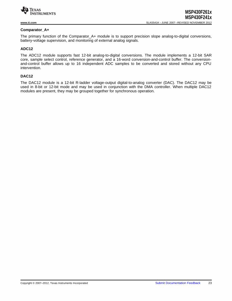
Comparator_A+
The primary function of the Comparator_A+ module is to support precision slope analog-to-digital conversions,battery-voltage supervision, and monitoring of external analog signals.
ADC12
The ADC12 module supports fast 12-bit analog-to-digital conversions. The module implements a 12-bit SARcore, sample select control, reference generator, and a 16-word conversion-and-control buffer. The conversion-and-control buffer allows up to 16 independent ADC samples to be converted and stored without any CPUintervention.
DAC12
The DAC12 module is a 12-bit R-ladder voltage-output digital-to-analog converter (DAC). The DAC12 may beused in 8-bit or 12-bit mode and may be used in conjunction with the DMA controller. When multiple DAC12modules are present, they may be grouped together for synchronous operation.
Copyright © 2007–2012, Texas Instruments Incorporated Submit Documentation Feedback 23
MSP430F261xMSP430F241xSLAS541K –JUNE 2007–REVISED NOVEMBER 2012 www.ti.com
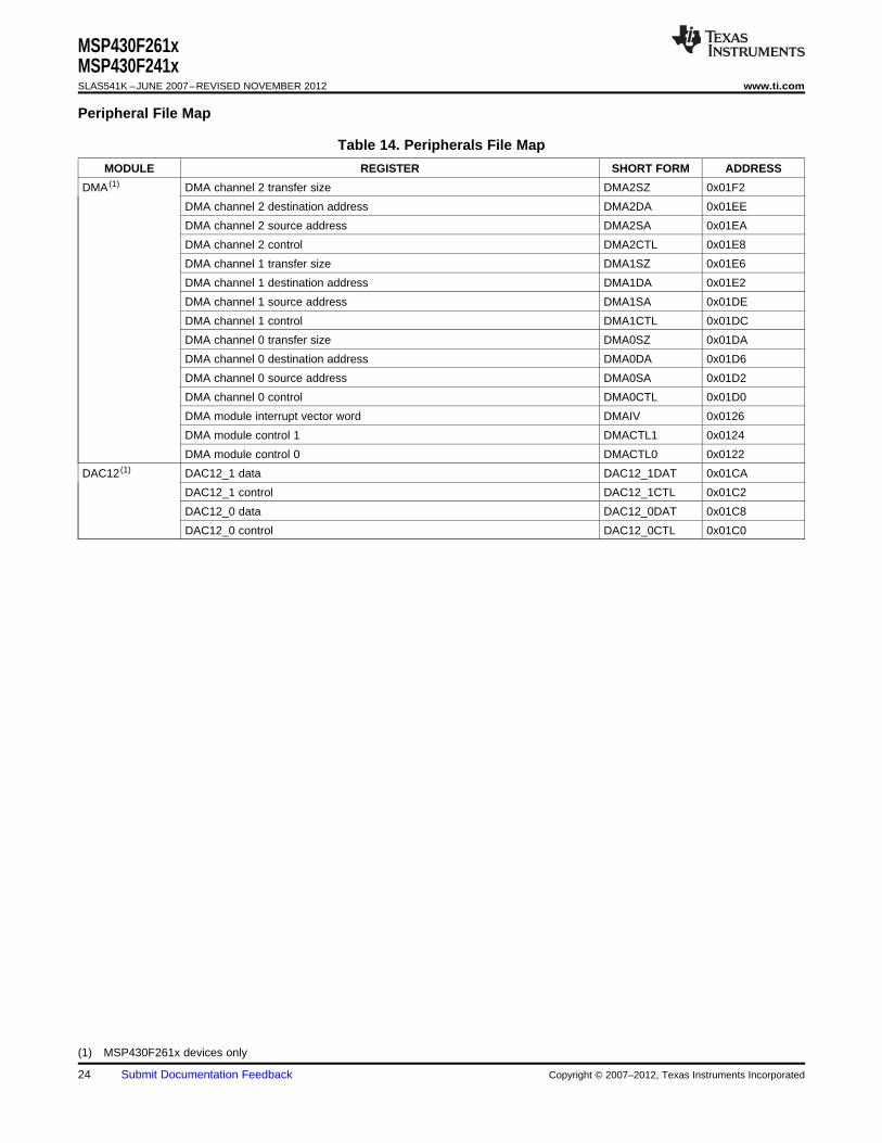
Peripheral File Map
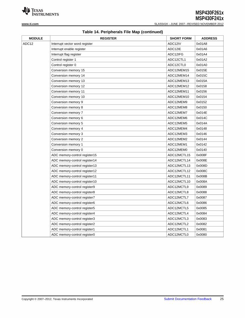
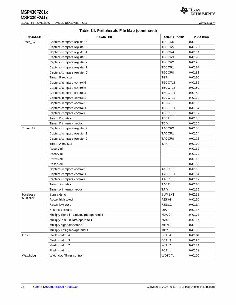
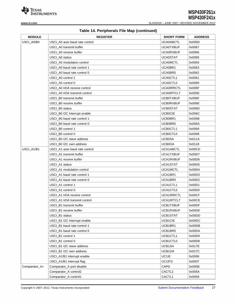
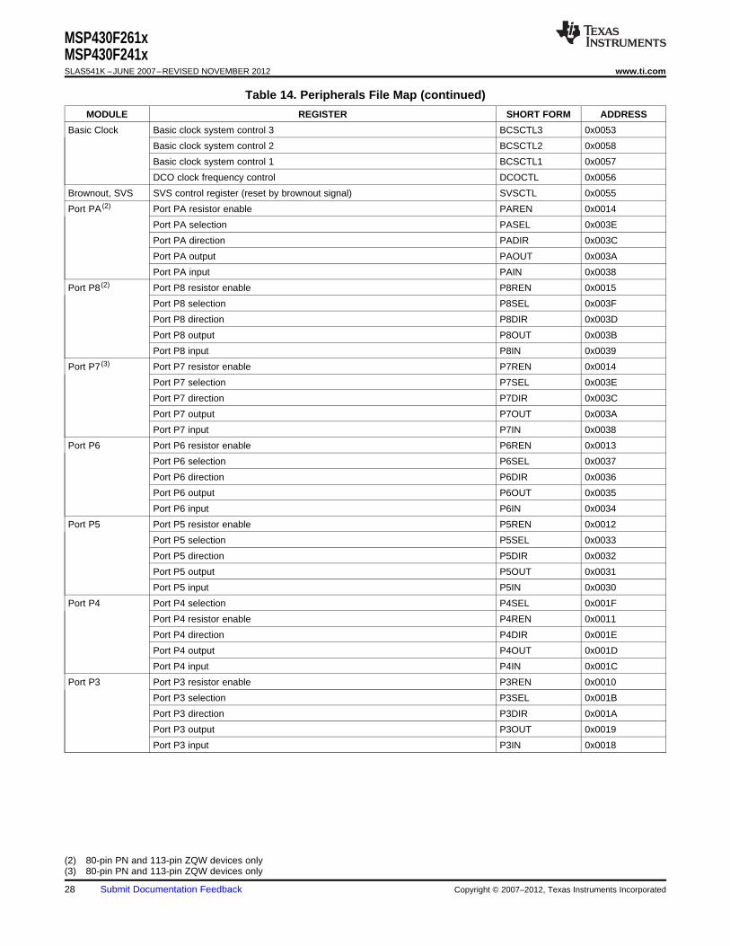
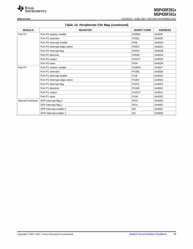
Table 14. Peripherals File Map
MODULE REGISTER SHORT FORM ADDRESS
DMA (1) DMA channel 2 transfer size DMA2SZ 0x01F2
DMA channel 2 destination address DMA2DA 0x01EE
DMA channel 2 source address DMA2SA 0x01EA
DMA channel 2 control DMA2CTL 0x01E8
DMA channel 1 transfer size DMA1SZ 0x01E6
DMA channel 1 destination address DMA1DA 0x01E2
DMA channel 1 source address DMA1SA 0x01DE
DMA channel 1 control DMA1CTL 0x01DC
DMA channel 0 transfer size DMA0SZ 0x01DA
DMA channel 0 destination address DMA0DA 0x01D6
DMA channel 0 source address DMA0SA 0x01D2
DMA channel 0 control DMA0CTL 0x01D0
DMA module interrupt vector word DMAIV 0x0126
DMA module control 1 DMACTL1 0x0124
DMA module control 0 DMACTL0 0x0122
DAC12 (1) DAC12_1 data DAC12_1DAT 0x01CA
DAC12_1 control DAC12_1CTL 0x01C2
DAC12_0 data DAC12_0DAT 0x01C8
DAC12_0 control DAC12_0CTL 0x01C0
(1) MSP430F261x devices only
24 Submit Documentation Feedback Copyright © 2007–2012, Texas Instruments Incorporated
MSP430F261xMSP430F241x
www.ti.com SLAS541K –JUNE 2007–REVISED NOVEMBER 2012
Table 14. Peripherals File Map (continued)
MODULE REGISTER SHORT FORM ADDRESS
ADC12 Interrupt vector word register ADC12IV 0x01A8
Interrupt enable register ADC12IE 0x01A6
Interrupt flag register ADC12IFG 0x01A4
Control register 1 ADC12CTL1 0x01A2
Control register 0 ADC12CTL0 0x01A0
Conversion memory 15 ADC12MEM15 0x015E
Conversion memory 14 ADC12MEM14 0x015C
Conversion memory 13 ADC12MEM13 0x015A
Conversion memory 12 ADC12MEM12 0x0158
Conversion memory 11 ADC12MEM11 0x0156
Conversion memory 10 ADC12MEM10 0x0154
Conversion memory 9 ADC12MEM9 0x0152
Conversion memory 8 ADC12MEM8 0x0150
Conversion memory 7 ADC12MEM7 0x014E
Conversion memory 6 ADC12MEM6 0x014C
Conversion memory 5 ADC12MEM5 0x014A
Conversion memory 4 ADC12MEM4 0x0148
Conversion memory 3 ADC12MEM3 0x0146
Conversion memory 2 ADC12MEM2 0x0144
Conversion memory 1 ADC12MEM1 0x0142
Conversion memory 0 ADC12MEM0 0x0140
ADC memory-control register15 ADC12MCTL15 0x008F
ADC memory-control register14 ADC12MCTL14 0x008E
ADC memory-control register13 ADC12MCTL13 0x008D
ADC memory-control register12 ADC12MCTL12 0x008C
ADC memory-control register11 ADC12MCTL11 0x008B
ADC memory-control register10 ADC12MCTL10 0x008A
ADC memory-control register9 ADC12MCTL9 0x0089
ADC memory-control register8 ADC12MCTL8 0x0088
ADC memory-control register7 ADC12MCTL7 0x0087
ADC memory-control register6 ADC12MCTL6 0x0086
ADC memory-control register5 ADC12MCTL5 0x0085
ADC memory-control register4 ADC12MCTL4 0x0084
ADC memory-control register3 ADC12MCTL3 0x0083
ADC memory-control register2 ADC12MCTL2 0x0082
ADC memory-control register1 ADC12MCTL1 0x0081
ADC memory-control register0 ADC12MCTL0 0x0080
Copyright © 2007–2012, Texas Instruments Incorporated Submit Documentation Feedback 25
MSP430F261xMSP430F241xSLAS541K –JUNE 2007–REVISED NOVEMBER 2012 www.ti.com
Table 14. Peripherals File Map (continued)
MODULE REGISTER SHORT FORM ADDRESS
Timer_B7 Capture/compare register 6 TBCCR6 0x019E
Capture/compare register 5 TBCCR5 0x019C
Capture/compare register 4 TBCCR4 0x019A
Capture/compare register 3 TBCCR3 0x0198
Capture/compare register 2 TBCCR2 0x0196
Capture/compare register 1 TBCCR1 0x0194
Capture/compare register 0 TBCCR0 0x0192
Timer_B register TBR 0x0190
Capture/compare control 6 TBCCTL6 0x018E
Capture/compare control 5 TBCCTL5 0x018C
Capture/compare control 4 TBCCTL4 0x018A
Capture/compare control 3 TBCCTL3 0x0188
Capture/compare control 2 TBCCTL2 0x0186
Capture/compare control 1 TBCCTL1 0x0184
Capture/compare control 0 TBCCTL0 0x0182
Timer_B control TBCTL 0x0180
Timer_B interrupt vector TBIV 0x011E
Timer_A3 Capture/compare register 2 TACCR2 0x0176
Capture/compare register 1 TACCR1 0x0174
Capture/compare register 0 TACCR0 0x0172
Timer_A register TAR 0x0170
Reserved 0x016E
Reserved 0x016C
Reserved 0x016A
Reserved 0x0168
Capture/compare control 2 TACCTL2 0x0166
Capture/compare control 1 TACCTL1 0x0164
Capture/compare control 0 TACCTL0 0x0162
Timer_A control TACTL 0x0160
Timer_A interrupt vector TAIV 0x012E
Hardware Sum extend SUMEXT 0x013EMultiplier Result high word RESHI 0x013C
Result low word RESLO 0x013A
Second operand OP2 0x0138
Multiply signed +accumulate/operand 1 MACS 0x0136
Multiply+accumulate/operand 1 MAC 0x0134
Multiply signed/operand 1 MPYS 0x0132
Multiply unsigned/operand 1 MPY 0x0130
Flash Flash control 4 FCTL4 0x01BE
Flash control 3 FCTL3 0x012C
Flash control 2 FCTL2 0x012A
Flash control 1 FCTL1 0x0128
Watchdog Watchdog Timer control WDTCTL 0x0120
26 Submit Documentation Feedback Copyright © 2007–2012, Texas Instruments Incorporated
MSP430F261xMSP430F241x
www.ti.com SLAS541K –JUNE 2007–REVISED NOVEMBER 2012
Table 14. Peripherals File Map (continued)
MODULE REGISTER SHORT FORM ADDRESS
USCI_A0/B0 USCI_A0 auto baud rate control UCA0ABCTL 0x005D
USCI_A0 transmit buffer UCA0TXBUF 0x0067
USCI_A0 receive buffer UCA0RXBUF 0x0066
USCI_A0 status UCA0STAT 0x0065
USCI_A0 modulation control UCA0MCTL 0x0064
USCI_A0 baud rate control 1 UCA0BR1 0x0063
USCI_A0 baud rate control 0 UCA0BR0 0x0062
USCI_A0 control 1 UCA0CTL1 0x0061
USCI_A0 control 0 UCA0CTL0 0x0060
USCI_A0 IrDA receive control UCA0IRRCTL 0x005F
USCI_A0 IrDA transmit control UCA0IRTCLT 0x005E
USCI_B0 transmit buffer UCB0TXBUF 0x006F
USCI_B0 receive buffer UCB0RXBUF 0x006E
USCI_B0 status UCB0STAT 0x006D
USCI_B0 I2C Interrupt enable UCB0CIE 0x006C
USCI_B0 baud rate control 1 UCB0BR1 0x006B
USCI_B0 baud rate control 0 UCB0BR0 0x006A
USCI_B0 control 1 UCB0CTL1 0x0069
USCI_B0 control 0 UCB0CTL0 0x0068
USCI_B0 I2C slave address UCB0SA 0x011A
USCI_B0 I2C own address UCB0OA 0x0118
USCI_A1/B1 USCI_A1 auto baud rate control UCA1ABCTL 0x00CD
USCI_A1 transmit buffer UCA1TXBUF 0x00D7
USCI_A1 receive buffer UCA1RXBUF 0x00D6
USCI_A1 status UCA1STAT 0x00D5
USCI_A1 modulation control UCA1MCTL 0x00D4
USCI_A1 baud rate control 1 UCA1BR1 0x00D3
USCI_A1 baud rate control 0 UCA1BR0 0x00D2
USCI_A1 control 1 UCA1CTL1 0x00D1
USCI_A1 control 0 UCA1CTL0 0x00D0
USCI_A1 IrDA receive control UCA1IRRCTL 0x00CF
USCI_A1 IrDA transmit control UCA1IRTCLT 0x00CE
USCI_B1 transmit buffer UCB1TXBUF 0x00DF
USCI_B1 receive buffer UCB1RXBUF 0x00DE
USCI_B1 status UCB1STAT 0x00DD
USCI_B1 I2C Interrupt enable UCB1CIE 0x00DC
USCI_B1 baud rate control 1 UCB1BR1 0x00DB
USCI_B1 baud rate control 0 UCB1BR0 0x00DA
USCI_B1 control 1 UCB1CTL1 0x00D9
USCI_B1 control 0 UCB1CTL0 0x00D8
USCI_B1 I2C slave address UCB1SA 0x017E
USCI_B1 I2C own address UCB1OA 0x017C
USCI_A1/B1 interrupt enable UC1IE 0x0006
USCI_A1/B1 interrupt flag UC1IFG 0x0007
Comparator_A+ Comparator_A port disable CAPD 0x005B
Comparator_A control2 CACTL2 0x005A
Comparator_A control1 CACTL1 0x0059
Copyright © 2007–2012, Texas Instruments Incorporated Submit Documentation Feedback 27
MSP430F261xMSP430F241xSLAS541K –JUNE 2007–REVISED NOVEMBER 2012 www.ti.com
Table 14. Peripherals File Map (continued)
MODULE REGISTER SHORT FORM ADDRESS
Basic Clock Basic clock system control 3 BCSCTL3 0x0053
Basic clock system control 2 BCSCTL2 0x0058
Basic clock system control 1 BCSCTL1 0x0057
DCO clock frequency control DCOCTL 0x0056
Brownout, SVS SVS control register (reset by brownout signal) SVSCTL 0x0055
Port PA (2) Port PA resistor enable PAREN 0x0014
Port PA selection PASEL 0x003E
Port PA direction PADIR 0x003C
Port PA output PAOUT 0x003A
Port PA input PAIN 0x0038
Port P8 (2) Port P8 resistor enable P8REN 0x0015
Port P8 selection P8SEL 0x003F
Port P8 direction P8DIR 0x003D
Port P8 output P8OUT 0x003B
Port P8 input P8IN 0x0039
Port P7 (3) Port P7 resistor enable P7REN 0x0014
Port P7 selection P7SEL 0x003E
Port P7 direction P7DIR 0x003C
Port P7 output P7OUT 0x003A
Port P7 input P7IN 0x0038
Port P6 Port P6 resistor enable P6REN 0x0013
Port P6 selection P6SEL 0x0037
Port P6 direction P6DIR 0x0036
Port P6 output P6OUT 0x0035
Port P6 input P6IN 0x0034
Port P5 Port P5 resistor enable P5REN 0x0012
Port P5 selection P5SEL 0x0033
Port P5 direction P5DIR 0x0032
Port P5 output P5OUT 0x0031
Port P5 input P5IN 0x0030
Port P4 Port P4 selection P4SEL 0x001F
Port P4 resistor enable P4REN 0x0011
Port P4 direction P4DIR 0x001E
Port P4 output P4OUT 0x001D
Port P4 input P4IN 0x001C
Port P3 Port P3 resistor enable P3REN 0x0010
Port P3 selection P3SEL 0x001B
Port P3 direction P3DIR 0x001A
Port P3 output P3OUT 0x0019
Port P3 input P3IN 0x0018
(2) 80-pin PN and 113-pin ZQW devices only(3) 80-pin PN and 113-pin ZQW devices only
28 Submit Documentation Feedback Copyright © 2007–2012, Texas Instruments Incorporated
MSP430F261xMSP430F241x
www.ti.com SLAS541K –JUNE 2007–REVISED NOVEMBER 2012
Table 14. Peripherals File Map (continued)
MODULE REGISTER SHORT FORM ADDRESS
Port P2 Port P2 resistor enable P2REN 0x002F
Port P2 selection P2SEL 0x002E
Port P2 interrupt enable P2IE 0x002D
Port P2 interrupt-edge select P2IES 0x002C
Port P2 interrupt flag P2IFG 0x002B
Port P2 direction P2DIR 0x002A
Port P2 output P2OUT 0x0029
Port P2 input P2IN 0x0028
Port P1 Port P1 resistor enable P1REN 0x0027
Port P1 selection P1SEL 0x0026
Port P1 interrupt enable P1IE 0x0025
Port P1 interrupt-edge select P1IES 0x0024
Port P1 interrupt flag P1IFG 0x0023
Port P1 direction P1DIR 0x0022
Port P1 output P1OUT 0x0021
Port P1 input P1IN 0x0020
Special Functions SFR interrupt flag 2 IFG2 0x0003
SFR interrupt flag 1 IFG1 0x0002
SFR interrupt enable 2 IE2 0x0001
SFR interrupt enable 1 IE1 0x0000
Copyright © 2007–2012, Texas Instruments Incorporated Submit Documentation Feedback 29
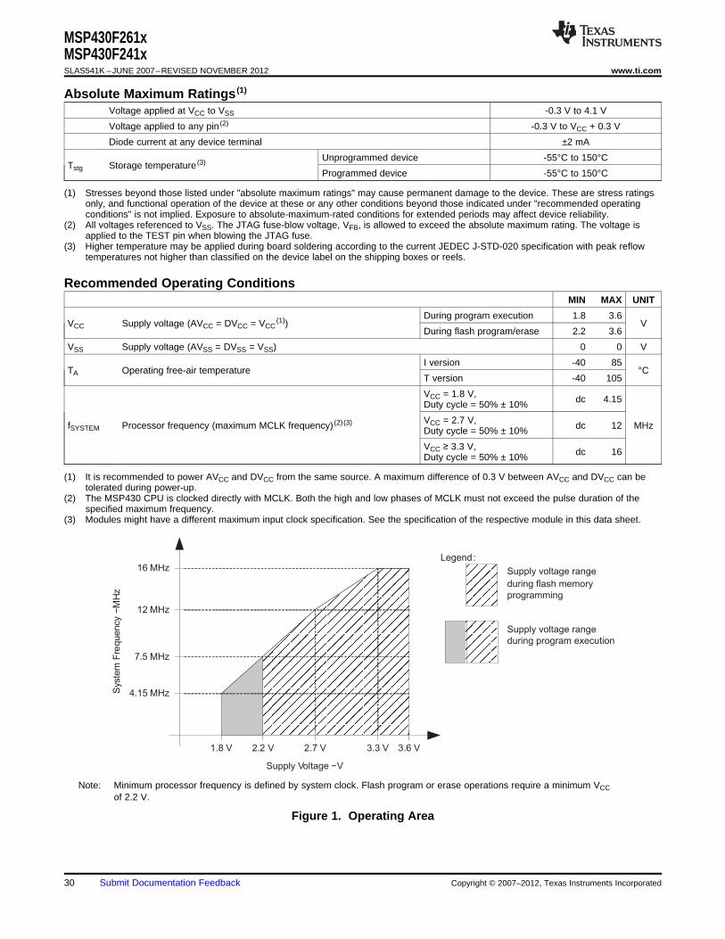
4.15 MHz
12 MHz
16 MHz
1.8 V 2.2 V 2.7 V 3.3 V 3.6 V
Supply Voltage −V
Syste
mF
requency
−M
Hz
Supply voltage range
during flash memory
programming
Supply voltage range
during program execution
Legend:
7.5 MHz
MSP430F261xMSP430F241xSLAS541K –JUNE 2007–REVISED NOVEMBER 2012 www.ti.com
Absolute Maximum Ratings (1)
Voltage applied at VCC to VSS -0.3 V to 4.1 V
Voltage applied to any pin (2) -0.3 V to VCC + 0.3 V
Diode current at any device terminal ±2 mA
Unprogrammed device -55°C to 150°CTstg Storage temperature (3)
Programmed device -55°C to 150°C
(1) Stresses beyond those listed under "absolute maximum ratings" may cause permanent damage to the device. These are stress ratingsonly, and functional operation of the device at these or any other conditions beyond those indicated under "recommended operatingconditions" is not implied. Exposure to absolute-maximum-rated conditions for extended periods may affect device reliability.
(2) All voltages referenced to VSS. The JTAG fuse-blow voltage, VFB, is allowed to exceed the absolute maximum rating. The voltage isapplied to the TEST pin when blowing the JTAG fuse.
(3) Higher temperature may be applied during board soldering according to the current JEDEC J-STD-020 specification with peak reflowtemperatures not higher than classified on the device label on the shipping boxes or reels.
Recommended Operating ConditionsMIN MAX UNIT
During program execution 1.8 3.6VCC Supply voltage (AVCC = DVCC = VCC
(1)) VDuring flash program/erase 2.2 3.6
VSS Supply voltage (AVSS = DVSS = VSS) 0 0 V
I version -40 85TA Operating free-air temperature °C
T version -40 105
VCC = 1.8 V, dc 4.15Duty cycle = 50% ± 10%
VCC = 2.7 V,fSYSTEM Processor frequency (maximum MCLK frequency) (2) (3) dc 12 MHzDuty cycle = 50% ± 10%
VCC ≥ 3.3 V, dc 16Duty cycle = 50% ± 10%
(1) It is recommended to power AVCC and DVCC from the same source. A maximum difference of 0.3 V between AVCC and DVCC can betolerated during power-up.
(2) The MSP430 CPU is clocked directly with MCLK. Both the high and low phases of MCLK must not exceed the pulse duration of thespecified maximum frequency.
(3) Modules might have a different maximum input clock specification. See the specification of the respective module in this data sheet.
Note: Minimum processor frequency is defined by system clock. Flash program or erase operations require a minimum VCCof 2.2 V.
Figure 1. Operating Area
30 Submit Documentation Feedback Copyright © 2007–2012, Texas Instruments Incorporated
MSP430F261xMSP430F241x
www.ti.com SLAS541K –JUNE 2007–REVISED NOVEMBER 2012
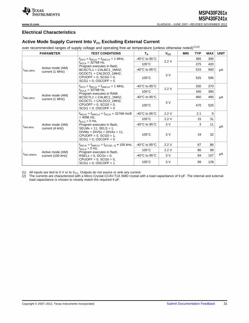
Electrical Characteristics
Active Mode Supply Current Into VCC Excluding External Currentover recommended ranges of supply voltage and operating free-air temperature (unless otherwise noted) (1) (2)
PARAMETER TEST CONDITIONS TA VCC MIN TYP MAX UNIT
fDCO = fMCLK = fSMCLK = 1 MHz, -40°C to 85°C 365 3952.2 VfACLK = 32768 Hz, 105°C 375 420
Program executes in flash,Active mode (AM) -40°C to 85°C 515 560IAM,1MHz BCSCTL1 = CALBC1_1MHZ, µAcurrent (1 MHz) DCOCTL = CALDCO_1MHZ, 3 VCPUOFF = 0, SCG0 = 0, 105°C 525 595SCG1 = 0, OSCOFF = 0
fDCO = fMCLK = fSMCLK = 1 MHz, -40°C to 85°C 330 3702.2 VfACLK = 32768 Hz, 105°C 340 390
Program executes in RAM,Active mode (AM) -40°C to 85°C 460 495IAM,1MHz BCSCTL1 = CALBC1_1MHZ, µAcurrent (1 MHz) DCOCTL = CALDCO_1MHZ, 3 VCPUOFF = 0, SCG0 = 0, 105°C 470 520SCG1 = 0, OSCOFF = 0
fMCLK = fSMCLK = fACLK = 32768 Hz/8 -40°C to 85°C 2.2 V 2.1 9= 4096 Hz, 105°C 2.2 V 15 31fDCO = 0 Hz,
-40°C to 85°C 3 V 3 11Active mode (AM) Program executes in flash,IAM,4kHz µAcurrent (4 kHz) SELMx = 11, SELS = 1,DIVMx = DIVSx = DIVAx = 11,
105°C 3 V 19 32CPUOFF = 0, SCG0 = 1,SCG1 = 0, OSCOFF = 0
fMCLK = fSMCLK = fDCO(0, 0) ≈ 100 kHz, -40°C to 85°C 2.2 V 67 86fACLK = 0 Hz, 105°C 2.2 V 80 99
Active mode (AM) Program executes in flash,IAM,100kHz µA-40°C to 85°C 3 V 84 107current (100 kHz) RSELx = 0, DCOx = 0,CPUOFF = 0, SCG0 = 0,
105°C 3 V 99 128SCG1 = 0, OSCOFF = 1
(1) All inputs are tied to 0 V or to VCC. Outputs do not source or sink any current.(2) The currents are characterized with a Micro Crystal CC4V-T1A SMD crystal with a load capacitance of 9 pF. The internal and external
load capacitance is chosen to closely match the required 9 pF.
Copyright © 2007–2012, Texas Instruments Incorporated Submit Documentation Feedback 31
0.0
1.0
2.0
3.0
4.0
5.0
6.0
7.0
0.0 4.0 8.0 12.0 16.0
fDCO − DCO Frequency − MHz
Active
Mo
de
Cu
rre
nt
−m
A
TA = 25 °C
TA = 85 °C
VCC = 2.2 V
VCC = 3 V
TA = 25 °C
TA = 85 °C
0.0
1.0
2.0
3.0
4.0
5.0
6.0
7.0
8.0
9.0
10.0
1.5 2.0 2.5 3.0 3.5 4.0
VCC − Supply Voltage − V
Active
Mo
de
Cu
rre
nt
−m
A
fDCO = 1 MHz
fDCO = 8 MHz
fDCO = 12 MHz
fDCO = 16 MHz
MSP430F261xMSP430F241xSLAS541K –JUNE 2007–REVISED NOVEMBER 2012 www.ti.com
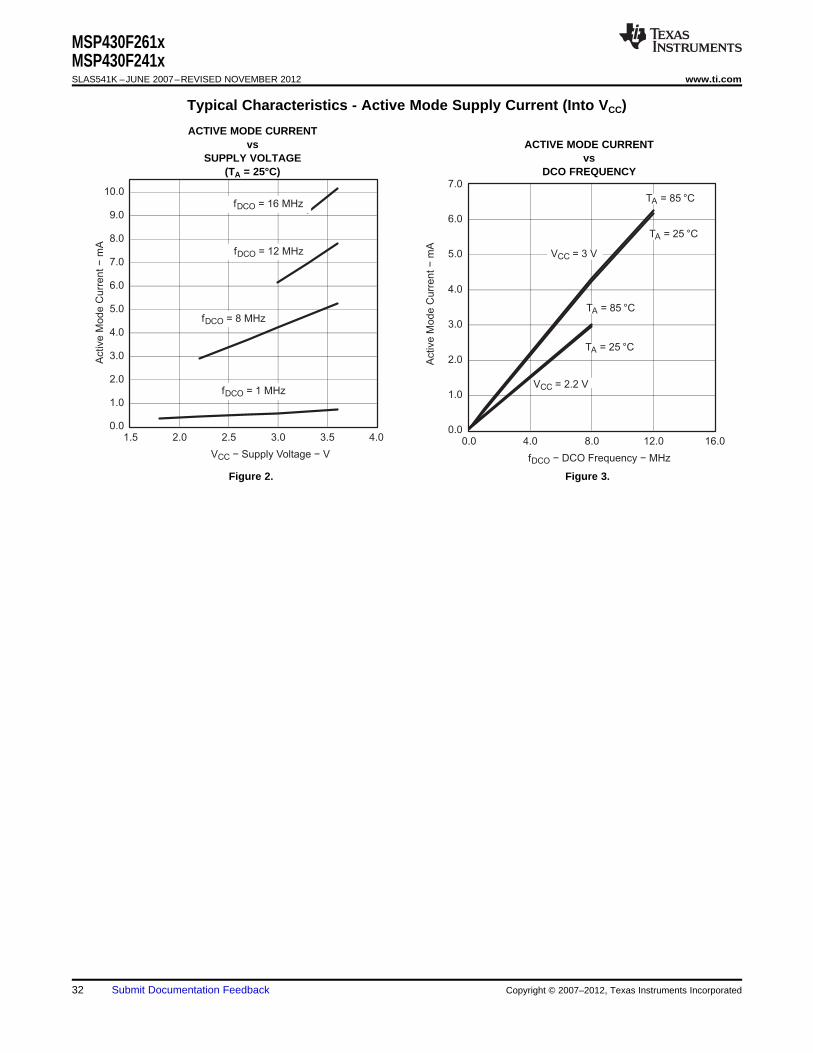
Typical Characteristics - Active Mode Supply Current (Into VCC)
ACTIVE MODE CURRENTvs ACTIVE MODE CURRENT
SUPPLY VOLTAGE vs(TA = 25°C) DCO FREQUENCY
Figure 2. Figure 3.
32 Submit Documentation Feedback Copyright © 2007–2012, Texas Instruments Incorporated
MSP430F261xMSP430F241x
www.ti.com SLAS541K –JUNE 2007–REVISED NOVEMBER 2012
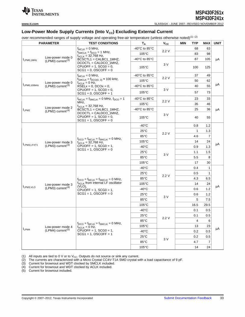
Low-Power Mode Supply Currents (Into VCC) Excluding External Currentover recommended ranges of supply voltage and operating free-air temperature (unless otherwise noted) (1) (2)
PARAMETER TEST CONDITIONS TA VCC MIN TYP MAX UNIT
fMCLK = 0 MHz, -40°C to 85°C 68 632.2 VfSMCLK = fDCO = 1 MHz, 105°C 83 98
fACLK = 32,768 Hz,Low-power mode 0 -40°C to 85°C 87 105ILPM0,1MHz BCSCTL1 = CALBC1_1MHZ, µA(LPM0) current (3)DCOCTL = CALDCO_1MHZ, 3 VCPUOFF = 1, SCG0 = 0, 105°C 100 125SCG1 = 0, OSCOFF = 0
fMCLK = 0 MHz, -40°C to 85°C 37 492.2 VfSMCLK = fDCO(0, 0) ≈ 100 kHz, 105°C 50 62
Low-power mode 0 fACLK = 0 Hz,ILPM0,100kHz µA-40°C to 85°C 40 55(LPM0) current (3) RSELx = 0, DCOx = 0,3 VCPUOFF = 1, SCG0 = 0,
105°C 57 73SCG1 = 0, OSCOFF = 1
fMCLK = fSMCLK = 0 MHz, fDCO = 1 -40°C to 85°C 23 332.2 VMHz, 105°C 35 46
fACLK = 32,768 Hz,Low-power mode 2 -40°C to 85°C 25 36ILPM2 BCSCTL1 = CALBC1_1MHZ, µA(LPM2) current (4)DCOCTL = CALDCO_1MHZ, 3 VCPUOFF = 1, SCG0 = 0, 105°C 40 55SCG1 = 1, OSCOFF = 0
-40°C 0.8 1.2
25°C 1 1.32.2 V
85°C 4.6 7fDCO = fMCLK = fSMCLK = 0 MHz,
105°C 14 24Low-power mode 3 fACLK = 32,768 Hz,ILPM3,LFXT1 µA(LPM3) current (3) CPUOFF = 1, SCG0 = 1, -40°C 0.9 1.3SCG1 = 1, OSCOFF = 0
25°C 1.1 1.53 V
85°C 5.5 8
105°C 17 30
-40°C 0.4 1
25°C 0.5 12.2 V
85°C 4.3 6.5fDCO = fMCLK = fSMCLK = 0 MHz,fACLK from internal LF oscillator 105°C 14 24Low-power mode 3ILPM3,VLO (VLO), µA(LPM3) current (4)
-40°C 0.6 1.2CPUOFF = 1, SCG0 = 1,SCG1 = 1, OSCOFF = 0 25°C 0.6 1.2
3 V85°C 5 7.5
105°C 16.5 29.5
-40°C 0.1 0.5
25°C 0.1 0.52.2 V
85°C 4 6fDCO = fMCLK = fSMCLK = 0 MHz,
105°C 13 23Low-power mode 4 fACLK = 0 Hz,ILPM4 µA(LPM4) current (5) CPUOFF = 1, SCG0 = 1, -40°C 0.2 0.5SCG1 = 1, OSCOFF = 1
25°C 0.2 0.53 V
85°C 4.7 7
105°C 14 24
(1) All inputs are tied to 0 V or to VCC. Outputs do not source or sink any current.(2) The currents are characterized with a Micro Crystal CC4V-T1A SMD crystal with a load capacitance of 9 pF.(3) Current for brownout and WDT clocked by SMCLK included.(4) Current for brownout and WDT clocked by ACLK included.(5) Current for brownout included.
Copyright © 2007–2012, Texas Instruments Incorporated Submit Documentation Feedback 33
0.0
1.0
2.0
3.0
4.0
5.0
6.0
7.0
8.0
9.0
10.0
11.0
12.0
13.0
14.0
15.0
16.0
−40.0 −20.0 0.0 20.0 40.0 60.0 80.0 100.0 120.0
TA − Temperature −
I−
Lo
w−
po
we
r m
od
e c
urr
en
t−
µA
LP
M4
Vcc = 3.6 V
TA − Temperature − °C
Vcc = 1.8 V
Vcc = 3.0 V
Vcc = 2.2 V
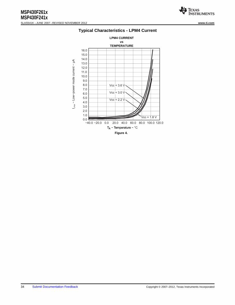
MSP430F261xMSP430F241xSLAS541K –JUNE 2007–REVISED NOVEMBER 2012 www.ti.com
Typical Characteristics - LPM4 Current
LPM4 CURRENTvs
TEMPERATURE
Figure 4.
34 Submit Documentation Feedback Copyright © 2007–2012, Texas Instruments Incorporated
MSP430F261xMSP430F241x
www.ti.com SLAS541K –JUNE 2007–REVISED NOVEMBER 2012
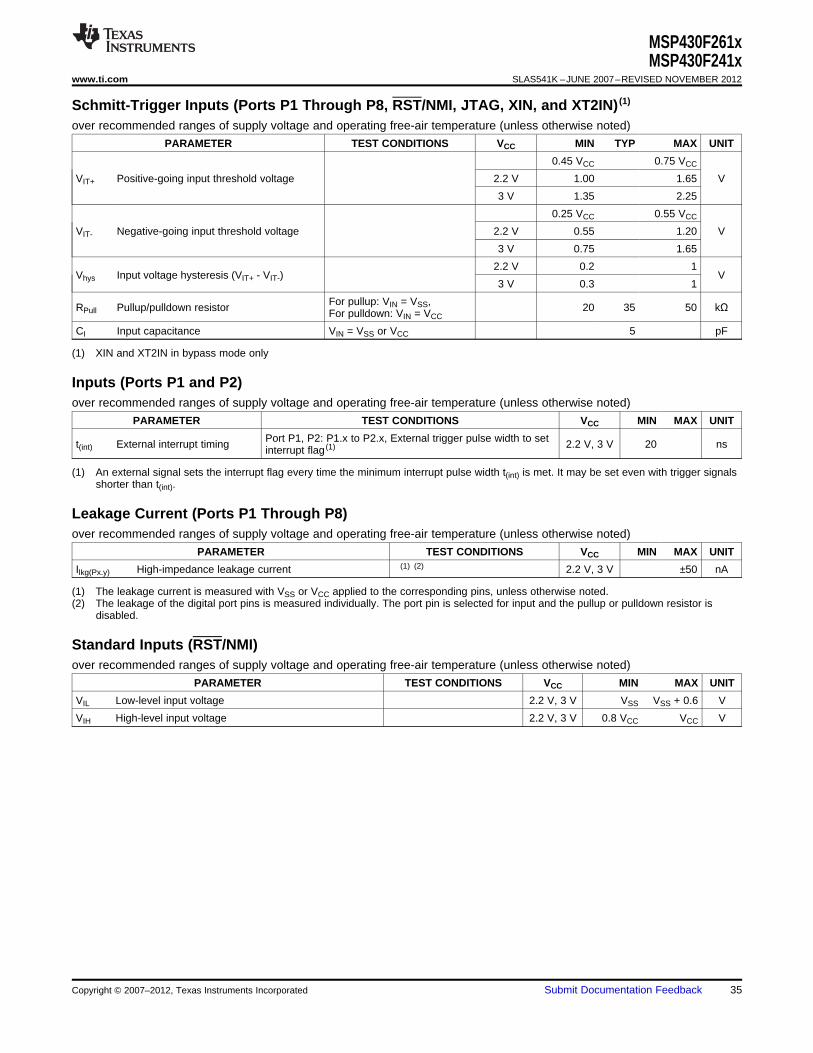
Schmitt-Trigger Inputs (Ports P1 Through P8, RST/NMI, JTAG, XIN, and XT2IN) (1)
over recommended ranges of supply voltage and operating free-air temperature (unless otherwise noted)
PARAMETER TEST CONDITIONS VCC MIN TYP MAX UNIT
0.45 VCC 0.75 VCC
VIT+ Positive-going input threshold voltage 2.2 V 1.00 1.65 V
3 V 1.35 2.25
0.25 VCC 0.55 VCC
VIT- Negative-going input threshold voltage 2.2 V 0.55 1.20 V
3 V 0.75 1.65
2.2 V 0.2 1Vhys Input voltage hysteresis (VIT+ - VIT-) V
3 V 0.3 1
For pullup: VIN = VSS,RPull Pullup/pulldown resistor 20 35 50 kΩFor pulldown: VIN = VCC
CI Input capacitance VIN = VSS or VCC 5 pF
(1) XIN and XT2IN in bypass mode only
Inputs (Ports P1 and P2)over recommended ranges of supply voltage and operating free-air temperature (unless otherwise noted)
PARAMETER TEST CONDITIONS VCC MIN MAX UNIT
Port P1, P2: P1.x to P2.x, External trigger pulse width to sett(int) External interrupt timing 2.2 V, 3 V 20 nsinterrupt flag (1)
(1) An external signal sets the interrupt flag every time the minimum interrupt pulse width t(int) is met. It may be set even with trigger signalsshorter than t(int).
Leakage Current (Ports P1 Through P8)over recommended ranges of supply voltage and operating free-air temperature (unless otherwise noted)
PARAMETER TEST CONDITIONS VCC MIN MAX UNIT
Ilkg(Px.y) High-impedance leakage current (1) (2) 2.2 V, 3 V ±50 nA
(1) The leakage current is measured with VSS or VCC applied to the corresponding pins, unless otherwise noted.(2) The leakage of the digital port pins is measured individually. The port pin is selected for input and the pullup or pulldown resistor is
disabled.
Standard Inputs (RST/NMI)over recommended ranges of supply voltage and operating free-air temperature (unless otherwise noted)
PARAMETER TEST CONDITIONS VCC MIN MAX UNIT
VIL Low-level input voltage 2.2 V, 3 V VSS VSS + 0.6 V
VIH High-level input voltage 2.2 V, 3 V 0.8 VCC VCC V
Copyright © 2007–2012, Texas Instruments Incorporated Submit Documentation Feedback 35
MSP430F261xMSP430F241xSLAS541K –JUNE 2007–REVISED NOVEMBER 2012 www.ti.com
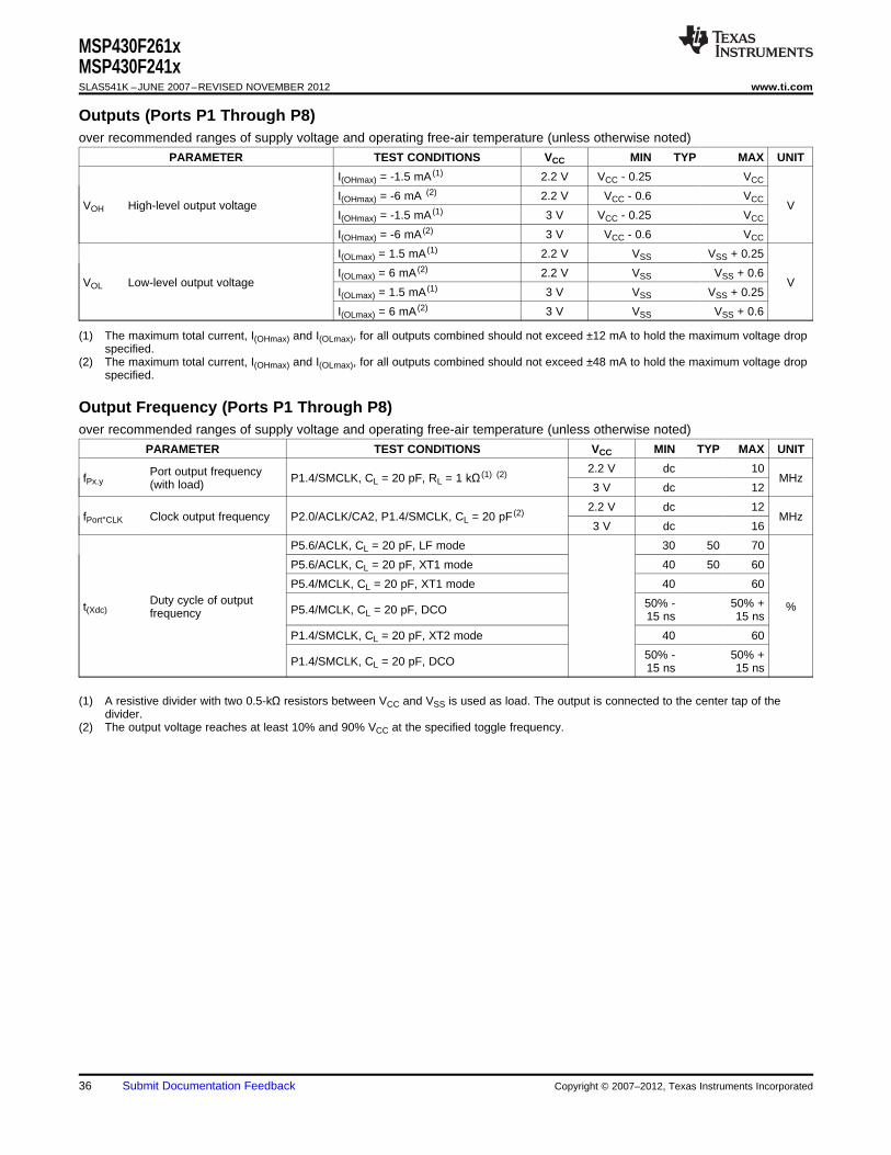
Outputs (Ports P1 Through P8)over recommended ranges of supply voltage and operating free-air temperature (unless otherwise noted)
PARAMETER TEST CONDITIONS VCC MIN TYP MAX UNIT
I(OHmax) = -1.5 mA (1) 2.2 V VCC - 0.25 VCC
I(OHmax) = -6 mA (2) 2.2 V VCC - 0.6 VCCVOH High-level output voltage V
I(OHmax) = -1.5 mA (1) 3 V VCC - 0.25 VCC
I(OHmax) = -6 mA (2) 3 V VCC - 0.6 VCC
I(OLmax) = 1.5 mA (1) 2.2 V VSS VSS + 0.25
I(OLmax) = 6 mA (2) 2.2 V VSS VSS + 0.6VOL Low-level output voltage V
I(OLmax) = 1.5 mA (1) 3 V VSS VSS + 0.25
I(OLmax) = 6 mA (2) 3 V VSS VSS + 0.6
(1) The maximum total current, I(OHmax) and I(OLmax), for all outputs combined should not exceed ±12 mA to hold the maximum voltage dropspecified.
(2) The maximum total current, I(OHmax) and I(OLmax), for all outputs combined should not exceed ±48 mA to hold the maximum voltage dropspecified.
Output Frequency (Ports P1 Through P8)over recommended ranges of supply voltage and operating free-air temperature (unless otherwise noted)
PARAMETER TEST CONDITIONS VCC MIN TYP MAX UNIT
2.2 V dc 10Port output frequencyfPx.y P1.4/SMCLK, CL = 20 pF, RL = 1 kΩ (1) (2) MHz(with load) 3 V dc 12
2.2 V dc 12fPort°CLK Clock output frequency P2.0/ACLK/CA2, P1.4/SMCLK, CL = 20 pF (2) MHz
3 V dc 16
P5.6/ACLK, CL = 20 pF, LF mode 30 50 70
P5.6/ACLK, CL = 20 pF, XT1 mode 40 50 60
P5.4/MCLK, CL = 20 pF, XT1 mode 40 60Duty cycle of output 50% - 50% +t(Xdc) %P5.4/MCLK, CL = 20 pF, DCOfrequency 15 ns 15 ns
P1.4/SMCLK, CL = 20 pF, XT2 mode 40 60
50% - 50% +P1.4/SMCLK, CL = 20 pF, DCO 15 ns 15 ns
(1) A resistive divider with two 0.5-kΩ resistors between VCC and VSS is used as load. The output is connected to the center tap of thedivider.
(2) The output voltage reaches at least 10% and 90% VCC at the specified toggle frequency.
36 Submit Documentation Feedback Copyright © 2007–2012, Texas Instruments Incorporated
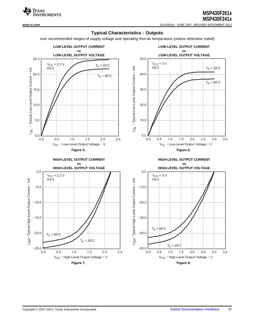
VOH − High-Level Output Voltage − V
−25.0
−20.0
−15.0
−10.0
−5.0
0.0
0.0 0.5 1.0 1.5 2.0 2.5
VCC = 2.2 V
P4.5
TA = 25°C
TA = 85°C
OH
I−
Typic
al H
igh-L
evel O
utp
ut C
urr
ent
−m
A
VOH − High-Level Output Voltage − V
−50.0
−40.0
−30.0
−20.0
−10.0
0.0
0.0 0.5 1.0 1.5 2.0 2.5 3.0 3.5
VCC = 3 V
P4.5
TA = 25°C
TA = 85°C
OH
I−
Typic
al H
igh-L
evel O
utp
ut C
urr
ent
−m
A
VOL − Low-Level Output Voltage − V
0.0
5.0
10.0
15.0
20.0
25.0
0.0 0.5 1.0 1.5 2.0 2.5
VCC = 2.2 V
P4.5TA = 25°C
TA = 85°C
OL
I−
Typ
ica
l L
ow
-Le
ve
l O
utp
ut
Cu
rre
nt
−m
A
VOL − Low-Level Output Voltage − V
0.0
10.0
20.0
30.0
40.0
50.0
0.0 0.5 1.0 1.5 2.0 2.5 3.0 3.5
VCC = 3 V
P4.5 TA = 25°C
TA = 85°C
OL
I−
Typic
al Low
-Level O
utp
ut C
urr
ent
−m
A
MSP430F261xMSP430F241x
www.ti.com SLAS541K –JUNE 2007–REVISED NOVEMBER 2012
Typical Characteristics - Outputsover recommended ranges of supply voltage and operating free-air temperature (unless otherwise noted)
LOW-LEVEL OUTPUT CURRENT LOW-LEVEL OUTPUT CURRENTvs vs
LOW-LEVEL OUTPUT VOLTAGE LOW-LEVEL OUTPUT VOLTAGE
Figure 5. Figure 6.
HIGH-LEVEL OUTPUT CURRENT HIGH-LEVEL OUTPUT CURRENTvs vs
HIGH-LEVEL OUTPUT VOLTAGE HIGH-LEVEL OUTPUT VOLTAGE
Figure 7. Figure 8.
Copyright © 2007–2012, Texas Instruments Incorporated Submit Documentation Feedback 37
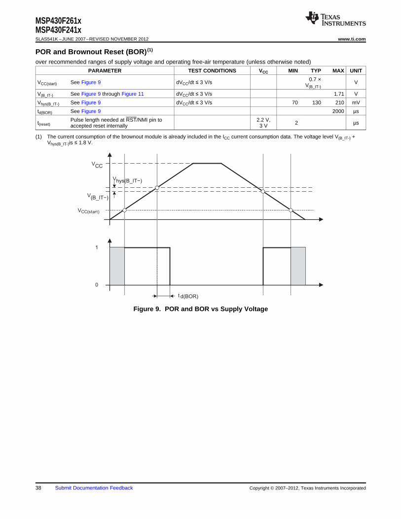
0
1
t d(BOR)
VCC
V(B_IT−)
Vhys(B_IT−)
VCC(start)
MSP430F261xMSP430F241xSLAS541K –JUNE 2007–REVISED NOVEMBER 2012 www.ti.com
POR and Brownout Reset (BOR) (1)
over recommended ranges of supply voltage and operating free-air temperature (unless otherwise noted)
PARAMETER TEST CONDITIONS VCC MIN TYP MAX UNIT
0.7 ×VCC(start) See Figure 9 dVCC/dt ≤ 3 V/s VV(B_IT-)
V(B_IT-) See Figure 9 through Figure 11 dVCC/dt ≤ 3 V/s 1.71 V
Vhys(B_IT-) See Figure 9 dVCC/dt ≤ 3 V/s 70 130 210 mV
td(BOR) See Figure 9 2000 µs
Pulse length needed at RST/NMI pin to 2.2 V,t(reset) 2 µsaccepted reset internally 3 V
(1) The current consumption of the brownout module is already included in the ICC current consumption data. The voltage level V(B_IT-) +Vhys(B_IT-)is ≤ 1.8 V.
Figure 9. POR and BOR vs Supply Voltage
38 Submit Documentation Feedback Copyright © 2007–2012, Texas Instruments Incorporated
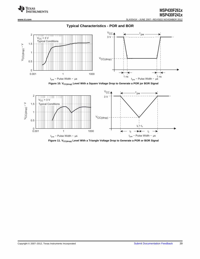
VCC
0
0.5
1
1.5
2
VCC(drop)
t pw
tpw − Pulse Width − µs
VC
C(d
rop)
−V
3 V
0.001 1 1000 tf tr
tpw − Pulse Width − µs
tf = tr
Typical Conditions
VCC = 3 V
VCC(drop)
VCC
3 V
t pw
0
0.5
1
1.5
2
0.001 1 1000
Typical Conditions
1 ns 1 nstpw − Pulse Width − µs
VC
C(d
rop)
−V
tpw − Pulse Width − µs
VCC = 3 V
MSP430F261xMSP430F241x
www.ti.com SLAS541K –JUNE 2007–REVISED NOVEMBER 2012
Typical Characteristics - POR and BOR
Figure 10. VCC(drop) Level With a Square Voltage Drop to Generate a POR jor BOR Signal
Figure 11. VCC(drop) Level With a Triangle Voltage Drop to Generate a POR or BOR Signal
Copyright © 2007–2012, Texas Instruments Incorporated Submit Documentation Feedback 39
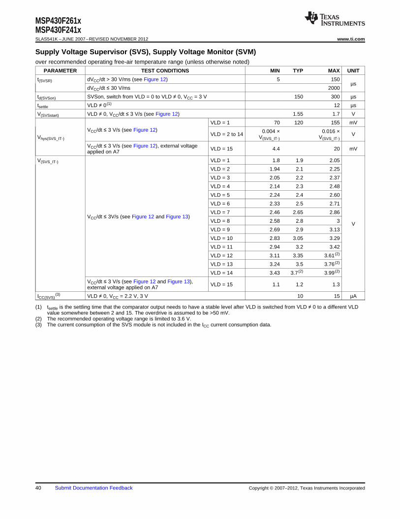
MSP430F261xMSP430F241xSLAS541K –JUNE 2007–REVISED NOVEMBER 2012 www.ti.com
Supply Voltage Supervisor (SVS), Supply Voltage Monitor (SVM)over recommended operating free-air temperature range (unless otherwise noted)
PARAMETER TEST CONDITIONS MIN TYP MAX UNIT
t(SVSR) dVCC/dt > 30 V/ms (see Figure 12) 5 150µs
dVCC/dt ≤ 30 V/ms 2000
td(SVSon) SVSon, switch from VLD = 0 to VLD ≠ 0, VCC = 3 V 150 300 µs
tsettle VLD ≠ 0 (1) 12 µs
V(SVSstart) VLD ≠ 0, VCC/dt ≤ 3 V/s (see Figure 12) 1.55 1.7 V
VLD = 1 70 120 155 mVVCC/dt ≤ 3 V/s (see Figure 12) 0.004 × 0.016 ×VLD = 2 to 14 VVhys(SVS_IT-) V(SVS_IT-) V(SVS_IT-)
VCC/dt ≤ 3 V/s (see Figure 12), external voltage VLD = 15 4.4 20 mVapplied on A7
V(SVS_IT-) VLD = 1 1.8 1.9 2.05
VLD = 2 1.94 2.1 2.25
VLD = 3 2.05 2.2 2.37
VLD = 4 2.14 2.3 2.48
VLD = 5 2.24 2.4 2.60
VLD = 6 2.33 2.5 2.71
VLD = 7 2.46 2.65 2.86VCC/dt ≤ 3V/s (see Figure 12 and Figure 13)
VLD = 8 2.58 2.8 3 VVLD = 9 2.69 2.9 3.13
VLD = 10 2.83 3.05 3.29
VLD = 11 2.94 3.2 3.42
VLD = 12 3.11 3.35 3.61 (2)
VLD = 13 3.24 3.5 3.76 (2)
VLD = 14 3.43 3.7 (2) 3.99 (2)
VCC/dt ≤ 3 V/s (see Figure 12 and Figure 13), VLD = 15 1.1 1.2 1.3external voltage applied on A7
ICC(SVS)(3) VLD ≠ 0, VCC = 2.2 V, 3 V 10 15 µA
(1) tsettle is the settling time that the comparator output needs to have a stable level after VLD is switched from VLD ≠ 0 to a different VLDvalue somewhere between 2 and 15. The overdrive is assumed to be >50 mV.
(2) The recommended operating voltage range is limited to 3.6 V.(3) The current consumption of the SVS module is not included in the ICC current consumption data.
40 Submit Documentation Feedback Copyright © 2007–2012, Texas Instruments Incorporated
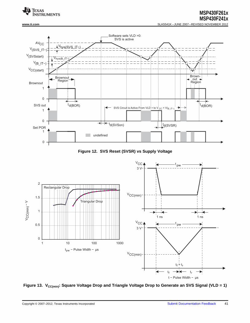
0
0.5
1
1.5
2
VCC
VCC
1 ns 1 ns
VCC(min)
t pw
tpw − Pulse Width − µs
VC
C(m
in)−
V
3 V
1 10 1000
tf tr
t − Pulse Width − µs
100
t pw3 V
tf = tr
Rectangular Drop
Triangular Drop
VCC(min)
VCC(start)
AVCC
V(B_IT−)
BrownoutRegion
V(SVSstart)
V(SVS_IT−)
Software sets VLD >0:SVS is active
td(SVSR)
undefined
Vhys(SVS_IT−)
0
1
td(BOR)
Brownout
0
1
td(SVSon)
td(BOR)
0
1Set POR
Brown-out
Region
SVS Circuit is Active From VLD > to V CC < V(B_IT−)
SVS out
Vhys(B_IT−)
MSP430F261xMSP430F241x
www.ti.com SLAS541K –JUNE 2007–REVISED NOVEMBER 2012
Figure 12. SVS Reset (SVSR) vs Supply Voltage
Figure 13. VCC(min): Square Voltage Drop and Triangle Voltage Drop to Generate an SVS Signal (VLD = 1)
Copyright © 2007–2012, Texas Instruments Incorporated Submit Documentation Feedback 41
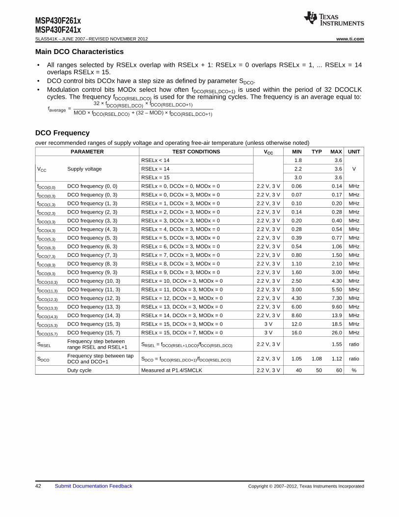
DCO(RSEL,DCO+1)DCO(RSEL,DCO)average
DCO(RSEL,DCO) DCO(RSEL,DCO+1)
32 × f × ff =
MOD × f + (32 – MOD) × f
MSP430F261xMSP430F241xSLAS541K –JUNE 2007–REVISED NOVEMBER 2012 www.ti.com
Main DCO Characteristics
• All ranges selected by RSELx overlap with RSELx + 1: RSELx = 0 overlaps RSELx = 1, ... RSELx = 14overlaps RSELx = 15.
• DCO control bits DCOx have a step size as defined by parameter SDCO.• Modulation control bits MODx select how often fDCO(RSEL,DCO+1) is used within the period of 32 DCOCLK
cycles. The frequency fDCO(RSEL,DCO) is used for the remaining cycles. The frequency is an average equal to:
DCO Frequencyover recommended ranges of supply voltage and operating free-air temperature (unless otherwise noted)
PARAMETER TEST CONDITIONS VCC MIN TYP MAX UNIT
RSELx < 14 1.8 3.6
VCC Supply voltage RSELx = 14 2.2 3.6 V
RSELx = 15 3.0 3.6
fDCO(0,0) DCO frequency (0, 0) RSELx = 0, DCOx = 0, MODx = 0 2.2 V, 3 V 0.06 0.14 MHz
fDCO(0,3) DCO frequency (0, 3) RSELx = 0, DCOx = 3, MODx = 0 2.2 V, 3 V 0.07 0.17 MHz
fDCO(1,3) DCO frequency (1, 3) RSELx = 1, DCOx = 3, MODx = 0 2.2 V, 3 V 0.10 0.20 MHz
fDCO(2,3) DCO frequency (2, 3) RSELx = 2, DCOx = 3, MODx = 0 2.2 V, 3 V 0.14 0.28 MHz
fDCO(3,3) DCO frequency (3, 3) RSELx = 3, DCOx = 3, MODx = 0 2.2 V, 3 V 0.20 0.40 MHz
fDCO(4,3) DCO frequency (4, 3) RSELx = 4, DCOx = 3, MODx = 0 2.2 V, 3 V 0.28 0.54 MHz
fDCO(5,3) DCO frequency (5, 3) RSELx = 5, DCOx = 3, MODx = 0 2.2 V, 3 V 0.39 0.77 MHz
fDCO(6,3) DCO frequency (6, 3) RSELx = 6, DCOx = 3, MODx = 0 2.2 V, 3 V 0.54 1.06 MHz
fDCO(7,3) DCO frequency (7, 3) RSELx = 7, DCOx = 3, MODx = 0 2.2 V, 3 V 0.80 1.50 MHz
fDCO(8,3) DCO frequency (8, 3) RSELx = 8, DCOx = 3, MODx = 0 2.2 V, 3 V 1.10 2.10 MHz
fDCO(9,3) DCO frequency (9, 3) RSELx = 9, DCOx = 3, MODx = 0 2.2 V, 3 V 1.60 3.00 MHz
fDCO(10,3) DCO frequency (10, 3) RSELx = 10, DCOx = 3, MODx = 0 2.2 V, 3 V 2.50 4.30 MHz
fDCO(11,3) DCO frequency (11, 3) RSELx = 11, DCOx = 3, MODx = 0 2.2 V, 3 V 3.00 5.50 MHz
fDCO(12,3) DCO frequency (12, 3) RSELx = 12, DCOx = 3, MODx = 0 2.2 V, 3 V 4.30 7.30 MHz
fDCO(13,3) DCO frequency (13, 3) RSELx = 13, DCOx = 3, MODx = 0 2.2 V, 3 V 6.00 9.60 MHz
fDCO(14,3) DCO frequency (14, 3) RSELx = 14, DCOx = 3, MODx = 0 2.2 V, 3 V 8.60 13.9 MHz
fDCO(15,3) DCO frequency (15, 3) RSELx = 15, DCOx = 3, MODx = 0 3 V 12.0 18.5 MHz
fDCO(15,7) DCO frequency (15, 7) RSELx = 15, DCOx = 7, MODx = 0 3 V 16.0 26.0 MHz
Frequency step betweenSRSEL SRSEL = fDCO(RSEL+1,DCO)/fDCO(RSEL,DCO) 2.2 V, 3 V 1.55 ratiorange RSEL and RSEL+1
Frequency step between tapSDCO SDCO = fDCO(RSEL,DCO+1)/fDCO(RSEL,DCO) 2.2 V, 3 V 1.05 1.08 1.12 ratioDCO and DCO+1
Duty cycle Measured at P1.4/SMCLK 2.2 V, 3 V 40 50 60 %
42 Submit Documentation Feedback Copyright © 2007–2012, Texas Instruments Incorporated
MSP430F261xMSP430F241x
www.ti.com SLAS541K –JUNE 2007–REVISED NOVEMBER 2012
Calibrated DCO Frequencies - Tolerance at Calibrationover recommended ranges of supply voltage and operating free-air temperature (unless otherwise noted)
PARAMETER TEST CONDITIONS TA VCC MIN TYP MAX UNIT
Frequency tolerance at calibration 25°C 3 V -1 ±0.2 +1 %
BCSCTL1 = CALBC1_1MHZ,fCAL(1MHz) 1-MHz calibration value DCOCTL = CALDCO_1MHZ, 25°C 3 V 0.990 1 1.010 MHz
Gating time: 5 ms
BCSCTL1 = CALBC1_8MHZ,fCAL(8MHz) 8-MHz calibration value DCOCTL = CALDCO_8MHZ, 25°C 3 V 7.920 8 8.080 MHz
Gating time: 5 ms
BCSCTL1 = CALBC1_12MHZ,fCAL(12MHz) 12-MHz calibration value DCOCTL = CALDCO_12MHZ, 25°C 3 V 11.88 12 12.12 MHz
Gating time: 5 ms
BCSCTL1 = CALBC1_16MHZ,fCAL(16MHz) 16-MHz calibration value DCOCTL = CALDCO_16MHZ, 25°C 3 V 15.84 16 16.16 MHz
Gating time: 2 ms
Calibrated DCO Frequencies - Tolerance Over Temperature 0°C to 85°Cover recommended ranges of supply voltage and operating free-air temperature (unless otherwise noted)
PARAMETER TEST CONDITIONS TA VCC MIN TYP MAX UNIT
1-MHz tolerance over 0°C to 85°C 3 V -2.5 ±0.5 +2.5 %temperature
8-MHz tolerance over 0°C to 85°C 3 V -2.5 ±1.0 +2.5 %temperature
12-MHz tolerance over 0°C to 85°C 3 V -2.5 ±1.0 +2.5 %temperature
16-MHz tolerance over 0°C to 85°C 3 V -3 ±2.0 +3 %temperature
2.2 V 0.970 1 1.030BCSCTL1 = CALBC1_1MHZ,fCAL(1MHz) 1-MHz calibration value DCOCTL = CALDCO_1MHZ, 0°C to 85°C 3 V 0.975 1 1.025 MHz
Gating time: 5 ms 3.6 V 0.970 1 1.030
2.2 V 7.760 8 8.40BCSCTL1 = CALBC1_8MHZ,fCAL(8MHz) 8-MHz calibration value DCOCTL = CALDCO_8MHZ, 0°C to 85°C 3 V 7.800 8 8.20 MHz
Gating time: 5 ms 3.6 V 7.600 8 8.24
2.2 V 11.64 12 12.36BCSCTL1 = CALBC1_12MHZ,fCAL(12MHz) 12-MHz calibration value DCOCTL = CALDCO_12MHZ, 0°C to 85°C 3 V 11.64 12 12.36 MHz
Gating time: 5 ms 3.6 V 11.64 12 12.36
BCSCTL1 = CALBC1_16MHZ, 3 V 15.52 16 16.48fCAL(16MHz) 16-MHz calibration value DCOCTL = CALDCO_16MHZ, 0°C to 85°C MHz
3.6 V 15.00 16 16.48Gating time: 2 ms
Copyright © 2007–2012, Texas Instruments Incorporated Submit Documentation Feedback 43
MSP430F261xMSP430F241xSLAS541K –JUNE 2007–REVISED NOVEMBER 2012 www.ti.com
Calibrated DCO Frequencies - Tolerance Over Supply Voltage VCC
over recommended ranges of supply voltage and operating free-air temperature (unless otherwise noted)
PARAMETER TEST CONDITIONS TA VCC MIN TYP MAX UNIT
1-MHz tolerance over VCC 25°C 1.8 V to 3.6 V -3 ±2 +3 %
8-MHz tolerance over VCC 25°C 1.8 V to 3.6 V -3 ±2 +3 %
12-MHz tolerance over VCC 25°C 2.2 V to 3.6 V -3 ±2 +3 %
16-MHz tolerance over VCC 25°C 3 V to 3.6 V -6 ±2 +3 %
BCSCTL1 = CALBC1_1MHZ,fCAL(1MHz) 1-MHz calibration value DCOCTL = CALDCO_1MHZ, 25°C 1.8 V to 3.6 V 0.97 1 1.03 MHz
Gating time: 5 ms
BCSCTL1 = CALBC1_8MHZ,fCAL(8MHz) 8-MHz calibration value DCOCTL = CALDCO_8MHZ, 25°C 1.8 V to 3.6 V 7.76 8 8.24 MHz
Gating time: 5 ms
BCSCTL1 = CALBC1_12MHZ,fCAL(12MHz) 12-MHz calibration value DCOCTL = CALDCO_12MHZ, 25°C 2.2 V to 3.6 V 11.64 12 12.36 MHz
Gating time: 5 ms
BCSCTL1 = CALBC1_16MHZ,fCAL(16MHz) 16-MHz calibration value DCOCTL = CALDCO_16MHZ, 25°C 3 V to 3.6 V 15 16 16.48 MHz
Gating time: 2 ms
Calibrated DCO Frequencies - Overall Toleranceover recommended ranges of supply voltage and operating free-air temperature (unless otherwise noted)
PARAMETER TEST CONDITIONS TA VCC MIN TYP MAX UNIT
1-MHz tolerance -40°C to 105°C 1.8 V to 3.6 V -5 ±2 +5 %overall
8-MHz tolerance -40°C to 105°C 1.8 V to 3.6 V -5 ±2 +5 %overall
12-MHz tolerance -40°C to 105°C 2.2 V to 3.6 V -5 ±2 +5 %overall
16-MHz tolerance -40°C to 105°C 3 V to 3.6 V -6 ±3 +6 %overall
BCSCTL1 = CALBC1_1MHZ,1-MHz calibrationfCAL(1MHz) DCOCTL = CALDCO_1MHZ, -40°C to 105°C 1.8 V to 3.6 V 0.95 1 1.05 MHzvalue Gating time: 5 ms
BCSCTL1 = CALBC1_8MHZ,8-MHz calibrationfCAL(8MHz) DCOCTL = CALDCO_8MHZ, -40°C to 105°C 1.8 V to 3.6 V 7.6 8 8.4 MHzvalue Gating time: 5 ms
BCSCTL1 = CALBC1_12MHZ,12-MHz calibrationfCAL(12MHz) DCOCTL = CALDCO_12MHZ, -40°C to 105°C 2.2 V to 3.6 V 11.4 12 12.6 MHzvalue Gating time: 5 ms
BCSCTL1 = CALBC1_16MHZ,16-MHz calibrationfCAL(16MHz) DCOCTL = CALDCO_16MHZ, -40°C to 105°C 3 V to 3.6 V 15 16 17 MHzvalue Gating time: 2 ms
44 Submit Documentation Feedback Copyright © 2007–2012, Texas Instruments Incorporated
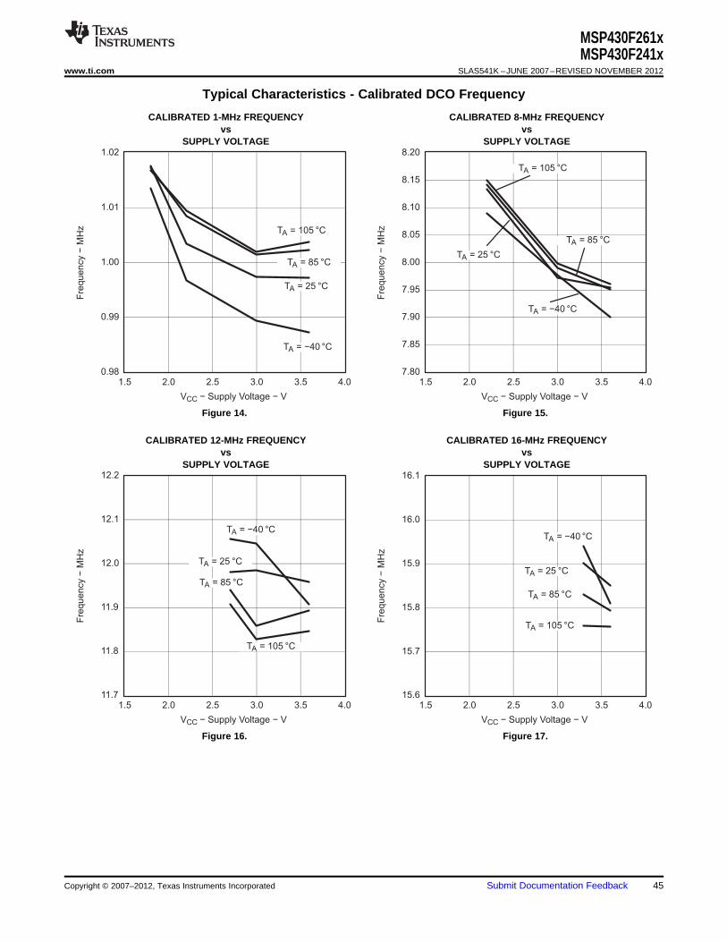
VCC − Supply Voltage − V
11.7
11.8
11.9
12.0
12.1
12.2
1.5 2.0 2.5 3.0 3.5 4.0
Fre
qu
en
cy
−M
Hz
TA = −40 °C
TA = 25 °C
TA = 85 °C
TA = 105 °C
VCC − Supply Voltage − V
15.6
15.7
15.8
15.9
16.0
16.1
1.5 2.0 2.5 3.0 3.5 4.0
Fre
qu
en
cy
−M
Hz
TA = −40 °C
TA = 25 °C
TA = 85 °C
TA = 105 °C
VCC − Supply Voltage − V
0.98
0.99
1.00
1.01
1.02
1.5 2.0 2.5 3.0 3.5 4.0
Fre
qu
en
cy
−M
Hz
TA = −40 °C
TA = 25 °C
TA = 85 °C
TA = 105 °C
VCC − Supply Voltage − V
7.80
7.85
7.90
7.95
8.00
8.05
8.10
8.15
8.20
1.5 2.0 2.5 3.0 3.5 4.0F
req
ue
ncy
−M
Hz
TA = −40 °C
TA = 25 °C
TA = 85 °C
TA = 105 °C
MSP430F261xMSP430F241x
www.ti.com SLAS541K –JUNE 2007–REVISED NOVEMBER 2012
Typical Characteristics - Calibrated DCO Frequency
CALIBRATED 1-MHz FREQUENCY CALIBRATED 8-MHz FREQUENCYvs vs
SUPPLY VOLTAGE SUPPLY VOLTAGE
Figure 14. Figure 15.
CALIBRATED 12-MHz FREQUENCY CALIBRATED 16-MHz FREQUENCYvs vs
SUPPLY VOLTAGE SUPPLY VOLTAGE
Figure 16. Figure 17.
Copyright © 2007–2012, Texas Instruments Incorporated Submit Documentation Feedback 45
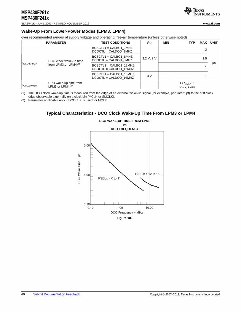
DCO Frequency − MHz
0.10
1.00
10.00
0.10 1.00 10.00
DC
O W
ake
Tim
e−
µs
RSELx = 0 to 11
RSELx = 12 to 15
MSP430F261xMSP430F241xSLAS541K –JUNE 2007–REVISED NOVEMBER 2012 www.ti.com
Wake-Up From Lower-Power Modes (LPM3, LPM4)over recommended ranges of supply voltage and operating free-air temperature (unless otherwise noted)
PARAMETER TEST CONDITIONS VCC MIN TYP MAX UNIT
BCSCTL1 = CALBC1_1MHZ, 2DCOCTL = CALDCO_1MHZ
BCSCTL1 = CALBC1_8MHZ, 2.2 V, 3 V 1.5DCOCTL = CALDCO_8MHZDCO clock wake-up timetDCO,LPM3/4 µsfrom LPM3 or LPM4 (1)BCSCTL1 = CALBC1_12MHZ, 1DCOCTL = CALDCO_12MHZ
BCSCTL1 = CALBC1_16MHZ, 3 V 1DCOCTL = CALDCO_16MHZ
CPU wake-up time from 1 / fMCLK +tCPU,LPM3/4 LPM3 or LPM4 (2) tClock,LPM3/4
(1) The DCO clock wake-up time is measured from the edge of an external wake-up signal (for example, port interrupt) to the first clockedge observable externally on a clock pin (MCLK or SMCLK).
(2) Parameter applicable only if DCOCLK is used for MCLK.
Typical Characteristics - DCO Clock Wake-Up Time From LPM3 or LPM4
DCO WAKE-UP TIME FROM LPM3vs
DCO FREQUENCY
Figure 18.
46 Submit Documentation Feedback Copyright © 2007–2012, Texas Instruments Incorporated
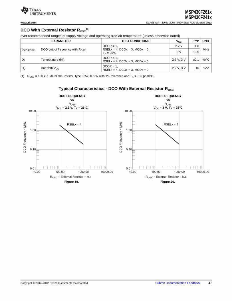
0.01
0.10
1.00
10.00
10.00 100.00 1000.00 10000.00
ROSC − External Resistor − kW
DC
O F
req
ue
ncy
−M
Hz
RSELx = 4
0.01
0.10
1.00
10.00
10.00 100.00 1000.00 10000.00
ROSC − External Resistor − kW
DC
O F
req
ue
ncy
−M
Hz
RSELx = 4
MSP430F261xMSP430F241x
www.ti.com SLAS541K –JUNE 2007–REVISED NOVEMBER 2012
DCO With External Resistor ROSC(1)
over recommended ranges of supply voltage and operating free-air temperature (unless otherwise noted)
PARAMETER TEST CONDITIONS VCC TYP UNIT
DCOR = 1, 2.2 V 1.8fDCO,ROSC DCO output frequency with ROSC RSELx = 4, DCOx = 3, MODx = 0, MHz
3 V 1.95TA = 25°C
DCOR = 1,DT Temperature drift 2.2 V, 3 V ±0.1 %/°CRSELx = 4, DCOx = 3, MODx = 0
DCOR = 1,DV Drift with VCC 2.2 V, 3 V 10 %/VRSELx = 4, DCOx = 3, MODx = 0
(1) ROSC = 100 kΩ. Metal film resistor, type 0257, 0.6 W with 1% tolerance and TK = ±50 ppm/°C.
Typical Characteristics - DCO With External Resistor ROSC
DCO FREQUENCY DCO FREQUENCYvs vs
ROSC ROSCVCC = 2.2 V, TA = 25°C VCC = 3 V, TA = 25°C
Figure 19. Figure 20.
Copyright © 2007–2012, Texas Instruments Incorporated Submit Documentation Feedback 47
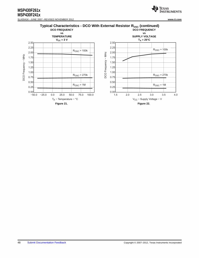
0.00
0.25
0.50
0.75
1.00
1.25
1.50
1.75
2.00
2.25
2.50
−50.0 −25.0 0.0 25.0 50.0 75.0 100.0
TA − Temperature − °C
DC
O F
requency
−M
Hz
ROSC = 100k
ROSC = 270k
ROSC = 1M
0.00
0.25
0.50
0.75
1.00
1.25
1.50
1.75
2.00
2.25
2.50
1.5 2.0 2.5 3.0 3.5 4.0
VCC − Supply Voltage − V
DC
O F
req
ue
ncy
−M
Hz
ROSC = 100k
ROSC = 270k
ROSC = 1M
MSP430F261xMSP430F241xSLAS541K –JUNE 2007–REVISED NOVEMBER 2012 www.ti.com
Typical Characteristics - DCO With External Resistor ROSC (continued)DCO FREQUENCY DCO FREQUENCY
vs vsTEMPERATURE SUPPLY VOLTAGE
VCC = 3 V TA = 25°C
Figure 21. Figure 22.
48 Submit Documentation Feedback Copyright © 2007–2012, Texas Instruments Incorporated
MSP430F261xMSP430F241x
www.ti.com SLAS541K –JUNE 2007–REVISED NOVEMBER 2012
Crystal Oscillator LFXT1, Low-Frequency Mode (1)
over recommended ranges of supply voltage and operating free-air temperature (unless otherwise noted)
PARAMETER TEST CONDITIONS VCC MIN TYP MAX UNIT
LFXT1 oscillator crystalfLFXT1,LF XTS = 0, LFXT1Sx = 0 or 1 1.8 V to 3.6 V 32768 Hzfrequency, LF mode 0, 1
LFXT1 oscillator logic levelfLFXT1,LF,logic square wave input frequency, XTS = 0, LFXT1Sx = 3, XCAPx = 0 1.8 V to 3.6 V 10000 32768 50000 Hz
LF mode
XTS = 0, LFXT1Sx = 0, 500fLFXT1,LF = 32768 Hz, CL,eff = 6 pFOscillation allowance forOALF kΩLF crystals XTS = 0, LFXT1Sx = 0, 200fLFXT1,LF = 32768 Hz, CL,eff = 12 pF
XTS = 0, XCAPx = 0 1
XTS = 0, XCAPx = 1 5.5Integrated effective loadCL,eff pFcapacitance, LF mode (2)XTS = 0, XCAPx = 2 8.5
XTS = 0, XCAPx = 3 11
XTS = 0, Measured at P2.0/ACLK,Duty cycle, LF mode 2.2 V, 3 V 30 50 70 %fLFXT1,LF = 32768 Hz
Oscillator fault frequency,fFault,LF XTS = 0, LFXT1Sx = 3, XCAPx = 0 (4) 2.2 V, 3 V 10 10000 HzLF mode (3)
(1) To improve EMI on the XT1 oscillator, the following guidelines should be observed.(a) Keep the trace between the device and the crystal as short as possible.(b) Design a good ground plane around the oscillator pins.(c) Prevent crosstalk from other clock or data lines into oscillator pins XIN and XOUT.(d) Avoid running PCB traces underneath or adjacent to the XIN and XOUT pins.(e) Use assembly materials and praxis to avoid any parasitic load on the oscillator XIN and XOUT pins.(f) If conformal coating is used, ensure that it does not induce capacitive or resistive leakage between the oscillator pins.(g) Do not route the XOUT line to the JTAG header to support the serial programming adapter as shown in other documentation. This
signal is no longer required for the serial programming adapter.(2) Includes parasitic bond and package capacitance (approximately 2 pF per pin).
Because the PCB adds additional capacitance, it is recommended to verify the correct load by measuring the ACLK frequency. For acorrect setup, the effective load capacitance should always match the specification of the crystal that is used.
(3) Frequencies below the MIN specification set the fault flag. Frequencies above the MAX specification do not set the fault flag.Frequencies in between might set the flag.
(4) Measured with logic-level input frequency but also applies to operation with crystals.
Internal Very-Low-Power Low-Frequency Oscillator (VLO)over recommended ranges of supply voltage and operating free-air temperature (unless otherwise noted)
PARAMETER TA VCC MIN TYP MAX UNIT
-40°C to 85°C 4 12 20fVLO VLO frequency 2.2 V, 3 V kHz
105°C 22
dfVLO/dT VLO frequency temperature drift (1) 2.2 V, 3 V 0.5 %/°C
dfVLO/dVCC VLO frequency supply voltage drift (2) 25°C 1.8 V to 3.6 V 4 %/V
(1) Calculated using the box method:I: (MAX(-40 to 85°C) - MIN(-40 to 85°C)) / MIN(-40 to 85°C) / (85°C - (-40°C))T: (MAX(-40 to 105°C) - MIN(-40 to 105°C)) / MIN(-40 to 105°C) / (105°C - (-40°C))
(2) Calculated using the box method: (MAX(1.8 to 3.6 V) - MIN(1.8 to 3.6 V)) / MIN(1.8 to 3.6 V) / (3.6 V - 1.8 V)
Copyright © 2007–2012, Texas Instruments Incorporated Submit Documentation Feedback 49
MSP430F261xMSP430F241xSLAS541K –JUNE 2007–REVISED NOVEMBER 2012 www.ti.com
Crystal Oscillator LFXT1, High-Frequency Mode (1)
PARAMETER TEST CONDITIONS VCC MIN TYP MAX UNIT
LFXT1 oscillator crystalfLFXT1,HF0 XTS = 1, LFXT1Sx = 0, XCAPx = 0 1.8 V to 3.6 V 0.4 1 MHzfrequency, HF mode 0
LFXT1 oscillator crystalfLFXT1,HF1 XTS = 1, LFXT1Sx = 1, XCAPx = 0 1.8 V to 3.6 V 1 4 MHzfrequency, HF mode 1
1.8 V to 3.6 V 2 10LFXT1 oscillator crystalfLFXT1,HF2 XTS = 1, LFXT1Sx = 2, XCAPx = 0 2.2 V to 3.6 V 2 12 MHzfrequency, HF mode 2
3 V to 3.6 V 2 16
1.8 V to 3.6 V 0.4 10LFXT1 oscillator logic-levelfLFXT1,HF,logic square-wave input XTS = 1, LFXT1Sx = 3, XCAPx = 0 2.2 V to 3.6 V 0.4 12 MHz
frequency, HF mode 3 V to 3.6 V 0.4 16
XTS = 1, XCAPx = 0, LFXT1Sx = 0, 2700fLFXT1,HF = 1 MHz, CL,eff = 15 pFOscillation allowance for HF XTS = 1, XCAPx = 0, LFXT1Sx = 1,OAHF crystals (see Figure 23 and 800 ΩfLFXT1,HF = 4 MHz, CL,eff = 15 pFFigure 24)
XTS = 1, XCAPx = 0, LFXT1Sx = 2, 300fLFXT1,HF = 16 MHz, CL,eff = 15 pF
Integrated effective loadCL,eff XTS = 1, XCAPx = 0 (3) 1 pFcapacitance, HF mode (2)
XTS = 1, XCAPx = 0,Measured at P2.0/ACLK, 40 50 60fLFXT1,HF = 10 MHz
Duty cycle, HF mode 2.2 V, 3 V %XTS = 1, XCAPx = 0,Measured at P2.0/ACLK, 40 50 60fLFXT1,HF = 16 MHz
fFault,HF Oscillator fault frequency (4) XTS = 1, LFXT1Sx = 3, XCAPx = 0 (5) 2.2 V, 3 V 30 300 kHz
(1) To improve EMI on the XT2 oscillator the following guidelines should be observed:(a) Keep the trace between the device and the crystal as short as possible.(b) Design a good ground plane around the oscillator pins.(c) Prevent crosstalk from other clock or data lines into oscillator pins XIN and XOUT.(d) Avoid running PCB traces underneath or adjacent to the XIN and XOUT pins.(e) Use assembly materials and praxis to avoid any parasitic load on the oscillator XIN and XOUT pins.(f) If conformal coating is used, ensure that it does not induce capacitive or resistive leakage between the oscillator pins.(g) Do not route the XOUT line to the JTAG header to support the serial programming adapter as shown in other documentation. This
signal is no longer required for the serial programming adapter.(2) Includes parasitic bond and package capacitance (approximately 2 pF per pin). Because the PCB adds additional capacitance, it is
recommended to verify the correct load by measuring the ACLK frequency. For a correct setup, the effective load capacitance shouldalways match the specification of the used crystal.
(3) Requires external capacitors at both terminals. Values are specified by crystal manufacturers.(4) Frequencies below the MIN specification set the fault flag, frequencies above the MAX specification do not set the fault flag, and
frequencies in between might set the flag.(5) Measured with logic-level input frequency, but also applies to operation with crystals.
50 Submit Documentation Feedback Copyright © 2007–2012, Texas Instruments Incorporated
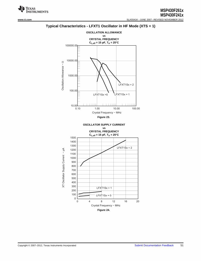
0
100
200
300
400
500
600
700
800
900
1000
1100
1200
1300
1400
1500
0 4 8 12 16 20
Crystal Frequency − MHz
XT
Oscill
ato
r S
up
ply
Cu
rre
nt
−µ
A
LFXT1Sx = 0
LFXT1Sx = 2
LFXT1Sx = 1
Crystal Frequency − MHz
10.00
100.00
1000.00
10000.00
100000.00
0.10 1.00 10.00 100.00
Oscill
atio
nA
llow
an
ce
−W
LFXT1Sx =0
LFXT1Sx = 2
LFXT1Sx = 1
MSP430F261xMSP430F241x
www.ti.com SLAS541K –JUNE 2007–REVISED NOVEMBER 2012
Typical Characteristics - LFXT1 Oscillator in HF Mode (XTS = 1)
OSCILLATION ALLOWANCEvs
CRYSTAL FREQUENCYCL,eff = 15 pF, TA = 25°C
Figure 23.
OSCILLATOR SUPPLY CURRENTvs
CRYSTAL FREQUENCYCL,eff = 15 pF, TA = 25°C
Figure 24.
Copyright © 2007–2012, Texas Instruments Incorporated Submit Documentation Feedback 51
MSP430F261xMSP430F241xSLAS541K –JUNE 2007–REVISED NOVEMBER 2012 www.ti.com
Crystal Oscillator XT2 (1)
PARAMETER TEST CONDITIONS VCC MIN TYP MAX UNIT
XT2 oscillator crystal frequency,fXT2 XT2Sx = 0 1.8 V to 3.6 V 0.4 1 MHzmode 0
XT2 oscillator crystal frequency,fXT2 XT2Sx = 1 1.8 V to 3.6 V 1 4 MHzmode 1
1.8 V to 2.2 V 2 10XT2 oscillator crystal frequency,fXT2 XT2Sx = 2 2.2 V to 3.6 V 2 12 MHzmode 2
3 V to 3.6 V 2 16
1.8 V to 2.2 V 0.4 10XT2 oscillator logic-level square-wavefXT2 XT2Sx = 3 2.2 V to 3.6 V 0.4 12 MHzinput frequency
3 V to 3.6 V 0.4 16
XT2Sx = 0, fXT2 = 1 MHz, 2700CL,eff = 15 pF
Oscillation allowance (see Figure 25 XT2Sx = 1, fXT2 = 4 MHz,OA 800 Ωand Figure 26) CL,eff = 15 pF
XT2Sx = 2, fXT2 = 16 MHz, 300CL,eff = 15 pF
Integrated effective load capacitance,CL,eff See (3) 1 pFHF mode (2)
Measured at P1.4/SMCLK, 40 50 60fXT2 = 10 MHzDuty cycle 2.2 V, 3 V %
Measured at P1.4/SMCLK, 40 50 60fXT2 = 16 MHz
fFault Oscillator fault frequency, HF mode (4) XT2Sx = 3 (5) 2.2 V, 3 V 30 300 kHz
(1) To improve EMI on the XT2 oscillator the following guidelines should be observed:(a) Keep the trace between the device and the crystal as short as possible.(b) Design a good ground plane around the oscillator pins.(c) Prevent crosstalk from other clock or data lines into oscillator pins XT2IN and XT2OUT.(d) Avoid running PCB traces underneath or adjacent to the XT2IN and XT2OUT pins.(e) Use assembly materials and praxis to avoid any parasitic load on the oscillator XT2IN and XT2OUT pins.(f) If conformal coating is used, ensure that it does not induce capacitive or resistive leakage between the oscillator pins.
(2) Includes parasitic bond and package capacitance (approximately 2 pF per pin). Because the PCB adds additional capacitance, it isrecommended to verify the correct load by measuring the ACLK frequency. For a correct setup, the effective load capacitance shouldalways match the specification of the used crystal.
(3) Requires external capacitors at both terminals. Values are specified by crystal manufacturers.(4) Frequencies below the MIN specification set the fault flag, frequencies above the MAX specification do not set the fault flag, and
frequencies in between might set the flag.(5) Measured with logic-level input frequency, but also applies to operation with crystals.
52 Submit Documentation Feedback Copyright © 2007–2012, Texas Instruments Incorporated
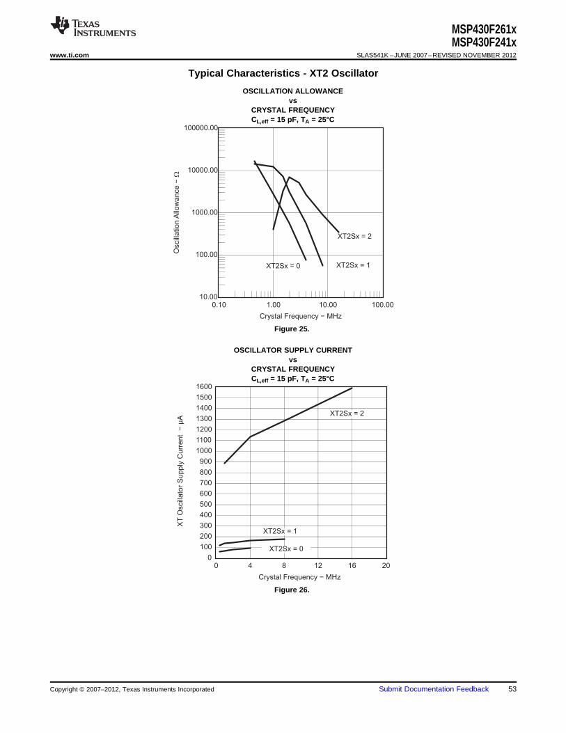
0
100
200
300
400
500
600
700
800
900
1000
1100
1200
1300
1400
1500
1600
0 4 8 12 16 20
Crystal Frequency − MHz
XT
Oscill
ato
r S
upply
Curr
ent
−µ
A
XT2Sx = 0
XT2Sx = 2
XT2Sx = 1
Crystal Frequency − MHz
10.00
100.00
1000.00
10000.00
100000.00
0.10 1.00 10.00 100.00
Oscill
atio
nA
llow
an
ce
−W
XT2Sx = 0
XT2Sx = 2
XT2Sx = 1
MSP430F261xMSP430F241x
www.ti.com SLAS541K –JUNE 2007–REVISED NOVEMBER 2012
Typical Characteristics - XT2 Oscillator
OSCILLATION ALLOWANCEvs
CRYSTAL FREQUENCYCL,eff = 15 pF, TA = 25°C
Figure 25.
OSCILLATOR SUPPLY CURRENTvs
CRYSTAL FREQUENCYCL,eff = 15 pF, TA = 25°C
Figure 26.
Copyright © 2007–2012, Texas Instruments Incorporated Submit Documentation Feedback 53
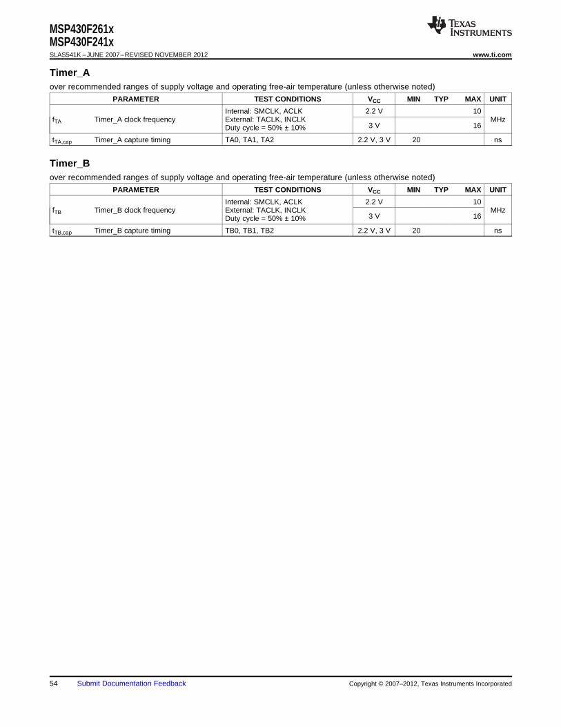
MSP430F261xMSP430F241xSLAS541K –JUNE 2007–REVISED NOVEMBER 2012 www.ti.com
Timer_Aover recommended ranges of supply voltage and operating free-air temperature (unless otherwise noted)
PARAMETER TEST CONDITIONS VCC MIN TYP MAX UNIT
Internal: SMCLK, ACLK 2.2 V 10fTA Timer_A clock frequency External: TACLK, INCLK MHz
3 V 16Duty cycle = 50% ± 10%
tTA,cap Timer_A capture timing TA0, TA1, TA2 2.2 V, 3 V 20 ns
Timer_Bover recommended ranges of supply voltage and operating free-air temperature (unless otherwise noted)
PARAMETER TEST CONDITIONS VCC MIN TYP MAX UNIT
Internal: SMCLK, ACLK 2.2 V 10fTB Timer_B clock frequency External: TACLK, INCLK MHz
3 V 16Duty cycle = 50% ± 10%
tTB,cap Timer_B capture timing TB0, TB1, TB2 2.2 V, 3 V 20 ns
54 Submit Documentation Feedback Copyright © 2007–2012, Texas Instruments Incorporated
MSP430F261xMSP430F241x
www.ti.com SLAS541K –JUNE 2007–REVISED NOVEMBER 2012
USCI (UART Mode)over recommended ranges of supply voltage and operating free-air temperature (unless otherwise noted)
PARAMETER CONDITIONS VCC MIN TYP MAX UNIT
Internal: SMCLK, ACLKfUSCI USCI input clock frequency External: UCLK fSYSTEM MHz
Duty cycle = 50% ± 10%
BITCLK clock frequencyfBITCLK 2.2 V, 3 V 1 MHz(equals baud rate in MBaud) (1)
2.2 V 50 150 600tτ UART receive deglitch time (2) ns
3 V 50 100 600
(1) The DCO wake-up time must be considered in LPM3 or LPM4 for baud rates above 1 MHz.(2) Pulses on the UART receive input (UCxRX) shorter than the UART receive deglitch time are suppressed.
USCI (SPI Master Mode) (1)
over recommended ranges of supply voltage and operating free-air temperature (unless otherwise noted)(see Figure 27 and Figure 28)
PARAMETER TEST CONDITIONS VCC MIN MAX UNIT
SMCLK, ACLKfUSCI USCI input clock frequency fSYSTEM MHzDuty cycle = 50% ± 10%
2.2 V 110tSU,MI SOMI input data setup time ns
3 V 75
2.2 V 0tHD,MI SOMI input data hold time ns
3 V 0
2.2 V 30tVALID,MO SIMO output data valid time UCLK edge to SIMO valid, CL = 20 pF ns
3 V 20
(1) fUCxCLK = 1/2tLO/HI with tLO/HI ≥ max(tVALID,MO(USCI) + tSU,SI(Slave), tSU,MI(USCI) + tVALID,SO(Slave)).For the slave's parameters tSU,SI(Slave) and tVALID,SO(Slave), see the SPI parameters of the attached slave.
USCI (SPI Slave Mode) (1)
over recommended ranges of supply voltage and operating free-air temperature (unless otherwise noted)(see Figure 29 and Figure 30)
PARAMETER TEST CONDITIONS VCC MIN TYP MAX UNIT
tSTE,LEAD STE lead time, STE low to clock 2.2 V, 3 V 50 ns
tSTE,LAG STE lag time, Last clock to STE high 2.2 V, 3 V 10 ns
tSTE,ACC STE access time, STE low to SOMI data out 2.2 V, 3 V 50 ns
STE disable time, STE high to SOMI hightSTE,DIS 2.2 V, 3 V 50 nsimpedance
2.2 V 20tSU,SI SIMO input data setup time ns
3 V 15
2.2 V 10tHD,SI SIMO input data hold time ns
3 V 10
2.2 V 75 110UCLK edge to SOMI valid,tVALID,SO SOMI output data valid time nsCL = 20 pF 3 V 50 75
(1) fUCxCLK = 1/2tLO/HI with tLO/HI ≥ max(tVALID,MO(Master) + tSU,SI(USCI), tSU,MI(Master) + tVALID,SO(USCI)).For the master's parameters tSU,MI(Master) and tVALID,MO(Master) see the SPI parameters of the attached slave.
Copyright © 2007–2012, Texas Instruments Incorporated Submit Documentation Feedback 55
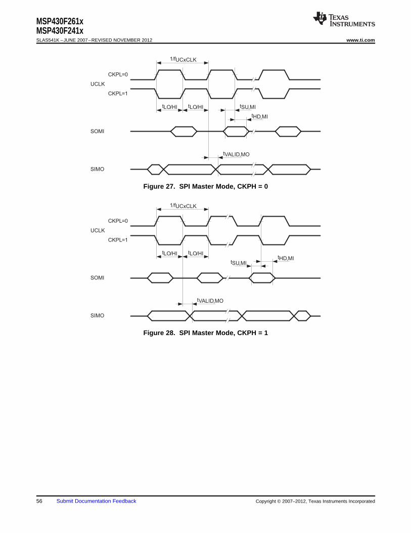
UCLK
CKPL=0
CKPL=1
SIMO
1/fUCxCLK
tLO/HI tLO/HI
SOMI
tSU,MItHD,MI
tVALID,MO
UCLK
CKPL=0
CKPL=1
SIMO
1/fUCxCLK
tLO/HI tLO/HI
SOMI
tSU,MI
tHD,MI
tVALID,MO
MSP430F261xMSP430F241xSLAS541K –JUNE 2007–REVISED NOVEMBER 2012 www.ti.com
Figure 27. SPI Master Mode, CKPH = 0
Figure 28. SPI Master Mode, CKPH = 1
56 Submit Documentation Feedback Copyright © 2007–2012, Texas Instruments Incorporated
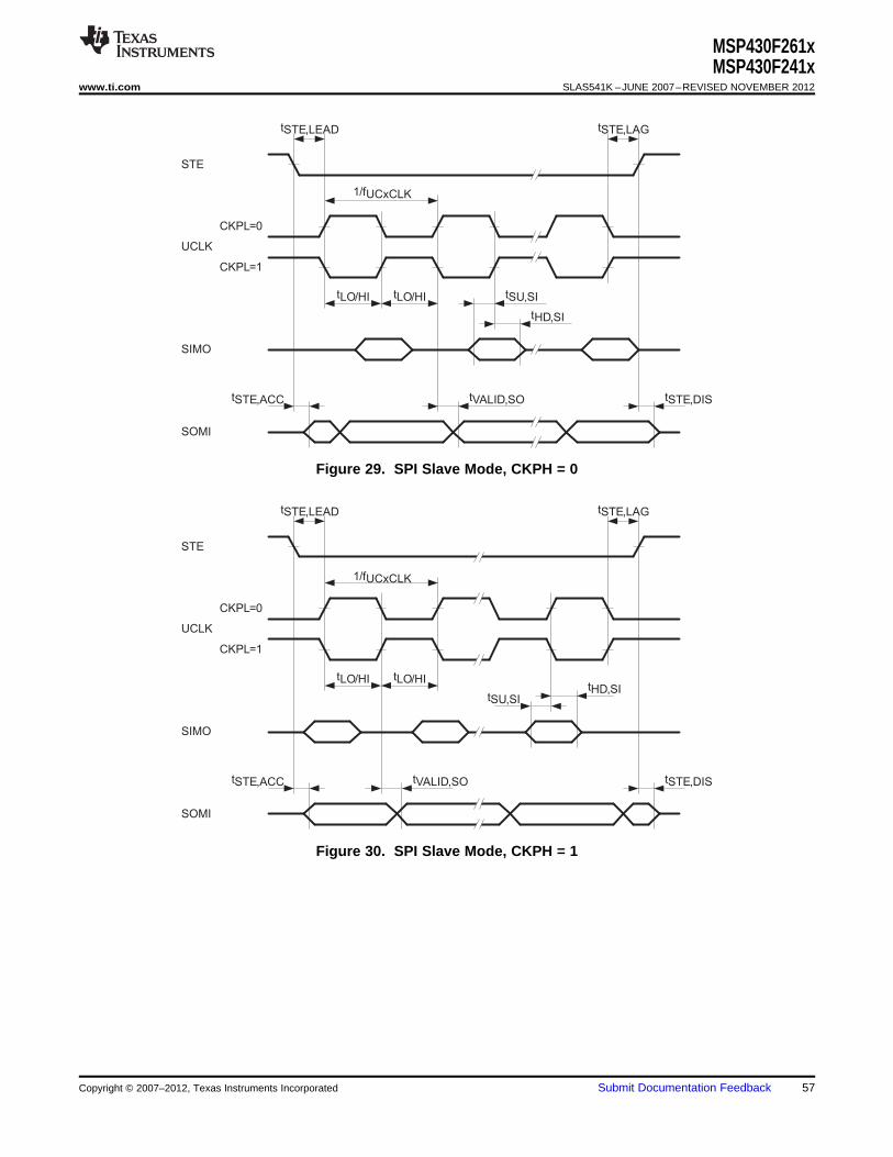
STE
UCLK
CKPL=0
CKPL=1
tSTE,LEAD tSTE,LAG
tSTE,ACC tSTE,DIS
tLO/HI tLO/HI
tSU,SItHD,SI
tVALID,SO
SOMI
SIMO
1/fUCxCLK
STE
UCLK
CKPL=0
CKPL=1
SOMI
tSTE,ACC tSTE,DIS
1/fUCxCLK
tLO/HI tLO/HI
SIMO
tSU,SI
tHD,SI
tVALID,SO
tSTE,LEAD tSTE,LAG
MSP430F261xMSP430F241x
www.ti.com SLAS541K –JUNE 2007–REVISED NOVEMBER 2012
Figure 29. SPI Slave Mode, CKPH = 0
Figure 30. SPI Slave Mode, CKPH = 1
Copyright © 2007–2012, Texas Instruments Incorporated Submit Documentation Feedback 57
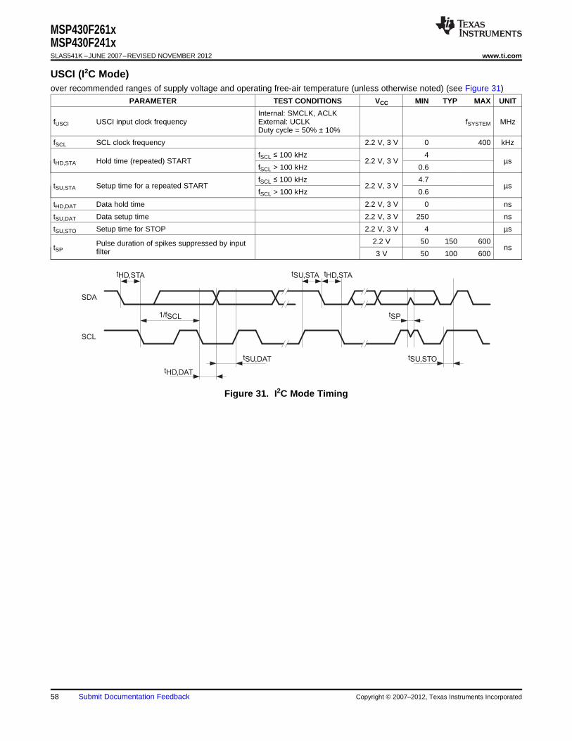
SDA
SCL
1/fSCL
tHD,DAT
tSU,DAT
tHD,STA tSU,STA tHD,STA
tSU,STO
tSP
MSP430F261xMSP430F241xSLAS541K –JUNE 2007–REVISED NOVEMBER 2012 www.ti.com
USCI (I2C Mode)over recommended ranges of supply voltage and operating free-air temperature (unless otherwise noted) (see Figure 31)
PARAMETER TEST CONDITIONS VCC MIN TYP MAX UNIT
Internal: SMCLK, ACLKfUSCI USCI input clock frequency External: UCLK fSYSTEM MHz
Duty cycle = 50% ± 10%
fSCL SCL clock frequency 2.2 V, 3 V 0 400 kHz
fSCL ≤ 100 kHz 4tHD,STA Hold time (repeated) START 2.2 V, 3 V µs
fSCL > 100 kHz 0.6
fSCL ≤ 100 kHz 4.7tSU,STA Setup time for a repeated START 2.2 V, 3 V µs
fSCL > 100 kHz 0.6
tHD,DAT Data hold time 2.2 V, 3 V 0 ns
tSU,DAT Data setup time 2.2 V, 3 V 250 ns
tSU,STO Setup time for STOP 2.2 V, 3 V 4 µs
2.2 V 50 150 600Pulse duration of spikes suppressed by inputtSP nsfilter 3 V 50 100 600
Figure 31. I2C Mode Timing
58 Submit Documentation Feedback Copyright © 2007–2012, Texas Instruments Incorporated
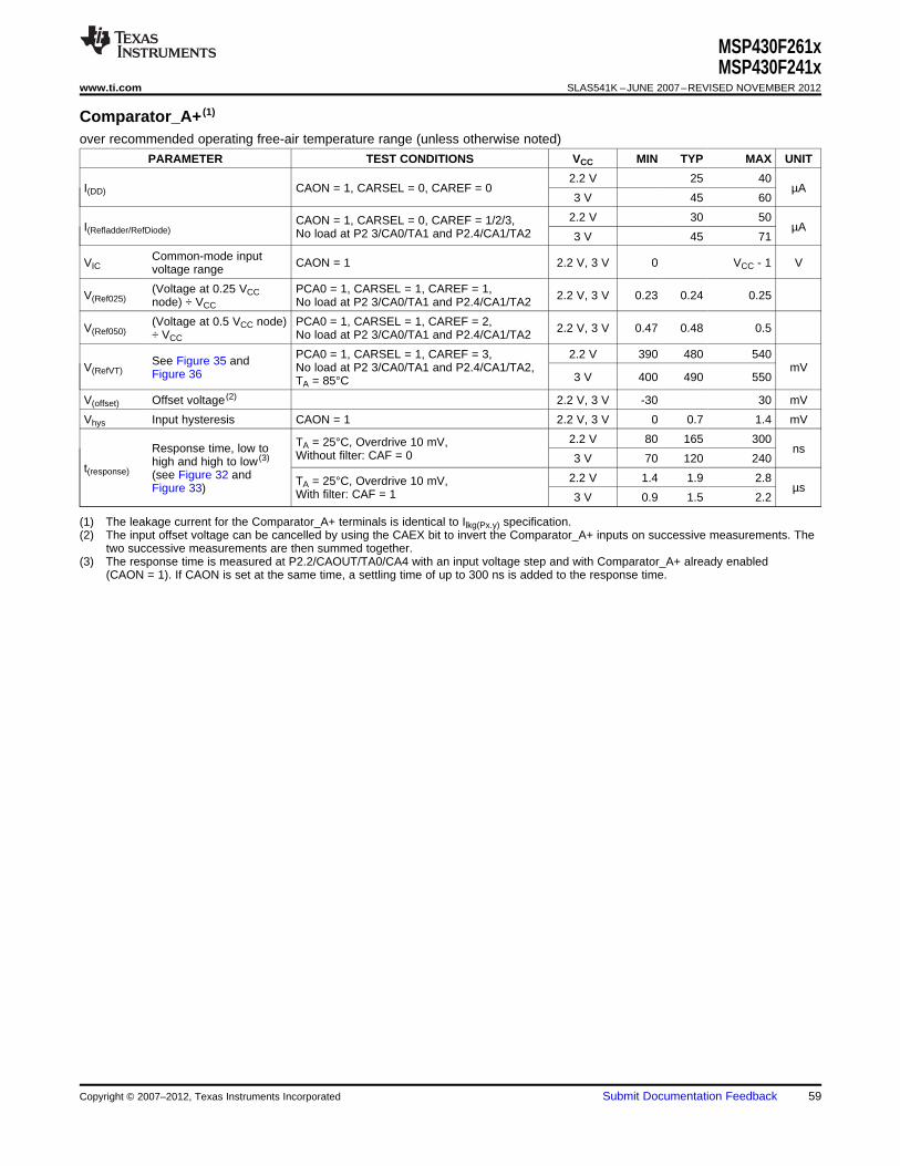
MSP430F261xMSP430F241x
www.ti.com SLAS541K –JUNE 2007–REVISED NOVEMBER 2012
Comparator_A+ (1)
over recommended operating free-air temperature range (unless otherwise noted)
PARAMETER TEST CONDITIONS VCC MIN TYP MAX UNIT
2.2 V 25 40I(DD) CAON = 1, CARSEL = 0, CAREF = 0 µA
3 V 45 60
2.2 V 30 50CAON = 1, CARSEL = 0, CAREF = 1/2/3,I(Refladder/RefDiode) µANo load at P2 3/CA0/TA1 and P2.4/CA1/TA2 3 V 45 71
Common-mode inputVIC CAON = 1 2.2 V, 3 V 0 VCC - 1 Vvoltage range
(Voltage at 0.25 VCC PCA0 = 1, CARSEL = 1, CAREF = 1,V(Ref025) 2.2 V, 3 V 0.23 0.24 0.25node) ÷ VCC No load at P2 3/CA0/TA1 and P2.4/CA1/TA2
(Voltage at 0.5 VCC node) PCA0 = 1, CARSEL = 1, CAREF = 2,V(Ref050) 2.2 V, 3 V 0.47 0.48 0.5÷ VCC No load at P2 3/CA0/TA1 and P2.4/CA1/TA2
PCA0 = 1, CARSEL = 1, CAREF = 3, 2.2 V 390 480 540See Figure 35 andV(RefVT) No load at P2 3/CA0/TA1 and P2.4/CA1/TA2, mVFigure 36 3 V 400 490 550TA = 85°C
V(offset) Offset voltage (2) 2.2 V, 3 V -30 30 mV
Vhys Input hysteresis CAON = 1 2.2 V, 3 V 0 0.7 1.4 mV
2.2 V 80 165 300TA = 25°C, Overdrive 10 mV,Response time, low to nsWithout filter: CAF = 0 3 V 70 120 240high and high to low (3)t(response) (see Figure 32 and 2.2 V 1.4 1.9 2.8TA = 25°C, Overdrive 10 mV, µsFigure 33) With filter: CAF = 1 3 V 0.9 1.5 2.2
(1) The leakage current for the Comparator_A+ terminals is identical to Ilkg(Px.y) specification.(2) The input offset voltage can be cancelled by using the CAEX bit to invert the Comparator_A+ inputs on successive measurements. The
two successive measurements are then summed together.(3) The response time is measured at P2.2/CAOUT/TA0/CA4 with an input voltage step and with Comparator_A+ already enabled
(CAON = 1). If CAON is set at the same time, a settling time of up to 300 ns is added to the response time.
Copyright © 2007–2012, Texas Instruments Incorporated Submit Documentation Feedback 59
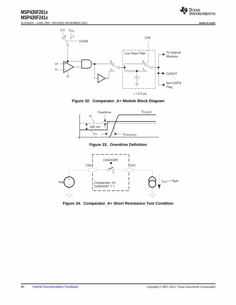
CASHORT
1
Comparator_A+
CASHORT = 1
CA1CA0
VIN+
−
IOUT = 10µA
Overdrive VCAOUT
t(response)V+
V−
400 mV
_
+
CAON
0
1
V+0
1
CAF
Low Pass Filter
τ ≈ 2.0 µs
To Internal
Modules
Set CAIFG
Flag
CAOUT
V−
VCC
1
0 V
0
MSP430F261xMSP430F241xSLAS541K –JUNE 2007–REVISED NOVEMBER 2012 www.ti.com
Figure 32. Comparator_A+ Module Block Diagram
Figure 33. Overdrive Definition
Figure 34. Comparator_A+ Short Resistance Test Condition
60 Submit Documentation Feedback Copyright © 2007–2012, Texas Instruments Incorporated
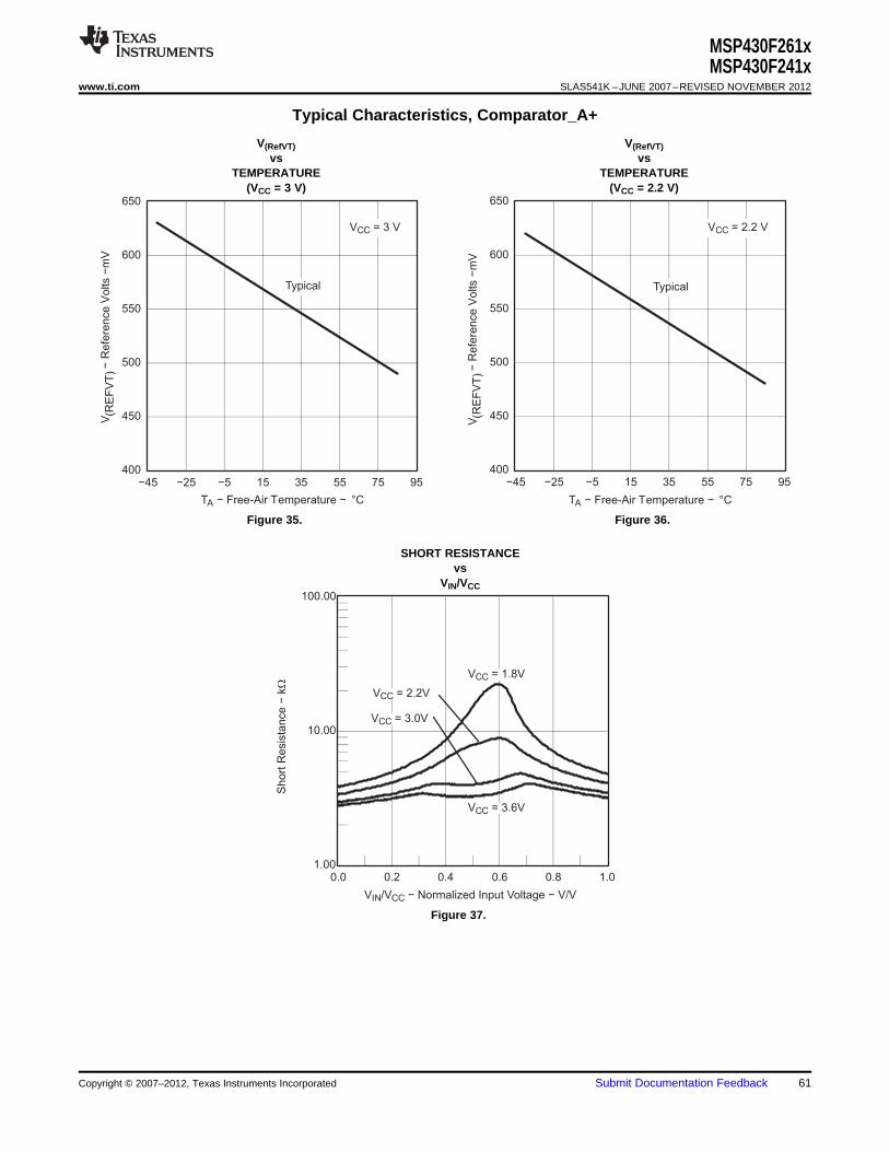
VIN/VCC − Normalized Input Voltage − V/V
1.00
10.00
100.00
0.0 0.2 0.4 0.6 0.8 1.0
VCC = 1.8V
VCC = 3.6V
VCC = 2.2V
VCC = 3.0V
Short
Resis
tance
−kW
TA − Free-Air Temperature − °C
400
450
500
550
600
650
−45 −25 −5 15 35 55 75 95
VCC = 3 V
V(R
EF
VT
)−
Re
fere
nce
Vo
lts
−m
V
Typical
TA − Free-Air Temperature − °C
400
450
500
550
600
650
−45 −25 −5 15 35 55 75 95
VCC = 2.2 V
V(R
EF
VT
)−
Refe
rence V
olts
−m
V
Typical
MSP430F261xMSP430F241x
www.ti.com SLAS541K –JUNE 2007–REVISED NOVEMBER 2012
Typical Characteristics, Comparator_A+
V(RefVT) V(RefVT)vs vs
TEMPERATURE TEMPERATURE(VCC = 3 V) (VCC = 2.2 V)
Figure 35. Figure 36.
SHORT RESISTANCEvs
VIN/VCC
Figure 37.
Copyright © 2007–2012, Texas Instruments Incorporated Submit Documentation Feedback 61
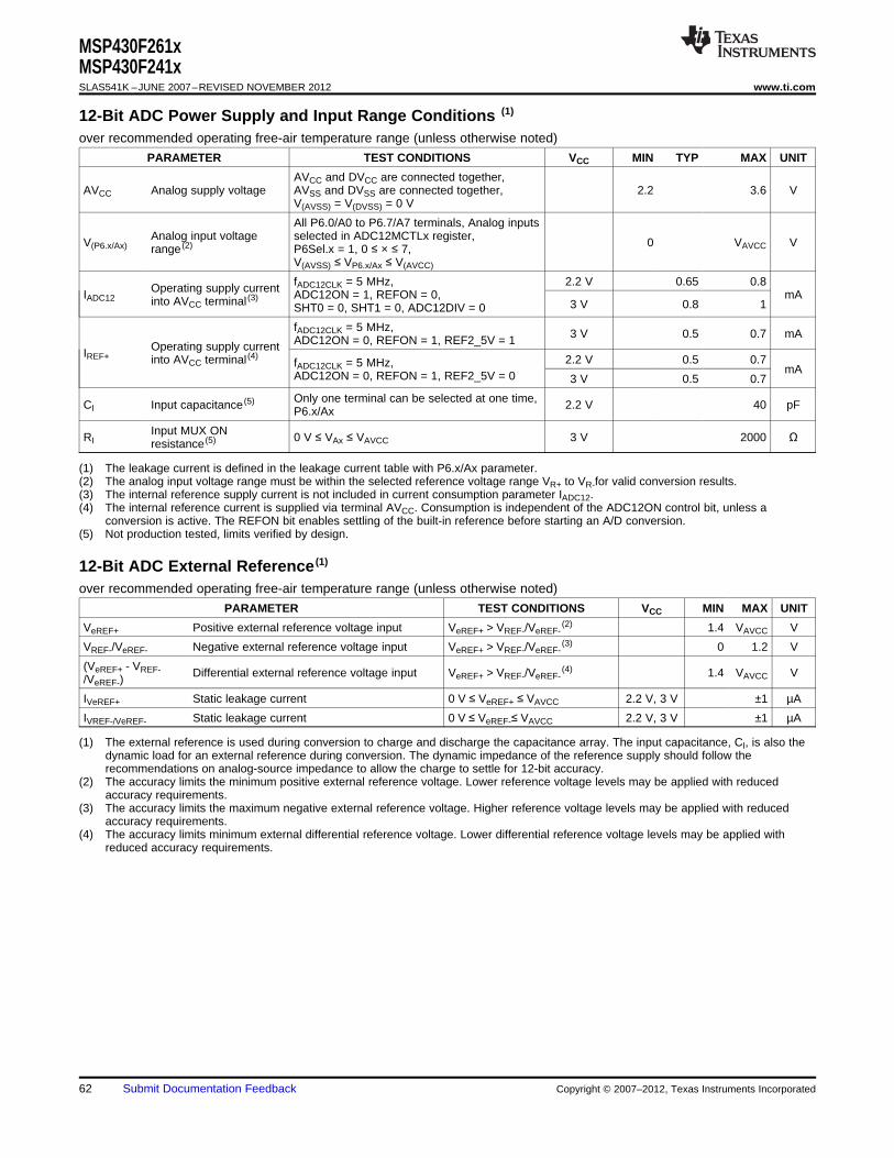
MSP430F261xMSP430F241xSLAS541K –JUNE 2007–REVISED NOVEMBER 2012 www.ti.com
12-Bit ADC Power Supply and Input Range Conditions (1)
over recommended operating free-air temperature range (unless otherwise noted)
PARAMETER TEST CONDITIONS VCC MIN TYP MAX UNIT
AVCC and DVCC are connected together,AVCC Analog supply voltage AVSS and DVSS are connected together, 2.2 3.6 V
V(AVSS) = V(DVSS) = 0 V
All P6.0/A0 to P6.7/A7 terminals, Analog inputsAnalog input voltage selected in ADC12MCTLx register,V(P6.x/Ax) 0 VAVCC Vrange (2) P6Sel.x = 1, 0 ≤ × ≤ 7,
V(AVSS) ≤ VP6.x/Ax ≤ V(AVCC)
fADC12CLK = 5 MHz, 2.2 V 0.65 0.8Operating supply currentIADC12 ADC12ON = 1, REFON = 0, mAinto AVCC terminal (3)3 V 0.8 1SHT0 = 0, SHT1 = 0, ADC12DIV = 0
fADC12CLK = 5 MHz, 3 V 0.5 0.7 mAADC12ON = 0, REFON = 1, REF2_5V = 1Operating supply currentIREF+ into AVCC terminal (4) 2.2 V 0.5 0.7fADC12CLK = 5 MHz, mAADC12ON = 0, REFON = 1, REF2_5V = 0 3 V 0.5 0.7
Only one terminal can be selected at one time,CI Input capacitance (5) 2.2 V 40 pFP6.x/Ax
Input MUX ONRI 0 V ≤ VAx ≤ VAVCC 3 V 2000 Ωresistance (5)
(1) The leakage current is defined in the leakage current table with P6.x/Ax parameter.(2) The analog input voltage range must be within the selected reference voltage range VR+ to VR-for valid conversion results.(3) The internal reference supply current is not included in current consumption parameter IADC12.(4) The internal reference current is supplied via terminal AVCC. Consumption is independent of the ADC12ON control bit, unless a
conversion is active. The REFON bit enables settling of the built-in reference before starting an A/D conversion.(5) Not production tested, limits verified by design.
12-Bit ADC External Reference (1)
over recommended operating free-air temperature range (unless otherwise noted)
PARAMETER TEST CONDITIONS VCC MIN MAX UNIT
VeREF+ Positive external reference voltage input VeREF+ > VREF-/VeREF-(2) 1.4 VAVCC V
VREF-/VeREF- Negative external reference voltage input VeREF+ > VREF-/VeREF-(3) 0 1.2 V
(VeREF+ - VREF- Differential external reference voltage input VeREF+ > VREF-/VeREF-(4) 1.4 VAVCC V/VeREF-)
IVeREF+ Static leakage current 0 V ≤ VeREF+ ≤ VAVCC 2.2 V, 3 V ±1 µA
IVREF-/VeREF- Static leakage current 0 V ≤ VeREF-≤ VAVCC 2.2 V, 3 V ±1 µA
(1) The external reference is used during conversion to charge and discharge the capacitance array. The input capacitance, CI, is also thedynamic load for an external reference during conversion. The dynamic impedance of the reference supply should follow therecommendations on analog-source impedance to allow the charge to settle for 12-bit accuracy.
(2) The accuracy limits the minimum positive external reference voltage. Lower reference voltage levels may be applied with reducedaccuracy requirements.
(3) The accuracy limits the maximum negative external reference voltage. Higher reference voltage levels may be applied with reducedaccuracy requirements.
(4) The accuracy limits minimum external differential reference voltage. Lower differential reference voltage levels may be applied withreduced accuracy requirements.
62 Submit Documentation Feedback Copyright © 2007–2012, Texas Instruments Incorporated
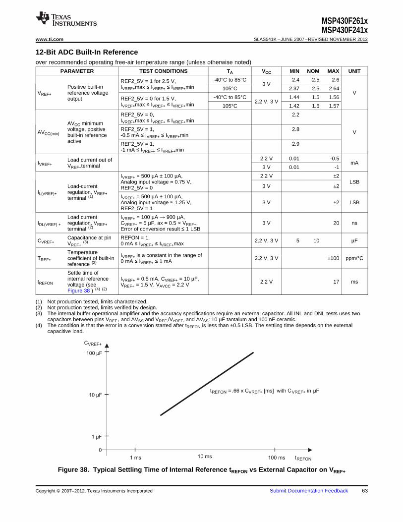
CVREF+
1 µF
0
1 ms 10 ms 100 ms tREFON
tREFON ≈ .66 x CVREF+ [ms] with CVREF+ in µF
100 µF
10 µF
MSP430F261xMSP430F241x
www.ti.com SLAS541K –JUNE 2007–REVISED NOVEMBER 2012
12-Bit ADC Built-In Referenceover recommended operating free-air temperature range (unless otherwise noted)
PARAMETER TEST CONDITIONS TA VCC MIN NOM MAX UNIT
-40°C to 85°C 2.4 2.5 2.6REF2_5V = 1 for 2.5 V, 3 VPositive built-in IVREF+max ≤ IVREF+ ≤ IVREF+min 105°C 2.37 2.5 2.64VREF+ reference voltage V
-40°C to 85°C 1.44 1.5 1.56REF2_5V = 0 for 1.5 V,output 2.2 V, 3 VIVREF+max ≤ IVREF+ ≤ IVREF+min 105°C 1.42 1.5 1.57
REF2_5V = 0, 2.2IVREF+max ≤ IVREF+ ≤ IVREF+minAVCC minimum
voltage, positive REF2_5V = 1, 2.8AVCC(min) Vbuilt-in reference -0.5 mA ≤ IVREF+ ≤ IVREF+minactive REF2_5V = 1, 2.9
-1 mA ≤ IVREF+ ≤ IVREF+min
2.2 V 0.01 -0.5Load current out ofIVREF+ mAVREF+terminal 3 V 0.01 -1
IVREF+ = 500 µA ± 100 µA, 2.2 V ±2Analog input voltage ≈ 0.75 V, LSB
Load-current 3 V ±2REF2_5V = 0IL(VREF)+ regulation, VREF+
IVREF+ = 500 µA ± 100 µA,terminal (1)
Analog input voltage ≈ 1.25 V, 3 V ±2 LSBREF2_5V = 1
Load current IVREF+ = 100 µA → 900 µA,IDL(VREF) + regulation, VREF+ CVREF+ = 5 µF, ax ≈ 0.5 × VREF+, 3 V 20 ns
terminal (2) Error of conversion result ≤ 1 LSB
Capacitance at pin REFON = 1,CVREF+ 2.2 V, 3 V 5 10 µFVREF+(3) 0 mA ≤ IVREF+ ≤ IVREF+max
Temperature IVREF+ is a constant in the range ofTREF+ coefficient of built-in 2.2 V, 3 V ±100 ppm/°C0 mA ≤ IVREF+ ≤ 1 mAreference (2)
Settle time ofinternal reference IVREF+ = 0.5 mA, CVREF+ = 10 µF,tREFON 2.2 V 17 msvoltage (see VREF+ = 1.5 V, VAVCC = 2.2 VFigure 38 ) (4) (2)
(1) Not production tested, limits characterized.(2) Not production tested, limits verified by design.(3) The internal buffer operational amplifier and the accuracy specifications require an external capacitor. All INL and DNL tests uses two
capacitors between pins VREF+ and AVSS and VREF-/VeREF- and AVSS: 10 µF tantalum and 100 nF ceramic.(4) The condition is that the error in a conversion started after tREFON is less than ±0.5 LSB. The settling time depends on the external
capacitive load.
Figure 38. Typical Settling Time of Internal Reference tREFON vs External Capacitor on VREF+
Copyright © 2007–2012, Texas Instruments Incorporated Submit Documentation Feedback 63
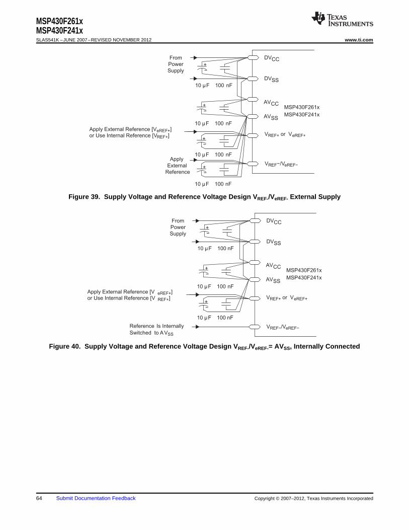
+−
10 µF 100 nF
AVSS
MSP430F261x
MSP430F241x
+−
10 µF 100 nF
AVCC
10 µF 100 nF
DVSS
DVCCFrom
Power
Supply+−
Apply External Reference [V eREF+]or Use Internal Reference [V REF+] VREF+ or VeREF+
VREF−/VeREF−Reference Is Internally
Switched to AVSS
+−
10 µF 100 nF
AVSS
MSP430F261x
MSP430F241x
+−
+−
10 µF 100 nF
10 µF 100 nF
AVCC
10 µF 100 nF
DVSS
DVCCFrom
Power
Supply
Apply
External
Reference
+−
Apply External Reference [VeREF+]or Use Internal Reference [VREF+] VREF+ or VeREF+
VREF−/VeREF−
MSP430F261xMSP430F241xSLAS541K –JUNE 2007–REVISED NOVEMBER 2012 www.ti.com
Figure 39. Supply Voltage and Reference Voltage Design VREF-/VeREF- External Supply
Figure 40. Supply Voltage and Reference Voltage Design VREF-/VeREF-= AVSS, Internally Connected
64 Submit Documentation Feedback Copyright © 2007–2012, Texas Instruments Incorporated
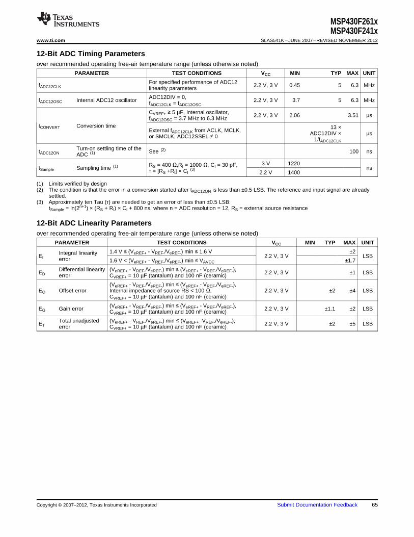
MSP430F261xMSP430F241x
www.ti.com SLAS541K –JUNE 2007–REVISED NOVEMBER 2012
12-Bit ADC Timing Parametersover recommended operating free-air temperature range (unless otherwise noted)
PARAMETER TEST CONDITIONS VCC MIN TYP MAX UNIT
For specified performance of ADC12fADC12CLK 2.2 V, 3 V 0.45 5 6.3 MHzlinearity parameters
ADC12DIV = 0,fADC12OSC Internal ADC12 oscillator 2.2 V, 3 V 3.7 5 6.3 MHzfADC12CLK = fADC12OSC
CVREF+ ≥ 5 µF, Internal oscillator, 2.2 V, 3 V 2.06 3.51 µsfADC12OSC = 3.7 MHz to 6.3 MHztCONVERT Conversion time 13 ×External fADC12CLK from ACLK, MCLK, ADC12DIV × µsor SMCLK, ADC12SSEL ≠ 0 1/fADC12CLK
Turn-on settling time of thetADC12ON See (2) 100 nsADC (1)
3 V 1220RS = 400 Ω,RI = 1000 Ω, CI = 30 pF,tSample Sampling time (1) nsτ = [RS +RI] × CI(3)
2.2 V 1400
(1) Limits verified by design(2) The condition is that the error in a conversion started after tADC12ON is less than ±0.5 LSB. The reference and input signal are already
settled.(3) Approximately ten Tau (τ) are needed to get an error of less than ±0.5 LSB:
tSample = ln(2n+1) × (RS + RI) × CI + 800 ns, where n = ADC resolution = 12, RS = external source resistance
12-Bit ADC Linearity Parametersover recommended operating free-air temperature range (unless otherwise noted)
PARAMETER TEST CONDITIONS VCC MIN TYP MAX UNIT
1.4 V ≤ (VeREF+ - VREF-/VeREF-) min ≤ 1.6 V ±2Integral linearityEI 2.2 V, 3 V LSBerror 1.6 V < (VeREF+ - VREF-/VeREF-) min ≤ VAVCC ±1.7
Differential linearity (VeREF+ - VREF-/VeREF-) min ≤ (VeREF+ - VREF-/VeREF-),ED 2.2 V, 3 V ±1 LSBerror CVREF+ = 10 µF (tantalum) and 100 nF (ceramic)
(VeREF+ - VREF-/VeREF-) min ≤ (VeREF+ - VREF-/VeREF-),EO Offset error Internal impedance of source RS < 100 Ω, 2.2 V, 3 V ±2 ±4 LSB
CVREF+ = 10 µF (tantalum) and 100 nF (ceramic)
(VeREF+ - VREF-/VeREF-) min ≤ (VeREF+ - VREF-/VeREF-),EG Gain error 2.2 V, 3 V ±1.1 ±2 LSBCVREF+ = 10 µF (tantalum) and 100 nF (ceramic)
Total unadjusted (VeREF+ - VREF-/VeREF-) min ≤ (VeREF+ -VREF-/VeREF-),ET 2.2 V, 3 V ±2 ±5 LSBerror CVREF+ = 10 µF (tantalum) and 100 nF (ceramic)
Copyright © 2007–2012, Texas Instruments Incorporated Submit Documentation Feedback 65
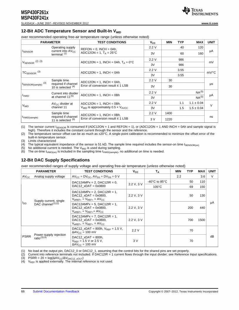
MSP430F261xMSP430F241xSLAS541K –JUNE 2007–REVISED NOVEMBER 2012 www.ti.com
12-Bit ADC Temperature Sensor and Built-In VMID
over recommended operating free-air temperature range (unless otherwise noted)
PARAMETER TEST CONDITIONS VCC MIN TYP MAX UNIT
Operating supply 2.2 V 40 120REFON = 0, INCH = 0Ah,ISENSOR current into AVCC µAADC12ON = 1, TA = 25°C 3V 60 160terminal (1)
2.2 V 986VSENSOR
(2) (3) ADC12ON = 1, INCH = 0Ah, TA = 0°C mV3V 986
2.2 V 3.55TCSENSOR
(3) ADC12ON = 1, INCH = 0Ah mV/°C3V 3.55
Sample time 2.2 V 30ADC12ON = 1, INCH = 0Ah,tSENSOR(sample)(3) required if channel µsError of conversion result ≤ 1 LSB 3V 3010 is selected (4)
2.2 V NA (5)Current into dividerIVMID ADC12ON = 1, INCH = 0Bh µAat channel 11 (5)
3V NA (5)
2.2 V 1.1 1.1 ± 0.04AVCC divider at ADC12ON = 1, INCH = 0Bh,VMID Vchannel 11 VMID is approximately 0.5 × VAVCC 3V 1.5 1.5 ± 0.04
Sample time 2.2 V 1400ADC12ON = 1, INCH = 0Bh,tVMID(sample) required if channel nsError of conversion result ≤ 1 LSB 3 V 122011 is selected (6)
(1) The sensor current ISENSOR is consumed if (ADC12ON = 1 and REFON = 1), or (ADC12ON = 1 AND INCH = 0Ah and sample signal ishigh). Therefore it includes the constant current through the sensor and the reference.
(2) The temperature sensor offset can be as much as ±20°C. A single-point calibration is recommended to minimize the offset error of thebuilt-in temperature sensor.
(3) Limits characterized(4) The typical equivalent impedance of the sensor is 51 kΩ. The sample time required includes the sensor-on time tSENSOR(on)(5) No additional current is needed. The VMID is used during sampling.(6) The on-time tVMID(on) is included in the sampling time tVMID(sample), no additional on time is needed.
12-Bit DAC Supply Specificationsover recommended ranges of supply voltage and operating free-air temperature (unless otherwise noted)
PARAMETER TEST CONDITIONS VCC TA MIN TYP MAX UNIT
AVCC Analog supply voltage AVCC = DVCC, AVSS = DVSS = 0 V 2.2 3.6 V
-40°C to 85°C 50 110DAC12AMPx = 2, DAC12IR = 0, 2.2 V, 3 VDAC12_xDAT = 0x0800 105°C 69 150
DAC12AMPx = 2, DAC12IR = 1,DAC12_xDAT = 0x0800, 2.2 V, 3 V 50 130VeREF+ = VREF+ = AVCCSupply current, singleIDD µADAC12AMPx = 5, DAC12IR = 1,DAC channel (1) (2)
DAC12_xDAT = 0x0800, 2.2 V, 3 V 200 440VeREF+ = VREF+= AVCC
DAC12AMPx = 7, DAC12IR = 1,DAC12_xDAT = 0x0800, 2.2 V, 3 V 700 1500VeREF+ = VREF+ = AVCC
DAC12_xDAT = 800h, VREF = 1.5 V, 2.2 V 70ΔAVCC = 100 mVPower-supply rejectionPSRR dBDAC12_xDAT = 800h,ratio (3) (4)
VREF = 1.5 V or 2.5 V, 3 V 70ΔAVCC = 100 mV
(1) No load at the output pin, DAC12_0 or DAC12_1, assuming that the control bits for the shared pins are set properly.(2) Current into reference terminals not included. If DAC12IR = 1 current flows through the input divider; see Reference Input specifications.(3) PSRR = 20 × log(ΔAVCC/ΔVDAC12_xOUT)(4) VREF is applied externally. The internal reference is not used.
66 Submit Documentation Feedback Copyright © 2007–2012, Texas Instruments Incorporated
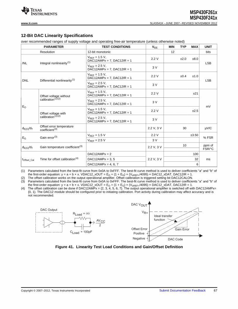
Positive
Negative
VR+
Gain ErrorOffset Error
DAC Code
DAC VOUT
Ideal transfer
function
RLoad =
AVCC
CLoad = 100pF
2
DAC Output
MSP430F261xMSP430F241x
www.ti.com SLAS541K –JUNE 2007–REVISED NOVEMBER 2012
12-Bit DAC Linearity Specificationsover recommended ranges of supply voltage and operating free-air temperature (unless otherwise noted)
PARAMETER TEST CONDITIONS VCC MIN TYP MAX UNIT
Resolution 12-bit monotonic 12 bits
VREF = 1.5 V, 2.2 V ±2.0 ±8.0DAC12AMPx = 7, DAC12IR = 1INL Integral nonlinearity (1) LSB
VREF = 2.5 V, 3 VDAC12AMPx = 7, DAC12IR = 1
VREF = 1.5 V, 2.2 V ±0.4 ±1.0DAC12AMPx = 7, DAC12IR = 1DNL Differential nonlinearity (1) LSB
VREF = 2.5 V, 3 VDAC12AMPx = 7, DAC12IR = 1
VREF = 1.5 V, 2.2 V ±21DAC12AMPx = 7, DAC12IR = 1Offset voltage withoutcalibration (1) (2)
VREF = 2.5 V, 3 VDAC12AMPx = 7, DAC12IR = 1EO mV
VREF = 1.5 V, 2.2 V ±2.5DAC12AMPx = 7, DAC12IR = 1Offset voltage withcalibration (1) (2)
VREF = 2.5 V, 3 VDAC12AMPx = 7, DAC12IR = 1
Offset error temperaturedE(O)/dT 2.2 V, 3 V 30 µV/Ccoefficient (3)
VREF = 1.5 V 2.2 V ±3.50EG Gain error (3) % FSR
VREF = 2.5 V 3 V
10 ppm ofdE(G)/dT Gain temperature coefficient (3) 2.2 V, 3 V FSR/°C
DAC12AMPx = 2 100
tOffset_Cal Time for offset calibration (4) DAC12AMPx = 3, 5 2.2 V, 3 V 32 ms
DAC12AMPx = 4, 6, 7 6
(1) Parameters calculated from the best-fit curve from 0x0A to 0xFFF. The best-fit curve method is used to deliver coefficients "a" and "b" ofthe first-order equation: y = a + b × x. VDAC12_xOUT = EO + (1 + EG) × (VeREF+/4095) × DAC12_xDAT, DAC12IR = 1.
(2) The offset calibration works on the output operational amplifier. Offset calibration is triggered setting bit DAC12CALON.(3) Parameters calculated from the best-fit curve from 0x0A to 0xFFF. The best-fit curve method is used to deliver coefficients "a" and "b" of
the first-order equation: y = a + b × x. VDAC12_xOUT = EO + (1 + EG) × (VeREF+/4095) × DAC12_xDAT, DAC12IR = 1.(4) The offset calibration can be done if DAC12AMPx = 2, 3, 4, 5, 6, 7. The output operational amplifier is switched off with DAC12AMPx=
0, 1. The DAC12 module should be configured prior to initiating calibration. Port activity during calibration may affect accuracy and isnot recommended.
Figure 41. Linearity Test Load Conditions and Gain/Offset Definition
Copyright © 2007–2012, Texas Instruments Incorporated Submit Documentation Feedback 67
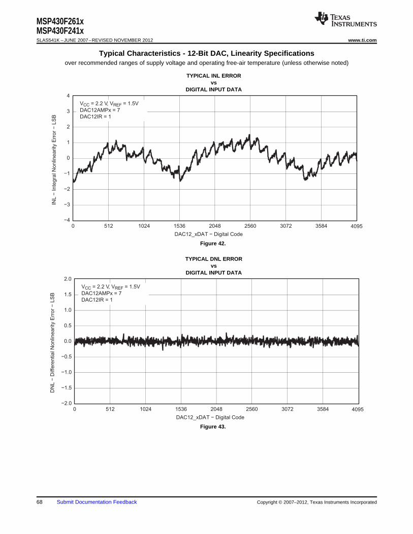
DAC12_xDAT − Digital Code
−2.0
−1.5
−1.0
−0.5
0.0
0.5
1.0
1.5
2.0
0 512 1024 1536 2048 2560 3072 3584
VCC = 2.2 V, VREF = 1.5V
DAC12AMPx = 7
DAC12IR = 1
4095
DN
L−
Diffe
ren
tia
l N
on
line
arity
Err
or
−L
SB
DAC12_xDAT − Digital Code
−4
−3
−2
−1
0
1
2
3
4
0 512 1024 1536 2048 2560 3072 3584
VCC = 2.2 V, VREF = 1.5V
DAC12AMPx = 7
DAC12IR = 1
4095
INL
−In
teg
ral N
on
line
arity
Err
or
−L
SB
MSP430F261xMSP430F241xSLAS541K –JUNE 2007–REVISED NOVEMBER 2012 www.ti.com
Typical Characteristics - 12-Bit DAC, Linearity Specificationsover recommended ranges of supply voltage and operating free-air temperature (unless otherwise noted)
TYPICAL INL ERRORvs
DIGITAL INPUT DATA
Figure 42.
TYPICAL DNL ERRORvs
DIGITAL INPUT DATA
Figure 43.
68 Submit Documentation Feedback Copyright © 2007–2012, Texas Instruments Incorporated
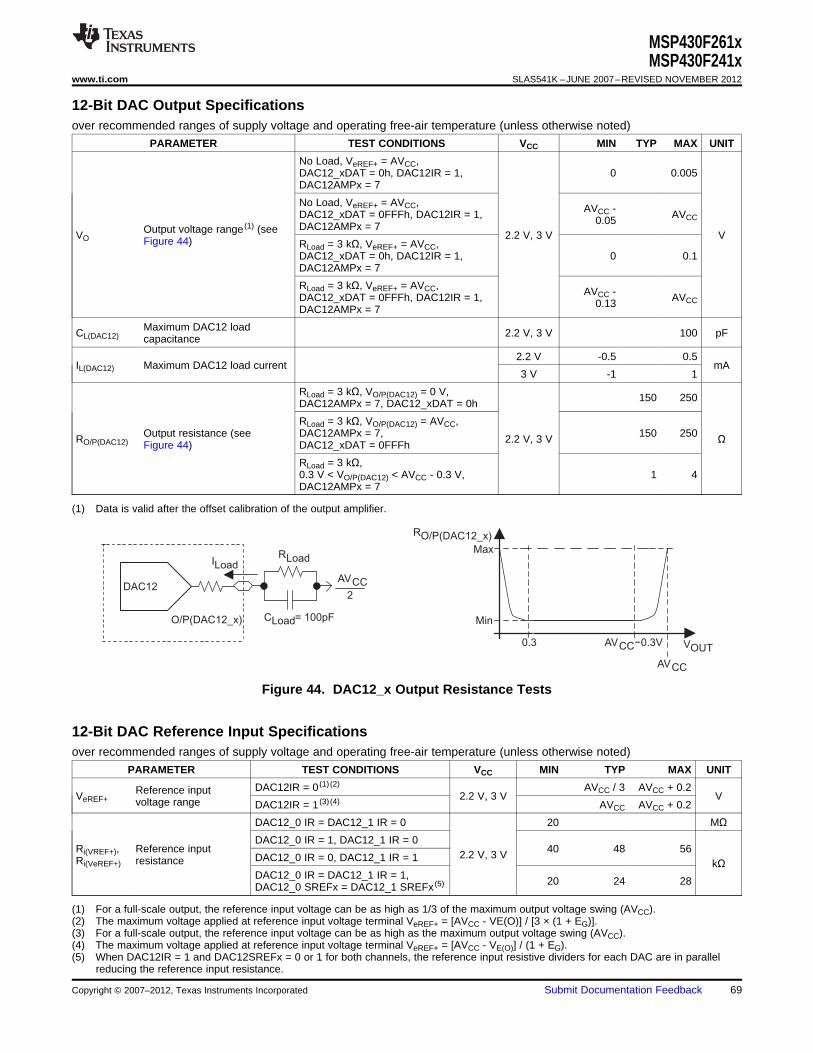
RO/P(DAC12_x)
Max
0.3
AVCC
AVCC−0.3V VOUT
Min
RLoad
AVCC
CLoad= 100pF
2
ILoad
DAC12
O/P(DAC12_x)
MSP430F261xMSP430F241x
www.ti.com SLAS541K –JUNE 2007–REVISED NOVEMBER 2012
12-Bit DAC Output Specificationsover recommended ranges of supply voltage and operating free-air temperature (unless otherwise noted)
PARAMETER TEST CONDITIONS VCC MIN TYP MAX UNIT
No Load, VeREF+ = AVCC,DAC12_xDAT = 0h, DAC12IR = 1, 0 0.005DAC12AMPx = 7
No Load, VeREF+ = AVCC, AVCC -DAC12_xDAT = 0FFFh, DAC12IR = 1, AVCC0.05DAC12AMPx = 7Output voltage range (1) (seeVO 2.2 V, 3 V VFigure 44) RLoad = 3 kΩ, VeREF+ = AVCC,DAC12_xDAT = 0h, DAC12IR = 1, 0 0.1DAC12AMPx = 7
RLoad = 3 kΩ, VeREF+ = AVCC, AVCC -DAC12_xDAT = 0FFFh, DAC12IR = 1, AVCC0.13DAC12AMPx = 7
Maximum DAC12 loadCL(DAC12) 2.2 V, 3 V 100 pFcapacitance
2.2 V -0.5 0.5IL(DAC12) Maximum DAC12 load current mA
3 V -1 1
RLoad = 3 kΩ, VO/P(DAC12) = 0 V, 150 250DAC12AMPx = 7, DAC12_xDAT = 0h
RLoad = 3 kΩ, VO/P(DAC12) = AVCC,Output resistance (see DAC12AMPx = 7, 150 250RO/P(DAC12) 2.2 V, 3 V ΩFigure 44) DAC12_xDAT = 0FFFh
RLoad = 3 kΩ,0.3 V < VO/P(DAC12) < AVCC - 0.3 V, 1 4DAC12AMPx = 7
(1) Data is valid after the offset calibration of the output amplifier.
Figure 44. DAC12_x Output Resistance Tests
12-Bit DAC Reference Input Specificationsover recommended ranges of supply voltage and operating free-air temperature (unless otherwise noted)
PARAMETER TEST CONDITIONS VCC MIN TYP MAX UNIT
DAC12IR = 0 (1) (2) AVCC / 3 AVCC + 0.2Reference inputVeREF+ 2.2 V, 3 V Vvoltage range DAC12IR = 1 (3) (4) AVCC AVCC + 0.2
DAC12_0 IR = DAC12_1 IR = 0 20 MΩDAC12_0 IR = 1, DAC12_1 IR = 0
Ri(VREF+), Reference input 40 48 562.2 V, 3 VDAC12_0 IR = 0, DAC12_1 IR = 1Ri(VeREF+) resistance kΩDAC12_0 IR = DAC12_1 IR = 1, 20 24 28DAC12_0 SREFx = DAC12_1 SREFx (5)
(1) For a full-scale output, the reference input voltage can be as high as 1/3 of the maximum output voltage swing (AVCC).(2) The maximum voltage applied at reference input voltage terminal VeREF+ = [AVCC - VE(O)] / [3 × (1 + EG)].(3) For a full-scale output, the reference input voltage can be as high as the maximum output voltage swing (AVCC).(4) The maximum voltage applied at reference input voltage terminal VeREF+ = [AVCC - VE(O)] / (1 + EG).(5) When DAC12IR = 1 and DAC12SREFx = 0 or 1 for both channels, the reference input resistive dividers for each DAC are in parallel
reducing the reference input resistance.
Copyright © 2007–2012, Texas Instruments Incorporated Submit Documentation Feedback 69
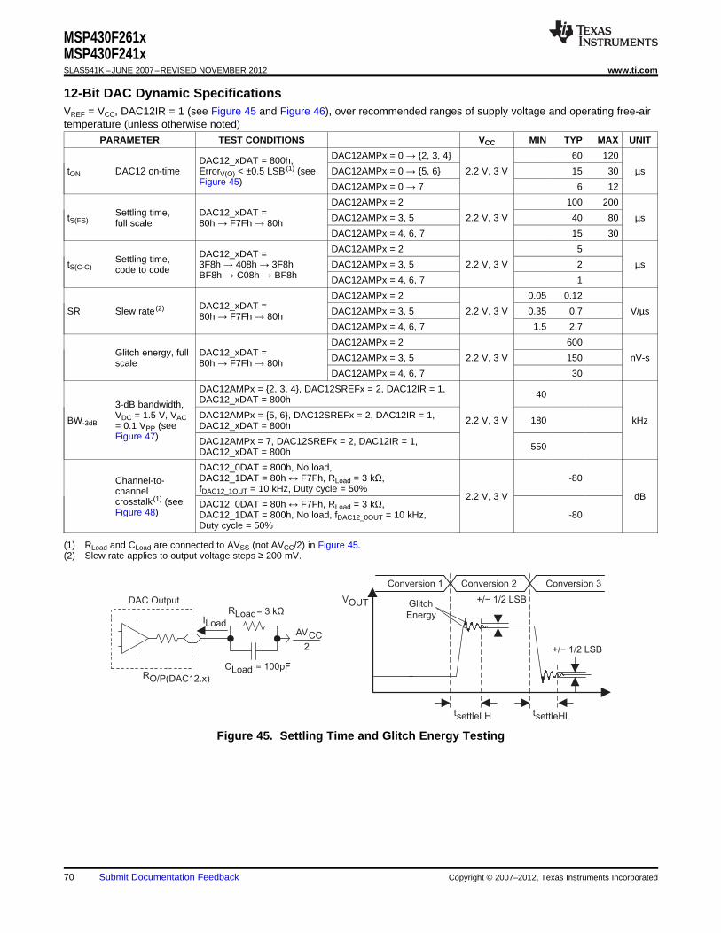
RLoad
AVCC
CLoad = 100pF
2
DAC Output
RO/P(DAC12.x)
ILoad
Conversion 1 Conversion 2
VOUT
Conversion 3
Glitch
Energy
+/− 1/2 LSB
+/− 1/2 LSB
tsettleLH tsettleHL
= 3 kΩ
MSP430F261xMSP430F241xSLAS541K –JUNE 2007–REVISED NOVEMBER 2012 www.ti.com
12-Bit DAC Dynamic SpecificationsVREF = VCC, DAC12IR = 1 (see Figure 45 and Figure 46), over recommended ranges of supply voltage and operating free-airtemperature (unless otherwise noted)
PARAMETER TEST CONDITIONS VCC MIN TYP MAX UNIT
DAC12AMPx = 0 → 2, 3, 4 60 120DAC12_xDAT = 800h,tON DAC12 on-time ErrorV(O) < ±0.5 LSB (1) (see DAC12AMPx = 0 → 5, 6 2.2 V, 3 V 15 30 µs
Figure 45) DAC12AMPx = 0 → 7 6 12
DAC12AMPx = 2 100 200Settling time, DAC12_xDAT =tS(FS) DAC12AMPx = 3, 5 2.2 V, 3 V 40 80 µsfull scale 80h → F7Fh → 80h
DAC12AMPx = 4, 6, 7 15 30
DAC12AMPx = 2 5DAC12_xDAT =Settling time,tS(C-C) 3F8h → 408h → 3F8h DAC12AMPx = 3, 5 2.2 V, 3 V 2 µscode to code BF8h → C08h → BF8h DAC12AMPx = 4, 6, 7 1
DAC12AMPx = 2 0.05 0.12DAC12_xDAT =SR Slew rate (2) DAC12AMPx = 3, 5 2.2 V, 3 V 0.35 0.7 V/µs80h → F7Fh → 80h
DAC12AMPx = 4, 6, 7 1.5 2.7
DAC12AMPx = 2 600Glitch energy, full DAC12_xDAT = DAC12AMPx = 3, 5 2.2 V, 3 V 150 nV-sscale 80h → F7Fh → 80h
DAC12AMPx = 4, 6, 7 30
DAC12AMPx = 2, 3, 4, DAC12SREFx = 2, DAC12IR = 1, 40DAC12_xDAT = 800h3-dB bandwidth,VDC = 1.5 V, VAC DAC12AMPx = 5, 6, DAC12SREFx = 2, DAC12IR = 1,BW-3dB 2.2 V, 3 V 180 kHz= 0.1 VPP (see DAC12_xDAT = 800hFigure 47) DAC12AMPx = 7, DAC12SREFx = 2, DAC12IR = 1, 550DAC12_xDAT = 800h
DAC12_0DAT = 800h, No load,DAC12_1DAT = 80h ↔ F7Fh, RLoad = 3 kΩ, -80Channel-to-fDAC12_1OUT = 10 kHz, Duty cycle = 50%channel 2.2 V, 3 V dBcrosstalk (1) (see DAC12_0DAT = 80h ↔ F7Fh, RLoad = 3 kΩ,
Figure 48) DAC12_1DAT = 800h, No load, fDAC12_0OUT = 10 kHz, -80Duty cycle = 50%
(1) RLoad and CLoad are connected to AVSS (not AVCC/2) in Figure 45.(2) Slew rate applies to output voltage steps ≥ 200 mV.
Figure 45. Settling Time and Glitch Energy Testing
70 Submit Documentation Feedback Copyright © 2007–2012, Texas Instruments Incorporated
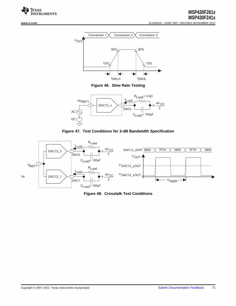
DAC12_xDAT 080h
V OUT
fToggle
7F7h
V DAC12_yOUT
080h 7F7h 080h
V DAC12_xOUTVe
REF+ RLoad
AVCC
CLoad= 100pF
2
ILoad
DAC12_1
RLoad
AVCC
CLoad= 100pF
2
ILoad
DAC12_0DAC0
DAC1
V
VeREF+
AC
DC
RLoad
AVCC
CLoad= 100pF
2
ILoad
DAC12_x
DACx
= 3 kΩ
Conversion 1 Conversion 2
VOUT
Conversion 3
10%
tSRLH tSRHL
90%
10%
90%
MSP430F261xMSP430F241x
www.ti.com SLAS541K –JUNE 2007–REVISED NOVEMBER 2012
Figure 46. Slew Rate Testing
Figure 47. Test Conditions for 3-dB Bandwidth Specification
Figure 48. Crosstalk Test Conditions
Copyright © 2007–2012, Texas Instruments Incorporated Submit Documentation Feedback 71
MSP430F261xMSP430F241xSLAS541K –JUNE 2007–REVISED NOVEMBER 2012 www.ti.com
Flash Memoryover recommended ranges of supply voltage and operating free-air temperature (unless otherwise noted)
PARAMETER TEST CONDITIONS VCC MIN TYP MAX UNIT
VCC(PGM/ERASE) Program and erase supply voltage 2.2 3.6 V
fFTG Flash timing generator frequency 257 476 kHz
IPGM Supply current from VCC during program 2.2 V/3.6 V 1 5 mA
IERASE Supply current from VCC during erase 2.2 V/3.6 V 1 7 mA
tCPT Cumulative program time (1) 2.2 V/3.6 V 10 ms
tCMErase Cumulative mass erase time 2.2 V/3.6 V 20 ms
Program and erase endurance 104 105 cycles
tRetention Data retention duration TJ = 25°C 100 years
tWord Word or byte program time (2) 30 tFTG
tBlock, 0 Block program time for first byte or word (2) 25 tFTG
Block program time for each additionaltBlock, 1-63(2) 18 tFTGbyte or word
tBlock, End Block program end-sequence wait time (2) 6 tFTG
tMass Erase Mass erase time (2) 10593 tFTG
tSeg Erase Segment erase time (2) 4819 tFTG
(1) The cumulative program time must not be exceeded when writing to a 64-byte flash block. This parameter applies to all programmingmethods: individual word/byte write and block write modes.
(2) These values are hardwired into the Flash Controller's state machine (tFTG = 1/fFTG).
RAMover recommended ranges of supply voltage and operating free-air temperature (unless otherwise noted)
PARAMETER TEST CONDITIONS MIN MAX UNIT
V(RAMh) RAM retention supply voltage (1) CPU halted 1.6 V
(1) This parameter defines the minimum supply voltage VCC when the data in RAM remains unchanged. No program execution shouldhappen during this supply voltage condition.
JTAG Interfaceover recommended ranges of supply voltage and operating free-air temperature (unless otherwise noted)
PARAMETER VCC MIN TYP MAX UNIT
2.2 V 0 5fTCK TCK input frequency (1) MHz
3 V 0 10
RInternal Internal pullup resistance on TMS, TCK, and TDI/TCLK (2) 2.2 V, 3 V 25 60 90 kΩ
(1) fTCK may be restricted to meet the timing requirements of the module selected.(2) TMS, TCK, and TDI/TCLK pullup resistors are implemented in all versions.
JTAG Fuse (1)
over recommended ranges of supply voltage and operating free-air temperature (unless otherwise noted)
PARAMETER TEST CONDITIONS MIN MAX UNIT
VCC(FB) Supply voltage during fuse-blow condition TA = 25°C 2.5 V
VFB Voltage level on TEST for fuse blow 6 7 V
IFB Supply current into TEST during fuse blow 100 mA
tFB Time to blow fuse 1 ms
(1) Once the fuse is blown, no further access to the JTAG/Test and emulation feature is possible, and JTAG is switched to bypass mode.
72 Submit Documentation Feedback Copyright © 2007–2012, Texas Instruments Incorporated
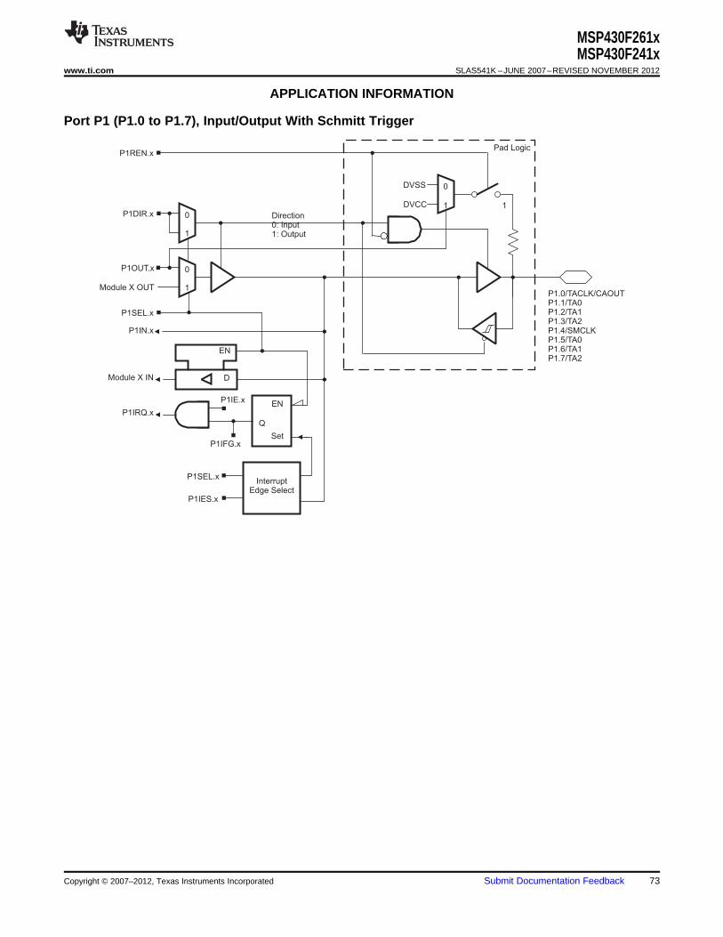
Direction0: Input1: Output
P1SEL.x
P1DIR.x
P1IN.x
P1IRQ.x
D
EN
Module X IN
Module X OUT
P1OUT.x
InterruptEdge Select
Q
EN
Set
P1SEL.x
P1IES.x
P1IFG.x
P1IE.x
P1.0/TACLK/CAOUTP1.1/TA0P1.2/TA1P1.3/TA2P1.4/SMCLKP1.5/TA0P1.6/TA1P1.7/TA2
DVSS
DVCC
Pad Logic
1
1
0
1
0
1
0
P1REN.x
MSP430F261xMSP430F241x
www.ti.com SLAS541K –JUNE 2007–REVISED NOVEMBER 2012
APPLICATION INFORMATION
Port P1 (P1.0 to P1.7), Input/Output With Schmitt Trigger
Copyright © 2007–2012, Texas Instruments Incorporated Submit Documentation Feedback 73
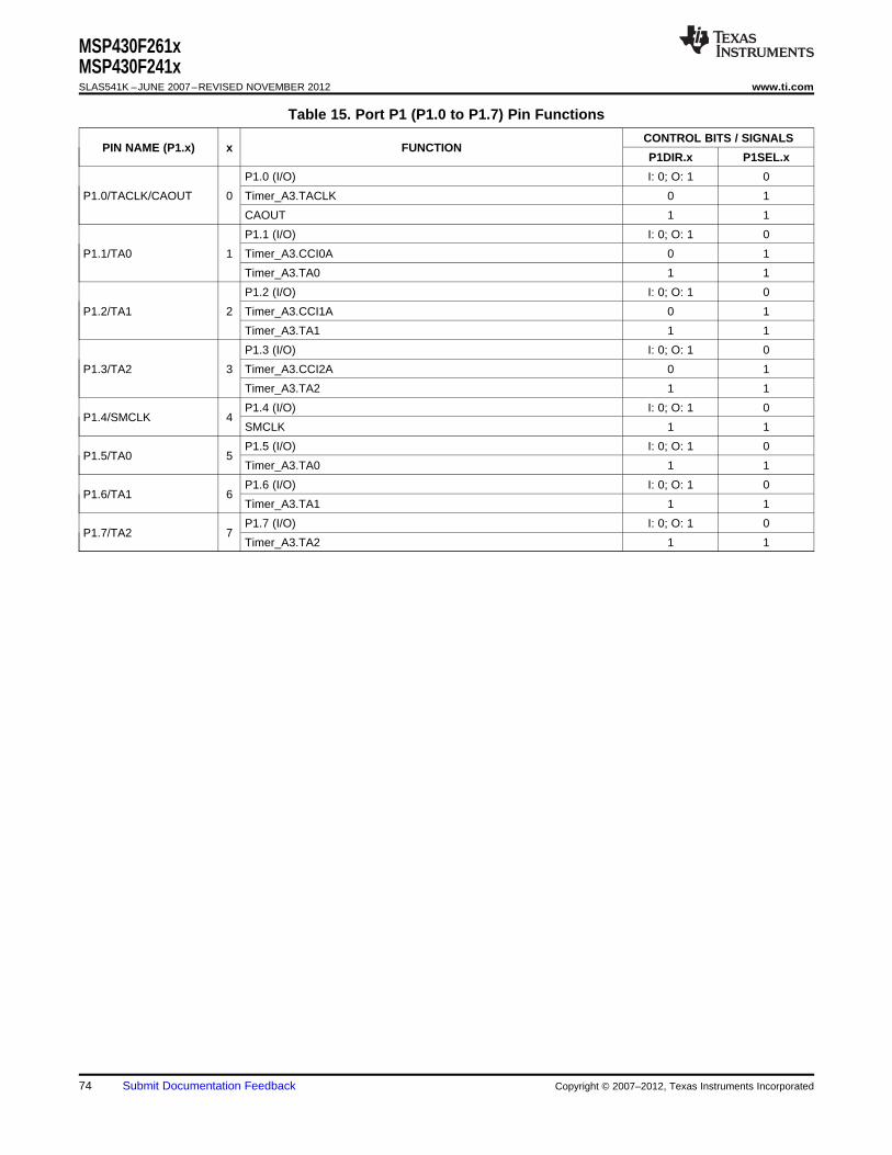
MSP430F261xMSP430F241xSLAS541K –JUNE 2007–REVISED NOVEMBER 2012 www.ti.com
Table 15. Port P1 (P1.0 to P1.7) Pin Functions
CONTROL BITS / SIGNALSPIN NAME (P1.x) x FUNCTION
P1DIR.x P1SEL.x
P1.0 (I/O) I: 0; O: 1 0
P1.0/TACLK/CAOUT 0 Timer_A3.TACLK 0 1
CAOUT 1 1
P1.1 (I/O) I: 0; O: 1 0
P1.1/TA0 1 Timer_A3.CCI0A 0 1
Timer_A3.TA0 1 1
P1.2 (I/O) I: 0; O: 1 0
P1.2/TA1 2 Timer_A3.CCI1A 0 1
Timer_A3.TA1 1 1
P1.3 (I/O) I: 0; O: 1 0
P1.3/TA2 3 Timer_A3.CCI2A 0 1
Timer_A3.TA2 1 1
P1.4 (I/O) I: 0; O: 1 0P1.4/SMCLK 4
SMCLK 1 1
P1.5 (I/O) I: 0; O: 1 0P1.5/TA0 5
Timer_A3.TA0 1 1
P1.6 (I/O) I: 0; O: 1 0P1.6/TA1 6
Timer_A3.TA1 1 1
P1.7 (I/O) I: 0; O: 1 0P1.7/TA2 7
Timer_A3.TA2 1 1
74 Submit Documentation Feedback Copyright © 2007–2012, Texas Instruments Incorporated
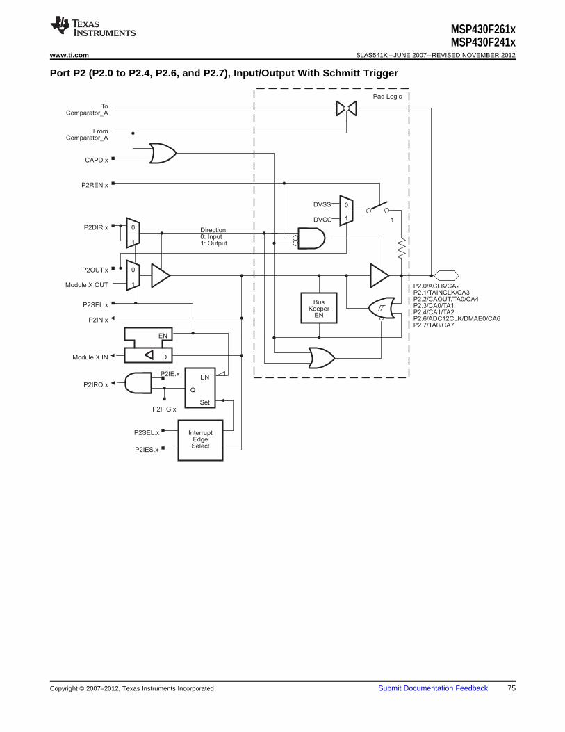
P2.0/ACLK/CA2P2.1/TAINCLK/CA3P2.2/CAOUT/TA0/CA4P2.3/CA0/TA1P2.4/CA1/TA2P2.6/ADC12CLK/DMAE0/CA6P2.7/TA0/CA7
Direction0: Input1: Output
P2SEL.x
P2DIR.x
P2IN.x
P2IRQ.x
D
EN
Module X IN
Module X OUT
P2OUT.x
InterruptEdgeSelect
Q
EN
Set
P2SEL.x
P2IES.x
P2IFG.x
P2IE.x
DVSS
DVCC
P2REN.x
Pad Logic
1
1
0
1
0
1
0
BusKeeper
EN
CAPD.x
FromComparator_A
ToComparator_A
MSP430F261xMSP430F241x
www.ti.com SLAS541K –JUNE 2007–REVISED NOVEMBER 2012
Port P2 (P2.0 to P2.4, P2.6, and P2.7), Input/Output With Schmitt Trigger
Copyright © 2007–2012, Texas Instruments Incorporated Submit Documentation Feedback 75
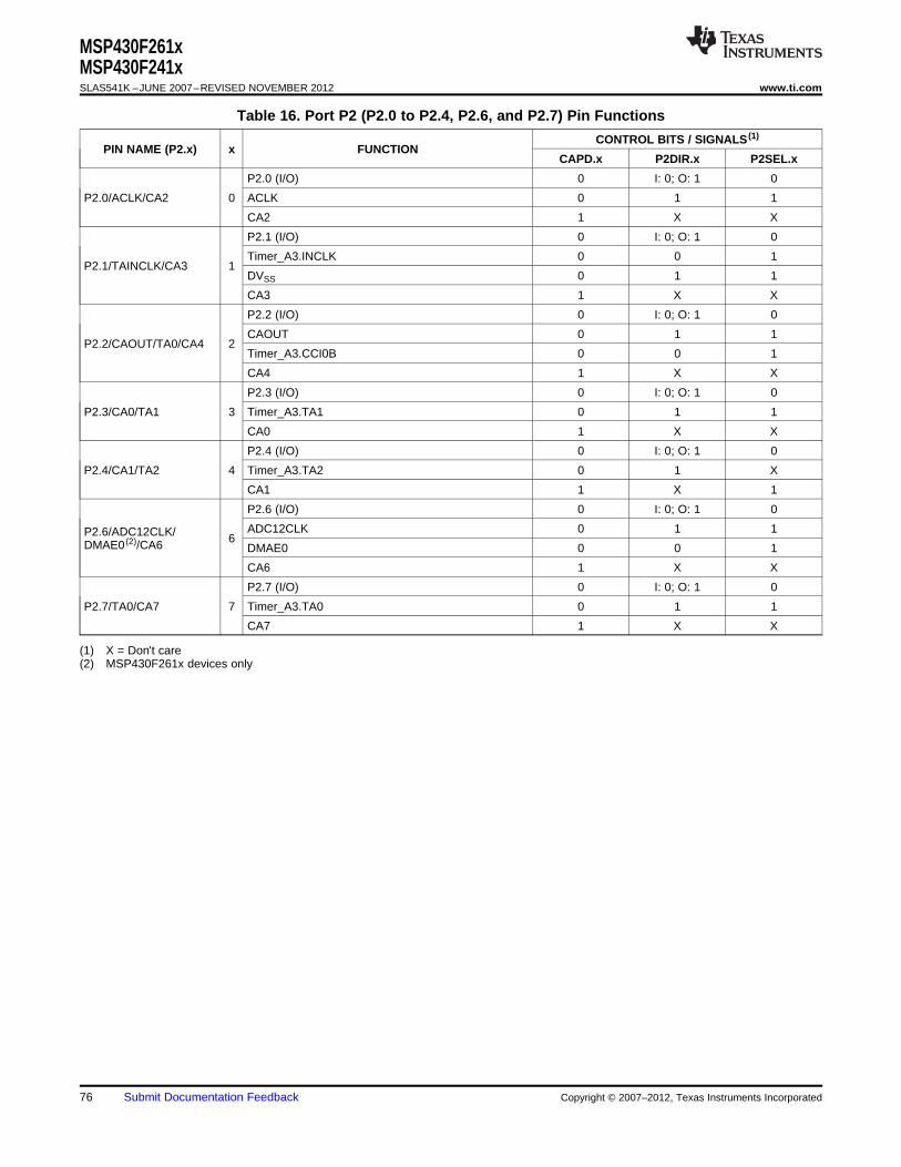
MSP430F261xMSP430F241xSLAS541K –JUNE 2007–REVISED NOVEMBER 2012 www.ti.com
Table 16. Port P2 (P2.0 to P2.4, P2.6, and P2.7) Pin Functions
CONTROL BITS / SIGNALS (1)
PIN NAME (P2.x) x FUNCTIONCAPD.x P2DIR.x P2SEL.x
P2.0 (I/O) 0 I: 0; O: 1 0
P2.0/ACLK/CA2 0 ACLK 0 1 1
CA2 1 X X
P2.1 (I/O) 0 I: 0; O: 1 0
Timer_A3.INCLK 0 0 1P2.1/TAINCLK/CA3 1
DVSS 0 1 1
CA3 1 X X
P2.2 (I/O) 0 I: 0; O: 1 0
CAOUT 0 1 1P2.2/CAOUT/TA0/CA4 2
Timer_A3.CCI0B 0 0 1
CA4 1 X X
P2.3 (I/O) 0 I: 0; O: 1 0
P2.3/CA0/TA1 3 Timer_A3.TA1 0 1 1
CA0 1 X X
P2.4 (I/O) 0 I: 0; O: 1 0
P2.4/CA1/TA2 4 Timer_A3.TA2 0 1 X
CA1 1 X 1
P2.6 (I/O) 0 I: 0; O: 1 0
ADC12CLK 0 1 1P2.6/ADC12CLK/ 6DMAE0 (2)/CA6 DMAE0 0 0 1
CA6 1 X X
P2.7 (I/O) 0 I: 0; O: 1 0
P2.7/TA0/CA7 7 Timer_A3.TA0 0 1 1
CA7 1 X X
(1) X = Don't care(2) MSP430F261x devices only
76 Submit Documentation Feedback Copyright © 2007–2012, Texas Instruments Incorporated
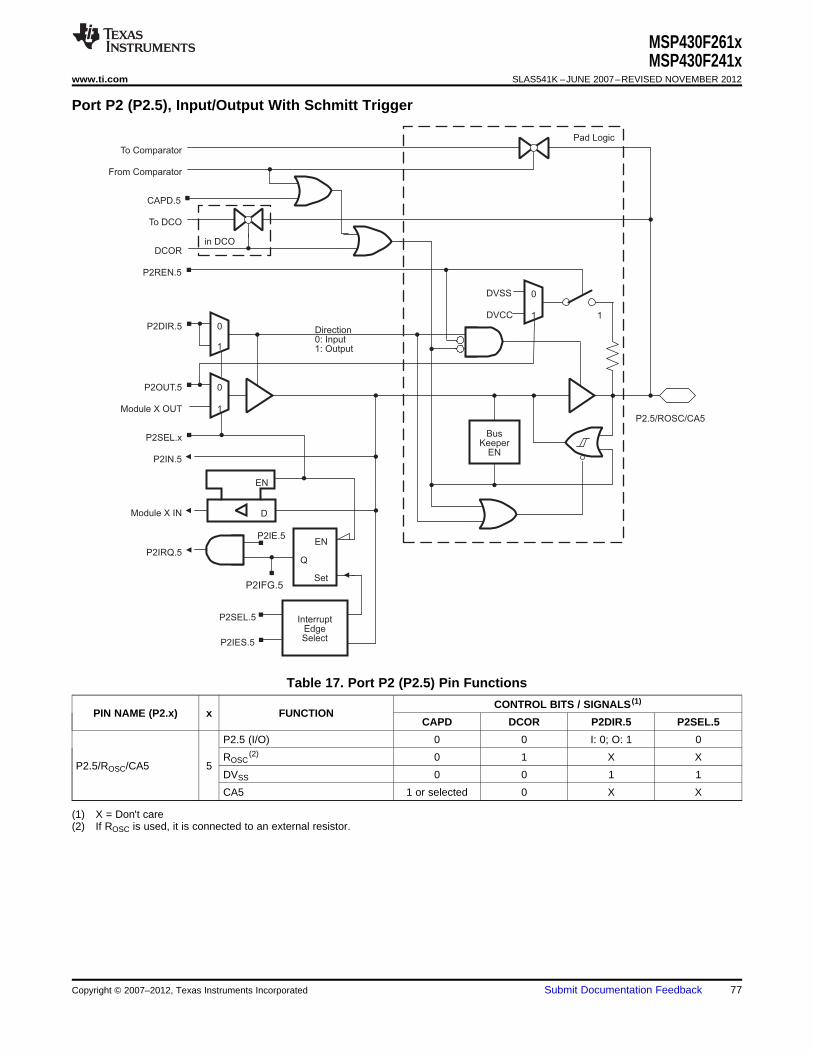
Direction0: Input1: Output
P2SEL.x
P2DIR.5
P2IN.5
P2IRQ.5
D
EN
Module X IN
Module X OUT
P2OUT.5
InterruptEdgeSelect
Q
EN
Set
P2SEL.5
P2IES.5
P2IE.5
P2.5/ROSC/CA5
DVSS
DVCC 1
1
0
1
0
1
0
BusKeeper
EN
DCOR
To DCO
Pad Logic
From Comparator
To Comparator
CAPD.5
in DCO
P2REN.5
MSP430F261xMSP430F241x
www.ti.com SLAS541K –JUNE 2007–REVISED NOVEMBER 2012
Port P2 (P2.5), Input/Output With Schmitt Trigger
Table 17. Port P2 (P2.5) Pin Functions
CONTROL BITS / SIGNALS (1)
PIN NAME (P2.x) x FUNCTIONCAPD DCOR P2DIR.5 P2SEL.5
P2.5 (I/O) 0 0 I: 0; O: 1 0
ROSC(2) 0 1 X X
P2.5/ROSC/CA5 5DVSS 0 0 1 1
CA5 1 or selected 0 X X
(1) X = Don't care(2) If ROSC is used, it is connected to an external resistor.
Copyright © 2007–2012, Texas Instruments Incorporated Submit Documentation Feedback 77
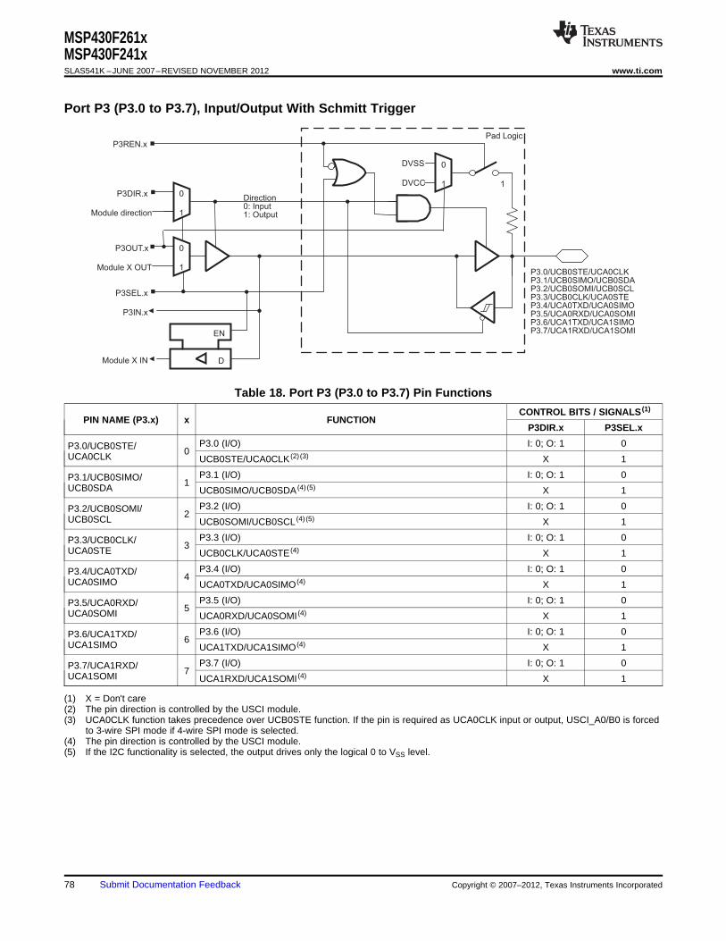
Direction0: Input1: Output
P3SEL.x
P3DIR.x
P3IN.x
D
EN
Module X IN
Module X OUT
P3OUT.x
DVSS
DVCC
Pad Logic
1
1
0
1
0
1
0
P3.0/UCB0STE/UCA0CLKP3.1/UCB0SIMO/UCB0SDAP3.2/UCB0SOMI/UCB0SCLP3.3/UCB0CLK/UCA0STEP3.4/UCA0TXD/UCA0SIMOP3.5/UCA0RXD/UCA0SOMIP3.6/UCA1TXD/UCA1SIMOP3.7/UCA1RXD/UCA1SOMI
P3REN.x
Module direction
MSP430F261xMSP430F241xSLAS541K –JUNE 2007–REVISED NOVEMBER 2012 www.ti.com
Port P3 (P3.0 to P3.7), Input/Output With Schmitt Trigger
Table 18. Port P3 (P3.0 to P3.7) Pin Functions
CONTROL BITS / SIGNALS (1)
PIN NAME (P3.x) x FUNCTIONP3DIR.x P3SEL.x
P3.0 (I/O) I: 0; O: 1 0P3.0/UCB0STE/ 0UCA0CLK UCB0STE/UCA0CLK (2) (3) X 1
P3.1 (I/O) I: 0; O: 1 0P3.1/UCB0SIMO/ 1UCB0SDA UCB0SIMO/UCB0SDA (4) (5) X 1
P3.2 (I/O) I: 0; O: 1 0P3.2/UCB0SOMI/ 2UCB0SCL UCB0SOMI/UCB0SCL (4) (5) X 1
P3.3 (I/O) I: 0; O: 1 0P3.3/UCB0CLK/ 3UCA0STE UCB0CLK/UCA0STE (4) X 1
P3.4 (I/O) I: 0; O: 1 0P3.4/UCA0TXD/ 4UCA0SIMO UCA0TXD/UCA0SIMO (4) X 1
P3.5 (I/O) I: 0; O: 1 0P3.5/UCA0RXD/ 5UCA0SOMI UCA0RXD/UCA0SOMI (4) X 1
P3.6 (I/O) I: 0; O: 1 0P3.6/UCA1TXD/ 6UCA1SIMO UCA1TXD/UCA1SIMO (4) X 1
P3.7 (I/O) I: 0; O: 1 0P3.7/UCA1RXD/ 7UCA1SOMI UCA1RXD/UCA1SOMI (4) X 1
(1) X = Don't care(2) The pin direction is controlled by the USCI module.(3) UCA0CLK function takes precedence over UCB0STE function. If the pin is required as UCA0CLK input or output, USCI_A0/B0 is forced
to 3-wire SPI mode if 4-wire SPI mode is selected.(4) The pin direction is controlled by the USCI module.(5) If the I2C functionality is selected, the output drives only the logical 0 to VSS level.
78 Submit Documentation Feedback Copyright © 2007–2012, Texas Instruments Incorporated
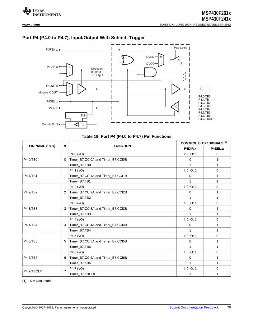
P4.0/TB0P4.1/TB1P4.2/TB2P4.3/TB3P4.4/TB4P4.5/TB5P4.6/TB6P4.7/TBCLK
P4SEL.x
P4DIR.x
P4IN.x
Module X IN
Module X OUT
P4OUT.x
P4REN.x
Direction0: Input1: Output
D
EN
DVSS
DVCC
Pad Logic
1
1
0
1
0
1
0
MSP430F261xMSP430F241x
www.ti.com SLAS541K –JUNE 2007–REVISED NOVEMBER 2012
Port P4 (P4.0 to P4.7), Input/Output With Schmitt Trigger
Table 19. Port P4 (P4.0 to P4.7) Pin Functions
CONTROL BITS / SIGNALS (1)
PIN NAME (P4.x) x FUNCTIONP4DIR.x P4SEL.x
P4.0 (I/O) I: 0; O: 1 0
P4.0/TB0 0 Timer_B7.CCI0A and Timer_B7.CCI0B 0 1
Timer_B7.TB0 1 1
P4.1 (I/O) I: 0; O: 1 0
P4.1/TB1 1 Timer_B7.CCI1A and Timer_B7.CCI1B 0 1
Timer_B7.TB1 1 1
P4.2 (I/O) I: 0; O: 1 0
P4.2/TB2 2 Timer_B7.CCI2A and Timer_B7.CCI2B 0 1
Timer_B7.TB2 1 1
P4.3 (I/O) I: 0; O: 1 0
P4.3/TB3 3 Timer_B7.CCI3A and Timer_B7.CCI3B 0 1
Timer_B7.TB3 1 1
P4.4 (I/O) I: 0; O: 1 0
P4.4/TB4 4 Timer_B7.CCI4A and Timer_B7.CCI4B 0 1
Timer_B7.TB4 1 1
P4.5 (I/O) I: 0; O: 1 0
P4.5/TB5 5 Timer_B7.CCI5A and Timer_B7.CCI5B 0 1
Timer_B7.TB5 1 1
P4.6 (I/O) I: 0; O: 1 0
P4.6/TB6 6 Timer_B7.CCI6A and Timer_B7.CCI6B 0 1
Timer_B7.TB6 1 1
P4.7 (I/O) I: 0; O: 1 0P4.7/TBCLK 7
Timer_B7.TBCLK 1 1
(1) X = Don't care
Copyright © 2007–2012, Texas Instruments Incorporated Submit Documentation Feedback 79
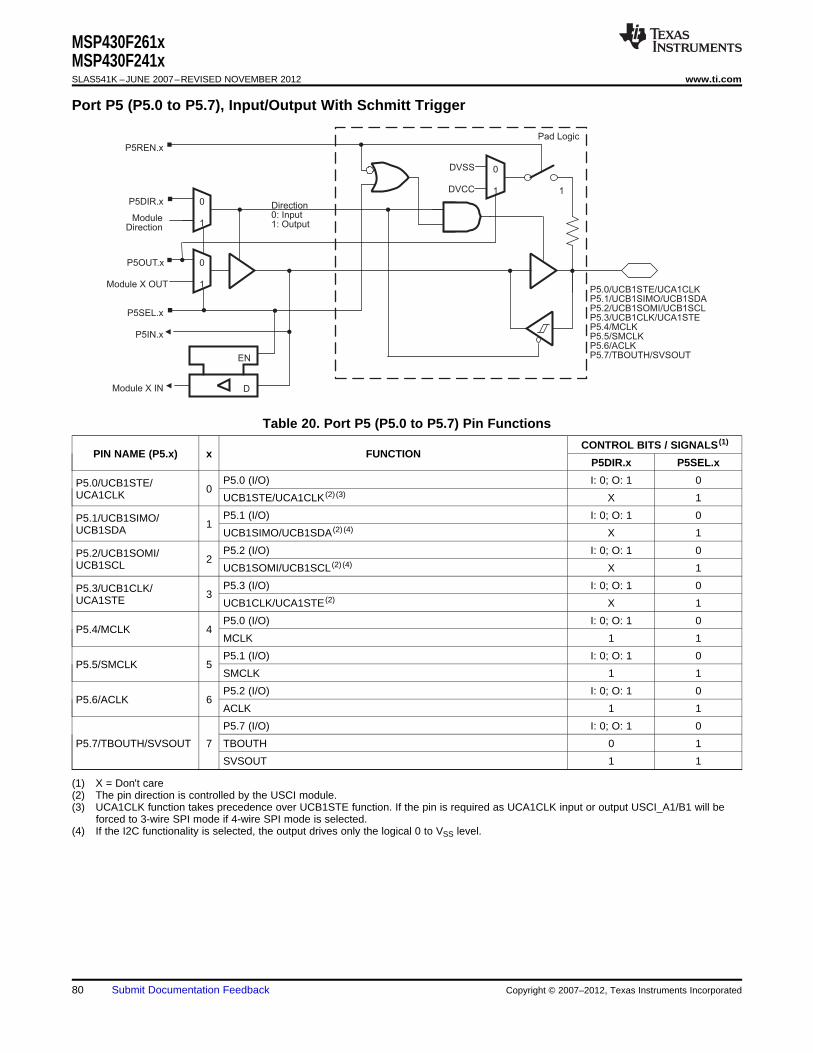
P5SEL.x
P5DIR.x
P5IN.x
Module X IN
Module X OUT
P5OUT.x
P5REN.x
P5.0/UCB1STE/UCA1CLKP5.1/UCB1SIMO/UCB1SDAP5.2/UCB1SOMI/UCB1SCLP5.3/UCB1CLK/UCA1STEP5.4/MCLKP5.5/SMCLKP5.6/ACLKP5.7/TBOUTH/SVSOUT
ModuleDirection
Direction0: Input1: Output
D
EN
DVSS
DVCC
Pad Logic
1
1
0
1
0
1
0
MSP430F261xMSP430F241xSLAS541K –JUNE 2007–REVISED NOVEMBER 2012 www.ti.com
Port P5 (P5.0 to P5.7), Input/Output With Schmitt Trigger
Table 20. Port P5 (P5.0 to P5.7) Pin Functions
CONTROL BITS / SIGNALS (1)
PIN NAME (P5.x) x FUNCTIONP5DIR.x P5SEL.x
P5.0 (I/O) I: 0; O: 1 0P5.0/UCB1STE/ 0UCA1CLK UCB1STE/UCA1CLK (2) (3) X 1
P5.1 (I/O) I: 0; O: 1 0P5.1/UCB1SIMO/ 1UCB1SDA UCB1SIMO/UCB1SDA (2) (4) X 1
P5.2 (I/O) I: 0; O: 1 0P5.2/UCB1SOMI/ 2UCB1SCL UCB1SOMI/UCB1SCL (2) (4) X 1
P5.3 (I/O) I: 0; O: 1 0P5.3/UCB1CLK/ 3UCA1STE UCB1CLK/UCA1STE (2) X 1
P5.0 (I/O) I: 0; O: 1 0P5.4/MCLK 4
MCLK 1 1
P5.1 (I/O) I: 0; O: 1 0P5.5/SMCLK 5
SMCLK 1 1
P5.2 (I/O) I: 0; O: 1 0P5.6/ACLK 6
ACLK 1 1
P5.7 (I/O) I: 0; O: 1 0
P5.7/TBOUTH/SVSOUT 7 TBOUTH 0 1
SVSOUT 1 1
(1) X = Don't care(2) The pin direction is controlled by the USCI module.(3) UCA1CLK function takes precedence over UCB1STE function. If the pin is required as UCA1CLK input or output USCI_A1/B1 will be
forced to 3-wire SPI mode if 4-wire SPI mode is selected.(4) If the I2C functionality is selected, the output drives only the logical 0 to VSS level.
80 Submit Documentation Feedback Copyright © 2007–2012, Texas Instruments Incorporated
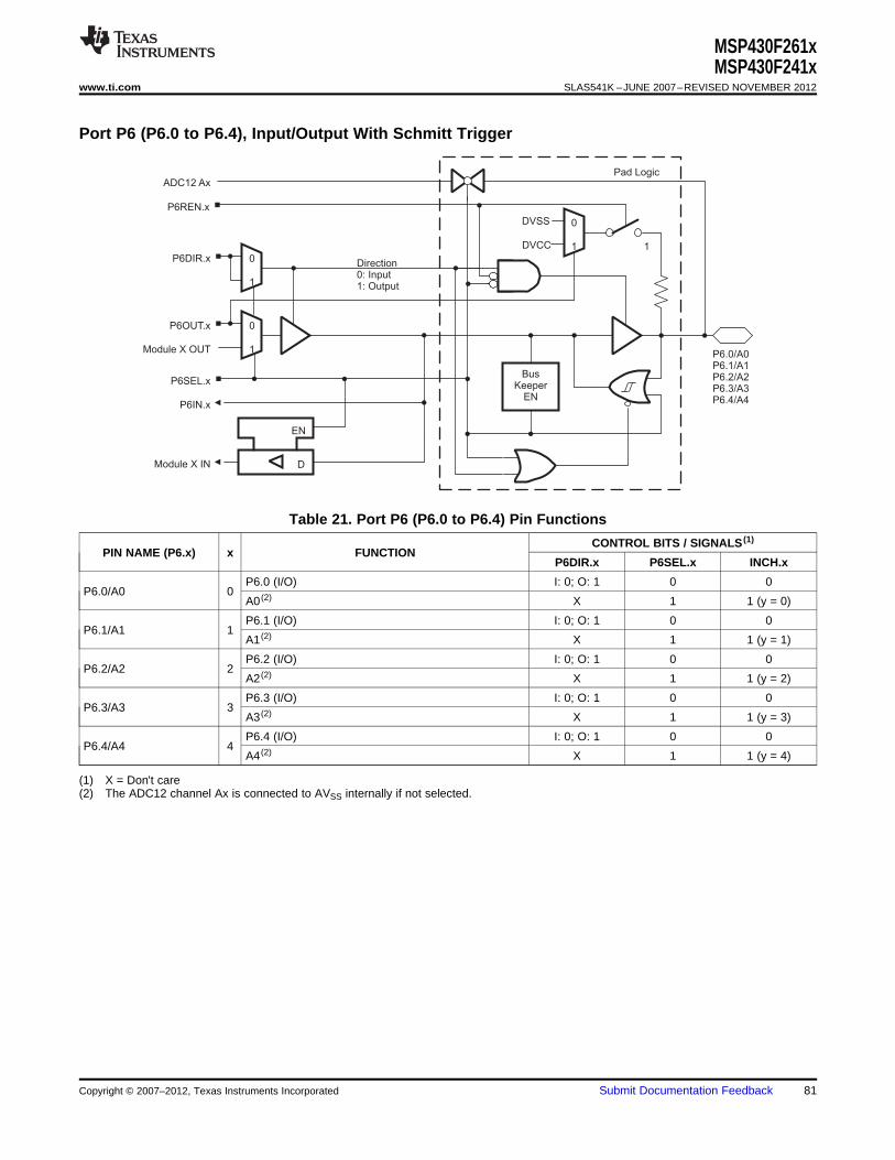
Direction0: Input1: Output
P6SEL.x
P6DIR.x
P6IN.x
D
EN
Module X IN
Module X OUT
P6OUT.x
P6.0/A0P6.1/A1P6.2/A2P6.3/A3P6.4/A4
DVSS
DVCC
Pad Logic
1
1
0
1
0
1
0
BusKeeper
EN
ADC12 Ax
P6REN.x
MSP430F261xMSP430F241x
www.ti.com SLAS541K –JUNE 2007–REVISED NOVEMBER 2012
Port P6 (P6.0 to P6.4), Input/Output With Schmitt Trigger
Table 21. Port P6 (P6.0 to P6.4) Pin Functions
CONTROL BITS / SIGNALS (1)
PIN NAME (P6.x) x FUNCTIONP6DIR.x P6SEL.x INCH.x
P6.0 (I/O) I: 0; O: 1 0 0P6.0/A0 0
A0 (2) X 1 1 (y = 0)
P6.1 (I/O) I: 0; O: 1 0 0P6.1/A1 1
A1 (2) X 1 1 (y = 1)
P6.2 (I/O) I: 0; O: 1 0 0P6.2/A2 2
A2 (2) X 1 1 (y = 2)
P6.3 (I/O) I: 0; O: 1 0 0P6.3/A3 3
A3 (2) X 1 1 (y = 3)
P6.4 (I/O) I: 0; O: 1 0 0P6.4/A4 4
A4 (2) X 1 1 (y = 4)
(1) X = Don't care(2) The ADC12 channel Ax is connected to AVSS internally if not selected.
Copyright © 2007–2012, Texas Instruments Incorporated Submit Documentation Feedback 81
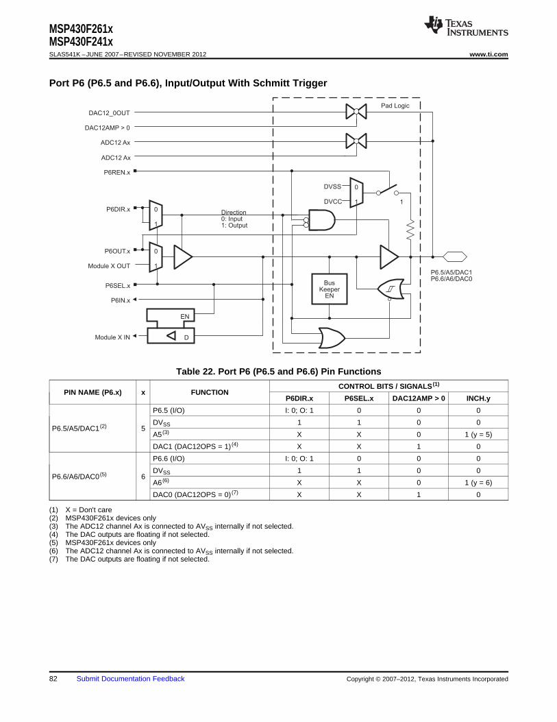
P6.5/A5/DAC1P6.6/A6/DAC0
Direction0: Input1: Output
P6SEL.x
P6DIR.x
P6IN.x
D
EN
Module X IN
Module X OUT
P6OUT.x
DVSS
DVCC
P6REN.x
Pad Logic
1
1
0
1
0
1
0
BusKeeper
EN
ADC12 Ax
DAC12AMP > 0
DAC12_0OUT
ADC12 Ax
MSP430F261xMSP430F241xSLAS541K –JUNE 2007–REVISED NOVEMBER 2012 www.ti.com
Port P6 (P6.5 and P6.6), Input/Output With Schmitt Trigger
Table 22. Port P6 (P6.5 and P6.6) Pin Functions
CONTROL BITS / SIGNALS (1)
PIN NAME (P6.x) x FUNCTIONP6DIR.x P6SEL.x DAC12AMP > 0 INCH.y
P6.5 (I/O) I: 0; O: 1 0 0 0
DVSS 1 1 0 0P6.5/A5/DAC1 (2) 5
A5 (3) X X 0 1 (y = 5)
DAC1 (DAC12OPS = 1) (4) X X 1 0
P6.6 (I/O) I: 0; O: 1 0 0 0
DVSS 1 1 0 0P6.6/A6/DAC0 (5) 6
A6 (6) X X 0 1 (y = 6)
DAC0 (DAC12OPS = 0) (7) X X 1 0
(1) X = Don't care(2) MSP430F261x devices only(3) The ADC12 channel Ax is connected to AVSS internally if not selected.(4) The DAC outputs are floating if not selected.(5) MSP430F261x devices only(6) The ADC12 channel Ax is connected to AVSS internally if not selected.(7) The DAC outputs are floating if not selected.
82 Submit Documentation Feedback Copyright © 2007–2012, Texas Instruments Incorporated
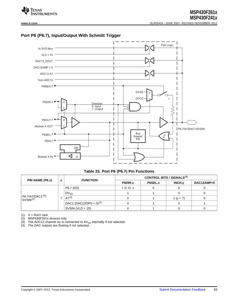
Direction0: Input1: Output
P6SEL.7
P6DIR.7
P6IN.7
D
EN
Module X IN
Module X OUT
P6OUT.7
P6.7/A7/DAC1/SVSIN
DVSS
DVCC
P6REN.7
Pad Logic
1
1
0
1
0
1
0
BusKeeper
EN
ADC12 A7
DAC12AMP > 0
DAC12_0OUT
VLD = 15
to SVS Mux
from ADC12
MSP430F261xMSP430F241x
www.ti.com SLAS541K –JUNE 2007–REVISED NOVEMBER 2012
Port P6 (P6.7), Input/Output With Schmitt Trigger
Table 23. Port P6 (P6.7) Pin Functions
CONTROL BITS / SIGNALS (1)
PIN NAME (P6.x) x FUNCTIONP6DIR.x P6SEL.x INCH.y DAC12AMP>0
P6.7 (I/O) I: 0; O: 1 0 0 0
DVSS 1 1 0 0P6.7/A7/DAC1 (2)/ 7 A7 (3) X 1 1 (y = 7) 0SVSIN (2)
DAC1 (DAC12OPS = 0) (4) X 1 0 1
SVSIN (VLD = 15) X 1 0 0
(1) X = Don't care(2) MSP430F261x devices only(3) The ADC12 channel Ax is connected to AVSS internally if not selected.(4) The DAC outputs are floating if not selected.
Copyright © 2007–2012, Texas Instruments Incorporated Submit Documentation Feedback 83
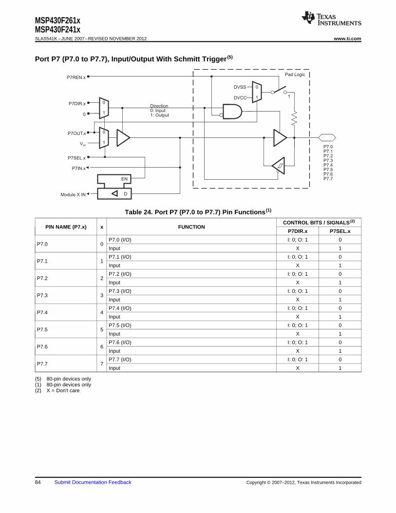
Direction0: Input1: Output
P7SEL.x
P7DIR.x
P7IN.x
D
EN
Module X IN
VSS
P7OUT.x
P7.0P7.1P7.2P7.3P7.4P7.5P7.6P7.7
DVSS
DVCC
P7REN.xPad Logic
1
1
0
1
0
1
0
0
MSP430F261xMSP430F241xSLAS541K –JUNE 2007–REVISED NOVEMBER 2012 www.ti.com
Port P7 (P7.0 to P7.7), Input/Output With Schmitt Trigger (5)
Table 24. Port P7 (P7.0 to P7.7) Pin Functions (1)
CONTROL BITS / SIGNALS (2)
PIN NAME (P7.x) x FUNCTIONP7DIR.x P7SEL.x
P7.0 (I/O) I: 0; O: 1 0P7.0 0
Input X 1
P7.1 (I/O) I: 0; O: 1 0P7.1 1
Input X 1
P7.2 (I/O) I: 0; O: 1 0P7.2 2
Input X 1
P7.3 (I/O) I: 0; O: 1 0P7.3 3
Input X 1
P7.4 (I/O) I: 0; O: 1 0P7.4 4
Input X 1
P7.5 (I/O) I: 0; O: 1 0P7.5 5
Input X 1
P7.6 (I/O) I: 0; O: 1 0P7.6 6
Input X 1
P7.7 (I/O) I: 0; O: 1 0P7.7 7
Input X 1
(5) 80-pin devices only(1) 80-pin devices only(2) X = Don't care
84 Submit Documentation Feedback Copyright © 2007–2012, Texas Instruments Incorporated
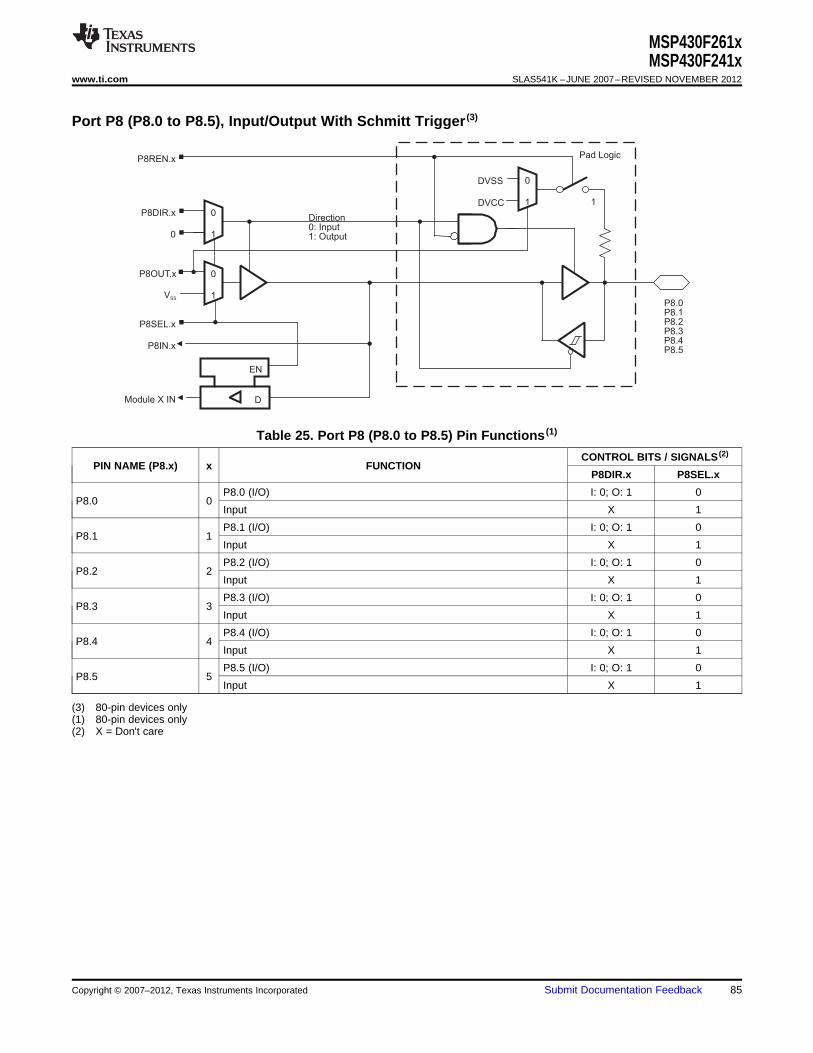
Direction0: Input1: Output
P8SEL.x
P8DIR.x
P8IN.x
D
EN
Module X IN
VSS
P8OUT.x
P8.0P8.1P8.2P8.3P8.4P8.5
DVSS
DVCC
P8REN.x Pad Logic
1
1
0
1
0
1
0
0
MSP430F261xMSP430F241x
www.ti.com SLAS541K –JUNE 2007–REVISED NOVEMBER 2012
Port P8 (P8.0 to P8.5), Input/Output With Schmitt Trigger (3)
Table 25. Port P8 (P8.0 to P8.5) Pin Functions (1)
CONTROL BITS / SIGNALS (2)
PIN NAME (P8.x) x FUNCTIONP8DIR.x P8SEL.x
P8.0 (I/O) I: 0; O: 1 0P8.0 0
Input X 1
P8.1 (I/O) I: 0; O: 1 0P8.1 1
Input X 1
P8.2 (I/O) I: 0; O: 1 0P8.2 2
Input X 1
P8.3 (I/O) I: 0; O: 1 0P8.3 3
Input X 1
P8.4 (I/O) I: 0; O: 1 0P8.4 4
Input X 1
P8.5 (I/O) I: 0; O: 1 0P8.5 5
Input X 1
(3) 80-pin devices only(1) 80-pin devices only(2) X = Don't care
Copyright © 2007–2012, Texas Instruments Incorporated Submit Documentation Feedback 85
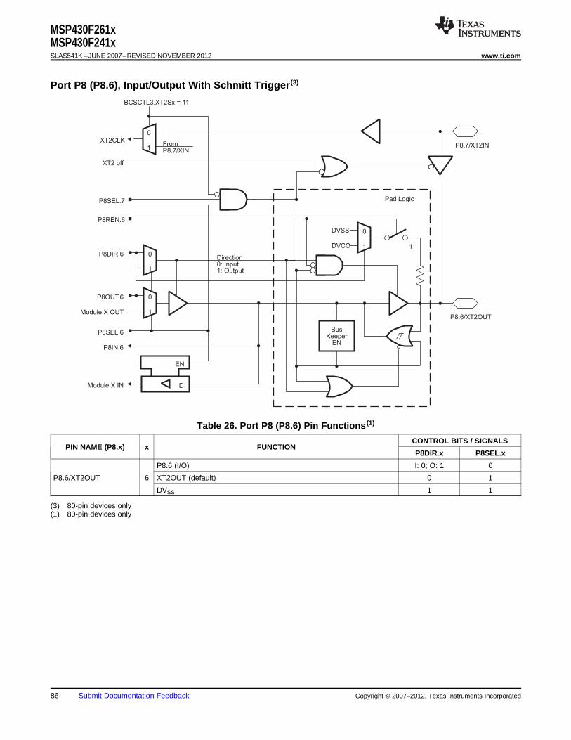
Direction0: Input1: Output
P8SEL.6
P8DIR.6
P8IN.6
D
EN
Module X IN
Module X OUT
P8OUT.6
DVSS
DVCC
Pad Logic
1
1
0
1
0
1
0
BusKeeper
EN
P8.6/XT2OUT
P8.7/XT2IN
P8SEL.7
P8REN.6
1
0XT2CLK
XT2 off
BCSCTL3.XT2Sx = 11
FromP8.7/XIN
MSP430F261xMSP430F241xSLAS541K –JUNE 2007–REVISED NOVEMBER 2012 www.ti.com
Port P8 (P8.6), Input/Output With Schmitt Trigger (3)
Table 26. Port P8 (P8.6) Pin Functions (1)
CONTROL BITS / SIGNALSPIN NAME (P8.x) x FUNCTION
P8DIR.x P8SEL.x
P8.6 (I/O) I: 0; O: 1 0
P8.6/XT2OUT 6 XT2OUT (default) 0 1
DVSS 1 1
(3) 80-pin devices only(1) 80-pin devices only
86 Submit Documentation Feedback Copyright © 2007–2012, Texas Instruments Incorporated
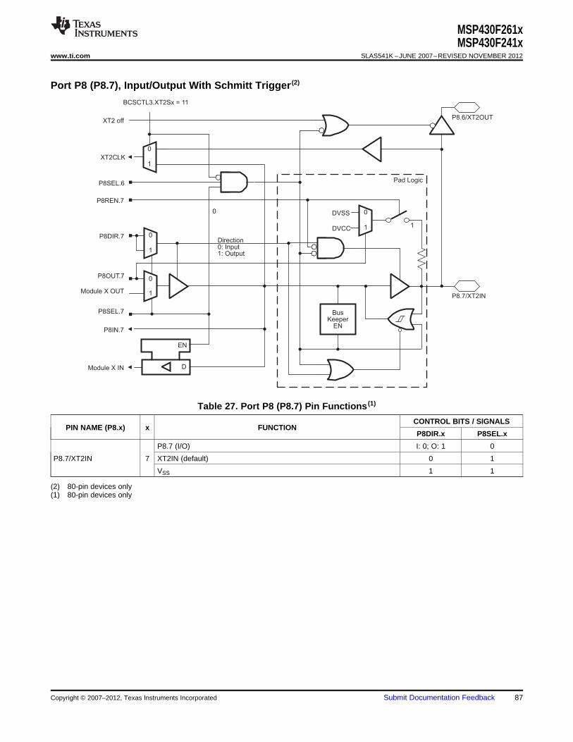
Direction0: Input1: Output
P8SEL.7
P8DIR.7
P8IN.7
D
EN
Module X IN
Module X OUT
P8OUT.7
DVSS
DVCC
Pad Logic
1
1
0
1
0
1
0
BusKeeper
EN
P8SEL.6
P8.7/XT2IN
1
0
XT2CLK
0
P8.6/XT2OUTXT2 off
BCSCTL3.XT2Sx = 11
P8REN.7
MSP430F261xMSP430F241x
www.ti.com SLAS541K –JUNE 2007–REVISED NOVEMBER 2012
Port P8 (P8.7), Input/Output With Schmitt Trigger (2)
Table 27. Port P8 (P8.7) Pin Functions (1)
CONTROL BITS / SIGNALSPIN NAME (P8.x) x FUNCTION
P8DIR.x P8SEL.x
P8.7 (I/O) I: 0; O: 1 0
P8.7/XT2IN 7 XT2IN (default) 0 1
VSS 1 1
(2) 80-pin devices only(1) 80-pin devices only
Copyright © 2007–2012, Texas Instruments Incorporated Submit Documentation Feedback 87
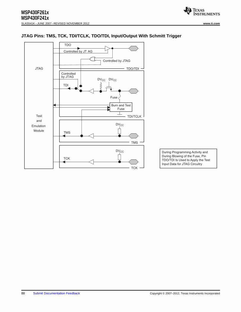
TDI
TDO
TMS
TCK
Test
JTAG
and
Emulation
Module
Burn and TestFuse
Controlled by JTAG
Controlled by JT AG
Controlledby JTAG
DVCC
DVCC
DVCC During Programming Activity and
During Blowing of the Fuse, Pin
TDO/TDI Is Used to Apply the Test
Input Data for JTAG Circuitry
TDO/TDI
TDI/TCLK
TMS
TCK
Fuse
DVCC
MSP430F261xMSP430F241xSLAS541K –JUNE 2007–REVISED NOVEMBER 2012 www.ti.com
JTAG Pins: TMS, TCK, TDI/TCLK, TDO/TDI, Input/Output With Schmitt Trigger
88 Submit Documentation Feedback Copyright © 2007–2012, Texas Instruments Incorporated
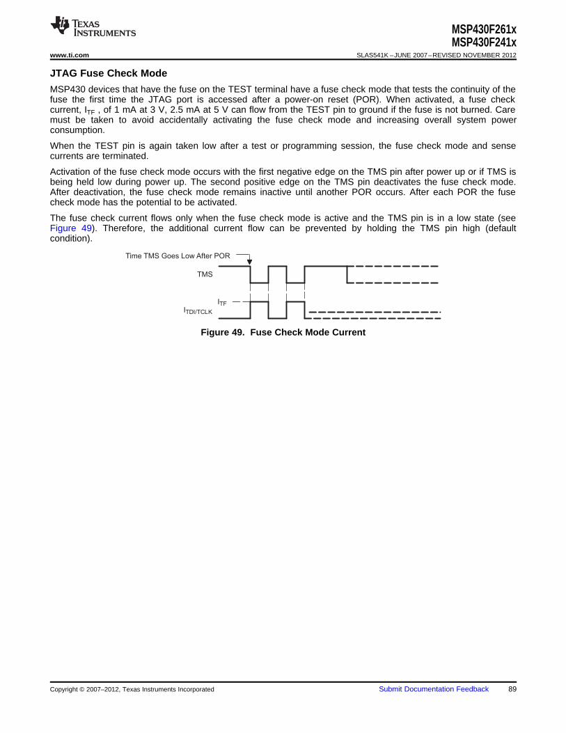
Time TMS Goes Low After POR
TMS
ITF
ITDI/TCLK
MSP430F261xMSP430F241x
www.ti.com SLAS541K –JUNE 2007–REVISED NOVEMBER 2012
JTAG Fuse Check Mode
MSP430 devices that have the fuse on the TEST terminal have a fuse check mode that tests the continuity of thefuse the first time the JTAG port is accessed after a power-on reset (POR). When activated, a fuse checkcurrent, ITF , of 1 mA at 3 V, 2.5 mA at 5 V can flow from the TEST pin to ground if the fuse is not burned. Caremust be taken to avoid accidentally activating the fuse check mode and increasing overall system powerconsumption.
When the TEST pin is again taken low after a test or programming session, the fuse check mode and sensecurrents are terminated.
Activation of the fuse check mode occurs with the first negative edge on the TMS pin after power up or if TMS isbeing held low during power up. The second positive edge on the TMS pin deactivates the fuse check mode.After deactivation, the fuse check mode remains inactive until another POR occurs. After each POR the fusecheck mode has the potential to be activated.
The fuse check current flows only when the fuse check mode is active and the TMS pin is in a low state (seeFigure 49). Therefore, the additional current flow can be prevented by holding the TMS pin high (defaultcondition).
Figure 49. Fuse Check Mode Current
Copyright © 2007–2012, Texas Instruments Incorporated Submit Documentation Feedback 89
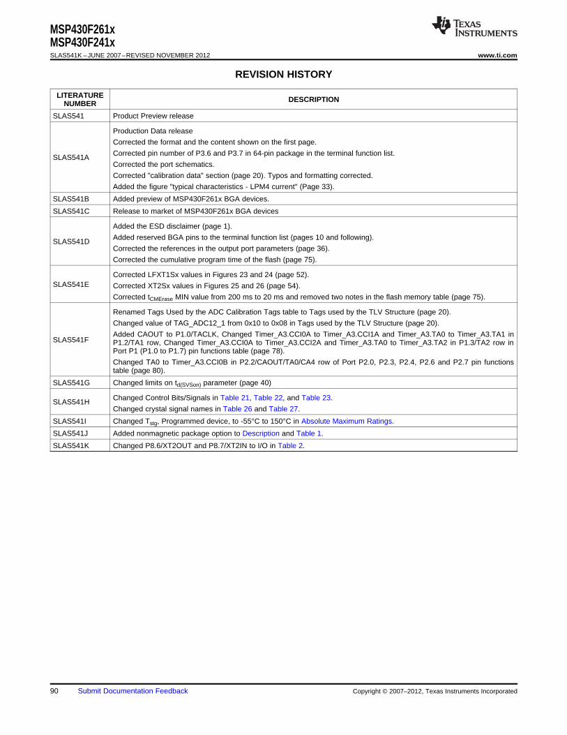
MSP430F261xMSP430F241xSLAS541K –JUNE 2007–REVISED NOVEMBER 2012 www.ti.com
REVISION HISTORY
LITERATURE DESCRIPTIONNUMBER
SLAS541 Product Preview release
Production Data release
Corrected the format and the content shown on the first page.
Corrected pin number of P3.6 and P3.7 in 64-pin package in the terminal function list.SLAS541ACorrected the port schematics.
Corrected "calibration data" section (page 20). Typos and formatting corrected.
Added the figure "typical characteristics - LPM4 current" (Page 33).
SLAS541B Added preview of MSP430F261x BGA devices.
SLAS541C Release to market of MSP430F261x BGA devices
Added the ESD disclaimer (page 1).
Added reserved BGA pins to the terminal function list (pages 10 and following).SLAS541DCorrected the references in the output port parameters (page 36).
Corrected the cumulative program time of the flash (page 75).
Corrected LFXT1Sx values in Figures 23 and 24 (page 52).SLAS541E Corrected XT2Sx values in Figures 25 and 26 (page 54).
Corrected tCMErase MIN value from 200 ms to 20 ms and removed two notes in the flash memory table (page 75).
Renamed Tags Used by the ADC Calibration Tags table to Tags used by the TLV Structure (page 20).
Changed value of TAG_ADC12_1 from 0x10 to 0x08 in Tags used by the TLV Structure (page 20).
Added CAOUT to P1.0/TACLK, Changed Timer_A3.CCI0A to Timer_A3.CCI1A and Timer_A3.TA0 to Timer_A3.TA1 inSLAS541F P1.2/TA1 row, Changed Timer_A3.CCI0A to Timer_A3.CCI2A and Timer_A3.TA0 to Timer_A3.TA2 in P1.3/TA2 row in
Port P1 (P1.0 to P1.7) pin functions table (page 78).
Changed TA0 to Timer_A3.CCI0B in P2.2/CAOUT/TA0/CA4 row of Port P2.0, P2.3, P2.4, P2.6 and P2.7 pin functionstable (page 80).
SLAS541G Changed limits on td(SVSon) parameter (page 40)
Changed Control Bits/Signals in Table 21, Table 22, and Table 23.SLAS541HChanged crystal signal names in Table 26 and Table 27.
SLAS541I Changed Tstg, Programmed device, to -55°C to 150°C in Absolute Maximum Ratings.
SLAS541J Added nonmagnetic package option to Description and Table 1.
SLAS541K Changed P8.6/XT2OUT and P8.7/XT2IN to I/O in Table 2.
90 Submit Documentation Feedback Copyright © 2007–2012, Texas Instruments Incorporated
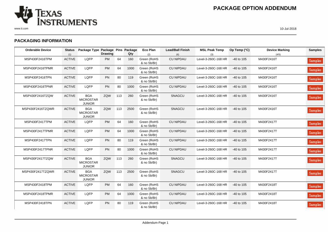
PACKAGE OPTION ADDENDUM
www.ti.com 10-Jul-2018
Addendum-Page 1
PACKAGING INFORMATION
Orderable Device Status(1)
Package Type PackageDrawing
Pins PackageQty
Eco Plan(2)
Lead/Ball Finish(6)
MSL Peak Temp(3)
Op Temp (°C) Device Marking(4/5)
Samples
MSP430F2416TPM ACTIVE LQFP PM 64 160 Green (RoHS& no Sb/Br)
CU NIPDAU Level-3-260C-168 HR -40 to 105 M430F2416T
MSP430F2416TPMR ACTIVE LQFP PM 64 1000 Green (RoHS& no Sb/Br)
CU NIPDAU Level-3-260C-168 HR -40 to 105 M430F2416T
MSP430F2416TPN ACTIVE LQFP PN 80 119 Green (RoHS& no Sb/Br)
CU NIPDAU Level-3-260C-168 HR -40 to 105 M430F2416T
MSP430F2416TPNR ACTIVE LQFP PN 80 1000 Green (RoHS& no Sb/Br)
CU NIPDAU Level-3-260C-168 HR -40 to 105 M430F2416T
MSP430F2416TZQW ACTIVE BGAMICROSTAR
JUNIOR
ZQW 113 260 Green (RoHS& no Sb/Br)
SNAGCU Level-3-260C-168 HR -40 to 105 M430F2416T
MSP430F2416TZQWR ACTIVE BGAMICROSTAR
JUNIOR
ZQW 113 2500 Green (RoHS& no Sb/Br)
SNAGCU Level-3-260C-168 HR -40 to 105 M430F2416T
MSP430F2417TPM ACTIVE LQFP PM 64 160 Green (RoHS& no Sb/Br)
CU NIPDAU Level-3-260C-168 HR -40 to 105 M430F2417T
MSP430F2417TPMR ACTIVE LQFP PM 64 1000 Green (RoHS& no Sb/Br)
CU NIPDAU Level-3-260C-168 HR -40 to 105 M430F2417T
MSP430F2417TPN ACTIVE LQFP PN 80 119 Green (RoHS& no Sb/Br)
CU NIPDAU Level-3-260C-168 HR -40 to 105 M430F2417T
MSP430F2417TPNR ACTIVE LQFP PN 80 1000 Green (RoHS& no Sb/Br)
CU NIPDAU Level-3-260C-168 HR -40 to 105 M430F2417T
MSP430F2417TZQW ACTIVE BGAMICROSTAR
JUNIOR
ZQW 113 260 Green (RoHS& no Sb/Br)
SNAGCU Level-3-260C-168 HR -40 to 105 M430F2417T
MSP430F2417TZQWR ACTIVE BGAMICROSTAR
JUNIOR
ZQW 113 2500 Green (RoHS& no Sb/Br)
SNAGCU Level-3-260C-168 HR -40 to 105 M430F2417T
MSP430F2418TPM ACTIVE LQFP PM 64 160 Green (RoHS& no Sb/Br)
CU NIPDAU Level-3-260C-168 HR -40 to 105 M430F2418T
MSP430F2418TPMR ACTIVE LQFP PM 64 1000 Green (RoHS& no Sb/Br)
CU NIPDAU Level-3-260C-168 HR -40 to 105 M430F2418T
MSP430F2418TPN ACTIVE LQFP PN 80 119 Green (RoHS& no Sb/Br)
CU NIPDAU Level-3-260C-168 HR -40 to 105 M430F2418T
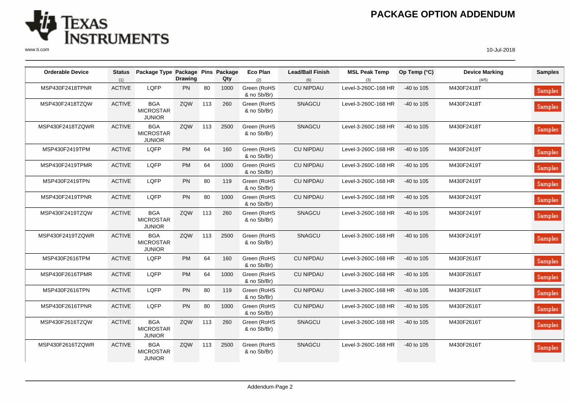
PACKAGE OPTION ADDENDUM
www.ti.com 10-Jul-2018
Addendum-Page 2
Orderable Device Status(1)
Package Type PackageDrawing
Pins PackageQty
Eco Plan(2)
Lead/Ball Finish(6)
MSL Peak Temp(3)
Op Temp (°C) Device Marking(4/5)
Samples
MSP430F2418TPNR ACTIVE LQFP PN 80 1000 Green (RoHS& no Sb/Br)
CU NIPDAU Level-3-260C-168 HR -40 to 105 M430F2418T
MSP430F2418TZQW ACTIVE BGAMICROSTAR
JUNIOR
ZQW 113 260 Green (RoHS& no Sb/Br)
SNAGCU Level-3-260C-168 HR -40 to 105 M430F2418T
MSP430F2418TZQWR ACTIVE BGAMICROSTAR
JUNIOR
ZQW 113 2500 Green (RoHS& no Sb/Br)
SNAGCU Level-3-260C-168 HR -40 to 105 M430F2418T
MSP430F2419TPM ACTIVE LQFP PM 64 160 Green (RoHS& no Sb/Br)
CU NIPDAU Level-3-260C-168 HR -40 to 105 M430F2419T
MSP430F2419TPMR ACTIVE LQFP PM 64 1000 Green (RoHS& no Sb/Br)
CU NIPDAU Level-3-260C-168 HR -40 to 105 M430F2419T
MSP430F2419TPN ACTIVE LQFP PN 80 119 Green (RoHS& no Sb/Br)
CU NIPDAU Level-3-260C-168 HR -40 to 105 M430F2419T
MSP430F2419TPNR ACTIVE LQFP PN 80 1000 Green (RoHS& no Sb/Br)
CU NIPDAU Level-3-260C-168 HR -40 to 105 M430F2419T
MSP430F2419TZQW ACTIVE BGAMICROSTAR
JUNIOR
ZQW 113 260 Green (RoHS& no Sb/Br)
SNAGCU Level-3-260C-168 HR -40 to 105 M430F2419T
MSP430F2419TZQWR ACTIVE BGAMICROSTAR
JUNIOR
ZQW 113 2500 Green (RoHS& no Sb/Br)
SNAGCU Level-3-260C-168 HR -40 to 105 M430F2419T
MSP430F2616TPM ACTIVE LQFP PM 64 160 Green (RoHS& no Sb/Br)
CU NIPDAU Level-3-260C-168 HR -40 to 105 M430F2616T
MSP430F2616TPMR ACTIVE LQFP PM 64 1000 Green (RoHS& no Sb/Br)
CU NIPDAU Level-3-260C-168 HR -40 to 105 M430F2616T
MSP430F2616TPN ACTIVE LQFP PN 80 119 Green (RoHS& no Sb/Br)
CU NIPDAU Level-3-260C-168 HR -40 to 105 M430F2616T
MSP430F2616TPNR ACTIVE LQFP PN 80 1000 Green (RoHS& no Sb/Br)
CU NIPDAU Level-3-260C-168 HR -40 to 105 M430F2616T
MSP430F2616TZQW ACTIVE BGAMICROSTAR
JUNIOR
ZQW 113 260 Green (RoHS& no Sb/Br)
SNAGCU Level-3-260C-168 HR -40 to 105 M430F2616T
MSP430F2616TZQWR ACTIVE BGAMICROSTAR
JUNIOR
ZQW 113 2500 Green (RoHS& no Sb/Br)
SNAGCU Level-3-260C-168 HR -40 to 105 M430F2616T
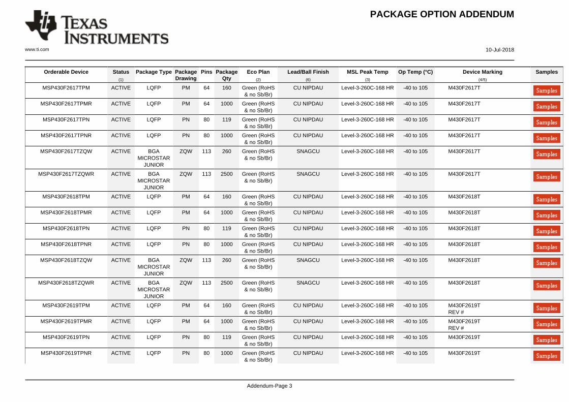
PACKAGE OPTION ADDENDUM
www.ti.com 10-Jul-2018
Addendum-Page 3
Orderable Device Status(1)
Package Type PackageDrawing
Pins PackageQty
Eco Plan(2)
Lead/Ball Finish(6)
MSL Peak Temp(3)
Op Temp (°C) Device Marking(4/5)
Samples
MSP430F2617TPM ACTIVE LQFP PM 64 160 Green (RoHS& no Sb/Br)
CU NIPDAU Level-3-260C-168 HR -40 to 105 M430F2617T
MSP430F2617TPMR ACTIVE LQFP PM 64 1000 Green (RoHS& no Sb/Br)
CU NIPDAU Level-3-260C-168 HR -40 to 105 M430F2617T
MSP430F2617TPN ACTIVE LQFP PN 80 119 Green (RoHS& no Sb/Br)
CU NIPDAU Level-3-260C-168 HR -40 to 105 M430F2617T
MSP430F2617TPNR ACTIVE LQFP PN 80 1000 Green (RoHS& no Sb/Br)
CU NIPDAU Level-3-260C-168 HR -40 to 105 M430F2617T
MSP430F2617TZQW ACTIVE BGAMICROSTAR
JUNIOR
ZQW 113 260 Green (RoHS& no Sb/Br)
SNAGCU Level-3-260C-168 HR -40 to 105 M430F2617T
MSP430F2617TZQWR ACTIVE BGAMICROSTAR
JUNIOR
ZQW 113 2500 Green (RoHS& no Sb/Br)
SNAGCU Level-3-260C-168 HR -40 to 105 M430F2617T
MSP430F2618TPM ACTIVE LQFP PM 64 160 Green (RoHS& no Sb/Br)
CU NIPDAU Level-3-260C-168 HR -40 to 105 M430F2618T
MSP430F2618TPMR ACTIVE LQFP PM 64 1000 Green (RoHS& no Sb/Br)
CU NIPDAU Level-3-260C-168 HR -40 to 105 M430F2618T
MSP430F2618TPN ACTIVE LQFP PN 80 119 Green (RoHS& no Sb/Br)
CU NIPDAU Level-3-260C-168 HR -40 to 105 M430F2618T
MSP430F2618TPNR ACTIVE LQFP PN 80 1000 Green (RoHS& no Sb/Br)
CU NIPDAU Level-3-260C-168 HR -40 to 105 M430F2618T
MSP430F2618TZQW ACTIVE BGAMICROSTAR
JUNIOR
ZQW 113 260 Green (RoHS& no Sb/Br)
SNAGCU Level-3-260C-168 HR -40 to 105 M430F2618T
MSP430F2618TZQWR ACTIVE BGAMICROSTAR
JUNIOR
ZQW 113 2500 Green (RoHS& no Sb/Br)
SNAGCU Level-3-260C-168 HR -40 to 105 M430F2618T
MSP430F2619TPM ACTIVE LQFP PM 64 160 Green (RoHS& no Sb/Br)
CU NIPDAU Level-3-260C-168 HR -40 to 105 M430F2619TREV #
MSP430F2619TPMR ACTIVE LQFP PM 64 1000 Green (RoHS& no Sb/Br)
CU NIPDAU Level-3-260C-168 HR -40 to 105 M430F2619TREV #
MSP430F2619TPN ACTIVE LQFP PN 80 119 Green (RoHS& no Sb/Br)
CU NIPDAU Level-3-260C-168 HR -40 to 105 M430F2619T
MSP430F2619TPNR ACTIVE LQFP PN 80 1000 Green (RoHS& no Sb/Br)
CU NIPDAU Level-3-260C-168 HR -40 to 105 M430F2619T
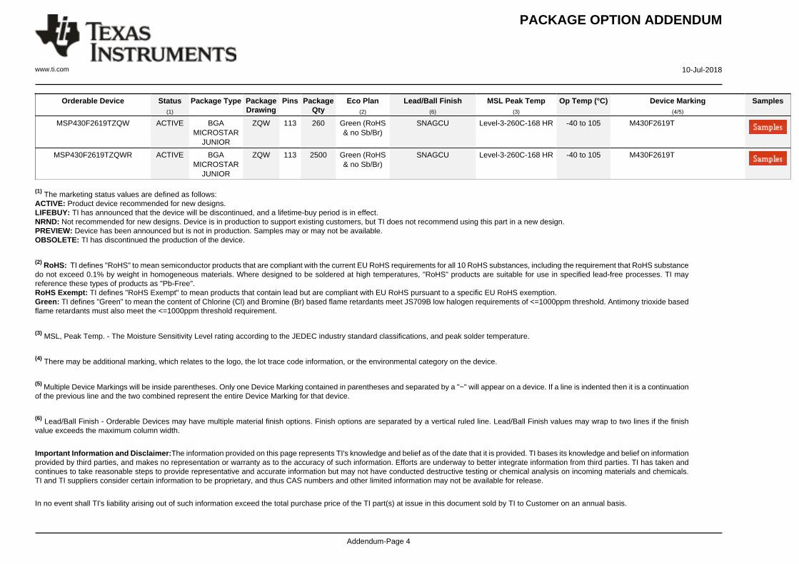
PACKAGE OPTION ADDENDUM
www.ti.com 10-Jul-2018
Addendum-Page 4
Orderable Device Status(1)
Package Type PackageDrawing
Pins PackageQty
Eco Plan(2)
Lead/Ball Finish(6)
MSL Peak Temp(3)
Op Temp (°C) Device Marking(4/5)
Samples
MSP430F2619TZQW ACTIVE BGAMICROSTAR
JUNIOR
ZQW 113 260 Green (RoHS& no Sb/Br)
SNAGCU Level-3-260C-168 HR -40 to 105 M430F2619T
MSP430F2619TZQWR ACTIVE BGAMICROSTAR
JUNIOR
ZQW 113 2500 Green (RoHS& no Sb/Br)
SNAGCU Level-3-260C-168 HR -40 to 105 M430F2619T
(1) The marketing status values are defined as follows:ACTIVE: Product device recommended for new designs.LIFEBUY: TI has announced that the device will be discontinued, and a lifetime-buy period is in effect.NRND: Not recommended for new designs. Device is in production to support existing customers, but TI does not recommend using this part in a new design.PREVIEW: Device has been announced but is not in production. Samples may or may not be available.OBSOLETE: TI has discontinued the production of the device.
(2) RoHS: TI defines "RoHS" to mean semiconductor products that are compliant with the current EU RoHS requirements for all 10 RoHS substances, including the requirement that RoHS substancedo not exceed 0.1% by weight in homogeneous materials. Where designed to be soldered at high temperatures, "RoHS" products are suitable for use in specified lead-free processes. TI mayreference these types of products as "Pb-Free".RoHS Exempt: TI defines "RoHS Exempt" to mean products that contain lead but are compliant with EU RoHS pursuant to a specific EU RoHS exemption.Green: TI defines "Green" to mean the content of Chlorine (Cl) and Bromine (Br) based flame retardants meet JS709B low halogen requirements of <=1000ppm threshold. Antimony trioxide basedflame retardants must also meet the <=1000ppm threshold requirement.
(3) MSL, Peak Temp. - The Moisture Sensitivity Level rating according to the JEDEC industry standard classifications, and peak solder temperature.
(4) There may be additional marking, which relates to the logo, the lot trace code information, or the environmental category on the device.
(5) Multiple Device Markings will be inside parentheses. Only one Device Marking contained in parentheses and separated by a "~" will appear on a device. If a line is indented then it is a continuationof the previous line and the two combined represent the entire Device Marking for that device.
(6) Lead/Ball Finish - Orderable Devices may have multiple material finish options. Finish options are separated by a vertical ruled line. Lead/Ball Finish values may wrap to two lines if the finishvalue exceeds the maximum column width.
Important Information and Disclaimer:The information provided on this page represents TI's knowledge and belief as of the date that it is provided. TI bases its knowledge and belief on informationprovided by third parties, and makes no representation or warranty as to the accuracy of such information. Efforts are underway to better integrate information from third parties. TI has taken andcontinues to take reasonable steps to provide representative and accurate information but may not have conducted destructive testing or chemical analysis on incoming materials and chemicals.TI and TI suppliers consider certain information to be proprietary, and thus CAS numbers and other limited information may not be available for release.
In no event shall TI's liability arising out of such information exceed the total purchase price of the TI part(s) at issue in this document sold by TI to Customer on an annual basis.
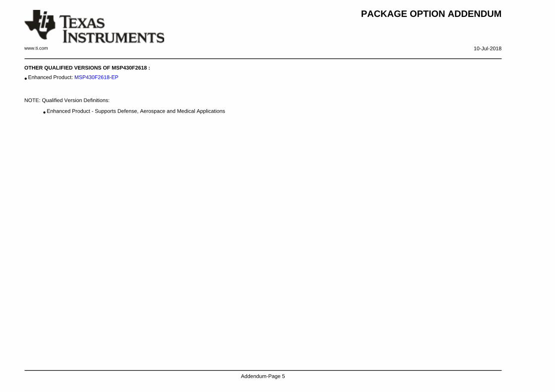
PACKAGE OPTION ADDENDUM
www.ti.com 10-Jul-2018
Addendum-Page 5
OTHER QUALIFIED VERSIONS OF MSP430F2618 :
• Enhanced Product: MSP430F2618-EP
NOTE: Qualified Version Definitions:
• Enhanced Product - Supports Defense, Aerospace and Medical Applications
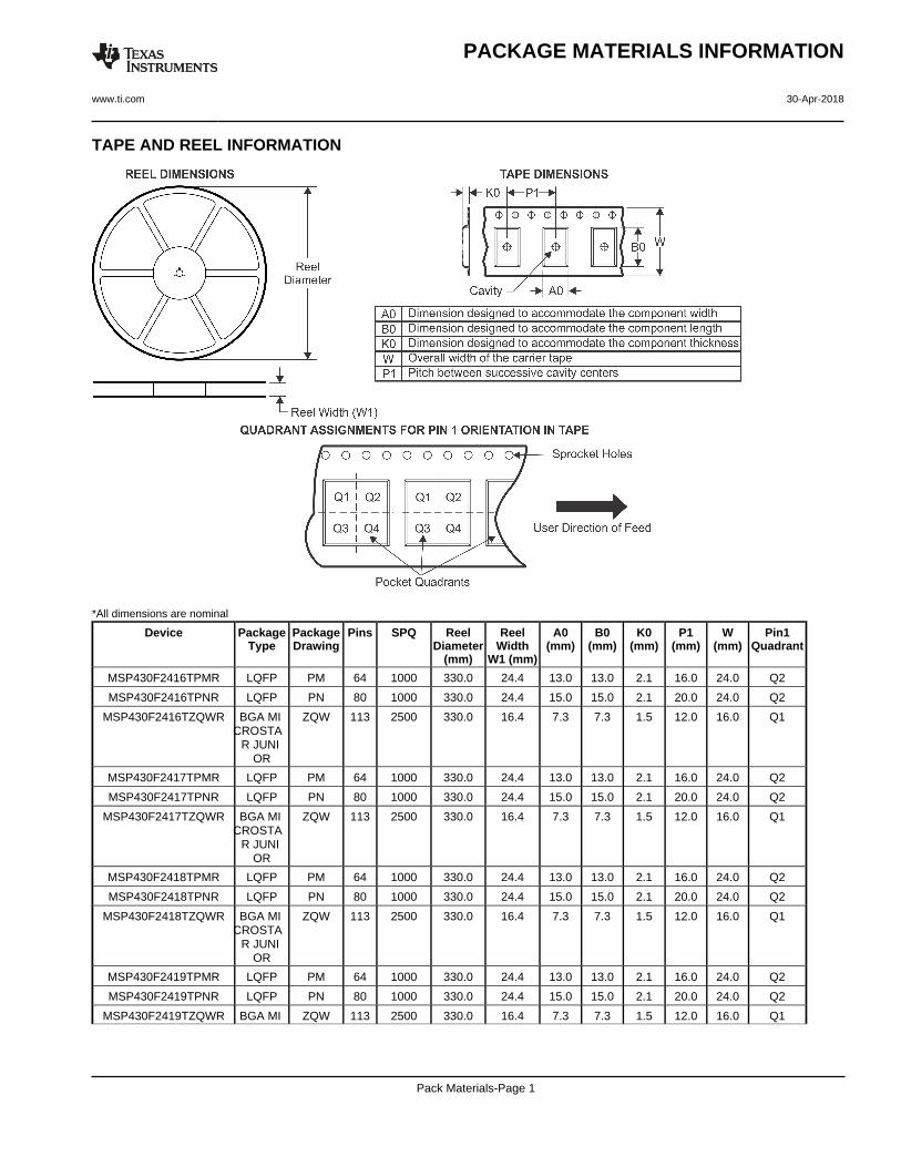
TAPE AND REEL INFORMATION
*All dimensions are nominal
Device PackageType
PackageDrawing
Pins SPQ ReelDiameter
(mm)
ReelWidth
W1 (mm)
A0(mm)
B0(mm)
K0(mm)
P1(mm)
W(mm)
Pin1Quadrant
MSP430F2416TPMR LQFP PM 64 1000 330.0 24.4 13.0 13.0 2.1 16.0 24.0 Q2
MSP430F2416TPNR LQFP PN 80 1000 330.0 24.4 15.0 15.0 2.1 20.0 24.0 Q2
MSP430F2416TZQWR BGA MI CROSTA
R JUNI OR
ZQW 113 2500 330.0 16.4 7.3 7.3 1.5 12.0 16.0 Q1
MSP430F2417TPMR LQFP PM 64 1000 330.0 24.4 13.0 13.0 2.1 16.0 24.0 Q2
MSP430F2417TPNR LQFP PN 80 1000 330.0 24.4 15.0 15.0 2.1 20.0 24.0 Q2
MSP430F2417TZQWR BGA MI CROSTA
R JUNI OR
ZQW 113 2500 330.0 16.4 7.3 7.3 1.5 12.0 16.0 Q1
MSP430F2418TPMR LQFP PM 64 1000 330.0 24.4 13.0 13.0 2.1 16.0 24.0 Q2
MSP430F2418TPNR LQFP PN 80 1000 330.0 24.4 15.0 15.0 2.1 20.0 24.0 Q2
MSP430F2418TZQWR BGA MI CROSTA
R JUNI OR
ZQW 113 2500 330.0 16.4 7.3 7.3 1.5 12.0 16.0 Q1
MSP430F2419TPMR LQFP PM 64 1000 330.0 24.4 13.0 13.0 2.1 16.0 24.0 Q2
MSP430F2419TPNR LQFP PN 80 1000 330.0 24.4 15.0 15.0 2.1 20.0 24.0 Q2
MSP430F2419TZQWR BGA MI ZQW 113 2500 330.0 16.4 7.3 7.3 1.5 12.0 16.0 Q1
PACKAGE MATERIALS INFORMATION
www.ti.com 30-Apr-2018
Pack Materials-Page 1
Device PackageType
PackageDrawing
Pins SPQ ReelDiameter
(mm)
ReelWidth
W1 (mm)
A0(mm)
B0(mm)
K0(mm)
P1(mm)
W(mm)
Pin1Quadrant
CROSTAR JUNI
OR
MSP430F2616TPMR LQFP PM 64 1000 330.0 24.4 13.0 13.0 2.1 16.0 24.0 Q2
MSP430F2616TPNR LQFP PN 80 1000 330.0 24.4 15.0 15.0 2.1 20.0 24.0 Q2
MSP430F2616TZQWR BGA MI CROSTA
R JUNI OR
ZQW 113 2500 330.0 16.4 7.3 7.3 1.5 12.0 16.0 Q1
MSP430F2617TPMR LQFP PM 64 1000 330.0 24.4 13.0 13.0 2.1 16.0 24.0 Q2
MSP430F2617TPNR LQFP PN 80 1000 330.0 24.4 15.0 15.0 2.1 20.0 24.0 Q2
MSP430F2617TZQWR BGA MI CROSTA
R JUNI OR
ZQW 113 2500 330.0 16.4 7.3 7.3 1.5 12.0 16.0 Q1
MSP430F2618TPMR LQFP PM 64 1000 330.0 24.4 13.0 13.0 2.1 16.0 24.0 Q2
MSP430F2618TPNR LQFP PN 80 1000 330.0 24.4 15.0 15.0 2.1 20.0 24.0 Q2
MSP430F2618TZQWR BGA MI CROSTA
R JUNI OR
ZQW 113 2500 330.0 16.4 7.3 7.3 1.5 12.0 16.0 Q1
MSP430F2619TPMR LQFP PM 64 1000 330.0 24.4 13.0 13.0 2.1 16.0 24.0 Q2
MSP430F2619TPNR LQFP PN 80 1000 330.0 24.4 15.0 15.0 2.1 20.0 24.0 Q2
MSP430F2619TZQWR BGA MI CROSTA
R JUNI OR
ZQW 113 2500 330.0 16.4 7.3 7.3 1.5 12.0 16.0 Q1
PACKAGE MATERIALS INFORMATION
www.ti.com 30-Apr-2018
Pack Materials-Page 2
*All dimensions are nominal
Device Package Type Package Drawing Pins SPQ Length (mm) Width (mm) Height (mm)
MSP430F2416TPMR LQFP PM 64 1000 367.0 367.0 45.0
MSP430F2416TPNR LQFP PN 80 1000 367.0 367.0 45.0
MSP430F2416TZQWR BGA MICROSTARJUNIOR
ZQW 113 2500 336.6 336.6 28.6
MSP430F2417TPMR LQFP PM 64 1000 367.0 367.0 45.0
MSP430F2417TPNR LQFP PN 80 1000 367.0 367.0 45.0
MSP430F2417TZQWR BGA MICROSTARJUNIOR
ZQW 113 2500 336.6 336.6 28.6
MSP430F2418TPMR LQFP PM 64 1000 350.0 350.0 43.0
MSP430F2418TPNR LQFP PN 80 1000 367.0 367.0 45.0
MSP430F2418TZQWR BGA MICROSTARJUNIOR
ZQW 113 2500 336.6 336.6 28.6
MSP430F2419TPMR LQFP PM 64 1000 367.0 367.0 45.0
MSP430F2419TPNR LQFP PN 80 1000 367.0 367.0 45.0
MSP430F2419TZQWR BGA MICROSTARJUNIOR
ZQW 113 2500 336.6 336.6 28.6
MSP430F2616TPMR LQFP PM 64 1000 367.0 367.0 45.0
MSP430F2616TPNR LQFP PN 80 1000 367.0 367.0 45.0
MSP430F2616TZQWR BGA MICROSTARJUNIOR
ZQW 113 2500 336.6 336.6 28.6
MSP430F2617TPMR LQFP PM 64 1000 367.0 367.0 45.0
MSP430F2617TPNR LQFP PN 80 1000 367.0 367.0 45.0
PACKAGE MATERIALS INFORMATION
www.ti.com 30-Apr-2018
Pack Materials-Page 3
Device Package Type Package Drawing Pins SPQ Length (mm) Width (mm) Height (mm)
MSP430F2617TZQWR BGA MICROSTARJUNIOR
ZQW 113 2500 336.6 336.6 28.6
MSP430F2618TPMR LQFP PM 64 1000 367.0 367.0 45.0
MSP430F2618TPNR LQFP PN 80 1000 367.0 367.0 45.0
MSP430F2618TZQWR BGA MICROSTARJUNIOR
ZQW 113 2500 336.6 336.6 28.6
MSP430F2619TPMR LQFP PM 64 1000 367.0 367.0 45.0
MSP430F2619TPNR LQFP PN 80 1000 367.0 367.0 45.0
MSP430F2619TZQWR BGA MICROSTARJUNIOR
ZQW 113 2500 336.6 336.6 28.6
PACKAGE MATERIALS INFORMATION
www.ti.com 30-Apr-2018
Pack Materials-Page 4
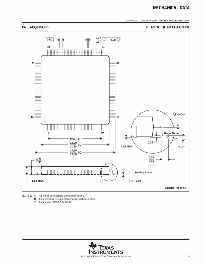
MECHANICAL DATA
MTQF010A – JANUARY 1995 – REVISED DECEMBER 1996
1POST OFFICE BOX 655303 • DALLAS, TEXAS 75265
PN (S-PQFP-G80) PLASTIC QUAD FLATPACK
4040135 /B 11/96
0,170,27
0,13 NOM
40
21
0,25
0,450,75
0,05 MIN
Seating Plane
Gage Plane
4160
61
80
20
SQ
SQ
1
13,8014,20
12,20
9,50 TYP
11,80
1,451,35
1,60 MAX 0,08
0,50 M0,08
0°–7°
NOTES: A. All linear dimensions are in millimeters.B. This drawing is subject to change without notice.C. Falls within JEDEC MS-026
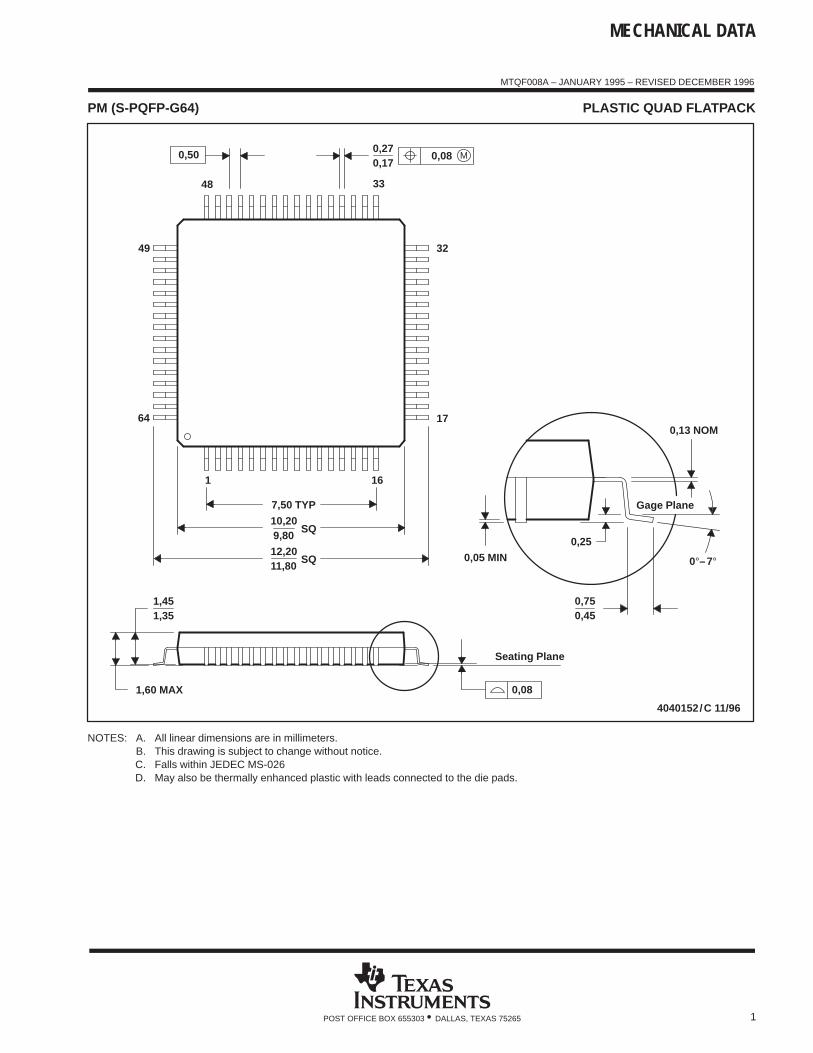
MECHANICAL DATA
MTQF008A – JANUARY 1995 – REVISED DECEMBER 1996
1POST OFFICE BOX 655303 • DALLAS, TEXAS 75265
PM (S-PQFP-G64) PLASTIC QUAD FLATPACK
4040152/C 11/96
32
170,13 NOM
0,25
0,450,75
Seating Plane
0,05 MIN
Gage Plane
0,27
33
16
48
1
0,17
49
64
SQ
SQ10,20
11,8012,20
9,80
7,50 TYP
1,60 MAX
1,451,35
0,08
0,50 M0,08
0°–7°
NOTES: A. All linear dimensions are in millimeters.B. This drawing is subject to change without notice.C. Falls within JEDEC MS-026D. May also be thermally enhanced plastic with leads connected to the die pads.
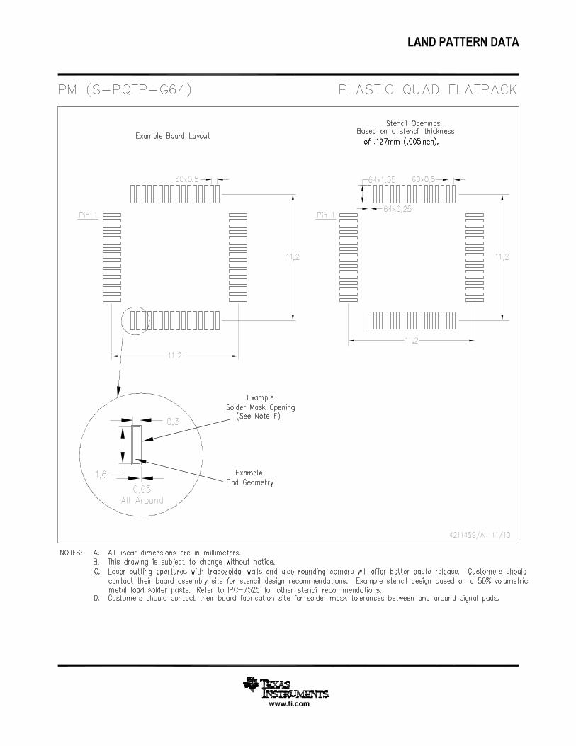
IMPORTANT NOTICE
Texas Instruments Incorporated (TI) reserves the right to make corrections, enhancements, improvements and other changes to itssemiconductor products and services per JESD46, latest issue, and to discontinue any product or service per JESD48, latest issue. Buyersshould obtain the latest relevant information before placing orders and should verify that such information is current and complete.TI’s published terms of sale for semiconductor products (http://www.ti.com/sc/docs/stdterms.htm) apply to the sale of packaged integratedcircuit products that TI has qualified and released to market. Additional terms may apply to the use or sale of other types of TI products andservices.Reproduction of significant portions of TI information in TI data sheets is permissible only if reproduction is without alteration and isaccompanied by all associated warranties, conditions, limitations, and notices. TI is not responsible or liable for such reproduceddocumentation. Information of third parties may be subject to additional restrictions. Resale of TI products or services with statementsdifferent from or beyond the parameters stated by TI for that product or service voids all express and any implied warranties for theassociated TI product or service and is an unfair and deceptive business practice. TI is not responsible or liable for any such statements.Buyers and others who are developing systems that incorporate TI products (collectively, “Designers”) understand and agree that Designersremain responsible for using their independent analysis, evaluation and judgment in designing their applications and that Designers havefull and exclusive responsibility to assure the safety of Designers' applications and compliance of their applications (and of all TI productsused in or for Designers’ applications) with all applicable regulations, laws and other applicable requirements. Designer represents that, withrespect to their applications, Designer has all the necessary expertise to create and implement safeguards that (1) anticipate dangerousconsequences of failures, (2) monitor failures and their consequences, and (3) lessen the likelihood of failures that might cause harm andtake appropriate actions. Designer agrees that prior to using or distributing any applications that include TI products, Designer willthoroughly test such applications and the functionality of such TI products as used in such applications.TI’s provision of technical, application or other design advice, quality characterization, reliability data or other services or information,including, but not limited to, reference designs and materials relating to evaluation modules, (collectively, “TI Resources”) are intended toassist designers who are developing applications that incorporate TI products; by downloading, accessing or using TI Resources in anyway, Designer (individually or, if Designer is acting on behalf of a company, Designer’s company) agrees to use any particular TI Resourcesolely for this purpose and subject to the terms of this Notice.TI’s provision of TI Resources does not expand or otherwise alter TI’s applicable published warranties or warranty disclaimers for TIproducts, and no additional obligations or liabilities arise from TI providing such TI Resources. TI reserves the right to make corrections,enhancements, improvements and other changes to its TI Resources. TI has not conducted any testing other than that specificallydescribed in the published documentation for a particular TI Resource.Designer is authorized to use, copy and modify any individual TI Resource only in connection with the development of applications thatinclude the TI product(s) identified in such TI Resource. NO OTHER LICENSE, EXPRESS OR IMPLIED, BY ESTOPPEL OR OTHERWISETO ANY OTHER TI INTELLECTUAL PROPERTY RIGHT, AND NO LICENSE TO ANY TECHNOLOGY OR INTELLECTUAL PROPERTYRIGHT OF TI OR ANY THIRD PARTY IS GRANTED HEREIN, including but not limited to any patent right, copyright, mask work right, orother intellectual property right relating to any combination, machine, or process in which TI products or services are used. Informationregarding or referencing third-party products or services does not constitute a license to use such products or services, or a warranty orendorsement thereof. Use of TI Resources may require a license from a third party under the patents or other intellectual property of thethird party, or a license from TI under the patents or other intellectual property of TI.TI RESOURCES ARE PROVIDED “AS IS” AND WITH ALL FAULTS. TI DISCLAIMS ALL OTHER WARRANTIES ORREPRESENTATIONS, EXPRESS OR IMPLIED, REGARDING RESOURCES OR USE THEREOF, INCLUDING BUT NOT LIMITED TOACCURACY OR COMPLETENESS, TITLE, ANY EPIDEMIC FAILURE WARRANTY AND ANY IMPLIED WARRANTIES OFMERCHANTABILITY, FITNESS FOR A PARTICULAR PURPOSE, AND NON-INFRINGEMENT OF ANY THIRD PARTY INTELLECTUALPROPERTY RIGHTS. TI SHALL NOT BE LIABLE FOR AND SHALL NOT DEFEND OR INDEMNIFY DESIGNER AGAINST ANY CLAIM,INCLUDING BUT NOT LIMITED TO ANY INFRINGEMENT CLAIM THAT RELATES TO OR IS BASED ON ANY COMBINATION OFPRODUCTS EVEN IF DESCRIBED IN TI RESOURCES OR OTHERWISE. IN NO EVENT SHALL TI BE LIABLE FOR ANY ACTUAL,DIRECT, SPECIAL, COLLATERAL, INDIRECT, PUNITIVE, INCIDENTAL, CONSEQUENTIAL OR EXEMPLARY DAMAGES INCONNECTION WITH OR ARISING OUT OF TI RESOURCES OR USE THEREOF, AND REGARDLESS OF WHETHER TI HAS BEENADVISED OF THE POSSIBILITY OF SUCH DAMAGES.Unless TI has explicitly designated an individual product as meeting the requirements of a particular industry standard (e.g., ISO/TS 16949and ISO 26262), TI is not responsible for any failure to meet such industry standard requirements.Where TI specifically promotes products as facilitating functional safety or as compliant with industry functional safety standards, suchproducts are intended to help enable customers to design and create their own applications that meet applicable functional safety standardsand requirements. Using products in an application does not by itself establish any safety features in the application. Designers mustensure compliance with safety-related requirements and standards applicable to their applications. Designer may not use any TI products inlife-critical medical equipment unless authorized officers of the parties have executed a special contract specifically governing such use.Life-critical medical equipment is medical equipment where failure of such equipment would cause serious bodily injury or death (e.g., lifesupport, pacemakers, defibrillators, heart pumps, neurostimulators, and implantables). Such equipment includes, without limitation, allmedical devices identified by the U.S. Food and Drug Administration as Class III devices and equivalent classifications outside the U.S.TI may expressly designate certain products as completing a particular qualification (e.g., Q100, Military Grade, or Enhanced Product).Designers agree that it has the necessary expertise to select the product with the appropriate qualification designation for their applicationsand that proper product selection is at Designers’ own risk. Designers are solely responsible for compliance with all legal and regulatoryrequirements in connection with such selection.Designer will fully indemnify TI and its representatives against any damages, costs, losses, and/or liabilities arising out of Designer’s non-compliance with the terms and provisions of this Notice.
Mailing Address: Texas Instruments, Post Office Box 655303, Dallas, Texas 75265Copyright © 2018, Texas Instruments Incorporated