Embed Size (px)
Citation preview
MSP430G2332-EP
www.ti.com SLAS885A –AUGUST 2012–REVISED OCTOBER 2012
MIXED SIGNAL MICROCONTROLLER1FEATURES23• Low Supply Voltage Range: 1.8 V to 3.6 V • Brownout Detector• Ultra-Low Power Consumption • Serial Onboard Programming,
No External Programming Voltage Needed,– Active Mode: 220 µA at 1 MHz, 2.2 VProgrammable Code Protection by Security– Standby Mode: 0.5 µAFuse
– Off Mode (RAM Retention): 0.1 µA• On-Chip Emulation Logic With Spy-Bi-Wire
• Five Power-Saving Modes Interface• Ultra-Fast Wake-Up From Standby Mode in • Family Members are Summarized in Table 1
Less Than 1 µs• Package Options
• 16-Bit RISC Architecture, 62.5-ns Instruction– TSSOP: 20 PinCycle Time
• For Complete Module Descriptions, See the• Basic Clock Module ConfigurationsMSP430x2xx Family User’s Guide (SLAU144)
– Internal Frequencies up to 16 MHz WithFour Calibrated Frequencies SUPPORTS DEFENSE, AEROSPACE,
– Internal Very-Low-Power Low-Frequency AND MEDICAL APPLICATIONS(LF) Oscillator
• Controlled Baseline– 32-kHz Crystal (1)
• One Assembly and Test Site– External Digital Clock Source
• One Fabrication Site• One 16-Bit Timer_A With Three
• Available in Extended (–40°C to 125°C)Capture/Compare RegistersTemperature Range (2)
• Up to 16 Touch-Sense Enabled I/O Pins• Extended Product Life Cycle
• Universal Serial Interface (USI) Supporting SPI• Extended Product-Change Notificationand I2C (see Table 1)• Product Traceability• 10-Bit 200-ksps Analog-to-Digital (A/D)
Converter With Internal Reference, Sample-and-Hold, and Autoscan (see Table 1)
(1) Crystal oscillator cannot be operated beyond 105°C (2) Custom temperature ranges available
DESCRIPTIONThe Texas Instruments MSP430™ family of ultra-low-power microcontrollers consist of several devices featuringdifferent sets of peripherals targeted for various applications. The architecture, combined with five low-powermodes is optimized to achieve extended battery life in portable measurement applications. The device features apowerful 16-bit RISC CPU, 16-bit registers, and constant generators that contribute to maximum code efficiency.The digitally controlled oscillator (DCO) allows wake-up from low-power modes to active mode in less than 1 µs.
The MSP430G2332 series of microcontrollers are ultra-low-power mixed signal microcontrollers with built-in16-bit timers, and up to 16 I/O touch sense enabled pins and built-in communication capability using theuniversal serial communication interface. The MSP430G2332 series have a 10-bit A/D converter. Forconfiguration details, see Table 1. Typical applications include low-cost sensor systems that capture analogsignals, convert them to digital values, and then process the data for display or for transmission to a host system.
1
Please be aware that an important notice concerning availability, standard warranty, and use in critical applications ofTexas Instruments semiconductor products and disclaimers thereto appears at the end of this data sheet.
2MSP430 is a trademark of Texas Instruments.3All other trademarks are the property of their respective owners.
PRODUCTION DATA information is current as of publication date. Copyright © 2012, Texas Instruments IncorporatedProducts conform to specifications per the terms of the TexasInstruments standard warranty. Production processing does notnecessarily include testing of all parameters.
MSP430G2332-EP
SLAS885A –AUGUST 2012–REVISED OCTOBER 2012 www.ti.com
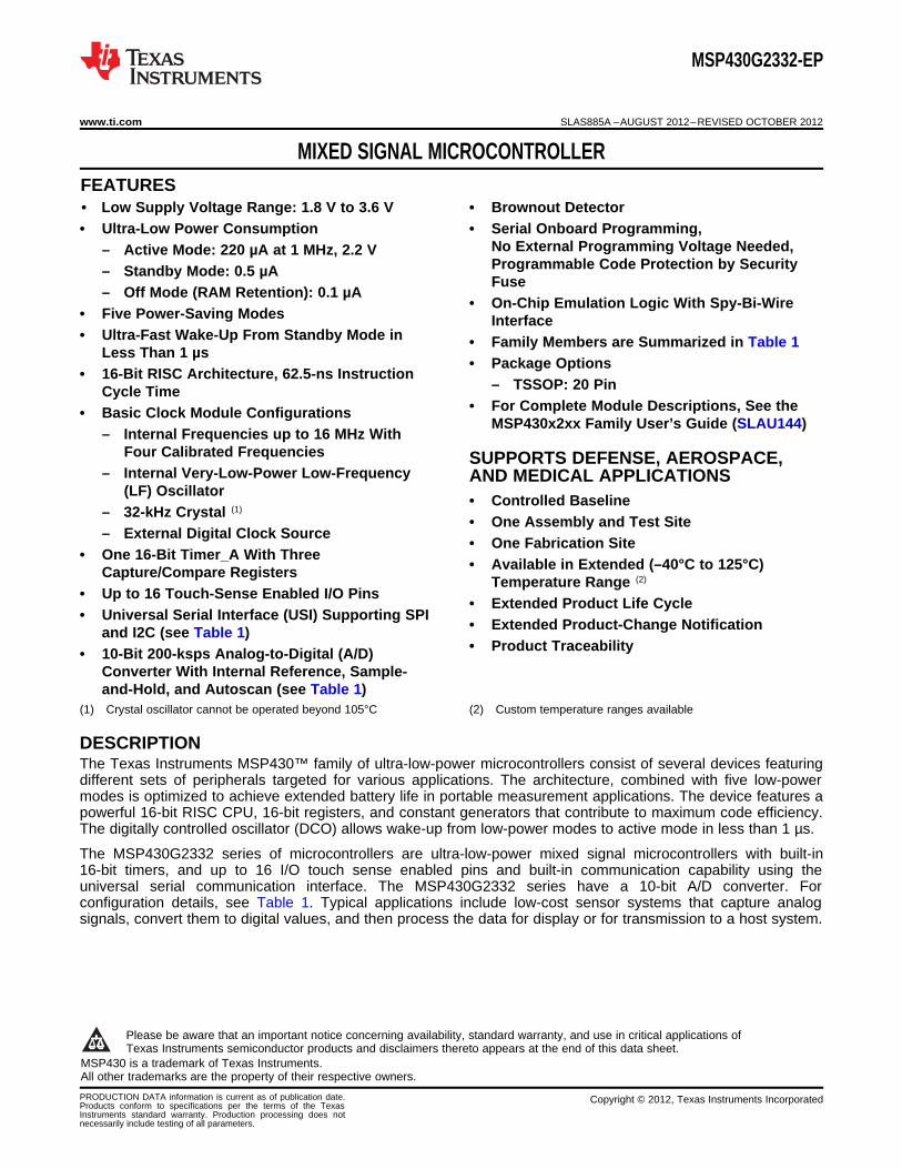
Table 1. Available Options
Flash RAM ADC10Device EEM Timer_A USI CLOCK I/O Package Type(kB) (B) Channel
MSP430G2332QPW2EP 1 4 256 1x TA3 8 1 LF, DCO, VLO 16 20-TSSOP
Table 2. ORDERING INFORMATION (1)
TA PACKAGE ORDERABLE PART NUMBER TOP-SIDE MARKING VID NUMBER
MSP430G2332QPW2REP Tape and Reel, 2000 V62/12625-01XE–40°C to 125°C TSSOP - PW G2332EP
MSP430G2332QPW2EP Tube, 70 V62/12625-01XE-T
(1) For the most current package and ordering information, see the Package Option Addendum at the end of this document, or see the TIWeb site at www.ti.com.
2 Submit Documentation Feedback Copyright © 2012, Texas Instruments Incorporated
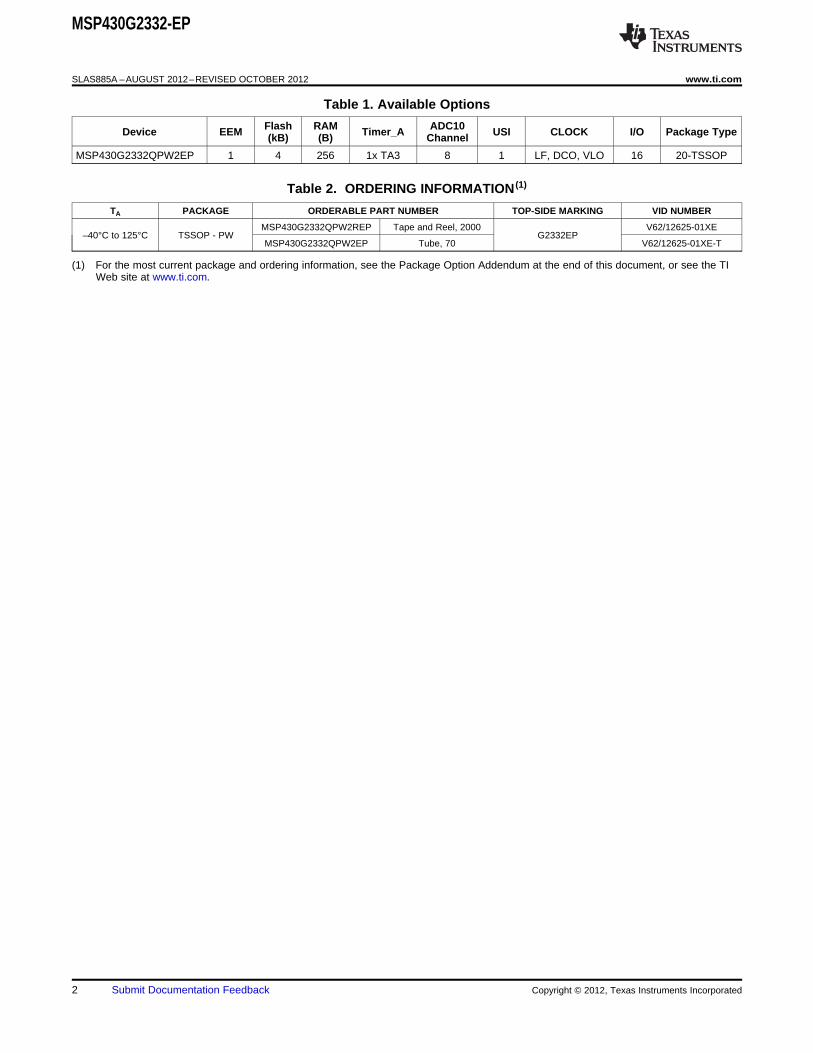
1DVCC
2P1.0/TA0CLK/ACLK/A0
3
4
5P1.3/ADC10CLK/VREF-/VEREF-/A3
6
7
8P2.0
9P2.1
10P2.2 11 P2.3
12 P2.4
13 P2.5
14
15
16 RST/NMI/SBWTDIO
17 TEST/SBWTCK
18 XOUT/P2.7
19 XIN/P2.6/TA0.1
20 DVSS
P1.6/TA0.1/ TDI/TCLKSDO/SCL/A6/
P1.7/SDI/SDA/A7/TDO/TDI
P1.1/TA0.0/A1
P1.2/TA0.1/A2
P1.4/TA0.2/SMCLK/A4/ /TCKVREF+/VEREF+
P1.5/TA0.0 A5/TMS/SCLK/
MSP430G2332-EP
www.ti.com SLAS885A –AUGUST 2012–REVISED OCTOBER 2012
This integrated circuit can be damaged by ESD. Texas Instruments recommends that all integrated circuits be handled withappropriate precautions. Failure to observe proper handling and installation procedures can cause damage.
ESD damage can range from subtle performance degradation to complete device failure. Precision integrated circuits may be moresusceptible to damage because very small parametric changes could cause the device not to meet its published specifications.
DEVICE PINOUTS
PW PACKAGE(TOP VIEW)
Copyright © 2012, Texas Instruments Incorporated Submit Documentation Feedback 3
Clock
System
Brownout
Protection
RST/NMI
DVCC DVSS
MCLK
Watchdog
WDT+
15-Bit
Timer0_A3
3 CC
Registers
16MHz
CPU
incl. 16
Registers
Emulation
2BP
JTAG
Interface
SMCLK
ACLK
MDB
MAB
Port P1
8 I/O
Interrupt
capability
pullup/down
resistors
P1.x
8
Spy-Bi
Wire
XIN XOUT
RAM
256B
256B
256B
128B
Flash
8KB
4KB
2KB
1KB
P2.x
Port P2
up to 8 I/O
Interrupt
capability
pullup/down
resistors
up to 8
USI
Universal
Serial
Interface
SPI, I2C
ADC
10-Bit
8 Ch.
Autoscan
1 ch DMA
MSP430G2332-EP
SLAS885A –AUGUST 2012–REVISED OCTOBER 2012 www.ti.com
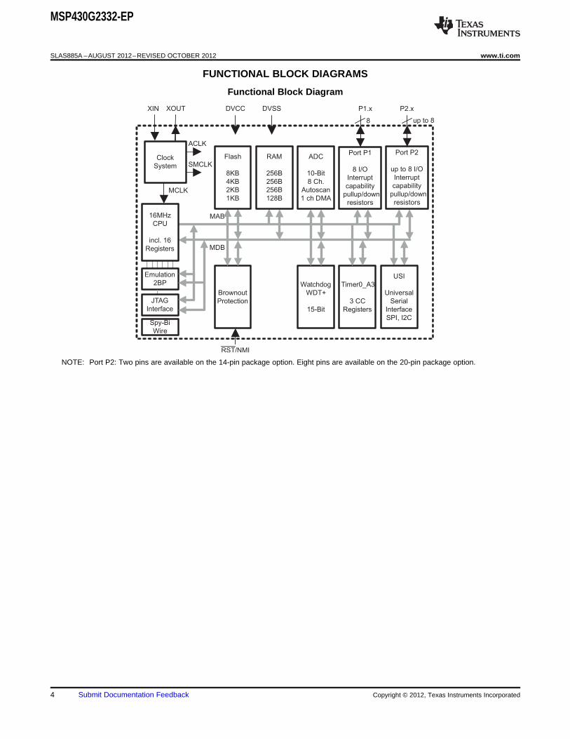
FUNCTIONAL BLOCK DIAGRAMS
Functional Block Diagram
NOTE: Port P2: Two pins are available on the 14-pin package option. Eight pins are available on the 20-pin package option.
4 Submit Documentation Feedback Copyright © 2012, Texas Instruments Incorporated
MSP430G2332-EP
www.ti.com SLAS885A –AUGUST 2012–REVISED OCTOBER 2012
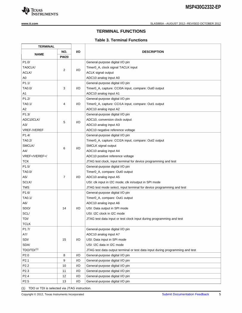
TERMINAL FUNCTIONS
Table 3. Terminal Functions
TERMINAL
NO. I/O DESCRIPTIONNAME
PW20
P1.0/ General-purpose digital I/O pin
TA0CLK/ Timer0_A, clock signal TACLK input2 I/O
ACLK/ ACLK signal output
A0 ADC10 analog input A0
P1.1/ General-purpose digital I/O pin
TA0.0/ 3 I/O Timer0_A, capture: CCI0A input, compare: Out0 output
A1 ADC10 analog input A1
P1.2/ General-purpose digital I/O pin
TA0.1/ 4 I/O Timer0_A, capture: CCI1A input, compare: Out1 output
A2 ADC10 analog input A2
P1.3/ General-purpose digital I/O pin
ADC10CLK/ ADC10, conversion clock output5 I/O
A3/ ADC10 analog input A3
VREF-/VEREF ADC10 negative reference voltage
P1.4/ General-purpose digital I/O pin
TA0.2/ Timer0_A, capture: CCI2A input, compare: Out2 output
SMCLK/ SMCLK signal output6 I/O
A4/ ADC10 analog input A4
VREF+/VEREF+/ ADC10 positive reference voltage
TCK JTAG test clock, input terminal for device programming and test
P1.5/ General-purpose digital I/O pin
TA0.0/ Timer0_A, compare: Out0 output
A5/ 7 I/O ADC10 analog input A5
SCLK/ USI: clk input in I2C mode; clk in/output in SPI mode
TMS JTAG test mode select, input terminal for device programming and test
P1.6/ General-purpose digital I/O pin
TA0.1/ Timer0_A, compare: Out1 output
A6/ ADC10 analog input A6
SDO/ 14 I/O USI: Data output in SPI mode
SCL/ USI: I2C clock in I2C mode
TDI/ JTAG test data input or test clock input during programming and test
TCLK
P1.7/ General-purpose digital I/O pin
A7/ ADC10 analog input A7
SDI/ 15 I/O USI: Data input in SPI mode
SDA/ USI: I2C data in I2C mode
TDO/TDI (1) JTAG test data output terminal or test data input during programming and test
P2.0 8 I/O General-purpose digital I/O pin
P2.1 9 I/O General-purpose digital I/O pin
P2.2 10 I/O General-purpose digital I/O pin
P2.3 11 I/O General-purpose digital I/O pin
P2.4 12 I/O General-purpose digital I/O pin
P2.5 13 I/O General-purpose digital I/O pin
(1) TDO or TDI is selected via JTAG instruction.
Copyright © 2012, Texas Instruments Incorporated Submit Documentation Feedback 5
MSP430G2332-EP
SLAS885A –AUGUST 2012–REVISED OCTOBER 2012 www.ti.com
Table 3. Terminal Functions (continued)
TERMINAL
NO. I/O DESCRIPTIONNAME
PW20
XIN/ Input terminal of crystal oscillator
P2.6/ 19 I/O General-purpose digital I/O pin
TA0.1 Timer0_A, compare: Out1 output
XOUT/ Output terminal of crystal oscillator (2)
18 I/OP2.7 General-purpose digital I/O pin
RST/ Reset
NMI/ 16 I Nonmaskable interrupt input
SBWTDIO/ Spy-Bi-Wire test data input/output during programming and test
TEST/ Selects test mode for JTAG pins on Port 1. The device protection fuse is connected to TEST.17 I
SBWTCK Spy-Bi-Wire test clock input during programming and test
DVCC 1 NA Supply voltage
AVCC NA NA Supply voltage
DVSS 20 NA Ground reference
AVSS NA NA Ground reference
NC - NA Not connected
QFN Pad - NA QFN package pad connection to VSS recommended.
(2) If XOUT/P2.7 is used as an input, excess current flows until P2SEL.7 is cleared. This is due to the oscillator output driver connection tothis pad after reset.
6 Submit Documentation Feedback Copyright © 2012, Texas Instruments Incorporated
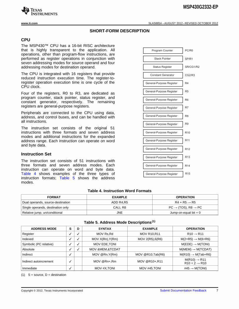
General-Purpose Register
Program Counter
Stack Pointer
Status Register
Constant Generator
General-Purpose Register
General-Purpose Register
General-Purpose Register
PC/R0
SP/R1
SR/CG1/R2
CG2/R3
R4
R5
R12
R13
General-Purpose Register
General-Purpose Register
R6
R7
General-Purpose Register
General-Purpose Register
R8
R9
General-Purpose Register
General-Purpose Register
R10
R11
General-Purpose Register
General-Purpose Register
R14
R15
MSP430G2332-EP
www.ti.com SLAS885A –AUGUST 2012–REVISED OCTOBER 2012
SHORT-FORM DESCRIPTION
CPUThe MSP430™ CPU has a 16-bit RISC architecturethat is highly transparent to the application. Alloperations, other than program-flow instructions, areperformed as register operations in conjunction withseven addressing modes for source operand and fouraddressing modes for destination operand.
The CPU is integrated with 16 registers that providereduced instruction execution time. The register-to-register operation execution time is one cycle of theCPU clock.
Four of the registers, R0 to R3, are dedicated asprogram counter, stack pointer, status register, andconstant generator, respectively. The remainingregisters are general-purpose registers.
Peripherals are connected to the CPU using data,address, and control buses, and can be handled withall instructions.
The instruction set consists of the original 51instructions with three formats and seven addressmodes and additional instructions for the expandedaddress range. Each instruction can operate on wordand byte data.
Instruction Set
The instruction set consists of 51 instructions withthree formats and seven address modes. Eachinstruction can operate on word and byte data.Table 4 shows examples of the three types ofinstruction formats; Table 5 shows the addressmodes.
Table 4. Instruction Word Formats
FORMAT EXAMPLE OPERATION
Dual operands, source-destination ADD R4,R5 R4 + R5 → R5
Single operands, destination only CALL R8 PC → (TOS), R8 → PC
Relative jump, un/conditional JNE Jump-on-equal bit = 0
Table 5. Address Mode Descriptions (1)
ADDRESS MODE S D SYNTAX EXAMPLE OPERATION
Register MOV Rs,Rd MOV R10,R11 R10 → R11
Indexed MOV X(Rn),Y(Rm) MOV 2(R5),6(R6) M(2+R5) → M(6+R6)
Symbolic (PC relative) MOV EDE,TONI M(EDE) → M(TONI)
Absolute MOV &MEM,&TCDAT M(MEM) → M(TCDAT)
Indirect MOV @Rn,Y(Rm) MOV @R10,Tab(R6) M(R10) → M(Tab+R6)
M(R10) → R11Indirect autoincrement MOV @Rn+,Rm MOV @R10+,R11 R10 + 2 → R10
Immediate MOV #X,TONI MOV #45,TONI #45 → M(TONI)
(1) S = source, D = destination
Copyright © 2012, Texas Instruments Incorporated Submit Documentation Feedback 7
MSP430G2332-EP
SLAS885A –AUGUST 2012–REVISED OCTOBER 2012 www.ti.com
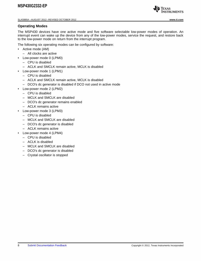
Operating Modes
The MSP430 devices have one active mode and five software selectable low-power modes of operation. Aninterrupt event can wake up the device from any of the low-power modes, service the request, and restore backto the low-power mode on return from the interrupt program.
The following six operating modes can be configured by software:• Active mode (AM)
– All clocks are active• Low-power mode 0 (LPM0)
– CPU is disabled– ACLK and SMCLK remain active, MCLK is disabled
• Low-power mode 1 (LPM1)– CPU is disabled– ACLK and SMCLK remain active, MCLK is disabled– DCO's dc generator is disabled if DCO not used in active mode
• Low-power mode 2 (LPM2)– CPU is disabled– MCLK and SMCLK are disabled– DCO's dc generator remains enabled– ACLK remains active
• Low-power mode 3 (LPM3)– CPU is disabled– MCLK and SMCLK are disabled– DCO's dc generator is disabled– ACLK remains active
• Low-power mode 4 (LPM4)– CPU is disabled– ACLK is disabled– MCLK and SMCLK are disabled– DCO's dc generator is disabled– Crystal oscillator is stopped
8 Submit Documentation Feedback Copyright © 2012, Texas Instruments Incorporated
MSP430G2332-EP
www.ti.com SLAS885A –AUGUST 2012–REVISED OCTOBER 2012
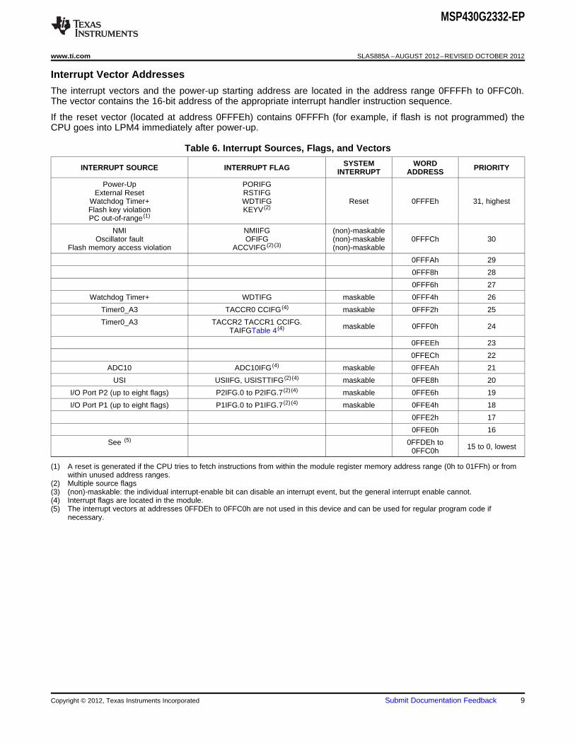
Interrupt Vector Addresses
The interrupt vectors and the power-up starting address are located in the address range 0FFFFh to 0FFC0h.The vector contains the 16-bit address of the appropriate interrupt handler instruction sequence.
If the reset vector (located at address 0FFFEh) contains 0FFFFh (for example, if flash is not programmed) theCPU goes into LPM4 immediately after power-up.
Table 6. Interrupt Sources, Flags, and Vectors
SYSTEM WORDINTERRUPT SOURCE INTERRUPT FLAG PRIORITYINTERRUPT ADDRESS
Power-Up PORIFGExternal Reset RSTIFG
Watchdog Timer+ WDTIFG Reset 0FFFEh 31, highestFlash key violation KEYV (2)
PC out-of-range (1)
NMI NMIIFG (non)-maskableOscillator fault OFIFG (non)-maskable 0FFFCh 30
Flash memory access violation ACCVIFG (2) (3) (non)-maskable
0FFFAh 29
0FFF8h 28
0FFF6h 27
Watchdog Timer+ WDTIFG maskable 0FFF4h 26
Timer0_A3 TACCR0 CCIFG (4) maskable 0FFF2h 25
Timer0_A3 TACCR2 TACCR1 CCIFG. maskable 0FFF0h 24TAIFGTable 4(4)
0FFEEh 23
0FFECh 22
ADC10 ADC10IFG (4) maskable 0FFEAh 21
USI USIIFG, USISTTIFG (2) (4) maskable 0FFE8h 20
I/O Port P2 (up to eight flags) P2IFG.0 to P2IFG.7 (2) (4) maskable 0FFE6h 19
I/O Port P1 (up to eight flags) P1IFG.0 to P1IFG.7 (2) (4) maskable 0FFE4h 18
0FFE2h 17
0FFE0h 16
See (5) 0FFDEh to 15 to 0, lowest0FFC0h
(1) A reset is generated if the CPU tries to fetch instructions from within the module register memory address range (0h to 01FFh) or fromwithin unused address ranges.
(2) Multiple source flags(3) (non)-maskable: the individual interrupt-enable bit can disable an interrupt event, but the general interrupt enable cannot.(4) Interrupt flags are located in the module.(5) The interrupt vectors at addresses 0FFDEh to 0FFC0h are not used in this device and can be used for regular program code if
necessary.
Copyright © 2012, Texas Instruments Incorporated Submit Documentation Feedback 9
MSP430G2332-EP
SLAS885A –AUGUST 2012–REVISED OCTOBER 2012 www.ti.com
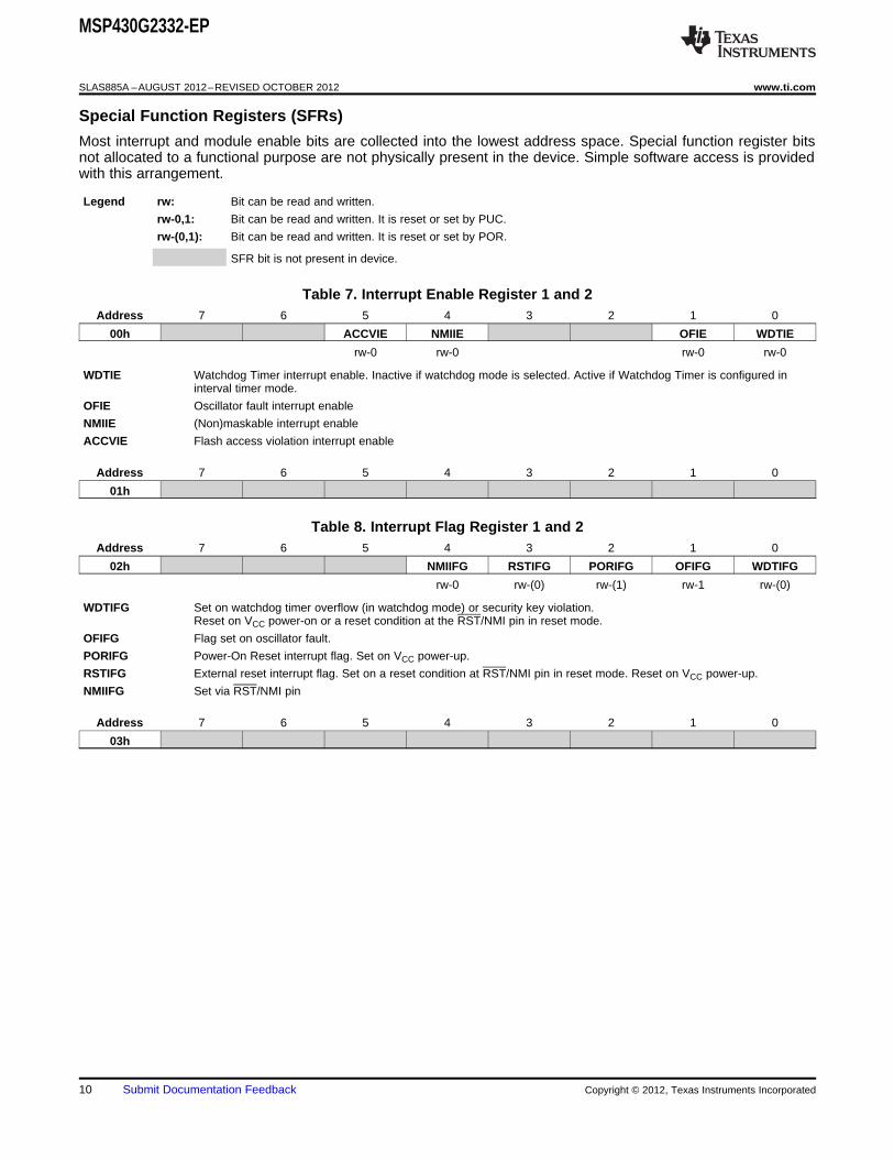
Special Function Registers (SFRs)
Most interrupt and module enable bits are collected into the lowest address space. Special function register bitsnot allocated to a functional purpose are not physically present in the device. Simple software access is providedwith this arrangement.
Legend rw: Bit can be read and written.
rw-0,1: Bit can be read and written. It is reset or set by PUC.
rw-(0,1): Bit can be read and written. It is reset or set by POR.
SFR bit is not present in device.
Table 7. Interrupt Enable Register 1 and 2Address 7 6 5 4 3 2 1 0
00h ACCVIE NMIIE OFIE WDTIE
rw-0 rw-0 rw-0 rw-0
WDTIE Watchdog Timer interrupt enable. Inactive if watchdog mode is selected. Active if Watchdog Timer is configured ininterval timer mode.
OFIE Oscillator fault interrupt enable
NMIIE (Non)maskable interrupt enable
ACCVIE Flash access violation interrupt enable
Address 7 6 5 4 3 2 1 0
01h
Table 8. Interrupt Flag Register 1 and 2Address 7 6 5 4 3 2 1 0
02h NMIIFG RSTIFG PORIFG OFIFG WDTIFG
rw-0 rw-(0) rw-(1) rw-1 rw-(0)
WDTIFG Set on watchdog timer overflow (in watchdog mode) or security key violation.Reset on VCC power-on or a reset condition at the RST/NMI pin in reset mode.
OFIFG Flag set on oscillator fault.
PORIFG Power-On Reset interrupt flag. Set on VCC power-up.
RSTIFG External reset interrupt flag. Set on a reset condition at RST/NMI pin in reset mode. Reset on VCC power-up.
NMIIFG Set via RST/NMI pin
Address 7 6 5 4 3 2 1 0
03h
10 Submit Documentation Feedback Copyright © 2012, Texas Instruments Incorporated

MSP430G2332-EP
www.ti.com SLAS885A –AUGUST 2012–REVISED OCTOBER 2012
Memory Organization
Table 9. Memory Organization
MSP430G2332
Memory Size 4kB
Main: interrupt vector Flash 0xFFFF to 0xFFC0
Main: code memory Flash 0xFFFF to 0xF000
Information memory Size 256 Byte
Flash 010FFh to 01000h
RAM Size 256 B
0x02FF to 0x0200
Peripherals 16-bit 01FFh to 0100h
8-bit 0FFh to 010h
8-bit SFR 0Fh to 00h
Flash Memory
The flash memory can be programmed via the Spy-Bi-Wire/JTAG port or in-system by the CPU. The CPU canperform single-byte and single-word writes to the flash memory. Features of the flash memory include:• Flash memory has n segments of main memory and four segments of information memory (A to D) of
64 bytes each. Each segment in main memory is 512 bytes in size.• Segments 0 to n may be erased in one step, or each segment may be individually erased.• Segments A to D can be erased individually or as a group with segments 0 to n. Segments A to D are also
called information memory.• Segment A contains calibration data. After reset, segment A is protected against programming and erasing. It
can be unlocked, but care should be taken not to erase this segment if the device-specific calibration data isrequired.
Copyright © 2012, Texas Instruments Incorporated Submit Documentation Feedback 11
MSP430G2332-EP
SLAS885A –AUGUST 2012–REVISED OCTOBER 2012 www.ti.com
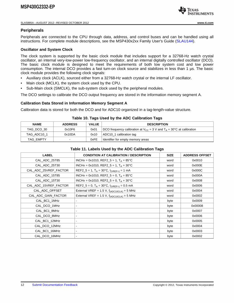
Peripherals
Peripherals are connected to the CPU through data, address, and control buses and can be handled using allinstructions. For complete module descriptions, see the MSP430x2xx Family User's Guide (SLAU144).
Oscillator and System Clock
The clock system is supported by the basic clock module that includes support for a 32768-Hz watch crystaloscillator, an internal very-low-power low-frequency oscillator, and an internal digitally controlled oscillator (DCO).The basic clock module is designed to meet the requirements of both low system cost and low powerconsumption. The internal DCO provides a fast turn-on clock source and stabilizes in less than 1 µs. The basicclock module provides the following clock signals:• Auxiliary clock (ACLK), sourced either from a 32768-Hz watch crystal or the internal LF oscillator.• Main clock (MCLK), the system clock used by the CPU.• Sub-Main clock (SMCLK), the sub-system clock used by the peripheral modules.
The DCO settings to calibrate the DCO output frequency are stored in the information memory segment A.
Calibration Data Stored in Information Memory Segment A
Calibration data is stored for both the DCO and for ADC10 organized in a tag-length-value structure.
Table 10. Tags Used by the ADC Calibration Tags
NAME ADDRESS VALUE DESCRIPTION
TAG_DCO_30 0x10F6 0x01 DCO frequency calibration at VCC = 3 V and TA = 30°C at calibration
TAG_ADC10_1 0x10DA 0x10 ADC10_1 calibration tag
TAG_EMPTY - 0xFE Identifier for empty memory areas
Table 11. Labels Used by the ADC Calibration Tags
LABEL CONDITION AT CALIBRATION / DESCRIPTION SIZE ADDRESS OFFSET
CAL_ADC_25T85 INCHx = 0x1010, REF2_5 = 1, TA = 85°C word 0x0010
CAL_ADC_25T30 INCHx = 0x1010, REF2_5 = 1, TA = 30°C word 0x000E
CAL_ADC_25VREF_FACTOR REF2_5 = 1, TA = 30°C, I(VREF+) = 1 mA word 0x000C
CAL_ADC_15T85 INCHx = 0x1010, REF2_5 = 0, TA = 85°C word 0x000A
CAL_ADC_15T30 INCHx = 0x1010, REF2_5 = 0, TA = 30°C word 0x0008
CAL_ADC_15VREF_FACTOR REF2_5 = 0, TA = 30°C, I(VREF+) = 0.5 mA word 0x0006
CAL_ADC_OFFSET External VREF = 1.5 V, f(ADC10CLK) = 5 MHz word 0x0004
CAL_ADC_GAIN_FACTOR External VREF = 1.5 V, f(ADC10CLK) = 5 MHz word 0x0002
CAL_BC1_1MHz - byte 0x0009
CAL_DCO_1MHz - byte 0x00008
CAL_BC1_8MHz - byte 0x0007
CAL_DCO_8MHz - byte 0x0006
CAL_BC1_12MHz - byte 0x0005
CAL_DCO_12MHz - byte 0x0004
CAL_BC1_16MHz - byte 0x0003
CAL_DCO_16MHz - byte 0x0002
12 Submit Documentation Feedback Copyright © 2012, Texas Instruments Incorporated
DCO(RSEL,DCO+1)DCO(RSEL,DCO)average
DCO(RSEL,DCO) DCO(RSEL,DCO+1)
32 × f × ff =
MOD × f + (32 – MOD) × f
MSP430G2332-EP
www.ti.com SLAS885A –AUGUST 2012–REVISED OCTOBER 2012
Main DCO Characteristics• All ranges selected by RSELx overlap with RSELx + 1: RSELx = 0 overlaps RSELx = 1, ... RSELx = 14
overlaps RSELx = 15.• DCO control bits DCOx have a step size as defined by parameter SDCO.• Modulation control bits MODx select how often fDCO(RSEL,DCO+1) is used within the period of 32 DCOCLK
cycles. The frequency fDCO(RSEL,DCO) is used for the remaining cycles. The frequency is an average equal to:
Brownout
The brownout circuit is implemented to provide the proper internal reset signal to the device during power on andpower off.
Digital I/O
There are two 8-bit I/O ports implemented:• All individual I/O bits are independently programmable.• Any combination of input, output, and interrupt condition(port P1 and port P2 only) is possible.• Edge-selectable interrupt input capability for all the eight bits of port P1 and port P2, if available.• Read/write access to port-control registers is supported by all instructions.• Each I/O has an individually programmable pullup/pulldown resistor.• Each I/O has an individually programmable pin-oscillator enable bit to enable low-cost touch sensing.
WDT+ Watchdog Timer
The primary function of the watchdog timer (WDT+) module is to perform a controlled system restart after asoftware problem occurs. If the selected time interval expires, a system reset is generated. If the watchdogfunction is not needed in an application, the module can be disabled or configured as an interval timer and cangenerate interrupts at selected time intervals.
Copyright © 2012, Texas Instruments Incorporated Submit Documentation Feedback 13
MSP430G2332-EP
SLAS885A –AUGUST 2012–REVISED OCTOBER 2012 www.ti.com
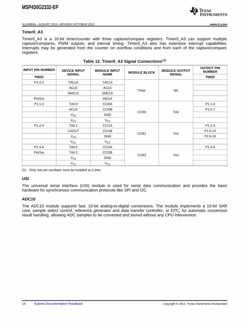
Timer0_A3
Timer0_A3 is a 16-bit timer/counter with three capture/compare registers. Timer0_A3 can support multiplecapture/compares, PWM outputs, and interval timing. Timer0_A3 also has extensive interrupt capabilities.Interrupts may be generated from the counter on overflow conditions and from each of the capture/compareregisters.
Table 12. Timer0_A3 Signal Connections (1)
OUTPUT PININPUT PIN NUMBER DEVICE INPUT MODULE INPUT MODULE OUTPUT NUMBERMODULE BLOCKSIGNAL NAME SIGNALPW20 PW20
P1.0-2 TACLK TACLK
ACLK ACLKTimer NA
SMCLK SMCLK
PinOsc INCLK
P1.1-3 TA0.0 CCI0A P1.1-3
ACLK CCI0B P1.5-7CCR0 TA0
VSS GND
VCC VCC
P1.2-4 TA0.1 CCI1A P1.2-4
CAOUT CCI1B P1.6-14CCR1 TA1
VSS GND P2.6-19
VCC VCC
P1.4-6 TA0.2 CCI2A P1.4-6
PinOsc TA0.2 CCI2BCCR2 TA2
VSS GND
VCC VCC
(1) Only one pin-oscillator must be enabled at a time.
USI
The universal serial interface (USI) module is used for serial data communication and provides the basichardware for synchronous communication protocols like SPI and I2C.
ADC10
The ADC10 module supports fast, 10-bit analog-to-digital conversions. The module implements a 10-bit SARcore, sample select control, reference generator and data transfer controller, or DTC, for automatic conversionresult handling, allowing ADC samples to be converted and stored without any CPU intervention.
14 Submit Documentation Feedback Copyright © 2012, Texas Instruments Incorporated
MSP430G2332-EP
www.ti.com SLAS885A –AUGUST 2012–REVISED OCTOBER 2012
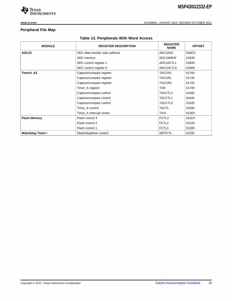
Peripheral File Map
Table 13. Peripherals With Word Access
REGISTERMODULE REGISTER DESCRIPTION OFFSETNAME
ADC10 ADC data transfer start address ADC10SA 01BCh
ADC memory ADC10MEM 01B4h
ADC control register 1 ADC10CTL1 01B2h
ADC control register 0 ADC10CTL0 01B0h
Timer0_A3 Capture/compare register TACCR2 0176h
Capture/compare register TACCR1 0174h
Capture/compare register TACCR0 0172h
Timer_A register TAR 0170h
Capture/compare control TACCTL2 0166h
Capture/compare control TACCTL1 0164h
Capture/compare control TACCTL0 0162h
Timer_A control TACTL 0160h
Timer_A interrupt vector TAIV 012Eh
Flash Memory Flash control 3 FCTL3 012Ch
Flash control 2 FCTL2 012Ah
Flash control 1 FCTL1 0128h
Watchdog Timer+ Watchdog/timer control WDTCTL 0120h
Copyright © 2012, Texas Instruments Incorporated Submit Documentation Feedback 15
MSP430G2332-EP
SLAS885A –AUGUST 2012–REVISED OCTOBER 2012 www.ti.com
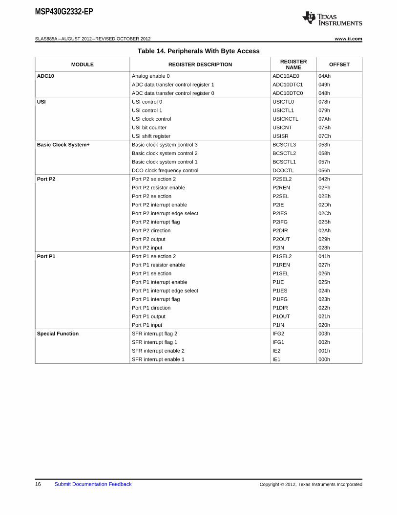
Table 14. Peripherals With Byte Access
REGISTERMODULE REGISTER DESCRIPTION OFFSETNAME
ADC10 Analog enable 0 ADC10AE0 04Ah
ADC data transfer control register 1 ADC10DTC1 049h
ADC data transfer control register 0 ADC10DTC0 048h
USI USI control 0 USICTL0 078h
USI control 1 USICTL1 079h
USI clock control USICKCTL 07Ah
USI bit counter USICNT 07Bh
USI shift register USISR 07Ch
Basic Clock System+ Basic clock system control 3 BCSCTL3 053h
Basic clock system control 2 BCSCTL2 058h
Basic clock system control 1 BCSCTL1 057h
DCO clock frequency control DCOCTL 056h
Port P2 Port P2 selection 2 P2SEL2 042h
Port P2 resistor enable P2REN 02Fh
Port P2 selection P2SEL 02Eh
Port P2 interrupt enable P2IE 02Dh
Port P2 interrupt edge select P2IES 02Ch
Port P2 interrupt flag P2IFG 02Bh
Port P2 direction P2DIR 02Ah
Port P2 output P2OUT 029h
Port P2 input P2IN 028h
Port P1 Port P1 selection 2 P1SEL2 041h
Port P1 resistor enable P1REN 027h
Port P1 selection P1SEL 026h
Port P1 interrupt enable P1IE 025h
Port P1 interrupt edge select P1IES 024h
Port P1 interrupt flag P1IFG 023h
Port P1 direction P1DIR 022h
Port P1 output P1OUT 021h
Port P1 input P1IN 020h
Special Function SFR interrupt flag 2 IFG2 003h
SFR interrupt flag 1 IFG1 002h
SFR interrupt enable 2 IE2 001h
SFR interrupt enable 1 IE1 000h
16 Submit Documentation Feedback Copyright © 2012, Texas Instruments Incorporated
MSP430G2332-EP
www.ti.com SLAS885A –AUGUST 2012–REVISED OCTOBER 2012
Absolute Maximum Ratings (1)
Voltage applied at VCC to VSS –0.3 V to 4.1 V
Voltage applied to any pin (2) –0.3 V to VCC + 0.3 V
Diode current at any device pin ±2 mA
Unprogrammed device –55°C to 150°CStorage temperature range, Tstg
(3)
Programmed device –55°C to 150°C
(1) Stresses beyond those listed under "absolute maximum ratings" may cause permanent damage to the device. These are stress ratingsonly, and functional operation of the device at these or any other conditions beyond those indicated under "recommended operatingconditions" is not implied. Exposure to absolute-maximum-rated conditions for extended periods may affect device reliability.
(2) All voltages referenced to VSS. The JTAG fuse-blow voltage, VFB, is allowed to exceed the absolute maximum rating. The voltage isapplied to the TEST pin when blowing the JTAG fuse.
(3) Higher temperature may be applied during board soldering according to the current JEDEC J-STD-020 specification with peak reflowtemperatures not higher than classified on the device label on the shipping boxes or reels.
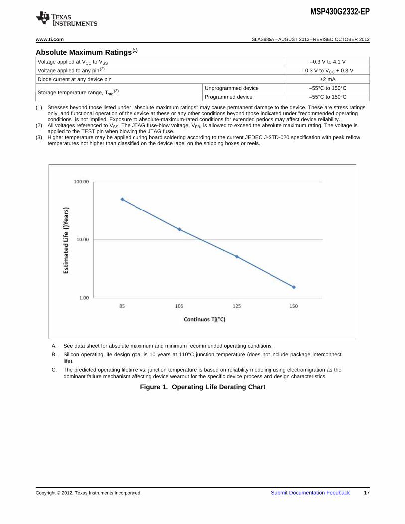
xxx
A. See data sheet for absolute maximum and minimum recommended operating conditions.
B. Silicon operating life design goal is 10 years at 110°C junction temperature (does not include package interconnectlife).
C. The predicted operating lifetime vs. junction temperature is based on reliability modeling using electromigration as thedominant failure mechanism affecting device wearout for the specific device process and design characteristics.
Figure 1. Operating Life Derating Chart
Copyright © 2012, Texas Instruments Incorporated Submit Documentation Feedback 17
MSP430G2332-EP
SLAS885A –AUGUST 2012–REVISED OCTOBER 2012 www.ti.com
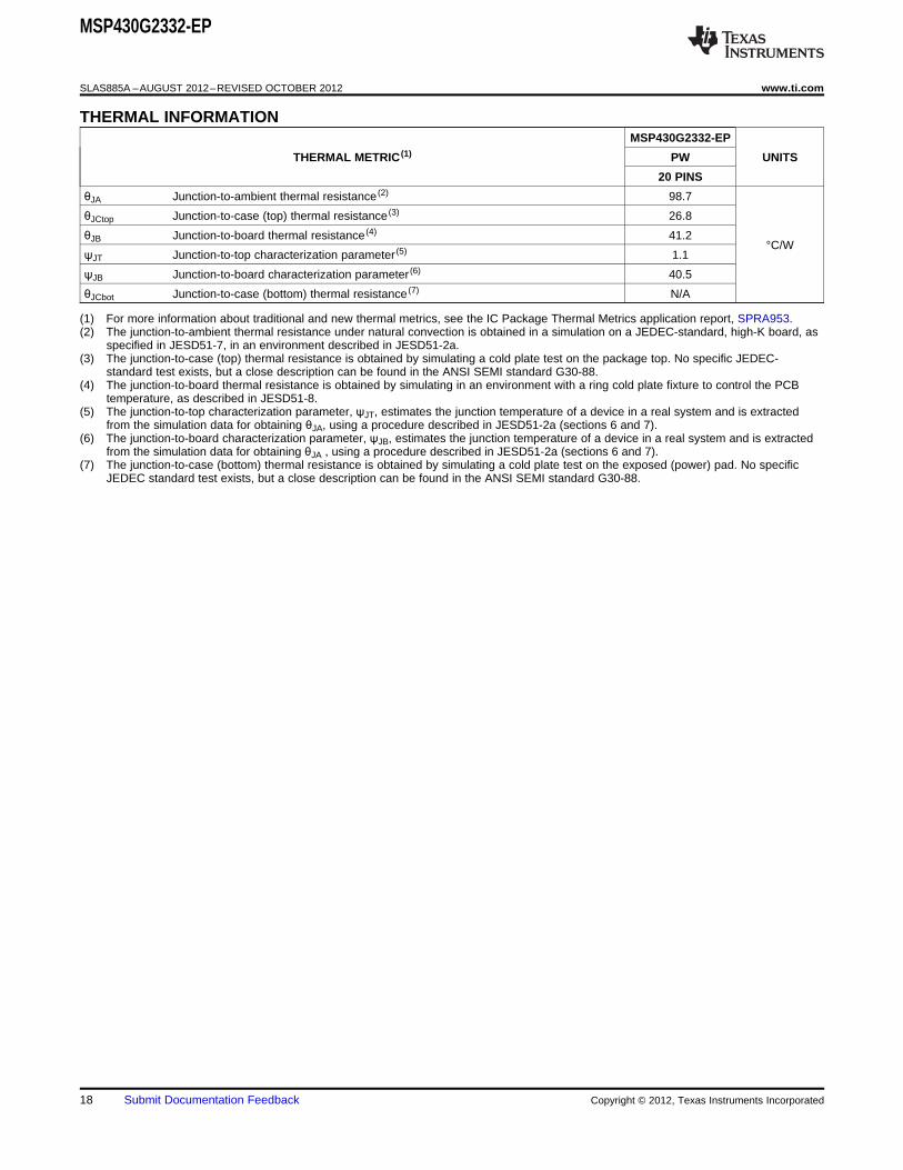
THERMAL INFORMATIONMSP430G2332-EP
THERMAL METRIC (1) PW UNITS
20 PINS
θJA Junction-to-ambient thermal resistance (2) 98.7
θJCtop Junction-to-case (top) thermal resistance (3) 26.8
θJB Junction-to-board thermal resistance (4) 41.2°C/W
ψJT Junction-to-top characterization parameter (5) 1.1
ψJB Junction-to-board characterization parameter (6) 40.5
θJCbot Junction-to-case (bottom) thermal resistance (7) N/A
(1) For more information about traditional and new thermal metrics, see the IC Package Thermal Metrics application report, SPRA953.(2) The junction-to-ambient thermal resistance under natural convection is obtained in a simulation on a JEDEC-standard, high-K board, as
specified in JESD51-7, in an environment described in JESD51-2a.(3) The junction-to-case (top) thermal resistance is obtained by simulating a cold plate test on the package top. No specific JEDEC-
standard test exists, but a close description can be found in the ANSI SEMI standard G30-88.(4) The junction-to-board thermal resistance is obtained by simulating in an environment with a ring cold plate fixture to control the PCB
temperature, as described in JESD51-8.(5) The junction-to-top characterization parameter, ψJT, estimates the junction temperature of a device in a real system and is extracted
from the simulation data for obtaining θJA, using a procedure described in JESD51-2a (sections 6 and 7).(6) The junction-to-board characterization parameter, ψJB, estimates the junction temperature of a device in a real system and is extracted
from the simulation data for obtaining θJA , using a procedure described in JESD51-2a (sections 6 and 7).(7) The junction-to-case (bottom) thermal resistance is obtained by simulating a cold plate test on the exposed (power) pad. No specific
JEDEC standard test exists, but a close description can be found in the ANSI SEMI standard G30-88.Spacer
18 Submit Documentation Feedback Copyright © 2012, Texas Instruments Incorporated
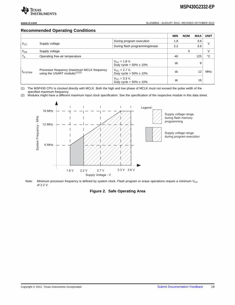
Supply voltage range,during flash memoryprogramming
Supply voltage range,during program execution
Legend:16 MHz
Syste
m F
requency -
MH
z
12 MHz
6 MHz
1.8 V
Supply Voltage - V
3.3 V2.7 V2.2 V 3.6 V
MSP430G2332-EP
www.ti.com SLAS885A –AUGUST 2012–REVISED OCTOBER 2012
Recommended Operating ConditionsMIN NOM MAX UNIT
During program execution 1.8 3.6VCC Supply voltage V
During flash programming/erase 2.2 3.6
VSS Supply voltage 0 V
TA Operating free-air temperature -40 125 °C
VCC = 1.8 V, dc 6Duty cycle = 50% ± 10%
Processor frequency (maximum MCLK frequency VCC = 2.7 V,fSYSTEM dc 12 MHzusing the USART module) (1) (2) Duty cycle = 50% ± 10%
VCC = 3.3 V, dc 16Duty cycle = 50% ± 10%
(1) The MSP430 CPU is clocked directly with MCLK. Both the high and low phase of MCLK must not exceed the pulse width of thespecified maximum frequency.
(2) Modules might have a different maximum input clock specification. See the specification of the respective module in this data sheet.
Note: Minimum processor frequency is defined by system clock. Flash program or erase operations require a minimum VCCof 2.2 V.
Figure 2. Safe Operating Area
Copyright © 2012, Texas Instruments Incorporated Submit Documentation Feedback 19
0.0
1.0
2.0
3.0
4.0
5.0
1.5 2.0 2.5 3.0 3.5 4.0
VCC − Supply Voltage − V
Active
Mo
de
Cu
rre
nt
−m
A
fDCO = 1 MHz
fDCO = 8 MHz
fDCO = 12 MHz
fDCO = 16 MHz
0.0
1.0
2.0
3.0
4.0
0.0 4.0 8.0 12.0 16.0
fDCO − DCO Frequency − MHz
Active
Mo
de
Cu
rre
nt
−m
A
TA = 25 °C
TA = 85 °C
VCC = 2.2 V
VCC = 3 V
TA = 25 °C
TA = 85 °C
MSP430G2332-EP
SLAS885A –AUGUST 2012–REVISED OCTOBER 2012 www.ti.com
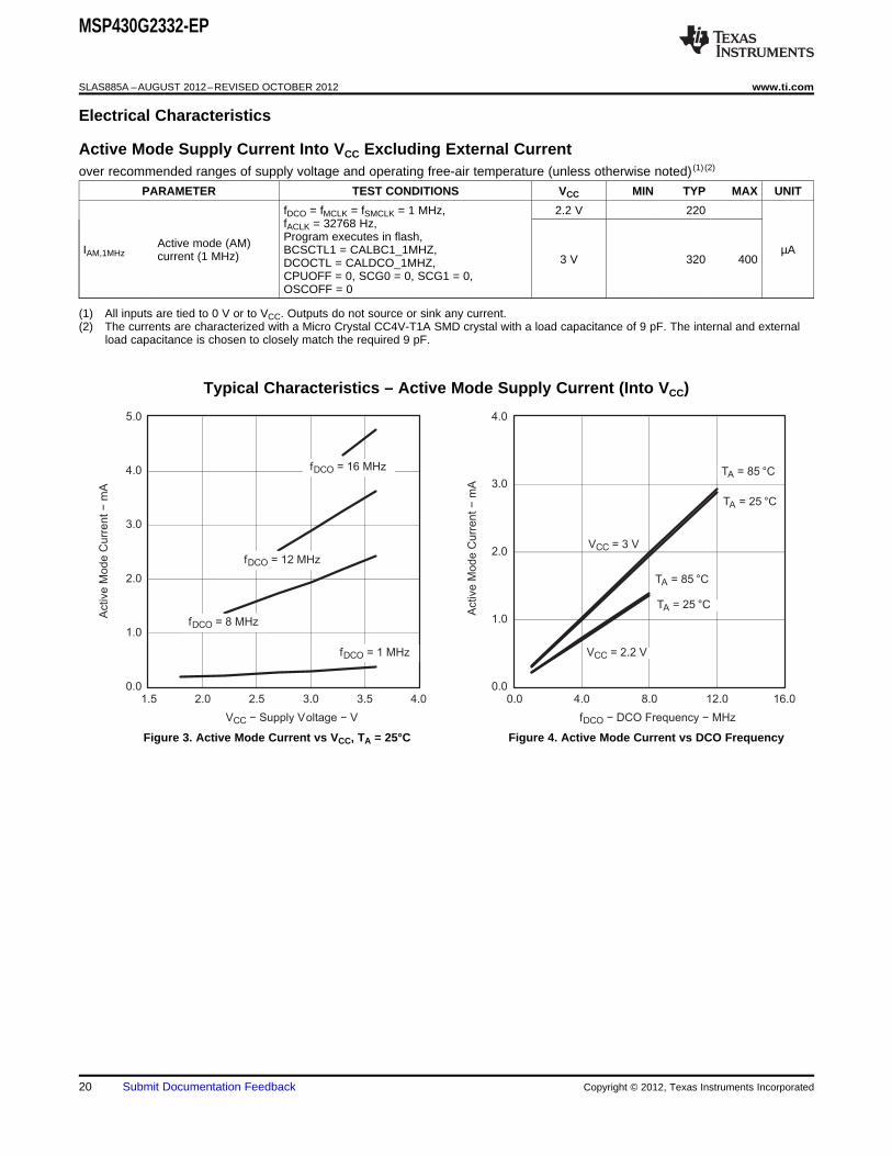
Electrical Characteristics
Active Mode Supply Current Into VCC Excluding External Currentover recommended ranges of supply voltage and operating free-air temperature (unless otherwise noted) (1) (2)
PARAMETER TEST CONDITIONS VCC MIN TYP MAX UNIT
fDCO = fMCLK = fSMCLK = 1 MHz, 2.2 V 220fACLK = 32768 Hz,Program executes in flash,Active mode (AM)IAM,1MHz BCSCTL1 = CALBC1_1MHZ, µAcurrent (1 MHz) 3 V 320 400DCOCTL = CALDCO_1MHZ,CPUOFF = 0, SCG0 = 0, SCG1 = 0,OSCOFF = 0
(1) All inputs are tied to 0 V or to VCC. Outputs do not source or sink any current.(2) The currents are characterized with a Micro Crystal CC4V-T1A SMD crystal with a load capacitance of 9 pF. The internal and external
load capacitance is chosen to closely match the required 9 pF.
Typical Characteristics – Active Mode Supply Current (Into VCC)
Figure 3. Active Mode Current vs VCC, TA = 25°C Figure 4. Active Mode Current vs DCO Frequency
20 Submit Documentation Feedback Copyright © 2012, Texas Instruments Incorporated
0.2
0.4
0.6
0.8
1.0
1.2
1.4
1.6
1.8
2.0
0.0−40.0 −20.0 0.0 20.0 40.0 60.0 80.0 100.0 120.0
I−
Low
−pow
er
mode c
urr
ent
−µ
ALP
M3
V = 3.6 VCC
TA − Temperature − °C
V = 1.8 VCC
V = 3 VCC
V = 2.2 VCC
0.0
0.1
0.2
0.3
0.4
0.5
0.6
0.7
0.8
0.9
1.0
−40.0 −20.0 0.0 20.0 40.0 60.0 80.0 100.0 120.0
TA − Temperature − C
V = 3.6 VCC
TA − Temperature − C
I−
Lo
w−
po
we
r m
od
e c
urr
en
t−
µA
LP
M4
V = 1.8 VCC
V = 3 VCC
V = 2.2 VCC
MSP430G2332-EP
www.ti.com SLAS885A –AUGUST 2012–REVISED OCTOBER 2012
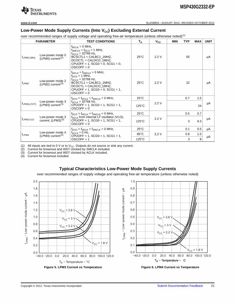
Low-Power Mode Supply Currents (Into VCC) Excluding External Currentover recommended ranges of supply voltage and operating free-air temperature (unless otherwise noted) (1)
PARAMETER TEST CONDITIONS TA VCC MIN TYP MAX UNIT
fMCLK = 0 MHz,fSMCLK = fDCO = 1 MHz,fACLK = 32768 Hz,Low-power mode 0ILPM0,1MHz BCSCTL1 = CALBC1_1MHZ, 25°C 2.2 V 55 µA(LPM0) current (2)DCOCTL = CALDCO_1MHZ,CPUOFF = 1, SCG0 = 0, SCG1 = 0,OSCOFF = 0
fMCLK = fSMCLK = 0 MHz,fDCO = 1 MHz,fACLK = 32768 Hz,Low-power mode 2ILPM2 BCSCTL1 = CALBC1_1MHZ, 25°C 2.2 V 22 µA(LPM2) current (3)DCOCTL = CALDCO_1MHZ,CPUOFF = 1, SCG0 = 0, SCG1 = 1,OSCOFF = 0
fDCO = fMCLK = fSMCLK = 0 MHz, 25°C 0.7 1.5Low-power mode 3 fACLK = 32768 Hz,ILPM3,LFXT1 2.2 V µA(LPM3) current (3) CPUOFF = 1, SCG0 = 1, SCG1 = 1, 125°C 24
OSCOFF = 0
fDCO = fMCLK = fSMCLK = 0 MHz, 25°C 0.5 0.7Low-power mode 3 fACLK from internal LF oscillator (VLO),ILPM3,VLO 2.2 V µAcurrent, (LPM3) (3) CPUOFF = 1, SCG0 = 1, SCG1 = 1, 125°C 3 9.3
OSCOFF = 0
fDCO = fMCLK = fSMCLK = 0 MHz, 25°C 0.1 0.5 µALow-power mode 4 fACLK = 0 Hz, 85°C 0.8 1.5ILPM4 2.2 V(LPM4) current (4) CPUOFF = 1, SCG0 = 1, SCG1 = 1, µA
125°C 3 8OSCOFF = 1
(1) All inputs are tied to 0 V or to VCC. Outputs do not source or sink any current.(2) Current for brownout and WDT clocked by SMCLK included.(3) Current for brownout and WDT clocked by ACLK included.(4) Current for brownout included.
Typical Characteristics Low-Power Mode Supply Currentsover recommended ranges of supply voltage and operating free-air temperature (unless otherwise noted)
Figure 5. LPM3 Current vs Temperature Figure 6. LPM4 Current vs Temperature
Copyright © 2012, Texas Instruments Incorporated Submit Documentation Feedback 21
MSP430G2332-EP
SLAS885A –AUGUST 2012–REVISED OCTOBER 2012 www.ti.com
Schmitt-Trigger Inputs – Ports Pxover recommended ranges of supply voltage and operating free-air temperature (unless otherwise noted)
PARAMETER TEST CONDITIONS VCC MIN TYP MAX UNIT
0.45 VCC 0.75 VCCVIT+ Positive-going input threshold voltage V
3 V 1.35 2.25
0.25 VCC 0.55 VCCVIT– Negative-going input threshold voltage V
3 V 0.75 1.65
Vhys Input voltage hysteresis (VIT+ – VIT–) 3 V 0.3 1 V
For pullup: VIN = VSSRPull Pullup/pulldown resistor 3 V 20 35 50 kΩFor pulldown: VIN = VCC
CI Input capacitance VIN = VSS or VCC 5 pF
Leakage Current – Ports Pxover recommended ranges of supply voltage and operating free-air temperature (unless otherwise noted)
PARAMETER TEST CONDITIONS VCC MIN MAX UNIT
TA = -40°C to 85°C ±50Ilkg(Px.x) High-impedance leakage current (1) (2) 3 V nA
TA = 125°C (1) (2) ±120
(1) The leakage current is measured with VSS or VCC applied to the corresponding pin(s), unless otherwise noted.(2) The leakage of the digital port pins is measured individually. The port pin is selected for input, and the pullup/pulldown resistor is
disabled.
Outputs – Ports Pxover recommended ranges of supply voltage and operating free-air temperature (unless otherwise noted)
PARAMETER TEST CONDITIONS VCC MIN TYP MAX UNIT
VOH High-level output voltage I(OHmax) = –6 mA (1) 3 V VCC – 0.3 V
VOL Low-level output voltage I(OLmax) = 6 mA (1) 3 V VSS + 0.3 V
(1) The maximum total current, I(OHmax) and I(OLmax), for all outputs combined should not exceed ±48 mA to hold the maximum voltage dropspecified.
Output Frequency – Ports Pxover recommended ranges of supply voltage and operating free-air temperature (unless otherwise noted)
PARAMETER TEST CONDITIONS VCC MIN TYP MAX UNIT
fPx.y Port output frequency (with load) Px.y, CL = 20 pF, RL = 1 kΩ (1) (2) 3 V 12 MHz
fPort_CLK Clock output frequency Px.y, CL = 20 pF (2) 3 V 16 MHz
(1) A resistive divider with two 0.5-kΩ resistors between VCC and VSS is used as load. The output is connected to the center tap of thedivider.
(2) The output voltage reaches at least 10% and 90% VCC at the specified toggle frequency.
22 Submit Documentation Feedback Copyright © 2012, Texas Instruments Incorporated
VOH − High-Level Output Voltage − V
−25.0
−20.0
−15.0
−10.0
−5.0
0.0
0.0 0.5 1.0 1.5 2.0 2.5
VCC = 2.2 V
P1.7
TYPICAL HIGH-LEVEL OUTPUT CURRENT
vs
HIGH-LEVEL OUTPUT VOLTAGE
TA = 25°C
TA = 85°C
OH
I−
Typic
al H
igh-L
evel O
utp
ut C
urr
ent
−m
A
VOH − High-Level Output Voltage − V
−50.0
−40.0
−30.0
−20.0
−10.0
0.0
0.0 0.5 1.0 1.5 2.0 2.5 3.0 3.5
VCC = 3 V
P1.7
TYPICAL HIGH-LEVEL OUTPUT CURRENT
vs
HIGH-LEVEL OUTPUT VOLTAGE
TA = 25°C
TA = 85°C
OH
I−
Typic
al H
igh-L
evel O
utp
ut C
urr
ent
−m
A
VOL − Low-Level Output Voltage − V
0.0
5.0
10.0
15.0
20.0
25.0
30.0
0.0 0.5 1.0 1.5 2.0 2.5
VCC = 2.2 V
P1.7
TYPICAL LOW-LEVEL OUTPUT CURRENT
vs
LOW-LEVEL OUTPUT VOLTAGE
TA = 25°C
TA = 85°C
OL
I−
Typic
al Low
-Level O
utp
ut C
urr
ent
−m
A
VOL − Low-Level Output Voltage − V
0.0
10.0
20.0
30.0
40.0
50.0
0.0 0.5 1.0 1.5 2.0 2.5 3.0 3.5
VCC = 3 V
P1.7
TYPICAL LOW -LEVEL OUTPUT CURRENT
vs
LOW-LEVEL OUTPUT VOLTAGE
TA = 25°C
TA = 85°C
OL
I−
Typic
al Low
-Level O
utp
ut C
urr
ent
−m
A
MSP430G2332-EP
www.ti.com SLAS885A –AUGUST 2012–REVISED OCTOBER 2012
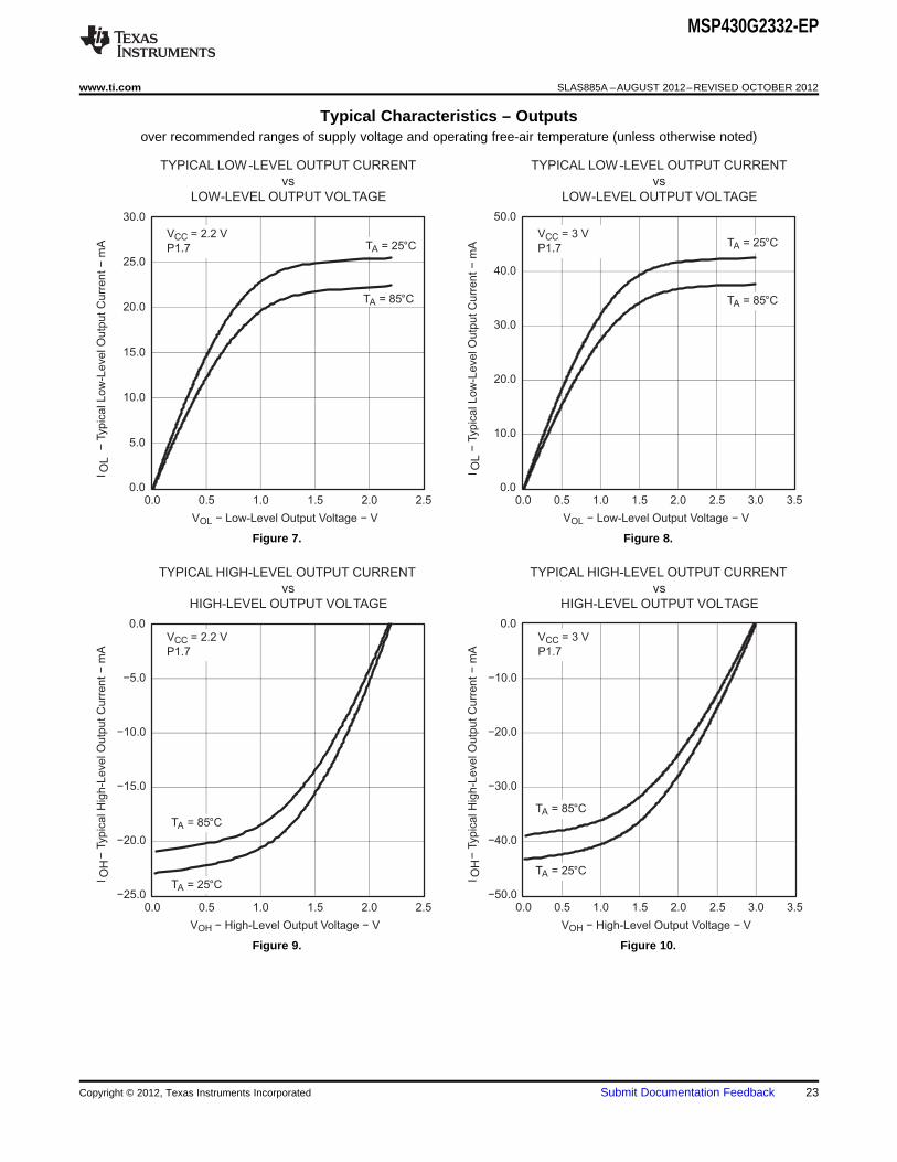
Typical Characteristics – Outputsover recommended ranges of supply voltage and operating free-air temperature (unless otherwise noted)
Figure 7. Figure 8.
Figure 9. Figure 10.
Copyright © 2012, Texas Instruments Incorporated Submit Documentation Feedback 23
CLOAD − External Capacitance − pF
0.00
0.15
0.30
0.45
0.60
0.75
0.90
1.05
1.20
1.35
1.50
10 50 100
P1.y
P2.0 ... P2.5
P2.6, P2.7
VCC = 2.2 V
TYPICAL OSCILLATING FREQUENCYvs
LOAD CAPACITANCE
fosc
−Typic
al O
scill
ation F
requency
−M
Hz
CLOAD − External Capacitance − pF
0.00
0.15
0.30
0.45
0.60
0.75
0.90
1.05
1.20
1.35
1.50
10 50 100
P1.y
P2.0 ... P2.5
P2.6, P2.7
VCC = 3.0 V
TYPICAL OSCILLATING FREQUENCYvs
LOAD CAPACITANCE
fosc
−Typic
al O
scill
ation F
requency
−M
Hz
MSP430G2332-EP
SLAS885A –AUGUST 2012–REVISED OCTOBER 2012 www.ti.com
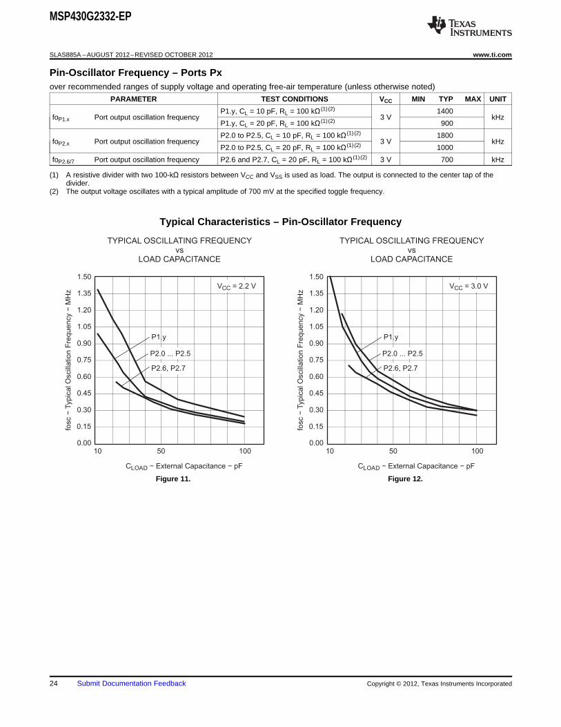
Pin-Oscillator Frequency – Ports Pxover recommended ranges of supply voltage and operating free-air temperature (unless otherwise noted)
PARAMETER TEST CONDITIONS VCC MIN TYP MAX UNIT
P1.y, CL = 10 pF, RL = 100 kΩ (1) (2) 1400foP1.x Port output oscillation frequency 3 V kHz
P1.y, CL = 20 pF, RL = 100 kΩ (1) (2) 900
P2.0 to P2.5, CL = 10 pF, RL = 100 kΩ (1) (2) 1800foP2.x Port output oscillation frequency 3 V kHz
P2.0 to P2.5, CL = 20 pF, RL = 100 kΩ (1) (2) 1000
foP2.6/7 Port output oscillation frequency P2.6 and P2.7, CL = 20 pF, RL = 100 kΩ (1) (2) 3 V 700 kHz
(1) A resistive divider with two 100-kΩ resistors between VCC and VSS is used as load. The output is connected to the center tap of thedivider.
(2) The output voltage oscillates with a typical amplitude of 700 mV at the specified toggle frequency.
Typical Characteristics – Pin-Oscillator Frequency
Figure 11. Figure 12.
24 Submit Documentation Feedback Copyright © 2012, Texas Instruments Incorporated
0
1
t d(BOR)
VCC
V(B_IT−)
Vhys(B_IT−)
VCC(start)
MSP430G2332-EP
www.ti.com SLAS885A –AUGUST 2012–REVISED OCTOBER 2012
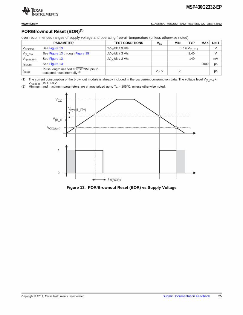
POR/Brownout Reset (BOR) (1)
over recommended ranges of supply voltage and operating free-air temperature (unless otherwise noted)
PARAMETER TEST CONDITIONS VCC MIN TYP MAX UNIT
VCC(start) See Figure 13 dVCC/dt ≤ 3 V/s 0.7 × V(B_IT–) V
V(B_IT–) See Figure 13 through Figure 15 dVCC/dt ≤ 3 V/s 1.40 V
Vhys(B_IT–) See Figure 13 dVCC/dt ≤ 3 V/s 140 mV
td(BOR) See Figure 13 2000 µs
Pulse length needed at RST/NMI pin tot(reset) 2.2 V 2 µsaccepted reset internally (2)
(1) The current consumption of the brownout module is already included in the ICC current consumption data. The voltage level V(B_IT–) +Vhys(B_IT–) is ≤ 1.8 V.
(2) Minimum and maximum parameters are characterized up to TA = 105°C, unless otherwise noted.
Figure 13. POR/Brownout Reset (BOR) vs Supply Voltage
Copyright © 2012, Texas Instruments Incorporated Submit Documentation Feedback 25
VCC
0
0.5
1
1.5
2
VCC(drop)
t pw
tpw − Pulse Width − µs
VC
C(d
rop)
−V
3 V
0.001 1 1000 tf tr
tpw − Pulse Width − µs
tf = tr
Typical Conditions
VCC = 3 V
VCC(drop)
VCC
3 V
t pw
0
0.5
1
1.5
2
0.001 1 1000
Typical Conditions
1 ns 1 nstpw − Pulse Width − µs
VC
C(d
rop)
−V
tpw − Pulse Width − µs
VCC = 3 V
MSP430G2332-EP
SLAS885A –AUGUST 2012–REVISED OCTOBER 2012 www.ti.com
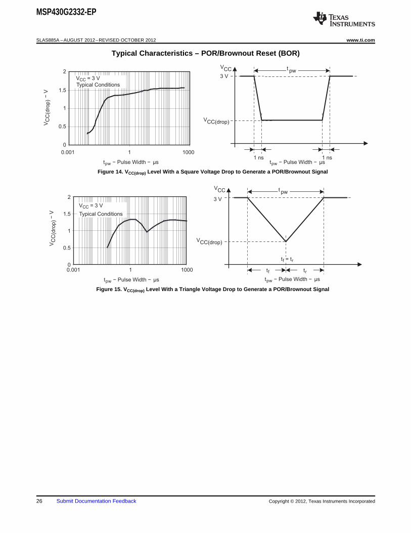
Typical Characteristics – POR/Brownout Reset (BOR)
Figure 14. VCC(drop) Level With a Square Voltage Drop to Generate a POR/Brownout Signal
Figure 15. VCC(drop) Level With a Triangle Voltage Drop to Generate a POR/Brownout Signal
26 Submit Documentation Feedback Copyright © 2012, Texas Instruments Incorporated
MSP430G2332-EP
www.ti.com SLAS885A –AUGUST 2012–REVISED OCTOBER 2012
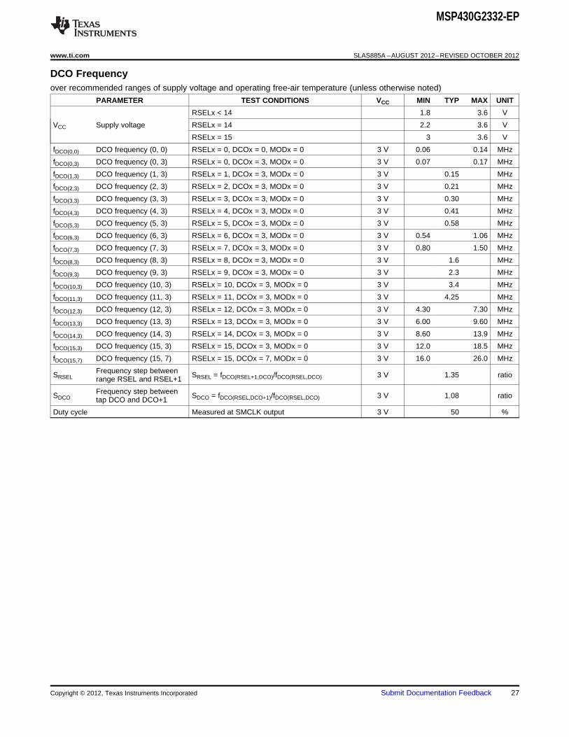
DCO Frequencyover recommended ranges of supply voltage and operating free-air temperature (unless otherwise noted)
PARAMETER TEST CONDITIONS VCC MIN TYP MAX UNIT
RSELx < 14 1.8 3.6 V
VCC Supply voltage RSELx = 14 2.2 3.6 V
RSELx = 15 3 3.6 V
fDCO(0,0) DCO frequency (0, 0) RSELx = 0, DCOx = 0, MODx = 0 3 V 0.06 0.14 MHz
fDCO(0,3) DCO frequency (0, 3) RSELx = 0, DCOx = 3, MODx = 0 3 V 0.07 0.17 MHz
fDCO(1,3) DCO frequency (1, 3) RSELx = 1, DCOx = 3, MODx = 0 3 V 0.15 MHz
fDCO(2,3) DCO frequency (2, 3) RSELx = 2, DCOx = 3, MODx = 0 3 V 0.21 MHz
fDCO(3,3) DCO frequency (3, 3) RSELx = 3, DCOx = 3, MODx = 0 3 V 0.30 MHz
fDCO(4,3) DCO frequency (4, 3) RSELx = 4, DCOx = 3, MODx = 0 3 V 0.41 MHz
fDCO(5,3) DCO frequency (5, 3) RSELx = 5, DCOx = 3, MODx = 0 3 V 0.58 MHz
fDCO(6,3) DCO frequency (6, 3) RSELx = 6, DCOx = 3, MODx = 0 3 V 0.54 1.06 MHz
fDCO(7,3) DCO frequency (7, 3) RSELx = 7, DCOx = 3, MODx = 0 3 V 0.80 1.50 MHz
fDCO(8,3) DCO frequency (8, 3) RSELx = 8, DCOx = 3, MODx = 0 3 V 1.6 MHz
fDCO(9,3) DCO frequency (9, 3) RSELx = 9, DCOx = 3, MODx = 0 3 V 2.3 MHz
fDCO(10,3) DCO frequency (10, 3) RSELx = 10, DCOx = 3, MODx = 0 3 V 3.4 MHz
fDCO(11,3) DCO frequency (11, 3) RSELx = 11, DCOx = 3, MODx = 0 3 V 4.25 MHz
fDCO(12,3) DCO frequency (12, 3) RSELx = 12, DCOx = 3, MODx = 0 3 V 4.30 7.30 MHz
fDCO(13,3) DCO frequency (13, 3) RSELx = 13, DCOx = 3, MODx = 0 3 V 6.00 9.60 MHz
fDCO(14,3) DCO frequency (14, 3) RSELx = 14, DCOx = 3, MODx = 0 3 V 8.60 13.9 MHz
fDCO(15,3) DCO frequency (15, 3) RSELx = 15, DCOx = 3, MODx = 0 3 V 12.0 18.5 MHz
fDCO(15,7) DCO frequency (15, 7) RSELx = 15, DCOx = 7, MODx = 0 3 V 16.0 26.0 MHz
Frequency step betweenSRSEL SRSEL = fDCO(RSEL+1,DCO)/fDCO(RSEL,DCO) 3 V 1.35 ratiorange RSEL and RSEL+1
Frequency step betweenSDCO SDCO = fDCO(RSEL,DCO+1)/fDCO(RSEL,DCO) 3 V 1.08 ratiotap DCO and DCO+1
Duty cycle Measured at SMCLK output 3 V 50 %
Copyright © 2012, Texas Instruments Incorporated Submit Documentation Feedback 27
MSP430G2332-EP
SLAS885A –AUGUST 2012–REVISED OCTOBER 2012 www.ti.com
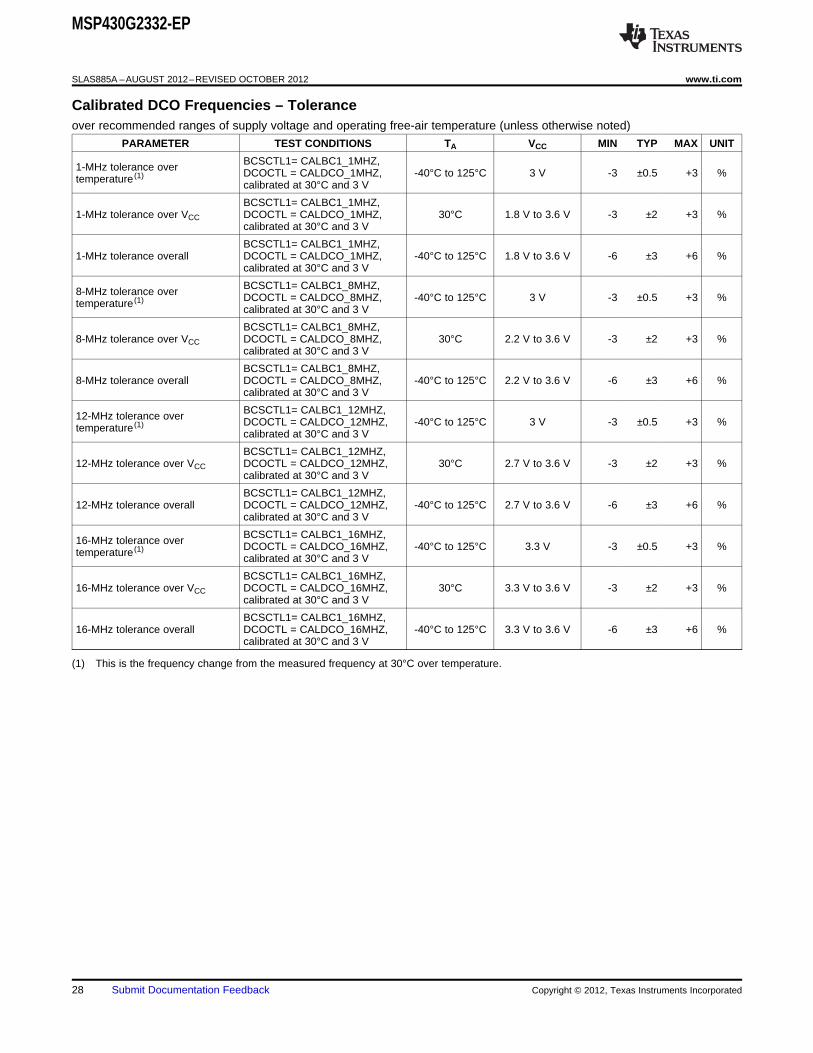
Calibrated DCO Frequencies – Toleranceover recommended ranges of supply voltage and operating free-air temperature (unless otherwise noted)
PARAMETER TEST CONDITIONS TA VCC MIN TYP MAX UNIT
BCSCTL1= CALBC1_1MHZ,1-MHz tolerance over DCOCTL = CALDCO_1MHZ, -40°C to 125°C 3 V -3 ±0.5 +3 %temperature (1)calibrated at 30°C and 3 V
BCSCTL1= CALBC1_1MHZ,1-MHz tolerance over VCC DCOCTL = CALDCO_1MHZ, 30°C 1.8 V to 3.6 V -3 ±2 +3 %
calibrated at 30°C and 3 V
BCSCTL1= CALBC1_1MHZ,1-MHz tolerance overall DCOCTL = CALDCO_1MHZ, -40°C to 125°C 1.8 V to 3.6 V -6 ±3 +6 %
calibrated at 30°C and 3 V
BCSCTL1= CALBC1_8MHZ,8-MHz tolerance over DCOCTL = CALDCO_8MHZ, -40°C to 125°C 3 V -3 ±0.5 +3 %temperature (1)calibrated at 30°C and 3 V
BCSCTL1= CALBC1_8MHZ,8-MHz tolerance over VCC DCOCTL = CALDCO_8MHZ, 30°C 2.2 V to 3.6 V -3 ±2 +3 %
calibrated at 30°C and 3 V
BCSCTL1= CALBC1_8MHZ,8-MHz tolerance overall DCOCTL = CALDCO_8MHZ, -40°C to 125°C 2.2 V to 3.6 V -6 ±3 +6 %
calibrated at 30°C and 3 V
BCSCTL1= CALBC1_12MHZ,12-MHz tolerance over DCOCTL = CALDCO_12MHZ, -40°C to 125°C 3 V -3 ±0.5 +3 %temperature (1)calibrated at 30°C and 3 V
BCSCTL1= CALBC1_12MHZ,12-MHz tolerance over VCC DCOCTL = CALDCO_12MHZ, 30°C 2.7 V to 3.6 V -3 ±2 +3 %
calibrated at 30°C and 3 V
BCSCTL1= CALBC1_12MHZ,12-MHz tolerance overall DCOCTL = CALDCO_12MHZ, -40°C to 125°C 2.7 V to 3.6 V -6 ±3 +6 %
calibrated at 30°C and 3 V
BCSCTL1= CALBC1_16MHZ,16-MHz tolerance over DCOCTL = CALDCO_16MHZ, -40°C to 125°C 3.3 V -3 ±0.5 +3 %temperature (1)calibrated at 30°C and 3 V
BCSCTL1= CALBC1_16MHZ,16-MHz tolerance over VCC DCOCTL = CALDCO_16MHZ, 30°C 3.3 V to 3.6 V -3 ±2 +3 %
calibrated at 30°C and 3 V
BCSCTL1= CALBC1_16MHZ,16-MHz tolerance overall DCOCTL = CALDCO_16MHZ, -40°C to 125°C 3.3 V to 3.6 V -6 ±3 +6 %
calibrated at 30°C and 3 V
(1) This is the frequency change from the measured frequency at 30°C over temperature.
28 Submit Documentation Feedback Copyright © 2012, Texas Instruments Incorporated
DCO Frequency − MHz
0.10
1.00
10.00
0.10 1.00 10.00
DC
O W
ake
Tim
e−
us
RSELx = 0...11RSELx = 12...15
MSP430G2332-EP
www.ti.com SLAS885A –AUGUST 2012–REVISED OCTOBER 2012
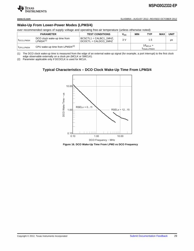
Wake-Up From Lower-Power Modes (LPM3/4)over recommended ranges of supply voltage and operating free-air temperature (unless otherwise noted)
PARAMETER TEST CONDITIONS VCC MIN TYP MAX UNIT
DCO clock wake-up time from BCSCTL1 = CALBC1_1MHZ,tDCO,LPM3/4 3 V 1.5 µsLPM3/4 (1) DCOCTL = CALDCO_1MHZ
1/fMCLK +tCPU,LPM3/4 CPU wake-up time from LPM3/4 (2)tClock,LPM3/4
(1) The DCO clock wake-up time is measured from the edge of an external wake-up signal (for example, a port interrupt) to the first clockedge observable externally on a clock pin (MCLK or SMCLK).
(2) Parameter applicable only if DCOCLK is used for MCLK.
Typical Characteristics – DCO Clock Wake-Up Time From LPM3/4
Figure 16. DCO Wake-Up Time From LPM3 vs DCO Frequency
Copyright © 2012, Texas Instruments Incorporated Submit Documentation Feedback 29
MSP430G2332-EP
SLAS885A –AUGUST 2012–REVISED OCTOBER 2012 www.ti.com
Crystal Oscillator, XT1, Low-Frequency Mode (1) (2)
over recommended ranges of supply voltage and up to operating free-air temperature, TA = 105°C (unless otherwise noted)
PARAMETER TEST CONDITIONS VCC MIN TYP MAX UNIT
LFXT1 oscillator crystalfLFXT1,LF XTS = 0, LFXT1Sx = 0 or 1 1.8 V to 3.6 V 32768 Hzfrequency, LF mode 0, 1
LFXT1 oscillator logic levelfLFXT1,LF,logic square wave input frequency, XTS = 0, XCAPx = 0, LFXT1Sx = 3 1.8 V to 3.6 V 10000 32768 50000 Hz
LF mode
LFXT1 oscillator logic level XTS = 0, XCAPx = 0, LFXT1Sx = 3,fLFXT1,LF,logic square wave input frequency, 1.8 V to 3.6 V 32768 HzTA = -40°C to 125°CLF mode
XTS = 0, LFXT1Sx = 0, 500fLFXT1,LF = 32768 Hz, CL,eff = 6 pFOscillation allowance forOALF kΩLF crystals XTS = 0, LFXT1Sx = 0, 200fLFXT1,LF = 32768 Hz, CL,eff = 12 pF
XTS = 0, XCAPx = 0 1
XTS = 0, XCAPx = 1 5.5Integrated effective loadCL,eff pFcapacitance, LF mode (3)XTS = 0, XCAPx = 2 8.5
XTS = 0, XCAPx = 3 11
XTS = 0, Measured at P2.0/ACLK,Duty cycle LF mode 2.2 V 30 50 70 %fLFXT1,LF = 32768 Hz
Oscillator fault frequency,fFault,LF XTS = 0, XCAPx = 0, LFXT1Sx = 3 (5) 2.2 V 10 10000 HzLF mode (4)
(1) To improve EMI on the XT1 oscillator, the following guidelines should be observed.(a) Keep the trace between the device and the crystal as short as possible.(b) Design a good ground plane around the oscillator pins.(c) Prevent crosstalk from other clock or data lines into oscillator pins XIN and XOUT.(d) Avoid running PCB traces underneath or adjacent to the XIN and XOUT pins.(e) Use assembly materials and praxis to avoid any parasitic load on the oscillator XIN and XOUT pins.(f) If conformal coating is used, ensure that it does not induce capacitive/resistive leakage between the oscillator pins.(g) Do not route the XOUT line to the JTAG header to support the serial programming adapter as shown in other documentation. This
signal is no longer required for the serial programming adapter.(2) Crystal oscillator cannot be operated beyond 105°C. Parameters are characterized up to TA = 105°C, unless otherwise noted.(3) Includes parasitic bond and package capacitance (approximately 2 pF per pin).
Because the PCB adds additional capacitance, it is recommended to verify the correct load by measuring the ACLK frequency. For acorrect setup, the effective load capacitance should always match the specification of the used crystal.
(4) Frequencies below the MIN specification set the fault flag. Frequencies above the MAX specification do not set the fault flag.Frequencies in between might set the flag.
(5) Measured with logic-level input frequency but also applies to operation with crystals.
Internal Very-Low-Power Low-Frequency Oscillator (VLO)over recommended ranges of supply voltage and operating free-air temperature (unless otherwise noted)
PARAMETER TA VCC MIN TYP MAX UNIT
-40°C to 85°C 4 12 20fVLO VLO frequency 3 V kHz
125°C 23
dfVLO/dT VLO frequency temperature drift (1) -40°C to 125°C 3 V 0.5 %/°C
dfVLO/dVCC VLO frequency supply voltage drift (2) 25°C 1.8 V to 3.6 V 4 %/V
(1) Calculated using the box method: (MAX(-40°C to 125°C) - MIN(-40°C to 125°C)) / MIN(-40°C to 125°C) / (125°C - (-40°C))(2) Calculated using the box method: (MAX(1.8 V to 3.6 V) - MIN(1.8 V to 3.6 V)) / MIN(1.8 V to 3.6 V) / (3.6 V - 1.8 V)
Timer_Aover recommended ranges of supply voltage and up to operating free-air temperature, TA = 105°C (unless otherwise noted)
PARAMETER TEST CONDITIONS VCC MIN TYP MAX UNIT
SMCLKfTA Timer_A input clock frequency fSYSTEM MHzDuty cycle = 50% ± 10%
tTA,cap Timer_A capture timing (1) TA0, TA1 3 V 20 ns
(1) Parameter characterized up to TA = 105°C, unless otherwise noted.
30 Submit Documentation Feedback Copyright © 2012, Texas Instruments Incorporated
VOL − Low-Level Output Voltage − V
0.0
1.0
2.0
3.0
4.0
5.0
0.0 0.2 0.4 0.6 0.8 1.0
VCC = 2.2 V
TA = 25°C
OL
I−
Low
-Level O
utp
ut C
urr
ent
−m
A
TA = 85°C
VOL − Low-Level Output Voltage − V
0.0
1.0
2.0
3.0
4.0
5.0
0.0 0.2 0.4 0.6 0.8 1.0
VCC = 3 V
TA = 25°C
OL
I−
Low
-Level O
utp
ut C
urr
ent
−m
A
TA = 85°C
MSP430G2332-EP
www.ti.com SLAS885A –AUGUST 2012–REVISED OCTOBER 2012
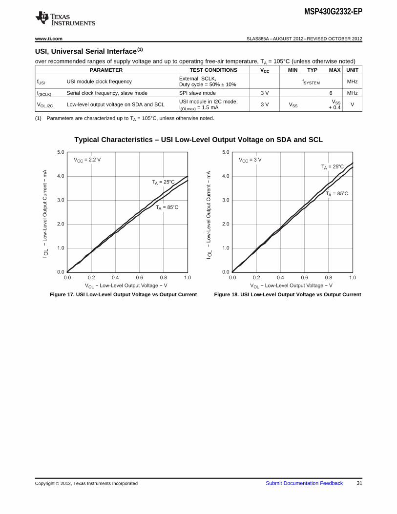
USI, Universal Serial Interface (1)
over recommended ranges of supply voltage and up to operating free-air temperature, TA = 105°C (unless otherwise noted)
PARAMETER TEST CONDITIONS VCC MIN TYP MAX UNIT
External: SCLK,fUSI USI module clock frequency fSYSTEM MHzDuty cycle = 50% ± 10%
f(SCLK) Serial clock frequency, slave mode SPI slave mode 3 V 6 MHz
USI module in I2C mode, VSSVOL,I2C Low-level output voltage on SDA and SCL 3 V VSS VI(OLmax) = 1.5 mA + 0.4
(1) Parameters are characterized up to TA = 105°C, unless otherwise noted.
Typical Characteristics – USI Low-Level Output Voltage on SDA and SCL
Figure 17. USI Low-Level Output Voltage vs Output Current Figure 18. USI Low-Level Output Voltage vs Output Current
Copyright © 2012, Texas Instruments Incorporated Submit Documentation Feedback 31
MSP430G2332-EP
SLAS885A –AUGUST 2012–REVISED OCTOBER 2012 www.ti.com
10-Bit ADC, Power Supply and Input Range Conditionsover recommended ranges of supply voltage and operating free-air temperature (unless otherwise noted) (1)
PARAMETER TEST CONDITIONS TA VCC MIN TYP MAX UNIT
VCC Analog supply voltage VSS = 0 V 2.2 3.6 V
All Ax terminals, Analog inputsVAx Analog input voltage (2) 3 V 0 VCC Vselected in ADC10AE register
fADC10CLK = 5.0 MHz,ADC10ON = 1, REFON = 0,IADC10 ADC10 supply current (3) -40°C to 125°C 3 V 0.6 mAADC10SHT0 = 1, ADC10SHT1 = 0,ADC10DIV = 0
fADC10CLK = 5.0 MHz,ADC10ON = 0, REF2_5V = 0, 0.25REFON = 1, REFOUT = 0Reference supply current,IREF+ -40°C to 125°C 3 V mAreference buffer disabled (4)fADC10CLK = 5.0 MHz,ADC10ON = 0, REF2_5V = 1, 0.25REFON = 1, REFOUT = 0
fADC10CLK = 5.0 MHz,Reference buffer supply ADC10ON = 0, REFON = 1,IREFB,0 -40°C to 125°C 3 V 1.1 mAcurrent with ADC10SR = 0 (4) REF2_5V = 0, REFOUT = 1,
ADC10SR = 0
fADC10CLK = 5.0 MHz,Reference buffer supply ADC10ON = 0, REFON = 1,IREFB,1 -40°C to 125°C 3 V 0.5 mAcurrent with ADC10SR = 1 (4) REF2_5V = 0, REFOUT = 1,
ADC10SR = 1
Only one terminal Ax can beCI Input capacitance -40°C to 125°C 3 V 27 pFselected at one time
RI Input MUX ON resistance 0 V ≤ VAx ≤ VCC -40°C to 125°C 3 V 1000 Ω
(1) The leakage current is defined in the leakage current table with Px.x/Ax parameter.(2) The analog input voltage range must be within the selected reference voltage range VR+ to VR– for valid conversion results.(3) The internal reference supply current is not included in current consumption parameter IADC10.(4) The internal reference current is supplied via terminal VCC. Consumption is independent of the ADC10ON control bit, unless a
conversion is active. The REFON bit enables the built-in reference to settle before starting an A/D conversion.
32 Submit Documentation Feedback Copyright © 2012, Texas Instruments Incorporated
MSP430G2332-EP
www.ti.com SLAS885A –AUGUST 2012–REVISED OCTOBER 2012
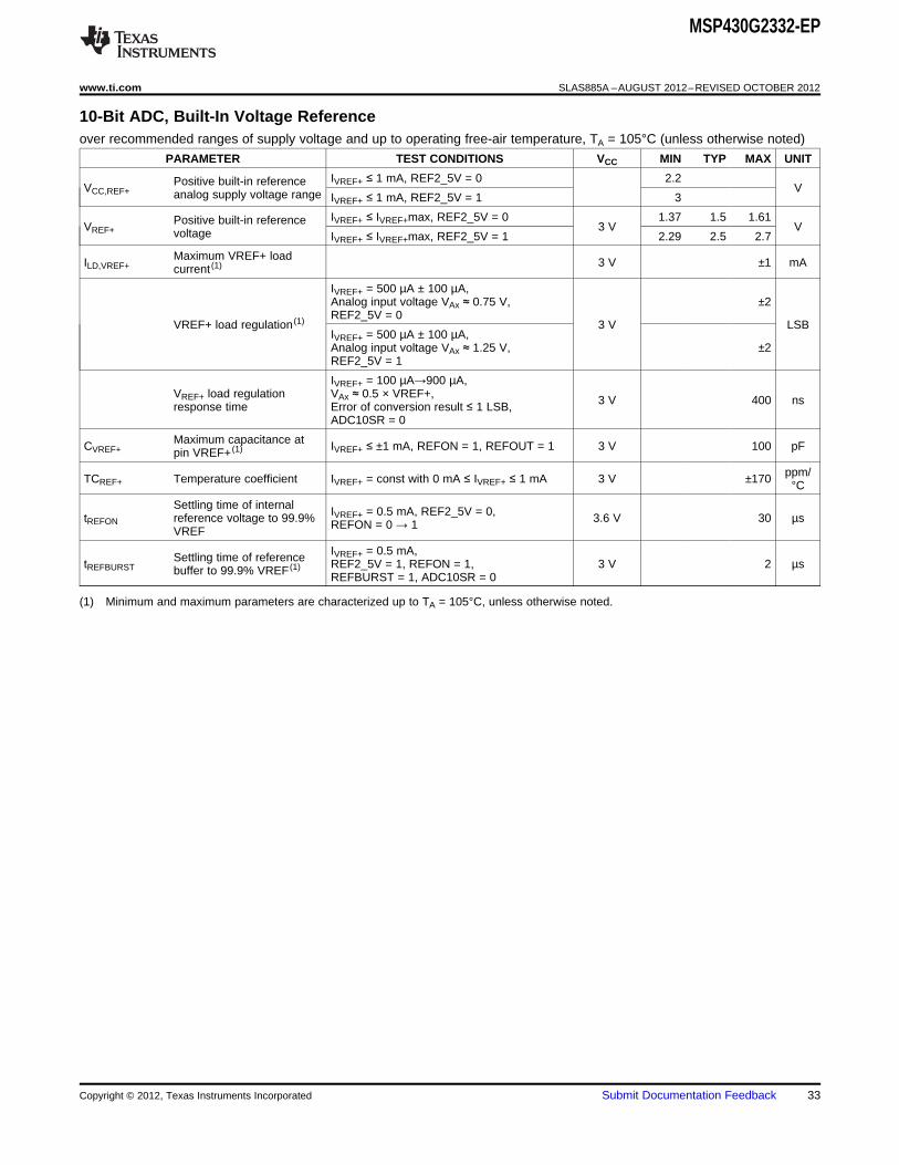
10-Bit ADC, Built-In Voltage Referenceover recommended ranges of supply voltage and up to operating free-air temperature, TA = 105°C (unless otherwise noted)
PARAMETER TEST CONDITIONS VCC MIN TYP MAX UNIT
IVREF+ ≤ 1 mA, REF2_5V = 0 2.2Positive built-in referenceVCC,REF+ Vanalog supply voltage range IVREF+ ≤ 1 mA, REF2_5V = 1 3
IVREF+ ≤ IVREF+max, REF2_5V = 0 1.37 1.5 1.61Positive built-in referenceVREF+ 3 V Vvoltage IVREF+ ≤ IVREF+max, REF2_5V = 1 2.29 2.5 2.7
Maximum VREF+ loadILD,VREF+ 3 V ±1 mAcurrent (1)
IVREF+ = 500 µA ± 100 µA,Analog input voltage VAx ≈ 0.75 V, ±2REF2_5V = 0
VREF+ load regulation (1) 3 V LSBIVREF+ = 500 µA ± 100 µA,Analog input voltage VAx ≈ 1.25 V, ±2REF2_5V = 1
IVREF+ = 100 µA→900 µA,VREF+ load regulation VAx ≈ 0.5 × VREF+, 3 V 400 nsresponse time Error of conversion result ≤ 1 LSB,
ADC10SR = 0
Maximum capacitance atCVREF+ IVREF+ ≤ ±1 mA, REFON = 1, REFOUT = 1 3 V 100 pFpin VREF+ (1)
ppm/TCREF+ Temperature coefficient IVREF+ = const with 0 mA ≤ IVREF+ ≤ 1 mA 3 V ±170 °C
Settling time of internal IVREF+ = 0.5 mA, REF2_5V = 0,tREFON reference voltage to 99.9% 3.6 V 30 µsREFON = 0 → 1VREF
IVREF+ = 0.5 mA,Settling time of referencetREFBURST REF2_5V = 1, REFON = 1, 3 V 2 µsbuffer to 99.9% VREF (1)REFBURST = 1, ADC10SR = 0
(1) Minimum and maximum parameters are characterized up to TA = 105°C, unless otherwise noted.
Copyright © 2012, Texas Instruments Incorporated Submit Documentation Feedback 33
MSP430G2332-EP
SLAS885A –AUGUST 2012–REVISED OCTOBER 2012 www.ti.com
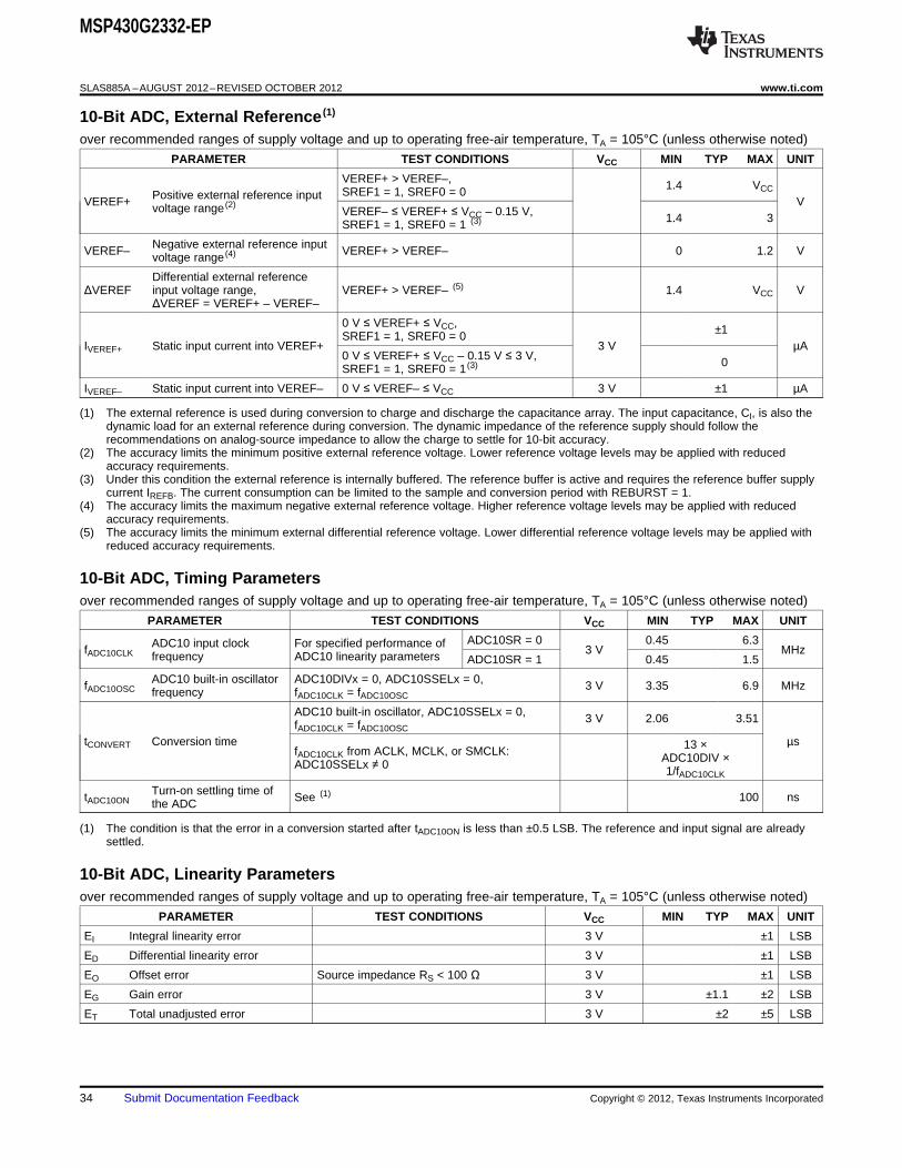
10-Bit ADC, External Reference (1)
over recommended ranges of supply voltage and up to operating free-air temperature, TA = 105°C (unless otherwise noted)
PARAMETER TEST CONDITIONS VCC MIN TYP MAX UNIT
VEREF+ > VEREF–, 1.4 VCCSREF1 = 1, SREF0 = 0Positive external reference inputVEREF+ Vvoltage range (2)VEREF– ≤ VEREF+ ≤ VCC – 0.15 V, 1.4 3SREF1 = 1, SREF0 = 1 (3)
Negative external reference inputVEREF– VEREF+ > VEREF– 0 1.2 Vvoltage range (4)
Differential external referenceΔVEREF input voltage range, VEREF+ > VEREF– (5) 1.4 VCC V
ΔVEREF = VEREF+ – VEREF–
0 V ≤ VEREF+ ≤ VCC, ±1SREF1 = 1, SREF0 = 0IVEREF+ Static input current into VEREF+ 3 V µA
0 V ≤ VEREF+ ≤ VCC – 0.15 V ≤ 3 V, 0SREF1 = 1, SREF0 = 1 (3)
IVEREF– Static input current into VEREF– 0 V ≤ VEREF– ≤ VCC 3 V ±1 µA
(1) The external reference is used during conversion to charge and discharge the capacitance array. The input capacitance, CI, is also thedynamic load for an external reference during conversion. The dynamic impedance of the reference supply should follow therecommendations on analog-source impedance to allow the charge to settle for 10-bit accuracy.
(2) The accuracy limits the minimum positive external reference voltage. Lower reference voltage levels may be applied with reducedaccuracy requirements.
(3) Under this condition the external reference is internally buffered. The reference buffer is active and requires the reference buffer supplycurrent IREFB. The current consumption can be limited to the sample and conversion period with REBURST = 1.
(4) The accuracy limits the maximum negative external reference voltage. Higher reference voltage levels may be applied with reducedaccuracy requirements.
(5) The accuracy limits the minimum external differential reference voltage. Lower differential reference voltage levels may be applied withreduced accuracy requirements.
10-Bit ADC, Timing Parametersover recommended ranges of supply voltage and up to operating free-air temperature, TA = 105°C (unless otherwise noted)
PARAMETER TEST CONDITIONS VCC MIN TYP MAX UNIT
ADC10SR = 0 0.45 6.3ADC10 input clock For specified performance offADC10CLK 3 V MHzfrequency ADC10 linearity parameters ADC10SR = 1 0.45 1.5
ADC10 built-in oscillator ADC10DIVx = 0, ADC10SSELx = 0,fADC10OSC 3 V 3.35 6.9 MHzfrequency fADC10CLK = fADC10OSC
ADC10 built-in oscillator, ADC10SSELx = 0, 3 V 2.06 3.51fADC10CLK = fADC10OSC
tCONVERT Conversion time µs13 ×fADC10CLK from ACLK, MCLK, or SMCLK: ADC10DIV ×ADC10SSELx ≠ 0 1/fADC10CLK
Turn-on settling time oftADC10ON See (1) 100 nsthe ADC
(1) The condition is that the error in a conversion started after tADC10ON is less than ±0.5 LSB. The reference and input signal are alreadysettled.
10-Bit ADC, Linearity Parametersover recommended ranges of supply voltage and up to operating free-air temperature, TA = 105°C (unless otherwise noted)
PARAMETER TEST CONDITIONS VCC MIN TYP MAX UNIT
EI Integral linearity error 3 V ±1 LSB
ED Differential linearity error 3 V ±1 LSB
EO Offset error Source impedance RS < 100 Ω 3 V ±1 LSB
EG Gain error 3 V ±1.1 ±2 LSB
ET Total unadjusted error 3 V ±2 ±5 LSB
34 Submit Documentation Feedback Copyright © 2012, Texas Instruments Incorporated
MSP430G2332-EP
www.ti.com SLAS885A –AUGUST 2012–REVISED OCTOBER 2012
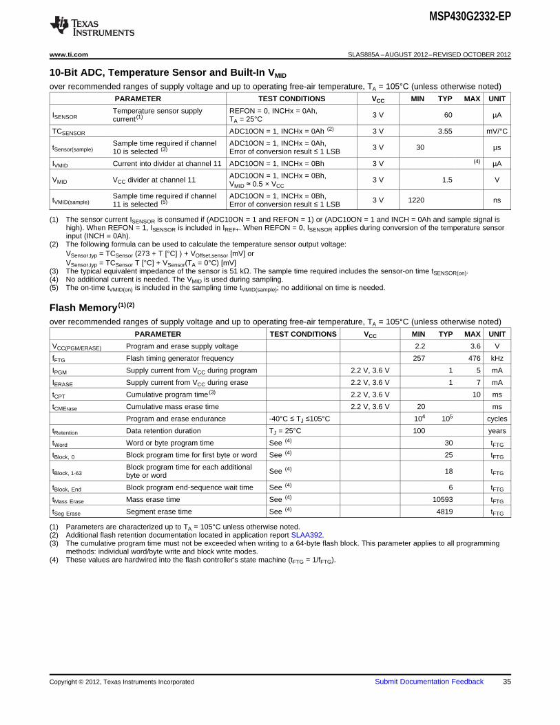
10-Bit ADC, Temperature Sensor and Built-In VMID
over recommended ranges of supply voltage and up to operating free-air temperature, TA = 105°C (unless otherwise noted)
PARAMETER TEST CONDITIONS VCC MIN TYP MAX UNIT
Temperature sensor supply REFON = 0, INCHx = 0Ah,ISENSOR 3 V 60 µAcurrent (1) TA = 25°C
TCSENSOR ADC10ON = 1, INCHx = 0Ah (2) 3 V 3.55 mV/°C
Sample time required if channel ADC10ON = 1, INCHx = 0Ah,tSensor(sample) 3 V 30 µs10 is selected (3) Error of conversion result ≤ 1 LSB
IVMID Current into divider at channel 11 ADC10ON = 1, INCHx = 0Bh 3 V (4) µA
ADC10ON = 1, INCHx = 0Bh,VMID VCC divider at channel 11 3 V 1.5 VVMID ≈ 0.5 × VCC
Sample time required if channel ADC10ON = 1, INCHx = 0Bh,tVMID(sample) 3 V 1220 ns11 is selected (5) Error of conversion result ≤ 1 LSB
(1) The sensor current ISENSOR is consumed if (ADC10ON = 1 and REFON = 1) or (ADC10ON = 1 and INCH = 0Ah and sample signal ishigh). When REFON = 1, ISENSOR is included in IREF+. When REFON = 0, ISENSOR applies during conversion of the temperature sensorinput (INCH = 0Ah).
(2) The following formula can be used to calculate the temperature sensor output voltage:VSensor,typ = TCSensor (273 + T [°C] ) + VOffset,sensor [mV] orVSensor,typ = TCSensor T [°C] + VSensor(TA = 0°C) [mV]
(3) The typical equivalent impedance of the sensor is 51 kΩ. The sample time required includes the sensor-on time tSENSOR(on).(4) No additional current is needed. The VMID is used during sampling.(5) The on-time tVMID(on) is included in the sampling time tVMID(sample); no additional on time is needed.
Flash Memory (1) (2)
over recommended ranges of supply voltage and up to operating free-air temperature, TA = 105°C (unless otherwise noted)
PARAMETER TEST CONDITIONS VCC MIN TYP MAX UNIT
VCC(PGM/ERASE) Program and erase supply voltage 2.2 3.6 V
fFTG Flash timing generator frequency 257 476 kHz
IPGM Supply current from VCC during program 2.2 V, 3.6 V 1 5 mA
IERASE Supply current from VCC during erase 2.2 V, 3.6 V 1 7 mA
tCPT Cumulative program time (3) 2.2 V, 3.6 V 10 ms
tCMErase Cumulative mass erase time 2.2 V, 3.6 V 20 ms
Program and erase endurance -40°C ≤ TJ ≤105°C 104 105 cycles
tRetention Data retention duration TJ = 25°C 100 years
tWord Word or byte program time See (4) 30 tFTG
tBlock, 0 Block program time for first byte or word See (4) 25 tFTG
Block program time for each additionaltBlock, 1-63 See (4) 18 tFTGbyte or word
tBlock, End Block program end-sequence wait time See (4) 6 tFTG
tMass Erase Mass erase time See (4) 10593 tFTG
tSeg Erase Segment erase time See (4) 4819 tFTG
(1) Parameters are characterized up to TA = 105°C unless otherwise noted.(2) Additional flash retention documentation located in application report SLAA392.(3) The cumulative program time must not be exceeded when writing to a 64-byte flash block. This parameter applies to all programming
methods: individual word/byte write and block write modes.(4) These values are hardwired into the flash controller's state machine (tFTG = 1/fFTG).
Copyright © 2012, Texas Instruments Incorporated Submit Documentation Feedback 35
MSP430G2332-EP
SLAS885A –AUGUST 2012–REVISED OCTOBER 2012 www.ti.com
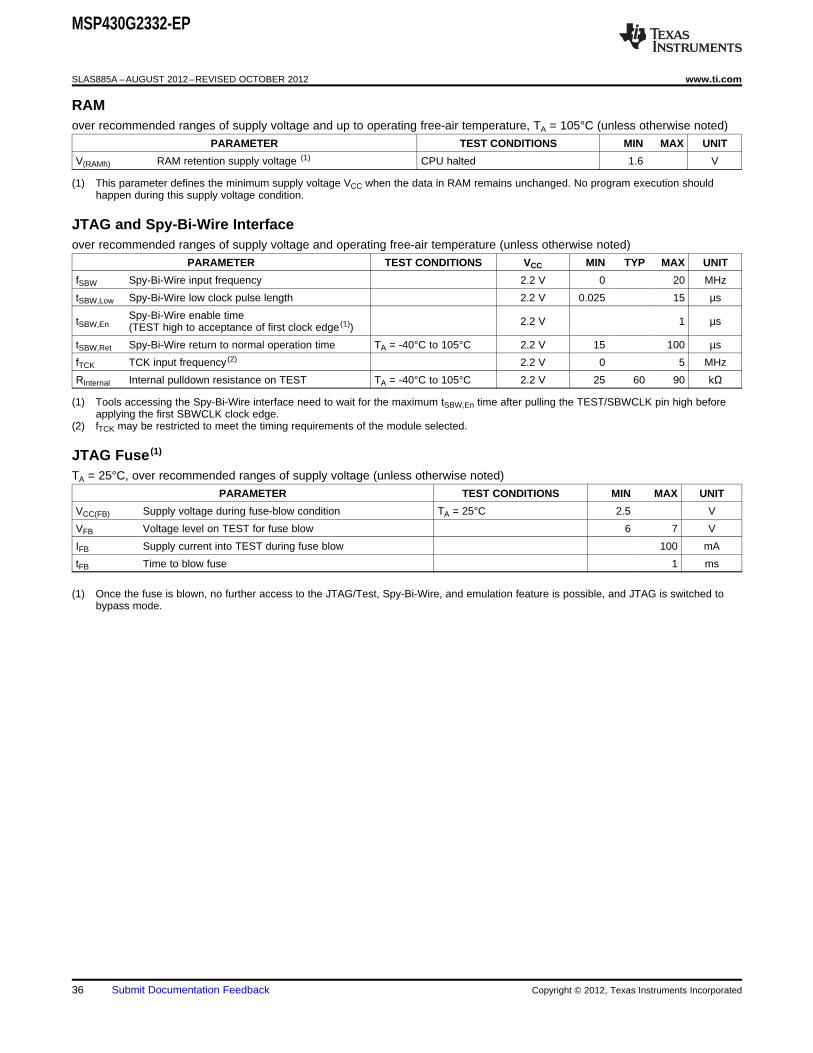
RAMover recommended ranges of supply voltage and up to operating free-air temperature, TA = 105°C (unless otherwise noted)
PARAMETER TEST CONDITIONS MIN MAX UNIT
V(RAMh) RAM retention supply voltage (1) CPU halted 1.6 V
(1) This parameter defines the minimum supply voltage VCC when the data in RAM remains unchanged. No program execution shouldhappen during this supply voltage condition.
JTAG and Spy-Bi-Wire Interfaceover recommended ranges of supply voltage and operating free-air temperature (unless otherwise noted)
PARAMETER TEST CONDITIONS VCC MIN TYP MAX UNIT
fSBW Spy-Bi-Wire input frequency 2.2 V 0 20 MHz
tSBW,Low Spy-Bi-Wire low clock pulse length 2.2 V 0.025 15 µs
Spy-Bi-Wire enable timetSBW,En 2.2 V 1 µs(TEST high to acceptance of first clock edge (1))
tSBW,Ret Spy-Bi-Wire return to normal operation time TA = -40°C to 105°C 2.2 V 15 100 µs
fTCK TCK input frequency (2) 2.2 V 0 5 MHz
RInternal Internal pulldown resistance on TEST TA = -40°C to 105°C 2.2 V 25 60 90 kΩ
(1) Tools accessing the Spy-Bi-Wire interface need to wait for the maximum tSBW,En time after pulling the TEST/SBWCLK pin high beforeapplying the first SBWCLK clock edge.
(2) fTCK may be restricted to meet the timing requirements of the module selected.
JTAG Fuse (1)
TA = 25°C, over recommended ranges of supply voltage (unless otherwise noted)
PARAMETER TEST CONDITIONS MIN MAX UNIT
VCC(FB) Supply voltage during fuse-blow condition TA = 25°C 2.5 V
VFB Voltage level on TEST for fuse blow 6 7 V
IFB Supply current into TEST during fuse blow 100 mA
tFB Time to blow fuse 1 ms
(1) Once the fuse is blown, no further access to the JTAG/Test, Spy-Bi-Wire, and emulation feature is possible, and JTAG is switched tobypass mode.
36 Submit Documentation Feedback Copyright © 2012, Texas Instruments Incorporated
To Module
From Module
PxOUT.y
DVSS
DVCC 1
TAx.yTAxCLK
BusKeeper
EN
1
0
PxIN.y
EN
D
PxSEL.y
PxREN.y
1
0
PxSEL2.y
1
0
INCHx = y
ADC10AE0.y
To ADC10
PxSEL.y
1
3
2
1
0
PxSEL2.y
PxIRQ.y
PxIE.y
EN
Set
Q
InterruptEdgeSelect
PxSEL.y
PxIES.y
PxIFG.y
Direction0: Input1: Output
PxDIR.y
PxSEL.y
3
2
1
0
PxSEL2.y
P1.0/TA0CLK/ACLK/A0P1.1/TA0.0/A1P1.2/TA0.1/A2
0
0
MSP430G2332-EP
www.ti.com SLAS885A –AUGUST 2012–REVISED OCTOBER 2012
PIN SCHEMATICS
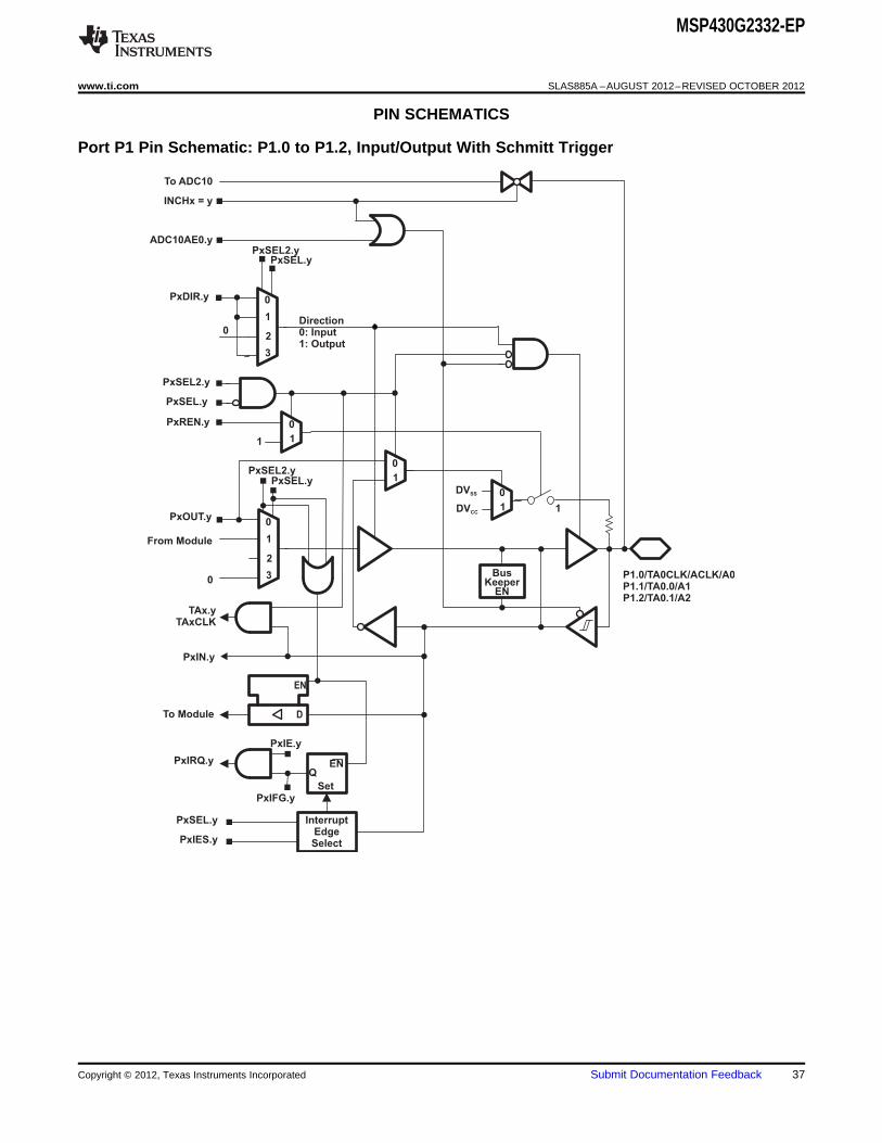
Port P1 Pin Schematic: P1.0 to P1.2, Input/Output With Schmitt Trigger
Copyright © 2012, Texas Instruments Incorporated Submit Documentation Feedback 37
MSP430G2332-EP
SLAS885A –AUGUST 2012–REVISED OCTOBER 2012 www.ti.com
Table 15. Port P1 (P1.0 to P1.2) Pin Functions
CONTROL BITS / SIGNALS (1)
PIN NAME (P1.x) x FUNCTIONP1DIR.x P1SEL.x P1SEL2.x
P1.0/ P1.x (I/O) I: 0; O: 1 0 0
TA0CLK/ 0 TA0.TACLK 0 1 0
ACLK/ ACLK 1 1 0
A0/ A0 X X X
Pin Osc Capacitive sensing x 0 1
P1.1/ P1.x (I/O) I: 0; O: 1 0 0
TA0.0/ 1 TA0.0 1 1 0
TA0.CCI0A 0 1 0
A1/ A1 X X X
Pin Osc Capacitive sensing X 0 1
P1.2/ P1.x (I/O) I: 0; O: 1 0 0
TA0.1/ 2 TA0.1 1 1 0
TA0.CCI1A 0 1 0
A2/ A2 X X X
Pin Osc Capacitive sensing X 0 1
(1) X = don't care
38 Submit Documentation Feedback Copyright © 2012, Texas Instruments Incorporated

P1.3/ADC10CLK/A3/VREF-/VEREF-
Direction0: Input1: Output
To Module
From ADC10 *
PxOUT.y
DVSS
DVCC 1
TAx.yTAxCLK
BusKeeper
EN
1
0
PxIN.y
EN
D
PxSEL.y
PxREN.y
1
0
PxDIR.y
1
0,2,3
PxSEL2.y
PxSEL.y
1
0
INCHx = y
To ADC10
To ADC10 VREF-1
0 VSS
SREF2
PxSEL.y
1
3
2
1
0
PxSEL2.y
PxIRQ.y
PxIE.y
EN
Set
Q
InterruptEdgeSelect
PxSEL.y
PxIES.y
PxIFG.y
ADC10AE0.y
PxSEL2.y
MSP430G2332-EP
www.ti.com SLAS885A –AUGUST 2012–REVISED OCTOBER 2012
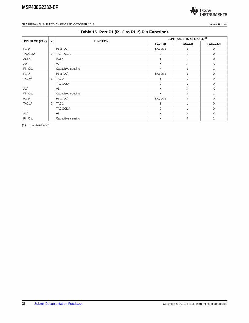
Port P1 Pin Schematic: P1.3, Input/Output With Schmitt Trigger
Copyright © 2012, Texas Instruments Incorporated Submit Documentation Feedback 39
MSP430G2332-EP
SLAS885A –AUGUST 2012–REVISED OCTOBER 2012 www.ti.com
Table 16. Port P1 (P1.3) Pin Functions
CONTROL BITS / SIGNALS (1)
PIN NAME x FUNCTION ADC10AE.x(P1.x) P1DIR.x P1SEL.x P1SEL2.x (INCH.x=1)
P1.3/ P1.x (I/O) I: 0; O: 1 0 0 0
ADC10CLK/ ADC10CLK 1 1 0 0
A3/ A3 X X X 1 (y = 3)3
VREF-/ VREF- X X X 1
VEREF-/ VEREF- X X X 1
Pin Osc Capacitive sensing X 0 1 0
(1) X = don't care
40 Submit Documentation Feedback Copyright © 2012, Texas Instruments Incorporated
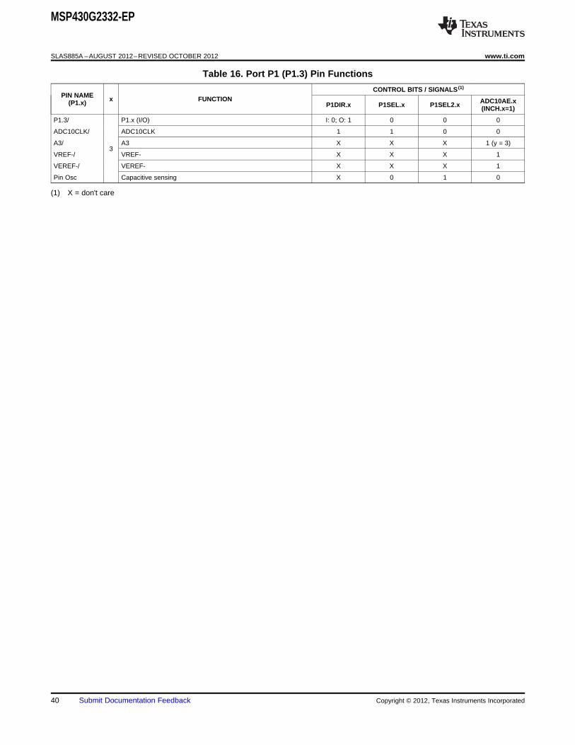
P1.4/SMCLK/TA0.2/A4/VREF+/VEREF+/TCK
Direction0: Input1: Output
To Module
SMCLK
PxOUT.y
DVSS
DVCC 1
TAx.yTAxCLK
BusKeeper
EN
1
0
PxIN.y
EN
D
PxSEL.y
PxREN.y
1
0
PxDIR.y
1
0
PxSEL2.y
PxSEL.y
1
0
INCHx = y
To ADC10
From/To ADC10 Ref+
PxSEL.y
1
3
2
1
0
PxSEL2.y
From JTAG
To JTAG
PxIRQ.y
PxIE.y
EN
SetQ
InterruptEdgeSelect
PxSEL.y
PxIES.y
PxIFG.y
ADC10AE0.y
from Timer
MSP430G2332-EP
www.ti.com SLAS885A –AUGUST 2012–REVISED OCTOBER 2012
Port P1 Pin Schematic: P1.4, Input/Output With Schmitt Trigger
Table 17. Port P1 (P1.4) Pin Functions
CONTROL BITS / SIGNALS (1)
PIN NAME (P1.x) x FUNCTION ADC10AE.xP1DIR.x P1SEL.x P1SEL2.x JTAG Mode(INCH.x=1)
P1.4/ P1.x (I/O) I: 0; O: 1 0 0 0 0
SMCLK/ SMCLK 1 1 0 0 0
TA0.2/ TA0.2 1 1 1 0 0
TA0.CCI2A 0 1 1 0 0
VREF+/ 4 VREF+ X X X 1 0
VEREF+/ VEREF+ X X X 1 0
A4/ A4 X X X 1 (y = 4) 0
TCK/ TCK X X X 0 1
Pin Osc Capacitive sensing X 0 1 0 0
(1) X = don't care
Copyright © 2012, Texas Instruments Incorporated Submit Documentation Feedback 41
P1.5/TA0.0/SCLK/A5/TMSP1.6/TA0.1/SDO/SCL/A6/TDI/TCLKP1.7//SDI/SDA/A7/TDO/TDI
To Module
From Module
PxOUT.y
DVSS
DVCC 1
TAx.yTAxCLK
BusKeeper
EN
1
0
PxIN.y
EN
D
PxSEL.y
PxREN.y
1
0
PxSEL2.y
1
0
INCHx = y
To ADC10
PxSEL.y
1
3
2
1
0
PxSEL2.y
From JTAG
To JTAG
PxIRQ.y
PxIE.y
EN
Set
Q
InterruptEdgeSelect
PxSEL.y
PxIES.y
PxIFG.y
Direction0: Input1: Output
PxDIR.y
From Module
PxSEL.y
3
2
1
0
PxSEL2.y
ADC10AE0.y
0
MSP430G2332-EP
SLAS885A –AUGUST 2012–REVISED OCTOBER 2012 www.ti.com
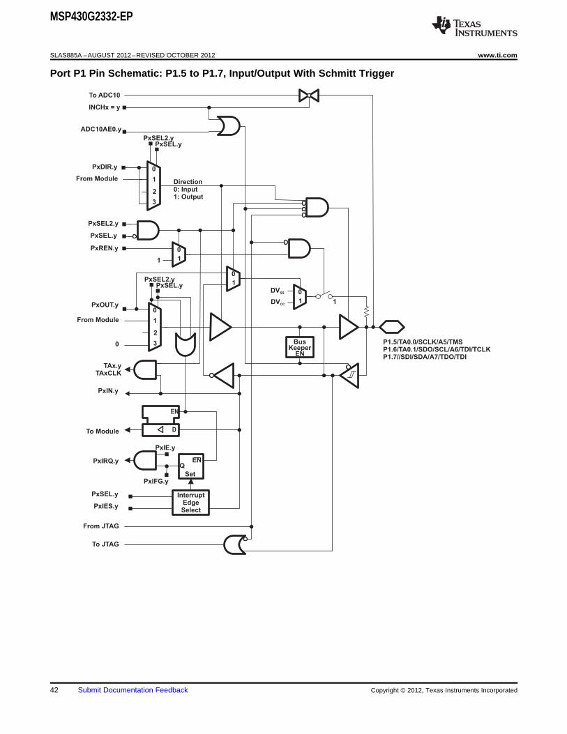
Port P1 Pin Schematic: P1.5 to P1.7, Input/Output With Schmitt Trigger
42 Submit Documentation Feedback Copyright © 2012, Texas Instruments Incorporated
MSP430G2332-EP
www.ti.com SLAS885A –AUGUST 2012–REVISED OCTOBER 2012
Table 18. Port P1 (P1.5 to P1.7) Pin Functions
CONTROL BITS / SIGNALS (1)
PIN NAME x FUNCTION ADC10AE.x(P1.x) P1DIR.x P1SEL.x P1SEL2.x USIP.x JTAG Mode (INCH.x=1)
P1.5/ P1.x (I/O) I: 0; O: 1 0 0 0 0 0
TA0.0/ TA0.0 1 1 0 0 0 0
SCLK/ SPI mode from USI 1 0 1 0 05
A5/ A5 X X X 0 0 1 (y = 5)
TMS/ TMS X X X 0 1 0
Pin Osc Capacitive sensing X 0 1 0 0 0
P1.6/ P1.x (I/O) I: 0; O: 1 0 0 0 0 0
TA0.1/ TA0.1 1 1 0 0 0 0
SDO/ SPI mode from USI 1 0 ! 0 0
SCL/ 6 I2C mode from USI 1 0 ! 0 0
A6/ A6 X X X 0 0 1 (y = 6)
TDI/TCLK/ TDI/TCLK X X X 0 1 0
Pin Osc Capacitive sensing X 0 1 0 0 0
P1.7/ P1.x (I/O) I: 0; O: 1 0 0 0 0 0
SDI/ SPI mode from USI 1 0 1 0 0
SDA/ SPI mode from USI 1 0 1 0 07
A7/ A7 X X X 0 0 1 (y = 7)
TDO/TDI/ TDO/TDI X X X 0 1 0
Pin Osc Capacitive sensing X 0 1 0 0 0
(1) X = don't care
Copyright © 2012, Texas Instruments Incorporated Submit Documentation Feedback 43
P2.0P2.1P2.2P2.3P2.4P2.5
Direction0: Input1: Output
To Module
PxOUT.y
DVSS
DVCC 1
TAx.yTAxCLK
1
0
PxIN.y
EN
D
PxSEL.y
PxREN.y
1
0
PxSEL2.y
1
0
PxSEL.y
1
3
2
1
0
PxSEL2.y
PxIRQ.y
PxIE.y
EN
Set
Q
InterruptEdgeSelect
PxSEL.y
PxIES.y
PxIFG.y
PxDIR.y
1
0
PxSEL.y
0
0
MSP430G2332-EP
SLAS885A –AUGUST 2012–REVISED OCTOBER 2012 www.ti.com
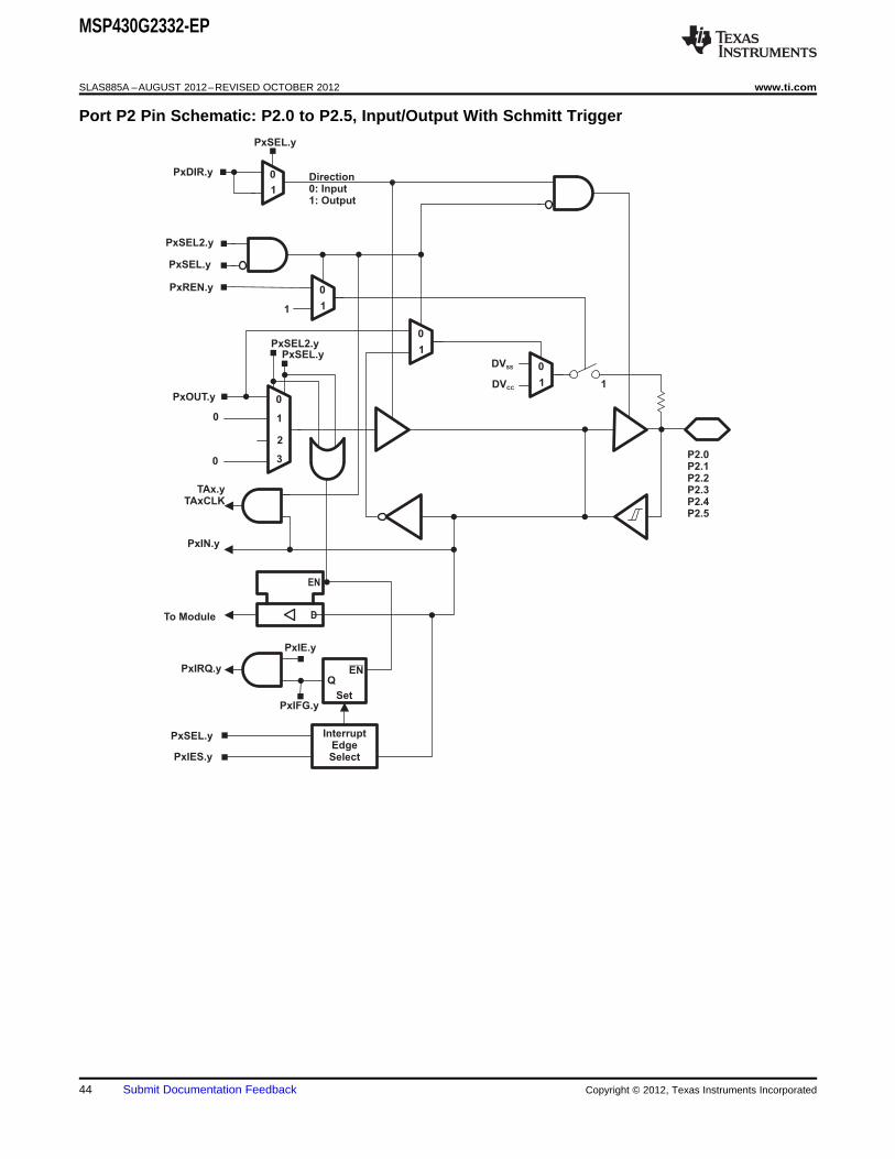
Port P2 Pin Schematic: P2.0 to P2.5, Input/Output With Schmitt Trigger
44 Submit Documentation Feedback Copyright © 2012, Texas Instruments Incorporated
MSP430G2332-EP
www.ti.com SLAS885A –AUGUST 2012–REVISED OCTOBER 2012
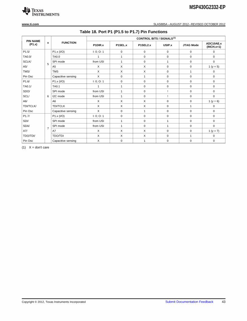
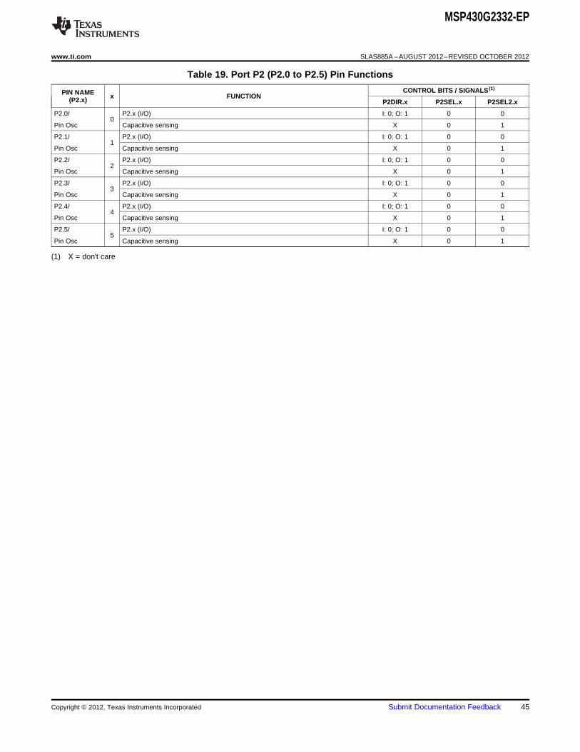
Table 19. Port P2 (P2.0 to P2.5) Pin Functions
CONTROL BITS / SIGNALS (1)PIN NAME x FUNCTION(P2.x) P2DIR.x P2SEL.x P2SEL2.x
P2.0/ P2.x (I/O) I: 0; O: 1 0 00
Pin Osc Capacitive sensing X 0 1
P2.1/ P2.x (I/O) I: 0; O: 1 0 01
Pin Osc Capacitive sensing X 0 1
P2.2/ P2.x (I/O) I: 0; O: 1 0 02
Pin Osc Capacitive sensing X 0 1
P2.3/ P2.x (I/O) I: 0; O: 1 0 03
Pin Osc Capacitive sensing X 0 1
P2.4/ P2.x (I/O) I: 0; O: 1 0 04
Pin Osc Capacitive sensing X 0 1
P2.5/ P2.x (I/O) I: 0; O: 1 0 05
Pin Osc Capacitive sensing X 0 1
(1) X = don't care
Copyright © 2012, Texas Instruments Incorporated Submit Documentation Feedback 45
XIN/P2.6/TA0.1
Direction0: Input1: Output
To Module
From Module
PxOUT.y
DVSS
DVCC 1
TAx.yTAxCLK
1
0
PxIN.y
EN
D
PxSEL.y
PxREN.y
1
0
PxDIR.y
1
0
PxSEL2.y
PxSEL.y
1
0
PxSEL.y
1
3
2
1
0
PxSEL2.y
PxIRQ.y
PxIE.y
EN
Set
Q
InterruptEdgeSelect
PxSEL.y
PxIES.y
PxIFG.y
1
0
XOUT/P2.7LF off
LFXT1CLK
PxSEL.6 & PxSEL.7BCSCTL3.LFXT1Sx = 11
0
MSP430G2332-EP
SLAS885A –AUGUST 2012–REVISED OCTOBER 2012 www.ti.com
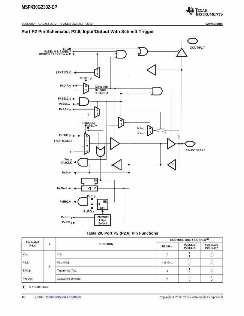
Port P2 Pin Schematic: P2.6, Input/Output With Schmitt Trigger
Table 20. Port P2 (P2.6) Pin Functions
CONTROL BITS / SIGNALS (1)
PIN NAME x FUNCTION P2SEL.6 P2SEL2.6(P2.x) P2DIR.x P2SEL.7 P2SEL2.7
1 0XIN/ XIN 0 1 0
0 0P2.6/ P2.x (I/O) I: 0; O: 1 X 06
1 0TA0.1/ Timer0_A3.TA1 1 0 0
0 1Pin Osc Capacitive sensing X X X
(1) X = don't care
46 Submit Documentation Feedback Copyright © 2012, Texas Instruments Incorporated
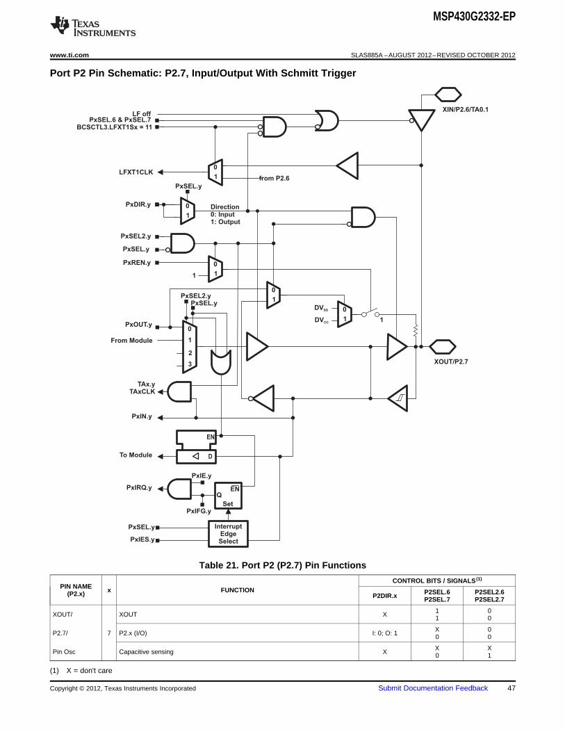
XOUT/P2.7
Direction0: Input1: Output
To Module
From Module
PxOUT.y
DVSS
DVCC 1
TAx.yTAxCLK
1
0
PxIN.y
EN
D
PxSEL.y
PxREN.y
1
0
PxDIR.y
1
0
PxSEL2.y
PxSEL.y
1
0
PxSEL.y
1
3
2
1
0
PxSEL2.y
PxIRQ.y
PxIE.y
EN
Set
Q
InterruptEdgeSelect
PxSEL.y
PxIES.y
PxIFG.y
1
0
XIN/P2.6/TA0.1LF off
LFXT1CLK
PxSEL.6 & PxSEL.7BCSCTL3.LFXT1Sx = 11
from P2.6
MSP430G2332-EP
www.ti.com SLAS885A –AUGUST 2012–REVISED OCTOBER 2012
Port P2 Pin Schematic: P2.7, Input/Output With Schmitt Trigger
Table 21. Port P2 (P2.7) Pin Functions
CONTROL BITS / SIGNALS (1)
PIN NAME x FUNCTION P2SEL.6 P2SEL2.6(P2.x) P2DIR.x P2SEL.7 P2SEL2.7
1 0XOUT/ XOUT X 1 0
X 0P2.7/ 7 P2.x (I/O) I: 0; O: 1 0 0
X XPin Osc Capacitive sensing X 0 1
(1) X = don't care
Copyright © 2012, Texas Instruments Incorporated Submit Documentation Feedback 47
PACKAGE OPTION ADDENDUM
www.ti.com 4-Sep-2014
Addendum-Page 1
PACKAGING INFORMATION
Orderable Device Status(1)
Package Type PackageDrawing
Pins PackageQty
Eco Plan(2)
Lead/Ball Finish(6)
MSL Peak Temp(3)
Op Temp (°C) Device Marking(4/5)
Samples
MSP430G2332QPW2EP ACTIVE TSSOP PW 20 70 Green (RoHS& no Sb/Br)
CU NIPDAU Level-1-260C-UNLIM -40 to 125 G2332EP
MSP430G2332QPW2REP ACTIVE TSSOP PW 20 2000 Green (RoHS& no Sb/Br)
CU NIPDAU Level-1-260C-UNLIM -40 to 125 G2332EP
V62/12625-01XE ACTIVE TSSOP PW 20 2000 Green (RoHS& no Sb/Br)
CU NIPDAU Level-1-260C-UNLIM -40 to 125 G2332EP
V62/12625-01XE-T ACTIVE TSSOP PW 20 70 Green (RoHS& no Sb/Br)
CU NIPDAU Level-1-260C-UNLIM -40 to 125 G2332EP
(1) The marketing status values are defined as follows:ACTIVE: Product device recommended for new designs.LIFEBUY: TI has announced that the device will be discontinued, and a lifetime-buy period is in effect.NRND: Not recommended for new designs. Device is in production to support existing customers, but TI does not recommend using this part in a new design.PREVIEW: Device has been announced but is not in production. Samples may or may not be available.OBSOLETE: TI has discontinued the production of the device.
(2) Eco Plan - The planned eco-friendly classification: Pb-Free (RoHS), Pb-Free (RoHS Exempt), or Green (RoHS & no Sb/Br) - please check http://www.ti.com/productcontent for the latest availabilityinformation and additional product content details.TBD: The Pb-Free/Green conversion plan has not been defined.Pb-Free (RoHS): TI's terms "Lead-Free" or "Pb-Free" mean semiconductor products that are compatible with the current RoHS requirements for all 6 substances, including the requirement thatlead not exceed 0.1% by weight in homogeneous materials. Where designed to be soldered at high temperatures, TI Pb-Free products are suitable for use in specified lead-free processes.Pb-Free (RoHS Exempt): This component has a RoHS exemption for either 1) lead-based flip-chip solder bumps used between the die and package, or 2) lead-based die adhesive used betweenthe die and leadframe. The component is otherwise considered Pb-Free (RoHS compatible) as defined above.Green (RoHS & no Sb/Br): TI defines "Green" to mean Pb-Free (RoHS compatible), and free of Bromine (Br) and Antimony (Sb) based flame retardants (Br or Sb do not exceed 0.1% by weightin homogeneous material)
(3) MSL, Peak Temp. - The Moisture Sensitivity Level rating according to the JEDEC industry standard classifications, and peak solder temperature.
(4) There may be additional marking, which relates to the logo, the lot trace code information, or the environmental category on the device.
(5) Multiple Device Markings will be inside parentheses. Only one Device Marking contained in parentheses and separated by a "~" will appear on a device. If a line is indented then it is a continuationof the previous line and the two combined represent the entire Device Marking for that device.
(6) Lead/Ball Finish - Orderable Devices may have multiple material finish options. Finish options are separated by a vertical ruled line. Lead/Ball Finish values may wrap to two lines if the finishvalue exceeds the maximum column width.
PACKAGE OPTION ADDENDUM
www.ti.com 4-Sep-2014
Addendum-Page 2
Important Information and Disclaimer:The information provided on this page represents TI's knowledge and belief as of the date that it is provided. TI bases its knowledge and belief on informationprovided by third parties, and makes no representation or warranty as to the accuracy of such information. Efforts are underway to better integrate information from third parties. TI has taken andcontinues to take reasonable steps to provide representative and accurate information but may not have conducted destructive testing or chemical analysis on incoming materials and chemicals.TI and TI suppliers consider certain information to be proprietary, and thus CAS numbers and other limited information may not be available for release.
In no event shall TI's liability arising out of such information exceed the total purchase price of the TI part(s) at issue in this document sold by TI to Customer on an annual basis.
OTHER QUALIFIED VERSIONS OF MSP430G2332-EP :
• Catalog: MSP430G2332
NOTE: Qualified Version Definitions:
• Catalog - TI's standard catalog product
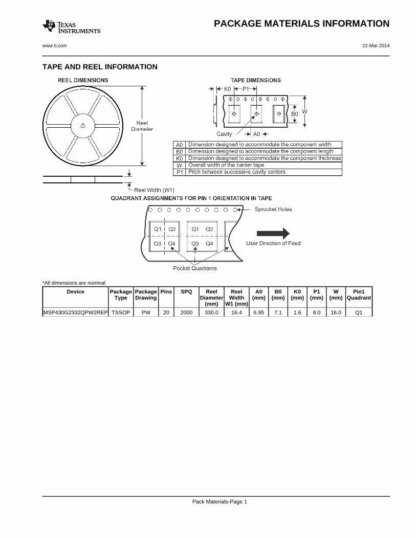
TAPE AND REEL INFORMATION
*All dimensions are nominal
Device PackageType
PackageDrawing
Pins SPQ ReelDiameter
(mm)
ReelWidth
W1 (mm)
A0(mm)
B0(mm)
K0(mm)
P1(mm)
W(mm)
Pin1Quadrant
MSP430G2332QPW2REP TSSOP PW 20 2000 330.0 16.4 6.95 7.1 1.6 8.0 16.0 Q1
PACKAGE MATERIALS INFORMATION
www.ti.com 22-Mar-2014
Pack Materials-Page 1
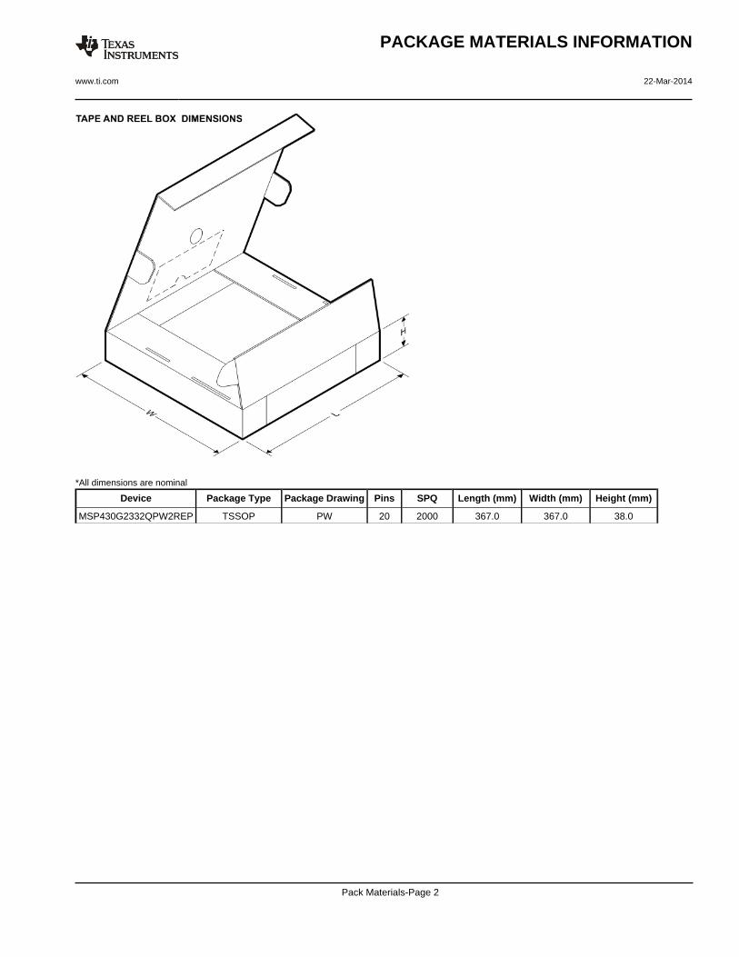
*All dimensions are nominal
Device Package Type Package Drawing Pins SPQ Length (mm) Width (mm) Height (mm)
MSP430G2332QPW2REP TSSOP PW 20 2000 367.0 367.0 38.0
PACKAGE MATERIALS INFORMATION
www.ti.com 22-Mar-2014
Pack Materials-Page 2
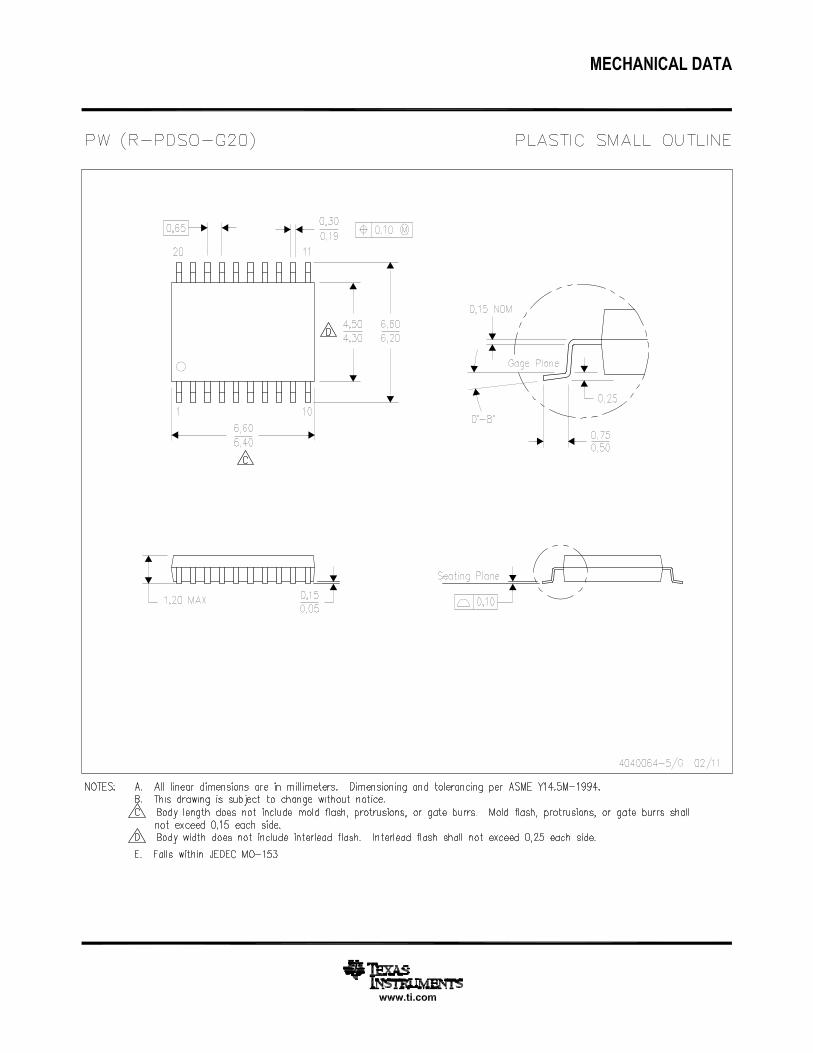
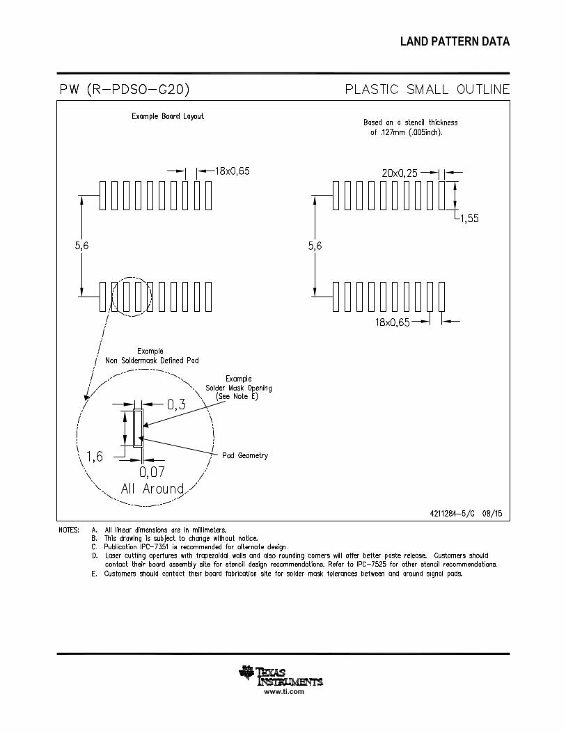
IMPORTANT NOTICE
Texas Instruments Incorporated and its subsidiaries (TI) reserve the right to make corrections, enhancements, improvements and otherchanges to its semiconductor products and services per JESD46, latest issue, and to discontinue any product or service per JESD48, latestissue. Buyers should obtain the latest relevant information before placing orders and should verify that such information is current andcomplete. All semiconductor products (also referred to herein as “components”) are sold subject to TI’s terms and conditions of salesupplied at the time of order acknowledgment.TI warrants performance of its components to the specifications applicable at the time of sale, in accordance with the warranty in TI’s termsand conditions of sale of semiconductor products. Testing and other quality control techniques are used to the extent TI deems necessaryto support this warranty. Except where mandated by applicable law, testing of all parameters of each component is not necessarilyperformed.TI assumes no liability for applications assistance or the design of Buyers’ products. Buyers are responsible for their products andapplications using TI components. To minimize the risks associated with Buyers’ products and applications, Buyers should provideadequate design and operating safeguards.TI does not warrant or represent that any license, either express or implied, is granted under any patent right, copyright, mask work right, orother intellectual property right relating to any combination, machine, or process in which TI components or services are used. Informationpublished by TI regarding third-party products or services does not constitute a license to use such products or services or a warranty orendorsement thereof. Use of such information may require a license from a third party under the patents or other intellectual property of thethird party, or a license from TI under the patents or other intellectual property of TI.Reproduction of significant portions of TI information in TI data books or data sheets is permissible only if reproduction is without alterationand is accompanied by all associated warranties, conditions, limitations, and notices. TI is not responsible or liable for such altereddocumentation. Information of third parties may be subject to additional restrictions.Resale of TI components or services with statements different from or beyond the parameters stated by TI for that component or servicevoids all express and any implied warranties for the associated TI component or service and is an unfair and deceptive business practice.TI is not responsible or liable for any such statements.Buyer acknowledges and agrees that it is solely responsible for compliance with all legal, regulatory and safety-related requirementsconcerning its products, and any use of TI components in its applications, notwithstanding any applications-related information or supportthat may be provided by TI. Buyer represents and agrees that it has all the necessary expertise to create and implement safeguards whichanticipate dangerous consequences of failures, monitor failures and their consequences, lessen the likelihood of failures that might causeharm and take appropriate remedial actions. Buyer will fully indemnify TI and its representatives against any damages arising out of the useof any TI components in safety-critical applications.In some cases, TI components may be promoted specifically to facilitate safety-related applications. With such components, TI’s goal is tohelp enable customers to design and create their own end-product solutions that meet applicable functional safety standards andrequirements. Nonetheless, such components are subject to these terms.No TI components are authorized for use in FDA Class III (or similar life-critical medical equipment) unless authorized officers of the partieshave executed a special agreement specifically governing such use.Only those TI components which TI has specifically designated as military grade or “enhanced plastic” are designed and intended for use inmilitary/aerospace applications or environments. Buyer acknowledges and agrees that any military or aerospace use of TI componentswhich have not been so designated is solely at the Buyer's risk, and that Buyer is solely responsible for compliance with all legal andregulatory requirements in connection with such use.TI has specifically designated certain components as meeting ISO/TS16949 requirements, mainly for automotive use. In any case of use ofnon-designated products, TI will not be responsible for any failure to meet ISO/TS16949.
Products ApplicationsAudio www.ti.com/audio Automotive and Transportation www.ti.com/automotiveAmplifiers amplifier.ti.com Communications and Telecom www.ti.com/communicationsData Converters dataconverter.ti.com Computers and Peripherals www.ti.com/computersDLP® Products www.dlp.com Consumer Electronics www.ti.com/consumer-appsDSP dsp.ti.com Energy and Lighting www.ti.com/energyClocks and Timers www.ti.com/clocks Industrial www.ti.com/industrialInterface interface.ti.com Medical www.ti.com/medicalLogic logic.ti.com Security www.ti.com/securityPower Mgmt power.ti.com Space, Avionics and Defense www.ti.com/space-avionics-defenseMicrocontrollers microcontroller.ti.com Video and Imaging www.ti.com/videoRFID www.ti-rfid.comOMAP Applications Processors www.ti.com/omap TI E2E Community e2e.ti.comWireless Connectivity www.ti.com/wirelessconnectivity
Mailing Address: Texas Instruments, Post Office Box 655303, Dallas, Texas 75265Copyright © 2016, Texas Instruments Incorporated