Embed Size (px)
Citation preview
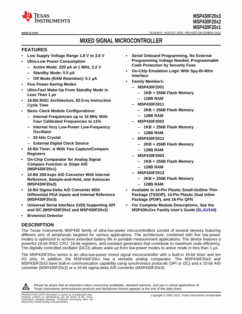
MSP430F20x3MSP430F20x2MSP430F20x1
www.ti.com SLAS491I –AUGUST 2005–REVISED DECEMBER 2012
MIXED SIGNAL MICROCONTROLLER1FEATURES• Low Supply Voltage Range 1.8 V to 3.6 V • Serial Onboard Programming, No External
Programming Voltage Needed, Programmable• Ultra-Low Power ConsumptionCode Protection by Security Fuse– Active Mode: 220 µA at 1 MHz, 2.2 V
• On-Chip Emulation Logic With Spy-Bi-Wire– Standby Mode: 0.5 µAInterface
– Off Mode (RAM Retention): 0.1 µA• Family Members:
• Five Power-Saving Modes– MSP430F2001
• Ultra-Fast Wake-Up From Standby Mode in– 1KB + 256B Flash MemoryLess Than 1 µs– 128B RAM• 16-Bit RISC Architecture, 62.5-ns Instruction
– MSP430F2011Cycle Time– 2KB + 256B Flash Memory• Basic Clock Module Configurations:– 128B RAM– Internal Frequencies up to 16 MHz With
Four Calibrated Frequencies to ±1% – MSP430F2002– Internal Very Low-Power Low-Frequency – 1KB + 256B Flash Memory
Oscillator – 128B RAM– 32-kHz Crystal – MSP430F2012– External Digital Clock Source – 2KB + 256B Flash Memory
• 16-Bit Timer_A With Two Capture/Compare – 128B RAMRegisters – MSP430F2003
• On-Chip Comparator for Analog Signal – 1KB + 256B Flash MemoryCompare Function or Slope A/D
– 128B RAM(MSP430F20x1)– MSP430F2013• 10-Bit 200-ksps A/D Converter With Internal
– 2KB + 256B Flash MemoryReference, Sample-and-Hold, and Autoscan(MSP430F20x2) – 128B RAM
• 16-Bit Sigma-Delta A/D Converter With • Available in 14-Pin Plastic Small-Outline ThinDifferential PGA Inputs and Internal Reference Package (TSSOP), 14-Pin Plastic Dual Inline(MSP430F20x3) Package (PDIP), and 16-Pin QFN
• Universal Serial Interface (USI) Supporting SPI • For Complete Module Descriptions, See theand I2C (MSP430F20x2 and MSP430F20x3) MSP430x2xx Family User's Guide (SLAU144)
• Brownout Detector
DESCRIPTIONThe Texas Instruments MSP430 family of ultra-low-power microcontrollers consist of several devices featuringdifferent sets of peripherals targeted for various applications. The architecture, combined with five low-powermodes is optimized to achieve extended battery life in portable measurement applications. The device features apowerful 16-bit RISC CPU, 16-bit registers, and constant generators that contribute to maximum code efficiency.The digitally controlled oscillator (DCO) allows wake-up from low-power modes to active mode in less than 1 µs.
The MSP430F20xx series is an ultra-low-power mixed signal microcontroller with a built-in 16-bit timer and tenI/O pins. In addition, the MSP430F20x1 has a versatile analog comparator. The MSP430F20x2 andMSP430F20x3 have built-in communication capability using synchronous protocols (SPI or I2C) and a 10-bit A/Dconverter (MSP430F20x2) or a 16-bit sigma-delta A/D converter (MSP430F20x3).
1
Please be aware that an important notice concerning availability, standard warranty, and use in critical applications ofTexas Instruments semiconductor products and disclaimers thereto appears at the end of this data sheet.
PRODUCTION DATA information is current as of publication date. Copyright © 2005–2012, Texas Instruments IncorporatedProducts conform to specifications per the terms of the TexasInstruments standard warranty. Production processing does notnecessarily include testing of all parameters.
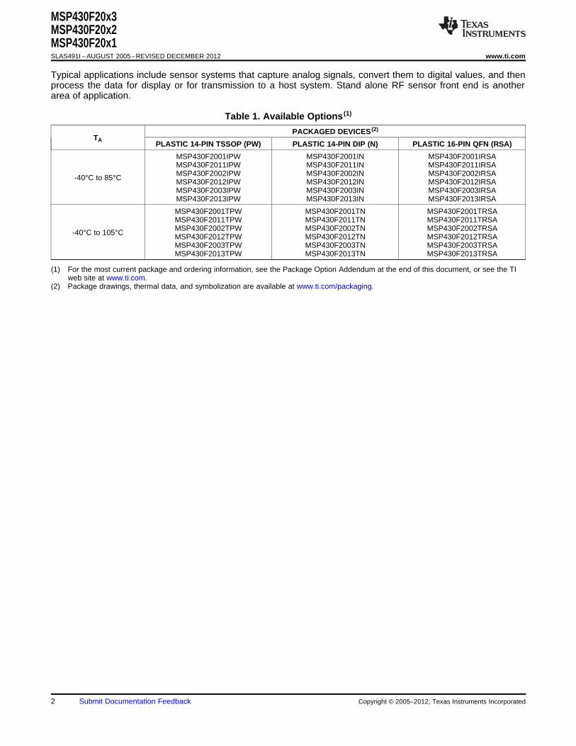
MSP430F20x3MSP430F20x2MSP430F20x1SLAS491I –AUGUST 2005–REVISED DECEMBER 2012 www.ti.com
Typical applications include sensor systems that capture analog signals, convert them to digital values, and thenprocess the data for display or for transmission to a host system. Stand alone RF sensor front end is anotherarea of application.
Table 1. Available Options (1)
PACKAGED DEVICES (2)
TAPLASTIC 14-PIN TSSOP (PW) PLASTIC 14-PIN DIP (N) PLASTIC 16-PIN QFN (RSA)
MSP430F2001IPW MSP430F2001IN MSP430F2001IRSAMSP430F2011IPW MSP430F2011IN MSP430F2011IRSAMSP430F2002IPW MSP430F2002IN MSP430F2002IRSA-40°C to 85°C MSP430F2012IPW MSP430F2012IN MSP430F2012IRSAMSP430F2003IPW MSP430F2003IN MSP430F2003IRSAMSP430F2013IPW MSP430F2013IN MSP430F2013IRSA
MSP430F2001TPW MSP430F2001TN MSP430F2001TRSAMSP430F2011TPW MSP430F2011TN MSP430F2011TRSAMSP430F2002TPW MSP430F2002TN MSP430F2002TRSA-40°C to 105°C MSP430F2012TPW MSP430F2012TN MSP430F2012TRSAMSP430F2003TPW MSP430F2003TN MSP430F2003TRSAMSP430F2013TPW MSP430F2013TN MSP430F2013TRSA
(1) For the most current package and ordering information, see the Package Option Addendum at the end of this document, or see the TIweb site at www.ti.com.
(2) Package drawings, thermal data, and symbolization are available at www.ti.com/packaging.
2 Submit Documentation Feedback Copyright © 2005–2012, Texas Instruments Incorporated
1
4
3
2
14
11
12
13
7
6
5
8
9
10
TEST/SBWTCK
VCC VSS
XOUT/P2.7
XIN/P2.6/TA1
RST/NMI/SBWTDIO
P1.7/CAOUT/CA7/TDO/TDI
P1.6/TA1/CA6/TDI/TCLKP1.5/TA0/CA5/TMS
P1.3/CAOUT/CA3
P1.2/TA1/CA2
P1.1/TA0/CA1
P1.0/TACLK/ACLK/CA0
P1.4/SMCLK/CA4/TCK
PW or N PACKAGE
(TOP VIEW)
114
2
3
4 9
10
11
12
6 7
15
RSA PACKAGE
(TOP VIEW)V
CC
VS
S
NC
NC
P1.3/CAOUT/CA3
P1.2/TA1/CA2
P1.1/TA0/CA1
P1.0/TACLK/ACLK/CA0
TEST/SBWTCK
XOUT/P2.7
XIN/P2.6/TA1
RST/NMI/SBWTDIO
P1.7
/CA
OU
T/C
A7/T
DO
/TD
I
P1.6
/TA
1/C
A6/T
DI/T
CLK
P1.4
/SM
CLK
/CA
4/T
CK
P1.5
/TA
0/C
A5/T
MS
MSP430F20x3MSP430F20x2MSP430F20x1
www.ti.com SLAS491I –AUGUST 2005–REVISED DECEMBER 2012
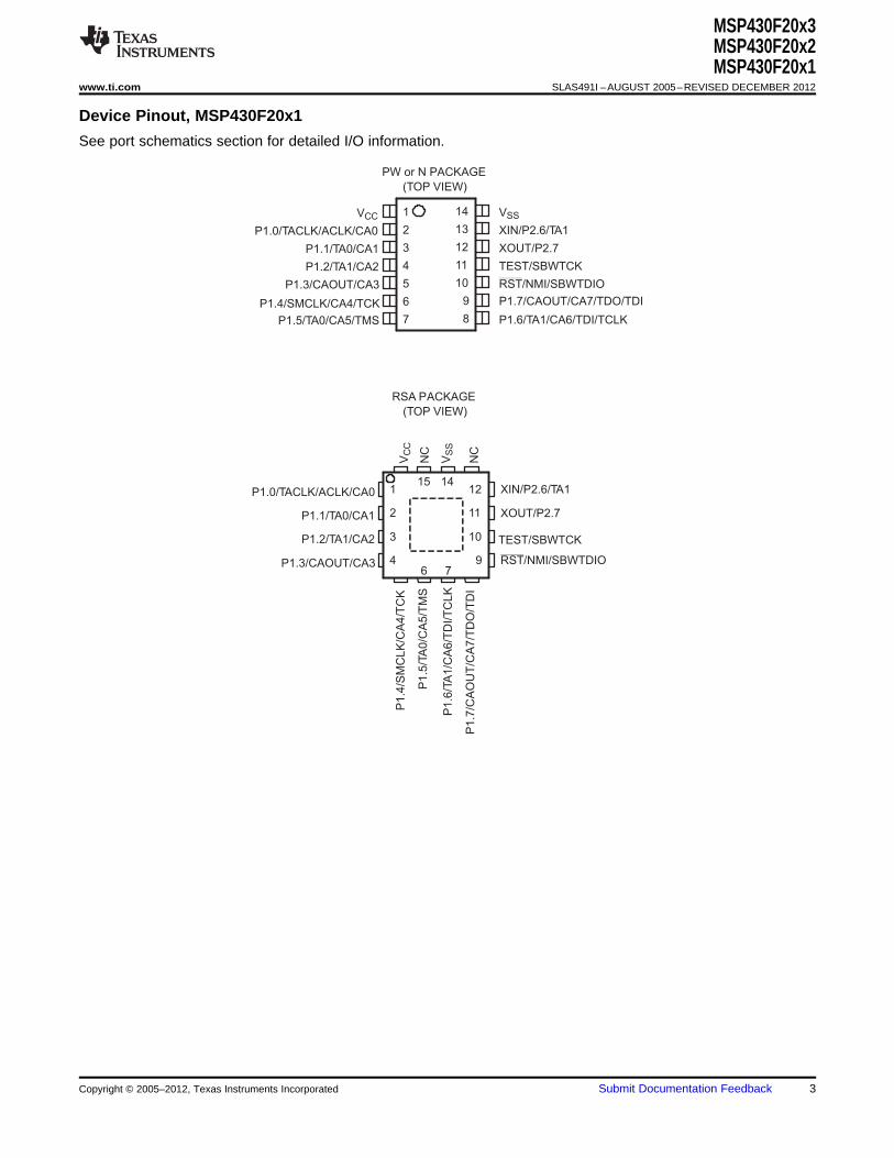
Device Pinout, MSP430F20x1
See port schematics section for detailed I/O information.
Copyright © 2005–2012, Texas Instruments Incorporated Submit Documentation Feedback 3
1
4
3
2
14
11
12
13
7
6
5
8
9
10
TEST/SBWTCK
VCC VSS
XOUT/P2.7
XIN/P2.6/TA1
RST/NMI/SBWTDIO
P1.7/A7/SDI/SDA/TDO/TDI
P1.6/TA1/A6/SDO/SCL/TDI/TCLKP1.5/TA0/A5/SCLK/TMS
P1.3/ADC10CLK/A3/VREF−/VeREF−
P1.2/TA1/A2
P1.1/TA0/A1
P1.0/TACLK/ACLK/A0
P1.4/SMCLK/A4/VREF+/VeREF+/TCK
PW or N PACKAGE
(TOP VIEW)
114
2
3
4 9
10
11
12
6 7
15
RSA PACKAGE
(TOP VIEW)D
VC
C
DV
SS
AV
CC
AV
SS
P1.3/ADC10CLK/A3/VREF−/VeREF−
P1.2/TA1/A2
P1.1/TA0/A1
P1.0/TACLK/ACLK/A0
TEST/SBWTCK
XOUT/P2.7
XIN/P2.6/TA1
RST/NMI/SBWTDIO
P1.7
/A7/S
DI/S
DA
/TD
O/T
DI
P1.6
/TA
1/A
6/S
DO
/SC
L/T
DI/T
CLK
P1.4
/SM
CLK
/A4/V
RE
F+
/VeR
EF
+/T
CK
P1.5
/TA
0/A
5/S
CLK
/TM
S
MSP430F20x3MSP430F20x2MSP430F20x1SLAS491I –AUGUST 2005–REVISED DECEMBER 2012 www.ti.com
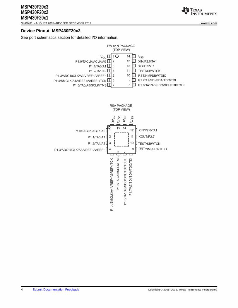
Device Pinout, MSP430F20x2
See port schematics section for detailed I/O information.
4 Submit Documentation Feedback Copyright © 2005–2012, Texas Instruments Incorporated
1
4
3
2
14
11
12
13
7
6
5
8
9
10
TEST/SBWTCK
VCC VSS
XOUT/P2.7
XIN/P2.6/TA1
RST/NMI/SBWTDIO
P1.7/A3−/SDI/SDA/TDO/TDI
P1.6/TA1/A3+/SDO/SCL/TDI/TCLKP1.5/TA0/A2−/SCLK/TMS
P1.3/VREF/A1−
P1.2/TA1/A1+/A4−
P1.1/TA0/A0−/A4+
P1.0/TACLK/ACLK/A0+
P1.4/SMCLK/A2+/TCK
PW or N PACKAGE
(TOP VIEW)
114
2
3
4 9
10
11
12
6 7
15
RSA PACKAGE
(TOP VIEW)
DV
CC
DV
SS
AV
CC
AV
SS
P1.3/VREF/A1−
P1.2/TA1/A1+/A4−
P1.1/TA0/A0−/A4+
P1.0/TACLK/ACLK/A0+
TEST/SBWTCK
XOUT/P2.7
XIN/P2.6/TA1
RST/NMI/SBWTDIO
P1.7
/A3
−/S
DI/S
DA
/TD
O/T
DI
P1.6
/TA
1/A
3+
/SD
O/S
CL/T
DI/T
CLK
P1.4
/SM
CLK
/A2+
/TC
K
P1.5
/TA
0/A
2−
/SC
LK
/TM
S
MSP430F20x3MSP430F20x2MSP430F20x1
www.ti.com SLAS491I –AUGUST 2005–REVISED DECEMBER 2012
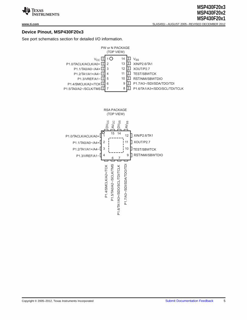
Device Pinout, MSP430F20x3
See port schematics section for detailed I/O information.
Copyright © 2005–2012, Texas Instruments Incorporated Submit Documentation Feedback 5
Basic Clock
System+RAM
128B
128B
Brownout
Protection
RST/NMI
VCC VSS
MCLK
SMCLK
Watchdog
WDT+
15/16−Bit
Timer_A2
2 CC
Registers
16MHz
CPU
incl. 16
Registers
Emulation
(2BP)
XOUT
JTAG
Interface
Flash
2kB
1kB
ACLK
XIN
Port P1
8 I/OInterrupt
capability,
pull−up/down
resistors
ADC10
10−bit
8 Channels
Autoscan
DTC
P1.x & JTAG
8 2
Port P2
2 I/OInterrupt
capability,
pull−up/down
resistors
MDB
MAB
USI
Universal
Serial
Interface
SPI, I2CSpy−Bi Wire
P2.x &
XIN/XOUT
Basic Clock
System+RAM
128B
128B
Brownout
Protection
RST/NMI
VCC VSS
MCLK
SMCLK
Watchdog
WDT+
15/16−Bit
Timer_A2
2 CC
Registers
16MHz
CPU
incl. 16
Registers
Emulation
(2BP)
XOUT
JTAG
Interface
Flash
2kB
1kB
ACLK
XIN
Port P1
8 I/OInterrupt
capability,
pull−up/down
resistors
Comparator
_A+
8 channel
input mux
P1.x & JTAG
8 2
Port P2
2 I/OInterrupt
capability,
pull−up/down
resistors
MDB
MAB
Spy−Bi Wire
P2.x &
XIN/XOUT
MSP430F20x3MSP430F20x2MSP430F20x1SLAS491I –AUGUST 2005–REVISED DECEMBER 2012 www.ti.com
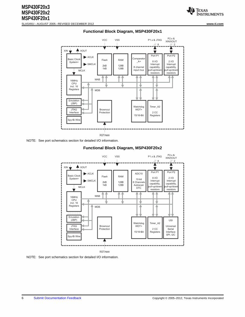
Functional Block Diagram, MSP430F20x1
NOTE: See port schematics section for detailed I/O information.
Functional Block Diagram, MSP430F20x2
NOTE: See port schematics section for detailed I/O information.
6 Submit Documentation Feedback Copyright © 2005–2012, Texas Instruments Incorporated
Basic Clock
System+RAM
128B
128B
Brownout
Protection
RST/NMI
VCC VSS
MCLK
SMCLK
Watchdog
WDT+
15/16−Bit
Timer_A2
2 CC
Registers
16MHz
CPU
incl. 16
Registers
Emulation
(2BP)
XOUT
JTAG
Interface
Flash
2kB
1kB
ACLK
XIN
Port P1
8 I/OInterrupt
capability,
pull−up/down
resistors
SD16_A
16−bit
Sigma−
Delta A/D
Converter
P1.x & JTAG
8 2
Port P2
2 I/OInterrupt
capability,
pull−up/down
resistors
MDB
MAB
USI
Universal
Serial
Interface
SPI, I2CSpy−Bi Wire
P2.x &
XIN/XOUT
MSP430F20x3MSP430F20x2MSP430F20x1
www.ti.com SLAS491I –AUGUST 2005–REVISED DECEMBER 2012
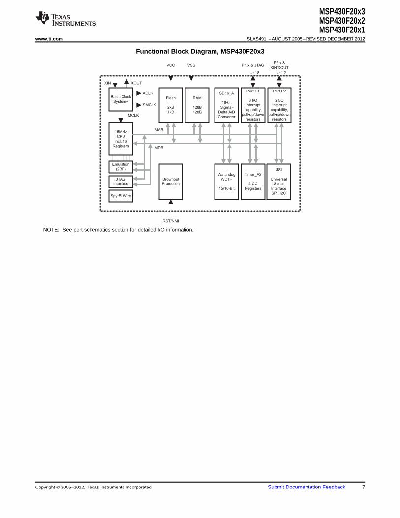
Functional Block Diagram, MSP430F20x3
NOTE: See port schematics section for detailed I/O information.
Copyright © 2005–2012, Texas Instruments Incorporated Submit Documentation Feedback 7
MSP430F20x3MSP430F20x2MSP430F20x1SLAS491I –AUGUST 2005–REVISED DECEMBER 2012 www.ti.com
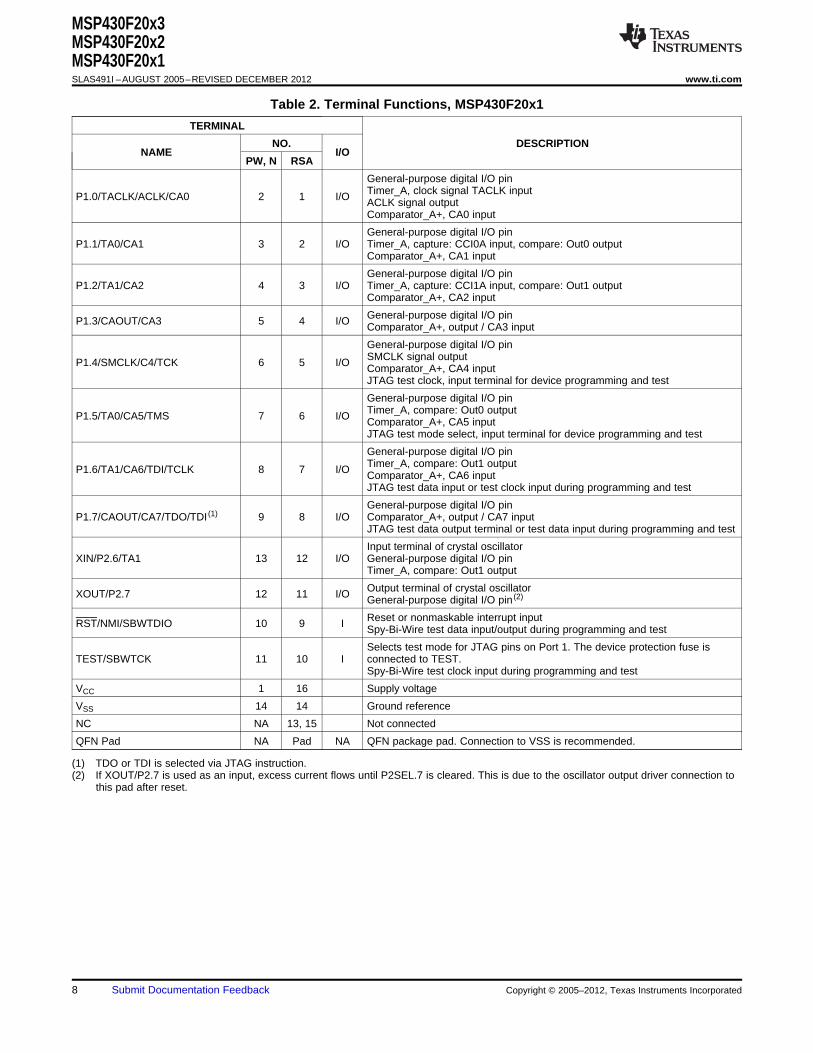
Table 2. Terminal Functions, MSP430F20x1
TERMINAL
NO. DESCRIPTIONNAME I/O
PW, N RSA
General-purpose digital I/O pinTimer_A, clock signal TACLK inputP1.0/TACLK/ACLK/CA0 2 1 I/O ACLK signal outputComparator_A+, CA0 input
General-purpose digital I/O pinP1.1/TA0/CA1 3 2 I/O Timer_A, capture: CCI0A input, compare: Out0 output
Comparator_A+, CA1 input
General-purpose digital I/O pinP1.2/TA1/CA2 4 3 I/O Timer_A, capture: CCI1A input, compare: Out1 output
Comparator_A+, CA2 input
General-purpose digital I/O pinP1.3/CAOUT/CA3 5 4 I/O Comparator_A+, output / CA3 input
General-purpose digital I/O pinSMCLK signal outputP1.4/SMCLK/C4/TCK 6 5 I/O Comparator_A+, CA4 inputJTAG test clock, input terminal for device programming and test
General-purpose digital I/O pinTimer_A, compare: Out0 outputP1.5/TA0/CA5/TMS 7 6 I/O Comparator_A+, CA5 inputJTAG test mode select, input terminal for device programming and test
General-purpose digital I/O pinTimer_A, compare: Out1 outputP1.6/TA1/CA6/TDI/TCLK 8 7 I/O Comparator_A+, CA6 inputJTAG test data input or test clock input during programming and test
General-purpose digital I/O pinP1.7/CAOUT/CA7/TDO/TDI (1) 9 8 I/O Comparator_A+, output / CA7 input
JTAG test data output terminal or test data input during programming and test
Input terminal of crystal oscillatorXIN/P2.6/TA1 13 12 I/O General-purpose digital I/O pin
Timer_A, compare: Out1 output
Output terminal of crystal oscillatorXOUT/P2.7 12 11 I/O General-purpose digital I/O pin (2)
Reset or nonmaskable interrupt inputRST/NMI/SBWTDIO 10 9 I Spy-Bi-Wire test data input/output during programming and test
Selects test mode for JTAG pins on Port 1. The device protection fuse isTEST/SBWTCK 11 10 I connected to TEST.
Spy-Bi-Wire test clock input during programming and test
VCC 1 16 Supply voltage
VSS 14 14 Ground reference
NC NA 13, 15 Not connected
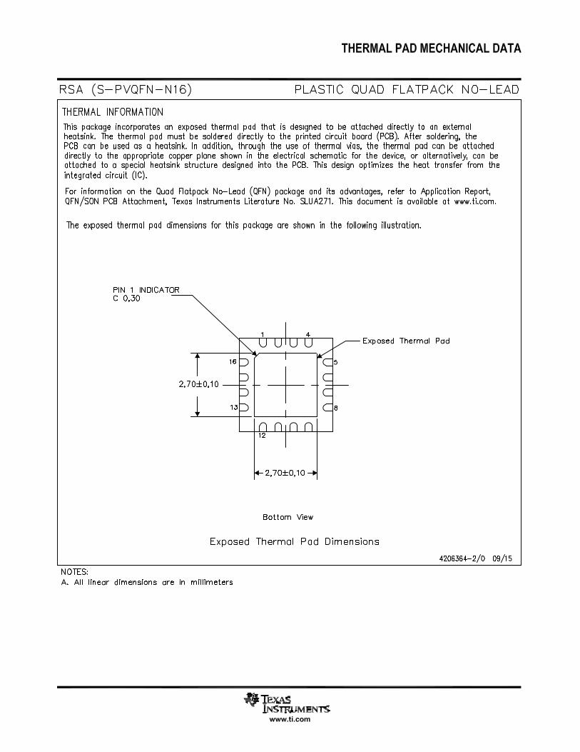
QFN Pad NA Pad NA QFN package pad. Connection to VSS is recommended.
(1) TDO or TDI is selected via JTAG instruction.(2) If XOUT/P2.7 is used as an input, excess current flows until P2SEL.7 is cleared. This is due to the oscillator output driver connection to
this pad after reset.
8 Submit Documentation Feedback Copyright © 2005–2012, Texas Instruments Incorporated
MSP430F20x3MSP430F20x2MSP430F20x1
www.ti.com SLAS491I –AUGUST 2005–REVISED DECEMBER 2012
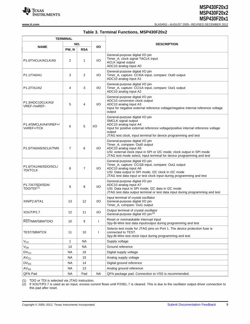
Table 3. Terminal Functions, MSP430F20x2
TERMINAL
NO. DESCRIPTIONNAME I/O
PW, N RSA
General-purpose digital I/O pinTimer_A, clock signal TACLK inputP1.0/TACLK/ACLK/A0 2 1 I/O ACLK signal outputADC10 analog input A0
General-purpose digital I/O pinP1.1/TA0/A1 3 2 I/O Timer_A, capture: CCI0A input, compare: Out0 output
ADC10 analog input A1
General-purpose digital I/O pinP1.2/TA1/A2 4 3 I/O Timer_A, capture: CCI1A input, compare: Out1 output
ADC10 analog input A2
General-purpose digital I/O pinADC10 conversion clock outputP1.3/ADC10CLK/A3/ 5 4 I/O ADC10 analog input A3VREF-/VeREF- Input for negative external reference voltage/negative internal reference voltageoutput
General-purpose digital I/O pinSMCLK signal output
P1.4/SMCLK/A4/VREF+/ ADC10 analog input A46 5 I/OVeREF+/TCK Input for positive external reference voltage/positive internal reference voltageoutputJTAG test clock, input terminal for device programming and test
General-purpose digital I/O pinTimer_A, compare: Out0 output
P1.5/TA0/A5/SCLK/TMS 7 6 I/O ADC10 analog input A5USI: external clock input in SPI or I2C mode; clock output in SPI modeJTAG test mode select, input terminal for device programming and test
General-purpose digital I/O pinTimer_A, capture: CCI1B input, compare: Out1 outputP1.6/TA1/A6/SDO/SCL/ 8 7 I/O ADC10 analog input A6TDI/TCLK USI: Data output in SPI mode; I2C clock in I2C modeJTAG test data input or test clock input during programming and test
General-purpose digital I/O pinP1.7/A7/SDI/SDA/ ADC10 analog input A79 8 I/OTDO/TDI (1) USI: Data input in SPI mode; I2C data in I2C mode
JTAG test data output terminal or test data input during programming and test
Input terminal of crystal oscillatorXIN/P2.6/TA1 13 12 I/O General-purpose digital I/O pin
Timer_A, compare: Out1 output
Output terminal of crystal oscillatorXOUT/P2.7 12 11 I/O General-purpose digital I/O pin (2)
Reset or nonmaskable interrupt inputRST/NMI/SBWTDIO 10 9 I Spy-Bi-Wire test data input/output during programming and test
Selects test mode for JTAG pins on Port 1. The device protection fuse isTEST/SBWTCK 11 10 I connected to TEST.
Spy-Bi-Wire test clock input during programming and test
VCC 1 NA Supply voltage
VSS 14 NA Ground reference
DVCC NA 16 Digital supply voltage
AVCC NA 15 Analog supply voltage
DVSS NA 14 Digital ground reference
AVSS NA 13 Analog ground reference
QFN Pad NA Pad NA QFN package pad. Connection to VSS is recommended.
(1) TDO or TDI is selected via JTAG instruction.(2) If XOUT/P2.7 is used as an input, excess current flows until P2SEL.7 is cleared. This is due to the oscillator output driver connection to
this pad after reset.
Copyright © 2005–2012, Texas Instruments Incorporated Submit Documentation Feedback 9
MSP430F20x3MSP430F20x2MSP430F20x1SLAS491I –AUGUST 2005–REVISED DECEMBER 2012 www.ti.com
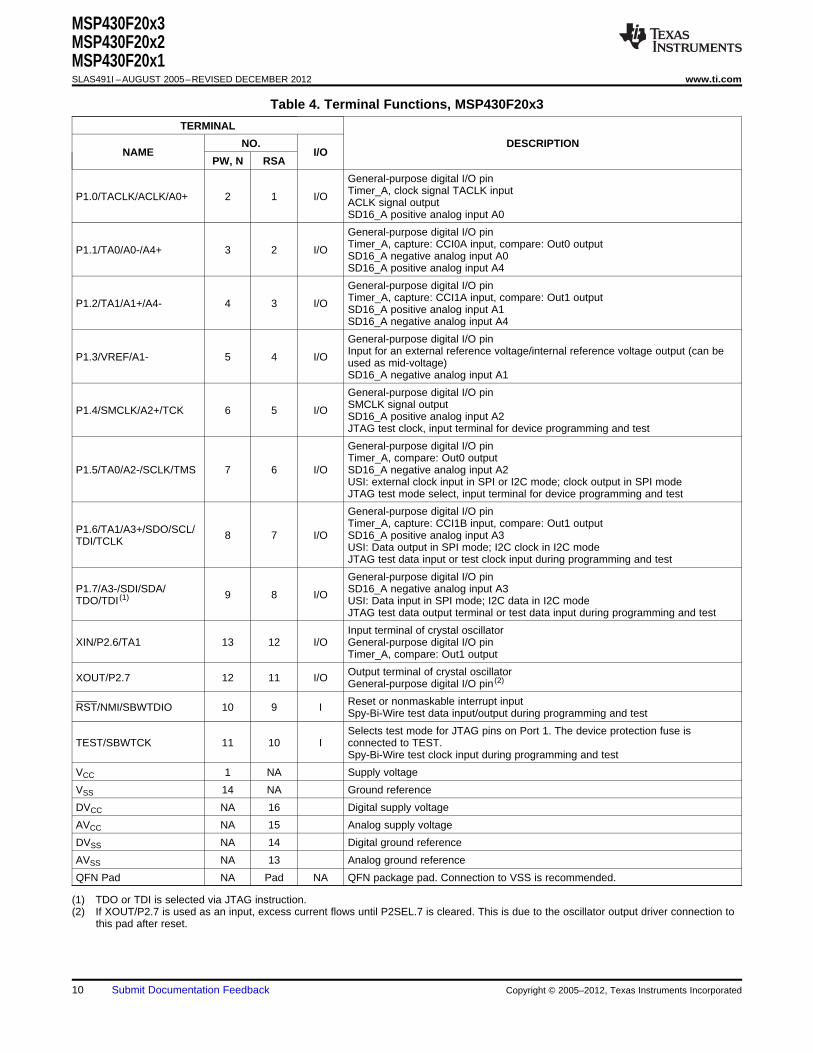
Table 4. Terminal Functions, MSP430F20x3
TERMINAL
NO. DESCRIPTIONNAME I/O
PW, N RSA
General-purpose digital I/O pinTimer_A, clock signal TACLK inputP1.0/TACLK/ACLK/A0+ 2 1 I/O ACLK signal outputSD16_A positive analog input A0
General-purpose digital I/O pinTimer_A, capture: CCI0A input, compare: Out0 outputP1.1/TA0/A0-/A4+ 3 2 I/O SD16_A negative analog input A0SD16_A positive analog input A4
General-purpose digital I/O pinTimer_A, capture: CCI1A input, compare: Out1 outputP1.2/TA1/A1+/A4- 4 3 I/O SD16_A positive analog input A1SD16_A negative analog input A4
General-purpose digital I/O pinInput for an external reference voltage/internal reference voltage output (can beP1.3/VREF/A1- 5 4 I/O used as mid-voltage)SD16_A negative analog input A1
General-purpose digital I/O pinSMCLK signal outputP1.4/SMCLK/A2+/TCK 6 5 I/O SD16_A positive analog input A2JTAG test clock, input terminal for device programming and test
General-purpose digital I/O pinTimer_A, compare: Out0 output
P1.5/TA0/A2-/SCLK/TMS 7 6 I/O SD16_A negative analog input A2USI: external clock input in SPI or I2C mode; clock output in SPI modeJTAG test mode select, input terminal for device programming and test
General-purpose digital I/O pinTimer_A, capture: CCI1B input, compare: Out1 outputP1.6/TA1/A3+/SDO/SCL/ 8 7 I/O SD16_A positive analog input A3TDI/TCLK USI: Data output in SPI mode; I2C clock in I2C modeJTAG test data input or test clock input during programming and test
General-purpose digital I/O pinP1.7/A3-/SDI/SDA/ SD16_A negative analog input A39 8 I/OTDO/TDI (1) USI: Data input in SPI mode; I2C data in I2C mode
JTAG test data output terminal or test data input during programming and test
Input terminal of crystal oscillatorXIN/P2.6/TA1 13 12 I/O General-purpose digital I/O pin
Timer_A, compare: Out1 output
Output terminal of crystal oscillatorXOUT/P2.7 12 11 I/O General-purpose digital I/O pin (2)
Reset or nonmaskable interrupt inputRST/NMI/SBWTDIO 10 9 I Spy-Bi-Wire test data input/output during programming and test
Selects test mode for JTAG pins on Port 1. The device protection fuse isTEST/SBWTCK 11 10 I connected to TEST.
Spy-Bi-Wire test clock input during programming and test
VCC 1 NA Supply voltage
VSS 14 NA Ground reference
DVCC NA 16 Digital supply voltage
AVCC NA 15 Analog supply voltage
DVSS NA 14 Digital ground reference
AVSS NA 13 Analog ground reference
QFN Pad NA Pad NA QFN package pad. Connection to VSS is recommended.
(1) TDO or TDI is selected via JTAG instruction.(2) If XOUT/P2.7 is used as an input, excess current flows until P2SEL.7 is cleared. This is due to the oscillator output driver connection to
this pad after reset.
10 Submit Documentation Feedback Copyright © 2005–2012, Texas Instruments Incorporated
General-Purpose Register
Program Counter
Stack Pointer
Status Register
Constant Generator
General-Purpose Register
General-Purpose Register
General-Purpose Register
PC/R0
SP/R1
SR/CG1/R2
CG2/R3
R4
R5
R12
R13
General-Purpose Register
General-Purpose Register
R6
R7
General-Purpose Register
General-Purpose Register
R8
R9
General-Purpose Register
General-Purpose Register
R10
R11
General-Purpose Register
General-Purpose Register
R14
R15
MSP430F20x3MSP430F20x2MSP430F20x1
www.ti.com SLAS491I –AUGUST 2005–REVISED DECEMBER 2012
SHORT-FORM DESCRIPTION
CPU
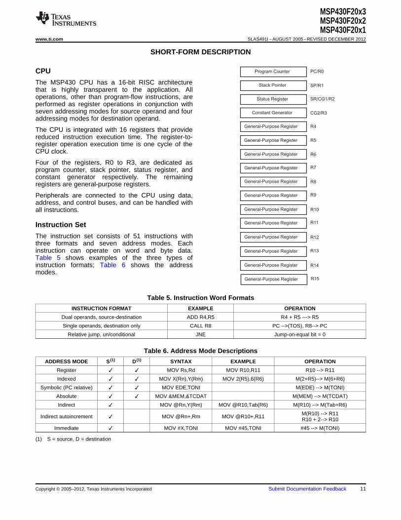
The MSP430 CPU has a 16-bit RISC architecturethat is highly transparent to the application. Alloperations, other than program-flow instructions, areperformed as register operations in conjunction withseven addressing modes for source operand and fouraddressing modes for destination operand.
The CPU is integrated with 16 registers that providereduced instruction execution time. The register-to-register operation execution time is one cycle of theCPU clock.
Four of the registers, R0 to R3, are dedicated asprogram counter, stack pointer, status register, andconstant generator respectively. The remainingregisters are general-purpose registers.
Peripherals are connected to the CPU using data,address, and control buses, and can be handled withall instructions.
Instruction Set
The instruction set consists of 51 instructions withthree formats and seven address modes. Eachinstruction can operate on word and byte data.Table 5 shows examples of the three types ofinstruction formats; Table 6 shows the addressmodes.
Table 5. Instruction Word Formats
INSTRUCTION FORMAT EXAMPLE OPERATION
Dual operands, source-destination ADD R4,R5 R4 + R5 ---> R5
Single operands, destination only CALL R8 PC -->(TOS), R8--> PC
Relative jump, un/conditional JNE Jump-on-equal bit = 0
Table 6. Address Mode Descriptions
ADDRESS MODE S (1) D (1) SYNTAX EXAMPLE OPERATION
Register MOV Rs,Rd MOV R10,R11 R10 --> R11
Indexed MOV X(Rn),Y(Rm) MOV 2(R5),6(R6) M(2+R5)--> M(6+R6)
Symbolic (PC relative) MOV EDE,TONI M(EDE) --> M(TONI)
Absolute MOV &MEM,&TCDAT M(MEM) --> M(TCDAT)
Indirect MOV @Rn,Y(Rm) MOV @R10,Tab(R6) M(R10) --> M(Tab+R6)
M(R10) --> R11Indirect autoincrement MOV @Rn+,Rm MOV @R10+,R11 R10 + 2--> R10
Immediate MOV #X,TONI MOV #45,TONI #45 --> M(TONI)
(1) S = source, D = destination
Copyright © 2005–2012, Texas Instruments Incorporated Submit Documentation Feedback 11
MSP430F20x3MSP430F20x2MSP430F20x1SLAS491I –AUGUST 2005–REVISED DECEMBER 2012 www.ti.com
Operating Modes
The MSP430 has one active mode and five software-selectable low-power modes of operation. An interruptevent can wake the device from any of the five low-power modes, service the request, and restore back to thelow-power mode on return from the interrupt program.
The following six operating modes can be configured by software:• Active mode (AM)
– All clocks are active• Low-power mode 0 (LPM0)
– CPU is disabled– ACLK and SMCLK remain active– MCLK is disabled
• Low-power mode 1 (LPM1)– CPU is disabled– ACLK and SMCLK remain active. MCLK is disabled– DCO's dc-generator is disabled if DCO not used in active mode
• Low-power mode 2 (LPM2)– CPU is disabled– MCLK and SMCLK are disabled– DCO's dc-generator remains enabled– ACLK remains active
• Low-power mode 3 (LPM3)– CPU is disabled– MCLK and SMCLK are disabled– DCO's dc-generator is disabled– ACLK remains active
• Low-power mode 4 (LPM4)– CPU is disabled– ACLK is disabled– MCLK and SMCLK are disabled– DCO's dc-generator is disabled– Crystal oscillator is stopped
12 Submit Documentation Feedback Copyright © 2005–2012, Texas Instruments Incorporated
MSP430F20x3MSP430F20x2MSP430F20x1
www.ti.com SLAS491I –AUGUST 2005–REVISED DECEMBER 2012
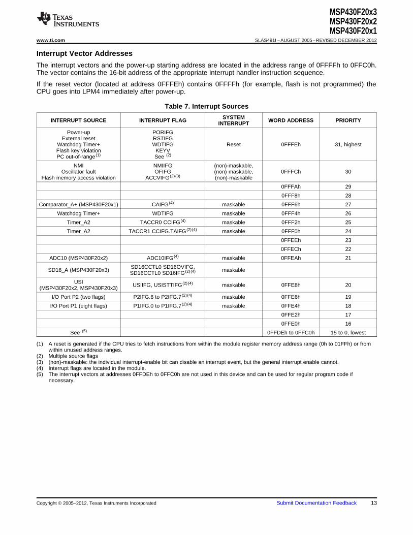
Interrupt Vector Addresses
The interrupt vectors and the power-up starting address are located in the address range of 0FFFFh to 0FFC0h.The vector contains the 16-bit address of the appropriate interrupt handler instruction sequence.
If the reset vector (located at address 0FFFEh) contains 0FFFFh (for example, flash is not programmed) theCPU goes into LPM4 immediately after power-up.
Table 7. Interrupt Sources
SYSTEMINTERRUPT SOURCE INTERRUPT FLAG WORD ADDRESS PRIORITYINTERRUPT
Power-up PORIFGExternal reset RSTIFG
Watchdog Timer+ WDTIFG Reset 0FFFEh 31, highestFlash key violation KEYVPC out-of-range (1) See (2)
NMI NMIIFG (non)-maskable,Oscillator fault OFIFG (non)-maskable, 0FFFCh 30
Flash memory access violation ACCVIFG (2) (3) (non)-maskable
0FFFAh 29
0FFF8h 28
Comparator_A+ (MSP430F20x1) CAIFG (4) maskable 0FFF6h 27
Watchdog Timer+ WDTIFG maskable 0FFF4h 26
Timer_A2 TACCR0 CCIFG (4) maskable 0FFF2h 25
Timer_A2 TACCR1 CCIFG.TAIFG (2) (4) maskable 0FFF0h 24
0FFEEh 23
0FFECh 22
ADC10 (MSP430F20x2) ADC10IFG (4) maskable 0FFEAh 21
SD16CCTL0 SD16OVIFG,SD16_A (MSP430F20x3) maskableSD16CCTL0 SD16IFG (2) (4)
USI USIIFG, USISTTIFG (2) (4) maskable 0FFE8h 20(MSP430F20x2, MSP430F20x3)
I/O Port P2 (two flags) P2IFG.6 to P2IFG.7 (2) (4) maskable 0FFE6h 19
I/O Port P1 (eight flags) P1IFG.0 to P1IFG.7 (2) (4) maskable 0FFE4h 18
0FFE2h 17
0FFE0h 16
See (5) 0FFDEh to 0FFC0h 15 to 0, lowest
(1) A reset is generated if the CPU tries to fetch instructions from within the module register memory address range (0h to 01FFh) or fromwithin unused address ranges.
(2) Multiple source flags(3) (non)-maskable: the individual interrupt-enable bit can disable an interrupt event, but the general interrupt enable cannot.(4) Interrupt flags are located in the module.(5) The interrupt vectors at addresses 0FFDEh to 0FFC0h are not used in this device and can be used for regular program code if
necessary.
Copyright © 2005–2012, Texas Instruments Incorporated Submit Documentation Feedback 13
MSP430F20x3MSP430F20x2MSP430F20x1SLAS491I –AUGUST 2005–REVISED DECEMBER 2012 www.ti.com
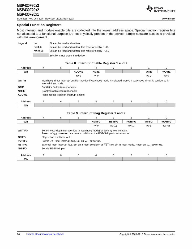
Special Function Registers
Most interrupt and module enable bits are collected into the lowest address space. Special function register bitsnot allocated to a functional purpose are not physically present in the device. Simple software access is providedwith this arrangement.
Legend rw: Bit can be read and written.
rw-0,1: Bit can be read and written. It is reset or set by PUC.
rw-(0,1): Bit can be read and written. It is reset or set by POR.
SFR bit is not present in device.
Table 8. Interrupt Enable Register 1 and 2Address 7 6 5 4 3 2 1 0
00h ACCVIE NMIIE OFIE WDTIE
rw-0 rw-0 rw-0 rw-0
WDTIE Watchdog Timer interrupt enable. Inactive if watchdog mode is selected. Active if Watchdog Timer is configured ininterval timer mode.
OFIE Oscillator fault interrupt enable
NMIIE (Non)maskable interrupt enable
ACCVIE Flash access violation interrupt enable
Address 7 6 5 4 3 2 1 0
01h
Table 9. Interrupt Flag Register 1 and 2Address 7 6 5 4 3 2 1 0
02h NMIIFG RSTIFG PORIFG OFIFG WDTIFG
rw-0 rw-(0) rw-(1) rw-1 rw-(0)
WDTIFG Set on watchdog timer overflow (in watchdog mode) or security key violation.Reset on VCC power-on or a reset condition at the RST/NMI pin in reset mode.
OFIFG Flag set on oscillator fault.
PORIFG Power-On Reset interrupt flag. Set on VCC power-up.
RSTIFG External reset interrupt flag. Set on a reset condition at RST/NMI pin in reset mode. Reset on VCC power-up.
NMIIFG Set via RST/NMI pin
Address 7 6 5 4 3 2 1 0
03h
14 Submit Documentation Feedback Copyright © 2005–2012, Texas Instruments Incorporated
MSP430F20x3MSP430F20x2MSP430F20x1
www.ti.com SLAS491I –AUGUST 2005–REVISED DECEMBER 2012
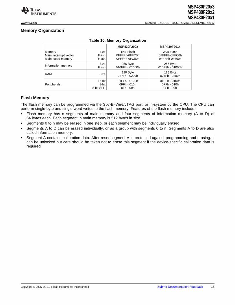
Memory Organization
Table 10. Memory Organization
MSP430F200x MSP430F201x
Memory Size 1KB Flash 2KB FlashMain: interrupt vector Flash 0FFFFh-0FFC0h 0FFFFh-0FFC0hMain: code memory Flash 0FFFFh-0FC00h 0FFFFh-0F800h
Size 256 Byte 256 ByteInformation memory Flash 010FFh - 01000h 010FFh - 01000h
128 Byte 128 ByteRAM Size 027Fh - 0200h 027Fh - 0200h
16-bit 01FFh - 0100h 01FFh - 0100hPeripherals 8-bit 0FFh - 010h 0FFh - 010h
8-bit SFR 0Fh - 00h 0Fh - 00h
Flash Memory
The flash memory can be programmed via the Spy-Bi-Wire/JTAG port, or in-system by the CPU. The CPU canperform single-byte and single-word writes to the flash memory. Features of the flash memory include:• Flash memory has n segments of main memory and four segments of information memory (A to D) of
64 bytes each. Each segment in main memory is 512 bytes in size.• Segments 0 to n may be erased in one step, or each segment may be individually erased.• Segments A to D can be erased individually, or as a group with segments 0 to n. Segments A to D are also
called information memory.• Segment A contains calibration data. After reset segment A is protected against programming and erasing. It
can be unlocked but care should be taken not to erase this segment if the device-specific calibration data isrequired.
Copyright © 2005–2012, Texas Instruments Incorporated Submit Documentation Feedback 15
MSP430F20x3MSP430F20x2MSP430F20x1SLAS491I –AUGUST 2005–REVISED DECEMBER 2012 www.ti.com
Peripherals
Peripherals are connected to the CPU through data, address, and control busses and can be handled using allinstructions. For complete module descriptions, refer to the MSP430F2xx Family User's Guide.
Oscillator and System Clock
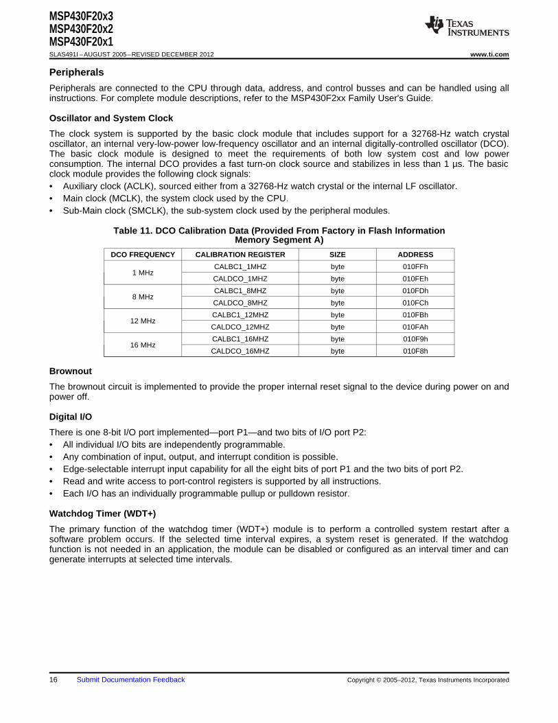
The clock system is supported by the basic clock module that includes support for a 32768-Hz watch crystaloscillator, an internal very-low-power low-frequency oscillator and an internal digitally-controlled oscillator (DCO).The basic clock module is designed to meet the requirements of both low system cost and low powerconsumption. The internal DCO provides a fast turn-on clock source and stabilizes in less than 1 µs. The basicclock module provides the following clock signals:• Auxiliary clock (ACLK), sourced either from a 32768-Hz watch crystal or the internal LF oscillator.• Main clock (MCLK), the system clock used by the CPU.• Sub-Main clock (SMCLK), the sub-system clock used by the peripheral modules.
Table 11. DCO Calibration Data (Provided From Factory in Flash InformationMemory Segment A)
DCO FREQUENCY CALIBRATION REGISTER SIZE ADDRESS
CALBC1_1MHZ byte 010FFh1 MHz
CALDCO_1MHZ byte 010FEh
CALBC1_8MHZ byte 010FDh8 MHz
CALDCO_8MHZ byte 010FCh
CALBC1_12MHZ byte 010FBh12 MHz
CALDCO_12MHZ byte 010FAh
CALBC1_16MHZ byte 010F9h16 MHz
CALDCO_16MHZ byte 010F8h
Brownout
The brownout circuit is implemented to provide the proper internal reset signal to the device during power on andpower off.
Digital I/O
There is one 8-bit I/O port implemented—port P1—and two bits of I/O port P2:• All individual I/O bits are independently programmable.• Any combination of input, output, and interrupt condition is possible.• Edge-selectable interrupt input capability for all the eight bits of port P1 and the two bits of port P2.• Read and write access to port-control registers is supported by all instructions.• Each I/O has an individually programmable pullup or pulldown resistor.
Watchdog Timer (WDT+)
The primary function of the watchdog timer (WDT+) module is to perform a controlled system restart after asoftware problem occurs. If the selected time interval expires, a system reset is generated. If the watchdogfunction is not needed in an application, the module can be disabled or configured as an interval timer and cangenerate interrupts at selected time intervals.
16 Submit Documentation Feedback Copyright © 2005–2012, Texas Instruments Incorporated
MSP430F20x3MSP430F20x2MSP430F20x1
www.ti.com SLAS491I –AUGUST 2005–REVISED DECEMBER 2012
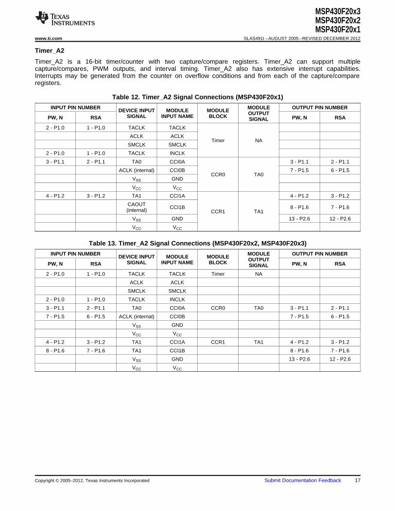
Timer_A2
Timer_A2 is a 16-bit timer/counter with two capture/compare registers. Timer_A2 can support multiplecapture/compares, PWM outputs, and interval timing. Timer_A2 also has extensive interrupt capabilities.Interrupts may be generated from the counter on overflow conditions and from each of the capture/compareregisters.
Table 12. Timer_A2 Signal Connections (MSP430F20x1)
INPUT PIN NUMBER MODULE OUTPUT PIN NUMBERDEVICE INPUT MODULE MODULE OUTPUTSIGNAL INPUT NAME BLOCKPW, N RSA PW, N RSASIGNAL
2 - P1.0 1 - P1.0 TACLK TACLK
ACLK ACLKTimer NA
SMCLK SMCLK
2 - P1.0 1 - P1.0 TACLK INCLK
3 - P1.1 2 - P1.1 TA0 CCI0A 3 - P1.1 2 - P1.1
ACLK (internal) CCI0B 7 - P1.5 6 - P1.5CCR0 TA0
VSS GND
VCC VCC
4 - P1.2 3 - P1.2 TA1 CCI1A 4 - P1.2 3 - P1.2
CAOUT CCI1B 8 - P1.6 7 - P1.6(internal) CCR1 TA1VSS GND 13 - P2.6 12 - P2.6
VCC VCC
Table 13. Timer_A2 Signal Connections (MSP430F20x2, MSP430F20x3)
INPUT PIN NUMBER MODULE OUTPUT PIN NUMBERDEVICE INPUT MODULE MODULE OUTPUTSIGNAL INPUT NAME BLOCKPW, N RSA PW, N RSASIGNAL
2 - P1.0 1 - P1.0 TACLK TACLK Timer NA
ACLK ACLK
SMCLK SMCLK
2 - P1.0 1 - P1.0 TACLK INCLK
3 - P1.1 2 - P1.1 TA0 CCI0A CCR0 TA0 3 - P1.1 2 - P1.1
7 - P1.5 6 - P1.5 ACLK (internal) CCI0B 7 - P1.5 6 - P1.5
VSS GND
VCC VCC
4 - P1.2 3 - P1.2 TA1 CCI1A CCR1 TA1 4 - P1.2 3 - P1.2
8 - P1.6 7 - P1.6 TA1 CCI1B 8 - P1.6 7 - P1.6
VSS GND 13 - P2.6 12 - P2.6
VCC VCC
Copyright © 2005–2012, Texas Instruments Incorporated Submit Documentation Feedback 17
MSP430F20x3MSP430F20x2MSP430F20x1SLAS491I –AUGUST 2005–REVISED DECEMBER 2012 www.ti.com
Comparator_A+ (MSP430F20x1)
The primary function of the comparator_A+ module is to support precision slope analog-to-digital conversions,battery-voltage supervision, and monitoring of external analog signals.
USI (MSP430F20x2 and MSP430F20x3)
The universal serial interface (USI) module is used for serial data communication and provides the basichardware for synchronous communication protocols like SPI and I2C.
ADC10 (MSP430F20x2)
The ADC10 module supports fast, 10-bit analog-to-digital conversions. The module implements a 10-bit SARcore, sample select control, reference generator and data transfer controller, or DTC, for automatic conversionresult handling, allowing ADC samples to be converted and stored without any CPU intervention.
SD16_A (MSP430F20x3)
The SD16_A module supports 16-bit analog-to-digital conversions. The module implements a 16-bit sigma-deltacore and reference generator. In addition to external analog inputs, internal VCC sense and temperature sensorsare also available.
18 Submit Documentation Feedback Copyright © 2005–2012, Texas Instruments Incorporated
MSP430F20x3MSP430F20x2MSP430F20x1
www.ti.com SLAS491I –AUGUST 2005–REVISED DECEMBER 2012
Peripheral File Map
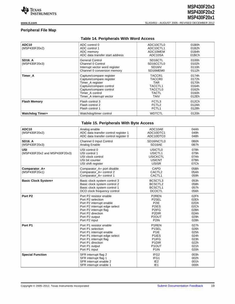
Table 14. Peripherals With Word Access
ADC10 ADC control 0 ADC10CTL0 01B0h(MSP430F20x2) ADC control 1 ADC10CTL1 01B2h
ADC memory ADC10MEM 01B4hADC data transfer start address ADC10SA 01BCh
SD16_A General Control SD16CTL 0100h(MSP430F20x3) Channel 0 Control SD16CCTL0 0102h
Interrupt vector word register SD16IV 0110hChannel 0 conversion memory SD16MEM0 0112h
Timer_A Capture/compare register TACCR1 0174hCapture/compare register TACCR0 0172hTimer_A register TAR 0170hCapture/compare control TACCTL1 0164hCapture/compare control TACCTL0 0162hTimer_A control TACTL 0160hTimer_A interrupt vector TAIV 012Eh
Flash Memory Flash control 3 FCTL3 012ChFlash control 2 FCTL2 012AhFlash control 1 FCTL1 0128h
Watchdog Timer+ Watchdog/timer control WDTCTL 0120h
Table 15. Peripherals With Byte Access
ADC10 Analog enable ADC10AE 04Ah(MSP430F20x2) ADC data transfer control register 1 ADC10DTC1 049h
ADC data transfer control register 0 ADC10DTC0 048h
SD16_A Channel 0 Input Control SD16INCTL0 0B0h(MSP430F20x3) Analog Enable SD16AE 0B7h
USI USI control 0 USICTL0 078h(MSP430F20x2 and MSP430F20x3) USI control 1 USICTL1 079h
USI clock control USICKCTL 07AhUSI bit counter USICNT 07BhUSI shift register USISR 07Ch
Comparator_A+ Comparator_A+ port disable CAPD 05Bh(MSP430F20x1) Comparator_A+ control 2 CACTL2 05Ah
Comparator_A+ control 1 CACTL1 059h
Basic Clock System+ Basic clock system control 3 BCSCTL3 053hBasic clock system control 2 BCSCTL2 058hBasic clock system control 1 BCSCTL1 057hDCO clock frequency control DCOCTL 056h
Port P2 Port P2 resistor enable P2REN 02FhPort P2 selection P2SEL 02EhPort P2 interrupt enable P2IE 02DhPort P2 interrupt edge select P2IES 02ChPort P2 interrupt flag P2IFG 02BhPort P2 direction P2DIR 02AhPort P2 output P2OUT 029hPort P2 input P2IN 028h
Port P1 Port P1 resistor enable P1REN 027hPort P1 selection P1SEL 026hPort P1 interrupt enable P1IE 025hPort P1 interrupt edge select P1IES 024hPort P1 interrupt flag P1IFG 023hPort P1 direction P1DIR 022hPort P1 output P1OUT 021hPort P1 input P1IN 020h
Special Function SFR interrupt flag 2 IFG2 003hSFR interrupt flag 1 IFG1 002hSFR interrupt enable 2 IE2 001hSFR interrupt enable 1 IE1 000h
Copyright © 2005–2012, Texas Instruments Incorporated Submit Documentation Feedback 19
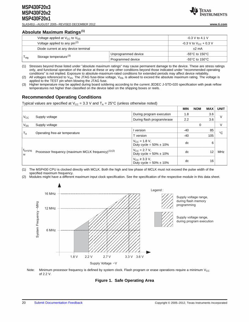
6 MHz
12 MHz
16 MHz
1.8 V 2.2 V 2.7 V 3.3 V 3.6 V
Supply Voltage −V
Syste
mF
reque
ncy
−M
Hz
Supply voltage range,
during flash memory
programming
Supply voltage range,
during program execution
Legend :
MSP430F20x3MSP430F20x2MSP430F20x1SLAS491I –AUGUST 2005–REVISED DECEMBER 2012 www.ti.com
Absolute Maximum Ratings (1)
Voltage applied at VCC to VSS -0.3 V to 4.1 V
Voltage applied to any pin (2) -0.3 V to VCC + 0.3 V
Diode current at any device terminal ±2 mA
Unprogrammed device -55°C to 150°CTstg Storage temperature (3)
Programmed device -55°C to 150°C
(1) Stresses beyond those listed under "absolute maximum ratings" may cause permanent damage to the device. These are stress ratingsonly, and functional operation of the device at these or any other conditions beyond those indicated under "recommended operatingconditions" is not implied. Exposure to absolute-maximum-rated conditions for extended periods may affect device reliability.
(2) All voltages referenced to VSS. The JTAG fuse-blow voltage, VFB, is allowed to exceed the absolute maximum rating. The voltage isapplied to the TEST pin when blowing the JTAG fuse.
(3) Higher temperature may be applied during board soldering according to the current JEDEC J-STD-020 specification with peak reflowtemperatures not higher than classified on the device label on the shipping boxes or reels.
Recommended Operating ConditionsTypical values are specified at VCC = 3.3 V and TA = 25°C (unless otherwise noted)
MIN NOM MAX UNIT
During program execution 1.8 3.6VCC Supply voltage V
During flash program/erase 2.2 3.6
VSS Supply voltage 0 V
I version -40 85TA Operating free-air temperature °C
T version -40 105
VCC = 1.8 V, dc 6Duty cycle = 50% ± 10%
fSYSTE VCC = 2.7 V,Processor frequency (maximum MCLK frequency) (1) (2) dc 12 MHzM Duty cycle = 50% ± 10%
VCC ≥ 3.3 V, dc 16Duty cycle = 50% ± 10%
(1) The MSP430 CPU is clocked directly with MCLK. Both the high and low phase of MCLK must not exceed the pulse width of thespecified maximum frequency.
(2) Modules might have a different maximum input clock specification. See the specification of the respective module in this data sheet.
Note: Minimum processor frequency is defined by system clock. Flash program or erase operations require a minimum VCCof 2.2 V.
Figure 1. Safe Operating Area
20 Submit Documentation Feedback Copyright © 2005–2012, Texas Instruments Incorporated
MSP430F20x3MSP430F20x2MSP430F20x1
www.ti.com SLAS491I –AUGUST 2005–REVISED DECEMBER 2012
Electrical Characteristics
Active Mode Supply Current Into VCC Excluding External Currentover recommended ranges of supply voltage and operating free-air temperature (unless otherwise noted) (1) (2)
PARAMETER TEST CONDITIONS TA VCC MIN TYP MAX UNIT
fDCO = fMCLK = fSMCLK = 1 MHz, 2.2 V 220 270fACLK = 32768 Hz,Program executes in flash,Active mode (AM)IAM,1MHz BCSCTL1 = CALBC1_1MHZ, µAcurrent (1 MHz) 3 V 300 370DCOCTL = CALDCO_1MHZ,CPUOFF = 0, SCG0 = 0,SCG1 = 0, OSCOFF = 0
fDCO = fMCLK = fSMCLK = 1 MHz, 2.2 V 190fACLK = 32768 Hz,Program executes in RAM,Active mode (AM)IAM,1MHz BCSCTL1 = CALBC1_1MHZ, µAcurrent (1 MHz) 3 V 260DCOCTL = CALDCO_1MHZ,CPUOFF = 0, SCG0 = 0,SCG1 = 0, OSCOFF = 0
fMCLK = fSMCLK = fACLK = 32768 Hz/8 -40°C to 85°C 2.2 V 1.2 3= 4096 Hz, 105°C 2.2 V 6fDCO = 0 Hz,
-40°C to 85°C 3 V 1.6 4Active mode (AM) Program executes in flash,IAM,4kHz µAcurrent (4 kHz) SELMx = 11, SELS = 1,DIVMx = DIVSx = DIVAx = 11,
105°C 3 V 7CPUOFF = 0, SCG0 = 1,SCG1 = 0, OSCOFF = 0
fMCLK = fSMCLK = fDCO(0, 0) ≈ 100 kHz, -40°C to 85°C 2.2 V 37 50fACLK = 0 Hz, 105°C 2.2 V 60
Active mode (AM) Program executes in flash,IAM,100kHz µA-40°C to 85°C 3 V 40 55current (100 kHz) RSELx = 0, DCOx = 0,CPUOFF = 0, SCG0 = 0,
105°C 3 V 65SCG1 = 0, OSCOFF = 1
(1) All inputs are tied to 0 V or to VCC. Outputs do not source or sink any current.(2) The currents are characterized with a Micro Crystal CC4V-T1A SMD crystal with a load capacitance of 9 pF. The internal and external
load capacitance is chosen to closely match the required 9 pF.
Copyright © 2005–2012, Texas Instruments Incorporated Submit Documentation Feedback 21
0.0
1.0
2.0
3.0
4.0
5.0
1.5 2.0 2.5 3.0 3.5 4.0
VCC − Supply Voltage − V
Active
Mo
de
Cu
rre
nt
−m
A
fDCO = 1 MHz
fDCO = 8 MHz
fDCO = 12 MHz
fDCO = 16 MHz
0.0
1.0
2.0
3.0
4.0
0.0 4.0 8.0 12.0 16.0
fDCO − DCO Frequency − MHz
Active
Mo
de
Cu
rre
nt
−m
A
T = 25°CA
V = 2.2 VCC
V = 3 VCC
T = 85°CA
T = 25°CA
T = 85°CA
MSP430F20x3MSP430F20x2MSP430F20x1SLAS491I –AUGUST 2005–REVISED DECEMBER 2012 www.ti.com
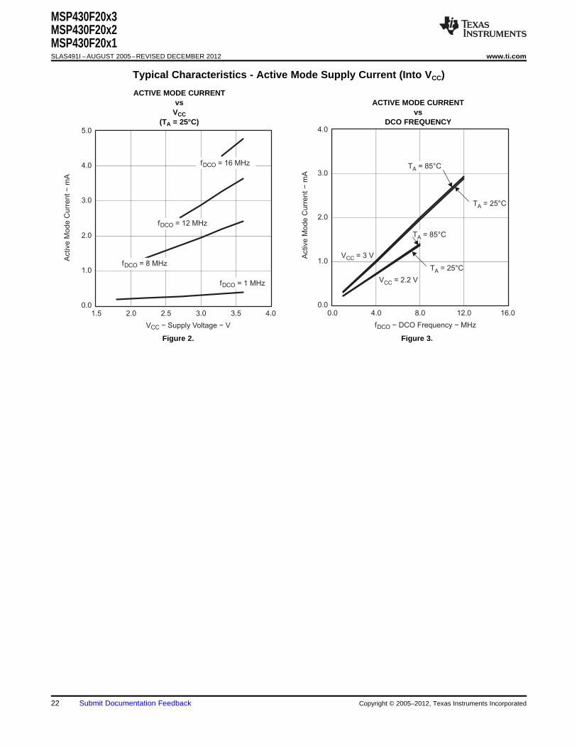
Typical Characteristics - Active Mode Supply Current (Into VCC)
ACTIVE MODE CURRENTvs ACTIVE MODE CURRENT
VCC vs(TA = 25°C) DCO FREQUENCY
Figure 2. Figure 3.
22 Submit Documentation Feedback Copyright © 2005–2012, Texas Instruments Incorporated
MSP430F20x3MSP430F20x2MSP430F20x1
www.ti.com SLAS491I –AUGUST 2005–REVISED DECEMBER 2012
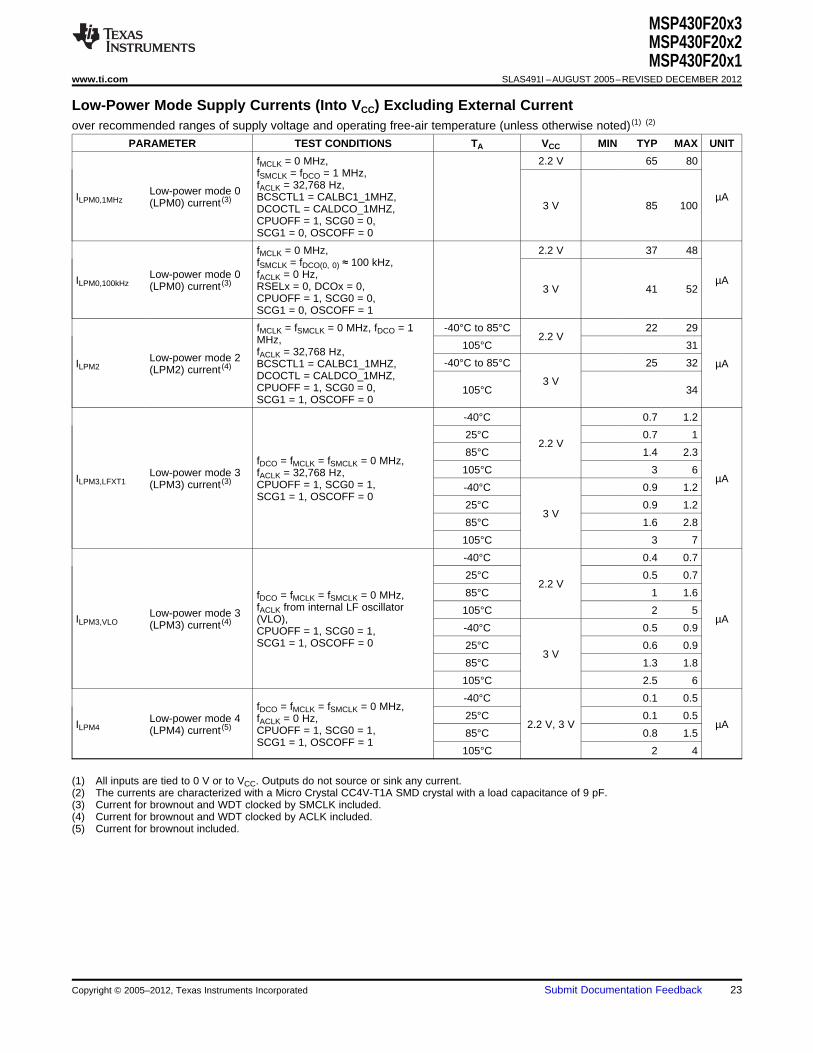
Low-Power Mode Supply Currents (Into VCC) Excluding External Currentover recommended ranges of supply voltage and operating free-air temperature (unless otherwise noted) (1) (2)
PARAMETER TEST CONDITIONS TA VCC MIN TYP MAX UNIT
fMCLK = 0 MHz, 2.2 V 65 80fSMCLK = fDCO = 1 MHz,fACLK = 32,768 Hz,Low-power mode 0ILPM0,1MHz BCSCTL1 = CALBC1_1MHZ, µA(LPM0) current (3)
3 V 85 100DCOCTL = CALDCO_1MHZ,CPUOFF = 1, SCG0 = 0,SCG1 = 0, OSCOFF = 0
fMCLK = 0 MHz, 2.2 V 37 48fSMCLK = fDCO(0, 0) ≈ 100 kHz,
Low-power mode 0 fACLK = 0 Hz,ILPM0,100kHz µA(LPM0) current (3) RSELx = 0, DCOx = 0, 3 V 41 52CPUOFF = 1, SCG0 = 0,SCG1 = 0, OSCOFF = 1
fMCLK = fSMCLK = 0 MHz, fDCO = 1 -40°C to 85°C 22 292.2 VMHz, 105°C 31
fACLK = 32,768 Hz,Low-power mode 2 -40°C to 85°C 25 32ILPM2 BCSCTL1 = CALBC1_1MHZ, µA(LPM2) current (4)DCOCTL = CALDCO_1MHZ, 3 VCPUOFF = 1, SCG0 = 0, 105°C 34SCG1 = 1, OSCOFF = 0
-40°C 0.7 1.2
25°C 0.7 12.2 V
85°C 1.4 2.3fDCO = fMCLK = fSMCLK = 0 MHz,
105°C 3 6Low-power mode 3 fACLK = 32,768 Hz,ILPM3,LFXT1 µA(LPM3) current (3) CPUOFF = 1, SCG0 = 1, -40°C 0.9 1.2SCG1 = 1, OSCOFF = 0
25°C 0.9 1.23 V
85°C 1.6 2.8
105°C 3 7
-40°C 0.4 0.7
25°C 0.5 0.72.2 V
85°C 1 1.6fDCO = fMCLK = fSMCLK = 0 MHz,fACLK from internal LF oscillator 105°C 2 5Low-power mode 3ILPM3,VLO (VLO), µA(LPM3) current (4)
-40°C 0.5 0.9CPUOFF = 1, SCG0 = 1,SCG1 = 1, OSCOFF = 0 25°C 0.6 0.9
3 V85°C 1.3 1.8
105°C 2.5 6
-40°C 0.1 0.5fDCO = fMCLK = fSMCLK = 0 MHz,
25°C 0.1 0.5Low-power mode 4 fACLK = 0 Hz,ILPM4 2.2 V, 3 V µA(LPM4) current (5) CPUOFF = 1, SCG0 = 1, 85°C 0.8 1.5SCG1 = 1, OSCOFF = 1
105°C 2 4
(1) All inputs are tied to 0 V or to VCC. Outputs do not source or sink any current.(2) The currents are characterized with a Micro Crystal CC4V-T1A SMD crystal with a load capacitance of 9 pF.(3) Current for brownout and WDT clocked by SMCLK included.(4) Current for brownout and WDT clocked by ACLK included.(5) Current for brownout included.
Copyright © 2005–2012, Texas Instruments Incorporated Submit Documentation Feedback 23
MSP430F20x3MSP430F20x2MSP430F20x1SLAS491I –AUGUST 2005–REVISED DECEMBER 2012 www.ti.com
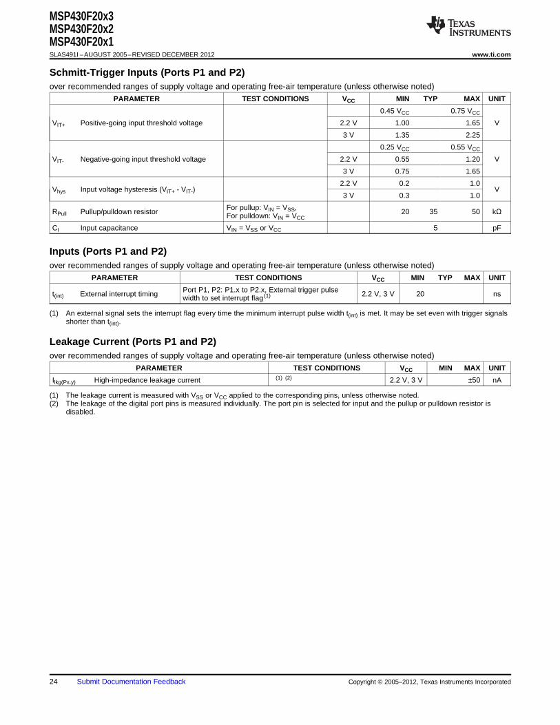
Schmitt-Trigger Inputs (Ports P1 and P2)over recommended ranges of supply voltage and operating free-air temperature (unless otherwise noted)
PARAMETER TEST CONDITIONS VCC MIN TYP MAX UNIT
0.45 VCC 0.75 VCC
VIT+ Positive-going input threshold voltage 2.2 V 1.00 1.65 V
3 V 1.35 2.25
0.25 VCC 0.55 VCC
VIT- Negative-going input threshold voltage 2.2 V 0.55 1.20 V
3 V 0.75 1.65
2.2 V 0.2 1.0Vhys Input voltage hysteresis (VIT+ - VIT-) V
3 V 0.3 1.0
For pullup: VIN = VSS,RPull Pullup/pulldown resistor 20 35 50 kΩFor pulldown: VIN = VCC
CI Input capacitance VIN = VSS or VCC 5 pF
Inputs (Ports P1 and P2)over recommended ranges of supply voltage and operating free-air temperature (unless otherwise noted)
PARAMETER TEST CONDITIONS VCC MIN TYP MAX UNIT
Port P1, P2: P1.x to P2.x, External trigger pulset(int) External interrupt timing 2.2 V, 3 V 20 nswidth to set interrupt flag (1)
(1) An external signal sets the interrupt flag every time the minimum interrupt pulse width t(int) is met. It may be set even with trigger signalsshorter than t(int).
Leakage Current (Ports P1 and P2)over recommended ranges of supply voltage and operating free-air temperature (unless otherwise noted)
PARAMETER TEST CONDITIONS VCC MIN MAX UNIT
Ilkg(Px.y) High-impedance leakage current (1) (2) 2.2 V, 3 V ±50 nA
(1) The leakage current is measured with VSS or VCC applied to the corresponding pins, unless otherwise noted.(2) The leakage of the digital port pins is measured individually. The port pin is selected for input and the pullup or pulldown resistor is
disabled.
24 Submit Documentation Feedback Copyright © 2005–2012, Texas Instruments Incorporated
MSP430F20x3MSP430F20x2MSP430F20x1
www.ti.com SLAS491I –AUGUST 2005–REVISED DECEMBER 2012
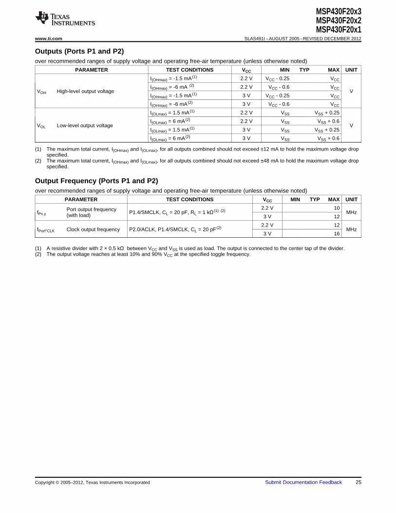
Outputs (Ports P1 and P2)over recommended ranges of supply voltage and operating free-air temperature (unless otherwise noted)
PARAMETER TEST CONDITIONS VCC MIN TYP MAX UNIT
I(OHmax) = -1.5 mA (1) 2.2 V VCC - 0.25 VCC
I(OHmax) = -6 mA (2) 2.2 V VCC - 0.6 VCCVOH High-level output voltage V
I(OHmax) = -1.5 mA (1) 3 V VCC - 0.25 VCC
I(OHmax) = -6 mA (2) 3 V VCC - 0.6 VCC
I(OLmax) = 1.5 mA (1) 2.2 V VSS VSS + 0.25
I(OLmax) = 6 mA (2) 2.2 V VSS VSS + 0.6VOL Low-level output voltage V
I(OLmax) = 1.5 mA (1) 3 V VSS VSS + 0.25
I(OLmax) = 6 mA (2) 3 V VSS VSS + 0.6
(1) The maximum total current, I(OHmax) and I(OLmax), for all outputs combined should not exceed ±12 mA to hold the maximum voltage dropspecified.
(2) The maximum total current, I(OHmax) and I(OLmax), for all outputs combined should not exceed ±48 mA to hold the maximum voltage dropspecified.
Output Frequency (Ports P1 and P2)over recommended ranges of supply voltage and operating free-air temperature (unless otherwise noted)
PARAMETER TEST CONDITIONS VCC MIN TYP MAX UNIT
2.2 V 10Port output frequencyfPx.y P1.4/SMCLK, CL = 20 pF, RL = 1 kΩ (1) (2) MHz(with load) 3 V 12
2.2 V 12fPort°CLK Clock output frequency P2.0/ACLK, P1.4/SMCLK, CL = 20 pF (2) MHz
3 V 16
(1) A resistive divider with 2 × 0.5 kΩ between VCC and VSS is used as load. The output is connected to the center tap of the divider.(2) The output voltage reaches at least 10% and 90% VCC at the specified toggle frequency.
Copyright © 2005–2012, Texas Instruments Incorporated Submit Documentation Feedback 25
VOH − High-Level Output Voltage − V
−25.0
−20.0
−15.0
−10.0
−5.0
0.0
0.0 0.5 1.0 1.5 2.0 2.5
VCC = 2.2 V
P1.7
TA = 25°C
TA = 85°C
OH
I−
Typic
al H
igh-L
evel O
utp
ut C
urr
ent
−m
A
VOH − High-Level Output Voltage − V
−50.0
−40.0
−30.0
−20.0
−10.0
0.0
0.0 0.5 1.0 1.5 2.0 2.5 3.0 3.5
VCC = 3 V
P1.7
TA = 25°C
TA = 85°C
OH
I−
Typic
al H
igh-L
evel O
utp
ut C
urr
ent
−m
A
VOL − Low-Level Output Voltage − V
0.0
5.0
10.0
15.0
20.0
25.0
30.0
0.0 0.5 1.0 1.5 2.0 2.5
VCC = 2.2 V
P1.7 TA = 25°C
TA = 85°C
OL
I−
Typic
al Low
-Level O
utp
ut C
urr
ent
−m
A
VOL − Low-Level Output Voltage − V
0.0
10.0
20.0
30.0
40.0
50.0
0.0 0.5 1.0 1.5 2.0 2.5 3.0 3.5
VCC = 3 V
P1.7TA = 25°C
TA = 85°C
OL
I−
Typic
al Low
-Level O
utp
ut C
urr
ent
−m
A
MSP430F20x3MSP430F20x2MSP430F20x1SLAS491I –AUGUST 2005–REVISED DECEMBER 2012 www.ti.com
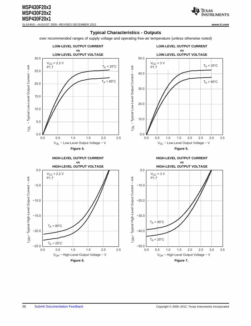
Typical Characteristics - Outputsover recommended ranges of supply voltage and operating free-air temperature (unless otherwise noted)
LOW-LEVEL OUTPUT CURRENT LOW-LEVEL OUTPUT CURRENTvs vs
LOW-LEVEL OUTPUT VOLTAGE LOW-LEVEL OUTPUT VOLTAGE
Figure 4. Figure 5.
HIGH-LEVEL OUTPUT CURRENT HIGH-LEVEL OUTPUT CURRENTvs vs
HIGH-LEVEL OUTPUT VOLTAGE HIGH-LEVEL OUTPUT VOLTAGE
Figure 6. Figure 7.
26 Submit Documentation Feedback Copyright © 2005–2012, Texas Instruments Incorporated
0
1
t d(BOR)
VCC
V(B_IT−)
Vhys(B_IT−)
VCC(start)
MSP430F20x3MSP430F20x2MSP430F20x1
www.ti.com SLAS491I –AUGUST 2005–REVISED DECEMBER 2012
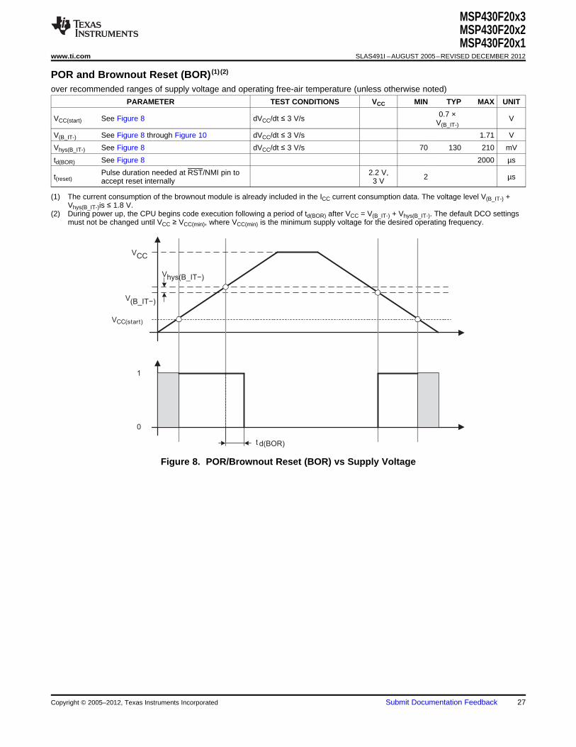
POR and Brownout Reset (BOR) (1) (2)
over recommended ranges of supply voltage and operating free-air temperature (unless otherwise noted)
PARAMETER TEST CONDITIONS VCC MIN TYP MAX UNIT
0.7 ×VCC(start) See Figure 8 dVCC/dt ≤ 3 V/s VV(B_IT-)
V(B_IT-) See Figure 8 through Figure 10 dVCC/dt ≤ 3 V/s 1.71 V
Vhys(B_IT-) See Figure 8 dVCC/dt ≤ 3 V/s 70 130 210 mV
td(BOR) See Figure 8 2000 µs
Pulse duration needed at RST/NMI pin to 2.2 V,t(reset) 2 µsaccept reset internally 3 V
(1) The current consumption of the brownout module is already included in the ICC current consumption data. The voltage level V(B_IT-) +Vhys(B_IT-)is ≤ 1.8 V.
(2) During power up, the CPU begins code execution following a period of td(BOR) after VCC = V(B_IT-) + Vhys(B_IT-). The default DCO settingsmust not be changed until VCC ≥ VCC(min), where VCC(min) is the minimum supply voltage for the desired operating frequency.
Figure 8. POR/Brownout Reset (BOR) vs Supply Voltage
Copyright © 2005–2012, Texas Instruments Incorporated Submit Documentation Feedback 27
VCC
0
0.5
1
1.5
2
VCC(drop)
t pw
tpw − Pulse Width − µs
VC
C(d
rop)
−V
3 V
0.001 1 1000 tf tr
tpw − Pulse Width − µs
tf = tr
Typical Conditions
VCC = 3 V
VCC(drop)
VCC
3 V
t pw
0
0.5
1
1.5
2
0.001 1 1000
Typical Conditions
1 ns 1 nstpw − Pulse Width − µs
VC
C(d
rop)
−V
tpw − Pulse Width − µs
VCC = 3 V
MSP430F20x3MSP430F20x2MSP430F20x1SLAS491I –AUGUST 2005–REVISED DECEMBER 2012 www.ti.com
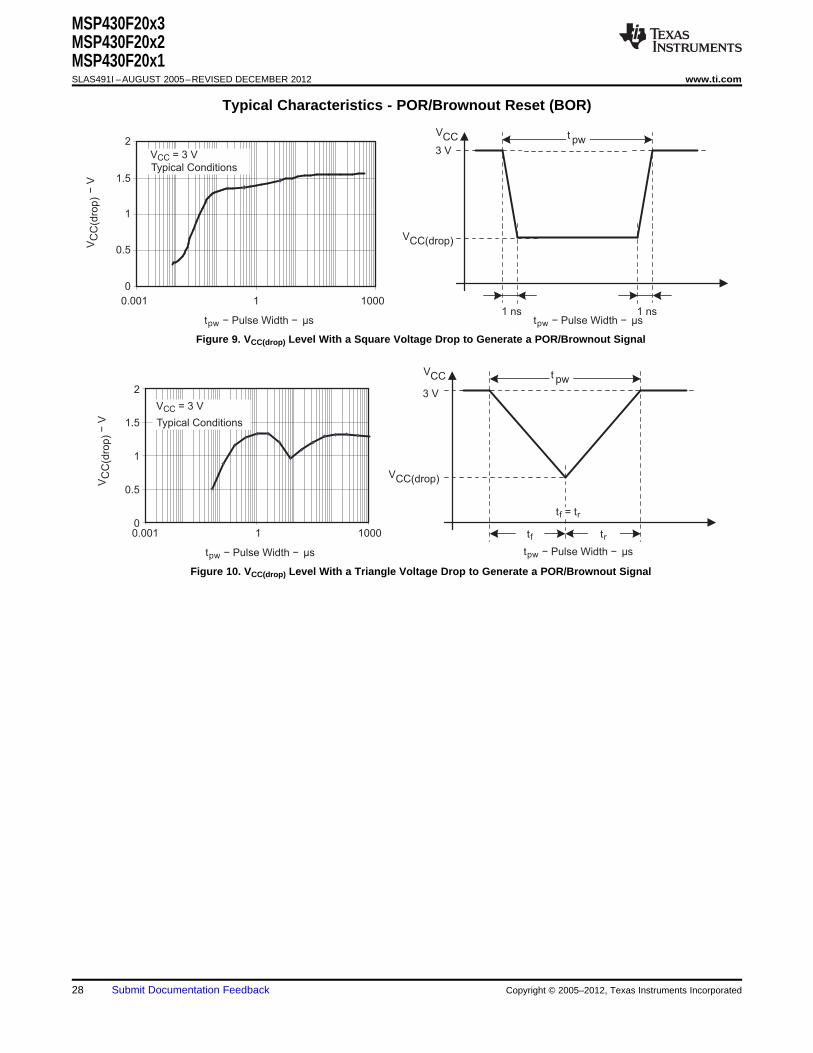
Typical Characteristics - POR/Brownout Reset (BOR)
Figure 9. VCC(drop) Level With a Square Voltage Drop to Generate a POR/Brownout Signal
Figure 10. VCC(drop) Level With a Triangle Voltage Drop to Generate a POR/Brownout Signal
28 Submit Documentation Feedback Copyright © 2005–2012, Texas Instruments Incorporated
DCO(RSEL,DCO+1)DCO(RSEL,DCO)average
DCO(RSEL,DCO) DCO(RSEL,DCO+1)
32 × f × ff =
MOD × f + (32 – MOD) × f
MSP430F20x3MSP430F20x2MSP430F20x1
www.ti.com SLAS491I –AUGUST 2005–REVISED DECEMBER 2012
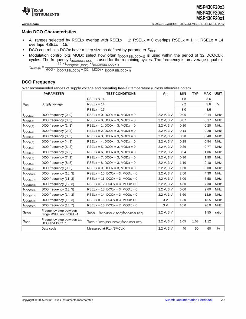
Main DCO Characteristics
• All ranges selected by RSELx overlap with RSELx + 1: RSELx = 0 overlaps RSELx = 1, ... RSELx = 14overlaps RSELx = 15.
• DCO control bits DCOx have a step size as defined by parameter SDCO.• Modulation control bits MODx select how often fDCO(RSEL,DCO+1) is used within the period of 32 DCOCLK
cycles. The frequency fDCO(RSEL,DCO) is used for the remaining cycles. The frequency is an average equal to:
DCO Frequencyover recommended ranges of supply voltage and operating free-air temperature (unless otherwise noted)
PARAMETER TEST CONDITIONS VCC MIN TYP MAX UNIT
RSELx < 14 1.8 3.6
VCC Supply voltage RSELx = 14 2.2 3.6 V
RSELx = 15 3.0 3.6
fDCO(0,0) DCO frequency (0, 0) RSELx = 0, DCOx = 0, MODx = 0 2.2 V, 3 V 0.06 0.14 MHz
fDCO(0,3) DCO frequency (0, 3) RSELx = 0, DCOx = 3, MODx = 0 2.2 V, 3 V 0.07 0.17 MHz
fDCO(1,3) DCO frequency (1, 3) RSELx = 1, DCOx = 3, MODx = 0 2.2 V, 3 V 0.10 0.20 MHz
fDCO(2,3) DCO frequency (2, 3) RSELx = 2, DCOx = 3, MODx = 0 2.2 V, 3 V 0.14 0.28 MHz
fDCO(3,3) DCO frequency (3, 3) RSELx = 3, DCOx = 3, MODx = 0 2.2 V, 3 V 0.20 0.40 MHz
fDCO(4,3) DCO frequency (4, 3) RSELx = 4, DCOx = 3, MODx = 0 2.2 V, 3 V 0.28 0.54 MHz
fDCO(5,3) DCO frequency (5, 3) RSELx = 5, DCOx = 3, MODx = 0 2.2 V, 3 V 0.39 0.77 MHz
fDCO(6,3) DCO frequency (6, 3) RSELx = 6, DCOx = 3, MODx = 0 2.2 V, 3 V 0.54 1.06 MHz
fDCO(7,3) DCO frequency (7, 3) RSELx = 7, DCOx = 3, MODx = 0 2.2 V, 3 V 0.80 1.50 MHz
fDCO(8,3) DCO frequency (8, 3) RSELx = 8, DCOx = 3, MODx = 0 2.2 V, 3 V 1.10 2.10 MHz
fDCO(9,3) DCO frequency (9, 3) RSELx = 9, DCOx = 3, MODx = 0 2.2 V, 3 V 1.60 3.00 MHz
fDCO(10,3) DCO frequency (10, 3) RSELx = 10, DCOx = 3, MODx = 0 2.2 V, 3 V 2.50 4.30 MHz
fDCO(11,3) DCO frequency (11, 3) RSELx = 11, DCOx = 3, MODx = 0 2.2 V, 3 V 3.00 5.50 MHz
fDCO(12,3) DCO frequency (12, 3) RSELx = 12, DCOx = 3, MODx = 0 2.2 V, 3 V 4.30 7.30 MHz
fDCO(13,3) DCO frequency (13, 3) RSELx = 13, DCOx = 3, MODx = 0 2.2 V, 3 V 6.00 9.60 MHz
fDCO(14,3) DCO frequency (14, 3) RSELx = 14, DCOx = 3, MODx = 0 2.2 V, 3 V 8.60 13.9 MHz
fDCO(15,3) DCO frequency (15, 3) RSELx = 15, DCOx = 3, MODx = 0 3 V 12.0 18.5 MHz
fDCO(15,7) DCO frequency (15, 7) RSELx = 15, DCOx = 7, MODx = 0 3 V 16.0 26.0 MHz
Frequency step betweenSRSEL SRSEL = fDCO(RSEL+1,DCO)/fDCO(RSEL,DCO) 2.2 V, 3 V 1.55 ratiorange RSEL and RSEL+1
Frequency step between tapSDCO SDCO = fDCO(RSEL,DCO+1)/fDCO(RSEL,DCO) 2.2 V, 3 V 1.05 1.08 1.12DCO and DCO+1
Duty cycle Measured at P1.4/SMCLK 2.2 V, 3 V 40 50 60 %
Copyright © 2005–2012, Texas Instruments Incorporated Submit Documentation Feedback 29
MSP430F20x3MSP430F20x2MSP430F20x1SLAS491I –AUGUST 2005–REVISED DECEMBER 2012 www.ti.com
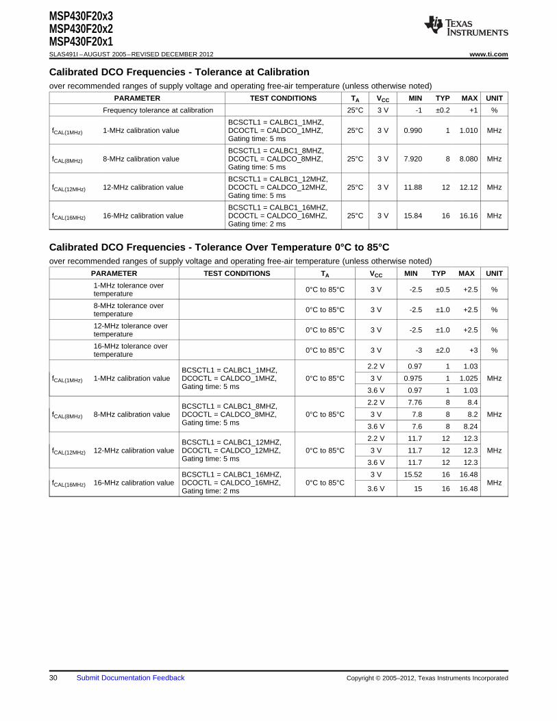
Calibrated DCO Frequencies - Tolerance at Calibrationover recommended ranges of supply voltage and operating free-air temperature (unless otherwise noted)
PARAMETER TEST CONDITIONS TA VCC MIN TYP MAX UNIT
Frequency tolerance at calibration 25°C 3 V -1 ±0.2 +1 %
BCSCTL1 = CALBC1_1MHZ,fCAL(1MHz) 1-MHz calibration value DCOCTL = CALDCO_1MHZ, 25°C 3 V 0.990 1 1.010 MHz
Gating time: 5 ms
BCSCTL1 = CALBC1_8MHZ,fCAL(8MHz) 8-MHz calibration value DCOCTL = CALDCO_8MHZ, 25°C 3 V 7.920 8 8.080 MHz
Gating time: 5 ms
BCSCTL1 = CALBC1_12MHZ,fCAL(12MHz) 12-MHz calibration value DCOCTL = CALDCO_12MHZ, 25°C 3 V 11.88 12 12.12 MHz
Gating time: 5 ms
BCSCTL1 = CALBC1_16MHZ,fCAL(16MHz) 16-MHz calibration value DCOCTL = CALDCO_16MHZ, 25°C 3 V 15.84 16 16.16 MHz
Gating time: 2 ms
Calibrated DCO Frequencies - Tolerance Over Temperature 0°C to 85°Cover recommended ranges of supply voltage and operating free-air temperature (unless otherwise noted)
PARAMETER TEST CONDITIONS TA VCC MIN TYP MAX UNIT
1-MHz tolerance over 0°C to 85°C 3 V -2.5 ±0.5 +2.5 %temperature
8-MHz tolerance over 0°C to 85°C 3 V -2.5 ±1.0 +2.5 %temperature
12-MHz tolerance over 0°C to 85°C 3 V -2.5 ±1.0 +2.5 %temperature
16-MHz tolerance over 0°C to 85°C 3 V -3 ±2.0 +3 %temperature
2.2 V 0.97 1 1.03BCSCTL1 = CALBC1_1MHZ,fCAL(1MHz) 1-MHz calibration value DCOCTL = CALDCO_1MHZ, 0°C to 85°C 3 V 0.975 1 1.025 MHz
Gating time: 5 ms 3.6 V 0.97 1 1.03
2.2 V 7.76 8 8.4BCSCTL1 = CALBC1_8MHZ,fCAL(8MHz) 8-MHz calibration value DCOCTL = CALDCO_8MHZ, 0°C to 85°C 3 V 7.8 8 8.2 MHz
Gating time: 5 ms 3.6 V 7.6 8 8.24
2.2 V 11.7 12 12.3BCSCTL1 = CALBC1_12MHZ,fCAL(12MHz) 12-MHz calibration value DCOCTL = CALDCO_12MHZ, 0°C to 85°C 3 V 11.7 12 12.3 MHz
Gating time: 5 ms 3.6 V 11.7 12 12.3
BCSCTL1 = CALBC1_16MHZ, 3 V 15.52 16 16.48fCAL(16MHz) 16-MHz calibration value DCOCTL = CALDCO_16MHZ, 0°C to 85°C MHz
3.6 V 15 16 16.48Gating time: 2 ms
30 Submit Documentation Feedback Copyright © 2005–2012, Texas Instruments Incorporated
MSP430F20x3MSP430F20x2MSP430F20x1
www.ti.com SLAS491I –AUGUST 2005–REVISED DECEMBER 2012
Calibrated DCO Frequencies - Tolerance Over Supply Voltage VCC
over recommended ranges of supply voltage and operating free-air temperature (unless otherwise noted)
PARAMETER TEST CONDITIONS TA VCC MIN TYP MAX UNIT
1-MHz tolerance over VCC 25°C 1.8 V to 3.6 V -3 ±2 +3 %
8-MHz tolerance over VCC 25°C 1.8 V to 3.6 V -3 ±2 +3 %
12-MHz tolerance over VCC 25°C 2.2 V to 3.6 V -3 ±2 +3 %
16-MHz tolerance over VCC 25°C 3 V to 3.6 V -6 ±2 +3 %
BCSCTL1 = CALBC1_1MHZ,fCAL(1MHz) 1-MHz calibration value DCOCTL = CALDCO_1MHZ, 25°C 1.8 V to 3.6 V 0.97 1 1.03 MHz
Gating time: 5 ms
BCSCTL1 = CALBC1_8MHZ,fCAL(8MHz) 8-MHz calibration value DCOCTL = CALDCO_8MHZ, 25°C 1.8 V to 3.6 V 7.76 8 8.24 MHz
Gating time: 5 ms
BCSCTL1 = CALBC1_12MHZ,fCAL(12MHz) 12-MHz calibration value DCOCTL = CALDCO_12MHZ, 25°C 2.2 V to 3.6 V 11.64 12 12.36 MHz
Gating time: 5 ms
BCSCTL1 = CALBC1_16MHZ,fCAL(16MHz) 16-MHz calibration value DCOCTL = CALDCO_16MHZ, 25°C 3 V to 3.6 V 15 16 16.48 MHz
Gating time: 2 ms
Calibrated DCO Frequencies - Overall Toleranceover recommended ranges of supply voltage and operating free-air temperature (unless otherwise noted)
PARAMETER TEST CONDITIONS TA VCC MIN TYP MAX UNIT
1-MHz tolerance I: -40°C to 85°C 1.8 V to 3.6 V -5 ±2 +5 %overall T: -40°C to 105°C
8-MHz tolerance I: -40°C to 85°C 1.8 V to 3.6 V -5 ±2 +5 %overall T: -40°C to 105°C
12-MHz I: -40°C to 85°C 2.2 V to 3.6 V -5 ±2 +5 %tolerance overall T: -40°C to 105°C
16-MHz I: -40°C to 85°C 3 V to 3.6 V -6 ±3 +6 %tolerance overall T: -40°C to 105°C
BCSCTL1 = CALBC1_1MHZ,1-MHz I: -40°C to 85°CfCAL(1MHz) DCOCTL = CALDCO_1MHZ, 1.8 V to 3.6 V 0.95 1 1.05 MHzcalibration value T: -40°C to 105°CGating time: 5 ms
BCSCTL1 = CALBC1_8MHZ,8-MHz I: -40°C to 85°CfCAL(8MHz) DCOCTL = CALDCO_8MHZ, 1.8 V to 3.6 V 7.6 8 8.4 MHzcalibration value T: -40°C to 105°CGating time: 5 ms
BCSCTL1 = CALBC1_12MHZ,12-MHz I: -40°C to 85°CfCAL(12MHz) DCOCTL = CALDCO_12MHZ, 2.2 V to 3.6 V 11.4 12 12.6 MHzcalibration value T: -40°C to 105°CGating time: 5 ms
BCSCTL1 = CALBC1_16MHZ,16-MHz I: -40°C to 85°CfCAL(16MHz) DCOCTL = CALDCO_16MHZ, 3 V to 3.6 V 15 16 17 MHzcalibration value T: -40°C to 105°CGating time: 2 ms
Copyright © 2005–2012, Texas Instruments Incorporated Submit Documentation Feedback 31
TA − Temperature − °C
0.97
0.98
0.99
1.00
1.01
1.02
1.03
−50.0 −25.0 0.0 25.0 50.0 75.0 100.0
Fre
quency
−M
Hz
VCC = 1.8 V
VCC = 2.2 VVCC = 3.0 V
VCC = 3.6 V
VCC − Supply Voltage − V
0.97
0.98
0.99
1.00
1.01
1.02
1.03
1.5 2.0 2.5 3.0 3.5 4.0F
req
ue
ncy
−M
Hz
TA = −40 °C
TA = 25 °C
TA = 85 °C
TA = 105 °C
MSP430F20x3MSP430F20x2MSP430F20x1SLAS491I –AUGUST 2005–REVISED DECEMBER 2012 www.ti.com
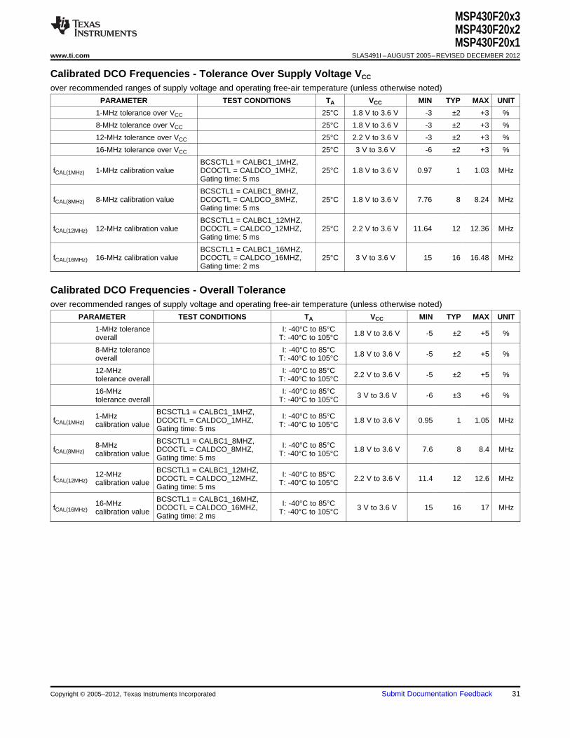
Typical Characteristics - Calibrated 1-MHz DCO Frequency
CALIBRATED 1-MHz FREQUENCY CALIBRATED 1-MHz FREQUENCYvs vs
TEMPERATURE SUPPLY VOLTAGE
Figure 11. Figure 12.
32 Submit Documentation Feedback Copyright © 2005–2012, Texas Instruments Incorporated
DCO Frequency − MHz
0.10
1.00
10.00
0.10 1.00 10.00
DC
O W
ake
Tim
e−
us
RSELx = 0...11RSELx = 12...15
MSP430F20x3MSP430F20x2MSP430F20x1
www.ti.com SLAS491I –AUGUST 2005–REVISED DECEMBER 2012
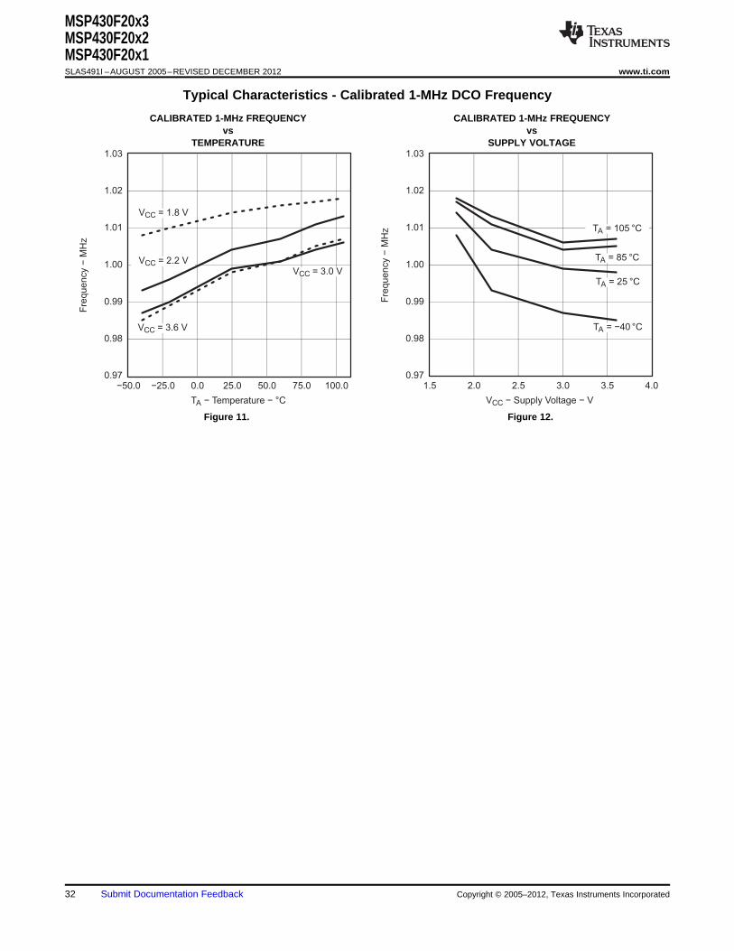
Wake-Up From Lower-Power Modes (LPM3, LPM4)over recommended ranges of supply voltage and operating free-air temperature (unless otherwise noted)
PARAMETER TEST CONDITIONS VCC MIN TYP MAX UNIT
BCSCTL1 = CALBC1_1MHZ, 2DCOCTL = CALDCO_1MHZ
BCSCTL1 = CALBC1_8MHZ, 2.2 V, 3 V 1.5DCOCTL = CALDCO_8MHZDCO clock wake-up timetDCO,LPM3/4 µsfrom LPM3 or LPM4 (1)BCSCTL1 = CALBC1_12MHZ, 1DCOCTL = CALDCO_12MHZ
BCSCTL1 = CALBC1_16MHZ, 3 V 1DCOCTL = CALDCO_16MHZ
CPU wake-up time from 1 / fMCLK +tCPU,LPM3/4 LPM3 or LPM4 (2) tClock,LPM3/4
(1) The DCO clock wake-up time is measured from the edge of an external wake-up signal (for example, port interrupt) to the first clockedge observable externally on a clock pin (MCLK or SMCLK).
(2) Parameter applicable only if DCOCLK is used for MCLK.
Typical Characteristics - DCO Clock Wake-Up Time From LPM3 or LPM4
DCO WAKE-UP TIME FROM LPM3vs
DCO FREQUENCY
Figure 13.
Copyright © 2005–2012, Texas Instruments Incorporated Submit Documentation Feedback 33
MSP430F20x3MSP430F20x2MSP430F20x1SLAS491I –AUGUST 2005–REVISED DECEMBER 2012 www.ti.com
Crystal Oscillator, XT1, Low-Frequency Mode (1)
over recommended ranges of supply voltage and operating free-air temperature (unless otherwise noted)
PARAMETER TEST CONDITIONS VCC MIN TYP MAX UNIT
LFXT1 oscillator crystalfLFXT1,LF XTS = 0, LFXT1Sx = 0 or 1 1.8 V to 3.6 V 32768 Hzfrequency, LF mode 0, 1
LFXT1 oscillator logic levelfLFXT1,LF,logic square wave input frequency, XTS = 0, LFXT1Sx = 3 1.8 V to 3.6 V 10000 32768 50000 Hz
LF mode
XTS = 0, LFXT1Sx = 0, 500fLFXT1,LF = 32768 Hz, CL,eff = 6 pFOscillation allowance forOALF kΩLF crystals XTS = 0, LFXT1Sx = 0, 200fLFXT1,LF = 32768 Hz, CL,eff = 12 pF
XTS = 0, XCAPx = 0 1
XTS = 0, XCAPx = 1 5.5Integrated effective loadCL,eff pFcapacitance, LF mode (2)XTS = 0, XCAPx = 2 8.5
XTS = 0, XCAPx = 3 11
XTS = 0, Measured at P1.0/ACLK,Duty cycle, LF mode 2.2 V, 3 V 30 50 70 %fLFXT1,LF = 32768 Hz
Oscillator fault frequency,fFault,LF XTS = 0, LFXT1Sx = 3 (4) 2.2 V, 3 V 10 10000 HzLF mode (3)
(1) To improve EMI on the XT1 oscillator, the following guidelines should be observed.(a) Keep the trace between the device and the crystal as short as possible.(b) Design a good ground plane around the oscillator pins.(c) Prevent crosstalk from other clock or data lines into oscillator pins XIN and XOUT.(d) Avoid running PCB traces underneath or adjacent to the XIN and XOUT pins.(e) Use assembly materials and praxis to avoid any parasitic load on the oscillator XIN and XOUT pins.(f) If conformal coating is used, ensure that it does not induce capacitive/resistive leakage between the oscillator pins.(g) Do not route the XOUT line to the JTAG header to support the serial programming adapter as shown in other documentation. This
signal is no longer required for the serial programming adapter.(2) Includes parasitic bond and package capacitance (approximately 2 pF per pin).
Since the PCB adds additional capacitance, it is recommended to verify the correct load by measuring the ACLK frequency. For acorrect setup, the effective load capacitance should always match the specification of the used crystal.
(3) Frequencies below the MIN specification set the fault flag. Frequencies above the MAX specification do not set the fault flag.Frequencies in between might set the flag.
(4) Measured with logic-level input frequency but also applies to operation with crystals.
Internal Very-Low-Power Low-Frequency Oscillator (VLO)over recommended ranges of supply voltage and operating free-air temperature (unless otherwise noted)
PARAMETER TA VCC MIN TYP MAX UNIT
-40°C to 85°C 4 12 20fVLO VLO frequency 2.2 V, 3 V kHz
105°C 22
I: -40°C to 85°CdfVLO/dT VLO frequency temperature drift (1) 2.2 V, 3 V 0.5 %/°CT: -40°C to 105°C
dfVLO/dVCC VLO frequency supply voltage drift (2) 25°C 1.8 V to 3.6 V 4 %/V
(1) Calculated using the box method:I: (MAX(-40 to 85°C) - MIN(-40 to 85°C)) / MIN(-40 to 85°C) / (85°C - (-40°C))T: (MAX(-40 to 105°C) - MIN(-40 to 105°C)) / MIN(-40 to 105°C) / (105°C - (-40°C))
(2) Calculated using the box method: (MAX(1.8 to 3.6 V) - MIN(1.8 to 3.6 V)) / MIN(1.8 to 3.6 V) / (3.6 V - 1.8 V)
Timer_Aover recommended ranges of supply voltage and operating free-air temperature (unless otherwise noted)
PARAMETER TEST CONDITIONS VCC MIN TYP MAX UNIT
Internal: SMCLK, ACLK 2.2 V 10fTA Timer_A clock frequency External: TACLK, INCLK MHz
3 V 16Duty cycle = 50% ± 10%
tTA,cap Timer_A capture timing TA0, TA1 2.2 V, 3 V 20 ns
34 Submit Documentation Feedback Copyright © 2005–2012, Texas Instruments Incorporated
VOL − Low-Level Output Voltage − V
0.0
1.0
2.0
3.0
4.0
5.0
0.0 0.2 0.4 0.6 0.8 1.0
VCC = 2.2 V
TA = 25°C
OL
I−
Low
-Level O
utp
ut C
urr
ent
−m
A
TA = 85°C
VOL − Low-Level Output V oltage − V
0.0
1.0
2.0
3.0
4.0
5.0
0.0 0.2 0.4 0.6 0.8 1.0
VCC = 3 V TA = 25°C
OL
I−
Low
-Level O
utp
ut C
urr
ent
−m
ATA = 85°C
MSP430F20x3MSP430F20x2MSP430F20x1
www.ti.com SLAS491I –AUGUST 2005–REVISED DECEMBER 2012
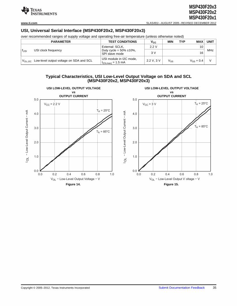
USI, Universal Serial Interface (MSP430F20x2, MSP430F20x3)over recommended ranges of supply voltage and operating free-air temperature (unless otherwise noted)
PARAMETER TEST CONDITIONS VCC MIN TYP MAX UNIT
External: SCLK, 2.2 V 10fUSI USI clock frequency Duty cycle = 50% ±10%, MHz
3 V 16SPI slave mode
USI module in I2C mode,VOL,I2C Low-level output voltage on SDA and SCL 2.2 V, 3 V VSS VSS + 0.4 VI(OLmax) = 1.5 mA
Typical Characteristics, USI Low-Level Output Voltage on SDA and SCL(MSP430F20x2, MSP430F20x3)
USI LOW-LEVEL OUTPUT VOLTAGE USI LOW-LEVEL OUTPUT VOLTAGEvs vs
OUTPUT CURRENT OUTPUT CURRENT
Figure 14. Figure 15.
Copyright © 2005–2012, Texas Instruments Incorporated Submit Documentation Feedback 35
MSP430F20x3MSP430F20x2MSP430F20x1SLAS491I –AUGUST 2005–REVISED DECEMBER 2012 www.ti.com
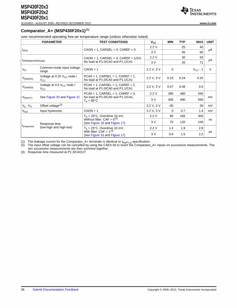
Comparator_A+ (MSP430F20x1) (1)
over recommended operating free-air temperature range (unless otherwise noted)
PARAMETER TEST CONDITIONS VCC MIN TYP MAX UNIT
2.2 V 25 40I(DD) CAON = 1, CARSEL = 0, CAREF = 0 μA
3 V 45 60
2.2 V 30 50CAON = 1, CARSEL = 0, CAREF = 1/2/3,I(Refladder/RefDiode) μANo load at P1.0/CA0 and P1.1/CA1 3 V 45 71
Common-mode input voltageVIC CAON = 1 2.2 V, 3 V 0 VCC - 1 Vrange
Voltage at 0.25 VCC node / PCA0 = 1, CARSEL = 1, CAREF = 1,V(Ref025) 2.2 V, 3 V 0.23 0.24 0.25VCC No load at P1.0/CA0 and P1.1/CA1
Voltage at 0.5 VCC node / PCA0 = 1, CARSEL = 1, CAREF = 2,V(Ref050) 2.2 V, 3 V 0.47 0.48 0.5VCC No load at P1.0/CA0 and P1.1/CA1
PCA0 = 1, CARSEL = 1, CAREF = 3, 2.2 V 390 480 540V(RefVT) See Figure 20 and Figure 21 No load at P1.0/CA0 and P1.1/CA1, mV
3 V 400 490 550TA = 85°C
Vp - VS Offset voltage (2) 2.2 V, 3 V -30 30 mV
Vhys Input hysteresis CAON = 1 2.2 V, 3 V 0 0.7 1.4 mV
TA = 25°C, Overdrive 10 mV, 2.2 V 80 165 300Without filter: CAF = 0 (3) ns
3 V 70 120 240(see Figure 16 and Figure 17)Response timet(response) (low-high and high-low) TA = 25°C, Overdrive 10 mV, 2.2 V 1.4 1.9 2.8With filter: CAF = 1 (3) μs
3 V 0.9 1.5 2.2(see Figure 16 and Figure 17)
(1) The leakage current for the Comparator_A+ terminals is identical to Ilkg(Px.y) specification.(2) The input offset voltage can be cancelled by using the CAEX bit to invert the Comparator_A+ inputs on successive measurements. The
two successive measurements are then summed together.(3) Response time measured at P1.3/CAOUT
36 Submit Documentation Feedback Copyright © 2005–2012, Texas Instruments Incorporated
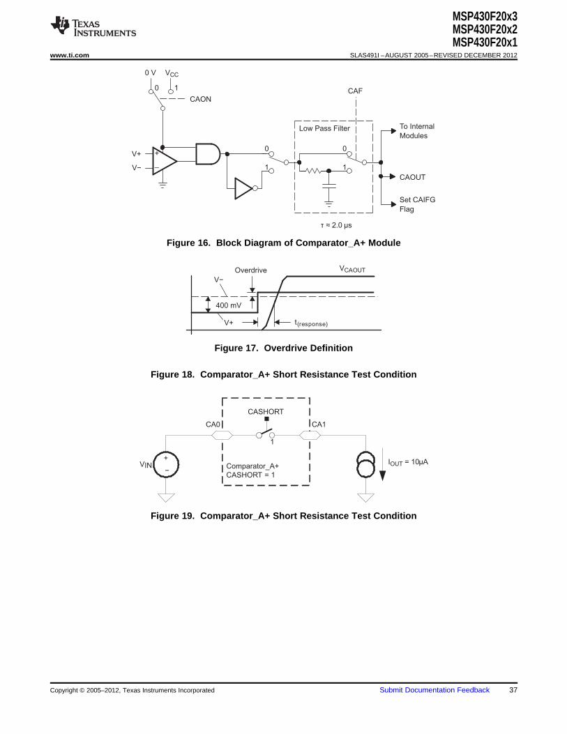
CASHORT
1
Comparator_A+
CASHORT = 1
CA1CA0
VIN+
−
IOUT = 10µA
Overdrive VCAOUT
t(response)V+
V−
400 mV
_
+
CAON
0
1
V+0
1
CAF
Low Pass Filter
τ ≈ 2.0 µs
To Internal
Modules
Set CAIFG
Flag
CAOUT
V−
VCC
1
0 V
0
MSP430F20x3MSP430F20x2MSP430F20x1
www.ti.com SLAS491I –AUGUST 2005–REVISED DECEMBER 2012
Figure 16. Block Diagram of Comparator_A+ Module
Figure 17. Overdrive Definition
Figure 18. Comparator_A+ Short Resistance Test Condition
Figure 19. Comparator_A+ Short Resistance Test Condition
Copyright © 2005–2012, Texas Instruments Incorporated Submit Documentation Feedback 37
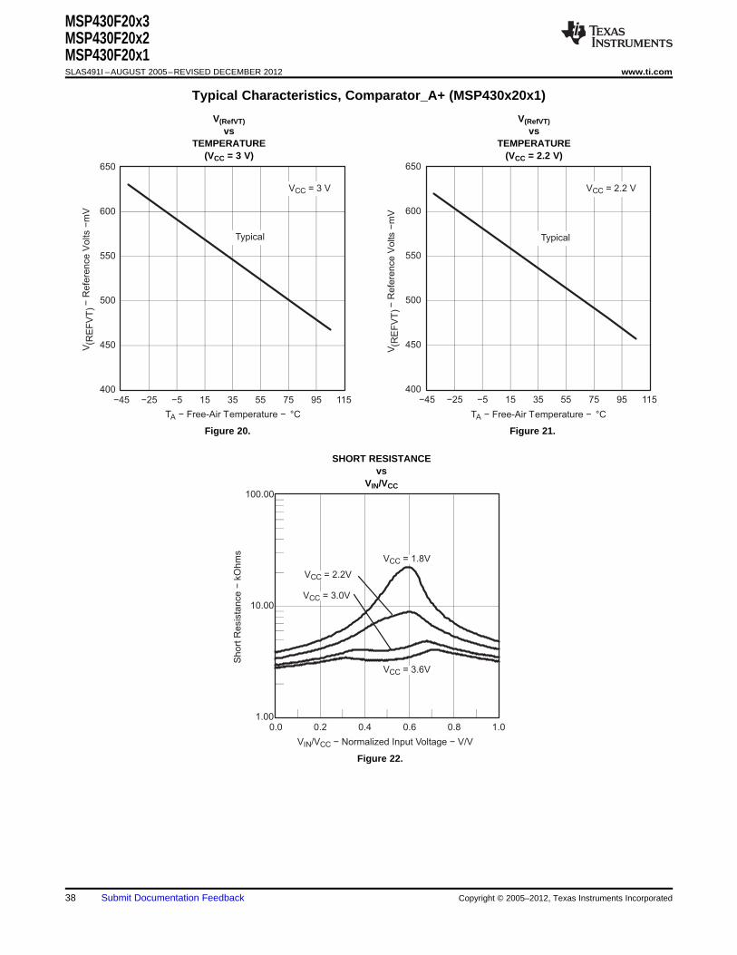
VIN/VCC − Normalized Input Voltage − V/V
1.00
10.00
100.00
0.0 0.2 0.4 0.6 0.8 1.0
Short
Resis
tance
−kO
hm
s
VCC = 1.8V
VCC = 3.6V
VCC = 2.2V
VCC = 3.0V
TA − Free-Air Temperature − °C
400
450
500
550
600
650
−45 −25 −5 15 35 55 75 95 115
VCC = 3 V
V(R
EF
VT
)−
Refe
rence V
olts
−m
V
Typical
TA − Free-Air Temperature − °C
400
450
500
550
600
650
−45 −25 −5 15 35 55 75 95 115
VCC = 2.2 V
V(R
EF
VT
)−
Refe
rence V
olts
−m
V
Typical
MSP430F20x3MSP430F20x2MSP430F20x1SLAS491I –AUGUST 2005–REVISED DECEMBER 2012 www.ti.com
Typical Characteristics, Comparator_A+ (MSP430x20x1)
V(RefVT) V(RefVT)vs vs
TEMPERATURE TEMPERATURE(VCC = 3 V) (VCC = 2.2 V)
Figure 20. Figure 21.
SHORT RESISTANCEvs
VIN/VCC
Figure 22.
38 Submit Documentation Feedback Copyright © 2005–2012, Texas Instruments Incorporated
MSP430F20x3MSP430F20x2MSP430F20x1
www.ti.com SLAS491I –AUGUST 2005–REVISED DECEMBER 2012
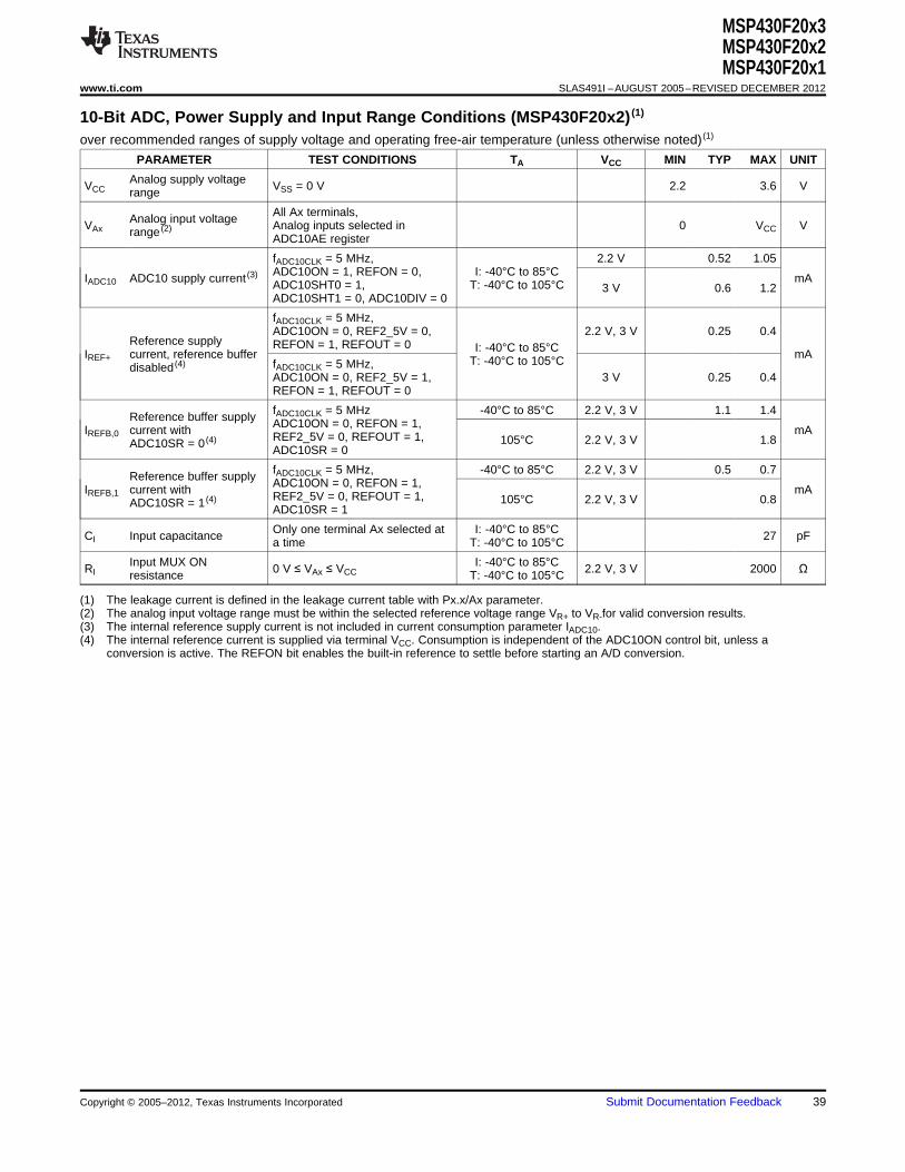
10-Bit ADC, Power Supply and Input Range Conditions (MSP430F20x2) (1)
over recommended ranges of supply voltage and operating free-air temperature (unless otherwise noted) (1)
PARAMETER TEST CONDITIONS TA VCC MIN TYP MAX UNIT
Analog supply voltageVCC VSS = 0 V 2.2 3.6 Vrange
All Ax terminals,Analog input voltageVAx Analog inputs selected in 0 VCC Vrange (2)ADC10AE register
fADC10CLK = 5 MHz, 2.2 V 0.52 1.05ADC10ON = 1, REFON = 0, I: -40°C to 85°CIADC10 ADC10 supply current (3) mAADC10SHT0 = 1, T: -40°C to 105°C 3 V 0.6 1.2ADC10SHT1 = 0, ADC10DIV = 0
fADC10CLK = 5 MHz,ADC10ON = 0, REF2_5V = 0, 2.2 V, 3 V 0.25 0.4
Reference supply REFON = 1, REFOUT = 0 I: -40°C to 85°CIREF+ current, reference buffer mAT: -40°C to 105°CfADC10CLK = 5 MHz,disabled (4)
ADC10ON = 0, REF2_5V = 1, 3 V 0.25 0.4REFON = 1, REFOUT = 0
fADC10CLK = 5 MHz -40°C to 85°C 2.2 V, 3 V 1.1 1.4Reference buffer supply ADC10ON = 0, REFON = 1,IREFB,0 current with mAREF2_5V = 0, REFOUT = 1, 105°C 2.2 V, 3 V 1.8ADC10SR = 0 (4)ADC10SR = 0
fADC10CLK = 5 MHz, -40°C to 85°C 2.2 V, 3 V 0.5 0.7Reference buffer supply ADC10ON = 0, REFON = 1,IREFB,1 current with mAREF2_5V = 0, REFOUT = 1, 105°C 2.2 V, 3 V 0.8ADC10SR = 1 (4)ADC10SR = 1
Only one terminal Ax selected at I: -40°C to 85°CCI Input capacitance 27 pFa time T: -40°C to 105°C
Input MUX ON I: -40°C to 85°CRI 0 V ≤ VAx ≤ VCC 2.2 V, 3 V 2000 Ωresistance T: -40°C to 105°C
(1) The leakage current is defined in the leakage current table with Px.x/Ax parameter.(2) The analog input voltage range must be within the selected reference voltage range VR+ to VR-for valid conversion results.(3) The internal reference supply current is not included in current consumption parameter IADC10.(4) The internal reference current is supplied via terminal VCC. Consumption is independent of the ADC10ON control bit, unless a
conversion is active. The REFON bit enables the built-in reference to settle before starting an A/D conversion.
Copyright © 2005–2012, Texas Instruments Incorporated Submit Documentation Feedback 39
MSP430F20x3MSP430F20x2MSP430F20x1SLAS491I –AUGUST 2005–REVISED DECEMBER 2012 www.ti.com
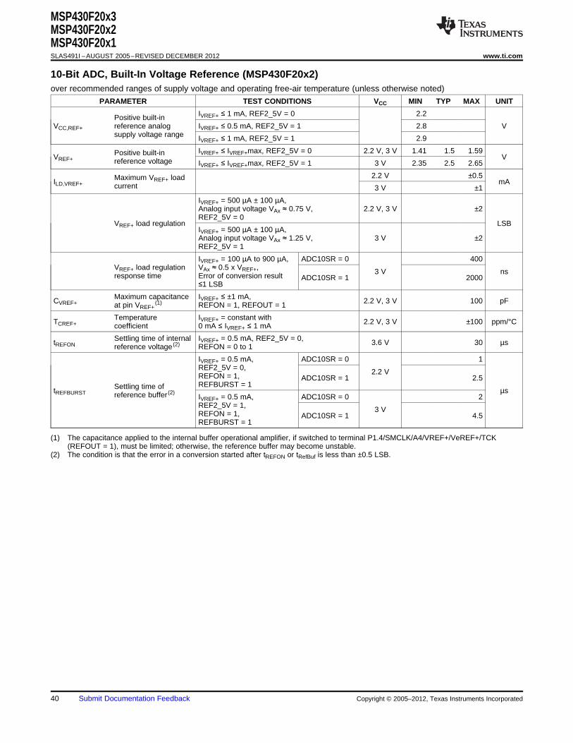
10-Bit ADC, Built-In Voltage Reference (MSP430F20x2)over recommended ranges of supply voltage and operating free-air temperature (unless otherwise noted)
PARAMETER TEST CONDITIONS VCC MIN TYP MAX UNIT
IVREF+ ≤ 1 mA, REF2_5V = 0 2.2Positive built-inVCC,REF+ reference analog IVREF+ ≤ 0.5 mA, REF2_5V = 1 2.8 V
supply voltage range IVREF+ ≤ 1 mA, REF2_5V = 1 2.9
IVREF+ ≤ IVREF+max, REF2_5V = 0 2.2 V, 3 V 1.41 1.5 1.59Positive built-inVREF+ Vreference voltage IVREF+ ≤ IVREF+max, REF2_5V = 1 3 V 2.35 2.5 2.65
2.2 V ±0.5Maximum VREF+ loadILD,VREF+ mAcurrent 3 V ±1
IVREF+ = 500 µA ± 100 µA,Analog input voltage VAx ≈ 0.75 V, 2.2 V, 3 V ±2REF2_5V = 0
VREF+ load regulation LSBIVREF+ = 500 µA ± 100 µA,Analog input voltage VAx ≈ 1.25 V, 3 V ±2REF2_5V = 1
IVREF+ = 100 µA to 900 µA, ADC10SR = 0 400VREF+ load regulation VAx ≈ 0.5 x VREF+, 3 V nsresponse time Error of conversion result ADC10SR = 1 2000
≤1 LSB
Maximum capacitance IVREF+ ≤ ±1 mA,CVREF+ 2.2 V, 3 V 100 pFat pin VREF+(1) REFON = 1, REFOUT = 1
Temperature IVREF+ = constant withTCREF+ 2.2 V, 3 V ±100 ppm/°Ccoefficient 0 mA ≤ IVREF+ ≤ 1 mA
Settling time of internal IVREF+ = 0.5 mA, REF2_5V = 0,tREFON 3.6 V 30 µsreference voltage (2) REFON = 0 to 1
IVREF+ = 0.5 mA, ADC10SR = 0 1REF2_5V = 0, 2.2 VREFON = 1, ADC10SR = 1 2.5REFBURST = 1Settling time oftREFBURST µsreference buffer (2)IVREF+ = 0.5 mA, ADC10SR = 0 2REF2_5V = 1, 3 VREFON = 1, ADC10SR = 1 4.5REFBURST = 1
(1) The capacitance applied to the internal buffer operational amplifier, if switched to terminal P1.4/SMCLK/A4/VREF+/VeREF+/TCK(REFOUT = 1), must be limited; otherwise, the reference buffer may become unstable.
(2) The condition is that the error in a conversion started after tREFON or tRefBuf is less than ±0.5 LSB.
40 Submit Documentation Feedback Copyright © 2005–2012, Texas Instruments Incorporated
MSP430F20x3MSP430F20x2MSP430F20x1
www.ti.com SLAS491I –AUGUST 2005–REVISED DECEMBER 2012
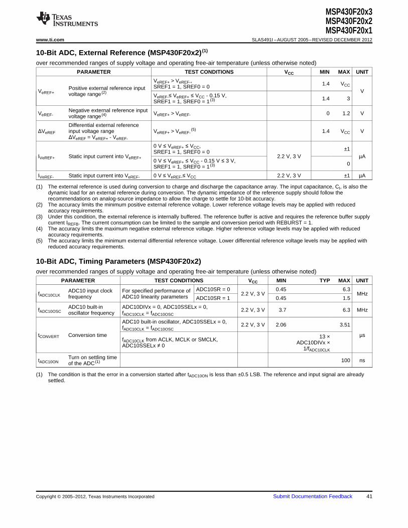
10-Bit ADC, External Reference (MSP430F20x2) (1)
over recommended ranges of supply voltage and operating free-air temperature (unless otherwise noted)
PARAMETER TEST CONDITIONS VCC MIN MAX UNIT
VeREF+ > VeREF-, 1.4 VCCSREF1 = 1, SREF0 = 0Positive external reference inputVeREF+ Vvoltage range (2)VeREF-≤ VeREF+ ≤ VCC - 0.15 V, 1.4 3SREF1 = 1, SREF0 = 1 (3)
Negative external reference inputVeREF- VeREF+ > VeREF- 0 1.2 Vvoltage range (4)
Differential external referenceΔVeREF input voltage range VeREF+ > VeREF-
(5) 1.4 VCC VΔVeREF = VeREF+ - VeREF-
0 V ≤ VeREF+ ≤ VCC, ±1SREF1 = 1, SREF0 = 0IVeREF+ Static input current into VeREF+ 2.2 V, 3 V µA
0 V ≤ VeREF+ ≤ VCC - 0.15 V ≤ 3 V, 0SREF1 = 1, SREF0 = 1 (3)
IVeREF- Static input current into VeREF- 0 V ≤ VeREF-≤ VCC 2.2 V, 3 V ±1 µA
(1) The external reference is used during conversion to charge and discharge the capacitance array. The input capacitance, CI, is also thedynamic load for an external reference during conversion. The dynamic impedance of the reference supply should follow therecommendations on analog-source impedance to allow the charge to settle for 10-bit accuracy.
(2) The accuracy limits the minimum positive external reference voltage. Lower reference voltage levels may be applied with reducedaccuracy requirements.
(3) Under this condition, the external reference is internally buffered. The reference buffer is active and requires the reference buffer supplycurrent IREFB. The current consumption can be limited to the sample and conversion period with REBURST = 1.
(4) The accuracy limits the maximum negative external reference voltage. Higher reference voltage levels may be applied with reducedaccuracy requirements.
(5) The accuracy limits the minimum external differential reference voltage. Lower differential reference voltage levels may be applied withreduced accuracy requirements.
10-Bit ADC, Timing Parameters (MSP430F20x2)over recommended ranges of supply voltage and operating free-air temperature (unless otherwise noted)
PARAMETER TEST CONDITIONS VCC MIN TYP MAX UNIT
ADC10SR = 0 0.45 6.3ADC10 input clock For specified performance offADC10CLK 2.2 V, 3 V MHzfrequency ADC10 linearity parameters ADC10SR = 1 0.45 1.5
ADC10 built-in ADC10DIVx = 0, ADC10SSELx = 0,fADC10OSC 2.2 V, 3 V 3.7 6.3 MHzoscillator frequency fADC10CLK = fADC10OSC
ADC10 built-in oscillator, ADC10SSELx = 0, 2.2 V, 3 V 2.06 3.51fADC10CLK = fADC10OSC
tCONVERT Conversion time µs13 ×fADC10CLK from ACLK, MCLK or SMCLK, ADC10DIVx ×ADC10SSELx ≠ 0 1/fADC10CLK
Turn on settling timetADC10ON 100 nsof the ADC (1)
(1) The condition is that the error in a conversion started after tADC10ON is less than ±0.5 LSB. The reference and input signal are alreadysettled.
Copyright © 2005–2012, Texas Instruments Incorporated Submit Documentation Feedback 41
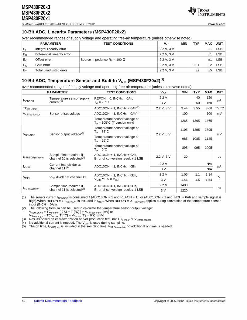
MSP430F20x3MSP430F20x2MSP430F20x1SLAS491I –AUGUST 2005–REVISED DECEMBER 2012 www.ti.com
10-Bit ADC, Linearity Parameters (MSP430F20x2)over recommended ranges of supply voltage and operating free-air temperature (unless otherwise noted)
PARAMETER TEST CONDITIONS VCC MIN TYP MAX UNIT
EI Integral linearity error 2.2 V, 3 V ±1 LSB
ED Differential linearity error 2.2 V, 3 V ±1 LSB
EO Offset error Source impedance RS < 100 Ω 2.2 V, 3 V ±1 LSB
EG Gain error 2.2 V, 3 V ±1.1 ±2 LSB
ET Total unadjusted error 2.2 V, 3 V ±2 ±5 LSB
10-Bit ADC, Temperature Sensor and Built-In VMID (MSP430F20x2) (1)
over recommended ranges of supply voltage and operating free-air temperature (unless otherwise noted)
PARAMETER TEST CONDITIONS VCC MIN TYP MAX UNIT
2.2 V 40 120Temperature sensor supply REFON = 0, INCHx = 0Ah,ISENSOR µAcurrent (1) TA = 25°C 3 V 60 160
TCSENSOR ADC10ON = 1, INCHx = 0Ah (2) 2.2 V, 3 V 3.44 3.55 3.66 mV/°C
VOffset,Sensor Sensor offset voltage ADC10ON = 1, INCHx = 0Ah (2) -100 100 mV
Temperature sensor voltage at 1265 1365 1465TA = 105°C (T version only)
Temperature sensor voltage at 1195 1295 1395TA = 85°CVSENSOR Sensor output voltage (3) 2.2 V, 3 V mV
Temperature sensor voltage at 985 1085 1185TA = 25°C
Temperature sensor voltage at 895 995 1095TA = 0°C
Sample time required if ADC10ON = 1, INCHx = 0Ah,tSENSOR(sample) 2.2 V, 3 V 30 µschannel 10 is selected (4) Error of conversion result ≤ 1 LSB
2.2 V N/ACurrent into divider atIVMID ADC10ON = 1, INCHx = 0Bh µAchannel 11 (4)3 V N/A
2.2 V 1.06 1.1 1.14ADC10ON = 1, INCHx = 0Bh,VMID VCC divider at channel 11 VVMID ≈ 0.5 × VCC 3 V 1.46 1.5 1.54
2.2 V 1400Sample time required if ADC10ON = 1, INCHx = 0Bh,tVMID(sample) nschannel 11 is selected (5) Error of conversion result ≤ 1 LSB 3 V 1220
(1) The sensor current ISENSOR is consumed if (ADC10ON = 1 and REFON = 1), or (ADC10ON = 1 and INCH = 0Ah and sample signal ishigh).When REFON = 1, ISENSOR is included in IREF+.When REFON = 0, ISENSOR applies during conversion of the temperature sensorinput (INCH = 0Ah).
(2) The following formula can be used to calculate the temperature sensor output voltage:VSensor,typ = TCSensor ( 273 + T [°C] ) + VOffset,sensor [mV] orVSensor,typ = TCSensor T [°C] + VSensor(TA = 0°C) [mV]
(3) Results based on characterization and/or production test, not TCSensor or VOffset,sensor.(4) No additional current is needed. The VMID is used during sampling.(5) The on time, tVMID(on), is included in the sampling time, tVMID(sample); no additional on time is needed.
42 Submit Documentation Feedback Copyright © 2005–2012, Texas Instruments Incorporated
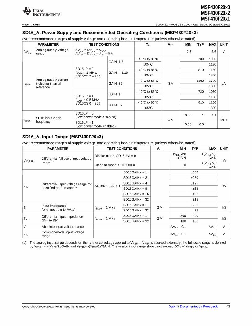
MSP430F20x3MSP430F20x2MSP430F20x1
www.ti.com SLAS491I –AUGUST 2005–REVISED DECEMBER 2012
SD16_A, Power Supply and Recommended Operating Conditions (MSP430F20x3)over recommended ranges of supply voltage and operating free-air temperature (unless otherwise noted)
PARAMETER TEST CONDITIONS TA VCC MIN TYP MAX UNIT
Analog supply voltage AVCC = DVCC = VCC,AVCC 2.5 3.6 Vrange AVSS = DVSS = VSS = 0 V
-40°C to 85°C 730 1050GAIN: 1,2
105°C 1170SD16LP = 0, -40°C to 85°C 810 1150fSD16 = 1 MHz, GAIN: 4,8,16
105°C 1300SD16OSR = 256Analog supply current -40°C to 85°C 1160 1700
ISD16 including internal GAIN: 32 3 V µA105°C 1850reference
-40°C to 85°C 720 1030GAIN: 1SD16LP = 1, 105°C 1160
fSD16 = 0.5 MHz,-40°C to 85°C 810 1150SD16OSR = 256 GAIN: 32
105°C 1300
SD16LP = 0 0.03 1 1.1(Low power mode disabled)SD16 input clockfSD16 3 V MHzfrequency SD16LP = 1 0.03 0.5(Low power mode enabled)
SD16_A, Input Range (MSP430F20x3)over recommended ranges of supply voltage and operating free-air temperature (unless otherwise noted)
PARAMETER TEST CONDITIONS VCC MIN TYP MAX UNIT
-(VREF/2)/ +(VREF/2)/Bipolar mode, SD16UNI = 0 GAIN GAINDifferential full scale input voltageVID,FSR mVrange (1)+(VREF/2)/Unipolar mode, SD16UNI = 1 0 GAIN
SD16GAINx = 1 ±500
SD16GAINx = 2 ±250
SD16GAINx = 4 ±125Differential input voltage range forVID SD16REFON = 1 mVspecified performance (1)SD16GAINx = 8 ±62
SD16GAINx = 16 ±31
SD16GAINx = 32 ±15
SD16GAINx = 1 200Input impedanceZI fSD16 = 1 MHz 3 V kΩ(one input pin to AVSS) SD16GAINx = 32 75
SD16GAINx = 1 300 400Differential input impedanceZID fSD16 = 1 MHz 3 V kΩ(IN+ to IN-) SD16GAINx = 32 100 150
VI Absolute input voltage range AVSS - 0.1 AVCC V
Common-mode input voltageVIC AVSS - 0.1 AVCC Vrange
(1) The analog input range depends on the reference voltage applied to VREF. If VREF is sourced externally, the full-scale range is definedby VFSR+ = +(VREF/2)/GAIN and VFSR-= -(VREF/2)/GAIN. The analog input range should not exceed 80% of VFSR+ or VFSR-.
Copyright © 2005–2012, Texas Instruments Incorporated Submit Documentation Feedback 43
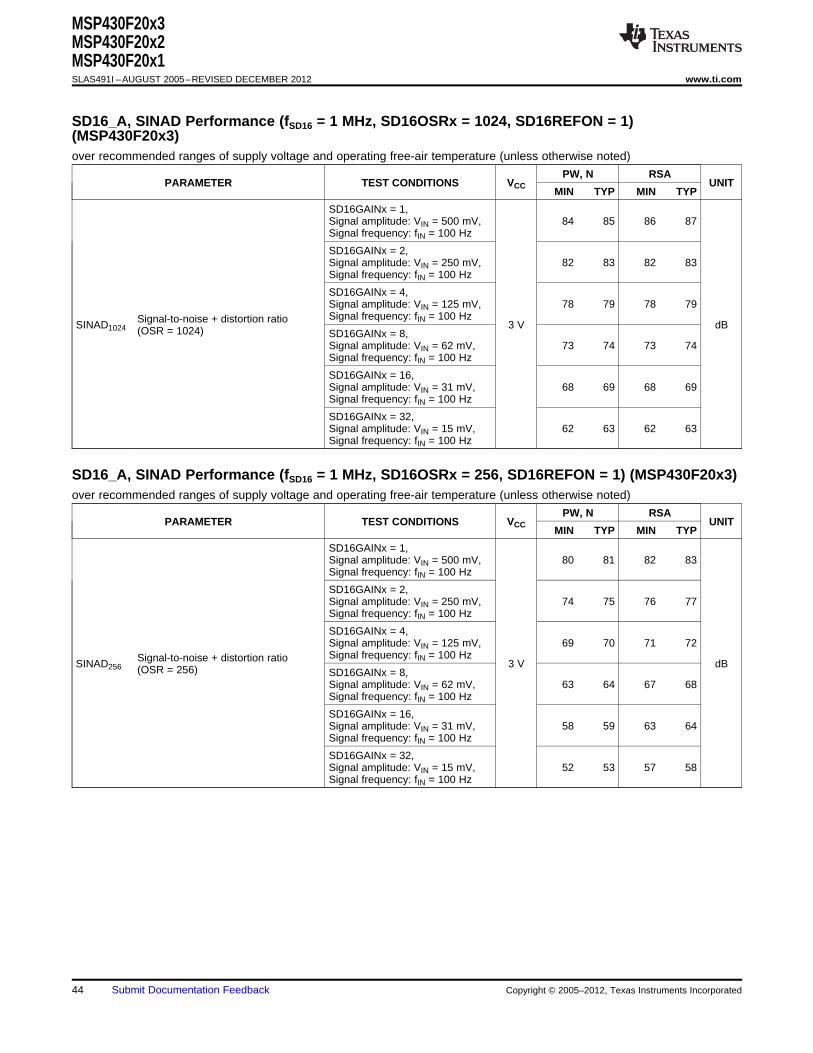
MSP430F20x3MSP430F20x2MSP430F20x1SLAS491I –AUGUST 2005–REVISED DECEMBER 2012 www.ti.com
SD16_A, SINAD Performance (fSD16 = 1 MHz, SD16OSRx = 1024, SD16REFON = 1)(MSP430F20x3)over recommended ranges of supply voltage and operating free-air temperature (unless otherwise noted)
PW, N RSAPARAMETER TEST CONDITIONS VCC UNIT
MIN TYP MIN TYP
SD16GAINx = 1,Signal amplitude: VIN = 500 mV, 84 85 86 87Signal frequency: fIN = 100 Hz
SD16GAINx = 2,Signal amplitude: VIN = 250 mV, 82 83 82 83Signal frequency: fIN = 100 Hz
SD16GAINx = 4,Signal amplitude: VIN = 125 mV, 78 79 78 79Signal frequency: fIN = 100 HzSignal-to-noise + distortion ratioSINAD1024 3 V dB(OSR = 1024) SD16GAINx = 8,Signal amplitude: VIN = 62 mV, 73 74 73 74Signal frequency: fIN = 100 Hz
SD16GAINx = 16,Signal amplitude: VIN = 31 mV, 68 69 68 69Signal frequency: fIN = 100 Hz
SD16GAINx = 32,Signal amplitude: VIN = 15 mV, 62 63 62 63Signal frequency: fIN = 100 Hz
SD16_A, SINAD Performance (fSD16 = 1 MHz, SD16OSRx = 256, SD16REFON = 1) (MSP430F20x3)over recommended ranges of supply voltage and operating free-air temperature (unless otherwise noted)
PW, N RSAPARAMETER TEST CONDITIONS VCC UNIT
MIN TYP MIN TYP
SD16GAINx = 1,Signal amplitude: VIN = 500 mV, 80 81 82 83Signal frequency: fIN = 100 Hz
SD16GAINx = 2,Signal amplitude: VIN = 250 mV, 74 75 76 77Signal frequency: fIN = 100 Hz
SD16GAINx = 4,Signal amplitude: VIN = 125 mV, 69 70 71 72Signal frequency: fIN = 100 HzSignal-to-noise + distortion ratioSINAD256 3 V dB(OSR = 256) SD16GAINx = 8,Signal amplitude: VIN = 62 mV, 63 64 67 68Signal frequency: fIN = 100 Hz
SD16GAINx = 16,Signal amplitude: VIN = 31 mV, 58 59 63 64Signal frequency: fIN = 100 Hz
SD16GAINx = 32,Signal amplitude: VIN = 15 mV, 52 53 57 58Signal frequency: fIN = 100 Hz
44 Submit Documentation Feedback Copyright © 2005–2012, Texas Instruments Incorporated
OSR
55.0
60.0
65.0
70.0
75.0
80.0
85.0
90.0
10.00 100.00 1000.00
SIN
AD
−dB
PW, or N
RSA
MSP430F20x3MSP430F20x2MSP430F20x1
www.ti.com SLAS491I –AUGUST 2005–REVISED DECEMBER 2012
Typical Characteristics, SD16_A SINAD Performance Over OSR (MSP430F20x3)
SINAD PERFORMANCEvs
OSR(fSD16 = 1 MHz, SD16REFON = 1,SD16GAINx = 1)
Figure 23.
SD16_A, Performance (fSD16 = 1 MHz, SD16OSRx = 256, SD16REFON = 1) (MSP430F20x3)over recommended ranges of supply voltage and operating free-air temperature (unless otherwise noted)
PARAMETER TEST CONDITIONS VCC MIN TYP MAX UNIT
SD16GAINx = 1 0.97 1.00 1.02
SD16GAINx = 2 1.90 1.96 2.02
SD16GAINx = 4 3.76 3.86 3.96G Nominal gain 3 V
SD16GAINx = 8 7.36 7.62 7.84
SD16GAINx = 16 14.56 15.04 15.52
SD16GAINx = 32 27.20 28.35 29.76
ΔG/ΔT Gain temperature drift SD16GAINx = 1 (1) 3 V 15 ppm/°C
SD16GAINx = 1 ±0.2EOS Offset error 3 V %FSR
SD16GAINx = 32 ±1.5
SD16GAINx = 1 ±4 ±20Offset error temperature ppmΔEOS/ΔT 3 Vcoefficient FSR/°CSD16GAINx = 32 ±20 ±100
SD16GAINx = 1,Common-mode input signal: >90VID = 500 mV, fIN = 50 Hz, 100 HzCommon-mode rejectionCMRR 3 V dBratio SD16GAINx = 32,Common-mode input signal: >75VID = 16 mV, fIN = 50 Hz, 100 Hz
SD16GAINx = 1, VIN = 500 mV,DC PSR DC power supply rejection 2.5 V to 3.6 V 0.35 %/VVCC = 2.5 V to 3.6 V (2)
AC power supply rejection SD16GAINx = 1,AC PSRR 3 V >80 dBratio VCC = 3 V ± 100 mV, fIN = 50 Hz
(1) Calculated using the box method: (MAX(-40°C to 85°C) - MIN(-40°C to 85°C)) / MIN(-40°C to 85°C) / (85°C - (-40°C))(2) Calculated using the ADC output code and the box method:
(MAX-code(2.5 V to 3.6 V) - MIN-code(2.5 V to 3.6 V)) / MIN-code(2.5 V to 3.6 V) / (3.6 V - 2.5 V)
Copyright © 2005–2012, Texas Instruments Incorporated Submit Documentation Feedback 45
MSP430F20x3MSP430F20x2MSP430F20x1SLAS491I –AUGUST 2005–REVISED DECEMBER 2012 www.ti.com
SD16_A, Built-In Voltage Reference (MSP430F20x3)over recommended ranges of supply voltage and operating free-air temperature (unless otherwise noted)
PARAMETER TEST CONDITIONS TA VCC MIN TYP MAX UNIT
SD16REFON = 1,VREF Internal reference voltage 3 V 1.14 1.20 1.26 VSD16VMIDON = 0
-40°C to 85°C 3 V 190 280SD16REFON = 1,IREF Reference supply current µASD16VMIDON = 0 105°C 3 V 295
SD16REFON = 1,TC Temperature coefficient 3 V 18 50 ppm/°CSD16VMIDON = 0
SD16REFON = 1,CREF VREF load capacitance 100 nFSD16VMIDON = 0 (1)
SD16REFON = 1,ILOAD VREF(I) maximum load current 3 V ±200 nASD16VMIDON = 0
SD16REFON = 0 → 1,tON Turn-on time SD16VMIDON = 0, 3 V 5 ms
CREF = 100 nF
SD16REFON = 1,DC power supply rejectionDC PSR SD16VMIDON = 0, 2.5 V to 3.6 V 100 µV/VΔVREF/ΔVCC VCC = 2.5 V to 3.6 V
(1) There is no capacitance required on VREF. However, a capacitance of at least 100 nF is recommended to reduce any reference voltagenoise.
SD16_A, Reference Output Buffer (MSP430F20x3)over recommended ranges of supply voltage and operating free-air temperature (unless otherwise noted)
PARAMETER TEST CONDITIONS TA VCC MIN TYP MAX UNIT
SD16REFON = 1,VREF,BUF Reference buffer output voltage 3 V 1.2 VSD16VMIDON = 1
-40°C to 85°C 385 600Reference supply + reference SD16REFON = 1,IREF,BUF 3 V µAoutput buffer quiescent current SD16VMIDON = 1 105°C 660
Required load capacitance on SD16REFON = 1,CREF(O) 470 nFVREF SD16VMIDON = 1
SD16REFON = 1,ILOAD,Max Maximum load current on VREF 3 V ±1 mASD16VMIDON = 1
Maximum voltage variation vs |ILOAD| = 0 to 1 mA 3 V -15 +15 mVload current
SD16REFON = 0 → 1,tON Turn on time SD16VMIDON = 1, 3 V 100 µs
CREF = 470 nF
SD16_A, External Reference Input (MSP430F20x3)over recommended ranges of supply voltage and operating free-air temperature (unless otherwise noted)
PARAMETER TEST CONDITIONS VCC MIN TYP MAX UNIT
VREF(I) Input voltage range SD16REFON = 0 3 V 1 1.25 1.5 V
IREF(I) Input current SD16REFON = 0 3 V 50 nA
46 Submit Documentation Feedback Copyright © 2005–2012, Texas Instruments Incorporated
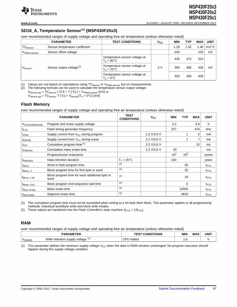
MSP430F20x3MSP430F20x2MSP430F20x1
www.ti.com SLAS491I –AUGUST 2005–REVISED DECEMBER 2012
SD16_A, Temperature Sensor (1) (MSP430F20x3)over recommended ranges of supply voltage and operating free-air temperature (unless otherwise noted)
PARAMETER TEST CONDITIONS VCC MIN TYP MAX UNIT
TCSensor Sensor temperature coefficient 1.18 1.32 1.46 mV/°C
VOffset,Sensor Sensor offset voltage -100 100 mV
Temperature sensor voltage at 435 475 515TA = 85°C
Temperature sensor voltage atVSensor Sensor output voltage (2) 3 V 355 395 435 mVTA = 25°C
Temperature sensor voltage at 320 360 400TA = 0°C
(1) Values are not based on calculations using TCSensor or VOffset,sensor but on measurements.(2) The following formula can be used to calculate the temperature sensor output voltage:
VSensor,typ = TCSensor ( 273 + T [°C] ) + VOffset,sensor [mV] orVSensor,typ = TCSensor T [°C] + VSensor(TA = 0°C) [mV]
Flash Memoryover recommended ranges of supply voltage and operating free-air temperature (unless otherwise noted)
TESTPARAMETER VCC MIN TYP MAX UNITCONDITIONS
VCC(PGM/ERASE) Program and erase supply voltage 2.2 3.6 V
fFTG Flash timing generator frequency 257 476 kHz
IPGM Supply current from VCC during program 2.2 V/3.6 V 1 5 mA
IERASE Supply current from VCC during erase 2.2 V/3.6 V 1 7 mA
tCPT Cumulative program time (1) 2.2 V/3.6 V 10 ms
tCMErase Cumulative mass erase time 2.2 V/3.6 V 20 ms
Program/erase endurance 104 105 cycles
tRetention Data retention duration TJ = 25°C 100 years
tWord Word or byte program time (2) 30 tFTG
tBlock, 0 Block program time for first byte or word (2) 25 tFTG
Block program time for each additional byte ortBlock, 1-63(2) 18 tFTGword
tBlock, End Block program end-sequence wait time (2) 6 tFTG
tMass Erase Mass erase time (2) 10593 tFTG
tSeg Erase Segment erase time (2) 4819 tFTG
(1) The cumulative program time must not be exceeded when writing to a 64-byte flash block. This parameter applies to all programmingmethods: individual word/byte write and block write modes.
(2) These values are hardwired into the Flash Controller's state machine (tFTG = 1/fFTG).
RAMover recommended ranges of supply voltage and operating free-air temperature (unless otherwise noted)
PARAMETER TEST CONDITIONS MIN MAX UNIT
V(RAMh) RAM retention supply voltage (1) CPU halted 1.6 V
(1) This parameter defines the minimum supply voltage VCC when the data in RAM remains unchanged. No program execution shouldhappen during this supply voltage condition.
Copyright © 2005–2012, Texas Instruments Incorporated Submit Documentation Feedback 47
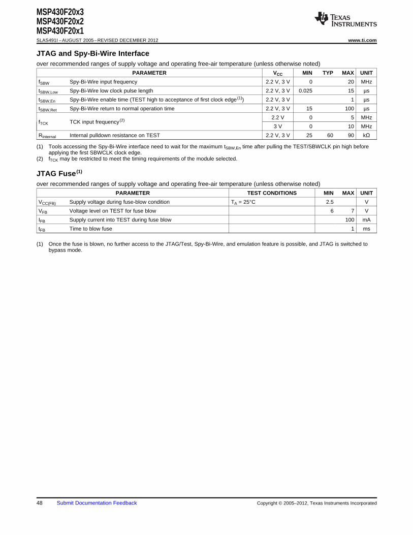
MSP430F20x3MSP430F20x2MSP430F20x1SLAS491I –AUGUST 2005–REVISED DECEMBER 2012 www.ti.com
JTAG and Spy-Bi-Wire Interfaceover recommended ranges of supply voltage and operating free-air temperature (unless otherwise noted)
PARAMETER VCC MIN TYP MAX UNIT
fSBW Spy-Bi-Wire input frequency 2.2 V, 3 V 0 20 MHz
tSBW,Low Spy-Bi-Wire low clock pulse length 2.2 V, 3 V 0.025 15 µs
tSBW,En Spy-Bi-Wire enable time (TEST high to acceptance of first clock edge (1)) 2.2 V, 3 V 1 µs
tSBW,Ret Spy-Bi-Wire return to normal operation time 2.2 V, 3 V 15 100 µs
2.2 V 0 5 MHzfTCK TCK input frequency (2)
3 V 0 10 MHz
RInternal Internal pulldown resistance on TEST 2.2 V, 3 V 25 60 90 kΩ
(1) Tools accessing the Spy-Bi-Wire interface need to wait for the maximum tSBW,En time after pulling the TEST/SBWCLK pin high beforeapplying the first SBWCLK clock edge.
(2) fTCK may be restricted to meet the timing requirements of the module selected.
JTAG Fuse (1)
over recommended ranges of supply voltage and operating free-air temperature (unless otherwise noted)
PARAMETER TEST CONDITIONS MIN MAX UNIT
VCC(FB) Supply voltage during fuse-blow condition TA = 25°C 2.5 V
VFB Voltage level on TEST for fuse blow 6 7 V
IFB Supply current into TEST during fuse blow 100 mA
tFB Time to blow fuse 1 ms
(1) Once the fuse is blown, no further access to the JTAG/Test, Spy-Bi-Wire, and emulation feature is possible, and JTAG is switched tobypass mode.
48 Submit Documentation Feedback Copyright © 2005–2012, Texas Instruments Incorporated
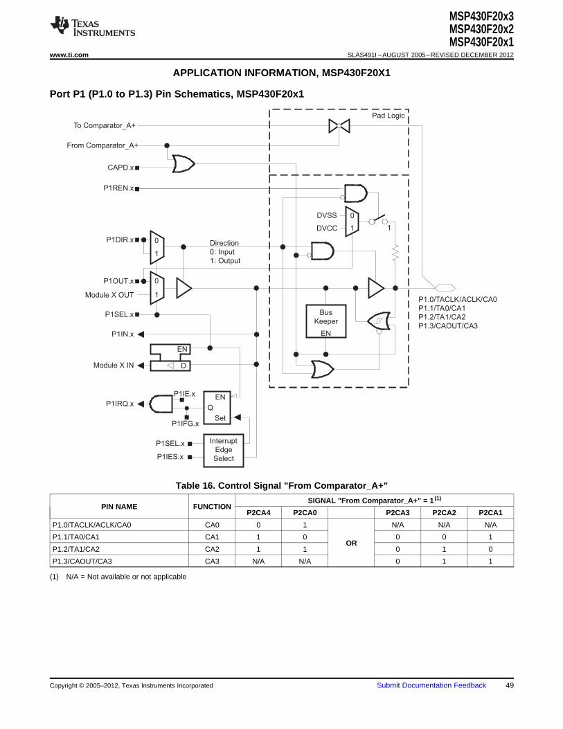
Bus
Keeper
EN
Direction
0: Input
1: Output
P1SEL.x
1
0P1DIR.x
P1IN.x
P1IRQ.x
D
EN
Module X IN
1
0
Module X OUT
P1OUT.x
Interrupt
Edge
Select
Q
EN
Set
P1SEL.x
P1IES.x
P1IFG.x
P1IE.x
P1.0/TACLK/ACLK/CA0
P1.1/TA0/CA1
P1.2/TA1/CA2
P1.3/CAOUT/CA3
1
0DVSS
DVCC
P1REN.x
CAPD.x
Pad Logic
From Comparator_A+
To Comparator_A+
1
MSP430F20x3MSP430F20x2MSP430F20x1
www.ti.com SLAS491I –AUGUST 2005–REVISED DECEMBER 2012
APPLICATION INFORMATION, MSP430F20X1
Port P1 (P1.0 to P1.3) Pin Schematics, MSP430F20x1
Table 16. Control Signal "From Comparator_A+"
SIGNAL "From Comparator_A+" = 1 (1)
PIN NAME FUNCTIONP2CA4 P2CA0 P2CA3 P2CA2 P2CA1
P1.0/TACLK/ACLK/CA0 CA0 0 1 N/A N/A N/A
P1.1/TA0/CA1 CA1 1 0 0 0 1OR
P1.2/TA1/CA2 CA2 1 1 0 1 0
P1.3/CAOUT/CA3 CA3 N/A N/A 0 1 1
(1) N/A = Not available or not applicable
Copyright © 2005–2012, Texas Instruments Incorporated Submit Documentation Feedback 49
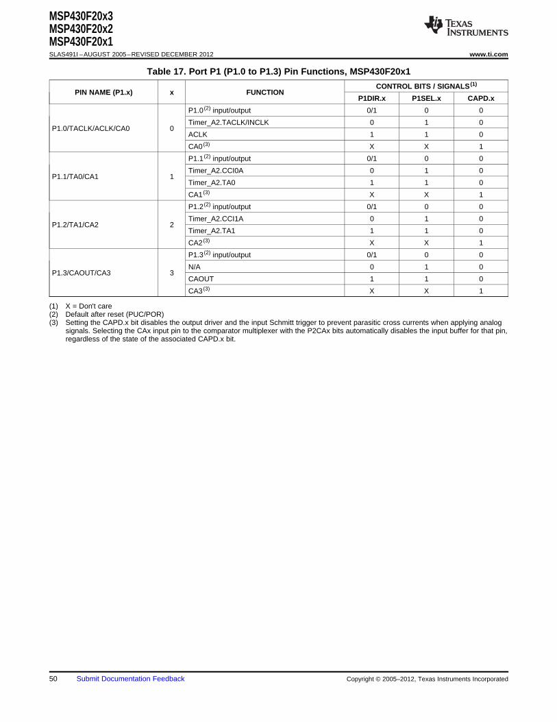
MSP430F20x3MSP430F20x2MSP430F20x1SLAS491I –AUGUST 2005–REVISED DECEMBER 2012 www.ti.com
Table 17. Port P1 (P1.0 to P1.3) Pin Functions, MSP430F20x1
CONTROL BITS / SIGNALS (1)
PIN NAME (P1.x) x FUNCTIONP1DIR.x P1SEL.x CAPD.x
P1.0 (2) input/output 0/1 0 0
Timer_A2.TACLK/INCLK 0 1 0P1.0/TACLK/ACLK/CA0 0
ACLK 1 1 0
CA0 (3) X X 1
P1.1 (2) input/output 0/1 0 0
Timer_A2.CCI0A 0 1 0P1.1/TA0/CA1 1
Timer_A2.TA0 1 1 0
CA1 (3) X X 1
P1.2 (2) input/output 0/1 0 0
Timer_A2.CCI1A 0 1 0P1.2/TA1/CA2 2
Timer_A2.TA1 1 1 0
CA2 (3) X X 1
P1.3 (2) input/output 0/1 0 0
N/A 0 1 0P1.3/CAOUT/CA3 3
CAOUT 1 1 0
CA3 (3) X X 1
(1) X = Don't care(2) Default after reset (PUC/POR)(3) Setting the CAPD.x bit disables the output driver and the input Schmitt trigger to prevent parasitic cross currents when applying analog
signals. Selecting the CAx input pin to the comparator multiplexer with the P2CAx bits automatically disables the input buffer for that pin,regardless of the state of the associated CAPD.x bit.
50 Submit Documentation Feedback Copyright © 2005–2012, Texas Instruments Incorporated
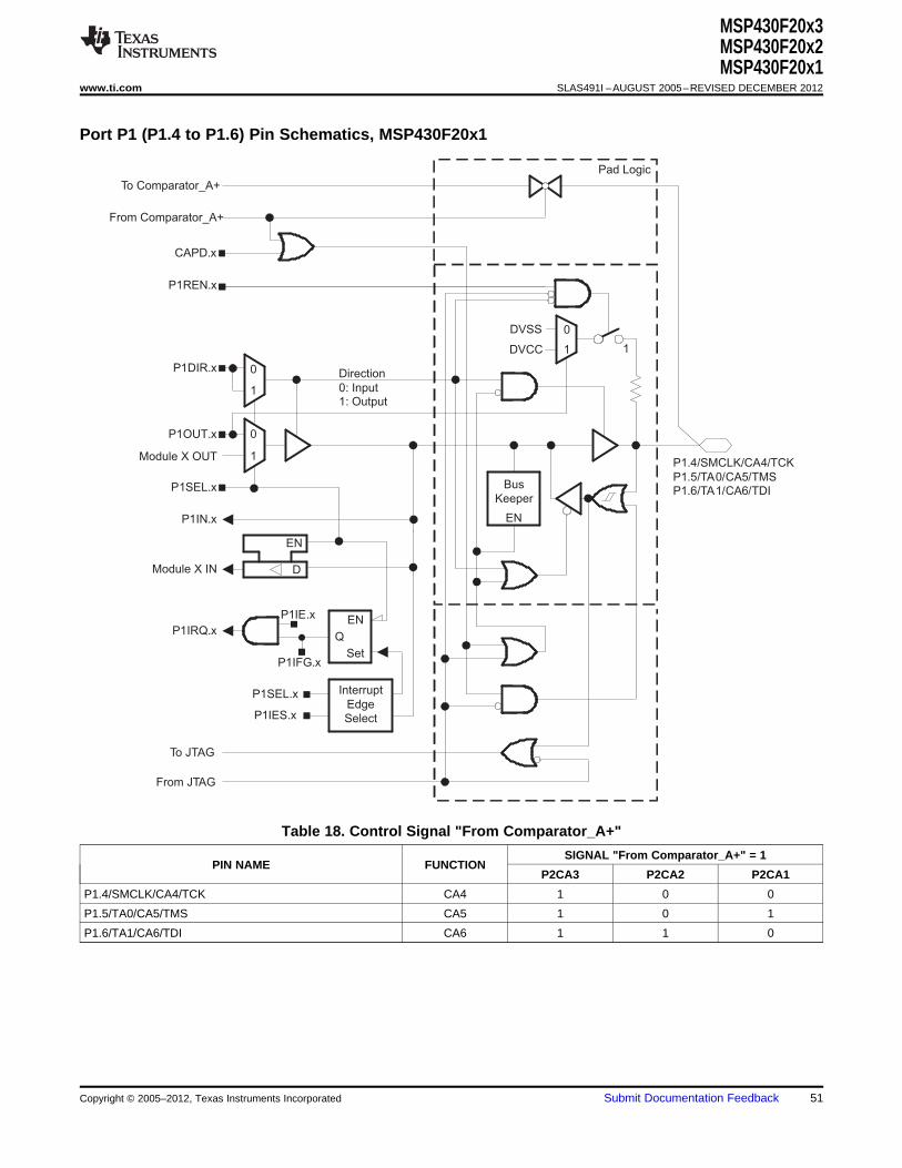
Bus
Keeper
EN
Direction
0: Input1: Output
P1SEL.x
1
0P1DIR.x
P1IN.x
P1IRQ.x
D
EN
Module X IN
1
0
Module X OUT
P1OUT.x
Interrupt
Edge
Select
Q
EN
Set
P1SEL.x
P1IES.x
P1IFG.x
P1IE.x
P1.4/SMCLK/CA4/TCK
P1.5/TA0/CA5/TMSP1.6/TA1/CA6/TDI
1
0DVSS
DVCC
P1REN.x
To JTAG
From JTAG
1
CAPD.x
Pad Logic
From Comparator_A+
To Comparator_A+
MSP430F20x3MSP430F20x2MSP430F20x1
www.ti.com SLAS491I –AUGUST 2005–REVISED DECEMBER 2012
Port P1 (P1.4 to P1.6) Pin Schematics, MSP430F20x1
Table 18. Control Signal "From Comparator_A+"
SIGNAL "From Comparator_A+" = 1PIN NAME FUNCTION
P2CA3 P2CA2 P2CA1
P1.4/SMCLK/CA4/TCK CA4 1 0 0
P1.5/TA0/CA5/TMS CA5 1 0 1
P1.6/TA1/CA6/TDI CA6 1 1 0
Copyright © 2005–2012, Texas Instruments Incorporated Submit Documentation Feedback 51
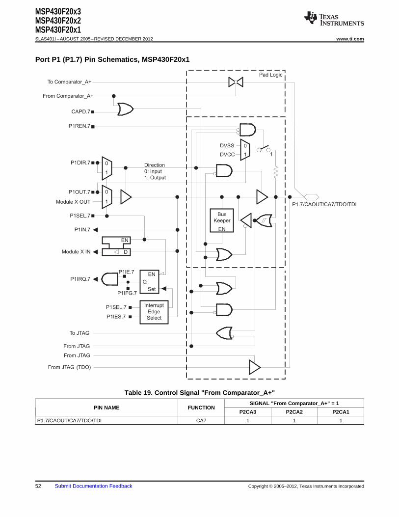
From JTAG
From JTAG (TDO)
Bus
Keeper
EN
Direction
0: Input
1: Output
P1SEL.7
1
0P1DIR.7
P1IN.7
P1IRQ.7
D
EN
Module X IN
1
0
Module X OUT
P1OUT.7
Interrupt
Edge
Select
Q
EN
Set
P1SEL.7
P1IES.7
P1IFG.7
P1IE.7
P1.7/CAOUT/CA7/TDO/TDI
1
0DVSS
DVCC
P1REN.7
To JTAG
From JTAG
1
CAPD.7
Pad Logic
From Comparator_A+
To Comparator_A+
MSP430F20x3MSP430F20x2MSP430F20x1SLAS491I –AUGUST 2005–REVISED DECEMBER 2012 www.ti.com
Port P1 (P1.7) Pin Schematics, MSP430F20x1
Table 19. Control Signal "From Comparator_A+"
SIGNAL "From Comparator_A+" = 1PIN NAME FUNCTION
P2CA3 P2CA2 P2CA1
P1.7/CAOUT/CA7/TDO/TDI CA7 1 1 1
52 Submit Documentation Feedback Copyright © 2005–2012, Texas Instruments Incorporated
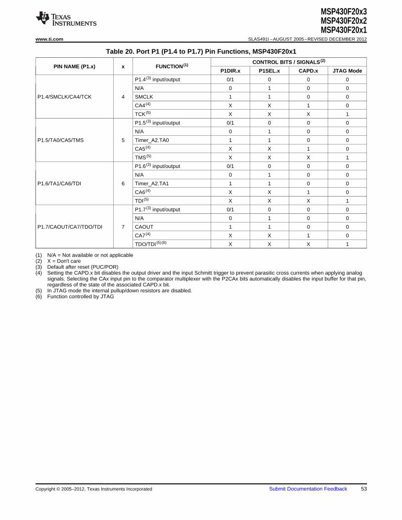
MSP430F20x3MSP430F20x2MSP430F20x1
www.ti.com SLAS491I –AUGUST 2005–REVISED DECEMBER 2012
Table 20. Port P1 (P1.4 to P1.7) Pin Functions, MSP430F20x1
CONTROL BITS / SIGNALS (2)
PIN NAME (P1.x) x FUNCTION (1)
P1DIR.x P1SEL.x CAPD.x JTAG Mode
P1.4 (3) input/output 0/1 0 0 0
N/A 0 1 0 0
P1.4/SMCLK/CA4/TCK 4 SMCLK 1 1 0 0
CA4 (4) X X 1 0
TCK (5) X X X 1
P1.5 (3) input/output 0/1 0 0 0
N/A 0 1 0 0
P1.5/TA0/CA5/TMS 5 Timer_A2.TA0 1 1 0 0
CA5 (4) X X 1 0
TMS (5) X X X 1
P1.6 (3) input/output 0/1 0 0 0
N/A 0 1 0 0
P1.6/TA1/CA6/TDI 6 Timer_A2.TA1 1 1 0 0
CA6 (4) X X 1 0
TDI (5) X X X 1
P1.7 (3) input/output 0/1 0 0 0
N/A 0 1 0 0
P1.7/CAOUT/CA7/TDO/TDI 7 CAOUT 1 1 0 0
CA7 (4) X X 1 0
TDO/TDI (5) (6) X X X 1
(1) N/A = Not available or not applicable(2) X = Don't care(3) Default after reset (PUC/POR)(4) Setting the CAPD.x bit disables the output driver and the input Schmitt trigger to prevent parasitic cross currents when applying analog
signals. Selecting the CAx input pin to the comparator multiplexer with the P2CAx bits automatically disables the input buffer for that pin,regardless of the state of the associated CAPD.x bit.
(5) In JTAG mode the internal pullup/down resistors are disabled.(6) Function controlled by JTAG
Copyright © 2005–2012, Texas Instruments Incorporated Submit Documentation Feedback 53

Bus
Keeper
EN
Direction
0: Input
1: Output
P2SEL.6
1
0P2DIR.6
P2IN.6
P2IRQ.6
D
EN
Module X IN
1
0
Module X OUT
P2OUT.6
Interrupt
Edge
Select
Q
EN
Set
P2SEL.6
P2IES.6
P2IFG.6
P2IE.6
P2.6/XIN/TA1
1
0DVSS
DVCC
P2REN.6
Pad Logic
LFXT1 OscillatorBCSCTL3.LFXT1Sx = 11
P2.7/XOUT
LFXT1 off
0
1
1
LFXT1CLK
P2SEL.7
MSP430F20x3MSP430F20x2MSP430F20x1SLAS491I –AUGUST 2005–REVISED DECEMBER 2012 www.ti.com
Port P2 (P2.6) Pin Schematics, MSP430F20x1
Table 21. Port P2 (P2.6) Pin Functions, MSP430F20x1
CONTROL BITS / SIGNALSPIN NAME (P2.x) x FUNCTION
P2DIR.x P2SEL.x
P2.6 input/output 0/1 0
P2.6/XIN/TA1 6 XIN (1) (2) 0 1
Timer_A2.TA1 1 1
(1) Default after reset (PUC/POR)(2) XIN is used as digital clock input if the bits LFXT1Sx in register BCSCTL3 are set to 11.
54 Submit Documentation Feedback Copyright © 2005–2012, Texas Instruments Incorporated

LFXT1 off
P2SEL.6
Bus
Keeper
EN
Direction
0: Input
1: Output
P2SEL.7
1
0P2DIR.7
P2IN.7
P2IRQ.7
D
EN
Module X IN
1
0
Module X OUT
P2OUT.7
Interrupt
Edge
Select
Q
EN
Set
P2SEL.7
P2IES.7
P2IFG.7
P2IE.7
P2.7/XOUT
1
0DVSS
DVCC
P2REN.7
Pad Logic
LFXT1 OscillatorBCSCTL3.LFXT1Sx = 11
0
1
1
LFXT1CLK From P2.6/XIN P2.6/XIN/TA1
MSP430F20x3MSP430F20x2MSP430F20x1
www.ti.com SLAS491I –AUGUST 2005–REVISED DECEMBER 2012
Port P2 (P2.7) Pin Schematics, MSP430F20x1
Table 22. Port P2 (P2.7) Pin Functions, MSP430F20x1
CONTROL BITS / SIGNALSPIN NAME (P2.x) x FUNCTION
P2DIR.x P2SEL.x
P2.7 input/output 0/1 0
P2.7/XOUT 7 DVSS 0 1
XOUT (1) (2) 1 1
(1) Default after reset (PUC/POR)(2) If the pin P2.7/XOUT is used as an input a current can flow until P2SEL.7 is cleared due to the oscillator output driver connection to this
pin after reset.
Copyright © 2005–2012, Texas Instruments Incorporated Submit Documentation Feedback 55
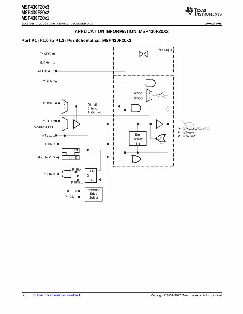
Bus
Keeper
EN
Direction
0: Input
1: Output
P1SEL.x
1
0P1DIR.x
P1IN.x
P1IRQ.x
D
EN
Module X IN
1
0
Module X OUT
P1OUT.x
Interrupt
Edge
Select
Q
EN
Set
P1SEL.x
P1IES.x
P1IFG.x
P1IE.x
P1.0/TACLK/ACLK/A0
P1.1/TA0/A1
P1.2/TA1/A2
1
0DVSS
DVCC
P1REN.x
ADC10AE.x
Pad Logic
INCHx = x
To ADC 10
1
MSP430F20x3MSP430F20x2MSP430F20x1SLAS491I –AUGUST 2005–REVISED DECEMBER 2012 www.ti.com
APPLICATION INFORMATION, MSP430F20X2
Port P1 (P1.0 to P1.2) Pin Schematics, MSP430F20x2
56 Submit Documentation Feedback Copyright © 2005–2012, Texas Instruments Incorporated
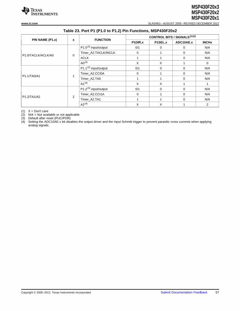
MSP430F20x3MSP430F20x2MSP430F20x1
www.ti.com SLAS491I –AUGUST 2005–REVISED DECEMBER 2012
Table 23. Port P1 (P1.0 to P1.2) Pin Functions, MSP430F20x2
CONTROL BITS / SIGNALS (1) (2)
PIN NAME (P1.x) x FUNCTIONP1DIR.x P1SEL.x ADC10AE.x INCHx
P1.0 (3) input/output 0/1 0 0 N/A
Timer_A2.TACLK/INCLK 0 1 0 N/AP1.0/TACLK/ACLK/A0 0
ACLK 1 1 0 N/A
A0 (4) X X 1 0
P1.1 (3) input/output 0/1 0 0 N/A
Timer_A2.CCI0A 0 1 0 N/AP1.1/TA0/A1 1
Timer_A2.TA0 1 1 0 N/A
A1 (4) X X 1 1
P1.2 (3) input/output 0/1 0 0 N/A
Timer_A2.CCI1A 0 1 0 N/AP1.2/TA1/A2 2
Timer_A2.TA1 1 1 0 N/A
A2 (4) X X 1 2
(1) X = Don't care(2) N/A = Not available or not applicable(3) Default after reset (PUC/POR)(4) Setting the ADC10AE.x bit disables the output driver and the input Schmitt trigger to prevent parasitic cross currents when applying
analog signals.
Copyright © 2005–2012, Texas Instruments Incorporated Submit Documentation Feedback 57
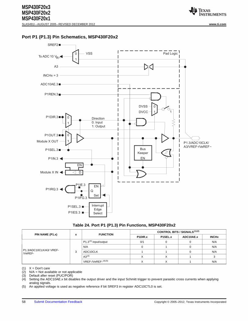
Bus
Keeper
EN
Direction
0: Input
1: Output
P1SEL.3
1
0P1DIR.3
P1IN.3
P1IRQ.3
D
EN
Module X IN
1
0
Module X OUT
P1OUT.3
Interrupt
Edge
Select
Q
EN
Set
P1SEL.3
P1IES.3
P1IFG.3
P1IE.3
P1.3/ADC10CLK/
A3/VREF−/VeREF−
1
0DVSS
DVCC
P1REN.3
ADC10AE.3
1
To ADC 10 VPad Logic
INCHx = 3
A3
R−1
0
SREF2
VSS
MSP430F20x3MSP430F20x2MSP430F20x1SLAS491I –AUGUST 2005–REVISED DECEMBER 2012 www.ti.com
Port P1 (P1.3) Pin Schematics, MSP430F20x2
Table 24. Port P1 (P1.3) Pin Functions, MSP430F20x2
CONTROL BITS / SIGNALS (1) (2)
PIN NAME (P1.x) x FUNCTIONP1DIR.x P1SEL.x ADC10AE.x INCHx
P1.3 (3) input/output 0/1 0 0 N/A
N/A 0 1 0 N/AP1.3/ADC10CLK/A3/ VREF- 3 ADC10CLK 1 1 0 N/A/VeREF-
A3 (4) X X 1 3
VREF-/VeREF- (4) (5) X X 1 N/A
(1) X = Don't care(2) N/A = Not available or not applicable(3) Default after reset (PUC/POR)(4) Setting the ADC10AE.x bit disables the output driver and the input Schmitt trigger to prevent parasitic cross currents when applying
analog signals.(5) An applied voltage is used as negative reference if bit SREF3 in register ADC10CTL0 is set.
58 Submit Documentation Feedback Copyright © 2005–2012, Texas Instruments Incorporated
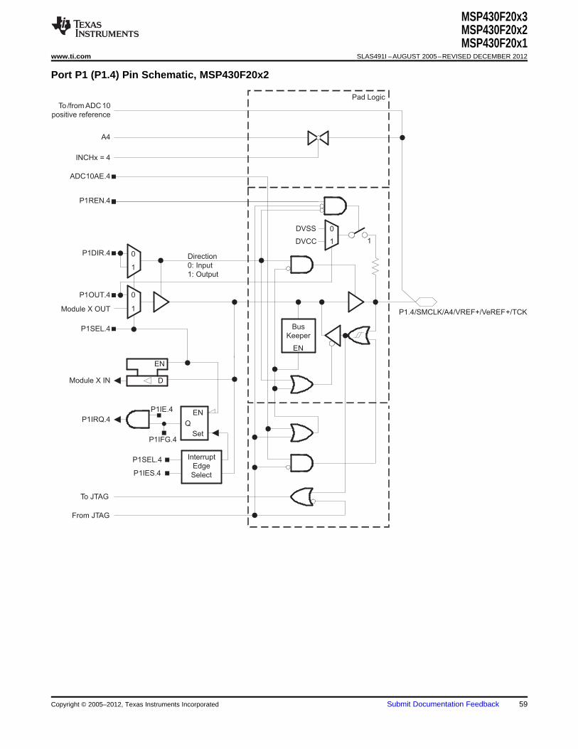
Bus
Keeper
EN
Direction
0: Input
1: Output
P1SEL.4
1
0P1DIR.4
P1IRQ.4
D
EN
Module X IN
1
0
Module X OUT
P1OUT.4
Interrupt
Edge
Select
Q
EN
Set
P1SEL.4
P1IES.4
P1IFG.4
P1IE.4
P1.4/SMCLK/A4/VREF+/VeREF+/TCK
1
0DVSS
DVCC
P1REN.4
To JTAG
From JTAG
1
ADC10AE.4
Pad Logic
INCHx = 4
A4
To /from ADC 10
positive reference
MSP430F20x3MSP430F20x2MSP430F20x1
www.ti.com SLAS491I –AUGUST 2005–REVISED DECEMBER 2012
Port P1 (P1.4) Pin Schematic, MSP430F20x2
Copyright © 2005–2012, Texas Instruments Incorporated Submit Documentation Feedback 59
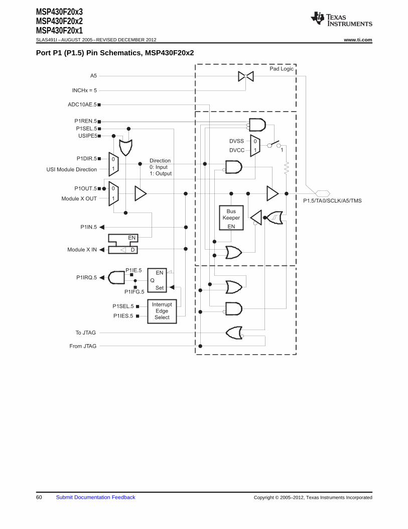
Bus
Keeper
EN
Direction
0: Input
1: Output1
0P1DIR.5
P1IN.5
P1IRQ.5
D
EN
Module X IN
1
0
Module X OUT
P1OUT.5
Interrupt
Edge
Select
Q
EN
Set
P1SEL.5
P1IES.5
P1IFG.5
P1IE.5
P1.5/TA0/SCLK/A5/TMS
1
0DVSS
DVCC
P1REN.5
P1SEL.5
USIPE5
USI Module Direction
1
To JTAG
From JTAG
ADC10AE.5
Pad Logic
INCHx = 5
A5
MSP430F20x3MSP430F20x2MSP430F20x1SLAS491I –AUGUST 2005–REVISED DECEMBER 2012 www.ti.com
Port P1 (P1.5) Pin Schematics, MSP430F20x2
60 Submit Documentation Feedback Copyright © 2005–2012, Texas Instruments Incorporated
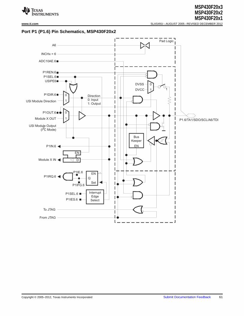
Bus
Keeper
EN
Direction
0: Input
1: Output1
0P1DIR.6
P1IN.6
P1IRQ.6
D
EN
Module X IN
1
0
Module X OUT
P1OUT.6
Interrupt
Edge
Select
Q
EN
Set
P1SEL.6
P1IES.6
P1IFG.6
P1IE.6
P1.6/TA1/SDO/SCL/A6/TDI
1
0DVSS
DVCC
P1REN.6
P1SEL.6
USIPE6
USI Module Direction
USI Module Output
(I2C Mode)
1
To JTAG
From JTAG
ADC10AE.6
Pad Logic
INCHx = 6
A6
MSP430F20x3MSP430F20x2MSP430F20x1
www.ti.com SLAS491I –AUGUST 2005–REVISED DECEMBER 2012
Port P1 (P1.6) Pin Schematics, MSP430F20x2
Copyright © 2005–2012, Texas Instruments Incorporated Submit Documentation Feedback 61
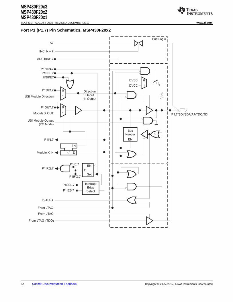
ADC10AE.7
Pad Logic
INCHx = 7
A7
Bus
Keeper
EN
Direction
0: Input
1: Output1
0P1DIR.7
P1IN.7
P1IRQ.7
D
EN
Module X IN
1
0
Module X OUT
P1OUT.7
Interrupt
Edge
Select
Q
EN
Set
P1SEL.7
P1IES.7
P1IFG.7
P1IE.7
P1.7/SDI/SDA/A7/TDO/TDI
1
0DVSS
DVCC
P1REN.7
P1SEL.7
USIPE7
USI Module Direction
From JTAG
From JTAG (TDO)
USI Module Output
(I2C Mode)
1
To JTAG
From JTAG
MSP430F20x3MSP430F20x2MSP430F20x1SLAS491I –AUGUST 2005–REVISED DECEMBER 2012 www.ti.com
Port P1 (P1.7) Pin Schematics, MSP430F20x2
62 Submit Documentation Feedback Copyright © 2005–2012, Texas Instruments Incorporated
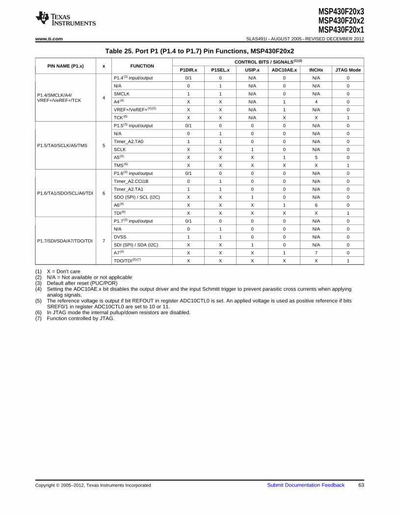
MSP430F20x3MSP430F20x2MSP430F20x1
www.ti.com SLAS491I –AUGUST 2005–REVISED DECEMBER 2012
Table 25. Port P1 (P1.4 to P1.7) Pin Functions, MSP430F20x2
CONTROL BITS / SIGNALS (1) (2)
PIN NAME (P1.x) x FUNCTIONP1DIR.x P1SEL.x USIP.x ADC10AE.x INCHx JTAG Mode
P1.4 (3) input/output 0/1 0 N/A 0 N/A 0
N/A 0 1 N/A 0 N/A 0
SMCLK 1 1 N/A 0 N/A 0P1.4/SMCLK/A4/ 4VREF+/VeREF+/TCK A4 (4) X X N/A 1 4 0
VREF+/VeREF+ (4) (5) X X N/A 1 N/A 0
TCK (6) X X N/A X X 1
P1.5 (3) input/output 0/1 0 0 0 N/A 0
N/A 0 1 0 0 N/A 0
Timer_A2.TA0 1 1 0 0 N/A 0P1.5/TA0/SCLK/A5/TMS 5
SCLK X X 1 0 N/A 0
A5 (4) X X X 1 5 0
TMS (6) X X X X X 1
P1.6 (3) input/output 0/1 0 0 0 N/A 0
Timer_A2.CCI1B 0 1 0 0 N/A 0
Timer_A2.TA1 1 1 0 0 N/A 0P1.6/TA1/SDO/SCL/A6/TDI 6
SDO (SPI) / SCL (I2C) X X 1 0 N/A 0
A6 (4) X X X 1 6 0
TDI (6) X X X X X 1
P1.7 (3) input/output 0/1 0 0 0 N/A 0
N/A 0 1 0 0 N/A 0
DVSS 1 1 0 0 N/A 0P1.7/SDI/SDA/A7/TDO/TDI 7
SDI (SPI) / SDA (I2C) X X 1 0 N/A 0
A7 (4) X X X 1 7 0
TDO/TDI (6) (7) X X X X X 1
(1) X = Don't care(2) N/A = Not available or not applicable(3) Default after reset (PUC/POR)(4) Setting the ADC10AE.x bit disables the output driver and the input Schmitt trigger to prevent parasitic cross currents when applying
analog signals.(5) The reference voltage is output if bit REFOUT in register ADC10CTL0 is set. An applied voltage is used as positive reference if bits
SREF0/1 in register ADC10CTL0 are set to 10 or 11.(6) In JTAG mode the internal pullup/down resistors are disabled.(7) Function controlled by JTAG.
Copyright © 2005–2012, Texas Instruments Incorporated Submit Documentation Feedback 63

Bus
Keeper
EN
Direction
0: Input
1: Output
P2SEL.6
1
0P2DIR.6
P2IN.6
P2IRQ.6
D
EN
Module X IN
1
0
Module X OUT
P2OUT.6
Interrupt
Edge
Select
Q
EN
Set
P2SEL.6
P2IES.6
P2IFG.6
P2IE.6
P2.6/XIN/TA1
1
0DVSS
DVCC
P2REN.6
Pad Logic
LFXT1 OscillatorBCSCTL3.LFXT1Sx = 11
P2.7/XOUT
LFXT1 off
0
1
1
LFXT1CLK
P2SEL.7
MSP430F20x3MSP430F20x2MSP430F20x1SLAS491I –AUGUST 2005–REVISED DECEMBER 2012 www.ti.com
Port P2 (P2.6) Pin Schematics, MSP430F20x2
Table 26. Port P2 (P2.6) Pin Functions, MSP430F20x2
CONTROL BITS / SIGNALSPIN NAME (P2.x) x FUNCTION
P2DIR.x P2SEL.x
P2.6 input/output 0/1 0
P2.6/XIN/TA1 6 XIN (1) (2) 0 1
Timer_A2.TA1 1 1
(1) Default after reset (PUC/POR)(2) XIN is used as digital clock input if the bits LFXT1Sx in register BCSCTL3 are set to 11.
64 Submit Documentation Feedback Copyright © 2005–2012, Texas Instruments Incorporated

LFXT1 off
P2SEL.6
Bus
Keeper
EN
Direction
0: Input
1: Output
P2SEL.7
1
0P2DIR.7
P2IN.7
P2IRQ.7
D
EN
Module X IN
1
0
Module X OUT
P2OUT.7
Interrupt
Edge
Select
Q
EN
Set
P2SEL.7
P2IES.7
P2IFG.7
P2IE.7
P2.7/XOUT
1
0DVSS
DVCC
P2REN.7
Pad Logic
LFXT1 OscillatorBCSCTL3.LFXT1Sx = 11
0
1
1
LFXT1CLK From P2.6/XIN P2.6/XIN/TA1
MSP430F20x3MSP430F20x2MSP430F20x1
www.ti.com SLAS491I –AUGUST 2005–REVISED DECEMBER 2012
Port P2 (P2.7) Pin Schematics, MSP430F20x2
Table 27. Port P2 (P2.7) Pin Functions, MSP430F20x2
CONTROL BITS / SIGNALSPIN NAME (P2.x) x FUNCTION
P2DIR.x P2SEL.x
P2.7 input/output 0/1 0
P2.7/XOUT 7 DVSS 0 1
XOUT (1) (2) 1 1
(1) Default after reset (PUC/POR)(2) If the pin P2.7/XOUT is used as an input a current can flow until P2SEL.7 is cleared due to the oscillator output driver connection to this
pin after reset.
Copyright © 2005–2012, Texas Instruments Incorporated Submit Documentation Feedback 65
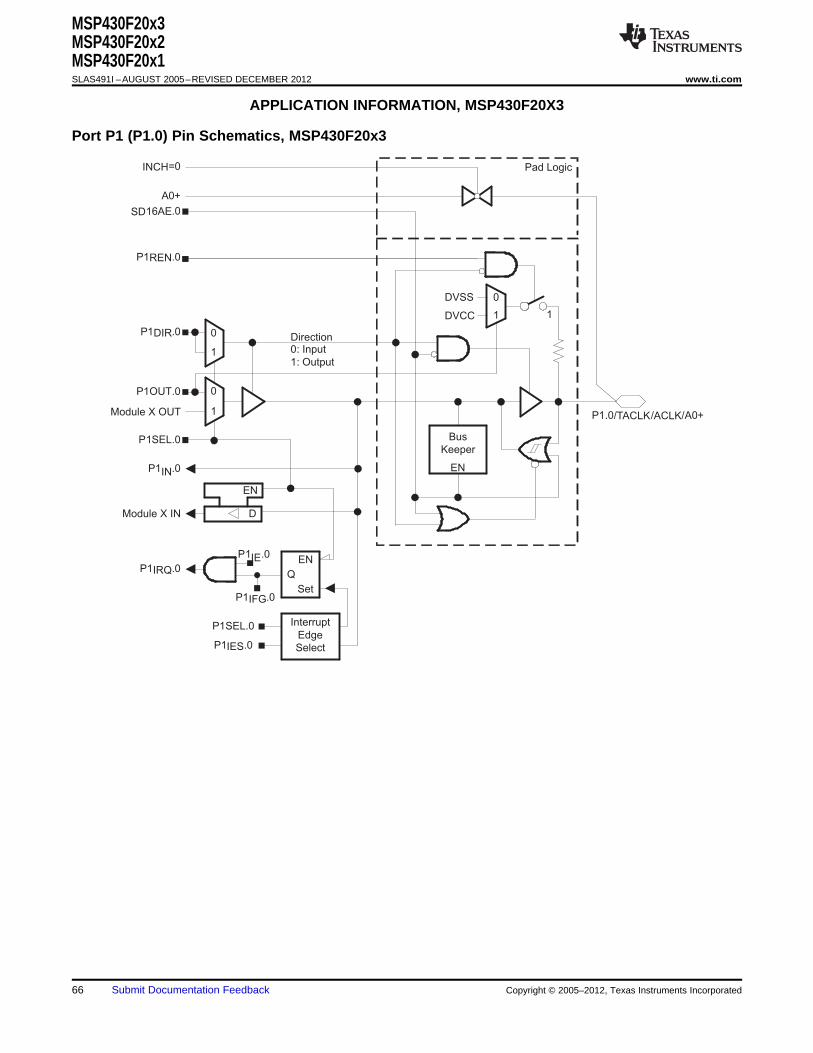
Bus
Keeper
EN
Direction0: Input
1: Output
P1SEL.0
1
0P1DIR.0
P1IN.0
P1IRQ.0
D
EN
Module X IN
1
0
Module X OUT
P1OUT.0
Interrupt
Edge
Select
Q
EN
Set
P1SEL.0
P1IES.0
P1IFG.0
P1IE.0
P1.0/TACLK/ACLK/A0+
1
0DVSS
DVCC
P1REN.0
SD16AE.0
Pad LogicINCH=0
A0+
1
MSP430F20x3MSP430F20x2MSP430F20x1SLAS491I –AUGUST 2005–REVISED DECEMBER 2012 www.ti.com
APPLICATION INFORMATION, MSP430F20X3
Port P1 (P1.0) Pin Schematics, MSP430F20x3
66 Submit Documentation Feedback Copyright © 2005–2012, Texas Instruments Incorporated
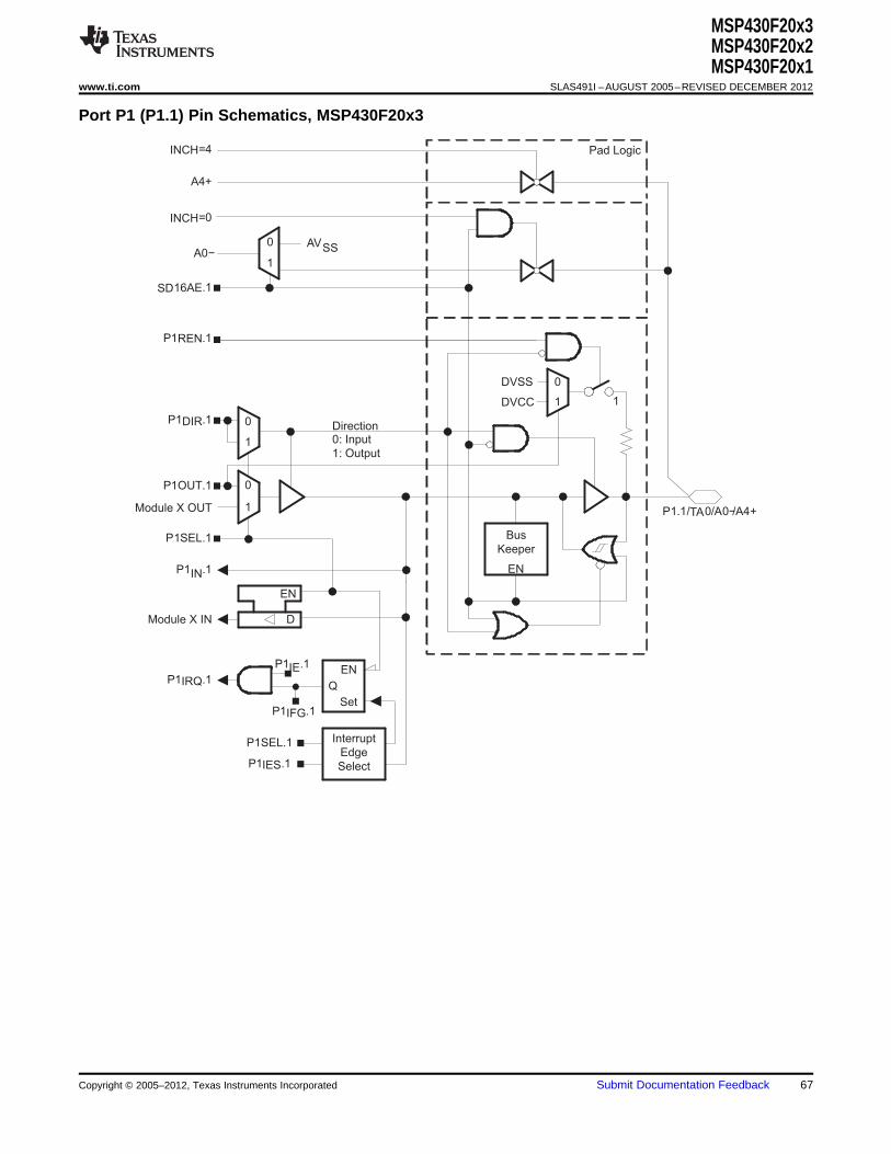
Bus
Keeper
EN
Direction0: Input
1: Output
P1SEL.1
1
0P1DIR.1
P1IN.1
P1IRQ.1
D
EN
Module X IN
1
0
Module X OUT
P1OUT.1
Interrupt
Edge
Select
Q
EN
Set
P1SEL.1
P1IES.1
P1IFG.1
P1IE.1
P1.1/TA0/A0−/A4+
1
0DVSS
DVCC
P1REN.1
A0−
SD16AE.1
1
0 AVSS
Pad Logic
INCH=0
INCH=4
A4+
1
MSP430F20x3MSP430F20x2MSP430F20x1
www.ti.com SLAS491I –AUGUST 2005–REVISED DECEMBER 2012
Port P1 (P1.1) Pin Schematics, MSP430F20x3
Copyright © 2005–2012, Texas Instruments Incorporated Submit Documentation Feedback 67
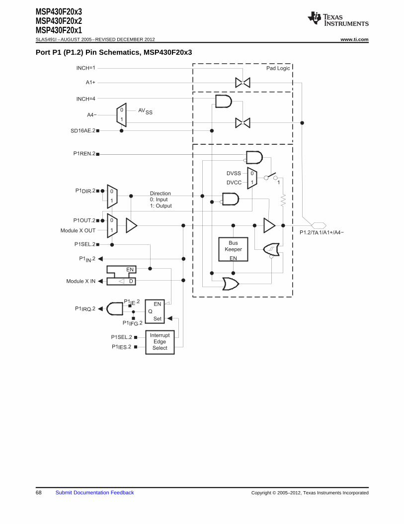
Bus
Keeper
EN
Direction0: Input
1: Output
P1SEL.2
1
0P1DIR.2
P1IN.2
P1IRQ.2
D
EN
Module X IN
1
0
Module X OUT
P1OUT.2
Interrupt
Edge
Select
Q
EN
Set
P1SEL.2
P1IES.2
P1IFG.2
P1IE.2
P1.2/TA1/A1+/A4−
1
0DVSS
DVCC
P1REN.2
A4−
SD16AE.2
1
0 AVSS
Pad Logic
INCH=4
INCH=1
A1+
1
MSP430F20x3MSP430F20x2MSP430F20x1SLAS491I –AUGUST 2005–REVISED DECEMBER 2012 www.ti.com
Port P1 (P1.2) Pin Schematics, MSP430F20x3
68 Submit Documentation Feedback Copyright © 2005–2012, Texas Instruments Incorporated
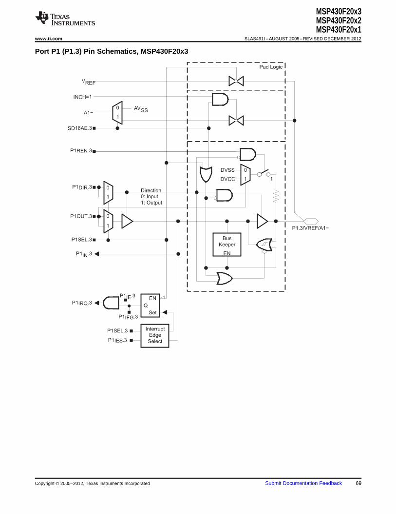
Bus
Keeper
EN
Direction0: Input
1: Output
P1SEL.3
1
0P1DIR.3
P1IN.3
P1IRQ.3
1
0P1OUT.3
Interrupt
Edge
Select
Q
EN
Set
P1SEL.3
P1IES.3
P1IFG.3
P1IE.3
P1.3/VREF/A1−
1
0DVSS
DVCC
P1REN.3
A1−
SD16AE.3
1
0 AVSS
Pad Logic
INCH=1
VREF
1
MSP430F20x3MSP430F20x2MSP430F20x1
www.ti.com SLAS491I –AUGUST 2005–REVISED DECEMBER 2012
Port P1 (P1.3) Pin Schematics, MSP430F20x3
Copyright © 2005–2012, Texas Instruments Incorporated Submit Documentation Feedback 69
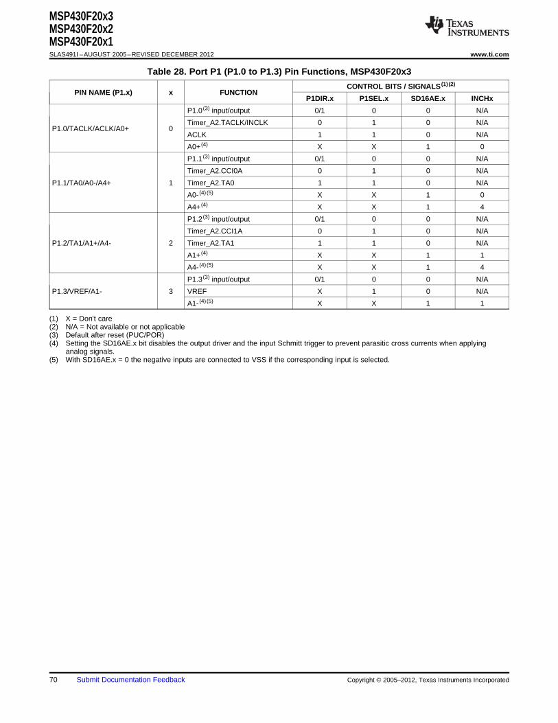
MSP430F20x3MSP430F20x2MSP430F20x1SLAS491I –AUGUST 2005–REVISED DECEMBER 2012 www.ti.com
Table 28. Port P1 (P1.0 to P1.3) Pin Functions, MSP430F20x3
CONTROL BITS / SIGNALS (1) (2)
PIN NAME (P1.x) x FUNCTIONP1DIR.x P1SEL.x SD16AE.x INCHx
P1.0 (3) input/output 0/1 0 0 N/A
Timer_A2.TACLK/INCLK 0 1 0 N/AP1.0/TACLK/ACLK/A0+ 0
ACLK 1 1 0 N/A
A0+ (4) X X 1 0
P1.1 (3) input/output 0/1 0 0 N/A
Timer_A2.CCI0A 0 1 0 N/A
P1.1/TA0/A0-/A4+ 1 Timer_A2.TA0 1 1 0 N/A
A0- (4) (5) X X 1 0
A4+ (4) X X 1 4
P1.2 (3) input/output 0/1 0 0 N/A
Timer_A2.CCI1A 0 1 0 N/A
P1.2/TA1/A1+/A4- 2 Timer_A2.TA1 1 1 0 N/A
A1+ (4) X X 1 1
A4- (4) (5) X X 1 4
P1.3 (3) input/output 0/1 0 0 N/A
P1.3/VREF/A1- 3 VREF X 1 0 N/A
A1- (4) (5) X X 1 1
(1) X = Don't care(2) N/A = Not available or not applicable(3) Default after reset (PUC/POR)(4) Setting the SD16AE.x bit disables the output driver and the input Schmitt trigger to prevent parasitic cross currents when applying
analog signals.(5) With SD16AE.x = 0 the negative inputs are connected to VSS if the corresponding input is selected.
70 Submit Documentation Feedback Copyright © 2005–2012, Texas Instruments Incorporated
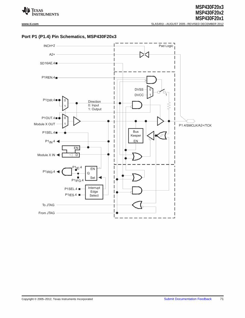
Bus
Keeper
EN
Direction0: Input
1: Output
P1SEL.4
1
0P1DIR.4
P1IN.4
P1IRQ.4
D
EN
Module X IN
1
0
Module X OUT
P1OUT.4
Interrupt
Edge
Select
Q
EN
Set
P1SEL.4
P1IES.4
P1IFG.4
P1IE.4
P1.4/SMCLK/A2+/TCK
1
0DVSS
DVCC
P1REN.4
SD16AE.4
Pad LogicINCH=2
A2+
To JTAG
From JTAG
1
MSP430F20x3MSP430F20x2MSP430F20x1
www.ti.com SLAS491I –AUGUST 2005–REVISED DECEMBER 2012
Port P1 (P1.4) Pin Schematics, MSP430F20x3
Copyright © 2005–2012, Texas Instruments Incorporated Submit Documentation Feedback 71
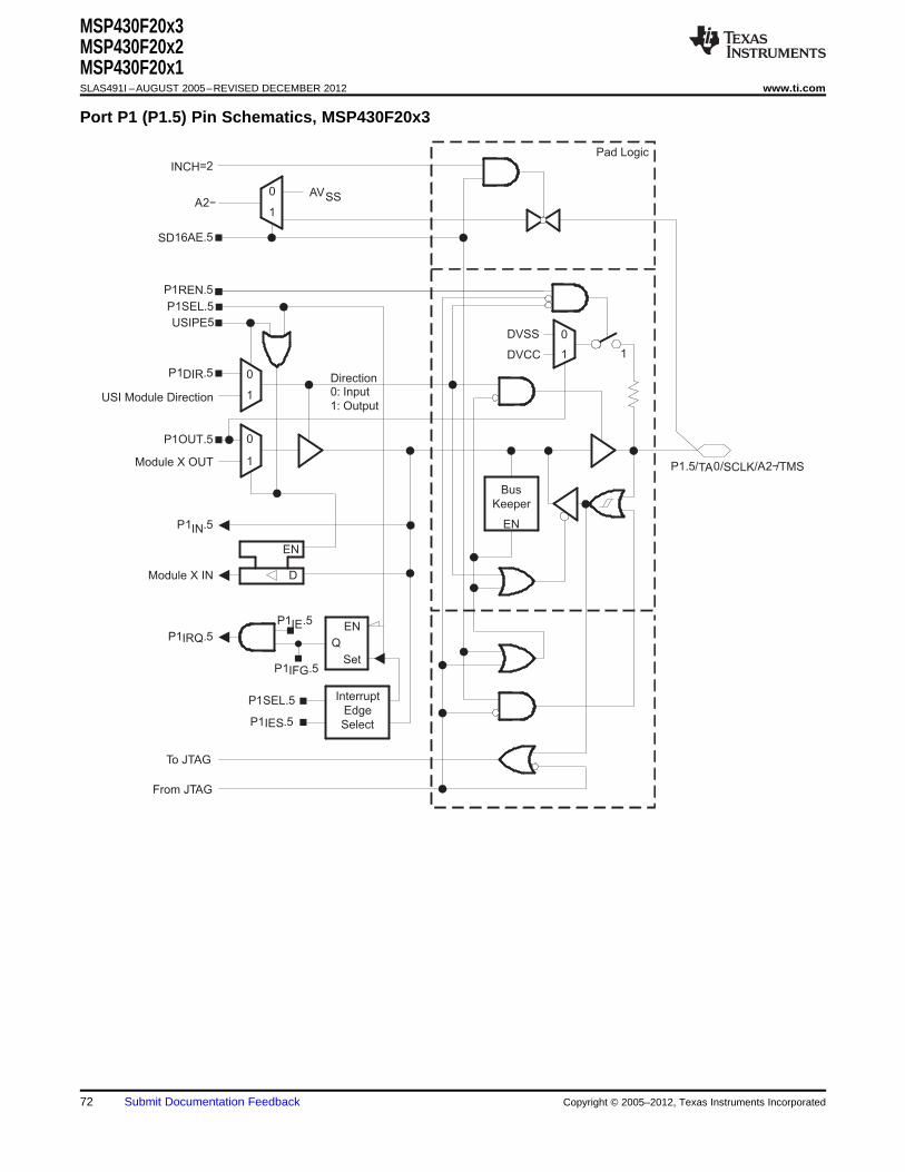
Bus
Keeper
EN
Direction0: Input
1: Output1
0P1DIR.5
P1IN.5
P1IRQ.5
D
EN
Module X IN
1
0
Module X OUT
P1OUT.5
Interrupt
Edge
Select
Q
EN
Set
P1SEL.5
P1IES.5
P1IFG.5
P1IE.5
P1.5/TA0/SCLK/A2−/TMS
1
0DVSS
DVCC
P1REN.5
SD16AE.5
Pad Logic
A2−1
0 AVSS
INCH=2
P1SEL.5
USIPE5
USI Module Direction
1
To JTAG
From JTAG
MSP430F20x3MSP430F20x2MSP430F20x1SLAS491I –AUGUST 2005–REVISED DECEMBER 2012 www.ti.com
Port P1 (P1.5) Pin Schematics, MSP430F20x3
72 Submit Documentation Feedback Copyright © 2005–2012, Texas Instruments Incorporated

Bus
Keeper
EN
Direction0: Input
1: Output1
0P1DIR.6
P1IN.6
P1IRQ.6
D
EN
Module X IN
1
0
Module X OUT
P1OUT.6
Interrupt
Edge
Select
Q
EN
Set
P1SEL.6
P1IES.6
P1IFG.6
P1IE.6
P1.6/TA1/SDO/SCL/A3+/TDI
1
0DVSS
DVCC
P1REN.6
SD16AE.6
Pad Logic
P1SEL.6
USIPE6
USI Module Direction
USI Module Output
(I2C Mode)
INCH=3
A3+
1
To JTAG
From JTAG
MSP430F20x3MSP430F20x2MSP430F20x1
www.ti.com SLAS491I –AUGUST 2005–REVISED DECEMBER 2012
Port P1 (P1.6) Pin Schematics, MSP430F20x3
Copyright © 2005–2012, Texas Instruments Incorporated Submit Documentation Feedback 73
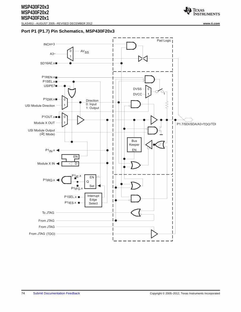
Bus
Keeper
EN
Direction0: Input
1: Output1
0P1DIR.x
P1IN.x
P1IRQ.x
D
EN
Module X IN
1
0
Module X OUT
P1OUT.x
Interrupt
Edge
Select
Q
EN
Set
P1SEL.x
P1IES.x
P1IFG.x
P1IE.x
P1.7/SDI/SDA/A3−/TDO/TDI
1
0DVSS
DVCC
P1REN.x
SD16AE.x
Pad Logic
A3−1
0 AVSS
INCH=3
P1SEL.x
USIPE7
USI Module Direction
From JTAG
From JTAG (TDO)
USI Module Output
(I2C Mode)
1
To JTAG
From JTAG
MSP430F20x3MSP430F20x2MSP430F20x1SLAS491I –AUGUST 2005–REVISED DECEMBER 2012 www.ti.com
Port P1 (P1.7) Pin Schematics, MSP430F20x3
74 Submit Documentation Feedback Copyright © 2005–2012, Texas Instruments Incorporated
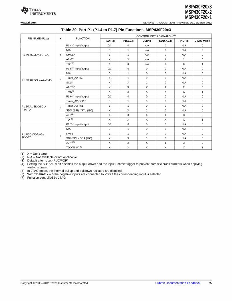
MSP430F20x3MSP430F20x2MSP430F20x1
www.ti.com SLAS491I –AUGUST 2005–REVISED DECEMBER 2012
Table 29. Port P1 (P1.4 to P1.7) Pin Functions, MSP430F20x3
CONTROL BITS / SIGNALS (1) (2)
PIN NAME (P1.x) x FUNCTIONP1DIR.x P1SEL.x USIP.x SD16AE.x INCHx JTAG Mode
P1.4 (3) input/output 0/1 0 N/A 0 N/A 0
N/A 0 1 N/A 0 N/A 0
P1.4/SMCLK/A2+/TCK 4 SMCLK 1 1 N/A 0 N/A 0
A2+ (4) X X N/A 1 2 0
TCK (5) X X N/A X X 1
P1.5 (3) input/output 0/1 0 0 0 N/A 0
N/A 0 1 0 0 N/A 0
Timer_A2.TA0 1 1 0 0 N/A 0P1.5/TA0/SCLK/A2-/TMS 5
SCLK X X 1 0 N/A 0
A2- (4) (6) X X X 1 2 0
TMS (5) X X X X X 1
P1.6 (3) input/output 0/1 0 0 0 N/A 0
Timer_A2.CCI1B 0 1 0 0 N/A 0
Timer_A2.TA1 1 1 0 0 N/A 0P1.6/TA1/SDO/SCL/ 6A3+/TDI SDO (SPI) / SCL (I2C) X X 1 0 N/A 0
A3+ (4) X X X 1 3 0
TDI (5) X X X X X 1
P1.7 (3) input/output 0/1 0 0 0 N/A 0
N/A 0 1 0 0 N/A 0
DVSS 1 1 0 0 N/A 0P1.7/SDI/SDA/A3-/ 7TDO/TDI SDI (SPI) / SDA (I2C) X X 1 0 N/A 0
A3- (4) (6) X X X 1 3 0
TDO/TDI (7) (5) X X X X X 1
(1) X = Don't care(2) N/A = Not available or not applicable(3) Default after reset (PUC/POR)(4) Setting the SD16AE.x bit disables the output driver and the input Schmitt trigger to prevent parasitic cross currents when applying
analog signals.(5) In JTAG mode, the internal pullup and pulldown resistors are disabled.(6) With SD16AE.x = 0 the negative inputs are connected to VSS if the corresponding input is selected.(7) Function controlled by JTAG
Copyright © 2005–2012, Texas Instruments Incorporated Submit Documentation Feedback 75
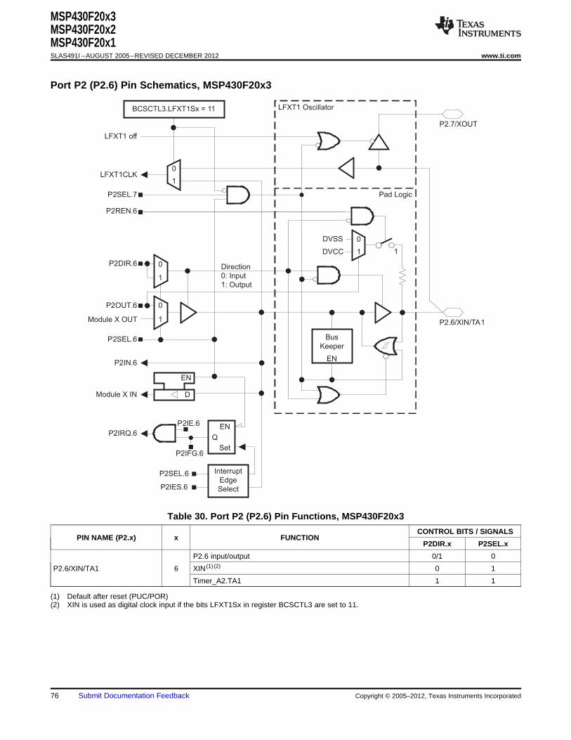
Bus
Keeper
EN
Direction
0: Input
1: Output
P2SEL.6
1
0P2DIR.6
P2IN.6
P2IRQ.6
D
EN
Module X IN
1
0
Module X OUT
P2OUT.6
Interrupt
Edge
Select
Q
EN
Set
P2SEL.6
P2IES.6
P2IFG.6
P2IE.6
P2.6/XIN/TA1
1
0DVSS
DVCC
P2REN.6
Pad Logic
LFXT1 OscillatorBCSCTL3.LFXT1Sx = 11
P2.7/XOUT
LFXT1 off
0
1
1
LFXT1CLK
P2SEL.7
MSP430F20x3MSP430F20x2MSP430F20x1SLAS491I –AUGUST 2005–REVISED DECEMBER 2012 www.ti.com
Port P2 (P2.6) Pin Schematics, MSP430F20x3
Table 30. Port P2 (P2.6) Pin Functions, MSP430F20x3
CONTROL BITS / SIGNALSPIN NAME (P2.x) x FUNCTION
P2DIR.x P2SEL.x
P2.6 input/output 0/1 0
P2.6/XIN/TA1 6 XIN (1) (2) 0 1
Timer_A2.TA1 1 1
(1) Default after reset (PUC/POR)(2) XIN is used as digital clock input if the bits LFXT1Sx in register BCSCTL3 are set to 11.
76 Submit Documentation Feedback Copyright © 2005–2012, Texas Instruments Incorporated
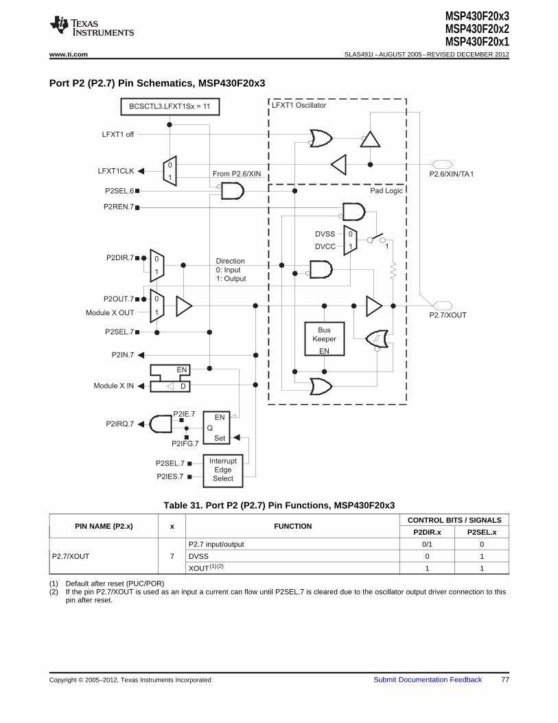
LFXT1 off
P2SEL.6
Bus
Keeper
EN
Direction
0: Input
1: Output
P2SEL.7
1
0P2DIR.7
P2IN.7
P2IRQ.7
D
EN
Module X IN
1
0
Module X OUT
P2OUT.7
Interrupt
Edge
Select
Q
EN
Set
P2SEL.7
P2IES.7
P2IFG.7
P2IE.7
P2.7/XOUT
1
0DVSS
DVCC
P2REN.7
Pad Logic
LFXT1 OscillatorBCSCTL3.LFXT1Sx = 11
0
1
1
LFXT1CLK From P2.6/XIN P2.6/XIN/TA1
MSP430F20x3MSP430F20x2MSP430F20x1
www.ti.com SLAS491I –AUGUST 2005–REVISED DECEMBER 2012
Port P2 (P2.7) Pin Schematics, MSP430F20x3
Table 31. Port P2 (P2.7) Pin Functions, MSP430F20x3
CONTROL BITS / SIGNALSPIN NAME (P2.x) x FUNCTION
P2DIR.x P2SEL.x
P2.7 input/output 0/1 0
P2.7/XOUT 7 DVSS 0 1
XOUT (1) (2) 1 1
(1) Default after reset (PUC/POR)(2) If the pin P2.7/XOUT is used as an input a current can flow until P2SEL.7 is cleared due to the oscillator output driver connection to this
pin after reset.
Copyright © 2005–2012, Texas Instruments Incorporated Submit Documentation Feedback 77
MSP430F20x3MSP430F20x2MSP430F20x1SLAS491I –AUGUST 2005–REVISED DECEMBER 2012 www.ti.com
REVISION HISTORY
LITERATURE SUMMARYNUMBER
SLAS491 Preliminary PRODUCT PREVIEW data sheet release
Production data sheet release for MSP430F20x3I.SLAS491A Updated specification and added characterization graphs.
Production data sheet release for MSP430F20x3T, MSP430F20x1I and MSP430F20x1T.
105°C characterization results added.
SD16_A SINAD characterization results for MSP430F20x3.
RSA package added.SLAS491B Updated SD16_A Power Supply Rejection specification.
DCO Calibration Register names: lower case "z" changed to upper case "Z".
Vhys(B_IT-) MAX specification increased from 180 mV to 210 mV.
MIN and MAX percentages for "calibrated DCO frequencies - tolerance over supply voltage VCC" corrected from 2.5% to3.0% to match the specified frequency ranges.
SLAS491C Production data sheet release for MSP430F20x2I and MSP430F20x2T.
Changed fACLK to 0 Hz in ILPM4 test conditions in Low-Power Mode Supply Currents (Into VCC) Excluding ExternalSLAS491D Current.
SLAS491E Changed Tstg maximum for programmed devices to 150°C in Absolute Maximum Ratings.
SLAS491F Added ADC10 data transfer registers to Peripheral File Map
Changed Test Conditions for "Duty cycle, LF mode" in Crystal Oscillator, XT1, Low-Frequency Mode.SLAS491G Changed note (1) on 10-Bit ADC, Built-In Voltage Reference.
Changed USIP.x Control Bits in Table 25 and Table 29.
SLAS491H Changed Tstg, Programmed device, to -55°C to 150°C in Absolute Maximum Ratings.
Added typical value test conditions to Recommended Operating Conditions.SLAS491IAdded note (2) to POR and Brownout Reset (BOR).
78 Submit Documentation Feedback Copyright © 2005–2012, Texas Instruments Incorporated
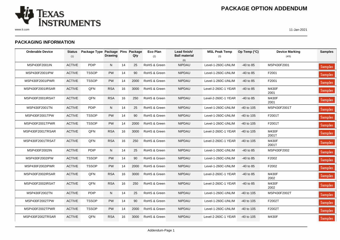
PACKAGE OPTION ADDENDUM
www.ti.com 11-Jan-2021
Addendum-Page 1
PACKAGING INFORMATION
Orderable Device Status(1)
Package Type PackageDrawing
Pins PackageQty
Eco Plan(2)
Lead finish/Ball material
(6)
MSL Peak Temp(3)
Op Temp (°C) Device Marking(4/5)
Samples
MSP430F2001IN ACTIVE PDIP N 14 25 RoHS & Green NIPDAU Level-1-260C-UNLIM -40 to 85 MSP430F2001
MSP430F2001IPW ACTIVE TSSOP PW 14 90 RoHS & Green NIPDAU Level-1-260C-UNLIM -40 to 85 F2001
MSP430F2001IPWR ACTIVE TSSOP PW 14 2000 RoHS & Green NIPDAU Level-1-260C-UNLIM -40 to 85 F2001
MSP430F2001IRSAR ACTIVE QFN RSA 16 3000 RoHS & Green NIPDAU Level-2-260C-1 YEAR -40 to 85 M430F2001
MSP430F2001IRSAT ACTIVE QFN RSA 16 250 RoHS & Green NIPDAU Level-2-260C-1 YEAR -40 to 85 M430F2001
MSP430F2001TN ACTIVE PDIP N 14 25 RoHS & Green NIPDAU Level-1-260C-UNLIM -40 to 105 MSP430F2001T
MSP430F2001TPW ACTIVE TSSOP PW 14 90 RoHS & Green NIPDAU Level-1-260C-UNLIM -40 to 105 F2001T
MSP430F2001TPWR ACTIVE TSSOP PW 14 2000 RoHS & Green NIPDAU Level-1-260C-UNLIM -40 to 105 F2001T
MSP430F2001TRSAR ACTIVE QFN RSA 16 3000 RoHS & Green NIPDAU Level-2-260C-1 YEAR -40 to 105 M430F2001T
MSP430F2001TRSAT ACTIVE QFN RSA 16 250 RoHS & Green NIPDAU Level-2-260C-1 YEAR -40 to 105 M430F2001T
MSP430F2002IN ACTIVE PDIP N 14 25 RoHS & Green NIPDAU Level-1-260C-UNLIM -40 to 85 MSP430F2002
MSP430F2002IPW ACTIVE TSSOP PW 14 90 RoHS & Green NIPDAU Level-1-260C-UNLIM -40 to 85 F2002
MSP430F2002IPWR ACTIVE TSSOP PW 14 2000 RoHS & Green NIPDAU Level-1-260C-UNLIM -40 to 85 F2002
MSP430F2002IRSAR ACTIVE QFN RSA 16 3000 RoHS & Green NIPDAU Level-2-260C-1 YEAR -40 to 85 M430F2002
MSP430F2002IRSAT ACTIVE QFN RSA 16 250 RoHS & Green NIPDAU Level-2-260C-1 YEAR -40 to 85 M430F2002
MSP430F2002TN ACTIVE PDIP N 14 25 RoHS & Green NIPDAU Level-1-260C-UNLIM -40 to 105 MSP430F2002T
MSP430F2002TPW ACTIVE TSSOP PW 14 90 RoHS & Green NIPDAU Level-1-260C-UNLIM -40 to 105 F2002T
MSP430F2002TPWR ACTIVE TSSOP PW 14 2000 RoHS & Green NIPDAU Level-1-260C-UNLIM -40 to 105 F2002T
MSP430F2002TRSAR ACTIVE QFN RSA 16 3000 RoHS & Green NIPDAU Level-2-260C-1 YEAR -40 to 105 M430F
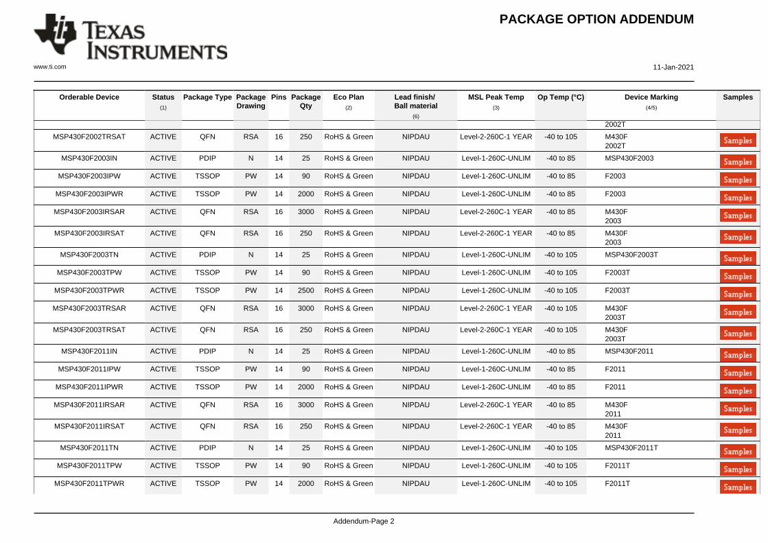
PACKAGE OPTION ADDENDUM
www.ti.com 11-Jan-2021
Addendum-Page 2
Orderable Device Status(1)
Package Type PackageDrawing
Pins PackageQty
Eco Plan(2)
Lead finish/Ball material
(6)
MSL Peak Temp(3)
Op Temp (°C) Device Marking(4/5)
Samples
2002T
MSP430F2002TRSAT ACTIVE QFN RSA 16 250 RoHS & Green NIPDAU Level-2-260C-1 YEAR -40 to 105 M430F2002T
MSP430F2003IN ACTIVE PDIP N 14 25 RoHS & Green NIPDAU Level-1-260C-UNLIM -40 to 85 MSP430F2003
MSP430F2003IPW ACTIVE TSSOP PW 14 90 RoHS & Green NIPDAU Level-1-260C-UNLIM -40 to 85 F2003
MSP430F2003IPWR ACTIVE TSSOP PW 14 2000 RoHS & Green NIPDAU Level-1-260C-UNLIM -40 to 85 F2003
MSP430F2003IRSAR ACTIVE QFN RSA 16 3000 RoHS & Green NIPDAU Level-2-260C-1 YEAR -40 to 85 M430F2003
MSP430F2003IRSAT ACTIVE QFN RSA 16 250 RoHS & Green NIPDAU Level-2-260C-1 YEAR -40 to 85 M430F2003
MSP430F2003TN ACTIVE PDIP N 14 25 RoHS & Green NIPDAU Level-1-260C-UNLIM -40 to 105 MSP430F2003T
MSP430F2003TPW ACTIVE TSSOP PW 14 90 RoHS & Green NIPDAU Level-1-260C-UNLIM -40 to 105 F2003T
MSP430F2003TPWR ACTIVE TSSOP PW 14 2500 RoHS & Green NIPDAU Level-1-260C-UNLIM -40 to 105 F2003T
MSP430F2003TRSAR ACTIVE QFN RSA 16 3000 RoHS & Green NIPDAU Level-2-260C-1 YEAR -40 to 105 M430F2003T
MSP430F2003TRSAT ACTIVE QFN RSA 16 250 RoHS & Green NIPDAU Level-2-260C-1 YEAR -40 to 105 M430F2003T
MSP430F2011IN ACTIVE PDIP N 14 25 RoHS & Green NIPDAU Level-1-260C-UNLIM -40 to 85 MSP430F2011
MSP430F2011IPW ACTIVE TSSOP PW 14 90 RoHS & Green NIPDAU Level-1-260C-UNLIM -40 to 85 F2011
MSP430F2011IPWR ACTIVE TSSOP PW 14 2000 RoHS & Green NIPDAU Level-1-260C-UNLIM -40 to 85 F2011
MSP430F2011IRSAR ACTIVE QFN RSA 16 3000 RoHS & Green NIPDAU Level-2-260C-1 YEAR -40 to 85 M430F2011
MSP430F2011IRSAT ACTIVE QFN RSA 16 250 RoHS & Green NIPDAU Level-2-260C-1 YEAR -40 to 85 M430F2011
MSP430F2011TN ACTIVE PDIP N 14 25 RoHS & Green NIPDAU Level-1-260C-UNLIM -40 to 105 MSP430F2011T
MSP430F2011TPW ACTIVE TSSOP PW 14 90 RoHS & Green NIPDAU Level-1-260C-UNLIM -40 to 105 F2011T
MSP430F2011TPWR ACTIVE TSSOP PW 14 2000 RoHS & Green NIPDAU Level-1-260C-UNLIM -40 to 105 F2011T
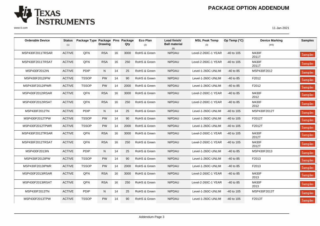
PACKAGE OPTION ADDENDUM
www.ti.com 11-Jan-2021
Addendum-Page 3
Orderable Device Status(1)
Package Type PackageDrawing
Pins PackageQty
Eco Plan(2)
Lead finish/Ball material
(6)
MSL Peak Temp(3)
Op Temp (°C) Device Marking(4/5)
Samples
MSP430F2011TRSAR ACTIVE QFN RSA 16 3000 RoHS & Green NIPDAU Level-2-260C-1 YEAR -40 to 105 M430F2011T
MSP430F2011TRSAT ACTIVE QFN RSA 16 250 RoHS & Green NIPDAU Level-2-260C-1 YEAR -40 to 105 M430F2011T
MSP430F2012IN ACTIVE PDIP N 14 25 RoHS & Green NIPDAU Level-1-260C-UNLIM -40 to 85 MSP430F2012
MSP430F2012IPW ACTIVE TSSOP PW 14 90 RoHS & Green NIPDAU Level-1-260C-UNLIM -40 to 85 F2012
MSP430F2012IPWR ACTIVE TSSOP PW 14 2000 RoHS & Green NIPDAU Level-1-260C-UNLIM -40 to 85 F2012
MSP430F2012IRSAR ACTIVE QFN RSA 16 3000 RoHS & Green NIPDAU Level-2-260C-1 YEAR -40 to 85 M430F2012
MSP430F2012IRSAT ACTIVE QFN RSA 16 250 RoHS & Green NIPDAU Level-2-260C-1 YEAR -40 to 85 M430F2012
MSP430F2012TN ACTIVE PDIP N 14 25 RoHS & Green NIPDAU Level-1-260C-UNLIM -40 to 105 MSP430F2012T
MSP430F2012TPW ACTIVE TSSOP PW 14 90 RoHS & Green NIPDAU Level-1-260C-UNLIM -40 to 105 F2012T
MSP430F2012TPWR ACTIVE TSSOP PW 14 2000 RoHS & Green NIPDAU Level-1-260C-UNLIM -40 to 105 F2012T
MSP430F2012TRSAR ACTIVE QFN RSA 16 3000 RoHS & Green NIPDAU Level-2-260C-1 YEAR -40 to 105 M430F2012T
MSP430F2012TRSAT ACTIVE QFN RSA 16 250 RoHS & Green NIPDAU Level-2-260C-1 YEAR -40 to 105 M430F2012T
MSP430F2013IN ACTIVE PDIP N 14 25 RoHS & Green NIPDAU Level-1-260C-UNLIM -40 to 85 MSP430F2013
MSP430F2013IPW ACTIVE TSSOP PW 14 90 RoHS & Green NIPDAU Level-1-260C-UNLIM -40 to 85 F2013
MSP430F2013IPWR ACTIVE TSSOP PW 14 2000 RoHS & Green NIPDAU Level-1-260C-UNLIM -40 to 85 F2013
MSP430F2013IRSAR ACTIVE QFN RSA 16 3000 RoHS & Green NIPDAU Level-2-260C-1 YEAR -40 to 85 M430F2013
MSP430F2013IRSAT ACTIVE QFN RSA 16 250 RoHS & Green NIPDAU Level-2-260C-1 YEAR -40 to 85 M430F2013
MSP430F2013TN ACTIVE PDIP N 14 25 RoHS & Green NIPDAU Level-1-260C-UNLIM -40 to 105 MSP430F2013T
MSP430F2013TPW ACTIVE TSSOP PW 14 90 RoHS & Green NIPDAU Level-1-260C-UNLIM -40 to 105 F2013T
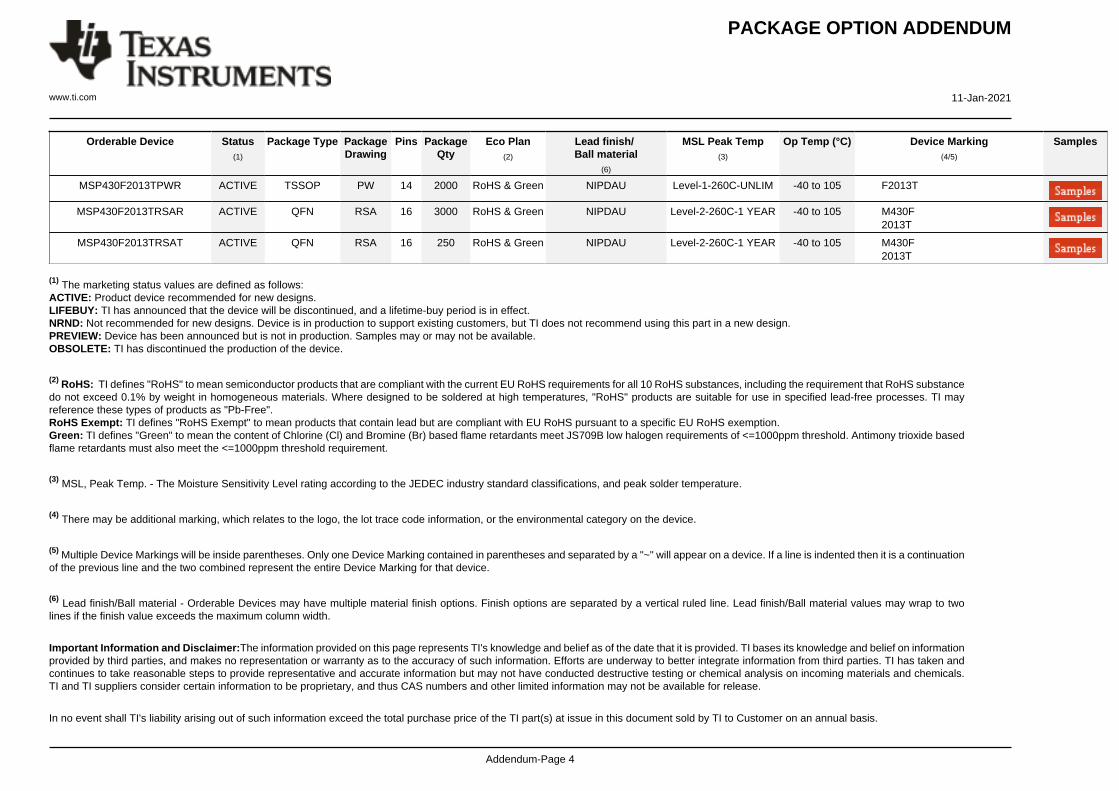
PACKAGE OPTION ADDENDUM
www.ti.com 11-Jan-2021
Addendum-Page 4
Orderable Device Status(1)
Package Type PackageDrawing
Pins PackageQty
Eco Plan(2)
Lead finish/Ball material
(6)
MSL Peak Temp(3)
Op Temp (°C) Device Marking(4/5)
Samples
MSP430F2013TPWR ACTIVE TSSOP PW 14 2000 RoHS & Green NIPDAU Level-1-260C-UNLIM -40 to 105 F2013T
MSP430F2013TRSAR ACTIVE QFN RSA 16 3000 RoHS & Green NIPDAU Level-2-260C-1 YEAR -40 to 105 M430F2013T
MSP430F2013TRSAT ACTIVE QFN RSA 16 250 RoHS & Green NIPDAU Level-2-260C-1 YEAR -40 to 105 M430F2013T
(1) The marketing status values are defined as follows:ACTIVE: Product device recommended for new designs.LIFEBUY: TI has announced that the device will be discontinued, and a lifetime-buy period is in effect.NRND: Not recommended for new designs. Device is in production to support existing customers, but TI does not recommend using this part in a new design.PREVIEW: Device has been announced but is not in production. Samples may or may not be available.OBSOLETE: TI has discontinued the production of the device.
(2) RoHS: TI defines "RoHS" to mean semiconductor products that are compliant with the current EU RoHS requirements for all 10 RoHS substances, including the requirement that RoHS substancedo not exceed 0.1% by weight in homogeneous materials. Where designed to be soldered at high temperatures, "RoHS" products are suitable for use in specified lead-free processes. TI mayreference these types of products as "Pb-Free".RoHS Exempt: TI defines "RoHS Exempt" to mean products that contain lead but are compliant with EU RoHS pursuant to a specific EU RoHS exemption.Green: TI defines "Green" to mean the content of Chlorine (Cl) and Bromine (Br) based flame retardants meet JS709B low halogen requirements of <=1000ppm threshold. Antimony trioxide basedflame retardants must also meet the <=1000ppm threshold requirement.
(3) MSL, Peak Temp. - The Moisture Sensitivity Level rating according to the JEDEC industry standard classifications, and peak solder temperature.
(4) There may be additional marking, which relates to the logo, the lot trace code information, or the environmental category on the device.
(5) Multiple Device Markings will be inside parentheses. Only one Device Marking contained in parentheses and separated by a "~" will appear on a device. If a line is indented then it is a continuationof the previous line and the two combined represent the entire Device Marking for that device.
(6) Lead finish/Ball material - Orderable Devices may have multiple material finish options. Finish options are separated by a vertical ruled line. Lead finish/Ball material values may wrap to twolines if the finish value exceeds the maximum column width.
Important Information and Disclaimer:The information provided on this page represents TI's knowledge and belief as of the date that it is provided. TI bases its knowledge and belief on informationprovided by third parties, and makes no representation or warranty as to the accuracy of such information. Efforts are underway to better integrate information from third parties. TI has taken andcontinues to take reasonable steps to provide representative and accurate information but may not have conducted destructive testing or chemical analysis on incoming materials and chemicals.TI and TI suppliers consider certain information to be proprietary, and thus CAS numbers and other limited information may not be available for release.
In no event shall TI's liability arising out of such information exceed the total purchase price of the TI part(s) at issue in this document sold by TI to Customer on an annual basis.
PACKAGE OPTION ADDENDUM
www.ti.com 11-Jan-2021
Addendum-Page 5
OTHER QUALIFIED VERSIONS OF MSP430F2013 :
• Enhanced Product: MSP430F2013-EP
NOTE: Qualified Version Definitions:
• Enhanced Product - Supports Defense, Aerospace and Medical Applications
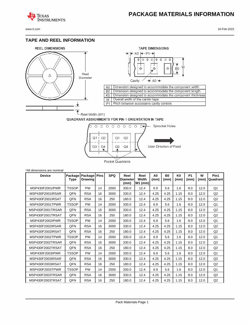
TAPE AND REEL INFORMATION
*All dimensions are nominal
Device PackageType
PackageDrawing
Pins SPQ ReelDiameter
(mm)
ReelWidth
W1 (mm)
A0(mm)
B0(mm)
K0(mm)
P1(mm)
W(mm)
Pin1Quadrant
MSP430F2001IPWR TSSOP PW 14 2000 330.0 12.4 6.9 5.6 1.6 8.0 12.0 Q1
MSP430F2001IRSAR QFN RSA 16 3000 330.0 12.4 4.25 4.25 1.15 8.0 12.0 Q2
MSP430F2001IRSAT QFN RSA 16 250 180.0 12.4 4.25 4.25 1.15 8.0 12.0 Q2
MSP430F2001TPWR TSSOP PW 14 2000 330.0 12.4 6.9 5.6 1.6 8.0 12.0 Q1
MSP430F2001TRSAR QFN RSA 16 3000 330.0 12.4 4.25 4.25 1.15 8.0 12.0 Q2
MSP430F2001TRSAT QFN RSA 16 250 180.0 12.4 4.25 4.25 1.15 8.0 12.0 Q2
MSP430F2002IPWR TSSOP PW 14 2000 330.0 12.4 6.9 5.6 1.6 8.0 12.0 Q1
MSP430F2002IRSAR QFN RSA 16 3000 330.0 12.4 4.25 4.25 1.15 8.0 12.0 Q2
MSP430F2002IRSAT QFN RSA 16 250 180.0 12.4 4.25 4.25 1.15 8.0 12.0 Q2
MSP430F2002TPWR TSSOP PW 14 2000 330.0 12.4 6.9 5.6 1.6 8.0 12.0 Q1
MSP430F2002TRSAR QFN RSA 16 3000 330.0 12.4 4.25 4.25 1.15 8.0 12.0 Q2
MSP430F2002TRSAT QFN RSA 16 250 180.0 12.4 4.25 4.25 1.15 8.0 12.0 Q2
MSP430F2003IPWR TSSOP PW 14 2000 330.0 12.4 6.9 5.6 1.6 8.0 12.0 Q1
MSP430F2003IRSAR QFN RSA 16 3000 330.0 12.4 4.25 4.25 1.15 8.0 12.0 Q2
MSP430F2003IRSAT QFN RSA 16 250 180.0 12.4 4.25 4.25 1.15 8.0 12.0 Q2
MSP430F2003TPWR TSSOP PW 14 2500 330.0 12.4 6.9 5.6 1.6 8.0 12.0 Q1
MSP430F2003TRSAR QFN RSA 16 3000 330.0 12.4 4.25 4.25 1.15 8.0 12.0 Q2
MSP430F2003TRSAT QFN RSA 16 250 180.0 12.4 4.25 4.25 1.15 8.0 12.0 Q2
PACKAGE MATERIALS INFORMATION
www.ti.com 16-Feb-2022
Pack Materials-Page 1
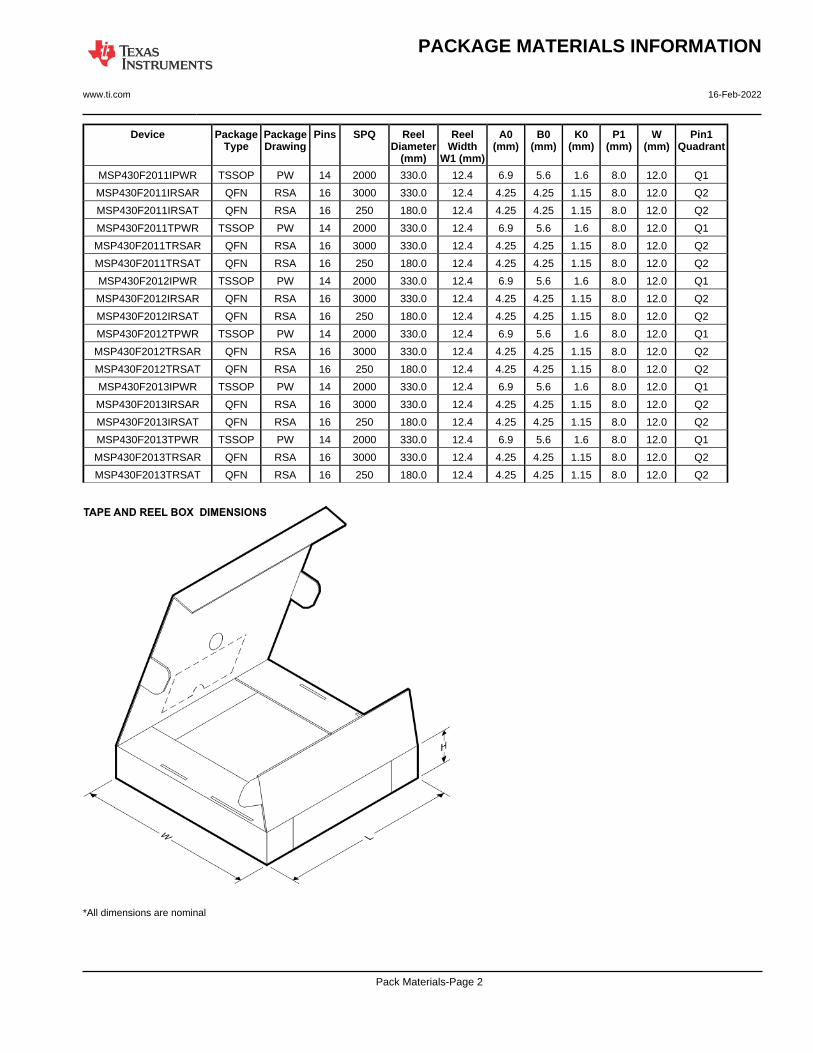
Device PackageType
PackageDrawing
Pins SPQ ReelDiameter
(mm)
ReelWidth
W1 (mm)
A0(mm)
B0(mm)
K0(mm)
P1(mm)
W(mm)
Pin1Quadrant
MSP430F2011IPWR TSSOP PW 14 2000 330.0 12.4 6.9 5.6 1.6 8.0 12.0 Q1
MSP430F2011IRSAR QFN RSA 16 3000 330.0 12.4 4.25 4.25 1.15 8.0 12.0 Q2
MSP430F2011IRSAT QFN RSA 16 250 180.0 12.4 4.25 4.25 1.15 8.0 12.0 Q2
MSP430F2011TPWR TSSOP PW 14 2000 330.0 12.4 6.9 5.6 1.6 8.0 12.0 Q1
MSP430F2011TRSAR QFN RSA 16 3000 330.0 12.4 4.25 4.25 1.15 8.0 12.0 Q2
MSP430F2011TRSAT QFN RSA 16 250 180.0 12.4 4.25 4.25 1.15 8.0 12.0 Q2
MSP430F2012IPWR TSSOP PW 14 2000 330.0 12.4 6.9 5.6 1.6 8.0 12.0 Q1
MSP430F2012IRSAR QFN RSA 16 3000 330.0 12.4 4.25 4.25 1.15 8.0 12.0 Q2
MSP430F2012IRSAT QFN RSA 16 250 180.0 12.4 4.25 4.25 1.15 8.0 12.0 Q2
MSP430F2012TPWR TSSOP PW 14 2000 330.0 12.4 6.9 5.6 1.6 8.0 12.0 Q1
MSP430F2012TRSAR QFN RSA 16 3000 330.0 12.4 4.25 4.25 1.15 8.0 12.0 Q2
MSP430F2012TRSAT QFN RSA 16 250 180.0 12.4 4.25 4.25 1.15 8.0 12.0 Q2
MSP430F2013IPWR TSSOP PW 14 2000 330.0 12.4 6.9 5.6 1.6 8.0 12.0 Q1
MSP430F2013IRSAR QFN RSA 16 3000 330.0 12.4 4.25 4.25 1.15 8.0 12.0 Q2
MSP430F2013IRSAT QFN RSA 16 250 180.0 12.4 4.25 4.25 1.15 8.0 12.0 Q2
MSP430F2013TPWR TSSOP PW 14 2000 330.0 12.4 6.9 5.6 1.6 8.0 12.0 Q1
MSP430F2013TRSAR QFN RSA 16 3000 330.0 12.4 4.25 4.25 1.15 8.0 12.0 Q2
MSP430F2013TRSAT QFN RSA 16 250 180.0 12.4 4.25 4.25 1.15 8.0 12.0 Q2
*All dimensions are nominal
PACKAGE MATERIALS INFORMATION
www.ti.com 16-Feb-2022
Pack Materials-Page 2
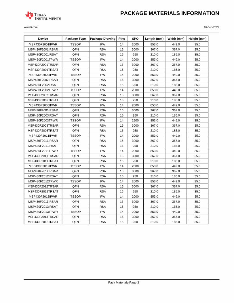
Device Package Type Package Drawing Pins SPQ Length (mm) Width (mm) Height (mm)
MSP430F2001IPWR TSSOP PW 14 2000 853.0 449.0 35.0
MSP430F2001IRSAR QFN RSA 16 3000 367.0 367.0 35.0
MSP430F2001IRSAT QFN RSA 16 250 210.0 185.0 35.0
MSP430F2001TPWR TSSOP PW 14 2000 853.0 449.0 35.0
MSP430F2001TRSAR QFN RSA 16 3000 367.0 367.0 35.0
MSP430F2001TRSAT QFN RSA 16 250 210.0 185.0 35.0
MSP430F2002IPWR TSSOP PW 14 2000 853.0 449.0 35.0
MSP430F2002IRSAR QFN RSA 16 3000 367.0 367.0 35.0
MSP430F2002IRSAT QFN RSA 16 250 210.0 185.0 35.0
MSP430F2002TPWR TSSOP PW 14 2000 853.0 449.0 35.0
MSP430F2002TRSAR QFN RSA 16 3000 367.0 367.0 35.0
MSP430F2002TRSAT QFN RSA 16 250 210.0 185.0 35.0
MSP430F2003IPWR TSSOP PW 14 2000 853.0 449.0 35.0
MSP430F2003IRSAR QFN RSA 16 3000 367.0 367.0 35.0
MSP430F2003IRSAT QFN RSA 16 250 210.0 185.0 35.0
MSP430F2003TPWR TSSOP PW 14 2500 853.0 449.0 35.0
MSP430F2003TRSAR QFN RSA 16 3000 367.0 367.0 35.0
MSP430F2003TRSAT QFN RSA 16 250 210.0 185.0 35.0
MSP430F2011IPWR TSSOP PW 14 2000 853.0 449.0 35.0
MSP430F2011IRSAR QFN RSA 16 3000 367.0 367.0 35.0
MSP430F2011IRSAT QFN RSA 16 250 210.0 185.0 35.0
MSP430F2011TPWR TSSOP PW 14 2000 853.0 449.0 35.0
MSP430F2011TRSAR QFN RSA 16 3000 367.0 367.0 35.0
MSP430F2011TRSAT QFN RSA 16 250 210.0 185.0 35.0
MSP430F2012IPWR TSSOP PW 14 2000 853.0 449.0 35.0
MSP430F2012IRSAR QFN RSA 16 3000 367.0 367.0 35.0
MSP430F2012IRSAT QFN RSA 16 250 210.0 185.0 35.0
MSP430F2012TPWR TSSOP PW 14 2000 853.0 449.0 35.0
MSP430F2012TRSAR QFN RSA 16 3000 367.0 367.0 35.0
MSP430F2012TRSAT QFN RSA 16 250 210.0 185.0 35.0
MSP430F2013IPWR TSSOP PW 14 2000 853.0 449.0 35.0
MSP430F2013IRSAR QFN RSA 16 3000 367.0 367.0 35.0
MSP430F2013IRSAT QFN RSA 16 250 210.0 185.0 35.0
MSP430F2013TPWR TSSOP PW 14 2000 853.0 449.0 35.0
MSP430F2013TRSAR QFN RSA 16 3000 367.0 367.0 35.0
MSP430F2013TRSAT QFN RSA 16 250 210.0 185.0 35.0
PACKAGE MATERIALS INFORMATION
www.ti.com 16-Feb-2022
Pack Materials-Page 3
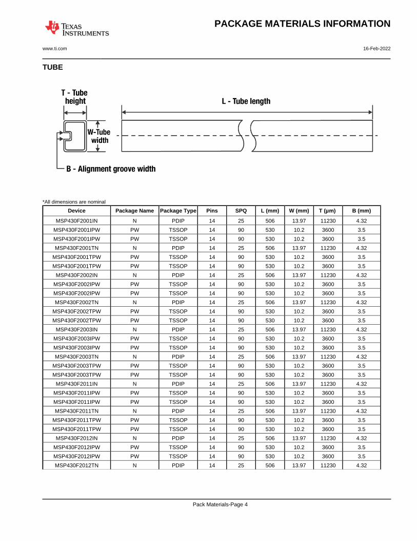
TUBE
*All dimensions are nominal
Device Package Name Package Type Pins SPQ L (mm) W (mm) T (µm) B (mm)
MSP430F2001IN N PDIP 14 25 506 13.97 11230 4.32
MSP430F2001IPW PW TSSOP 14 90 530 10.2 3600 3.5
MSP430F2001IPW PW TSSOP 14 90 530 10.2 3600 3.5
MSP430F2001TN N PDIP 14 25 506 13.97 11230 4.32
MSP430F2001TPW PW TSSOP 14 90 530 10.2 3600 3.5
MSP430F2001TPW PW TSSOP 14 90 530 10.2 3600 3.5
MSP430F2002IN N PDIP 14 25 506 13.97 11230 4.32
MSP430F2002IPW PW TSSOP 14 90 530 10.2 3600 3.5
MSP430F2002IPW PW TSSOP 14 90 530 10.2 3600 3.5
MSP430F2002TN N PDIP 14 25 506 13.97 11230 4.32
MSP430F2002TPW PW TSSOP 14 90 530 10.2 3600 3.5
MSP430F2002TPW PW TSSOP 14 90 530 10.2 3600 3.5
MSP430F2003IN N PDIP 14 25 506 13.97 11230 4.32
MSP430F2003IPW PW TSSOP 14 90 530 10.2 3600 3.5
MSP430F2003IPW PW TSSOP 14 90 530 10.2 3600 3.5
MSP430F2003TN N PDIP 14 25 506 13.97 11230 4.32
MSP430F2003TPW PW TSSOP 14 90 530 10.2 3600 3.5
MSP430F2003TPW PW TSSOP 14 90 530 10.2 3600 3.5
MSP430F2011IN N PDIP 14 25 506 13.97 11230 4.32
MSP430F2011IPW PW TSSOP 14 90 530 10.2 3600 3.5
MSP430F2011IPW PW TSSOP 14 90 530 10.2 3600 3.5
MSP430F2011TN N PDIP 14 25 506 13.97 11230 4.32
MSP430F2011TPW PW TSSOP 14 90 530 10.2 3600 3.5
MSP430F2011TPW PW TSSOP 14 90 530 10.2 3600 3.5
MSP430F2012IN N PDIP 14 25 506 13.97 11230 4.32
MSP430F2012IPW PW TSSOP 14 90 530 10.2 3600 3.5
MSP430F2012IPW PW TSSOP 14 90 530 10.2 3600 3.5
MSP430F2012TN N PDIP 14 25 506 13.97 11230 4.32
PACKAGE MATERIALS INFORMATION
www.ti.com 16-Feb-2022
Pack Materials-Page 4
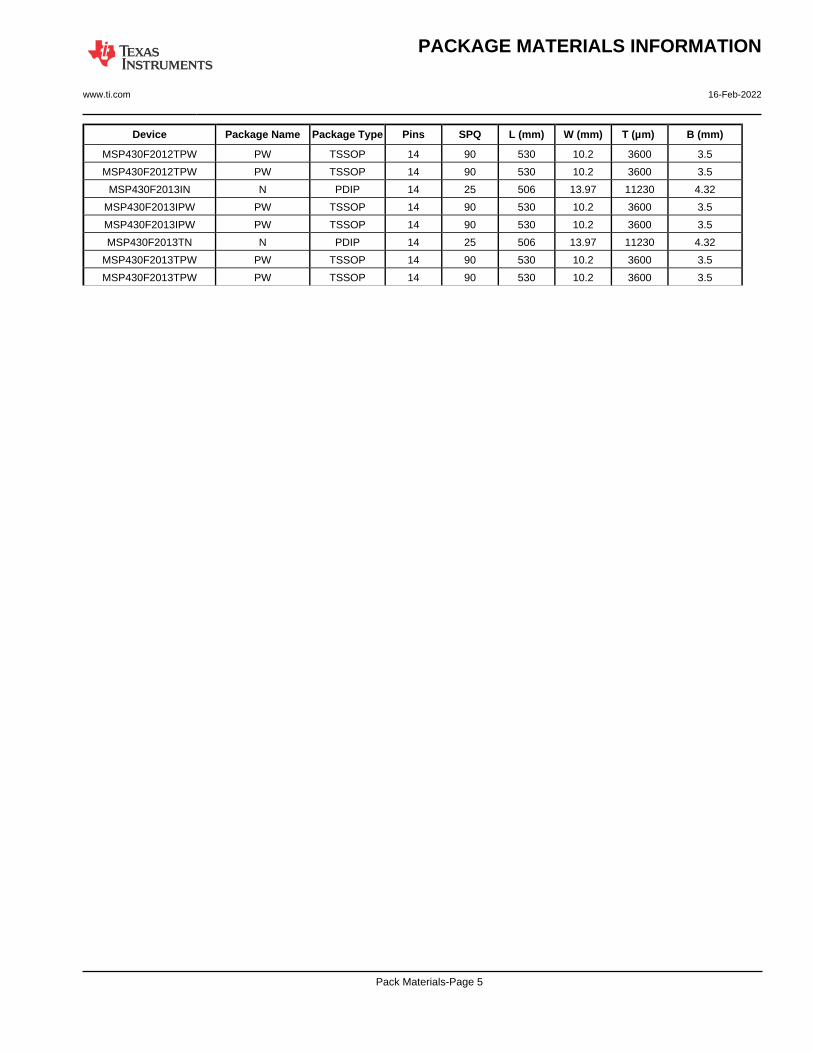
Device Package Name Package Type Pins SPQ L (mm) W (mm) T (µm) B (mm)
MSP430F2012TPW PW TSSOP 14 90 530 10.2 3600 3.5
MSP430F2012TPW PW TSSOP 14 90 530 10.2 3600 3.5
MSP430F2013IN N PDIP 14 25 506 13.97 11230 4.32
MSP430F2013IPW PW TSSOP 14 90 530 10.2 3600 3.5
MSP430F2013IPW PW TSSOP 14 90 530 10.2 3600 3.5
MSP430F2013TN N PDIP 14 25 506 13.97 11230 4.32
MSP430F2013TPW PW TSSOP 14 90 530 10.2 3600 3.5
MSP430F2013TPW PW TSSOP 14 90 530 10.2 3600 3.5
PACKAGE MATERIALS INFORMATION
www.ti.com 16-Feb-2022
Pack Materials-Page 5
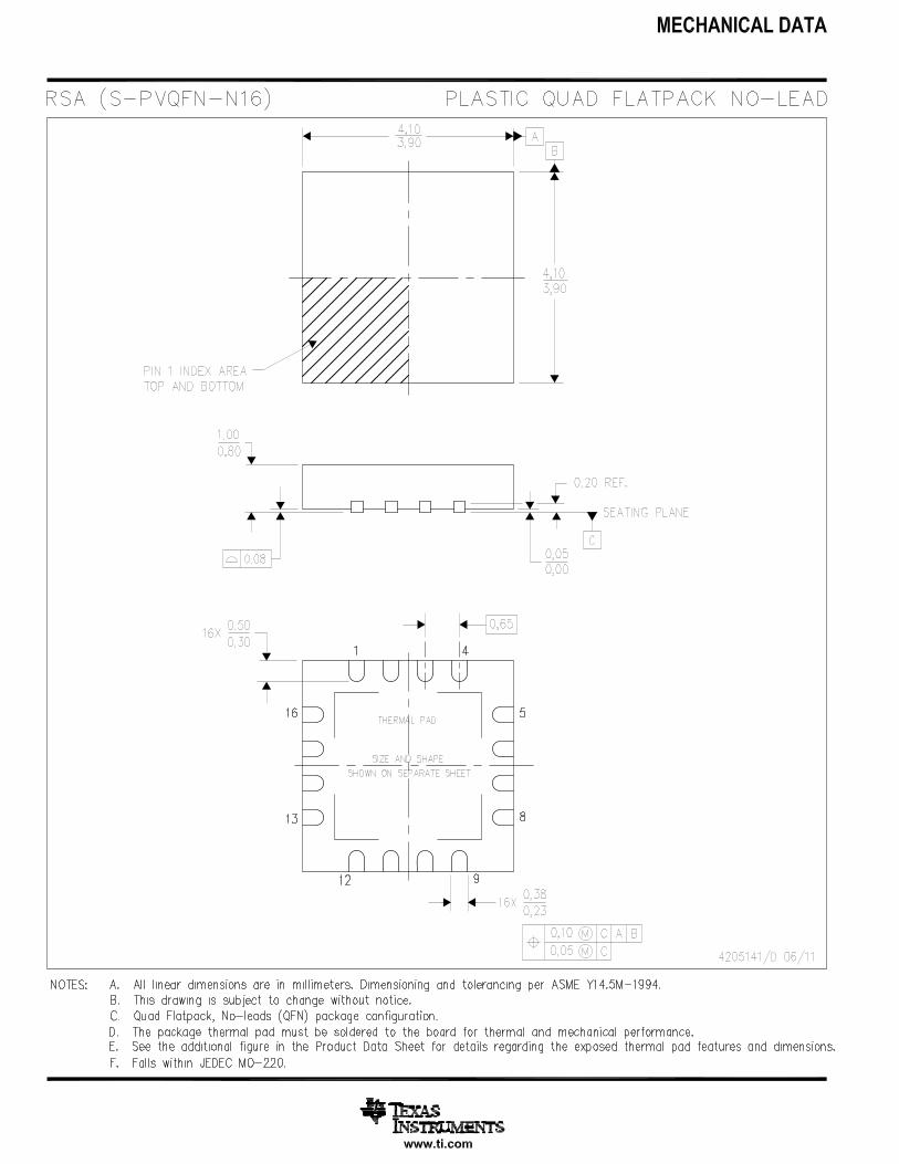
IMPORTANT NOTICE AND DISCLAIMERTI PROVIDES TECHNICAL AND RELIABILITY DATA (INCLUDING DATA SHEETS), DESIGN RESOURCES (INCLUDING REFERENCE DESIGNS), APPLICATION OR OTHER DESIGN ADVICE, WEB TOOLS, SAFETY INFORMATION, AND OTHER RESOURCES “AS IS” AND WITH ALL FAULTS, AND DISCLAIMS ALL WARRANTIES, EXPRESS AND IMPLIED, INCLUDING WITHOUT LIMITATION ANY IMPLIED WARRANTIES OF MERCHANTABILITY, FITNESS FOR A PARTICULAR PURPOSE OR NON-INFRINGEMENT OF THIRD PARTY INTELLECTUAL PROPERTY RIGHTS.These resources are intended for skilled developers designing with TI products. You are solely responsible for (1) selecting the appropriate TI products for your application, (2) designing, validating and testing your application, and (3) ensuring your application meets applicable standards, and any other safety, security, regulatory or other requirements.These resources are subject to change without notice. TI grants you permission to use these resources only for development of an application that uses the TI products described in the resource. Other reproduction and display of these resources is prohibited. No license is granted to any other TI intellectual property right or to any third party intellectual property right. TI disclaims responsibility for, and you will fully indemnify TI and its representatives against, any claims, damages, costs, losses, and liabilities arising out of your use of these resources.TI’s products are provided subject to TI’s Terms of Sale or other applicable terms available either on ti.com or provided in conjunction with such TI products. TI’s provision of these resources does not expand or otherwise alter TI’s applicable warranties or warranty disclaimers for TI products.TI objects to and rejects any additional or different terms you may have proposed. IMPORTANT NOTICE
Mailing Address: Texas Instruments, Post Office Box 655303, Dallas, Texas 75265Copyright © 2022, Texas Instruments Incorporated