Embed Size (px)
Citation preview
Northern India Engineering College
Model Test Paper
Q1. Differentiate between microprocessor and microcontroller?
Ans. 1. Microprocessor is a general purpose devise
2. Microcontroller is indented for a specific purpose
3. Memory, I/O devices etc. need to be interfaced with microprocessor
4. Microcontroller is having its own memory, I/O etc. integrated with it
5. We can say that microprocessor is a CPU on a chip
6. Microcontroller is a system on a chip
Q2. What is an instruction queue? Explain?
Ans. This is introduced in 8086 processor. This queue is in the BIU and is used for
storing the predecoded instructions. This will overlap the fetching and execution cycle.
The EU will take the instructions from the queue for decoding and execution.
Q3. What is REP prefix? How it functions for string instructions?
Ans. This REP prefix is used for repeating. The instruction with REP prefix will execute
repeatedly till the count in the CX register will be zero. This can be used in with some of
the string handling instructions.
Q4. Explain the instructions (i) LDS (ii) PUSHF (iii) TEST (iv) CLD
Ans.
i) LDS: Load Pointer to DS
Move a 32 bit content from the memory given as source to 16
bit destination register specified and to DS register.
ii) PUSHF: Push the Flag
After the execution the content of the flag register will be
pushed to the stack. The higher byte to sp-1 and lower to
SP-2
iii) TEST: Logical Comparison
This will compare the source and the destination specified.
The result will be reflected only in the flag registers.
iv) CLD: Clear Direction Flag. This will clear the direction flag.
Q5. What is stack? Explain the use and operation of stack and stack pointer?
Ans. A stack is a portion of the memory used for the temporary storage. A stack is a last
in first out memory. A stack grows in the decreasing order. A stack will hold the
temporary information, PUSH and POP are the instructions used for storing and
accessing data from the stack. Contents can be moved as 16 bit only using PUSH
and POP instructions.
Northern India Engineering College
Q6. What are the flags in 8086?
Ans. In 8086 Carry Flag, Parity Flag, Auxiliary Carry Flag, Zero Flag, Overflow Flag,
Trap Flag, Interrupt Flag, Direction Flag, and Sign Flag.
Q7. What are the various interrupts in 8086? Explain.
Ans. Maskable Interrupts, Non maskable interrupts.
i) An interrupt that can be turned off by the programmer is known as maskable
interrupt.
ii) An interrupt which can be never be turned off (i.e. disabled) by the programmer
is known as Non maskable interrupt.
Q8. Which interrupts are generally used for critical events?
Ans. Non maskable interrupts are used in critical events. Such as power failure,
emergency shut off etc.
Q9. What is the effect of executing the instruction?
MOV CX, [SOURCE_MEM]
Where SOURCE_MEM equal to 2016 is a memory location offset relative to
the current data segment starting at address 1A00016
Ans. Execution of this instruction results in the following:
((DS) 0 + 2016) (CL)
((DS) 0 + 2016 + 116) (CH)
In other words, CL is loaded with the contents held at memory address
1A00016 +2016 +116 =1A02116
Q10. The original contents of AX, BL, word-sized memory location SUM, and carry
flag
CF are 1234H, ABH, 00CDH, and 0H, respectively. Describe the results of
executing the following sequence of instructions:
ADD AX, [SUM]
ADC BL, 05H
INC WORD PTR [SUM]
Ans. Executing the first instruction adds the word in the accumulator and the word in the
memory location pointed to by address SUM. The result is placed in the
accumulator. That is,
(AX) ← (AX) + (SUM) = 1234H + 00CDH = 1301H
The carry flag remains reset.
The second instruction adds to the lower byte of the base register (BL) the
immediate operand 5H and the carry flag, which is 0H. This gives
(BL) ← (BL) + imm8 + (CF) = ABH + 5H+ 0H = B0H
Since no carry is generated CF remains reset.
The last instruction increments the contents of memory location SUM by one. That
is,
(SUM) ← (SUM) + 1H = 00CDH + 1H =00CEH
Northern India Engineering College
Q11. The 2’s complement signed data contents of AL equal -1 and the contents of
CL are
-2. What result is produced in AX by executing the following instructions:
i) MUL CL ii) IMUL CL
Ans. As binary data, the contents of AL and CL are
(AL) = -1 (as 2‘s complement) = 111111112 = FFH
(CL) = -2 (as 2‘s complement) = 111111102 = FEH
Executing the MUL instruction gives
(AX) = 111111112 * 111111102 = 11111101000000102
= FD02H
The second instruction multiplies the two numbers as signed numbers to generate
the signed result. That is,
(AX) = -1H * -2H
= 2H = 0002H
Q12. Explain different types of registers in 8086 microprocessor architecture.
Ans. Most of the registers contain data/instruction offsets within 64 KB memory
segment. There are four different 64 KB segments for instructions, stack, data and extra
data. To specify where in 1 MB of processor memory these 4 segments are located the
processor uses four segment registers:
Code segment (CS) is a 16-bit register containing address of 64 KB segment with
processor instructions. The processor uses CS segment for all accesses to instructions
referenced by instruction pointer (IP) register. CS register cannot be changed directly.
The CS register is automatically updated during far jump, far call and far return
instructions.
Stack segment (SS) is a 16-bit register containing address of 64KB segment with
program stack. By default, the processor assumes that all data referenced by the stack
pointer (SP) and base pointer (BP) registers is located in the stack segment. SS register
can be changed directly using POP instruction.
Data segment (DS) is a 16-bit register containing address of 64KB segment with
program data. By default, the processor assumes that all data referenced by general
registers (AX, BX, CX, DX) and index register (SI, DI) is located in the data segment. DS
register can be changed directly using POP and LDS instructions.
Extra segment (ES) is a 16-bit register containing address of 64KB segment, usually
with program data. By default, the processor assumes that the DI register references the
ES segment in string manipulation instructions. ES register can be changed directly using
POP and LES instructions.
It is possible to change default segments used by general and index registers by prefixing
instructions with a CS, SS, DS or ES prefix.
All general registers of the 8086 microprocessor can be used for arithmetic and logic
operations. The general registers are:
Accumulator register consists of 2 8-bit registers AL and AH, which can be combined
Northern India Engineering College
together and used as a 16-bit register AX. AL in this case contains the low-order byte of
the word, and AH contains the high-order byte. Accumulator can be used for I/O
operations and string manipulation.
Base register consists of 2 8-bit registers BL and BH, which can be combined together
and used as a 16-bit register BX. BL in this case contains the low-order byte of the word,
and BH contains the high-order byte. BX register usually contains a data pointer used for
based, based indexed or register indirect addressing.
Count register consists of 2 8-bit registers CL and CH, which can be combined together
and used as a 16-bit register CX. When combined, CL register contains the low-order
byte of the word, and CH contains the high-order byte. Count register can be used as a
counter in string manipulation and shift/rotate instructions.
Data register consists of 2 8-bit registers DL and DH, which can be combined together
and used as a 16-bit register DX. When combined, DL register contains the low-order
byte of the word, and DH contains the high-order byte. Data register can be used as a port
number in I/O operations. In integer 32-bit multiply and divide instruction the DX
register contains high-order word of the initial or resulting number.
The following registers are both general and index registers:
Stack Pointer (SP) is a 16-bit register pointing to program stack.
Base Pointer (BP) is a 16-bit register pointing to data in stack segment. BP register is
usually used for based, based indexed or register indirect addressing.
Source Index (SI) is a 16-bit register. SI is used for indexed, based indexed and register
indirect addressing, as well as a source data address in string manipulation instructions.
Destination Index (DI) is a 16-bit register. DI is used for indexed, based indexed and
register indirect addressing, as well as a destination data address in string manipulation
instructions.
Q13. Explain the 80186 microprocessor evolution.
Ans. The 80186 microprocessor was developed by Intel in 1982. It is an improved 8086
with several common support functions built in: clock generator, system controller,
interrupt controller, DMA controller, and timer/counter. It also added 8 new instructions
and executes instructions faster than the 8086. As with the 8086, it has a 16-bit external
bus and is also available as the 80188, with an 8-bit external data bus. The initial clock
rate of the 80186 and 80188 was 6 MHz. In 1987 Intel announced the second generation
of the 80186 family: the 80C186/C188. The 80186 was redesigned as a static, stand-alone
module known as the 80C186 Modular Core and is pin compatible with the 80186 family,
while adding an enhanced feature set. The high-performance CHMOS III process allowed
the 80C186 to run at twice the clock rate of the NMOS 80186, while consuming less than
one-fourth the power.
In 1991 the 80C186 Modular Core family was again extended with the introduction of the
80C186XL. The 80C186XL/C188XL is a higher performance, lower power replacement
for the 80C186/C188
Northern India Engineering College
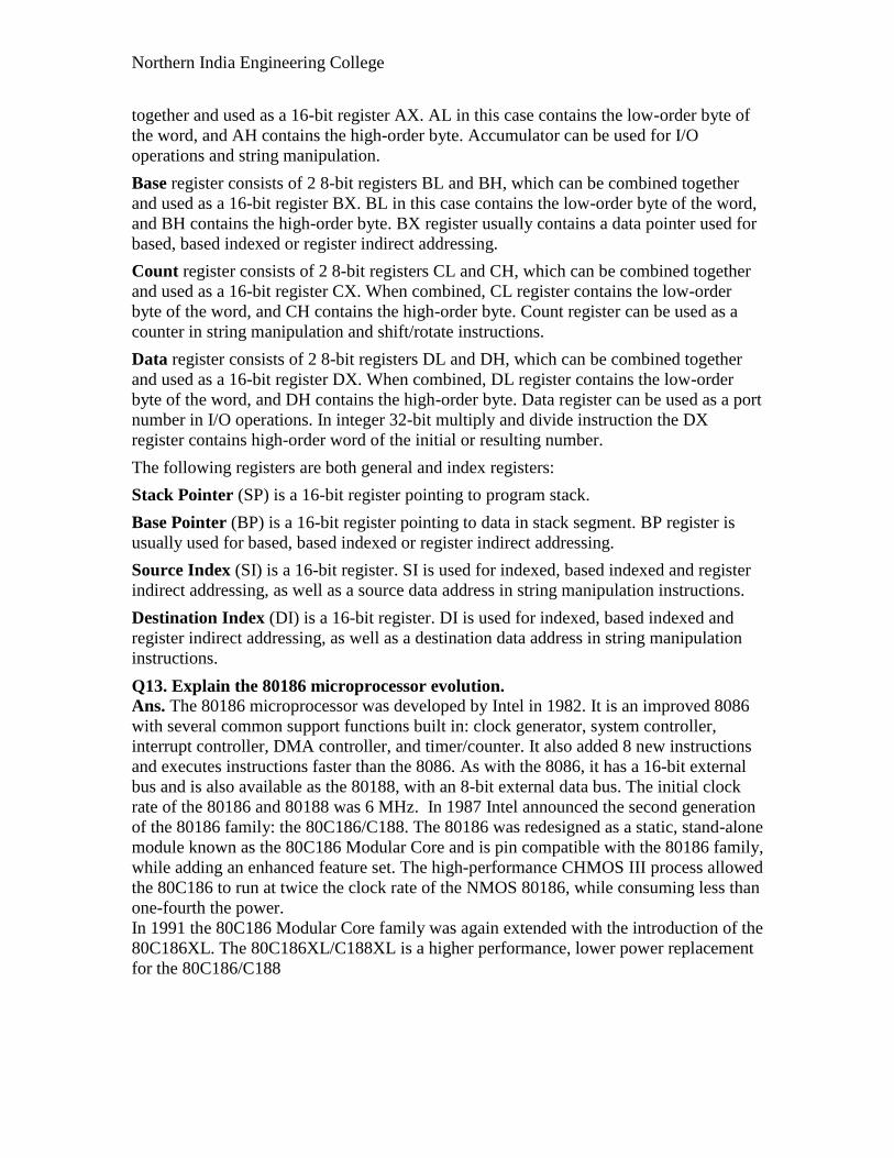
Q14. Draw the internal architecture of 8086.
Ans.
Q15. What are the features of 80186? Ans. The various enhancement features of 80186/88 processors are:
Clock Generator
Programmable Interrupt Controller
Timers
Programmable DMA Unit
Programmable Chip Selection Unit
Power Save/Power Down Feature
Refresh Control Unit
Northern India Engineering College
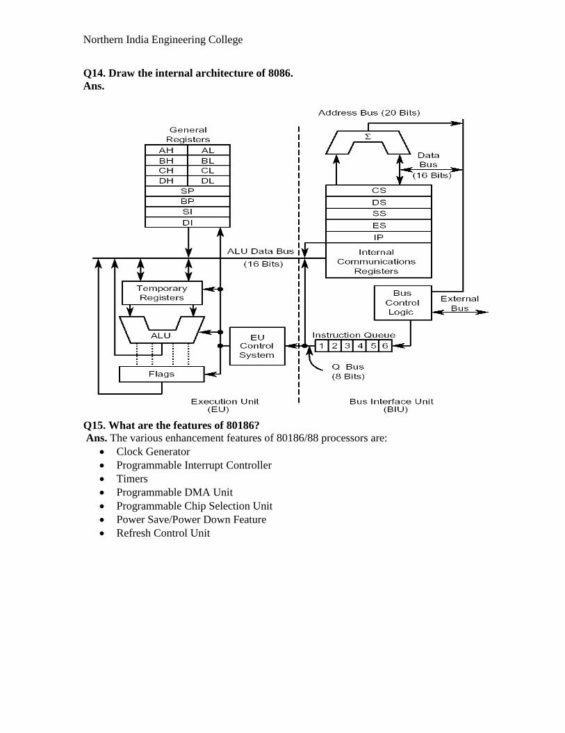
Q16. Draw the timing diagram of 80186.
Ans.
Note, the only difference in 80186/88 vs. 8086/88 is in the generation of ALE which
is asserted one-half clock cycle earlier
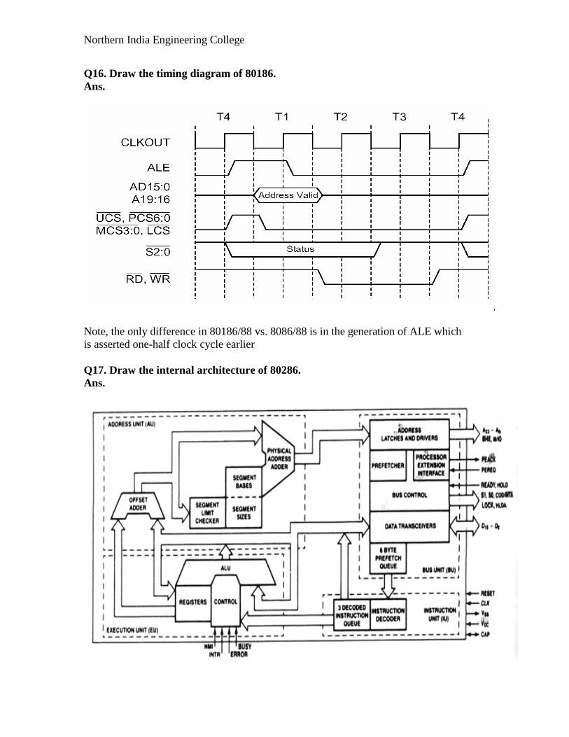
Q17. Draw the internal architecture of 80286.
Ans.
Northern India Engineering College
Q18. What are the features of 80286?
Ans. 80286 has following features:
1. 4 independent units (8086 has only two units) 4
2. 24-bit Address bus in
3. Bus Unit generates all data, address and I/O signals.
Prefetcher flushes the prefetched data, if IU finds a branch instruction.
4. Address Unit (AU) off-loads address generation, translation and checking from
BU.
5. Instruction Unit off-loads EU by performing the instruction decoding.
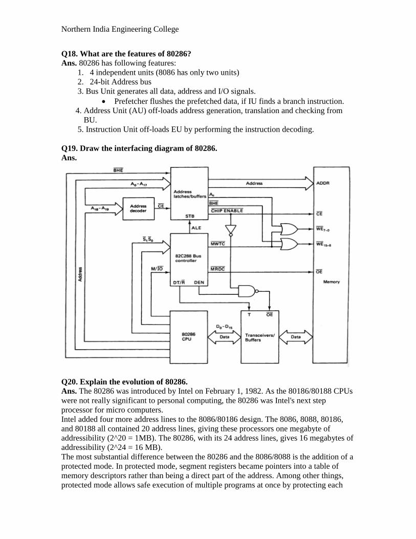
Q19. Draw the interfacing diagram of 80286.
Ans.
ly two units)
Q20. Explain the evolution of 80286.
Ans. The 80286 was introduced by Intel on February 1, 1982. As the 80186/80188 CPUs
were not really significant to personal computing, the 80286 was Intel's next step
processor for micro computers.
Intel added four more address lines to the 8086/80186 design. The 8086, 8088, 80186,
and 80188 all contained 20 address lines, giving these processors one megabyte of
addressibility (2^20 = 1MB). The 80286, with its 24 address lines, gives 16 megabytes of
addressibility (2^24 = 16 MB).
The most substantial difference between the 80286 and the 8086/8088 is the addition of a
protected mode. In protected mode, segment registers became pointers into a table of
memory descriptors rather than being a direct part of the address. Among other things,
protected mode allows safe execution of multiple programs at once by protecting each
Northern India Engineering College
program in memory. DOS normally operates in real mode, in which segment registers act
just as they do in the 8086/8088. Protected mode is used by Microsoft Windows, IBM's
OS/2 and UNIX. (For an introduction to protected mode please refer to this source)
The 80286 is a much more powerful CPU than the 8086, offering 3-6 times the
performance of it. The 6 MHz 80286 is the CPU of the IBM AT (Advanced Technology),
which also introduced a 16-bit motherboard and 16-bit expansion bus to the PC world.
The IBM AT was introduced in 1985 - three years after introduction of the 80286.
With the 80286, the first "chipsets" were introduced. The computer chipset is a set of
chips that replaced dozens of other peripheral chips while maintaining identical
functionality. Chips and Technologies became one of the first popular chipset companies.
Intel second-sourced the 80286 to ensure an adequate supply of chips to the computer
industry. AMD, IBM, and Harris were known to produce 80286 chips as OEM products;
while Siemens, Fujitsu, and Kruger either cloned it or was also second-sources. Between
these various manufacturers, the 80286 was offered in speeds ranging from 6 MHz to 25
MHz:
Intel:6-12.5MHz
Siemens:8-16MHz
AMD:8-20MHz
Harris:10-25MHz
The 80286 was typically made in 3 package versions, each with 68 contacts: a PGA-,
CLCC-and a PLCC-package.
Q21. Is there any instruction added to 80286 instruction set? If yes, mention.
Ans. Yes, in 80286 few instruction is added with 80186 instruction set.
They are written below: ARPL - Adjust RPL Field of Segment Selector
CLTS - Clear Task-Switched Flag in CRO
LAR - Load Access Rights Byte
LGDT/LIDT - Load Global/Interrupt Descriptor Table
Register
LLDT - Load Local Descriptor Table Register
LMSW - Load Machine Status Word
LOADALL - Load All Registers
LSL - Load Segment Limit
LTR - Load Task Register
SGDT - Store Global Descriptor Table Register
SIDT - Store Interrupt Descriptor Table Register
SLDT - Store Local Descriptor Table Register
SMSW - Store Machine Status Word
Northern India Engineering College
STR - Store Task Register
VERR/VERW - Verify a Segment for Reading or
Writing
Q22. What are the features of 80386?
Ans. Features of 80386 are given below:
275,000 transistors
Intel‘s first practical 32-bit microprocessor
32-bit data bus and memory address
4GB of memory
Memory management unit
Multitasking
Q23. What are the features of Pentium?
Ans. Features of Pentium:
P5 architecture / 80586
Introductory version: 60MHz and 66MHz, 110MIPS / 100MHz, 150MIPS
16KB of cache size (8KB IC, 8KB DC)
4GB of memory system, 64-bit data bus
Executes up to two instructions at a time (If they don‘t conflict!)
Q24. Write down the addressing modes of 80386 with examples.
Ans. Addressing modes of 80386:
Register addressing: MOV ECX, EDX
Immediate addressing: MOV EBX, 12345678H
Direct addressing: MOV CX, LIST
Register indirect addressing: MOV AL, [ECX]
Base-plus-index addressing: MOV [EAX+EBX], CL
Register relative addressing: MOV AX, [ECX+4]
Base relative-plus-index addressing: MOV EAX, ARRAY [EBX+ECX]
Scaled-index addressing: MOV EDX, [EAX+4*EBX]
Q25. What are the comparisons between 8086, 80286, 80386, Pentium?
Ans.
8086 80286 80386 Pentium
Introduced 78 82 85 95
Clock Speed 5–10 MHz 6-12MHz 16-33MHz 150-200 MHz
Bus width 16 bits 16 bits 32 bits 64 bits
No.of transistor 29000 134000 275000 5.5 million
Addressable
Memory 1 MB 16 megabytes 4 gigabytes 64 gigabytes
Virtual memory — 1 gigabyte 64 terabytes 64 terabytes
Northern India Engineering College
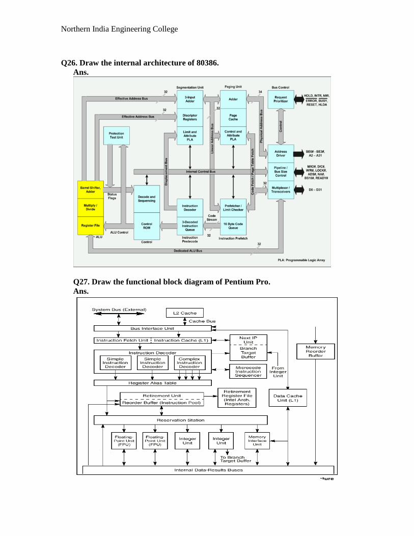
Q26. Draw the internal architecture of 80386.
Ans.
Q27. Draw the functional block diagram of Pentium Pro.
Ans.
Northern India Engineering College
Q28. Write an 8086 ALP to generate a delay of 100 ms, if 8086 system frequency is 10
MHz. Ans. Program:
MOVCX,COUT ; 4
BACK: DEC CX ; 2
JNZ BACK ;
16/
4 Step 1: Calculate the number of required clock cycles
Number of required clock cycles
=
Required delay
time
Time for 1 clock
cycle
= 100
0.1 ms
s
Step 2: Find the required count
Count
= 1
Execution time for one loop
= 1000000 4 6 1
= 55556 = D904H Q29. Write an 8086 ALP to generate a delay of 1 minute if 8086 system frequency is 10
MHz. Ans. Program:
MOV BX, multiplier
count
REE: MOV CX, Count ; 4
BAK: DEC CX ; 2
JNZ BACK ;
16/
4 DEC BX
JNZ REPE Step 1: Calculate the delay generated by inner loop with maximum count
(FFFFH) Delay generated by inner loop for count (FFFFH = 65535)
= [4 + (65535 – 1 × (2 + 16) + (2 + 4)] × 0.1 µs
= 118.1422 m sec
Northern India Engineering College
Step 2: Calculate the multiplier count to get delay of 1 minute
Required delay Multiplier count =
Delay provided by inner loop
= 118.1422 m sec
= 509 = 1FDH
Q30. Difference between Procedures and Macros
Ans.
Sr. No. Procedure Macro
1.
Accessed by CALL and RET
instruction
Accessed during assembly with
name
during program execution. given to macro when defined.
2.
Machine code for instructions is put
only
Machine code is generated for
instructions
once in the memory. each time when macro is called.
3.
With procedures less memory is
required.
With macros more memory is
required.
4. Parameters can be passed in registers,
Parameters passed as part of
statement
memory locations, or stack. which calls macro.
Q31. How do you pass parameters to macro?
Ans. In assembly language program, we can write a generalized macro with dummy
parameter. Then when we wall the macro we can pass it to the actual parameters
needed for the specific application.
For example,
MOVE_ASCII MACRO NUMBER< SOURCE< DESTINATION
MOV CX, number LEA SI, source LEA DI, destination CLD
REP MOVSB END M
The word, NUMBER< SOURCE and DESTINATION in this macro are called
dummy variable. When we call the macro value from the calling statements will
be but in the instruction in place of the dummies.
Northern India Engineering College
Q32. What is nested macro ?
Ans. Nested Macro: A macro body may also contain further macro definitions.
However, these nested macro definition are not valid until the enclosing macro
has been expanded. That means the enclosing macro must have been called before
the nested macros can be called.
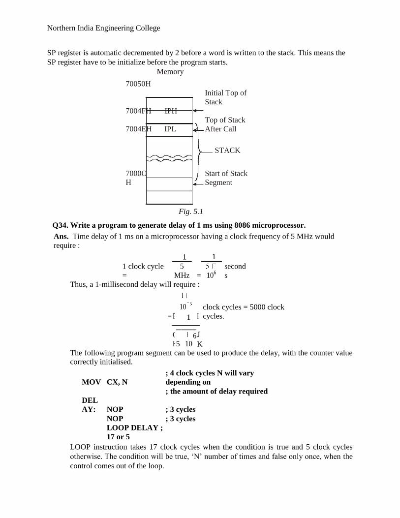
Q33. Explain the stack structure of 8086 in details.
Ans. STACK is a section of memory which is set aside for storing return address. The
stack is also used to save the content of register for calling program while a
procedure executes. A third use of stack is to hold data as address.
Northern India Engineering College
SP register is automatic decremented by 2 before a word is written to the stack. This means the
SP register have to be initialize before the program starts.
Memory
70050H
Initial Top of
Stack
7004FH IPH
7004EH IPL
Top of Stack
After Call
STACK
7000O
H
Start of Stack
Segment
Fig. 5.1
Q34. Write a program to generate delay of 1 ms using 8086 microprocessor.
Ans. Time delay of 1 ms on a microprocessor having a clock frequency of 5 MHz would
require :
1 clock cycle
=
1
=
1
second
s
5
MHz 106
Thus, a 1-millisecond delay will require :
= F
10
I
clock cycles = 5000 clock
cycles.
1
G
J
5 10 6
H K
The following program segment can be used to produce the delay, with the counter value
correctly initialised.
MOV CX, N
; 4 clock cycles N will vary
depending on
; the amount of delay required
DEL
AY: NOP ; 3 cycles
NOP ; 3 cycles
LOOP DELAY ;
17 or 5 LOOP instruction takes 17 clock cycles when the condition is true and 5 clock cycles
otherwise. The condition will be true, ‗N‘ number of times and false only once, when the
control comes out of the loop.
Northern India Engineering College
To calculate ‗N‘ :
Total clock cycles = Clock cycles for MOV + N(2*NOP clock cycles + 17) – 12 (when CX = 0)
5000 = 4 + N(6 + 17) – 12
N = 5000
23 = 218 = 0DAh
Therefore, the counter, CX, should be initialized by 0DAh, in order to get the delay of 1
millisecond.
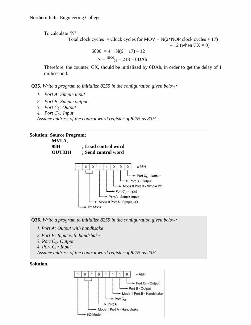
Q35. Write a program to initialize 8255 in the configuration given below:
1. Port A: Simple input
2. Port B: Simple output 3. Port CL: Output 4. Port CU: Input Assume address of the control word register of 8255 as 83H.
Solution: Source Program:
MVI A,
98H ; Load control word
OUT83H ; Send control word Q36. Write a program to initialize 8255 in the configuration given below:
1. Port A: Output with handhsake
2. Port B: Input with handshake 3. Port CL: Output 4. Port CU: Input Assume address of the control word register of 8255 as 23H.
Solution.
Northern India Engineering College
Source Program:
MVIA, AEH ; Load control word OUT 23H ; Send control word
Q37. Write a program to blink Port C bit 0 of the 8255. Assume address of control word
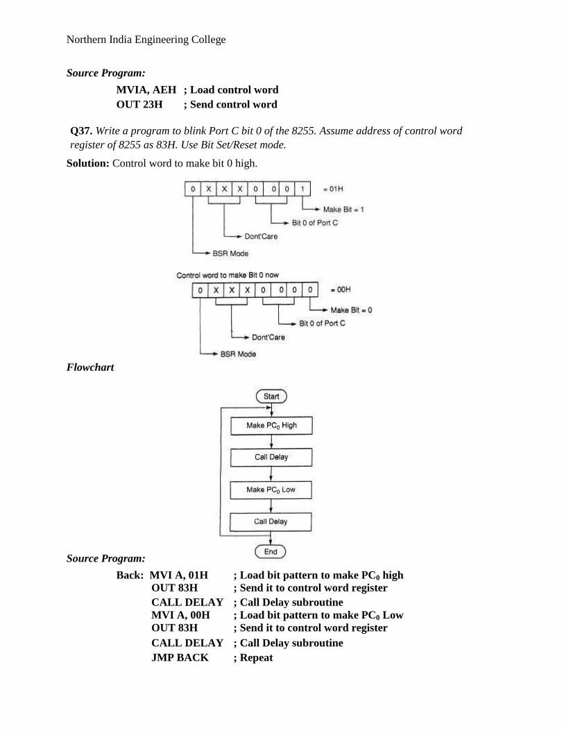
register of 8255 as 83H. Use Bit Set/Reset mode. Solution: Control word to make bit 0 high.
Flowchart
Source Program:
Back: MVI A, 01H ; Load bit pattern to make PC0 high
OUT 83H ; Send it to control word register CALL DELAY ; Call Delay subroutine MVI A, 00H ; Load bit pattern to make PC0 Low
OUT 83H ; Send it to control word register CALL DELAY ; Call Delay subroutine JMP BACK ; Repeat
Northern India Engineering College
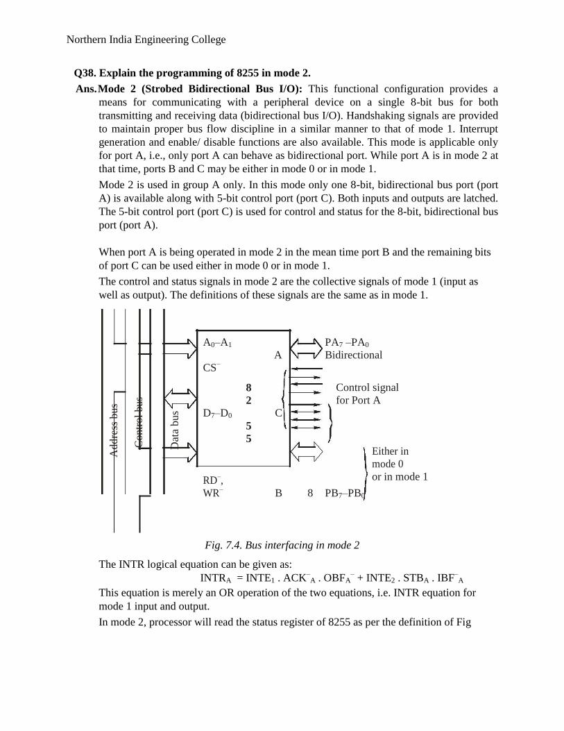
Q38. Explain the programming of 8255 in mode 2.
Ans. Mode 2 (Strobed Bidirectional Bus I/O): This functional configuration provides a
means for communicating with a peripheral device on a single 8-bit bus for both
transmitting and receiving data (bidirectional bus I/O). Handshaking signals are provided
to maintain proper bus flow discipline in a similar manner to that of mode 1. Interrupt
generation and enable/ disable functions are also available. This mode is applicable only
for port A, i.e., only port A can behave as bidirectional port. While port A is in mode 2 at
that time, ports B and C may be either in mode 0 or in mode 1.
Mode 2 is used in group A only. In this mode only one 8-bit, bidirectional bus port (port
A) is available along with 5-bit control port (port C). Both inputs and outputs are latched.
The 5-bit control port (port C) is used for control and status for the 8-bit, bidirectional bus
port (port A).
When port A is being operated in mode 2 in the mean time port B and the remaining bits
of port C can be used either in mode 0 or in mode 1.
The control and status signals in mode 2 are the collective signals of mode 1 (input as
well as output). The definitions of these signals are the same as in mode 1.
A0–A1
A
PA7 –PA0
Bidirectional
CS–
Ad
dre
ss b
us
8 Control signal
Co
ntr
ol
bu
s
Dat
a bus D7–D0
2 C
for Port A
5
5
Either in
mode 0
RD–,
WR–
or in mode 1
B 8 PB7–PB0
Fig. 7.4. Bus interfacing in mode 2
The INTR logical equation can be given as: INTRA = INTE1 . ACK
–A . OBFA
– + INTE2 . STBA . IBF
–A
This equation is merely an OR operation of the two equations, i.e. INTR equation for
mode 1 input and output.
In mode 2, processor will read the status register of 8255 as per the definition of Fig
Northern India Engineering College
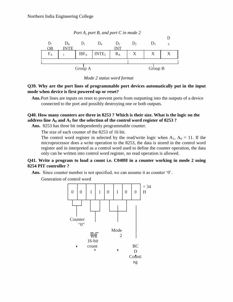
Port A, port B, and port C in mode 2
D7 D6 D5 D4 D3 D2 D1
D
0
OB
FA
INTE
1 IBFA INTE2
INT
RA X X X
Group A Group B
Mode 2 status word format Q39. Why are the port lines of programmable port devices automatically put in the input
mode when device is first powered up or reset?
Ans. Port lines are inputs on reset to prevent ports from outputting into the outputs of a device
connected to the port and possibly destroying one or both outputs.
Q40. How many counters are three in 8253 ? Which is their size. What is the logic on the
address line A0 and A1 for the selection of the control word register of 8253 ? Ans. 8253 has three bit independently programmable counter.
The size of each counter of the 8253 of 16 bit. The control word register in selected by the read/write logic when A1, A0 = 11. If the
microprocessor does a write operation to the 8253, the data is stored in the control word
register and in interpreted as a control word used to define the counter operation, the data
only can be written into control word register, no read operation is allowed. Q41. Write a program to load a count i.e. C040H in a counter working in mode 2 using
8254 PIT controller ?
Ans. Since counter number is not specified, we can assume it as counter ‗0‘.
Generation of control word
0 0 1 1 0 1 0 0
= 34
H
Counter
―0‖
Mode
2
RD/WR
16-bit
count BC
D
Counti
ng
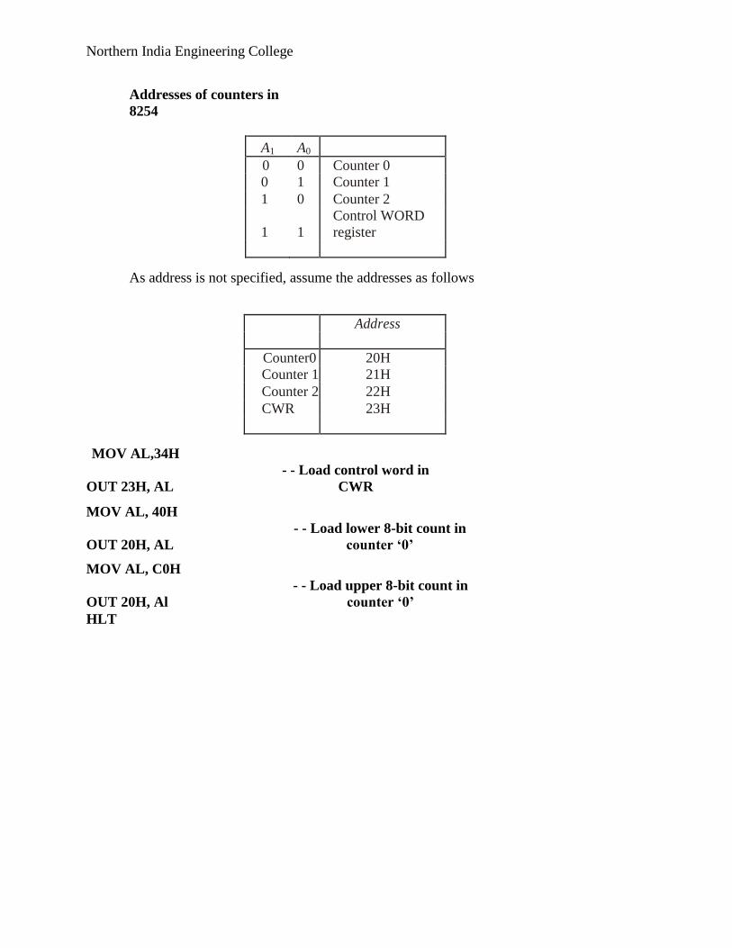
Northern India Engineering College
Addresses of counters in
8254
A1 A0
0 0 Counter 0
0 1 Counter 1
1 0 Counter 2
1 1
Control WORD
register
As address is not specified, assume the addresses as follows
Address
Counter0 20H
Counter 1 21H
Counter 2 22H
CWR 23H
MOV AL,34H
OUT 23H, AL
- - Load control word in
CWR
MOV AL, 40H
OUT 20H, AL
- - Load lower 8-bit count in
counter ‘0’
MOV AL, C0H
OUT 20H, Al
- - Load upper 8-bit count in
counter ‘0’
HLT
![bhavanakhivsara.files.wordpress.com · Web viewSubject : Computer Networks Exam: ENDSEM Marks:70 Paper Solution By: Prof. B.A.Khivsara Q1 a) Differentiate between OSI and] : OSI Model](https://img.pdfslide.net/doc/110x75/5b2c0c607f8b9ae6278bc2a8/-web-viewsubject-computer-networks-exam-endsem-marks70-paper-solution-by.jpg)


![Q1: Differentiate between acids and alkalis - WordPress.com · 4. What was the Faraizi Movement? [4] ... 26.Why did Sir Syed Ahmad start the Aligarh Movement? [4]](https://img.pdfslide.net/doc/110x75/5b4136257f8b9a896a8b66fb/q1-differentiate-between-acids-and-alkalis-4-what-was-the-faraizi-movement.jpg)