Embed Size (px)
Citation preview
10623 Roselle Street, San Diego, CA 92121 (858) 550-9559 Fax (858) 550-7322
[email protected] www.accesio.com
MODELS PCIe-DIO-48S PCIe-DIO-48
PCIe-DIO-24S
PCI Express 48 Channel Digital I/O Card with Change of State Detection
USER MANUAL
File: MPCIe-DIO-48S.B1b
Manual PCIe-DIO-48S PCI Express Digital I/O Card 2
Notice The information in this document is provided for reference only. ACCES does not assume any liability arising out of the application or use of the information or products described herein. This document may contain or reference information and products protected by copyrights or patents and does not convey any license under the patent rights of ACCES, nor the rights of others. IBM PC, PC/XT, and PC/AT are registered trademarks of the International Business Machines Corporation. Printed in USA. Copyright 2009 by ACCES I/O Products, Inc. 10623 Roselle Street, San Diego, CA 92121. All rights reserved.
WARNING!! ALWAYS CONNECT AND DISCONNECT YOUR FIELD CABLING WITH THE
COMPUTER POWER OFF. ALWAYS TURN COMPUTER POWER OFF BEFORE INSTALLING A BOARD. CONNECTING AND DISCONNECTING
CABLES, OR INSTALLING BOARDS INTO A SYSTEM WITH THE COMPUTER OR FIELD POWER ON MAY CAUSE DAMAGE TO THE I/O
BOARD AND WILL VOID ALL WARRANTIES, IMPLIED OR EXPRESSED.

Manual PCIe-DIO-48S PCI Express Digital I/O Card 3
Warranty Prior to shipment, ACCES equipment is thoroughly inspected and tested to applicable specifications. However, should equipment failure occur, ACCES assures its customers that prompt service and support will be available. All equipment originally manufactured by ACCES which is found to be defective will be repaired or replaced subject to the following considerations.
Terms and Conditions If a unit is suspected of failure, contact ACCES' Customer Service department. Be prepared to give the unit model number, serial number, and a description of the failure symptom(s). We may suggest some simple tests to confirm the failure. We will assign a Return Material Authorization (RMA) number which must appear on the outer label of the return package. All units/components should be properly packed for handling and returned with freight prepaid to the ACCES designated Service Center, and will be returned to the customer's/user's site freight prepaid and invoiced.
Coverage First Three Years: Returned unit/part will be repaired and/or replaced at ACCES option with no charge for labor or parts not excluded by warranty. Warranty commences with equipment shipment. Following Years: Throughout your equipment's lifetime, ACCES stands ready to provide on-site or in-plant service at reasonable rates similar to those of other manufacturers in the industry.
Equipment Not Manufactured by ACCES Equipment provided but not manufactured by ACCES is warranted and will be repaired according to the terms and conditions of the respective equipment manufacturer's warranty.
General Under this Warranty, liability of ACCES is limited to replacing, repairing or issuing credit (at ACCES discretion) for any products which are proved to be defective during the warranty period. In no case is ACCES liable for consequential or special damage arriving from use or misuse of our product. The customer is responsible for all charges caused by modifications or additions to ACCES equipment not approved in writing by ACCES or, if in ACCES opinion the equipment has been subjected to abnormal use. "Abnormal use" for purposes of this warranty is defined as any use to which the equipment is exposed other than that use specified or intended as evidenced by purchase or sales representation. Other than the above, no other warranty, expressed or implied, shall apply to any and all such equipment furnished or sold by ACCES.
Manual PCIe-DIO-48S PCI Express Digital I/O Card 4
TABLE OF CONTENTS
Chapter 1: Introduction........................................................................................................................................ 5 Features ............................................................................................................................................................. 5 Applications....................................................................................................................................................... 5 Functional Description ..................................................................................................................................... 5 Ordering Guide.................................................................................................................................................. 7 Factory Options................................................................................................................................................. 7 Optional Accessories ....................................................................................................................................... 7
Chapter 2: Installation.......................................................................................................................................... 8 Software CD Installation................................................................................................................................... 8 Hardware Installation........................................................................................................................................ 8
Chapter 3: Hardware Details................................................................................................................................ 9 Option Selection................................................................................................................................................ 9 C3 IRQ Enable ................................................................................................................................................... 9 50 Pin Headers .................................................................................................................................................. 9 VCCIO Resettable Fused Outputs ................................................................................................................. 10
Chapter 4: Address Selection ........................................................................................................................... 11 Chapter 5: Programming ................................................................................................................................... 12 Chapter 6: Connector Pin Assignments .......................................................................................................... 15 Chapter 7: Specifications .................................................................................................................................. 17 Customer Comments ......................................................................................................................................... 18
LIST OF FIGURES
Figure 1-1: Block Diagram ................................................................................................................................... 6 Figure 3-1: Option Selection Map ....................................................................................................................... 9 Figure 6-1: 50-Pin Male Header ......................................................................................................................... 15
LIST OF TABLES
Table 1-1: Accessories......................................................................................................................................... 7 Table 5-1: Register Address Map...................................................................................................................... 12 Table 5-2: Base +0 Group 0, Port A DIO; Base +4 Group 1, Port A DIO........................................................ 12 Table 5-3: Base +1 Group 0, Port B DIO; Base +5 Group 1, Port B DIO........................................................ 13 Table 5-4: Base +2 Group 0, Port C DIO; Base +6 Group 1, Port C DIO........................................................ 13 Table 5-5: Base +3 and Base +7, Group 0 and 1 Control Register ................................................................ 13 Table 5-6: Base +B, COS/C3 IRQ Enable.......................................................................................................... 14 Table 6-1: P2 and P3 I/O Header Connector Pin Assignments ...................................................................... 15 Table 6-2: I/O Header Connector Signal Names, Directions and Descriptions............................................ 16
Manual PCIe-DIO-48S PCI Express Digital I/O Card 5
Chapter 1: Introduction
The PCIe-DIO-48(S) is a x1 lane PCI Express (PCIe) board designed for use in a variety of Digital I/O (DIO) applications. It uses the high speed PCIe bus to transfer digital data to and from the board. The DIO emulates 8255 compatible chips making it easy program. This also allows for simple migration from older ACCES’ PCI-based DIO boards. Change of State (COS) and interrupt capabilities relieve software from polling routines that consume valuable processing time. Lastly, the x1 lane PCIe connector is very flexible and can be inserted into any x1, x4, x8, x16, or x32 PCIe slots. Features
• 48 high-current DIO lines • Two 50-pin male headers with 24 digital lines each • COS interrupt (“S” models only) • User interrupt on port C bit 3 of each DIO group • DIO lines buffered • Four and eight bit ports independently selectable for inputs or outputs • Pull-ups on DIO lines (optional pull-down) • 5V VCCIO (3.3V optional) • VCCIO voltage available to the user on each I/O header • Compatible with industry standard I/O racks like Gordos, Opto-22, Potter & Brumfield,
Western Reserve Controls, etc. Applications
• Automatic test systems • Laboratory automation • Robotics • Machine control • Security systems, energy management • Relay monitoring and control • Parallel data transfer to PC • Sensing switch closures or TTL, DTL, CMOS logic • Driving indicator lights or recorders
Functional Description This product is a x1 lane PCIe DIO board. It occupies sixteen bytes of I/O address space and the base address is selected by the system. The card emulates two 8255 compatible chips, providing 48 DIO lines in two 24-bit groups. Each group provides three 8-bit ports: A, B, and C. Each 8-bit port can be software configured to function as either inputs or outputs. Port C can be further broken into two 4-bit nybbles. Also, these nybbles can be software configured to function as either inputs or outputs. This board has two methods for generating an interrupt. The first is using bit 3 of Port C (C3 IRQ). When this method is enabled, a rising signal edge detected on bit 3 of Port C will generate an interrupt. The second method uses COS detection hardware to produce an interrupt ('S' model only).
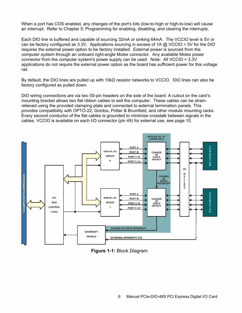
Manual PCIe-DIO-48S PCI Express Digital I/O Card 6
When a port has COS enabled, any changes of the port's bits (low-to-high or high-to-low) will cause an interrupt. Refer to Chapter 5: Programming for enabling, disabling, and clearing the interrupts. Each DIO line is buffered and capable of sourcing 32mA or sinking 64mA. The VCCIO level is 5V or can be factory configured as 3.3V. Applications sourcing in excess of 1A @ VCCIO = 5V for the DIO requires the external power option to be factory installed. External power is sourced from the computer system through an onboard right-angle Molex connector. Any available Molex power connector from the computer system's power supply can be used. Note: All VCCIO = 3.3V applications do not require the external power option as the board has sufficient power for this voltage rail. By default, the DIO lines are pulled up with 10kΩ resistor networks to VCCIO. DIO lines can also be factory configured as pulled down. DIO wiring connections are via two 50-pin headers on the side of the board. A cutout on the card’s mounting bracket allows two flat ribbon cables to exit the computer. These cables can be strain-relieved using the provided clamping plate and connected to external termination panels. This provides compatibility with OPTO-22, Gordos, Potter & Brumfield, and other module mounting racks. Every second conductor of the flat cables is grounded to minimize crosstalk between signals in the cables. VCCIO is available on each I/O connector (pin 49) for external use, see page 10.
Figure 1-1: Block Diagram
Manual PCIe-DIO-48S PCI Express Digital I/O Card 7
Ordering Guide
• PCIe-DIO-48S 48-bit Digital I/O card with change of state detection • PCIe-DIO-48 48-bit Digital I/O card • PCIe-DIO-24S 24-bit Digital I/O card with change of state detection
Factory Options
• Extended temperature operation (-40° to +85°C) • Molex PC-style connector for maximum 5V VCCIO current sourcing capability • 3.3V VCCIO • I/O lines pulled down
Optional Accessories
• CAB50F-6 Six-foot ribbon cable assembly with 50-pin female connectors
• CAB50-6 Six-foot ribbon cable assembly with a 50-pin female header connector and a 50-pin female edge connector
• STB-50 Screw terminal board, ships with standoffs but can also mount on SNAP-TRACK or DIN-SNAP
• DIN-SNAP-6 Six inch length of SNAP-TRACK with two clips for mounting one STB-50 screw terminal board on a DIN rail
• DIN-SNAP One foot length of SNAP-TRACK with four clips, for mounting up to two STB-50 screw terminal boards on a DIN rail
• STB-48CH Screw Terminal Board provides two 50-pin headers with corresponding I/O terminals that accept from 26 to 12 AWG size wires
Table 1-1: Accessories
Manual PCIe-DIO-48S PCI Express Digital I/O Card 8
Chapter 2: Installation
Software CD Installation
The software provided with this board is contained on one CD and must be installed onto your hard disk prior to use. To do this, perform the following steps as appropriate for your operating system. Substitute the appropriate drive letter for your drive where you see D: in the examples below.
Win2000/XP/2003 a. Place the CD into your CD-ROM drive.
b. The install program automatically run. If the install program does not run, click START | RUN and type , click OK or press .
c. Follow the on-screen prompts to install the software for this board.
Linux a. Please refer to linux.htm on the CD-ROM for information on installing under Linux.
Hardware Installation
Please install the software package before plugging the hardware into the system. Refer to the printed I/O Quick Start Guide included with your board which can also be found on the CD, for specific, quick steps to complete the hardware and software installation.
Manual PCIe-DIO-48S PCI Express Digital I/O Card 9
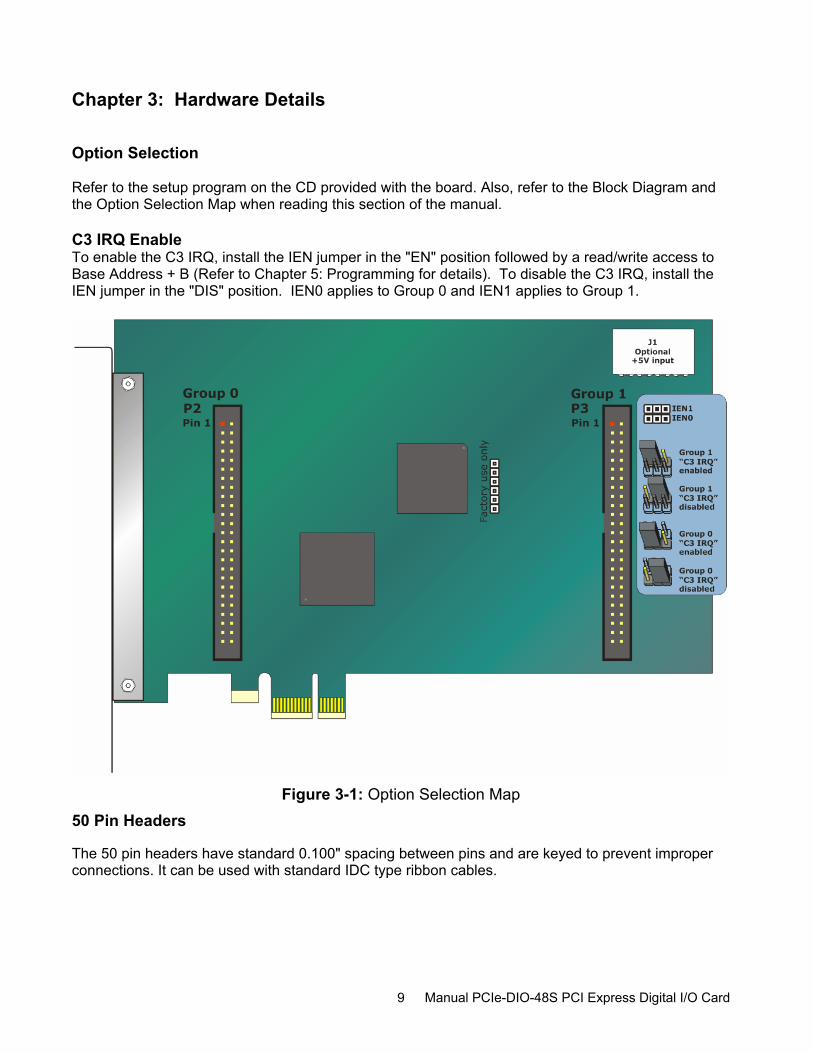
Chapter 3: Hardware Details
Option Selection Refer to the setup program on the CD provided with the board. Also, refer to the Block Diagram and the Option Selection Map when reading this section of the manual. C3 IRQ Enable To enable the C3 IRQ, install the IEN jumper in the "EN" position followed by a read/write access to Base Address + B (Refer to Chapter 5: Programming for details). To disable the C3 IRQ, install the IEN jumper in the "DIS" position. IEN0 applies to Group 0 and IEN1 applies to Group 1.
Figure 3-1: Option Selection Map 50 Pin Headers The 50 pin headers have standard 0.100" spacing between pins and are keyed to prevent improper connections. It can be used with standard IDC type ribbon cables.
Manual PCIe-DIO-48S PCI Express Digital I/O Card 10
VCCIO Resettable Fused Outputs There are two 0.5A resettable fuses. Each fuse feeds one I/O connector at pin 49 used to power external module racks, relay boards, or for general purposes. If an over-current persists on a circuit protected by the resettable fuse, it will open interrupting power to the circuit. The amount of time it takes the fuse to act depends on the amount of over-current and other conditions such as ambient temperature, humidity, etc. The fuse will remain open until the bi-metal elements cool sufficiently, at which time the circuit will be restored.
Manual PCIe-DIO-48S PCI Express Digital I/O Card 11
Chapter 4: Address Selection
The Vendor ID for this card is 0x494F. (ASCII for "IO") The Device ID for the PCIe-DIO-48S is 0x0E61. The Device ID for the PCIe-DIO-48 is 0x0C61. The Device ID for the PCIe-DIO-24S is 0x0E53. This card uses I/O addresses offset from the base address assigned by the PCIe bus. The address spaces are defined in the programming section of this manual. PCIe architecture is Plug-and-Play. This means that the BIOS or Operating System determines the resources assigned to PCIe cards rather than the user selecting those resources with switches or jumpers. As a result, you cannot set or change the card's base address or IRQ level. You can only determine what the system has assigned. The following information is for advanced users only:
The PCIe bus supports 64K of I/O address space, so your card's addresses may be located anywhere in the 0000h to FFFFh range.
To determine the base address that has been assigned, run the PCIFind utility program. This utility will display a list of all the cards detected on the PCI/PCIe bus, the addresses assigned to each function on each of the cards, and the respective IRQs. Alternatively, Windows systems can be queried to determine which resources were assigned. In these operating systems, you can use either PCIFind, or the Device Manager utility from the System Properties Applet of the control panel. The card is installed in the Data Acquisition class of the Device Manager list. Selecting the card, clicking Properties, and then selecting the Resources Tab will display a list of the resources allocated to the card. In Linux you can use the LSPCI command to determine this information. A PCIFind.pl script is also provided which may simplify this task. An example of how to locate PCIe card resources in DOS is provided with in the PCI\SOURCE directory, under your installation directory. This code runs in DOS, and uses the PCI defined interrupt BIOS calls to query the PCI bus for card specific information. You will need the Device ID and Vendor ID listed above to use this code. The card uses more resources than you usually need be concerned with. PCIFind will show only the most commonly required information to reduce confusion. For those who require it, be aware of the following: BAR[0]: memory mapped PEX8311 BAR[1]: I/O mapped PEX8311 BAR[2]: I/O mapped card registers (←all most software needs)
Manual PCIe-DIO-48S PCI Express Digital I/O Card 12
Chapter 5: Programming
This card is an I/O-mapped device that is easily configured from any language. The base address is assigned by the computer system during installation. The card's read/write functions are as follows.
Address Function Operation Base Address +0 PA Group 0 Read/Write
Base Address +1 PB Group 0 Read/Write
Base Address +2 PC Group 0 Read Write
Base Address +3 Control Group 0 Read/Write
Base Address +4 PA Group 1 Read/Write
Base Address +5 PB Group 1 Read/Write
Base Address +6 PC Group 1 Read/Write
Base Address +7 Control Group 1 Read/Write
Base Address +8 Not used N/A
Base Address +9 Not used N/A
Base Address +A Not used N/A
Base Address +B Enable COS Interrupt Read/Write
Base Address +C Not used N/A
Base Address +D Not used N/A
Base Address +E Not used N/A
Base Address +F Clear COS Interrupt Write Only
Table 5-1: Register Address Map Base Address +0 (read/write) Group 0, Port A DIO; +4 (read/write) Group 1, Port A DIO
Bit 7 Bit 6 Bit 5 Bit 4 Bit 3 Bit 2 Bit 1 Bit 0PA7 PA6 PA5 PA4 PA3 PA2 PA1 PA0
Table 5-2: Base +0 Group 0, Port A DIO; Base +4 Group 1, Port A DIO Reading from these addresses will return the digital data on Port A. Writing to this address will output the digital data on Port A. Readback is supported while in output mode. Base Address +3 / Base Address +7 controls Port A's input/output direction.
Manual PCIe-DIO-48S PCI Express Digital I/O Card 13
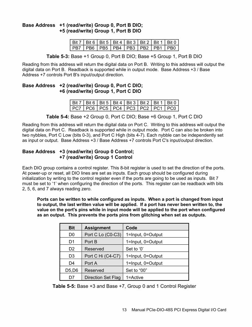
Base Address +1 (read/write) Group 0, Port B DIO; +5 (read/write) Group 1, Port B DIO
Bit 7 Bit 6 Bit 5 Bit 4 Bit 3 Bit 2 Bit 1 Bit 0PB7 PB6 PB5 PB4 PB3 PB2 PB1 PB0
Table 5-3: Base +1 Group 0, Port B DIO; Base +5 Group 1, Port B DIO Reading from this address will return the digital data on Port B. Writing to this address will output the digital data on Port B. Readback is supported while in output mode. Base Address +3 / Base Address +7 controls Port B's input/output direction. Base Address +2 (read/write) Group 0, Port C DIO; +6 (read/write) Group 1, Port C DIO
Bit 7 Bit 6 Bit 5 Bit 4 Bit 3 Bit 2 Bit 1 Bit 0PC7 PC6 PC5 PC4 PC3 PC2 PC1 PC0
Table 5-4: Base +2 Group 0, Port C DIO; Base +6 Group 1, Port C DIO Reading from this address will return the digital data on Port C. Writing to this address will output the digital data on Port C. Readback is supported while in output mode. Port C can also be broken into two nybbles, Port C Low (bits 0-3), and Port C High (bits 4-7). Each nybble can be independently set as input or output. Base Address +3 / Base Address +7 controls Port C's input/output direction. Base Address +3 (read/write) Group 0 Control; +7 (read/write) Group 1 Control Each DIO group contains a control register. This 8-bit register is used to set the direction of the ports. At power-up or reset, all DIO lines are set as inputs. Each group should be configured during initialization by writing to the control register even if the ports are going to be used as inputs. Bit 7 must be set to ‘1’ when configuring the direction of the ports. This register can be readback with bits 2, 5, 6, and 7 always reading zero.
Ports can be written to while configured as inputs. When a port is changed from input to output, the last written value will be applied. If a port has never been written to, the value on the port's pins while in input mode will be applied to the port when configured as an output. This prevents the ports pins from glitching when set as outputs.
Bit Assignment CodeD0 Port C Lo (C0-C3) 1=Input, 0=Output D1 Port B 1=Input, 0=Output D2 Reserved Set to ‘0’ D3 Port C Hi (C4-C7) 1=Input, 0=Output D4 Port A 1=Input, 0=Output
D5,D6 Reserved Set to “00” D7 Direction Set Flag 1=Active
Table 5-5: Base +3 and Base +7, Group 0 and 1 Control Register
Manual PCIe-DIO-48S PCI Express Digital I/O Card 14
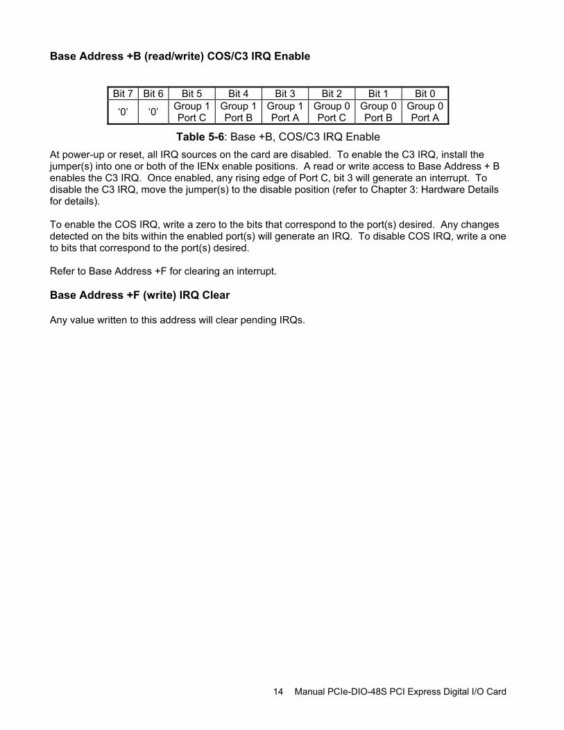
Base Address +B (read/write) COS/C3 IRQ Enable
Bit 7 Bit 6 Bit 5 Bit 4 Bit 3 Bit 2 Bit 1 Bit 0
‘0’ ‘0’ Group 1 Port C
Group 1Port B
Group 1Port A
Group 0Port C
Group 0 Port B
Group 0 Port A
Table 5-6: Base +B, COS/C3 IRQ Enable At power-up or reset, all IRQ sources on the card are disabled. To enable the C3 IRQ, install the jumper(s) into one or both of the IENx enable positions. A read or write access to Base Address + B enables the C3 IRQ. Once enabled, any rising edge of Port C, bit 3 will generate an interrupt. To disable the C3 IRQ, move the jumper(s) to the disable position (refer to Chapter 3: Hardware Details for details). To enable the COS IRQ, write a zero to the bits that correspond to the port(s) desired. Any changes detected on the bits within the enabled port(s) will generate an IRQ. To disable COS IRQ, write a one to bits that correspond to the port(s) desired. Refer to Base Address +F for clearing an interrupt. Base Address +F (write) IRQ Clear Any value written to this address will clear pending IRQs.
Manual PCIe-DIO-48S PCI Express Digital I/O Card 15
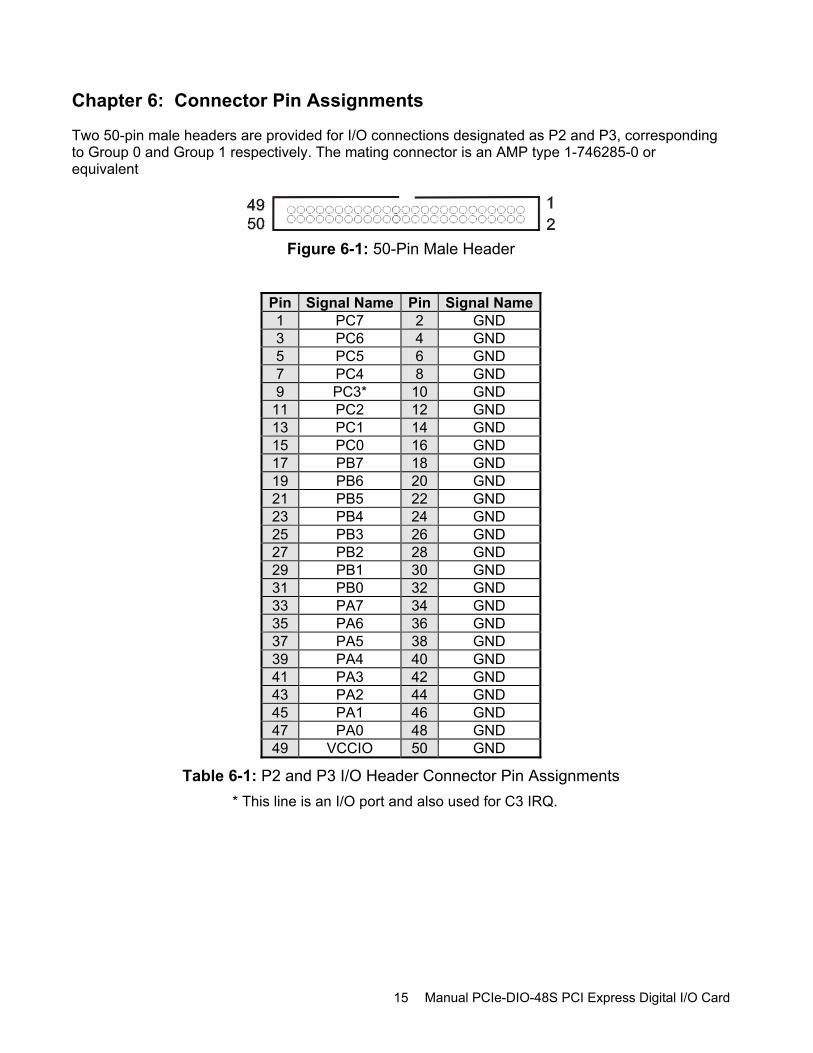
Chapter 6: Connector Pin Assignments
Two 50-pin male headers are provided for I/O connections designated as P2 and P3, corresponding to Group 0 and Group 1 respectively. The mating connector is an AMP type 1-746285-0 or equivalent
Figure 6-1: 50-Pin Male Header
Pin Signal Name Pin Signal Name1 PC7 2 GND 3 PC6 4 GND 5 PC5 6 GND 7 PC4 8 GND 9 PC3* 10 GND
11 PC2 12 GND 13 PC1 14 GND 15 PC0 16 GND 17 PB7 18 GND 19 PB6 20 GND 21 PB5 22 GND 23 PB4 24 GND 25 PB3 26 GND 27 PB2 28 GND 29 PB1 30 GND 31 PB0 32 GND 33 PA7 34 GND 35 PA6 36 GND 37 PA5 38 GND 39 PA4 40 GND 41 PA3 42 GND 43 PA2 44 GND 45 PA1 46 GND 47 PA0 48 GND 49 VCCIO 50 GND
Table 6-1: P2 and P3 I/O Header Connector Pin Assignments * This line is an I/O port and also used for C3 IRQ.
Manual PCIe-DIO-48S PCI Express Digital I/O Card 16
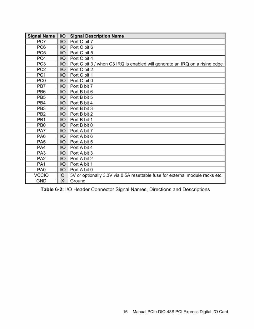
Signal Name I/O Signal Description Name
PC7 I/O Port C bit 7 PC6 I/O Port C bit 6 PC5 I/O Port C bit 5 PC4 I/O Port C bit 4 PC3 I/O Port C bit 3 / when C3 IRQ is enabled will generate an IRQ on a rising edgePC2 I/O Port C bit 2 PC1 I/O Port C bit 1 PC0 I/O Port C bit 0 PB7 I/O Port B bit 7 PB6 I/O Port B bit 6 PB5 I/O Port B bit 5 PB4 I/O Port B bit 4 PB3 I/O Port B bit 3 PB2 I/O Port B bit 2 PB1 I/O Port B bit 1 PB0 I/O Port B bit 0 PA7 I/O Port A bit 7 PA6 I/O Port A bit 6 PA5 I/O Port A bit 5 PA4 I/O Port A bit 4 PA3 I/O Port A bit 3 PA2 I/O Port A bit 2 PA1 I/O Port A bit 1 PA0 I/O Port A bit 0
VCCIO O 5V or optionally 3.3V via 0.5A resettable fuse for external module racks etc.GND X Ground
Table 6-2: I/O Header Connector Signal Names, Directions and Descriptions
Manual PCIe-DIO-48S PCI Express Digital I/O Card 17
Chapter 7: Specifications
VCCIO 5V or optionally 3.3V
Digital Inputs Logic High 2.0V to VCCIO
Logic Low 0V to 0.8V
Current ±20uA (max)
Digital Outputs Logic High 2.0V (min); 32mA source
Logic Low 0.55V (max); 64mA sink
Power Output VCCIO (P2 & P3; pin 49)
Environmental Operating Temperature 0° to 70°C, optional -40° to +85°C
Storage Temperature -55° to +150°C
Humidity 5% to 90% RH, without condensation
Board Dimensions Length - 6.6"; Height - 4.2" (seated)
Manual PCIe-DIO-48S PCI Express Digital I/O Card 18
Customer Comments
If you experience any problems with this manual or just want to give us some feedback, please email us at: [email protected]. Please detail any errors you find and include your mailing address so that we can send you any manual updates.
10623 Roselle Street, San Diego CA 92121
Tel. (858)550-9559 FAX (858)550-7322 www.accesio.com