Embed Size (px)
Citation preview
“Moore’s Law….where next?”
Craig DeYoung Vice President Investor Relations Bank of America Merrill Lynch
2017 Asia Pacific Telecom, Media &Technology Conference
Taipei,Taiwan
22 March 2017
Slide 2
Public
Forward looking statements This document contains statements relating to certain projections and business trends that are forward-looking, including statements with respect to our outlook,
including expected customer demand in specified market segments (and underlying assumptions) including memory, logic and foundry, expected sales levels, trends,
including trends towards 2020 and beyond and expected industry growth, and outlook, systems backlog, expected or indicative market opportunity, financial results and
targets, including, for ASML and ASML and HMI combined, expected sales, other income, gross margin, R&D and SG&A expenses, capital expenditures, cash
conversion cycle, EPS and effective annualized tax rate, annual revenue opportunity and EPS potential by end of decade and growth opportunity beyond 2020 for
ASML and ASML and HMI combined, cost per function reduction and ASML system ASP, goals relating to gross cash balance and ASML’s capital structure, customer,
partner and industry roadmaps, productivity of our tools and systems performance, including EUV system performance (such as endurance tests), expected industry
trends and expected trends in the business environment, the addition of value through delivery of lithography products and the achievement of cost-effective shrink,
expected continued lithography demand and increasing lithography spend, the main drivers of lithography systems, lithography intensity for all market segments,
customer execution of shrink roadmaps, future memory application distribution, expected addressable markets, including the market for lithography systems and service
and options, expected manufacturing and process R&D, statements with respect to growing end markets that require fab capacity driving demand for ASML’s tools,
statements with respect to the acquisition of HMI by ASML, including market opportunity, the expected timing of completion of the HMI acquisition and delisting of HMI,
the expected benefits of the acquisition of HMI by ASML, including expected continuation of year on year growth, the provision of e-beam metrology capability and its
effect on holistic lithography solutions, including the introduction of a new class of pattern fidelity control and the improvement of customers’ control strategy, statements
with respect to EUV, including targets, such as availability, productivity, facilities and shipments, including the number of EUV systems expected to be shipped and
timing of shipments, and roadmaps, shrink being key driver to industry growth, expected industry adoption of EUV and statements with respect to plans of customers to
insert EUV into production and timing, the benefits of EUV, including expected cost reduction and cost-effective shrink, the expected continuation of Moore's law,
without slowing down, and that EUV will continue to enable Moore’s law and drive long term value, goals for holistic lithography, including pattern fidelity control,
expectations relating to double patterning, immersion and dry systems, intention to return excess cash to shareholders, statements about our proposed dividend,
dividend policy and intention to repurchase shares and statements with respect to the current share repurchase plan. You can generally identify these statements by the
use of words like "may", "will", "could", "should", "project", "believe", "anticipate", "expect", "plan", "estimate", "forecast", "potential", "intend", "continue" and variations of
these words or comparable words. These statements are not historical facts, but rather are based on current expectations, estimates, assumptions and projections
about the business and our future financial results and readers should not place undue reliance on them.
Forward-looking statements do not guarantee future performance and involve risks and uncertainties. These risks and uncertainties include, without limitation, economic
conditions, product demand and semiconductor equipment industry capacity, worldwide demand and manufacturing capacity utilization for semiconductors (the principal
product of our customer base), including the impact of general economic conditions on consumer confidence and demand for our customers' products, competitive
products and pricing, the impact of any manufacturing efficiencies and capacity constraints, performance of our systems, the continuing success of technology
advances and the related pace of new product development and customer acceptance of new products including EUV, the number and timing of EUV systems
expected to be shipped and recognized in revenue, delays in EUV systems production and development, our ability to enforce patents and protect intellectual property
rights, the risk of intellectual property litigation, availability of raw materials and critical manufacturing equipment, trade environment, changes in exchange rates,
changes in tax rates, available cash and liquidity, our ability to refinance our indebtedness, distributable reserves for dividend payments and share repurchases and
timing of resumption of the share repurchase plan, and other risks indicated in the risk factors included in ASML's Annual Report on Form 20-F and other filings with the
US Securities and Exchange Commission. These forward-looking statements are made only as of the date of this document. We do not undertake to update or revise
the forward-looking statements, whether as a result of new information, future events or otherwise.
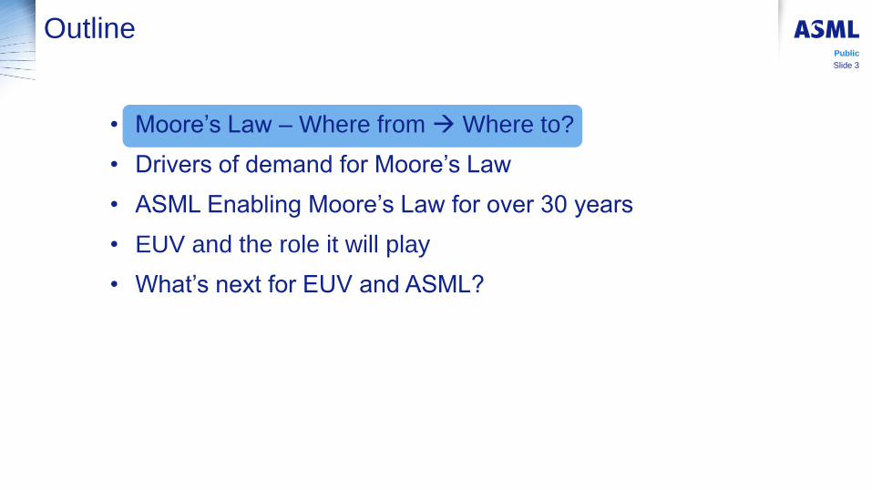
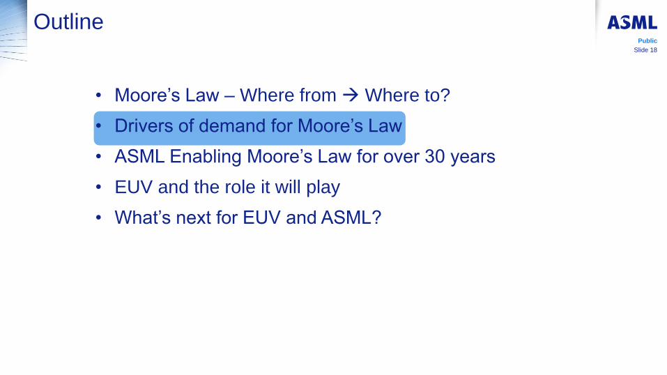
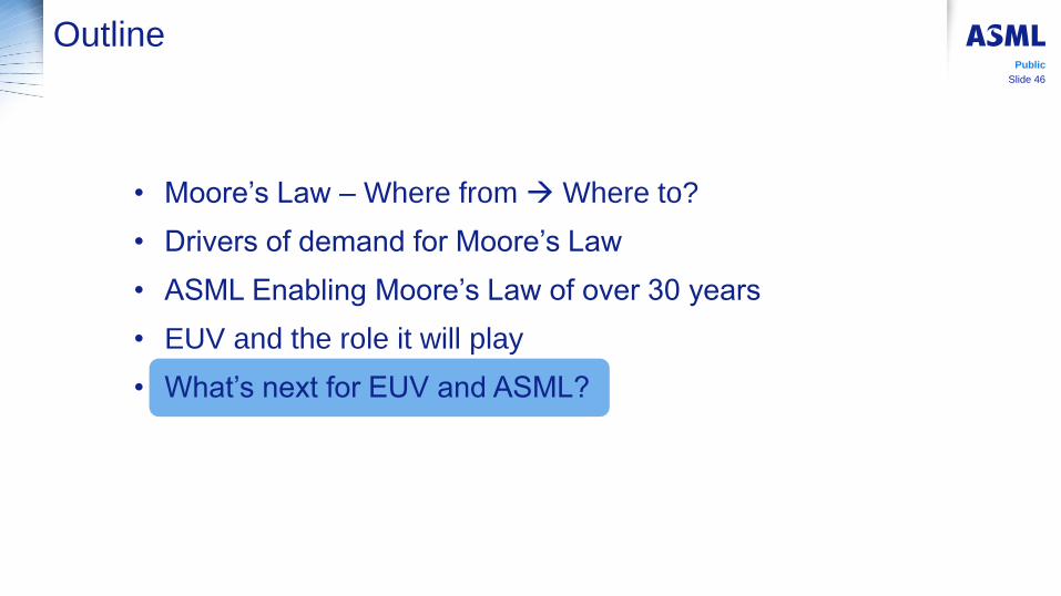
Outline
• Moore’s Law – Where from Where to?
• Drivers of demand for Moore’s Law
• ASML Enabling Moore’s Law for over 30 years
• EUV and the role it will play
• What’s next for EUV and ASML?
Public
Slide 3
Slide 4
Public
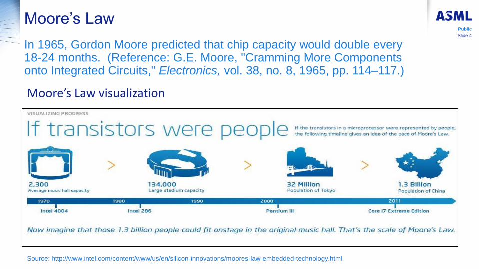
Moore’s Law
In 1965, Gordon Moore predicted that chip capacity would double every 18-24 months. (Reference: G.E. Moore, "Cramming More Components onto Integrated Circuits," Electronics, vol. 38, no. 8, 1965, pp. 114–117.)
Source: http://www.intel.com/content/www/us/en/silicon-innovations/moores-law-embedded-technology.html
Moore’s Law visualization
Public
Slide 5
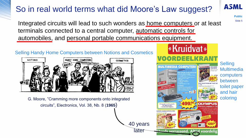
So in real world terms what did Moore’s Law suggest?
Integrated circuits will lead to such wonders as home computers or at least
terminals connected to a central computer, automatic controls for
automobiles, and personal portable communications equipment.
G. Moore, ”Cramming more components onto integrated
circuits”, Electronics, Vol. 38, Nb. 8 (1965)
Selling Handy Home Computers between Notions and Cosmetics
40 years
later
Selling
Multimedia
computers
between
toilet paper
and hair
coloring
1900 1905 1910 1915 1920 1925 1930 1935 1940 1945 1950 1955 1960 1965 1970 1975 1980 1985 1990 1995 2000 2005 2010 2015 2020 2025 2030
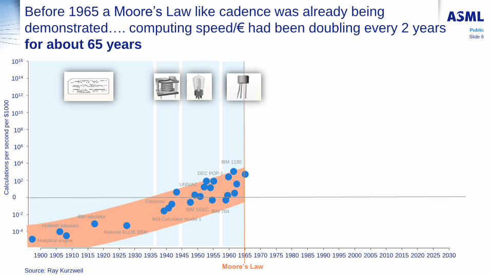
Before 1965 a Moore’s Law like cadence was already being
demonstrated…. computing speed/€ had been doubling every 2 years
for about 65 years
10-4
10-2
0
102
104
106
108
1010
1012
1014
1016
Ca
lcu
latio
ns p
er
se
co
nd
pe
r $
10
00
Analytical engine
Hollerith tabulator
IBM tabulator
National ELLIS 3000
Bell Calculator model 1
Colossus
IBM SSEC
UNIVAC
IBM 704
DEC POP-1
IBM 1130
Moore’s Law Source: Ray Kurzweil
Public
Slide 6
1900 1905 1910 1915 1920 1925 1930 1935 1940 1945 1950 1955 1960 1965 1970 1975 1980 1985 1990 1995 2000 2005 2010 2015 2020 2025 2030
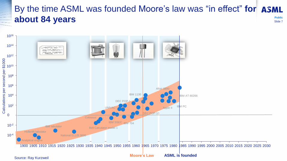
By the time ASML was founded Moore’s law was “in effect” for
about 84 years
10-4
10-2
0
102
104
106
108
1010
1012
1014
1016
Ca
lcu
latio
ns p
er
se
co
nd
pe
r $
10
00
Analytical engine
Hollerith tabulator
IBM tabulator
National ELLIS 3000
Bell Calculator model 1
Colossus
IBM SSEC
UNIVAC
IBM 704
DEC POP-1
IBM 1130
DEC POP-10
Apple II IBM PC
Altair 8800
IBM AT-80266
ASML is founded Source: Ray Kurzweil
Moore’s Law
Public
Slide 7
1900 1905 1910 1915 1920 1925 1930 1935 1940 1945 1950 1955 1960 1965 1970 1975 1980 1985 1990 1995 2000 2005 2010 2015 2020 2025 2030
Slide 8
Public
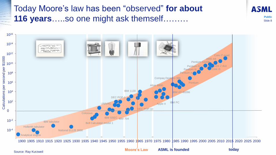
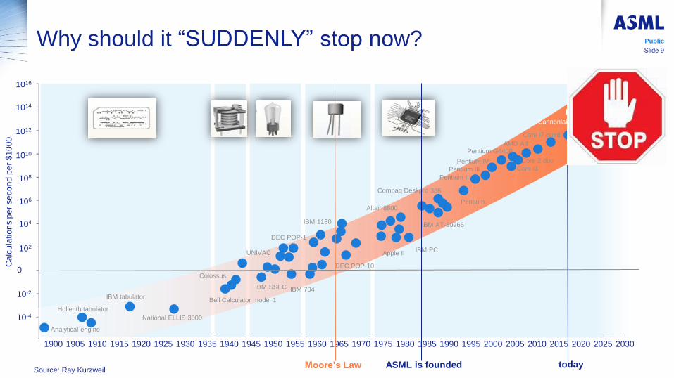
Today Moore’s law has been “observed” for about
116 years…..so one might ask themself………
10-4
10-2
0
102
104
106
108
1010
1012
1014
1016
Ca
lcu
latio
ns p
er
se
co
nd
pe
r $
10
00
Analytical engine
Hollerith tabulator
IBM tabulator
National ELLIS 3000
Bell Calculator model 1
Colossus
IBM SSEC
UNIVAC
IBM 704
DEC POP-1
IBM 1130
DEC POP-10
Apple II IBM PC
Altair 8800
IBM AT-80266
ASML is founded Moore’s Law
Compaq Deskpro 386
Pentium
Pentium II
Pentium III
Pentium IV Core 2 duo
Core i7 quad
today
Pentium G4400
Core i3
AMD A8
Source: Ray Kurzweil
1900 1905 1910 1915 1920 1925 1930 1935 1940 1945 1950 1955 1960 1965 1970 1975 1980 1985 1990 1995 2000 2005 2010 2015 2020 2025 2030
Slide 9
Public Why should it “SUDDENLY” stop now?
10-4
10-2
0
102
104
106
108
1010
1012
1014
1016
Ca
lcu
latio
ns p
er
se
co
nd
pe
r $
10
00
Analytical engine
Hollerith tabulator
IBM tabulator
National ELLIS 3000
Bell Calculator model 1
Colossus
IBM SSEC
UNIVAC
IBM 704
DEC POP-1
IBM 1130
DEC POP-10
Apple II IBM PC
Altair 8800
IBM AT-80266
ASML is founded Moore’s Law
Compaq Deskpro 386
Pentium
Pentium II
Pentium III
Pentium IV Core 2 duo
Core i7 quad
DNA?
Quantum?
today
Neuromorphic?
Pentium G4400
Core i3
AMD A8
Cannonlake
Icelake Kaby Lake
1 nm
transistors?
Source: Ray Kurzweil
Slide 10
Public
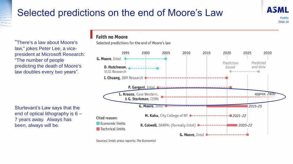
"There's a law about Moore's
law," jokes Peter Lee, a vice-
president at Microsoft Research:
"The number of people
predicting the death of Moore's
law doubles every two years”.
Selected predictions on the end of Moore’s Law
Sturtevant’s Law says that the
end of optical lithography is 6 –
7 years away. Always has
been, always will be.
Slide 11
Public Astrophysicists Krauss and Starkman on Moore’s Law
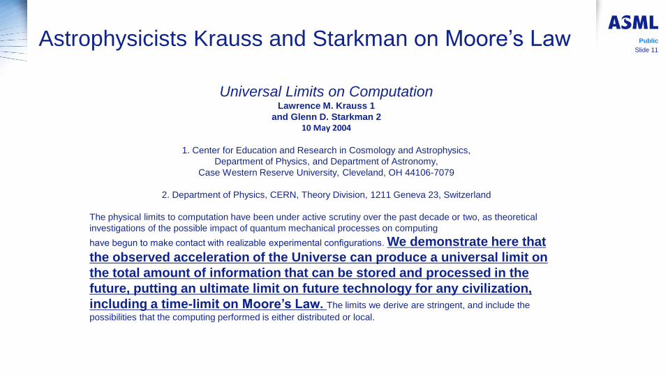
Universal Limits on Computation Lawrence M. Krauss 1
and Glenn D. Starkman 2 10 May 2004
1. Center for Education and Research in Cosmology and Astrophysics,
Department of Physics, and Department of Astronomy,
Case Western Reserve University, Cleveland, OH 44106-7079
2. Department of Physics, CERN, Theory Division, 1211 Geneva 23, Switzerland
The physical limits to computation have been under active scrutiny over the past decade or two, as theoretical
investigations of the possible impact of quantum mechanical processes on computing
have begun to make contact with realizable experimental configurations. We demonstrate here that
the observed acceleration of the Universe can produce a universal limit on
the total amount of information that can be stored and processed in the
future, putting an ultimate limit on future technology for any civilization,
including a time-limit on Moore’s Law. The limits we derive are stringent, and include the
possibilities that the computing performed is either distributed or local.

Slide 12
Public
After many unrecognizable calculations to most of
us……………….
Slide 13
Public
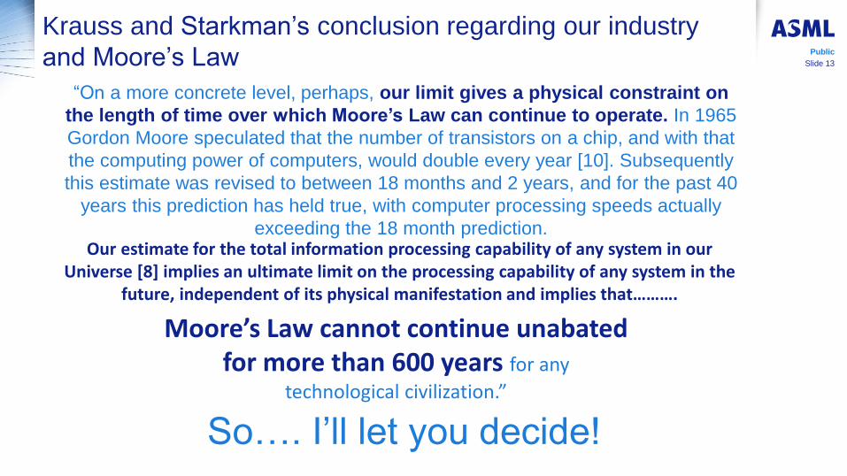
Krauss and Starkman’s conclusion regarding our industry
and Moore’s Law
“On a more concrete level, perhaps, our limit gives a physical constraint on
the length of time over which Moore’s Law can continue to operate. In 1965
Gordon Moore speculated that the number of transistors on a chip, and with that
the computing power of computers, would double every year [10]. Subsequently
this estimate was revised to between 18 months and 2 years, and for the past 40
years this prediction has held true, with computer processing speeds actually
exceeding the 18 month prediction.
So…. I’ll let you decide!
Moore’s Law cannot continue unabated for more than 600 years for any
technological civilization.”
Our estimate for the total information processing capability of any system in our Universe [8] implies an ultimate limit on the processing capability of any system in the
future, independent of its physical manifestation and implies that……….
1900 1905 1910 1915 1920 1925 1930 1935 1940 1945 1950 1955 1960 1965 1970 1975 1980 1985 1990 1995 2000 2005 2010 2015 2020 2025 2030
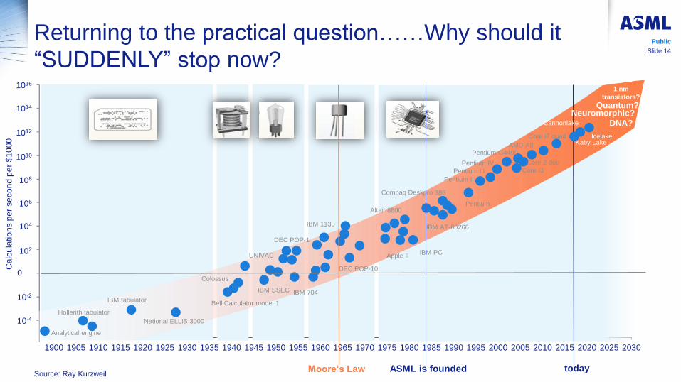
Slide 14
Public Returning to the practical question……Why should it
“SUDDENLY” stop now?
10-4
10-2
0
102
104
106
108
1010
1012
1014
1016
Ca
lcu
latio
ns p
er
se
co
nd
pe
r $
10
00
Analytical engine
Hollerith tabulator
IBM tabulator
National ELLIS 3000
Bell Calculator model 1
Colossus
IBM SSEC
UNIVAC
IBM 704
DEC POP-1
IBM 1130
DEC POP-10
Apple II IBM PC
Altair 8800
IBM AT-80266
ASML is founded Moore’s Law
Compaq Deskpro 386
Pentium
Pentium II
Pentium III
Pentium IV Core 2 duo
Core i7 quad
DNA?
Quantum?
today
Neuromorphic?
Pentium G4400
Core i3
AMD A8
Cannonlake
Icelake Kaby Lake
1 nm
transistors?
Source: Ray Kurzweil
Slide 15
Public
10-4
10-2
0
102
104
106
108
1010
1012
1014
1016
Ca
lcu
latio
ns p
er
se
co
nd
pe
r $
10
00
Analytical engine
Hollerith tabulator
IBM tabulator
National ELLIS 3000
Bell Calculator model 1
Colossus
IBM SSEC
UNIVAC
IBM 704
DEC POP-1
IBM 1130
DEC POP-10
Apple II IBM PC
Altair 8800
IBM AT-80266
ASML is founded Moore’s Law
Compaq Deskpro 386
Pentium
Pentium II
Pentium III
Pentium IV Core 2 duo
Core i7 quad
DNA?
Quantum?
today
Neuromorphic?
Pentium G4400
Core i3
AMD A8
Cannonlake
Icelake Kaby Lake
1 nm
transistors?
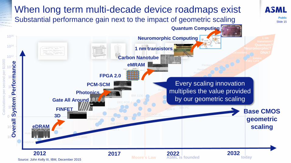
When long term multi-decade device roadmaps exist Substantial performance gain next to the impact of geometric scaling
FPGA 2.0
Source: John Kelly III, IBM, December 2015
Ove
rall
Sys
tem
Pe
rfo
rma
nc
e
eDRAM
3D
Photonics
PCM-SCM
Base CMOS
geometric
scaling
2012 2017 2022 2032
FINFET
eMRAM
Carbon Nanotube
Neuromorphic Computing
Gate All Around
Every scaling innovation
multiplies the value provided
by our geometric scaling
Q1
Q2
Q3
Quantum Computing
1 nm transistors
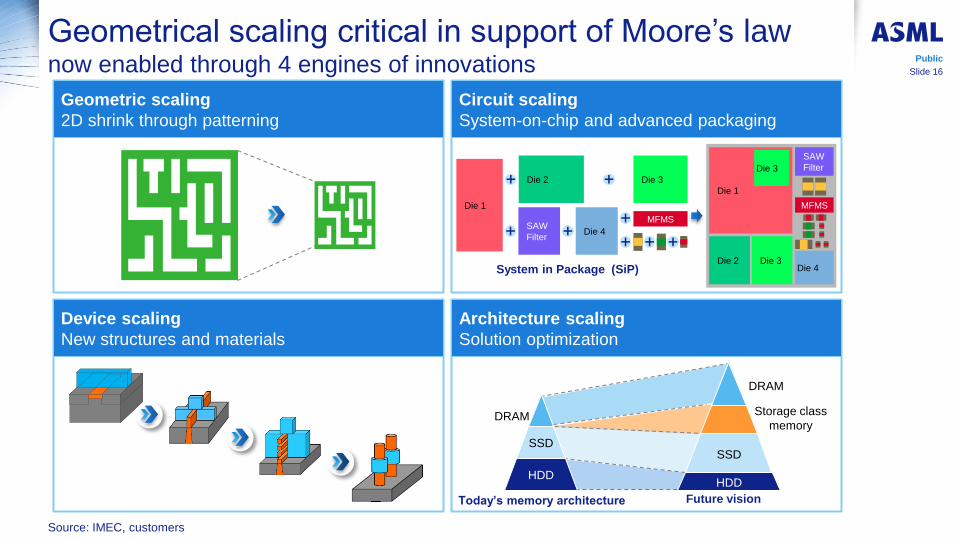
Geometrical scaling critical in support of Moore’s law now enabled through 4 engines of innovations
Source: IMEC, customers
Public
Slide 16
Today’s memory architecture Future vision
DRAM
SSD
HDD
DRAM
Storage class
memory
SSD
HDD
Circuit scaling
System-on-chip and advanced packaging
Device scaling
New structures and materials
Architecture scaling
Solution optimization
Geometric scaling
2D shrink through patterning
System in Package (SiP)
Die 1
Die 2
SAW
Filter Die 4
Die 3
MFMS
Die 1
Die 2 Die 3
SAW
Filter
MFMS
Die 4
Die 3
Slide 17
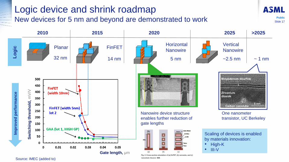
Public
Logic device and shrink roadmap New devices for 5 nm and beyond are demonstrated to work
Source: IMEC (added to)
Sw
itch
ing
th
resh
old
, m
V/V
2010 2015 2020 2025
Lo
gic
Nanowire device structure
enables further reduction of
gate lengths
Scaling of devices is enabled
by materials innovation:
• High-K
• III-V
Imp
rov
ed
perf
orm
an
ce
Gate length, μm
Planar
32 nm
FinFET
14 nm
Horizontal
Nanowire
5 nm
Vertical
Nanowire
~2.5 nm ~ 1 nm
>2025
One nanometer
transistor, UC Berkeley
• Moore’s Law – Where from Where to?
• Drivers of demand for Moore’s Law
• ASML Enabling Moore’s Law for over 30 years
• EUV and the role it will play
• What’s next for EUV and ASML?
Outline Public
Slide 18
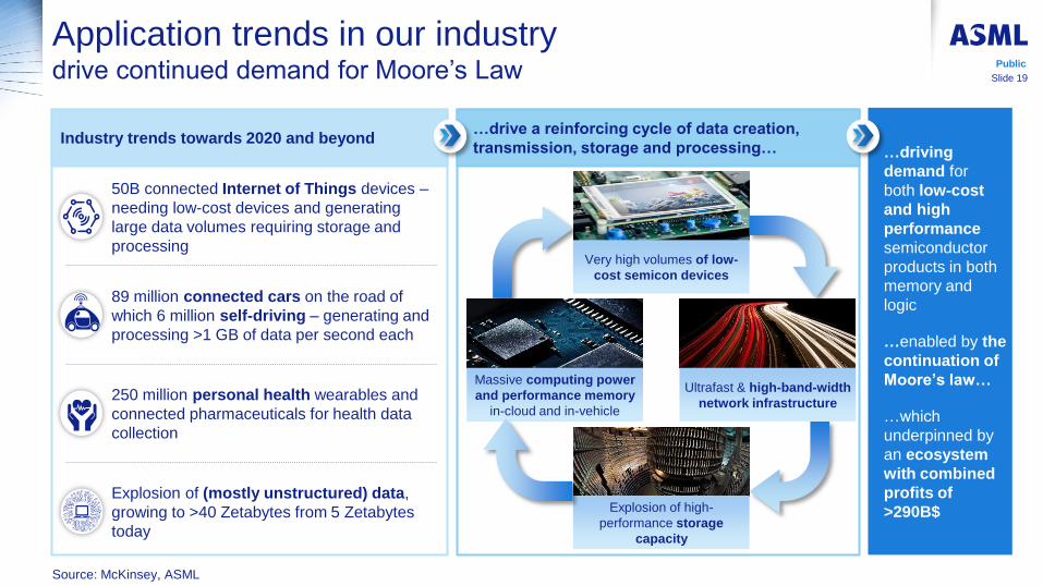
Application trends in our industry drive continued demand for Moore’s Law
…drive a reinforcing cycle of data creation,
transmission, storage and processing…
Ultrafast & high-band-width
network infrastructure
Very high volumes of low-
cost semicon devices
Explosion of high-
performance storage
capacity
Massive computing power
and performance memory
in-cloud and in-vehicle
Industry trends towards 2020 and beyond
50B connected Internet of Things devices –
needing low-cost devices and generating
large data volumes requiring storage and
processing
89 million connected cars on the road of
which 6 million self-driving – generating and
processing >1 GB of data per second each
250 million personal health wearables and
connected pharmaceuticals for health data
collection
Explosion of (mostly unstructured) data,
growing to >40 Zetabytes from 5 Zetabytes
today
…driving
demand for
both low-cost
and high
performance
semiconductor
products in both
memory and
logic
…enabled by the
continuation of
Moore’s law…
…which
underpinned by
an ecosystem
with combined
profits of
>290B$
Source: McKinsey, ASML
Public
Slide 19
We operate in a highly profitable value chain
with strong incentives to compete and drive innovation
Top technology companies in our ecosystem (EBIT 2015, B$), source: S&P Capital IQ
Semi
Manufacturers
Semi
Design
Software &
Services
Hardware
Semi
Equipment
ASML (2)
Non-semi
Lam (1) TEL (1) KLA (1) AMAT (2)
Nete
ase
eB
ay
Seagate
T
oshib
a
Baid
u
(16)
(71) (3)
(4)
(3)
(3)
(7) (5)
(14)
(12)
(22) (7)
(10)
(14) (19) (28)
(5) (4)
(8) (5)
(6)
2014
~290 ~275 ~250
The ecosystem
continues to grow
Total EBIT, B$
(5) (1) (2) (2)
(1) (1)
®
(2)
NX
P
(2)
2013 2015
Semi
Public
Slide 20
$290B
Slide 21
Public
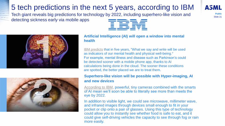
5 tech predictions in the next 5 years, according to IBM
Superhero-like vision will be possible with Hyper-imaging, AI
and new devices
According to IBM, powerful, tiny cameras combined with the smarts of AI mean we’ll soon be able to literally see more than meets the eye by 2022.
In addition to visible light, we could see microwave, millimeter wave, and infrared images through devices small enough to fit in your pocket or clip onto a pair of glasses. Using this type of technology could allow you to instantly see whether food is safe to eat, and it could give self-driving vehicles the capacity to see through fog or rain more easily.
Tech giant reveals big predictions for technology by 2022, including superhero-like vision and
detecting sickness early via mobile apps
Artificial Intelligence (AI) will open a window into mental
health
IBM predicts that in five years, "What we say and write will be used
as indicators of our mental health and physical well-being.“ For example, mental illness and disease such as Parkinson’s could
be detected sooner with a mobile phone app, thanks to AI
calculations being done in the cloud. The sooner these conditions
are spotted, the better placed we are to treat them.
Slide 22
Public
5 tech predictions in the next 5 years, according to IBM
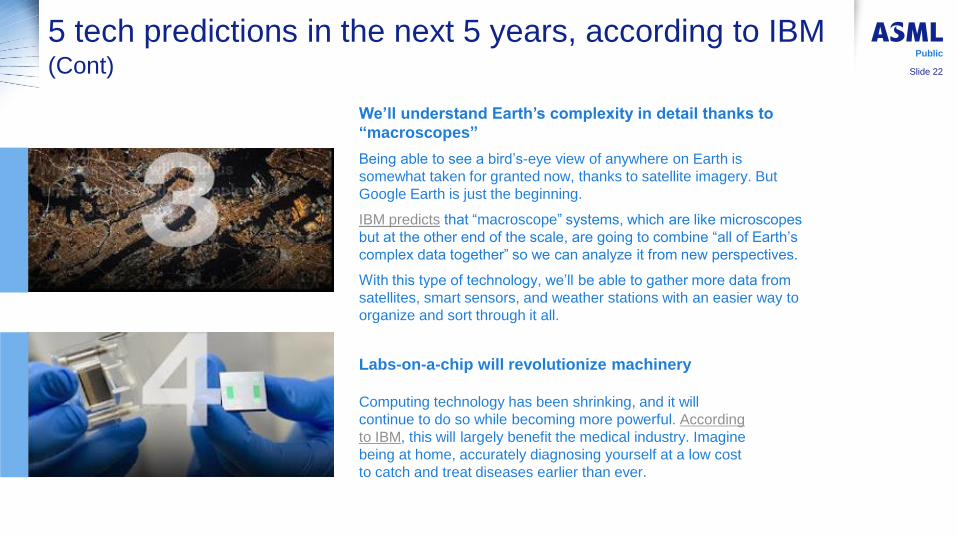
We’ll understand Earth’s complexity in detail thanks to
“macroscopes”
Being able to see a bird’s-eye view of anywhere on Earth is
somewhat taken for granted now, thanks to satellite imagery. But
Google Earth is just the beginning.
IBM predicts that “macroscope” systems, which are like microscopes
but at the other end of the scale, are going to combine “all of Earth’s
complex data together” so we can analyze it from new perspectives.
With this type of technology, we’ll be able to gather more data from
satellites, smart sensors, and weather stations with an easier way to
organize and sort through it all.
(Cont)
Labs-on-a-chip will revolutionize machinery
Computing technology has been shrinking, and it will
continue to do so while becoming more powerful. According
to IBM, this will largely benefit the medical industry. Imagine
being at home, accurately diagnosing yourself at a low cost
to catch and treat diseases earlier than ever.
Slide 23
Public
5 tech predictions in the next 5 years, according to IBM
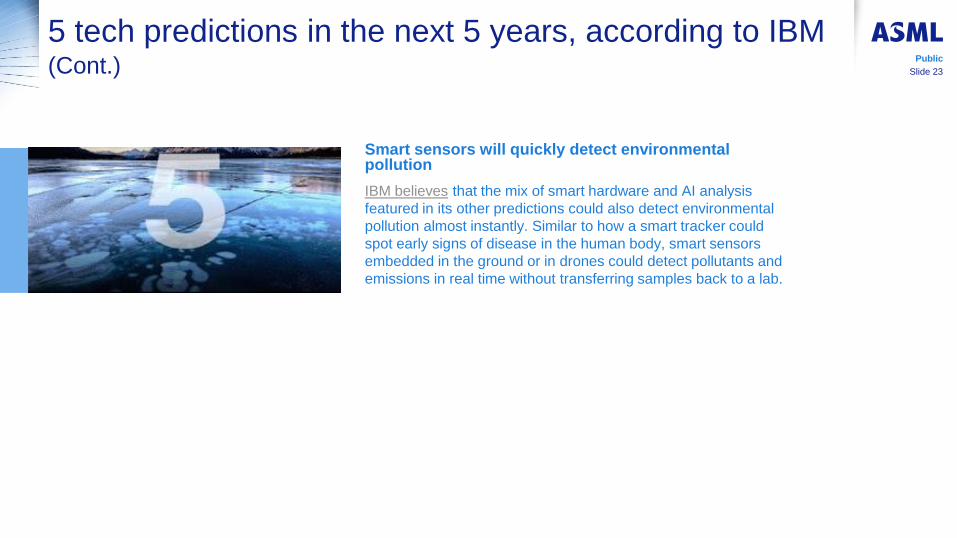
Smart sensors will quickly detect environmental pollution
IBM believes that the mix of smart hardware and AI analysis
featured in its other predictions could also detect environmental
pollution almost instantly. Similar to how a smart tracker could
spot early signs of disease in the human body, smart sensors
embedded in the ground or in drones could detect pollutants and
emissions in real time without transferring samples back to a lab.
(Cont.)
Slide 24
Public Huge Growth in Cloud Changes Semiconductor Supply Chain By Paula Doe, SEMI
Solid State Technology
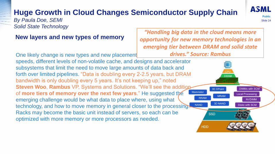
One likely change is new types and new placement for memory, for higher
speeds, different levels of non-volatile cache, and designs and accelerator
subsystems that limit the need to move large amounts of data back and
forth over limited pipelines. “Data is doubling every 2-2.5 years, but DRAM
bandwidth is only doubling every 5 years. It’s not keeping up,” noted
Steven Woo, Rambus VP, Systems and Solutions. “We’ll see the addition
of more tiers of memory over the next few years.” He suggested the
emerging challenge would be what data to place where, using what
technology, and how to move memory in general closer to the processing.
Racks may become the basic unit instead of servers, so each can be
optimized with more memory or more processors as needed.
“Handling big data in the cloud means more opportunity for new memory technologies in an
emerging tier between DRAM and solid state drives.” Source: Rambus
New layers and new types of memory
Slide 25
Public
Large innovation ongoing in memory, driving continued litho demand
1ms
1 µs
1ns
Ac
ce
ss
tim
e
0.01 0. 1 1 10
NAND
DRAM
STT-MRAM
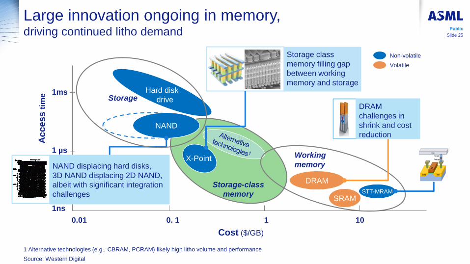
Storage
Storage-class
memory
Working
memory
Cost ($/GB)
X-Point
Hard disk
drive
Non-volatile
Volatile
SRAM
Source: Western Digital
NAND displacing hard disks,
3D NAND displacing 2D NAND,
albeit with significant integration
challenges
Storage class
memory filling gap
between working
memory and storage
1 Alternative technologies (e.g., CBRAM, PCRAM) likely high litho volume and performance
DRAM
challenges in
shrink and cost
reduction
Slide 26
Public
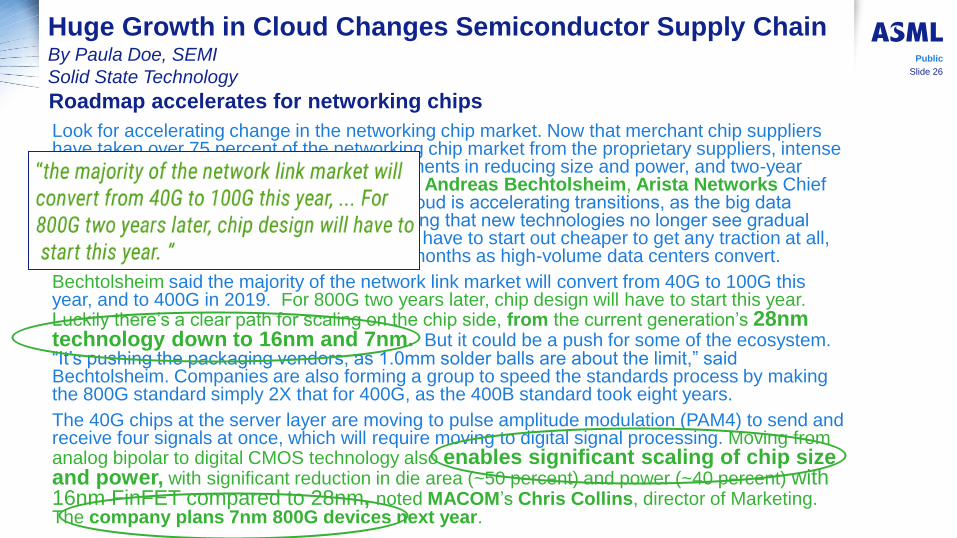
Huge Growth in Cloud Changes Semiconductor Supply Chain By Paula Doe, SEMI
Solid State Technology
Look for accelerating change in the networking chip market. Now that merchant chip suppliers have taken over 75 percent of the networking chip market from the proprietary suppliers, intense competition has meant astonishing improvements in reducing size and power, and two-year technology cycles, reported keynote speaker Andreas Bechtolsheim, Arista Networks Chief Development Officer and Chairman. “The cloud is accelerating transitions, as the big data centers demand low cost,” he noted, explaining that new technologies no longer see gradual adoption through different applications. They have to start out cheaper to get any traction at all, but then ramp sharply to high volume in six months as high-volume data centers convert.
Bechtolsheim said the majority of the network link market will convert from 40G to 100G this year, and to 400G in 2019. For 800G two years later, chip design will have to start this year. Luckily there’s a clear path for scaling on the chip side, from the current generation’s 28nm technology down to 16nm and 7nm. But it could be a push for some of the ecosystem. “It’s pushing the packaging vendors, as 1.0mm solder balls are about the limit,” said Bechtolsheim. Companies are also forming a group to speed the standards process by making the 800G standard simply 2X that for 400G, as the 400B standard took eight years.
The 40G chips at the server layer are moving to pulse amplitude modulation (PAM4) to send and receive four signals at once, which will require moving to digital signal processing. Moving from analog bipolar to digital CMOS technology also enables significant scaling of chip size and power, with significant reduction in die area (~50 percent) and power (~40 percent) with 16nm FinFET compared to 28nm, noted MACOM’s Chris Collins, director of Marketing. The company plans 7nm 800G devices next year.
Roadmap accelerates for networking chips
Slide 27
Public
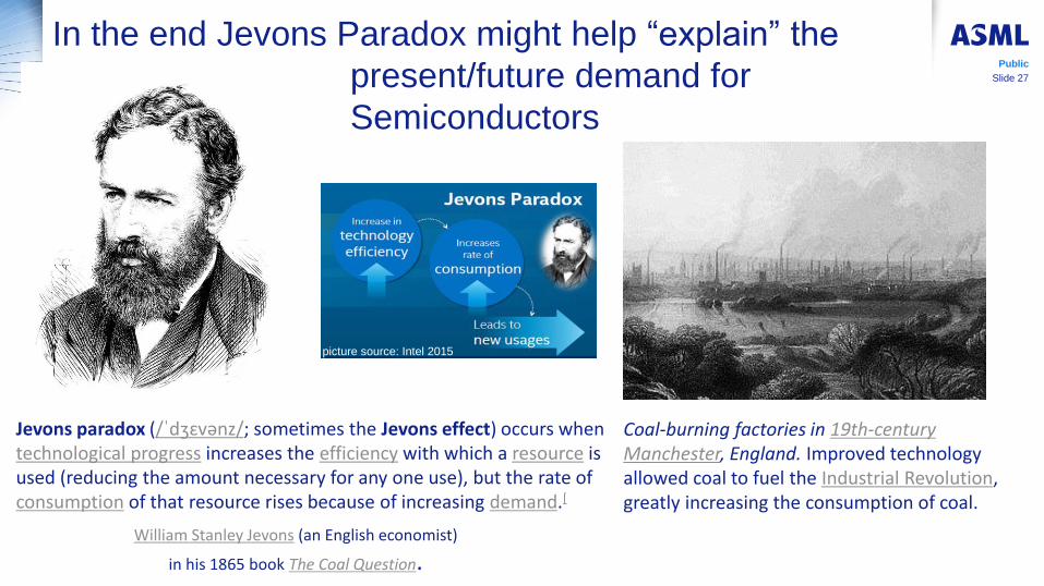
In the end Jevons Paradox might help “explain” the
present/future demand for
Semiconductors
Coal-burning factories in 19th-century Manchester, England. Improved technology allowed coal to fuel the Industrial Revolution, greatly increasing the consumption of coal.
Jevons paradox (/ˈdʒɛvənz/; sometimes the Jevons effect) occurs when technological progress increases the efficiency with which a resource is used (reducing the amount necessary for any one use), but the rate of consumption of that resource rises because of increasing demand.[
picture source: Intel 2015
William Stanley Jevons (an English economist)
in his 1865 book The Coal Question.
Outline
• Moore’s Law – Where from Where to?
• Drivers of demand for Moore’s Law
• ASML Enabling Moore’s Law for over 30 years
• EUV and the role it will play
• What’s next for EUV and ASML?
Public
Slide 28
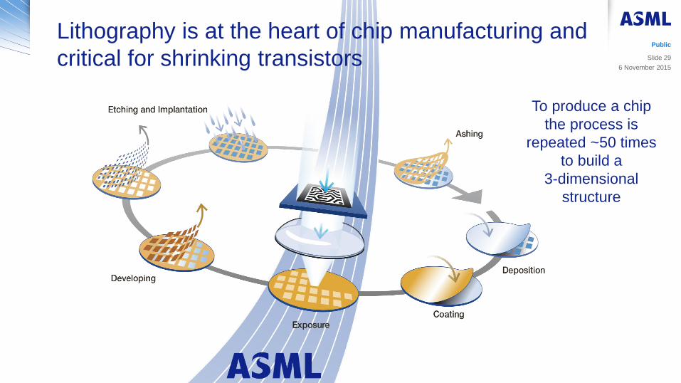
Lithography is at the heart of chip manufacturing and
critical for shrinking transistors
To produce a chip
the process is
repeated ~50 times
to build a
3-dimensional
structure
Public
6 November 2015
Slide 29
Slide 30
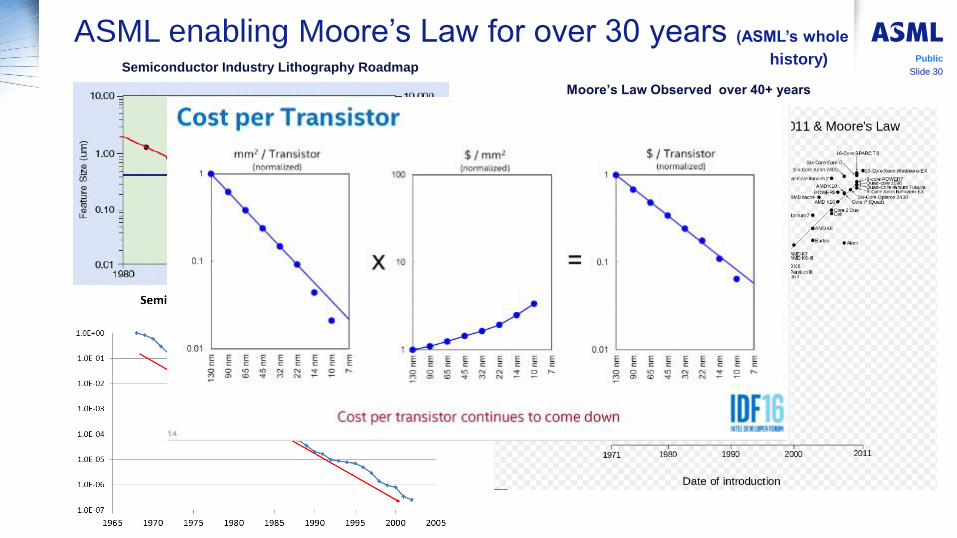
Public
ASML enabling Moore’s Law for over 30 years (ASML’s whole
history) Semiconductor Industry Lithography Roadmap
Moore’s Law Observed over 40+ years
Slide 31
Public
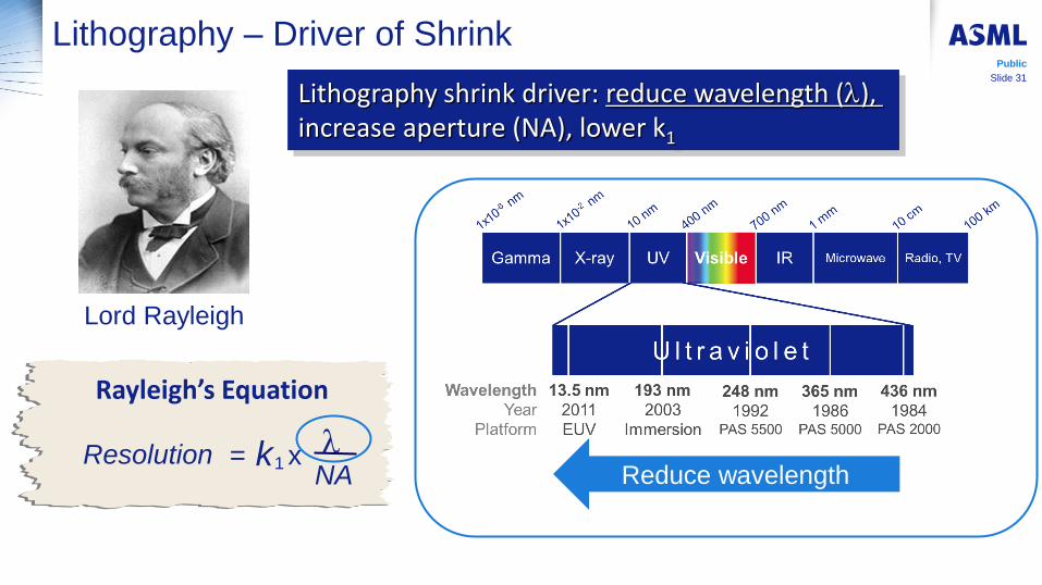
Lithography – Driver of Shrink
Lord Rayleigh
Lithography shrink driver: reduce wavelength (l), increase aperture (NA), lower k1
Rayleigh’s Equation
NA k Resolution x 1 = l
Reduce wavelength
Slide 32
Public
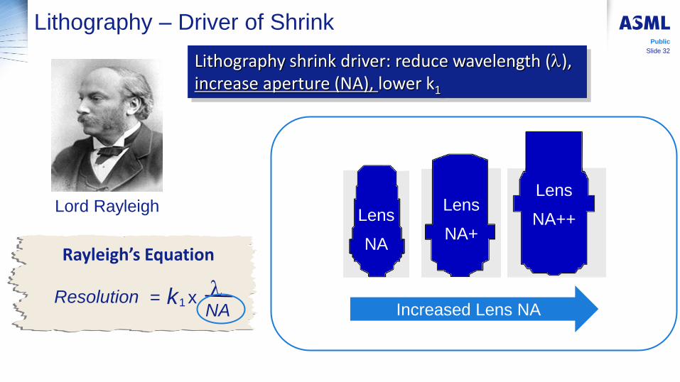
Lithography – Driver of Shrink
Lord Rayleigh
Lithography shrink driver: reduce wavelength (l), increase aperture (NA), lower k1
Rayleigh’s Equation
NA k Resolution x 1 = l
Increased Lens NA
Lens
NA
Lens
NA+
Lens
NA++
Slide 33
Public
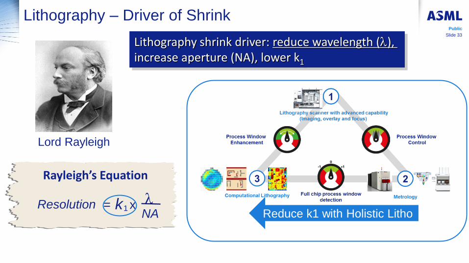
Lithography – Driver of Shrink
Lord Rayleigh
Lithography shrink driver: reduce wavelength (l), increase aperture (NA), lower k1
Rayleigh’s Equation
NA k Resolution x 1 = l
Reduce k1 with Holistic Litho
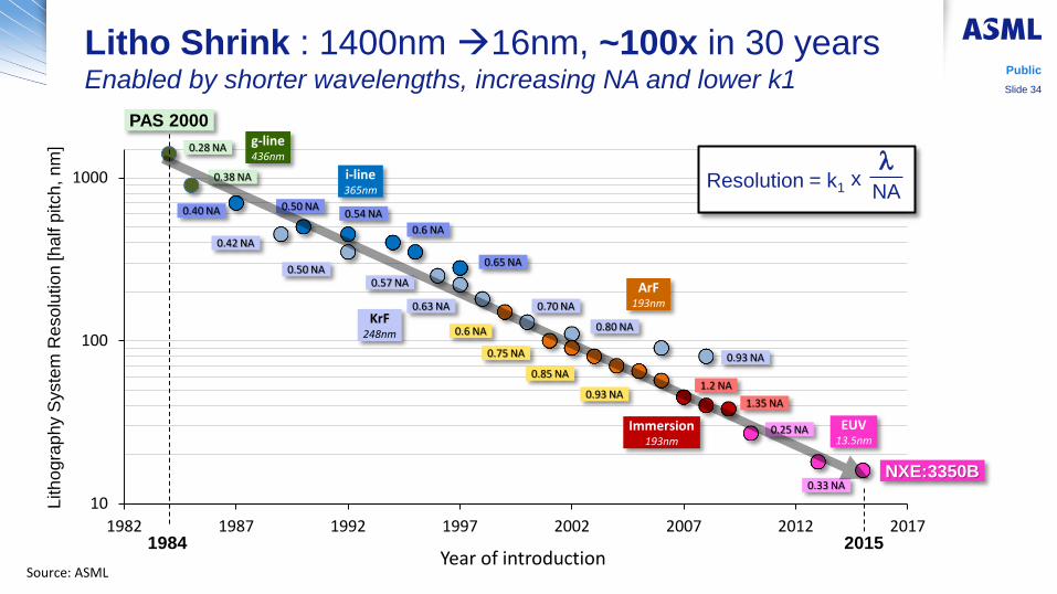
Litho Shrink : 1400nm 16nm, ~100x in 30 years Enabled by shorter wavelengths, increasing NA and lower k1
Public
Slide 34
10
100
1000
1982 1987 1992 1997 2002 2007 2012 2017
0.28 NA
0.38 NA
0.40 NA
0.65 NA
0.42 NA
0.50 NA 0.57 NA
0.93 NA
0.80 NA
0.63 NA 0.70 NA
0.6 NA
0.54 NA 0.50 NA
0.25 NA
0.33 NA
1.35 NA
1.2 NA
0.6 NA
0.75 NA
0.85 NA
0.93 NA
g-line 436nm
i-line 365nm
KrF 248nm
ArF 193nm
Immersion 193nm
EUV 13.5nm
Resolution = k1 NA x
l
Lith
ogra
phy S
yste
m R
eso
lution [h
alf p
itch
, n
m]
1984
PAS 2000
2015
NXE:3350B
Year of introduction Source: ASML
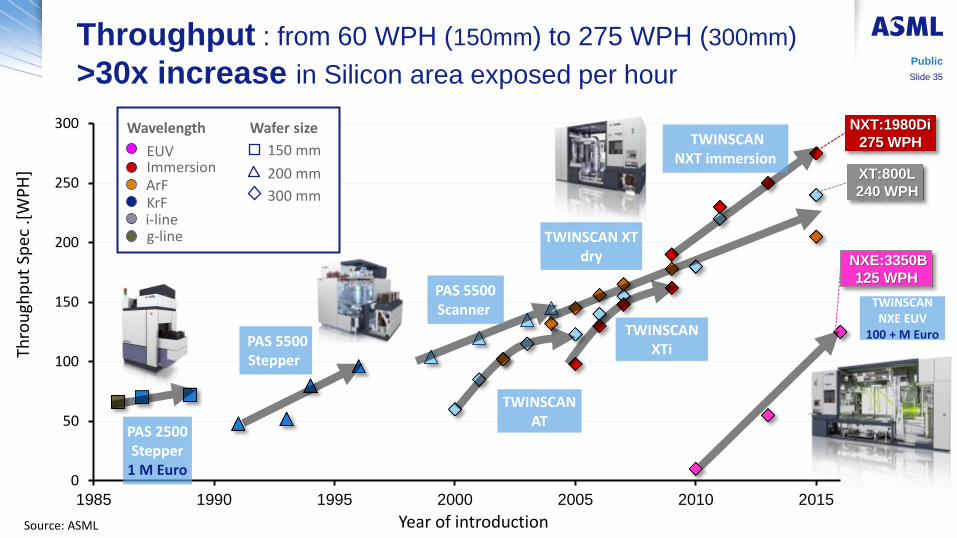
0
50
100
150
200
250
300
1985 1990 1995 2000 2005 2010 2015
Throughput : from 60 WPH (150mm) to 275 WPH (300mm)
>30x increase in Silicon area exposed per hour
g-line i-line KrF ArF Immersion
150 mm
200 mm
300 mm
EUV
Wavelength Wafer size
Year of introduction
Thro
ugh
pu
t Sp
ec .[
WP
H]
PAS 5500 Stepper
PAS 2500 Stepper
1 M Euro
PAS 5500 Scanner
TWINSCAN XTi
TWINSCAN NXT immersion
TWINSCAN NXE EUV
100 + M Euro
Source: ASML
TWINSCAN AT
TWINSCAN XT dry
Public
Slide 35
NXT:1980Di
275 WPH
XT:800L
240 WPH
NXE:3350B
125 WPH
Outline
• Moore’s Law – Where from Where to?
• Drivers of demand for Moore’s Law
• ASML Enabling Moore’s Law of over 30 years
• EUV and the role it will play
• What’s next for EUV and ASML?
Public
Slide 36
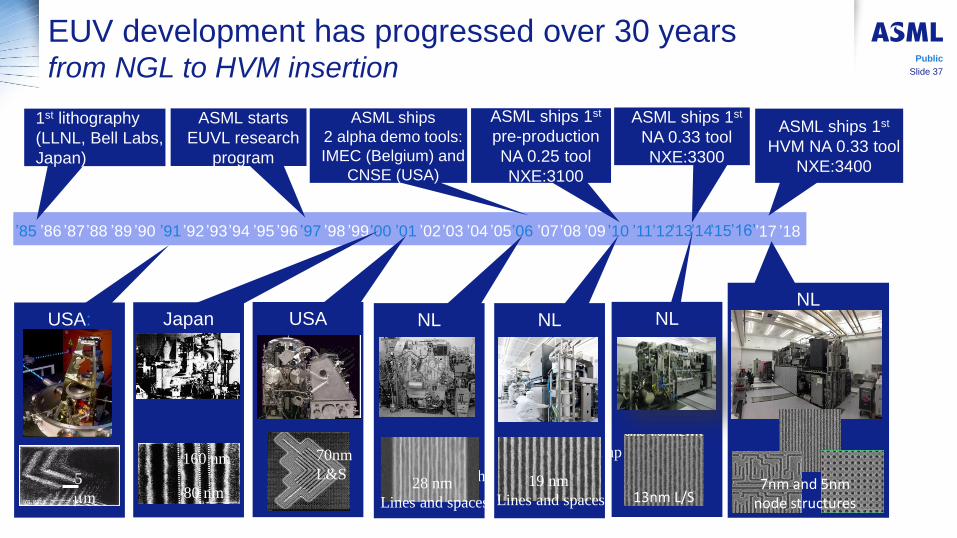
EUV development has progressed over 30 years from NGL to HVM insertion
Public
Slide 37
NL NL NL
’84 ’85 ’91 ’97 ’00 ’01 ’06 ’10 ’86 ’87 ’88 ’89 ’90 ’92 ’93 ’94 ’95 ’96 ’98 ’99 ’02 ’03 ’04 ’05 ’07 ’08 ’09 ’11 ’12 ’13 ’14 ’15
1st lithography
(LLNL, Bell Labs,
Japan)
USA
40 nm hp
70nm
L&S
Japan
80 nm
160 nm 40 nm hp 28 nm
Lines and spaces
40 nm hp
19 nm
Lines and spaces
USA:
5
mm
ASML starts
EUVL research
program
ASML ships
2 alpha demo tools:
IMEC (Belgium) and
CNSE (USA)
ASML ships 1st
pre-production
NA 0.25 tool
NXE:3100
ASML ships 1st
NA 0.33 tool
NXE:3300
13nm L/S
’16’
NL
’17 ’18
ASML ships 1st
HVM NA 0.33 tool
NXE:3400
7nm and 5nm node structures
Public
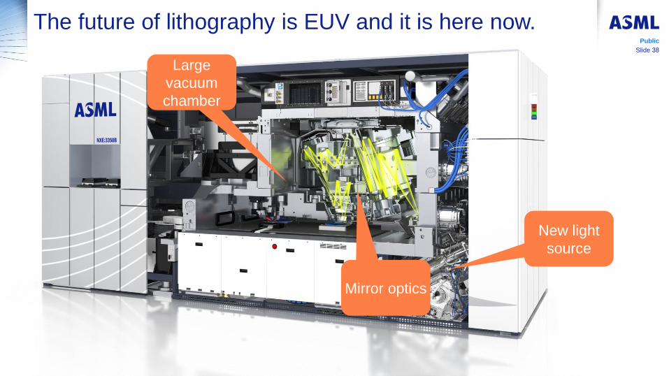
The future of lithography is EUV and it is here now.
Large
vacuum
chamber
Mirror optics
New light
source
Slide 38
Slide 39
Public
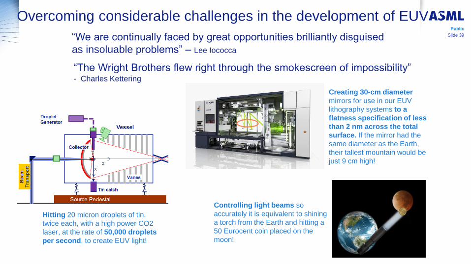
“We are continually faced by great opportunities brilliantly disguised
as insoluable problems” – Lee Iococca
Creating 30-cm diameter
mirrors for use in our EUV
lithography systems to a
flatness specification of less
than 2 nm across the total
surface. If the mirror had the
same diameter as the Earth,
their tallest mountain would be
just 9 cm high!
Controlling light beams so
accurately it is equivalent to shining
a torch from the Earth and hitting a
50 Eurocent coin placed on the
moon!
Hitting 20 micron droplets of tin,
twice each, with a high power CO2
laser, at the rate of 50,000 droplets
per second, to create EUV light!
Overcoming considerable challenges in the development of EUV
“The Wright Brothers flew right through the smokescreen of impossibility” - Charles Kettering
Slide 40
Public
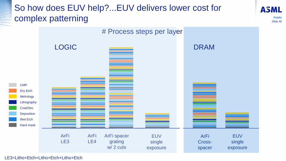
So how does EUV help?...EUV delivers lower cost for
complex patterning
# Process steps per layer
ArFi
LE3 ArFi
Cross-
spacer
CMP
Dry Etch
Metrology
Coat/Dev
Deposition
Hard mask
Wet Etch
Lithography
ArFi spacer
grating
w/ 2 cuts
EUV
single
exposure
ArFi
LE4 EUV
single
exposure
LOGIC
DRAM
LE3=Litho+Etch+Litho+Etch+Litho+Etch
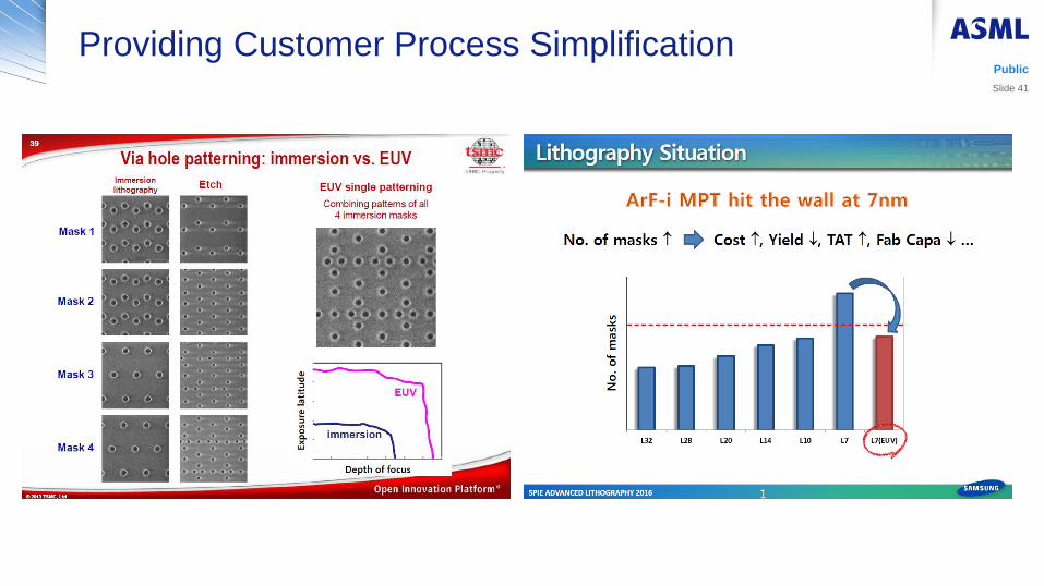
Providing Customer Process Simplification
Public
Slide 41
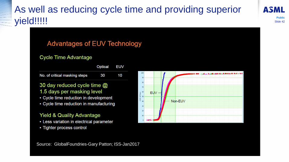
Slide 42
Public
As well as reducing cycle time and providing superior
yield!!!!!
Source: GlobalFoundries-Gary Patton; ISS-Jan2017
EUV Production
Insertion Window
2014 2015 2016 2017 2018 2019 2020 2021 2022
>x200 >x192 >x128
Planar Floating Gate NAND
>x96
Sto
rag
e
Me
mo
ry 14-15
3D NAND
x64
17-18 22
x48 x32 x24
Slide 43
Public
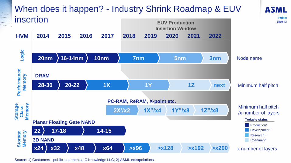
When does it happen? - Industry Shrink Roadmap & EUV
insertion
HVM
Production1
Research1
Development1
Roadmap2
Today’s status
x number of layers
3nm 5nm 7nm 10nm 16-14nm 20nm Lo
gic
P
erf
orm
an
ce
Me
mo
ry
Public
Slide 43
Source: 1) Customers - public statements, IC Knowledge LLC; 2) ASML extrapolations
Sto
rag
e
Cla
ss
Me
mo
ry
next 1Z 1Y 1X 20-22 28-30
DRAM
1Z”/x8 1Y”/x8
PC-RAM, ReRAM, X-point etc.
1X”/x4 2X’/x2
Node name
Minimum half pitch
Minimum half pitch
/x number of layers
44
1%
10%
100%
2004 2006 2008 2010 2012 2014 2016 2018 2020 2022 2024
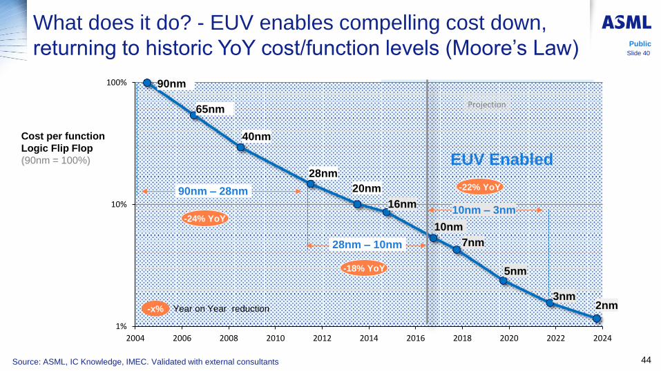
What does it do? - EUV enables compelling cost down,
returning to historic YoY cost/function levels (Moore’s Law)
-x% Year on Year reduction
40nm
28nm
10nm
20nm
Cost per function
Logic Flip Flop
(90nm = 100%)
65nm
90nm
16nm
7nm
5nm
Source: ASML, IC Knowledge, IMEC. Validated with external consultants
Public
Slide 40
3nm 2nm
-24% YoY
-18% YoY
-22% YoY 90nm – 28nm
28nm – 10nm
10nm – 3nm
Projection
EUV Enabled
Slide 45
Public
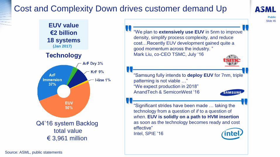
Cost and Complexity Down drives customer demand Up
Source: ASML, public statements
50% 34%
“We plan to extensively use EUV in 5nm to improve
density, simplify process complexity, and reduce
cost…Recently EUV development gained quite a
good momentum across the industry. ”
Mark Liu, co-CEO TSMC, July ‘16
“Samsung fully intends to deploy EUV for 7nm, triple
patterning is not viable …”
“We expect production in 2018”
AnandTech & SemiconWest ‘16
“Significant strides have been made … taking the
technology from a question of if to a question of
when. EUV is solidly on a path to HVM insertion
as soon as the technology becomes ready and cost
effective”
Intel, SPIE ‘16
EUV value
€2 billion
18 systems (Jan 2017)
Q4’16 system Backlog
total value
€ 3,961 million
Outline
• Moore’s Law – Where from Where to?
• Drivers of demand for Moore’s Law
• ASML Enabling Moore’s Law of over 30 years
• EUV and the role it will play
• What’s next for EUV and ASML?
Public
Slide 46
Public
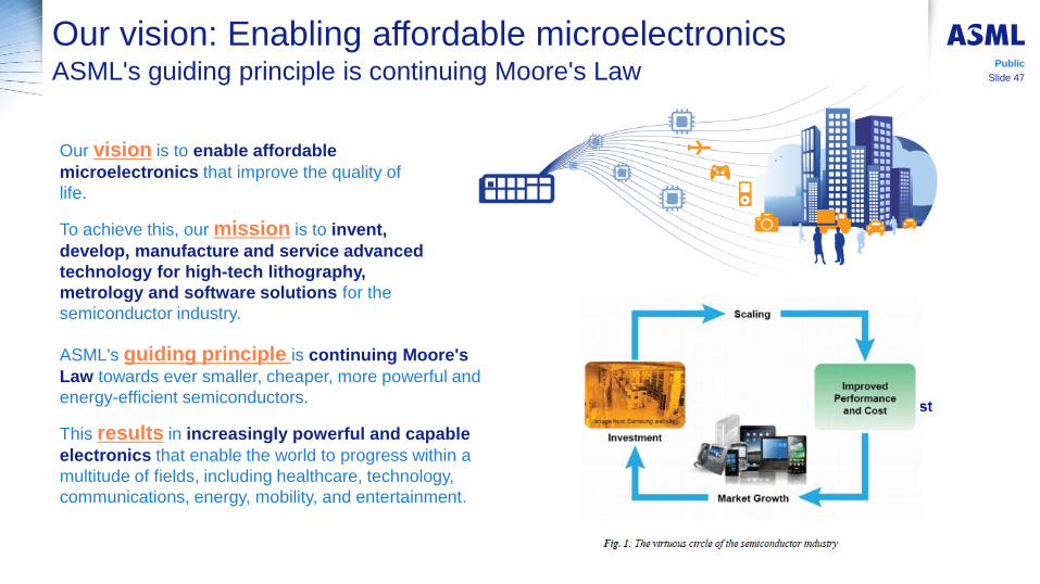
Our vision: Enabling affordable microelectronics ASML's guiding principle is continuing Moore's Law
Our vision is to enable affordable
microelectronics that improve the quality of
life.
To achieve this, our mission is to invent,
develop, manufacture and service advanced
technology for high-tech lithography,
metrology and software solutions for the
semiconductor industry.
ASML's guiding principle is continuing Moore's
Law towards ever smaller, cheaper, more powerful and
energy-efficient semiconductors.
This results in increasingly powerful and capable
electronics that enable the world to progress within a
multitude of fields, including healthcare, technology,
communications, energy, mobility, and entertainment.
Slide 47
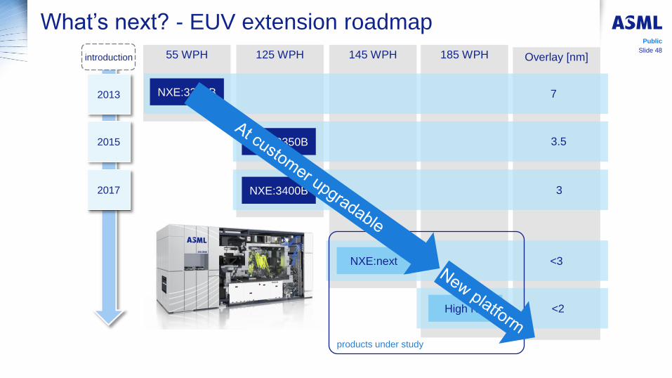
Overlay [nm] 55 WPH 125 WPH 185 WPH 145 WPH
NXE:3300B
NXE:3350B
NXE:next
High NA
Slide 48
Public
What’s next? - EUV extension roadmap
NXE:3400B 2017
2015
2013
introduction
products under study
7
3.5
3
<3
<2
Slide 49
Public
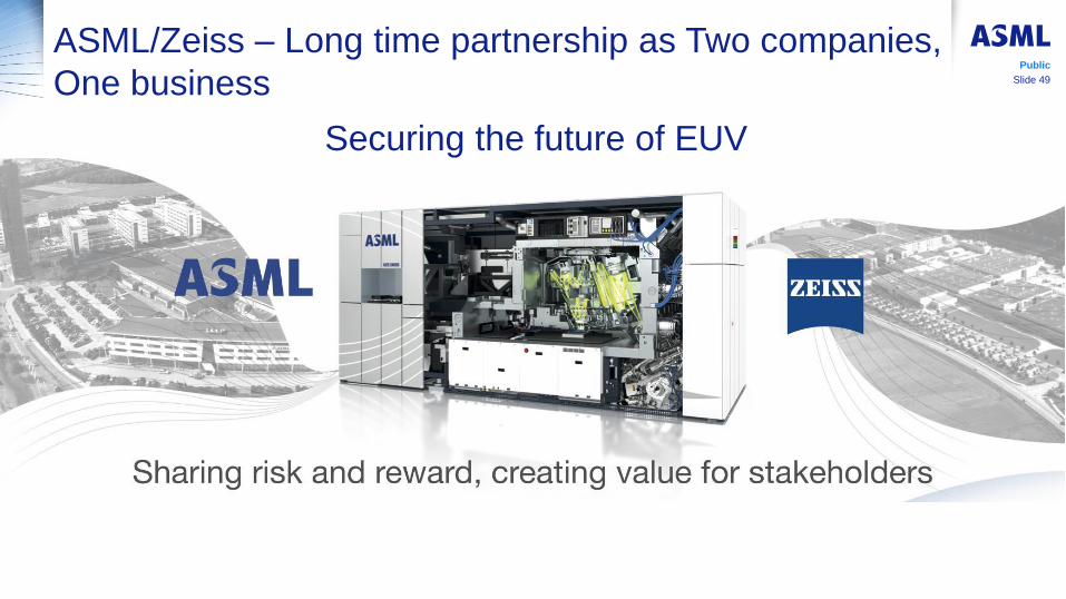
ASML/Zeiss – Long time partnership as Two companies,
One business
Securing the future of EUV
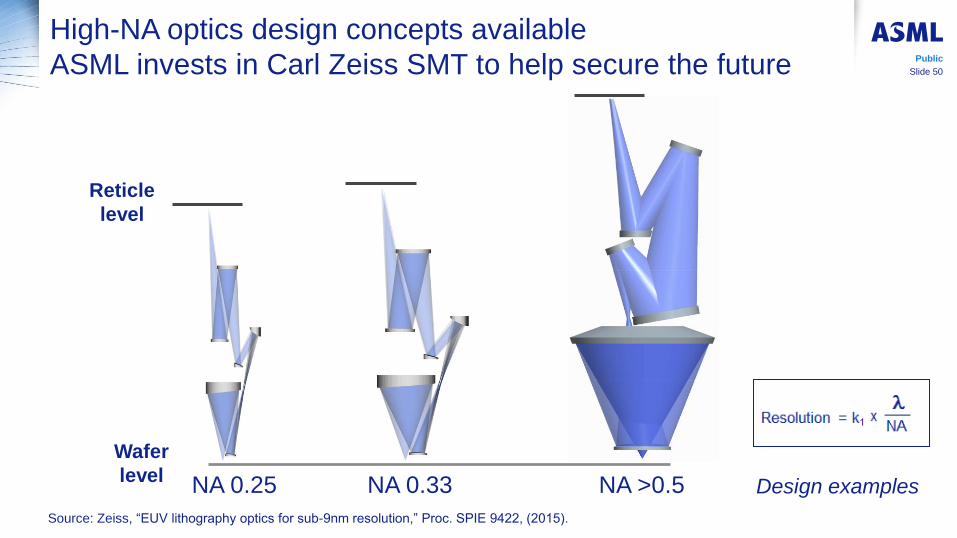
Source: Zeiss, “EUV lithography optics for sub-9nm resolution,” Proc. SPIE 9422, (2015).
Slide 50
Public
High-NA optics design concepts available
ASML invests in Carl Zeiss SMT to help secure the future
NA 0.25 NA 0.33 NA >0.5 Design examples
Wafer
level
Reticle
level
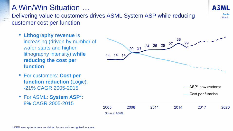
A Win/Win Situation … Delivering value to customers drives ASML System ASP while reducing
customer cost per function
• Lithography revenue is
increasing (driven by number of
wafer starts and higher
lithography intensity) while
reducing the cost per
function
• For customers: Cost per
function reduction (Logic):
-21% CAGR 2005-2015
• For ASML: System ASP*:
8% CAGR 2005-2015
Source: ASML
* ASML new systems revenue divided by new units recognized in a year
Public
Slide 51
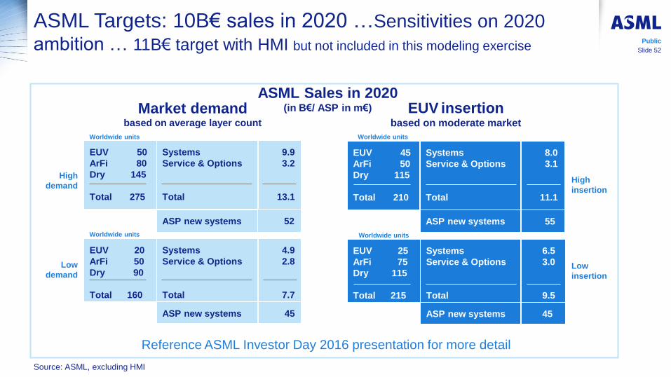
ASML Targets: 10B€ sales in 2020 …Sensitivities on 2020
ambition … 11B€ target with HMI but not included in this modeling exercise Public
Slide 52
Source: ASML, excluding HMI
Low
demand
Systems
Service & Options
Total
6.5
3.0
9.5
ASP new systems 45
Systems
Service & Options
Total
8.0
3.1
11.1
ASP new systems 55
Systems
Service & Options
Total
4.9
2.8
7.7
ASP new systems 45
Systems
Service & Options
Total
9.9
3.2
13.1
ASP new systems 52
High
demand
EUV 50
ArFi 80
Dry 145
Total 275
Worldwide units
EUV 45
ArFi 50
Dry 115
Total 210
EUV 20
ArFi 50
Dry 90
Total 160
EUV 25
ArFi 75
Dry 115
Total 215
Low
insertion
High
insertion
Worldwide units Worldwide units
Worldwide units
ASML Sales in 2020 (in B€/ ASP in m€)
Market demand
based on average layer count
EUV insertion based on moderate market
Reference ASML Investor Day 2016 presentation for more detail
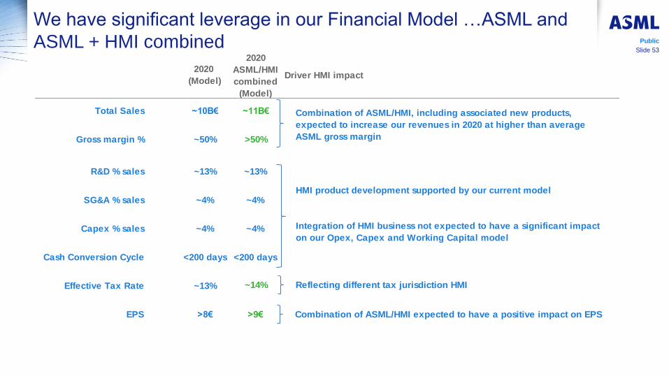
We have significant leverage in our Financial Model …ASML and
ASML + HMI combined
2020
(Model)
Total Sales ~10B€
Gross margin % ~50%
R&D % sales ~13%
SG&A % sales ~4%
Capex % sales ~4%
Cash Conversion Cycle <200 days
Effective Tax Rate ~13%
EPS >8€
Public
Slide 53
2020
ASML/HMI
combined
(Model)
Driver HMI impact
~11B€
>50%
Combination of ASML/HMI, including associated new products,
expected to increase our revenues in 2020 at higher than average
ASML gross margin
~13%
~4%
~4%
<200 days
HMI product development supported by our current model
Integration of HMI business not expected to have a significant impact
on our Opex, Capex and Working Capital model
~14% Reflecting different tax jurisdiction HMI
>9€ Combination of ASML/HMI expected to have a positive impact on EPS
Conclusions
• Opportunities for semiconductor device shrink continue to exist; Moore’s law is likely to
remain an adequate description of the pace of computing-based technology innovation for
the foreseeable future
• Application trends and economics in our ecosystem are driving increasing demand for
processing power, high-speed memory, and low-cost storage, fueling the continuation
of Moore’s law
• Continuation of Moore’s law will be supported by improved patterning solutions, achieving
fast yield ramp-up, hence realizing attractive economics
• Improving the single exposure resolution of lithography systems through the introduction of
higher Numerical Aperture EUV systems remains the most cost effective way to enable
device shrink
• As a result, ASML’s strategic priorities are: EUV industrialization, DUV competitiveness
(not discussed today), leadership in Holistic lithography (touched on today) and EUV
extension with High NA all underpinned with clear product roadmaps.
• The above underpins ASML’s long term growth opportunity through 2020 and beyond.
Public
Slide 54
“Moore’s Law….where next?”
Thank You