Embed Size (px)
Citation preview
Freescale Semiconductor MPC5642ARev. 3.2, 12/2014
© Freescale Semiconductor, Inc., 2014. All rights reserved.
MPC5642A Microcontroller DatasheetThis is the MPC5642A Datasheet set consisting of the following files:
• MPC5642A Datasheet Addendum (MPC5642A_AD), Rev. 1
• MPC5642A Datasheet (MPC5642A), Rev. 3.1
Freescale SemiconductorDatasheet Addendum
MPC5642A_ADRev. 1, 12/2014
Table of Contents
MPC5642A Microcontroller Datasheet Addendum
Addendum List for Revision 3.1 . . . . . . . . . . . . . . 2Revision History . . . . . . . . . . . . . . . . . . . . . . . . . . 2
This addendum describes corrections to the MPC5642A Microcontroller Datasheet, order number MPC5642A. For convenience, the addenda items are grouped by revision. Please check our website at http://www.freescale.com/powerarchitecture for the latest updates.
The current version available of the MPC5642A Microcontroller Datasheet is Revision 3.1.
12
© Freescale Semiconductor, Inc., 2014. All rights reserved.
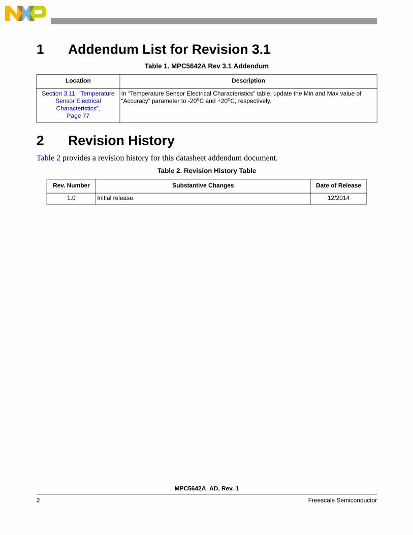
1 Addendum List for Revision 3.1
2 Revision HistoryTable 2 provides a revision history for this datasheet addendum document.
Table 1. MPC5642A Rev 3.1 Addendum
Location Description
Section 3.11, “Temperature Sensor Electrical Characteristics”,
Page 77
In “Temperature Sensor Electrical Characteristics” table, update the Min and Max value of “Accuracy” parameter to -20oC and +20oC, respectively.
Table 2. Revision History Table
Rev. Number Substantive Changes Date of Release
1.0 Initial release. 12/2014
MPC5642A_AD, Rev. 1
Freescale Semiconductor2
Document Number: MPC5642A_ADRev. 112/2014
Information in this document is provided solely to enable system and software
implementers to use Freescale products. There are no express or implied copyright
licenses granted hereunder to design or fabricate any integrated circuits based on the
information in this document.
Freescale reserves the right to make changes without further notice to any products
herein. Freescale makes no warranty, representation, or guarantee regarding the
suitability of its products for any particular purpose, nor does Freescale assume any
liability arising out of the application or use of any product or circuit, and specifically
disclaims any and all liability, including without limitation consequential or incidental
damages. “Typical” parameters that may be provided in Freescale data sheets and/or
specifications can and do vary in different applications, and actual performance may
vary over time. All operating parameters, including “typicals,” must be validated for
each customer application by customer’s technical experts. Freescale does not convey
any license under its patent rights nor the rights of others. Freescale sells products
pursuant to standard terms and conditions of sale, which can be found at the following
address:freescale.com/SalesTermsandConditions.
How to Reach Us:Home Page: freescale.com
Web Support: freescale.com/support
Freescale, the Freescale logo, AltiVec, C-5, CodeTest, CodeWarrior, ColdFire,
C-Ware, Energy Efficient Solutions logo, Kinetis, mobileGT, PowerQUICC, Processor
Expert, QorIQ, Qorivva, StarCore, Symphony, and VortiQa are trademarks of
Freescale Semiconductor, Inc., Reg. U.S. Pat. & Tm. Off. Airfast, BeeKit, BeeStack,
ColdFire+, CoreNet, Flexis, MagniV, MXC, Platform in a Package, QorIQ Qonverge,
QUICC Engine, Ready Play, SafeAssure, SMARTMOS, TurboLink, Vybrid, and Xtrinsic
are trademarks of Freescale Semiconductor, Inc. All other product or service names
are the property of their respective owners.
© 2014 Freescale Semiconductor, Inc.
Freescale SemiconductorData Sheet: Technical Data
Document Number: MPC5642ARev. 3.1, 06/2012
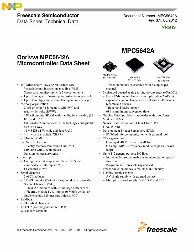
MPC5642A
208 MAPBGA176 LQFP 324 TEPBGA (17 x 17 mm)
Qorivva MPC5642A Microcontroller Data Sheet
• 150 MHz e200z4 Power Architecture core– Variable length instruction encoding (VLE)– Superscalar architecture with 2 execution units– Up to 2 integer or floating point instructions per cycle– Up to 4 multiply and accumulate operations per cycle
• Memory organization– 2 MB on-chip flash memory with ECC and
read-while-write (RWW)– 128 KB on-chip SRAM with standby functionality (32
KB) and ECC– 8 KB instruction cache (with line locking), configurable
as 2- or 4-way– 14 + 3 KB eTPU code and data RAM– 4 4 crossbar switch (XBAR)– 24-entry MMU
• Fail Safe Protection– 16-entry Memory Protection Unit (MPU)– CRC unit with 3 submodules– Junction temperature sensor
• Interrupt– Configurable interrupt controller (INTC) with
non-maskable interrupt (NMI)– 64-channel eDMA
• Serial channels– 3 eSCI modules– 3 DSPI modules (2 of which support downstream Micro
Second Channel [MSC])– 3 FlexCAN modules with 64 message buffers each– 1 FlexRay module (V2.1) up to 10 Mbit/s w/dual or
single channel, 128 message objects, ECC• 1 eMIOS
– 24 unified channels• 1 eTPU2 (second generation eTPU)—32 standard channels
© Freescale Semiconductor, Inc., 2009, 2010, 2012. All rights re
(24 × 24 mm) (23 × 23 mm)
– 1 reaction module (6 channels with 3 outputs per channel)
• 2 enhanced queued analog-to-digital converters (eQADCs)– Forty 12-bit input channels (multiplexed on 2 ADCs);
expandable to 56 channels with external multiplexers– 6 command queues– Trigger and DMA support– 688 ns minimum conversion time
• On-chip CAN/SCI Bootstrap loader with Boot Assist Module (BAM)
• Nexus: Class 3+ for core; Class 1 for eTPU• JTAG (5-pin)• Development Trigger Semaphore (DTS)
– EVTO pin for communication with external tool • Clock generation
– On-chip 4–40 MHz main oscillator– On-chip FMPLL (frequency-modulated phase-locked
loop)• Up to 112 general purpose I/O lines
– Individually programmable as input, output or special function
– Programmable threshold (hysteresis)• Power reduction modes: slow, stop, and standby• Flexible supply scheme
– 5 V single supply with external ballast– Multiple external supply: 5 V, 3.3 V, and 1.2 V
served.
MPC5642A Microcontroller Data Sheet, Rev. 3.1
Freescale Semiconductor2
Table of Contents1 Introduction . . . . . . . . . . . . . . . . . . . . . . . . . . . . . . . . . . . . . . . .3
1.1 Document overview. . . . . . . . . . . . . . . . . . . . . . . . . . . . .31.2 Description . . . . . . . . . . . . . . . . . . . . . . . . . . . . . . . . . . .31.3 Device feature summary . . . . . . . . . . . . . . . . . . . . . . . . .31.4 Block diagram . . . . . . . . . . . . . . . . . . . . . . . . . . . . . . . . .51.5 Feature details . . . . . . . . . . . . . . . . . . . . . . . . . . . . . . . .9
1.5.1 e200z4 core. . . . . . . . . . . . . . . . . . . . . . . . . . . . .91.5.2 Crossbar switch (XBAR) . . . . . . . . . . . . . . . . . .101.5.3 Enhanced direct memory access (eDMA) . . . . .101.5.4 Interrupt controller (INTC) . . . . . . . . . . . . . . . . .111.5.5 Memory protection unit (MPU). . . . . . . . . . . . . .111.5.6 Frequency-modulated phase-locked loop
(FMPLL). . . . . . . . . . . . . . . . . . . . . . . . . . . . . . .121.5.7 System integration unit (SIU). . . . . . . . . . . . . . .121.5.8 Flash memory . . . . . . . . . . . . . . . . . . . . . . . . . .131.5.9 Static random access memory (SRAM) . . . . . .141.5.10 Boot assist module (BAM) . . . . . . . . . . . . . . . . .141.5.11 Enhanced modular input/output system
(eMIOS) . . . . . . . . . . . . . . . . . . . . . . . . . . . . . . .141.5.12 Second generation enhanced time processing
unit (eTPU2) . . . . . . . . . . . . . . . . . . . . . . . . . . .151.5.13 Reaction module (REACM) . . . . . . . . . . . . . . . .161.5.14 Enhanced queued analog-to-digital converter
(eQADC) . . . . . . . . . . . . . . . . . . . . . . . . . . . . . .171.5.15 Deserial serial peripheral interface (DSPI) . . . .181.5.16 Enhanced serial communications interface
(eSCI) . . . . . . . . . . . . . . . . . . . . . . . . . . . . . . . .191.5.17 Controller area network (FlexCAN) . . . . . . . . . .191.5.18 FlexRay . . . . . . . . . . . . . . . . . . . . . . . . . . . . . . .201.5.19 System timers . . . . . . . . . . . . . . . . . . . . . . . . . .201.5.20 Software watchdog timer (SWT) . . . . . . . . . . . .211.5.21 Cyclic redundancy check (CRC) module . . . . . .211.5.22 Error correction status module (ECSM). . . . . . .221.5.23 Peripheral bridge (PBRIDGE) . . . . . . . . . . . . . .221.5.24 Calibration bus interface . . . . . . . . . . . . . . . . . .221.5.25 Power management controller (PMC) . . . . . . . .221.5.26 Nexus port controller (NPC) . . . . . . . . . . . . . . .231.5.27 JTAG controller (JTAGC) . . . . . . . . . . . . . . . . . .231.5.28 Development trigger semaphore (DTS). . . . . . .23
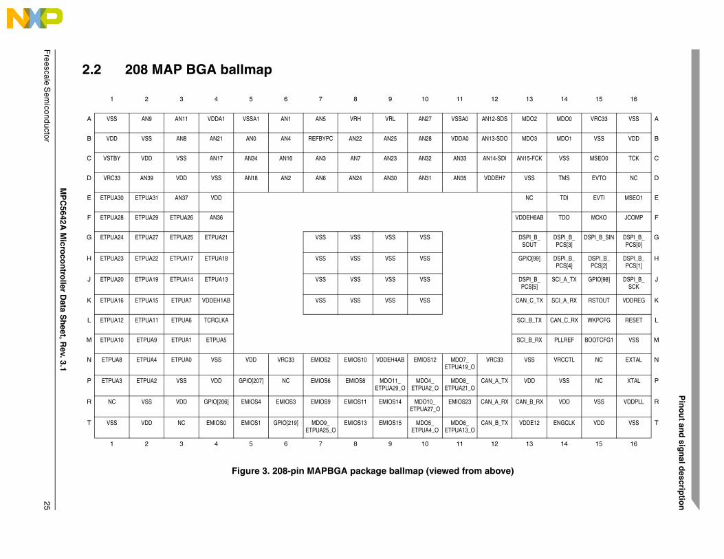
2 Pinout and signal description . . . . . . . . . . . . . . . . . . . . . . . . .232.1 176 LQFP pinout. . . . . . . . . . . . . . . . . . . . . . . . . . . . . .242.2 208 MAP BGA ballmap . . . . . . . . . . . . . . . . . . . . . . . . .252.3 324 TEPBGA ballmap. . . . . . . . . . . . . . . . . . . . . . . . . .262.4 Signal summary . . . . . . . . . . . . . . . . . . . . . . . . . . . . . .30
2.5 Signal details . . . . . . . . . . . . . . . . . . . . . . . . . . . . . . . . 493 Electrical characteristics . . . . . . . . . . . . . . . . . . . . . . . . . . . . 55
3.1 Parameter classification. . . . . . . . . . . . . . . . . . . . . . . . 553.2 Maximum ratings . . . . . . . . . . . . . . . . . . . . . . . . . . . . . 563.3 Thermal characteristics . . . . . . . . . . . . . . . . . . . . . . . . 58
3.3.1 General notes for specifications at maximum junction temperature . . . . . . . . . . . . . . . . . . . . . . . . . . 59
3.4 EMI (electromagnetic interference) characteristics . . . 613.5 Electrostatic discharge (ESD) characteristics . . . . . . . 623.6 Power management control (PMC) and power on
reset (POR) electrical specifications . . . . . . . . . . . . . . 623.6.1 Regulator example . . . . . . . . . . . . . . . . . . . . . . 653.6.2 Recommended power transistors. . . . . . . . . . . 66
3.7 Power up/down sequencing. . . . . . . . . . . . . . . . . . . . . 663.8 DC electrical specifications . . . . . . . . . . . . . . . . . . . . . 673.9 I/O pad current specifications . . . . . . . . . . . . . . . . . . . 72
3.9.1 I/O pad VRC33 current specifications . . . . . . . . 733.9.2 LVDS pad specifications. . . . . . . . . . . . . . . . . . 74
3.10 Oscillator and PLLMRFM electrical characteristics . . . 753.11 Temperature sensor electrical characteristics . . . . . . . 773.12 eQADC electrical characteristics . . . . . . . . . . . . . . . . . 773.13 Configuring SRAM wait states. . . . . . . . . . . . . . . . . . . 793.14 Platform flash controller electrical characteristics . . . . 803.15 Flash memory electrical characteristics . . . . . . . . . . . 803.16 AC specifications . . . . . . . . . . . . . . . . . . . . . . . . . . . . . 82
3.16.1 Pad AC specifications. . . . . . . . . . . . . . . . . . . . 823.17 AC timing . . . . . . . . . . . . . . . . . . . . . . . . . . . . . . . . . . . 86
3.17.1 Reset and configuration pin timing . . . . . . . . . . 863.17.2 IEEE 1149.1 interface timing . . . . . . . . . . . . . . 863.17.3 Nexus timing. . . . . . . . . . . . . . . . . . . . . . . . . . . 903.17.4 Calibration bus interface timing . . . . . . . . . . . . 953.17.5 External interrupt timing (IRQ pin) . . . . . . . . . . 993.17.6 eTPU timing . . . . . . . . . . . . . . . . . . . . . . . . . . . 993.17.7 eMIOS timing . . . . . . . . . . . . . . . . . . . . . . . . . 1003.17.8 DSPI timing . . . . . . . . . . . . . . . . . . . . . . . . . . 1003.17.9 eQADC SSI timing . . . . . . . . . . . . . . . . . . . . . 1073.17.10FlexCAN system clock source . . . . . . . . . . . . 108
4 Packages. . . . . . . . . . . . . . . . . . . . . . . . . . . . . . . . . . . . . . . 1094.1 Package mechanical data . . . . . . . . . . . . . . . . . . . . . 109
4.1.1 176 LQFP. . . . . . . . . . . . . . . . . . . . . . . . . . . . 1094.1.2 208 MAPBGA. . . . . . . . . . . . . . . . . . . . . . . . . 1124.1.3 324 TEPBGA . . . . . . . . . . . . . . . . . . . . . . . . . 114
5 Ordering information . . . . . . . . . . . . . . . . . . . . . . . . . . . . . . 1166 Document revision history . . . . . . . . . . . . . . . . . . . . . . . . . . 117
Introduction
1 Introduction
1.1 Document overviewThis document provides electrical specifications, pin assignments, and package diagrams for the MPC5642A series of microcontroller units (MCUs). It also describes the device features and highlights important electrical and physical characteristics. For functional characteristics, refer to the device reference manual.
1.2 DescriptionThis microcontroller is a 32-bit system-on-chip (SoC) device intended for use in mid-range engine control and automotive transmission control applications.
It is compatible with devices in Freescale’s MPC5600 family and offers performance and capabilities beyond the MPC5632M devices.
The microcontroller’s e200z4 host processor core is built on the Power Architecture® technology and designed specifically for embedded applications. In addition to the Power Architecture technology, this core supports instructions for digital signal processing (DSP).
The device has two levels of memory hierarchy consisting of 8 KB of instruction cache, backed by a 128 KB on-chip SRAM and a 2 MB internal flash memory.
For development, the device includes a calibration bus that is accessible only when using the Freescale VertiCal Calibration System.
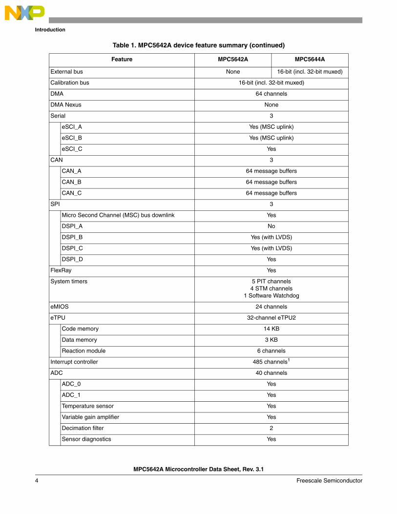
1.3 Device feature summaryTable 1 summarizes the MPC5642A features and compares them to those of the MPC5644A.
Table 1. MPC5642A device feature summary
Feature MPC5642A MPC5644A
Process 90 nm
Core e200z4
SIMD Yes
VLE Yes
Cache 8 KB instruction
Non-Maskable Interrupt (NMI) NMI and Critical Interrupt
MMU 24-entry
MPU 16-entry
Crossbar switch 4 4 5 4
Core performance 0–150 MHz
Windowing software watchdog Yes
Core Nexus Class 3+
SRAM 128 KB 192 KB
Flash 2 MB 4 MB
Flash fetch accelerator 4 128-bit 4 256-bit
MPC5642A Microcontroller Data Sheet, Rev. 3.1
Freescale Semiconductor 3
Introduction
External bus None 16-bit (incl. 32-bit muxed)
Calibration bus 16-bit (incl. 32-bit muxed)
DMA 64 channels
DMA Nexus None
Serial 3
eSCI_A Yes (MSC uplink)
eSCI_B Yes (MSC uplink)
eSCI_C Yes
CAN 3
CAN_A 64 message buffers
CAN_B 64 message buffers
CAN_C 64 message buffers
SPI 3
Micro Second Channel (MSC) bus downlink Yes
DSPI_A No
DSPI_B Yes (with LVDS)
DSPI_C Yes (with LVDS)
DSPI_D Yes
FlexRay Yes
System timers 5 PIT channels4 STM channels
1 Software Watchdog
eMIOS 24 channels
eTPU 32-channel eTPU2
Code memory 14 KB
Data memory 3 KB
Reaction module 6 channels
Interrupt controller 485 channels1
ADC 40 channels
ADC_0 Yes
ADC_1 Yes
Temperature sensor Yes
Variable gain amplifier Yes
Decimation filter 2
Sensor diagnostics Yes
Table 1. MPC5642A device feature summary (continued)
Feature MPC5642A MPC5644A
MPC5642A Microcontroller Data Sheet, Rev. 3.1
4 Freescale Semiconductor
Introduction
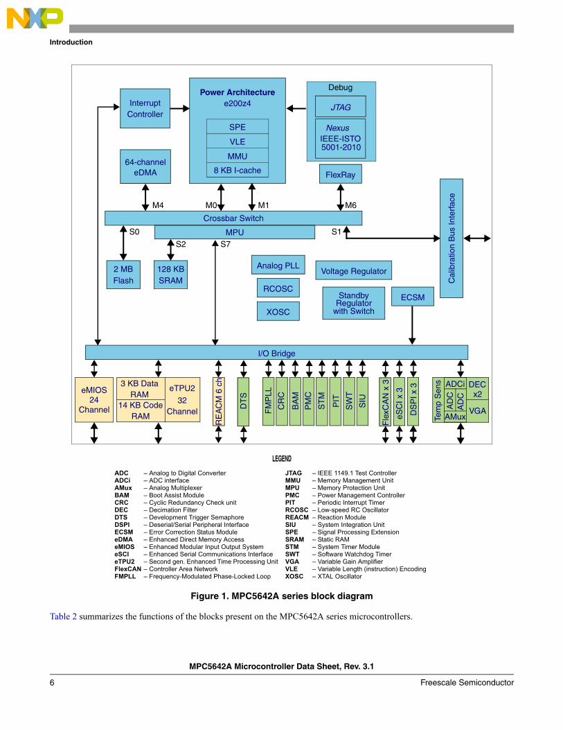
1.4 Block diagramFigure 1 shows a top-level block diagram of the MPC5642A series.
CRC Yes
FMPLL Yes
VRC Yes
Supplies 5 V, 3.3 V2
Low-power modes Stop modeSlow mode
Packages 176 LQFP3
208 MAPBGA3,4
324 TEPBGA5
496-pin CSP6
176 LQFP3
208 MAPBGA3,4
324 TEPBGA5
496-pin CSP6
1 197 interrupt vectors are reserved.2 5 V single supply only for 176 LQFP3 Pinout compatible with Freescale’s MPC5634M devices4 Pinout compatible with Freescale’s MPC55345 Ballmap upwardly compatible with the standardized package ballmap used for various Freescale MPC563xM family
members6 For Freescale VertiCal Calibration System only
Table 1. MPC5642A device feature summary (continued)
Feature MPC5642A MPC5644A
MPC5642A Microcontroller Data Sheet, Rev. 3.1
Freescale Semiconductor 5
Introduction
Figure 1. MPC5642A series block diagram
Table 2 summarizes the functions of the blocks present on the MPC5642A series microcontrollers.
ADC – Analog to Digital ConverterADCi – ADC interfaceAMux – Analog MultiplexerBAM – Boot Assist ModuleCRC – Cyclic Redundancy Check unitDEC – Decimation FilterDTS – Development Trigger SemaphoreDSPI – Deserial/Serial Peripheral InterfaceECSM – Error Correction Status ModuleeDMA – Enhanced Direct Memory AccesseMIOS – Enhanced Modular Input Output SystemeSCI – Enhanced Serial Communications InterfaceeTPU2 – Second gen. Enhanced Time Processing UnitFlexCAN – Controller Area NetworkFMPLL – Frequency-Modulated Phase-Locked Loop
JTAG – IEEE 1149.1 Test ControllerMMU – Memory Management UnitMPU – Memory Protection UnitPMC – Power Management ControllerPIT – Periodic Interrupt TimerRCOSC – Low-speed RC OscillatorREACM – Reaction ModuleSIU – System Integration UnitSPE – Signal Processing ExtensionSRAM – Static RAMSTM – System Timer ModuleSWT – Software Watchdog TimerVGA – Variable Gain AmplifierVLE – Variable Length (instruction) EncodingXOSC – XTAL Oscillator
LEGEND
eMIOS24
Channel
3 KB DataRAM
14 KB CodeRAM
eTPU2
32
Tem
p S
ens ADCi DEC
x2
VGAAD
CA
DC
AMux
2 MBFlash
128 KBSRAM
MPU
Crossbar Switch
InterruptController
eDMA64-channel
SPE
VLE
MMU
8 KB I-cache
Power Architecturee200z4 JTAG
NexusIEEE-ISTO5001-2010
FlexRay
Cal
ibra
tion
Bus
Inte
rface
Fle
xCA
Nx
3
I/O Bridge
FM
PLL
CR
C
BA
M
PM
C
ST
M
PIT
SW
T
SIU
Analog PLL
RCOSC
XOSC
Voltage Regulator
StandbyRegulator
with Switch
DS
PIx
3
eSC
Ix3
M4 M0 M6
S0
S2 S7
S1
M1
RE
AC
M 6
ch
DT
S
Debug
Channel
ECSM
MPC5642A Microcontroller Data Sheet, Rev. 3.1
6 Freescale Semiconductor
Introduction
Table 2. MPC5642A series block summary
Block Function
Boot assist module (BAM) Block of read-only memory containing executable code that searches for user-supplied boot code and, if none is found, executes the BAM boot code resident in device ROM
Calibration bus interface Transfers data across the crossbar switch to/from peripherals attached to the calibration system connector
Controller area network (FlexCAN) Supports the standard CAN communications protocol
Crossbar switch (XBAR) Internal busmaster
Cyclic redundancy check (CRC) CRC checksum generator
Deserial serial peripheral interface (DSPI) Provides a synchronous serial interface for communication with external devices
e200z4 core Executes programs and interrupt handlers
Enhanced direct memory access (eDMA) Performs complex data movements with minimal intervention from the core.
Enhanced modular input-output system (eMIOS)
Provides the functionality to generate or measure events
Enhanced queued analog-to-digital converter (eQADC)
Provides accurate and fast conversions for a wide range of applications
Enhanced serial communication interface (eSCI)
Provides asynchronous serial communication capability with peripheral devices and other microcontroller units
Enhanced time processor unit (eTPU2) Second-generation co-processor processes real-time input events, performs output waveform generation, and accesses shared data without host intervention
Error Correction Status Module (ECSM) The Error Correction Status Module supports a number of miscellaneous control functions for the platform, and includes registers for capturing information on platform memory errors if error-correcting codes (ECC) are implemented
Flash memory Provides storage for program code, constants, and variables
FlexRay Provides high-speed distributed control for advanced automotive applications
Frequency-modulated phase-locked loop (FMPLL)
Generates high-speed system clocks and supports programmable frequency modulation
Interrupt controller (INTC) Provides priority-based preemptive scheduling of interrupt requests
JTAG controller Provides the means to test chip functionality and connectivity while remaining transparent to system logic when not in test mode
Memory protection unit (MPU) Provides hardware access control for all memory references generated
Nexus port controller (NPC) Provides real-time development support capabilities in compliance with the IEEE-ISTO 5001-2010 standard
Periodic interrupt timer (PIT) Produces periodic interrupts and triggers
Reaction Module (REACM) Works in conjunction with the eQADC and eTPU2 to increase system performance by removing the CPU from the current control loop.
MPC5642A Microcontroller Data Sheet, Rev. 3.1
Freescale Semiconductor 7
Introduction
System Integration Unit (SIU) Controls MCU reset configuration, pad configuration, external interrupt, general purpose I/O (GPIO), internal peripheral multiplexing, and the system reset operation.
Static random-access memory (SRAM) Provides storage for program code, constants, and variables
System timers Includes periodic interrupt timer with real-time interrupt; output compare timer and system watchdog timer
System watchdog timer (SWT) Provides protection from runaway code
Temperature sensor Provides the temperature of the device as an analog value
Table 2. MPC5642A series block summary (continued)
Block Function
MPC5642A Microcontroller Data Sheet, Rev. 3.1
8 Freescale Semiconductor
Introduction
1.5 Feature details
1.5.1 e200z4 coreMPC5642A devices have a high performance e200z4 core processor:
• 32-bit Power Architecture technology programmer’s model
• Variable Length Encoding (VLE) enhancements
• Dual issue, 32-bit Power Architecture technology compliant CPU
• 8 KB, 2/4-way set associative instruction cache
• Thirty-two 64-bit general purpose registers (GPRs)
• Memory Management Unit (MMU) with 24-entry fully-associative translation look-aside buffer (TLB)
• Harvard Architecture: Separate instruction bus and load/store bus
• Vectored interrupt support
• Non-maskable interrupt input
• Critical Interrupt input
• New ‘Wait for Interrupt’ instruction, to be used with new low power modes
• Reservation instructions for implementing read-modify-write accesses
• Signal processing extension (SPE) APU
• Single Precision Floating point (scalar and vector)
• Nexus Class 3+ debug
• Process ID manipulation for the MMU using an external tool
• In-order execution and retirement
• Precise exception handling
• Branch processing unit
— Dedicated branch address calculation adder
— Branch target prefetching using 8-entry BTB
• Supports independent instruction and data accesses to different memory subsystems, such as SRAM and flash memory via independent Instruction and Data BIUs
• Load/store unit
— 2-cycle load latency
— Fully pipelined
— Big and Little endian support
— Misaligned access support
• Signal Processing Extension (SPE1.1) APU supporting SIMD fixed-point operations using the 64-bit General Purpose Register file
• Embedded Floating-Point (EFP2) APU supporting scalar and vector SIMD single-precision floating-point operations, using the 64-bit General Purpose Register file
• Power management
— Low power design – extensive clock gating
— Power saving modes: wait
— Dynamic power management of execution units, cache and MMU
• Testability
— Synthesizeable, MuxD scan design
— ABIST/MBIST for arrays
— Built-in Parallel Signature Unit
MPC5642A Microcontroller Data Sheet, Rev. 3.1
Freescale Semiconductor 9
Introduction
• Calibration support allowing an external tool to modify address mapping
1.5.2 Crossbar switch (XBAR)The XBAR multiport crossbar switch supports simultaneous connections between four master ports and four slave ports. The crossbar supports a 32-bit address bus width and a 64-bit data bus width.
The crossbar allows three concurrent transactions to occur from the master ports to any slave port but each master must access a different slave. If a slave port is simultaneously requested by more than one master port, arbitration logic selects the higher priority master and grants it ownership of the slave port. All other masters requesting that slave port are stalled until the higher priority master completes its transactions. Requesting masters are treated with equal priority and are granted access to a slave port in round-robin fashion, based upon the ID of the last master to be granted access. The crossbar provides the following features:
• 4 master ports
— CPU instruction bus
— CPU data bus
— eDMA
— FlexRay
• 4 slave ports
— Flash
— Calibration bus interface
— SRAM
— Peripheral bridge
• 32-bit internal address, 64-bit internal data paths
1.5.3 Enhanced direct memory access (eDMA)The enhanced direct memory access (eDMA) controller is a second-generation module capable of performing complex data movements via 64 programmable channels, with minimal intervention from the host processor. The hardware micro-architecture includes a DMA engine which performs source and destination address calculations, and the actual data movement operations, along with an SRAM-based memory containing the transfer control descriptors (TCD) for the channels. This implementation minimizes overall block size. The eDMA module provides the following features:
• All data movement via dual-address transfers: read from source, write to destination
• Programmable source and destination addresses, transfer size, plus support for enhanced addressing modes
• Transfer control descriptor organized to support two-deep, nested transfer operations
• An inner data transfer loop defined by a “minor” byte transfer count
• An outer data transfer loop defined by a “major” iteration count
• Channel activation via one of three methods:
— Explicit software initiation
— Initiation via a channel-to-channel linking mechanism for continuous transfers
— Peripheral-paced hardware requests (one per channel)
• Support for fixed-priority and round-robin channel arbitration
• Channel completion reported via optional interrupt requests
• 1 interrupt per channel, optionally asserted at completion of major iteration count
• Error termination interrupts optionally enabled
• Support for scatter/gather DMA processing
• Ability to suspend channel transfers by a higher priority channel
MPC5642A Microcontroller Data Sheet, Rev. 3.1
10 Freescale Semiconductor
Introduction
1.5.4 Interrupt controller (INTC)The INTC provides priority-based preemptive scheduling of interrupt requests, suitable for statically scheduled hard real-time systems.
For high priority interrupt requests, the time from the assertion of the interrupt request from the peripheral to when the processor is executing the interrupt service routine (ISR) has been minimized. The INTC provides a unique vector for each interrupt request source for quick determination of which ISR needs to be executed. It also provides an ample number of priorities so that lower priority ISRs do not delay the execution of higher priority ISRs. To allow the appropriate priorities for each source of interrupt request, the priority of each interrupt request is software configurable.
When multiple tasks share a resource, coherent accesses to that resource need to be supported. The INTC supports the priority ceiling protocol for coherent accesses. By providing a modifiable priority mask, the priority can be raised temporarily so that all tasks which share the resource cannot preempt each other.
The INTC provides the following features:
• 9-bit vector addresses
• Unique vector for each interrupt request source
• Hardware connection to processor or read from register
• Each interrupt source can assigned a specific priority by software
• Preemptive prioritized interrupt requests to processor
• ISR at a higher priority preempts executing ISRs or tasks at lower priorities
• Automatic pushing or popping of preempted priority to or from a LIFO
• Ability to modify the ISR or task priority to implement the priority ceiling protocol for accessing shared resources
• Low latency—3 clocks from receipt of interrupt request from peripheral to interrupt request to processor
This device also includes a non-maskable interrupt (NMI) pin that bypasses the INTC and multiplexing logic.
1.5.5 Memory protection unit (MPU)The Memory Protection Unit (MPU) provides hardware access control for all memory references generated in a device. Using preprogrammed region descriptors, which define memory spaces and their associated access rights, the MPU concurrently monitors all system bus transactions and evaluates the appropriateness of each transfer. Memory references with sufficient access control rights are allowed to complete; references that are not mapped to any region descriptor or have insufficient rights are terminated with a protection error response.
The MPU has these major features:
• Support for 16 memory region descriptors, each 128 bits in size
— Specification of start and end addresses provide granularity for region sizes from 32 bytes to 4 GB
— MPU is invalid at reset, thus no access restrictions are enforced
— 2 types of access control definitions: processor core bus master supports the traditional {read, write, execute} permissions with independent definitions for supervisor and user mode accesses; the remaining non-core bus masters (eDMA, FlexRay) support {read, write} attributes
— Automatic hardware maintenance of the region descriptor valid bit removes issues associated with maintaining a coherent image of the descriptor
— Alternate memory view of the access control word for each descriptor provides an efficient mechanism to dynamically alter the access rights of a descriptor only
— For overlapping region descriptors, priority is given to permission granting over access denying as this approach provides more flexibility to system software
• Support for two XBAR slave port connections (SRAM and PBRIDGE)
— For each connected XBAR slave port (SRAM and PBRIDGE), MPU hardware monitors every port access using the preprogrammed memory region descriptors
MPC5642A Microcontroller Data Sheet, Rev. 3.1
Freescale Semiconductor 11
Introduction
— An access protection error is detected if a memory reference does not hit in any memory region or the reference is flagged as illegal in all memory regions where it does hit. In the event of an access error, the XBAR reference is terminated with an error response and the MPU inhibits the bus cycle being sent to the targeted slave device
— 64-bit error registers, one for each XBAR slave port, capture the last faulting address, attributes, and detail information
1.5.6 Frequency-modulated phase-locked loop (FMPLL)The FMPLL allows the user to generate high speed system clocks from a 4 MHz to 40 MHz crystal oscillator or external clock generator. Further, the FMPLL supports programmable frequency modulation of the system clock. The PLL multiplication factor, output clock divider ratio are all software configurable. The PLL has the following major features:
• Input clock frequency from 4 MHz to 40 MHz
• Reduced frequency divider (RFD) for reduced frequency operation without forcing the PLL to relock
• 3 modes of operation
— Bypass mode with PLL off
— Bypass mode with PLL running (default mode out of reset)
— PLL normal mode
• Each of the 3 modes may be run with a crystal oscillator or an external clock reference
• Programmable frequency modulation
— Modulation enabled/disabled through software
— Triangle wave modulation up to 100 kHz modulation frequency
— Programmable modulation depth (0% to 2% modulation depth)
— Programmable modulation frequency dependent on reference frequency
• Lock detect circuitry reports when the PLL has achieved frequency lock and continuously monitors lock status to report loss of lock conditions
• Clock Quality Module
— Detects the quality of the crystal clock and causes interrupt request or system reset if error is detected
— Detects the quality of the PLL output clock; if error detected, causes system reset or switches system clock to crystal clock and causes interrupt request
• Programmable interrupt request or system reset on loss of lock
• Self-clocked mode (SCM) operation
1.5.7 System integration unit (SIU)The MPC5642A SIU controls MCU reset configuration, pad configuration, external interrupt, general purpose I/O (GPIO), internal peripheral multiplexing, and the system reset operation. The reset configuration block contains the external pin boot configuration logic. The pad configuration block controls the static electrical characteristics of I/O pins. The GPIO block provides uniform and discrete input/output control of the I/O pins of the MCU. The reset controller performs reset monitoring of internal and external reset sources, and drives the RSTOUT pin. Communication between the SIU and the e200z4 CPU core is via the crossbar switch. The SIU provides the following features:
• System configuration
— MCU reset configuration via external pins
— Pad configuration control for each pad
— Pad configuration control for virtual I/O via DSPI serialization
• System reset monitoring and generation
— Power-on reset support
— Reset status register provides last reset source to software
MPC5642A Microcontroller Data Sheet, Rev. 3.1
12 Freescale Semiconductor
Introduction
— Glitch detection on reset input
— Software controlled reset assertion
• External interrupt
— Rising or falling edge event detection
— Programmable digital filter for glitch rejection
— Critical Interrupt request
— Non-Maskable Interrupt request
• GPIO
— Centralized control of I/O and bus pins
— Virtual GPIO via DSPI serialization (requires external deserialization device)
— Dedicated input and output registers for setting each GPIO and Virtual GPIO pin
• Internal multiplexing
— Allows serial and parallel chaining of DSPIs
— Allows flexible selection of eQADC trigger inputs
— Allows selection of interrupt requests between external pins and DSPI
— From a set of eTPU output channels, allows selection of source signals for decimation filter integrators
1.5.8 Flash memoryThe MPC5642A provides 2 MB of programmable, non-volatile, flash memory. The non-volatile memory (NVM) can be used to store instructions or data, or both. The flash module includes a Fetch Accelerator that optimizes the performance of the flash array to match the CPU architecture. The flash module interfaces the system bus to a dedicated flash memory array controller. For CPU ‘loads’, DMA transfers and CPU instruction fetch, it supports a 64-bit data bus width at the system bus port, and 128-bit read data interfaces to flash memory. The module contains a prefetch controller which prefetches sequential lines of data from the flash array into the buffers. Prefetch buffer hits allow no-wait responses.
The flash memory provides the following features:
• Supports a 64-bit data bus for instruction fetch, CPU loads and DMA access. Byte, halfword, word and doubleword reads are supported. Only aligned word and doubleword writes are supported.
• Fetch Accelerator
— Architected to optimize the performance of the flash
— Configurable read buffering and line prefetch support
— 4-entry 128-bit wide line read buffer
— Prefetch controller
• Hardware and software configurable read and write access protections on a per-master basis
• Interface to the flash array controller pipelined with a depth of one, allowing overlapped accesses to proceed in parallel for pipelined flash array designs
• Configurable access timing usable in a wide range of system frequencies
• Multiple-mapping support and mapping-based block access timing (0–31 additional cycles) usable for emulation of other memory types
• Software programmable block program/erase restriction control
• Erase of selected block(s)
• Read page size of 128 bits (4 words)
• ECC with single-bit correction, double-bit detection
• Program page size of 128 bits (4 words) to accelerate programming
• ECC single-bit error corrections are visible to software
• Minimum program size is 2 consecutive 32-bit words, aligned on a 0-modulo-8 byte address, due to ECC
MPC5642A Microcontroller Data Sheet, Rev. 3.1
Freescale Semiconductor 13
Introduction
• Embedded hardware program and erase algorithm
• Erase suspend, program suspend and erase-suspended program
• Shadow information stored in non-volatile shadow block
• Independent program/erase of the shadow block
1.5.9 Static random access memory (SRAM)The SRAM provides 128 KB of general purpose system SRAM. The first 32 KB block of the SRAM is powered by its own power supply pin only during standby operation.
The SRAM controller includes these features:
• 128 KB data RAM implemented as eight 16 KB (2048 78 bits) blocks
• Each 16 KB block has 2 rows repairable (RAMs with internal repair feature)
• Supports read/write accesses mapped to the SRAM memory from any master
• 32 KB block powered by separate supply for standby operation
• Byte, halfword, word and doubleword addressable
• ECC performs single bit correction, double bit detection
1.5.10 Boot assist module (BAM)The BAM is a block of read-only memory that is programmed once by Freescale and is identical for all MPC5642A MCUs. The BAM program is executed every time the MCU is powered on or reset in normal mode. The BAM supports different modes of booting. They are:
• Booting from internal flash memory
• Serial boot loading (boot code is downloaded into RAM via eSCI or the FlexCAN and then executed)
The BAM also reads the reset configuration half word (RCHW) from internal flash memory and configures the MPC5642A hardware accordingly. The BAM provides the following features:
• Sets up MMU to cover all resources and mapping of all physical addresses to logical addresses with minimum address translation
• Sets up MMU to allow user boot code to execute as either Power Architecture technology code (default) or as Freescale VLE code
• Location and detection of user boot code
• Automatic switch to serial boot mode if internal flash is blank or invalid
• Supports user programmable 64-bit password protection for serial boot mode
• Supports serial bootloading via FlexCAN bus and eSCI using Freescale protocol
• Supports serial bootloading via FlexCAN bus and eSCI with auto baud rate sensing
• Supports serial bootloading of either Power Architecture technology code (default) or Freescale VLE code
• Supports booting from calibration bus interface
• Supports censorship protection for internal flash memory
• Provides an option to enable the core watchdog timer
• Provides an option to disable the system watchdog timer
1.5.11 Enhanced modular input/output system (eMIOS)The eMIOS timer module provides the capability to generate or measure events in hardware.
The eMIOS module features include:
• Twenty-four 24-bit wide channels
MPC5642A Microcontroller Data Sheet, Rev. 3.1
14 Freescale Semiconductor
Introduction
• 3 channels’ internal timebases sharable between channels
• 1 timebase from eTPU2 can be imported and used by the channels
• Global enable feature for all eMIOS and eTPU timebases
• Dedicated pin for each channel (not available on all package types)
• Each channel (0–23) supports the following functions:
— General Purpose Input/Output (GPIO)
— Single Action Input Capture (SAIC)
— Single Action Output Compare (SAOC)
— Output Pulse Width Modulation Buffered (OPWMB)
— Input Period Measurement (IPM)
— Input Pulse Width Measurement (IPWM)
— Double Action Output Compare (DOAC)
— Modulus Counter Buffered (MCB)
— Output Pulse Width & Frequency Modulation Buffered (OPWFMB)
• Each channel has its own pin (not available on all package types)
1.5.12 Second generation enhanced time processing unit (eTPU2)The eTPU2 is an enhanced co-processor designed for timing control. Operating in parallel with the host CPU, the eTPU2 processes instructions and real-time input events, performs output waveform generation, and accesses shared data without host intervention. Consequently, for each timer event, the host CPU setup and service times are minimized or eliminated. A powerful timer subsystem is formed by combining the eTPU2 with its own instruction and data RAM. High-level assembler/compiler and documentation allows customers to develop their own functions on the eTPU2.
MPC5642A devices feature the second generation of the eTPU, called eTPU2. Enhancements of the eTPU2 over the standard eTPU include:
• The Timer Counter (TCR1), channel logic and digital filters (both channel and the external timer clock input [TCRCLK]) now have an option to run at full system clock speed or system clock / 2.
• Channels support unordered transitions: transition 2 can now be detected before transition 1. Related to this enhancement, the transition detection latches (TDL1 and TDL2) can now be independently negated by microcode.
• A new User Programmable Channel Mode has been added: the blocking, enabling, service request and capture characteristics of this channel mode can be programmed via microcode.
• Microinstructions now provide an option to issue Interrupt and Data Transfer requests selected by channel. They can also be requested simultaneously at the same instruction.
• Channel Flags 0 and 1 can now be tested for branching, in addition to selecting the entry point.
• Channel digital filters can be bypassed.
The eTPU2 includes these distinctive features:
• 32 channels; each channel associated with one input and one output signal
— Enhanced input digital filters on the input pins for improved noise immunity
— Identical, orthogonal channels: each channel can perform any time function. Each time function can be assigned to more than one channel at a given time, so each signal can have any functionality.
— Each channel has an event mechanism which supports single and double action functionality in various combinations. It includes two 24-bit capture registers, two 24-bit match registers, 24-bit greater-equal and equal-only comparators.
— Input and output signal states visible from the host
• 2 independent 24-bit time bases for channel synchronization:
— First time base clocked by system clock with programmable prescale division from 2 to 512 (in steps of 2), or by output of second time base prescaler
MPC5642A Microcontroller Data Sheet, Rev. 3.1
Freescale Semiconductor 15
Introduction
— Second time base counter can work as a continuous angle counter, enabling angle based applications to match angle instead of time
— Both time bases can be exported to the eMIOS timer module
— Both time bases visible from the host
• Event-triggered microengine:
— Fixed-length instruction execution in two-system-clock microcycle
— 14 KB of code memory (SCM)
— 3 KB of parameter (data) RAM (SPRAM)
— Parallel execution of data memory, ALU, channel control and flow control sub-instructions in selected combinations
— 32-bit microengine registers and 24-bit wide ALU, with 1 microcycle addition and subtraction, absolute value, bitwise logical operations on 24-bit, 16-bit, or byte operands, single-bit manipulation, shift operations, sign extension and conditional execution
— Additional 24-bit Multiply/MAC/Divide unit which supports all signed/unsigned Multiply/MAC combinations, and unsigned 24-bit divide. The MAC/Divide unit works in parallel with the regular microcode commands.
• Resource sharing features support channel use of common channel registers, memory and microengine time:
— Hardware scheduler works as a “task management” unit, dispatching event service routines by predefined, host-configured priority
— Automatic channel context switch when a “task switch” occurs, that is, one function thread ends and another begins to service a request from other channel: channel-specific registers, flags and parameter base address are automatically loaded for the next serviced channel
— SPRAM shared between host CPU and eTPU2, supporting communication either between channels and host or inter-channel
— Hardware implementation of 4 semaphores support coherent parameter sharing between both eTPU engines
— Dual-parameter coherency hardware support allows atomic access to 2 parameters by host
• Test and development support features:
— Nexus Class 1 debug, supporting single-step execution, arbitrary microinstruction execution, hardware breakpoints and watchpoints on several conditions
— Software breakpoints
— SCM continuous signature-check built-in self test MISC (multiple input signature calculator), runs concurrently with eTPU2 normal operation
1.5.13 Reaction module (REACM)The REACM provides the ability to modulate output signals to manage closed loop control without CPU assistance. It works in conjunction with the eQADC and eTPU2 to increase system performance by removing the CPU from the current control loop.
The REACM has the following features:
• 6 reaction channels with peak and hold control blocks
• Each channel output is a bus of 3 signals, providing ability to control 3 inputs.
• Each channel can implement a peak and hold waveform, making it possible to implement up to six independent peak and hold control channels
Target applications include solenoid control for direct injection systems and valve control in automatic transmissions.
MPC5642A Microcontroller Data Sheet, Rev. 3.1
16 Freescale Semiconductor
Introduction
1.5.14 Enhanced queued analog-to-digital converter (eQADC)The eQADC block provides accurate and fast conversions for a wide range of applications. The eQADC provides a parallel interface to two on-chip analog-to-digital converters (ADC), and a single master to single slave serial interface to an off-chip external device. Both on-chip ADCs have access to all the analog channels.
The eQADC prioritizes and transfers commands from six command conversion command ‘queues’ to the on-chip ADCs or to the external device. The block can also receive data from the on-chip ADCs or from an off-chip external device into the six result queues, in parallel, independently of the command queues. The six command queues are prioritized with Queue_0 having the highest priority and Queue_5 the lowest. Queue_0 also has the added ability to bypass all buffering and queuing and abort a currently running conversion on either ADC and start a Queue_0 conversion. This means that Queue_0 will always have a deterministic time from trigger to start of conversion, irrespective of what tasks the ADCs were performing when the trigger occurred. The eQADC supports software and external hardware triggers from other blocks to initiate transfers of commands from the queues to the on-chip ADCs or to the external device. It also monitors the fullness of command queues and result queues, and accordingly generates DMA or interrupt requests to control data movement between the queues and the system memory, which is external to the eQADC.
The ADCs also support features designed to allow the direct connection of high impedance acoustic sensors that might be used in a system for detecting engine knock. These features include differential inputs; integrated variable gain amplifiers for increasing the dynamic range; programmable pull-up and pull-down resistors for biasing and sensor diagnostics.
The eQADC also integrates a programmable decimation filter capable of taking in ADC conversion results at a high rate, passing them through a hardware low pass filter, then down-sampling the output of the filter and feeding the lower sample rate results to the result FIFOs. This allows the ADCs to sample the sensor at a rate high enough to avoid aliasing of out-of-band noise; while providing a reduced sample rate output to minimize the amount DSP processing bandwidth required to fully process the digitized waveform.
The eQADC provides the following features:
• Dual on-chip ADCs
— 2 12-bit ADC resolution
— Programmable resolution for increased conversion speed (12-bit, 10-bit, 8-bit)
– 12-bit conversion time – 938 ns (1M sample/s)
– 10-bit conversion time – 813 ns (1.2M sample/s)
– 8-bit conversion time – 688 ns (1.4M sample/s)
— Up to 10-bit accuracy at 500K sample/s and 8-bit accuracy at 1M sample/s
— Differential conversions
— Single-ended signal range from 0 to 5 V
— Sample times of 2 (default), 8, 64, or 128 ADC clock cycles
— Provides time stamp information when requested
— Allows time stamp information relative to eTPU clock sources, such as an angle clock
— Parallel interface to eQADC command FIFOs (CFIFOs) and result FIFOs (RFIFOs)
— Supports both right-justified unsigned and signed formats for conversion results
• 40 single-ended input channels, expandable to 56 channels with external multiplexers (supports 4 external 8-to-1 muxes)
• 8 channels can be used as 4 pairs of differential analog input channels
• Differential channels include variable gain amplifier for improved dynamic range (1, 2, 4)
• Differential channels include programmable pull-up and pull-down resistors for biasing and sensor diagnostics (200 k100 k5 k
• Additional internal channels for monitoring voltages (such as core voltage, I/O voltage, LVI voltages, etc.) inside the device
• An internal bandgap reference to allow absolute voltage measurements
• Silicon die temperature sensor
MPC5642A Microcontroller Data Sheet, Rev. 3.1
Freescale Semiconductor 17
Introduction
— Provides temperature of silicon as an analog value
— Read using an internal ADC analog channel
— May be read with either ADC
• 2 decimation filters
— Programmable decimation factor (1 to 16)
— Selectable IIR or FIR filter
— Up to 4th order IIR or 8th order FIR
— Programmable coefficients
— Saturated or non-saturated modes
— Programmable Rounding (Convergent; Two’s Complement; Truncated)
— Prefill mode to precondition the filter before the sample window opens
— Supports Multiple Cascading Decimation Filters to implement more complex filter designs
— Optional Absolute Integrators on the output of Decimation Filters
• Full duplex synchronous serial interface (SSI) to an external device
— Free-running clock for use by an external device
— Supports a 26-bit message length
• Priority based queues
— Supports 6 queues with fixed priority. When commands of distinct queues are bound for the same ADC, the higher priority queue is always served first
— Queue_0 can bypass all prioritization, buffering and abort current conversions to start a Queue_0 conversion a deterministic time after the queue trigger
— Supports software and hardware trigger modes to arm a particular queue
— Generates interrupt when command coherency is not achieved
• External hardware triggers
— Supports rising edge, falling edge, high level and low level triggers
— Supports configurable digital filter
1.5.15 Deserial serial peripheral interface (DSPI)The DSPI block provides a synchronous serial interface for communication between the MPC5642A MCU and external devices. The DSPI supports pin count reduction through serialization and deserialization of eTPU and eMIOS channels and memory-mapped registers. The channels and register content are transmitted using a SPI-like protocol. This SPI-like protocol is completely configurable for baud rate, polarity and phase, frame length, chip select assertion, etc. Each bit in the frame may be configured to serialize either eTPU channels, eMIOS channels or GPIO signals. The DSPI can be configured to serialize data to an external device that implements the Microsecond Bus protocol. There are three identical DSPI blocks on the MPC5642A MCU. The DSPI pins support 5 V logic levels or Low Voltage Differential Signalling (LVDS) to improve high speed operation.
DSPI module features include:
• Selectable LVDS pads working at 40 MHz for SOUT and SCK pins for DSPI_B and DSPI_C
• Support for downstream Micro Second Channel (MSC) with Timed Serial Bus (TSB) configuration on DSPI_B and DSPI_C
• 3 sources of serialized data: eTPU_A, eMIOS output channels, and memory-mapped register in the DSPI
• 4 destinations for deserialized data: eTPU_A and eMIOS input channels, SIU external Interrupt input request, memory-mapped register in the DSPI
• 32-bit DSI and TSB modes require 32 PCR registers, 32 GPO and GPI registers in the SIU to select either GPIO, eTPU or eMIOS bits for serialization
• The DSPI module can generate and check parity in a serial frame
MPC5642A Microcontroller Data Sheet, Rev. 3.1
18 Freescale Semiconductor
Introduction
1.5.16 Enhanced serial communications interface (eSCI)Three eSCI modules provide asynchronous serial communications with peripheral devices and other MCUs, and include support to interface to Local Interconnect Network (LIN) slave devices. Each eSCI block provides the following features:
• Full-duplex operation
• Standard mark/space non-return-to-zero (NRZ) format
• 13-bit baud rate selection
• Programmable 8-bit or 9-bit data format
• Programmable 12-bit or 13-bit data format for Timed Serial Bus (TSB) configuration to support the Microsecond bus standard
• Automatic parity generation
• LIN support
— Compatible with LIN slaves from revisions 1.x and 2.0 of the LIN standard
— Autonomous transmission of entire frames
— Configurable to support all revisions of the LIN standard
— Automatic parity bit generation
— Double stop bit after bit error
— 10- or 13-bit break support
• Separately enabled transmitter and receiver
• Programmable transmitter output parity
• 2 receiver wake-up methods:
— Idle line wake-up
— Address mark wake-up
• Interrupt-driven operation with flags
• Receiver framing error detection
• Hardware parity checking
• 1/16 bit-time noise detection
• DMA support for both transmit and receive data
— Global error bit stored with receive data in system RAM to allow post processing of errors
1.5.17 Controller area network (FlexCAN)The MPC5642A MCU includes three FlexCAN blocks. The FlexCAN module is a communication controller implementing the CAN protocol according to Bosch Specification version 2.0B. The CAN protocol was designed to be used primarily as a vehicle serial data bus, meeting the specific requirements of this field: real-time processing, reliable operation in the EMI environment of a vehicle, cost-effectiveness and required bandwidth. Each FlexCAN module contains 64 message buffers.
The FlexCAN modules provide the following features:
• Based on and including all existing features of the Freescale TouCAN module
• Full Implementation of the CAN protocol specification, Version 2.0B
— Standard data and remote frames
— Extended data and remote frames
— Zero to eight bytes data length
— Programmable bit rate up to 1 Mbit/s
• Content-related addressing
• 64 message buffers of 0 to 8 bytes data length
• Individual Rx Mask Register per message buffer
MPC5642A Microcontroller Data Sheet, Rev. 3.1
Freescale Semiconductor 19
Introduction
• Each message buffer configurable as Rx or Tx, all supporting standard and extended messages
• Includes 1088 bytes of embedded memory for message buffer storage
• Includes 256-byte memory for storing individual Rx mask registers
• Full-featured Rx FIFO with storage capacity for 6 frames and internal pointer handling
• Powerful Rx FIFO ID filtering, capable of matching incoming IDs against 8 extended, 16 standard or 32 partial (8 bits) IDs, with individual masking capability
• Selectable backwards compatibility with previous FlexCAN versions
• Programmable clock source to the CAN Protocol Interface, either system clock or oscillator clock
• Listen only mode capability
• Programmable loop-back mode supporting self-test operation
• 3 programmable Mask Registers
• Programmable transmit-first scheme: lowest ID, lowest buffer number or highest priority
• Time Stamp based on 16-bit free-running timer
• Global network time, synchronized by a specific message
• Maskable interrupts
• Warning interrupts when the Rx and Tx Error Counters reach 96
• Independent of the transmission medium (an external transceiver is assumed)
• Multi-master concept
• High immunity to EMI
• Short latency time due to an arbitration scheme for high-priority messages
• Low power mode, with programmable wakeup on bus activity
1.5.18 FlexRayThe MPC5642A includes one dual-channel FlexRay module that implements the FlexRay Communications System Protocol Specification, Version 2.1 Rev A. Features include:
• Single channel support
• FlexRay bus data rates of 10 Mbit/s, 8 Mbit/s, 5 Mbit/s, and 2.5 Mbit/s supported
• 128 message buffers, each configurable as:
— Receive message buffer
— Single-buffered transmit message buffer
— Double-buffered transmit message buffer (combines two single-buffered message buffers)
• 2 independent receive FIFOs
— 1 receive FIFO per channel
— Up to 255 entries for each FIFO
• ECC support
1.5.19 System timersThe system timers include two distinct types of system timer:
• Periodic interrupts/triggers using the Periodic Interrupt Timer (PIT)
• Operating system task monitors using the System Timer Module (STM)
1.5.19.1 Periodic interrupt timer (PIT)The PIT provides five independent timer channels, capable of producing periodic interrupts and periodic triggers. The PIT has no external input or output pins and is intended to provide system ‘tick’ signals to the operating system, as well as periodic
MPC5642A Microcontroller Data Sheet, Rev. 3.1
20 Freescale Semiconductor
Introduction
triggers for eQADC queues. Of the five channels in the PIT, four are clocked by the system clock and one is clocked by the crystal clock. This one channel is also referred to as Real-Time Interrupt (RTI) and is used to wake up the device from low power stop mode.
The following features are implemented in the PIT:
• 5 independent timer channels
• Each channel includes 32-bit wide down counter with automatic reload
• 4 channels clocked from system clock
• 1 channel clocked from crystal clock (wake-up timer)
• Wake-up timer remains active when System STOP mode is entered; used to restart system clock after predefined time-out period
• Each channel optionally able to generate an interrupt request or a trigger event (to trigger eQADC queues) when timer reaches zero
1.5.19.2 System timer module (STM)The STM is designed to implement the software task monitor as defined by AUTOSAR1. It consists of a single 32-bit counter, clocked by the system clock, and four independent timer comparators. These comparators produce a CPU interrupt when the timer exceeds the programmed value.
The following features are implemented in the STM:
• One 32-bit up counter with 8-bit prescaler
• Four 32-bit compare channels
• Independent interrupt source for each channel
• Counter can be stopped in debug mode
1.5.20 Software watchdog timer (SWT)The SWT is a second watchdog module to complement the standard Power Architecture watchdog integrated in the CPU core. The SWT is a 32-bit modulus counter, clocked by the system clock or the crystal clock, that can provide a system reset or interrupt request when the correct software key is not written within the required time window.
The following features are implemented:
• 32-bit modulus counter
• Clocked by system clock or crystal clock
• Optional programmable watchdog window mode
• Can optionally cause system reset or interrupt request on timeout
• Reset by writing a software key to memory mapped register
• Enabled out of reset
• Configuration is protected by a software key or a write-once register
1.5.21 Cyclic redundancy check (CRC) moduleThe CRC computing unit is dedicated to the computation of CRC off-loading the CPU. The CRC module features:
• Support for CRC-16-CCITT (x25 protocol):
— x16 + x12 + x5 + 1
• Support for CRC-32 (Ethernet protocol):
— x32 + x26 + x23 + x22 + x16 + x12 + x11 + x10 + x8 + x7 + x5 + x4 + x2 + x + 1
1. AUTOSAR: AUTomotive Open System ARchitecture (see http://www.autosar.org)
MPC5642A Microcontroller Data Sheet, Rev. 3.1
Freescale Semiconductor 21
Introduction
• Zero wait states for each write/read operations to the CRC_CFG and CRC_INP registers at the maximum frequency
1.5.22 Error correction status module (ECSM)The ECSM provides a myriad of miscellaneous control functions regarding program-visible information about the platform configuration and revision levels, a reset status register, a software watchdog timer, wakeup control for exiting sleep modes, and information on platform memory errors reported by error-correcting codes and/or generic access error information for certain processor cores.
The Error Correction Status Module supports a number of miscellaneous control functions for the platform. The ECSM includes these features:
• Registers for capturing information on platform memory errors if error-correcting codes (ECC) are implemented
• For test purposes, optional registers to specify the generation of double-bit memory errors are enabled on the MPC5642A.
The sources of the ECC errors are:
• Flash memory
• SRAM
• Peripheral RAM (FlexRay, CAN, eTPU2 parameter RAM)
1.5.23 Peripheral bridge (PBRIDGE)The PBRIDGE implements the following features:
• Duplicated periphery
• Master access privilege level per peripheral (per master: read access enable; write access enable)
• Write buffering for peripherals
• Checker applied on PBRIDGE output toward periphery
• Byte endianess swap capability
1.5.24 Calibration bus interfaceThe calibration bus interface controls data transfer across the crossbar switch to/from memories or peripherals attached to the VertiCal connector in the calibration address space. The calibration bus interface is only available in the VertiCal Calibration System.
Features include:
• 3.3 V ± 10% I/O (3.0 V to 3.6 V)
• Memory controller supports various memory types
• 16-bit data bus, up to 22-bit address bus
• Pin muxing supports 32-bit muxed bus
• Selectable drive strength
• Configurable bus speed modes
• Bus monitor
• Configurable wait states
1.5.25 Power management controller (PMC)The PMC contains circuitry to generate the internal 3.3 V supply and to control the regulation of 1.2 V supply with an external NPN ballast transistor. It also contains low voltage inhibit (LVI) and power-on reset (POR) circuits for the 1.2 V supply, the 3.3 V supply, the 3.3 V/5 V supply of the closest I/O segment (VDDEH1), and the 5 V supply of the regulators (VDDREG).
MPC5642A Microcontroller Data Sheet, Rev. 3.1
22 Freescale Semiconductor
Pinout and signal description
1.5.26 Nexus port controller (NPC)The NPC block provides real-time Nexus Class3+ development support capabilities for the MPC5642A Power Architecture technology-based MCU in compliance with the IEEE-ISTO 5001-2010 standard. MDO port widths of 4 pins and 12 pins are available in all packages.
1.5.27 JTAG controller (JTAGC)The JTAG controller (JTAGC) block provides the means to test chip functionality and connectivity while remaining transparent to system logic when not in test mode. Testing is performed via a boundary scan technique, as defined in the IEEE 1149.1-2001 standard. All data input to and output from the JTAGC block is communicated in serial format. The JTAGC block is compliant with the IEEE 1149.1-2001 standard and supports the following features:
• IEEE 1149.1-2001 Test Access Port (TAP) interface 4 pins (TDI, TMS, TCK, and TDO)
• A 5-bit instruction register that supports the following IEEE 1149.1-2001 defined instructions:
— BYPASS, IDCODE, EXTEST, SAMPLE, SAMPLE/PRELOAD, HIGHZ, CLAMP
• A 5-bit instruction register that supports the additional following public instructions:
— ACCESS_AUX_TAP_NPC
— ACCESS_AUX_TAP_ONCE
— ACCESS_AUX_TAP_eTPU
— ACCESS_CENSOR
• 3 test data registers to support JTAG Boundary Scan mode
— Bypass register
— Boundary scan register
— Device identification register
• A TAP controller state machine that controls the operation of the data registers, instruction register and associated circuitry
• Censorship Inhibit Register
— 64-bit Censorship password register
— If the external tool writes a 64-bit password that matches the Serial Boot password stored in the internal flash shadow row, Censorship is disabled until the next system reset.
1.5.28 Development trigger semaphore (DTS)MPC5642A devices include a system development feature, the Development Trigger Semaphore (DTS) module, that enables user software to signal to an external tool—by driving a persistent (affected only by reset or an external tool) signal on an external device pin—that data is available. The DTS includes a register of semaphores (32-bits) and an identification register.
There are a variety of ways this module can be used, including as a component of an external real-time data acquisition system.
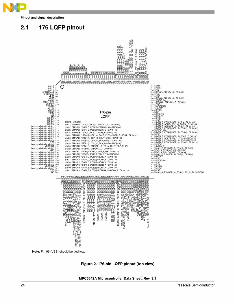
2 Pinout and signal descriptionThis section contains the pinouts for all production packages for the MPC5642A device. For pin signal descriptions, please refer to Table 3
NOTEAny pins labeled “NC” are to be left unconnected. Any connection to an external circuit or voltage may cause unpredictable device behavior or damage.
MPC5642A Microcontroller Data Sheet, Rev. 3.1
Freescale Semiconductor 23
Pinout and signal description
2.1 176 LQFP pinout
Figure 2. 176-pin LQFP pinout (top view)
176-pinLQFP
VD
DA
N[3
7]A
N[3
6]A
N[2
1]A
N[0
] (D
AN
0+)
AN
[1] (
DA
N0-
)A
N[2
] (D
AN
1+)
AN
[3] (
DA
N1-
)A
N[4
] (D
AN
2+)
AN
[5] (
DA
N2-
)A
N[6
] (D
AN
3+)
AN
[7] (
DA
N3-
)R
EF
BY
PC
VR
HV
RL
AN
[22]
AN
[23]
AN
[24]
AN
[25]
AN
[27]
AN
[28]
AN
[30]
AN
[31]
AN
[32]
AN
[33]
AN
[34]
AN
[35]
VD
DA
N[1
2] /
MA
[0] /
ET
PU
A19
_O /
SD
SA
N[1
3] /
MA
[1] /
ET
PU
A21
_O /
SD
OA
N[1
4] /
MA
[2] /
ET
PU
A27
_O /
SD
IA
N[1
5] /
FC
K /
ET
PU
A29
_OG
PIO
[207
] / E
TR
IG1
GP
IO[2
06] /
ET
RIG
0D
SP
I_A
_PC
S[3
] / D
SP
I_D
_SIN
/ G
PIO
[99]
DS
PI_
A_P
CS
[2] /
DS
PI_
D_S
CK
/ G
PIO
[98]
VS
SM
DO
9 / E
TP
UA
25_O
/ G
PIO
[80]
VD
DE
H7B
MD
O8
/ ET
PU
A21
_O /
GP
IO[7
9]M
DO
7 / E
TP
UA
19_O
/ G
PIO
[78]
MD
O6
/ ET
PU
A13
_O /
GP
IO[7
7]M
DO
10 /
ET
PU
A27
_O /
GP
IO[8
1]V
SS
VD
DE
TP
UA
13 /
DS
PI_
B_P
CS
[3] /
GP
IO[1
27]
ET
PU
A12
/ D
SP
I_B
_PC
S[1
] / R
CH
4_C
/ G
PIO
[126
]E
TP
UA
11 /
ET
PU
A23
_O /
RC
H4_
B /
GP
IO[1
25]
ET
PU
A10
/ E
TP
UA
22_O
/ R
CH
1_C
/ G
PIO
[124
]E
TP
UA
9 / E
TP
UA
21_O
/ R
CH
1_B
/ G
PIO
[123
]E
TP
UA
8 / E
TP
UA
20_O
/ D
SP
I_B
_SO
UT
_LV
DS
+ /
GP
IO[1
22]
ET
PU
A7
/ ET
PU
A19
_O /
DS
PI_
B_S
OU
T_L
VD
S-
/ ET
PU
A6_
O /
GP
IO[1
21]
ET
PU
A6
/ ET
PU
A18
_O /
DS
PI_
B_S
CK
_LV
DS
+ /
FR
_B_R
X /
GP
IO[1
20]
ET
PU
A5
/ ET
PU
A17
_O /
DS
PI_
B_S
CK
_LV
DS
- / F
R_B
_TX
_EN
/ G
PIO
[119
]V
DD
EH
4AE
TP
UA
4 / E
TP
UA
16_O
/ F
R_B
_TX
/ G
PIO
[118
]V
SS
ET
PU
A3
/ ET
PU
A15
_O /
GP
IO[1
17]
ET
PU
A2
/ ET
PU
A14
_O /
GP
IO[1
16]
ET
PU
A1
/ ET
PU
A13
_O /
GP
IO[1
15]
ET
PU
A0
/ ET
PU
A12
_O /
ET
PU
A19
_O /
GP
IO[1
14]
VD
DE
MIO
S0
/ ET
PU
A0
/ ET
PU
A25
_O /
GP
IO[1
79]
EM
IOS
1 / E
TP
UA
1_O
/ G
PIO
[180
]E
MIO
S2
/ ET
PU
A2_
O /
RC
H2_
B /
GP
IO[1
81]
EM
IOS
3 / E
TP
UA
3_O
/ G
PIO
[182
]E
MIO
S4
/ ET
PU
A4_
O /
RC
H2_
C /
GP
IO[1
83]
EM
IOS
6 / E
TP
UA
6_O
/ G
PIO
[185
]E
MIO
S7
/ ET
PU
A7_
O /
GP
IO[1
86]
EM
IOS
8 / E
TP
UA
8_O
/ S
CI_
B_T
X /
GP
IO[1
87]
EM
IOS
9 / E
TP
UA
9_O
/ S
CI_
B_R
X /
GP
IO[1
88]
VS
SE
MIO
S10
/ D
SP
I_B
_PC
S[3
] / R
CH
3_B
/ G
PIO
[189
]V
DD
EH
4BE
MIO
S11
/ D
SP
I_D
_PC
S[4
] / R
CH
3_C
/ G
PIO
[190
]E
MIO
S12
/ D
SP
I_C
_SO
UT
/ E
TP
UA
27_O
/ G
PIO
[191
]E
MIO
S13
/ D
SP
I_D
_SO
UT
/ G
PIO
[192
]E
MIO
S14
/ IR
Q[0
] / E
TP
UA
29_O
/ G
PIO
[193
]E
MIO
S15
/ IR
Q[1
] / G
PIO
[194
]E
MIO
S23
/ E
TP
UB
7_O
/ G
PIO
[202
]C
AN
_A_T
X /
SC
I_A
_TX
/ G
PIO
[83]
CA
N_A
_RX
/ S
CI_
A_R
X /
GP
IO[8
4]P
LLR
EF
/ IR
Q[4
] / E
TR
IG[2
] / G
PIO
[208
]S
CI_
B_R
X /
DS
PI_
D_P
CS
[5] /
GP
IO[9
2]B
OO
TC
FG
1 / I
RQ
[3] /
ET
RIG
[3] /
GP
IO[2
12]
WK
PC
FG
/ N
MI /
DS
PI_
B_S
OU
T /
GP
IO[2
13]
SC
I_B
_TX
/ D
SP
I_D
_PC
S[1
] / G
PIO
[91]
CA
N_B
_TX
/ D
SP
I_C
_PC
S[3
] / S
CI_
C_T
X /
GP
IO[8
5]
VDDTMSTDIMDO5 / ETPUA4_O / GPIO[76]TCKVSSMDO4 / ETPUA2_O / GPIO[75]VDDEH7AMDO11 / ETPUA29_O / GPIO[82]TDOGPIO[219]JCOMPEVTONCMSEO[0]MSEO[1]EVTIVSSDSPI_B_PCS[3] / DSPI_C_SIN / GPIO[108]DSPI_B_SOUT / DSPI_C_PCS[5] / GPIO[104]DSPI_B_SIN / DSPI_C_PCS[2] / GPIO[103]DSPI_B_PCS[0] / DSPI_D_PCS[2] / GPIO[105]VDDEH6BDSPI_B_PCS[1] / DSPI_D_PCS[0] / GPIO[106]VSSDSPI_B_PCS[2] / DSPI_C_SOUT / GPIO[107]DSPI_B_SCK / DSPI_C_PCS[1] / GPIO[102]DSPI_B_PCS[4] / DSPI_C_SCK / GPIO[109]DSPI_B_PCS[5] / DSPI_C_PCS[0] / GPIO[110]VDDFRSTOUTCAN_C_TX / DSPI_D_PCS[3] / GPIO[87]SCI_A_TX / EMIOS13 / GPIO[89]SCI_A_RX / EMIOS15 / GPIO[90]CAN_C_RX / DSPI_D_PCS[4] / GPIO[88]RESETVSSVDDEH6AVSSXTALEXTALVDDPLLVSSCAN_B_RX / DSPI_C_PCS[4] / SCI_C_RX / GPIO[86]
AN[18]AN[17]AN[16]
AN[11] / ANZAN[9] / ANX
VDDAVSSA
AN[39]AN[8] / ANW
VDDREGVRCCTL
VSTBYVRC33MCKO
VSSNC
MDO[0]MDO[1]MDO[2]MDO[3]
(see signal details, pin 21)(see signal details, pin 22)(see signal details, pin 23)(see signal details, pin 24)(see signal details, pin 25)(see signal details, pin 26)(see signal details, pin 27)(see signal details, pin 28)
VSS(see signal details, pin 30)
VDDEH1A(see signal details, pin 32)
VDD(see signal details, pin 34)(see signal details, pin 35)(see signal details, pin 36)(see signal details, pin 37)(see signal details, pin 38)(see signal details, pin 39)(see signal details, pin 40)
VDDEH1B(see signal details, pin 42)
VSSNC
1 23456789101112131415161718 19202122232425262728293031 32333435363738394041424344
176
175
174
173
172
171
170
169
168
167
166
165
164
163
162
161
160
159
158
157
156
155
154
153
152
151
150
149
148
147
146
145
144
143
142
141
140
139
138
137
136
135
134
133
45 46 47 48 49 50 51 52 53 54 55 56 57 58 59 60 61 62 63 64 65 66 67 68 69 70 71 72 73 74 75 76 77 78 79 80 81 82 83 84 85 86 87 88
132131130129128127126125124123122121120119118117116115114113112111110109108107106105104103102101100
9998979695949392919089
signal details:pin 21: ETPUA31 / DSPI_C_PCS[4] / ETPUA13_O / GPIO[145]pin 22: ETPUA30 / DSPI_C_PCS[3] / ETPUA11_O / GPIO[144]pin 23: ETPUA29 / DSPI_C_PCS[2] / RCH5_C / GPIO[143]pin 24: ETPUA28 / DSPI_C_PCS[1] / RCH5_B / GPIO[142]pin 25: ETPUA27 / IRQ[15] / DSPI_C_SOUT_LVDS+ / DSPI_B_SOUT / GPIO[141]pin 26: ETPUA26 / IRQ[14] / DSPI_C_SOUT_LVDS- / GPIO[140]pin 27: ETPUA25 / IRQ[13] / DSPI_C_SCK_LVDS+ / GPIO[139]pin 28: ETPUA24 / IRQ[12] / DSPI_C_SCK_LVDS- / GPIO[138]pin 30: ETPUA23 / IRQ[11] / ETPUA21_O / FR_A_TX_EN / GPIO[137]pin 32: ETPUA22 / IRQ[10] / ETPUA17_O / GPIO[136]pin 34: ETPUA21 / IRQ[9] / RCH0_C / FR_A_RX / GPIO[135]pin 35: ETPUA20 / IRQ[8] / RCH0_B / FR_A_TX / GPIO[134]pin 36: ETPUA19 / DSPI_D_PCS[4] / RCH5_A / GPIO[133]pin 37: ETPUA18 / DSPI_D_PCS[3] / RCH4_A / GPIO[132]pin 38: ETPUA17 / DSPI_D_PCS[2] / RCH3_A / GPIO[131]pin 39: ETPUA16 / DSPI_D_PCS[1] / RCH2_A / GPIO[130]pin 40: ETPUA15 / DSPI_B_PCS[5] / RCH1_A / GPIO[129]pin 42: ETPUA14 / DSPI_B_PCS[4] / ETPUA9_O / RCH0_A / GPIO[128]
Note: Pin 96 (VSS) should be tied low.
MPC5642A Microcontroller Data Sheet, Rev. 3.1
24 Freescale Semiconductor
Pin
ou
t and
sign
al descrip
tion
F
13 14 15 16
MDO2 MDO0 VRC33 VSS A
MDO3 MDO1 VSS VDD B
N15-FCK VSS MSEO0 TCK C
VSS TMS EVTO NC D
NC TDI EVTI MSEO1 E
DDEH6AB TDO MCKO JCOMP F
DSPI_B_SOUT
DSPI_B_PCS[3]
DSPI_B_SIN DSPI_B_PCS[0]
G
PIO[99] DSPI_B_PCS[4]
DSPI_B_PCS[2]
DSPI_B_PCS[1]
H
DSPI_B_PCS[5]
SCI_A_TX GPIO[98] DSPI_B_SCK
J
AN_C_TX SCI_A_RX RSTOUT VDDREG K
CI_B_TX CAN_C_RX WKPCFG RESET L
CI_B_RX PLLREF BOOTCFG1 VSS M
VSS VRCCTL NC EXTAL N
VDD VSS NC XTAL P
AN_B_RX VDD VSS VDDPLL R
VDDE12 ENGCLK VDD VSS T
13 14 15 16
MP
C5642A
Micro
con
troller D
ata Sh
eet, Rev. 3.1
reescale Sem
iconductor 25
2.2 208 MAP BGA ballmap
Figure 3. 208-pin MAPBGA package ballmap (viewed from above)
1 2 3 4 5 6 7 8 9 10 11 12
A VSS AN9 AN11 VDDA1 VSSA1 AN1 AN5 VRH VRL AN27 VSSA0 AN12-SDS
B VDD VSS AN8 AN21 AN0 AN4 REFBYPC AN22 AN25 AN28 VDDA0 AN13-SDO
C VSTBY VDD VSS AN17 AN34 AN16 AN3 AN7 AN23 AN32 AN33 AN14-SDI A
D VRC33 AN39 VDD VSS AN18 AN2 AN6 AN24 AN30 AN31 AN35 VDDEH7
E ETPUA30 ETPUA31 AN37 VDD
F ETPUA28 ETPUA29 ETPUA26 AN36 V
G ETPUA24 ETPUA27 ETPUA25 ETPUA21 VSS VSS VSS VSS
H ETPUA23 ETPUA22 ETPUA17 ETPUA18 VSS VSS VSS VSS G
J ETPUA20 ETPUA19 ETPUA14 ETPUA13 VSS VSS VSS VSS
K ETPUA16 ETPUA15 ETPUA7 VDDEH1AB VSS VSS VSS VSS C
L ETPUA12 ETPUA11 ETPUA6 TCRCLKA S
M ETPUA10 ETPUA9 ETPUA1 ETPUA5 S
N ETPUA8 ETPUA4 ETPUA0 VSS VDD VRC33 EMIOS2 EMIOS10 VDDEH4AB EMIOS12 MDO7_ETPUA19_O
VRC33
P ETPUA3 ETPUA2 VSS VDD GPIO[207] NC EMIOS6 EMIOS8 MDO11_ETPUA29_O
MDO4_ETPUA2_O
MDO8_ETPUA21_O
CAN_A_TX
R NC VSS VDD GPIO[206] EMIOS4 EMIOS3 EMIOS9 EMIOS11 EMIOS14 MDO10_ETPUA27_O
EMIOS23 CAN_A_RX C
T VSS VDD NC EMIOS0 EMIOS1 GPIO[219] MDO9_ETPUA25_O
EMIOS13 EMIOS15 MDO5_ETPUA4_O
MDO6_ETPUA13_O
CAN_B_TX
1 2 3 4 5 6 7 8 9 10 11 12
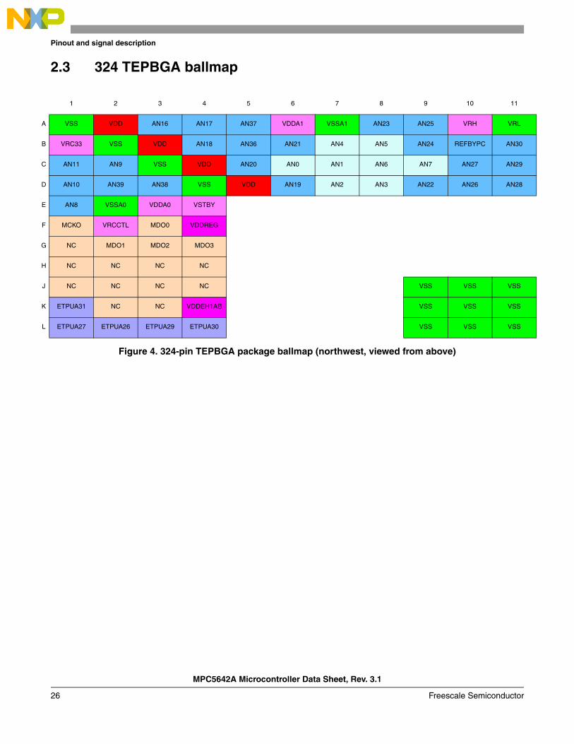
Pinout and signal description
A
B
C
D
E
F
G
H
J
K
L
2.3 324 TEPBGA ballmap
Figure 4. 324-pin TEPBGA package ballmap (northwest, viewed from above)
1 2 3 4 5 6 7 8 9 10 11
VSS VDD AN16 AN17 AN37 VDDA1 VSSA1 AN23 AN25 VRH VRL
VRC33 VSS VDD AN18 AN36 AN21 AN4 AN5 AN24 REFBYPC AN30
AN11 AN9 VSS VDD AN20 AN0 AN1 AN6 AN7 AN27 AN29
AN10 AN39 AN38 VSS VDD AN19 AN2 AN3 AN22 AN26 AN28
AN8 VSSA0 VDDA0 VSTBY
MCKO VRCCTL MDO0 VDDREG
NC MDO1 MDO2 MDO3
NC NC NC NC
NC NC NC NC VSS VSS VSS
ETPUA31 NC NC VDDEH1AB VSS VSS VSS
ETPUA27 ETPUA26 ETPUA29 ETPUA30 VSS VSS VSS
MPC5642A Microcontroller Data Sheet, Rev. 3.1
26 Freescale Semiconductor
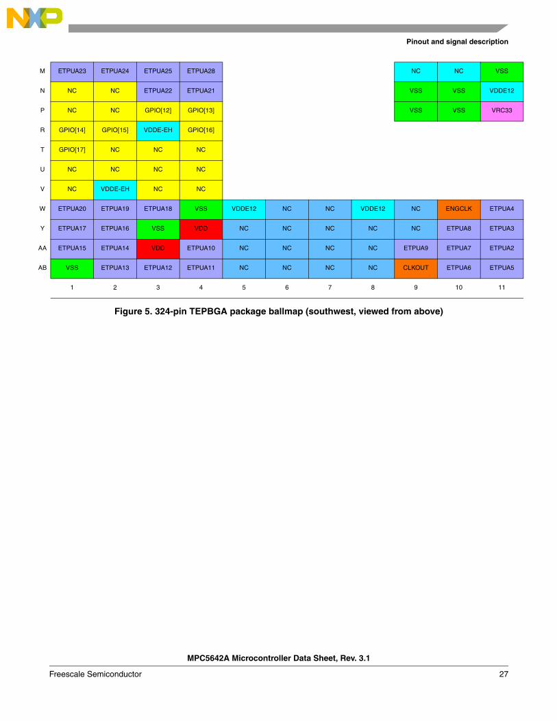
Pinout and signal description
M
N
P
R
T
U
V
W
Y
A
A
Figure 5. 324-pin TEPBGA package ballmap (southwest, viewed from above)
ETPUA23 ETPUA24 ETPUA25 ETPUA28 NC NC VSS
NC NC ETPUA22 ETPUA21 VSS VSS VDDE12
NC NC GPIO[12] GPIO[13] VSS VSS VRC33
GPIO[14] GPIO[15] VDDE-EH GPIO[16]
GPIO[17] NC NC NC
NC NC NC NC
NC VDDE-EH NC NC
ETPUA20 ETPUA19 ETPUA18 VSS VDDE12 NC NC VDDE12 NC ENGCLK ETPUA4
ETPUA17 ETPUA16 VSS VDD NC NC NC NC NC ETPUA8 ETPUA3
A ETPUA15 ETPUA14 VDD ETPUA10 NC NC NC NC ETPUA9 ETPUA7 ETPUA2
B VSS ETPUA13 ETPUA12 ETPUA11 NC NC NC NC CLKOUT ETPUA6 ETPUA5
1 2 3 4 5 6 7 8 9 10 11
MPC5642A Microcontroller Data Sheet, Rev. 3.1
Freescale Semiconductor 27
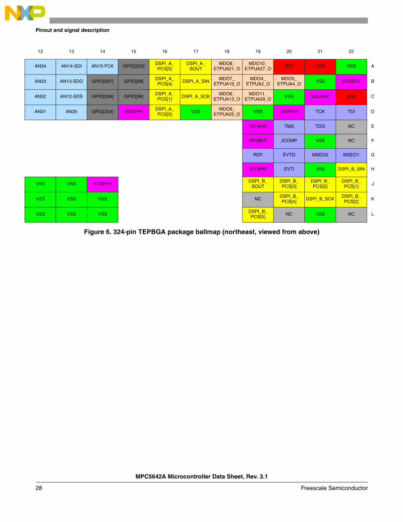
Pinout and signal description
Figure 6. 324-pin TEPBGA package ballmap (northeast, viewed from above)
12 13 14 15 16 17 18 19 20 21 22
AN34 AN14-SDI AN15-FCK GPIO[203] DSPI_A_PCS[5]
DSPI_A_SOUT
MDO8_ETPUA21_O
MDO10_ETPUA27_O VDD VDD VSS A
AN33 AN13-SDO GPIO[207] GPIO[99] DSPI_A_PCS[4] DSPI_A_SIN MDO7_
ETPUA19_OMDO4_
ETPUA2_OMDO5_
ETPUA4_O VSS VDDEH7 B
AN32 AN12-SDS GPIO[206] GPIO[98] DSPI_A_PCS[1] DSPI_A_SCK MDO6_
ETPUA13_OMDO11_
ETPUA29_O VSS VDDEH7 VDD C
AN31 AN35 GPIO[204] VDDEH7 DSPI_A_PCS[0] VSS MDO9_
ETPUA25_O VSS VDDEH7 TCK TDI D
VDDEH7 TMS TDO NC E
VDDEH7 JCOMP VSS NC F
RDY EVTO MSEO0 MSEO1 G
VDDEH7 EVTI VSS DSPI_B_SIN H
VSS VSS VDDEH7 DSPI_B_SOUT
DSPI_B_PCS[3]
DSPI_B_PCS[0]
DSPI_B_PCS[1] J
VSS VSS VSS NC DSPI_B_PCS[4] DSPI_B_SCK DSPI_B_
PCS[2] K
VSS VSS VSS DSPI_B_PCS[5] NC VSS NC L
MPC5642A Microcontroller Data Sheet, Rev. 3.1
28 Freescale Semiconductor
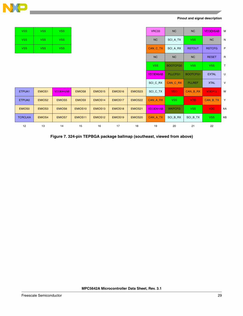
Pinout and signal description
T
Figure 7. 324-pin TEPBGA package ballmap (southeast, viewed from above)
VSS VSS VSS VRC33 NC NC VDDEH6AB M
VSS VSS VSS NC SCI_A_TX VSS NC N
VSS VSS VSS CAN_C_TX SCI_A_RX RSTOUT RSTCFG P
NC NC NC RESET R
VSS BOOTCFG0 VSS VSS T
VDDEH6AB PLLCFG1 BOOTCFG1 EXTAL U
SCI_C_RX CAN_C_RX PLLREF XTAL V
ETPUA1 EMIOS1 VDDEH4AB EMIOS8 EMIOS15 EMIOS16 EMIOS23 SCI_C_TX VDD CAN_B_RX VDDPLL W
ETPUA0 EMIOS2 EMIOS5 EMIOS9 EMIOS14 EMIOS17 EMIOS22 CAN_A_RX VSS VDD CAN_B_TX Y
EMIOS0 EMIOS3 EMIOS6 EMIOS10 EMIOS13 EMIOS18 EMIOS21 VDDEH4AB WKPCFG VSS VDD AA
CRCLKA EMIOS4 EMIOS7 EMIOS11 EMIOS12 EMIOS19 EMIOS20 CAN_A_TX SCI_B_RX SCI_B_TX VSS AB
12 13 14 15 16 17 18 19 20 21 22
MPC5642A Microcontroller Data Sheet, Rev. 3.1
Freescale Semiconductor 29
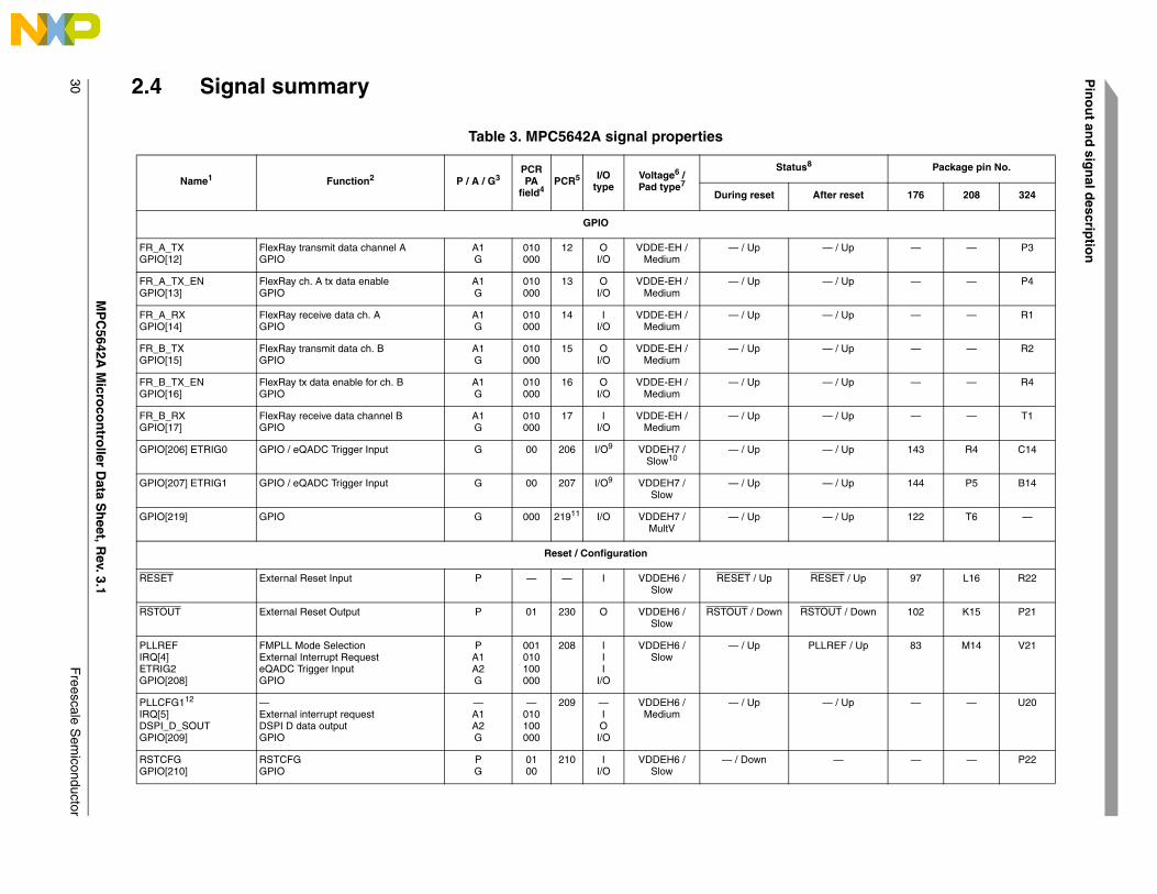
Pin
ou
t and
sign
al descrip
tion
3
Package pin No.
r reset 176 208 324
/ Up — — P3
/ Up — — P4
/ Up — — R1
/ Up — — R2
/ Up — — R4
/ Up — — T1
/ Up 143 R4 C14
/ Up 144 P5 B14
/ Up 122 T6 —
ET / Up 97 L16 R22
T / Down 102 K15 P21
EF / Up 83 M14 V21
/ Up — — U20
— — — P22
MP
C5642A
Micro
con
troller D
ata Sh
eet, Rev. 3.1
Freescale S
emiconductor
0 2.4 Signal summary
Table 3. MPC5642A signal properties
Name1 Function2 P / A / G3PCR PA
field4PCR5 I/O
typeVoltage6 /Pad type7
Status8
During reset Afte
GPIO
FR_A_TXGPIO[12]
FlexRay transmit data channel AGPIO
A1G
010000
12 OI/O
VDDE-EH /Medium
— / Up —
FR_A_TX_ENGPIO[13]
FlexRay ch. A tx data enableGPIO
A1G
010000
13 OI/O
VDDE-EH /Medium
— / Up —
FR_A_RXGPIO[14]
FlexRay receive data ch. AGPIO
A1G
010000
14 II/O
VDDE-EH /Medium
— / Up —
FR_B_TXGPIO[15]
FlexRay transmit data ch. BGPIO
A1G
010000
15 OI/O
VDDE-EH /Medium
— / Up —
FR_B_TX_ENGPIO[16]
FlexRay tx data enable for ch. BGPIO
A1G
010000
16 OI/O
VDDE-EH /Medium
— / Up —
FR_B_RXGPIO[17]
FlexRay receive data channel BGPIO
A1G
010000
17 II/O
VDDE-EH /Medium
— / Up —
GPIO[206] ETRIG0 GPIO / eQADC Trigger Input G 00 206 I/O9 VDDEH7 /Slow10
— / Up —
GPIO[207] ETRIG1 GPIO / eQADC Trigger Input G 00 207 I/O9 VDDEH7 /Slow
— / Up —
GPIO[219] GPIO G 000 21911 I/O VDDEH7 /MultV
— / Up —
Reset / Configuration
RESET External Reset Input P — — I VDDEH6 /Slow
RESET / Up RES
RSTOUT External Reset Output P 01 230 O VDDEH6 /Slow
RSTOUT / Down RSTOU
PLLREFIRQ[4]ETRIG2GPIO[208]
FMPLL Mode SelectionExternal Interrupt RequesteQADC Trigger InputGPIO
PA1A2G
001010100000
208 III
I/O
VDDEH6 /Slow
— / Up PLLR
PLLCFG112
IRQ[5]DSPI_D_SOUTGPIO[209]
—External interrupt requestDSPI D data outputGPIO
—A1A2G
—010100000
209 —IOI/O
VDDEH6 /Medium
— / Up —
RSTCFGGPIO[210]
RSTCFGGPIO
PG
0100
210 II/O
VDDEH6 /Slow
— / Down
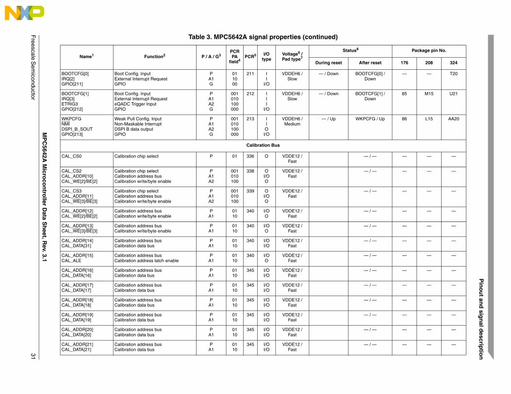
Pin
ou
t and
sign
al descrip
tion
F
CFG[0] / own
— — T20
CFG[1] / own
85 M15 U21
FG / Up 86 L15 AA20
/ — — — —
/ — — — —
/ — — — —
/ — — — —
/ — — — —
/ — — — —
/ — — — —
/ — — — —
/ — — — —
/ — — — —
/ — — — —
/ — — — —
/ — — — —
Package pin No.
r reset 176 208 324
MP
C5642A
Micro
con
troller D
ata Sh
eet, Rev. 3.1
reescale Sem
iconductor 31
BOOTCFG[0]IRQ[2]GPIO[211]
Boot Config. InputExternal Interrupt RequestGPIO
PA1G
011000
211 II
I/O
VDDEH6 /Slow
— / Down BOOTD
BOOTCFG[1]IRQ[3]ETRIG3GPIO[212]
Boot Config. InputExternal Interrupt RequesteQADC Trigger InputGPIO
PA1A2G
001010100000
212 III
I/O
VDDEH6 /Slow
— / Down BOOTD
WKPCFGNMIDSPI_B_SOUTGPIO[213]
Weak Pull Config. InputNon-Maskable InterruptDSPI B data outputGPIO
PA1A2G
001010100000
213 IIOI/O
VDDEH6 /Medium
— / Up WKPC
Calibration Bus
CAL_CS0 Calibration chip select P 01 336 O VDDE12 /Fast
—
CAL_CS2CAL_ADDR[10]CAL_WE[2]/BE[2]
Calibration chip selectCalibration address busCalibration write/byte enable
PA1A2
001010100
338 OI/OO
VDDE12 /Fast
—
CAL_CS3CAL_ADDR[11]CAL_WE[3]/BE[3]
Calibration chip selectCalibration address busCalibration write/byte enable
PA1A2
001010100
339 OI/OO
VDDE12 /Fast
—
CAL_ADDR[12]CAL_WE[2]/BE[2]
Calibration address busCalibration write/byte enable
PA1
0110
340 I/OO
VDDE12 /Fast
—
CAL_ADDR[13]CAL_WE[3]/BE[3]
Calibration address busCalibration write/byte enable
PA1
0110
340 I/OO
VDDE12 /Fast
—
CAL_ADDR[14]CAL_DATA[31]
Calibration address busCalibration data bus
PA1
0110
340 I/OI/O
VDDE12 /Fast
—
CAL_ADDR[15]CAL_ALE
Calibration address busCalibration address latch enable
PA1
0110
340 I/OO
VDDE12 /Fast
—
CAL_ADDR[16]CAL_DATA[16]
Calibration address busCalibration data bus
PA1
0110
345 I/OI/O
VDDE12 /Fast
—
CAL_ADDR[17]CAL_DATA[17]
Calibration address busCalibration data bus
PA1
0110
345 I/OI/O
VDDE12 /Fast
—
CAL_ADDR[18]CAL_DATA[18]
Calibration address busCalibration data bus
PA1
0110
345 I/OI/O
VDDE12 /Fast
—
CAL_ADDR[19]CAL_DATA[19]
Calibration address busCalibration data bus
PA1
0110
345 I/OI/O
VDDE12 /Fast
—
CAL_ADDR[20]CAL_DATA[20]
Calibration address busCalibration data bus
PA1
0110
345 I/OI/O
VDDE12 /Fast
—
CAL_ADDR[21]CAL_DATA[21]
Calibration address busCalibration data bus
PA1
0110
345 I/OI/O
VDDE12 /Fast
—
Table 3. MPC5642A signal properties (continued)
Name1 Function2 P / A / G3PCR PA
field4PCR5 I/O
typeVoltage6 /Pad type7
Status8
During reset Afte
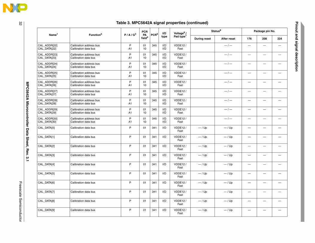
Pin
ou
t and
sign
al descrip
tion
3
/ — — — —
/ — — — —
/ — — — —
/ — — — —
/ — — — —
/ — — — —
/ — — — —
/ — — — —
/ — — — —
/ Up — — —
/ Up — — —
/ Up — — —
/ Up — — —
/ Up — — —
/ Up — — —
/ Up — — —
/ Up — — —
/ Up — — —
/ Up — — —
Package pin No.
r reset 176 208 324
MP
C5642A
Micro
con
troller D
ata Sh
eet, Rev. 3.1
Freescale S
emiconductor
2
CAL_ADDR[22]CAL_DATA[22]
Calibration address busCalibration data bus
PA1
0110
345 I/OI/O
VDDE12 /Fast
—
CAL_ADDR[23]CAL_DATA[23]
Calibration address busCalibration data bus
PA1
0110
345 I/OI/O
VDDE12 /Fast
—
CAL_ADDR[24]CAL_DATA[24]
Calibration address busCalibration data bus
PA1
0110
345 I/OI/O
VDDE12 /Fast
—
CAL_ADDR[25]CAL_DATA[25]
Calibration address busCalibration data bus
PA1
0110
345 I/OI/O
VDDE12 /Fast
—
CAL_ADDR[26]CAL_DATA[26]
Calibration address busCalibration data bus
PA1
0110
345 I/OI/O
VDDE12 /Fast
—
CAL_ADDR[27]CAL_DATA[27]
Calibration address busCalibration data bus
PA1
0110
345 I/OI/O
VDDE12 /Fast
—
CAL_ADDR[28]CAL_DATA[28]
Calibration address busCalibration data bus
PA1
0110
345 I/OI/O
VDDE12 /Fast
—
CAL_ADDR[29]CAL_DATA[29]
Calibration address busCalibration data bus
PA1
0110
345 I/OI/O
VDDE12 /Fast
—
CAL_ADDR[30]CAL_DATA[30]
Calibration address busCalibration data bus
PA1
0110
345 I/OI/O
VDDE12 /Fast
—
CAL_DATA[0] Calibration data bus P 01 341 I/O VDDE12 /Fast
— / Up —
CAL_DATA[1] Calibration data bus P 01 341 I/O VDDE12 /Fast
— / Up —
CAL_DATA[2] Calibration data bus P 01 341 I/O VDDE12 /Fast
— / Up —
CAL_DATA[3] Calibration data bus P 01 341 I/O VDDE12 /Fast
— / Up —
CAL_DATA[4] Calibration data bus P 01 341 I/O VDDE12 /Fast
— / Up —
CAL_DATA[5] Calibration data bus P 01 341 I/O VDDE12 /Fast
— / Up —
CAL_DATA[6] Calibration data bus P 01 341 I/O VDDE12 /Fast
— / Up —
CAL_DATA[7] Calibration data bus P 01 341 I/O VDDE12 /Fast
— / Up —
CAL_DATA[8] Calibration data bus P 01 341 I/O VDDE12 /Fast
— / Up —
CAL_DATA[9] Calibration data bus P 01 341 I/O VDDE12 /Fast
— / Up —
Table 3. MPC5642A signal properties (continued)
Name1 Function2 P / A / G3PCR PA
field4PCR5 I/O
typeVoltage6 /Pad type7
Status8
During reset Afte
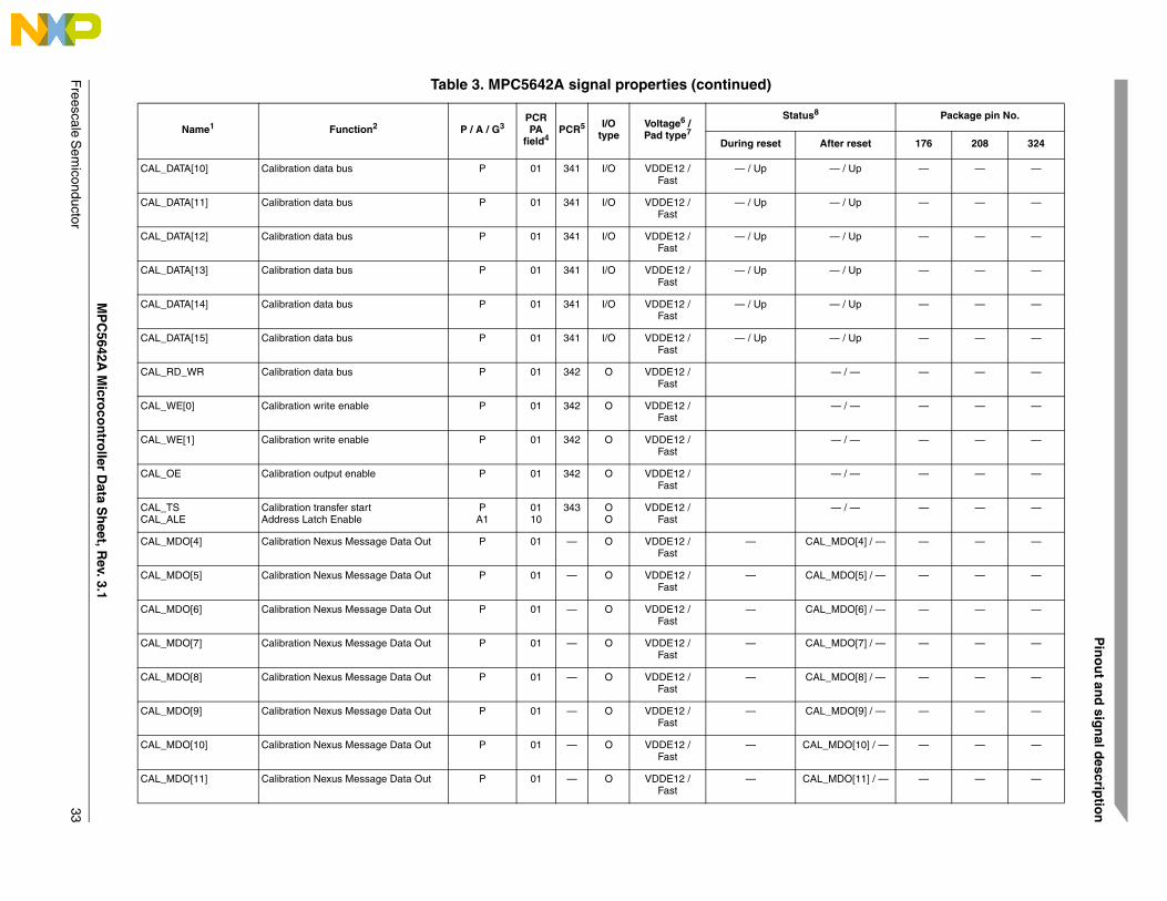
Pin
ou
t and
sign
al descrip
tion
F
/ Up — — —
/ Up — — —
/ Up — — —
/ Up — — —
/ Up — — —
/ Up — — —
/ — — — —
/ — — — —
/ — — — —
/ — — — —
/ — — — —
DO[4] / — — — —
DO[5] / — — — —
DO[6] / — — — —
DO[7] / — — — —
DO[8] / — — — —
DO[9] / — — — —
DO[10] / — — — —
DO[11] / — — — —
Package pin No.
r reset 176 208 324
MP
C5642A
Micro
con
troller D
ata Sh
eet, Rev. 3.1
reescale Sem
iconductor 33
CAL_DATA[10] Calibration data bus P 01 341 I/O VDDE12 /Fast
— / Up —
CAL_DATA[11] Calibration data bus P 01 341 I/O VDDE12 /Fast
— / Up —
CAL_DATA[12] Calibration data bus P 01 341 I/O VDDE12 /Fast
— / Up —
CAL_DATA[13] Calibration data bus P 01 341 I/O VDDE12 /Fast
— / Up —
CAL_DATA[14] Calibration data bus P 01 341 I/O VDDE12 /Fast
— / Up —
CAL_DATA[15] Calibration data bus P 01 341 I/O VDDE12 /Fast
— / Up —
CAL_RD_WR Calibration data bus P 01 342 O VDDE12 /Fast
—
CAL_WE[0] Calibration write enable P 01 342 O VDDE12 /Fast
—
CAL_WE[1] Calibration write enable P 01 342 O VDDE12 /Fast
—
CAL_OE Calibration output enable P 01 342 O VDDE12 /Fast
—
CAL_TSCAL_ALE
Calibration transfer startAddress Latch Enable
PA1
0110
343 OO
VDDE12 /Fast
—
CAL_MDO[4] Calibration Nexus Message Data Out P 01 — O VDDE12 /Fast
— CAL_M
CAL_MDO[5] Calibration Nexus Message Data Out P 01 — O VDDE12 /Fast
— CAL_M
CAL_MDO[6] Calibration Nexus Message Data Out P 01 — O VDDE12 /Fast
— CAL_M
CAL_MDO[7] Calibration Nexus Message Data Out P 01 — O VDDE12 /Fast
— CAL_M
CAL_MDO[8] Calibration Nexus Message Data Out P 01 — O VDDE12 /Fast
— CAL_M
CAL_MDO[9] Calibration Nexus Message Data Out P 01 — O VDDE12 /Fast
— CAL_M
CAL_MDO[10] Calibration Nexus Message Data Out P 01 — O VDDE12 /Fast
— CAL_M
CAL_MDO[11] Calibration Nexus Message Data Out P 01 — O VDDE12 /Fast
— CAL_M
Table 3. MPC5642A signal properties (continued)
Name1 Function2 P / A / G3PCR PA
field4PCR5 I/O
typeVoltage6 /Pad type7
Status8
During reset Afte
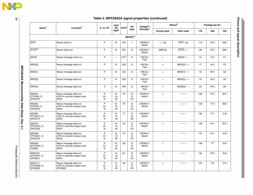
Pin
ou
t and
sign
al descrip
tion
3
TI / Up 116 E15 H20
TO / — 120 D15 G20
KO / — 14 F15 F1
[0] / — 17 A14 F3
[1] / — 18 B14 G2
[2] / — 19 A13 G3
[3] / — 20 B13 G4
/ — 126 P10 B19
/ — 129 T10 B20
/ — 135 T11 C18
/ — 136 N11 B18
/ — 137 P11 A18
/ — 139 T7 D18
/ — 134 R10 A19
/ — 124 P9 C19
Package pin No.
r reset 176 208 324
MP
C5642A
Micro
con
troller D
ata Sh
eet, Rev. 3.1
Freescale S
emiconductor
4
NEXUS13
EVTI Nexus event in P 01 231 I VDDEH7 /MultiV
— / Up EV
EVTO14 Nexus event out P 01 227 O VDDEH7 /MultiV
ABR/Up EV
MCKO Nexus message clock out P — 21911 O VRC33 /Fast
— MC
MDO[0] Nexus message data out P 01 220 O VRC33 /Fast
— MDO
MDO[1] Nexus message data out P 01 221 O VRC33 /Fast
— MDO
MDO[2] Nexus message data out P 01 222 O VRC33 /Fast
— MDO
MDO[3] Nexus message data out P 01 223 O VRC33 /Fast
— MDO
MDO[4]ETPUA2_OGPIO[75]
Nexus message data outeTPU A channel (output only)GPIO
PA1G
011000
75 OOI/O
VDDEH7 /MultiV
— —
MDO[5]ETPUA4_OGPIO[76]
Nexus message data outeTPU A channel (output only)GPIO
PA1G
011000
76 OOI/O
VDDEH7 /MultiV
— —
MDO[6]ETPUA13_OGPIO[77]
Nexus message data outeTPU A channel (output only)GPIO
PA1G
011000
77 OOI/O
VDDEH7 /MultiV
— —
MDO[7]ETPUA19_OGPIO[78]
Nexus message data outeTPU A channel (output only)GPIO
PA1G
011000
78 OOI/O
VDDEH7 /MultiV
— —
MDO[8]ETPUA21_OGPIO[79]
Nexus message data outeTPU A channel (output only)GPIO
PA1G
011000
79 OOI/O
VDDEH7 /MultiV
— —
MDO[9]ETPUA25_OPIO[80]
Nexus message data outeTPU A channel (output only)GPIO
PA1G
011000
80 OOI/O
VDDEH7 /MultiV
— —
MDO[10]ETPUA27_OGPIO[81]
Nexus message data outeTPU A channel (output only)GPIO
PA1G
011000
81 OOI/O
VDDEH7 /MultiV
— —
MDO[11]ETPUA29_OGPIO[82]
Nexus message data outeTPU A channel (output only)GPIO[82]
PA1G
011000
82 OOI/O
VDDEH7 /MultiV
— —
Table 3. MPC5642A signal properties (continued)
Name1 Function2 P / A / G3PCR PA
field4PCR5 I/O
typeVoltage6 /Pad type7
Status8
During reset Afte
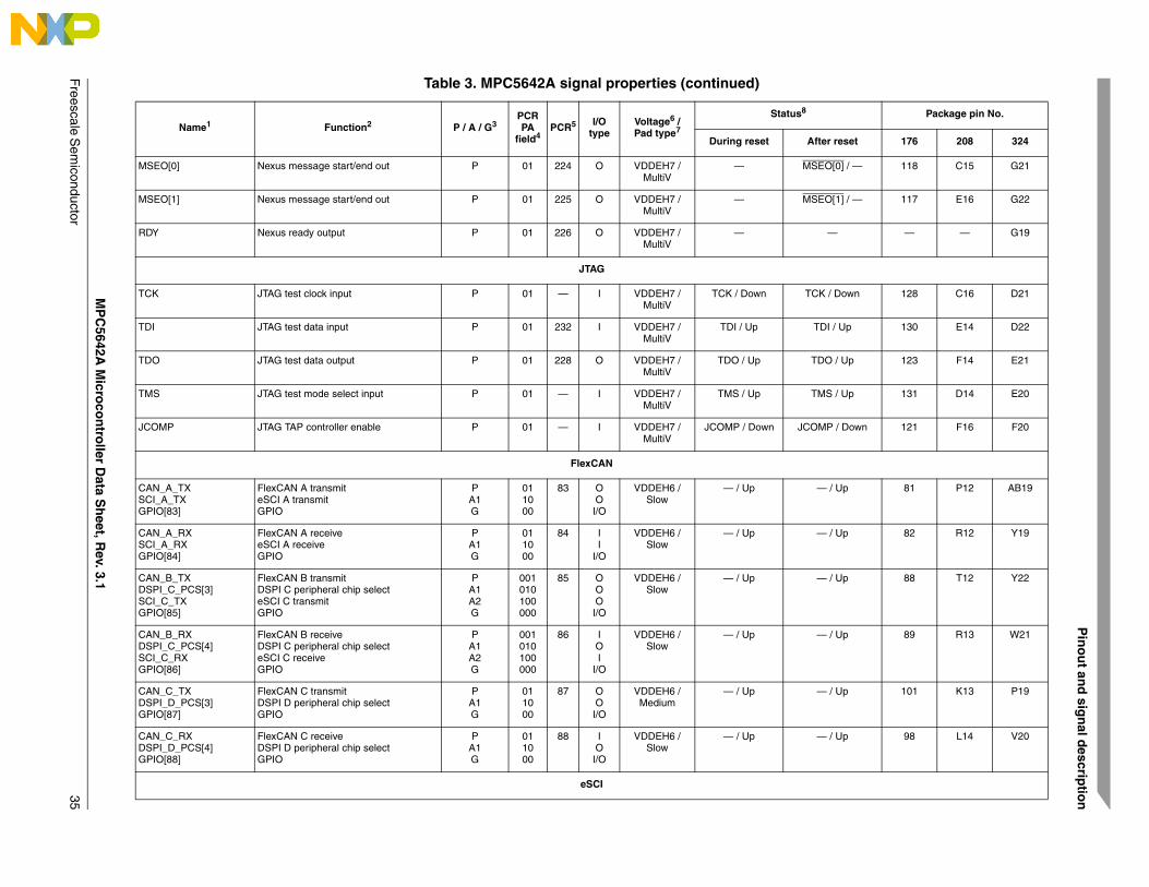
Pin
ou
t and
sign
al descrip
tion
F
O[0] / — 118 C15 G21
O[1] / — 117 E16 G22
— — — G19
/ Down 128 C16 D21
I / Up 130 E14 D22
O / Up 123 F14 E21
S / Up 131 D14 E20
P / Down 121 F16 F20
/ Up 81 P12 AB19
/ Up 82 R12 Y19
/ Up 88 T12 Y22
/ Up 89 R13 W21
/ Up 101 K13 P19
/ Up 98 L14 V20
Package pin No.
r reset 176 208 324
MP
C5642A
Micro
con
troller D
ata Sh
eet, Rev. 3.1
reescale Sem
iconductor 35
MSEO[0] Nexus message start/end out P 01 224 O VDDEH7 /MultiV
— MSE
MSEO[1] Nexus message start/end out P 01 225 O VDDEH7 /MultiV
— MSE
RDY Nexus ready output P 01 226 O VDDEH7 /MultiV
—
JTAG
TCK JTAG test clock input P 01 — I VDDEH7 /MultiV
TCK / Down TCK
TDI JTAG test data input P 01 232 I VDDEH7 /MultiV
TDI / Up TD
TDO JTAG test data output P 01 228 O VDDEH7 /MultiV
TDO / Up TD
TMS JTAG test mode select input P 01 — I VDDEH7 /MultiV
TMS / Up TM
JCOMP JTAG TAP controller enable P 01 — I VDDEH7 /MultiV
JCOMP / Down JCOM
FlexCAN
CAN_A_TXSCI_A_TXGPIO[83]
FlexCAN A transmiteSCI A transmitGPIO
PA1G
011000
83 OOI/O
VDDEH6 /Slow
— / Up —
CAN_A_RXSCI_A_RXGPIO[84]
FlexCAN A receiveeSCI A receiveGPIO
PA1G
011000
84 II
I/O
VDDEH6 /Slow
— / Up —
CAN_B_TXDSPI_C_PCS[3]SCI_C_TXGPIO[85]
FlexCAN B transmitDSPI C peripheral chip selecteSCI C transmitGPIO
PA1A2G
001010100000
85 OOOI/O
VDDEH6 /Slow
— / Up —
CAN_B_RXDSPI_C_PCS[4]SCI_C_RXGPIO[86]
FlexCAN B receiveDSPI C peripheral chip selecteSCI C receiveGPIO
PA1A2G
001010100000
86 IOI
I/O
VDDEH6 /Slow
— / Up —
CAN_C_TXDSPI_D_PCS[3]GPIO[87]
FlexCAN C transmitDSPI D peripheral chip selectGPIO
PA1G
011000
87 OOI/O
VDDEH6 /Medium
— / Up —
CAN_C_RXDSPI_D_PCS[4]GPIO[88]
FlexCAN C receiveDSPI D peripheral chip selectGPIO
PA1G
011000
88 IOI/O
VDDEH6 /Slow
— / Up —
eSCI
Table 3. MPC5642A signal properties (continued)
Name1 Function2 P / A / G3PCR PA
field4PCR5 I/O
typeVoltage6 /Pad type7
Status8
During reset Afte
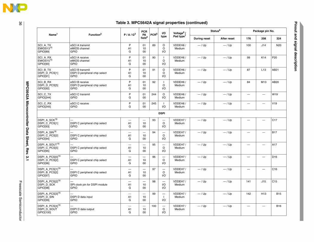
Pin
ou
t and
sign
al descrip
tion
3
/ Up 100 J14 N20
/ Up 99 K14 P20
/ Up 87 L13 AB21
/ Up 84 M13 AB20
/ Up — — W19
/ Up — — V19
/ Up — — C17
/ Up — — B17
/ Up — — A17
/ Up — — D16
/ Up — — C16
/ Up 141 J15 C15
/ Up 142 H13 B15
/ Up — — B16
Package pin No.
r reset 176 208 324
MP
C5642A
Micro
con
troller D
ata Sh
eet, Rev. 3.1
Freescale S
emiconductor
6
SCI_A_TXEMIOS1315
GPIO[89]
eSCI A transmiteMIOS channelGPIO
PA1G
011000
89 OOI/O
VDDEH6 /Medium
— / Up —
SCI_A_RXEMIOS1515
GPIO[90]
eSCI A receiveeMIOS channelGPIO
PA1G
011000
90 IOI/O
VDDEH6 /Medium
— / Up —
SCI_B_TXDSPI_D_PCS[1]GPIO[91]
eSCI B transmitDSPI D peripheral chip selectGPIO
PA1G
011000
91 OOI/O
VDDEH6 /Medium
— / Up —
SCI_B_RXDSPI_D_PCS[5]GPIO[92]
eSCI B receiveDSPI D peripheral chip selectGPIO
PA1G
011000
92 IOI/O
VDDEH6 /Medium
— / Up —
SCI_C_TXGPIO[244]
eSCI C transmitGPIO
PG
0100
244 OI/O
VDDEH6 /Medium
— / Up —
SCI_C_RXGPIO[245]
eSCI C receiveGPIO
PG
0100
245 II/O
VDDEH6 /Medium
— / Up —
DSPI
DSPI_A_SCK16
DSPI_C_PCS[1]GPIO[93]
—DSPI C peripheral chip selectGPIO
—A1G
—1000
93 —OI/O
VDDEH7 /Medium
— / Up —
DSPI_A_SIN16
DSPI_C_PCS[2]GPIO[94]
—DSPI C peripheral chip selectGPIO
—A1G
—1000
94 —OI/O
VDDEH7 /Medium
— / Up —
DSPI_A_SOUT16
DSPI_C_PCS[5]GPIO[95]
—DSPI C peripheral chip selectGPIO
—A1G
—1000
95 —OI/O
VDDEH7 /Medium
— / Up —
DSPI_A_PCS[0]16
DSPI_D_PCS[2]GPIO[96]
—DSPI C peripheral chip selectGPIO
—A1G
—1000
96 —OI/O
VDDEH7 /Medium
— / Up —
DSPI_A_PCS[1]16
DSPI_B_PCS[2]GPIO[97]
—DSPI C peripheral chip selectGPIO
—A1G
—1000
97 —OI/O
VDDEH7 /Medium
— / Up —
DSPI_A_PCS[2]16
DSPI_D_SCKGPIO[98]
—SPI clock pin for DSPI moduleGPIO
—A1G
—1000
98 —I/OI/O
VDDEH7 /Medium
— / Up —
DSPI_A_PCS[3]16
DSPI_D_SINGPIO[99]
—DSPI D data inputGPIO
—A1G
—1000
99 —I
I/O
VDDEH7 /Medium
— / Up —
DSPI_A_PCS[4]16
DSPI_D_SOUTGPIO[100]
—DSPI D data outputGPIO
—A1G
—1000
100 —OI/O
VDDEH7 /Medium
— / Up —
Table 3. MPC5642A signal properties (continued)
Name1 Function2 P / A / G3PCR PA
field4PCR5 I/O
typeVoltage6 /Pad type7
Status8
During reset Afte
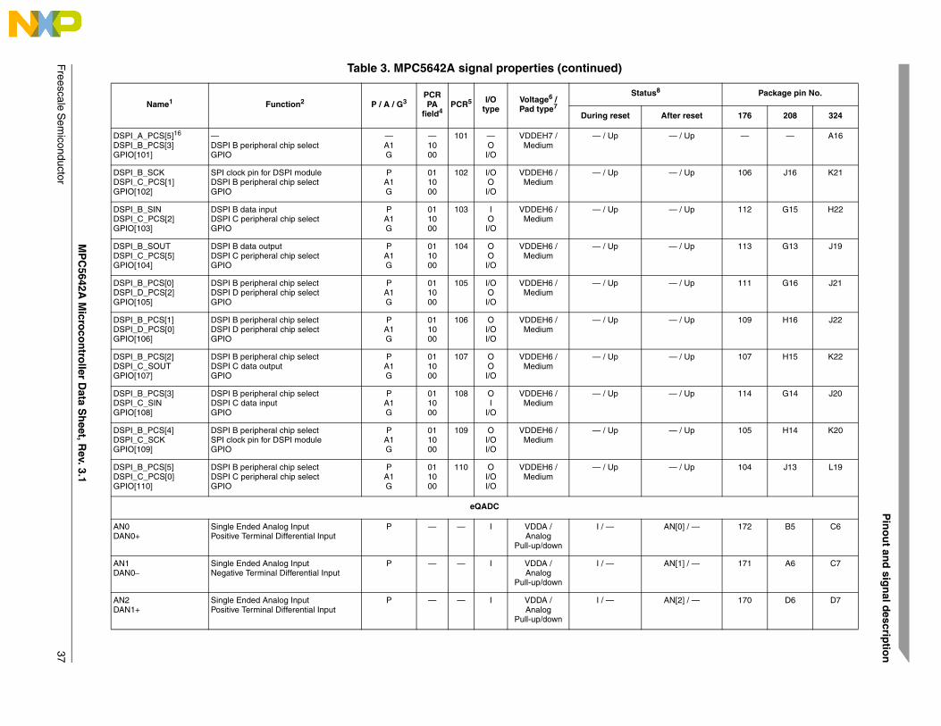
Pin
ou
t and
sign
al descrip
tion
F
/ Up — — A16
/ Up 106 J16 K21
/ Up 112 G15 H22
/ Up 113 G13 J19
/ Up 111 G16 J21
/ Up 109 H16 J22
/ Up 107 H15 K22
/ Up 114 G14 J20
/ Up 105 H14 K20
/ Up 104 J13 L19
[0] / — 172 B5 C6
[1] / — 171 A6 C7
[2] / — 170 D6 D7
Package pin No.
r reset 176 208 324
MP
C5642A
Micro
con
troller D
ata Sh
eet, Rev. 3.1
reescale Sem
iconductor 37
DSPI_A_PCS[5]16
DSPI_B_PCS[3]GPIO[101]
—DSPI B peripheral chip selectGPIO
—A1G
—1000
101 —OI/O
VDDEH7 /Medium
— / Up —
DSPI_B_SCKDSPI_C_PCS[1]GPIO[102]
SPI clock pin for DSPI moduleDSPI B peripheral chip selectGPIO
PA1G
011000
102 I/OOI/O
VDDEH6 /Medium
— / Up —
DSPI_B_SINDSPI_C_PCS[2]GPIO[103]
DSPI B data inputDSPI C peripheral chip selectGPIO
PA1G
011000
103 IOI/O
VDDEH6 /Medium
— / Up —
DSPI_B_SOUTDSPI_C_PCS[5]GPIO[104]
DSPI B data outputDSPI C peripheral chip selectGPIO
PA1G
011000
104 OOI/O
VDDEH6 /Medium
— / Up —
DSPI_B_PCS[0]DSPI_D_PCS[2]GPIO[105]
DSPI B peripheral chip selectDSPI D peripheral chip selectGPIO
PA1G
011000
105 I/OOI/O
VDDEH6 /Medium
— / Up —
DSPI_B_PCS[1]DSPI_D_PCS[0]GPIO[106]
DSPI B peripheral chip selectDSPI D peripheral chip selectGPIO
PA1G
011000
106 OI/OI/O
VDDEH6 /Medium
— / Up —
DSPI_B_PCS[2]DSPI_C_SOUTGPIO[107]
DSPI B peripheral chip selectDSPI C data outputGPIO
PA1G
011000
107 OOI/O
VDDEH6 /Medium
— / Up —
DSPI_B_PCS[3]DSPI_C_SINGPIO[108]
DSPI B peripheral chip selectDSPI C data inputGPIO
PA1G
011000
108 OI
I/O
VDDEH6 /Medium
— / Up —
DSPI_B_PCS[4]DSPI_C_SCKGPIO[109]
DSPI B peripheral chip selectSPI clock pin for DSPI moduleGPIO
PA1G
011000
109 OI/OI/O
VDDEH6 /Medium
— / Up —
DSPI_B_PCS[5]DSPI_C_PCS[0]GPIO[110]
DSPI B peripheral chip selectDSPI C peripheral chip selectGPIO
PA1G
011000
110 OI/OI/O
VDDEH6 /Medium
— / Up —
eQADC
AN0DAN0+
Single Ended Analog InputPositive Terminal Differential Input
P — — I VDDA /Analog
Pull-up/down
I / — AN
AN1DAN0
Single Ended Analog InputNegative Terminal Differential Input
P — — I VDDA /Analog
Pull-up/down
I / — AN
AN2DAN1+
Single Ended Analog InputPositive Terminal Differential Input
P — — I VDDA /Analog
Pull-up/down
I / — AN
Table 3. MPC5642A signal properties (continued)
Name1 Function2 P / A / G3PCR PA
field4PCR5 I/O
typeVoltage6 /Pad type7
Status8
During reset Afte
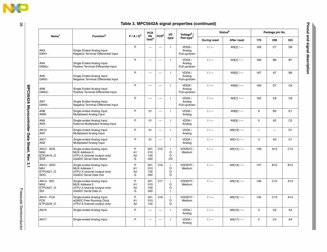
Pin
ou
t and
sign
al descrip
tion
3
[3] / — 169 C7 D8
[4] / — 168 B6 B7
[5] / — 167 A7 B8
[6] / — 166 D7 C8
[7] / — 165 C8 C9
[8] / — 9 B3 E1
[9] / — 5 A2 C2
10] / — — — D1
11] / — 4 A3 C1
12] / — 148 A12 C13
13] / — 147 B12 B13
14] / — 146 C12 A13
15] / — 145 C13 A14
16] / — 3 C6 A3
17] / — 2 C4 A4
Package pin No.
r reset 176 208 324
MP
C5642A
Micro
con
troller D
ata Sh
eet, Rev. 3.1
Freescale S
emiconductor
8
AN3DAN1
Single Ended Analog InputNegative Terminal Differential Input
P — — I VDDA /Analog
Pull-up/down
I / — AN
AN4DAN2+
Single Ended Analog InputPositive Terminal Differential Input
P — — I VDDA /Analog
Pull-up/down
I / — AN
AN5DAN2
Single Ended Analog InputNegative Terminal Differential Input
P — — I VDDA /Analog
Pull-up/down
I / — AN
AN6DAN3+
Single Ended Analog InputPositive Terminal Differential Input
P — — I VDDA /Analog
Pull-up/down
I / — AN
AN7DAN3
Single Ended Analog InputNegative Terminal Differential Input
P — — I VDDA /Analog
Pull-up/down
I / — AN
AN8ANW
Single-ended Analog InputMultiplexed Analog Input
P 01 — I VDDA /Analog
I / — AN
AN9ANX
Single-ended Analog InputExternal Multiplexed Analog Input
P 01 — I VDDA /Analog
I / — AN
AN10ANY
Single-ended Analog InputMultiplexed Analog Input
P 01 — I VDDA /Analog
I / — AN[
AN11ANZ
Single-ended Analog InputMultiplexed Analog Input
P 01 — I VDDA /Analog
I / — AN[
AN12 - SDSMA0ETPUA19_OSDS
Single-ended Analog InputMUX Address 0eTPU A channel (output only)eQADC Serial Data Select
PA1A2G
001010100000
215 IOOI/O
VDDEH7 /Medium
I / — AN[
AN13 - SDOMA1ETPUA21_OSDO
Single-ended Analog InputMUX Address 1eTPU A channel (output only)eQADC Serial Data Out
PA1A2G
001010100000
216 IOOO
VDDEH7 /Medium
I / — AN[
AN14 - SDIMA2ETPUA27_OSDI
Single-ended Analog InputMUX Address 2eTPU A channel (output only)eQADC Serial Data In
PA1A2G
001010100000
217 IOOI
VDDEH7 /Medium
I / — AN[
AN15 - FCKFCKETPUA29_O
Single-ended Analog InputeQADC Free Running ClockeTPU A channel (output only)
PA1A2
001010100
218 IOO
VDDEH7 /Medium
I / — AN[
AN16 Single-ended Analog Input P — — I VDDA /Analog
I / — AN[
AN17 Single-ended Analog Input P — — I VDDA /Analog
I / — AN[
Table 3. MPC5642A signal properties (continued)
Name1 Function2 P / A / G3PCR PA
field4PCR5 I/O
typeVoltage6 /Pad type7
Status8
During reset Afte
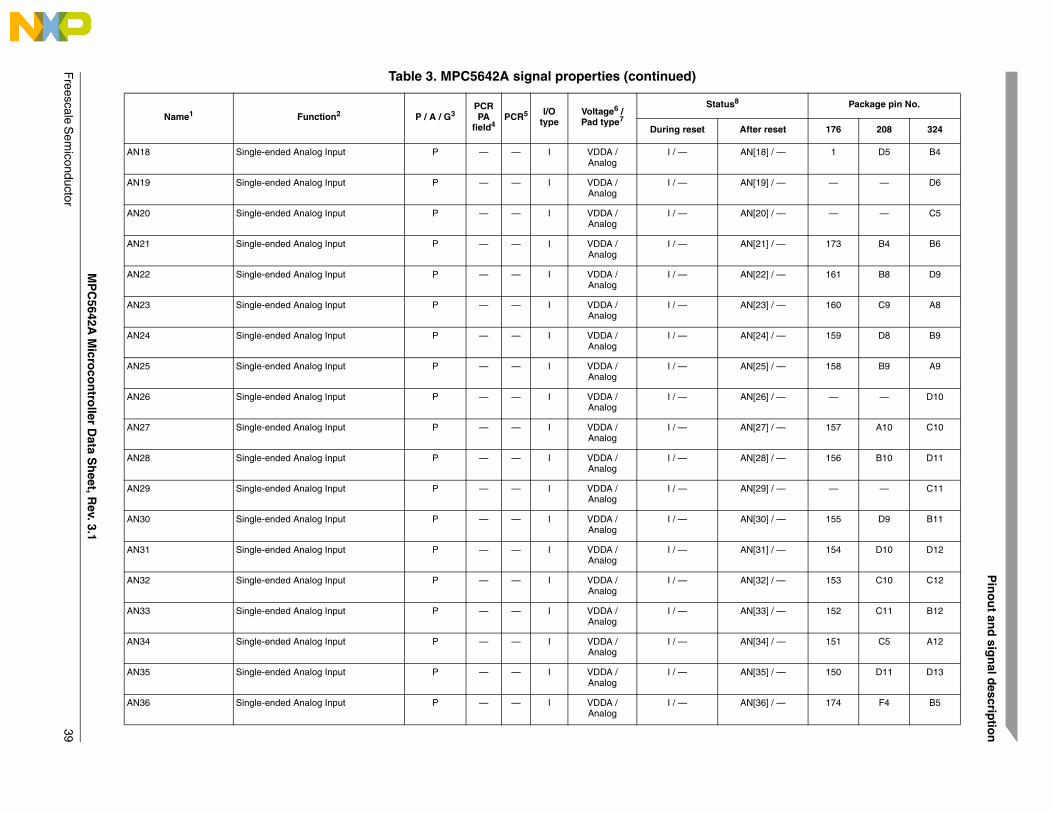
Pin
ou
t and
sign
al descrip
tion
F
18] / — 1 D5 B4
19] / — — — D6
20] / — — — C5
21] / — 173 B4 B6
22] / — 161 B8 D9
23] / — 160 C9 A8
24] / — 159 D8 B9
25] / — 158 B9 A9
26] / — — — D10
27] / — 157 A10 C10
28] / — 156 B10 D11
29] / — — — C11
30] / — 155 D9 B11
31] / — 154 D10 D12
32] / — 153 C10 C12
33] / — 152 C11 B12
34] / — 151 C5 A12
35] / — 150 D11 D13
36] / — 174 F4 B5
Package pin No.
r reset 176 208 324
MP
C5642A
Micro
con
troller D
ata Sh
eet, Rev. 3.1
reescale Sem
iconductor 39
AN18 Single-ended Analog Input P — — I VDDA /Analog
I / — AN[
AN19 Single-ended Analog Input P — — I VDDA /Analog
I / — AN[
AN20 Single-ended Analog Input P — — I VDDA /Analog
I / — AN[
AN21 Single-ended Analog Input P — — I VDDA /Analog
I / — AN[
AN22 Single-ended Analog Input P — — I VDDA /Analog
I / — AN[
AN23 Single-ended Analog Input P — — I VDDA /Analog
I / — AN[
AN24 Single-ended Analog Input P — — I VDDA /Analog
I / — AN[
AN25 Single-ended Analog Input P — — I VDDA /Analog
I / — AN[
AN26 Single-ended Analog Input P — — I VDDA /Analog
I / — AN[
AN27 Single-ended Analog Input P — — I VDDA /Analog
I / — AN[
AN28 Single-ended Analog Input P — — I VDDA /Analog
I / — AN[
AN29 Single-ended Analog Input P — — I VDDA /Analog
I / — AN[
AN30 Single-ended Analog Input P — — I VDDA /Analog
I / — AN[
AN31 Single-ended Analog Input P — — I VDDA /Analog
I / — AN[
AN32 Single-ended Analog Input P — — I VDDA /Analog
I / — AN[
AN33 Single-ended Analog Input P — — I VDDA /Analog
I / — AN[
AN34 Single-ended Analog Input P — — I VDDA /Analog
I / — AN[
AN35 Single-ended Analog Input P — — I VDDA /Analog
I / — AN[
AN36 Single-ended Analog Input P — — I VDDA /Analog
I / — AN[
Table 3. MPC5642A signal properties (continued)
Name1 Function2 P / A / G3PCR PA
field4PCR5 I/O
typeVoltage6 /Pad type7
Status8
During reset Afte
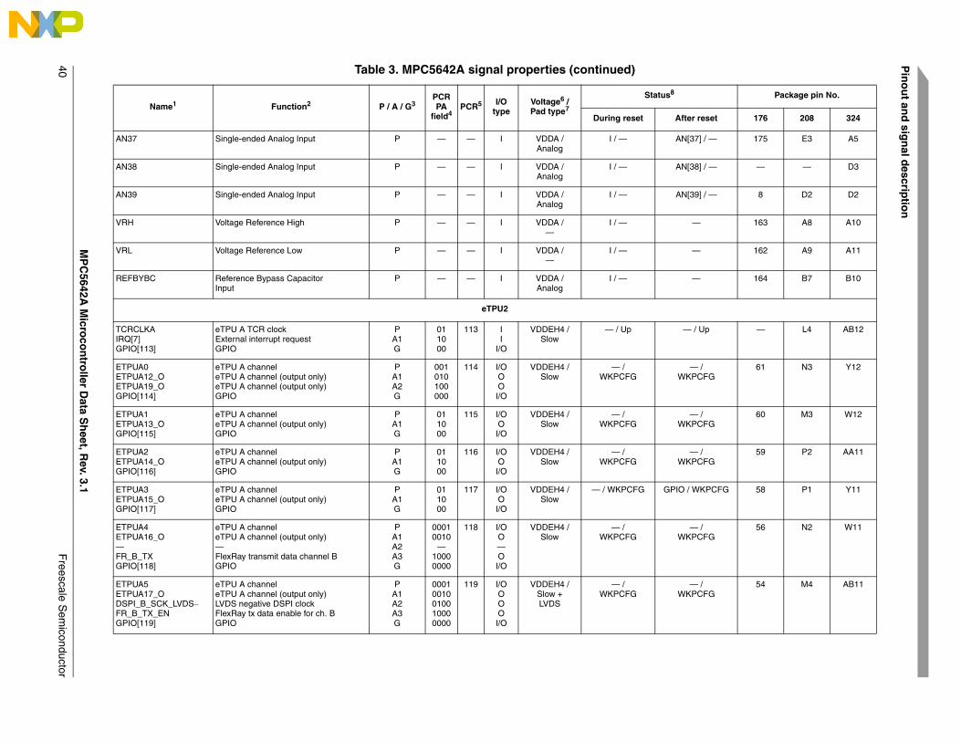
Pin
ou
t and
sign
al descrip
tion
4
37] / — 175 E3 A5
38] / — — — D3
39] / — 8 D2 D2
— 163 A8 A10
— 162 A9 A11
— 164 B7 B10
/ Up — L4 AB12
— / PCFG
61 N3 Y12
— / PCFG
60 M3 W12
— / PCFG
59 P2 AA11
WKPCFG 58 P1 Y11
— / PCFG
56 N2 W11
— / PCFG
54 M4 AB11
Package pin No.
r reset 176 208 324
MP
C5642A
Micro
con
troller D
ata Sh
eet, Rev. 3.1
Freescale S
emiconductor
0
AN37 Single-ended Analog Input P — — I VDDA /Analog
I / — AN[
AN38 Single-ended Analog Input P — — I VDDA /Analog
I / — AN[
AN39 Single-ended Analog Input P — — I VDDA /Analog
I / — AN[
VRH Voltage Reference High P — — I VDDA /—
I / —
VRL Voltage Reference Low P — — I VDDA /—
I / —
REFBYBC Reference Bypass CapacitorInput
P — — I VDDA /Analog
I / —
eTPU2
TCRCLKA IRQ[7]GPIO[113]
eTPU A TCR clockExternal interrupt requestGPIO
PA1G
011000
113 II
I/O
VDDEH4 /Slow
— / Up —
ETPUA0ETPUA12_OETPUA19_OGPIO[114]
eTPU A channeleTPU A channel (output only)eTPU A channel (output only)GPIO
PA1A2G
001010100000
114 I/OOOI/O
VDDEH4 /Slow
— / WKPCFG WK
ETPUA1ETPUA13_OGPIO[115]
eTPU A channeleTPU A channel (output only)GPIO
PA1G
011000
115 I/OOI/O
VDDEH4 /Slow
— / WKPCFG WK
ETPUA2ETPUA14_OGPIO[116]
eTPU A channeleTPU A channel (output only)GPIO
PA1G
011000
116 I/OOI/O
VDDEH4 /Slow
— / WKPCFG WK
ETPUA3ETPUA15_OGPIO[117]
eTPU A channeleTPU A channel (output only)GPIO
PA1G
011000
117 I/OOI/O
VDDEH4 /Slow
— / WKPCFG GPIO /
ETPUA4ETPUA16_O—FR_B_TXGPIO[118]
eTPU A channeleTPU A channel (output only)—FlexRay transmit data channel BGPIO
PA1A2A3G
00010010
—10000000
118 I/OO—OI/O
VDDEH4 /Slow
— / WKPCFG WK
ETPUA5ETPUA17_ODSPI_B_SCK_LVDSFR_B_TX_ENGPIO[119]
eTPU A channeleTPU A channel (output only)LVDS negative DSPI clockFlexRay tx data enable for ch. BGPIO
PA1A2A3G
00010010010010000000
119 I/OOOOI/O
VDDEH4 /Slow +LVDS
— / WKPCFG WK
Table 3. MPC5642A signal properties (continued)
Name1 Function2 P / A / G3PCR PA
field4PCR5 I/O
typeVoltage6 /Pad type7
Status8
During reset Afte
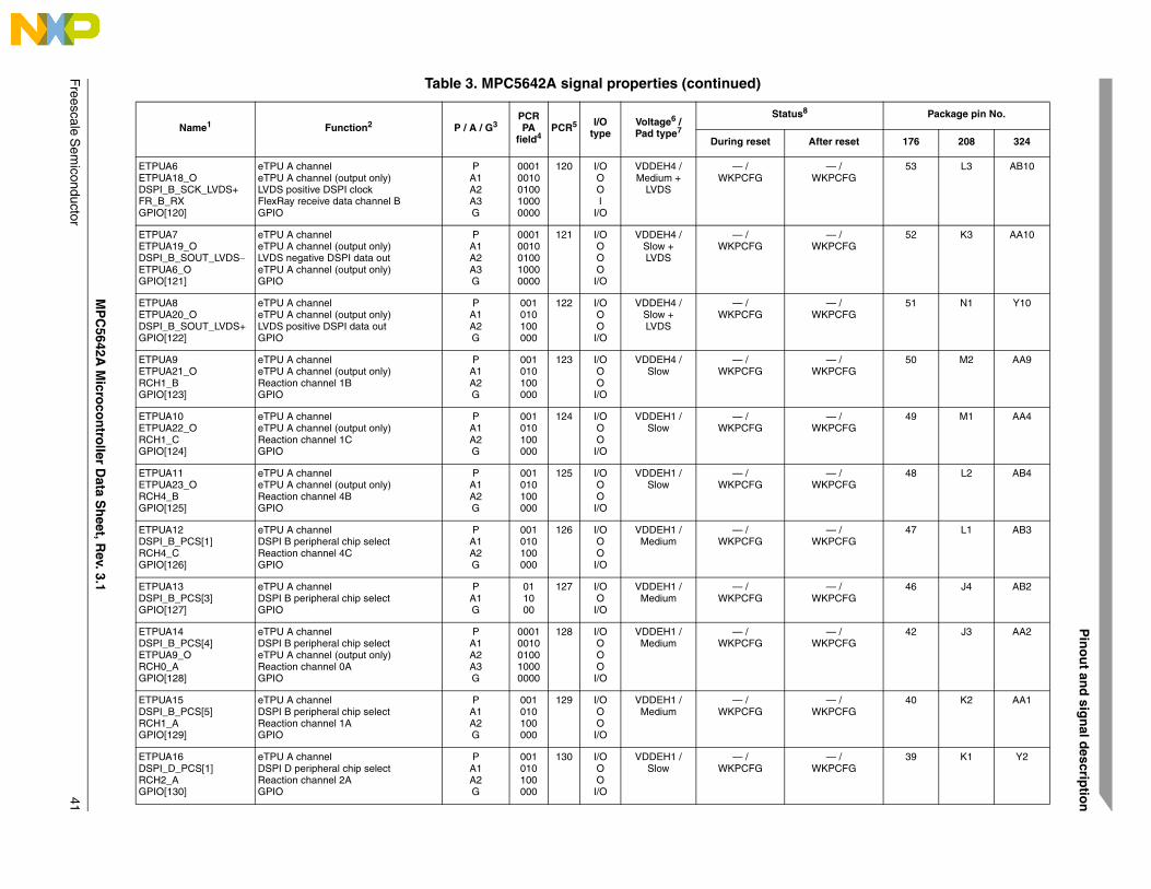
Pin
ou
t and
sign
al descrip
tion
F
— / PCFG
53 L3 AB10
— / PCFG
52 K3 AA10
— / PCFG
51 N1 Y10
— / PCFG
50 M2 AA9
— / PCFG
49 M1 AA4
— / PCFG
48 L2 AB4
— / PCFG
47 L1 AB3
— / PCFG
46 J4 AB2
— / PCFG
42 J3 AA2
— / PCFG
40 K2 AA1
— / PCFG
39 K1 Y2
Package pin No.
r reset 176 208 324
MP
C5642A
Micro
con
troller D
ata Sh
eet, Rev. 3.1
reescale Sem
iconductor 41
ETPUA6ETPUA18_ODSPI_B_SCK_LVDS+FR_B_RXGPIO[120]
eTPU A channeleTPU A channel (output only)LVDS positive DSPI clockFlexRay receive data channel BGPIO
PA1A2A3G
00010010010010000000
120 I/OOOI
I/O
VDDEH4 /Medium +
LVDS
— / WKPCFG WK
ETPUA7ETPUA19_ODSPI_B_SOUT_LVDSETPUA6_OGPIO[121]
eTPU A channeleTPU A channel (output only)LVDS negative DSPI data outeTPU A channel (output only)GPIO
PA1A2A3G
00010010010010000000
121 I/OOOOI/O
VDDEH4 /Slow +LVDS
— / WKPCFG WK
ETPUA8ETPUA20_ODSPI_B_SOUT_LVDS+GPIO[122]
eTPU A channeleTPU A channel (output only)LVDS positive DSPI data outGPIO
PA1A2G
001010100000
122 I/OOOI/O
VDDEH4 /Slow +LVDS
— / WKPCFG WK
ETPUA9ETPUA21_ORCH1_BGPIO[123]
eTPU A channeleTPU A channel (output only)Reaction channel 1BGPIO
PA1A2G
001010100000
123 I/OOOI/O
VDDEH4 /Slow
— / WKPCFG WK
ETPUA10ETPUA22_ORCH1_CGPIO[124]
eTPU A channeleTPU A channel (output only)Reaction channel 1CGPIO
PA1A2G
001010100000
124 I/OOOI/O
VDDEH1 /Slow
— / WKPCFG WK
ETPUA11ETPUA23_ORCH4_BGPIO[125]
eTPU A channeleTPU A channel (output only)Reaction channel 4BGPIO
PA1A2G
001010100000
125 I/OOOI/O
VDDEH1 /Slow
— / WKPCFG WK
ETPUA12DSPI_B_PCS[1]RCH4_CGPIO[126]
eTPU A channelDSPI B peripheral chip selectReaction channel 4CGPIO
PA1A2G
001010100000
126 I/OOOI/O
VDDEH1 /Medium
— / WKPCFG WK
ETPUA13DSPI_B_PCS[3]GPIO[127]
eTPU A channelDSPI B peripheral chip selectGPIO
PA1G
011000
127 I/OOI/O
VDDEH1 /Medium
— / WKPCFG WK
ETPUA14DSPI_B_PCS[4]ETPUA9_ORCH0_AGPIO[128]
eTPU A channelDSPI B peripheral chip selecteTPU A channel (output only)Reaction channel 0AGPIO
PA1A2A3G
00010010010010000000
128 I/OOOOI/O
VDDEH1 /Medium
— / WKPCFG WK
ETPUA15DSPI_B_PCS[5]RCH1_AGPIO[129]
eTPU A channelDSPI B peripheral chip selectReaction channel 1AGPIO
PA1A2G
001010100000
129 I/OOOI/O
VDDEH1 /Medium
— / WKPCFG WK
ETPUA16DSPI_D_PCS[1]RCH2_AGPIO[130]
eTPU A channelDSPI D peripheral chip selectReaction channel 2AGPIO
PA1A2G
001010100000
130 I/OOOI/O
VDDEH1 /Slow
— / WKPCFG WK
Table 3. MPC5642A signal properties (continued)
Name1 Function2 P / A / G3PCR PA
field4PCR5 I/O
typeVoltage6 /Pad type7
Status8
During reset Afte
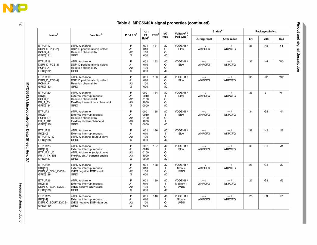
Pin
ou
t and
sign
al descrip
tion
4
— / PCFG
38 H3 Y1
— / PCFG
37 H4 W3
— / PCFG
36 J2 W2
— / PCFG
35 J1 W1
— / PCFG
34 G4 N4
— / PCFG
32 H2 N3
— / PCFG
30 H1 M1
— / PCFG
28 G1 M2
— / PCFG
27 G3 M3
— / PCFG
26 F3 L2
Package pin No.
r reset 176 208 324
MP
C5642A
Micro
con
troller D
ata Sh
eet, Rev. 3.1
Freescale S
emiconductor
2
ETPUA17DSPI_D_PCS[2]RCH3_AGPIO[131]
eTPU A channelDSPI D peripheral chip selectReaction channel 3AGPIO
PA1A2G
001010100000
131 I/OOOI/O
VDDEH1 /Slow
— / WKPCFG WK
ETPUA18DSPI_D_PCS[3]RCH4_AGPIO[132]
eTPU A channelDSPI D peripheral chip selectReaction channel 4AGPIO
PA1A2G
001010100000
132 I/OOOI/O
VDDEH1 /Slow
— / WKPCFG WK
ETPUA19DSPI_D_PCS[4]RCH5_AGPIO[133]
eTPU A channelDSPI D peripheral chip selectReaction channel 5AGPIO
PA1A2G
001010100000
133 I/OOOI/O
VDDEH1 /Slow
— / WKPCFG WK
ETPUA20IRQ[8]RCH0_BFR_A_TXGPIO[134]
eTPU A channelExternal interrupt requestReaction channel 0BFlexRay transmit data channel AGPIO
PA1A2A3G
00010010010010000000
134 I/OIOOI/O
VDDEH1 /Slow
— / WKPCFG WK
ETPUA21IRQ[9]RCH0_CFR_A_RXGPIO[135]
eTPU A channelExternal interrupt requestReaction channel 0CFlexRay receive channel AGPIO
PA1A2A3G
00010010010010000000
135 I/OIOI
I/O
VDDEH1 /Slow
— / WKPCFG WK
ETPUA22IRQ[10]ETPUA17_OGPIO[136]
eTPU A channelExternal interrupt requesteTPU A channel (output only)GPIO
PA1A2G
001010100000
136 I/OIOI/O
VDDEH1 /Slow
— / WKPCFG WK
ETPUA23IRQ[11]ETPUA21_OFR_A_TX_ENGPIO[137]
eTPU A channelExternal interrupt requesteTPU A channel (output only)FlexRay ch. A transmit enableGPIO
PA1A2A3G
00010010010010000000
137 I/OIOOI/O
VDDEH1 /Slow
— / WKPCFG WK
ETPUA24IRQ[12]DSPI_C_SCK_LVDSGPIO[138]
eTPU A channelExternal interrupt requestLVDS negative DSPI clockGPIO
PA1A2G
001010100000
138 I/OIOI/O
VDDEH1 /Slow +LVDS
— / WKPCFG WK
ETPUA25IRQ[13]DSPI_C_SCK_LVDS+GPIO[139]
eTPU A channelExternal interrupt requestLVDS positive DSPI clockGPIO
PA1A2G
001010100000
139 I/OIOI/O
VDDEH1 /Medium +
LVDS
— / WKPCFG WK
ETPUA26IRQ[14]DSPI_C_SOUT_LVDSGPIO[140]
eTPU A channelExternal interrupt requestLVDS negative DSPI data outGPIO
PA1A2G
001010100000
140 I/OIOI/O
VDDEH1 /Slow +LVDS
— / WKPCFG WK
Table 3. MPC5642A signal properties (continued)
Name1 Function2 P / A / G3PCR PA
field4PCR5 I/O
typeVoltage6 /Pad type7
Status8
During reset Afte
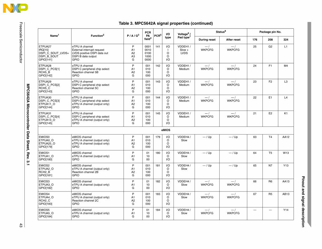
Pin
ou
t and
sign
al descrip
tion
F
— / PCFG
25 G2 L1
— / PCFG
24 F1 M4
— / PCFG
23 F2 L3
— / PCFG
22 E1 L4
— / PCFG
21 E2 K1
/ Up 63 T4 AA12
/ Up 64 T5 W13
/ Up 65 N7 Y13
— / PCFG
66 R6 AA13
— / PCFG
67 R5 AB13
— / PCFG
— — Y14
Package pin No.
r reset 176 208 324
MP
C5642A
Micro
con
troller D
ata Sh
eet, Rev. 3.1
reescale Sem
iconductor 43
ETPUA27IRQ[15]DSPI_C_SOUT_LVDS+DSPI_B_SOUTGPIO[141]
eTPU A channelExternal interrupt requestLVDS positive DSPI data outDSPI B data outputGPIO
PA1A2A3G
00010010010010000000
141 I/OIOOI/O
VDDEH1 /Slow +LVDS
— / WKPCFG WK
ETPUA28DSPI_C_PCS[1]RCH5_BGPIO[142]
eTPU A channelDSPI C peripheral chip selectReaction channel 5BGPIO
PA1A2G
001010100000
142 I/OOOI/O
VDDEH1 /Medium
— / WKPCFG WK
ETPUA29DSPI_C_PCS[2]RCH5_CGPIO[143]
eTPU A channelDSPI C peripheral chip selectReaction channel 5CGPIO
PA1A2G
001010100000
143 I/OOOI/O
VDDEH1 /Medium
— / WKPCFG WK
ETPUA30DSPI_C_PCS[3]ETPUA11_OGPIO[144]
eTPU A channelDSPI C peripheral chip selecteTPU A channel (output only)GPIO
PA1A2G
001010100000
144 I/OOOI/O
VDDEH1 /Medium
— / WKPCFG WK
ETPUA31DSPI_C_PCS[4]ETPUA13_OGPIO[145]
eTPU A channelDSPI C peripheral chip selecteTPU A channel (output only)GPIO
PA1A2G
001010100000
145 I/OOOI/O
VDDEH1 /Medium
— / WKPCFG WK
eMIOS
EMIOS0ETPUA0_OETPUA25_OGPIO[179]
eMIOS channeleTPU A channel (output only)eTPU A channel (output only)GPIO
PA1A2G
001010100000
179 I/OOOI/O
VDDEH4 /Slow
— / Up —
EMIOS1ETPUA1_OGPIO[180]
eMIOS channeleTPU A channel (output only)GPIO
PA1G
011000
180 I/OOI/O
VDDEH4 /Slow
— / Up —
EMIOS2ETPUA2_ORCH2_BGPIO[181]
eMIOS channeleTPU A channel (output only)Reaction channel 2BGPIO
PA1A2G
001010100000
181 I/OOOI/O
VDDEH4 /Slow
— / Up —
EMIOS3ETPUA3_OGPIO[182]
eMIOS channeleTPU A channel (output only)GPIO
PA1G
011000
182 I/OOI/O
VDDEH4 /Slow
— / WKPCFG WK
EMIOS4ETPUA4_ORCH2_CGPIO[183]
eMIOS channeleTPU A channel (output only)Reaction channel 2CGPIO
PA1A2G
001010100000
183 I/OOOI/O
VDDEH4 /Slow
— / WKPCFG WK
EMIOS5ETPUA5_OGPIO[184]
eMIOS channeleTPU A channel (output only)GPIO
PA1G
011000
184 I/OOI/O
VDDEH4 /Slow
— / WKPCFG WK
Table 3. MPC5642A signal properties (continued)
Name1 Function2 P / A / G3PCR PA
field4PCR5 I/O
typeVoltage6 /Pad type7
Status8
During reset Afte
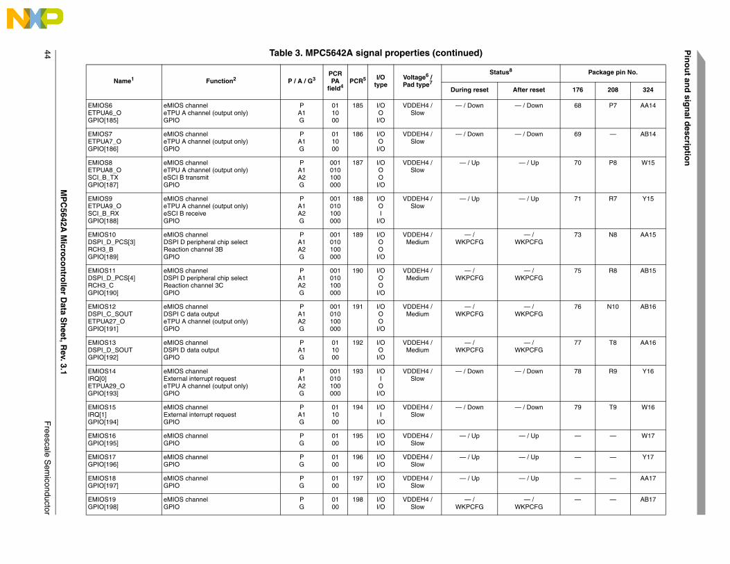
Pin
ou
t and
sign
al descrip
tion
4
/ Down 68 P7 AA14
/ Down 69 — AB14
/ Up 70 P8 W15
/ Up 71 R7 Y15
— / PCFG
73 N8 AA15
— / PCFG
75 R8 AB15
— / PCFG
76 N10 AB16
— / PCFG
77 T8 AA16
/ Down 78 R9 Y16
/ Down 79 T9 W16
/ Up — — W17
/ Up — — Y17
/ Up — — AA17
— / PCFG
— — AB17
Package pin No.
r reset 176 208 324
MP
C5642A
Micro
con
troller D
ata Sh
eet, Rev. 3.1
Freescale S
emiconductor
4
EMIOS6ETPUA6_OGPIO[185]
eMIOS channeleTPU A channel (output only)GPIO
PA1G
011000
185 I/OOI/O
VDDEH4 /Slow
— / Down —
EMIOS7ETPUA7_OGPIO[186]
eMIOS channeleTPU A channel (output only)GPIO
PA1G
011000
186 I/OOI/O
VDDEH4 /Slow
— / Down —
EMIOS8ETPUA8_OSCI_B_TXGPIO[187]
eMIOS channeleTPU A channel (output only)eSCI B transmitGPIO
PA1A2G
001010100000
187 I/OOOI/O
VDDEH4 /Slow
— / Up —
EMIOS9ETPUA9_OSCI_B_RXGPIO[188]
eMIOS channeleTPU A channel (output only)eSCI B receiveGPIO
PA1A2G
001010100000
188 I/OOI
I/O
VDDEH4 /Slow
— / Up —
EMIOS10DSPI_D_PCS[3]RCH3_BGPIO[189]
eMIOS channelDSPI D peripheral chip selectReaction channel 3BGPIO
PA1A2G
001010100000
189 I/OOOI/O
VDDEH4 /Medium
— / WKPCFG WK
EMIOS11DSPI_D_PCS[4]RCH3_CGPIO[190]
eMIOS channelDSPI D peripheral chip selectReaction channel 3CGPIO
PA1A2G
001010100000
190 I/OOOI/O
VDDEH4 /Medium
— / WKPCFG WK
EMIOS12DSPI_C_SOUTETPUA27_OGPIO[191]
eMIOS channelDSPI C data outputeTPU A channel (output only)GPIO
PA1A2G
001010100000
191 I/OOOI/O
VDDEH4 /Medium
— / WKPCFG WK
EMIOS13DSPI_D_SOUTGPIO[192]
eMIOS channelDSPI D data outputGPIO
PA1G
011000
192 I/OOI/O
VDDEH4 /Medium
— / WKPCFG WK
EMIOS14IRQ[0]ETPUA29_OGPIO[193]
eMIOS channelExternal interrupt requesteTPU A channel (output only)GPIO
PA1A2G
001010100000
193 I/OIOI/O
VDDEH4 /Slow
— / Down —
EMIOS15IRQ[1]GPIO[194]
eMIOS channelExternal interrupt requestGPIO
PA1G
011000
194 I/OI
I/O
VDDEH4 /Slow
— / Down —
EMIOS16GPIO[195]
eMIOS channelGPIO
PG
0100
195 I/OI/O
VDDEH4 /Slow
— / Up —
EMIOS17GPIO[196]
eMIOS channelGPIO
PG
0100
196 I/OI/O
VDDEH4 /Slow
— / Up —
EMIOS18GPIO[197]
eMIOS channelGPIO
PG
0100
197 I/OI/O
VDDEH4 /Slow
— / Up —
EMIOS19GPIO[198]
eMIOS channelGPIO
PG
0100
198 I/OI/O
VDDEH4 /Slow
— / WKPCFG WK
Table 3. MPC5642A signal properties (continued)
Name1 Function2 P / A / G3PCR PA
field4PCR5 I/O
typeVoltage6 /Pad type7
Status8
During reset Afte
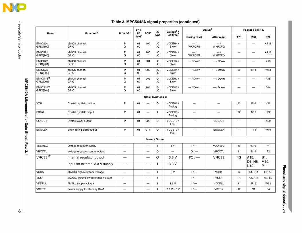
Pin
ou
t and
sign
al descrip
tion
F
— / PCFG
— — AB18
— / PCFG
— — AA18
/ Down — — Y18
/ Down 80 R11 W18
/ Down — — A15
/ Down — — D14
— 93 P16 V22
— 92 N16 U22
KOUT — — AB9
GCLK — T14 W10
DREG 10 K16 F4
CCTL 11 N14 F2
C33 13 A15, D1, N6, N12
B1,M19, P11
DDA 6 A4, B11 E3, A6
SSA 7 A5, A11 A7, E2
DPLL 91 R16 W22
TBY 12 C1 E4
Package pin No.
r reset 176 208 324
MP
C5642A
Micro
con
troller D
ata Sh
eet, Rev. 3.1
reescale Sem
iconductor 45
EMIOS20GPIO[199]
eMIOS channelGPIO
PG
0100
199 I/OI/O
VDDEH4 /Slow
— / WKPCFG WK
EMIOS21GPIO[200]
eMIOS channelGPIO
PG
0100
200 I/OI/O
VDDEH4 /Slow
— / WKPCFG WK
EMIOS22GPIO[201]
eMIOS channelGPIO
PG
0100
201 I/OI/O
VDDEH4 /Slow
— / Down —
EMIOS23GPIO[202]
eMIOS channelGPIO
PG
0100
202 I/OI/O
VDDEH4 /Slow
— / Down —
EMIOS1415
GPIO[203]eMIOS channelGPIO
PG
0100
203 OI/O
VDDEH7 /Slow
— / Down —
EMIOS1515
GPIO[204]eMIOS channelGPIO
PG
0100
204 OI/O
VDDEH7 /Slow
— / Down —
Clock Synthesizer
XTAL Crystal oscillator output P 01 — O VDDEH6 /Analog
—
EXTAL Crystal oscillator input P 01 — I VDDEH6 /Analog
—
CLKOUT System clock output P 01 229 O VDDE12 /Fast
— CL
ENGCLK Engineering clock output P 01 214 O VDDE12 /Fast
— EN
Power / Ground
VDDREG Voltage regulator supply — — I 5 V I / — VD
VRCCTL Voltage regulator control output — — O — O / — VR
VRC3317 Internal regulator output — — O 3.3 V I/O / — VR
Input for external 3.3 V supply — — I 3.3 V
VDDA eQADC high reference voltage — — I 5 V I / — V
VSSA eQADC ground/low reference voltage — — I — I / — V
VDDPLL FMPLL supply voltage — — I 1.2 V I / — VD
VSTBY Power supply for standby RAM — — I 0.9 V – 6 V I / — VS
Table 3. MPC5642A signal properties (continued)
Name1 Function2 P / A / G3PCR PA
field4PCR5 I/O
typeVoltage6 /Pad type7
Status8
During reset Afte
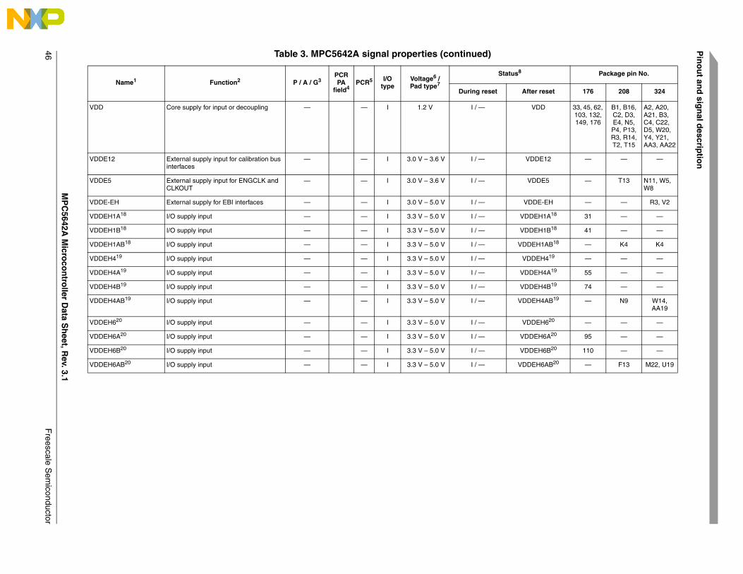
Pin
ou
t and
sign
al descrip
tion
4
DD 33, 45, 62, 103, 132, 149, 176
B1, B16, C2, D3, E4, N5, P4, P13, R3, R14, T2, T15
A2, A20, A21, B3, C4, C22, D5, W20, Y4, Y21, AA3, AA22
DE12 — — —
DE5 — T13 N11, W5, W8
DE-EH — — R3, V2
EH1A18 31 — —
EH1B18 41 — —
H1AB18 — K4 K4
EH419 — — —
EH4A19 55 — —
EH4B19 74 — —
H4AB19 — N9 W14, AA19
EH620 — — —
EH6A20 95 — —
EH6B20 110 — —
H6AB20 — F13 M22, U19
Package pin No.
r reset 176 208 324
MP
C5642A
Micro
con
troller D
ata Sh
eet, Rev. 3.1
Freescale S
emiconductor
6
VDD Core supply for input or decoupling — — I 1.2 V I / — V
VDDE12 External supply input for calibration bus interfaces
— — I 3.0 V – 3.6 V I / — VD
VDDE5 External supply input for ENGCLK and CLKOUT
— — I 3.0 V – 3.6 V I / — VD
VDDE-EH External supply for EBI interfaces — — I 3.0 V – 5.0 V I / — VD
VDDEH1A18 I/O supply input — — I 3.3 V – 5.0 V I / — VDD
VDDEH1B18 I/O supply input — — I 3.3 V – 5.0 V I / — VDD
VDDEH1AB18 I/O supply input — — I 3.3 V – 5.0 V I / — VDDE
VDDEH419 I/O supply input — — I 3.3 V – 5.0 V I / — VDD
VDDEH4A19 I/O supply input — — I 3.3 V – 5.0 V I / — VDD
VDDEH4B19 I/O supply input — — I 3.3 V – 5.0 V I / — VDD
VDDEH4AB19 I/O supply input — — I 3.3 V – 5.0 V I / — VDDE
VDDEH620 I/O supply input — — I 3.3 V – 5.0 V I / — VDD
VDDEH6A20 I/O supply input — — I 3.3 V – 5.0 V I / — VDD
VDDEH6B20 I/O supply input — — I 3.3 V – 5.0 V I / — VDD
VDDEH6AB20 I/O supply input — — I 3.3 V – 5.0 V I / — VDDE
Table 3. MPC5642A signal properties (continued)
Name1 Function2 P / A / G3PCR PA
field4PCR5 I/O
typeVoltage6 /Pad type7
Status8
During reset Afte
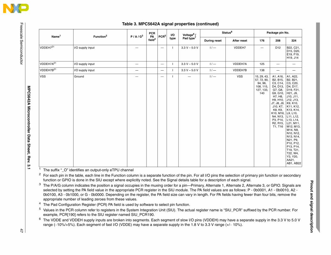
Pin
ou
t and
sign
al descrip
tion
F
DEH7 — D12 B22, C21, D15, D20, E19, F19, H19, J14
EH7A 125 — —
EH7B 138 — —
SS 15, 29, 43, 57, 72, 90,
94, 96, 108, 115, 127, 133,
140
A1, A16, B2, B15,C3, C14, D4, D13,G7, G8, G9, G10,H7, H8,
H9, H10,J7, J8, J9, J10, K7,K8, K9,
K10, M16,N4, N13, P3, P14,R2, R15, T1, T16
A1, A22, B2, B21, C3, C20, D4, D17, D19, F21, H21, J9, J10, J11, J12, J13, K9, K10, K11, K12, K13, K14, L9, L10, L11, L12, L13, L14, L21, M11, M12, M13, M14, N9, N10, N12, N13, N14, N21, P9, P10, P12, P13, P14, T19, T21, T22, W4, Y3, Y20, AA21, AB1, AB22
n of primary pin function or secondary h signal.te 2, Alternate 3, or GPIO. Signals are llows: P - 0b0001, A1 - 0b0010, A2 - ing fewer than four bits, remove the
R” suffixed by the PCR number. For
separate supply in the 3.3 V to 5.0 V %).
Package pin No.
r reset 176 208 324
MP
C5642A
Micro
con
troller D
ata Sh
eet, Rev. 3.1
reescale Sem
iconductor 47
VDDEH721 I/O supply input — — I 3.3 V – 5.0 V I / — VD
VDDEH7A21 I/O supply input — — I 3.3 V – 5.0 V I / — VDD
VDDEH7B21 I/O supply input — — I 3.3 V – 5.0 V I / — VDD
VSS Ground — — I — I / — V
1 The suffix “_O” identifies an output-only eTPU channel2 For each pin in the table, each line in the Function column is a separate function of the pin. For all I/O pins the selectio
function or GPIO is done in the SIU except where explicitly noted. See the Signal details table for a description of eac3 The P/A/G column indicates the position a signal occupies in the muxing order for a pin—Primary, Alternate 1, Alterna
selected by setting the PA field value in the appropriate PCR register in the SIU module. The PA field values are as fo0b0100, A3 - 0b1000, or G - 0b0000. Depending on the register, the PA field size can vary in length. For PA fields havappropriate number of leading zeroes from these values.
4 The Pad Configuration Register (PCR) PA field is used by software to select pin function.5 Values in the PCR column refer to registers in the System Integration Unit (SIU). The actual register name is “SIU_PC
example, PCR[190] refers to the SIU register named SIU_PCR190.6 The VDDE and VDDEH supply inputs are broken into segments. Each segment of slow I/O pins (VDDEH) may have a
range (10%/+5%). Each segment of fast I/O (VDDE) may have a separate supply in the 1.8 V to 3.3 V range (+/ 10
Table 3. MPC5642A signal properties (continued)
Name1 Function2 P / A / G3PCR PA
field4PCR5 I/O
typeVoltage6 /Pad type7
Status8
During reset Afte
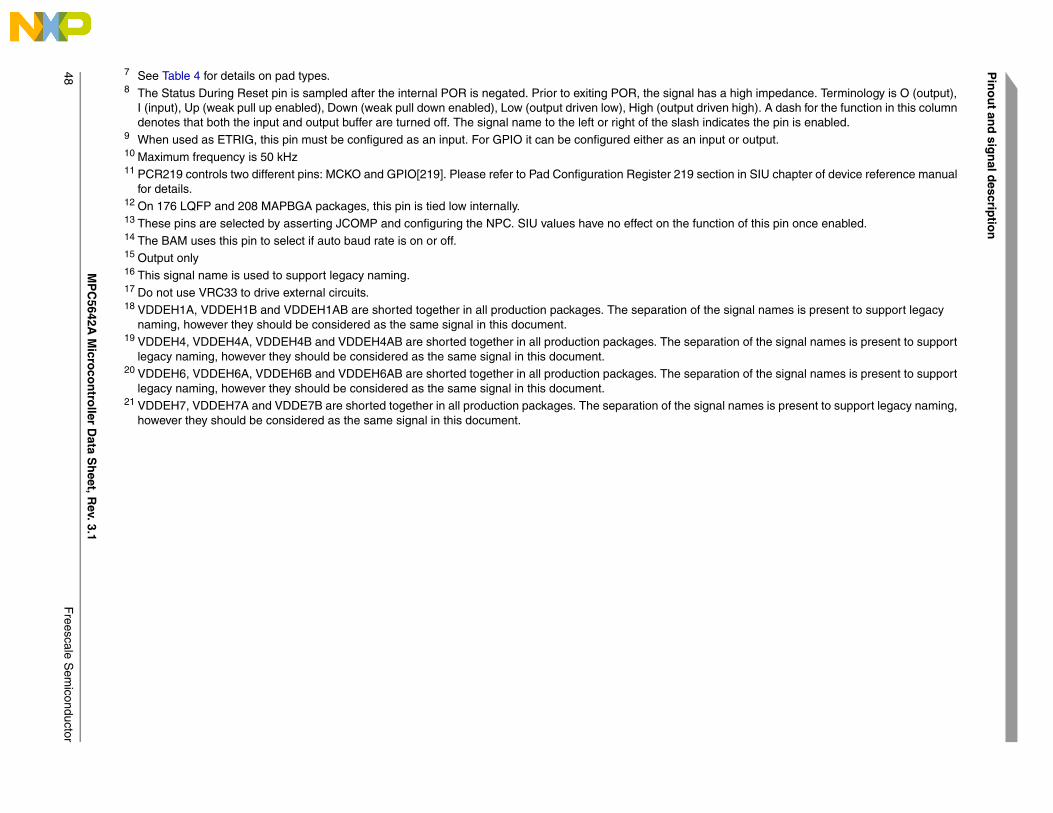
Pin
ou
t and
sign
al descrip
tion
4 7
impedance. Terminology is O (output), ). A dash for the function in this column he pin is enabled.
tput.
IU chapter of device reference manual
his pin once enabled.
names is present to support legacy
the signal names is present to support
the signal names is present to support
s is present to support legacy naming,
MP
C5642A
Micro
con
troller D
ata Sh
eet, Rev. 3.1
Freescale S
emiconductor
8 See Table 4 for details on pad types.8 The Status During Reset pin is sampled after the internal POR is negated. Prior to exiting POR, the signal has a high
I (input), Up (weak pull up enabled), Down (weak pull down enabled), Low (output driven low), High (output driven highdenotes that both the input and output buffer are turned off. The signal name to the left or right of the slash indicates t
9 When used as ETRIG, this pin must be configured as an input. For GPIO it can be configured either as an input or ou10 Maximum frequency is 50 kHz11 PCR219 controls two different pins: MCKO and GPIO[219]. Please refer to Pad Configuration Register 219 section in S
for details.12 On 176 LQFP and 208 MAPBGA packages, this pin is tied low internally.13 These pins are selected by asserting JCOMP and configuring the NPC. SIU values have no effect on the function of t14 The BAM uses this pin to select if auto baud rate is on or off.15 Output only16 This signal name is used to support legacy naming.17 Do not use VRC33 to drive external circuits.18 VDDEH1A, VDDEH1B and VDDEH1AB are shorted together in all production packages. The separation of the signal
naming, however they should be considered as the same signal in this document.19 VDDEH4, VDDEH4A, VDDEH4B and VDDEH4AB are shorted together in all production packages. The separation of
legacy naming, however they should be considered as the same signal in this document.20 VDDEH6, VDDEH6A, VDDEH6B and VDDEH6AB are shorted together in all production packages. The separation of
legacy naming, however they should be considered as the same signal in this document.21 VDDEH7, VDDEH7A and VDDE7B are shorted together in all production packages. The separation of the signal name
however they should be considered as the same signal in this document.
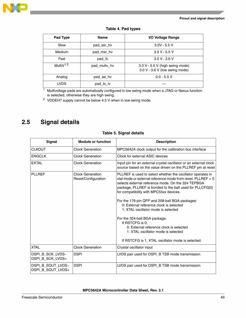
Pinout and signal description
2.5 Signal details
Table 4. Pad types
Pad Type Name I/O Voltage Range
Slow pad_ssr_hv 3.0V - 5.5 V
Medium pad_msr_hv 3.0 V - 5.5 V
Fast pad_fc 3.0 V - 3.6 V
MultiV1,2
1 Multivoltage pads are automatically configured in low swing mode when a JTAG or Nexus function is selected, otherwise they are high swing.
2 VDDEH7 supply cannot be below 4.5 V when in low-swing mode.
pad_multv_hv 3.0 V - 5.5 V (high swing mode)3.0 V - 3.6 V (low swing mode)
Analog pad_ae_hv 0.0 - 5.5 V
LVDS pad_lo_lv —
Table 5. Signal details
Signal Module or function Description
CLKOUT Clock Generation MPC5642A clock output for the calibration bus interface
ENGCLK Clock Generation Clock for external ASIC devices
EXTAL Clock Generation Input pin for an external crystal oscillator or an external clock source based on the value driven on the PLLREF pin at reset
PLLREF Clock GenerationReset/Configuration
PLLREF is used to select whether the oscillator operates in xtal mode or external reference mode from reset. PLLREF = 0 selects external reference mode. On the 324 TEPBGA package, PLLREF is bonded to the ball used for PLLCFG[0] for compatibility with MPC55xx devices.
For the 176-pin QFP and 208-ball BGA packages:0: External reference clock is selected1: XTAL oscillator mode is selected
For the 324-ball BGA package:If RSTCFG is 0:
0: External reference clock is selected1: XTAL oscillator mode is selected
If RSTCFG is 1, XTAL oscillator mode is selected.
XTAL Clock Generation Crystal oscillator input
DSPI_B_SCK_LVDSDSPI_B_SCK_LVDS+
DSPI LVDS pair used for DSPI_B TSB mode transmission
DSPI_B_SOUT_LVDSDSPI_B_SOUT_LVDS+
DSPI LVDS pair used for DSPI_B TSB mode transmission
MPC5642A Microcontroller Data Sheet, Rev. 3.1
Freescale Semiconductor 49
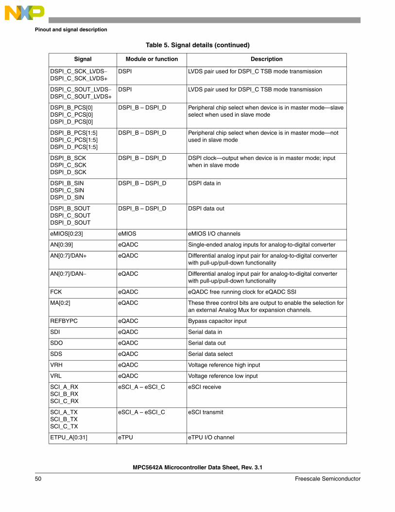
Pinout and signal description
DSPI_C_SCK_LVDSDSPI_C_SCK_LVDS+
DSPI LVDS pair used for DSPI_C TSB mode transmission
DSPI_C_SOUT_LVDSDSPI_C_SOUT_LVDS+
DSPI LVDS pair used for DSPI_C TSB mode transmission
DSPI_B_PCS[0]DSPI_C_PCS[0]DSPI_D_PCS[0]
DSPI_B – DSPI_D Peripheral chip select when device is in master mode—slave select when used in slave mode
DSPI_B_PCS[1:5]DSPI_C_PCS[1:5]DSPI_D_PCS[1:5]
DSPI_B – DSPI_D Peripheral chip select when device is in master mode—not used in slave mode
DSPI_B_SCKDSPI_C_SCKDSPI_D_SCK
DSPI_B – DSPI_D DSPI clock—output when device is in master mode; input when in slave mode
DSPI_B_SINDSPI_C_SINDSPI_D_SIN
DSPI_B – DSPI_D DSPI data in
DSPI_B_SOUTDSPI_C_SOUTDSPI_D_SOUT
DSPI_B – DSPI_D DSPI data out
eMIOS[0:23] eMIOS eMIOS I/O channels
AN[0:39] eQADC Single-ended analog inputs for analog-to-digital converter
AN[0:7]/DAN+ eQADC Differential analog input pair for analog-to-digital converter with pull-up/pull-down functionality
AN[0:7]/DAN eQADC Differential analog input pair for analog-to-digital converter with pull-up/pull-down functionality
FCK eQADC eQADC free running clock for eQADC SSI
MA[0:2] eQADC These three control bits are output to enable the selection for an external Analog Mux for expansion channels.
REFBYPC eQADC Bypass capacitor input
SDI eQADC Serial data in
SDO eQADC Serial data out
SDS eQADC Serial data select
VRH eQADC Voltage reference high input
VRL eQADC Voltage reference low input
SCI_A_RXSCI_B_RXSCI_C_RX
eSCI_A – eSCI_C eSCI receive
SCI_A_TXSCI_B_TXSCI_C_TX
eSCI_A – eSCI_C eSCI transmit
ETPU_A[0:31] eTPU eTPU I/O channel
Table 5. Signal details (continued)
Signal Module or function Description
MPC5642A Microcontroller Data Sheet, Rev. 3.1
50 Freescale Semiconductor
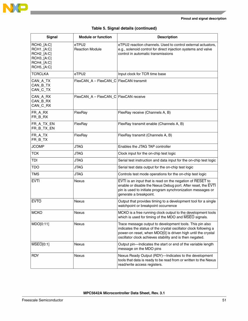
Pinout and signal description
RCH0_[A:C]RCH1_[A:C]RCH2_[A:C]RCH3_[A:C]RCH4_[A:C]RCH5_[A:C]
eTPU2Reaction Module
eTPU2 reaction channels. Used to control external actuators, e.g., solenoid control for direct injection systems and valve control in automatic transmissions
TCRCLKA eTPU2 Input clock for TCR time base
CAN_A_TXCAN_B_TXCAN_C_TX
FlexCAN_A – FlexCAN_C FlexCAN transmit
CAN_A_RXCAN_B_RXCAN_C_RX
FlexCAN_A – FlexCAN_C FlexCAN receive
FR_A_RXFR_B_RX
FlexRay FlexRay receive (Channels A, B)
FR_A_TX_ENFR_B_TX_EN
FlexRay FlexRay transmit enable (Channels A, B)
FR_A_TXFR_B_TX
FlexRay FlexRay transmit (Channels A, B)
JCOMP JTAG Enables the JTAG TAP controller
TCK JTAG Clock input for the on-chip test logic
TDI JTAG Serial test instruction and data input for the on-chip test logic
TDO JTAG Serial test data output for the on-chip test logic
TMS JTAG Controls test mode operations for the on-chip test logic
EVTI Nexus EVTI is an input that is read on the negation of RESET to enable or disable the Nexus Debug port. After reset, the EVTI pin is used to initiate program synchronization messages or generate a breakpoint.
EVTO Nexus Output that provides timing to a development tool for a single watchpoint or breakpoint occurrence
MCKO Nexus MCKO is a free running clock output to the development tools which is used for timing of the MDO and MSEO signals.
MDO[0:11] Nexus Trace message output to development tools. This pin also indicates the status of the crystal oscillator clock following a power-on reset, when MDO[0] is driven high until the crystal oscillator clock achieves stability and is then negated.
MSEO[0:1] Nexus Output pin—Indicates the start or end of the variable length message on the MDO pins
RDY Nexus Nexus Ready Output (RDY)—Indicates to the development tools that data is ready to be read from or written to the Nexus read/write access registers.
Table 5. Signal details (continued)
Signal Module or function Description
MPC5642A Microcontroller Data Sheet, Rev. 3.1
Freescale Semiconductor 51
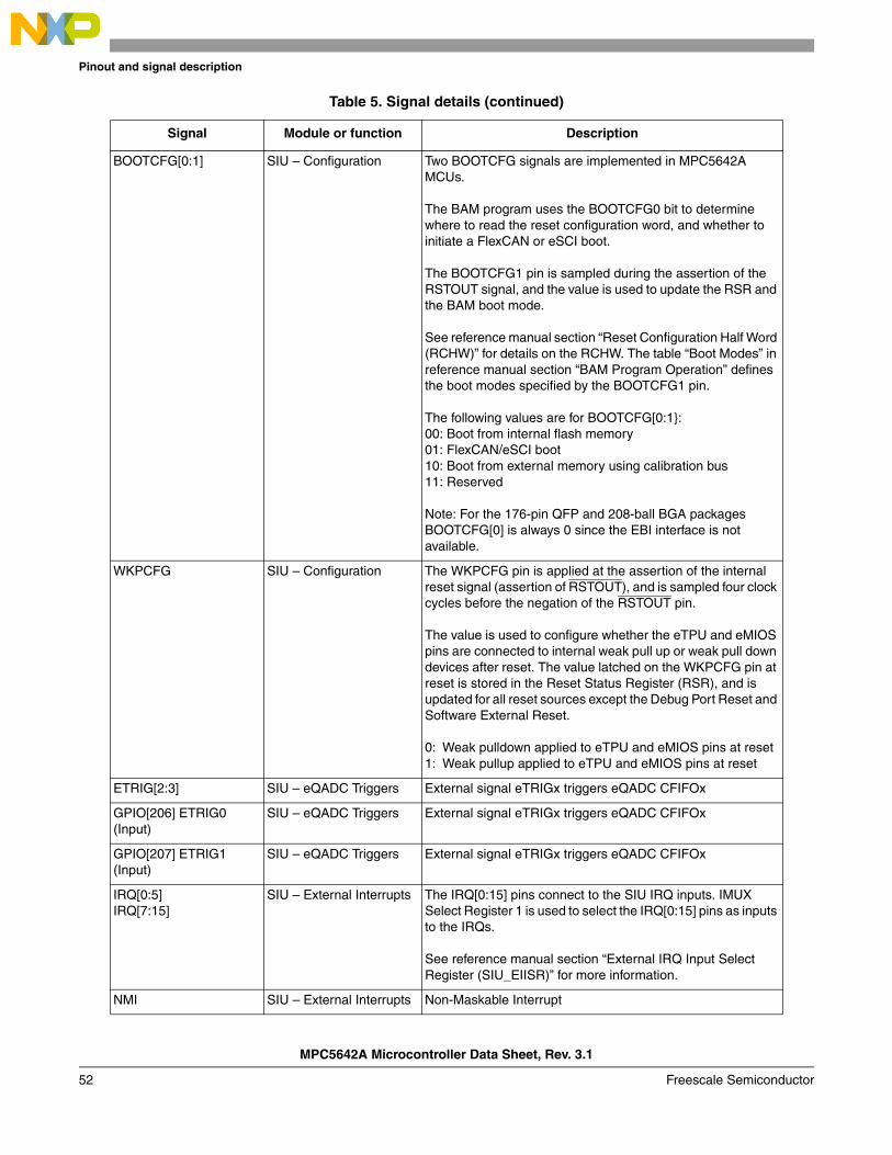
Pinout and signal description
BOOTCFG[0:1] SIU – Configuration Two BOOTCFG signals are implemented in MPC5642A MCUs.
The BAM program uses the BOOTCFG0 bit to determine where to read the reset configuration word, and whether to initiate a FlexCAN or eSCI boot.
The BOOTCFG1 pin is sampled during the assertion of the RSTOUT signal, and the value is used to update the RSR and the BAM boot mode.
See reference manual section “Reset Configuration Half Word (RCHW)” for details on the RCHW. The table “Boot Modes” in reference manual section “BAM Program Operation” defines the boot modes specified by the BOOTCFG1 pin.
The following values are for BOOTCFG[0:1}:00: Boot from internal flash memory01: FlexCAN/eSCI boot10: Boot from external memory using calibration bus11: Reserved
Note: For the 176-pin QFP and 208-ball BGA packages BOOTCFG[0] is always 0 since the EBI interface is not available.
WKPCFG SIU – Configuration The WKPCFG pin is applied at the assertion of the internal reset signal (assertion of RSTOUT), and is sampled four clock cycles before the negation of the RSTOUT pin.
The value is used to configure whether the eTPU and eMIOS pins are connected to internal weak pull up or weak pull down devices after reset. The value latched on the WKPCFG pin at reset is stored in the Reset Status Register (RSR), and is updated for all reset sources except the Debug Port Reset and Software External Reset.
0: Weak pulldown applied to eTPU and eMIOS pins at reset1: Weak pullup applied to eTPU and eMIOS pins at reset
ETRIG[2:3] SIU – eQADC Triggers External signal eTRIGx triggers eQADC CFIFOx
GPIO[206] ETRIG0 (Input)
SIU – eQADC Triggers External signal eTRIGx triggers eQADC CFIFOx
GPIO[207] ETRIG1 (Input)
SIU – eQADC Triggers External signal eTRIGx triggers eQADC CFIFOx
IRQ[0:5]IRQ[7:15]
SIU – External Interrupts The IRQ[0:15] pins connect to the SIU IRQ inputs. IMUX Select Register 1 is used to select the IRQ[0:15] pins as inputs to the IRQs.
See reference manual section “External IRQ Input Select Register (SIU_EIISR)” for more information.
NMI SIU – External Interrupts Non-Maskable Interrupt
Table 5. Signal details (continued)
Signal Module or function Description
MPC5642A Microcontroller Data Sheet, Rev. 3.1
52 Freescale Semiconductor
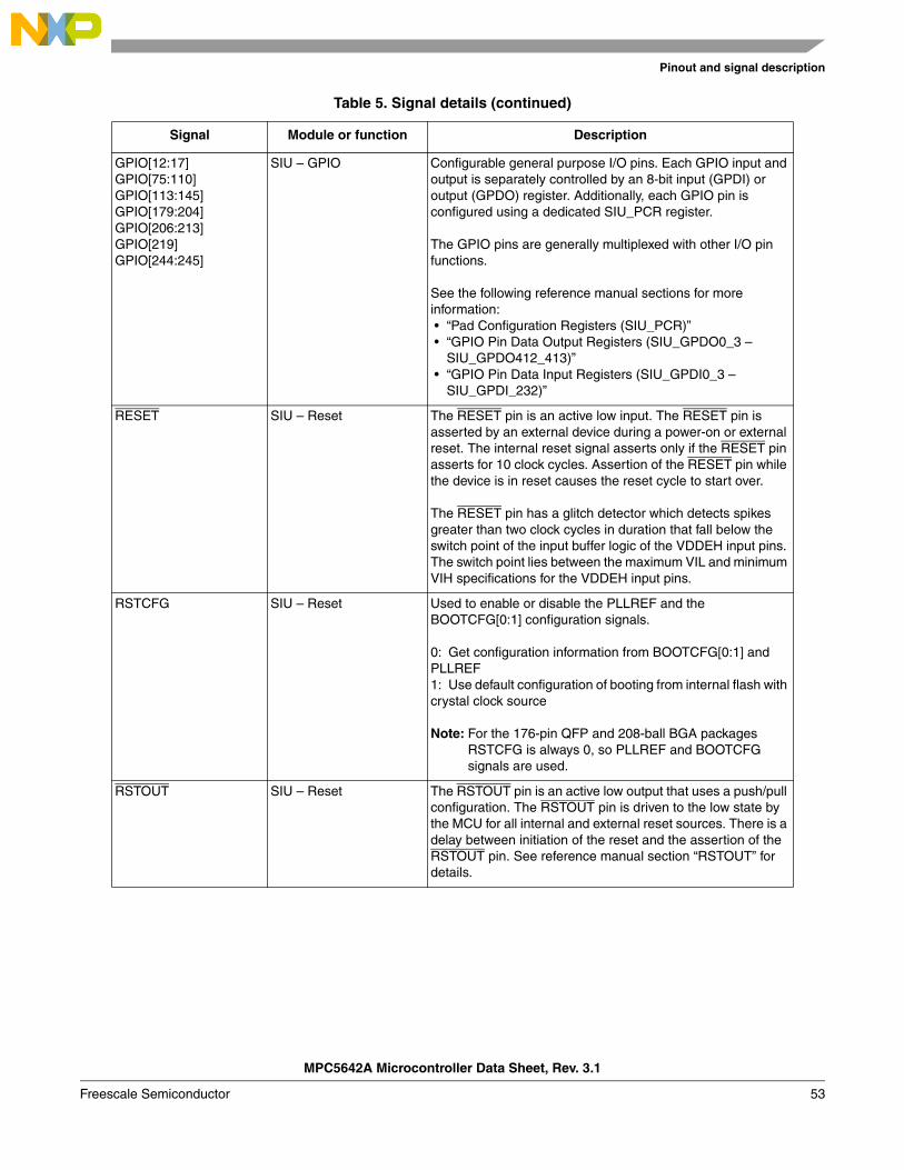
Pinout and signal description
GPIO[12:17]GPIO[75:110]GPIO[113:145]GPIO[179:204]GPIO[206:213]GPIO[219]GPIO[244:245]
SIU – GPIO Configurable general purpose I/O pins. Each GPIO input and output is separately controlled by an 8-bit input (GPDI) or output (GPDO) register. Additionally, each GPIO pin is configured using a dedicated SIU_PCR register.
The GPIO pins are generally multiplexed with other I/O pin functions.
See the following reference manual sections for more information: • “Pad Configuration Registers (SIU_PCR)” • “GPIO Pin Data Output Registers (SIU_GPDO0_3 –
SIU_GPDO412_413)” • “GPIO Pin Data Input Registers (SIU_GPDI0_3 –
SIU_GPDI_232)”
RESET SIU – Reset The RESET pin is an active low input. The RESET pin is asserted by an external device during a power-on or external reset. The internal reset signal asserts only if the RESET pin asserts for 10 clock cycles. Assertion of the RESET pin while the device is in reset causes the reset cycle to start over.
The RESET pin has a glitch detector which detects spikes greater than two clock cycles in duration that fall below the switch point of the input buffer logic of the VDDEH input pins. The switch point lies between the maximum VIL and minimum VIH specifications for the VDDEH input pins.
RSTCFG SIU – Reset Used to enable or disable the PLLREF and the BOOTCFG[0:1] configuration signals.
0: Get configuration information from BOOTCFG[0:1] and PLLREF1: Use default configuration of booting from internal flash with crystal clock source
Note: For the 176-pin QFP and 208-ball BGA packages RSTCFG is always 0, so PLLREF and BOOTCFG signals are used.
RSTOUT SIU – Reset The RSTOUT pin is an active low output that uses a push/pull configuration. The RSTOUT pin is driven to the low state by the MCU for all internal and external reset sources. There is a delay between initiation of the reset and the assertion of the RSTOUT pin. See reference manual section “RSTOUT” for details.
Table 5. Signal details (continued)
Signal Module or function Description
MPC5642A Microcontroller Data Sheet, Rev. 3.1
Freescale Semiconductor 53
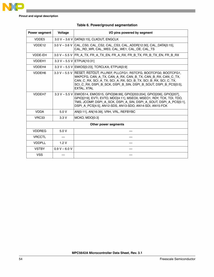
Pinout and signal description
Table 6. Power/ground segmentation
Power segment Voltage I/O pins powered by segment
VDDE5 3.0 V – 3.6 V DATA[0:15], CLKOUT, ENGCLK
VDDE12 3.0 V – 3.6 V CAL_CS0, CAL_CS2, CAL_CS3, CAL_ADDR[12:30], CAL_DATA[0:15], CAL_RD_WR, CAL_WE0, CAL_WE1, CAL_OE, CAL_TS
VDDE-EH 3.0 V – 5.5 V FR_A_TX, FR_A_TX_EN, FR_A_RX, FR_B_TX, FR_B_TX_EN, FR_B_RX
VDDEH1 3.3 V – 5.5 V ETPUA[10:31]
VDDEH4 3.3 V – 5.5 V EMIOS[0:23], TCRCLKA, ETPUA[0:9]
VDDEH6 3.3 V – 5.5 V RESET, RSTOUT, PLLREF, PLLCFG1, RSTCFG, BOOTCFG0, BOOTCFG1, WKPCFG, CAN_A_TX, CAN_A_RX, CAN_B_TX, CAN_B_RX, CAN_C_TX, CAN_C_RX, SCI_A_TX, SCI_A_RX, SCI_B_TX, SCI_B_RX, SCI_C_TX, SCI_C_RX, DSPI_B_SCK, DSPI_B_SIN, DSPI_B_SOUT, DSPI_B_PCS[0:5], EXTAL, XTAL
VDDEH7 3.3 V – 5.5 V EMIOS14, EMIOS15, GPIO[98:99], GPIO[203:204], GPIO[206], GPIO[207], GPIO[219], EVTI, EVTO, MDO[4:11], MSEO0, MSEO1, RDY, TCK, TDI, TDO, TMS, JCOMP, DSPI_A_SCK, DSPI_A_SIN, DSPI_A_SOUT, DSPI_A_PCS[0:1], DSPI_A_PCS[4:5], AN12-SDS, AN13-SDO, AN14-SDI, AN15-FCK
VDDA 5.0 V AN[0:11], AN[16:39], VRH, VRL, REFBYBC
VRC33 3.3 V MCKO, MDO[0:3]
Other power segments
VDDREG 5.0 V —
VRCCTL — —
VDDPLL 1.2 V —
VSTBY 0.9 V – 6.0 V —
VSS — —
MPC5642A Microcontroller Data Sheet, Rev. 3.1
54 Freescale Semiconductor
Electrical characteristics
3 Electrical characteristicsThis section contains detailed information on power considerations, DC/AC electrical characteristics, and AC timing specifications for the MPC5642A series of MCUs.
The electrical specifications are preliminary and are from previous designs, design simulations, or initial evaluation. These specifications may not be fully tested or guaranteed at this early stage of the product life cycle, however for production silicon these specifications will be met. Finalized specifications will be published after complete characterization and device qualifications have been completed.
In the tables where the device logic provides signals with their respective timing characteristics, the symbol “CC” for Controller Characteristics is included in the Symbol column.
In the tables where the external system must provide signals with their respective timing characteristics to the device, the symbol “SR” for System Requirement is included in the Symbol column.
3.1 Parameter classificationThe electrical parameters shown in this supplement are guaranteed by various methods. To give the customer a better understanding, the classifications listed in Table 7 are used and the parameters are tagged accordingly in the tables where appropriate.
NOTEThe classification is shown in the column labeled “C” in the parameter tables where appropriate.
Table 7. Parameter classifications
Classification tag Tag description
P Those parameters are guaranteed during production testing on each individual device.
C Those parameters are achieved by the design characterization by measuring a statistically relevant sample size across process variations.
T Those parameters are achieved by design characterization on a small sample size from typical devices under typical conditions unless otherwise noted. All values shown in the typical column are within this category.
D Those parameters are derived mainly from simulations.
MPC5642A Microcontroller Data Sheet, Rev. 3.1
Freescale Semiconductor 55
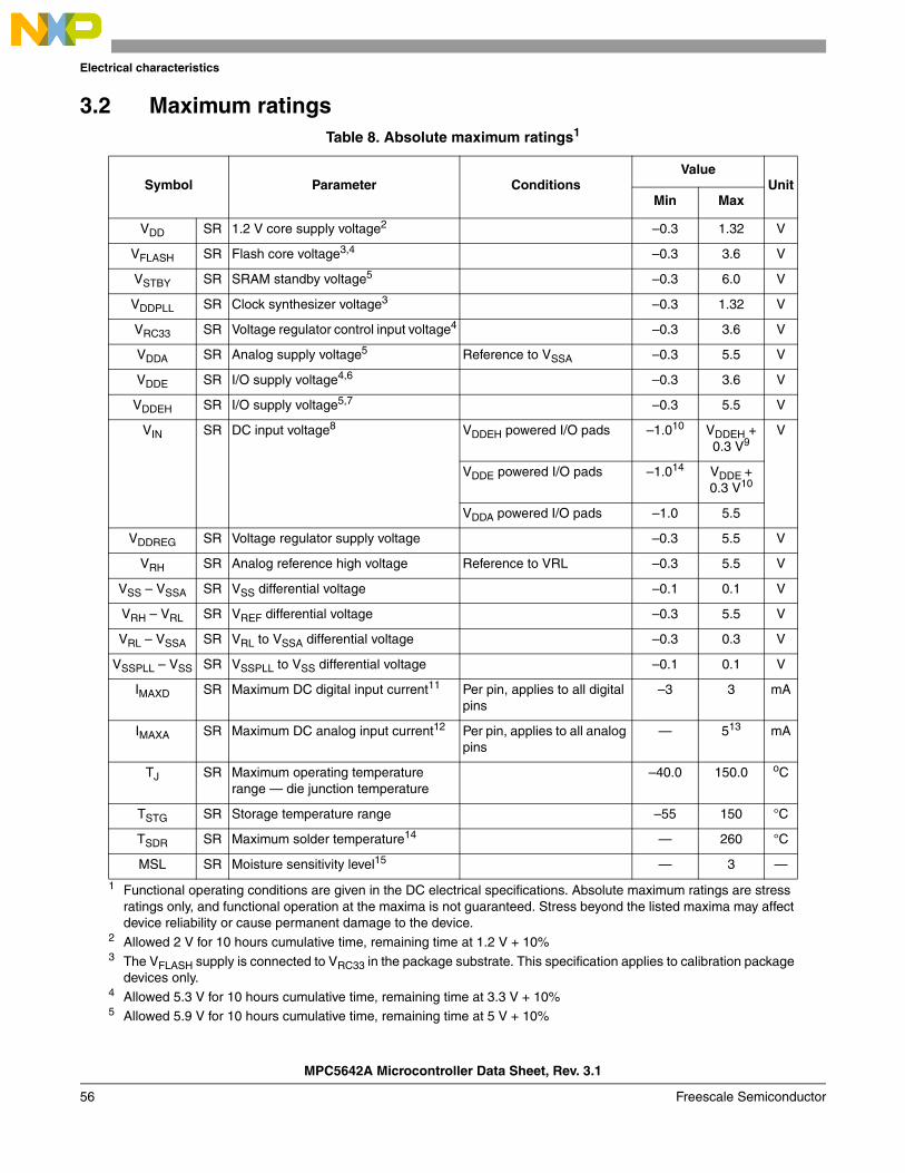
Electrical characteristics
3.2 Maximum ratingsTable 8. Absolute maximum ratings1
1 Functional operating conditions are given in the DC electrical specifications. Absolute maximum ratings are stress ratings only, and functional operation at the maxima is not guaranteed. Stress beyond the listed maxima may affect device reliability or cause permanent damage to the device.
Symbol Parameter ConditionsValue
UnitMin Max
VDD SR 1.2 V core supply voltage2
2 Allowed 2 V for 10 hours cumulative time, remaining time at 1.2 V + 10%
–0.3 1.32 V
VFLASH SR Flash core voltage3,4
3 The VFLASH supply is connected to VRC33 in the package substrate. This specification applies to calibration package devices only.
4 Allowed 5.3 V for 10 hours cumulative time, remaining time at 3.3 V + 10%
–0.3 3.6 V
VSTBY SR SRAM standby voltage5
5 Allowed 5.9 V for 10 hours cumulative time, remaining time at 5 V + 10%
–0.3 6.0 V
VDDPLL SR Clock synthesizer voltage3 –0.3 1.32 V
VRC33 SR Voltage regulator control input voltage4 –0.3 3.6 V
VDDA SR Analog supply voltage5 Reference to VSSA –0.3 5.5 V
VDDE SR I/O supply voltage4,6 –0.3 3.6 V
VDDEH SR I/O supply voltage5,7 –0.3 5.5 V
VIN SR DC input voltage8 VDDEH powered I/O pads –1.010 VDDEH + 0.3 V9
V
VDDE powered I/O pads –1.014 VDDE + 0.3 V10
VDDA powered I/O pads –1.0 5.5
VDDREG SR Voltage regulator supply voltage –0.3 5.5 V
VRH SR Analog reference high voltage Reference to VRL –0.3 5.5 V
VSS – VSSA SR VSS differential voltage –0.1 0.1 V
VRH – VRL SR VREF differential voltage –0.3 5.5 V
VRL – VSSA SR VRL to VSSA differential voltage –0.3 0.3 V
VSSPLL – VSS SR VSSPLL to VSS differential voltage –0.1 0.1 V
IMAXD SR Maximum DC digital input current11 Per pin, applies to all digital pins
–3 3 mA
IMAXA SR Maximum DC analog input current12 Per pin, applies to all analog pins
— 513 mA
TJ SR Maximum operating temperature range — die junction temperature
–40.0 150.0 oC
TSTG SR Storage temperature range –55 150 °C
TSDR SR Maximum solder temperature14 — 260 °C
MSL SR Moisture sensitivity level15 — 3 —
MPC5642A Microcontroller Data Sheet, Rev. 3.1
56 Freescale Semiconductor
Electrical characteristics
6 All functional non-supply I/O pins are clamped to VSS and VDDE, or VDDEH.7 Internal structures hold the voltage greater than –1.0 V if the injection current limit of 2 mA is met. 8 AC signal overshoot and undershoot of up to 2.0 V of the input voltages is permitted for an accumulative duration of
60 hours over the complete lifetime of the device (injection current not limited for this duration).9 Internal structures hold the input voltage less than the maximum voltage on all pads powered by VDDEH supplies, if
the maximum injection current specification is met (2 mA for all pins) and VDDEH is within the operating voltage specifications.
10 Internal structures hold the input voltage less than the maximum voltage on all pads powered by VDDE supplies, if the maximum injection current specification is met (2 mA for all pins) and VDDE is within the operating voltage specifications.
11 Total injection current for all pins (including both digital and analog) must not exceed 25 mA.12 Total injection current for all analog input pins must not exceed 15 mA.13 Lifetime operation at these specification limits is not guaranteed.14 Solder profile per IPC/JEDEC J-STD-020D15 Moisture sensitivity per JEDEC test method A112
MPC5642A Microcontroller Data Sheet, Rev. 3.1
Freescale Semiconductor 57
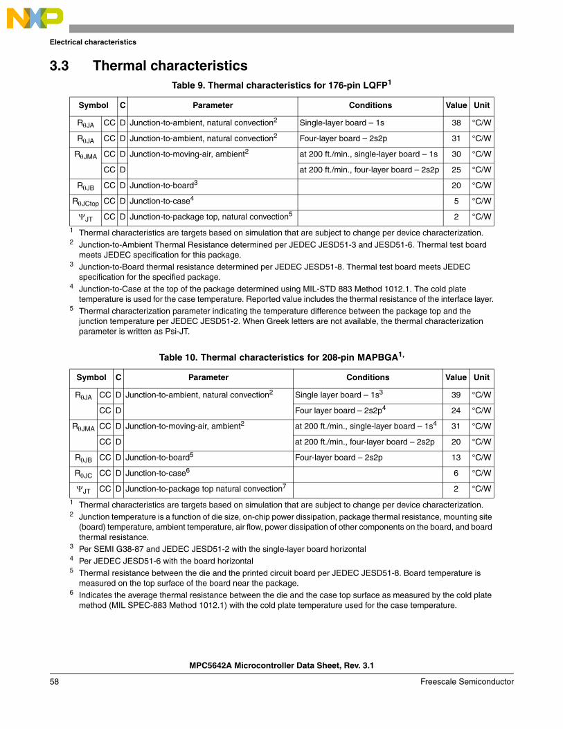
Electrical characteristics
3.3 Thermal characteristicsTable 9. Thermal characteristics for 176-pin LQFP1
1 Thermal characteristics are targets based on simulation that are subject to change per device characterization.
Symbol C Parameter Conditions Value Unit
RJA CC D Junction-to-ambient, natural convection2
2 Junction-to-Ambient Thermal Resistance determined per JEDEC JESD51-3 and JESD51-6. Thermal test board meets JEDEC specification for this package.
Single-layer board – 1s 38 °C/W
RJA CC D Junction-to-ambient, natural convection2 Four-layer board – 2s2p 31 °C/W
RJMA CC D Junction-to-moving-air, ambient2 at 200 ft./min., single-layer board – 1s 30 °C/W
CC D at 200 ft./min., four-layer board – 2s2p 25 °C/W
RJB CC D Junction-to-board3
3 Junction-to-Board thermal resistance determined per JEDEC JESD51-8. Thermal test board meets JEDEC specification for the specified package.
20 °C/W
RJCtop CC D Junction-to-case4
4 Junction-to-Case at the top of the package determined using MIL-STD 883 Method 1012.1. The cold plate temperature is used for the case temperature. Reported value includes the thermal resistance of the interface layer.
5 °C/W
JT CC D Junction-to-package top, natural convection5
5 Thermal characterization parameter indicating the temperature difference between the package top and the junction temperature per JEDEC JESD51-2. When Greek letters are not available, the thermal characterization parameter is written as Psi-JT.
2 °C/W
Table 10. Thermal characteristics for 208-pin MAPBGA1,
1 Thermal characteristics are targets based on simulation that are subject to change per device characterization.
Symbol C Parameter Conditions Value Unit
RJA CC D Junction-to-ambient, natural convection2
2 Junction temperature is a function of die size, on-chip power dissipation, package thermal resistance, mounting site (board) temperature, ambient temperature, air flow, power dissipation of other components on the board, and board thermal resistance.
Single layer board – 1s3
3 Per SEMI G38-87 and JEDEC JESD51-2 with the single-layer board horizontal
39 °C/W
CC D Four layer board – 2s2p4
4 Per JEDEC JESD51-6 with the board horizontal
24 °C/W
RJMA CC D Junction-to-moving-air, ambient2 at 200 ft./min., single-layer board – 1s4 31 °C/W
CC D at 200 ft./min., four-layer board – 2s2p 20 °C/W
RJB CC D Junction-to-board5
5 Thermal resistance between the die and the printed circuit board per JEDEC JESD51-8. Board temperature is measured on the top surface of the board near the package.
Four-layer board – 2s2p 13 °C/W
RJC CC D Junction-to-case6
6 Indicates the average thermal resistance between the die and the case top surface as measured by the cold plate method (MIL SPEC-883 Method 1012.1) with the cold plate temperature used for the case temperature.
6 °C/W
JT CC D Junction-to-package top natural convection7 2 °C/W
MPC5642A Microcontroller Data Sheet, Rev. 3.1
58 Freescale Semiconductor
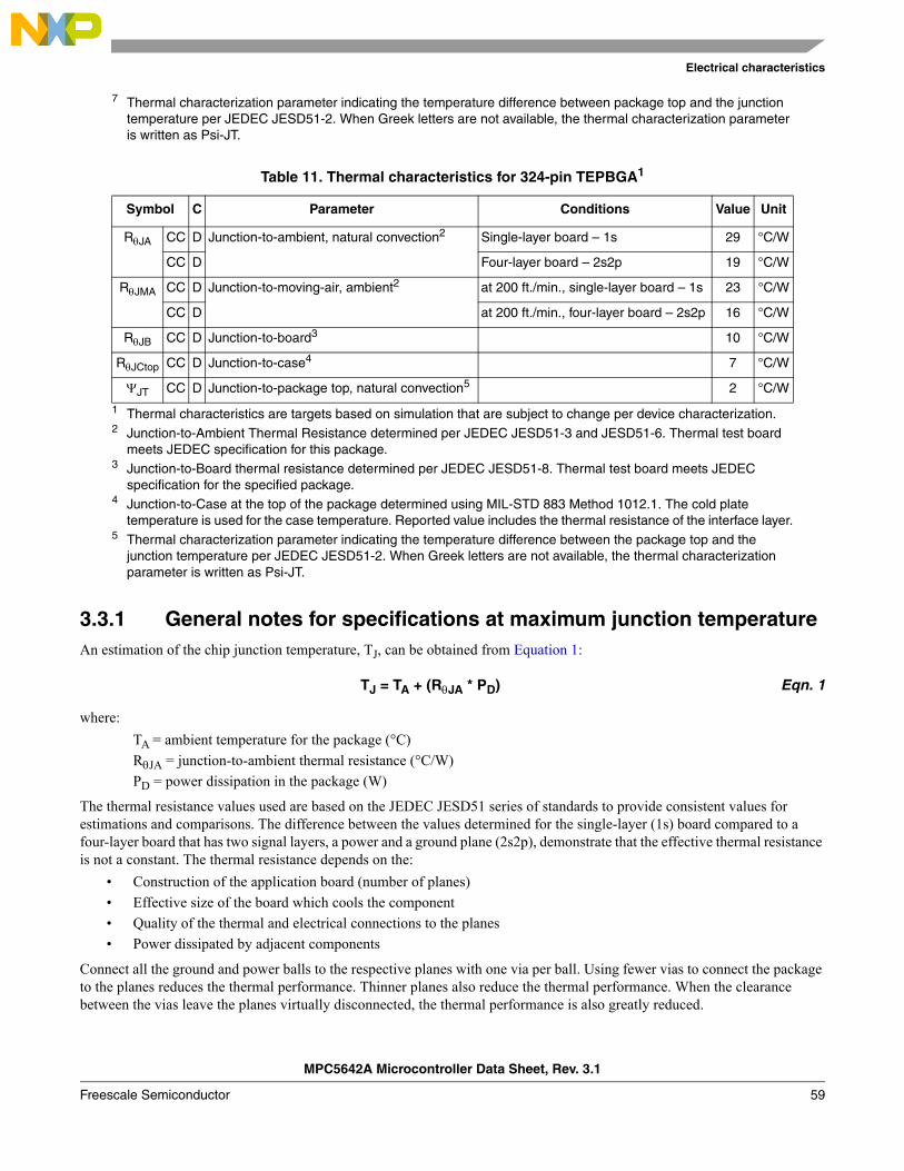
Electrical characteristics
3.3.1 General notes for specifications at maximum junction temperatureAn estimation of the chip junction temperature, TJ, can be obtained from Equation 1:
TJ = TA + (RJA * PD) Eqn. 1
where:
TA = ambient temperature for the package (°C)
RJA = junction-to-ambient thermal resistance (°C/W)
PD = power dissipation in the package (W)
The thermal resistance values used are based on the JEDEC JESD51 series of standards to provide consistent values for estimations and comparisons. The difference between the values determined for the single-layer (1s) board compared to a four-layer board that has two signal layers, a power and a ground plane (2s2p), demonstrate that the effective thermal resistance is not a constant. The thermal resistance depends on the:
• Construction of the application board (number of planes)
• Effective size of the board which cools the component
• Quality of the thermal and electrical connections to the planes
• Power dissipated by adjacent components
Connect all the ground and power balls to the respective planes with one via per ball. Using fewer vias to connect the package to the planes reduces the thermal performance. Thinner planes also reduce the thermal performance. When the clearance between the vias leave the planes virtually disconnected, the thermal performance is also greatly reduced.
7 Thermal characterization parameter indicating the temperature difference between package top and the junction temperature per JEDEC JESD51-2. When Greek letters are not available, the thermal characterization parameter is written as Psi-JT.
Table 11. Thermal characteristics for 324-pin TEPBGA1
1 Thermal characteristics are targets based on simulation that are subject to change per device characterization.
Symbol C Parameter Conditions Value Unit
RJA CC D Junction-to-ambient, natural convection2
2 Junction-to-Ambient Thermal Resistance determined per JEDEC JESD51-3 and JESD51-6. Thermal test board meets JEDEC specification for this package.
Single-layer board – 1s 29 °C/W
CC D Four-layer board – 2s2p 19 °C/W
RJMA CC D Junction-to-moving-air, ambient2 at 200 ft./min., single-layer board – 1s 23 °C/W
CC D at 200 ft./min., four-layer board – 2s2p 16 °C/W
RJB CC D Junction-to-board3
3 Junction-to-Board thermal resistance determined per JEDEC JESD51-8. Thermal test board meets JEDEC specification for the specified package.
10 °C/W
RJCtop CC D Junction-to-case4
4 Junction-to-Case at the top of the package determined using MIL-STD 883 Method 1012.1. The cold plate temperature is used for the case temperature. Reported value includes the thermal resistance of the interface layer.
7 °C/W
JT CC D Junction-to-package top, natural convection5
5 Thermal characterization parameter indicating the temperature difference between the package top and the junction temperature per JEDEC JESD51-2. When Greek letters are not available, the thermal characterization parameter is written as Psi-JT.
2 °C/W
MPC5642A Microcontroller Data Sheet, Rev. 3.1
Freescale Semiconductor 59
Electrical characteristics
As a general rule, the value obtained on a single-layer board is within the normal range for the tightly packed printed circuit board. The value obtained on a board with the internal planes is usually within the normal range if the application board has:
• One oz. (35 micron nominal thickness) internal planes
• Components that are well separated
• Overall power dissipation on the board is less than 0.02 W/cm2
The thermal performance of any component depends on the power dissipation of the surrounding components. In addition, the ambient temperature varies widely within the application. For many natural convection and especially closed-box applications, the board temperature at the perimeter (edge) of the package is approximately the same as the local air temperature near the device. Specifying the local ambient conditions explicitly as the board temperature provides a more precise description of the local ambient conditions that determine the temperature of the device.
At a known board temperature, the junction temperature is estimated using Equation 2:
TJ = TB + (RJB * PD) Eqn. 2
where:
TB = board temperature for the package perimeter (°C)
RJB = junction-to-board thermal resistance (°C/W) per JESD51-8S
PD = power dissipation in the package (W)
When the heat loss from the package case to the air does not factor into the calculation, an acceptable value for the junction temperature is predictable. Ensure the application board is similar to the thermal test condition, with the component soldered to a board with internal planes.
The thermal resistance is expressed as the sum of a junction-to-case thermal resistance plus a case-to-ambient thermal resistance:
RJA = RJC + RCA Eqn. 3
where:
RJA = junction-to-ambient thermal resistance (°C/W)
RJC = junction-to-case thermal resistance (°C/W)
RCA = case to ambient thermal resistance (°C/W)
RJC is device-related and is not affected by other factors. The thermal environment can be controlled to change the case-to-ambient thermal resistance, RCA. For example, change the air flow around the device, add a heat sink, change the mounting arrangement on the printed circuit board, or change the thermal dissipation on the printed circuit board surrounding the device. This description is most useful for packages with heat sinks where 90% of the heat flow is through the case to heat sink to ambient. For most packages, a better model is required.
A more accurate two-resistor thermal model can be constructed from the junction-to-board thermal resistance and the junction-to-case thermal resistance. The junction-to-case thermal resistance describes when using a heat sink or where a substantial amount of heat is dissipated from the top of the package. The junction-to-board thermal resistance describes the thermal performance when most of the heat is conducted to the printed circuit board. This model can be used to generate simple estimations and for computational fluid dynamics (CFD) thermal models.
To determine the junction temperature of the device in the application on a prototype board, use the thermal characterization parameter (JT) to determine the junction temperature by measuring the temperature at the top center of the package case using Equation 4:
TJ = TT + (JT x PD) Eqn. 4
where:
TT = thermocouple temperature on top of the package (°C)
MPC5642A Microcontroller Data Sheet, Rev. 3.1
60 Freescale Semiconductor
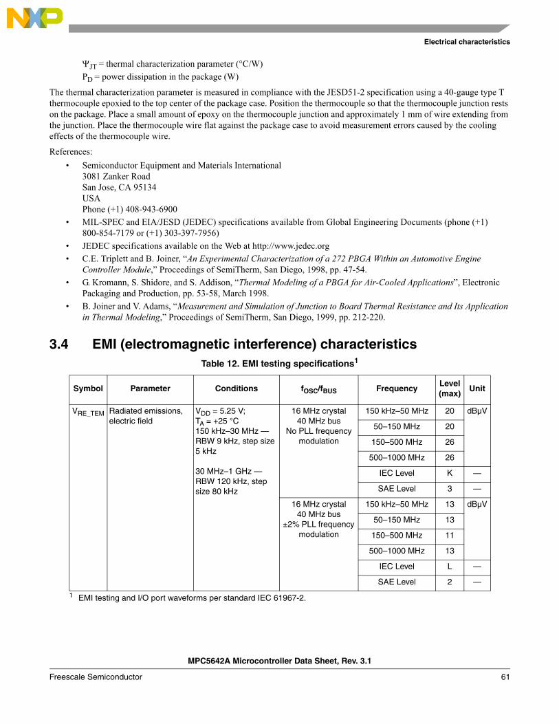
Electrical characteristics
JT = thermal characterization parameter (°C/W)
PD = power dissipation in the package (W)
The thermal characterization parameter is measured in compliance with the JESD51-2 specification using a 40-gauge type T thermocouple epoxied to the top center of the package case. Position the thermocouple so that the thermocouple junction rests on the package. Place a small amount of epoxy on the thermocouple junction and approximately 1 mm of wire extending from the junction. Place the thermocouple wire flat against the package case to avoid measurement errors caused by the cooling effects of the thermocouple wire.
References:
• Semiconductor Equipment and Materials International3081 Zanker RoadSan Jose, CA 95134USAPhone (+1) 408-943-6900
• MIL-SPEC and EIA/JESD (JEDEC) specifications available from Global Engineering Documents (phone (+1) 800-854-7179 or (+1) 303-397-7956)
• JEDEC specifications available on the Web at http://www.jedec.org
• C.E. Triplett and B. Joiner, “An Experimental Characterization of a 272 PBGA Within an Automotive Engine Controller Module,” Proceedings of SemiTherm, San Diego, 1998, pp. 47-54.
• G. Kromann, S. Shidore, and S. Addison, “Thermal Modeling of a PBGA for Air-Cooled Applications”, Electronic Packaging and Production, pp. 53-58, March 1998.
• B. Joiner and V. Adams, “Measurement and Simulation of Junction to Board Thermal Resistance and Its Application in Thermal Modeling,” Proceedings of SemiTherm, San Diego, 1999, pp. 212-220.
3.4 EMI (electromagnetic interference) characteristicsTable 12. EMI testing specifications1
1 EMI testing and I/O port waveforms per standard IEC 61967-2.
Symbol Parameter Conditions fOSC/fBUS FrequencyLevel(max)
Unit
VRE_TEM Radiated emissions,electric field
VDD = 5.25 V;TA = +25 °C150 kHz–30 MHz — RBW 9 kHz, step size 5 kHz
30 MHz–1 GHz — RBW 120 kHz, step size 80 kHz
16 MHz crystal40 MHz bus
No PLL frequency modulation
150 kHz–50 MHz 20 dBµV
50–150 MHz 20
150–500 MHz 26
500–1000 MHz 26
IEC Level K —
SAE Level 3 —
16 MHz crystal40 MHz bus
±2% PLL frequency modulation
150 kHz–50 MHz 13 dBµV
50–150 MHz 13
150–500 MHz 11
500–1000 MHz 13
IEC Level L —
SAE Level 2 —
MPC5642A Microcontroller Data Sheet, Rev. 3.1
Freescale Semiconductor 61
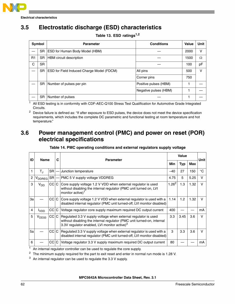
Electrical characteristics
3.5 Electrostatic discharge (ESD) characteristics
3.6 Power management control (PMC) and power on reset (POR) electrical specifications
Table 13. ESD ratings1,2
1 All ESD testing is in conformity with CDF-AEC-Q100 Stress Test Qualification for Automotive Grade Integrated Circuits.
2 Device failure is defined as: “If after exposure to ESD pulses, the device does not meet the device specification requirements, which includes the complete DC parametric and functional testing at room temperature and hot temperature.”
Symbol Parameter Conditions Value Unit
— SR ESD for Human Body Model (HBM) — 2000 V
R1 SR HBM circuit description — 1500
C SR — 100 pF
— SR ESD for Field Induced Charge Model (FDCM) All pins 500 V
Corner pins 750
— SR Number of pulses per pin Positive pulses (HBM) 1 —
Negative pulses (HBM) 1 —
— SR Number of pulses — 1 —
Table 14. PMC operating conditions and external regulators supply voltage
ID Name C ParameterValue
UnitMin Typ Max
1 TJ SR — Junction temperature –40 27 150 °C
2 VDDREG SR — PMC 5 V supply voltage VDDREG 4.75 5 5.25 V
3 VDD CC C Core supply voltage 1.2 V VDD when external regulator is used without disabling the internal regulator (PMC unit turned on, LVI monitor active)1
1 An internal regulator controller can be used to regulate the core supply.
1.262
2 The minimum supply required for the part to exit reset and enter in normal run mode is 1.28 V.
1.3 1.32 V
3a — CC C Core supply voltage 1.2 V VDD when external regulator is used with a disabled internal regulator (PMC unit turned-off, LVI monitor disabled)
1.14 1.2 1.32 V
4 IVDD CC C Voltage regulator core supply maximum required DC output current 400 — — mA
5 VDD33 CC C Regulated 3.3 V supply voltage when external regulator is used without disabling the internal regulator (PMC unit turned-on, internal 3.3V regulator enabled, LVI monitor active)3
3 An internal regulator can be used to regulate the 3.3 V supply.
3.3 3.45 3.6 V
5a — CC C Regulated 3.3 V supply voltage when external regulator is used with a disabled internal regulator (PMC unit turned-off, LVI monitor disabled)
3 3.3 3.6 V
6 — CC C Voltage regulator 3.3 V supply maximum required DC output current 80 — — mA
MPC5642A Microcontroller Data Sheet, Rev. 3.1
62 Freescale Semiconductor
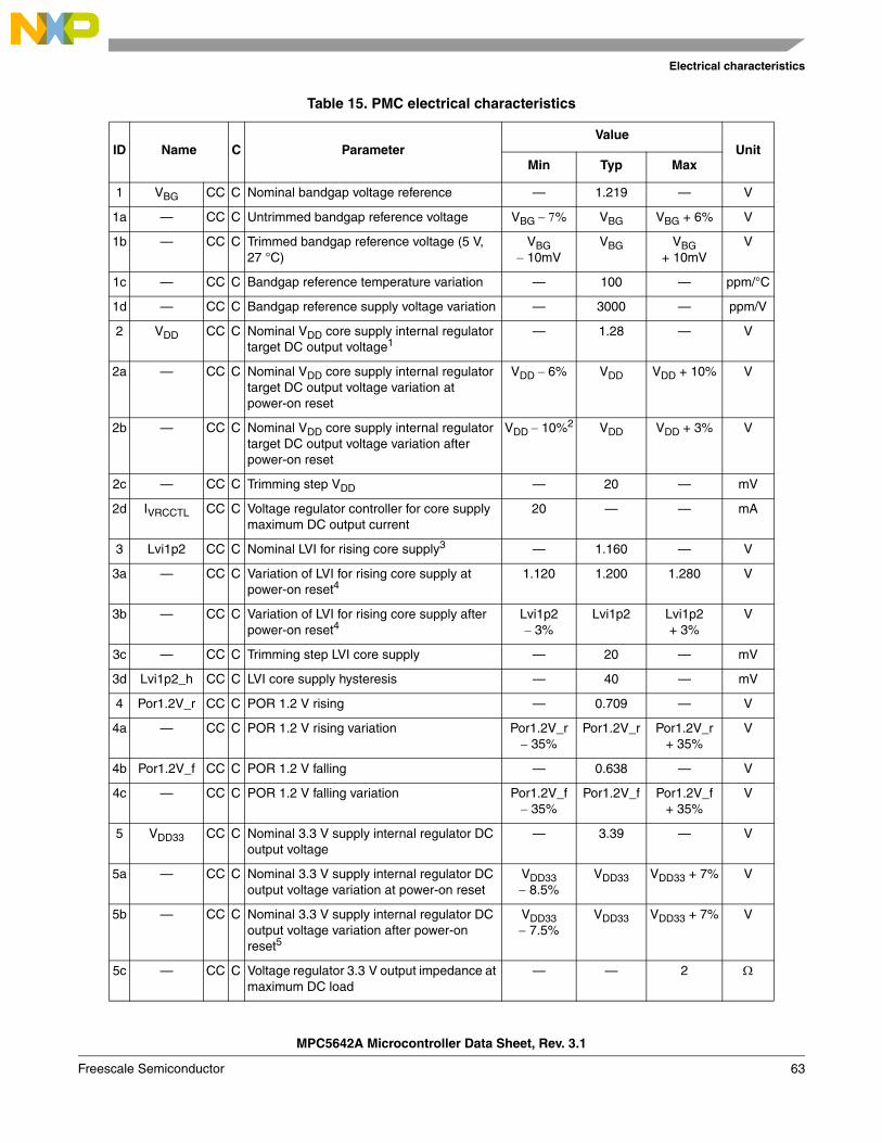
Electrical characteristics
Table 15. PMC electrical characteristics
ID Name C ParameterValue
UnitMin Typ Max
1 VBG CC C Nominal bandgap voltage reference — 1.219 — V
1a — CC C Untrimmed bandgap reference voltage VBG % VBG VBG + 6% V
1b — CC C Trimmed bandgap reference voltage (5 V, 27 °C)
VBG 10mV
VBG VBG + 10mV
V
1c — CC C Bandgap reference temperature variation — 100 — ppm/°C
1d — CC C Bandgap reference supply voltage variation — 3000 — ppm/V
2 VDD CC C Nominal VDD core supply internal regulator target DC output voltage1
— 1.28 — V
2a — CC C Nominal VDD core supply internal regulator target DC output voltage variation at power-on reset
VDD 6% VDD VDD + 10% V
2b — CC C Nominal VDD core supply internal regulator target DC output voltage variation after power-on reset
VDD 10%2 VDD VDD + 3% V
2c — CC C Trimming step VDD — 20 — mV
2d IVRCCTL CC C Voltage regulator controller for core supply maximum DC output current
20 — — mA
3 Lvi1p2 CC C Nominal LVI for rising core supply3 — 1.160 — V
3a — CC C Variation of LVI for rising core supply at power-on reset4
1.120 1.200 1.280 V
3b — CC C Variation of LVI for rising core supply after power-on reset4
Lvi1p2 3%
Lvi1p2 Lvi1p2 + 3%
V
3c — CC C Trimming step LVI core supply — 20 — mV
3d Lvi1p2_h CC C LVI core supply hysteresis — 40 — mV
4 Por1.2V_r CC C POR 1.2 V rising — 0.709 — V
4a — CC C POR 1.2 V rising variation Por1.2V_r 35%
Por1.2V_r Por1.2V_r + 35%
V
4b Por1.2V_f CC C POR 1.2 V falling — 0.638 — V
4c — CC C POR 1.2 V falling variation Por1.2V_f 35%
Por1.2V_f Por1.2V_f + 35%
V
5 VDD33 CC C Nominal 3.3 V supply internal regulator DC output voltage
— 3.39 — V
5a — CC C Nominal 3.3 V supply internal regulator DC output voltage variation at power-on reset
VDD33 8.5%
VDD33 VDD33 + 7% V
5b — CC C Nominal 3.3 V supply internal regulator DC output voltage variation after power-on reset5
VDD33 7.5%
VDD33 VDD33 + 7% V
5c — CC C Voltage regulator 3.3 V output impedance at maximum DC load
— — 2
MPC5642A Microcontroller Data Sheet, Rev. 3.1
Freescale Semiconductor 63
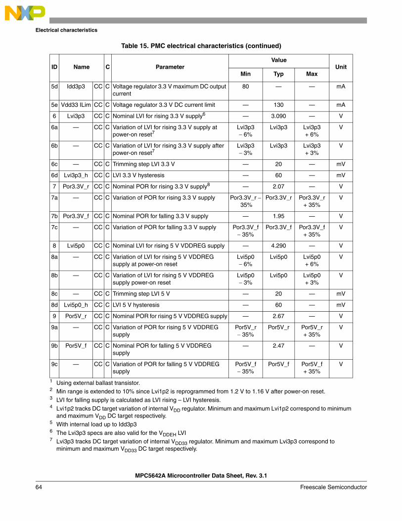
Electrical characteristics
5d Idd3p3 CC C Voltage regulator 3.3 V maximum DC output current
80 — — mA
5e Vdd33 ILim CC C Voltage regulator 3.3 V DC current limit — 130 — mA
6 Lvi3p3 CC C Nominal LVI for rising 3.3 V supply6 — 3.090 — V
6a — CC C Variation of LVI for rising 3.3 V supply at power-on reset7
Lvi3p3 6%
Lvi3p3 Lvi3p3 + 6%
V
6b — CC C Variation of LVI for rising 3.3 V supply after power-on reset7
Lvi3p3 3%
Lvi3p3 Lvi3p3 + 3%
V
6c — CC C Trimming step LVI 3.3 V — 20 — mV
6d Lvi3p3_h CC C LVI 3.3 V hysteresis — 60 — mV
7 Por3.3V_r CC C Nominal POR for rising 3.3 V supply8 — 2.07 — V
7a — CC C Variation of POR for rising 3.3 V supply Por3.3V_r 35%
Por3.3V_r Por3.3V_r+ 35%
V
7b Por3.3V_f CC C Nominal POR for falling 3.3 V supply — 1.95 — V
7c — CC C Variation of POR for falling 3.3 V supply Por3.3V_f 35%
Por3.3V_f Por3.3V_f + 35%
V
8 Lvi5p0 CC C Nominal LVI for rising 5 V VDDREG supply — 4.290 — V
8a — CC C Variation of LVI for rising 5 V VDDREG supply at power-on reset
Lvi5p0 6%
Lvi5p0 Lvi5p0 + 6%
V
8b — CC C Variation of LVI for rising 5 V VDDREG supply power-on reset
Lvi5p0 3%
Lvi5p0 Lvi5p0 + 3%
V
8c — CC C Trimming step LVI 5 V — 20 — mV
8d Lvi5p0_h CC C LVI 5 V hysteresis — 60 — mV
9 Por5V_r CC C Nominal POR for rising 5 V VDDREG supply — 2.67 — V
9a — CC C Variation of POR for rising 5 V VDDREG supply
Por5V_r 35%
Por5V_r Por5V_r+ 35%
V
9b Por5V_f CC C Nominal POR for falling 5 V VDDREG supply
— 2.47 — V
9c — CC C Variation of POR for falling 5 V VDDREG supply
Por5V_f 35%
Por5V_f Por5V_f+ 35%
V
1 Using external ballast transistor.2 Min range is extended to 10% since Lvi1p2 is reprogrammed from 1.2 V to 1.16 V after power-on reset.3 LVI for falling supply is calculated as LVI rising – LVI hysteresis.4 Lvi1p2 tracks DC target variation of internal VDD regulator. Minimum and maximum Lvi1p2 correspond to minimum
and maximum VDD DC target respectively.5 With internal load up to Idd3p36 The Lvi3p3 specs are also valid for the VDDEH LVI7 Lvi3p3 tracks DC target variation of internal VDD33 regulator. Minimum and maximum Lvi3p3 correspond to
minimum and maximum VDD33 DC target respectively.
Table 15. PMC electrical characteristics (continued)
ID Name C ParameterValue
UnitMin Typ Max
MPC5642A Microcontroller Data Sheet, Rev. 3.1
64 Freescale Semiconductor
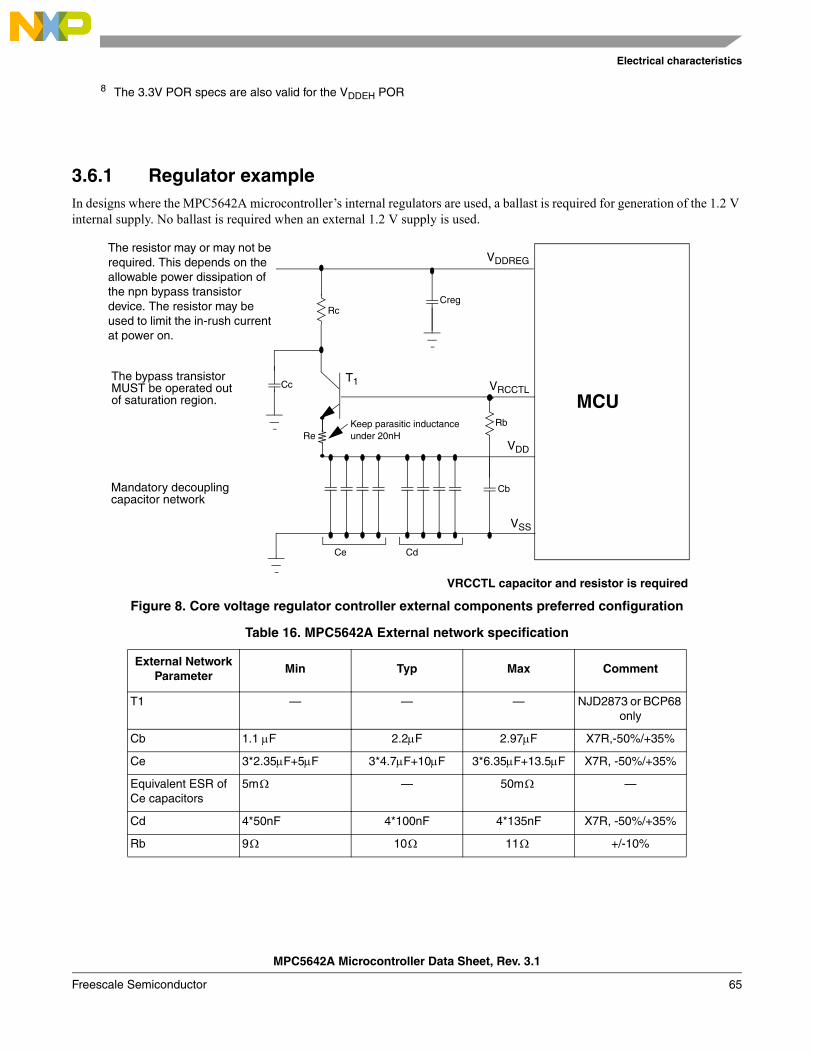
Electrical characteristics
3.6.1 Regulator exampleIn designs where the MPC5642A microcontroller’s internal regulators are used, a ballast is required for generation of the 1.2 V internal supply. No ballast is required when an external 1.2 V supply is used.
Figure 8. Core voltage regulator controller external components preferred configuration
8 The 3.3V POR specs are also valid for the VDDEH POR
Table 16. MPC5642A External network specification
External Network Parameter
Min Typ Max Comment
T1 — — — NJD2873 or BCP68 only
Cb 1.1 F 2.2F 2.97F X7R,-50%/+35%
Ce 3*2.35F+5F 3*4.7F+10F 3*6.35F+13.5F X7R, -50%/+35%
Equivalent ESR of Ce capacitors
5m — 50m —
Cd 4*50nF 4*100nF 4*135nF X7R, -50%/+35%
Rb 9 10 11 +/-10%
MCUThe bypass transistorMUST be operated outof saturation region.
Mandatory decouplingcapacitor network
VDDREG
VRCCTL
VDD
VSS
VRCCTL capacitor and resistor is required
Ce Cd
Cb
Rb
Cc
CregRc
The resistor may or may not be required. This depends on the allowable power dissipation of the npn bypass transistor device. The resistor may be used to limit the in-rush current at power on.
Re
Keep parasitic inductanceunder 20nH
T1
MPC5642A Microcontroller Data Sheet, Rev. 3.1
Freescale Semiconductor 65
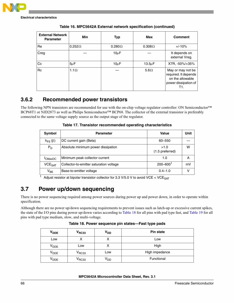
Electrical characteristics
3.6.2 Recommended power transistorsThe following NPN transistors are recommended for use with the on-chip voltage regulator controller: ON Semiconductor™ BCP68T1 or NJD2873 as well as Philips Semiconductor™ BCP68. The collector of the external transistor is preferably connected to the same voltage supply source as the output stage of the regulator.
3.7 Power up/down sequencingThere is no power sequencing required among power sources during power up and power down, in order to operate within specification.
Although there are no power up/down sequencing requirements to prevent issues such as latch-up or excessive current spikes, the state of the I/O pins during power up/down varies according to Table 18 for all pins with pad type fast, and Table 19 for all pins with pad type medium, slow, and multi-voltage.
Re 0.252 0.280 0.308 +/-10%
Creg — 10F — It depends on external Vreg.
Cc 5F 10F 13.5F X7R, -50%/+35%
Rc 1.1 — 5.6 May or may not be required. It depends
on the allowable power dissipation of
T1.
Table 17. Transistor recommended operating characteristics
Symbol Parameter Value Unit
hFE () DC current gain (Beta) 60–550 —
PD Absolute minimum power dissipation >1.0(1.5 preferred)
W
ICMaxDC Minimum peak collector current 1.0 A
VCESAT Collector-to-emitter saturation voltage 200–6001
1 Adjust resistor at bipolar transistor collector for 3.3 V/5.0 V to avoid VCE < VCESAT
mV
VBE Base-to-emitter voltage 0.4–1.0 V
Table 18. Power sequence pin states—Fast type pads
VDDE VRC33 VDD Pin state
Low X X Low
VDDE Low X High
VDDE VRC33 Low High impedance
VDDE VRC33 VDD Functional
Table 16. MPC5642A External network specification (continued)
External Network Parameter
Min Typ Max Comment
MPC5642A Microcontroller Data Sheet, Rev. 3.1
66 Freescale Semiconductor
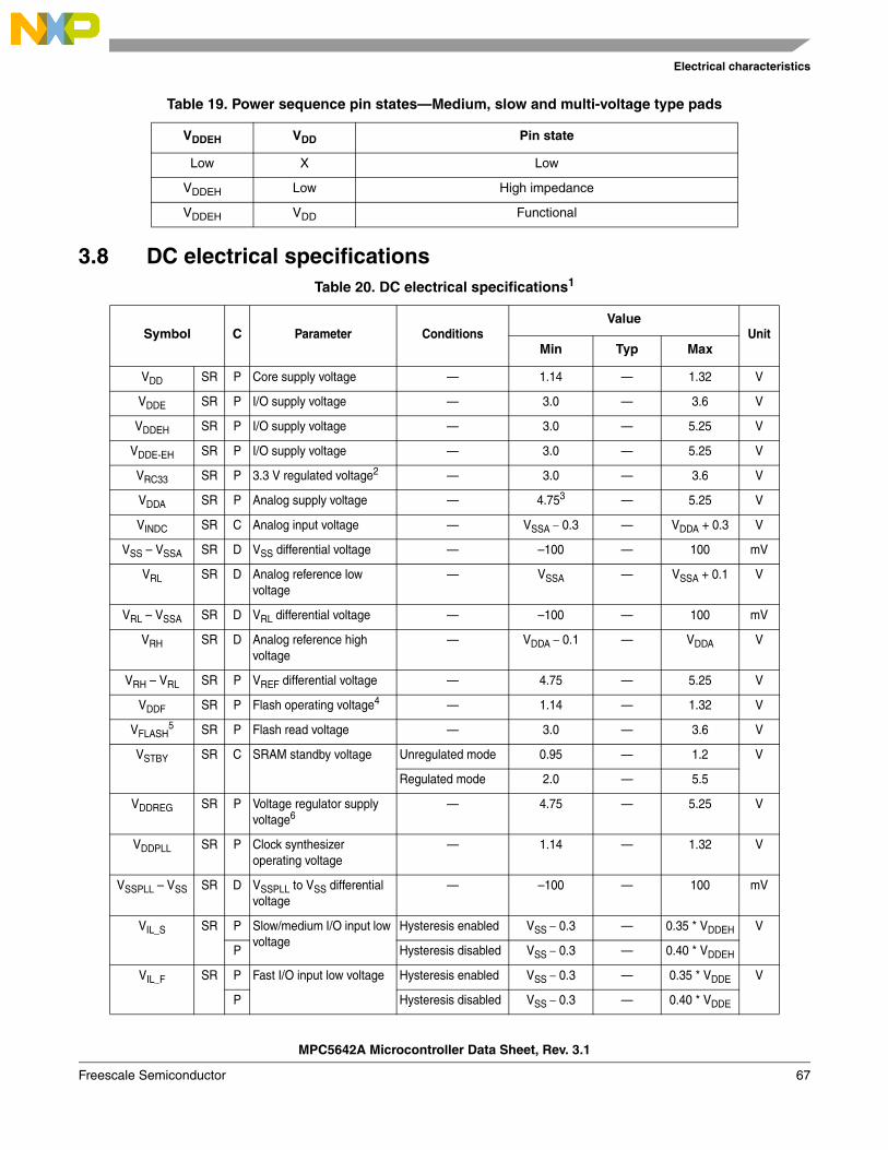
Electrical characteristics
3.8 DC electrical specifications
Table 19. Power sequence pin states—Medium, slow and multi-voltage type pads
VDDEH VDD Pin state
Low X Low
VDDEH Low High impedance
VDDEH VDD Functional
Table 20. DC electrical specifications1
Symbol C Parameter ConditionsValue
UnitMin Typ Max
VDD SR P Core supply voltage — 1.14 — 1.32 V
VDDE SR P I/O supply voltage — 3.0 — 3.6 V
VDDEH SR P I/O supply voltage — 3.0 — 5.25 V
VDDE-EH SR P I/O supply voltage — 3.0 — 5.25 V
VRC33 SR P 3.3 V regulated voltage2 — 3.0 — 3.6 V
VDDA SR P Analog supply voltage — 4.753 — 5.25 V
VINDC SR C Analog input voltage — VSSA 0.3 — VDDA + 0.3 V
VSS – VSSA SR D VSS differential voltage — –100 — 100 mV
VRL SR D Analog reference low voltage
— VSSA — VSSA + 0.1 V
VRL – VSSA SR D VRL differential voltage — –100 — 100 mV
VRH SR D Analog reference high voltage
— VDDA 0.1 — VDDA V
VRH – VRL SR P VREF differential voltage — 4.75 — 5.25 V
VDDF SR P Flash operating voltage4 — 1.14 — 1.32 V
VFLASH5 SR P Flash read voltage — 3.0 — 3.6 V
VSTBY SR C SRAM standby voltage Unregulated mode 0.95 — 1.2 V
Regulated mode 2.0 — 5.5
VDDREG SR P Voltage regulator supply voltage6
— 4.75 — 5.25 V
VDDPLL SR P Clock synthesizer operating voltage
— 1.14 — 1.32 V
VSSPLL – VSS SR D VSSPLL to VSS differential voltage
— –100 — 100 mV
VIL_S SR P Slow/medium I/O input low voltage
Hysteresis enabled VSS 0.3 — 0.35 * VDDEH V
P Hysteresis disabled VSS 0.3 — 0.40 * VDDEH
VIL_F SR P Fast I/O input low voltage Hysteresis enabled VSS 0.3 — 0.35 * VDDE V
P Hysteresis disabled VSS 0.3 — 0.40 * VDDE
MPC5642A Microcontroller Data Sheet, Rev. 3.1
Freescale Semiconductor 67
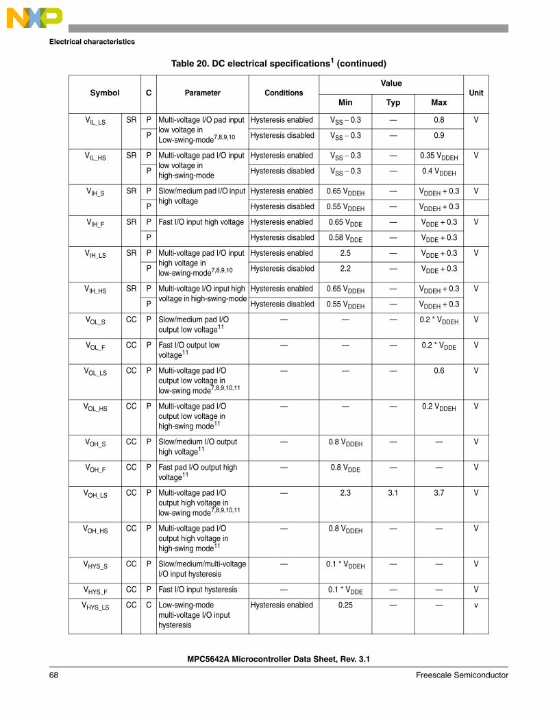
Electrical characteristics
VIL_LS SR P Multi-voltage I/O pad input low voltage in Low-swing-mode7,8,9,10
Hysteresis enabled VSS 0.3 — 0.8 V
P Hysteresis disabled VSS 0.3 — 0.9
VIL_HS SR P Multi-voltage pad I/O input low voltage in high-swing-mode
Hysteresis enabled VSS 0.3 — 0.35 VDDEH V
P Hysteresis disabled VSS 0.3 — 0.4 VDDEH
VIH_S SR P Slow/medium pad I/O input high voltage
Hysteresis enabled 0.65 VDDEH — VDDEH + 0.3 V
P Hysteresis disabled 0.55 VDDEH — VDDEH + 0.3
VIH_F SR P Fast I/O input high voltage Hysteresis enabled 0.65 VDDE — VDDE + 0.3 V
P Hysteresis disabled 0.58 VDDE — VDDE + 0.3
VIH_LS SR P Multi-voltage pad I/O input high voltage in low-swing-mode7,8,9,10
Hysteresis enabled 2.5 — VDDE + 0.3 V
P Hysteresis disabled 2.2 — VDDE + 0.3
VIH_HS SR P Multi-voltage I/O input high voltage in high-swing-mode
Hysteresis enabled 0.65 VDDEH — VDDEH + 0.3 V
P Hysteresis disabled 0.55 VDDEH — VDDEH + 0.3
VOL_S CC P Slow/medium pad I/O output low voltage11
— — — 0.2 * VDDEH V
VOL_F CC P Fast I/O output low voltage11
— — — 0.2 * VDDE V
VOL_LS CC P Multi-voltage pad I/O output low voltage in low-swing mode7,8,9,10,11
— — — 0.6 V
VOL_HS CC P Multi-voltage pad I/O output low voltage in high-swing mode11
— — — 0.2 VDDEH V
VOH_S CC P Slow/medium I/O output high voltage11
— 0.8 VDDEH — — V
VOH_F CC P Fast pad I/O output high voltage11
— 0.8 VDDE — — V
VOH_LS CC P Multi-voltage pad I/O output high voltage in low-swing mode7,8,9,10,11
— 2.3 3.1 3.7 V
VOH_HS CC P Multi-voltage pad I/O output high voltage in high-swing mode11
— 0.8 VDDEH — — V
VHYS_S CC P Slow/medium/multi-voltageI/O input hysteresis
— 0.1 * VDDEH — — V
VHYS_F CC P Fast I/O input hysteresis — 0.1 * VDDE — — V
VHYS_LS CC C Low-swing-mode multi-voltage I/O input hysteresis
Hysteresis enabled 0.25 — — v
Table 20. DC electrical specifications1 (continued)
Symbol C Parameter ConditionsValue
UnitMin Typ Max
MPC5642A Microcontroller Data Sheet, Rev. 3.1
68 Freescale Semiconductor
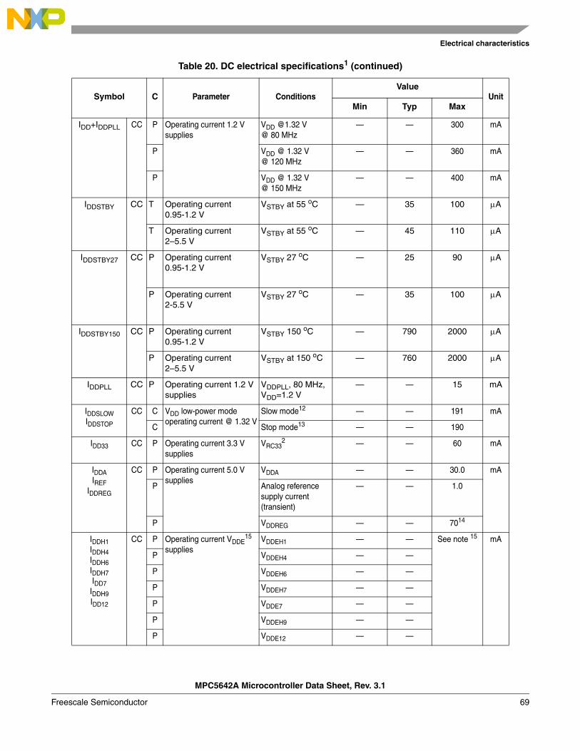
Electrical characteristics
IDD+IDDPLL CC P Operating current 1.2 V supplies
VDD @1.32 V @ 80 MHz
— — 300 mA
P VDD @ 1.32 V @ 120 MHz
— — 360 mA
P VDD @ 1.32 V @ 150 MHz
— — 400 mA
IDDSTBY CC T Operating current 0.95-1.2 V
VSTBY at 55 oC — 35 100 A
T Operating current 2–5.5 V
VSTBY at 55 oC — 45 110 A
IDDSTBY27 CC P Operating current 0.95-1.2 V
VSTBY 27 oC — 25 90 A
P Operating current 2-5.5 V
VSTBY 27 oC — 35 100 A
IDDSTBY150 CC P Operating current 0.95-1.2 V
VSTBY 150 oC — 790 2000 A
P Operating current 2–5.5 V
VSTBY at 150 oC — 760 2000 A
IDDPLL CC P Operating current 1.2 V supplies
VDDPLL, 80 MHz, VDD=1.2 V
— — 15 mA
IDDSLOWIDDSTOP
CC C VDD low-power mode operating current @ 1.32 V
Slow mode12 — — 191 mA
C Stop mode13 — — 190
IDD33 CC P Operating current 3.3 V supplies
VRC332 — — 60 mA
IDDAIREF
IDDREG
CC P Operating current 5.0 V supplies
VDDA — — 30.0 mA
P Analog reference supply current (transient)
— — 1.0
P VDDREG — — 7014
IDDH1IDDH4IDDH6IDDH7IDD7
IDDH9IDD12
CC P Operating current VDDE15
suppliesVDDEH1 — — See note 15 mA
P VDDEH4 — —
P VDDEH6 — —
P VDDEH7 — —
P VDDE7 — —
P VDDEH9 — —
P VDDE12 — —
Table 20. DC electrical specifications1 (continued)
Symbol C Parameter ConditionsValue
UnitMin Typ Max
MPC5642A Microcontroller Data Sheet, Rev. 3.1
Freescale Semiconductor 69
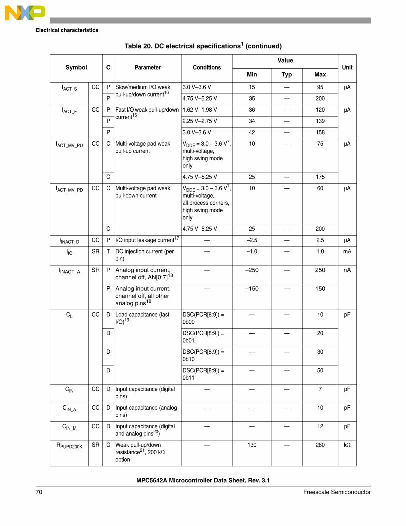
Electrical characteristics
IACT_S CC P Slow/medium I/O weak pull-up/down current16
3.0 V–3.6 V 15 — 95 µA
P 4.75 V–5.25 V 35 — 200
IACT_F CC P Fast I/O weak pull-up/down current16
1.62 V–1.98 V 36 — 120 µA
P 2.25 V–2.75 V 34 — 139
P 3.0 V–3.6 V 42 — 158
IACT_MV_PU CC C Multi-voltage pad weak pull-up current
VDDE = 3.0 – 3.6 V7,multi-voltage,high swing mode only
10 — 75 µA
C 4.75 V–5.25 V 25 — 175
IACT_MV_PD CC C Multi-voltage pad weak pull-down current
VDDE = 3.0 – 3.6 V7,multi-voltage,all process corners,high swing mode only
10 — 60 µA
C 4.75 V–5.25 V 25 — 200
IINACT_D CC P I/O input leakage current17 — –2.5 — 2.5 µA
IIC SR T DC injection current (per pin)
— –1.0 — 1.0 mA
IINACT_A SR P Analog input current, channel off, AN[0:7]18
— –250 — 250 nA
P Analog input current, channel off, all other analog pins18
— –150 — 150
CL CC D Load capacitance (fast I/O)19
DSC(PCR[8:9]) = 0b00
— — 10 pF
D DSC(PCR[8:9]) = 0b01
— — 20
D DSC(PCR[8:9]) = 0b10
— — 30
D DSC(PCR[8:9]) = 0b11
— — 50
CIN CC D Input capacitance (digital pins)
— — — 7 pF
CIN_A CC D Input capacitance (analog pins)
— — — 10 pF
CIN_M CC D Input capacitance (digital and analog pins20)
— — — 12 pF
RPUPD200K SR C Weak pull-up/down resistance21, 200 k option
— 130 — 280 k
Table 20. DC electrical specifications1 (continued)
Symbol C Parameter ConditionsValue
UnitMin Typ Max
MPC5642A Microcontroller Data Sheet, Rev. 3.1
70 Freescale Semiconductor
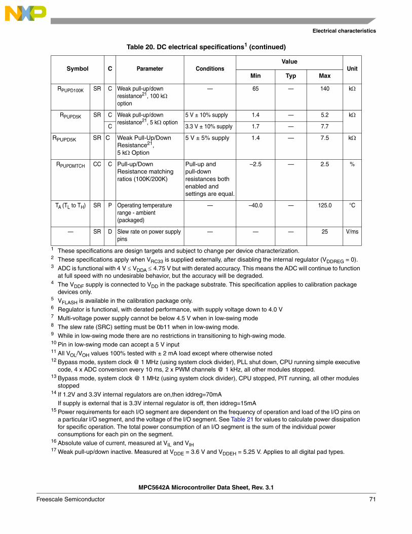
Electrical characteristics
RPUPD100K SR C Weak pull-up/down resistance21, 100 k option
— 65 — 140 k
RPUPD5K SR C Weak pull-up/down resistance21, 5 k option
5 V ± 10% supply 1.4 — 5.2 k
C 3.3 V ± 10% supply 1.7 — 7.7
RPUPD5K SR C Weak Pull-Up/Down Resistance21,5 k Option
5 V ± 5% supply 1.4 — 7.5 k
RPUPDMTCH CC C Pull-up/Down Resistance matching ratios (100K/200K)
Pull-up and pull-down resistances both enabled and settings are equal.
–2.5 — 2.5 %
TA (TL to TH) SR P Operating temperature range - ambient (packaged)
— –40.0 — 125.0 °C
— SR D Slew rate on power supply pins
— — — 25 V/ms
1 These specifications are design targets and subject to change per device characterization.2 These specifications apply when VRC33 is supplied externally, after disabling the internal regulator (VDDREG = 0).3 ADC is functional with 4 V VDDA 4.75 V but with derated accuracy. This means the ADC will continue to function
at full speed with no undesirable behavior, but the accuracy will be degraded.4 The VDDF supply is connected to VDD in the package substrate. This specification applies to calibration package
devices only.5 VFLASH is available in the calibration package only.6 Regulator is functional, with derated performance, with supply voltage down to 4.0 V7 Multi-voltage power supply cannot be below 4.5 V when in low-swing mode8 The slew rate (SRC) setting must be 0b11 when in low-swing mode.9 While in low-swing mode there are no restrictions in transitioning to high-swing mode.10 Pin in low-swing mode can accept a 5 V input11 All VOL/VOH values 100% tested with ± 2 mA load except where otherwise noted12 Bypass mode, system clock @ 1 MHz (using system clock divider), PLL shut down, CPU running simple executive
code, 4 x ADC conversion every 10 ms, 2 x PWM channels @ 1 kHz, all other modules stopped.13 Bypass mode, system clock @ 1 MHz (using system clock divider), CPU stopped, PIT running, all other modules
stopped14 If 1.2V and 3.3V internal regulators are on,then iddreg=70mA
If supply is external that is 3.3V internal regulator is off, then iddreg=15mA15 Power requirements for each I/O segment are dependent on the frequency of operation and load of the I/O pins on
a particular I/O segment, and the voltage of the I/O segment. See Table 21 for values to calculate power dissipation for specific operation. The total power consumption of an I/O segment is the sum of the individual power consumptions for each pin on the segment.
16 Absolute value of current, measured at VIL and VIH17 Weak pull-up/down inactive. Measured at VDDE = 3.6 V and VDDEH = 5.25 V. Applies to all digital pad types.
Table 20. DC electrical specifications1 (continued)
Symbol C Parameter ConditionsValue
UnitMin Typ Max
MPC5642A Microcontroller Data Sheet, Rev. 3.1
Freescale Semiconductor 71
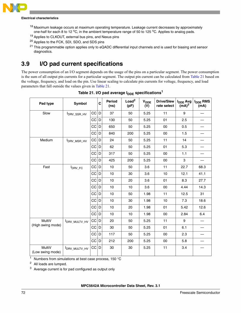
Electrical characteristics
3.9 I/O pad current specificationsThe power consumption of an I/O segment depends on the usage of the pins on a particular segment. The power consumption is the sum of all output pin currents for a particular segment. The output pin current can be calculated from Table 21 based on the voltage, frequency, and load on the pin. Use linear scaling to calculate pin currents for voltage, frequency, and load parameters that fall outside the values given in Table 21.
18 Maximum leakage occurs at maximum operating temperature. Leakage current decreases by approximately one-half for each 8 to 12 oC, in the ambient temperature range of 50 to 125 oC. Applies to analog pads.
19 Applies to CLKOUT, external bus pins, and Nexus pins20 Applies to the FCK, SDI, SDO, and SDS pins21 This programmable option applies only to eQADC differential input channels and is used for biasing and sensor
diagnostics.
Table 21. I/O pad average IDDE specifications1
1 Numbers from simulations at best case process, 150 °C
Pad type Symbol CPeriod
(ns)Load2
(pF)
2 All loads are lumped.
VDDE(V)
Drive/Slewrate select
IDDE Avg(mA)3
3 Average current is for pad configured as output only
IDDE RMS(mA)
Slow IDRV_SSR_HV CC D 37 50 5.25 11 9 —
CC D 130 50 5.25 01 2.5 —
CC D 650 50 5.25 00 0.5 —
CC D 840 200 5.25 00 1.5 —
Medium IDRV_MSR_HV CC D 24 50 5.25 11 14 —
CC D 62 50 5.25 01 5.3 —
CC D 317 50 5.25 00 1.1 —
CC D 425 200 5.25 00 3 —
Fast IDRV_FC CC D 10 50 3.6 11 22.7 68.3
CC D 10 30 3.6 10 12.1 41.1
CC D 10 20 3.6 01 8.3 27.7
CC D 10 10 3.6 00 4.44 14.3
CC D 10 50 1.98 11 12.5 31
CC D 10 30 1.98 10 7.3 18.6
CC D 10 20 1.98 01 5.42 12.6
CC D 10 10 1.98 00 2.84 6.4
MultiV(High swing mode)
IDRV_MULTV_HV CC D 20 50 5.25 11 9 —
CC D 30 50 5.25 01 6.1 —
CC D 117 50 5.25 00 2.3 —
CC D 212 200 5.25 00 5.8 —
MultiV(Low swing mode)
IDRV_MULTV_HV CC D 30 30 5.25 11 3.4 —
MPC5642A Microcontroller Data Sheet, Rev. 3.1
72 Freescale Semiconductor
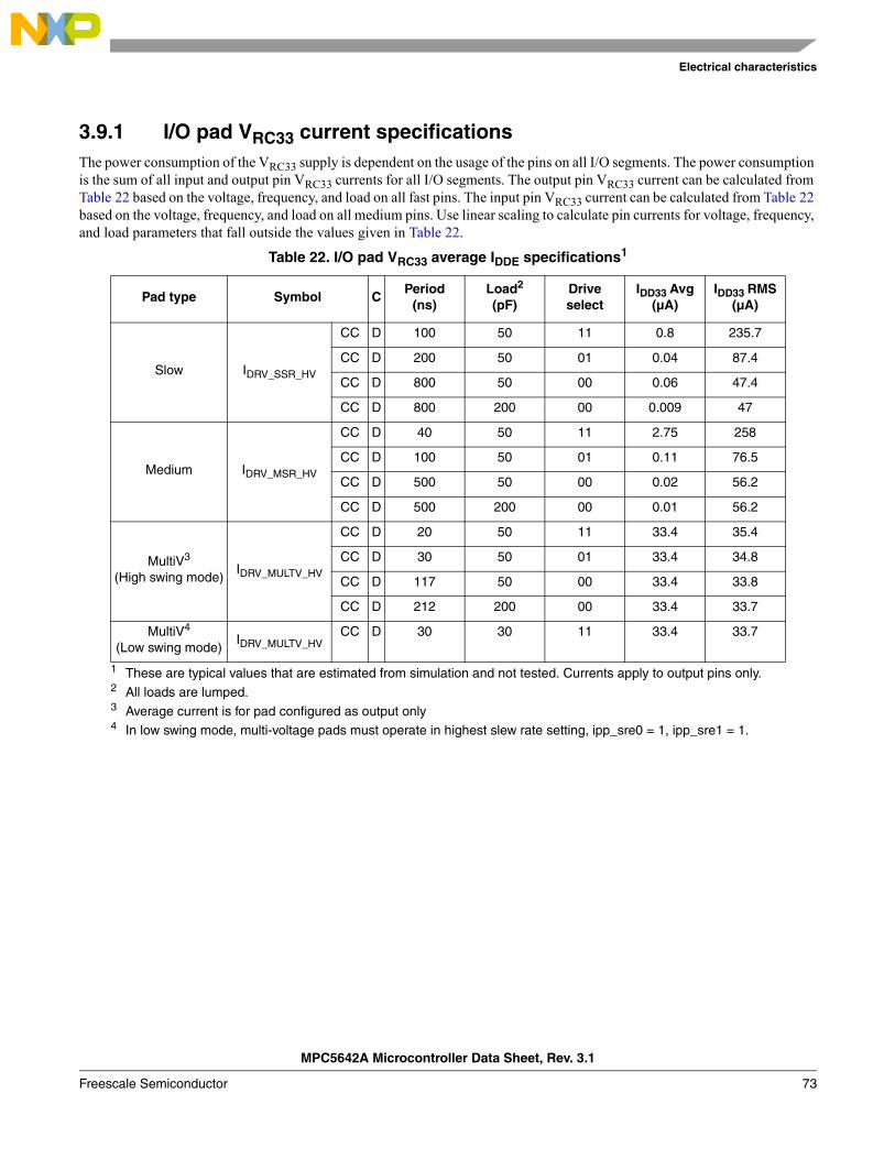
Electrical characteristics
3.9.1 I/O pad VRC33 current specificationsThe power consumption of the VRC33 supply is dependent on the usage of the pins on all I/O segments. The power consumption is the sum of all input and output pin VRC33 currents for all I/O segments. The output pin VRC33 current can be calculated from Table 22 based on the voltage, frequency, and load on all fast pins. The input pin VRC33 current can be calculated from Table 22 based on the voltage, frequency, and load on all medium pins. Use linear scaling to calculate pin currents for voltage, frequency, and load parameters that fall outside the values given in Table 22.
Table 22. I/O pad VRC33 average IDDE specifications1
1 These are typical values that are estimated from simulation and not tested. Currents apply to output pins only.
Pad type Symbol CPeriod
(ns)Load2
(pF)
2 All loads are lumped.
Driveselect
IDD33 Avg(µA)
IDD33 RMS(µA)
Slow IDRV_SSR_HV
CC D 100 50 11 0.8 235.7
CC D 200 50 01 0.04 87.4
CC D 800 50 00 0.06 47.4
CC D 800 200 00 0.009 47
Medium IDRV_MSR_HV
CC D 40 50 11 2.75 258
CC D 100 50 01 0.11 76.5
CC D 500 50 00 0.02 56.2
CC D 500 200 00 0.01 56.2
MultiV3
(High swing mode)
3 Average current is for pad configured as output only
IDRV_MULTV_HV
CC D 20 50 11 33.4 35.4
CC D 30 50 01 33.4 34.8
CC D 117 50 00 33.4 33.8
CC D 212 200 00 33.4 33.7
MultiV4
(Low swing mode)
4 In low swing mode, multi-voltage pads must operate in highest slew rate setting, ipp_sre0 = 1, ipp_sre1 = 1.
IDRV_MULTV_HVCC D 30 30 11 33.4 33.7
MPC5642A Microcontroller Data Sheet, Rev. 3.1
Freescale Semiconductor 73
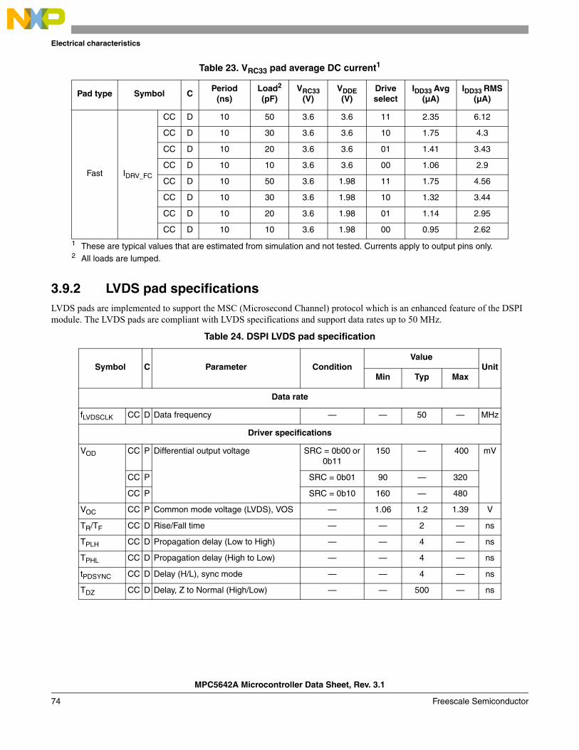
Electrical characteristics
3.9.2 LVDS pad specificationsLVDS pads are implemented to support the MSC (Microsecond Channel) protocol which is an enhanced feature of the DSPI module. The LVDS pads are compliant with LVDS specifications and support data rates up to 50 MHz.
Table 23. VRC33 pad average DC current1
1 These are typical values that are estimated from simulation and not tested. Currents apply to output pins only.
Pad type Symbol CPeriod
(ns)Load2
(pF)
2 All loads are lumped.
VRC33(V)
VDDE(V)
Driveselect
IDD33 Avg(µA)
IDD33 RMS(µA)
Fast IDRV_FC
CC D 10 50 3.6 3.6 11 2.35 6.12
CC D 10 30 3.6 3.6 10 1.75 4.3
CC D 10 20 3.6 3.6 01 1.41 3.43
CC D 10 10 3.6 3.6 00 1.06 2.9
CC D 10 50 3.6 1.98 11 1.75 4.56
CC D 10 30 3.6 1.98 10 1.32 3.44
CC D 10 20 3.6 1.98 01 1.14 2.95
CC D 10 10 3.6 1.98 00 0.95 2.62
Table 24. DSPI LVDS pad specification
Symbol C Parameter ConditionValue
UnitMin Typ Max
Data rate
fLVDSCLK CC D Data frequency — — 50 — MHz
Driver specifications
VOD CC P Differential output voltage SRC = 0b00 or 0b11
150 — 400 mV
CC P SRC = 0b01 90 — 320
CC P SRC = 0b10 160 — 480
VOC CC P Common mode voltage (LVDS), VOS — 1.06 1.2 1.39 V
TR/TF CC D Rise/Fall time — — 2 — ns
TPLH CC D Propagation delay (Low to High) — — 4 — ns
TPHL CC D Propagation delay (High to Low) — — 4 — ns
tPDSYNC CC D Delay (H/L), sync mode — — 4 — ns
TDZ CC D Delay, Z to Normal (High/Low) — — 500 — ns
MPC5642A Microcontroller Data Sheet, Rev. 3.1
74 Freescale Semiconductor
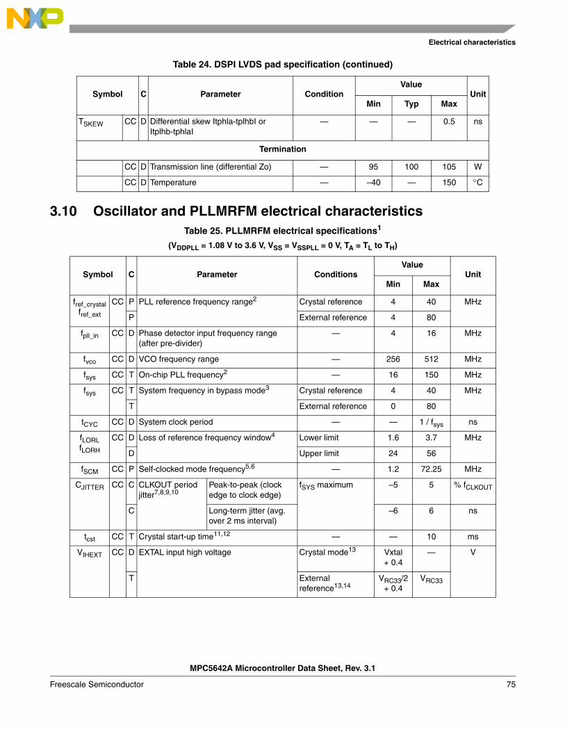
Electrical characteristics
3.10 Oscillator and PLLMRFM electrical characteristics
TSKEW CC D Differential skew Itphla-tplhbI or Itplhb-tphlaI
— — — 0.5 ns
Termination
CC D Transmission line (differential Zo) — 95 100 105 W
CC D Temperature — –40 — 150 C
Table 25. PLLMRFM electrical specifications1
(VDDPLL = 1.08 V to 3.6 V, VSS = VSSPLL = 0 V, TA = TL to TH)
Symbol C Parameter ConditionsValue
UnitMin Max
fref_crystalfref_ext
CC P PLL reference frequency range2 Crystal reference 4 40 MHz
P External reference 4 80
fpll_in CC D Phase detector input frequency range (after pre-divider)
— 4 16 MHz
fvco CC D VCO frequency range — 256 512 MHz
fsys CC T On-chip PLL frequency2 — 16 150 MHz
fsys CC T System frequency in bypass mode3 Crystal reference 4 40 MHz
T External reference 0 80
tCYC CC D System clock period — — 1 / fsys ns
fLORLfLORH
CC D Loss of reference frequency window4 Lower limit 1.6 3.7 MHz
D Upper limit 24 56
fSCM CC P Self-clocked mode frequency5,6 — 1.2 72.25 MHz
CJITTER CC C CLKOUT period jitter7,8,9,10
Peak-to-peak (clock edge to clock edge)
fSYS maximum –5 5 % fCLKOUT
C Long-term jitter (avg. over 2 ms interval)
–6 6 ns
tcst CC T Crystal start-up time11,12 — — 10 ms
VIHEXT CC D EXTAL input high voltage Crystal mode13 Vxtal + 0.4
— V
T External reference13,14
VRC33/2 + 0.4
VRC33
Table 24. DSPI LVDS pad specification (continued)
Symbol C Parameter ConditionValue
UnitMin Typ Max
MPC5642A Microcontroller Data Sheet, Rev. 3.1
Freescale Semiconductor 75
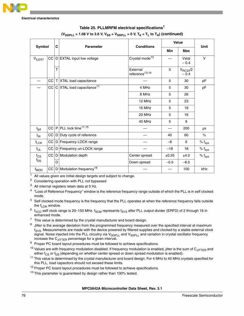
Electrical characteristics
VILEXT CC D EXTAL input low voltage Crystal mode13 — Vxtal– 0.4
V
T External reference13,14
0 VRC33/2 – 0.4
— CC T XTAL load capacitance — 5 30 pF
— CC C XTAL load capacitance11 4 MHz 5 30 pF
8 MHz 5 26
12 MHz 5 23
16 MHz 5 19
20 MHz 5 16
40 MHz 5 8
tlpll CC P PLL lock time11,15 — — 200 µs
tdc CC D Duty cycle of reference — 40 60 %
fLCK CC D Frequency LOCK range — –6 6 % fsys
fUL CC D Frequency un-LOCK range — –18 18 % fsys
fCSfDS
CC D Modulation depth Center spread ±0.25 ±4.0 % fsys
D Down spread –0.5 –8.0
fMOD CC D Modulation frequency16 — — 100 kHz
1 All values given are initial design targets and subject to change.2 Considering operation with PLL not bypassed3 All internal registers retain data at 0 Hz.4 “Loss of Reference Frequency” window is the reference frequency range outside of which the PLL is in self clocked
mode.5 Self clocked mode frequency is the frequency that the PLL operates at when the reference frequency falls outside
the fLOR window.6 fVCO self clock range is 20–150 MHz. fSCM represents fSYS after PLL output divider (ERFD) of 2 through 16 in
enhanced mode.7 This value is determined by the crystal manufacturer and board design.8 Jitter is the average deviation from the programmed frequency measured over the specified interval at maximum
fSYS. Measurements are made with the device powered by filtered supplies and clocked by a stable external clock signal. Noise injected into the PLL circuitry via VDDPLL and VSSPLL and variation in crystal oscillator frequency increase the CJITTER percentage for a given interval.
9 Proper PC board layout procedures must be followed to achieve specifications.10 Values are with frequency modulation disabled. If frequency modulation is enabled, jitter is the sum of CJITTER and
either fCS or fDS (depending on whether center spread or down spread modulation is enabled).11 This value is determined by the crystal manufacturer and board design. For 4 MHz to 40 MHz crystals specified for
this PLL, load capacitors should not exceed these limits.12 Proper PC board layout procedures must be followed to achieve specifications.13 This parameter is guaranteed by design rather than 100% tested.
Table 25. PLLMRFM electrical specifications1
(VDDPLL = 1.08 V to 3.6 V, VSS = VSSPLL = 0 V, TA = TL to TH) (continued)
Symbol C Parameter ConditionsValue
UnitMin Max
MPC5642A Microcontroller Data Sheet, Rev. 3.1
76 Freescale Semiconductor
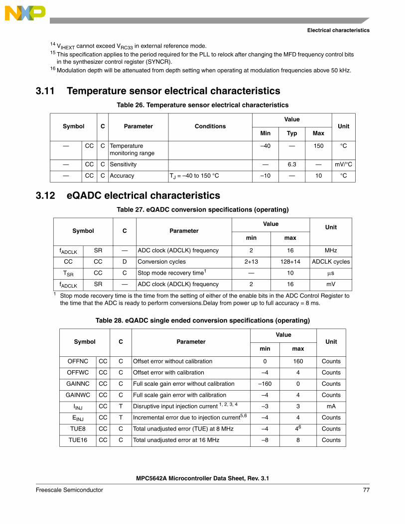
Electrical characteristics
3.11 Temperature sensor electrical characteristics
3.12 eQADC electrical characteristics
14 VIHEXT cannot exceed VRC33 in external reference mode.15 This specification applies to the period required for the PLL to relock after changing the MFD frequency control bits
in the synthesizer control register (SYNCR).16 Modulation depth will be attenuated from depth setting when operating at modulation frequencies above 50 kHz.
Table 26. Temperature sensor electrical characteristics
Symbol C Parameter ConditionsValue
UnitMin Typ Max
— CC C Temperature monitoring range
–40 — 150 °C
— CC C Sensitivity — 6.3 — mV/°C
— CC C Accuracy TJ = –40 to 150 °C –10 — 10 °C
Table 27. eQADC conversion specifications (operating)
Symbol C ParameterValue Unit
min max
fADCLK SR — ADC clock (ADCLK) frequency 2 16 MHz
CC CC D Conversion cycles 2+13 128+14 ADCLK cycles
TSR CC C Stop mode recovery time1
1 Stop mode recovery time is the time from the setting of either of the enable bits in the ADC Control Register to the time that the ADC is ready to perform conversions.Delay from power up to full accuracy = 8 ms.
— 10 s
fADCLK SR — ADC clock (ADCLK) frequency 2 16 mV
Table 28. eQADC single ended conversion specifications (operating)
Symbol C ParameterValue
Unitmin max
OFFNC CC C Offset error without calibration 0 160 Counts
OFFWC CC C Offset error with calibration –4 4 Counts
GAINNC CC C Full scale gain error without calibration –160 0 Counts
GAINWC CC C Full scale gain error with calibration –4 4 Counts
IINJ CC T Disruptive input injection current 1, 2, 3, 4 –3 3 mA
EINJ CC T Incremental error due to injection current5,6 –4 4 Counts
TUE8 CC C Total unadjusted error (TUE) at 8 MHz –4 46 Counts
TUE16 CC C Total unadjusted error at 16 MHz –8 8 Counts
MPC5642A Microcontroller Data Sheet, Rev. 3.1
Freescale Semiconductor 77
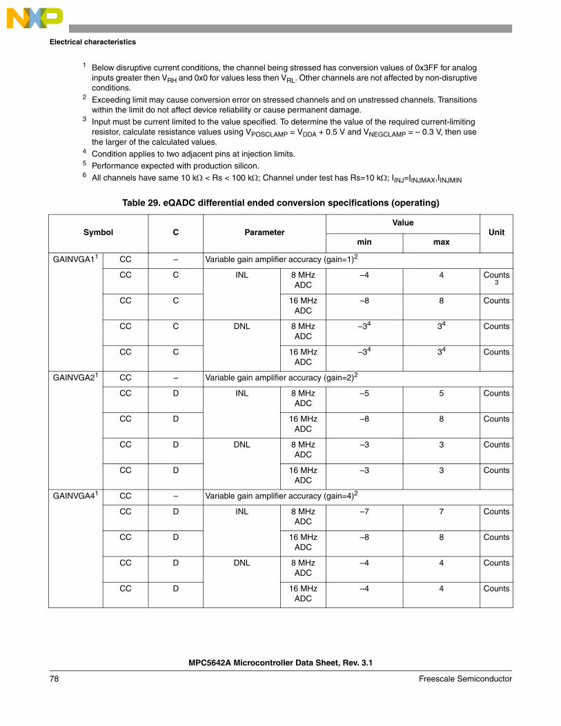
Electrical characteristics
1 Below disruptive current conditions, the channel being stressed has conversion values of 0x3FF for analog inputs greater then VRH and 0x0 for values less then VRL. Other channels are not affected by non-disruptive conditions.
2 Exceeding limit may cause conversion error on stressed channels and on unstressed channels. Transitions within the limit do not affect device reliability or cause permanent damage.
3 Input must be current limited to the value specified. To determine the value of the required current-limiting resistor, calculate resistance values using VPOSCLAMP = VDDA + 0.5 V and VNEGCLAMP = – 0.3 V, then use the larger of the calculated values.
4 Condition applies to two adjacent pins at injection limits.5 Performance expected with production silicon.6 All channels have same 10 k < Rs < 100 k; Channel under test has Rs=10 k; IINJ=IINJMAX,IINJMIN
Table 29. eQADC differential ended conversion specifications (operating)
Symbol C ParameterValue
Unitmin max
GAINVGA11 CC – Variable gain amplifier accuracy (gain=1)2
CC C INL 8 MHz ADC
–4 4 Counts3
CC C 16 MHz ADC
–8 8 Counts
CC C DNL 8 MHz ADC
–34 34 Counts
CC C 16 MHz ADC
–34 34 Counts
GAINVGA21 CC – Variable gain amplifier accuracy (gain=2)2
CC D INL 8 MHz ADC
–5 5 Counts
CC D 16 MHz ADC
–8 8 Counts
CC D DNL 8 MHz ADC
–3 3 Counts
CC D 16 MHz ADC
–3 3 Counts
GAINVGA41 CC – Variable gain amplifier accuracy (gain=4)2
CC D INL 8 MHz ADC
–7 7 Counts
CC D 16 MHz ADC
–8 8 Counts
CC D DNL 8 MHz ADC
–4 4 Counts
CC D 16 MHz ADC
–4 4 Counts
MPC5642A Microcontroller Data Sheet, Rev. 3.1
78 Freescale Semiconductor
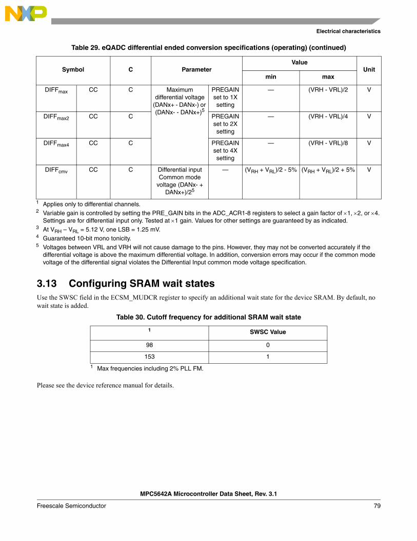
Electrical characteristics
3.13 Configuring SRAM wait statesUse the SWSC field in the ECSM_MUDCR register to specify an additional wait state for the device SRAM. By default, no wait state is added.
Please see the device reference manual for details.
DIFFmax CC C Maximum differential voltage
(DANx+ - DANx-) or (DANx- - DANx+)5
PREGAIN set to 1X setting
— (VRH - VRL)/2 V
DIFFmax2 CC C PREGAIN set to 2X setting
— (VRH - VRL)/4 V
DIFFmax4 CC C PREGAIN set to 4X setting
— (VRH - VRL)/8 V
DIFFcmv CC C Differential input Common mode
voltage (DANx- + DANx+)/25
— (VRH + VRL)/2 - 5% (VRH + VRL)/2 + 5% V
1 Applies only to differential channels.2 Variable gain is controlled by setting the PRE_GAIN bits in the ADC_ACR1-8 registers to select a gain factor of 1, 2, or 4.
Settings are for differential input only. Tested at 1 gain. Values for other settings are guaranteed by as indicated.3 At VRH – VRL = 5.12 V, one LSB = 1.25 mV. 4 Guaranteed 10-bit mono tonicity.5 Voltages between VRL and VRH will not cause damage to the pins. However, they may not be converted accurately if the
differential voltage is above the maximum differential voltage. In addition, conversion errors may occur if the common mode voltage of the differential signal violates the Differential Input common mode voltage specification.
Table 30. Cutoff frequency for additional SRAM wait state
1
1 Max frequencies including 2% PLL FM.
SWSC Value
98 0
153 1
Table 29. eQADC differential ended conversion specifications (operating) (continued)
Symbol C ParameterValue
Unitmin max
MPC5642A Microcontroller Data Sheet, Rev. 3.1
Freescale Semiconductor 79
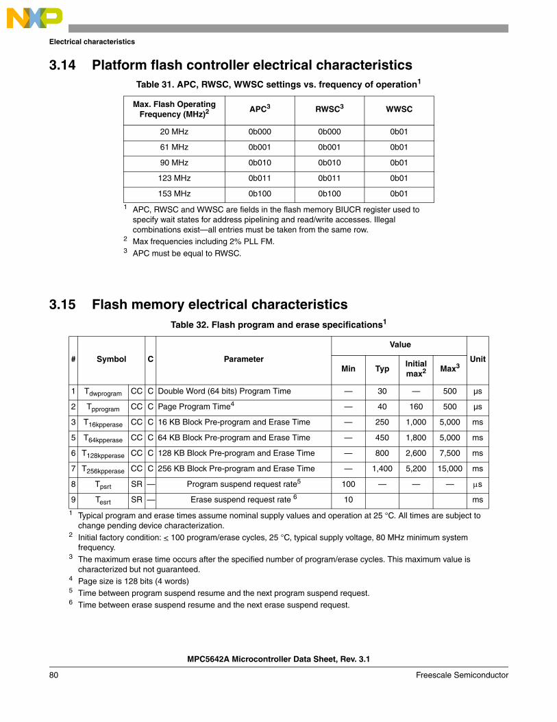
Electrical characteristics
3.14 Platform flash controller electrical characteristics
3.15 Flash memory electrical characteristics
Table 31. APC, RWSC, WWSC settings vs. frequency of operation1
1 APC, RWSC and WWSC are fields in the flash memory BIUCR register used to specify wait states for address pipelining and read/write accesses. Illegal combinations exist—all entries must be taken from the same row.
Max. Flash Operating Frequency (MHz)2
2 Max frequencies including 2% PLL FM.
APC3
3 APC must be equal to RWSC.
RWSC3 WWSC
20 MHz 0b000 0b000 0b01
61 MHz 0b001 0b001 0b01
90 MHz 0b010 0b010 0b01
123 MHz 0b011 0b011 0b01
153 MHz 0b100 0b100 0b01
Table 32. Flash program and erase specifications1
1 Typical program and erase times assume nominal supply values and operation at 25 °C. All times are subject to change pending device characterization.
# Symbol C Parameter
Value
UnitMin Typ
Initial max2
2 Initial factory condition: < 100 program/erase cycles, 25 °C, typical supply voltage, 80 MHz minimum system frequency.
Max3
3 The maximum erase time occurs after the specified number of program/erase cycles. This maximum value is characterized but not guaranteed.
1 Tdwprogram CC C Double Word (64 bits) Program Time — 30 — 500 µs
2 Tpprogram CC C Page Program Time4
4 Page size is 128 bits (4 words)
— 40 160 500 µs
3 T16kpperase CC C 16 KB Block Pre-program and Erase Time — 250 1,000 5,000 ms
5 T64kpperase CC C 64 KB Block Pre-program and Erase Time — 450 1,800 5,000 ms
6 T128kpperase CC C 128 KB Block Pre-program and Erase Time — 800 2,600 7,500 ms
7 T256kpperase CC C 256 KB Block Pre-program and Erase Time — 1,400 5,200 15,000 ms
8 Tpsrt SR — Program suspend request rate5
5 Time between program suspend resume and the next program suspend request.
100 — — — s
9 Tesrt SR — Erase suspend request rate 6
6 Time between erase suspend resume and the next erase suspend request.
10 ms
MPC5642A Microcontroller Data Sheet, Rev. 3.1
80 Freescale Semiconductor
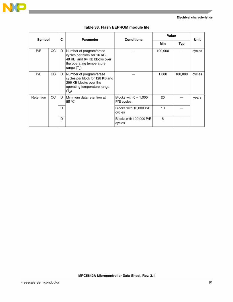
Electrical characteristics
Table 33. Flash EEPROM module life
Symbol C Parameter ConditionsValue
UnitMin Typ
P/E CC D Number of program/erase cycles per block for 16 KB, 48 KB, and 64 KB blocks over the operating temperature range (TJ)
— 100,000 — cycles
P/E CC D Number of program/erase cycles per block for 128 KB and 256 KB blocks over the operating temperature range (TJ)
— 1,000 100,000 cycles
Retention CC D Minimum data retention at 85 °C
Blocks with 0 – 1,000 P/E cycles
20 — years
D Blocks with 10,000 P/E cycles
10 —
D Blocks with 100,000 P/E cycles
5 —
MPC5642A Microcontroller Data Sheet, Rev. 3.1
Freescale Semiconductor 81
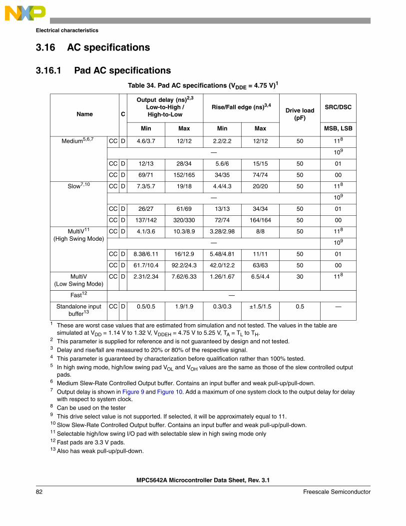
Electrical characteristics
3.16 AC specifications
3.16.1 Pad AC specifications
Table 34. Pad AC specifications (VDDE = 4.75 V)1
1 These are worst case values that are estimated from simulation and not tested. The values in the table are simulated at VDD = 1.14 V to 1.32 V, VDDEH = 4.75 V to 5.25 V, TA = TL to TH.
Name C
Output delay (ns)2,3
Low-to-High / High-to-Low
2 This parameter is supplied for reference and is not guaranteed by design and not tested.3 Delay and rise/fall are measured to 20% or 80% of the respective signal.
Rise/Fall edge (ns)3,4
4 This parameter is guaranteed by characterization before qualification rather than 100% tested.
Drive load(pF)
SRC/DSC
Min Max Min Max MSB, LSB
Medium5,6,7
5 In high swing mode, high/low swing pad VOL and VOH values are the same as those of the slew controlled output pads.
6 Medium Slew-Rate Controlled Output buffer. Contains an input buffer and weak pull-up/pull-down.7 Output delay is shown in Figure 9 and Figure 10. Add a maximum of one system clock to the output delay for delay
with respect to system clock.
CC D 4.6/3.7 12/12 2.2/2.2 12/12 50 118
8 Can be used on the tester
— 109
9 This drive select value is not supported. If selected, it will be approximately equal to 11.
CC D 12/13 28/34 5.6/6 15/15 50 01
CC D 69/71 152/165 34/35 74/74 50 00
Slow7,10
10 Slow Slew-Rate Controlled Output buffer. Contains an input buffer and weak pull-up/pull-down.
CC D 7.3/5.7 19/18 4.4/4.3 20/20 50 118
— 109
CC D 26/27 61/69 13/13 34/34 50 01
CC D 137/142 320/330 72/74 164/164 50 00
MultiV11
(High Swing Mode)
11 Selectable high/low swing I/O pad with selectable slew in high swing mode only
CC D 4.1/3.6 10.3/8.9 3.28/2.98 8/8 50 118
— 109
CC D 8.38/6.11 16/12.9 5.48/4.81 11/11 50 01
CC D 61.7/10.4 92.2/24.3 42.0/12.2 63/63 50 00
MultiV(Low Swing Mode)
CC D 2.31/2.34 7.62/6.33 1.26/1.67 6.5/4.4 30 118
Fast12
12 Fast pads are 3.3 V pads.
—
Standalone input buffer13
13 Also has weak pull-up/pull-down.
CC D 0.5/0.5 1.9/1.9 0.3/0.3 ±1.5/1.5 0.5 —
MPC5642A Microcontroller Data Sheet, Rev. 3.1
82 Freescale Semiconductor
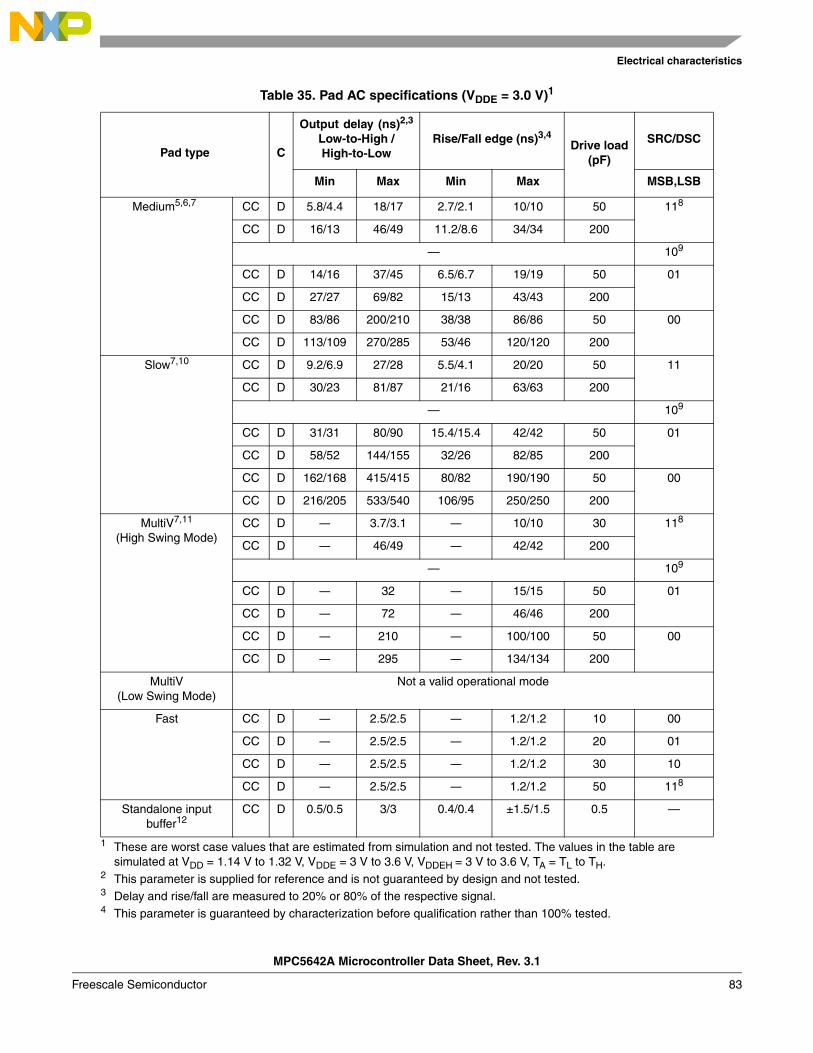
Electrical characteristics
Table 35. Pad AC specifications (VDDE = 3.0 V)1
1 These are worst case values that are estimated from simulation and not tested. The values in the table are simulated at VDD = 1.14 V to 1.32 V, VDDE = 3 V to 3.6 V, VDDEH = 3 V to 3.6 V, TA = TL to TH.
Pad type C
Output delay (ns)2,3
Low-to-High / High-to-Low
2 This parameter is supplied for reference and is not guaranteed by design and not tested.3 Delay and rise/fall are measured to 20% or 80% of the respective signal.
Rise/Fall edge (ns)3,4
4 This parameter is guaranteed by characterization before qualification rather than 100% tested.
Drive load(pF)
SRC/DSC
Min Max Min Max MSB,LSB
Medium5,6,7 CC D 5.8/4.4 18/17 2.7/2.1 10/10 50 118
CC D 16/13 46/49 11.2/8.6 34/34 200
— 109
CC D 14/16 37/45 6.5/6.7 19/19 50 01
CC D 27/27 69/82 15/13 43/43 200
CC D 83/86 200/210 38/38 86/86 50 00
CC D 113/109 270/285 53/46 120/120 200
Slow7,10 CC D 9.2/6.9 27/28 5.5/4.1 20/20 50 11
CC D 30/23 81/87 21/16 63/63 200
— 109
CC D 31/31 80/90 15.4/15.4 42/42 50 01
CC D 58/52 144/155 32/26 82/85 200
CC D 162/168 415/415 80/82 190/190 50 00
CC D 216/205 533/540 106/95 250/250 200
MultiV7,11
(High Swing Mode)CC D — 3.7/3.1 — 10/10 30 118
CC D — 46/49 — 42/42 200
— 109
CC D — 32 — 15/15 50 01
CC D — 72 — 46/46 200
CC D — 210 — 100/100 50 00
CC D — 295 — 134/134 200
MultiV(Low Swing Mode)
Not a valid operational mode
Fast CC D — 2.5/2.5 — 1.2/1.2 10 00
CC D — 2.5/2.5 — 1.2/1.2 20 01
CC D — 2.5/2.5 — 1.2/1.2 30 10
CC D — 2.5/2.5 — 1.2/1.2 50 118
Standalone input buffer12
CC D 0.5/0.5 3/3 0.4/0.4 ±1.5/1.5 0.5 —
MPC5642A Microcontroller Data Sheet, Rev. 3.1
Freescale Semiconductor 83
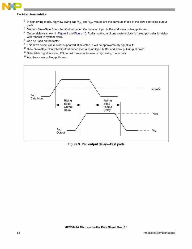
Electrical characteristics
Figure 9. Pad output delay—Fast pads
5 In high swing mode, high/low swing pad VOL and VOH values are the same as those of the slew controlled output pads.
6 Medium Slew-Rate Controlled Output buffer. Contains an input buffer and weak pull-up/pull-down.7 Output delay is shown in Figure 9 and Figure 10. Add a maximum of one system clock to the output delay for delay
with respect to system clock.8 Can be used on the tester.9 This drive select value is not supported. If selected, it will be approximately equal to 11.10 Slow Slew-Rate Controlled Output buffer. Contains an input buffer and weak pull-up/pull-down.11 Selectable high/low swing I/O pad with selectable slew in high swing mode only.12 Also has weak pull-up/pull-down.
VDDE/2
VOH
VOL
RisingEdgeOutputDelay
FallingEdgeOutputDelay
PadData Input
PadOutput
MPC5642A Microcontroller Data Sheet, Rev. 3.1
84 Freescale Semiconductor
Electrical characteristics
Figure 10. Pad output delay—Slew rate controlled fast, medium, and slow pads
VDDE/2
VOH
VOL
RisingEdgeOutputDelay
FallingEdgeOutputDelay
PadData Input
PadOutput
MPC5642A Microcontroller Data Sheet, Rev. 3.1
Freescale Semiconductor 85
Electrical characteristics
3.17 AC timing
3.17.1 Reset and configuration pin timing
Figure 11. Reset and configuration pin timing
3.17.2 IEEE 1149.1 interface timing
Table 36. Reset and configuration pin timing1
1 Reset timing specified at: VDDEH = 3.0 V to 5.25 V, VDD = 1.14 V to 1.32 V, TA = TL to TH.
# Symbol CharacteristicValue
UnitMin Max
1 tRPW RESET Pulse Width 10 — tCYC
2 tGPW RESET Glitch Detect Pulse Width 2 — tCYC
3 tRCSU PLLREF, BOOTCFG, WKPCFG Setup Time to RSTOUT Valid 10 — tCYC
4 tRCH PLLREF, BOOTCFG, WKPCFG Hold Time to RSTOUT Valid 0 — tCYC
Table 37. JTAG pin AC electrical characteristics1
# Symbol C CharacteristicValue
UnitMin Max
1 tJCYC CC D TCK Cycle Time 100 — ns
2 tJDC CC D TCK Clock Pulse Width 40 60 ns
3 tTCKRISE CC D TCK Rise and Fall Times (40%–70%) — 3 ns
1
2
RESET
RSTOUT
WKPCFG
3
4
BOOTCFG
MPC5642A Microcontroller Data Sheet, Rev. 3.1
86 Freescale Semiconductor
Electrical characteristics
NOTEThe Nexus/JTAG Read/Write Access Control/Status Register (RWCS) write (to begin a read access) or the write to the Read/Write Access Data Register (RWD) (to begin a write access) does not actually begin its action until 1 JTAG clock (TCK) after leaving the JTAG Update-DR state. This prevents the access from being performed and therefore will not signal its completion via the READY (RDY) output unless the JTAG controller receives an additional TCK. In addition, EVTI is not latched into the device unless there are clock transitions on TCK.
The tool/debugger must provide at least one TCK clock for the EVTI signal to be recognized by the MCU. When using the RDY signal to indicate the end of a Nexus read/write access, ensure that TCK continues to run for at least one TCK after leaving the Update-DR state. This can be just a TCK with TMS low while in the Run-Test/Idle state or by continuing with the next Nexus/JTAG command. Expect the effect of EVTI and RDY to be delayed by edges of TCK.
RDY is not available in all device packages.
4 tTMSS, tTDIS CC D TMS, TDI Data Setup Time 10 — ns
5 tTMSH, tTDIH CC D TMS, TDI Data Hold Time 25 — ns
6 tTDOV CC D TCK Low to TDO Data Valid — 222 ns
7 tTDOI CC D TCK Low to TDO Data Invalid 0 — ns
8 tTDOHZ CC D TCK Low to TDO High Impedance — 22 ns
9 tJCMPPW CC D JCOMP Assertion Time 100 — ns
10 tJCMPS CC D JCOMP Setup Time to TCK Low 40 — ns
11 tBSDV CC D TCK Falling Edge to Output Valid — 50 ns
12 tBSDVZ CC D TCK Falling Edge to Output Valid out of High Impedance — 50 ns
13 tBSDHZ CC D TCK Falling Edge to Output High Impedance — 50 ns
14 tBSDST CC D Boundary Scan Input Valid to TCK Rising Edge 253 — ns
15 tBSDHT CC D TCK Rising Edge to Boundary Scan Input Invalid 253 — ns
1 JTAG timing specified at VDD = 1.14 V to 1.32 V, VDDEH = 4.75 V to 5.25 V with multi-voltage pads programmed to Low-Swing mode, TA = TL to TH, CL = 30 pF, SRC = 0b11. These specifications apply to JTAG boundary scan only. See Table 38 for functional specifications.
2 Pad delay is 8–10 ns. Remainder includes TCK pad delay, clock tree delay logic delay and TDO output pad delay.3 For 20 MHz TCK.
Table 37. JTAG pin AC electrical characteristics1 (continued)
# Symbol C CharacteristicValue
UnitMin Max
MPC5642A Microcontroller Data Sheet, Rev. 3.1
Freescale Semiconductor 87
Electrical characteristics
Figure 12. JTAG test clock input timing
Figure 13. JTAG test access port timing
TCK
1
2
2
3
3
TCK
4
5
6
7 8
TMS, TDI
TDO
MPC5642A Microcontroller Data Sheet, Rev. 3.1
88 Freescale Semiconductor
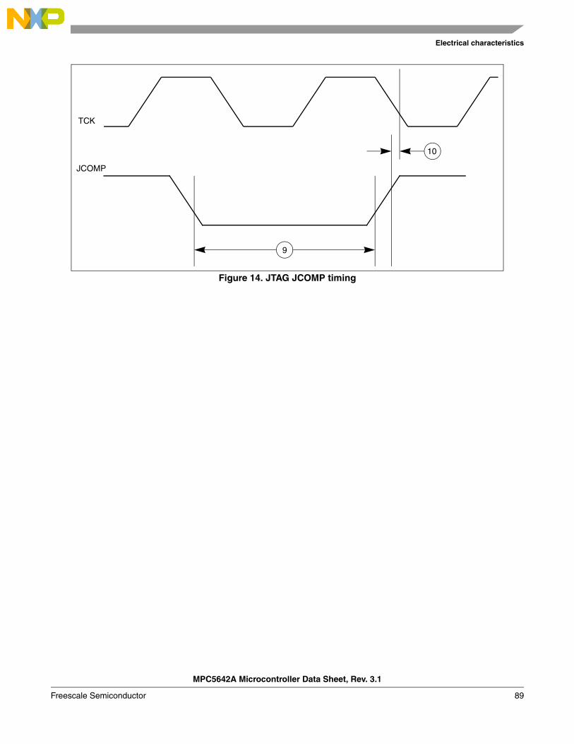
Electrical characteristics
Figure 14. JTAG JCOMP timing
TCK
JCOMP
9
10
MPC5642A Microcontroller Data Sheet, Rev. 3.1
Freescale Semiconductor 89
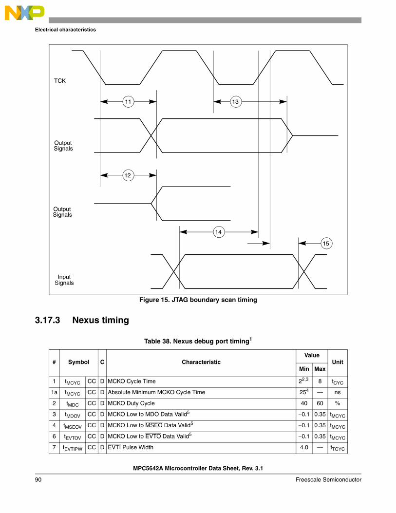
Electrical characteristics
Figure 15. JTAG boundary scan timing
3.17.3 Nexus timing
Table 38. Nexus debug port timing1
# Symbol C CharacteristicValue
UnitMin Max
1 tMCYC CC D MCKO Cycle Time 22,3 8 tCYC
1a tMCYC CC D Absolute Minimum MCKO Cycle Time 254 — ns
2 tMDC CC D MCKO Duty Cycle 40 60 %
3 tMDOV CC D MCKO Low to MDO Data Valid5 0.1 0.35 tMCYC
4 tMSEOV CC D MCKO Low to MSEO Data Valid5 0.1 0.35 tMCYC
6 tEVTOV CC D MCKO Low to EVTO Data Valid5 0.1 0.35 tMCYC
7 tEVTIPW CC D EVTI Pulse Width 4.0 — tTCYC
TCK
OutputSignals
InputSignals
OutputSignals
11
12
13
14
15
MPC5642A Microcontroller Data Sheet, Rev. 3.1
90 Freescale Semiconductor
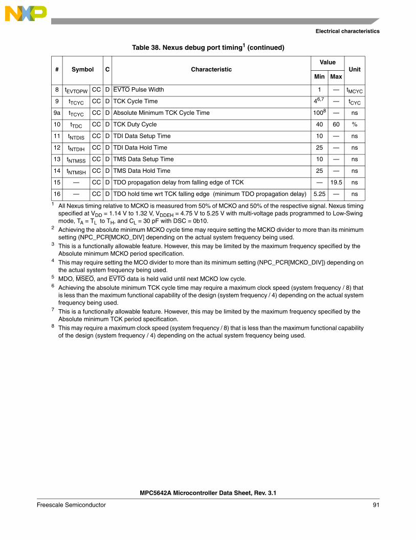
Electrical characteristics
8 tEVTOPW CC D EVTO Pulse Width 1 — tMCYC
9 tTCYC CC D TCK Cycle Time 46,7 — tCYC
9a tTCYC CC D Absolute Minimum TCK Cycle Time 1008 — ns
10 tTDC CC D TCK Duty Cycle 40 60 %
11 tNTDIS CC D TDI Data Setup Time 10 — ns
12 tNTDIH CC D TDI Data Hold Time 25 — ns
13 tNTMSS CC D TMS Data Setup Time 10 — ns
14 tNTMSH CC D TMS Data Hold Time 25 — ns
15 — CC D TDO propagation delay from falling edge of TCK — 19.5 ns
16 — CC D TDO hold time wrt TCK falling edge (minimum TDO propagation delay) 5.25 — ns
1 All Nexus timing relative to MCKO is measured from 50% of MCKO and 50% of the respective signal. Nexus timing specified at VDD = 1.14 V to 1.32 V, VDDEH = 4.75 V to 5.25 V with multi-voltage pads programmed to Low-Swing mode, TA = TL to TH, and CL = 30 pF with DSC = 0b10.
2 Achieving the absolute minimum MCKO cycle time may require setting the MCKO divider to more than its minimum setting (NPC_PCR[MCKO_DIV] depending on the actual system frequency being used.
3 This is a functionally allowable feature. However, this may be limited by the maximum frequency specified by the Absolute minimum MCKO period specification.
4 This may require setting the MCO divider to more than its minimum setting (NPC_PCR[MCKO_DIV]) depending on the actual system frequency being used.
5 MDO, MSEO, and EVTO data is held valid until next MCKO low cycle.6 Achieving the absolute minimum TCK cycle time may require a maximum clock speed (system frequency / 8) that
is less than the maximum functional capability of the design (system frequency / 4) depending on the actual system frequency being used.
7 This is a functionally allowable feature. However, this may be limited by the maximum frequency specified by the Absolute minimum TCK period specification.
8 This may require a maximum clock speed (system frequency / 8) that is less than the maximum functional capability of the design (system frequency / 4) depending on the actual system frequency being used.
Table 38. Nexus debug port timing1 (continued)
# Symbol C CharacteristicValue
UnitMin Max
MPC5642A Microcontroller Data Sheet, Rev. 3.1
Freescale Semiconductor 91
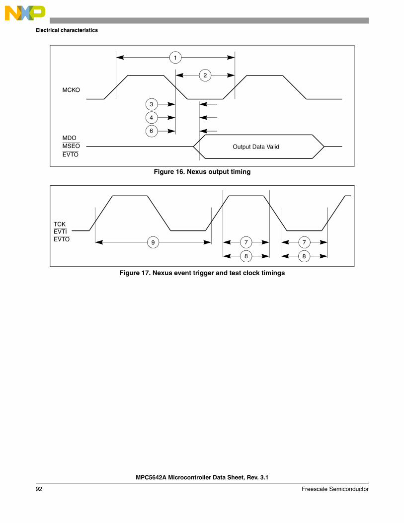
Electrical characteristics
Figure 16. Nexus output timing
Figure 17. Nexus event trigger and test clock timings
1
2
4
6
MCKO
MDOMSEOEVTO
Output Data Valid
3
TCK
9 7
8
EVTIEVTO
8
7
MPC5642A Microcontroller Data Sheet, Rev. 3.1
92 Freescale Semiconductor
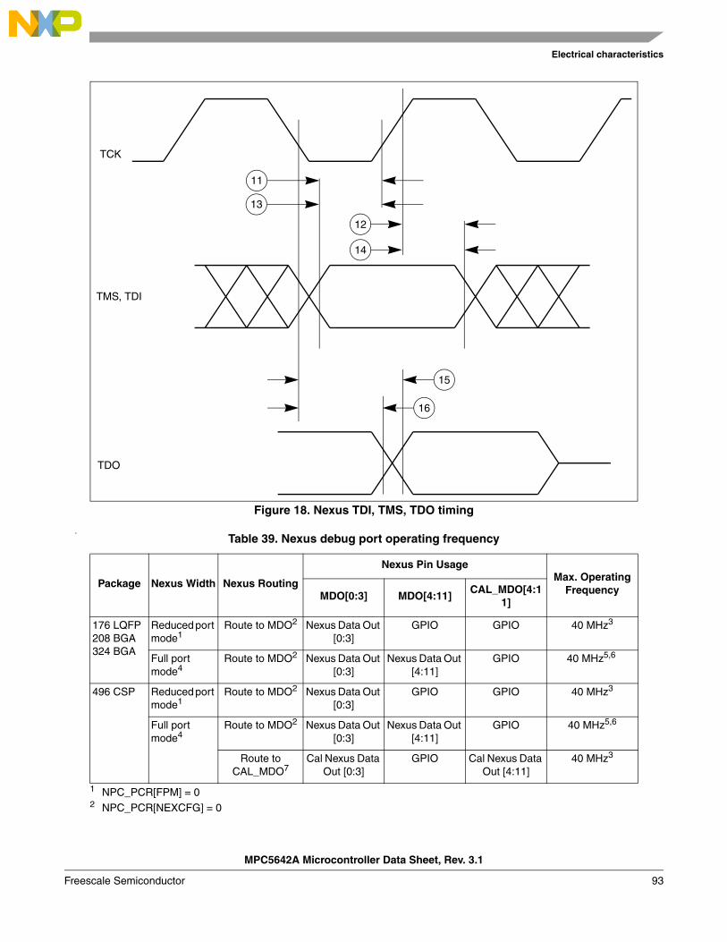
Electrical characteristics
Figure 18. Nexus TDI, TMS, TDO timing
N
Table 39. Nexus debug port operating frequency
Package Nexus Width Nexus Routing
Nexus Pin UsageMax. Operating
FrequencyMDO[0:3] MDO[4:11]CAL_MDO[4:1
1]
176 LQFP208 BGA324 BGA
Reduced port mode1
1 NPC_PCR[FPM] = 0
Route to MDO2
2 NPC_PCR[NEXCFG] = 0
Nexus Data Out [0:3]
GPIO GPIO 40 MHz3
Full port mode4
Route to MDO2 Nexus Data Out [0:3]
Nexus Data Out [4:11]
GPIO 40 MHz5,6
496 CSP Reduced port mode1
Route to MDO2 Nexus Data Out [0:3]
GPIO GPIO 40 MHz3
Full port mode4
Route to MDO2 Nexus Data Out [0:3]
Nexus Data Out [4:11]
GPIO 40 MHz5,6
Route to CAL_MDO7
Cal Nexus Data Out [0:3]
GPIO Cal Nexus Data Out [4:11]
40 MHz3
TCK
11
12
15
TMS, TDI
TDO
13
14
16
MPC5642A Microcontroller Data Sheet, Rev. 3.1
Freescale Semiconductor 93
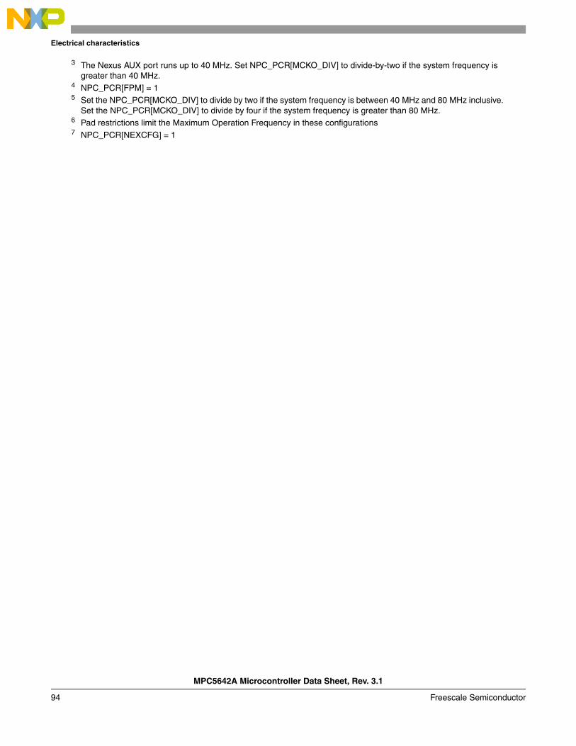
Electrical characteristics
3 The Nexus AUX port runs up to 40 MHz. Set NPC_PCR[MCKO_DIV] to divide-by-two if the system frequency is greater than 40 MHz.
4 NPC_PCR[FPM] = 15 Set the NPC_PCR[MCKO_DIV] to divide by two if the system frequency is between 40 MHz and 80 MHz inclusive.
Set the NPC_PCR[MCKO_DIV] to divide by four if the system frequency is greater than 80 MHz.6 Pad restrictions limit the Maximum Operation Frequency in these configurations7 NPC_PCR[NEXCFG] = 1
MPC5642A Microcontroller Data Sheet, Rev. 3.1
94 Freescale Semiconductor
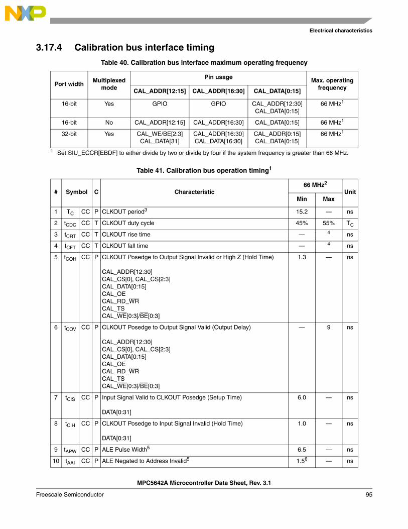
Electrical characteristics
3.17.4 Calibration bus interface timing
Table 40. Calibration bus interface maximum operating frequency
Port widthMultiplexed
mode
Pin usage Max. operating frequencyCAL_ADDR[12:15] CAL_ADDR[16:30] CAL_DATA[0:15]
16-bit Yes GPIO GPIO CAL_ADDR[12:30]CAL_DATA[0:15]
66 MHz1
1 Set SIU_ECCR[EBDF] to either divide by two or divide by four if the system frequency is greater than 66 MHz.
16-bit No CAL_ADDR[12:15] CAL_ADDR[16:30] CAL_DATA[0:15] 66 MHz1
32-bit Yes CAL_WE/BE[2:3]CAL_DATA[31]
CAL_ADDR[16:30]CAL_DATA[16:30]
CAL_ADDR[0:15]CAL_DATA[0:15]
66 MHz1
Table 41. Calibration bus operation timing1
# Symbol C Characteristic66 MHz2
UnitMin Max
1 TC CC P CLKOUT period3 15.2 — ns
2 tCDC CC T CLKOUT duty cycle 45% 55% TC
3 tCRT CC T CLKOUT rise time — 4 ns
4 tCFT CC T CLKOUT fall time — 4 ns
5 tCOH CC P CLKOUT Posedge to Output Signal Invalid or High Z (Hold Time)
CAL_ADDR[12:30]CAL_CS[0], CAL_CS[2:3]CAL_DATA[0:15]CAL_OECAL_RD_WRCAL_TSCAL_WE[0:3]/BE[0:3]
1.3 — ns
6 tCOV CC P CLKOUT Posedge to Output Signal Valid (Output Delay)
CAL_ADDR[12:30]CAL_CS[0], CAL_CS[2:3]CAL_DATA[0:15]CAL_OECAL_RD_WRCAL_TSCAL_WE[0:3]/BE[0:3]
— 9 ns
7 tCIS CC P Input Signal Valid to CLKOUT Posedge (Setup Time)
DATA[0:31]
6.0 — ns
8 tCIH CC P CLKOUT Posedge to Input Signal Invalid (Hold Time)
DATA[0:31]
1.0 — ns
9 tAPW CC P ALE Pulse Width5 6.5 — ns
10 tAAI CC P ALE Negated to Address Invalid5 1.56 — ns
MPC5642A Microcontroller Data Sheet, Rev. 3.1
Freescale Semiconductor 95
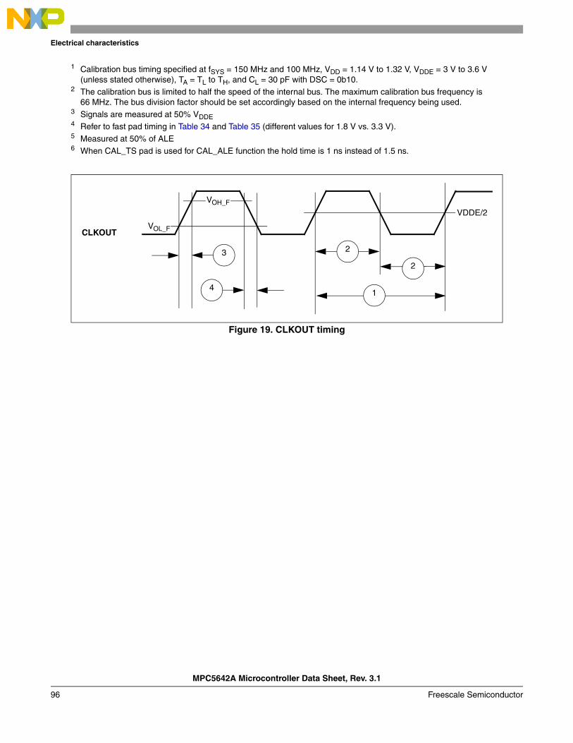
Electrical characteristics
Figure 19. CLKOUT timing
1 Calibration bus timing specified at fSYS = 150 MHz and 100 MHz, VDD = 1.14 V to 1.32 V, VDDE = 3 V to 3.6 V (unless stated otherwise), TA = TL to TH, and CL = 30 pF with DSC = 0b10.
2 The calibration bus is limited to half the speed of the internal bus. The maximum calibration bus frequency is 66 MHz. The bus division factor should be set accordingly based on the internal frequency being used.
3 Signals are measured at 50% VDDE4 Refer to fast pad timing in Table 34 and Table 35 (different values for 1.8 V vs. 3.3 V).5 Measured at 50% of ALE6 When CAL_TS pad is used for CAL_ALE function the hold time is 1 ns instead of 1.5 ns.
1
2
2
3
4
CLKOUT
VDDE/2
VOL_F
VOH_F
MPC5642A Microcontroller Data Sheet, Rev. 3.1
96 Freescale Semiconductor
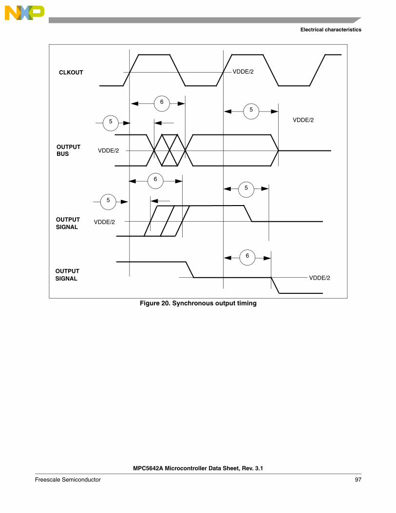
Electrical characteristics
Figure 20. Synchronous output timing
65
5
CLKOUT
BUS
5
OUTPUT SIGNAL
OUTPUT
VDDE/2
VDDE/2
VDDE/2
VDDE/2
6
5
OUTPUT SIGNAL VDDE/2
6
MPC5642A Microcontroller Data Sheet, Rev. 3.1
Freescale Semiconductor 97
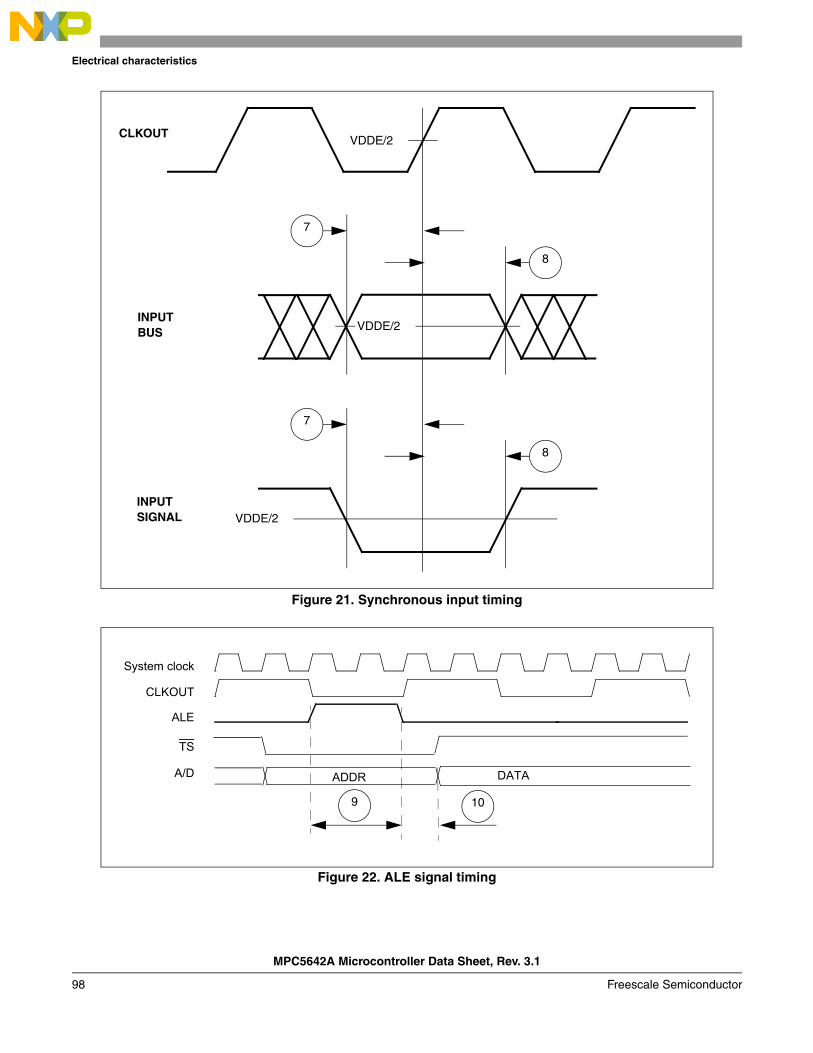
Electrical characteristics
Figure 21. Synchronous input timing
Figure 22. ALE signal timing
7
8
CLKOUT
INPUTBUS
7
8
INPUTSIGNAL
VDDE/2
VDDE/2
VDDE/2
System clock
CLKOUT
ALE
TS
ADDR DATAA/D
9 10
MPC5642A Microcontroller Data Sheet, Rev. 3.1
98 Freescale Semiconductor
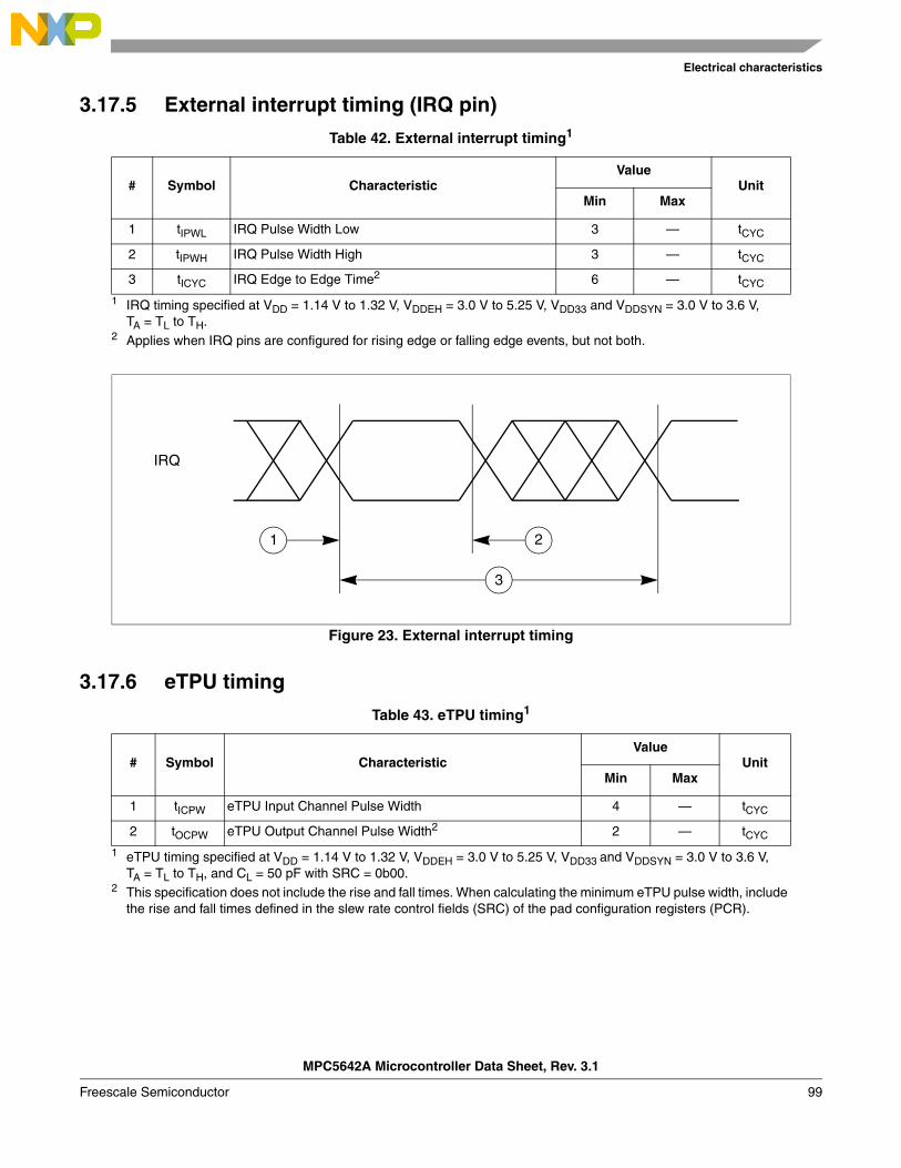
Electrical characteristics
3.17.5 External interrupt timing (IRQ pin)
Figure 23. External interrupt timing
3.17.6 eTPU timing
Table 42. External interrupt timing1
1 IRQ timing specified at VDD = 1.14 V to 1.32 V, VDDEH = 3.0 V to 5.25 V, VDD33 and VDDSYN = 3.0 V to 3.6 V, TA = TL to TH.
# Symbol CharacteristicValue
UnitMin Max
1 tIPWL IRQ Pulse Width Low 3 — tCYC
2 tIPWH IRQ Pulse Width High 3 — tCYC
3 tICYC IRQ Edge to Edge Time2
2 Applies when IRQ pins are configured for rising edge or falling edge events, but not both.
6 — tCYC
Table 43. eTPU timing1
1 eTPU timing specified at VDD = 1.14 V to 1.32 V, VDDEH = 3.0 V to 5.25 V, VDD33 and VDDSYN = 3.0 V to 3.6 V, TA = TL to TH, and CL = 50 pF with SRC = 0b00.
# Symbol CharacteristicValue
UnitMin Max
1 tICPW eTPU Input Channel Pulse Width 4 — tCYC
2 tOCPW eTPU Output Channel Pulse Width2
2 This specification does not include the rise and fall times. When calculating the minimum eTPU pulse width, include the rise and fall times defined in the slew rate control fields (SRC) of the pad configuration registers (PCR).
2 — tCYC
IRQ
1 2
3
MPC5642A Microcontroller Data Sheet, Rev. 3.1
Freescale Semiconductor 99
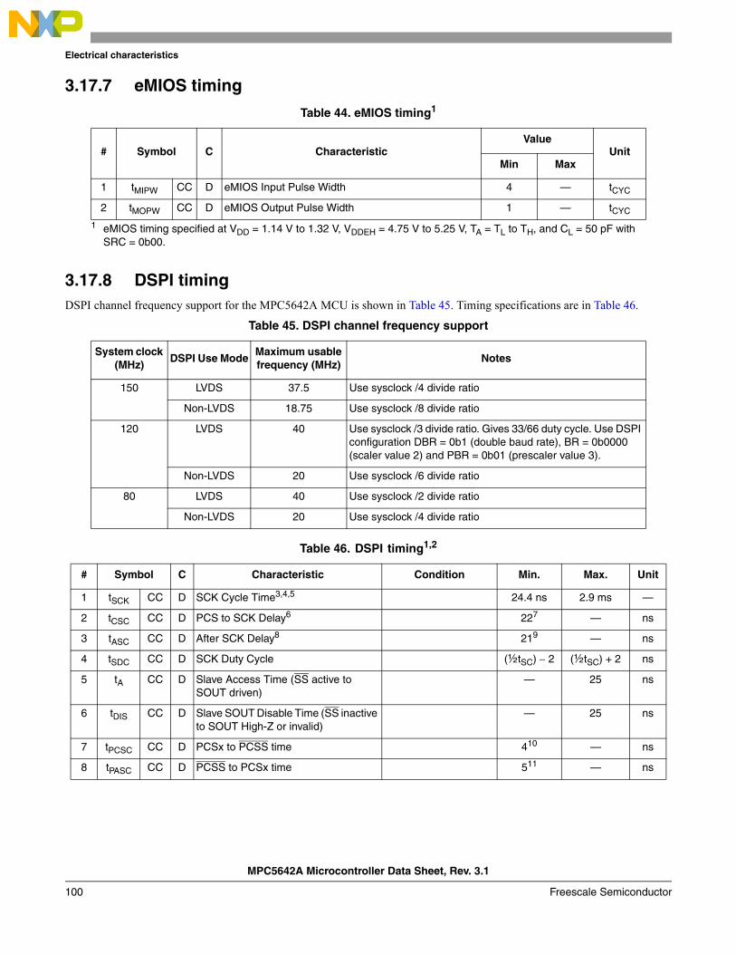
Electrical characteristics
3.17.7 eMIOS timing
3.17.8 DSPI timingDSPI channel frequency support for the MPC5642A MCU is shown in Table 45. Timing specifications are in Table 46.
Table 44. eMIOS timing1
1 eMIOS timing specified at VDD = 1.14 V to 1.32 V, VDDEH = 4.75 V to 5.25 V, TA = TL to TH, and CL = 50 pF with SRC = 0b00.
# Symbol C CharacteristicValue
UnitMin Max
1 tMIPW CC D eMIOS Input Pulse Width 4 — tCYC
2 tMOPW CC D eMIOS Output Pulse Width 1 — tCYC
Table 45. DSPI channel frequency support
System clock (MHz)
DSPI Use ModeMaximum usable frequency (MHz)
Notes
150 LVDS 37.5 Use sysclock /4 divide ratio
Non-LVDS 18.75 Use sysclock /8 divide ratio
120 LVDS 40 Use sysclock /3 divide ratio. Gives 33/66 duty cycle. Use DSPI configuration DBR = 0b1 (double baud rate), BR = 0b0000 (scaler value 2) and PBR = 0b01 (prescaler value 3).
Non-LVDS 20 Use sysclock /6 divide ratio
80 LVDS 40 Use sysclock /2 divide ratio
Non-LVDS 20 Use sysclock /4 divide ratio
Table 46. DSPI timing1,2
# Symbol C Characteristic Condition Min. Max. Unit
1 tSCK CC D SCK Cycle Time3,4,5 24.4 ns 2.9 ms —
2 tCSC CC D PCS to SCK Delay6 227 — ns
3 tASC CC D After SCK Delay8 219 — ns
4 tSDC CC D SCK Duty Cycle (½tSC) 2 (½tSC) + 2 ns
5 tA CC D Slave Access Time (SS active to SOUT driven)
— 25 ns
6 tDIS CC D Slave SOUT Disable Time (SS inactive to SOUT High-Z or invalid)
— 25 ns
7 tPCSC CC D PCSx to PCSS time 410 — ns
8 tPASC CC D PCSS to PCSx time 511 — ns
MPC5642A Microcontroller Data Sheet, Rev. 3.1
100 Freescale Semiconductor
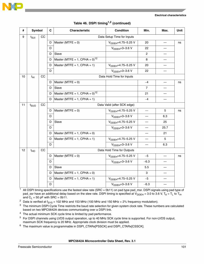
Electrical characteristics
9 tSUI CC Data Setup Time for Inputs
D Master (MTFE = 0) VDDEH=4.75–5.25 V 20 — ns
D VDDEH=3–3.6 V 22 —
D Slave 2 —
D Master (MTFE = 1, CPHA = 0)12 8 —
D Master (MTFE = 1, CPHA = 1) VDDEH=4.75–5.25 V 20 —
D VDDEH=3–3.6 V 22 —
10 tHI CC Data Hold Time for Inputs
D Master (MTFE = 0) 4 — ns
D Slave 7 —
D Master (MTFE = 1, CPHA = 0)12 21 —
D Master (MTFE = 1, CPHA = 1) 4 —
11 tSUO CC Data Valid (after SCK edge)
D Master (MTFE = 0) VDDEH=4.75–5.25 V — 5 ns
D VDDEH=3–3.6 V — 6.3
D Slave VDDEH=4.75–5.25 V — 25
D VDDEH=3–3.6 V — 25.7
D Master (MTFE = 1, CPHA = 0) — 21
D Master (MTFE = 1, CPHA = 1) VDDEH=4.75–5.25 V — 5
D VDDEH=3–3.6 V — 6.3
12 tHO CC Data Hold Time for Outputs
D Master (MTFE = 0) VDDEH=4.75–5.25 V 5 — ns
D VDDEH=3–3.6 V 6.3 —
D Slave 5.5 —
D Master (MTFE = 1, CPHA = 0) 3 —
D Master (MTFE = 1, CPHA = 1) VDDEH=4.75–5.25 V 5 —
D VDDEH=3–3.6 V 6.3 —
1 All DSPI timing specifications use the fastest slew rate (SRC = 0b11) on pad type pad_msr. DSPI signals using pad type of pad_ssr have an additional delay based on the slew rate. DSPI timing is specified at VDDEH = 3.0 to 3.6 V, TA = TL to TH, and CL = 50 pF with SRC = 0b11.
2 Data is verified at fSYS = 102 MHz and 153 MHz (100 MHz and 150 MHz + 2% frequency modulation).3 The minimum DSPI Cycle Time restricts the baud rate selection for given system clock rate. These numbers are calculated
based on two MPC5642A devices communicating over a DSPI link.4 The actual minimum SCK cycle time is limited by pad performance.5 For DSPI channels using LVDS output operation, up to 40 MHz SCK cycle time is supported. For non-LVDS output,
maximum SCK frequency is 20 MHz. Appropriate clock division must be applied.6 The maximum value is programmable in DSPI_CTARx[PSSCK] and DSPI_CTARx[CSSCK].
Table 46. DSPI timing1,2 (continued)
# Symbol C Characteristic Condition Min. Max. Unit
MPC5642A Microcontroller Data Sheet, Rev. 3.1
Freescale Semiconductor 101
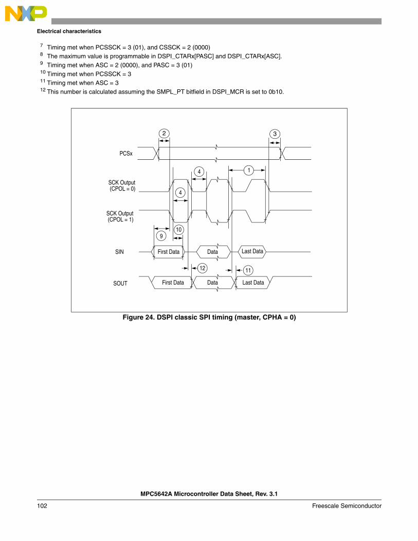
Electrical characteristics
Figure 24. DSPI classic SPI timing (master, CPHA = 0)
7 Timing met when PCSSCK = 3 (01), and CSSCK = 2 (0000)8 The maximum value is programmable in DSPI_CTARx[PASC] and DSPI_CTARx[ASC].9 Timing met when ASC = 2 (0000), and PASC = 3 (01)10 Timing met when PCSSCK = 311 Timing met when ASC = 312 This number is calculated assuming the SMPL_PT bitfield in DSPI_MCR is set to 0b10.
Data Last DataFirst Data
First Data Data Last Data
SIN
SOUT
PCSx
SCK Output
4
9
12
1
11
10
4
SCK Output
(CPOL = 0)
(CPOL = 1)
32
MPC5642A Microcontroller Data Sheet, Rev. 3.1
102 Freescale Semiconductor
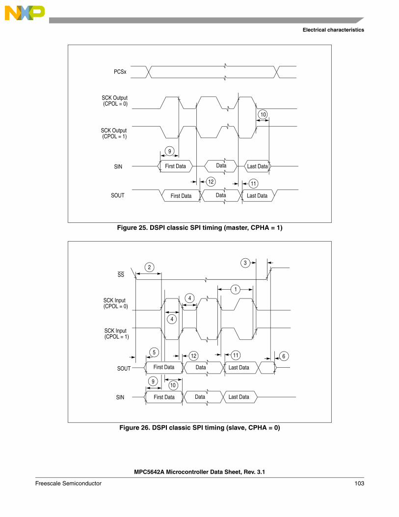
Electrical characteristics
Figure 25. DSPI classic SPI timing (master, CPHA = 1)
Figure 26. DSPI classic SPI timing (slave, CPHA = 0)
Data Last DataFirst DataSIN
SOUT
12 11
10
Last DataDataFirst Data
SCK Output
SCK Output
PCSx
9
(CPOL = 0)
(CPOL = 1)
Last DataFirst Data
3
4
1
Data
Data
SIN
SOUT
SS
4
5 6
9
11
10
12
SCK Input
First Data Last Data
SCK Input
2
(CPOL = 0)
(CPOL = 1)
MPC5642A Microcontroller Data Sheet, Rev. 3.1
Freescale Semiconductor 103
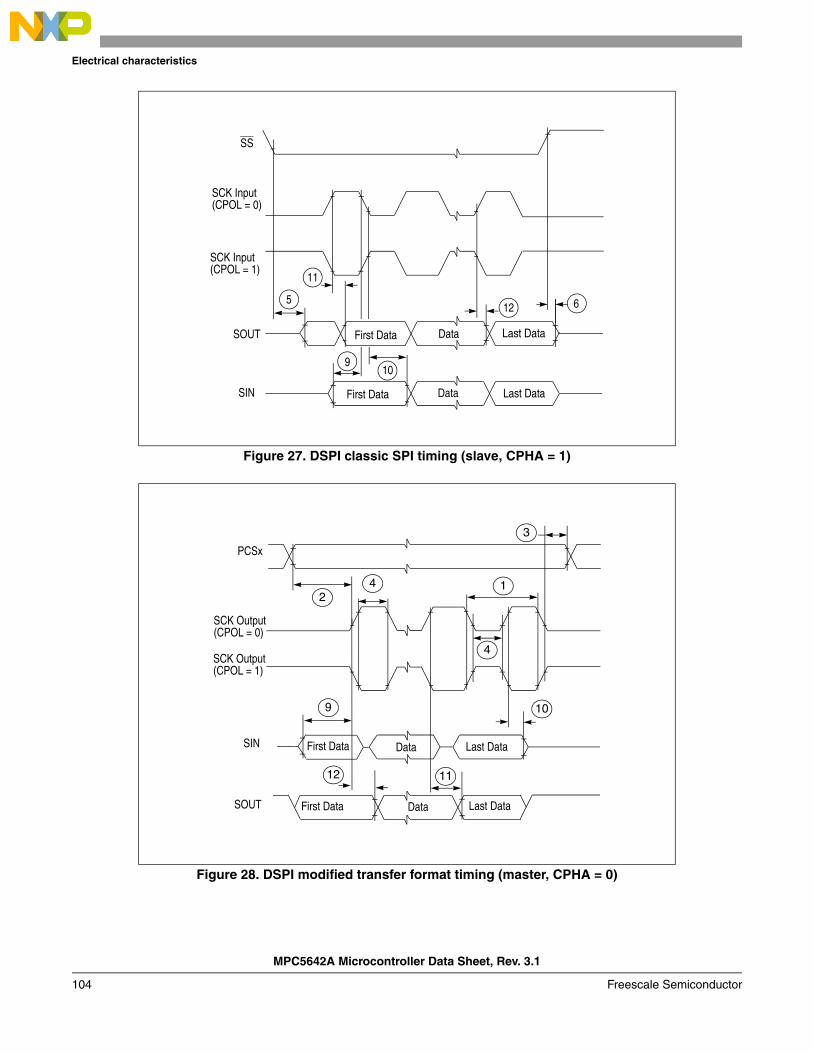
Electrical characteristics
Figure 27. DSPI classic SPI timing (slave, CPHA = 1)
Figure 28. DSPI modified transfer format timing (master, CPHA = 0)
5 6
9
12
11
10
Last Data
Last DataSIN
SOUT
SS
First Data
First Data
Data
Data
SCK Input
SCK Input
(CPOL = 0)
(CPOL = 1)
PCSx
3
14
10
4
9
12 11
SCK Output
SCK Output
SIN
SOUT
First Data Data Last Data
First Data Data Last Data
2
(CPOL = 0)
(CPOL = 1)
MPC5642A Microcontroller Data Sheet, Rev. 3.1
104 Freescale Semiconductor
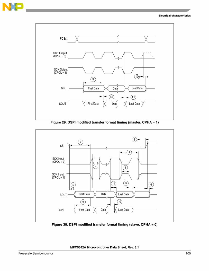
Electrical characteristics
Figure 29. DSPI modified transfer format timing (master, CPHA = 1)
Figure 30. DSPI modified transfer format timing (slave, CPHA = 0)
PCSx
109
12 11
SCK Output
SCK Output
SIN
SOUT
First Data Data Last Data
First Data Data Last Data
(CPOL = 0)
(CPOL = 1)
Last DataFirst Data
3
4
1
Data
Data
SIN
SOUT
SS
4
5 6
9
11
10
SCK Input
First Data Last Data
SCK Input
2
(CPOL = 0)
(CPOL = 1)
12
MPC5642A Microcontroller Data Sheet, Rev. 3.1
Freescale Semiconductor 105
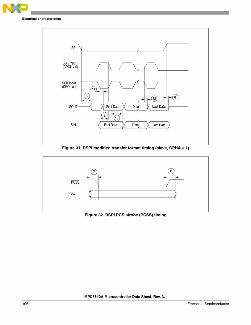
Electrical characteristics
Figure 31. DSPI modified transfer format timing (slave, CPHA = 1)
Figure 32. DSPI PCS strobe (PCSS) timing
5 6
9
12
11
10
Last Data
Last DataSIN
SOUT
SS
First Data
First Data
Data
Data
SCK Input
SCK Input
(CPOL = 0)
(CPOL = 1)
PCSx
7 8
PCSS
MPC5642A Microcontroller Data Sheet, Rev. 3.1
106 Freescale Semiconductor
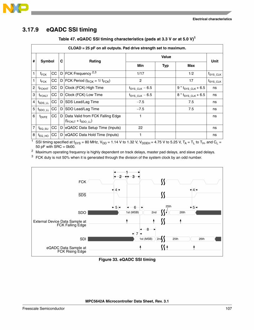
Electrical characteristics
3.17.9 eQADC SSI timing
Figure 33. eQADC SSI timing
Table 47. eQADC SSI timing characteristics (pads at 3.3 V or at 5.0 V)1
1 SSI timing specified at fSYS = 80 MHz, VDD = 1.14 V to 1.32 V, VDDEH = 4.75 V to 5.25 V, TA = TL to TH, and CL = 50 pF with SRC = 0b00.
CLOAD = 25 pF on all outputs. Pad drive strength set to maximum.
# Symbol C RatingValue
UnitMin Typ Max
1 fFCK CC D FCK Frequency 2,3
2 Maximum operating frequency is highly dependent on track delays, master pad delays, and slave pad delays.3 FCK duty is not 50% when it is generated through the division of the system clock by an odd number.
1/17 12 fSYS_CLK
1 tFCK CC D FCK Period (tFCK = 1/ fFCK) 2 17 tSYS_CLK
2 tFCKHT CC D Clock (FCK) High Time tSYS_CLK 6.5 9 * tSYS_CLK + 6.5 ns
3 tFCKLT CC D Clock (FCK) Low Time tSYS_CLK 6.5 8 * tSYS_CLK + 6.5 ns
4 tSDS_LL CC D SDS Lead/Lag Time 7.5 7.5 ns
5 tSDO_LL CC D SDO Lead/Lag Time 7.5 7.5 ns
6 tDVFE CC D Data Valid from FCK Falling Edge (tFCKLT + tSDO_LL)
1 ns
7 tEQ_SU CC D eQADC Data Setup Time (Inputs) 22 ns
8 tEQ_HO CC D eQADC Data Hold Time (Inputs) 1 ns
1st (MSB) 2nd
25th
26th
1st (MSB) 2nd 25th 26th
87
565
44
31
321
2FCK
SDS
SDO
External Device Data Sample at
SDI
eQADC Data Sample at
FCK Falling Edge
FCK Rising Edge
MPC5642A Microcontroller Data Sheet, Rev. 3.1
Freescale Semiconductor 107
Electrical characteristics
3.17.10 FlexCAN system clock source
Table 48. FlexCAN engine system clock divider threshold
# Symbol Characteristic Value Unit
1 fCAN_TH FlexCAN engine system clock threshold 100 MHz
Table 49. FlexCAN engine system clock divider
System frequency Required SIU_SYSDIV[CAN_SRC] value
fCAN_TH 01,2
1 Divides system clock source for FlexCAN engine by 12 System clock is only selected for FlexCAN when CAN_CR[CLK_SRC] = 1
> fCAN_TH 12,3
3 Divides system clock source for FlexCAN engine by 2
MPC5642A Microcontroller Data Sheet, Rev. 3.1
108 Freescale Semiconductor
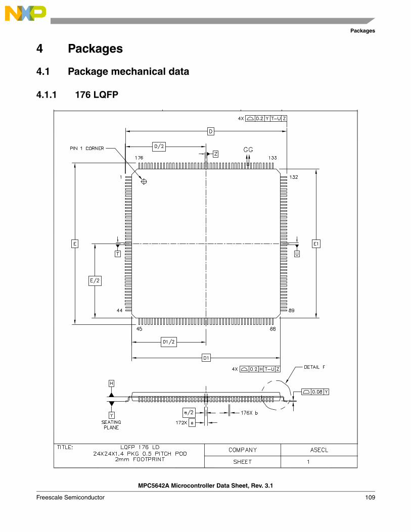
Packages
4 Packages
4.1 Package mechanical data
4.1.1 176 LQFP
MPC5642A Microcontroller Data Sheet, Rev. 3.1
Freescale Semiconductor 109
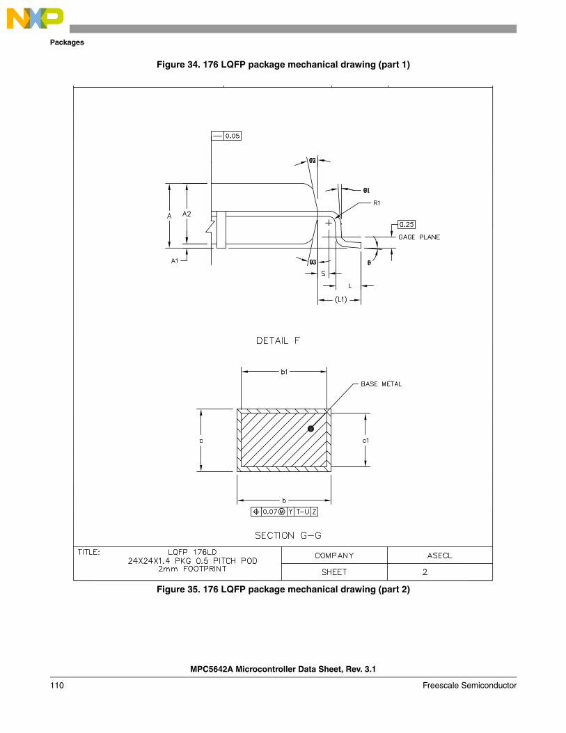
Packages
Figure 34. 176 LQFP package mechanical drawing (part 1)
Figure 35. 176 LQFP package mechanical drawing (part 2)
MPC5642A Microcontroller Data Sheet, Rev. 3.1
110 Freescale Semiconductor
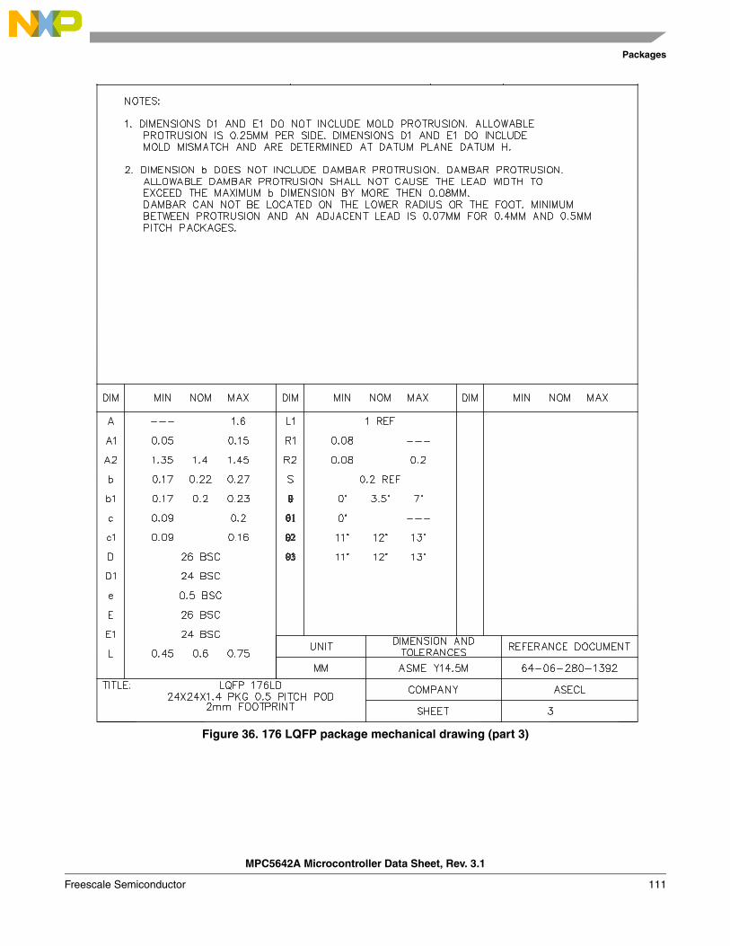
Packages
Figure 36. 176 LQFP package mechanical drawing (part 3)
MPC5642A Microcontroller Data Sheet, Rev. 3.1
Freescale Semiconductor 111
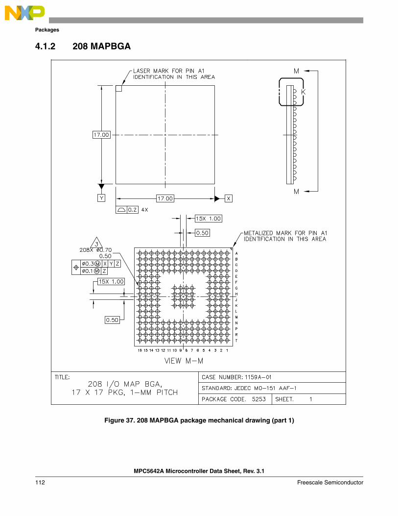
Packages
4.1.2 208 MAPBGA
Figure 37. 208 MAPBGA package mechanical drawing (part 1)
MPC5642A Microcontroller Data Sheet, Rev. 3.1
112 Freescale Semiconductor
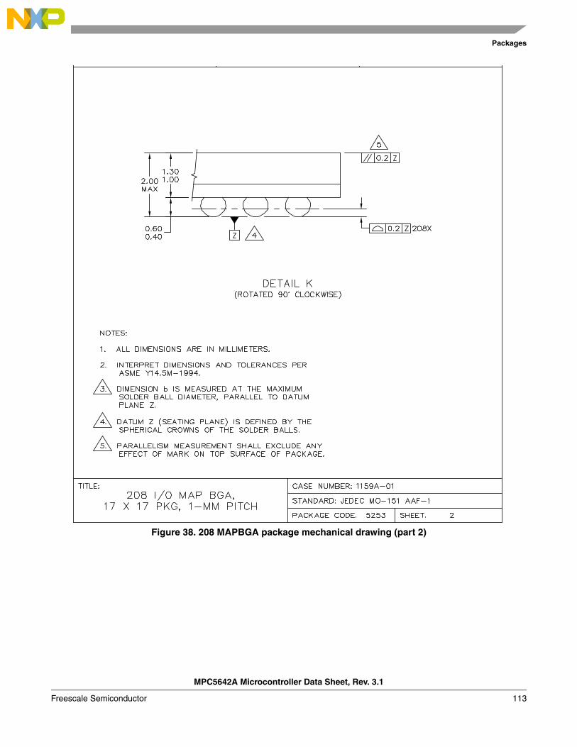
Packages
Figure 38. 208 MAPBGA package mechanical drawing (part 2)
MPC5642A Microcontroller Data Sheet, Rev. 3.1
Freescale Semiconductor 113
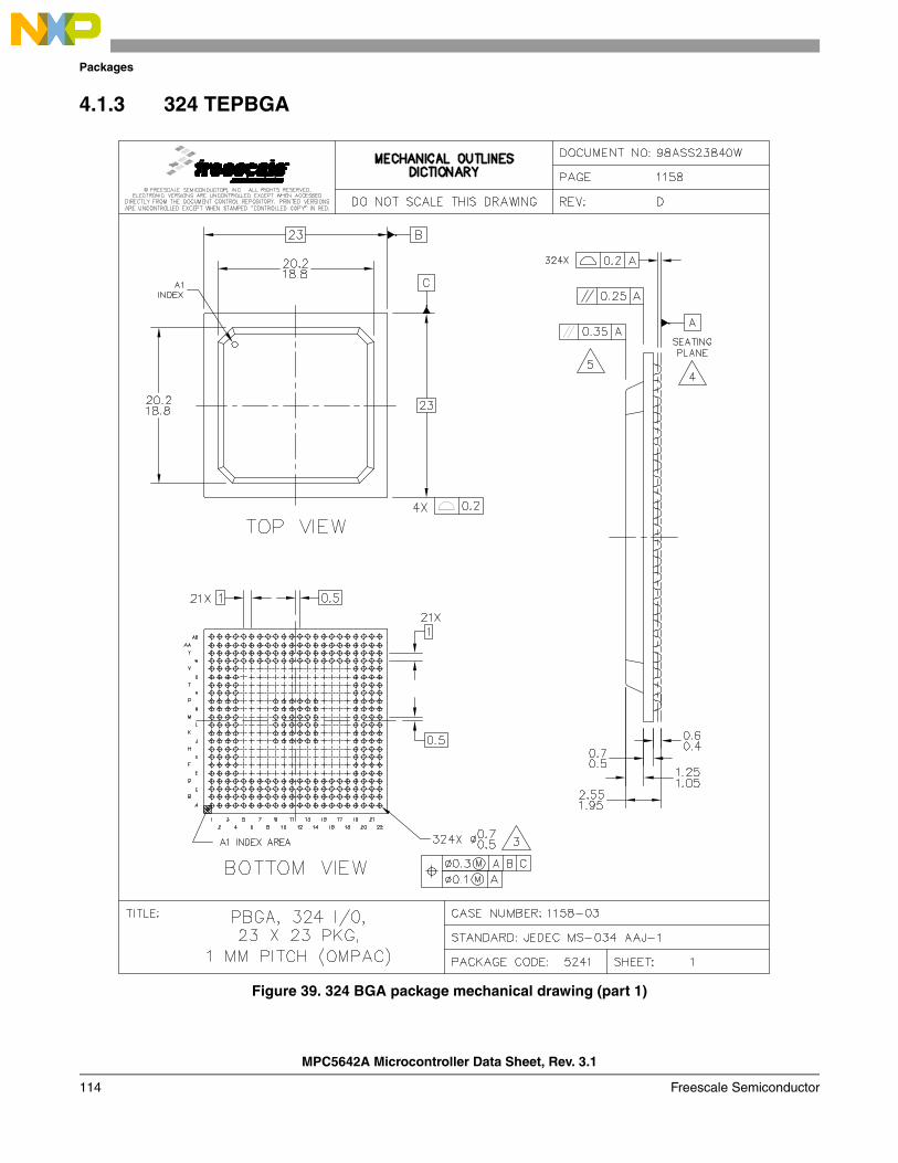
Packages
4.1.3 324 TEPBGA
Figure 39. 324 BGA package mechanical drawing (part 1)
MPC5642A Microcontroller Data Sheet, Rev. 3.1
114 Freescale Semiconductor
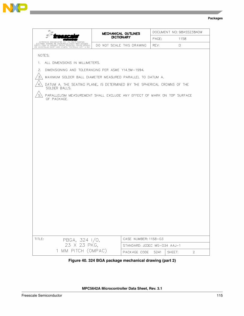
Packages
Figure 40. 324 BGA package mechanical drawing (part 2)
MPC5642A Microcontroller Data Sheet, Rev. 3.1
Freescale Semiconductor 115
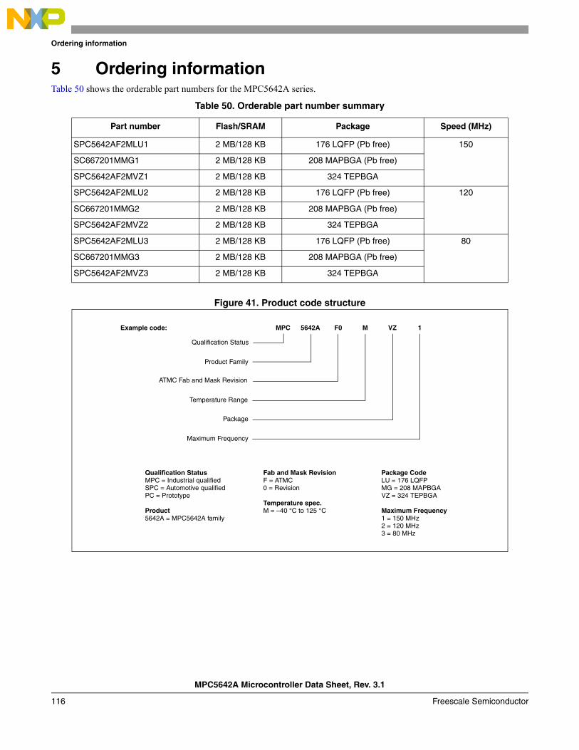
Ordering information
5 Ordering informationTable 50 shows the orderable part numbers for the MPC5642A series.
Figure 41. Product code structure
Table 50. Orderable part number summary
Part number Flash/SRAM Package Speed (MHz)
SPC5642AF2MLU1 2 MB/128 KB 176 LQFP (Pb free) 150
SC667201MMG1 2 MB/128 KB 208 MAPBGA (Pb free)
SPC5642AF2MVZ1 2 MB/128 KB 324 TEPBGA
SPC5642AF2MLU2 2 MB/128 KB 176 LQFP (Pb free) 120
SC667201MMG2 2 MB/128 KB 208 MAPBGA (Pb free)
SPC5642AF2MVZ2 2 MB/128 KB 324 TEPBGA
SPC5642AF2MLU3 2 MB/128 KB 176 LQFP (Pb free) 80
SC667201MMG3 2 MB/128 KB 208 MAPBGA (Pb free)
SPC5642AF2MVZ3 2 MB/128 KB 324 TEPBGA
Qualification Status
Product Family
ATMC Fab and Mask Revision
Temperature Range
Package
Maximum Frequency
MPC 5642A 1Example code: M VZ
Qualification StatusMPC = Industrial qualifiedSPC = Automotive qualifiedPC = Prototype
Product5642A = MPC5642A family
Fab and Mask RevisionF = ATMC0 = Revision
Temperature spec.M = –40 °C to 125 °C
Package CodeLU = 176 LQFPMG = 208 MAPBGAVZ = 324 TEPBGA
Maximum Frequency1 = 150 MHz2 = 120 MHz3 = 80 MHz
F0
MPC5642A Microcontroller Data Sheet, Rev. 3.1
116 Freescale Semiconductor
Document revision history
6 Document revision historyTable 51 summarizes customer facing revisions to this document.
Table 51. Revision history
Date Revision Substantive changes
05 Oct 2010 1 Initial release
26 Mar 2012 2 Figure 1 (MPC5642A series block diagram), added ECSM block and its definition in the elegend.
Table 2 (MPC5642A series block summary), added the following blocks: REACN, SIU, ECSM, FMPLL, PIT and SWT.
Updated Table 8 (Absolute maximum ratings)In 3, Electrical characteristics, deleted the “Recommended operating conditions”
subsection.Table 14 (PMC operating conditions and external regulators supply voltage), removed
minimum value of VDDREG and its footnote.Updated Table 15 (PMC electrical characteristics)Updated Section 3.6.1, Regulator exampleUpdated Table 20 (DC electrical specifications)Figure 8 (Core voltage regulator controller external components preferred
configuration), added “T1” label to indicate the transistor.Table 20 (DC electrical specifications), changed maximum value of VIL_LS to 0.9, was
1.1Table 21 (I/O pad average IDDE specifications), in the VDDE column changed all 5.5 to
5.25Table 24 (DSPI LVDS pad specification):
Renamed VOC, was VODUpdated minimum and maximum value of VOCdeleted all footnote
Table 26 (Temperature sensor electrical characteristics), updated minimum and maximum value of accuracy
Updated Section 3.12, eQADC electrical characteristicsAdded Section 3.13, Configuring SRAM wait statesUpdated Table 31 (APC, RWSC, WWSC settings vs. frequency of operation)Updated Table 32 (Flash program and erase specifications)Table 31 (APC, RWSC, WWSC settings vs. frequency of operation), changed all values
in the WWSC column to 0b01.Updated Table 32 (Flash program and erase specifications)Table 33 (Flash EEPROM module life):
updated temperature value in the Retention description (was 150 C, is 85 C)added values for Retention
Table 34 (Pad AC specifications (VDDE = 4.75 V)):changed maximum value of Medium to 12/12changed maximum value of Slow to 20/20
Updated Table 35 (Pad AC specifications (VDDE = 3.0 V))Table 37 (JTAG pin AC electrical characteristics):
changed all parameter classification to Dchanged minumum value of tTMSS, tTDIS to 10
Updated Table 38 (Nexus debug port timing)Added Table 39 (Nexus debug port operating frequency)Table 39 (Nexus debug port operating frequency), added a footnote near the value of
tAAITable 44 (eMIOS timing):
changed minumum value of tMOPW to 1removed the footnote of tMOPW
MPC5642A Microcontroller Data Sheet, Rev. 3.1
Freescale Semiconductor 117
Document revision history
26 Mar 2012 2(cont’d)
Merged “DSPI timing (VDDEH = 3.0 to 3.6 V)” and “DSPI timing (VDDEH = 4.5 to 5.5V)” tables into Table 46 (DSPI timing,) and changed all parameter classification to D
Table 47 (eQADC SSI timing characteristics (pads at 3.3 V or at 5.0 V)) changed all parameter classification to D
04 May 2012 3 Minor editorial changes and improvements throughout.In Section 2.4, Signal summary, Table 3 (MPC5642A signal properties), updated the
following properties for the Nexus pins: • Added a footnote to the “Nexus” title for this pin group. • Added a footnote to the “Name” entry for EVTO. • Updated the “Status During reset” entry for EVTO.In Section 3.2, Maximum ratings, Table 8 (Absolute maximum ratings), removed the
“TBD - To be defined” footnote.In Section 3.6, Power management control (PMC) and power on reset (POR) electrical
specifications, removed the “Voltage regulator controller (VRC) electrical specifications” subsection.
In Section 3.8, DC electrical specifications, Table 20 (DC electrical specifications), removed the “TBD - To be defined” footnote.
In Section 3.9, I/O pad current specifications, Table 21 (I/O pad average IDDE specifications):
• Updated values and replaced TBDs with numerical data. • Removed the “TBD - To be defined” footnote.In Section 3.9.1, I/O pad VRC33 current specifications, Table 22 (I/O pad VRC33 average
IDDE specifications): • Updated values and replaced TBDs with numerical data. • Removed the “TBD - To be defined” footnote.In Section 3.14, Platform flash controller electrical characteristics, Table 31 (APC,
RWSC, WWSC settings vs. frequency of operation), removed the “TBD - To be defined” footnote.
In Section 5, Ordering information, Table 50 (Orderable part number summary): • Changed all part numbers from “MPC5642AF0...“ to “SPC5642AF2...“. • Changed “MPC5642AF0MMG1“ to “SC667201MMG1“. • Changed “MPC5642AF0MMG2“ to “SC667201MMG2“. • Changed “MPC5642AF0MMG3“ to “SC667201MMG3“.In Table 51 (Revision history), removed several erroneous items from the Revision 2
entry.
29 Jun 2012 3.1 No content changes, technical or editorial, were made in this revision.Removed the “preliminary” footers throughout.Changed “Data Sheet: Advance Information” to “Data Sheet: Technical Data” on page 1.Removed the “product under development” disclaimer on page 1.
Table 51. Revision history (continued)
Date Revision Substantive changes
MPC5642A Microcontroller Data Sheet, Rev. 3.1
118 Freescale Semiconductor

Document revision history
MPC5642A Microcontroller Data Sheet, Rev. 3.1
Freescale Semiconductor 119
Document revision history
Document Number: MPC5642ARev. 3.106/2012
Information in this document is provided solely to enable system and software
implementers to use Freescale products. There are no express or implied copyright
licenses granted hereunder to design or fabricate any integrated circuits based on the
information in this document.
Freescale reserves the right to make changes without further notice to any products
herein. Freescale makes no warranty, representation, or guarantee regarding the
suitability of its products for any particular purpose, nor does Freescale assume any
liability arising out of the application or use of any product or circuit, and specifically
disclaims any and all liability, including without limitation consequential or incidental
damages. “Typical” parameters that may be provided in Freescale data sheets and/or
specifications can and do vary in different applications, and actual performance may
vary over time. All operating parameters, including “typicals,” must be validated for each
customer application by customer’s technical experts. Freescale does not convey any
license under its patent rights nor the rights of others. Freescale sells products
pursuant to standard terms and conditions of sale, which can be found at the following
address: http://www.reg.net/v2/webservices/Freescale/Docs/TermsandConditions.htm
How to Reach Us:
Home Page: freescale.com
Web Support: freescale.com/support
Freescale, the Freescale logo, AltiVec, C-5, CodeTest, CodeWarrior, ColdFire, C-Ware,
Energy Efficient Solutions logo, Kinetis, mobileGT, PowerQUICC, Processor Expert,
QorIQ, Qorivva, StarCore, Symphony, and VortiQa are trademarks of Freescale
Semiconductor, Inc., Reg. U.S. Pat. & Tm. Off. Airfast, BeeKit, BeeStack, ColdFire+,
CoreNet, Flexis, MagniV, MXC, Platform in a Package, QorIQ Qonverge, QUICC
Engine, Ready Play, SafeAssure, SMARTMOS, TurboLink, Vybrid, and Xtrinsic are
trademarks of Freescale Semiconductor, Inc. All other product or service names are
the property of their respective owners. The Power Architecture and Power.org word
marks and the Power and Power.org logos and related marks are trademarks and
service marks licensed by Power.org.
© 2009, 2010, 2012 Freescale Semiconductor, Inc.
MPC5642A Microcontroller Data Sheet, Rev. 3.1
120 Freescale Semiconductor