Embed Size (px)
Citation preview
MSP430 Family Mixed-Signal Microcontroller
Application Reports
Author: Lutz Bierl
Literature Number: SLAA024January 2000
Printed on Recycled Paper

IMPORTANT NOTICE
Texas Instruments and its subsidiaries (TI) reserve the right to make changes to their products or to discontinueany product or service without notice, and advise customers to obtain the latest version of relevant informationto verify, before placing orders, that information being relied on is current and complete. All products are soldsubject to the terms and conditions of sale supplied at the time of order acknowledgement, including thosepertaining to warranty, patent infringement, and limitation of liability.
TI warrants performance of its semiconductor products to the specifications applicable at the time of sale inaccordance with TI’s standard warranty. Testing and other quality control techniques are utilized to the extentTI deems necessary to support this warranty. Specific testing of all parameters of each device is not necessarilyperformed, except those mandated by government requirements.
CERTAIN APPLICATIONS USING SEMICONDUCTOR PRODUCTS MAY INVOLVE POTENTIAL RISKS OFDEATH, PERSONAL INJURY, OR SEVERE PROPERTY OR ENVIRONMENTAL DAMAGE (“CRITICALAPPLICATIONS”). TI SEMICONDUCTOR PRODUCTS ARE NOT DESIGNED, AUTHORIZED, ORWARRANTED TO BE SUITABLE FOR USE IN LIFE-SUPPORT DEVICES OR SYSTEMS OR OTHERCRITICAL APPLICATIONS. INCLUSION OF TI PRODUCTS IN SUCH APPLICATIONS IS UNDERSTOOD TOBE FULLY AT THE CUSTOMER’S RISK.
In order to minimize risks associated with the customer’s applications, adequate design and operatingsafeguards must be provided by the customer to minimize inherent or procedural hazards.
TI assumes no liability for applications assistance or customer product design. TI does not warrant or representthat any license, either express or implied, is granted under any patent right, copyright, mask work right, or otherintellectual property right of TI covering or relating to any combination, machine, or process in which suchsemiconductor products or services might be or are used. TI’s publication of information regarding any thirdparty’s products or services does not constitute TI’s approval, warranty or endorsement thereof.
Copyright 2000, Texas Instruments Incorporated

iiiContents
Preface
Read This First
How to Use This Manual
This document contains the following chapters:
Chapter 1 – MSP430 Microcontroller Family: Introduction to the MSP430family, advantages of the MSP430 concept, and operating modes
Chapter 2 – MSP430 14-Bit Analog-To-Digital Converter:
Chapter 3 – MSP430 Hardware Applications:
Chapter 4 – MSP430 Application Examples:
Chapter 5 – Software Applications:
Chapter 6 – On-Chip Peripherals:
Chapter 7 – Hints and Recommendations:
Chapter 8 – Architecture and Instruction Set:
Chapter 9 – CPU Registers:
Contents
v
Contents
1 MSP430 Microcontroller Family 1-1. . . . . . . . . . . . . . . . . . . . . . . . . . . . . . . . . . . . . . . . . . . . . . . . . . . 1.1 Introduction 1-2. . . . . . . . . . . . . . . . . . . . . . . . . . . . . . . . . . . . . . . . . . . . . . . . . . . . . . . . . . . . . . . . 1.2 Related Documents 1-3. . . . . . . . . . . . . . . . . . . . . . . . . . . . . . . . . . . . . . . . . . . . . . . . . . . . . . . . . 1.3 Notation 1-3. . . . . . . . . . . . . . . . . . . . . . . . . . . . . . . . . . . . . . . . . . . . . . . . . . . . . . . . . . . . . . . . . . . 1.4 MSP430 Family 1-4. . . . . . . . . . . . . . . . . . . . . . . . . . . . . . . . . . . . . . . . . . . . . . . . . . . . . . . . . . . .
1.4.1 MSP430C31x 1-5. . . . . . . . . . . . . . . . . . . . . . . . . . . . . . . . . . . . . . . . . . . . . . . . . . . . . . . 1.4.2 MSP430C32x 1-6. . . . . . . . . . . . . . . . . . . . . . . . . . . . . . . . . . . . . . . . . . . . . . . . . . . . . . . 1.4.3 MSP430C33x 1-6. . . . . . . . . . . . . . . . . . . . . . . . . . . . . . . . . . . . . . . . . . . . . . . . . . . . . . .
1.5 Advantages of the MSP430 Concept 1-8. . . . . . . . . . . . . . . . . . . . . . . . . . . . . . . . . . . . . . . . . . 1.5.1 RISC Architecture Without RISC Disadvantages 1-8. . . . . . . . . . . . . . . . . . . . . . . . . 1.5.2 Real-Time Capability With Ultra-Low Power Consumption 1-8. . . . . . . . . . . . . . . . 1.5.3 Digitally Controlled Oscillator Stability 1-9. . . . . . . . . . . . . . . . . . . . . . . . . . . . . . . . . . 1.5.4 Stack Processing Capability 1-9. . . . . . . . . . . . . . . . . . . . . . . . . . . . . . . . . . . . . . . . . .
1.6 MSP430 Application Operating Modes 1-10. . . . . . . . . . . . . . . . . . . . . . . . . . . . . . . . . . . . . . . 1.6.1 Active Mode 1-10. . . . . . . . . . . . . . . . . . . . . . . . . . . . . . . . . . . . . . . . . . . . . . . . . . . . . . . 1.6.2 Low Power Mode 3 (LPM3) 1-10. . . . . . . . . . . . . . . . . . . . . . . . . . . . . . . . . . . . . . . . . . 1.6.3 Low Power Mode 4 (LPM4) 1-13. . . . . . . . . . . . . . . . . . . . . . . . . . . . . . . . . . . . . . . . . .
2 Analog-To-Digital Converters 2-1. . . . . . . . . . . . . . . . . . . . . . . . . . . . . . . . . . . . . . . . . . . . . . . . . . . . .
Architecture and Function of the MSP430 14-Bit ADC 2-3. . . . . . . . . . . . . . . . . . . . . . . . . . . . . .
A table of contents for this application report is found starting on page 2-5. . . . . . . . . . .
Application Basics for the MSP430 14-Bit ADC 2-41. . . . . . . . . . . . . . . . . . . . . . . . . . . . . . . . . . .
A table of contents for this application report is found starting on page 2-43. . . . . . . . . .
Additive Improvement of the MSP430 14-Bit ADC Characteristic 2-83. . . . . . . . . . . . . . . . . . .
A table of contents for this application report is found starting on page 2-85. . . . . . . . . .
Linear Improvement of the MSP430 14-Bit ADC Characteristic 2-113. . . . . . . . . . . . . . . . . . . .
A table of contents for this application report is found starting on page 2-115. . . . . . . . .
Nonlinear Improvement of the MSP430 14-Bit ADC Characteristic 2-143. . . . . . . . . . . . . . . . .
A table of contents for this application report is found starting on page 2-145. . . . . . . . .
Using the MSP430 Universal Timer/Port Module as an Analog-to-Digital Converter 2-175.
A table of contents for this application report is found starting on page 2-177. . . . . . . . .
Contents
vi
3 Hardware Applications 3-1. . . . . . . . . . . . . . . . . . . . . . . . . . . . . . . . . . . . . . . . . . . . . . . . . . . . . . . . . . . 3.1 I/O Port Usage 3-2. . . . . . . . . . . . . . . . . . . . . . . . . . . . . . . . . . . . . . . . . . . . . . . . . . . . . . . . . . . . .
3.1.1 General Usage 3-2. . . . . . . . . . . . . . . . . . . . . . . . . . . . . . . . . . . . . . . . . . . . . . . . . . . . . . 3.1.2 Zero Crossing Detection 3-6. . . . . . . . . . . . . . . . . . . . . . . . . . . . . . . . . . . . . . . . . . . . . . 3.1.3 Output Buffering 3-8. . . . . . . . . . . . . . . . . . . . . . . . . . . . . . . . . . . . . . . . . . . . . . . . . . . . . 3.1.4 Universal Timer/Port I/Os 3-9. . . . . . . . . . . . . . . . . . . . . . . . . . . . . . . . . . . . . . . . . . . . . 3.1.5 I/O Used for Fast Serial Transfers 3-11. . . . . . . . . . . . . . . . . . . . . . . . . . . . . . . . . . . .
3.2 Storage of Calibration Constants 3-14. . . . . . . . . . . . . . . . . . . . . . . . . . . . . . . . . . . . . . . . . . . . 3.2.1 External EPROM for Calibration Constants 3-14. . . . . . . . . . . . . . . . . . . . . . . . . . . . 3.2.2 Internal RAM for Calibration Constants 3-16. . . . . . . . . . . . . . . . . . . . . . . . . . . . . . . .
3.3 M-Bus Connection 3-17. . . . . . . . . . . . . . . . . . . . . . . . . . . . . . . . . . . . . . . . . . . . . . . . . . . . . . . . . 3.4 I2C Bus Connection 3-18. . . . . . . . . . . . . . . . . . . . . . . . . . . . . . . . . . . . . . . . . . . . . . . . . . . . . . . . 3.5 Hardware Optimization 3-25. . . . . . . . . . . . . . . . . . . . . . . . . . . . . . . . . . . . . . . . . . . . . . . . . . . . .
3.5.1 Use of Unused Analog Inputs 3-25. . . . . . . . . . . . . . . . . . . . . . . . . . . . . . . . . . . . . . . . 3.5.2 Use of Unused Segment Lines for Digital Outputs 3-28. . . . . . . . . . . . . . . . . . . . . .
3.6 Digital-to-Analog Converters 3-30. . . . . . . . . . . . . . . . . . . . . . . . . . . . . . . . . . . . . . . . . . . . . . . . 3.6.1 R/2R Method 3-30. . . . . . . . . . . . . . . . . . . . . . . . . . . . . . . . . . . . . . . . . . . . . . . . . . . . . . 3.6.2 Weighted Resistors Method 3-31. . . . . . . . . . . . . . . . . . . . . . . . . . . . . . . . . . . . . . . . . . 3.6.3 Digital-to-Analog Converters Connected Via the I2C Bus 3-32. . . . . . . . . . . . . . . . 3.6.4 PWM DAC With the Universal Timer/Port Module 3-33. . . . . . . . . . . . . . . . . . . . . . . 3.6.5 PWM DAC With the Timer_A 3-42. . . . . . . . . . . . . . . . . . . . . . . . . . . . . . . . . . . . . . . . .
3.7 Connection of Large External Memories 3-45. . . . . . . . . . . . . . . . . . . . . . . . . . . . . . . . . . . . . . 3.8 Power Supplies for MSP430 Systems 3-52. . . . . . . . . . . . . . . . . . . . . . . . . . . . . . . . . . . . . . . .
3.8.1 Battery-Power Systems 3-52. . . . . . . . . . . . . . . . . . . . . . . . . . . . . . . . . . . . . . . . . . . . . 3.8.2 Accumulator-Driven Systems 3-54. . . . . . . . . . . . . . . . . . . . . . . . . . . . . . . . . . . . . . . . 3.8.3 AC-Driven Systems 3-56. . . . . . . . . . . . . . . . . . . . . . . . . . . . . . . . . . . . . . . . . . . . . . . . . 3.8.4 Supply From Other System DC Voltages 3-68. . . . . . . . . . . . . . . . . . . . . . . . . . . . . . 3.8.5 Supply From the M Bus 3-71. . . . . . . . . . . . . . . . . . . . . . . . . . . . . . . . . . . . . . . . . . . . . 3.8.6 Supply Via a Fiber-Optic Cable 3-73. . . . . . . . . . . . . . . . . . . . . . . . . . . . . . . . . . . . . . .
4 Application Examples 4-1. . . . . . . . . . . . . . . . . . . . . . . . . . . . . . . . . . . . . . . . . . . . . . . . . . . . . . . . . . . . 4.1 Electricity Meters 4-2. . . . . . . . . . . . . . . . . . . . . . . . . . . . . . . . . . . . . . . . . . . . . . . . . . . . . . . . . . .
4.1.1 Overview 4-2. . . . . . . . . . . . . . . . . . . . . . . . . . . . . . . . . . . . . . . . . . . . . . . . . . . . . . . . . . . 4.1.2 The Measurement Principle 4-3. . . . . . . . . . . . . . . . . . . . . . . . . . . . . . . . . . . . . . . . . . . 4.1.3 The Analog-to-Digital Converter of the MSP430C32x 4-11. . . . . . . . . . . . . . . . . . . . 4.1.4 Analog Interfaces to the MSP430 4-18. . . . . . . . . . . . . . . . . . . . . . . . . . . . . . . . . . . . . 4.1.5 Single-Phase Electricity Meters 4-30. . . . . . . . . . . . . . . . . . . . . . . . . . . . . . . . . . . . . . . 4.1.6 Dual-Phase Electricity Meters 4-35. . . . . . . . . . . . . . . . . . . . . . . . . . . . . . . . . . . . . . . . 4.1.7 Three-Phase Electricity Meters 4-39. . . . . . . . . . . . . . . . . . . . . . . . . . . . . . . . . . . . . . . 4.1.8 Measurement of Voltage, Current, Apparent Power, and Reactive Power 4-49. . 4.1.9 Calculation of the System Current Consumption 4-50. . . . . . . . . . . . . . . . . . . . . . . . 4.1.10 System Components 4-52. . . . . . . . . . . . . . . . . . . . . . . . . . . . . . . . . . . . . . . . . . . . . . . . 4.1.11 Electricity Meter With an External ADC 4-56. . . . . . . . . . . . . . . . . . . . . . . . . . . . . . . . 4.1.12 Error Simulation for an MSP430C32x-Based Electricity Meter 4-58. . . . . . . . . . . .
Contents
viiContents
4.2 Gas Meter 4-64. . . . . . . . . . . . . . . . . . . . . . . . . . . . . . . . . . . . . . . . . . . . . . . . . . . . . . . . . . . . . . . . 4.3 Water Flow Meter 4-69. . . . . . . . . . . . . . . . . . . . . . . . . . . . . . . . . . . . . . . . . . . . . . . . . . . . . . . . . . 4.4 Heat Allocation Counter 4-70. . . . . . . . . . . . . . . . . . . . . . . . . . . . . . . . . . . . . . . . . . . . . . . . . . . . 4.5 Heat Volume Counter 4-72. . . . . . . . . . . . . . . . . . . . . . . . . . . . . . . . . . . . . . . . . . . . . . . . . . . . . . 4.6 Battery Charge Meter 4-75. . . . . . . . . . . . . . . . . . . . . . . . . . . . . . . . . . . . . . . . . . . . . . . . . . . . . . 4.7 Connection of Sensors 4-77. . . . . . . . . . . . . . . . . . . . . . . . . . . . . . . . . . . . . . . . . . . . . . . . . . . . .
4.7.1 Sensor Connection and Linearization 4-77. . . . . . . . . . . . . . . . . . . . . . . . . . . . . . . . . 4.7.2 Connection of Special Sensors 4-82. . . . . . . . . . . . . . . . . . . . . . . . . . . . . . . . . . . . . . .
4.8 RF Readout 4-87. . . . . . . . . . . . . . . . . . . . . . . . . . . . . . . . . . . . . . . . . . . . . . . . . . . . . . . . . . . . . . . 4.8.1 MSP430 Electricity Meter 4-87. . . . . . . . . . . . . . . . . . . . . . . . . . . . . . . . . . . . . . . . . . . . 4.8.2 MSP430 Electricity Meter With Front End 4-88. . . . . . . . . . . . . . . . . . . . . . . . . . . . . . 4.8.3 MSP430 Ferraris-Wheel Electricity Meter With RF Readout 4-90. . . . . . . . . . . . . . 4.8.4 RF-Interface Module 4-91. . . . . . . . . . . . . . . . . . . . . . . . . . . . . . . . . . . . . . . . . . . . . . . . 4.8.5 Protocol 4-92. . . . . . . . . . . . . . . . . . . . . . . . . . . . . . . . . . . . . . . . . . . . . . . . . . . . . . . . . . . 4.8.6 RF Readout With Other Metering Applications 4-93. . . . . . . . . . . . . . . . . . . . . . . . . .
4.9 Ultra-Low-Power Design With the MSP430 Family 4-94. . . . . . . . . . . . . . . . . . . . . . . . . . . . . 4.9.1 The Ultra Low Power Concept of the MSP430 4-94. . . . . . . . . . . . . . . . . . . . . . . . . . 4.9.2 Current Consumption and Battery Life 4-96. . . . . . . . . . . . . . . . . . . . . . . . . . . . . . . . . 4.9.3 Minimization of the System Consumption 4-98. . . . . . . . . . . . . . . . . . . . . . . . . . . . . . 4.9.4 Correct Termination of Unused Terminals (3xx Family) 4-102. . . . . . . . . . . . . . . . .
4.10 Other MSP430 Applications 4-104. . . . . . . . . . . . . . . . . . . . . . . . . . . . . . . . . . . . . . . . . . . . . . . . 4.10.1 Controller for a Heating Installation 4-104. . . . . . . . . . . . . . . . . . . . . . . . . . . . . . . . . . 4.10.2 Pocket Scale 4-107. . . . . . . . . . . . . . . . . . . . . . . . . . . . . . . . . . . . . . . . . . . . . . . . . . . . . . 4.10.3 Remote Control Applications 4-108. . . . . . . . . . . . . . . . . . . . . . . . . . . . . . . . . . . . . . . . 4.10.4 Sub-Controller for a TV Set 4-110. . . . . . . . . . . . . . . . . . . . . . . . . . . . . . . . . . . . . . . . . 4.10.5 Sub-Controller of a Personal Computer 4-112. . . . . . . . . . . . . . . . . . . . . . . . . . . . . . . 4.10.6 Subcontroller of a FAX Device 4-114. . . . . . . . . . . . . . . . . . . . . . . . . . . . . . . . . . . . . . .
4.11 Digital Motor Control 4-115. . . . . . . . . . . . . . . . . . . . . . . . . . . . . . . . . . . . . . . . . . . . . . . . . . . . . . 4.11.1 Introduction 4-115. . . . . . . . . . . . . . . . . . . . . . . . . . . . . . . . . . . . . . . . . . . . . . . . . . . . . . . 4.11.2 Digital Motor Control With Pulse Width Modulation (PWM) 4-119. . . . . . . . . . . . . . 4.11.3 Digital Motor Control With TRIACs 4-138. . . . . . . . . . . . . . . . . . . . . . . . . . . . . . . . . . . 4.11.4 Motor Measurements 4-145. . . . . . . . . . . . . . . . . . . . . . . . . . . . . . . . . . . . . . . . . . . . . . 4.11.5 Conclusion 4-150. . . . . . . . . . . . . . . . . . . . . . . . . . . . . . . . . . . . . . . . . . . . . . . . . . . . . . .
5 Software Applications 5-1. . . . . . . . . . . . . . . . . . . . . . . . . . . . . . . . . . . . . . . . . . . . . . . . . . . . . . . . . . . 5.1 Integer Calculation Subroutines 5-2. . . . . . . . . . . . . . . . . . . . . . . . . . . . . . . . . . . . . . . . . . . . . .
5.1.1 Unsigned Multiplication 16 x 16-Bits 5-2. . . . . . . . . . . . . . . . . . . . . . . . . . . . . . . . . . . . 5.1.2 Signed Multiplication 16 x 16-Bits 5-7. . . . . . . . . . . . . . . . . . . . . . . . . . . . . . . . . . . . . . 5.1.3 Unsigned Multiplication 8 x 8-Bits 5-11. . . . . . . . . . . . . . . . . . . . . . . . . . . . . . . . . . . . . 5.1.4 Signed Multiplication 8 x 8-Bits 5-13. . . . . . . . . . . . . . . . . . . . . . . . . . . . . . . . . . . . . . . 5.1.5 Unsigned Division 32/16-Bits 5-16. . . . . . . . . . . . . . . . . . . . . . . . . . . . . . . . . . . . . . . . . 5.1.6 Signed Division 32/16-Bits 5-17. . . . . . . . . . . . . . . . . . . . . . . . . . . . . . . . . . . . . . . . . . . 5.1.7 Shift Routines 5-19. . . . . . . . . . . . . . . . . . . . . . . . . . . . . . . . . . . . . . . . . . . . . . . . . . . . . . 5.1.8 Square Root Routines 5-20. . . . . . . . . . . . . . . . . . . . . . . . . . . . . . . . . . . . . . . . . . . . . . .
Contents
viii
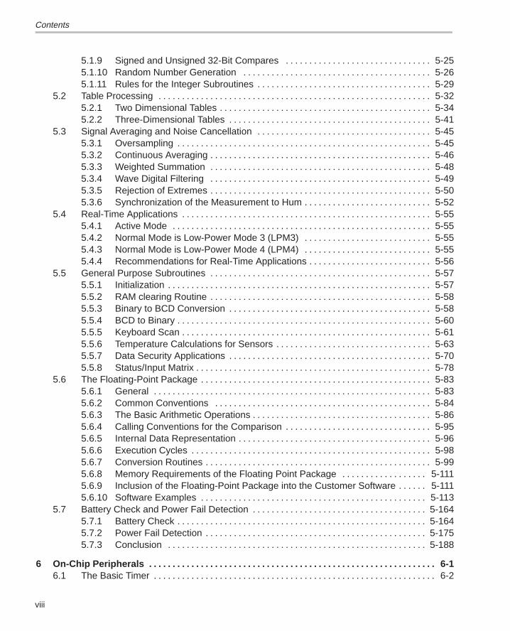
5.1.9 Signed and Unsigned 32-Bit Compares 5-25. . . . . . . . . . . . . . . . . . . . . . . . . . . . . . . 5.1.10 Random Number Generation 5-26. . . . . . . . . . . . . . . . . . . . . . . . . . . . . . . . . . . . . . . . 5.1.11 Rules for the Integer Subroutines 5-29. . . . . . . . . . . . . . . . . . . . . . . . . . . . . . . . . . . . .
5.2 Table Processing 5-32. . . . . . . . . . . . . . . . . . . . . . . . . . . . . . . . . . . . . . . . . . . . . . . . . . . . . . . . . . 5.2.1 Two Dimensional Tables 5-34. . . . . . . . . . . . . . . . . . . . . . . . . . . . . . . . . . . . . . . . . . . . . 5.2.2 Three-Dimensional Tables 5-41. . . . . . . . . . . . . . . . . . . . . . . . . . . . . . . . . . . . . . . . . . .
5.3 Signal Averaging and Noise Cancellation 5-45. . . . . . . . . . . . . . . . . . . . . . . . . . . . . . . . . . . . . 5.3.1 Oversampling 5-45. . . . . . . . . . . . . . . . . . . . . . . . . . . . . . . . . . . . . . . . . . . . . . . . . . . . . . 5.3.2 Continuous Averaging 5-46. . . . . . . . . . . . . . . . . . . . . . . . . . . . . . . . . . . . . . . . . . . . . . . 5.3.3 Weighted Summation 5-48. . . . . . . . . . . . . . . . . . . . . . . . . . . . . . . . . . . . . . . . . . . . . . . 5.3.4 Wave Digital Filtering 5-49. . . . . . . . . . . . . . . . . . . . . . . . . . . . . . . . . . . . . . . . . . . . . . . 5.3.5 Rejection of Extremes 5-50. . . . . . . . . . . . . . . . . . . . . . . . . . . . . . . . . . . . . . . . . . . . . . . 5.3.6 Synchronization of the Measurement to Hum 5-52. . . . . . . . . . . . . . . . . . . . . . . . . . .
5.4 Real-Time Applications 5-55. . . . . . . . . . . . . . . . . . . . . . . . . . . . . . . . . . . . . . . . . . . . . . . . . . . . . 5.4.1 Active Mode 5-55. . . . . . . . . . . . . . . . . . . . . . . . . . . . . . . . . . . . . . . . . . . . . . . . . . . . . . . 5.4.2 Normal Mode is Low-Power Mode 3 (LPM3) 5-55. . . . . . . . . . . . . . . . . . . . . . . . . . . 5.4.3 Normal Mode is Low-Power Mode 4 (LPM4) 5-55. . . . . . . . . . . . . . . . . . . . . . . . . . . 5.4.4 Recommendations for Real-Time Applications 5-56. . . . . . . . . . . . . . . . . . . . . . . . . .
5.5 General Purpose Subroutines 5-57. . . . . . . . . . . . . . . . . . . . . . . . . . . . . . . . . . . . . . . . . . . . . . . 5.5.1 Initialization 5-57. . . . . . . . . . . . . . . . . . . . . . . . . . . . . . . . . . . . . . . . . . . . . . . . . . . . . . . . 5.5.2 RAM clearing Routine 5-58. . . . . . . . . . . . . . . . . . . . . . . . . . . . . . . . . . . . . . . . . . . . . . . 5.5.3 Binary to BCD Conversion 5-58. . . . . . . . . . . . . . . . . . . . . . . . . . . . . . . . . . . . . . . . . . . 5.5.4 BCD to Binary 5-60. . . . . . . . . . . . . . . . . . . . . . . . . . . . . . . . . . . . . . . . . . . . . . . . . . . . . . 5.5.5 Keyboard Scan 5-61. . . . . . . . . . . . . . . . . . . . . . . . . . . . . . . . . . . . . . . . . . . . . . . . . . . . . 5.5.6 Temperature Calculations for Sensors 5-63. . . . . . . . . . . . . . . . . . . . . . . . . . . . . . . . . 5.5.7 Data Security Applications 5-70. . . . . . . . . . . . . . . . . . . . . . . . . . . . . . . . . . . . . . . . . . . 5.5.8 Status/Input Matrix 5-78. . . . . . . . . . . . . . . . . . . . . . . . . . . . . . . . . . . . . . . . . . . . . . . . . .
5.6 The Floating-Point Package 5-83. . . . . . . . . . . . . . . . . . . . . . . . . . . . . . . . . . . . . . . . . . . . . . . . . 5.6.1 General 5-83. . . . . . . . . . . . . . . . . . . . . . . . . . . . . . . . . . . . . . . . . . . . . . . . . . . . . . . . . . . 5.6.2 Common Conventions 5-84. . . . . . . . . . . . . . . . . . . . . . . . . . . . . . . . . . . . . . . . . . . . . . 5.6.3 The Basic Arithmetic Operations 5-86. . . . . . . . . . . . . . . . . . . . . . . . . . . . . . . . . . . . . . 5.6.4 Calling Conventions for the Comparison 5-95. . . . . . . . . . . . . . . . . . . . . . . . . . . . . . . 5.6.5 Internal Data Representation 5-96. . . . . . . . . . . . . . . . . . . . . . . . . . . . . . . . . . . . . . . . . 5.6.6 Execution Cycles 5-98. . . . . . . . . . . . . . . . . . . . . . . . . . . . . . . . . . . . . . . . . . . . . . . . . . . 5.6.7 Conversion Routines 5-99. . . . . . . . . . . . . . . . . . . . . . . . . . . . . . . . . . . . . . . . . . . . . . . . 5.6.8 Memory Requirements of the Floating Point Package 5-111. . . . . . . . . . . . . . . . . . 5.6.9 Inclusion of the Floating-Point Package into the Customer Software 5-111. . . . . . 5.6.10 Software Examples 5-113. . . . . . . . . . . . . . . . . . . . . . . . . . . . . . . . . . . . . . . . . . . . . . . .
5.7 Battery Check and Power Fail Detection 5-164. . . . . . . . . . . . . . . . . . . . . . . . . . . . . . . . . . . . . 5.7.1 Battery Check 5-164. . . . . . . . . . . . . . . . . . . . . . . . . . . . . . . . . . . . . . . . . . . . . . . . . . . . . 5.7.2 Power Fail Detection 5-175. . . . . . . . . . . . . . . . . . . . . . . . . . . . . . . . . . . . . . . . . . . . . . . 5.7.3 Conclusion 5-188. . . . . . . . . . . . . . . . . . . . . . . . . . . . . . . . . . . . . . . . . . . . . . . . . . . . . . .
6 On-Chip Peripherals 6-1. . . . . . . . . . . . . . . . . . . . . . . . . . . . . . . . . . . . . . . . . . . . . . . . . . . . . . . . . . . . . 6.1 The Basic Timer 6-2. . . . . . . . . . . . . . . . . . . . . . . . . . . . . . . . . . . . . . . . . . . . . . . . . . . . . . . . . . . .
Contents
ixContents
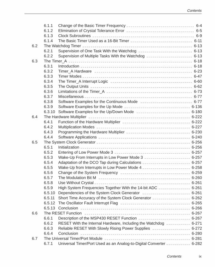
6.1.1 Change of the Basic Timer Frequency 6-4. . . . . . . . . . . . . . . . . . . . . . . . . . . . . . . . . . 6.1.2 Elimination of Crystal Tolerance Error 6-5. . . . . . . . . . . . . . . . . . . . . . . . . . . . . . . . . . 6.1.3 Clock Subroutines 6-9. . . . . . . . . . . . . . . . . . . . . . . . . . . . . . . . . . . . . . . . . . . . . . . . . . . 6.1.4 The Basic Timer Used as a 16-Bit Timer 6-11. . . . . . . . . . . . . . . . . . . . . . . . . . . . . . .
6.2 The Watchdog Timer 6-13. . . . . . . . . . . . . . . . . . . . . . . . . . . . . . . . . . . . . . . . . . . . . . . . . . . . . . . 6.2.1 Supervision of One Task With the Watchdog 6-13. . . . . . . . . . . . . . . . . . . . . . . . . . . 6.2.2 Supervision of Multiple Tasks With the Watchdog 6-13. . . . . . . . . . . . . . . . . . . . . . .
6.3 The Timer_A 6-18. . . . . . . . . . . . . . . . . . . . . . . . . . . . . . . . . . . . . . . . . . . . . . . . . . . . . . . . . . . . . . 6.3.1 Introduction 6-18. . . . . . . . . . . . . . . . . . . . . . . . . . . . . . . . . . . . . . . . . . . . . . . . . . . . . . . . 6.3.2 Timer_A Hardware 6-23. . . . . . . . . . . . . . . . . . . . . . . . . . . . . . . . . . . . . . . . . . . . . . . . . 6.3.3 Timer Modes 6-47. . . . . . . . . . . . . . . . . . . . . . . . . . . . . . . . . . . . . . . . . . . . . . . . . . . . . . . 6.3.4 The Timer_A Interrupt Logic 6-60. . . . . . . . . . . . . . . . . . . . . . . . . . . . . . . . . . . . . . . . . 6.3.5 The Output Units 6-62. . . . . . . . . . . . . . . . . . . . . . . . . . . . . . . . . . . . . . . . . . . . . . . . . . . 6.3.6 Limitations of the Timer_A 6-73. . . . . . . . . . . . . . . . . . . . . . . . . . . . . . . . . . . . . . . . . . . 6.3.7 Miscellaneous 6-77. . . . . . . . . . . . . . . . . . . . . . . . . . . . . . . . . . . . . . . . . . . . . . . . . . . . . . 6.3.8 Software Examples for the Continuous Mode 6-77. . . . . . . . . . . . . . . . . . . . . . . . . . 6.3.9 Software Examples for the Up Mode 6-136. . . . . . . . . . . . . . . . . . . . . . . . . . . . . . . . . 6.3.10 Software Examples for the Up/Down Mode 6-180. . . . . . . . . . . . . . . . . . . . . . . . . . .
6.4 The Hardware Multiplier 6-222. . . . . . . . . . . . . . . . . . . . . . . . . . . . . . . . . . . . . . . . . . . . . . . . . . . 6.4.1 Function of the Hardware Multiplier 6-222. . . . . . . . . . . . . . . . . . . . . . . . . . . . . . . . . . 6.4.2 Multiplication Modes 6-227. . . . . . . . . . . . . . . . . . . . . . . . . . . . . . . . . . . . . . . . . . . . . . . 6.4.3 Programming the Hardware Multiplier 6-230. . . . . . . . . . . . . . . . . . . . . . . . . . . . . . . . 6.4.4 Software Applications 6-240. . . . . . . . . . . . . . . . . . . . . . . . . . . . . . . . . . . . . . . . . . . . . .
6.5 The System Clock Generator 6-256. . . . . . . . . . . . . . . . . . . . . . . . . . . . . . . . . . . . . . . . . . . . . . . 6.5.1 Initialization 6-256. . . . . . . . . . . . . . . . . . . . . . . . . . . . . . . . . . . . . . . . . . . . . . . . . . . . . . . 6.5.2 Entering of Low Power Mode 3 6-257. . . . . . . . . . . . . . . . . . . . . . . . . . . . . . . . . . . . . . 6.5.3 Wake-Up From Interrupts in Low Power Mode 3 6-257. . . . . . . . . . . . . . . . . . . . . . . 6.5.4 Adaptation of the DCO Tap during Calculations 6-257. . . . . . . . . . . . . . . . . . . . . . . . 6.5.5 Wake-Up from Interrupts in Low Power Mode 4 6-258. . . . . . . . . . . . . . . . . . . . . . . . 6.5.6 Change of the System Frequency 6-259. . . . . . . . . . . . . . . . . . . . . . . . . . . . . . . . . . . 6.5.7 The Modulation Bit M 6-260. . . . . . . . . . . . . . . . . . . . . . . . . . . . . . . . . . . . . . . . . . . . . . 6.5.8 Use Without Crystal 6-261. . . . . . . . . . . . . . . . . . . . . . . . . . . . . . . . . . . . . . . . . . . . . . . . 6.5.9 High System Frequencies Together With the 14-bit ADC 6-261. . . . . . . . . . . . . . . . 6.5.10 Dependencies of the System Clock Generator 6-261. . . . . . . . . . . . . . . . . . . . . . . . 6.5.11 Short Time Accuracy of the System Clock Generator 6-262. . . . . . . . . . . . . . . . . . . 6.5.12 The Oscillator Fault Interrupt Flag 6-265. . . . . . . . . . . . . . . . . . . . . . . . . . . . . . . . . . . 6.5.13 Conclusion 6-266. . . . . . . . . . . . . . . . . . . . . . . . . . . . . . . . . . . . . . . . . . . . . . . . . . . . . . .
6.6 The RESET Function 6-267. . . . . . . . . . . . . . . . . . . . . . . . . . . . . . . . . . . . . . . . . . . . . . . . . . . . . 6.6.1 Description of the MSP430 RESET Function 6-267. . . . . . . . . . . . . . . . . . . . . . . . . . 6.6.2 RESET With the Internal Hardware, Including the Watchdog 6-271. . . . . . . . . . . . 6.6.3 Reliable RESET With Slowly Rising Power Supplies 6-272. . . . . . . . . . . . . . . . . . . 6.6.4 Conclusion 6-280. . . . . . . . . . . . . . . . . . . . . . . . . . . . . . . . . . . . . . . . . . . . . . . . . . . . . . .
6.7 The Universal Timer/Port Module 6-281. . . . . . . . . . . . . . . . . . . . . . . . . . . . . . . . . . . . . . . . . . . 6.7.1 Universal Timer/Port Used as an Analog-to-Digital Converter 6-282. . . . . . . . . . . .
Contents
x
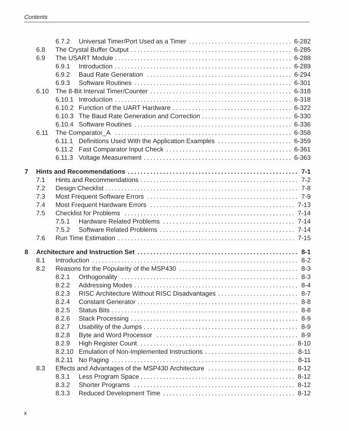
6.7.2 Universal Timer/Port Used as a Timer 6-282. . . . . . . . . . . . . . . . . . . . . . . . . . . . . . . . 6.8 The Crystal Buffer Output 6-285. . . . . . . . . . . . . . . . . . . . . . . . . . . . . . . . . . . . . . . . . . . . . . . . . . 6.9 The USART Module 6-288. . . . . . . . . . . . . . . . . . . . . . . . . . . . . . . . . . . . . . . . . . . . . . . . . . . . . . .
6.9.1 Introduction 6-289. . . . . . . . . . . . . . . . . . . . . . . . . . . . . . . . . . . . . . . . . . . . . . . . . . . . . . . 6.9.2 Baud Rate Generation 6-294. . . . . . . . . . . . . . . . . . . . . . . . . . . . . . . . . . . . . . . . . . . . . 6.9.3 Software Routines 6-301. . . . . . . . . . . . . . . . . . . . . . . . . . . . . . . . . . . . . . . . . . . . . . . . .
6.10 The 8-Bit Interval Timer/Counter 6-318. . . . . . . . . . . . . . . . . . . . . . . . . . . . . . . . . . . . . . . . . . . . 6.10.1 Introduction 6-318. . . . . . . . . . . . . . . . . . . . . . . . . . . . . . . . . . . . . . . . . . . . . . . . . . . . . . . 6.10.2 Function of the UART Hardware 6-322. . . . . . . . . . . . . . . . . . . . . . . . . . . . . . . . . . . . . 6.10.3 The Baud Rate Generation and Correction 6-330. . . . . . . . . . . . . . . . . . . . . . . . . . . . 6.10.4 Software Routines 6-336. . . . . . . . . . . . . . . . . . . . . . . . . . . . . . . . . . . . . . . . . . . . . . . . .
6.11 The Comparator_A 6-358. . . . . . . . . . . . . . . . . . . . . . . . . . . . . . . . . . . . . . . . . . . . . . . . . . . . . . . 6.11.1 Definitions Used With the Application Examples 6-359. . . . . . . . . . . . . . . . . . . . . . . 6.11.2 Fast Comparator Input Check 6-361. . . . . . . . . . . . . . . . . . . . . . . . . . . . . . . . . . . . . . . 6.11.3 Voltage Measurement 6-363. . . . . . . . . . . . . . . . . . . . . . . . . . . . . . . . . . . . . . . . . . . . . .
7 Hints and Recommendations 7-1. . . . . . . . . . . . . . . . . . . . . . . . . . . . . . . . . . . . . . . . . . . . . . . . . . . . . 7.1 Hints and Recommendations 7-2. . . . . . . . . . . . . . . . . . . . . . . . . . . . . . . . . . . . . . . . . . . . . . . . . 7.2 Design Checklist 7-8. . . . . . . . . . . . . . . . . . . . . . . . . . . . . . . . . . . . . . . . . . . . . . . . . . . . . . . . . . . . 7.3 Most Frequent Software Errors 7-9. . . . . . . . . . . . . . . . . . . . . . . . . . . . . . . . . . . . . . . . . . . . . . . 7.4 Most Frequent Hardware Errors 7-13. . . . . . . . . . . . . . . . . . . . . . . . . . . . . . . . . . . . . . . . . . . . . 7.5 Checklist for Problems 7-14. . . . . . . . . . . . . . . . . . . . . . . . . . . . . . . . . . . . . . . . . . . . . . . . . . . . .
7.5.1 Hardware Related Problems 7-14. . . . . . . . . . . . . . . . . . . . . . . . . . . . . . . . . . . . . . . . . 7.5.2 Software Related Problems 7-14. . . . . . . . . . . . . . . . . . . . . . . . . . . . . . . . . . . . . . . . . .
7.6 Run Time Estimation 7-15. . . . . . . . . . . . . . . . . . . . . . . . . . . . . . . . . . . . . . . . . . . . . . . . . . . . . . .
8 Architecture and Instruction Set 8-1. . . . . . . . . . . . . . . . . . . . . . . . . . . . . . . . . . . . . . . . . . . . . . . . . . 8.1 Introduction 8-2. . . . . . . . . . . . . . . . . . . . . . . . . . . . . . . . . . . . . . . . . . . . . . . . . . . . . . . . . . . . . . . . 8.2 Reasons for the Popularity of the MSP430 8-3. . . . . . . . . . . . . . . . . . . . . . . . . . . . . . . . . . . . .
8.2.1 Orthogonality 8-3. . . . . . . . . . . . . . . . . . . . . . . . . . . . . . . . . . . . . . . . . . . . . . . . . . . . . . . 8.2.2 Addressing Modes 8-4. . . . . . . . . . . . . . . . . . . . . . . . . . . . . . . . . . . . . . . . . . . . . . . . . . . 8.2.3 RISC Architecture Without RISC Disadvantages 8-7. . . . . . . . . . . . . . . . . . . . . . . . . 8.2.4 Constant Generator 8-8. . . . . . . . . . . . . . . . . . . . . . . . . . . . . . . . . . . . . . . . . . . . . . . . . . 8.2.5 Status Bits 8-8. . . . . . . . . . . . . . . . . . . . . . . . . . . . . . . . . . . . . . . . . . . . . . . . . . . . . . . . . . 8.2.6 Stack Processing 8-9. . . . . . . . . . . . . . . . . . . . . . . . . . . . . . . . . . . . . . . . . . . . . . . . . . . . 8.2.7 Usability of the Jumps 8-9. . . . . . . . . . . . . . . . . . . . . . . . . . . . . . . . . . . . . . . . . . . . . . . . 8.2.8 Byte and Word Processor 8-9. . . . . . . . . . . . . . . . . . . . . . . . . . . . . . . . . . . . . . . . . . . . 8.2.9 High Register Count 8-10. . . . . . . . . . . . . . . . . . . . . . . . . . . . . . . . . . . . . . . . . . . . . . . . 8.2.10 Emulation of Non-Implemented Instructions 8-11. . . . . . . . . . . . . . . . . . . . . . . . . . . . 8.2.11 No Paging 8-11. . . . . . . . . . . . . . . . . . . . . . . . . . . . . . . . . . . . . . . . . . . . . . . . . . . . . . . . .
8.3 Effects and Advantages of the MSP430 Architecture 8-12. . . . . . . . . . . . . . . . . . . . . . . . . . . 8.3.1 Less Program Space 8-12. . . . . . . . . . . . . . . . . . . . . . . . . . . . . . . . . . . . . . . . . . . . . . . . 8.3.2 Shorter Programs 8-12. . . . . . . . . . . . . . . . . . . . . . . . . . . . . . . . . . . . . . . . . . . . . . . . . . 8.3.3 Reduced Development Time 8-12. . . . . . . . . . . . . . . . . . . . . . . . . . . . . . . . . . . . . . . . .
Contents
xiContents
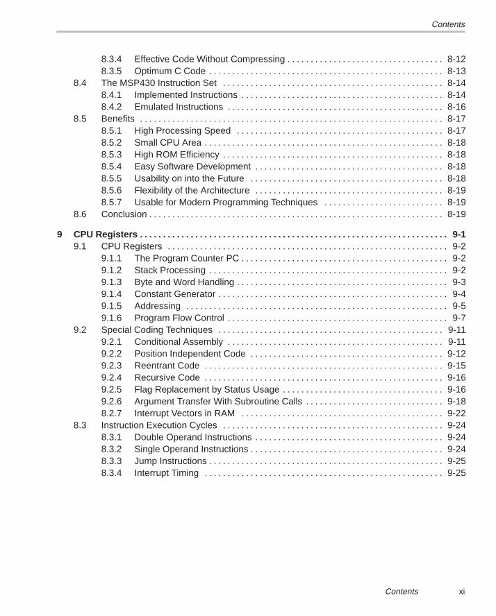
8.3.4 Effective Code Without Compressing 8-12. . . . . . . . . . . . . . . . . . . . . . . . . . . . . . . . . . 8.3.5 Optimum C Code 8-13. . . . . . . . . . . . . . . . . . . . . . . . . . . . . . . . . . . . . . . . . . . . . . . . . . .
8.4 The MSP430 Instruction Set 8-14. . . . . . . . . . . . . . . . . . . . . . . . . . . . . . . . . . . . . . . . . . . . . . . . 8.4.1 Implemented Instructions 8-14. . . . . . . . . . . . . . . . . . . . . . . . . . . . . . . . . . . . . . . . . . . . 8.4.2 Emulated Instructions 8-16. . . . . . . . . . . . . . . . . . . . . . . . . . . . . . . . . . . . . . . . . . . . . . .
8.5 Benefits 8-17. . . . . . . . . . . . . . . . . . . . . . . . . . . . . . . . . . . . . . . . . . . . . . . . . . . . . . . . . . . . . . . . . . 8.5.1 High Processing Speed 8-17. . . . . . . . . . . . . . . . . . . . . . . . . . . . . . . . . . . . . . . . . . . . . 8.5.2 Small CPU Area 8-18. . . . . . . . . . . . . . . . . . . . . . . . . . . . . . . . . . . . . . . . . . . . . . . . . . . . 8.5.3 High ROM Efficiency 8-18. . . . . . . . . . . . . . . . . . . . . . . . . . . . . . . . . . . . . . . . . . . . . . . . 8.5.4 Easy Software Development 8-18. . . . . . . . . . . . . . . . . . . . . . . . . . . . . . . . . . . . . . . . . 8.5.5 Usability on into the Future 8-18. . . . . . . . . . . . . . . . . . . . . . . . . . . . . . . . . . . . . . . . . . 8.5.6 Flexibility of the Architecture 8-19. . . . . . . . . . . . . . . . . . . . . . . . . . . . . . . . . . . . . . . . . 8.5.7 Usable for Modern Programming Techniques 8-19. . . . . . . . . . . . . . . . . . . . . . . . . .
8.6 Conclusion 8-19. . . . . . . . . . . . . . . . . . . . . . . . . . . . . . . . . . . . . . . . . . . . . . . . . . . . . . . . . . . . . . . .
9 CPU Registers 9-1. . . . . . . . . . . . . . . . . . . . . . . . . . . . . . . . . . . . . . . . . . . . . . . . . . . . . . . . . . . . . . . . . . . 9.1 CPU Registers 9-2. . . . . . . . . . . . . . . . . . . . . . . . . . . . . . . . . . . . . . . . . . . . . . . . . . . . . . . . . . . . .
9.1.1 The Program Counter PC 9-2. . . . . . . . . . . . . . . . . . . . . . . . . . . . . . . . . . . . . . . . . . . . . 9.1.2 Stack Processing 9-2. . . . . . . . . . . . . . . . . . . . . . . . . . . . . . . . . . . . . . . . . . . . . . . . . . . . 9.1.3 Byte and Word Handling 9-3. . . . . . . . . . . . . . . . . . . . . . . . . . . . . . . . . . . . . . . . . . . . . . 9.1.4 Constant Generator 9-4. . . . . . . . . . . . . . . . . . . . . . . . . . . . . . . . . . . . . . . . . . . . . . . . . . 9.1.5 Addressing 9-5. . . . . . . . . . . . . . . . . . . . . . . . . . . . . . . . . . . . . . . . . . . . . . . . . . . . . . . . . 9.1.6 Program Flow Control 9-7. . . . . . . . . . . . . . . . . . . . . . . . . . . . . . . . . . . . . . . . . . . . . . . .
9.2 Special Coding Techniques 9-11. . . . . . . . . . . . . . . . . . . . . . . . . . . . . . . . . . . . . . . . . . . . . . . . . 9.2.1 Conditional Assembly 9-11. . . . . . . . . . . . . . . . . . . . . . . . . . . . . . . . . . . . . . . . . . . . . . . 9.2.2 Position Independent Code 9-12. . . . . . . . . . . . . . . . . . . . . . . . . . . . . . . . . . . . . . . . . . 9.2.3 Reentrant Code 9-15. . . . . . . . . . . . . . . . . . . . . . . . . . . . . . . . . . . . . . . . . . . . . . . . . . . . 9.2.4 Recursive Code 9-16. . . . . . . . . . . . . . . . . . . . . . . . . . . . . . . . . . . . . . . . . . . . . . . . . . . . 9.2.5 Flag Replacement by Status Usage 9-16. . . . . . . . . . . . . . . . . . . . . . . . . . . . . . . . . . . 9.2.6 Argument Transfer With Subroutine Calls 9-18. . . . . . . . . . . . . . . . . . . . . . . . . . . . . . 8.2.7 Interrupt Vectors in RAM 9-22. . . . . . . . . . . . . . . . . . . . . . . . . . . . . . . . . . . . . . . . . . . .
8.3 Instruction Execution Cycles 9-24. . . . . . . . . . . . . . . . . . . . . . . . . . . . . . . . . . . . . . . . . . . . . . . . 8.3.1 Double Operand Instructions 9-24. . . . . . . . . . . . . . . . . . . . . . . . . . . . . . . . . . . . . . . . . 8.3.2 Single Operand Instructions 9-24. . . . . . . . . . . . . . . . . . . . . . . . . . . . . . . . . . . . . . . . . . 8.3.3 Jump Instructions 9-25. . . . . . . . . . . . . . . . . . . . . . . . . . . . . . . . . . . . . . . . . . . . . . . . . . . 8.3.4 Interrupt Timing 9-25. . . . . . . . . . . . . . . . . . . . . . . . . . . . . . . . . . . . . . . . . . . . . . . . . . . .
Figures
xii
Figures
1–1 MSP430C31x Block Diagram 1-5. . . . . . . . . . . . . . . . . . . . . . . . . . . . . . . . . . . . . . . . . . . . . . . . . . . 1–2 MSP430C32x Block Diagram 1-6. . . . . . . . . . . . . . . . . . . . . . . . . . . . . . . . . . . . . . . . . . . . . . . . . . . 1–3 MSP430C33x Block Diagram 1-7. . . . . . . . . . . . . . . . . . . . . . . . . . . . . . . . . . . . . . . . . . . . . . . . . . .
3–1 MSP430 Input for Zero-Crossing 3-6. . . . . . . . . . . . . . . . . . . . . . . . . . . . . . . . . . . . . . . . . . . . . . . . 3–2 Timing for the Zero Crossing 3-7. . . . . . . . . . . . . . . . . . . . . . . . . . . . . . . . . . . . . . . . . . . . . . . . . . . 3–3 Output Buffering 3-9. . . . . . . . . . . . . . . . . . . . . . . . . . . . . . . . . . . . . . . . . . . . . . . . . . . . . . . . . . . . . . 3–4 The I/O Section of the Universal Timer/Port Module 3-10. . . . . . . . . . . . . . . . . . . . . . . . . . . . . . 3–5 Connections for Fast Serial Transfer 3-13. . . . . . . . . . . . . . . . . . . . . . . . . . . . . . . . . . . . . . . . . . . . 3–6 External EPROM Connections 3-15. . . . . . . . . . . . . . . . . . . . . . . . . . . . . . . . . . . . . . . . . . . . . . . . . 3–7 TSS721 Connections to the MSP430 3-17. . . . . . . . . . . . . . . . . . . . . . . . . . . . . . . . . . . . . . . . . . . 3–8 I2C Bus Connections 3-18. . . . . . . . . . . . . . . . . . . . . . . . . . . . . . . . . . . . . . . . . . . . . . . . . . . . . . . . . 3–9 Unused ADC Inputs Used as Outputs 3-27. . . . . . . . . . . . . . . . . . . . . . . . . . . . . . . . . . . . . . . . . . . 3–10 R/2R Method for Digital-to-Analog Conversion 3-31. . . . . . . . . . . . . . . . . . . . . . . . . . . . . . . . . . . 3–11 Weighted Resistors Method for Digital-to-Analog Conversion 3-32. . . . . . . . . . . . . . . . . . . . . . 3–12 I2C-Bus for Digital-to-Analog Converter Connection 3-33. . . . . . . . . . . . . . . . . . . . . . . . . . . . . . 3–13 PWM for the DAC 3-34. . . . . . . . . . . . . . . . . . . . . . . . . . . . . . . . . . . . . . . . . . . . . . . . . . . . . . . . . . . . 3–14 PWM Timing by the Universal Timer/Port Module and Basic Timer 3-35. . . . . . . . . . . . . . . . . . 3–15 PWM for DAC 3-39. . . . . . . . . . . . . . . . . . . . . . . . . . . . . . . . . . . . . . . . . . . . . . . . . . . . . . . . . . . . . . . 3–16 PWM Timing by Universal Timer/Port Module and Basic Timer 3-40. . . . . . . . . . . . . . . . . . . . . 3–17 PWM Generation With Continuous Mode 3-43. . . . . . . . . . . . . . . . . . . . . . . . . . . . . . . . . . . . . . . . 3–18 PWM Generation With Up Mode 3-44. . . . . . . . . . . . . . . . . . . . . . . . . . . . . . . . . . . . . . . . . . . . . . . 3–19 PWM Generation With Up-Down Mode 3-45. . . . . . . . . . . . . . . . . . . . . . . . . . . . . . . . . . . . . . . . . 3–20 External Memory Control With MSP430 Ports 3-46. . . . . . . . . . . . . . . . . . . . . . . . . . . . . . . . . . . . 3–21 External Memory Control With Shift Registers 3-47. . . . . . . . . . . . . . . . . . . . . . . . . . . . . . . . . . . . 3–22 EEPROM Control With Direct Addressing by I/O Ports 3-48. . . . . . . . . . . . . . . . . . . . . . . . . . . . 3–23 Addressing of 1-MB RAM With the MSP430C33x 3-49. . . . . . . . . . . . . . . . . . . . . . . . . . . . . . . . 3–24 Addressing of 1-MB RAM With the MSP430C31x 3-51. . . . . . . . . . . . . . . . . . . . . . . . . . . . . . . . 3–25 Battery-Power MSP430C32x System 3-53. . . . . . . . . . . . . . . . . . . . . . . . . . . . . . . . . . . . . . . . . . . 3–26 Battery-Power MSP430C31x System 3-54. . . . . . . . . . . . . . . . . . . . . . . . . . . . . . . . . . . . . . . . . . . 3–27 Accumulator-Driven MSP430 System With Battery Management 3-56. . . . . . . . . . . . . . . . . . . 3–28 Voltages and Timing for the Half-Wave Rectification 3-57. . . . . . . . . . . . . . . . . . . . . . . . . . . . . . 3–29 Half-Wave Rectification With 1 Voltage and a Zener Diode 3-59. . . . . . . . . . . . . . . . . . . . . . . . 3–30 Half-Wave Rectification With One Voltage and a Voltage Regulator 3-60. . . . . . . . . . . . . . . . . 3–31 Half-Wave Rectification With Two Voltages and Two Voltage Regulators 3-61. . . . . . . . . . . . 3–32 Voltages and Timing for Full-Wave Rectification 3-61. . . . . . . . . . . . . . . . . . . . . . . . . . . . . . . . . . 3–33 Full Wave Rectification for one Voltage With a Voltage Regulator 3-62. . . . . . . . . . . . . . . . . . .
Figures
xiiiContents
3–34 Full-Wave Rectification for Two Voltages With Voltage Regulators 3-63. . . . . . . . . . . . . . . . . . 3–35 Simple Capacitor Power Supply for a Single Voltage 3-65. . . . . . . . . . . . . . . . . . . . . . . . . . . . . . 3–36 Capacitor Power Supply for a Single Voltage 3-66. . . . . . . . . . . . . . . . . . . . . . . . . . . . . . . . . . . . 3–37 Split Capacitor Power Supply for Two Voltages 3-66. . . . . . . . . . . . . . . . . . . . . . . . . . . . . . . . . . . 3–38 Split Capacitor Power Supply for Two Voltages With Discrete Components 3-67. . . . . . . . . . 3–39 Simple Power Supply from Other DC Voltages 3-69. . . . . . . . . . . . . . . . . . . . . . . . . . . . . . . . . . . 3–40 Power Supply from other DC Voltages With a Voltage Regulator 3-70. . . . . . . . . . . . . . . . . . . 3–41 Supply from the M Bus 3-72. . . . . . . . . . . . . . . . . . . . . . . . . . . . . . . . . . . . . . . . . . . . . . . . . . . . . . . . 3–42 Supply via Fiber-Optic Cable 3-75. . . . . . . . . . . . . . . . . . . . . . . . . . . . . . . . . . . . . . . . . . . . . . . . . .
4–1 Two Measurement Methods for Electronic Electricity Meters 4-2. . . . . . . . . . . . . . . . . . . . . . . . 4–2 Timing for the Reduced Scan Principle (Single Phase) 4-3. . . . . . . . . . . . . . . . . . . . . . . . . . . . . 4–3 Reduced Scan Measurement Principle 4-4. . . . . . . . . . . . . . . . . . . . . . . . . . . . . . . . . . . . . . . . . . . 4–4 Allocation of the ADC Range 4-11. . . . . . . . . . . . . . . . . . . . . . . . . . . . . . . . . . . . . . . . . . . . . . . . . . 4–5 Explanation of ADC Deviation (2nd Column of Table 4–5) 4-12. . . . . . . . . . . . . . . . . . . . . . . . . 4–6 Use of the Actual ADC Characteristic for Corrections (8 Subranges Used) 4-16. . . . . . . . . . . 4–7 MSP430 14-Bit ADC Grounding 4-19. . . . . . . . . . . . . . . . . . . . . . . . . . . . . . . . . . . . . . . . . . . . . . . . 4–8 Split Power Supply for Level Shifting 4-21. . . . . . . . . . . . . . . . . . . . . . . . . . . . . . . . . . . . . . . . . . . . 4–9 Virtual Ground IC for Level Shifting 4-22. . . . . . . . . . . . . . . . . . . . . . . . . . . . . . . . . . . . . . . . . . . . . 4–10 Resistor Interface Without Current Source 4-23. . . . . . . . . . . . . . . . . . . . . . . . . . . . . . . . . . . . . . . 4–11 Resistor Interface With Current Source 4-24. . . . . . . . . . . . . . . . . . . . . . . . . . . . . . . . . . . . . . . . . 4–12 Current Measurement 4-26. . . . . . . . . . . . . . . . . . . . . . . . . . . . . . . . . . . . . . . . . . . . . . . . . . . . . . . . 4–13 Current Measurement With a Ferrite Core 4-28. . . . . . . . . . . . . . . . . . . . . . . . . . . . . . . . . . . . . . . 4–14 Voltage Measurement 4-29. . . . . . . . . . . . . . . . . . . . . . . . . . . . . . . . . . . . . . . . . . . . . . . . . . . . . . . . 4–15 Single-Phase Electricity Meter With Shunt Resistor 4-32. . . . . . . . . . . . . . . . . . . . . . . . . . . . . . . 4–16 Single-Phase Electricity Meter With Current Transformer and RF Readout 4-33. . . . . . . . . . . 4–17 Timing for the Reduced Scan Principle (Dual-Phase Meter) 4-35. . . . . . . . . . . . . . . . . . . . . . . . 4–18 Dual-Phase Electricity Meter With Current Transformers and Virtual Ground 4-36. . . . . . . . . 4–19 Dual-Phase Electricity Meter With Current Transformers and Software Offset 4-38. . . . . . . . . 4–20 Normal Timing for the Reduced Scan Principle (Three-Phase Meters) 4-40. . . . . . . . . . . . . . . 4–21 Evenly Spaced Timing for the Reduced Scan Principle (Three-Phase Meters) 4-40. . . . . . . . 4–22 Three-Phase Electricity Meter With Ferrite Cores and Software Offset 4-42. . . . . . . . . . . . . . 4–23 Electricity Meter With Current Transformers and Split Power Supply 4-44. . . . . . . . . . . . . . . . 4–24 Timing for the Reduced Scan Principle 4-46. . . . . . . . . . . . . . . . . . . . . . . . . . . . . . . . . . . . . . . . . . 4–25 Electricity Meter With an External 16-Bit ADC 4-57. . . . . . . . . . . . . . . . . . . . . . . . . . . . . . . . . . . . 4–26 Allocation of the ADC Range 4-62. . . . . . . . . . . . . . . . . . . . . . . . . . . . . . . . . . . . . . . . . . . . . . . . . . 4–27 Explanation of the ADC Deviation 4-63. . . . . . . . . . . . . . . . . . . . . . . . . . . . . . . . . . . . . . . . . . . . . . 4–28 Gas Meter With MSP430C32x 4-65. . . . . . . . . . . . . . . . . . . . . . . . . . . . . . . . . . . . . . . . . . . . . . . . . 4–29 Gas Meter With MSP430C31x 4-66. . . . . . . . . . . . . . . . . . . . . . . . . . . . . . . . . . . . . . . . . . . . . . . . . 4–30 MSP430C336 Gas Meter 4-67. . . . . . . . . . . . . . . . . . . . . . . . . . . . . . . . . . . . . . . . . . . . . . . . . . . . . 4–31 Electronic Water Flow Meter 4-69. . . . . . . . . . . . . . . . . . . . . . . . . . . . . . . . . . . . . . . . . . . . . . . . . . . 4–32 Electronic Heat Allocation Meter With MSP430C32x 4-70. . . . . . . . . . . . . . . . . . . . . . . . . . . . . . 4–33 Electronic Heat Allocation Meter With MSP430C31x 4-71. . . . . . . . . . . . . . . . . . . . . . . . . . . . . . 4–34 Heat Volume Counter MSP430C32x 4-72. . . . . . . . . . . . . . . . . . . . . . . . . . . . . . . . . . . . . . . . . . . .
Figures
xiv
4–35 Heat Volume Counter With 4-Wire-Circuitry MSP430C32x 4-73. . . . . . . . . . . . . . . . . . . . . . . . . 4–36 Heat Volume Counter With 16 Bits Resolution MSP430C32x 4-74. . . . . . . . . . . . . . . . . . . . . . . 4–37 Battery Charge Meter MSP430C32x 4-76. . . . . . . . . . . . . . . . . . . . . . . . . . . . . . . . . . . . . . . . . . . . 4–38 Resistive Sensors Connected to MSP430C32x 4-77. . . . . . . . . . . . . . . . . . . . . . . . . . . . . . . . . . 4–39 Measurement With Reference Resistors 4-79. . . . . . . . . . . . . . . . . . . . . . . . . . . . . . . . . . . . . . . . 4–40 Connection of Bridge Assemblies 4-79. . . . . . . . . . . . . . . . . . . . . . . . . . . . . . . . . . . . . . . . . . . . . . 4–41 Simplified ADC Characteristic 4-81. . . . . . . . . . . . . . . . . . . . . . . . . . . . . . . . . . . . . . . . . . . . . . . . . . 4–42 Fixing of Bridge Assemblies Into One ADC Range 4-82. . . . . . . . . . . . . . . . . . . . . . . . . . . . . . . . 4–43 Gas Sensor Connection to the MSP430C32x 4-83. . . . . . . . . . . . . . . . . . . . . . . . . . . . . . . . . . . . 4–44 Connection of Digital Sensors (Thermometer) 4-84. . . . . . . . . . . . . . . . . . . . . . . . . . . . . . . . . . . 4–45 Connection of Sensors With Frequency Output Respective Time Output 4-85. . . . . . . . . . . . 4–46 Revolution Counter With a Digital Hall Sensor 4-86. . . . . . . . . . . . . . . . . . . . . . . . . . . . . . . . . . . 4–47 Measurement of the Magnetic Flux With an Analog Hall Sensor 4-86. . . . . . . . . . . . . . . . . . . . 4–48 MSP430C32x EE Meter With RF Readout 4-88. . . . . . . . . . . . . . . . . . . . . . . . . . . . . . . . . . . . . . . 4–49 MSP430 EE Meter With RF Readout 4-89. . . . . . . . . . . . . . . . . . . . . . . . . . . . . . . . . . . . . . . . . . . 4–50 MSP430 With a Ferraris-Wheel Meter and RF Readout 4-90. . . . . . . . . . . . . . . . . . . . . . . . . . . 4–51 RF-Interface Module 4-91. . . . . . . . . . . . . . . . . . . . . . . . . . . . . . . . . . . . . . . . . . . . . . . . . . . . . . . . . . 4–52 RF-Modulation Modes 4-92. . . . . . . . . . . . . . . . . . . . . . . . . . . . . . . . . . . . . . . . . . . . . . . . . . . . . . . . 4–53 M-BUS Long Frame Format 4-93. . . . . . . . . . . . . . . . . . . . . . . . . . . . . . . . . . . . . . . . . . . . . . . . . . . 4–54 Sequence of Data Transmission 4-93. . . . . . . . . . . . . . . . . . . . . . . . . . . . . . . . . . . . . . . . . . . . . . . 4–55 Conventional Solution for a Battery-Driven System 4-95. . . . . . . . . . . . . . . . . . . . . . . . . . . . . . . 4–56 Solution With MSP430 for a Battery-Driven System 4-95. . . . . . . . . . . . . . . . . . . . . . . . . . . . . . . 4–57 Approximated Characteristics for the Low Power-Supply Currents 4-96. . . . . . . . . . . . . . . . . . 4–58 Current Consumption Characteristic 4-97. . . . . . . . . . . . . . . . . . . . . . . . . . . . . . . . . . . . . . . . . . . . 4–59 Connection of Keys to Inputs 4-100. . . . . . . . . . . . . . . . . . . . . . . . . . . . . . . . . . . . . . . . . . . . . . . . . 4–60 Turnoff of External Circuits 4-101. . . . . . . . . . . . . . . . . . . . . . . . . . . . . . . . . . . . . . . . . . . . . . . . . . . 4–61 Intelligent Heating Installation Control With the MSP430 4-106. . . . . . . . . . . . . . . . . . . . . . . . . . 4–62 Heating Installation Controller for a Single-Family Home 4-107. . . . . . . . . . . . . . . . . . . . . . . . . 4–63 Simple Battery Driven Scale 4-108. . . . . . . . . . . . . . . . . . . . . . . . . . . . . . . . . . . . . . . . . . . . . . . . . . 4–64 Remote Control Transmitter for Security Applications 4-109. . . . . . . . . . . . . . . . . . . . . . . . . . . . 4–65 Remote Control Transmitter for Audio/Video 4-110. . . . . . . . . . . . . . . . . . . . . . . . . . . . . . . . . . . . 4–66 Remote Control Receiver With the MSP430 4-110. . . . . . . . . . . . . . . . . . . . . . . . . . . . . . . . . . . . 4–67 MSP430 in a TV Set 4-111. . . . . . . . . . . . . . . . . . . . . . . . . . . . . . . . . . . . . . . . . . . . . . . . . . . . . . . . . 4–68 MSP430 in an AC-Powered Personal Computer 4-112. . . . . . . . . . . . . . . . . . . . . . . . . . . . . . . . . 4–69 MSP430 in a Battery-Powered Personal Computer With Battery Management 4-113. . . . . . 4–70 MSP430-Controlled FAX Device 4-114. . . . . . . . . . . . . . . . . . . . . . . . . . . . . . . . . . . . . . . . . . . . . . 4–71 Block Diagram of the UTPM (16-Bit Timer Mode) 4-118. . . . . . . . . . . . . . . . . . . . . . . . . . . . . . . . 4–72 Low-Frequency PWM-Timing Generated With the Universal Timer/Port Module 4-118. . . . . 4–73 Low Frequency PWM Timing by Universal Timer/Port Module and Basic Timer 4-119. . . . . . 4–74 Transistor Output Stage Allowing Both Directions of Rotation 4-121. . . . . . . . . . . . . . . . . . . . . 4–75 Control for Two MOSFET Output Stages 4-122. . . . . . . . . . . . . . . . . . . . . . . . . . . . . . . . . . . . . . . 4–76 PWM Motor Control With a MOSFET H-Bridge 4-125. . . . . . . . . . . . . . . . . . . . . . . . . . . . . . . . . . 4–77 PWM Motor Control for Brushless DC Motor 4-127. . . . . . . . . . . . . . . . . . . . . . . . . . . . . . . . . . . . 4–78 Integrated PWM Motor Control With Static Rotation Direction 4-128. . . . . . . . . . . . . . . . . . . . .
Figures
xvContents
4–79 Integrated PWM Motor Control With Dynamic Rotation Direction 4-129. . . . . . . . . . . . . . . . . . 4–80 PWM Motors Control for High Motor Voltages 4-131. . . . . . . . . . . . . . . . . . . . . . . . . . . . . . . . . . . 4–81 PWM Outputs for Different Phase Voltages 4-134. . . . . . . . . . . . . . . . . . . . . . . . . . . . . . . . . . . . . 4–82 PWM Motors Control for High Motor Voltages 4-135. . . . . . . . . . . . . . . . . . . . . . . . . . . . . . . . . . . 4–83 Minimum System and Maximum System Using the MSP430 Family 4-137. . . . . . . . . . . . . . . 4–84 TRIAC Control for AC Motors and DC Motors 4-139. . . . . . . . . . . . . . . . . . . . . . . . . . . . . . . . . . . 4–85 Positive and Negative TRIAC Gate Control 4-140. . . . . . . . . . . . . . . . . . . . . . . . . . . . . . . . . . . . . 4–86 Static and Dynamic TRIAC Gate Control 4-141. . . . . . . . . . . . . . . . . . . . . . . . . . . . . . . . . . . . . . . 4–87 Nonregulated Voltage for the TRIAC Control 4-143. . . . . . . . . . . . . . . . . . . . . . . . . . . . . . . . . . . . 4–88 Minimum System and Maximum System With the MSP430 Family 4-145. . . . . . . . . . . . . . . . 4–89 Overcurrent Detection With Single and Multiple Thresholds 4-147. . . . . . . . . . . . . . . . . . . . . . . 4–90 Motor Voltage Measurement and Current Measurement 4-148. . . . . . . . . . . . . . . . . . . . . . . . . . 4–91 Support Functions for the TRIAC Control 4-149. . . . . . . . . . . . . . . . . . . . . . . . . . . . . . . . . . . . . . . 4–92 Change of the Direction of Rotation for a Universal Motor 4-150. . . . . . . . . . . . . . . . . . . . . . . .
5–1 16 x 16 Bit Multiplication – Register Use 5-3. . . . . . . . . . . . . . . . . . . . . . . . . . . . . . . . . . . . . . . . . 5–2 8 x 8 Bit Multiplication – Register use 5-12. . . . . . . . . . . . . . . . . . . . . . . . . . . . . . . . . . . . . . . . . . . 5–3 Unsigned Division – Register Use 5-16. . . . . . . . . . . . . . . . . . . . . . . . . . . . . . . . . . . . . . . . . . . . . . 5–4 Signed Division – Register Use 5-18. . . . . . . . . . . . . . . . . . . . . . . . . . . . . . . . . . . . . . . . . . . . . . . . 5–5 Data Arrangement in Tables 5-32. . . . . . . . . . . . . . . . . . . . . . . . . . . . . . . . . . . . . . . . . . . . . . . . . . . 5–6 Two-dimensional Function 5-35. . . . . . . . . . . . . . . . . . . . . . . . . . . . . . . . . . . . . . . . . . . . . . . . . . . . . 5–7 Algorithm for Two-Dimensional Tables 5-36. . . . . . . . . . . . . . . . . . . . . . . . . . . . . . . . . . . . . . . . . . 5–8 Table Configuration for Signed X and Y 5-40. . . . . . . . . . . . . . . . . . . . . . . . . . . . . . . . . . . . . . . . . 5–9 Algorithm for a Three-Dimensional Table 5-42. . . . . . . . . . . . . . . . . . . . . . . . . . . . . . . . . . . . . . . . 5–10 Frequency Response of the Continuous Averaging Filter 5-47. . . . . . . . . . . . . . . . . . . . . . . . . . 5–11 Reduction of Hum by Synchronizing to the AC Frequency. Single Measurement 5-52. . . . . . 5–12 Reduction of Hum by Synchronizing to the AC Frequency. Differential Measurement 5-53. . 5–13 Keyboard Connection to MSP430 5-61. . . . . . . . . . . . . . . . . . . . . . . . . . . . . . . . . . . . . . . . . . . . . . 5–14 Connection of Different Input Signals 5-62. . . . . . . . . . . . . . . . . . . . . . . . . . . . . . . . . . . . . . . . . . . 5–15 Nonlinear Function K = f(N) 5-63. . . . . . . . . . . . . . . . . . . . . . . . . . . . . . . . . . . . . . . . . . . . . . . . . . . 5–16 DES Encryption Subroutine 5-71. . . . . . . . . . . . . . . . . . . . . . . . . . . . . . . . . . . . . . . . . . . . . . . . . . . 5–17 Biphase Space Code 5-75. . . . . . . . . . . . . . . . . . . . . . . . . . . . . . . . . . . . . . . . . . . . . . . . . . . . . . . . . 5–18 Matrix for Few Valid Combinations 5-78. . . . . . . . . . . . . . . . . . . . . . . . . . . . . . . . . . . . . . . . . . . . . 5–19 Stack Allocation for .FLOAT and .DOUBLE Formats 5-93. . . . . . . . . . . . . . . . . . . . . . . . . . . . . . 5–20 Floating Point Formats for the MSP430 FPP 5-96. . . . . . . . . . . . . . . . . . . . . . . . . . . . . . . . . . . . . 5–21 Signed Binary Input Buffer Format 16 Bits 5-100. . . . . . . . . . . . . . . . . . . . . . . . . . . . . . . . . . . . . . 5–22 Unsigned Binary Input Buffer Format 16 Bits 5-101. . . . . . . . . . . . . . . . . . . . . . . . . . . . . . . . . . . . 5–23 Signed Binary Input Buffer Format 32 Bits 5-101. . . . . . . . . . . . . . . . . . . . . . . . . . . . . . . . . . . . . . 5–24 Unsigned Binary Input Buffer Format 32 Bits 5-101. . . . . . . . . . . . . . . . . . . . . . . . . . . . . . . . . . . . 5–25 Binary Number Format 48 Bit 5-102. . . . . . . . . . . . . . . . . . . . . . . . . . . . . . . . . . . . . . . . . . . . . . . . . 5–26 Binary Number Format 48 Bit 5-102. . . . . . . . . . . . . . . . . . . . . . . . . . . . . . . . . . . . . . . . . . . . . . . . . 5–27 BCD Buffer Format 5-103. . . . . . . . . . . . . . . . . . . . . . . . . . . . . . . . . . . . . . . . . . . . . . . . . . . . . . . . . . 5–28 Binary Number Format 5-104. . . . . . . . . . . . . . . . . . . . . . . . . . . . . . . . . . . . . . . . . . . . . . . . . . . . . . . 5–29 Function f(x) 5-125. . . . . . . . . . . . . . . . . . . . . . . . . . . . . . . . . . . . . . . . . . . . . . . . . . . . . . . . . . . . . . . .
Figures
xvi
5–30 Complex Number on TOS and in Memory (.FLOAT Format) 5-132. . . . . . . . . . . . . . . . . . . . . . 5–31 Connection of the Voltage Reference 5-165. . . . . . . . . . . . . . . . . . . . . . . . . . . . . . . . . . . . . . . . . . 5–32 Battery Check With an External Comparator 5-170. . . . . . . . . . . . . . . . . . . . . . . . . . . . . . . . . . . . 5–33 Discharge Curves for the Battery Check With the Universal Timer/Port Module 5-173. . . . . . 5–34 Battery Check With the Universal Timer/Port Module 5-174. . . . . . . . . . . . . . . . . . . . . . . . . . . . 5–35 Power Fail Detection by Observation of the Charge Capacitor 5-177. . . . . . . . . . . . . . . . . . . . 5–36 Voltages for the Power-Fail Detection by Observation of the Charge Capacitor 5-177. . . . . . 5–37 Power-Fail Detection by Observation of the Charge Capacitor 5-178. . . . . . . . . . . . . . . . . . . . 5–38 Power-Fail Detection With the Watchdog 5-181. . . . . . . . . . . . . . . . . . . . . . . . . . . . . . . . . . . . . . . 5–39 Voltages for the Power-Fail Detection With the Watchdog 5-182. . . . . . . . . . . . . . . . . . . . . . . . 5–40 Power-Fail Detection With a Supply Voltage Supervisor 5-185. . . . . . . . . . . . . . . . . . . . . . . . . . 5–41 Voltages for the Power-Fail Detection With a Supply Supervisor 5-186. . . . . . . . . . . . . . . . . .
6–1 Crystal Calibration 6-6. . . . . . . . . . . . . . . . . . . . . . . . . . . . . . . . . . . . . . . . . . . . . . . . . . . . . . . . . . . . 6–2 Crystal Frequency Deviation With Temperature 6-7. . . . . . . . . . . . . . . . . . . . . . . . . . . . . . . . . . . 6–3 The Hardware of the 16-Bit Timer_A (Simplified MSP430x33x Configuration) 6-19. . . . . . . . 6–4 The Timer Register Block 6-25. . . . . . . . . . . . . . . . . . . . . . . . . . . . . . . . . . . . . . . . . . . . . . . . . . . . . 6–5 Timer Control Register (TACTL) 6-26. . . . . . . . . . . . . . . . . . . . . . . . . . . . . . . . . . . . . . . . . . . . . . . . 6–6 Timer Vector Register (TAIV) 6-31. . . . . . . . . . . . . . . . . . . . . . . . . . . . . . . . . . . . . . . . . . . . . . . . . . 6–7 Simplified Logic of the Timer Interrupt Vector Register 6-34. . . . . . . . . . . . . . . . . . . . . . . . . . . . 6–8 Capture/Compare BLock 1 6-35. . . . . . . . . . . . . . . . . . . . . . . . . . . . . . . . . . . . . . . . . . . . . . . . . . . . 6–9 The Capture/Compare Registers CCRx 6-35. . . . . . . . . . . . . . . . . . . . . . . . . . . . . . . . . . . . . . . . . 6–10 Function of the Capture/Compare Registers (CCRx) 6-37. . . . . . . . . . . . . . . . . . . . . . . . . . . . . . 6–11 Timer Control Registers (CCTLx) 6-38. . . . . . . . . . . . . . . . . . . . . . . . . . . . . . . . . . . . . . . . . . . . . . . 6–12 Two Different Timings Generated With the Continuous Mode 6-48. . . . . . . . . . . . . . . . . . . . . . 6–13 Three Different Asymmetric PWM Timings Generated With the Up Mode 6-52. . . . . . . . . . . . 6–14 Two Different Symmetric PWM Timings Generated With the Up/Down Mode 6-55. . . . . . . . . 6–15 Unsafe Output Mode Changes 6-63. . . . . . . . . . . . . . . . . . . . . . . . . . . . . . . . . . . . . . . . . . . . . . . . . 6–16 Simplified Logic of the Output Units 6-64. . . . . . . . . . . . . . . . . . . . . . . . . . . . . . . . . . . . . . . . . . . . . 6–17 Connection of the Port3 Terminals to the Timer_A (MSP430C33x Configuration) 6-66. . . . . 6–18 PWM Generation in the Continuous Mode (CCR1 only controls TA1) 6-68. . . . . . . . . . . . . . . . 6–19 PWM Generation in the Continuous Mode (CCR0 and CCR1 control TA1) 6-69. . . . . . . . . . . 6–20 PWM Signals at TAx in the Up Mode (CCR0 contains 4) 6-71. . . . . . . . . . . . . . . . . . . . . . . . . . 6–21 PWM Signals at Pin TAx With the Up/Down Mode (CCR0 contains 3) 6-73. . . . . . . . . . . . . . . 6–22 Five independent Timings Generated in the Continuous Mode 6-82. . . . . . . . . . . . . . . . . . . . . 6–23 DTMF Filters and Mixer 6-87. . . . . . . . . . . . . . . . . . . . . . . . . . . . . . . . . . . . . . . . . . . . . . . . . . . . . . . 6–24 TRIAC Control With Timer_A 6-95. . . . . . . . . . . . . . . . . . . . . . . . . . . . . . . . . . . . . . . . . . . . . . . . . . 6–25 Static and Dynamic TRIAC Gate Control 6-96. . . . . . . . . . . . . . . . . . . . . . . . . . . . . . . . . . . . . . . . 6–26 Mixture of Capture Mode and Compare Mode With the Continuous Mode 6-103. . . . . . . . . . 6–27 Compare Mode With Timer Values greater than 16 Bit (shown for CCR1) 6-108. . . . . . . . . . . 6–28 Capture Mode With Timer Values greater than 16 Bit (shown for CCR3) 6-109. . . . . . . . . . . . 6–29 Five Different Timings Extending the Normal Timer_A Range 6-110. . . . . . . . . . . . . . . . . . . . . 6–30 MSP430 Operation Without Crystal 6-116. . . . . . . . . . . . . . . . . . . . . . . . . . . . . . . . . . . . . . . . . . . . 6–31 RF Interface Module Connection to the MSP430 6-121. . . . . . . . . . . . . . . . . . . . . . . . . . . . . . . .
Figures
xviiContents
6–32 RF Modulation Modes 6-122. . . . . . . . . . . . . . . . . . . . . . . . . . . . . . . . . . . . . . . . . . . . . . . . . . . . . . . 6–33 Amplitude Modulation 6-123. . . . . . . . . . . . . . . . . . . . . . . . . . . . . . . . . . . . . . . . . . . . . . . . . . . . . . . . 6–34 Biphase Code Modulation 6-126. . . . . . . . . . . . . . . . . . . . . . . . . . . . . . . . . . . . . . . . . . . . . . . . . . . . 6–35 Biphase Space Modulation 6-130. . . . . . . . . . . . . . . . . . . . . . . . . . . . . . . . . . . . . . . . . . . . . . . . . . . 6–36 Real Time Clock Application of the Timer_A 6-132. . . . . . . . . . . . . . . . . . . . . . . . . . . . . . . . . . . . 6–37 Three Different Asymmetric PWM-Timings Generated With the Up Mode 6-147. . . . . . . . . . . 6–38 Digital-to-Analog Conversion 6-151. . . . . . . . . . . . . . . . . . . . . . . . . . . . . . . . . . . . . . . . . . . . . . . . . 6–39 TRIAC Control With Timer_A 6-158. . . . . . . . . . . . . . . . . . . . . . . . . . . . . . . . . . . . . . . . . . . . . . . . . 6–40 Signals for the TRIAC Gate Control With Up Mode 6-159. . . . . . . . . . . . . . . . . . . . . . . . . . . . . . 6–41 RF Modulation Modes 6-166. . . . . . . . . . . . . . . . . . . . . . . . . . . . . . . . . . . . . . . . . . . . . . . . . . . . . . . 6–42 Capture Mode With the Up Mode (shown for CCR1) 6-173. . . . . . . . . . . . . . . . . . . . . . . . . . . . . 6–43 PWM Generation and Capturing With the Up Mode 6-175. . . . . . . . . . . . . . . . . . . . . . . . . . . . . . 6–44 PWM Signals at Pin TAx for the Current MSP430C33x Version 6-184. . . . . . . . . . . . . . . . . . . . 6–45 PWM Signals at Terminal TAx for the Improved MSP430C11x Version 6-185. . . . . . . . . . . . . 6–46 PWM Outputs for Different Phase Voltages 6-195. . . . . . . . . . . . . . . . . . . . . . . . . . . . . . . . . . . . . 6–47 PWM Motors Control for High Motor Voltages 6-196. . . . . . . . . . . . . . . . . . . . . . . . . . . . . . . . . . . 6–48 Symmetric PWM Timings Generated With the Up/Down Mode 6-197. . . . . . . . . . . . . . . . . . . . 6–49 TRIAC Control and 3-Phase Control With the Timer_A 6-202. . . . . . . . . . . . . . . . . . . . . . . . . . . 6–50 Signals for the TRIAC Gate Control With Up/Down Mode 6-203. . . . . . . . . . . . . . . . . . . . . . . . . 6–51 Biphase Code Modulation With the Up/Down Mode 6-211. . . . . . . . . . . . . . . . . . . . . . . . . . . . . . 6–52 Capturing With the Up/Down Mode 6-213. . . . . . . . . . . . . . . . . . . . . . . . . . . . . . . . . . . . . . . . . . . . 6–53 Capture Mode With the Up/Down Mode (Capture/Compare Block 3) 6-214. . . . . . . . . . . . . . . 6–54 PWM Generation and Capturing With the Up/Down Mode 6-216. . . . . . . . . . . . . . . . . . . . . . . . 6–55 Block Diagram of the MSP430 16 y 16-Bit Hardware Multiplier 6-223. . . . . . . . . . . . . . . . . . . . 6–56 The Internal Connection of the MSP430 16 × 16-Bit Hardware Multiplier 6-224. . . . . . . . . . . . 6–57 40 y 40-Bit Unsigned Multiplication MPYU40 6-241. . . . . . . . . . . . . . . . . . . . . . . . . . . . . . . . . . . . 6–58 32 y 32-Bit Signed Multiplication MPYS32 6-243. . . . . . . . . . . . . . . . . . . . . . . . . . . . . . . . . . . . . . 6–59 Finite Impulse Response Filter 6-247. . . . . . . . . . . . . . . . . . . . . . . . . . . . . . . . . . . . . . . . . . . . . . . 6–60 Storage for the Finite Impulse Response Filter 6-248. . . . . . . . . . . . . . . . . . . . . . . . . . . . . . . . . . 6–61 RAM and ROM Allocation for the Fast Fourier Transformation Algorithm 6-251. . . . . . . . . . . 6–62 Control of the DCO by the System Clock Frequency Integrator 6-262. . . . . . . . . . . . . . . . . . . . 6–63 Switching of The DCO Taps Dependent on NDCOmod 6-263. . . . . . . . . . . . . . . . . . . . . . . . . . . 6–64 Simplified MSP430 RESET Circuitry 6-267. . . . . . . . . . . . . . . . . . . . . . . . . . . . . . . . . . . . . . . . . . . 6–65 Generation of RESET-Signals for External Peripherals 6-271. . . . . . . . . . . . . . . . . . . . . . . . . . . 6–66 Battery-Powered System With RESET Switch 6-273. . . . . . . . . . . . . . . . . . . . . . . . . . . . . . . . . . 6–67 Simple RESET Circuit With a PNP Transistor 6-273. . . . . . . . . . . . . . . . . . . . . . . . . . . . . . . . . . . 6–68 RESET Circuit With a Comparator and a Reference Diode 6-274. . . . . . . . . . . . . . . . . . . . . . . 6–69 RESET Circuit With a Schmitt Trigger and a Reference Diode 6-275. . . . . . . . . . . . . . . . . . . . 6–70 RESET Generation With a Comparator 6-277. . . . . . . . . . . . . . . . . . . . . . . . . . . . . . . . . . . . . . . . 6–71 Power Fail Detection With a Supply Voltage Supervisor 6-277. . . . . . . . . . . . . . . . . . . . . . . . . . 6–72 System Voltages With a Power Supply Supervisor 6-278. . . . . . . . . . . . . . . . . . . . . . . . . . . . . . . 6–73 Power Supply From Other DC Voltages With a Voltage Regulator/Supervisor 6-279. . . . . . . 6–74 Block Diagram of the Universal Timer/Port Module 6-282. . . . . . . . . . . . . . . . . . . . . . . . . . . . . . 6–75 Block Diagram of the Universal Timer/Port Module (16-Bit Timer Mode) 6-283. . . . . . . . . . . .
Figures
xviii
6–76 Low Frequency PWM Timing Generated With the Universal Timer/Port Module 6-284. . . . . 6–77 Two MSP430s Running From the Same Crystal 6-285. . . . . . . . . . . . . . . . . . . . . . . . . . . . . . . . . 6–78 The Crystal Buffer Output Used for a DC/DC Converter 6-287. . . . . . . . . . . . . . . . . . . . . . . . . . 6–79 The MSP430 Family USART Hardware 6-289. . . . . . . . . . . . . . . . . . . . . . . . . . . . . . . . . . . . . . . . 6–80 The USART Switched to the UART Mode 6-290. . . . . . . . . . . . . . . . . . . . . . . . . . . . . . . . . . . . . . 6–81 The RS232 Format (Levels at the MSP430) 6-293. . . . . . . . . . . . . . . . . . . . . . . . . . . . . . . . . . . . 6–82 The RS232 Format (Levels on the Transmission Line) 6-293. . . . . . . . . . . . . . . . . . . . . . . . . . . 6–83 USART Control Registers Used for the UART Mode 6-294. . . . . . . . . . . . . . . . . . . . . . . . . . . . . 6–84 The Baud Rate Generator 6-295. . . . . . . . . . . . . . . . . . . . . . . . . . . . . . . . . . . . . . . . . . . . . . . . . . . . 6–85 Baud Rate Correction Function 6-297. . . . . . . . . . . . . . . . . . . . . . . . . . . . . . . . . . . . . . . . . . . . . . . 6–86 MSP430 8-Bit Interval Timer/Counter Module Hardware 6-319. . . . . . . . . . . . . . . . . . . . . . . . . . 6–87 RS232 Format (Levels at the MSP430) 6-321. . . . . . . . . . . . . . . . . . . . . . . . . . . . . . . . . . . . . . . . 6–88 The RS232 Format (Levels on the Transmission Line) 6-322. . . . . . . . . . . . . . . . . . . . . . . . . . . 6–89 UART Hardware Registers 6-323. . . . . . . . . . . . . . . . . . . . . . . . . . . . . . . . . . . . . . . . . . . . . . . . . . . 6–90 The 8-Bit Timer/Counter Transmit Mode 6-324. . . . . . . . . . . . . . . . . . . . . . . . . . . . . . . . . . . . . . . . 6–91 Interrupt Timing for the Transmit Mode 6-326. . . . . . . . . . . . . . . . . . . . . . . . . . . . . . . . . . . . . . . . . 6–92 The 8-Bit Timer/Counter in Receive Mode 6-327. . . . . . . . . . . . . . . . . . . . . . . . . . . . . . . . . . . . . . 6–93 Interrupt Timing for the Receive Mode 6-329. . . . . . . . . . . . . . . . . . . . . . . . . . . . . . . . . . . . . . . . . 6–94 Baud Rate Correction 6-333. . . . . . . . . . . . . . . . . . . . . . . . . . . . . . . . . . . . . . . . . . . . . . . . . . . . . . . . 6–95 Transmitted Data Format 6-338. . . . . . . . . . . . . . . . . . . . . . . . . . . . . . . . . . . . . . . . . . . . . . . . . . . . . 6–96 Received Data Format 6-339. . . . . . . . . . . . . . . . . . . . . . . . . . . . . . . . . . . . . . . . . . . . . . . . . . . . . . . 6–97 Comparator_A Hardware 6-358. . . . . . . . . . . . . . . . . . . . . . . . . . . . . . . . . . . . . . . . . . . . . . . . . . . . . 6–98 Fast Comparator Input Check Circuitry 6-361. . . . . . . . . . . . . . . . . . . . . . . . . . . . . . . . . . . . . . . . . 6–99 Voltage Measurement 6-363. . . . . . . . . . . . . . . . . . . . . . . . . . . . . . . . . . . . . . . . . . . . . . . . . . . . . . .
8–1 Orthogonal Architecture (Double Operand Instructions) 8-3. . . . . . . . . . . . . . . . . . . . . . . . . . . . 8–2 Non-Orthogonal Architecture (Dual Operand Instructions) 8-4. . . . . . . . . . . . . . . . . . . . . . . . . . 8–3 Addressing Modes 8-4. . . . . . . . . . . . . . . . . . . . . . . . . . . . . . . . . . . . . . . . . . . . . . . . . . . . . . . . . . . . 8–4 Word and Byte Addresses of the MSP430 8-10. . . . . . . . . . . . . . . . . . . . . . . . . . . . . . . . . . . . . . . 8–5 Register Set of the MSP430 8-10. . . . . . . . . . . . . . . . . . . . . . . . . . . . . . . . . . . . . . . . . . . . . . . . . . .
9–1 Word and Byte Configuration 9-4. . . . . . . . . . . . . . . . . . . . . . . . . . . . . . . . . . . . . . . . . . . . . . . . . . . 9–2 Argument Allocation on the Stack 9-20. . . . . . . . . . . . . . . . . . . . . . . . . . . . . . . . . . . . . . . . . . . . . . 9–3 Argument and Result Allocation on the Stack 9-21. . . . . . . . . . . . . . . . . . . . . . . . . . . . . . . . . . . . 9–4 Execution Cycles for Double Operand Instructions 9-24. . . . . . . . . . . . . . . . . . . . . . . . . . . . . . . . 9–5 Execution Cycles for Single Operand Instructions 9-25. . . . . . . . . . . . . . . . . . . . . . . . . . . . . . . .
Tables
xixContents
Tables
1–1 MSP430 Sub-Families Hardware Features 1-4. . . . . . . . . . . . . . . . . . . . . . . . . . . . . . . . . . . . . . . 1–2 System Status During LPM3 1-11. . . . . . . . . . . . . . . . . . . . . . . . . . . . . . . . . . . . . . . . . . . . . . . . . . . 1–3 System During LPM4 1-14. . . . . . . . . . . . . . . . . . . . . . . . . . . . . . . . . . . . . . . . . . . . . . . . . . . . . . . . .
3–1 I/O-Port0 Registers 3-2. . . . . . . . . . . . . . . . . . . . . . . . . . . . . . . . . . . . . . . . . . . . . . . . . . . . . . . . . . . . 3–2 I/O-Port0 Hardware Addresses 3-3. . . . . . . . . . . . . . . . . . . . . . . . . . . . . . . . . . . . . . . . . . . . . . . . . 3–3 Timer_A I/O-Port Selection 3-4. . . . . . . . . . . . . . . . . . . . . . . . . . . . . . . . . . . . . . . . . . . . . . . . . . . . 3–4 LCD and Output Configuration 3-28. . . . . . . . . . . . . . . . . . . . . . . . . . . . . . . . . . . . . . . . . . . . . . . . . 3–5 Resolution of the PWM-DAC 3-33. . . . . . . . . . . . . . . . . . . . . . . . . . . . . . . . . . . . . . . . . . . . . . . . . . 3–6 Register Values for the PWM-DAC 3-34. . . . . . . . . . . . . . . . . . . . . . . . . . . . . . . . . . . . . . . . . . . . .
4–1 Errors Dependent on the Sampling Frequency 4-8. . . . . . . . . . . . . . . . . . . . . . . . . . . . . . . . . . . . 4–2 Errors dependent on the AC Frequency Deviation 4-9. . . . . . . . . . . . . . . . . . . . . . . . . . . . . . . . . 4–3 Errors dependent on the Interrupt Latency Time 4-10. . . . . . . . . . . . . . . . . . . . . . . . . . . . . . . . . . 4–4 Errors dependent on Overvoltage and Overcurrent 4-11. . . . . . . . . . . . . . . . . . . . . . . . . . . . . . . 4–5 Errors With one Current Range and Single Calibration Range 4-14. . . . . . . . . . . . . . . . . . . . . . 4–6 Errors With One Current Range and Two Calibration Ranges 4-15. . . . . . . . . . . . . . . . . . . . . . 4–7 Errors in Dependence on Current, Voltage and Phase Angle 4-16. . . . . . . . . . . . . . . . . . . . . . . 4–8 Typical Values for a Single-Phase Meter 4-34. . . . . . . . . . . . . . . . . . . . . . . . . . . . . . . . . . . . . . . . 4–9 Typical Values for a Dual-Phase Meter 4-39. . . . . . . . . . . . . . . . . . . . . . . . . . . . . . . . . . . . . . . . . . 4–10 Typical Values for a Three-Phase Meter 4-45. . . . . . . . . . . . . . . . . . . . . . . . . . . . . . . . . . . . . . . . . 4–11 Current Consumption of the System Components 4-51. . . . . . . . . . . . . . . . . . . . . . . . . . . . . . . . 4–12 System Current Consumption for Six Proposals 4-52. . . . . . . . . . . . . . . . . . . . . . . . . . . . . . . . . . 4–13 Termination of Unused Terminals 4-103. . . . . . . . . . . . . . . . . . . . . . . . . . . . . . . . . . . . . . . . . . . . . . 4–14 Peripherals of the MSP430 Sub-Families 4-116. . . . . . . . . . . . . . . . . . . . . . . . . . . . . . . . . . . . . . . 4–15 Capabilities of the MSP430 Sub-Families 4-150. . . . . . . . . . . . . . . . . . . . . . . . . . . . . . . . . . . . . .
5–1 Examples for the Virtual Decimal Point 5-30. . . . . . . . . . . . . . . . . . . . . . . . . . . . . . . . . . . . . . . . . . 5–2 Rules for the Virtual Decimal Point 5-30. . . . . . . . . . . . . . . . . . . . . . . . . . . . . . . . . . . . . . . . . . . . . 5–3 Sample Weight 5-48. . . . . . . . . . . . . . . . . . . . . . . . . . . . . . . . . . . . . . . . . . . . . . . . . . . . . . . . . . . . . . 5–4 Basic Timer Frequencies for Hum Suppression 5-53. . . . . . . . . . . . . . . . . . . . . . . . . . . . . . . . . . 5–5 Basic Timer Frequencies for Hum Suppression 5-54. . . . . . . . . . . . . . . . . . . . . . . . . . . . . . . . . . 5–6 Error Indication Table 5-93. . . . . . . . . . . . . . . . . . . . . . . . . . . . . . . . . . . . . . . . . . . . . . . . . . . . . . . . . 5–7 Comparison Results 5-95. . . . . . . . . . . . . . . . . . . . . . . . . . . . . . . . . . . . . . . . . . . . . . . . . . . . . . . . . . 5–8 CPU Cycles needed for Calculations 5-99. . . . . . . . . . . . . . . . . . . . . . . . . . . . . . . . . . . . . . . . . . . 5–9 Execution Cycles of the Conversion Routines 5-111. . . . . . . . . . . . . . . . . . . . . . . . . . . . . . . . . . . 5–10 Memory Requirements Without Hardware Multiplier 5-111. . . . . . . . . . . . . . . . . . . . . . . . . . . . . 5–11 Memory Requirements With Hardware Multiplier 5-111. . . . . . . . . . . . . . . . . . . . . . . . . . . . . . . .
Tables
xx
5–12 Relative Errors of the Square Root Function 5-114. . . . . . . . . . . . . . . . . . . . . . . . . . . . . . . . . . . . 5–13 Relative Errors of the Cubic Root Function 5-117. . . . . . . . . . . . . . . . . . . . . . . . . . . . . . . . . . . . . 5–14 Errors of the Trigonometric Functions 5-139. . . . . . . . . . . . . . . . . . . . . . . . . . . . . . . . . . . . . . . . . 5–15 Errors of the Hyperbolic Functions 5-139. . . . . . . . . . . . . . . . . . . . . . . . . . . . . . . . . . . . . . . . . . . . . 5–16 Relative Errors of the Natural Logarithm Function 5-152. . . . . . . . . . . . . . . . . . . . . . . . . . . . . . . 5–17 Errors of the Exponential Function 5-157. . . . . . . . . . . . . . . . . . . . . . . . . . . . . . . . . . . . . . . . . . . . . 5–18 Relative Errors of the Power Function 5-161. . . . . . . . . . . . . . . . . . . . . . . . . . . . . . . . . . . . . . . . . .
6–1 Basic Timer Interrupt Frequencies 6-2. . . . . . . . . . . . . . . . . . . . . . . . . . . . . . . . . . . . . . . . . . . . . . . 6–2 Crystal Accuracy 6-5. . . . . . . . . . . . . . . . . . . . . . . . . . . . . . . . . . . . . . . . . . . . . . . . . . . . . . . . . . . . . . 6–3 Timer_A Registers 6-24. . . . . . . . . . . . . . . . . . . . . . . . . . . . . . . . . . . . . . . . . . . . . . . . . . . . . . . . . . . 6–4 Mode Control Bits 6-28. . . . . . . . . . . . . . . . . . . . . . . . . . . . . . . . . . . . . . . . . . . . . . . . . . . . . . . . . . . . 6–5 Input Divider Control Bits 6-29. . . . . . . . . . . . . . . . . . . . . . . . . . . . . . . . . . . . . . . . . . . . . . . . . . . . . . 6–6 Input Selection Bits (MSP430x33x — Source Depends on MSP430 Type) 6-30. . . . . . . . . . . 6–7 Timer Vector Register Contents 6-31. . . . . . . . . . . . . . . . . . . . . . . . . . . . . . . . . . . . . . . . . . . . . . . . 6–8 Output Modes of the Output Units 6-42. . . . . . . . . . . . . . . . . . . . . . . . . . . . . . . . . . . . . . . . . . . . . . 6–9 Capture/Compare Input Selection Bits (MSP430x33x) 6-44. . . . . . . . . . . . . . . . . . . . . . . . . . . . 6–10 Capture Mode Selection Bits 6-45. . . . . . . . . . . . . . . . . . . . . . . . . . . . . . . . . . . . . . . . . . . . . . . . . . 6–11 Combinations of Timer_A Modes 6-59. . . . . . . . . . . . . . . . . . . . . . . . . . . . . . . . . . . . . . . . . . . . . . . 6–12 Timer_A Interrupt Priorities 6-61. . . . . . . . . . . . . . . . . . . . . . . . . . . . . . . . . . . . . . . . . . . . . . . . . . . . 6–13 Output Modes of the Output Units 6-62. . . . . . . . . . . . . . . . . . . . . . . . . . . . . . . . . . . . . . . . . . . . . . 6–14 Timer_A I/O-Port Selection 6-65. . . . . . . . . . . . . . . . . . . . . . . . . . . . . . . . . . . . . . . . . . . . . . . . . . . . 6–15 Short Description of the Five Independent Timings 6-81. . . . . . . . . . . . . . . . . . . . . . . . . . . . . . . 6–16 DTMF Frequency Pairs 6-86. . . . . . . . . . . . . . . . . . . . . . . . . . . . . . . . . . . . . . . . . . . . . . . . . . . . . . . 6–17 Errors of the DTMF Frequencies Caused by the MCLK 6-87. . . . . . . . . . . . . . . . . . . . . . . . . . . 6–18 Short Description of the Capture and Compare Mix 6-103. . . . . . . . . . . . . . . . . . . . . . . . . . . . . . 6–19 Short Description of the Capture and Compare Mix 6-110. . . . . . . . . . . . . . . . . . . . . . . . . . . . . . 6–20 Interrupt Overhead for the Three Different Update Methods 6-144. . . . . . . . . . . . . . . . . . . . . . . 6–21 Output Voltages for Unsigned PWM 6-145. . . . . . . . . . . . . . . . . . . . . . . . . . . . . . . . . . . . . . . . . . . 6–22 Output Voltages for Signed PWM 6-146. . . . . . . . . . . . . . . . . . . . . . . . . . . . . . . . . . . . . . . . . . . . . 6–23 Short Description of the Capture and PWM Mix 6-174. . . . . . . . . . . . . . . . . . . . . . . . . . . . . . . . . 6–24 Interrupt Overhead for the Four Different Update Methods 6-193. . . . . . . . . . . . . . . . . . . . . . . . 6–25 Output Voltages for Unsigned PWM 6-194. . . . . . . . . . . . . . . . . . . . . . . . . . . . . . . . . . . . . . . . . . . 6–26 Output Voltages for Signed PWM 6-195. . . . . . . . . . . . . . . . . . . . . . . . . . . . . . . . . . . . . . . . . . . . . 6–27 Results With the Unsigned Multiply Mode 6-228. . . . . . . . . . . . . . . . . . . . . . . . . . . . . . . . . . . . . . 6–28 Results With the Signed Multiply Mode 6-228. . . . . . . . . . . . . . . . . . . . . . . . . . . . . . . . . . . . . . . . . 6–29 Results With the Unsigned Multiply-and-Accumulate Mode 6-229. . . . . . . . . . . . . . . . . . . . . . . 6–30 CPU Cycles Needed for the Different Multiplication Modes 6-237. . . . . . . . . . . . . . . . . . . . . . . 6–31 CPU Cycles Needed for the FPP Multiplication (FLT_MUL) 6-239. . . . . . . . . . . . . . . . . . . . . . . 6–32 System Clock Generator Error 6-264. . . . . . . . . . . . . . . . . . . . . . . . . . . . . . . . . . . . . . . . . . . . . . . . 6–33 Baud Rate Register UBR Content (MCLK = 1,048 MHz) 6-299. . . . . . . . . . . . . . . . . . . . . . . . . . 6–34 Baud Rate Registers UBR Content (ACLK = 32,768 Hz) 6-300. . . . . . . . . . . . . . . . . . . . . . . . . 6–35 UART Hardware Registers 6-322. . . . . . . . . . . . . . . . . . . . . . . . . . . . . . . . . . . . . . . . . . . . . . . . . . . 6–36 Baud Rate Register TCDAT Contents (MCLK = 1,048 MHz) 6-335. . . . . . . . . . . . . . . . . . . . . .

Tables
xxiContents
6–37 Baud Rate Register TCDAT Contents (ACLK = 32,768 Hz) 6-335. . . . . . . . . . . . . . . . . . . . . . .
8–1 Constants implemented in the Constant Generator 8-8. . . . . . . . . . . . . . . . . . . . . . . . . . . . . . . .
9–1 Constant Generator 9-5. . . . . . . . . . . . . . . . . . . . . . . . . . . . . . . . . . . . . . . . . . . . . . . . . . . . . . . . . . . 9–2 Addressing Modes 9-5. . . . . . . . . . . . . . . . . . . . . . . . . . . . . . . . . . . . . . . . . . . . . . . . . . . . . . . . . . . . 9–3 Jump Usage 9-9. . . . . . . . . . . . . . . . . . . . . . . . . . . . . . . . . . . . . . . . . . . . . . . . . . . . . . . . . . . . . . . . . .
Examples
xxii
Examples
1–1 Interrupt Handling I 1-11. . . . . . . . . . . . . . . . . . . . . . . . . . . . . . . . . . . . . . . . . . . . . . . . . . . . . . . . . . . 1–2 Interrupt Handling II 1-12. . . . . . . . . . . . . . . . . . . . . . . . . . . . . . . . . . . . . . . . . . . . . . . . . . . . . . . . . .
3–1 Using Timer_A in the MSP430C33x System 3-4. . . . . . . . . . . . . . . . . . . . . . . . . . . . . . . . . . . . . . 3–2 MSP430C33x System uses the USART Hardware for SCI (UART) 3-4. . . . . . . . . . . . . . . . . . 3–3 The I/O-ports P0.0 to P0.3 are used for Input Only 3-53–4 All Six Ports are Used as Outputs 3-11. . . . . . . . . . . . . . . . . . . . . . . . . . . . . . . . . . . . . . . . . . . . . . 3–5 External EEPROM Connections 3-15. . . . . . . . . . . . . . . . . . . . . . . . . . . . . . . . . . . . . . . . . . . . . . . . 3–6 A0 – A4 are used as ADC Inputs and A5 – A7 as Digital Inputs 3-25. . . . . . . . . . . . . . . . . . . . . 3–7 Controlling Two Inputs as Outputs 3-27. . . . . . . . . . . . . . . . . . . . . . . . . . . . . . . . . . . . . . . . . . . . . . 3–8 S0 to S13 Drive a 4-MUX LCD 3-29. . . . . . . . . . . . . . . . . . . . . . . . . . . . . . . . . . . . . . . . . . . . . . . . . 3–9 PWM DAC With Timer/Port Module 3-34. . . . . . . . . . . . . . . . . . . . . . . . . . . . . . . . . . . . . . . . . . . . . 3–10 PWM Outputs With 7-Bit Resolution 3-38. . . . . . . . . . . . . . . . . . . . . . . . . . . . . . . . . . . . . . . . . . . . 3–11 External Memory Connected to the Outputs 3-46. . . . . . . . . . . . . . . . . . . . . . . . . . . . . . . . . . . . .
6–1 Basic Timer Control 6-2. . . . . . . . . . . . . . . . . . . . . . . . . . . . . . . . . . . . . . . . . . . . . . . . . . . . . . . . . . . 6–2 Basic Timer Interrupt Handler 6-4. . . . . . . . . . . . . . . . . . . . . . . . . . . . . . . . . . . . . . . . . . . . . . . . . . . 6–3 Quadratic Crystal Temperature Deviation Compensation 6-7. . . . . . . . . . . . . . . . . . . . . . . . . . . 6–4 Watchdog Supervision of Three Functions 6-13. . . . . . . . . . . . . . . . . . . . . . . . . . . . . . . . . . . . . . . 6–5 Timer Register Low Byte 6-24. . . . . . . . . . . . . . . . . . . . . . . . . . . . . . . . . . . . . . . . . . . . . . . . . . . . . . 6–6 The Timer_A Control Register TACTL 6-27. . . . . . . . . . . . . . . . . . . . . . . . . . . . . . . . . . . . . . . . . . . 6–7 Timer Overflow Interrupt Enable Bit TAIE 6-28. . . . . . . . . . . . . . . . . . . . . . . . . . . . . . . . . . . . . . . 6–8 Timer Clear Bit CLR 6-28. . . . . . . . . . . . . . . . . . . . . . . . . . . . . . . . . . . . . . . . . . . . . . . . . . . . . . . . . 6–9 Mode Control Bits 6-29. . . . . . . . . . . . . . . . . . . . . . . . . . . . . . . . . . . . . . . . . . . . . . . . . . . . . . . . . . . . 6–10 Input Divider Control Bits 6-29. . . . . . . . . . . . . . . . . . . . . . . . . . . . . . . . . . . . . . . . . . . . . . . . . . . . . . 6–11 Input Selection Bits 6-30. . . . . . . . . . . . . . . . . . . . . . . . . . . . . . . . . . . . . . . . . . . . . . . . . . . . . . . . . . . 6–12 Capture/Compare Interrupt Flag CCIFG 6-39. . . . . . . . . . . . . . . . . . . . . . . . . . . . . . . . . . . . . . . . 6–13 Capture Overflow Flag COV 6-39. . . . . . . . . . . . . . . . . . . . . . . . . . . . . . . . . . . . . . . . . . . . . . . . . . 6–14 Output Bit OUT 6-40. . . . . . . . . . . . . . . . . . . . . . . . . . . . . . . . . . . . . . . . . . . . . . . . . . . . . . . . . . . . . 6–15 Capture/Compare Input Bit CCI 6-40. . . . . . . . . . . . . . . . . . . . . . . . . . . . . . . . . . . . . . . . . . . . . . . 6–16 Capture/Compare Interrupt Enable Bit CCIE 6-41. . . . . . . . . . . . . . . . . . . . . . . . . . . . . . . . . . . . 6–17 Capture/Compare Select Bit CAP 6-42. . . . . . . . . . . . . . . . . . . . . . . . . . . . . . . . . . . . . . . . . . . . . 6–18 Synchronized Capture/Compare Input SCCI 6-43. . . . . . . . . . . . . . . . . . . . . . . . . . . . . . . . . . . . 6–19 Synchronization of Capture Signal Bit SCS 6-44. . . . . . . . . . . . . . . . . . . . . . . . . . . . . . . . . . . . . 6–20 Capture Mode Selection 6-45. . . . . . . . . . . . . . . . . . . . . . . . . . . . . . . . . . . . . . . . . . . . . . . . . . . . . . 6–21 Continuous Mode 6-49. . . . . . . . . . . . . . . . . . . . . . . . . . . . . . . . . . . . . . . . . . . . . . . . . . . . . . . . . . . . 6–22 Three Different Asymmetric PWM Timings Generated With the Up Mode 6-53. . . . . . . . . . . .
Examples
xxiiiContents
6–23 Two Different Symmetric PWM Timings Generated With the Up/Down Mode 6-56. . . . . . . . . 6–24 The Stop Mode 6-58. . . . . . . . . . . . . . . . . . . . . . . . . . . . . . . . . . . . . . . . . . . . . . . . . . . . . . . . . . . . . . 6–25 Timer_A Vectors 6-61. . . . . . . . . . . . . . . . . . . . . . . . . . . . . . . . . . . . . . . . . . . . . . . . . . . . . . . . . . . . . 6–26 Safe Output Mode Changes 6-63. . . . . . . . . . . . . . . . . . . . . . . . . . . . . . . . . . . . . . . . . . . . . . . . . . . 6–27 Port3 Output Control 6-66. . . . . . . . . . . . . . . . . . . . . . . . . . . . . . . . . . . . . . . . . . . . . . . . . . . . . . . . . 6–28 PWM near 0% and 100% 6-69. . . . . . . . . . . . . . . . . . . . . . . . . . . . . . . . . . . . . . . . . . . . . . . . . . . . . 6–29 Pulse Width Modulation in the Up/Down Mode 6-72. . . . . . . . . . . . . . . . . . . . . . . . . . . . . . . . . . . 6–30 Five independent Timings Generated in the Continuous Mode 6-82. . . . . . . . . . . . . . . . . . . . . 6–31 DTMF Software 6-88. . . . . . . . . . . . . . . . . . . . . . . . . . . . . . . . . . . . . . . . . . . . . . . . . . . . . . . . . . . . . . 6–32 DTMF Software — Faster 6-91. . . . . . . . . . . . . . . . . . . . . . . . . . . . . . . . . . . . . . . . . . . . . . . . . . . . . 6–33 TRIAC Control 6-97. . . . . . . . . . . . . . . . . . . . . . . . . . . . . . . . . . . . . . . . . . . . . . . . . . . . . . . . . . . . . . . 6–34 Mixed Capture and Compare Modes 6-104. . . . . . . . . . . . . . . . . . . . . . . . . . . . . . . . . . . . . . . . . . . 6–35 Extending the Normal Timer_A Range 6-111. . . . . . . . . . . . . . . . . . . . . . . . . . . . . . . . . . . . . . . . . 6–36 Operation Without Crystal 6-117. . . . . . . . . . . . . . . . . . . . . . . . . . . . . . . . . . . . . . . . . . . . . . . . . . . . 6–37 Amplitude Modulation Methods 6-123. . . . . . . . . . . . . . . . . . . . . . . . . . . . . . . . . . . . . . . . . . . . . . . 6–38 Biphase Code Modulation 6-126. . . . . . . . . . . . . . . . . . . . . . . . . . . . . . . . . . . . . . . . . . . . . . . . . . . . 6–39 Biphase Space Modulation 6-130. . . . . . . . . . . . . . . . . . . . . . . . . . . . . . . . . . . . . . . . . . . . . . . . . . . 6–40 Real Time Clock Application of the Timer_A 6-132. . . . . . . . . . . . . . . . . . . . . . . . . . . . . . . . . . . . 6–41 Prescaling Factor of 2 6-138. . . . . . . . . . . . . . . . . . . . . . . . . . . . . . . . . . . . . . . . . . . . . . . . . . . . . . . 6–42 Generation of Two PWM Output Signals 6-146. . . . . . . . . . . . . . . . . . . . . . . . . . . . . . . . . . . . . . . 6–43 Digital-to-Analog Conversion 6-152. . . . . . . . . . . . . . . . . . . . . . . . . . . . . . . . . . . . . . . . . . . . . . . . . 6–44 Static TRIAC Control 6-159. . . . . . . . . . . . . . . . . . . . . . . . . . . . . . . . . . . . . . . . . . . . . . . . . . . . . . . . 6–45 RF Modulation Modes 6-167. . . . . . . . . . . . . . . . . . . . . . . . . . . . . . . . . . . . . . . . . . . . . . . . . . . . . . . 6–46 PWM Generation and Capturing With the Up Mode 6-175. . . . . . . . . . . . . . . . . . . . . . . . . . . . . . 6–47 Macro Code 6-186. . . . . . . . . . . . . . . . . . . . . . . . . . . . . . . . . . . . . . . . . . . . . . . . . . . . . . . . . . . . . . . . 6–48 PWM Outputs for Different Phase Voltages 6-195. . . . . . . . . . . . . . . . . . . . . . . . . . . . . . . . . . . . . 6–49 Symmetric PWM Timings Generated With the Up/Down Mode 6-197. . . . . . . . . . . . . . . . . . . . 6–50 Static TRIAC Control Software 6-203. . . . . . . . . . . . . . . . . . . . . . . . . . . . . . . . . . . . . . . . . . . . . . . . 6–51 Timer_A Used for PWM Generation and Capturing 6-216. . . . . . . . . . . . . . . . . . . . . . . . . . . . . . 6–52 Multiply Unsigned 6-225. . . . . . . . . . . . . . . . . . . . . . . . . . . . . . . . . . . . . . . . . . . . . . . . . . . . . . . . . . . 6–53 64-Bit Result 6-226. . . . . . . . . . . . . . . . . . . . . . . . . . . . . . . . . . . . . . . . . . . . . . . . . . . . . . . . . . . . . . . 6–54 Division by Multiplication 6-239. . . . . . . . . . . . . . . . . . . . . . . . . . . . . . . . . . . . . . . . . . . . . . . . . . . . . 6–55 32 x 32-bit Multiplication and MAC Functions 6-243. . . . . . . . . . . . . . . . . . . . . . . . . . . . . . . . . . . 6–56 Value Correction 6-245. . . . . . . . . . . . . . . . . . . . . . . . . . . . . . . . . . . . . . . . . . . . . . . . . . . . . . . . . . . . 6–57 RESET Circuit 6-276. . . . . . . . . . . . . . . . . . . . . . . . . . . . . . . . . . . . . . . . . . . . . . . . . . . . . . . . . . . . . . 6–58 4800 Baud from 32 kHz Crystal 6-295. . . . . . . . . . . . . . . . . . . . . . . . . . . . . . . . . . . . . . . . . . . . . . . 6–59 2400 Baud From 32 kHz ACLK 6-297. . . . . . . . . . . . . . . . . . . . . . . . . . . . . . . . . . . . . . . . . . . . . . . 6–60 Full Duplex Modem 6-301. . . . . . . . . . . . . . . . . . . . . . . . . . . . . . . . . . . . . . . . . . . . . . . . . . . . . . . . . . 6–61 Full Duplex UART 6-304. . . . . . . . . . . . . . . . . . . . . . . . . . . . . . . . . . . . . . . . . . . . . . . . . . . . . . . . . . . 6–62 Full Duplex UART With Interrupt 6-308. . . . . . . . . . . . . . . . . . . . . . . . . . . . . . . . . . . . . . . . . . . . . . 6–63 Baud Rate Generation 6-330. . . . . . . . . . . . . . . . . . . . . . . . . . . . . . . . . . . . . . . . . . . . . . . . . . . . . . . 6–64 2400 Baud From ACLK 6-332. . . . . . . . . . . . . . . . . . . . . . . . . . . . . . . . . . . . . . . . . . . . . . . . . . . . . . 6–65 Half Duplex UART With Interrupt 6-336. . . . . . . . . . . . . . . . . . . . . . . . . . . . . . . . . . . . . . . . . . . . . . 6–66 Half duplex UART With Interrupt 6-348. . . . . . . . . . . . . . . . . . . . . . . . . . . . . . . . . . . . . . . . . . . . . .

1-1
MSP430 Microcontroller Family
Chapter 1
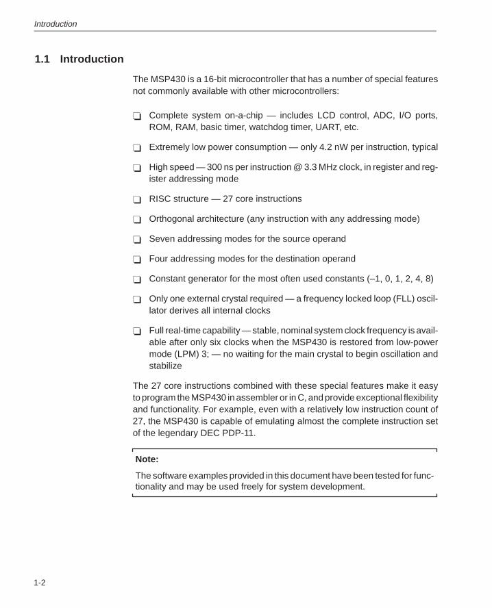
Introduction
1-2
1.1 Introduction
The MSP430 is a 16-bit microcontroller that has a number of special featuresnot commonly available with other microcontrollers:
Complete system on-a-chip — includes LCD control, ADC, I/O ports,ROM, RAM, basic timer, watchdog timer, UART, etc.
Extremely low power consumption — only 4.2 nW per instruction, typical
High speed — 300 ns per instruction @ 3.3 MHz clock, in register and reg-ister addressing mode
RISC structure — 27 core instructions
Orthogonal architecture (any instruction with any addressing mode)
Seven addressing modes for the source operand
Four addressing modes for the destination operand
Constant generator for the most often used constants (–1, 0, 1, 2, 4, 8)
Only one external crystal required — a frequency locked loop (FLL) oscil-lator derives all internal clocks
Full real-time capability — stable, nominal system clock frequency is avail-able after only six clocks when the MSP430 is restored from low-powermode (LPM) 3; — no waiting for the main crystal to begin oscillation andstabilize
The 27 core instructions combined with these special features make it easyto program the MSP430 in assembler or in C, and provide exceptional flexibilityand functionality. For example, even with a relatively low instruction count of27, the MSP430 is capable of emulating almost the complete instruction setof the legendary DEC PDP-11.
Note:
The software examples provided in this document have been tested for func-tionality and may be used freely for system development.
Related Documents
1-3MSP430 Microcontroller Family
1.2 Related Documents
The following documents are recommended for MSP430 reference:
The MSP430 Architecture User’s Guide and Module Library (TI literaturenumber SLAUE10B) contains a detailed hardware description.
The MSP430 Software User’s Guide (TI literature number SLAUE11) con-tains further information regarding the instruction set, plus other morecommon software information.
1.3 Notation
The following abbreviations and special notations are used:
.and. Logical AND function
.not. Logical Inversion
.or. Logical OR function
.xor. Logical Exclusive-OR function
[ns] Square brackets contain the unit for a value (here nanoseconds)
ACLK Auxiliary clock (output of the 32-kHz oscillator)
ACTL.1 Bit 1 (value 21) of the register ACTL
ADC Analog-to-digital converter
AGND Ground connection for the ADC; Vss (MSP430x31x) or AVss(MSP430x32x)
Background Normal program
BCD Binary coded decimal (numbers 0 to 9 coded binary with 4 bits)
CPU Central processing unit
DCO Digitally controlled oscillator
(dst) Destination (location receiving write data)
Foreground Interrupt driven software parts (interrupt handlers)
I/O Input and output Port
LCD Liquid crystal display
LSB Least significant bit (or byte)
MCLK Master clock (output of the FLL oscillator) for the CPU
MSB Most significant bit (or byte)
PC Program counter (R0 of register set)
R1||R2 Resistor R1 is connected in parallel with resistor R2
R4|R3 32-bit number. MSBs in CPU register R4, LSBs in R3
RAM Random access memory (data memory)

MSP430 Family
1-4
ROM Read only memory (program memory)
SP Stack pointer (R1 of register set)
(src) Source (location supplying read data)
TOS Top of stack (data word the Stack Pointer SP points to)
NOTES:If no units are defined for equations, the following standard units are used: Volt, Ampere, Farad, seconds and Ohm.
1.4 MSP430 Family
The MSP430 family currently consists of three subfamilies:
MSP430C31x
MSP430C32x
MSP430C33x
All three are described in detail in the MSP430 Family Architecture User’sGuide and Module Library. The hardware features of the different devices areshown in Table 1, Figure 1, Figure 2, and Figure 3.
Table 1–1. MSP430 Sub-Families Hardware FeaturesHardware Item MSP430C31x MSP430C32x MSP430C33x
14-bit ADC No Yes No
16-bit timer_A No No Yes
Basic timer Yes Yes Yes
FLL oscillator Yes Yes Yes
HW/SW UART Yes Yes Yes
HW-multiplier No No Yes
I/O ports with interrupt 8 8 24
I/O ports without interrupt 0 0 16
LCD segment lines 23 21 30
Package 56 SSOP 64 QFP 100 QFP
Universal timer/port module Yes Yes Yes
USART (SCI or SPI) No No Yes
Watchdog timer Yes Yes Yes
NOTE: Examples and explanations in this document are applicable for all MSP430 devices, unless otherwise noted.
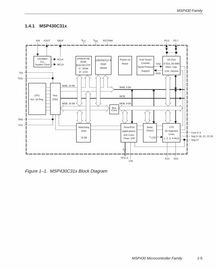
MSP430 Family
1-5MSP430 Microcontroller Family
1.4.1 MSP430C31x
OscillatorFLL
System Clock
ACLK
MCLK
2/4/8/16 KBROM
8/16 KB OTP’C’: ROM
128/256/512 B
RAM
SRAM
Power-on-
Reset
8 bit Timer/Counter
Serial Protocol
I/O Port
8 I/Os, All WithInterr. Cap.
3 Int. Vectors
CPU
Incl. 16 Reg.
Test
JTAG
BusConv
Timer/Port
Applications:
Timer, O/P
Basic LCD
92 SegmentLines
1, 2, 3, 4 MUX
Timer1Watchdog
timer
15 Bit
MAB, 16 Bit
MDB, 16 Bit
MAB, 4 Bit
MDB, 8 Bit
MCB
6
LCDf
TP.0–5CIN
XIN XOUT XBUF VCC VSS RST/NMI P0.0 P0.7
Com 0–3
Seg 0–18, 22, 23 26
Seg 27
R13 R23
TDI
TDO
TMS
TCK
TXD
’P’: OTP
A/D Conv.
SupportRXD
Figure 1–1. MSP430C31x Block Diagram
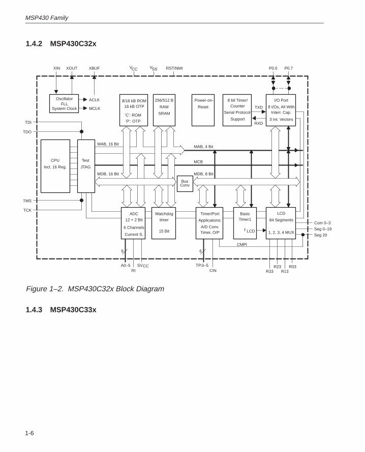
MSP430 Family
1-6
1.4.2 MSP430C32x
OscillatorFLL
System Clock
ACLK
MCLK
8/16 kB ROM16 kB OTP
’C’: ROM
256/512 B
RAM
SRAM
Power-on-
Reset
8 bit Timer/Counter
Serial Protocol
I/O Port
8 I/Os, All WithInterr. Cap.
3 Int. Vectors
CPU
Incl. 16 Reg.
Test
JTAG
BusConv
Timer/Port
Applications:
Timer, O/P
Basic LCD
84 Segments
1, 2, 3, 4 MUX
Timer1ADC
12 + 2 Bit
6 Channels
MAB, 16 Bit
MDB, 16 Bit
MAB, 4 Bit
MDB, 8 Bit
MCB
6
LCDf
CMPI
TP.0–5CIN
XIN XOUT XBUF VCC VSS RST/NMI P0.0 P0.7
Com 0–3
Seg 0–19
Seg 20
R23 R03
TDI
TDO
TMS
TCK
TXD
’P’: OTP
A/D Conv.
SupportRXD
Watchdog
timer
15 BitCurrent S.
6
A0–5RI
SVCCR33 R13
Figure 1–2. MSP430C32x Block Diagram
1.4.3 MSP430C33x
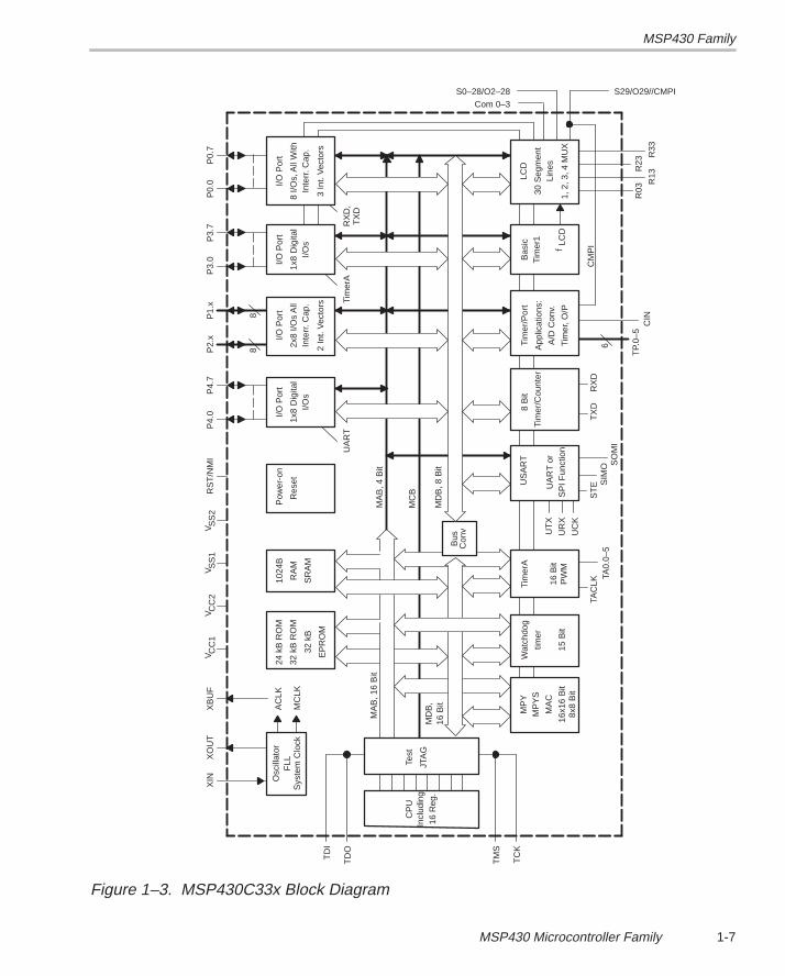
MSP430 Family
1-7MSP430 Microcontroller Family
Osc
illat
orF
LLS
yste
m C
lock
AC
LK
MC
LK32
kB
EP
RO
M
1024
B
RA
M
SR
AM
Pow
er-o
n
Res
et
I/O P
ort
1x8
Dig
ital
I/Os
I/O P
ort
2x8
I/Os
All
Inte
rr. C
ap.
88
2 In
t. V
ecto
rs
I/O P
ort
1x8
Dig
ital
I/Os
I/O P
ort
8 I/O
s, A
ll W
ithIn
terr
. Cap
.
3 In
t. V
ecto
rs
CP
UIn
clud
ing
Test
JTA
G
Bus
Con
v
US
AR
T
UA
RT
or
8 B
itTi
mer
/Por
t
App
licat
ions
:
Tim
er, O
/P
Bas
icLC
D
30 S
egm
ent
Line
s
1, 2
, 3, 4
MU
XS
PI F
unct
ion
Tim
er/C
ount
erTi
mer
1
MP
YW
atch
dog
Tim
erA
MP
YS
timer
MA
C
16x1
6 B
it8x
8 B
it15
Bit
16 B
itP
WM
MA
B, 1
6 B
it
MD
B,
MA
B, 4
Bit
MD
B, 8
Bit
MC
B
TAC
LKTA
0.0–
5
UT
X
UR
X
UC
K
ST
E SIM
O SO
MI
TX
DR
XD
6
LCD
f
CM
PI
TP.
0–5
CIN
XIN
XO
UT
XB
UF
V CC
1V C
C2
V SS
1V S
S2
RS
T/N
MI
P4.
0P
4.7
P2.
xP
1.x
P3.
0P
3.7
P0.
0P
0.7
R03
R13
R23
R33
TD
I
TD
O
TM
S
TC
K
UA
RT
Tim
erA
RX
D,
TX
D
24 k
B R
OM
32 k
B R
OM
A/D
Con
v.
16 R
eg.
16 B
it
Com 0–3
S0–28/O2–28 S29/O29//CMPI
Figure 1–3. MSP430C33x Block Diagram

Advantages of the MSP430 Concept
1-8
1.5 Advantages of the MSP430 Concept
The MSP430 concept differs considerably from other microcontrollers and of-fers some significant advantages over more traditional designs.
1.5.1 RISC Architecture Without RISC Disadvantages
Typical RISC architectures show their highest performance in calculation- in-tensive applications in which several registers are loaded with input data, allcalculations are made within the registers, and the results are stored back intoRAM. Memory accesses (using addressing modes) are necessary only for theLOAD instructions at the beginning and the STORE instructions at the end ofthe calculations. The MSP430 can be programmed for such operation, for ex-ample, performing a pure calculation task in the floating point without any I/Oaccesses.
Pure RISC architectures have some disadvantages when running real-timeapplications that require frequent I/O accesses, however. Time is lost whenev-er an operand is fetched and loaded from RAM, modified, and then stored backinto RAM.
The MSP430 architecture was designed to include the best of both worlds, tak-ing advantage of RISC features for fast and efficient calculations, and addres-sing modes for real-time requirements:
The RISC architecture provides a limited number of powerful instructions,numerous registers, and single-cycle execution times.
The more traditional microcomputer features provide addressing modesfor all instructions. This functionality is further enhanced with 100% ortho-gonality, allowing any instruction to be used with any addressing mode.
1.5.2 Real-Time Capability With Ultra-Low Power Consumption
The design of the MSP430 was driven by the need to provide full real-time ca-pability while still exhibiting extremely low power consumption. Average powerconsumption is reduced to the minimum by running the CPU and certain otherfunctions of the MSP430 only when it is necessary. The rest of the time (themajority of the time), power is conserved by keeping only selected low-powerperipheral functions active.
But to have a true real-time capability, the device must be able to shift from alow-power mode with the CPU off to a fully active mode with the CPU and allother device functions operating nominally in a very short time. This was ac-complished primarily with the design of the system clock:
Advantages of the MSP430 Concept
1-9MSP430 Microcontroller Family
No second high frequency crystal is used — inherent delays can rangefrom 20 ms to 200 ms until oscillator stability is reached
Instead, a sophisticated FLL system clock generator is used — generatoroutput frequency (MCLK) reaches the nominal frequency within 8 cyclesafter activation from low power mode 3 (LPM3) or sleep mode
This design provides real-time capability almost immediately after the devicecomes out of a LPM — as if the CPU is always active. Only two additionalMCLK cycles (2 µs @ fC = 1 MHz) are necessary to get the device from LPM3to the first instruction of the interrupt handler.
1.5.3 Digitally Controlled Oscillator Stability
The digitally controlled oscillator (DCO) is voltage and temperature depen-dent, which does not mean that its frequency is not stable. During the activemode, the integral error is corrected to approximately zero every 30.5 µs . Thisis accomplished by switching between two different DCO frequencies. Onefrequency is higher than the programmed MCLK frequency and the other islower, causing the errors to essentially cancel-out. The two DCO frequenciesare interlaced as much as possible to provide the smallest possible error at anygiven time. See System Clock Generator for more information.
1.5.4 Stack Processing Capability
The MSP430 is a true stack processor, with most of the seven addressingmodes implemented for the stack pointer (SP) as well as the other CPU regis-ters (PC and R4 through R15). The capabilities of the stack include:
Free access to all items on the stack — not only to the top of the stack(TOS)
Ability to modify subroutine and interrupt return addresses located on thestack
Ability to modify the stored status register of interrupt returns located onthe stack
No special stack instructions — all of the implemented instructions maybe used for the stack and the stack pointer
Byte and word capability for the stack
Free mix of subroutine and interrupt handling — as long as no stack modi-fication (PUSH, POP, etc.) is made, no errors can occur
For more information concerning the stack, see Appendix A.
MSP430 Application Operating Modes
1-10
1.6 MSP430 Application Operating Modes
MSP430 applications fall into two main classes, depending on the power sup-ply:
AC power-driven applications such as electricity meters and AC-poweredcontrollers. In these applications, the microcontroller needs to be activeat all times. The low current consumption of the MSP430 when active(900 µA @ 5 V & fC = 1 MHz) puts it well within the typical low-power cate-gory now (currently < 40 mA) and in the future as tolerable current con-sumption diminishes.
Battery-powered applications such as gas meters, water flow meters, heatvolume counters, data loggers, and other controller and remote meteringtasks. For these applications, power consumption is the key issue sinceoperation from a single battery for 10 years or longer is often required. Theaverage current drawn by the MSP430 needs to be in the range of the selfdischarge current of the battery, approximately 1 µA to 3 µA.
MSP430 has six operating modes, each with different power requirements.Three of these modes are important for battery-powered applications:
Active mode — CPU and other device functions run all the time
Low power mode 3 (LPM3) — the normal mode for most applications dur-ing 99% to 99.9% of the time. This mode is also called done mode or sleepmode
Low power mode 4 (LPM4) — the mode typically used during storage. Thismode is also called off mode
1.6.1 Active Mode
Active mode is used for calculations, decision-making, I/O functions, and otheractivities that require the capabilities of an operating CPU. All of the peripheralfunctions may be used, provided that they are enabled. The examples shownin this document use the active mode.
1.6.2 Low Power Mode 3 (LPM3)
LPM3 is the most important mode for battery-powered applications. The CPUis disabled, but enabled peripherals stay active. The basic timer provides aprecise time base. When enabled, interrupts restore the CPU, switch onMCLK, and start normal operation. Table 1–2 lists the status of the MSP430system when in LPM3.
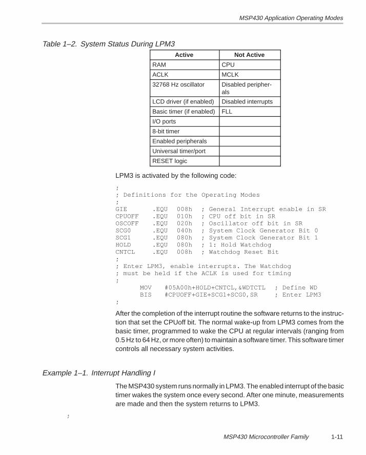
MSP430 Application Operating Modes
1-11MSP430 Microcontroller Family
Table 1–2. System Status During LPM3Active Not Active
RAM CPU
ACLK MCLK
32768 Hz oscillator Disabled peripher-als
LCD driver (if enabled) Disabled interrupts
Basic timer (if enabled) FLL
I/O ports
8-bit timer
Enabled peripherals
Universal timer/port
RESET logic
LPM3 is activated by the following code:
;; Definitions for the Operating Modes;GIE .EQU 008h ; General Interrupt enable in SRCPUOFF .EQU 010h ; CPU off bit in SROSCOFF .EQU 020h ; Oscillator off bit in SRSCG0 .EQU 040h ; System Clock Generator Bit 0SCG1 .EQU 080h ; System Clock Generator Bit 1HOLD .EQU 080h ; 1: Hold WatchdogCNTCL .EQU 008h ; Watchdog Reset Bit;; Enter LPM3, enable interrupts. The Watchdog; must be held if the ACLK is used for timing;
MOV #05A00h+HOLD+CNTCL,&WDTCTL ; Define WDBIS #CPUOFF+GIE+SCG1+SCG0,SR ; Enter LPM3
;
After the completion of the interrupt routine the software returns to the instruc-tion that set the CPUoff bit. The normal wake-up from LPM3 comes from thebasic timer, programmed to wake the CPU at regular intervals (ranging from0.5 Hz to 64 Hz, or more often) to maintain a software timer. This software timercontrols all necessary system activities.
Example 1–1. Interrupt Handling I
The MSP430 system runs normally in LPM3. The enabled interrupt of the basictimer wakes the system once every second. After one minute, measurementsare made and then the system returns to LPM3.
;
MSP430 Application Operating Modes
1-12
; Interrupt handler for Basic Timer: Wake–up with 1Hz
;
BT_HAN MOV #05A00h+CNTCL,&WDTCTL ; Reset watchdog
INC.B SECCNT ; Counter for seconds +1
CMP.B #60,SECCNT ; 1 minute elapsed?
JHS MIN1 ; Yes, do necessary tasks
RETI ; No return to LPM3
;
; One minute elapsed: Return is removed from stack, a branch to
; the necessary tasks is made. There it is decided how to proceed
;
MIN1 INC MINCNT ; Minute counter +1
CLR SECCNT ; 0 –> SECCNT
ADD #4,SP ; House keeping: SR, PC off Stack
BR #TASK ; Do tasks
...
;
TASK ... ; Start of necessary tasks
;
; All measurements and calculations are made: Return to LPM3
;
MOV #05A00h+HOLD+CNTCL,&WDTCTL ; Hold WD
BIS #CPUOFF+GIE+SCG0+SCG1,SR ; Enter LPM3
LPM3 is the lowest current consumption mode that still allows the use of a real-time clock. The basic timer can interrupt the LPM3 at relatively long time inter-vals (up to 2 seconds) and update the real-time clock. If the status register isnot changed during the interrupt routines, the RETI instruction returns to theinstruction that set the CPUoff bit (and placed the CPU in LPM3). The programcounter points to the next instruction, which is not executed unless the interruptroutine resets the CPUoff bit during its run.
If the MSP430 is awakened from LPM3, two additional clock cycles are neededto load the PC with the interrupt vector address and start the interrupt handler(8 clocks compared to 6 when in the active mode).
Example 1–2. Interrupt Handling II
The MSP430 system runs normally in LPM3. The enabled interrupt of the basictimer wakes the system once every second. After one minute, measurementsare made and then the system returns to LPM3. The branch to the task is madeby resetting the CPUoff bit inside the interrupt routine.
; Interrupt handler for Basic Timer: Wake–up with 1 Hz
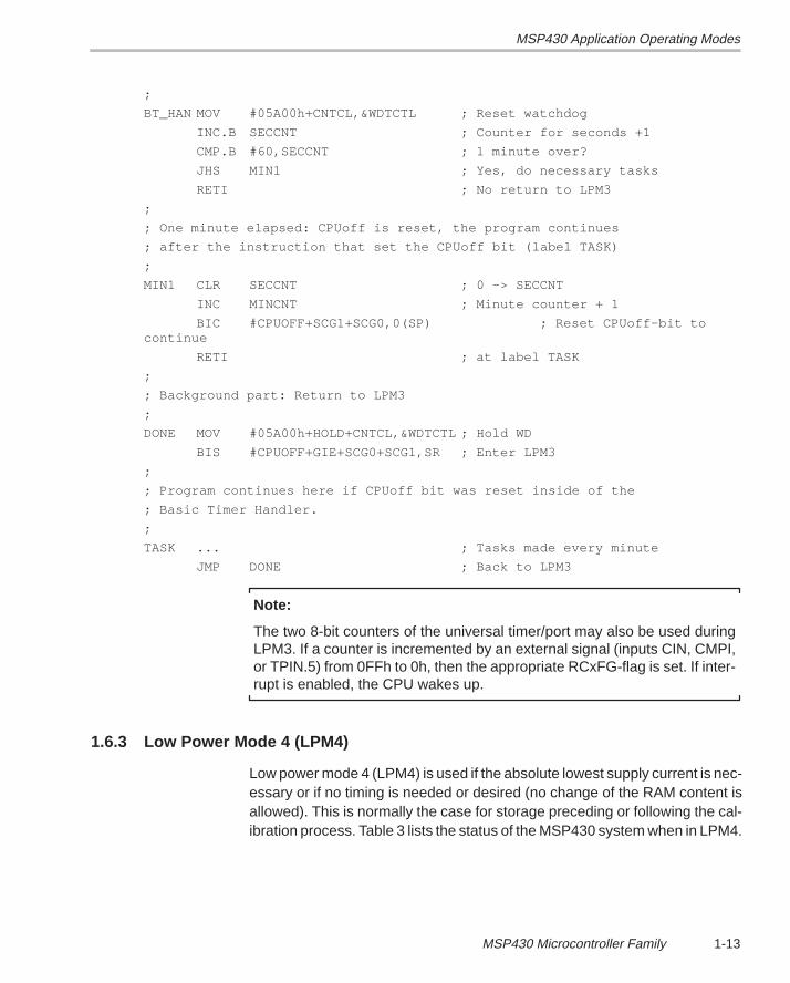
MSP430 Application Operating Modes
1-13MSP430 Microcontroller Family
;
BT_HAN MOV #05A00h+CNTCL,&WDTCTL ; Reset watchdog
INC.B SECCNT ; Counter for seconds +1
CMP.B #60,SECCNT ; 1 minute over?
JHS MIN1 ; Yes, do necessary tasks
RETI ; No return to LPM3
;
; One minute elapsed: CPUoff is reset, the program continues
; after the instruction that set the CPUoff bit (label TASK)
;
MIN1 CLR SECCNT ; 0 –> SECCNT
INC MINCNT ; Minute counter + 1
BIC #CPUOFF+SCG1+SCG0,0(SP) ; Reset CPUoff–bit tocontinue
RETI ; at label TASK
;
; Background part: Return to LPM3
;
DONE MOV #05A00h+HOLD+CNTCL,&WDTCTL ; Hold WD
BIS #CPUOFF+GIE+SCG0+SCG1,SR ; Enter LPM3
;
; Program continues here if CPUoff bit was reset inside of the
; Basic Timer Handler.
;
TASK ... ; Tasks made every minute
JMP DONE ; Back to LPM3
Note:
The two 8-bit counters of the universal timer/port may also be used duringLPM3. If a counter is incremented by an external signal (inputs CIN, CMPI,or TPIN.5) from 0FFh to 0h, then the appropriate RCxFG-flag is set. If inter-rupt is enabled, the CPU wakes up.
1.6.3 Low Power Mode 4 (LPM4)
Low power mode 4 (LPM4) is used if the absolute lowest supply current is nec-essary or if no timing is needed or desired (no change of the RAM content isallowed). This is normally the case for storage preceding or following the cal-ibration process. Table 3 lists the status of the MSP430 system when in LPM4.
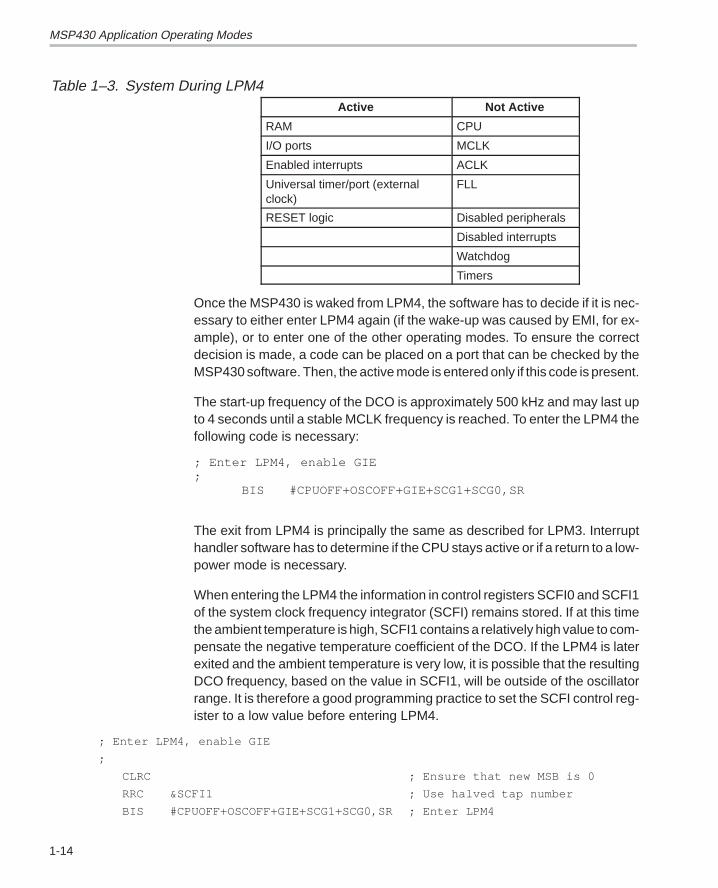
MSP430 Application Operating Modes
1-14
Table 1–3. System During LPM4Active Not Active
RAM CPU
I/O ports MCLK
Enabled interrupts ACLK
Universal timer/port (externalclock)
FLL
RESET logic Disabled peripherals
Disabled interrupts
Watchdog
Timers
Once the MSP430 is waked from LPM4, the software has to decide if it is nec-essary to either enter LPM4 again (if the wake-up was caused by EMI, for ex-ample), or to enter one of the other operating modes. To ensure the correctdecision is made, a code can be placed on a port that can be checked by theMSP430 software. Then, the active mode is entered only if this code is present.
The start-up frequency of the DCO is approximately 500 kHz and may last upto 4 seconds until a stable MCLK frequency is reached. To enter the LPM4 thefollowing code is necessary:
; Enter LPM4, enable GIE;
BIS #CPUOFF+OSCOFF+GIE+SCG1+SCG0,SR
The exit from LPM4 is principally the same as described for LPM3. Interrupthandler software has to determine if the CPU stays active or if a return to a low-power mode is necessary.
When entering the LPM4 the information in control registers SCFI0 and SCFI1of the system clock frequency integrator (SCFI) remains stored. If at this timethe ambient temperature is high, SCFI1 contains a relatively high value to com-pensate the negative temperature coefficient of the DCO. If the LPM4 is laterexited and the ambient temperature is very low, it is possible that the resultingDCO frequency, based on the value in SCFI1, will be outside of the oscillatorrange. It is therefore a good programming practice to set the SCFI control reg-ister to a low value before entering LPM4.
; Enter LPM4, enable GIE
;
CLRC ; Ensure that new MSB is 0
RRC &SCFI1 ; Use halved tap number
BIS #CPUOFF+OSCOFF+GIE+SCG1+SCG0,SR ; Enter LPM4

MSP430 Application Operating Modes
1-15MSP430 Microcontroller Family
Note:
The two 8-bit counters of the universal timer/port may also be used duringLPM4. If a counter is incremented by an external signal (inputs CIN, CMP,or TPIN.5) from 0FFh to 0h, then the appropriate RCxFG-flag is set. If inter-rupt is enabled, the CPU wakes up.

2-1
Analog-to-Digital Converters
Chapter 2

2-2
2–3
Architecture and Function of theMSP430 14-Bit ADC
Lutz Bierl
Literature Number: SLAA045June 1999
Printed on Recycled Paper

2–4
IMPORTANT NOTICE
Texas Instruments and its subsidiaries (TI) reserve the right to make changes to theirproducts or to discontinue any product or service without notice, and advise customers toobtain the latest version of relevant information to verify, before placing orders, thatinformation being relied on is current and complete. All products are sold subject to the termsand conditions of sale supplied at the time of order acknowledgement, including thosepertaining to warranty, patent infringement, and limitation of liability.
TI warrants performance of its semiconductor products to the specifications applicable at thetime of sale in accordance with TI’s standard warranty. Testing and other quality controltechniques are utilized to the extent TI deems necessary to support this warranty. Specifictesting of all parameters of each device is not necessarily performed, except those mandatedby government requirements.
CERTAIN APPLICATIONS USING SEMICONDUCTOR PRODUCTS MAY INVOLVEPOTENTIAL RISKS OF DEATH, PERSONAL INJURY, OR SEVERE PROPERTY ORENVIRONMENTAL DAMAGE (“CRITICAL APPLICATIONS”). TI SEMICONDUCTORPRODUCTS ARE NOT DESIGNED, AUTHORIZED, OR WARRANTED TO BE SUITABLEFOR USE IN LIFE-SUPPORT DEVICES OR SYSTEMS OR OTHER CRITICALAPPLICATIONS. INCLUSION OF TI PRODUCTS IN SUCH APPLICATIONS ISUNDERSTOOD TO BE FULLY AT THE CUSTOMER’S RISK.
In order to minimize risks associated with the customer’s applications, adequate design andoperating safeguards must be provided by the customer to minimize inherent or proceduralhazards.
TI assumes no liability for applications assistance or customer product design. TI does notwarrant or represent that any license, either express or implied, is granted under any patentright, copyright, mask work right, or other intellectual property right of TI covering or relatingto any combination, machine, or process in which such semiconductor products or servicesmight be or are used. TI’s publication of information regarding any third party’s products orservices does not constitute TI’s approval, warranty or endorsement thereof.
Copyright 1999, Texas Instruments Incorporated
2–5 Architecture and Function of the MSP430 14-Bit ADC
Contents1 Introduction 2–9. . . . . . . . . . . . . . . . . . . . . . . . . . . . . . . . . . . . . . . . . . . . . . . . . . . . . . . . . . . . . . . . . . . . . . . . . . . . . . . . .
1.1 Characteristics of the 14-Bit ADC 2–10. . . . . . . . . . . . . . . . . . . . . . . . . . . . . . . . . . . . . . . . . . . . . . . . . . . . . . . .
2 ADC Function and Modes 2–11. . . . . . . . . . . . . . . . . . . . . . . . . . . . . . . . . . . . . . . . . . . . . . . . . . . . . . . . . . . . . . . . . . . 2.1 Function of the ADC 2–12. . . . . . . . . . . . . . . . . . . . . . . . . . . . . . . . . . . . . . . . . . . . . . . . . . . . . . . . . . . . . . . . . . .
2.1.1 ADC Timing Restrictions 2–13. . . . . . . . . . . . . . . . . . . . . . . . . . . . . . . . . . . . . . . . . . . . . . . . . . . . . . . . 2.1.2 Sample and Hold 2–14. . . . . . . . . . . . . . . . . . . . . . . . . . . . . . . . . . . . . . . . . . . . . . . . . . . . . . . . . . . . . . 2.1.3 Absolute and Relative Measurements 2–15. . . . . . . . . . . . . . . . . . . . . . . . . . . . . . . . . . . . . . . . . . . .
2.2 Using the ADC in 14-Bit Mode 2–16. . . . . . . . . . . . . . . . . . . . . . . . . . . . . . . . . . . . . . . . . . . . . . . . . . . . . . . . . . . 2.2.1 Timing 2–17. . . . . . . . . . . . . . . . . . . . . . . . . . . . . . . . . . . . . . . . . . . . . . . . . . . . . . . . . . . . . . . . . . . . . . . . 2.2.2 Software Example 2–18. . . . . . . . . . . . . . . . . . . . . . . . . . . . . . . . . . . . . . . . . . . . . . . . . . . . . . . . . . . . . .
2.3 Using the ADC in 12-Bit Mode 2–18. . . . . . . . . . . . . . . . . . . . . . . . . . . . . . . . . . . . . . . . . . . . . . . . . . . . . . . . . . . 2.3.1 Timing 2–20. . . . . . . . . . . . . . . . . . . . . . . . . . . . . . . . . . . . . . . . . . . . . . . . . . . . . . . . . . . . . . . . . . . . . . . . 2.3.2 Software Example 2–20. . . . . . . . . . . . . . . . . . . . . . . . . . . . . . . . . . . . . . . . . . . . . . . . . . . . . . . . . . . . . .
3 The A/D Controller Hardware 2–21. . . . . . . . . . . . . . . . . . . . . . . . . . . . . . . . . . . . . . . . . . . . . . . . . . . . . . . . . . . . . . . . . 3.1 ADC Control Registers 2–21. . . . . . . . . . . . . . . . . . . . . . . . . . . . . . . . . . . . . . . . . . . . . . . . . . . . . . . . . . . . . . . . .
3.1.1 ACTL Control Register 2–21. . . . . . . . . . . . . . . . . . . . . . . . . . . . . . . . . . . . . . . . . . . . . . . . . . . . . . . . . . 3.1.2 A/D Data Register ADAT 2–24. . . . . . . . . . . . . . . . . . . . . . . . . . . . . . . . . . . . . . . . . . . . . . . . . . . . . . . . 3.1.3 Input Register AIN 2–25. . . . . . . . . . . . . . . . . . . . . . . . . . . . . . . . . . . . . . . . . . . . . . . . . . . . . . . . . . . . . 3.1.4 Input Enable Register AEN 2–26. . . . . . . . . . . . . . . . . . . . . . . . . . . . . . . . . . . . . . . . . . . . . . . . . . . . . .
3.2 Current Source 2–26. . . . . . . . . . . . . . . . . . . . . . . . . . . . . . . . . . . . . . . . . . . . . . . . . . . . . . . . . . . . . . . . . . . . . . . . 3.2.1 Normal Use of the Current Source 2–26. . . . . . . . . . . . . . . . . . . . . . . . . . . . . . . . . . . . . . . . . . . . . . . 3.2.2 Current Source Used for Level Shifting 2–30. . . . . . . . . . . . . . . . . . . . . . . . . . . . . . . . . . . . . . . . . . .
3.3 SVcc Terminal 2–31. . . . . . . . . . . . . . . . . . . . . . . . . . . . . . . . . . . . . . . . . . . . . . . . . . . . . . . . . . . . . . . . . . . . . . . . . 3.3.1 SVcc Terminal Used as an Output for the ADC Reference Voltage 2–31. . . . . . . . . . . . . . . . . . . . 3.3.2 SVcc Terminal Used as an Input for the ADC Reference Voltage 2–32. . . . . . . . . . . . . . . . . . . . . 3.3.3 Connection of Current Consuming Loads to SVcc 2–33. . . . . . . . . . . . . . . . . . . . . . . . . . . . . . . . . .
3.4 Interrupt Handling 2–34. . . . . . . . . . . . . . . . . . . . . . . . . . . . . . . . . . . . . . . . . . . . . . . . . . . . . . . . . . . . . . . . . . . . . 3.4.1 Interrupt Flags 2–34. . . . . . . . . . . . . . . . . . . . . . . . . . . . . . . . . . . . . . . . . . . . . . . . . . . . . . . . . . . . . . . . . 3.4.2 Interrupt Handlers 2–34. . . . . . . . . . . . . . . . . . . . . . . . . . . . . . . . . . . . . . . . . . . . . . . . . . . . . . . . . . . . . .
3.5 ADC Clock Generation 2–37. . . . . . . . . . . . . . . . . . . . . . . . . . . . . . . . . . . . . . . . . . . . . . . . . . . . . . . . . . . . . . . . .
4 ADC Characteristics 2–37. . . . . . . . . . . . . . . . . . . . . . . . . . . . . . . . . . . . . . . . . . . . . . . . . . . . . . . . . . . . . . . . . . . . . . . . .
5 Summary 2–38. . . . . . . . . . . . . . . . . . . . . . . . . . . . . . . . . . . . . . . . . . . . . . . . . . . . . . . . . . . . . . . . . . . . . . . . . . . . . . . . . . .
6 References 2–38. . . . . . . . . . . . . . . . . . . . . . . . . . . . . . . . . . . . . . . . . . . . . . . . . . . . . . . . . . . . . . . . . . . . . . . . . . . . . . . . .
Appendix A Definitions Used With the Application Examples 2–39. . . . . . . . . . . . . . . . . . . . . . . . . . . . . . . . . . . .
Figures
2–6 SLAA045
List of Figures1 Hardware of the 14-Bit ADC 2–10. . . . . . . . . . . . . . . . . . . . . . . . . . . . . . . . . . . . . . . . . . . . . . . . . . . . . . . . . . . . . . . . . . . . 2 Possible Connections to the Analog-to-Digital Converter 2–11. . . . . . . . . . . . . . . . . . . . . . . . . . . . . . . . . . . . . . . . . . . 3 Sources of the Conversion Result 2–12. . . . . . . . . . . . . . . . . . . . . . . . . . . . . . . . . . . . . . . . . . . . . . . . . . . . . . . . . . . . . . . 4 ADC Spikes Due to Violated Timing Restrictions 2–14. . . . . . . . . . . . . . . . . . . . . . . . . . . . . . . . . . . . . . . . . . . . . . . . . . 5 Simplified Input Circuitry for Signal Sampling 2–14. . . . . . . . . . . . . . . . . . . . . . . . . . . . . . . . . . . . . . . . . . . . . . . . . . . . . 6 Relative Measurements With the MSP430C32x 2–15. . . . . . . . . . . . . . . . . . . . . . . . . . . . . . . . . . . . . . . . . . . . . . . . . . . 7 Absolute Measurements Using External Reference Voltage 2–16. . . . . . . . . . . . . . . . . . . . . . . . . . . . . . . . . . . . . . . . . 8 Complete 14-Bit ADC Range 2–16. . . . . . . . . . . . . . . . . . . . . . . . . . . . . . . . . . . . . . . . . . . . . . . . . . . . . . . . . . . . . . . . . . . 9 Timing for the 14-bit Analog-to-Digital Conversion 2–17. . . . . . . . . . . . . . . . . . . . . . . . . . . . . . . . . . . . . . . . . . . . . . . . . 10 The Four 12-Bit ADC Ranges A to D 2–18. . . . . . . . . . . . . . . . . . . . . . . . . . . . . . . . . . . . . . . . . . . . . . . . . . . . . . . . . . . 11 Single 12-Bit ADC Range 2–19. . . . . . . . . . . . . . . . . . . . . . . . . . . . . . . . . . . . . . . . . . . . . . . . . . . . . . . . . . . . . . . . . . . . . 12 Timing for the 12-Bit A/D Conversion 2–20. . . . . . . . . . . . . . . . . . . . . . . . . . . . . . . . . . . . . . . . . . . . . . . . . . . . . . . . . . . 13 ACTL Control Register 2–21. . . . . . . . . . . . . . . . . . . . . . . . . . . . . . . . . . . . . . . . . . . . . . . . . . . . . . . . . . . . . . . . . . . . . . . . 14 Conversion Start (SOC) 2–21. . . . . . . . . . . . . . . . . . . . . . . . . . . . . . . . . . . . . . . . . . . . . . . . . . . . . . . . . . . . . . . . . . . . . . . 15 Voltage Reference Bit (VREF) 2–22. . . . . . . . . . . . . . . . . . . . . . . . . . . . . . . . . . . . . . . . . . . . . . . . . . . . . . . . . . . . . . . . . 16 ADC Input Selection Bits 2–22. . . . . . . . . . . . . . . . . . . . . . . . . . . . . . . . . . . . . . . . . . . . . . . . . . . . . . . . . . . . . . . . . . . . . . 17 Current Source Output Select Bits 2–23. . . . . . . . . . . . . . . . . . . . . . . . . . . . . . . . . . . . . . . . . . . . . . . . . . . . . . . . . . . . . 18 Range Select Bits 2–23. . . . . . . . . . . . . . . . . . . . . . . . . . . . . . . . . . . . . . . . . . . . . . . . . . . . . . . . . . . . . . . . . . . . . . . . . . . . 19 Power Down Bit (Pd) 2–24. . . . . . . . . . . . . . . . . . . . . . . . . . . . . . . . . . . . . . . . . . . . . . . . . . . . . . . . . . . . . . . . . . . . . . . . . 20 Clock Frequency Selection Bits 2–24. . . . . . . . . . . . . . . . . . . . . . . . . . . . . . . . . . . . . . . . . . . . . . . . . . . . . . . . . . . . . . . . 21 Bit 15 2–24. . . . . . . . . . . . . . . . . . . . . . . . . . . . . . . . . . . . . . . . . . . . . . . . . . . . . . . . . . . . . . . . . . . . . . . . . . . . . . . . . . . . . . . 22 The Data Register ADAT, 12-Bit A/D Conversion 2–25. . . . . . . . . . . . . . . . . . . . . . . . . . . . . . . . . . . . . . . . . . . . . . . . . 23 Data Register ADAT, 14-Bit A/D Conversion 2–25. . . . . . . . . . . . . . . . . . . . . . . . . . . . . . . . . . . . . . . . . . . . . . . . . . . . . 24 Input Register AIN 2–25. . . . . . . . . . . . . . . . . . . . . . . . . . . . . . . . . . . . . . . . . . . . . . . . . . . . . . . . . . . . . . . . . . . . . . . . . . . 25 Input Enable Register AEN 2–26. . . . . . . . . . . . . . . . . . . . . . . . . . . . . . . . . . . . . . . . . . . . . . . . . . . . . . . . . . . . . . . . . . . . 26 The Current Source 2–27. . . . . . . . . . . . . . . . . . . . . . . . . . . . . . . . . . . . . . . . . . . . . . . . . . . . . . . . . . . . . . . . . . . . . . . . . . 27 Measurement Circuitry for the Error of the Current Source 2–28. . . . . . . . . . . . . . . . . . . . . . . . . . . . . . . . . . . . . . . . . 28 Error of the Current Source at the Limit 2–29. . . . . . . . . . . . . . . . . . . . . . . . . . . . . . . . . . . . . . . . . . . . . . . . . . . . . . . . . 29 Error of the Current Source at the Limit 2–29. . . . . . . . . . . . . . . . . . . . . . . . . . . . . . . . . . . . . . . . . . . . . . . . . . . . . . . . . 30 Application of the Current Source With the Full ADC Range at Input A0 2–30. . . . . . . . . . . . . . . . . . . . . . . . . . . . . 31 Current Measurement With Level Shifting 2–31. . . . . . . . . . . . . . . . . . . . . . . . . . . . . . . . . . . . . . . . . . . . . . . . . . . . . . . 32 SVcc Terminal Used as an Output 2–32. . . . . . . . . . . . . . . . . . . . . . . . . . . . . . . . . . . . . . . . . . . . . . . . . . . . . . . . . . . . . . 33 SVcc Terminal Used as an Input for a Reference Voltage 2–33. . . . . . . . . . . . . . . . . . . . . . . . . . . . . . . . . . . . . . . . . . 34 Connection of Current Consuming Loads to SVcc 2–34. . . . . . . . . . . . . . . . . . . . . . . . . . . . . . . . . . . . . . . . . . . . . . . . 35 Error Characteristic Device 1 2–37. . . . . . . . . . . . . . . . . . . . . . . . . . . . . . . . . . . . . . . . . . . . . . . . . . . . . . . . . . . . . . . . . . 36 Error Characteristic Device 2 2–37. . . . . . . . . . . . . . . . . . . . . . . . . . . . . . . . . . . . . . . . . . . . . . . . . . . . . . . . . . . . . . . . . . 37 Error Characteristic Device 3 2–38. . . . . . . . . . . . . . . . . . . . . . . . . . . . . . . . . . . . . . . . . . . . . . . . . . . . . . . . . . . . . . . . . . 38 Error Characteristic Device 4 2–38. . . . . . . . . . . . . . . . . . . . . . . . . . . . . . . . . . . . . . . . . . . . . . . . . . . . . . . . . . . . . . . . . .

Tables
2–7 Architecture and Function of the MSP430 14-Bit ADC
List of Tables1 ADC Input Selection Bits 2–22. . . . . . . . . . . . . . . . . . . . . . . . . . . . . . . . . . . . . . . . . . . . . . . . . . . . . . . . . . . . . . . . . . . . . . . 2 Current Source Output Select Bits 2–23. . . . . . . . . . . . . . . . . . . . . . . . . . . . . . . . . . . . . . . . . . . . . . . . . . . . . . . . . . . . . . . 3 Range Select Bits 2–23. . . . . . . . . . . . . . . . . . . . . . . . . . . . . . . . . . . . . . . . . . . . . . . . . . . . . . . . . . . . . . . . . . . . . . . . . . . . . 4 Clock Frequency Selection Bits 2–24. . . . . . . . . . . . . . . . . . . . . . . . . . . . . . . . . . . . . . . . . . . . . . . . . . . . . . . . . . . . . . . . .

2–8 SLAA045

2–9
Architecture and Function of the MSP430 14-Bit ADC
Lutz Bierl
ABSTRACTThis application report describes the architecture and function of the 14-bitanalog-to-digital converter (ADC) of the MSP430 family. The principles of the ADC areexplained and software examples are given. The report also explains the function of allhardware registers in the ADC. The References section at the end of the report listsrelated application reports in the MSP430 14-bit ADC series.
1 IntroductionThe analog-to-digital converter (ADC) of the MSP430 family can work in twomodes: the 12-bit mode or the 14-bit mode. Hardware registers allow easyadaptation to different ADC tasks. The following paragraphs describe the modesand hardware registers.
NOTE: The MSP430 Family Architecture Guide and ModuleLibrary data book[1] is recommended. The hardware-relatedinformation given there is very valuable and complements theinformation given in this application report.
NOTE: For related application reports in the MSP430 14-bit ADCseries, see the References section.
Figure 1 shows the block diagram of the MSP430 14-bit ADC.
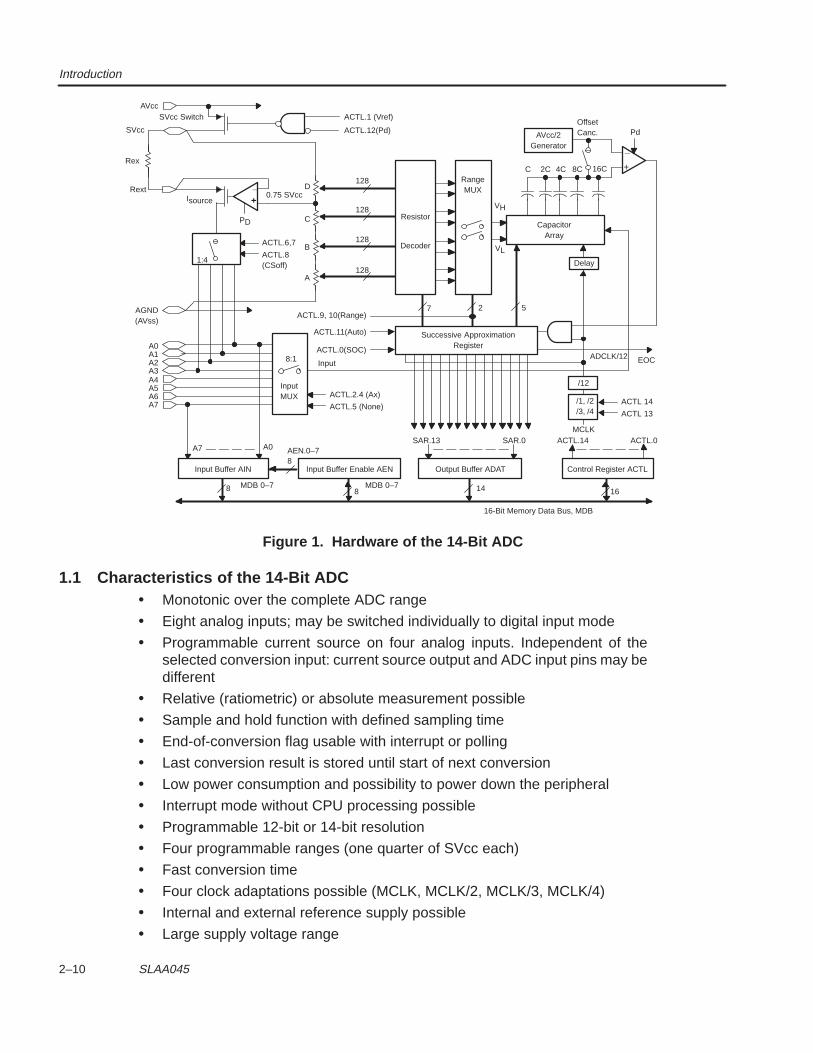
Introduction
2–10 SLAA045
AVcc/2Generator
_
+
Successive ApproximationRegister
SAR.13 SAR.0 ACTL.14 ACTL.0
14 16
Output Buffer ADAT Control Register ACTL
/12
/1, /2/3, /4
ACTL 14
ACTL 13
ACTL.0(SOC)
ACTL.11(Auto)
ACTL.9, 10(Range)
Resistor
RangeMUX
7 2
ADCLK/12 EOC
5
Delay
VH
VL
CapacitorArray
AVcc/2Generator
C 2C 4C 8C
Pd
16C
128
8:1 Input
ACTL.2.4 (Ax)
ACTL.5 (None)
8
Input Buffer Enable AEN
A7 A0
8
8
MDB 0–7
AEN.0–7
_
+0.75 SVcc
ACTL.6,7
ACTL.8(CSoff)
1:4
A7A6A5A4A3A2A1A0
AGND(AVss)
ACTL.12(Pd)
ACTL.1 (Vref)SVcc Switch
Isource
D
C
B
A
Rext
Rex
SVcc
AVcc
16-Bit Memory Data Bus, MDB
PD
Decoder
Input Buffer AIN
MDB 0–7
InputMUX
OffsetCanc.
128
128
128
MCLK
Figure 1. Hardware of the 14-Bit ADC
1.1 Characteristics of the 14-Bit ADC• Monotonic over the complete ADC range
• Eight analog inputs; may be switched individually to digital input mode
• Programmable current source on four analog inputs. Independent of theselected conversion input: current source output and ADC input pins may bedifferent
• Relative (ratiometric) or absolute measurement possible
• Sample and hold function with defined sampling time
• End-of-conversion flag usable with interrupt or polling
• Last conversion result is stored until start of next conversion
• Low power consumption and possibility to power down the peripheral
• Interrupt mode without CPU processing possible
• Programmable 12-bit or 14-bit resolution
• Four programmable ranges (one quarter of SVcc each)
• Fast conversion time
• Four clock adaptations possible (MCLK, MCLK/2, MCLK/3, MCLK/4)
• Internal and external reference supply possible
• Large supply voltage range
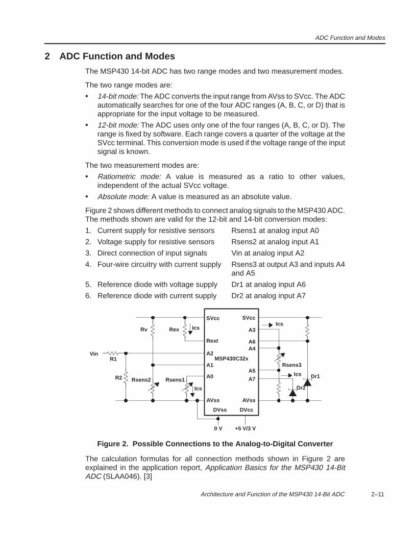
ADC Function and Modes
2–11 Architecture and Function of the MSP430 14-Bit ADC
2 ADC Function and Modes
The MSP430 14-bit ADC has two range modes and two measurement modes.
The two range modes are:
• 14-bit mode: The ADC converts the input range from AVss to SVcc. The ADCautomatically searches for one of the four ADC ranges (A, B, C, or D) that isappropriate for the input voltage to be measured.
• 12-bit mode: The ADC uses only one of the four ranges (A, B, C, or D). Therange is fixed by software. Each range covers a quarter of the voltage at theSVcc terminal. This conversion mode is used if the voltage range of the inputsignal is known.
The two measurement modes are:
• Ratiometric mode: A value is measured as a ratio to other values,independent of the actual SVcc voltage.
• Absolute mode: A value is measured as an absolute value.
Figure 2 shows different methods to connect analog signals to the MSP430 ADC.The methods shown are valid for the 12-bit and 14-bit conversion modes:
1. Current supply for resistive sensors Rsens1 at analog input A0
2. Voltage supply for resistive sensors Rsens2 at analog input A1
3. Direct connection of input signals Vin at analog input A2
4. Four-wire circuitry with current supply Rsens3 at output A3 and inputs A4and A5
5. Reference diode with voltage supply Dr1 at analog input A6
6. Reference diode with current supply Dr2 at analog input A7
SVcc
Rex
SVcc
A3Ics
A6A4
A5
A7
Rsens3
Rext
A2
A1
A0Rsens1
Rv
Rsens2R2
R1Vin
AVssAVss
DVss DVcc
0 V +5 V/3 V
Ics
Ics Dr2
Dr1
MSP430C32x
Ics
Figure 2. Possible Connections to the Analog-to-Digital Converter
The calculation formulas for all connection methods shown in Figure 2 areexplained in the application report, Application Basics for the MSP430 14-BitADC (SLAA046). [3]
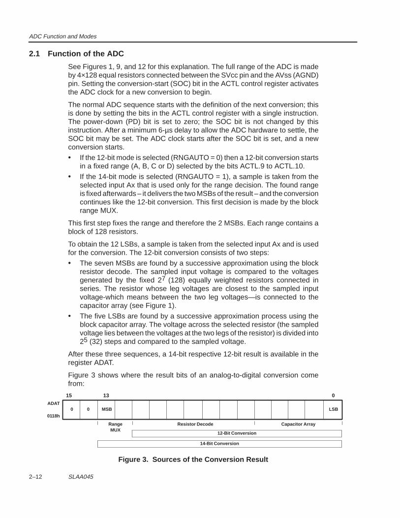
ADC Function and Modes
2–12 SLAA045
2.1 Function of the ADC
See Figures 1, 9, and 12 for this explanation. The full range of the ADC is madeby 4×128 equal resistors connected between the SVcc pin and the AVss (AGND)pin. Setting the conversion-start (SOC) bit in the ACTL control register activatesthe ADC clock for a new conversion to begin.
The normal ADC sequence starts with the definition of the next conversion; thisis done by setting the bits in the ACTL control register with a single instruction.The power-down (PD) bit is set to zero; the SOC bit is not changed by thisinstruction. After a minimum 6-µs delay to allow the ADC hardware to settle, theSOC bit may be set. The ADC clock starts after the SOC bit is set, and a newconversion starts.
• If the 12-bit mode is selected (RNGAUTO = 0) then a 12-bit conversion startsin a fixed range (A, B, C or D) selected by the bits ACTL.9 to ACTL.10.
• If the 14-bit mode is selected (RNGAUTO = 1), a sample is taken from theselected input Ax that is used only for the range decision. The found rangeis fixed afterwards – it delivers the two MSBs of the result – and the conversioncontinues like the 12-bit conversion. This first decision is made by the blockrange MUX.
This first step fixes the range and therefore the 2 MSBs. Each range contains ablock of 128 resistors.
To obtain the 12 LSBs, a sample is taken from the selected input Ax and is usedfor the conversion. The 12-bit conversion consists of two steps:
• The seven MSBs are found by a successive approximation using the blockresistor decode. The sampled input voltage is compared to the voltagesgenerated by the fixed 27 (128) equally weighted resistors connected inseries. The resistor whose leg voltages are closest to the sampled inputvoltage-which means between the two leg voltages—is connected to thecapacitor array (see Figure 1).
• The five LSBs are found by a successive approximation process using theblock capacitor array. The voltage across the selected resistor (the sampledvoltage lies between the voltages at the two legs of the resistor) is divided into25 (32) steps and compared to the sampled voltage.
After these three sequences, a 14-bit respective 12-bit result is available in theregister ADAT.
Figure 3 shows where the result bits of an analog-to-digital conversion comefrom:
15 0
Resistor Decode
0 0 MSB LSB
RangeMUX
Capacitor Array
13
12-Bit Conversion
14-Bit Conversion
ADAT
0118h
Figure 3. Sources of the Conversion Result
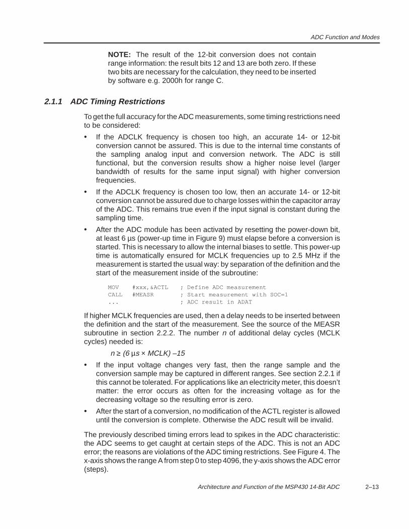
ADC Function and Modes
2–13 Architecture and Function of the MSP430 14-Bit ADC
NOTE: The result of the 12-bit conversion does not containrange information: the result bits 12 and 13 are both zero. If thesetwo bits are necessary for the calculation, they need to be insertedby software e.g. 2000h for range C.
2.1.1 ADC Timing Restrictions
To get the full accuracy for the ADC measurements, some timing restrictions needto be considered:
• If the ADCLK frequency is chosen too high, an accurate 14- or 12-bitconversion cannot be assured. This is due to the internal time constants ofthe sampling analog input and conversion network. The ADC is stillfunctional, but the conversion results show a higher noise level (largerbandwidth of results for the same input signal) with higher conversionfrequencies.
• If the ADCLK frequency is chosen too low, then an accurate 14- or 12-bitconversion cannot be assured due to charge losses within the capacitor arrayof the ADC. This remains true even if the input signal is constant during thesampling time.
• After the ADC module has been activated by resetting the power-down bit,at least 6 µs (power-up time in Figure 9) must elapse before a conversion isstarted. This is necessary to allow the internal biases to settle. This power-uptime is automatically ensured for MCLK frequencies up to 2.5 MHz if themeasurement is started the usual way: by separation of the definition and thestart of the measurement inside of the subroutine:
MOV #xxx,&ACTL ; Define ADC measurementCALL #MEASR ; Start measurement with SOC=1... ; ADC result in ADAT
If higher MCLK frequencies are used, then a delay needs to be inserted betweenthe definition and the start of the measurement. See the source of the MEASRsubroutine in section 2.2.2. The number n of additional delay cycles (MCLKcycles) needed is:
n ≥ (6 µs × MCLK) –15
• If the input voltage changes very fast, then the range sample and theconversion sample may be captured in different ranges. See section 2.2.1 ifthis cannot be tolerated. For applications like an electricity meter, this doesn’tmatter: the error occurs as often for the increasing voltage as for thedecreasing voltage so the resulting error is zero.
• After the start of a conversion, no modification of the ACTL register is alloweduntil the conversion is complete. Otherwise the ADC result will be invalid.
The previously described timing errors lead to spikes in the ADC characteristic:the ADC seems to get caught at certain steps of the ADC. This is not an ADCerror; the reasons are violations of the ADC timing restrictions. See Figure 4. Thex-axis shows the range A from step 0 to step 4096, the y-axis shows the ADC error(steps).
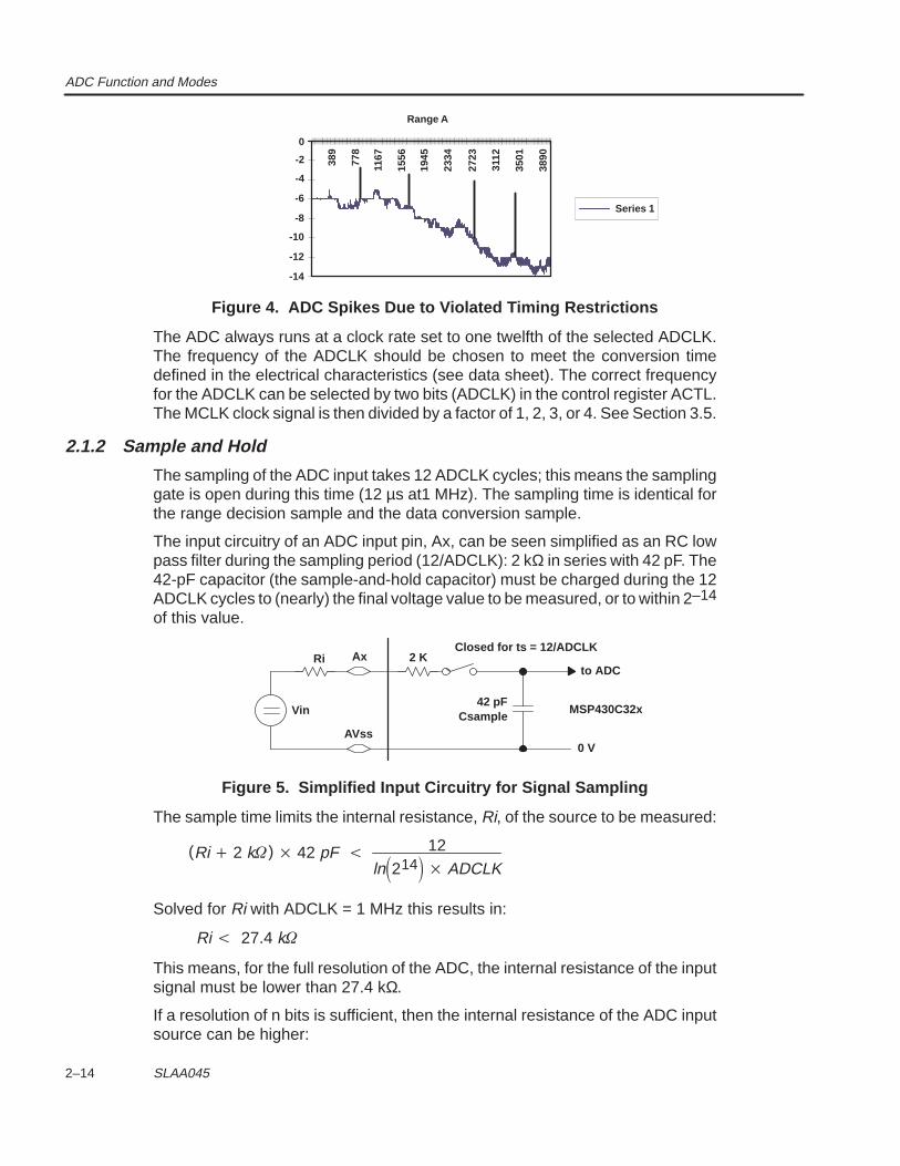
ADC Function and Modes
2–14 SLAA045
-12
-14
-10
-8
Range A
-6Series 1
-4
-2
0
389
778
1167
1556
1945
2334
2723
3112
3501
3890
Figure 4. ADC Spikes Due to Violated Timing Restrictions
The ADC always runs at a clock rate set to one twelfth of the selected ADCLK.The frequency of the ADCLK should be chosen to meet the conversion timedefined in the electrical characteristics (see data sheet). The correct frequencyfor the ADCLK can be selected by two bits (ADCLK) in the control register ACTL.The MCLK clock signal is then divided by a factor of 1, 2, 3, or 4. See Section 3.5.
2.1.2 Sample and Hold
The sampling of the ADC input takes 12 ADCLK cycles; this means the samplinggate is open during this time (12 µs at1 MHz). The sampling time is identical forthe range decision sample and the data conversion sample.
The input circuitry of an ADC input pin, Ax, can be seen simplified as an RC lowpass filter during the sampling period (12/ADCLK): 2 kΩ in series with 42 pF. The42-pF capacitor (the sample-and-hold capacitor) must be charged during the 12ADCLK cycles to (nearly) the final voltage value to be measured, or to within 2–14
of this value.
Ri
Vin
AVss
Ax 2 KClosed for ts = 12/ADCLK
to ADC
42 pFCsample
MSP430C32x
0 V
Figure 5. Simplified Input Circuitry for Signal Sampling
The sample time limits the internal resistance, Ri, of the source to be measured:
(Ri 2 k) 42 pF 12ln214 ADCLK
Solved for Ri with ADCLK = 1 MHz this results in:
Ri 27.4 k
This means, for the full resolution of the ADC, the internal resistance of the inputsignal must be lower than 27.4 kΩ.
If a resolution of n bits is sufficient, then the internal resistance of the ADC inputsource can be higher:
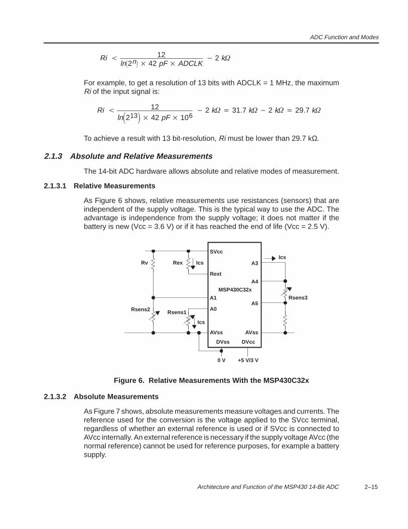
ADC Function and Modes
2–15 Architecture and Function of the MSP430 14-Bit ADC
Ri 12ln2n 42 pF ADCLK
2 k
For example, to get a resolution of 13 bits with ADCLK = 1 MHz, the maximumRi of the input signal is:
Ri 12ln213 42 pF 106
2 k 31.7 k 2 k 29.7 k
To achieve a result with 13 bit-resolution, Ri must be lower than 29.7 kΩ.
2.1.3 Absolute and Relative Measurements
The 14-bit ADC hardware allows absolute and relative modes of measurement.
2.1.3.1 Relative Measurements
As Figure 6 shows, relative measurements use resistances (sensors) that areindependent of the supply voltage. This is the typical way to use the ADC. Theadvantage is independence from the supply voltage; it does not matter if thebattery is new (Vcc = 3.6 V) or if it has reached the end of life (Vcc = 2.5 V).
SVcc
Rex A3Ics
A4
A5
Rext
A1
A0
Rv
AVssAVss
DVss DVcc
0 V +5 V/3 V
Ics
Ics
MSP430C32x
Rsens1Rsens2
Rsens3
Figure 6. Relative Measurements With the MSP430C32x
2.1.3.2 Absolute Measurements
As Figure 7 shows, absolute measurements measure voltages and currents. Thereference used for the conversion is the voltage applied to the SVcc terminal,regardless of whether an external reference is used or if SVcc is connected toAVcc internally. An external reference is necessary if the supply voltage AVcc (thenormal reference) cannot be used for reference purposes, for example a batterysupply.
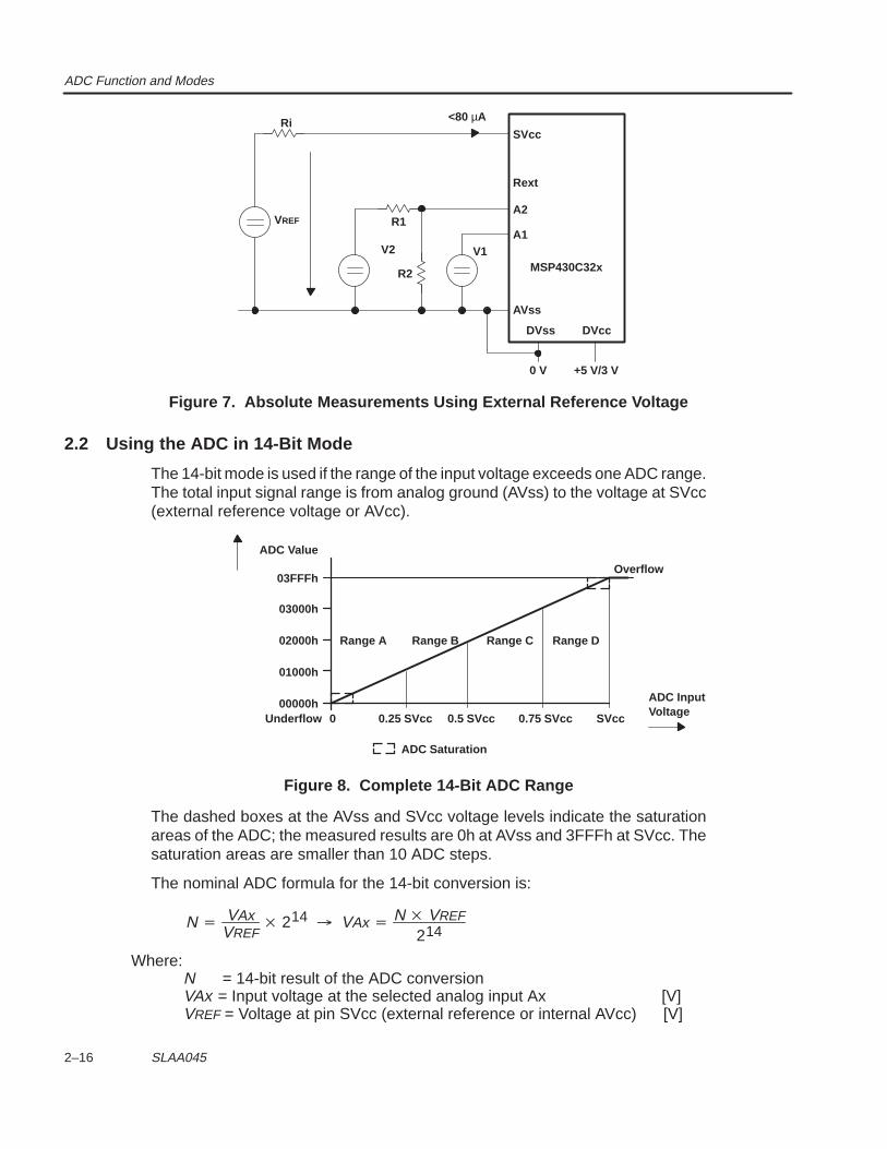
ADC Function and Modes
2–16 SLAA045
SVcc
Rext
A2
A1
AVss
DVss DVcc
0 V +5 V/3 V
MSP430C32x
<80 µARi
R1
V2
R2
V1
VREF
Figure 7. Absolute Measurements Using External Reference Voltage
2.2 Using the ADC in 14-Bit Mode
The 14-bit mode is used if the range of the input voltage exceeds one ADC range.The total input signal range is from analog ground (AVss) to the voltage at SVcc(external reference voltage or AVcc).
03FFFh
ADC Value
03000h
02000h
01000h
00000h0 0.25 SVcc 0.5 SVcc 0.75 SVcc SVcc
ADC InputVoltage
Overflow
ADC Saturation
Underflow
Range A Range B Range C Range D
Figure 8. Complete 14-Bit ADC Range
The dashed boxes at the AVss and SVcc voltage levels indicate the saturationareas of the ADC; the measured results are 0h at AVss and 3FFFh at SVcc. Thesaturation areas are smaller than 10 ADC steps.
The nominal ADC formula for the 14-bit conversion is:
N VAxVREF
214 VAx N VREF
214
Where:N = 14-bit result of the ADC conversionVAx = Input voltage at the selected analog input Ax [V]VREF = Voltage at pin SVcc (external reference or internal AVcc) [V]
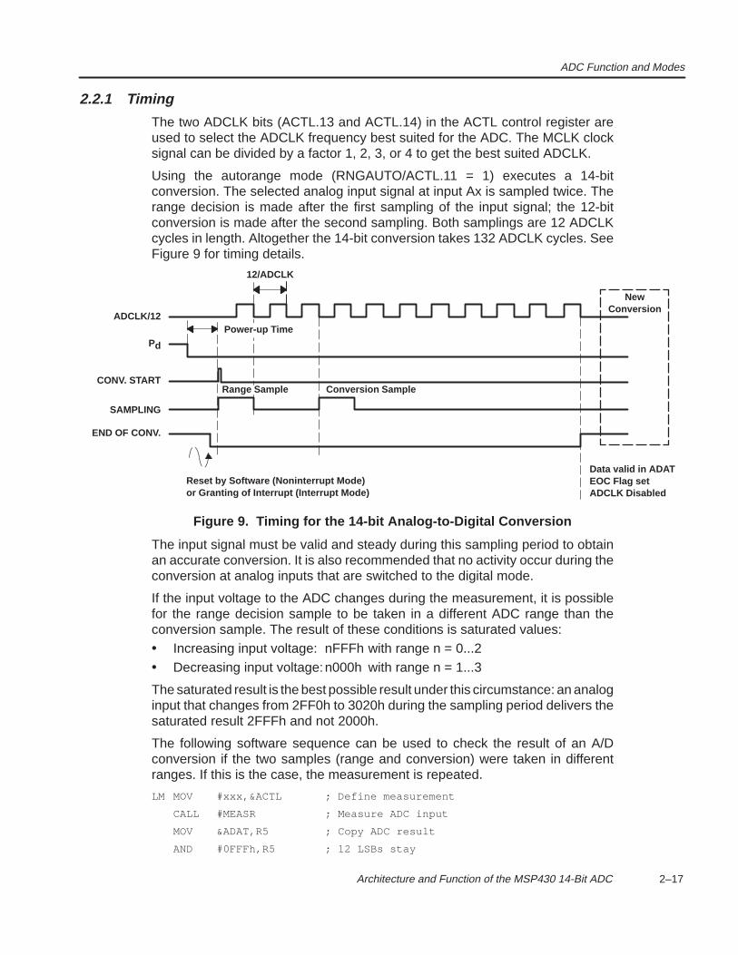
ADC Function and Modes
2–17 Architecture and Function of the MSP430 14-Bit ADC
2.2.1 Timing
The two ADCLK bits (ACTL.13 and ACTL.14) in the ACTL control register areused to select the ADCLK frequency best suited for the ADC. The MCLK clocksignal can be divided by a factor 1, 2, 3, or 4 to get the best suited ADCLK.
Using the autorange mode (RNGAUTO/ACTL.11 = 1) executes a 14-bitconversion. The selected analog input signal at input Ax is sampled twice. Therange decision is made after the first sampling of the input signal; the 12-bitconversion is made after the second sampling. Both samplings are 12 ADCLKcycles in length. Altogether the 14-bit conversion takes 132 ADCLK cycles. SeeFigure 9 for timing details.
Reset by Software (Noninterrupt Mode)or Granting of Interrupt (Interrupt Mode)
Data valid in ADATEOC Flag setADCLK Disabled
NewConversion
ADCLK/12
Pd
CONV. START
SAMPLING
END OF CONV.
12/ADCLK
Range Sample Conversion Sample
Power-up Time
Figure 9. Timing for the 14-bit Analog-to-Digital Conversion
The input signal must be valid and steady during this sampling period to obtainan accurate conversion. It is also recommended that no activity occur during theconversion at analog inputs that are switched to the digital mode.
If the input voltage to the ADC changes during the measurement, it is possiblefor the range decision sample to be taken in a different ADC range than theconversion sample. The result of these conditions is saturated values:• Increasing input voltage: nFFFh with range n = 0...2• Decreasing input voltage:n000h with range n = 1...3
The saturated result is the best possible result under this circumstance: an analoginput that changes from 2FF0h to 3020h during the sampling period delivers thesaturated result 2FFFh and not 2000h.
The following software sequence can be used to check the result of an A/Dconversion if the two samples (range and conversion) were taken in differentranges. If this is the case, the measurement is repeated.
LM MOV #xxx,&ACTL ; Define measurement
CALL #MEASR ; Measure ADC input
MOV &ADAT,R5 ; Copy ADC result
AND #0FFFh,R5 ; 12 LSBs stay
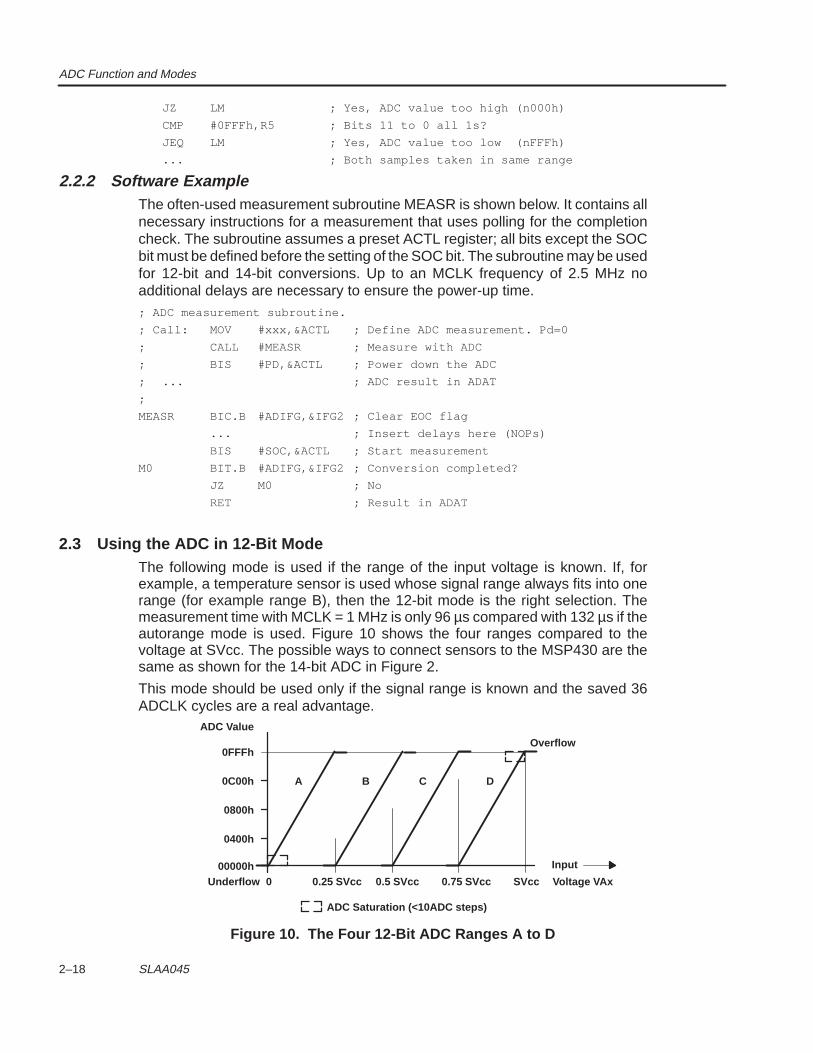
ADC Function and Modes
2–18 SLAA045
JZ LM ; Yes, ADC value too high (n000h)
CMP #0FFFh,R5 ; Bits 11 to 0 all 1s?
JEQ LM ; Yes, ADC value too low (nFFFh)
... ; Both samples taken in same range
2.2.2 Software ExampleThe often-used measurement subroutine MEASR is shown below. It contains allnecessary instructions for a measurement that uses polling for the completioncheck. The subroutine assumes a preset ACTL register; all bits except the SOCbit must be defined before the setting of the SOC bit. The subroutine may be usedfor 12-bit and 14-bit conversions. Up to an MCLK frequency of 2.5 MHz noadditional delays are necessary to ensure the power-up time.; ADC measurement subroutine.
; Call: MOV #xxx,&ACTL ; Define ADC measurement. Pd=0
; CALL #MEASR ; Measure with ADC
; BIS #PD,&ACTL ; Power down the ADC
; ... ; ADC result in ADAT
;
MEASR BIC.B #ADIFG,&IFG2 ; Clear EOC flag
... ; Insert delays here (NOPs)
BIS #SOC,&ACTL ; Start measurement
M0 BIT.B #ADIFG,&IFG2 ; Conversion completed?
JZ M0 ; No
RET ; Result in ADAT
2.3 Using the ADC in 12-Bit ModeThe following mode is used if the range of the input voltage is known. If, forexample, a temperature sensor is used whose signal range always fits into onerange (for example range B), then the 12-bit mode is the right selection. Themeasurement time with MCLK = 1 MHz is only 96 µs compared with 132 µs if theautorange mode is used. Figure 10 shows the four ranges compared to thevoltage at SVcc. The possible ways to connect sensors to the MSP430 are thesame as shown for the 14-bit ADC in Figure 2.
This mode should be used only if the signal range is known and the saved 36ADCLK cycles are a real advantage.
ADC Value
0FFFh
0C00h
0800h
0400h
00000h0 0.25 SVcc 0.5 SVcc 0.75 SVcc SVcc Voltage VAx
Input
Underflow
A B C D
Overflow
ADC Saturation (<10ADC steps)
Figure 10. The Four 12-Bit ADC Ranges A to D
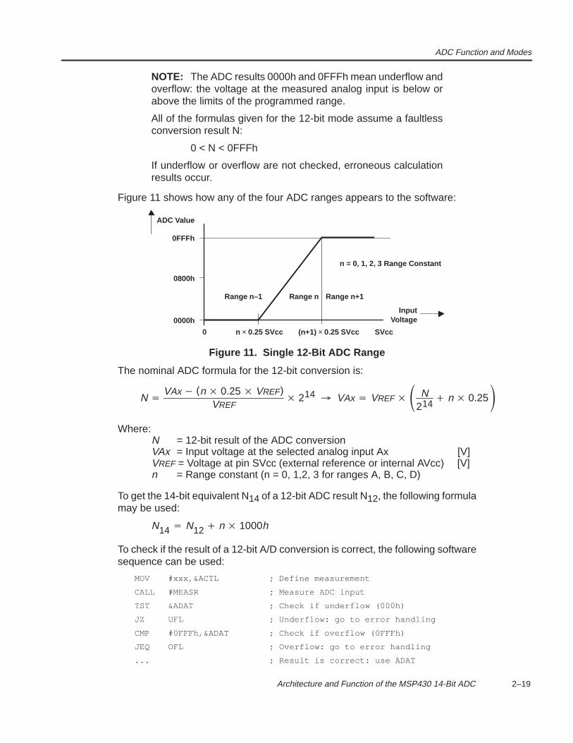
ADC Function and Modes
2–19 Architecture and Function of the MSP430 14-Bit ADC
NOTE: The ADC results 0000h and 0FFFh mean underflow andoverflow: the voltage at the measured analog input is below orabove the limits of the programmed range.
All of the formulas given for the 12-bit mode assume a faultlessconversion result N:
0 < N < 0FFFh
If underflow or overflow are not checked, erroneous calculationresults occur.
Figure 11 shows how any of the four ADC ranges appears to the software:
InputVoltage
ADC Value
0FFFh
0800h
0000h
0 n × 0.25 SVcc (n+1) × 0.25 SVcc SVcc
Range n–1 Range n Range n+1
n = 0, 1, 2, 3 Range Constant
Figure 11. Single 12-Bit ADC Range
The nominal ADC formula for the 12-bit conversion is:
N VAx (n 0.25 VREF)
VREF 214 VAx VREF N
214 n 0.25
Where:N = 12-bit result of the ADC conversionVAx = Input voltage at the selected analog input Ax [V]VREF = Voltage at pin SVcc (external reference or internal AVcc) [V]n = Range constant (n = 0, 1,2, 3 for ranges A, B, C, D)
To get the 14-bit equivalent N14 of a 12-bit ADC result N12, the following formulamay be used:
N14 N12 n 1000h
To check if the result of a 12-bit A/D conversion is correct, the following softwaresequence can be used:
MOV #xxx,&ACTL ; Define measurement
CALL #MEASR ; Measure ADC input
TST &ADAT ; Check if underflow (000h)
JZ UFL ; Underflow: go to error handling
CMP #0FFFh,&ADAT ; Check if overflow (0FFFh)
JEQ OFL ; Overflow: go to error handling
... ; Result is correct: use ADAT
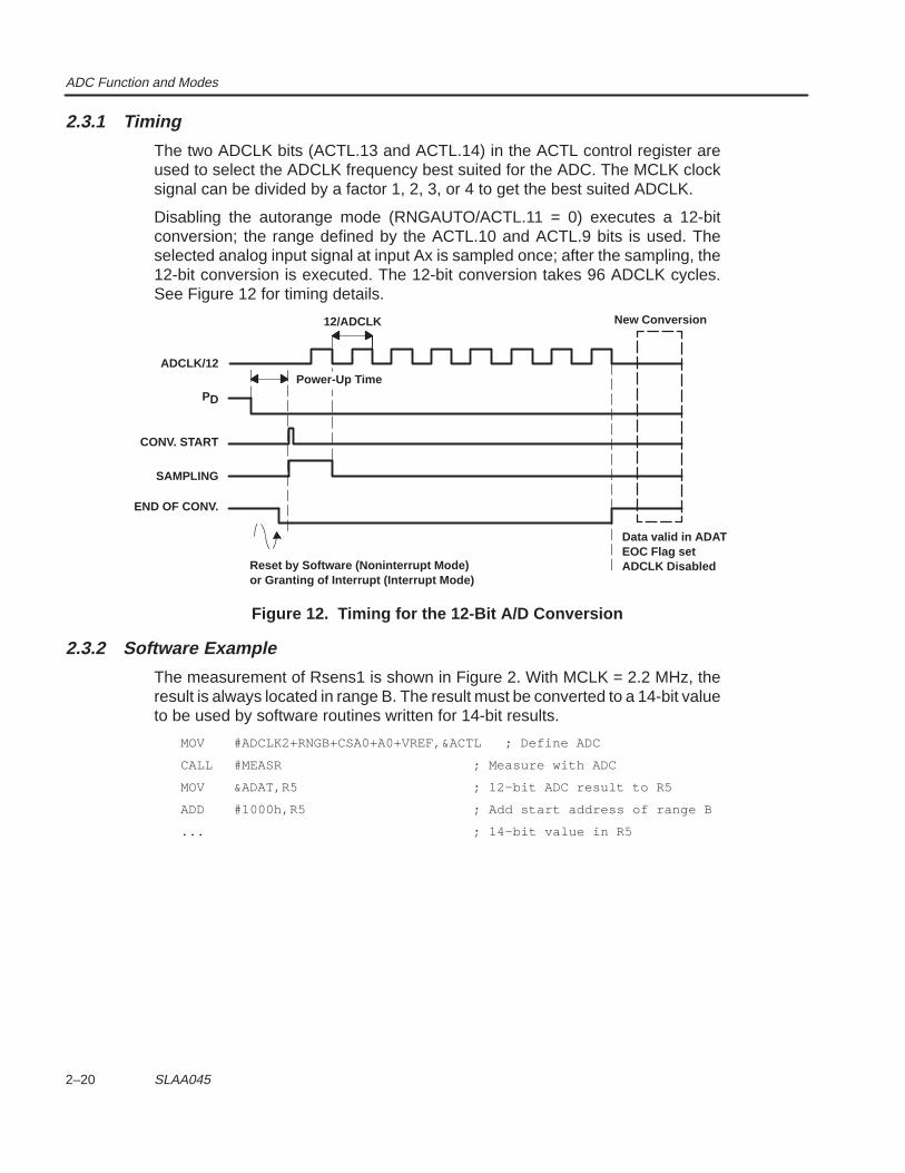
ADC Function and Modes
2–20 SLAA045
2.3.1 Timing
The two ADCLK bits (ACTL.13 and ACTL.14) in the ACTL control register areused to select the ADCLK frequency best suited for the ADC. The MCLK clocksignal can be divided by a factor 1, 2, 3, or 4 to get the best suited ADCLK.
Disabling the autorange mode (RNGAUTO/ACTL.11 = 0) executes a 12-bitconversion; the range defined by the ACTL.10 and ACTL.9 bits is used. Theselected analog input signal at input Ax is sampled once; after the sampling, the12-bit conversion is executed. The 12-bit conversion takes 96 ADCLK cycles.See Figure 12 for timing details.
Reset by Software (Noninterrupt Mode)or Granting of Interrupt (Interrupt Mode)
Data valid in ADATEOC Flag setADCLK Disabled
New Conversion
ADCLK/12
PD
CONV. START
SAMPLING
END OF CONV.
12/ADCLK
Power-Up Time
Figure 12. Timing for the 12-Bit A/D Conversion
2.3.2 Software Example
The measurement of Rsens1 is shown in Figure 2. With MCLK = 2.2 MHz, theresult is always located in range B. The result must be converted to a 14-bit valueto be used by software routines written for 14-bit results.
MOV #ADCLK2+RNGB+CSA0+A0+VREF,&ACTL ; Define ADC
CALL #MEASR ; Measure with ADC
MOV &ADAT,R5 ; 12-bit ADC result to R5
ADD #1000h,R5 ; Add start address of range B
... ; 14-bit value in R5
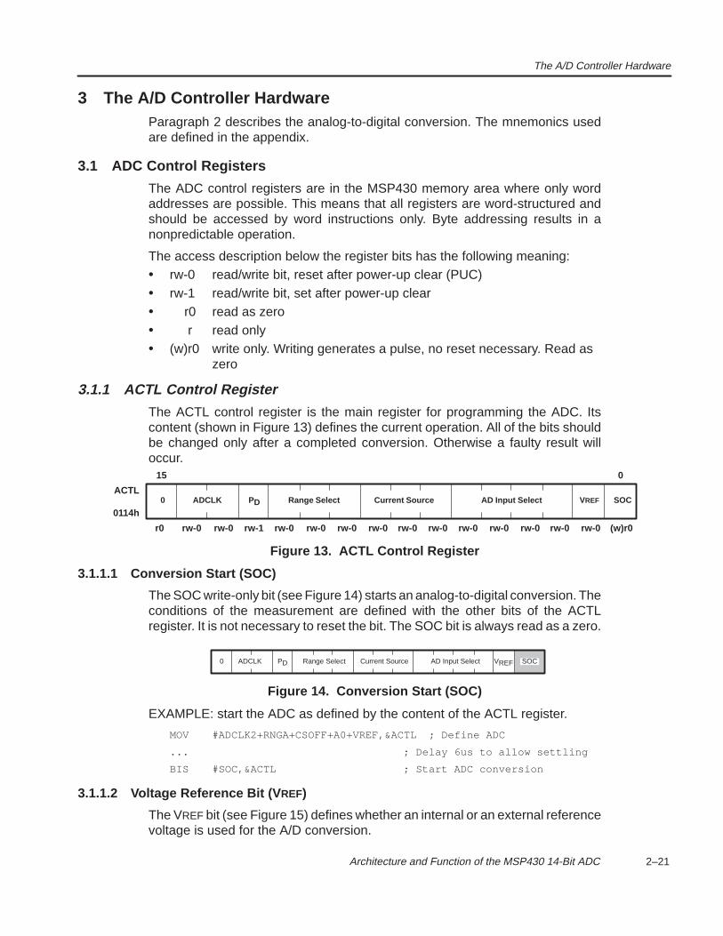
The A/D Controller Hardware
2–21 Architecture and Function of the MSP430 14-Bit ADC
3 The A/D Controller HardwareParagraph 2 describes the analog-to-digital conversion. The mnemonics usedare defined in the appendix.
3.1 ADC Control Registers
The ADC control registers are in the MSP430 memory area where only wordaddresses are possible. This means that all registers are word-structured andshould be accessed by word instructions only. Byte addressing results in anonpredictable operation.
The access description below the register bits has the following meaning:• rw-0 read/write bit, reset after power-up clear (PUC)• rw-1 read/write bit, set after power-up clear• r0 read as zero• r read only• (w)r0 write only. Writing generates a pulse, no reset necessary. Read as
zero
3.1.1 ACTL Control Register
The ACTL control register is the main register for programming the ADC. Itscontent (shown in Figure 13) defines the current operation. All of the bits shouldbe changed only after a completed conversion. Otherwise a faulty result willoccur.
r0
15 0
ACTLAD Input Select0
0114h
rw-0 (w)r0rw-0 rw-1 rw-0 rw-0 rw-0 rw-0 rw-0 rw-0 rw-0 rw-0 rw-0 rw-0 rw-0
ADCLK P D Range Select Current Source V REF SOC
Figure 13. ACTL Control Register
3.1.1.1 Conversion Start (SOC)
The SOC write-only bit (see Figure 14) starts an analog-to-digital conversion. Theconditions of the measurement are defined with the other bits of the ACTLregister. It is not necessary to reset the bit. The SOC bit is always read as a zero.
AD Input Select0 PD Range Select Current Source VREFADCLK SOC
Figure 14. Conversion Start (SOC)
EXAMPLE: start the ADC as defined by the content of the ACTL register.
MOV #ADCLK2+RNGA+CSOFF+A0+VREF,&ACTL ; Define ADC
... ; Delay 6us to allow settling
BIS #SOC,&ACTL ; Start ADC conversion
3.1.1.2 Voltage Reference Bit (V REF)
The VREF bit (see Figure 15) defines whether an internal or an external referencevoltage is used for the A/D conversion.
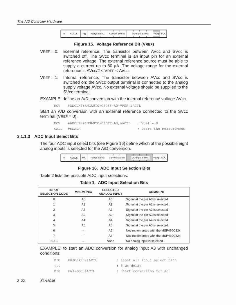
The A/D Controller Hardware
2–22 SLAA045
AD Input Select0 PD Range Select Current Source VREF SOCADCLK
Figure 15. Voltage Reference Bit (V REF)
VREF = 0: External reference. The transistor between AVcc and SVcc isswitched off. The SVcc terminal is an input pin for an externalreference voltage. The external reference source must be able tosupply a current up to 80 µA. The voltage range for the externalreference is AVcc/2 ≤ VREF ≤ AVcc.
VREF = 1: Internal reference. The transistor between AVcc and SVcc isswitched on: the SVcc output terminal is connected to the analogsupply voltage AVcc. No external voltage should be supplied to theSVcc terminal.
EXAMPLE: define an A/D conversion with the internal reference voltage AVcc.
MOV #ADCLK2+RNGAUTO+CSOFF+A0+VREF,&ACTL
Start an A/D conversion with an external reference connected to the SVccterminal (VREF = 0).
MOV #ADCLK2+RNGAUTO+CSOFF+A0,&ACTL ; Vref = 0
CALL #MEASR ; Start the measurement
3.1.1.3 ADC Input Select Bits
The four ADC input select bits (see Figure 16) define which of the possible eightanalog inputs is selected for the A/D conversion.
Range Select0 PD VREF SOCÎÎÎÎCurrent SourceADCLK AD Input Select
Figure 16. ADC Input Selection Bits
Table 2 lists the possible ADC input selections.
Table 1. ADC Input Selection Bits
INPUTSELECTION CODE MNEMONIC
SELECTEDANALOG INPUT COMMENT
0 A0 A0 Signal at the pin A0 is selected
1 A1 A1 Signal at the pin A1 is selected
2 A2 A2 Signal at the pin A2 is selected
3 A3 A3 Signal at the pin A3 is selected
4 A4 A4 Signal at the pin A4 is selected
5 A5 A5 Signal at the pin A5 is selected
6 – A6 Not implemented with the MSP430C32x
7 – A7 Not implemented with the MSP430C32x
8–15 – None No analog input is selected
EXAMPLE: to start an ADC conversion for analog input A3 with unchangedconditions:
BIC #03Ch+PD,&ACTL ; Reset all input select bits
... ; 6 µs delay
BIS #A3+SOC,&ACTL ; Start conversion for A3
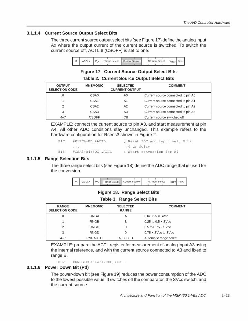
The A/D Controller Hardware
2–23 Architecture and Function of the MSP430 14-Bit ADC
3.1.1.4 Current Source Output Select Bits
The three current source output select bits (see Figure 17) define the analog inputAx where the output current of the current source is switched. To switch thecurrent source off, ACTL.8 (CSOFF) is set to one.
AD Input Select0 PD Range Select VREF SOCÎÎÎÎÎÎÎÎ
Current SourceADCLK
Figure 17. Current Source Output Select Bits
Table 2. Current Source Output Select Bits
OUTPUTSELECTION CODE
MNEMONIC SELECTEDCURRENT OUTPUT
COMMENT
0 CSA0 A0 Current source connected to pin A0
1 CSA1 A1 Current source connected to pin A1
2 CSA2 A2 Current source connected to pin A2
3 CSA3 A3 Current source connected to pin A3
4–7 CSOFF Off Current source switched off
EXAMPLE: connect the current source to pin A3, and start measurement at pinA4. All other ADC conditions stay unchanged. This example refers to thehardware configuration for Rsens3 shown in Figure 2.
BIC #01FCh+PD,&ACTL ; Reset SOC and input sel. Bits
... ;6 µs delay
BIS #CSA3+A4+SOC,&ACTL ; Start conversion for A4
3.1.1.5 Range Selection Bits
The three range select bits (see Figure 18) define the ADC range that is used forthe conversion.
AD Input Select0 PD Range Select VREF SOC
ÎÎÎÎCurrent SourceADCLK
Figure 18. Range Select Bits
Table 3. Range Select Bits
RANGESELECTION CODE
MNEMONIC SELECTEDRANGE
COMMENT
0 RNGA A 0 to 0.25 × SVcc
1 RNGB B 0.25 to 0.5 × SVcc
2 RNGC C 0.5 to 0.75 × SVcc
3 RNGD D 0.75 × SVcc to SVcc
4–7 RNGAUTO A, B, C, D Automatic range select
EXAMPLE: prepare the ACTL register for measurement of analog input A3 usingthe internal reference, and with the current source connected to A3 and fixed torange B.
MOV #RNGB+CSA3+A3+VREF,&ACTL
3.1.1.6 Power Down Bit (Pd)
The power-down bit (see Figure 19) reduces the power consumption of the ADCto the lowest possible value. It switches off the comparator, the SVcc switch, andthe current source.
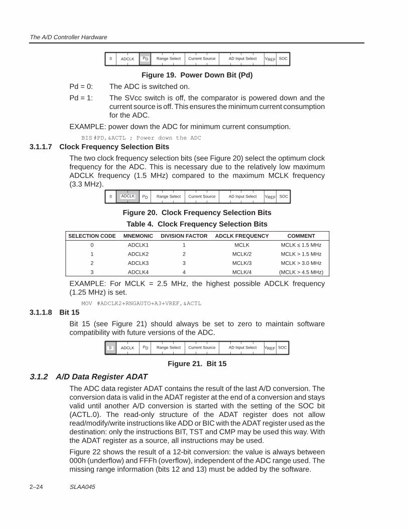
The A/D Controller Hardware
2–24 SLAA045
Range Select AD Input Select0 VREF SOCÎÎÎÎCurrent SourceADCLK PD
Figure 19. Power Down Bit (Pd)
Pd = 0: The ADC is switched on.
Pd = 1: The SVcc switch is off, the comparator is powered down and thecurrent source is off. This ensures the minimum current consumptionfor the ADC.
EXAMPLE: power down the ADC for minimum current consumption.BIS #PD,&ACTL ; Power down the ADC
3.1.1.7 Clock Frequency Selection Bits
The two clock frequency selection bits (see Figure 20) select the optimum clockfrequency for the ADC. This is necessary due to the relatively low maximumADCLK frequency (1.5 MHz) compared to the maximum MCLK frequency(3.3 MHz).
ADCLK PD Range Select AD Input Select0 VREF SOC
ÎÎÎÎCurrent Source
Figure 20. Clock Frequency Selection Bits
Table 4. Clock Frequency Selection Bits
SELECTION CODE MNEMONIC DIVISION FACTOR ADCLK FREQUENCY COMMENT
0 ADCLK1 1 MCLK MCLK ≤ 1.5 MHz
1 ADCLK2 2 MCLK/2 MCLK > 1.5 MHz
2 ADCLK3 3 MCLK/3 MCLK > 3.0 MHz
3 ADCLK4 4 MCLK/4 (MCLK > 4.5 MHz)
EXAMPLE: For MCLK = 2.5 MHz, the highest possible ADCLK frequency(1.25 MHz) is set.
MOV #ADCLK2+RNGAUTO+A3+VREF,&ACTL
3.1.1.8 Bit 15
Bit 15 (see Figure 21) should always be set to zero to maintain softwarecompatibility with future versions of the ADC.
PD Range Select AD Input Select0 VREF SOCÎÎÎÎÎÎÎÎ
Current SourceADCLK
Figure 21. Bit 15
3.1.2 A/D Data Register ADATThe ADC data register ADAT contains the result of the last A/D conversion. Theconversion data is valid in the ADAT register at the end of a conversion and staysvalid until another A/D conversion is started with the setting of the SOC bit(ACTL.0). The read-only structure of the ADAT register does not allowread/modify/write instructions like ADD or BIC with the ADAT register used as thedestination: only the instructions BIT, TST and CMP may be used this way. Withthe ADAT register as a source, all instructions may be used.
Figure 22 shows the result of a 12-bit conversion: the value is always between000h (underflow) and FFFh (overflow), independent of the ADC range used. Themissing range information (bits 12 and 13) must be added by the software.
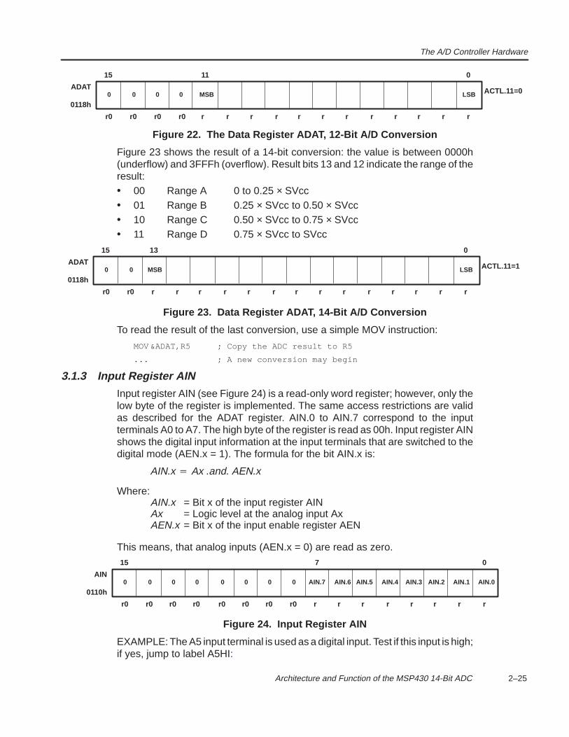
The A/D Controller Hardware
2–25 Architecture and Function of the MSP430 14-Bit ADC
r0
15 0
ADAT0
0118h
ACTL.11=00 0 0 MSB LSB
11
r0 r0 r0 r r r r r r r r r r r r
Figure 22. The Data Register ADAT, 12-Bit A/D Conversion
Figure 23 shows the result of a 14-bit conversion: the value is between 0000h(underflow) and 3FFFh (overflow). Result bits 13 and 12 indicate the range of theresult:• 00 Range A 0 to 0.25 × SVcc• 01 Range B 0.25 × SVcc to 0.50 × SVcc• 10 Range C 0.50 × SVcc to 0.75 × SVcc• 11 Range D 0.75 × SVcc to SVcc
r0
15 0
ADAT0
0118h
ACTL.11=10 MSB LSB
13
r0 r r r r r r r r r r r r r r
Figure 23. Data Register ADAT, 14-Bit A/D Conversion
To read the result of the last conversion, use a simple MOV instruction:
MOV &ADAT,R5 ; Copy the ADC result to R5
... ; A new conversion may begin
3.1.3 Input Register AIN
Input register AIN (see Figure 24) is a read-only word register; however, only thelow byte of the register is implemented. The same access restrictions are validas described for the ADAT register. AIN.0 to AIN.7 correspond to the inputterminals A0 to A7. The high byte of the register is read as 00h. Input register AINshows the digital input information at the input terminals that are switched to thedigital mode (AEN.x = 1). The formula for the bit AIN.x is:
AIN.x Ax .and. AEN.x
Where:AIN.x = Bit x of the input register AINAx = Logic level at the analog input AxAEN.x = Bit x of the input enable register AEN
This means, that analog inputs (AEN.x = 0) are read as zero.
r0
15 0
AIN0
0110h0 AIN.0
r0 r r r r r r r r
0
r0
0
r0
0
r0
0
r0
0
r0
0
r0
AIN.1AIN.2AIN.3AIN.4AIN.5AIN.6AIN.7
7
Figure 24. Input Register AIN
EXAMPLE: The A5 input terminal is used as a digital input. Test if this input is high;if yes, jump to label A5HI:
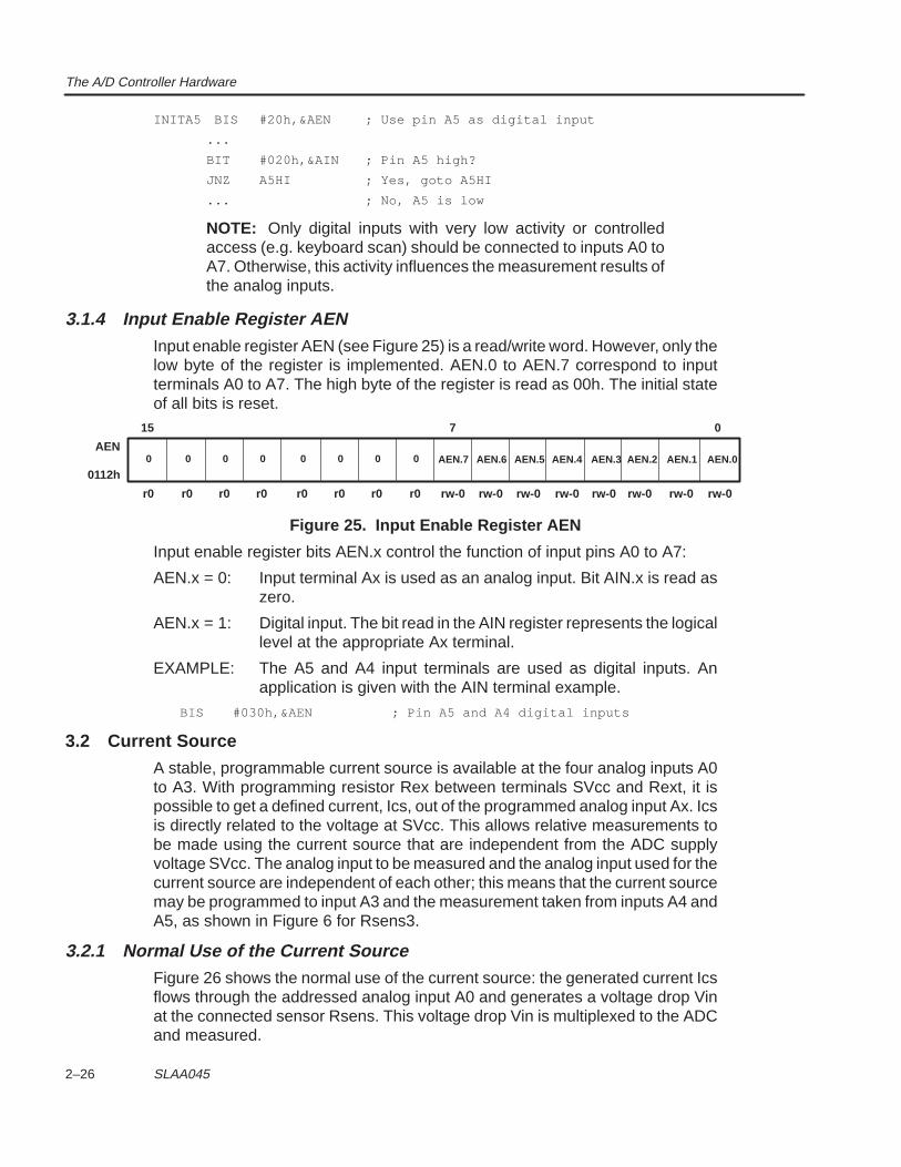
The A/D Controller Hardware
2–26 SLAA045
INITA5 BIS #20h,&AEN ; Use pin A5 as digital input
...
BIT #020h,&AIN ; Pin A5 high?
JNZ A5HI ; Yes, goto A5HI
... ; No, A5 is low
NOTE: Only digital inputs with very low activity or controlledaccess (e.g. keyboard scan) should be connected to inputs A0 toA7. Otherwise, this activity influences the measurement results ofthe analog inputs.
3.1.4 Input Enable Register AENInput enable register AEN (see Figure 25) is a read/write word. However, only thelow byte of the register is implemented. AEN.0 to AEN.7 correspond to inputterminals A0 to A7. The high byte of the register is read as 00h. The initial stateof all bits is reset.
r0
15 0
AEN0
0112h0 AEN.0
r0 rw-0
0
r0
0
r0
0
r0
0
r0
0
r0
0
r0
AEN.1AEN.2AEN.3AEN.4AEN.5AEN.6AEN.7
7
rw-0 rw-0 rw-0 rw-0 rw-0 rw-0 rw-0
Figure 25. Input Enable Register AEN
Input enable register bits AEN.x control the function of input pins A0 to A7:
AEN.x = 0: Input terminal Ax is used as an analog input. Bit AIN.x is read aszero.
AEN.x = 1: Digital input. The bit read in the AIN register represents the logicallevel at the appropriate Ax terminal.
EXAMPLE: The A5 and A4 input terminals are used as digital inputs. Anapplication is given with the AIN terminal example.
BIS #030h,&AEN ; Pin A5 and A4 digital inputs
3.2 Current Source
A stable, programmable current source is available at the four analog inputs A0to A3. With programming resistor Rex between terminals SVcc and Rext, it ispossible to get a defined current, Ics, out of the programmed analog input Ax. Icsis directly related to the voltage at SVcc. This allows relative measurements tobe made using the current source that are independent from the ADC supplyvoltage SVcc. The analog input to be measured and the analog input used for thecurrent source are independent of each other; this means that the current sourcemay be programmed to input A3 and the measurement taken from inputs A4 andA5, as shown in Figure 6 for Rsens3.
3.2.1 Normal Use of the Current SourceFigure 26 shows the normal use of the current source: the generated current Icsflows through the addressed analog input A0 and generates a voltage drop Vinat the connected sensor Rsens. This voltage drop Vin is multiplexed to the ADCand measured.
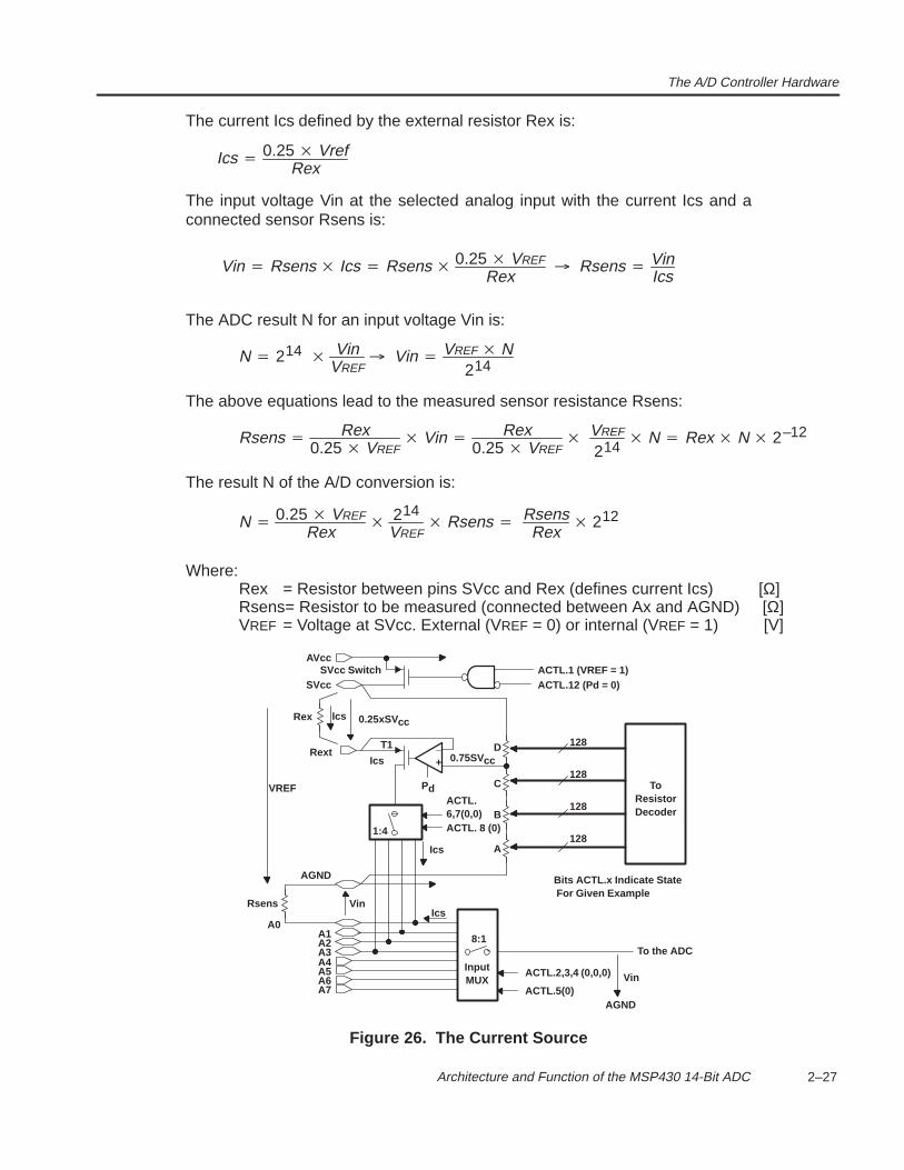
The A/D Controller Hardware
2–27 Architecture and Function of the MSP430 14-Bit ADC
The current Ics defined by the external resistor Rex is:
Ics 0.25 VrefRex
The input voltage Vin at the selected analog input with the current Ics and aconnected sensor Rsens is:
Vin Rsens Ics Rsens 0.25 VREF
Rex Rsens Vin
Ics
The ADC result N for an input voltage Vin is:
N 214 VinVREF
Vin VREF N214
The above equations lead to the measured sensor resistance Rsens:
Rsens Rex0.25 VREF
Vin Rex0.25 VREF
VREF
214 N Rex N 2–12
The result N of the A/D conversion is:
N 0.25 VREF
Rex 214
VREF Rsens Rsens
Rex 212
Where:Rex = Resistor between pins SVcc and Rex (defines current Ics) [Ω]Rsens= Resistor to be measured (connected between Ax and AGND) [Ω]VREF = Voltage at SVcc. External (VREF = 0) or internal (VREF = 1) [V]
ToResistorDecoder
128
8:1To the ADC
ACTL.5(0)
InputMUX
_
+ 0.75SVcc
ACTL.6,7(0,0)ACTL. 8 (0)1:4
A7A6A5A4A3A2A1
A0
AGND
ACTL.12 (Pd = 0)ACTL.1 (VREF = 1)SVcc Switch
IcsD
C
B
A
Rex
Rext
SVcc
AVcc
Rsens
Pd
Ics 0.25xSVcc
128
128
128
Bits ACTL.x Indicate State For Given Example
ACTL.2,3,4 (0,0,0)
AGND
Vin
T1
Ics
IcsVin
VREF
Figure 26. The Current Source
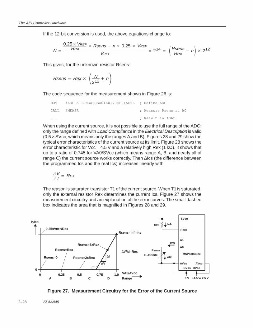
The A/D Controller Hardware
2–28 SLAA045
If the 12-bit conversion is used, the above equations change to:
N
0.25VREFRex Rsens n 0.25 VREF
VREF 214 Rsens
Rex n 212
This gives, for the unknown resistor Rsens:
Rsens Rex N212
n
The code sequence for the measurement shown in Figure 26 is:
MOV #ADCLK1+RNGA+CSA0+A0+VREF,&ACTL ; Define ADC
CALL #MEASR ; Measure Rsens at A0
... ; Result in ADAT
When using the current source, it is not possible to use the full range of the ADC:only the range defined with Load Compliance in the Electrical Description is valid(0.5 × SVcc, which means only the ranges A and B). Figures 28 and 29 show thetypical error characteristics of the current source at its limit. Figure 28 shows theerror characteristic for Vcc = 4.5 V and a relatively high Rex (1 kΩ). It shows thatup to a ratio of 0.745 for VA0/SVcc (which means range A, B, and nearly all ofrange C) the current source works correctly. Then ∆Ics (the difference betweenthe programmed Ics and the real Ics) increases linearly with
VI
Rex
The reason is saturated transistor T1 of the current source. When T1 is saturated,only the external resistor Rex determines the current Ics. Figure 27 shows themeasurement circuitry and an explanation of the error curves. The small dashedbox indicates the area that is magnified in Figures 28 and 29.
AVcc
DVss
AVss
SVcc
Rext
A0
Rex ICS
A1
Rsens
DVcc
0 V +4.5 V/ 2.5 V
Va0
ICS
MSP430C32x0...Infinite
I∆IcsI
0 0.25 0.5 0.75 1.0 VA0/AVcc
RangeA B C D
0.25xVREF/Rex
Rsens=0
Rsens=Rex
Rsens=2xRex
Rsens=7xRex
∆I
∆V
∆V/∆I=Rex
Rsens=Infinite
0
Figure 27. Measurement Circuitry for the Error of the Current Source
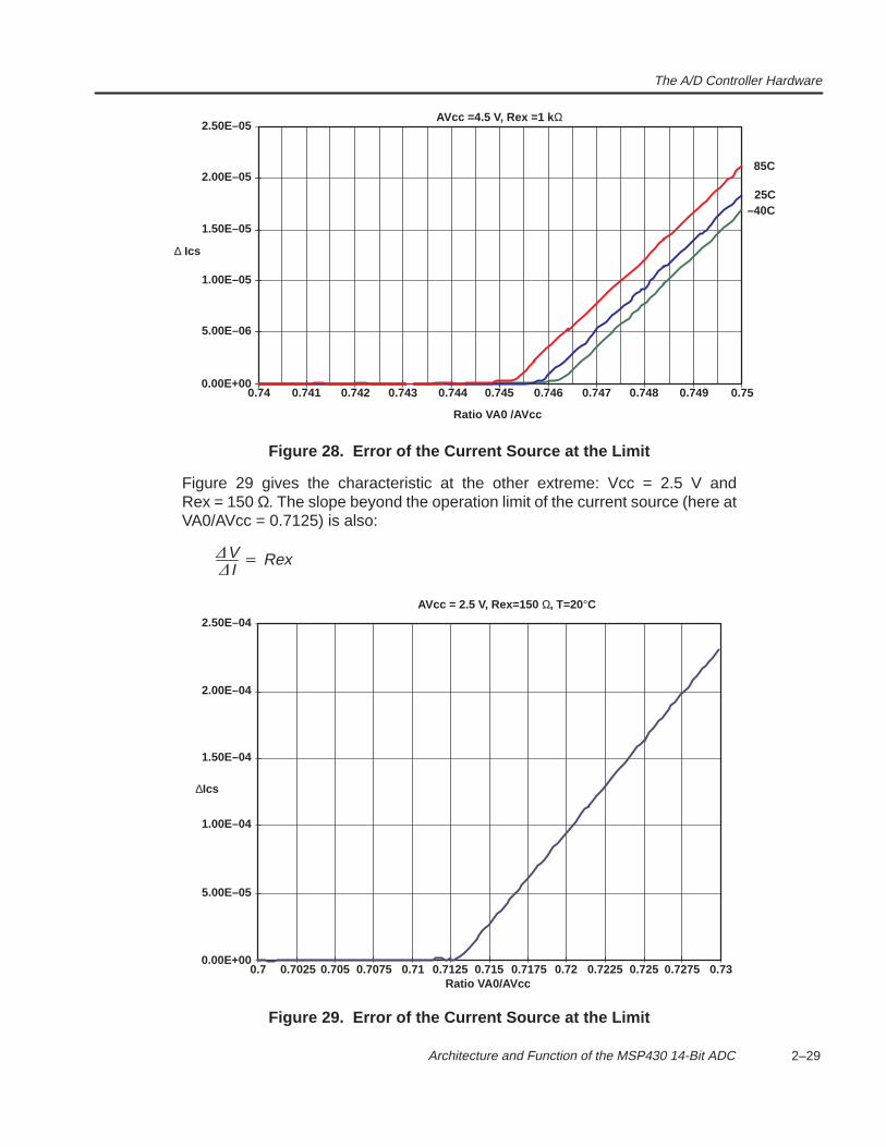
The A/D Controller Hardware
2–29 Architecture and Function of the MSP430 14-Bit ADC
5.00E–06
0.00E+000.74 0.741 0.742 0.743 0.744 0.745 0.746
1.50E–05
2.00E–05
2.50E–05
0.747 0.749 0.750.748
AVcc =4.5 V, Rex =1 k Ω
85C
25C–40C
1.00E–05
∆ Ics
Ratio VA0 /AVcc
Figure 28. Error of the Current Source at the Limit
Figure 29 gives the characteristic at the other extreme: Vcc = 2.5 V andRex = 150 Ω. The slope beyond the operation limit of the current source (here atVA0/AVcc = 0.7125) is also:
VI
Rex
1.00E–04
0.00E+000.7 0.7025 0.705 0.7075 0.71 0.7125 0.715
1.50E–04
2.00E–04
2.50E–04
0.7175 0.72 0.7225 0.725
AVcc = 2.5 V, Rex=150 Ω, T=20°C
Ratio VA0/AVcc
∆Ics
0.7275 0.73
5.00E–05
Figure 29. Error of the Current Source at the Limit
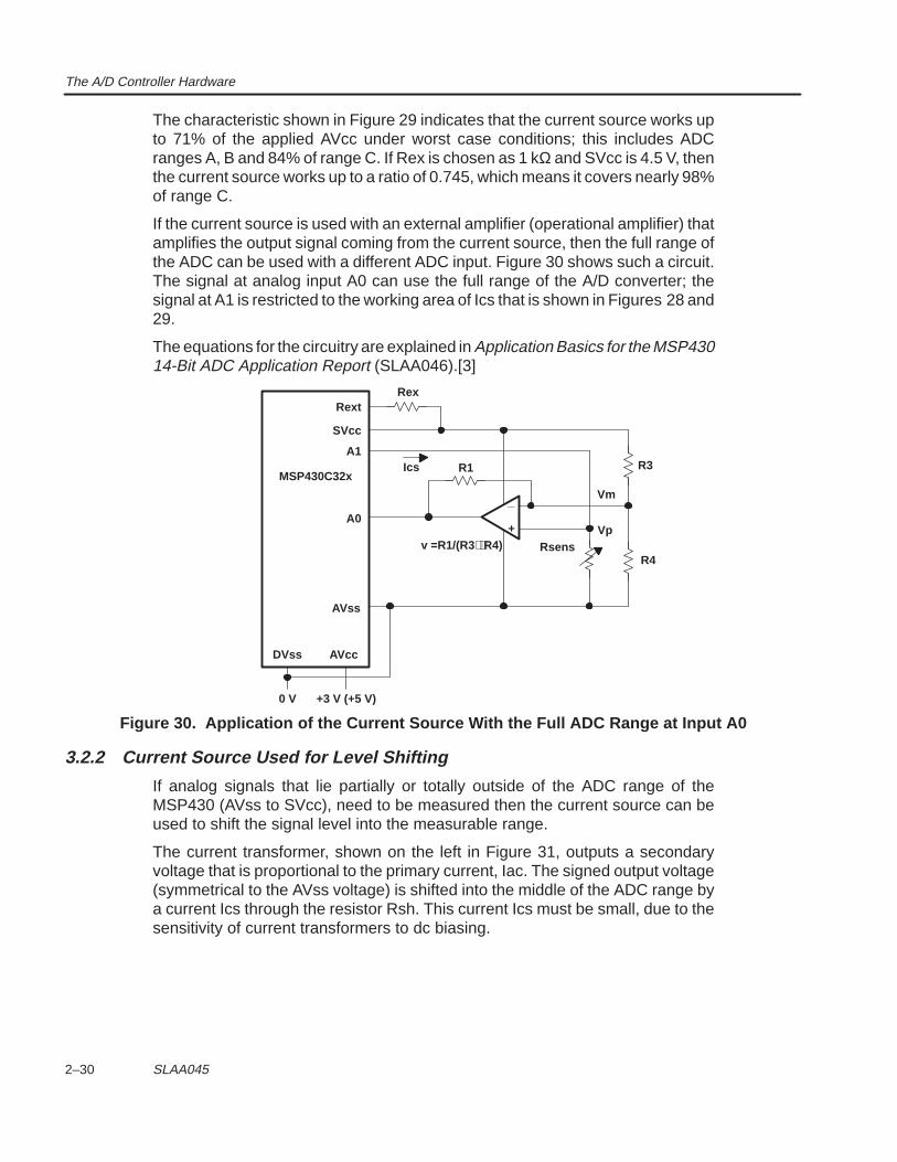
The A/D Controller Hardware
2–30 SLAA045
The characteristic shown in Figure 29 indicates that the current source works upto 71% of the applied AVcc under worst case conditions; this includes ADCranges A, B and 84% of range C. If Rex is chosen as 1 kΩ and SVcc is 4.5 V, thenthe current source works up to a ratio of 0.745, which means it covers nearly 98%of range C.
If the current source is used with an external amplifier (operational amplifier) thatamplifies the output signal coming from the current source, then the full range ofthe ADC can be used with a different ADC input. Figure 30 shows such a circuit.The signal at analog input A0 can use the full range of the A/D converter; thesignal at A1 is restricted to the working area of Ics that is shown in Figures 28 and29.
The equations for the circuitry are explained in Application Basics for the MSP43014-Bit ADC Application Report (SLAA046).[3]
_
+
R1
Rex
Vm
R3
R4
SVcc
A0
A1
DVss AVcc
MSP430C32x
0 V +3 V (+5 V)
v =R1/(R3 R4)
Rext
Rsens
Ics
Vp
AVss
Figure 30. Application of the Current Source With the Full ADC Range at Input A0
3.2.2 Current Source Used for Level Shifting
If analog signals that lie partially or totally outside of the ADC range of theMSP430 (AVss to SVcc), need to be measured then the current source can beused to shift the signal level into the measurable range.
The current transformer, shown on the left in Figure 31, outputs a secondaryvoltage that is proportional to the primary current, Iac. The signed output voltage(symmetrical to the AVss voltage) is shifted into the middle of the ADC range bya current Ics through the resistor Rsh. This current Ics must be small, due to thesensitivity of current transformers to dc biasing.
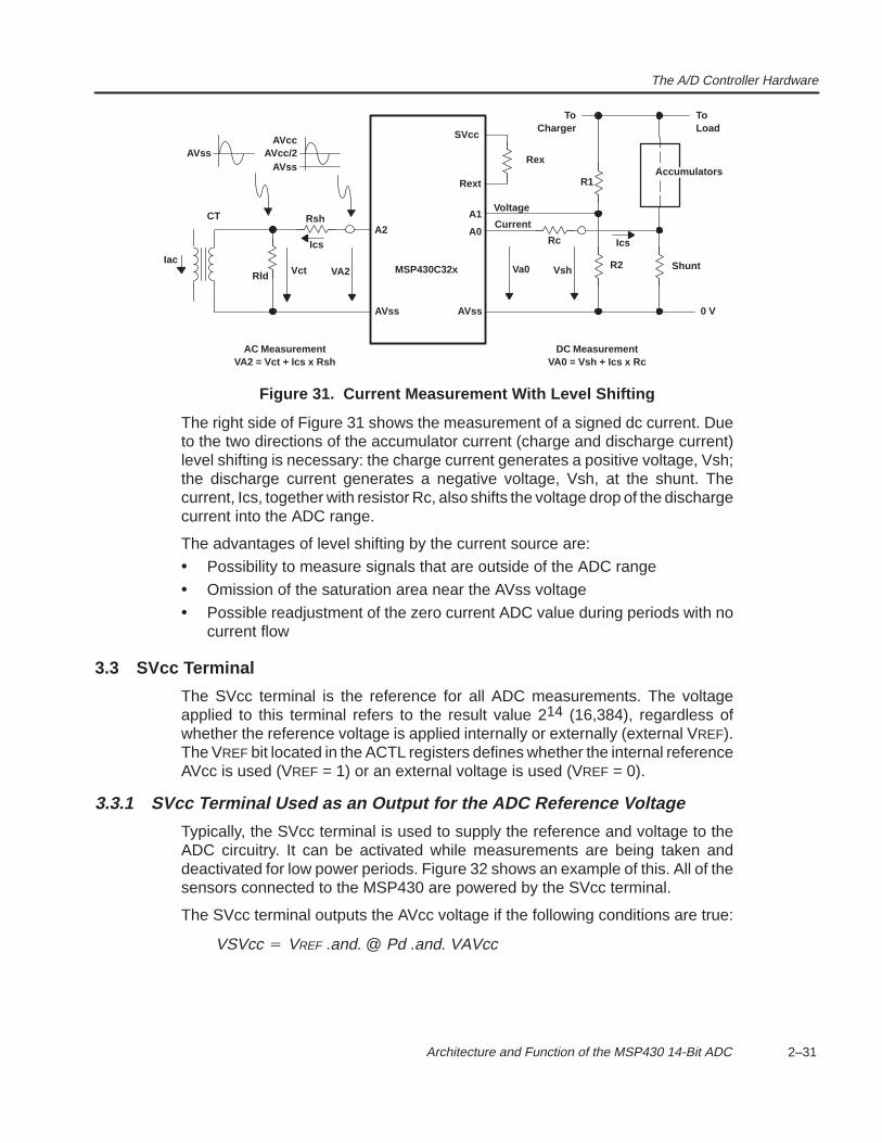
The A/D Controller Hardware
2–31 Architecture and Function of the MSP430 14-Bit ADC
AVss AVcc/2Rex
SVcc
A1
A0
Rext
A2
Rld
AVss AVss
MSP430C32x
0 V
Vct VA2
Ics
RshCT
Iac
AVcc
AVss Accumulators
ShuntR2Va0 Vsh
Rc
Voltage
Current
Ics
ToLoad
R1
ToCharger
AC MeasurementVA2 = Vct + Ics x Rsh
DC MeasurementVA0 = Vsh + Ics x Rc
Figure 31. Current Measurement With Level Shifting
The right side of Figure 31 shows the measurement of a signed dc current. Dueto the two directions of the accumulator current (charge and discharge current)level shifting is necessary: the charge current generates a positive voltage, Vsh;the discharge current generates a negative voltage, Vsh, at the shunt. Thecurrent, Ics, together with resistor Rc, also shifts the voltage drop of the dischargecurrent into the ADC range.
The advantages of level shifting by the current source are:
• Possibility to measure signals that are outside of the ADC range
• Omission of the saturation area near the AVss voltage
• Possible readjustment of the zero current ADC value during periods with nocurrent flow
3.3 SVcc Terminal
The SVcc terminal is the reference for all ADC measurements. The voltageapplied to this terminal refers to the result value 214 (16,384), regardless ofwhether the reference voltage is applied internally or externally (external VREF).The VREF bit located in the ACTL registers defines whether the internal referenceAVcc is used (VREF = 1) or an external voltage is used (VREF = 0).
3.3.1 SVcc Terminal Used as an Output for the ADC Reference Voltage
Typically, the SVcc terminal is used to supply the reference and voltage to theADC circuitry. It can be activated while measurements are being taken anddeactivated for low power periods. Figure 32 shows an example of this. All of thesensors connected to the MSP430 are powered by the SVcc terminal.
The SVcc terminal outputs the AVcc voltage if the following conditions are true:
VSVcc VREF .and. @ Pd .and. VAVcc
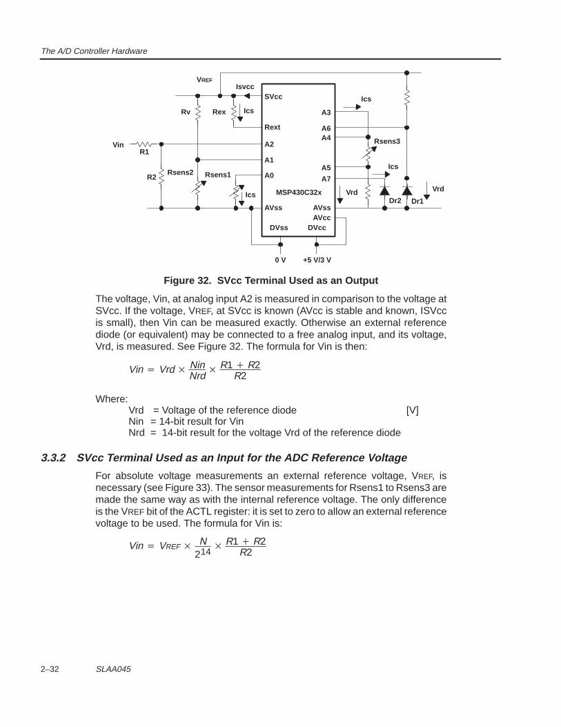
The A/D Controller Hardware
2–32 SLAA045
SVcc
Rex
AVcc
A3
A6A4
A5
A7
Rsens3
Rext
A2
A1
A0Rsens1
Rv
Rsens2R2
R1Vin
AVssAVss
DVss DVcc
0 V +5 V/3 V
MSP430C32xIcs Vrd
Ics
Ics
Ics
VREFIsvcc
Dr2 Dr1
Vrd
Figure 32. SVcc Terminal Used as an Output
The voltage, Vin, at analog input A2 is measured in comparison to the voltage atSVcc. If the voltage, VREF, at SVcc is known (AVcc is stable and known, ISVccis small), then Vin can be measured exactly. Otherwise an external referencediode (or equivalent) may be connected to a free analog input, and its voltage,Vrd, is measured. See Figure 32. The formula for Vin is then:
Vin Vrd NinNrd
R1 R2R2
Where:Vrd = Voltage of the reference diode [V]Nin = 14-bit result for VinNrd = 14-bit result for the voltage Vrd of the reference diode
3.3.2 SVcc Terminal Used as an Input for the ADC Reference Voltage
For absolute voltage measurements an external reference voltage, VREF, isnecessary (see Figure 33). The sensor measurements for Rsens1 to Rsens3 aremade the same way as with the internal reference voltage. The only differenceis the VREF bit of the ACTL register: it is set to zero to allow an external referencevoltage to be used. The formula for Vin is:
Vin VREF N214
R1 R2R2
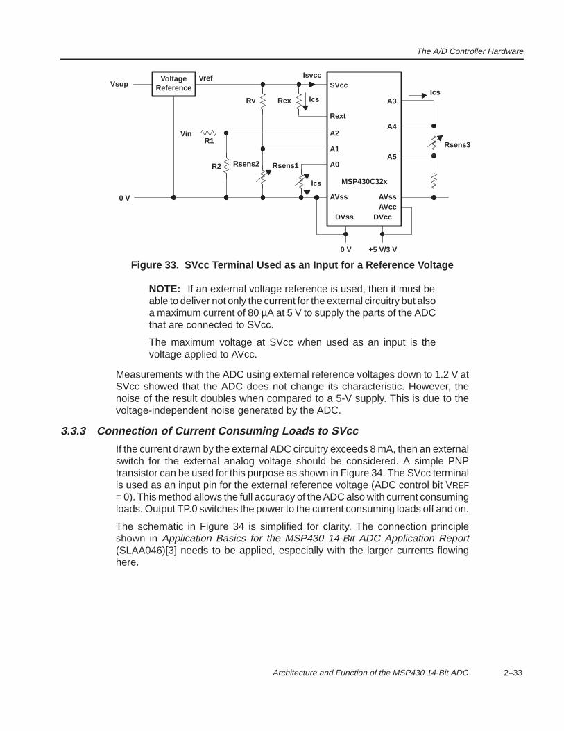
The A/D Controller Hardware
2–33 Architecture and Function of the MSP430 14-Bit ADC
SVcc
Rex
AVcc
A3
A4
A5
Rext
A2
A1
A0
Rv
R2
R1Vin
AVssAVss
DVss DVcc
0 V +5 V/3 V
MSP430C32xIcs
IcsIcs
Vref IsvccVoltageReferenceVsup
0 V
Rsens3
Rsens1Rsens2
Figure 33. SVcc Terminal Used as an Input for a Reference Voltage
NOTE: If an external voltage reference is used, then it must beable to deliver not only the current for the external circuitry but alsoa maximum current of 80 µA at 5 V to supply the parts of the ADCthat are connected to SVcc.
The maximum voltage at SVcc when used as an input is thevoltage applied to AVcc.
Measurements with the ADC using external reference voltages down to 1.2 V atSVcc showed that the ADC does not change its characteristic. However, thenoise of the result doubles when compared to a 5-V supply. This is due to thevoltage-independent noise generated by the ADC.
3.3.3 Connection of Current Consuming Loads to SVcc
If the current drawn by the external ADC circuitry exceeds 8 mA, then an externalswitch for the external analog voltage should be considered. A simple PNPtransistor can be used for this purpose as shown in Figure 34. The SVcc terminalis used as an input pin for the external reference voltage (ADC control bit VREF= 0). This method allows the full accuracy of the ADC also with current consumingloads. Output TP.0 switches the power to the current consuming loads off and on.
The schematic in Figure 34 is simplified for clarity. The connection principleshown in Application Basics for the MSP430 14-Bit ADC Application Report(SLAA046)[3] needs to be applied, especially with the larger currents flowinghere.
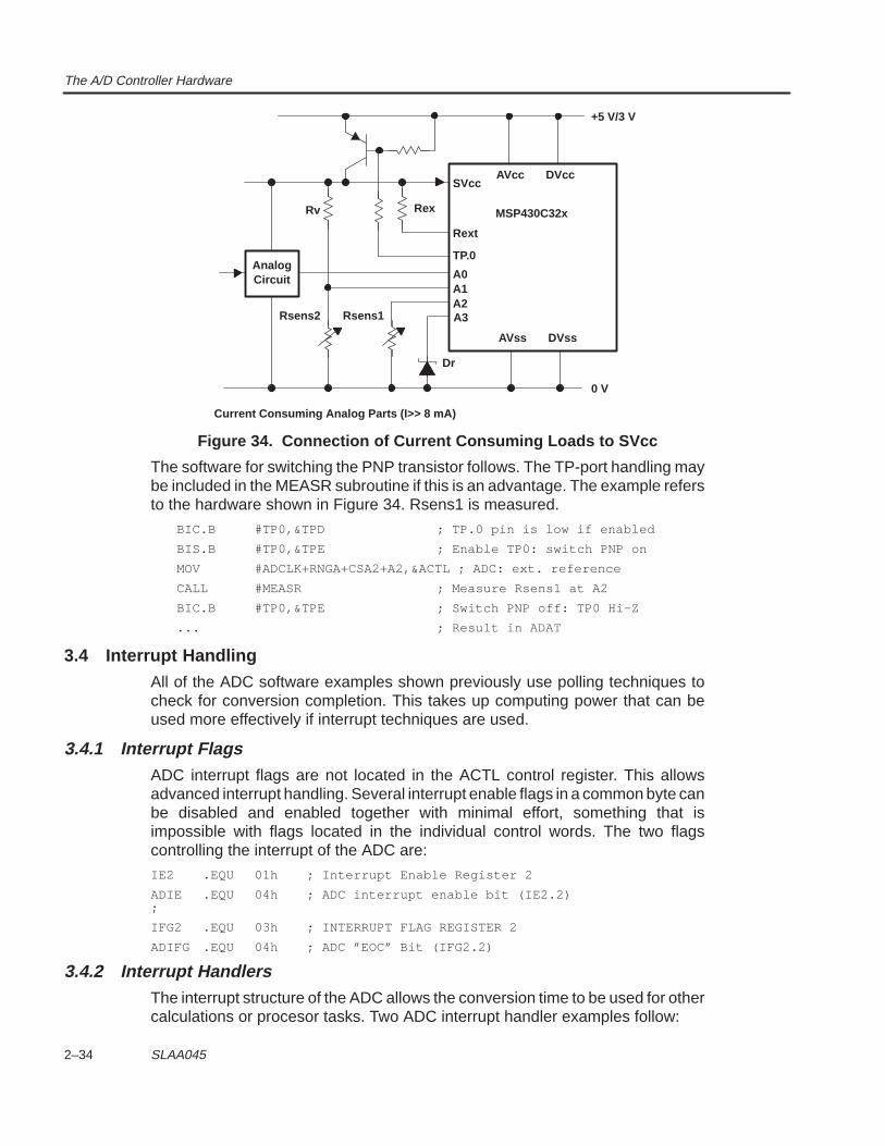
The A/D Controller Hardware
2–34 SLAA045
SVcc
A2A1
Rsens1
AVss DVss
MSP430C32x
Rext
AVcc DVcc
Rsens2
RexRv
TP.0
A0AnalogCircuit
+5 V/3 V
0 V
Current Consuming Analog Parts (I>> 8 mA)
A3
Dr
Figure 34. Connection of Current Consuming Loads to SVcc
The software for switching the PNP transistor follows. The TP-port handling maybe included in the MEASR subroutine if this is an advantage. The example refersto the hardware shown in Figure 34. Rsens1 is measured.
BIC.B #TP0,&TPD ; TP.0 pin is low if enabled
BIS.B #TP0,&TPE ; Enable TP0: switch PNP on
MOV #ADCLK+RNGA+CSA2+A2,&ACTL ; ADC: ext. reference
CALL #MEASR ; Measure Rsens1 at A2
BIC.B #TP0,&TPE ; Switch PNP off: TP0 Hi-Z
... ; Result in ADAT
3.4 Interrupt Handling
All of the ADC software examples shown previously use polling techniques tocheck for conversion completion. This takes up computing power that can beused more effectively if interrupt techniques are used.
3.4.1 Interrupt FlagsADC interrupt flags are not located in the ACTL control register. This allowsadvanced interrupt handling. Several interrupt enable flags in a common byte canbe disabled and enabled together with minimal effort, something that isimpossible with flags located in the individual control words. The two flagscontrolling the interrupt of the ADC are:
IE2 .EQU 01h ; Interrupt Enable Register 2
ADIE .EQU 04h ; ADC interrupt enable bit (IE2.2);
IFG2 .EQU 03h ; INTERRUPT FLAG REGISTER 2
ADIFG .EQU 04h ; ADC ”EOC” Bit (IFG2.2)
3.4.2 Interrupt HandlersThe interrupt structure of the ADC allows the conversion time to be used for othercalculations or procesor tasks. Two ADC interrupt handler examples follow:
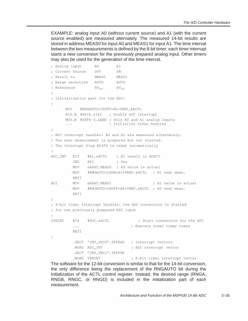
The A/D Controller Hardware
2–35 Architecture and Function of the MSP430 14-Bit ADC
EXAMPLE: analog input A0 (without current source) and A1 (with the currentsource enabled) are measured alternately. The measured 14-bit results arestored in address MEAS0 for input A0 and MEAS1 for input A1. The time intervalbetween the two measurements is defined by the 8-bit timer: each timer interruptstarts a new conversion for the previously prepared analog input. Other timersmay also be used for the generation of the time interval.; Analog input A0 A1
; Current Source OFF ON
; Result to MEAS0 MEAS1
; Range selection AUTO AUTO
; Reference SV cc SVcc
;
; Initialization part for the ADC:
;
MOV #RNGAUTO+CSOFF+A0+VREF,&ACTL
BIS.B #ADIE,&IE2 ; Enable ADC interrupt
MOV.B #0FFh–3,&AEN ; Only A0 and A1 analog inputs... ; Initialize other modules
;
; ADC interrupt handler: A0 and A1 are measured alternately.
; The next measurement is prepared but not started.
; The interrupt flag ADIFG is reset automatically
;
ADC_INT BIT #A1,&ACTL ; A1 result in ADAT?
JNZ ADI ; Yes
MOV &ADAT,MEAS0 ; A0 value is actual
MOV #RNGAUTO+CSON+A1+VREF,&ACTL ; A1 next meas.
RETI
ADI MOV &ADAT,MEAS1 ; A1 value is actual
MOV #RNGAUTO+CSOFF+A0+VREF,&ACTL ; A0 next meas.
RETI
;
; 8-bit timer interrupt handler: the ADC conversion is started
; for the previously prepared ADC input
;
T8BINT BIS #SOC,&ACTL ; Start conversion for the ADC
... ; Execute other timer tasks
RETI
;
.SECT ”INT_VEC0”,0FFEAh ; Interrupt vectors
.WORD ADC_INT ; ADC interrupt vector
.SECT ”INT_VEC1”,0FFF8h
.WORD T8BINT ; 8-bit timer interrupt vector
The software for the 12-bit conversion is similar to that for the 14-bit conversion,the only difference being the replacement of the RNGAUTO bit during theinitialization of the ACTL control register. Instead, the desired range (RNGA,RNGB, RNGC, or RNGD) is included in the initialization part of eachmeasurement.
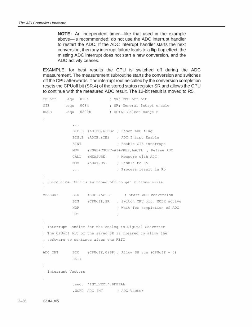
The A/D Controller Hardware
2–36 SLAA045
NOTE: An independent timer—like that used in the exampleabove—is recommended; do not use the ADC interrupt handlerto restart the ADC. If the ADC interrupt handler starts the nextconversion, then any interrupt failure leads to a flip-flop effect; themissing ADC interrupt does not start a new conversion, and theADC activity ceases.
EXAMPLE: for best results the CPU is switched off during the ADCmeasurement. The measurement subroutine starts the conversion and switchesoff the CPU afterwards. The interrupt routine called by the conversion completionresets the CPUoff bit (SR.4) of the stored status register SR and allows the CPUto continue with the measured ADC result. The 12-bit result is moved to R5.
CPUoff .equ 010h ; SR: CPU off bit
GIE .equ 008h ; SR: General Intrpt enable
RNGB .equ 0200h ; ACTL: Select Range B
;
...
BIC.B #ADIFG,&IFG2 ; Reset ADC flag
BIS.B #ADIE,&IE2 ; ADC Intrpt Enable
EINT ; Enable GIE interrupt
MOV #RNGB+CSOFF+A1+VREF,&ACTL ; Define ADC
CALL #MEASURE ; Measure with ADC
MOV &ADAT,R5 ; Result to R5
... ; Process result in R5
;
; Subroutine: CPU is switched off to get minimum noise
;
MEASURE BIS #SOC,&ACTL ; Start ADC conversion
BIS #CPUoff,SR ; Switch CPU off, MCLK active
NOP ; Wait for completion of ADC
RET ;
;
; Interrupt Handler for the Analog-to-Digital Converter
; The CPUoff bit of the saved SR is cleared to allow the
; software to continue after the RETI
;
ADC_INT BIC #CPUoff,0(SP) ; Allow SW run (CPUoff = 0)
RETI
;
; Interrupt Vectors
;
.sect ”INT_VEC1”,0FFEAh
.WORD ADC_INT ; ADC Vector
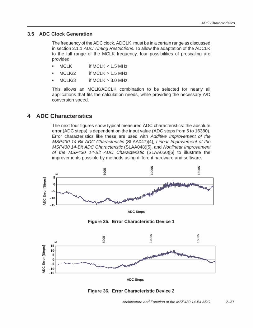
ADC Characteristics
2–37 Architecture and Function of the MSP430 14-Bit ADC
3.5 ADC Clock Generation
The frequency of the ADC clock, ADCLK, must be in a certain range as discussedin section 2.1.1 ADC Timing Restrictions. To allow the adaptation of the ADCLKto the full range of the MCLK frequency, four possibilities of prescaling areprovided:
• MCLK if MCLK < 1.5 MHz
• MCLK/2 if MCLK > 1.5 MHz
• MCLK/3 if MCLK > 3.0 MHz
This allows an MCLK/ADCLK combination to be selected for nearly allapplications that fits the calculation needs, while providing the necessary A/Dconversion speed.
4 ADC Characteristics
The next four figures show typical measured ADC characteristics: the absoluteerror (ADC steps) is dependent on the input value (ADC steps from 5 to 16380).Error characteristics like these are used with Additive Improvement of theMSP430 14-Bit ADC Characteristic (SLAA047)[4], Linear Improvement of theMSP430 14-Bit ADC Characteristic (SLAA048)[5], and Nonlinear Improvementof the MSP430 14-Bit ADC Characteristic (SLAA050)[6] to illustrate theimprovements possible by methods using different hardware and software.
–10
–15AD
C E
rror
[Ste
ps]
–5
0
ADC Steps
5
5 5005
1000
5
1500
5
Figure 35. Error Characteristic Device 1
–10–15A
DC
Err
or [S
teps
]
–50
ADC Steps
510
5 5005
1000
5
1500
5
15
Figure 36. Error Characteristic Device 2
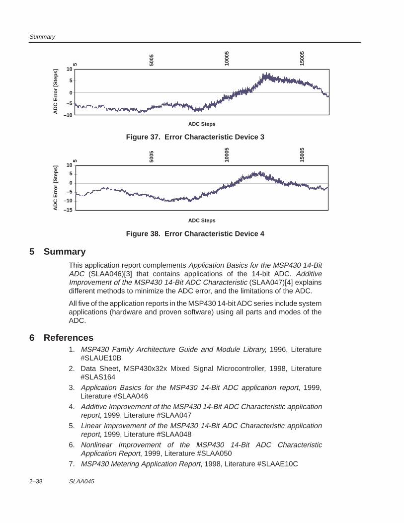
Summary
2–38 SLAA045
–10AD
C E
rror
[Ste
ps]
–5
0
ADC Steps
5
105 50
05
1000
5
1500
5
Figure 37. Error Characteristic Device 3
–10
–15AD
C E
rror
[Ste
ps]
–5
0
ADC Steps
5
10
5 5005
1000
5
1500
5
Figure 38. Error Characteristic Device 4
5 SummaryThis application report complements Application Basics for the MSP430 14-BitADC (SLAA046)[3] that contains applications of the 14-bit ADC. AdditiveImprovement of the MSP430 14-Bit ADC Characteristic (SLAA047)[4] explainsdifferent methods to minimize the ADC error, and the limitations of the ADC.
All five of the application reports in the MSP430 14-bit ADC series include systemapplications (hardware and proven software) using all parts and modes of theADC.
6 References1. MSP430 Family Architecture Guide and Module Library, 1996, Literature
#SLAUE10B
2. Data Sheet, MSP430x32x Mixed Signal Microcontroller, 1998, Literature#SLAS164
3. Application Basics for the MSP430 14-Bit ADC application report, 1999,Literature #SLAA046
4. Additive Improvement of the MSP430 14-Bit ADC Characteristic applicationreport, 1999, Literature #SLAA047
5. Linear Improvement of the MSP430 14-Bit ADC Characteristic applicationreport, 1999, Literature #SLAA048
6. Nonlinear Improvement of the MSP430 14-Bit ADC CharacteristicApplication Report, 1999, Literature #SLAA050
7. MSP430 Metering Application Report, 1998, Literature #SLAAE10C
Definitions Used With the Application Examples
2–39 Architecture and Function of the MSP430 14-Bit ADC
Appendix A Definitions Used With the Application Examples; HARDWARE DEFINITIONS;
AIN .equ 0110h ; Input register (for digital inputs)
AEN .equ 0112h ; 0: analog input 1: digital input;
ACTL .equ 0114h ; ADC control register: control bits
SOC .equ 01h ; Conversion start
VREF .equ 02h ; 0: ext. reference 1: SVcc on
A0 .equ 00h ; Input A0
A1 .equ 04h ; Input A1
A2 .equ 08h ; Input A2
A3 .equ 0Ch ; Input A3
A4 .equ 10h ; Input A4
A5 .equ 14h ; Input A5
CSA0 .equ 00h ; Current Source to A0
CSA1 .equ 40h ; Current Source to A1
CSA2 .equ 80h ; Current Source to A2
CSA3 .equ 0C0h ; Current Source to A3
CSOFF .equ 100h ; Current Source off
CSON .equ 000h ; Current Source on
RNGA .equ 000h ; Range select A (0 ... 0.25 ×SVcc)
RNGB .equ 200h ; Range select B (0.25..0.50 ×SVcc)
RNGC .equ 400h ; Range select C (0.5...0.75 ×SVcc)
RNGD .equ 600h ; Range select D (0.75..SVcc)
RNGAUTO .equ 800h ; 1: range selected automatically
PD .equ 1000h ; 1: ADC powered down
ADCLK1 .equ 0000h ; ADCLK = MCLK
ADCLK2 .equ 2000h ; ADCLK = MCLK/2
ADCLK3 .equ 4000h ; ADCLK = MCLK/3
ADCLK4 .equ 6000h ; ADCLK = MCLK/4;
ADAT .equ 0118h ; ADC data register (12 or 14-bits);
IFG2 .equ 03h ; Interrupt flag register 2
ADIFG .equ 04h ; ADC ”EOC” bit (IFG2.2);
IE2 .equ 01h ; Interrupt enable register 2
ADIE .equ 04h ; ADC interrupt enable bit (IE2.2);
TPD .equ 04Eh ; TP–port: address data register
TPE .equ 04Fh ; TP–port: address of enable register
TP0 .equ 1 ; Bit address of TP.0
TP1 .equ 2 ; Bit address of TP.1

2–40 SLAA045
2–41
Application Basics for the MSP43014-Bit ADC
Lutz Bierl
Literature Number: SLAA046June 1999
Printed on Recycled Paper

2–42
IMPORTANT NOTICE
Texas Instruments and its subsidiaries (TI) reserve the right to make changes to theirproducts or to discontinue any product or service without notice, and advise customers toobtain the latest version of relevant information to verify, before placing orders, thatinformation being relied on is current and complete. All products are sold subject to the termsand conditions of sale supplied at the time of order acknowledgement, including thosepertaining to warranty, patent infringement, and limitation of liability.
TI warrants performance of its semiconductor products to the specifications applicable at thetime of sale in accordance with TI’s standard warranty. Testing and other quality controltechniques are utilized to the extent TI deems necessary to support this warranty. Specifictesting of all parameters of each device is not necessarily performed, except those mandatedby government requirements.
CERTAIN APPLICATIONS USING SEMICONDUCTOR PRODUCTS MAY INVOLVEPOTENTIAL RISKS OF DEATH, PERSONAL INJURY, OR SEVERE PROPERTY ORENVIRONMENTAL DAMAGE (“CRITICAL APPLICATIONS”). TI SEMICONDUCTORPRODUCTS ARE NOT DESIGNED, AUTHORIZED, OR WARRANTED TO BE SUITABLEFOR USE IN LIFE-SUPPORT DEVICES OR SYSTEMS OR OTHER CRITICALAPPLICATIONS. INCLUSION OF TI PRODUCTS IN SUCH APPLICATIONS ISUNDERSTOOD TO BE FULLY AT THE CUSTOMER’S RISK.
In order to minimize risks associated with the customer’s applications, adequate design andoperating safeguards must be provided by the customer to minimize inherent or proceduralhazards.
TI assumes no liability for applications assistance or customer product design. TI does notwarrant or represent that any license, either express or implied, is granted under any patentright, copyright, mask work right, or other intellectual property right of TI covering or relatingto any combination, machine, or process in which such semiconductor products or servicesmight be or are used. TI’s publication of information regarding any third party’s products orservices does not constitute TI’s approval, warranty or endorsement thereof.
Copyright 1999, Texas Instruments Incorporated
2–43 Application Basics for the MSP430 14-Bit ADC
Contents1 Introduction 2-45. . . . . . . . . . . . . . . . . . . . . . . . . . . . . . . . . . . . . . . . . . . . . . . . . . . . . . . . . . . . . . . . . . . . . . . . . . . . . . . .
2 Applications 2-46. . . . . . . . . . . . . . . . . . . . . . . . . . . . . . . . . . . . . . . . . . . . . . . . . . . . . . . . . . . . . . . . . . . . . . . . . . . . . . . . 2.1 Connection of Analog Signals and Sensors 2–46. . . . . . . . . . . . . . . . . . . . . . . . . . . . . . . . . . . . . . . . . . . . . . .
2.1.1 Current Supply for Sensors 2–46. . . . . . . . . . . . . . . . . . . . . . . . . . . . . . . . . . . . . . . . . . . . . . . . . . . . . . 2.1.2 Voltage Supply for Sensors 2–48. . . . . . . . . . . . . . . . . . . . . . . . . . . . . . . . . . . . . . . . . . . . . . . . . . . . . . 2.1.3 Four-Wire Sensors Circuit 2–49. . . . . . . . . . . . . . . . . . . . . . . . . . . . . . . . . . . . . . . . . . . . . . . . . . . . . . . 2.1.4 Connection of Bridge Assemblies 2–50. . . . . . . . . . . . . . . . . . . . . . . . . . . . . . . . . . . . . . . . . . . . . . . . 2.1.5 Reference Measurements 2–52. . . . . . . . . . . . . . . . . . . . . . . . . . . . . . . . . . . . . . . . . . . . . . . . . . . . . . .
2.2 14-Bit Analog-to-Digital Conversion With Signed Signals 2–54. . . . . . . . . . . . . . . . . . . . . . . . . . . . . . . . . . . . 2.2.1 Virtual Ground IC 2–54. . . . . . . . . . . . . . . . . . . . . . . . . . . . . . . . . . . . . . . . . . . . . . . . . . . . . . . . . . . . . . 2.2.2 Split Power Supply 2–55. . . . . . . . . . . . . . . . . . . . . . . . . . . . . . . . . . . . . . . . . . . . . . . . . . . . . . . . . . . . . 2.2.3 Use of the Current Source 2–56. . . . . . . . . . . . . . . . . . . . . . . . . . . . . . . . . . . . . . . . . . . . . . . . . . . . . . 2.2.4 Resistor Divider 2–59. . . . . . . . . . . . . . . . . . . . . . . . . . . . . . . . . . . . . . . . . . . . . . . . . . . . . . . . . . . . . . . .
2.3 12-Bit Analog-to-Digital Conversion With Signed Signals 2–60. . . . . . . . . . . . . . . . . . . . . . . . . . . . . . . . . . . . 2.3.1 Virtual Ground Circuitry 2–60. . . . . . . . . . . . . . . . . . . . . . . . . . . . . . . . . . . . . . . . . . . . . . . . . . . . . . . . . 2.3.2 Use of the Current Source 2–62. . . . . . . . . . . . . . . . . . . . . . . . . . . . . . . . . . . . . . . . . . . . . . . . . . . . . . 2.3.3 Resistor Divider 2–62. . . . . . . . . . . . . . . . . . . . . . . . . . . . . . . . . . . . . . . . . . . . . . . . . . . . . . . . . . . . . . . .
2.4 Reference Resistor Method 2–63. . . . . . . . . . . . . . . . . . . . . . . . . . . . . . . . . . . . . . . . . . . . . . . . . . . . . . . . . . . . . 2.4.1 Reference Resistor Method Without Amplification 2–63. . . . . . . . . . . . . . . . . . . . . . . . . . . . . . . . . . 2.4.2 Reference Resistor Method With Amplification 2–65. . . . . . . . . . . . . . . . . . . . . . . . . . . . . . . . . . . . .
3 Hum and Noise Considerations 2-67. . . . . . . . . . . . . . . . . . . . . . . . . . . . . . . . . . . . . . . . . . . . . . . . . . . . . . . . . . . . . . 3.1 Connection of Long Sensor Lines 2–67. . . . . . . . . . . . . . . . . . . . . . . . . . . . . . . . . . . . . . . . . . . . . . . . . . . . . . . . 3.2 Grounding 2–68. . . . . . . . . . . . . . . . . . . . . . . . . . . . . . . . . . . . . . . . . . . . . . . . . . . . . . . . . . . . . . . . . . . . . . . . . . . . 3.3 Routing 2–69. . . . . . . . . . . . . . . . . . . . . . . . . . . . . . . . . . . . . . . . . . . . . . . . . . . . . . . . . . . . . . . . . . . . . . . . . . . . . . .
4 Enhancement of the Resolution 2-70. . . . . . . . . . . . . . . . . . . . . . . . . . . . . . . . . . . . . . . . . . . . . . . . . . . . . . . . . . . . . . 4.1 16-Bit Mode With the Current Source 2–70. . . . . . . . . . . . . . . . . . . . . . . . . . . . . . . . . . . . . . . . . . . . . . . . . . . . . 4.2 Enhanced Resolution Without Current Source 2–72. . . . . . . . . . . . . . . . . . . . . . . . . . . . . . . . . . . . . . . . . . . . . 4.3 Calculated Resolution of the 16-Bit Mode 2–75. . . . . . . . . . . . . . . . . . . . . . . . . . . . . . . . . . . . . . . . . . . . . . . . .
4.3.1 16-Bit Mode With the Current Source 2–75. . . . . . . . . . . . . . . . . . . . . . . . . . . . . . . . . . . . . . . . . . . . . 4.3.2 16-Bit Mode Without the Current Source 2–75. . . . . . . . . . . . . . . . . . . . . . . . . . . . . . . . . . . . . . . . . .
5 Hints and Recommendations 2-76. . . . . . . . . . . . . . . . . . . . . . . . . . . . . . . . . . . . . . . . . . . . . . . . . . . . . . . . . . . . . . . . 5.1 Replacement of the First Measurement 2–76. . . . . . . . . . . . . . . . . . . . . . . . . . . . . . . . . . . . . . . . . . . . . . . . . . . 5.2 Grounding and Routing 2–76. . . . . . . . . . . . . . . . . . . . . . . . . . . . . . . . . . . . . . . . . . . . . . . . . . . . . . . . . . . . . . . . . 5.3 Supply Voltage and Current 2–76. . . . . . . . . . . . . . . . . . . . . . . . . . . . . . . . . . . . . . . . . . . . . . . . . . . . . . . . . . . . .
5.3.1 Influence of the Supply Voltage 2–76. . . . . . . . . . . . . . . . . . . . . . . . . . . . . . . . . . . . . . . . . . . . . . . . . . 5.3.2 Battery Driven Systems 2–77. . . . . . . . . . . . . . . . . . . . . . . . . . . . . . . . . . . . . . . . . . . . . . . . . . . . . . . . . 5.3.3 Mains Driven Systems 2–78. . . . . . . . . . . . . . . . . . . . . . . . . . . . . . . . . . . . . . . . . . . . . . . . . . . . . . . . . . 5.3.4 Current Consumption 2–78. . . . . . . . . . . . . . . . . . . . . . . . . . . . . . . . . . . . . . . . . . . . . . . . . . . . . . . . . . .
5.4 Use of the Floating Point Package 2–78. . . . . . . . . . . . . . . . . . . . . . . . . . . . . . . . . . . . . . . . . . . . . . . . . . . . . . .
6 Additional Information 2-79. . . . . . . . . . . . . . . . . . . . . . . . . . . . . . . . . . . . . . . . . . . . . . . . . . . . . . . . . . . . . . . . . . . . . .
7 References 2-79. . . . . . . . . . . . . . . . . . . . . . . . . . . . . . . . . . . . . . . . . . . . . . . . . . . . . . . . . . . . . . . . . . . . . . . . . . . . . . . . .
Appendix A Definitions Used With the Application Examples 2-81. . . . . . . . . . . . . . . . . . . . . . . . . . . . . . . . . . . .
Figures
2–44 SLAA046
List of Figures1 MSP430 14-Bit ADC Hardware 2–45. . . . . . . . . . . . . . . . . . . . . . . . . . . . . . . . . . . . . . . . . . . . . . . . . . . . . . . . . . . . . . . . . 2 Possible Connections to the ADC 2–46. . . . . . . . . . . . . . . . . . . . . . . . . . . . . . . . . . . . . . . . . . . . . . . . . . . . . . . . . . . . . . . 3 Current Supply for the Sensor Rx 2–47. . . . . . . . . . . . . . . . . . . . . . . . . . . . . . . . . . . . . . . . . . . . . . . . . . . . . . . . . . . . . . . 4 Voltage Supply for the Sensor Rx 2–48. . . . . . . . . . . . . . . . . . . . . . . . . . . . . . . . . . . . . . . . . . . . . . . . . . . . . . . . . . . . . . . 5 Four-Wire Circuit With Current Supply 2–49. . . . . . . . . . . . . . . . . . . . . . . . . . . . . . . . . . . . . . . . . . . . . . . . . . . . . . . . . . . 6 Connection of Bridge Assemblies 2–50. . . . . . . . . . . . . . . . . . . . . . . . . . . . . . . . . . . . . . . . . . . . . . . . . . . . . . . . . . . . . . . 7 Connecting Reference Elements 2–53. . . . . . . . . . . . . . . . . . . . . . . . . . . . . . . . . . . . . . . . . . . . . . . . . . . . . . . . . . . . . . . . 8 Virtual Ground IC for Signed Voltage Measurement 2–54. . . . . . . . . . . . . . . . . . . . . . . . . . . . . . . . . . . . . . . . . . . . . . . . 9 Split Power Supply for Signed Voltage Measurement 2–56. . . . . . . . . . . . . . . . . . . . . . . . . . . . . . . . . . . . . . . . . . . . . . 10 Current Source Used for Level Shifting 2–57. . . . . . . . . . . . . . . . . . . . . . . . . . . . . . . . . . . . . . . . . . . . . . . . . . . . . . . . . 11 Signed Signals Shifted With the Current Source 2–57. . . . . . . . . . . . . . . . . . . . . . . . . . . . . . . . . . . . . . . . . . . . . . . . . . 12 Signed Current Measurement With Level Shifting (Current Source) 2–58. . . . . . . . . . . . . . . . . . . . . . . . . . . . . . . . . 13 Resistor Divider for High Input Voltages 2–59. . . . . . . . . . . . . . . . . . . . . . . . . . . . . . . . . . . . . . . . . . . . . . . . . . . . . . . . . 14 Virtual Ground Circuitry for Level Shifting 2–61. . . . . . . . . . . . . . . . . . . . . . . . . . . . . . . . . . . . . . . . . . . . . . . . . . . . . . . 15 Current Source Used for Level Shifting 2–62. . . . . . . . . . . . . . . . . . . . . . . . . . . . . . . . . . . . . . . . . . . . . . . . . . . . . . . . . 16 Referencing With Precision Resistors – No Amplification 2–64. . . . . . . . . . . . . . . . . . . . . . . . . . . . . . . . . . . . . . . . . . 17 Referencing with Precision Resistors – With Amplification 2–66. . . . . . . . . . . . . . . . . . . . . . . . . . . . . . . . . . . . . . . . . 18 Sensor Connection via Long Cables With Voltage Supply 2–67. . . . . . . . . . . . . . . . . . . . . . . . . . . . . . . . . . . . . . . . . 19 Analog-to-Digital Converter Grounding 2–68. . . . . . . . . . . . . . . . . . . . . . . . . . . . . . . . . . . . . . . . . . . . . . . . . . . . . . . . . . 20 Routing That is Sensitive to External EMI 2–69. . . . . . . . . . . . . . . . . . . . . . . . . . . . . . . . . . . . . . . . . . . . . . . . . . . . . . . 21 Routing for Minimum EMI Sensitivity 2–69. . . . . . . . . . . . . . . . . . . . . . . . . . . . . . . . . . . . . . . . . . . . . . . . . . . . . . . . . . . 22 Dividing of an ADC-Step Into Four Steps 2–70. . . . . . . . . . . . . . . . . . . . . . . . . . . . . . . . . . . . . . . . . . . . . . . . . . . . . . . . 23 Hardware for a 16-Bit ADC 2–71. . . . . . . . . . . . . . . . . . . . . . . . . . . . . . . . . . . . . . . . . . . . . . . . . . . . . . . . . . . . . . . . . . . . 24 ADC-Resolution Expanded to 15 Bits 2–72. . . . . . . . . . . . . . . . . . . . . . . . . . . . . . . . . . . . . . . . . . . . . . . . . . . . . . . . . . . 25 ADC-Resolution Expanded to 16 Bits 2–73. . . . . . . . . . . . . . . . . . . . . . . . . . . . . . . . . . . . . . . . . . . . . . . . . . . . . . . . . . . 26 Influence of the Supply Voltage 2–77. . . . . . . . . . . . . . . . . . . . . . . . . . . . . . . . . . . . . . . . . . . . . . . . . . . . . . . . . . . . . . . .
List of Tables1 Resistor Ratios 2–61. . . . . . . . . . . . . . . . . . . . . . . . . . . . . . . . . . . . . . . . . . . . . . . . . . . . . . . . . . . . . . . . . . . . . . . . . . . . . . . 2 Measurement Results of the 16-Bit Method 2–70. . . . . . . . . . . . . . . . . . . . . . . . . . . . . . . . . . . . . . . . . . . . . . . . . . . . . . . 3 Calculation Results for Different 16-Bit Corrections 2–75. . . . . . . . . . . . . . . . . . . . . . . . . . . . . . . . . . . . . . . . . . . . . . . .
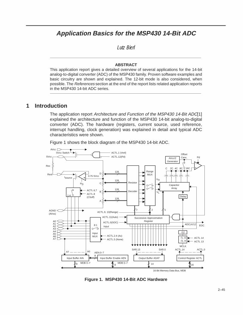
2–45
Application Basics for the MSP430 14-Bit ADC
Lutz Bierl
ABSTRACTThis application report gives a detailed overview of several applications for the 14-bitanalog-to-digital converter (ADC) of the MSP430 family. Proven software examples andbasic circuitry are shown and explained. The 12-bit mode is also considered, whenpossible. The References section at the end of the report lists related application reportsin the MSP430 14-bit ADC series.
1 IntroductionThe application report Architecture and Function of the MSP430 14-Bit ADC[1]explained the architecture and function of the MSP430 14-bit analog-to-digitalconverter (ADC). The hardware (registers, current source, used reference,interrupt handling, clock generation) was explained in detail and typical ADCcharacteristics were shown.
Figure 1 shows the block diagram of the MSP430 14-bit ADC.
AVcc/2Generator
_
+
Successive ApproximationRegister
SAR.13 SAR.0 ACTL.14 ACTL.0
14 16
Output Buffer ADAT Control Register ACTL
/12
/1, /2/3, /4
ACTL 14
ACTL 13
ACTL.0(SOC)
ACTL.11(Auto)
ACTL.9, 10(Range)
Resistor
RangeMUX
7 2
ADCLK/12 EOC
5
Delay
VH
VL
CapacitorArray
AVcc/2Generator
C 2C 4C 8C
Pd
16C
128
8:1 Input
ACTL.2.4 (Ax)
ACTL.5 (None)
8
Input Buffer Enable AEN
A7 A0
8
8
MDB 0–7
AEN.0–7
_
+0.75 SVcc
ACTL.6,7
ACTL.8(CSoff)
1:4
A7A6A5A4A3A2A1A0
AGND(AVss)
ACTL.12(Pd)
ACTL.1 (Vref)SVcc Switch
Isource
D
C
B
A
Rext
Rex
SVcc
AVcc
16-Bit Memory Data Bus, MDB
PD
Decoder
Input Buffer AIN
MDB 0–7
InputMUX
OffsetCanc.
128
128
128
MCLK
Figure 1. MSP430 14-Bit ADC Hardware
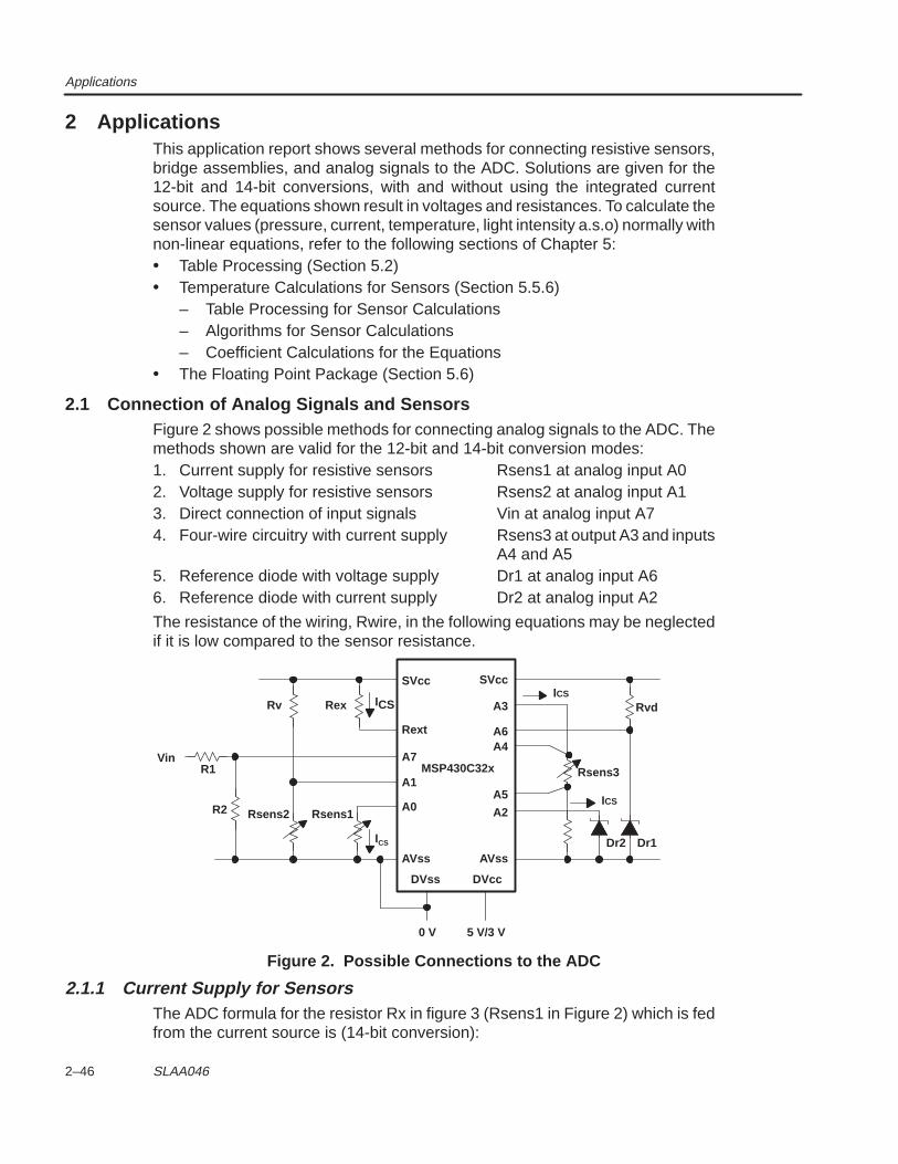
Applications
2–46 SLAA046
2 ApplicationsThis application report shows several methods for connecting resistive sensors,bridge assemblies, and analog signals to the ADC. Solutions are given for the12-bit and 14-bit conversions, with and without using the integrated currentsource. The equations shown result in voltages and resistances. To calculate thesensor values (pressure, current, temperature, light intensity a.s.o) normally withnon-linear equations, refer to the following sections of Chapter 5:• Table Processing (Section 5.2)• Temperature Calculations for Sensors (Section 5.5.6)
– Table Processing for Sensor Calculations– Algorithms for Sensor Calculations– Coefficient Calculations for the Equations
• The Floating Point Package (Section 5.6)
2.1 Connection of Analog Signals and SensorsFigure 2 shows possible methods for connecting analog signals to the ADC. Themethods shown are valid for the 12-bit and 14-bit conversion modes:1. Current supply for resistive sensors Rsens1 at analog input A02. Voltage supply for resistive sensors Rsens2 at analog input A13. Direct connection of input signals Vin at analog input A74. Four-wire circuitry with current supply Rsens3 at output A3 and inputs
A4 and A55. Reference diode with voltage supply Dr1 at analog input A66. Reference diode with current supply Dr2 at analog input A2
The resistance of the wiring, Rwire, in the following equations may be neglectedif it is low compared to the sensor resistance.
SVcc
Rex
SVcc
A3ICS
A6A4
A5
A2
Rvd
Rext
A7
A1
A0Rsens1
Rv
Rsens2R2
R1Vin
AVssAVss
DVss DVcc
0 V 5 V/3 V
ICS
ICS
ICS
Dr2 Dr1
MSP430C32x Rsens3
Figure 2. Possible Connections to the ADC
2.1.1 Current Supply for SensorsThe ADC formula for the resistor Rx in figure 3 (Rsens1 in Figure 2) which is fedfrom the current source is (14-bit conversion):
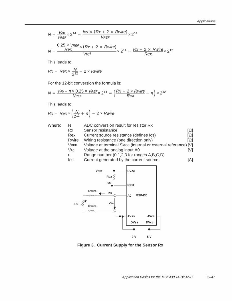
Applications
2–47 Application Basics for the MSP430 14-Bit ADC
N VA0
VREF× 214
Ics (Rx 2 Rwire)VREF
× 214
N
0.25 × VREFRex × (Rx 2 Rwire)
Vref× 214 Rx 2 Rwire
Rex× 212
This leads to:
Rx Rex × N212
2 × Rwire
For the 12-bit conversion the formula is:
N VA0 n × 0.25 × VREF
VREF× 214 Rx 2 × Rwire
Rex n × 212
This leads to:
Rx Rex × N212
n 2 × Rwire
Where: N ADC conversion result for resistor RxRx Sensor resistance [Ω]Rex Current source resistance (defines Ics) [Ω]Rwire Wiring resistance (one direction only) [Ω]VREF Voltage at terminal SVcc (internal or external reference) [V]VA0 Voltage at the analog input A0 [V]n Range number (0,1,2,3 for ranges A,B,C,D)Ics Current generated by the current source [A]
SVcc
Rext
A0
AVss
DVss DVcc
0 V 5 V
MSP430
Rex
Ics
AVcc
VREF
ICSRwire
RwireRx VA0
Figure 3. Current Supply for the Sensor Rx
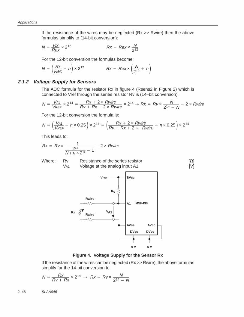
Applications
2–48 SLAA046
If the resistance of the wires may be neglected (Rx >> Rwire) then the aboveformulas simplify to (14-bit conversion):
N RxRex
× 212 Rx Rex × N212
For the 12-bit conversion the formulas become:
N RxRex
n × 212 Rx Rex × N212
n
2.1.2 Voltage Supply for SensorsThe ADC formula for the resistor Rx in figure 4 (Rsens2 in Figure 2) which isconnected to Vref through the series resistor Rv is (14–bit conversion):
N VA1
VREF× 214 Rx 2 × Rwire
Rv Rx 2 × Rwire× 214 Rx Rv × N
214 N 2 × Rwire
For the 12-bit conversion the formula is:
N VA1
VREF n × 0.25 × 214 Rx 2 × Rwire
Rv Rx 2 Rwire n × 0.25 × 214
This leads to:
Rx Rv × 1214
Nn × 212 1 2 × Rwire
Where: Rv Resistance of the series resistor [Ω]VA1 Voltage at the analog input A1 [V]
SVcc
A1
AVss
DVss DVcc
0 V 5 V
MSP430
Rv
AVcc
VREF
Rwire
RwireRx VA1
Figure 4. Voltage Supply for the Sensor Rx
If the resistance of the wires can be neglected (Rx >> Rwire), the above formulassimplify for the 14-bit conversion to:
N RxRv Rx
× 214 Rx Rv × N214 N
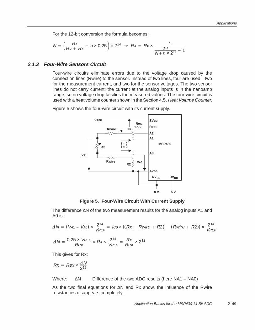
Applications
2–49 Application Basics for the MSP430 14-Bit ADC
For the 12-bit conversion the formula becomes:
N RxRv Rx
n × 0.25 × 214 Rx Rv × 1214
Nn × 212 1
2.1.3 Four-Wire Sensors Circuit
Four-wire circuits eliminate errors due to the voltage drop caused by theconnection lines (Rwire) to the sensor. Instead of two lines, four are used—twofor the measurement current, and two for the sensor voltages. The two sensorlines do not carry current; the current at the analog inputs is in the nanoamprange, so no voltage drop falsifies the measured values. The four-wire circuit isused with a heat volume counter shown in the Section 4.5, Heat Volume Counter.
Figure 5 shows the four-wire circuit with its current supply.
SVccRex
Rext
A2A1
A0
R2
AVss
DVss DVcc
0 V 5 V
Ics
VA0
Rwire
Rwire
Rx
VA1
VREF
I = 0I = 0
MSP430
Figure 5. Four-Wire Circuit With Current Supply
The difference ∆N of the two measurement results for the analog inputs A1 andA0 is:
N (VA1 VA0) × 214
VREF Ics × ((Rx Rwire R2) (Rwire R2)) × 214
VREF
N 0.25 × VREF
Rex× Rx × 214
VREF Rx
Rex× 212
This gives for Rx:
Rx Rex × N212
Where: ∆N Difference of the two ADC results (here NA1 – NA0)
As the two final equations for ∆N and Rx show, the influence of the Rwireresistances disappears completely.
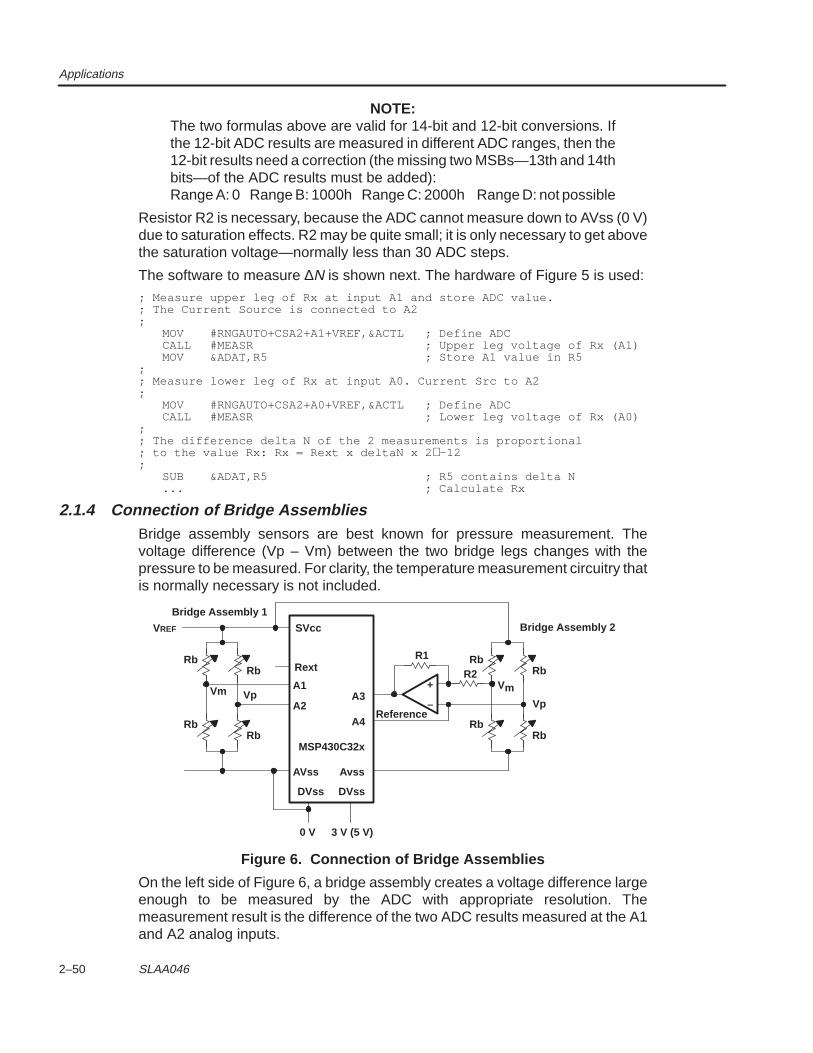
Applications
2–50 SLAA046
NOTE:The two formulas above are valid for 14-bit and 12-bit conversions. Ifthe 12-bit ADC results are measured in different ADC ranges, then the12-bit results need a correction (the missing two MSBs—13th and 14thbits—of the ADC results must be added):Range A: 0 Range B: 1000h Range C: 2000h Range D: not possible
Resistor R2 is necessary, because the ADC cannot measure down to AVss (0 V)due to saturation effects. R2 may be quite small; it is only necessary to get abovethe saturation voltage—normally less than 30 ADC steps.
The software to measure ∆N is shown next. The hardware of Figure 5 is used:; Measure upper leg of Rx at input A1 and store ADC value.; The Current Source is connected to A2;
MOV #RNGAUTO+CSA2+A1+VREF,&ACTL ; Define ADCCALL #MEASR ; Upper leg voltage of Rx (A1)MOV &ADAT,R5 ; Store A1 value in R5
;; Measure lower leg of Rx at input A0. Current Src to A2;
MOV #RNGAUTO+CSA2+A0+VREF,&ACTL ; Define ADCCALL #MEASR ; Lower leg voltage of Rx (A0)
;; The difference delta N of the 2 measurements is proportional; to the value Rx: Rx = Rext x deltaN x 2 ∧ –12;
SUB &ADAT,R5 ; R5 contains delta N... ; Calculate Rx
2.1.4 Connection of Bridge AssembliesBridge assembly sensors are best known for pressure measurement. Thevoltage difference (Vp – Vm) between the two bridge legs changes with thepressure to be measured. For clarity, the temperature measurement circuitry thatis normally necessary is not included.
Avss
DVss
A1
AVss
SVcc
Rext
A3A2
A4
VREF
R1
DVss
0 V 3 V (5 V)
+
–
R2
Reference
VmVm Vp
Bridge Assembly 1Bridge Assembly 2
MSP430C32x
Rb
Rb
Rb
RbRb
Vp
RbRb
Rb
Figure 6. Connection of Bridge Assemblies
On the left side of Figure 6, a bridge assembly creates a voltage difference largeenough to be measured by the ADC with appropriate resolution. Themeasurement result is the difference of the two ADC results measured at the A1and A2 analog inputs.
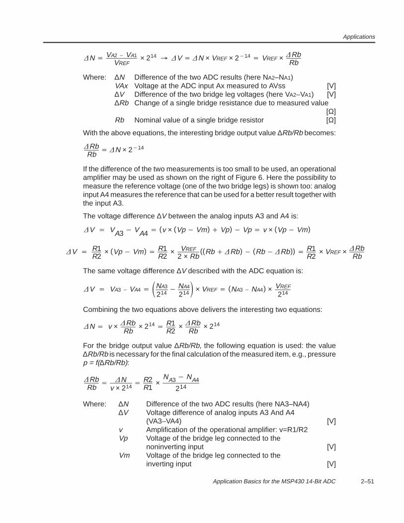
Applications
2–51 Application Basics for the MSP430 14-Bit ADC
N VA2 VA1
VREF× 214 V N × VREF × 214 VREF × Rb
Rb
Where: ∆N Difference of the two ADC results (here NA2–NA1)VAx Voltage at the ADC input Ax measured to AVss [V]∆V Difference of the two bridge leg voltages (here VA2–VA1) [V]∆Rb Change of a single bridge resistance due to measured value
[Ω]Rb Nominal value of a single bridge resistor [Ω]
With the above equations, the interesting bridge output value ∆Rb/Rb becomes:
RbRb
N × 214
If the difference of the two measurements is too small to be used, an operationalamplifier may be used as shown on the right of Figure 6. Here the possibility tomeasure the reference voltage (one of the two bridge legs) is shown too: analoginput A4 measures the reference that can be used for a better result together withthe input A3.
The voltage difference ∆V between the analog inputs A3 and A4 is:
V VA3 VA4 (v × (Vp Vm) Vp) Vp v × (Vp Vm)
V R1R2
× (Vp Vm) R1R2
× VREF
2 × Rb((Rb Rb) (Rb Rb)) R1
R2× VREF × Rb
Rb
The same voltage difference ∆V described with the ADC equation is:
V VA3 VA4 NA3
214 NA4
214 × VREF (NA3 NA4) × VREF
214
Combining the two equations above delivers the interesting two equations:
N v × RbRb
× 214 R1R2
× RbRb
× 214
For the bridge output value ∆Rb/Rb, the following equation is used: the value∆Rb/Rb is necessary for the final calculation of the measured item, e.g., pressurep = f(∆Rb/Rb):
RbRb
Nv × 214
R2R1
×NA3 NA4
214
Where: ∆N Difference of the two ADC results (here NA3–NA4)∆V Voltage difference of analog inputs A3 And A4
(VA3–VA4) [V]v Amplification of the operational amplifier: v=R1/R2Vp Voltage of the bridge leg connected to the
noninverting input [V]Vm Voltage of the bridge leg connected to the
inverting input [V]
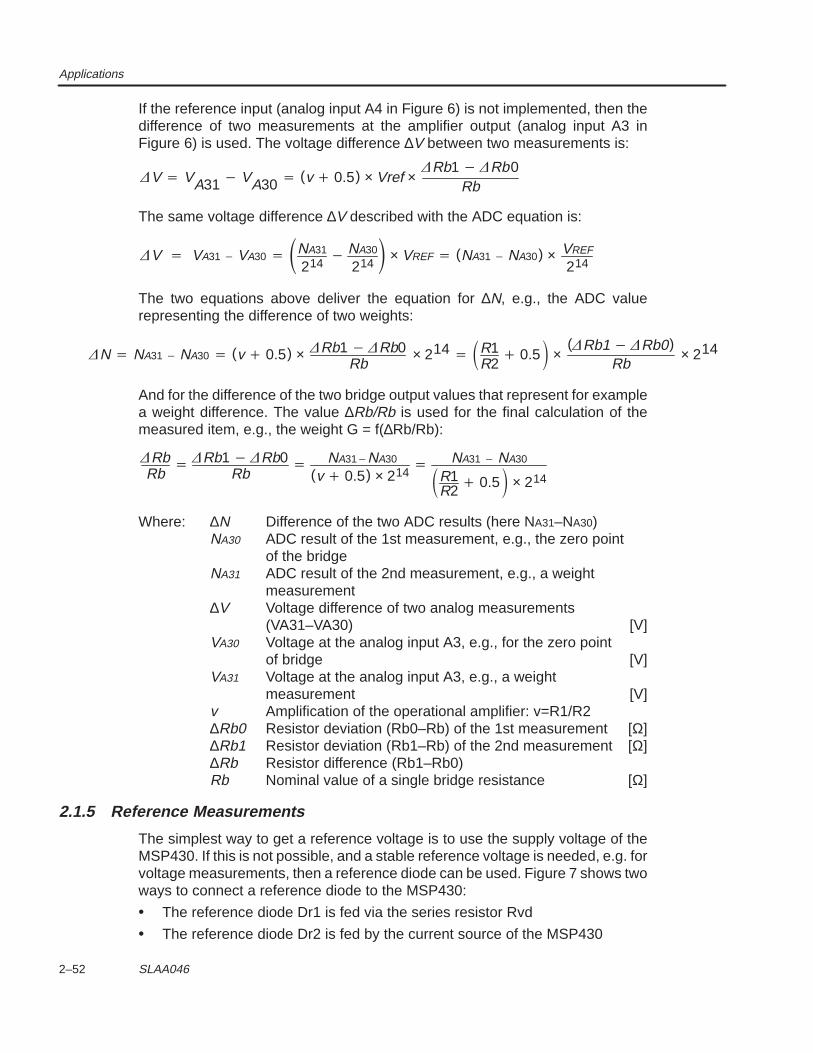
Applications
2–52 SLAA046
If the reference input (analog input A4 in Figure 6) is not implemented, then thedifference of two measurements at the amplifier output (analog input A3 inFigure 6) is used. The voltage difference ∆V between two measurements is:
V VA31 VA30 (v 0.5) × Vref ×Rb1 Rb0
Rb
The same voltage difference ∆V described with the ADC equation is:
V VA31 VA30 NA31
214 NA30
214 × VREF (NA31 NA30) × VREF
214
The two equations above deliver the equation for ∆N, e.g., the ADC valuerepresenting the difference of two weights:
N NA31 NA30 (v 0.5) × Rb1 Rb0Rb
× 214 R1R2
0.5 ×(Rb1 Rb0)
Rb× 214
And for the difference of the two bridge output values that represent for examplea weight difference. The value ∆Rb/Rb is used for the final calculation of themeasured item, e.g., the weight G = f(∆Rb/Rb):
RbRb
Rb1 Rb0Rb
NA31NA30
(v 0.5) × 214 NA31 NA30
R1R2
0.5 × 214
Where: ∆N Difference of the two ADC results (here NA31–NA30)NA30 ADC result of the 1st measurement, e.g., the zero point
of the bridgeNA31 ADC result of the 2nd measurement, e.g., a weight
measurement∆V Voltage difference of two analog measurements
(VA31–VA30) [V]VA30 Voltage at the analog input A3, e.g., for the zero point
of bridge [V]VA31 Voltage at the analog input A3, e.g., a weight
measurement [V]v Amplification of the operational amplifier: v=R1/R2∆Rb0 Resistor deviation (Rb0–Rb) of the 1st measurement [Ω]∆Rb1 Resistor deviation (Rb1–Rb) of the 2nd measurement [Ω]∆Rb Resistor difference (Rb1–Rb0)Rb Nominal value of a single bridge resistance [Ω]
2.1.5 Reference Measurements
The simplest way to get a reference voltage is to use the supply voltage of theMSP430. If this is not possible, and a stable reference voltage is needed, e.g. forvoltage measurements, then a reference diode can be used. Figure 7 shows twoways to connect a reference diode to the MSP430:
• The reference diode Dr1 is fed via the series resistor Rvd
• The reference diode Dr2 is fed by the current source of the MSP430
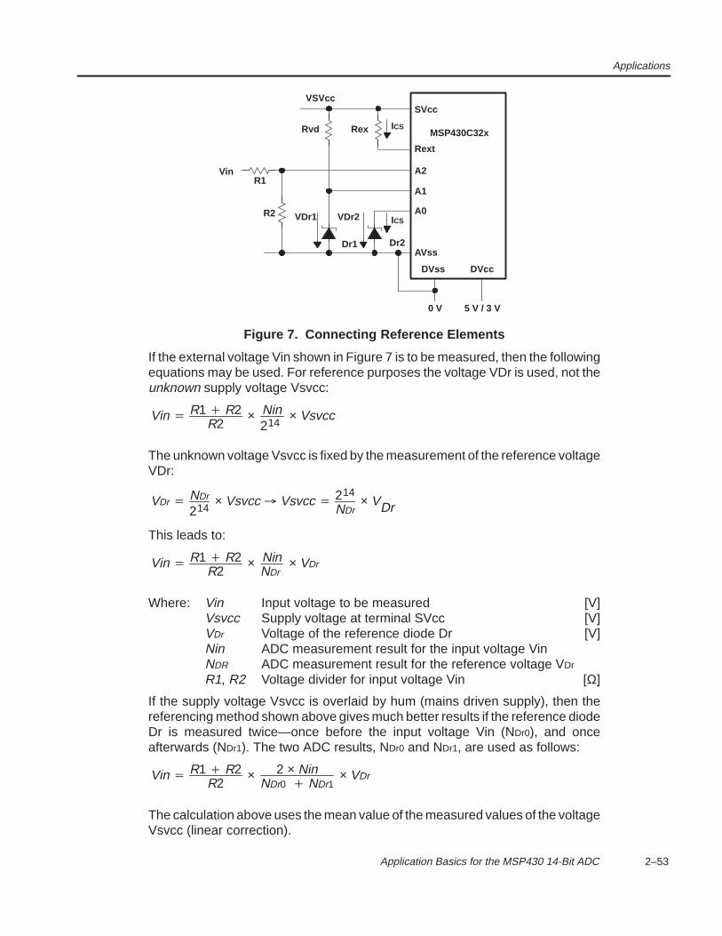
Applications
2–53 Application Basics for the MSP430 14-Bit ADC
SVcc
Rex
Rext
A2
A1
A0
Rvd
R2
R1Vin
AVss
DVss DVcc
0 V 5 V / 3 V
MSP430C32xICS
ICS
Dr2Dr1
VDr2VDr1
VSVcc
Figure 7. Connecting Reference Elements
If the external voltage Vin shown in Figure 7 is to be measured, then the followingequations may be used. For reference purposes the voltage VDr is used, not theunknown supply voltage Vsvcc:
Vin R1 R2R2
× Nin214
× Vsvcc
The unknown voltage Vsvcc is fixed by the measurement of the reference voltageVDr:
VDr NDr
214× Vsvcc Vsvcc 214
NDr× VDr
This leads to:
Vin R1 R2R2
× NinNDr
× VDr
Where: Vin Input voltage to be measured [V]Vsvcc Supply voltage at terminal SVcc [V]VDr Voltage of the reference diode Dr [V]Nin ADC measurement result for the input voltage VinNDR ADC measurement result for the reference voltage VDr
R1, R2 Voltage divider for input voltage Vin [Ω]
If the supply voltage Vsvcc is overlaid by hum (mains driven supply), then thereferencing method shown above gives much better results if the reference diodeDr is measured twice—once before the input voltage Vin (NDr0), and onceafterwards (NDr1). The two ADC results, NDr0 and NDr1, are used as follows:
Vin R1 R2R2
× 2 × NinNDr0 NDr1
× VDr
The calculation above uses the mean value of the measured values of the voltageVsvcc (linear correction).
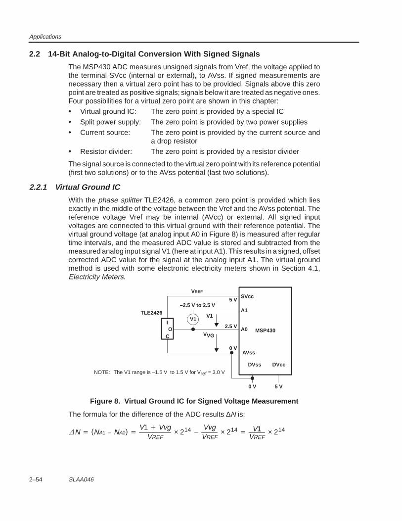
Applications
2–54 SLAA046
2.2 14-Bit Analog-to-Digital Conversion With Signed Signals
The MSP430 ADC measures unsigned signals from Vref, the voltage applied tothe terminal SVcc (internal or external), to AVss. If signed measurements arenecessary then a virtual zero point has to be provided. Signals above this zeropoint are treated as positive signals; signals below it are treated as negative ones.Four possibilities for a virtual zero point are shown in this chapter:
• Virtual ground IC: The zero point is provided by a special IC
• Split power supply: The zero point is provided by two power supplies
• Current source: The zero point is provided by the current source anda drop resistor
• Resistor divider: The zero point is provided by a resistor divider
The signal source is connected to the virtual zero point with its reference potential(first two solutions) or to the AVss potential (last two solutions).
2.2.1 Virtual Ground IC
With the phase splitter TLE2426, a common zero point is provided which liesexactly in the middle of the voltage between the Vref and the AVss potential. Thereference voltage Vref may be internal (AVcc) or external. All signed inputvoltages are connected to this virtual ground with their reference potential. Thevirtual ground voltage (at analog input A0 in Figure 8) is measured after regulartime intervals, and the measured ADC value is stored and subtracted from themeasured analog input signal V1 (here at input A1). This results in a signed, offsetcorrected ADC value for the signal at the analog input A1. The virtual groundmethod is used with some electronic electricity meters shown in Section 4.1,Electricity Meters.
SVcc
A1
A0
DVss DVcc
0 V 5 V
V1
–2.5 V to 2.5 V
I
CO
TLE2426
5 V
2.5 V
0 V
MSP430VVG
V1
VREF
AVss
NOTE: The V1 range is –1.5 V to 1.5 V for Vref = 3.0 V
Figure 8. Virtual Ground IC for Signed Voltage Measurement
The formula for the difference of the ADC results ∆N is:
N (NA1 NA0) V1 Vvg
VREF× 214
VvgVREF
× 214 V1VREF
× 214
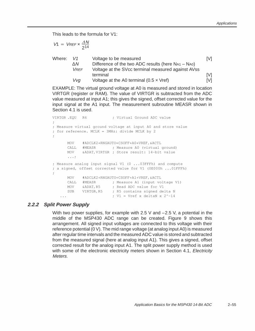
Applications
2–55 Application Basics for the MSP430 14-Bit ADC
This leads to the formula for V1:
V1 VREF × N214
Where: V1 Voltage to be measured [V]∆N Difference of the two ADC results (here NA1 – NA0)VREF Voltage at the SVcc terminal measured against AVss
terminal [V]Vvg Voltage at the A0 terminal (0.5 × Vref) [V]
EXAMPLE: The virtual ground voltage at A0 is measured and stored in locationVIRTGR (register or RAM). The value of VIRTGR is subtracted from the ADCvalue measured at input A1; this gives the signed, offset corrected value for theinput signal at the A1 input. The measurement subroutine MEASR shown inSection 4.1 is used.
VIRTGR .EQU R6 ; Virtual Ground ADC value;; Measure virtual ground voltage at input A0 and store value; for reference. MCLK = 3MHz: divide MCLK by 2;
MOV #ADCLK2+RNGAUTO+CSOFF+A0+VREF,&ACTLCALL #MEASR ; Measure A0 (virtual ground)MOV &ADAT,VIRTGR ; Store result: 14–bit value...;
; Measure analog input signal V1 (0 ...03FFFh) and compute; a signed, offset corrected value for V1 (0E000h ...01FFFh);
MOV #ADCLK2+RNGAUTO+CSOFF+A1+VREF,&ACTLCALL #MEASR ; Measure A1 (input voltage V1)MOV &ADAT,R5 ; Read ADC value for V1SUB VIRTGR,R5 ; R5 contains signed delta N
... ; V1 = Vref x deltaN x 2^–14
2.2.2 Split Power Supply
With two power supplies, for example with 2.5 V and –2.5 V, a potential in themiddle of the MSP430 ADC range can be created. Figure 9 shows thisarrangement. All signed input voltages are connected to this voltage with theirreference potential (0 V). The mid range voltage (at analog input A0) is measuredafter regular time intervals and the measured ADC value is stored and subtractedfrom the measured signal (here at analog input A1). This gives a signed, offsetcorrected result for the analog input A1. The split power supply method is usedwith some of the electronic electricity meters shown in Section 4.1, ElectricityMeters.
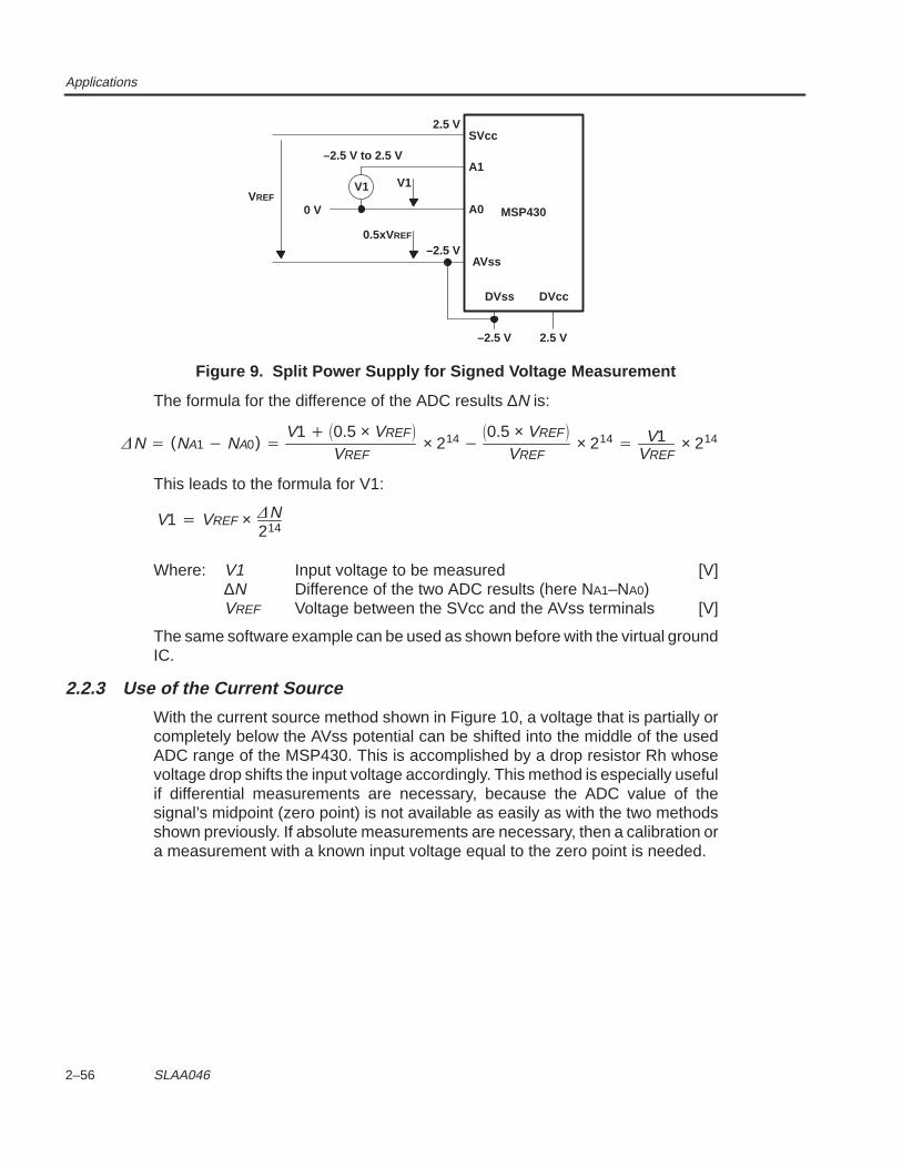
Applications
2–56 SLAA046
SVcc
A1
A0
DVss DVcc
–2.5 V 2.5 V
V1
2.5 V
0 V MSP430
–2.5 V
V1
AVss
0.5xVREF
VREF
–2.5 V to 2.5 V
Figure 9. Split Power Supply for Signed Voltage Measurement
The formula for the difference of the ADC results ∆N is:
N (NA1 NA0) V1 0.5 × VREF
VREF× 214
0.5 × VREF
VREF× 214 V1
VREF× 214
This leads to the formula for V1:
V1 VREF × N214
Where: V1 Input voltage to be measured [V]∆N Difference of the two ADC results (here NA1–NA0)VREF Voltage between the SVcc and the AVss terminals [V]
The same software example can be used as shown before with the virtual groundIC.
2.2.3 Use of the Current Source
With the current source method shown in Figure 10, a voltage that is partially orcompletely below the AVss potential can be shifted into the middle of the usedADC range of the MSP430. This is accomplished by a drop resistor Rh whosevoltage drop shifts the input voltage accordingly. This method is especially usefulif differential measurements are necessary, because the ADC value of thesignal’s midpoint (zero point) is not available as easily as with the two methodsshown previously. If absolute measurements are necessary, then a calibration ora measurement with a known input voltage equal to the zero point is needed.
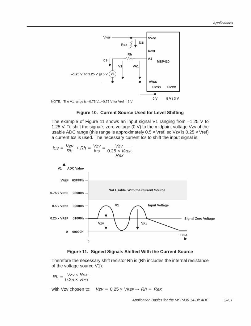
Applications
2–57 Application Basics for the MSP430 14-Bit ADC
SVcc
Rext
A1
DVSS DVCC
0 V 5 V / 3 V
ICS MSP430
Rex
V1–1.25 V to 1.25 V @ 5 V
Rh
V1
VREF
VA1
ICS
AVSS
NOTE: The V1 range is –0.75 V...+0.75 V for Vref = 3 V
Figure 10. Current Source Used for Level Shifting
The example of Figure 11 shows an input signal V1 ranging from –1.25 V to1.25 V. To shift the signal’s zero voltage (0 V) to the midpoint voltage Vzv of theusable ADC range (this range is approximately 0.5 × Vref, so Vzv is 0.25 × Vref)a current Ics is used. The necessary current Ics to shift the input signal is:
ICS VzvRh
Rh VzvICS
Vzv0.25 × VREF
Rex
Time
VZV
Signal Zero Voltage
VREF 03FFFh
0 00000h
0
0.25 x VREF 01000h
0.5 x VREF 02000h
0.75 x VREF 03000h
V1 ADC Value
VA1
Input Voltage
Not Usable With the Current Source
V1
Figure 11. Signed Signals Shifted With the Current Source
Therefore the necessary shift resistor Rh is (Rh includes the internal resistanceof the voltage source V1):
Rh Vzv × Rex0.25 × VREF
with Vzv chosen to: Vzv 0.25 × VREF Rh Rex
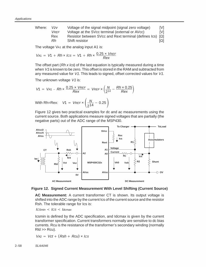
Applications
2–58 SLAA046
Where: Vzv Voltage of the signal midpoint (signal zero voltage) [V]VREF Voltage at the SVcc terminal (external or AVcc) [V]Rex Resistor between SVcc and Rext terminal (defines Ics) [Ω]Rh Shift resistor [Ω]
The voltage VA1 at the analog input A1 is:
VA1 V1 Rh × ICS V1 Rh × 0.25 × VREFRex
The offset part (Rh x Ics) of the last equation is typically measured during a timewhen V1 is known to be zero. This offset is stored in the RAM and subtracted fromany measured value for V1. This leads to signed, offset corrected values for V1.
The unknown voltage V1 is:
V1 VA1 Rh × 0.25 × VREFRex
VREF × N214
Rh × 0.25Rex
With Rh=Rex: V1 VREF × N214
0.25Figure 12 gives two practical examples for dc and ac measurements using thecurrent source. Both applications measure signed voltages that are partially (thenegative parts) out of the ADC range of the MSP430.
AVcc/4Rex
SVcc
A1
A0
Rext
A2
Rld
AVss AVss
MSP430C32x
OV
Vct VA2
Ics
RshCT
Iac
AVss
Accumulators
ShuntR2VA0 Vsh
Rc
Voltage
Current
Ics
ToLoad
R1
To Charger
AC Measurement DC Measurement
Ics
0V
AVcc/2
Figure 12. Signed Current Measurement With Level Shifting (Current Source)
AC Measurement: A current transformer CT is shown. Its output voltage isshifted into the ADC range by the current Ics of the current source and the resistorRsh. The tolerable range for Ics is:
ICSmin ICS Idcmax
Icsmin is defined by the ADC specification, and Idcmax is given by the currenttransformer specification. Current transformers normally are sensitive to dc biascurrents. Rcu is the resistance of the transformer’s secondary winding (normallyRld >> Rcu).
VA2 Vct (Rsh Rcu) × ICS
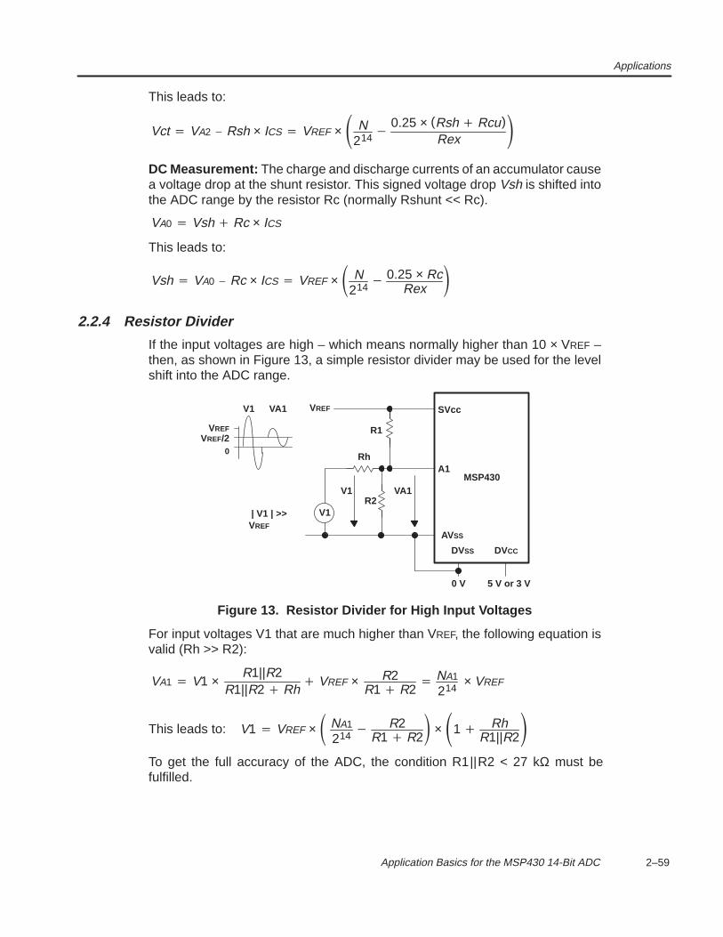
Applications
2–59 Application Basics for the MSP430 14-Bit ADC
This leads to:
Vct VA2 Rsh × ICS VREF × N214
0.25 × (Rsh Rcu)
Rex
DC Measurement: The charge and discharge currents of an accumulator causea voltage drop at the shunt resistor. This signed voltage drop Vsh is shifted intothe ADC range by the resistor Rc (normally Rshunt << Rc).
VA0 Vsh Rc × ICS
This leads to:
Vsh VA0 Rc × ICS VREF × N214
0.25 × RcRex
2.2.4 Resistor Divider
If the input voltages are high – which means normally higher than 10 × VREF –then, as shown in Figure 13, a simple resistor divider may be used for the levelshift into the ADC range.
SVcc
A1
DVSS DVCC
0 V 5 V or 3 V
MSP430
V1 | V1 | >>VREF
Rh
V1
VREF
VA1
AVSS
R1
R2
VREF/20
VREF
V1 VA1
Figure 13. Resistor Divider for High Input Voltages
For input voltages V1 that are much higher than VREF, the following equation isvalid (Rh >> R2):
VA1 V1 ×R1||R2
R1||R2 Rh VREF × R2
R1 R2 NA1
214× VREF
This leads to: V1 VREF × NA1
214 R2
R1 R2 × 1 Rh
R1||R2
To get the full accuracy of the ADC, the condition R1||R2 < 27 kΩ must befulfilled.
Applications
2–60 SLAA046
For high input voltages V1 the resistors R1 and R2 are normally equal—it is notpossible or necessary to correct the small error of the input signal—so theequation simplifies to:
VA1 V1 × R1R1 2 × Rh
0.5 × VREF NA1
214× VREF
This leads to: V1 VREF × NA1
214 0.5 × 1 2 × Rh
R1
The dc offset part (0.5 × VREF) of the last equation is typically measured duringa time when V1 is known to be zero. This measured offset is stored in the RAMand subtracted from any measured value for V1. This leads to signed, offsetcorrected values for V1.
For input voltages that have no dc-part (e.g., sinusoidal signals), the zero pointcan be calculated by an integration of the input signal. After a multiple m of thesignal period, the integrated sum of ADC results equals m times the value of thezero point.
2.3 12-Bit Analog-to-Digital Conversion With Signed Signals
The asymmetrical arrangement of the four ADC ranges reduces the number ofsolutions that are possible with the 12-bit conversion:
• Normal phase splitter circuits are not able to shift the virtual ground into themiddle of range A, B C or D as it is necessary here. See Table 2 column Vvgfor the center values of the four ADC ranges.
• The split power supply method would need two voltages to get the zero pointinto the center of the used range: e.g., 0.625 V and 4.375 V for range A if a5-V supply is used.
NOTE: The formulas given in this section are valid only if bothmeasurements for differences (∆N) are measured in the sameADC range. If they are measured in different ADC ranges, then the12–bit results need a correction (the missing two MSBs of theADC result must be added). The correction numbers are:
Range A: 0Range B: 1000hRange C: 2000hRange D: 3000h
2.3.1 Virtual Ground Circuitry
The phase splitter TLE2426 delivers only one half of the input voltage at its outputterminal; it cannot be used here. With a simple op amp as shown in Figure 14,the necessary output voltages for the four ADC ranges can be obtained:
R = R1 + R2. See Table 1 for the relative resistor values.
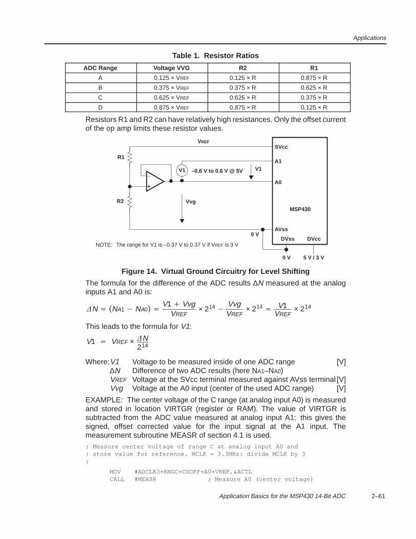
Applications
2–61 Application Basics for the MSP430 14-Bit ADC
Table 1. Resistor Ratios
ADC Range Voltage VVG R2 R1
A 0.125 × VREF 0.125 × R 0.875 × R
B 0.375 × VREF 0.375 × R 0.625 × R
C 0.625 × VREF 0.625 × R 0.375 × R
D 0.875 × VREF 0.875 × R 0.125 × R
Resistors R1 and R2 can have relatively high resistances. Only the offset currentof the op amp limits these resistor values.
SVcc
A0
AVss
DVss DVcc
0 V 5 V / 3 V
MSP430
VREF
V1
Vvg
A1
_
+
R1
R2
–0.6 V to 0.6 V @ 5VV1
0 V
NOTE: The range for V1 is –0.37 V to 0.37 V if VREF is 3 V
Figure 14. Virtual Ground Circuitry for Level Shifting
The formula for the difference of the ADC results ∆N measured at the analoginputs A1 and A0 is:
N (NA1 NA0) V1 Vvg
VREF× 214
VvgVREF
× 214 V1VREF
× 214
This leads to the formula for V1:
V1 VREF × N214
Where:V1 Voltage to be measured inside of one ADC range [V]∆N Difference of two ADC results (here NA1–NA0)VREF Voltage at the SVcc terminal measured against AVss terminal [V]Vvg Voltage at the A0 input (center of the used ADC range) [V]
EXAMPLE: The center voltage of the C range (at analog input A0) is measuredand stored in location VIRTGR (register or RAM). The value of VIRTGR issubtracted from the ADC value measured at analog input A1; this gives thesigned, offset corrected value for the input signal at the A1 input. Themeasurement subroutine MEASR of section 4.1 is used.; Measure center voltage of range C at analog input A0 and; store value for reference. MCLK = 3.3MHz: divide MCLK by 3;
MOV #ADCLK3+RNGC+CSOFF+A0+VREF,&ACTLCALL #MEASR ; Measure A0 (center voltage)
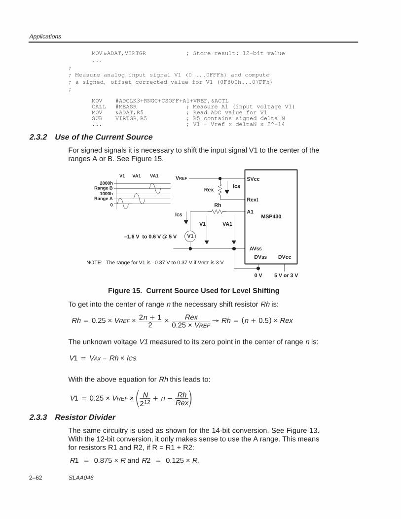
Applications
2–62 SLAA046
MOV &ADAT,VIRTGR ; Store result: 12–bit value...
;; Measure analog input signal V1 (0 ...0FFFh) and compute; a signed, offset corrected value for V1 (0F800h...07FFh);
MOV #ADCLK3+RNGC+CSOFF+A1+VREF,&ACTLCALL #MEASR ; Measure A1 (input voltage V1)MOV &ADAT,R5 ; Read ADC value for V1SUB VIRTGR,R5 ; R5 contains signed delta N... ; V1 = Vref x deltaN x 2^–14
2.3.2 Use of the Current Source
For signed signals it is necessary to shift the input signal V1 to the center of theranges A or B. See Figure 15.
V1
Range A1000h
0
SVcc
Rext
A1
DVSS DVcc
0 V 5 V or 3 V
ICS MSP430
Rex
V1–1.6 V to 0.6 V @ 5 V
Rh
V1
VREF
VA1
IcsRange B2000h
VA1 VA1
AVSS
NOTE: The range for V1 is –0.37 V to 0.37 V if VREF is 3 V
Figure 15. Current Source Used for Level Shifting
To get into the center of range n the necessary shift resistor Rh is:
Rh 0.25 × VREF × 2n 12
× Rex0.25 × VREF
Rh (n 0.5) × Rex
The unknown voltage V1 measured to its zero point in the center of range n is:
V1 VAx Rh × ICS
With the above equation for Rh this leads to:
V1 0.25 × VREF × N212
n RhRex
2.3.3 Resistor Divider
The same circuitry is used as shown for the 14-bit conversion. See Figure 13.With the 12-bit conversion, it only makes sense to use the A range. This meansfor resistors R1 and R2, if R = R1 + R2:
R1 0.875 × R and R2 0.125 × R.
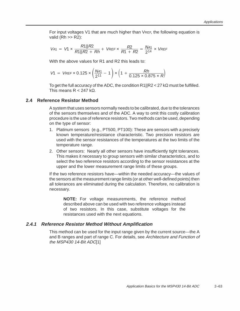
Applications
2–63 Application Basics for the MSP430 14-Bit ADC
For input voltages V1 that are much higher than VREF, the following equation isvalid (Rh >> R2):
VA1 V1 ×R1||R2
R1||R2 Rh VREF × R2
R1 R2 NA1
214× VREF
With the above values for R1 and R2 this leads to:
V1 VREF × 0.125 × NA1
211 1 × 1 Rh
0.125 × 0.875 × R
To get the full accuracy of the ADC, the condition R1||R2 < 27 kΩ must be fulfilled.This means R < 247 kΩ.
2.4 Reference Resistor Method
A system that uses sensors normally needs to be calibrated, due to the tolerancesof the sensors themselves and of the ADC. A way to omit this costly calibrationprocedure is the use of reference resistors. Two methods can be used, dependingon the type of sensor:
1. Platinum sensors (e.g., PT500, PT100): These are sensors with a preciselyknown temperature/resistance characteristic. Two precision resistors areused with the sensor resistances of the temperatures at the two limits of thetemperature range.
2. Other sensors: Nearly all other sensors have insufficiently tight tolerances.This makes it necessary to group sensors with similar characteristics, and toselect the two reference resistors according to the sensor resistances at theupper and the lower measurement range limits of these groups.
If the two reference resistors have—within the needed accuracy—the values ofthe sensors at the measurement range limits (or at other well-defined points) thenall tolerances are eliminated during the calculation. Therefore, no calibration isnecessary.
NOTE: For voltage measurements, the reference methoddescribed above can be used with two reference voltages insteadof two resistors. In this case, substitute voltages for theresistances used with the next equations.
2.4.1 Reference Resistor Method Without Amplification
This method can be used for the input range given by the current source—the Aand B ranges and part of range C. For details, see Architecture and Function ofthe MSP430 14-Bit ADC[1]
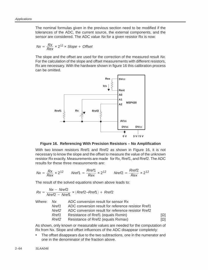
Applications
2–64 SLAA046
The nominal formulas given in the previous section need to be modified if thetolerances of the ADC, the current source, the external components, and thesensor are considered. The ADC value Nx for a given resistor Rx is now:
Nx RxRex
× 212 × Slope Offset
The slope and the offset are used for the correction of the measured result Nx.For the calculation of the slope and offset measurements with different resistors,Rx are necessary. With the hardware shown in figure 16 this calibration processcan be omitted.
SVCC
A2
DVSS DVCC
0 V 3 V / 5 V
Rex
MSP430
Rext
Rref2Rx
A1
Rref1
A0
AVSS
Ics
Figure 16. Referencing With Precision Resistors – No Amplification
With two known resistors Rref1 and Rref2 as shown in Figure 16, it is notnecessary to know the slope and the offset to measure the value of the unknownresistor Rx exactly. Measurements are made for Rx, Rref1, and Rref2. The ADCresults for these three measurements are:
Nx RxRex
× 212 Nref1 Rref1Rex
× 212 Nref2 Rref2Rex
× 212
The result of the solved equations shown above leads to:
Rx Nx Nref2
Nref2 Nref1× Rref2–Rref1 Rref2
Where: Nx ADC conversion result for sensor RxNref1 ADC conversion result for reference resistor Rref1Nref2 ADC conversion result for reference resistor Rref2Rref1 Resistance of Rref1 (equals Rxmin) [Ω]Rref2 Resistance of Rref2 (equals Rxmax) [Ω]
As shown, only known or measurable values are needed for the computation ofRx from Nx. Slope and offset influences of the ADC disappear completely:• The offset disappears due to the two subtractions, one in the numerator and
one in the denominator of the fraction above.

Applications
2–65 Application Basics for the MSP430 14-Bit ADC
• The slope disappears due to the division
EXAMPLE: The values of these two reference resistors are chosen here for aPT1000 temperature sensor:
Rref1: 1000 Ω: The value of Rxmin. The resistance of a PT1000 sensor at0°C (Tmin)
Rref2: 1380 Ω: The value of Rxmax. The resistance of a PT1000 sensor at100°C (Tmax)
2.4.2 Reference Resistor Method With Amplification
If amplification is necessary to get a better resolution, then the solution shownbelow may be used. The full ADC range (0 to 3FFFh) can be used at analog inputA1 despite the use of the current source at analog input A0. As with the sectionabove, the offset and slope disappear; this is also true for the voltage drop at theoutputs TP.x due to RDSon. The TP port of the measured resistor is switched toAVss potential; the other ones are set to Hi-Z.
The only error source of this arrangement is the difference of the internalresistances of the TP outputs (∆RDSon). To minimize the influence of differentinternal resistances RDSon, only sensors with a minimum resistance should beused, e.g., PT1000 not PT100.
For the full 14-bit resolution at the analog input A1 the following design equationsare valid (Rref2 > Rref1). They simplify this way if Rex is chosen to:
Rex Rref22
This results in a maximum voltage of VREF/2—the safe maximum output voltagethe current source can deliver—at the analog input A0 for the maximum resistorvalue Rref2.
Vm Rref1Rref1 Rref2
× VREF v VREFVREF–2 × Vm
R1R2||R3
The calculated amplification v of the op amp needs to be reduced by 10 to 15%to be sure that VA1 does not saturate under worst case conditions.
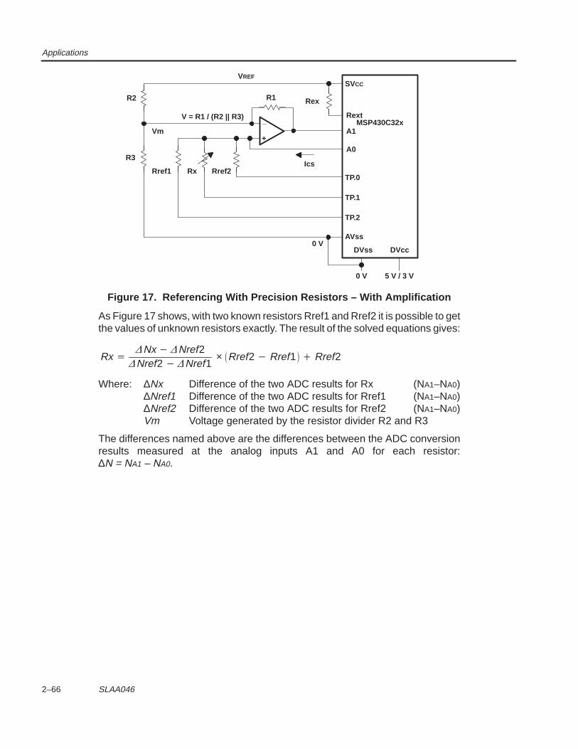
Applications
2–66 SLAA046
SVCC
AVss
DVss DVcc
0 V 5 V / 3 V
MSP430C32x
VREF
TP.2
_
+
R2
R3
V = R1 / (R2 || R3)
0 V
Rext
A1
A0
Ics
TP.1
TP.0
R1
Rref1 Rx
Vm
Rref2
Rex
Figure 17. Referencing With Precision Resistors – With Amplification
As Figure 17 shows, with two known resistors Rref1 and Rref2 it is possible to getthe values of unknown resistors exactly. The result of the solved equations gives:
Rx Nx Nref2
Nref2 Nref1× Rref2 Rref1 Rref2
Where: ∆Nx Difference of the two ADC results for Rx (NA1–NA0)∆Nref1 Difference of the two ADC results for Rref1 (NA1–NA0)∆Nref2 Difference of the two ADC results for Rref2 (NA1–NA0)Vm Voltage generated by the resistor divider R2 and R3
The differences named above are the differences between the ADC conversionresults measured at the analog inputs A1 and A0 for each resistor:∆N = NA1 – NA0.
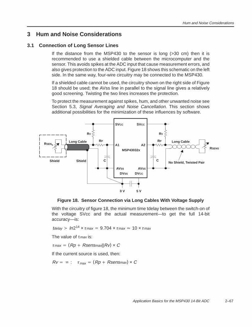
Hum and Noise Considerations
2–67 Application Basics for the MSP430 14-Bit ADC
3 Hum and Noise Considerations
3.1 Connection of Long Sensor Lines
If the distance from the MSP430 to the sensor is long (>30 cm) then it isrecommended to use a shielded cable between the microcomputer and thesensor. This avoids spikes at the ADC input that cause measurement errors, andalso gives protection to the ADC input. Figure 18 shows this schematic on the leftside. In the same way, four-wire circuitry may be connected to the MSP430.
If a shielded cable cannot be used, the circuitry shown on the right side of Figure18 should be used; the AVss line in parallel to the signal line gives a relativelygood screening. Twisting the two lines increases the protection.
To protect the measurement against spikes, hum, and other unwanted noise seeSection 5.3, Signal Averaging and Noise Cancellation. This section showsadditional possibilities for the minimization of these influences by software.
SVCC
A1
DVSS DVCC
0 V 5 V
MSP43032x
C CShield Shield
RP
RV
Long Cable Long Cable
RV
No Shield, Twisted Pair
SVCC
A2RP
RSENS
AVSS AVSS
RSENS
Figure 18. Sensor Connection via Long Cables With Voltage Supply
With the circuitry of figure 18, the minimum time tdelay between the switch-on ofthe voltage SVcc and the actual measurement—to get the full 14-bitaccuracy—is:
tdelay ln214 × max 9.704 × max 10 × max
The value of τmax is:
max (Rp Rsensmax||Rv) × C
If the current source is used, then:
Rv : max (Rp Rsensmax) × C
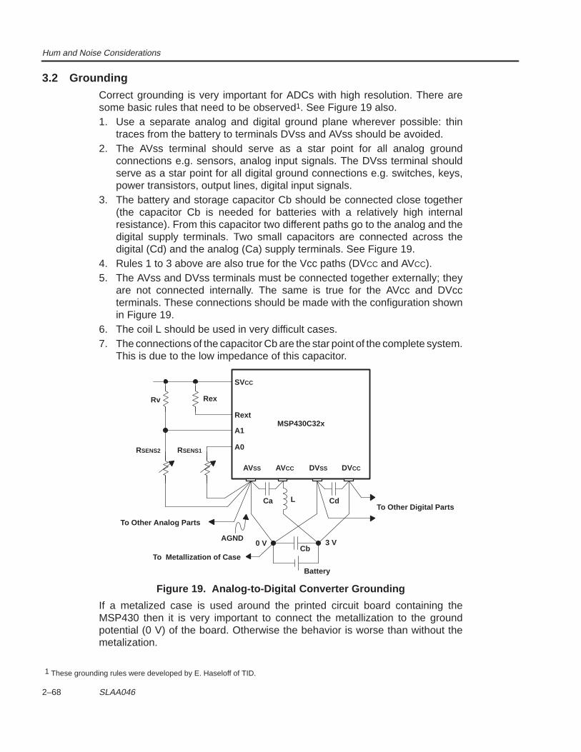
Hum and Noise Considerations
2–68 SLAA046
3.2 GroundingCorrect grounding is very important for ADCs with high resolution. There aresome basic rules that need to be observed1. See Figure 19 also.1. Use a separate analog and digital ground plane wherever possible: thin
traces from the battery to terminals DVss and AVss should be avoided.2. The AVss terminal should serve as a star point for all analog ground
connections e.g. sensors, analog input signals. The DVss terminal shouldserve as a star point for all digital ground connections e.g. switches, keys,power transistors, output lines, digital input signals.
3. The battery and storage capacitor Cb should be connected close together(the capacitor Cb is needed for batteries with a relatively high internalresistance). From this capacitor two different paths go to the analog and thedigital supply terminals. Two small capacitors are connected across thedigital (Cd) and the analog (Ca) supply terminals. See Figure 19.
4. Rules 1 to 3 above are also true for the Vcc paths (DVCC and AVCC).5. The AVss and DVss terminals must be connected together externally; they
are not connected internally. The same is true for the AVcc and DVccterminals. These connections should be made with the configuration shownin Figure 19.
6. The coil L should be used in very difficult cases.7. The connections of the capacitor Cb are the star point of the complete system.
This is due to the low impedance of this capacitor.
SVCC
A1
A0RSENS1
AVSS AVCC
MSP430C32xRext
DVSS DVCC
RSENS2
RexRv
Ca L Cd
Cb3 V0 V
Battery
AGND
To Other Digital Parts
To Metallization of Case
To Other Analog Parts
Figure 19. Analog-to-Digital Converter Grounding
If a metalized case is used around the printed circuit board containing theMSP430 then it is very important to connect the metallization to the groundpotential (0 V) of the board. Otherwise the behavior is worse than without themetalization.
1 These grounding rules were developed by E. Haseloff of TID.
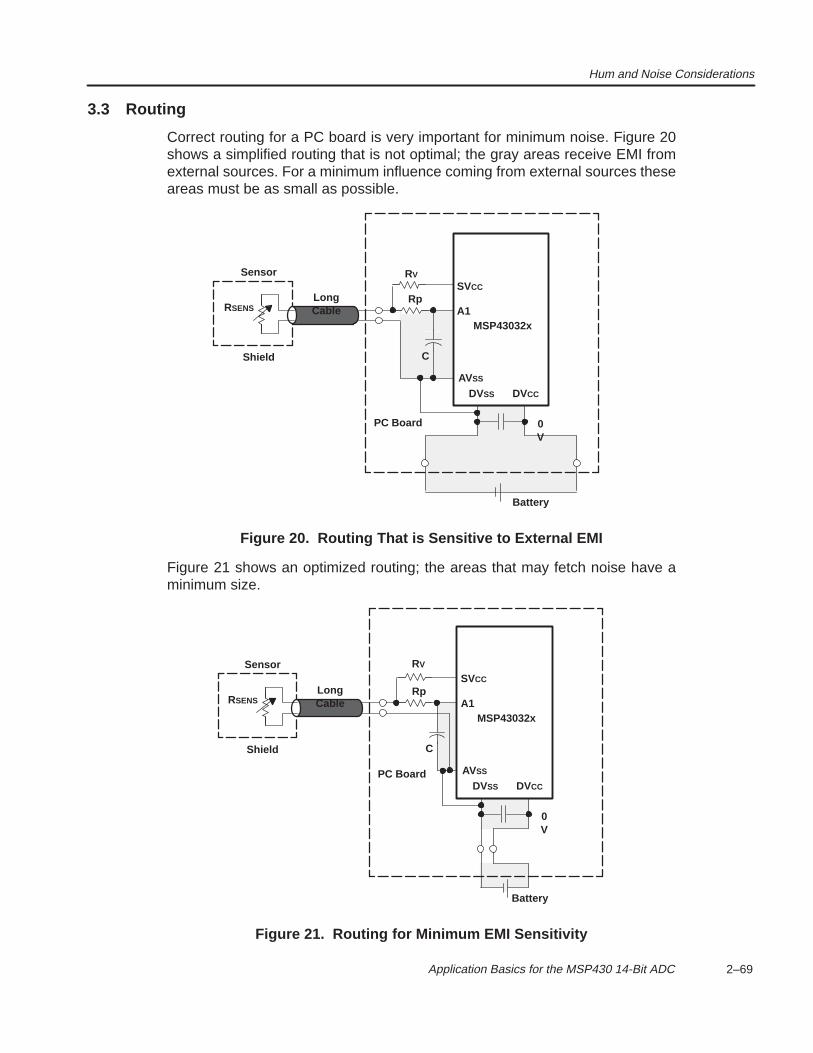
Hum and Noise Considerations
2–69 Application Basics for the MSP430 14-Bit ADC
3.3 Routing
Correct routing for a PC board is very important for minimum noise. Figure 20shows a simplified routing that is not optimal; the gray areas receive EMI fromexternal sources. For a minimum influence coming from external sources theseareas must be as small as possible.
SVCC
A1
DVSS DVCC
0V
Battery
MSP43032x
CShield
Rp
RV
LongCable
PC Board
Sensor
AVSS
RSENS
Figure 20. Routing That is Sensitive to External EMI
Figure 21 shows an optimized routing; the areas that may fetch noise have aminimum size.
SVCC
A1
DVSS DVCC
0V
Battery
MSP43032x
CShield
Rp
RV
LongCable
PC Board
Sensor
AVSS
RSENS
Figure 21. Routing for Minimum EMI Sensitivity
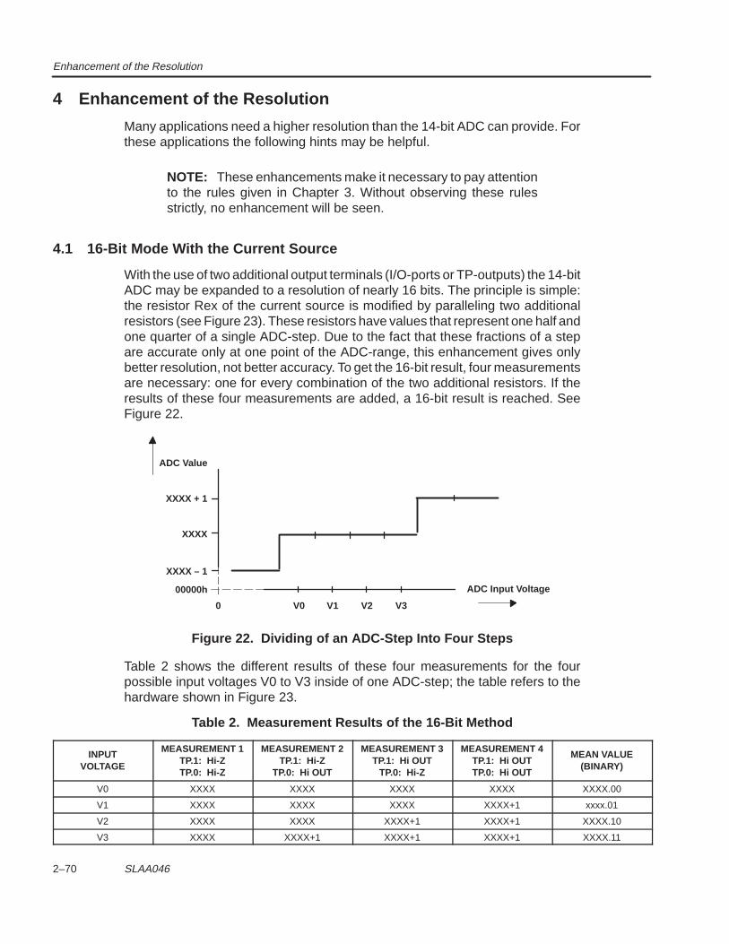
Enhancement of the Resolution
2–70 SLAA046
4 Enhancement of the Resolution
Many applications need a higher resolution than the 14-bit ADC can provide. Forthese applications the following hints may be helpful.
NOTE: These enhancements make it necessary to pay attentionto the rules given in Chapter 3. Without observing these rulesstrictly, no enhancement will be seen.
4.1 16-Bit Mode With the Current Source
With the use of two additional output terminals (I/O-ports or TP-outputs) the 14-bitADC may be expanded to a resolution of nearly 16 bits. The principle is simple:the resistor Rex of the current source is modified by paralleling two additionalresistors (see Figure 23). These resistors have values that represent one half andone quarter of a single ADC-step. Due to the fact that these fractions of a stepare accurate only at one point of the ADC-range, this enhancement gives onlybetter resolution, not better accuracy. To get the 16-bit result, four measurementsare necessary: one for every combination of the two additional resistors. If theresults of these four measurements are added, a 16-bit result is reached. SeeFigure 22.
ADC Value
XXXX + 1
XXXX
00000h
0 V0 V1 V2 V3
ADC Input Voltage
XXXX – 1
Figure 22. Dividing of an ADC-Step Into Four Steps
Table 2 shows the different results of these four measurements for the fourpossible input voltages V0 to V3 inside of one ADC-step; the table refers to thehardware shown in Figure 23.
Table 2. Measurement Results of the 16-Bit Method
INPUTVOLTAGE
MEASUREMENT 1TP.1: Hi-ZTP.0: Hi-Z
MEASUREMENT 2TP.1: Hi-Z
TP.0: Hi OUT
MEASUREMENT 3TP.1: Hi OUT
TP.0: Hi-Z
MEASUREMENT 4TP.1: Hi OUTTP.0: Hi OUT
MEAN VALUE(BINARY)
V0 XXXX XXXX XXXX XXXX XXXX.00
V1 XXXX XXXX XXXX XXXX+1 xxxx.01
V2 XXXX XXXX XXXX+1 XXXX+1 XXXX.10
V3 XXXX XXXX+1 XXXX+1 XXXX+1 XXXX.11
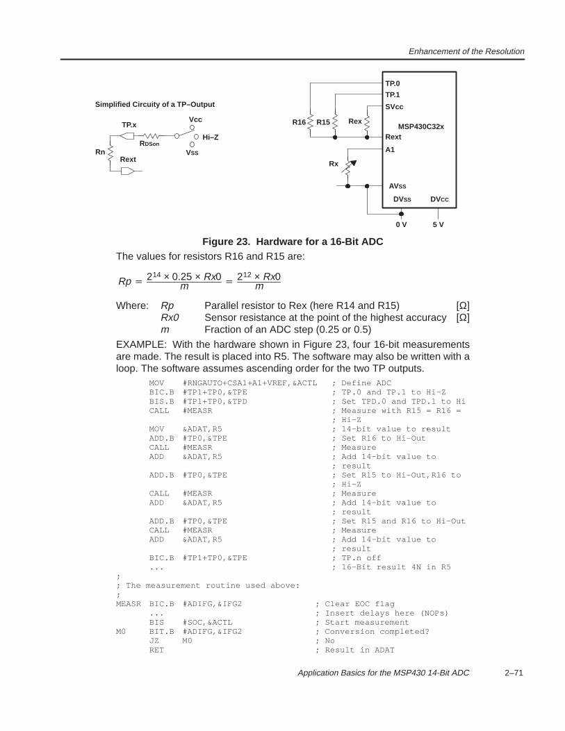
Enhancement of the Resolution
2–71 Application Basics for the MSP430 14-Bit ADC
SVcc
A1
Rx
DVSS DVCC
0 V 5 V
RexMSP430C32x
Rext
R15
TP.1
TP.0
R16
Rn VSS
Vcc
Hi–Z
TP.x
Rext
RDSon
Simplified Circuity of a TP–Output
AVSS
Figure 23. Hardware for a 16-Bit ADCThe values for resistors R16 and R15 are:
Rp 214 × 0.25 × Rx0m 212 × Rx0
m
Where: Rp Parallel resistor to Rex (here R14 and R15) [Ω]Rx0 Sensor resistance at the point of the highest accuracy [Ω]m Fraction of an ADC step (0.25 or 0.5)
EXAMPLE: With the hardware shown in Figure 23, four 16-bit measurementsare made. The result is placed into R5. The software may also be written with aloop. The software assumes ascending order for the two TP outputs.
MOV #RNGAUTO+CSA1+A1+VREF,&ACTL ; Define ADCBIC.B #TP1+TP0,&TPE ; TP.0 and TP.1 to Hi–ZBIS.B #TP1+TP0,&TPD ; Set TPD.0 and TPD.1 to HiCALL #MEASR ; Measure with R15 = R16 =
; Hi–ZMOV &ADAT,R5 ; 14–bit value to resultADD.B #TP0,&TPE ; Set R16 to Hi–OutCALL #MEASR ; MeasureADD &ADAT,R5 ; Add 14–bit value to
; resultADD.B #TP0,&TPE ; Set R15 to Hi–Out,R16 to
; Hi–ZCALL #MEASR ; MeasureADD &ADAT,R5 ; Add 14–bit value to
; resultADD.B #TP0,&TPE ; Set R15 and R16 to Hi–OutCALL #MEASR ; MeasureADD &ADAT,R5 ; Add 14–bit value to
; resultBIC.B #TP1+TP0,&TPE ; TP.n off... ; 16–Bit result 4N in R5
;; The measurement routine used above:;MEASR BIC.B #ADIFG,&IFG2 ; Clear EOC flag
... ; Insert delays here (NOPs)BIS #SOC,&ACTL ; Start measurement
M0 BIT.B #ADIFG,&IFG2 ; Conversion completed?JZ M0 ; NoRET ; Result in ADAT
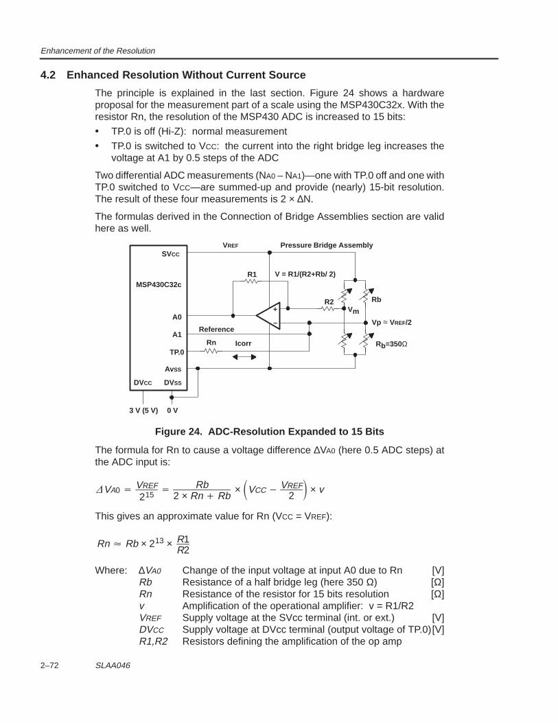
Enhancement of the Resolution
2–72 SLAA046
4.2 Enhanced Resolution Without Current Source
The principle is explained in the last section. Figure 24 shows a hardwareproposal for the measurement part of a scale using the MSP430C32x. With theresistor Rn, the resolution of the MSP430 ADC is increased to 15 bits:
• TP.0 is off (Hi-Z): normal measurement
• TP.0 is switched to VCC: the current into the right bridge leg increases thevoltage at A1 by 0.5 steps of the ADC
Two differential ADC measurements (NA0 – NA1)—one with TP.0 off and one withTP.0 switched to VCC—are summed-up and provide (nearly) 15-bit resolution.The result of these four measurements is 2 × ∆N.
The formulas derived in the Connection of Bridge Assemblies section are validhere as well.
AvSS
DVSS
SVCC
A0
TP.0
A1
R1
DVCC
0 V3 V (5 V)
+
–
R2
Reference
Vm
Pressure Bridge Assembly
MSP430C32cV = R1/(R2+Rb/ 2)
Rn Icorr
VREF
Rb
Rb=350Ω
Vp ≈ VREF/2
Figure 24. ADC-Resolution Expanded to 15 Bits
The formula for Rn to cause a voltage difference ∆VA0 (here 0.5 ADC steps) atthe ADC input is:
VA0 VREF
215 Rb
2 × Rn Rb× VCC VREF
2 × v
This gives an approximate value for Rn (VCC = VREF):
Rn Rb × 213 × R1R2
Where: ∆VA0 Change of the input voltage at input A0 due to Rn [V]Rb Resistance of a half bridge leg (here 350 Ω) [Ω]Rn Resistance of the resistor for 15 bits resolution [Ω]v Amplification of the operational amplifier: v = R1/R2VREF Supply voltage at the SVcc terminal (int. or ext.) [V]DVCC Supply voltage at DVcc terminal (output voltage of TP.0)[V]R1,R2 Resistors defining the amplification of the op amp
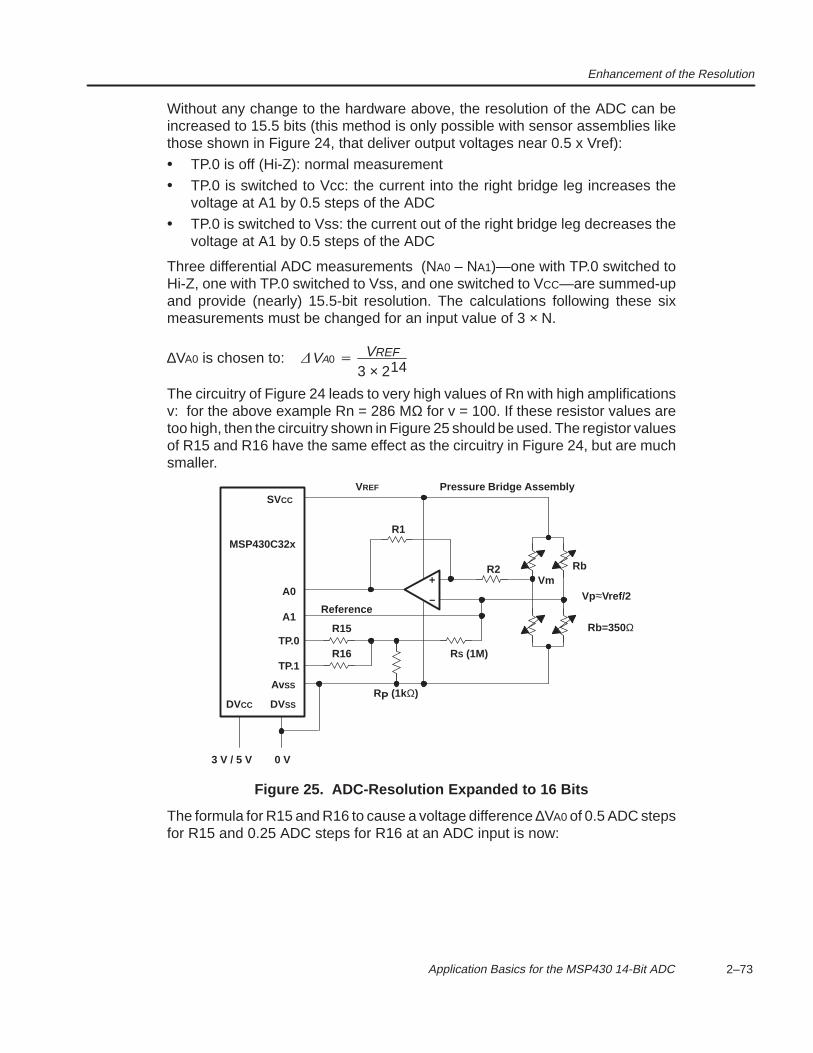
Enhancement of the Resolution
2–73 Application Basics for the MSP430 14-Bit ADC
Without any change to the hardware above, the resolution of the ADC can beincreased to 15.5 bits (this method is only possible with sensor assemblies likethose shown in Figure 24, that deliver output voltages near 0.5 x Vref):
• TP.0 is off (Hi-Z): normal measurement
• TP.0 is switched to Vcc: the current into the right bridge leg increases thevoltage at A1 by 0.5 steps of the ADC
• TP.0 is switched to Vss: the current out of the right bridge leg decreases thevoltage at A1 by 0.5 steps of the ADC
Three differential ADC measurements (NA0 – NA1)—one with TP.0 switched toHi-Z, one with TP.0 switched to Vss, and one switched to VCC—are summed-upand provide (nearly) 15.5-bit resolution. The calculations following these sixmeasurements must be changed for an input value of 3 × N.
∆VA0 is chosen to: VA0 VREF
3 × 214
The circuitry of Figure 24 leads to very high values of Rn with high amplificationsv: for the above example Rn = 286 MΩ for v = 100. If these resistor values aretoo high, then the circuitry shown in Figure 25 should be used. The registor valuesof R15 and R16 have the same effect as the circuitry in Figure 24, but are muchsmaller.
AvSS
DVSS
SVCC
A0
TP.0
A1
R1
DVCC
0 V3 V / 5 V
+
–
R2
Reference
Vm
Pressure Bridge Assembly
MSP430C32x
R15
VREF
Rb
TP.1R16 RS (1M)
RP (1kΩ)
Rb=350Ω
Vp≈Vref/2
Figure 25. ADC-Resolution Expanded to 16 Bits
The formula for R15 and R16 to cause a voltage difference ∆VA0 of 0.5 ADC stepsfor R15 and 0.25 ADC steps for R16 at an ADC input is now:
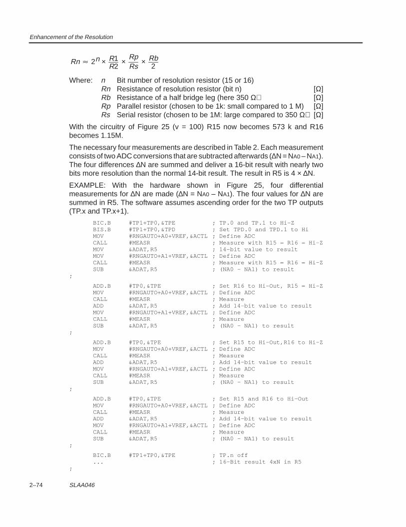
Enhancement of the Resolution
2–74 SLAA046
Rn 2n × R1R2
×RpRs
× Rb2
Where: n Bit number of resolution resistor (15 or 16)Rn Resistance of resolution resistor (bit n) [Ω]Rb Resistance of a half bridge leg (here 350 Ω) [Ω]Rp Parallel resistor (chosen to be 1k: small compared to 1 M) [Ω]Rs Serial resistor (chosen to be 1M: large compared to 350 Ω) [Ω]
With the circuitry of Figure 25 (v = 100) R15 now becomes 573 k and R16becomes 1.15M.
The necessary four measurements are described in Table 2. Each measurementconsists of two ADC conversions that are subtracted afterwards (∆N = NA0 – NA1).The four differences ∆N are summed and deliver a 16-bit result with nearly twobits more resolution than the normal 14-bit result. The result in R5 is 4 × ∆N.
EXAMPLE: With the hardware shown in Figure 25, four differentialmeasurements for ∆N are made (∆N = NA0 – NA1). The four values for ∆N aresummed in R5. The software assumes ascending order for the two TP outputs(TP.x and TP.x+1).
BIC.B #TP1+TP0,&TPE ; TP.0 and TP.1 to Hi–ZBIS.B #TP1+TP0,&TPD ; Set TPD.0 and TPD.1 to HiMOV #RNGAUTO+A0+VREF,&ACTL ; Define ADCCALL #MEASR ; Measure with R15 = R16 = Hi–ZMOV &ADAT,R5 ; 14–bit value to resultMOV #RNGAUTO+A1+VREF,&ACTL ; Define ADCCALL #MEASR ; Measure with R15 = R16 = Hi–ZSUB &ADAT,R5 ; (NA0 – NA1) to result
;
ADD.B #TP0,&TPE ; Set R16 to Hi–Out, R15 = Hi–ZMOV #RNGAUTO+A0+VREF,&ACTL ; Define ADCCALL #MEASR ; MeasureADD &ADAT,R5 ; Add 14–bit value to resultMOV #RNGAUTO+A1+VREF,&ACTL ; Define ADCCALL #MEASR ; MeasureSUB &ADAT,R5 ; (NA0 – NA1) to result
;
ADD.B #TP0,&TPE ; Set R15 to Hi–Out,R16 to Hi–ZMOV #RNGAUTO+A0+VREF,&ACTL ; Define ADCCALL #MEASR ; MeasureADD &ADAT,R5 ; Add 14–bit value to resultMOV #RNGAUTO+A1+VREF,&ACTL ; Define ADCCALL #MEASR ; MeasureSUB &ADAT,R5 ; (NA0 – NA1) to result
;
ADD.B #TP0,&TPE ; Set R15 and R16 to Hi–OutMOV #RNGAUTO+A0+VREF,&ACTL ; Define ADCCALL #MEASR ; MeasureADD &ADAT,R5 ; Add 14–bit value to resultMOV #RNGAUTO+A1+VREF,&ACTL ; Define ADCCALL #MEASR ; MeasureSUB &ADAT,R5 ; (NA0 – NA1) to result
;
BIC.B #TP1+TP0,&TPE ; TP.n off... ; 16–Bit result 4xN in R5
;
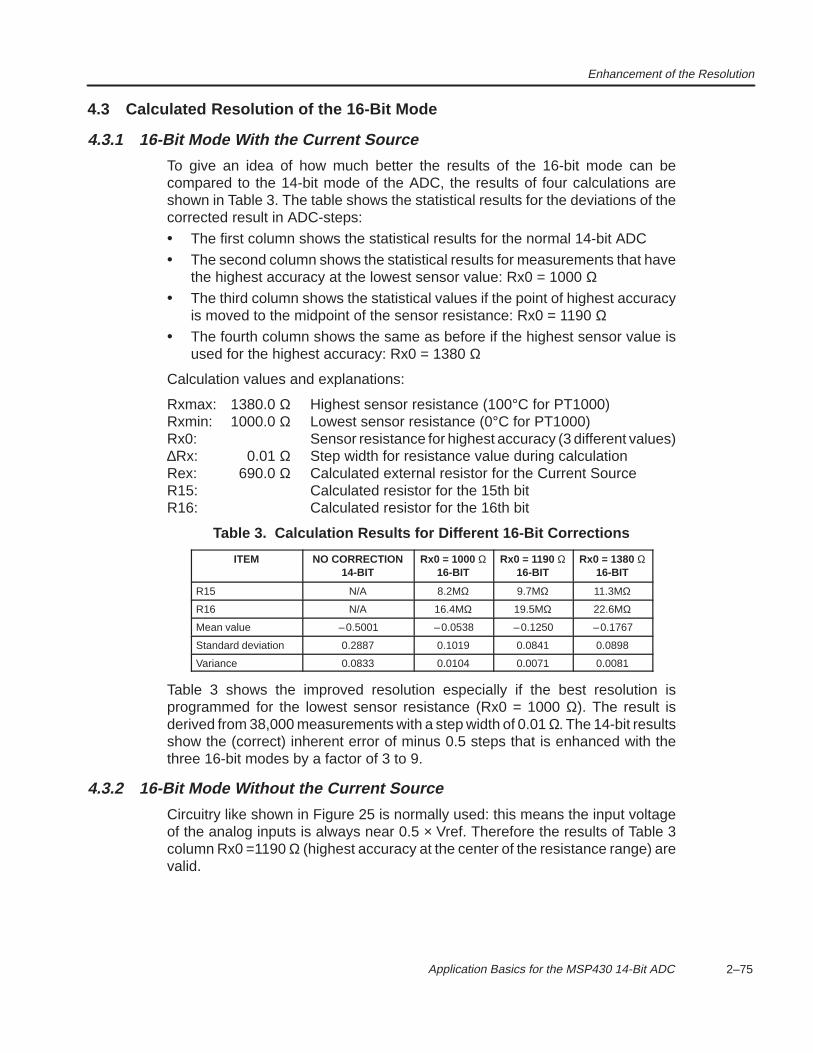
Enhancement of the Resolution
2–75 Application Basics for the MSP430 14-Bit ADC
4.3 Calculated Resolution of the 16-Bit Mode
4.3.1 16-Bit Mode With the Current Source
To give an idea of how much better the results of the 16-bit mode can becompared to the 14-bit mode of the ADC, the results of four calculations areshown in Table 3. The table shows the statistical results for the deviations of thecorrected result in ADC-steps:
• The first column shows the statistical results for the normal 14-bit ADC
• The second column shows the statistical results for measurements that havethe highest accuracy at the lowest sensor value: Rx0 = 1000 Ω
• The third column shows the statistical values if the point of highest accuracyis moved to the midpoint of the sensor resistance: Rx0 = 1190 Ω
• The fourth column shows the same as before if the highest sensor value isused for the highest accuracy: Rx0 = 1380 Ω
Calculation values and explanations:
Rxmax: 1380.0 Ω Highest sensor resistance (100°C for PT1000)Rxmin: 1000.0 Ω Lowest sensor resistance (0°C for PT1000)Rx0: Sensor resistance for highest accuracy (3 different values)∆Rx: 0.01 Ω Step width for resistance value during calculationRex: 690.0 Ω Calculated external resistor for the Current SourceR15: Calculated resistor for the 15th bitR16: Calculated resistor for the 16th bit
Table 3. Calculation Results for Different 16-Bit Corrections
ITEM NO CORRECTION14-BIT
Rx0 = 1000 Ω16-BIT
Rx0 = 1190 Ω16-BIT
Rx0 = 1380 Ω16-BIT
R15 N/A 8.2MΩ 9.7MΩ 11.3MΩ
R16 N/A 16.4MΩ 19.5MΩ 22.6MΩ
Mean value –0.5001 –0.0538 –0.1250 –0.1767
Standard deviation 0.2887 0.1019 0.0841 0.0898
Variance 0.0833 0.0104 0.0071 0.0081
Table 3 shows the improved resolution especially if the best resolution isprogrammed for the lowest sensor resistance (Rx0 = 1000 Ω). The result isderived from 38,000 measurements with a step width of 0.01 Ω. The 14-bit resultsshow the (correct) inherent error of minus 0.5 steps that is enhanced with thethree 16-bit modes by a factor of 3 to 9.
4.3.2 16-Bit Mode Without the Current Source
Circuitry like shown in Figure 25 is normally used: this means the input voltageof the analog inputs is always near 0.5 × Vref. Therefore the results of Table 3column Rx0 =1190 Ω (highest accuracy at the center of the resistance range) arevalid.

Hints and Recommendations
2–76 SLAA046
5 Hints and Recommendations
5.1 Replacement of the First Measurement
In certain cases the first measurement is discarded. Instead, a secondmeasurement is started and used. This method is especially useful if the settlingtime for the ADC is insufficient.
MOV #XX,&ACTL ; Define ADCCALL #MEASR ; 1st measurement (not used)CALL #MEASR ; 2nd measurement is usedMOV &ADAT,R5 ; for calculations. Result to R5
5.2 Grounding and Routing
With increasing ADC accuracy and CPU frequency, the board layout becomesmore important. A few hints may help to increase the performance of the ADC:
• To avoid cross talk from one ADC input line to the other one, grounded lines(AVSS potential) between the analog input lines are recommended.
• Large ground planes (0V potential) should be used wherever possible. Anyfree space on the board should be used for this purpose.
• Analog input lines should be as short as possible. If this is not possible, inputfiltering may be necessary.
• To get reliable ADC results in noisy environments, additional hardware andsoftware filtering should be used. Chapter 5 describes several methods to dothis in Section 5.3, Signal Averaging and Noise Cancellation: over sampling,continuous averaging, weighted summation, rejection of extremes, andsynchronization to hum. Tested software examples are included.
See also sections 3.2 and 3.3.
5.3 Supply Voltage and Current
Completely different environments exist for battery and mains driven systems. Afew hints are given for these two supplies. More information concerning this topicis included in Section 3.8, Power Supplies.
5.3.1 Influence of the Supply Voltage
The supply voltage is used for reference purposes if the Vref-bit (ACTL.1) is set.This means a change of the analog supply voltage AVcc during the measurementinfluences the final ADC result. The same is true for an external referencevoltage.
Figure 26 shows a decreasing analog supply voltage with the ADC timing. Theerror of the ADC result N is mainly introduced during the conversion time for the12 LSBs of the ADC result. The input sample is taken with an AVCC voltage Vref0,the LSB is generated with an AVCC voltage Vref1. The two results have the ratio:
N1N0
Vref 0Vref1
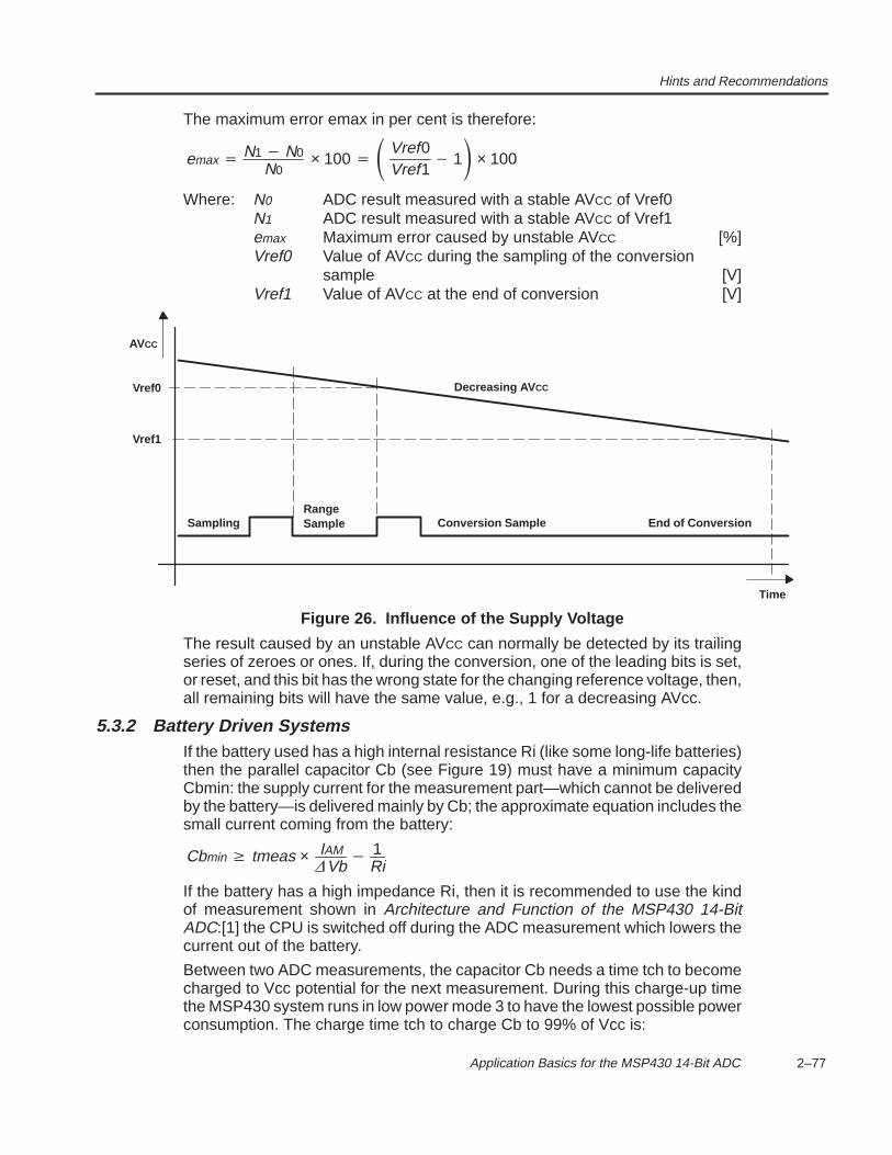
Hints and Recommendations
2–77 Application Basics for the MSP430 14-Bit ADC
The maximum error emax in per cent is therefore:
emax N1 N0N0
× 100 Vref0Vref1
1 × 100
Where: N0 ADC result measured with a stable AVCC of Vref0N1 ADC result measured with a stable AVCC of Vref1emax Maximum error caused by unstable AVCC [%]Vref0 Value of AVCC during the sampling of the conversion
sample [V]Vref1 Value of AVCC at the end of conversion [V]
AVCC
Vref1
Time
Vref0 Decreasing AV CC
End of ConversionConversion SampleRange Sample Sampling
Figure 26. Influence of the Supply Voltage
The result caused by an unstable AVCC can normally be detected by its trailingseries of zeroes or ones. If, during the conversion, one of the leading bits is set,or reset, and this bit has the wrong state for the changing reference voltage, then,all remaining bits will have the same value, e.g., 1 for a decreasing AVcc.
5.3.2 Battery Driven SystemsIf the battery used has a high internal resistance Ri (like some long-life batteries)then the parallel capacitor Cb (see Figure 19) must have a minimum capacityCbmin: the supply current for the measurement part—which cannot be deliveredby the battery—is delivered mainly by Cb; the approximate equation includes thesmall current coming from the battery:
Cbmin tmeas × IAMVb
1Ri
If the battery has a high impedance Ri, then it is recommended to use the kindof measurement shown in Architecture and Function of the MSP430 14-BitADC:[1] the CPU is switched off during the ADC measurement which lowers thecurrent out of the battery.
Between two ADC measurements, the capacitor Cb needs a time tch to becomecharged to Vcc potential for the next measurement. During this charge-up timethe MSP430 system runs in low power mode 3 to have the lowest possible powerconsumption. The charge time tch to charge Cb to 99% of Vcc is:
Hints and Recommendations
2–78 SLAA046
tchmin 5 × Cbmax × Rimax
Where: Cb Capacitor in parallel to the battery [F]IAM Medium system current (MSP430 and ADC) [A]tmeas Discharge time of Cb during measurement [s]∆Vb Tolerable discharge voltage of Cb during time tmeas [V]Ri Internal resistance (impedance) of the battery [Ω]tch Charge-up time for the capacitor Cb [s]
5.3.3 Mains Driven Systems
No hum, noise, or spikes are allowed for the supply voltages AVcc and DVcc. Ifpresent, the reliability of the system and the accuracy of the ADC will decrease.This is especially true for applications where the AVcc voltage is used for the ADCreference [ACTL.1 = 1 (Vref bit)]. See Section 5.3, Signal Averaging and NoiseCancellation for ways to overcome this problem.
5.3.4 Current Consumption
Often it is important to know the current consumption of the complete MSP430system—which means including the supply current of the MSP430 and its ADC.The supply current of the CPU increases nearly linearly with the MCLK frequencyand the applied supply voltage DVCC, but this is not the case for the ADC: the maincomponent of the ADC supply current is drawn by the resistor divider with its4 × 128 resistors. An approximate formula for the nominal current consumptionIcc of the MSP430C32x is (internal ADC reference):
ICC ICCdigital ICCanalog VDVcc5V
×fMCLK
1MHz× 750 µA VAVcc
3V× 200 µA
Where: ICC Complete current consumption of MSP430 (nominal) [µA]ICCdigital Current consumption of the digital parts [µA]ICCanalog Current consumption of the ADC [µA]VDVcc Voltage at the DVCC terminal [V]VAVcc Voltage at the AVCC [V]fMCLK Frequency of the system clock generator (MCLK) [Hz]
5.4 Use of the Floating Point Package
For the MSP430 a Floating Point Package exists with two selectable bit lengths:32 bit and 48 bit. For calculations with the ADC, results consisting of severalmultiplications and divisions, it is recommend to use this package: no decreaseof accuracy is caused by the calculation itself. A detailed description of theFloating Point Package and all available mathematical functions is given in theMSP430 Application Report. See Section 5.6, The Floating Point Package.
A small example is given below: the measured ADC result—in ADC bufferADAT—is corrected with slope and offset. The result (BCD format) is placed intothe locations BCDMSD, BCDMID and BCDLSD (RAM or registers).
DOUBLE .EQU 0 ; Use .FLOAT format (32 bits);
MOV #xxx,&ACTL ; Define ADC measurementCALL #MEASR ; Measure. Result to ADATCALL #FLT_SAV ; Save registers R5 to R12
Additional Information
2–79 Application Basics for the MSP430 14-Bit ADC
SUB #4,SP ; Allocate stack for FP resultMOV #ADAT,RPARG ; Load address of ADC bufferCALL #CNV_BIN16U ; Convert ADC result to FP
;; Calculate: ADCcorr = (ADC result x Slope) + Offset;
MOV #Slope,RPARG ; Load address of slopeCALL #FLT_MUL ; ADC result x SlopeMOV #Offset,RPARG ; Load address of offsetCALL #FLT_ADD ; ADC result x Slope + Offset... ; Continue with calculations
;; The final result is converted to BCD format for the display;
CALL #CNV_FP_BCD ; Convert FP result to BCDJN CNVERR ; Result too big for BCD bufferPOP BCDMSD ; BCD number: sign and MSDsPOP BCDMID ; BCD digits MSD–4 to LSD+4POP BCDLSD ; BCD digits LSD+3 to LSD
; Stack is corrected by POPsCALL #FLT_REC ; Restore registers R12 to R5... ; Continue with program
Slope .FLOAT –1.2345 ; Slope (fixed, RAM, EEPROM)Offset .FLOAT 14.4567 ; Offset (fixed, RAM, EEPROM)CNVERR ... ; Start error handler
6 Additional InformationThis application report is complemented by the Additive Improvement of theMSP430 14-Bit ADC Characteristic application report[5] that explains severalmethods to minimize the error of the 14-Bit ADC. For all methods (linear,quadratic, cubic and others) the actual improvement for a measured ADCcharacteristic is shown. The enhancement methods discussed are comparedcompletely with statistic results, advantages and disadvantages, necessary CPUcycles, and storage needs.
7 References1. Architecture and Function of the MSP430 14-Bit ADC Application Report,
1999, Literature #SLAA045
2. MSP430 Application Report, 1998, Literature #SLAAE10C
3. MSP430 Family Architecture Guide and Module Library, 1996, Literature#SLAUE10B
4. MSP430C325, MSP430P323 Data Sheet, 1999, Literature #SLAS219
5. Additive Improvement of the MSP430 14-Bit ADC Characteristic ApplicationReport, 1999, Literature #SLAA047
6. Linear Improvement of the MSP430 14-Bit ADC Characteristic ApplicationReport, 1999, Literature #SLAA048
7. Nonlinear Improvement of the MSP430 14-Bit ADC CharacteristicApplication Report, 1999, Literature #SLAA050

2–80 SLAA046
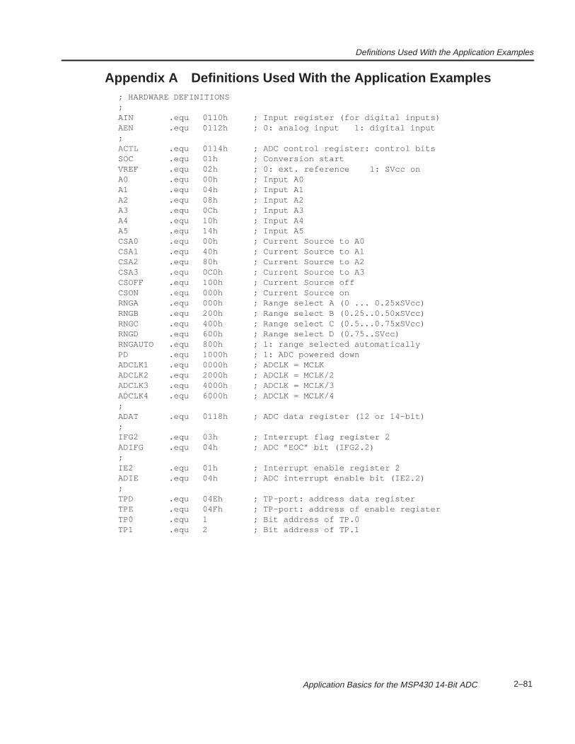
Definitions Used With the Application Examples
2–81 Application Basics for the MSP430 14-Bit ADC
Appendix A Definitions Used With the Application Examples; HARDWARE DEFINITIONS;AIN .equ 0110h ; Input register (for digital inputs)AEN .equ 0112h ; 0: analog input 1: digital input;ACTL .equ 0114h ; ADC control register: control bitsSOC .equ 01h ; Conversion startVREF .equ 02h ; 0: ext. reference 1: SVcc onA0 .equ 00h ; Input A0A1 .equ 04h ; Input A1A2 .equ 08h ; Input A2A3 .equ 0Ch ; Input A3A4 .equ 10h ; Input A4A5 .equ 14h ; Input A5CSA0 .equ 00h ; Current Source to A0CSA1 .equ 40h ; Current Source to A1CSA2 .equ 80h ; Current Source to A2CSA3 .equ 0C0h ; Current Source to A3CSOFF .equ 100h ; Current Source offCSON .equ 000h ; Current Source onRNGA .equ 000h ; Range select A (0 ... 0.25xSVcc)RNGB .equ 200h ; Range select B (0.25..0.50xSVcc)RNGC .equ 400h ; Range select C (0.5...0.75xSVcc)RNGD .equ 600h ; Range select D (0.75..SVcc)RNGAUTO .equ 800h ; 1: range selected automaticallyPD .equ 1000h ; 1: ADC powered downADCLK1 .equ 0000h ; ADCLK = MCLKADCLK2 .equ 2000h ; ADCLK = MCLK/2ADCLK3 .equ 4000h ; ADCLK = MCLK/3ADCLK4 .equ 6000h ; ADCLK = MCLK/4;ADAT .equ 0118h ; ADC data register (12 or 14–bit);IFG2 .equ 03h ; Interrupt flag register 2ADIFG .equ 04h ; ADC ”EOC” bit (IFG2.2);IE2 .equ 01h ; Interrupt enable register 2ADIE .equ 04h ; ADC interrupt enable bit (IE2.2);TPD .equ 04Eh ; TP–port: address data registerTPE .equ 04Fh ; TP–port: address of enable registerTP0 .equ 1 ; Bit address of TP.0TP1 .equ 2 ; Bit address of TP.1

2–82 SLAA046
2-83
Additive Improvement of theMSP430 14-Bit ADC Characteristic
Lutz Bierl
Printed on Recycled Paper
2-84
IMPORTANT NOTICE
Texas Instruments and its subsidiaries (TI) reserve the right to make changes to their productsor to discontinue any product or service without notice, and advise customers to obtain the latestversion of relevant information to verify, before placing orders, that information being relied onis current and complete. All products are sold subject to the terms and conditions of sale suppliedat the time of order acknowledgement, including those pertaining to warranty, patentinfringement, and limitation of liability.
TI warrants performance of its semiconductor products to the specifications applicable at thetime of sale in accordance with TI’s standard warranty. Testing and other quality controltechniques are utilized to the extent TI deems necessary to support this warranty. Specific testingof all parameters of each device is not necessarily performed, except those mandated bygovernment requirements.
CERTAIN APPLICATIONS USING SEMICONDUCTOR PRODUCTS MAY INVOLVEPOTENTIAL RISKS OF DEATH, PERSONAL INJURY, OR SEVERE PROPERTY ORENVIRONMENTAL DAMAGE (“CRITICAL APPLICATIONS”). TI SEMICONDUCTORPRODUCTS ARE NOT DESIGNED, AUTHORIZED, OR WARRANTED TO BE SUITABLE FORUSE IN LIFE-SUPPORT DEVICES OR SYSTEMS OR OTHER CRITICAL APPLICATIONS.INCLUSION OF TI PRODUCTS IN SUCH APPLICATIONS IS UNDERSTOOD TO BE FULLYAT THE CUSTOMER’S RISK.
In order to minimize risks associated with the customer’s applications, adequate design andoperating safeguards must be provided by the customer to minimize inherent or proceduralhazards.
TI assumes no liability for applications assistance or customer product design. TI does notwarrant or represent that any license, either express or implied, is granted under any patent right,copyright, mask work right, or other intellectual property right of TI covering or relating to anycombination, machine, or process in which such semiconductor products or services might beor are used. TI’s publication of information regarding any third party’s products or services doesnot constitute TI’s approval, warranty or endorsement thereof.
Copyright 1999, Texas Instruments Incorporated
2–85 Additive Improvement of the MSP430 14-Bit ADC Characteristic
Contents1 Introduction 2–87. . . . . . . . . . . . . . . . . . . . . . . . . . . . . . . . . . . . . . . . . . . . . . . . . . . . . . . . . . . . . . . . . . . . . . . . . . . . . . . .
2 The External Calibration Hardware for the ADC Improvement 2–89. . . . . . . . . . . . . . . . . . . . . . . . . . . . . . . . . . 2.1 Measurement Methods for the ADC Reference Samples 2–89. . . . . . . . . . . . . . . . . . . . . . . . . . . . . . . . . . . . 2.2 External Digital-to-Analog Converter 2–89. . . . . . . . . . . . . . . . . . . . . . . . . . . . . . . . . . . . . . . . . . . . . . . . . . . . . 2.3 External Discrete, Precise Voltages 2–92. . . . . . . . . . . . . . . . . . . . . . . . . . . . . . . . . . . . . . . . . . . . . . . . . . . . . . 2.4 External Discrete Precision Resistors 2–93. . . . . . . . . . . . . . . . . . . . . . . . . . . . . . . . . . . . . . . . . . . . . . . . . . . . 2.5 Storage of the Correction Data 2–93. . . . . . . . . . . . . . . . . . . . . . . . . . . . . . . . . . . . . . . . . . . . . . . . . . . . . . . . . .
3 Different Improvement Methods 2–94. . . . . . . . . . . . . . . . . . . . . . . . . . . . . . . . . . . . . . . . . . . . . . . . . . . . . . . . . . . . . . 3.1 The ADC Characteristic of Device 1 Without Correction 2–95. . . . . . . . . . . . . . . . . . . . . . . . . . . . . . . . . . . . . 3.2 Correction Methods Using Addition Only 2–96. . . . . . . . . . . . . . . . . . . . . . . . . . . . . . . . . . . . . . . . . . . . . . . . . .
3.2.1 Correction With the Mean Value of the Full ADC Range 2–96. . . . . . . . . . . . . . . . . . . . . . . . . . . . . 3.2.2 Correction With the Mean Values of the Four Ranges 2–99. . . . . . . . . . . . . . . . . . . . . . . . . . . . . . . 3.2.3 Correction With the Center Points of the Four Ranges 2–101. . . . . . . . . . . . . . . . . . . . . . . . . . . . . 3.2.4 Correction With Multiple Sections 2–103. . . . . . . . . . . . . . . . . . . . . . . . . . . . . . . . . . . . . . . . . . . . . . . 3.2.5 Summary of the Additive Corrections 2–108. . . . . . . . . . . . . . . . . . . . . . . . . . . . . . . . . . . . . . . . . . . .
3.3 Additional Information 2–108. . . . . . . . . . . . . . . . . . . . . . . . . . . . . . . . . . . . . . . . . . . . . . . . . . . . . . . . . . . . . . . . .
4 References 2–109. . . . . . . . . . . . . . . . . . . . . . . . . . . . . . . . . . . . . . . . . . . . . . . . . . . . . . . . . . . . . . . . . . . . . . . . . . . . . . . .
Appendix A Definitions Used With the Application Examples 2–111. . . . . . . . . . . . . . . . . . . . . . . . . . . . . . . . . . .

Figures
2–86 SLAA047
List of Figures1 The Hardware of the 14-Bit Analog-to-Digital Converter 2–88. . . . . . . . . . . . . . . . . . . . . . . . . . . . . . . . . . . . . . . . . . . . 2 Flowchart 1: Calibration With an External Digital-to-Analog Converter 2–90. . . . . . . . . . . . . . . . . . . . . . . . . . . . . . . . 3 External, Serially Controlled DAC for ADC Measurement 2–91. . . . . . . . . . . . . . . . . . . . . . . . . . . . . . . . . . . . . . . . . . . 4 External, Parallel Controlled DAC for ADC Measurement 2–92. . . . . . . . . . . . . . . . . . . . . . . . . . . . . . . . . . . . . . . . . . . 5 External, Precise Voltages for Calibration 2–92. . . . . . . . . . . . . . . . . . . . . . . . . . . . . . . . . . . . . . . . . . . . . . . . . . . . . . . . 6 External Precision Resistors for Calibration 2–93. . . . . . . . . . . . . . . . . . . . . . . . . . . . . . . . . . . . . . . . . . . . . . . . . . . . . . . 7 The Noncorrected Characteristic of Device 1 2–96. . . . . . . . . . . . . . . . . . . . . . . . . . . . . . . . . . . . . . . . . . . . . . . . . . . . . 8 Principle of the Error Correction by the Mean Value of the Full Range 2–97. . . . . . . . . . . . . . . . . . . . . . . . . . . . . . . . 9 Error Correction With the Mean Value of the Used Range 2–98. . . . . . . . . . . . . . . . . . . . . . . . . . . . . . . . . . . . . . . . . . 10 Principle of the Error Correction With the Mean Values of the Four Ranges 2–99. . . . . . . . . . . . . . . . . . . . . . . . . . 11 Error Correction With the Mean Values of the Four Ranges 2–100. . . . . . . . . . . . . . . . . . . . . . . . . . . . . . . . . . . . . . . 12 Principle of the Error Correction With the Centers of the Four Ranges 2–101. . . . . . . . . . . . . . . . . . . . . . . . . . . . . 13 Correction With the Centers of the Four Ranges 2–102. . . . . . . . . . . . . . . . . . . . . . . . . . . . . . . . . . . . . . . . . . . . . . . . 14 Principle of the Additive Correction With Multiple Sections (8 sections) 2–103. . . . . . . . . . . . . . . . . . . . . . . . . . . . . 15 Additive Correction With 8 Sections Over the Full ADC Range 2–104. . . . . . . . . . . . . . . . . . . . . . . . . . . . . . . . . . . . 16 Additive Correction With 16 Sections Over the Full ADC Range 2–104. . . . . . . . . . . . . . . . . . . . . . . . . . . . . . . . . . . 17 Additive Correction With 32 Sections Over the Full ADC Range 2–105. . . . . . . . . . . . . . . . . . . . . . . . . . . . . . . . . . . 18 Additive Correction With 64 Sections Over the Full ADC Range 2–106. . . . . . . . . . . . . . . . . . . . . . . . . . . . . . . . . . . 19 Improvement of the ADC Results With Increasing Section Count p 2–107. . . . . . . . . . . . . . . . . . . . . . . . . . . . . . . . 20 Overview of the Additive Correction Methods 2–108. . . . . . . . . . . . . . . . . . . . . . . . . . . . . . . . . . . . . . . . . . . . . . . . . . .
2–87
Additive Improvement of the MSP430 14-Bit ADC Characteristic
Lutz Bierl
ABSTRACTThis application report shows different simple methods to improve the accuracy of the14-bit analog-to-digital converter of the MSP430 family. They all use only addition for thecorrection of the analog-to-digital converter characteristic. Different correction methodsare explained—all without the need for multiplication—which makes them usable for realtime systems like electronic electricity meters. The methods used differ in RAM and ROMallocation, reachable improvement, and complexity. The external hardware for themeasurement of the analog-to-digital converter characteristic is also described. For allcorrection methods, proven, optimized software examples are given. The Referencessection at the end of the report lists related application reports in the MSP430 14-bit ADCseries.
1 IntroductionThe application report Architecture and Function of the MSP430 14-Bit ADC[1]gives a detailed overview to the architecture and function of the 14-bitanalog-to-digital converter (ADC) of the MSP430 family. The principle of the ADCis explained and software examples are given. Also included are the explanationof the function of all hardware registers contained in the ADC.
The application report Application Basics for the MSP430 14-Bit ADC[2] showsseveral applications of the 14-bit ADC of the MSP430 family. Proven softwareexamples and basic circuitry are shown and explained.
Figure 1 shows the block diagram of the 14-bit analog-to-digital converter of theMSP430 family.
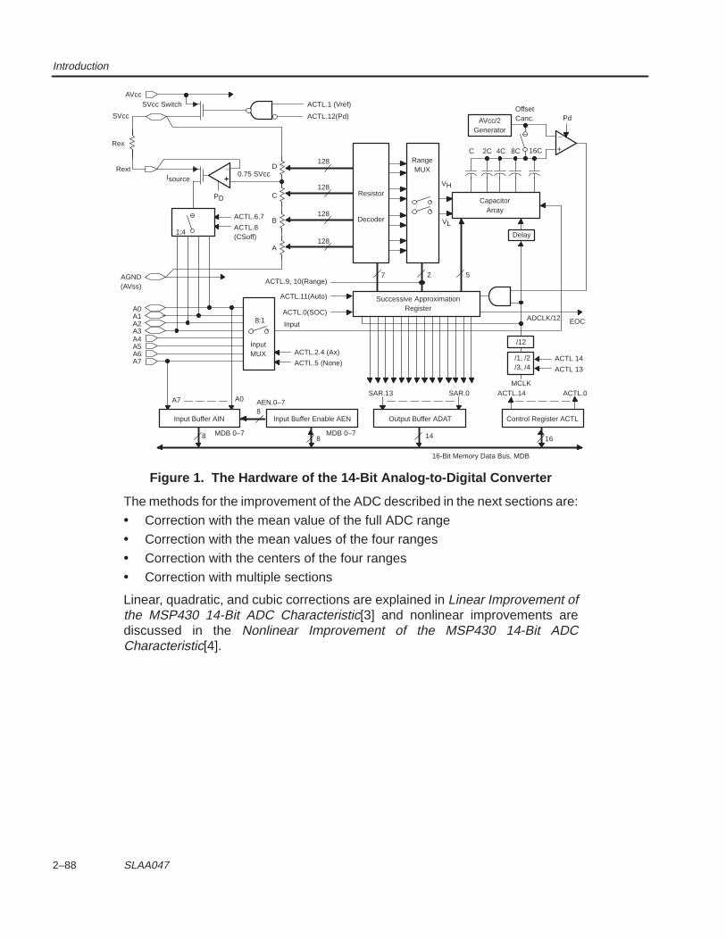
Introduction
2–88 SLAA047
AVcc/2Generator
_
+
Successive ApproximationRegister
SAR.13 SAR.0 ACTL.14 ACTL.0
14 16
Output Buffer ADAT Control Register ACTL
/12
/1, /2/3, /4
ACTL 14
ACTL 13
ACTL.0(SOC)
ACTL.11(Auto)
ACTL.9, 10(Range)
Resistor
RangeMUX
7 2
ADCLK/12 EOC
5
Delay
VH
VL
CapacitorArray
AVcc/2Generator
C 2C 4C 8C
Pd
16C
128
8:1 Input
ACTL.2.4 (Ax)
ACTL.5 (None)
8
Input Buffer Enable AEN
A7 A0
8
8
MDB 0–7
AEN.0–7
_
+0.75 SVcc
ACTL.6,7
ACTL.8(CSoff)
1:4
A7A6A5A4A3A2A1A0
AGND(AVss)
ACTL.12(Pd)
ACTL.1 (Vref)SVcc Switch
Isource
D
C
B
A
Rext
Rex
SVcc
AVcc
16-Bit Memory Data Bus, MDB
PD
Decoder
Input Buffer AIN
MDB 0–7
InputMUX
OffsetCanc.
128
128
128
MCLK
Figure 1. The Hardware of the 14-Bit Analog-to-Digital Converter
The methods for the improvement of the ADC described in the next sections are:
• Correction with the mean value of the full ADC range
• Correction with the mean values of the four ranges
• Correction with the centers of the four ranges
• Correction with multiple sections
Linear, quadratic, and cubic corrections are explained in Linear Improvement ofthe MSP430 14-Bit ADC Characteristic[3] and nonlinear improvements arediscussed in the Nonlinear Improvement of the MSP430 14-Bit ADCCharacteristic[4].
The External Calibration Hardware for the ADC
2–89 Additive Improvement of the MSP430 14-Bit ADC Characteristic
2 The External Calibration Hardware for the ADCAll of the methods of improvement discussed in this report need to know theactual errors of the ADC at different points of the four ADC ranges. See Figure7 for an example of a noncorrected ADC characteristic.
2.1 Measurement Methods for the ADC Reference Samples
The characterization of the ADC for this report is made with three differentmethods:• External digital-to-analog converter (DAC): an accurate DAC—controlled by
the measured MSP430—produces precise analog output voltages that aremeasured with the 14-bit ADC. The difference of the two numbers is theabsolute error of the ADC.
• External discrete, precise voltages: the MSP430 controls its input voltage viaan external analog multiplexer. If only a few accurate input voltages areneeded, then this method is best.
• External precision resistors: the MSP430 controls which resistor ismeasured. For systems that measure the resistance of sensors, this methodis best.
Several other methods exist to measure the errors of different reference pointsfor improvement of the ADC characteristic including:• Measurement of a single ADC sample: fastest way, but not recommended
due to statistical reasons.• Multiple measurements of the same point and calculation of the mean value:
e.g. 16 measurements.• Multiple measurements of the errors around a given point and calculation of
the mean value: e.g. 16 measurements ±8 (or ±32) around the center pointof interest.
• External 16-bit DAC: measurement of all possible four points (xxx.00, xxx.01,xxx.10, xxx.11 for the 14-bit value xxx) and summing them up. This gives anadditional 2 bits of resolution.
• Sophisticated statistical methods.• Measurement of 12 samples for the same ADC point and rejection of the two
extreme values. The remaining 10 samples are averaged.
These error measurement methods may be used for all of the given improvementmethods in this report. However, they are not discussed with the description ofthe improvement methods. See also Section 5.3, Signal Averaging and NoiseCancellation.
This application report only uses simple measurement methods.
2.2 External Digital-to-Analog Converter
The external hardware connected to the MSP430-PC board (see Figure 3) isused to obtain the necessary information about the characteristic of the ADC. Itsmain part is a precise 14- or 16-bit digital-to-analog converter (DAC). Figure 2shows the calibration process:
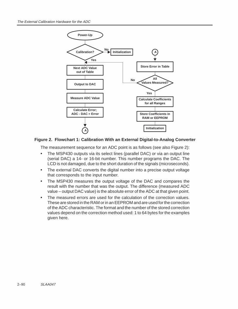
The External Calibration Hardware for the ADC
2–90 SLAA047
Power-Up
Calibration?
Next ADC Valueout of Table
Output to DAC
Measure ADC Value
Calculate Error;ADC - DAC = Error
Store Error in Table
AllValues Measured?
Calculate Coefficientsfor all Ranges
Store Coefficients inRAM or EEPROM
Initialization
No
Yes
No
Yes
A
AInitialization
Figure 2. Flowchart 1: Calibration With an External Digital-to-Analog Converter
The measurement sequence for an ADC point is as follows (see also Figure 2):
• The MSP430 outputs via its select lines (parallel DAC) or via an output line(serial DAC) a 14- or 16-bit number. This number programs the DAC. TheLCD is not damaged, due to the short duration of the signals (microseconds).
• The external DAC converts the digital number into a precise output voltagethat corresponds to the input number.
• The MSP430 measures the output voltage of the DAC and compares theresult with the number that was the output. The difference (measured ADCvalue – output DAC value) is the absolute error of the ADC at that given point.
• The measured errors are used for the calculation of the correction values.These are stored in the RAM or in an EEPROM and are used for the correctionof the ADC characteristic. The format and the number of the stored correctionvalues depend on the correction method used: 1 to 64 bytes for the examplesgiven here.
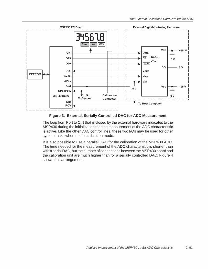
The External Calibration Hardware for the ADC
2–91 Additive Improvement of the MSP430 14-Bit ADC Characteristic
Error kW kWh
MSP430C32x
MSP430 PC Board
16-BitDAC
EEPROM
Ox
O19
O20
Ax
SVcc
AVss
Port
TXDRCV
Vdd
DG
Vss
Data
CS
LDAC
VOUT
Vref+
Vref–
+15 V
0 V
–15 V0 V
To System
To Host Computer
CalibrationConnector
CIN,TP0.5
External Digital-to-Analog Hardware
0 V
0 V
Figure 3. External, Serially Controlled DAC for ADC Measurement
The loop from Port to CIN that is closed by the external hardware indicates to theMSP430 during the initialization that the measurement of the ADC characteristicis active. Like the other DAC control lines, these two I/Os may be used for othersystem tasks when not in calibration mode.
It is also possible to use a parallel DAC for the calibration of the MSP430 ADC.The time needed for the measurement of the ADC characteristic is shorter thanwith a serial DAC, but the number of connections between the MSP430 board andthe calibration unit are much higher than for a serially controlled DAC. Figure 4shows this arrangement.
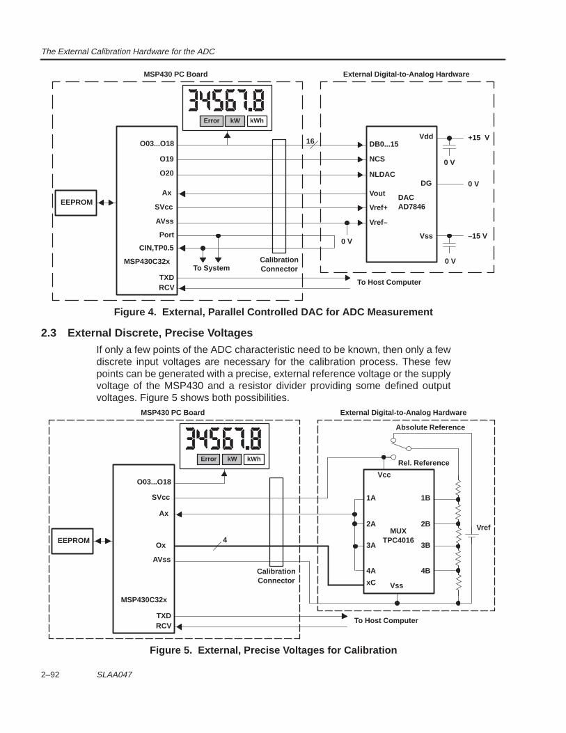
The External Calibration Hardware for the ADC
2–92 SLAA047
Error kW kWh
MSP430C32x
MSP430 PC Board
DACAD7846
EEPROM
O03...O18
O19
O20
Ax
SVcc
AVss
Port
TXDRCV
Vdd
DG
Vss
DB0...15
NCS
NLDAC
Vout
Vref+
Vref–
+15 V
0 V
–15 V0 V
To System
To Host Computer
CalibrationConnector
CIN,TP0.5
External Digital-to-Analog Hardware
16
0 V
0 V
Figure 4. External, Parallel Controlled DAC for ADC Measurement
2.3 External Discrete, Precise VoltagesIf only a few points of the ADC characteristic need to be known, then only a fewdiscrete input voltages are necessary for the calibration process. These fewpoints can be generated with a precise, external reference voltage or the supplyvoltage of the MSP430 and a resistor divider providing some defined outputvoltages. Figure 5 shows both possibilities.
Error kW kWh
MSP430C32x
MSP430 PC Board
EEPROM
O03...O18
SVcc
Ax
Ox
AVss
TXDRCV
1B
2B
4B
2A
3A
4A
To Host Computer
CalibrationConnector
External Digital-to-Analog Hardware
1A
4
xC
3B
Rel. Reference
Absolute Reference
Vss
Vref
Vcc
MUXTPC4016
Figure 5. External, Precise Voltages for Calibration
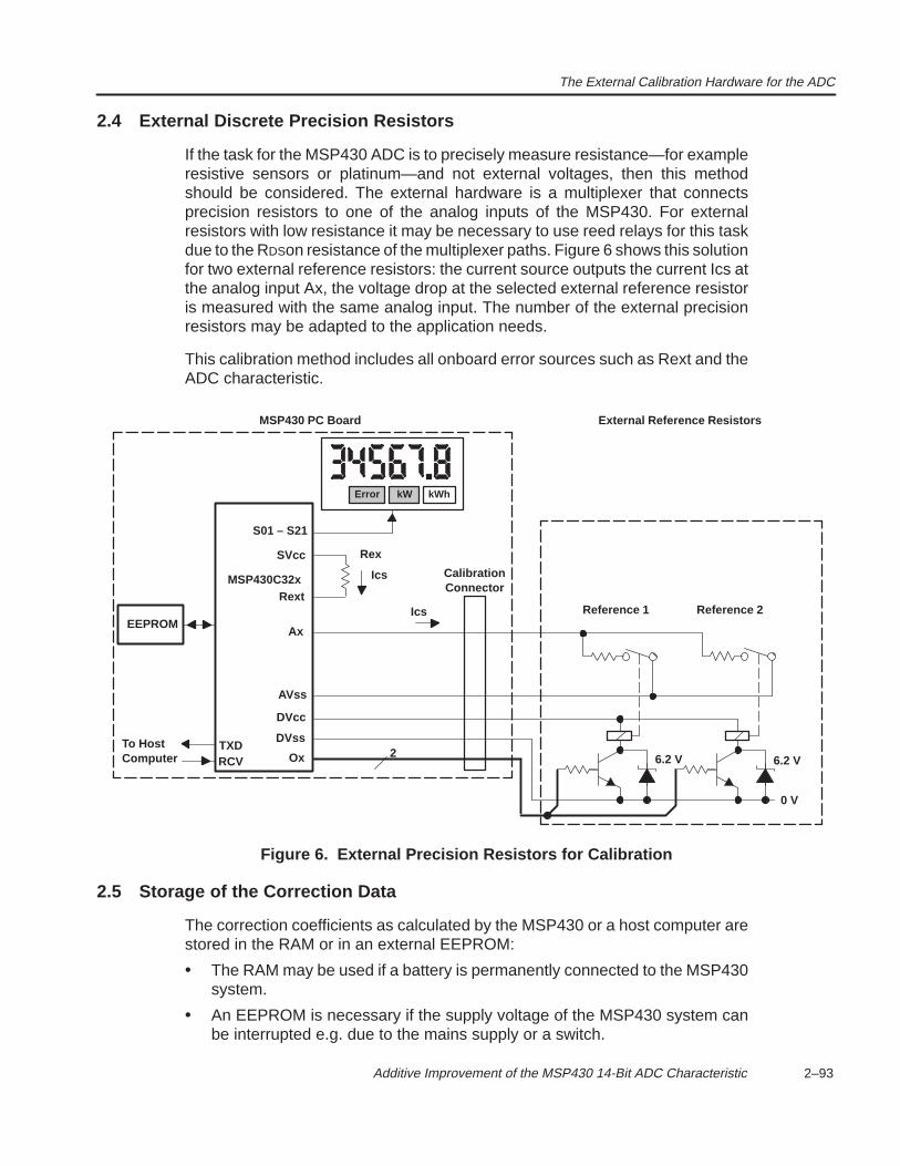
The External Calibration Hardware for the ADC
2–93 Additive Improvement of the MSP430 14-Bit ADC Characteristic
2.4 External Discrete Precision Resistors
If the task for the MSP430 ADC is to precisely measure resistance—for exampleresistive sensors or platinum—and not external voltages, then this methodshould be considered. The external hardware is a multiplexer that connectsprecision resistors to one of the analog inputs of the MSP430. For externalresistors with low resistance it may be necessary to use reed relays for this taskdue to the RDSon resistance of the multiplexer paths. Figure 6 shows this solutionfor two external reference resistors: the current source outputs the current Ics atthe analog input Ax, the voltage drop at the selected external reference resistoris measured with the same analog input. The number of the external precisionresistors may be adapted to the application needs.
This calibration method includes all onboard error sources such as Rext and theADC characteristic.
Error kW kWh
MSP430C32x
MSP430 PC Board
EEPROM
S01 – S21
SVcc
Ax
Ox
AVss
TXDRCV
To HostComputer
CalibrationConnector
External Reference Resistors
2DVss
DVcc
Rext
Rex
Reference 1 Reference 2Ics
Ics
0 V
6.2 V6.2 V
Figure 6. External Precision Resistors for Calibration
2.5 Storage of the Correction Data
The correction coefficients as calculated by the MSP430 or a host computer arestored in the RAM or in an external EEPROM:
• The RAM may be used if a battery is permanently connected to the MSP430system.
• An EEPROM is necessary if the supply voltage of the MSP430 system canbe interrupted e.g. due to the mains supply or a switch.
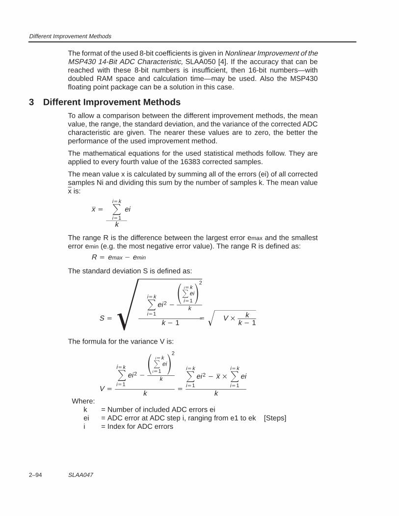
Different Improvement Methods
2–94 SLAA047
The format of the used 8-bit coefficients is given in Nonlinear Improvement of theMSP430 14-Bit ADC Characteristic, SLAA050 [4]. If the accuracy that can bereached with these 8-bit numbers is insufficient, then 16-bit numbers—withdoubled RAM space and calculation time—may be used. Also the MSP430floating point package can be a solution in this case.
3 Different Improvement MethodsTo allow a comparison between the different improvement methods, the meanvalue, the range, the standard deviation, and the variance of the corrected ADCcharacteristic are given. The nearer these values are to zero, the better theperformance of the used improvement method.
The mathematical equations for the used statistical methods follow. They areapplied to every fourth value of the 16383 corrected samples.
The mean value x is calculated by summing all of the errors (ei) of all correctedsamples Ni and dividing this sum by the number of samples k. The mean valuex is:
x ik
i1k
ei
The range R is the difference between the largest error emax and the smallesterror emin (e.g. the most negative error value). The range R is defined as:
R emax emin
The standard deviation S is defined as:
S
ik
i1
ei 2
eiik
i1
2
k
k 1
V k
k 1
The formula for the variance V is:
Where:k = Number of included ADC errors eiei = ADC error at ADC step i, ranging from e1 to ek [Steps]i = Index for ADC errors
V
ik
i1
ei 2
i1
eiik
2
k
k
ik
i1
ei 2 x ik
i1
ei
k
Different Improvement Methods
2–95 Additive Improvement of the MSP430 14-Bit ADC Characteristic
NOTE: Each measured ADC value needs to be correctedindividually to get a correct result. If differences are measured(∆N) then both values have to be corrected and then thesubtraction executed. A correction of the difference ∆N aloneleads to false results.
It is important to note the different scaling that is used for the y-axisof the graphs with the corrected ADC characteristic. They differsignificantly, dependent on the amount of improvement.
The correction coefficients for all improvement methods arecalculated in such a way that allows addition for the final correctionof the measured ADC result. This saves execution time andprogram space.
All of the calculations used for the correction are made with a floating pointpackage (like the MSP430 FPP4 software). If—as is necessary in real-timesystems—an integer package is used, then small rounding errors will occur. InNonlinear Improvement of the MSP430 14-Bit ADC Characteristic[4] the softwareroutines and their influence on the accuracy of the final result are explained.
The improvement methods and their results for this report are demonstrated withthe characteristic of device 1 due to its worst characteristic compared to the otherthree devices shown in Architecture and Function of the MSP430 14-Bit ADC[1].
The ADC samples used for the following improvement methods and calculationswere measured the following way:• Twelve samples with the same ADC input voltage—generated by a 16-bit
DAC—were measured and stored.• The maximum and the minimum value of these twelve samples were rejected
(rejection of extremes).• Out of the remaining ten samples the mean value was calculated and used
afterwards.
The improvement methods are always shown for the full ADC range (ranges A,B, C, and D). If the current source is active, then only ranges A, B, and part of Ccan be used: the same improvement methods with the same formulas are validbut with less needed RAM or EEPROM space for the correction coefficients. Dueto the importance of the current source for several applications, the statisticalresults are also shown for ranges A and B only.
The 14-bit oriented correction software is also usable if the 12-bit ADC mode isused: only the correction coefficients of the applied ADC range are used in thiscase.
The orientation of this application report to the ADC ranges (single or multiplecorrections per range) is applicable, due to the visibly different slopes of the fourranges inside of an ADC characteristic. See the noncorrected ADCcharacteristics of device 1 (Figure 7) and devices 2 to 4 in [1] for examples.
3.1 The ADC Characteristic of Device 1 Without Correction
The noncorrected ADC characteristic of device 1 is shown in Figure 7. Itsstatistical values are given in the table below Figure 7.
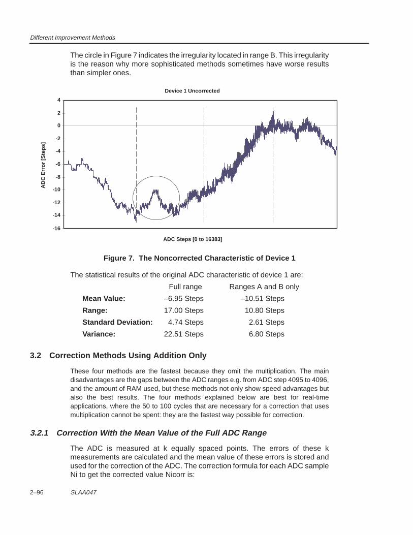
Different Improvement Methods
2–96 SLAA047
The circle in Figure 7 indicates the irregularity located in range B. This irregularityis the reason why more sophisticated methods sometimes have worse resultsthan simpler ones.
-2
-16
AD
C E
rror
[Ste
ps]
0
2
ADC Steps [0 to 16383]
4
Device 1 Uncorrected
-10
-8
-6
-4
-14
-12
Figure 7. The Noncorrected Characteristic of Device 1
The statistical results of the original ADC characteristic of device 1 are:
Full range Ranges A and B only
Mean Value: –6.95 Steps –10.51 Steps
Range: 17.00 Steps 10.80 Steps
Standard Deviation: 4.74 Steps 2.61 Steps
Variance: 22.51 Steps 6.80 Steps
3.2 Correction Methods Using Addition Only
These four methods are the fastest because they omit the multiplication. The maindisadvantages are the gaps between the ADC ranges e.g. from ADC step 4095 to 4096,and the amount of RAM used, but these methods not only show speed advantages butalso the best results. The four methods explained below are best for real-timeapplications, where the 50 to 100 cycles that are necessary for a correction that usesmultiplication cannot be spent: they are the fastest way possible for correction.
3.2.1 Correction With the Mean Value of the Full ADC Range
The ADC is measured at k equally spaced points. The errors of these kmeasurements are calculated and the mean value of these errors is stored andused for the correction of the ADC. The correction formula for each ADC sampleNi to get the corrected value Nicorr is:
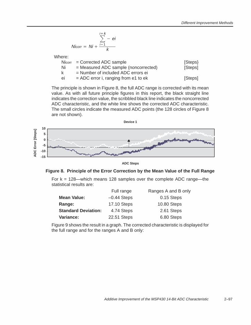
Different Improvement Methods
2–97 Additive Improvement of the MSP430 14-Bit ADC Characteristic
Where:Nicorr = Corrected ADC sample [StepsNi = Measured ADC sample (noncorrected) [Steps]k = Number of included ADC errors eiei = ADC error i, ranging from e1 to ek [Steps]
Nicorr Ni
ik
i1
ei
k
The principle is shown in Figure 8, the full ADC range is corrected with its meanvalue. As with all future principle figures in this report, the black straight lineindicates the correction value, the scribbled black line indicates the noncorrectedADC characteristic, and the white line shows the corrected ADC characteristic.The small circles indicate the measured ADC points (the 128 circles of Figure 8are not shown).
-10
-15AD
C E
rror
[Ste
ps]
-5
0
ADC Steps
5
10
Device 1
Figure 8. Principle of the Error Correction by the Mean Value of the Full Range
For k = 128—which means 128 samples over the complete ADC range—thestatistical results are:
Full range Ranges A and B only
Mean Value: –0.44 Steps 0.15 Steps
Range: 17.10 Steps 10.80 Steps
Standard Deviation: 4.74 Steps 2.61 Steps
Variance: 22.51 Steps 6.80 Steps
Figure 9 shows the result in a graph. The corrected characteristic is displayed forthe full range and for the ranges A and B only:
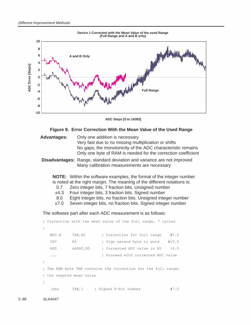
Different Improvement Methods
2–98 SLAA047
4
2
AD
C E
rror
[Ste
ps]
6
8
ADC Steps [0 to 16383]
10
-6
-8
-4
-2
0
-10
Device 1 Corrected with the Mean Value of the used Range(Full Range and A and B only)
A and B Only
Full Range
Figure 9. Error Correction With the Mean Value of the Used Range
Advantages: Only one addition is necessaryVery fast due to no missing multiplication or shiftsNo gaps; the monotonicity of the ADC characteristic remainsOnly one byte of RAM is needed for the correction coefficient
Disadvantages: Range, standard deviation and variance are not improvedMany calibration measurements are necessary
NOTE: Within the software examples, the format of the integer numberis noted at the right margin. The meaning of the different notations is: 0.7 Zero integer bits, 7 fraction bits. Unsigned number ±4.3 Four integer bits, 3 fraction bits. Signed number 8.0 Eight integer bits, no fraction bits. Unsigned integer number
±7.0 Seven integer bits, no fraction bits. Signed integer number
The software part after each ADC measurement is as follows:
; Correction with the mean value of the full range. 7 cycles
;
MOV.B TAB,R5 ; Correction for full range ±7.0
SXT R5 ; Sign extend byte to word ±15.0
ADD &ADAT,R5 ; Corrected ADC value in R5 14.0
... ; Proceed with corrected ADC value
;
; The RAM byte TAB contains the correction for the full range:
; the negated mean value
;
.bss TAB,1 ; Signed 8–bit number ±7.0
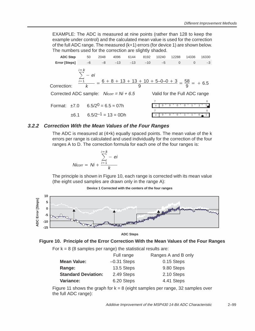
Different Improvement Methods
2–99 Additive Improvement of the MSP430 14-Bit ADC Characteristic
EXAMPLE: The ADC is measured at nine points (rather than 128 to keep theexample under control) and the calculated mean value is used for the correctionof the full ADC range. The measured (k+1) errors (for device 1) are shown below.The numbers used for the correction are slightly shaded.
ADC Step 50 2048 4096 6144 8192 10240 12288 14336 16330
Error [Steps] –6 –8 –13 –13 –10 –5 0 0 –3
Correction:
Corrected ADC sample: Nicorr = Ni + 6.5 Valid for the Full ADC range
Format: ±7.0 6.5/20 = 6.5 ≈ 07h
±6.1 6.5/2–1 = 13 = 0Dh
0 0 0 0 0 1 1 1
07
0 0 0 0 1 1 0 1
07
ik
i1
ei
k 6 8 13 13 10 5–0–0 3
9 58
9 6.5
3.2.2 Correction With the Mean Values of the Four RangesThe ADC is measured at (4×k) equally spaced points. The mean value of the kerrors per range is calculated and used individually for the correction of the fourranges A to D. The correction formula for each one of the four ranges is:
Nicorr Ni
ik
i1
ei
k
The principle is shown in Figure 10, each range is corrected with its mean value(the eight used samples are drawn only in the range A):
-10
-15
AD
C E
rror
[Ste
ps]
-5
0
ADC Steps
5
10
Device 1 Corrected with the centers of the four ranges
Figure 10. Principle of the Error Correction With the Mean Values of the Four Ranges
For k = 8 (8 samples per range) the statistical results are:Full range Ranges A and B only
Mean Value: –0.31 Steps 0.15 StepsRange: 13.5 Steps 9.80 StepsStandard Deviation: 2.49 Steps 2.10 StepsVariance: 6.20 Steps 4.41 Steps
Figure 11 shows the graph for k = 8 (eight samples per range, 32 samples overthe full ADC range):
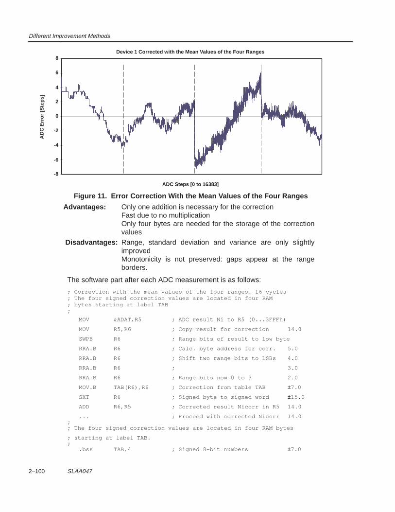
Different Improvement Methods
2–100 SLAA047
2
0
AD
C E
rror
[Ste
ps]
4
6
ADC Steps [0 to 16383]
8Device 1 Corrected with the Mean Values of the Four Ranges
-8
-6
-4
-2
Figure 11. Error Correction With the Mean Values of the Four Ranges
Advantages: Only one addition is necessary for the correctionFast due to no multiplicationOnly four bytes are needed for the storage of the correctionvalues
Disadvantages: Range, standard deviation and variance are only slightlyimprovedMonotonicity is not preserved: gaps appear at the rangeborders.
The software part after each ADC measurement is as follows:
; Correction with the mean values of the four ranges. 16 cycles; The four signed correction values are located in four RAM; bytes starting at label TAB;
MOV &ADAT,R5 ; ADC result Ni to R5 (0...3FFFh)
MOV R5,R6 ; Copy result for correction 14.0
SWPB R6 ; Range bits of result to low byte
RRA.B R6 ; Calc. byte address for corr. 5.0
RRA.B R6 ; Shift two range bits to LSBs 4.0
RRA.B R6 ; 3.0
RRA.B R6 ; Range bits now 0 to 3 2.0
MOV.B TAB(R6),R6 ; Correction from table TAB ±7.0
SXT R6 ; Signed byte to signed word ±15.0
ADD R6,R5 ; Corrected result Nicorr in R5 14.0
... ; Proceed with corrected Nicorr 14.0;; The four signed correction values are located in four RAM bytes
; starting at label TAB.;
.bss TAB,4 ; Signed 8–bit numbers ±7.0
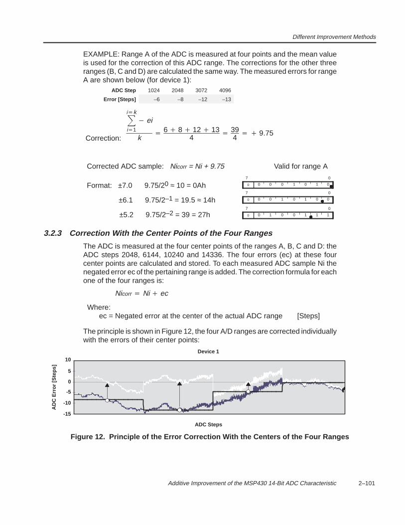
Different Improvement Methods
2–101 Additive Improvement of the MSP430 14-Bit ADC Characteristic
EXAMPLE: Range A of the ADC is measured at four points and the mean valueis used for the correction of this ADC range. The corrections for the other threeranges (B, C and D) are calculated the same way. The measured errors for rangeA are shown below (for device 1):
ADC Step 1024 2048 3072 4096
Error [Steps] –6 –8 –12 –13
Correction:
Corrected ADC sample: Nicorr = Ni + 9.75 Valid for range A
Format: ±7.0 9.75/20 ≈ 10 = 0Ah
±6.1 9.75/2–1 = 19.5 ≈ 14h
±5.2 9.75/2–2 = 39 = 27h
0 0 0 0 1 0 1 0
07
0 0 0 1 0 1 0 0
07
0 0 1 0 0 1 1 1
07
ik
i1
ei
k 6 8 12 13
4 39
4 9.75
3.2.3 Correction With the Center Points of the Four Ranges
The ADC is measured at the four center points of the ranges A, B, C and D: theADC steps 2048, 6144, 10240 and 14336. The four errors (ec) at these fourcenter points are calculated and stored. To each measured ADC sample Ni thenegated error ec of the pertaining range is added. The correction formula for eachone of the four ranges is:
Where:ec = Negated error at the center of the actual ADC range [Steps]
Nicorr Ni ec
The principle is shown in Figure 12, the four A/D ranges are corrected individuallywith the errors of their center points:
-10
-15
AD
C E
rror
[Ste
ps]
-5
0
ADC Steps
5
Device 1
10
Figure 12. Principle of the Error Correction With the Centers of the Four Ranges
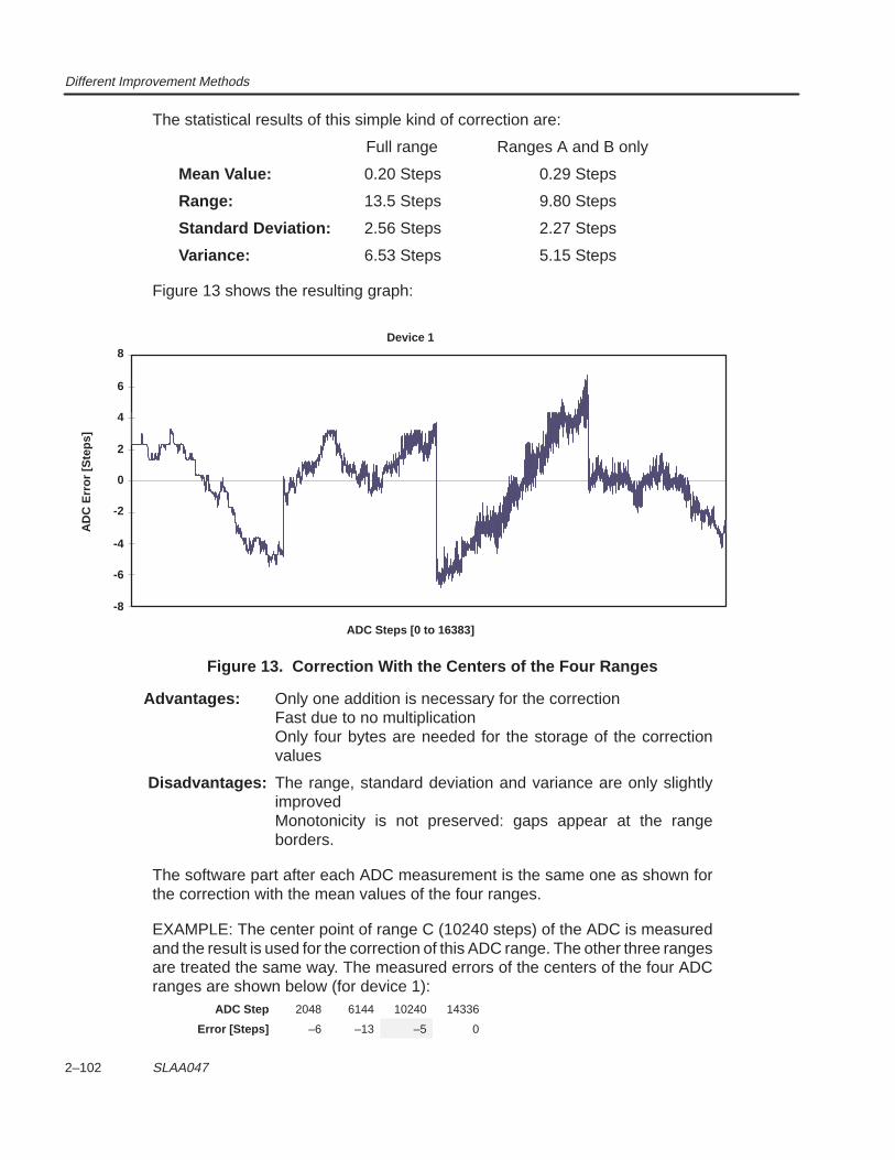
Different Improvement Methods
2–102 SLAA047
The statistical results of this simple kind of correction are:
Full range Ranges A and B only
Mean Value: 0.20 Steps 0.29 Steps
Range: 13.5 Steps 9.80 Steps
Standard Deviation: 2.56 Steps 2.27 Steps
Variance: 6.53 Steps 5.15 Steps
Figure 13 shows the resulting graph:
2
0
AD
C E
rror
[Ste
ps]
4
6
ADC Steps [0 to 16383]
8Device 1
-8
-6
-4
-2
Figure 13. Correction With the Centers of the Four Ranges
Advantages: Only one addition is necessary for the correctionFast due to no multiplicationOnly four bytes are needed for the storage of the correctionvalues
Disadvantages: The range, standard deviation and variance are only slightlyimprovedMonotonicity is not preserved: gaps appear at the rangeborders.
The software part after each ADC measurement is the same one as shown forthe correction with the mean values of the four ranges.
EXAMPLE: The center point of range C (10240 steps) of the ADC is measuredand the result is used for the correction of this ADC range. The other three rangesare treated the same way. The measured errors of the centers of the four ADCranges are shown below (for device 1):
ADC Step 2048 6144 10240 14336
Error [Steps] –6 –13 –5 0
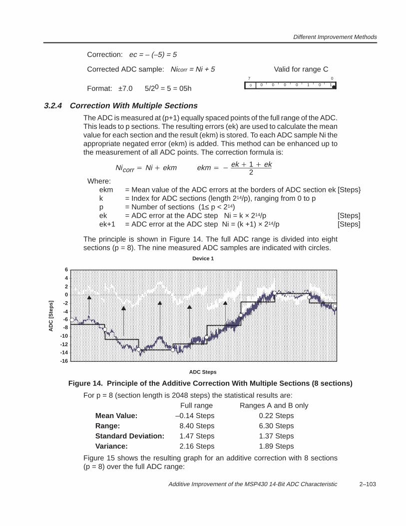
Different Improvement Methods
2–103 Additive Improvement of the MSP430 14-Bit ADC Characteristic
Correction: ec = – (–5) = 5
Corrected ADC sample: Nicorr = Ni + 5 Valid for range C
Format: ±7.0 5/20 = 5 = 05h0 0 0 0 0 1 0 1
07
3.2.4 Correction With Multiple SectionsThe ADC is measured at (p+1) equally spaced points of the full range of the ADC.This leads to p sections. The resulting errors (ek) are used to calculate the meanvalue for each section and the result (ekm) is stored. To each ADC sample Ni theappropriate negated error (ekm) is added. This method can be enhanced up tothe measurement of all ADC points. The correction formula is:
Nicorr Ni ekm ekm ek 1 ek2
Where:ekm = Mean value of the ADC errors at the borders of ADC section ek [Stepsk = Index for ADC sections (length 214/p), ranging from 0 to pp = Number of sections (1≤ p < 214)ek = ADC error at the ADC step Ni = k × 214/p [Steps]ek+1 = ADC error at the ADC step Ni = (k +1) × 214/p [Steps]
The principle is shown in Figure 14. The full ADC range is divided into eightsections (p = 8). The nine measured ADC samples are indicated with circles.
ÎÎÎÎÎÎÎÎÎÎÎÎÎÎÎÎÎÎÎÎÎÎÎÎÎÎÎÎÎÎÎÎÎÎÎÎÎÎÎÎÎÎÎÎÎÎÎÎÎÎÎÎÎÎÎÎÎÎÎÎÎÎÎÎÎÎÎÎÎÎÎÎÎÎÎÎÎÎÎÎÎÎÎÎÎÎÎÎÎÎÎÎÎÎÎÎÎÎÎÎÎÎÎÎÎÎÎÎÎÎÎÎÎÎÎÎÎÎÎÎÎÎÎÎÎÎÎÎÎÎÎÎÎÎÎÎÎÎÎÎÎÎÎÎÎÎÎÎÎÎÎÎÎÎÎÎÎÎÎÎÎÎÎÎÎÎÎÎÎÎÎÎÎÎÎÎÎÎÎÎÎÎÎÎÎÎÎÎÎÎÎÎÎÎÎÎÎÎÎÎÎÎÎÎÎÎÎÎÎÎÎÎÎÎÎÎÎÎÎÎÎÎÎÎÎÎÎÎÎÎÎÎÎÎÎÎÎÎÎÎÎÎÎÎÎÎÎÎÎÎÎÎÎÎÎÎÎÎÎÎÎÎÎÎÎÎÎÎÎÎÎÎÎÎÎÎÎÎÎÎ
0
-2
AD
C [S
teps
]
2
4
ADC Steps
6
-10
-12
-8
-6-4
-14
-16
Device 1
Figure 14. Principle of the Additive Correction With Multiple Sections (8 sections)
For p = 8 (section length is 2048 steps) the statistical results are:Full range Ranges A and B only
Mean Value: –0.14 Steps 0.22 StepsRange: 8.40 Steps 6.30 StepsStandard Deviation: 1.47 Steps 1.37 StepsVariance: 2.16 Steps 1.89 Steps
Figure 15 shows the resulting graph for an additive correction with 8 sections(p = 8) over the full ADC range:
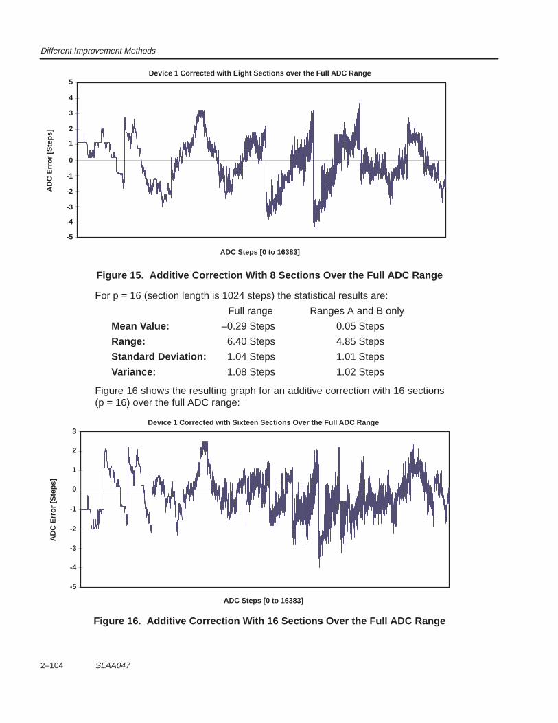
Different Improvement Methods
2–104 SLAA047
2
1
AD
C E
rror
[Ste
ps]
3
4
ADC Steps [0 to 16383]
5Device 1 Corrected with Eight Sections over the Full ADC Range
-3
-4
-2
-1
0
-5
Figure 15. Additive Correction With 8 Sections Over the Full ADC Range
For p = 16 (section length is 1024 steps) the statistical results are:
Full range Ranges A and B only
Mean Value: –0.29 Steps 0.05 Steps
Range: 6.40 Steps 4.85 Steps
Standard Deviation: 1.04 Steps 1.01 Steps
Variance: 1.08 Steps 1.02 Steps
Figure 16 shows the resulting graph for an additive correction with 16 sections(p = 16) over the full ADC range:
0
-1
AD
C E
rror
[Ste
ps]
1
2
ADC Steps [0 to 16383]
3
-5
-4
-3
-2
Device 1 Corrected with Sixteen Sections Over the Full ADC Range
Figure 16. Additive Correction With 16 Sections Over the Full ADC Range
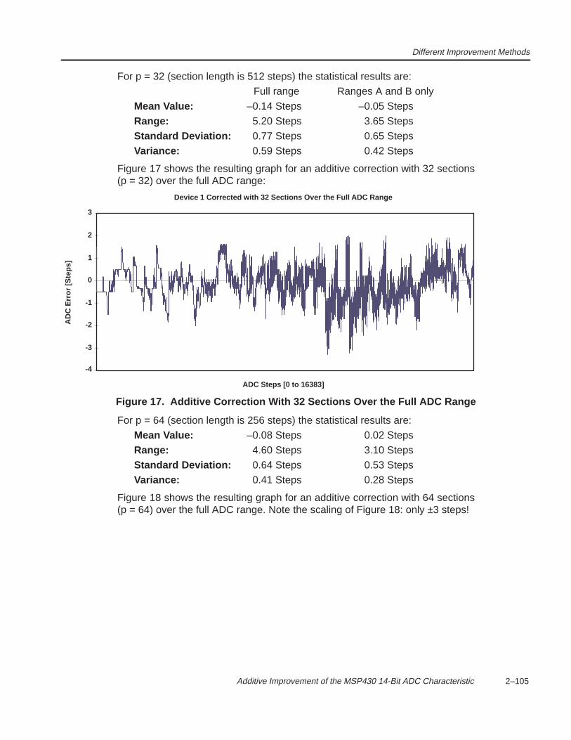
Different Improvement Methods
2–105 Additive Improvement of the MSP430 14-Bit ADC Characteristic
For p = 32 (section length is 512 steps) the statistical results are:
Full range Ranges A and B only
Mean Value: –0.14 Steps –0.05 Steps
Range: 5.20 Steps 3.65 Steps
Standard Deviation: 0.77 Steps 0.65 Steps
Variance: 0.59 Steps 0.42 Steps
Figure 17 shows the resulting graph for an additive correction with 32 sections(p = 32) over the full ADC range:
AD
C E
rror
[Ste
ps]
ADC Steps [0 to 16383]
0
-1
1
2
3
-4
-3
-2
Device 1 Corrected with 32 Sections Over the Full ADC Range
Figure 17. Additive Correction With 32 Sections Over the Full ADC Range
For p = 64 (section length is 256 steps) the statistical results are:
Mean Value: –0.08 Steps 0.02 Steps
Range: 4.60 Steps 3.10 Steps
Standard Deviation: 0.64 Steps 0.53 Steps
Variance: 0.41 Steps 0.28 Steps
Figure 18 shows the resulting graph for an additive correction with 64 sections(p = 64) over the full ADC range. Note the scaling of Figure 18: only ±3 steps!
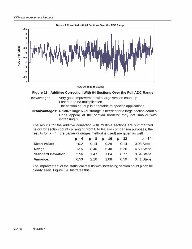
Different Improvement Methods
2–106 SLAA047
1
0.5
AD
C E
rror
[Ste
ps]
1.5
2
ADC Steps [0 to 16383]
2.5Device 1 Corrected with 64 Sections Over the ADC Range
-1.5
-2
-1
-0.5
0
-2.5
-3
Figure 18. Additive Correction With 64 Sections Over the Full ADC Range
Advantages: Very good improvement with large section counts pFast due to no multiplicationThe section count p is adaptable to specific applications.
Disadvantages: Relative large RAM storage is needed for a large section count pGaps appear at the section borders: they get smaller withincreasing p
The results for the additive correction with multiple sections are summarizedbelow for section counts p ranging from 8 to 64. For comparison purposes, theresults for p = 4 ( the center of ranges method is used) are given as well.
p = 4 p = 8 p = 16 p = 32 p = 64
Mean Value: +0.2 –0.14 –0.29 –0.14 –0.08 Steps
Range: 13.5 8.40 6.40 5.20 4.60 Steps
Standard Deviation: 2.56 1.47 1.04 0.77 0.64 Steps
Variance: 6.53 2.16 1.08 0.59 0.41 Steps
The improvement of the statistical results with increasing section count p can beclearly seen. Figure 19 illustrates this.
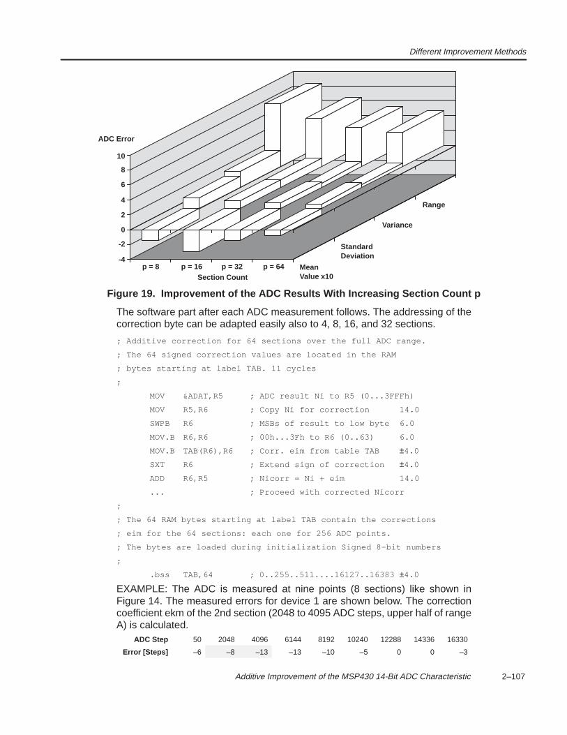
Different Improvement Methods
2–107 Additive Improvement of the MSP430 14-Bit ADC Characteristic
ADC Error
10
8
6
4
2
0
-2
-4p = 8 p = 16 p = 32 p = 64
Section Count
Range
Variance
StandardDeviation
MeanValue x10
Figure 19. Improvement of the ADC Results With Increasing Section Count p
The software part after each ADC measurement follows. The addressing of thecorrection byte can be adapted easily also to 4, 8, 16, and 32 sections.
; Additive correction for 64 sections over the full ADC range.
; The 64 signed correction values are located in the RAM
; bytes starting at label TAB. 11 cycles
;
MOV &ADAT,R5 ; ADC result Ni to R5 (0...3FFFh)
MOV R5,R6 ; Copy Ni for correction 14.0
SWPB R6 ; MSBs of result to low byte 6.0
MOV.B R6,R6 ; 00h...3Fh to R6 (0..63) 6.0
MOV.B TAB(R6),R6 ; Corr. eim from table TAB ±4.0
SXT R6 ; Extend sign of correction ±4.0
ADD R6,R5 ; Nicorr = Ni + eim 14.0
... ; Proceed with corrected Nicorr
;
; The 64 RAM bytes starting at label TAB contain the corrections
; eim for the 64 sections: each one for 256 ADC points.
; The bytes are loaded during initialization Signed 8–bit numbers
;
.bss TAB,64 ; 0..255..511....16127..16383 ±4.0
EXAMPLE: The ADC is measured at nine points (8 sections) like shown inFigure 14. The measured errors for device 1 are shown below. The correctioncoefficient ekm of the 2nd section (2048 to 4095 ADC steps, upper half of rangeA) is calculated.
ADC Step 50 2048 4096 6144 8192 10240 12288 14336 16330
Error [Steps] –6 –8 –13 –13 –10 –5 0 0 –3
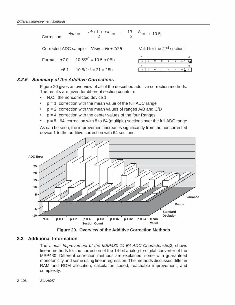
Different Improvement Methods
2–108 SLAA047
Correction:
Corrected ADC sample: Nicorr = Ni + 10.5 Valid for the 2nd section
Format: ±7.0 10.5/20 = 10.5 ≈ 0Bh
±6.1 10.5/2–1 = 21 = 15h
ekm ek1 ek2
13 82
10.5
0 0 0 0 1 0 1 1
07
0 0 0 1 0 1 0 1
07
3.2.5 Summary of the Additive CorrectionsFigure 20 gives an overview of all of the described additive correction methods.The results are given for different section counts p:• N.C.: the noncorrected device 1• p = 1: correction with the mean value of the full ADC range• p = 2: correction with the mean values of ranges A/B and C/D• p = 4: correction with the center values of the four Ranges• p = 8...64: correction with 8 to 64 (multiple) sections over the full ADC range
As can be seen, the improvement increases significantly from the noncorrecteddevice 1 to the additive correction with 64 sections.
ADC Error
25
20
15
10
5
-5
-10N.C. p = 1 p = 2 p = 4
Section Count
Range
Variance
StandardDeviation
MeanValue
p = 8 p = 16 p = 32 p = 64
Figure 20. Overview of the Additive Correction Methods
3.3 Additional InformationThe Linear Improvement of the MSP430 14-Bit ADC Characteristic[3] showslinear methods for the correction of the 14-bit analog-to-digital converter of theMSP430. Different correction methods are explained: some with guaranteedmonotonicity and some using linear regression. The methods discussed differ inRAM and ROM allocation, calculation speed, reachable improvement, andcomplexity.
References
2–109 Additive Improvement of the MSP430 14-Bit ADC Characteristic
4 References1. Architecture and Function of the MSP430 14-Bit ADC Application Report,
1999, Literature #SLAA045
2. Application Basics for the MSP430 14-Bit ADC Application Report, 1999,Literature #SLAA046
3. Linear Improvement of the MSP430 14-Bit ADC Characteristic ApplicationReport, 1999, Literature #SLAA048
4. Nonlinear Improvement of the MSP430 14-Bit ADC CharacteristicApplication Report, 1999, Literature #SLAA050
5. MSP430 Application Report, 1998, Literature #SLAAE10C
6. Data Sheet MSP430C325, MSP430P323, 1997, Literature #SLASE06
7. MSP430 Family Architecture Guide and Module Library, 1996, Literature#SLAUE10B

2–110 SLAA047

Definitions Used With the Application Examples
2–111 Additive Improvement of the MSP430 14-Bit ADC Characteristic
Appendix A Definitions Used With the Application Examples
; HARDWARE DEFINITIONS
;; ADAT .equ 0118h ; ADC data register (12 or 14–bits); ACTL .equ 0114h ; ADC control register: control bits

2–112 SLAA047

2–113
Linear Improvement of the MSP43014-Bit ADC Characteristic
Literature Number: SLAA048June 1999
Printed on Recycled Paper

2–114
IMPORTANT NOTICE
Texas Instruments and its subsidiaries (TI) reserve the right to make changes to theirproducts or to discontinue any product or service without notice, and advise customers toobtain the latest version of relevant information to verify, before placing orders, thatinformation being relied on is current and complete. All products are sold subject to the termsand conditions of sale supplied at the time of order acknowledgement, including thosepertaining to warranty, patent infringement, and limitation of liability.
TI warrants performance of its semiconductor products to the specifications applicable at thetime of sale in accordance with TI’s standard warranty. Testing and other quality controltechniques are utilized to the extent TI deems necessary to support this warranty. Specifictesting of all parameters of each device is not necessarily performed, except those mandatedby government requirements.
CERTAIN APPLICATIONS USING SEMICONDUCTOR PRODUCTS MAY INVOLVEPOTENTIAL RISKS OF DEATH, PERSONAL INJURY, OR SEVERE PROPERTY ORENVIRONMENTAL DAMAGE (“CRITICAL APPLICATIONS”). TI SEMICONDUCTORPRODUCTS ARE NOT DESIGNED, AUTHORIZED, OR WARRANTED TO BE SUITABLEFOR USE IN LIFE-SUPPORT DEVICES OR SYSTEMS OR OTHER CRITICALAPPLICATIONS. INCLUSION OF TI PRODUCTS IN SUCH APPLICATIONS ISUNDERSTOOD TO BE FULLY AT THE CUSTOMER’S RISK.
In order to minimize risks associated with the customer’s applications, adequate design andoperating safeguards must be provided by the customer to minimize inherent or proceduralhazards.
TI assumes no liability for applications assistance or customer product design. TI does notwarrant or represent that any license, either express or implied, is granted under any patentright, copyright, mask work right, or other intellectual property right of TI covering or relatingto any combination, machine, or process in which such semiconductor products or servicesmight be or are used. TI’s publication of information regarding any third party’s products orservices does not constitute TI’s approval, warranty or endorsement thereof.
Copyright 1999, Texas Instruments Incorporated
2–115 Linear Improvement of the MSP430 14-Bit ADC Characteristic
Contents1 Introduction 2–117. . . . . . . . . . . . . . . . . . . . . . . . . . . . . . . . . . . . . . . . . . . . . . . . . . . . . . . . . . . . . . . . . . . . . . . . . . . . . . .
1.1 Correction With Linear Equations 2–118. . . . . . . . . . . . . . . . . . . . . . . . . . . . . . . . . . . . . . . . . . . . . . . . . . . . . . . 1.2 Coefficients Estimation 2–120. . . . . . . . . . . . . . . . . . . . . . . . . . . . . . . . . . . . . . . . . . . . . . . . . . . . . . . . . . . . . . . .
1.2.1 Linear Equations With Border Fit 2–120. . . . . . . . . . . . . . . . . . . . . . . . . . . . . . . . . . . . . . . . . . . . . . . . 1.2.2 Linear Equations With Linear Regression 2–130. . . . . . . . . . . . . . . . . . . . . . . . . . . . . . . . . . . . . . . .
2 Additional Information 2–138. . . . . . . . . . . . . . . . . . . . . . . . . . . . . . . . . . . . . . . . . . . . . . . . . . . . . . . . . . . . . . . . . . . . .
3 References 2–139. . . . . . . . . . . . . . . . . . . . . . . . . . . . . . . . . . . . . . . . . . . . . . . . . . . . . . . . . . . . . . . . . . . . . . . . . . . . . . . .
Appendix A Definitions Used With the Application Examples 2–141. . . . . . . . . . . . . . . . . . . . . . . . . . . . . . . . . . .
List of Figures1 The Hardware of the 14-Bit Analog-to-Digital Converter 2–118. . . . . . . . . . . . . . . . . . . . . . . . . . . . . . . . . . . . . . . . . . . 2 Principle of the Correction With Border Fit (single linear equation per range) 2–121. . . . . . . . . . . . . . . . . . . . . . . . . 3 Error Correction With Border Fit (single linear equation) 2–122. . . . . . . . . . . . . . . . . . . . . . . . . . . . . . . . . . . . . . . . . . . 4 Principle of the Correction With Border Fit (two linear equations per range) 2–125. . . . . . . . . . . . . . . . . . . . . . . . . . 5 Error Correction With Border Fit (two linear equations per range) 2–126. . . . . . . . . . . . . . . . . . . . . . . . . . . . . . . . . . . 6 Principle of the Correction With Border Fit (four linear equations per range) 2–127. . . . . . . . . . . . . . . . . . . . . . . . . . 7 Error Correction With Border Fit (four linear equations per range) 2–128. . . . . . . . . . . . . . . . . . . . . . . . . . . . . . . . . . 8 Principle of the Linear Regression Method (single linear equation per range) 2–131. . . . . . . . . . . . . . . . . . . . . . . . 9 Error Correction With Linear Regression (single linear equation per range) 2–132. . . . . . . . . . . . . . . . . . . . . . . . . . 10 Device 2 Showing the Typical Gaps at the Range Borders 2–132. . . . . . . . . . . . . . . . . . . . . . . . . . . . . . . . . . . . . . . . 11 Principle of the Linear Regression Method (two linear equations per range) 2–136. . . . . . . . . . . . . . . . . . . . . . . . . 12 Error Correction With Linear Regression (two linear equations per range) 2–136. . . . . . . . . . . . . . . . . . . . . . . . . .
List of Tables1 Worst Case Coefficients With 8-Bit Arithmetic 2–120. . . . . . . . . . . . . . . . . . . . . . . . . . . . . . . . . . . . . . . . . . . . . . . . . . . .

2–116 SLAA048
2–117
Linear Improvement of the MSP430 14-Bit ADC Characteristic
Lutz Bierl
ABSTRACTThis application report shows different linear methods to improve the accuracy of the14-bit analog-to-digital converter (ADC) of the MSP430 family. Different correctionmethods are explained: some with monotonicity and some using linear regression. Themethods used differ in RAM and ROM allocation, calculation speed, reachableimprovement, and complexity. For all correction methods, proven, optimized, softwareexamples are given with 8-bit and 16-bit arithmetic. The References section at the endof the report lists related application reports in the MSP430 14-bit ADC series.
1 IntroductionThe application report Architecture and Function of the MSP430 14-Bit ADC[1]gives a detailed overview to the architecture and function of the 14-bitanalog-to-digital converter (ADC) of the MSP430 family. The principle of the ADCis explained and software examples are given. Also included are the explanationof the function of all hardware registers contained in the ADC.
The application report Application Basics for the MSP430 14-Bit ADC[2] showsseveral applications of the 14-bit ADC of the MSP430 family. Proven softwareexamples and basic circuitry are shown and explained.
The application report Additive Improvement of the MSP430 14-Bit ADCCharacteristic[3] explains the external hardware that is needed for themeasurement of the characteristic of the MSP430’s analog-to-digital converter.This report also demonstrates correction methods that use only addition. Thisallows the application of these methods in real time systems, were execution timecan be critical.
Figure 1 shows the block diagram of the 14-bit analog-to-digital converter of theMSP430 family.
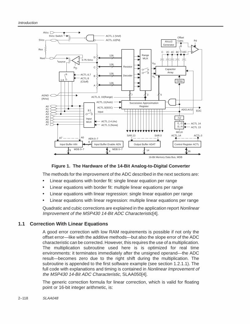
Introduction
2–118 SLAA048
AVcc/2Generator
_
+
Successive ApproximationRegister
SAR.13 SAR.0 ACTL.14 ACTL.0
14 16
Output Buffer ADAT Control Register ACTL
/12
/1, /2/3, /4
ACTL 14
ACTL 13
ACTL.0(SOC)
ACTL.11(Auto)
ACTL.9, 10(Range)
Resistor
RangeMUX
7 2
ADCLK/12 EOC
5
Delay
VH
VL
CapacitorArray
AVcc/2Generator
C 2C 4C 8C
Pd
16C
128
8:1 Input
ACTL.2.4 (Ax)
ACTL.5 (None)
8
Input Buffer Enable AEN
A7 A0
8
8
MDB 0–7
AEN.0–7
_
+0.75 SVcc
ACTL.6,7
ACTL.8(CSoff)
1:4
A7A6A5A4A3A2A1A0
AGND(AVss)
ACTL.12(Pd)
ACTL.1 (Vref)SVcc Switch
Isource
D
C
B
A
Rext
Rex
SVcc
AVcc
16-Bit Memory Data Bus, MDB
PD
Decoder
Input Buffer AIN
MDB 0–7
InputMUX
OffsetCanc.
128
128
128
MCLK
Figure 1. The Hardware of the 14-Bit Analog-to-Digital Converter
The methods for the improvement of the ADC described in the next sections are:
• Linear equations with border fit: single linear equation per range
• Linear equations with border fit: multiple linear equations per range
• Linear equations with linear regression: single linear equation per range
• Linear equations with linear regression: multiple linear equations per range
Quadratic and cubic corrections are explained in the application report NonlinearImprovement of the MSP430 14-Bit ADC Characteristic[4].
1.1 Correction With Linear Equations
A good error correction with low RAM requirements is possible if not only theoffset error—like with the additive methods—but also the slope error of the ADCcharacteristic can be corrected. However, this requires the use of a multiplication.The multiplication subroutine used here is is optimized for real timeenvironments: it terminates immediately after the unsigned operand—the ADCresult—becomes zero due to the right shift during the multiplication. Thesubroutine is appended to the first software example (see section 1.2.1.1). Thefull code with explanations and timing is contained in Nonlinear Improvement ofthe MSP430 14-Bit ADC Characteristic, SLAA050[4].
The generic correction formula for linear correction, which is valid for floatingpoint or 16-bit integer arithmetic, is:
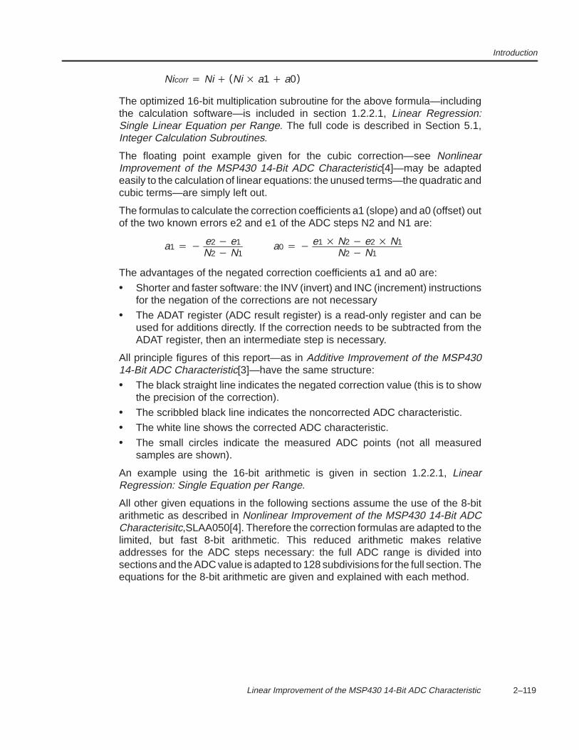
Introduction
2–119 Linear Improvement of the MSP430 14-Bit ADC Characteristic
Nicorr Ni (Ni a1 a0)
The optimized 16-bit multiplication subroutine for the above formula—includingthe calculation software—is included in section 1.2.2.1, Linear Regression:Single Linear Equation per Range. The full code is described in Section 5.1,Integer Calculation Subroutines.
The floating point example given for the cubic correction—see NonlinearImprovement of the MSP430 14-Bit ADC Characteristic[4]—may be adaptedeasily to the calculation of linear equations: the unused terms—the quadratic andcubic terms—are simply left out.
The formulas to calculate the correction coefficients a1 (slope) and a0 (offset) outof the two known errors e2 and e1 of the ADC steps N2 and N1 are:
a1 e2 e1N2 N1
a0 e1 N2 e2 N1N2 N1
The advantages of the negated correction coefficients a1 and a0 are:
• Shorter and faster software: the INV (invert) and INC (increment) instructionsfor the negation of the corrections are not necessary
• The ADAT register (ADC result register) is a read-only register and can beused for additions directly. If the correction needs to be subtracted from theADAT register, then an intermediate step is necessary.
All principle figures of this report—as in Additive Improvement of the MSP43014-Bit ADC Characteristic[3]—have the same structure:
• The black straight line indicates the negated correction value (this is to showthe precision of the correction).
• The scribbled black line indicates the noncorrected ADC characteristic.
• The white line shows the corrected ADC characteristic.
• The small circles indicate the measured ADC points (not all measuredsamples are shown).
An example using the 16-bit arithmetic is given in section 1.2.2.1, LinearRegression: Single Equation per Range.
All other given equations in the following sections assume the use of the 8-bitarithmetic as described in Nonlinear Improvement of the MSP430 14-Bit ADCCharacterisitc,SLAA050[4]. Therefore the correction formulas are adapted to thelimited, but fast 8-bit arithmetic. This reduced arithmetic makes relativeaddresses for the ADC steps necessary: the full ADC range is divided intosections and the ADC value is adapted to 128 subdivisions for the full section. Theequations for the 8-bit arithmetic are given and explained with each method.
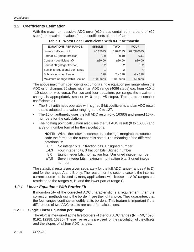
Introduction
2–120 SLAA048
1.2 Coefficients EstimationWith the maximum possible ADC error (±10 steps contained in a band of ±20steps) the maximum values for the coefficients a1 and a0 are:
Table 1. Worst Case Coefficients With 8-Bit Arithmetic
EQUATIONS PER RANGE SINGLE TWO FOUR
Linear coefficient a1: ±0.15625 ±0.078125 ±0.0390625
Format a1 (integer.fraction) 0.9 0.10 0.11
Constant coefficient a0: ±20.00 ±20.00 ±20.00
Format a0 (integer.fraction) 5.2 5.2 5.2
Sections (Equations) per Range 1 2 4
Subdivisions per Range 128 2 × 128 4 × 128
Maximum Change within Section ±20 Steps ±10 Steps ±5 Steps
The above maximum coefficients occur for a single equation per range when theADC error changes 20 steps within an ADC range (4096 steps) e.g. from +10 to–10 steps or vice versa. For two and four equations per range, the maximumchange is appropriately smaller (±10 resp. ±5 steps). This leads to smallercoefficients a1.• The 8-bit arithmetic operates with signed 8-bit coefficients and an ADC result
that is adapted to a value ranging from 0 to 127.• The 16-bit arithmetic uses the full ADC result (0 to 16383) and signed 16-bit
numbers for the calculations.• The floating point calculation also uses the full ADC result (0 to 16383) and
a 32-bit number format for the calculations.
NOTE: Within the software examples, at the right margin of the sourcecode the format of the numbers is noted. The meaning of the differentnotations is: 0.7 No integer bits, 7 fraction bits. Unsigned number
±4.3 Four integer bits, 3 fraction bits. Signed number 8.0 Eight integer bits, no fraction bits. Unsigned integer number
±7.0 Seven integer bits maximum, no fraction bits. Signed integernumber
The statistical results are given separately for the full ADC range (ranges A to D)and for the ranges A and B only. The reason for the second case is the internalcurrent source that is used by many applications: with its use the ADC ranges arerestricted to the ranges A, B, and the lower part of range C.
1.2.1 Linear Equations With Border FitIf monotonicity of the corrected ADC characteristic is a requirement, then thecorrection methods using the border fit are the right choice. They guarantee, thatthe four ranges continue smoothly at its borders. This feature is important if thedifferences of two ADC results are used for calculations.
1.2.1.1 Single Linear Equation per Range
The ADC is measured at the five borders of the four ADC ranges (Ni = 50, 4096,8192, 12288, 16330). These five results are used for the calculation of the offsetsand the slopes of all four ADC ranges.
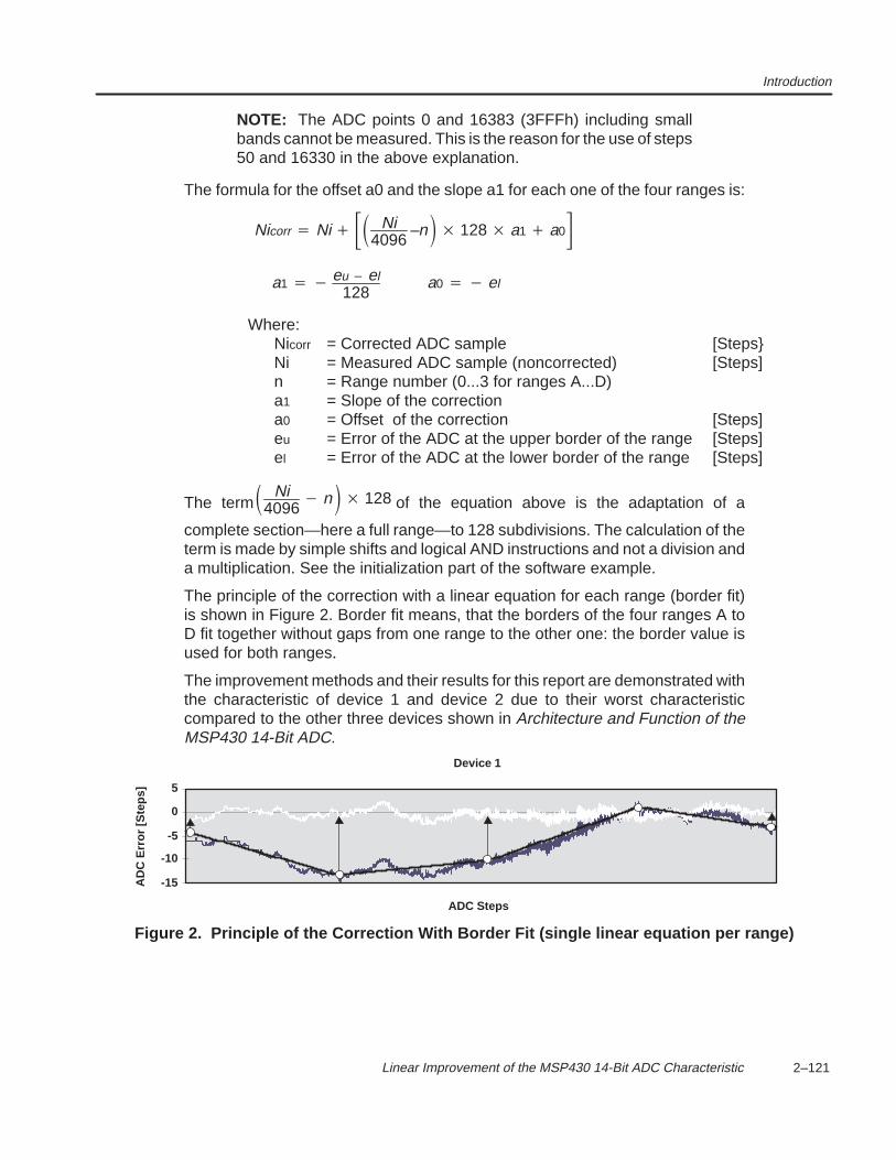
Introduction
2–121 Linear Improvement of the MSP430 14-Bit ADC Characteristic
NOTE: The ADC points 0 and 16383 (3FFFh) including smallbands cannot be measured. This is the reason for the use of steps50 and 16330 in the above explanation.
The formula for the offset a0 and the slope a1 for each one of the four ranges is:
Nicorr Ni Ni4096
–n 128 a1 a0
a1 eu el128
a0 el
Where:Nicorr = Corrected ADC sample [StepsNi = Measured ADC sample (noncorrected) [Steps]n = Range number (0...3 for ranges A...D)a1 = Slope of the correctiona0 = Offset of the correction [Steps]eu = Error of the ADC at the upper border of the range [Steps]el = Error of the ADC at the lower border of the range [Steps]
The term Ni4096
n 128 of the equation above is the adaptation of a
complete section—here a full range—to 128 subdivisions. The calculation of theterm is made by simple shifts and logical AND instructions and not a division anda multiplication. See the initialization part of the software example.
The principle of the correction with a linear equation for each range (border fit)is shown in Figure 2. Border fit means, that the borders of the four ranges A toD fit together without gaps from one range to the other one: the border value isused for both ranges.
The improvement methods and their results for this report are demonstrated withthe characteristic of device 1 and device 2 due to their worst characteristiccompared to the other three devices shown in Architecture and Function of theMSP430 14-Bit ADC.
-10
-15AD
C E
rror
[Ste
ps]
-5
0
ADC Steps
5
Device 1
Figure 2. Principle of the Correction With Border Fit (single linear equation per range)
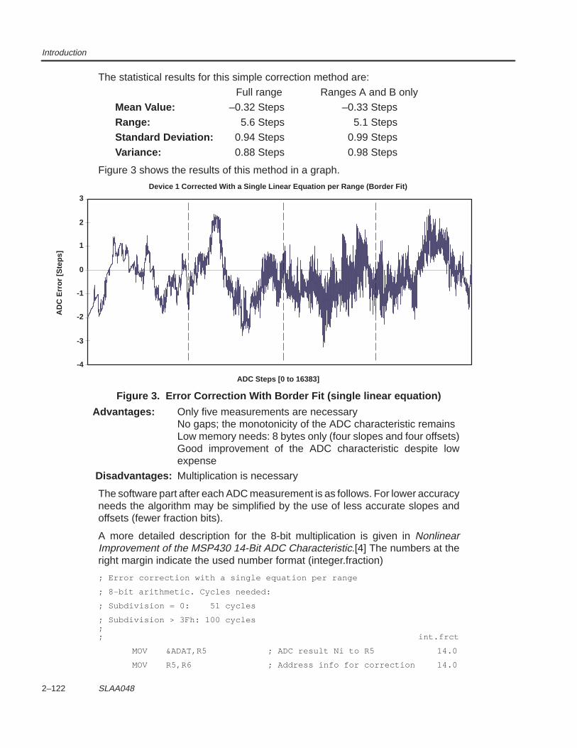
Introduction
2–122 SLAA048
The statistical results for this simple correction method are:Full range Ranges A and B only
Mean Value: –0.32 Steps –0.33 Steps
Range: 5.6 Steps 5.1 StepsStandard Deviation: 0.94 Steps 0.99 Steps
Variance: 0.88 Steps 0.98 Steps
Figure 3 shows the results of this method in a graph.
0
-1
AD
C E
rror
[Ste
ps]
1
2
ADC Steps [0 to 16383]
3
-3
-4
-2
Device 1 Corrected With a Single Linear Equation per Range (Border Fit)
Figure 3. Error Correction With Border Fit (single linear equation)
Advantages: Only five measurements are necessaryNo gaps; the monotonicity of the ADC characteristic remainsLow memory needs: 8 bytes only (four slopes and four offsets)Good improvement of the ADC characteristic despite lowexpense
Disadvantages: Multiplication is necessary
The software part after each ADC measurement is as follows. For lower accuracyneeds the algorithm may be simplified by the use of less accurate slopes andoffsets (fewer fraction bits).
A more detailed description for the 8-bit multiplication is given in NonlinearImprovement of the MSP430 14-Bit ADC Characteristic.[4] The numbers at theright margin indicate the used number format (integer.fraction)
; Error correction with a single equation per range
; 8–bit arithmetic. Cycles needed:
; Subdivision = 0: 51 cycles
; Subdivision > 3Fh: 100 cycles;; int.frct
MOV &ADAT,R5 ; ADC result Ni to R5 14.0
MOV R5,R6 ; Address info for correction 14.0
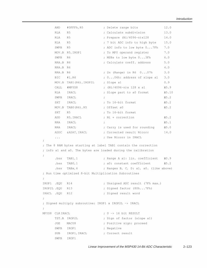
Introduction
2–123 Linear Improvement of the MSP430 14-Bit ADC Characteristic
AND #0FFFh,R5 ; Delete range bits 12.0
RLA R5 ; Calculate subdivision 13.0
RLA R5 ; Prepare (Ni/4096–n)x128 14.0
RLA R5 ; 7 bit ADC info to high byte 15.0
SWPB R5 ; ADC info to low byte 0...7Fh 7.0
MOV.B R5,IROP1 ; To MPY operand register 7.0
SWPB R6 ; MSBs to low byte 0...3Fh 6.0
RRA.B R6 ; Calculate coeff. address 5.0
RRA.B R6 4.0
RRA.B R6 ; 2n (Range) in R6 0...07h 3.0
BIC #1,R6 ; 0...06h: address of slope a1 3.0
MOV.B TAB1(R6),IROP2L ; Slope a1 0.9
CALL #MPYS8 ; (Ni/4096–n)x 128 x a1 ±5.9
RLA IRACL ; Slope part to a0 format ±5.10
SWPB IRACL ; ±5.2
SXT IRACL ; To 16–bit format ±5.2
MOV.B TAB0(R6),R5 ; Offset a0 ±5.2
SXT R5 ; To 16–bit format
ADD R5,IRACL ; Ni + correction ±5.2
RRA IRACL ; ±5.1
RRA IRACL ; Carry is used for rounding ±5.0
ADDC &ADAT,IRACL ; Corrected result Nicorr 14.0
... ; Use Nicorr in IRACL;
; The 8 RAM bytes starting at label TAB1 contain the correction
; info a1 and a0. The bytes are loaded during the calibration
;.bss TAB1,1 ; Range A a1: lin. coefficient ±0.9
.bss TAB0,1 ; a0: constant coefficient ±5.2
.bss TABx,6 ; Ranges B, C, D: a1, a0. (like above)
; Run time optimized 8–bit Multiplication Subroutines
;
IROP1 .EQU R14 ; Unsigned ADC result (7Fh max.)
IROP2L .EQU R13 ; Signed factor (80h...7Fh)
IRACL .EQU R12 ; Signed result word
;
; Signed multiply subroutine: IROP1 x IROP2L –> IRACL
;
MPYS8 CLR IRACL ; 0 –> 16 bit RESULT
TST.B IROP2L ; Sign of factor (slope a1)
JGE MACU8 ; Positive sign: proceed
SWPB IROP1 ; Negative
SUB IROP1,IRACL ; Correct result
SWPB IROP1
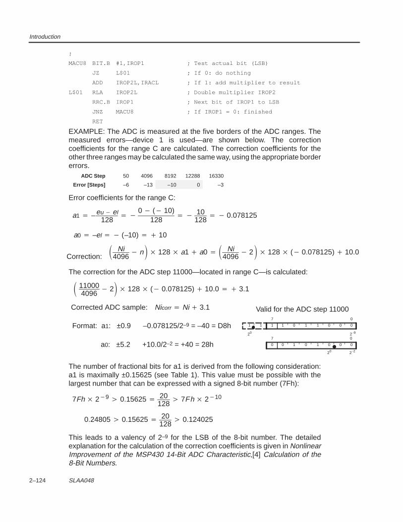
Introduction
2–124 SLAA048
;
MACU8 BIT.B #1,IROP1 ; Test actual bit (LSB)
JZ L$01 ; If 0: do nothing
ADD IROP2L,IRACL ; If 1: add multiplier to result
L$01 RLA IROP2L ; Double multiplier IROP2
RRC.B IROP1 ; Next bit of IROP1 to LSB
JNZ MACU8 ; If IROP1 = 0: finished
RET
EXAMPLE: The ADC is measured at the five borders of the ADC ranges. Themeasured errors—device 1 is used—are shown below. The correctioncoefficients for the range C are calculated. The correction coefficients for theother three ranges may be calculated the same way, using the appropriate bordererrors.
ADC Step 50 4096 8192 12288 16330
Error [Steps] –6 –13 –10 0 –3
Error coefficients for the range C:
a1 – eu el128
0 ( 10)
128 10
128 0.078125
a0 –el (–10) 10
Correction: Ni4096
n 128 a1 a0 Ni4096
2 128 ( 0.078125) 10.0
The correction for the ADC step 11000—located in range C—is calculated:
110004096
2 128 ( 0.078125) 10.0 3.1
Corrected ADC sample: Nicorr Ni 3.1 Valid for the ADC step 11000
Format: a1: ±0.9 –0.078125/2–9 = –40 = D8h
a0: ±5.2 +10.0/2–2 = +40 = 28h 0 1 0 1 0 0 0
07
1 1 0 1 1 0 0 0
07
1 1
20 2 -9
2 -220
0
The number of fractional bits for a1 is derived from the following consideration:a1 is maximally ±0.15625 (see Table 1). This value must be possible with thelargest number that can be expressed with a signed 8-bit number (7Fh):
7Fh 29 0.15625 20128
7Fh 210
0.24805 0.15625 20128
0.124025
This leads to a valency of 2–9 for the LSB of the 8-bit number. The detailedexplanation for the calculation of the correction coefficients is given in NonlinearImprovement of the MSP430 14-Bit ADC Characteristic,[4] Calculation of the8-Bit Numbers.
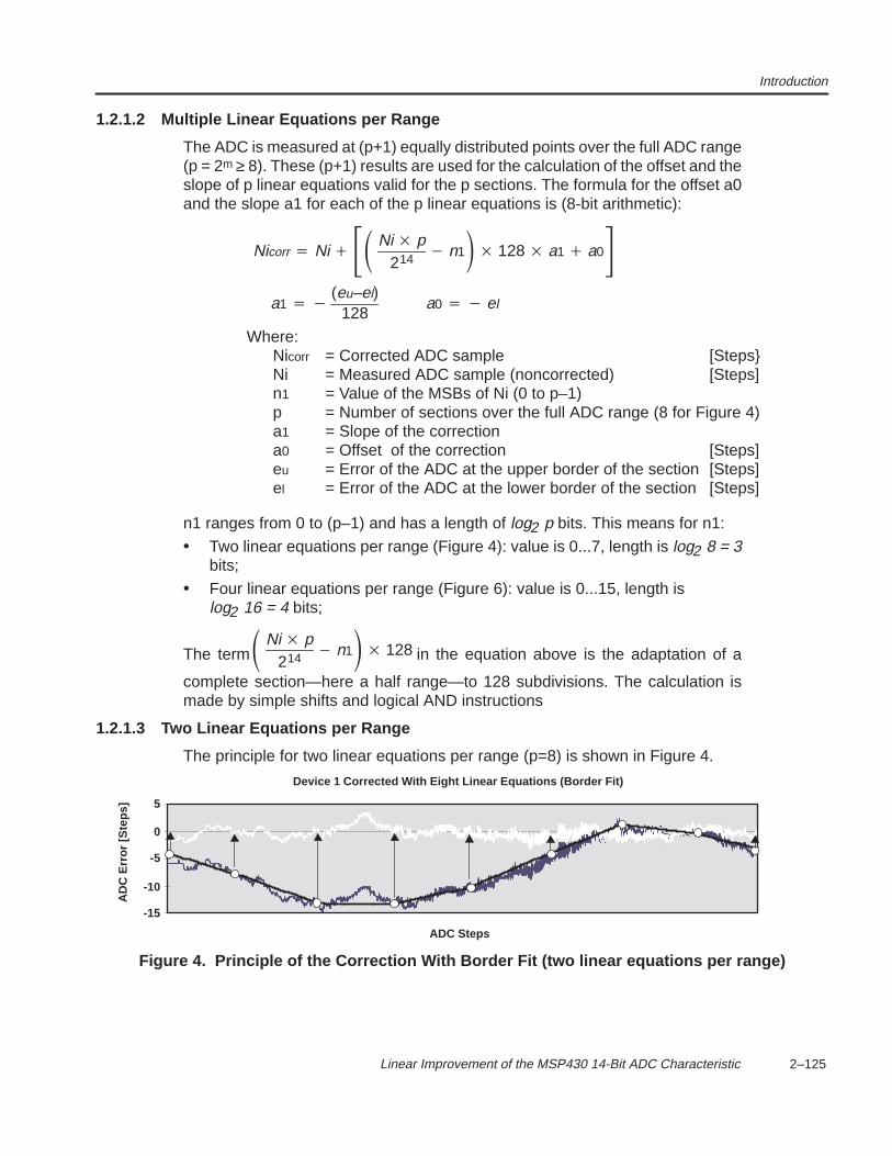
Introduction
2–125 Linear Improvement of the MSP430 14-Bit ADC Characteristic
1.2.1.2 Multiple Linear Equations per Range
The ADC is measured at (p+1) equally distributed points over the full ADC range(p = 2m ≥ 8). These (p+1) results are used for the calculation of the offset and theslope of p linear equations valid for the p sections. The formula for the offset a0and the slope a1 for each of the p linear equations is (8-bit arithmetic):
Nicorr Ni Ni p214
n1 128 a1 a0a1
(eu–el)128
a0 el
Where:Nicorr = Corrected ADC sample [StepsNi = Measured ADC sample (noncorrected) [Steps]n1 = Value of the MSBs of Ni (0 to p–1)p = Number of sections over the full ADC range (8 for Figure 4)a1 = Slope of the correctiona0 = Offset of the correction [Steps]eu = Error of the ADC at the upper border of the section [Steps]el = Error of the ADC at the lower border of the section [Steps]
n1 ranges from 0 to (p–1) and has a length of log2 p bits. This means for n1:
• Two linear equations per range (Figure 4): value is 0...7, length is log2 8 = 3bits;
• Four linear equations per range (Figure 6): value is 0...15, length islog2 16 = 4 bits;
The term Ni p214
n1 128 in the equation above is the adaptation of a
complete section—here a half range—to 128 subdivisions. The calculation ismade by simple shifts and logical AND instructions
1.2.1.3 Two Linear Equations per Range
The principle for two linear equations per range (p=8) is shown in Figure 4.
-10
-15
AD
C E
rror
[Ste
ps]
-5
0
ADC Steps
5
Device 1 Corrected With Eight Linear Equations (Border Fit)
Figure 4. Principle of the Correction With Border Fit (two linear equations per range)
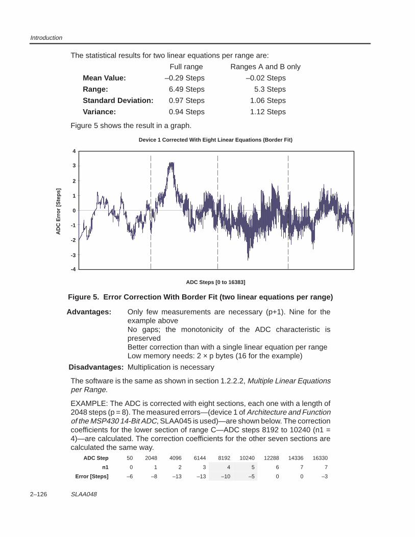
Introduction
2–126 SLAA048
The statistical results for two linear equations per range are:
Full range Ranges A and B only
Mean Value: –0.29 Steps –0.02 Steps
Range: 6.49 Steps 5.3 Steps
Standard Deviation: 0.97 Steps 1.06 Steps
Variance: 0.94 Steps 1.12 Steps
Figure 5 shows the result in a graph.
1
0
AD
C E
rror
[Ste
ps]
2
3
ADC Steps [0 to 16383]
4
-2
-3
-1
Device 1 Corrected With Eight Linear Equations (Border Fit)
-4
Figure 5. Error Correction With Border Fit (two linear equations per range)
Advantages: Only few measurements are necessary (p+1). Nine for theexample aboveNo gaps; the monotonicity of the ADC characteristic ispreservedBetter correction than with a single linear equation per rangeLow memory needs: 2 × p bytes (16 for the example)
Disadvantages: Multiplication is necessary
The software is the same as shown in section 1.2.2.2, Multiple Linear Equationsper Range.
EXAMPLE: The ADC is corrected with eight sections, each one with a length of2048 steps (p = 8). The measured errors—(device 1 of Architecture and Functionof the MSP430 14-Bit ADC, SLAA045 is used)—are shown below. The correctioncoefficients for the lower section of range C—ADC steps 8192 to 10240 (n1 =4)—are calculated. The correction coefficients for the other seven sections arecalculated the same way.
ADC Step 50 2048 4096 6144 8192 10240 12288 14336 16330
n1 0 1 2 3 4 5 6 7 7
Error [Steps] –6 –8 –13 –13 –10 –5 0 0 –3
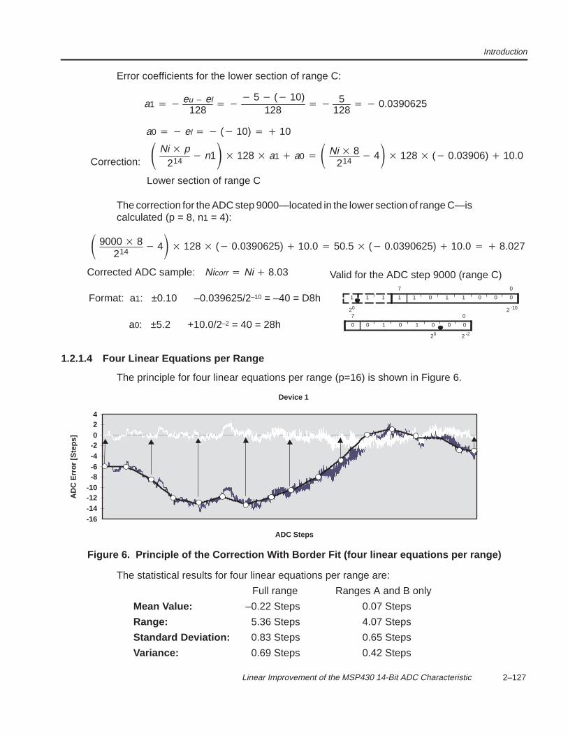
Introduction
2–127 Linear Improvement of the MSP430 14-Bit ADC Characteristic
Error coefficients for the lower section of range C:
a1 eu el128
5 ( 10)
128 5
128 0.0390625
a0 el ( 10) 10
Correction: Ni p
214 n1 128 a1 a0 Ni 8
214 4 128 ( 0.03906) 10.0
Lower section of range C
The correction for the ADC step 9000—located in the lower section of range C—iscalculated (p = 8, n1 = 4):
9000 8214
4 128 ( 0.0390625) 10.0 50.5 ( 0.0390625) 10.0 8.027
Corrected ADC sample: Nicorr Ni 8.03 Valid for the ADC step 9000 (range C)
Format: a1: ±0.10 –0.039625/2–10 = –40 = D8h
a0: ±5.2 +10.0/2–2 = 40 = 28h 0 1 0 1 0 0 0
07
1 1 0 1 1 0 0 0
07
1 1
20 2 -10
2 -220
0
1
1.2.1.4 Four Linear Equations per Range
The principle for four linear equations per range (p=16) is shown in Figure 6.
-2-4
AD
C E
rror
[Ste
ps] 0
2
ADC Steps
4
Device 1
-12-14
-10-8-6
-16
Figure 6. Principle of the Correction With Border Fit (four linear equations per range)
The statistical results for four linear equations per range are:
Full range Ranges A and B only
Mean Value: –0.22 Steps 0.07 Steps
Range: 5.36 Steps 4.07 Steps
Standard Deviation: 0.83 Steps 0.65 Steps
Variance: 0.69 Steps 0.42 Steps
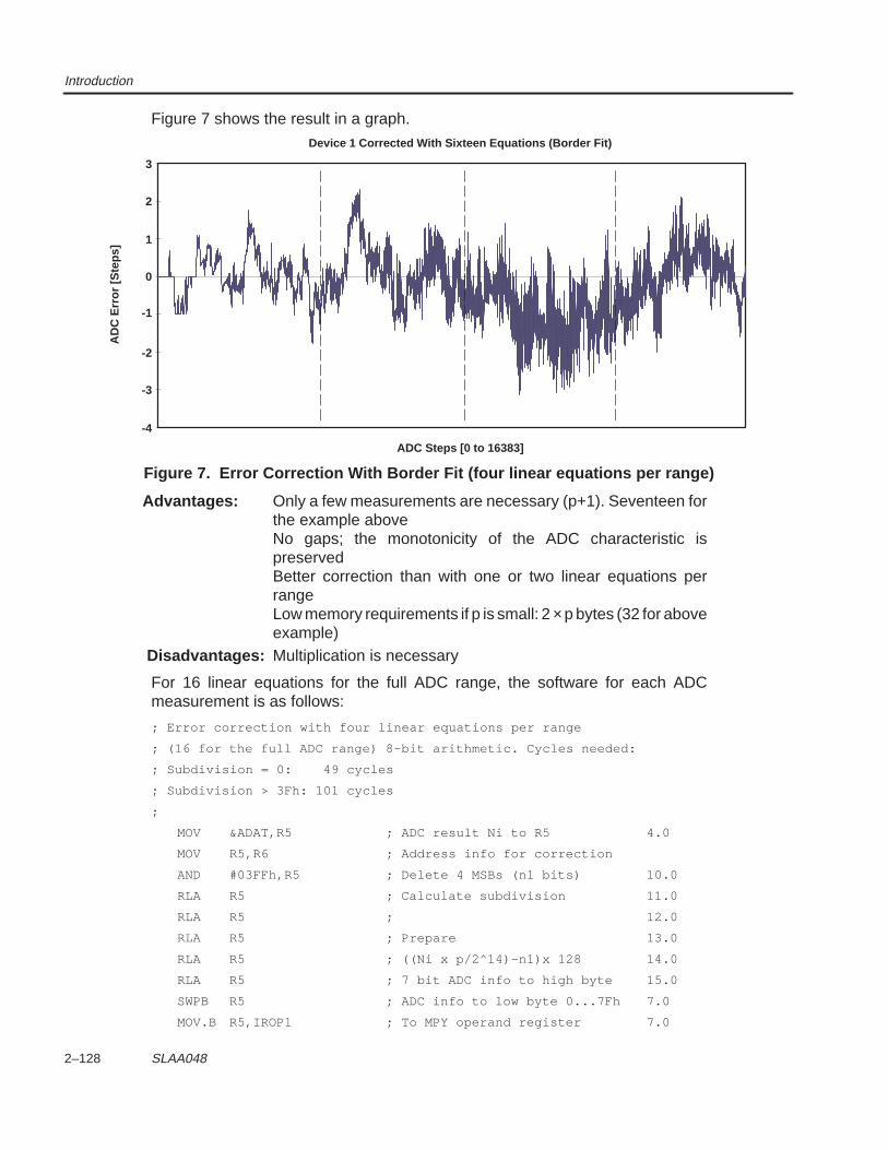
Introduction
2–128 SLAA048
Figure 7 shows the result in a graph.
1
0
AD
C E
rror
[Ste
ps]
2
3
ADC Steps [0 to 16383]
-2
-3
-1
Device 1 Corrected With Sixteen Equations (Border Fit)
-4
Figure 7. Error Correction With Border Fit (four linear equations per range)
Advantages: Only a few measurements are necessary (p+1). Seventeen forthe example aboveNo gaps; the monotonicity of the ADC characteristic ispreservedBetter correction than with one or two linear equations perrangeLow memory requirements if p is small: 2 × p bytes (32 for aboveexample)
Disadvantages: Multiplication is necessary
For 16 linear equations for the full ADC range, the software for each ADCmeasurement is as follows:
; Error correction with four linear equations per range
; (16 for the full ADC range) 8–bit arithmetic. Cycles needed:
; Subdivision = 0: 49 cycles
; Subdivision > 3Fh: 101 cycles
;
MOV &ADAT,R5 ; ADC result Ni to R5 4.0
MOV R5,R6 ; Address info for correction
AND #03FFh,R5 ; Delete 4 MSBs (n1 bits) 10.0
RLA R5 ; Calculate subdivision 11.0
RLA R5 ; 12.0
RLA R5 ; Prepare 13.0
RLA R5 ; ((Ni x p/2^14)–n1)x 128 14.0
RLA R5 ; 7 bit ADC info to high byte 15.0
SWPB R5 ; ADC info to low byte 0...7Fh 7.0
MOV.B R5,IROP1 ; To MPY operand register 7.0
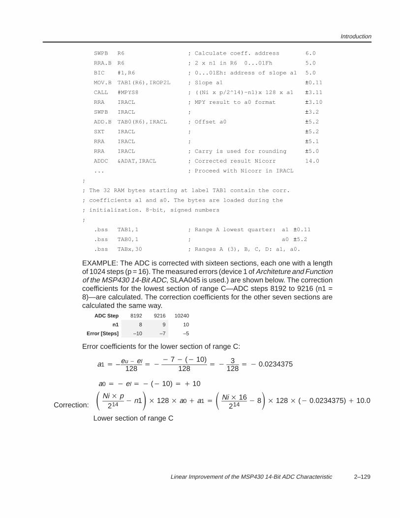
Introduction
2–129 Linear Improvement of the MSP430 14-Bit ADC Characteristic
SWPB R6 ; Calculate coeff. address 6.0
RRA.B R6 ; 2 x n1 in R6 0...01Fh 5.0
BIC #1,R6 ; 0...01Eh: address of slope a1 5.0
MOV.B TAB1(R6),IROP2L ; Slope a1 ±0.11
CALL #MPYS8 ; ((Ni x p/2^14)–n1)x 128 x a1 ±3.11
RRA IRACL ; MPY result to a0 format ±3.10
SWPB IRACL ; ±3.2
ADD.B TAB0(R6),IRACL ; Offset a0 ±5.2
SXT IRACL ; ±5.2
RRA IRACL ; ±5.1
RRA IRACL ; Carry is used for rounding ±5.0
ADDC &ADAT,IRACL ; Corrected result Nicorr 14.0
... ; Proceed with Nicorr in IRACL
;
; The 32 RAM bytes starting at label TAB1 contain the corr.
; coefficients a1 and a0. The bytes are loaded during the
; initialization. 8–bit, signed numbers
;
.bss TAB1,1 ; Range A lowest quarter: a1 ±0.11
.bss TAB0,1 ; a0 ±5.2
.bss TABx,30 ; Ranges A (3), B, C, D: a1, a0.
EXAMPLE: The ADC is corrected with sixteen sections, each one with a lengthof 1024 steps (p = 16). The measured errors (device 1 of Architeture and Functionof the MSP430 14-Bit ADC, SLAA045 is used.) are shown below. The correctioncoefficients for the lowest section of range C—ADC steps 8192 to 9216 (n1 =8)—are calculated. The correction coefficients for the other seven sections arecalculated the same way.
ADC Step 8192 9216 10240
n1 8 9 10
Error [Steps] –10 –7 –5
Error coefficients for the lower section of range C:
a1 – eu el128
7 ( 10)
128 3
128 0.0234375
a0 el ( 10) 10
Correction: Ni p
214 n1 128 a0 a1 Ni 16
214 8 128 ( 0.0234375) 10.0
Lower section of range C
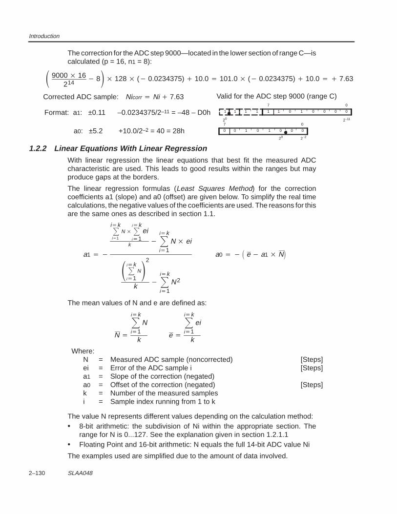
Introduction
2–130 SLAA048
The correction for the ADC step 9000—located in the lower section of range C—iscalculated (p = 16, n1 = 8):
9000 16214
8 128 ( 0.0234375) 10.0 101.0 ( 0.0234375) 10.0 7.63
Corrected ADC sample: Nicorr Ni 7.63 Valid for the ADC step 9000 (range C)
Format: a1: ±0.11 –0.0234375/2–11 = –48 – D0h
a0: ±5.2 +10.0/2–2 = 40 = 28h 0 1 0 1 0 0 0
07
1 1 0 1 0 0 0 0
07
1 1
20 2 -11
2 -220
0
11
1.2.2 Linear Equations With Linear RegressionWith linear regression the linear equations that best fit the measured ADCcharacteristic are used. This leads to good results within the ranges but mayproduce gaps at the borders.
The linear regression formulas (Least Squares Method) for the correctioncoefficients a1 (slope) and a0 (offset) are given below. To simplify the real timecalculations, the negative values of the coefficients are used. The reasons for thisare the same ones as described in section 1.1.
a1
ik
i1
N ik
i1ei
k ik
i1
N ei
ik
i1N
2
k
ik
i1
N 2
a0 e a1 N
The mean values of N and e are defined as:
Where:N = Measured ADC sample (noncorrected) [Steps]ei = Error of the ADC sample i [Steps]a1 = Slope of the correction (negated)a0 = Offset of the correction (negated) [Steps]k = Number of the measured samplesi = Sample index running from 1 to k
N
ik
i1
N
ke
ik
i1
ei
k
The value N represents different values depending on the calculation method:• 8-bit arithmetic: the subdivision of Ni within the appropriate section. The
range for N is 0...127. See the explanation given in section 1.2.1.1• Floating Point and 16-bit arithmetic: N equals the full 14-bit ADC value Ni
The examples used are simplified due to the amount of data involved.
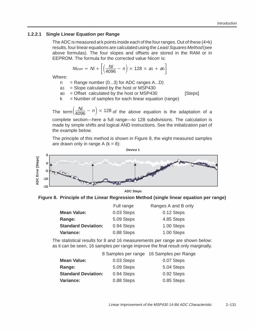
Introduction
2–131 Linear Improvement of the MSP430 14-Bit ADC Characteristic
1.2.2.1 Single Linear Equation per Range
The ADC is measured at k points inside each of the four ranges. Out of these (4×k)results, four linear equations are calculated using the Least Squares Method (seeabove formulas). The four slopes and offsets are stored in the RAM or inEEPROM. The formula for the corrected value Nicorr is:
Nicorr Ni Ni4096
n 128 a1 a0Where:
n = Range number (0...3) for ADC ranges A...D)a1 = Slope calculated by the host or MSP430a0 = Offset calculated by the host or MSP430 [Steps]k = Number of samples for each linear equation (range)
The term Ni4096
n 128 of the above equation is the adaptation of a
complete section—here a full range—to 128 subdivisions. The calculation ismade by simple shifts and logical AND instructions. See the initialization part ofthe example below.
The principle of this method is shown in Figure 8, the eight measured samplesare drawn only in range A (k = 8):
-10
-15
AD
C E
rror
[Ste
ps]
0
-5
ADC Steps
5
Device 1
Figure 8. Principle of the Linear Regression Method (single linear equation per range)
Full range Ranges A and B only
Mean Value: 0.03 Steps 0.12 Steps
Range: 5.09 Steps 4.85 Steps
Standard Deviation: 0.94 Steps 1.00 Steps
Variance: 0.88 Steps 1.00 Steps
The statistical results for 8 and 16 measurements per range are shown below:as it can be seen, 16 samples per range improve the final result only marginally.
8 Samples per range 16 Samples per Range
Mean Value: 0.03 Steps 0.07 Steps
Range: 5.09 Steps 5.04 Steps
Standard Deviation: 0.94 Steps 0.92 Steps
Variance: 0.88 Steps 0.85 Steps
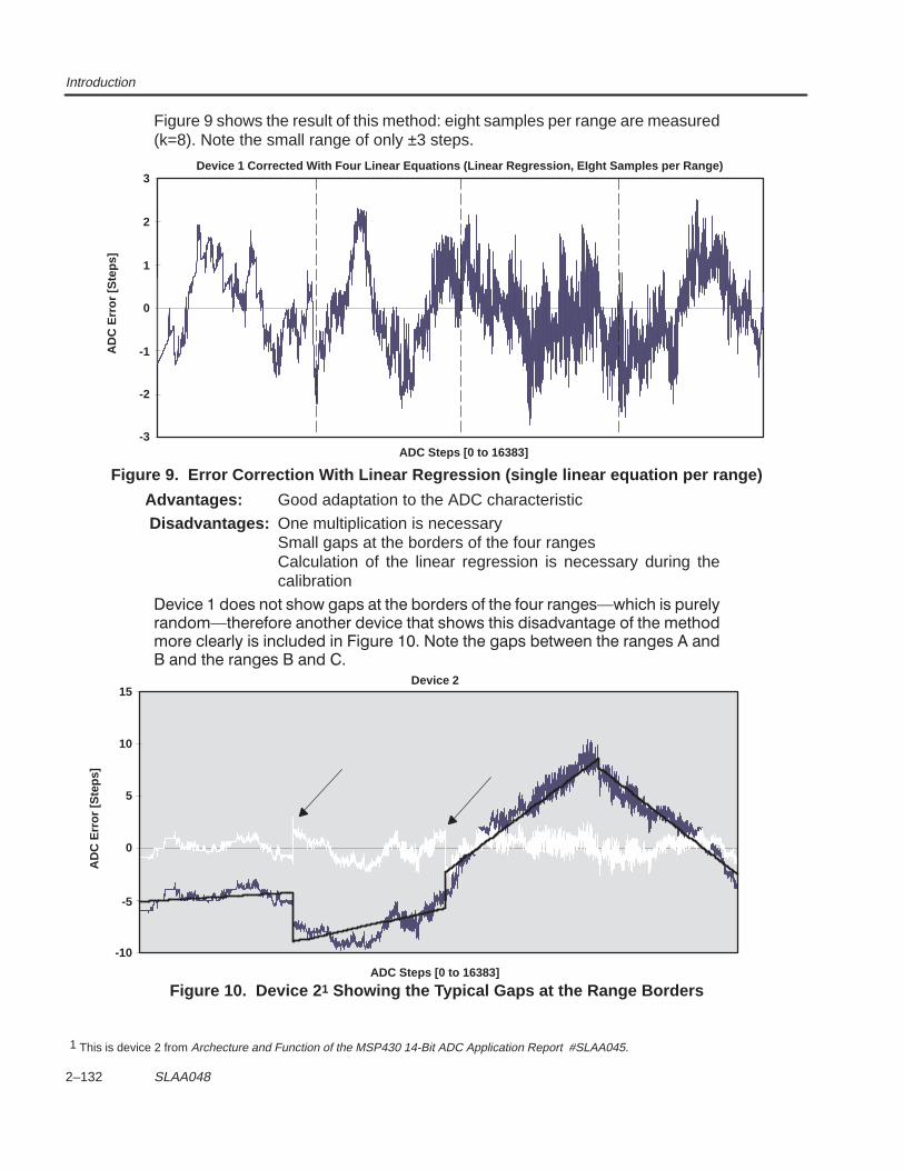
Introduction
2–132 SLAA048
Figure 9 shows the result of this method: eight samples per range are measured(k=8). Note the small range of only ±3 steps.
1
0
AD
C E
rror
[Ste
ps]
2
3
ADC Steps [0 to 16383]
-2
-3
-1
Device 1 Corrected With Four Linear Equations (Linear Regression, EIght Samples per Range)
Figure 9. Error Correction With Linear Regression (single linear equation per range)
Advantages: Good adaptation to the ADC characteristic
Disadvantages: One multiplication is necessarySmall gaps at the borders of the four rangesCalculation of the linear regression is necessary during thecalibration
5
0
AD
C E
rror
[Ste
ps]
10
15
ADC Steps [0 to 16383]
-10
-5
Device 2
Figure 10. Device 2 1 Showing the Typical Gaps at the Range Borders
1 This is device 2 from Archecture and Function of the MSP430 14-Bit ADC Application Report #SLAA045.
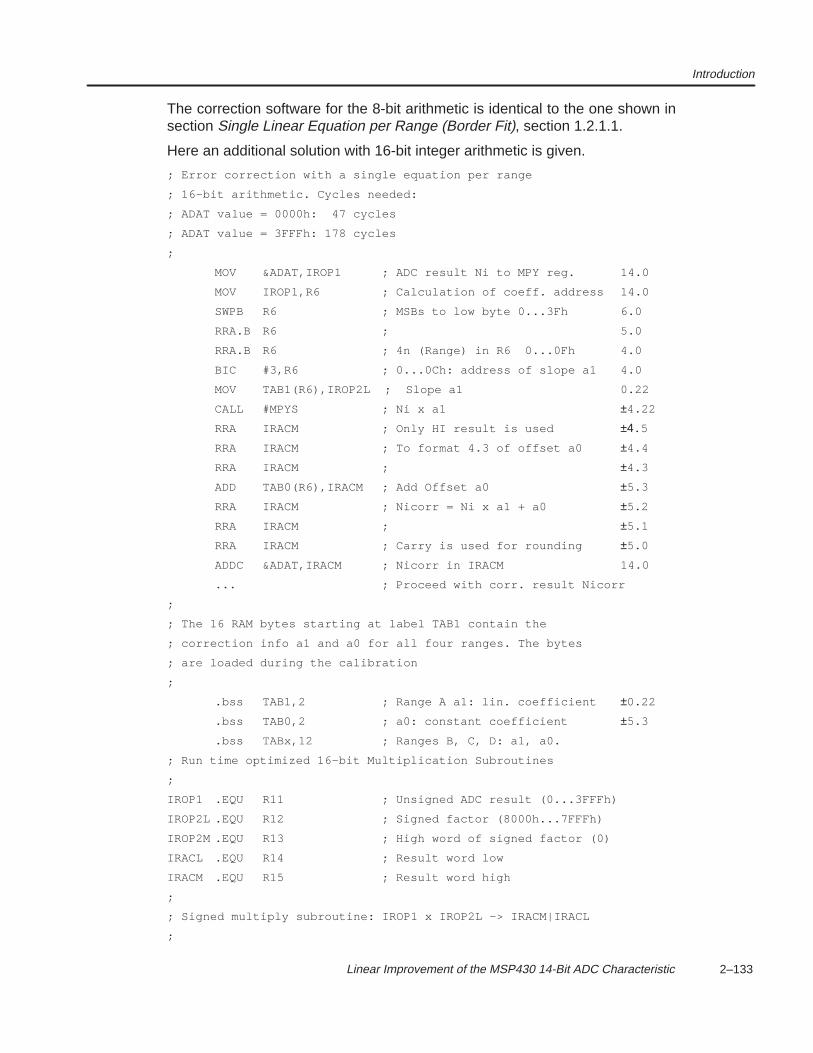
Introduction
2–133 Linear Improvement of the MSP430 14-Bit ADC Characteristic
The correction software for the 8-bit arithmetic is identical to the one shown insection Single Linear Equation per Range (Border Fit), section 1.2.1.1.
Here an additional solution with 16-bit integer arithmetic is given.
; Error correction with a single equation per range
; 16-bit arithmetic. Cycles needed:
; ADAT value = 0000h: 47 cycles
; ADAT value = 3FFFh: 178 cycles
;
MOV &ADAT,IROP1 ; ADC result Ni to MPY reg. 14.0
MOV IROP1,R6 ; Calculation of coeff. address 14.0
SWPB R6 ; MSBs to low byte 0...3Fh 6.0
RRA.B R6 ; 5.0
RRA.B R6 ; 4n (Range) in R6 0...0Fh 4.0
BIC #3,R6 ; 0...0Ch: address of slope a1 4.0
MOV TAB1(R6),IROP2L ; Slope a1 0.22
CALL #MPYS ; Ni x a1 ±4.22
RRA IRACM ; Only HI result is used ±4.5
RRA IRACM ; To format 4.3 of offset a0 ±4.4
RRA IRACM ; ±4.3
ADD TAB0(R6),IRACM ; Add Offset a0 ±5.3
RRA IRACM ; Nicorr = Ni x a1 + a0 ±5.2
RRA IRACM ; ±5.1
RRA IRACM ; Carry is used for rounding ±5.0
ADDC &ADAT,IRACM ; Nicorr in IRACM 14.0
... ; Proceed with corr. result Nicorr
;
; The 16 RAM bytes starting at label TAB1 contain the
; correction info a1 and a0 for all four ranges. The bytes
; are loaded during the calibration
;
.bss TAB1,2 ; Range A a1: lin. coefficient ±0.22
.bss TAB0,2 ; a0: constant coefficient ±5.3
.bss TABx,12 ; Ranges B, C, D: a1, a0.
; Run time optimized 16–bit Multiplication Subroutines
;
IROP1 .EQU R11 ; Unsigned ADC result (0...3FFFh)
IROP2L .EQU R12 ; Signed factor (8000h...7FFFh)
IROP2M .EQU R13 ; High word of signed factor (0)
IRACL .EQU R14 ; Result word low
IRACM .EQU R15 ; Result word high
;
; Signed multiply subroutine: IROP1 x IROP2L –> IRACM|IRACL
;
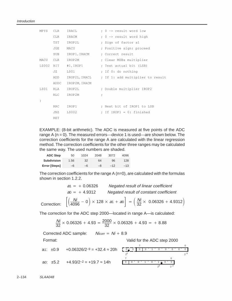
Introduction
2–134 SLAA048
MPYS CLR IRACL ; 0 –> result word low
CLR IRACM ; 0 –> result word high
TST IROP2L ; Sign of factor a1
JGE MACU ; Positive sign: proceed
SUB IROP1,IRACM ; Correct result
MACU CLR IROP2M ; Clear MSBs multiplier
L$002 BIT #1,IROP1 ; Test actual bit (LSB)
JZ L$01 ; If 0: do nothing
ADD IROP2L,IRACL ; If 1: add multiplier to result
ADDC IROP2M,IRACM
L$01 RLA IROP2L ; Double multiplier IROP2
RLC IROP2M ;
;
RRC IROP1 ; Next bit of IROP1 to LSB
JNZ L$002 ; If IROP1 = 0: finished
RET
EXAMPLE: (8-bit arithmetic). The ADC is measured at five points of the ADCrange A (n = 0). The measured errors—device 1 is used—are shown below. Thecorrection coefficients for the range A are calculated with the linear regressionmethod. The correction coefficients for the other three ranges may be calculatedthe same way. The used numbers are shaded.
ADC Step 50 1024 2048 3072 4096
Subdivision 1.56 32 64 96 128
Error [Steps] –6 –6 –8 –12 –13
The correction coefficients for the range A (n=0), are calculated with the formulasshown in section 1.2.2.
Ni4096
0 128 a1 a0 Ni32
0.06326 4.9312
a1 0.06326 Negated result of linear coefficient
a0 4.9312 Negated result of constant coefficient
Correction:
The correction for the ADC step 2000—located in range A—is calculated:
Ni32
0.06326 4.93 200032
0.06326 4.93 8.88
Corrected ADC sample: Nicorr Ni 8.9
Valid for the ADC step 2000
a0: ±5.2 +4.93/2–2 = +19.7 ≈ 14h
a1: ±0.9 +0.06326/2–9 = +32.4 ≈ 20h
0 0 1 0 1 0 0
07
0 0 1 0 0 0 0 0
07
0 0
20 2 -9
2 -220
0
Format:
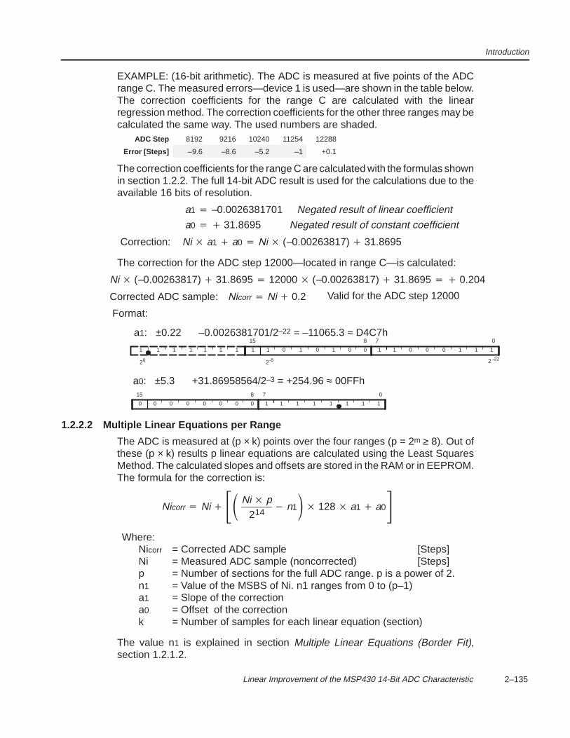
Introduction
2–135 Linear Improvement of the MSP430 14-Bit ADC Characteristic
EXAMPLE: (16-bit arithmetic). The ADC is measured at five points of the ADCrange C. The measured errors—device 1 is used—are shown in the table below.The correction coefficients for the range C are calculated with the linearregression method. The correction coefficients for the other three ranges may becalculated the same way. The used numbers are shaded.
ADC Step 8192 9216 10240 11254 12288
Error [Steps] –9.6 –8.6 –5.2 –1 +0.1
The correction coefficients for the range C are calculated with the formulas shownin section 1.2.2. The full 14-bit ADC result is used for the calculations due to theavailable 16 bits of resolution.
Ni a1 a0 Ni (–0.00263817) 31.8695
a1 –0.0026381701 Negated result of linear coefficient
a0 31.8695 Negated result of constant coefficient
Correction:
The correction for the ADC step 12000—located in range C—is calculated:
Ni (–0.00263817) 31.8695 12000 (–0.00263817) 31.8695 0.204
Corrected ADC sample: Nicorr Ni 0.2 Valid for the ADC step 12000
a0: ±5.3 +31.86958564/2–3 = +254.96 ≈ 00FFh
a1: ±0.22 –0.0026381701/2–22 = –11065.3 ≈ D4C7h
1 0 0 0 1 1 1
07
2 -22
11 0 1 0 1 0 0
815
11 1111 1
20
1
2-8
1 1 1 1 1 1 1
07
10 0 0 0 0 0 0
815
0
Format:
1.2.2.2 Multiple Linear Equations per Range
The ADC is measured at (p × k) points over the four ranges (p = 2m ≥ 8). Out ofthese (p × k) results p linear equations are calculated using the Least SquaresMethod. The calculated slopes and offsets are stored in the RAM or in EEPROM.The formula for the correction is:
Nicorr Ni Ni p214
n1 128 a1 a0Where:
Nicorr = Corrected ADC sample [Steps]Ni = Measured ADC sample (noncorrected) [Steps]p = Number of sections for the full ADC range. p is a power of 2.n1 = Value of the MSBS of Ni. n1 ranges from 0 to (p–1)a1 = Slope of the correctiona0 = Offset of the correctionk = Number of samples for each linear equation (section)
The value n1 is explained in section Multiple Linear Equations (Border Fit),section 1.2.1.2.
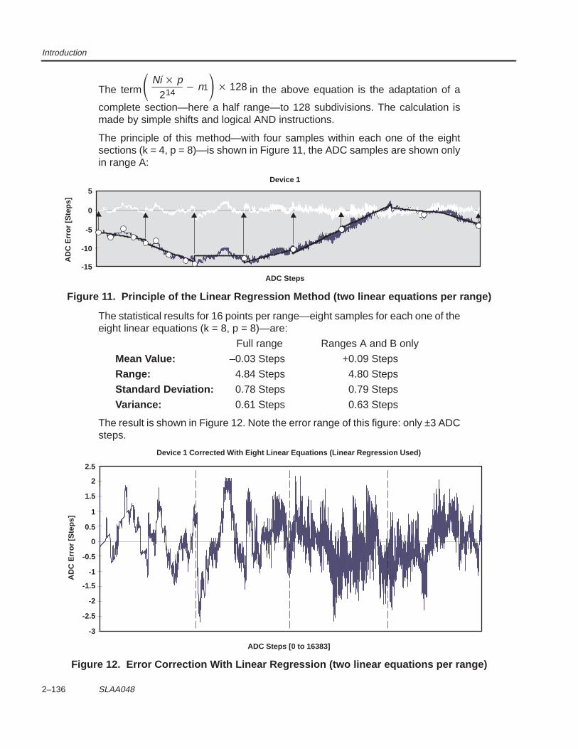
Introduction
2–136 SLAA048
The term Ni p214
n1 128 in the above equation is the adaptation of a
complete section—here a half range—to 128 subdivisions. The calculation ismade by simple shifts and logical AND instructions.
The principle of this method—with four samples within each one of the eightsections (k = 4, p = 8)—is shown in Figure 11, the ADC samples are shown onlyin range A:
-10
-15
AD
C E
rror
[Ste
ps]
0
-5
ADC Steps
5
Device 1
Figure 11. Principle of the Linear Regression Method (two linear equations per range)
The statistical results for 16 points per range—eight samples for each one of theeight linear equations (k = 8, p = 8)—are:
Full range Ranges A and B only
Mean Value: –0.03 Steps +0.09 Steps
Range: 4.84 Steps 4.80 Steps
Standard Deviation: 0.78 Steps 0.79 Steps
Variance: 0.61 Steps 0.63 Steps
The result is shown in Figure 12. Note the error range of this figure: only ±3 ADCsteps.
0.5
-1
AD
C E
rror
[Ste
ps]
1.5
2.5
ADC Steps [0 to 16383]
-3
-2
Device 1 Corrected With Eight Linear Equations (Linear Regression Used)
2
1
0
-0.5
-1.5
-2.5
Figure 12. Error Correction With Linear Regression (two linear equations per range)
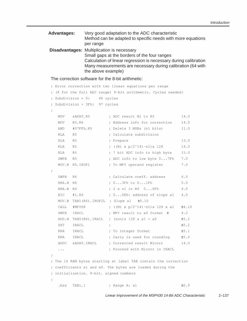
Introduction
2–137 Linear Improvement of the MSP430 14-Bit ADC Characteristic
Advantages: Very good adaptation to the ADC characteristicMethod can be adapted to specific needs with more equationsper range
Disadvantages: Multiplication is necessarySmall gaps at the borders of the four rangesCalculation of linear regression is necessary during calibrationMany measurements are necessary during calibration (64 withthe above example)
The correction software for the 8-bit arithmetic:
; Error correction with two linear equations per range
; (8 for the full ADC range) 8–bit arithmetic. Cycles needed:
; Subdivision = 0: 48 cycles
; Subdivision > 3Fh: 97 cycles
;
MOV &ADAT,R5 ; ADC result Ni to R5 14.0
MOV R5,R6 ; Address info for correction 14.0
AND #07FFh,R5 ; Delete 3 MSBs (n1 bits) 11.0
RLA R5 ; Calculate subdivision
RLA R5 ; Prepare 13.0
RLA R5 ; ((Ni x p/2^14)–n1)x 128 14.0
RLA R5 ; 7 bit ADC info to high byte 15.0
SWPB R5 ; ADC info to low byte 0...7Fh 7.0
MOV.B R5,IROP1 ; To MPY operand register 7.0
;
SWPB R6 ; Calculate coeff. address 6.0
RRA.B R6 ; 0...3Fh to 0...1Fh 5.0
RRA.B R6 ; 2 x n1 in R6 0...0Fh 4.0
BIC #1,R6 ; 0...0Eh: address of slope a1 4.0
MOV.B TAB1(R6),IROP2L ; Slope a1 ±0.10
CALL #MPYS8 ; ((Ni x p/2^14)–n1)x 128 x a1 ±4.10
SWPB IRACL ; MPY result to a0 format ± 4.2
ADD.B TAB0(R6),IRACL ; (nnn)x 128 x a1 + a0 ±5.2
SXT IRACL ; ±5.2
RRA IRACL ; To integer format ±5.1
RRA IRACL ; Carry is used for rounding ±5.0
ADDC &ADAT,IRACL ; Corrected result Nicorr 14.0
... ; Proceed with Nicorr in IRACL
;
; The 16 RAM bytes starting at label TAB contain the correction
; coefficients a1 and a0. The bytes are loaded during the
; initialization. 8-bit, signed numbers
;
.bss TAB1,1 ; Range A: a1 ±0.9
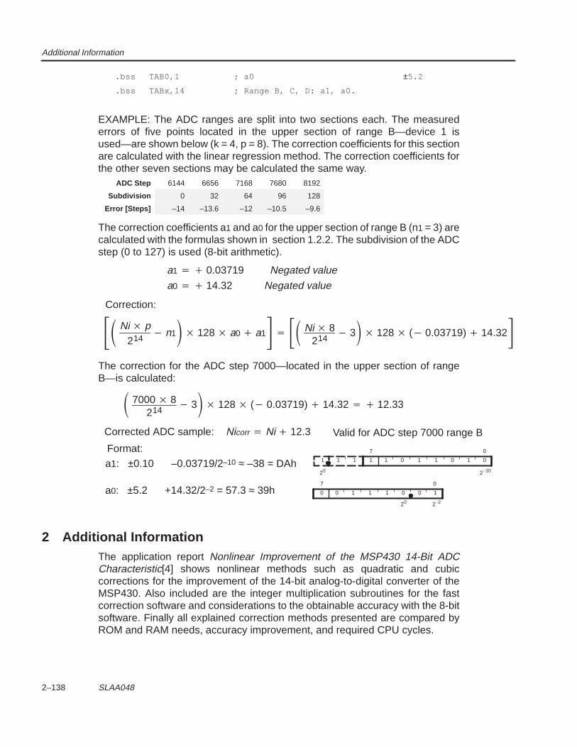
Additional Information
2–138 SLAA048
.bss TAB0,1 ; a0 ±5.2
.bss TABx,14 ; Range B, C, D: a1, a0.
EXAMPLE: The ADC ranges are split into two sections each. The measurederrors of five points located in the upper section of range B—device 1 isused—are shown below (k = 4, p = 8). The correction coefficients for this sectionare calculated with the linear regression method. The correction coefficients forthe other seven sections may be calculated the same way.
ADC Step 6144 6656 7168 7680 8192
Subdivision 0 32 64 96 128
Error [Steps] –14 –13.6 –12 –10.5 –9.6
The correction coefficients a1 and a0 for the upper section of range B (n1 = 3) arecalculated with the formulas shown in section 1.2.2. The subdivision of the ADCstep (0 to 127) is used (8-bit arithmetic).
a1 0.03719 Negated value
a0 14.32 Negated value
Correction:
Ni p214
n1 128 a0 a1 Ni 8214
3 128 ( 0.03719) 14.32The correction for the ADC step 7000—located in the upper section of rangeB—is calculated:
7000 8214
3 128 ( 0.03719) 14.32 12.33
Corrected ADC sample: Nicorr Ni 12.3 Valid for ADC step 7000 range B
a1: ±0.10 –0.03719/2–10 ≈ –38 = DAh
a0: ±5.2 +14.32/2–2 = 57.3 ≈ 39h
1 1 0 1 1 0 1 0
07
1 1
20 2 -10
1
0 1 1 1 0 0 1
07
2 -220
0
Format:
2 Additional InformationThe application report Nonlinear Improvement of the MSP430 14-Bit ADCCharacteristic[4] shows nonlinear methods such as quadratic and cubiccorrections for the improvement of the 14-bit analog-to-digital converter of theMSP430. Also included are the integer multiplication subroutines for the fastcorrection software and considerations to the obtainable accuracy with the 8-bitsoftware. Finally all explained correction methods presented are compared byROM and RAM needs, accuracy improvement, and required CPU cycles.

References
2–139 Linear Improvement of the MSP430 14-Bit ADC Characteristic
3 References1. Architecture and Function of the MSP430 14-Bit ADC Application Report,
1999, Literature #SLAA045
2. Application Basics for the MSP430 14-Bit ADC Application Report, 1999,Literature #SLAA046
3. Additive Improvement of the MSP430 14-Bit ADC Characteristic ApplicationReport, 1999, Literature #SLAA047
4. Nonlinear Improvement of the MSP430 14-Bit ADC CharacteristicApplication Report, 1999, Literature #SLAA050
5. MSP430 Application Report, 1998, Literature #SLAAE10C
6. Data Sheet MSP430C325, MSP430P323, 1997, Literature #SLASE06B
7. MSP430 Family Architecture Guide and Module Library, 1996, Literature#SLAUE10B

2–140 SLAA048

Definitions Used With the Application Examples
2–141 Linear Improvement of the MSP430 14-Bit ADC Characteristic
Appendix A Definitions Used With the Application Examples
; HARDWARE DEFINITIONS;ACTL .equ 0114h ; ADC control register: control bitsADAT .equ 0118h ; ADC data register (12 or 14–bits)

2–142 SLAA048

2–143
Nonlinear Improvement of the MSP43014-Bit ADC Characteristic
Literature Number: SLAA050June 1999
Printed on Recycled Paper

2–144
IMPORTANT NOTICE
Texas Instruments and its subsidiaries (TI) reserve the right to make changes to theirproducts or to discontinue any product or service without notice, and advise customers toobtain the latest version of relevant information to verify, before placing orders, thatinformation being relied on is current and complete. All products are sold subject to the termsand conditions of sale supplied at the time of order acknowledgement, including thosepertaining to warranty, patent infringement, and limitation of liability.
TI warrants performance of its semiconductor products to the specifications applicable at thetime of sale in accordance with TI’s standard warranty. Testing and other quality controltechniques are utilized to the extent TI deems necessary to support this warranty. Specifictesting of all parameters of each device is not necessarily performed, except those mandatedby government requirements.
CERTAIN APPLICATIONS USING SEMICONDUCTOR PRODUCTS MAY INVOLVEPOTENTIAL RISKS OF DEATH, PERSONAL INJURY, OR SEVERE PROPERTY ORENVIRONMENTAL DAMAGE (“CRITICAL APPLICATIONS”). TI SEMICONDUCTORPRODUCTS ARE NOT DESIGNED, AUTHORIZED, OR WARRANTED TO BE SUITABLEFOR USE IN LIFE-SUPPORT DEVICES OR SYSTEMS OR OTHER CRITICALAPPLICATIONS. INCLUSION OF TI PRODUCTS IN SUCH APPLICATIONS ISUNDERSTOOD TO BE FULLY AT THE CUSTOMER’S RISK.
In order to minimize risks associated with the customer’s applications, adequate design andoperating safeguards must be provided by the customer to minimize inherent or proceduralhazards.
TI assumes no liability for applications assistance or customer product design. TI does notwarrant or represent that any license, either express or implied, is granted under any patentright, copyright, mask work right, or other intellectual property right of TI covering or relatingto any combination, machine, or process in which such semiconductor products or servicesmight be or are used. TI’s publication of information regarding any third party’s products orservices does not constitute TI’s approval, warranty or endorsement thereof.
Copyright 1999, Texas Instruments Incorporated
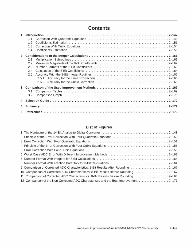
2–145 Nonlinear Improvement of the MSP430 14-Bit ADC Characteristic
Contents1 Introduction 2–147. . . . . . . . . . . . . . . . . . . . . . . . . . . . . . . . . . . . . . . . . . . . . . . . . . . . . . . . . . . . . . . . . . . . . . . . . . . . . . .
1.1 Correction With Quadratic Equations 2–148. . . . . . . . . . . . . . . . . . . . . . . . . . . . . . . . . . . . . . . . . . . . . . . . . . . . 1.2 Coefficients Estimation 2–151. . . . . . . . . . . . . . . . . . . . . . . . . . . . . . . . . . . . . . . . . . . . . . . . . . . . . . . . . . . . . . . . 1.3 Correction With Cubic Equations 2–154. . . . . . . . . . . . . . . . . . . . . . . . . . . . . . . . . . . . . . . . . . . . . . . . . . . . . . . 1.4 Coefficients Estimation 2–156. . . . . . . . . . . . . . . . . . . . . . . . . . . . . . . . . . . . . . . . . . . . . . . . . . . . . . . . . . . . . . . .
2 Considerations to the Integer Calculations 2–161. . . . . . . . . . . . . . . . . . . . . . . . . . . . . . . . . . . . . . . . . . . . . . . . . . . 2.1 Multiplication Subroutines 2–161. . . . . . . . . . . . . . . . . . . . . . . . . . . . . . . . . . . . . . . . . . . . . . . . . . . . . . . . . . . . . . 2.2 Maximum Magnitude of the 8-Bit Coefficients 2–162. . . . . . . . . . . . . . . . . . . . . . . . . . . . . . . . . . . . . . . . . . . . . 2.3 Number Formats of the 8-Bit Coefficients 2–163. . . . . . . . . . . . . . . . . . . . . . . . . . . . . . . . . . . . . . . . . . . . . . . . 2.4 Calculation of the 8-Bit Coefficients 2–164. . . . . . . . . . . . . . . . . . . . . . . . . . . . . . . . . . . . . . . . . . . . . . . . . . . . . 2.5 Accuracy With the 8-Bit Integer Routines 2–166. . . . . . . . . . . . . . . . . . . . . . . . . . . . . . . . . . . . . . . . . . . . . . . .
2.5.1 Accuracy for the Linear Correction 2–166. . . . . . . . . . . . . . . . . . . . . . . . . . . . . . . . . . . . . . . . . . . . . . 2.5.2 Accuracy for the Cubic Correction 2–168. . . . . . . . . . . . . . . . . . . . . . . . . . . . . . . . . . . . . . . . . . . . . . .
3 Comparison of the Used Improvement Methods 2–169. . . . . . . . . . . . . . . . . . . . . . . . . . . . . . . . . . . . . . . . . . . . . . 3.1 Comparison Tables 2–169. . . . . . . . . . . . . . . . . . . . . . . . . . . . . . . . . . . . . . . . . . . . . . . . . . . . . . . . . . . . . . . . . . . 3.2 Comparison Graph 2–170. . . . . . . . . . . . . . . . . . . . . . . . . . . . . . . . . . . . . . . . . . . . . . . . . . . . . . . . . . . . . . . . . . .
4 Selection Guide 2–172. . . . . . . . . . . . . . . . . . . . . . . . . . . . . . . . . . . . . . . . . . . . . . . . . . . . . . . . . . . . . . . . . . . . . . . . . . . .
5 Summary 2–172. . . . . . . . . . . . . . . . . . . . . . . . . . . . . . . . . . . . . . . . . . . . . . . . . . . . . . . . . . . . . . . . . . . . . . . . . . . . . . . . . .
6 References 2–173. . . . . . . . . . . . . . . . . . . . . . . . . . . . . . . . . . . . . . . . . . . . . . . . . . . . . . . . . . . . . . . . . . . . . . . . . . . . . . . .
List of Figures1 The Hardware of the 14-Bit Analog-to-Digital Converter 2–148. . . . . . . . . . . . . . . . . . . . . . . . . . . . . . . . . . . . . . . . . . . 2 Principle of the Error Correction With Four Quadratic Equations 2–150. . . . . . . . . . . . . . . . . . . . . . . . . . . . . . . . . . . . 3 Error Correction With Four Quadratic Equations 2–151. . . . . . . . . . . . . . . . . . . . . . . . . . . . . . . . . . . . . . . . . . . . . . . . . . 4 Principle of the Error Correction With Four Cubic Equations 2–155. . . . . . . . . . . . . . . . . . . . . . . . . . . . . . . . . . . . . . . 5 Error Correction With Four Cubic Equations 2–156. . . . . . . . . . . . . . . . . . . . . . . . . . . . . . . . . . . . . . . . . . . . . . . . . . . . . 6 Worst Case ADC Error With Different Improvement Methods 2–163. . . . . . . . . . . . . . . . . . . . . . . . . . . . . . . . . . . . . . 7 Number Format With Integers for 8-Bit Calculations 2–164. . . . . . . . . . . . . . . . . . . . . . . . . . . . . . . . . . . . . . . . . . . . . . 8 Number Format With Fraction Part Only for 8-Bit Calculations 2–164. . . . . . . . . . . . . . . . . . . . . . . . . . . . . . . . . . . . . 9 Comparison of Corrected ADC Characteristics. 8-Bit Results After Rounding 2–167. . . . . . . . . . . . . . . . . . . . . . . . 10 Comparison of Corrected ADC Characteristics. 8-Bit Results Before Rounding 2–167. . . . . . . . . . . . . . . . . . . . . . 11 Comparison of Corrected ADC Characteristics. 8-Bit Results Before Rounding 2–168. . . . . . . . . . . . . . . . . . . . . . 12 Comparison of the Non-Corrected ADC Characteristic and the Best Improvement 2–171. . . . . . . . . . . . . . . . . . .

Tables
2–146 SLAA050
List of Tables1 Worst Case Coefficients for Quadratic Equations (8-Bit) 2–151. . . . . . . . . . . . . . . . . . . . . . . . . . . . . . . . . . . . . . . . . . . 2 8-Bit Coefficients for the Four Quadratic Equations of Device 1 2–152. . . . . . . . . . . . . . . . . . . . . . . . . . . . . . . . . . . . 3 Worst Case Cubic Coefficients (8-Bit Arithmetic) 2–156. . . . . . . . . . . . . . . . . . . . . . . . . . . . . . . . . . . . . . . . . . . . . . . . . 4 Correction Coefficients for the Cubic Equations of Device 1 2–157. . . . . . . . . . . . . . . . . . . . . . . . . . . . . . . . . . . . . . . . 5 Worst Case Correction Coefficients (8-Bit Arithmetic) 2–163. . . . . . . . . . . . . . . . . . . . . . . . . . . . . . . . . . . . . . . . . . . . . 6 Comparison Table for the Different Improvement Methods 2–169. . . . . . . . . . . . . . . . . . . . . . . . . . . . . . . . . . . . . . . . . 7 Comparison Table for the Different Improvement Methods 2–170. . . . . . . . . . . . . . . . . . . . . . . . . . . . . . . . . . . . . . . . . 8 Selection for the Improvement Methods 2–172. . . . . . . . . . . . . . . . . . . . . . . . . . . . . . . . . . . . . . . . . . . . . . . . . . . . . . . . .
2–147
Nonlinear Improvement of the MSP430 14-Bit ADC Characteristic
Lutz Bierl
ABSTRACTThis application report shows nonlinear methods—with quadratic and cubic equations—to improve the accuracy of the 14-bit analog-to-digital converter (ADC) of the MSP430family. The methods used differ in RAM and ROM requirements, calculation speed,achievable improvement, and complexity. The influence of the restricted calculationaccuracy for 8-bit coefficients is compared to the accuracy of floating-point calculations.Finally, a comparison of all improvement methods is given. The References section at theend of the report lists related application reports in the MSP430 14-bit ADC series.
1 IntroductionThe application report Architecture and Function of the MSP430 14-Bit ADC[1]gives a detailed overview of the architecture and function of the 14-bitanalog-to-digital converter (ADC) of the MSP430 family. The principle of the ADCis explained and software examples are given. Also included are the explanationof the function of all hardware registers contained in the ADC.
The application report Application Basics for the MSP430 14-Bit ADC[2] showsseveral applications of the 14-bit ADC of the MSP430 family. Proven softwareexamples and basic circuitry are shown and explained.
The application report Additive Improvement of the MSP430 14-Bit ADCCharacteristic[3] explains the external hardware that is needed for themeasurement of the characteristic of the MSP430’s analog-to-digital converter.This report also demonstrates correction methods that use addition only: nomultiplication is needed. This allows the application of these methods in real-timesystems, where execution time can be critical.
The application report Linear Improvement of the MSP430 14-Bit ADCCharacteristic[4] shows linear improvements using linear equations with borderfit and correction by linear regression methods.
Figure 1 shows the block diagram of the 14-bit analog-to-digital converter of theMSP430 family.
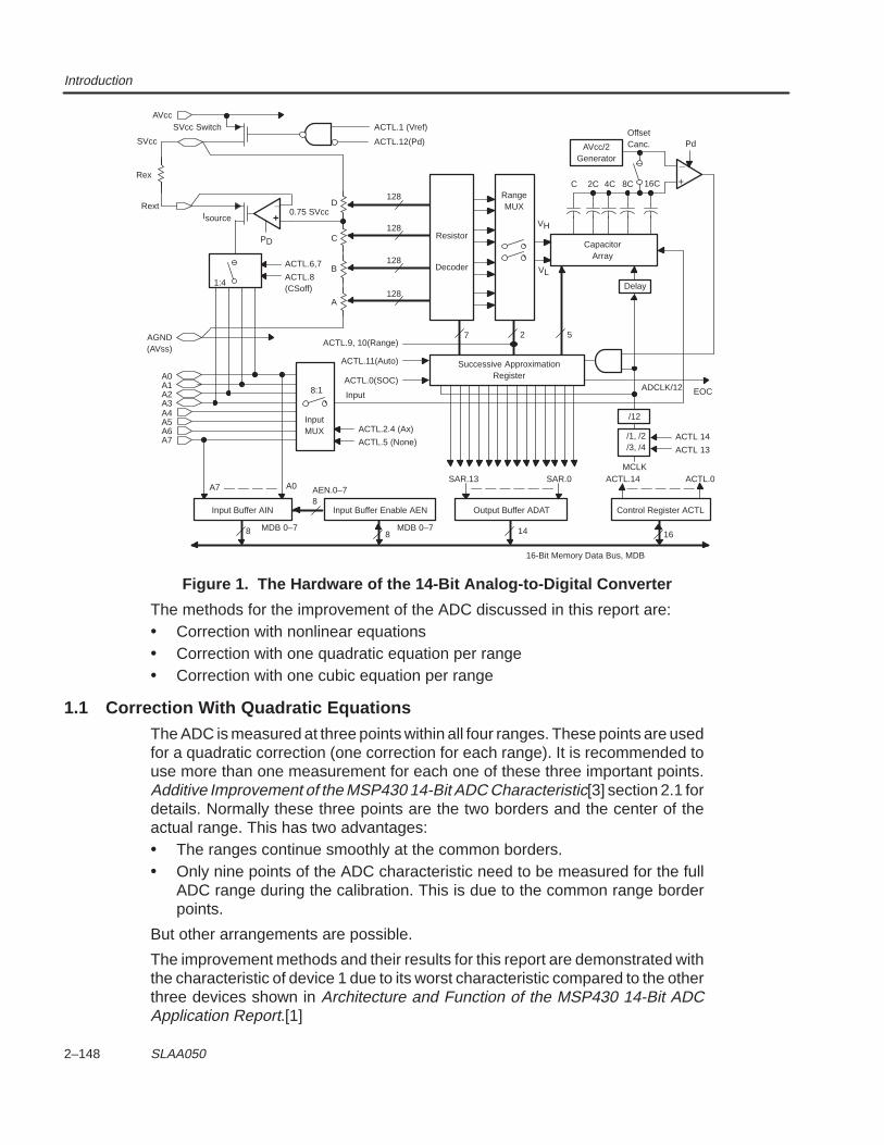
Introduction
2–148 SLAA050
AVcc/2Generator
_
+
Successive ApproximationRegister
SAR.13 SAR.0 ACTL.14 ACTL.0
14 16
Output Buffer ADAT Control Register ACTL
/12
/1, /2/3, /4
ACTL 14
ACTL 13
ACTL.0(SOC)
ACTL.11(Auto)
ACTL.9, 10(Range)
Resistor
RangeMUX
7 2
ADCLK/12 EOC
5
Delay
VH
VL
CapacitorArray
AVcc/2Generator
C 2C 4C 8C
Pd
16C
128
8:1 Input
ACTL.2.4 (Ax)
ACTL.5 (None)
8
Input Buffer Enable AEN
A7 A0
8
8
MDB 0–7
AEN.0–7
_
+0.75 SVcc
ACTL.6,7
ACTL.8(CSoff)
1:4
A7A6A5A4A3A2A1A0
AGND(AVss)
ACTL.12(Pd)
ACTL.1 (Vref)SVcc Switch
Isource
D
C
B
A
Rext
Rex
SVcc
AVcc
16-Bit Memory Data Bus, MDB
PD
Decoder
Input Buffer AIN
MDB 0–7
InputMUX
OffsetCanc.
128
128
128
MCLK
Figure 1. The Hardware of the 14-Bit Analog-to-Digital Converter
The methods for the improvement of the ADC discussed in this report are:• Correction with nonlinear equations• Correction with one quadratic equation per range• Correction with one cubic equation per range
1.1 Correction With Quadratic EquationsThe ADC is measured at three points within all four ranges. These points are usedfor a quadratic correction (one correction for each range). It is recommended touse more than one measurement for each one of these three important points.Additive Improvement of the MSP430 14-Bit ADC Characteristic[3] section 2.1 fordetails. Normally these three points are the two borders and the center of theactual range. This has two advantages:• The ranges continue smoothly at the common borders.• Only nine points of the ADC characteristic need to be measured for the full
ADC range during the calibration. This is due to the common range borderpoints.
But other arrangements are possible.
The improvement methods and their results for this report are demonstrated withthe characteristic of device 1 due to its worst characteristic compared to the otherthree devices shown in Architecture and Function of the MSP430 14-Bit ADCApplication Report.[1]
Introduction
2–149 Nonlinear Improvement of the MSP430 14-Bit ADC Characteristic
The formula used for each range with separate factors ax for 8-bit integercalculations is:
Nicorr Ni Ni4096
n × 2562
× a2 Ni4096
n × 256 × a1 a0Where: Nicorr Corrected ADC sample [Steps]
Ni Measured ADC sample (non-corrected) [Steps]N Subdivision representing the ADC sample (0...255)n Range number (0...3 for ranges A...D)a2 Quadratic coefficient of the correction [Steps–1]a1 Linear coefficient of the correctiona0 Offset of the correction [Steps]i Nominal ADC step of the ADC input (DAC output) [Steps]
The term N Ni4096
n × 256 of the equation above is the adaptation of a
complete section—here a full range—to 256 subdivisions. The calculation of theterm is made by simple shifts rather than division and a multiplication. Roundingis used to achieve better accuracy. See the initialization part of the softwareexample.
The formula above uses the subdivisions (0 to 255) inside of an ADC range (0to 4095 steps) instead of the full 14-bit position (0 to 16383 steps) of an ADC point.This is to maintain the accuracy of the calculation with limited coefficient length(here for 8-bit coefficients). The above formula is used with the 8-bit calculation.
If floating point calculation or 16-bit arithmetic is used, the higher resolutionmakes the range correction unnecessary: the full 14-bit result may be used forthe calculations.
Nicorr Ni Ni 2 × a2 Ni × a1 a0
The software example given for the cubic correction in section 1.3—which iswritten in floating point notation—may be adapted easily to quadratic correction:the unused cubic part is simply left out and the address calculation for thecoefficients is modified to three coefficients (a2..a0) instead of the four (a3..a0).
To save multiplications, the so-called Horner scheme is used. This scheme isapplicable for all given examples. The formula using the 8-bit arithmetic nowbecomes:
Nicorr Ni Ni4096
n × 256 × a2 a1 × Ni4096
n × 256 × a0
The 16-bit formula and the FPP formula now require only two multiplicationsinstead of three.
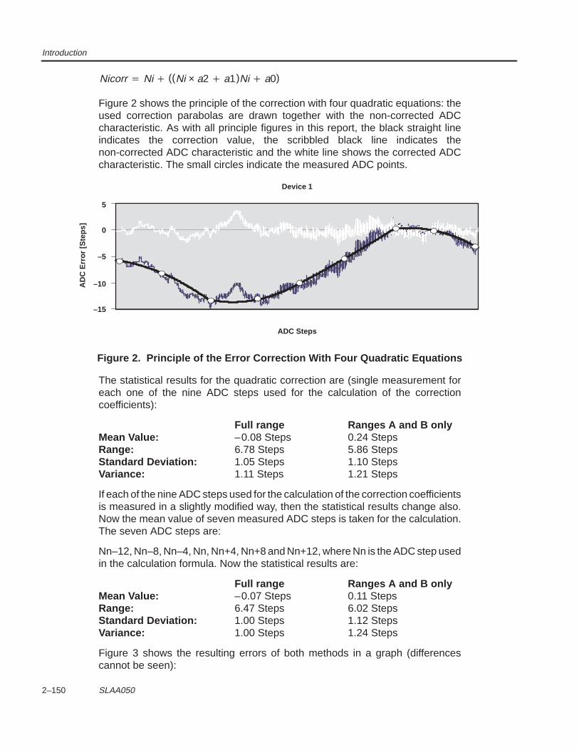
Introduction
2–150 SLAA050
Nicorr Ni ((Ni × a2 a1)Ni a0)
Figure 2 shows the principle of the correction with four quadratic equations: theused correction parabolas are drawn together with the non-corrected ADCcharacteristic. As with all principle figures in this report, the black straight lineindicates the correction value, the scribbled black line indicates thenon-corrected ADC characteristic and the white line shows the corrected ADCcharacteristic. The small circles indicate the measured ADC points.
5
0
–5
–10
–15
AD
C E
rror
[Ste
ps]
ADC Steps
Device 1
Figure 2. Principle of the Error Correction With Four Quadratic Equations
The statistical results for the quadratic correction are (single measurement foreach one of the nine ADC steps used for the calculation of the correctioncoefficients):
Full range Ranges A and B onlyMean Value: –0.08 Steps 0.24 StepsRange: 6.78 Steps 5.86 StepsStandard Deviation: 1.05 Steps 1.10 StepsVariance: 1.11 Steps 1.21 Steps
If each of the nine ADC steps used for the calculation of the correction coefficientsis measured in a slightly modified way, then the statistical results change also.Now the mean value of seven measured ADC steps is taken for the calculation.The seven ADC steps are:
Nn–12, Nn–8, Nn–4, Nn, Nn+4, Nn+8 and Nn+12, where Nn is the ADC step usedin the calculation formula. Now the statistical results are:
Full range Ranges A and B onlyMean Value: –0.07 Steps 0.11 StepsRange: 6.47 Steps 6.02 StepsStandard Deviation: 1.00 Steps 1.12 StepsVariance: 1.00 Steps 1.24 Steps
Figure 3 shows the resulting errors of both methods in a graph (differencescannot be seen):
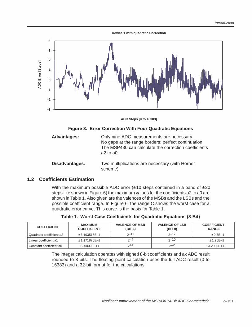
Introduction
2–151 Nonlinear Improvement of the MSP430 14-Bit ADC Characteristic
2
1
0
–1
–3
AD
C E
rror
[Ste
ps]
ADC Steps [0 to 16383]
Device 1 with quadratic Correction
3
4
–2
Figure 3. Error Correction With Four Quadratic Equations
Advantages: Only nine ADC measurements are necessaryNo gaps at the range borders: perfect continuationThe MSP430 can calculate the correction coefficientsa2 to a0
Disadvantages: Two multiplications are necessary (with Hornerscheme)
1.2 Coefficients Estimation
With the maximum possible ADC error (±10 steps contained in a band of ±20steps like shown in Figure 6) the maximum values for the coefficients a2 to a0 areshown in Table 1. Also given are the valences of the MSBs and the LSBs and thepossible coefficient range. In Figure 6, the range C shows the worst case for aquadratic error curve. This curve is the basis for Table 1.
Table 1. Worst Case Coefficients for Quadratic Equations (8-Bit)
COEFFICIENTMAXIMUM
COEFFICIENTVALENCE OF MSB
(BIT 6)VALENCE OF LSB
(BIT 0)COEFFICIENT
RANGE
Quadratic coefficient a2 ±6.103515E–4 2–11 2–17 ±9.7E–4
Linear coefficient a1 ±1.171875E–1 2–4 2–10 ±1.25E–1
Constant coefficient a0 ±2.00000E+1 2+4 2–2 ±3.2000E+1
The integer calculation operates with signed 8-bit coefficients and ax ADC resultrounded to 8 bits. The floating point calculation uses the full ADC result (0 to16383) and a 32-bit format for the calculations.
Introduction
2–152 SLAA050
To give an idea concerning the actual magnitudes, the twelve calculatedcorrection coefficients ax for device 1 are:
Table 2. 8-Bit Coefficients for the Four Quadratic Equations of Device 1
COEFFICIENT RANGE A RANGE B RANGE C RANGE D
a2 9.155273E–5 –1.831055E–4 –2.746582E–5 1.517946E–4
a1 4.687500E–3 3.281250E–2 –3.0859375E–2 –2.0992208E–2
a0 6.000000E+0 1.320000E+1 9.600000E+0 –1.000000E–1
The three equations to calculate the correction coefficients a2, a1 and a0 out ofthe three known errors e3, e2 and e1 at the ADC steps N3, N2 and N1 are:
a1 e2 e1
× N 23 N
22 e3 e2
× N 22 N
21
N2 N1 × N 2
3 N22 N3 N2
× N 22 N
21
a2 e2 e1
a1 × N2 N1
N22 N
21
a0 e1 a2 × N21 a1 × N1
NOTE:
N3, N2, and N1 can be expressed in ADC steps (0...16383), range steps(0...4095) or subdivisions of the range (0...255) for 8-bit calculations.In the following, N represents subdivisions.
As shown with the linear improvements, using more than one quadratic parabolaper ADC range is also possible. It is only necessary to adapt the 256 subdivisionsto the sections of the ranges, to calculate the new coefficients a2 to a0, and tomodify the addressing of the coefficients.
The software part after each ADC measurement is as follows. The numbers atthe right border—below int.frct—indicate the maximum integer bits and the actualnumber of fraction bits for the result (integer.fraction). The Horner scheme is usedfor the calculation.
; Quadratic error correction with a single equation per range.; 8–bit arithmetic. Cycles needed:; Subdivision N = 0: 85 cycles; Subdivision N > 7Fh: 206 cycles;; int.frct
MOV &ADAT,R5 ; ADC result Ni to R5 14.0MOV R5,R6 ; Address info for correction 14.0RRA R5 ; Calculate subdivision 0...FFh 13.0RRA R5 ; Prepare N = (Ni/4096–n)x256 12.0RRA R5 ; 8 bit ADC info to low byte 11.0RRA R5 ; 10.0ADC.B R5 ; Round subdivision 0...FFh 8.0JNC L$1 ; If result overflows to 100h:DEC.B R5 ; Limit subdivision to FFh 8.0
;
L$1 SWPB R6 ; Calculate coefficient address 6.0RRA.B R6 ; 0...1Fh 5.0RRA.B R6 ; 0...0Fh 4.0RRA.B R6 ; 0...07h 3.0BIC #1h,R6 ; 0...06h 3.0
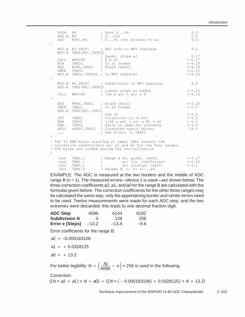
Introduction
2–153 Nonlinear Improvement of the MSP430 14-Bit ADC Characteristic
PUSH R6 ; Save 0...6h 3.0RRA.B R6 ; 0...03h 2.0ADD @SP+,R6 ; 0...9h (3n) pointer to a2 4.0
;
MOV.B R5,IROP1 ; ADC info to MPY register 8.0MOV.B TAB2(R6),IROP2L
; Quadr. slope a2 0.17CALL #MPYS8 ; N x a2 +–0.17RLA IRACL ; To a1 format +–0.18ADD #80h,IRACL ; Round result +–0.18SWPB IRACL ; +–0.10MOV.B IRACL,IROP2L ; To MPY register +–0.10
;
MOV.B R5,IROP1 ; Subdivision to MPY register 8.0ADD.B TAB1(R6),IROP2L
; Linear slope a1 added +–0.10CALL #MPYS8 ; ((N x a2) + a1) x N +–5.10
;
ADD #80h,IRACL ; Round result +–5.10SWPB IRACL ; To a0 format +–5.2ADD.B TAB0(R6),IRACL
; Add a0 +–5.2SXT IRACL ; Correction to 16 bit +–5.2RRA IRACL ; (((N x a2) + a1) x N) + a0 +–5.1RRA IRACL ; Carry is used for rounding +–5.0ADDC &ADAT,IRACL ; Corrected result Nicorr 14.0... ; Use Nicorr in IRACL
;
; The 12 RAM bytes starting at label TAB2 contain the; correction coefficients a2, a1 and a0 for the four ranges.; The bytes are loaded during the initialization;
.bss TAB2,1 ; Range A a2: quadr. coeff. +–0.17
.bss TAB1,1 ; a1: lin. coefficient +–0.10
.bss TAB0,1 ; a0: constant coeff. +–5.2
.bss TABx,9 ; Ranges B, C, D: a2...a0.
EXAMPLE: The ADC is measured at the two borders and the middle of ADCrange B (n = 1). The measured errors—device 1 is used—are shown below. Thethree correction coefficients a2, a1, and a0 for the range B are calculated with theformulas given before. The correction coefficients for the other three ranges maybe calculated the same way; only the appertaining border and center errors needto be used. Twelve measurements were made for each ADC step, and the twoextremes were discarded: this leads to one decimal fraction digit.
ADC Step 4096 6144 8192Subdivision N 0 128 256Error e [Steps] –13.2 –13.4 –9.6
Error coefficients for the range B:
a2 –0.000183106
a1 0.0328125
a0 13.2
For better legibility N Ni4096
n × 256 is used in the following.
Correction:((N × a2 a1) × N a0) ((N × ( 0.000183106) 0.0328125) × N 13.2)
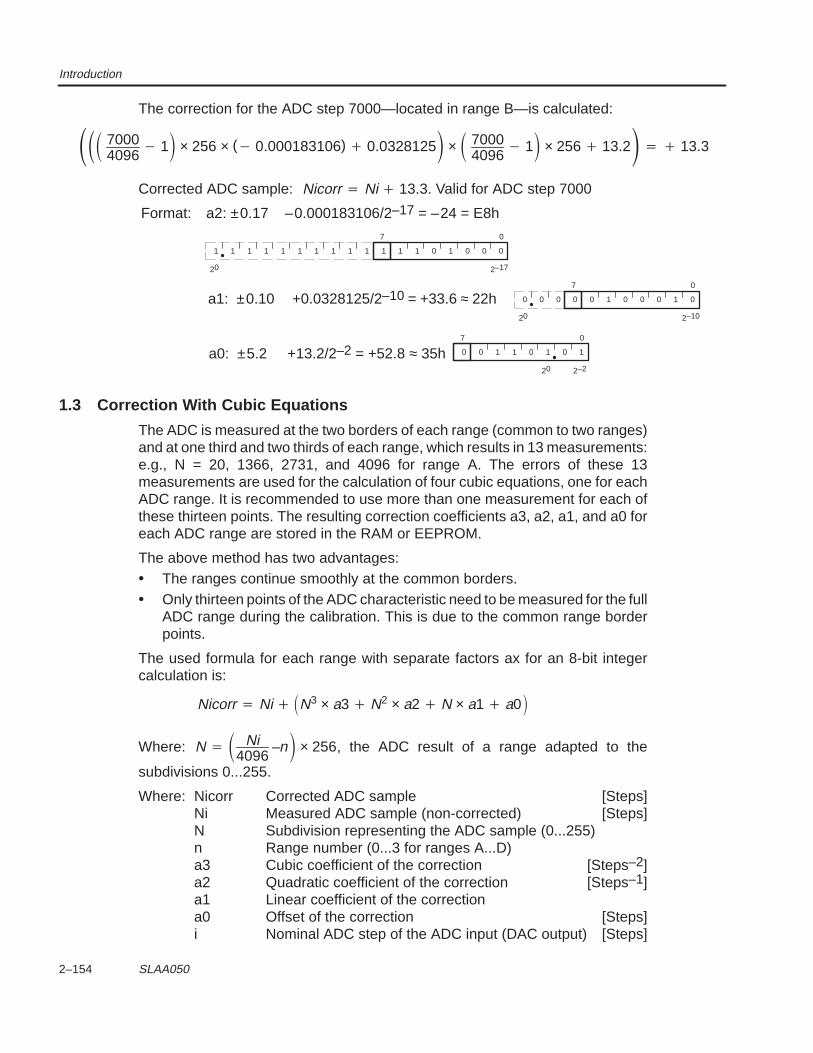
Introduction
2–154 SLAA050
The correction for the ADC step 7000—located in range B—is calculated:
70004096
1 × 256 × ( 0.000183106) 0.0328125 × 70004096
1 × 256 13.2 13.3
Corrected ADC sample: Nicorr Ni 13.3. Valid for ADC step 7000
a1: ±0.10 +0.0328125/2–10 = +33.6 ≈ 22h
Format: a2: ±0.17 –0.000183106/2–17 = –24 = E8h
a0: ±5.2 +13.2/2–2 = +52.8 ≈ 35h
2–17
1 1 1 0 1 0 01111111111 0
07
20
2–10
0 0 1 0 0 0 1000 0
07
20
2–2
0 0 1 1 0 1 0 1
07
20
1.3 Correction With Cubic Equations
The ADC is measured at the two borders of each range (common to two ranges)and at one third and two thirds of each range, which results in 13 measurements:e.g., N = 20, 1366, 2731, and 4096 for range A. The errors of these 13measurements are used for the calculation of four cubic equations, one for eachADC range. It is recommended to use more than one measurement for each ofthese thirteen points. The resulting correction coefficients a3, a2, a1, and a0 foreach ADC range are stored in the RAM or EEPROM.
The above method has two advantages:• The ranges continue smoothly at the common borders.• Only thirteen points of the ADC characteristic need to be measured for the full
ADC range during the calibration. This is due to the common range borderpoints.
The used formula for each range with separate factors ax for an 8-bit integercalculation is:
Nicorr Ni N3 × a3 N2 × a2 N × a1 a0
Where: N Ni4096
–n × 256, the ADC result of a range adapted to the
subdivisions 0...255.
Where: Nicorr Corrected ADC sample [Steps]Ni Measured ADC sample (non-corrected) [Steps]N Subdivision representing the ADC sample (0...255)n Range number (0...3 for ranges A...D)a3 Cubic coefficient of the correction [Steps–2]a2 Quadratic coefficient of the correction [Steps–1]a1 Linear coefficient of the correctiona0 Offset of the correction [Steps]i Nominal ADC step of the ADC input (DAC output) [Steps]
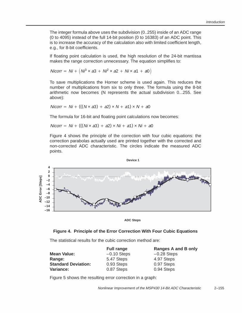
Introduction
2–155 Nonlinear Improvement of the MSP430 14-Bit ADC Characteristic
The integer formula above uses the subdivision (0..255) inside of an ADC range(0 to 4095) instead of the full 14-bit position (0 to 16383) of an ADC point. Thisis to increase the accuracy of the calculation also with limited coefficient length,e.g., for 8-bit coefficients.
If floating point calculation is used, the high resolution of the 24-bit mantissamakes the range correction unnecessary. The equation simplifies to:
Nicorr Ni Ni3 × a3 Ni2 × a2 Ni × a1 a0
To save multiplications the Horner scheme is used again. This reduces thenumber of multiplications from six to only three. The formula using the 8-bitarithmetic now becomes (N represents the actual subdivision 0...255. Seeabove):
Nicorr Ni (((N × a3) a2) × N a1) × N a0
The formula for 16-bit and floating point calculations now becomes:
Nicorr Ni (((Ni × a3) a2) × Ni a1) × Ni a0
Figure 4 shows the principle of the correction with four cubic equations: thecorrection parabolas actually used are printed together with the corrected andnon-corrected ADC characteristic. The circles indicate the measured ADCpoints.
ADC Steps
–6–8
–10–12
–16
AD
C E
rror
[Ste
ps]
Device 1
–4–2
–14
024
Figure 4. Principle of the Error Correction With Four Cubic Equations
The statistical results for the cubic correction method are:
Full range Ranges A and B onlyMean Value: –0.10 Steps –0.28 StepsRange: 5.47 Steps 4.97 StepsStandard Deviation: 0.93 Steps 0.97 StepsVariance: 0.87 Steps 0.94 Steps
Figure 5 shows the resulting error correction in a graph:
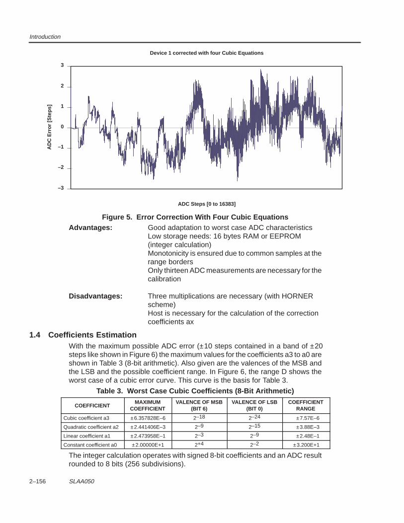
Introduction
2–156 SLAA050
2
1
0
–1
–3
AD
C E
rror
[Ste
ps]
ADC Steps [0 to 16383]
Device 1 corrected with four Cubic Equations
3
–2
Figure 5. Error Correction With Four Cubic EquationsAdvantages: Good adaptation to worst case ADC characteristics
Low storage needs: 16 bytes RAM or EEPROM(integer calculation)Monotonicity is ensured due to common samples at therange bordersOnly thirteen ADC measurements are necessary for thecalibration
Disadvantages: Three multiplications are necessary (with HORNERscheme)Host is necessary for the calculation of the correctioncoefficients ax
1.4 Coefficients EstimationWith the maximum possible ADC error (±10 steps contained in a band of ±20steps like shown in Figure 6) the maximum values for the coefficients a3 to a0 areshown in Table 3 (8-bit arithmetic). Also given are the valences of the MSB andthe LSB and the possible coefficient range. In Figure 6, the range D shows theworst case of a cubic error curve. This curve is the basis for Table 3.
Table 3. Worst Case Cubic Coefficients (8-Bit Arithmetic)
COEFFICIENTMAXIMUM
COEFFICIENTVALENCE OF MSB
(BIT 6)VALENCE OF LSB
(BIT 0)COEFFICIENT
RANGE
Cubic coefficient a3 ±6.357828E–6 2–18 2–24 ±7.57E–6
Quadratic coefficient a2 ±2.441406E–3 2–9 2–15 ±3.88E–3
Linear coefficient a1 ±2.473958E–1 2–3 2–9 ±2.48E–1
Constant coefficient a0 ±2.00000E+1 2+4 2–2 ±3.200E+1
The integer calculation operates with signed 8-bit coefficients and an ADC resultrounded to 8 bits (256 subdivisions).
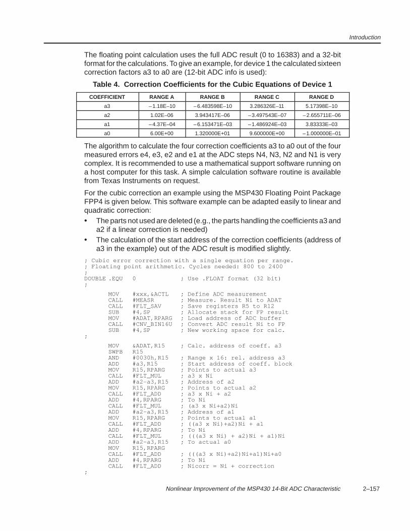
Introduction
2–157 Nonlinear Improvement of the MSP430 14-Bit ADC Characteristic
The floating point calculation uses the full ADC result (0 to 16383) and a 32-bitformat for the calculations. To give an example, for device 1 the calculated sixteencorrection factors a3 to a0 are (12-bit ADC info is used):
Table 4. Correction Coefficients for the Cubic Equations of Device 1
COEFFICIENT RANGE A RANGE B RANGE C RANGE D
a3 –1.18E–10 –6.483598E–10 3.286326E–11 5.17398E–10
a2 1.02E–06 3.943417E–06 –3.497543E–07 –2.655711E–06
a1 –4.37E–04 –6.153471E–03 –1.486924E–03 3.83333E–03
a0 6.00E+00 1.320000E+01 9.600000E+00 –1.000000E–01
The algorithm to calculate the four correction coefficients a3 to a0 out of the fourmeasured errors e4, e3, e2 and e1 at the ADC steps N4, N3, N2 and N1 is verycomplex. It is recommended to use a mathematical support software running ona host computer for this task. A simple calculation software routine is availablefrom Texas Instruments on request.
For the cubic correction an example using the MSP430 Floating Point PackageFPP4 is given below. This software example can be adapted easily to linear andquadratic correction:• The parts not used are deleted (e.g., the parts handling the coefficients a3 and
a2 if a linear correction is needed)• The calculation of the start address of the correction coefficients (address of
a3 in the example) out of the ADC result is modified slightly.
; Cubic error correction with a single equation per range.; Floating point arithmetic. Cycles needed: 800 to 2400;DOUBLE .EQU 0 ; Use .FLOAT format (32 bit);
MOV #xxx,&ACTL ; Define ADC measurementCALL #MEASR ; Measure. Result Ni to ADATCALL #FLT_SAV ; Save registers R5 to R12SUB #4,SP ; Allocate stack for FP resultMOV #ADAT,RPARG ; Load address of ADC bufferCALL #CNV_BIN16U ; Convert ADC result Ni to FPSUB #4,SP ; New working space for calc.
;
MOV &ADAT,R15 ; Calc. address of coeff. a3SWPB R15AND #0030h,R15 ; Range x 16: rel. address a3ADD #a3,R15 ; Start address of coeff. blockMOV R15,RPARG ; Points to actual a3CALL #FLT_MUL ; a3 x NiADD #a2–a3,R15 ; Address of a2MOV R15,RPARG ; Points to actual a2CALL #FLT_ADD ; a3 x Ni + a2ADD #4,RPARG ; To NiCALL #FLT_MUL ; (a3 x Ni+a2)NiADD #a2–a3,R15 ; Address of a1MOV R15,RPARG ; Points to actual a1CALL #FLT_ADD ; ((a3 x Ni)+a2)Ni + a1ADD #4,RPARG ; To NiCALL #FLT_MUL ; (((a3 x Ni) + a2)Ni + a1)NiADD #a2–a3,R15 ; To actual a0MOV R15,RPARGCALL #FLT_ADD ; (((a3 x Ni)+a2)Ni+a1)Ni+a0ADD #4,RPARG ; To NiCALL #FLT_ADD ; Nicorr = Ni + correction
;
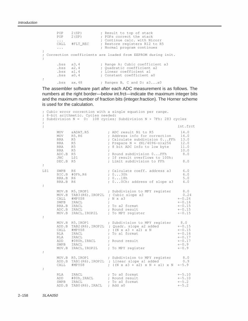
Introduction
2–158 SLAA050
POP 2(SP) ; Result to top of stackPOP 2(SP) ; POPs correct the stack... ; Continue calc. with NicorrCALL #FLT_REC ; Restore registers R12 to R5... ; Normal program continues
;; Correction coefficients are loaded from EEPROM during init.;
.bss a3,4 ; Range A: Cubic coefficient a3
.bss a2,4 ; Quadratic coefficient a2
.bss a1,4 ; Linear coefficient a1
.bss a0,4 ; Constant coefficient a0;
.bss ax,48 ; Ranges B, C and D: a3...a0
The assembler software part after each ADC measurement is as follows. Thenumbers at the right border—below int.frct—indicate the maximum integer bitsand the maximum number of fraction bits (integer.fraction). The Horner schemeis used for the calculation.
; Cubic error correction with a single equation per range.; 8–bit arithmetic. Cycles needed:; Subdivision N = 0: 108 cycles; Subdivision N > 7Fh: 283 cycles;; int.frct
MOV &ADAT,R5 ; ADC result Ni to R5 14.0MOV R5,R6 ; Address info for correction 14.0RRA R5 ; Calculate subdivision 0...FFh 13.0RRA R5 ; Prepare N = (Ni/4096–n)x256 12.0RRA R5 ; 8 bit ADC info to low byte 11.0RRA R5 ; 10.0ADC.B R5 ; Round subdivision 0...FFh 8.0JNC L$1 ; If result overflows to 100h:DEC.B R5 ; Limit subdivision to FFh 8.0
;
L$1 SWPB R6 ; Calculate coeff. address a3 6.0BIC.B #0Fh,R6 ; 0...30h 6.0RRA.B R6 ; 0...18h 5.0RRA.B R6 ; 0...0Ch: address of slope a3 4.0
;
MOV.B R5,IROP1 ; Subdivision to MPY register 8.0MOV.B TAB3(R6),IROP2L ; Cubic slope a3 0.24CALL #MPYS8 ; N x a3 +–0.24SWPB IRACL ; +–0.16RRA.B IRACL ; To a2 format +–0.15ADC.B IRACL ; Round result +–0.15MOV.B IRACL,IROP2L ; To MPY register +–0.15
;
MOV.B R5,IROP1 ; Subdivision to MPY register 8.0ADD.B TAB2(R6),IROP2L ; Quadr. slope a2 added +–0.15CALL #MPYS8 ; ((N x a3 + a2) x N +–0.15RLA IRACL ; To a1 format +–0.16RLA IRACL ; +–0.17ADD #080h,IRACL ; Round result +–0.17SWPB IRACL ; +–0.9MOV.B IRACL,IROP2L ; To MPY register +–0.9
;
MOV.B R5,IROP1 ; Subdivision to MPY register 8.0ADD.B TAB1(R6),IROP2L ; Linear slope a1 added 0.9CALL #MPYS8 ; ((N x a3 + a2) x N + a1) x N +–5.9
;
RLA IRACL ; To a0 format +–5.10ADD #80h,IRACL ; Round result +–5.10SWPB IRACL ; To a0 format +–5.2ADD.B TAB0(R6),IRACL ; Add a0 +–5.2
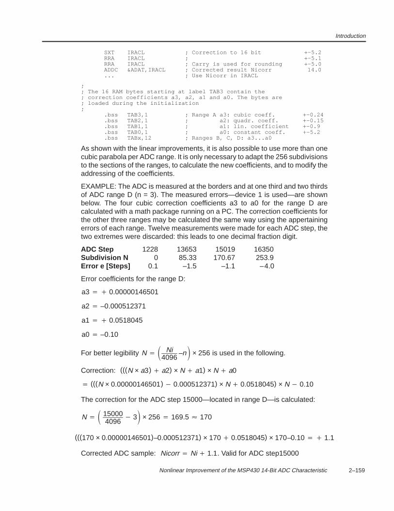
Introduction
2–159 Nonlinear Improvement of the MSP430 14-Bit ADC Characteristic
SXT IRACL ; Correction to 16 bit +–5.2RRA IRACL ; +–5.1RRA IRACL ; Carry is used for rounding +–5.0ADDC &ADAT,IRACL ; Corrected result Nicorr 14.0... ; Use Nicorr in IRACL
;; The 16 RAM bytes starting at label TAB3 contain the; correction coefficients a3, a2, a1 and a0. The bytes are; loaded during the initialization;
.bss TAB3,1 ; Range A a3: cubic coeff. +–0.24
.bss TAB2,1 ; a2: quadr. coeff. +–0.15
.bss TAB1,1 ; a1: lin. coefficient +–0.9
.bss TAB0,1 ; a0: constant coeff. +–5.2
.bss TABx,12 ; Ranges B, C, D: a3...a0
As shown with the linear improvements, it is also possible to use more than onecubic parabola per ADC range. It is only necessary to adapt the 256 subdivisionsto the sections of the ranges, to calculate the new coefficients, and to modify theaddressing of the coefficients.
EXAMPLE: The ADC is measured at the borders and at one third and two thirdsof ADC range D (n = 3). The measured errors—device 1 is used—are shownbelow. The four cubic correction coefficients a3 to a0 for the range D arecalculated with a math package running on a PC. The correction coefficients forthe other three ranges may be calculated the same way using the appertainingerrors of each range. Twelve measurements were made for each ADC step, thetwo extremes were discarded: this leads to one decimal fraction digit.
ADC Step 1228 13653 15019 16350Subdivision N 0 85.33 170.67 253.9Error e [Steps] 0.1 –1.5 –1.1 –4.0
Error coefficients for the range D:
a3 0.00000146501
a2 –0.000512371
a1 0.0518045
a0 –0.10
For better legibility N Ni4096
–n × 256 is used in the following.
Correction: (((N × a3) a2) × N a1) × N a0
(((N × 0.00000146501) 0.000512371) × N 0.0518045) × N 0.10
The correction for the ADC step 15000—located in range D—is calculated:
N 150004096
3 × 256 169.5 170
(((170 × 0.00000146501)–0.000512371) × 170 0.0518045) × 170–0.10 1.1
Corrected ADC sample: Nicorr Ni 1.1. Valid for ADC step15000
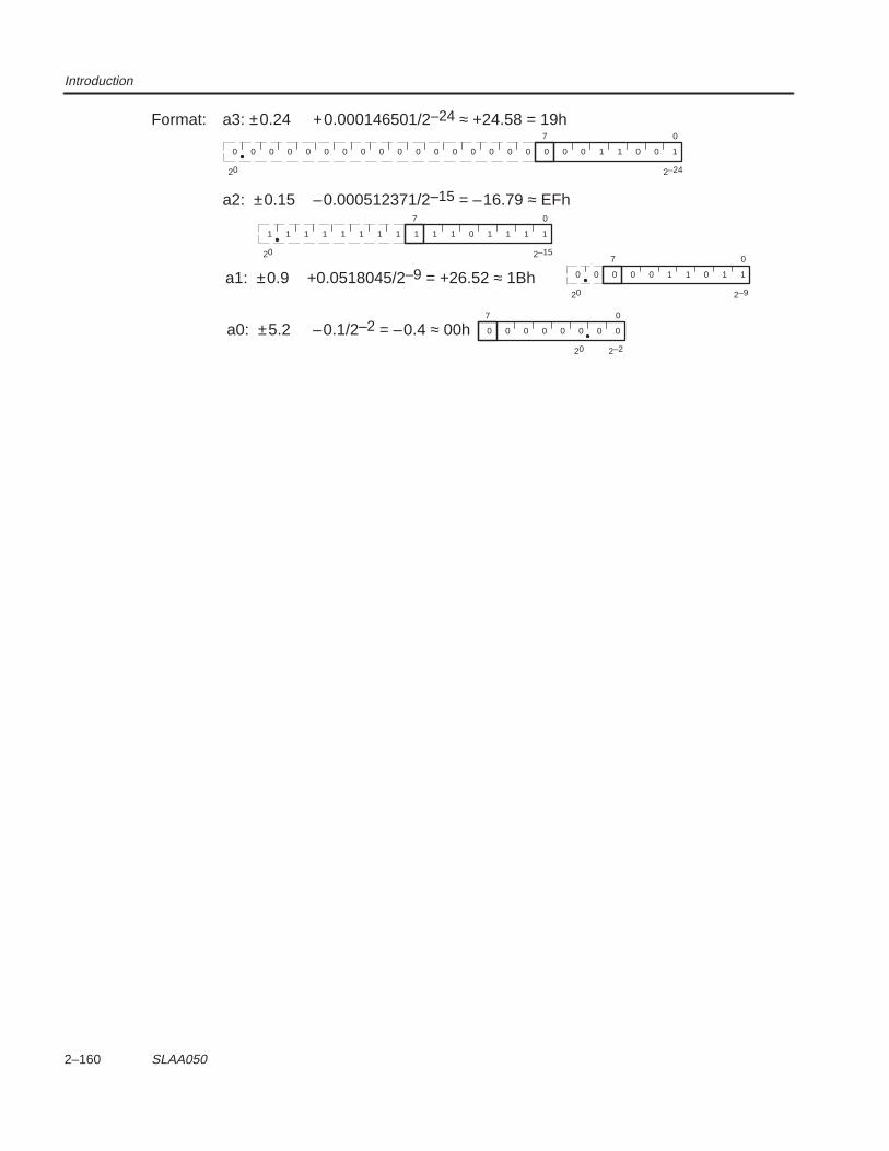
Introduction
2–160 SLAA050
Format: a3: ±0.24 +0.000146501/2–24 ≈ +24.58 = 19h
a2: ±0.15 –0.000512371/2–15 = –16.79 ≈ EFh
a1: ±0.9 +0.0518045/2–9 = +26.52 ≈ 1Bh
a0: ±5.2 –0.1/2–2 = –0.4 ≈ 00h
2–24
0 0 0 1 1 0 000000000000000000 1
07
20
2–15
1 1 1 0 1 1 111111111 1
07
20
2–9
0 0 0 1 1 0 100 1
07
20
2–2
0 0 0 0 0 0 0 0
07
20
Considerations to the Integer Calculations
2–161 Nonlinear Improvement of the MSP430 14-Bit ADC Characteristic
2 Considerations to the Integer CalculationsThe calculations for this application report were made with a floating pointpackage. If the 14-bit ADC is used within a real time system the floating pointcalculation time is normally too long. Therefore the necessary loss of accuracyneeds to be known if integer calculations with their restricted bit length are used.The most time consuming parts are the multiplication subroutines, so they areshown first.
2.1 Multiplication Subroutines
To reduce the multiplication time as much as possible, two multiplicationsubroutines, which terminate immediately after the operand IROP1 becomeszero are shown; this means that the operand with leading zeroes should be in theregister IROP1—here the subdivision representing the ADC result.1
2.1.1 8-Bit Multiplication Subroutine
If the operands of the multiplication subroutine are normally shorter than 8 bits,then the multiplication subroutine below saves time due to its run timeoptimization: the multiplication terminates immediately after IROP1 gets zero dueto the right shifts during the processing.
; Run time optimized 8–bit Multiplication Subroutines; Definitions;IROP1 .EQU R14 ; Unsigned subdivision (00h...FFh)IROP2L .EQU R13 ; Signed coefficient (80h...7Fh)IRACL .EQU R12 ; Result word;; Cycles for specific registers contents without CALL:
; TASK MACU8 MACS8 MPYS8 IROP1 IROP2 Result (MPYS8);–––––––––––––––––––––––––––––––––––––––––––––––––––––––––––––; MINIMUM 9 12 13 000h x 000h = 0000h; MEDIUM 34 37 38 00Fh x 00Fh = 00E1h; MAXIMUM 66 70 71 0FFh x 0FFh = FF01h;; Used registers IROP1, IROP2L, IRACL;; Signed multiply subroutine: IROP1 x IROP2L –> IRACL;MPYS8 CLR IRACL ; 0 –> 16 bit RESULT;; Signed multiply–and–accumulate subroutine:; (IROP1 x IROP2L) + IRACL –> IRACL;MACS8 TST.B IROP2L ; Sign of factor
JGE MACU8 ; Positive sign: proceedSWPB IROP1 ; Negative sign: correction nec.SUB IROP1,IRACL ; Correct result wordSWPB IROP1
;; Unsigned multiply–and–accumulate subroutine (MAC):; (IROP1 x IROP2L) + IRACL –> IRACL;MACU8 BIT.B #1,IROP1 ; Test actual bit (LSB)
JZ L$01 ; If 0: do nothingADD IROP2L,IRACL ; If 1: add multiplier to resultL$01
L$01 RLA IROP2L ; Double multiplier IROP2RRC.B IROP1 ; Next bit of IROP1 to LSBJNZ MACU8 ; If IROP1 = 0: finishedRET
1The idea for these subroutines initially came from Leslie Mable of TIL.
Considerations to the Integer Calculations
2–162 SLAA050
2.1.1.1 16-Bit Multiplication Subroutine
This multiplication subroutine is used if the 8-bit version is not accurate enough.Like the 8-bit version, the multiplication terminates immediately after IROP1becomes zero due to the right shifts during the processing. All of the shown ADCimprovement methods may be adapted to the 16-bit multiplication subroutine.
; Run time optimized 16–bit Multiplication Subroutines;IROP1 .EQU R11 ; Unsigned ADC result (0000h...3FFFh)IROP2L .EQU R12 ; Signed coefficient (8000h...7FFFh)IROP2M .EQU R13 ; High word of signed factor (0)IRACL .EQU R14 ; Result word lowIRACM .EQU R15 ; Result word high;; Cycles for specific register contents without CALL:; TASK MACU MACS MPYS IROP1 IROP2 Result (MPYS);–––––––––––––––––––––––––––––––––––––––––––––––––––––––––––––; MINIMUM 11 14 16 0000h x 0000h = 00000000h; MEDIUM 83 86 88 00FFh x 00FFh = 0000FE01h; MAXIMUM 143 147 149 3FFFh x FFFFh = FFFFC001h;; Used registers: all of the above ones;; Signed multiply subroutine: IROP1 x IROP2L –> IRACM|IRACL;
MPYS CLR IRACL ; 0 –> result word lowCLR IRACM ; 0 –> result word high
MACS TST IROP2L ; Sign of factor a1JGE MACU ; Positive sign: proceedSUB IROP1,IRACM ; Correct result
MACU CLR IROP2M ; Clear MSBs of multiplierL$002 BIT #1,IROP1 ; Test actual bit (LSB)
JZ L$01 ; If 0: do nothingADD IROP2L,IRACL ; If 1: add multiplier to resultADDC IROP2M,IRACM
L$01 RLA IROP2L ; Double multiplier IROP2RLC IROP2M ;
;RRC IROP1 ; Next bit of IROP1 to LSBJNZ L$002 ; If IROP1 = 0: finishedRET
2.2 Maximum Magnitude of the 8-Bit Coefficients
To get the maximum accuracy with the limited 8-bit format used for the correctioncoefficients, it is necessary to calculate the worst case magnitude for each oneof these coefficients. The basis for this calculation is the maximum error of the14-bit ADC:
±10 steps within a band of ±20 steps
Figure 6 shows examples for the worst case errors of the 14-bit ADC:• Range A shows the maximum error band of the ADC: ±20 steps; within this
error band all errors of different devices are contained. The four dark boxesindicate four possible error ranges of ±10 steps: they are examples for singledevices, within such an error band the errors of a single device are contained.
• Range B gives an example for the maximum linear error: within one range(4096 steps) the error changes by 20 steps.
• Range C is an example for a maximum quadratic error.• Range D is an example for a maximum cubic error. This means within an ADC
range the ADC characteristic moves from an error of +10 steps at the lower
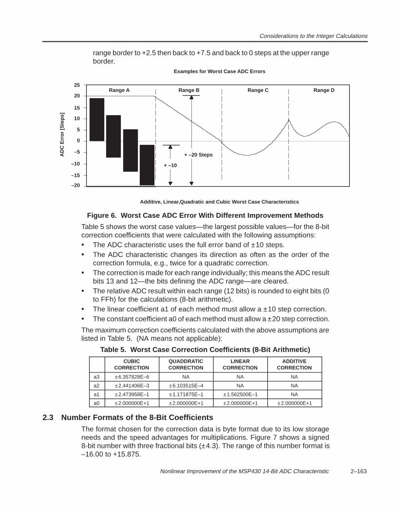
Considerations to the Integer Calculations
2–163 Nonlinear Improvement of the MSP430 14-Bit ADC Characteristic
range border to +2.5 then back to +7.5 and back to 0 steps at the upper rangeborder.
Additive, Linear,Quadratic and Cubic Worst Case Characteristics
5
0
–5
–10
–20
AD
C E
rror
[Ste
ps]
Examples for Worst Case ADC Errors
10
15
–15
20
25
+ –20 Steps
+ –10
Range A Range B Range C Range D
Figure 6. Worst Case ADC Error With Different Improvement Methods
Table 5 shows the worst case values—the largest possible values—for the 8-bitcorrection coefficients that were calculated with the following assumptions:• The ADC characteristic uses the full error band of ±10 steps.• The ADC characteristic changes its direction as often as the order of the
correction formula, e.g., twice for a quadratic correction.• The correction is made for each range individually; this means the ADC result
bits 13 and 12—the bits defining the ADC range—are cleared.• The relative ADC result within each range (12 bits) is rounded to eight bits (0
to FFh) for the calculations (8-bit arithmetic).• The linear coefficient a1 of each method must allow a ±10 step correction.• The constant coefficient a0 of each method must allow a ±20 step correction.
The maximum correction coefficients calculated with the above assumptions arelisted in Table 5. (NA means not applicable):
Table 5. Worst Case Correction Coefficients (8-Bit Arithmetic)
CUBICCORRECTION
QUADDRATICCORRECTION
LINEARCORRECTION
ADDITIVECORRECTION
a3 ±6.357828E–6 NA NA NA
a2 ±2.441406E–3 ±6.103515E–4 NA NA
a1 ±2.473958E–1 ±1.171875E–1 ±1.562500E–1 NA
a0 ±2.000000E+1 ±2.000000E+1 ±2.000000E+1 ±2.000000E+1
2.3 Number Formats of the 8-Bit CoefficientsThe format chosen for the correction data is byte format due to its low storageneeds and the speed advantages for multiplications. Figure 7 shows a signed8-bit number with three fractional bits (±4.3). The range of this number format is–16.00 to +15.875.
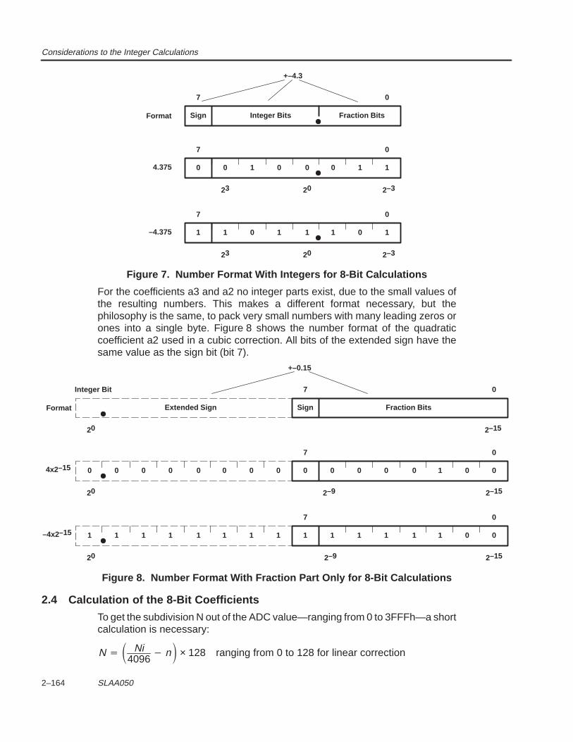
Considerations to the Integer Calculations
2–164 SLAA050
SignFormat Integer Bits Fraction Bits
7 0
0 0 1 0 0 0 1 1
7 0
23 20 2–3
4.375
1 1 0 1 1 1 0 1
7 0
23 20 2–3
–4.375
+–4.3
Figure 7. Number Format With Integers for 8-Bit Calculations
For the coefficients a3 and a2 no integer parts exist, due to the small values ofthe resulting numbers. This makes a different format necessary, but thephilosophy is the same, to pack very small numbers with many leading zeros orones into a single byte. Figure8 shows the number format of the quadraticcoefficient a2 used in a cubic correction. All bits of the extended sign have thesame value as the sign bit (bit 7).
SignFormat Fraction Bits
7 0
2–15
0 0 0 0 0 1 0 0
7 0
2–9 2–15
4x2–15
1 1 1 1 1 1 0 0
7 0
2–9 2–15
–4x2–15
+–0.15
0 0 0 0 0 0 0 0
1 1 1 1 1 1 1 1
Extended Sign
Integer Bit
20
20
20
Figure 8. Number Format With Fraction Part Only for 8-Bit Calculations
2.4 Calculation of the 8-Bit Coefficients
To get the subdivision N out of the ADC value—ranging from 0 to 3FFFh—a shortcalculation is necessary:
N Ni4096
n × 128 ranging from 0 to 128 for linear correction

Considerations to the Integer Calculations
2–165 Nonlinear Improvement of the MSP430 14-Bit ADC Characteristic
N Ni4096
n × 256 ranging from 0 to 256 for quadratic and cubic
correction
With two, three, or four subdivisions N—dependent on the used correctionmethod—the coefficients ax are calculated. See the appropriate sections.
1. To start, it is necessary to find the minimum valence—a power of 2—of bit 6(MSB) of the 8-bit number that is sufficient for the worst case value of thecoefficient ax. The formula for this calculation is:
VMSB log2|ax|–1
Where: VMSB Valence for the MSB (bit 6) of the 8-bit numberVLSB Valence for the LSB (bit 0) of the 8-bit numberax Decimal correction coefficient (a3 to a0)
The above formula ensures that the worst case value of the coefficient ax fits intoan 8-bit twos complement number.
2. The valence VLSB of the LSB is for 8-bit arithmetic
VLSB VMSB 6
With this valence VLSB the 8-bit coefficient ax8bit is calculated:
ax8bit ax
2VLSB
3. The result ax8bit—which is also named ax in the following equations—isconverted into a signed hexadecimal number using the twos complementformat:
• A positive coefficient is simply converted.
• A negative coefficient is converted and negated afterwards (complementedand incremented).
EXAMPLE: The worst case value for the cubic correction coefficient a3 is±6.357828E–6 (see Table 5). To find the minimum valence of the MSB of thenumber format the equation above is used:
VMSB log2|ax| 1 log2 6.357828E 6 1 17.263 1 18.263
VMSB 18.263 VMSB 18
This result means that bit 6—the MSB—of the 8-bit coefficient a3 must have aminimum valence of 2–18. For the LSB the valence VLSB becomes:
VLSB VMSB 6 18–6 24
This means, a3 can cover the number range from –128 × 2–24 to +127 × 2–24
(–7.57E–6 to +7.63E–6) in steps of 2–24 (5.96E–8).
Calculation: a3: ±0.24 +6.357828E–6/2–24 = +106.67 ≈ 6Bh
This means the worst case of the a3 value results in 107 steps out of 127 steps:good resolution and enough reserve are given. The number format—shown forthe negative worst case value of a3 (–107 = 95h)—is:
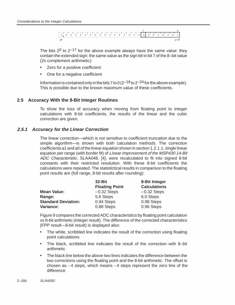
Considerations to the Integer Calculations
2–166 SLAA050
2–24
1 0 0 1 0 1 011111111111111111 1
07
20
The bits 20 to 2–17 for the above example always have the same value: theycontain the extended sign: the same value as the sign bit in bit 7 of the 8–bit value(2s complement arithmetic):
• Zero for a positive coefficient
• One for a negative coefficient
Information is contained only in the bits 7 to 0 (2–18 to 2–24 for the above example).This is possible due to the known maximum value of these coefficients.
2.5 Accuracy With the 8-Bit Integer Routines
To show the loss of accuracy when moving from floating point to integercalculations with 8-bit coefficients, the results of the linear and the cubiccorrection are given.
2.5.1 Accuracy for the Linear Correction
The linear correction—which is not sensitive to coefficient truncation due to thesimple algorithm—is shown with both calculation methods. The correctioncoefficients a1 and a0 of the linear equation shown in section 1.2.1.1, single linearequation per range (with border fit) of Linear Improvement of the MSP430 14-BitADC Characteristic, SLAA048, [4], were recalculated to fit into signed 8-bitconstants with their restricted resolution. With these 8-bit coefficients thecalculations were repeated. The statistictical results in comparison to the floatingpoint results are (full range, 8-bit results after rounding):
32-Bit 8-Bit IntegerFloating Point Calculations
Mean Value: –0.32 Steps –0.32 StepsRange: 5.6 Steps 6.0 StepsStandard Deviation: 0.94 Steps 0.98 StepsVariance: 0.88 Steps 0.96 Steps
Figure 9 compares the corrected ADC characteristics by floating point calculationvs 8-bit arithmetic (integer result). The difference of the corrected characteristics(FPP result—8-bit result) is displayed also:
• The white, scribbled line indicates the result of the correction using floatingpoint calculations
• The black, scribbled line indicates the result of the correction with 8–bitarithmetic
• The black line below the above two lines indicates the difference between thetwo corrections using the floating point and the 8-bit arithmetic. The offset ischosen as –4 steps, which means –4 steps represent the zero line of thedifference
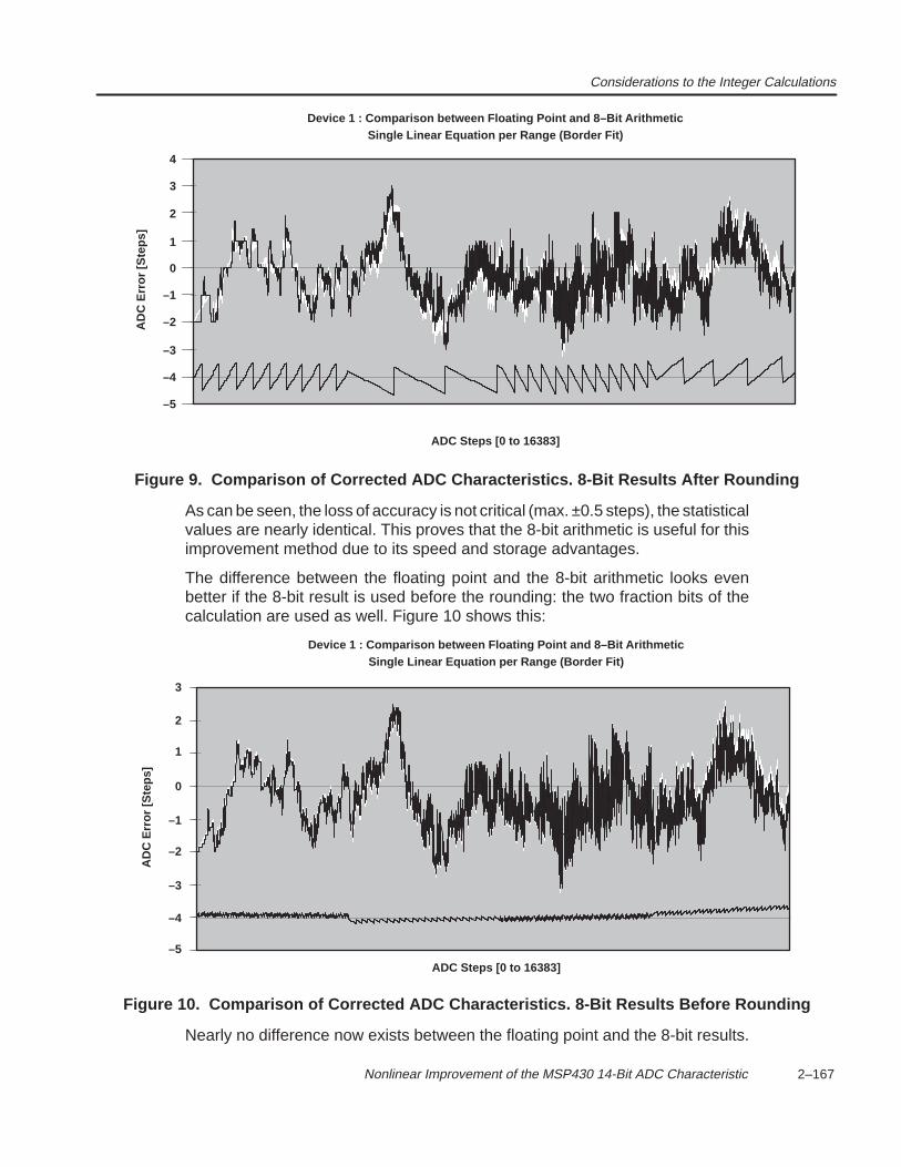
Considerations to the Integer Calculations
2–167 Nonlinear Improvement of the MSP430 14-Bit ADC Characteristic
0
–1
–2
–3
–5
AD
C E
rror
[Ste
ps]
ADC Steps [0 to 16383]
Device 1 : Comparison between Floating Point and 8–Bit Arithmetic
3
4
–4
1
2
Single Linear Equation per Range (Border Fit)
Figure 9. Comparison of Corrected ADC Characteristics. 8-Bit Results After Rounding
As can be seen, the loss of accuracy is not critical (max. ±0.5 steps), the statisticalvalues are nearly identical. This proves that the 8-bit arithmetic is useful for thisimprovement method due to its speed and storage advantages.
The difference between the floating point and the 8-bit arithmetic looks evenbetter if the 8-bit result is used before the rounding: the two fraction bits of thecalculation are used as well. Figure 10 shows this:
0
–1
–2
–3
–5
AD
C E
rror
[Ste
ps]
ADC Steps [0 to 16383]
Device 1 : Comparison between Floating Point and 8–Bit Arithmetic
3
–4
1
2
Single Linear Equation per Range (Border Fit)
Figure 10. Comparison of Corrected ADC Characteristics. 8-Bit Results Before Rounding
Nearly no difference now exists between the floating point and the 8-bit results.
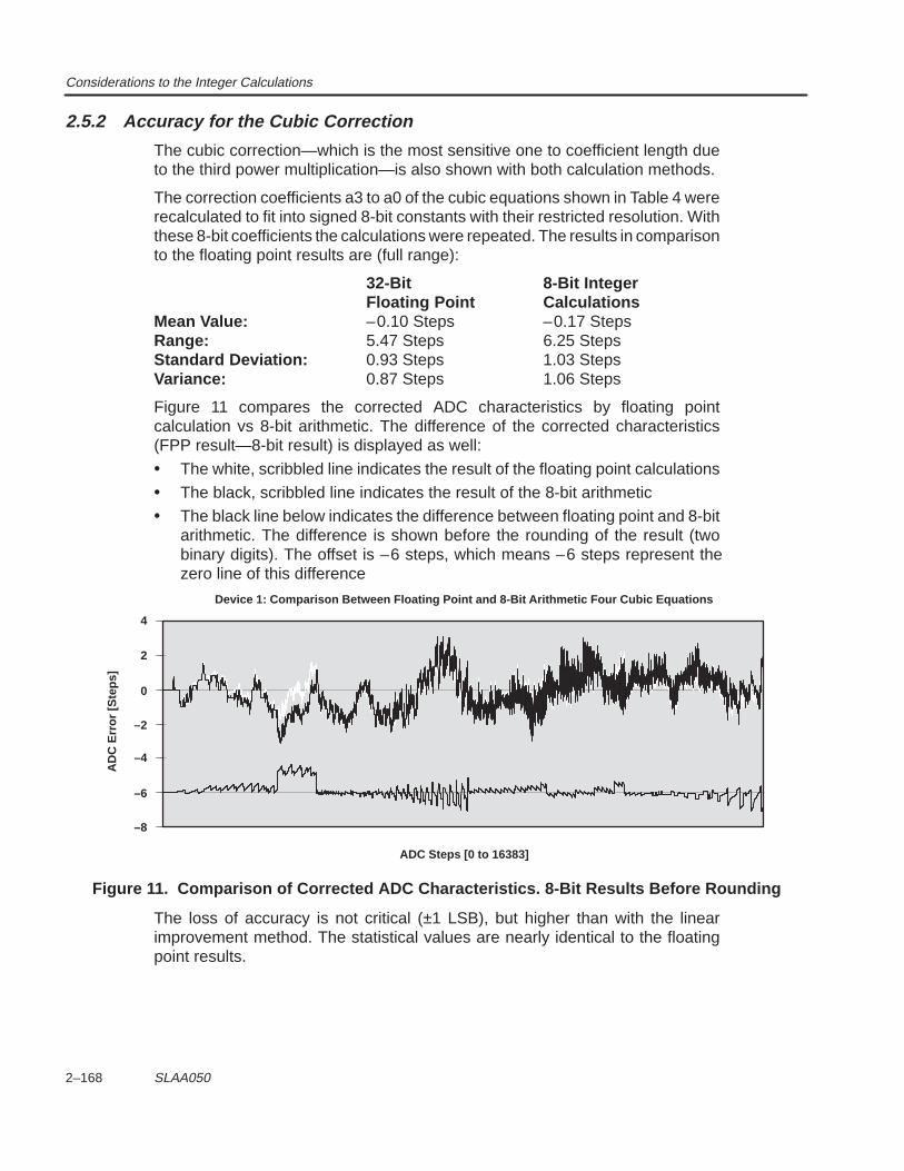
Considerations to the Integer Calculations
2–168 SLAA050
2.5.2 Accuracy for the Cubic Correction
The cubic correction—which is the most sensitive one to coefficient length dueto the third power multiplication—is also shown with both calculation methods.
The correction coefficients a3 to a0 of the cubic equations shown in Table 4 wererecalculated to fit into signed 8-bit constants with their restricted resolution. Withthese 8-bit coefficients the calculations were repeated. The results in comparisonto the floating point results are (full range):
32-Bit 8-Bit IntegerFloating Point Calculations
Mean Value: –0.10 Steps –0.17 StepsRange: 5.47 Steps 6.25 StepsStandard Deviation: 0.93 Steps 1.03 StepsVariance: 0.87 Steps 1.06 Steps
Figure 11 compares the corrected ADC characteristics by floating pointcalculation vs 8-bit arithmetic. The difference of the corrected characteristics(FPP result—8-bit result) is displayed as well:
• The white, scribbled line indicates the result of the floating point calculations
• The black, scribbled line indicates the result of the 8-bit arithmetic
• The black line below indicates the difference between floating point and 8-bitarithmetic. The difference is shown before the rounding of the result (twobinary digits). The offset is –6 steps, which means –6 steps represent thezero line of this difference
2
0
–2
–4
–8
AD
C E
rror
[Ste
ps]
ADC Steps [0 to 16383]
Device 1: Comparison Between Floating Point and 8-Bit Arithmetic Four Cubic Equations
–6
4
Figure 11. Comparison of Corrected ADC Characteristics. 8-Bit Results Before Rounding
The loss of accuracy is not critical (±1 LSB), but higher than with the linearimprovement method. The statistical values are nearly identical to the floatingpoint results.
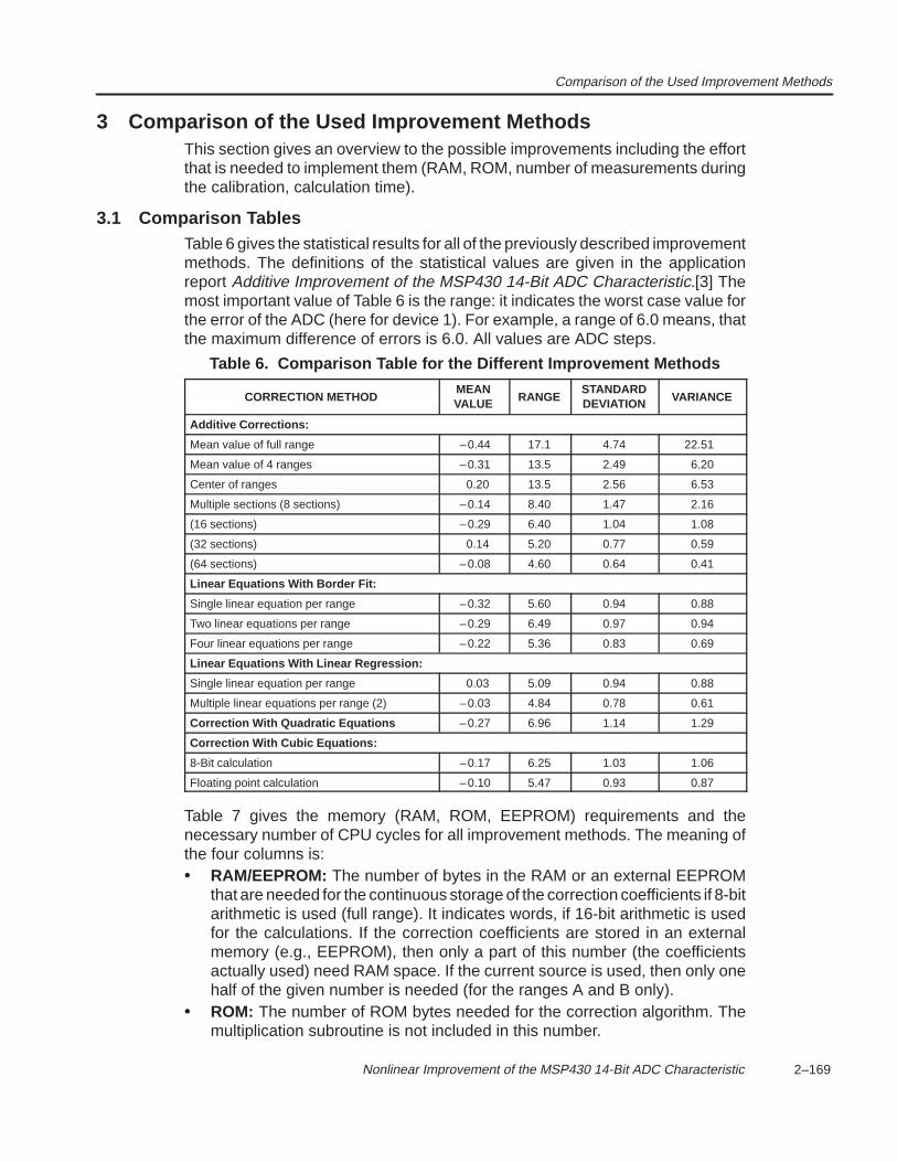
Comparison of the Used Improvement Methods
2–169 Nonlinear Improvement of the MSP430 14-Bit ADC Characteristic
3 Comparison of the Used Improvement MethodsThis section gives an overview to the possible improvements including the effortthat is needed to implement them (RAM, ROM, number of measurements duringthe calibration, calculation time).
3.1 Comparison TablesTable 6 gives the statistical results for all of the previously described improvementmethods. The definitions of the statistical values are given in the applicationreport Additive Improvement of the MSP430 14-Bit ADC Characteristic.[3] Themost important value of Table 6 is the range: it indicates the worst case value forthe error of the ADC (here for device 1). For example, a range of 6.0 means, thatthe maximum difference of errors is 6.0. All values are ADC steps.
Table 6. Comparison Table for the Different Improvement Methods
CORRECTION METHODMEANVALUE RANGE
STANDARDDEVIATION VARIANCE
Additive Corrections:
Mean value of full range –0.44 17.1 4.74 22.51
Mean value of 4 ranges –0.31 13.5 2.49 6.20
Center of ranges 0.20 13.5 2.56 6.53
Multiple sections (8 sections) –0.14 8.40 1.47 2.16
(16 sections) –0.29 6.40 1.04 1.08
(32 sections) 0.14 5.20 0.77 0.59
(64 sections) –0.08 4.60 0.64 0.41
Linear Equations With Border Fit:
Single linear equation per range –0.32 5.60 0.94 0.88
Two linear equations per range –0.29 6.49 0.97 0.94
Four linear equations per range –0.22 5.36 0.83 0.69
Linear Equations With Linear Regression:
Single linear equation per range 0.03 5.09 0.94 0.88
Multiple linear equations per range (2) –0.03 4.84 0.78 0.61
Correction With Quadratic Equations –0.27 6.96 1.14 1.29
Correction With Cubic Equations:
8-Bit calculation –0.17 6.25 1.03 1.06
Floating point calculation –0.10 5.47 0.93 0.87
Table 7 gives the memory (RAM, ROM, EEPROM) requirements and thenecessary number of CPU cycles for all improvement methods. The meaning ofthe four columns is:• RAM/EEPROM: The number of bytes in the RAM or an external EEPROM
that are needed for the continuous storage of the correction coefficients if 8-bitarithmetic is used (full range). It indicates words, if 16-bit arithmetic is usedfor the calculations. If the correction coefficients are stored in an externalmemory (e.g., EEPROM), then only a part of this number (the coefficientsactually used) need RAM space. If the current source is used, then only onehalf of the given number is needed (for the ranges A and B only).
• ROM: The number of ROM bytes needed for the correction algorithm. Themultiplication subroutine is not included in this number.
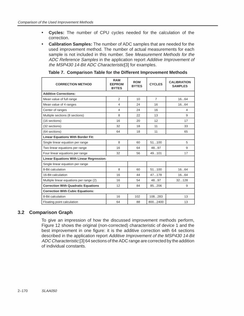
Comparison of the Used Improvement Methods
2–170 SLAA050
• Cycles: The number of CPU cycles needed for the calculation of thecorrection.
• Calibration Samples: The number of ADC samples that are needed for theused improvement method. The number of actual measurements for eachsample is not included in this number. See Measurement Methods for theADC Reference Samples in the application report Additive Improvement ofthe MSP430 14-Bit ADC Characteristic[3] for examples.
Table 7. Comparison Table for the Different Improvement Methods
CORRECTION METHODRAM
EEPROMBYTES
ROMBYTES CYCLES
CALIBRATIONSAMPLES
Additive Corrections:
Mean value of full range 2 10 7 16...64
Mean value of 4 ranges 4 24 16 16...64
Center of ranges 4 24 16 4
Multiple sections (8 sections) 8 22 13 9
(16 sections) 16 20 12 17
(32 sections) 32 18 11 33
(64 sections) 64 18 11 65
Linear Equations With Border Fit:
Single linear equation per range 8 60 51...100 5
Two linear equations per range 16 64 48...97 9
Four linear equations per range 32 56 49...101 17
Linear Equations With Linear Regression:
Single linear equation per range
8-Bit calculation 8 60 51...100 16...64
16-Bit calculation 16 44 47...178 16...64
Multiple linear equations per range (2) 16 54 48...97 32...128
Correction With Quadratic Equations 12 84 85...206 9
Correction With Cubic Equations:
8-Bit calculation 16 102 108...283 13
Floating point calculation 64 88 800...2400 13
3.2 Comparison Graph
To give an impression of how the discussed improvement methods perform,Figure 12 shows the original (non-corrected) characteristic of device 1 and thebest improvement in one figure: it is the additive correction with 64 sectionsdescribed in the application report Additive Improvement of the MSP430 14-BitADC Characteristic:[3] 64 sections of the ADC range are corrected by the additionof individual constants.
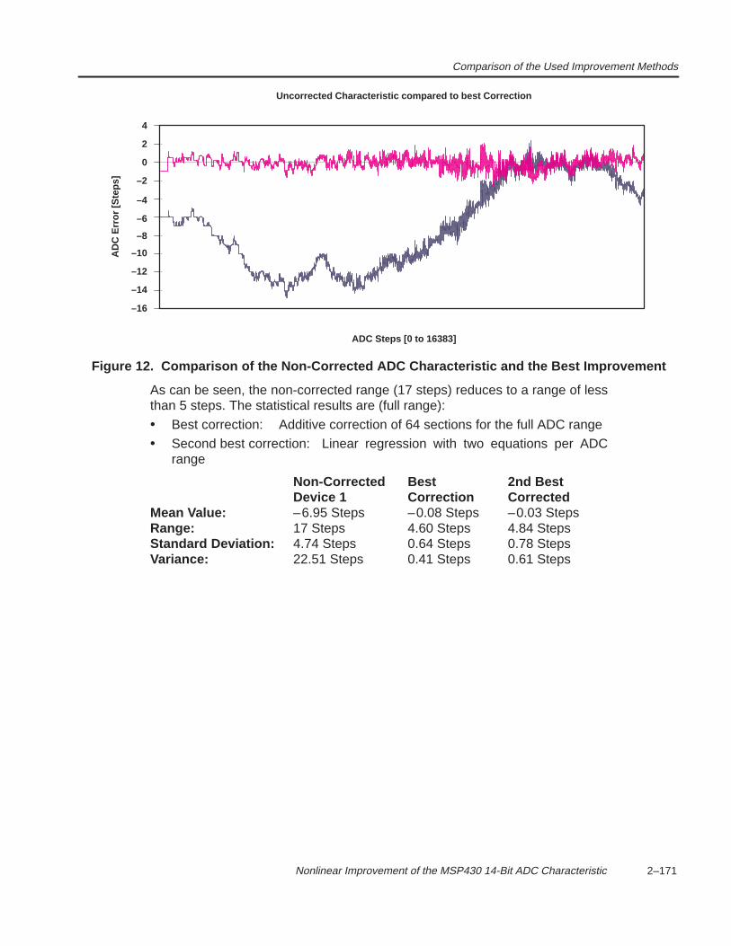
Comparison of the Used Improvement Methods
2–171 Nonlinear Improvement of the MSP430 14-Bit ADC Characteristic
–6
–8
–10
–12
–16
AD
C E
rror
[Ste
ps]
Uncorrected Characteristic compared to best Correction
–4
–2
–14
0
2
4
ADC Steps [0 to 16383]
Figure 12. Comparison of the Non-Corrected ADC Characteristic and the Best Improvement
As can be seen, the non-corrected range (17 steps) reduces to a range of lessthan 5 steps. The statistical results are (full range):
• Best correction: Additive correction of 64 sections for the full ADC range
• Second best correction: Linear regression with two equations per ADCrange
Non-Corrected Best 2nd BestDevice 1 Correction Corrected
Mean Value: –6.95 Steps –0.08 Steps –0.03 StepsRange: 17 Steps 4.60 Steps 4.84 StepsStandard Deviation: 4.74 Steps 0.64 Steps 0.78 StepsVariance: 22.51 Steps 0.41 Steps 0.61 Steps
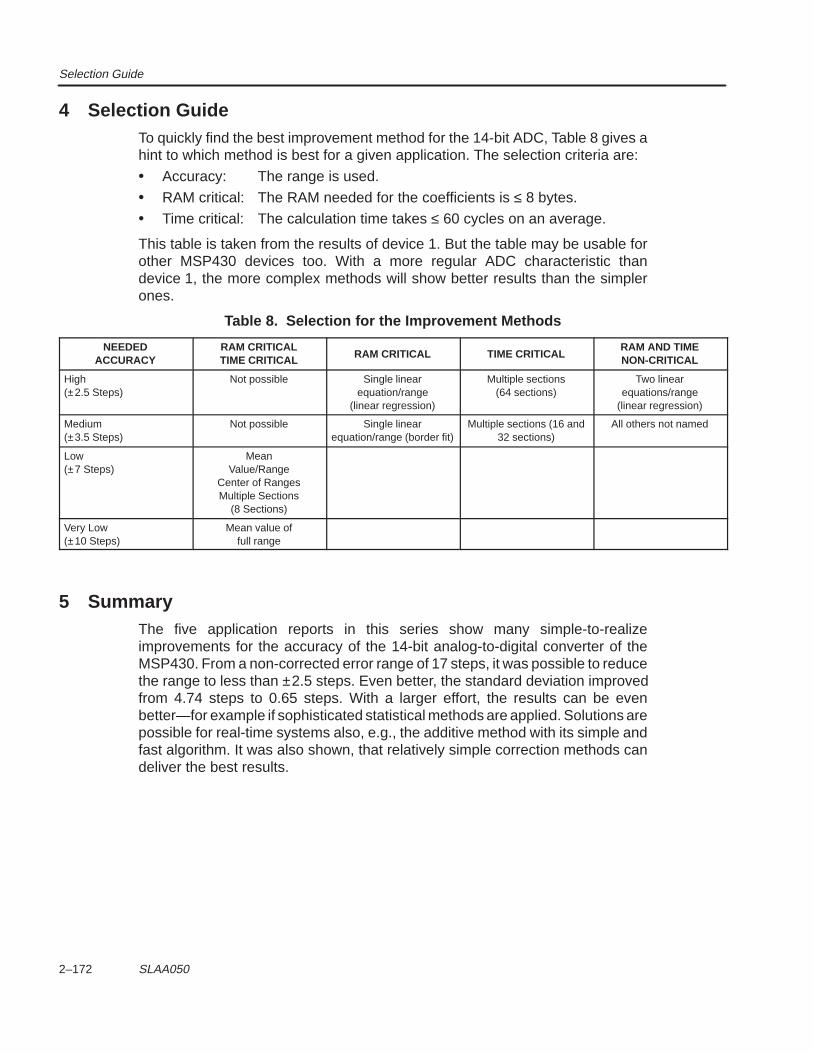
Selection Guide
2–172 SLAA050
4 Selection GuideTo quickly find the best improvement method for the 14-bit ADC, Table 8 gives ahint to which method is best for a given application. The selection criteria are:
• Accuracy: The range is used.
• RAM critical: The RAM needed for the coefficients is ≤ 8 bytes.
• Time critical: The calculation time takes ≤ 60 cycles on an average.
This table is taken from the results of device 1. But the table may be usable forother MSP430 devices too. With a more regular ADC characteristic thandevice 1, the more complex methods will show better results than the simplerones.
Table 8. Selection for the Improvement Methods
NEEDEDACCURACY
RAM CRITICALTIME CRITICAL RAM CRITICAL TIME CRITICAL
RAM AND TIMENON-CRITICAL
High(±2.5 Steps)
Not possible Single linearequation/range
(linear regression)
Multiple sections(64 sections)
Two linearequations/range
(linear regression)
Medium(±3.5 Steps)
Not possible Single linearequation/range (border fit)
Multiple sections (16 and32 sections)
All others not named
Low(±7 Steps)
MeanValue/Range
Center of RangesMultiple Sections
(8 Sections)
Very Low(±10 Steps)
Mean value offull range
5 SummaryThe five application reports in this series show many simple-to-realizeimprovements for the accuracy of the 14-bit analog-to-digital converter of theMSP430. From a non-corrected error range of 17 steps, it was possible to reducethe range to less than ±2.5 steps. Even better, the standard deviation improvedfrom 4.74 steps to 0.65 steps. With a larger effort, the results can be evenbetter—for example if sophisticated statistical methods are applied. Solutions arepossible for real-time systems also, e.g., the additive method with its simple andfast algorithm. It was also shown, that relatively simple correction methods candeliver the best results.

References
2–173 Nonlinear Improvement of the MSP430 14-Bit ADC Characteristic
6 References1. Architecture and Function of the MSP430 14-Bit ADC Application Report,
1999, Literature #SLAA045
2. Application Basics for the MSP430 14-Bit ADC Application Report, 1999,Literature #SLAA046
3. Additive Improvement of the MSP430 14-Bit ADC Characteristic ApplicationReport, 1999, Literature #SLAA047
4. Linear Improvement of the MSP430 14-Bit ADC Characteristic ApplicationReport, 1999, Literature #SLAA048
5. MSP430 Metering Application Report, 1997, Literature #SLAAE10B
6. Data Sheet MSP430C325, MSP430P323, 1998, Literature #SLASE06A
7. MSP430 Family Architecture Guide and Module Library, 1996, Literature#SLAUE10B
8. MSP430 Application Report, 1998, Literature #SLAAE10C

2–174 SLAA050
2–175
Using the MSP430 Universal Timer/PortModule as an Analog-to-Digital
Converter
Lutz Bierl
Literature Number: SLAA046June 1999
Printed on Recycled Paper

2–176
IMPORTANT NOTICE
Texas Instruments and its subsidiaries (TI) reserve the right to make changes to theirproducts or to discontinue any product or service without notice, and advise customers toobtain the latest version of relevant information to verify, before placing orders, thatinformation being relied on is current and complete. All products are sold subject to the termsand conditions of sale supplied at the time of order acknowledgement, including thosepertaining to warranty, patent infringement, and limitation of liability.
TI warrants performance of its semiconductor products to the specifications applicable at thetime of sale in accordance with TI’s standard warranty. Testing and other quality controltechniques are utilized to the extent TI deems necessary to support this warranty. Specifictesting of all parameters of each device is not necessarily performed, except those mandatedby government requirements.
CERTAIN APPLICATIONS USING SEMICONDUCTOR PRODUCTS MAY INVOLVEPOTENTIAL RISKS OF DEATH, PERSONAL INJURY, OR SEVERE PROPERTY ORENVIRONMENTAL DAMAGE (“CRITICAL APPLICATIONS”). TI SEMICONDUCTORPRODUCTS ARE NOT DESIGNED, AUTHORIZED, OR WARRANTED TO BE SUITABLEFOR USE IN LIFE-SUPPORT DEVICES OR SYSTEMS OR OTHER CRITICALAPPLICATIONS. INCLUSION OF TI PRODUCTS IN SUCH APPLICATIONS ISUNDERSTOOD TO BE FULLY AT THE CUSTOMER’S RISK.
In order to minimize risks associated with the customer’s applications, adequate design andoperating safeguards must be provided by the customer to minimize inherent or proceduralhazards.
TI assumes no liability for applications assistance or customer product design. TI does notwarrant or represent that any license, either express or implied, is granted under any patentright, copyright, mask work right, or other intellectual property right of TI covering or relatingto any combination, machine, or process in which such semiconductor products or servicesmight be or are used. TI’s publication of information regarding any third party’s products orservices does not constitute TI’s approval, warranty or endorsement thereof.
Copyright 1999, Texas Instruments Incorporated
2–177 Using the MSP430 Universal Timer/Port Module As An Analog-to-Digital Converter
Contents1 The Universal Timer/Port Module 2–179. . . . . . . . . . . . . . . . . . . . . . . . . . . . . . . . . . . . . . . . . . . . . . . . . . . . . . . . . . . .
1.1 Interrupt Handling 2–185. . . . . . . . . . . . . . . . . . . . . . . . . . . . . . . . . . . . . . . . . . . . . . . . . . . . . . . . . . . . . . . . . . . . 1.2 Connection of Long Sensor Lines 2–192. . . . . . . . . . . . . . . . . . . . . . . . . . . . . . . . . . . . . . . . . . . . . . . . . . . . . . . 1.3 Grounding 2–192. . . . . . . . . . . . . . . . . . . . . . . . . . . . . . . . . . . . . . . . . . . . . . . . . . . . . . . . . . . . . . . . . . . . . . . . . . . 1.4 Voltage Measurement With the Universal Timer Port/Module 2–193. . . . . . . . . . . . . . . . . . . . . . . . . . . . . . .
1.4.1 Measurement Principle 2–193. . . . . . . . . . . . . . . . . . . . . . . . . . . . . . . . . . . . . . . . . . . . . . . . . . . . . . . . 1.4.2 Resolution of the Measurement 2–197. . . . . . . . . . . . . . . . . . . . . . . . . . . . . . . . . . . . . . . . . . . . . . . . . 1.4.3 Measurement Timing 2–198. . . . . . . . . . . . . . . . . . . . . . . . . . . . . . . . . . . . . . . . . . . . . . . . . . . . . . . . . . 1.4.4 Applications 2–198. . . . . . . . . . . . . . . . . . . . . . . . . . . . . . . . . . . . . . . . . . . . . . . . . . . . . . . . . . . . . . . . . . 1.5 Temperature Calculation Example 2–203. . . . . . . . . . . . . . . . . . . . . . . . . . . . . . . . . . . . . . . . . . . . . . . .
1.6 Measurement of the Position of a Potentiometer 2–206. . . . . . . . . . . . . . . . . . . . . . . . . . . . . . . . . . . . . . . . . . 1.7 Measurement of Sensors With Low Resistance 2–207. . . . . . . . . . . . . . . . . . . . . . . . . . . . . . . . . . . . . . . . . . . 1.8 Measurement of Capacitance 2–208. . . . . . . . . . . . . . . . . . . . . . . . . . . . . . . . . . . . . . . . . . . . . . . . . . . . . . . . . .
2 External Analog-To-Digital Converters 2–209. . . . . . . . . . . . . . . . . . . . . . . . . . . . . . . . . . . . . . . . . . . . . . . . . . . . . . . 2.1 External Analog-To-Digital Converter ICs 2–209. . . . . . . . . . . . . . . . . . . . . . . . . . . . . . . . . . . . . . . . . . . . . . . . 2.2 R/2R Analog-To-Digital Converter 2–210. . . . . . . . . . . . . . . . . . . . . . . . . . . . . . . . . . . . . . . . . . . . . . . . . . . . . . .
Figures
2–178
List of Figures1 Block Diagram of the Universal Timer/Port Module 2–180. . . . . . . . . . . . . . . . . . . . . . . . . . . . . . . . . . . . . . . . . . . . . . 2 Minimum Sensor Circuit 2–180. . . . . . . . . . . . . . . . . . . . . . . . . . . . . . . . . . . . . . . . . . . . . . . . . . . . . . . . . . . . . . . . . . . . . . 3 Timing for the Universal Timer/Port Module ADC 2–181. . . . . . . . . . . . . . . . . . . . . . . . . . . . . . . . . . . . . . . . . . . . . . . . 4 Schematic of Example 2–183. . . . . . . . . . . . . . . . . . . . . . . . . . . . . . . . . . . . . . . . . . . . . . . . . . . . . . . . . . . . . . . . . . . . . . . 5 Noise Influence During Measurement 2–186. . . . . . . . . . . . . . . . . . . . . . . . . . . . . . . . . . . . . . . . . . . . . . . . . . . . . . . . . . 6 Hardware Schematic for Interrupt Example 2–186. . . . . . . . . . . . . . . . . . . . . . . . . . . . . . . . . . . . . . . . . . . . . . . . . . . . . 7 Measurement Sequence 2–187. . . . . . . . . . . . . . . . . . . . . . . . . . . . . . . . . . . . . . . . . . . . . . . . . . . . . . . . . . . . . . . . . . . . . 8 Connection of Long Sensor Lines 2–192. . . . . . . . . . . . . . . . . . . . . . . . . . . . . . . . . . . . . . . . . . . . . . . . . . . . . . . . . . . . . 9 Grounding for the Universal Timer/Port ADC 2–193. . . . . . . . . . . . . . . . . . . . . . . . . . . . . . . . . . . . . . . . . . . . . . . . . . . . 10 Voltage Measurement With the Universal Timer/Port Module 2–194. . . . . . . . . . . . . . . . . . . . . . . . . . . . . . . . . . . . . 11 Voltage Measurement 2–195. . . . . . . . . . . . . . . . . . . . . . . . . . . . . . . . . . . . . . . . . . . . . . . . . . . . . . . . . . . . . . . . . . . . . . 12 Voltage Measurement of a Voltage Source 2–199. . . . . . . . . . . . . . . . . . . . . . . . . . . . . . . . . . . . . . . . . . . . . . . . . . . . 13 Circuit for the Current Measurement 2–201. . . . . . . . . . . . . . . . . . . . . . . . . . . . . . . . . . . . . . . . . . . . . . . . . . . . . . . . . . 14 Current Measurement 2–202. . . . . . . . . . . . . . . . . . . . . . . . . . . . . . . . . . . . . . . . . . . . . . . . . . . . . . . . . . . . . . . . . . . . . . 15 Temperature Measurement 2–203. . . . . . . . . . . . . . . . . . . . . . . . . . . . . . . . . . . . . . . . . . . . . . . . . . . . . . . . . . . . . . . . . . 16 Measurement of a Potentiometer’s Position 2–206. . . . . . . . . . . . . . . . . . . . . . . . . . . . . . . . . . . . . . . . . . . . . . . . . . . 17 Hardware Schematic for Low-Resistive Sensors 2–207. . . . . . . . . . . . . . . . . . . . . . . . . . . . . . . . . . . . . . . . . . . . . . . 18 Solution With a Low-Resistive Multiplexer 2–208. . . . . . . . . . . . . . . . . . . . . . . . . . . . . . . . . . . . . . . . . . . . . . . . . . . . . 19 Measurement of a Capacitor Cx 2–208. . . . . . . . . . . . . . . . . . . . . . . . . . . . . . . . . . . . . . . . . . . . . . . . . . . . . . . . . . . . . 20 Timing for the Capacity Measurement 2–209. . . . . . . . . . . . . . . . . . . . . . . . . . . . . . . . . . . . . . . . . . . . . . . . . . . . . . . . 21 Analog-to-Digital Conversion With External ADCs 2–210. . . . . . . . . . . . . . . . . . . . . . . . . . . . . . . . . . . . . . . . . . . . . . 22 R/2R Method for Analog-to-Digital Conversion 2–211. . . . . . . . . . . . . . . . . . . . . . . . . . . . . . . . . . . . . . . . . . . . . . . . .
List of Tables1 ADC Conversion With the Timer/Port Module 2–182. . . . . . . . . . . . . . . . . . . . . . . . . . . . . . . . . . . . . . . . . . . . . . . . . . .
2–179
Using the MSP430 Universal Timer/Port Module as anAnalog-to-Digital Converter
Lutz Bierl
ABSTRACTThis application report gives a detailed overview of several applications for theMSP430family Universal Timer/Port Module when used as an analog-to-digital converter (ADC).Proven software examples and basic circuitry are shown and explained.
1 The Universal Timer/Port ModuleThe function of the Universal Timer/Port Module is completely different from the14-bit ADC. The discharge times of a capacitor for different resistors aremeasured and compared.
The module consists of two independent parts, which work together for themeasurement of resistors or voltages.
• Counter with Controller: two 8-bit counters, which can be connected in seriesto get a 16-bit counter. Additionally, there is a controller, a comparator input(CMPI), and a normal input (CIN).
• Input/Output Port: five outputs (TP.0...TP.4), which can be switched to Hi-Zand an I/O-port (TP.5).
Two different inputs are available with the module:
• The CIN input having a Schmitt-Trigger characteristic. It is normally used forresistor measurements. The threshold voltages are the same ones as for theother inputs (P0.x).
• The comparator input CMPI, which is used for the voltage measurement, hasa threshold voltage Vref that is nominally 0.25 × VCC with small tolerances.The threshold voltage Vref itself is temperature independent. The input CMPIshares a pin with an LCD select line and must be switched by software to theinput function. This input function is valid until the next PUC. The software forthe activation of the comparator is:
BIS.B #CPON,&TPD ; Switch on the comparator
The comparator hardware consumes approximately 300 µA, it should beswitched off therefore when not in use.
BIC.B #CPON,&TPD ; Switch off the comparator
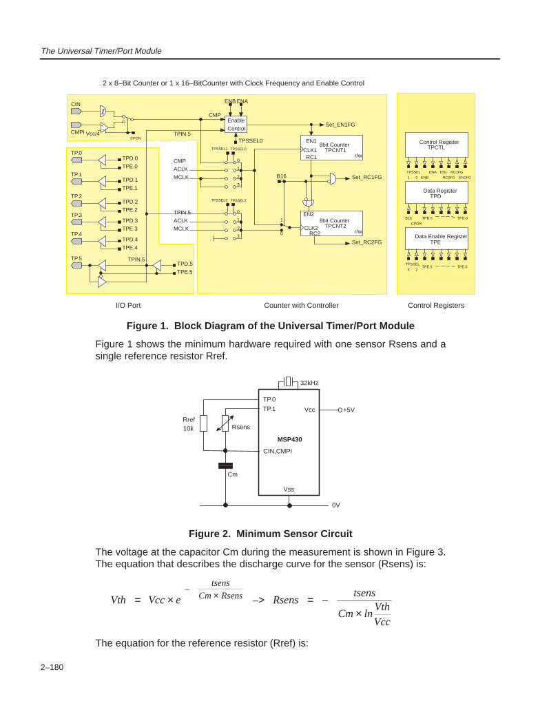
The Universal Timer/Port Module
2–180
TPIN.5
Enable
ControlSet_EN1FG
EN1
RC1
TPSSEL0
Set_RC1FGB16
TPIN.5
MCLK
ACLKEN2
CLK2
CLK18bit Counter
TPCNT1
RC2
8bit CounterTPCNT2
r/w
CIN ENB ENA
TPD.0
TPE.0
TPD.1
TPE.1
TPD.2
TPE.2
TPD.3
TPE.3
TPD.4
TPE.4
TPD.5
TPE.5
Data RegisterTPD
Data Enable RegisterTPE
Control RegisterTPCTL
r/w
Set_RC2FG
TPSSEL3 TPSSEL2
TPD.0TPD.5
TPE.0TPE.5
EN1
ENB
TPSSEL
B16
ENA
0
3 2
1 EN1FGRC2FG
RC1FG
TP.0
TP.1
TP.5
TP.3
TP.4
TP.2
TPIN.5
TPSSEL
0
1
2
3
CMP
MCLK
ACLK
TPSSEL1 TPSSEL0
0
1
2
3
CMP
CPON
Vcc/4CPON
0
1
+–
I/O Port
2 x 8–Bit Counter or 1 x 16–BitCounter with Clock Frequency and Enable Control
Control Registers
Counter with Controller
CMPI
Figure 1. Block Diagram of the Universal Timer/Port Module
Figure 1 shows the minimum hardware required with one sensor Rsens and asingle reference resistor Rref.
Vss
Vcc
32kHz
TP.1
CIN,CMPI
MSP430
Rref
0V
Cm
Rsens
TP.0
+5V
10k
Figure 2. Minimum Sensor Circuit
The voltage at the capacitor Cm during the measurement is shown in Figure 3.The equation that describes the discharge curve for the sensor (Rsens) is:
Vth Vcc e
tsens
Cm Rsens= × –> =×
–× Rsens –
tsens
Cm lnVth
Vcc
The equation for the reference resistor (Rref) is:
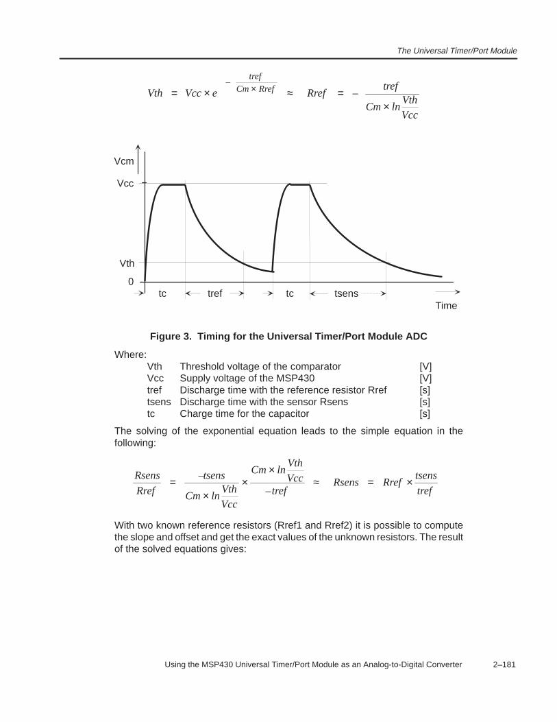
The Universal Timer/Port Module
2–181 Using the MSP430 Universal Timer/Port Module as an Analog-to-Digital Converter
Vth Vcc e
tref
Cm Rref= × ≈ =×
–× Rref –
tref
Cm lnVth
Vcc
0
Vcc
Time
Vth
tref tsenstc
Vcm
tc
Figure 3. Timing for the Universal Timer/Port Module ADC
Where:Vth Threshold voltage of the comparator [V]Vcc Supply voltage of the MSP430 [V]tref Discharge time with the reference resistor Rref [s]tsens Discharge time with the sensor Rsens [s]tc Charge time for the capacitor [s]
The solving of the exponential equation leads to the simple equation in thefollowing:
Rsens
Rref
–tsens
Cm lnVth
Vcc
Cm lnVth
Vcc Rsens Rreftsens
tref=
××
×
–≈ = ×
tref
With two known reference resistors (Rref1 and Rref2) it is possible to computethe slope and offset and get the exact values of the unknown resistors. The resultof the solved equations gives:
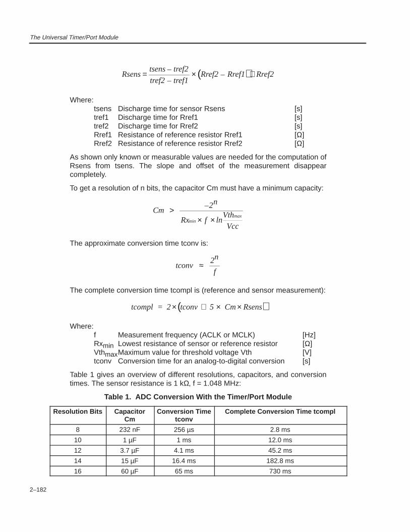
The Universal Timer/Port Module
2–182
( )Rsenstsens tref2
tref2 tref1Rref2 Rref1 Rref2= –
–× – +
Where:tsens Discharge time for sensor Rsens [s]tref1 Discharge time for Rref1 [s]tref2 Discharge time for Rref2 [s]Rref1 Resistance of reference resistor Rref1 [Ω]Rref2 Resistance of reference resistor Rref2 [Ω]
As shown only known or measurable values are needed for the computation ofRsens from tsens. The slope and offset of the measurement disappearcompletely.
To get a resolution of n bits, the capacitor Cm must have a minimum capacity:
Cm2n
Rx f lnVth
Vccmin
max> –
× ×
The approximate conversion time tconv is:
tconv2n
f≈
The complete conversion time tcompl is (reference and sensor measurement):
( )tcompl = 2 tconv 5 Cm Rsens× + × ×
Where:f Measurement frequency (ACLK or MCLK) [Hz]Rxmin Lowest resistance of sensor or reference resistor [Ω]VthmaxMaximum value for threshold voltage Vth [V]tconv Conversion time for an analog-to-digital conversion [s]
Table 1 gives an overview of different resolutions, capacitors, and conversiontimes. The sensor resistance is 1 kΩ, f = 1.048 MHz:
Table 1. ADC Conversion With the Timer/Port Module
Resolution Bits CapacitorCm
Conversion Timetconv
Complete Conversion Time tcompl
8 232 nF 256 µs 2.8 ms
10 1 µF 1 ms 12.0 ms
12 3.7 µF 4.1 ms 45.2 ms
14 15 µF 16.4 ms 182.8 ms
16 60 µF 65 ms 730 ms
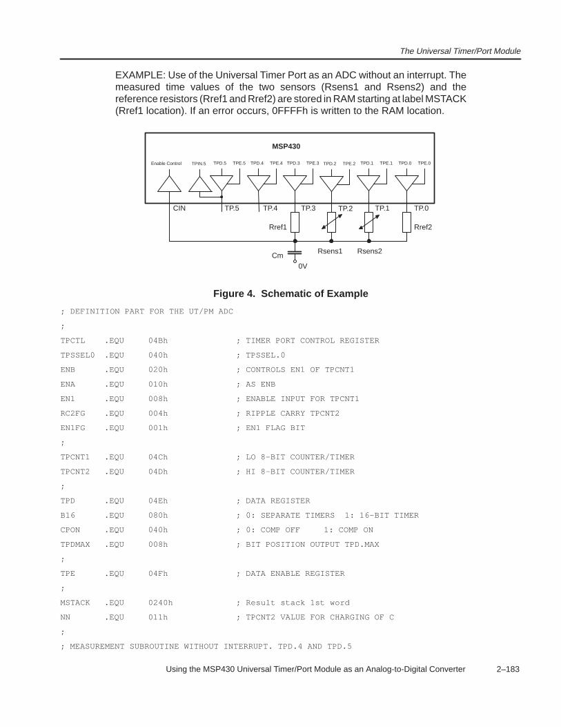
The Universal Timer/Port Module
2–183 Using the MSP430 Universal Timer/Port Module as an Analog-to-Digital Converter
EXAMPLE: Use of the Universal Timer Port as an ADC without an interrupt. Themeasured time values of the two sensors (Rsens1 and Rsens2) and thereference resistors (Rref1 and Rref2) are stored in RAM starting at label MSTACK(Rref1 location). If an error occurs, 0FFFFh is written to the RAM location.
TPD.0
MSP430
TP.0
TPE.0TPD.1
TP.1
TPE.1TPD.2
TP.2
TPE.2TPD.3
TP.3
TPE.3TPD.4
TP.4
TPE.4TPD.5
TP.5
TPE.5TPIN.5Enable Control
CIN
0V
Rref1
Rsens1 Rsens2
Rref2
Cm
Figure 4. Schematic of Example
; DEFINITION PART FOR THE UT/PM ADC
;
TPCTL .EQU 04Bh ; TIMER PORT CONTROL REGISTER
TPSSEL0 .EQU 040h ; TPSSEL.0
ENB .EQU 020h ; CONTROLS EN1 OF TPCNT1
ENA .EQU 010h ; AS ENB
EN1 .EQU 008h ; ENABLE INPUT FOR TPCNT1
RC2FG .EQU 004h ; RIPPLE CARRY TPCNT2
EN1FG .EQU 001h ; EN1 FLAG BIT
;
TPCNT1 .EQU 04Ch ; LO 8–BIT COUNTER/TIMER
TPCNT2 .EQU 04Dh ; HI 8–BIT COUNTER/TIMER
;
TPD .EQU 04Eh ; DATA REGISTER
B16 .EQU 080h ; 0: SEPARATE TIMERS 1: 16–BIT TIMER
CPON .EQU 040h ; 0: COMP OFF 1: COMP ON
TPDMAX .EQU 008h ; BIT POSITION OUTPUT TPD.MAX
;
TPE .EQU 04Fh ; DATA ENABLE REGISTER
;
MSTACK .EQU 0240h ; Result stack 1st word
NN .EQU 011h ; TPCNT2 VALUE FOR CHARGING OF C
;
; MEASUREMENT SUBROUTINE WITHOUT INTERRUPT. TPD.4 AND TPD.5
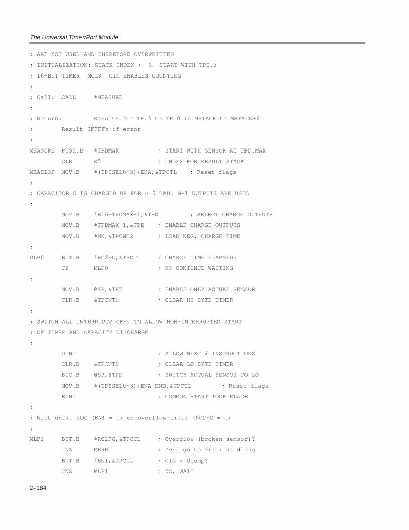
The Universal Timer/Port Module
2–184
; ARE NOT USED AND THEREFORE OVERWRITTEN
; INITIALIZATION: STACK INDEX <– 0, START WITH TPD.3
; 16–BIT TIMER, MCLK, CIN ENABLES COUNTING
;
; Call: CALL #MEASURE
;
; Return: Results for TP.3 to TP.0 in MSTACK to MSTACK+6
; Result 0FFFFh if error
;
MEASURE PUSH.B #TPDMAX ; START WITH SENSOR AT TPD.MAX
CLR R5 ; INDEX FOR RESULT STACK
MEASLOP MOV.B #(TPSSEL0*3)+ENA,&TPCTL ; Reset flags
;
; CAPACITOR C IS CHARGED UP FOR > 5 TAU. N–1 OUTPUTS ARE USED
;
MOV.B #B16+TPDMAX–1,&TPD ; SELECT CHARGE OUTPUTS
MOV.B #TPDMAX–1,&TPE ; ENABLE CHARGE OUTPUTS
MOV.B #NN,&TPCNT2 ; LOAD NEG. CHARGE TIME
;
MLP0 BIT.B #RC2FG,&TPCTL ; CHARGE TIME ELAPSED?
JZ MLP0 ; NO CONTINUE WAITING
;
MOV.B @SP,&TPE ; ENABLE ONLY ACTUAL SENSOR
CLR.B &TPCNT2 ; CLEAR HI BYTE TIMER
;
; SWITCH ALL INTERRUPTS OFF, TO ALLOW NON–INTERRUPTED START
; OF TIMER AND CAPACITY DISCHARGE
;
DINT ; ALLOW NEXT 2 INSTRUCTIONS
CLR.B &TPCNT1 ; CLEAR LO BYTE TIMER
BIC.B @SP,&TPD ; SWITCH ACTUAL SENSOR TO LO
MOV.B #(TPSSEL0*3)+ENA+ENB,&TPCTL ; Reset flags
EINT ; COMMON START TOOK PLACE
;
; Wait until EOC (EN1 = 1) or overflow error (RC2FG = 1)
;
MLP1 BIT.B #RC2FG,&TPCTL ; Overflow (broken sensor)?
JNZ MERR ; Yes, go to error handling
BIT.B #EN1,&TPCTL ; CIN < Ucomp?
JNZ MLP1 ; NO, WAIT
The Universal Timer/Port Module
2–185 Using the MSP430 Universal Timer/Port Module as an Analog-to-Digital Converter
;
; EN1 = 0: End of Conversion: Store 2 x 8 bit result on MSTACK
; Address next sensor, if no one addressed: End reached
;
MOV.B &TPCNT1,MSTACK(R5) ; STORE RESULT ON STACK
MOV.B &TPCNT2,MSTACK+1(R5) ; HI BYTE
L$301 INCD R5 ; ADDRESS NEXT WORD
RRA.B @SP ; NEXT OUTPUT TPD.x
JNC MEASLOP ; IF C=1: FINISHED
INCD SP ; HOUSEKEEPING: TPDMAX
RET
;
; ERROR HANDLING: ONLY OVERFLOW POSSIBLE (BROKEN SENSOR ?)
; 0FFFFh IS WRITTEN FOR RESULT AND SUBROUTINE CONTINUED
;
MERR MOV #0FFFFh,MSTACK(R5) ; Overflow
JMP L$301
1.1 Interrupt Handling
If the Universal Timer/Port Module is used as an ADC for applications that needan accuracy greater than 10 bits, the digital noise generated by the running CPUhas a strong influence on the result. If the flag (EN1) in the hardware registerTPCTL is polled by software for the signal of a completed conversion then theresults are normally different. They show a wide distribution that reflects thelength of the polling loop (i.e. the results are concentrated on evenly spacednumbers with nothing in between). To avoid this effect the CPU is switched offduring the conversion and woken-up at the completion of the conversion by theADC interrupt. With this method and adequate hardware, results with much betteraccuracy are possible.
The influence of the digital noise is shown in Figure 5. The exponential dischargecurve is relatively flat near the comparator threshold Vth. Therefore noise comingfrom the CPU (or other sources of non-wanted noise) can be under the thresholdvoltage and terminate the conversion. The result is a timer value tdcw that is toolow. The correct value would be tdcc. The resulting error Ecnv is:
Ecnvtdcw tdcc
tdcc100= – ×
Where:tdcw Resulting measurement time caused by CPU noise [s]tdcc Correct measurement time [s]
The Universal Timer/Port Module
2–186
0
Vcc
Time
Vth
tdcw
Vcm
tctdcc
Figure 5. Noise Influence During MeasurementEXAMPLE: The hardware schematic is shown in Figure 6. Two resistivetemperature sensors are used (Rmeas0 and Rmeas1) two reference resistors(Rref0 and Rref1) that have the resistance of the sensors at the lower (or upper)end of the measurement range and a resistor (Rcharge) that is used only for thecharge-up of the capacitor (Cm). This charge resistor is only necessary if thesensors have low resistance (approximately 100 Ω.). Otherwise, the referenceresistors can be used for charging.
Rref0
Rref1
Rcharge
Rmeas0
Rmeas1
Cm
TP.0
TP.1
TP.2
TP.3
TP.4
CIN, CMPI
MSP430x3xx
0V +3V
AGND
Vss Vcc
Figure 6. Hardware Schematic for Interrupt ExampleThe example software works with a status byte (MEASSTAT) that defines thecurrent operation. Normally, this byte is zero, which indicates no activity or aftera complete measurement sequence conversions made. The two referenceresistors and two temperature sensors are measured one after the other; Rref0first, then Rmeas0, then Rmeas1 and finally Rref1.
The Universal Timer/Port Module
2–187 Using the MSP430 Universal Timer/Port Module as an Analog-to-Digital Converter
The measured discharge times (a direct measure for the relative resistance) areplaced in successive RAM words starting at label ADCRESULT.
First these RAM words are set to zero (a value impossible as a measurementresult). If an error occurs, the zero value indicates an erroneous result.
The Basic Timer is programmed to 0.5 s interrupt timing. The measurementsequence is shown in Figure 7. This sequence can be shortened to one referenceresistor and one sensor as well as enlarged up to four sensors and two referenceresistors. It is only necessary to add or delete charging and measurement statesand the accompanying software parts.
The modulation mode of the FLL is switched off during the measurement to havethe exactly same MCLK during all four measurements. Status 9 switches on themodulation mode again.
The software shown can be used for the MSP430C31x and MSP430C32x. Thedifferent interrupt enable bits and the different addresses of the interrupt vectorsare used correctly by the definition of the software switch Type. If this switch isdefined as 310, the MSP430C31x is used; otherwise, the MSP430C32x is used.
No activity
Status 0 1 2 3 4 5 6 7 8 9/0
Charge Cm Rref0 Charge Cm Charge Cm Charge Cm Conversions madeRmeas0 Rmeas1 Rref1
Measure Measure MeasureMeasure
CPUoff = 1
MOD = 1
0.5s
Figure 7. Measurement Sequence
; Definitions of the MSP430 hardware
;
Type .equ 310 ; 310: MSP43C31x 0: others
BTCTL .equ 040h ; Basic Timer: Control Reg.
BTCNT1 .equ 046h ; Counter
BTCNT2 .equ 047h ; Counter
BTIE .equ 080h ; : Intrpt Enable
DIV .equ 020h ; BTCTL: xCLK/256
IP2 .equ 004h ; BTCTL: Clock Divider2
IP0 .equ 001h ; Clock Divider0
;
SCFQCTL .equ 052h ; FLL Control Register
MOD .equ 080h ; Modulation Bit: 1 = off
;
CPUoff .equ 010h ; SR: CPU off bit
GIE .equ 008h ; SR: General Intrpt enable
The Universal Timer/Port Module
2–188
;
TPCTL .equ 04Bh ; Timer Port: Control Reg.
TPCNT1 .equ 04Ch ; Counter Reg.Lo
TPCNT2 .equ 04Dh ; Counter Reg.Hi
TPD .equ 04Eh ; Data Reg.
TPE .equ 04Fh ; Enable Reg.
;
.if Type=310 ; MSP430C31x?
TPIE .equ 004h ; ADC: Intrpt Enable Bit
.else
TPIE .equ 008h ; MSP430C32x configuration
.endif
IE2 .equ 001h ; Intrpt Enable Byte
TPSSEL1 .equ 080h ; Selects clock input (TPCTL)
TPSSEL0 .equ 040h ;
ENB .equ 020h ; Selects clock gate (TPCTL)
ENA .equ 010h ;
EN1 .equ 008h ; Gate for TPCNTx (TPCTL)
RC2FG .equ 004h ; Carry of HI counter (TPCTL)
RC1FG .equ 002h ; Carry of LO counter (TPCTL)
EN1FG .equ 001h ; End of Conversion Flag “
B16 .equ 080h ; Use 16–bit counter (TPD)
;
Rref0 .equ 001h ; TP.0: Reference Resistor
Rmeas0 .equ 002h ; TP.1: Sensor0
Rmeas1 .equ 004h ; TP.2: Sensor1
Rref1 .equ 008h ; TP.3: Reference Resistor
Rcharge .equ 010h ; TP.4: Charge Resistor
;
; RAM Definitions
;
ADCRESULT .equ 0200h ; ADC results (4 words)
MEASSTAT .equ ADCRESULT+8 ; Measurement Status Byte
;
;=========================================================
;
.sect “INIT”,0F000h ; Initialization Section
;
INIT MOV #0300h,SP ; Initialize Stack Pointer
MOV.B #DIV+IP2+IP0,&BTCTL ; Basic Timer: 2Hz
The Universal Timer/Port Module
2–189 Using the MSP430 Universal Timer/Port Module as an Analog-to-Digital Converter
BIS.B #BTIE,&IE2 ; Basic Timer Intrpt Enable
CLR.B &BTCNT1 ; Clear Basic Timer Regs.
CLR.B &BTCNT2
CALL #CLRRAM ; Clear RAM
... ; Initialize other Modules
;
MAINLOOP ... ; Main loop of program
;
; It’s time to measure the sensors
;
MOV.B #1,MEASSTAT ; Activate Measurement
JMP MEASURE ; Go to Measurement Part
...
; Measurement Part: The CPU is switched off to avoid noise
; that would falsify the measurements. Interrupt is used
; to indicate the end of conversion (and wake–up the CPU).
; The program remains on the NOP until MSTAT9 clears the
; CPUoff–bit of the stored SR on the stack.
;
MEASURE CLR ADCRESULT ; Clear result buffers
CLR ADCRESULT+2 ; 0 indicates error
CLR ADCRESULT+4 ;
CLR ADCRESULT+6 ;
MOV #CPUoff+GIE,SR ; CPU off, but MCLK on
NOP ; Wait for end of measurement
... ; Process measured data
;
; Interrupt Handler for the Basic Timer Interrupt: 2Hz
;
BT_INT PUSH R5 ; Save Help Register
CALL #INCRWTCH ; Incr. Watch
MOV.B MEASSTAT,R5 ; Calculate Handler
MOV.B TABLE(R5),R5 ; Offset for PC
ADD R5,PC ; Add Offset to PC
TABLE .BYTE MSTAT0–TABLE ; 0: No activity
.BYTE MSTAT1–TABLE ; 1: Charge for Rref0
.BYTE MSTAT2–TABLE ; 2: Measure Rref0
.BYTE MSTAT1–TABLE ; 3: Charge for Rmeas0
.BYTE MSTAT4–TABLE ; 4: Measure Rmeas0
.BYTE MSTAT1–TABLE ; 5: Charge for Rmeas1
The Universal Timer/Port Module
2–190
.BYTE MSTAT6–TABLE ; 6: Measure Rmeas1
.BYTE MSTAT1–TABLE ; 7: Charge for Rref1
.BYTE MSTAT8–TABLE ; 8: Measure Rref1
.BYTE MSTAT9–TABLE ; 9: Finished, go on
;
MSTAT1 MOV.B #B16+Rcharge,&TPD ; Charge Cm for 0.5s
MOV.B #Rcharge,&TPE ; Use Rcharge
JMP BT_RET
;
MSTAT2 MOV #Rref0,R5 ; Measure Rref0
JMP MEASCOM ; To common Part
;
MSTAT4 MOV #Rmeas0,R5 ; Measure Rmeas0
JMP MEASCOM ; To common Part
;
MSTAT6 MOV #Rmeas1,R5 ; Measure Rmeas1
JMP MEASCOM ; To common Part
;
MSTAT8 MOV #Rref1,R5 ; Measure Rref1
MEASCOM BIS.B #MOD,&SCFQCTL ; Switch off FLL Modulation
BIS #SCG0,SR ; Loop control off
CLR.B &TPE ; TP.x to HI–Z
MOV.B #B16,&TPD ; TP.x LO (disabled!)
;
; No MCLK for ADC, Clear Flags RC2FG, RC1FG, EN1FG
;
MOV.B #TPSSEL1+ENB+ENA,&TPCTL
CLR.B &TPCNT1 ; Reset Counter LO
CLR.B &TPCNT2 ; Reset Counter HI
BIS.B R5,&TPE ; Enable selected TP.x
;
; MCLK on, Comparator on: Intrpt for Ucm < Vth
;
MOV.B #TPSSEL1+TPSSEL0+ENB+ENA+EN1,&TPCTL
BIS.B #TPIE,&IE2 ; Enable ADC Intrpt
;
BT_RET INC.B MEASSTAT ; To next Status
MSTAT0 POP R5 ; If no activity necessary
RETI
;
The Universal Timer/Port Module
2–191 Using the MSP430 Universal Timer/Port Module as an Analog-to-Digital Converter
; MSTAT9: Measurements are completed, CPU is switched on,
; MSTAT is set to zero: no activity. FLL loop control on
;
MSTAT9 BIC #CPUoff+SCG0,2(SP) ; Stored SR on stack
CLR.B MEASSTAT ; No activity
BIC.B #MOD,&SCFQCTL ; Switch on FLL Modulation
JMP MSTAT0 ; Return
;
; End of Basic Timer Handler
;––––––––––––––––––––––––––––––––––––––––––––––––––––––––––
; Interrupt Handler for the Analog–to–Digital Converter
; The results in TPCNT1 and TPCNT2 are stored starting at
; label ADCRESULT (result for Rref0)
;
ADC_INT PUSH R5 ; Save Help Register
MOV.B MEASSTAT,R5 ; Build offset for results
SUB #3,R5 ; Status for Rref0
JN ADC_F ; MEASSTAT < 3: error
;
; Check for correct result:
; If RC2FG = 1: Overflow of the counter (Rx too high)
; If EN1 = 1: False interrupt, conversion not finished
;
BIT.B #RC2FG+EN1,&TPCTL ; Error?
JNZ ADC_RET ; Yes, let 0h for error
MOV.B &TPCNT1,ADCRESULT(R5) ; Store result
MOV.B &TPCNT2,ADCRESULT+1(R5)
;
ADC_RET BIC.B #TPIE,&IE2 ; Disable ADC Intrpt
BIC.B #RC2FG+RC1FG+EN1FG,&TPCTL ; Flags = 0
ADC_F POP R5 ; Restore R5
RETI
;
; End of Universal Timer/Port Module Handler
;––––––––––––––––––––––––––––––––––––––––––––––––––––––––––
; Interrupt vectors
;
.sect “INT_VECT”,0FFE2h
.WORD BT_INT ; Basic Timer Vector
.if Type=310
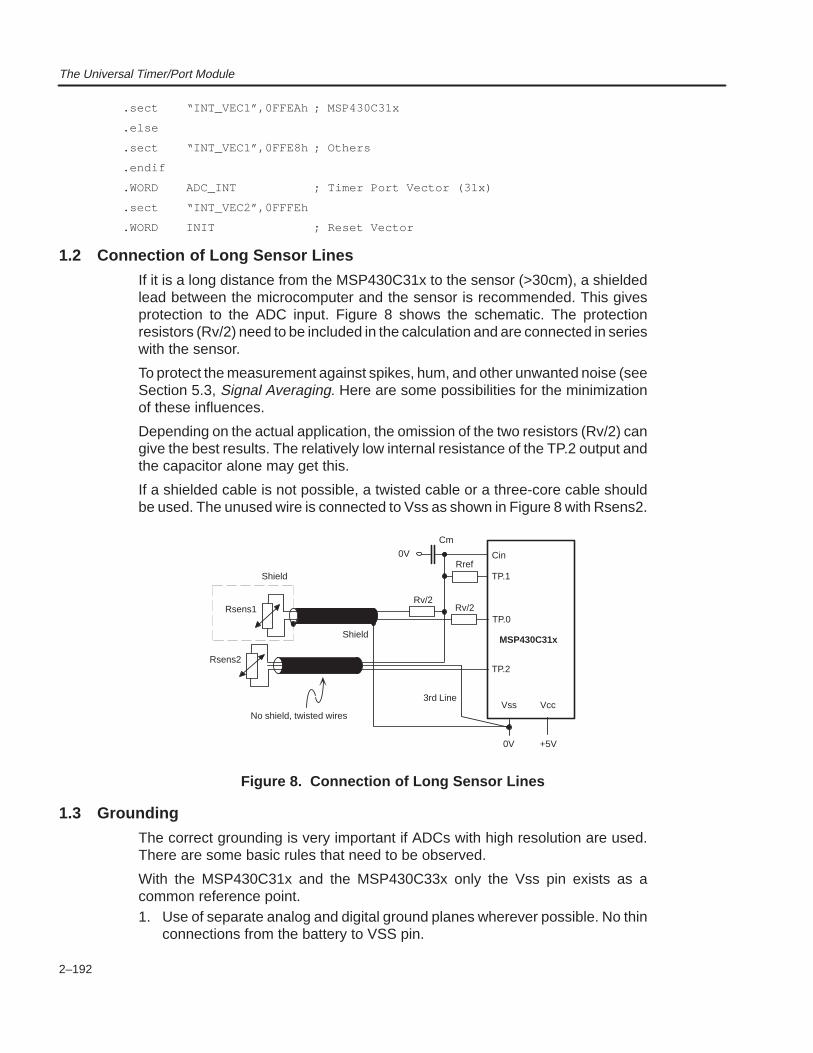
The Universal Timer/Port Module
2–192
.sect “INT_VEC1”,0FFEAh ; MSP430C31x
.else
.sect “INT_VEC1”,0FFE8h ; Others
.endif
.WORD ADC_INT ; Timer Port Vector (31x)
.sect “INT_VEC2”,0FFFEh
.WORD INIT ; Reset Vector
1.2 Connection of Long Sensor Lines
If it is a long distance from the MSP430C31x to the sensor (>30cm), a shieldedlead between the microcomputer and the sensor is recommended. This givesprotection to the ADC input. Figure 8 shows the schematic. The protectionresistors (Rv/2) need to be included in the calculation and are connected in serieswith the sensor.
To protect the measurement against spikes, hum, and other unwanted noise (seeSection 5.3, Signal Averaging. Here are some possibilities for the minimizationof these influences.
Depending on the actual application, the omission of the two resistors (Rv/2) cangive the best results. The relatively low internal resistance of the TP.2 output andthe capacitor alone may get this.
If a shielded cable is not possible, a twisted cable or a three-core cable shouldbe used. The unused wire is connected to Vss as shown in Figure 8 with Rsens2.
Vss Vcc
Cin
TP.0
MSP430C31x
0V +5V
Rv/2Rsens1
Rv/2
Rref
Cm
Shield
0V
TP.1
Rsens2
3rd Line
TP.2
No shield, twisted wires
Shield
Figure 8. Connection of Long Sensor Lines
1.3 Grounding
The correct grounding is very important if ADCs with high resolution are used.There are some basic rules that need to be observed.
With the MSP430C31x and the MSP430C33x only the Vss pin exists as acommon reference point.1. Use of separate analog and digital ground planes wherever possible. No thin
connections from the battery to VSS pin.
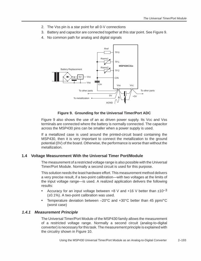
The Universal Timer/Port Module
2–193 Using the MSP430 Universal Timer/Port Module as an Analog-to-Digital Converter
2. The Vss pin is a star point for all 0-V connections
3. Battery and capacitor are connected together at this star point. See Figure 9.
4. No common path for analog and digital signals
Vss Vcc
MSP430C31x
0V
Rsens2
Rsens1
TP.0
Rref
+3V
To other parts
TP.2
TP.1
To other parts
Cm
CIN
AGND
5V Vcc
Vss
Battery Replacement
To metallization
Figure 9. Grounding for the Universal Timer/Port ADC
Figure 9 also shows the use of an ac driven power supply. Its Vcc and Vssterminals are connected where the battery is normally connected. The capacitoracross the MSP430 pins can be smaller when a power supply is used.
If a metallized case is used around the printed-circuit board containing theMSP430, then it is very important to connect the metallization to the groundpotential (0V) of the board. Otherwise, the performance is worse than without themetallization.
1.4 Voltage Measurement With the Universal Timer Port/Module
The measurement of a restricted voltage range is also possible with the UniversalTimer/Port Module. Normally a second circuit is used for this purpose.
This solution needs the least hardware effort. This measurement method deliversa very precise result, if a two-point calibration—with two voltages at the limits ofthe input voltage range—is used. A realized application delivers the followingresults:
• Accuracy for an input voltage between +8 V and +16 V better than ±10–3
(±0.1%). A two-point calibration was used.
• Temperature deviation between –20°C and +30°C better than 45 ppm/°C(worst case)
1.4.1 Measurement Principle
The Universal Timer/Port Module of the MSP430 family allows the measurementof a restricted voltage range. Normally a second circuit (analog-to-digitalconverter) is necessary for this task. The measurement principle is explained withthe circuitry shown in Figure 10.
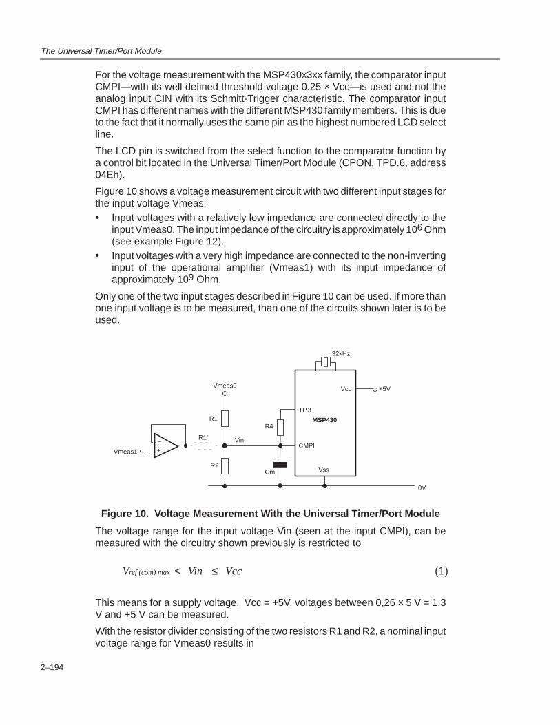
The Universal Timer/Port Module
2–194
For the voltage measurement with the MSP430x3xx family, the comparator inputCMPI—with its well defined threshold voltage 0.25 × Vcc—is used and not theanalog input CIN with its Schmitt-Trigger characteristic. The comparator inputCMPI has different names with the different MSP430 family members. This is dueto the fact that it normally uses the same pin as the highest numbered LCD selectline.
The LCD pin is switched from the select function to the comparator function bya control bit located in the Universal Timer/Port Module (CPON, TPD.6, address04Eh).
Figure 10 shows a voltage measurement circuit with two different input stages forthe input voltage Vmeas:• Input voltages with a relatively low impedance are connected directly to the
input Vmeas0. The input impedance of the circuitry is approximately 106 Ohm(see example Figure 12).
• Input voltages with a very high impedance are connected to the non-invertinginput of the operational amplifier (Vmeas1) with its input impedance ofapproximately 109 Ohm.
Only one of the two input stages described in Figure 10 can be used. If more thanone input voltage is to be measured, than one of the circuits shown later is to beused.
Vss
Vcc
32kHz
MSP430
TP.3
Cm
CMPI
R1
R2
Vmeas0
Vin
+5V
R4
0V
R1’–+Vmeas1
Figure 10. Voltage Measurement With the Universal Timer/Port Module
The voltage range for the input voltage Vin (seen at the input CMPI), can bemeasured with the circuitry shown previously is restricted to
Vref (com) max< ≤Vin Vcc (1)
This means for a supply voltage, Vcc = +5V, voltages between 0,26 × 5 V = 1.3V and +5 V can be measured.
With the resistor divider consisting of the two resistors R1 and R2, a nominal inputvoltage range for Vmeas0 results in
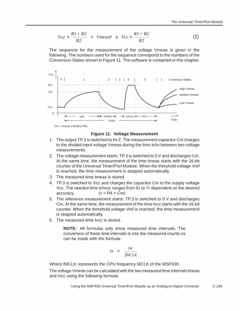
The Universal Timer/Port Module
2–195 Using the MSP430 Universal Timer/Port Module as an Analog-to-Digital Converter
VR1+ R2
R2Vmeas0 Vcc
R1+ R2
R2ref × < ≤ × (2)
The sequence for the measurement of the voltage Vmeas is given in thefollowing. The numbers used for the sequence correspond to the numbers of theConversion States shown in Figure 11. The software is contained in this chapter.
0
Vcc
Timetmeas tvcc
V
Vin = Vmeas x R2/(R1+R2)
2 3 4 5 11
tchvcc
Conversion States
High Vmeas
Medium Vmeas
Low Vmeas
Cm
Vref
Vin
5
tchvtconv
Figure 11. Voltage Measurement1. The output TP.3 is switched to Hi-Z. The measurement capacitor Cm charges
to the divided input voltage Vmeas during the time tchv between two voltagemeasurements.
2. The voltage measurement starts: TP.3 is switched to 0 V and discharges Cm.At the same time, the measurement of the time tmeas starts with the 16-bitcounter of the Universal Timer/Port Module. When the threshold voltage Vrefis reached, the time measurement is stopped automatically.
3. The measured time tmeas is stored.4. TP.3 is switched to Vcc and charges the capacitor Cm to the supply voltage
Vcc. The needed time tchvcc ranges from 5τ to 7τ dependent on the desiredaccuracy. (τ ≈ R4 × Cm)
5. The reference measurement starts: TP.3 is switched to 0 V and dischargesCm. At the same time, the measurement of the time tvcc starts with the 16-bitcounter. When the threshold voltage Vref is reached, the time measurementis stopped automatically.
6. The measured time tvcc is stored.
NOTE: All formulas only show measured time intervals. Theconversion of these time intervals tx into the measured counts nxcan be made with the formula:
txnx
fMCLK=
Where fMCLK represents the CPU frequency MCLK of the MSP430.
The voltage Vmeas can be calculated with the two measured time intervals tmeasand tvcc using the following formula:
The Universal Timer/Port Module
2–196
Vmeas VccR1 R2
R2e
tmeas tvcc
= × + ×
–
τ (3)
Where:Vmeas Input voltage to be measured [V]Vcc Supply voltage of the MSP430 (used for reference) [V]R1,R2 Input resistor divider at input CMPI [Ω]tmeas Discharge time of the divided Vmeas until Vref is reached [s]tvcc Discharge time from Vcc to Vref [s]τ Time constant of the discharge circuit (τ ≈ R4 × Cm) [s]Vref Threshold voltage of the comparator input CMPI [V]tconv Time between two complete voltage measurements [s]
To get a constant value for the value τ, an expensive, highly stable capacitor Cmis necessary. To avoid this capacitor, the value τ of the equation (3) is substituted.From the equation (4) for the discharge of the capacitor Cm
V Vcc eref
tvcc
= ×–
τ (4)
τ is calculated:
τ = =t
lnVcc
V
4vcc
ref
whereVcc
Vref (5)
Inserted into equation (3) this leads to:
Vmeas VccR1 R2
R2e
tmeas–tvcc
tvccln
Vcc
Vref= × + ×× (6)
With equation 6, Vmeas is calculated. Equation 6 is also used with the softwareexample shown in Section 1.4.4.1.
For the capacitor Cm used for the voltage measurement, it is only important, thatit owns a constant or a very high isolation resistance. The isolation resistor of thecapacitor Cm is connected in parallel with the resistor R2 and changes theresistor ratio (e.g. due to temperature).
Equation 6 shows the dependence of the voltage measurement to the supplyvoltage Vcc (which is the reference), the threshold voltage Vref, the accuracy ofthe resistors R1 and R2 and the temperature drift of these values. To get ameasurement accuracy of ±1% for Vmeas without calibration, the followingbasics are necessary:
• Stable supply voltage Vcc: Vcc needs to be within ±25 mV for the definedtemperature range. The actual value of Vcc does not matter, if a two-pointcalibration is used.

The Universal Timer/Port Module
2–197 Using the MSP430 Universal Timer/Port Module as an Analog-to-Digital Converter
• Input CMPI is used for the comparator input: the relatively good definedthreshold voltage Vref (0.25 × Vcc) allows better results than the normalSchmitt-Trigger input CIN with its large tolerances for the threshold voltages.
• Temperature drift of the resistor divider maximum ±50 ppm/C• Sufficient charge-up times for the measurement capacitor Cm:
– For an accuracy of one per cent approximately 5τ are necessary (e5 =148,41)
– For an accuracy of 0.1% approximately 7τ are necessary (e7 = 1096.63)
If a two-point calibration is used, the calculated values for slope and offset arestored in an external EEPROM, or if the battery is connected continuously to theMSP430 system, they are stored in the RAM.
1.4.2 Resolution of the Measurement
The resolution for one counter step nmeas of the voltage measurement is:
dVmeasdn
Vmeas Vmeas4meas
=×
≈× ×τ f R Cm fMCLK MCLK
(7)
This means for the circuit shown in Figure 12 (worst case) (Vmeas = Vmeasmax):
dVmeas
dn
18
47 10 47 10 3 102.7 10
meas 3 9 6–3≈
× × × × ×= ×
–
The resolution is for the worst case 2.7 mV for Vaccu = 18 V, Cm = 47 nF, R4 =47 kΩ, fMCLK = 3 MHz. This equals an analog-to-digital converter with a bit lengtha of:
a ld18V
2,7mV12,703= = (8)
(ld = log2) The previous result means, the resolution of this circuit ranges betweena 12-bit and a 13-bit analog-to-digital converter.
For the interesting voltage range at the input CMPI (Vref to Vcc) the non-linearcharacteristic of the exponential function can be substituted by a hyperbola. Thismethod has the advantage of no time-consuming exponential function, only onedivision:
Vmeas =– +
+A
tmeas tvcc BC
( )(9)
The values for A, B, and C can be determined by the solution of three equationsor with a PC-software program like MATHCAD.
For the calculation of all of the previous formulas, the MSP430 floating pointpackage FPP4 is ideally suited. The package contains all necessary functionslike the exponential and the logarithm function. An example of its use is given inSection 2.2.4.4.1.
The Universal Timer/Port Module
2–198
1.4.3 Measurement Timing
With the formulas shown previously, the worst case time interval tconv for acomplete voltage measurement can be calculated.
This is the time interval that determines the highest repetition rate for a completevoltage measurement. The time interval tconv is the sum of all time intervals thatare shown in Figure 11.
tconv tchv tmeas tchvcc tvcc= + + + (10)
With the values that determine the time intervals of equation 10, the worst casevalue for the complete measurement time tconv can be calculated. The accuracyis assumed to be 1%. If the accuracy needs to be higher, then the ln100 inequation 11 must be replaced by the logarithm of the desired accuracy (e.g. byln1000 for 0.1%). The time tmeas is assumed to be the maximum one, this meansfor Vin = Vcc
tconv ln100 R1||R2 lnVcc
Vrefln100 ln
Vcc
Vref= × × + × + × + ×Cm τ τ τ (11)
With the components of Figure 12 (right circuit), the time interval tconv betweentwo complete voltage measurements is:
( )tconv Cm ln100 R1||R2 2 R4 ln4 ln100 R4= × × + × × + × (12)
( )tconv 47 10 4,6 3 10 ||820 10 2 47 10 1,386 4,6 47 109 6 3 3 3= × × × × × + × × × + × ×–
tconv 0,155= s
If an accuracy of 0.1% is used (10–3), the time interval tconv gets 233 ms. Witha modification of the values for R1, R2, R4, and Cm, the time interval betweentwo complete measurements can be greatly changed. The componentcalculation of Figure 12 was made for a high-precision voltage measurement.The values of the components can be changed if the accuracy needs are lessimportant.
1.4.4 Applications
This section shows how to connect different voltage sources to the UniversalTimer/Port Module. Dependent on the structure of the external voltage sourcedifferent hardware configurations are necessary.
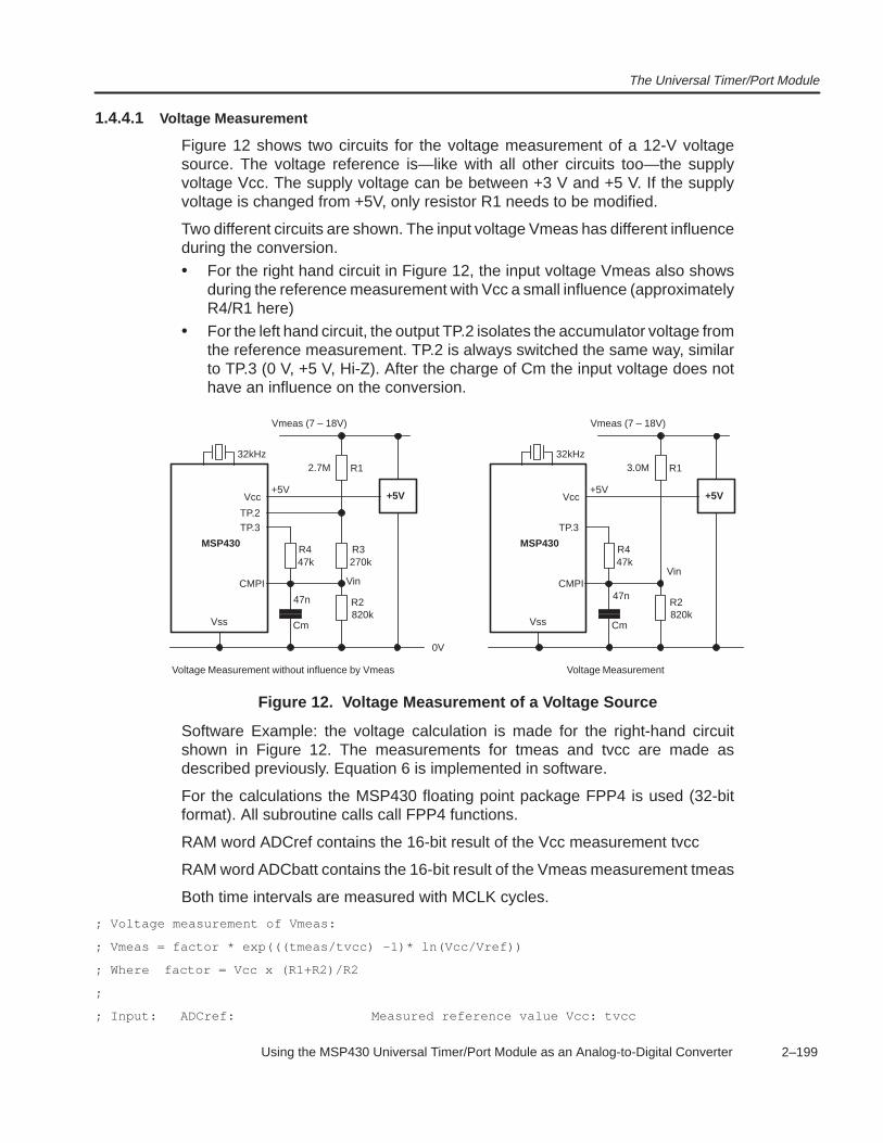
The Universal Timer/Port Module
2–199 Using the MSP430 Universal Timer/Port Module as an Analog-to-Digital Converter
1.4.4.1 Voltage Measurement
Figure 12 shows two circuits for the voltage measurement of a 12-V voltagesource. The voltage reference is—like with all other circuits too—the supplyvoltage Vcc. The supply voltage can be between +3 V and +5 V. If the supplyvoltage is changed from +5V, only resistor R1 needs to be modified.
Two different circuits are shown. The input voltage Vmeas has different influenceduring the conversion.
• For the right hand circuit in Figure 12, the input voltage Vmeas also showsduring the reference measurement with Vcc a small influence (approximatelyR4/R1 here)
• For the left hand circuit, the output TP.2 isolates the accumulator voltage fromthe reference measurement. TP.2 is always switched the same way, similarto TP.3 (0 V, +5 V, Hi-Z). After the charge of Cm the input voltage does nothave an influence on the conversion.
Vss
Vcc
32kHz
MSP430
TP.3
0V
R3
Cm
CMPI
Voltage Measurement
R1
R2
Vmeas (7 – 18V)
2.7M
820k
+5V
Vin
+5V
TP.2
270kR447k
Vss
Vcc
32kHz
MSP430
TP.3
Cm
CMPI
Voltage Measurement without influence by Vmeas
R1
R2
Vmeas (7 – 18V)
3.0M
820k
+5V
Vin
+5V
R447k
47n 47n
Figure 12. Voltage Measurement of a Voltage Source
Software Example: the voltage calculation is made for the right-hand circuitshown in Figure 12. The measurements for tmeas and tvcc are made asdescribed previously. Equation 6 is implemented in software.
For the calculations the MSP430 floating point package FPP4 is used (32-bitformat). All subroutine calls call FPP4 functions.
RAM word ADCref contains the 16-bit result of the Vcc measurement tvcc
RAM word ADCbatt contains the 16-bit result of the Vmeas measurement tmeas
Both time intervals are measured with MCLK cycles.
; Voltage measurement of Vmeas:
; Vmeas = factor * exp(((tmeas/tvcc) –1)* ln(Vcc/Vref))
; Where factor = Vcc x (R1+R2)/R2
;
; Input: ADCref: Measured reference value Vcc: tvcc
The Universal Timer/Port Module
2–200
; ADCbatt: Measured voltage value: tmeas
; Output: Act. Stack Calculated voltage Vmeas: @SP
;
Calc_VoltSUB #4,SP ; Reserve stack
MOV #ADCbatt,RPARG ; ADC value of voltage tmeas
CALL #CNV_BIN16U ; Convert to unsigned number
MOV @RPRES+,x ; Store result to x. MSBs
MOV @RPRES+,x+2 ; LSBs
MOV #ADCref,RPARG ; ADC value of Vcc tvcc
CALL #CNV_BIN16U ; Convert to unsigned number
MOV #x,RPRES ; Address tmeas
CALL #FLT_DIV ; tmeas/tvcc
JN Calc_Error ; Error
MOV #FLT1,RPARG ; Address 1.0
CALL #FLT_SUB ; (tmeas/tvcc) – 1.0
MOV #FLTLN4,RPARG ; Address Ln(Vcc/Vref)
CALL #FLT_MUL ; [(tmeas/tvcc)–1] * ln(Vcc/Vref)
CALL #FLT_EXP ; exp[(tmeas/tvcc) – 1)*ln4]
JN Calc_Error
MOV #factor,RPARG ; Address Vcc x (R1+R2)/R2
CALL #FLT_MUL ; Vmeas = factor * exp[...]
;
; Correction of Vmeas with calculated slope and offset
; Vmeas’ = factor*exp[(tmeas/tvcc)–1)*ln4]*slope + offset
;
MOV #Slope,RPARG ; Address slope
CALL #FLT_MUL ; Vmeas * slope
MOV #Offset,RPARG ; Address offset
CALL #FLT_ADD ; Vmeas’ = Vmeas * slope + offset
;
MOV @RPRES+,6(SP) ; Corrected Vmeas on Stack
MOV @RPRES+,8(SP) ; LSBs
ADD #4,SP ; Release stack
RET ; Return
;
; Calculation error (N = 1 after return): FFFF,FFFF result
;
Calc_Error MOV #0FFFFh,6(SP)
MOV #0FFFFh,8(SP)
ADD #4,SP ; Correct stack
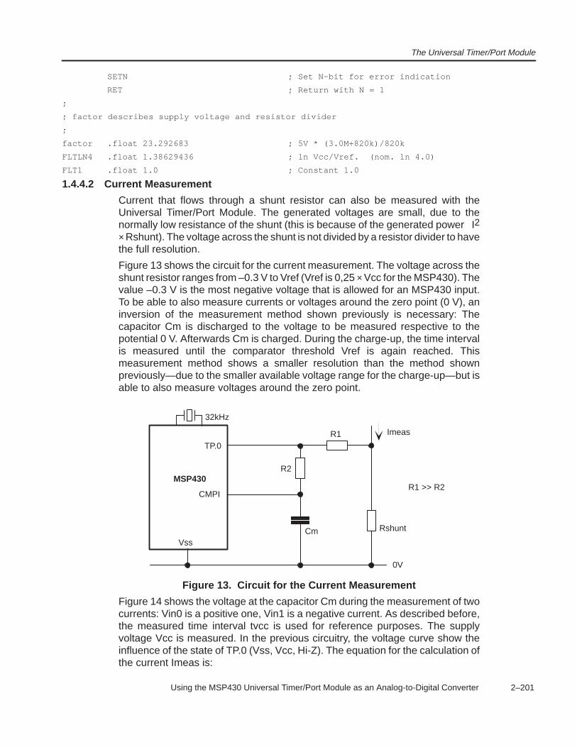
The Universal Timer/Port Module
2–201 Using the MSP430 Universal Timer/Port Module as an Analog-to-Digital Converter
SETN ; Set N–bit for error indication
RET ; Return with N = 1
;
; factor describes supply voltage and resistor divider
;
factor .float 23.292683 ; 5V * (3.0M+820k)/820k
FLTLN4 .float 1.38629436 ; ln Vcc/Vref. (nom. ln 4.0)
FLT1 .float 1.0 ; Constant 1.0
1.4.4.2 Current Measurement
Current that flows through a shunt resistor can also be measured with theUniversal Timer/Port Module. The generated voltages are small, due to thenormally low resistance of the shunt (this is because of the generated power I2× Rshunt). The voltage across the shunt is not divided by a resistor divider to havethe full resolution.
Figure 13 shows the circuit for the current measurement. The voltage across theshunt resistor ranges from –0.3 V to Vref (Vref is 0,25 × Vcc for the MSP430). Thevalue –0.3 V is the most negative voltage that is allowed for an MSP430 input.To be able to also measure currents or voltages around the zero point (0 V), aninversion of the measurement method shown previously is necessary: Thecapacitor Cm is discharged to the voltage to be measured respective to thepotential 0 V. Afterwards Cm is charged. During the charge-up, the time intervalis measured until the comparator threshold Vref is again reached. Thismeasurement method shows a smaller resolution than the method shownpreviously—due to the smaller available voltage range for the charge-up—but isable to also measure voltages around the zero point.
Vss
32kHz
MSP430
Cm
R1
R2
Imeas
CMPI
TP.0
0V
Rshunt
R1 >> R2
Figure 13. Circuit for the Current Measurement
Figure 14 shows the voltage at the capacitor Cm during the measurement of twocurrents: Vin0 is a positive one, Vin1 is a negative current. As described before,the measured time interval tvcc is used for reference purposes. The supplyvoltage Vcc is measured. In the previous circuitry, the voltage curve show theinfluence of the state of TP.0 (Vss, Vcc, Hi-Z). The equation for the calculation ofthe current Imeas is:
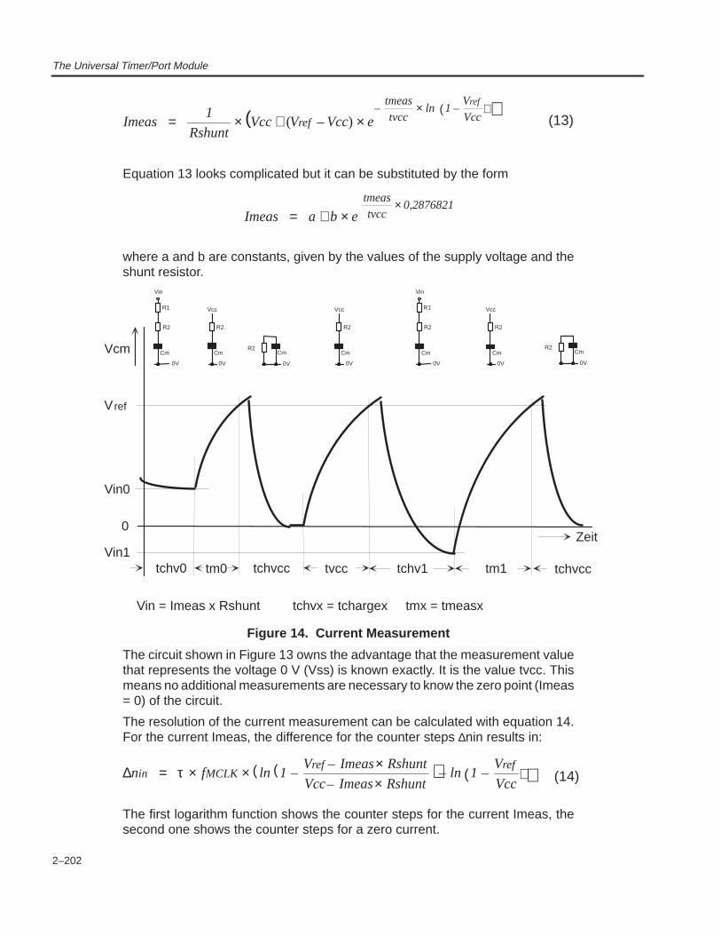
The Universal Timer/Port Module
2–202
Imeas1
Rshunte
tmeas
tvccln 1
V
Vcc
ref
= × + – ×( )– × –( )Vcc V Vccref( ) (13)
Equation 13 looks complicated but it can be substituted by the form
Imeas e
tmeas
tvcc0,2876821
= + ××
a b
where a and b are constants, given by the values of the supply voltage and theshunt resistor.
0Zeit
V
tm0 tvcctchvcc
Vcm
tchv0
ref
tchv1 tm1 tchvcc
Vin0
Cm
R1
R2
Vin
0V
Cm
R2
0V
Cm
0V
Vcc
Cm
R2
0V
Vcc
Cm
R2
0V
Vcc
R2
Vin = Imeas x Rshunt tchvx = tchargex tmx = tmeasx
Cm
R1
R2
Vin
0V
Vin1
Cm
0V
R2
Figure 14. Current Measurement
The circuit shown in Figure 13 owns the advantage that the measurement valuethat represents the voltage 0 V (Vss) is known exactly. It is the value tvcc. Thismeans no additional measurements are necessary to know the zero point (Imeas= 0) of the circuit.
The resolution of the current measurement can be calculated with equation 14.For the current Imeas, the difference for the counter steps ∆nin results in:
∆n ln 1 V Imeas Rshunt
Vcc Imeas Rshuntln 1
V
Vccin
ref ref= × × –– ×– ×
( )– –( )( )τ fMCLK (14)
The first logarithm function shows the counter steps for the current Imeas, thesecond one shows the counter steps for a zero current.
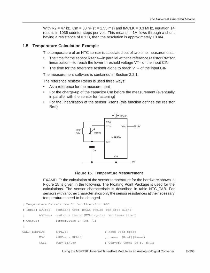
The Universal Timer/Port Module
2–203 Using the MSP430 Universal Timer/Port Module as an Analog-to-Digital Converter
With R2 = 47 kΩ, Cm = 33 nF (τ = 1.55 ms) and fMCLK = 3.3 MHz, equation 14results in 1036 counter steps per volt. This means, if 1A flows through a shunthaving a resistance of 0.1 Ω, then the resolution is approximately 10 mA.
1.5 Temperature Calculation Example
The temperature of an NTC sensor is calculated out of two time measurements:
• The time for the sensor Rsens—in parallel with the reference resistor Rref forlinearization—to reach the lower threshold voltage VT– of the input CIN
• The time for the reference resistor alone to reach VT– of the input CIN
The measurement software is contained in Section 2.2.1.
The reference resistor Rsens is used three ways:
• As a reference for the measurement
• For the charge-up of the capacitor Cm before the measurement (eventuallyin parallel with the sensor for fastening)
• For the linearization of the sensor Rsens (this function defines the resistorRref)
Vss
Vcc
32kHz
TP.1
CIN
MSP430
Rref
0V
Cm
Rsens
TP.0
+5V
10k
Figure 15. Temperature Measurement
EXAMPLE: the calculation of the sensor temperature for the hardware shown inFigure 15 is given in the following. The Floating Point Package is used for thecalculations. The sensor characteristic is described in table NTC_TAB. Forsensors with another characteristics only the sensor resistances at the necessarytemperatures need to be changed.
; Temperature Calculation SW for Timer/Port ADC
; Input: ADCref contains tref (MCLK cycles for Rref alone)
; ADCsens contains tsens (MCLK cycles for Rsens||Rref)
; Output: Temperature on TOS ( C)
;
CALC_TEMPSUB #FPL,SP ; Free work space
MOV #ADCsens,RPARG ; tsens (Rref||Rsens)
CALL #CNV_BIN16U ; Convert tsens to FP (NTC)
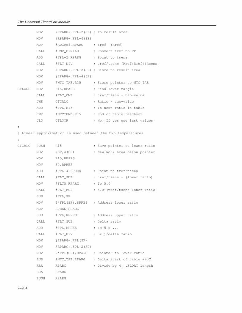
The Universal Timer/Port Module
2–204
MOV @RPARG+,FPL+2(SP) ; To result area
MOV @RPARG+,FPL+4(SP)
MOV #ADCref,RPARG ; tref (Rref)
CALL #CNV_BIN16U ; Convert tref to FP
ADD #FPL+2,RPARG ; Point to tsens
CALL #FLT_DIV ; tref/tsens (Rref/Rref||Rsens)
MOV @RPARG+,FPL+2(SP) ; Store to result area
MOV @RPARG+,FPL+4(SP)
MOV #NTC_TAB,R15 ; Store pointer to NTC_TAB
CTLOOP MOV R15,RPARG ; Find lower margin
CALL #FLT_CMP ; tref/tsens – tab–value
JHS CTCALC ; Ratio > tab–value
ADD #FPL,R15 ; To next ratio in table
CMP #NTCTEND,R15 ; End of table reached?
JLO CTLOOP ; No. If yes use last values
;
; Linear approximation is used between the two temperatures
;
CTCALC PUSH R15 ; Save pointer to lower ratio
MOV @SP,4(SP) ; New work area below pointer
MOV R15,RPARG
MOV SP,RPRES
ADD #FPL+4,RPRES ; Point to tref/tsens
CALL #FLT_SUB ; tref/tsens – (lower ratio)
MOV #FLT5,RPARG ; To 5.0
CALL #FLT_MUL ; 5.0*(tref/tsens–lower ratio)
SUB #FPL,SP
MOV 2*FPL(SP),RPRES ; Address lower ratio
MOV RPRES,RPARG
SUB #FPL,RPRES ; Address upper ratio
CALL #FLT_SUB ; Delta ratio
ADD #FPL,RPRES ; to 5 x ...
CALL #FLT_DIV ; 5x()/delta ratio
MOV @RPARG+,FPL(SP)
MOV @RPARG+,FPL+2(SP)
MOV 2*FPL(SP),RPARG ; Pointer to lower ratio
SUB #NTC_TAB,RPARG ; Delta start of table +90C
RRA RPARG ; Divide by 4: .FLOAT length
RRA RPARG
PUSH RPARG
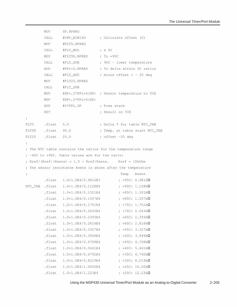
The Universal Timer/Port Module
2–205 Using the MSP430 Universal Timer/Port Module as an Analog-to-Digital Converter
MOV SP,RPARG
CALL #CNV_BIN16U ; Calculate offset (C)
MOV #FLT5,RPARG
CALL #FLT_MUL ; x 5C
MOV #FLT90,RPRES ; To +90C
CALL #FLT_SUB ; 90C – lower temperature
ADD #FPL+2,RPARG ; To delta within 5C ratios
CALL #FLT_ADD ; minus offset = – 25 deg
MOV #FLT25,RPARG
CALL #FLT_SUB
MOV @SP+,2*FPL+4(SP) ; Sensor temperature to TOS
MOV @SP+,2*FPL+4(SP)
ADD #2*FPL,SP ; Free stack
RET ; Result on TOS
;
FLT5 .float 5.0 ; Delta T for table NTC_TAB
FLT90 .float 90.0 ; Temp. at table start NTC_TAB
FLT25 .float 25.0 ; offset –25 deg
;
; The NTC table contains the ratios for the temperature range
; –40C to +90C. Table values are for the ratio:
; Rref/(Rref||Rsens) = 1.0 + Rref/Rsens. Rref = 10kOhm
; The sensor resistance Rsens is shown after the temperature
; Temp Rsens
.float 1.0+1.0E4/0.9812E3 ; +95C: 0.9812 Ω
NTC_TAB .float 1.0+1.0E4/0.1128E4 ; +90C: 1.128k Ω
.float 1.0+1.0E4/0.1301E4 ; +85C: 1.301k Ω
.float 1.0+1.0E4/0.1507E4 ; +80C: 1.507k Ω
.float 1.0+1.0E4/0.1751E4 ; +75C: 1.751k Ω
.float 1.0+1.0E4/0.2043E4 ; +70C: 2.043k Ω
.float 1.0+1.0E4/0.2393E4 ; +65C: 2.393k Ω
.float 1.0+1.0E4/0.2816E4 ; +60C: 2.816k Ω
.float 1.0+1.0E4/0.3327E4 ; +55C: 3.327k Ω
.float 1.0+1.0E4/0.3949E4 ; +50C: 3.949k Ω
.float 1.0+1.0E4/0.4708E4 ; +45C: 4.708k Ω
.float 1.0+1.0E4/0.5641E4 ; +40C: 5.641k Ω
.float 1.0+1.0E4/0.6792E4 ; +35C: 6.792k Ω
.float 1.0+1.0E4/0.8219E4 ; +30C: 8.219k Ω
.float 1.0+1.0E4/1.0000E4 ; +25C: 10.00k Ω
.float 1.0+1.0E4/1.223E4 ; +20C: 12.23k Ω
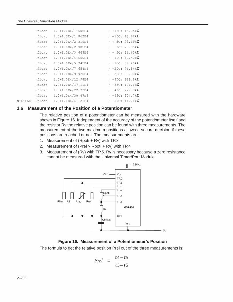
The Universal Timer/Port Module
2–206
.float 1.0+1.0E4/1.505E4 ; +15C: 15.05k Ω
.float 1.0+1.0E4/1.862E4 ; +10C: 18.62k Ω
.float 1.0+1.0E4/2.319E4 ; + 5C: 23.19k Ω
.float 1.0+1.0E4/2.905E4 ; 0C: 29.05k Ω
.float 1.0+1.0E4/3.663E4 ; – 5C: 36.63k Ω
.float 1.0+1.0E4/4.650E4 ; –10C: 46.50k Ω
.float 1.0+1.0E4/5.945E4 ; –15C: 59.45k Ω
.float 1.0+1.0E4/7.654E4 ; –20C: 76.54k Ω
.float 1.0+1.0E4/9.930E4 ; –25C: 99.30k Ω
.float 1.0+1.0E4/12.98E4 ; –30C: 129.8k Ω
.float 1.0+1.0E4/17.11E4 ; –35C: 171.1k Ω
.float 1.0+1.0E4/22.73E4 ; –40C: 227.3k Ω
.float 1.0+1.0E4/30.47E4 ; –45C: 304.7k ΩNTCTEND .float 1.0+1.0E4/41.21E4 ; –50C: 412.1k Ω
1.6 Measurement of the Position of a PotentiometerThe relative position of a potentiometer can be measured with the hardwareshown in Figure 16. Independent of the accuracy of the potentiometer itself andthe resistor Rv the relative position can be found with three measurements. Themeasurement of the two maximum positions allows a secure decision if thesepositions are reached or not. The measurements are:1. Measurement of (Rpoti + Rv) with TP.32. Measurement of (Prel × Rpoti + Rv) with TP.43. Measurement of (Rv) with TP.5. Rv is necessary because a zero resistance
cannot be measured with the Universal Timer/Port Module.
Vss
Vcc
TP.2
MSP430
Rref
Cmeas
TP.1
TP.5
CIN
Rntc
TP.3
TP.4
Rv
Rpoti
Rlin
0V
Rlim
+5V
TP.0
32kHz
Figure 16. Measurement of a Potentiometer’s Position
The formula to get the relative position Prel out of the three measurements is:
P lre =–
–
t t
t t
4 5
3 5
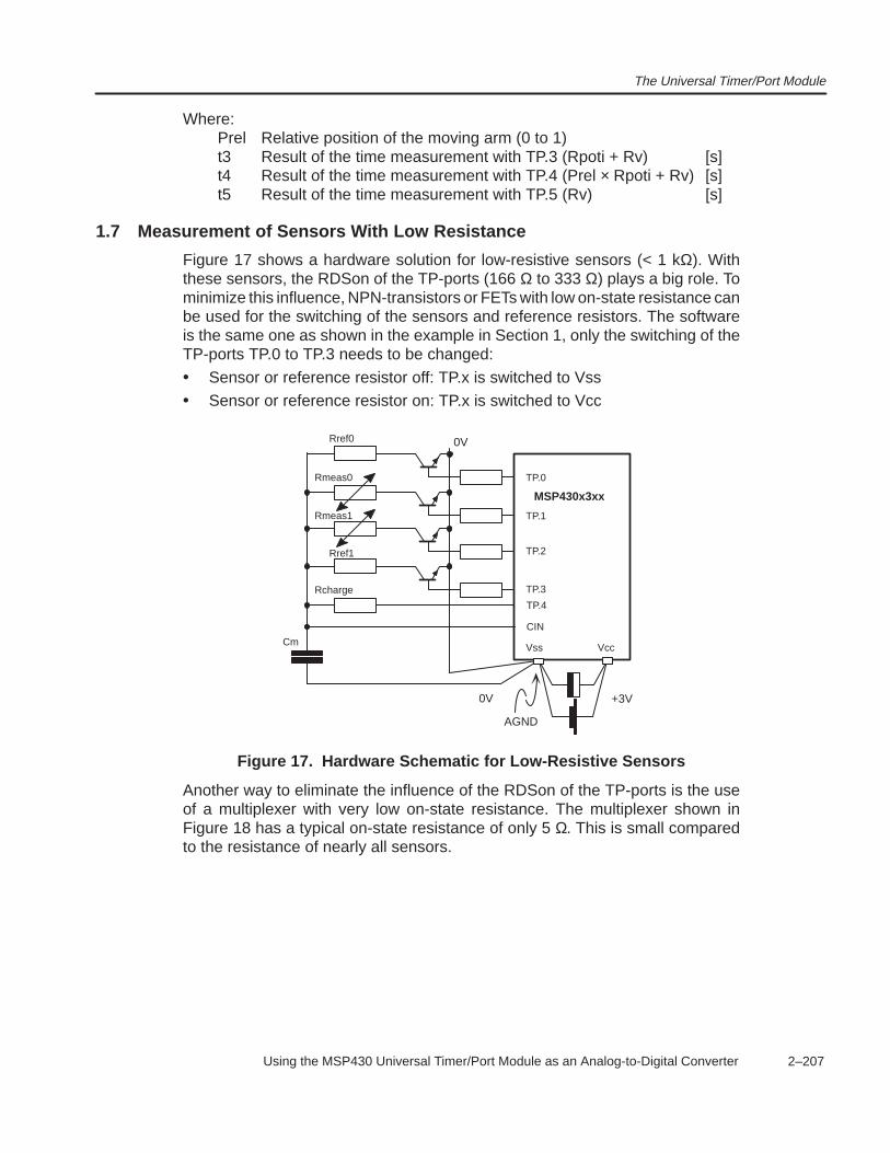
The Universal Timer/Port Module
2–207 Using the MSP430 Universal Timer/Port Module as an Analog-to-Digital Converter
Where:Prel Relative position of the moving arm (0 to 1)t3 Result of the time measurement with TP.3 (Rpoti + Rv) [s]t4 Result of the time measurement with TP.4 (Prel × Rpoti + Rv) [s]t5 Result of the time measurement with TP.5 (Rv) [s]
1.7 Measurement of Sensors With Low Resistance
Figure 17 shows a hardware solution for low-resistive sensors (< 1 kΩ). Withthese sensors, the RDSon of the TP-ports (166 Ω to 333 Ω) plays a big role. Tominimize this influence, NPN-transistors or FETs with low on-state resistance canbe used for the switching of the sensors and reference resistors. The softwareis the same one as shown in the example in Section 1, only the switching of theTP-ports TP.0 to TP.3 needs to be changed:
• Sensor or reference resistor off: TP.x is switched to Vss
• Sensor or reference resistor on: TP.x is switched to Vcc
Rref0
Rref1
Rcharge
Rmeas0
Rmeas1
Cm
TP.0
TP.1
TP.2
TP.3
TP.4
CIN
MSP430x3xx
0V +3V
AGND
Vss Vcc
0V
Figure 17. Hardware Schematic for Low-Resistive Sensors
Another way to eliminate the influence of the RDSon of the TP-ports is the useof a multiplexer with very low on-state resistance. The multiplexer shown inFigure 18 has a typical on-state resistance of only 5 Ω. This is small comparedto the resistance of nearly all sensors.
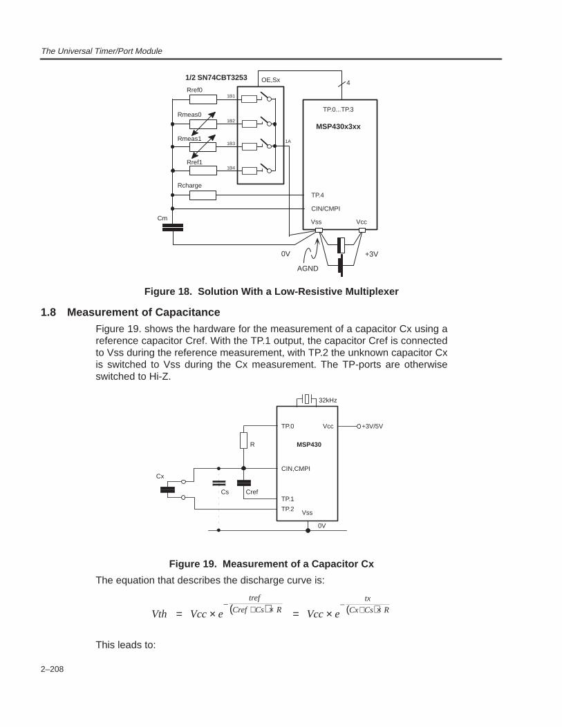
The Universal Timer/Port Module
2–208
Rref0
Rref1
Rcharge
Rmeas0
Rmeas1
Cm
TP.0...TP.3
TP.4
CIN/CMPI
MSP430x3xx
0V +3V
AGND
Vss Vcc
OE,Sx1/2 SN74CBT3253
1B1
1B2
1B3
1B4
1A
4
Figure 18. Solution With a Low-Resistive Multiplexer
1.8 Measurement of CapacitanceFigure 19. shows the hardware for the measurement of a capacitor Cx using areference capacitor Cref. With the TP.1 output, the capacitor Cref is connectedto Vss during the reference measurement, with TP.2 the unknown capacitor Cxis switched to Vss during the Cx measurement. The TP-ports are otherwiseswitched to Hi-Z.
Vss
Vcc
32kHz
TP.1
CIN,CMPI
MSP430
0V
Cref
R
TP.0 +3V/5V
Cx
Cs
TP.2
Figure 19. Measurement of a Capacitor Cx
The equation that describes the discharge curve is:
( ) ( )Vth Vcc e Vcc e
tref
Cref Cs R
tx
Cx Cs R= × = ×–
+ ×–
+ ×
This leads to:
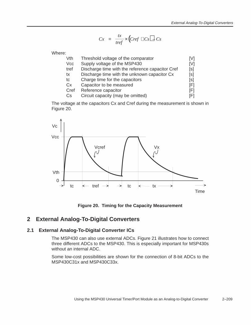
External Analog-To-Digital Converters
2–209 Using the MSP430 Universal Timer/Port Module as an Analog-to-Digital Converter
( )Cxtx
trefCref Cs Cs= × + –
Where:Vth Threshold voltage of the comparator [V]Vcc Supply voltage of the MSP430 [V]tref Discharge time with the reference capacitor Cref [s]tx Discharge time with the unknown capacitor Cx [s]tc Charge time for the capacitors [s]Cx Capacitor to be measured [F]Cref Reference capacitor [F]Cs Circuit capacity (may be omitted) [F]
The voltage at the capacitors Cx and Cref during the measurement is shown inFigure 20.
0
Vcc
Time
Vth
tref txtc
tc
Vc
Vcref Vx
Figure 20. Timing for the Capacity Measurement
2 External Analog-To-Digital Converters
2.1 External Analog-To-Digital Converter ICs
The MSP430 can also use external ADCs. Figure 21 illustrates how to connectthree different ADCs to the MSP430. This is especially important for MSP430swithout an internal ADC.
Some low-cost possibilities are shown for the connection of 8-bit ADCs to theMSP430C31x and MSP430C33x.
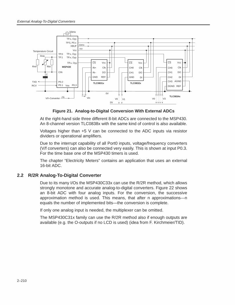
External Analog-To-Digital Converters
2–210
Vss
Vcc
32kHz
TP.1
CIN
MSP430Rref
0V
C
Rntc
TP.0
TP.5, P0.x
Temperature Circuit
TXD
RCV
P0.2P0.1
Rlin
CS
IN+
IN–
GND
Vcc
Clk
DO
REF
CS
CH1
GND
Vcc
Clk
DO
DI
CS
CH0
CH1
CH2
Vcc
Clk
DO
DI
DGND
AGNDCH3
REF
XBUF 32kHz
TP.x, Oyy
TP.x, Oyy
TP.x, Oyy
TP.x, Oyy
CH0
TLC0831x TLC0832x
TLC0834x
0V
Vin V0 V1 V0 V3
+5V
P0.3
V/f–Converter
Figure 21. Analog-to-Digital Conversion With External ADCs
At the right-hand side three different 8-bit ADCs are connected to the MSP430.An 8-channel version TLC0838x with the same kind of control is also available.
Voltages higher than +5 V can be connected to the ADC inputs via resistordividers or operational amplifiers.
Due to the interrupt capability of all Port0 inputs, voltage/frequency converters(V/f converters) can also be connected very easily. This is shown at input P0.3.For the time base one of the MSP430 timers is used.
The chapter “Electricity Meters” contains an application that uses an external16-bit ADC.
2.2 R/2R Analog-To-Digital Converter
Due to its many I/Os the MSP430C33x can use the R/2R method, which allowsstrongly monotone and accurate analog-to-digital converters. Figure 22 showsan 8-bit ADC with four analog inputs. For the conversion, the successiveapproximation method is used. This means, that after n approximations—nequals the number of implemented bits—the conversion is complete.
If only one analog input is needed, the multiplexer can be omitted.
The MSP430C31x family can use the R/2R method also if enough outputs areavailable (e.g. the O-outputs if no LCD is used) (idea from F. Kirchmeier/TID).
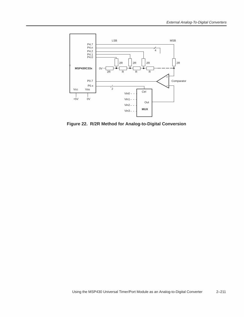
External Analog-To-Digital Converters
2–211 Using the MSP430 Universal Timer/Port Module as an Analog-to-Digital Converter
VssVcc
MSP430C33x
+5V 0V
P4.7
.2R 2R 2R2R
R2R RR0V
LSB MSB
P4.2P4.1P4.0
P4.n4
+
–
P0.7 Comparator
Vin0
Vin1
Vin2
Vin3
2Ctrl
Out
MUX
P0.x
Figure 22. R/2R Method for Analog-to-Digital Conversion

External Analog-To-Digital Converters
2–212

3-1
Hardware Applications
Chapter 3

3-2
3.1 I/O Port Usage
The each I/O of Port0, Port1, and Port2 has interrupt capability for the leadingedge and trailing edge of an input signal. This has the following advantages:
More than one interrupt input is available
Eight resp. 24 external events can wake-up from Low Power Modes 3 or 4
No glue logic is necessary for most applications: all inputs can be ob-served without the need of gates connecting them to a single interrupt input.
Wake-up is possible out of any input state (high or low)
Due to the edge-triggered characteristic of the interrupts, no externalswitch-off logic is necessary for long-lasting input signals, therefore nomultiple interrupt is possible therefore.
3.1.1 General Usage
Six peripheral registers controling the activities of the I/O–Port0 are shown inTable 3–1.
Table 3–1. I/O–Port0 RegistersRegister Usage State After Reset
Input register Signals at I/O terminals Signals at I/O terminals
Output register Content of output buffer Unchanged
Direction register 0: Input 1: Output Reset to input direction
Interrupt flags 0: No interrupt pending1: Interrupt pending
Set to 0
Interrupt edges 0: Low to high causes Inter-rupt1: High to low causes Inter-rupt
Unchanged
Interrupt enable 0: Disabled1: Enabled
Set to 0
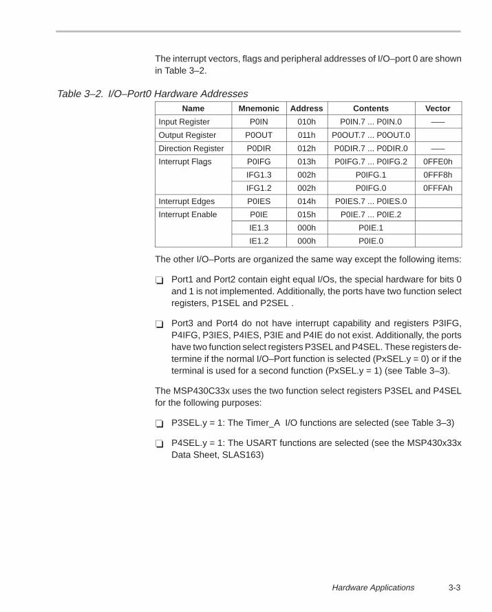
3-3Hardware Applications
The interrupt vectors, flags and peripheral addresses of I/O–port 0 are shownin Table 3–2.
Table 3–2. I/O–Port0 Hardware AddressesName Mnemonic Address Contents Vector
Input Register P0IN 010h P0IN.7 ... P0IN.0 –––
Output Register P0OUT 011h P0OUT.7 ... P0OUT.0
Direction Register P0DIR 012h P0DIR.7 ... P0DIR.0 –––
Interrupt Flags P0IFG 013h P0IFG.7 ... P0IFG.2 0FFE0hg
IFG1.3 002h P0IFG.1 0FFF8h
IFG1.2 002h P0IFG.0 0FFFAh
Interrupt Edges P0IES 014h P0IES.7 ... P0IES.0
Interrupt Enable P0IE 015h P0IE.7 ... P0IE.2
IE1.3 000h P0IE.1
IE1.2 000h P0IE.0
The other I/O–Ports are organized the same way except the following items:
Port1 and Port2 contain eight equal I/Os, the special hardware for bits 0and 1 is not implemented. Additionally, the ports have two function selectregisters, P1SEL and P2SEL .
Port3 and Port4 do not have interrupt capability and registers P3IFG,P4IFG, P3IES, P4IES, P3IE and P4IE do not exist. Additionally, the portshave two function select registers P3SEL and P4SEL. These registers de-termine if the normal I/O–Port function is selected (PxSEL.y = 0) or if theterminal is used for a second function (PxSEL.y = 1) (see Table 3–3).
The MSP430C33x uses the two function select registers P3SEL and P4SELfor the following purposes:
P3SEL.y = 1: The Timer_A I/O functions are selected (see Table 3–3)
P4SEL.y = 1: The USART functions are selected (see the MSP430x33xData Sheet, SLAS163)
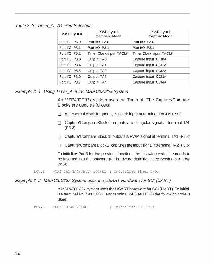
3-4
Table 3–3. Timer_A I/O–Port Selection
P3SEL.y = 0 P3SEL.y = 1Compare Mode
P3SEL.y = 1Capture Mode
Port I/O P3.0 Port I/O P3.0 Port I/O P3.0
Port I/O P3.1 Port I/O P3.1 Port I/O P3.1
Port I/O P3.2 Timer Clock input TACLK Timer Clock input TACLK
Port I/O P3.3 Output TA0 Capture input CCI0A
Port I/O P3.4 Output TA1 Capture input CCI1A
Port I/O P3.5 Output TA2 Capture input CCI2A
Port I/O P3.6 Output TA3 Capture input CCI3A
Port I/O P3.7 Output TA4 Capture input CCI4A
Example 3–1. Using Timer_A in the MSP430C33x System
An MSP430C33x system uses the Timer_A. The Capture/CompareBlocks are used as follows:
An external clock frequency is used: input at terminal TACLK (P3.2)
Capture/Compare Block 0: outputs a rectangular signal at terminal TA0(P3.3)
Capture/Compare Block 1: outputs a PWM signal at terminal TA1 (P3.4)
Capture/Compare Block 2: captures the input signal at terminal TA2 (P3.5)
To initialize Port3 for the previous functions the following code line needs tobe inserted into the software (for hardware definitions see Section 6.3, Tim-er_A):
MOV.B #TA2+TA1+TA0+TACLK,&P3SEL ; Initialize Timer I/Os
Example 3–2. MSP430C33x System uses the USART Hardware for SCI (UART)
A MSP430C33x system uses the USART hardware for SCI (UART). To initial-ize terminal P4.7 as URXD and terminal P4.6 as UTXD the following code isused:
MOV.B #URXD+UTXD,&P4SEL ; Initialize SCI I/Os
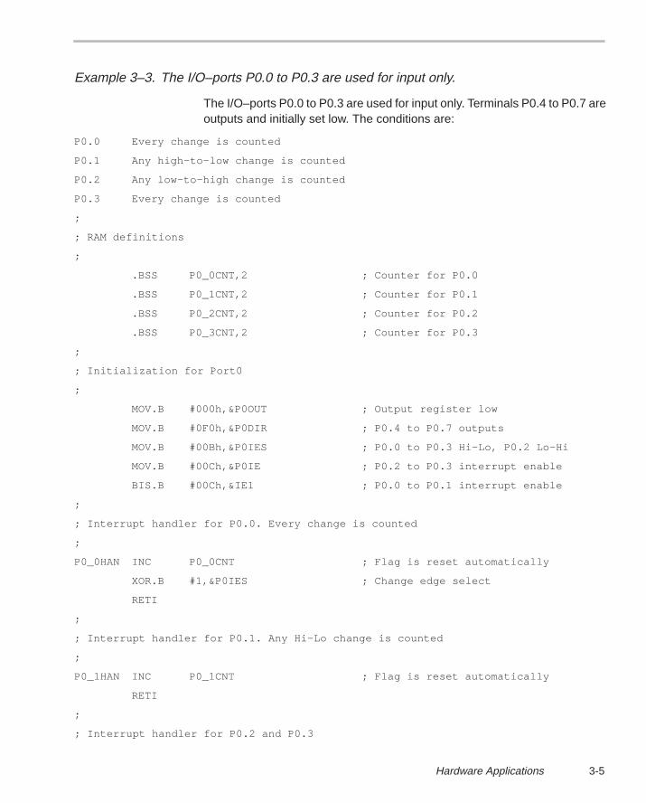
3-5Hardware Applications
Example 3–3. The I/O–ports P0.0 to P0.3 are used for input only.
The I/O–ports P0.0 to P0.3 are used for input only. Terminals P0.4 to P0.7 areoutputs and initially set low. The conditions are:
P0.0 Every change is counted
P0.1 Any high–to–low change is counted
P0.2 Any low–to–high change is counted
P0.3 Every change is counted
;
; RAM definitions
;
.BSS P0_0CNT,2 ; Counter for P0.0
.BSS P0_1CNT,2 ; Counter for P0.1
.BSS P0_2CNT,2 ; Counter for P0.2
.BSS P0_3CNT,2 ; Counter for P0.3
;
; Initialization for Port0
;
MOV.B #000h,&P0OUT ; Output register low
MOV.B #0F0h,&P0DIR ; P0.4 to P0.7 outputs
MOV.B #00Bh,&P0IES ; P0.0 to P0.3 Hi–Lo, P0.2 Lo–Hi
MOV.B #00Ch,&P0IE ; P0.2 to P0.3 interrupt enable
BIS.B #00Ch,&IE1 ; P0.0 to P0.1 interrupt enable
;
; Interrupt handler for P0.0. Every change is counted
;
P0_0HAN INC P0_0CNT ; Flag is reset automatically
XOR.B #1,&P0IES ; Change edge select
RETI
;
; Interrupt handler for P0.1. Any Hi–Lo change is counted
;
P0_1HAN INC P0_1CNT ; Flag is reset automatically
RETI
;
; Interrupt handler for P0.2 and P0.3
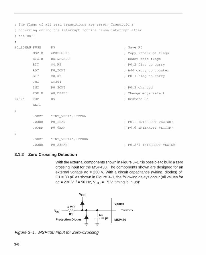
3-6
; The flags of all read transitions are reset. Transitions
; occurring during the interrupt routine cause interrupt after
; the RETI
;
P0_23HAN PUSH R5 ; Save R5
MOV.B &P0FLG,R5 ; Copy interrupt flags
BIC.B R5,&P0FLG ; Reset read flags
BIT #4,R5 ; P0.2 flag to carry
ADC P0_2CNT ; Add carry to counter
BIT #8,R5 ; P0.3 flag to carry
JNC L$304
INC P0_3CNT ; P0.3 changed
XOR.B #8,P0IES ; Change edge select
L$304 POP R5 ; Restore R5
RETI
;
.SECT ”INT_VECT”,0FFF8h
.WORD P0_1HAN ; P0.1 INTERRUPT VECTOR;
.WORD P0_0HAN ; P0.0 INTERRUPT VECTOR;
;
.SECT ”INT_VECT1”,0FFE0h
.WORD P0_23HAN ; P0.2/7 INTERRUPT VECTOR
3.1.2 Zero Crossing Detection
With the external components shown in Figure 3–1 it is possible to build a zerocrossing input for the MSP430. The components shown are designed for anexternal voltage ac = 230 V. With a circuit capacitance (wiring, diodes) of C1 = 30 pF as shown in Figure 3–1, the following delays occur (all values forac = 230 V, f = 50 Hz, VCC = +5 V, timing is in µs):
C1
Protection Diodes
1 MΩ
R1Vac To Portx
Vportx
MSP430
VCC
30 pF
Figure 3–1. MSP430 Input for Zero-Crossing
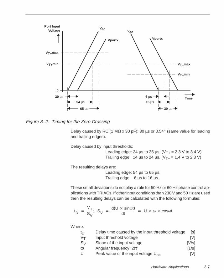
3-7Hardware Applications
Vac
Vportx
Vac
Vportx
Port InputVoltage
VT+max
VT+min
0
30 µs
54 µs
65 µs
6 µs
16 µs
30 µs
Time
VT–max
VT–min
Figure 3–2. Timing for the Zero Crossing
Delay caused by RC (1 MΩ x 30 pF): 30 µs or 0.54 (same value for leadingand trailing edges).
Delay caused by input thresholds: Leading edge: 24 µs to 35 µs. (VT+ = 2.3 V to 3.4 V)Trailing edge: 14 µs to 24 µs. (VT– = 1.4 V to 2.3 V)
The resulting delays are:Leading edge: 54 µs to 65 µs.Trailing edge: 6 µs to 16 µs.
These small deviations do not play a role for 50 Hz or 60 Hz phase control ap-plications with TRIACs. If other input conditions than 230 V and 50 Hz are usedthen the resulting delays can be calculated with the following formulas:
tD VTSV
; SV d(U sint)
dt U cost
Where:tD Delay time caused by the input threshold voltage [s]VT Input threshold voltage [V]SV Slope of the input voltage [V/s]ω Angular frequency 2πf [1/s]U Peak value of the input voltage Uac [V]
3-8
For t = 0 (zero crossing time) the previous equation becomes:
× ×ω ω=t
V
U 1
V
UDT T
×=
3.1.3 Output Buffering
The outputs of the MSP430 (P0.x, P1.x, P2.x, P3.x, P4.x, Ox) have nominalinternal resistances depending on the supply voltage, VCC:
VCC = 3 V: Max. 333 Ω (∆V = 0.4V max. @ 1.2mA)
VCC = 5 V: Max. 266 Ω (∆V = 0.4V max. @ 1.5mA)
These internal resistances are non-linear and are valid only for small outputcurrents (see the previous text). If larger currents are drawn, saturation effectswill limit the output current.
These outputs are intended for driving digital inputs and gates and normallyhave too high an impedance level for other applications, such as the drivingof relays, lines, etc. If output currents greater than the previously mentionedones are needed then output buffering is necessary. Figure 3–3 shows someof the possibilities. The resistors shown in Figure 3–3 for the limitation of theMSP430 output current are minimum values. The application is designed forVCC = 5 V. The values shown in brackets are for VCC = 3 V.
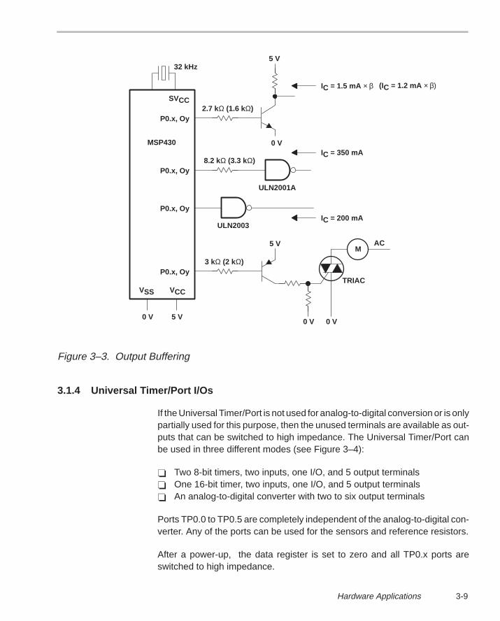
3-9Hardware Applications
SVCC
P0.x, Oy2.7 kΩ (1.6 kΩ)
0 V
P0.x, Oy8.2 kΩ (3.3 kΩ)
ULN2001A
ULN2003
P0.x, Oy
P0.x, Oy3 kΩ (2 kΩ)
5 V
5 VM
AC
TRIAC
0 V 0 V
VSS VCC
32 kHz
MSP430
0 V 5 V
IC = 1.5 mA × β
IC = 350 mA
IC = 200 mA
(IC = 1.2 mA × β)
Figure 3–3. Output Buffering
3.1.4 Universal Timer/Port I/Os
If the Universal Timer/Port is not used for analog-to-digital conversion or is onlypartially used for this purpose, then the unused terminals are available as out-puts that can be switched to high impedance. The Universal Timer/Port canbe used in three different modes (see Figure 3–4):
Two 8-bit timers, two inputs, one I/O, and 5 output terminals One 16-bit timer, two inputs, one I/O, and 5 output terminals An analog-to-digital converter with two to six output terminals
Ports TP0.0 to TP0.5 are completely independent of the analog-to-digital con-verter. Any of the ports can be used for the sensors and reference resistors.
After a power-up, the data register is set to zero and all TP0.x ports areswitched to high impedance.
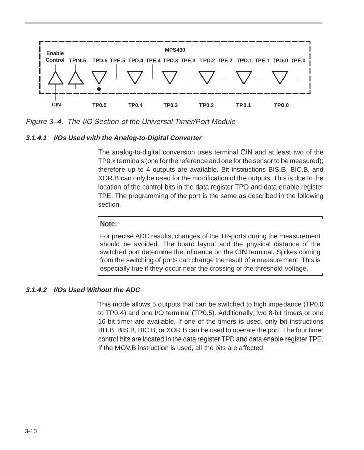
3-10
EnableControl TPIN.5 TPD.5 TPE.5 TPD.4 TPE.4 TPD.3 TPE.3 TPD.2 TPE.2 TPD.1 TPE.1 TPD.0 TPE.0
CIN TP0.5 TP0.4 TP0.3 TP0.2 TP0.1 TP0.0
MPS430
Figure 3–4. The I/O Section of the Universal Timer/Port Module
3.1.4.1 I/Os Used with the Analog-to-Digital Converter
The analog-to-digital conversion uses terminal CIN and at least two of theTP0.x terminals (one for the reference and one for the sensor to be measured);therefore up to 4 outputs are available. Bit instructions BIS.B, BIC.B, andXOR.B can only be used for the modification of the outputs. This is due to thelocation of the control bits in the data register TPD and data enable registerTPE. The programming of the port is the same as described in the followingsection.
Note:
For precise ADC results, changes of the TP-ports during the measurementshould be avoided. The board layout and the physical distance of theswitched port determine the influence on the CIN terminal. Spikes comingfrom the switching of ports can change the result of a measurement. This isespecially true if they occur near the crossing of the threshold voltage.
3.1.4.2 I/Os Used Without the ADC
This mode allows 5 outputs that can be switched to high impedance (TP0.0to TP0.4) and one I/O terminal (TP0.5). Additionally, two 8-bit timers or one16-bit timer are available. If one of the timers is used, only bit instructionsBIT.B, BIS.B, BIC.B, or XOR.B can be used to operate the port. The four timercontrol bits are located in the data register TPD and data enable register TPE.If the MOV.B instruction is used, all the bits are affected.
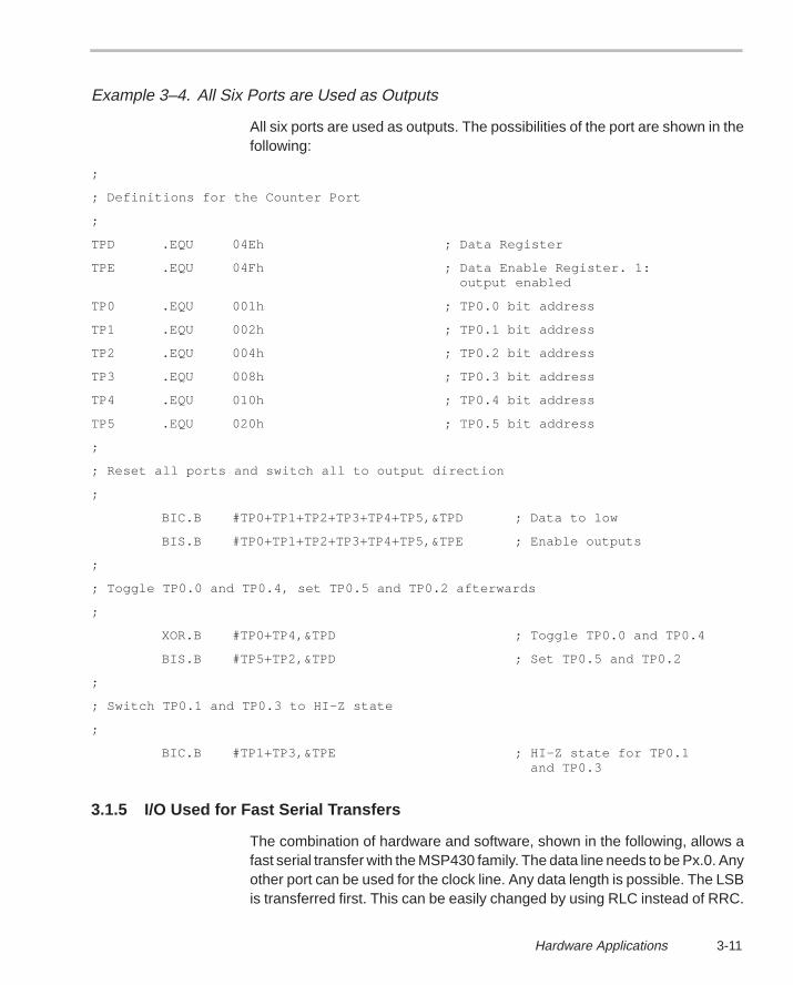
3-11Hardware Applications
Example 3–4. All Six Ports are Used as Outputs
All six ports are used as outputs. The possibilities of the port are shown in thefollowing:
;
; Definitions for the Counter Port
;
TPD .EQU 04Eh ; Data Register
TPE .EQU 04Fh ; Data Enable Register. 1: output enabled
TP0 .EQU 001h ; TP0.0 bit address
TP1 .EQU 002h ; TP0.1 bit address
TP2 .EQU 004h ; TP0.2 bit address
TP3 .EQU 008h ; TP0.3 bit address
TP4 .EQU 010h ; TP0.4 bit address
TP5 .EQU 020h ; TP0.5 bit address
;
; Reset all ports and switch all to output direction
;
BIC.B #TP0+TP1+TP2+TP3+TP4+TP5,&TPD ; Data to low
BIS.B #TP0+TP1+TP2+TP3+TP4+TP5,&TPE ; Enable outputs
;
; Toggle TP0.0 and TP0.4, set TP0.5 and TP0.2 afterwards
;
XOR.B #TP0+TP4,&TPD ; Toggle TP0.0 and TP0.4
BIS.B #TP5+TP2,&TPD ; Set TP0.5 and TP0.2
;
; Switch TP0.1 and TP0.3 to HI–Z state
;
BIC.B #TP1+TP3,&TPE ; HI–Z state for TP0.1 and TP0.3
3.1.5 I/O Used for Fast Serial Transfers
The combination of hardware and software, shown in the following, allows afast serial transfer with the MSP430 family. The data line needs to be Px.0. Anyother port can be used for the clock line. Any data length is possible. The LSBis transferred first. This can be easily changed by using RLC instead of RRC.
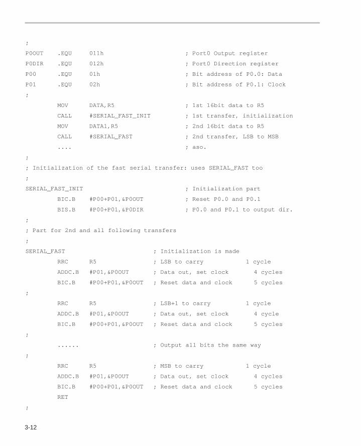
3-12
;
P0OUT .EQU 011h ; Port0 Output register
P0DIR .EQU 012h ; Port0 Direction register
P00 .EQU 01h ; Bit address of P0.0: Data
P01 .EQU 02h ; Bit address of P0.1: Clock
;
MOV DATA,R5 ; 1st 16bit data to R5
CALL #SERIAL_FAST_INIT ; 1st transfer, initialization
MOV DATA1,R5 ; 2nd 16bit data to R5
CALL #SERIAL_FAST ; 2nd transfer, LSB to MSB
.... ; aso.
;
; Initialization of the fast serial transfer: uses SERIAL_FAST too
;
SERIAL_FAST_INIT ; Initialization part
BIC.B #P00+P01,&P0OUT ; Reset P0.0 and P0.1
BIS.B #P00+P01,&P0DIR ; P0.0 and P0.1 to output dir.
;
; Part for 2nd and all following transfers
;
SERIAL_FAST ; Initialization is made
RRC R5 ; LSB to carry 1 cycle
ADDC.B #P01,&P0OUT ; Data out, set clock 4 cycles
BIC.B #P00+P01,&P0OUT ; Reset data and clock 5 cycles
;
RRC R5 ; LSB+1 to carry 1 cycle
ADDC.B #P01,&P0OUT ; Data out, set clock 4 cycle
BIC.B #P00+P01,&P0OUT ; Reset data and clock 5 cycles
;
...... ; Output all bits the same way
;
RRC R5 ; MSB to carry 1 cycle
ADDC.B #P01,&P0OUT ; Data out, set clock 4 cycles
BIC.B #P00+P01,&P0OUT ; Reset data and clock 5 cycles
RET
;
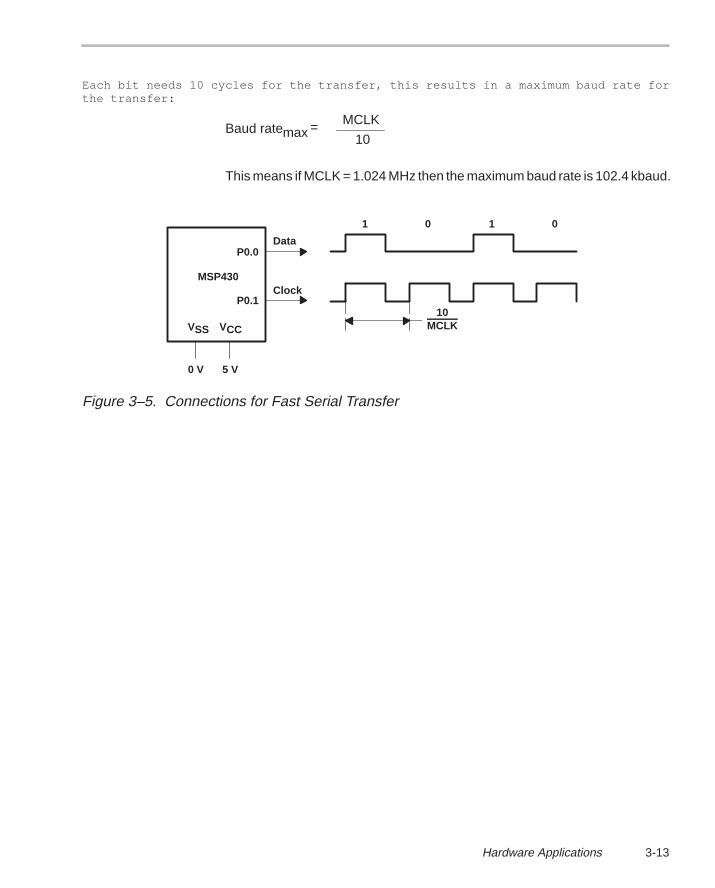
3-13Hardware Applications
Each bit needs 10 cycles for the transfer, this results in a maximum baud rate forthe transfer:
Baud rateMCLK
10max =
This means if MCLK = 1.024 MHz then the maximum baud rate is 102.4 kbaud.
P0.0
P0.1
Data
Clock
VCCVSS
1 0 1 0
10MCLK
0 V 5 V
MSP430
Figure 3–5. Connections for Fast Serial Transfer
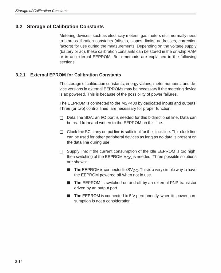
Storage of Calibration Constants
3-14
3.2 Storage of Calibration Constants
Metering devices, such as electricity meters, gas meters etc., normally needto store calibration constants (offsets, slopes, limits, addresses, correctionfactors) for use during the measurements. Depending on the voltage supply(battery or ac), these calibration constants can be stored in the on-chip RAMor in an external EEPROM. Both methods are explained in the followingsections.
3.2.1 External EPROM for Calibration Constants
The storage of calibration constants, energy values, meter numbers, and de-vice versions in external EEPROMs may be necessary if the metering deviceis ac powered. This is because of the possibility of power failures.
The EEPROM is connected to the MSP430 by dedicated inputs and outputs.Three (or two) control lines are necessary for proper function:
Data line SDA: an I/O port is needed for this bidirectional line. Data canbe read from and written to the EEPROM on this line.
Clock line SCL: any output line is sufficient for the clock line. This clock linecan be used for other peripheral devices as long as no data is present onthe data line during use.
Supply line: if the current consumption of the idle EEPROM is too high,then switching of the EEPROM VCC is needed. Three possible solutionsare shown:
The EEPROM is connected to SVCC. This is a very simple way to havethe EEPROM powered off when not in use.
The EEPROM is switched on and off by an external PNP transistordriven by an output port.
The EEPROM is connected to 5 V permanently, when its power con-sumption is not a consideration.
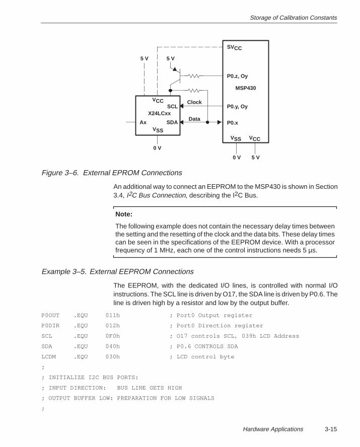
Storage of Calibration Constants
3-15Hardware Applications
SCL
SDAVSS
VCC
X24LCxx
Ax
5 V5 V
Clock
Data
SVCC
P0.z, Oy
P0.y, Oy
P0.x
VSS VCC
0 V
0 V 5 V
MSP430
Figure 3–6. External EPROM Connections
An additional way to connect an EEPROM to the MSP430 is shown in Section3.4, I2C Bus Connection, describing the I2C Bus.
Note:
The following example does not contain the necessary delay times betweenthe setting and the resetting of the clock and the data bits. These delay timescan be seen in the specifications of the EEPROM device. With a processorfrequency of 1 MHz, each one of the control instructions needs 5 µs.
Example 3–5. External EEPROM Connections
The EEPROM, with the dedicated I/O lines, is controlled with normal I/Oinstructions. The SCL line is driven by O17, the SDA line is driven by P0.6. Theline is driven high by a resistor and low by the output buffer.
P0OUT .EQU 011h ; Port0 Output register
P0DIR .EQU 012h ; Port0 Direction register
SCL .EQU 0F0h ; O17 controls SCL, 039h LCD Address
SDA .EQU 040h ; P0.6 CONTROLS SDA
LCDM .EQU 030h ; LCD control byte
;
; INITIALIZE I2C BUS PORTS:
; INPUT DIRECTION: BUS LINE GETS HIGH
; OUTPUT BUFFER LOW: PREPARATION FOR LOW SIGNALS
;
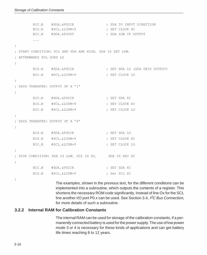
Storage of Calibration Constants
3-16
BIC.B #SDA,&P0DIR ; SDA TO INPUT DIRECTION
BIS.B #SCL,&LCDM+9 ; SET CLOCK HI
BIC.B #SDA,&P0OUT ; SDA LOW IF OUTPUT
...
;
; START CONDITION: SCL AND SDA ARE HIGH, SDA IS SET LOW,
; AFTERWARDS SCL GOES LO
;
BIS.B #SDA,&P0DIR ; SET SDA LO (SDA GETS OUTPUT)
BIC.B #SCL,&LCDM+9 ; SET CLOCK LO
;
; DATA TRANSFER: OUTPUT OF A ”1”
;
BIC.B #SDA,&P0DIR ; SET SDA HI
BIS.B #SCL,&LCDM+9 ; SET CLOCK HI
BIC.B #SCL,&LCDM+9 ; SET CLOCK LO
;
; DATA TRANSFER: OUTPUT OF A ”0”
;
BIS.B #SDA,&P0DIR ; SET SDA LO
BIS.B #SCL,&LCDM+9 ; SET CLOCK HI
BIC.B #SCL,&LCDM+9 ; SET CLOCK LO
;
; STOP CONDITION: SDA IS LOW, SCL IS HI, SDA IS SET HI
;
BIC.B #SDA,&P0DIR ; SET SDA HI
BIS.B #SCL,&LCDM+9 ; Set SCL HI
;The examples, shown in the previous text, for the different conditions can beimplemented into a subroutine, which outputs the contents of a register. Thisshortens the necessary ROM code significantly. Instead of line Ox for the SCLline another I/O port P0.x can be used. See Section 3.4, I2C Bus Connection,for more details of such a subroutine.
3.2.2 Internal RAM for Calibration Constants
The internal RAM can be used for storage of the calibration constants, if a per-manently connected battery is used for the power supply. The use of low powermode 3 or 4 is necessary for these kinds of applications and can get batterylife times reaching 8 to 12 years.
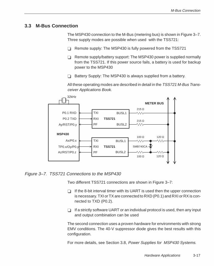
M-Bus Connection
3-17Hardware Applications
3.3 M-Bus Connection
The MSP430 connection to the M-Bus (metering bus) is shown in Figure 3–7.Three supply modes are possible when used with the TSS721:
Remote supply: The MSP430 is fully powered from the TSS721
Remote supply/battery support: The MSP430 power is supplied normallyfrom the TSS721. If this power source fails, a battery is used for backuppower to the MSP430
Battery Supply: The MSP430 is always supplied from a battery.
All these operating modes are described in detail in the TSS721 M-Bus Trans-ceiver Applications Book.
32kHz
RXI
MSP430
P0.2 TXD
P0.1 RXD TXI
PF
PF
RXITP0.x/Oy/P0.y
Ax/P0.x TXI
Az/RST/P0.z
TSS721
TSS721
METER BUS
BUSL1
BUSL1
BUSL2
BUSL2
Ay/RST/P0.y
SMB740CA
215 Ω
215 Ω
100 Ω
100 Ω
120 Ω
120 Ω
Figure 3–7. TSS721 Connections to the MSP430
Two different TSS721 connections are shown in Figure 3–7:
If the 8-bit interval timer with its UART is used then the upper connectionis necessary. TXI or TX are connected to RXD (P0.1) and RXI or RX is con-nected to TXD (P0.2).
If a strictly software UART or an individual protocol is used, then any inputand output combination can be used
The second connection uses a proven hardware for environments with strongEMV conditions. The 40-V suppressor diode gives the best results with thisconfiguration.
For more details, see Section 3.8, Power Supplies for MSP430 Systems.
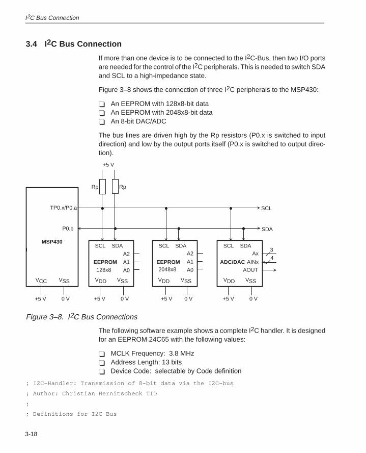
I2C Bus Connection
3-18
3.4 I2C Bus Connection
If more than one device is to be connected to the I2C-Bus, then two I/O portsare needed for the control of the I2C peripherals. This is needed to switch SDAand SCL to a high-impedance state.
Figure 3–8 shows the connection of three I2C peripherals to the MSP430:
An EEPROM with 128x8-bit data An EEPROM with 2048x8-bit data An 8-bit DAC/ADC
The bus lines are driven high by the Rp resistors (P0.x is switched to inputdirection) and low by the output ports itself (P0.x is switched to output direc-tion).
VSSVCC
MSP430
+5 V
VDD
SCL SDA
VSS
EEPROM
A0
0 V
+5 V
+5 V
TP0.x/P0.a
P0.b
RpRp
VDD
SCL SDA
VSS
EEPROM
0 V+5 V
SCL
SDA
VDD
SCL SDA
VSS
ADC/DAC
0 V+5 V
A1
A2
A0
A1
A2
AOUT
AINx
Ax3
4
128x8 2048x8
0 V
Figure 3–8. I2C Bus Connections
The following software example shows a complete I2C handler. It is designedfor an EEPROM 24C65 with the following values:
MCLK Frequency: 3.8 MHz Address Length: 13 bits Device Code: selectable by Code definition
; I2C–Handler: Transmission of 8–bit data via the I2C–bus
; Author: Christian Hernitscheck TID
;
; Definitions for I2C Bus
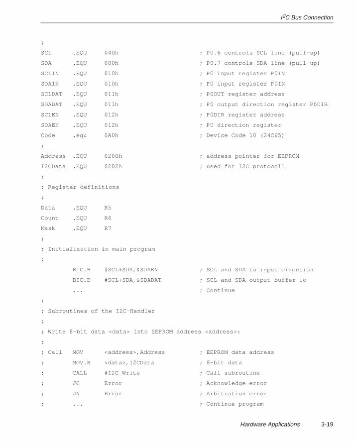
I2C Bus Connection
3-19Hardware Applications
;
SCL .EQU 040h ; P0.6 controls SCL line (pull–up)
SDA .EQU 080h ; P0.7 controls SDA line (pull–up)
SCLIN .EQU 010h ; P0 input register P0IN
SDAIN .EQU 010h ; P0 input register P0IN
SCLDAT .EQU 011h ; P0OUT register address
SDADAT .EQU 011h ; P0 output direction register P0DIR
SCLEN .EQU 012h ; P0DIR register address
SDAEN .EQU 012h ; P0 direction register
Code .equ 0A0h ; Device Code 10 (24C65)
;
Address .EQU 0200h ; address pointer for EEPROM
I2CData .EQU 0202h ; used for I2C protocoll
;
; Register definitions
;
Data .EQU R5
Count .EQU R6
Mask .EQU R7
;
; Initialization in main program
;
BIC.B #SCL+SDA,&SDAEN ; SCL and SDA to input direction
BIC.B #SCL+SDA,&SDADAT ; SCL and SDA output buffer lo
... ; Continue
;
; Subroutines of the I2C–Handler
;
; Write 8–bit data <data> into EEPROM address <address>:
;
; Call MOV <address>,Address ; EEPROM data address
; MOV.B <data>,I2CData ; 8–bit data
; CALL #I2C_Write ; Call subroutine
; JC Error ; Acknowledge error
; JN Error ; Arbitration error
; ... ; Continue program
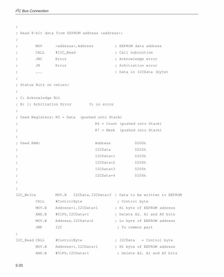
I2C Bus Connection
3-20
;
; Read 8–bit data from EEPROM address <address>:
;
; MOV <address>,Address ; EEPROM data address
; CALL #I2C_Read ; Call subroutine
; JNC Error ; Acknowledge error
; JN Error ; Arbitration error
; ... ; Data in I2CData (byte)
;
; Status Bits on return:
;
; C: Acknowledge Bit
; N: 1: Arbitration Error 0: no error
;
; Used Registers: R5 = Data (pushed onto Stack)
; R6 = Count (pushed onto Stack)
; R7 = Mask (pushed onto Stack)
;
; Used RAM: Address 0200h
; I2CData 0202h
; I2CData+1 0203h
; I2CData+2 0204h
; I2CData+3 0205h
; I2CData+4 0206h
;
;
I2C_Write MOV.B I2CData,I2CData+3 ; Data to be written to EEPROM
CALL #ControlByte ; Control byte
MOV.B Address+1,I2CData+1 ; Hi byte of EEPROM address
AND.B #01Fh,I2CData+1 ; Delete A2, A1 and A0 bits
MOV.B Address,I2CData+2 ; Lo byte of EEPROM address
JMP I2C ; To common part
;
I2C_Read CALL #ControlByte ; I2CData = Control byte
MOV.B Address+1,I2CData+1 ; Hi byte of EEPROM address
AND.B #01Fh,I2CData+1 ; Delete A2, A1 and A0 bits
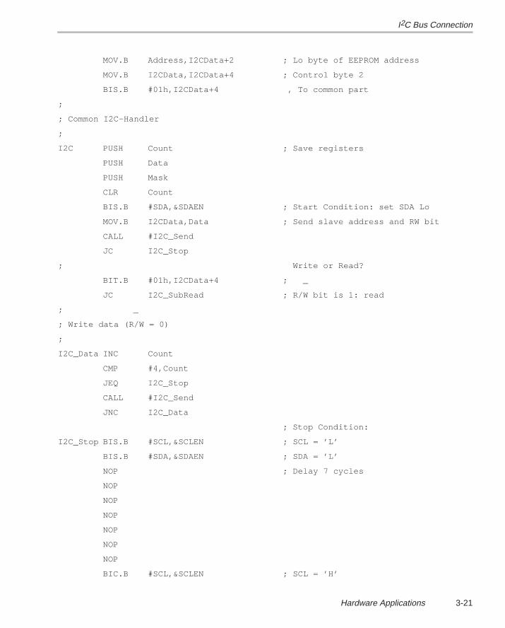
I2C Bus Connection
3-21Hardware Applications
MOV.B Address,I2CData+2 ; Lo byte of EEPROM address
MOV.B I2CData,I2CData+4 ; Control byte 2
BIS.B #01h,I2CData+4 , To common part
;
; Common I2C–Handler
;
I2C PUSH Count ; Save registers
PUSH Data
PUSH Mask
CLR Count
BIS.B #SDA,&SDAEN ; Start Condition: set SDA Lo
MOV.B I2CData,Data ; Send slave address and RW bit
CALL #I2C_Send
JC I2C_Stop
; Write or Read?
BIT.B #01h,I2CData+4 ; _
JC I2C_SubRead ; R/W bit is 1: read
; _
; Write data (R/W = 0)
;
I2C_Data INC Count
CMP #4,Count
JEQ I2C_Stop
CALL #I2C_Send
JNC I2C_Data
; Stop Condition:
I2C_Stop BIS.B #SCL,&SCLEN ; SCL = ’L’
BIS.B #SDA,&SDAEN ; SDA = ’L’
NOP ; Delay 7 cycles
NOP
NOP
NOP
NOP
NOP
NOP
BIC.B #SCL,&SCLEN ; SCL = ’H’
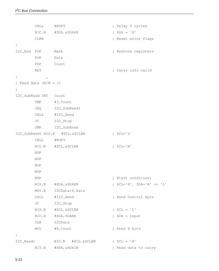
I2C Bus Connection
3-22
CALL #NOP9 ; Delay 9 cycles
BIC.B #SDA,&SDAEN ; SDA = ’H’
CLRN ; Reset error flags
;
I2C_End POP Mask ; Restore registers
POP Data
POP Count
RET ; Carry info valid
; _
; Read data (R/W = 1)
;
I2C_SubRead INC Count
CMP #3,Count
JEQ I2C_SubRead1
CALL #I2C_Send
JC I2C_Stop
JMP I2C_SubRead
I2C_SubRead1 BIS.B #SCL,&SCLEN ; SCL=’L’
CALL #NOP9
BIC.B #SCL,&SCLEN ; SCL=’H’
NOP
NOP
NOP
NOP
NOP ; Start condition:
BIS.B #SDA,&SDAEN ; SCL=’H’, SDA=’H’ => ’L’
MOV.B I2CData+4,Data
CALL #I2C_Send ; Send Control Byte
JC I2C_Stop
BIS.B #SCL,&SCLEN ; SCL = ’L’
BIC.B #SDA,SDAEN ; SDA = Input
CLR I2CData
MOV #8,Count ; Read 8 bits
;
I2C_Read1 BIC.B #SCL,&SCLEN ; SCL = ’H’
BIT.B #SDA,&SDAIN ; Read data to carry
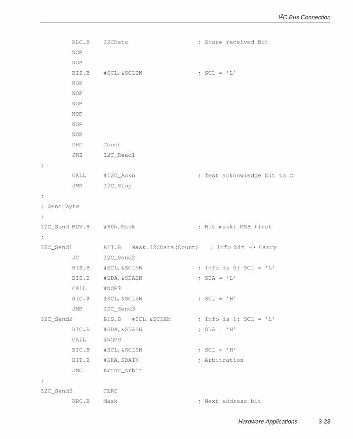
I2C Bus Connection
3-23Hardware Applications
RLC.B I2CData ; Store received Bit
NOP
NOP
BIS.B #SCL,&SCLEN ; SCL = ’L’
NOP
NOP
NOP
NOP
NOP
NOP
DEC Count
JNZ I2C_Read1
;
CALL #I2C_Ackn ; Test acknowledge bit to C
JMP I2C_Stop
;
; Send byte
;
I2C_Send MOV.B #80h,Mask ; Bit mask: MSB first
;
I2C_Send1 BIT.B Mask,I2CData(Count) ; Info bit –> Carry
JC I2C_Send2
BIS.B #SCL,&SCLEN ; Info is 0: SCL = ’L’
BIS.B #SDA,&SDAEN ; SDA = ’L’
CALL #NOP9
BIC.B #SCL,&SCLEN ; SCL = ’H’
JMP I2C_Send3
I2C_Send2 BIS.B #SCL,&SCLEN ; Info is 1: SCL = ’L’
BIC.B #SDA,&SDAEN ; SDA = ’H’
CALL #NOP9
BIC.B #SCL,&SCLEN ; SCL = ’H’
BIT.B #SDA,SDAIN ; Arbitration
JNC Error_Arbit
;
I2C_Send3 CLRC
RRC.B Mask ; Next address bit
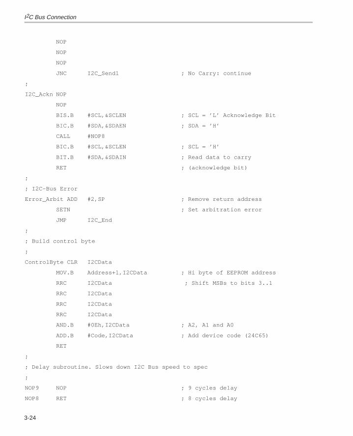
I2C Bus Connection
3-24
NOP
NOP
NOP
JNC I2C_Send1 ; No Carry: continue
;
I2C_Ackn NOP
NOP
BIS.B #SCL,&SCLEN ; SCL = ’L’ Acknowledge Bit
BIC.B #SDA,&SDAEN ; SDA = ’H’
CALL #NOP8
BIC.B #SCL,&SCLEN ; SCL = ’H’
BIT.B #SDA,&SDAIN ; Read data to carry
RET ; (acknowledge bit)
;
; I2C–Bus Error
Error_Arbit ADD #2,SP ; Remove return address
SETN ; Set arbitration error
JMP I2C_End
;
; Build control byte
;
ControlByte CLR I2CData
MOV.B Address+1,I2CData ; Hi byte of EEPROM address
RRC I2CData ; Shift MSBs to bits 3..1
RRC I2CData
RRC I2CData
RRC I2CData
AND.B #0Eh,I2CData ; A2, A1 and A0
ADD.B #Code,I2CData ; Add device code (24C65)
RET
;
; Delay subroutine. Slows down I2C Bus speed to spec
;
NOP9 NOP ; 9 cycles delay
NOP8 RET ; 8 cycles delay
Hardware Optimization
3-25Hardware Applications
3.5 Hardware Optimization
The MSP430 permits the use of unused analog inputs (A7 to A0) and segmentlines (S29 to S2) for inputs and outputs, respectively. The following two sec-tions explain in detail how to program and use these inputs and outputs.
3.5.1 Use of Unused Analog Inputs
Unused analog-to-digital converter (ADC) inputs can be used as digital inputsor, with some restrictions, as digital outputs.
3.5.1.1 Analog Inputs Used for Digital Inputs
Any ADC input A7 to A0 can be used as a digital input. It only needs to be pro-grammed (for example, during the initialization) for this function. Three thingsare important if this feature is used:
Any activity at these digital inputs has to be stopped during ongoing sensi-tive ADC measurements. This activity will cause noise, which invalidatesthe ADC results. Activity in this case means:
No change of the AEN register (switching between digital and analogmode)
No input change at the digital ADC inputs (this rarely allows changingsignals at these inputs).
All bits that are switched to ADC inputs will read zero when read. There-fore, it is not necessary to clear them with software after reading.
Not all analog inputs are implemented in a given device
Example 3–6. A0 – A4 are used as ADC Inputs and A5 – A7 as Digital Inputs
AIN .EQU 0110h ; Address DIGITAL INPUT REGISTER
AEN .EQU 0112h ; Address DIGITAL INPUT ENABLE REG.
A7EN .EQU 080h ; Bits in Dig. Input Enable Reg.:
A6EN .EQU 040h ; 0: ADC 1: Digital Input
A5EN .EQU 020h ;
; INITIALIZATION: A7 TO A5 ARE SWITCHED TO DIGITAL INPUTS
; A4 TO A0 ARE USED AS ANALOG INPUTS
;
MOV #A7EN+A6EN+A5EN,&AEN ; A7 TO A5 DIGITAL MODE
...
;
Hardware Optimization
3-26
; NORMAL PROGRAM EXECUTION:
; CHECK IF A7 OR A5 ARE HIGH. IF YES: JUMP TO LABEL L$100
;
BIT #A7EN+A5EN,&AIN ; A7 .OR. A5 HI?
JNZ L$100 ; YES
... ; NO, CONTINUE
;
; CHECK IF ALL DIG. INPUTS A7 TO A5 ARE LOW. IF YES: Go to L$200
;
TST &AIN ; A7 TO A5 LO?
JZ L$200 ; YES, (ANALOG INPUTS READ ZERO)
3.5.1.2 Analog Inputs Used as Digital Outputs
If outputs are needed then the unused ADC inputs with the current source con-nection can be used with the following restrictions:
Only one ADC input can be high at a given time (1 out of n principle)
Only the ADC inputs A0 to A3 are usable (only they are connected to thecurrent source)
The outputs can go high only while the ADC is not using the current source.
The output current is directly related to the supply voltage, VCC.
The output voltage is only about 50% of the supply voltage, VCC. Logic lev-els have to be carefully monitored. A transistor stage might be necessary(if not there already, e.g. for a relay).
The output current is the current of the current source. Again, logic levelshave to be carefully monitored. The pull-down resistor has to be bigenough to allow the maximum output level.
The example in Figure 3–9 shows the ADC using inputs A0 and A1 as digitaloutputs driving two stages; a transistor stage (energy pulse, e.g. with an elec-tricity meter) and a 3.3-V gate (3.3 V ensures that the input levels are suffi-cient).
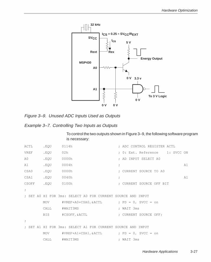
Hardware Optimization
3-27Hardware Applications
SVCC
A0
0 V
A1
5 V
0 V
32 kHz
MSP430
ICS = 0.25 × SVCC/REXT
To 3 V Logic
0 V
Rext
Ics
Rex
3.3 v
0 V
Energy Output
Figure 3–9. Unused ADC Inputs Used as Outputs
Example 3–7. Controlling Two Inputs as Outputs
To control the two outputs shown in Figure 3–9, the following software programis necessary:
ACTL .EQU 0114h ; ADC CONTROL REGISTER ACTL
VREF .EQU 02h ; 0: Ext. Reference 1: SVCC ON
A0 .EQU 0000h ; AD INPUT SELECT A0
A1 .EQU 0004h ; A1
CSA0 .EQU 0000h ; CURRENT SOURCE TO A0
CSA1 .EQU 0040h ; A1
CSOFF .EQU 0100h ; CURRENT SOURCE OFF BIT
;
; SET A0 HI FOR 3ms: SELECT A0 FOR CURRENT SOURCE AND INPUT
MOV #VREF+A0+CSA0,&ACTL ; PD = 0, SVCC = on
CALL #WAIT3MS ; WAIT 3ms
BIS #CSOFF,&ACTL ; CURRENT SOURCE OFF;
;
; SET A1 HI FOR 3ms: SELECT A1 FOR CURRENT SOURCE AND INPUT
MOV #VREF+A1+CSA1,&ACTL ; PD = 0, SVCC = on
CALL #WAIT3MS ; WAIT 3ms
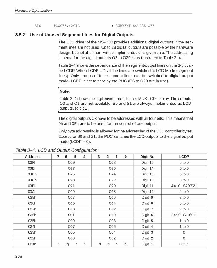
Hardware Optimization
3-28
BIS #CSOFF,&ACTL ; CURRENT SOURCE OFF
3.5.2 Use of Unused Segment Lines for Digital Outputs
The LCD driver of the MSP430 provides additional digital outputs, if the seg-ment lines are not used. Up to 28 digital outputs are possible by the hardwaredesign, but not all of them will be implemented on a given chip. The addressingscheme for the digital outputs O2 to O29 is as illustrated in Table 3–4.
Table 3–4 shows the dependence of the segment/output lines on the 3-bit val-ue LCDP. When LCDP = 7, all the lines are switched to LCD Mode (segmentlines). Only groups of four segment lines can be switched to digital outputmode. LCDP is set to zero by the PUC (O6 to O29 are in use).
Note:
Table 3–4 shows the digit environment for a 4-MUX LCD display. The outputsO0 and O1 are not available: S0 and S1 are always implemented as LCDoutputs. (digit 1).
The digital outputs Ox have to be addressed with all four bits. This means that0h and 0Fh are to be used for the control of one output.
Only byte addressing is allowed for the addressing of the LCD controller bytes.Except for S0 and S1, the PUC switches the LCD outputs to the digital outputmode (LCDP = 0).
Table 3–4. LCD and Output ConfigurationAddress 7 6 5 4 3 2 1 0 Digit Nr. LCDP
03Fh O29 O28 Digit 15 6 to 0
03Eh O27 O26 Digit 14 6 to 0
03Dh O25 O24 Digit 13 5 to 0
03Ch O23 O22 Digit 12 5 to 0
03Bh O21 O20 Digit 11 4 to 0 S20/S21
03Ah O19 O18 Digit 10 4 to 0
039h O17 O16 Digit 9 3 to 0
038h O15 O14 Digit 8 3 to 0
037h O13 O12 Digit 7 2 to 0
036h O11 O10 Digit 6 2 to 0 S10/S11
035h O09 O08 Digit 5 1 to 0
034h O07 O06 Digit 4 1 to 0
033h O05 O04 Digit 3 0
032h O03 O02 Digit 2 0
031h h g f e d c b a Digit 1 S0/S1
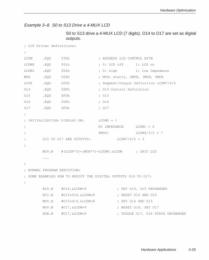
Hardware Optimization
3-29Hardware Applications
Example 3–8. S0 to S13 Drive a 4-MUX LCD
S0 to S13 drive a 4-MUX LCD (7 digits). O14 to O17 are set as digitaloutputs.
; LCD Driver definitions:
;
LCDM .EQU 030h ; ADDRESS LCD CONTROL BYTE
LCDM0 .EQU 001h ; 0: LCD off 1: LCD on
LCDM1 .EQU 002h ; 0: high 1: low Impedance
MUX .EQU 004h ; MUX: static, 2MUX, 3MUX, 4MUX
LCDP .EQU 020h ; Segment/Output Definition LCDM7/6/5
O14 .EQU 00Fh ; O14 Control Definition
O15 .EQU 0F0h ; O15
O16 .EQU 00Fh ; O16
O17 .EQU 0F0h ; O17
;
; INITIALIZATION: DISPLAY ON: LCDM0 = 1
; HI IMPEDANCE LCDM1 = 0
; 4MUX: LCDM4/3/2 = 7
; O14 TO O17 ARE OUTPUTS: LCDM7/6/5 = 3
;
MOV.B #(LCDP*3)+(MUX*7)+LCDM0,&LCDM ; INIT LCD
...
;
; NORMAL PROGRAM EXECUTION:
; SOME EXAMPLES HOW TO MODIFY THE DIGITAL OUTPUTS O14 TO O17:
;
BIS.B #O14,&LCDM+8 ; SET O14, O15 UNCHANGED
BIC.B #O15+O14,&LCDM+8 ; RESET O14 AND O15
MOV.B #O15+O14,&LCDM+8 ; SET O14 AND O15
MOV.B #O17,&LCDM+9 ; RESET O16, SET O17
XOR.B #O17,&LCDM+9 ; TOGGLE O17, O16 STAYS UNCHANGED

Digital-to-Analog Converters
3-30
3.6 Digital-to-Analog Converters
The MSP430 does not contain a digital-to-analog converter (DAC) on-chip, butit is relatively simple to implement the DAC function. Five different solutionswith distinct hardware and software requirements are shown in the following:
The R/2R method The weighted-resistors method Integrated DACs connected to the I2C Bus Pulse width modulation (PWM) with the universal timer/port module Pulse width modulation with Timer A
3.6.1 R/2R Method
With a CMOS shift register or digital outputs, a DAC can be built for any bitlength. The outputs Qx of the shift register switch the 2R-resistors to 0 V or VCCaccording to the digital input. The voltage at the non-inverting input and alsoat the output voltage Vout of the operational amplifier is:
kCC= × VVout n2
Where:k Value of the digital input word with n bits lengthn Number of Q outputs, maximum length of input wordVCC Supply voltage
Signed output is possible by level shifting or by splitting of the power supply(+VCC/2 and –VCC/2). With split power supplies the voltage at the output of theoperational amplifier is:
n= VCC
–Vout VCC2
×k
= VCC2
–12
kn2
( )
Advantages of the R/2R Method
Only two different resistors are necessary (R and 2R) Absolute monotony over the complete output range Internal impedance independent of the digital value: impedance is
always R Expandable to any bit length by the adding of shift registers With only three digital outputs (Ox, TP0.x, Portx), an inexpensive solution
is possible.
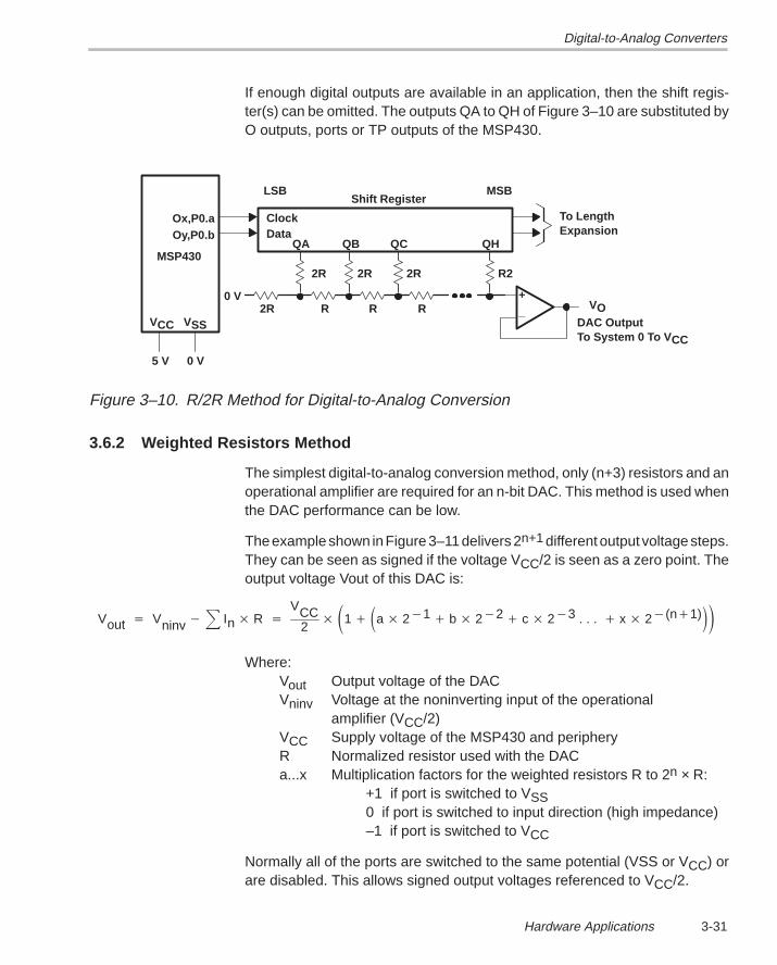
Digital-to-Analog Converters
3-31Hardware Applications
If enough digital outputs are available in an application, then the shift regis-ter(s) can be omitted. The outputs QA to QH of Figure 3–10 are substituted byO outputs, ports or TP outputs of the MSP430.
2R 2R 2R
2R R R R
R2
_+
QA QB QC QH
ClockData
To LengthExpansion
VODAC OutputTo System 0 To V CC
LSB MSBShift Register
Ox,P0.aOy,P0.b
0 V
VCC VSS
5 V 0 V
MSP430
Figure 3–10. R/2R Method for Digital-to-Analog Conversion
3.6.2 Weighted Resistors Method
The simplest digital-to-analog conversion method, only (n+3) resistors and anoperational amplifier are required for an n-bit DAC. This method is used whenthe DAC performance can be low.
The example shown in Figure 3–11 delivers 2n+1 different output voltage steps.They can be seen as signed if the voltage VCC/2 is seen as a zero point. Theoutput voltage Vout of this DAC is:
Vout Vninv In R VCC
21 a 21 b 22 c 23 . . . x 2(n1)
Where:Vout Output voltage of the DACVninv Voltage at the noninverting input of the operational
amplifier (VCC/2)VCC Supply voltage of the MSP430 and peripheryR Normalized resistor used with the DACa...x Multiplication factors for the weighted resistors R to 2n × R:
+1 if port is switched to VSS0 if port is switched to input direction (high impedance)–1 if port is switched to VCC
Normally all of the ports are switched to the same potential (VSS or VCC) orare disabled. This allows signed output voltages referenced to VCC/2.
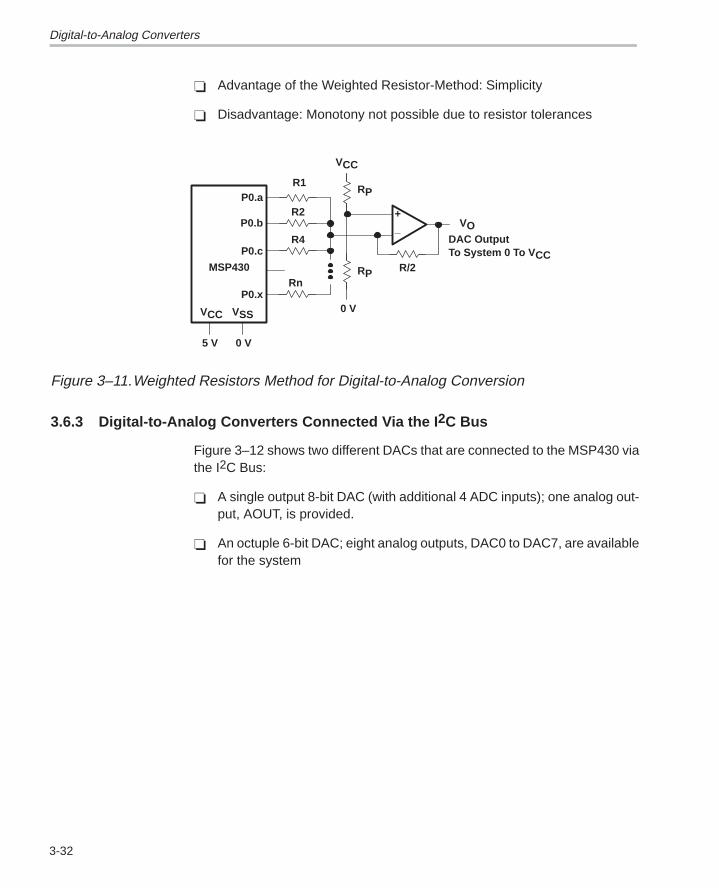
Digital-to-Analog Converters
3-32
Advantage of the Weighted Resistor-Method: Simplicity
Disadvantage: Monotony not possible due to resistor tolerances
_+
VODAC OutputTo System 0 To V CC
R/2
R1
R2
R4
Rn
P0.a
P0.b
P0.c
P0.x
5 V 0 V
MSP430 RP
0 V
RP
VCC VSS
VCC
Figure 3–11.Weighted Resistors Method for Digital-to-Analog Conversion
3.6.3 Digital-to-Analog Converters Connected Via the I 2C Bus
Figure 3–12 shows two different DACs that are connected to the MSP430 viathe I2C Bus:
A single output 8-bit DAC (with additional 4 ADC inputs); one analog out-put, AOUT, is provided.
An octuple 6-bit DAC; eight analog outputs, DAC0 to DAC7, are availablefor the system
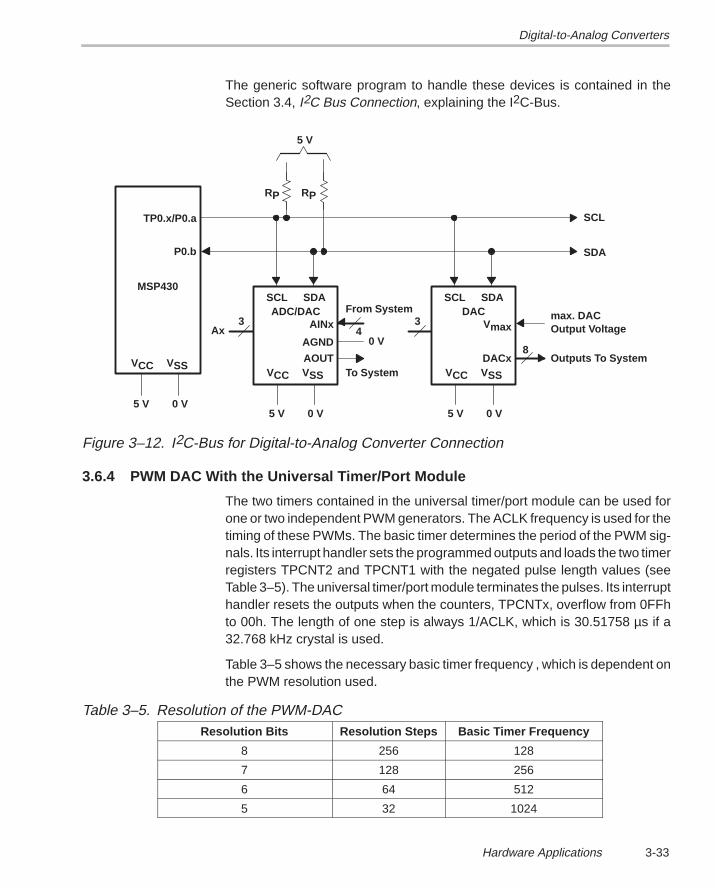
Digital-to-Analog Converters
3-33Hardware Applications
The generic software program to handle these devices is contained in theSection 3.4, I2C Bus Connection, explaining the I2C-Bus.
AINx
AGND
AOUTVCC VSS
SCL SDAADC/DAC
5 V 0 V
Vmax
DACx
SCL SDA
VCC VSS
5 V 0 V
RP RP
5 V
SCL
SDA
TP0.x/P0.a
P0.b
MSP430
34
DAC
VCC VSS
5 V 0 V
From System3
0 V
To System
8
max. DACOutput Voltage
Outputs To System
Ax
Figure 3–12. I2C-Bus for Digital-to-Analog Converter Connection
3.6.4 PWM DAC With the Universal Timer/Port Module
The two timers contained in the universal timer/port module can be used forone or two independent PWM generators. The ACLK frequency is used for thetiming of these PWMs. The basic timer determines the period of the PWM sig-nals. Its interrupt handler sets the programmed outputs and loads the two timerregisters TPCNT2 and TPCNT1 with the negated pulse length values (seeTable 3–5). The universal timer/port module terminates the pulses. Its interrupthandler resets the outputs when the counters, TPCNTx, overflow from 0FFhto 00h. The length of one step is always 1/ACLK, which is 30.51758 µs if a32.768 kHz crystal is used.
Table 3–5 shows the necessary basic timer frequency , which is dependent onthe PWM resolution used.
Table 3–5. Resolution of the PWM-DACResolution Bits Resolution Steps Basic Timer Frequency
8 256 128
7 128 256
6 64 512
5 32 1024
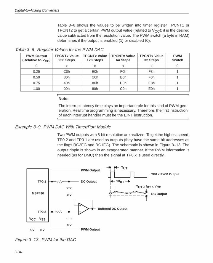
Digital-to-Analog Converters
3-34
Table 3–6 shows the values to be written into timer register TPCNT1 orTPCNT2 to get a certain PWM output value (related to VCC); it is the desiredvalue subtracted from the resolution value. The PWM switch (a byte in RAM)determines if the output is enabled (1) or disabled (0).
Table 3–6. Register Values for the PWM-DACPWM Output
(Relative to V CC)TPCNTx Value
256 StepsTPCNTx Value
128 StepsTPCNTx Value
64 StepsTPCNTx Value
32 StepsPWM
Switch
0 x x x x 0
0.25 C0h E0h F0h F8h 1
0.50 80h C0h E0h F0h 1
0.75 40h A0h D0h E8h 1
1.00 00h 80h C0h E0h 1
Note:
The interrupt latency time plays an important role for this kind of PWM gen-eration. Real time programming is necessary. Therefore, the first instructionof each interrupt handler must be the EINT instruction.
Example 3–9. PWM DAC With Timer/Port Module
Two PWM outputs with 8-bit resolution are realized. To get the highest speed,TP0.2 and TP0.1 are used as outputs (they have the same bit addresses asthe flags RC2FG and RC1FG). The schematic is shown in Figure 3–13. Theoutput ripple is shown in an exaggerated manner. If the PWM information isneeded (as for DMC) then the signal at TP0.x is used directly.
_+
Buffered DC Output
0 V
0 V
TP0.1
TP0.2
VCC VSS
0 V5 V
PWM Output
DC Output
PWM Output
TUT
1/fBTTUT x fBT x VCC
DC Output
TP0.x PWM Output
MSP430
Figure 3–13. PWM for the DAC
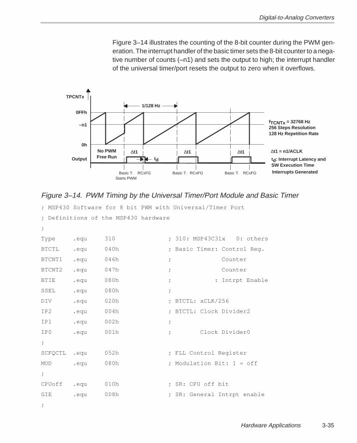
Digital-to-Analog Converters
3-35Hardware Applications
Figure 3–14 illustrates the counting of the 8-bit counter during the PWM gen-eration. The interrupt handler of the basic timer sets the 8-bit counter to a nega-tive number of counts (–n1) and sets the output to high; the interrupt handlerof the universal timer/port resets the output to zero when it overflows.
TPCNTx
0FFh
–n1
0h
Output
No PWMFree Run
∆t1 ∆t1 ∆t1td
1/128 Hz
Basic T.Starts PWM
RCxFG Basic T. RCxFG Basic T. RCxFG
fTCNTx = 32768 Hz256 Steps Resolution128 Hz Repetition Rate
∆t1 = n1/ACLK
td: Interrupt Latency andSW Execution TimeInterrupts Generated
Figure 3–14. PWM Timing by the Universal Timer/Port Module and Basic Timer
; MSP430 Software for 8 bit PWM with Universal/Timer Port
; Definitions of the MSP430 hardware
;
Type .equ 310 ; 310: MSP43C31x 0: others
BTCTL .equ 040h ; Basic Timer: Control Reg.
BTCNT1 .equ 046h ; Counter
BTCNT2 .equ 047h ; Counter
BTIE .equ 080h ; : Intrpt Enable
SSEL .equ 080h ;
DIV .equ 020h ; BTCTL: xCLK/256
IP2 .equ 004h ; BTCTL: Clock Divider2
IP1 .equ 002h ;
IP0 .equ 001h ; Clock Divider0
;
SCFQCTL .equ 052h ; FLL Control Register
MOD .equ 080h ; Modulation Bit: 1 = off
;
CPUoff .equ 010h ; SR: CPU off bit
GIE .equ 008h ; SR: General Intrpt enable
;
Digital-to-Analog Converters
3-36
TPCTL .equ 04Bh ; Timer Port: Control Reg.
TPCNT1 .equ 04Ch ; Counter Reg.Lo
TPCNT2 .equ 04Dh ; Counter Reg.Hi
TPD .equ 04Eh ; Data Reg.
TPE .equ 04Fh ; Enable Reg.
TP1 .equ 002h ; Bit address TP0.1
TP2 .equ 004h ; TP0.2
TP3 .equ 008h TP0.3
TP4 .equ 010h ; TP0.4
TP5 .equ 020h ; TP0.5
;
.if Type=310 ; MSP430C31x?
TPIE .equ 004h ; ADC: Intrpt Enable Bit
.else
TPIE .equ 008h ; MSP430C32x configuration
.endif
IE2 .equ 001h ; Intrpt Enable Byte
TPSSEL3 .equ 080h ;
TPSSEL2 .equ 040h
TPSSEL1 .equ 080h ; Selects clock input (TPCTL)
TPSSEL0 .equ 040h ;
ENB .equ 020h ; Selects clock gate (TPCTL)
ENA .equ 010h ;
EN1 .equ 008h ; Gate for TPCNTx (TPCTL)
RC2FG .equ 004h ; Carry of HI counter (TPCTL)
RC1FG .equ 002h ; Carry of LO counter (TPCTL)
EN1FG .equ 001h ; End of Conversion Flag ”
B16 .equ 080h ; Use 16–bit counter (TPD)
; RAM Definitions
;
SW_PWM .equ 0200h ; Enable bits for TP0.2 and TP0.1
TIM_PWM1 .equ 0201h ; Calc. PWM result PWM1
TIM_PWM2 .equ 0202h ; Calc. PWM result PWM2
;
;=========================================================
;
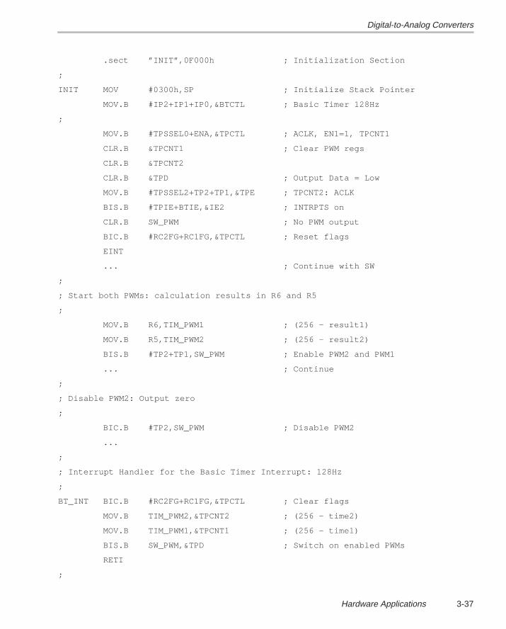
Digital-to-Analog Converters
3-37Hardware Applications
.sect ”INIT”,0F000h ; Initialization Section
;
INIT MOV #0300h,SP ; Initialize Stack Pointer
MOV.B #IP2+IP1+IP0,&BTCTL ; Basic Timer 128Hz
;
MOV.B #TPSSEL0+ENA,&TPCTL ; ACLK, EN1=1, TPCNT1
CLR.B &TPCNT1 ; Clear PWM regs
CLR.B &TPCNT2
CLR.B &TPD ; Output Data = Low
MOV.B #TPSSEL2+TP2+TP1,&TPE ; TPCNT2: ACLK
BIS.B #TPIE+BTIE,&IE2 ; INTRPTS on
CLR.B SW_PWM ; No PWM output
BIC.B #RC2FG+RC1FG,&TPCTL ; Reset flags
EINT
... ; Continue with SW
;
; Start both PWMs: calculation results in R6 and R5
;
MOV.B R6,TIM_PWM1 ; (256 – result1)
MOV.B R5,TIM_PWM2 ; (256 – result2)
BIS.B #TP2+TP1,SW_PWM ; Enable PWM2 and PWM1
... ; Continue
;
; Disable PWM2: Output zero
;
BIC.B #TP2,SW_PWM ; Disable PWM2
...
;
; Interrupt Handler for the Basic Timer Interrupt: 128Hz
;
BT_INT BIC.B #RC2FG+RC1FG,&TPCTL ; Clear flags
MOV.B TIM_PWM2,&TPCNT2 ; (256 – time2)
MOV.B TIM_PWM1,&TPCNT1 ; (256 – time1)
BIS.B SW_PWM,&TPD ; Switch on enabled PWMs
RETI
;
Digital-to-Analog Converters
3-38
; End of Basic Timer Handler
;––––––––––––––––––––––––––––––––––––––––––––––––––––––––––
; Interrupt Handler for the Universal Timer/Port Module
; For max. speed TP0.2 and TP0.1 are used (same bit locations
; as RC2FG and RC1FG). If other locations are used, RLA
; instructions have to be inserted after the flag clearing
;
UT_HNDL PUSH.B &TPCTL ; INTRPT from where?
AND #RC2FG+RC1FG,0(SP) ; Isolate flags
BIC.B @SP,&TPCTL ; Clear set flag(s)
BIC.B @SP+,&TPD ; Reset actual I/O(s)
RETI
;
; End of Universal Timer/Port Module Handler
;––––––––––––––––––––––––––––––––––––––––––––––––––––––––––
;
.sect ”INT_VECT”,0FFE2h
.WORD BT_INT ; Basic Timer Vector
.if Type=310
.sect ”INT_VEC1”,0FFEAh ; MSP430C31x
.else
.sect ”INT_VEC1”,0FFE8h ; Others
.endif
.WORD UT_HNDL ; UTP Vector (31x)
.sect ”INT_VEC2”,0FFFEh
.WORD INIT ; Reset Vector
Example 3–10. PWM Outputs With 7-Bit Resolution
Two PWM outputs with 7-bit resolution are realized. TP0.4 and TP0.3 are usedas PWM outputs (this makes shifting necessary). The schematic is shown inFigure 3–15. Due to the inverting filters at the PWM outputs, the outputs of theMSP430 are also inverted to compensate for this. The output ripple is shown
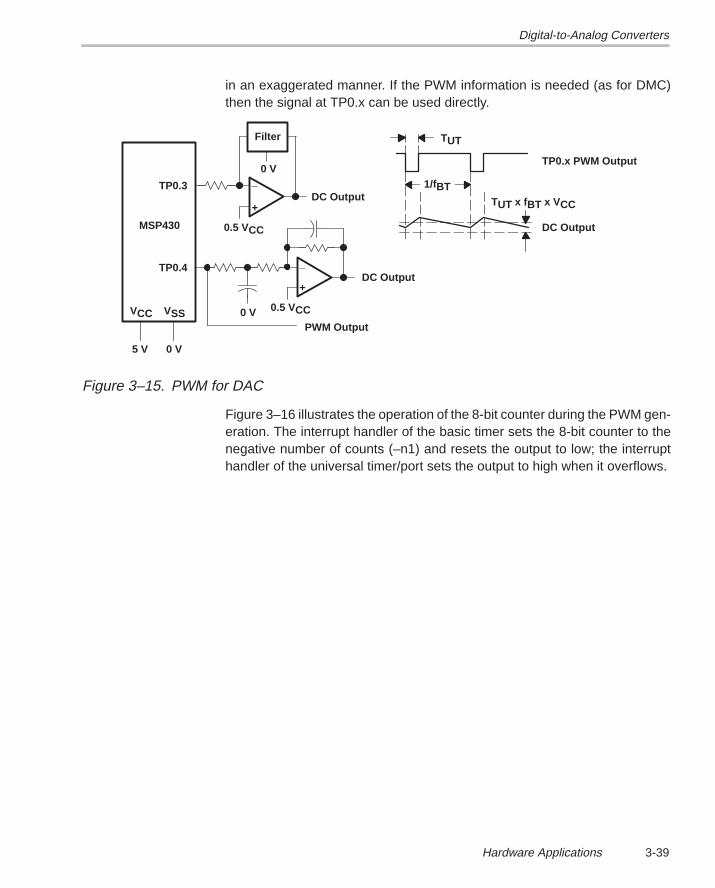
Digital-to-Analog Converters
3-39Hardware Applications
in an exaggerated manner. If the PWM information is needed (as for DMC)then the signal at TP0.x can be used directly.
_
+DC Output
0 V
TP0.3
TP0.4
VCC VSS
0 V5 V
Filter
DC Output
PWM Output
TUT
1/fBTTUT x fBT x VCC
DC Output
TP0.x PWM Output
MSP430
_
+
0 V
0.5 VCC
0.5 VCC
Figure 3–15. PWM for DAC
Figure 3–16 illustrates the operation of the 8-bit counter during the PWM gen-eration. The interrupt handler of the basic timer sets the 8-bit counter to thenegative number of counts (–n1) and resets the output to low; the interrupthandler of the universal timer/port sets the output to high when it overflows.
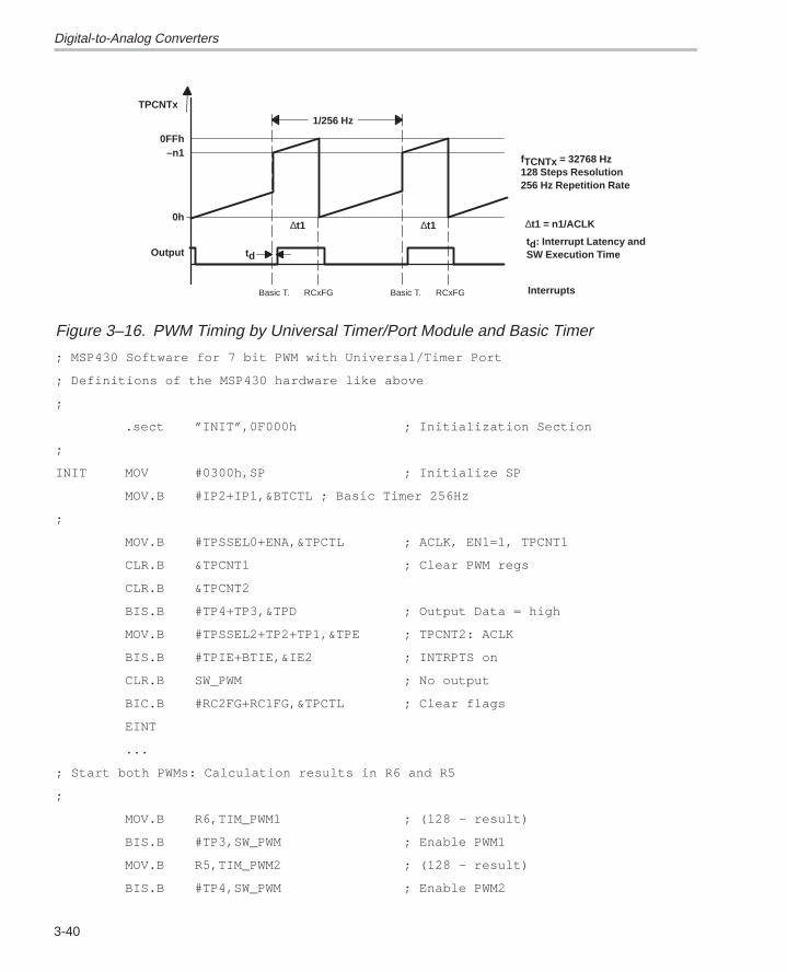
Digital-to-Analog Converters
3-40
TPCNTx
0FFh–n1
0h
Output
∆t1 ∆t1
td
1/256 Hz
Basic T. RCxFG
fTCNTx = 32768 Hz128 Steps Resolution256 Hz Repetition Rate
∆t1 = n1/ACLK
td: Interrupt Latency andSW Execution Time
InterruptsBasic T. RCxFG
Figure 3–16. PWM Timing by Universal Timer/Port Module and Basic Timer
; MSP430 Software for 7 bit PWM with Universal/Timer Port
; Definitions of the MSP430 hardware like above
;
.sect ”INIT”,0F000h ; Initialization Section
;
INIT MOV #0300h,SP ; Initialize SP
MOV.B #IP2+IP1,&BTCTL ; Basic Timer 256Hz
;
MOV.B #TPSSEL0+ENA,&TPCTL ; ACLK, EN1=1, TPCNT1
CLR.B &TPCNT1 ; Clear PWM regs
CLR.B &TPCNT2
BIS.B #TP4+TP3,&TPD ; Output Data = high
MOV.B #TPSSEL2+TP2+TP1,&TPE ; TPCNT2: ACLK
BIS.B #TPIE+BTIE,&IE2 ; INTRPTS on
CLR.B SW_PWM ; No output
BIC.B #RC2FG+RC1FG,&TPCTL ; Clear flags
EINT
...
; Start both PWMs: Calculation results in R6 and R5
;
MOV.B R6,TIM_PWM1 ; (128 – result)
BIS.B #TP3,SW_PWM ; Enable PWM1
MOV.B R5,TIM_PWM2 ; (128 – result)
BIS.B #TP4,SW_PWM ; Enable PWM2
Digital-to-Analog Converters
3-41Hardware Applications
...
; Disable PWMs: Output is zero
;
BIC.B #TP4+TP3,SW_PWM ; No output
;
; Interrupt Handler for the Basic Timer Interrupt: 256Hz
; The enabled PWMs are switched on
;
BT_INT BIC.B #RC2FG+RC1FG,&TPCTL ; Clear flags
MOV.B TIM_PWM2,&TPCNT2 ; (128 – time2)
MOV.B TIM_PWM1,&TPCNT1 ; (128 – time1)
BIC.B SW_PWM,&TPD ; Switch on enabled PWMs
RETI
;
; End of Basic Timer Handler
;––––––––––––––––––––––––––––––––––––––––––––––––––––––––––
; Interrupt Handler for the UT/PM. The PWM–channel that
; caused the interrupt is switched off.
;
UT_HNDL PUSH R6 ; Save R6
MOV.B &TPCTL,R6 ; INTRPT from where?
AND #RC2FG+RC1FG,R6 ; Isolate flags
BIC.B R6,&TPCTL ; Clear set flag(s)
RLA R6 ; To TP0.4/TP0.3
RLA R6
BIS.B R6,&TPD ; Set actual I/O(s)
POP R6 ; Restore R6
RETI
;
; End of Universal Timer/Port Module Handler
;––––––––––––––––––––––––––––––––––––––––––––––––––––––––––
; Vectors like with the example before

Digital-to-Analog Converters
3-42
3.6.5 PWM DAC With the Timer_A
Timer_A of the MSP430 family is ideally suited for the generation of PWM sig-nals. The output unit of each one of the (up to five) capture/compare registersis able to generate seven different output modes. The PWM generation de-pends mainly on which mode of the Timer_A was used.
Continuous Mode: the timer register runs continuously upwards and rollsover to zero after the value 0FFFFh. The capture/compare register 0 isused like the other capture/compare registers. This mode allows up to fiveindependent timings. The continuous mode is not intended for PWM ap-plications. But, it can be used for relatively slow PWM applications, if othertimings are also needed. Interrupt is used for the setting and the resettingof the PWM output. The output unit controls the PWM output and the inter-rupt handler adds the next time interval to the capture/compare registerand modifies the mode of the output unit (set, toggle, or reset).
Up Mode: The timer register counts up to the content of capture/compareregister 0 (here the period register) and restarts at zero when it reachesthis value The capture/compare register 0 contains the period informationfor all other capture/compare registers.
Up-Down Mode: The timer register counts up to the content of capture/compare register 0 (here the period register) and counts down to zerowhen it reaches this value. When zero is reached again, the timer registercounts up again. capture/compare register 0 contains the period informa-tion for all other capture/compare registers.
All three modes are explained in detail in the Section 6.3, Timer_A. Softwareprogram examples are also given. If dc output is needed, the same output fil-ters can be used as shown in the previous section. The only difference is thepossible speed of the Timer_A (input frequency can be up to the MCLK fre-quency).
3.6.5.1 PWM DAC With Timer_A Running in Continuous Mode
Up to five completely different PWM generations are possible. If the TimerRegister equals one of the four capture/compare latches (programmed tocompare mode), the hardware task programmed to the output unit is per-formed (set, reset, toggle etc.) and an interrupt is requested. Figure 3–17 illus-trates the generation of a PWM signal with the capture/compare registers 0.The interrupt handler is responsible for the following tasks:
The time difference (represented by the clock count nx) to the next inter-rupt is added to the used capture/compare register by software: once ∆t0,once ∆t1
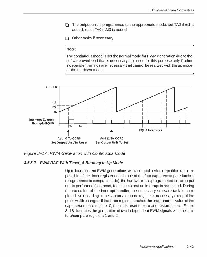
Digital-to-Analog Converters
3-43Hardware Applications
The output unit is programmed to the appropriate mode: set TA0 if ∆t1 isadded, reset TA0 if ∆t0 is added.
Other tasks if necessary
Note:
The continuous mode is not the normal mode for PWM generation due to thesoftware overhead that is necessary. It is used for this purpose only if otherindependent timings are necessary that cannot be realized with the up modeor the up-down mode.
0FFFFh
n1n0
0h
Interrupt Events:Example EQU0
t0 t1EQU0 Interrupts
Add t0 To CCR0Set Output Unit To Reset
Add t1 To CCR0Set Output Unit To Set
Figure 3–17. PWM Generation with Continuous Mode
3.6.5.2 PWM DAC With Timer_A Running in Up Mode
Up to four different PWM generations with an equal period (repetition rate) arepossible. If the timer register equals one of the four capture/compare latches(programmed to compare mode), the hardware task programmed to the outputunit is performed (set, reset, toggle etc.) and an interrupt is requested. Duringthe execution of the interrupt handler, the necessary software task is com-pleted. No reloading of the capture/compare register is necessary except if thepulse width changes. If the timer register reaches the programmed value of thecapture/compare register 0, then it is reset to zero and restarts there. Figure3–18 illustrates the generation of two independent PWM signals with the cap-ture/compare registers 1 and 2.
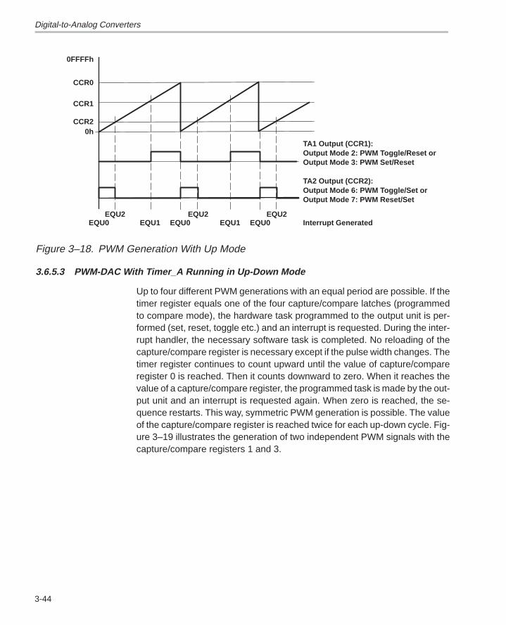
Digital-to-Analog Converters
3-44
0FFFFh
CCR0
CCR1
CCR20h
EQU0EQU2 EQU2 EQU2
EQU1 EQU0 EQU1 EQU0
TA1 Output (CCR1):Output Mode 2: PWM Toggle/Reset orOutput Mode 3: PWM Set/Reset
TA2 Output (CCR2):Output Mode 6: PWM Toggle/Set orOutput Mode 7: PWM Reset/Set
Interrupt Generated
Figure 3–18. PWM Generation With Up Mode
3.6.5.3 PWM-DAC With Timer_A Running in Up-Down Mode
Up to four different PWM generations with an equal period are possible. If thetimer register equals one of the four capture/compare latches (programmedto compare mode), the hardware task programmed to the output unit is per-formed (set, reset, toggle etc.) and an interrupt is requested. During the inter-rupt handler, the necessary software task is completed. No reloading of thecapture/compare register is necessary except if the pulse width changes. Thetimer register continues to count upward until the value of capture/compareregister 0 is reached. Then it counts downward to zero. When it reaches thevalue of a capture/compare register, the programmed task is made by the out-put unit and an interrupt is requested again. When zero is reached, the se-quence restarts. This way, symmetric PWM generation is possible. The valueof the capture/compare register is reached twice for each up-down cycle. Fig-ure 3–19 illustrates the generation of two independent PWM signals with thecapture/compare registers 1 and 3.
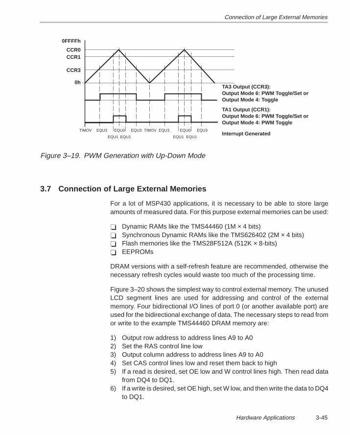
Connection of Large External Memories
3-45Hardware Applications
0FFFFh
CCR0CCR1
CCR3
0h
TIMOV EQU3 EQU0 EQU3 TIMOV EQU3 EQU0 EQU3
EQU1 EQU1 EQU1 EQU1
TA3 Output (CCR3):Output Mode 6: PWM Toggle/Set orOutput Mode 4: Toggle
TA1 Output (CCR1):Output Mode 6: PWM Toggle/Set orOutput Mode 4: PWM Toggle
Interrupt Generated
Figure 3–19. PWM Generation with Up-Down Mode
3.7 Connection of Large External Memories
For a lot of MSP430 applications, it is necessary to be able to store largeamounts of measured data. For this purpose external memories can be used:
Dynamic RAMs like the TMS44460 (1M × 4 bits) Synchronous Dynamic RAMs like the TMS626402 (2M × 4 bits) Flash memories like the TMS28F512A (512K × 8-bits) EEPROMs
DRAM versions with a self-refresh feature are recommended, otherwise thenecessary refresh cycles would waste too much of the processing time.
Figure 3–20 shows the simplest way to control external memory. The unusedLCD segment lines are used for addressing and control of the externalmemory. Four bidirectional I/O lines of port 0 (or another available port) areused for the bidirectional exchange of data. The necessary steps to read fromor write to the example TMS44460 DRAM memory are:
1) Output row address to address lines A9 to A02) Set the RAS control line low3) Output column address to address lines A9 to A04) Set CAS control lines low and reset them back to high5) If a read is desired, set OE low and W control lines high. Then read data
from DQ4 to DQ1.6) If a write is desired, set OE high, set W low, and then write the data to DQ4
to DQ1.
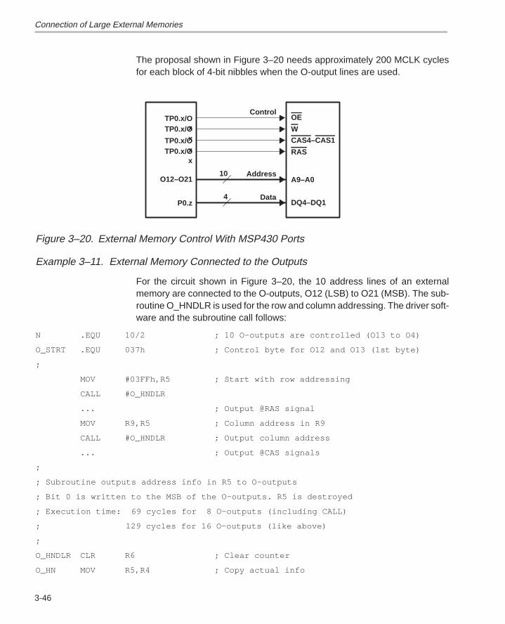
Connection of Large External Memories
3-46
The proposal shown in Figure 3–20 needs approximately 200 MCLK cyclesfor each block of 4-bit nibbles when the O-output lines are used.
10
4
TP0.x/OxTP0.x/OxTP0.x/OxTP0.x/Ox
O12–O21
P0.z
Address
Data
ControlOE
W
CAS4–CAS1
RAS
A9–A0
DQ4–DQ1
Figure 3–20. External Memory Control With MSP430 Ports
Example 3–11. External Memory Connected to the Outputs
For the circuit shown in Figure 3–20, the 10 address lines of an externalmemory are connected to the O-outputs, O12 (LSB) to O21 (MSB). The sub-routine O_HNDLR is used for the row and column addressing. The driver soft-ware and the subroutine call follows:
N .EQU 10/2 ; 10 O–outputs are controlled (O13 to O4)
O_STRT .EQU 037h ; Control byte for O12 and O13 (1st byte)
;
MOV #03FFh,R5 ; Start with row addressing
CALL #O_HNDLR
... ; Output @RAS signal
MOV R9,R5 ; Column address in R9
CALL #O_HNDLR ; Output column address
... ; Output @CAS signals
;
; Subroutine outputs address info in R5 to O–outputs
; Bit 0 is written to the MSB of the O–outputs. R5 is destroyed
; Execution time: 69 cycles for 8 O–outputs (including CALL)
; 129 cycles for 16 O–outputs (like above)
;
O_HNDLR CLR R6 ; Clear counter
O_HN MOV R5,R4 ; Copy actual info
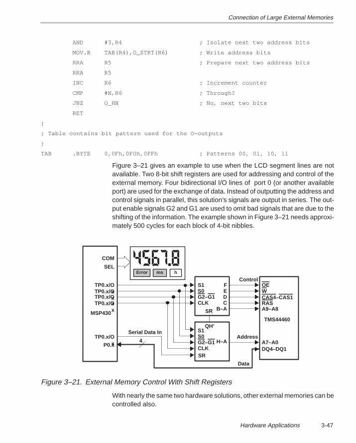
Connection of Large External Memories
3-47Hardware Applications
AND #3,R4 ; Isolate next two address bits
MOV.B TAB(R4),O_STRT(R6) ; Write address bits
RRA R5 ; Prepare next two address bits
RRA R5
INC R6 ; Increment counter
CMP #N,R6 ; Through?
JNZ O_HN ; No, next two bits
RET
;
; Table contains bit pattern used for the O–outputs
;
TAB .BYTE 0,0Fh,0F0h,0FFh ; Patterns 00, 01, 10, 11
Figure 3–21 gives an example to use when the LCD segment lines are notavailable. Two 8-bit shift registers are used for addressing and control of theexternal memory. Four bidirectional I/O lines of port 0 (or another availableport) are used for the exchange of data. Instead of outputting the address andcontrol signals in parallel, this solution’s signals are output in series. The out-put enable signals G2 and G1 are used to omit bad signals that are due to theshifting of the information. The example shown in Figure 3–21 needs approxi-mately 500 cycles for each block of 4-bit nibbles.
Error ms h
4
COM
SEL
TP0.x/OxTP0.x/OxTP0.x/OxTP0.x/Ox
TP0.x/OxP0.x
MSP430
S1S0G2–G1CLK
SR
FEDC
B–A
S1S0G2–G1CLKSR
H–A
Serial Data InAddress
ControlOEWCAS4–CAS1RASA9–A8
A7–A0DQ4–DQ1
QH’
Data
TMS44460
Figure 3–21. External Memory Control With Shift Registers
With nearly the same two hardware solutions, other external memories can becontrolled also.
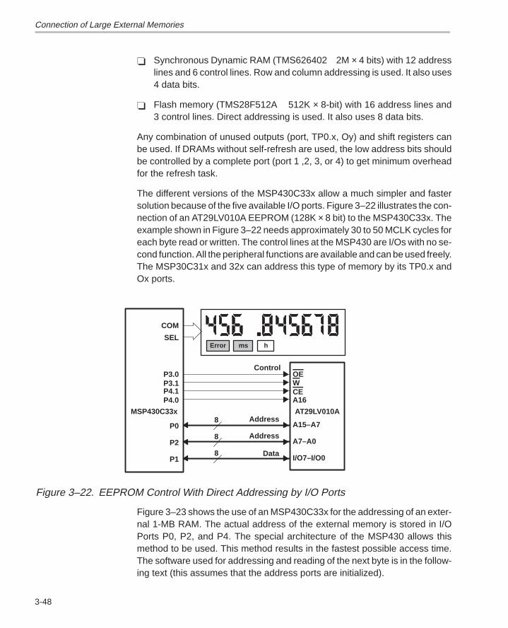
Connection of Large External Memories
3-48
Synchronous Dynamic RAM (TMS626402 2M × 4 bits) with 12 addresslines and 6 control lines. Row and column addressing is used. It also uses4 data bits.
Flash memory (TMS28F512A 512K × 8-bit) with 16 address lines and3 control lines. Direct addressing is used. It also uses 8 data bits.
Any combination of unused outputs (port, TP0.x, Oy) and shift registers canbe used. If DRAMs without self-refresh are used, the low address bits shouldbe controlled by a complete port (port 1 ,2, 3, or 4) to get minimum overheadfor the refresh task.
The different versions of the MSP430C33x allow a much simpler and fastersolution because of the five available I/O ports. Figure 3–22 illustrates the con-nection of an AT29LV010A EEPROM (128K × 8 bit) to the MSP430C33x. Theexample shown in Figure 3–22 needs approximately 30 to 50 MCLK cycles foreach byte read or written. The control lines at the MSP430 are I/Os with no se-cond function. All the peripheral functions are available and can be used freely.The MSP30C31x and 32x can address this type of memory by its TP0.x andOx ports.
Error ms h
8
COM
SEL
P3.0P3.1P4.1P4.0
P1
MSP430C33x
Address
ControlOEWCEA16
I/O7–I/O0
8P2 A7–A0
Data
Address8P0 A15–A7
AT29LV010A
Figure 3–22. EEPROM Control With Direct Addressing by I/O Ports
Figure 3–23 shows the use of an MSP430C33x for the addressing of an exter-nal 1-MB RAM. The actual address of the external memory is stored in I/OPorts P0, P2, and P4. The special architecture of the MSP430 allows thismethod to be used. This method results in the fastest possible access time.The software used for addressing and reading of the next byte is in the follow-ing text (this assumes that the address ports are initialized).
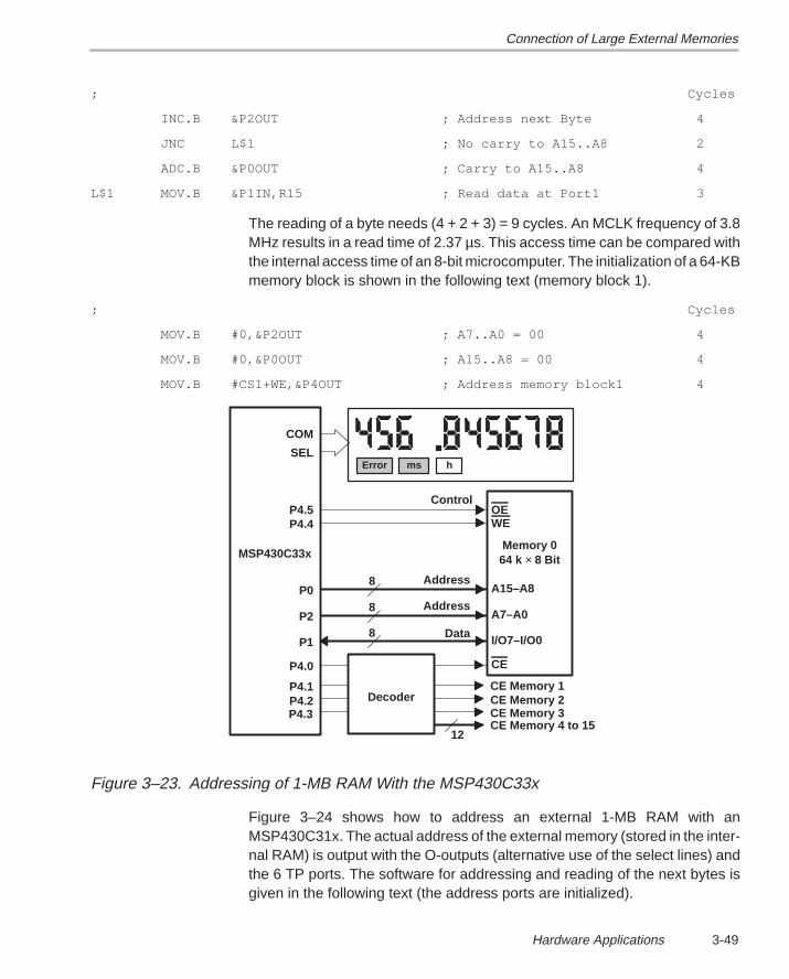
Connection of Large External Memories
3-49Hardware Applications
; Cycles
INC.B &P2OUT ; Address next Byte 4
JNC L$1 ; No carry to A15..A8 2
ADC.B &P0OUT ; Carry to A15..A8 4
L$1 MOV.B &P1IN,R15 ; Read data at Port1 3
The reading of a byte needs (4 + 2 + 3) = 9 cycles. An MCLK frequency of 3.8MHz results in a read time of 2.37 µs. This access time can be compared withthe internal access time of an 8-bit microcomputer. The initialization of a 64-KBmemory block is shown in the following text (memory block 1).
; Cycles
MOV.B #0,&P2OUT ; A7..A0 = 00 4
MOV.B #0,&P0OUT ; A15..A8 = 00 4
MOV.B #CS1+WE,&P4OUT ; Address memory block1 4
Error ms h
8
COM
SEL
P4.5P4.4
P4.1
P4.0
P1
MSP430C33x
Address
ControlOEWE
CE
I/O7–I/O0
8P2 A7–A0
Data
Address8P0 A15–A8
Memory 064 k × 8 Bit
Decoder
12
P4.2P4.3
CE Memory 1CE Memory 2CE Memory 3CE Memory 4 to 15
Figure 3–23. Addressing of 1-MB RAM With the MSP430C33x
Figure 3–24 shows how to address an external 1-MB RAM with anMSP430C31x. The actual address of the external memory (stored in the inter-nal RAM) is output with the O-outputs (alternative use of the select lines) andthe 6 TP ports. The software for addressing and reading of the next bytes isgiven in the following text (the address ports are initialized).
Connection of Large External Memories
3-50
; Cycles
INC.B A7_0 ; Address next byte 4
JNC L$1 ; No carry to A15..A8 2
ADC.B A15_8 ; Carry to A15..A8 4
;
; Address A15 to A8 is output to O17 to O10.
; This part is necessary for only 0.4% of all accesses
;
MOV.B A15_8,R14 ; A15..8 –> R14 3
MOV R14,R15 ; 1
AND #3,R15 ; Next 2 address bits 2
MOV.B TAB(R15),&036h ; A9..8 to O11..10 6
RRA R14 ; Next 2 address bits 1
RRA R14 1
MOV R14,R15 1
AND #3,R15 ; Address A7..6 aso. 2
... ; 4 x the same A15..6 36
;
; Address bits A7 to A0 output to TP–Port and O27/26
;
L$1 MOV.B A7_0,&TPD ; A7..A2 to TP–Port 6
MOV.B A7_0,R15 ; A1..A0 generated 3
AND #3,R15 ; A1..A0 in R15 2
MOV.B TAB(R15),&LCDx ; A1..A0 to O27 and O26 6
MOV.B &P0IN,R15 ; Read data at Port0 3
... ; Process data
;
TAB .BYTE 0, 0Fh, 0F0h, 0FFh ; For O–outputs
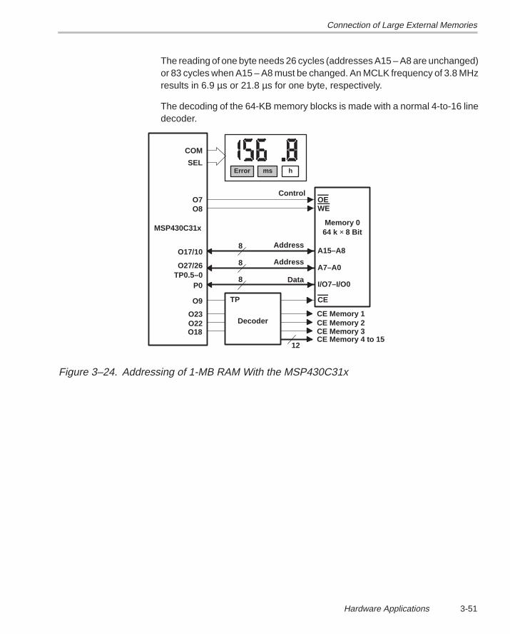
Connection of Large External Memories
3-51Hardware Applications
The reading of one byte needs 26 cycles (addresses A15 – A8 are unchanged)or 83 cycles when A15 – A8 must be changed. An MCLK frequency of 3.8 MHzresults in 6.9 µs or 21.8 µs for one byte, respectively.
The decoding of the 64-KB memory blocks is made with a normal 4-to-16 linedecoder.
Error ms h
8
COM
SEL
O7O8
O23
O9
P0
MSP430C31x
Address
ControlOEWE
CE
I/O7–I/O0
8O27/26TP0.5–0
A7–A0
Data
Address8O17/10 A15–A8
Memory 064 k × 8 Bit
Decoder
12
O22O18
CE Memory 1CE Memory 2CE Memory 3CE Memory 4 to 15
TP
Figure 3–24. Addressing of 1-MB RAM With the MSP430C31x
Power Supplies for MSP430 Systems
3-52
3.8 Power Supplies for MSP430 Systems
There are various ways to generate the supply voltage(s) for the MSP430 sys-tems. Due to the extremely low-power consumption of the MSP430 family, thisis possible with batteries, accumulators, the M-Bus, fiber-optic lines, and ac.Every method uses completely different hardware and is explained in depth.Wherever possible, the formulas necessary for the hardware design are giventoo.
3.8.1 Battery-Power Systems
Due to the extremely low current consumption of the MSP430 family it is pos-sible to run an MSP430 system with a 0.5-Ah battery more than 10 years. Thismakes possible applications that were impossible before. To reach such ex-tended time spans, it is only necessary to observe some simple rules. Themost important one is to always switch off the CPU when its not needed (e.g.,after the calculations are completed). This reduces the current consumptionfrom an operational low of 400 µA down to 1.6 µA.
The Figures 3–25 and 3–26 are drawn in a way that makes it easier to see howthe battery needs to be connected to get the highest accuracy out of the ADC.
Figure 3–25 illustrates the MSP430C32x with its separated digital and analogsupply terminals. This provides a separation of the noise-generating digitalparts and the noise-sensitive analog parts.
Figure 3–26 shows how to best separate the two parts for the MSP430 familymembers with common supply terminals for the analog and digital parts of thechip.
If the battery used has a high internal resistance, RI, (like some long-life batter-ies) then the parallel capacitor Cch must have a minimum capacity. The supplycurrent for the measurement part (which cannot be delivered by the battery)is delivered via Cch. The equation includes the small current coming from thebattery.
Cchmin ≥ tmeas IAM∆Vch
1RI
Between two measurements, the capacitor Cch needs time, tch, to getcharged-up to VCC for the next measurement. During this charge-up time, theMSP430 system runs in low-power mode 3 to have the lowest possible powerconsumption. The charge-up time, tch, to charge Cch to 99% of VCC is:
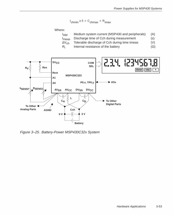
Power Supplies for MSP430 Systems
3-53Hardware Applications
tchmin ≥ 5 Cchmax Rimax
Where:IAM Medium system current (MSP430 and peripherals) (A)tmeas Discharge time of Cch during measurement (s)∆Vch Tolerable discharge of Cch during time tmeas (V)Ri Internal resistance of the battery (Ω)
SVCC
A1
A0
AVSS AVCC
MSP430C323Rext
DVSS DVCCRSENS2
RexRV
CAL
CD
Cch
3 V0 V
Battery
AGND
To OtherDigital Parts
To OtherAnalog Parts
Error ms h
COMSEL
P0.x, TP0.y I/Os
RSENS1
Figure 3–25. Battery-Power MSP430C32x System
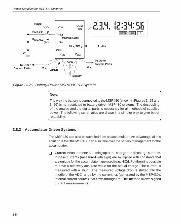
Power Supplies for MSP430 Systems
3-54
TDP.0
VSS VCC
MSP430C31x
RREF
3 V0 VAGND
TP0.1
TP0.2
CIN
RMEAS1
RMEAS2
To OtherSystem Parts
To Other System Parts
Error ms h
COMSEL
P0.x, TP0.y I/Os
CCH
C1
Battery
Figure 3–26. Battery-Power MSP430C31x System
Note:
The way the battery is connected to the MSP430 (shown in Figures 3–25 and3–26) is not restricted to battery-driven MSP430 systems. The decouplingof the analog and the digital parts is necessary for all methods of suppliedpower. The following schematics are drawn in a simpler way to give betterreadability.
3.8.2 Accumulator-Driven Systems
The MSP430 can also be supplied from an accumulator. An advantage of thissolution is that the MSP430 can also take over the battery management for theaccumulator.
Current Measurement: Summing up of the charge and discharge currents.If these currents (measured with sign) are multiplied with constants thatare unique for the accumulator type used (e.g. NiCd, Pb) then it is possibleto have a relatively accurate value for the actual charge. The current ismeasured with a shunt. The measured voltage drop is shifted into themiddle of the ADC range by the current Ics (generated by the MSP430’sinternal current source) that flows through Rc. This method allows signedcurrent measurements.

Power Supplies for MSP430 Systems
3-55Hardware Applications
Temperature Measurement: All of the internal processes of an accumula-tor (e.g., maximum charge, self discharge) are strongly dependent on thetemperature of the pack. Therefore, the temperature of the pack is mea-sured with a sensor and used afterwards with the calculations. When theMSP430’s current source is used, the voltage drop of its current Ics acrossthe sensor resistance is measured with the ADC input A2.
Voltage Measurement: The voltage of an accumulator pack is an indica-tion of the states full charge and complete discharge. Therefore, the volt-age of the pack is measured with the voltage divider consisting of R1 andR2.
Charge Control: Dependent on the result of the charge calculations, theMSP430 can decide if the charge transistor needs to be switched on or off.This decision can also be made in PWM (Pulse Width Modulation) mode.Figure 3–27 shows three possible charge modes. If replaceable accumu-lators are used, the charge control is not needed.
Rest Mode Handling: During periods of non-use, the low power mode 3of the MSP430 allows the control of the rest mode. The rest mode hasnearly no current consumption. In fact, the supply current has the samemagnitude as the self-discharge current of the accumulator. All system pe-ripherals are switched off; the MSP430 wakes-up at regular intervals,which are controlled by its basic timer. It then calculates, every few hours,the amount of self discharge of the accumulator. This calculated value issubtracted from the actual charge level.
Figure 3–27 illustrates an MSP430 system driven by an accumulator. The bat-tery management is done by the MSP430 also. The hardware needed is sim-ple. As shown in the figure, just a few resistors and a temperature sensor. Theactual charge of the accumulator is indicated in the LCD with a bar graph rang-ing from Empty to Full.
All necessary constants and a security copy of the actual charge are containedin an external EEPROM typically with 128 x 8 bits.
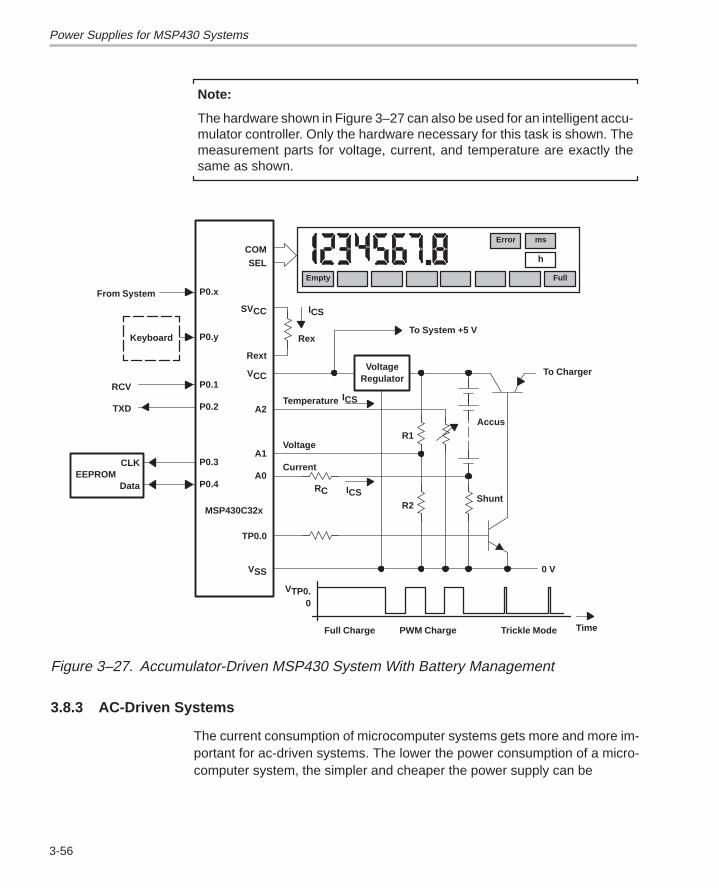
Power Supplies for MSP430 Systems
3-56
Note:
The hardware shown in Figure 3–27 can also be used for an intelligent accu-mulator controller. Only the hardware necessary for this task is shown. Themeasurement parts for voltage, current, and temperature are exactly thesame as shown.
Empty
COMSEL
Full
Error ms
h
SVCC
Rext
ICS
Rex
VCCVoltage
Regulator
To System +5 V
A2Temperature ICS
A1Voltage
A0Current
RC ICS
R1
R2Shunt
TP0.0
VSS
To Charger
0 V
P0.x
P0.y
EEPROM
Keyboard
P0.1
P0.2
P0.3
P0.4
CLK
Data
MSP430C32x
VTP0.0
Full Charge PWM Charge Trickle Mode Time
From System
RCV
TXDAccus
Figure 3–27. Accumulator-Driven MSP430 System With Battery Management
3.8.3 AC-Driven Systems
The current consumption of microcomputer systems gets more and more im-portant for ac-driven systems. The lower the power consumption of a micro-computer system, the simpler and cheaper the power supply can be
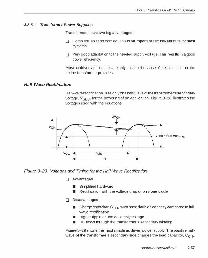
Power Supplies for MSP430 Systems
3-57Hardware Applications
3.8.3.1 Transformer Power Supplies
Transformers have two big advantages:
Complete isolation from ac. This is an important security attribute for mostsystems.
Very good adaptation to the needed supply voltage. This results in a goodpower efficiency.
Most ac-driven applications are only possible because of the isolation from theac the transformer provides.
Half-Wave Rectification
Half-wave rectification uses only one half-wave of the transformer’s secondaryvoltage, VSEC, for the powering of an application. Figure 3–28 illustrates thevoltages used with the equations.
VCH
VCC
∆VCH
Vsec × √2 = Vchmax
tdis
T
Figure 3–28. Voltages and Timing for the Half-Wave Rectification
Advantages
Simplified hardware Rectification with the voltage drop of only one diode
Disadvantages
Charge capacitor, CCH, must have doubled capacity compared to full-wave rectification
Higher ripple on the dc supply voltage DC flows through the transformer’s secondary winding
Figure 3–29 shows the most simple ac driven power supply. The positive half-wave of the transformer’s secondary side charges the load capacitor, CCH,.
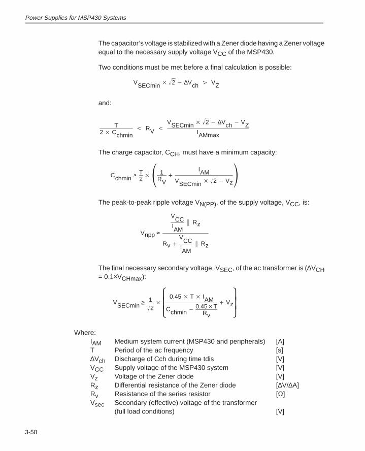
Power Supplies for MSP430 Systems
3-58
The capacitor’s voltage is stabilized with a Zener diode having a Zener voltageequal to the necessary supply voltage VCC of the MSP430.
Two conditions must be met before a final calculation is possible:
VSECmin 2 ∆Vch VZ
and:
T2 Cchmin
RV VSECmin 2 ∆Vch VZ
IAMmax
The charge capacitor, CCH, must have a minimum capacity:
Cchmin ≥ T2 1
RV
IAMVSECmin 2 Vz
The peak-to-peak ripple voltage VN(PP), of the supply voltage, VCC, is:
Vnpp ≈
VCC
IAM
Rz
Rv V
CCIAM
Rz
The final necessary secondary voltage, VSEC, of the ac transformer is (∆VCH= 0.1×VCHmax):
VSECmin ≥ 12
0.45 T IAM
Cchmin 0.45TRv
Vz
Where:IAM Medium system current (MSP430 and peripherals) [A]T Period of the ac frequency [s]∆Vch Discharge of Cch during time tdis [V]VCC Supply voltage of the MSP430 system [V]Vz Voltage of the Zener diode [V]Rz Differential resistance of the Zener diode [∆V/∆A]Rv Resistance of the series resistor [Ω]Vsec Secondary (effective) voltage of the transformer
(full load conditions) [V]
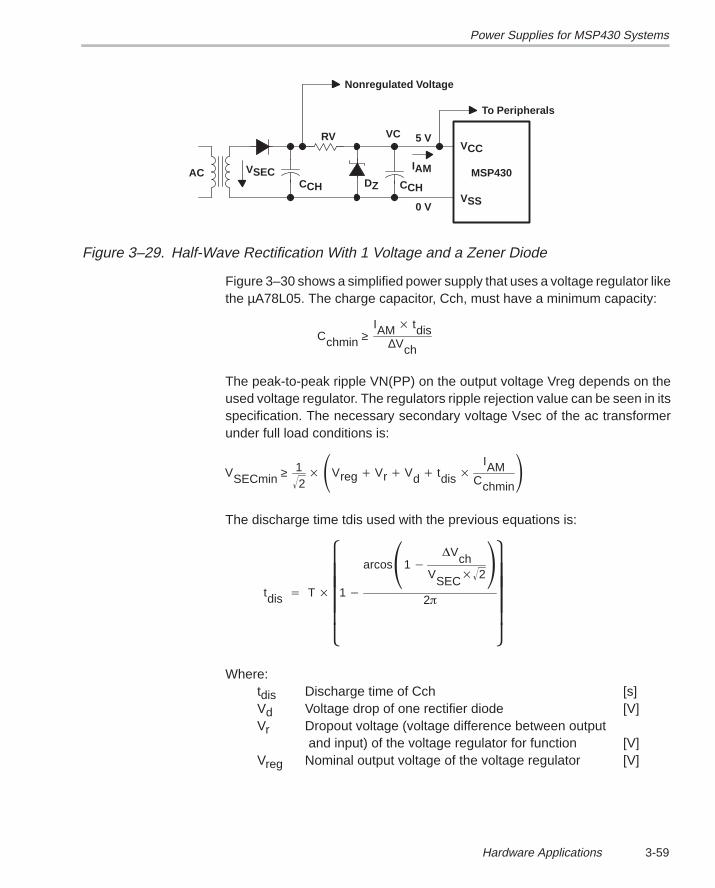
Power Supplies for MSP430 Systems
3-59Hardware Applications
MSP430
VCC
VSS
IAMDZ
VC
0 V
CCH
VSECAC
Nonregulated Voltage
To Peripherals
5 VRV
CCH
Figure 3–29. Half-Wave Rectification With 1 Voltage and a Zener Diode
Figure 3–30 shows a simplified power supply that uses a voltage regulator likethe µA78L05. The charge capacitor, Cch, must have a minimum capacity:
Cchmin ≥IAM tdis
∆Vch
The peak-to-peak ripple VN(PP) on the output voltage Vreg depends on theused voltage regulator. The regulators ripple rejection value can be seen in itsspecification. The necessary secondary voltage Vsec of the ac transformerunder full load conditions is:
VSECmin ≥ 12Vreg Vr Vd tdis
IAMCchmin
The discharge time tdis used with the previous equations is:
tdis T
1
arcos1 Vch
VSEC
2
2
Where:tdis Discharge time of Cch [s]Vd Voltage drop of one rectifier diode [V]Vr Dropout voltage (voltage difference between output
and input) of the voltage regulator for function [V]Vreg Nominal output voltage of the voltage regulator [V]
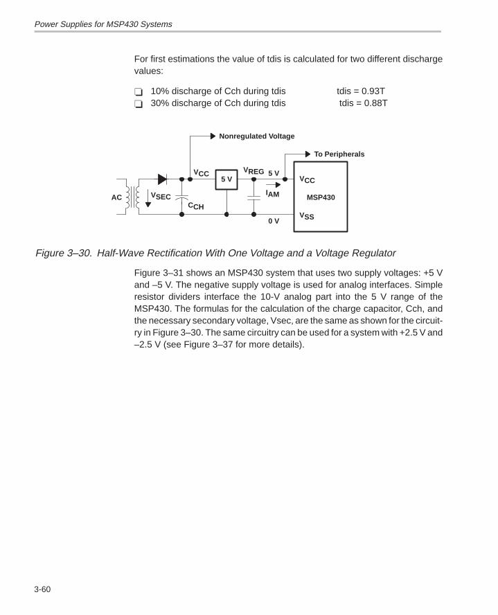
Power Supplies for MSP430 Systems
3-60
For first estimations the value of tdis is calculated for two different dischargevalues:
10% discharge of Cch during tdis tdis = 0.93T 30% discharge of Cch during tdis tdis = 0.88T
MSP430
VCC
VSS
IAM
VREG
0 V
CCH
VSECAC
Nonregulated Voltage
To Peripherals
5 V5 V
VCC
Figure 3–30. Half-Wave Rectification With One Voltage and a Voltage Regulator
Figure 3–31 shows an MSP430 system that uses two supply voltages: +5 Vand –5 V. The negative supply voltage is used for analog interfaces. Simpleresistor dividers interface the 10-V analog part into the 5 V range of theMSP430. The formulas for the calculation of the charge capacitor, Cch, andthe necessary secondary voltage, Vsec, are the same as shown for the circuit-ry in Figure 3–30. The same circuitry can be used for a system with +2.5 V and–2.5 V (see Figure 3–37 for more details).
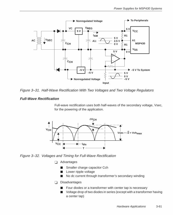
Power Supplies for MSP430 Systems
3-61Hardware Applications
MSP430
VCC
VSS
IAM
VREG
CCH
VSECAC
Nonregulated Voltage
–5 V To System–5 V
5 VVC
5 V2.5 V0 V
A1:
_+
–5 V
CCH
5 V
–5 V0 V
To Peripherals
Nonregulated VoltageInput
5 V
R1
R1
A1
0 V5 V
Figure 3–31. Half-Wave Rectification With Two Voltages and Two Voltage Regulators
Full-Wave Rectification
Full-wave rectification uses both half-waves of the secondary voltage, Vsec,for the powering of the application.
VCH
VCC tdis
T
∆VCH
Vsec × √2 = Vchmax
Figure 3–32. Voltages and Timing for Full-Wave Rectification
Advantages
Smaller charge capacitor Cch Lower ripple voltage No dc current through transformer’s secondary winding
Disadvantages
Four diodes or a transformer with center tap is necessary Voltage drop of two diodes in series (except with a transformer having
a center tap)
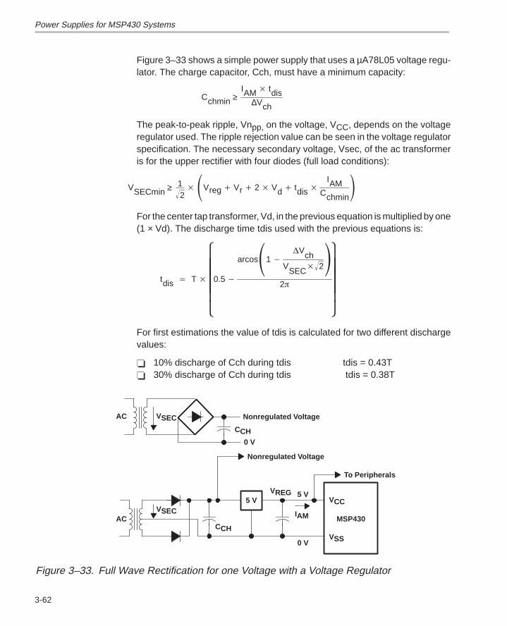
Power Supplies for MSP430 Systems
3-62
Figure 3–33 shows a simple power supply that uses a µA78L05 voltage regu-lator. The charge capacitor, Cch, must have a minimum capacity:
Cchmin ≥IAM tdis
∆Vch
The peak-to-peak ripple, Vnpp, on the voltage, VCC, depends on the voltageregulator used. The ripple rejection value can be seen in the voltage regulatorspecification. The necessary secondary voltage, Vsec, of the ac transformeris for the upper rectifier with four diodes (full load conditions):
VSECmin ≥ 12Vreg Vr 2 Vd tdis
IAMCchmin
For the center tap transformer, Vd, in the previous equation is multiplied by one(1 × Vd). The discharge time tdis used with the previous equations is:
tdis T
0.5
arcos1 Vch
VSEC
2
2
For first estimations the value of tdis is calculated for two different dischargevalues:
10% discharge of Cch during tdis tdis = 0.43T 30% discharge of Cch during tdis tdis = 0.38T
MSP430
VCC
VSS
IAM
VREG
0 V
CCH
VSECAC
Nonregulated Voltage
To Peripherals
5 V5 V
0 V
VSECAC
CCH
Nonregulated Voltage
Figure 3–33. Full Wave Rectification for one Voltage with a Voltage Regulator
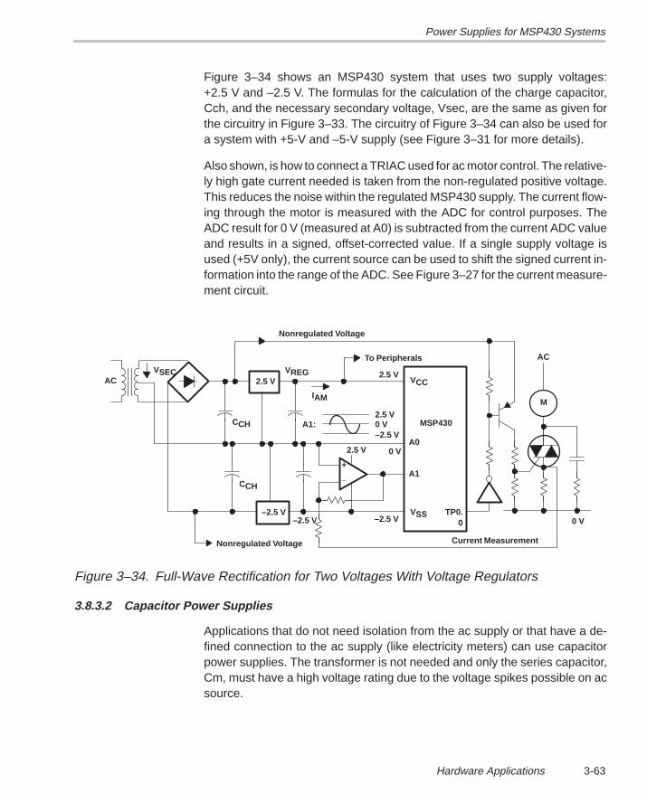
Power Supplies for MSP430 Systems
3-63Hardware Applications
Figure 3–34 shows an MSP430 system that uses two supply voltages:+2.5 V and –2.5 V. The formulas for the calculation of the charge capacitor,Cch, and the necessary secondary voltage, Vsec, are the same as given forthe circuitry in Figure 3–33. The circuitry of Figure 3–34 can also be used fora system with +5-V and –5-V supply (see Figure 3–31 for more details).
Also shown, is how to connect a TRIAC used for ac motor control. The relative-ly high gate current needed is taken from the non-regulated positive voltage.This reduces the noise within the regulated MSP430 supply. The current flow-ing through the motor is measured with the ADC for control purposes. TheADC result for 0 V (measured at A0) is subtracted from the current ADC valueand results in a signed, offset-corrected value. If a single supply voltage isused (+5V only), the current source can be used to shift the signed current in-formation into the range of the ADC. See Figure 3–27 for the current measure-ment circuit.
MSP430
VCC
IAM
VREG
CCH
Nonregulated Voltage
–2.5 V
2.5 V
2.5 V0 V–2.5 V
A1:
_+
–2.5 V
To Peripherals
Current Measurement
2.5 V
A1
0 V2.5 V
VSECAC
M
AC
TP0.0 0 V–2.5 V
VSS
A0
CCH
Nonregulated Voltage
Figure 3–34. Full-Wave Rectification for Two Voltages With Voltage Regulators
3.8.3.2 Capacitor Power Supplies
Applications that do not need isolation from the ac supply or that have a de-fined connection to the ac supply (like electricity meters) can use capacitorpower supplies. The transformer is not needed and only the series capacitor,Cm, must have a high voltage rating due to the voltage spikes possible on acsource.
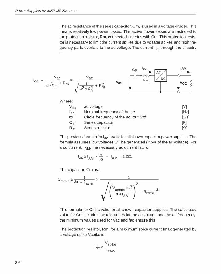
Power Supplies for MSP430 Systems
3-64
The ac resistance of the series capacitor, Cm, is used in a voltage divider. Thismeans relatively low power losses. The active power losses are restricted tothe protection resistor, Rm, connected in series with Cm. This protection resis-tor is necessary to limit the current spikes due to voltage spikes and high fre-quency parts overlaid to the ac voltage. The current Iac through the circuitryis:
AC
DCVCC
IAMIac
Rm
CM
VacIac
Vac1
jωCm Rm
≈Vac
1ω2C2
m R2
mWhere:
Vac ac voltage [V]fac Nominal frequency of the ac [Hz]ω Circle frequency of the ac: ω = 2πf [1/s]Cm Series capacitor [F]Rm Series resistor [Ω]
The previous formula for Iac is valid for all shown capacitor power supplies. Theformula assumes low voltages will be generated (< 5% of the ac voltage). Fora dc current, IAM, the necessary ac current Iac is:
Iac ≥ IAM
2 IAM 2.221
The capacitor, Cm, is:
Cmmin ≥ 12 facmin
1
Vacmin 2
IAM
2
Rmmax2
This formula for Cm is valid for all shown capacitor supplies. The calculatedvalue for Cm includes the tolerances for the ac voltage and the ac frequency;the minimum values used for Vac and fac ensure this.
The protection resistor, Rm, for a maximum spike current Imax generated bya voltage spike Vspike is:
Rm ≥VspikeImax
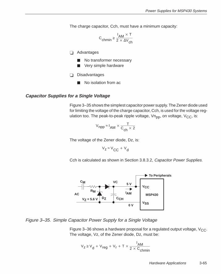
Power Supplies for MSP430 Systems
3-65Hardware Applications
The charge capacitor, Cch, must have a minimum capacity:
Cchmin ≥IAM T
2 ∆Vch
Advantages
No transformer necessary Very simple hardware
Disadvantages
No isolation from ac
Capacitor Supplies for a Single Voltage
Figure 3–35 shows the simplest capacitor power supply. The Zener diode usedfor limiting the voltage of the charge capacitor, Cch, is used for the voltage reg-ulation too. The peak-to-peak ripple voltage, Vnpp, on voltage, VCC, is:
Vnpp ≈ IAM TCch 2
The voltage of the Zener diode, Dz, is:
Vz ≈ VCC Vd
Cch is calculated as shown in Section 3.8.3.2, Capacitor Power Supplies.
MSP430
VCC
VSS
IAMDZ
0 V
CCHAC
To Peripherals
5 VCM
RM
VC
VZ = 5.6 V
Figure 3–35. Simple Capacitor Power Supply for a Single Voltage
Figure 3–36 shows a hardware proposal for a regulated output voltage, VCC.The voltage, Vz, of the Zener diode, Dz, must be:
Vz ≥ Vd Vreg Vr T IAM
2 Cchmin
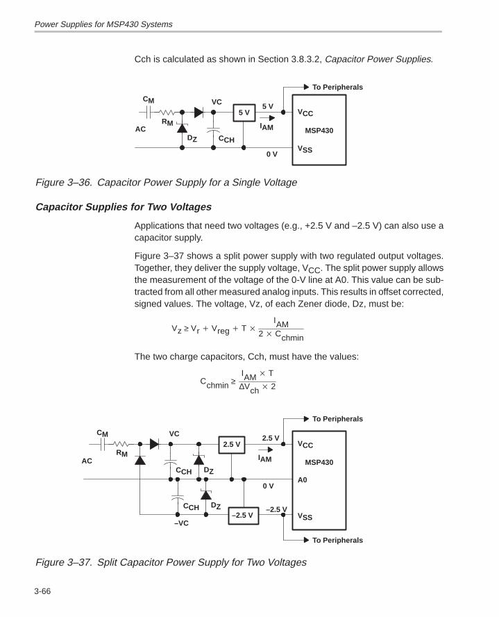
Power Supplies for MSP430 Systems
3-66
Cch is calculated as shown in Section 3.8.3.2, Capacitor Power Supplies.
MSP430
VCC
VSS
IAMDZ
0 V
CCHAC
To Peripherals
5 VCM
RM
VC5 V
Figure 3–36. Capacitor Power Supply for a Single Voltage
Capacitor Supplies for Two Voltages
Applications that need two voltages (e.g., +2.5 V and –2.5 V) can also use acapacitor supply.
Figure 3–37 shows a split power supply with two regulated output voltages.Together, they deliver the supply voltage, VCC. The split power supply allowsthe measurement of the voltage of the 0-V line at A0. This value can be sub-tracted from all other measured analog inputs. This results in offset corrected,signed values. The voltage, Vz, of each Zener diode, Dz, must be:
Vz ≥ Vr Vreg T IAM
2 Cchmin
The two charge capacitors, Cch, must have the values:
Cchmin ≥IAM T
∆Vch 2
MSP430
VCC
VSS
IAMDZ
0 V
CCHAC
To Peripherals
2.5 VCM
RM
VC2.5 V
DZ–2.5 V
–2.5 V
A0
–VC
To Peripherals
CCH
Figure 3–37. Split Capacitor Power Supply for Two Voltages
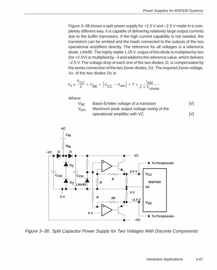
Power Supplies for MSP430 Systems
3-67Hardware Applications
Figure 3–38 shows a split power supply for +2.5 V and –2.5 V made in a com-pletely different way. It is capable of delivering relatively large output currentsdue to the buffer transistors. If the high current capability is not needed, thetransistors can be omitted and the loads connected to the outputs of the twooperational amplifiers directly. The reference for all voltages is a referencediode, LMx85. The highly stable 1.25 V output of this diode is multiplied by two(for +2.5V) or multiplied by –3 and added to the reference value, which delivers–2.5 V. The voltage drop of each one of the two diodes, D, is compensated bythe series connection of the two Zener diodes, Dz. The required Zener voltage,Vz, of the two diodes Dz is:
Vz ≥VCC
2 VBE VCC Vom T
IAM2 Cchmin
Where:VBE Basis-Emitter voltage of a transistor [V]Vom Maximum peak output voltage swing of the
operational amplifier with VC [V]
MSP430
VCC
VSS
0 V
AC
To Peripherals
2.5 V
RM
VC
DZ
–2.5 V
A0
–VCTo Peripherals
_+
_+
LMx85
DD
CM
–VC
CCH
DZ
0 V
0 V
CCHR
R
R 2R
Figure 3–38. Split Capacitor Power Supply for Two Voltages With Discrete Components
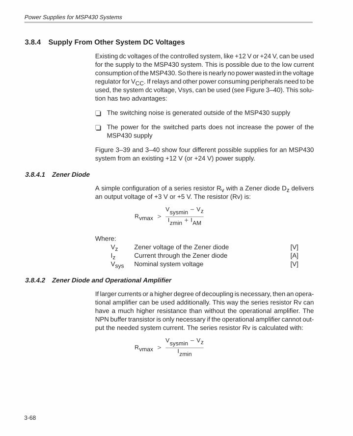
Power Supplies for MSP430 Systems
3-68
3.8.4 Supply From Other System DC Voltages
Existing dc voltages of the controlled system, like +12 V or +24 V, can be usedfor the supply to the MSP430 system. This is possible due to the low currentconsumption of the MSP430. So there is nearly no power wasted in the voltageregulator for VCC. If relays and other power consuming peripherals need to beused, the system dc voltage, Vsys, can be used (see Figure 3–40). This solu-tion has two advantages:
The switching noise is generated outside of the MSP430 supply
The power for the switched parts does not increase the power of theMSP430 supply
Figure 3–39 and 3–40 show four different possible supplies for an MSP430system from an existing +12 V (or +24 V) power supply.
3.8.4.1 Zener Diode
A simple configuration of a series resistor Rv with a Zener diode Dz deliversan output voltage of +3 V or +5 V. The resistor (Rv) is:
Rvmax Vsysmin Vz
Izmin IAM
Where:Vz Zener voltage of the Zener diode [V]Iz Current through the Zener diode [A]Vsys Nominal system voltage [V]
3.8.4.2 Zener Diode and Operational Amplifier
If larger currents or a higher degree of decoupling is necessary, then an opera-tional amplifier can be used additionally. This way the series resistor Rv canhave a much higher resistance than without the operational amplifier. TheNPN buffer transistor is only necessary if the operational amplifier cannot out-put the needed system current. The series resistor Rv is calculated with:
Rvmax Vsysmin Vz
Izmin
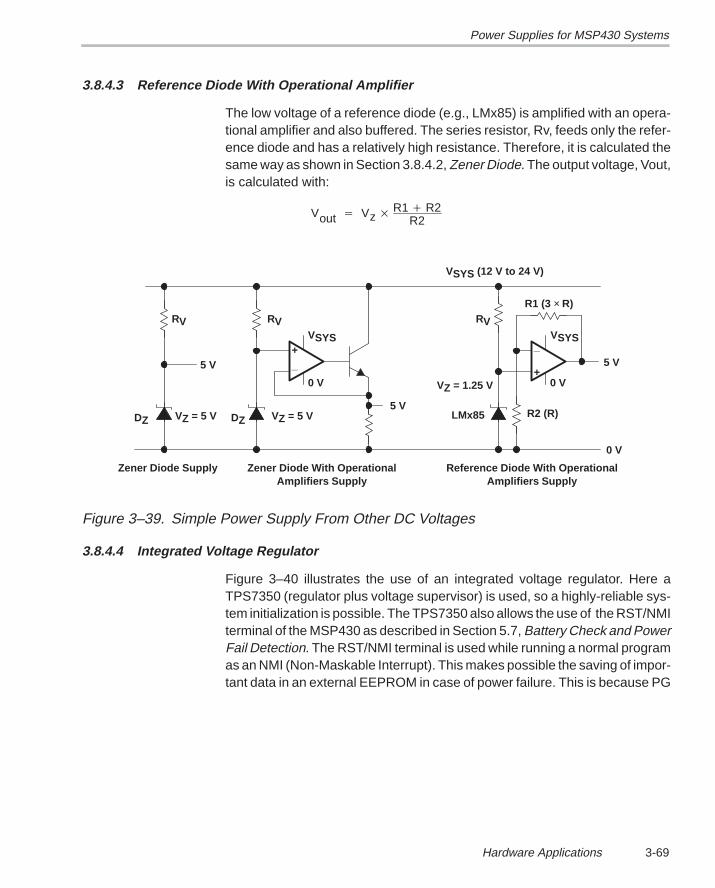
Power Supplies for MSP430 Systems
3-69Hardware Applications
3.8.4.3 Reference Diode With Operational Amplifier
The low voltage of a reference diode (e.g., LMx85) is amplified with an opera-tional amplifier and also buffered. The series resistor, Rv, feeds only the refer-ence diode and has a relatively high resistance. Therefore, it is calculated thesame way as shown in Section 3.8.4.2, Zener Diode. The output voltage, Vout,is calculated with:
Vout Vz R1 R2R2
_+
0 V
VSYS_
+0 V
VZ = 5 VDZ5 V
R1 (3 × R)
VZ = 1.25 V
LMx85 R2 (R)
5 V5 V
0 V
RV
VSYS (12 V to 24 V)
Reference Diode With OperationalAmplifiers Supply
Zener Diode With OperationalAmplifiers Supply
Zener Diode Supply
RV
DZ VZ = 5 V
RVVSYS
Figure 3–39. Simple Power Supply From Other DC Voltages
3.8.4.4 Integrated Voltage Regulator
Figure 3–40 illustrates the use of an integrated voltage regulator. Here aTPS7350 (regulator plus voltage supervisor) is used, so a highly-reliable sys-tem initialization is possible. The TPS7350 also allows the use of the RST/NMIterminal of the MSP430 as described in Section 5.7, Battery Check and PowerFail Detection. The RST/NMI terminal is used while running a normal programas an NMI (Non-Maskable Interrupt). This makes possible the saving of impor-tant data in an external EEPROM in case of power failure. This is because PG
Power Supplies for MSP430 Systems
3-70
outputs a negative signal starting at VCC = 4.75 V, which allows a lot of activitiesuntil VCCmin of the MSP430 (2.5 V) is reached.
IAM
VCC
Reset/NMI
VSSTP0.x DZ
VZ = VSYS + 3 V10 µF
OUT
SENSE
PG
GND
IN
CB
VSYS
D1
RV
VCB
TP73050
MSP430
0 V
EN
+5 V
Figure 3–40. Power Supply From Other DC Voltages With a Voltage Regulator
With two additional components (an RC combination) the MSP430 system canbe protected against spikes and bridging of supply voltage dropouts is pos-sible. The diode, D1, protects the capacitor, Cb, against discharge duringdropouts in voltage Vsys. The series resistor, Rv, is:
Rvmax
Vsysmin Vd VCC VrIAM Iregmax
The minimum capacity of Cb is:
Cbmin ∆t IAM Ireg
Vsysmin IAM Iregmax Rvmax Vrmax VCCmin
Where:IAM System current (medium value MSP430 and
peripherals) [A]Ireg Supply current of the voltage regulator [A]Vsys System voltage (e.g., +12 V) [V]Vd Diode forward voltage ( < 0.7 V) [V]Vr Dropout voltage of the voltage regulator for function [V]VCC Supply voltage of the complete MSP430 system [V]∆t Dropout time of Vsys to be bridged [s]
Power Supplies for MSP430 Systems
3-71Hardware Applications
3.8.5 Supply From the M Bus
If the MSP430 system is connected to the M–Bus, three possibilities exist forthe supply of the MSP430:
Battery Supply: The supply of the MSP430 is completely independent ofthe M-Bus. This method is not shown in Figure 3–41, because it is the nor-mal way the MSP430 is powered (see Section 3.8.1, Battery Driven Sys-tems).
M-Bus Supply: The MSP430 system is always supplied by the M-Bus.During off phases of the M-Bus, the MSP430 is not powered.
Mixed Supply: Normally the M-Bus supplies the MSP430 and only duringoff phases of the M-Bus does the battery of the MSP430 provide power.
3.8.5.1 M-Bus Supply
The MSP430 is always powered from the M-Bus. The TSS721 power fail sig-nal, PF, indicates to the MSP430 failure of the bus voltage. This early warningenables the MSP430 to save important data in an external EEPROM. The ca-pacitor, Cch, must have a capacity that allows this storage:
Cchmin ≥IAM tstore
VDD VCCmin
Where:IAM System current (MSP430 and EEPROM) [A]tstore Processing time to store important data into
the EEPROM [s]VDD Supply voltage delivered from the TSS721 [V]VCCmin Minimum supply voltage of the complete MSP430
system [V]
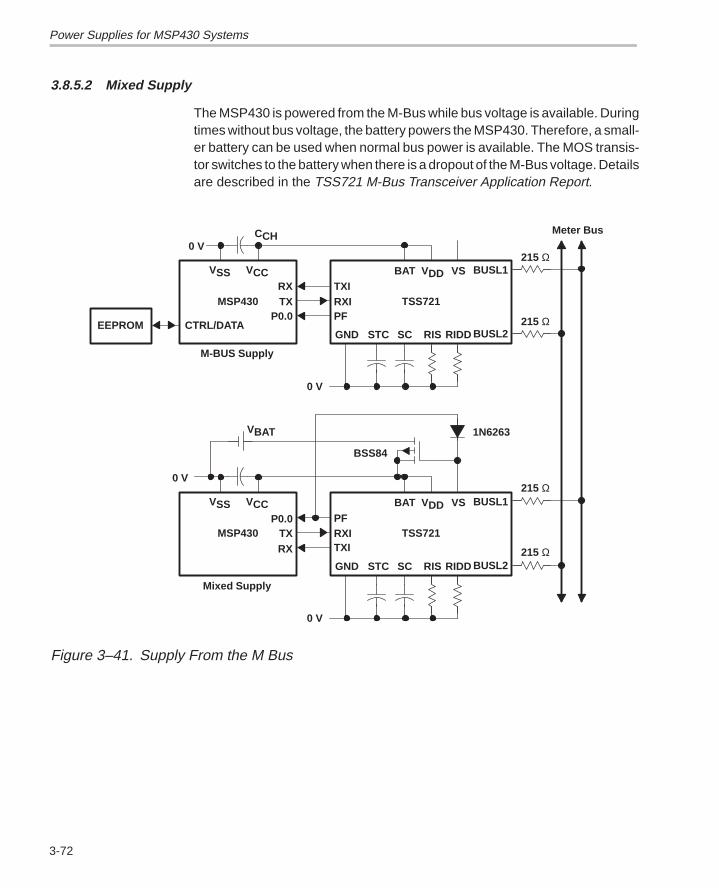
Power Supplies for MSP430 Systems
3-72
3.8.5.2 Mixed Supply
The MSP430 is powered from the M-Bus while bus voltage is available. Duringtimes without bus voltage, the battery powers the MSP430. Therefore, a small-er battery can be used when normal bus power is available. The MOS transis-tor switches to the battery when there is a dropout of the M-Bus voltage. Detailsare described in the TSS721 M-Bus Transceiver Application Report.
RXTX
P0.0
TXIRXIPF
TSS721
BUSL1
BUSL2
Meter Bus
GND STC SC RIS RIDD
BAT VDD VSVSS VCC
EEPROM CTRL/DATA
0 V
0 V215 Ω
MSP430
RXTX
P0.0
TXIRXIPF
TSS721
BUSL1
BUSL2GND STC SC RIS RIDD
BAT VDD VSVSS VCC
0 V
0 V
MSP430
BSS84
VBAT 1N6263
M-BUS Supply
Mixed Supply
CCH
215 Ω
215 Ω
215 Ω
Figure 3–41. Supply From the M Bus
Power Supplies for MSP430 Systems
3-73Hardware Applications
3.8.6 Supply Via a Fiber-Optic Cable
The MSP430 needs a supply current of only 400µA, if supplied with a voltageof 3 V and operating with an MCLK of 1 MHz. This low power can be trans-mitted via a glass-fiber (fiber-optic) cable. This allows completely isolatedmeasurement systems, which are not possible with other microcomputers.This transmission mode is an advantage for applications in strong electric ormagnetic fields.
Because the data transmitted from the host to the MSP430 is also used for thesupply of the MSP430 system, a certain amount of light is required continuous-ly and is independent of the transmitted data. Possible ways to reach this are:
Use of extended charge periods between host-to-MSP430 data transfers.The MARK level of the RS232 protocol is used for this purpose. This meth-od is shown in Figure 3–42 with every logical one, stop bit, and MARK levelused for the supply.
Use of a transmission code that always transmits the same number ofones and zeroes, independent of the transmitted data. (e.g., the Bi-PhaseCode)
To achieve a positive current balance, a few conditions must be met:
The complete hardware design uses ultra-low-power devices (operationalamplifiers, reference diode, measurement parts etc.).
The MSP430 is in Low Power Mode 3 anytime processing power is notneeded.
The measurement unit is switched on only during the actual measurementcycle.
All applicable hints given in Section 4.9, Ultra-Low-Power Design with theMSP430 Family are used.
3.8.6.1 Description of the Hardware
The host sends approximately. 15 mW of optical power into the fiber-opticcable. This optical power is made with a laser diode consuming 30 mW of elec-trical power. At the other end of the fiber-optic cable, the optical power is con-verted into 6 mW of electrical power with a power-converter diode. The open-circuit voltage of the power converter (approximately 6 V) decreases to 5 Vwith the load represented by the MSP430. The received electrical energy isused to charge the capacitor, Cch. The charge-up time required is approxi-mately 300 ms for a capacitor with 30 µF.
The uppermost operational amplifier is used for the voltage regulation of thesystem supply voltage (3 V to 4 V).
Power Supplies for MSP430 Systems
3-74
If a stabilized supply voltage is unnecessary, then this operational amplifiercan be omitted, as well as the diodes and pull-up resistors at the RST/NMI andP0.1 inputs.
The reference for the complete system is an LMx85 reference diode. This ref-erence voltage (1.25 V) is used for several purposes: trigger threshold for theSchmitt-triggers, reference for the calculation of VCC, and reference for thevoltage regulator.
The operational amplifier in the middle works as a reset controller. TheSchmitt-trigger switches the RST/NMI input of the MSP430 to a high levelwhen VC reaches approximately 4 V. The RST/NMI input is set low when VCfalls below 2.5 V.
The third operational amplifier decodes the information out of the charge volt-age and data of the power converter output. This decoder also shows aSchmitt-trigger characteristic.
The measured data is sent back to the host by an IR LED controlled by an NPNtransistor. The data format used here is an inverted RS232 protocol and hasno current flow for the MARK information (e.g. stop bits).
3.8.6.2 Working Sequence
The normal sequence for a measurement cycle is as follows:
1) The host starts a measurement sequence with the transmission of steadylight. This time period is used for the initial charge-up of the charge capaci-tor, Cch.
2) When this capacitor has enough charge, which means a capacitor voltage(VC) of approximately 4 V is reached, then the reset-Schmitt-triggerswitches the RST/NMI input of the MSP430 from low to high. The MSP430program starts with execution
3) The MSP430 program initializes the system and signals its readiness tothe host by the transmission of a defined code via the back channel (a se-cond fiber-optic cable).
4) After the receive of the acknowledge, the host sends the first controlinstruction (data) to the MSP430.
5) The MSP430 executes the received control instruction and sends back themeasured result to the host via the back channel.
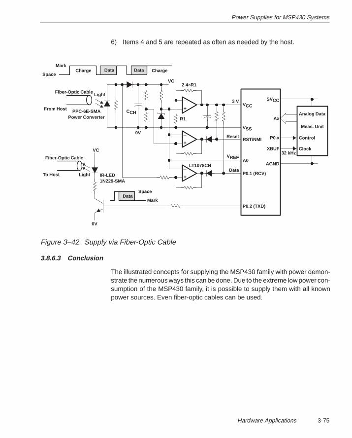
Power Supplies for MSP430 Systems
3-75Hardware Applications
6) Items 4 and 5 are repeated as often as needed by the host.
Analog Data
Control
Clock
Meas. Unit
_
+
2.4×R1
_
+
_
+
VCC
VSS
RST/NMI
A0
P0.1 (RCV)
P0.2 (TXD)
SVCC
Ax
P0.x
XBUF
AGND
CCH
LightFiber-Optic Cable
From Host PPC-6E-SMAPower Converter
Data
Space
Mark
Fiber-Optic Cable
To Host Light IR-LED1N229-SMA
0V
Data ChargeCharge
Data
Space
Mark
VC
32 kHz
LT1078CN
3 V
Reset
VREF
Data
0V
R1
VC
Figure 3–42. Supply via Fiber-Optic Cable
3.8.6.3 Conclusion
The illustrated concepts for supplying the MSP430 family with power demon-strate the numerous ways this can be done. Due to the extreme low power con-sumption of the MSP430 family, it is possible to supply them with all knownpower sources. Even fiber-optic cables can be used.

Power Supplies for MSP430 Systems
3-76

4-1
Application Examples
Several MSP430 application examples are given in the following sections.Common to nearly all of them is the storage of calibration data, tables,constants, etc. in the external EEPROMs. External EEPROMs are used forsafety reasons. If the microcomputer fails completely, it is still relatively easyto read out the accumulated consumption values. This is usually impossibleif these values reside in internal EEPROMs.
These EEPROMs can also store tables that describe the principal errors of agiven measurement principle that is dependent on the input value (current,flow, heat etc.). The MSP430, with its excellent table processing capabilities,can determine the right starting value out of these tables and calculate the lin-ear, quadratic or cubic approximation value. The following figure shows theprincipal error of a meter. The complete range starting at 1% up to 200% is di-vided into sub ranges of different length. A stored table would contain the start-ing point, the different distances and the inherent error at the beginning of eachrange. With this information, the MSP430 can calculate the error at any pointof the measurement range.
Chapter 4
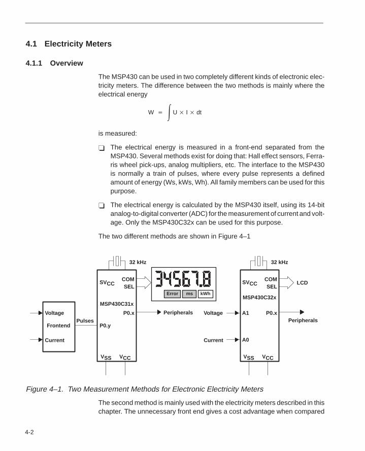
4-2
4.1 Electricity Meters
4.1.1 Overview
The MSP430 can be used in two completely different kinds of electronic elec-tricity meters. The difference between the two methods is mainly where theelectrical energy
W U I dt
is measured:
The electrical energy is measured in a front-end separated from theMSP430. Several methods exist for doing that: Hall effect sensors, Ferra-ris wheel pick-ups, analog multipliers, etc. The interface to the MSP430is normally a train of pulses, where every pulse represents a definedamount of energy (Ws, kWs, Wh). All family members can be used for thispurpose.
The electrical energy is calculated by the MSP430 itself, using its 14-bitanalog-to-digital converter (ADC) for the measurement of current and volt-age. Only the MSP430C32x can be used for this purpose.
The two different methods are shown in Figure 4–1
32 kHz32 kHz
Error ms kWh
COMSEL
P0.x
P0.y
SVCC
Pulses
MSP430C31x
VSS VCC
Frontend
Peripherals
COMSEL
P0.x
SVCC
MSP430C32x
VSS VCC
PeripheralsA1
A0
Voltage
Current
Voltage
Current
LCD
Figure 4–1. Two Measurement Methods for Electronic Electricity Meters
The second method is mainly used with the electricity meters described in thischapter. The unnecessary front end gives a cost advantage when compared
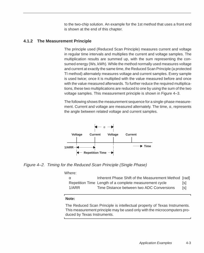
4-3Application Examples
to the two-chip solution. An example for the 1st method that uses a front endis shown at the end of this chapter.
4.1.2 The Measurement Principle
The principle used (Reduced Scan Principle) measures current and voltagein regular time intervals and multiplies the current and voltage samples. Themultiplication results are summed up, with the sum representing the con-sumed energy (Ws, kWh). While the method normally used measures voltageand current at exactly the same time, the Reduced Scan Principle (a protectedTI method) alternately measures voltage and current samples. Every sampleis used twice; once it is multiplied with the value measured before and oncewith the value measured afterwards. To further reduce the required multiplica-tions, these two multiplications are reduced to one by using the sum of the twovoltage samples. This measurement principle is shown in Figure 4–3.
The following shows the measurement sequence for a single-phase measure-ment. Current and voltage are measured alternately. The time, α, representsthe angle between related voltage and current samples.
Voltage Current Voltage Current
Time1/ARR
Repetition Time
α
Figure 4–2. Timing for the Reduced Scan Principle (Single Phase)
Where:α Inherent Phase Shift of the Measurement Method [rad]Repetition Time Length of a complete measurement cycle [s]1/ARR Time Distance between two ADC Conversions [s]
Note:
The Reduced Scan Principle is intellectual property of Texas Instruments.This measurement principle may be used only with the microcomputers pro-duced by Texas Instruments.
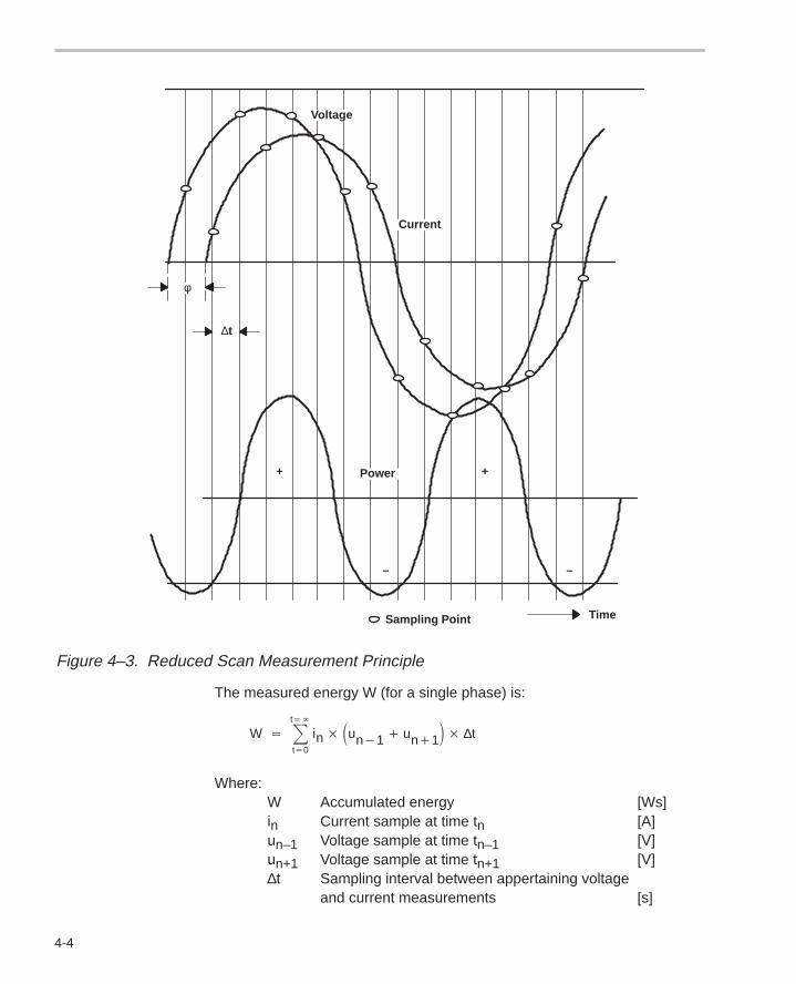
4-4
Voltage
Current
Power+ +
TimeSampling Point
∆t
φ
– –
Figure 4–3. Reduced Scan Measurement Principle
The measured energy W (for a single phase) is:
W t
t0
in un1 un1 ∆t
Where:W Accumulated energy [Ws]in Current sample at time tn [A]un–1 Voltage sample at time tn–1 [V]un+1 Voltage sample at time tn+1 [V]∆t Sampling interval between appertaining voltage
and current measurements [s]

4-5Application Examples
4.1.2.1 The Inherent Error of the Reduced Scan Principle
The Reduced Scan Principle has a small inherent error caused by the phaseshift ∆t, once inductive and once capacitive, due to the time interval betweenvoltage and current measurements. Any calculated energy sample shows thiserror, it is independent of the phase angle ϕ between voltage and current. Thevalue, e, of this error is:
e (cos (∆t f 2) 1) 100
where:e Error [%]∆t Sampling interval between voltage and current
measurements [s]f AC frequency [Hz]
For example, with the values (f = 60 Hz, ∆t = 300 µs) the inherent error is–0.639%. This error can be eliminated during runtime by a multiplication of theaccumulated energy with the correction factor c:
c 1cos(∆t f 2)
The correction factor, c, is normally included in the calibration constants (slopeand offset) and not used explicitly.
For a multiple-phase electricity meter, the Reduced Scan Principle is used forall phases one after the other. This is described in the following chapters.
Derivation of the inherent error
The flawless equation (except the quantization error) for the electric energy Wis:
W t
t0
in un ∆t
The equation used for the Reduced Scan Principle is:
W t
t0
in un1 un1 ∆t

4-6
Where:un = U × sinωt Voltage sample at time tin = I × sin(ωt+ϕ) Current sample at time tun–1 = U × sin(ωt–α) Voltage sample at time t – ∆tun+1 = U × sin(ωt+α) Voltage sample at time t + ∆tα Angle in radians between current and voltage samples (α = ω∆t = 2π×f×∆t)∆t Time between appertaining current and voltage samplesϕ Phase angle in radians between voltage and current
The error e of an energy sample due to the Reduced Scan Principle is:
e erroneouscorrect 1
e 0.5 I sin(ωt ) (U sin(ωt α) U sin(ωt α) )
U sin ωt I sin(ωt ) 1
e 0.5 (sin(ωt ) sin(ωt α) )
sin ωt 1
e 0.5 (sin ωt cos α sin α cos ωt sin ωt cos α sin α cos ωt)
sin ωt 1
e 0.5 (2 sin ωt cos α)
sin ωt 1 cos α 1
e (cos α 1) 100 (cos(2 f ∆t) 1) 100
or in percent
This result means that the error of each energy sample calculated with the Re-duced Scan Principle shows a constant value e. This inherent error dependsonly on the angle α between the current and the voltage samples; it is indepen-dent of the phase angle ϕ and of the sample point of the measurement insidethe sine wave. So for all samples, the same correction can be used.
4.1.2.2 The Advantages of the Reduced Scan Principle
1) Only 50% of the measurements are necessary because every measuredcurrent or voltage sample is used twice
2) Only 50% of the multiplications are necessary because two voltage sam-ples are added before the multiplication
3) Only one ADC is needed compared to up to six with the usual method.
4-7Application Examples
4) The computing power gained by reducing the number of multiplicationscan be used by the microcomputer for other system tasks. The MSP430is able to do the task of the front-end and of the host computer.
5) The Reduced Scan Principle is nearly independent of frequency devi-ations of the ac. See Section 4.1.2.4 for results.
6) The Reduced Scan Principle is also nearly independent of the interrupt la-tency time of the microcomputer. See Section 4.1.2.5 for results.
The Reduced Scan Measurement Principle is implemented in an evaluationboard for a 3-phase meter, which shows a typical error of 0.2%.
4.1.2.3 Measurement Errors for Some Sampling Frequencies
Table 4–1 gives an overview for the measurement errors dependent on thesampling frequency. The inherent error shows the error for the ac frequency(50 Hz or 60 Hz). The 3rd harmonics error shows the corrected measurementerror for the 3rd harmonic of the ac frequency (150 Hz or 180 Hz). The 5th har-monics error shows the corrected measurement error for the 5th harmonic ofthe ac frequency (250 Hz or 300 Hz). For any number of measurements (cur-rent and voltage samples together) for a full period, a rough error estimationcan be made with this table.
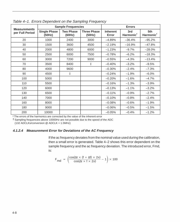
4-8
Table 4–1. Errors Dependent on the Sampling Frequency
Meas rementsSample Frequencies Errors
Measurementsper Full Period Single Phase
(50Hz)Two Phase
(60Hz)Three Phase
(50Hz)Inherent
Error3rd
Harmonic †5th
Harmonic †
20 1000 2400 3000 –4.89% –36.4% –95.2%
30 1500 3600 4500 –2.19% –16.9% –47.8%
40 2000 4800 6000 –1.23% –9.7% –28.0%
50 2500 6000 7500 –0.78% –6.2% –18.3%
60 3000 7200 9000 –0.55% –4.3% –13.4%
70 3500 8400 ‡ –0.40% –3.2% –9.5%
80 4000 9600 –0.30% –2.4% –7.3%
90 4500 ‡ –0.24% –1.9% –6.0%
100 5000 –0.20% –1.6% –4.7%
110 5500 –0.16% –1.3% –3.9%
120 6000 –0.13% –1.1% –3.2%
130 6500 –0.11% –0.9% –2.7%
140 7000 –0.10% –0.8% –2.4%
160 8000 –0.08% –0.6% –1.9%
180 9000 –0.06% –0.5% –1.5%
200 10000 –0.05% –0.4% –1.2%† The errors of the harmonics are corrected by the value of the inherent error‡ Sampling frequencies above 10000Hz are not possible due to the speed of the ADC
(132 ADCLKs/conversion @ ADCLK = 1.5MHz)
4.1.2.4 Measurement Error for Deviations of the AC Frequency
If the ac frequency deviates from the nominal value used during the calibration,then a small error is generated. Table 4–2 shows this error dependent on thesample frequency and the ac frequency deviation. The introduced error, Fmd,is:
Fmd cos(∆t (f ∆f) 2)cos(∆t f 2)
1 100
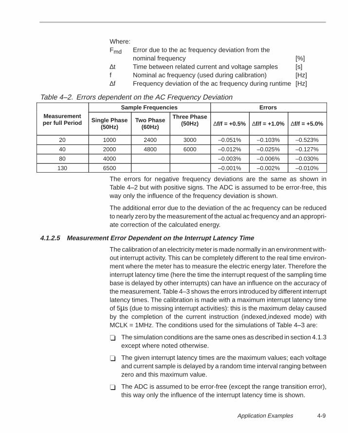
4-9Application Examples
Where:Fmd Error due to the ac frequency deviation from the
nominal frequency [%]∆t Time between related current and voltage samples [s]f Nominal ac frequency (used during calibration) [Hz]∆f Frequency deviation of the ac frequency during runtime [Hz]
Table 4–2. Errors dependent on the AC Frequency DeviationSample Frequencies Errors
Measurementper full Period Single Phase
(50Hz)Two Phase
(60Hz)
Three Phase(50Hz) ∆f/f = +0.5% ∆f/f = +1.0% ∆f/f = +5.0%
20 1000 2400 3000 –0.051% –0.103% –0.523%
40 2000 4800 6000 –0.012% –0.025% –0.127%
80 4000 –0.003% –0.006% –0.030%
130 6500 –0.001% –0.002% –0.010%
The errors for negative frequency deviations are the same as shown inTable 4–2 but with positive signs. The ADC is assumed to be error-free, thisway only the influence of the frequency deviation is shown.
The additional error due to the deviation of the ac frequency can be reducedto nearly zero by the measurement of the actual ac frequency and an appropri-ate correction of the calculated energy.
4.1.2.5 Measurement Error Dependent on the Interrupt Latency Time
The calibration of an electricity meter is made normally in an environment with-out interrupt activity. This can be completely different to the real time environ-ment where the meter has to measure the electric energy later. Therefore theinterrupt latency time (here the time the interrupt request of the sampling timebase is delayed by other interrupts) can have an influence on the accuracy ofthe measurement. Table 4–3 shows the errors introduced by different interruptlatency times. The calibration is made with a maximum interrupt latency timeof 5µs (due to missing interrupt activities): this is the maximum delay causedby the completion of the current instruction (indexed,indexed mode) withMCLK = 1MHz. The conditions used for the simulations of Table 4–3 are:
The simulation conditions are the same ones as described in section 4.1.3except where noted otherwise.
The given interrupt latency times are the maximum values; each voltageand current sample is delayed by a random time interval ranging betweenzero and this maximum value.
The ADC is assumed to be error-free (except the range transition error),this way only the influence of the interrupt latency time is shown.
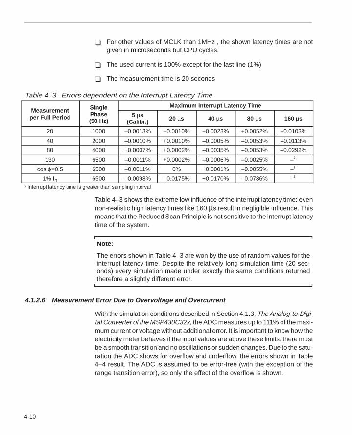
4-10
For other values of MCLK than 1MHz , the shown latency times are notgiven in microseconds but CPU cycles.
The used current is 100% except for the last line (1%)
The measurement time is 20 seconds
Table 4–3. Errors dependent on the Interrupt Latency Time
Meas rement Single Maximum Interrupt Latency TimeMeasurementper Full Period
SinglePhase(50 Hz)
5 µs(Calibr.) 20 µs 40 µs 80 µs 160 µs
20 1000 –0.0013% –0.0010% +0.0023% +0.0052% +0.0103%
40 2000 –0.0010% +0.0010% –0.0005% –0.0053% –0.0113%
80 4000 +0.0007% +0.0002% –0.0035% –0.0053% –0.0292%
130 6500 –0.0011% +0.0002% –0.0006% –0.0025% –†
cos ϕ=0.5 6500 –0.0011% 0% +0.0001% –0.0055% –†
1% In 6500 –0.0098% –0.0175% +0.0170% –0.0786% –†
† Interrupt latency time is greater than sampling interval
Table 4–3 shows the extreme low influence of the interrupt latency time: evennon-realistic high latency times like 160 µs result in negligible influence. Thismeans that the Reduced Scan Principle is not sensitive to the interrupt latencytime of the system.
Note:
The errors shown in Table 4–3 are won by the use of random values for theinterrupt latency time. Despite the relatively long simulation time (20 sec-onds) every simulation made under exactly the same conditions returnedtherefore a slightly different error.
4.1.2.6 Measurement Error Due to Overvoltage and Overcurrent
With the simulation conditions described in Section 4.1.3, The Analog-to-Digi-tal Converter of the MSP430C32x, the ADC measures up to 111% of the maxi-mum current or voltage without additional error. It is important to know how theelectricity meter behaves if the input values are above these limits: there mustbe a smooth transition and no oscillations or sudden changes. Due to the satu-ration the ADC shows for overflow and underflow, the errors shown in Table4–4 result. The ADC is assumed to be error-free (with the exception of therange transition error), so only the effect of the overflow is shown.
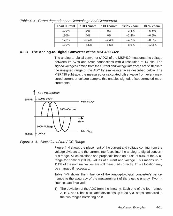
4-11Application Examples
Table 4–4. Errors dependent on Overvoltage and OvercurrentLoad Current 100% Vnom 110% Vnom 120% Vnom 130% Vnom
100% 0% 0% –2.4% –6.5%
110% 0% 0% –2.4% –6.5%
120% –2.4% –2.4% –4.7% –8.6%
130% –6.5% –6.5% –8.6% –12.3%
4.1.3 The Analog-to-Digital Converter of the MSP430C32x
The analog-to-digital converter (ADC) of the MSP430 measures the voltagebetween its AVss and SVcc connections with a resolution of 14 bits. Thesigned voltages coming from the current and voltage interfaces are shifted intothe unsigned range of the ADC by simple interfaces described below. TheMSP430 subtracts the measured or calculated offset value from every mea-sured current or voltage sample: this enables signed, offset corrected mea-surements.
Time
95% SVCC
100% Current
5% SVCC
100% SVCC
AVSS
3FFFh
0000h
100% Voltage
ADC Value (Steps)
Figure 4–4. Allocation of the ADC Range
Figure 4–4 shows the placement of the current and voltage coming from thevoltage dividers and the current interfaces into the analog-to-digital convert-er’s range. All calculations and proposals base on a use of 90% of the ADCrange for nominal (100%) values of current and voltage. This means up to111% of the nominal values are still measured correctly. This allocation maybe changed if necessary.
Table 4–5 shows the influence of the analog-to-digital converter’s perfor-mance to the accuracy of the measurement of the electric energy. Two in-fluences are involved:
1) The deviation of the ADC from the linearity. Each one of the four rangesA, B, C and D has calculated deviations up to 20 ADC steps compared tothe two ranges bordering on it.
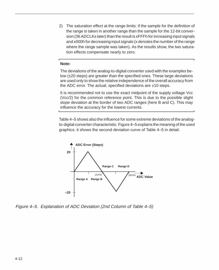
4-12
2) The saturation effect at the range limits: if the sample for the definition ofthe range is taken in another range than the sample for the 12-bit conver-sion (36 ADCLKs later) than the result is xFFFh for increasing input signalsand x000h for decreasing input signals (x denotes the number of the rangewhere the range sample was taken). As the results show, the two satura-tion effects compensate nearly to zero.
Note:
The deviations of the analog-to-digital converter used with the examples be-low (±20 steps) are greater than the specified ones. These large deviationsare used only to show the relative independence of the overall accuracy fromthe ADC error. The actual, specified deviations are ±10 steps.
It is recommended not to use the exact midpoint of the supply voltage Vcc(Vcc/2) for the common reference point. This is due to the possible slightslope deviation at the border of two ADC ranges (here B and C). This mayinfluence the accuracy for the lowest currents.
Table 4–5 shows also the influence for some extreme deviations of the analog-to-digital converter characteristic. Figure 4–5 explains the meaning of the usedgraphics: it shows the second deviation curve of Table 4–5 in detail.
Range C Range D
ADC ValueRange A Range B
20
–20
1FFFh 3FFFh
ADC Error (Steps)
Figure 4–5. Explanation of ADC Deviation (2nd Column of Table 4–5)
4-13Application Examples
The function shows the deviation at any point of the four ADC ranges. Due tothe monotony of the ADC the errors at the range limits are always equal. Theerrors shown in Table 4–5 were calculated with a PASCAL program. The fol-lowing steps were taken:
1) Measurement and calculation of the error at 5% of the nominal current.
2) Measurement and calculation of the error at 100% of the nominal current
3) Calculation of the slope and offset for the correction (calibration)
4) Simulation of voltage and current samples: any sample is modified withthe ADC error (exactly like during calibration).
5) Correction of all measured values with the calculated slope and offset
6) Calculation of the resulting error
The saturation effect at the range limits is always included. The first columnof Table 4–5 with an ideal ADC characteristic (zero deviation) shows only thiseffect and the finite ADC resolution. This column can be used as a referencefor the errors of the other five columns.
The calculations are made with the following conditions:
Virtual Ground location in the ADC range: 8190 steps (1FFEh) 49.98% of full ADC range Measurement time for calibration points: 5s (calibration points are measured this time) Measurement time for different loads: 9s AC frequency: 50 Hz Cosine ϕ: 1 (0) Sample frequency: 2048 Hz (488.3 µs sample distance) Voltage: 100% Vpp uses 90% of the ADC range Current: 100% Ipp uses 90% of the ADC range
Note:
The drawings on top of the columns of Table 4–5 indicate the ADC error independence of the ADC value. Figure 4–5 shows the drawing above the sec-ond column in a magnified form.
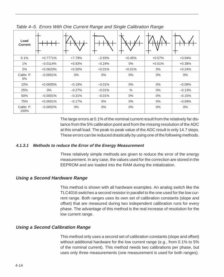
4-14
Table 4–5. Errors With One Current Range and Single Calibration Range
LoadCurrent
0.1% +0.7771% +7.79% –2.93% +0.45% +0.57% +3.94%
1% –0.0114% +0.83% –0.24% 0% +0.01% +0.38%
2% +0.0620% +0.50% +0.01% +0.01% 0% +0.24%
Calibr. P.5%
–0.0001% 0% 0% 0% 0% 0%
10% +0.0005% –0.19% –0.01% 0% 0% –0.09%
25% 0% –0.27% –0.01% % 0% –0.13%
50% –0.0001% –0.31% –0.01% 0% 0% –0.15%
75% +0.0001% –0.17% 0% 0% 0% –0.09%
Calibr. P.100%
–0.0002% 0% 0% 0% 0% 0%
The large errors at 0.1% of the nominal current result from the relatively far dis-tance from the 5% calibration point and from the missing resolution of the ADCat this small load. The peak-to-peak value of the ADC result is only 14.7 steps.These errors can be reduced drastically by using one of the following methods.
4.1.3.1 Methods to reduce the Error of the Energy Measurement
Three relatively simple methods are given to reduce the error of the energymeasurement. In any case, the values used for the correction are stored in theEEPROM and are loaded into the RAM during the initialization.
Using a Second Hardware Range
This method is shown with all hardware examples. An analog switch like theTLC4016 switches a second resistor in parallel to the one used for the low cur-rent range. Both ranges uses its own set of calibration constants (slope andoffset) that are measured during two independent calibration runs for everyphase. The advantage of this method is the real increase of resolution for thelow current range.
Using a Second Calibration Range
This method only uses a second set of calibration constants (slope and offset)without additional hardware for the low current range (e.g., from 0.1% to 5%of the nominal current). This method needs two calibrations per phase, butuses only three measurements (one measurement is used for both ranges).
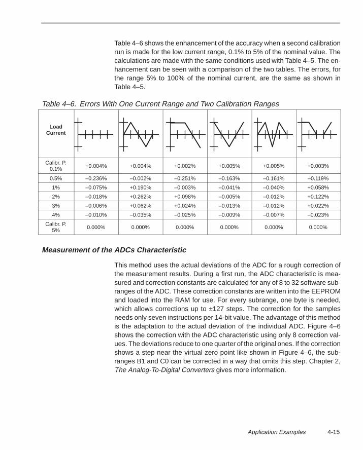
4-15Application Examples
Table 4–6 shows the enhancement of the accuracy when a second calibrationrun is made for the low current range, 0.1% to 5% of the nominal value. Thecalculations are made with the same conditions used with Table 4–5. The en-hancement can be seen with a comparison of the two tables. The errors, forthe range 5% to 100% of the nominal current, are the same as shown inTable 4–5.
Table 4–6. Errors With One Current Range and Two Calibration Ranges
LoadCurrent
Calibr. P.0.1% +0.004% +0.004% +0.002% +0.005% +0.005% +0.003%
0.5% –0.236% –0.002% –0.251% –0.163% –0.161% –0.119%
1% –0.075% +0.190% –0.003% –0.041% –0.040% +0.058%
2% –0.018% +0.262% +0.098% –0.005% –0.012% +0.122%
3% –0.006% +0.062% +0.024% –0.013% –0.012% +0.022%
4% –0.010% –0.035% –0.025% –0.009% –0.007% –0.023%
Calibr. P.5% 0.000% 0.000% 0.000% 0.000% 0.000% 0.000%
Measurement of the ADCs Characteristic
This method uses the actual deviations of the ADC for a rough correction ofthe measurement results. During a first run, the ADC characteristic is mea-sured and correction constants are calculated for any of 8 to 32 software sub-ranges of the ADC. These correction constants are written into the EEPROMand loaded into the RAM for use. For every subrange, one byte is needed,which allows corrections up to ±127 steps. The correction for the samplesneeds only seven instructions per 14-bit value. The advantage of this methodis the adaptation to the actual deviation of the individual ADC. Figure 4–6shows the correction with the ADC characteristic using only 8 correction val-ues. The deviations reduce to one quarter of the original ones. If the correctionshows a step near the virtual zero point like shown in Figure 4–6, the sub-ranges B1 and C0 can be corrected in a way that omits this step. Chapter 2,The Analog-To-Digital Converters gives more information.
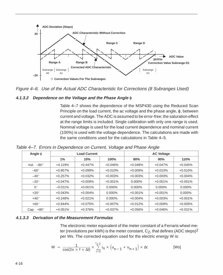
4-16
SubrangeA0
Range A Range B
Range C Range D
Corrected ADC Characteristic
ADC Deviation (Steps)
SubrangeA1
SubrangeD1
Correction Values For The Subranges
Correction Value Subrange D1
ADC Value
ADC Characteristic Without Correction20
–20
3FFFH
Figure 4–6. Use of the Actual ADC Characteristic for Corrections (8 Subranges Used)
4.1.3.2 Dependence on the Voltage and the Phase Angle ϕ
Table 4–7 shows the dependence of the MSP430 using the Reduced ScanPrinciple on the load current, the ac voltage and the phase angle, ϕ, betweencurrent and voltage. The ADC is assumed to be error-free; the saturation effectat the range limits is included. Single calibration with only one range is used.Nominal voltage is used for the load current dependence and nominal current(100%) is used with the voltage dependence. The calculations are made withthe same conditions used for the calculations in Table 4–5.
Table 4–7. Errors in Dependence on Current, Voltage and Phase AngleAngle ϕ Load Current AC Voltageg e ϕ
1% 10% 100% 80% 90% 110%
Ind. –80 +4.119% +0.447% +0.046% +0.048% +0.047% +0.045%
–60 +0.857% +0.099% +0.010% +0.009% +0.010% +0.010%
–40 +0.257% +0.032% +0.003% +0.003% +0.003% +0.004%
–20 +0.047% +0.009% +0.001% 0.000% +0.001% +0.001%
0 –0.011% +0.001% 0.000% 0.000% 0.000% 0.000%
+20 +0.043% +0.004% 0.000% +0.001% +0.001% 0.000%
+40 +0.248% +0.021% 0.000% +0.004% +0.003% +0.001%
+60 +0.844% +0.075% +0.007% +0.012% +0.009% +0.005%
Cap. +80 +4.051% +0.376% +0.037% +0.056% +0.046% +0.031%
4.1.3.3 Derivation of the Measurement Formulas
The electronic meter equivalent of the meter constant of a Ferraris wheel me-ter (revolutions per kWh) is the meter constant, CZ, that defines (ADC steps)2
per Ws. The corrected equation used for the electric energy W is:
W 1cos(2 f ∆t)
t
t0
in un1 un1 ∆t [Ws]
4-17Application Examples
With the ADC results ADCi (current sample) ADCu (voltage sample) andADC0u and ADC0i (zero volt samples) the previous equation gets:
W 1cos(2 f ∆t)
t
t0
ki ADCin ADC0i ku ADCun1 ADCun1 2 ADC0u ∆t
Separation into variable and constant values results in:
W 1cos(2 f ∆t)
∆t ki ku t
t0
ADCin ADC0i ADCun1 ADCun1 2 ADC0u
Where:f AC frequency [Hz]∆t Sampling interval between appertaining
voltage and current samples [s]ki Current multiplication factor [A/step].
See Section 4.1.4.5 for more detailsku Voltage multiplication factor. [V/step]
See section 4.1.4.6 for more detailsADCin ADC value of current sample taken at time tnADCun–1 ADC value of voltage sample taken at
time tn–1 (tn – ∆t)ADCun+1 ADC value of voltage sample taken at time
tn+1 (tn + ∆t)ADC0u ADC value of voltage zero point (measured or calculated)ADC0i ADC value of current zero point (measured or calculated)
The first, constant part of the equation is the inverse value of the meterconstant ,CZ:
CZ cos(2 f ∆t)
∆t ki ku[Steps2/Ws]
The values for ki and ku for different interfaces are explained in detail in Sec-tion 4.1.4.
For a system using a current transformer and a resistor divider for the voltage,the previous equation gets:
W 1cos(2 f ∆t)
∆t SVCC wsec
214 wprim Rsec
SVCC (Rm Rc)
214 Rc
t
t0
ADCin ADC0i ADCun1 ADCun1 2 ADC0u
4-18
Where:Rsec Load resistor (secondary) of the current
transformer [Ω]wsec Secondary windings of the current transformerwprim Primary windings of the current transformer
SVCC Voltage at terminal SVCC (AVCC or external reference voltage) [V]
Rm Voltage divider: resistor between ac connection and analog input [Ω]
Rc Voltage divider: resistor between analog input and zero volts [Ω]
The first, constant part of the equation is the inverse value of the meterconstant CZ:
CZ cos(2 f ∆t) 228 wprim Rsec Rc
∆t SVCC2 wsec (Rm Rc)
[Steps2/Ws]
With the previous value of CZ, the equation for the energy W is:
W
t
t0
ADCin ADC0i ADCun1 ADCun1 2 ADC0u
CZ
[Ws]
If the energy W is to be expressed in kWh:
W
t
t0
ADCin ADC0i ADCun1 ADCun1 2 ADC0u
3.6 109 CZ
[kWh]
The value W needs to be corrected with the slope and offset calculated duringthe calibration process.
4.1.4 Analog Interfaces to the MSP430
This chapter describes some important topics that can affect the overall accu-racy of the electricity meter.
4.1.4.1 Analog and Digital Grounding
The following schematics are drawn in a simplified manner to make them easi-er to understand. In reality, it is necessary to decouple the analog and the digi-tal part as shown in Figure 4–7. This is to avoid digital noise on the analog sig-nals to be measured.
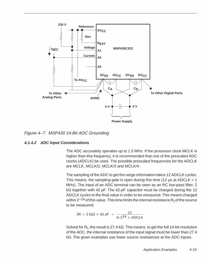
4-19Application Examples
SVCC
A1
A0Current
AVSS AVCC
MSP430C323
REXT
DVSS DVCC
ISEC
Rex
CA CD
5 V0 V
AGND
To Other Digital PartsTo OtherAnalog Parts
Voltage
A5
230 V
Power Supply
Reference
To AVCC
Figure 4–7. MSP430 14-Bit ADC Grounding
4.1.4.2 ADC Input Considerations
The ADC accurately operates up to 1.5 MHz. If the processor clock MCLK ishigher than this frequency, it is recommended that one of the prescaled ADCclocks (ADCLK) be used. The possible prescaled frequencies for the ADCLKare MCLK, MCLK/2, MCLK/3 and MCLK/4.
The sampling of the ADC to get the range information takes 12 ADCLK cycles.This means, the sampling gate is open during this time (12 µs at ADCLK = 1MHz). The input of an ADC terminal can be seen as an RC low-pass filter, 2kΩ together with 42 pF. The 42-pF capacitor must be charged during the 12ADCLK cycles to the final value in order to be measured. This means chargedwithin 2–14 of this value. This time limits the internal resistance RI of the sourceto be measured:
(Ri 2 k) 42 pF 12In 214 ADCLK
Solved for RI, the result is 27.4 kΩ. This means, to get the full 14-bit resolutionof the ADC, the internal resistance of the input signal must be lower than 27.4kΩ. The given examples use lower source resistances at the ADC inputs.
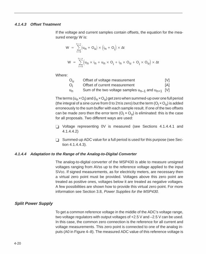
4-20
4.1.4.3 Offset Treatment
If the voltage and current samples contain offsets, the equation for the mea-sured energy W is:
W t
t0
un Ou in Oi ∆t
W t
t0
un in un Oi in Ou Oi Ou ∆t
Where:Ou Offset of voltage measurement [V]Oi Offset of current measurement [A]un Sum of the two voltage samples un–1 and un+1 [V]
The terms (un × Oi) and (in × Ou) get zero when summed-up over one full period(the integral of a sine curve from 0 to 2π is zero) but the term (Oi × Ou) is addederroneously to the sum buffer with each sample result. If one of the two offsetscan be made zero then the error term (Oi × Ou) is eliminated: this is the casefor all proposals. Two different ways are used:
Voltage representing 0V is measured (see Sections 4.1.4.4.1 and4.1.4.4.2)
Summed-up ADC value for a full period is used for this purpose (see Sec-tion 4.1.4.4.3).
4.1.4.4 Adaptation to the Range of the Analog-to-Digital Converter
The analog-to-digital converter of the MSP430 is able to measure unsignedvoltages ranging from AVss up to the reference voltage applied to the inputSVcc. If signed measurements, as for electricity meters, are necessary thena virtual zero point must be provided. Voltages above this zero point aretreated as positive ones, voltages below it are treated as negative voltages.A few possibilities are shown how to provide this virtual zero point. For moreinformation see Section 3.8, Power Supplies for the MSP430.
Split Power Supply
To get a common reference voltage in the middle of the ADC’s voltage range,two voltage regulators with output voltages of +2.5 V and –2.5 V can be used.In this case, the common zero connection is the reference for all current andvoltage measurements. This zero point is connected to one of the analog in-puts (A0 in Figure 4–8). The measured ADC value of this reference voltage is
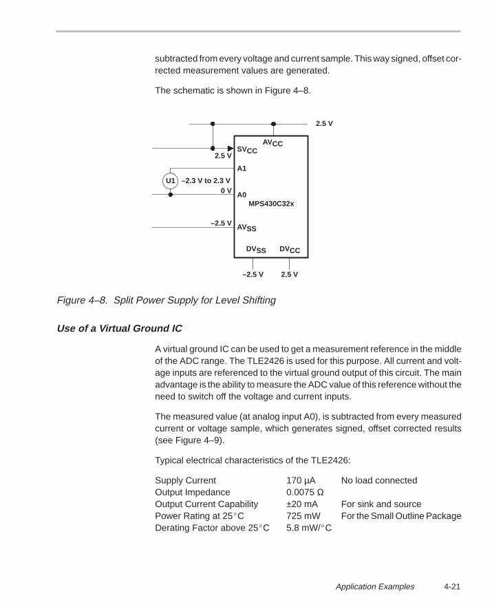
4-21Application Examples
subtracted from every voltage and current sample. This way signed, offset cor-rected measurement values are generated.
The schematic is shown in Figure 4–8.
SVCC
A1
A0
AVSS
DVSS DVCC
–2.5 V 2.5 V
U1 –2.3 V to 2.3 V
2.5 V
MPS430C32x
–2.5 V
AVCC
2.5 V
0 V
Figure 4–8. Split Power Supply for Level Shifting
Use of a Virtual Ground IC
A virtual ground IC can be used to get a measurement reference in the middleof the ADC range. The TLE2426 is used for this purpose. All current and volt-age inputs are referenced to the virtual ground output of this circuit. The mainadvantage is the ability to measure the ADC value of this reference without theneed to switch off the voltage and current inputs.
The measured value (at analog input A0), is subtracted from every measuredcurrent or voltage sample, which generates signed, offset corrected results(see Figure 4–9).
Typical electrical characteristics of the TLE2426:
Supply Current 170 µA No load connectedOutput Impedance 0.0075 ΩOutput Current Capability ±20 mA For sink and sourcePower Rating at 25C 725 mW For the Small Outline PackageDerating Factor above 25C 5.8 mW/C
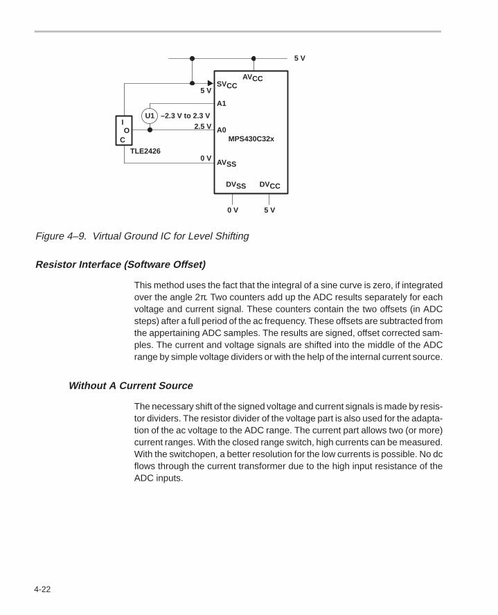
4-22
SVCC
A1
A0
AVSS
DVSS DVCC
0 V 5 V
U1 –2.3 V to 2.3 V
5 V
MPS430C32x
2.5 V
AVCC
5 V
0 V
I
CO
TLE2426
Figure 4–9. Virtual Ground IC for Level Shifting
Resistor Interface (Software Offset)
This method uses the fact that the integral of a sine curve is zero, if integratedover the angle 2π. Two counters add up the ADC results separately for eachvoltage and current signal. These counters contain the two offsets (in ADCsteps) after a full period of the ac frequency. These offsets are subtracted fromthe appertaining ADC samples. The results are signed, offset corrected sam-ples. The current and voltage signals are shifted into the middle of the ADCrange by simple voltage dividers or with the help of the internal current source.
Without A Current Source
The necessary shift of the signed voltage and current signals is made by resis-tor dividers. The resistor divider of the voltage part is also used for the adapta-tion of the ac voltage to the ADC range. The current part allows two (or more)current ranges. With the closed range switch, high currents can be measured.With the switchopen, a better resolution for the low currents is possible. No dcflows through the current transformer due to the high input resistance of theADC inputs.
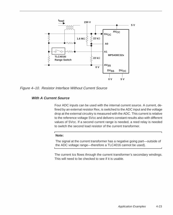
4-23Application Examples
SVCC
A1
A0
AVSS
DVSS DVCC
0 V 5 V
MPS430C32x
AVCC
5 V
TLC4016iRange Switch
22 kΩ1.6 MΩ
230 VIload
0 V
22 kΩ
Figure 4–10. Resistor Interface Without Current Source
With A Current Source
Four ADC inputs can be used with the internal current source. A current, de-fined by an external resistor Rex, is switched to the ADC input and the voltagedrop at the external circuitry is measured with the ADC. This current is relativeto the reference voltage SVcc and delivers constant results also with differentvalues of SVcc. If a second current range is needed, a reed relay is neededto switch the second load resistor of the current transformer.
Note:
The signal at the current transformer has a negative going part—outside ofthe ADC voltage range—therefore a TLC4016 cannot be used).
The current Ics flows through the current transformer’s secondary windings.This will need to be checked to see if it is usable.
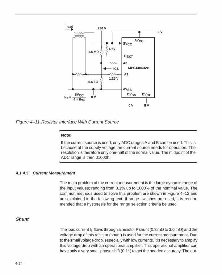
4-24
SVCC
A0
REXT
AVSSDVSS DVCC
0 V 5 V
MPS430C32x
AVCC
5 V
Rex1.6 MΩ
230 VIload
0 V
A1
ICS
5.6 kΩ
Ics =SVCC
4 × Rex
1.25 V
Figure 4–11.Resistor Interface With Current Source
Note:
If the current source is used, only ADC ranges A and B can be used. This isbecause of the supply voltage the current source needs for operation. Theresolution is therefore only one-half of the normal value. The midpoint of theADC range is then 01000h.
4.1.4.5 Current Measurement
The main problem of the current measurement is the large dynamic range ofthe input values; ranging from 0.1% up to 1000% of the nominal value. Thecommon methods used to solve this problem are shown in Figure 4–12 andare explained in the following text. If range switches are used, it is recom-mended that a hysteresis for the range selection criteria be used.
Shunt
The load current IL flows through a resistor Rshunt (0.3 mΩ to 3.0 mΩ) and thevoltage drop of this resistor (shunt) is used for the current measurement. Dueto the small voltage drop, especially with low currents, it is necessary to amplifythis voltage drop with an operational amplifier. This operational amplifier canhave only a very small phase shift (0.1) to get the needed accuracy. The out-

4-25Application Examples
put voltage VOut, which is proportional to the current IL, is measured by theMSP430. The amount of VOut is:
Vout Iload Rshunt R2R1
Vout Iload Rshunt R2| | R3
R1
(open switch, low current)
(closed switch, high current)
The value ki [A/step], used for the calculation of the meter constant CZ (seeSection 4.1.3.3) is:
ki SVCC
214 R1
Rshunt R2(open switch, low current, see Figure 4–12)
(closed switch, high current)ki SVCC
214 R1
Rshunt R2| | R3
Advantages
Resistive behavior
Simple
More than one range possible with switches
Disadvantages
High losses with high currents
Very low output voltage with small currents (amplifier necessary)
Only usable with single-phase meters
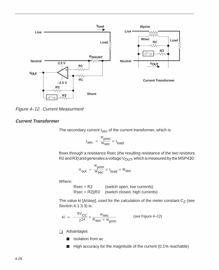
4-26
Iload
2.5 V
R2Wsec
VOUT
Live
Neutral
Wprim
R3
Live
Neutral
LoadLoad
RSHUNT
_+
R1
R1–2.5 V
R2
R3
VOUT
Shunt
Current Transformer
Figure 4–12. Current Measurment
Current Transformer
The secondary current Isec of the current transformer, which is
Isec wprimwsec
Iload
flows through a resistance Rsec (the resulting resistance of the two resistorsR2 and R3) and generates a voltage VOUT, which is measured by the MSP430:
Vout wprimwsec
Iload Rsec
Where:Rsec = R2 (switch open, low currents)Rsec = R2||R3 (switch closed, high currents)
The value ki [A/step], used for the calculation of the meter constant CZ (seeSection 4.1.3.3) is:
ki SVCC
214
wsecRsec wprim
(see Figure 4–12)
Advantages
Isolation from ac
High accuracy for the magnitude of the current (0.1% reachable)

4-27Application Examples
More than one range possible with switched resistors
Disadvantages
Sensible to dc current: may lead to saturation
Costly
Ferrite Core
The load current Iload flows through a ferrite core with a single winding. Theferrite core has a small air gap. The magnetic flux crossing this air gap goesthrough an air-core coil, which is not loaded. The small output voltage Vfc ofthis coil is amplified, integrated, and measured by the MSP430. The voltagegain of the preamplifier is used for the range switching. The ferrite core be-haves as an inductivity L i.e. the output voltage Vfc is:
Vfc dIload
dt L
This means, the voltage Vfc has a leading phase shift of 90 compared to Iload.This phase shift can be corrected by two methods:
1) Software shift: All current samples are delayed by the time representing90 of the ac frequency. This is possible with a circulating buffer and acarefully chosen sampling frequency.
2) Analog shift: An integrator combined with a pre-amplifier is used as shownin Figure 4–13.
The value ki [A/step], used for the calculation of the meter constant CZ (seeSection 4.1.3.3) is :
ki SVCC
214 C R1
v L
The formula is valid only if R2 >> R1 (normal case).
Advantages
Isolation from the ac
No saturation possible by dc parts of the load current due to the air gap
Disadvantages
Low output voltage due to loose coupling
Output voltage leads 90 compared to load current
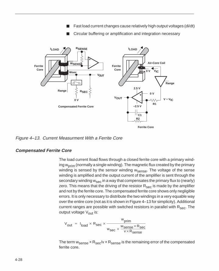
4-28
Fast load current changes cause relatively high output voltages (di/dt)
Circular buffering or amplification and integration necessary
_+
WSENSE
RSENSE
FerriteCore
Range
0 V
RSEC
VOUT
Compensated Ferrite Core
ILOAD
Range
_+
VIC0 V
0 V
R1
2.5 V
–2.5 V
C1R2
VOUT V × VIC
FerriteCore
Ferrite Core
Air-Core Coil
ILOAD
Wsec
Figure 4–13. Current Measurment With a Ferrite Core
Compensated Ferrite Core
The load current Iload flows through a closed ferrite core with a primary wind-ing wprim (normally a single winding). The magnetic flux created by the primarywinding is sensed by the sensor winding wsense. The voltage of the sensewinding is amplified and the output current of the amplifier is sent through thesecondary winding wsec in a way that compensates the primary flux to (nearly)zero. This means that the driving of the resistor Rsec is made by the amplifierand not by the ferrite core. The compensated ferrite core shows only negligibleerrors. It is only necessary to distribute the two windings in a very equable wayover the entire core (not as it is shown in Figure 4–13 for simplicity). Additionalcurrent ranges are possible with switched resistors in parallel with Rsec. Theoutput voltage Vout is:
Vout Iload Rsec wprim
wsec wsenseRsec
vRsense
The term wsense × Rsec/v × Rsense is the remaining error of the compensatedferrite core.
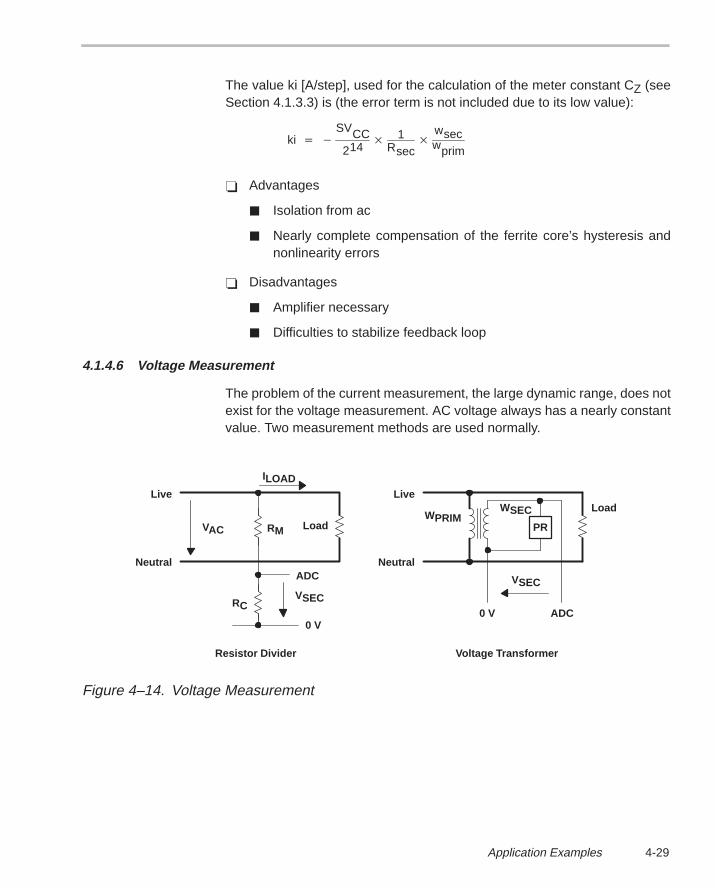
4-29Application Examples
The value ki [A/step], used for the calculation of the meter constant CZ (seeSection 4.1.3.3) is (the error term is not included due to its low value):
ki SVCC
214 1
Rsec
wsecwprim
Advantages
Isolation from ac
Nearly complete compensation of the ferrite core’s hysteresis andnonlinearity errors
Disadvantages
Amplifier necessary
Difficulties to stabilize feedback loop
4.1.4.6 Voltage Measurement
The problem of the current measurement, the large dynamic range, does notexist for the voltage measurement. AC voltage always has a nearly constantvalue. Two measurement methods are used normally.
PR
WSECWPRIM
VSEC
ADC0 V
Live
Neutral
LoadLive
Neutral
Load
ILOAD
RM
ADC
VSECRC
0 V
VAC
Resistor Divider Voltage Transformer
Figure 4–14. Voltage Measurement
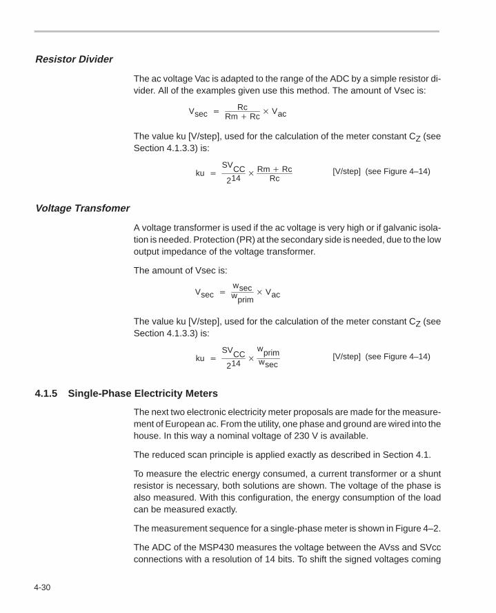
4-30
Resistor Divider
The ac voltage Vac is adapted to the range of the ADC by a simple resistor di-vider. All of the examples given use this method. The amount of Vsec is:
Vsec RcRm Rc
Vac
The value ku [V/step], used for the calculation of the meter constant CZ (seeSection 4.1.3.3) is:
ku SVCC
214 Rm Rc
Rc[V/step] (see Figure 4–14)
Voltage Transfomer
A voltage transformer is used if the ac voltage is very high or if galvanic isola-tion is needed. Protection (PR) at the secondary side is needed, due to the lowoutput impedance of the voltage transformer.
The amount of Vsec is:
Vsec wsecwprim
Vac
The value ku [V/step], used for the calculation of the meter constant CZ (seeSection 4.1.3.3) is:
ku SVCC
214
wprimwsec
[V/step] (see Figure 4–14)
4.1.5 Single-Phase Electricity Meters
The next two electronic electricity meter proposals are made for the measure-ment of European ac. From the utility, one phase and ground are wired into thehouse. In this way a nominal voltage of 230 V is available.
The reduced scan principle is applied exactly as described in Section 4.1.
To measure the electric energy consumed, a current transformer or a shuntresistor is necessary, both solutions are shown. The voltage of the phase isalso measured. With this configuration, the energy consumption of the loadcan be measured exactly.
The measurement sequence for a single-phase meter is shown in Figure 4–2.
The ADC of the MSP430 measures the voltage between the AVss and SVccconnections with a resolution of 14 bits. To shift the signed voltages coming
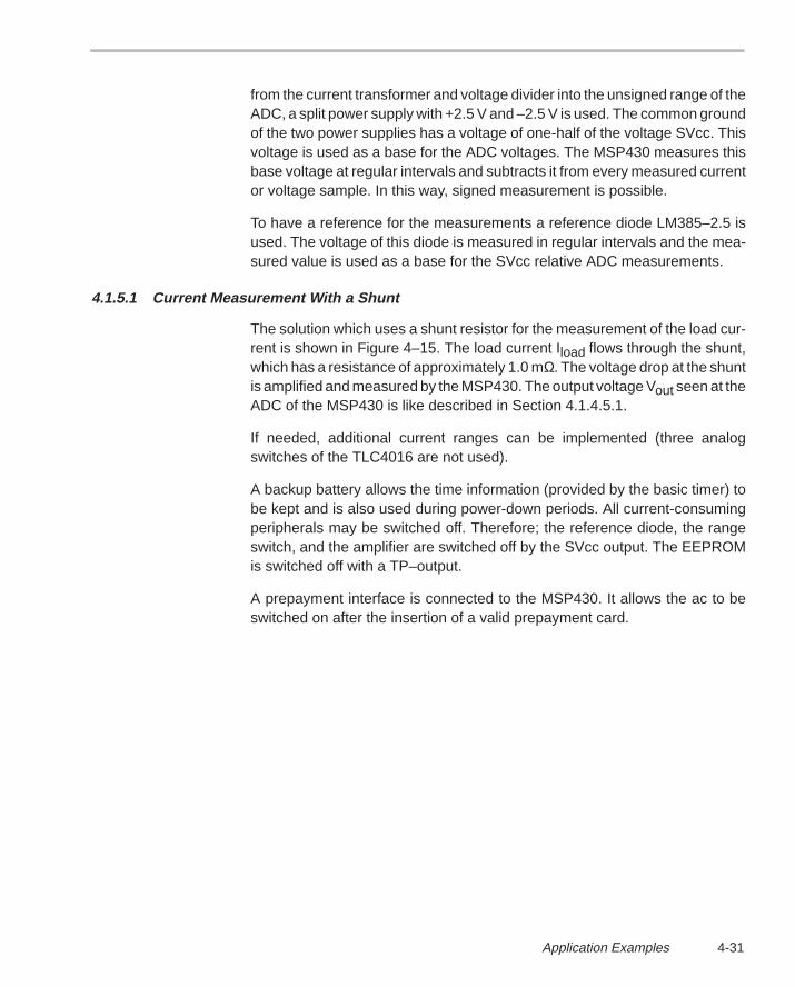
4-31Application Examples
from the current transformer and voltage divider into the unsigned range of theADC, a split power supply with +2.5 V and –2.5 V is used. The common groundof the two power supplies has a voltage of one-half of the voltage SVcc. Thisvoltage is used as a base for the ADC voltages. The MSP430 measures thisbase voltage at regular intervals and subtracts it from every measured currentor voltage sample. In this way, signed measurement is possible.
To have a reference for the measurements a reference diode LM385–2.5 isused. The voltage of this diode is measured in regular intervals and the mea-sured value is used as a base for the SVcc relative ADC measurements.
4.1.5.1 Current Measurement With a Shunt
The solution which uses a shunt resistor for the measurement of the load cur-rent is shown in Figure 4–15. The load current Iload flows through the shunt,which has a resistance of approximately 1.0 mΩ. The voltage drop at the shuntis amplified and measured by the MSP430. The output voltage Vout seen at theADC of the MSP430 is like described in Section 4.1.4.5.1.
If needed, additional current ranges can be implemented (three analogswitches of the TLC4016 are not used).
A backup battery allows the time information (provided by the basic timer) tobe kept and is also used during power-down periods. All current-consumingperipherals may be switched off. Therefore; the reference diode, the rangeswitch, and the amplifier are switched off by the SVcc output. The EEPROMis switched off with a TP–output.
A prepayment interface is connected to the MSP430. It allows the ac to beswitched on after the insertion of a valid prepayment card.
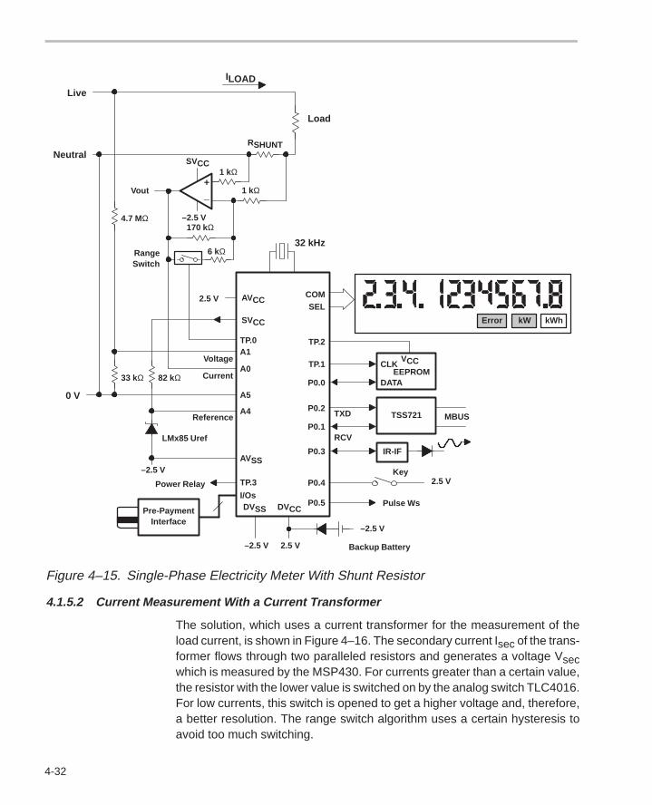
4-32
Error kW kWh
COMSEL
TP.1 CLK
DATA
VCCEEPROM
TP.2
P0.0
P0.2TSS721 MBUS
P0.1
TXD
RCV
P0.3 IR-IF
P0.4Key
2.5 V
P0.5 Pulse WsDVSS DVCC
–2.5 V
Backup Battery2.5 V–2.5 V
LMx85 Uref
I/Os
Pre-PaymentInterface
TP.3Power Relay
AVSS–2.5 V
A4Reference
A5
82 kΩ33 kΩA0
Current
A1Voltage
TP.0
SVCC
AVCC2.5 V
Live
Neutral
Load
ILOAD
RSHUNT
_+
4.7 MΩ
1 kΩSVCC
Vout
–2.5 V170 kΩ
6 kΩ32 kHz
RangeSwitch
0 V
1 kΩ
Figure 4–15. Single-Phase Electricity Meter With Shunt Resistor
4.1.5.2 Current Measurement With a Current Transformer
The solution, which uses a current transformer for the measurement of theload current, is shown in Figure 4–16. The secondary current Isec of the trans-former flows through two paralleled resistors and generates a voltage Vsecwhich is measured by the MSP430. For currents greater than a certain value,the resistor with the lower value is switched on by the analog switch TLC4016.For low currents, this switch is opened to get a higher voltage and, therefore,a better resolution. The range switch algorithm uses a certain hysteresis toavoid too much switching.
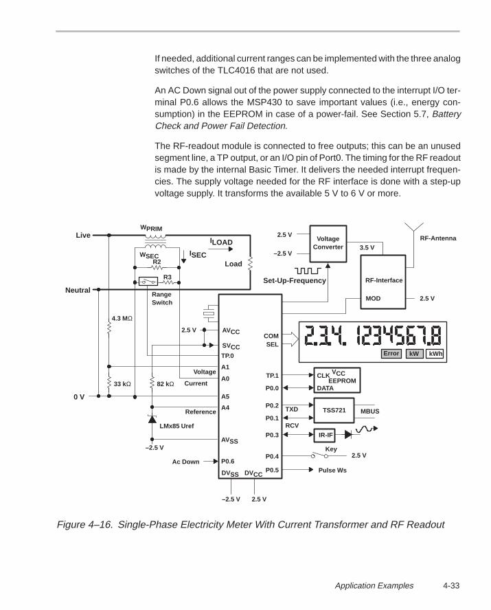
4-33Application Examples
If needed, additional current ranges can be implemented with the three analogswitches of the TLC4016 that are not used.
An AC Down signal out of the power supply connected to the interrupt I/O ter-minal P0.6 allows the MSP430 to save important values (i.e., energy con-sumption) in the EEPROM in case of a power-fail. See Section 5.7, BatteryCheck and Power Fail Detection.
The RF-readout module is connected to free outputs; this can be an unusedsegment line, a TP output, or an I/O pin of Port0. The timing for the RF readoutis made by the internal Basic Timer. It delivers the needed interrupt frequen-cies. The supply voltage needed for the RF interface is done with a step-upvoltage supply. It transforms the available 5 V to 6 V or more.
Error kW kWh
COMSEL
TP.1 CLK
DATA
VCCEEPROM
P0.0
P0.2TSS721 MBUS
P0.1TXD
RCVP0.3 IR-IF
P0.4Key
2.5 V
P0.5 Pulse WsDVSS DVCC
2.5 V–2.5 V
LMx85 Uref
P0.6Ac Down
AVSS–2.5 V
A4Reference
A5
82 kΩ33 kΩA0
Current
A1Voltage
TP.0
SVCC
AVCC2.5 V
Live
Neutral
Load
ILOAD
R2
R3
RangeSwitch
0 V
ISEC
4.3 MΩ
WSEC
WPRIM
VoltageConverter
2.5 V
–2.5 V
Set-Up-Frequency RF-Interface
MOD 2.5 V
RF-Antenna3.5 V
Figure 4–16. Single-Phase Electricity Meter With Current Transformer and RF Readout
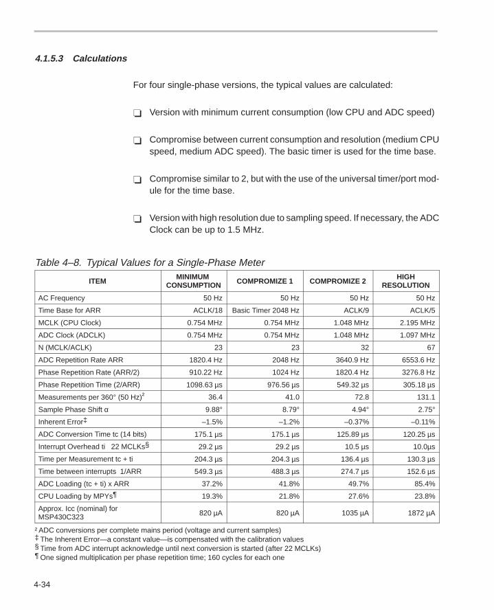
4-34
4.1.5.3 Calculations
For four single-phase versions, the typical values are calculated:
Version with minimum current consumption (low CPU and ADC speed)
Compromise between current consumption and resolution (medium CPUspeed, medium ADC speed). The basic timer is used for the time base.
Compromise similar to 2, but with the use of the universal timer/port mod-ule for the time base.
Version with high resolution due to sampling speed. If necessary, the ADCClock can be up to 1.5 MHz.
Table 4–8. Typical Values for a Single-Phase Meter
ITEMMINIMUM
CONSUMPTION COMPROMIZE 1 COMPROMIZE 2HIGH
RESOLUTION
AC Frequency 50 Hz 50 Hz 50 Hz 50 Hz
Time Base for ARR ACLK/18 Basic Timer 2048 Hz ACLK/9 ACLK/5
MCLK (CPU Clock) 0.754 MHz 0.754 MHz 1.048 MHz 2.195 MHz
ADC Clock (ADCLK) 0.754 MHz 0.754 MHz 1.048 MHz 1.097 MHz
N (MCLK/ACLK) 23 23 32 67
ADC Repetition Rate ARR 1820.4 Hz 2048 Hz 3640.9 Hz 6553.6 Hz
Phase Repetition Rate (ARR/2) 910.22 Hz 1024 Hz 1820.4 Hz 3276.8 Hz
Phase Repetition Time (2/ARR) 1098.63 µs 976.56 µs 549.32 µs 305.18 µs
Measurements per 360° (50 Hz)† 36.4 41.0 72.8 131.1
Sample Phase Shift α 9.88° 8.79° 4.94° 2.75°
Inherent Error‡ –1.5% –1.2% –0.37% –0.11%
ADC Conversion Time tc (14 bits) 175.1 µs 175.1 µs 125.89 µs 120.25 µs
Interrupt Overhead ti 22 MCLKs§ 29.2 µs 29.2 µs 10.5 µs 10.0µs
Time per Measurement tc + ti 204.3 µs 204.3 µs 136.4 µs 130.3 µs
Time between interrupts 1/ARR 549.3 µs 488.3 µs 274.7 µs 152.6 µs
ADC Loading (tc + ti) x ARR 37.2% 41.8% 49.7% 85.4%
CPU Loading by MPYs¶ 19.3% 21.8% 27.6% 23.8%
Approx. Icc (nominal) forMSP430C323 820 µA 820 µA 1035 µA 1872 µA
† ADC conversions per complete mains period (voltage and current samples)‡ The Inherent Error—a constant value—is compensated with the calibration values§ Time from ADC interrupt acknowledge until next conversion is started (after 22 MCLKs)¶ One signed multiplication per phase repetition time; 160 cycles for each one
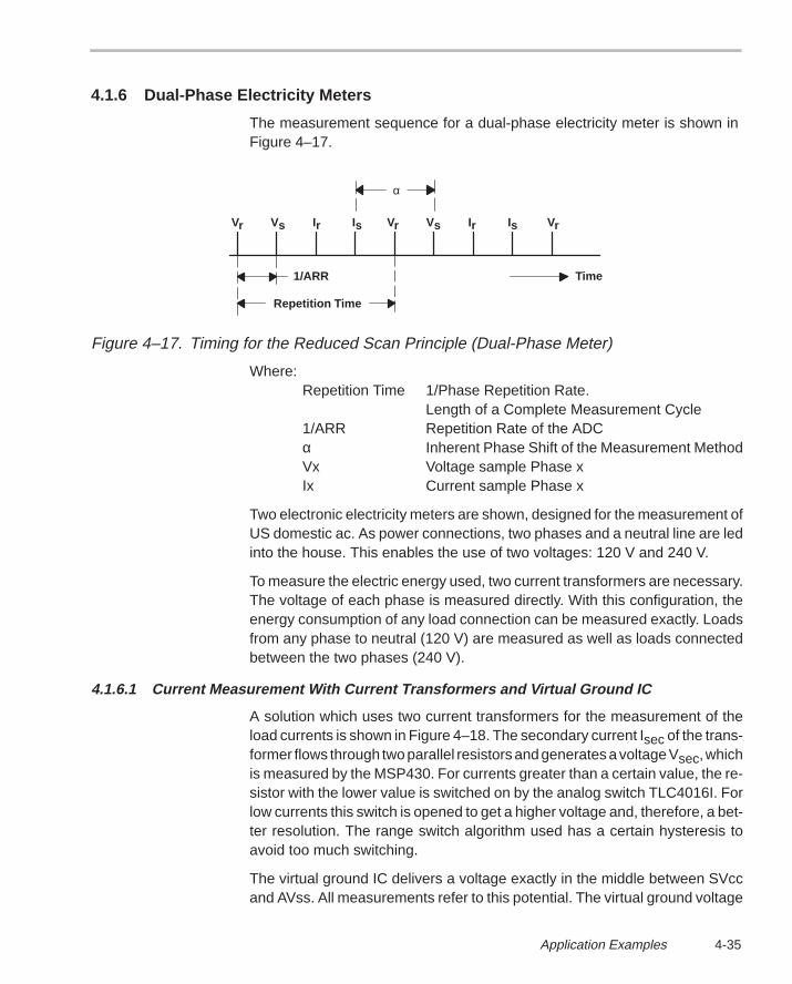
4-35Application Examples
4.1.6 Dual-Phase Electricity Meters
The measurement sequence for a dual-phase electricity meter is shown in Figure 4–17.
Time
Vr Vs Ir Is Vr Vs Ir Is Vr
1/ARR
Repetition Time
α
Figure 4–17. Timing for the Reduced Scan Principle (Dual-Phase Meter)
Where:Repetition Time 1/Phase Repetition Rate.
Length of a Complete Measurement Cycle1/ARR Repetition Rate of the ADCα Inherent Phase Shift of the Measurement MethodVx Voltage sample Phase xIx Current sample Phase x
Two electronic electricity meters are shown, designed for the measurement ofUS domestic ac. As power connections, two phases and a neutral line are ledinto the house. This enables the use of two voltages: 120 V and 240 V.
To measure the electric energy used, two current transformers are necessary.The voltage of each phase is measured directly. With this configuration, theenergy consumption of any load connection can be measured exactly. Loadsfrom any phase to neutral (120 V) are measured as well as loads connectedbetween the two phases (240 V).
4.1.6.1 Current Measurement With Current Transformers and Virtual Ground IC
A solution which uses two current transformers for the measurement of theload currents is shown in Figure 4–18. The secondary current Isec of the trans-former flows through two parallel resistors and generates a voltage Vsec, whichis measured by the MSP430. For currents greater than a certain value, the re-sistor with the lower value is switched on by the analog switch TLC4016I. Forlow currents this switch is opened to get a higher voltage and, therefore, a bet-ter resolution. The range switch algorithm used has a certain hysteresis toavoid too much switching.
The virtual ground IC delivers a voltage exactly in the middle between SVccand AVss. All measurements refer to this potential. The virtual ground voltage
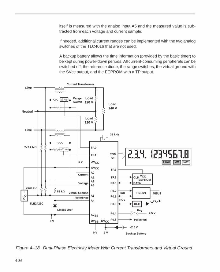
4-36
itself is measured with the analog input A5 and the measured value is sub-tracted from each voltage and current sample.
If needed, additional current ranges can be implemented with the two analogswitches of the TLC4016 that are not used.
A backup battery allows the time information (provided by the basic timer) tobe kept during power-down periods. All current-consuming peripherals can beswitched off; the reference diode, the range switches, the virtual ground withthe SVcc output, and the EEPROM with a TP output.
Error kW kWh
COMSEL
TP.2 CLK
DATA
VCCEEPROM
P0.0
P0.2TSS721 MBUS
P0.1TXD
RCVP0.3 IR-IF
P0.4Key
2.5 V
P0.5 Pulse WsDVSS DVCC
5 V0 V
LMx85 Uref
TP.1
AVSS
0 V
A4Reference
A582 kΩ
A0Current
A1
Voltage
TP.0
SVCC
AVCC5 V
Live
Neutral
Load240 V
RangeSwitch
TP.3
A2A3
OI
C
TLE2426C
2x33 kΩ
2x2.2 MΩ
LiveCurrent Transformer
Load120 V
Load120 V
Virtual Ground
–2.5 V
Backup Battery
32 kHz
Figure 4–18. Dual-Phase Electricity Meter With Current Transformers and Virtual Ground

4-37Application Examples
4.1.6.2 Current Measurement With Current Transformers and Software Offset
Figure 4–19 shows a two-phase electricity meter that uses voltage dividers toget reference voltages in the middle of the supply voltage for current and volt-age inputs. The resistors of this voltage dividers are chosen to be smaller thanthe maximum source impedance of the ADC (see Section 4.1.4.2, ADC InputConsiderations). To get the ADC value of the virtual midpoint of the ADC range,the software offset method is used (see Section 4.1.4.4.3, Resister Interface(Software Offset)). This value is subtracted from each voltage and currentsample to get signed, offset-corrected results.
No backup battery is provided. This means, that in regular time intervals, theactual amount of the energy consumption needs to be stored in the EEPROM.If the power supply used provides an ac down, this storage is only neededwhen this signal is activated.
An ac down signal from the power supply connected to the interrupt I/O termi-nal P0.6 allows the MSP430 to save important values (i.e., energy consump-tion) in the EEPROM in case of a power failure (see Section 5.7, Battery Checkand Power Fail Detection).
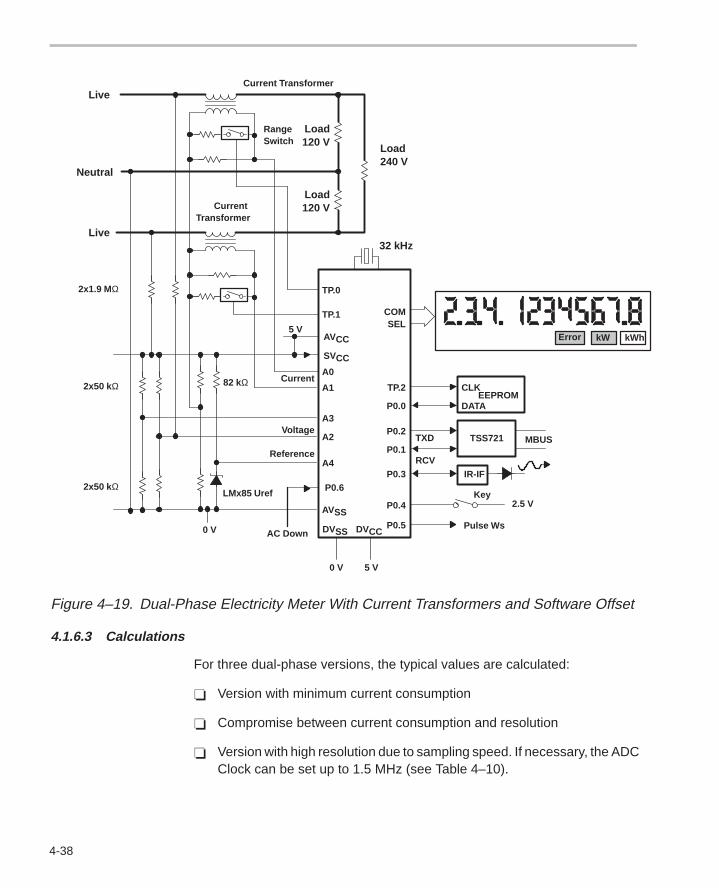
4-38
Error kW kWh
COMSEL
TP.2 CLK
DATAEEPROM
P0.0
P0.2TSS721 MBUS
P0.1TXD
RCVP0.3 IR-IF
P0.4Key
2.5 V
P0.5 Pulse WsDVSS DVCC
5 V0 V
LMx85 Uref
TP.1
AVSS
0 V
A4Reference
82 kΩA0
CurrentA1
Voltage
TP.0
SVCC
AVCC5 V
Live
Neutral
Load240 V
RangeSwitch
A2
A3
2x1.9 MΩ
LiveCurrent Transformer
Load120 V
Load120 VCurrent
Transformer
2x50 kΩ
2x50 kΩ
32 kHz
P0.6
AC Down
Figure 4–19. Dual-Phase Electricity Meter With Current Transformers and Software Offset
4.1.6.3 Calculations
For three dual-phase versions, the typical values are calculated:
Version with minimum current consumption
Compromise between current consumption and resolution
Version with high resolution due to sampling speed. If necessary, the ADCClock can be set up to 1.5 MHz (see Table 4–10).
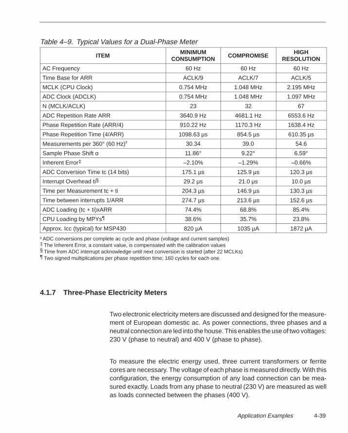
4-39Application Examples
Table 4–9. Typical Values for a Dual-Phase Meter
ITEM MINIMUMCONSUMPTION COMPROMISE HIGH
RESOLUTION
AC Frequency 60 Hz 60 Hz 60 Hz
Time Base for ARR ACLK/9 ACLK/7 ACLK/5
MCLK (CPU Clock) 0.754 MHz 1.048 MHz 2.195 MHz
ADC Clock (ADCLK) 0.754 MHz 1.048 MHz 1.097 MHz
N (MCLK/ACLK) 23 32 67
ADC Repetition Rate ARR 3640.9 Hz 4681.1 Hz 6553.6 Hz
Phase Repetition Rate (ARR/4) 910.22 Hz 1170.3 Hz 1638.4 Hz
Phase Repetition Time (4/ARR) 1098.63 µs 854.5 µs 610.35 µs
Measurements per 360° (60 Hz)† 30.34 39.0 54.6
Sample Phase Shift α 11.86° 9.22° 6.59°Inherent Error‡ –2.10% –1.29% –0.66%
ADC Conversion Time tc (14 bits) 175.1 µs 125.9 µs 120.3 µs
Interrupt Overhead ti§ 29.2 µs 21.0 µs 10.0 µs
Time per Measurement tc + ti 204.3 µs 146.9 µs 130.3 µs
Time between interrupts 1/ARR 274.7 µs 213.6 µs 152.6 µs
ADC Loading (tc + ti)xARR 74.4% 68.8% 85.4%
CPU Loading by MPYs¶ 38.6% 35.7% 23.8%
Approx. Icc (typical) for MSP430 820 µA 1035 µA 1872 µA
† ADC conversions per complete ac cycle and phase (voltage and current samples)‡ The Inherent Error, a constant value, is compensated with the calibration values§ Time from ADC interrupt acknowledge until next conversion is started (after 22 MCLKs)¶ Two signed multiplications per phase repetition time; 160 cycles for each one
4.1.7 Three-Phase Electricity Meters
Two electronic electricity meters are discussed and designed for the measure-ment of European domestic ac. As power connections, three phases and aneutral connection are led into the house. This enables the use of two voltages:230 V (phase to neutral) and 400 V (phase to phase).
To measure the electric energy used, three current transformers or ferritecores are necessary. The voltage of each phase is measured directly. With thisconfiguration, the energy consumption of any load connection can be mea-sured exactly. Loads from any phase to neutral (230 V) are measured as wellas loads connected between the phases (400 V).
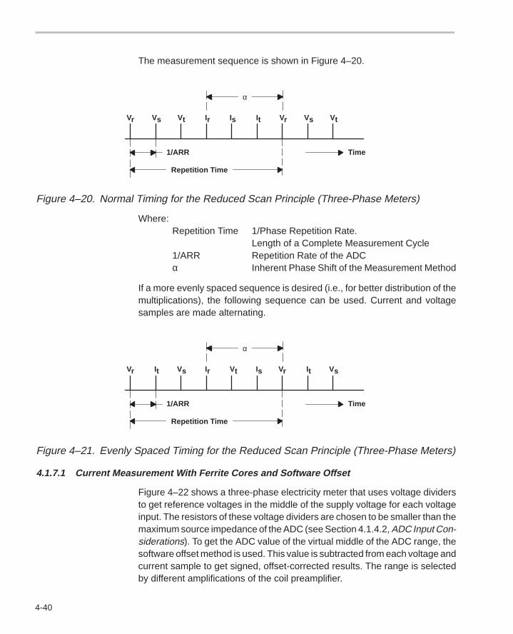
4-40
The measurement sequence is shown in Figure 4–20.
Time
Vr Vs Vt Ir Vr VsItIs Vt
1/ARR
Repetition Time
α
Figure 4–20. Normal Timing for the Reduced Scan Principle (Three-Phase Meters)
Where:Repetition Time 1/Phase Repetition Rate.
Length of a Complete Measurement Cycle1/ARR Repetition Rate of the ADCα Inherent Phase Shift of the Measurement Method
If a more evenly spaced sequence is desired (i.e., for better distribution of themultiplications), the following sequence can be used. Current and voltagesamples are made alternating.
Time
Vr Vs VtIr Vr VsIt Is It
1/ARR
Repetition Time
α
Figure 4–21. Evenly Spaced Timing for the Reduced Scan Principle (Three-Phase Meters)
4.1.7.1 Current Measurement With Ferrite Cores and Software Offset
Figure 4–22 shows a three-phase electricity meter that uses voltage dividersto get reference voltages in the middle of the supply voltage for each voltageinput. The resistors of these voltage dividers are chosen to be smaller than themaximum source impedance of the ADC (see Section 4.1.4.2, ADC Input Con-siderations). To get the ADC value of the virtual middle of the ADC range, thesoftware offset method is used. This value is subtracted from each voltage andcurrent sample to get signed, offset-corrected results. The range is selectedby different amplifications of the coil preamplifier.

4-41Application Examples
The reference is provided by the stable +5 V supply.
If needed and with more TLC4016 ICs, additional current ranges can be imple-mented.
A backup battery allows the time information (provided by the basic timer) tobe kept during power-down periods. All current-consuming peripherals can beswitched off; including, the resistor dividers, the range switches, the amplifiers(integrators) by the SVcc output, and the EEPROM with a TP output.
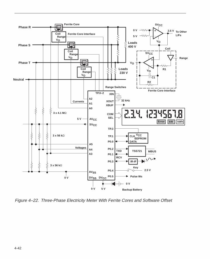
4-42
Error kW kWh
COMSEL
TP.1 CLK
DATA
VCCEEPROM
P0.0
P0.2TSS721 MBUS
P0.1TXD
RCVP0.3 IR-IF
P0.4Key
2.5 V
P0.5 Pulse WsDVSS DVCC
5 V0 V
TP.0–2
AVSS
0 V
A4
A5
A0
CurrentsA1
Voltages
SVCC
AVCC5 V
Neutral
Loads400 V
TP.3
A2
A3
Phase R
0 V
Backup Battery
Coil
VORange
XIN
XOUTXBUF
Coil
VORange
Coil
VORange
Loads230 V
3 x 4.1 MΩ
Phase S
Phase T
3 x 56 kΩ
3 x 56 kΩ
_+
SVCC
VO
R2
C1
_+
SVCC
VO
0 V
5 V
R1
To OtherL/Fs
2.5 V
Coil
VO
Ferrite Core Interface
Range
Ferrite Core Interface
Ferrite Core
Range Switches
32 kHz
Figure 4–22. Three-Phase Electricity Meter With Ferrite Cores and Software Offset

4-43Application Examples
4.1.7.2 Current Measurement With Current Transformers and Split Power Supplies
The six analog inputs of the MSP430C32x only allow the measurement of thethree currents and three voltages without external circuitry. If a reference diodeis needed (i.e., because the power supply cannot be used as a reference) orone of the methods using a ground that needs to be measured is used, thenan analog multiplexer, like the TLC4016, is needed (see Figure 4–23). With itsthree outputs (TP.3 to TP.5) the MSP430 selects the phase to be measured.
No backup battery is provided, this means that in regular time intervals, the ac-tual amount of energy consumption needs to be stored in the EEPROM. If thepower supply used provides an ac Down, this storage would only necessarywhen this signal was activated.
The same circuitry can be used with a virtual ground IC. Only a few modifica-tions are necessary (see Figure 4–18).
An ac down signal from the power supply connected to the interrupt I/O termi-nal P0.6 allows the MSP430 to save important values (i.e., energy consump-tion) in the EEPROM in case of a power failure (see Section 5.7, Battery Checkand Power Fail Detection).
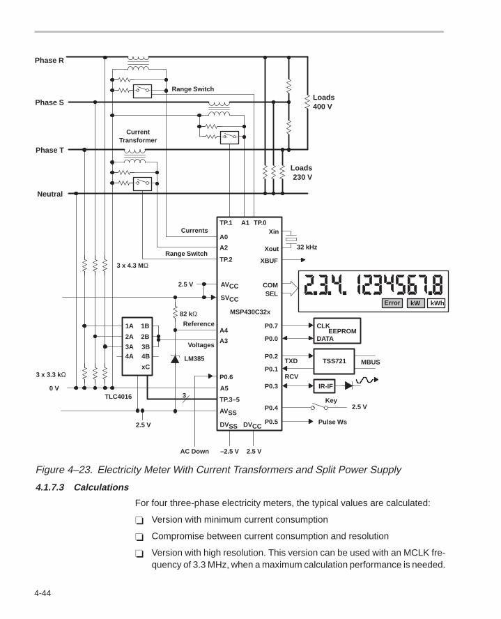
4-44
Error kW kWh
COMSEL
P0.7 CLK
DATAEEPROM
P0.0
P0.2TSS721 MBUS
P0.1TXD
RCVP0.3 IR-IF
P0.4Key
2.5 V
P0.5 Pulse WsDVSS DVCC
2.5 V–2.5 V
TP.1
AVSS
2.5 V
A4
A5
A0Currents
A1
Voltages
SVCC
AVCC2.5 V
Neutral
Loads400 V
A2
A3
Phase R
Xin
Xout
XBUF
Loads230 V
3 x 4.3 MΩ
Phase S
Phase T
3 x 3.3 kΩ
TLC4016
CurrentTransformer
Range Switch32 kHz
LM385
82 kΩ
TP.3–5
1A
2A
3A4A
1B
2B
3B4B
xC
P0.6
AC Down
TP.2
TP.0
Range Switch
3
Reference
0 V
MSP430C32x
Figure 4–23. Electricity Meter With Current Transformers and Split Power Supply
4.1.7.3 Calculations
For four three-phase electricity meters, the typical values are calculated:
Version with minimum current consumption
Compromise between current consumption and resolution
Version with high resolution. This version can be used with an MCLK fre-quency of 3.3 MHz, when a maximum calculation performance is needed.
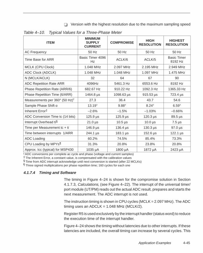
4-45Application Examples
Version with the highest resolution due to the maximum sampling speed
Table 4–10. Typical Values for a Three-Phase Meter
ITEMMINIMUMSUPPLY
CURRENTCOMPROMISE HIGH
RESOLUTIONHIGHEST
RESOLUTION
AC Frequency 50 Hz 50 Hz 50 Hz 50 Hz
Time Base for ARRBasic Timer 4096
Hz ACLK/6 ACLK/5Basic Timer
8192 Hz
MCLK (CPU Clock) 1.048 MHz 2.097 MHz 2.195 MHz 2.949 MHz
ADC Clock (ADCLK) 1.048 MHz 1.048 MHz 1.097 MHz 1.475 MHz
N (MCLK/ACLK) 32 64 67 90
ADC Repetition Rate ARR 4096Hz 5461.3 Hz 6553.6 Hz 8192 Hz
Phase Repetition Rate (ARR/6) 682.67 Hz 910.22 Hz 1092.3 Hz 1365.33 Hz
Phase Repetition Time (6/ARR) 1464.8 µs 1098.63 µs 915.53 µs 723.4 µs
Measurements per 360° (50 Hz)† 27.3 36.4 43.7 54.6
Sample Phase Shift α 13.19° 9.88° 8.24° 6.59°Inherent Error‡ –2.6% –1.5% –1.03% –0.66%
ADC Conversion Time tc (14 bits) 125.9 µs 125.9 µs 120.3 µs 89.5 µs
Interrupt Overhead ti§ 21.0 µs 10.5 µs 10.0 µs 7.5 µs
Time per Measurement tc + ti 146.9 µs 136.4 µs 130.3 µs 97.0 µs
Time between interrupts 1/ARR 244.1 µs 183.1 µs 152.6 µs 122.1 µs
ADC Loading 60.2% 74.5% 85.4% 73.3%
CPU Loading by MPYs¶ 31.3% 20.8% 23.8% 20.8%
Approx. Icc (typical) for MSP430 1035 µA 1800 µA 1872 µA 2423 µA† ADC conversions per complete ac cycle and phase (voltage and current samples)‡ The Inherent Error, a constant value, is compensated with the calibration values§ Time from ADC interrupt acknowledge until next conversion is started (after 22 MCLKs)¶ Three signed multiplications per phase repetition time; 160 cycles for each one
4.1.7.4 Timing and Software
The timing in Figure 4–24 is shown for the compromise solution in Section4.1.7.3, Calculations, (see Figure 4–22). The interrupt of the universal timer/port module (UT/PM) reads out the actual ADC result, prepares and starts thenext measurement. The ADC interrupt is not used.
The instruction timing is shown in CPU cycles (MCLK = 2.097 MHz). The ADCtiming uses an ADCLK = 1.048 MHz (MCLK/2).
Register R5 is used exclusively by the interrupt handler (status word) to reducethe execution time of the interrupt handler.
Figure 4–24 shows the timing without latencies due to other interrupts. If theselatencies are included, the overall timing can increase by several cycles. This
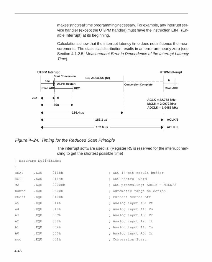
4-46
makes strict real time programming necessary. For example, any interrupt ser-vice handler (except the UT/PM handler) must have the instruction EINT (En-able Interrupt) at its beginning.
Calculations show that the interrupt latency time does not influence the mea-surements. The statistical distribution results in an error are nearly zero (seeSection 4.1.2.5, Measurement Error in Dependence of the Interrupt LatencyTime).
UT/PM InteruptStart Conversion
12c
Read ADC
UT/PM Restart
RETI
132 ADCLKS (tc)
Conversion Complete
22c ti
39c
136.4 µs
183.1 µs
152.6 µs
ACLK = 32.768 kHzMCLK = 2.0972 kHzADCLK = 1.0486 kHz
ti
Read ADC
ACLK/6
ACLK/5
UT/PM Interupt
Figure 4–24. Timing for the Reduced Scan Principle
The interrupt software used is: (Register R5 is reserved for the interrupt han-dling to get the shortest possible time)
; Hardware Definitions
;
ADAT .EQU 0118h ; ADC 14–bit result buffer
ACTL .EQU 0114h ; ADC control word
M2 .EQU 02000h ; ADC prescaling: ADCLK = MCLK/2
Rauto .EQU 0800h ; Automatic range selection
CSoff .EQU 0100h ; Current Source off
A5 .EQU 014h ; Analog input A5: Vt
A4 .EQU 010h ; Analog input A4: Vs
A3 .EQU 00Ch ; Analog input A3: Vr
A2 .EQU 008h ; Analog input A2: It
A1 .EQU 004h ; Analog input A1: Is
A0 .EQU 000h ; Analog input A0: Ir
soc .EQU 001h ; Conversion Start
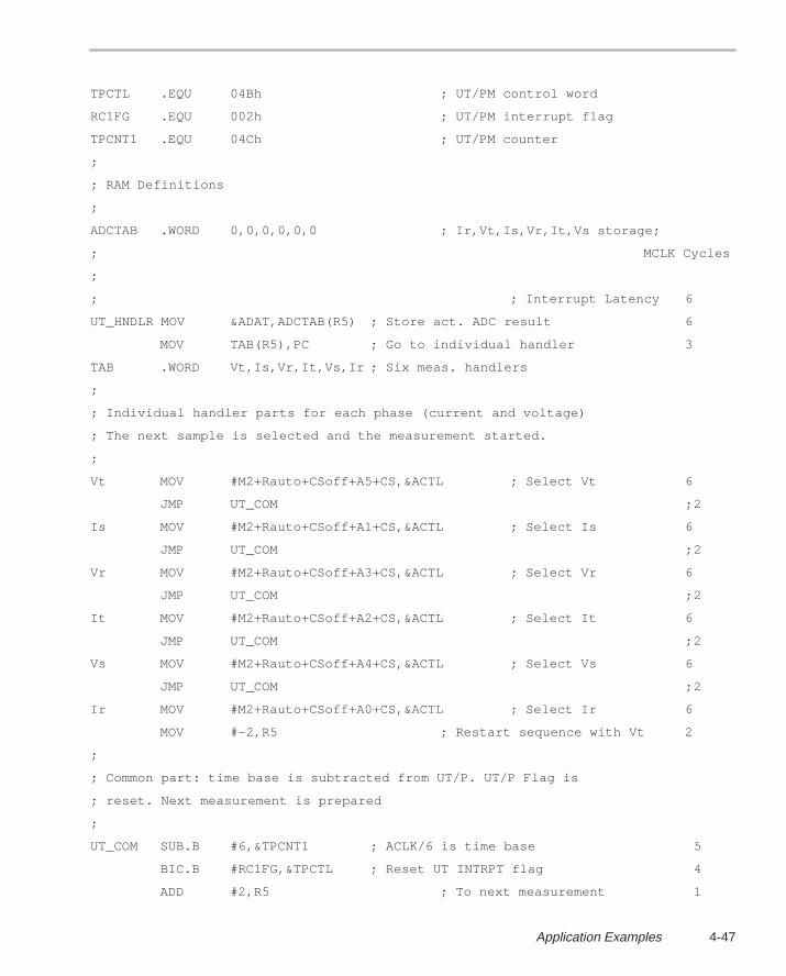
4-47Application Examples
TPCTL .EQU 04Bh ; UT/PM control word
RC1FG .EQU 002h ; UT/PM interrupt flag
TPCNT1 .EQU 04Ch ; UT/PM counter
;
; RAM Definitions
;
ADCTAB .WORD 0,0,0,0,0,0 ; Ir,Vt,Is,Vr,It,Vs storage;
; MCLK Cycles
;
; ; Interrupt Latency 6
UT_HNDLR MOV &ADAT,ADCTAB(R5) ; Store act. ADC result 6
MOV TAB(R5),PC ; Go to individual handler 3
TAB .WORD Vt,Is,Vr,It,Vs,Ir ; Six meas. handlers
;
; Individual handler parts for each phase (current and voltage)
; The next sample is selected and the measurement started.
;
Vt MOV #M2+Rauto+CSoff+A5+CS,&ACTL ; Select Vt 6
JMP UT_COM ;2
Is MOV #M2+Rauto+CSoff+A1+CS,&ACTL ; Select Is 6
JMP UT_COM ;2
Vr MOV #M2+Rauto+CSoff+A3+CS,&ACTL ; Select Vr 6
JMP UT_COM ;2
It MOV #M2+Rauto+CSoff+A2+CS,&ACTL ; Select It 6
JMP UT_COM ;2
Vs MOV #M2+Rauto+CSoff+A4+CS,&ACTL ; Select Vs 6
JMP UT_COM ;2
Ir MOV #M2+Rauto+CSoff+A0+CS,&ACTL ; Select Ir 6
MOV #–2,R5 ; Restart sequence with Vt 2
;
; Common part: time base is subtracted from UT/P. UT/P Flag is
; reset. Next measurement is prepared
;
UT_COM SUB.B #6,&TPCNT1 ; ACLK/6 is time base 5
BIC.B #RC1FG,&TPCTL ; Reset UT INTRPT flag 4
ADD #2,R5 ; To next measurement 1
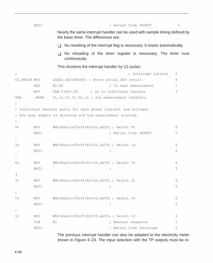
4-48
RETI ; Return from INTRPT 5
Nearly the same interrupt handler can be used with sample timing defined bythe basic timer. The differences are:
No resetting of the interrupt flag is necessary. It resets automatically.
No reloading of the timer register is necessary. The timer runscontinuously.
This shortens the interrupt handler by 12 cycles.
; ; Interrupt Latency 6
UT_HNDLR MOV &ADAT,ADCTAB(R5) ; Store actual ADC result 6
ADD #2,R5 ; To next measurement 1
MOV TAB–2(R5),PC ; Go to individual handler 3
TAB .WORD Vt,Is,Vr,It,Vs,Ir ; Six measurement handlers
;
; Individual handler parts for each phase (current and voltage)
; The next sample is selected and the measurement started.
;
Vt MOV #M2+Rauto+CSoff+A5+CS,&ACTL ; Select Vt 6
RETI ; Return from INTRPT 5
;
Is MOV #M2+Rauto+CSoff+A1+CS,&ACTL ; Select Is 6
RETI ; 5
;
Vr MOV #M2+Rauto+CSoff+A3+CS,&ACTL ; Select Vr 6
RETI ; 5
;It MOV #M2+Rauto+CSoff+A2+CS,&ACTL ; Select It 6
RETI ; 5
;
Vs MOV #M2+Rauto+CSoff+A4+CS,&ACTL ; Select Vs 6
RETI ; 5
;
Ir MOV #M2+Rauto+CSoff+A0+CS,&ACTL ; Select Ir 6
CLR R5 ; Restart sequence 1
RETI ; Return from interrupt 5
The previous interrupt handler can also be adapted to the electricity metershown in Figure 4–23. The input selection with the TP outputs must be in-
4-49Application Examples
cluded into the parts serving the three ac voltages. The selected ADC input isA3 for all voltage measurements.
4.1.8 Measurement of Voltage, Current, Apparent Power, and Reactive Power
The reduced scan principle measures only active power. If reactive power orapparent power is to be measured, other methods have to be used. The imple-mented measurement method also depends on the main application of theelectricity meter. A meter for the measurement of reactive power only probablyuses a different algorithm than an electricity meter for active power that doesthe reactive power measurement as a background task only. This sectionshows simple methods that use as much as possible the voltage and currentsamples measured for the active power calculation.
4.1.8.1 Measurement of Voltage and Current
The measurement of voltage and current is possible by summing up the abso-lute values of the ADC results during integer numbers of full periods. The resultis an indication of the average value of the voltage Vavrg respective of the cur-rent Iavrg. If corrected as shown, the current and voltage values can be usedfor other purposes. The formula for a sinusoidal voltage is shown in the follow-ing. The one for the current is equivalent to it.
Vavrg Vpeak 2
p ; Veff Vpeak
2 Veff
Vavrg p
2 2≈ 1.11 Vavrg
4.1.8.2 Measurement of the Apparent Power
The apparent power is defined by the formula Papp = U × I. There is no exactdefinition for the apparent power when harmonics are included. A possiblesolution is to use the voltage and current samples (see Section 4.1.8.1, Mea-surement of Voltage and Current) taken for the active power measurement.These samples are made absolute and summed up for an integer number ofac periods. If these summed-up values, representing the average value, aremultiplied and corrected the apparent power is the result.
The correction is necessary due to the difference of the average value and theeffective value of a sinusoidal current or voltage (see Section 4.1.8.1). The ap-parent energy Wapp is:
Wapp Vavrg Iavrg 1.112 t
4-50
4.1.8.3 Measurement of the Reactive Power
Two simple methods exist for the measurement of the reactive power:
Delay of the voltage (or current) samples for the time representing 90°(π/2) of the ac frequency.
Calculation of the apparent power and the active power
Delay of Samples
With a carefully chosen sampling frequency, the angle 90 (π/2) can be madean integer multiple of the sampling interval. If each voltage sample is delayedwith a RAM-based by this integer number and multiplied with the actual currentsample, the result is the reactive power.
EXAMPLE: ac frequency 50 Hz, 90 are 5 ms, with a sampling frequency of2000 Hz the necessary FIFO buffer is 5 ms x 2000 Hz = 10 words. For everyphase 20 bytes of RAM are needed for the FIFO.
Calculation out of the Apparent Power
The apparent power is calculated as described in Section 4.1.8.2. The reactivepower is calculated with the values of the active power and the apparent powerby the formula:
Wreact Wapp2 Wact
2
Note:
All the calculations described previously can be made with the MSP430 float-ing-point package. It is available with two lengths of mantissa; 24 bits and 40bits (see Section 5.6, The Floating Point Package).
4.1.9 Calculation of the System Current Consumption
The base of the following current consumption table is derived from the follow-ing data sheet information:
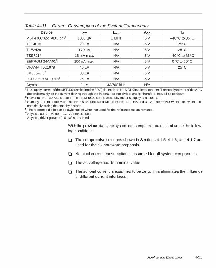
4-51Application Examples
Table 4–11. Current Consumption of the System ComponentsDevice ICC fosc VCC TA
MSP430C32x (ADC on)† 1000 µA 1 MHz 5 V –40C to 85C
TLC4016 20 µA N/A 5 V 25C
TLE2426 170 µA N/A 5 V 25C
TSS721‡ 18 mA max. N/A 5 V –40C to 85C
EEPROM 24AA01§ 100 µA max. N/A 5 V 0C to 70C
OPAMP TLC1079 40 µA N/A 5 V 25C
LM385–2.5¶ 30 µA N/A 5 V
LCD 20mm×100mm# 26 µA N/A 5 V
Crystal|| 2 µA 32.768 kHz N/A† The supply current of the MSP430 (excluding the ADC) depends on the MCLK in a linear manner. The supply current of the ADC
depends mainly on the current flowing through the internal resistor divider and is, therefore, treated as constant.‡ Power for the TSS721 is taken from the M-BUS, so the electricity meter’s supply is not used.§ Standby current of the Microchip EEPROM. Read and write currents are 1 mA and 3 mA. The EEPROM can be switched off
completely during the standby periods.¶ The reference diode can be switched off when not used for the reference measurements.# A typical current value of 13 nA/mm2 is used.|| A typical driver power of 10 µW is assumed.
With the previous data, the system consumption is calculated under the follow-ing conditions:
The compromise solutions shown in Sections 4.1.5, 4.1.6, and 4.1.7 areused for the six hardware proposals
Nominal current consumption is assumed for all system components
The ac voltage has its nominal value
The ac load current is assumed to be zero. This eliminates the influenceof different current interfaces.
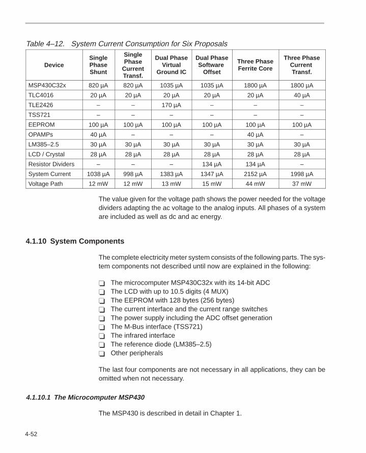
4-52
Table 4–12. System Current Consumption for Six Proposals
DeviceSinglePhaseShunt
SinglePhase
CurrentTransf.
Dual PhaseVirtual
Ground IC
Dual PhaseSoftware
Offset
Three PhaseFerrite Core
Three PhaseCurrent Transf.
MSP430C32x 820 µA 820 µA 1035 µA 1035 µA 1800 µA 1800 µA
TLC4016 20 µA 20 µA 20 µA 20 µA 20 µA 40 µA
TLE2426 – – 170 µA – – –
TSS721 – – – – – –
EEPROM 100 µA 100 µA 100 µA 100 µA 100 µA 100 µA
OPAMPs 40 µA – – – 40 µA –
LM385–2.5 30 µA 30 µA 30 µA 30 µA 30 µA 30 µA
LCD / Crystal 28 µA 28 µA 28 µA 28 µA 28 µA 28 µA
Resistor Dividers – – – 134 µA 134 µA –
System Current 1038 µA 998 µA 1383 µA 1347 µA 2152 µA 1998 µA
Voltage Path 12 mW 12 mW 13 mW 15 mW 44 mW 37 mW
The value given for the voltage path shows the power needed for the voltagedividers adapting the ac voltage to the analog inputs. All phases of a systemare included as well as dc and ac energy.
4.1.10 System Components
The complete electricity meter system consists of the following parts. The sys-tem components not described until now are explained in the following:
The microcomputer MSP430C32x with its 14-bit ADC The LCD with up to 10.5 digits (4 MUX) The EEPROM with 128 bytes (256 bytes) The current interface and the current range switches The power supply including the ADC offset generation The M-Bus interface (TSS721) The infrared interface The reference diode (LM385–2.5) Other peripherals
The last four components are not necessary in all applications, they can beomitted when not necessary.
4.1.10.1 The Microcomputer MSP430
The MSP430 is described in detail in Chapter 1.
4-53Application Examples
4.1.10.2 The LCD
Any customized LCD can be connected to the MSP430, as long as it meetsthe electrical specifications (i.e., maximum capacitance per segment andcommon lines). Every segment of the LCD can be controlled independently ofthe others. This means 256 (or 512) (3 MUX) possible combinations. SLmeans number of segment lines.
The number of digits dependent on the multiplexing scheme:
4 MUX digits = SL/23 MUX digits = SL/32 MUX digits = SL/41 MUX digits = SL/8
The unused segments H (decimal points) of the digits can be used for the dis-play of complete words (kWh, Ws, Low Tariff, etc.). This is used within the fig-ures showing the electricity meter proposals.
4.1.10.3 The EEPROM
The EEPROM contains data that must not be lost during power down cycles.
Calibration data (slopes and offsets for every range and phase) Meter number and other device related numbers Summed-up energy (stored in regular intervals (e.g., every 12 hours)) Other data (e.g., statistical data) Error characteristics (current transformer, ADC, etc.).
For the summed-up energy, a kind of circular buffer can be used, which avoidsthe use of the same cells for every update. No pointer should be used for thispurpose. A simple check for the lowest stored energy value determines thenext storage location. This check can be made during the power-up sequenceand the result is stored in the RAM for later use. This pointer is updated aftereach write cycle to the EEPROM. A checksum or an CRC (cyclic redundancycheck) can be used for the safety of the stored data.
The tables containing the error characteristics of the current transformer andthe ADC can be used for correction purposes if needed.
Dependent on the amount of data to be stored, an EEPROM with 128 bytesor 256 bytes is required. The EEPROM is driven with a software handler. Clockand data lines are set and reset by software (also see Section 3.2, Storage ofCalibration Constants, and Section 3.4, I2C Bus Connections). The EEPROMcan be switched off by an output, if it is not in use to save current.

4-54
4.1.10.4 The Range Switches
The resolution and accuracy of an electricity meter can be increased if morethan one current range is used. The analog switch TLC4016 with its four chan-nels is suited very well for this purpose. The MSP430 decides independently,for any phase, which current range is to be used. The ranges should be over-lapping and the design should use a SCHMITT-trigger characteristic for thechange in ranges. This is done to avoid too many changes.
4.1.10.5 Power Supplies
The stability of the power supply used decides if a reference voltage (see Sec-tion 4.1.10.8) is necessary or not. If the power supply is stable enough, it canbe used as the reference also. This simplifies the system in three ways:
No reference measurements are necessary in regular time intervals (e.g.,every second) that makes the omission of one sample necessary.
No correction calculations are needed to correct the summed-up energyvalues.
No reference diode and additional hardware is necessary. The analog in-put can be used for other purposes.
The stability of the power supply should be better than a factor of 4 of the de-sired accuracy of the electricity meter. This is due to the quadratic influenceof SVcc. See Section 4.1.3.3. More information is given in the Section 3.8,Power supplies for the MSP430..
4.1.10.6 The M-Bus Interface TSS721 (Option)
The M-Bus interface allows the connection of the electricity meter to networks.The M-Bus interface uses the on-chip UART or one input and one output witha software driven protocol.
Applications of the M-Bus interface:
Calibration: connection to the calibration hardware
Automatic readout by a host: the actual consumption and other interestingvalues can be read out with a customer defined protocol.
Tariff switching: the host defines the actual tariff by sending the appropri-ate information
Test: start of ROM-based testing routines or down-loading and starting ofRAM-based test routines
4-55Application Examples
Instead of the M-Bus, any other bus can be used with the MSP430.
4.1.10.7 The Infrared Interface
The infrared interface allows bidirectional data transfer for calibration, test,and readout. One of the P0-ports can be used with its interrupt capability forbidirectional transfers.
4.1.10.8 The Voltage Reference
To have a reference for the measurements, a reference diode LM385–2.5 canbe used. The voltage of this diode is measured in regular intervals and themeasured value is used as a base for the SVcc relative ADC measurements.To reduce the supply current, the LM385 can be switched on only during thereference measurements.(see Figure 4–15).
No reference diode is necessary if a 5-V voltage regulator (or two 2.5-V regula-tors) is used with the necessary accuracy and long term stability (see Section4.1.10.5, Power Supplies).
The stability of the reference should be better than a factor of 4 as the desiredaccuracy of the electricity meter.
4.1.10.9 Peripherals
Some options show how to interface the MSP430 to other devices.
Pulse Output: this output changes its state when a certain energy amountis consumed and is usable during calibration or accuracy checks. Me-chanical displays can use this pulse output.
Key Interface: keys can be interfaced very simply to the inputs of theMSP430. Interrupt is possible with all Port0 inputs.
LEDs: currents up to 1.5 mA @ 0.4 V voltage drop can be driven withoutexternal buffers..
Relays: driving is possible with a simple npn transistor and two resistors.
The crystal buffer output XBUF provides four different, software selectable fre-quencies that may be used for the peripherals. These frequencies are: MCLK,ACLK (32.768kHz), ACLK/2 (16.384kHz), ACLK/4 (8.192kHz).
4.1.10.10 Summary
As this chapter shows it is possible to build cost-effective, domestic electricitymeters based on the ultra-low-power mixed-signal RISC-processor MSP430.

4-56
The 14-bit ADC and the reduced scan principle eliminate the need for a specialfront end. All necessary system functions are realized with the on-chip periph-erals of the MSP430C32x. With appropriate calibration methods, the devi-ations of the ADC can nearly be eliminated. This allows electricity meters tobe built for classes 2, 1 and 0.5 ranging from single-phase meters to three-phase meters.
A customer developed a single-phase electricity meter with the following prop-erties:
Class 0.5 meter for the range 0.5 A to 130 A Error within 0.2% from 300 mA to 40 A Use of the full 14-bit ADC range for current and voltage Reduced scan principle is used for the energy calculation (inclusive
correction formula) Use of a virtual ground and use of the measurement result for the offset
correction Current transformer is used for current measurement (a low cost version
is planned with a shunt) Single range only for current measurement (no range switches) Meaningful current measurements down to 25 mA
4.1.11 Electricity Meter With an External ADC
Modern three-phase electricity meters of the upper classes must provide anenormous calculation power. Additional to the multiplications of the currentand voltage samples for the active power measurement, it is necessary to cal-culate additional, very computation intensive values:
Apparent power for all phases Sum of the capacitive reactive power Sum of the inductive reactive power Calculation of the cosϕ for every phase
These calculations need to be done in real time, a microcomputer with highthroughput like the MSP430C33x is necessary.
With an external ADC three different scan principles can be used:
The reduced scan principle that was used with all electricity meters shownin the previous sections. Only one ADC is necessary for current and volt-age with this method.
The alternating scan principle—a TID invention—that also needs only asingle ADC. Due to pending patent reasons, it cannot be explained further.The hardware is identical to the hardware for the reduced scan principle.
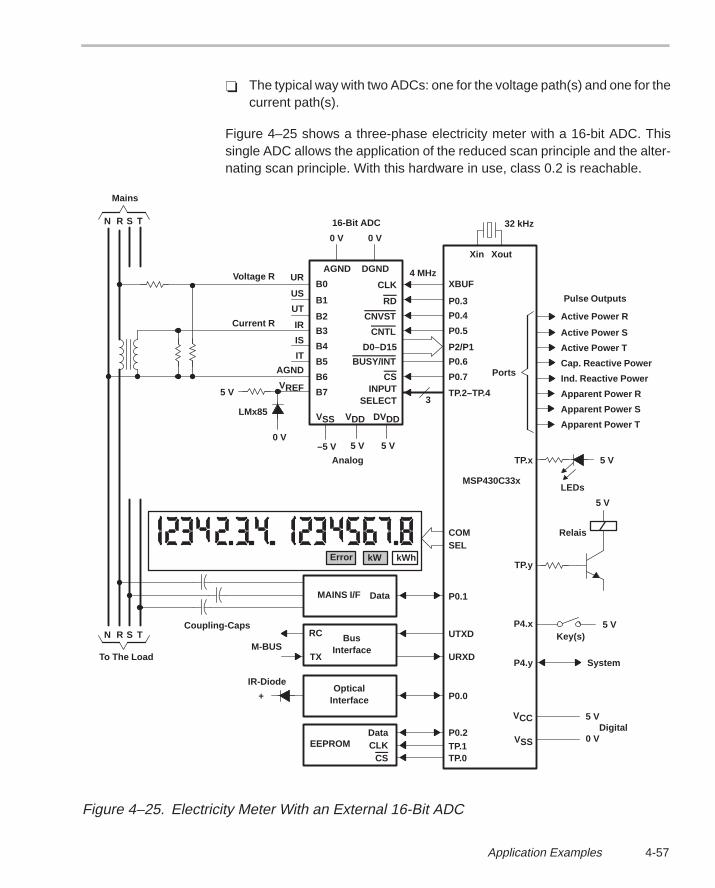
4-57Application Examples
The typical way with two ADCs: one for the voltage path(s) and one for thecurrent path(s).
Figure 4–25 shows a three-phase electricity meter with a 16-bit ADC. Thissingle ADC allows the application of the reduced scan principle and the alter-nating scan principle. With this hardware in use, class 0.2 is reachable.
Error kW kWh
Key(s)
3
XBUF
P0.3
P0.4
P0.5
P2/P1
P0.6
P0.7
TP.2–TP.4
CLK
RD
CNVST
CNTL
D0–D15
BUSY/INT
CSINPUT
SELECT
VSS VDD DVDD
–5 V 5 V 5 V
Analog
UR
US
UT
IR
IS
IT
AGND
VREF5 V
0 V
Voltage R
Current R
B0
B1
B2
B3
B4
B5
B6
B7
0 V 0 V
AGND DGND
DataMAINS I/F P0.1
COMSEL
Coupling-CapsN R S T
To The Load
BusInterface
RC
TXM-BUS
UTXD
URXD
OpticalInterface+
IR-Diode
EEPROM
P0.0
DataCLK
CS
P0.2TP.1TP.0
N R S T
Mains
16-Bit ADC
Xin Xout
Active Power R
Active Power S
Active Power T
Cap. Reactive Power
Ind. Reactive Power
Apparent Power R
Apparent Power S
Apparent Power T
LEDs
5 V
5 V
Relais
Ports
TP.x
TP.y
P4.x
P4.y
VCC
VSS
5 V
System
5 V
0 VDigital
LMx85
Pulse Outputs
32 kHz
4 MHz
MSP430C33x
Figure 4–25. Electricity Meter With an External 16-Bit ADC

4-58
4.1.12 Error Simulation for an MSP430C32x-Based Electricity Meter
The simulation methods that lead to the results shown in this chapter are ex-plained in detail.
4.1.12.1 Abstract
The way the calculation of the error of a simulated electricity meter built withthe MSP430C32x family is shown in detail. A single-phase is simulated; thiscan be the only phase or one phase of a poly-phase meter. The error simulator(ES) simulates nearly exact an MSP430C32x working as an electronic elec-tricity meter. All influences due to the MSP430 hardware are taken into ac-count.
The error due to the characteristic of the ADC
The error due to the interrupt latency of the MSP430 interrupt system
The error due to the range transition for samples at the boundaries of thefour ADC ranges
The error due to the used reduced scan principle for the measurement
4.1.12.2 Common Measurement Conditions
The ES asks at the beginning for the conditions that are used for all measure-ment points (they are written to the listing file):
Listing path name
The characteristic of the ADC; the ADC errors (in steps) at the five rangeboundaries are defined. See Figure 4–25 for explanation.
The time interval between voltage and current sample pairs (sampling in-terval)
The nominal ac frequency
The maximum interrupt latency time; the worst-case value for the time in-terval from an interrupt request to the actual start of the interrupt handler.
The correct ADC value for the external reference voltage 0 V
The measurement time for each measurement
4.1.12.3 Calibration
The next step is the calibration for the simulated system. Two calibrations arenecessary for the complete current range (the ranges shown in the followingcan be changed if needed):

4-59Application Examples
One for the current range from 0% to 5% of the maximum current. The cal-ibration points are 0.5% and 5% of the maximum current.
One for the current range from 5% to 111% of the maximum current. Thecalibration points are 5% and 100% of the maximum current.
The calculated energy for the low and the high calibration points are summed-up for five seconds each. The conditions are:
Voltage = 100% Nominal ac voltage
Cosϕ = 1 Resistive load
Frequency deviation = 0 Nominal ac frequency
Third harmonic in current = 0 No distortion, pure sine
Interrupt latency time = 5 µs No interrupt activity except from the basic timer
Measurement time for each calibration point = 5 s
The calculation for the calibration part is made exactly the same way as de-scribed in Section 4.1.4 for the error calculations.
The slope and the offset for the correction formulas are calculated with the er-rors calculated for these two calibration points when compared to the correctenergy values. The correct energy W is calculated with the formula:
W U I t cos ϕ
4.1.12.4 Conditions for the Load Curve
Next the ES asks for the special conditions used for a load curve:
The start current, the delta current, and the maximum current as a per-centage of the maximum current
The voltage value as a percentage of the nominal voltage
The phase angle between voltage and current in degrees
The frequency deviation from the nominal ac frequency
The percentage of the 3rd harmonic overlaid to the current path
The running time for each measurement
With the input of the values, the load curve is calculated and the results arewritten to the listing output.

4-60
4.1.12.5 Energy Calculation
The ES now calculates the error for the measurement points the same way theMSP430 hardware does it:
The ES calculates the real ADC value for the given 0 V reference and trun-cates it. This is the ADC value including the ADC error
Calculation of the Voltage Sample
The voltage sample used by the ADC to define the actual ADC range (bits 13and 12 of the ADC result) is taken:
The sampling time for the next voltage sample is calculated with the de-fined value of the sampling interval; last voltage sample time + 2 × sam-pling interval.
To this calculated voltage sampling time, a random value ranging fromzero up to the defined maximum interrupt latency time is added. This simu-lates the interrupt latency time of the MSP430’s interrupt system.
The correct value of the next voltage sample is calculated including the fre-quency deviation and the given voltage value. The result is a signed ADCvalue (steps, but with a fractional part).
The 0-V value defined during the common measurement conditions isadded to the voltage value. This shifts the signed voltage value into theunsigned ADC range.
This voltage value is modified with the ADC error defined by the ADC char-acteristic and truncated afterwards to get an integer value between 0000hto 3FFFh. Overflow and underflow leads to the results 3FFFH and 0000hrespectively. This value is used for the range transition check.
The real ADC value of the 0-V reference (as seen by the ADC) is sub-tracted from the truncated voltage value. This is the signed integer voltagevalue used for the calculations.
The same procedure as shown above is made for a second voltage samplemeasured 36µs later: this second sample is used by the ADC for the 12-bit con-version. If the two samples are located in different ADC ranges—due to the fastchanging input voltage—then the saturated ADC result for the range of the 1stsample is used, exactly like the MSP430 hardware does it. This treatment sim-ulates the range transition error of the ADC. If the two samples are located inthe same ADC range, then the ADC value of the second sample is used forthe energy calculation.

4-61Application Examples
Calculation of the Current Samples
Each voltage sample is multiplied with the sum of two current samples; the cur-rent sample, one sampling interval before it, and one sampling interval afterit. Both are sampled the same way (in reality each current sample is usedtwice, only one measurement is made).
The current sample used by the ADC to define the actual ADC range is taken:
The sampling time for the next current sample is calculated with the de-fined value of the sampling interval; actual voltage sample time + samplinginterval.
To this calculated current sampling time, a random value ranging fromzero up to the defined maximum interrupt latency time is added. This simu-lates the interrupt latency time of the MSP430.
The correct value of the next current sample is calculated including thepercentage of the current, the frequency deviation, the phase angle, andthe percentage of the 3rd harmonic. The result is a signed ADC value(steps, but with fractional part).
The 0-V value defined during the common measurement conditions isadded to the current value. This shifts the current value into the ADC range
The current value is modified with the ADC error defined by the ADC char-acteristic and truncated to get an integer value between 0000h and3FFFh. Overflow and underflow lead to the results 3FFFH and 0000h, re-spectively. This value is used for the range transition check.
The real ADC value of the 0-V reference (as seen by the ADC) is sub-tracted from the truncated current value. This is the signed integer currentvalue used for the calculations.
The same procedure, as previously shown, is made for a second current sam-ple measured 36 µs later. This second sample is used by the ADC for the 12-bitconversion. The same steps are used, as previously described, for the voltagesamples. This second sample is used for the energy calculation.
Calculation of the Energy Value
The two calculated current samples described in Section 4.1.4.2 are add-ed and are multiplied afterwards with the voltage sample located betweenthem (see Section 4.1.4.1). The result is divided by two (two samples areadded) and summed-up to the energy buffer containing Werror
After the defined measurement time, the energy buffer is multiplied by theslope and corrected with the offset (both from the calibration part)
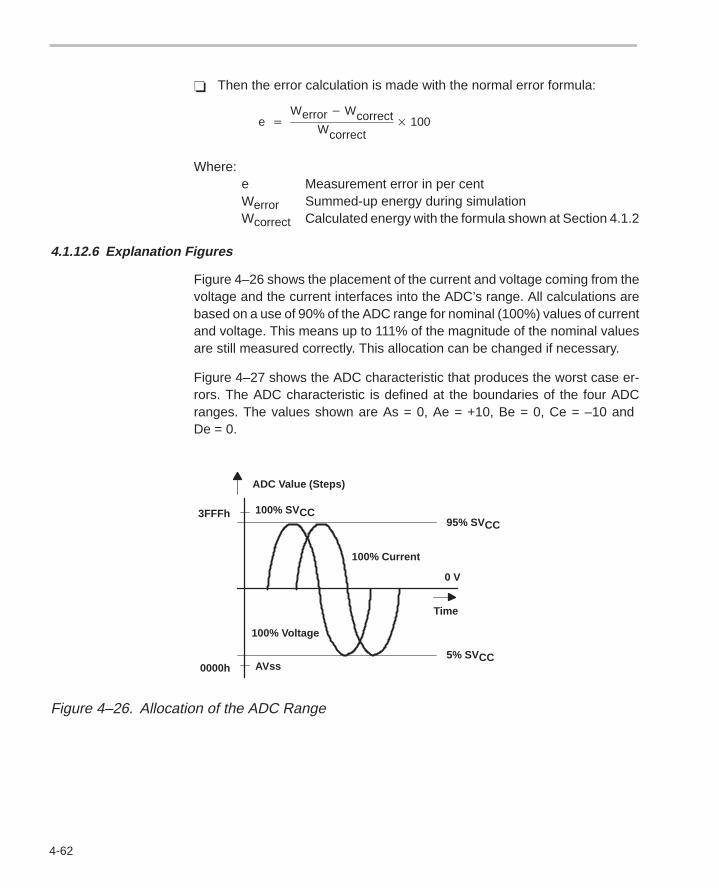
4-62
Then the error calculation is made with the normal error formula:
e Werror Wcorrect
Wcorrect 100
Where: e Measurement error in per centWerror Summed-up energy during simulationWcorrect Calculated energy with the formula shown at Section 4.1.2
4.1.12.6 Explanation Figures
Figure 4–26 shows the placement of the current and voltage coming from thevoltage and the current interfaces into the ADC’s range. All calculations arebased on a use of 90% of the ADC range for nominal (100%) values of currentand voltage. This means up to 111% of the magnitude of the nominal valuesare still measured correctly. This allocation can be changed if necessary.
Figure 4–27 shows the ADC characteristic that produces the worst case er-rors. The ADC characteristic is defined at the boundaries of the four ADCranges. The values shown are As = 0, Ae = +10, Be = 0, Ce = –10 and De = 0.
Time
95% SVCC
100% Current
5% SVCC
100% SVCC
AVss
3FFFh
0000h
100% Voltage
ADC Value (Steps)
0 V
Figure 4–26. Allocation of the ADC Range
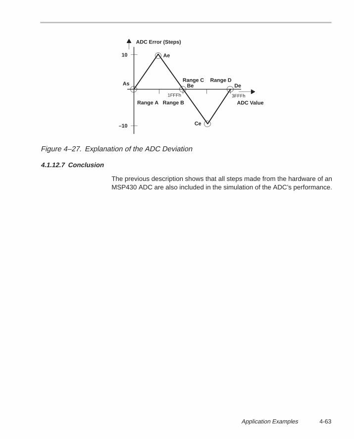
4-63Application Examples
Range C Range D
ADC ValueRange A Range B
10
–10
1FFFh 3FFFh
ADC Error (Steps)
As
Ae
Ce
DeBe
Figure 4–27. Explanation of the ADC Deviation
4.1.12.7 Conclusion
The previous description shows that all steps made from the hardware of anMSP430 ADC are also included in the simulation of the ADC’s performance.

Gas Meter
4-64
4.2 Gas Meter
A gas meter is shown in Figure 4–28 that contains all peripherals modern gasmeters can have. The volume interface is shown as a mechanical meter andon the left-hand side for an electronic solution:
The mechanical interface uses contacts to give the volume information tothe MSP430. The output Oz is used for scanning, reducing this way thecurrent flow if one or more contacts are closed permanently.
The electronic interface outputs electrical signals to the MSP430 as longas the enable input is high. The signals V1 and V2 are 90 out of phaseto allow a reliable distinction of the gas flow direction.
The gas temperature is measured with the ADC of the MSP430. This allowsa much better accuracy for the volume measurement, because the depen-dence of the gas volume to the temperature can be taken into account (lawsof Boyle-Mariotte and Gay-Lussac).
Any combination of the peripherals shown can be used for a given solution.It is not necessary to have all of them implemented.
The MSP430 is normally in low-power mode 3 (Icc = 1.6 µA nominal), but allenabled interrupt sources wake it up:
Volume Interface: any change of the volume interface when the output Ozis active (Hi)
Basic Timer: this continuously running timer can regularly wake-up theMSP430 in a very large, programmable time range (2–16s up to 2 s). Itsfrequency is derived from the crystal frequency (32 kHz).
Key push: all Port0 inputs have an interrupt capability.
M-BUS Activity: via the P0.0 interrupt (RCD).
Insertion of a card into the card interface. All Port0 inputs have interruptcapability.
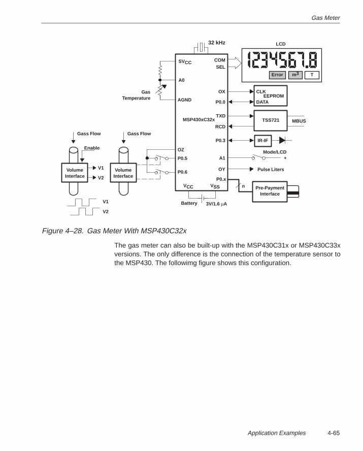
Gas Meter
4-65Application Examples
Error m3 T
COMSEL
OX CLK
DATAEEPROM
P0.0
TSS721 MBUSTXD
RCD
P0.3 IR-IF
A1Mode/LCD
+
OY Pulse Liters
VSSVCC
3V/1.6 µA
P0.x
Pre-PaymentInterface
P0.6
AGND
SVCC
A0
32 kHz
n
P0.5
OZ
VolumeInterface
VolumeInterface
V1
V2
Enable
Gass Flow Gass Flow
V1
V2
GasTemperature
LCD
Battery
MSP430xC32x
Figure 4–28. Gas Meter With MSP430C32x
The gas meter can also be built-up with the MSP430C31x or MSP430C33xversions. The only difference is the connection of the temperature sensor tothe MSP430. The followimg figure shows this configuration.
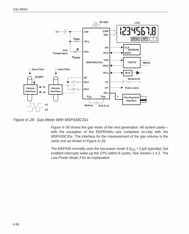
Gas Meter
4-66
Error m3 T
COMSEL
OX CLK
DATAEEPROM
P0.0
TSS721 MBUSTXD
RCD
P0.3 IR-IF
A1Mode/LCD
+
OY Pulse Liters
VSSVCC
3V/1.6 µA
P0.x
Pre-PaymentInterface
P0.6
TP.0
CIN
TP.1
32 kHz
n
P0.5
OZ
VolumeInterface
VolumeInterface
V1
V2
Enable
Gass Flow Gass Flow
V1
V2
GasTemperature
LCD
RREF
RSENS
0 V
Battery
MSP430xC31x
Figure 4–29. Gas Meter With MSP430C31x
Figure 4–30 shows the gas meter of the next generation. All system parts—with the exception of the EEPROMs—are contained on-chip with theMSP430C33x. The interface for the measurement of the gas volume is thesame one as shown in Figure 4–29
The MSP430 normally uses the low power mode 3 (ICC = 2 µA typically), butenabled interrupts wake-up the CPU within 8 cycles. See Section 1.4.2, TheLow Power Mode 3 for an explanation.
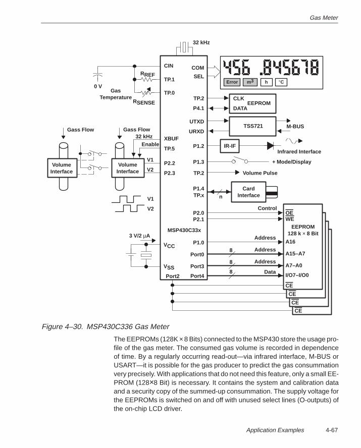
Gas Meter
4-67Application Examples
CE
32 kHz
Error m3 h
8
COM
SEL
P2.0P2.1
Port3
MSP430C33x
Address
ControlOEWE
A7–A0
8Port0 A15–A7
AddressP1.0 A16
EEPROM128 k × 8 Bit
°C
CLK
DATAEEPROM
TSS721 M-BUS
IR-IF
CardInterfacen
+ Mode/Display
Volume Pulse
VolumeInterface
Gass Flow
VolumeInterface
V1
V2
Enable
Gass Flow32 kHz
8Port4 I/O7–I/O0
Data
Address
CE
CE
CE
V1
V2
VCC
VSS
3 V/2 µA
Port2
Infrared Interface
RREF
RSENSE
0 VGas
Temperature
CIN
TP.1
TP.0
XBUF
TP.5
P2.2
P2.3
TP.2
P4.1
UTXD
URXD
P1.2
P1.3
TP.2
P1.4TP.x
Figure 4–30. MSP430C336 Gas Meter
The EEPROMs (128K × 8 Bits) connected to the MSP430 store the usage pro-file of the gas meter. The consumed gas volume is recorded in dependenceof time. By a regularly occurring read-out—via infrared interface, M-BUS orUSART—it is possible for the gas producer to predict the gas consummationvery precisely. With applications that do not need this feature, only a small EE-PROM (128×8 Bit) is necessary. It contains the system and calibration dataand a security copy of the summed-up consummation. The supply voltage forthe EEPROMs is switched on and off with unused select lines (O-outputs) ofthe on-chip LCD driver.

Gas Meter
4-68
External peripherals which are not necessary for a given application can beomitted.
The MSP430 is normally in low-power mode 3 (Icc = 2 µA nominal), but all en-abled interrupt sources will wake it up:
Volume Interface: any change of the volume interface when the outputTP.5 is active (high). All Port2 inputs have interrupt capability.
Basic Timer: this continuously running timer can regularly wake-up theMSP430 in a very large, programmable time range (2–16s up to 2 s). Itsfrequency is derived from the crystal frequency (32 kHz).
Key push: all Port1 inputs have interrupt capability.
M-BUS Activity: via the USART interrupt.
Insertion of a card into the card interface: all Port1 inputs have interruptcapability
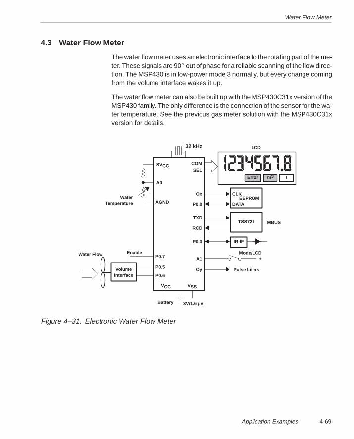
Water Flow Meter
4-69Application Examples
4.3 Water Flow Meter
The water flow meter uses an electronic interface to the rotating part of the me-ter. These signals are 90 out of phase for a reliable scanning of the flow direc-tion. The MSP430 is in low-power mode 3 normally, but every change comingfrom the volume interface wakes it up.
The water flow meter can also be built up with the MSP430C31x version of theMSP430 family. The only difference is the connection of the sensor for the wa-ter temperature. See the previous gas meter solution with the MSP430C31xversion for details.
Error m3 T
COMSEL
Ox CLK
DATAEEPROM
P0.0
TSS721 MBUSTXD
RCD
P0.3 IR-IF
A1Mode/LCD
+
Oy Pulse Liters
VSSVCC
3V/1.6 µA
P0.6
AGND
SVCC
A0
32 kHz
P0.5
P0.7
VolumeInterface
Water Flow
WaterTemperature
LCD
Enable
Battery
Figure 4–31. Electronic Water Flow Meter
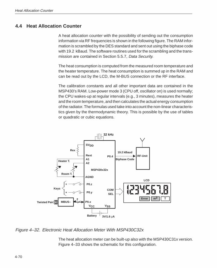
Heat Allocation Counter
4-70
4.4 Heat Allocation Counter
A heat allocation counter with the possibility of sending out the consumptioninformation via RF frequencies is shown in the following figure. The RAM infor-mation is scrambled by the DES standard and sent out using the biphase codewith 19.2 kBaud. The software routines used for the scrambling and the trans-mission are contained in Section 5.5.7, Data Security.
The heat consumption is computed from the measured room temperature andthe heater temperature. The heat consumption is summed up in the RAM andcan be read out by the LCD, the M-BUS connection or the RF interface.
The calibration constants and all other important data are contained in theMSP430’s RAM. Low-power mode 3 (CPU off, oscillator on) is used normally;the CPU wakes-up at regular intervals (e.g., 3 minutes), measures the heaterand the room temperature, and then calculates the actual energy consumptionof the radiator. The formulas used take into account the non-linear characteris-tics given by the thermodynamic theory. This is possible by the use of tablesor quadratic or cubic equations.
Error m3 T
COMSEL
VSSVCC
3V/1.6 µA
P0.x
AGND
SVDD
A1
32 kHz
MBUS–
Keys
LCD
P0.y
P0.z
2
A2
Rext
+
+
RF-Unit19.2 kBaud
Biphase CodeHeater T.
Room T.
Rex
P0.4
Battery
MSP430x32x
Twisted Pair
Figure 4–32. Electronic Heat Allocation Meter With MSP430C32x
The heat allocation meter can be built-up also with the MSP430C31x version.Figure 4–33 shows the schematic for this configuration.
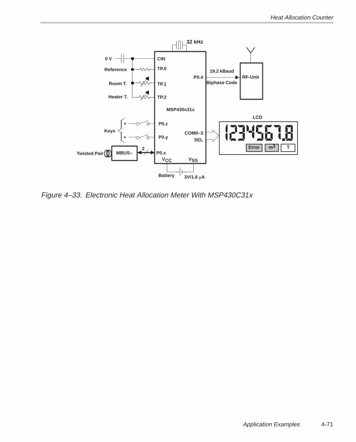
Heat Allocation Counter
4-71Application Examples
Error m3 T
COM0–3SEL
VSSVCC
3V/1.6 µA
P0.x
CIN
32 kHz
MBUS–
Keys
LCD
P0.y
P0.z
2
TP.0
+
+
RF-Unit19.2 kBaud
Biphase Code
0 V
TP.1
TP.2
P0.4
Heater T.
Room T.
Reference
Battery
MSP430x31x
Twisted Pair
Figure 4–33. Electronic Heat Allocation Meter With MSP430C31x
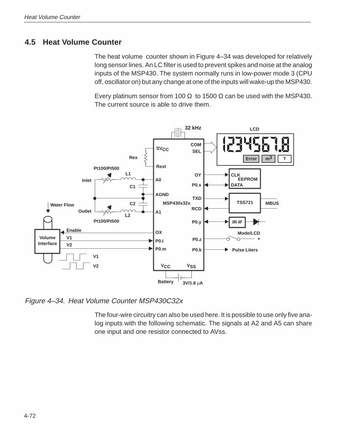
Heat Volume Counter
4-72
4.5 Heat Volume Counter
The heat volume counter shown in Figure 4–34 was developed for relativelylong sensor lines. An LC filter is used to prevent spikes and noise at the analoginputs of the MSP430. The system normally runs in low-power mode 3 (CPUoff, oscillator on) but any change at one of the inputs will wake-up the MSP430.
Every platinum sensor from 100 Ω to 1500 Ω can be used with the MSP430.The current source is able to drive them.
Error m3 T
COMSEL
OY CLK
DATAEEPROM
P0.x
TSS721 MBUSTXD
RCD
P0.y IR-IF
Mode/LCD+
Pulse Liters
VSSVCC
3V/1.6 µA
P0.m
A0
SVCC
Rext
32 kHz
P0.I
OXVolume
Interface
Water Flow
V1
V2
LCD
Rex
A1
L1
L2
C1
C2
Inlet
Outlet
AGND
P0.z
P0.k
V1
V2
Enable
Pt100/Pt500
Pt100/Pt500
Battery
MSP430x32x
Figure 4–34. Heat Volume Counter MSP430C32x
The four-wire circuitry can also be used here. It is possible to use only five ana-log inputs with the following schematic. The signals at A2 and A5 can shareone input and one resistor connected to AVss.
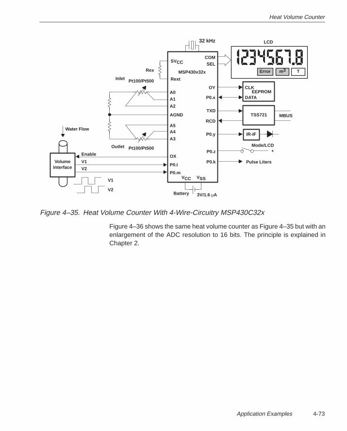
Heat Volume Counter
4-73Application Examples
Error m3 T
COMSEL
OY CLK
DATAEEPROM
P0.x
TSS721 MBUSTXD
RCD
P0.y IR-IF
Mode/LCD+
Pulse Liters
VSSVCC
3V/1.6 µA
P0.m
A0
SVCC
Rext
32 kHz
P0.I
OXVolume
Interface
Water Flow
V1
V2
LCD
Rex
A5
Inlet
Outlet
AGND
P0.z
P0.kV1
V2
Enable
Pt100/Pt500
Pt100/Pt500
A1
A2
A4
A3
Battery
MSP430x32x
Figure 4–35. Heat Volume Counter With 4-Wire-Circuitry MSP430C32x
Figure 4–36 shows the same heat volume counter as Figure 4–35 but with anenlargement of the ADC resolution to 16 bits. The principle is explained inChapter 2.
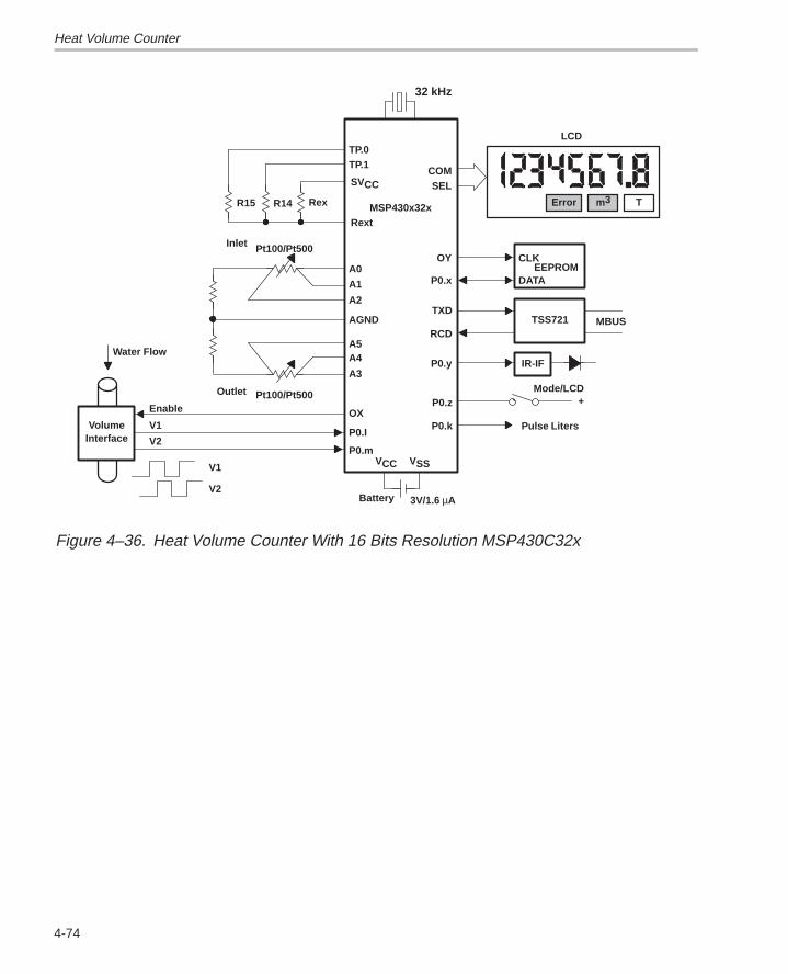
Heat Volume Counter
4-74
Error m3 T
COMSEL
OY CLK
DATAEEPROM
P0.x
TSS721 MBUSTXD
RCD
P0.y IR-IF
Mode/LCD+
Pulse Liters
VSSVCC
3V/1.6 µA
P0.m
A0
SVCC
Rext
32 kHz
P0.I
OXVolume
Interface
Water Flow
V1
V2
LCD
Rex
A5
Inlet
Outlet
AGND
P0.z
P0.kV1
V2
Enable
Pt100/Pt500
Pt100/Pt500
A1
A2
A4
A3
TP.1TP.0
R15 R14
Battery
MSP430x32x
Figure 4–36. Heat Volume Counter With 16 Bits Resolution MSP430C32x

Battery Charge Meter
4-75Application Examples
4.6 Battery Charge Meter
The battery charge meter shown in Figure 4–37 monitors the charge of a bat-tery by means of the measurement of all relevant parameters:
Battery voltage is measured with the voltage divider R1/R2. This voltageis used for the recognition of the end of charge (the battery voltage re-duces in a defined manner) and for safety reasons.
Battery current: the voltage across a shunt gives an exact indication of thecurrent flowing. The low shunt voltage is shifted into the ADC range by aresistor R3 using the current source of the MSP430. The battery currentis measured signed (positive sign means charge, negative sign meansdischarge) to give the possibility of treating charge and discharge currentsdifferently.
Battery temperature: the resistance of the temperature sensor is mea-sured with the current of the current source.
The battery charge meter shown is not restricted concerning the magnitudeof voltage, current, or capacity of the batteries controlled. These depend onlyon the design of the shunt resistor, the voltage divider, and the calibrationconstants used. It can be used for cascaded batteries as well as for singleones. This means, it is applicable from camcorders to forklifts.
The reference voltage for the system is delivered by the voltage regulator out-put. Therefore, the voltage needs to be sufficiently stable. Referencing by areference diode (LMx85) is also possible. This reference diode can be mea-sured at regular intervals and the result stored. It is not necessary to have thereference always switched on.
The charge indication can be given with a numerical LCD or, as shown in thefollowing, with a battery symbol showing 20% steps. Other methods for indica-tion are also possible (e.g. LEDs with different colors that are enabled for ashort time by a key stroke).
The voltage regulator needs to have a very low supply current, not exceedingsome micro amps. This is needed because of the long periods the system canbe in rest mode (no load). The charge part shown is not necessary for all ap-plications. It can be omitted if, for example, the available space is not provided.
The charge transistor Q1 is switched on by the MSP430 if a certain (low)charge level is reached. The charge current can be fine tuned by PWM. If thecharge current is above the maximum current the transistor is switched off dueto safety reasons.
The host connection (for example via 232 using the MSP430’s UART) can beused for the transfer of data; charge, temperature, voltage, current, and other
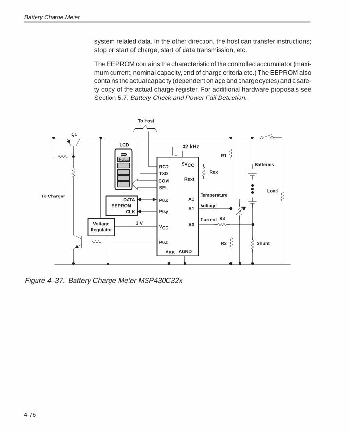
Battery Charge Meter
4-76
system related data. In the other direction, the host can transfer instructions;stop or start of charge, start of data transmission, etc.
The EEPROM contains the characteristic of the controlled accumulator (maxi-mum current, nominal capacity, end of charge criteria etc.) The EEPROM alsocontains the actual capacity (dependent on age and charge cycles) and a safe-ty copy of the actual charge register. For additional hardware proposals seeSection 5.7, Battery Check and Power Fail Detection.
COMSEL
A1
A0
AGNDVSS
P0.x
32 kHzLCD
VCC
TXDRCD
DATA
CLKEEPROM
FULLSVCC
Rext
P0.y
VoltageRegulator
3 V
P0.z
Current R3
VoltageA1
R2
R1
Batteries
Load
Shunt
To Charger
To Host
Temperature
Rex
Q1
Figure 4–37. Battery Charge Meter MSP430C32x
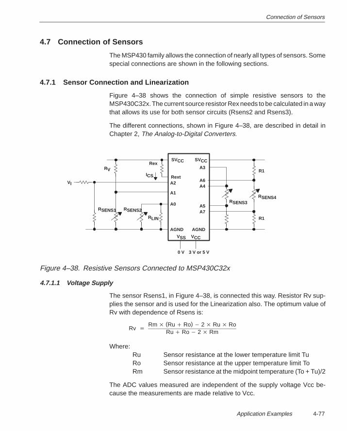
Connection of Sensors
4-77Application Examples
4.7 Connection of Sensors
The MSP430 family allows the connection of nearly all types of sensors. Somespecial connections are shown in the following sections.
4.7.1 Sensor Connection and Linearization
Figure 4–38 shows the connection of simple resistive sensors to theMSP430C32x. The current source resistor Rex needs to be calculated in a waythat allows its use for both sensor circuits (Rsens2 and Rsens3).
The different connections, shown in Figure 4–38, are described in detail inChapter 2, The Analog-to-Digital Converters.
A7
AGND
VSS
A2
AGND
SVCC
Rext
A0
A3Rex
ICS
A1
RLIN
RSENS2RSENS1
RV
SVCC
A5
A4A6
RSENS3RSENS4
R1
R1
VI
VCC
0 V 3 V or 5 V
Figure 4–38. Resistive Sensors Connected to MSP430C32x
4.7.1.1 Voltage Supply
The sensor Rsens1, in Figure 4–38, is connected this way. Resistor Rv sup-plies the sensor and is used for the Linearization also. The optimum value ofRv with dependence of Rsens is:
Rv Rm (Ru Ro) 2 Ru Ro
Ru Ro 2 Rm
Where:Ru Sensor resistance at the lower temperature limit TuRo Sensor resistance at the upper temperature limit ToRm Sensor resistance at the midpoint temperature (To + Tu)/2
The ADC values measured are independent of the supply voltage Vcc be-cause the measurements are made relative to Vcc.
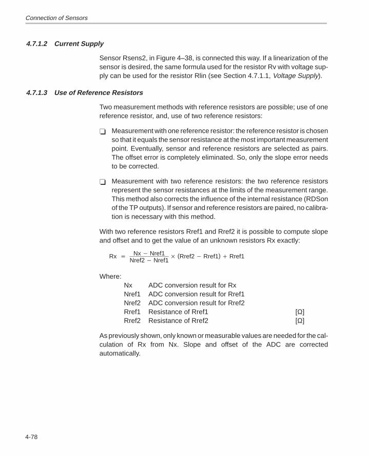
Connection of Sensors
4-78
4.7.1.2 Current Supply
Sensor Rsens2, in Figure 4–38, is connected this way. If a linearization of thesensor is desired, the same formula used for the resistor Rv with voltage sup-ply can be used for the resistor Rlin (see Section 4.7.1.1, Voltage Supply).
4.7.1.3 Use of Reference Resistors
Two measurement methods with reference resistors are possible; use of onereference resistor, and, use of two reference resistors:
Measurement with one reference resistor: the reference resistor is chosenso that it equals the sensor resistance at the most important measurementpoint. Eventually, sensor and reference resistors are selected as pairs.The offset error is completely eliminated. So, only the slope error needsto be corrected.
Measurement with two reference resistors: the two reference resistorsrepresent the sensor resistances at the limits of the measurement range.This method also corrects the influence of the internal resistance (RDSonof the TP outputs). If sensor and reference resistors are paired, no calibra-tion is necessary with this method.
With two reference resistors Rref1 and Rref2 it is possible to compute slopeand offset and to get the value of an unknown resistors Rx exactly:
Rx Nx Nref1Nref2 Nref1
(Rref2 Rref1) Rref1
Where:Nx ADC conversion result for RxNref1 ADC conversion result for Rref1Nref2 ADC conversion result for Rref2Rref1 Resistance of Rref1 [Ω]Rref2 Resistance of Rref2 [Ω]
As previously shown, only known or measurable values are needed for the cal-culation of Rx from Nx. Slope and offset of the ADC are correctedautomatically.
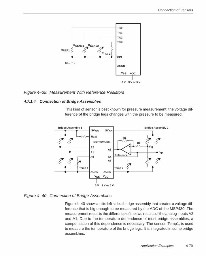
Connection of Sensors
4-79Application Examples
VSS
TP.0
CIN
TP.3
TP.1
RREF2
RSENS2RSENS1
VCC
0 V 3 V or 5 V
TP.2
RREF1
AGNDC1
Figure 4–39. Measurement With Reference Resistors
4.7.1.4 Connection of Bridge Assemblies
This kind of sensor is best known for pressure measurement: the voltage dif-ference of the bridge legs changes with the pressure to be measured.
AGND
VSS
A2
AGND
SVCC
Rext
A0
A3A1
R2
SVCC
A5
Bridge Assembly 2
VCC
0 V 3 V or 5 V
Temp 1
_+
Temp 2
R1
VM
VPReference
Bridge Assembly 1
A4
MSP430x32x
Figure 4–40. Connection of Bridge Assemblies
Figure 4–40 shows on its left side a bridge assembly that creates a voltage dif-ference that is big enough to be measured by the ADC of the MSP430. Themeasurement result is the difference of the two results of the analog inputs A2and A1. Due to the temperature dependence of most bridge assemblies, acompensation of this dependence is necessary. The sensor, Temp1, is usedto measure the temperature of the bridge legs. It is integrated in some bridgeassemblies.
Connection of Sensors
4-80
The used formula is:
P MWP (Ye (t Tk) Tke) Yo (T Tk) Tko
Where:P Pressure to be measuredMWP Difference of the measured values at A2 and A1Ye Sensitivity of the pressure sensorT Temperature of the sensorTke Temperature coefficient of the sensitivityYo OffsetTko Temperature coefficient of the offsetTk Temperature during Calibration (e.g. +25ºC)
The units depend on the system used (hP, kg/m2, kg/mm2 a.s.o.)
If the difference of the two measurements is too small to be used, an operation-al amplifier, as shown in Figure 4–40, can be used. Here the ability to measurethe reference voltage (one of the two bridge legs) is shown also. Analog inputA4 measures the reference that can be used for the A3 input. The same formu-la as shown previously can be used when MWP is calculated as shown in thefollowing.
MWP Difference of the measured values at A4 and A3:MWP = (A3 – A4)
The actual measured voltage difference ∆V between the analog inputs A3 andA4 is:
∆V VA3 VA4 v (Vp Vm) Vp Vp v (Vp Vm)
Where:∆V Voltage difference between analog inputs A3 and A4 [V]v Amplification of the operational amplifier: v = R1/R2Vp Voltage at the bridge leg connected to the non-inverting
input [V]Vm Voltage at the bridge leg connected to the inverting input [V]
The use of the reference input A4 results in correct values for the measure-ments. If just the differences of two A3 measurements are used, the resultneeds to be corrected due to the following behavior:
∆V VA32 VA31 v (Vp2 Vp1 (Vm2 Vm1)) Vp2 Vp1
∆V (v 1)(Vp2 Vp1) v (Vm2 Vm1)
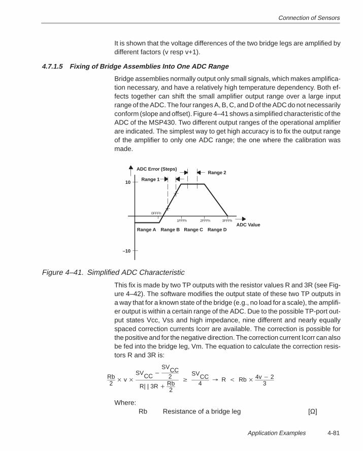
Connection of Sensors
4-81Application Examples
It is shown that the voltage differences of the two bridge legs are amplified bydifferent factors (v resp v+1).
4.7.1.5 Fixing of Bridge Assemblies Into One ADC Range
Bridge assemblies normally output only small signals, which makes amplifica-tion necessary, and have a relatively high temperature dependency. Both ef-fects together can shift the small amplifier output range over a large inputrange of the ADC. The four ranges A, B, C, and D of the ADC do not necessarilyconform (slope and offset). Figure 4–41 shows a simplified characteristic of theADC of the MSP430. Two different output ranges of the operational amplifierare indicated. The simplest way to get high accuracy is to fix the output rangeof the amplifier to only one ADC range; the one where the calibration wasmade.
Range 2
Range A Range B Range C Range DADC Value
0FFFh
1FFFh 2FFFh 3FFFh
ADC Error (Steps)
Range 110
–10
Figure 4–41. Simplified ADC Characteristic
This fix is made by two TP outputs with the resistor values R and 3R (see Fig-ure 4–42). The software modifies the output state of these two TP outputs ina way that for a known state of the bridge (e.g., no load for a scale), the amplifi-er output is within a certain range of the ADC. Due to the possible TP-port out-put states Vcc, Vss and high impedance, nine different and nearly equallyspaced correction currents Icorr are available. The correction is possible forthe positive and for the negative direction. The correction current Icorr can alsobe fed into the bridge leg, Vm. The equation to calculate the correction resis-tors R and 3R is:
Rb2
v SVCC
SVCC2
R| | 3R Rb2
SVCC
4 R Rb 4v 2
3
Where:Rb Resistance of a bridge leg [Ω]
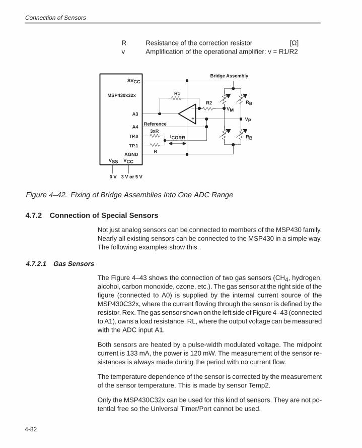
Connection of Sensors
4-82
R Resistance of the correction resistor [Ω]v Amplification of the operational amplifier: v = R1/R2
AGNDVSS
A3
R2
SVCC
TP.0
Bridge Assembly
VCC
0 V 3 V or 5 V
_
+
R1
VM
VPReference
A4
TP.1
3xR
R
ICORR
RB
RB
MSP430x32x
Figure 4–42. Fixing of Bridge Assemblies Into One ADC Range
4.7.2 Connection of Special Sensors
Not just analog sensors can be connected to members of the MSP430 family.Nearly all existing sensors can be connected to the MSP430 in a simple way.The following examples show this.
4.7.2.1 Gas Sensors
The Figure 4–43 shows the connection of two gas sensors (CH4, hydrogen,alcohol, carbon monoxide, ozone, etc.). The gas sensor at the right side of thefigure (connected to A0) is supplied by the internal current source of theMSP430C32x, where the current flowing through the sensor is defined by theresistor, Rex. The gas sensor shown on the left side of Figure 4–43 (connectedto A1), owns a load resistance, RL, where the output voltage can be measuredwith the ADC input A1.
Both sensors are heated by a pulse-width modulated voltage. The midpointcurrent is 133 mA, the power is 120 mW. The measurement of the sensor re-sistances is always made during the period with no current flow.
The temperature dependence of the sensor is corrected by the measurementof the sensor temperature. This is made by sensor Temp2.
Only the MSP430C32x can be used for this kind of sensors. They are not po-tential free so the Universal Timer/Port cannot be used.
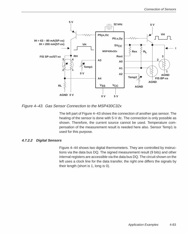
Connection of Sensors
4-83Application Examples
32 kHz
P0.x,Oy
SVCC
A1
Rext
VSS
A4
P0yx,Oz
VCC
A3
0 V
4RH
1
3
2Temp1
VH
5 V
FIS SP-xx/ST-xx
IH = 63 – 80 mA(SP-xx)IH = 200 mA(ST-xx)
RL
AGND 0 V 0 V 5 V
Rex RL
A2
A0
Temp2
5 V
VH
AGND
AGND
AGND1
32
FIS BP-xx
IMSP430x32x
Figure 4–43. Gas Sensor Connection to the MSP430C32x
The left part of Figure 4–43 shows the connection of another gas sensor. Theheating of the sensor is done with 5-V dc. The connection is only possible asshown. Therefore, the current source cannot be used. Temperature com-pensation of the measurement result is needed here also. Sensor Temp1 isused for this purpose.
4.7.2.2 Digital Sensors
Figure 4–44 shows two digital thermometers. They are controlled by instruc-tions via the data bus DQ. The signed measurement result (9 bits) and otherinternal registers are accessible via the data bus DQ. The circuit shown on theleft uses a clock line for the data transfer, the right one differs the signals bytheir length (short is 1, long is 0).
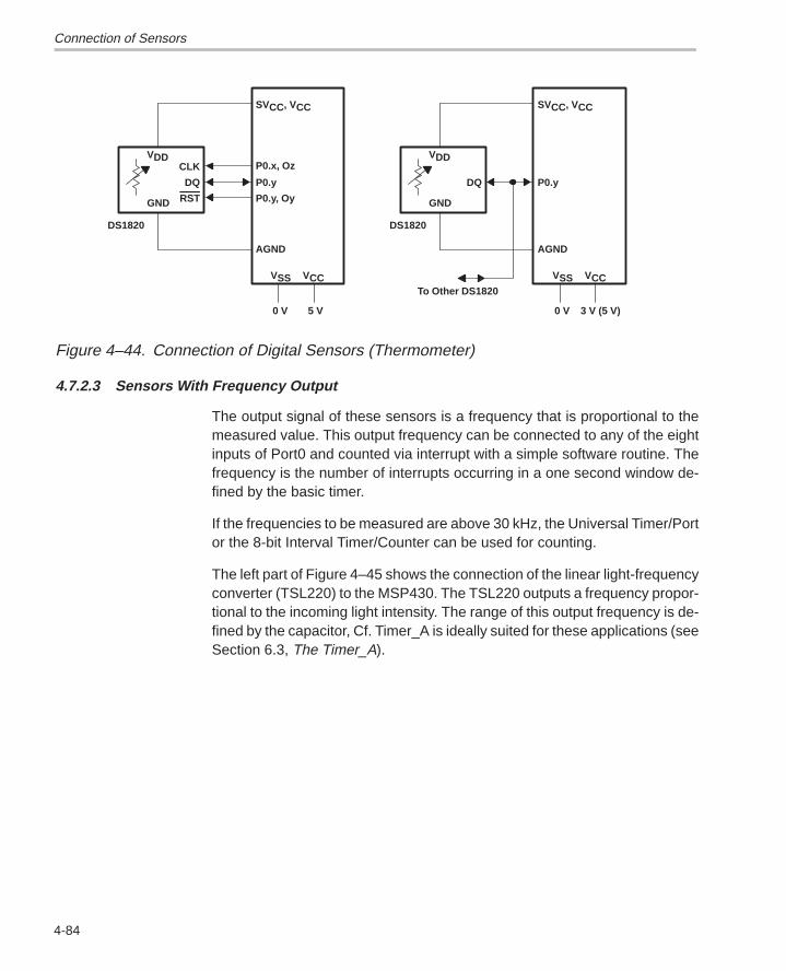
Connection of Sensors
4-84
VSS
SVCC, VCC
P0.x, Oz
VCC
0 V 5 V
P0.y
AGND
VDDCLK
DQ
RSTGND P0.y, Oy
DS1820
VSS
SVCC, VCC
VCC
0 V 3 V (5 V)
P0.y
AGND
VDD
DQ
GND
DS1820
To Other DS1820
Figure 4–44. Connection of Digital Sensors (Thermometer)
4.7.2.3 Sensors With Frequency Output
The output signal of these sensors is a frequency that is proportional to themeasured value. This output frequency can be connected to any of the eightinputs of Port0 and counted via interrupt with a simple software routine. Thefrequency is the number of interrupts occurring in a one second window de-fined by the basic timer.
If the frequencies to be measured are above 30 kHz, the Universal Timer/Portor the 8-bit Interval Timer/Counter can be used for counting.
The left part of Figure 4–45 shows the connection of the linear light-frequencyconverter (TSL220) to the MSP430. The TSL220 outputs a frequency propor-tional to the incoming light intensity. The range of this output frequency is de-fined by the capacitor, Cf. Timer_A is ideally suited for these applications (seeSection 6.3, The Timer_A).
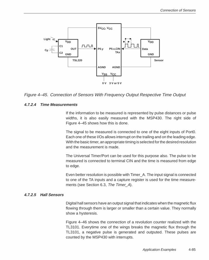
Connection of Sensors
4-85Application Examples
VSS
SVCC, VCC
VCC
0 V 3 V or 5 V
P0.y
AGND
VDD
OUT
GND
TSL220
C1
C2CF
LightVDD
GND
Data
Sensor
P0.x,CINTAx
AGND
Figure 4–45. Connection of Sensors With Frequency Output Respective Time Output
4.7.2.4 Time Measurements
If the information to be measured is represented by pulse distances or pulsewidths, it is also easily measured with the MSP430. The right side ofFigure 4–45 shows how this is done.
The signal to be measured is connected to one of the eight inputs of Port0.Each one of these I/Os allows interrupt on the trailing and on the leading edge.With the basic timer, an appropriate timing is selected for the desired resolutionand the measurement is made.
The Universal Timer/Port can be used for this purpose also. The pulse to bemeasured is connected to terminal CIN and the time is measured from edgeto edge.
Even better resolution is possible with Timer_A. The input signal is connectedto one of the TA inputs and a capture register is used for the time measure-ments (see Section 6.3, The Timer_A).
4.7.2.5 Hall Sensors
Digital hall sensors have an output signal that indicates when the magnetic fluxflowing through them is larger or smaller than a certain value. They normallyshow a hysteresis.
Figure 4–46 shows the connection of a revolution counter realized with theTL3101. Everytime one of the wings breaks the magnetic flux through theTL3101, a negative pulse is generated and outputed. These pulses arecounted by the MSP430 with interrupts.
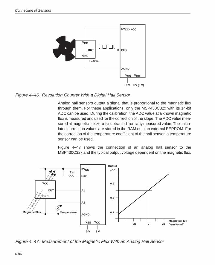
Connection of Sensors
4-86
VSS
SVCC, VCC
VCC
0 V 3 V (5 V)
P0.y
AGND
VCC
OUT
GND
TL3101
Figure 4–46. Revolution Counter With a Digital Hall Sensor
Analog hall sensors output a signal that is proportional to the magnetic fluxthrough them. For these applications, only the MSP430C32x with its 14-bitADC can be used. During the calibration, the ADC value at a known magneticflux is measured and used for the correction of the slope. The ADC value mea-sured at magnetic flux zero is subtracted from any measured value. The calcu-lated correction values are stored in the RAM or in an external EEPROM. Forthe correction of the temperature coefficient of the hall sensor, a temperaturesensor can be used.
Figure 4–47 shows the connection of an analog hall sensor to theMSP430C32x and the typical output voltage dependent on the magnetic flux.
VSS
SVCC
VCC
0 V 5 V
A1
AGND
VCC
OUT
GND
Magnetic Flux Temperature
A2
RextRex
0.9
0.8
0.7
–25 0 25
OutputVCC
Magnetic FluxDensity mT
Figure 4–47. Measurement of the Magnetic Flux With an Analog Hall Sensor

RF Readout
4-87Application Examples
4.8 RF Readout
The read-out of metering devices gets more and more important. The next pro-posals show electricity meters having the possibility to send their consumptioninformation via an RF-transmitter to a host having an RF-receiver. For data se-curity reasons the information sent is normally encrypted with the DES encryp-tion algorithm (data encryption standard). The normally used frequency for thispurpose is 433 MHz. But, any other allocated frequency can be used. Themodulation mainly used is amplitude modulation, but Biphase modulation canalso be used (see Section 4.8.4, RF-Interface Module).
4.8.1 MSP430 Electricity Meter
Figure 4–48 shows an electricity meter with the MSP430C32x. This single-chip microcomputer contains all necessary peripherals on-chip except the EE-PROM. The measurement of voltage and current is made with an internal14-bit ADC.
The interface to ac is shown only for the phase R. The other two phases S andT use the same interfaces.
The RF readout is connected to a free output. This can be an unused segmentline or an output bit of Port0. The timing for the RF readout is made by the inter-nal basic timer. It delivers the necessary interrupt frequencies. The supply volt-age needed for the RF-interface is done with a step-up voltage supply thattransforms the available 5 V to 6 V or more.
The shown hardware proposal uses the reduced scan principle a way of mea-surement that needs only one ADC. Every measured current sample is usedtwice; once with the voltage sample measured before and once with the onemeasured after it. This reduces the number of needed samples without loosingaccuracy. A second advantage is reducing by half the number of needed multi-plications. This advantage is especially important for microcomputers that donot have a hardware multiplier like most members of the MSP430 family (seeSection 4.1, Electricity Meters).
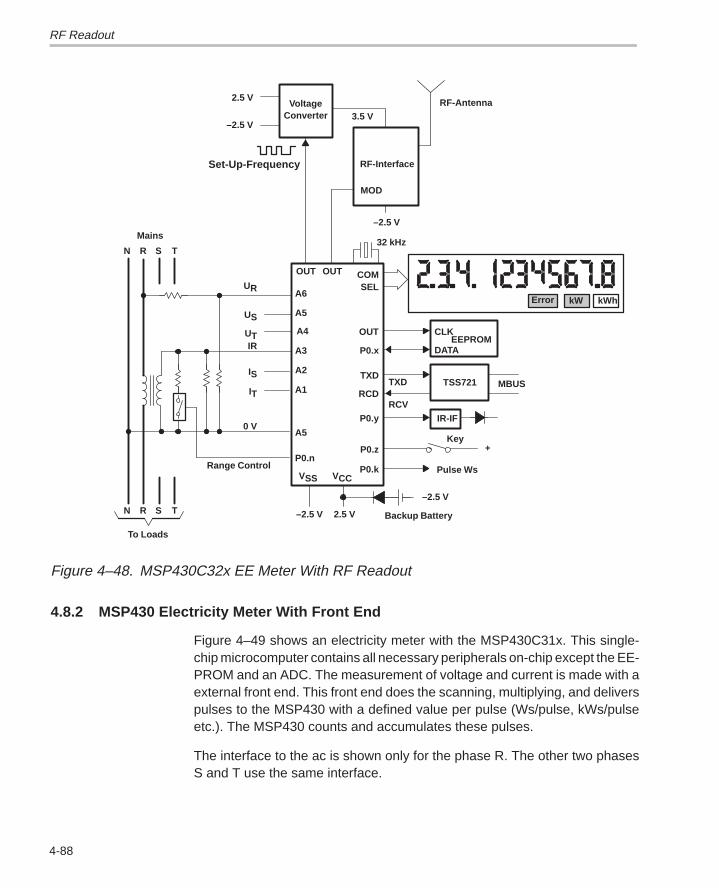
RF Readout
4-88
Error kW kWh
COMSEL
OUT CLK
DATAEEPROM
P0.x
TXDTSS721 MBUS
RCDTXD
RCVP0.y IR-IF
P0.zKey
+
P0.k Pulse WsVSS VCC
2.5 V–2.5 V
A6
P0.n
A5
A3
A1
A4
A2
–2.5 V
Backup Battery
A5
N R S T
N R S T
Mains
To Loads
UR
US
UTIR
IS
IT
0 V
Range Control
VoltageConverter
2.5 V
–2.5 V
Set-Up-Frequency RF-Interface
MOD
–2.5 V
RF-Antenna3.5 V
32 kHz
OUT OUT
Figure 4–48. MSP430C32x EE Meter With RF Readout
4.8.2 MSP430 Electricity Meter With Front End
Figure 4–49 shows an electricity meter with the MSP430C31x. This single-chip microcomputer contains all necessary peripherals on-chip except the EE-PROM and an ADC. The measurement of voltage and current is made with aexternal front end. This front end does the scanning, multiplying, and deliverspulses to the MSP430 with a defined value per pulse (Ws/pulse, kWs/pulseetc.). The MSP430 counts and accumulates these pulses.
The interface to the ac is shown only for the phase R. The other two phasesS and T use the same interface.
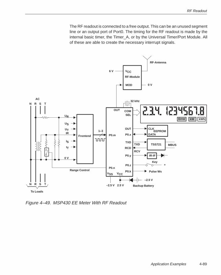
RF Readout
4-89Application Examples
The RF readout is connected to a free output. This can be an unused segmentline or an output port of Port0. The timing for the RF readout is made by theinternal basic timer, the Timer_A, or by the Universal Timer/Port Module. Allof these are able to create the necessary interrupt signals.
Error kW kWh
COMSEL
OUT CLK
DATAEEPROM
P0.x
TXDTSS721 MBUS
RCDTXD
RCVP0.y IR-IF
P0.zKey
+
P0.k Pulse WsVSS VCC
2.5 V–2.5 V
P0.n
–2.5 V
Backup Battery
N R S T
N R S T
AC
To Loads
UR
US
UTIR
IS
IT
0 V
Range Control
6 V
RF-Module
MOD
RF-Antenna
VCC
32 kHz
OUT
Frontend
0 V
P0.m1–3
Figure 4–49. MSP430 EE Meter With RF Readout
RF Readout
4-90
4.8.3 MSP430 Ferraris-Wheel Electricity Meter With RF Readout
If an RF readout is needed for conventional Ferraris-wheel electricity meters,an MSP430C31x can be used. An optical or magnetic pick-up counts the revo-lutions of the disk and outputs a signal to the MSP430. The MSP430 computesthe used energy and displays it on the LCD. In regular intervals, the measuredenergy is transmitted using the RF module.
Error kW kWh
COMSEL
OUT CLK
DATAEEPROM
P0.x
TXDTSS721 MBUS
RCDTXD
RCVP0.y IR-IF
P0.zKey
+
P0.k Pulse WsVSS VCC
2.5 V–2.5 V
–2.5 V
Backup Battery
6 V
RF-Module
MOD
RF-Antenna
VCC
32 kHz
OUT
0 V
P0.m
Pick-up
Ferraris Wheel
Figure 4–50. MSP430 With a Ferraris-Wheel Meter and RF Readout
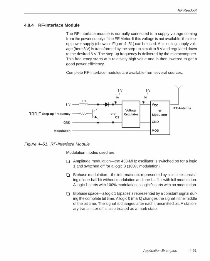
RF Readout
4-91Application Examples
4.8.4 RF-Interface Module
The RF-interface module is normally connected to a supply voltage comingfrom the power supply of the EE Meter. If this voltage is not available, the step-up power supply (shown in Figure 4–51) can be used. An existing supply volt-age (here 3 V) is transformed by the step-up circuit to 8 V and regulated downto the desired 6 V. The step-up frequency is delivered by the microcomputer.This frequency starts at a relatively high value and is then lowered to get agood power efficiency.
Complete RF-interface modules are available from several sources.
VoltageRegulator
RFModulator
VCC
GND
MOD
L1
C1
8 V 6 V
RF-Antenna3 V
Step-up Frequency
GND
Modulation
Figure 4–51. RF-Interface Module
Modulation modes used are:
Amplitude modulation—the 433-MHz oscillator is switched on for a logic1 and switched off for a logic 0 (100% modulation).
Biphase modulation—the information is represented by a bit time consist-ing of one-half bit without modulation and one-half bit with full modulation.A logic 1 starts with 100% modulation, a logic 0 starts with no modulation.
Biphase space—a logic 1 (space) is represented by a constant signal dur-ing the complete bit time. A logic 0 (mark) changes the signal in the middleof the bit time. The signal is changed after each transmitted bit. A station-ary transmitter off is also treated as a mark state.
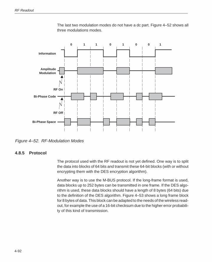
RF Readout
4-92
The last two modulation modes do not have a dc part. Figure 4–52 shows allthree modulations modes.
RF Off
0 1 1 0 1 0 0 1
RF On
Information
AmplitudeModulation
Bi-Phase Code
Bi-Phase Space
Figure 4–52. RF-Modulation Modes
4.8.5 Protocol
The protocol used with the RF readout is not yet defined. One way is to splitthe data into blocks of 64 bits and transmit these 64-bit blocks (with or withoutencrypting them with the DES encryption algorithm).
Another way is to use the M-BUS protocol. If the long-frame format is used,data blocks up to 252 bytes can be transmitted in one frame. If the DES algo-rithm is used, these data blocks should have a length of 8 bytes (64 bits) dueto the definition of the DES algorithm. Figure 4–53 shows a long frame blockfor 8 bytes of data. This block can be adapted to the needs of the wireless read-out, for example the use of a 16-bit checksum due to the higher error probabili-ty of this kind of transmission.
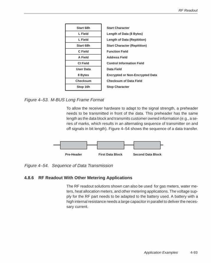
RF Readout
4-93Application Examples
Start 68h
L Field
L Field
Start 68h
C Field
A Field
CI Field
User Data
8 Bytes
Checksum
Stop 16h
Start Character
Length of Data (8 Bytes)
Length of Data (Repitition)
Start Character (Repitition)
Function Field
Address Field
Control Information Field
Data Field
Encrypted or Non-Encrypted Data
Checksum of Data Field
Stop Character
Figure 4–53. M-BUS Long Frame Format
To allow the receiver hardware to adapt to the signal strength, a preheaderneeds to be transmitted in front of the data. This preheader has the samelength as the data block and transmits customer owned information (e.g., a se-ries of marks, which results in an alternating sequence of transmitter on andoff signals in bit length). Figure 4–54 shows the sequence of a data transfer.
Pre-Header First Data Block Second Data Block
Figure 4–54. Sequence of Data Transmission
4.8.6 RF Readout With Other Metering Applications
The RF readout solutions shown can also be used for gas meters, water me-ters, heat allocation meters, and other metering applications. The voltage sup-ply for the RF part needs to be adapted to the battery used. A battery with ahigh internal resistance needs a large capacitor in parallel to deliver the neces-sary current.

Ultra-Low-Power Design With the MSP430 Family
4-94
4.9 Ultra-Low-Power Design With the MSP430 Family
To get all the low-power advantages that the MSP430 family can provide,some rules need to be kept in mind. This section gives an overview of theserules.
4.9.1 The Ultra Low Power Concept of the MSP430
A lot of microcomputer applications need to be driven by a battery. It is impor-tant for these applications to run as long as possible with as small a battery aspossible. To reach a battery life longer than 5 years, often the configurationshown in Figure 4–55 is used:
A low-frequency oscillator feeds a prescaler that outputs a pulse everysecond (or in longer intervals), which sets a flip-flop. This pulse deliversthe needed time base with the accuracy of the crystal.
The flip-flop switches on the supply voltage of the microcomputer. The mi-crocomputer measures the necessary system values with an externalADC (necessary if the accuracy needed exceeds 8 bits) and calculates theresults afterwards.
The results are summed-up in an external RAM and are displayed with anexternal LCD driver.
After the completion of all necessary activities, the microcomputer resetsthe flip-flop and switches itself off in this way. The current consumption ofthe system reduces to the value that is drawn by the oscillator, the RAMand the LCD driver.
The system shown in Figure 4–55 needs a relatively large battery due to thehigh number of external system components (>5 Ah).
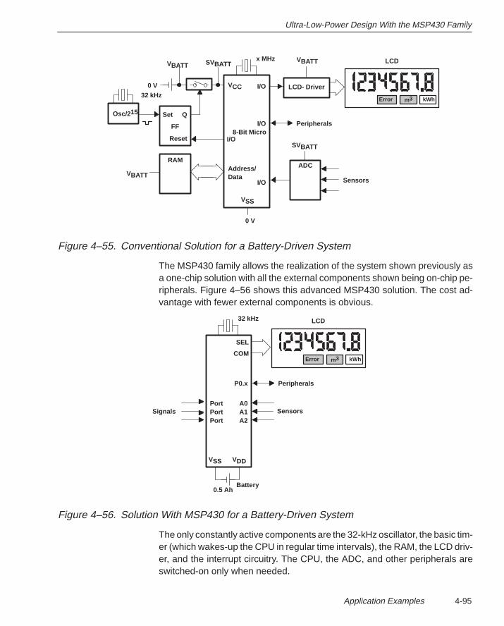
Ultra-Low-Power Design With the MSP430 Family
4-95Application Examples
Error m3 kWh
I/O LCD- Driver
I/O
VSS
0 V
I/O
VCC
x MHz LCD
PeripheralsSet Q
Reset
FF
32 kHz0 V
VBATT SVBATT
Address/Data
RAM
VBATTI/O
ADC
SVBATT
Sensors
8-Bit Micro
VBATT
Osc/215
Figure 4–55. Conventional Solution for a Battery-Driven System
The MSP430 family allows the realization of the system shown previously asa one-chip solution with all the external components shown being on-chip pe-ripherals. Figure 4–56 shows this advanced MSP430 solution. The cost ad-vantage with fewer external components is obvious.
Error m3 kWh
P0.x
VSS
0.5 Ah
32 kHz LCD
Peripherals
A0
VDD
Sensors
COM
SEL
A1A2
Battery
PortPortPort
Signals
Figure 4–56. Solution With MSP430 for a Battery-Driven System
The only constantly active components are the 32-kHz oscillator, the basic tim-er (which wakes-up the CPU in regular time intervals), the RAM, the LCD driv-er, and the interrupt circuitry. The CPU, the ADC, and other peripherals areswitched-on only when needed.
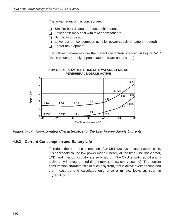
Ultra-Low-Power Design With the MSP430 Family
4-96
The advantages of this concept are:
Smaller boards due to reduced chip count Lower assembly cost with fewer components Simplicity of design Lower current consumption (smaller power supply or battery needed) Faster development
The following examples use the current characteristic shown in Figure 4–57(these values are only approximated and are not assured).
3
2
1
0–40 –20 0 20 40 60
4
5
NOMINAL CHARACTERISTICS OF LPM3 AND LPM4, NOPERIPHERAL MODULE ACTIVE
85
1.44
0.055
1.36
0.055
1.35
0.05
1.6
0.1
1.8
0.5
2.8
1.1
LPM3
LPM4
4.3
2.6
I CC
Aµ
–
T – Temperature – °C
Figure 4–57. Approximated Characteristics for the Low Power-Supply Currents
4.9.2 Current Consumption and Battery Life
To reduce the current consumption of an MSP430 system as far as possible,it is necessary to use low power mode 3 nearly all the time. The basic timer,LCD, and interrupt circuitry are switched on. The CPU is switched off and isactive only in programmed time intervals (e.g., every second). The currentconsumption characteristic of such a system, that is active every second andthat measures and calculates only once a minute, looks as seen inFigure 4–58.
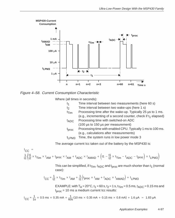
Ultra-Low-Power Design With the MSP430 Family
4-97Application Examples
MSP430-CurrentConsumption
1 mAIAMAD
IAM
100 µA
10 µA
1 µA
ILPM3
tTimtADC
tproc
Time sn n+1 n+2 n+3 n+60 n+61
t1
t2
Figure 4–58. Current Consumption Characteristic
Where (all times in seconds):t1 Time interval between two measurements (here 60 s)t2 Time interval between two wake-ups (here 1 s)tTim Processing time after the wake-up. Typically 25 µs to 1 ms.
(e.g., incrementing of a second counter, check if t1 elapsed)tADC Processing time with switched-on ADC
(100 µs to 150 µs per measurement)tproc Processing time with enabled CPU. Typically 1 ms to 100 ms.
(e.g., calculations after measurements)tLPM3 Time, the system runs in low power mode 3
The average current Icc taken out of the battery by the MSP430 is:
ICC
1t1t1
t2 tTim IAM tproc IAM tADC IAMAD t1 t1
t2 tTim tADC tproc ILPM3
This can be simplified, if tTim, tADC and tproc are much shorter than t1 (normalcase):
ICC ≈ 1t2
tTim IAM 1t1tproc IAM tADC IAMAD
ILPM3
EXAMPLE: with TA = 20°C, t1 = 60 s, t2 = 1 s, tTim = 0.5 ms, tADC = 0.15 ms andtproc = 10 ms a medium current Icc results:
ICC ≈ 11s
0.5 ms 0.35 mA 160s
(10 ms 0.35 mA 0.15 ms 0.8 mA) 1.6 µA 1.83 µA

Ultra-Low-Power Design With the MSP430 Family
4-98
With the previous example, the current consumption increases by 15% whencompared to the consumption of low power mode 3 (1.6 µA).
4.9.3 Minimization of the System Consumption
The overall current consumption of an MSP430 system is composed of threecomponents:
The consumption of the MSP430 The self-discharge of the battery The consumption of the other system components
The minimization of the current consumption of each of these three parts is dis-cussed in detail.
4.9.3.1 Consumption of the MSP430
The low power mode 3 needs to be the normal mode. Active mode and activemode with ADC are used only when necessary. The rules for the minimizationof the current consumption are:
Leaving of the low power mode 3 (wake-up) as rarely as possible, for ex-ample only every two seconds.
The program executed after the wake-up should be as short as possible(e.g. incrementing of a counter and test, if other activities are necessary).If this is not the case, immediately return to the low power mode 3.
The time intervals between active periods (calculations) should be as longas possible (e.g., 60 s or longer).
Only the necessary peripherals should be switched-on (e.g., the ADCshould be on only during a conversion). After the completion of a conver-sion, the ADC should be switched-off. This can be supported by the useof the ADC interrupt. The interrupt service routine of the ADC switches offthe ADC supply SVcc after the conversion is completed.
Use of the interrupt capability of Port0 to react to external changes. Theinputs can interrupt using the leading or trailing edge of an input signal.This ensures the detection of any changes at the inputs without current-wasting polling.
Extremely long calculations (McLaurin-series, Taylor-series) should beavoided. Instead tables should be used. The seven addressing modes,provided by the MSP430, are tailored especially for fast table processing.
Subroutine CALLs should be avoided in frequently used software partsdue to the overhead time they need. Instead, the code should be rein-
Ultra-Low-Power Design With the MSP430 Family
4-99Application Examples
serted two or three times (like a MACRO). More ROM space may be need-ed, but fewer CPU cycles are needed.
Short loops should be avoided due to the overhead needed for the loopcontrol. Instead, the loop should be placed into a linear code sequence.
For longer software parts, the working registers R4 to R15, should beused. This results in shorter execution times and in less needed ROMspace.
Immediate stop of the calculation if one of the factors—and therefore theresult too—is zero
If the previouly mentioned recommendations are applied, the current con-sumption of the active mode is of second order only. The exceptionally highcalculation power of 660 million instructions per Ws (MIPS/W) allows it to ig-nore the influence of a single instruction. Much more important is the currentconsumption during the low power mode 3.
4.9.3.2 Self Discharge of the Battery
The self discharge element of the current consumption can not be influenced.The battery manufacturer recommendations should be followed. It is recom-mended that the battery be placed in a relatively cool location inside of thecase. This means do not place the battery next to hot parts (e.g., the radiatorto be measured with a heat cost allocator).
An estimation value often used for the self discharge of a battery during 10years, is to calculate only with 70% of the nominal charge. This relates to 3.5%self discharge per year. Expressed by a discharge current this means 2 µA fora 0.5 Ah battery.
4.9.3.3 Current Consumption of Other System Components
This current is composed of different parts. The most important ones are dis-cussed.
Crystal
The desire for good quality and a low frequency (32,768 Hz) results in a needfor a driver power ranging from 1 µW to 10 µW. With a supply voltage of 3 V,the current consumption ranges from 333 nA to 3.33 µA (with an average of1 µA). This current is always being consumed, because the 32-kHz oscillatoris used for the time base.
Liquid Crystal Display
The desire for good quality and a low frequency (128 Hz) results in a need forcurrent consumption of approx. 13 nA/mm2 segment area. For an LCD with100 mm2, this means a current near 1 µA (1.3 µA).
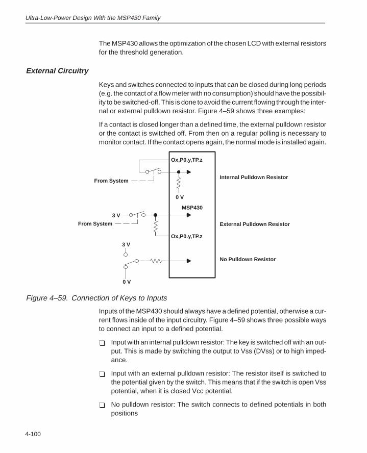
Ultra-Low-Power Design With the MSP430 Family
4-100
The MSP430 allows the optimization of the chosen LCD with external resistorsfor the threshold generation.
External Circuitry
Keys and switches connected to inputs that can be closed during long periods(e.g. the contact of a flow meter with no consumption) should have the possibil-ity to be switched-off. This is done to avoid the current flowing through the inter-nal or external pulldown resistor. Figure 4–59 shows three examples:
If a contact is closed longer than a defined time, the external pulldown resistoror the contact is switched off. From then on a regular polling is necessary tomonitor contact. If the contact opens again, the normal mode is installed again.
MSP430
Ox,P0.y,TP.z
0 V
Ox,P0.y,TP.z
3 V
From System
From System
3 V
0 V
Internal Pulldown Resistor
External Pulldown Resistor
No Pulldown Resistor
Figure 4–59. Connection of Keys to Inputs
Inputs of the MSP430 should always have a defined potential, otherwise a cur-rent flows inside of the input circuitry. Figure 4–59 shows three possible waysto connect an input to a defined potential.
Input with an internal pulldown resistor: The key is switched off with an out-put. This is made by switching the output to Vss (DVss) or to high imped-ance.
Input with an external pulldown resistor: The resistor itself is switched tothe potential given by the switch. This means that if the switch is open Vsspotential, when it is closed Vcc potential.
No pulldown resistor: The switch connects to defined potentials in bothpositions
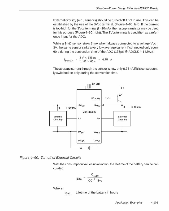
Ultra-Low-Power Design With the MSP430 Family
4-101Application Examples
External circuitry (e.g., sensors) should be turned off if not in use. This can beestablished by the use of the SVcc terminal. (Figure 4–60, left). If the currentis too high for the SVcc terminal (I >10mA), then a pnp transistor may be usedfor this purpose (Figure 4–60, right). The SVcc terminal is used then as a refer-ence input for the ADC.
While a 1-kΩ sensor sinks 3 mA when always connected to a voltage Vcc =3V, the same sensor sinks a very low average current if connected only every60 s during the conversion time of the ADC (135µs @ ADCLK = 1 MHz):
Isensor 3 V 135 µs1 kΩ 60 s
6.75 nA
The average current through the sensor is now only 6.75 nA if it is consequent-ly switched on only during the conversion time.
P0.x, Oy
A0
DVSS DVCC
32 kHz
A3
AVSS
SVCCSVCC
ExternalCircuitry
ExternalCircuitry
AVSS
3 V
Ι > 10 mAΙ < 10 mA
MSP430x32x
Figure 4–60. Turnoff of External Circuits
With the consumption values now known, the lifetime of the battery can be cal-culated:
tBatt QBatt
ICC ISys
Where:tBatt Lifetime of the battery in hours
Ultra-Low-Power Design With the MSP430 Family
4-102
QBatt Usable charge of the battery in Ah(70% of 0,5 Ah for this example)
Icc Supply current of the MSP430 in A(1.83µA for this example)
ISys Current through the external circuitry (crystal, LCD, peripherals) in A (2.3 µA for this example)
For a free-air temperature TA = 20°C and the consumption values calculatedbefore the lifetime of the battery is:
tBatt 0.7 0.5 Ah1.83 µA 2.3 µA
84745 h
This number of hours is equivalent to 9.6 years.
For ambient temperatures deviating from TA = 20ºC the typical values for ILPM3can be seen in Figure 4–57. The exact values for the self-discharge of a batterycan be found in the device specification.
4.9.4 Correct Termination of Unused Terminals (3xx Family)
MSP430 terminals not used need to be treated in a defined manner.Table 4–13 defines the correct termination for every terminal not used in a giv-en application. The termination shown assures lowest supply current.

Ultra-Low-Power Design With the MSP430 Family
4-103Application Examples
Table 4–13. Termination of Unused Terminals
PIN POTENTIAL COMMENT
AVcc DVcc Necessary for EPROM programming also
AVss DVss Same as AVCC
SVcc Open Can be used as a low impedance output
Rext Open
A0 to A7 Open Switched to analog inputs: AEN.x = 0
Xin Vcc If no crystal is used
Xout Open If no crystal is used
XBUF Open Output disabled
CIN Vss Can be used as a digital input
TP0.0 to TP0.5 Open TP.5 switched to output direction, others to high impedance
P0.0 to P0.7 Open Unused ports switched to output direction
R03 Vss Display off: LCDM0 = 0
R13 Vss
R23 Vss
R33 Open
S0 to S1 Open
S3 to S20 Open Switched to output direction
Com0 to Com3 Open
RST/NMI DVcc resp. Vcc Pull-up resistor 100 kΩTDO Refer to the specific device data sheet
TDI Refer to the specific device data sheet
TMS Refer to the specific device data sheet
TCK Refer to the specific device data sheet

Other MSP430 Applications
4-104
4.10 Other MSP430 Applications
4.10.1 Controller for a Heating Installation
A very big part of the energy consumed in Europe is used for the heating ofrooms. An intelligent controller for heating is a good investment. The controllershown in Figure 4–61 has the following possibilities for the optimum alignment:
Opening and closing of the mixing valve (regulates the mix of hot boilerwater with the warm reflux).
Control of the burner (off/on).
Control of the circulation pump (off/on respective of the speed control witha TRIAC). If the outdoor temperature is above a programmable limit (e.g.20°C) then the circulation pump is off.
Supervision of the boiler temperature: measurement with a temperaturesensor.
Supervision of all temperature sensors (feasibility checks)
The criteria for all of these decisions comes from the following inputs:
The measured outdoor temperature is the most important value. It is mea-sured with an outdoor temperature sensor.
The system and calibration data stored in an EEPROM:
The individual characteristic of the building stored as the slope and off-set for the characteristic of the temperature of the circulating water tothe outside temperature
The dependence of the boiler temperature on the outdoor tempera-ture
The outdoor temperature that stops the activity of the circulating pump(above this temperature only the warm water supply stays active)
The minimum switch-on time of the burner (a burner must be on for aminimum time to stay within given environmental limits)
Recording of errors for the field service (maintenance)
The mean value of the outdoor temperature for the last 24 hours. Thisgives a value for the storage of heat in the walls and influences the neces-sary amount of energy.

Other MSP430 Applications
4-105Application Examples
The chosen mode:
Summer Mode: Only the warm water supply is on, the mixing valve isalways closed, the circulation pump is always off
Winter Mode: Normal heating is on
Maintenance Mode: For repair and maintenance only
Day Mode: the heating installation runs always independent of thetime
Night Mode: the heating installation runs always with the lowered val-ues for the night
Switch-off or temperature lowering during the night (circulating pumpon resp. off)
The advantages of a microcomputer controlled heating installation are:
Self calibration of the complete system is possible: learning phase and fi-nal optimization.
Exact tuning of the optimum mixing temperature due to the involvementof all relevant data
Exact knowledge of the timing for the temperature lowering at evening
Optimum usage of the heating material with minimum pollution
Different concepts are possible for the control of the heating installation
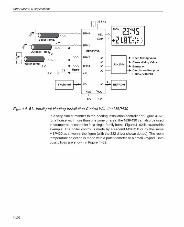
Other MSP430 Applications
4-106
32 kHz
TP0.0
VSS VCC
0 V 5 V
MPS43031x
RREF
TP0.2
0 V
TP0.3
TP0.1
C10 V
0 V
0 V
Boiler Temp.
Outdoor Temp.
Water Temp.
CIN
Keyboardn 2
EEPROM
ULN200x
MON
COM
SEL
I/O
I/OI/O
I/O
Open Mixing Value
Close Mixing Value
Burner onCirculation Pump on(TRIAC Control)
I/O
I/O
Figure 4–61. Intelligent Heating Installation Control With the MSP430
In a very similar manner to the heating installation controller of Figure 4–61,for a house with more than one zone or area, the MSP430 can also be usedin a temperature controller for a single-family home. Figure 4–62 illustrates thisexample. The boiler control is made by a second MSP430 or by the sameMSP430 as shwon in the figure (with the 232 driver shown dotted). The roomtemperature selection is made with a potentiometer or a small keypad. Bothpossibilities are shown in Figure 4–62.
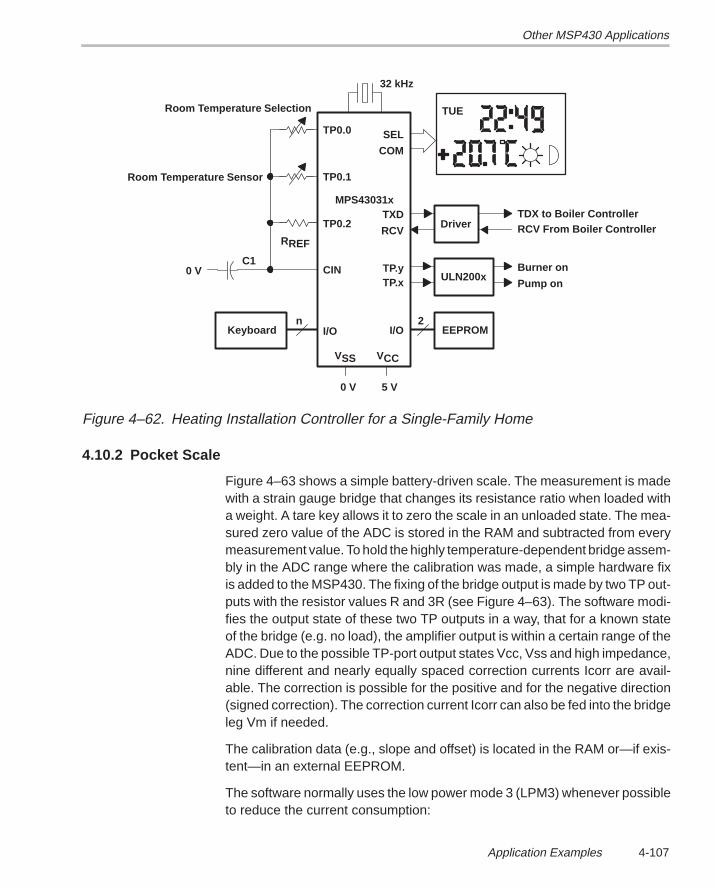
Other MSP430 Applications
4-107Application Examples
32 kHz
TP0.0
VSS VCC
0 V 5 V
MPS43031x
RREF
TP0.2
TP0.1
C10 V CIN
Keyboardn 2
EEPROM
ULN200x
COM
SEL
TXD
RCV
TP.x
TDX to Boiler Controller
Burner on
Pump on
Driver
Room Temperature Selection TUE
Room Temperature Sensor
RCV From Boiler Controller
I/OI/O
TP.y
Figure 4–62. Heating Installation Controller for a Single-Family Home
4.10.2 Pocket Scale
Figure 4–63 shows a simple battery-driven scale. The measurement is madewith a strain gauge bridge that changes its resistance ratio when loaded witha weight. A tare key allows it to zero the scale in an unloaded state. The mea-sured zero value of the ADC is stored in the RAM and subtracted from everymeasurement value. To hold the highly temperature-dependent bridge assem-bly in the ADC range where the calibration was made, a simple hardware fixis added to the MSP430. The fixing of the bridge output is made by two TP out-puts with the resistor values R and 3R (see Figure 4–63). The software modi-fies the output state of these two TP outputs in a way, that for a known stateof the bridge (e.g. no load), the amplifier output is within a certain range of theADC. Due to the possible TP-port output states Vcc, Vss and high impedance,nine different and nearly equally spaced correction currents Icorr are avail-able. The correction is possible for the positive and for the negative direction(signed correction). The correction current Icorr can also be fed into the bridgeleg Vm if needed.
The calibration data (e.g., slope and offset) is located in the RAM or—if exis-tent—in an external EEPROM.
The software normally uses the low power mode 3 (LPM3) whenever possibleto reduce the current consumption:
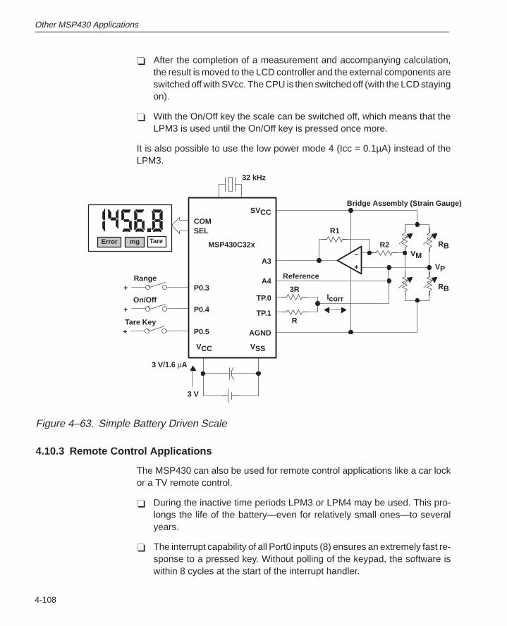
Other MSP430 Applications
4-108
After the completion of a measurement and accompanying calculation,the result is moved to the LCD controller and the external components areswitched off with SVcc. The CPU is then switched off (with the LCD stayingon).
With the On/Off key the scale can be switched off, which means that theLPM3 is used until the On/Off key is pressed once more.
It is also possible to use the low power mode 4 (Icc = 0.1µA) instead of theLPM3.
32 kHz
MSP430C32xError mg Tare
COMSEL
A3
VCC VSS
A4
3 V
SVCC
Range+
On/Off+
Tare Key+
–
+
3R
R
Icorr
Reference
R1
R2VM
RB
RB
VP
TP.0
TP.1
AGND
P0.3
P0.4
P0.5
3 V/1.6 µA
Bridge Assembly (Strain Gauge)
Figure 4–63. Simple Battery Driven Scale
4.10.3 Remote Control Applications
The MSP430 can also be used for remote control applications like a car lockor a TV remote control.
During the inactive time periods LPM3 or LPM4 may be used. This pro-longs the life of the battery—even for relatively small ones—to severalyears.
The interrupt capability of all Port0 inputs (8) ensures an extremely fast re-sponse to a pressed key. Without polling of the keypad, the software iswithin 8 cycles at the start of the interrupt handler.
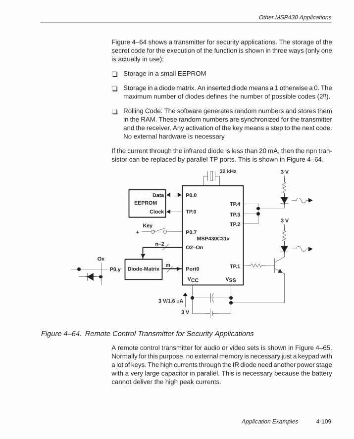
Other MSP430 Applications
4-109Application Examples
Figure 4–64 shows a transmitter for security applications. The storage of thesecret code for the execution of the function is shown in three ways (only oneis actually in use):
Storage in a small EEPROM
Storage in a diode matrix. An inserted diode means a 1 otherwise a 0. Themaximum number of diodes defines the number of possible codes (2n).
Rolling Code: The software generates random numbers and stores themin the RAM. These random numbers are synchronized for the transmitterand the receiver. Any activation of the key means a step to the next code.No external hardware is necessary
If the current through the infrared diode is less than 20 mA, then the npn tran-sistor can be replaced by parallel TP ports. This is shown in Figure 4–64.
32 kHz
MSP430C31x
P0.0
TP.0TP.4
VCC VSS
3 V
Key+
TP.1
P0.7
3 V/1.6 µA
Data
Clock
EEPROM
TP.3
TP.2
Diode-Matrix
n–2
m
O2–On
Port0
3 V
3 V
Ox
P0.y
Figure 4–64. Remote Control Transmitter for Security Applications
A remote control transmitter for audio or video sets is shown in Figure 4–65.Normally for this purpose, no external memory is necessary just a keypad witha lot of keys. The high currents through the IR diode need another power stagewith a very large capacitor in parallel. This is necessary because the batterycannot deliver the high peak currents.
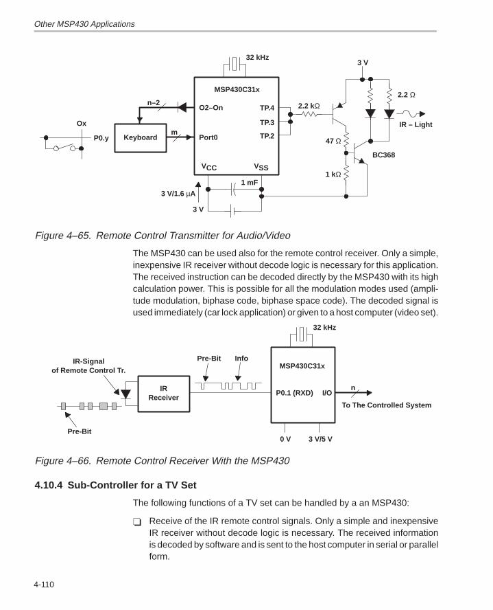
Other MSP430 Applications
4-110
32 kHz
MSP430C31x
TP.4
VCC VSS
3 V
3 V/1.6 µA
TP.3
TP.2Keyboard
n–2
m
O2–On
Port0
Ox
P0.y
2.2 kΩ
47 Ω
1 kΩ
2.2 Ω
IR – Light
BC368
1 mF
3 V
Figure 4–65. Remote Control Transmitter for Audio/Video
The MSP430 can be used also for the remote control receiver. Only a simple,inexpensive IR receiver without decode logic is necessary for this application.The received instruction can be decoded directly by the MSP430 with its highcalculation power. This is possible for all the modulation modes used (ampli-tude modulation, biphase code, biphase space code). The decoded signal isused immediately (car lock application) or given to a host computer (video set).
32 kHz
MSP430C31x
IRReceiver
nP0.1 (RXD)
InfoPre-BitIR-Signalof Remote Control Tr.
Pre-Bit
I/O
To The Controlled System
0 V 3 V/5 V
Figure 4–66. Remote Control Receiver With the MSP430
4.10.4 Sub-Controller for a TV Set
The following functions of a TV set can be handled by a an MSP430:
Receive of the IR remote control signals. Only a simple and inexpensiveIR receiver without decode logic is necessary. The received informationis decoded by software and is sent to the host computer in serial or parallelform.
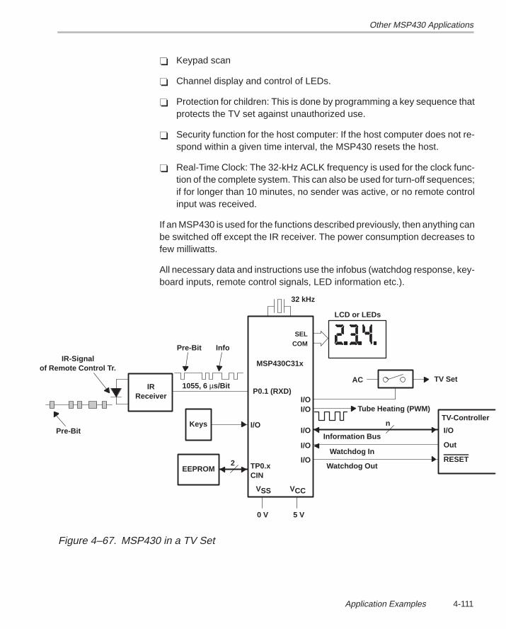
Other MSP430 Applications
4-111Application Examples
Keypad scan
Channel display and control of LEDs.
Protection for children: This is done by programming a key sequence thatprotects the TV set against unauthorized use.
Security function for the host computer: If the host computer does not re-spond within a given time interval, the MSP430 resets the host.
Real-Time Clock: The 32-kHz ACLK frequency is used for the clock func-tion of the complete system. This can also be used for turn-off sequences;if for longer than 10 minutes, no sender was active, or no remote controlinput was received.
If an MSP430 is used for the functions described previously, then anything canbe switched off except the IR receiver. The power consumption decreases tofew milliwatts.
All necessary data and instructions use the infobus (watchdog response, key-board inputs, remote control signals, LED information etc.).
32 kHz
MSP430C31x
IRReceiver
P0.1 (RXD)
InfoPre-BitIR-Signal
of Remote Control Tr.
Pre-Bit
I/O
0 V 5 V
1055, 6 µs/Bit
COMSEL
LCD or LEDs
AC TV Set
I/O Tube Heating (PWM)
I/O
TV-Controllern
I/O
I/OInformation Bus
OutWatchdog In
I/O RESETWatchdog Out
Keys I/O
EEPROM2 TP0.x
CIN
VSS VCC
Figure 4–67. MSP430 in a TV Set
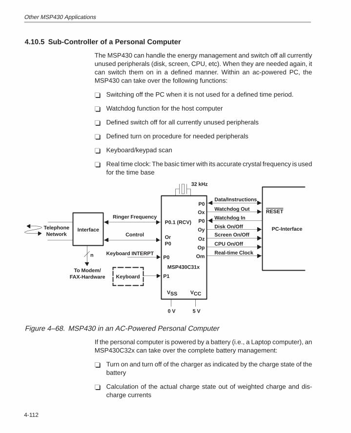
Other MSP430 Applications
4-112
4.10.5 Sub-Controller of a Personal Computer
The MSP430 can handle the energy management and switch off all currentlyunused peripherals (disk, screen, CPU, etc). When they are needed again, itcan switch them on in a defined manner. Within an ac-powered PC, theMSP430 can take over the following functions:
Switching off the PC when it is not used for a defined time period.
Watchdog function for the host computer
Defined switch off for all currently unused peripherals
Defined turn on procedure for needed peripherals
Keyboard/keypad scan
Real time clock: The basic timer with its accurate crystal frequency is usedfor the time base
32 kHz
MSP430C31x
P0.1 (RCV)
P0
0 V 5 V
P0
VSS VCC
Data/Instructions
Watchdog Out
Watchdog In
Disk On/Off
Screen On/Off
CPU On/Off
Real-time Clock
RESET
PC-Interface
Ox
P0
Oy
Oz
Op
Om
Ringer Frequency
Control OrP0
InterfaceTelephoneNetwork
Keyboard INTERPTn
P1KeyboardTo Modem/
FAX-Hardware
Figure 4–68. MSP430 in an AC-Powered Personal Computer
If the personal computer is powered by a battery (i.e., a Laptop computer), anMSP430C32x can take over the complete battery management:
Turn on and turn off of the charger as indicated by the charge state of thebattery
Calculation of the actual charge state out of weighted charge and dis-charge currents
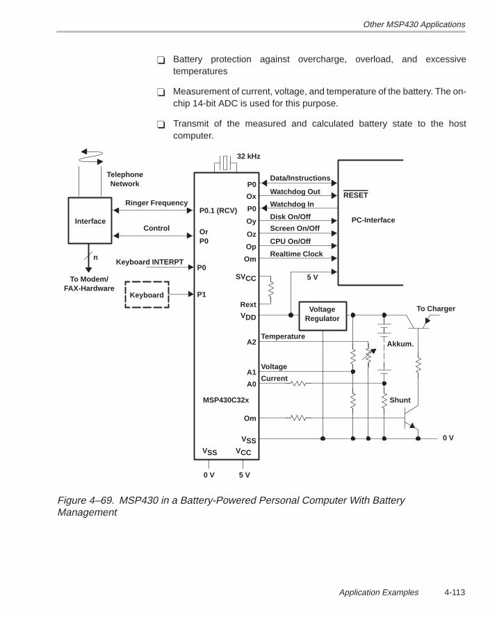
Other MSP430 Applications
4-113Application Examples
Battery protection against overcharge, overload, and excessivetemperatures
Measurement of current, voltage, and temperature of the battery. The on-chip 14-bit ADC is used for this purpose.
Transmit of the measured and calculated battery state to the hostcomputer.
32 kHz
MSP430C32x
P0.1 (RCV)
P0
0 V 5 V
P0
VSS VCC
Data/Instructions
Watchdog Out
Watchdog In
Disk On/Off
Screen On/Off
CPU On/Off
Realtime Clock
RESET
PC-Interface
Ox
P0
Oy
Oz
Op
Om
Ringer Frequency
Control OrP0
Interface
TelephoneNetwork
Keyboard INTERPTn
P1Keyboard
To Modem/FAX-Hardware
SVCC
Rext
5 V
VoltageRegulator
A2Temperature
A1Voltage
A0Current
Akkum.
Shunt
Om
VSS
To Charger
0 V
VDD
Figure 4–69. MSP430 in a Battery-Powered Personal Computer With BatteryManagement
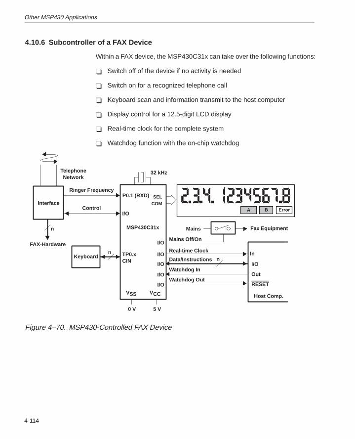
Other MSP430 Applications
4-114
4.10.6 Subcontroller of a FAX Device
Within a FAX device, the MSP430C31x can take over the following functions:
Switch off of the device if no activity is needed
Switch on for a recognized telephone call
Keyboard scan and information transmit to the host computer
Display control for a 12.5-digit LCD display
Real-time clock for the complete system
Watchdog function with the on-chip watchdog
32 kHz
MSP430C31x
P0.1 (RXD)
I/O
0 V 5 V
COMSEL
Mains Fax Equipment
I/O
I/O
Inn
I/O
I/O OutWatchdog In
I/O RESETWatchdog Out
I/O
Keyboardn TP0.x
CIN
VSS VCC
Ringer Frequency
ControlInterface
n
FAX-Hardware
A B Error
Mains Off/On
Real-time Clock
Data/Instructions
Host Comp.
TelephoneNetwork
Figure 4–70. MSP430-Controlled FAX Device
Digital Motor Control
4-115Application Examples
4.11 Digital Motor Control
The MSP430 family is shown with digital motor control (DMC) applications.Several hardware proposals are given for pulse width modulation (PWM) andTRIAC-control applications for electric motors. Numerous circuit and pulsediagrams show the application of the MSP430 family for different electric-mo-tor types and control concepts. For each hardware proposal the applicablemotor types are named.
4.11.1 Introduction
The application of DMC has some advantages compared to conventional con-cepts for motor control:
Better energy efficiency Better control of motor behavior (speed, torque, direction of rotation) Easy supervision of important motor conditions (temperature, current,
speed) Use of smaller motors due to the better adaptability to the given application Use of motor types not applicable without DMC (brushless dc motors, re-
luctance motors)
If the accuracy of fixed-point calculations is not sufficient then a floating pointpackage (FPP), designed especially for real time applications, is availablefrom TID. This memory and speed optimized FPP can be configured for twodifferent number formats: 32 bits or 48 bits. The high speed results from theRISC-mode it uses (mainly single-cycle instructions) and the involved hard-ware multiplier (see Section 5.6, The Floating Point Package).
Additionally a C Compiler with a very good code efficiency is available.
4.11.1.1 The MSP430 Family
The MSP430 family with its 16-bit RISC architecture is capable to realize veryadvanced control concepts. This is especially true for the MSP430C33x withits hardware multiplier (16 x 16 bits) and its 16-bit Timer_A allowing four inde-pendent PWM-outputs. All MSP430 family members use the same instructionset and the same CPU. This eases the use of existing user software enor-mously.
Operating frequencies up to 3.8 MHz and single-cycle instructions when theregister/register addressing mode is used for the source and the destination—the normal addressing combination for real-time applications—results in cal-culation speeds formerly only known by DSPs. This high throughput allowscalculations and algorithms needing more than 16 times the capability of 8-bitmicrocomputers.
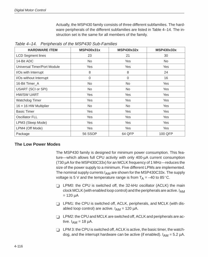
Digital Motor Control
4-116
Actually, the MSP430 family consists of three different subfamilies. The hard-ware peripherals of the different subfamilies are listed in Table 4–14. The in-struction set is the same for all members of the family.
Table 4–14. Peripherals of the MSP430 Sub-FamiliesHARDWARE ITEM MSP430x31x MSP430x32x MSP430x33x
LCD Segment lines 23 21 30
14-Bit ADC No Yes No
Universal Timer/Port Module Yes Yes Yes
I/Os with Interrupt 8 8 24
I/Os without Interrupt 0 0 16
16-Bit Timer_A No No Yes
USART (SCI or SPI) No No Yes
HW/SW UART Yes Yes Yes
Watchdog Timer Yes Yes Yes
16 × 16 HW Multiplier No No Yes
Basic Timer Yes Yes Yes
Oscillator FLL Yes Yes Yes
LPM3 (Sleep Mode) Yes Yes Yes
LPM4 (Off Mode) Yes Yes Yes
Package 56 SSOP 64 QFP 100 QFP
The Low Power Modes
The MSP430 family is designed for minimum power consumption. This fea-ture—which allows full CPU activity with only 400-µA current consumption(730 µA for the MSP430C33x) for an MCLK frequency of 1 MHz—reduces thesize of the power supply to a minimum. Five different LPMs are implemented.The nominal supply currents IAM are shown for the MSP430C33x. The supplyvoltage is 5 V and the temperature range is from TA = –40 to 85C.
LPM0: the CPU is switched off, the 32-kHz oscillator (ACLK) the mainclock MCLK (with enabled loop control) and the peripherals are active. IAM= 120 µA
LPM1: the CPU is switched off, ACLK, peripherals, and MCLK (with dis-abled loop control) are active. IAM = 120 µA.
LPM2: the CPU and MCLK are switched off, ACLK and peripherals are ac-tive. IAM = 18 µA.
LPM 3: the CPU is switched off, ACLK is active, the basic timer, the watch-dog, and the interrupt hardware can be active (if enabled). IAM = 5.2 µA.
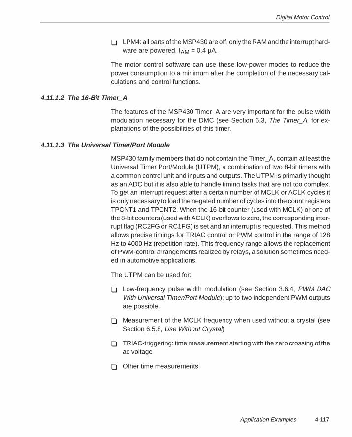
Digital Motor Control
4-117Application Examples
LPM4: all parts of the MSP430 are off, only the RAM and the interrupt hard-ware are powered. IAM = 0.4 µA.
The motor control software can use these low-power modes to reduce thepower consumption to a minimum after the completion of the necessary cal-culations and control functions.
4.11.1.2 The 16-Bit Timer_A
The features of the MSP430 Timer_A are very important for the pulse widthmodulation necessary for the DMC (see Section 6.3, The Timer_A, for ex-planations of the possibilities of this timer.
4.11.1.3 The Universal Timer/Port Module
MSP430 family members that do not contain the Timer_A, contain at least theUniversal Timer Port/Module (UTPM), a combination of two 8-bit timers witha common control unit and inputs and outputs. The UTPM is primarily thoughtas an ADC but it is also able to handle timing tasks that are not too complex.To get an interrupt request after a certain number of MCLK or ACLK cycles itis only necessary to load the negated number of cycles into the count registersTPCNT1 and TPCNT2. When the 16-bit counter (used with MCLK) or one ofthe 8-bit counters (used with ACLK) overflows to zero, the corresponding inter-rupt flag (RC2FG or RC1FG) is set and an interrupt is requested. This methodallows precise timings for TRIAC control or PWM control in the range of 128Hz to 4000 Hz (repetition rate). This frequency range allows the replacementof PWM-control arrangements realized by relays, a solution sometimes need-ed in automotive applications.
The UTPM can be used for:
Low-frequency pulse width modulation (see Section 3.6.4, PWM DACWith Universal Timer/Port Module); up to two independent PWM outputsare possible.
Measurement of the MCLK frequency when used without a crystal (seeSection 6.5.8, Use Without Crystal)
TRIAC-triggering: time measurement starting with the zero crossing of theac voltage
Other time measurements
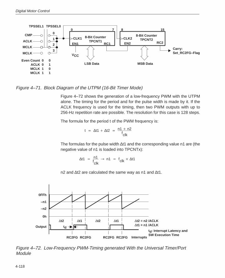
Digital Motor Control
4-118
EN1
CLK1 8-Bit CounterTPCNT1
EN2
CLK2RC2
8-Bit CounterTPCNT2
TPSSEL0TPSSEL1
CMP
ACLK
MCLK
0
1
2
3 Carry:Set_RC2FG–Flag
RC1
VCC
LSB Data MSB DataEven Count 0
ACLK 0MCLK 1MCLK 1
MCLK
0101
0 7 8 15
Figure 4–71. Block Diagram of the UTPM (16-Bit Timer Mode)
Figure 4–72 shows the generation of a low-frequency PWM with the UTPMalone. The timing for the period and for the pulse width is made by it. If theACLK frequency is used for the timing, then two PWM outputs with up to256-Hz repetition rate are possible. The resolution for this case is 128 steps.
The formula for the period t of the PWM frequency is:
t ∆t1 ∆t2 n1 n2fclk
The formulas for the pulse width ∆t1 and the corresponding value n1 are (thenegative value of n1 is loaded into TPCNTx):
∆t1 n1fclk
n1 fclk ∆t1
n2 and ∆t2 are calculated the same way as n1 and ∆t1.
0FFh
–n1
–n2
0h
Output
∆t2
td
∆t1 ∆t2 ∆t1 ∆t2 = n2 /ACLK∆t1 = n1 /ACLK
td: Interrupt Latency andSW Execution Time
RC2FG RC2FG RC2FG RC2FG Interrupts
Figure 4–72. Low-Frequency PWM-Timing generated With the Universal Timer/PortModule
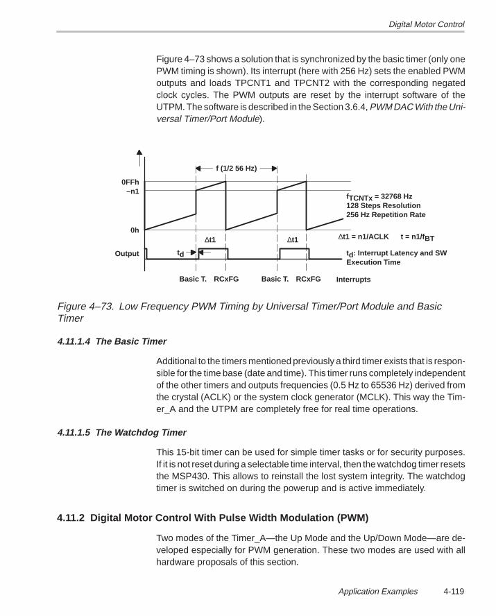
Digital Motor Control
4-119Application Examples
Figure 4–73 shows a solution that is synchronized by the basic timer (only onePWM timing is shown). Its interrupt (here with 256 Hz) sets the enabled PWMoutputs and loads TPCNT1 and TPCNT2 with the corresponding negatedclock cycles. The PWM outputs are reset by the interrupt software of theUTPM. The software is described in the Section 3.6.4, PWM DAC With the Uni-versal Timer/Port Module).
f (1/2 56 Hz)
td
0FFh–n1
0h
Output
∆t1 ∆t1 ∆t1 = n1/ACLK t = n1/f BT
Basic T. RCxFG Basic T. RCxFG
td: Interrupt Latency and SWExecution Time
fTCNTx = 32768 Hz128 Steps Resolution256 Hz Repetition Rate
Interrupts
Figure 4–73. Low Frequency PWM Timing by Universal Timer/Port Module and BasicTimer
4.11.1.4 The Basic Timer
Additional to the timers mentioned previously a third timer exists that is respon-sible for the time base (date and time). This timer runs completely independentof the other timers and outputs frequencies (0.5 Hz to 65536 Hz) derived fromthe crystal (ACLK) or the system clock generator (MCLK). This way the Tim-er_A and the UTPM are completely free for real time operations.
4.11.1.5 The Watchdog Timer
This 15-bit timer can be used for simple timer tasks or for security purposes.If it is not reset during a selectable time interval, then the watchdog timer resetsthe MSP430. This allows to reinstall the lost system integrity. The watchdogtimer is switched on during the powerup and is active immediately.
4.11.2 Digital Motor Control With Pulse Width Modulation (PWM)
Two modes of the Timer_A—the Up Mode and the Up/Down Mode—are de-veloped especially for PWM generation. These two modes are used with allhardware proposals of this section.
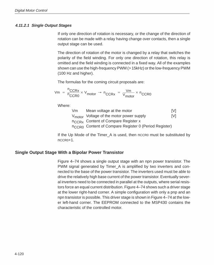
Digital Motor Control
4-120
4.11.2.1 Single Output Stages
If only one direction of rotation is necessary, or the change of the direction ofrotation can be made with a relay having change over contacts, then a singleoutput stage can be used.
The direction of rotation of the motor is changed by a relay that switches thepolarity of the field winding. For only one direction of rotation, this relay isomitted and the field winding is connected in a fixed way. All of the examplesshown can use the high-frequency PWM (> 15kHz) or the low-frequency PWM(100 Hz and higher).
The formulas for the coming circuit proposals are:
Vm nCCRxnCCR0
Vmotor nCCRx VmVmotor
nCCR0
Where:Vm Mean voltage at the motor [V]Vmotor Voltage of the motor power supply [V]nCCRx Content of Compare Register xnCCR0 Content of Compare Register 0 (Period Register)
If the Up Mode of the Timer_A is used, then nCCR0 must be substituted bynCCR0+1.
Single Output Stage With a Bipolar Power Transistor
Figure 4–74 shows a single output stage with an npn power transistor. ThePWM signal generated by Timer_A is amplified by two inverters and con-nected to the base of the power transistor. The inverters used must be able todrive the relatively high base current of the power transistor. Eventually sever-al inverters need to be connected in parallel at the outputs, where serial resis-tors force an equal current distribution. Figure 4–74 shows such a driver stageat the lower right-hand corner. A simple configuration with only a pnp and annpn transistor is possible. This driver stage is shown in Figure 4–74 at the low-er left-hand corner. The EEPROM connected to the MSP430 contains thecharacteristic of the controlled motor.
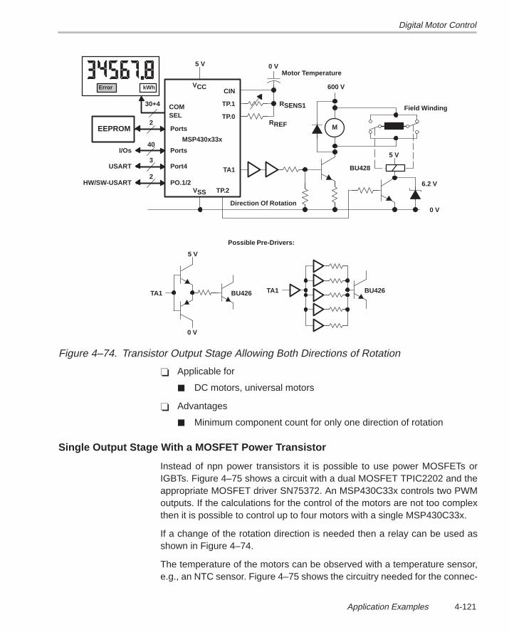
Digital Motor Control
4-121Application Examples
3
Error kWh
2EEPROM
Possible Pre-Drivers:
30+4 COMSEL
Ports
40PortsI/Os
Port4USART
2PO.1/2HW/SW-USART
VSS
VCC
5 V
TP.2
Direction Of Rotation
TA1
M
0 VMotor Temperature
600 V
Field Winding
5 V
6.2 V
0 V
BU428
RREF
RSENS1
CIN
TP.1
TP.0
5 V
0 V
TA1 BU426 TA1 BU426
MSP430x33x
Figure 4–74. Transistor Output Stage Allowing Both Directions of Rotation
Applicable for
DC motors, universal motors
Advantages
Minimum component count for only one direction of rotation
Single Output Stage With a MOSFET Power Transistor
Instead of npn power transistors it is possible to use power MOSFETs orIGBTs. Figure 4–75 shows a circuit with a dual MOSFET TPIC2202 and theappropriate MOSFET driver SN75372. An MSP430C33x controls two PWMoutputs. If the calculations for the control of the motors are not too complexthen it is possible to control up to four motors with a single MSP430C33x.
If a change of the rotation direction is needed then a relay can be used asshown in Figure 4–74.
The temperature of the motors can be observed with a temperature sensor,e.g., an NTC sensor. Figure 4–75 shows the circuitry needed for the connec-
Digital Motor Control
4-122
tion of two temperature sensors to the ADC inputs of the MSP430C33x. Themotor temperatures are measured in appropriate time intervals to be sure, thattypical circumstances are present. In case of a overly high motor temperature,the microcomputer switches off the MOSFET power transistor and switcheson a fault indication LED.
The observation of the motor current is realized with an operational amplifierworking as a comparator. The circuitry shown allows eight different thresholds,a number that can be modified easily if necessary. The control ports P3.xswitch between the high state and the high-impedance state to get eight differ-ent thresholds (corresponding to eight different temperatures).
32 kHz
2
2EEPROM
TP.3
Ports
23Ports w IntrptI/Os
TP.xADC (Sensors)
3Port4USART
VCC
5 V
TA1
0 VMotor Temperature
CIN
TP.2
TP.1
TP.0
TA2
Inp A5 V
En A
Inp B
En A
VCC1 VCC2
5 V 15 V
SN75372
M1 M2
Out A
Out B
Gate1
T
Drain1 Drain2
45 V 45 V
_
+
Gate2
Source
Rshunt
0 V
Number of Revolutions
0 V
Current Comparison
R
2R
4R
PO.7, NMI
VSSP0.0
P3.1
P3.2
P3.3
Fault LED
0 V
Tachometer
5 Ports(w/o Intrrupt)
I/Os
XIN XOUT
MSP430x33x
Rsens2
Rsens1
Rref
Figure 4–75. Control for Two MOSFET Output Stages
Applicable for
DC motors, permanently excited dc motors
Advantages
Control for two motors with minimum chip count
The MOSFETs shown in Figure 4–75 allow up to 7.5-A continuous current si-multaneously for both transistors. The TPIC2202, having only one source ter-

Digital Motor Control
4-123Application Examples
minal, allows only the measurement of the sum of both motor currents. If it isnecessary to observe the motor currents independently, then the TPIC5201can be used. This dual power MOSFET features two source terminals. For mo-tor currents up to 3 A, the 15-V supply for the SN75372 is not necessary, a 5-Vsupply is sufficient for switching on of the MOSFETs.
4.11.2.2 H-Bridge Output Stages
An H-bridge means the fourfold expense for power drivers compared to asingle output stage. But if integrated drivers are used, the resulting expenseis often lower than with a single output stage because the change of the direc-tion of rotation is included with the H-bridge.
H-Bridges for Low Motor Voltages
For voltages up to 36 V, TI offers several solutions. Into this range belong theautomotive sector and industrial control applications working with 24-V supplyvoltage.
Output Stage With a MOSFET Bridge
Motor control applications working with relatively low voltages can use the Tex-as Instruments H-bridge TPIC5424. This device is able to switch currents upto 3 A at a maximum voltage of 60 V. The complete circuit diagram is shownin Figure 4–76.
The gate voltage necessary for the turn-on of the upper MOSFETs of thebridge is generated by a bootstrap circuit. This gate voltage must be at least5 V higher than the motor voltage. The MSP430 generates this support voltageusing two capacitors and the low impedance power driver BT1.
Three simple solutions are possible for the generation of the higher gate volt-age:
PWM-output TA3 is used with the full PWM frequency (e.g. 19.2 kHz)
PWM-output TA0 is used with the divided PWM frequency (e.g. 9.6 kHzfor 19.2 kHz). This is due to the only possible output mode for the periodregister, CCR0: Toggle/Toggle Mode. This way has the advantage that noother timer output is needed. Figure 4–76 illustrates this solution.
One of the available output frequencies of the XBUF output is used: ACLK,ACLK/2 or ACLK/4 corresponding to 32.768 kHz, 16.384 kHz or 8192 Hz.
Solutions 2 and 3 have the advantage of an always usable output voltage.They are independent of the PWM output driving the electric motor.
Digital Motor Control
4-124
Note:
The power inverter shown, BT1, can be replaced by some paralleled—notused otherwise—output ports of the MSP430C33x. They are toggled by asoftware routine, driven by the interrupts of the period register CCR0.
A possible driver circuit for a pulldown output is shown on the upper left-handcorner in Figure 4–76: the additional npn transistor lowers the output imped-ance for the positive supply voltage 12 V. In this way the supply voltage VCC2(18 V), which is needed for the output voltage of the SN75372, is generated.
The two lower MOSFETs of the H-bridge are driven in a static manner from theMSP430 with 5-V signals. This is possible because the TPIC5424 is designedfor logic drive signals (0 to 5 V).
As shown in Figure 4–76, the TPIC5424 has integrated all the necessaryprotection diodes on-chip, therefore, no external components are needed. Thesignals at the MOSFET gates are shown in Figure 4–76 in the lower right-handcorner.
An exceedingly high motor current is detected by the overcurrent detection cir-cuit. If a fixed voltage level, according to a maximum current value, is exceed-ed (e.g. by a blocking of the motor or by a current flow through one of the H-bridge halves), the comparator output switches off the lower drivers T2 and T4and the additionally requested P0.0 or NMI interrupt (highest priority) takessteps to switch off the output stages completely. The overcurrent detection canbe realized with more than one level as shown in Figure 4–75. The motor tem-perature can be measured the same way as shown in Figure 4–75.
Applicable for
Permanently excited dc motors
Advantages
Few components necessary
Both directions of rotation possible
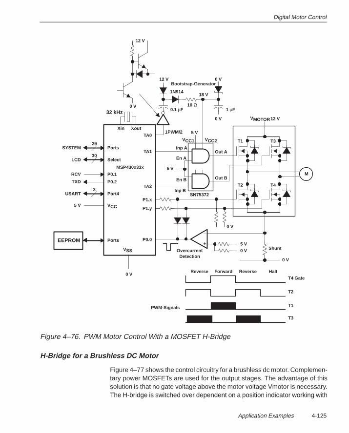
Digital Motor Control
4-125Application Examples
32 kHz
EEPROM Ports
30SelectLCD
P0.1RCV
3Port4USART
TA1
0 V
TA2
Inp A
5 V
En A
Inp B
En B
VCC1 VCC2
5 V
18 V
Out A
Out B
12 V
12 V
_
+
1N914
Shunt
0 V
T1
P0.0
VSS
Xin Xout
M
5 V0 V
0 V
OvercurrentDetection
SN75372
1PWM/2
10 Ω
0 V
T3
T2 T4
VMOTOR
Bootstrap-Generator
12 V
0 V
29PortsSYSTEM
P0.2TXD
VCC5 V
TA0
P1.x
P1.y
Reverse Forward Reverse HaltT4 Gate
T2
T1
T3
PWM-Signals
0.1 µF 1 µF
0 V
MSP430x33x
Figure 4–76. PWM Motor Control With a MOSFET H-Bridge
H-Bridge for a Brushless DC Motor
Figure 4–77 shows the control circuitry for a brushless dc motor. Complemen-tary power MOSFETs are used for the output stages. The advantage of thissolution is that no gate voltage above the motor voltage Vmotor is necessary.The H-bridge is switched over dependent on a position indicator working with

Digital Motor Control
4-126
the Hall effect. If the change of polarity is necessary for the motor voltage, theHall sensor requests interrupt and the MSP430 switches over the H-bridge.
The necessary delay times (ts in Figure–77), which prevent a short circuit inthe H-bridge halves, are generated by software. If this happens, the over cur-rent detection switches off the two lower MOSFET drivers T2 and T4. The si-multaneously requested interrupt at input P0.0 will force the software toswitch-off all of the MOSFET drivers completely until the lost synchronism isbuilt-up again.
The direction of rotation can be reversed by changing the current flow directionrelatively to the location of the rotor. This is possible because the field is gener-ated normally with a permanent magnet (see pulse diagram in Figure 4–77).
The circuitry shown does not need a tachometer because the signal of the Hallsensor can be used for the measurement of the number of revolutions per sec-ond.
The TLE2144 operational amplifiers are used as MOSFET drivers with theiroutputs and as AND gates with their inputs. The circuitry used with the eightequal resistors allows the two control outputs P0.4 and P0.5 to switch the PWMsignal to the proper MOSFET transistors. The PWM-output TA1 is able toswitch off both operational amplifier drivers and to switch on the driver pre-pared by P0.4 or P0.5. This solution leaves three compare/capture latches forother purposes.
The type of control (only one-half of the bridge is switched by the PWM signal,the other half is switched on in a static manner) decreases the switchinglosses.
Applicable for
Brushless dc motors
Advantages
Both directions of rotation possible
Robust motors without brush wear usable
Control of the motor speed without expense (Hall sensor)
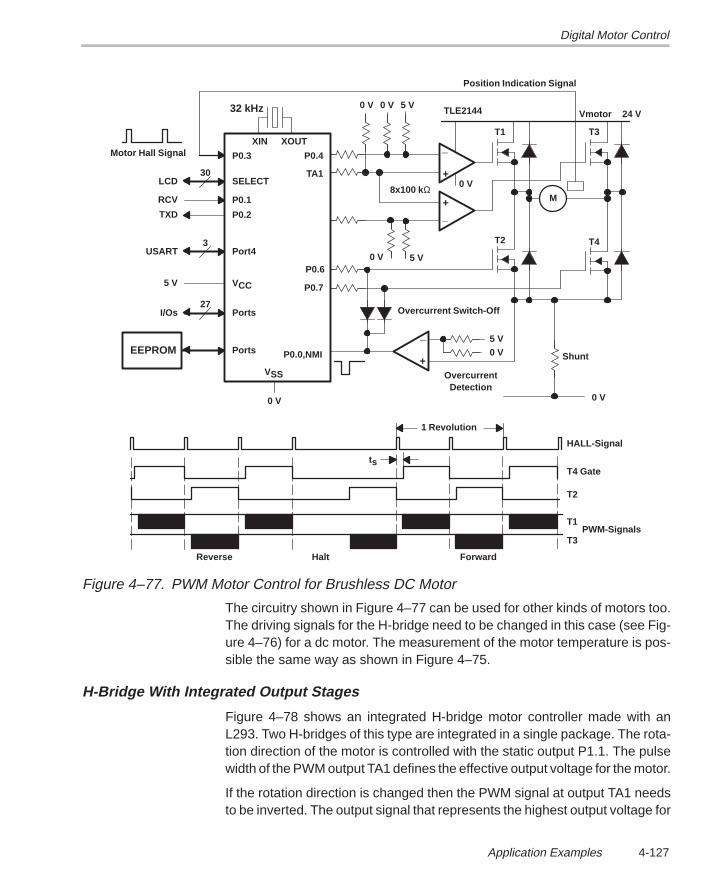
Digital Motor Control
4-127Application Examples
27
32 kHz
EEPROM Ports
P0.1RCV
3Port4USART
TA1
P0.6
24 V
_
+ Shunt
0 V
T1
P0.0,NMI
VSS
XIN XOUT
M
OvercurrentDetection
T3
T2 T4
Vmotor
30SELECTLCD
P0.2TXD
VCC5 V
P0.4
P0.7
_
+
_+
0 V
5 V0 V
Overcurrent Switch-Off
5 V0 V
0 V
8x100 kΩ
P0.3Motor Hall Signal
PortsI/Os
TLE21445 V0 V0 V
Position Indication Signal
1 Revolution
ts
Reverse ForwardHalt
T4 Gate
T2
PWM-SignalsT1
T3
HALL-Signal
Figure 4–77. PWM Motor Control for Brushless DC Motor
The circuitry shown in Figure 4–77 can be used for other kinds of motors too.The driving signals for the H-bridge need to be changed in this case (see Fig-ure 4–76) for a dc motor. The measurement of the motor temperature is pos-sible the same way as shown in Figure 4–75.
H-Bridge With Integrated Output Stages
Figure 4–78 shows an integrated H-bridge motor controller made with anL293. Two H-bridges of this type are integrated in a single package. The rota-tion direction of the motor is controlled with the static output P1.1. The pulsewidth of the PWM output TA1 defines the effective output voltage for the motor.
If the rotation direction is changed then the PWM signal at output TA1 needsto be inverted. The output signal that represents the highest output voltage for
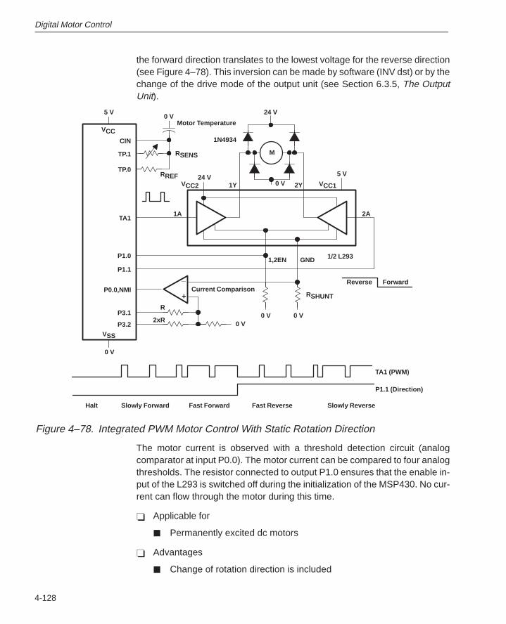
Digital Motor Control
4-128
the forward direction translates to the lowest voltage for the reverse direction(see Figure 4–78). This inversion can be made by software (INV dst) or by thechange of the drive mode of the output unit (see Section 6.3.5, The OutputUnit).
2Y
VCC
5 V
TA1
0 VMotor Temperature
CIN
TP.1
TP.05 VRREF
M
1,2EN
24 V
_
+
1N4934
RSHUNT
0 V
Current Comparison
R
2xR
P1.0
P0.0,NMI
P3.1
P3.2
VCC2
1A
0 V 0 V
2A
VCC11Y 0 V
24 V
VSS
GND 1/2 L293
Reverse Forward
RSENS
0 V
P1.1
TA1 (PWM)
P1.1 (Direction)
Halt Slowly Forward Fast Forward Fast Reverse Slowly Reverse
Figure 4–78. Integrated PWM Motor Control With Static Rotation Direction
The motor current is observed with a threshold detection circuit (analogcomparator at input P0.0). The motor current can be compared to four analogthresholds. The resistor connected to output P1.0 ensures that the enable in-put of the L293 is switched off during the initialization of the MSP430. No cur-rent can flow through the motor during this time.
Applicable for
Permanently excited dc motors
Advantages
Change of rotation direction is included
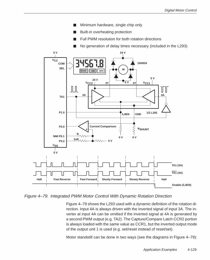
Digital Motor Control
4-129Application Examples
Minimum hardware, single chip only
Built-in overheating protection
Full PWM resolution for both rotation directions
No generation of delay times necessary (included in the L293)
4Y
VCC
5 V
TA1
COM
SEL
5 V
M
3,4EN
24 V
_
+
1N4934
RSHUNT
0 V
Current Comparison
R
2xR
P1.0
P3.0
NMI P0.1
P3.2
VCC2
3A
0 V 0 V
4A
VCC13Y 0 V
24 V
VSS
GND 1/2 L293
0 V
Enable (3,4EN)
Halt Slowly ForwardFast ForwardFast Reverse Slowly Reverse
Error ON rpm
Halt
TA1 (3A)
TA1 (4A)
Figure 4–79. Integrated PWM Motor Control With Dynamic Rotation Direction
Figure 4–79 shows the L293 used with a dynamic definition of the rotation di-rection. Input 4A is always driven with the inverted signal of input 3A. The in-verter at input 4A can be omitted if the inverted signal at 4A is generated bya second PWM output (e.g. TA2). The Capture/Compare Latch CCR2 portionis always loaded with the same value as CCR1, but the inverted output modeof the output unit 1 is used (e.g. set/reset instead of reset/set).
Motor standstill can be done in two ways (see the diagrams in Figure 4–79):

Digital Motor Control
4-130
With a PWM impulse ratio equal to one (see the left-hand side of the dia-gram)
By switching the enable input of the L293 low (here P1.0, see the right-hand side of diagram)
With the same PWM output frequency, the dynamic control allows only half ofthe resolution when compared to the static control shown in Figure 4–78. Oneresolution bit is necessary for the sign of the direction of rotation.
Applicable for
Permanently excited dc motors
Advantages
Change of rotation direction is included
Minimum hardware, single chip only
Built-in overheating protection
Sliding transition possible for the change of the rotation direction
No generation of delay times necessary (included in the L293)
The two circuits shown in Figures 4–78 and 4–79 can be controlled togetherwith a single MSP430C33x. Both figures can be integrated into one schematicwith only slight modifications.
If a lower motor current is sufficient, the L293D can be used.
Both the L293 and the L293D feature built-in overheating protection thatswitches off the device during over temperature events.
H-Bridge for High Motor Voltages
Electric motors with voltages above 60 V need completely different driver con-cepts. The motor drive is most often made with IGTBs. The voltages and cur-rents necessary for driving these semiconductors are delivered from specialdriver ICs. These ICs also contain the necessary safety circuits. An examplefor such a driver circuit is shown in Figure 4–80. The MSP430 defines the rota-tion direction with the PWM outputs TA1 and TA2. Only one of the PWM out-puts is active, the other switches on the lower transistor of the other half of thebridge (static). This way the circuitry shown in Figure 4–80 is able to run themotor in both directions. As the supply voltage for the motor, the rectified acvoltage of 230 V is used.
The capture/compare register 4 works as a capture latch. It is used for thespeed measurement of the motor (input TA4).
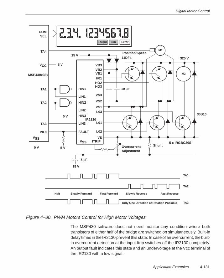
Digital Motor Control
4-131Application Examples
VSS
COMSEL
M1
5 V
Torque r/m Error
HIN1
LIN1
TA1
HIN2
LIN2
TA2
HIN3
LIN3TA3
FAULTP0.0
5 V0 V
VB3VB2VB1H01HO2
M2
HO3
VS3
VS2
VS1L03
L01
L02
VSITRIPVSS
ShuntOvercurrentAdjustment
5 x IRGBC20S
30S10
325 V
Position/Speed15 V
5 V
VCC
11DF4
10 µF
15 V
5 µF
Halt Slowly Forward Fast Forward Fast ReverseSlowly Reverse
TA1
Only One Direction of Rotation Possible
TA2
TA3
MSP430x33x
TA4
IR2130
Figure 4–80. PWM Motors Control for High Motor Voltages
The MSP430 software does not need monitor any condition where bothtransistors of either half of the bridge are switched on simultaneously. Built-indelay times in the IR2130 prevent this state. In case of an overcurrent, the built-in overcurrent detection at the input Itrip switches off the IR2130 completely.An output fault indicates this state and an undervoltage at the Vcc terminal ofthe IR2130 with a low signal.
Digital Motor Control
4-132
The gate voltage of the two upper power transistors, which must be higher thanthe motor voltage, is generated by the IR2130 with the help of a bootstrap gen-erator. The output signals VS2 and VS1 drive this internal generator. External-ly, only two diodes and two storage capacitors are needed. Static operation isnot possible in this configuration. The generation of the gate voltage makesdynamic operation necessary. VS1 or VS2 must also be active during motoridle (lower bridge transistors off).
With the unused IR2130 output LO3, a second motor (M2) can be driven withthe PWM TA3 output. For the change of rotation direction, a relay is needed.The circuitry for this is shown in Figure 4–74. Motor M2 is driven as desribedin Section 4.11.2.1, Single Output Stages. M2 is completely independant fromM1.
Applicable for
DC motors with direct ac circuit connection, universal motors
Advantages
Both rotation directions are possible due to H-bridge
Direct ac circuit connection possible
Built-in delay times
Full PWM resolution for both rotation directions
High motor power possible
4.11.2.3 Three-Phase Motor Control
The MSP430C33x is also able to control 3-phase electric motors. This is dueto the following hardware features:
Three synchronized PWM outputs (Timer_A)
Table processing capabilities (indirect, indirect with autoincrement, and in-dexed addressing modes)
Hardware multiplier (16×16 bit) with immediate 32-bit result
Up to 3.8-MHz CPU frequency; 263-ns execution time for single-cycle in-structions (register/register mode)
These features together allow the generation of three PWM output signals thatare phase shifted 120 relative to the others. The repetition rate should be near20 kHz to prevent it from being heard. With a PWM frequency of 16 kHz, nearly8-bit resolution is possible. The system works as follows:
Digital Motor Control
4-133Application Examples
The repetition rate of the PWM pulses is defined by the content of the peri-od register CCR0. This value is always the same.
The pulse width for the three PWM signals is defined by registers CCR1– CCR3. Each CCR controls one phase.
The nominal pulse widths for the generation of a sine curve are containedin a byte table (nominal 100% values). Dependent on the angle counter,the actual values are read out individually for each phase by indexed ad-dressing.
The frequency of the motor voltage is defined by the modification frequen-cy of the angle counter. The hardware multiplier is used here for the neces-sary calculations.
The motor voltage is defined by the modified pulse width (table value multi-plied by the percentage of the voltage). The hardware multiplier is usedalso for this task
The complete hardware diagram is shown in Figure 4–82. The interface to themotor is made by an IR2130 motor controller. This chip includes the necessarysafety functions for overcurrent detection and generation of the necessarydead times for the output transistors.
The formula for the timer value nCCRx is:
Vm nCCRxnCCR0
0.5 Vmotor nCCRx VmVmotor
0.5 nCCR0
Where:Vm Mean voltage at the motor phases
(–Vmotor/2 to +Vmotor/2) [V]Vmotor Voltage of the motor power supply [V]nCCRx Content of Compare Register xnCCR0 Content of Compare Register 0 (Period Register)
If the up mode of the Timer_A is used, then nCCR0 must be substituted bynCCR0+1.
Applicable for
Three-phase motors like induction motors
Open loop control method
Voltage/frequency method
Figure 4–81 shows some PWM outputs for different phase voltages.
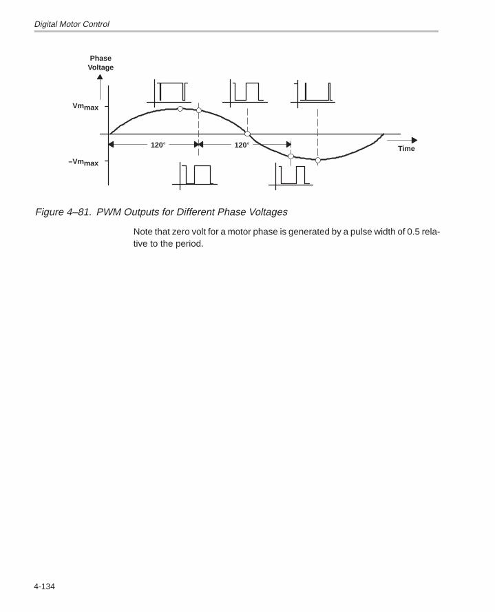
Digital Motor Control
4-134
Vmmax
–Vmmax
120° 120° Time
PhaseVoltage
Figure 4–81. PWM Outputs for Different Phase Voltages
Note that zero volt for a motor phase is generated by a pulse width of 0.5 rela-tive to the period.
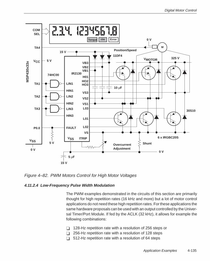
Digital Motor Control
4-135Application Examples
VSS
COMSEL
M
5 V
Torque r/m Error
HIN1
LIN1TA1
HIN2
LIN2TA2
HIN3
LIN3TA3
FAULTP0.0
5 V
0 V
VB3VB2VB1
H01HO2HO3
VS3
VS2
VS1L03
L01
L02
VS
ITRIPVSSShuntOvercurrent
Adjustment
6 x IRGBC20S
30S10
325 V
Position/Speed15 V
VCC
11DF4
10 µF
15 V
5 µF
0 V
TA4
VMOTOR
0 V
74HC00
MS
P43
0x33
x
IR2130
Figure 4–82. PWM Motors Control for High Motor Voltages
4.11.2.4 Low-Frequency Pulse Width Modulation
The PWM examples demonstrated in the circuits of this section are primarilythought for high repetition rates (16 kHz and more) but a lot of motor controlapplications do not need these high repetition rates. For these applications thesame hardware proposals can be used with an output controlled by the Univer-sal Timer/Port Module. If fed by the ACLK (32 kHz), it allows for example thefollowing combinations:
128-Hz repetition rate with a resolution of 256 steps or 256-Hz repetition rate with a resolution of 128 steps 512-Hz repetition rate with a resolution of 64 steps
Digital Motor Control
4-136
Other combinations are possible too. If the MCLK is used as input frequencythen the repetition rates and the resolution can be even higher, but the interruptlatency time plays an increasing role due to the software-based structure ofthis timer module: the PWM output is controlled by an interrupt handler and notby a hardware module as with the Timer_A. The characteristics of this kind ofcontrol are very similar to the TRIAC control due to the low repetition rates.
This way of motor control can substitute the PWM-control solutions realizedwith relays, as it is implemented in some automotive applications.
More details of the PWM generation are described in Section 3.6.4, PWM DACWith the Universal Timer/Port Module.
Applicable for
All motors controllable by TRIACs
DC motors
4.11.2.5 Bandwidth of the MSP430 Solutions for PWM Control
Figure 4–83 shows the bandwidth of solutions the MSP430 family offers forPWM control systems; starting from a minimum system with a MSP430C312up to a maximum system using a MSP430C337.
The minimum system with the MSP430C312 gets its information concerningthe motor control (reference speed, direction of rotation, on/off) normally froma host via the I/O terminals or the SW/HW UART (RS232 link). It allows rela-tively slow PWM frequencies (≈1 kHz).
The maximum system with the MSP430C337 is shown in the following. Its ca-pabilities allow complete system control, not just the motor handling.
The PWM control for a single-phase motor normally does not use 100% of theMSP430 CPU. This being known, many functions of the host computer can betaken over by the MSP430 (e.g., when used in a tumbler or a dish washer con-troller). This is especially true for versions of the MSP430 having large memo-ries and many I/O lines.
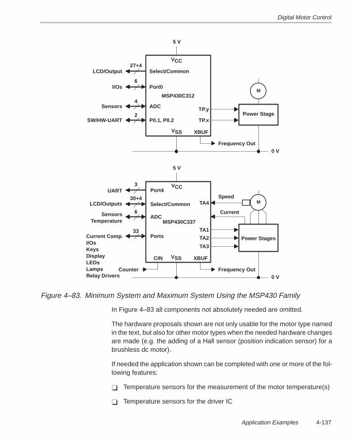
Digital Motor Control
4-137Application Examples
M
Select/Common27+4
LCD/Output
Port06
I/Os
ADC4
Sensors
P0.1, P0.22
SW/HW-UART
MSP430C312
Power StageTP.y
TP.x
VCC
5 V
VSS XBUF
Frequency Out0 V
M
Port43
LCD/Outputs Select/Common30+4
ADC6Sensors
Temperature
Ports33
UART
MSP430C337
Power StagesTA2
TA3
VCC
5 V
VSS XBUF
Frequency Out0 V
TA1
TA4Speed
Current
CIN
Current Comp.I/OsKeysDisplayLEDsLampsRelay Drivers
Counter
Figure 4–83. Minimum System and Maximum System Using the MSP430 Family
In Figure 4–83 all components not absolutely needed are omitted.
The hardware proposals shown are not only usable for the motor type namedin the text, but also for other motor types when the needed hardware changesare made (e.g. the adding of a Hall sensor (position indication sensor) for abrushless dc motor).
If needed the application shown can be completed with one or more of the fol-lowing features:
Temperature sensors for the measurement of the motor temperature(s)
Temperature sensors for the driver IC

Digital Motor Control
4-138
Tachometer for the measurement of the motor speed or the rotor position
Inputs for light sensors (safety, movement, flame observation etc.)
Analog inputs for the measurement of the motor voltage (improvement ofcontrol)
Connections to a host via the USART (SPI or SCI), HW/SW–UART orports
Some of the possibilities shown in Figure 4–83 (keys, LEDs, relays, LCDetc)
Caused by the numerous peripherals of the MSP430 family, all of these pre-vious functions can be implemented easily and cheaply.
4.11.3 Digital Motor Control With TRIACs
With the help of a TRIAC (TRiode for ac) the following electric motor types canbe controlled:
Universal motors
DC motors (connected via a bridge rectifier. See Figure 4–84)
Capacitor motors
Single-phase asynchronous motors
Single-phase synchronous motors
The timing for the TRIAC control is possible with the Universal Timer/Port Mod-ule and the Timer_A. Both can deliver the timing in the range from 0.5 ms to20 ms with the needed resolution.
4.11.3.1 Motor Connection and Control
The electric motor can be connected to ac directly or via a bridge rectifier. Bothpossibilities are shown in Figure 4–84. It is possible to control ac motors as wellas dc motors with a TRIAC.
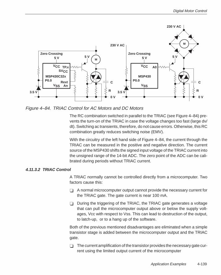
Digital Motor Control
4-139Application Examples
M
MSP430C32x
TP.xSVCC
RextAn
M
Zero Crossing5 V
P0.0
VCC
VSS
5 V
3.5 V
0 V
C
R
MSP430
A0
Zero Crossing5 V
P0.0
VCC
VSS
5 V
3.5 V
0 V
C
R
230 V AC
230 V AC
Figure 4–84. TRIAC Control for AC Motors and DC Motors
The RC combination switched in parallel to the TRIAC (see Figure 4–84) pre-vents the turn-on of the TRIAC in case the voltage changes too fast (large dv/dt). Switching ac transients, therefore, do not cause errors. Otherwise, this RCcombination greatly reduces switching noise (EMV).
With the circuitry of the left hand side of Figure 4–84, the current through theTRIAC can be measured in the positive and negative direction. The currentsource of the MSP430 shifts the signed input voltage of the TRIAC current intothe unsigned range of the 14-bit ADC. The zero point of the ADC can be cali-brated during periods without TRIAC current.
4.11.3.2 TRIAC Control
A TRIAC normally cannot be controlled directly from a microcomputer. Twofactors cause this:
A normal microcomputer output cannot provide the necessary current forthe TRIAC gate. The gate current is near 100 mA.
During the triggering of the TRIAC, the TRIAC gate generates a voltagethat can pull the microcomputer output above or below the supply volt-ages, Vcc with respect to Vss. This can lead to destruction of the output,to latch-up, or to a hang up of the software.
Both of the previous mentioned disadvantages are eliminated when a simpletransistor stage is added between the microcomputer output and the TRIACgate.
The current amplification of the transistor provides the necessary gate cur-rent using the limited output current of the microcomputer
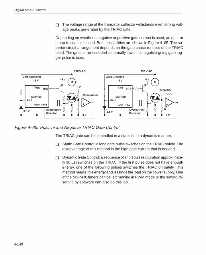
Digital Motor Control
4-140
The voltage range of the transistor collector withstands even strong volt-age peaks generated by the TRIAC gate.
Depending on whether a negative or positive gate current is used, an npn- ora pnp-transistor is used. Both possibilities are shown in Figure 4–85. The su-perior circuit arrangement depends on the gate characteristics of the TRIACused. The gate current needed is normally lower if a negative-going gate trig-ger pulse is used.
MSP430
TP.x
M
Zero Crossing–5 V
P0.3
VSS
VCC
–5 V
3.5 V
0 V
MSP430
TP.x
Zero Crossing5 V
P0.3
VSS
VCC
5 V
3.5 V0 V
R
230 V AC
OvercurrentDetector
_
+
M
OvercurrentDetector
P0.0 P0.0
_
+
Comparator
5 VAmplifier
230 V AC
Figure 4–85. Positive and Negative TRIAC Gate Control
The TRIAC gate can be controlled in a static or in a dynamic manner.
Static Gate Control: a long gate pulse switches on the TRIAC safely. Thedisadvantage of this method is the high gate current that is needed.
Dynamic Gate Control: a sequence of short pulses (duration approximate-ly 10 µs) switches on the TRIAC. If the first pulse does not have enoughenergy, one of the following pulses switches the TRIAC on safely. Thismethod needs little energy and lessings the load on the power supply. Oneof the MSP430 timers can be left running in PWM mode or the setting/re-setting by software can also do this job.
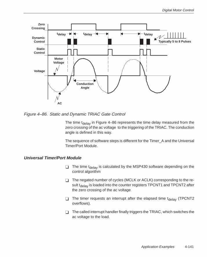
Digital Motor Control
4-141Application Examples
tdelay tdelay tdelay
MotorVoltage
AC
ConductionAngle
Typically 5 to 8 Pulses
ZeroCrossing
DynamicControl
StaticControl
Voltage
Figure 4–86. Static and Dynamic TRIAC Gate Control
The time tdelay in Figure 4–86 represents the time delay measured from thezero crossing of the ac voltage to the triggering of the TRIAC. The conductionangle is defined in this way.
The sequence of software steps is different for the Timer_A and the UniversalTimer/Port Module.
Universal Timer/Port Module
The time tdelay is calculated by the MSP430 software depending on thecontrol algorithm
The negated number of cycles (MCLK or ACLK) corresponding to the re-sult tdelay is loaded into the counter registers TPCNT1 and TPCNT2 afterthe zero crossing of the ac voltage
The timer requests an interrupt after the elapsed time tdelay (TPCNT2overflows).
The called interrupt handler finally triggers the TRIAC, which switches theac voltage to the load.
Digital Motor Control
4-142
Timer_A (Continuous Mode)
The time tdelay is calculated by the MSP430 software depending on thecontrol algorithm
The number of cycles (MCLK or ACLK) corresponding to the result tdelayis added to one of the compare registers CCRx after the zero crossing ofthe ac voltage
The output unit x is programmed to the mode that outputs the desired trig-ger pulse
The CCRx requests an interrupt after the elapsed time tdelay (CCRx equalsthe timer register).
The output unit x triggers the TRIAC, which switches the ac voltage to theload.
If dynamic gate control is used, the called interrupt handler outputs severaltrigger pulses by software or by using the PWM capability of Timer_A.
4.11.3.3 Control Algorithms
The value to be controlled (speed/velocity, current consumption, or torque) isinfluenced with the conduction angle of the TRIAC. This conduction angle (seeFigure 4–86) is defined by tdelay, the time the TRIAC triggering is delayed withreference to the zero crossing of the ac voltage.
For the control algorithms (that need to run in real time) two different methodsare used:
Normal calculation of the algorithm: For this method, the MSP430c33x iswell suited very because of its hardware multiplier on-chip. This allows avery-high calculation speed. (10 to 20 times higher than possible with an8-bit CPU.
Use of tables (especially with very high control speeds): For this method,the MSP430 is also very well suited because of its addressing modes, indi-rect, indirect autoincrement, and indexed, allow for a very simple and fastaccess to table values.
With TRIAC controls, normally everything necessary for the controlling is cal-culated directly. For dc machines, PID control is possible without the use ofcharacteristics because of their linear behavior.
Exception: With asynchronous machines most often a voltage/frequency or acurrent/frequency characteristic method is used that uses description tables.These are located in the ROM (normalized form) or in an external memory.
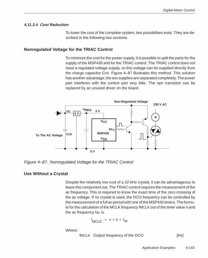
Digital Motor Control
4-143Application Examples
4.11.3.4 Cost Reduction
To lower the cost of the complete system, two possibilities exist. They are de-scribed in the following two sections.
Nonregulated Voltage for the TRIAC Control
To minimize the cost for the power supply, it is possible to split the parts for thesupply of the MSP430 and for the TRIAC control. The TRIAC control does notneed a regulated voltage supply, so this voltage can be supplied directly fromthe charge capacitor Cch. Figure 4–87 illustrates this method. This solutionhas another advantage; the two supplies are separated completely. The powerpart interferes with the control part very little. The npn transistor can bereplaced by an unused driver on the board.
MSP430TP.x
5 V
VCC
VSS
5 V
230 V ACNon-Regulated Voltage
Cch
VCVREG
To The AC Voltage
0 V
M
Figure 4–87. Nonregulated Voltage for the TRIAC Control
Use Without a Crystal
Despite the relatively low cost of a 32-kHz crystal, it can be advantageous toleave this component out. The TRIAC control requires the measurement of theac frequency. This is required to know the exact time of the zero crossing ofthe ac voltage. If no crystal is used, the DCO frequency can be controlled bythe measurement of a full ac period with one of the MSP430 timers. The formu-la for the calculation of the MCLK frequency fMCLK out of the timer value n andthe ac frequency fac is:
fMCLK n k fac
Where:fMCLK Output frequency of the DCO [Hz]
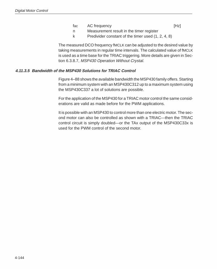
Digital Motor Control
4-144
fac AC frequency [Hz]n Measurement result in the timer registerk Predivider constant of the timer used (1, 2, 4, 8)
The measured DCO frequency fMCLK can be adjusted to the desired value bytaking measurements in regular time intervals. The calculated value of fMCLKis used as a time base for the TRIAC triggering. More details are given in Sec-tion 6.3.8.7, MSP430 Operation Without Crystal.
4.11.3.5 Bandwidth of the MSP430 Solutions for TRIAC Control
Figure 4–88 shows the available bandwidth the MSP430 family offers. Startingfrom a minimum system with an MSP430C312 up to a maximum system usingthe MSP430C337 a lot of solutions are possible.
For the application of the MSP430 for a TRIAC motor control the same consid-erations are valid as made before for the PWM applications.
It is possible with an MSP430 to control more than one electric motor. The sec-ond motor can also be controlled as shown with a TRIAC—then the TRIACcontrol circuit is simply doubled—or the TAx output of the MSP430C33x isused for the PWM control of the second motor.
Digital Motor Control
4-145Application Examples
MSP430C312TP.y
M
5 V
CIN
VCC
VSS
5 V
0 V
MSP430C337
TP.x
5 V
VCC
VSS
5 V
230 V AC
M1
XBUF
TAy
5 VM2
TP.y
3
2
Port4
4
34
HW/SW-UART
Sensors
USART
EEPROMsI/O PortsKeyboardDisplay (LCD)LEDsLampsRelais DriverExt. MemoriesGatesJumpers
P0.1, P0.2
TP.x
Ports
2
Tx,CIN
Counter Input
XBUF
MCLK, ACLK
5
8
TP.x
23
2HW/SW-UART
Sensors
I/O Ports
P0.1, P0.2
Sxx
Ports
LCD Outputs
MCLK, ACLKCounter Input
230 V AC
PWM
0 V
Figure 4–88. Minimum System and Maximum System With the MSP430 Family
In Figure 4–88, all circuitry not needed to demonstrate the application isomitted.
4.11.4 Motor Measurements
The methods shown for the measurement of the needed values like tempera-ture, speed/velocity, etc are valid for PWM and TRIAC controls.
4.11.4.1 Overcurrent Detection
Many applications make it necessary to detect increased motor current andto start provisions when this occurs. An example for this is the blocking of amotor.
Independent, if the high current consumption is detected by a threshold com-parison or by a current measurement In any case, the software has to take
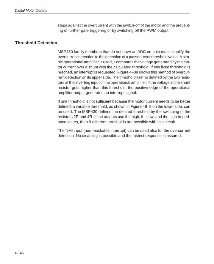
Digital Motor Control
4-146
steps against the overcurrent with the switch-off of the motor and the prevent-ing of further gate triggering or by switching off the PWM output.
Threshold Detection
MSP430 family members that do not have an ADC on-chip must simplify theovercurrent detection to the detection of a passed-over threshold value. A sim-ple operational amplifier is used, it compares the voltage generated by the mo-tor current over a shunt with the calculated threshold. If this fixed threshold isreached, an interrupt is requested. Figure 4–89 shows this method of overcur-rent detection on its upper side. The threshold itself is defined by the two resis-tors at the inverting input of the operational amplifier. If the voltage at the shuntresistor gets higher than this threshold, the positive edge of the operationalamplifier output generates an interrupt signal.
If one threshold is not sufficient because the motor current needs to be betterdefined, a variable threshold, as shown in Figure 48–9 on the lower side, canbe used. The MSP430 defines the desired threshold by the switching of theresistors 2R and 4R. If the outputs use the high, the low, and the high-imped-ance states, then 9 different thresholds are possible with this circuit.
The NMI input (non-maskable interrupt) can be used also for the overcurrentdetection. No disabling is possible and the fastest response is assured.
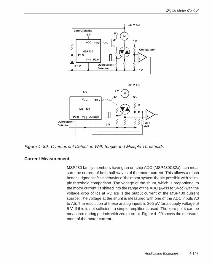
Digital Motor Control
4-147Application Examples
MSP430
TP.x
M
Zero Crossing5 V
P0.3
VCC
VSS
5 V
3.5 V0 V
MSP430
TP.x
5 V
P0.0
VCC
VSS
5 V
0 V2xR
230 V AC
OvercurrentDetector
_
+
M
OvercurrentDetector
P0.0
Outputs
_
+
Comparator
5 V
5 V
R
4xR
230 V AC
Figure 4–89. Overcurrent Detection With Single and Multiple Thresholds
Current Measurement
MSP430 family members having an on-chip ADC (MSP430C32x), can mea-sure the current of both half-waves of the motor current. This allows a muchbetter judgment of the behavior of the motor system than is possible with a sim-ple threshold comparison. The voltage at the shunt, which is proportional tothe motor current, is shifted into the range of the ADC (AVss to SVcc) with thevoltage drop of Ics at Rv. Ics is the output current of the MSP430 currentsource. The voltage at the shunt is measured with one of the ADC inputs A0to A5. The resolution at these analog inputs is 305 µV for a supply voltage of5 V. If this is not sufficient, a simple amplifier is used. The zero point can bemeasured during periods with zero current. Figure 4–90 shows the measure-ment of the motor current.
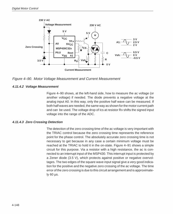
Digital Motor Control
4-148
MSP430C32x
TP.xSVCC
RextA1
M
Zero Crossing
5 V
P0.0
VCC
VSS
5 V
3.5 V
0 V
C
R
230 V AC
A0
Voltage Measurement
ICS
3 V2.5 V2 V
A1:
0.5 V0 VVsh:–0.5 V
RV
Current Measurement
230 V AC
Vsh:
Figure 4–90. Motor Voltage Measurement and Current Measurement
4.11.4.2 Voltage Measurement
Figure 4–90 shows, at the left-hand side, how to measure the ac voltage (oranother voltage) if needed. The diode prevents a negative voltage at theanalog input A0. In this way, only the positive half wave can be measured. Ifboth half waves are needed, the same way as shown for the motor current pathand can be used. The voltage drop of Ics at resistor Rv shifts the signed inputvoltage into the range of the ADC.
4.11.4.3 Zero Crossing Detection
The detection of the zero crossing time of the ac voltage is very important withthe TRIAC control because the zero crossing time represents the referencepoint for the phase control. The absolutely accurate zero crossing time is notnecessary to get because in any case a certain minimum voltage must bereached at the TRIAC to hold it in the on-state. Figure 4–91 shows a simplecircuit for this purpose. Via a resistor with a high resistance, the ac is con-nected to an interrupt input of the MSP430. This interrupt input is protected bya Zener diode (3.5 V), which protects against positive or negative overvol-tages. The two edges of the square wave input signal give a very good indica-tion for the positive and the negative zero crossing of the ac voltage. The timeerror of the zero crossing is due to this circuit arrangement and is approximate-ly 60 µs.
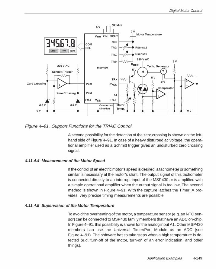
Digital Motor Control
4-149Application Examples
OvercurrentDirection
Error rpm
COMSEL
P0.3
VSS
VCC
5 V
P0.5
0 VMotor Temperature
RREF
Rsense2
CIN
TP.2
TP.0
MSP430
TP.x
M5 V
230 V AC
_
+
Comparator
5 V
TP.1
_+
5 V
T
Rsense1
Tacho Generator
0 V
0 V
SVCC
A1
P0.4
RW
_
+
0 V
Zero Crossing
3.5 V2.7 V
Zero Crossing
Schmitt Trigger
P0.0
32 kHz
XIN XOUT
MotorTemp.
230 V AC
Figure 4–91. Support Functions for the TRIAC Control
A second possibility for the detection of the zero crossing is shown on the left-hand side of Figure 4–91. In case of a heavy disturbed ac voltage, the opera-tional amplifier used as a Schmitt trigger gives an undisturbed zero crossingsignal.
4.11.4.4 Measurement of the Motor Speed
If the control of an electric motor’s speed is desired, a tachometer or somethingsimilar is necessary at the motor’s shaft. The output signal of this tachometeris connected directly to an interrupt input of the MSP430 or is amplified witha simple operational amplifier when the output signal is too low. The secondmethod is shown in Figure 4–91. With the capture latches the Timer_A pro-vides, very precise timing measurements are possible.
4.11.4.5 Supervision of the Motor Temperature
To avoid the overheating of the motor, a temperature sensor (e.g. an NTC sen-sor) can be connected to MSP430 family members that have an ADC on-chip.In Figure 4–91, this possibility is shown for the analog input A1. Other MSP430members can use the Universal Timer/Port Module as an ADC (seeFigure 4–91). The software has to take steps when a high temperature is de-tected (e.g. turn-off of the motor, turn-on of an error indication, and otherthings).
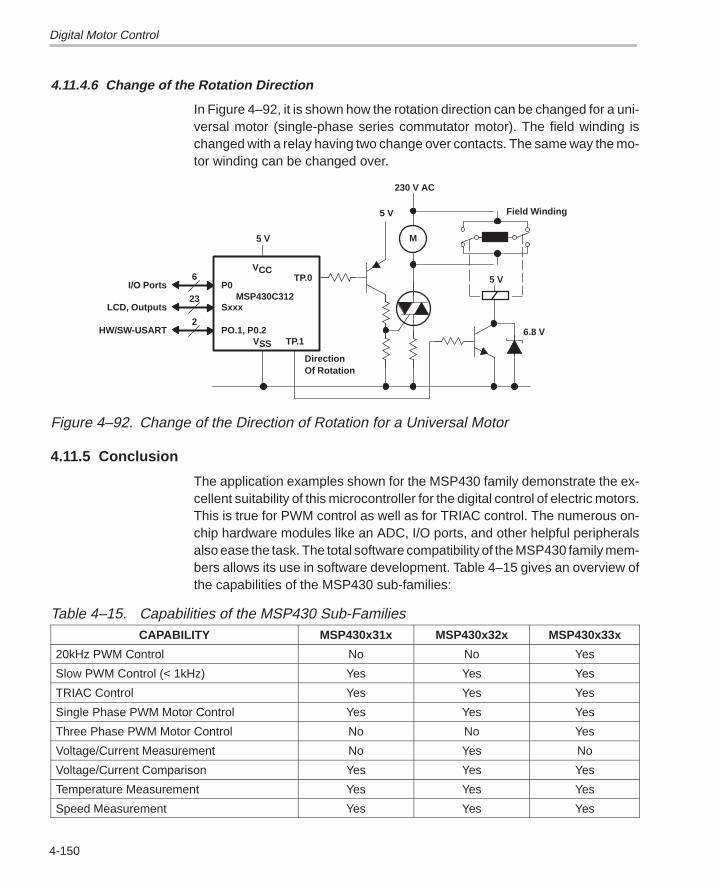
Digital Motor Control
4-150
4.11.4.6 Change of the Rotation Direction
In Figure 4–92, it is shown how the rotation direction can be changed for a uni-versal motor (single-phase series commutator motor). The field winding ischanged with a relay having two change over contacts. The same way the mo-tor winding can be changed over.
23 MSP430C312
6P0I/O Ports
SxxxLCD, Outputs
2PO.1, P0.2HW/SW-USART
VSS
VCC
5 V
TP.1
DirectionOf Rotation
TP.0
M
230 V AC
Field Winding
5 V
6.8 V
5 V
Figure 4–92. Change of the Direction of Rotation for a Universal Motor
4.11.5 Conclusion
The application examples shown for the MSP430 family demonstrate the ex-cellent suitability of this microcontroller for the digital control of electric motors.This is true for PWM control as well as for TRIAC control. The numerous on-chip hardware modules like an ADC, I/O ports, and other helpful peripheralsalso ease the task. The total software compatibility of the MSP430 family mem-bers allows its use in software development. Table 4–15 gives an overview ofthe capabilities of the MSP430 sub-families:
Table 4–15. Capabilities of the MSP430 Sub-FamiliesCAPABILITY MSP430x31x MSP430x32x MSP430x33x
20kHz PWM Control No No Yes
Slow PWM Control (< 1kHz) Yes Yes Yes
TRIAC Control Yes Yes Yes
Single Phase PWM Motor Control Yes Yes Yes
Three Phase PWM Motor Control No No Yes
Voltage/Current Measurement No Yes No
Voltage/Current Comparison Yes Yes Yes
Temperature Measurement Yes Yes Yes
Speed Measurement Yes Yes Yes

5-1
Software Applications
Chapter 5
5-2
5.1 Integer Calculation Subroutines
Integer routines have important advantages compared to all other calculationsubroutines:
Speed: Highest speed is possible especially when no loops are used
ROM space: Least amount of ROM space is needed for these subroutines
Adaptability: With the following definitions it is very easy to adapt the sub-routines to the actual needs. The necessary calculation registers can belocated in the RAM or in registers.
The following definitions are valid for all of the following integer subroutines.They can be changed as needed.
; Integer Subroutines Definitions: Software Multiply
;
IRBT .EQU R9 ; Bit test register MPY
IROP1 .EQU R4 ; First operand
IROP2L .EQU R5 ; Second operand low word
IROP2M .EQU R6 ; Second operand high word
IRACL .EQU R7 ; Result low word
IRACM .EQU R8 ; Result high word
;
; Hardware Multiplier
;
ResLo .EQU 013Ah ; HW_MPYer: Result reg. LSBs
ResHi .EQU 013Ch ; Result register MSBs
SumExt .EQU 013Eh ; Sum Ext. Register
All multiplication subroutines shown in the following section permit two differ-ent modes:
The normal multiplication: the result of the multiplication is placed into theresult registers
The multiplication and accumulation function (MAC): the result of the multi-plication is added to the previous content of the result registers.
5.1.1 Unsigned Multiplication 16 x 16-Bits
The following subroutine performs an unsigned 16 x 16-bit multiplication (labelMPYU) or multiplication and accumulation (label MACU). The multiplication
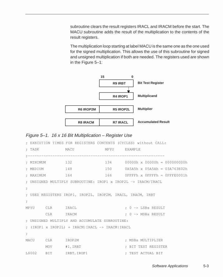
5-3Software Applications
subroutine clears the result registers IRACL and IRACM before the start. TheMACU subroutine adds the result of the multiplication to the contents of theresult registers.
The multiplication loop starting at label MACU is the same one as the one usedfor the signed multiplication. This allows the use of this subroutine for signedand unsigned multiplication if both are needed. The registers used are shownin the Figure 5–1:
R9 IRBT
15 0
R4 IROP1
R5 IROP2LR6 IROP2M
R7 IRACLR8 IRACM
Bit Test Register
Multiplicand
Multiplier
Accumulated Result
Figure 5–1. 16 x 16 Bit Multiplication – Register Use
; EXECUTION TIMES FOR REGISTERS CONTENTS (CYCLES) without CALL:
; TASK MACU MPYU EXAMPLE
;–––––––––––––––––––––––––––––––––––––––––––––––––––––––––––––
; MINIMUM 132 134 00000h x 00000h = 000000000h
; MEDIUM 148 150 0A5A5h x 05A5Ah = 03A763E02h
; MAXIMUM 164 166 0FFFFh x 0FFFFh = 0FFFE0001h
; UNSIGNED MULTIPLY SUBROUTINE: IROP1 x IROP2L –> IRACM/IRACL
;
; USED REGISTERS IROP1, IROP2L, IROP2M, IRACL, IRACM, IRBT
;
MPYU CLR IRACL ; 0 –> LSBs RESULT
CLR IRACM ; 0 –> MSBs RESULT
; UNSIGNED MULTIPLY AND ACCUMULATE SUBROUTINE:
; (IROP1 x IROP2L) + IRACM|IRACL –> IRACM|IRACL
;
MACU CLR IROP2M ; MSBs MULTIPLIER
MOV #1,IRBT ; BIT TEST REGISTER
L$002 BIT IRBT,IROP1 ; TEST ACTUAL BIT
5-4
JZ L$01 ; IF 0: DO NOTHING
ADD IROP2L,IRACL ; IF 1: ADD MULTIPLIER TO RESULT
ADDC IROP2M,IRACM
L$01 RLA IROP2L ; MULTIPLIER x 2
RLC IROP2M ;
;
RLA IRBT ; NEXT BIT TO TEST
JNC L$002 ; IF BIT IN CARRY: FINISHED
RET
If the hardware multiplier is implemented then the previous subroutines canbe substituted by MACROs. For source and destination, all seven addressingmodes are possible. If register indirect or register indirect with autoincrementaddressing modes are used to address the result, a NOP is necessary afterthe MACRO call to allow the completion of the multiplication. The SumExt Reg-ister contains the carry after the MAC instruction; 0 (no carry) or 1 (carry oc-curred).
; Macro Definition for the unsigned multiplication 16 x 16 bits
;
MPYU .MACRO arg1,arg2 ; Unsigned MPY 16x16
MOV arg1,&0130h
MOV arg2,&0138h
.ENDM ; Result in ResHi|ResLo
;
; Multiply the contents of two registers
;
MPYU IROP1,IROP2L ; CALL the MPYU macro
MOV ResLo,R6 ; Fetch LSBs of result
MOV ResHi,R7 ; Fetch MSBs of result
...
;
; Multiply the operands located in a table, R6 points to
;
MOV #ResLo,R5 ; Pointer to LSBs of result
MPYU @R6+,@R6 ; CALL the MPYU macro
NOP ; NOP: allow completion of MPYU
MOV @R5+,R7 ; Fetch LSBs of result
5-5Software Applications
MOV @R5,R8 ; Fetch MSBs of result
;
; Macro Definition for the unsigned multiplication and
; accumulation 16 x 16 bits
;
MACU .MACRO arg1,arg2 ; Unsigned MAC 16x16
MOV arg1,&0134h ; Carry in SumExt
MOV arg2,&0138h
.ENDM ; Result in SumExt|ResHi|ResLo
;
; Multiply and accumulate the contents of two registers
;
MPYU R5,R6 ; Initialize SumExt|ResHi|ResLo
MACU IROP1,IROP2L ; Add IROP1 x IROP2 to result
ADC &SumExt,RAM ; Add carry to RAM extension
;
5.1.1.1 Run Time Optimized Unsigned Multiplication 16 x 16-Bits
If the operands of the multiplication subroutine are shorter than 16 bits, the pre-vious multiplication subroutine MPYU can be optimized during run time
The multiplication stops immediately after the operand IROP1 equals zero.This indicates that the operand with leading zeroes should be in IROP1. Thisrun time optimized subroutine can be used instead of the normal subroutine.(The subroutine was developed by Leslie Mable/UK).
;
; EXECUTION TIMES FOR REGISTERS CONTENTS (CYCLES) without CALL:
; TASK MACU MPYU IROP1 IROP2
;–––––––––––––––––––––––––––––––––––––––––––––––––––––––––––––
; MINIMUM 18 20 00000h x 00000h = 000000000h
; MEDIUM 90 92 000FFh x 0FFFFh = 000FEFF01h
; MAXIMUM 170 172 0FFFFh x 0FFFFh = 0FFFE0001h
; UNSIGNED MULTIPLY SUBROUTINE (Run time optimized):
; IROP1 x IROP2L –> IRACM|IRACL
;
; USED REGISTERS IROP1, IROP2L, IROP2M, IRACL, IRACM
;
5-6
MPYU CLR IRACL ; 0 –> LSBs RESULT
CLR IRACM ; 0 –> MSBs RESULT
; UNSIGNED MULTIPLY AND ACCUMULATE SUBROUTINE:
; (IROP1 x IROP2L) + IRACM|IRACL –> IRACM|IRACL
;
MACU CLR IROP2M ; MSBs MULTIPLIER
L$002 BIT #1,IROP1 ; TEST ACTUAL BIT (LSB)
JZ L$01 ; IF 0: DO NOTHING
ADD IROP2L,IRACL ; IF 1: ADD MULTIPLIER TO RESULT
ADDC IROP2M,IRACM
L$01 RLA IROP2L ; Double MULTIPLIER IROP2
RLC IROP2M ;
;
RRC IROP1 ; Next bit of IROP1 to LSB
JNZ L$002 ; If IROP1 = 0: finished
RET
5.1.1.2 Fast Unsigned Square Function
For some applications, a fast square function is necessary. Two different solu-tions are given:
For 16-bit unsigned numbers without rounding
For 14-bit unsigned numbers with rounding. This version is adapted to theoutput of the ADC of the MSP430C32x family.
Both use table processing; an offset to a table containing the squared inputnumbers is built. The given cycles include the move of the operand into R5.
; Fast unsigned squaring for a 16 bit number. The upper 16 bits
; of the result are moved to R5. No rounding is used. 7 cycles
;
MOV.B DATA+1,R5 ; MSBs to R5
RLA R5 ; Number x 2 (word table address)
MOV SQTAB(R5),R5 ; MSBs^2 to R5
... ; Squared value in R5
;
; Fast unsigned squaring for a 14 bit number. The upper 16 bits of
; the result are added to a buffer SQSUM. Rounding is used.
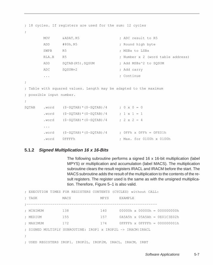
5-7Software Applications
; 18 cycles. If registers are used for the sum: 12 cycles
;
MOV &ADAT,R5 ; ADC result to R5
ADD #80h,R5 ; Round high byte
SWPB R5 ; MSBs to LSBs
RLA.B R5 ; Number x 2 (word table address)
ADD SQTAB(R5),SQSUM ; Add MSBs^2 to SQSUM
ADC SQSUM+2 ; Add carry
... ; Continue
;
; Table with squared values. Length may be adapted to the maximum
; possible input number.
;
SQTAB .word ($–SQTAB)*($–SQTAB)/4 ; 0 x 0 = 0
.word ($–SQTAB)*($–SQTAB)/4 ; 1 x 1 = 1
.word ($–SQTAB)*($–SQTAB)/4 ; 2 x 2 = 4
...
.word ($–SQTAB)*($–SQTAB)/4 ; 0FFh x 0FFh = 0FE01h
.word 0FFFFh ; Max. for 0100h x 0100h
5.1.2 Signed Multiplication 16 x 16-Bits
The following subroutine performs a signed 16 x 16-bit multiplication (labelMPYS) or multiplication and accumulation (label MACS). The multiplicationsubroutine clears the result registers IRACL and IRACM before the start. TheMACS subroutine adds the result of the multiplication to the contents of the re-sult registers. The register used is the same as with the unsigned multiplica-tion. Therefore, Figure 5–1 is also valid.
; EXECUTION TIMES FOR REGISTERS CONTENTS (CYCLES) without CALL:
; TASK MACS MPYS EXAMPLE
;–––––––––––––––––––––––––––––––––––––––––––––––––––––––––––––
; MINIMUM 138 140 00000h x 00000h = 000000000h
; MEDIUM 155 157 0A5A5h x 05A5Ah = 0E01C3E02h
; MAXIMUM 172 174 0FFFFh x 0FFFFh = 000000001h
; SIGNED MULTIPLY SUBROUTINE: IROP1 x IROP2L –> IRACM|IRACL
;
; USED REGISTERS IROP1, IROP2L, IROP2M, IRACL, IRACM, IRBT
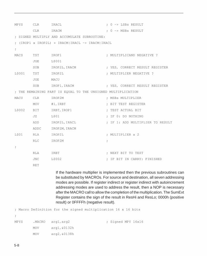
5-8
MPYS CLR IRACL ; 0 –> LSBs RESULT
CLR IRACM ; 0 –> MSBs RESULT
; SIGNED MULTIPLY AND ACCUMULATE SUBROUTINE:
; (IROP1 x IROP2L) + IRACM|IRACL –> IRACM|IRACL
;
MACS TST IROP1 ; MULTIPLICAND NEGATIVE ?
JGE L$001
SUB IROP2L,IRACM ; YES, CORRECT RESULT REGISTER
L$001 TST IROP2L ; MULTIPLIER NEGATIVE ?
JGE MACU
SUB IROP1,IRACM ; YES, CORRECT RESULT REGISTER
; THE REMAINING PART IS EQUAL TO THE UNSIGNED MULTIPLICATION
MACU CLR IROP2M ; MSBs MULTIPLIER
MOV #1,IRBT ; BIT TEST REGISTER
L$002 BIT IRBT,IROP1 ; TEST ACTUAL BIT
JZ L$01 ; IF 0: DO NOTHING
ADD IROP2L,IRACL ; IF 1: ADD MULTIPLIER TO RESULT
ADDC IROP2M,IRACM
L$01 RLA IROP2L ; MULTIPLIER x 2
RLC IROP2M ;
;
RLA IRBT ; NEXT BIT TO TEST
JNC L$002 ; IF BIT IN CARRY: FINISHED
RET
If the hardware multiplier is implemented then the previous subroutines canbe substituted by MACROs. For source and destination, all seven addressingmodes are possible. If register indirect or register indirect with autoincrementaddressing modes are used to address the result, then a NOP is necessaryafter the MACRO call to allow the completion of the multiplication. The SumExtRegister contains the sign of the result in ResHi and ResLo; 0000h (positiveresult) or 0FFFFh (negative result).
; Macro Definition for the signed multiplication 16 x 16 bits
;
MPYS .MACRO arg1,arg2 ; Signed MPY 16x16
MOV arg1,&0132h
MOV arg2,&0138h
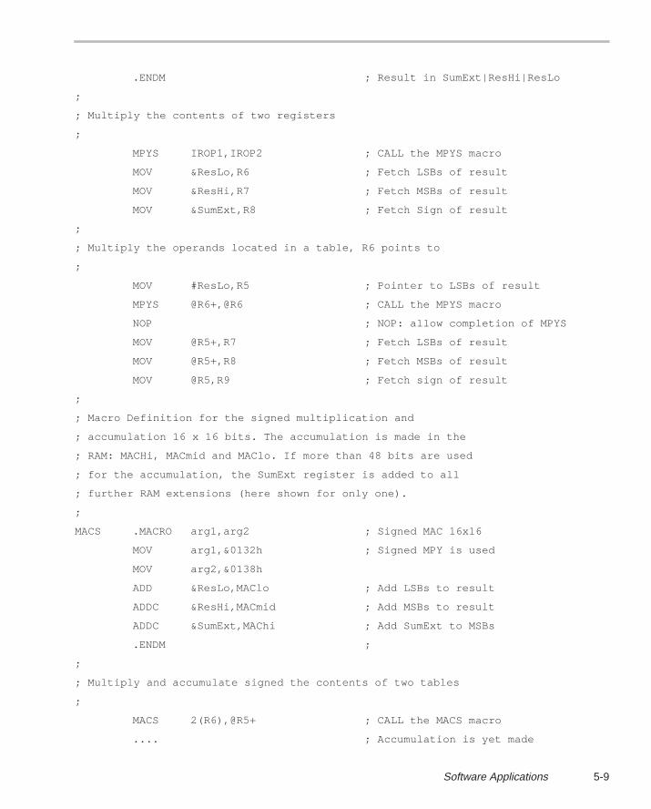
5-9Software Applications
.ENDM ; Result in SumExt|ResHi|ResLo
;
; Multiply the contents of two registers
;
MPYS IROP1,IROP2 ; CALL the MPYS macro
MOV &ResLo,R6 ; Fetch LSBs of result
MOV &ResHi,R7 ; Fetch MSBs of result
MOV &SumExt,R8 ; Fetch Sign of result
;
; Multiply the operands located in a table, R6 points to
;
MOV #ResLo,R5 ; Pointer to LSBs of result
MPYS @R6+,@R6 ; CALL the MPYS macro
NOP ; NOP: allow completion of MPYS
MOV @R5+,R7 ; Fetch LSBs of result
MOV @R5+,R8 ; Fetch MSBs of result
MOV @R5,R9 ; Fetch sign of result
;
; Macro Definition for the signed multiplication and
; accumulation 16 x 16 bits. The accumulation is made in the
; RAM: MACHi, MACmid and MAClo. If more than 48 bits are used
; for the accumulation, the SumExt register is added to all
; further RAM extensions (here shown for only one).
;
MACS .MACRO arg1,arg2 ; Signed MAC 16x16
MOV arg1,&0132h ; Signed MPY is used
MOV arg2,&0138h
ADD &ResLo,MAClo ; Add LSBs to result
ADDC &ResHi,MACmid ; Add MSBs to result
ADDC &SumExt,MAChi ; Add SumExt to MSBs
.ENDM ;
;
; Multiply and accumulate signed the contents of two tables
;
MACS 2(R6),@R5+ ; CALL the MACS macro
.... ; Accumulation is yet made
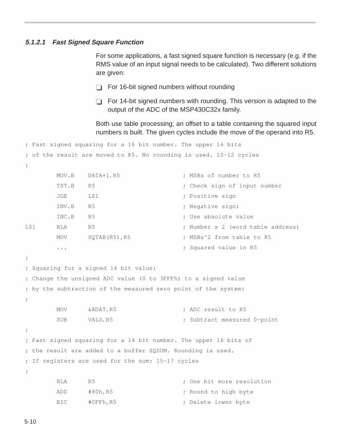
5-10
5.1.2.1 Fast Signed Square Function
For some applications, a fast signed square function is necessary (e.g. if theRMS value of an input signal needs to be calculated). Two different solutionsare given:
For 16-bit signed numbers without rounding
For 14-bit signed numbers with rounding. This version is adapted to theoutput of the ADC of the MSP430C32x family.
Both use table processing; an offset to a table containing the squared inputnumbers is built. The given cycles include the move of the operand into R5.
; Fast signed squaring for a 16 bit number. The upper 16 bits
; of the result are moved to R5. No rounding is used. 10–12 cycles
;
MOV.B DATA+1,R5 ; MSBs of number to R5
TST.B R5 ; Check sign of input number
JGE L$1 ; Positive sign
INV.B R5 ; Negative sign:
INC.B R5 ; Use absolute value
L$1 RLA R5 ; Number x 2 (word table address)
MOV SQTAB(R5),R5 ; MSBs^2 from table to R5
... ; Squared value in R5
;
; Squaring for a signed 14 bit value:
; Change the unsigned ADC value (0 to 3FFFh) to a signed value
; by the subtraction of the measured zero point of the system:
;
MOV &ADAT,R5 ; ADC result to R5
SUB VAL0,R5 ; Subtract measured 0–point
;
; Fast signed squaring for a 14 bit number. The upper 16 bits of
; the result are added to a buffer SQSUM. Rounding is used.
; If registers are used for the sum: 15–17 cycles
;
RLA R5 ; One bit more resolution
ADD #80h,R5 ; Round to high byte
BIC #0FFh,R5 ; Delete lower byte
5-11Software Applications
JGE L$1 ; Sign?
INV R5 ; Absolute value of ADC result
INC R5 ; Complement + increment
L$1 SWPB R5 ; MSBs to LSBs
RLA.B R5 ; Number x 2 (word table address)
ADD SQTAB(R5),SQSUM ; Add MSBs^2 to SQSUM
ADC SQSUM+2 ; Add carry
... ; Continue
;
; Table with squared values. Length may be adapted to the maximum
; possible input number.
;
SQTAB .word ($–SQTAB)*($–SQTAB)/4 ; 0 x 0 = 0
.word ($–SQTAB)*($–SQTAB)/4 ; 1 x 1 = 1
.word ($–SQTAB)*($–SQTAB)/4 ; 2 x 2 = 4
...
.word ($–SQTAB)*($–SQTAB)/4 ; 07Fh x 07Fh
.word ($–SQTAB)*($–SQTAB)/4 ; 080h x 080h
The errors for a single squaring are in the range of 1%. But, if rounding is usedand several squared inputs are summed-up, the resulting error gets muchsmaller. For example, if a sinusoidal input voltage is measured in distances of15, then an error of less than 0.24% results.
If the previous method is used for the measurement of RMS values, then fora decision, it usually is not necessary to calculate the square root out of theaccumulated squared inputs. It is much faster to use the accumulated valueitself .
5.1.3 Unsigned Multiplication 8 x 8-Bits
The following subroutine performs an unsigned 8 x 8-bit multiplication (labelMPYU8) or multiplication and accumulation (label MACU8). The multiplicationsubroutine clears the result register IRACL before the start. The MACU sub-routine adds the result of the multiplication to the contents of the result register.The upper bytes of IROP1 and IROP2L must be zero when the subroutine is
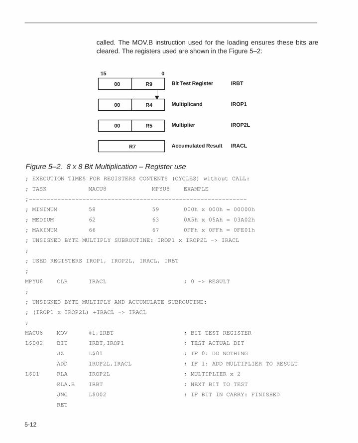
5-12
called. The MOV.B instruction used for the loading ensures these bits arecleared. The registers used are shown in the Figure 5–2:
R9
15 0
Bit Test Register
Multiplicand
Multiplier
Accumulated Result
00
R400
R500
R7
IRBT
IROP1
IROP2L
IRACL
Figure 5–2. 8 x 8 Bit Multiplication – Register use
; EXECUTION TIMES FOR REGISTERS CONTENTS (CYCLES) without CALL:
; TASK MACU8 MPYU8 EXAMPLE
;–––––––––––––––––––––––––––––––––––––––––––––––––––––––––––––
; MINIMUM 58 59 000h x 000h = 00000h
; MEDIUM 62 63 0A5h x 05Ah = 03A02h
; MAXIMUM 66 67 0FFh x 0FFh = 0FE01h
; UNSIGNED BYTE MULTIPLY SUBROUTINE: IROP1 x IROP2L –> IRACL
;
; USED REGISTERS IROP1, IROP2L, IRACL, IRBT
;
MPYU8 CLR IRACL ; 0 –> RESULT
;
; UNSIGNED BYTE MULTIPLY AND ACCUMULATE SUBROUTINE:
; (IROP1 x IROP2L) +IRACL –> IRACL
;
MACU8 MOV #1,IRBT ; BIT TEST REGISTER
L$002 BIT IRBT,IROP1 ; TEST ACTUAL BIT
JZ L$01 ; IF 0: DO NOTHING
ADD IROP2L,IRACL ; IF 1: ADD MULTIPLIER TO RESULT
L$01 RLA IROP2L ; MULTIPLIER x 2
RLA.B IRBT ; NEXT BIT TO TEST
JNC L$002 ; IF BIT IN CARRY: FINISHED
RET
5-13Software Applications
If the hardware multiplier is implemented, the previous subroutines can besubstituted by MACROs. For source and destination, all seven addressingmodes are possible. If register indirect or register indirect with autoincrementaddressing modes are used to address the result, a NOP is necessary afterthe MACRO call to allow the completion of the multiplication. If byte instruc-tions are used for loading the multiplier registers, the high byte is cleared likea CPU register.
; Macro Definition for the unsigned multiplication 8 x 8 bits
;
MPYU8 .MACRO arg1,arg2 ; Unsigned MPY 8x8
MOV.B arg1,&0130h ; 00xx to 0130h
MOV.B arg2,&0138h ; 00yy to 0138h
.ENDM ; Result in ResLo. ResHi = 0
;
; Multiply the contents of two registers (low bytes)
;
MPYU8 IROP1,IROP2L ; CALL the MPYU8 macro
MOV &ResLo,R6 ; Fetch result (16 bits)
...
;
; Macro Definition for the unsigned multiplication and
; accumulation 8 x 8 bits
;
MACU8 .MACRO arg1,arg2 ; Unsigned MAC 8x8
MOV.B arg1,&0134h ; 00xx
MOV.B arg2,&0138h ; 00yy
.ENDM ; Result in SumExt|ResHi|ResLo
;
; Multiply and accumulate the low bytes of two registers
;
MACU8 IROP1,IROP2 ; CALL the MACU8 macro
5.1.4 Signed Multiplication 8 x 8-Bits
The following subroutine performs a signed 8 x 8-bit multiplication (labelMPYS8) or multiplication and accumulation (label MACS8). The multiplicationsubroutine clears the result register IRACL before the start, the MACS8 sub-routine adds the result of the multiplication to the contents of the result register.
5-14
The register usage is the same as with the unsigned 8 x 8 multiplication. There-fore, Figure 5–2 is also valid.
The part starting with label MACU8 is the same as used with the unsigned mul-tiplication.
; EXECUTION TIMES FOR REGISTER CONTENTS (CYCLES) without CALL:
; TASK MACS8 MPYS8 EXAMPLE
;–––––––––––––––––––––––––––––––––––––––––––––––––––––––––––––
; MINIMUM 64 65 000h x 000h = 00000h
; MEDIUM 75 76 0A5h x 05Ah = 0E002h
; MAXIMUM 86 87 0FFh x 0FFh = 00001h
; SIGNED BYTE MULTIPLY SUBROUTINE: IROP1 x IROP2L –> IRACL
;
; USED REGISTERS IROP1, IROP2L, IRACL, IRBT
;
MPYS8 CLR IRACL ; 0 –> RESULT
;
; SIGNED BYTE MULTIPLY AND ACCUMULATE SUBROUTINE:
; (IROP1 x IROP2L) +IRACL –> IRACL
;
MACS8 TST.B IROP1 ; MULTIPLICAND NEGATIVE ?
JGE L$101 ; NO
SWPB IROP2L ; YES, CORRECT RESULT
SUB IROP2L,IRACL
SWPB IROP2L ; RESTORE MULTIPLICATOR
;
L$101 TST.B IROP2L ; MULTIPLICATOR NEGATIVE ?
JGE MACU8
SWPB IROP1 ; YES, CORRECT RESULT
SUB IROP1,IRACL
SWPB IROP1
;
; THE REMAINING PART IS THE UNSIGNED MULTIPLICATION
;
MACU8 MOV #1,IRBT ; BIT TEST REGISTER
L$002 BIT IRBT,IROP1 ; TEST ACTUAL BIT
5-15Software Applications
JZ L$01 ; IF 0: DO NOTHING
ADD IROP2L,IRACL ; IF 1: ADD MULTIPLIER TO RESULT
L$01 RLA IROP2L ; MULTIPLIER x 2
RLA.B IRBT ; NEXT BIT TO TEST
JNC L$002 ; IF BIT IN CARRY: FINISHED
RET
If the hardware multiplier is implemented, the previous subroutines can besubstituted by MACROs. For source and destination, all seven addressingmodes are possible. If register indirect or register indirect with autoincrementaddressing modes are used to address the result, a NOP is necessary afterthe MACRO call to allow the completion of the multiplication. If byte instruc-tions are used for loading the multiplier registers, the high byte is cleared likea CPU register.
; Macro Definition for the signed multiplication 8 x 8 bits
;
MPYS8 .MACRO arg1,arg2 ; Signed MPY 8x8
MOV.B arg1,&0132h ; 00xx
SXT &0132h ; Extend sign: 00xx or FFxx
MOV.B arg2,&0138h ; 00yy
SXT &0138h ; Extend sign: 00yy or FFyy
.ENDM ; Result in SumExt|ResHi|ResLo
;
; Multiply the contents of two registers signed (low bytes)
;
MPYS8 IROP1,IROP2 ; CALL the MPYS8 macro
MOV &ResLo,R6 ; Fetch result (16 bits)
MOV &ResHi,R7 ; Only sign: 0000 or FFFF
;
; Macro Definition for the signed multiplication and
; accumulation 8 x 8 bits. The accumulation is made in the
; RAM: MACHi, MACmid and MAClo. If more than 48 bits are used
; for the accumulation, the SumExt register is added to all
; further RAM extensions
;
MACS8 .MACRO arg1,arg2 ; Signed MAC 8x8
MOV.B arg1,&0132h ; MPYS is used
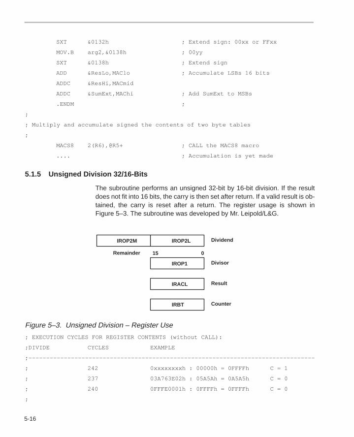
5-16
SXT &0132h ; Extend sign: 00xx or FFxx
MOV.B arg2,&0138h ; 00yy
SXT &0138h ; Extend sign
ADD &ResLo,MAClo ; Accumulate LSBs 16 bits
ADDC &ResHi,MACmid
ADDC &SumExt,MAChi ; Add SumExt to MSBs
.ENDM ;
;
; Multiply and accumulate signed the contents of two byte tables
;
MACS8 2(R6),@R5+ ; CALL the MACS8 macro
.... ; Accumulation is yet made
5.1.5 Unsigned Division 32/16-Bits
The subroutine performs an unsigned 32-bit by 16-bit division. If the resultdoes not fit into 16 bits, the carry is then set after return. If a valid result is ob-tained, the carry is reset after a return. The register usage is shown inFigure 5–3. The subroutine was developed by Mr. Leipold/L&G.
IROP1
15 0
IRACL
IRBT
Divisor
Result
Counter
IROP2LIROP2M Dividend
Remainder
Figure 5–3. Unsigned Division – Register Use
; EXECUTION CYCLES FOR REGISTER CONTENTS (without CALL):
;DIVIDE CYCLES EXAMPLE
;–––––––––––––––––––––––––––––––––––––––––––––––––––––––––––––––––––––––––––––––––
; 242 0xxxxxxxxh : 00000h = 0FFFFh C = 1
; 237 03A763E02h : 05A5Ah = 0A5A5h C = 0
; 240 0FFFE0001h : 0FFFFh = 0FFFFh C = 0
;
5-17Software Applications
; USED REGISTERS IROP1, IROP2L, IRACL, IRBT, IROP2M
;
; UNSIGNED DIVISION SUBROUTINE 32–BIT BY 16–BIT
; IROP2M|IROP2L : IROP1 –> IRACL REMAINDER IN IROP2M
; RETURN: CARRY = 0: OK CARRY = 1: QUOTIENT > 16 BITS
;
DIVIDE CLR IRACL ; CLEAR RESULT
MOV #17,IRBT ; INITIALIZE LOOP COUNTER
DIV1 CMP IROP1,IROP2M ;
JLO DIV2
SUB IROP1,IROP2M
DIV2 RLC IRACL
JC DIV4 ; Error: result > 16 bits
DEC IRBT ; Decrement loop counter
JZ DIV3 ; Is 0: terminate w/o error
RLA IROP2L
RLC IROP2M
JNC DIV1
SUB IROP1,IROP2M
SETC
JMP DIV2
DIV3 CLRC ; No error, C = 0
DIV4 RET ; Error indication in C
A 32-bit divided by 32-bit numbers (XDIV) is given in the square root section.
5.1.6 Signed Division 32/16-Bits
The subroutine performs a signed 32-bit by 16-bit division. If the result doesnot fit into 16 bits, the carry is then set after a return. If a valid result is obtained,the carry is reset after a return. The register IRACM contains the extended sign(0000h or 0FFFFh) of the signed result in IRACL. The register usage is shownin the Figure 5–4:
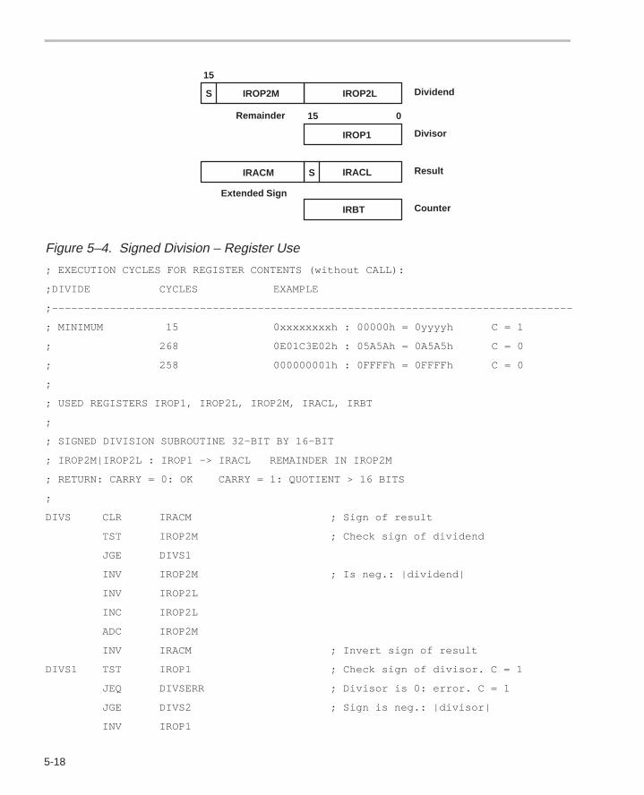
5-18
IROP1
15 0
IRACL
IRBT
Divisor
Result
Counter
IROP2LIROP2M Dividend
Remainder
S
IRACM S
15
Extended Sign
Figure 5–4. Signed Division – Register Use
; EXECUTION CYCLES FOR REGISTER CONTENTS (without CALL):
;DIVIDE CYCLES EXAMPLE
;–––––––––––––––––––––––––––––––––––––––––––––––––––––––––––––––––––––––––––––––––
; MINIMUM 15 0xxxxxxxxh : 00000h = 0yyyyh C = 1
; 268 0E01C3E02h : 05A5Ah = 0A5A5h C = 0
; 258 000000001h : 0FFFFh = 0FFFFh C = 0
;
; USED REGISTERS IROP1, IROP2L, IROP2M, IRACL, IRBT
;
; SIGNED DIVISION SUBROUTINE 32–BIT BY 16–BIT
; IROP2M|IROP2L : IROP1 –> IRACL REMAINDER IN IROP2M
; RETURN: CARRY = 0: OK CARRY = 1: QUOTIENT > 16 BITS
;
DIVS CLR IRACM ; Sign of result
TST IROP2M ; Check sign of dividend
JGE DIVS1
INV IROP2M ; Is neg.: |dividend|
INV IROP2L
INC IROP2L
ADC IROP2M
INV IRACM ; Invert sign of result
DIVS1 TST IROP1 ; Check sign of divisor. C = 1
JEQ DIVSERR ; Divisor is 0: error. C = 1
JGE DIVS2 ; Sign is neg.: |divisor|
INV IROP1
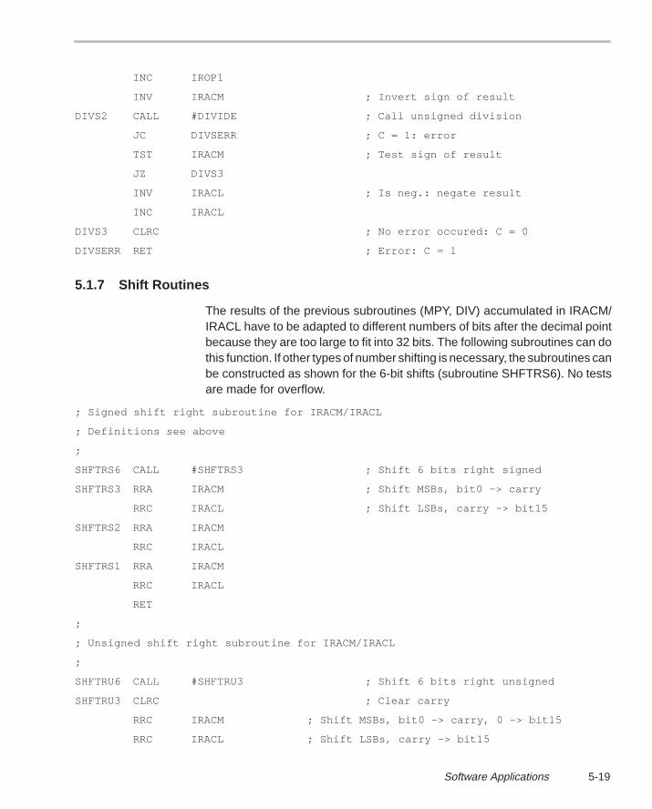
5-19Software Applications
INC IROP1
INV IRACM ; Invert sign of result
DIVS2 CALL #DIVIDE ; Call unsigned division
JC DIVSERR ; C = 1: error
TST IRACM ; Test sign of result
JZ DIVS3
INV IRACL ; Is neg.: negate result
INC IRACL
DIVS3 CLRC ; No error occured: C = 0
DIVSERR RET ; Error: C = 1
5.1.7 Shift Routines
The results of the previous subroutines (MPY, DIV) accumulated in IRACM/IRACL have to be adapted to different numbers of bits after the decimal pointbecause they are too large to fit into 32 bits. The following subroutines can dothis function. If other types of number shifting is necessary, the subroutines canbe constructed as shown for the 6-bit shifts (subroutine SHFTRS6). No testsare made for overflow.
; Signed shift right subroutine for IRACM/IRACL
; Definitions see above
;
SHFTRS6 CALL #SHFTRS3 ; Shift 6 bits right signed
SHFTRS3 RRA IRACM ; Shift MSBs, bit0 –> carry
RRC IRACL ; Shift LSBs, carry –> bit15
SHFTRS2 RRA IRACM
RRC IRACL
SHFTRS1 RRA IRACM
RRC IRACL
RET
;
; Unsigned shift right subroutine for IRACM/IRACL
;
SHFTRU6 CALL #SHFTRU3 ; Shift 6 bits right unsigned
SHFTRU3 CLRC ; Clear carry
RRC IRACM ; Shift MSBs, bit0 –> carry, 0 –> bit15
RRC IRACL ; Shift LSBs, carry –> bit15

5-20
SHFTRU2 CLRC
RRC IRACM
RRC IRACL
SHFTRU1 CLRC
RRC IRACM
RRC IRACL
RET
;
; Signed/unsigned shift left subroutine for IRACM/IRACL
;
SHFTL6 CALL #SHFTL3 ; Shift 6 bits left
SHFTL3 RLA IRACL ; Shift LSBs, bit0 –> carry
RLC IRACM ; Shift MSBs, carry –> bit15
SHFTL2 RLA IRACL
RLC IRACM
SHFTL1 RLA IRACL
RLC IRACM
RET
5.1.8 Square Root Routines
The square root of a number is often needed in computations. Two differentmethods are given:
A very fast method for 32-bit integer numbers
A normal method for 32-bit numbers that can have a fractional part
5.1.8.1 Square Root for 32-Bit Integer Numbers
The square root of a 30-bit integer number is calculated. The result contains15 correct fractional bits. The subroutine uses the method known from the find-ing of a square root by hand. This method is much faster than the widely knownNEWTONIAN method and only 720 cycles are needed. This subroutine wasdeveloped by Jürg Müller Software–Art GmbH/Zurich. The C program codeneeded is also shown:
unsigned long y, h;
int i;
h = x;
x = y = 0;
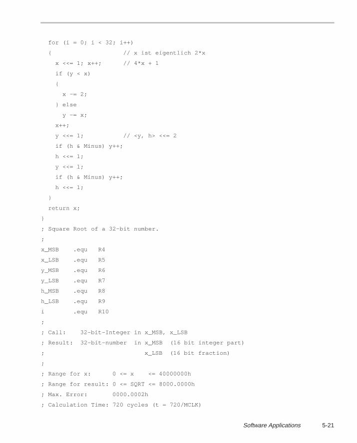
5-21Software Applications
for (i = 0; i < 32; i++)
// x ist eigentlich 2*x
x <<= 1; x++; // 4*x + 1
if (y < x)
x –= 2;
else
y –= x;
x++;
y <<= 1; // <y, h> <<= 2
if (h & Minus) y++;
h <<= 1;
y <<= 1;
if (h & Minus) y++;
h <<= 1;
return x;
; Square Root of a 32–bit number.
;
x_MSB .equ R4
x_LSB .equ R5
y_MSB .equ R6
y_LSB .equ R7
h_MSB .equ R8
h_LSB .equ R9
i .equ R10
;
; Call: 32–bit–Integer in x_MSB, x_LSB
; Result: 32–bit–number in x_MSB (16 bit integer part)
; x_LSB (16 bit fraction)
;
; Range for x: 0 <= x <= 40000000h
; Range for result: 0 <= SQRT <= 8000.0000h
; Max. Error: 0000.0002h
; Calculation Time: 720 cycles (t = 720/MCLK)
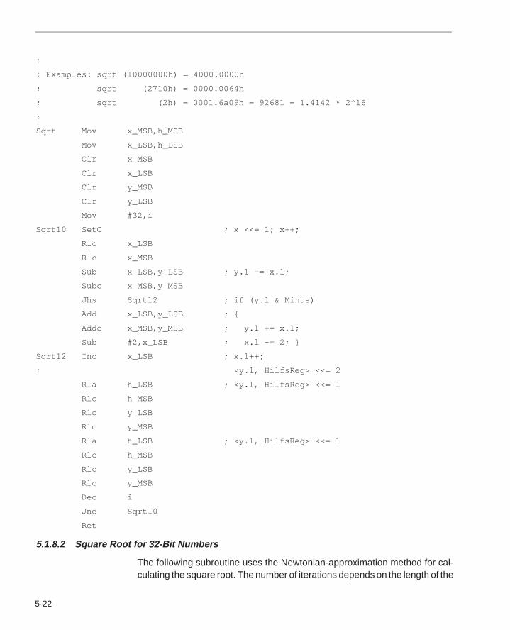
5-22
;
; Examples: sqrt (10000000h) = 4000.0000h
; sqrt (2710h) = 0000.0064h
; sqrt (2h) = 0001.6a09h = 92681 = 1.4142 * 2^16
;
Sqrt Mov x_MSB,h_MSB
Mov x_LSB,h_LSB
Clr x_MSB
Clr x_LSB
Clr y_MSB
Clr y_LSB
Mov #32,i
Sqrt10 SetC ; x <<= 1; x++;
Rlc x_LSB
Rlc x_MSB
Sub x_LSB,y_LSB ; y.l –= x.l;
Subc x_MSB,y_MSB
Jhs Sqrt12 ; if (y.l & Minus)
Add x_LSB,y_LSB ;
Addc x_MSB,y_MSB ; y.l += x.l;
Sub #2,x_LSB ; x.l –= 2;
Sqrt12 Inc x_LSB ; x.l++;
; <y.l, HilfsReg> <<= 2
Rla h_LSB ; <y.l, HilfsReg> <<= 1
Rlc h_MSB
Rlc y_LSB
Rlc y_MSB
Rla h_LSB ; <y.l, HilfsReg> <<= 1
Rlc h_MSB
Rlc y_LSB
Rlc y_MSB
Dec i
Jne Sqrt10
Ret
5.1.8.2 Square Root for 32-Bit Numbers
The following subroutine uses the Newtonian-approximation method for cal-culating the square root. The number of iterations depends on the length of the
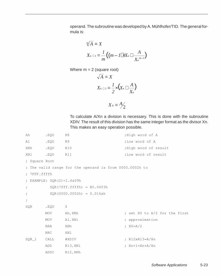
5-23Software Applications
operand. The subroutine was developed by A. Mühlhofer/TID. The general for-mula is:
( )
A X
X1
mm 1 X
A
X
m
n 1 nm 1
n
=
= – × +( )+–
Where m = 2 (square root)
A X
X1
2X
A
Xn 1 n
n
=
= × +( )+
X A0 2=
To calculate A/Xn a division is necessary. This is done with the subroutineXDIV. The result of this division has the same integer format as the divisor Xn.This makes an easy operation possible.
Ah .EQU R8 ;High word of A
Al .EQU R9 ;Low word of A
XNh .EQU R10 ;High word of result
XNl .EQU R11 ;Low word of result
; Square Root
; The valid range for the operand is from 0000.0002h to
; 7FFF.ffffh
; EXAMPLE: SQR(2)=1.6a09h
; SQR(7fff.ffffh) = B5.04f3h
; SQR(0000.0002h) = 0.016ah
;
SQR .EQU $
MOV Ah,XNh ; set X0 to A/2 for the first
MOV Al,XNl ; approximation
RRA XNh ; X0=A/2
RRC XNl
SQR_1 CALL #XDIV ; R12xR13=A/Xn
ADD R13,XNl ; Xn+1=Xn+A/Xn
ADDC R12,XNh
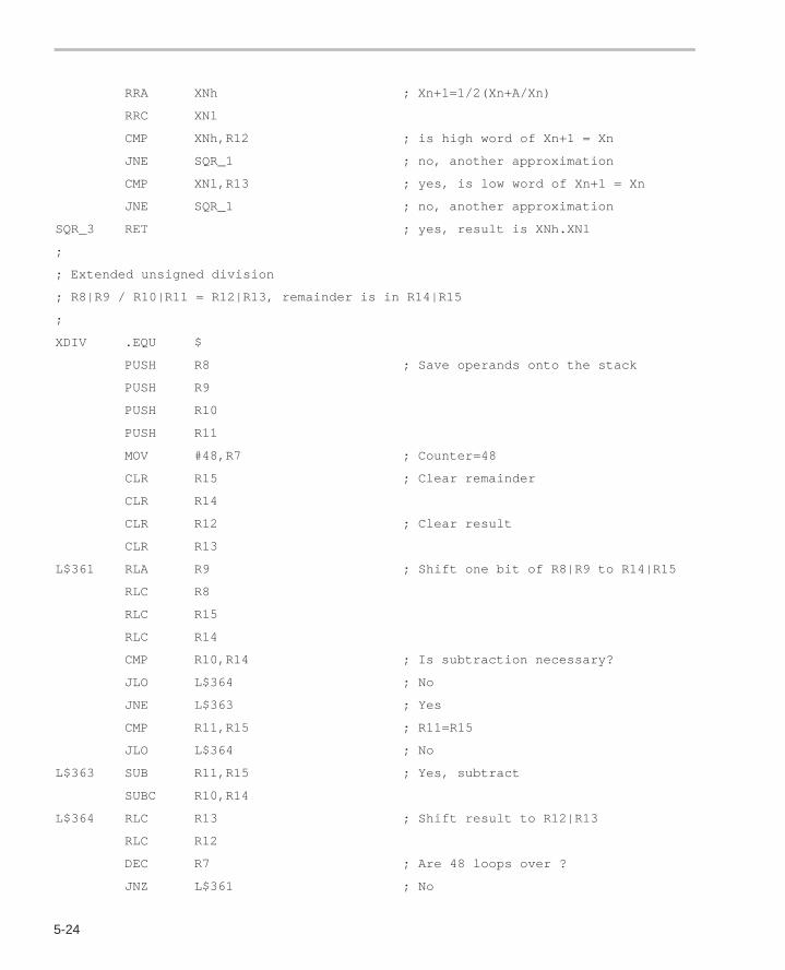
5-24
RRA XNh ; Xn+1=1/2(Xn+A/Xn)
RRC XNl
CMP XNh,R12 ; is high word of Xn+1 = Xn
JNE SQR_1 ; no, another approximation
CMP XNl,R13 ; yes, is low word of Xn+1 = Xn
JNE SQR_1 ; no, another approximation
SQR_3 RET ; yes, result is XNh.XNl
;
; Extended unsigned division
; R8|R9 / R10|R11 = R12|R13, remainder is in R14|R15
;
XDIV .EQU $
PUSH R8 ; Save operands onto the stack
PUSH R9
PUSH R10
PUSH R11
MOV #48,R7 ; Counter=48
CLR R15 ; Clear remainder
CLR R14
CLR R12 ; Clear result
CLR R13
L$361 RLA R9 ; Shift one bit of R8|R9 to R14|R15
RLC R8
RLC R15
RLC R14
CMP R10,R14 ; Is subtraction necessary?
JLO L$364 ; No
JNE L$363 ; Yes
CMP R11,R15 ; R11=R15
JLO L$364 ; No
L$363 SUB R11,R15 ; Yes, subtract
SUBC R10,R14
L$364 RLC R13 ; Shift result to R12|R13
RLC R12
DEC R7 ; Are 48 loops over ?
JNZ L$361 ; No
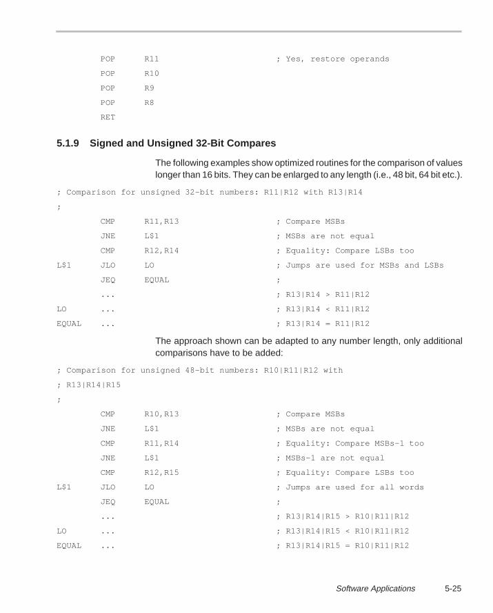
5-25Software Applications
POP R11 ; Yes, restore operands
POP R10
POP R9
POP R8
RET
5.1.9 Signed and Unsigned 32-Bit Compares
The following examples show optimized routines for the comparison of valueslonger than 16 bits. They can be enlarged to any length (i.e., 48 bit, 64 bit etc.).
; Comparison for unsigned 32–bit numbers: R11|R12 with R13|R14
;
CMP R11,R13 ; Compare MSBs
JNE L$1 ; MSBs are not equal
CMP R12,R14 ; Equality: Compare LSBs too
L$1 JLO LO ; Jumps are used for MSBs and LSBs
JEQ EQUAL ;
... ; R13|R14 > R11|R12
LO ... ; R13|R14 < R11|R12
EQUAL ... ; R13|R14 = R11|R12
The approach shown can be adapted to any number length, only additionalcomparisons have to be added:
; Comparison for unsigned 48–bit numbers: R10|R11|R12 with
; R13|R14|R15
;
CMP R10,R13 ; Compare MSBs
JNE L$1 ; MSBs are not equal
CMP R11,R14 ; Equality: Compare MSBs–1 too
JNE L$1 ; MSBs–1 are not equal
CMP R12,R15 ; Equality: Compare LSBs too
L$1 JLO LO ; Jumps are used for all words
JEQ EQUAL ;
... ; R13|R14|R15 > R10|R11|R12
LO ... ; R13|R14|R15 < R10|R11|R12
EQUAL ... ; R13|R14|R15 = R10|R11|R12
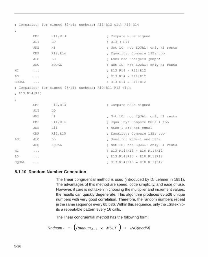
5-26
; Comparison for signed 32–bit numbers: R11|R12 with R13|R14
;
CMP R11,R13 ; Compare MSBs signed
JLT LO ; R13 < R11
JNE HI ; Not LO, not EQUAL: only HI rests
CMP R12,R14 ; Equality: Compare LSBs too
JLO LO ; LSBs use unsigned jumps!
JEQ EQUAL ; Not LO, not EQUAL: only HI rests
HI ... ; R13|R14 > R11|R12
LO ... ; R13|R14 < R11|R12
EQUAL ... ; R13|R14 = R11|R12
; Comparison for signed 48–bit numbers: R10|R11|R12 with
; R13|R14|R15
;
CMP R10,R13 ; Compare MSBs signed
JLT LO
JNE HI ; Not LO, not EQUAL: only HI rests
CMP R11,R14 ; Equality: Compare MSBs–1 too
JNE L$1 ; MSBs–1 are not equal
CMP R12,R15 ; Equality: Compare LSBs too
L$1 JLO LO ; Used for MSBs–1 and LSBs
JEQ EQUAL ; Not LO, not EQUAL: only HI rests
HI ... ; R13|R14|R15 > R10|R11|R12
LO ... ; R13|R14|R15 < R10|R11|R12
EQUAL ... ; R13|R14|R15 = R10|R11|R12
5.1.10 Random Number Generation
The linear congruential method is used (introduced by D. Lehmer in 1951).The advantages of this method are speed, code simplicity, and ease of use.However, if care is not taken in choosing the multiplier and increment values,the results can quickly degenerate. This algorithm produces 65,536 uniquenumbers with very good correlation. Therefore, the random numbers repeatin the same sequence every 65,536. Within this sequence, only the LSB exhib-its a repeatable pattern every 16 calls.
The linear congruential method has the following form:
Rndnum Rndnum MULT INC(modM)n n 1= ×( ) +–

5-27Software Applications
Where:Rndnumn Current random numberRndnumn–1 Previous random numberMULT Multiplier (unique constant)INC Increment (unique constant)M Modulus (word width of MSP430 = 16 bits = 64K)
Many hours of research have been done to identify the optimal choices for theconstants MULT and INC. The constant used in this implementation are basedon this research. If changes are made to these numbers, extreme care mustbe taken to avoid degeneration. The following text is a more detailed look atthe algorithm and the numbers used:
M: M is the modulus value and is typically defined by the word width of theprocessor. The linear congruential algorithm returns a random number be-tween 0 and 65,536 and is NOT internally bounded. If the user requiresa min/max limit, this must be coded externally to this routine. The resultis not actually divided by 65,536. The result register is allowed to overflow,thus implementing the modulus.
SEED: The first random number in the sequence is called the seed value.This is an arbitrary constant between 0 and 64K. Zero can be used. Thisis OK if the code is allowed 3 calls to warm up before the numbers are con-sidered valid. The number 21,845 was used in this implementation be-cause it is 1/3 of the modulus (65,536).
MULT: Based on random number theory, this number should be chosensuch that the last three digits are even–2–1(such as xx821, x421, etc.).The number 31,821 was used in this implementation.
The generator is extremely sensitive to the choice of this constant!
INC: In general, this constant can be any prime number related to M. Twovalues were actually tested in this implementation: 1 and 13,849. Re-search shows that INC should be chosen based on the following formula:
INC1
2
1
63 M= – ×( )( )×
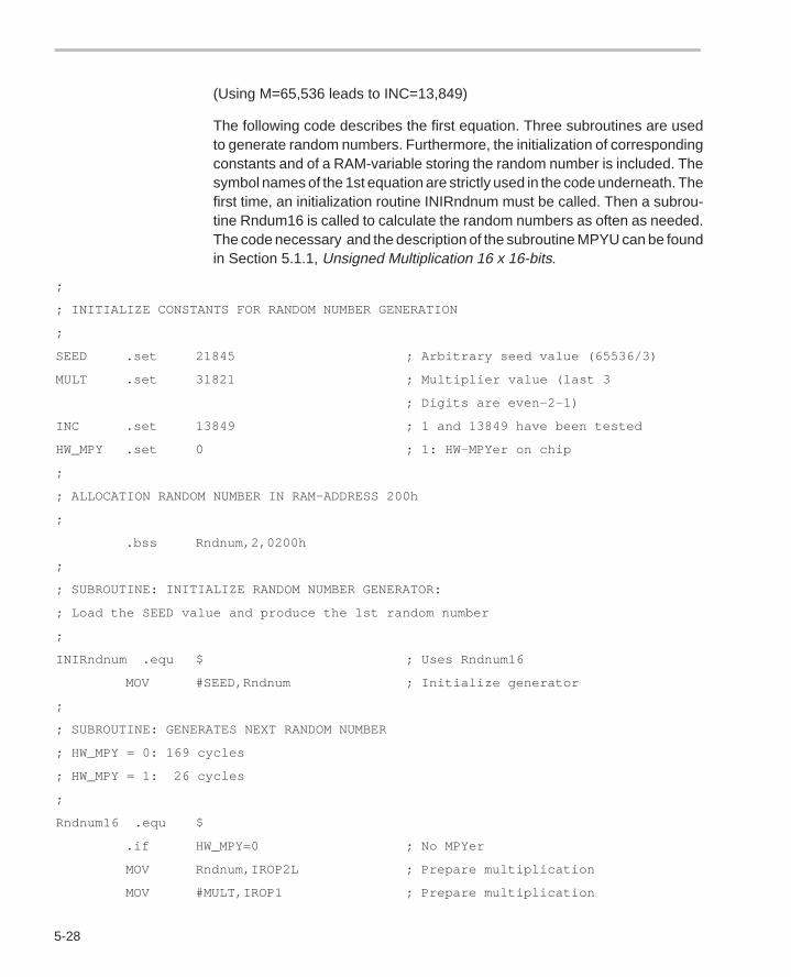
5-28
(Using M=65,536 leads to INC=13,849)
The following code describes the first equation. Three subroutines are usedto generate random numbers. Furthermore, the initialization of correspondingconstants and of a RAM-variable storing the random number is included. Thesymbol names of the 1st equation are strictly used in the code underneath. Thefirst time, an initialization routine INIRndnum must be called. Then a subrou-tine Rndum16 is called to calculate the random numbers as often as needed.The code necessary and the description of the subroutine MPYU can be foundin Section 5.1.1, Unsigned Multiplication 16 x 16-bits.
;
; INITIALIZE CONSTANTS FOR RANDOM NUMBER GENERATION
;
SEED .set 21845 ; Arbitrary seed value (65536/3)
MULT .set 31821 ; Multiplier value (last 3
; Digits are even–2–1)
INC .set 13849 ; 1 and 13849 have been tested
HW_MPY .set 0 ; 1: HW–MPYer on chip
;
; ALLOCATION RANDOM NUMBER IN RAM–ADDRESS 200h
;
.bss Rndnum,2,0200h
;
; SUBROUTINE: INITIALIZE RANDOM NUMBER GENERATOR:
; Load the SEED value and produce the 1st random number
;
INIRndnum .equ $ ; Uses Rndnum16
MOV #SEED,Rndnum ; Initialize generator
;
; SUBROUTINE: GENERATES NEXT RANDOM NUMBER
; HW_MPY = 0: 169 cycles
; HW_MPY = 1: 26 cycles
;
Rndnum16 .equ $
.if HW_MPY=0 ; No MPYer
MOV Rndnum,IROP2L ; Prepare multiplication
MOV #MULT,IROP1 ; Prepare multiplication
5-29Software Applications
CALL #MPYU ; Call unsigned MPY (5.1.1)
ADD #INC,IRACL ; Add INC to low word of product
;
; Overwrite old random number with low word of new product
;
MOV IRACL,Rndnum ; Result to Rndnum and IRACL
.else ; HW MPYer on chip
MPYU Rndnum,#MULT ; Rndnum x MULT
MOV &ResLo,Rndnum ; Low word of product
ADD #INC,Rndnum ; Add INC to low word
.endif
RET ; Random number in Rndnum
EXAMPLE: Use of the Random Generator (1st call and succeeding calls).
;
; First call: produce the 1st random number
;
CALL #INIRndum ; Initialize generator
....
; Second and all other calls to get the next random number
;
CALL #Rndnum16 ; Next random number to register
.... ; IRACL and location Rndnum
Algorithm from TMS320DSP Designer’s Notebook Number 43 Random Num-ber Generation on a TMS320C5x. 7/94
5.1.11 Rules for the Integer Subroutines
Despite the fact that the subroutines shown previously can only handle integernumbers, it is possible to use numbers with fractional parts. It is necessary onlyto define for each number where the virtual decimal point is located. Relativelysimple rules define where the decimal point is located for the result.
For calculations with the integer subroutines, it is almost impossible to remem-ber where the virtual decimal point is located. It is good programming practiceto indicate in the comment part of the software listing where the decimal pointis currently located. The indication can have the following form:
N.M
whereN Worst-case bit count of integer part (allows additional assessments)M Number of bits after the virtual decimal point
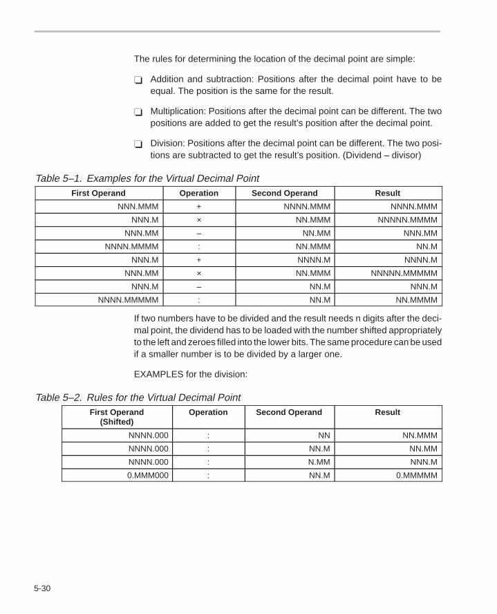
5-30
The rules for determining the location of the decimal point are simple:
Addition and subtraction: Positions after the decimal point have to beequal. The position is the same for the result.
Multiplication: Positions after the decimal point can be different. The twopositions are added to get the result’s position after the decimal point.
Division: Positions after the decimal point can be different. The two posi-tions are subtracted to get the result’s position. (Dividend – divisor)
Table 5–1. Examples for the Virtual Decimal PointFirst Operand Operation Second Operand Result
NNN.MMM + NNNN.MMM NNNN.MMM
NNN.M × NN.MMM NNNNN.MMMM
NNN.MM – NN.MM NNN.MM
NNNN.MMMM : NN.MMM NN.M
NNN.M + NNNN.M NNNN.M
NNN.MM × NN.MMM NNNNN.MMMMM
NNN.M – NN.M NNN.M
NNNN.MMMMM : NN.M NN.MMMM
If two numbers have to be divided and the result needs n digits after the deci-mal point, the dividend has to be loaded with the number shifted appropriatelyto the left and zeroes filled into the lower bits. The same procedure can be usedif a smaller number is to be divided by a larger one.
EXAMPLES for the division:
Table 5–2. Rules for the Virtual Decimal PointFirst Operand
(Shifted)Operation Second Operand Result
NNNN.000 : NN NN.MMM
NNNN.000 : NN.M NN.MM
NNNN.000 : N.MM NNN.M
0.MMM000 : NN.M 0.MMMMM
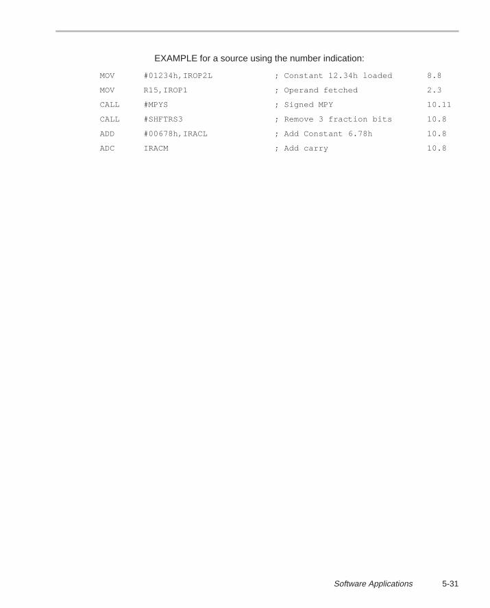
5-31Software Applications
EXAMPLE for a source using the number indication:
MOV #01234h,IROP2L ; Constant 12.34h loaded 8.8
MOV R15,IROP1 ; Operand fetched 2.3
CALL #MPYS ; Signed MPY 10.11
CALL #SHFTRS3 ; Remove 3 fraction bits 10.8
ADD #00678h,IRACL ; Add Constant 6.78h 10.8
ADC IRACM ; Add carry 10.8
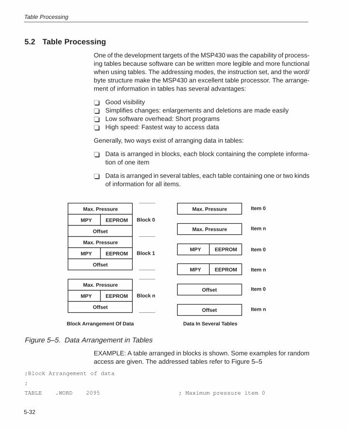
Table Processing
5-32
5.2 Table Processing
One of the development targets of the MSP430 was the capability of process-ing tables because software can be written more legible and more functionalwhen using tables. The addressing modes, the instruction set, and the word/byte structure make the MSP430 an excellent table processor. The arrange-ment of information in tables has several advantages:
Good visibility Simplifies changes: enlargements and deletions are made easily Low software overhead: Short programs High speed: Fastest way to access data
Generally, two ways exist of arranging data in tables:
Data is arranged in blocks, each block containing the complete informa-tion of one item
Data is arranged in several tables, each table containing one or two kindsof information for all items.
Max. Pressure
EEPROMMPY
Offset
Item 0
Max. Pressure Item n
Item n
EEPROMMPY Item 0
Offset Item n
Item 0
Max. Pressure
EEPROMMPY
Offset
Max. Pressure
EEPROMMPY
Offset
Max. Pressure
EEPROMMPY
Offset
Block 0
Block 1
Block n
Data In Several TablesBlock Arrangement Of Data
Figure 5–5. Data Arrangement in Tables
EXAMPLE: A table arranged in blocks is shown. Some examples for randomaccess are given. The addressed tables refer to Figure 5–5
;Block Arrangement of data
;
TABLE .WORD 2095 ; Maximum pressure item 0
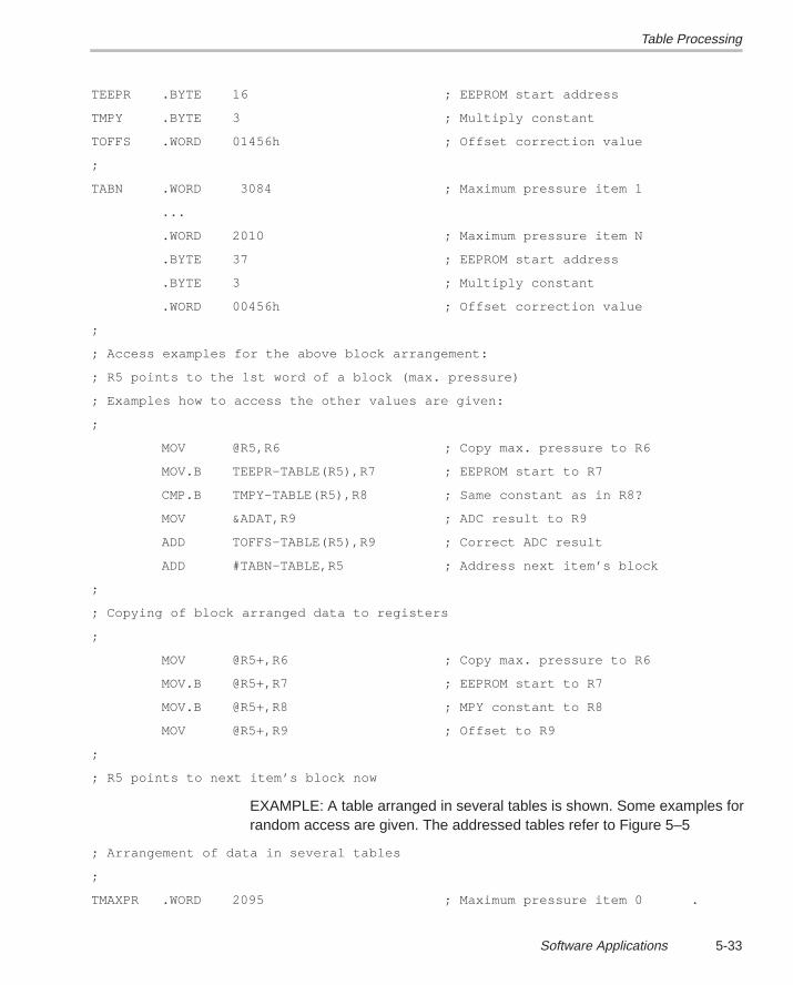
Table Processing
5-33Software Applications
TEEPR .BYTE 16 ; EEPROM start address
TMPY .BYTE 3 ; Multiply constant
TOFFS .WORD 01456h ; Offset correction value
;
TABN .WORD 3084 ; Maximum pressure item 1
...
.WORD 2010 ; Maximum pressure item N
.BYTE 37 ; EEPROM start address
.BYTE 3 ; Multiply constant
.WORD 00456h ; Offset correction value
;
; Access examples for the above block arrangement:
; R5 points to the 1st word of a block (max. pressure)
; Examples how to access the other values are given:
;
MOV @R5,R6 ; Copy max. pressure to R6
MOV.B TEEPR–TABLE(R5),R7 ; EEPROM start to R7
CMP.B TMPY–TABLE(R5),R8 ; Same constant as in R8?
MOV &ADAT,R9 ; ADC result to R9
ADD TOFFS–TABLE(R5),R9 ; Correct ADC result
ADD #TABN–TABLE,R5 ; Address next item’s block
;
; Copying of block arranged data to registers
;
MOV @R5+,R6 ; Copy max. pressure to R6
MOV.B @R5+,R7 ; EEPROM start to R7
MOV.B @R5+,R8 ; MPY constant to R8
MOV @R5+,R9 ; Offset to R9
;
; R5 points to next item’s block now
EXAMPLE: A table arranged in several tables is shown. Some examples forrandom access are given. The addressed tables refer to Figure 5–5
; Arrangement of data in several tables
;
TMAXPR .WORD 2095 ; Maximum pressure item 0 .
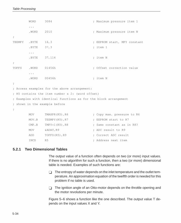
Table Processing
5-34
WORD 3084 ; Maximum pressure item 1
...
.WORD 2010 ; Maximum pressure item N
;
TEEMPY .BYTE 16,3 ; EEPROM start, MPY constant
.BYTE 37,3 ; item 1
...
.BYTE 37,114 ; item N
;
TOFFS .WORD 01456h ; Offset correction value
...
.WORD 00456h ; item N
;
; Access examples for the above arrangement:
; R5 contains the item number x 2: (word offset)
; Examples with identical functions as for the block arrangement
; shown in the example before
;
MOV TMAXPR(R5),R6 ; Copy max. pressure to R6
MOV.B TEEMPY(R5),R7 ; EEPROM start to R7
CMP.B TMPY+1(R5),R8 ; Same constant as in R8?
MOV &ADAT,R9 ; ADC result to R9
ADD TOFFS(R5),R9 ; Correct ADC result
INCD R5 ; Address next item
5.2.1 Two Dimensional Tables
The output value of a function often depends on two (or more) input values.If there is no algorithm for such a function, then a two (or more) dimensionaltable is needed. Examples of such functions are:
The entropy of water depends on the inlet temperature and the outlet tem-perature. An approximation equation of the twelfth order is needed for thisproblem if no table is used.
The ignition angle of an Otto-motor depends on the throttle opening andthe motor revolutions per minute.
Figure 5–6 shows a function like the one described. The output value T de-pends on the input values X and Y.
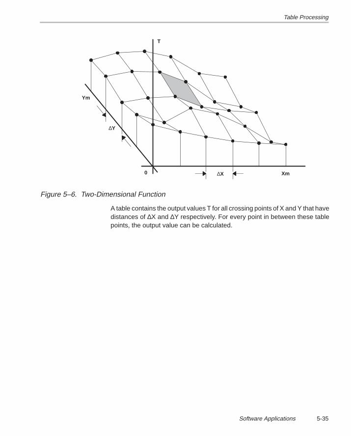
Table Processing
5-35Software Applications
T
Ym
∆Y
0 ∆X Xm
Figure 5–6. Two-Dimensional Function
A table contains the output values T for all crossing points of X and Y that havedistances of ∆X and ∆Y respectively. For every point in between these tablepoints, the output value can be calculated.
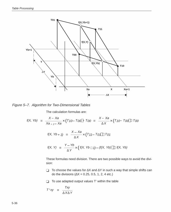
Table Processing
5-36
∆Y
Yb
Y
Yb+1
T01
T00
f(X,Yb+1)
T11
f(X,Y)
f(X,Yb)T10
Xa X Xa+1
∆X
Figure 5–7. Algorithm for Two-Dimensional Tables
The calculation formulas are:
( ) ( )f(X, Yb)X Xa
Xa XaT T T
X Xa
XT T T
110 00 00 10 00 00=
–
–× – + =
–× – +
+ ∆
( )f(X, Yb )X Xa
XT T T1 11 01 01+ = – × – +
∆
( )f(X, Y)Y Yb
Yf(X, Yb ) (f(X, Yb) f(X, Yb)1= – × – ++
∆
These formulas need division. There are two possible ways to avoid the divi-sion:
To choose the values for ∆X and ∆Y in such a way that simple shifts cando the divisions (∆X = 0.25, 0.5, 1, 2, 4 etc.)
To use adapted output values T’ within the table
T xyTxy
X Y’ =
∆ ∆
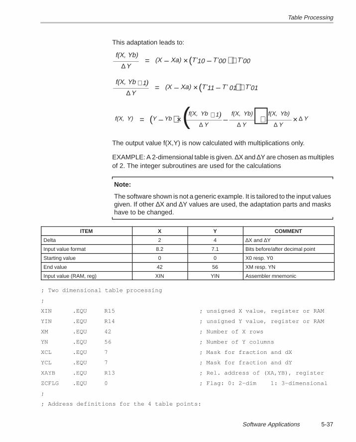
Table Processing
5-37Software Applications
This adaptation leads to:
( )f(X, Yb)
Y(X Xa) T’ T’ T’10 00 00
∆= – × – +
( )f(X, Yb )
Y(X Xa) T’ T’ T’
111 01 01
+ = – × – +∆
( )f(X, Y) Y Ybf(X, Yb )
Y
f(X, Yb)
Y
f(X, Yb)
YY
1= – × –( )+ ×+
∆ ∆ ∆∆
The output value f(X,Y) is now calculated with multiplications only.
EXAMPLE: A 2-dimensional table is given. ∆X and ∆Y are chosen as multiplesof 2. The integer subroutines are used for the calculations
Note:
The software shown is not a generic example. It is tailored to the input valuesgiven. If other ∆X and ∆Y values are used, the adaptation parts and maskshave to be changed.
ITEM X Y COMMENT
Delta 2 4 ∆X and ∆Y
Input value format 8.2 7.1 Bits before/after decimal point
Starting value 0 0 X0 resp. Y0
End value 42 56 XM resp. YN
Input value (RAM, reg) XIN YIN Assembler mnemonic
; Two dimensional table processing
;
XIN .EQU R15 ; unsigned X value, register or RAM
YIN .EQU R14 ; unsigned Y value, register or RAM
XM .EQU 42 ; Number of X rows
YN .EQU 56 ; Number of Y columns
XCL .EQU 7 ; Mask for fraction and dX
YCL .EQU 7 ; Mask for fraction and dY
XAYB .EQU R13 ; Rel. address of (XA,YB), register
ZCFLG .EQU 0 ; Flag: 0: 2–dim 1: 3–dimensional
;
; Address definitions for the 4 table points:
Table Processing
5-38
;
T00 .EQU TABLE ; (XA,YB) TABLE(XAYB)
T01 .EQU TABLE+2 ; (XA,YB+1) TABLE+2(XAYB)
T10 .EQU TABLE+(YN*2) ; (XA+1,YB) TABLE+(YN*2)(XAYB)
T11 .EQU TABLE+(YN*2)+2 ; (XA+1,YB+1) TABLE+(YM*2)+2(XAYB)
;
; Table for two dimensional processing. Contents are signed
; numbers.
;
TABLE .WORD 01015h,...073A7h ; (X0,Y0) (X0,Y1)...(X0,YN)
.WORD 02222h,...08E21h ; (X1,Y0) (X1,Y1)...(X1,YN)
...
.WORD 0A730h,...068D1h ; (XM,Y0) (XM,Y1)...(XM,YN)
;
; Table calculation software 2–dimensional. Approx. 700 cycles
;
; Input value X in XIN, Input value Y in YIN
; Result T in IRACL, same format as TABLE contents
;
; Calculation of YB out of YIN. One less adaption due to
; word table. Relative address of (X0,YB) to IRACL
;
TABCAL2 CLR IRACM ; 0 –> Hi result register
MOV YIN,IRACL ; Y –> Lo result register 7.1
RRA IRACL ; Shift out fraction part 7.0
RRA IRACL ; Adapt to dY = 4 6.0
BIC #1,IRACL ; Word address needed
;
; Calculation of XA out of XIN. One less adaption due to
; word table. Relative address of (XA,YB) to IRACL (T00)
;
MOV XIN,IROP1 ; X –> Multiplicand 8.2
RRA IROP1 ; Shift out fraction part 8.1
RRA IROP1 ; Adapt to dX = 2 8.0
BIC #1,IROP1 ; Word address needed
MOV #YN,IROP2L ; Max. Y (YN) to multipl. 5.0
Table Processing
5-39Software Applications
CALL #MACS ; Rel address (XA,YB) 13.0
MOV IRACL,XAYB ; to storage register 13.0
;
.IF ZCFLG ; If 3–dimensional calculation
ADD OFFZC,XAYB ; Add offset for actual table
.ENDIF ; Rel. address of ZC
;
; Calculation of f(X,YB) = (XIN–XA)/dX x (T10–T00) + T00
;
MOV XIN,IROP1 ; build (XIN – XA) 8.2
AND #XCL,IROP1 ; Fraction and dX rests 1.2
MOV T10(XAYB),IROP2L ; T10 –> IROP2L 16.0
SUB T00(XAYB),IROP2L ; T10 – T00 16.0
CALL #MPYS ; (XIN – XA)(T10 – T00) 17.2
CALL #SHFTRS3 ; :dX, to integer 15.0
ADD T00(XAYB),IRACL ; (XIN–XA)(T10–T00)+T00 15.0
PUSH IRACL ; Result on stack
;
; Calculation of f(X,YB+1) = (XIN–XA)/dX x (T11–T01) + T01
; (XIN–XA) still in IROP1
;
MOV T11(XAYB),IROP2L ; T11 –> IROP2L 16.0
SUB T01(XAYB),IROP2L ; T11 – T01 16.0
CALL #MPYS ; (XIN – XA)(T11 – T01) 17.2
CALL #SHFTRS3 ; :dX, to integer 15.0
ADD T01(XAYB),IRACL ; (XIN–XA)(T11–T01)+T01 15.0
;
; Calculation of f(X,Y) = (YIN–YB)/dY x (f(X,YB)–f(X,YB+1) +
; f(X,YB)
;
MOV YIN,IROP1 ; build (YIN – XB 7.1
AND #YCL,IROP1 ; Fraction and dX rests 2.1
SUB @SP,IRACL ; f(X,YB+1)–f(X,YB) 16.0
MOV IRACL,IROP2L ; Result to multiplier
CALL #MPYS ; (YIN–YB)(f..–f..) 18.1
CALL #SHFTRS3 ; :dY, to integer 16.0
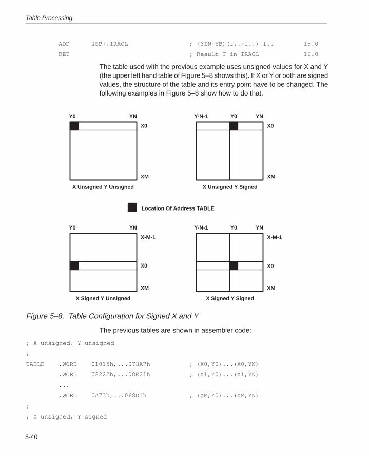
Table Processing
5-40
ADD @SP+,IRACL ; (YIN–YB)(f..–f..)+f.. 15.0
RET ; Result T in IRACL 16.0
The table used with the previous example uses unsigned values for X and Y(the upper left hand table of Figure 5–8 shows this). If X or Y or both are signedvalues, the structure of the table and its entry point have to be changed. Thefollowing examples in Figure 5–8 show how to do that.
Y0 YN
X0
XM
Y-N-1 YN
X0
XM
Y0
X Unsigned Y Unsigned X Unsigned Y Signed
Location Of Address TABLE
Y0 YN
X-M-1
XM
Y-N-1 YN
X-M-1
XM
Y0
X Signed Y Unsigned X Signed Y Signed
X0 X0
Figure 5–8. Table Configuration for Signed X and Y
The previous tables are shown in assembler code:
; X unsigned, Y unsigned
;
TABLE .WORD 01015h,...073A7h ; (X0,Y0)...(X0,YN)
.WORD 02222h,...08E21h ; (X1,Y0)...(X1,YN)
...
.WORD 0A73h,...068D1h ; (XM,Y0)...(XM,YN)
;
; X unsigned, Y signed
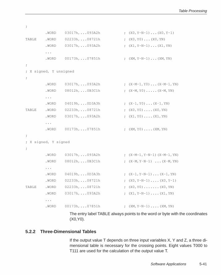
Table Processing
5-41Software Applications
;
.WORD 03017h,...093A2h ; (X0,Y–N–1)...(X0,Y–1)
TABLE .WORD 02233h,...08721h ; (X0,Y0)...(X0,YN)
.WORD 03017h,...093A2h ; (X1,Y–N–1)...(X1,YN)
...
.WORD 00173h,...07851h ; (XM,Y–N–1)...(XM,YN)
;
; X signed, Y unsigned
;
.WORD 03017h,...093A2h ; (X–M–1,Y0)...(X–M–1,YN)
.WORD 08012h,...0B3C1h ; (X–M,Y0).....(X–M,YN)
...
.WORD 04019h,...0D3A3h ; (X–1,Y0)...(X–1,YN)
TABLE .WORD 02233h,...08721h ; (X0,Y0)....(X0,YN)
.WORD 03017h,...093A2h ; (X1,Y0)....(X1,YN)
...
.WORD 00173h,...07851h ; (XM,Y0)....(XM,YN)
;
; X signed, Y signed
;
.WORD 03017h,...093A2h ; (X–M–1,Y–N–1)(X–M–1,YN)
.WORD 08012h,...0B3C1h ; (X–M,Y–N–1) ...(X–M,YN)
...
.WORD 04019h,...0D3A3h ; (X–1,Y–N–1)...(X–1,YN)
.WORD 02233h,...08721h ; (X0,Y–N–1)....(X0,Y–1)
TABLE .WORD 02233h,...08721h ; (X0,Y0).......(X0,YN)
.WORD 03017h,...093A2h ; (X1,Y–N–1)....(X1,YN)
...
.WORD 00173h,...07851h ; (XM,Y–N–1)....(XM,YN)
The entry label TABLE always points to the word or byte with the coordinates(X0,Y0).
5.2.2 Three-Dimensional Tables
If the output value T depends on three input variables X, Y and Z, a three di-mensional table is necessary for the crossing points. Eight values T000 toT111 are used for the calculation of the output value T.
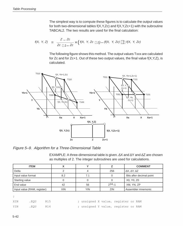
Table Processing
5-42
The simplest way is to compute these figures is to calculate the output valuesfor both two-dimensional tables f(X,Y,Zc) and f(X,Y,Zc+1) with the subroutineTABCAL2. The two results are used for the final calculation:
( )f(X, Y, Z)Z Zc
Zc Zcf(X, Y, Zc ) (f(X, Y, Zc) f(X, Y, Zc)
11= –
–× – +
++
The following figure shows this method. The output values Txxx are calculatedfor Zc and for Zc+1. Out of these two output values, the final value f(X,Y,Z), iscalculated.
T010 f(X, Yb+1,Zc)
T110
T100
f(X, Y,Zc)
f(X, Yb,Zc)
T000Yb+1
Y
Yb
Xa X Xa+1
Yb+1
Y
Yb
Xa X Xa+1
T011
T001
f(X, Yb+1,Zc+1)
f(X, Y,Zc+1)
T111
T101
f(X, Y,Zc)
f(X, Y,Z)
f(X, Y,Zc+1)
Zc Z Zc+1
f(X, Yb,Zc+1)
Figure 5–9. Algorithm for a Three-Dimensional Table
EXAMPLE: A three-dimensional table is given. ∆X and ∆Y and ∆Z are chosenas multiples of 2. The integer subroutines are used for calculations.
ITEM X Y Z COMMENT
Delta 2 4 256 ∆X, ∆Y, ∆Z
Input value format 8.2 7.1 0 Bits after decimal point
Starting value 0 0 0 X0, Y0, Z0
End value 42 56 214–1 XM, YN, ZP
Input value (RAM, register) XIN YIN ZIN Assembler mnemonic
;
XIN .EQU R15 ; unsigned X value, register or RAM
YIN .EQU R14 ; unsigned Y value, register or RAM
Table Processing
5-43Software Applications
ZIN .EQU R13 ; unsigned Z value, register or RAM
XM .EQU 42 ; Number of X rows
YN .EQU 56 ; Number of Y columns
XCL .EQU 7 ; Mask for fraction and dX
YCL .EQU 7 ; Mask for fraction and dY
ZCL .EQU 0FFh ; Mask for deltaZ
XAYB .EQU R12 ; Rel. address of (XA,YB), register
ZCFLG .EQU 1 ; Flag: 0: 2–dim. 1: 3–dim. Table
OFFZC .EQU R11 ; Relative offset to actual (X0,Y0,ZC)
;
; Three dimensional table
;
TABL3D .WORD 01015h,...073A7h ; (X0,Y0,Z0)...(X0,YN,Z0)
...
.WORD 02222h,...08E21h ; (XM,Y0,Z0)...(XM,YN,Z0)
;
.WORD 0A730h,...068D1h ; (X0,Y0,Z1)...(X0,YN,Z1)
...
.WORD 010A5h,...09BA7h ; (XM,Y0,Z1)...(XM,YN,Z1)
;
.WORD 02BC2h,...08E41h ; (X0,Y0,ZP)...(X0,YN,ZP)
...
.WORD 0A980h,...023D1h ; (XM,Y0,ZP)...(XM,YN,ZP)
; Table calculation software 3–dimensional
; Input values: X in XIN, Y in YIN, Z in ZIN
; Result is located in IRACL, same format as TABLE content
;
; Calculation of ZC out of ZIN. One less adaption due to
; word table.
;
TABCAL3 MOV ZIN,IROP1 ; Z –> Operand register 14.0
SWPB IROP1 ; Use only upper byte (dZ =256)
MOV.B IROP1,IROP1 ; Adapt to dZ = 256 6.0
;
; Calculation of relative address of (X0,Y0,ZC) to IRACL
; Corrected for word table
Table Processing
5-44
;
MOV #YN*2*XM,IROP2L ; Table length for dZ
CALL #MPYU ; Rel address (X0,Y0,ZC) 13.0
MOV IRACL,OFFZC ; to storage register 13.0
;
; Calculation of f(X,Y,ZC): The table block for ZC is used
;
CALL #TABCAL2 ; f(X,Y,ZC) –> IRACL 16.0
PUSH IRACL ; Save f(X,Y,ZC)
; Calculation of f(X,Y,ZC+1): The table block for ZC+1 is used
;
ADD #YN*2*XM,OFFZC ; Rel. adress (X0,Y0,ZC+1)
CALL #TABCAL2 ; f(X,Y,ZC+1) –> IRACL 16.0
;
; Calculation of f(X,Y,Z)
;
MOV ZIN,IROP1 ; build (YIN – XB 6.8
AND #ZCL,IROP1 ; Fraction and dZ rests 0.8
SUB @SP,IRACL : f(X,Y,ZC+1)–f(X,Y,ZC) 16.0
MOV IRACL,IROP2L ; Result to multiplier
CALL #MPYS ; (ZIN–ZC)(f..–f..) 16.8
CALL #SHFTRS6 ; :dZ, to integer 16.2
CALL #SHFTRS2 ; 16.0
ADD @SP+,IRACL ; (ZIN–ZC)(f..–f..)+f.. 15.0
RET ; Result in IRACL
Signal Averaging and Noise Cancellation
5-45Software Applications
5.3 Signal Averaging and Noise Cancellation
If the measured signals contain noise, spikes, and other unwanted signal com-ponents, it may be necessary to average the ADC results. Six different meth-ods are mentioned here:
1) Oversampling: Several measurements are added-up and the accu-mulated sum is used for the calculations.
2) Continuous Averaging: A circular buffer is used for the measuredsamples. With every new sample a new average value can be calcu-lated.
3) Weighted summation: The old value and the new one are added to-gether and divided by two afterwards.
4) Wave Digital Filtering: Complex filter algorithms, which need onlysmall amounts of calculation power, are used for the signal condition-ing.
5) Rejection of Extremes: the largest and the smallest samples are re-jected from the measured values and the remaining samples are add-ed-up and averaged.
6) Synchronization of the measurements to hum
The advantages and disadvantages of the different methods are shown in thefollowing sections.
5.3.1 Oversampling
Oversampling is the simplest method for the averaging of measurement re-sults. N samples are added-up and the accumulated sum is divided by N after-wards or is used as it is with the following algorithm steps. It is only necessaryto remember that the accumulated value is N-times too large. For example, thefollowing formula, used for a single measurement, needs to be modified whenN samples are summed-up as shown:
V Slope ADC Offset VSlope ADC Offset
Nnormal oversample= × + → =
∑ × +( )
EXAMPLE: N measurements have to be summed-up in SUM and SUM+2. Thenumber N is defined in R6
SUMLO .EQU R4 ; LSBs of sum
SUMHI .EQU R5 ; MSBs of sum
;
Signal Averaging and Noise Cancellation
5-46
CLR SUMLO ; Init of registers
CLR SUMHI
MOV #16,R6 ; Sum–up 16 samples of the ADC
OVSLOP CALL #MEASURE ; Result in ADAT
ADD &ADAT,SUMLO ; LSD of accumulated sum
ADC SUMHI ; MSD
DEC R6 ; Decr. N counter: 0 reached?
JNZ OVSLOP
... ; Yes, 16 samples in SUMHI|SUMLO
Advantages
Simple programming
Disadvantages
High current consumption due to number of ADC conversions
Low suppression of spikes etc. (by N)
5.3.2 Continuous Averaging
A very simple and fast way for averaging digital signals is continuous averag-ing. A circular buffer is fed at one end with the newest sample and the oldestsample and is deleted at the other end (both items share the same RAM loca-tion). To reduce the calculation time, the oldest sample is subtracted from theactual sum and the new sample is added to the sum. The actual sum (a 32-bitvalue containing N samples) is used by the background. For calculations, it isonly necessary to remember that it contains the accumulated sum of N sam-ples. The same rule is valid for oversampling.
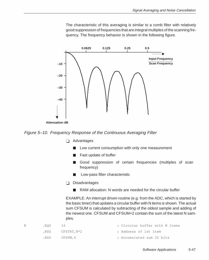
Signal Averaging and Noise Cancellation
5-47Software Applications
The characteristic of this averaging is similar to a comb filter with relativelygood suppression of frequencies that are integral multiples of the scanning fre-quency. The frequency behavior is shown in the following figure.
0.0625 0.125 0.25 0.5
–10
–20
–30
–40
Attenuation dB
Input Frequency
Scan Frequency
Figure 5–10. Frequency Response of the Continuous Averaging Filter
Advantages
Low current consumption with only one measurement
Fast update of buffer
Good suppression of certain frequencies (multiples of scan frequency)
Low-pass filter characteristic
Disadvantages
RAM allocation: N words are needed for the circular buffer
EXAMPLE: An interrupt driven routine (e.g. from the ADC, which is started bythe basic timer) that updates a circular buffer with N items is shown. The actualsum CFSUM is calculated by subtracting of the oldest sample and adding ofthe newest one. CFSUM and CFSUM+2 contain the sum of the latest N sam-ples.
N .EQU 16 ; Circular buffer with N items
.BSS CFSTRT,N*2 ; Address of 1st item
.BSS CFSUM,4 ; Accumulated sum 32 bits
Signal Averaging and Noise Cancellation
5-48
.BSS CFPOI,2 ; Points to next (= oldest) item
;
CFHND PUSH R5 ; Save R5
MOV CFPOI,R5 ; Actual address to R5
CMP #CFSTRT+(N*2),R5 ; Outside circ. buffer?
JLO L$300 ; No
MOV #CFSTRT,R5 ; Yes, reset pointer
;
; The oldest item is subtracted from the sum. The newest item
; overwrites the oldest one and is added to the sum
;
L$300 SUB @R5,CFSUM ; Subtract oldest item from CFSUM
SBC CFSUM+2
MOV &ADAT,0(R5) ; Move actual item to buffer
ADD @R5+,CFSUM ; Add latest ADC result to CFSUM
ADC CFSUM+2
MOV R5,CFPOI ; Update pointer
POP R5 ; Restore R5
RETI
5.3.3 Weighted Summation
The weighted sum of the measurements before and the current measurementresult are added and then divided by two. This gives every measurement resulta certain weight.
Table 5–3. Sample WeightMEASUREMENT TIME WEIGHT COMMENT
t0 0.5 Actual measurement
t0 – ∆t 0.25 Last measurement
t0 – 2∆t 0.125
t0 – 3∆t 0.0625
t0 – 4∆t 0.03125
t0 – n∆t 2–(n+1)
Advantages
Low current consumption due to one measurement only
Low pass filter characteristic
Signal Averaging and Noise Cancellation
5-49Software Applications
Very short code
Only one RAM word needed
Disadvantages
Suppression of spikes not sufficient (factor 2 only for actual sample)
EXAMPLE: The update of the actual sum WSSUM is shown.
.BSS WSSUM,2 ; Accumulated weighted sum
;
WSHND ADD &ADAT,WSSUM ; Add actual measurement to sum
RRA WSSUM ; New sum divided by 2
... ; Continue with value in WSSUM
5.3.4 Wave Digital Filtering
Wave digital filters (WDFs) have notable advantages:
Excellent stability even under nonlinear operating conditions resultingfrom overflow and roundoff effects
Low coefficient word length requirements
Inherently good dynamic range
Stability under looped conditions
Compared with the often used averaging of measured sensor data, the digitalfiltering has advantages: Lowpass filtering with sharp cut-off region, notch fil-tering of noise.
For the design of WDF algorithms specialized CAD programs have been de-signed to speed-up the top-down design from filter specification to the ma-chine program for the processor:
LWDF_DESIGN allows the design of Lattice-WDFs
LWDF_COMP transforms a Lattice-WDF structure into an assembler pro-gram for the MSP430
DSP430 allows fast transient simulations of the filter algorithms on a mod-el of the MSP430, analysis of frequency response, check of accuracy andstability proof.
The programs enable the users of the MSP430 to solve special measurementproblems by means of robust digital filter algorithms.
Signal Averaging and Noise Cancellation
5-50
A complete description of the WDF algorithms and development tools is givenin the ”TEXAS INSTRUMENTS Technical Journal” November/December1994.
Disadvantages
Complex algorithm. Support software needed for finding algorithm
Advantages
Low current consumption because only one measurement per timeslice needed
Good attenuation inside stopband
Good dynamic stability
5.3.5 Rejection of Extremes
This averaging method measures (N+2) ADC-samples and rejects the largestand the smallest values. The remaining N samples are added-up and the ac-cumulated sum is divided by N afterwards or is used as it is with the next algo-rithm steps. It is only necessary to remember that the added-up value is N-times too large.
Disadvantages
Current consumption high due to (N+2) ADC conversions
Advantages
Simple programming
Very good suppression of spikes (extremes are rejected)
Small amount of RAM needs (4 words)
The following software example adds six ADC samples, subtracts the two ex-tremes, and returns with the sum of the four medium samples. The constantN can be changed to any number, but the summing-up buffer SESUM needstwo words if N exceeds two. It is an advantage to use powers of two for N dueto the simple divisions needed (right shifts only). Register use is possible forSESUM, SEHI and SELO.
N .EQU 4 ; Sample count used –2
.IF N>2
.BSS SESUM,4 ; Summing–up buffer
.ELSE ;
.BSS SESUM,2 ; N<=2
Signal Averaging and Noise Cancellation
5-51Software Applications
.ENDIF
.BSS SEHI,2 ; Largest ADC result
.BSS SELO,2 ; Smallest ADC result
.BSS SECNT,1 ; Counter for N+2
;
SEHND CLR SESUM ; Initialize buffers
.IF N>2
CLR SESUM+2
.ENDIF
MOV.B #N+2,SECNT ; Sample count +2 to counter
MOV #0FFFFh,SELO ; ADCmax –> SELO
CLR SEHI ; ADCmin –> SEHI
;
; N+2 measurements are made and summed–up in SESUM
;
SELOOP CALL #MEASURE ; ADC result to &ADAT
MOV &ADAT,R5 ; Copy ADC result to R5
ADD R5,SESUM
.IF N>2 ; Use 2nd sum buffer if N>2
ADC SESUM+2
.ENDIF
CMP R5,SEHI ; Result > SEHI?
JHS L$1 ; No
MOV R5,SEHI ; Yes, actualize SEHI
L$1 CMP R5,SELO ; Result < SELO?
JLO L$2 ; No
MOV R5,SELO
L$2 DEC.B SECNT ; Counter – 1
JNZ SELOOP ; N+2 not yet reached
;
; N+2 measurements are made, extremes are subtracted now
; from summed–up result. Return with N–times value in SESUM
;
SUB SELO,SESUM ; Subtract lowest result
.IF N>2 ; Necessary if N>2
SBC SESUM+2
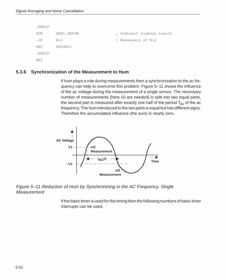
Signal Averaging and Noise Cancellation
5-52
.ENDIF
SUB SEHI,SESUM ; Subtract highest result
.IF N>2 ; Necessary if N>2
SBC SESUM+2
.ENDIF
RET
5.3.6 Synchronization of the Measurement to Hum
If hum plays a role during measurements then a synchronization to the ac fre-quency can help to overcome this problem. Figure 5–11 shows the influenceof the ac voltage during the measurement of a single sensor. The necessarynumber of measurements (here 10 are needed) is split into two equal parts,the second part is measured after exactly one half of the period Tac of the acfrequency. The hum introduced to the two parts is equal but has different signs.Therefore the accumulated influence (the sum) is nearly zero.
AC Voltage
V1
–V1
n/2 Measurement
tAC/2Time
n/2 Measurement
Figure 5–11.Reduction of Hum by Synchronizing to the AC Frequency. SingleMeasurement
If the basic timer is used for the timing then the following numbers of basic timerinterrupts can be used.
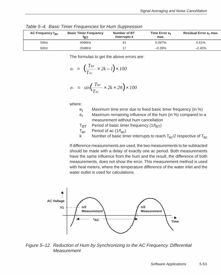
Signal Averaging and Noise Cancellation
5-53Software Applications
Table 5–4. Basic Timer Frequencies for Hum SuppressionAC Frequency f ac Basic Timer Frequency
fBTNumber of BT
Interrupts kTime Error e t
max.Residual Error e r max.
50Hz 4096Hz 41 0.097% 0.61%
60Hz 2048Hz 17 –0.39% –2.45%
The formulas to get the above errors are:
eT
T2k 1 100t
BT
AC= × –( )×
e sinT
T2k 2 100r
BT
AC= × ×( )×π
where:et Maximum time error due to fixed basic timer frequency (in %)er Maximum remaining influence of the hum (in %) compared to a
measurement without hum cancellationTBT Period of basic timer frequency (1/fBT)Tac Period of ac (1/fac)k Number of basic timer interrupts to reach Tac/2 respective of Tac
If difference measurements are used, the two measurements to be subtractedshould be made with a delay of exactly one ac period. Both measurementshave the same influence from the hum and the result, the difference of bothmeasurements, does not show the error. This measurement method is usedwith heat meters, where the temperature difference of the water inlet and thewater outlet is used for calculations.
AC Voltage
V1 n/2Measurement
n/2Measurement
tAC Time
Figure 5–12. Reduction of Hum by Synchronizing to the AC Frequency. Differential Measurement
Signal Averaging and Noise Cancellation
5-54
If the basic timer is used for the timing then the following numbers of basic timerinterrupts can be used.
Table 5–5. Basic Timer Frequencies for Hum SuppressionAC Frequency f ac Basic Timer Frequency
fBTNumber of Interruptsk
Time Error e tmax.
Residual Error e r max.
50Hz 2048Hz 41 0.097% 0.61%
60Hz 1024Hz 17 –0.39% –2.45%
The formulas to get the previous results are:
eT
Tk 1 100t
BT
AC= × –( )×
e sinT
Tk 2 100r
BT
AC= × ×( ) ×π
The software needed for the modification of the Basic Timer frequency withoutthe loss of the exact time base is shown in Section 6.1.1, Change of the BasicTimer Frequency.
Real-Time Applications
5-55Software Applications
5.4 Real-Time Applications
Real-time applications for microprocessors are defined often as follows:
The controlling processor is able, under worst case conditions, to finish thenecessary control algorithms before the next sample of the control inputarrives.
The architecture of the MSP430 is ideally suited for real time applications dueto its system clock generation. The system clock MCLK of the CPU is not gen-erated by a second crystal, which needs a lot of time until it is oscillating withthe nominal frequency. But, by the multiplication of the frequency of the 32-kHzcrystal that is oscillating continuously.
5.4.1 Active Mode
The active mode shows the fastest response to interrupts because all of theinternal clocks are operating at their nominal frequencies. The active mode isrecommended when the speed of the MSP430 is the critical factor of an ap-plication.
5.4.2 Normal Mode is Low-Power Mode 3 (LPM3)
This mode is used for battery-driven systems where the power consumptionplays an overwhelming role. Battery lifetimes over ten years are only possiblewhen the CPU is switched off whenever its processing capability is not need-ed.
Despite the switched-off CPU, the MSP430 is at the start address of the inter-rupt handler within eight MCLK cycles; the system clock oscillator is then work-ing at the correct frequency. This means true real-time capability, no delay dueto the slow coming-up of the main oscillator crystal (up to 400 ms) is slowingdown the system behavior.
See Section 6.5, The System Clock Generator, for the details of the program-ming.
5.4.3 Normal Mode is Low-Power Mode 4 (LPM4)
The low power mode 4 is used if there are relatively long time elapses betweentwo interrupt events. The power consumption goes below 0.1mA if this modeis used All oscillators are switched off and only the RAM and the interrupt hard-ware are powered.
Despite this inactivity the MSP430 CPU is at the start of the interrupt handlerwithin eight cycles of the programmed DCO tap. See Section 6.5, The SystemClock Generator for the details of the speed-up of the CPU.

Real-Time Applications
5-56
5.4.4 Recommendations for Real-Time Applications
Switch on the GIE bit (SR.3) as soon as possible. Within the interrupt han-dlers, only the tasks that do not allow interruption should be completedfirst. This allows nested interrupts and avoids the blocking of other inter-rupts.
Interrupt handlers (foreground) should be as short as possible. All calcula-tions should be made in the background part of the program. The commu-nication between these two software parts is made by status bytes. SeeSection 9.2.5, Flag Replacement by Status Usage.
Use status bytes and calculated branches.
The interrupt capability of the I/O ports makes input polling superfluous.Any change of an input is seen immediately. Use of the ports this way isrecommended.
Disabling and enabling of the peripheral interrupts during the software runis not recommended. Additional interrupt requests can result from thesemanipulations. The use of status bytes is recommended instead. They in-form the software if an interrupt is valid or not. If not, it is neglected.
General-Purpose Subroutines
5-57Software Applications
5.5 General-Purpose Subroutines
The following, tested software examples can be of help during the software de-velopment phase. The examples can not fit into any application, but they canbe modified easily to the user’s needs.
5.5.1 Initialization
For the first power-on, it is necessary to clear the internal RAM to get a definedbasis. If the MSP430 is battery powered and contains calibration factors or oth-er important data in its RAM, it is necessary to distinguish between a cold startand a warm start. The reason for this is the possibility of initializations causedby electromagnetic interference (EMI). If such an erroneous initialization is notchecked for legality, EMI influence could destroy the RAM content by clearingthe RAM with the initialization software routine. Testing can be done bycomparing RAM bytes with known content to their nominal value. These RAMbytes could be identification codes or non-critical test patterns (e.g. A5h, F0h).If the tested RAM locations contain the correct pattern, a spurious signalcaused the initialization and the normal program can continue. If the testedRAM bytes differ from the nominal value, the RAM content is destroyed (e.g.by a power loss) and the initialization routine is invoked. The RAM is clearedand the peripherals are initialized.
The cold start software contains the waiting loop for the DCO, which is neededto set it to the correct frequency. See Section 6.5, The System Clock Genera-tor, and Section 6.6, The RESET Function.
; Initialization part: Check if Cold Start or Warm Start:
; RAM location 0200h decides kind of initialization:
; Cold Start: content differs from 0A5F0h
; Warm Start: content is 0A5F0h
;
INIT CMP #0A5F0h,&0200h ; Test content of &200h
JEQ EMIINI ; Correct content: No reset
;
; Control RAM content differs from 0A5F0: RAM needs to be
; cleared, peripherals needs to be initialized
;
MOV #0300h,SP ; Init. Stack Pointer
CALL #RAMCLR ; Clear complete RAM
MOV #0A5F0h,&0200h ; Insert test word
;
General-Purpose Subroutines
5-58
; System frequency MCLK is set to 2.048MHz
;
MOV.B #64–1,&SCFQCTL ; 64 x 32kHz = 2.048MHz
MOV.B #FN_2,&SCFI0 ; DCO current for 2MHz
;
; Waiting loop for the DCO of the FLL to settle: 130ms
;
CLR R5 ; 3 x 65536us = 186ms
L$1 INC R5
JNZ L$1
...
;
; EMI caused initialization: Periphery needs to be initialized:
; Interrupts need to be enabled again
;
EMINI ...
5.5.2 RAM clearing Routine
The RAM is cleared starting at label RAMSTRT up to label RAMEND (inclu-sive).
;
; Definitions for the RAM block (depends on MSP430 type)
;
RAMSTRT .EQU 0200h ; Start of RAM
RAMEND .EQU 02FEh ; Last RAM address (return address)
; Subroutine for the clearing of the RAM block
RAMCLR CLR R5 ; Prepare index register
RCL CLR.B RAMSTRT(R5) ; 1st RAM address
INC R5 ; Next address
CMP #RAMEND–RAMSTRT+1,R5 ; RAM cleared?
JLO RCL ; No, once more
RET ; Yes, return
;
5.5.3 Binary to BCD Conversion
The conversion of binary to BCD and vice versa is normally a time consumingtask. Five divisions by ten are necessary to convert a 16-bit binary number toBCD. The DADD instruction reduces this to a loop with five instructions.
General-Purpose Subroutines
5-59Software Applications
; THE BINARY NUMBER IN R12 IS CONVERTED TO A 5–DIGIT BCD
; NUMBER CONTAINED IN R14 AND R13: R14|R13
;
BINDEC MOV #16,R15 ; LOOP COUNTER
CLR R14 ; 0 –> RESULT MSD
CLR R13 ; 0 –> RESULT LSD
L$1 RLA R12 ; Binary MSB to carry
DADD R13,R13 ; RESULT x2 LSD
DADD R14,R14 ; MSD
DEC R15 ; THROUGH?
JNZ L$1
RET ; YES, RESULT IN R14|R13
The previous subroutine can be enlarged to any length of the binary part simplyby the adding of registers for the storage of the BCD number (a binary numberwith n bits needs approximately 1.2 x n bits for BCD format).
If numbers containing fractions have to be converted to BCD, the following al-gorithm can be used:
1) Multiply the binary number as often with 5 as there are fractional bits. Forexample if the number looks like MMM.NN, then multiply it with 25. Ensurethat no overflow will take place.
2) Convert the result of step 1 to BCD with the (eventually enlarged) subrou-tine BINDEC. The BCD result is a number with the same number of frac-tional digits as the binary number has fractional bits.
EXAMPLE: The hexadecimal number 0A8Bh has the binary formatMMM.NNN. The decimal value is therefore 337,375. The steps to get the BCDnumber are:
3) 0A8Bh is to be multiplied by 53 or 12510 due to its 3 fractional bits. 0A8Bh x 12510 =0525DFh
4) 0525DFh has the decimal equivalent 337,375. The correct BCD numberwith 3 fractional digits.
To convert the previous example, the basic subroutine BINDEC needs to beenlarged. Two binary registers are necessary to hold the input number.
; THE BINARY NUMBER IN R12|R11 IS CONVERTED TO AN 8–DIGIT BCD
; NUMBER CONTAINED IN R14 AND R13: R14|R13
; Max. hex number in R12|R11: 05F5E0FFh (999999999)
General-Purpose Subroutines
5-60
;
BINDEC MOV #32,R15 ; LOOP COUNTER
CLR R14 ; 0 –> RESULT MSD
CLR R13 ; 0 –> RESULT LSD
L$1 RLA R11 ; MSB of LSBs to carry
RLC R12 ; Binary MSB to carry
DADD R13,R13 ; RESULT x2 LSD
DADD R14,R14 ; MSD
DEC R15 ; THROUGH?
JNZ L$1
RET ; YES, RESULT IN R14|R13
5.5.4 BCD to Binary
This subroutine converts a packed 16-bit BCD word to a 16-bit binary word bymultiplying each digit with its decimal value (100, 101, . . .). To reduce codelength, the HORNER scheme is used as follows:
R5 X0 10(X1 10(X2 10X3)= + + +
; The packed BCD number contained in R4 is converted to a binary
; number contained in R5
;
BCDBIN MOV #4,R8 ; LOOP COUNTER ( 4 DIGITS )
CLR R5
CLR R6
SHFT4 RLA R4 ; SHIFT LEFT DIGIT INTO R6
RLC R6 ; THROUGH CARRY
RLA R4
RLC R6
RLA R4
RLC R6
RLA R4
RLC R6
ADD R6,R5 ; X N+10XN+1
CLR R6
DEC R8 ; THROUGH ?
JZ END ; YES
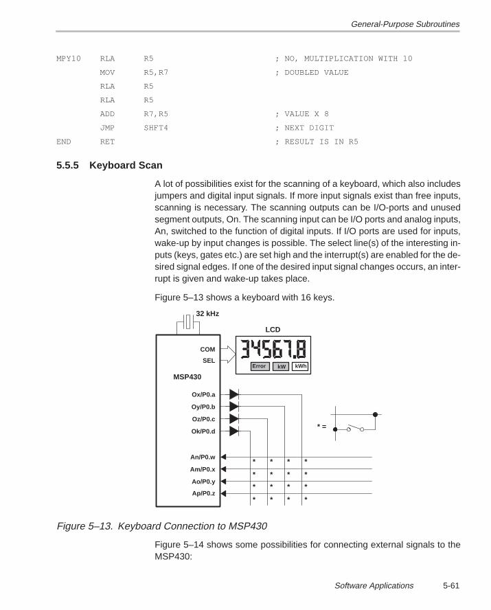
General-Purpose Subroutines
5-61Software Applications
MPY10 RLA R5 ; NO, MULTIPLICATION WITH 10
MOV R5,R7 ; DOUBLED VALUE
RLA R5
RLA R5
ADD R7,R5 ; VALUE X 8
JMP SHFT4 ; NEXT DIGIT
END RET ; RESULT IS IN R5
5.5.5 Keyboard Scan
A lot of possibilities exist for the scanning of a keyboard, which also includesjumpers and digital input signals. If more input signals exist than free inputs,scanning is necessary. The scanning outputs can be I/O-ports and unusedsegment outputs, On. The scanning input can be I/O ports and analog inputs,An, switched to the function of digital inputs. If I/O ports are used for inputs,wake-up by input changes is possible. The select line(s) of the interesting in-puts (keys, gates etc.) are set high and the interrupt(s) are enabled for the de-sired signal edges. If one of the desired input signal changes occurs, an inter-rupt is given and wake-up takes place.
Figure 5–13 shows a keyboard with 16 keys.
COM
SELError kW kWh
32 kHz
Ox/P0.a
Oy/P0.b
Oz/P0.c
Ok/P0.d
An/P0.w
Am/P0.x
Ao/P0.y
Ap/P0.z
* * * *
* * * *
* * * *
* * * *
* =
LCD
MSP430
Figure 5–13. Keyboard Connection to MSP430
Figure 5–14 shows some possibilities for connecting external signals to theMSP430:
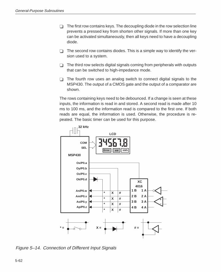
General-Purpose Subroutines
5-62
The first row contains keys. The decoupling diode in the row selection lineprevents a pressed key from shorten other signals. If more than one keycan be activated simultaneously, then all keys need to have a decouplingdiode.
The second row contains diodes. This is a simple way to identify the ver-sion used to a system.
The third row selects digital signals coming from peripherals with outputsthat can be switched to high-impedance mode.
The fourth row uses an analog switch to connect digital signals to theMSP430. The output of a CMOS gate and the output of a comparator areshown.
The rows containing keys need to be debounced. If a change is seen at theseinputs, the information is read in and stored. A second read is made after 10ms to 100 ms, and the information read is compared to the first one. If bothreads are equal, the information is used. Otherwise, the procedure is re-peated. The basic timer can be used for this purpose.
COM
SELError kW kWh
32 kHz
Ox/P0.a
Oy/P0.b
Oz/P0.c
Ok/P0.d
An/P0.w
Am/P0.x
Ao/P0.y
Ap/P0.z
* X #
* X #
* X #
* X #
* =
LCD
MSP430
1 B
2 B
3 B
4 B
1 A
2 A
3 A
4 A
XC
+–
X = # =
4016
Figure 5–14. Connection of Different Input Signals
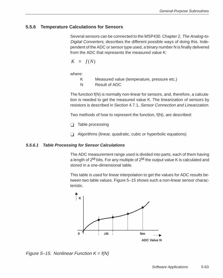
General-Purpose Subroutines
5-63Software Applications
5.5.6 Temperature Calculations for Sensors
Several sensors can be connected to the MSP430. Chapter 2, The Analog-to-Digital Converters, describes the different possible ways of doing this. Inde-pendent of the ADC or sensor type used, a binary number N is finally deliveredfrom the ADC that represents the measured value K:
K f N= ( )
where:K Measured value (temperature, pressure etc.)N Result of ADC
The function f(N) is normally non-linear for sensors, and, therefore, a calcula-tion is needed to get the measured value K. The linearization of sensors byresistors is described in Section 4.7.1, Sensor Connection and Linearization.
Two methods of how to represent the function, f(N), are described:
Table processing
Algorithms (linear, quadratic, cubic or hyperbolic equations)
5.5.6.1 Table Processing for Sensor Calculations
The ADC measurement range used is divided into parts, each of them havinga length of 2M bits. For any multiple of 2M the output value K is calculated andstored in a one-dimensional table.
This table is used for linear interpolation to get the values for ADC results be-tween two table values. Figure 5–15 shows such a non-linear sensor charac-teristic.
0 ∆N Nm
ADC Value N
K
Figure 5–15. Nonlinear Function K = f(N)
General-Purpose Subroutines
5-64
Steps for the development of a sensor table:
1) Definition of the external circuitry used at the ADC inputs (see Chapter 2,The Analog-to-Digital Converters)
2) Definition of the output format of the table contents (bits after decimalpoint, M.N)
3) Calculation of the voltage at the analog input Ax for equally spaced (∆Ν)ADC values n
4) Calculation of the sensor resistances for the previous calculated analoginput voltages
5) Calculation of the input values K (temperature, pressure etc.) that causethese sensor resistances
6) Insertion of the calculated input values K in the format defined with 2. intothe table
EXAMPLE: A sensor characteristic is described in a table TABLE. The ADCresults are divided in distances ∆Ν = 128 starting at value N0 = 256. The outputvalue K is content of this table. The ADC result is corrected with offset andslope coming from the calibration procedure.
;
.BSS OFFSET,2 ; Offset from calibration 10.0
.BSS SLOPE,2 ; Slope from calibration 1.10
DN .EQU 128 ; Delta N
;
; Table contains signed values. The decimal point may be anywhere
;
TABLE .WORD 02345h, ...,00F3h ; K0, K1, ...KM
;
TABCAL1 MOV &ADAT,IROP1 ; ADC result N to IROP1 14.0
ADD OFFSET,IROP1 ; Correct offset 10.0
MOV SLOPE,IROP2L ; Slope 1.10
CALL #MPYS ; (ADC+OFFSET)xSLOPE 15.10
;
; Corrected ADC value in IRACM|IRACL.
;
CALL #SHFTLS6 ; Result to IRACM 15.0
MOV IRACM,XIN ; Copy it
General-Purpose Subroutines
5-65Software Applications
;
; Calculation of NA address. One less adaptation due to
; word table (2 bytes/item).
;
MOV XIN,IROP1 ; N –> Multiplicand 15.0
SWPB IROP1 ; Adapt to deltaN = 128 14.0
BIC.B #1,IROP1 ; Even word address needed 8.0
SUB #2,IROP1 ; Adapt to N0 = 256 (2 x deltaN)
MOV TABLE(IROP1),R15 ; KA from table
MOV TABLE+2(IROP1),R14 ; KA+1 from table
;
; K = ((XIN–KA)/deltaN) x (KA+1 – KA) + KA
;
SUB R15,XIN ; XIN – KA
MOV R14,IROP2L ; KA+1
SUB R15,IROP2L ; KA+1 – KA)
MOV XIN,IROP1 ; XIN – KA
CALL #MPYS ; (XIN – KA) x (KA+1 – KA)
CALL #SHFTRS6 ; /deltaN
CALL #SHFTRS1 ; deltaN = 2^7
ADD R15,IRACL ; + KA, result in IRACL
RET
5.5.6.2 Algorithms for Sensor Calculations
If the sensor characteristic can be described by a function, K = f(N), then notable processing is necessary. The value K can be calculated out of the ADCresult N. The coefficients an and bn can be found with PC computer software(e.g. MATHCAD), with formulas by hand, or by the MSP430 itself. These cate-gories are for example:
Linear Equation
K a N a1 0= × +
Quadratic Equation
K a N a N a22
1 0= × + × +
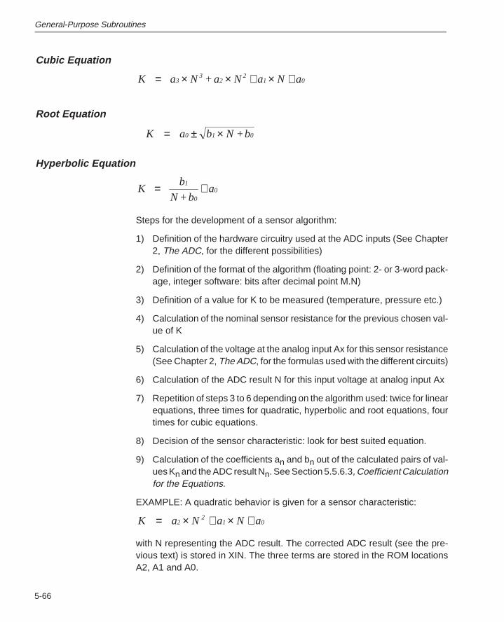
General-Purpose Subroutines
5-66
Cubic Equation
K a N +a N a N a33
22
1 0= × × + × +
Root Equation
K a b N +b0 1 0= ± ×
Hyperbolic Equation
Kb
N +ba
1
00= +
Steps for the development of a sensor algorithm:
1) Definition of the hardware circuitry used at the ADC inputs (See Chapter2, The ADC, for the different possibilities)
2) Definition of the format of the algorithm (floating point: 2- or 3-word pack-age, integer software: bits after decimal point M.N)
3) Definition of a value for K to be measured (temperature, pressure etc.)
4) Calculation of the nominal sensor resistance for the previous chosen val-ue of K
5) Calculation of the voltage at the analog input Ax for this sensor resistance(See Chapter 2, The ADC, for the formulas used with the different circuits)
6) Calculation of the ADC result N for this input voltage at analog input Ax
7) Repetition of steps 3 to 6 depending on the algorithm used: twice for linearequations, three times for quadratic, hyperbolic and root equations, fourtimes for cubic equations.
8) Decision of the sensor characteristic: look for best suited equation.
9) Calculation of the coefficients an and bn out of the calculated pairs of val-ues Kn and the ADC result Nn. See Section 5.5.6.3, Coefficient Calculationfor the Equations.
EXAMPLE: A quadratic behavior is given for a sensor characteristic:
K a N a N a22
1 0= × + × +
with N representing the ADC result. The corrected ADC result (see the pre-vious text) is stored in XIN. The three terms are stored in the ROM locationsA2, A1 and A0.
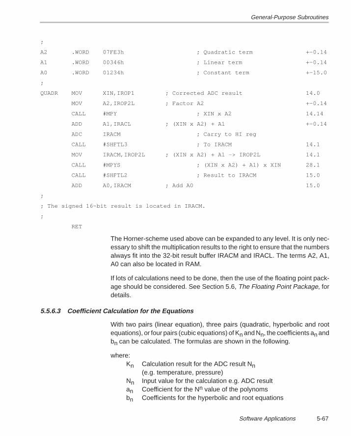
General-Purpose Subroutines
5-67Software Applications
;
A2 .WORD 07FE3h ; Quadratic term +–0.14
A1 .WORD 00346h ; Linear term +–0.14
A0 .WORD 01234h ; Constant term +–15.0
;
QUADR MOV XIN,IROP1 ; Corrected ADC result 14.0
MOV A2,IROP2L ; Factor A2 +–0.14
CALL #MPY ; XIN x A2 14.14
ADD A1,IRACL ; (XIN x A2) + A1 +–0.14
ADC IRACM ; Carry to HI reg
CALL #SHFTL3 ; To IRACM 14.1
MOV IRACM,IROP2L ; (XIN x A2) + A1 –> IROP2L 14.1
CALL #MPYS ; (XIN x A2) + A1) x XIN 28.1
CALL #SHFTL2 ; Result to IRACM 15.0
ADD A0,IRACM ; Add A0 15.0
;
; The signed 16–bit result is located in IRACM.
;
RET
The Horner-scheme used above can be expanded to any level. It is only nec-essary to shift the multiplication results to the right to ensure that the numbersalways fit into the 32-bit result buffer IRACM and IRACL. The terms A2, A1,A0 can also be located in RAM.
If lots of calculations need to be done, then the use of the floating point pack-age should be considered. See Section 5.6, The Floating Point Package, fordetails.
5.5.6.3 Coefficient Calculation for the Equations
With two pairs (linear equation), three pairs (quadratic, hyperbolic and rootequations), or four pairs (cubic equations) of Kn and Nn, the coefficients an andbn can be calculated. The formulas are shown in the following.
where:Kn Calculation result for the ADC result Nn
(e.g. temperature, pressure)Nn Input value for the calculation e.g. ADC resultan Coefficient for the Nn value of the polynomsbn Coefficients for the hyperbolic and root equations
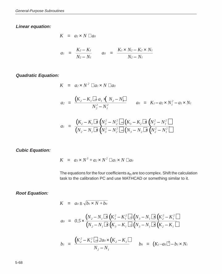
General-Purpose Subroutines
5-68
Linear equation:
K a N a1 0= × +
aK K
N Na
K N K N
N N1
2 1
2 10
1 2 2 1
2 1= –
–= × – ×
–
Quadratic Equation:
K a N a N a22
1 0= × + × +
( ) ( )a
K K a N N
N Na K a N a N2
2 1 1 2 1
22
12
0 1 2 12
1 1=– – × –
–= – × – ×
( ) ( ) ( ) ( )( ) ( ) ( ) ( )a
K K N N K K N N
N N N N N N N N1
2 1 32
22
3 2 22
12
2 1 32
22
3 2 22
12
=– × – – – × –
– × – – – × –
Cubic Equation:
K a N +a N a N a33
22
1 0= × × + × +
The equations for the four coefficients an are too complex. Shift the calculationtask to the calibration PC and use MATHCAD or something similar to it.
Root Equation:
K a b N +b0 1 0= ± ×
( ) ( ) ( ) ( )( ) ( ) ( ) ( )a 0.5N N K K N N K K
N N K K N N K K0
2 1 32
12
3 1 22
12
2 1 3 1 3 1 2 1
= ×– × – – – × –
– × – – – × –
( ) ( )( )b
K K 2a K K
N Nb K –a b N1
22
12
0 2 1
2 1
0 1 02
1 1=– – × –
–= – ×
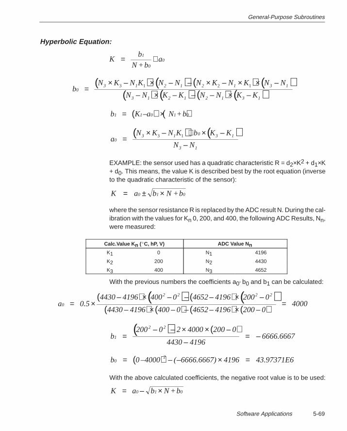
General-Purpose Subroutines
5-69Software Applications
Hyperbolic Equation:
Kb
N +ba
1
00= +
( ) ( ) ( ) ( )( ) ( ) ( ) ( )b
N N N N N N
N N K K N N K K0
3 1 2 1 2 1 3 1
3 1 2 1 2 1 3 1
=× – × – – × – × × –
– × – – – × –
K K N K K N3 1 2 1
( ) ( )b K –a N +b1 1 0 1 0= ×
( ) ( )a
N N K
N N0
3 1 0 3 1
3 1
=× – + × –
–
K K b K3 1
EXAMPLE: the sensor used has a quadratic characteristic R = d2×K2 + d1×K+ d0. This means, the value K is described best by the root equation (inverseto the quadratic characteristic of the sensor):
K a b N +b0 1 0= ± ×
where the sensor resistance R is replaced by the ADC result N. During the cal-ibration with the values for Kn 0, 200, and 400, the following ADC Results, Nn,were measured:
Calc.Value K n (C, hP, V) ADC Value N nK1 0 N1 4196
K2 200 N2 4430
K3 400 N3 4652
With the previous numbers the coefficients a0’ b0 and b1 can be calculated:
( ) ( ) ( ) ( )( ) ( ) ( ) ( )
a 0.54430 4196 400 0 4652 4196 200 0
4430 4196 400 0 4652 4196 200 040000
2 2 2 2
= ×– × – – – × –
– × – – – × –=
( ) ( )b
200 0 2 4000 200 0
4430 41966666.66671
2 2
=– – × × –
–= –
( )b 0 –4000 ( 6666.6667) 4196 43.97371E602= – – × =
With the above calculated coefficients, the negative root value is to be used:
K a b N +b0 1 0= – ×
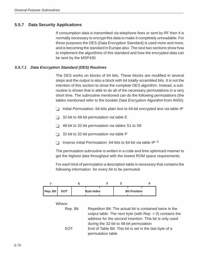
General-Purpose Subroutines
5-70
5.5.7 Data Security Applications
If consumption data is transmitted via telephone lines or sent by RF then it isnormally necessary to encrypt this data to make it completely unreadable. Forthese purposes the DES (Data Encryption Standard) is used more and more,and is becoming the standard in Europe also. The next two sections show howto implement the algorithms of this standard and how the encrypted data canbe sent by the MSP430.
5.5.7.1 Data Encryption Standard (DES) Routines
The DES works on blocks of 64 bits. These blocks are modified in severalsteps and the output is also a block with 64 totally-scrambled bits. It is not theintention of this section to show the complete DES algorithm. Instead, a sub-routine is shown that is able to do all of the necessary permutations in a veryshort time. The subroutine mentioned can do the following permutations (thetables mentioned refer to the booklet Data Encryption Algorithm from ANSI):
Initial Permutation: 64-bits plain text to 64-bit encrypted text via table IP
32-bit to 48-bit permutation via table E
48-bit to 32-bit permutation via tables S1 to S8
32-bit to 32-bit permutation via table P
Inverse initial Permutation: 64-bits to 64-bit via table IP–1
The permutation subroutine is written in a code and time optimized manner toget the highest data throughput with the lowest ROM space requirements.
For each kind of permutation a description table is necessary that contains thefollowing information for every bit to be permuted:
Rep. Bit EOT Byte Index Bit Position
7 5 3 2 0
Where:Rep. Bit Repetition Bit: The actual bit is contained twice in the
output table. The next byte (with Rep. = 0) contains the address for the second insertion. This bit is only used during the 32-bit to 48-bit permutation
EOT End of Table Bit: This bit is set in the last byte of a permutation table
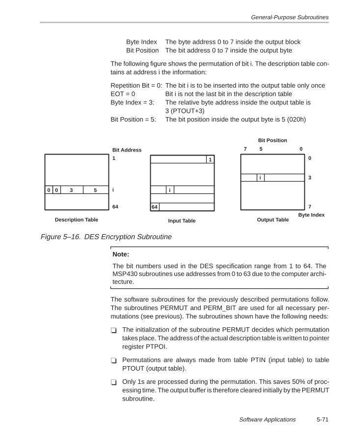
General-Purpose Subroutines
5-71Software Applications
Byte Index The byte address 0 to 7 inside the output blockBit Position The bit address 0 to 7 inside the output byte
The following figure shows the permutation of bit i. The description table con-tains at address i the information:
Repetition Bit = 0: The bit i is to be inserted into the output table only onceEOT = 0 Bit i is not the last bit in the description tableByte Index = 3: The relative byte address inside the output table is
3 (PTOUT+3)Bit Position = 5: The bit position inside the output byte is 5 (020h)
1
64
7 0
0
7
5
Description Table Output Table
Bit Address
Input Table
i0 0 3 5
1
i
64
i 3
Byte Index
Bit Position
Figure 5–16. DES Encryption Subroutine
Note:
The bit numbers used in the DES specification range from 1 to 64. TheMSP430 subroutines use addresses from 0 to 63 due to the computer archi-tecture.
The software subroutines for the previously described permutations follow.The subroutines PERMUT and PERM_BIT are used for all necessary per-mutations (see previous). The subroutines shown have the following needs:
The initialization of the subroutine PERMUT decides which permutationtakes place. The address of the actual description table is written to pointerregister PTPOI.
Permutations are always made from table PTIN (input table) to tablePTOUT (output table).
Only 1s are processed during the permutation. This saves 50% of proc-essing time. The output buffer is therefore cleared initially by the PERMUTsubroutine.
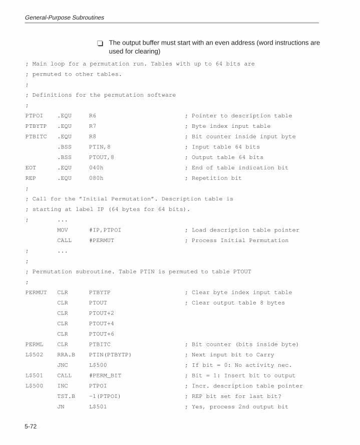
General-Purpose Subroutines
5-72
The output buffer must start with an even address (word instructions areused for clearing)
; Main loop for a permutation run. Tables with up to 64 bits are
; permuted to other tables.
;
; Definitions for the permutation software
;
PTPOI .EQU R6 ; Pointer to description table
PTBYTP .EQU R7 ; Byte index input table
PTBITC .EQU R8 ; Bit counter inside input byte
.BSS PTIN,8 ; Input table 64 bits
.BSS PTOUT,8 ; Output table 64 bits
EOT .EQU 040h ; End of table indication bit
REP .EQU 080h ; Repetition bit
;
; Call for the ”Initial Permutation”. Description table is
; starting at label IP (64 bytes for 64 bits).
; ...
MOV #IP,PTPOI ; Load description table pointer
CALL #PERMUT ; Process Initial Permutation
; ...
;
; Permutation subroutine. Table PTIN is permuted to table PTOUT
;
PERMUT CLR PTBYTP ; Clear byte index input table
CLR PTOUT ; Clear output table 8 bytes
CLR PTOUT+2
CLR PTOUT+4
CLR PTOUT+6
PERML CLR PTBITC ; Bit counter (bits inside byte)
L$502 RRA.B PTIN(PTBYTP) ; Next input bit to Carry
JNC L$500 ; If bit = 0: No activity nec.
L$501 CALL #PERM_BIT ; Bit = 1: Insert bit to output
L$500 INC PTPOI ; Incr. description table pointer
TST.B –1(PTPOI) ; REP bit set for last bit?
JN L$501 ; Yes, process 2nd output bit
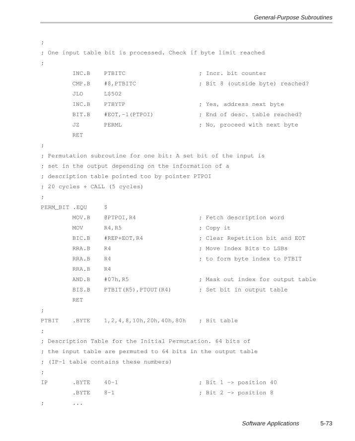
General-Purpose Subroutines
5-73Software Applications
;
; One input table bit is processed. Check if byte limit reached
;
INC.B PTBITC ; Incr. bit counter
CMP.B #8,PTBITC ; Bit 8 (outside byte) reached?
JLO L$502
INC.B PTBYTP ; Yes, address next byte
BIT.B #EOT,–1(PTPOI) ; End of desc. table reached?
JZ PERML ; No, proceed with next byte
RET
;
; Permutation subroutine for one bit: A set bit of the input is
; set in the output depending on the information of a
; description table pointed too by pointer PTPOI
; 20 cycles + CALL (5 cycles)
;
PERM_BIT .EQU $
MOV.B @PTPOI,R4 ; Fetch description word
MOV R4,R5 ; Copy it
BIC.B #REP+EOT,R4 ; Clear Repetition bit and EOT
RRA.B R4 ; Move Index Bits to LSBs
RRA.B R4 ; to form byte index to PTBIT
RRA.B R4
AND.B #07h,R5 ; Mask out index for output table
BIS.B PTBIT(R5),PTOUT(R4) ; Set bit in output table
RET
;
PTBIT .BYTE 1,2,4,8,10h,20h,40h,80h ; Bit table
;
; Description Table for the Initial Permutation. 64 bits of
; the input table are permuted to 64 bits in the output table
; (IP–1 table contains these numbers)
;
IP .BYTE 40–1 ; Bit 1 –> position 40
.BYTE 8–1 ; Bit 2 –> position 8
; ...
General-Purpose Subroutines
5-74
.BYTE EOT+25–1 ; Bit 64 –> pos. 25, End of table
;
; Description Table for the Expansion Function E. 32 bits of
; the input table are permuted to 48 bits in the output table
;
E .BYTE REP+2–1 ; Bit 1 –> position 2 and 48
.BYTE 48–1 ; Bit 1 –> position 48
.BYTE 3–1 ; Bit 2 –> pos. 3
; ...
.BYTE REP+1–1 ; Bit 32 –> position 1 and 47
.BYTE EOT+47–1 ; Bit 32 –> pos. 47, End of table
Processing time for a 64-bit block: The most time consuming parts for the en-cryption are the permutations. All other operations are simple moves or exclu-sive ORs (XOR). This means that the number of permutations multiplied withthe number of cycles per bit gives an estimation of the processing time needed.Every bit needs 43 cycles to be permuted.
The necessary number of permutations is:
1) Initial Permutation 642) 32-bit to 48-bit permutation 16 × 483) 48-bit to 32-bit permutation 16 × 324) 32-bit to 32-bit permutation 16 × 325) Inverse initial Permutation: 646) Key permutations choice 1 567) Key permutations choice 2 16 × 48
Sum of permutations 2744
Number of cycles typically (2744 × 43 x 0.5) 58996 cycles 32 ones in block
maximum (2744 × 43) 117992 cycles 64 ones in block
For a block with 64 bits approximately 59 ms are needed with an MCLK of1 MHz.
ROM space: The needed ROM space can be divided into the following parts:
1) Main program (approx.) 400 bytes2) Subroutines 100 bytes3) Tables for permutations 570 bytes
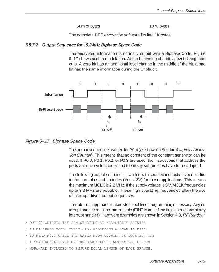
General-Purpose Subroutines
5-75Software Applications
Sum of bytes 1070 bytes
The complete DES encryption software fits into 1K bytes.
5.5.7.2 Output Sequence for 19.2-kHz Biphase Space Code
The encrypted information is normally output with a Biphase Code. Figure5–17 shows such a modulation. At the beginning of a bit, a level change oc-curs. A zero bit has an additional level change in the middle of the bit, a onebit has the same information during the whole bit.
RF Off RF On
0 1 1 0 1 0 0 1
Information
Bi-Phase Space
Figure 5–17. Biphase Space Code
The output sequence is written for P0.4 (as shown in Section 4.4, Heat Alloca-tion Counter). This means that no constant of the constant generator can beused. If P0.0, P0.1, P0.2, or P0.3 are used, the instructions that address theports are one cycle shorter and the delay subroutines have to be adapted.
The following output sequence is written with counted instructions per bit dueto the normal use of batteries (Vcc = 3V) for these applications. This meansthe maximum MCLK is 2.2 MHz. If the supply voltage is 5 V, MCLK frequenciesup to 3.3 MHz are possible. These high operating frequencies allow the useof interrupt driven output sequences.
The interrupt approach makes strict real time programming necessary. Any in-terrupt handler must be interruptible (EINT is one of the first instructions of anyinterrupt handler). Hardware examples are shown in Section 4.8, RF Readout.
; OUT192 OUTPUTS THE RAM STARTING AT ”RAMSTART” BITWISE
; IN BI–PHASE–CODE. EVERY 040h ADDRESSES A SCAN IS MADE
; TO READ P0.1 WHERE THE WATER FLOW COUNTER IS LOCATED. THE
; 4 SCAN RESULTS ARE ON THE STACK AFTER RETURN FOR CHECKS
; NOPs ARE INCLUDED TO ENSURE EQUAL LENGTH OF EACH BRANCH.
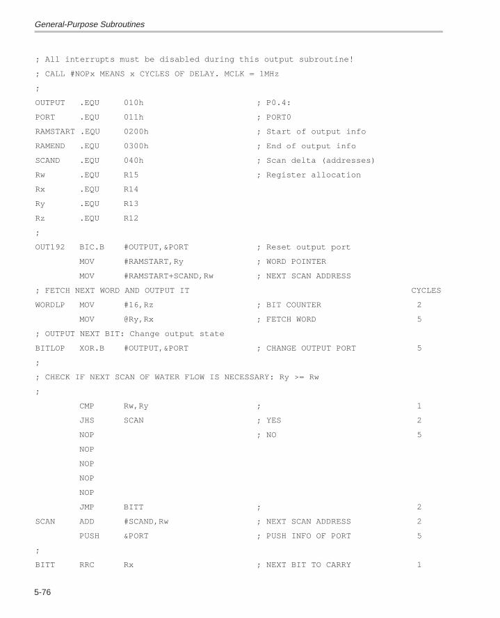
General-Purpose Subroutines
5-76
; All interrupts must be disabled during this output subroutine!
; CALL #NOPx MEANS x CYCLES OF DELAY. MCLK = 1MHz
;
OUTPUT .EQU 010h ; P0.4:
PORT .EQU 011h ; PORT0
RAMSTART .EQU 0200h ; Start of output info
RAMEND .EQU 0300h ; End of output info
SCAND .EQU 040h ; Scan delta (addresses)
Rw .EQU R15 ; Register allocation
Rx .EQU R14
Ry .EQU R13
Rz .EQU R12
;
OUT192 BIC.B #OUTPUT,&PORT ; Reset output port
MOV #RAMSTART,Ry ; WORD POINTER
MOV #RAMSTART+SCAND,Rw ; NEXT SCAN ADDRESS
; FETCH NEXT WORD AND OUTPUT IT CYCLES
WORDLP MOV #16,Rz ; BIT COUNTER 2
MOV @Ry,Rx ; FETCH WORD 5
; OUTPUT NEXT BIT: Change output state
BITLOP XOR.B #OUTPUT,&PORT ; CHANGE OUTPUT PORT 5
;
; CHECK IF NEXT SCAN OF WATER FLOW IS NECESSARY: Ry >= Rw
;
CMP Rw,Ry ; 1
JHS SCAN ; YES 2
NOP ; NO 5
NOP
NOP
NOP
NOP
JMP BITT ; 2
SCAN ADD #SCAND,Rw ; NEXT SCAN ADDRESS 2
PUSH &PORT ; PUSH INFO OF PORT 5
;
BITT RRC Rx ; NEXT BIT TO CARRY 1
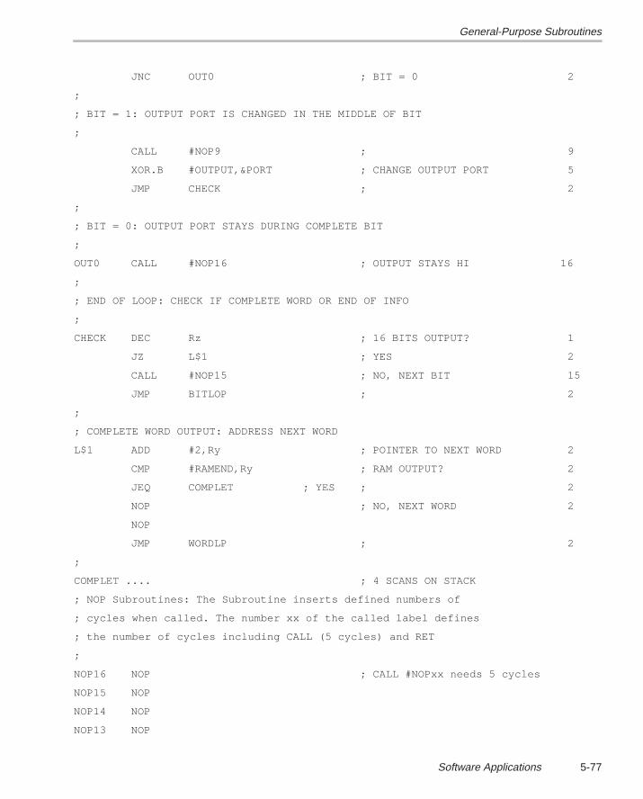
General-Purpose Subroutines
5-77Software Applications
JNC OUT0 ; BIT = 0 2
;
; BIT = 1: OUTPUT PORT IS CHANGED IN THE MIDDLE OF BIT
;
CALL #NOP9 ; 9
XOR.B #OUTPUT,&PORT ; CHANGE OUTPUT PORT 5
JMP CHECK ; 2
;
; BIT = 0: OUTPUT PORT STAYS DURING COMPLETE BIT
;
OUT0 CALL #NOP16 ; OUTPUT STAYS HI 16
;
; END OF LOOP: CHECK IF COMPLETE WORD OR END OF INFO
;
CHECK DEC Rz ; 16 BITS OUTPUT? 1
JZ L$1 ; YES 2
CALL #NOP15 ; NO, NEXT BIT 15
JMP BITLOP ; 2
;
; COMPLETE WORD OUTPUT: ADDRESS NEXT WORD
L$1 ADD #2,Ry ; POINTER TO NEXT WORD 2
CMP #RAMEND,Ry ; RAM OUTPUT? 2
JEQ COMPLET ; YES ; 2
NOP ; NO, NEXT WORD 2
NOP
JMP WORDLP ; 2
;
COMPLET .... ; 4 SCANS ON STACK
; NOP Subroutines: The Subroutine inserts defined numbers of
; cycles when called. The number xx of the called label defines
; the number of cycles including CALL (5 cycles) and RET
;
NOP16 NOP ; CALL #NOPxx needs 5 cycles
NOP15 NOP
NOP14 NOP
NOP13 NOP
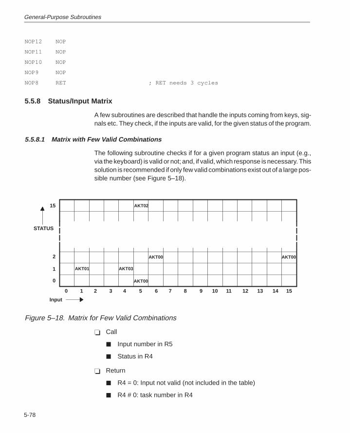
General-Purpose Subroutines
5-78
NOP12 NOP
NOP11 NOP
NOP10 NOP
NOP9 NOP
NOP8 RET ; RET needs 3 cycles
5.5.8 Status/Input Matrix
A few subroutines are described that handle the inputs coming from keys, sig-nals etc. They check, if the inputs are valid, for the given status of the program.
5.5.8.1 Matrix with Few Valid Combinations
The following subroutine checks if for a given program status an input (e.g.,via the keyboard) is valid or not; and, if valid, which response is necessary. Thissolution is recommended if only few valid combinations exist out of a large pos-sible number (see Figure 5–18).
AKT02
AKT00 AKT00
AKT00
AKT03AKT01
0 1 2 3 4 5 6 7 8 9 10 11 12 13 14 15
15
2
1
0
STATUS
Input
Figure 5–18. Matrix for Few Valid Combinations
Call
Input number in R5
Status in R4
Return
R4 = 0: Input not valid (not included in the table)
R4 # 0: task number in R4
General-Purpose Subroutines
5-79Software Applications
CALL MOV STATUS,R4 ; Program status to R4
MOV INPUT,R5 ; New input to R5
CALL #STIMTRX ; Check validity
... ; R4 contains info
;
STIMTRX MOV.B STTAB(R4),R4 ; Start of table for status
ADD #STTAB,R4 ; Table address to R4
L$3 CMP.B @R4+,R5 ; New input included in table?
JEQ L$2 ; Yes, output it
INC R4 ; No, skip response byte
TST.B 0(R4) ; End of status table? (0)
JNE L$3 ; No, try next input
CLR R4 ; Yes, end of table reached
RET ; Input invalid, return with R4 = 0
L$2 MOV.B @R4,R4 ; Input valid, return with task
RET ; number in R4
;
; Table with relative start addresses for the status tables
;
STTAB .BYTE ST0–STTAB,ST1–STTAB,ST2–STTAB,...ST15–STTAB
;
; Status tables: valid inputs,response,..,0 (up to 15 inputs)
;
ST0 .BYTE IN5,AKT00,0 ; Status 0 table
ST1 .BYTE IN1,AKT01,IN4,AKT03,0 ; Status 1 table
ST2 .BYTE IN15,AKT00,IN6,AKT06,0 ; Status 2 table
.... ; Status 3 to 14
ST15 .BYTE IN5,AKT02,0 ; Status 15 table
With a small change, the task to do is also executed within the subroutine:
CALL MOV STATUS,R4 ; Program status to R4
MOV INPUT,R5 ; New input to R5
CALL #STIMTRX ; Check validity and execute task
... ; R4 = 0: invalid input
;
STIMTRX MOV.B STTAB(R4),R4 ; Start of table for status
General-Purpose Subroutines
5-80
ADD #STTAB,R4 ; to R4
L$3 CMP.B @R4+,R5 ; New input included?
JEQ L$2 ; Yes, proceed
INC R4 ; No, skip task address
TST.B 0(R4) ; End of status table? (0)
JNE L$3 ; No, try next input
CLR R4 ; End of table reached
RET ; Input invalid, return with R4 = 0
L$2 MOV.B @R4,R4 ; Input valid, go to task
ADD R4,PC ; offset to AKT00 in R4
AKT00 ... ; Task 00
RET
AKT01 ... ; Task 01
RET
AKT06 ... ; Task 06
RET
AKT03 ... ; Task 03
RET
;
; Table with relative start addresses for the status tables
;
STTAB .BYTE ST1–STTAB,ST2–STTAB,...ST15–STTAB
;
; Status tables: valid inputs,task–table_start,0
;
ST1 .BYTE IN5,AKT00–AKT00,0 ; Status 1 table
ST2 .BYTE IN1,AKT01–AKT00,IN4, AKT03–AKT00,0
ST3 .BYTE IN15,AKT00–AKT00,IN6,AKT06–AKT00,0
.... ; Status 4 to 14
ST15 .BYTE IN5,AKT02–AKT00,0 ; Status 15 table
5.5.8.2 Matrix With Valid Combinations Only
The following subroutine executes the tasks belonging to the 16 possible STA-TUS/INPUT combinations. The handler start addresses must be within 254bytes relative to the label STTAB. The number of combinations can be en-larged to any value.
General-Purpose Subroutines
5-81Software Applications
Call
Input number in RAM byte INPUT (four possibilities 0 to 3)
Program status in RAM byte STATUS (four possibilities 0 to 3)
Return
No information returned
CALL CALL #STIMTRX ; Execute task for input
;
STIMTRX MOV.B STATUS,R4 ; Program status 00xx
MOV.B INPUT,R5 ; Input (key, Intrpt,) 0yy
RLA R4 ; STATUS x 4: 00xx –> 0xx0
RLA R4 ; 0xx0 –> 0xx00
ADD R5,R4 ; Build table offset: 0xxyy
MOV.B STTAB(R4),R4 ; Offset of Start of table
ADD R4,PC ; Handler start to PC
STTAB .BYTE AKT00–STTAB ; Action STATUS = 0, INPUT = 0
.BYTE AKT01–STTAB ; Action STATUS = 0, INPUT = 1
.BYTE AKT02–STTAB,AKT03–STTAB,AKT04–STTAB,AKT05–STTAB
...
.BYTE AKT12–STTAB,AKT13–STTAB,AKT14–STTAB,AKT15–STTAB
;
; Action handlers for the 16 STATUS/INPUT xy combinations
;
AKT00 ... ; Handler for task 0,0
RET
AKT01 ... ; Handler for task 0,1
RET
... ; Tasks 02 to 31
AKT32 ... ; Handler for task 3,2
RET
AKT33 ... ; Handler for task 3,3
RET
The next subroutine also executes the tasks belonging to the 16 possible STA-TUS/INPUT combinations. Here the handler start addresses can be locatedin the complete 64K-byte address space. The number of STATUS/INPUTcombinations can be enlarged to any value.
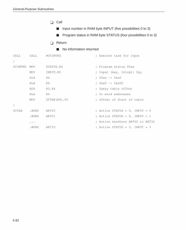
General-Purpose Subroutines
5-82
Call
Input number in RAM byte INPUT (five possibilities 0 to 3)
Program status in RAM byte STATUS (four possibilities 0 to 3)
Return
No information returned
CALL CALL #STIMTRX ; Execute task for input
;
STIMTRX MOV STATUS,R4 ; Program status 00xx
MOV INPUT,R5 ; Input (key, Intrpt) 0yy
RLA R4 ; 00xx –> 0xx0
RLA R4 ; 0xx0 –> 0xx00
ADD R5,R4 ; 0xxyy table offset
RLA R4 ; To word addresses
MOV STTAB(R4),PC ; Offset of Start of table
;
STTAB .WORD AKT00 ; Action STATUS = 0, INPUT = 0
.WORD AKT01 ; Action STATUS = 0, INPUT = 1
... ; Action handlers AKT02 to AKT32
.WORD AKT33 ; Action STATUS = 3, INPUT = 3
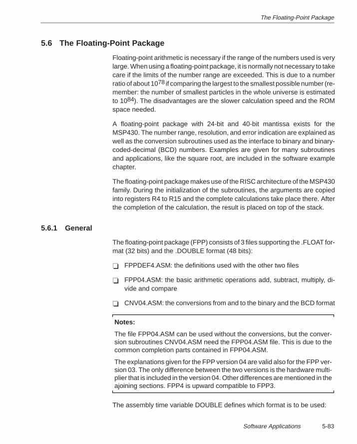
The Floating-Point Package
5-83Software Applications
5.6 The Floating-Point Package
Floating-point arithmetic is necessary if the range of the numbers used is verylarge. When using a floating-point package, it is normally not necessary to takecare if the limits of the number range are exceeded. This is due to a numberratio of about 1078 if comparing the largest to the smallest possible number (re-member: the number of smallest particles in the whole universe is estimatedto 1084). The disadvantages are the slower calculation speed and the ROMspace needed.
A floating-point package with 24-bit and 40-bit mantissa exists for theMSP430. The number range, resolution, and error indication are explained aswell as the conversion subroutines used as the interface to binary and binary-coded-decimal (BCD) numbers. Examples are given for many subroutinesand applications, like the square root, are included in the software examplechapter.
The floating-point package makes use of the RISC architecture of the MSP430family. During the initialization of the subroutines, the arguments are copiedinto registers R4 to R15 and the complete calculations take place there. Afterthe completion of the calculation, the result is placed on top of the stack.
5.6.1 General
The floating-point package (FPP) consists of 3 files supporting the .FLOAT for-mat (32 bits) and the .DOUBLE format (48 bits):
FPPDEF4.ASM: the definitions used with the other two files
FPP04.ASM: the basic arithmetic operations add, subtract, multiply, di-vide and compare
CNV04.ASM: the conversions from and to the binary and the BCD format
Notes:
The file FPP04.ASM can be used without the conversions, but the conver-sion subroutines CNV04.ASM need the FPP04.ASM file. This is due to thecommon completion parts contained in FPP04.ASM.
The explanations given for the FPP version 04 are valid also for the FPP ver-sion 03. The only difference between the two versions is the hardware multi-plier that is included in the version 04. Other differences are mentioned in theajoining sections. FPP4 is upward compatible to FPP3.
The assembly time variable DOUBLE defines which format is to be used:
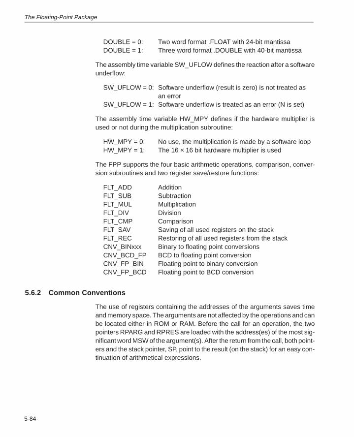
The Floating-Point Package
5-84
DOUBLE = 0: Two word format .FLOAT with 24-bit mantissaDOUBLE = 1: Three word format .DOUBLE with 40-bit mantissa
The assembly time variable SW_UFLOW defines the reaction after a softwareunderflow:
SW_UFLOW = 0: Software underflow (result is zero) is not treated as an error
SW_UFLOW = 1: Software underflow is treated as an error (N is set)
The assembly time variable HW_MPY defines if the hardware multiplier isused or not during the multiplication subroutine:
HW_MPY = 0: No use, the multiplication is made by a software loopHW_MPY = 1: The 16 × 16 bit hardware multiplier is used
The FPP supports the four basic arithmetic operations, comparison, conver-sion subroutines and two register save/restore functions:
FLT_ADD AdditionFLT_SUB SubtractionFLT_MUL MultiplicationFLT_DIV DivisionFLT_CMP ComparisonFLT_SAV Saving of all used registers on the stackFLT_REC Restoring of all used registers from the stackCNV_BINxxx Binary to floating point conversionsCNV_BCD_FP BCD to floating point conversionCNV_FP_BIN Floating point to binary conversionCNV_FP_BCD Floating point to BCD conversion
5.6.2 Common Conventions
The use of registers containing the addresses of the arguments saves timeand memory space. The arguments are not affected by the operations and canbe located either in ROM or RAM. Before the call for an operation, the twopointers RPARG and RPRES are loaded with the address(es) of the most sig-nificant word MSW of the argument(s). After the return from the call, both point-ers and the stack pointer, SP, point to the result (on the stack) for an easy con-tinuation of arithmetical expressions.
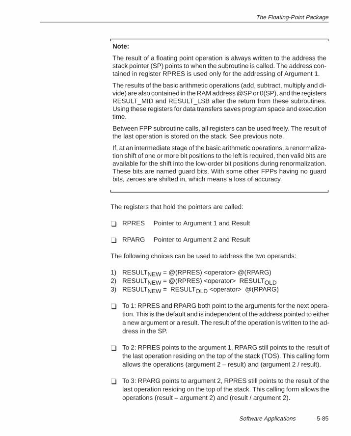
The Floating-Point Package
5-85Software Applications
Note:
The result of a floating point operation is always written to the address thestack pointer (SP) points to when the subroutine is called. The address con-tained in register RPRES is used only for the addressing of Argument 1.
The results of the basic arithmetic operations (add, subtract, multiply and di-vide) are also contained in the RAM address @SP or 0(SP), and the registersRESULT_MID and RESULT_LSB after the return from these subroutines.Using these registers for data transfers saves program space and executiontime.
Between FPP subroutine calls, all registers can be used freely. The result ofthe last operation is stored on the stack. See previous note.
If, at an intermediate stage of the basic arithmetic operations, a renormaliza-tion shift of one or more bit positions to the left is required, then valid bits areavailable for the shift into the low-order bit positions during renormalization.These bits are named guard bits. With some other FPPs having no guardbits, zeroes are shifted in, which means a loss of accuracy.
The registers that hold the pointers are called:
RPRES Pointer to Argument 1 and Result
RPARG Pointer to Argument 2 and Result
The following choices can be used to address the two operands:
1) RESULTNEW = @(RPRES) <operator> @(RPARG)2) RESULTNEW = @(RPRES) <operator> RESULTOLD3) RESULTNEW = RESULTOLD <operator> @(RPARG)
To 1: RPRES and RPARG both point to the arguments for the next opera-tion. This is the default and is independent of the address pointed to eithera new argument or a result. The result of the operation is written to the ad-dress in the SP.
To 2: RPRES points to the argument 1, RPARG still points to the result ofthe last operation residing on the top of the stack (TOS). This calling formallows the operations (argument 2 – result) and (argument 2 / result).
To 3: RPARG points to argument 2, RPRES still points to the result of thelast operation residing on the top of the stack. This calling form allows theoperations (result – argument 2) and (result / argument 2).
The Floating-Point Package
5-86
Note:
Formulas 2 and 3 are not equal, they allow use of the result on the TOS intwo ways with division and subtraction. No time is needed and no ROM-con-suming moves are necessary if the result is the divisor or the subtrahend forthe next operation.
Common to these subroutines is:
1) The pointers RPARG and RPRES point to the addresses of the input num-bers. They always point to the MSBs of these numbers.
2) The input numbers are not modified, except the last result on the stack,if it is used as an operand.
3) The result is located on the top of the stack (TOS), the stack pointer,RPARG, and RPRES point to the most significant word of the result
4) Every floating point number represents a valid value. No invalid combina-tions like Not a Number, Denormalized Number, or Infinity exist. In thisway, the MSP430 FPP has a larger range than other FPPs and allows ahigher speed with less memory used. This is because no unnecessarychecks for invalid numbers are made.
5) Every floating point operation outputs a valid floating point number thatcan be used immediately by other operations.
6) If a result is too large (exceeds the number range), the signed maximumnumber is output. An error indication is given in this case (see Table 5–6,Error Indication).
7) The CPU registers used are modified within the FPP subroutines, but donot contain valid data after a return from the subroutine. This means, theycan be used freely between the FPP subroutines for other purposes.
5.6.3 The Basic Arithmetic Operations
The FPP is designed for fast and memory saving calculations. So register in-structions are ideally suited for this operation. A common save and recall rou-tine for the registers used at the beginning and the end of an arithmetical ex-pression is an additional option. The subroutines FLT_SAV and FLT_RECshould be applied as shown in the following examples.
5.6.3.1 Addition
FLT_ADD: The floating point number pointed to by the register RPARG isadded to the floating point number pointed to by the register RPRES. The
The Floating-Point Package
5-87Software Applications
25th bit (41st bit in case of DOUBLE format) of the calculated mantissa isused for rounding. It is added to the result.
RESULT on TOS = @(RPRES) + @(RPARG)
Errors: Normal error handling. See Section 5.6.3.5, Error Handling, for adetailed description.
Output: The floating point sum of the two arguments is placed on the topof the stack. The stack pointer points to the same location as it did beforethe subroutine call.
The stack pointer, RPRES, and RPARG point to the MSBs of the floatingpoint sum. If an error occurred (N = 1 after return), the result is the numberthat best represents the correct result: 0 resp. ±3.4 × 1038.
EXAMPLE: The floating point number (.FLOAT format) contained in theROM starting at address NUMBER is added to the RAM location pointedto by R5. The result is written to the RAM addresses RES and RES+2(LSBs).
DOUBLE .EQU 0
MOV R5,RPRES ; Address of Argument 1 in R5
MOV #NUMBER,RPARG ; Address of Argument 2
CALL #FLT_ADD ; Call add subroutine
JN ERR_HND ; Error occurred, check reason
MOV @RPRES+,RES ; Store FPP result (MSBs)
MOV @RPRES+,RES+2 ; LSBs
... ; Continue with program
5.6.3.2 Subtraction
FLT_SUB: The floating point number pointed to by register RPARG is sub-tracted from the floating point number pointed to by register RPRES. Withproper loading of the two input pointers, it is possible to calculate (Argu-ment1 – Argument2) and (Argument2 – Argument1). The 25th bit (41st bitin case of DOUBLE format) of the calculated mantissa is used for roundingand is subtracted from the result.
RESULT on TOS = @(RPRES) – @(RPARG)
Errors: Normal error handling. See Section 5.6.3.5, Error Handling, for adetailed description.
Output: The floating point difference of the two arguments is placed on topof the stack. The stack pointer points to the same location as it did beforethe subroutine call.
The Floating-Point Package
5-88
The stack pointer, RPRES, and RPARG point to the MSBs of the floatingpoint difference. If an error occurred (N = 1 after return), the result is thenumber that best represents the correct result; 0 resp. ±3.4 × 1038.
EXAMPLE: The floating point number (.DOUBLE format) contained in theROM locations starting at address NUMBER is subtracted from RAM loca-tions pointed to by R5. The result is written to the RAM addresses pointedto by R5.
DOUBLE .EQU 1
MOV R5,RPRES ; Address of Argument1 in R5
MOV #NUMBER,RPARG ; Address of Argument2
CALL #FLT_SUB ; ((R5)) – (NUMBER) –> TOS
JN ERR_HND ; Error occurred, check reason
MOV @RPRES+,0(R5) ; Store FPP result (MSBs)
MOV @RPRES+,2(R5)
MOV @RPRES,4(R5) ; LSBs
... ; Continue with program
5.6.3.3 Multiplication
FLT_MUL: The floating point number pointed to by the register RPARG ismultiplied by the floating point number pointed to by the register RPRES.The 25th and 26th bit (41st and 42nd bit in case of DOUBLE format) of thecalculated mantissa are used for rounding.
If a shift is necessary to get the MSB of the mantissa set then the LSB–1 isshifted into the mantissa and the LSB–2 is added to the result.
If the MSB of the mantissa is set, only the LSB–1 is added to the result. Themultiplication subroutine returns the same result regardless of whether thehardware multiplier is used (HW_MPY = 1) or not (HW_MPY = 0).
RESULT on TOS = @(RPRES) × @(RPARG)
Errors: Normal error handling. See Section 5.6.3.5, Error Handling, for adetailed description.
Output: The floating point product of the two arguments is placed on thetop of the stack. The stack pointer points to the same location as it did be-fore the subroutine call.
The stack pointer, RPRES, and RPARG point to the MSBs of the floatingpoint product. If an error occurred (N = 1 after return), the result is the num-ber that best represents the correct result; 0 resp. ±3.4 × 1038.
Special Cases: 0 × 0 = 0 0 × X = 0 X × 0 = 0
The Floating-Point Package
5-89Software Applications
EXAMPLE: The result of the last operation, a floating point number(.FLOAT format) on the top of the stack, is multiplied by the constant π.
DOUBLE .EQU 0
MOV #PI,RPARG ; Address of constant PI
CALL #FLT_MUL ; ((RPRES)) x (PI) –> TOS
JN ERR_HND ; Error occurred, check reason
... ; Continue with program
PI .FLOAT 3.1415926535 ; Constant PI
5.6.3.4 Division
FLT_DIV: The floating point number pointed to by the register RPRES isdivided by the floating point number pointed to by the register RPARG.With proper loading of the two input pointers, it is possible to calculate (Ar-gument1 / Argument2) and (Argument2 / Argument1). The 25th bit (41stbit in case of DOUBLE format) of the calculated mantissa is used forrounding and is added to the result.
RESULT on TOS= @ ( RPRES)
@ ( RPARG )
Errors: Normal error handling. See Section 5.6.3.5, Error Handling, for adetailed description. Division by zero is indicated also.
Output: The floating point quotient of the two arguments is placed on thetop of the stack. The stack pointer points to the same location as it did be-fore the subroutine call.
The stack pointer, RPRES, and RPARG point to the MSBs of the floatingpoint quotient. If an error occurred (N = 1 after return), the result is the num-ber that best represents the correct result. For example, the largest num-ber that can be represented if a division by zero was made.
Special Cases: 0/0 = 0 0/X = 0 –X/0 = max. neg. number
+X/0 = max. pos. number
EXAMPLE: The floating point number (.DOUBLE format) contained in theROM locations starting at address NUMBER is divided by the RAM loca-tions pointed to by R5. The result is written to the RAM addresses pointedto by R5.
The Floating-Point Package
5-90
DOUBLE .EQU 1
MOV R5,RPARG ; Address of dividend
MOV #NUMBER,RPRES ; Address of divisor
CALL #FLT_DIV ; (NUMBER) / ((R5)) –> TOS
JN ERR_HND ; Error occurred, check reason
MOV @RPRES+,0(R5) ; Store FPP result (MSBs)
MOV @RPRES+,2(R5)
MOV @RPRES,4(R5) ; LSBs
... ; Continue with program
Examples for the Basic Arithmetic Operations
The following example shows the following program steps for the .FLOAT for-mat:
1) The registers used R5 to R12 are saved on the stack.
2) Four bytes are allocated on the stack to hold the results of the operations.
3) The address to a 12-digit BCD-buffer is loaded into pointer RPARG andthe BCD-to-floating point conversion is called. The resulting floating pointnumber is written to the result space previously allocated.
4) The resulting floating point number is multiplied with a number residing inthe memory address VAL3. RPARG points to this address.
5) To the last result, a floating point number contained in the memory addressVAL4 is added
6) The final result is converted back to BCD format (6 bytes) that can be dis-played in the LCD.
7) The final result is copied to the RAM addresses BCDMSD, BCDMID andBCDLSB. The three necessary POP instructions correct the stack pointerto the value after the save register subroutine.
8) The registers used, R5 to R12, are restored from the stack. The systemenvironment is exactly the same now as before the floating point calcula-tions.
DOUBLE .EQU 0 ; Use .FLOAT format
;
...... ; Normal program
CALL #FLT_SAV ; Save registers R5 to R12
The Floating-Point Package
5-91Software Applications
SUB #4,SP ; Allocate stack for result
MOV #BCDB,RPARG ; Load address of BCD–buffer
CALL #CNV_BCD_FP ; Convert BCD number to FP
;
; Calculate (BCD–number x VAL3) + VAL4
;
MOV #VAL3,RPARG ; Load address of slope
CALL #FLT_MUL ; Calculate next result
MOV #VAL4,RPARG ; Load address of offset
CALL #FLT_ADD ; Calculate next result
CALL #CNV_FP_BCD ; Convert final FP result to BCD
JN CNVERR ; Result too big for BCD buffer
POP BCDMSD ; BCD number MSDs and sign
POP BCDMID ; BCD digits MSD–4 to LSD+4
POP BCDLSD ; BCD digits LSD+3 to LSD
; Stack is corrected by POPs
CALL #FLT_REC ; Restore registers R5 to R12
; Continue with program
VAL3 .FLOAT –1.2345 ; Slope
VAL4 .FLOAT 14.4567 ; Offset
CNVERR ... ; Start error handler
The next example shows the following program steps for the .DOUBLE format:
1) The registers used, R5 to R15, are saved on the stack.
2) Six bytes are allocated on the stack to hold the results of the operations.
3) The ADC buffer address of the MSP430C32x (14-bit result) is written toRPARG and the last ADC result converted into a floating point number.The resulting floating point number is written to the result space previouslyallocated.
4) The resulting floating point number is multiplied with a number located atthe memory address VAL3. RPARG points to this address.
5) To the last result, a floating point number contained in the memory addressVAL4 is added.
6) The final result is converted back to binary format (6 bytes) and can beused for integer calculations.
The Floating-Point Package
5-92
7) The resulting binary number is copied to the RAM addresses BINMSD,BINMID, and BINLSB. The three necessary POP instructions correct thestack pointer to the value after the save register subroutine.
8) The registers used, R5 to R15, are restored from the stack. The systemenvironment is now exactly the same as it was before the floating point cal-culations.
DOUBLE .EQU 1 ; Use .DOUBLE format
;
...... ; Normal program
CALL #FLT_SAV ; Save registers R5 to R15
SUB #6,SP ; Allocate stack for result
MOV #ADAT,RPARG ; Load address of ADC data buffer
CALL #CNV_BIN16U ; Convert unsigned result to FP
;
; Calculate (ADC–Result x VAL3) + VAL4
;
MOV #VAL3,RPARG ; Load address of slope
CALL #FLT_MUL ; Calculate next result
MOV #VAL4,RPARG ; Load address of offset
CALL #FLT_ADD ; Calculate next result
CALL #CNV_FP_BIN ; Convert final FP result to binary
POP BINMSD ; Store MSBs of result and sign
POP BINMID ; Store MIDs and LSBs
POP BINLSD ; Stack is corrected by POPs
CALL #FLT_REC ; restore registers R5 to R15
; Continue with program
VAL3 .DOUBLE 1.2E–3 ; Slope 0.0012
VAL4 .DOUBLE 1.44567E1 ; Offset 14.4567
5.6.3.5 Error Handling
Errors during the operation affect the status bits in the status register SR. If theN-bit contained in the status register is reset to zero, no error occurred. If theN-bit is set to one, an error occurred. The kind of error can be seen inTable 5–6. The columns .FLOAT and .DOUBLE show the returned results foreach error.
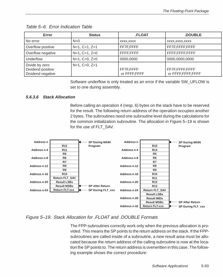
The Floating-Point Package
5-93Software Applications
Table 5–6. Error Indication Table
Error Status .FLOAT .DOUBLE
No error N=0 xxxx,xxxx xxxx,xxxx,xxxx
Overflow positive N=1, C=1, Z=1 FF7F,FFFF FF7F,FFFF,FFFF
Overflow negative N=1, C=1, Z=0 FFFF,FFFF FFFF,FFFF,FFFF
Underflow N=1, C=0, Z=0 0000,0000 0000,0000,0000
Divide by zeroDividend positiveDividend negative
N=1, C=0, Z=1FF7F,FFFF or FFFF,FFFF
FF7F,FFFF,FFFF or FFFF,FFFF,FFFF
Software underflow is only treated as an error if the variable SW_UFLOW isset to one during assembly.
5.6.3.6 Stack Allocation
Before calling an operation 4 (resp. 6) bytes on the stack have to be reservedfor the result. The following return address of the operation occupies another2 bytes. The subroutines need one subroutine level during the calculations forthe common initialization subroutine. The allocation in Figure 5–19 is shownfor the use of FLT_SAV.
Return FLT-xxxResult MSBsResult MIDsResult LSBs
Return FLT_SAVR13R12R11R10R9R8R7R6R5R14R15
SP During MAINProgram
SP After Return
SP During FLT_xxx
Address n
Address n-4
Address n-8
Address n-12
Address n-16
Address n-20
Address n-24
Address n-28
Address n-32
Return FLT-xxxResult MSBsResult LSBs
Return FLT_SAVR10R9R8R7R6R5R11R12
SP During MAINProgram
SP After ReturnSP During FLT_xxx
Address n
Address n-4
Address n-8
Address n-12
Address n-16
Address n-20
Address n-24
Figure 5–19. Stack Allocation for .FLOAT and .DOUBLE Formats
The FPP-subroutines correctly work only when the previous allocation is pro-vided. This means the SP points to the return address on the stack. If the FPP-subroutines are called inside of a subroutine, a new result area must be allo-cated because the return address of the calling subroutine is now at the loca-tion the SP points to. The return address is overwritten in this case. The follow-ing example shows the correct procedure:
The Floating-Point Package
5-94
SUBR SUB #(ML/8)+1,SP ; Allocate new result area
MOV @RPARG+,0(SP) ; Fetch argument 2 to new
MOV @RPARG+,2(SP) ; result area
.if DOUBLE=1
MOV @RPARG,4(SP)
.endif
MOV SP,RPARG ; Point again to argument 2
MOV #xx,RPRES ; Point to argument 1
CALL #FLT_xxx ; Use new result area for calc.
... ; Continue with calculations
MOV @SP+,result ; Free allocated stack
MOV @SP+,result+2 ; Store result, correct SP
.if DOUBLE=1
MOV @SP+,result+4
.endif
RET
Note that it is strongly recommended that conscientious housekeeping be pro-vided for SP to avoid stack overflow.
5.6.3.7 Number Range and Resolution
E = exponent of the floating point number. See Section 5.6.5, Internal DataRepresentation for more information.
.Float Format
Most positive number FF7F,FFFF 2127 x (2 – 2–23) = 3.402823 x 1038
Least positive number 0000,0001 2–128 x (1 + 2–23) = 2.938736 x 10–39
Zero 0000,0000 0 = 0.0
Least negative number 0080,0000 –2–128 = –2.938736 x 10–39
Most negative number FFFF,FFFF –2127 x (2 – 2–23) = –3.402823 x 1038
Resolution 2–23 x 2E = 119.2093 x 10⁻⁹ 2E
.DOUBLE Format
Most positive number FF7F,FFFF,FFFF 2127 x (2 – 2–39) = 3.402824 x 1038
The Floating-Point Package
5-95Software Applications
Least positive number 0000,0000,0001 2–128 x (1 + 2–39) = 2.938736 x 10–39
Zero 0000,0000,0000 0 = 0.0
Least negative number 0080,0000,0000 –2–128 = –2.938736 x 10–39
Most negative number FFFF,FFFF,FFFF –2127 x (2 – 2–39) = –3.402824 x 1038
Resolution 2–39 x 2E = 1.818989 x 10–12 x 2E
5.6.4 Calling Conventions for the Comparison
The comparison subroutine works much faster than a floating subtraction.Only the signs are compared in a first step to find out the relation of the twoarguments. When the signs of the two operands are equal, the mantissas arecompared. After the comparison, the status bits of the status register (SR) holdthe result: The registers RPRES and RPARG point to the same location theSP points to (for the FPP version 3 they were not defined).
Table 5–7. Comparison Results
Relations Status
Argument 1 > Argument 2 C=1, Z=0
Argument 1 < Argument 2 C=0, Z=0
Argument 1 = Argument 2 C=1, Z=1
The calling and use of the returned status bits is shown in the next example:
...
MOV #ARG1,RPRES ; Point to Argument 1 MSBs
MOV #ARG2,RPARG ; Point to Argument 2 MSBs
CALL #FLT_CMP ; Comparison: result to SR
JEQ EQUAL ; Condition for program flow
JHS ARG1_GT_ARG2 ; ARG1 is greater than ARG2
...... ; ARG1 is less than ARG2
EQUAL ...... ; ARG1 and ARG2 are equal
ARG1_GT_ARG2 .. ; ARG1 is greater than ARG2
;
; Other possibilities after the return
;
CALL #FLT_CMP ; Comparison: result to SR
The Floating-Point Package
5-96
JHS ARG1_GE_ARG2 ; ARG1 is greater/equal ARG2
...... ; ARG1 is less than ARG2
;
CALL #FLT_CMP ; Comparison: result to SR
JNE ARG1_NE_ARG2 ; @RPRES not equal to @RPARG
...... ; ARG1 is equal to ARG2
;
CALL #FLT_CMP ; Comparison: result to SR
JLO ARG1_LT_ARG2 ; ARG1 is less than ARG2
...... ; ARG1 is greater/equal ARG2
5.6.5 Internal Data Representation
The following description explains both the FLOAT and the DOUBLE formats.The two floating point formats consist of a floating point number whose:
8 most significant bits represent the exponent
24 (or 40 in the case of DOUBLE format) least significant bits hold the signand the mantissa.
Exponent Sm Mantissa
31 15 016
e7 e0 m0
FLOAT
Exponent Sm Mantissa
47 31 032
e7 e0 m0
DOUBLE
1516
m38
m22
Figure 5–20. Floating Point Formats for the MSP430 FPP
Where:Sm Sign of floating point number (sign of mantissa)mx Mantissa bit xex Exponent bit xx Valence of bit
The value N of a floating point number is
N MSm E= – × ×( )1 2

The Floating-Point Package
5-97Software Applications
Note:
The only exception to the previous equation is the floating zero. It is repre-sented by all zeroes (32 if FLOAT format or 48 if DOUBLE format). No nega-tive zero exists, the corresponding number (0080,0000) is a valid non-zeronumber and is the smallest negative number.
A frequently asked question is why the MSP430 floating point format does notconform to the widely used IEEE format. There are two main reasons why thisis not the case:
1) The MSP430 is often used in a real time environment where calculationsneed to be completed before the next input data are present.
2) Battery-supplied applications make calculations quickly to produce longerbattery lifes (up to 10 years for example).
These two main reasons make a run-time optimized floating point packagenecessary. The format of the floating-point number plays an important role inreaching this target.
With the MSP430-format, every floating-point number represents a validvalue. No invalid combinations like Not a Number, Denormalized Number,or Infinity exist. This way the MSP430 FPP has a larger range than otherFPPs. This allows a higher speed with the smallest memory usage. Thiseliminates the need for unnecessary checks for invalid numbers.
The exponent of the IEEE-format is located in two bytes because of thelocation of the sign in the MSB of the floating point number. With theMSP430-format, the exponent resides completely within the high byte ofthe most significant word and can, therefore, use the advantages of thebyte-oriented architecture of the MSP430. No shifts and no bit handlingare necessary to manipulate the exponent.
5.6.5.1 Computation of the Mantissa M
M m FLOAT Formati
i
i= + ×=
–∑1 20
2223( ) .
M m DOUBLE Formati
i
i= + ×=
–∑1 20
3839( ) .
The result of the previous calculation is always:2 > M ≥ 1
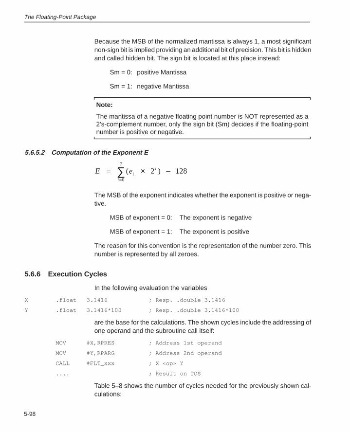
The Floating-Point Package
5-98
Because the MSB of the normalized mantissa is always 1, a most significantnon-sign bit is implied providing an additional bit of precision. This bit is hiddenand called hidden bit. The sign bit is located at this place instead:
Sm = 0: positive Mantissa
Sm = 1: negative Mantissa
Note:
The mantissa of a negative floating point number is NOT represented as a2’s-complement number, only the sign bit (Sm) decides if the floating-pointnumber is positive or negative.
5.6.5.2 Computation of the Exponent E
E eii
i= × –=∑ ( )
0
7
2 128
The MSB of the exponent indicates whether the exponent is positive or nega-tive.
MSB of exponent = 0: The exponent is negative
MSB of exponent = 1: The exponent is positive
The reason for this convention is the representation of the number zero. Thisnumber is represented by all zeroes.
5.6.6 Execution Cycles
In the following evaluation the variables
X .float 3.1416 ; Resp. .double 3.1416
Y .float 3.1416*100 ; Resp. .double 3.1416*100
are the base for the calculations. The shown cycles include the addressing ofone operand and the subroutine call itself:
MOV #X,RPRES ; Address 1st operand
MOV #Y,RPARG ; Address 2nd operand
CALL #FLT_xxx ; X <op> Y
.... ; Result on TOS
Table 5–8 shows the number of cycles needed for the previously shown cal-culations:
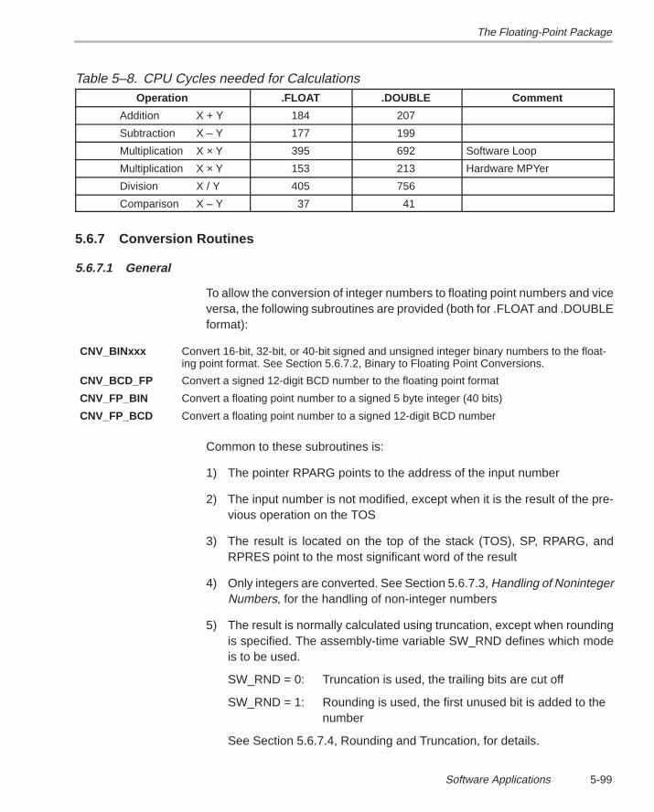
The Floating-Point Package
5-99Software Applications
Table 5–8. CPU Cycles needed for CalculationsOperation .FLOAT .DOUBLE Comment
Addition X + Y 184 207
Subtraction X – Y 177 199
Multiplication X × Y 395 692 Software Loop
Multiplication X × Y 153 213 Hardware MPYer
Division X / Y 405 756
Comparison X – Y 37 41
5.6.7 Conversion Routines
5.6.7.1 General
To allow the conversion of integer numbers to floating point numbers and viceversa, the following subroutines are provided (both for .FLOAT and .DOUBLEformat):
CNV_BINxxx Convert 16-bit, 32-bit, or 40-bit signed and unsigned integer binary numbers to the float-ing point format. See Section 5.6.7.2, Binary to Floating Point Conversions.
CNV_BCD_FP Convert a signed 12-digit BCD number to the floating point format
CNV_FP_BIN Convert a floating point number to a signed 5 byte integer (40 bits)
CNV_FP_BCD Convert a floating point number to a signed 12-digit BCD number
Common to these subroutines is:
1) The pointer RPARG points to the address of the input number
2) The input number is not modified, except when it is the result of the pre-vious operation on the TOS
3) The result is located on the top of the stack (TOS), SP, RPARG, andRPRES point to the most significant word of the result
4) Only integers are converted. See Section 5.6.7.3, Handling of NonintegerNumbers, for the handling of non-integer numbers
5) The result is normally calculated using truncation, except when roundingis specified. The assembly-time variable SW_RND defines which modeis to be used.
SW_RND = 0: Truncation is used, the trailing bits are cut off
SW_RND = 1: Rounding is used, the first unused bit is added to the number
See Section 5.6.7.4, Rounding and Truncation, for details.
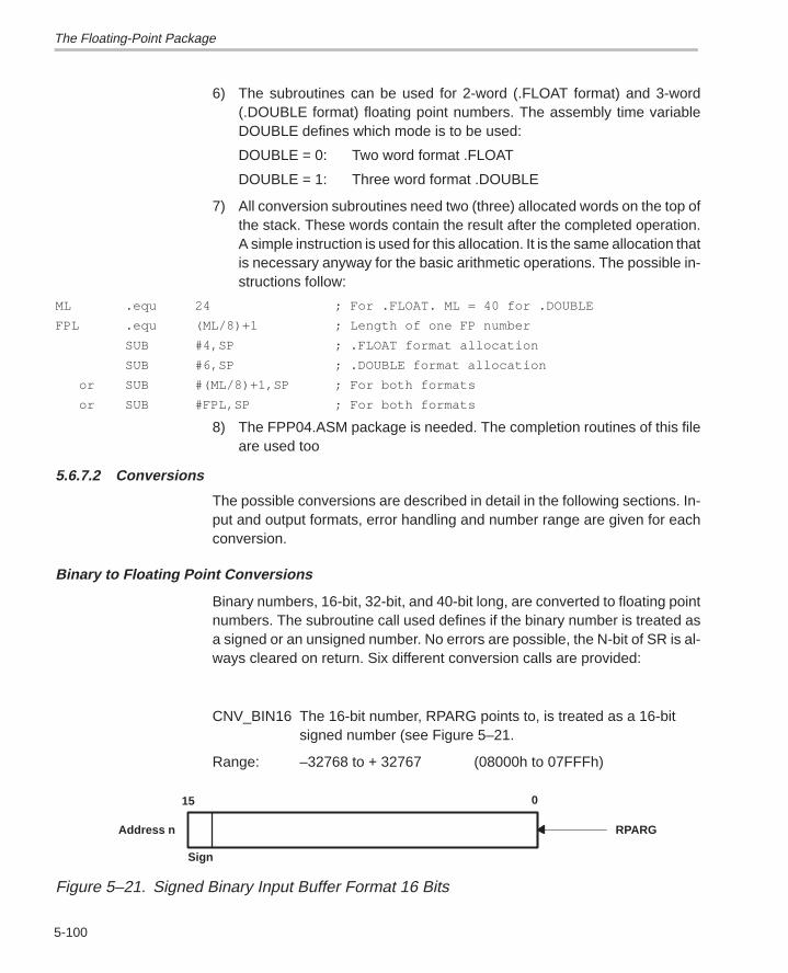
The Floating-Point Package
5-100
6) The subroutines can be used for 2-word (.FLOAT format) and 3-word(.DOUBLE format) floating point numbers. The assembly time variableDOUBLE defines which mode is to be used:
DOUBLE = 0: Two word format .FLOAT
DOUBLE = 1: Three word format .DOUBLE
7) All conversion subroutines need two (three) allocated words on the top ofthe stack. These words contain the result after the completed operation.A simple instruction is used for this allocation. It is the same allocation thatis necessary anyway for the basic arithmetic operations. The possible in-structions follow:
ML .equ 24 ; For .FLOAT. ML = 40 for .DOUBLE
FPL .equ (ML/8)+1 ; Length of one FP number
SUB #4,SP ; .FLOAT format allocation
SUB #6,SP ; .DOUBLE format allocation
or SUB #(ML/8)+1,SP ; For both formats
or SUB #FPL,SP ; For both formats
8) The FPP04.ASM package is needed. The completion routines of this fileare used too
5.6.7.2 Conversions
The possible conversions are described in detail in the following sections. In-put and output formats, error handling and number range are given for eachconversion.
Binary to Floating Point Conversions
Binary numbers, 16-bit, 32-bit, and 40-bit long, are converted to floating pointnumbers. The subroutine call used defines if the binary number is treated asa signed or an unsigned number. No errors are possible, the N-bit of SR is al-ways cleared on return. Six different conversion calls are provided:
CNV_BIN16 The 16-bit number, RPARG points to, is treated as a 16-bit signed number (see Figure 5–21.
Range: –32768 to + 32767 (08000h to 07FFFh)
15 0
Sign
RPARGAddress n
Figure 5–21. Signed Binary Input Buffer Format 16 Bits
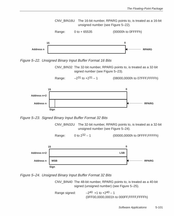
The Floating-Point Package
5-101Software Applications
CNV_BIN16U The 16-bit number, RPARG points to, is treated as a 16-bit unsigned number (see Figure 5–22).
Range: 0 to + 65535 (00000h to 0FFFFh)
15 0
RPARGAddress n
Figure 5–22. Unsigned Binary Input Buffer Format 16 Bits
CNV_BIN32 The 32-bit number, RPARG points to, is treated as a 32-bit signed number (see Figure 5–23).
Range: –231 to +231 – 1 (08000,0000h to 07FFF,FFFFh)
15 0
Sign
RPARGAddress n
Address n+2
Figure 5–23. Signed Binary Input Buffer Format 32 Bits
CNV_BIN32U The 32-bit number, RPARG points to, is treated as a 32-bitunsigned number (see Figure 5–24).
Range: 0 to 232 – 1 (00000,0000h to 0FFFF,FFFFh)
15 0
Sign
RPARGAddress n
Address n+2 LSB
MSB
Figure 5–24. Unsigned Binary Input Buffer Format 32 Bits
CNV_BIN40 The 48-bit number, RPARG points to, is treated as a 40-bitsigned (unsigned number) (see Figure 5–25).
Range signed: –240 +1 to +240 – 1(0FF00,0000,0001h to 000FF,FFFF,FFFFh)
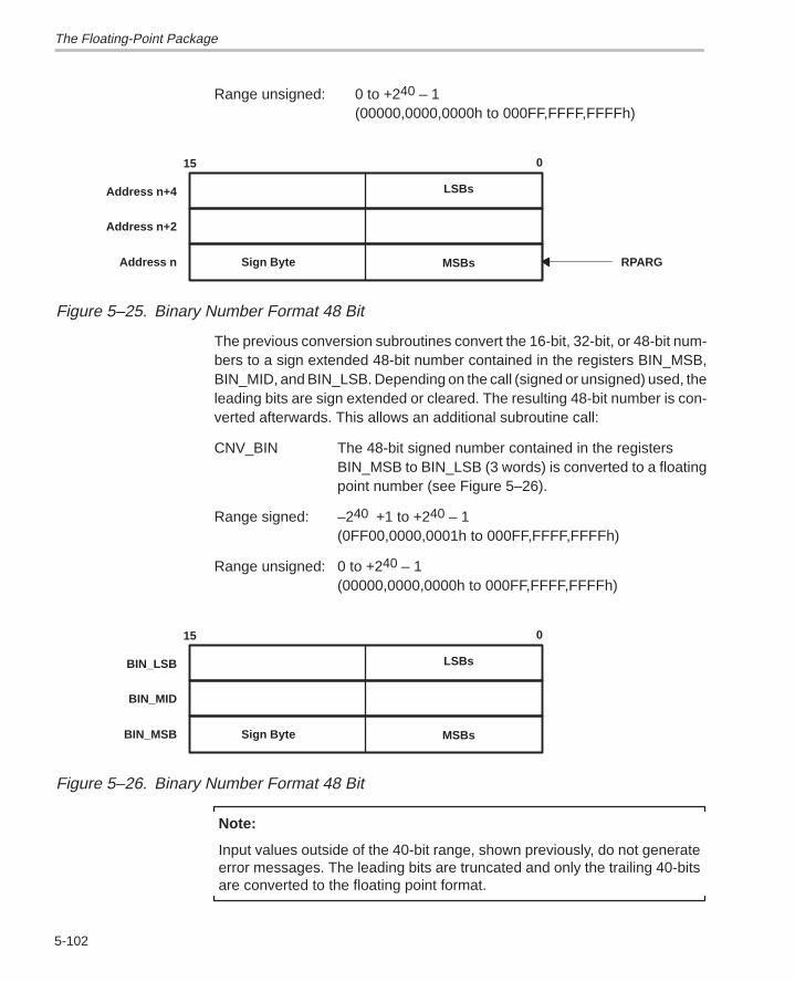
The Floating-Point Package
5-102
Range unsigned: 0 to +240 – 1(00000,0000,0000h to 000FF,FFFF,FFFFh)
15 0
RPARGAddress n
Address n+2
LSBs
Sign Byte MSBs
Address n+4
Figure 5–25. Binary Number Format 48 Bit
The previous conversion subroutines convert the 16-bit, 32-bit, or 48-bit num-bers to a sign extended 48-bit number contained in the registers BIN_MSB,BIN_MID, and BIN_LSB. Depending on the call (signed or unsigned) used, theleading bits are sign extended or cleared. The resulting 48-bit number is con-verted afterwards. This allows an additional subroutine call:
CNV_BIN The 48-bit signed number contained in the registersBIN_MSB to BIN_LSB (3 words) is converted to a floating
point number (see Figure 5–26).
Range signed: –240 +1 to +240 – 1(0FF00,0000,0001h to 000FF,FFFF,FFFFh)
Range unsigned: 0 to +240 – 1(00000,0000,0000h to 000FF,FFFF,FFFFh)
15 0
BIN_MSB
BIN_MID
LSBs
Sign Byte MSBs
BIN_LSB
Figure 5–26. Binary Number Format 48 Bit
Note:
Input values outside of the 40-bit range, shown previously, do not generateerror messages. The leading bits are truncated and only the trailing 40-bitsare converted to the floating point format.
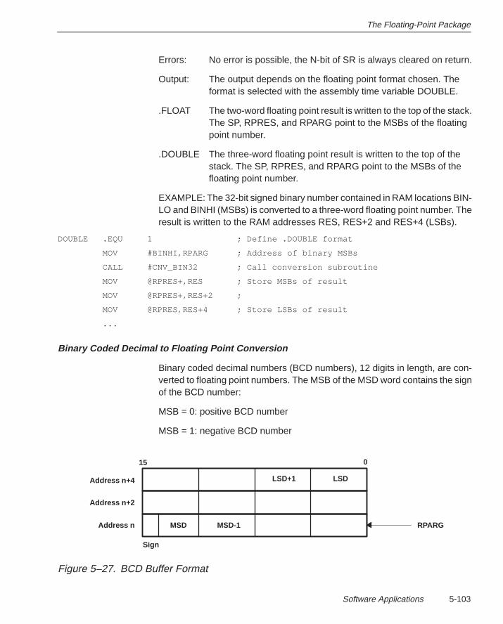
The Floating-Point Package
5-103Software Applications
Errors: No error is possible, the N-bit of SR is always cleared on return.
Output: The output depends on the floating point format chosen. The format is selected with the assembly time variable DOUBLE.
.FLOAT The two-word floating point result is written to the top of the stack. The SP, RPRES, and RPARG point to the MSBs of the floating point number.
.DOUBLE The three-word floating point result is written to the top of thestack. The SP, RPRES, and RPARG point to the MSBs of the floating point number.
EXAMPLE: The 32-bit signed binary number contained in RAM locations BIN-LO and BINHI (MSBs) is converted to a three-word floating point number. Theresult is written to the RAM addresses RES, RES+2 and RES+4 (LSBs).
DOUBLE .EQU 1 ; Define .DOUBLE format
MOV #BINHI,RPARG ; Address of binary MSBs
CALL #CNV_BIN32 ; Call conversion subroutine
MOV @RPRES+,RES ; Store MSBs of result
MOV @RPRES+,RES+2 ;
MOV @RPRES,RES+4 ; Store LSBs of result
...
Binary Coded Decimal to Floating Point Conversion
Binary coded decimal numbers (BCD numbers), 12 digits in length, are con-verted to floating point numbers. The MSB of the MSD word contains the signof the BCD number:
MSB = 0: positive BCD number
MSB = 1: negative BCD number
15 0
RPARGAddress n
Address n+2
LSD
MSD
Address n+4
Sign
MSD-1
LSD+1
Figure 5–27. BCD Buffer Format
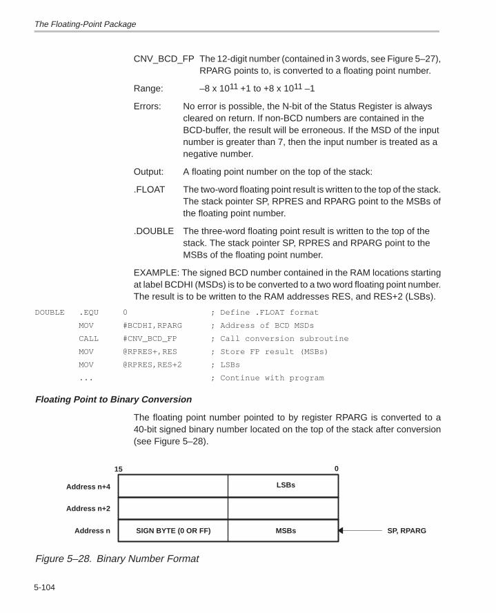
The Floating-Point Package
5-104
CNV_BCD_FP The 12-digit number (contained in 3 words, see Figure 5–27), RPARG points to, is converted to a floating point number.
Range: –8 x 10¹¹ +1 to +8 x 10¹¹ –1
Errors: No error is possible, the N-bit of the Status Register is alwayscleared on return. If non-BCD numbers are contained in theBCD-buffer, the result will be erroneous. If the MSD of the inputnumber is greater than 7, then the input number is treated as anegative number.
Output: A floating point number on the top of the stack:
.FLOAT The two-word floating point result is written to the top of the stack.The stack pointer SP, RPRES and RPARG point to the MSBs ofthe floating point number.
.DOUBLE The three-word floating point result is written to the top of thestack. The stack pointer SP, RPRES and RPARG point to theMSBs of the floating point number.
EXAMPLE: The signed BCD number contained in the RAM locations startingat label BCDHI (MSDs) is to be converted to a two word floating point number.The result is to be written to the RAM addresses RES, and RES+2 (LSBs).
DOUBLE .EQU 0 ; Define .FLOAT format
MOV #BCDHI,RPARG ; Address of BCD MSDs
CALL #CNV_BCD_FP ; Call conversion subroutine
MOV @RPRES+,RES ; Store FP result (MSBs)
MOV @RPRES,RES+2 ; LSBs
... ; Continue with program
Floating Point to Binary Conversion
The floating point number pointed to by register RPARG is converted to a40-bit signed binary number located on the top of the stack after conversion(see Figure 5–28).
15 0
SP, RPARGAddress n
Address n+2
LSBs
SIGN BYTE (0 OR FF)
Address n+4
MSBs
Figure 5–28. Binary Number Format
The Floating-Point Package
5-105Software Applications
CNV_FP_BIN The floating point number at the address in RPARG is con-verted to a 40-bit signed binary number.
Range signed: –240 +1 to + 240 – 1(0FF00,0000,0001h to 000FF,FFFF,FFFFh)
Errors: If the absolute value of the floating point number is greater than240–1, then the N bit in the status register is set to one. Otherwise,
the N bit is cleared.The result, put on top of the stack, is the largest signed binarynumber (saturation mode).
Output: A 40-bit signed, binary number at the top of the stack. The signuses a full byte.
.FLOAT SP, RPRES, and RPARG point to the MSBs of the three-wordbinary result. An additional word is inserted. It is the responsibilityof the calling software to correct the stack by one level upwardsafter the result is read.
.DOUBLE SP, RPRES, and RPARG point to the MSBs of the three-wordbinary result.
EXAMPLE: The floating point number (.DOUBLE format) contained in theRAM locations starting at label FPHI (MSBs) is converted to a 40-bit signedbinary number. The result is written to the RAM addresses RES, RES+2, andRES+4 (LSBs).
DOUBLE .EQU 1
MOV #FPHI,RPARG ; Address of FP MSBs
CALL #CNV_FP_BIN ; Call conversion subroutine
JN ERR_HND ; |FP number| is too big
MOV @RPRES+,RES ; Store binary result (MSBs)
MOV @RPRES+,RES+2 ;
MOV @RPRES,RES+4 ; LSBs
... ; Continue with program
Floating Point to Binary-Coded Decimal Conversion
The floating point number at the address in RPARG is converted to a signed12-digit BCD number located on the top of the stack after conversion (see Fig-ure 5–27). The MSD of the result has a maximum value of 7 because the signbit uses the MSB position.
CNV_FP_BCD The floating point number at the address in RPARG is converted to a 12-digit signed BCD number.
The Floating-Point Package
5-106
Range: –8 x 10¹¹ +1 to +8 x 10¹¹ –1
Errors: Three errors, at different stages of the conversion, are possible.These errors set the N-bit in the status register:
The exponent value of the floating point number is greaterthan 39, which represents an absolute value greater than1.0995 x 1012
The absolute value of the floating point number is greater than8 x 1011 –1
The absolute value is greater than 1 x 10¹²
Otherwise, the N bit is cleared.
The result, on the top of the stack, is the largest signed BCD number in case of an error.
Output: A 12-digit signed BCD number at the top of the stack (see Figure 5–27).
.FLOAT SP, RPRES, and RPARG point to the MSDs of the three-wordBCD result. An additional word is inserted. It is the responsibilityof the calling software to correct the stack by one level upwardsafter the reading of the result.
.DOUBLE SP, RPRES and RPARG point to the MSDs of the three-wordBCD result.
EXAMPLE: The floating point number (.FLOAT format) contained in RAM loca-tions starting at label FPHI (MSBs) is converted to a 12-digit BCD number. Theresult is written to RAM addresses RES, RES+2, and RES+4 (LSDs).
DOUBLE .EQU 0
MOV #FPHI,RPARG ; Address of FP MSBs
CALL #CNV_FP_BCD ; Call conversion subroutine
JN ERR_HND ; |FP number| is too big
MOV @SP+,RES ; Store BCD result (MSDs)
MOV @SP,RES+2 ; SP is corrected
MOV 2(SP),RES+4 ; LSDs
... ; Continue with program
ERR_HND ... ; Correct error here

The Floating-Point Package
5-107Software Applications
5.6.7.3 Handling of Non-Integer Numbers
The conversion subroutines handle only integer numbers when converting toor from floating point numbers. The reasons for this restriction are:
1) The stack grows if non-integer handling is included
2) The necessary program code of the conversion software grows larger
3) The integration of non-integer numbers is easier outside of the conversionsubroutines
4) The execution time grows longer due to the necessary successive divi-sions or multiplies by 10. This cannot be tolerated in real time environ-ments.
Binary to Floating-Point Conversion
If the location of the decimal point in the binary or hexadecimal number isknown, the correction of the result is as follows:
The resulting floating point number is divided by the constant 2n for binarynumbers or 16m for hexadecimal numbers (with m = 0.25 n). This is made sim-ply by subtracting n from the exponent of the floating-point number. Overflowor underflow is not possible due to the restricted range of the binary input (–240
+1 to +240 –1) compared to the range of the floating-point numbers (–1032 to+1032).
EXAMPLE: The binary 32-bit signed number contained in the RAM locationsstarting at label BINHI (MSBs) is converted to a floating-point number(.DOUBLE format). The virtual decimal point of the binary input number is 5bits left to the LSB. This means the integer input number is 32-times too large.For example, the binary buffer contains 1011000 (8810) but the real number is10.11000 (2.7510: 88 / 32 = 2.75)
MOV #BINHI,RPARG ; Address of binary buffer MSBs
CALL #CNV_BIN32 ; Call conversion subroutine
SUB.B #5,1(SP) ; Correct result’s exp. by 2^5
... ; Continue with corrected number
Binary-Coded Decimal (BCD) to Floating-Point Conversion
If the location of the decimal point in the BCD number is known, the correctionof the result is as follows:
The resulting floating-point number is divided by the constant 10n after the con-version. Overflow or underflow is not possible due to the restricted range of the
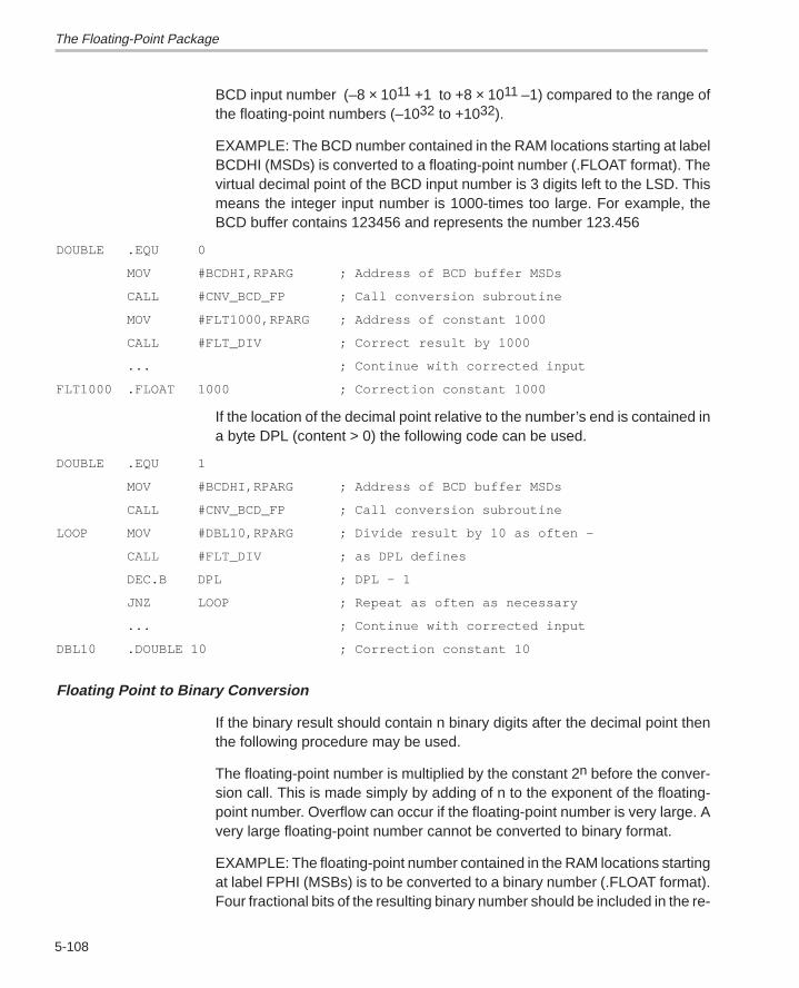
The Floating-Point Package
5-108
BCD input number (–8 × 10¹¹ +1 to +8 × 10¹¹ –1) compared to the range ofthe floating-point numbers (–1032 to +1032).
EXAMPLE: The BCD number contained in the RAM locations starting at labelBCDHI (MSDs) is converted to a floating-point number (.FLOAT format). Thevirtual decimal point of the BCD input number is 3 digits left to the LSD. Thismeans the integer input number is 1000-times too large. For example, theBCD buffer contains 123456 and represents the number 123.456
DOUBLE .EQU 0
MOV #BCDHI,RPARG ; Address of BCD buffer MSDs
CALL #CNV_BCD_FP ; Call conversion subroutine
MOV #FLT1000,RPARG ; Address of constant 1000
CALL #FLT_DIV ; Correct result by 1000
... ; Continue with corrected input
FLT1000 .FLOAT 1000 ; Correction constant 1000
If the location of the decimal point relative to the number’s end is contained ina byte DPL (content > 0) the following code can be used.
DOUBLE .EQU 1
MOV #BCDHI,RPARG ; Address of BCD buffer MSDs
CALL #CNV_BCD_FP ; Call conversion subroutine
LOOP MOV #DBL10,RPARG ; Divide result by 10 as often –
CALL #FLT_DIV ; as DPL defines
DEC.B DPL ; DPL – 1
JNZ LOOP ; Repeat as often as necessary
... ; Continue with corrected input
DBL10 .DOUBLE 10 ; Correction constant 10
Floating Point to Binary Conversion
If the binary result should contain n binary digits after the decimal point thenthe following procedure may be used.
The floating-point number is multiplied by the constant 2n before the conver-sion call. This is made simply by adding of n to the exponent of the floating-point number. Overflow can occur if the floating-point number is very large. Avery large floating-point number cannot be converted to binary format.
EXAMPLE: The floating-point number contained in the RAM locations startingat label FPHI (MSBs) is to be converted to a binary number (.FLOAT format).Four fractional bits of the resulting binary number should be included in the re-
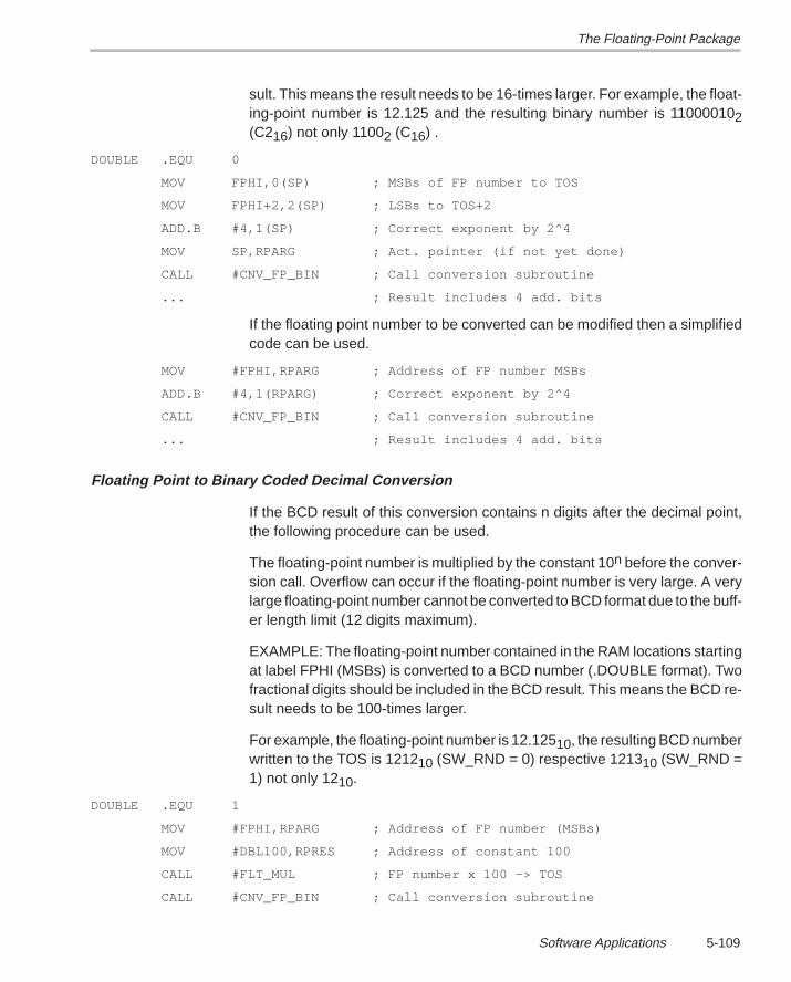
The Floating-Point Package
5-109Software Applications
sult. This means the result needs to be 16-times larger. For example, the float-ing-point number is 12.125 and the resulting binary number is 110000102(C216) not only 11002 (C16) .
DOUBLE .EQU 0
MOV FPHI,0(SP) ; MSBs of FP number to TOS
MOV FPHI+2,2(SP) ; LSBs to TOS+2
ADD.B #4,1(SP) ; Correct exponent by 2^4
MOV SP,RPARG ; Act. pointer (if not yet done)
CALL #CNV_FP_BIN ; Call conversion subroutine
... ; Result includes 4 add. bits
If the floating point number to be converted can be modified then a simplifiedcode can be used.
MOV #FPHI,RPARG ; Address of FP number MSBs
ADD.B #4,1(RPARG) ; Correct exponent by 2^4
CALL #CNV_FP_BIN ; Call conversion subroutine
... ; Result includes 4 add. bits
Floating Point to Binary Coded Decimal Conversion
If the BCD result of this conversion contains n digits after the decimal point,the following procedure can be used.
The floating-point number is multiplied by the constant 10n before the conver-sion call. Overflow can occur if the floating-point number is very large. A verylarge floating-point number cannot be converted to BCD format due to the buff-er length limit (12 digits maximum).
EXAMPLE: The floating-point number contained in the RAM locations startingat label FPHI (MSBs) is converted to a BCD number (.DOUBLE format). Twofractional digits should be included in the BCD result. This means the BCD re-sult needs to be 100-times larger.
For example, the floating-point number is 12.12510, the resulting BCD numberwritten to the TOS is 121210 (SW_RND = 0) respective 121310 (SW_RND =1) not only 1210.
DOUBLE .EQU 1
MOV #FPHI,RPARG ; Address of FP number (MSBs)
MOV #DBL100,RPRES ; Address of constant 100
CALL #FLT_MUL ; FP number x 100 –> TOS
CALL #CNV_FP_BIN ; Call conversion subroutine
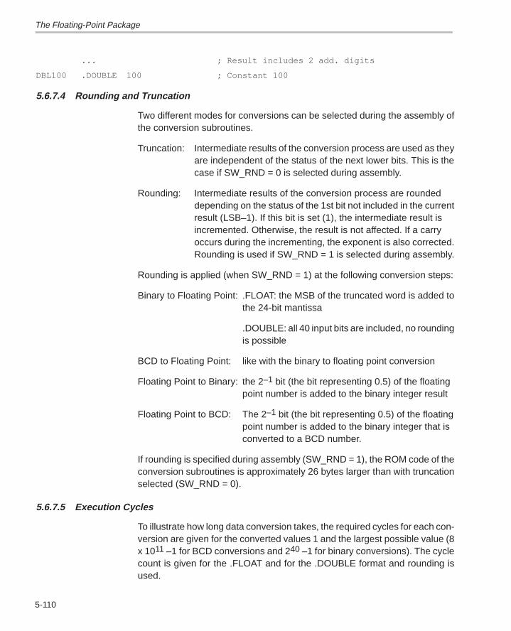
The Floating-Point Package
5-110
... ; Result includes 2 add. digits
DBL100 .DOUBLE 100 ; Constant 100
5.6.7.4 Rounding and Truncation
Two different modes for conversions can be selected during the assembly ofthe conversion subroutines.
Truncation: Intermediate results of the conversion process are used as theyare independent of the status of the next lower bits. This is thecase if SW_RND = 0 is selected during assembly.
Rounding: Intermediate results of the conversion process are roundeddepending on the status of the 1st bit not included in the currentresult (LSB–1). If this bit is set (1), the intermediate result is incremented. Otherwise, the result is not affected. If a carry occurs during the incrementing, the exponent is also corrected.Rounding is used if SW_RND = 1 is selected during assembly.
Rounding is applied (when SW_RND = 1) at the following conversion steps:
Binary to Floating Point: .FLOAT: the MSB of the truncated word is added tothe 24-bit mantissa
.DOUBLE: all 40 input bits are included, no roundingis possible
BCD to Floating Point: like with the binary to floating point conversion
Floating Point to Binary: the 2–1 bit (the bit representing 0.5) of the floatingpoint number is added to the binary integer result
Floating Point to BCD: The 2–1 bit (the bit representing 0.5) of the floatingpoint number is added to the binary integer that isconverted to a BCD number.
If rounding is specified during assembly (SW_RND = 1), the ROM code of theconversion subroutines is approximately 26 bytes larger than with truncationselected (SW_RND = 0).
5.6.7.5 Execution Cycles
To illustrate how long data conversion takes, the required cycles for each con-version are given for the converted values 1 and the largest possible value (8x 10¹¹ –1 for BCD conversions and 240 –1 for binary conversions). The cyclecount is given for the .FLOAT and for the .DOUBLE format and rounding isused.
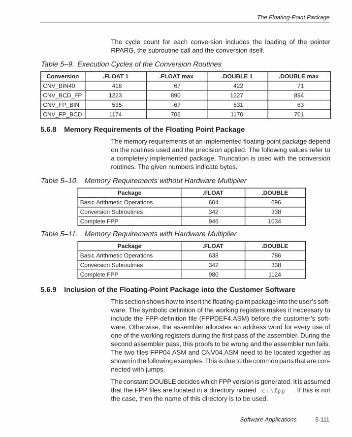
The Floating-Point Package
5-111Software Applications
The cycle count for each conversion includes the loading of the pointerRPARG, the subroutine call and the conversion itself.
Table 5–9. Execution Cycles of the Conversion Routines
Conversion .FLOAT 1 .FLOAT max .DOUBLE 1 .DOUBLE max
CNV_BIN40 418 67 422 71
CNV_BCD_FP 1223 890 1227 894
CNV_FP_BIN 535 67 531 63
CNV_FP_BCD 1174 706 1170 701
5.6.8 Memory Requirements of the Floating Point Package
The memory requirements of an implemented floating-point package dependon the routines used and the precision applied. The following values refer toa completely implemented package. Truncation is used with the conversionroutines. The given numbers indicate bytes.
Table 5–10. Memory Requirements without Hardware Multiplier
Package .FLOAT .DOUBLE
Basic Arithmetic Operations 604 696
Conversion Subroutines 342 338
Complete FPP 946 1034
Table 5–11. Memory Requirements with Hardware Multiplier
Package .FLOAT .DOUBLE
Basic Arithmetic Operations 638 786
Conversion Subroutines 342 338
Complete FPP 980 1124
5.6.9 Inclusion of the Floating-Point Package into the Customer Software
This section shows how to insert the floating-point package into the user’s soft-ware. The symbolic definition of the working registers makes it necessary toinclude the FPP-definition file (FPPDEF4.ASM) before the customer’s soft-ware. Otherwise, the assembler allocates an address word for every use ofone of the working registers during the first pass of the assembler. During thesecond assembler pass, this proofs to be wrong and the assembler run fails.The two files FPP04.ASM and CNV04.ASM need to be located together asshown in the following examples. This is due to the common parts that are con-nected with jumps.
The constant DOUBLE decides which FPP version is generated. It is assumedthat the FPP files are located in a directory named c:\fpp . If this is notthe case, then the name of this directory is to be used.
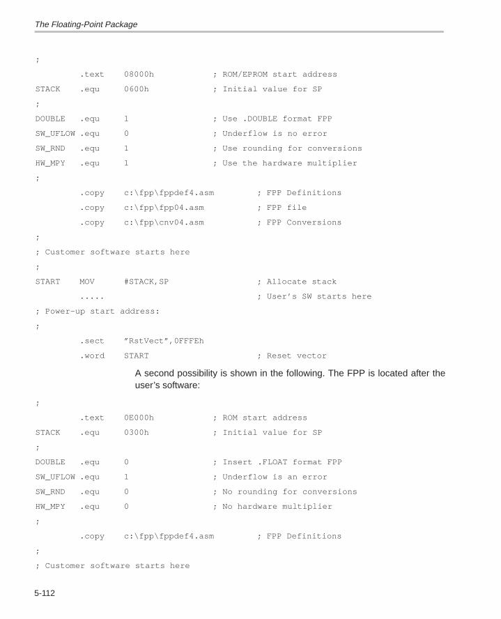
The Floating-Point Package
5-112
;
.text 08000h ; ROM/EPROM start address
STACK .equ 0600h ; Initial value for SP
;
DOUBLE .equ 1 ; Use .DOUBLE format FPP
SW_UFLOW .equ 0 ; Underflow is no error
SW_RND .equ 1 ; Use rounding for conversions
HW_MPY .equ 1 ; Use the hardware multiplier
;
.copy c:\fpp\fppdef4.asm ; FPP Definitions
.copy c:\fpp\fpp04.asm ; FPP file
.copy c:\fpp\cnv04.asm ; FPP Conversions
;
; Customer software starts here
;
START MOV #STACK,SP ; Allocate stack
..... ; User’s SW starts here
; Power–up start address:
;
.sect ”RstVect”,0FFFEh
.word START ; Reset vector
A second possibility is shown in the following. The FPP is located after theuser’s software:
;
.text 0E000h ; ROM start address
STACK .equ 0300h ; Initial value for SP
;
DOUBLE .equ 0 ; Insert .FLOAT format FPP
SW_UFLOW .equ 1 ; Underflow is an error
SW_RND .equ 0 ; No rounding for conversions
HW_MPY .equ 0 ; No hardware multiplier
;
.copy c:\fpp\fppdef4.asm ; FPP Definitions
;
; Customer software starts here
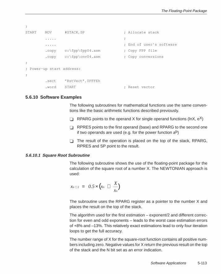
The Floating-Point Package
5-113Software Applications
;
START MOV #STACK,SP ; Allocate stack
..... ;
..... ; End of user’s software
.copy c:\fpp\fpp04.asm ; Copy FPP file
.copy c:\fpp\cnv04.asm ; Copy conversions
;
; Power–up start address:
;
.sect ”RstVect”,0FFFEh
.word START ; Reset vector
5.6.10 Software Examples
The following subroutines for mathematical functions use the same conven-tions like the basic arithmetic functions described previously.
RPARG points to the operand X for single operand functions (lnX, eX)
RPRES points to the first operand (base) and RPARG to the second oneif two operands are used (e.g. for the power function ab)
The result of the operation is placed on the top of the stack, RPARG,RPRES and SP point to the result.
5.6.10.1 Square Root Subroutine
The following subroutine shows the use of the floating-point package for thecalculation of the square root of a number X. The NEWTONIAN approach isused:
x 0.5 xX
xn 1 n
n+ ( )= × +
The subroutine uses the RPARG register as a pointer to the number X andplaces the result on the top of the stack.
The algorithm used for the first estimation – exponent/2 and different correc-tion for even and odd exponents – leads to the worst case estimation errorsof +8% and –13%. This relatively exact estimations lead to only four iterationloops to get the full accuracy.
The number range of X for the square-root function contains all positive num-bers including zero. Negative values for X return the previous result on the topof the stack and the N bit set as an error indication.
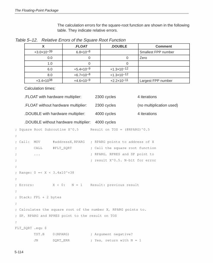
The Floating-Point Package
5-114
The calculation errors for the square-root function are shown in the followingtable. They indicate relative errors.
Table 5–12. Relative Errors of the Square Root FunctionX .FLOAT .DOUBLE Comment
+3.0×10–39 6.8×10⁻⁸ Smallest FPP number
0.0 0 0 Zero
1.0 0 0
6.0 +5.4×10⁻⁹ +1.3×10⁻¹²
8.0 +6.7×10⁻⁸ +1.3×10⁻¹²
+3.4×1038 +4.6×10⁻⁹ +2.2×10⁻¹¹ Largest FPP number
Calculation times:
.FLOAT with hardware multiplier: 2300 cycles 4 iterations
.FLOAT without hardware multiplier: 2300 cycles (no multiplication used)
.DOUBLE with hardware multiplier: 4000 cycles 4 iterations
.DOUBLE without hardware multiplier: 4000 cycles
; Square Root Subroutine X^0.5 Result on TOS = (@RPARG)^0.5
;
; Call: MOV #addressX,RPARG ; RPARG points to address of X
; CALL #FLT_SQRT ; Call the square root function
; ... ; RPARG, RPRES and SP point to
; ; result X^0.5. N–bit for error
;
; Range: 0 =< X < 3.4x10^+38
;
; Errors: X < 0: N = 1 Result: previous result
;
; Stack: FPL + 2 bytes
;
; Calculates the square root of the number X, RPARG points to.
; SP, RPARG and RPRES point to the result on TOS
;
FLT_SQRT .equ $
TST.B 0(RPARG) ; Argument negative?
JN SQRT_ERR ; Yes, return with N = 1
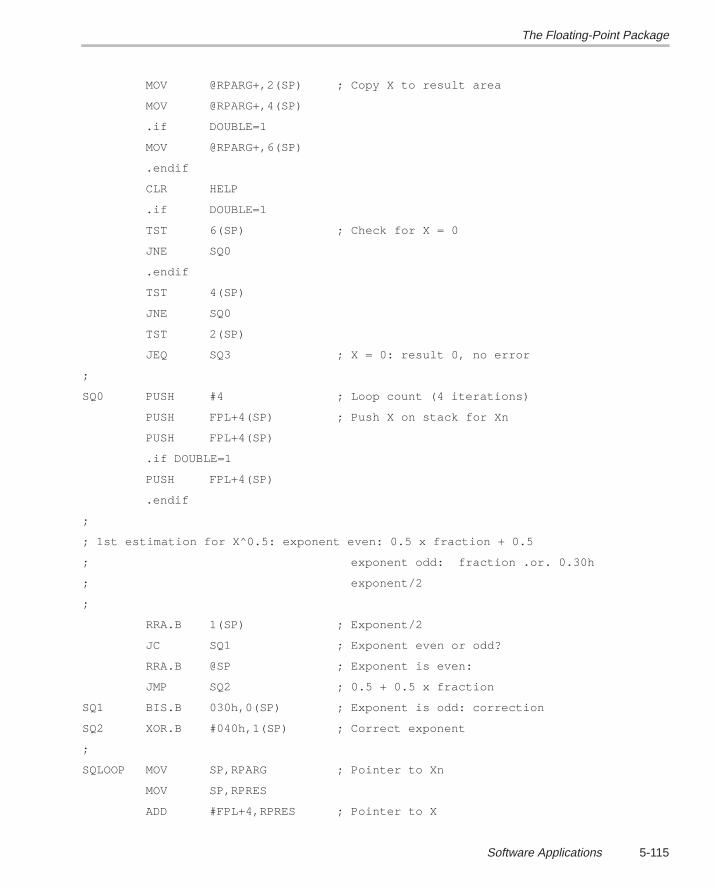
The Floating-Point Package
5-115Software Applications
MOV @RPARG+,2(SP) ; Copy X to result area
MOV @RPARG+,4(SP)
.if DOUBLE=1
MOV @RPARG+,6(SP)
.endif
CLR HELP
.if DOUBLE=1
TST 6(SP) ; Check for X = 0
JNE SQ0
.endif
TST 4(SP)
JNE SQ0
TST 2(SP)
JEQ SQ3 ; X = 0: result 0, no error
;
SQ0 PUSH #4 ; Loop count (4 iterations)
PUSH FPL+4(SP) ; Push X on stack for Xn
PUSH FPL+4(SP)
.if DOUBLE=1
PUSH FPL+4(SP)
.endif
;
; 1st estimation for X^0.5: exponent even: 0.5 x fraction + 0.5
; exponent odd: fraction .or. 0.30h
; exponent/2
;
RRA.B 1(SP) ; Exponent/2
JC SQ1 ; Exponent even or odd?
RRA.B @SP ; Exponent is even:
JMP SQ2 ; 0.5 + 0.5 x fraction
SQ1 BIS.B 030h,0(SP) ; Exponent is odd: correction
SQ2 XOR.B #040h,1(SP) ; Correct exponent
;
SQLOOP MOV SP,RPARG ; Pointer to Xn
MOV SP,RPRES
ADD #FPL+4,RPRES ; Pointer to X
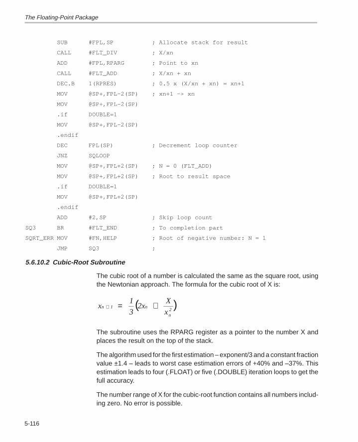
The Floating-Point Package
5-116
SUB #FPL,SP ; Allocate stack for result
CALL #FLT_DIV ; X/xn
ADD #FPL,RPARG ; Point to xn
CALL #FLT_ADD ; X/xn + xn
DEC.B 1(RPRES) ; 0.5 x (X/xn + xn) = xn+1
MOV @SP+,FPL–2(SP) ; xn+1 –> xn
MOV @SP+,FPL–2(SP)
.if DOUBLE=1
MOV @SP+,FPL–2(SP)
.endif
DEC FPL(SP) ; Decrement loop counter
JNZ SQLOOP
MOV @SP+,FPL+2(SP) ; N = 0 (FLT_ADD)
MOV @SP+,FPL+2(SP) ; Root to result space
.if DOUBLE=1
MOV @SP+,FPL+2(SP)
.endif
ADD #2,SP ; Skip loop count
SQ3 BR #FLT_END ; To completion part
SQRT_ERR MOV #FN,HELP ; Root of negative number: N = 1
JMP SQ3 ;
5.6.10.2 Cubic-Root Subroutine
The cubic root of a number is calculated the same as the square root, usingthe Newtonian approach. The formula for the cubic root of X is:
x1
32x
X
xn 1 n
n2
+ ( )= +
The subroutine uses the RPARG register as a pointer to the number X andplaces the result on the top of the stack.
The algorithm used for the first estimation – exponent/3 and a constant fractionvalue ±1.4 – leads to worst case estimation errors of +40% and –37%. Thisestimation leads to four (.FLOAT) or five (.DOUBLE) iteration loops to get thefull accuracy.
The number range of X for the cubic-root function contains all numbers includ-ing zero. No error is possible.
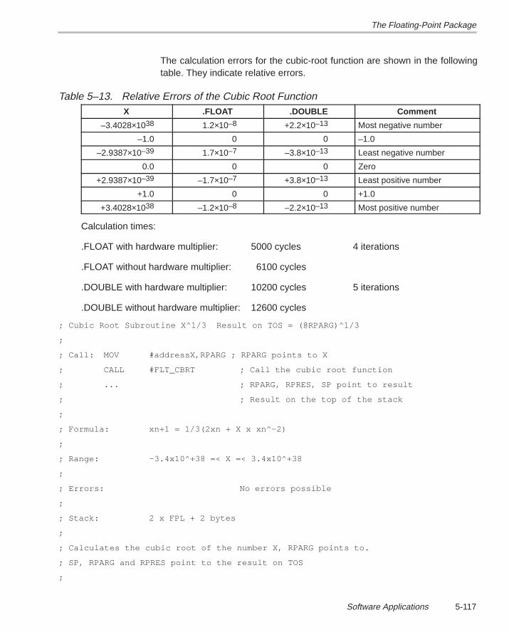
The Floating-Point Package
5-117Software Applications
The calculation errors for the cubic-root function are shown in the followingtable. They indicate relative errors.
Table 5–13. Relative Errors of the Cubic Root FunctionX .FLOAT .DOUBLE Comment
–3.4028×1038 1.2×10⁻⁸ +2.2×10⁻¹³ Most negative number
–1.0 0 0 –1.0
–2.9387×10–39 1.7×10⁻⁷ –3.8×10⁻¹³ Least negative number
0.0 0 0 Zero
+2.9387×10–39 –1.7×10⁻⁷ +3.8×10⁻¹³ Least positive number
+1.0 0 0 +1.0
+3.4028×1038 –1.2×10⁻⁸ –2.2×10⁻¹³ Most positive number
Calculation times:
.FLOAT with hardware multiplier: 5000 cycles 4 iterations
.FLOAT without hardware multiplier: 6100 cycles
.DOUBLE with hardware multiplier: 10200 cycles 5 iterations
.DOUBLE without hardware multiplier: 12600 cycles
; Cubic Root Subroutine X^1/3 Result on TOS = (@RPARG)^1/3
;
; Call: MOV #addressX,RPARG ; RPARG points to X
; CALL #FLT_CBRT ; Call the cubic root function
; ... ; RPARG, RPRES, SP point to result
; ; Result on the top of the stack
;
; Formula: xn+1 = 1/3(2xn + X x xn^–2)
;
; Range: –3.4x10^+38 =< X =< 3.4x10^+38
;
; Errors: No errors possible
;
; Stack: 2 x FPL + 2 bytes
;
; Calculates the cubic root of the number X, RPARG points to.
; SP, RPARG and RPRES point to the result on TOS
;
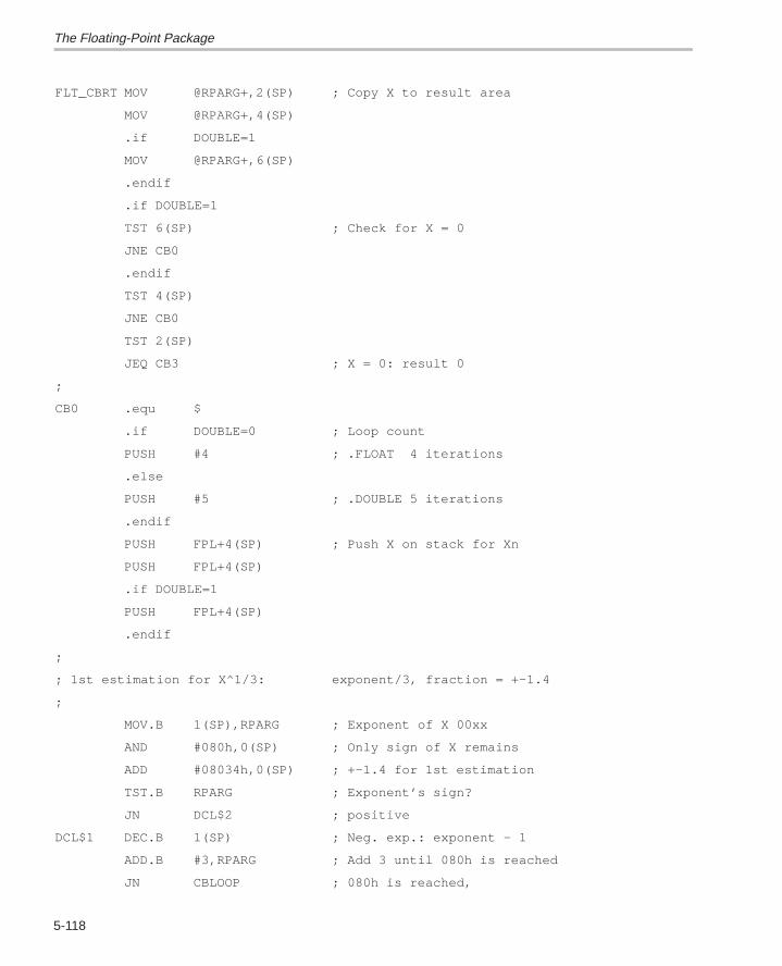
The Floating-Point Package
5-118
FLT_CBRT MOV @RPARG+,2(SP) ; Copy X to result area
MOV @RPARG+,4(SP)
.if DOUBLE=1
MOV @RPARG+,6(SP)
.endif
.if DOUBLE=1
TST 6(SP) ; Check for X = 0
JNE CB0
.endif
TST 4(SP)
JNE CB0
TST 2(SP)
JEQ CB3 ; X = 0: result 0
;
CB0 .equ $
.if DOUBLE=0 ; Loop count
PUSH #4 ; .FLOAT 4 iterations
.else
PUSH #5 ; .DOUBLE 5 iterations
.endif
PUSH FPL+4(SP) ; Push X on stack for Xn
PUSH FPL+4(SP)
.if DOUBLE=1
PUSH FPL+4(SP)
.endif
;
; 1st estimation for X^1/3: exponent/3, fraction = +–1.4
;
MOV.B 1(SP),RPARG ; Exponent of X 00xx
AND #080h,0(SP) ; Only sign of X remains
ADD #08034h,0(SP) ; +–1.4 for 1st estimation
TST.B RPARG ; Exponent’s sign?
JN DCL$2 ; positive
DCL$1 DEC.B 1(SP) ; Neg. exp.: exponent – 1
ADD.B #3,RPARG ; Add 3 until 080h is reached
JN CBLOOP ; 080h is reached,
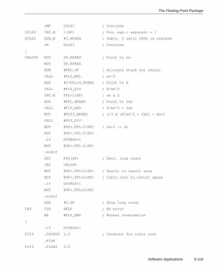
The Floating-Point Package
5-119Software Applications
JMP DCL$1 ; Continue
DCL$3 INC.B 1(SP) ; Pos. exp.: exponent + 1
DCL$2 SUB.B #3,RPARG ; Subtr. 3 until 080h is reached
JN DCL$3 ; Continue
;
CBLOOP MOV SP,RPARG ; Point to xn
MOV SP,RPRES
SUB #FPL,SP ; Allocate stack for result
CALL #FLT_MUL ; xn^2
ADD #2*FPL+4,RPRES ; Point to A
CALL #FLT_DIV ; X/xn^2
INC.B FPL+1(SP) ; xn x 2
ADD #FPL,RPARG ; Point to 2xn
CALL #FLT_ADD ; X/xn^2 + 2xn
MOV #FLT3,RPARG ; 1/3 x (X/xn^2 + 2xn) = xn+1
CALL #FLT_DIV
MOV @SP+,FPL–2(SP) ; xn+1 –> xn
MOV @SP+,FPL–2(SP)
.if DOUBLE=1
MOV @SP+,FPL–2(SP)
.endif
DEC FPL(SP) ; Decr. loop count
JNZ CBLOOP
MOV @SP+,FPL+2(SP) ; Result to result area
MOV @SP+,FPL+2(SP) ; Cubic root to result space
.if DOUBLE=1
MOV @SP+,FPL+2(SP)
.endif
ADD #2,SP ; Skip loop count
CB3 CLR HELP ; No error
BR #FLT_END ; Normal termination
;
.if DOUBLE=1
FLT3 .DOUBLE 3.0 ; Constant for cubic root
.else
FLT3 .FLOAT 3.0
The Floating-Point Package
5-120
.endif
5.6.10.3 Fourth-Root Subroutine
The fourth root of a number is calculated by calling the square root subroutinetwice.
EXAMPLE: the fourth root is calculated for a number residing in RAM at ad-dress NUMBER (MSBs). The fourth root is written to RESULT. The previousresult on TOS must not be overwritten.
SUB #ML/8+1,SP ; Allocate work area
MOV #NUMBER,RPARG ; Address of NUMBER to RPARG
CALL #FLT_SQRT ; Square root of NUMBER on TOS
JN ERROR ; NUMBER is negative
CALL #FLT_SQRT ; Fourth root on TOS
MOV @SP+,RESULT ; 4th root MSBs
MOV @SP+,RESULT+2 ; Correct SP to previous result
.if DOUBLE=1
MOV @SP+,RESULT+4 ; LSBs for DOUBLE
.endif
5.6.10.4 Other Root Subroutines
Using the same calculations shown previously, higher roots can also be calcu-lated using the Newtonian approach. The generic formula for the mth root outof A is:
( )x1
mm 1 x
A
xn 1 n
nm 1
+ –( )= – +
To get short calculation times – which means only few iterations are necessary– the choice of the first estimation x0 is very important. For the above formulaa good first iteration x0 is (M = mantissa, E = exponent):
( )x
M
mE m
01
1 2=–
+( ) × /
5.6.10.5 Calculations With Intermediate Results
If a calculation cannot be executed simply and has intermediate results, a newresult space is used. This is done by subtracting 4 (.FLOAT) or 6 (.DOUBLE)from the stack pointer.
The Floating-Point Package
5-121Software Applications
EXAMPLE: The following function for e is to be calculated. The example is val-id for both formats:
e a bc
d= × –
FPL .equ (ML/8)+1 ; Length of a FPP number
;
SUB #FPL,SP ; Allocate result space 0 (RS0)
MOV #a,RPRES ; Address argument 1
MOV #b,RPARG ; Address argument 2
CALL #FLT_MUL ; a x b –> RS0
SUB #FPL,SP ; Allocate result space 1 (RS1)
MOV #c,RPRES ; Address c
MOV #d,RPARG ; Address d
CALL #FLT_DIV ; c/d –> RS1
ADD #FPL,RPRES ; Address (a x b) in RS0
CALL #FLT_SUB ; e = (a x b) – c/d –> RS1
MOV @SP+,FPL–2(SP) ; Result e to RS0
MOV @SP+,FPL–2(SP) ; Overwrite (a x b) with e
.if DOUBLE=1
MOV @SP+,FPL–2(SP) ; LSBs for DOUBLE
.endif
;
; Housekeeping is made, SP points to RS0 again, but not
; RPARG and RPRES
EXAMPLE: The multiply-and-add (MAC) function for e shown in the followingis calculated. The example is written for both formats:
e a b en n+ = × +1
SUB #ML/8+1,SP ; Allocate result space
MOV #a,RPRES ; Address argument 1
MOV #b,RPARG ; Address argument 2
CALL #FLT_MUL ; a x b
MOV #e,RPARG ; Address e
CALL #FLT_ADD ; (a x b)+ e
The Floating-Point Package
5-122
MOV @RPARG+,e ; Actualize e with result
MOV @RPARG+,e+2 ; MIDs or LSBs
.if DOUBLE=1
MOV @RPARG+,e+4 ; LSBs
.endif
;
; SP and RPRES still point to the result, RPARG may be used
; for the next argument address.
5.6.10.6 Absolute Value of a Number
If the absolute value of a number is needed, this is done by simply resettingthe sign bit of the number.
EXAMPLE: the absolute value of the result on the top of the stack is needed.
BIC #080h,0(SP) ; |result| on TOS
5.6.10.7 Change of the Sign of a Number
If a sign change is necessary (multiplication by –1), this is done by simply in-verting the sign bit of the number.
EXAMPLE: the sign of the result on the top of the stack is changed.
XOR #080h,0(SP) ; Negate result on TOS
5.6.10.8 Integer Value of a Number
The integer value of a floating-point number can be calculated with the subrou-tine FLT_INTG in the following example. The pointer RPARG is loaded with theaddress of the number. The result is then placed on the top of the stack. Noerror is possible. Numbers below one are returned as zero. The subroutine canhandle .FLOAT and .DOUBLE formats.
;
; Calculate the integer value of the number RPARG points to.
; Result: on top of the stack. RPARG, RPRES and SP point to it
; Call MOV #number,RPARG ; Address to RPARG
; CALL #FLT_INTG ; Call subroutine
; ... ; Result on TOS
;
FLT_INTG MOV.B 1(RPARG),COUNTER ; Exponent to COUNTER
MOV @RPARG+,2(SP) ; MSBs and Exponent
The Floating-Point Package
5-123Software Applications
MOV @RPARG+,4(SP) ; LSBs .FLOAT
.if DOUBLE=1
MOV @RPARG,6(SP) ; LSBs .DOUBLE
.endif
MOV #0FFFFh,ARG2_MSB ; Mask for fractional part
.if DOUBLE=1
MOV #0FFFFh,ARG2_MID
.endif
MOV #0FFFFh,ARG2_LSB
JMP L$30
;
INTGLP CLRC ; Shift 0 in always
RRC.B ARG2_MSB ; Shift mask to next lower bit
.if DOUBLE=1
RRC ARG2_MID
.endif
RRC ARG2_LSB
DEC COUNTER ; Shift as often as:
L$30 CMP #080h,COUNTER ; SHIFT COUNT = EXPONENT – 07Fh
JHS INTGLP
BIC ARG2_MSB,2(SP) ; Mask out fract. part
.if DOUBLE=1
BIC ARG2_MID,4(SP) ; For .DOUBLE format
BIC ARG2_LSB,6(SP)
.else
BIC ARG2_LSB,4(SP) ; For .FLOAT format
.endif
MOV SP,RPARG ; Both pointer to result‘s MSBs
ADD #2,RPARG
MOV RPARG,RPRES
RET ; Return with Integer on TOS
EXAMPLE: the integer value of the floating point number residing at addressVOL1 is placed on TOS.
MOV #VOL1,RPARG ; Load pointer with address
CALL #FLT_INTG ; Calculate integer of VOL1
The Floating-Point Package
5-124
.... ; Integer on TOS
5.6.10.9 Fractional Part of a Number
The fractional part of a floating-point number can be calculated with the sub-routine FLT_FRCT in the following example. The pointer RPARG is loadedwith the address of the number. The result is placed on the top of the stack.No error is possible. The subroutine can handle both floating-point formats.The subroutine calls the subroutine FLT_INTG shown previously.
Integer values or very large numbers return a zero value due to the given reso-lution.
.DOUBLE format: numbers > 1.099512 x 10¹² (>240)
.FLOAT format: numbers > 1.6777216 x10⁷) (>224)
; Calculate the fractional part of the number RPARG points to.
; Result: on top of the stack. RPARG, RPRES and SP point to it
; Subroutine FLT_INTG is used
; Call MOV #number,RPARG ; Address to RPARG
; CALL #FLT_FRCT ; Call subroutine
; ... ; Result on TOS
;
FLT_FRCT PUSH RPARG ; Copy operand‘s address
.if DOUBLE=1
PUSH 4(RPARG) ; Copy operand to allow the use
.endif ; of the value on TOS
PUSH 2(RPARG)
PUSH @RPARG
CALL #FLT_INTG ; Integer part of operand to TOS
MOV ML/8+1(SP),RPRES ; Operand address to RPRES
CALL #FLT_SUB ; Operand – Integer part to TOS
.if DOUBLE=1 ; Housekeeping:
MOV @SP+,ML/8+3(SP) ; Fractional part back
.endif
MOV @SP+,ML/8+3(SP) ; To result area
MOV @SP+,ML/8+3(SP)
ADD #2,SP ; Skip saved operand address
CLR HELP ; No error
BR #FLT_END ; Use FPP termination
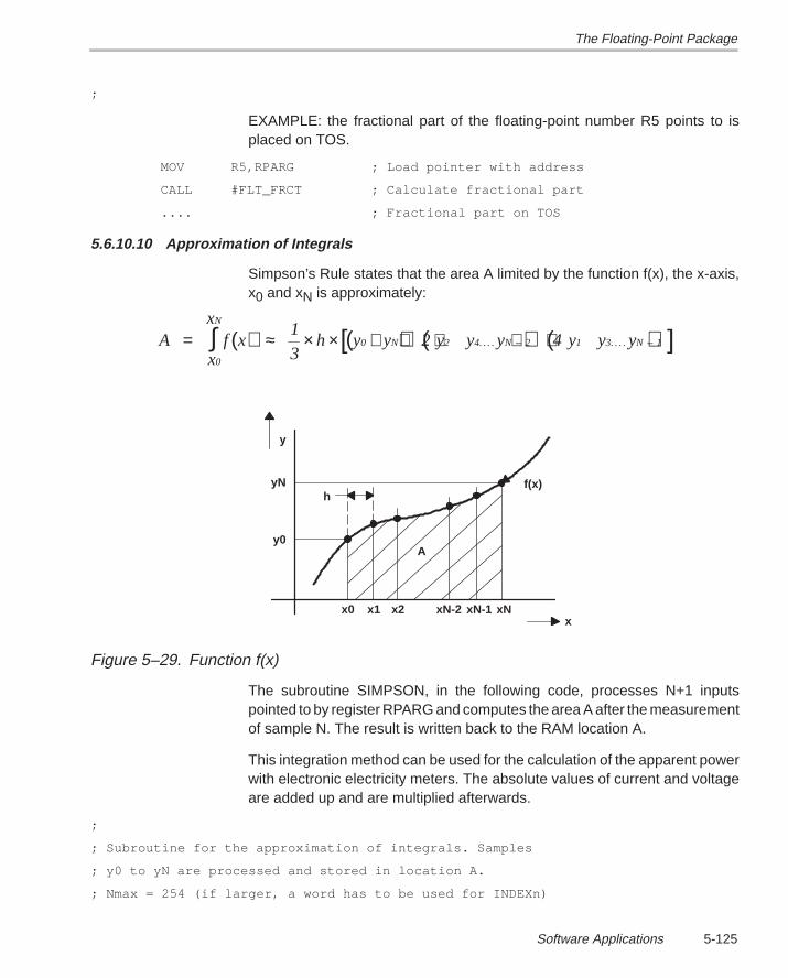
The Floating-Point Package
5-125Software Applications
;
EXAMPLE: the fractional part of the floating-point number R5 points to isplaced on TOS.
MOV R5,RPARG ; Load pointer with address
CALL #FLT_FRCT ; Calculate fractional part
.... ; Fractional part on TOS
5.6.10.10 Approximation of Integrals
Simpson’s Rule states that the area A limited by the function f(x), the x-axis,x0 and xN is approximately:
( ) ( ) ( ) ( )[ ]A f xx
x1
3h y y 2 y y y 4 y y y
0
N
0 N 2 4. . . . N 2 1 3. . . . N 1= ≈ × × + + + + +∫ – –
A
f(x)
y
yN
y0
h
x0 x1 x2 xN-2 xN-1 xNx
Figure 5–29. Function f(x)
The subroutine SIMPSON, in the following code, processes N+1 inputspointed to by register RPARG and computes the area A after the measurementof sample N. The result is written back to the RAM location A.
This integration method can be used for the calculation of the apparent powerwith electronic electricity meters. The absolute values of current and voltageare added up and are multiplied afterwards.
;
; Subroutine for the approximation of integrals. Samples
; y0 to yN are processed and stored in location A.
; Nmax = 254 (if larger, a word has to be used for INDEXn)
The Floating-Point Package
5-126
;
; Call: CLR.B INDEXn ; Before 1st call: n = 0
; LOOP MOV #sample,RPARG ; Address of yn
; CALL #SIMPSON ; Process sample yn
; CMP.B #N+1,INDEXn ; YN processed?
; JLO LOOP ; No, proceed
; ... ; Yes, integral in A
;
N .equ 8 ; Max. index (must be even)
.if DOUBLE=0
A .equ 0200h ; summed up value (integral)
INDXn .equ 0204H ; Index n (0 to N)
FLT3 .float 3.0
h .float 0.32 ; Difference h: yn+1 – yn
.else
A .equ 0200h ; Summed up value (integral)
INDXn .equ 0206H ; Index n (0 to N)
FLT3 .double 3.0
h .double 0.32 ; Difference h: yn+1 – yn
.endif
SIMPSON SUB #(ML/8)+1,SP ; Allocate new workspace
MOV @RPARG+,0(SP) ; Fetch yn
MOV @RPARG+,2(SP)
.if DOUBLE=1
MOV @RPARG,4(SP)
.endif
CMP.B #0,INDXn ; 1st value y0?
JEQ Y0
CMP.B #N,INDXn ; Last value yN?
JEQ YN
BIT #1,INDXn ; Odd or even n?
JZ YEVEN
INC.B 1(SP) ; Odd: value x 4
YEVEN INC.B 1(SP) ; Even: value x 2
MOV #A,RPARG ; Fetch summed–up value A
MOV SP,RPRES ; New sample yn on TOS
The Floating-Point Package
5-127Software Applications
CALL #FLT_ADD ; Add it to A
JMP Y0 ; Store added result in A
;
YN MOV #A,RPARG ; Last value yN: calculate
MOV SP,RPRES ; New sample yn on TOS
CALL #FLT_ADD ; Add last result to A
MOV #FLT3,RPARG ; To constant 3.0
CALL #FLT_DIV ; Divide summed–up value by 3.0
MOV #h,RPARG ; Multiply with distance h
CALL #FLT_MUL
;
Y0 MOV @SP+,A ; Store result to A
MOV @SP+,A+2 ; and correct stack
.if DOUBLE=1
MOV @SP+,A+4
.endif
INC.B INDXn ; Next n
RET ; Return with integral in A
EXAMPLE: The function f(x) described by the calculated results on top of thestack is integrated using Simpson’s rule..
CLR.B INDXn ; Initialization: INDXn = 0
INTLOP ... ; Calculation, result on TOS
CALL #SIMPSON ; Process samples y0 to yN
CMP.B #N+1,INDXn ; Last sample yN processed?
JLO INTLOP ; No, continue
... ; Yes, result in A
5.6.10.11Statistical Calculations
The mean value, the standard deviation, and the variance of measured sam-ples can be calculated with the following subroutines.
STAT_INIT clears the RAM locations used for data gathering.
STAT_PREP adds the input sample to the RAM location SUMYi, thesquared input sample to SUM2Yi and increments the sample counter N.
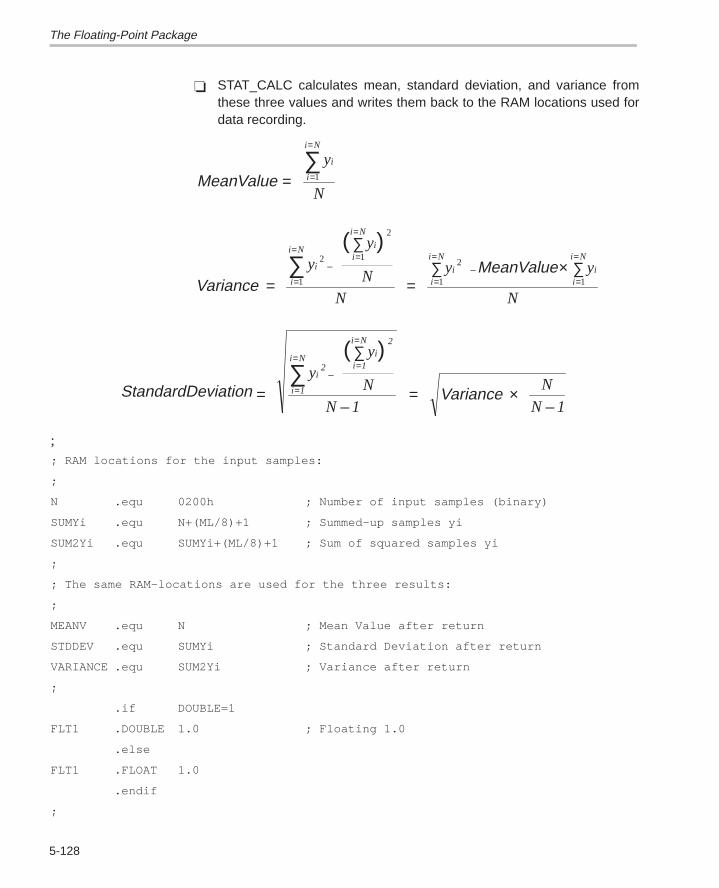
The Floating-Point Package
5-128
STAT_CALC calculates mean, standard deviation, and variance fromthese three values and writes them back to the RAM locations used fordata recording.
MeanValuey
N
i
i
i N
= =
=
∑1
Variancey
y
NN
y MeanValue y
N
i
ii
i N
i
i N
ii
i N
ii
i N
=
∑( )
=∑ × ∑–
=
=
=
=
–=
=
=
=∑ 2 1
2
1
2
1 1
StandardDeviationy
y
NN 1
VarianceN
N 1
i2
ii 1
i N 2
i 1
i N
=
∑( )
–= ×
–
–=
=
=
=
∑
;; RAM locations for the input samples:
;
N .equ 0200h ; Number of input samples (binary)
SUMYi .equ N+(ML/8)+1 ; Summed–up samples yi
SUM2Yi .equ SUMYi+(ML/8)+1 ; Sum of squared samples yi
;
; The same RAM–locations are used for the three results:
;
MEANV .equ N ; Mean Value after return
STDDEV .equ SUMYi ; Standard Deviation after return
VARIANCE .equ SUM2Yi ; Variance after return
;
.if DOUBLE=1
FLT1 .DOUBLE 1.0 ; Floating 1.0
.else
FLT1 .FLOAT 1.0
.endif
;
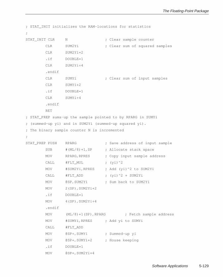
The Floating-Point Package
5-129Software Applications
; STAT_INIT initializes the RAM–locations for statistics
;
STAT_INIT CLR N ; Clear sample counter
CLR SUM2Yi ; Clear sum of squared samples
CLR SUM2Yi+2
.if DOUBLE=1
CLR SUM2Yi+4
.endif
CLR SUMYi ; Clear sum of input samples
CLR SUMYi+2
.if DOUBLE=1
CLR SUMYi+4
.endif
RET
; STAT_PREP sums–up the sample pointed to by RPARG in SUMYi
; (summed–up yi) and in SUM2Yi (summed–up squared yi).
; The binary sample counter N is incremented
;
STAT_PREP PUSH RPARG ; Save address of input sample
SUB #(ML/8)+1,SP ; Allocate stack space
MOV RPARG,RPRES ; Copy input sample address
CALL #FLT_MUL ; (yi)^2
MOV #SUM2Yi,RPRES ; Add (yi)^2 to SUM2Yi
CALL #FLT_ADD ; (yi)^2 + SUM2Yi
MOV @SP,SUM2Yi ; Sum back to SUM2Yi
MOV 2(SP),SUM2Yi+2
.if DOUBLE=1
MOV 4(SP),SUM2Yi+4
.endif
MOV (ML/8)+1(SP),RPARG ; Fetch sample address
MOV #SUMYi,RPRES ; Add yi to SUMYi
CALL #FLT_ADD
MOV @SP+,SUMYi ; Summed–up yi
MOV @SP+,SUMYi+2 ; House keeping
.if DOUBLE=1
MOV @SP+,SUM2Yi+4
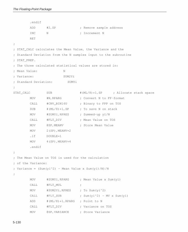
The Floating-Point Package
5-130
.endif
ADD #2,SP ; Remove sample address
INC N ; Increment N
RET
;
; STAT_CALC calculates the Mean Value, the Variance and the
; Standard Deviation from the N samples input to the subroutine
; STAT_PREP.
; The three calculated statistical values are stored in:
; Mean Value: N
; Variance: SUM2Yi
; Standard Deviation: SUMYi
;
STAT_CALC SUB #(ML/8)+1,SP ; Allocate stack space
MOV #N,RPARG ; Convert N to FP–format
CALL #CNV_BIN16U ; Binary to FPP on TOS
SUB #(ML/8)+1,SP ; To save N on stack
MOV #SUMYi,RPRES ; Summed–up yi/N
CALL #FLT_DIV ; Mean Value on TOS
MOV @SP,MEANV ; Store Mean Value
MOV 2(SP),MEANV+2
.if DOUBLE=1
MOV 4(SP),MEANV+4
.endif
;
; The Mean Value on TOS is used for the calculation
; of the Variance:
; Variance = (Sum(yi^2) – Mean Value x Sum(yi)/N)/N
;
MOV #SUMYi,RPARG ; Mean Value x Sum(yi)
CALL #FLT_MUL ;
MOV #SUM2Yi,RPRES ; To Sum(yi^2)
CALL #FLT_SUB ; Sum(yi^2) – MV x Sum(yi)
ADD #(ML/8)+1,RPARG ; Point to N
CALL #FLT_DIV ; Variance on TOS
MOV @SP,VARIANCE ; Store Variance
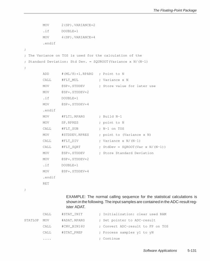
The Floating-Point Package
5-131Software Applications
MOV 2(SP),VARIANCE+2
.if DOUBLE=1
MOV 4(SP),VARIANCE+4
.endif
;
; The Variance on TOS is used for the calculation of the
; Standard Deviation: Std Dev. = SQUROOT(Variance x N/(N–1)
;
ADD #(ML/8)+1,RPARG ; Point to N
CALL #FLT_MUL ; Variance x N
MOV @SP+,STDDEV ; Store value for later use
MOV @SP+,STDDEV+2
.if DOUBLE=1
MOV @SP+,STDDEV+4
.endif
MOV #FLT1,RPARG ; Build N–1
MOV SP,RPRES ; point to N
CALL #FLT_SUB ; N–1 on TOS
MOV #STDDEV,RPRES ; point to (Variance x N)
CALL #FLT_DIV ; Variance x N/(N–1)
CALL #FLT_SQRT ; StdDev = SQROOT(Var x N/(N–1))
MOV @SP+,STDDEV ; Store Standard Deviation
MOV @SP+,STDDEV+2
.if DOUBLE=1
MOV @SP+,STDDEV+4
.endif
RET
;
EXAMPLE: The normal calling sequence for the statistical calculations isshown in the following. The input samples are contained in the ADC-result reg-ister ADAT.
CALL #STAT_INIT ; Initialization: clear used RAM
STATLOP MOV #ADAT,RPARG ; Set pointer to ADC–result
CALL #CNV_BIN16U ; Convert ADC–result to FP on TOS
CALL #STAT_PREP ; Process samples y1 to yN
.... ; Continue
The Floating-Point Package
5-132
CMP.B #xx,N ; yN processed?
JLO STATLOP ; No, next sample
;
; N samples are pre–processed: Calculate Mean Value, Variance,
; and Standard Deviation out of SUMYi, SUM2Y1 and N
;
CALL #STAT_CALC ; Call calculation subroutine
.... ; Results in sample locations
5.6.10.12 Complex Calculations
Complex numbers of the form (a + jb) can be used in calculations also. Thefour basic arithmetic operations are shown for complex numbers. PointersRPARG and RPRES are used in the same way as with the normal FPP subrou-tines. They point to the real parts of the complex numbers used for input andto the result on the TOS after the completion of the subroutine. The real andimaginary part of a complex number need to be allocated in the way shown inFigure 5–30 (shown for .FLOAT format).
Stack Usage: The subroutines need up to 36 bytes (.DOUBLE) or 28 bytes(.FLOAT) of stack space (complex division). Not included in this numbers is theinitially allocated result space. No error handling is provided. It is assumed thatthe numbers used stay within the range of the floating-point package.
Addition Result Space
Return CMPLX-xxx
Imaginary Part
SP During MAIN Program
SP After ReturnSP During FLT_xxx
Address n
Address n-4
Address n-8
Address n-12
Address n-x
MSBs
Real Part MSBs
Imaginary Part
SP, RPARG,RPRES
Address n+4
Address n+2Address n
MSBs
Real Part MSBs
Stack Configuration
RAM/ROM Configuration
Address n+6
Figure 5–30. Complex Number on TOS and in Memory (.FLOAT Format)
FPL .equ (ML/8)+1 ; Length of an FP–number (bytes)
;
; Complex calculation is made with the complex numbers RPARG
The Floating-Point Package
5-133Software Applications
; and RPRES point to.
;
; Call: MOV #arg1,RPRES ; Address argument1
; MOV #arg2,RPARG ; Address argument2
; CALL #CMPLX_xxx ; Calculate arg1 op arg2
; ... ; Result on TOS. Pointed to
; ... ; by SP, RPARG and RPRES
;
; Complex Subtraction: (a + jb) – (c + jd). @RPRES – @RPARG.
; Stack Usage: 16 bytes (.DOUBLE) 12 bytes (.FLOAT)
;
CMPLX_SUB MOV #0FFFFh,HELP ; Define subtraction
JMP CL$1 ; To common part
;
; Complex Addition: (a + jb) + (c + jd). @RPRES + @RPARG
; Stack Usage: 16 bytes (.DOUBLE) 12 bytes (.FLOAT)
;
CMPLX_ADD CLR HELP ; Define addition
CL$1 PUSH RPRES ; Save argument pointer
.if DOUBLE=1
PUSH 10(RPARG) ; LSBs imaginary part d
PUSH 8(RPARG) ; MIDS imaginary part d
.endif
PUSH 6(RPARG) ; The coming words depend on
PUSH 4(RPARG) ; DOUBLE
PUSH 2(RPARG) ; LSBs real part c
PUSH @RPARG ; MSBs real part c
TST HELP ; Addition or subtraction?
JZ CA
;
; Subtraction: the complex number (c + jd) is negated
;
XOR #080h,0(SP) ; Negate real part c
XOR #080h,FPL(SP) ; Negate imaginary part d
CA MOV SP,RPARG ; Point to c
CALL #FLT_ADD ; Add real parts (a + c)
The Floating-Point Package
5-134
MOV @SP+,2*FPL+2(SP) ; To real storage
MOV @SP+,2*FPL+2(SP) ; Housekeeping
.if DOUBLE=1
MOV @SP+,2*FPL+2(SP)
.endif
MOV SP,RPARG ; Point to d
MOV FPL(SP),RPRES ; Restore RPRES
ADD #FPL,RPRES ; To imaginary part b
CALL #FLT_ADD ; Add imaginary parts (b + d)
MOV @SP+,2*FPL+2(SP) ; To imaginary storage
MOV @SP+,2*FPL+2(SP) ; Housekeeping
.if DOUBLE=1
MOV @SP+,2*FPL+2(SP)
.endif
ADD #2,SP ; Skip saved RPRES
JMP CMPLX_RT ; Result on TOS
;
; Complex Division: (a + jb)/(c + jd). @RPRES/@RPARG
;
; The Complex Division uses the inverted divisor and
; the multiplication afterwards:
; (a + jb)/(c + jd) = (a + jb) x 1/(c + jd)
; with: 1/(c + jd) = (c – jd)/(c^2 + d^2)
;; Stack Usage: 36 bytes (.DOUBLE) 28 bytes (.FLOAT)
;
CMPLX_DIV PUSH RPRES ; Save RPRES (dividend a + jb))
PUSH RPARG ; Save RPARG (divisor c + jd)
SUB #FPL,SP ; Allocate result space
MOV RPARG,RPRES ; Fetch real part c
CALL #FLT_MUL ; c^2
SUB #FPL,SP ; Allocate result space
MOV 2*FPL(SP),RPARG ; Fetch imaginary part d
ADD #FPL,RPARG
MOV RPARG,RPRES ; Copy address of d
CALL #FLT_MUL ; d^2
ADD #FPL,RPARG ; to c^2
The Floating-Point Package
5-135Software Applications
CALL #FLT_ADD ; c^2 + d^2
PUSH FPL(SP) ; Copy c^2 + d^2
PUSH FPL(SP)
.if DOUBLE=1
PUSH FPL(SP)
.endif
MOV SP,RPARG ; To (c2 +d2)
MOV 3*FPL(SP),RPRES ; Pointer to (c + jd)
ADD #FPL,RPRES ; Address d
CALL #FLT_DIV ; d/(c^2 + d^2) imag. part
XOR #080h,0(SP) ; –d/(c^2 + d2)
MOV @SP+,2*FPL–2(SP) ; Store imaginary part
MOV @SP+,2*FPL–2(SP) ; to final location
.if DOUBLE=1
MOV @SP+,2*FPL–2(SP)
.endif
MOV SP,RPARG ; To copy of c^2 + d^2
MOV 2*FPL(SP),RPRES ; To (c + jd)
CALL #FLT_DIV ; c/(c^2 + d2)
;
; Prepare the interface to the multiplication and call it:
; RPARG points to 1/(c + jd) yet made by FLT_DIV
; RPRES points to (a + jb)
;
MOV 2*FPL+2(SP),RPRES ; address of (a + jb)
CALL #CMPLX_MUL ; (a +jb) x 1/(c +jd)
MOV #FPL,HELP ; Result to final location
CDIVL MOV @SP+,2*FPL+4(SP)
DEC HELP
JNZ CDIVL
;
JMP CMPLX_RET ; To common housekeeping
;
; Complex Multiplication: (a + jb)x(c + jd). @RPRES x @RPARG
;(a + jb)x(c + jd) = ac + jad + jbc – bd
; Stack Usage: 24 bytes (.DOUBLE) 18 bytes (.FLOAT)
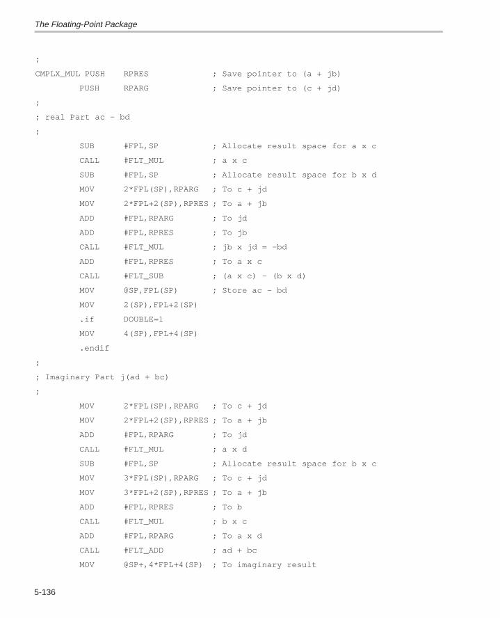
The Floating-Point Package
5-136
;
CMPLX_MUL PUSH RPRES ; Save pointer to (a + jb)
PUSH RPARG ; Save pointer to (c + jd)
;
; real Part ac – bd
;
SUB #FPL,SP ; Allocate result space for a x c
CALL #FLT_MUL ; a x c
SUB #FPL,SP ; Allocate result space for b x d
MOV 2*FPL(SP),RPARG ; To c + jd
MOV 2*FPL+2(SP),RPRES ; To a + jb
ADD #FPL,RPARG ; To jd
ADD #FPL,RPRES ; To jb
CALL #FLT_MUL ; jb x jd = –bd
ADD #FPL,RPRES ; To a x c
CALL #FLT_SUB ; (a x c) – (b x d)
MOV @SP,FPL(SP) ; Store ac – bd
MOV 2(SP),FPL+2(SP)
.if DOUBLE=1
MOV 4(SP),FPL+4(SP)
.endif
;
; Imaginary Part j(ad + bc)
;
MOV 2*FPL(SP),RPARG ; To c + jd
MOV 2*FPL+2(SP),RPRES ; To a + jb
ADD #FPL,RPARG ; To jd
CALL #FLT_MUL ; a x d
SUB #FPL,SP ; Allocate result space for b x c
MOV 3*FPL(SP),RPARG ; To c + jd
MOV 3*FPL+2(SP),RPRES ; To a + jb
ADD #FPL,RPRES ; To b
CALL #FLT_MUL ; b x c
ADD #FPL,RPARG ; To a x d
CALL #FLT_ADD ; ad + bc
MOV @SP+,4*FPL+4(SP) ; To imaginary result
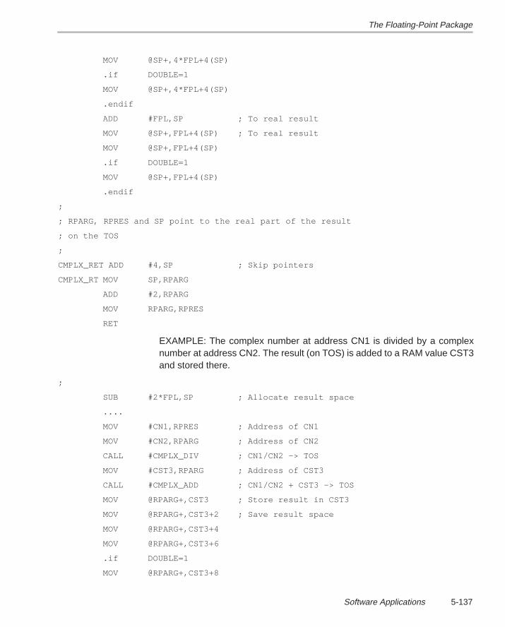
The Floating-Point Package
5-137Software Applications
MOV @SP+,4*FPL+4(SP)
.if DOUBLE=1
MOV @SP+,4*FPL+4(SP)
.endif
ADD #FPL,SP ; To real result
MOV @SP+,FPL+4(SP) ; To real result
MOV @SP+,FPL+4(SP)
.if DOUBLE=1
MOV @SP+,FPL+4(SP)
.endif
;
; RPARG, RPRES and SP point to the real part of the result
; on the TOS
;
CMPLX_RET ADD #4,SP ; Skip pointers
CMPLX_RT MOV SP,RPARG
ADD #2,RPARG
MOV RPARG,RPRES
RET
EXAMPLE: The complex number at address CN1 is divided by a complexnumber at address CN2. The result (on TOS) is added to a RAM value CST3and stored there.
;
SUB #2*FPL,SP ; Allocate result space
....
MOV #CN1,RPRES ; Address of CN1
MOV #CN2,RPARG ; Address of CN2
CALL #CMPLX_DIV ; CN1/CN2 –> TOS
MOV #CST3,RPARG ; Address of CST3
CALL #CMPLX_ADD ; CN1/CN2 + CST3 –> TOS
MOV @RPARG+,CST3 ; Store result in CST3
MOV @RPARG+,CST3+2 ; Save result space
MOV @RPARG+,CST3+4
MOV @RPARG+,CST3+6
.if DOUBLE=1
MOV @RPARG+,CST3+8
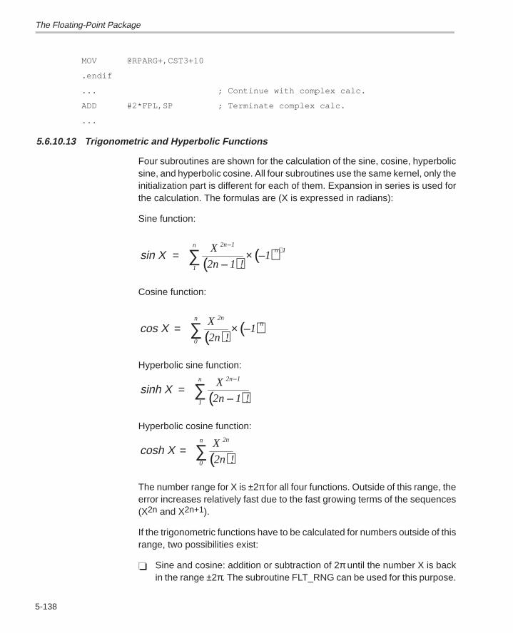
The Floating-Point Package
5-138
MOV @RPARG+,CST3+10
.endif
... ; Continue with complex calc.
ADD #2*FPL,SP ; Terminate complex calc.
...
5.6.10.13 Trigonometric and Hyperbolic Functions
Four subroutines are shown for the calculation of the sine, cosine, hyperbolicsine, and hyperbolic cosine. All four subroutines use the same kernel, only theinitialization part is different for each of them. Expansion in series is used forthe calculation. The formulas are (X is expressed in radians):
Sine function:
( ) ( )sin XX
2n 1 !1
2n 1
1
nn 1=
–× –
–+∑
Cosine function:
( ) ( )cos XX
2n !1
2n
0
nn= × –∑
Hyperbolic sine function:
( )sinh XX
2n 1 !
2n 1
1
n
=–
–
∑
Hyperbolic cosine function:
( )cosh XX
2n !
2n
0
n
= ∑
The number range for X is ±2π for all four functions. Outside of this range, theerror increases relatively fast due to the fast growing terms of the sequences(X2n and X2n+1).
If the trigonometric functions have to be calculated for numbers outside of thisrange, two possibilities exist:
Sine and cosine: addition or subtraction of 2π until the number X is backin the range ±2π. The subroutine FLT_RNG can be used for this purpose.
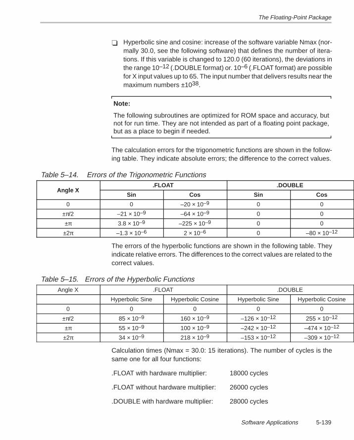
The Floating-Point Package
5-139Software Applications
Hyperbolic sine and cosine: increase of the software variable Nmax (nor-mally 30.0, see the following software) that defines the number of itera-tions. If this variable is changed to 120.0 (60 iterations), the deviations inthe range 10–12 (.DOUBLE format) or. 10–6 (.FLOAT format) are possiblefor X input values up to 65. The input number that delivers results near themaximum numbers ±1038.
Note:
The following subroutines are optimized for ROM space and accuracy, butnot for run time. They are not intended as part of a floating point package,but as a place to begin if needed.
The calculation errors for the trigonometric functions are shown in the follow-ing table. They indicate absolute errors; the difference to the correct values.
Table 5–14. Errors of the Trigonometric Functions
Angle X.FLOAT .DOUBLE
Angle XSin Cos Sin Cos
0 0 –20 × 10–9 0 0
±π/2 –21 × 10–9 –64 × 10–9 0 0
±π 3.8 × 10⁻⁹ –225 × 10–9 0 0
±2π –1.3 × 10⁻⁶ 2 × 10⁻⁶ 0 –80 × 10–12
The errors of the hyperbolic functions are shown in the following table. Theyindicate relative errors. The differences to the correct values are related to thecorrect values.
Table 5–15. Errors of the Hyperbolic FunctionsAngle X .FLOAT .DOUBLE
Hyperbolic Sine Hyperbolic Cosine Hyperbolic Sine Hyperbolic Cosine
0 0 0 0 0
±π/2 85 × 10–9 160 × 10–9 –126 × 10–12 255 × 10–12
±π 55 × 10–9 100 × 10–9 –242 × 10–12 –474 × 10–12
±2π 34 × 10–9 218 × 10–9 –153 × 10–12 –309 × 10–12
Calculation times (Nmax = 30.0: 15 iterations). The number of cycles is thesame one for all four functions:
.FLOAT with hardware multiplier: 18000 cycles
.FLOAT without hardware multiplier: 26000 cycles
.DOUBLE with hardware multiplier: 28000 cycles
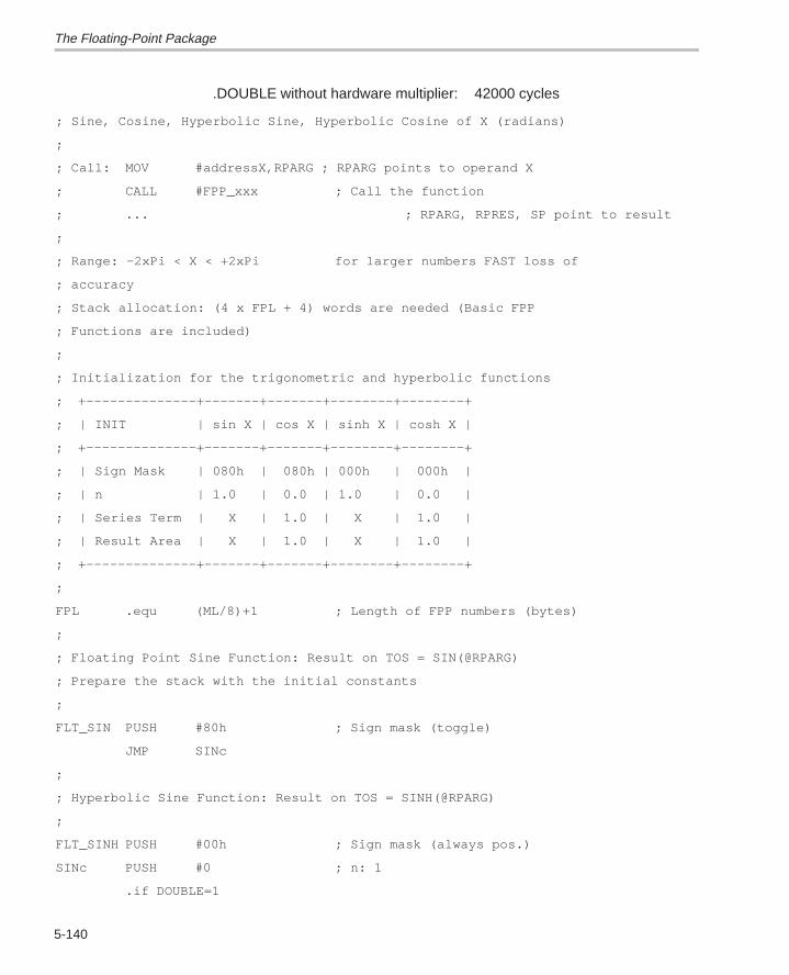
The Floating-Point Package
5-140
.DOUBLE without hardware multiplier: 42000 cycles
; Sine, Cosine, Hyperbolic Sine, Hyperbolic Cosine of X (radians)
;
; Call: MOV #addressX,RPARG ; RPARG points to operand X
; CALL #FPP_xxx ; Call the function
; ... ; RPARG, RPRES, SP point to result
;
; Range: –2xPi < X < +2xPi for larger numbers FAST loss of
; accuracy
; Stack allocation: (4 x FPL + 4) words are needed (Basic FPP
; Functions are included)
;
; Initialization for the trigonometric and hyperbolic functions
; +––––––––––––––+–––––––+–––––––+––––––––+––––––––+
; | INIT | sin X | cos X | sinh X | cosh X |
; +––––––––––––––+–––––––+–––––––+––––––––+––––––––+
; | Sign Mask | 080h | 080h | 000h | 000h |
; | n | 1.0 | 0.0 | 1.0 | 0.0 |
; | Series Term | X | 1.0 | X | 1.0 |
; | Result Area | X | 1.0 | X | 1.0 |
; +––––––––––––––+–––––––+–––––––+––––––––+––––––––+
;
FPL .equ (ML/8)+1 ; Length of FPP numbers (bytes)
;
; Floating Point Sine Function: Result on TOS = SIN(@RPARG)
; Prepare the stack with the initial constants
;
FLT_SIN PUSH #80h ; Sign mask (toggle)
JMP SINc
;
; Hyperbolic Sine Function: Result on TOS = SINH(@RPARG)
;
FLT_SINH PUSH #00h ; Sign mask (always pos.)
SINc PUSH #0 ; n: 1
.if DOUBLE=1
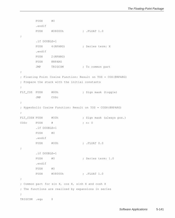
The Floating-Point Package
5-141Software Applications
PUSH #0
.endif
PUSH #08000h ; .FLOAT 1.0
;
.if DOUBLE=1
PUSH 4(RPARG) ; Series term: X
.endif
PUSH 2(RPARG)
PUSH @RPARG
JMP TRIGCOM ; To common part
;
; Floating Point Cosine Function: Result on TOS = COS(@RPARG)
; Prepare the stack with the initial constants
;
FLT_COS PUSH #80h ; Sign mask (toggle)
JMP COSc
;
; Hyperbolic Cosine Function: Result on TOS = COSH(@RPARG)
;
FLT_COSH PUSH #00h ; Sign mask (always pos.)
COSc PUSH # ; n: 0
.if DOUBLE=1
PUSH #0
.endif
PUSH #00h ; .FLOAT 0.0
;
.if DOUBLE=1
PUSH #0 ; Series term: 1.0
.endif
PUSH #0
PUSH #08000h ; .FLOAT 1.0
;
; Common part for sin X, cos X, sinh X and cosh X
; The functions are realized by expansions in series
;
TRIGCOM .equ $
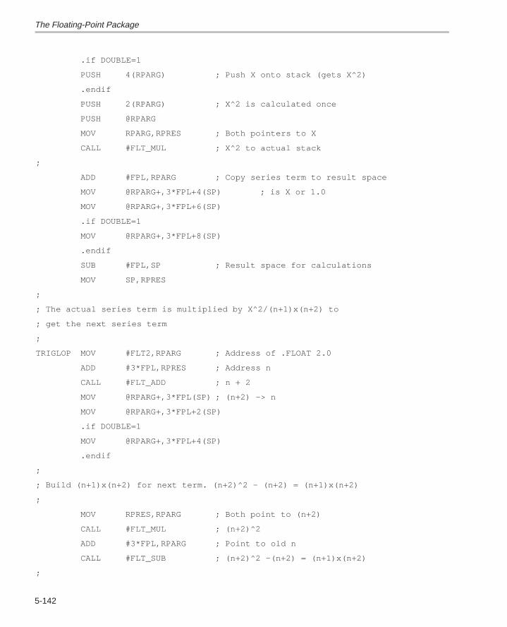
The Floating-Point Package
5-142
.if DOUBLE=1
PUSH 4(RPARG) ; Push X onto stack (gets X^2)
.endif
PUSH 2(RPARG) ; X^2 is calculated once
PUSH @RPARG
MOV RPARG,RPRES ; Both pointers to X
CALL #FLT_MUL ; X^2 to actual stack
;
ADD #FPL,RPARG ; Copy series term to result space
MOV @RPARG+,3*FPL+4(SP) ; is X or 1.0
MOV @RPARG+,3*FPL+6(SP)
.if DOUBLE=1
MOV @RPARG+,3*FPL+8(SP)
.endif
SUB #FPL,SP ; Result space for calculations
MOV SP,RPRES
;
; The actual series term is multiplied by X^2/(n+1)x(n+2) to
; get the next series term
;
TRIGLOP MOV #FLT2,RPARG ; Address of .FLOAT 2.0
ADD #3*FPL,RPRES ; Address n
CALL #FLT_ADD ; n + 2
MOV @RPARG+,3*FPL(SP) ; (n+2) –> n
MOV @RPARG+,3*FPL+2(SP)
.if DOUBLE=1
MOV @RPARG+,3*FPL+4(SP)
.endif
;
; Build (n+1)x(n+2) for next term. (n+2)^2 – (n+2) = (n+1)x(n+2)
;
MOV RPRES,RPARG ; Both point to (n+2)
CALL #FLT_MUL ; (n+2)^2
ADD #3*FPL,RPARG ; Point to old n
CALL #FLT_SUB ; (n+2)^2 –(n+2) = (n+1)x(n+2)
;
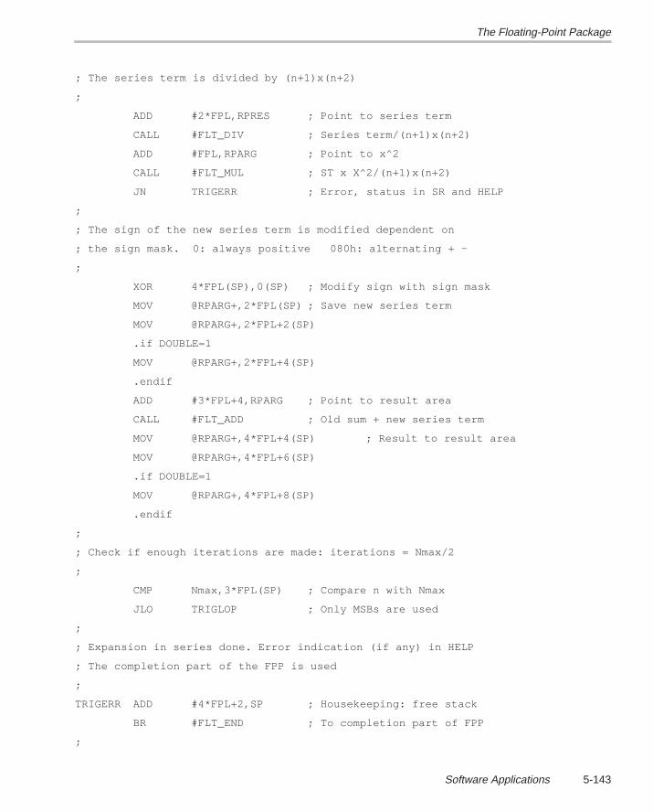
The Floating-Point Package
5-143Software Applications
; The series term is divided by (n+1)x(n+2)
;
ADD #2*FPL,RPRES ; Point to series term
CALL #FLT_DIV ; Series term/(n+1)x(n+2)
ADD #FPL,RPARG ; Point to x^2
CALL #FLT_MUL ; ST x X^2/(n+1)x(n+2)
JN TRIGERR ; Error, status in SR and HELP
;
; The sign of the new series term is modified dependent on
; the sign mask. 0: always positive 080h: alternating + –
;
XOR 4*FPL(SP),0(SP) ; Modify sign with sign mask
MOV @RPARG+,2*FPL(SP) ; Save new series term
MOV @RPARG+,2*FPL+2(SP)
.if DOUBLE=1
MOV @RPARG+,2*FPL+4(SP)
.endif
ADD #3*FPL+4,RPARG ; Point to result area
CALL #FLT_ADD ; Old sum + new series term
MOV @RPARG+,4*FPL+4(SP) ; Result to result area
MOV @RPARG+,4*FPL+6(SP)
.if DOUBLE=1
MOV @RPARG+,4*FPL+8(SP)
.endif
;
; Check if enough iterations are made: iterations = Nmax/2
;
CMP Nmax,3*FPL(SP) ; Compare n with Nmax
JLO TRIGLOP ; Only MSBs are used
;
; Expansion in series done. Error indication (if any) in HELP
; The completion part of the FPP is used
;
TRIGERR ADD #4*FPL+2,SP ; Housekeeping: free stack
BR #FLT_END ; To completion part of FPP
;

The Floating-Point Package
5-144
.if DOUBLE=1
FLT2 .DOUBLE 2.0 ; Constant 2.0
.else
FLT2 .FLOAT 2.0
.endif
Nmax .FLOAT 30.0 ; Iterations x 2 (MSBs used only)
5.6.10.14 Other Trigonometric and Hyperbolic Functions
With the previous calculated four functions (sin, cosin, hyperbolic sin, and hy-perbolic cosin), five other important functions can be calculated: tangent, co-tangent, hyperbolic tangent, hyperbolic cotangent, and exponential functions.
tan Xsin Xcos X
= cot Xcos Xsin X
= tanh Xsinh Xcosh X
= coth Xcosh Xsinh X
=
eX
= sinh X cosh XXn
= +∑ n!
To calculate one of the five functions, the two functions it consists of are calcu-lated and combined.
The errors of the five functions can be calculated with the errors of the two func-tions used and are shown in Table 5–14 and Table 5–15:
tan X, cot X, tanh X and coth X: the resulting error is the difference of thetwo errors
exp X: the resulting error is the sum of the two errors
Calculation times (Nmax = 30.0: 15 iterations). The number of cycles is thesame one for all five functions:
.FLOAT with hardware multiplier: 36000 cycles
.FLOAT without hardware multiplier: 52000 cycles
.DOUBLE with hardware multiplier: 56000 cycles
.DOUBLE without hardware multiplier: 84000 cycles
The same software kernel is used for all five functions. The number containedin R4 decides which function is executed. The range for all five functions is ±2π.For larger numbers a relatively fast loss of accuracy occurs.
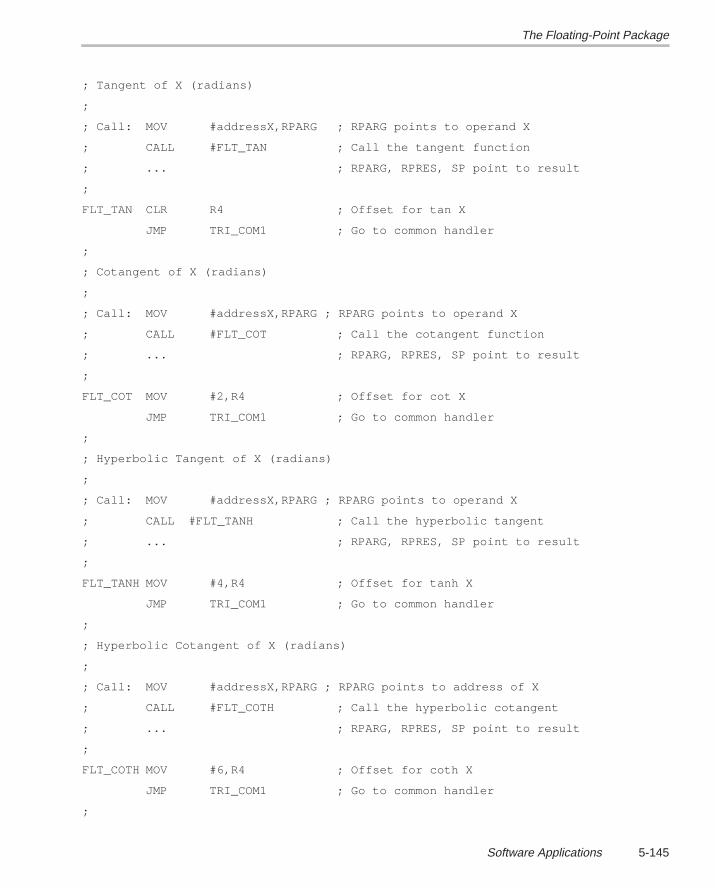
The Floating-Point Package
5-145Software Applications
; Tangent of X (radians)
;
; Call: MOV #addressX,RPARG ; RPARG points to operand X
; CALL #FLT_TAN ; Call the tangent function
; ... ; RPARG, RPRES, SP point to result
;
FLT_TAN CLR R4 ; Offset for tan X
JMP TRI_COM1 ; Go to common handler
;
; Cotangent of X (radians)
;
; Call: MOV #addressX,RPARG ; RPARG points to operand X
; CALL #FLT_COT ; Call the cotangent function
; ... ; RPARG, RPRES, SP point to result
;
FLT_COT MOV #2,R4 ; Offset for cot X
JMP TRI_COM1 ; Go to common handler
;
; Hyperbolic Tangent of X (radians)
;
; Call: MOV #addressX,RPARG ; RPARG points to operand X
; CALL #FLT_TANH ; Call the hyperbolic tangent
; ... ; RPARG, RPRES, SP point to result
;
FLT_TANH MOV #4,R4 ; Offset for tanh X
JMP TRI_COM1 ; Go to common handler
;
; Hyperbolic Cotangent of X (radians)
;
; Call: MOV #addressX,RPARG ; RPARG points to address of X
; CALL #FLT_COTH ; Call the hyperbolic cotangent
; ... ; RPARG, RPRES, SP point to result
;
FLT_COTH MOV #6,R4 ; Offset for coth X
JMP TRI_COM1 ; Go to common handler
;
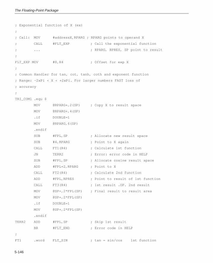
The Floating-Point Package
5-146
; Exponential function of X (ex)
;
; Call: MOV #addressX,RPARG ; RPARG points to operand X
; CALL #FLT_EXP ; Call the exponential function
; ... ; RPARG, RPRES, SP point to result
;
FLT_EXP MOV #8,R4 ; Offset for exp X
;
; Common Handler for tan, cot, tanh, coth and exponent function
; Range: –2xPi < X < +2xPi. For larger numbers FAST loss of
; accuracy
;
TRI_COM1 .equ $
MOV @RPARG+,2(SP) ; Copy X to result space
MOV @RPARG+,4(SP)
.if DOUBLE=1
MOV @RPARG,6(SP)
.endif
SUB #FPL,SP ; Allocate new result space
SUB #4,RPARG ; Point to X again
CALL FT1(R4) ; Calculate 1st function
JN TERR2 ; Error: error code in HELP
SUB #FPL,SP ; Allocate cosine result space
ADD #FPL+2,RPARG ; Point to X
CALL FT2(R4) ; Calculate 2nd function
ADD #FPL,RPRES ; Point to result of 1st function
CALL FT3(R4) ; 1st result .OP. 2nd result
MOV @SP+,2*FPL(SP) ; Final result to result area
MOV @SP+,2*FPL(SP)
.if DOUBLE=1
MOV @SP+,2*FPL(SP)
.endif
TERR2 ADD #FPL,SP ; Skip 1st result
BR #FLT_END ; Error code in HELP
;
FT1 .word FLT_SIN ; tan = sin/cos 1st function
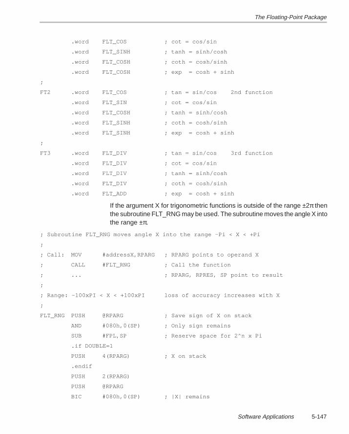
The Floating-Point Package
5-147Software Applications
.word FLT_COS ; cot = cos/sin
.word FLT_SINH ; tanh = sinh/cosh
.word FLT_COSH ; coth = cosh/sinh
.word FLT_COSH ; exp = cosh + sinh
;
FT2 .word FLT_COS ; tan = sin/cos 2nd function
.word FLT_SIN ; cot = cos/sin
.word FLT_COSH ; tanh = sinh/cosh
.word FLT_SINH ; coth = cosh/sinh
.word FLT_SINH ; exp = cosh + sinh
;
FT3 .word FLT_DIV ; tan = sin/cos 3rd function
.word FLT_DIV ; cot = cos/sin
.word FLT_DIV ; tanh = sinh/cosh
.word FLT_DIV ; coth = cosh/sinh
.word FLT_ADD ; exp = cosh + sinh
If the argument X for trigonometric functions is outside of the range ±2π thenthe subroutine FLT_RNG may be used. The subroutine moves the angle X intothe range ±π.
; Subroutine FLT_RNG moves angle X into the range –Pi < X < +Pi
;
; Call: MOV #addressX,RPARG ; RPARG points to operand X
; CALL #FLT_RNG ; Call the function
; ... ; RPARG, RPRES, SP point to result
;
; Range: –100xPI < X < +100xPI loss of accuracy increases with X
;
FLT_RNG PUSH @RPARG ; Save sign of X on stack
AND #080h,0(SP) ; Only sign remains
SUB #FPL,SP ; Reserve space for 2^n x Pi
.if DOUBLE=1
PUSH 4(RPARG) ; X on stack
.endif
PUSH 2(RPARG)
PUSH @RPARG
BIC #080h,0(SP) ; |X| remains
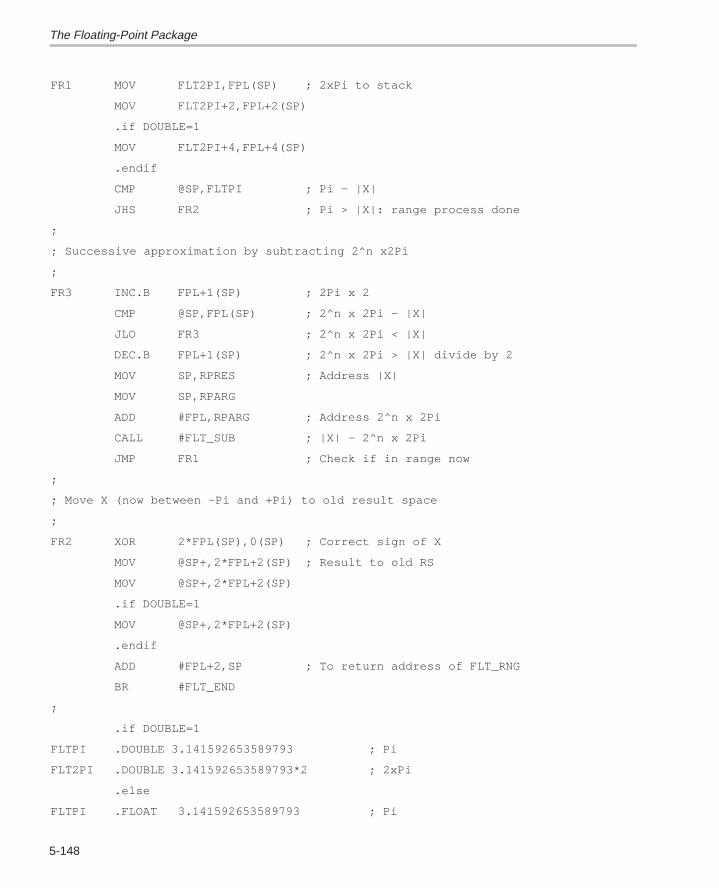
The Floating-Point Package
5-148
FR1 MOV FLT2PI,FPL(SP) ; 2xPi to stack
MOV FLT2PI+2,FPL+2(SP)
.if DOUBLE=1
MOV FLT2PI+4,FPL+4(SP)
.endif
CMP @SP,FLTPI ; Pi – |X|
JHS FR2 ; Pi > |X|: range process done
;
; Successive approximation by subtracting 2^n x2Pi
;
FR3 INC.B FPL+1(SP) ; 2Pi x 2
CMP @SP,FPL(SP) ; 2^n x 2Pi – |X|
JLO FR3 ; 2^n x 2Pi < |X|
DEC.B FPL+1(SP) ; 2^n x 2Pi > |X| divide by 2
MOV SP,RPRES ; Address |X|
MOV SP,RPARG
ADD #FPL,RPARG ; Address 2^n x 2Pi
CALL #FLT_SUB ; |X| – 2^n x 2Pi
JMP FR1 ; Check if in range now
;
; Move X (now between –Pi and +Pi) to old result space
;
FR2 XOR 2*FPL(SP),0(SP) ; Correct sign of X
MOV @SP+,2*FPL+2(SP) ; Result to old RS
MOV @SP+,2*FPL+2(SP)
.if DOUBLE=1
MOV @SP+,2*FPL+2(SP)
.endif
ADD #FPL+2,SP ; To return address of FLT_RNG
BR #FLT_END
;
.if DOUBLE=1
FLTPI .DOUBLE 3.141592653589793 ; Pi
FLT2PI .DOUBLE 3.141592653589793*2 ; 2xPi
.else
FLTPI .FLOAT 3.141592653589793 ; Pi
The Floating-Point Package
5-149Software Applications
FLT2PI .FLOAT 3.141592653589793*2 ; 2xPi
.endif
5.6.10.15 Faster Approximations for Trigonometric Functions
If the calculation times of the previous iterations are too long and the high accu-racy is not needed (e.g. for the calculation of pulse widths for PWM), tables orcubic equations can be used. The table method is described in the MSP430Software User’s Guide (literature number SLAUE11).
With the following four definition points, a cubic approximation to the sin curveis made. The range is 0 to π/2. All other angles must be adapted to this range.
X1:= 0.0000000000 SIN X1:= 0.0000000000 (0°)
X2:= 0.3490658504 SIN X2:= 0.3420201433 (20°)
X3:= 1.2217304760 SIN X3:= 0.9396926208 (70°)
X4:= 1.5707963270 SIN X4:= 1.0000000000 (90°)
The resulting multiplication factors are:
SIN X = –0.11316874 X3–0.063641170 X^2 +1.01581976 X
The following results and errors are obtained with the previous factors:
X = 0 , SIN X = 0.000000000 0.00% (0°)
X = π/12 SIN X = 0.259548457 +0.28% (15°)
X = π/6 SIN X = 0.498189297 –0.36% (30°)
X:=π/4 SIN X = 0.703738695 –0.47% (45°)
X:=π/3 SIN X = 0.864012827 –0.23% (60°)
X:= 5π/12 SIN X = 0.966827870 +0.09% (75°)
X:=π/2 SIN X = 1.000000000 0.00% (90°)
The error of the previous approximation is within ±0.5% from 0 to 2π. Calcula-tion times:
.FLOAT with hardware multiplier: 880 cycles
.FLOAT without hardware multiplier: 1600 cycles
.DOUBLE with hardware multiplier: 1150 cycles
.DOUBLE without hardware multiplier: 2550 cycles
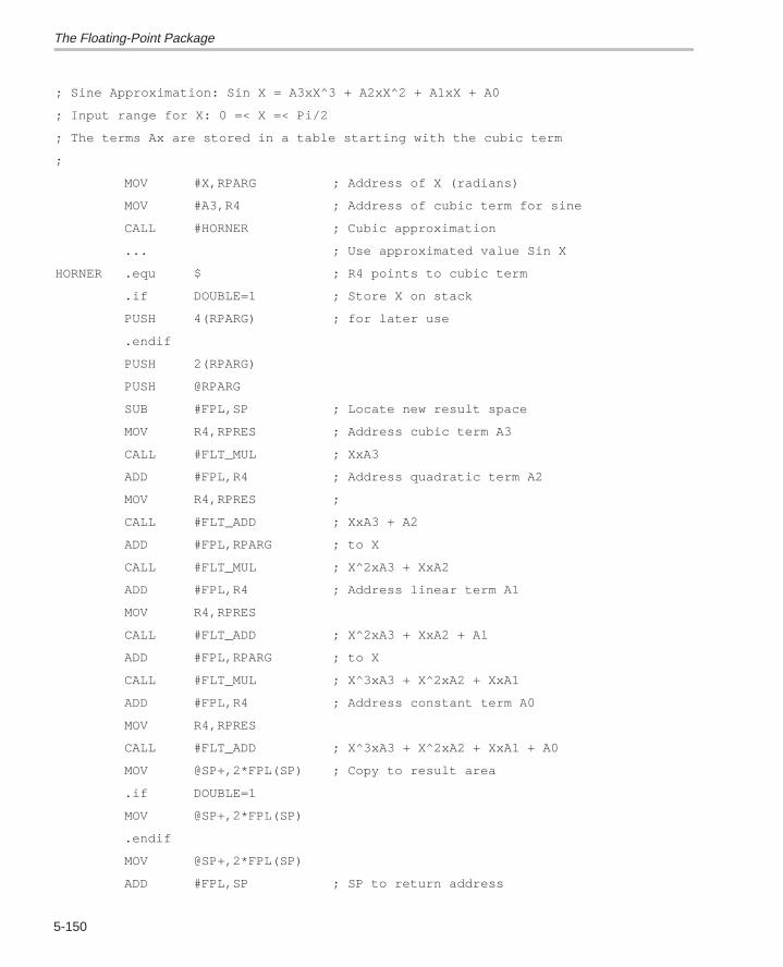
The Floating-Point Package
5-150
; Sine Approximation: Sin X = A3xX^3 + A2xX^2 + A1xX + A0
; Input range for X: 0 =< X =< Pi/2
; The terms Ax are stored in a table starting with the cubic term
;
MOV #X,RPARG ; Address of X (radians)
MOV #A3,R4 ; Address of cubic term for sine
CALL #HORNER ; Cubic approximation
... ; Use approximated value Sin X
HORNER .equ $ ; R4 points to cubic term
.if DOUBLE=1 ; Store X on stack
PUSH 4(RPARG) ; for later use
.endif
PUSH 2(RPARG)
PUSH @RPARG
SUB #FPL,SP ; Locate new result space
MOV R4,RPRES ; Address cubic term A3
CALL #FLT_MUL ; XxA3
ADD #FPL,R4 ; Address quadratic term A2
MOV R4,RPRES ;
CALL #FLT_ADD ; XxA3 + A2
ADD #FPL,RPARG ; to X
CALL #FLT_MUL ; X^2xA3 + XxA2
ADD #FPL,R4 ; Address linear term A1
MOV R4,RPRES
CALL #FLT_ADD ; X^2xA3 + XxA2 + A1
ADD #FPL,RPARG ; to X
CALL #FLT_MUL ; X^3xA3 + X^2xA2 + XxA1
ADD #FPL,R4 ; Address constant term A0
MOV R4,RPRES
CALL #FLT_ADD ; X^3xA3 + X^2xA2 + XxA1 + A0
MOV @SP+,2*FPL(SP) ; Copy to result area
.if DOUBLE=1
MOV @SP+,2*FPL(SP)
.endif
MOV @SP+,2*FPL(SP)
ADD #FPL,SP ; SP to return address
The Floating-Point Package
5-151Software Applications
BR #FLT_END ; Use standard FPP return
;
; Multiplication factors for the Sine generation (0 to Pi/2)
; SIN X = –0.11316874 X 3–0.063641170 X^ 2 +1.01581976 X
.if DOUBLE=1
A3 .DOUBLE –0.11316874 ; cubic term
A2 .DOUBLE –0.063641170 ; quadratic term
A1 .DOUBLE 1.01581976 ; linear term
A0 .DOUBLE 0.0 ; constant term
.else
A3 .FLOAT –0.11316874 ; cubic term
A2 .FLOAT –0.063641170 ; quadratic term
A1 .FLOAT 1.01581976 ; linear term
A0 .FLOAT 0.0 ; constant term
.endif
Note:
The HORNER algorithm (used previously) can be used for several other pur-poses. It is only necessary to load the register R4 with the starting addressof the appropriate block containing the factors (address A3 with the previousexample).
5.6.10.16 The Natural Logarithm Function
The natural logarithm of a number X is calculated with the following formula:
( ) ( )ln XX –1
n1
n
1
nn–1= × –∑
The number range of X for the natural logarithm contains all positive numbersexcept zero. Values of X less than or equal to zero return the largest negativenumber (–3.4x1038) and the N bit set as an error indication.
The calculation errors for the natural logarithm function are shown in the fol-lowing table. They indicate relative errors. The errors of the .DOUBLE routineare estimated: no logarithm values greater than 12 digits were available.Table 5–16 shows the relative large errors – especially for the .FLOAT format– for input values X very near to 1.0. This is due to the (X – 1) operation neces-sary for the calculation. Algorithms used should avoid the calculation of thelogarithm of numbers very close to 1.0.
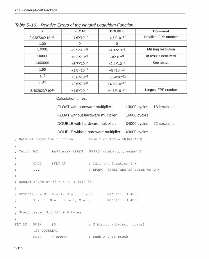
The Floating-Point Package
5-152
Table 5–16. Relative Errors of the Natural Logarithm FunctionX .FLOAT .DOUBLE Comment
2.938736×10–39 –1.5×10⁻⁷ –4.5×10⁻¹² Smallest FPP number
1.00 0 0
1.0001 –3.5×10⁻⁵ –1.4×10⁻⁸ Missing resolution
1.00001 +5.2×10⁻³ –8×10⁻⁸ at results near zero
1.000001 +6.7×10⁻² +2.4×10⁻⁷ See above
1.95 +1.5×10⁻⁷ +5×10–12
106 +3.6×10⁻⁸ +1.5×10⁻¹¹
1012 +3.6×10⁻⁸ +4.5×10⁻¹²
3.402823×1038 +1.5×10⁻⁷ +4.5×10⁻¹² Largest FPP number
Calculation times:
.FLOAT with hardware multiplier: 13000 cycles 13 iterations
.FLOAT without hardware multiplier: 16000 cycles
.DOUBLE with hardware multiplier: 34000 cycles 22 iterations
.DOUBLE without hardware multiplier: 43000 cycles
; Natural Logarithm Function: Result on TOS = LN(@RPARG)
;
; Call: MOV #addressX,RPARG ; RPARG points to operand X
;
; CALL #FLT_LN ; Call the function lnX
; ... ; RPARG, RPRES and SP point to lnX
;
; Range: +2.9x10^–38 < X < +3.4x10^38
;
; Errors: X = 0: N = 1, C = 1, Z = 0 Result: –3.4E38
; X < 0: N = 1, C = 1, Z = 0 Result: –3.4E38
;
; Stack usage: 3 x FPL + 6 bytes
;
FLT_LN PUSH #0 ; N binary (divisor, power)
.if DOUBLE=1
PUSH 4(RPARG) ; Push X onto stack
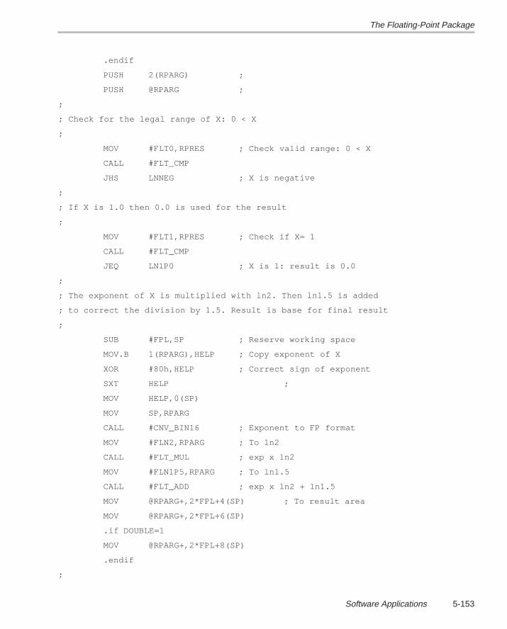
The Floating-Point Package
5-153Software Applications
.endif
PUSH 2(RPARG) ;
PUSH @RPARG ;
;
; Check for the legal range of X: 0 < X
;
MOV #FLT0,RPRES ; Check valid range: 0 < X
CALL #FLT_CMP
JHS LNNEG ; X is negative
;
; If X is 1.0 then 0.0 is used for the result
;
MOV #FLT1,RPRES ; Check if X= 1
CALL #FLT_CMP
JEQ LN1P0 ; X is 1: result is 0.0
;
; The exponent of X is multiplied with ln2. Then ln1.5 is added
; to correct the division by 1.5. Result is base for final result
;
SUB #FPL,SP ; Reserve working space
MOV.B 1(RPARG),HELP ; Copy exponent of X
XOR #80h,HELP ; Correct sign of exponent
SXT HELP ;
MOV HELP,0(SP)
MOV SP,RPARG
CALL #CNV_BIN16 ; Exponent to FP format
MOV #FLN2,RPARG ; To ln2
CALL #FLT_MUL ; exp x ln2
MOV #FLN1P5,RPARG ; To ln1.5
CALL #FLT_ADD ; exp x ln2 + ln1.5
MOV @RPARG+,2*FPL+4(SP) ; To result area
MOV @RPARG+,2*FPL+6(SP)
.if DOUBLE=1
MOV @RPARG+,2*FPL+8(SP)
.endif
;
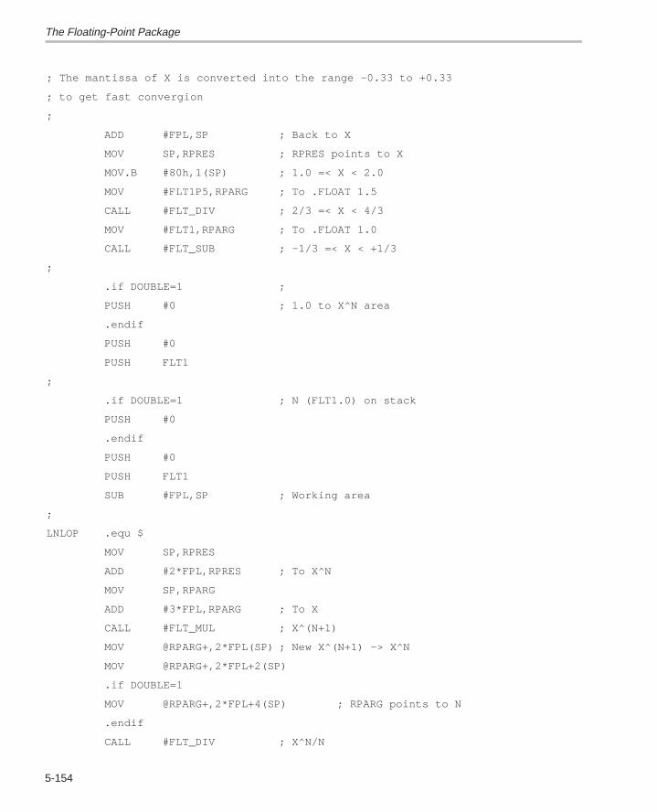
The Floating-Point Package
5-154
; The mantissa of X is converted into the range –0.33 to +0.33
; to get fast convergion
;
ADD #FPL,SP ; Back to X
MOV SP,RPRES ; RPRES points to X
MOV.B #80h,1(SP) ; 1.0 =< X < 2.0
MOV #FLT1P5,RPARG ; To .FLOAT 1.5
CALL #FLT_DIV ; 2/3 =< X < 4/3
MOV #FLT1,RPARG ; To .FLOAT 1.0
CALL #FLT_SUB ; –1/3 =< X < +1/3
;
.if DOUBLE=1 ;
PUSH #0 ; 1.0 to X^N area
.endif
PUSH #0
PUSH FLT1
;
.if DOUBLE=1 ; N (FLT1.0) on stack
PUSH #0
.endif
PUSH #0
PUSH FLT1
SUB #FPL,SP ; Working area
;
LNLOP .equ $
MOV SP,RPRES
ADD #2*FPL,RPRES ; To X^N
MOV SP,RPARG
ADD #3*FPL,RPARG ; To X
CALL #FLT_MUL ; X^(N+1)
MOV @RPARG+,2*FPL(SP) ; New X^(N+1) –> X^N
MOV @RPARG+,2*FPL+2(SP)
.if DOUBLE=1
MOV @RPARG+,2*FPL+4(SP) ; RPARG points to N
.endif
CALL #FLT_DIV ; X^N/N
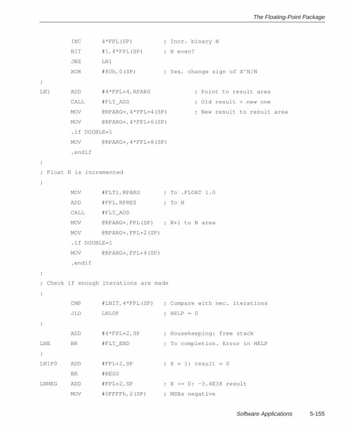
The Floating-Point Package
5-155Software Applications
INC 4*FPL(SP) ; Incr. binary N
BIT #1,4*FPL(SP) ; N even?
JNZ LN1
XOR #80h,0(SP) ; Yes, change sign of X^N/N
;
LN1 ADD #4*FPL+4,RPARG ; Point to result area
CALL #FLT_ADD ; Old result + new one
MOV @RPARG+,4*FPL+4(SP) ; New result to result area
MOV @RPARG+,4*FPL+6(SP)
.if DOUBLE=1
MOV @RPARG+,4*FPL+8(SP)
.endif
;
; Float N is incremented
;
MOV #FLT1,RPARG ; To .FLOAT 1.0
ADD #FPL,RPRES ; To N
CALL #FLT_ADD
MOV @RPARG+,FPL(SP) ; N+1 to N area
MOV @RPARG+,FPL+2(SP)
.if DOUBLE=1
MOV @RPARG+,FPL+4(SP)
.endif
;
; Check if enough iterations are made
;
CMP #LNIT,4*FPL(SP) ; Compare with nec. iterations
JLO LNLOP ; HELP = 0
;
ADD #4*FPL+2,SP ; Housekeeping: free stack
LNE BR #FLT_END ; To completion. Error in HELP
;
LN1P0 ADD #FPL+2,SP ; X = 1: result = 0
BR #RES0
LNNEG ADD #FPL+2,SP ; X <= 0: –3.4E38 result
MOV #0FFFFh,2(SP) ; MSBs negative
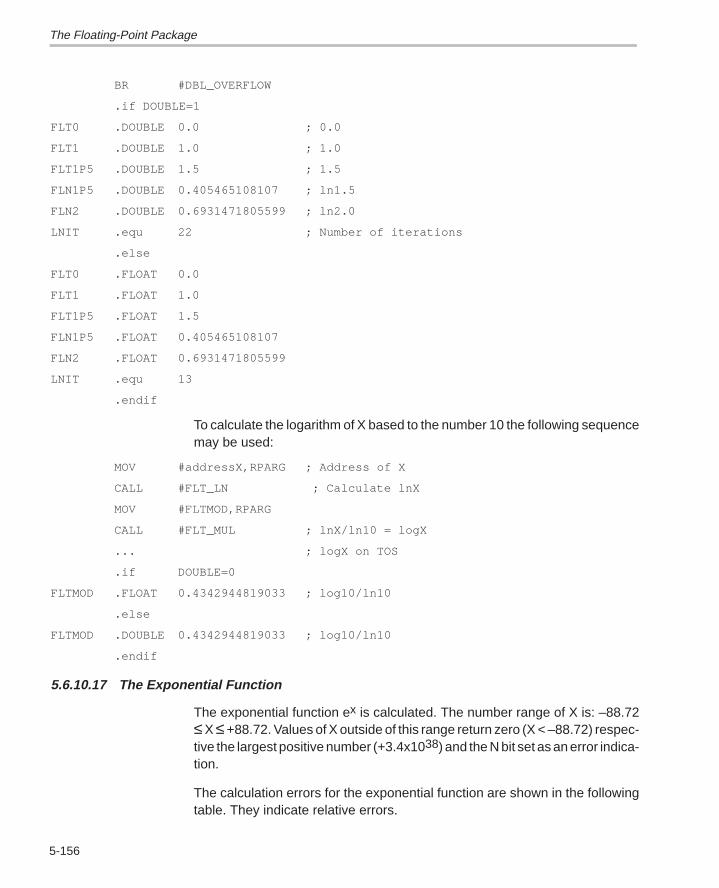
The Floating-Point Package
5-156
BR #DBL_OVERFLOW
.if DOUBLE=1
FLT0 .DOUBLE 0.0 ; 0.0
FLT1 .DOUBLE 1.0 ; 1.0
FLT1P5 .DOUBLE 1.5 ; 1.5
FLN1P5 .DOUBLE 0.405465108107 ; ln1.5
FLN2 .DOUBLE 0.6931471805599 ; ln2.0
LNIT .equ 22 ; Number of iterations
.else
FLT0 .FLOAT 0.0
FLT1 .FLOAT 1.0
FLT1P5 .FLOAT 1.5
FLN1P5 .FLOAT 0.405465108107
FLN2 .FLOAT 0.6931471805599
LNIT .equ 13
.endif
To calculate the logarithm of X based to the number 10 the following sequencemay be used:
MOV #addressX,RPARG ; Address of X
CALL #FLT_LN ; Calculate lnX
MOV #FLTMOD,RPARG
CALL #FLT_MUL ; lnX/ln10 = logX
... ; logX on TOS
.if DOUBLE=0
FLTMOD .FLOAT 0.4342944819033 ; log10/ln10
.else
FLTMOD .DOUBLE 0.4342944819033 ; log10/ln10
.endif
5.6.10.17 The Exponential Function
The exponential function ex is calculated. The number range of X is: –88.72≤ X ≤ +88.72. Values of X outside of this range return zero (X < –88.72) respec-tive the largest positive number (+3.4x1038) and the N bit set as an error indica-tion.
The calculation errors for the exponential function are shown in the followingtable. They indicate relative errors.
The Floating-Point Package
5-157Software Applications
Table 5–17. Errors of the Exponential FunctionX .FLOAT .DOUBLE Result
–88.72 –9.4×10⁻⁷ –4.5×10⁻¹¹ 2.9470911×10–39
–12.3456 –1.7×10⁻⁸ –1.5×10⁻¹¹ 4.348846154014×10⁻⁶
0.0 0 0 1.0
2–41 –4.5×10⁻¹³ –4.5×10⁻¹³ 1.0
2–25 –30×10–9 1.0+29.8×10⁻⁹
+88.72 –2.8×10⁻⁶ –4.5×10⁻¹¹ Most positive FPP number
Calculation times:
.FLOAT with hardware multiplier: 3200 cycles
.FLOAT without hardware multiplier: 5100 cycles
.DOUBLE with hardware multiplier: 4500 cycles
.DOUBLE without hardware multiplier: 7500 cycles
; Exponential Function: e^X. Result on TOS = e^(@RPARG)
;
; Call: MOV #addressX,RPARG ; RPARG points to operand X
; CALL #FLT_EXP ; Call the exp. function
; ... ; RPARG, RPRES, SP point to result
;
; Range: –88.72 < X < +88.72
;
; Errors:
; X > +88.72: N = 1, C = 1, Z = 1 Result: +3.4E38
; X < –88.72: N = 1, C = 0, Z = 0 Result: 0.0 if SW_UFLOW = 1
; N = 0, C = x, Z = x Result: 0.0 if SW_UFLOW = 0
;
; Stack usage: 3 x FPL + 4 bytes
;
FLT_EXP MOV @RPARG+,2(SP) ; Copy X to result area
MOV @RPARG+,4(SP)
.if DOUBLE=1
MOV @RPARG,6(SP)
.endif
The Floating-Point Package
5-158
;
; Check if X is inside limits: –88.72 < X < +88.72 (8631h,7218h)
;
MOV 2(SP),COUNTER ; MSBs, exp and sign of X
BIC #080h,COUNTER ; |X|
CMP #08631h,COUNTER ; |X| > 88.72? ln3.4x10^38=88.72
JLO EXP_L3 ; |X| is in range
JNE EXP_RNGOUT ; X > 88.72 .or. X < –88.72: error
CMP #07217h,4(SP) ; Check LSBs
JHS EXP_RNGOUT ; LSBs show: |X| > 88.72
;
; Prepare exponent of result: N = X/ln2 (rounded)
;
EXP_L3 MOV SP,RPRES
SUB #FPL,SP ; New working area
ADD #2,RPRES ; To X (result area)
MOV #FLTLN2I,RPARG ; To 2/ln2 (allows MPY)
CALL #FLT_MUL ; 2 x X/ln2
CALL #CNV_FP_BIN ; 2 x X/ln2 –> binary
.if DOUBLE=1
SUB #2,SP ; LSBs contain N
ADD #FPL–2,RPARG ; To N
.else
ADD #FPL,RPARG ; To binary N
.endif ; N is at correct place yet
RRA @RPARG ; /2 for rounding
JNC EXPL1 ; No carry, no rounding
TST 0(RPARG) ; Sign of N
JN EXPL1
INC 0(RPARG) ; Round N
EXPL1 CALL #CNV_BIN16 ; N –> FPP format Xn
;
; Calculation of g: g = X – Xn*(C1 + C2)
;
MOV #EXPC,RPARG ; C1 + C2
CALL #FLT_MUL ; Xn*(C1 + C2)
The Floating-Point Package
5-159Software Applications
ADD #FPL+4,RPRES ; To X
CALL #FLT_SUB ; g = X – Xn*(C1 + C2)
;
; Calculation of mantissa R(g):
; R(g) = 0.5 + g*P(z)/(Q(z) – g*P(z))
;
SUB #FPL,SP ; Area for z = g^2
CALL #FLT_MUL ; z = g^2
;
; Calculation of g*P(z): g*P(z) = g*(p1*z + p0)
;
SUB #FPL,SP ; Area for g*P(z)
MOV #EXPP1,RPARG ; To p1, RPRES points to z
CALL #FLT_MUL ; p1*z
MOV #EXPP0,RPARG ; To p0
CALL #FLT_ADD ; p1*z + p0
ADD #2*FPL,RPARG ; To g
CALL #FLT_MUL ; g*P(z) = g*(p1*z + p0)
MOV @SP+,2*FPL–2(SP) ; Store g*P(z)
MOV @SP+,2*FPL–2(SP)
.if DOUBLE=1
MOV @SP+,2*FPL–2(SP)
.endif
;
; Calculation of Q(z): Q(z) = (q1*z + q0) .FLOAT format
; Q(z) = (q2*z + q1)*z + q0 .DOUBLE format
;
SUB #FPL,SP ; Area for Q(z)
.if DOUBLE=1 ; Quadratic equation
MOV #EXPQ2,RPARG ; To q2
ADD #FPL,RPRES ; To z
CALL #FLT_MUL ; q2*z
MOV #EXPQ1,RPARG ; To q1
CALL #FLT_ADD ; q2*z + q1
.else ; Linear equation
MOV #EXPQ1,RPARG ; To q1
The Floating-Point Package
5-160
.endif
ADD #FPL,RPRES ; To z
CALL #FLT_MUL ; (q2*z + q1)*z resp. q1*z
MOV #EXPQ0,RPARG ; To q0
CALL #FLT_ADD ; (q2*z + q1)*z + q0 or q1*z + q0
;
; Result mantissa R(g) = 0.5 + g*P(z)/(Q(z) – g*P(z))
;
ADD #2*FPL,RPARG ; To g*P(z), RPRES to Q(z)
CALL #FLT_SUB ; Q(z) – g*P(z)
ADD #2*FPL,RPRES ; To g*P(z)
CALL #FLT_DIV ; g*P(z)/(Q(z) – g*P(z))
MOV #FLT0P5,RPARG ; To 0.5
CALL #FLT_ADD ; R(g)=0.5 + g*P(z)/(Q(z)–g*P(z))
MOV @SP+,3*FPL+2(SP) ; Store R(g) to result area
MOV @SP+,3*FPL+2(SP)
.if DOUBLE=1
MOV @SP+,3*FPL+2(SP)
.endif
;
; Insert exponent N+1 to result
;
ADD #2*FPL,SP ; To binary N
SETC ; N + 1
ADDC.B @SP+,3(SP) ; Add N + 1 to exponent of result
BR #FLT_END ; To normal return, HELP = 0
;
; X is out of range: test if overflow (+) or underflow (–)
;
EXP_RNGOUT TST.B 2(SP) ; Overflow? (sign positive)
JGE EXP_OVFL ; Yes, error: handling in FPP04
BR #DBL_UNDERFLOW ; Underflow: depends on SW_UFLOW
EXP_OVFL BR #DBL_OVERFLOW
;
.if DOUBLE=1
FLTLN2I .double +1.4426950408889634074*2 ; 2/ln2

The Floating-Point Package
5-161Software Applications
EXPC .double +0.693359375–2.1219444005469058277E–4 ; c1+c2
EXPP1 .double +0.595042549776E–2 ;p1
EXPP0 .double 0.24999999999992 ;p0
EXPQ2 .double +0.29729363682E–3 ;q2
EXPQ1 .double +0.5356751764522E–1 ;q1
FLT0P5 .equ $ ; both are 0.5
EXPQ0 .double +0.50000000000000E+0 ; q0
.else
FLTLN2I .float +1.4426950408889634074*2
EXPC .float +0.693359375–2.1219444005469058277E–4
EXPP1 .float +0.00416028863
EXPP0 .float 0.24999999950
EXPQ1 .float +0.04998717878
FLT0P5 .equ $ ; both are 0.5
EXPQ0 .float +0.50000000000
.endif
5.6.10.18 The Power Function
The power function AB is calculated. The number range for A and B is:
2.9 × 10–39 ≤ A ≤ 3.4 × 1038
–88.72 ≤ B × InA ≤ + 88.72
For the error handling, see the header of the software.
The used formula is:
A eB B lnA= ×
The calculation errors for the power function are shown in the following table.They indicate relative errors.
Table 5–18. Relative Errors of the Power FunctionX .FLOAT .DOUBLE Result
11 0 0 1.0
(3.4×1038)0 0 0 1.0
(5.5×10⁻²⁰)2 –9×10⁻⁷ 0 3.025×10–39
1.0000788 –4.×10–6 –9×10⁻¹⁰ 1.0061788
1.000071267513 –5.5% –7×10⁻⁷ 3.4027×1038
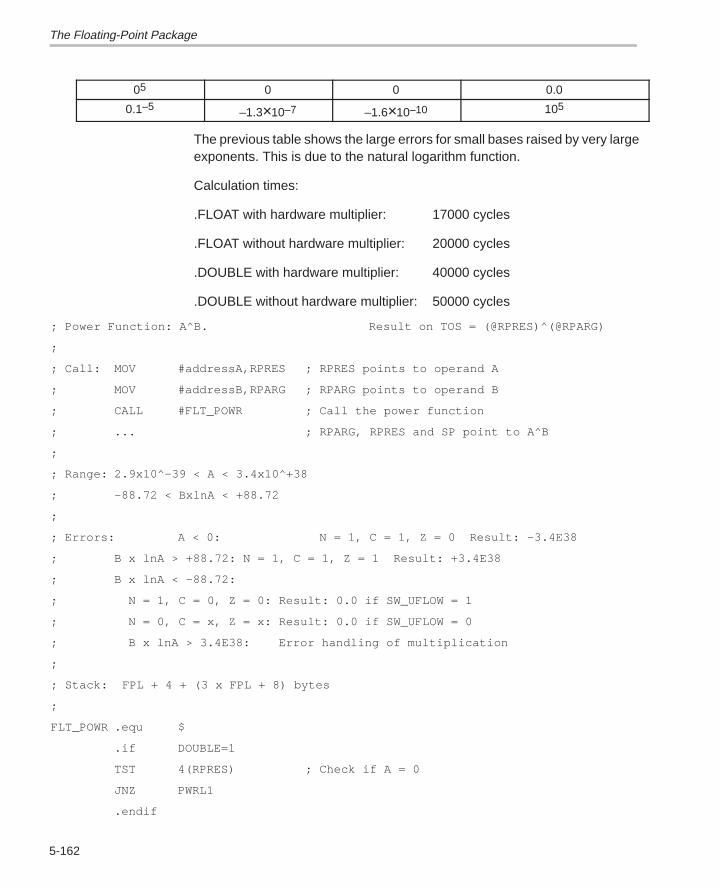
The Floating-Point Package
5-162
05 0 0 0.0
0.1–5 –1.3×10⁻⁷ –1.6×10⁻¹⁰ 105
The previous table shows the large errors for small bases raised by very largeexponents. This is due to the natural logarithm function.
Calculation times:
.FLOAT with hardware multiplier: 17000 cycles
.FLOAT without hardware multiplier: 20000 cycles
.DOUBLE with hardware multiplier: 40000 cycles
.DOUBLE without hardware multiplier: 50000 cycles
; Power Function: A^B. Result on TOS = (@RPRES)^(@RPARG)
;
; Call: MOV #addressA,RPRES ; RPRES points to operand A
; MOV #addressB,RPARG ; RPARG points to operand B
; CALL #FLT_POWR ; Call the power function
; ... ; RPARG, RPRES and SP point to A^B
;
; Range: 2.9x10^–39 < A < 3.4x10^+38
; –88.72 < BxlnA < +88.72
;
; Errors: A < 0: N = 1, C = 1, Z = 0 Result: –3.4E38
; B x lnA > +88.72: N = 1, C = 1, Z = 1 Result: +3.4E38
; B x lnA < –88.72:
; N = 1, C = 0, Z = 0: Result: 0.0 if SW_UFLOW = 1
; N = 0, C = x, Z = x: Result: 0.0 if SW_UFLOW = 0
; B x lnA > 3.4E38: Error handling of multiplication
;
; Stack: FPL + 4 + (3 x FPL + 8) bytes
;
FLT_POWR .equ $
.if DOUBLE=1
TST 4(RPRES) ; Check if A = 0
JNZ PWRL1
.endif
The Floating-Point Package
5-163Software Applications
TST 2(RPRES)
JNZ PWRL1 ; A # 0
TST 0(RPRES)
JZ POWR0 ; A = 0: result = 0
;
PWRL1 PUSH RPARG ; Save pointer to exponent B
SUB #FPL,SP ; Working area
MOV RPRES,RPARG ; Pointer to base A
CALL #FLT_LN ; lnA
JN PWERR ; A is negative
MOV FPL(SP),RPARG ; Pointer to exponent
CALL #FLT_MUL ; BxlnA
JN PWERR ; B is too large. HELP # 0
CALL #FLT_EXP ; e^(BxlnA) = A^B
PWERR MOV @SP+,FPL+2(SP) ; To result area
MOV @SP+,FPL+2(SP)
.if DOUBLE=1
MOV @SP+,FPL+2(SP)
.endif
ADD #2,SP ; Skip exponent pointer
BR #FLT_END ; Error code in HELP
;
POWR0 BR #RES0 ; A = 0: A^B = 0

Battery Check and Power Fail Detection
5-164
5.7 Battery Check and Power Fail Detection
The detection of the near loss of the supply voltage is shown for battery drivenand for ac–powered MSP430 systems.
Described in the following section are several methods of how to check if thevoltage of a battery or an accumulator is above the minimum supply voltageof the MSP430–system. Possibilities are given for the family members havingthe 14–bit ADC on–chip and also for the members without it.
Three ways, with different hardware, are given to detect power fail situationsfor ac–driven systems.
For all examples, applications, schematics, diagrams, and proven softwarecode are given for a better understanding.
5.7.1 Battery Check
In microcomputer systems driven by a battery or an accumulator it is neces-sary to detect when the lowest usable supply voltage is reached. A batterycheck executed in regular time intervals ensures that the supply voltage is stillsufficient. If the lowest acceptable voltage is reached, normally with an addedsecurity value, a warning can be given with the LCD. The decision algorithmsused can be very different:
Simple checks; if the low threshold is reached or not
Sophisticated methods using the speed of the voltage reduction (∆V/∆t)dependent on the discharge behavior of the actual battery or accumulatortype. For even better estimations the temperature of the battery can alsobe taken into account.
5.7.1.1 Battery Check With the 14–Bit ADC
Due to the ratiometric measurement principle of the ADC, the measured digitalvalue of a constant, known reference voltage is an indication of the supply volt-age of the MSP430C32x. The measured value is inversely proportional to thesupply voltage Vcc. Figure 5–31 shows the connecting of the voltage refer-ence for all three explained variants.
Using the auto mode of the ADC, the digital result, N, for an analog input volt-age Vin is:
N INTVin 2
V
14
SVcc= ×
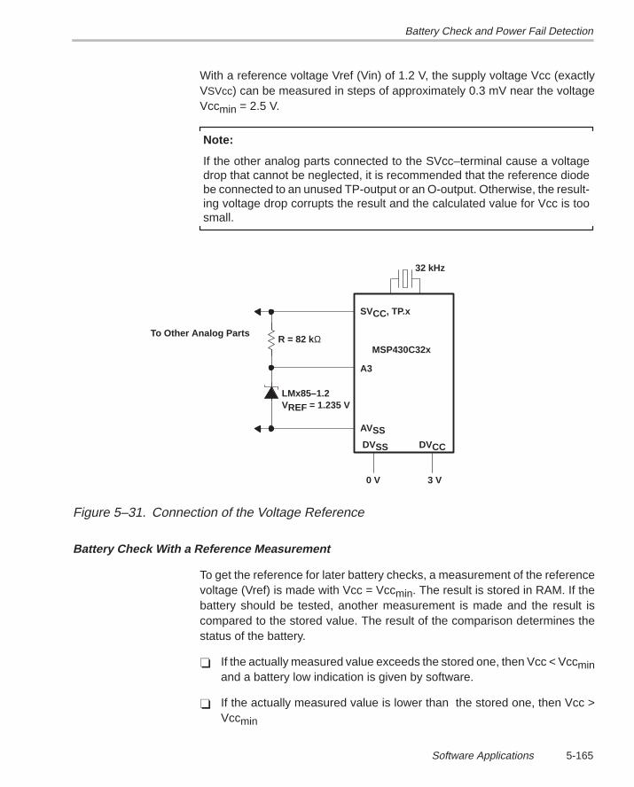
Battery Check and Power Fail Detection
5-165Software Applications
With a reference voltage Vref (Vin) of 1.2 V, the supply voltage Vcc (exactlyVSVcc) can be measured in steps of approximately 0.3 mV near the voltageVccmin = 2.5 V.
Note:
If the other analog parts connected to the SVcc–terminal cause a voltagedrop that cannot be neglected, it is recommended that the reference diodebe connected to an unused TP-output or an O-output. Otherwise, the result-ing voltage drop corrupts the result and the calculated value for Vcc is toosmall.
32 kHz
SVCC, TP.x
A3
AVSS
DVSS DVCC
MSP430C32xR = 82 kΩ
LMx85–1.2VREF = 1.235 V
0 V 3 V
To Other Analog Parts
Figure 5–31. Connection of the Voltage Reference
Battery Check With a Reference Measurement
To get the reference for later battery checks, a measurement of the referencevoltage (Vref) is made with Vcc = Vccmin. The result is stored in RAM. If thebattery should be tested, another measurement is made and the result iscompared to the stored value. The result of the comparison determines thestatus of the battery.
If the actually measured value exceeds the stored one, then Vcc < Vccminand a battery low indication is given by software.
If the actually measured value is lower than the stored one, then Vcc >Vccmin
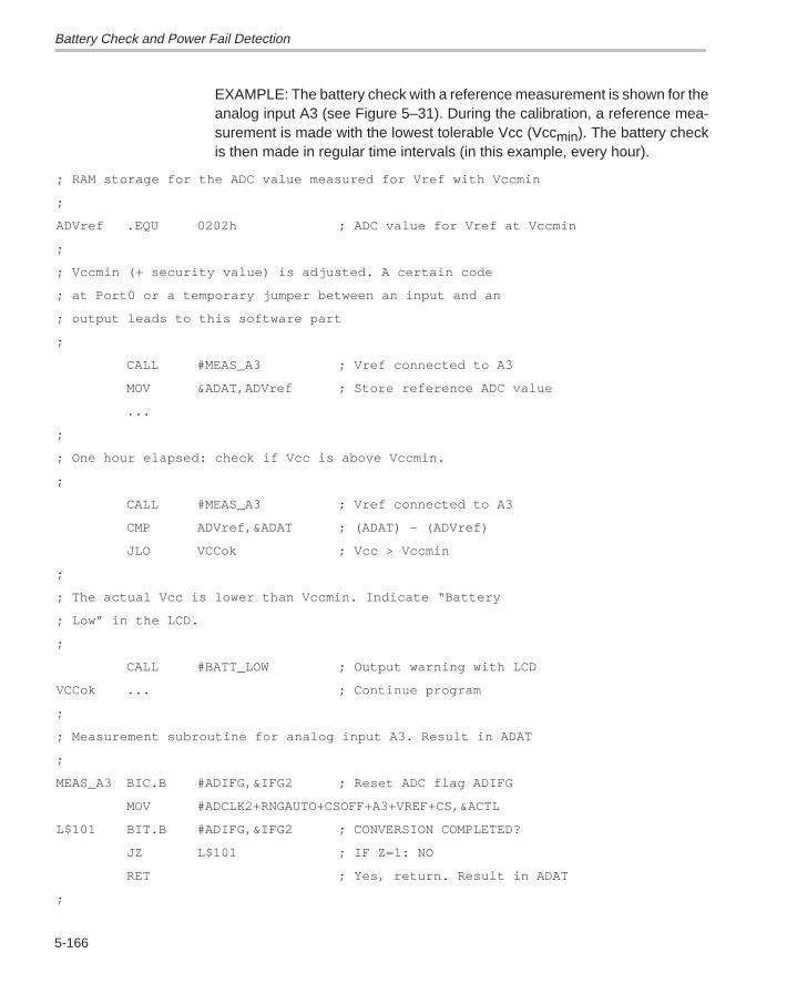
Battery Check and Power Fail Detection
5-166
EXAMPLE: The battery check with a reference measurement is shown for theanalog input A3 (see Figure 5–31). During the calibration, a reference mea-surement is made with the lowest tolerable Vcc (Vccmin). The battery checkis then made in regular time intervals (in this example, every hour).
; RAM storage for the ADC value measured for Vref with Vccmin
;
ADVref .EQU 0202h ; ADC value for Vref at Vccmin
;
; Vccmin (+ security value) is adjusted. A certain code
; at Port0 or a temporary jumper between an input and an
; output leads to this software part
;
CALL #MEAS_A3 ; Vref connected to A3
MOV &ADAT,ADVref ; Store reference ADC value
...
;
; One hour elapsed: check if Vcc is above Vccmin.
;
CALL #MEAS_A3 ; Vref connected to A3
CMP ADVref,&ADAT ; (ADAT) – (ADVref)
JLO VCCok ; Vcc > Vccmin
;
; The actual Vcc is lower than Vccmin. Indicate “Battery
; Low” in the LCD.
;
CALL #BATT_LOW ; Output warning with LCD
VCCok ... ; Continue program
;
; Measurement subroutine for analog input A3. Result in ADAT
;
MEAS_A3 BIC.B #ADIFG,&IFG2 ; Reset ADC flag ADIFG
MOV #ADCLK2+RNGAUTO+CSOFF+A3+VREF+CS,&ACTL
L$101 BIT.B #ADIFG,&IFG2 ; CONVERSION COMPLETED?
JZ L$101 ; IF Z=1: NO
RET ; Yes, return. Result in ADAT
;

Battery Check and Power Fail Detection
5-167Software Applications
Advantages
Very precise definition of one voltage
Small amount of software code
Different reference elements possible without software modifications
Disadvantages
Calibration necessary
Relation to only one supply voltage value is known (calibration volt-age)
Battery Check With the Calculation of the Voltage
If no reference measurement during a calibration phase is possible, the valueof the supply voltage Vcc can be determined by calculation.
The formula is:
Vcc 2Vref
N14= ×
With:N ADC result of the measurement of VrefVref Voltage of the reference diode [V]
EXAMPLE: The actual supply voltage (Vcc) needs to be checked. The pre-vious formula is used for the calculation after the measurement of the refer-ence voltage (Vref). The MSP430 floating point package (32-bit .FLOAT ver-sion) is used for all calculations. The hardware is shown in Figure 5–31.
FPL .equ (ML/8)+1 ; Length of FPP number
...... ; Normal program sequence
;
; One hour elapsed: check if Vcc is above Vccmin or not.
;
CALL #FLT_SAV ; Save FPP registers on stack
SUB #FPL,SP ; Allocate stack for result
CALL #MEAS_A3 ; Measure ref. diode at A3 (N)
MOV #ADAT,RPARG ; Address of ADC result
CALL #CNV_BIN16U ; Convert ADC result N to FP
;
; Calculate Vcc = 2^14 x Vref/(ADC–Result)
Battery Check and Power Fail Detection
5-168
;
MOV #Vref,RPRES ; Load address of Vref voltage
CALL #FLT_DIV ; Calculate Vref/N (N on TOS)
ADD.B #14,1(RPRES) ; Vcc = 2^14 x Vref/N (exp+14)
MOV #VCCmin,RPARG ; Compare Vcc to VCCmin
CALL #FLT_CMP ; Vcc – VCCmin
JHS BATT_ok ; Vcc > VCCmin: ok
CALL #BATT_LOW ; Give “Battery Low” Indication
BATT_ok ADD #FPL,SP ; Correct SP (result area)
CALL #FLT_REC ; Restore FP registers
... ; Continue with program
Vref .FLOAT 1.235 ; Voltage of ref. diode 1.235V
VCCmin .FLOAT 2.5 ; Vccmin MSP430: 2.5V
Advantages
Battery voltage is known (trend calculation possible)
Disadvantages
Error of the reference element is not eliminated
Calculation takes time
Battery Check With a Fixed Value for Comparison
This method uses a fixed ROM–based value for the decision; if Vcc is sufficientor not. According to the data sheet of the LMx85–1.2, the typical voltage of thisreference diode is 1.235 V with a maximum deviation of ±0.012 V. Therefore,the fixed comparison value (Nref) for the minimum supply voltage (Vccmin) canbe calculated:
N INTVref 2
Vccref
14
min= ×
With Vccmin = 2.5 V and Vref = 1.235 V ± 0,012 V:
N INT(1.235 0,012 V) 2
2.5 V8093 78ref
14= ± × = ±
To ensure that the voltage of the battery is above Vccmin, the reference valueshould be set to:

Battery Check and Power Fail Detection
5-169Software Applications
Nref = 8093 – 78 = 8015
Every measured value below 8015 indicates that the battery voltage is higherthan the calculated value, even under worst–case conditions. If the measuredvalue is above 8015, a Battery Low warning should be given.
EXAMPLE: The battery check with a fixed value for comparison is executed.The hardware needed is shown in Figure 5–31. The comparison value isstored in ROM at address VCCmin.
; One hour elapsed: check if Vcc is above Vccmin or not.
;
CALL #MEAS_A3 ; Vref connected to A3
CMP VCCmin,&ADAT ; (ADAT) – (VCCmin)
JLO VCCok ; Vcc > Vccmin
;
; The actual Vcc is lower than Vccmin. Output “Battery
; Low” to the LCD.
;
CALL #BATT_LOW ; Output warning to the LCD
VCCok ... ; Continue program
;
; ROM storage for the calculated ADC value: Vref at Vccmin.
; (worst case value).
;
VCCmin .WORD 8015 ; ADC value 1.235V at 2.5V
Advantages
Small amount of software code
Disadvantages
Error of the reference element is not eliminated
Fixed reference element
Relation to only one supply voltage value is known
5.7.1.2 Battery Check With an External Comparator
With an operational amplifier used as a comparator, a simple battery check canbe implemented for MSP430 family members that do not have the 14–bit ADC.Figure 5–32 shows two possibilities:
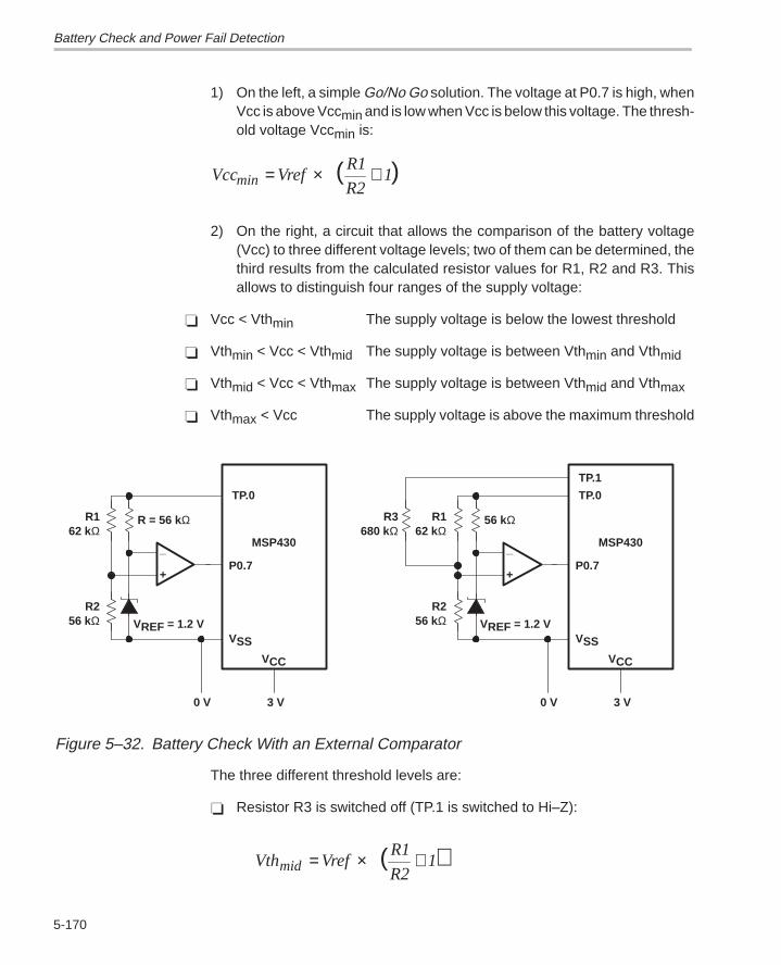
Battery Check and Power Fail Detection
5-170
1) On the left, a simple Go/No Go solution. The voltage at P0.7 is high, whenVcc is above Vccmin and is low when Vcc is below this voltage. The thresh-old voltage Vccmin is:
Vcc VrefR1
R21min = × +( )
2) On the right, a circuit that allows the comparison of the battery voltage(Vcc) to three different voltage levels; two of them can be determined, thethird results from the calculated resistor values for R1, R2 and R3. Thisallows to distinguish four ranges of the supply voltage:
Vcc < Vthmin The supply voltage is below the lowest threshold
Vthmin < Vcc < Vthmid The supply voltage is between Vthmin and Vthmid
Vthmid < Vcc < Vthmax The supply voltage is between Vthmid and Vthmax
Vthmax < Vcc The supply voltage is above the maximum threshold
TP.0
P0.7
VSS
VCC
MSP430
R = 56 kΩ
VREF = 1.2 V
3 V0 V
_
+
R162 kΩ
R256 kΩ
TP.0
P0.7
VSS
VCC
MSP430
56 kΩ
VREF = 1.2 V
3 V0 V
_
+
R162 kΩ
R256 kΩ
R3680 kΩ
TP.1
Figure 5–32. Battery Check With an External Comparator
The three different threshold levels are:
Resistor R3 is switched off (TP.1 is switched to Hi–Z):
Vth VrefR1
R21mid = × +( )
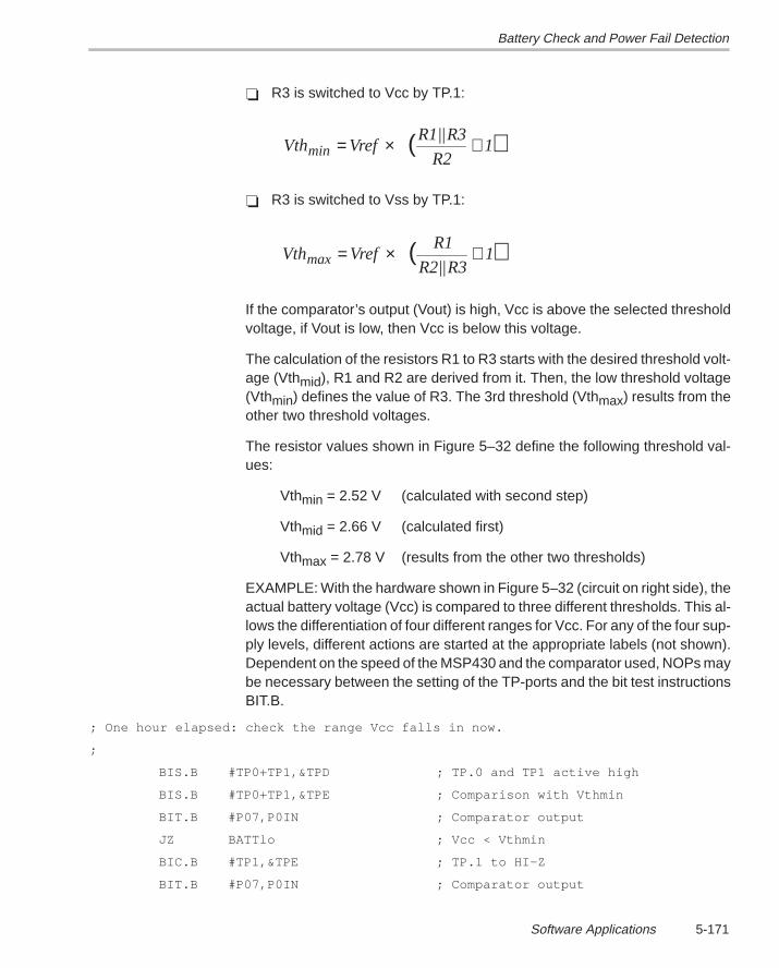
Battery Check and Power Fail Detection
5-171Software Applications
R3 is switched to Vcc by TP.1:
Vth VrefR1||R3
R21min = × +( )
R3 is switched to Vss by TP.1:
Vth VrefR1
R2||R31max = × +( )
If the comparator’s output (Vout) is high, Vcc is above the selected thresholdvoltage, if Vout is low, then Vcc is below this voltage.
The calculation of the resistors R1 to R3 starts with the desired threshold volt-age (Vthmid), R1 and R2 are derived from it. Then, the low threshold voltage(Vthmin) defines the value of R3. The 3rd threshold (Vthmax) results from theother two threshold voltages.
The resistor values shown in Figure 5–32 define the following threshold val-ues:
Vthmin = 2.52 V (calculated with second step)
Vthmid = 2.66 V (calculated first)
Vthmax = 2.78 V (results from the other two thresholds)
EXAMPLE: With the hardware shown in Figure 5–32 (circuit on right side), theactual battery voltage (Vcc) is compared to three different thresholds. This al-lows the differentiation of four different ranges for Vcc. For any of the four sup-ply levels, different actions are started at the appropriate labels (not shown).Dependent on the speed of the MSP430 and the comparator used, NOPs maybe necessary between the setting of the TP-ports and the bit test instructionsBIT.B.
; One hour elapsed: check the range Vcc falls in now.
;
BIS.B #TP0+TP1,&TPD ; TP.0 and TP1 active high
BIS.B #TP0+TP1,&TPE ; Comparison with Vthmin
BIT.B #P07,P0IN ; Comparator output
JZ BATTlo ; Vcc < Vthmin
BIC.B #TP1,&TPE ; TP.1 to HI–Z
BIT.B #P07,P0IN ; Comparator output
Battery Check and Power Fail Detection
5-172
JZ BATTmid ; Vthmin < Vcc < Vthmid
BIC.B #TP1,&TPD ; TP.1 active to Vss
BIS.B #TP1,&TPE ; Check Vthmax
BIT.B #P07,P0IN ; Comparator output
JNZ BATThi ; Vcc > Vthmax
... ; Vthmid < Vcc < Vthmax
;
Advantages
Four ranges defined (more ranges are possible if desired)
Very fast software
Different reference elements are possible without software change
Disadvantages
Hardware effort (except if an unused operational amplifier of a quad–pack can be used)
5.7.1.3 Battery Check With the Universal Timer/Port Module
The Universal Timer/Port module allows a relatively accurate measurementof the battery voltage (Vcc). The principle (see Figures 5–33 and 5–34) is asfollows: the capacitor (C), also used for the other measurements, is charged–up to the voltage (Vref) of the reference diode. C is then discharged with Rrefand the time tref until VC reaches the lower threshold VIT– of the input CIN ismeasured. Afterwards, C is charged–up fully to the supply voltage (Vcc) andthe discharge time (tVcc) is also measured. Vcc is then:
Vcc Vref e
tVcc tref
= ×
–
τ
With:Vcc Actual supply voltage of the MSP430 [V]Vref Voltage of the reference diode [V]tref Time to discharge C from Vref to VIT– [s]tVcc Time to discharge C from Vcc to VIT– [s]τ Time constant for discharge: τ = Rref × C [s]VIT– Lower threshold voltage of input CIN [V]
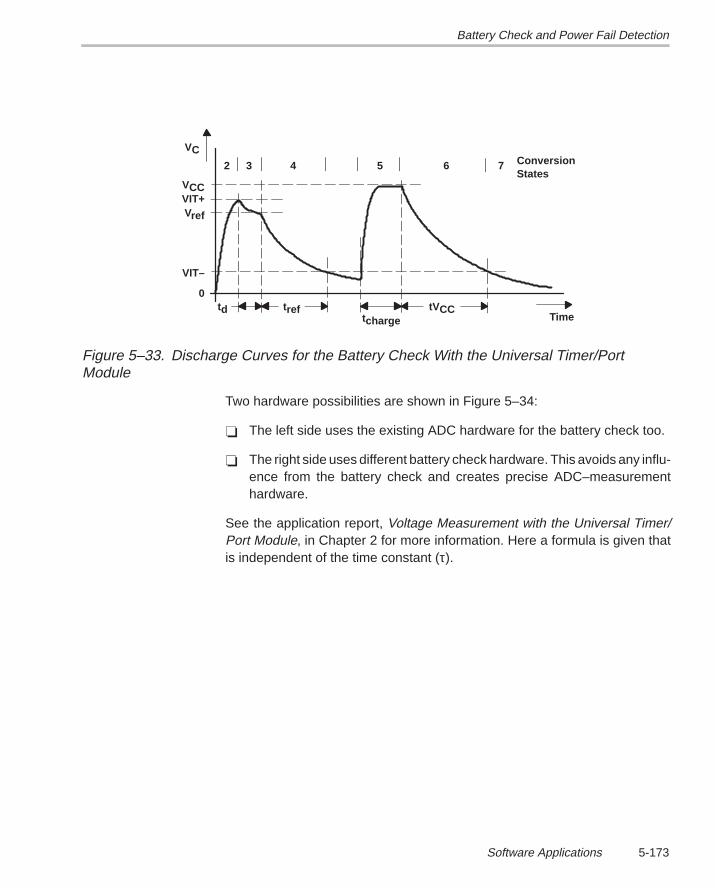
Battery Check and Power Fail Detection
5-173Software Applications
td treftcharge
tVCCTime
VC
VCCVIT+Vref
VIT–
0
2 3 4 5 6 7 ConversionStates
Figure 5–33. Discharge Curves for the Battery Check With the Universal Timer/PortModule
Two hardware possibilities are shown in Figure 5–34:
The left side uses the existing ADC hardware for the battery check too.
The right side uses different battery check hardware. This avoids any influ-ence from the battery check and creates precise ADC–measurementhardware.
See the application report, Voltage Measurement with the Universal Timer/Port Module, in Chapter 2 for more information. Here a formula is given thatis independent of the time constant (τ).
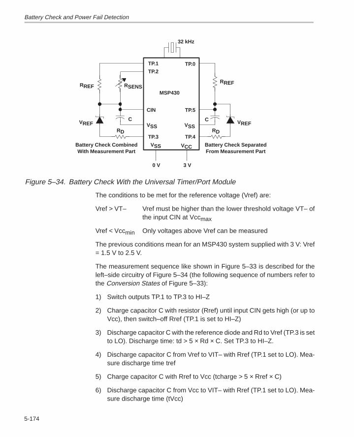
Battery Check and Power Fail Detection
5-174
32 kHz
TP.2
CIN
VSS VCC
MSP430
3 V0 V
TP.1
RSENS
VSSC
TP.3
VREFRD
RREFRREF
C VREF
TP.4
VSS
TP.5
TP.0
Battery Check CombinedWith Measurement Part
Battery Check SeparatedFrom Measurement Part
RD
Figure 5–34. Battery Check With the Universal Timer/Port Module
The conditions to be met for the reference voltage (Vref) are:
Vref > VT– Vref must be higher than the lower threshold voltage VT– of the input CIN at Vccmax
Vref < Vccmin Only voltages above Vref can be measured
The previous conditions mean for an MSP430 system supplied with 3 V: Vref= 1.5 V to 2.5 V.
The measurement sequence like shown in Figure 5–33 is described for theleft–side circuitry of Figure 5–34 (the following sequence of numbers refer tothe Conversion States of Figure 5–33):
1) Switch outputs TP.1 to TP.3 to HI–Z
2) Charge capacitor C with resistor (Rref) until input CIN gets high (or up toVcc), then switch–off Rref (TP.1 is set to HI–Z)
3) Discharge capacitor C with the reference diode and Rd to Vref (TP.3 is setto LO). Discharge time: td > 5 × Rd × C. Set TP.3 to HI–Z.
4) Discharge capacitor C from Vref to VIT– with Rref (TP.1 set to LO). Mea-sure discharge time tref
5) Charge capacitor C with Rref to Vcc (tcharge > 5 × Rref × C)
6) Discharge capacitor C from Vcc to VIT– with Rref (TP.1 set to LO). Mea-sure discharge time (tVcc)

Battery Check and Power Fail Detection
5-175Software Applications
7) Calculate Vcc with the formula shown previously
For the supply voltage range of a 3–V system (Vcc = 2.5V to 3.5V) and a refer-ence voltage of Vref = 2.3 V, the exponential part of the equation can be re-placed by a linear function:
Vcc Vref 1.29tVcc tref
0.97= × ×–
+( )τ
If the Universal Timer/Port Module is used in an ADC application with high ac-curacy (like a heat volume counter) then the battery–check circuitry should beconnected to other I/Os as shown in Figure 5–34 on the right side. This waythe measurement of the sensors cannot be influenced by the battery–checkcircuitry.
The software shown in the application report, Using the MSP430 UniversalTimer/Port Module as an Analog-to-Digital Converter in Chapter 2, can alsobe used for the battery check with only a few modifications.
Advantages
Minimum hardware effort if measurement part exists anyway
Supply voltage is known after the measurement
Disadvantages
Slow measurement
5.7.2 Power Fail Detection
AC driven systems need a much faster indication of a power–down situationthan battery–driven systems. It is a matter of milliseconds, not of hours or days.Therefore, other methods are used. Three of them are described in the follow-ing text.
The non–regulated side of the power supply is observed. If the voltage(VC) of the charge capacitor falls below a certain level (VCmin), an interruptis requested.
The voltage at the secondary side of the ac transformer is observed. A suf-ficient level change there resets the watchdog. If the secondary voltageis too low or ceases, an interrupt is requested.
The non–regulated side of the power supply is observed with a TLC7701.The output of this supply voltage supervisor requests an NMI interrupt orresets the microcomputer.

Battery Check and Power Fail Detection
5-176
The interrupt requested by the previous three solutions is used to start the nec-essary emergency actions:
Switching–off all loads to lengthen the available time for the emergencyactions
Reduction of the system clock MCLK to 1 MHz to be able to use Vcc downto Vccmin
Storage of all important values into an external EEPROM
Use of LPM3 finally to bridge the power failure eventually
The three hardware proposals can be used with all members of the MSP430family. The power–fail detection is also called ac–low detection. It issues theac–low signal.
5.7.2.1 Power–Fail Detection by Observation of the Charge Capacitor
Here the voltage level of the charge capacitor (Cch) is observed. If the voltagelevel of this capacitor falls below a certain voltage level (VCmin), an interruptis requested. With the circuit shown in Figure 5–35, VCmin is:
VC
R3
R41
R1
R21
min = ×+( )
+( )Vcc
R1, R2, R3 and R4 are chosen in a way that delivers the desired threshold volt-age (VCmin). The regulated supply voltage (Vcc) is used as a reference. TheNMI (non–maskable interrupt) can be used to get the fastest possible re-sponse.
The remaining time (trem) for actions after a power–fail interrupt is approxi-mately:
( )trem VC Vcc VrCch
Imin minAM
= – – ×
Where:trem Approximate time from interrupt to the reaching of Vccmin [s]Cch Capacity of the charge capacitor [F]IAM Supply current of the MSP430 system (medium value) [A]VCmin Voltage at the charge capacitor that causes ac–low interrupt [V]Vccmin Lowest supply voltage for the MSP430 [V]Vr Dropout voltage (voltage difference between output and input)
of the voltage regulator for function [V]
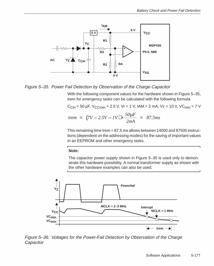
Battery Check and Power Fail Detection
5-177Software Applications
VCC
P0.0, NMI
VSS
MSP430
R4
_+
R1
R2
5 V
R3
IAM
VC
CCHVZAC
5 V
0 V
Figure 5–35. Power Fail Detection by Observation of the Charge Capacitor
With the following component values for the hardware shown in Figure 5–35,trem for emergency tasks can be calculated with the following formula.
CCH = 50 µF, VCCmin = 2.5 V, Vr = 1 V, IAM = 2 mA, Vz = 10 V, VCmin = 7 V
( )trem 7V 2.5V 1V50 F
2mA87.5ms= – – × =µ
This remaining time trem = 87.5 ms allows between 14000 and 87500 instruc-tions (dependent on the addressing modes) for the saving of important valuesin an EEPROM and other emergency tasks.
Note:
The capacitor power supply shown in Figure 5–35 is used only to demon-strate this hardware possibility. A normal transformer supply as shown withthe other hardware examples can also be used.
VZ
VCC
Powerfail
InteruptMCLK = 1 MHz
MCLK = 2–3 MHz
trem
VCminVCmin
Figure 5–36. Voltages for the Power-Fail Detection by Observation of the ChargeCapacitor
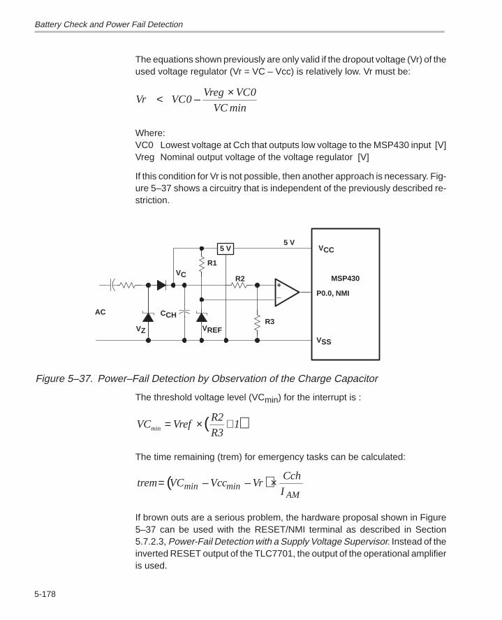
Battery Check and Power Fail Detection
5-178
The equations shown previously are only valid if the dropout voltage (Vr) of theused voltage regulator (Vr = VC – Vcc) is relatively low. Vr must be:
Vr < –×
VCVreg VC
VC0
0
min
Where:VC0 Lowest voltage at Cch that outputs low voltage to the MSP430 input [V]Vreg Nominal output voltage of the voltage regulator [V]
If this condition for Vr is not possible, then another approach is necessary. Fig-ure 5–37 shows a circuitry that is independent of the previously described re-striction.
VCC
P0.0, NMI
VSS
MSP430
R3
_+
5 V
R2VC
CCH
VZ
AC
5 V
VREF
R1
Figure 5–37. Power–Fail Detection by Observation of the Charge Capacitor
The threshold voltage level (VCmin) for the interrupt is :
VC VrefR2
R31min = × +( )
The time remaining (trem) for emergency tasks can be calculated:
( )trem VC Vcc VrCch
Imin minAM
= – – ×
If brown outs are a serious problem, the hardware proposal shown in Figure5–37 can be used with the RESET/NMI terminal as described in Section5.7.2.3, Power-Fail Detection with a Supply Voltage Supervisor. Instead of theinverted RESET output of the TLC7701, the output of the operational amplifieris used.

Battery Check and Power Fail Detection
5-179Software Applications
EXAMPLE: The interrupt handler and its initialization is shown for the power–fail detection by observation of the charge capacitor with a comparator. Afterthe completion of the emergency tasks, a test is made to check if the supplyvoltage is still low. If not, the software restarts at label PF_INIT. Otherwise,LPM3 is entered to eventually bridge the power failure. The basic timer checkswith its interrupt handler in regular intervals for an indication that the voltageis above VCmin again. The hardware shown in Figure 5–35 is used.
; SYSTAT contains the current system status: calibration,
; normal run, power fail aso.
;
SYSTAT .EQU 0200h ; System status byte
;
; The program starts at label INIT if a power–up occurs
;
INIT ... ; Normal initialization
;
; The program restarts at label PF_INIT if the supply voltage
; returns before Vccmin is reached (short power fail)
;
PF_INIT MOV #0300h,SP ; Restart after power fail
... ; Special initialization
;
; Initialization: Prepare P0.0 for power fail detection.
;
BIS.B #P0IFG0,&IE1 ; Enable P0.0 interrupt
BIS.B #P00,&P0IES ; Intrpt for trailing edge
BIC.B #P0IFG0,&IFG1 ; Reset flag (safety)
... ; Continue with initialization
EINT ; Enable GIE
MAINLOOP MOV.B #NORMAL,SYSTAT ; Start normal program
... ;
;
; P0.0 Interrupt Handler: the voltage VC at Cch fell below a
; minimum voltage VCmin. Switch off all loads and interrupts
; except Basic Timer interrupt.
;
P00_HNDLR BIS #PD,&ACTL ; ADC to Power down
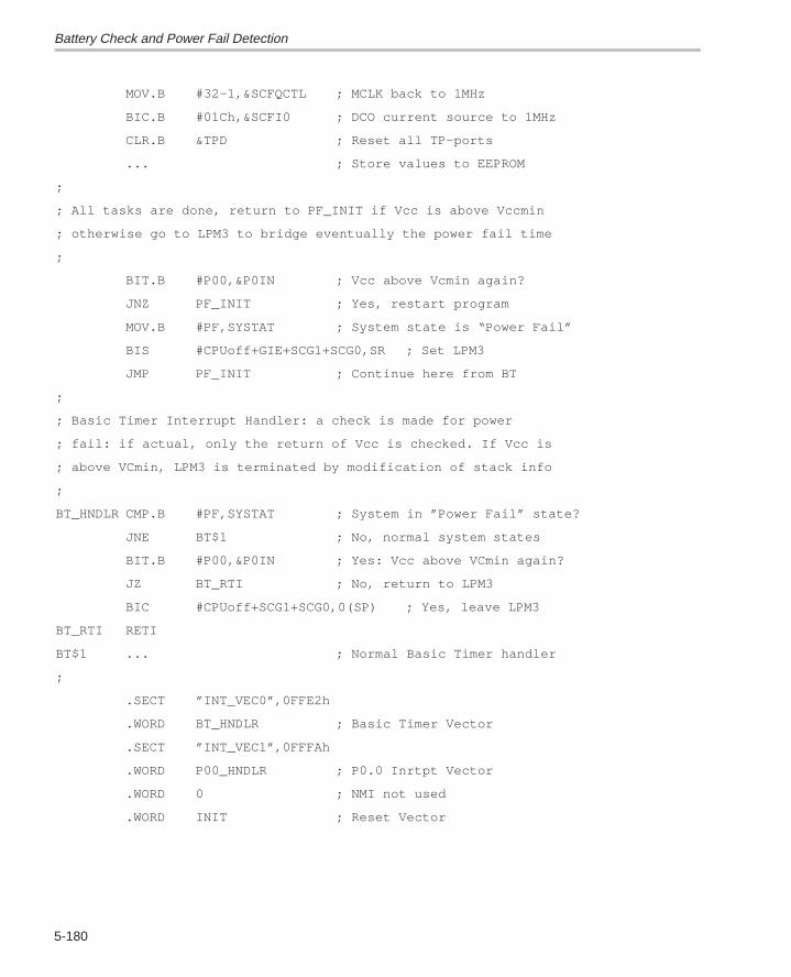
Battery Check and Power Fail Detection
5-180
MOV.B #32–1,&SCFQCTL ; MCLK back to 1MHz
BIC.B #01Ch,&SCFI0 ; DCO current source to 1MHz
CLR.B &TPD ; Reset all TP–ports
... ; Store values to EEPROM
;
; All tasks are done, return to PF_INIT if Vcc is above Vccmin
; otherwise go to LPM3 to bridge eventually the power fail time
;
BIT.B #P00,&P0IN ; Vcc above Vcmin again?
JNZ PF_INIT ; Yes, restart program
MOV.B #PF,SYSTAT ; System state is “Power Fail”
BIS #CPUoff+GIE+SCG1+SCG0,SR ; Set LPM3
JMP PF_INIT ; Continue here from BT
;
; Basic Timer Interrupt Handler: a check is made for power
; fail: if actual, only the return of Vcc is checked. If Vcc is
; above VCmin, LPM3 is terminated by modification of stack info
;
BT_HNDLR CMP.B #PF,SYSTAT ; System in ”Power Fail” state?
JNE BT$1 ; No, normal system states
BIT.B #P00,&P0IN ; Yes: Vcc above VCmin again?
JZ BT_RTI ; No, return to LPM3
BIC #CPUoff+SCG1+SCG0,0(SP) ; Yes, leave LPM3
BT_RTI RETI
BT$1 ... ; Normal Basic Timer handler
;
.SECT ”INT_VEC0”,0FFE2h
.WORD BT_HNDLR ; Basic Timer Vector
.SECT ”INT_VEC1”,0FFFAh
.WORD P00_HNDLR ; P0.0 Inrtpt Vector
.WORD 0 ; NMI not used
.WORD INIT ; Reset Vector
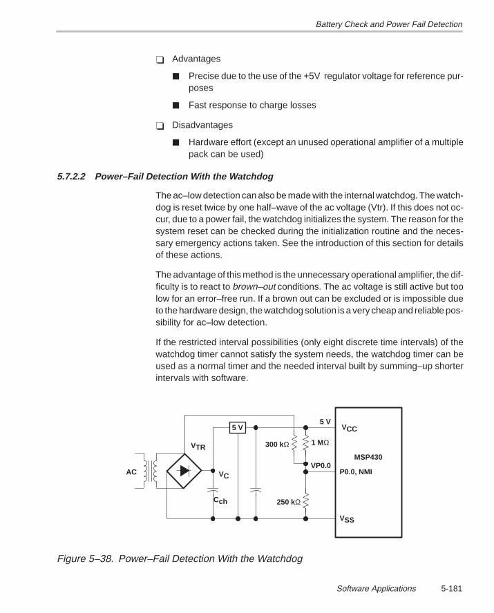
Battery Check and Power Fail Detection
5-181Software Applications
Advantages
Precise due to the use of the +5V regulator voltage for reference pur-poses
Fast response to charge losses
Disadvantages
Hardware effort (except an unused operational amplifier of a multiplepack can be used)
5.7.2.2 Power–Fail Detection With the Watchdog
The ac–low detection can also be made with the internal watchdog. The watch-dog is reset twice by one half–wave of the ac voltage (Vtr). If this does not oc-cur, due to a power fail, the watchdog initializes the system. The reason for thesystem reset can be checked during the initialization routine and the neces-sary emergency actions taken. See the introduction of this section for detailsof these actions.
The advantage of this method is the unnecessary operational amplifier, the dif-ficulty is to react to brown–out conditions. The ac voltage is still active but toolow for an error–free run. If a brown out can be excluded or is impossible dueto the hardware design, the watchdog solution is a very cheap and reliable pos-sibility for ac–low detection.
If the restricted interval possibilities (only eight discrete time intervals) of thewatchdog timer cannot satisfy the system needs, the watchdog timer can beused as a normal timer and the needed interval built by summing–up shorterintervals with software.
VCC
P0.0, NMI
VSS
MSP430
5 V
300 kΩ
VC
Cch
AC
5 V
VTR1 MΩ
250 kΩ
VP0.0
Figure 5–38. Power–Fail Detection With the Watchdog
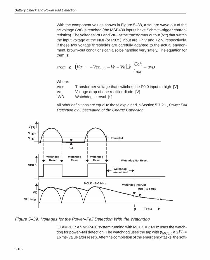
Battery Check and Power Fail Detection
5-182
With the component values shown in Figure 5–38, a square wave out of theac voltage (Vtr) is reached (the MSP430 inputs have Schmitt–trigger charac-teristics). The voltages Vtr+ and Vtr– at the transformer output (Vtr) that switchthe input voltage at the NMI (or P0.x ) input are +7 V and +2 V, respectively.If these two voltage thresholds are carefully adapted to the actual environ-ment, brown–out conditions can also be handled very safely. The equation fortrem is:
trem Vtr Vcc VrCch
I+ min
AM≥ – – –( ) × –Vd tWD
Where:Vtr+ Transformer voltage that switches the P0.0 input to high [V]Vd Voltage drop of one rectifier diode [V]tWD Watchdog interval [s]
All other definitions are equal to those explained in Section 5.7.2.1, Power FailDetection by Observation of the Charge Capacitor.
WatchdogReset
WatchdogReset
WatchdogReset
WatchdogInterval twd
Watchdog Not Reset
Watchdog Interupt
MCLK = 1 MHz
TREM
Powerfail
Vd
VTR
VTR+VTR–
VP0.0
VCCmin
VC
MCLK = 2–3 MHz
Figure 5–39. Voltages for the Power–Fail Detection With the Watchdog
EXAMPLE: An MSP430 system running with MCLK = 2 MHz uses the watch-dog for power–fail detection. The watchdog uses the tap with (tMCLK × 215) =16 ms (value after reset). After the completion of the emergency tasks, the soft-

Battery Check and Power Fail Detection
5-183Software Applications
ware checks if the ac voltage is back again with a loop. This is made by check-ing if P0.0 goes high. If this is the case, the initialization part is entered. Thecircuit shown in Figure 5–38 is used.
; Power–up and watchdog reset start at label INIT. The reason
; for the reset needs to be known (power–up or watchdog)
;
INIT BIT.B #WDTIFG,&IFG1 ; Reset by watchdog?
JNZ WD_RESET ; Yes; power fail
;
; Normal reset caused by RESET pin or power–up: Init. system
;
BIS.B #4,&SCFI0 ; Switch DCO to 2MHz drive
MOV.B #64–1,&SCFQCTL ; FLL to 2MHz
MOV #05A00h+CNTCL,&WDTCTL ; Reset watchdog
BIS.B #P0IE0,&IE1 ; Enable P0.0 intrpt
... ; Continue initialization
EINT ; Finally set GIE
MAINLOOP ... ; Start main program
;
; Reset caused by watchdog: missing main means power fail
; Supply current is minimized to enlarge active time. All
; interrupts except P0.0 interrupt are switched off
;
WD_RESET BIC.B #03Fh,&TPD ; Switch off all TP–outputs
... ; Switch off other loads
BIS #PD,&ACTL ; Power down ADC
MOV.B #32–1,&SCFQCTL ; MCLK back to 1MHz
BIC.B #01Ch,&SCFI0 ; DCO drive to 1MHz, FN_x = 0
... ; Store values to EEPROM
;
; All tasks are done: check if mains is back (P0.0 gets HI).
;
Llow BIT.B #P00,&P0IN ; Actual state of P0.0 pin
JZ Llow ; Still low
BR #INIT ; P0.0 is HI, initialize
;
Battery Check and Power Fail Detection
5-184
; The P00_HNDLR is called twice each period of the mains
; voltage. The watchdog is reset to indicate normal run,
; the edge selection bit of P0.0 is inverted.
;
P00_HNDLR MOV #05A00h+CNTCL,&WDTCTL ; Reset watchdog
XOR.B #P00,&P0IES ; Invert edge select for P0.0
RETI ;
;
.SECT ”INT_VEC1”,0FFFAh
.WORD P00_HNDLR ; P0.0 Inrtpt Vector
.WORD 0 ; NMI not used
.WORD INIT ; Reset Vector
Advantages
Minimum hardware effort
Minimum software effort
Very fast
Brown out conditions can be handled by a precise hardware definition
Disadvantages
Remaining time trem can be calculated only for worst case
5.7.2.3 Power–Fail Detection With a Supply Voltage Supervisor
For extremely safe MSP430 applications, a TLC7701 supply voltage supervi-sor can be used. The voltage (VC) of the charge capacitor (Cch) is observed.The output signal /RESET indicates if VC is higher or lower than the thresholdvoltage (Vth). Figure 5–40 shows the schematic for this application. The outputsignal /RESET of the TLC7701 is used in two different ways, depending on theactual state of the application.
During power–up, the TLC7701 output is used as a reset signal. TheMSP430 is held in the reset state until VC reaches a certain voltage (Vth)(e.g., supply voltage + regulator voltage drop) (see Figure 5–41).
During run mode the RESET/NMI terminal of the MSP430 is switched toNMI–mode (Non–Maskable Interrupt) by software. If VC falls below Vth,an NMI is requested. The interrupt handler can start all necessary emer-gency tasks. See the introduction of this section for the description ofthese tasks.
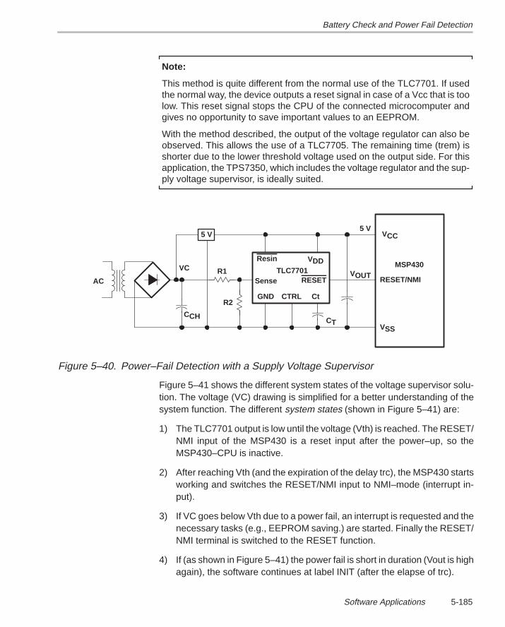
Battery Check and Power Fail Detection
5-185Software Applications
Note:
This method is quite different from the normal use of the TLC7701. If usedthe normal way, the device outputs a reset signal in case of a Vcc that is toolow. This reset signal stops the CPU of the connected microcomputer andgives no opportunity to save important values to an EEPROM.
With the method described, the output of the voltage regulator can also beobserved. This allows the use of a TLC7705. The remaining time (trem) isshorter due to the lower threshold voltage used on the output side. For thisapplication, the TPS7350, which includes the voltage regulator and the sup-ply voltage supervisor, is ideally suited.
VCC
RESET/NMI
VSS
MSP430
5 V
VC
CT
AC
5 V
RESET
VDD
Ct
Sense
CTRLGND
Resin
TLC7701
CCH
R1
R2
VOUT
Figure 5–40. Power–Fail Detection with a Supply Voltage Supervisor
Figure 5–41 shows the different system states of the voltage supervisor solu-tion. The voltage (VC) drawing is simplified for a better understanding of thesystem function. The different system states (shown in Figure 5–41) are:
1) The TLC7701 output is low until the voltage (Vth) is reached. The RESET/NMI input of the MSP430 is a reset input after the power–up, so theMSP430–CPU is inactive.
2) After reaching Vth (and the expiration of the delay trc), the MSP430 startsworking and switches the RESET/NMI input to NMI–mode (interrupt in-put).
3) If VC goes below Vth due to a power fail, an interrupt is requested and thenecessary tasks (e.g., EEPROM saving.) are started. Finally the RESET/NMI terminal is switched to the RESET function.
4) If (as shown in Figure 5–41) the power fail is short in duration (Vout is highagain), the software continues at label INIT (after the elapse of trc).
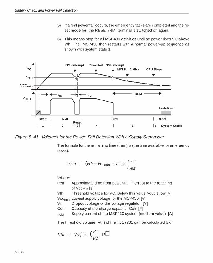
Battery Check and Power Fail Detection
5-186
5) If a real power fail occurs, the emergency tasks are completed and the re-set mode for the RESET/NMI terminal is switched on again.
6) This means stop for all MSP430 activities until ac power rises VC aboveVth. The MSP430 then restarts with a normal power–up sequence asshown with system state 1.
NMI-Interupt Powerfail NMI-InteruptMCLK = 1 MHz CPU Stops
tREMtrctrc
Undefined
Reset NMI NMI Reset
1 2 3Reset
4 5 6 System States
VC
VTH
VCCmin
VOUT
Figure 5–41. Voltages for the Power–Fail Detection With a Supply Supervisor
The formula for the remaining time (trem) is (the time available for emergencytasks):
( )trem Vth Vcc VrCch
IminAM
= – – ×
Where:trem Approximate time from power-fail interrupt to the reaching
of Vccmin [s]Vth Threshold voltage for VC. Below this value Vout is low [V]Vccmin Lowest supply voltage for the MSP430 [V]Vr Dropout voltage of the voltage regulator [V]Cch Capacity of the charge capacitor Cch [F]IAM Supply current of the MSP430 system (medium value) [A]
The threshold voltage (Vth) of the TLC7701 can be calculated by:
Vth VrefR1
R21= × +( )
Battery Check and Power Fail Detection
5-187Software Applications
Where:Vref Voltage of the internal reference diode of the TLC7701: +1.1 VR2 Resistor from SENSE input to 0 V. Nominal value 100 kΩ to 200 kΩ
The delay (trc) after the return of VC is defined by the capacitor (Ct) shown inFigure 5–40. If this delay is not desired, Ct is omitted. The formula trc is:
trc = 21kΩ × Ct
EXAMPLE: The MSP430 system shown in Figure 5–40 with its initializationand run–time software.
; Initialization: prepare RESET/NMI as an NMI interrupt input.
;
INIT MOV #05A00h+NMI+NMIES+CNTCL,&WDTCTL ; 1–>0 edge
... ; Continue with initialization
EINT ; Enable interrupt
MAINLOOP ... ; Start normal program here
;
; NMI Interrupt Handler: an oscillator fault or the trailing
; edge of the TLC7701 caused interrupt due to the low input
; voltage VC. Check first the cause of the interrupt.
; The load is reduced to gain time for emergency actions.
;
NMI_HNDLR BIT.B #OFIFG,IFG1 ; Oscillator fault?
JNZ OSCFLT ; Yes, proceed there
BIC.B #03Fh,&TPD ; Switch off all TP–outputs
... ; Switch off other loads
BIS #PD,&ACTL ; ADC Power down
MOV.B #32–1,&SCFQCTL ; MCLK back to 1MHz
BIC.B #01Ch,&SCFI0 ; DCO drive to 1MHz
... ; Store values to EEPROM
;
; All tasks are done: switch RESET/NMI to RESET function.
; CPU stops until next power–up sequence. If the TLC7701 output
; is high again (mains back) the program restarts at INIT
;
MOV #05A00h+CNTCL,&WDTCTL ; PC is set to INIT
BR #INIT ; Short power fail: Vcc high

Battery Check and Power Fail Detection
5-188
;
.SECT ”INT_VEC1”,0FFFCh
.WORD NMI_HNDLR ; NMI Vector
.WORD INIT ; Reset Vector
;
Advantages
Extremely safe: can handle any environment with the appropriatesoftware and hardware combination
Disadvantages
Hardware effort (TLC7701 needed)
5.7.3 Conclusion
The concepts shown for battery check and power–fail detection are only pos-sible due to the MSP430’s hardware features:
Battery–driven systems can be realized only with microcomputers thatneed only a very low supply current
In ac–driven systems, the available security of MSP430 systems is due tothree unique MSP430 features:
1) The low current consumption allows the remaining charge of the (relativelysmall) charge capacitor to be used for a lot of emergency tasks in case ofa power fail
2) The high speed of the CPU allows to finish all these necessary emergencytasks during the remaining time from power–fail detection to the reachingof the lowest usable supply voltage.
3) The wide supply voltage range (+5.5 V down to +2.5 V) increases the timeremaining for these tasks.
These three features together allow relatively simple hardware solutions forMSP430 systems, especially the use of small charge capacitors.

6-1
On-Chip Peripherals
Chapter 6
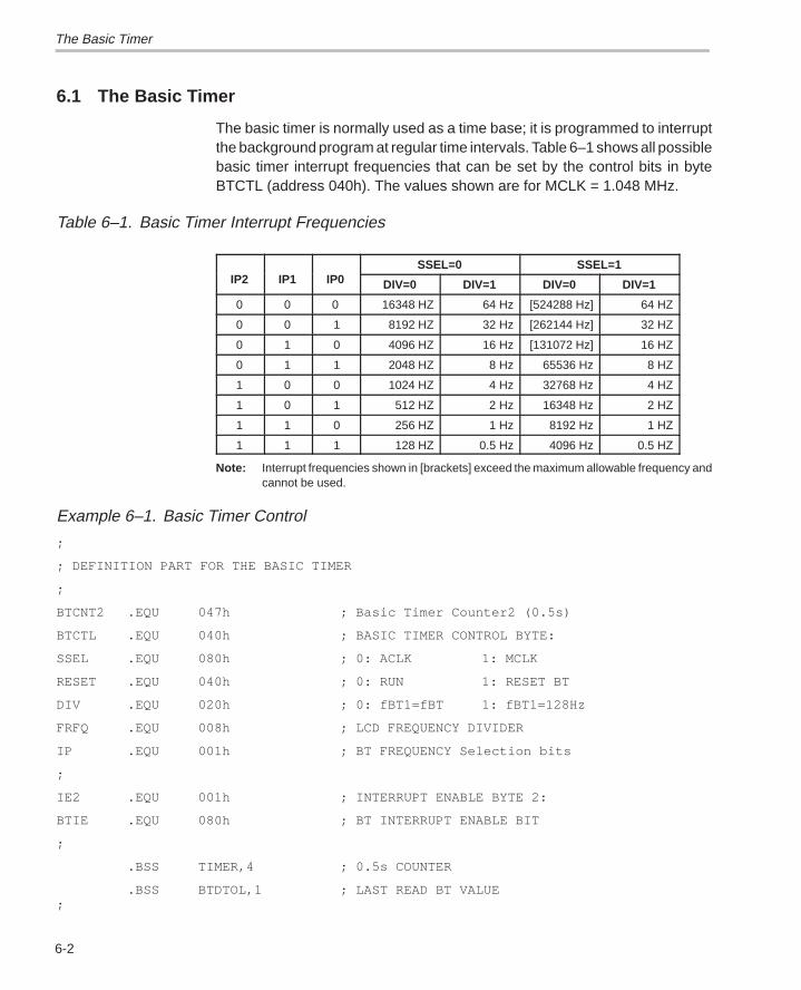
The Basic Timer
6-2
6.1 The Basic Timer
The basic timer is normally used as a time base; it is programmed to interruptthe background program at regular time intervals. Table 6–1 shows all possiblebasic timer interrupt frequencies that can be set by the control bits in byteBTCTL (address 040h). The values shown are for MCLK = 1.048 MHz.
Table 6–1. Basic Timer Interrupt Frequencies
SSEL=0 SSEL=1IP2 IP1 IP0 DIV=0 DIV=1 DIV=0 DIV=1
0 0 0 16348 HZ 64 Hz [524288 Hz] 64 HZ
0 0 1 8192 HZ 32 Hz [262144 Hz] 32 HZ
0 1 0 4096 HZ 16 Hz [131072 Hz] 16 HZ
0 1 1 2048 HZ 8 Hz 65536 Hz 8 HZ
1 0 0 1024 HZ 4 Hz 32768 Hz 4 HZ
1 0 1 512 HZ 2 Hz 16348 Hz 2 HZ
1 1 0 256 HZ 1 Hz 8192 Hz 1 HZ
1 1 1 128 HZ 0.5 Hz 4096 Hz 0.5 HZ
Note: Interrupt frequencies shown in [brackets] exceed the maximum allowable frequency andcannot be used.
Example 6–1. Basic Timer Control
;
; DEFINITION PART FOR THE BASIC TIMER
;
BTCNT2 .EQU 047h ; Basic Timer Counter2 (0.5s)
BTCTL .EQU 040h ; BASIC TIMER CONTROL BYTE:
SSEL .EQU 080h ; 0: ACLK 1: MCLK
RESET .EQU 040h ; 0: RUN 1: RESET BT
DIV .EQU 020h ; 0: fBT1=fBT 1: fBT1=128Hz
FRFQ .EQU 008h ; LCD FREQUENCY DIVIDER
IP .EQU 001h ; BT FREQUENCY Selection bits
;
IE2 .EQU 001h ; INTERRUPT ENABLE BYTE 2:
BTIE .EQU 080h ; BT INTERRUPT ENABLE BIT
;
.BSS TIMER,4 ; 0.5s COUNTER
.BSS BTDTOL,1 ; LAST READ BT VALUE;
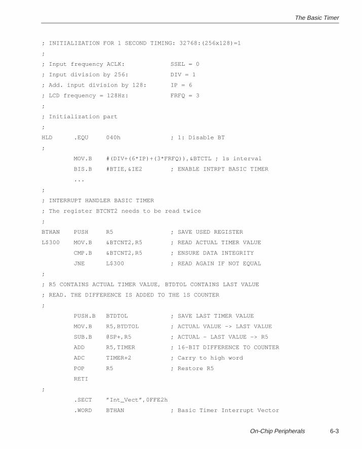
The Basic Timer
6-3On-Chip Peripherals
; INITIALIZATION FOR 1 SECOND TIMING: 32768:(256x128)=1
;
; Input frequency ACLK: SSEL = 0
; Input division by 256: DIV = 1
; Add. input division by 128: IP = 6
; LCD frequency = 128Hz: FRFQ = 3
;
; Initialization part
;
HLD .EQU 040h ; 1: Disable BT
;
MOV.B #(DIV+(6*IP)+(3*FRFQ)),&BTCTL ; 1s interval
BIS.B #BTIE,&IE2 ; ENABLE INTRPT BASIC TIMER
...
;
; INTERRUPT HANDLER BASIC TIMER
; The register BTCNT2 needs to be read twice
;
BTHAN PUSH R5 ; SAVE USED REGISTER
L$300 MOV.B &BTCNT2,R5 ; READ ACTUAL TIMER VALUE
CMP.B &BTCNT2,R5 ; ENSURE DATA INTEGRITY
JNE L$300 ; READ AGAIN IF NOT EQUAL
;
; R5 CONTAINS ACTUAL TIMER VALUE, BTDTOL CONTAINS LAST VALUE
; READ. THE DIFFERENCE IS ADDED TO THE 1S COUNTER
;
PUSH.B BTDTOL ; SAVE LAST TIMER VALUE
MOV.B R5,BTDTOL ; ACTUAL VALUE –> LAST VALUE
SUB.B @SP+,R5 ; ACTUAL – LAST VALUE –> R5
ADD R5,TIMER ; 16–BIT DIFFERENCE TO COUNTER
ADC TIMER+2 ; Carry to high word
POP R5 ; Restore R5
RETI
;
.SECT ”Int_Vect”,0FFE2h
.WORD BTHAN ; Basic Timer Interrupt Vector
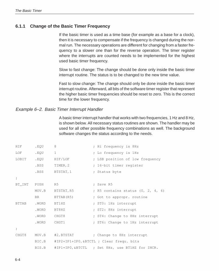
The Basic Timer
6-4
6.1.1 Change of the Basic Timer Frequency
If the basic timer is used as a time base (for example as a base for a clock),then it is necessary to compensate if the frequency is changed during the nor-mal run. The necessary operations are different for changing from a faster fre-quency to a slower one than for the reverse operation. The timer registerwhere the interrupts are counted needs to be implemented for the highestused basic timer frequency.
Slow to fast change: The change should be done only inside the basic timerinterrupt routine. The status is to be changed to the new time value.
Fast to slow change: The change should only be done inside the basic timerinterrupt routine. Afterward, all bits of the software timer register that representthe higher basic timer frequencies should be reset to zero. This is the correcttime for the lower frequency.
Example 6–2. Basic Timer Interrupt Handler
A basic timer interrupt handler that works with two frequencies, 1 Hz and 8 Hz,is shown below. All necessary status routines are shown. The handler may beused for all other possible frequency combinations as well. The backgroundsoftware changes the status according to the needs.
HIF .EQU 8 ; Hi frequency is 8Hz
LOF .EQU 1 ; Lo frequency is 1Hz
LOBIT .EQU HIF/LOF ; LSB position of low frequency
.BSS TIMER,2 ; 16–bit timer register
.BSS BTSTAT,1 ; Status byte
;
BT_INT PUSH R5 ; Save R5
MOV.B BTSTAT,R5 ; R5 contains status (0, 2, 4, 6)
BR BTTAB(R5) ; Got to appropr. routine
BTTAB .WORD BT1HZ ; ST0: 1Hz interrupt
.WORD BT8HZ ; ST2: 8Hz interrupt
.WORD CHGT8 ; ST4: Change to 8Hz interrupt
.WORD CHGT1 ; ST6: Change to 1Hz interrupt
;
CHGT8 MOV.B #2,BTSTAT ; Change to 8Hz interrupt
BIC.B #IP2+IP1+IP0,&BTCTL ; Clear frequ. bits
BIS.B #IP1+IP0,&BTCTL ; Set 8Hz, use BT1HZ for INCR.
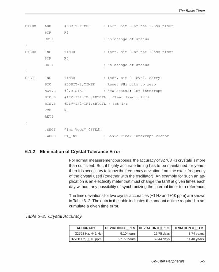
The Basic Timer
6-5On-Chip Peripherals
BT1HZ ADD #LOBIT,TIMER ; Incr. bit 3 of the 125ms timer
POP R5
RETI ; No change of status
;
BT8HZ INC TIMER ; Incr. bit 0 of the 125ms timer
POP R5
RETI ; No change of status
;
CHGT1 INC TIMER ; Incr. bit 0 (evtl. carry)
BIC #LOBIT–1,TIMER ; Reset 8Hz bits to zero
MOV.B #0,BTSTAT ; New status: 1Hz interrupt
BIC.B #IP2+IP1+IP0,&BTCTL ; Clear frequ. bits
BIS.B #DIV+IP2+IP1,&BTCTL ; Set 1Hz
POP R5
RETI
;
.SECT ”Int_Vect”,0FFE2h
.WORD BT_INT ; Basic Timer Interrupt Vector
6.1.2 Elimination of Crystal Tolerance Error
For normal measurement purposes, the accuracy of 32768 Hz crystals is morethan sufficient. But, if highly accurate timing has to be maintained for years,then it is necessary to know the frequency deviation from the exact frequencyof the crystal used (together with the oscillator). An example for such an ap-plication is an electricity meter that must change the tariff at given times eachday without any possibility of synchronizing the internal timer to a reference.
The time deviations for two crystal accuracies (+1 Hz and +10 ppm) are shownin Table 6–2. The data in the table indicates the amount of time required to ac-cumulate a given time error.
Table 6–2. Crystal Accuracy
ACCURACY DEVIATION = 1 S DEVIATION = 1 m DEVIATION = 1 h
32768 Hz, 1 Hz 9.10 hours 22.75 days 3.74 years
32768 Hz, 10 ppm 27.77 hours 69.44 days 11.40 years
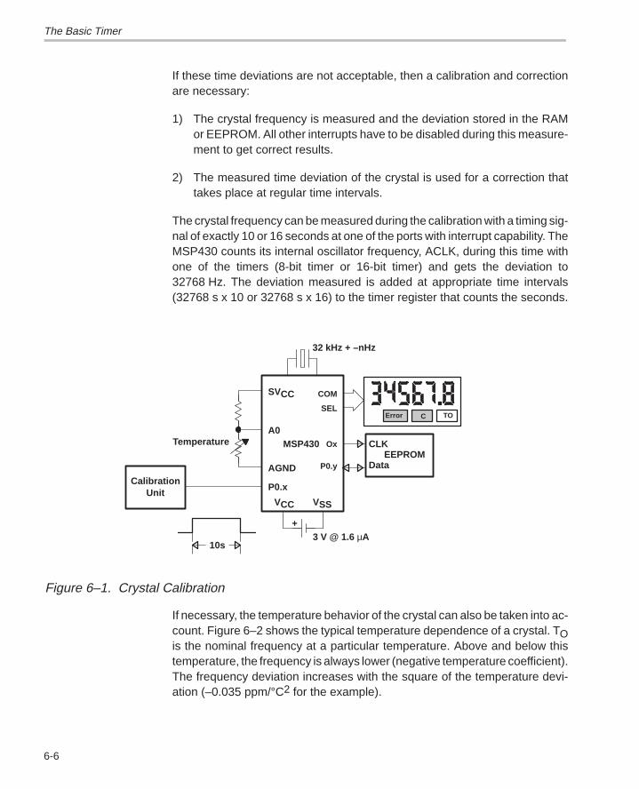
The Basic Timer
6-6
If these time deviations are not acceptable, then a calibration and correctionare necessary:
1) The crystal frequency is measured and the deviation stored in the RAMor EEPROM. All other interrupts have to be disabled during this measure-ment to get correct results.
2) The measured time deviation of the crystal is used for a correction thattakes place at regular time intervals.
The crystal frequency can be measured during the calibration with a timing sig-nal of exactly 10 or 16 seconds at one of the ports with interrupt capability. TheMSP430 counts its internal oscillator frequency, ACLK, during this time withone of the timers (8-bit timer or 16-bit timer) and gets the deviation to32768 Hz. The deviation measured is added at appropriate time intervals(32768 s x 10 or 32768 s x 16) to the timer register that counts the seconds.
COM
SELError C TO
32 kHz + –nHz
Ox
P0.y
MSP430 CLK
DataEEPROM
VCC VSS
P0.x
AGND
A0
SVCC
Temperature
CalibrationUnit
3 V @ 1.6 µA10s
+
Figure 6–1. Crystal Calibration
If necessary, the temperature behavior of the crystal can also be taken into ac-count. Figure 6–2 shows the typical temperature dependence of a crystal. TOis the nominal frequency at a particular temperature. Above and below thistemperature, the frequency is always lower (negative temperature coefficient).The frequency deviation increases with the square of the temperature devi-ation (–0.035 ppm/°C2 for the example).
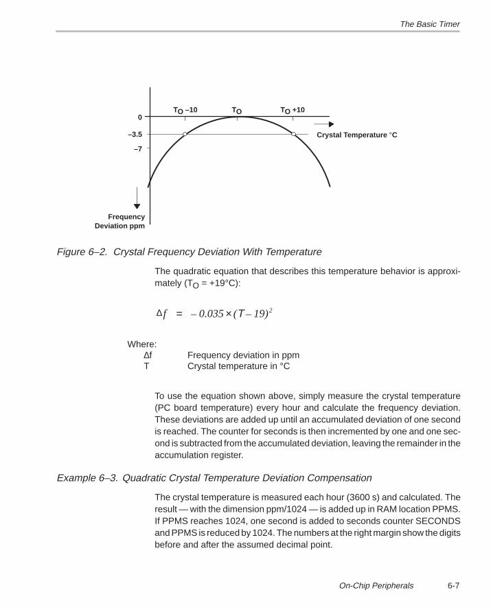
The Basic Timer
6-7On-Chip Peripherals
TO –10 TO TO +10
Crystal Temperature °C
0
–3.5
–7
FrequencyDeviation ppm
Figure 6–2. Crystal Frequency Deviation With Temperature
The quadratic equation that describes this temperature behavior is approxi-mately (TO = +19°C):
∆ f 0.035 (T 19)2= – × –
Where: ∆f Frequency deviation in ppmT Crystal temperature in °C
To use the equation shown above, simply measure the crystal temperature(PC board temperature) every hour and calculate the frequency deviation.These deviations are added up until an accumulated deviation of one secondis reached. The counter for seconds is then incremented by one and one sec-ond is subtracted from the accumulated deviation, leaving the remainder in theaccumulation register.
Example 6–3. Quadratic Crystal Temperature Deviation Compensation
The crystal temperature is measured each hour (3600 s) and calculated. Theresult — with the dimension ppm/1024 — is added up in RAM location PPMS.If PPMS reaches 1024, one second is added to seconds counter SECONDSand PPMS is reduced by 1024. The numbers at the right margin show the digitsbefore and after the assumed decimal point.
The Basic Timer
6-8
; Quadratic temperature compensation after each hour:
; tcorr = –|(T–19)^2 x –0.035ppm| x t
; Tmax = To+40C, Tmin = To–40C
;
To .SET 19 ; Turning point of temperature
PPM .SET 35 ; –0.035ppm/(T–To)^2
.BSS PPMS,2 ; RAM word for adding–up deviation
.BSS SECOND,2 ; RAM word for seconds counting
;
TIMCORR CALL #MEASTEMP ;Meas. crystal temperature 6.4h
POP IROP2L ; Result to IROP2L 6.4h
SUB #(To*10h),IROP2L ; T – To 6.4h
MOV IROP2L,IROP1 ; Copy result
CALL #MPYS ; |T–To|^2 (always pos.) 12.8
CALL #SHFTRS6 ; Adapt |T–To|^2 12.2
ADC IRACL ; Rounding
MOV IRACL,IROP2L ; |T–To|^2 –> IROP2L 12.2
;
; tcorr = 3600 x –0.035 x 1E–6 x (T–19)^2 s/h
;
L$006 MOV #(36*PPM),IROP1 ; 36 x PPM/1E4 ms/h
CALL #MPYS ; Signed multiplication
;
; IRAC contains: 36s x PPM x 4 (To–T)^2 x 1E–7 s/h
; = 36s x PPM x 4 (To–T)^2 x 1E–4 ms/h
;
CALL #SHFTLS6 ; to IRACM
;
; IRACM contains: tcorr = 4 x dT x 36 x PPM/1024
; Correction: 0.25 x 1E–7 x 1024 = 1/39062.5
;
ADD IRACM,PPMS ; Add–up deviation
CMP #39062,PPMS ; One second deviation reached?
JLO L$200
INC SECONDS ; Yes, add one second
SUB #39062,PPMS ; and adjust deviation counter
L$200 RET
The Basic Timer
6-9On-Chip Peripherals
6.1.3 Clock Subroutines
The following two subroutines provide 24-hour clocks — one using decimalcounting (RTCLKD) and one using hexadecimal counting (RTCLK). Thesesubroutines are called every second by the basic timer handler.
;
SEC .EQU 0200H ; Byte for counting of seconds
MIN .EQU 0201H ; Byte for counting of minutes
HOURS .EQU 0202H ; Byte for counting of hours
;
; Subroutine provides a decimal clock: 00.00.00 to 23.59.59
;
RTCLKD SETC ; Entry every second
DADC.B SEC ; Increment seconds
CMP.B #060H,SEC ; One minute elapsed?
JLO RTRETD ; No, return (C = 0)
CLR.B SEC ; Yes, clear seconds (C = 1)
DADC.B MIN ; Increment minutes with set carry
CMP.B #060H,MIN ;
JLO RTRETD
CLR.B MIN
DADC.B HOURS
CMP.B #024H,HOURS
JLO RTRETD
CLR.B HOURS ; 00.00.00 Return to caller
RTRETD RET ; C = 1: one day elapsed
;
; Subroutine provides a hex clock: 00.00.00 to 17.3B.3B
;
RTCLK INC.B SEC ; Entry point every second
CMP.B #60,SEC ; Increment seconds
JLO RTRET ; One minute elapsed?
CLR.B SEC ; No, return to caller
INC.B MIN ; Yes, clear seconds
CMP.B #60,MIN ; Increment minutes
JLO RTRET
The Basic Timer
6-10
CLR.B MIN
INC.B HOURS
CMP.B #24,HOURS
JLO RTRET
CLR.B HOURS ; 00.00.00
RTRET RET ; C = 1: one day elapsed
The next subroutine increments the date with each call. The handling of leap–years is included. The data is stored in binary format.
DAY .EQU 0203h ; Day of month 1 – 31 (byte)
MONTH .EQU 0204h ; Month 1 – 12 (byte)
YEAR .EQU 0206h ; Year 1990 – 2399 (word)
;
DATE PUSH R5 ; Save R5
INC.B DAY ; To next day of month
MOV.B MONTH,R5 ; Look for length of month
MOV.B MT–1(R5),R5
CMP.B #2,MONTH ; February now?
JNE NOFEB
BIT #3,YEAR ; Yes, Leap Year?
JNZ NOFEB
INC R5 ; Yes, 29 days for February
NOFEB CMP.B R5,DAY ; One month elapsed?
JLO DATRET ; No
MOV.B #1,DAY ; Yes, start with 1st day
INC.B MONTH ; of next month
CMP.B #13,MONTH ; Year over?
JLO DATRET ; No
MOV.B #1,MONTH ; Yes, start with 1st month
INC YEAR ; of next year
DATRET POP R5 ; Restore R5
RET
;
; Table with the length of the 12 months
;
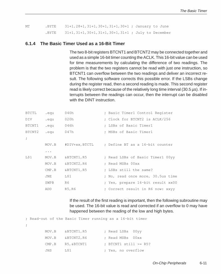
The Basic Timer
6-11On-Chip Peripherals
MT .BYTE 31+1,28+1,31+1,30+1,31+1,30+1 ; January to June
.BYTE 31+1,31+1,30+1,31+1,30+1,31+1 ; July to December
6.1.4 The Basic Timer Used as a 16-Bit Timer
The two 8-bit registers BTCNT1 and BTCNT2 may be connected together andused as a simple 16-bit timer counting the ACLK. This 16-bit value can be usedfor time measurements by calculating the difference of two readings. Theproblem is that the two registers cannot be read with just one instruction, soBTCNT1 can overflow between the two readings and deliver an incorrect re-sult. The following software corrects this possible error. If the LSBs changeduring the register read, then a second reading is made. This second registerread is likely correct because of the relatively long time interval (30.5 µs). If in-terrupts between the readings can occur, then the interrupt can be disabledwith the DINT instruction.
BTCTL .equ 040h ; Basic Timer1 Control Register
DIV .equ 020h ; Clock for BTCNT2 is ACLK/256
BTCNT1 .equ 046h ; LSBs of Basic Timer1
BTCNT2 .equ 047h ; MSBs of Basic Timer1
;
MOV.B #DIV+xx,BTCTL ; Define BT as a 16–bit counter
...
L$1 MOV.B &BTCNT1,R5 ; Read LSBs of Basic Timer1 00yy
MOV.B &BTCNT2,R6 ; Read MSBs 00xx
CMP.B &BTCNT1,R5 ; LSBs still the same?
JNE L$1 ; No, read once more, 30.5us time
SWPB R6 ; Yes, prepare 16–bit result xx00
ADD R5,R6 ; Correct result in R6 now: xxyy
If the result of the first reading is important, then the following subroutine maybe used. The 16-bit value is read and corrected if an overflow to 0 may havehappened between the reading of the low and high bytes.
; Read–out of the Basic Timer running as a 16–bit timer
;
MOV.B &BTCNT1,R5 ; Read LSBs 00yy
MOV.B &BTCNT2,R6 ; Read MSBs 00xx
CMP.B R5,&BTCNT1 ; BTCNT1 still >= R5?
JHS L$1 ; Yes, no overflow
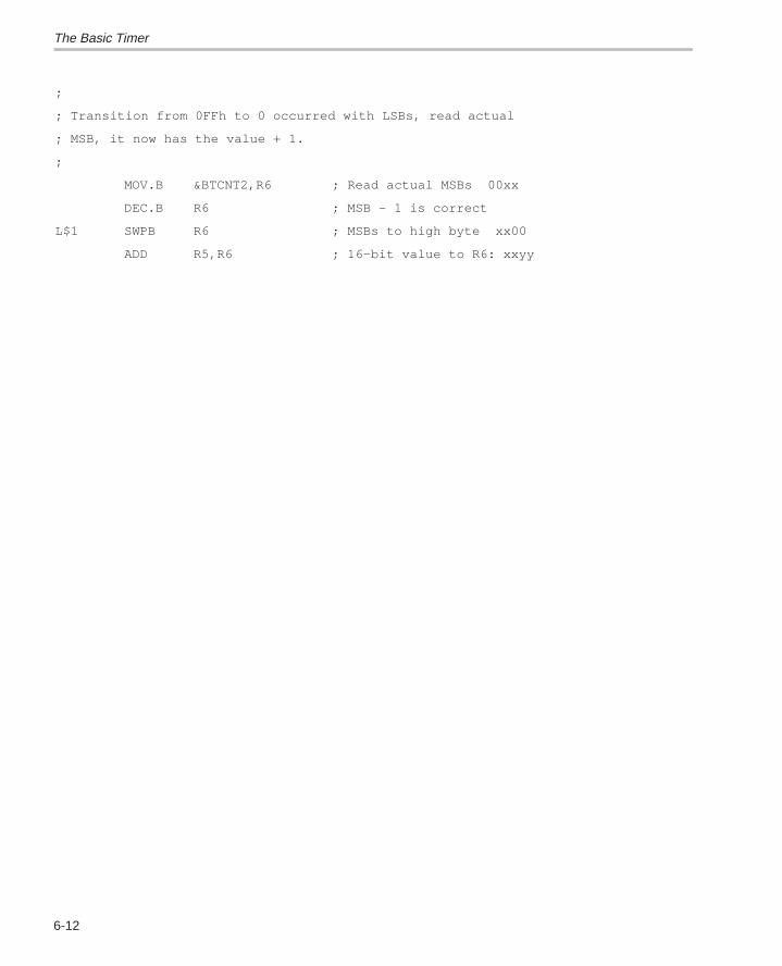
The Basic Timer
6-12
;
; Transition from 0FFh to 0 occurred with LSBs, read actual
; MSB, it now has the value + 1.
;
MOV.B &BTCNT2,R6 ; Read actual MSBs 00xx
DEC.B R6 ; MSB – 1 is correct
L$1 SWPB R6 ; MSBs to high byte xx00
ADD R5,R6 ; 16–bit value to R6: xxyy
The Watchdog Timer
6-13On-Chip Peripherals
6.2 The Watchdog Timer
The internal watchdog of the MSP430 family may be used as a simple timeror as a watchdog that ensures system integrity. The watchdog function is en-abled after power-on reset or a system reset. This means that if there are diffi-culties after the start-up of the MSP430, the watchdog will reset the system asoften as it is needed for it to start successfully. The watchdog mode is de-scribed in this chapter.
6.2.1 Supervision of One Task With the Watchdog
In Section 5.7.2.2 Power Fail Detection With the Watchdog, an example is giv-en of how to use the watchdog for the supervision of a power fail task only. Thisexample shows the necessary hardware and the software needed to detectan impending power failure. As long as ac line voltage is present, an interruptoccurs for each polarity change of the ac line. These interrupts reset the watch-dog, preventing it from timing out. If the line voltage falls below a certain levelor fails completely, these interrupts disappear and the watchdog is not reset.When the watchdog times out, it initializes the MSP430 system.
6.2.2 Supervision of Multiple Tasks With the Watchdog
Normally, the watchdog can only supervise one task at a time. If this task doesnot reset the watchdog, the MSP430 is initialized by the watchdog. In complexsystems, more than one function needs to be supervised to assure correct sys-tem functionality. This is possible with a small software effort — each super-vised function sets a bit in a RAM byte if it runs correctly. The mainloop thenresets the watchdog only if all bits are set. This approach can be enlarged toany number of supervised functions if more than one byte is used.
Example 6–4. Watchdog Supervision of Three Functions
A system running with MCLK = 3 MHz uses the watchdog for the supervisionof three functions.
Power Fail — by the checking of the 60 Hz AC line (see section BatteryCheck and Power Fail Detection for details)
Function 1 — a check is made if the software reaches this backgroundpart regularly
Function 3 — a check is made if this interrupt handler is called regularly
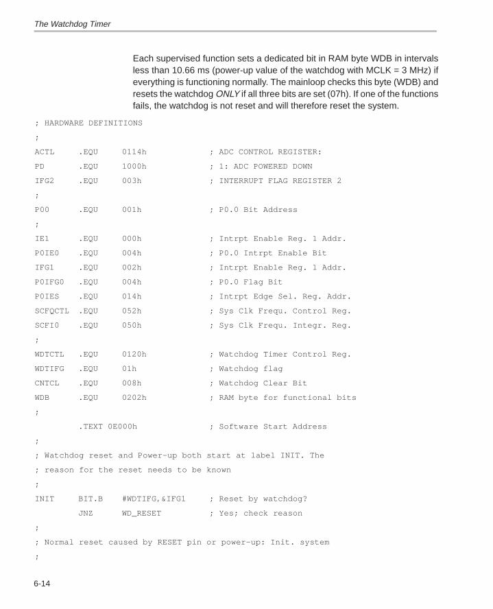
The Watchdog Timer
6-14
Each supervised function sets a dedicated bit in RAM byte WDB in intervalsless than 10.66 ms (power-up value of the watchdog with MCLK = 3 MHz) ifeverything is functioning normally. The mainloop checks this byte (WDB) andresets the watchdog ONLY if all three bits are set (07h). If one of the functionsfails, the watchdog is not reset and will therefore reset the system.
; HARDWARE DEFINITIONS
;
ACTL .EQU 0114h ; ADC CONTROL REGISTER:
PD .EQU 1000h ; 1: ADC POWERED DOWN
IFG2 .EQU 003h ; INTERRUPT FLAG REGISTER 2
;
P00 .EQU 001h ; P0.0 Bit Address
;
IE1 .EQU 000h ; Intrpt Enable Reg. 1 Addr.
P0IE0 .EQU 004h ; P0.0 Intrpt Enable Bit
IFG1 .EQU 002h ; Intrpt Enable Reg. 1 Addr.
P0IFG0 .EQU 004h ; P0.0 Flag Bit
P0IES .EQU 014h ; Intrpt Edge Sel. Reg. Addr.
SCFQCTL .EQU 052h ; Sys Clk Frequ. Control Reg.
SCFI0 .EQU 050h ; Sys Clk Frequ. Integr. Reg.
;
WDTCTL .EQU 0120h ; Watchdog Timer Control Reg.
WDTIFG .EQU 01h ; Watchdog flag
CNTCL .EQU 008h ; Watchdog Clear Bit
WDB .EQU 0202h ; RAM byte for functional bits
;
.TEXT 0E000h ; Software Start Address
;
; Watchdog reset and Power–up both start at label INIT. The
; reason for the reset needs to be known
;
INIT BIT.B #WDTIFG,&IFG1 ; Reset by watchdog?
JNZ WD_RESET ; Yes; check reason
;
; Normal reset caused by RESET pin or power–up: Init. system
;
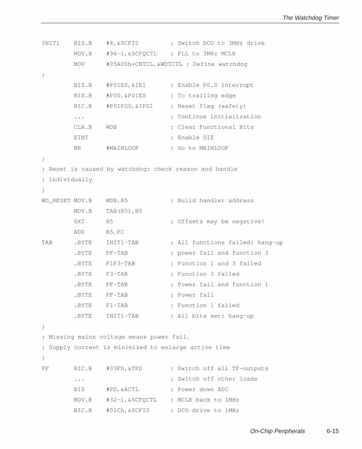
The Watchdog Timer
6-15On-Chip Peripherals
INIT1 BIS.B #8,&SCFI0 ; Switch DCO to 3MHz drive
MOV.B #96–1,&SCFQCTL ; FLL to 3MHz MCLK
MOV #05A00h+CNTCL,&WDTCTL ; Define watchdog
;
BIS.B #P0IE0,&IE1 ; Enable P0.0 interrupt
BIS.B #P00,&P0IES ; To trailing edge
BIC.B #P0IFG0,&IFG1 ; Reset flag (safety)
... ; Continue initialization
CLR.B WDB ; Clear Functional Bits
EINT ; Enable GIE
BR #MAINLOOP ; Go to MAINLOOP
;
; Reset is caused by watchdog: check reason and handle
; individually
;
WD_RESET MOV.B WDB,R5 ; Build handler address
MOV.B TAB(R5),R5
SXT R5 ; Offsets may be negative!
ADD R5,PC
TAB .BYTE INIT1–TAB ; All functions failed: hang–up
.BYTE PF–TAB ; power fail and function 3
.BYTE F1F3–TAB ; Function 1 and 3 failed
.BYTE F3–TAB ; Function 3 failed
.BYTE PF–TAB ; Power fail and function 1
.BYTE PF–TAB ; Power fail
.BYTE F1–TAB ; Function 1 failed
.BYTE INIT1–TAB ; All bits set: hang–up
;
; Missing mains voltage means power fail.
; Supply current is minimized to enlarge active time
;
PF BIC.B #03Fh,&TPD ; Switch off all TP–outputs
... ; Switch off other loads
BIS #PD,&ACTL ; Power down ADC
MOV.B #32–1,&SCFQCTL ; MCLK back to 1MHz
BIC.B #01Ch,&SCFI0 ; DCO drive to 1MHz
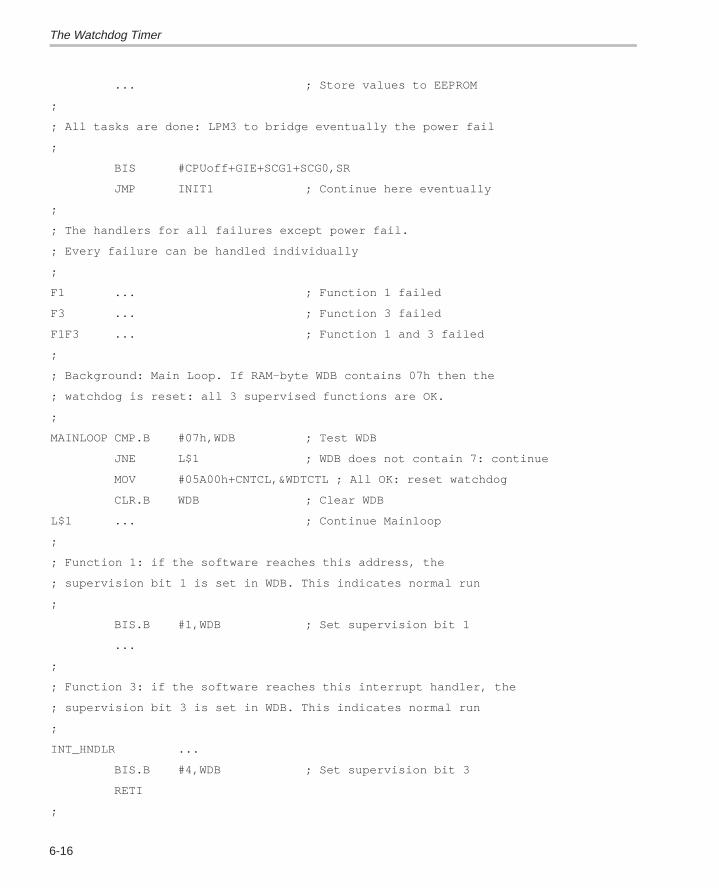
The Watchdog Timer
6-16
... ; Store values to EEPROM
;
; All tasks are done: LPM3 to bridge eventually the power fail
;
BIS #CPUoff+GIE+SCG1+SCG0,SR
JMP INIT1 ; Continue here eventually
;
; The handlers for all failures except power fail.
; Every failure can be handled individually
;
F1 ... ; Function 1 failed
F3 ... ; Function 3 failed
F1F3 ... ; Function 1 and 3 failed
;
; Background: Main Loop. If RAM–byte WDB contains 07h then the
; watchdog is reset: all 3 supervised functions are OK.
;
MAINLOOP CMP.B #07h,WDB ; Test WDB
JNE L$1 ; WDB does not contain 7: continue
MOV #05A00h+CNTCL,&WDTCTL ; All OK: reset watchdog
CLR.B WDB ; Clear WDB
L$1 ... ; Continue Mainloop
;
; Function 1: if the software reaches this address, the
; supervision bit 1 is set in WDB. This indicates normal run
;
BIS.B #1,WDB ; Set supervision bit 1
...
;
; Function 3: if the software reaches this interrupt handler, the
; supervision bit 3 is set in WDB. This indicates normal run
;
INT_HNDLR ...
BIS.B #4,WDB ; Set supervision bit 3
RETI
;
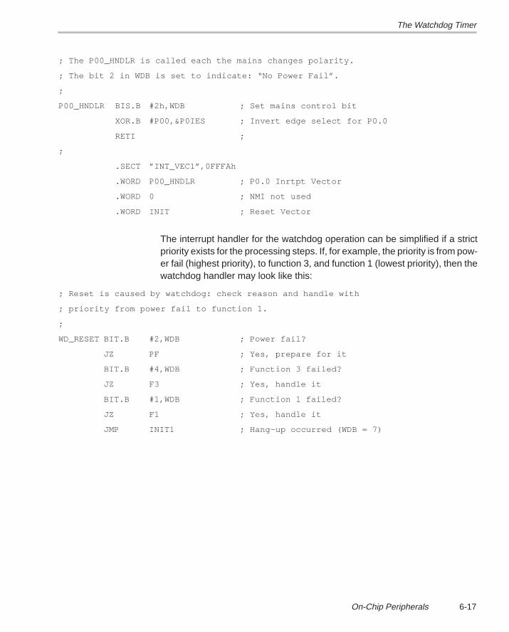
The Watchdog Timer
6-17On-Chip Peripherals
; The P00_HNDLR is called each the mains changes polarity.
; The bit 2 in WDB is set to indicate: “No Power Fail”.
;
P00_HNDLR BIS.B #2h,WDB ; Set mains control bit
XOR.B #P00,&P0IES ; Invert edge select for P0.0
RETI ;
;
.SECT ”INT_VEC1”,0FFFAh
.WORD P00_HNDLR ; P0.0 Inrtpt Vector
.WORD 0 ; NMI not used
.WORD INIT ; Reset Vector
The interrupt handler for the watchdog operation can be simplified if a strictpriority exists for the processing steps. If, for example, the priority is from pow-er fail (highest priority), to function 3, and function 1 (lowest priority), then thewatchdog handler may look like this:
; Reset is caused by watchdog: check reason and handle with
; priority from power fail to function 1.
;
WD_RESET BIT.B #2,WDB ; Power fail?
JZ PF ; Yes, prepare for it
BIT.B #4,WDB ; Function 3 failed?
JZ F3 ; Yes, handle it
BIT.B #1,WDB ; Function 1 failed?
JZ F1 ; Yes, handle it
JMP INIT1 ; Hang–up occurred (WDB = 7)
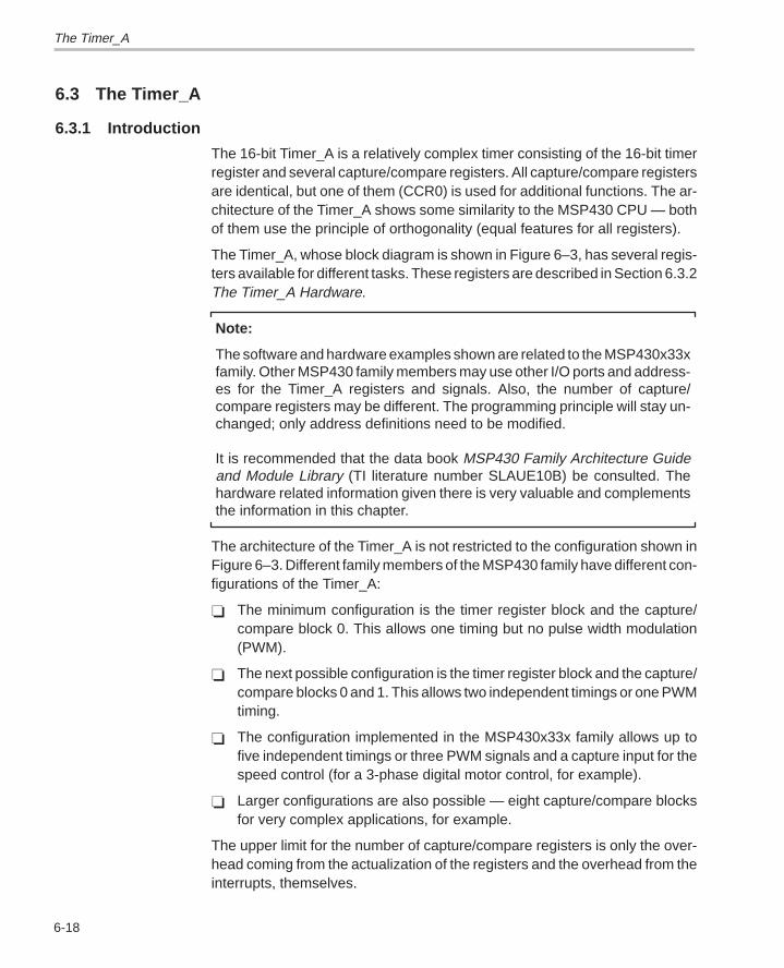
The Timer_A
6-18
6.3 The Timer_A
6.3.1 Introduction
The 16-bit Timer_A is a relatively complex timer consisting of the 16-bit timerregister and several capture/compare registers. All capture/compare registersare identical, but one of them (CCR0) is used for additional functions. The ar-chitecture of the Timer_A shows some similarity to the MSP430 CPU — bothof them use the principle of orthogonality (equal features for all registers).
The Timer_A, whose block diagram is shown in Figure 6–3, has several regis-ters available for different tasks. These registers are described in Section 6.3.2The Timer_A Hardware.
Note:
The software and hardware examples shown are related to the MSP430x33xfamily. Other MSP430 family members may use other I/O ports and address-es for the Timer_A registers and signals. Also, the number of capture/compare registers may be different. The programming principle will stay un-changed; only address definitions need to be modified.
It is recommended that the data book MSP430 Family Architecture Guideand Module Library (TI literature number SLAUE10B) be consulted. Thehardware related information given there is very valuable and complementsthe information in this chapter.
The architecture of the Timer_A is not restricted to the configuration shown inFigure 6–3. Different family members of the MSP430 family have different con-figurations of the Timer_A:
The minimum configuration is the timer register block and the capture/compare block 0. This allows one timing but no pulse width modulation(PWM).
The next possible configuration is the timer register block and the capture/compare blocks 0 and 1. This allows two independent timings or one PWMtiming.
The configuration implemented in the MSP430x33x family allows up tofive independent timings or three PWM signals and a capture input for thespeed control (for a 3-phase digital motor control, for example).
Larger configurations are also possible — eight capture/compare blocksfor very complex applications, for example.
The upper limit for the number of capture/compare registers is only the over-head coming from the actualization of the registers and the overhead from theinterrupts, themselves.
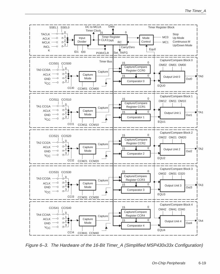
The Timer_A
6-19On-Chip Peripherals
InputDivider
CLK1Timer Register
TAR
SSEL0SSEL1
TACLK
ACLKMCLK
0
12
3RC
INCLK ID1 ID0
15 0
DataDC to MCLKTimer Clock
POR/CLR
ModeControl MC1
MC0
Equ0Carry/Zero
Set_TAIFG
Timer Register Block
CaptureMode
CCIS00CCIS01
TA0 CCI0A
ACLK
GND
012
3VCC
CCI0 CCM00CCM01
Capture/CompareRegister CCR0
15 0
Comparator 0
15 0 Output Unit 0
OM02 OM00OM01
TA0
Capture
EQU0
Capture/Compare Block 0Timer Bus
CaptureMode
CCIS10CCIS11
TA1 CCI1A
ACLK
GND
012
3VCC
CCI1 CCM10CCM11
Capture/CompareRegister CCR1
15 0
Comparator 1
15 0 Output Unit 1
OM12 OM10OM11
Capture
EQU1
Capture/Compare Block 1
CaptureMode
CCIS20CCIS21
TA2 CCI2A
ACLK
GND
012
3VCC
CCI2 CCM20CCM21
Capture/CompareRegister CCR2
15 0
Comparator 2
15 0 Output Unit 2
OM22 OM20OM21
Capture
EQU2
Capture/Compare Block 2
CaptureMode
CCIS30CCIS31
TA3 CCI3A
ACLKGND
012
3VCC
CCI3 CCM30CCM31
Capture/CompareRegister CCR3
15 0
Comparator 3
15 0 Output Unit 3
OM32 O320OM31
Capture
EQU3
Capture/Compare Block 3
CaptureMode
CCIS40CCIS41
TA4 CCI4A
ACLK
GND
012
3VCC
CCI4 CCM40CCM41
Capture/CompareRegister CCR4
15 0
Comparator 4
15 0 Output Unit 4
OM42 O340OM41
Capture
EQU4
Capture/Compare Block 4
TA1
TA2
TA3
TA4
StopUp ModeContinuous MUp/Down Mode
Out4
Out3
Out2
Out1
Out0
Figure 6–3. The Hardware of the 16-Bit Timer_A (Simplified MSP430x33x Configuration)
The Timer_A
6-20
Applications for the Timer_A can be:
Generation of up to five independent timings (MSP430x33x configuration)
Frequency generation — using the output units, the internal generatedtimings can be output to the external periphery of the MSP430
Generation of the timing for RF transmission (amplitude modulation, bi-phase code, biphase space modulation) for the transfer of metered data(gas meters, electric meters, heat allocation meters, etc.)
Realization of a software SPI
Realization of a software UART
Digital motor control (DMC) — the MSP430x33x is able to control a3-phase electric motor with PWM in closed loop mode
TRIAC control for electric motors and other power applications
Time measurement, period measurement, pulse width measurement
Frequency measurement (using the capture mode for low frequencies)
Analog-to-digital converter (ADC) — a single-slope ADC can be built usingthe capture mode. Normal I/O ports switch the reference resistors andsensors
DTMF generation — the DTMF frequency pairs can be generated by soft-ware and output by three external operational amplifiers for filtering andmixing. See the third part of this chapter for hardware and software details
Crystal replacement — the frequency locked loop (FLL) of the MSP430may be locked to the ac line frequency instead of the 32-kHz frequencyof a crystal. This eliminates the need for a crystal and provides a betteradaptation to the ac line frequency (for DMC applications, for example)
PWM generation with the output units
Real Time Clock (RTC) — if fed by the ACLK (32 kHz), the Timer_A canbe used as an RTC with all low power modes. Time intervals of up to twoseconds in steps of 2–15 s are possible.
The Timer_A
6-21On-Chip Peripherals
6.3.1.1 Definitions Used with the Application Examples
; HARDWARE DEFINITIONS
;
TAIV .equ 12Eh ; Timer_A Vector Register
TACTL .equ 160h ; Timer_A Control Register
; ; Bits of the TACTL Register:
TAIFG .equ 001h ; Interrupt flag
TAIE .equ 002h ; Interrupt enable bit
CLR .equ 004h ; Reset TAR and Input Divider
MSTOP .equ 000h ; Stop Mode
MUP .equ 010h ; Up Mode
MCONT .equ 020h ; Continuous Mode
MUPD .equ 030h ; Up/Down Mode
D1 .equ 000h ; Input Divider: Pass
D2 .equ 040h ; /2
D4 .equ 080h ; /4
D8 .equ 0C0h ; /8
ISTACLK .equ 000h ; Input Selector:TACLK
ISACLK .equ 100h ; ACLK
ISMCLK .equ 200h ; MCLK
ISINCLK .equ 300h ; INCLK
;
CCTL0 .equ 162h ; Capture/Compare Control Reg. 0
CCTL1 .equ 164h ; Capture/Compare Control Reg. 1
CCTL2 .equ 166h ; Capture/Compare Control Reg. 2
CCTL3 .equ 168h ; Capture/Compare Control Reg. 3
CCTL4 .equ 16Ah ; Capture/Compare Control Reg. 4
; ; Bits in the CCTLx Registers:
CCIFG .equ 001h ; Interrupt flag
COV .equ 002h ; Capture overflow flag
OUT .equ 004h ; Output bit
CCI .equ 008h ; Input signal
CCIE .equ 010h ; Interrupt enable bit
OMOO .equ 000h ; Output Mode: output only
OMSET .equ 020h ; set
OMTR .equ 040h ; toggle/reset
The Timer_A
6-22
OMSR .equ 060h ; set/reset
OMT .equ 080h ; toggle
OMR .equ 0A0h ; reset
OMTS .equ 0C0h ; toggle/set
OMRS .equ 0E0h ; reset/set
CAP .equ 100h ; Capture/Compare switch
SCCI .equ 400h ; Synchronized CCI
SCS .equ 800h ; Async/sync switch
ISCCIA .equ 000h ; Capture input: CCIxA
ISCCIB .equ 1000h ; CCIxB
ISGND .equ 2000h ; GND
ISVCC .equ 3000h ; Vcc
CMDIS .equ 000h ; Capture mode: disabled
CMPE .equ 4000h ; rising edge
CMNE .equ 8000h ; falling edge
CMBE .equ 0c000h ; both edges
CCR0 .equ 172h ; Capture/Compare Register 0
CCR1 .equ 174h ; Capture/Compare Register 1
CCR2 .equ 176h ; Capture/Compare Register 2
CCR3 .equ 178h ; Capture/Compare Register 3
CCR4 .equ 17Ah ; Capture/Compare Register 4
TAR .equ 0170h ; Timer Register
;
TA0 .equ 008h ; Bit address TA0 Port3: P3.3
TA1 .equ 010h ; Bit address TA1 Port3: P3.4
TA2 .equ 020h ; Bit address TA2 Port3: P3.5
TA3 .equ 040h ; Bit address TA3 Port3: P3.6
TA4 .equ 080h ; Bit address TA4 Port3: P3.7
;
P3SEL .equ 01Bh ; Port3 Select Register
P3DIR .equ 01Ah ; Port3 Direction Register
P3OUT .equ 019h ; Port3 Direction Register
;
; Definitions of other used peripherals
;
SCFQCTL .equ 052h ; FLL Multiplier and Mod. Bit
The Timer_A
6-23On-Chip Peripherals
M .equ 080h ; Modulation Bit
SCFI0 .equ 050h ; Current Switches FN_x, FLL
FN_2 .equ 004h ; DCO Switch for 2MHz
FN_3 .equ 008h ; DCO Switch for 3MHz
SCFI1 .equ 051h ; Taps of DCO
P0FG .equ 013h ; Port0 Flag Register Address
P0IE .equ 015h ; Port0 Interrupt Enable Reg.
IE1 .equ 0 ; Interrupt Enable Register
P0IE.0 .equ 4 ; P0.0 Interrupt Enable Bit
;
CBCTL .equ 053h ; Crystal Buffer Control
CBE .equ 001h ; Enable XBUF output
CBACLK .equ 000h ; ACLK is output at XBUF
CBMCLK .equ 006h ; MCLK is output at XBUF
;
BTCTL .equ 040h ; Basic Timer Control Register
BTCNT1 .equ 046h ; Basic Timer Counter 1
WDTCTL .equ 120h ; Watchdog Control Register
CNCTL .equ 008h ; Reset Watchdog Bit
HOLD .equ 080h ; Stop Watchdog
; ; Bits in the Status Register SR
GIE .equ 008h ; General Interrupt Enable
CPUOFF .equ 010h ; CPU–Off bit
SCG0 .equ 040h ; Low Power Mode Bits
SCG1 .equ 080h
6.3.2 Timer_A Hardware
Timer_A has a modular structure, giving it considerable flexibility. At least onecapture/compare block is necessary for all configurations, and an almost un-limited number of capture/compare blocks may be connected to the timer reg-ister block (see Figure 6–4). The general function of these blocks is describedbelow. The user software controls the Timer_A with the registers that are de-scribed there.
Several registers control the function of Timer_A. Every capture/compare reg-ister (CCRx) has its own control register CCTLx and the timer register (TAR)is also controlled by its own control register TACTL. This section describes allregisters contained in the Timer_A.

The Timer_A
6-24
The Timer_A registers have two common attributes:
All registers, with the exception of the interrupt vector register (TAIV), canbe read and written to
All registers are word-structured and should be accessed therefore byword instructions only. Byte addressing results in a nonpredictable opera-tion.
Example 6–5. Timer Register Low Byte
If only the information contained in the low byte of the timer register is wanted,then the following code sequence may be used:
MOV &TAR,R5 ; Read the complete TAR: yyxxh
MOV.B R5,R5 ; 00xxh to R5
If only the high byte information of the timer register is wanted:
MOV &TAR,R5 ; Read the complete TAR: yyxxh
SWPB R5 ; Swap bytes: yyxxh –> xxyyh
MOV.B R5,R5 ; 00yyh to R5
Table 6–3 shows the mnemonics and the hardware addresses of the Timer_Aregisters.
Table 6–3. Timer_A Registers
REGISTER NAME ABBREVIATION REGISTER TYPE ADDRESS INITIAL STATE
Timer_A control register TACTL Read/Write 160h POR Reset
Timer register TAR Read/Write 170h POR Reset
Cap/Com Control Register 0 CCTL0 Read/Write 162h POR Reset
Capture/Compare Register 0 CCR0 Read/Write 172h POR Reset
Cap/Com Control Register 1 CCTL1 Read/Write 164h POR Reset
Capture/Compare Register 1 CCR1 Read/Write 174h POR Reset
Cap/Com Control Register 2 CCTL2 Read/Write 166h POR Reset
Capture/Compare Register 2 CCR2 Read/Write 176h POR Reset
Cap/Com Control Register 3 CCTL3 Read/Write 168h POR Reset
Capture/Compare Register 3 CCR3 Read/Write 178h POR Reset
Cap/Com Control Register 4 CCTL4 Read/Write 16Ah POR Reset
Capture/Compare Register 4 CCR4 Read/Write 17Ah POR Reset
Interrupt Vector Register TAIV Read only 12Eh (POR Reset)
Note: Future extensions — more capture/compare registers — will use the reserved addresses 16Ch, 16Eh, 17Ch, and 17Eh.
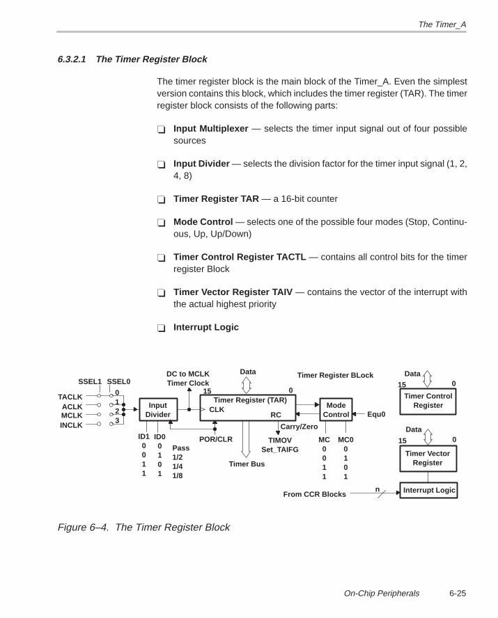
The Timer_A
6-25On-Chip Peripherals
6.3.2.1 The Timer Register Block
The timer register block is the main block of the Timer_A. Even the simplestversion contains this block, which includes the timer register (TAR). The timerregister block consists of the following parts:
Input Multiplexer — selects the timer input signal out of four possiblesources
Input Divider — selects the division factor for the timer input signal (1, 2,4, 8)
Timer Register TAR — a 16-bit counter
Mode Control — selects one of the possible four modes (Stop, Continu-ous, Up, Up/Down)
Timer Control Register TACTL — contains all control bits for the timerregister Block
Timer Vector Register TAIV — contains the vector of the interrupt withthe actual highest priority
Interrupt Logic
InputDivider
CLK
SSEL0SSEL1
TACLKACLKMCLK
0123
RCINCLK
ID10011
ID00101
15 0
DataDC to MCLKTimer Clock
POR/CLR
ModeControl
MC0011
MC00101
Equ0
Carry/Zero
TIMOVSet_TAIFG
Timer Register (TAR)
Pass1/21/41/8
Timer Bus
Timer Register BLock
Timer ControlRegister
Timer VectorRegister
Interrupt Logic
Data015
015
Data
From CCR Blocksn
Figure 6–4. The Timer Register Block
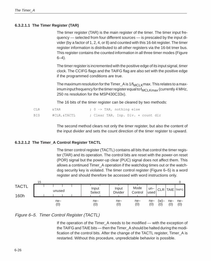
The Timer_A
6-26
6.3.2.1.1 The Timer Register (TAR)
The timer register (TAR) is the main register of the timer. The timer input fre-quency — selected from four different sources — is prescaled by the input di-vider (by a factor of 1, 2, 4, or 8) and counted with this 16-bit register. The timerregister information is distributed to all other registers via the 16-bit tmer bus.This register contains the counted information in all three timer modes (Figure6–4).
The timer register is incremented with the positive edge of its input signal, timerclock. The CCIFG flags and the TAIFG flag are also set with the positive edgeif the programmed conditions are true.
The maximum resolution for the Timer_A is 1/fMCLKmax. This relates to a max-imum input frequency for the timer register equal to fMCLKmax (currently 4 MHz,250 ns resolution for the MSP430C33x).
The 16 bits of the timer register can be cleared by two methods:
CLR &TAR ; 0 –> TAR, nothing else
BIS #CLR,&TACTL ; Clear TAR, Inp. Div. + count dir
The second method clears not only the timer register, but also the content ofthe input divider and sets the count direction of the timer register to upward.
6.3.2.1.2 The Timer_A Control Register TACTL
The timer control register (TACTL) contains all bits that control the timer regis-ter (TAR) and its operation. The control bits are reset with the power-on reset(POR) signal but the power-up clear (PUC) signal does not affect them. Thisallows a continued Timer_A operation if the watchdog times out or the watch-dog security key is violated. The timer control register (Figure 6–5) is a wordregister and should therefore be accessed with word instructions only.
CLR
015
160h
TACTLControlMode
DividerInput
SelectInput
unused
rw–(0)
rw–(0)
rw–(0)
rw–(0)
rw–(0)
rw–(0)
rw–(0)
un–used
(w)–(0)
TAIFGTAIE
Figure 6–5. Timer Control Register (TACTL)
If the operation of the Timer_A needs to be modified — with the exception ofthe TAIFG and TAIE bits — then the Timer_A should be halted during the modi-fication of the control bits. After the change of the TACTL register, Timer_A isrestarted. Without this procedure, unpredictable behavior is possible.
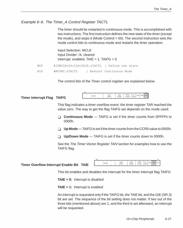
The Timer_A
6-27On-Chip Peripherals
Example 6–6. The Timer_A Control Register TACTL
The timer should be restarted in continuous mode. This is accomplished withtwo instructions. The first instruction defines the new state of the timer (exceptthe mode), and stops it (Mode Control = 00). The second instruction sets themode control bits to continuous mode and restarts the timer operation.
Input Selection: MCLKInput Divider: /4, clearedInterrupt: enabled, TAIE = 1, TAIFG = 0
MOV #ISMCLK+D4+CLR+TAIE,&TACTL ; Define new state
BIS #MCONT,&TACTL ; Restart Continuous Mode
The control bits of the Timer control register are explained below.
Timer Interrupt Flag TAIFGCLR
015
ControlMode
DividerInput
SelectInput
unusedun–used
TAIE TAIFG
This flag indicates a timer overflow event: the timer register TAR reached thevalue zero. The way to get the flag TAIFG set depends on the mode used:
Continuous Mode — TAIFG is set if the timer counts from 0FFFFh to0000h.
Up Mode — TAIFG is set if the timer counts from the CCR0 value to 0000h.
Up/Down Mode — TAIFG is set if the timer counts down to 0000h.
See the The Timer Vector Register TAIV section for examples how to use theTAIFG flag.
Timer Overflow Interrupt Enable Bit TAIE CLR
015
ControlMode
DividerInput
SelectInput
unusedun–used
TAIFGTAIE
This bit enables and disables the interrupt for the timer interrupt flag TAIFG:
TAIE = 0: Interrupt is disabled
TAIE = 1: Interrupt is enabled
An interrupt is requested only if the TAIFG bit, the TAIE bit, and the GIE (SR.3)bit are set. The sequence of the bit setting does not matter. If two out of thethree bits (mentioned above) are 1, and the third is set afterward, an interruptwill be requested.
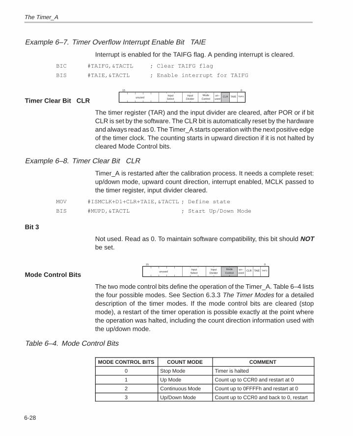
The Timer_A
6-28
Example 6–7. Timer Overflow Interrupt Enable Bit TAIE
Interrupt is enabled for the TAIFG flag. A pending interrupt is cleared.
BIC #TAIFG,&TACTL ; Clear TAIFG flag
BIS #TAIE,&TACTL ; Enable interrupt for TAIFG
Timer Clear Bit CLR
015
ControlMode
DividerInput
SelectInput
unusedun–used
TAIFGTAIECLR
The timer register (TAR) and the input divider are cleared, after POR or if bitCLR is set by the software. The CLR bit is automatically reset by the hardwareand always read as 0. The Timer_A starts operation with the next positive edgeof the timer clock. The counting starts in upward direction if it is not halted bycleared Mode Control bits.
Example 6–8. Timer Clear Bit CLR
Timer_A is restarted after the calibration process. It needs a complete reset:up/down mode, upward count direction, interrupt enabled, MCLK passed tothe timer register, input divider cleared.
MOV #ISMCLK+D1+CLR+TAIE,&TACTL ; Define state
BIS #MUPD,&TACTL ; Start Up/Down Mode
Bit 3
Not used. Read as 0. To maintain software compatibility, this bit should NOTbe set.
Mode Control BitsCLR
015
DividerInput
SelectInput
unusedun–used
TAIE TAIFGControlMode
The two mode control bits define the operation of the Timer_A. Table 6–4 liststhe four possible modes. See Section 6.3.3 The Timer Modes for a detaileddescription of the timer modes. If the mode control bits are cleared (stopmode), a restart of the timer operation is possible exactly at the point wherethe operation was halted, including the count direction information used withthe up/down mode.
Table 6–4. Mode Control Bits
MODE CONTROL BITS COUNT MODE COMMENT
0 Stop Mode Timer is halted
1 Up Mode Count up to CCR0 and restart at 0
2 Continuous Mode Count up to 0FFFFh and restart at 0
3 Up/Down Mode Count up to CCR0 and back to 0, restart
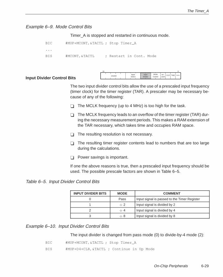
The Timer_A
6-29On-Chip Peripherals
Example 6–9. Mode Control Bits
Timer_A is stopped and restarted in continuous mode.
BIC #MUP+MCONT,&TACTL ; Stop Timer_A
...
BIS #MCONT,&TACTL ; Restart in Cont. Mode
Input Divider Control BitsCLR
015
SelectInput
unusedun–used
TAIE TAIFGControlModeInput
Divider
The two input divider control bits allow the use of a prescaled input frequency(timer clock) for the timer register (TAR). A prescaler may be necessary be-cause of any of the following:
The MCLK frequency (up to 4 MHz) is too high for the task.
The MCLK frequency leads to an overflow of the timer register (TAR) dur-ing the necessary measurement periods. This makes a RAM extension ofthe TAR necessary, which takes time and occupies RAM space.
The resulting resolution is not necessary.
The resulting timer register contents lead to numbers that are too largeduring the calculations.
Power savings is important.
If one the above reasons is true, then a prescaled input frequency should beused. The possible prescale factors are shown in Table 6–5.
Table 6–5. Input Divider Control Bits
INPUT DIVIDER BITS MODE COMMENT
0 Pass Input signal is passed to the Timer Register
1 2 Input signal is divided by 2
2 4 Input signal is divided by 4
3 8 Input signal is divided by 8
Example 6–10. Input Divider Control Bits
The input divider is changed from pass mode (0) to divide-by-4 mode (2):
BIC #MUP+MCONT,&TACTL ; Stop Timer_A
BIS #MUP+D4+CLR,&TACTL ; Continue in Up Mode
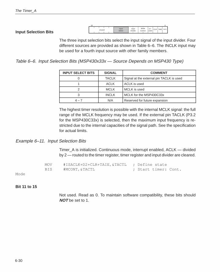
The Timer_A
6-30
Input Selection BitsCLR
015
unusedun–used
TAIE TAIFGControlModeInput
DividerInput
Select
The three input selection bits select the input signal of the input divider. Fourdifferent sources are provided as shown in Table 6–6. The INCLK input maybe used for a fourth input source with other family members.
Table 6–6. Input Selection Bits (MSP430x33x — Source Depends on MSP430 Type)
INPUT SELECT BITS SIGNAL COMMENT
0 TACLK Signal at the external pin TACLK is used
1 ACLK ACLK is used
2 MCLK MCLK is used
3 INCLK MCLK for the MSP430C33x
4 – 7 N/A Reserved for future expansion
The highest timer resolution is possible with the internal MCLK signal: the fullrange of the MCLK frequency may be used. If the external pin TACLK (P3.2for the MSP430C33x) is selected, then the maximum input frequency is re-stricted due to the internal capacities of the signal path. See the specificationfor actual limits.
Example 6–11. Input Selection Bits
Timer_A is initialized. Continuous mode, interrupt enabled, ACLK — dividedby 2 — routed to the timer register, timer register and input divider are cleared.
MOV #ISACLK+D2+CLR+TAIE,&TACTL ; Define stateBIS #MCONT,&TACTL ; Start timer: Cont.
Mode
Bit 11 to 15
Not used. Read as 0. To maintain software compatibility, these bits shouldNOT be set to 1.
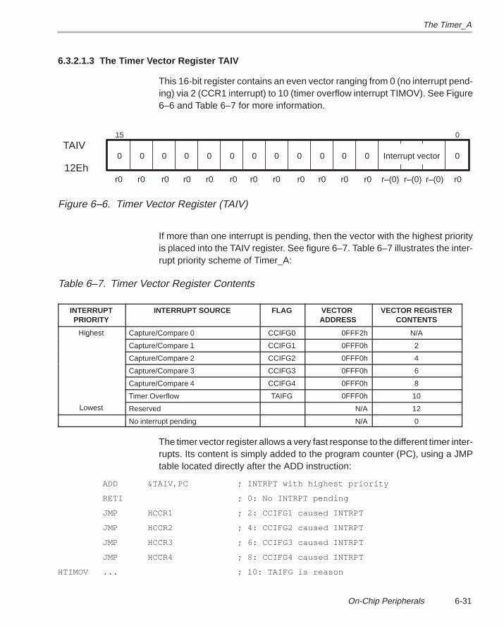
The Timer_A
6-31On-Chip Peripherals
6.3.2.1.3 The Timer Vector Register TAIV
This 16-bit register contains an even vector ranging from 0 (no interrupt pend-ing) via 2 (CCR1 interrupt) to 10 (timer overflow interrupt TIMOV). See Figure6–6 and Table 6–7 for more information.
0
015
12Eh
TAIVInterrupt vector
r0 r0r0 r0 r0 r0 r0 r0r0 r0 r0 r0 r–(0) r–(0) r–(0) r0
00000000000 0
Figure 6–6. Timer Vector Register (TAIV)
If more than one interrupt is pending, then the vector with the highest priorityis placed into the TAIV register. See figure 6–7. Table 6–7 illustrates the inter-rupt priority scheme of Timer_A:
Table 6–7. Timer Vector Register Contents
INTERRUPTPRIORITY
INTERRUPT SOURCE FLAG VECTOR ADDRESS
VECTOR REGISTERCONTENTS
Highest Capture/Compare 0 CCIFG0 0FFF2h N/Ag
Capture/Compare 1 CCIFG1 0FFF0h 2
Capture/Compare 2 CCIFG2 0FFF0h 4
Capture/Compare 3 CCIFG3 0FFF0h 6
Capture/Compare 4 CCIFG4 0FFF0h 8
Timer Overflow TAIFG 0FFF0h 10
Lowest Reserved N/A 12
No interrupt pending N/A 0
The timer vector register allows a very fast response to the different timer inter-rupts. Its content is simply added to the program counter (PC), using a JMPtable located directly after the ADD instruction:
ADD &TAIV,PC ; INTRPT with highest priority
RETI ; 0: No INTRPT pending
JMP HCCR1 ; 2: CCIFG1 caused INTRPT
JMP HCCR2 ; 4: CCIFG2 caused INTRPT
JMP HCCR3 ; 6: CCIFG3 caused INTRPT
JMP HCCR4 ; 8: CCIFG4 caused INTRPT
HTIMOV ... ; 10: TAIFG is reason
The Timer_A
6-32
If the corresponding interrupt handlers are out of the reach of JMPs (more than± 511 words), then a word table containing the handler start addresses may beused:
MOV &TAIV,R5 ; TAIV contains vector: 0 – 10
MOV TTAB(R5),PC ; Write handler address to PC
TTAB .WORD PRETI ; 0: No INTRPT pending, RETI
.WORD HCCR1 ; 2: CCIFG1 caused INTRPT
.WORD HCCR2 ; 4: CCIFG2 caused INTRPT
.WORD HCCR3 ; 6: CCIFG3 caused INTRPT
.WORD HCCR4 ; 8: CCIFG4 caused INTRPT
.WORD HTIMOV ; 10: TAIFG is reason
A third (slower) method is to read the content of the register TAIV and to usethe read value for the decision of where to proceed (the interrupt flag with thehighest priority is reset by the MOV instruction):
MOV &TAIV,R5 ; Actual vector to R5. Reset flag
CMP #2,R5 ; Check for CCIFG1 interrupt
JEQ HCCR1 ; 2: CCIFG1 caused INTRPT
CMP #4,R5 ; Check for CCIFG2 interrupt
JEQ HCCR2 ; 4: CCIFG2 caused INTRPT
... ; a.s.o.
The next software example shows a method that does not use the registerTAIV. A normal skip chain is used. Only the software for blocks 0 and 1 is shown(this example makes the advantages of using the TAIV register obvious):
BIT #CCIFG0,&CCTL0 ; Block 0: Flag set?
JNZ MOD0 ; Yes, serve it
BIT #CCIFG1,&CCTL1 ; Block 1: Flag set?
JNZ MOD1 ; Yes, serve it
... ; Continue with skip chain
MOD0 BIC #CCIFG0,&CCTL0 ; Reset CCIFG0 flag
... ; Start handler for block 0
MOD1 BIC #CCIFG1,&CCTL1 ; Reset CCIFG1 flag
... ; Start handler for block 1
The capture/compare block 0 is not included in the TAIV register; it has its owninterrupt vector located at address 0FFF2h. The shorter interrupt latency timeof register CCR0, makes it the preferred choice for the most time critical ap-plications. The vector for the other Timer_A interrupts is located at address0FFF0h.
The Timer_A
6-33On-Chip Peripherals
Note:
The timer vector register contains only the vectors of timer blocks with en-abled interrupt (set CCIEx resp. TAIE bits). Blocks with disabled interrupt bits(reset CCIEx resp. TAIE bits) can be checked by software if their CCIFGresp. TAIFG flag is set and the flag must be reset by software too. See theskip chain example above.
No interrupt flag (CCIFGx or TAIFG) needs to be reset if the register TAIV isused. The act of reading of the timer vector register TAIV resets the interruptflag automatically that determines the actual register content. The interruptflag with the next lower priority level defines the timer vector register TAIV af-terward.
Note:
Any access to the timer vector register (read or write) resets the interrupt flagwith the highest priority. The timer vector register should be read only andthe read data should be used to determine the interrupt handler with the high-est priority, otherwise the data is lost.
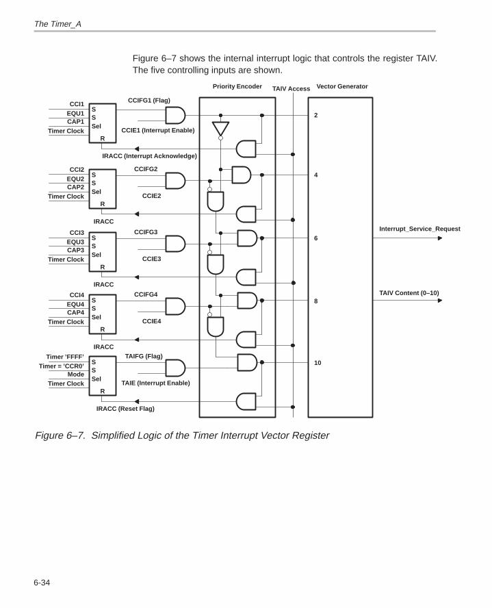
The Timer_A
6-34
Figure 6–7 shows the internal interrupt logic that controls the register TAIV.The five controlling inputs are shown.
SSSel
R
CCIFG1 (Flag)
CCIE1 (Interrupt Enable)
CCI1EQU1CAP1
Timer Clock
IRACC (Interrupt Acknowledge)
SSSel
R
CCIFG2
CCIE2
CCI2EQU2CAP2
Timer Clock
IRACC
SSSel
R
CCIFG3
CCIE3
CCI3EQU3CAP3
Timer Clock
IRACC
SSSel
R
CCIFG4
CCIE4
CCI4EQU4CAP4
Timer Clock
IRACC
SSSel
R
TAIFG (Flag)
TAIE (Interrupt Enable)
Timer ’FFFF’Timer = ’CCR0’
ModeTimer Clock
IRACC (Reset Flag)
2
4
6
8
10
Interrupt_Service_Request
TAIV Content (0–10)
Priority Encoder TAIV Access Vector Generator
Figure 6–7. Simplified Logic of the Timer Interrupt Vector Register
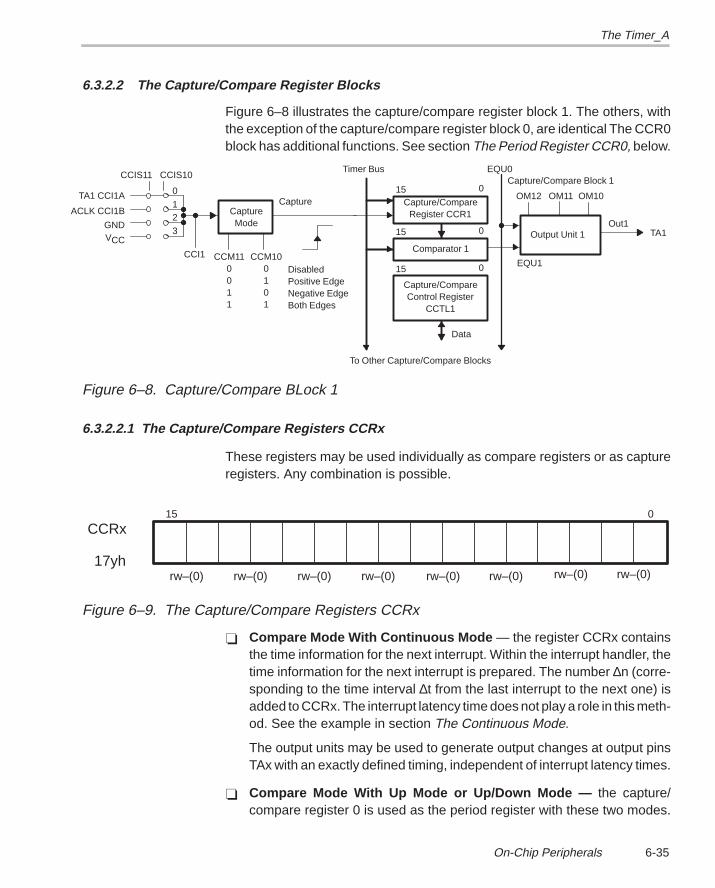
The Timer_A
6-35On-Chip Peripherals
6.3.2.2 The Capture/Compare Register Blocks
Figure 6–8 illustrates the capture/compare register block 1. The others, withthe exception of the capture/compare register block 0, are identical The CCR0block has additional functions. See section The Period Register CCR0, below.
CaptureMode
CCIS10CCIS11
TA1 CCI1A
ACLK CCI1B
GND
0
12
3VCC
CCI1 CCM100101
CCM110011
Capture/CompareRegister CCR1
15 0
Comparator 1
15 0 Output Unit 1
OM12 OM10OM11
TA1
Capture
EQU1
Capture/Compare Block 1Timer Bus EQU0
Out1
15 0
Capture/CompareControl Register
CCTL1
Data
DisabledPositive EdgeNegative EdgeBoth Edges
To Other Capture/Compare Blocks
Figure 6–8. Capture/Compare BLock 1
6.3.2.2.1 The Capture/Compare Registers CCRx
These registers may be used individually as compare registers or as captureregisters. Any combination is possible.
015
17yh
CCRx
rw–(0) rw–(0) rw–(0) rw–(0) rw–(0) rw–(0) rw–(0) rw–(0)
Figure 6–9. The Capture/Compare Registers CCRx
Compare Mode With Continuous Mode — the register CCRx containsthe time information for the next interrupt. Within the interrupt handler, thetime information for the next interrupt is prepared. The number ∆n (corre-sponding to the time interval ∆t from the last interrupt to the next one) isadded to CCRx. The interrupt latency time does not play a role in this meth-od. See the example in section The Continuous Mode.
The output units may be used to generate output changes at output pinsTAx with an exactly defined timing, independent of interrupt latency times.
Compare Mode With Up Mode or Up/Down Mode — the capture/compare register 0 is used as the period register with these two modes.
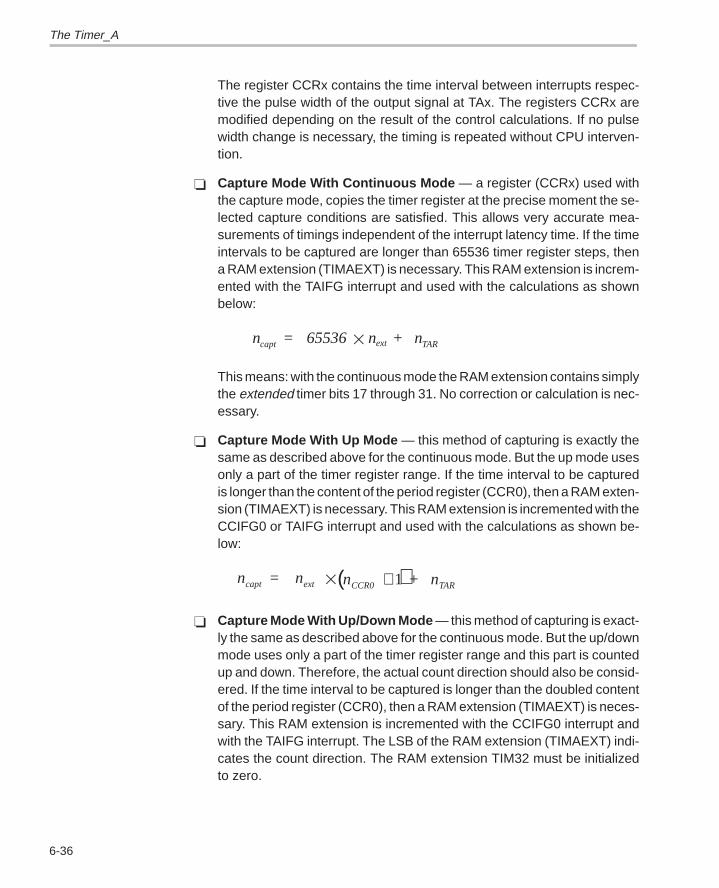
The Timer_A
6-36
The register CCRx contains the time interval between interrupts respec-tive the pulse width of the output signal at TAx. The registers CCRx aremodified depending on the result of the control calculations. If no pulsewidth change is necessary, the timing is repeated without CPU interven-tion.
Capture Mode With Continuous Mode — a register (CCRx) used withthe capture mode, copies the timer register at the precise moment the se-lected capture conditions are satisfied. This allows very accurate mea-surements of timings independent of the interrupt latency time. If the timeintervals to be captured are longer than 65536 timer register steps, thena RAM extension (TIMAEXT) is necessary. This RAM extension is increm-ented with the TAIFG interrupt and used with the calculations as shownbelow:
n = 65536 n + ncapt ext TAR
This means: with the continuous mode the RAM extension contains simplythe extended timer bits 17 through 31. No correction or calculation is nec-essary.
Capture Mode With Up Mode — this method of capturing is exactly thesame as described above for the continuous mode. But the up mode usesonly a part of the timer register range. If the time interval to be capturedis longer than the content of the period register (CCR0), then a RAM exten-sion (TIMAEXT) is necessary. This RAM extension is incremented with theCCIFG0 or TAIFG interrupt and used with the calculations as shown be-low:
( )n = n n + ncapt ext CCR0 TAR + 1
Capture Mode With Up/Down Mode — this method of capturing is exact-ly the same as described above for the continuous mode. But the up/downmode uses only a part of the timer register range and this part is countedup and down. Therefore, the actual count direction should also be consid-ered. If the time interval to be captured is longer than the doubled contentof the period register (CCR0), then a RAM extension (TIMAEXT) is neces-sary. This RAM extension is incremented with the CCIFG0 interrupt andwith the TAIFG interrupt. The LSB of the RAM extension (TIMAEXT) indi-cates the count direction. The RAM extension TIM32 must be initializedto zero.
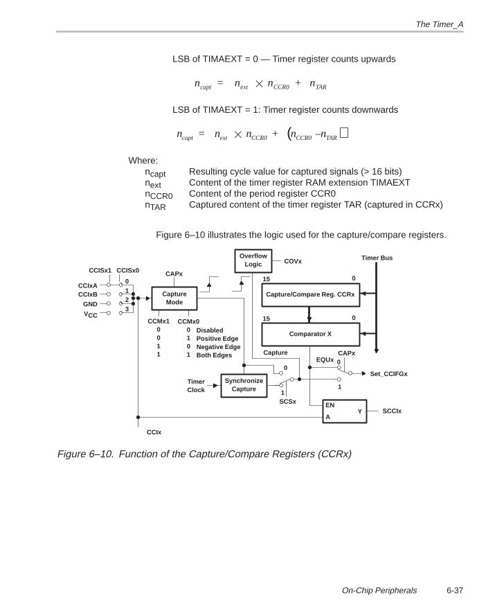
The Timer_A
6-37On-Chip Peripherals
LSB of TIMAEXT = 0 — Timer register counts upwards
n = n n + ncapt ext CCR0 TAR
LSB of TIMAEXT = 1: Timer register counts downwards
( )n = n n + n –ncapt ext CCR0 CCR0 TAR
Where: ncapt Resulting cycle value for captured signals (> 16 bits)next Content of the timer register RAM extension TIMAEXTnCCR0 Content of the period register CCR0nTAR Captured content of the timer register TAR (captured in CCRx)
Figure 6–10 illustrates the logic used for the capture/compare registers.
CaptureMode
CCISx0CCISx1
CCIxACCIxB
GND
0123
VCCCCMx1
0011
CCMx00101
15 0
SynchronizeCapture
Capture/Compare Reg. CCRx
DisabledPositive EdgeNegative EdgeBoth Edges
Timer Bus
CAPx
SCSx
TimerClock
15 0
Comparator X
OverflowLogic COVx
Capture
0
1
0
1
EQUx
Set_CCIFGx
CAPx
EN
AY SCCIx
CCIx
Figure 6–10. Function of the Capture/Compare Registers (CCRx)
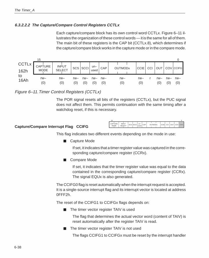
The Timer_A
6-38
6.3.2.2.2 The Capture/Compare Control Registers CCTLx
Each capture/compare block has its own control word CCTLx. Figure 6–11 il-lustrates the organization of these control words — it is the same for all of them.The main bit of these registers is the CAP bit (CCTLx.8), which determines ifthe capture/compare block works in the capture mode or in the compare mode.
0
162h
CCTLx15
un–SCS OUTMODx
rw–(0)
CAPINPUT
SELECTCAPTURE
MODE
r(0)
rw–(0)
rw–(0)
rw–(0)
rw–(0)
rw–(0)
rw–(0)
rw–(0)
rw–(0)
rw–(0)
CCIFGCOVOUTCCICCIE
16Ahto
rw–
SCCIused
Figure 6–11.Timer Control Registers (CCTLx)
The POR signal resets all bits of the registers (CCTLx), but the PUC signaldoes not affect them. This permits continuation with the same timing after awatchdog reset, if this is necessary.
Capture/Compare Interrupt Flag CCIFG
015
un–SCS OUTMODxCAP
INPUTSELECT
CAPTUREMODE
COVOUTCCICCIESCCIused
CCIFG
This flag indicates two different events depending on the mode in use:
Capture Mode
If set, it indicates that a timer register value was captured in the corre-sponding capture/compare register (CCRx).
Compare Mode
If set, it indicates that the timer register value was equal to the datacontained in the corresponding capture/compare register (CCRx).The signal EQUx is also generated.
The CCIFG0 flag is reset automatically when the interrupt request is accepted.It is a single-source interrupt flag and its interrupt vector is located at address0FFF2h.
The reset of the CCIFG1 to CCIFGx flags depends on:
The timer vector register TAIV is used
The flag that determines the actual vector word (content of TAIV) isreset automatically after the register TAIV is read.
The timer vector register TAIV is not used
The flags CCIFG1 to CCIFGx must be reset by the interrupt handler
The Timer_A
6-39On-Chip Peripherals
If the interrupt capability is not enabled for a capture/compare block then theflag CCIFGx must be tested to check if the block x needs service. The CCIFGflag must be reset by software for this case:
BIT #CCIFG,&CCTLx ; Flag set?
JZ NO_FLAG ; No continue
BIC #CCIFG,&CCTLx ; Yes, reset flag
... ; Execute task for block x
Example 6–12. Capture/Compare Interrupt Flag CCIFG
See the examples in section The Timer Vector Register TAIV. Examples for thetreatment of the CCIFG flags are given there.
Capture Overflow Flag COV
015
un–SCS OUTMODxCAP
INPUTSELECT
CAPTUREMODE
OUTCCICCIESCCIused
CCIFGCOV
This flag indicates two different events depending on the mode in use:
Compare Mode
No function. The COV bit is always reset, independent of the stateof the capture input.
Capture Mode
The capture overflow flag COV is set if a second capture event oc-curred before the first capture sample was read out of the captureregister (CCRx). The COV flag allows the software to detect the lossof synchronization and helps to reacquire synchronization. The COVflag is not reset by the reading of the CCRx register and must be resetby software.
Example 6–13. Capture Overflow Flag COV
The interrupt handler of capture/compare block 2 — running in capture mode— checks first to see if a capture overflow occurred.
HCCR2 BIT #COV,&CCTL2 ; Capture overflow ?
JNZ COV2 ; Yes, handle it
MOV &CCR2,CAPSTO2 ; Store valid captured value
... ; Proceed with task
;
; Error handler for Capture/Compare Block 2
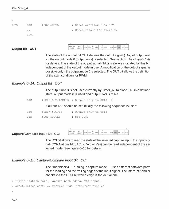
The Timer_A
6-40
;
COV2 BIC #COV,&CCTL2 ; Reset overflow flag COV
... ; Check reason for overflow
RETI
Output Bit OUT
015
un–SCS OUTMODxCAP
INPUTSELECT
CAPTUREMODE
CCICCIESCCIused
CCIFGCOVOUT
The state of the output bit OUT defines the output signal (TAx) of output unitx if the output mode 0 (output only) is selected. See section The Output Unitsfor details. The state of the output signal (TAx) is always indicated by this bit,independent of the output mode in use. A modification of the output signal ispossible only if the output mode 0 is selected. The OUT bit allows the definitionof the start condition for PWM.
Example 6–14. Output Bit OUT
The output unit 3 is not used currently by Timer_A. To place TA3 in a definedstate, output mode 0 is used and output TA3 is reset.
BIC #0E0h+OUT,&CCTL3 ; Output only to OUT3: 0
If output TA3 should be set initially the following sequence is used:
BIC #0E0h,&CCTL3 ; Output only to OUT3
BIS #OUT,&CCTL3 ; Set OUT3
Capture/Compare Input Bit CCI
015
un–SCS OUTMODxCAP
INPUTSELECT
CAPTUREMODE
CCIESCCIused
CCIFGCOVOUTCCI
The CCI bit allows to read the state of the selected capture input: the input sig-nal (CCIxA at pin TAx, ACLK, Vcc or Vss) can be read independent of the se-lected mode. See figure 6–10 for details.
Example 6–15. Capture/Compare Input Bit CCI
The timer block 4 — running in capture mode — uses different software partsfor the leading and the trailing edges of the input signal. The interrupt handlerchecks via the CCI4 bit which edge is the actual one.
; Initialization part: Capture both edges, TA4 input,
; synchronized capture, Capture Mode, interrupt enabled
;
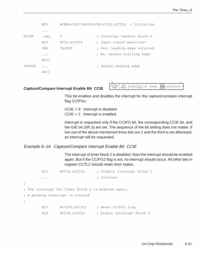
The Timer_A
6-41On-Chip Peripherals
MOV #CMBE+ISCCIA+SCS+CAP+CCIE,&CCTL4 ; Initialize
...
HCCR4 .equ $ ; Interrupt handler Block 4
BIT #CCI,&CCTL4 ; Input signal positive?
JNZ TA4POS ; Yes: leading edge occurred
... ; No, handle trailing edge
RETI
TA4POS ... ; Handle leading edge
RETI
Capture/Compare Interrupt Enable Bit CCIE
015
un–SCS OUTMODxCAP
INPUTSELECT
CAPTUREMODE
SCCIused
CCIFGCOVOUTCCICCIE
This bit enables and disables the interrupt for the capture/compare interruptflag CCIFGx:
CCIE = 0: Interrupt is disabledCCIE = 1: Interrupt is enabled
Interrupt is requested only if the CCIFG bit, the corresponding CCIE bit, andthe GIE bit (SR.3) are set. The sequence of the bit setting does not matter. Iftwo out of the above-mentioned three bits are 1 and the third is set afterward,an interrupt will be requested.
Example 6–16. Capture/Compare Interrupt Enable Bit CCIE
The interrupt of timer block 2 is disabled. Now the interrupt should be enabledagain. But if the CCIFG2 flag is set, no interrupt should occur. All other bits inregister CCTL2 should retain their states.
BIC #CCIE,&CCTL2 ; Disable interrupt Block 2
... ; Continue
;
; The interrupt for Timer Block 2 is enabled again.
; A pending interrupt is cleared
;
BIC #CCIFG,&CCTL2 ; Reset CCIFG2 flag
BIS #CCIE,&CCTL2 ; Enable interrupt Block 2
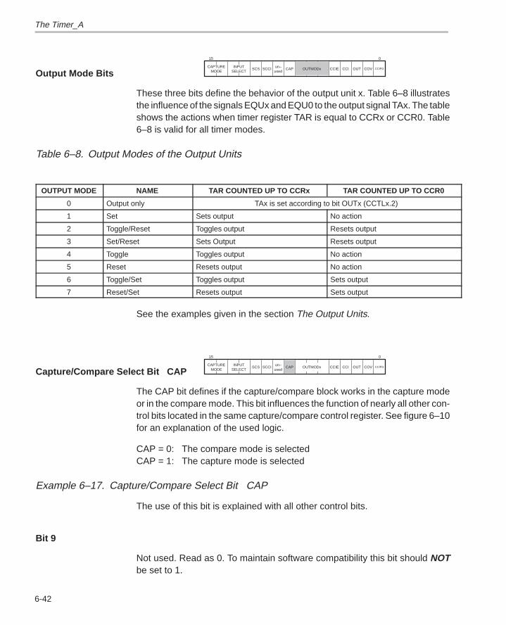
The Timer_A
6-42
Output Mode Bits
015
un–SCS CAP
INPUTSELECT
CAPTUREMODE
SCCIused
CCIFGCOVOUTCCICCIEOUTMODx
These three bits define the behavior of the output unit x. Table 6–8 illustratesthe influence of the signals EQUx and EQU0 to the output signal TAx. The tableshows the actions when timer register TAR is equal to CCRx or CCR0. Table6–8 is valid for all timer modes.
Table 6–8. Output Modes of the Output Units
OUTPUT MODE NAME TAR COUNTED UP TO CCRx TAR COUNTED UP TO CCR0
0 Output only TAx is set according to bit OUTx (CCTLx.2)
1 Set Sets output No action
2 Toggle/Reset Toggles output Resets output
3 Set/Reset Sets Output Resets output
4 Toggle Toggles output No action
5 Reset Resets output No action
6 Toggle/Set Toggles output Sets output
7 Reset/Set Resets output Sets output
See the examples given in the section The Output Units.
Capture/Compare Select Bit CAP
015
un–SCS
INPUTSELECT
CAPTUREMODE
SCCIused
CCIFGCOVOUTCCICCIEOUTMODxCAP
The CAP bit defines if the capture/compare block works in the capture modeor in the compare mode. This bit influences the function of nearly all other con-trol bits located in the same capture/compare control register. See figure 6–10for an explanation of the used logic.
CAP = 0: The compare mode is selectedCAP = 1: The capture mode is selected
Example 6–17. Capture/Compare Select Bit CAP
The use of this bit is explained with all other control bits.
Bit 9
Not used. Read as 0. To maintain software compatibility this bit should NOTbe set to 1.
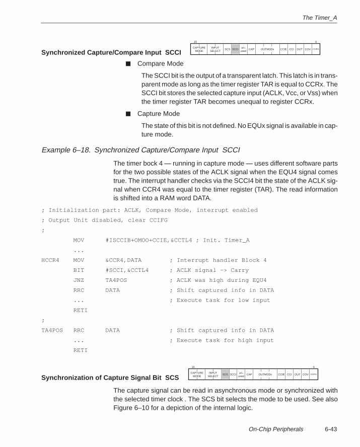
The Timer_A
6-43On-Chip Peripherals
Synchronized Capture/Compare Input SCCI
015
un–SCS
INPUTSELECT
CAPTUREMODE used
CCIFGCOVOUTCCICCIEOUTMODxCAPSCCI
Compare Mode
The SCCI bit is the output of a transparent latch. This latch is in trans-parent mode as long as the timer register TAR is equal to CCRx. TheSCCI bit stores the selected capture input (ACLK, Vcc, or Vss) whenthe timer register TAR becomes unequal to register CCRx.
Capture Mode
The state of this bit is not defined. No EQUx signal is available in cap-ture mode.
Example 6–18. Synchronized Capture/Compare Input SCCI
The timer bock 4 — running in capture mode — uses different software partsfor the two possible states of the ACLK signal when the EQU4 signal comestrue. The interrupt handler checks via the SCCI4 bit the state of the ACLK sig-nal when CCR4 was equal to the timer register (TAR). The read informationis shifted into a RAM word DATA.
; Initialization part: ACLK, Compare Mode, interrupt enabled
; Output Unit disabled, clear CCIFG
;
MOV #ISCCIB+OMOO+CCIE,&CCTL4 ; Init. Timer_A
...
HCCR4 MOV &CCR4,DATA ; Interrupt handler Block 4
BIT #SCCI,&CCTL4 ; ACLK signal –> Carry
JNZ TA4POS ; ACLK was high during EQU4
RRC DATA ; Shift captured info in DATA
... ; Execute task for low input
RETI
;
TA4POS RRC DATA ; Shift captured info in DATA
... ; Execute task for high input
RETI
Synchronization of Capture Signal Bit SCS
015
un–INPUTSELECT
CAPTUREMODE used
CCIFGCOVOUTCCICCIEOUTMODxCAPSCCISCS
The capture signal can be read in asynchronous mode or synchronized withthe selected timer clock . The SCS bit selects the mode to be used. See alsoFigure 6–10 for a depiction of the internal logic.
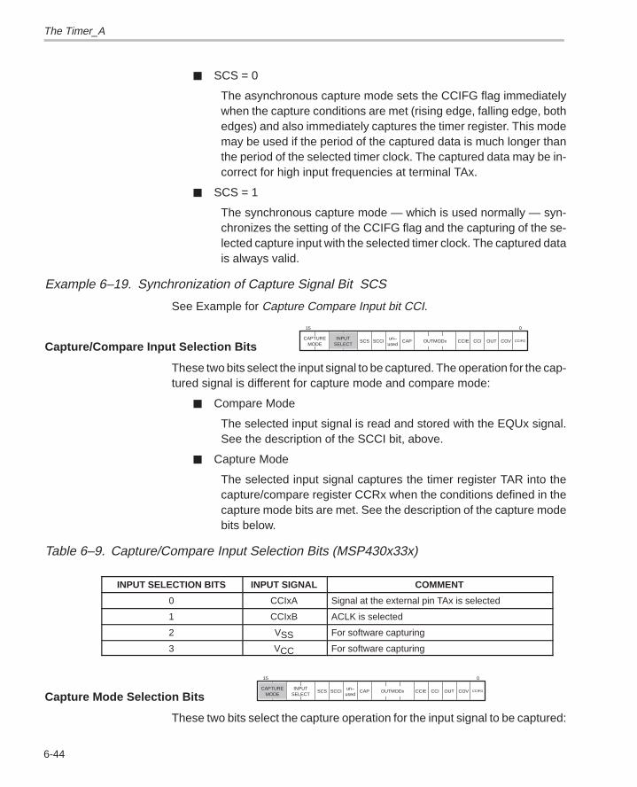
The Timer_A
6-44
SCS = 0
The asynchronous capture mode sets the CCIFG flag immediatelywhen the capture conditions are met (rising edge, falling edge, bothedges) and also immediately captures the timer register. This modemay be used if the period of the captured data is much longer thanthe period of the selected timer clock. The captured data may be in-correct for high input frequencies at terminal TAx.
SCS = 1
The synchronous capture mode — which is used normally — syn-chronizes the setting of the CCIFG flag and the capturing of the se-lected capture input with the selected timer clock. The captured datais always valid.
Example 6–19. Synchronization of Capture Signal Bit SCS
See Example for Capture Compare Input bit CCI.
Capture/Compare Input Selection Bits
015
un–used
CCIFGCOVOUTCCICCIEOUTMODxCAPSCCISCSINPUT
SELECTCAPTURE
MODE
These two bits select the input signal to be captured. The operation for the cap-tured signal is different for capture mode and compare mode:
Compare Mode
The selected input signal is read and stored with the EQUx signal.See the description of the SCCI bit, above.
Capture Mode
The selected input signal captures the timer register TAR into thecapture/compare register CCRx when the conditions defined in thecapture mode bits are met. See the description of the capture modebits below.
Table 6–9. Capture/Compare Input Selection Bits (MSP430x33x)
INPUT SELECTION BITS INPUT SIGNAL COMMENT
0 CCIxA Signal at the external pin TAx is selected
1 CCIxB ACLK is selected
2 VSS For software capturing
3 VCC For software capturing
Capture Mode Selection Bits
015
un–used
CCIFGCOVOUTCCICCIEOUTMODxCAPSCCISCSINPUT
SELECTCAPTURE
MODE
These two bits select the capture operation for the input signal to be captured:
The Timer_A
6-45On-Chip Peripherals
Compare Mode
No function.
Capture Mode
The content of the timer register TAR is stored in the capture/compare register CCRx when the capture condition is true for the se-lected input signal. The capture conditions are listed in Table 6–10.
Table 6–10. Capture Mode Selection Bits
CAPTURE MODE BITS COMMENT
0 Capture mode is disabled
1 Capturing is done with the rising edge (0 to 1)
2 Capturing is done with the falling edge (1 to 0)
3 Capturing is done for both edges
Example 6–20. Capture Mode Selection
The capture/compare block 3 — running in capture mode — measures the pe-riod of the input signal CCI3A at terminal TA3. The measurement is made con-tinuously between two rising edges. The calculated period is stored in the RAMlocation PERIOD for the use by the background software. The actual value ofCCR3 is stored in OLDVAL for the next calculation. Timer_A uses the continu-ous mode.
; Initialization part: Capture rising edge, TA3 input,
; synchronous capture, Capture Mode, interrupt enabled
;
PERIOD .equ 0200h ; Calculated period
OLDVAL .equ 0202h ; Storage of last pos. edge time
;
MOV #CMPE+ISCCIA+CAP+CCIE+SCS,&CCTL3 ; Init.
...
HCCR3 .equ $ ; Interrupt handler Block 3
PUSH &CCR3 ; Captured TAR, rising edge
MOV @SP,PERIOD
SUB OLDVAL,PERIOD ; New – old = period
POP OLDVAL ; For next calculation
RETI
The Timer_A
6-46
6.3.2.2.3 The Period Register CCR0
The purpose of register CCR0 changes with the used timer mode.
Continuous Mode — if this mode is used, CCR0 is a capture/compareregister exactly like the other four registers (CCR1 to CCR4). See sectionThe Timer_A Modes for details.
Up Mode or Up/Down Mode — with one of these modes selected, theregister CCR0 works as the period register for the Timer_A, which definesthe length of the timer period. Whenever the timer register (TAR) reachesthe value of CCR0 (EQU0 = 1), the following actions occur, depending onthe mode in use:
Up Mode
The timer register is cleared with the next timer clock and restartsfrom the value 0. This continues automatically without any softwareintervention necessary. See section The Timer_A Modes.
Up/Down Mode
The timer register changes the count direction and starts to countdown to 0 with the next timer clock. If 0 is reached, the timer registercounts up again with the next timer clock until the value of CCR0 isreached again. This continues automatically without any further soft-ware intervention necessary. See section The Timer_A Modes.
With the up mode or up/down mode selected, the EQU0 signal is valid if thetimer register (TAR) equals the period register (CCR0), or if it is greater thanCCR0. This is not the case for the other registers (CCRx).
The value 0 is not a valid content for the period register: the Timer_A blocks.
The content of the period register CCR0 is not modified normally. The timerperiod is a constant value (50 µs for a repetition rate of 20 kHz — this means200 cycles for a 4 MHz MCLK). But this value may also be modified if neces-sary.
The Timer_A
6-47On-Chip Peripherals
6.3.3 Timer Modes
Timer_A provides three different operating modes as well as the stop mode:
Continuous Mode — the normal mode, except when high-speed PWMgeneration is necessary
Up Mode — used for high-speed, asymmetric PWM generation
Up/Down Mode — used for high-speed, symmetric PWM generation
Stop Mode — Timer_A is halted, all control bits retain their status
One of the advantages of Timer_A is the absolute synchrony of all timings andoutput signals. This is due to the single timer register (TAR) that controls alltimings. This synchrony is very important for the interdependence of timings,for example, if the MSP430 is used with a 3-phase digital motor control applica-tion (DMC).
The equations shown in the next sections use the following abbreviations:
∆t Time interval between two similar interrupts [s]t Time e.g. period of a PWM signal [s]tpw Pulse width of a PWM signal [s]∆n Cycle value added to a CCRx register (timer clock cycles)n Number — content of a register (CCRx)k Predivider constant of the input divider (1, 2, 4 or 8)fCLK Input frequency at the input divider input of Timer_A [Hz]nCCR0 Content of the period register CCR0
The calculation formulas and explanations for the capture mode are given inthe section Capture/Compare Blocks.
6.3.3.1 The Continuous Mode
This mode allows up to five completely independent, synchronous timings.The capture/compare register, CCR0, works exactly the same as the otherregisters (CCRx) when running in continuous mode.
Note:
The signal EQU0 has the same influence on the Mode Control Logic as itdoes in the other timer modes. This means that only the Set, Reset, andToggle modes should be used if independent output signals are desired.
Figure 6–12 shows two independent timings generated by capture/compareregisters CCR0 and CCR1. The content of the capture/compare registers
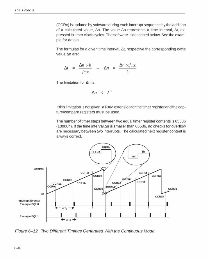
The Timer_A
6-48
(CCRx) is updated by software during each interrupt sequence by the additionof a calculated value, ∆n. The value ∆n represents a time interval, ∆t, ex-pressed in timer clock cycles. The software is described below. See the exam-ple for details.
The formulas for a given time interval, ∆t, respective the corresponding cyclevalue ∆n are:
∆ ∆ ∆ ∆t
n k
fn
t f
kCLK
CLK= → =
The limitation for ∆n is:
∆n < 216
If this limitation is not given, a RAM extension for the timer register and the cap-ture/compare registers must be used.
The number of timer steps between two equal timer register contents is 65536(10000h). If the time interval ∆n is smaller than 65536, no checks for overfloware necessary between two interrupts. The calculated next register content isalways correct.
CCR0aCCR1a
CCR0bCCR1b
CCR1cCCR0c
CCR1dCCR0d
CCR1eCCR0e
CCR1f
CCR0f
CCR1h
CCR1g
CCR0g
0FFFFh
0h
Interrupt Events:Example EQU0
Example EQU1
FFFEh
FFFFh
0h
1h
∆ t0
∆ t1
Figure 6–12. Two Different Timings Generated With the Continuous Mode
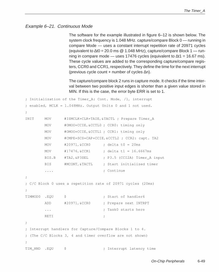
The Timer_A
6-49On-Chip Peripherals
Example 6–21. Continuous Mode
The software for the example illustrated in figure 6–12 is shown below. Thesystem clock frequency is 1.048 MHz. capture/compare Block 0 — running incompare Mode — uses a constant interrupt repetition rate of 20971 cycles(equivalent to ∆t0 = 20.0 ms @ 1.048 MHz), capture/compare Block 1 — run-ning in compare mode — uses 17476 cycles (equivalent to ∆t1 = 16.67 ms).These cycle values are added to the corresponding capture/compare regis-ters, CCR0 and CCR1, respectively. They define the time for the next interrupt(previous cycle count + number of cycles ∆n).
The capture/compare block 2 runs in capture mode. It checks if the time inter-val between two positive input edges is shorter than a given value stored inMIN. If this is the case, the error byte ERR is set to 1.
; Initialization of the Timer_A: Cont. Mode, /1, interrupt
; enabled, MCLK = 1.048MHz. Output Units 0 and 1 not used.
;
INIT MOV #ISMCLK+CLR+TAIE,&TACTL ; Prepare Timer_A
MOV #OMOO+CCIE,&CCTL0 ; CCR0: timing only
MOV #OMOO+CCIE,&CCTL1 ; CCR1: timing only
MOV #CMPE+SCS+CAP+CCIE,&CCTL2 ; CCR2: capt. TA2
MOV #20971,&CCR0 ; delta t0 = 20ms
MOV #17476,&CCR1 ; delta t1 = 16.6667ms
BIS.B #TA2,&P3SEL ; P3.5 (CCI2A) Timer_A input
BIS #MCONT,&TACTL ; Start initialized timer
.... ; Continue
;
; C/C Block 0 uses a repetition rate of 20971 cycles (20ms)
;
TIMMOD0 .EQU $ ; Start of handler6
ADD #20971,&CCR0 ; Prepare next INTRPT
... ; Task0 starts here
RETI ;
;
; Interrupt handlers for Capture/Compare Blocks 1 to 4.
; (The C/C Blocks 3, 4 and timer overflow are not shown)
;
TIM_HND .EQU $ ; Interrupt latency time
The Timer_A
6-50
ADD &TAIV,PC ; Add Jump table offset
RETI ; TAIV = 0: No interrupt
JMP TIMMOD1 ; TAIV = 2: C/C Block 1
JMP TIMMOD2 ; TAIV = 4: C/C Block 2
JMP TIMMOD3 ; TAIV = 6: C/C Block 3
JMP TIMMOD4 ; TAIV = 8: C/C Block 4
TIMOVH ... ; TAIV = 10: Timer OVFL
;
; C/C Block 1 uses a repetition rate of 17476 cycles (16.67ms)
;
TIMMOD1 .EQU $ ; Vector 2: C/C Block 1
ADD #17476,&CCR1 ; Add time interval
... ; Task1 starts here
RETI ; Back to main program
;
; C/C Block 2 checks if the time interval between two pos.
; input edges is shorter than a given value in MIN
;
TIMMOD2 .EQU $ ; Vector 4: C/C Block 2
BIT #COV,&CCTL2 ; Frequency much too high?
JNZ COV2 ; Yes, overflow!
PUSH &CCR2 ; Time of last transition
SUB OLDC2,0(SP) ; Time difference to stack
ADD @SP,OLDC2 ; Old + difference = new
CMP @SP+,MIN ; Time interval >= MIN
JLO RET2 ; Yes, ok
COV2 MOV.B #1,ERR ; No, set error state 1
BIC #COV,&CCTL2 ; Reset overflow flag
RET2 RETI ; Back to main program
The tasks started by the interrupt handlers are not shown; these include:
Incrementing software counters
Checks after regular time intervals (keyboard, watchdog reset, etc.)
Input tests
Update of status bytes, etc.
Measurement intervals
Frequency generation with the output units
The Timer_A
6-51On-Chip Peripherals
6.3.3.2 The Up Mode
The up mode is mainly used for the generation of asymmetric PWM signals.These PWM signals are absolutely synchronous due to the single timer regis-ter used for all signals. The period of the PWM repetition frequency is loadedinto the period register (CCR0) and the pulse width for each of the outputs, TA1through TA4, is loaded into the capture/compare registers, CCR1 throughCCR4. The formula for a given timer period, t, with respect to the correspond-ing cycle value nCCR0 is (nCCR0 < 65536):
( )t
n + 1 k
fn
t f
k1
CCR0
CLKCCR0
CLK=
= –
The formula for a given pulse width tpw and the corresponding cycle value n(the content of CCRx) is (n < 65536):
tn k
fn
t f
kpw
CLK
pw CLK= =
As long as no modifications to the period register or the capture/compare reg-isters are made, the PWM signals are repeated without any CPU interventionnecessary. The number of timer clock cycles between two equal timer registercontents is nCCR0 +1.
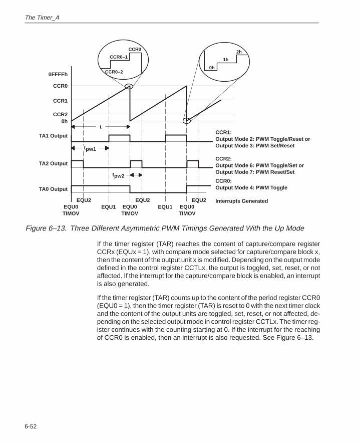
The Timer_A
6-52
0FFFFh
CCR0
CCR1
CCR20h
TA1 Output
TA2 Output
TA0 Output
EQU1 EQU0TIMOV
EQU1 EQU0TIMOV
EQU2 EQU2 EQU2
CCR1:Output Mode 2: PWM Toggle/Reset orOutput Mode 3: PWM Set/Reset
CCR2:Output Mode 6: PWM Toggle/Set orOutput Mode 7: PWM Reset/Set
CCR0:Output Mode 4: PWM Toggle
Interrupts Generated
CCR0–1
CCR0
0h
1h
CCR0–2
2h
t
tpw1
tpw2
EQU0TIMOV
Figure 6–13. Three Different Asymmetric PWM Timings Generated With the Up Mode
If the timer register (TAR) reaches the content of capture/compare registerCCRx (EQUx = 1), with compare mode selected for capture/compare block x,then the content of the output unit x is modified. Depending on the output modedefined in the control register CCTLx, the output is toggled, set, reset, or notaffected. If the interrupt for the capture/compare block is enabled, an interruptis also generated.
If the timer register (TAR) counts up to the content of the period register CCR0(EQU0 = 1), then the timer register (TAR) is reset to 0 with the next timer clockand the content of the output units are toggled, set, reset, or not affected, de-pending on the selected output mode in control register CCTLx. The timer reg-ister continues with the counting starting at 0. If the interrupt for the reachingof CCR0 is enabled, then an interrupt is also requested. See Figure 6–13.
The Timer_A
6-53On-Chip Peripherals
Notes:
The three interrupts caused by the TAIFG flag, the CCIFG0 flag, and CCIFGxflags do not occur simultaneously if used with the up mode:
The CCIFGx flag is set when the capture/compare register x equals thetimer register (TAR) (EQUx = 1)
The CCIFG0 flag is prepared when the timer register equals the periodregister CCR0 (EQU0 = 1). The CCIFG0 flag is delayed one timer clock cycleand set, therefore, together with the TAIFG flag (timer register TAR contains0)
The TAIFG flag is set when the timer register is reset to 0 (TIMOV = 1)
This means for the up mode: only one interrupt handler is necessary togetherfor the TAIFG flag and the CCIFG0 flag.
If the period register CCR0 contains 0, then the timer register TAR continuescounting until it also reaches 0. Then the counting stops until a nonzero valueis written to CCR0.
Example 6–22. Three Different Asymmetric PWM Timings Generated With the Up Mode
The software for the example illustrated in figure 6–13 is shown below. cap-ture/compare block 1 generates a negative pulse with output unit 1, capture/compare block 2 generates a positive pulse with the output unit 2 and capture/compare block 0 (the period register block) outputs an evenly spaced outputpulse with its output unit 0. The initializing part of the example is also shown.If no tasks must be executed (here tasks 0, 1, and 2), the interrupts may beswitched off; the pulse generation continues.
; Initialization of the Timer_A: Up Mode, /1, interrupt
; enabled, MCLK = 3.8MHz
;
INIT MOV #ISMCLK+D1+CLR+TAIE,&TACTL ; Prepare Timer_A
MOV #OMT+CCIE,&CCTL0 ; CCR0: toggle TA0
MOV #OMTR+CCIE,&CCTL1 ; CCR1: toggle/reset TA1
MOV #OMRS+CCIE,&CCTL2 ; CCR2: reset/set TA2
MOV #190–1,&CCR0 ; fccr0 = 20kHz
MOV #114,&CCR1 ; tpw1 = 30us
MOV #48,&CCR2 ; tpw2 = 12.6us
BIS.B #TA2+TA1+TA0,&P3SEL; Enable TA2, TA1 TA0
BIS #MUP,&TACTL ; Start init. timer. Up Mode
The Timer_A
6-54
.... ; Continue
; Interrupt handler for the Period Register CCR0
; C/C Block 0 outputs a signal with 1/2 of the frequency
; of the other C/C Blocks (50%/50%). It also increments the
; RAM extension of the Timer Register TIMAEXT. It is
; initialized to: toggle (EQU0)
;
TIMMOD0 .EQU $ ; Start of handler
INC TIMAEXT ; Incr. timer extension
... ; Task0 starts here
RETI ;
;
; Interrupt handlers for Capture/Compare Blocks 1 to 4.
;
TIM_HND .EQU $ ; Interrupt latency time
ADD &TAIV,PC ; Add Jump table offset
RETI ; TAIV = 0: No interrupt
JMP TIMMOD1 ; TAIV = 2: C/C Block 1
JMP TIMMOD2 ; TAIV = 4: C/C Block 2
JMP TIMMOD3 ; TAIV = 6: C/C Block 3
JMP TIMMOD4 ; TAIV = 8: C/C Block 4
TIMOVH ... ; TAIV = 10: Timer OVFL
;
; C/C Block 1 outputs a negative pulse automatically. It is
; initialized to: toggle/reset (EQU1/EQU0)
;
TIMMOD1 .EQU $ ; Vector 2: C/C Block 1
... ; Task1 starts here
RETI ; Back to main program
;
; C/C Block 2 outputs a positive pulse automatically. It is
; initialized to: reset/set (EQU2/EQU0)
;
TIMMOD2 .EQU $ ; Vector 4: C/C Block 2
... ; Task2 starts here
RETI ; Back to main program
The tasks started by the interrupt handlers are not shown; these may include:
Pulse width modulation for control purposes with the output units DC generation (DAC) with the output units Tasks like those shown for the continuous mode, but with special treat-
ment due to the short period. The RAM extension (TIMAEXT) must there-fore be taken into account for measurement.
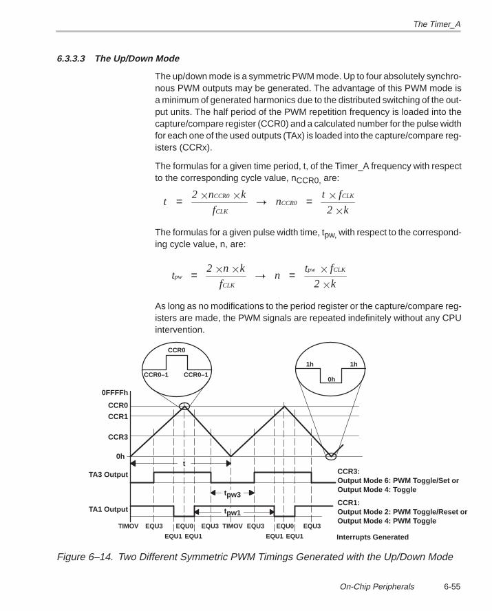
The Timer_A
6-55On-Chip Peripherals
6.3.3.3 The Up/Down Mode
The up/down mode is a symmetric PWM mode. Up to four absolutely synchro-nous PWM outputs may be generated. The advantage of this PWM mode isa minimum of generated harmonics due to the distributed switching of the out-put units. The half period of the PWM repetition frequency is loaded into thecapture/compare register (CCR0) and a calculated number for the pulse widthfor each one of the used outputs (TAx) is loaded into the capture/compare reg-isters (CCRx).
The formulas for a given time period, t, of the Timer_A frequency with respectto the corresponding cycle value, nCCR0, are:
t2 n k
fn
t f
2 k
CCR0
CLKCCR0
CLK= =
The formulas for a given pulse width time, tpw, with respect to the correspond-ing cycle value, n, are:
t2 n k
fn
t f
2 kpw
CLK
pw CLK= =
As long as no modifications to the period register or the capture/compare reg-isters are made, the PWM signals are repeated indefinitely without any CPUintervention.
0FFFFh
CCR0
CCR1
CCR3
0h
TA3 Output
TA1 Output
TIMOV EQU3 EQU0 EQU3 EQU3 EQU3TIMOV EQU0
EQU1 EQU1 EQU1 EQU1
CCR3:Output Mode 6: PWM Toggle/Set orOutput Mode 4: Toggle
CCR1:Output Mode 2: PWM Toggle/Reset orOutput Mode 4: PWM Toggle
Interrupts Generated
CCR0–1
CCR0
0h
1h
CCR0–1
1h
t
tpw3
tpw1
Figure 6–14. Two Different Symmetric PWM Timings Generated with the Up/Down Mode
The Timer_A
6-56
If the timer register (TAR) reaches the content of capture/compare register,CCRx (EQUx = 1), and the corresponding capture/compare block is switchedto the compare mode, then the content of output unit x is modified (toggled,set, reset, or not affected) depending on the output mode of the control register(CCTLx). If the interrupt for the capture/compare block is enabled, then an in-terrupt is also generated.
The timer register TAR reverses its count direction when it reaches the contentof the period register (CCR0), and the content of output unit x is modified again(toggled, set, reset, or not affected) depending on the output mode of the con-trol register (CCTLx). If the interrupt for the reaching of CCR0 is enabled, thenan interrupt is also requested. If the timer register reaches the value 0 again,it starts counting upward with the next timer clock cycle. If the interrupt for thereaching of 0 is enabled (TIMOV = 1), then an interrupt is also requested withthe TAIFG flag. See Figure 6–14.
Note:
If the period register (CCR0) contains 0, then the timer register (TAR) contin-ues counting until it also reaches 0. Then the counting stops until a nonzerovalue is written to CCR0.
Example 6–23. Two Different Symmetric PWM Timings Generated With the Up/DownMode
The software for the example illustrated in figure 6–14 is shown below. cap-ture/compare block 3 generates a negative pulse with output unit 3 at the out-put TA3. capture/compare block 1 generates a positive pulse — symmetricallyto the zero point — with the output unit 1 at the output TA1. The initializing partof the example is also shown. If no software tasks must be executed, the inter-rupts for the capture/compare blocks 0, 1, and 3 may be switched off.
TIMAEXT .EQU 200h ; RAM extension (bits 17 – 23)
; Initialization of Timer_A: Up/Down Mode, /2, interrupt
; enabled, MCLK = 3.8MHz
;
INIT MOV #ISMCLK+D2+CLR+TAIE,&TACTL ; Prepare Timer_A
MOV #OMOO+CCIE,&CCTL0 ; CCR0: normal I/O pin
MOV #OMTR+CCIE,&CCTL1 ; CCR1: toggle/reset TA1
MOV #OMTS+CCIE,&CCTL3 ; CCR3: toggle/set TA3
MOV #190,&CCR0 ; fccr0 = 5kHz
MOV #114,&CCR1 ; tpw1 = 120.0us
MOV #48,&CCR3 ; tpw3 = 50.5us
The Timer_A
6-57On-Chip Peripherals
BIS.B #TA3+TA1,&P3SEL ; Enable TA3 and TA1 outputs
BIS #MUPD,&TACTL ; Start initialized timer
.... ; Continue
; Interrupt handler for the Period Register CCR0
; Block 0 sets the RAM extension TIMAEXT of the Timer Register
; (count down). The LSB of TIMAEXT indicates the
; count direction: LSB = 0: count up
; LSB = 1: count down
; This indication is necessary if the Capture Mode is used.
; The count direction indication is self–synchronizing
;
TIMMOD0 .EQU $ ; Start of handler
BIS #1,TIMAEXT ; LSB = 1: count down now
... ; Task0 starts here
RETI ;
;
; Interrupt handlers and decision (only 3 handlers shown)
;
TIM_HND .EQU $ ; Interrupt latency time
ADD &TAIV,PC ; Add Jump table offset
RETI ; TAIV = 0: No interrupt
JMP TIMMOD1 ; TAIV = 2: C/C Block 1
JMP TIMMOD2 ; TAIV = 4: C/C Block 2
JMP TIMMOD3 ; TAIV = 6: C/C Block 3
JMP TIMMOD4 ; TAIV = 8: C/C Block 4
;
; Timer Register reached zero: LSB is set to 0 (count up)
;
TIMOVH .EQU $ ; TIMOV interrupt
INC TIMAEXT ; TAIV = 10: Block 5
RETI ;
;
; C/C Block 1 outputs a positive pulse automatically.
; Initialized to: toggle/reset (EQU1/EQU0)
;
TIMMOD1 .EQU $ ; Vector 2: C/C Block 1
The Timer_A
6-58
... ; Task1 starts here
RETI ; Back to main program
;
; C/C Block 3 outputs a negative pulse automatically.
; Initialized to: toggle/set (EQU3/EQU0)
;
TIMMOD3 .EQU $ ; Vector 6: C/C Block 3
... ; Task3 starts here
RETI ; Back to main program
The tasks started by the interrupt handlers are not shown; these may be:
Symmetric pulse width modulation for control purposes with the outputunits
DC generation (DAC) with the output units
Tasks like those shown for the continuous mode, but with special treat-ment due to the changing count direction and short period. The RAM ex-tension TIMAEXT must therefore be taken into account for measure-ments.
6.3.3.4 The Stop Mode
The stop mode halts the timer register without the change of any control regis-ter. The timer actions can then continue on from exactly where they werestopped.
Example 6–24. The Stop Mode
The Timer_A running in up/down mode is stopped. After a certain time, itshould continue from exactly where it was halted, including the count direction.
BIC #MUPD,&TACTL ; Halt Timer_A
... ; Proceed without Timer_A
BIS #MUPD,&TACTL ; Continue with Up/Down Mode

The Timer_A
6-59On-Chip Peripherals
6.3.3.5 Applications of the Timer Modes
Table 6–11 gives an overview of the different applications of the Timer _Amodes, together with the capture/compare registers.
Table 6–11. Combinations of Timer_A Modes
COMBINATIONS CAPTURE/COMPARE REGISTER 0 CAPTURE/COMPARE REGISTER X
Continuous Mode
Interrupt timing
Slow PWM generation
Compare register TRIAC timingCom are register
SW/HW UART (transmitter)Same as for capture/compare register 0
SW/HW SPISame as for capture/compare register 0
Capturing of internal and external events
Capture register SW/HW UART (receiver)Ca ture register
Revolutions measurement
Up Mode
Interrupt timing
Asymmetric PWM generation
Compare register Fixed to period register Digital motor controlCom are register Fixed to eriod register
TRIAC timing
SW/HW UART (transmitter)
Capturing of int. and ext. events
Capture register Not possible due to period register function SW/HW UART (receiver)Ca ture register Not ossible due to eriod register function
Revolutions measurement
Up/Down Mode
Compare register Fixed to period register Symmetric PWM generation
Compare register Fixed to period register Digital motor control
Capture register Not possible due to period register function (Capturing of internal and external events is
difficult due to up/down counting)
The Timer_A
6-60
6.3.4 The Timer_A Interrupt Logic
6.3.4.1 Interrupt Sources
Several interrupt sources exist within the Timer_A hardware. An interrupt is re-quested only if the interrupt of the corresponding timer block is enabled (inter-rupt enable bit TAIE or CCIEx is set) and the general interrupt enable bit GIE(SR.3) is also set. If more than one interrupt is pending, then the interrupt withthe highest priority is first in line for servicing. An interrupt is also requestedimmediately if any interrupt enable bit (CCIEx or TAIE) is set and the corre-sponding interrupt flag and GIE (SR.3) were already set.
Timer Register Block — The timer interrupt flag TAIFG requests an interruptif the timer register reaches 0 and the interrupt enable bit TAIE is set. TheTAIFG flag is set, dependent on the actual mode:
Continuous Mode — after the overflow from 0FFFFh to 0000h
Up Mode — one timer clock after the timer period in CCR0 is reached
Up/Down Mode — when the value 0000h is reached during the count-down
Capture/Compare Block x — The capture/compare interrupt Flags CCIFGxare set if one of the following conditions is met. An interrupt is requested onlyif the corresponding interrupt enable bit CCIEx and GIE are also set.
Capture Mode — an input value is captured in register CCRx (the capturecondition at the selected input came true)
Compare Mode — the timer register counted to the value contained inregister CCRx
6.3.4.2 Interrupt Vectors
Two interrupt vectors are associated with the Timer_A module.
The single-source vector for the capture/compare register CCR0 has thehighest priority of all Timer_A interrupts. The capture/compare registerCCR0 is used to define the timer period during the up mode and the up/down mode. Therefore, it requires the fastest service. This interrupt vectoris located at address 0FFF2h.
The multi-source interrupt vector for all other interrupt sources of the Tim-er_A (capture/compare registers x and Timer Overflow). A 16-bit vectorword — the timer vector register (TAIV) — indicates the interrupt with the
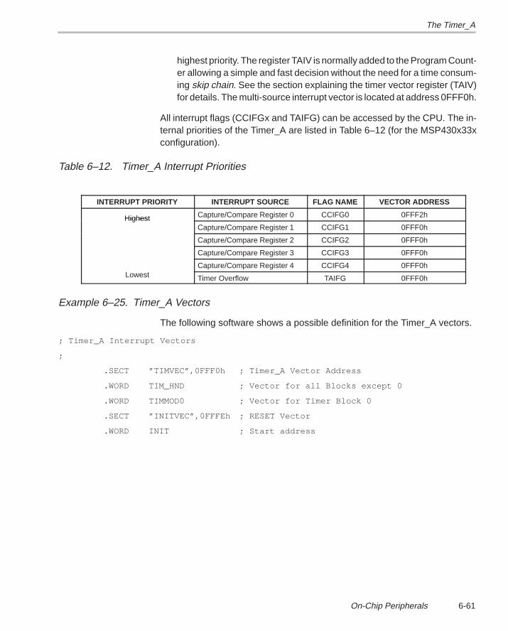
The Timer_A
6-61On-Chip Peripherals
highest priority. The register TAIV is normally added to the Program Count-er allowing a simple and fast decision without the need for a time consum-ing skip chain. See the section explaining the timer vector register (TAIV)for details. The multi-source interrupt vector is located at address 0FFF0h.
All interrupt flags (CCIFGx and TAIFG) can be accessed by the CPU. The in-ternal priorities of the Timer_A are listed in Table 6–12 (for the MSP430x33xconfiguration).
Table 6–12. Timer_A Interrupt Priorities
INTERRUPT PRIORITY INTERRUPT SOURCE FLAG NAME VECTOR ADDRESS
Highest Capture/Compare Register 0 CCIFG0 0FFF2hHighestCapture/Compare Register 1 CCIFG1 0FFF0h
Capture/Compare Register 2 CCIFG2 0FFF0h
Capture/Compare Register 3 CCIFG3 0FFF0h
Capture/Compare Register 4 CCIFG4 0FFF0hLowest Timer Overflow TAIFG 0FFF0h
Example 6–25. Timer_A Vectors
The following software shows a possible definition for the Timer_A vectors.
; Timer_A Interrupt Vectors
;
.SECT ”TIMVEC”,0FFF0h ; Timer_A Vector Address
.WORD TIM_HND ; Vector for all Blocks except 0
.WORD TIMMOD0 ; Vector for Timer Block 0
.SECT ”INITVEC”,0FFFEh ; RESET Vector
.WORD INIT ; Start address
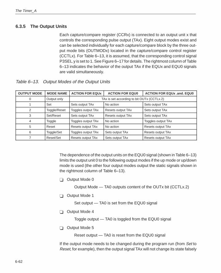
The Timer_A
6-62
6.3.5 The Output Units
Each capture/compare register (CCRx) is connected to an output unit x thatcontrols the corresponding pulse output (TAx). Eight output modes exist andcan be selected individually for each capture/compare block by the three out-put mode bits (OUTMODx) located in the capture/compare control register(CCTLx). For Table 6–13, it is assumed, that the corresponding control signalP3SEL.y is set to 1. See Figure 6–17 for details. The rightmost column of Table6–13 indicates the behavior of the output TAx if the EQUx and EQU0 signalsare valid simultaneously.
Table 6–13. Output Modes of the Output Units
OUTPUT MODE MODE NAME ACTION FOR EQUx ACTION FOR EQU0 ACTION FOR EQUx .and. EQU0
0 Output only TAx is set according to bit OUTx (CCTLx.2)
1 Set Sets output TAx No action Sets output TAx
2 Toggle/Reset Toggles output TAx Resets output TAx Sets output TAx
3 Set/Reset Sets output TAx Resets output TAx Sets output TAx
4 Toggle Toggles output TAx No action Toggles output TAx
5 Reset Resets output TAx No action Resets output TAx
6 Toggle/Set Toggles output TAx Sets output TAx Resets output TAx
7 Reset/Set Resets output TAx Sets output TAx Resets output TAx
The dependence of the output units on the EQU0 signal (shown in Table 6–13)limits the output unit 0 to the following output modes if the up mode or up/downmode is used (the other four output modes output the static signals shown inthe rightmost column of Table 6–13).
Output Mode 0
Output Mode — TA0 outputs content of the OUTx bit (CCTLx.2)
Output Mode 1
Set output — TA0 is set from the EQU0 signal
Output Mode 4
Toggle output — TA0 is toggled from the EQU0 signal
Output Mode 5
Reset output — TA0 is reset from the EQU0 signal
If the output mode needs to be changed during the program run (from Set toReset, for example), then the output signal TAx will not change its state falsely
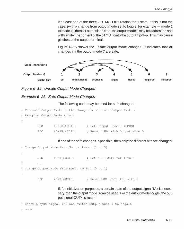
The Timer_A
6-63On-Chip Peripherals
if at least one of the three OUTMOD bits retains the 1 state. If this is not thecase, (with a change from output mode set to toggle, for example — mode 1to mode 4), then for a transition time, the output mode 0 may be addressed andwill transfer the content of the bit OUTx into the output flip-flop. This may causeglitches at the output terminal.
Figure 6–15 shows the unsafe output mode changes. It indicates that allchanges via the output mode 7 are safe.
0 1 2 3 4 5 6 7
Output only Set Toggle/Reset Set/Reset Toggle Reset Toggle/Set Reset/Set
Output Modes
Mode Transitions
Figure 6–15. Unsafe Output Mode Changes
Example 6–26. Safe Output Mode Changes
The following code may be used for safe changes.
; To avoid Output Mode 0, the change is made via Output Mode 7
; Example: Output Mode x to 4
;
BIS #OMRS,&CCTL1 ; Set Output Mode 7 (OMRS)
BIC #OMSR,&CCTL1 ; Reset LSBs with Output Mode 3
If one of the safe changes is possible, then only the different bits are changed:
; Change Output Mode from Set to Reset (1 to 5)
;
BIS #OMT,&CCTL1 ; Set MSB (OMT) for 1 to 5
; ...
; Change Output Mode from Reset to Set (5 to 1)
;
BIC #OMT,&CCTL1 ; Reset MSB (OMT) for 5 to 1
If, for initialization purposes, a certain state of the output signal TAx is neces-sary, then the output mode 0 can be used. For the output mode toggle, the out-put signal OUTx is reset:
; Reset output signal TA1 and switch Output Unit 1 to toggle
; mode
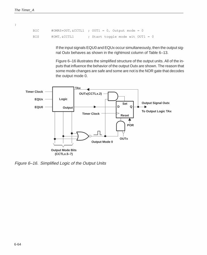
The Timer_A
6-64
;
BIC #OMRS+OUT,&CCTL1 ; OUT1 = 0, Output mode = 0
BIS #OMT,&CCTL1 ; Start toggle mode wit OUT1 = 0
If the input signals EQU0 and EQUx occur simultaneously, then the output sig-nal Outx behaves as shown in the rightmost column of Table 6–13.
Figure 6–16 illustrates the simplified structure of the output units. All of the in-puts that influence the behavior of the output Outx are shown. The reason thatsome mode changes are safe and some are not is the NOR gate that decodesthe output mode 0.
Output
Logic
D QSet
Reset
POR
OUTxOutput Mode 0
TAx
OUTx(CCTLx.2)
Timer Clock
Output Signal Outx
To Output Logic TAx
Timer Clock
EQUx
EQU0
Output Mode Bits(CCTLx.5–7)
Figure 6–16. Simplified Logic of the Output Units
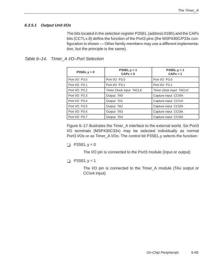
The Timer_A
6-65On-Chip Peripherals
6.3.5.1 Output Unit I/Os
The bits located in the selection register P3SEL (address 01Bh) and the CAPxbits (CCTLx.8) define the function of the Port3 pins (the MSP430C/P33x con-figuration is shown — Other family members may use a different implementa-tion, but the principle is the same).
Table 6–14. Timer_A I/O–Port Selection
P3SEL.y = 0P3SEL.y = 1
CAPx = 0P3SEL.y = 1
CAPx = 1
Port I/O P3.0 Port I/O P3.0 Port I/O P3.0
Port I/O P3.1 Port I/O P3.1 Port I/O P3.1
Port I/O P3.2 Timer Clock input TACLK Timer clock input TACLK
Port I/O P3.3 Output TA0 Capture input CCI0A
Port I/O P3.4 Output TA1 Capture input CCI1A
Port I/O P3.5 Output TA2 Capture input CCI2A
Port I/O P3.6 Output TA3 Capture input CCI3A
Port I/O P3.7 Output TA4 Capture input CCI4A
Figure 6–17 illustrates the Timer_A interface to the external world. Six Port3I/O terminals (MSP430C33x) may be selected individually as normalPort3 I/Os or as Timer_A I/Os. The control bit P3SEL.y selects the function:
P3SEL.y = 0
The I/O pin is connected to the Port3 module (input or output)
P3SEL.y = 1
The I/O pin is connected to the Timer_A module (TAx output orCCIxA input)
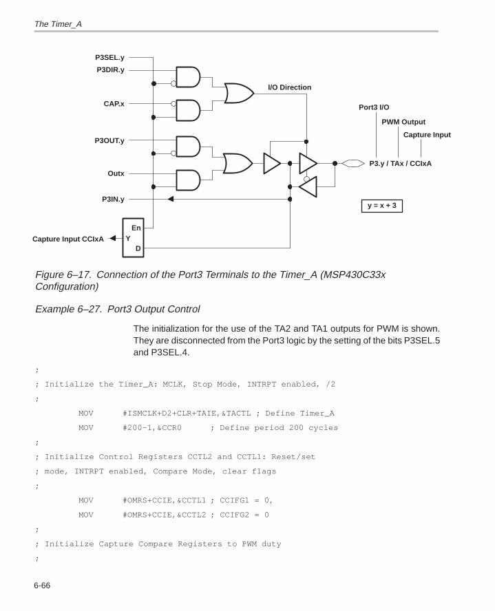
The Timer_A
6-66
EnY
D
I/O Direction
P3.y / TAx / CCIxA
Capture Input
PWM Output
Port3 I/O
y = x + 3
P3SEL.y
P3DIR.y
CAP.x
P3OUT.y
Outx
P3IN.y
Capture Input CCIxA
Figure 6–17. Connection of the Port3 Terminals to the Timer_A (MSP430C33xConfiguration)
Example 6–27. Port3 Output Control
The initialization for the use of the TA2 and TA1 outputs for PWM is shown.They are disconnected from the Port3 logic by the setting of the bits P3SEL.5and P3SEL.4.
;
; Initialize the Timer_A: MCLK, Stop Mode, INTRPT enabled, /2
;
MOV #ISMCLK+D2+CLR+TAIE,&TACTL ; Define Timer_A
MOV #200–1,&CCR0 ; Define period 200 cycles
;
; Initialize Control Registers CCTL2 and CCTL1: Reset/set
; mode, INTRPT enabled, Compare Mode, clear flags
;
MOV #OMRS+CCIE,&CCTL1 ; CCIFG1 = 0,
MOV #OMRS+CCIE,&CCTL2 ; CCIFG2 = 0
;
; Initialize Capture Compare Registers to PWM duty
;
The Timer_A
6-67On-Chip Peripherals
MOV #100,&CCR1 ; 50% PWM
MOV #50,&CCR2 ; 25% PWM
;
; Prepare Timer_A Output Units TA2 and TA1 (P3.5 and P3.4)
;
MOV.B #TA2+TA1,&P3SEL ; Connect to Output Units
;
BIS #MUP,&TACTL ; Start Timer_A in Up Mode
6.3.5.2 Pulse Width Modulation in the Continuous Mode
The continuous mode is not intended for PWM, but may be used for this pur-pose in two ways. The timing can be controlled from:
One capture/compare register only
One capture/compare register and additional capture/compare register 0
6.3.5.2.1 One Capture/Compare Register only
The same capture/control register x sets and resets the output TAx. The outputmodes toggle or alternating set and reset are used. For the second method(Set and Reset), the interrupt handler modifies the output mode in addition tothe adding of the time interval to the register CCRx. PWM values near 0% and100% must be realized with software. See also Section 6.3.6 The Limitationsof Timer_A.
The output modes and their usability for the first method of PWM in the continu-ous mode are listed below:
Set Mode — used to get the output signal into the set state. It is necessaryto alternate with the reset mode to get a PWM output signal
Toggle/Reset — not usable due to the influence of capture/compare reg-ister 0
Set/Reset — not usable due to the influence of capture/compare register0
Toggle — usable, but a defined start position must be initialized. Other-wise, an inverted output signal is generated
Reset Mode — used to get the output signal into the reset state. It is nec-essary to alternate with the set mode to get a PWM output signal
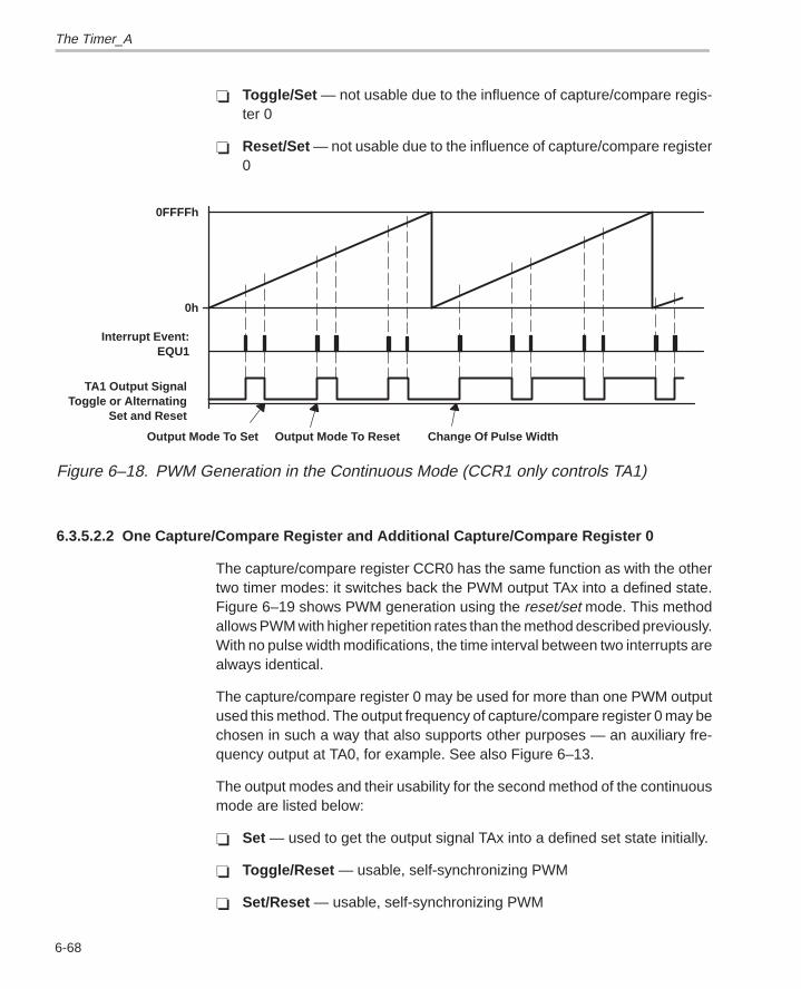
The Timer_A
6-68
Toggle/Set — not usable due to the influence of capture/compare regis-ter 0
Reset/Set — not usable due to the influence of capture/compare register0
0FFFFh
0h
Interrupt Event:EQU1
Output Mode To Set Output Mode To Reset Change Of Pulse Width
TA1 Output SignalToggle or Alternating
Set and Reset
Figure 6–18. PWM Generation in the Continuous Mode (CCR1 only controls TA1)
6.3.5.2.2 One Capture/Compare Register and Additional Capture/Compare Register 0
The capture/compare register CCR0 has the same function as with the othertwo timer modes: it switches back the PWM output TAx into a defined state.Figure 6–19 shows PWM generation using the reset/set mode. This methodallows PWM with higher repetition rates than the method described previously.With no pulse width modifications, the time interval between two interrupts arealways identical.
The capture/compare register 0 may be used for more than one PWM outputused this method. The output frequency of capture/compare register 0 may bechosen in such a way that also supports other purposes — an auxiliary fre-quency output at TA0, for example. See also Figure 6–13.
The output modes and their usability for the second method of the continuousmode are listed below:
Set — used to get the output signal TAx into a defined set state initially.
Toggle/Reset — usable, self-synchronizing PWM
Set/Reset — usable, self-synchronizing PWM
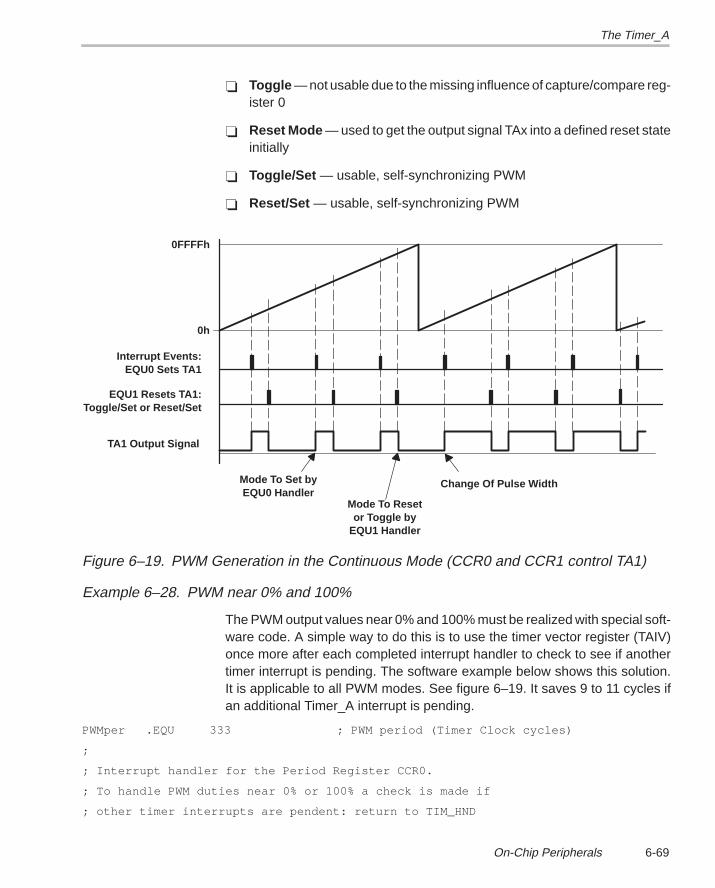
The Timer_A
6-69On-Chip Peripherals
Toggle — not usable due to the missing influence of capture/compare reg-ister 0
Reset Mode — used to get the output signal TAx into a defined reset stateinitially
Toggle/Set — usable, self-synchronizing PWM
Reset/Set — usable, self-synchronizing PWM
0FFFFh
0h
Interrupt Events:EQU0 Sets TA1
Mode To Set byEQU0 Handler
Change Of Pulse Width
TA1 Output Signal
Mode To Resetor Toggle by
EQU1 Handler
EQU1 Resets TA1:Toggle/Set or Reset/Set
Figure 6–19. PWM Generation in the Continuous Mode (CCR0 and CCR1 control TA1)
Example 6–28. PWM near 0% and 100%
The PWM output values near 0% and 100% must be realized with special soft-ware code. A simple way to do this is to use the timer vector register (TAIV)once more after each completed interrupt handler to check to see if anothertimer interrupt is pending. The software example below shows this solution.It is applicable to all PWM modes. See figure 6–19. It saves 9 to 11 cycles ifan additional Timer_A interrupt is pending.
PWMper .EQU 333 ; PWM period (Timer Clock cycles)
;
; Interrupt handler for the Period Register CCR0.
; To handle PWM duties near 0% or 100% a check is made if
; other timer interrupts are pendent: return to TIM_HND
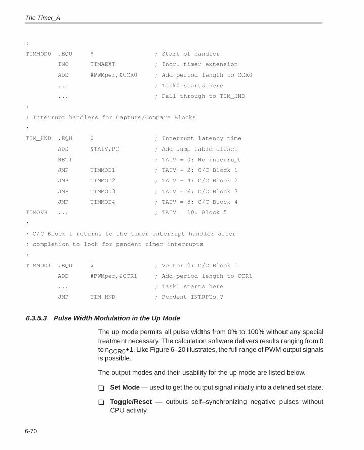
The Timer_A
6-70
;
TIMMOD0 .EQU $ ; Start of handler
INC TIMAEXT ; Incr. timer extension
ADD #PWMper,&CCR0 ; Add period length to CCR0
... ; Task0 starts here
... ; Fall through to TIM_HND
;
; Interrupt handlers for Capture/Compare Blocks
;
TIM_HND .EQU $ ; Interrupt latency time
ADD &TAIV,PC ; Add Jump table offset
RETI ; TAIV = 0: No interrupt
JMP TIMMOD1 ; TAIV = 2: C/C Block 1
JMP TIMMOD2 ; TAIV = 4: C/C Block 2
JMP TIMMOD3 ; TAIV = 6: C/C Block 3
JMP TIMMOD4 ; TAIV = 8: C/C Block 4
TIMOVH ... ; TAIV = 10: Block 5
;
; C/C Block 1 returns to the timer interrupt handler after
; completion to look for pendent timer interrupts
;
TIMMOD1 .EQU $ ; Vector 2: C/C Block 1
ADD #PWMper,&CCR1 ; Add period length to CCR1
... ; Task1 starts here
JMP TIM_HND ; Pendent INTRPTs ?
6.3.5.3 Pulse Width Modulation in the Up Mode
The up mode permits all pulse widths from 0% to 100% without any specialtreatment necessary. The calculation software delivers results ranging from 0to nCCR0+1. Like Figure 6–20 illustrates, the full range of PWM output signalsis possible.
The output modes and their usability for the up mode are listed below.
Set Mode — used to get the output signal initially into a defined set state.
Toggle/Reset — outputs self–synchronizing negative pulses withoutCPU activity.
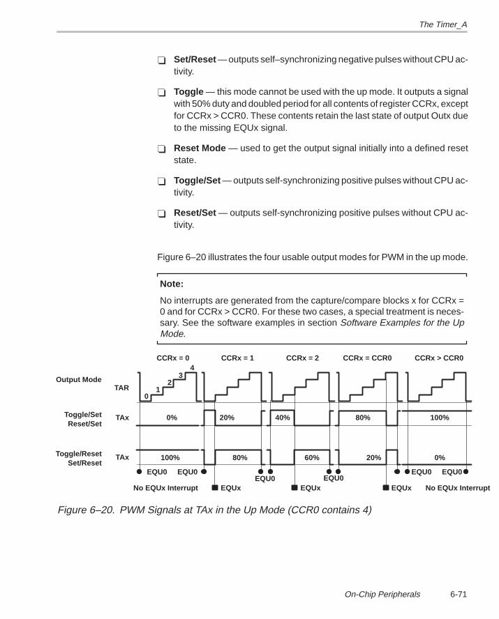
The Timer_A
6-71On-Chip Peripherals
Set/Reset — outputs self–synchronizing negative pulses without CPU ac-tivity.
Toggle — this mode cannot be used with the up mode. It outputs a signalwith 50% duty and doubled period for all contents of register CCRx, exceptfor CCRx > CCR0. These contents retain the last state of output Outx dueto the missing EQUx signal.
Reset Mode — used to get the output signal initially into a defined resetstate.
Toggle/Set — outputs self-synchronizing positive pulses without CPU ac-tivity.
Reset/Set — outputs self-synchronizing positive pulses without CPU ac-tivity.
Figure 6–20 illustrates the four usable output modes for PWM in the up mode.
Note:
No interrupts are generated from the capture/compare blocks x for CCRx =0 and for CCRx > CCR0. For these two cases, a special treatment is neces-sary. See the software examples in section Software Examples for the UpMode.
No EQUx Interrupt
01
23
4CCRx = 0 CCRx = 1 CCRx = 2 CCRx = CCR0 CCRx > CCR0
TAR
TAx
TAx
0% 20% 40% 80% 100%
0%20%60%80%100%
EQU0 EQU0EQU0 EQU0
EQU0 EQU0
EQUx EQUx EQUx No EQUx Interrupt
Output Mode
Toggle/SetReset/Set
Toggle/ResetSet/Reset
Figure 6–20. PWM Signals at TAx in the Up Mode (CCR0 contains 4)
The Timer_A
6-72
6.3.5.4 Pulse Width Modulation in the Up/Down Mode
The output modes and their usability for the up/down mode are listed below.
Set Mode — used to get the output signal initially into a defined set state.
Toggle/Reset — outputs self-synchronizing positive pulses without CPUactivity. The Timer_A hardware can produce all of the theoretically pos-sible nCCR0+1 states. But special treatment is necessary if register CCRxcontains 0. Then the output signal Outx toggles only once per period,which means the output shows a 50% duty and not 0%. See figure 6–21.
Set/Reset — cannot be used with up/down mode.
Toggle — should not be used with the up/down mode.
Reset Mode — used to get the output signal initially into a defined resetstate.
Toggle/Set — outputs self-synchronizing negative pulses without CPUactivity. See Toggle/Reset, above, for restrictions.
Reset/Set — cannot be used with up/down mode.
As figure 6–21 also shows, the missing PWM values of 0% for toggle/reset and100% for toggle/set can be output if CCRx contains a greater value thanCCR0.
Example 6–29. Pulse Width Modulation in the Up/Down Mode
The checking software for output mode toggle/reset is shown. All PWM valuesfrom 1 to nCCR0 are valid. The value 0 is emulated by a number greater thannCCR0. R5 contains the calculated PWM value.
; PWM value in R5 is checked to be in limits 1 to nCCR0
;
CMP R5,&CCR0 ; PWM value =< nCCR0?
JHS L$1 ; Yes, proceed
MOV &CCR0,R5 ; No, upper limit (100% PWM)
;
; If 0% PWM is needed: 0FFFFh to R5
;
L$1 TST R5 ; Zero value?
JNZ L$2 ; No, proceed
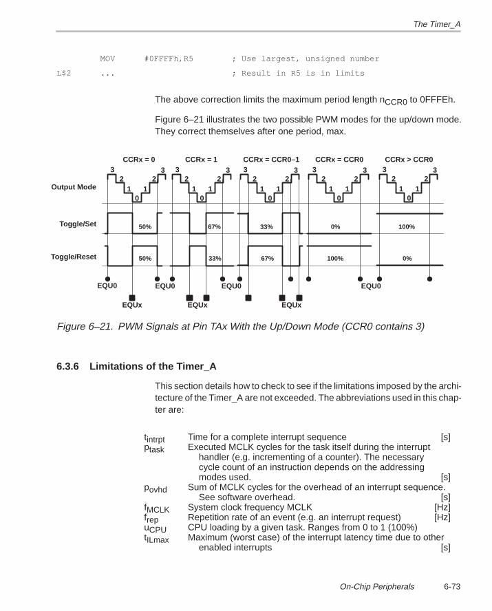
The Timer_A
6-73On-Chip Peripherals
MOV #0FFFFh,R5 ; Use largest, unsigned number
L$2 ... ; Result in R5 is in limits
The above correction limits the maximum period length nCCR0 to 0FFFEh.
Figure 6–21 illustrates the two possible PWM modes for the up/down mode.They correct themselves after one period, max.
EQUx
01 1
2 23 3
01 1
2 23 3
01 1
2 23 3
01 1
2 23 3
01 1
2 23 3
CCRx = 0 CCRx = 1 CCRx = CCR0–1 CCRx = CCR0 CCRx > CCR0
50% 67% 33% 0% 100%
50% 67%33% 0%100%
EQU0 EQU0 EQU0 EQU0
EQUx EQUx
Output Mode
Toggle/Set
Toggle/Reset
Figure 6–21. PWM Signals at Pin TAx With the Up/Down Mode (CCR0 contains 3)
6.3.6 Limitations of the Timer_A
This section details how to check to see if the limitations imposed by the archi-tecture of the Timer_A are not exceeded. The abbreviations used in this chap-ter are:
tintrpt Time for a complete interrupt sequence [s]ptask Executed MCLK cycles for the task itself during the interrupt
handler (e.g. incrementing of a counter). The necessary cycle count of an instruction depends on the addressing modes used. [s]
povhd Sum of MCLK cycles for the overhead of an interrupt sequence. See software overhead. [s]
fMCLK System clock frequency MCLK [Hz]frep Repetition rate of an event (e.g. an interrupt request) [Hz]uCPU CPU loading by a given task. Ranges from 0 to 1 (100%)tILmax Maximum (worst case) of the interrupt latency time due to other
enabled interrupts [s]
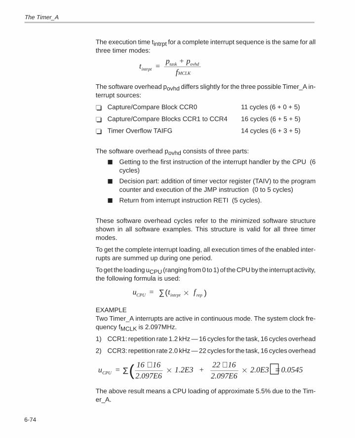
The Timer_A
6-74
The execution time tintrpt for a complete interrupt sequence is the same for allthree timer modes:
t =p + p
fintrpt task ovhd
MCLK
The software overhead povhd differs slightly for the three possible Timer_A in-terrupt sources:
Capture/Compare Block CCR0 11 cycles (6 + 0 + 5)
Capture/Compare Blocks CCR1 to CCR4 16 cycles (6 + 5 + 5)
Timer Overflow TAIFG 14 cycles (6 + 3 + 5)
The software overhead povhd consists of three parts:
Getting to the first instruction of the interrupt handler by the CPU (6cycles)
Decision part: addition of timer vector register (TAIV) to the programcounter and execution of the JMP instruction (0 to 5 cycles)
Return from interrupt instruction RETI (5 cycles).
These software overhead cycles refer to the minimized software structureshown in all software examples. This structure is valid for all three timermodes.
To get the complete interrupt loading, all execution times of the enabled inter-rupts are summed up during one period.
To get the loading uCPU (ranging from 0 to 1) of the CPU by the interrupt activity,the following formula is used:
u =
t
f CPU intrpt rep∑( )
EXAMPLETwo Timer_A interrupts are active in continuous mode. The system clock fre-quency fMCLK is 2.097MHz.
1) CCR1: repetition rate 1.2 kHz — 16 cycles for the task, 16 cycles overhead
2) CCR3: repetition rate 2.0 kHz — 22 cycles for the task, 16 cycles overhead
u =
16 16
2.097E6 1.2E3 +
22 16
2.097E6 2.0E3 0.0545CPU
+
+Σ =( )
The above result means a CPU loading of approximate 5.5% due to the Tim-er_A.
The Timer_A
6-75On-Chip Peripherals
6.3.6.1 Limitations of the Continuous Mode
Interrupt Handling — the shortest repetitive time interval, tCRmin, betweentwo similar timer events using a compare register CCRx is:
t = t +p p
fCRmin ILmax
taskmax OVHD
MCLK
+
The shortest repetitive time interval, tCLmin, between two interrupt events usinga capture register CCRx is:
t = t +p p
fCLmin ILmax
taskmax OVHD
MCLK
+
The time, ttaskmax, for the capture mode is the time to read the captured timevalue and to test and reset the COV flag.
Software Overhead — the interrupt loading ranges from one interrupt re-quest (request from CCIFGx) up to six interrupt requests (requests fromTAIFG, CCIFG0, and all CCIFGx flags).
Output Units — for relatively high PWM repetition rates special treatmentmay be necessary for PWM duties near the limits 0% and 100%.
Maximum Resolution:
r =k
f CLK
where: r is equivalent to the period of the timer clock
6.3.6.2 Limitations of the Up Mode
Interrupt Handling — the worst case sum of all the execution times need-ed by all interrupts during one timer period must be less than the timer peri-od (defined by the period register, CCR0). Otherwise, the interrupt part willloose the synchronization due to overload.
This means:
( )( )
n +1 k
f>
1
fp pCCR0
CLK
MCLKtaskmax ovhd
t 0
tn +1 k
fCLKCCR0
+
=
=
∑
Software Overhead — the overhead ranges from zero (PWM is outputautomatically after the loading of the timer registers), up to six interrupt re-quests per period (interrupt requests from TAIFG, CCIFG0, and from allCCIFGx flags).
The Timer_A
6-76
Output Units — all values ranging from 0% to 100% for pulse width modu-lation (PWM) are possible without special treatment.
Maximum Resolution — for a given repetition rate, frep, of the timer out-put, a maximum resolution, r, is possible:
r =f
fn + 1
MCLKmax
repCCR0=
This means that with a maximum system clock frequency of 4 MHz and a repe-tition rate of 20 kHz for a PWM output — due to audibility — a resolution of 200steps is possible (0.5%).
6.3.6.3 Limitations of the Up/Down Mode
Interrupt Handling — the worst case sum of all the execution times need-ed by all interrupts during one timer period must be less than the doubledperiod defined by the period register CCR0. Otherwise, the interrupt partwill loose the synchronization due to overload.
2 n k
f>
1
fp pCCR0
CLK
MCLKtaskmax ovhd
t 0
t2 n k
fCLKCCR0
+
=
=
Σ
Software Overhead — the overhead ranges from zero (PWM is outputautomatically after the loading of the timer registers) up to ten interrupt re-quests per full period (interrupt requests from TAIFG, CCIFG0, and 2 inter-rupts per CCIFGx).
Output Units — the pulse width zero (0%) needs a special software treat-ment. Without this, the hardware outputs a 50% pulse width instead. Thisbehavior will be changed in future versions.
Maximum Resolution — for a given repetition rate, frep, of the timer out-put, a maximum resolution, r, is possible:
r =f
2 fn
MCLKmax
repCCR0
=
This means that with a maximum system clock frequency of 4 MHz and a repe-tition rate of 20 kHz for a PWM output — due to audibility — a resolution of 100steps is possible (1.0%). The resolution of the up/down mode is less than it isin the up mode. With the same timer clock, the up mode delivers (nCCR0+2)different pulse widths and the up/down mode delivers (nCCR0+1) differentpulse widths — but with a reduced output frequency due to the up and downcounting. This means the resolution is approximately one half the resolutionof the up mode.
The Timer_A
6-77On-Chip Peripherals
6.3.7 Miscellaneous
The frequencies generated by the Timer_A may also be used as the timebasefor other tasks if defined appropriately:
Serial Communication Interface (SCI) — If for an MSP430, a secondUART (RS232) is needed, then with a timer frequency of 19.2 kHz (8 × 2.4kHz) a software UART with 2400 baud can be implemented. This softwareUART uses the interrupt generated with the reaching of the content of theperiod register, CCR0 (CCIFG0 = 1), for the synchronization of the UARTsoftware.
Timing Intervals for Control — These important control values can alsobe derived from the timer frequency by an appropriate software prescal-ing. This timing may be used for calculations, keyboard scan, measure-ment starts, etc.
6.3.8 Software Examples for the Continuous Mode
This section shows several proven application examples for the Timer_A.Whenever possible, the abbreviations used in the Architecture Guide andModule Library are used.
All examples use the value FLLMPY — it defines the master clock frequencyfMCLK.
f =
FLLMPY fMCLK crystal
If this frequency, fMCLK, is too high for the application (for example: it causesvalues for the timer registers exceeding the 16-bit range), then the input dividerof the Timer_A may be used. It allows a prescaling by 1, 2, 4, and 8. For pres-caling by 2, the definitions at the start of each example are simply changed to:
FLLMPY .equ 100 ; FLL multiplier for 3.2768MHz
TCLK .equ FLLMPY*32768/2 ; Timer Clock = 1.6384MHz
;
; The Input Divider D2 is used to get MCLK/2 for the TCLK
;
MOV #ISMCLK+D2+TAIE+CLR,&TACTL ; Use D2 divider
Note:
The software and hardware examples shown here are specific to theMSP430C/P33x family. Other MSP430 family members may use other I/Oports and addresses for the Timer_A registers and signals. The program-ming principles are unchanged — only address definitions may need to bemodified.
The Timer_A
6-78
The software examples were tested with the software simulator and anEVK330 evaluation kit.
For all examples, the loading of the CPU is given. The terms used are definedbelow:
Overhead — the sum of necessary CPU cycles to get to the first instruc-tion of the interrupt handler and to get back to the interrupted program se-quence (wakeup cycles, storing of PC and SR, determination of the inter-rupt source, and RETI cycles)
Task — the CPU cycles used for the interrupt task: incrementing of acounter, calculations, etc.
Advantages of the Continuous Mode:
Five complete, independent timings and captures are possible.Any mix is possible
No dominance by a period register
Disadvantages of the Continuous Mode:
Software update necessary for the capture/compare registers toallow continuous run
Speed limit due to the necessary software update
6.3.8.1 Common Initialization Subroutine
The initialization subroutine INITSR is used by all examples. It executes thefollowing tasks:
A check is made if the initialization subroutine is called after applying thesupply voltage (the RAM word INITKEY does not contain 0F05Ah) or afteran external reset or watchdog reset (INITKEY contains 0F05Ah). If the ap-plying of the supply voltage caused the reset, then the RAM is cleared andthe INITKEY is initialized to 0F05Ah.
The system clock oscillator is programmed with the FLL multiplier N. Thisdefines the MCLK frequency fMCLK. See above.
The correct DCO switch FN_x for the chosen MCLK frequency (fMCLK) isset. These switches allow the system clock oscillator to operate with oneof the center taps of the digitally controlled oscillator (DCO). This way theDCO operates always in a nonsaturated condition.
The Timer_A
6-79On-Chip Peripherals
A delay of 30000 clock cycles is included to give the oscillator time to settleat the correct frequency.
; Common Initialization Subroutine
; Check the INITKEY value first:
; If value is 0F05Ah: a reset occurred, RAM is not cleared
; otherwise Vcc was switched on: complete initialization
;
INITSR CMP #0F05Ah,INITKEY ; PUC or POR?
JEQ IN0 ; Key is ok, continue program
CALL #RAMCLR ; Restart completely: clear RAM
MOV #0F05Ah,INITKEY ; Define “initialized state”
;
IN0 MOV.B #FLLMPY–1,&SCFQCTL ; Define MCLK frequency
;
.if FLLMPY < 48 ; Use the right DCO current:
MOV.B #0,&SCFI0 ; MCLK < 1.5MHz: FN_x off
.else
.if FLLMPY < 80 ; 1.5MHz < MCLK < 2.5MHz?
MOV.B #FN_2,&SCFI0 ; Yes, FN_2 on
.else ;
.if FLLMPY < 112 ; 2.5MHz < MCLK < 3.5MHz?
MOV.B #FN_3,&SCFI0 ; Yes, FN_3 on
.else
MOV.B #FN_4,&SCFI0 ; MCLK > 3.5MHz: FN_4 on
.endif
.endif
.endif
;
MOV #10000,R5 ; Allow the FLL to settle
IN1 DEC R5 ; at the correct DCO tap
JNZ IN1 ; during 30000 cycles
RET ; Return from initialization
;
; Subroutine for the clearing of the RAM block
;
.bss INITKEY,2,0200h ; 0F05Ah: initialized state
The Timer_A
6-80
RAMSTRT .equ 0200h ; Start of RAM
RAMEND .equ 05FEh ; Highest RAM address (33x)
;
RAMCLR CLR R5 ; Prepare index register
RCL CLR RAMSTRT(R5) ; 1st RAM address
INCD R5 ; Next word address
CMP #RAMEND–RAMSTRT+2,R5 ; RAM cleared?
JLO RCL ; No, once more
RET ; Yes, return
6.3.8.2 Generation of Five Independent Timings
The software example explains the use of the timer vector register (TAIV) andthe overhead of the interrupt handling. It refers to figure 6–22. The interrupthandler of timer block x adds the appropriate time interval, ∆t, to the corre-sponding compare register, CCRx. The MCLK frequency (3.2768 MHz) isused also for the timer clock. The five timings generated are defined as follows(see also Table 6–15):
Capture/Compare Block 0 — a positive pulse with a 10 kHz repetitionrate is generated and output at terminal TA0. The pulse is reset by the in-terrupt handler of timer block 0. The pulse is used for the precise triggeringof an external analog-to-digital converter. The error of the repetition ratedue to the MCLK frequency used is –0.097%
Capture/Compare Block 1 — an internal interrupt with variable timing isgenerated. The cycle count is stored in the RAM word TIM1REP. The max-imum value of this cycle count is 0FFFFh, the minimum value is 1000. Theoutput terminal TA1 is not used.
Capture/Compare Block 2 — a square wave with a fixed 1 kHz repetitionrate is generated and output at terminal TA2. The pulse is used as a refer-ence for external devices. The error of the repetition rate due to the MCLKfrequency used is –244 ppm.
Capture/Compare Block 3 — an internal interrupt with a fixed 200 Hzrepetition rate is generated. The output terminal TA3 is not used. The errorof the repetition rate due to the MCLK frequency used is –244 ppm.
Capture/Compare Block 4 — a square wave with a variable output fre-quency is generated and output at terminal TA4. The output frequencystarts at 409.6 Hz (4000 cycles) and increases up to 1638.4 Hz (1000cycles). The square wave is used for the control of an external DC/DC con-verter.
The Timer_A
6-81On-Chip Peripherals
The formula for calculating the value, ∆n, that is added to the timer register(TAR) depends on the application. For the internal interrupts (CCR1 and CCR3in the example) and the external pulse (CCR0 in the example), ∆n is:
∆ ∆n
t f
k
CLK=
For the external-generated square wave signals with the frequency fext(CCR2 and CCR4 in the example) ∆n is:
∆nf
k 2 f
CLK
ext=
Where: fCLK Frequency at the input of the input divider [Hz]fext Frequency to be output with toggle mode [Hz]k Input divider constant (1, 2, 4, 8)∆t Time interval to be generated [s]
Table 6–15. Short Description of the five independent Timings
CAPTURE/COMPARE BLOCK
TIME INTERVAL (TIMERCLOCK CYCLES)
SIGNAL TYPE COMMENT
0 328 External Pulse: 10kHz ADC repetition rate
1 Variable Internal Cycle count stored in TIM1REP (min 1000)
2 1638 External 1 kHz @ 3.2768 MHz (error: –244 ppm)
3 16384 Internal Fixed frequency 200 Hz
4 4000 to 1000 External Increasing frequency for ext. DC/DC converter
The software example is written for an fMCLK of 3.276 MHz. If other frequen-cies are used, the time intervals need to be adapted. Subsequent examplesshow methods of writing frequency-independent software. Figure 6–22 illus-trates the five timings described above:
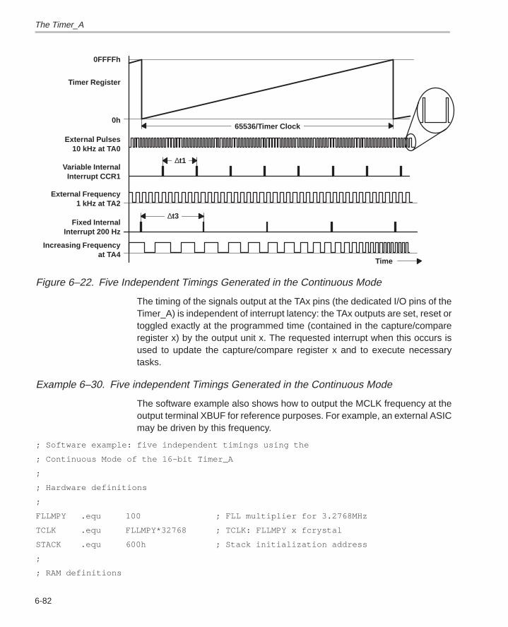
The Timer_A
6-82
∆t1
∆t3
65536/Timer Clock
Time
0FFFFh
Timer Register
0h
External Pulses10 kHz at TA0
Variable InternalInterrupt CCR1
External Frequency1 kHz at TA2
Fixed InternalInterrupt 200 Hz
Increasing Frequencyat TA4
Figure 6–22. Five Independent Timings Generated in the Continuous Mode
The timing of the signals output at the TAx pins (the dedicated I/O pins of theTimer_A) is independent of interrupt latency: the TAx outputs are set, reset ortoggled exactly at the programmed time (contained in the capture/compareregister x) by the output unit x. The requested interrupt when this occurs isused to update the capture/compare register x and to execute necessarytasks.
Example 6–30. Five independent Timings Generated in the Continuous Mode
The software example also shows how to output the MCLK frequency at theoutput terminal XBUF for reference purposes. For example, an external ASICmay be driven by this frequency.
; Software example: five independent timings using the
; Continuous Mode of the 16–bit Timer_A
;
; Hardware definitions
;
FLLMPY .equ 100 ; FLL multiplier for 3.2768MHz
TCLK .equ FLLMPY*32768 ; TCLK: FLLMPY x fcrystal
STACK .equ 600h ; Stack initialization address
;
; RAM definitions
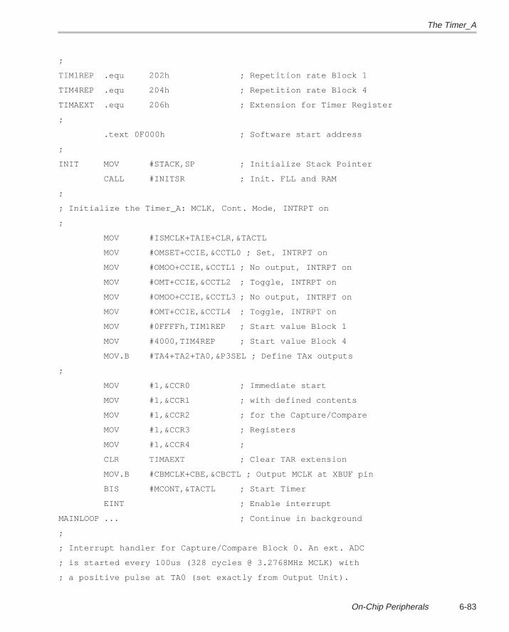
The Timer_A
6-83On-Chip Peripherals
;
TIM1REP .equ 202h ; Repetition rate Block 1
TIM4REP .equ 204h ; Repetition rate Block 4
TIMAEXT .equ 206h ; Extension for Timer Register
;
.text 0F000h ; Software start address
;
INIT MOV #STACK,SP ; Initialize Stack Pointer
CALL #INITSR ; Init. FLL and RAM
;
; Initialize the Timer_A: MCLK, Cont. Mode, INTRPT on
;
MOV #ISMCLK+TAIE+CLR,&TACTL
MOV #OMSET+CCIE,&CCTL0 ; Set, INTRPT on
MOV #OMOO+CCIE,&CCTL1 ; No output, INTRPT on
MOV #OMT+CCIE,&CCTL2 ; Toggle, INTRPT on
MOV #OMOO+CCIE,&CCTL3 ; No output, INTRPT on
MOV #OMT+CCIE,&CCTL4 ; Toggle, INTRPT on
MOV #0FFFFh,TIM1REP ; Start value Block 1
MOV #4000,TIM4REP ; Start value Block 4
MOV.B #TA4+TA2+TA0,&P3SEL ; Define TAx outputs
;
MOV #1,&CCR0 ; Immediate start
MOV #1,&CCR1 ; with defined contents
MOV #1,&CCR2 ; for the Capture/Compare
MOV #1,&CCR3 ; Registers
MOV #1,&CCR4 ;
CLR TIMAEXT ; Clear TAR extension
MOV.B #CBMCLK+CBE,&CBCTL ; Output MCLK at XBUF pin
BIS #MCONT,&TACTL ; Start Timer
EINT ; Enable interrupt
MAINLOOP ... ; Continue in background
;
; Interrupt handler for Capture/Compare Block 0. An ext. ADC
; is started every 100us (328 cycles @ 3.2768MHz MCLK) with
; a positive pulse at TA0 (set exactly from Output Unit).
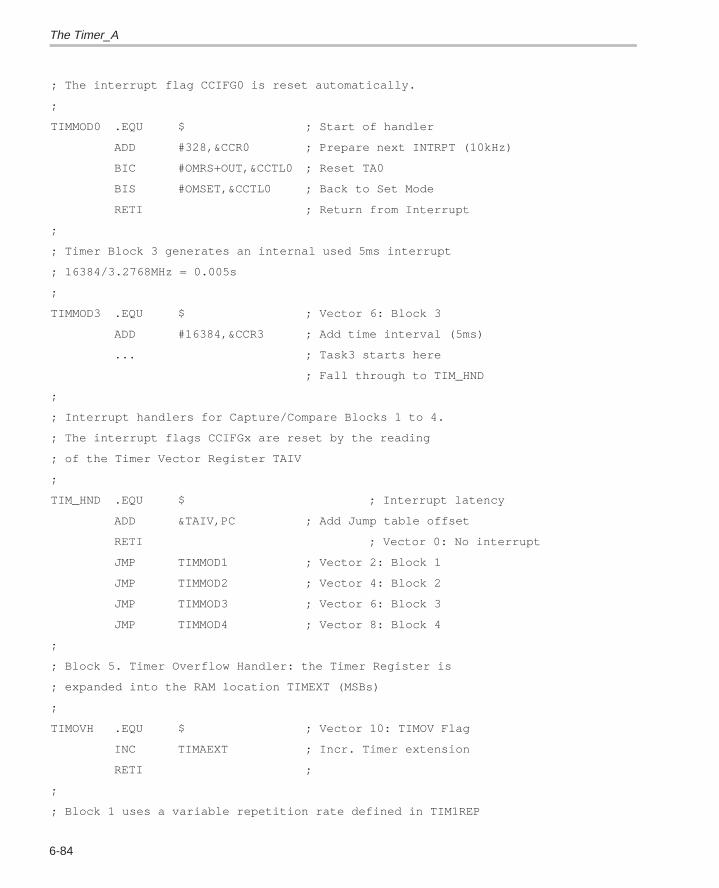
The Timer_A
6-84
; The interrupt flag CCIFG0 is reset automatically.
;
TIMMOD0 .EQU $ ; Start of handler
ADD #328,&CCR0 ; Prepare next INTRPT (10kHz)
BIC #OMRS+OUT,&CCTL0 ; Reset TA0
BIS #OMSET,&CCTL0 ; Back to Set Mode
RETI ; Return from Interrupt
;
; Timer Block 3 generates an internal used 5ms interrupt
; 16384/3.2768MHz = 0.005s
;
TIMMOD3 .EQU $ ; Vector 6: Block 3
ADD #16384,&CCR3 ; Add time interval (5ms)
... ; Task3 starts here
; Fall through to TIM_HND
;
; Interrupt handlers for Capture/Compare Blocks 1 to 4.
; The interrupt flags CCIFGx are reset by the reading
; of the Timer Vector Register TAIV
;
TIM_HND .EQU $ ; Interrupt latency
ADD &TAIV,PC ; Add Jump table offset
RETI ; Vector 0: No interrupt
JMP TIMMOD1 ; Vector 2: Block 1
JMP TIMMOD2 ; Vector 4: Block 2
JMP TIMMOD3 ; Vector 6: Block 3
JMP TIMMOD4 ; Vector 8: Block 4
;
; Block 5. Timer Overflow Handler: the Timer Register is
; expanded into the RAM location TIMEXT (MSBs)
;
TIMOVH .EQU $ ; Vector 10: TIMOV Flag
INC TIMAEXT ; Incr. Timer extension
RETI ;
;
; Block 1 uses a variable repetition rate defined in TIM1REP
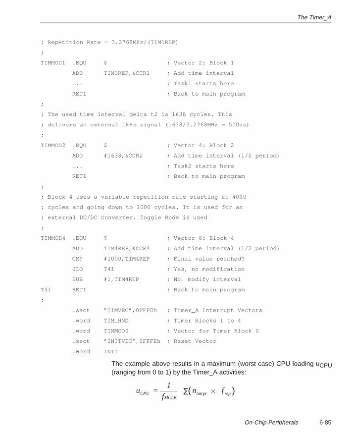
The Timer_A
6-85On-Chip Peripherals
; Repetition Rate = 3.2768MHz/(TIM1REP)
;
TIMMOD1 .EQU $ ; Vector 2: Block 1
ADD TIM1REP,&CCR1 ; Add time interval
... ; Task1 starts here
RETI ; Back to main program
;
; The used time interval delta t2 is 1638 cycles. This
; delivers an external 1kHz signal (1638/3.2768MHz = 500us)
;
TIMMOD2 .EQU $ ; Vector 4: Block 2
ADD #1638,&CCR2 ; Add time interval (1/2 period)
... ; Task2 starts here
RETI ; Back to main program
;
; Block 4 uses a variable repetition rate starting at 4000
; cycles and going down to 1000 cycles. It is used for an
; external DC/DC converter. Toggle Mode is used
;
TIMMOD4 .EQU $ ; Vector 8: Block 4
ADD TIM4REP,&CCR4 ; Add time interval (1/2 period)
CMP #1000,TIM4REP ; Final value reached?
JLO T41 ; Yes, no modification
SUB #1,TIM4REP ; No, modify interval
T41 RETI ; Back to main program
;
.sect ”TIMVEC”,0FFF0h ; Timer_A Interrupt Vectors
.word TIM_HND ; Timer Blocks 1 to 4
.word TIMMOD0 ; Vector for Timer Block 0
.sect ”INITVEC”,0FFFEh ; Reset Vector
.word INIT
The example above results in a maximum (worst case) CPU loading uCPU(ranging from 0 to 1) by the Timer_A activities:
u =1
f n
f CPU
MCLKintrpt repΣ( )
The Timer_A
6-86
Where: fMCLK Frequency of the DCO [Hz]nintrpt Number of cycles executed by the interrupt handlerfrep Repetition rate of the interrupt handler [Hz]
CCR0 — repetition rate 10 kHz 15 cycles for the task, 11 cycles overhead 26 cyclesCCR1 — repetition rate 3.27 kHz 6 cycles for the task, 16 cycles overhead 22 cyclesCCR2 — repetition rate 2.0 kHz 5 cycles for the task, 16 cycles overhead 21 cyclesCCR3 — repetition rate 0.2 kHz 5 cycles for the task, 20 cycles overhead 25 cyclesCCR4 — repetition rate 3.27 kHz 17 cycles for the task, 16 cycles overhead 33 cyclesTIMOV — repetition rate 50 Hz 4 cycles for the task, 14 cycles overhead 18 cycles
u =26 10 22 3276.8 21 2000 25 200 33 3276.8 18 50
3.2768 100.15CPU
4
6 + + + + +
=
The result above means a CPU loading of approximative 15% due to the Tim-er_A (the tasks of the timer blocks 1, 2, and 3 are not included).
6.3.8.3 DTMF Generation
Modern telephones use dual-tone multi-frequency (DTMF) signaling for thedialing process. A pair of frequencies defines each of the 16 possible numbersand characters, and are selected from the matrix shown in Table 6–16. TwoTimer_A outputs (TA2 and TA1) are used to generate the frequency pair. Exter-nal filters clean up the waveform and mix the two frequencies. The length ofthe output signals is normally 65 ms to 100 ms.
Table 6–16. DTMF Frequency Pairs
FREQUENCY 1209 Hz 1336 Hz 1477 Hz 1633 Hz
697 Hz 1 2 3 A
770 Hz 4 5 6 B
852 Hz 7 8 9 C
941 Hz * 0 # D
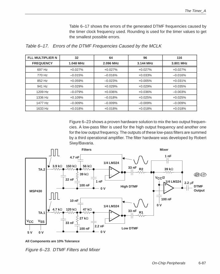
The Timer_A
6-87On-Chip Peripherals
Table 6–17 shows the errors of the generated DTMF frequencies caused bythe timer clock frequency used. Rounding is used for the timer values to getthe smallest possible errors.
Table 6–17. Errors of the DTMF Frequencies Caused by the MCLK
FLL MULTIPLIER N 32 64 96 116
FREQUENCY 1.048 MHz 2.096 MHz 3.144 MHz 3.801 MHz
697 Hz +0.027% +0.027% +0.027% +0.027%
770 Hz –0.015% –0.016% +0.033% –0.016%
852 Hz +0.059% –0.023% +0.005% +0.031%
941 Hz +0.029% +0.029% +0.029% +0.035%
1209 Hz –0.079% +0.036% +0.036% –0.003%
1336 Hz +0.109% –0.018% +0.025% +0.025%
1477 Hz –0.009% –0.009% –0.009% –0.009%
1633 Hz +0.018% +0.018% +0.018% +0.018%
Figure 6–23 shows a proven hardware solution to mix the two output frequen-cies. A low-pass filter is used for the high output frequency and another onefor the low output frequency. The outputs of these low-pass filters are summedby a third operational amplifier. The filter hardware was developed by RobertSiwy/Bavaria.
3.9 kΩ
22 nF
150 kΩ
4.7 nF
100 nF1 nF
56 kΩ
_+
0 V
33 nF R2
_+
1/4 LM324
1/4 LM324VCC/2
39 kΩ
Filters Mixer
1 nF
2.2 µFDTMFOutput
4.7 kΩ
33 nF
120 kΩ
10 nF
100 nF
47 kΩ
_+
0 V
33 nF R1
1/4 LM324
100 nF
0 V
39 kΩ
27 kΩ
2.2 nF
TA.2
TA.1
VCC VSS
5 V 0 VLow DTMF
All Components are 10% Tolerance
ÎÎÎÎÎÎÎÎÎÎÎÎÎÎ
MSP430High DTMF
Figure 6–23. DTMF Filters and Mixer
The Timer_A
6-88
The two low-pass filters and the mixer are shown in figure 6–23. The symmetri-cal output pulses at TA2 and TA1 bias the filter amplifiers with VCC/2.
The component values are valid for the specification of the German public tele-phone system. The positive supply voltage for the operational amplifiers isswitched by a TP output or an O output.
With the two resistors R1 and R2, the filters can be adapted to the specifica-tions of the telephone systems in other countries. These resistors define thehigh and low DTMF frequency parts of the DTMF output signal.
Example 6–31. DTMF Software
The following DTMF software routine is independent of the timer clock fre-quency used. During the assembly, the new timer values are calculated. Thelength of the DTMF output signal is defined with the value DL — its value isin milliseconds.
; Hardware definitions
;
FLLMPY .equ 32 ; FLL multiplier for 1.048MHz
TCLK .equ FLLMPY*32768 ; TCLK: FLLMPY x fcrystal
DL .equ 82 ; DTMF signal length (65..100ms)
STACK .equ 600h ; Stack initialization address
;
; RAM definitions
;
STDTMF .equ 202h ; Status Hi and Lo frequency
TIMAEXT .equ 204 ; Timer Register Extension
LENGTH .equ 206h ; DTMF length counter
;
.text 0F000h ; Software start address
;
; Initialize the Timer_A: MCLK, Cont. Mode, INTRPT enabled
; Prepare Timer_A Output Units, MCLK = 1.048MHz (autom.)
;
INIT MOV #STACK,SP ; Initialize Stack Pointer SP
CALL #INITSR ; Init. FLL and RAM
MOV #ISMCLK+TAIE+CLR,&TACTL ; Define Timer
MOV.B #TA2+TA1,&P3SEL ; TA2 and TA1 at P3.5/4
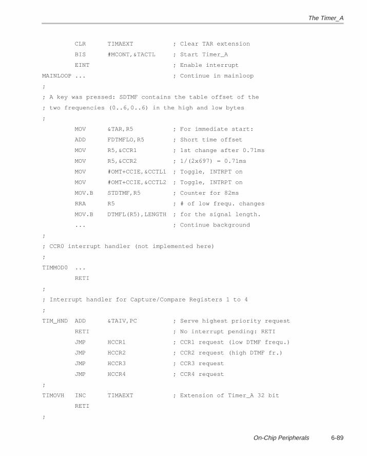
The Timer_A
6-89On-Chip Peripherals
CLR TIMAEXT ; Clear TAR extension
BIS #MCONT,&TACTL ; Start Timer_A
EINT ; Enable interrupt
MAINLOOP ... ; Continue in mainloop
;
; A key was pressed: SDTMF contains the table offset of the
; two frequencies (0..6,0..6) in the high and low bytes
;
MOV &TAR,R5 ; For immediate start:
ADD FDTMFLO,R5 ; Short time offset
MOV R5,&CCR1 ; 1st change after 0.71ms
MOV R5,&CCR2 ; 1/(2x697) = 0.71ms
MOV #OMT+CCIE,&CCTL1 ; Toggle, INTRPT on
MOV #OMT+CCIE,&CCTL2 ; Toggle, INTRPT on
MOV.B STDTMF,R5 ; Counter for 82ms
RRA R5 ; # of low frequ. changes
MOV.B DTMFL(R5),LENGTH ; for the signal length.
... ; Continue background
;
; CCR0 interrupt handler (not implemented here)
;
TIMMOD0 ...
RETI
;
; Interrupt handler for Capture/Compare Registers 1 to 4
;
TIM_HND ADD &TAIV,PC ; Serve highest priority request
RETI ; No interrupt pending: RETI
JMP HCCR1 ; CCR1 request (low DTMF frequ.)
JMP HCCR2 ; CCR2 request (high DTMF fr.)
JMP HCCR3 ; CCR3 request
JMP HCCR4 ; CCR4 request
;
TIMOVH INC TIMAEXT ; Extension of Timer_A 32 bit
RETI
;
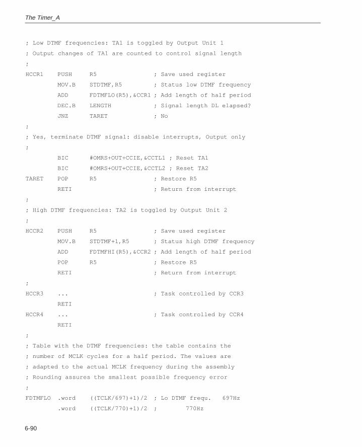
The Timer_A
6-90
; Low DTMF frequencies: TA1 is toggled by Output Unit 1
; Output changes of TA1 are counted to control signal length
;
HCCR1 PUSH R5 ; Save used register
MOV.B STDTMF,R5 ; Status low DTMF frequency
ADD FDTMFLO(R5),&CCR1 ; Add length of half period
DEC.B LENGTH ; Signal length DL elapsed?
JNZ TARET ; No
;
; Yes, terminate DTMF signal: disable interrupts, Output only
;
BIC #OMRS+OUT+CCIE,&CCTL1 ; Reset TA1
BIC #OMRS+OUT+CCIE,&CCTL2 ; Reset TA2
TARET POP R5 ; Restore R5
RETI ; Return from interrupt
;
; High DTMF frequencies: TA2 is toggled by Output Unit 2
;
HCCR2 PUSH R5 ; Save used register
MOV.B STDTMF+1,R5 ; Status high DTMF frequency
ADD FDTMFHI(R5),&CCR2 ; Add length of half period
POP R5 ; Restore R5
RETI ; Return from interrupt
;
HCCR3 ... ; Task controlled by CCR3
RETI
HCCR4 ... ; Task controlled by CCR4
RETI
;
; Table with the DTMF frequencies: the table contains the
; number of MCLK cycles for a half period. The values are
; adapted to the actual MCLK frequency during the assembly
; Rounding assures the smallest possible frequency error
;
FDTMFLO .word ((TCLK/697)+1)/2 ; Lo DTMF frequ. 697Hz
.word ((TCLK/770)+1)/2 ; 770Hz
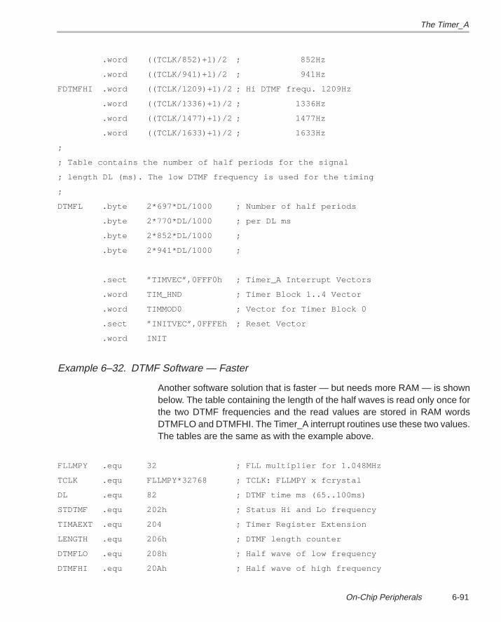
The Timer_A
6-91On-Chip Peripherals
.word ((TCLK/852)+1)/2 ; 852Hz
.word ((TCLK/941)+1)/2 ; 941Hz
FDTMFHI .word ((TCLK/1209)+1)/2 ; Hi DTMF frequ. 1209Hz
.word ((TCLK/1336)+1)/2 ; 1336Hz
.word ((TCLK/1477)+1)/2 ; 1477Hz
.word ((TCLK/1633)+1)/2 ; 1633Hz
;
; Table contains the number of half periods for the signal
; length DL (ms). The low DTMF frequency is used for the timing
;
DTMFL .byte 2*697*DL/1000 ; Number of half periods
.byte 2*770*DL/1000 ; per DL ms
.byte 2*852*DL/1000 ;
.byte 2*941*DL/1000 ;
.sect ”TIMVEC”,0FFF0h ; Timer_A Interrupt Vectors
.word TIM_HND ; Timer Block 1..4 Vector
.word TIMMOD0 ; Vector for Timer Block 0
.sect ”INITVEC”,0FFFEh ; Reset Vector
.word INIT
Example 6–32. DTMF Software — Faster
Another software solution that is faster — but needs more RAM — is shownbelow. The table containing the length of the half waves is read only once forthe two DTMF frequencies and the read values are stored in RAM wordsDTMFLO and DTMFHI. The Timer_A interrupt routines use these two values.The tables are the same as with the example above.
FLLMPY .equ 32 ; FLL multiplier for 1.048MHz
TCLK .equ FLLMPY*32768 ; TCLK: FLLMPY x fcrystal
DL .equ 82 ; DTMF time ms (65..100ms)
STDTMF .equ 202h ; Status Hi and Lo frequency
TIMAEXT .equ 204 ; Timer Register Extension
LENGTH .equ 206h ; DTMF length counter
DTMFLO .equ 208h ; Half wave of low frequency
DTMFHI .equ 20Ah ; Half wave of high frequency
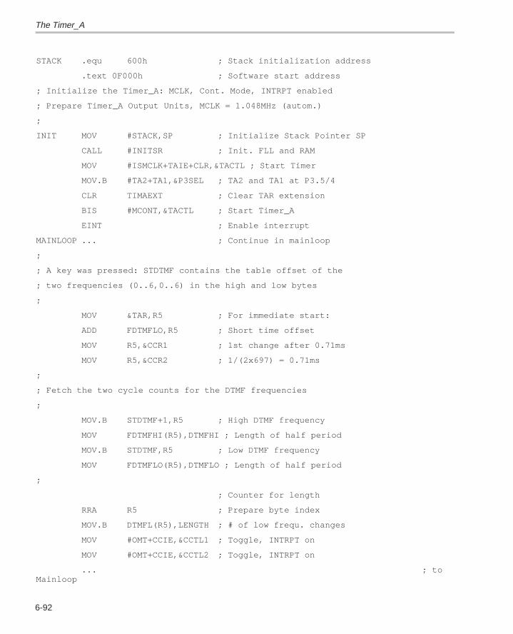
The Timer_A
6-92
STACK .equ 600h ; Stack initialization address
.text 0F000h ; Software start address
; Initialize the Timer_A: MCLK, Cont. Mode, INTRPT enabled
; Prepare Timer_A Output Units, MCLK = 1.048MHz (autom.)
;
INIT MOV #STACK,SP ; Initialize Stack Pointer SP
CALL #INITSR ; Init. FLL and RAM
MOV #ISMCLK+TAIE+CLR,&TACTL ; Start Timer
MOV.B #TA2+TA1,&P3SEL ; TA2 and TA1 at P3.5/4
CLR TIMAEXT ; Clear TAR extension
BIS #MCONT,&TACTL ; Start Timer_A
EINT ; Enable interrupt
MAINLOOP ... ; Continue in mainloop
;
; A key was pressed: STDTMF contains the table offset of the
; two frequencies (0..6,0..6) in the high and low bytes
;
MOV &TAR,R5 ; For immediate start:
ADD FDTMFLO,R5 ; Short time offset
MOV R5,&CCR1 ; 1st change after 0.71ms
MOV R5,&CCR2 ; 1/(2x697) = 0.71ms
;
; Fetch the two cycle counts for the DTMF frequencies
;
MOV.B STDTMF+1,R5 ; High DTMF frequency
MOV FDTMFHI(R5),DTMFHI ; Length of half period
MOV.B STDTMF,R5 ; Low DTMF frequency
MOV FDTMFLO(R5),DTMFLO ; Length of half period
;
; Counter for length
RRA R5 ; Prepare byte index
MOV.B DTMFL(R5),LENGTH ; # of low frequ. changes
MOV #OMT+CCIE,&CCTL1 ; Toggle, INTRPT on
MOV #OMT+CCIE,&CCTL2 ; Toggle, INTRPT on
... ; toMainloop
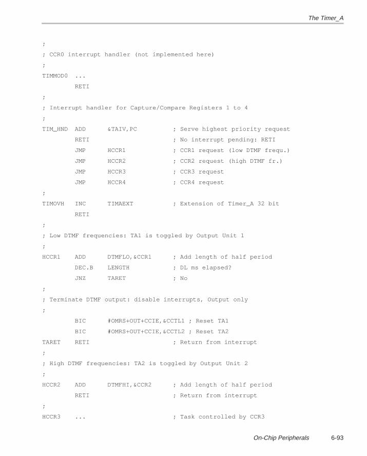
The Timer_A
6-93On-Chip Peripherals
;
; CCR0 interrupt handler (not implemented here)
;
TIMMOD0 ...
RETI
;
; Interrupt handler for Capture/Compare Registers 1 to 4
;
TIM_HND ADD &TAIV,PC ; Serve highest priority request
RETI ; No interrupt pending: RETI
JMP HCCR1 ; CCR1 request (low DTMF frequ.)
JMP HCCR2 ; CCR2 request (high DTMF fr.)
JMP HCCR3 ; CCR3 request
JMP HCCR4 ; CCR4 request
;
TIMOVH INC TIMAEXT ; Extension of Timer_A 32 bit
RETI
;
; Low DTMF frequencies: TA1 is toggled by Output Unit 1
;
HCCR1 ADD DTMFLO,&CCR1 ; Add length of half period
DEC.B LENGTH ; DL ms elapsed?
JNZ TARET ; No
;
; Terminate DTMF output: disable interrupts, Output only
;
BIC #OMRS+OUT+CCIE,&CCTL1 ; Reset TA1
BIC #OMRS+OUT+CCIE,&CCTL2 ; Reset TA2
TARET RETI ; Return from interrupt
;
; High DTMF frequencies: TA2 is toggled by Output Unit 2
;
HCCR2 ADD DTMFHI,&CCR2 ; Add length of half period
RETI ; Return from interrupt
;
HCCR3 ... ; Task controlled by CCR3
The Timer_A
6-94
RETI
HCCR4 ... ; Task controlled by CCR4
RETI
;
; Tables and interrupt vectors are identical to the previous
; example
The second example, with maximum frequencies on both channels, results ina maximum CPU loading, uCPU (ranging from 0 to 1), by the Timer_A activitiesdue to DTMF generation:
u =1
f n
f CPU
MCLKintrpt repΣ ( )
Where: fMCLK Frequency of the system clock oscilator (DCO) [Hz]nintrpt Number of cycles executed by the interrupt handlerfrep Repetition rate of the interrupt handler [Hz]
CCR1 — repetition rate 2×941 Hz 12 cycles for the task, 16 cycles overhead 28 cyclesCCR2 — repetition rate 2×1633 Hz 6 cycles for the task, 16 cycles overhead 22 cycles
u =28 22
1.048 100.12CPU 6
+
=
2 941 2 1633
This result shows a worst case CPU loading of approximate 12% due to theDTMF generation. This loading occurs only during the 82 ms activity.
6.3.8.4 TRIAC Control
TRIAC control for electric motors (DMC) or other loads is a simple task whenusing the Timer_A. The software loads one of the capture/compare registers(CCR4 with this example), prepares the output unit to change the TAx outputafter the desired time, and continues with the background task. When theloaded time interval elapses, the output unit fires the TRIAC gate at exactly theprogrammed time and requests an interrupt. The interrupt handler can use dy-namic control (several short pulses to save current) or static control (one longgate pulse), which is used with this example. See figure 6–25 for details.
The TRIAC control software contains some security features. They ensurethat no gate triggering of the previous half wave can last into the next half waveand cause gate triggering there also:
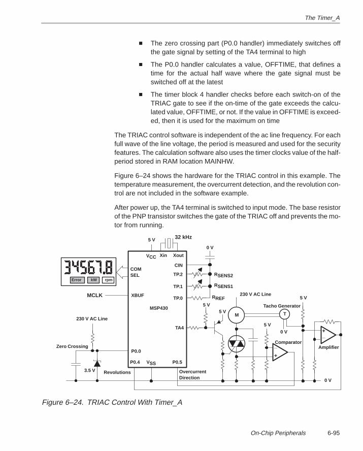
The Timer_A
6-95On-Chip Peripherals
The zero crossing part (P0.0 handler) immediately switches offthe gate signal by setting of the TA4 terminal to high
The P0.0 handler calculates a value, OFFTIME, that defines atime for the actual half wave where the gate signal must beswitched off at the latest
The timer block 4 handler checks before each switch-on of theTRIAC gate to see if the on-time of the gate exceeds the calcu-lated value, OFFTIME, or not. If the value in OFFTIME is exceed-ed, then it is used for the maximum on time
The TRIAC control software is independent of the ac line frequency. For eachfull wave of the line voltage, the period is measured and used for the securityfeatures. The calculation software also uses the timer clocks value of the half-period stored in RAM location MAINHW.
Figure 6–24 shows the hardware for the TRIAC control in this example. Thetemperature measurement, the overcurrent detection, and the revolution con-trol are not included in the software example.
After power up, the TA4 terminal is switched to input mode. The base resistorof the PNP transistor switches the gate of the TRIAC off and prevents the mo-tor from running.
OvercurrentDirection
Error rpm
COMSEL
VSS
VCC
5 V
P0.5
0 V
RREF
RSENS2
CIN
TP.2
TP.0
MSP430
TA4
M5 V
230 V AC Line
_
+
Comparator
5 V
TP.1
_+
5 V
T
RSENS1
Tacho Generator
0 V
0 V
P0.4
kW
3.5 V
Zero CrossingP0.0
32 kHz
Xin Xout
230 V AC Line
Revolutions
XBUFMCLK
Amplifier
5 V
Figure 6–24. TRIAC Control With Timer_A
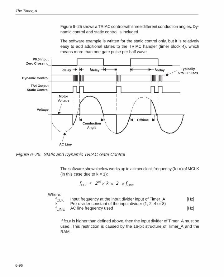
The Timer_A
6-96
Figure 6–25 shows a TRIAC control with three different conduction angles. Dy-namic control and static control is included.
The software example is written for the static control only, but it is relativelyeasy to add additional states to the TRIAC handler (timer block 4), whichmeans more than one gate pulse per half wave.
tdelay tdelay tdelay
MotorVoltage
AC Line
ConductionAngle
Typically5 to 8 Pulses
P0.0 InputZero Crossing
Dynamic Control
TA4 OutputStatic Control
Voltage
Offtime
Figure 6–25. Static and Dynamic TRIAC Gate Control
The software shown below works up to a timer clock frequency (fCLK) of MCLK(in this case due to k = 1):
f < 2 k 2 fCLK16
LINE
Where: fCLK Input frequency at the input divider input of Timer_A [Hz]k Pre-divider constant of the input divider (1, 2, 4 or 8)fLINE AC line frequency used [Hz]
If fCLK is higher than defined above, then the input divider of Timer_A must beused. This restriction is caused by the 16-bit structure of Timer_A and theRAM.
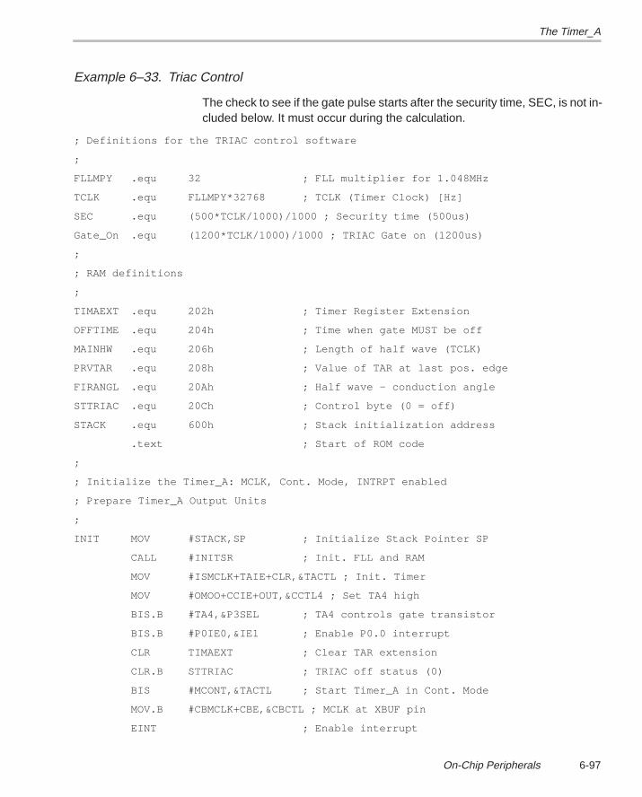
The Timer_A
6-97On-Chip Peripherals
Example 6–33. Triac Control
The check to see if the gate pulse starts after the security time, SEC, is not in-cluded below. It must occur during the calculation.
; Definitions for the TRIAC control software
;
FLLMPY .equ 32 ; FLL multiplier for 1.048MHz
TCLK .equ FLLMPY*32768 ; TCLK (Timer Clock) [Hz]
SEC .equ (500*TCLK/1000)/1000 ; Security time (500us)
Gate_On .equ (1200*TCLK/1000)/1000 ; TRIAC Gate on (1200us)
;
; RAM definitions
;
TIMAEXT .equ 202h ; Timer Register Extension
OFFTIME .equ 204h ; Time when gate MUST be off
MAINHW .equ 206h ; Length of half wave (TCLK)
PRVTAR .equ 208h ; Value of TAR at last pos. edge
FIRANGL .equ 20Ah ; Half wave – conduction angle
STTRIAC .equ 20Ch ; Control byte (0 = off)
STACK .equ 600h ; Stack initialization address
.text ; Start of ROM code
;
; Initialize the Timer_A: MCLK, Cont. Mode, INTRPT enabled
; Prepare Timer_A Output Units
;
INIT MOV #STACK,SP ; Initialize Stack Pointer SP
CALL #INITSR ; Init. FLL and RAM
MOV #ISMCLK+TAIE+CLR,&TACTL ; Init. Timer
MOV #OMOO+CCIE+OUT,&CCTL4 ; Set TA4 high
BIS.B #TA4,&P3SEL ; TA4 controls gate transistor
BIS.B #P0IE0,&IE1 ; Enable P0.0 interrupt
CLR TIMAEXT ; Clear TAR extension
CLR.B STTRIAC ; TRIAC off status (0)
BIS #MCONT,&TACTL ; Start Timer_A in Cont. Mode
MOV.B #CBMCLK+CBE,&CBCTL ; MCLK at XBUF pin
EINT ; Enable interrupt
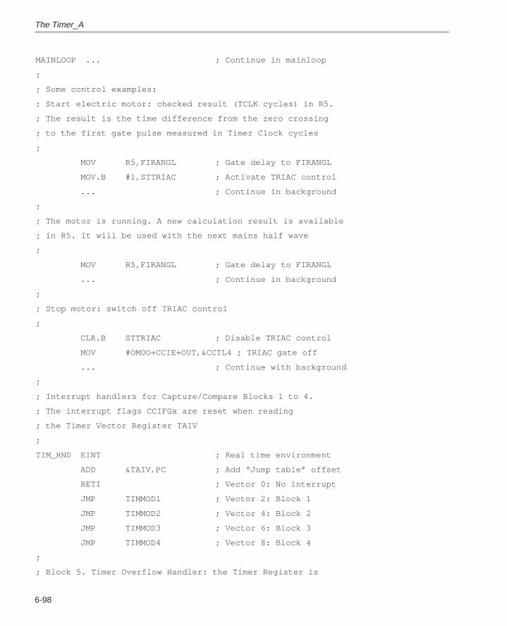
The Timer_A
6-98
MAINLOOP ... ; Continue in mainloop
;
; Some control examples:
; Start electric motor: checked result (TCLK cycles) in R5.
; The result is the time difference from the zero crossing
; to the first gate pulse measured in Timer Clock cycles
;
MOV R5,FIRANGL ; Gate delay to FIRANGL
MOV.B #1,STTRIAC ; Activate TRIAC control
... ; Continue in background
;
; The motor is running. A new calculation result is available
; in R5. It will be used with the next mains half wave
;
MOV R5,FIRANGL ; Gate delay to FIRANGL
... ; Continue in background
;
; Stop motor: switch off TRIAC control
;
CLR.B STTRIAC ; Disable TRIAC control
MOV #OMOO+CCIE+OUT,&CCTL4 ; TRIAC gate off
... ; Continue with background
;
; Interrupt handlers for Capture/Compare Blocks 1 to 4.
; The interrupt flags CCIFGx are reset when reading
; the Timer Vector Register TAIV
;
TIM_HND EINT ; Real time environment
ADD &TAIV,PC ; Add “Jump table” offset
RETI ; Vector 0: No interrupt
JMP TIMMOD1 ; Vector 2: Block 1
JMP TIMMOD2 ; Vector 4: Block 2
JMP TIMMOD3 ; Vector 6: Block 3
JMP TIMMOD4 ; Vector 8: Block 4
;
; Block 5. Timer Overflow Handler: the Timer Register is
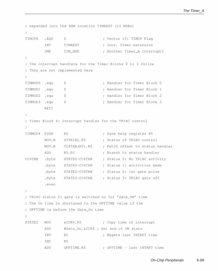
The Timer_A
6-99On-Chip Peripherals
; expanded into the RAM location TIMAEXT (16 MSBs)
;
TIMOVH .EQU $ ; Vector 10: TIMOV Flag
INC TIMAEXT ; Incr. Timer extension
JMP TIM_HND ; Another Timer_A interrupt?
;
; The interrupt handlers for the Timer Blocks 0 to 3 follow
; They are not implemented here
;
TIMMOD0 .equ $ ; Handler for Timer Block 0
TIMMOD1 .equ $ ; Handler for Timer Block 1
TIMMOD2 .equ $ ; Handler for Timer Block 2
TIMMOD3 .equ $ ; Handler for Timer Block 3
RETI
;
; Timer Block 4: interrupt handler for the TRIAC control
;
TIMMOD4 PUSH R5 ; Save help register R5
MOV.B STTRIAC,R5 ; Status of TRIAC control
MOV.B CC4TAB(R5),R5 ; Fetch offset to status handler
ADD R5,PC ; Branch to status handler
CC4TAB .byte STATE0–CC4TAB ; Status 0: No TRIAC activity
.byte STATE0–CC4TAB ; Status 1: activition made
.byte STATE2–CC4TAB ; Status 2: 1st gate pulse
.byte STATE3–CC4TAB ; Status 3: TRIAC gate off
.even
;
; TRIAC status 2: gate is switched on for ”Gate_ON” time
; The On time is shortened to the OFFTIME value if the
; OFFTIME is before the Gate_On time
;
STATE2 MOV &CCR4,R5 ; Copy time of interrupt
ADD #Gate_On,&CCR4 ; Set end of ON state
INV R5 ; Negate last INTRPT time
INC R5
ADD OFFTIME,R5 ; OFFTIME – last INTRPT time
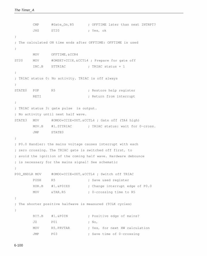
The Timer_A
6-100
CMP #Gate_On,R5 ; OFFTIME later than next INTRPT?
JHS ST20 ; Yes, ok
;
; The calculated ON time ends after OFFTIME: OFFTIME is used
;
MOV OFFTIME,&CCR4
ST20 MOV #OMSET+CCIE,&CCTL4 ; Prepare for gate off
INC.B STTRIAC ; TRIAC status + 1
;
; TRIAC status 0: No activity. TRIAC is off always
;
STATE0 POP R5 ; Restore help register
RETI ; Return from interrupt
;
; TRIAC status 3: gate pulse is output.
; No activity until next half wave.
STATE3 MOV #OMOO+CCIE+OUT,&CCTL4 ; Gate off (TA4 high)
MOV.B #1,STTRIAC ; TRIAC status: wait for 0–cross.
JMP STATE0
;
; P0.0 Handler: the mains voltage causes interrupt with each
; zero crossing. The TRIAC gate is switched off first, to
; avoid the ignition of the coming half wave. Hardware debounce
; is necessary for the mains signal! See schematic
;
P00_HNDLR MOV #OMOO+CCIE+OUT,&CCTL4 ; Switch off TRIAC
PUSH R5 ; Save used register
XOR.B #1,&P0IES ; Change interrupt edge of P0.0
MOV &TAR,R5 ; 0–crossing time to R5
;
; The shorter positive halfwave is measured (TCLK cycles)
;
BIT.B #1,&P0IN ; Positive edge of mains?
JZ P01 ; No,
MOV R5,PRVTAR ; Yes, for next HW calculation
JMP P03 ; Save time of 0–crossing
The Timer_A
6-101On-Chip Peripherals
P01 MOV R5,MAINHW ; Measure pos. mains half wave
SUB PRVTAR,MAINHW ; Difference is length of pos. HW
;
; If STTRIAC is not 0 ( 0 = inactivity) then the next gate
; firing is prepared
;
P03 TST.B STTRIAC ;
JZ P02 ; STTRIAC = 0: no activity
MOV.B #2,STTRIAC ; STTRIAC > 0: prep. next firing
;
; The TRIAC firing time is calculated: Timer Reg. + FIRANGL
;
MOV R5,&CCR4 ; TAR to CCR4
ADD FIRANGL,&CCR4 ; TAR + delay –> CCR4
MOV #OMR+CCIE+OUT,&CCTL4 ; TA4 is reset by INTRPT
;
; The worst case switch–off time for the TRIAC is calculated:
; Zero crossing time + half period – security time
; This calculation ensures a safe distance to the next zero
; crossing of the mains
;
ADD MAINHW,R5 ; TAR + MAINHW
SUB #SEC,R5 ; Subtract security time
MOV R5,OFFTIME ; worst case switch–off time
P02 POP R5 ; Restore R5
RETI
.sect ”TIMVEC”,0FFF0h ; Timer_A Interrupt Vectors
.word TIM_HND ; Timer Blocks 1..4 Vector
.word TIMMOD0 ; Vector for Timer Block 0
.sect ”P00VEC”,0FFFAh ; P0.0 Vector
.word P00_HNDLR
.sect ”INITVEC”,0FFFEh ; Reset Vector
.word INIT
The TRIAC control example results in a nominal CPU loading uCPU (rangingfrom 0 to 1):
u =1
f n
f CPU
MCLKintrpt repΣ ( )
The Timer_A
6-102
Where: fMCLK Frequency of the system clock generator (DCO) [Hz]nintrpt Number of cycles executed by the interrupt handlerfrep Repetition rate of the interrupt handler [Hz]
CCR4 — repetition rate 100Hz 79 cycles for the task, 16 cycles overhead 95 cyclesP0.0 — repetition rate 100Hz 60 cycles for the task, 11 cycles overhead 71 cycles
uCPU =100 95 100 71
1.048 1060.016
+
=
This shows a CPU loading of approximately 1.6% due to the static TRIAC con-trol.
6.3.8.5 Mixture of Capture and Compare Modes
Any mix of capture and compare mode is possible with the Timer_A. The fol-lowing software example shows two timer blocks using the capture mode andthree timer blocks using the compare mode. For formulas, see Section 6.3.8.2.
Capture/Compare Block 0 — a short negative pulse with a 1 kHz repeti-tion rate is generated and output at the terminal TA0. The pulse is resetto high by the interrupt handler of timer block 0. The pulse is used for theprecise triggering of an external peripheral. The error of the repetition ratedue to the MCLK frequency used is –0.055%.
Capture/Compare Block 1 — the period of the input signal at the CCI1Ainput terminal is measured in timer clock cycles. The period is measuredfrom leading edge to leading edge of the input signal. The last measuredvalue is stored in the RAM word PERIOD. The maximum period length thatcan be measured this way is k × 216/fCLK.
Capture/Compare Block 2 — a square wave with a variable repetitionrate is generated and output at the terminal TA2. The actual cycle countfor one half-wave is stored in the RAM word TIM2REP.
Capture/Compare Block 3 — the event time of the trailing edge of theinput signal at the CCI3A input terminal is captured. The last captured val-ue is stored in the RAM word STOR3.
Capture/Compare Block 4 — a square wave with a variable output fre-quency is generated and output at the TA4 terminal. The output frequencystarts at 4 kHz and decreases to 1 kHz. The square wave is used for thecontrol of an external peripheral.
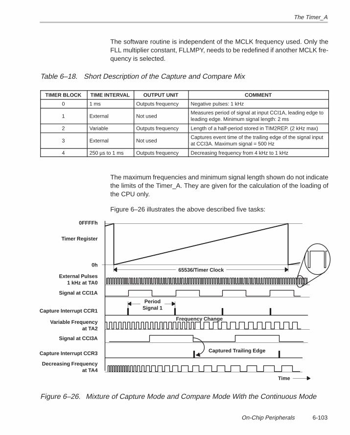
The Timer_A
6-103On-Chip Peripherals
The software routine is independent of the MCLK frequency used. Only theFLL multiplier constant, FLLMPY, needs to be redefined if another MCLK fre-quency is selected.
Table 6–18. Short Description of the Capture and Compare Mix
TIMER BLOCK TIME INTERVAL OUTPUT UNIT COMMENT
0 1 ms Outputs frequency Negative pulses: 1 kHz
1 External Not usedMeasures period of signal at input CCI1A, leading edge toleading edge. Minimum signal length: 2 ms
2 Variable Outputs frequency Length of a half-period stored in TIM2REP. (2 kHz max)
3 External Not usedCaptures event time of the trailing edge of the signal inputat CCI3A. Maximum signal = 500 Hz
4 250 µs to 1 ms Outputs frequency Decreasing frequency from 4 kHz to 1 kHz
The maximum frequencies and minimum signal length shown do not indicatethe limits of the Timer_A. They are given for the calculation of the loading ofthe CPU only.
Figure 6–26 illustrates the above described five tasks:
Time
65536/Timer Clock
PeriodSignal 1
Captured Trailing Edge
0FFFFh
Timer Register
0h
External Pulses1 kHz at TA0
Signal at CCI1A
Capture Interrupt CCR1
Variable Frequencyat TA2
Signal at CCI3A
Decreasing Frequencyat TA4
Capture Interrupt CCR3
Frequency Change
Figure 6–26. Mixture of Capture Mode and Compare Mode With the Continuous Mode
The Timer_A
6-104
The software example also shows how to output the ACLK frequency at outputterminal XBUF for reference purposes. An external device may be driven bythis stable and precise crystal-controlled frequency.
A special method is used for the return from interrupt. The interrupt handlersof the five timer blocks do not return normally with a RETI instruction but jumpback to the start of the timer handler for a test to see if another Timer_A inter-rupt is pending. This makes it necessary to enable the interrupt at the start ofthe timer handler. Otherwise, the interrupt latency time will get too long for oth-er interrupts.
Example 6–34. Mixed Capture and Compare Modes
; Software example: three independent timings and two inputs
; with capturing. The Continuous Mode of Timer_A is used
;
FLLMPY .equ 64 ; FLL multiplier for 2.096MHz
TCLK .equ FLLMPY*32768 ; TCLK: FLLMPY x fcrystal
OLDRE .equ 202h ; Time of last edge at CCI1A
PERIOD .equ 204h ; Calc. period of CCI1A event
TIM2REP .equ 206h ; Repetition rate Block 2
STOR3 .equ 208h ; Last neg. edge at CCI3A
TIM4REP .equ 20Ah ; Repetition rate Block 4
TIMAEXT .equ 20Ch ; Extension for Timer Register
STACK .equ 600h ; Stack initialization address
.text 0F000h ; Software start address
INIT MOV #STACK,SP ; Initialize Stack Pointer
CALL #INITSR ; Init. FLL and RAM
;
; Initialize the Timer_A: MCLK, Cont. Mode, INTRPT on
; Inputs (CCIxA) and outputs (Tax) of Timer_A are defined
;
MOV #ISMCLK+TAIE+CLR,&TACTL
MOV #OMR+CCIE,&CCTL0 ; Reset Mode, INTRPT on
MOV #CMPE+ISCCIA+SCS+CAP+CCIE,&CCTL1 ;
MOV #OMT+CCIE,&CCTL2 ; Toggle, INTRPT on
MOV #CMNE+ISCCIA+SCS+CAP+CCIE,&CCTL3 ;
MOV #OMT+CCIE,&CCTL4 ; Toggle, INTRPT on
MOV #0FFFFh,TIM2REP ; Start value Block 2
The Timer_A
6-105On-Chip Peripherals
MOV #((TCLK/4000)+1)/2,TIM4REP ; 4kHz start frequ.
MOV.B #TA4+TA3+TA2+TA1+TA0,&P3SEL ; Define I/Os
;
MOV #1,&CCR0 ; Immediate start
MOV #1,&CCR2 ; for the Capture/Compare
MOV #1,&CCR4 ; Registers
CLR TIMAEXT ; Clear TAR extension
MOV.B #CBACLK+CBE,&CBCTL ; Output ACLK at XBUF pin
BIS #MCONT,&TACTL ; Start Timer
EINT ; Enable interrupt
MAINLOOP ... ; Continue in background
; Interrupt handler for Capture/Compare Block 0. An ext.
; peripheral is started every 1ms with a negative pulse at
; TA0 (set exactly in time by Output Unit 0). The handler
; resets the negative signal.
;
TIMMOD0 .EQU $ ; Start of handler
ADD #((2*TCLK/1000)+1)/2,&CCR0 ; For next INTRPT
MOV #OMOO+CCIE+OUT,&CCTL0; Set TA0: pulse off
BIS #OMR,&CCTL0 ; Back to Reset Mode
; Fall through to TIM_HND
;
; Interrupt handlers for Capture/Compare Blocks 1 to 4.
; The interrupt flags CCIFGx are reset by the reading
; of the Timer Vector Register TAIV
;
TIM_HND .EQU $ ; Start of Timer_A handler
EINT ; Allow interrupt nesting
TH0 ADD &TAIV,PC ; Add Jump table offset
RETI ; Vector 0: No interrupt
JMP TIMMOD1 ; Vector 2: Block 1
JMP TIMMOD2 ; Vector 4: Block 2
JMP TIMMOD3 ; Vector 6: Block 3
JMP TIMMOD4 ; Vector 8: Block 4
;
; Block 5. Timer Overflow Handler: the Timer Register is
The Timer_A
6-106
; expanded into the RAM location TIMEXT (MSBs)
;
TIMOVH .EQU $ ; Vector 10: TIMOV Flag
INC TIMAEXT ; Incr. Timer extension
JMP TH0 ; Test for other interrupts
;
; Timer Block 1 measures the period of an input signal at
; pin CCI1A. The interval between two rising edges is measured
;
TIMMOD1 .EQU $ ; Vector 2: Block 1
MOV &CCR1,PERIOD ; Time of captured rising edge
SUB OLDRE,PERIOD ; Calculate period (difference)
MOV &CCR1,OLDRE ; Store actual edge time
JMP TH0 ; Test for another interrupts
;
; The used time interval delta t2 is stored in TIM2REP.
;
TIMMOD2 .EQU $ ; Vector 4: Block 2
ADD TIM2REP,&CCR2 ; Add time interval
... ; Task2 starts here
JMP TH0 ; Test for another interrupts
;
; Timer Block 3stores the time for a trailing edge at CCI3A
; STOR3 contains the time of the latest trailing edge
;
TIMMOD3 .EQU $ ; Vector 6: Block 3
MOV &CCR3,STOR3 ; Store event time
JMP TH0 ; Test for another interrupts
;
; Block 4 uses a variable repetition rate starting at 4kHz
; cycles and going down to 1kHz.
;
TIMMOD4 .EQU $ ; Vector 8: Block 4
ADD TIM4REP,&CCR4 ; Add time interval
CMP #((TCLK/1000)+1)/2,TIM4REP ; Final value?
JHS TH0 ; Yes, no modification
The Timer_A
6-107On-Chip Peripherals
INC TIM4REP ; No, modify interval
JMP TH0 ; Test for other interrupts
;
.sect ”TIMVEC”,0FFF0h ; Timer_A Interrupt Vectors
.word TIM_HND ; Timer Blocks 1..4 Vector
.word TIMMOD0 ; Vector for Timer Block 0
.sect ”INITVEC”,0FFFEh ; Reset Vector
.word INIT
The software example above results in a maximum (worst case) CPU loadinguCPU (ranging from 0 to 1) by the Timer_A activities:
u =1
f n
f CPU
MCLKintrpt repΣ ( )
Where: fMCLK Frequency of the system clock generator (DCO) [Hz]nintrpt Number of cycles executed by the interrupt handlerfrep Repetition rate of the interrupt handler [Hz]
CCR0 — repetition rate 1 kHz 15 cycles for the task, 15 cycles overhead 30 cyclesCCR1— rep. rate max. 0.5 kHz 18 cycles for the task, 22 cycles overhead 40 cyclesCCR2 — repetition rate 2 kHz 6 cycles for the task, 22 cycles overhead 28 cyclesCCR3 — repetition rate 0.5 kHz 6 cycles for the task, 22 cycles overhead 28 cyclesCCR4 — repetition rate 8 kHz 17 cycles for the task, 22 cycles overhead 39 cyclesTIMOV — rep. rate 32 Hz@2 MHz 4 cycles for the task, 20 cycles overhead 24 cycles
u =30 10 40 500 28 2000 28 500 39 8000 24 32
2.096 100.21CPU
3
6 + + + + +
=
This shows a worst case CPU loading of approximate 21% due to the Timer_A(the task of the timer block 2 is not included). If fMCLK is chosen to be 3.8 MHz,then the CPU loading is only 11.5%, max.
Any pending Timer_A interrupt during the return phase saves 6 cycles be-cause of the code in this example.
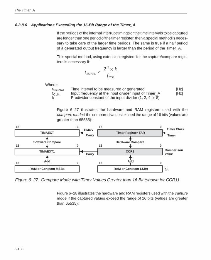
The Timer_A
6-108
6.3.8.6 Applications Exceeding the 16-Bit Range of the Timer_A
If the periods of the internal interrupt timings or the time intervals to be capturedare longer than one period of the timer register, then a special method is neces-sary to take care of the larger time periods. The same is true if a half periodof a generated output frequency is larger than the period of the Timer_A.
This special method, using extension registers for the capture/compare regis-ters is necessary if:
t >2 k
fSIGNAL
16
CLK
Where: tSIGNAL Time interval to be measured or generated [Hz]fCLK Input frequency at the input divider input of Timer_A [Hz]k Predivider constant of the input divider (1, 2, 4 or 8)
Figure 6–27 illustrates the hardware and RAM registers used with thecompare mode if the compared values exceed the range of 16 bits (values aregreater than 65535):
TIMAEXT
015
Timer Register TAR
015
TIMAEXT1
015
CCR1
015
RAM or Constant MSBs
015 015
RAM or Constant LSBs
Software Compare Hardware Compare
Add Add
TIMOV
Carry
Carry
Timer Clock
Timer
ComparisonValue
∆ t
Figure 6–27. Compare Mode with Timer Values Greater than 16 Bit (shown for CCR1)
Figure 6–28 illustrates the hardware and RAM registers used with the capturemode if the captured values exceed the range of 16 bits (values are greaterthan 65535):
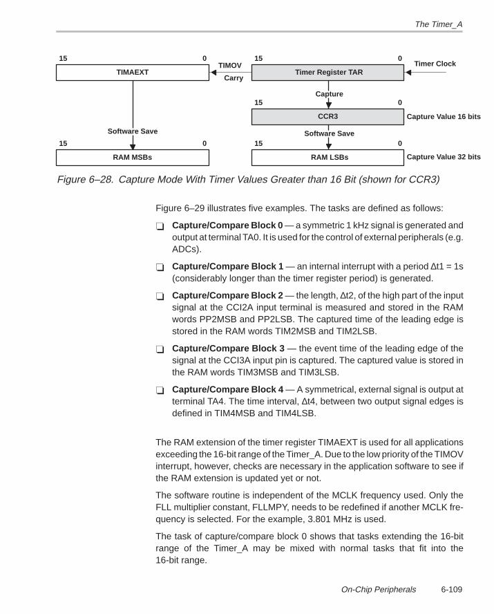
The Timer_A
6-109On-Chip Peripherals
TIMAEXT
015
Timer Register TAR
015
CCR3
015
RAM MSBs
015 015
RAM LSBs
Software Save
TIMOV
Carry
Timer Clock
Capture Value 16 bits
Software Save
Capture Value 32 bits
Capture
Figure 6–28. Capture Mode With Timer Values Greater than 16 Bit (shown for CCR3)
Figure 6–29 illustrates five examples. The tasks are defined as follows:
Capture/Compare Block 0 — a symmetric 1 kHz signal is generated andoutput at terminal TA0. It is used for the control of external peripherals (e.g.ADCs).
Capture/Compare Block 1 — an internal interrupt with a period ∆t1 = 1s(considerably longer than the timer register period) is generated.
Capture/Compare Block 2 — the length, ∆t2, of the high part of the inputsignal at the CCI2A input terminal is measured and stored in the RAMwords PP2MSB and PP2LSB. The captured time of the leading edge isstored in the RAM words TIM2MSB and TIM2LSB.
Capture/Compare Block 3 — the event time of the leading edge of thesignal at the CCI3A input pin is captured. The captured value is stored inthe RAM words TIM3MSB and TIM3LSB.
Capture/Compare Block 4 — A symmetrical, external signal is output atterminal TA4. The time interval, ∆t4, between two output signal edges isdefined in TIM4MSB and TIM4LSB.
The RAM extension of the timer register TIMAEXT is used for all applicationsexceeding the 16-bit range of the Timer_A. Due to the low priority of the TIMOVinterrupt, however, checks are necessary in the application software to see ifthe RAM extension is updated yet or not.
The software routine is independent of the MCLK frequency used. Only theFLL multiplier constant, FLLMPY, needs to be redefined if another MCLK fre-quency is selected. For the example, 3.801 MHz is used.
The task of capture/compare block 0 shows that tasks extending the 16-bitrange of the Timer_A may be mixed with normal tasks that fit into the16-bit range.
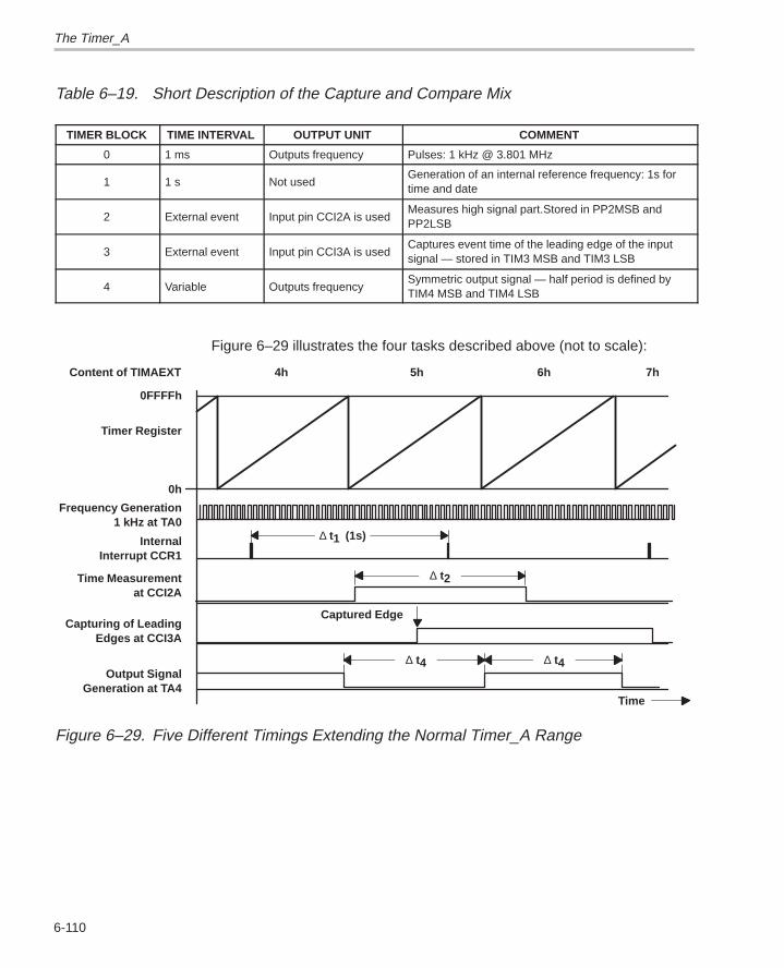
The Timer_A
6-110
Table 6–19. Short Description of the Capture and Compare Mix
TIMER BLOCK TIME INTERVAL OUTPUT UNIT COMMENT
0 1 ms Outputs frequency Pulses: 1 kHz @ 3.801 MHz
1 1 s Not usedGeneration of an internal reference frequency: 1s fortime and date
2 External event Input pin CCI2A is usedMeasures high signal part.Stored in PP2MSB andPP2LSB
3 External event Input pin CCI3A is usedCaptures event time of the leading edge of the inputsignal — stored in TIM3 MSB and TIM3 LSB
4 Variable Outputs frequencySymmetric output signal — half period is defined byTIM4 MSB and TIM4 LSB
Figure 6–29 illustrates the four tasks described above (not to scale):
Time
0FFFFh
Timer Register
0h
Frequency Generation1 kHz at TA0
Content of TIMAEXT 4h 5h 6h 7h
∆ t1 (1s)
∆ t2
∆ t4 ∆ t4
Captured Edge
InternalInterrupt CCR1
Time Measurementat CCI2A
Capturing of LeadingEdges at CCI3A
Output SignalGeneration at TA4
Figure 6–29. Five Different Timings Extending the Normal Timer_A Range
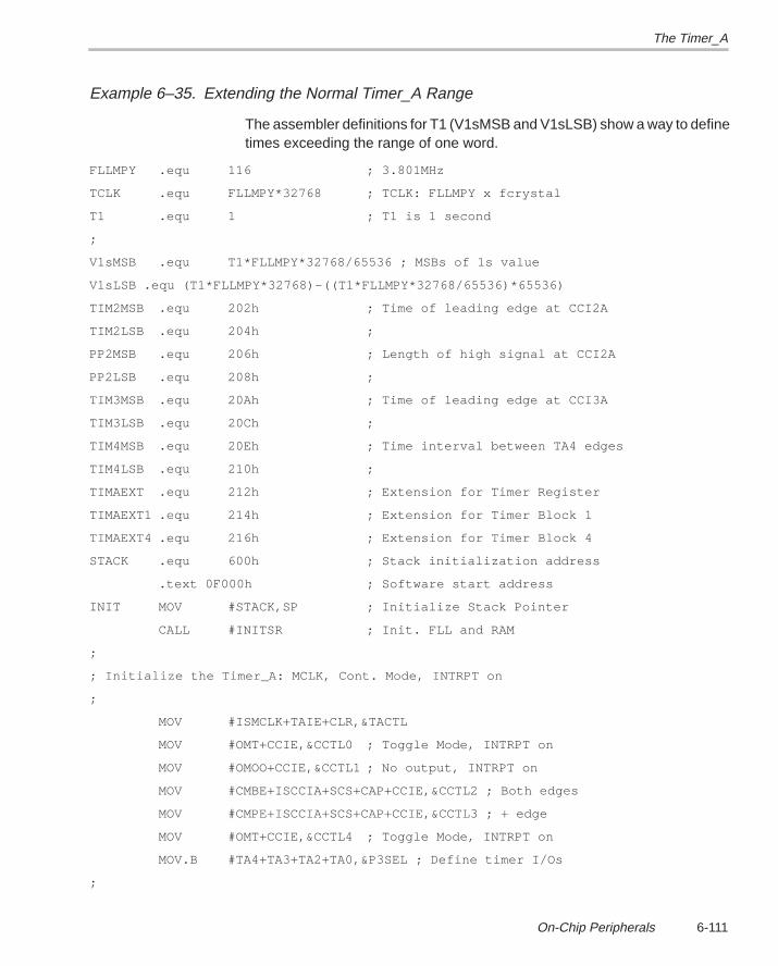
The Timer_A
6-111On-Chip Peripherals
Example 6–35. Extending the Normal Timer_A Range
The assembler definitions for T1 (V1sMSB and V1sLSB) show a way to definetimes exceeding the range of one word.
FLLMPY .equ 116 ; 3.801MHz
TCLK .equ FLLMPY*32768 ; TCLK: FLLMPY x fcrystal
T1 .equ 1 ; T1 is 1 second
;
V1sMSB .equ T1*FLLMPY*32768/65536 ; MSBs of 1s value
V1sLSB .equ (T1*FLLMPY*32768)–((T1*FLLMPY*32768/65536)*65536)
TIM2MSB .equ 202h ; Time of leading edge at CCI2A
TIM2LSB .equ 204h ;
PP2MSB .equ 206h ; Length of high signal at CCI2A
PP2LSB .equ 208h ;
TIM3MSB .equ 20Ah ; Time of leading edge at CCI3A
TIM3LSB .equ 20Ch ;
TIM4MSB .equ 20Eh ; Time interval between TA4 edges
TIM4LSB .equ 210h ;
TIMAEXT .equ 212h ; Extension for Timer Register
TIMAEXT1 .equ 214h ; Extension for Timer Block 1
TIMAEXT4 .equ 216h ; Extension for Timer Block 4
STACK .equ 600h ; Stack initialization address
.text 0F000h ; Software start address
INIT MOV #STACK,SP ; Initialize Stack Pointer
CALL #INITSR ; Init. FLL and RAM
;
; Initialize the Timer_A: MCLK, Cont. Mode, INTRPT on
;
MOV #ISMCLK+TAIE+CLR,&TACTL
MOV #OMT+CCIE,&CCTL0 ; Toggle Mode, INTRPT on
MOV #OMOO+CCIE,&CCTL1 ; No output, INTRPT on
MOV #CMBE+ISCCIA+SCS+CAP+CCIE,&CCTL2 ; Both edges
MOV #CMPE+ISCCIA+SCS+CAP+CCIE,&CCTL3 ; + edge
MOV #OMT+CCIE,&CCTL4 ; Toggle Mode, INTRPT on
MOV.B #TA4+TA3+TA2+TA0,&P3SEL ; Define timer I/Os
;
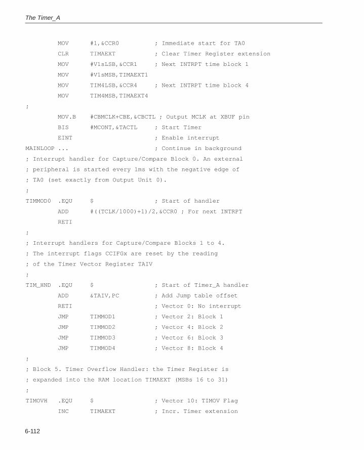
The Timer_A
6-112
MOV #1,&CCR0 ; Immediate start for TA0
CLR TIMAEXT ; Clear Timer Register extension
MOV #V1sLSB,&CCR1 ; Next INTRPT time block 1
MOV #V1sMSB,TIMAEXT1
MOV TIM4LSB,&CCR4 ; Next INTRPT time block 4
MOV TIM4MSB,TIMAEXT4
;
MOV.B #CBMCLK+CBE,&CBCTL ; Output MCLK at XBUF pin
BIS #MCONT,&TACTL ; Start Timer
EINT ; Enable interrupt
MAINLOOP ... ; Continue in background
; Interrupt handler for Capture/Compare Block 0. An external
; peripheral is started every 1ms with the negative edge of
; TA0 (set exactly from Output Unit 0).
;
TIMMOD0 .EQU $ ; Start of handler
ADD #((TCLK/1000)+1)/2,&CCR0 ; For next INTRPT
RETI
;
; Interrupt handlers for Capture/Compare Blocks 1 to 4.
; The interrupt flags CCIFGx are reset by the reading
; of the Timer Vector Register TAIV
;
TIM_HND .EQU $ ; Start of Timer_A handler
ADD &TAIV,PC ; Add Jump table offset
RETI ; Vector 0: No interrupt
JMP TIMMOD1 ; Vector 2: Block 1
JMP TIMMOD2 ; Vector 4: Block 2
JMP TIMMOD3 ; Vector 6: Block 3
JMP TIMMOD4 ; Vector 8: Block 4
;
; Block 5. Timer Overflow Handler: the Timer Register is
; expanded into the RAM location TIMAEXT (MSBs 16 to 31)
;
TIMOVH .EQU $ ; Vector 10: TIMOV Flag
INC TIMAEXT ; Incr. Timer extension
The Timer_A
6-113On-Chip Peripherals
RETI ;
;
; Timer Block 1 gen. the 1s reference used for date and time
;
TIMMOD1 .EQU $ ; Vector 2: Block 1
BIT #TAIFG,&TACTL ; TIMOV pending?
JNZ TM11 ; Yes, checks necessary
TM12 CMP TIMAEXT,TIMAEXT1 ; MSBs also equal?
JEQ T13 ; Yes
RETI
;
TM11 TST &CCR1 ; TAIFG = 1: check CCR1
JN TM12 ; CCR1 > 7FFFh: correct values
PUSH TIMAEXT ; TIMAEXT not yet updated
INC 0(SP) ; Updated value of TIMAEXT
CMP @SP+,TIMAEXT1 ; MSBs equal?
JNE TM1R ; No, return
T13 ADD #V1sLSB,&CCR1 ; Yes, prepare next INTRPT (1s)
ADDC #V1sMSB,TIMAEXT1 ; MSBs of 1 second
CALL #RTCLK ; Increment time by 1s
JNC TM1R ; if C = 1: incr. date
CALL #DATE ; 00.00 o’clock: next day
TM1R RETI
;
; Capture Mode: the high part of the CCI2A input signal is
; measured. The result is stored in PP2MSB and PP2LSB.
;
TIMMOD2 .EQU $ ; Vector 4: Block 2
BIT #CCI,&CCTL2 ; Input signal high?
JZ TM21 ; No,calculation necessary
MOV &CCR2,TIM2LSB ; Store LSBs of capt. time
MOV TIMAEXT,TIM2MSB ; MSBs of capt. time
BIT #TAIFG,&TACTL ; TIMOV pending?
JZ TM2RET ; No, values are correct
TST &CCR2 ; Yes, check CCR2
JN TM2RET ; CCR2 > 7FFFh: correct values
The Timer_A
6-114
INC TIM2MSB ; MSBs not yet updated
TM2RET RETI
; ; High part is calculated
TM21 MOV &CCR2,PP2LSB ; Store LSBs of capt. time
MOV TIMAEXT,PP2MSB ; MSBs of capt. time
BIT #TAIFG,&TACTL ; TIMOV pending?
JZ TM22 ; No, values are correct
TST &CCR2 ; Yes, check CCR2
JN TM22 ; CCR2 > 7FFFh: correct values
INC TIM2MSB ; MSBs not yet updated
TM22 SUB TIM2LSB,PP2LSB ; Build difference
SUBC TIM2MSB,PP2MSB ;
... ; Task 2 to do
RETI
;
; Timer Block 3 captures the time of a leading edge at CCI3A
; TIM3MSB and TIM3LSB contain the time of the actual edge
;
TIMMOD3 .EQU $ ; Vector 6: Block 3
MOV &CCR3,TIM3LSB ; Store LSBs of event time
MOV TIMAEXT,TIM3MSB ; MSBs of event time
BIT #TAIFG,&TACTL ; TIMOV pending?
JZ TM31 ; No, values are correct
TST &CCR3 ; Yes, check CCR3
JN TM31 ; CCR3 > 7FFFh: correct values
INC TIM3MSB ; MSBs not yet updated
TM31 ... ; Task 3 to do
RETI
;
; Timer Block 4 gen. a symmetric pulse at pin TA4
; f = 0.5 x TCLK/TIM4xSB
;
TIMMOD4 .EQU $ ; Vector 8: Block 4
BIT #TAIFG,&TACTL ; TIMOV pending?
JNZ TM41 ; Yes, checks necessary
TM42 CMP TIMAEXT,TIMAEXT4 ; MSBs also equal?
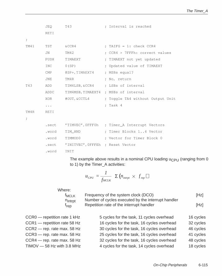
The Timer_A
6-115On-Chip Peripherals
JEQ T43 ; Interval is reached
RETI
;
TM41 TST &CCR4 ; TAIFG = 1: check CCR4
JN TM42 ; CCR4 > 7FFFh: correct values
PUSH TIMAEXT ; TIMAEXT not yet updated
INC 0(SP) ; Updated value of TIMAEXT
CMP @SP+,TIMAEXT4 ; MSBs equal?
JNE TM4R ; No, return
T43 ADD TIM4LSB,&CCR4 ; LSBs of interval
ADDC TIM4MSB,TIMAEXT4 ; MSBs of interval
XOR #OUT,&CCTL4 ; Toggle TA4 without Output Unit
... ; Task 4
TM4R RETI
;
.sect ”TIMVEC”,0FFF0h ; Timer_A Interrupt Vectors
.word TIM_HND ; Timer Blocks 1..4 Vector
.word TIMMOD0 ; Vector for Timer Block 0
.sect ”INITVEC”,0FFFEh ; Reset Vector
.word INIT
The example above results in a nominal CPU loading uCPU (ranging from 0to 1) by the Timer_A activities:
u =1
f n
f CPU
MCLKintrpt repΣ ( )
Where: fMCLK Frequency of the system clock (DCO) [Hz]nintrpt Number of cycles executed by the interrupt handlerfrep Repetition rate of the interrupt handler [Hz]
CCR0 — repetition rate 1 kHz 5 cycles for the task, 11 cycles overhead 16 cyclesCCR1 — repetition rate 58 Hz 16 cycles for the task, 16 cycles overhead 32 cyclesCCR2 — rep. rate max. 58 Hz 30 cycles for the task, 16 cycles overhead 46 cyclesCCR3 — rep. rate max. 58 Hz 25 cycles for the task, 16 cycles overhead 41 cyclesCCR4 — rep. rate max. 58 Hz 32 cycles for the task, 16 cycles overhead 48 cyclesTIMOV — 58 Hz with 3.8 MHz 4 cycles for the task, 14 cycles overhead 18 cycles
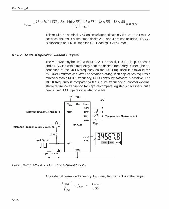
The Timer_A
6-116
u =16 10 32 58 46 58 41 58 48 58 18 58
3.801 100.007CPU
3
6
+ + + + +
=
This results in a nominal CPU loading of approximate 0.7% due to the Timer_Aactivities (the tasks of the timer blocks 2, 3, and 4 are not included). If fMCLKis chosen to be 1 MHz, then the CPU loading is 2.6%, max.
6.3.8.7 MSP430 Operation Without a Crystal
The MSP430 may be used without a 32 kHz crystal. The FLL loop is openedand a DCO tap with a frequency near the desired frequency is used (the de-pendence of the MCLK frequency on the DCO tap used is shown in theMSP430 Architecture Guide and Module Library). If an application requires arelatively stable MCLK frequency, DCO control by software is possible. TheMCLK frequency is compared to the AC line frequency or another externalstable reference frequency. No capture/compare register is necessary, but ifone is used, LCD operation is also possible.
COM
SELError kW rpm
CIN
TP.2
TP.1
TP.0
MSP430
0 V
VSS
P0.7
3.5 V47 pF
Input Signal
10 M
Reference Frequency 230 V AC Line
XBUFSoftware Regulated MCLK
VCC Xin Xout
VCC5 V
Temperature Measurement
Rref
Figure 6–30. MSP430 Operation Without Crystal
Any external reference frequency, fREF, may be used if it is in the range:
k 2
f< f <
f
100
16
CLKREF
MCLK
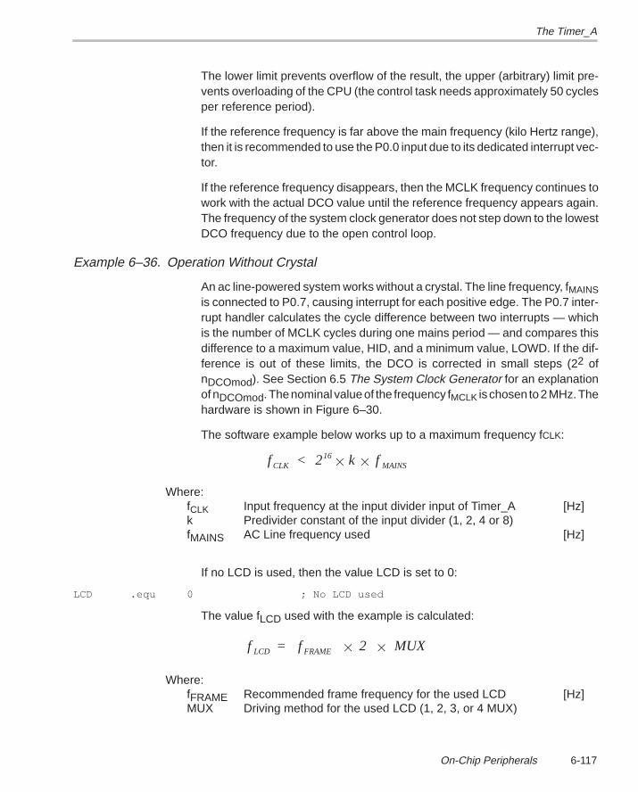
The Timer_A
6-117On-Chip Peripherals
The lower limit prevents overflow of the result, the upper (arbitrary) limit pre-vents overloading of the CPU (the control task needs approximately 50 cyclesper reference period).
If the reference frequency is far above the main frequency (kilo Hertz range),then it is recommended to use the P0.0 input due to its dedicated interrupt vec-tor.
If the reference frequency disappears, then the MCLK frequency continues towork with the actual DCO value until the reference frequency appears again.The frequency of the system clock generator does not step down to the lowestDCO frequency due to the open control loop.
Example 6–36. Operation Without Crystal
An ac line-powered system works without a crystal. The line frequency, fMAINSis connected to P0.7, causing interrupt for each positive edge. The P0.7 inter-rupt handler calculates the cycle difference between two interrupts — whichis the number of MCLK cycles during one mains period — and compares thisdifference to a maximum value, HID, and a minimum value, LOWD. If the dif-ference is out of these limits, the DCO is corrected in small steps (22 ofnDCOmod). See Section 6.5 The System Clock Generator for an explanationof nDCOmod. The nominal value of the frequency fMCLK is chosen to 2 MHz. Thehardware is shown in Figure 6–30.
The software example below works up to a maximum frequency fCLK:
f <
2 k fCLK16
MAINS
Where: fCLK Input frequency at the input divider input of Timer_A [Hz]k Predivider constant of the input divider (1, 2, 4 or 8)fMAINS AC Line frequency used [Hz]
If no LCD is used, then the value LCD is set to 0:
LCD .equ 0 ; No LCD used
The value fLCD used with the example is calculated:
f =
f 2 MUXLCD FRAME
Where: fFRAME Recommended frame frequency for the used LCD [Hz]MUX Driving method for the used LCD (1, 2, 3, or 4 MUX)
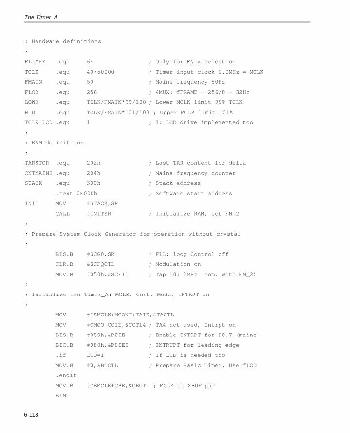
The Timer_A
6-118
; Hardware definitions
;
FLLMPY .equ 64 ; Only for FN_x selection
TCLK .equ 40*50000 ; Timer input clock 2.0MHz = MCLK
FMAIN .equ 50 ; Mains frequency 50Hz
FLCD .equ 256 ; 4MUX: fFRAME = 256/8 = 32Hz
LOWD .equ TCLK/FMAIN*99/100 ; Lower MCLK limit 99% TCLK
HID .equ TCLK/FMAIN*101/100 ; Upper MCLK limit 101%
TCLK LCD .equ 1 ; 1: LCD drive implemented too
;
; RAM definitions
;
TARSTOR .equ 202h ; Last TAR content for delta
CNTMAINS .equ 204h ; Mains frequency counter
STACK .equ 300h ; Stack address
.text 0F000h ; Software start address
INIT MOV #STACK,SP
CALL #INITSR ; Initialize RAM, set FN_2
;
; Prepare System Clock Generator for operation without crystal
;
BIS.B #SCG0,SR ; FLL: loop Control off
CLR.B &SCFQCTL ; Modulation on
MOV.B #050h,&SCFI1 ; Tap 10: 2MHz (nom. with FN_2)
;
; Initialize the Timer_A: MCLK, Cont. Mode, INTRPT on
;
MOV #ISMCLK+MCONT+TAIE,&TACTL
MOV #OMOO+CCIE,&CCTL4 ; TA4 not used, Intrpt on
BIS.B #080h,&P0IE ; Enable INTRPT for P0.7 (mains)
BIC.B #080h,&P0IES ; INTRUPT for leading edge
.if LCD=1 ; If LCD is needed too
MOV.B #0,&BTCTL ; Prepare Basic Timer. Use fLCD
.endif
MOV.B #CBMCLK+CBE,&CBCTL ; MCLK at XBUF pin
EINT
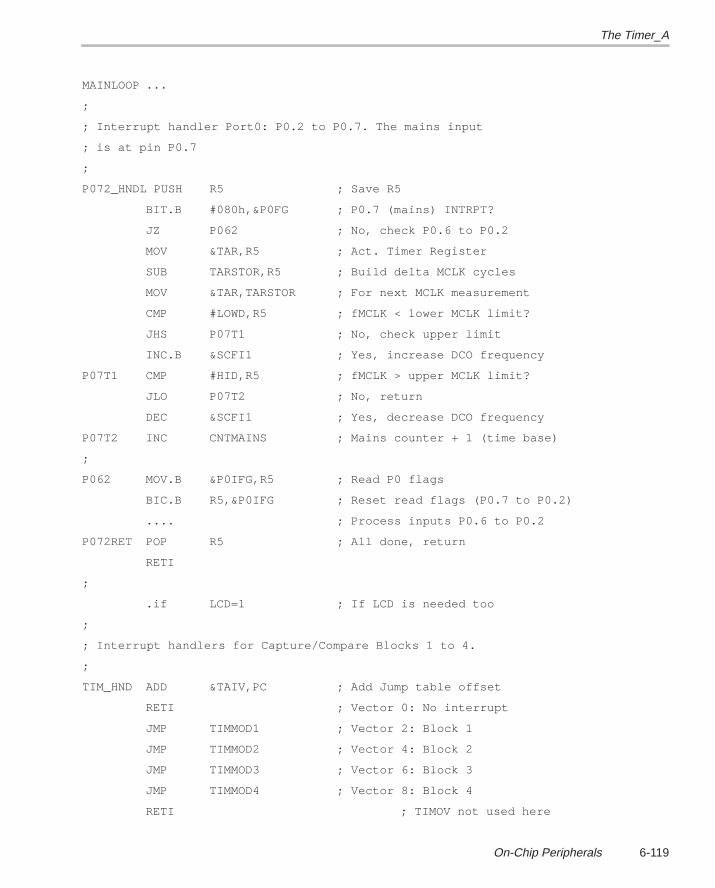
The Timer_A
6-119On-Chip Peripherals
MAINLOOP ...
;
; Interrupt handler Port0: P0.2 to P0.7. The mains input
; is at pin P0.7
;
P072_HNDL PUSH R5 ; Save R5
BIT.B #080h,&P0FG ; P0.7 (mains) INTRPT?
JZ P062 ; No, check P0.6 to P0.2
MOV &TAR,R5 ; Act. Timer Register
SUB TARSTOR,R5 ; Build delta MCLK cycles
MOV &TAR,TARSTOR ; For next MCLK measurement
CMP #LOWD,R5 ; fMCLK < lower MCLK limit?
JHS P07T1 ; No, check upper limit
INC.B &SCFI1 ; Yes, increase DCO frequency
P07T1 CMP #HID,R5 ; fMCLK > upper MCLK limit?
JLO P07T2 ; No, return
DEC &SCFI1 ; Yes, decrease DCO frequency
P07T2 INC CNTMAINS ; Mains counter + 1 (time base)
;
P062 MOV.B &P0IFG,R5 ; Read P0 flags
BIC.B R5,&P0IFG ; Reset read flags (P0.7 to P0.2)
.... ; Process inputs P0.6 to P0.2
P072RET POP R5 ; All done, return
RETI
;
.if LCD=1 ; If LCD is needed too
;
; Interrupt handlers for Capture/Compare Blocks 1 to 4.
;
TIM_HND ADD &TAIV,PC ; Add Jump table offset
RETI ; Vector 0: No interrupt
JMP TIMMOD1 ; Vector 2: Block 1
JMP TIMMOD2 ; Vector 4: Block 2
JMP TIMMOD3 ; Vector 6: Block 3
JMP TIMMOD4 ; Vector 8: Block 4
RETI ; TIMOV not used here
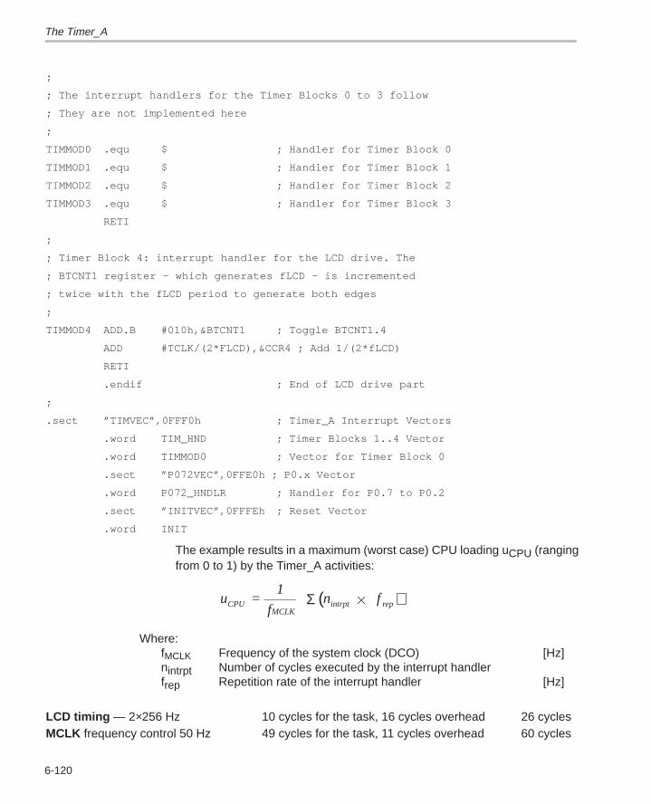
The Timer_A
6-120
;
; The interrupt handlers for the Timer Blocks 0 to 3 follow
; They are not implemented here
;
TIMMOD0 .equ $ ; Handler for Timer Block 0
TIMMOD1 .equ $ ; Handler for Timer Block 1
TIMMOD2 .equ $ ; Handler for Timer Block 2
TIMMOD3 .equ $ ; Handler for Timer Block 3
RETI
;
; Timer Block 4: interrupt handler for the LCD drive. The
; BTCNT1 register – which generates fLCD – is incremented
; twice with the fLCD period to generate both edges
;
TIMMOD4 ADD.B #010h,&BTCNT1 ; Toggle BTCNT1.4
ADD #TCLK/(2*FLCD),&CCR4 ; Add 1/(2*fLCD)
RETI
.endif ; End of LCD drive part
;
.sect ”TIMVEC”,0FFF0h ; Timer_A Interrupt Vectors
.word TIM_HND ; Timer Blocks 1..4 Vector
.word TIMMOD0 ; Vector for Timer Block 0
.sect ”P072VEC”,0FFE0h ; P0.x Vector
.word P072_HNDLR ; Handler for P0.7 to P0.2
.sect ”INITVEC”,0FFFEh ; Reset Vector
.word INIT
The example results in a maximum (worst case) CPU loading uCPU (rangingfrom 0 to 1) by the Timer_A activities:
u =1
f n
f CPU
MCLKintrpt repΣ ( )
Where: fMCLK Frequency of the system clock (DCO) [Hz]nintrpt Number of cycles executed by the interrupt handlerfrep Repetition rate of the interrupt handler [Hz]
LCD timing — 2×256 Hz 10 cycles for the task, 16 cycles overhead 26 cyclesMCLK frequency control 50 Hz 49 cycles for the task, 11 cycles overhead 60 cycles
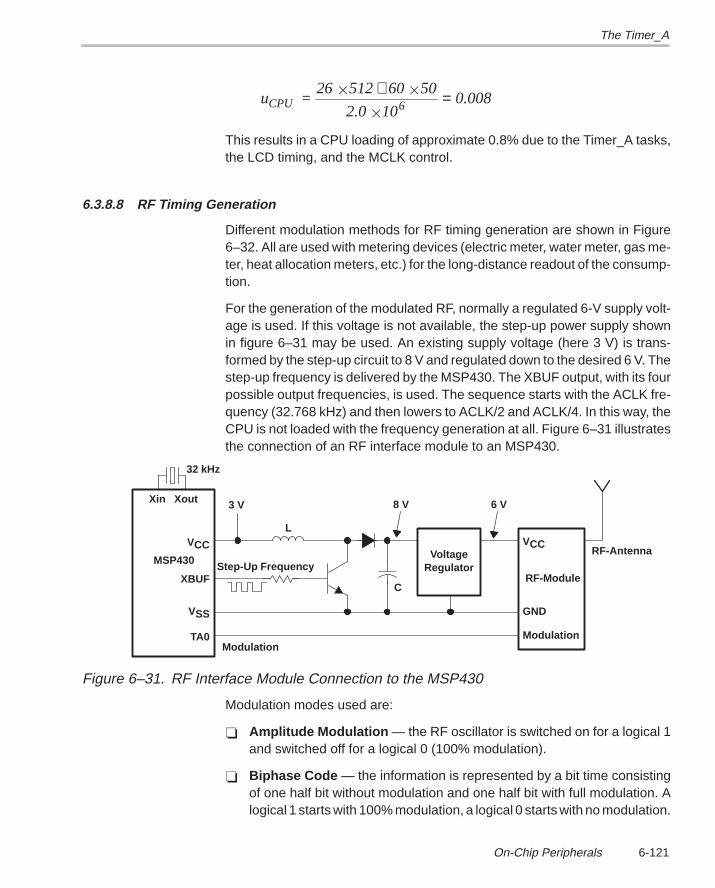
The Timer_A
6-121On-Chip Peripherals
u =26 512 60 50
2.0 100.008CPU 6
+
=
This results in a CPU loading of approximate 0.8% due to the Timer_A tasks,the LCD timing, and the MCLK control.
6.3.8.8 RF Timing Generation
Different modulation methods for RF timing generation are shown in Figure6–32. All are used with metering devices (electric meter, water meter, gas me-ter, heat allocation meters, etc.) for the long-distance readout of the consump-tion.
For the generation of the modulated RF, normally a regulated 6-V supply volt-age is used. If this voltage is not available, the step-up power supply shownin figure 6–31 may be used. An existing supply voltage (here 3 V) is trans-formed by the step-up circuit to 8 V and regulated down to the desired 6 V. Thestep-up frequency is delivered by the MSP430. The XBUF output, with its fourpossible output frequencies, is used. The sequence starts with the ACLK fre-quency (32.768 kHz) and then lowers to ACLK/2 and ACLK/4. In this way, theCPU is not loaded with the frequency generation at all. Figure 6–31 illustratesthe connection of an RF interface module to an MSP430.
TA0
VSS
32 kHz
VCCVCC
3 V
Step-Up Frequency
C
VoltageRegulator
L
Modulation
RF-Module
GND
Modulation
RF-AntennaMSP430
XBUF
Xin Xout 8 V 6 V
Figure 6–31. RF Interface Module Connection to the MSP430
Modulation modes used are:
Amplitude Modulation — the RF oscillator is switched on for a logical 1and switched off for a logical 0 (100% modulation).
Biphase Code — the information is represented by a bit time consistingof one half bit without modulation and one half bit with full modulation. Alogical 1 starts with 100% modulation, a logical 0 starts with no modulation.
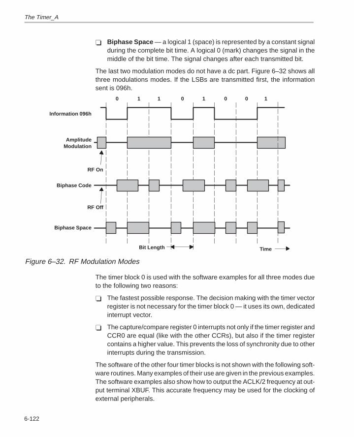
The Timer_A
6-122
Biphase Space — a logical 1 (space) is represented by a constant signalduring the complete bit time. A logical 0 (mark) changes the signal in themiddle of the bit time. The signal changes after each transmitted bit.
The last two modulation modes do not have a dc part. Figure 6–32 shows allthree modulations modes. If the LSBs are transmitted first, the informationsent is 096h.
RF Off
0 1 1 0 1 0 0 1
RF On
Information 096h
AmplitudeModulation
Biphase Code
Biphase Space
Bit Length Time
Figure 6–32. RF Modulation Modes
The timer block 0 is used with the software examples for all three modes dueto the following two reasons:
The fastest possible response. The decision making with the timer vectorregister is not necessary for the timer block 0 — it uses its own, dedicatedinterrupt vector.
The capture/compare register 0 interrupts not only if the timer register andCCR0 are equal (like with the other CCRs), but also if the timer registercontains a higher value. This prevents the loss of synchronity due to otherinterrupts during the transmission.
The software of the other four timer blocks is not shown with the following soft-ware routines. Many examples of their use are given in the previous examples.The software examples also show how to output the ACLK/2 frequency at out-put terminal XBUF. This accurate frequency may be used for the clocking ofexternal peripherals.
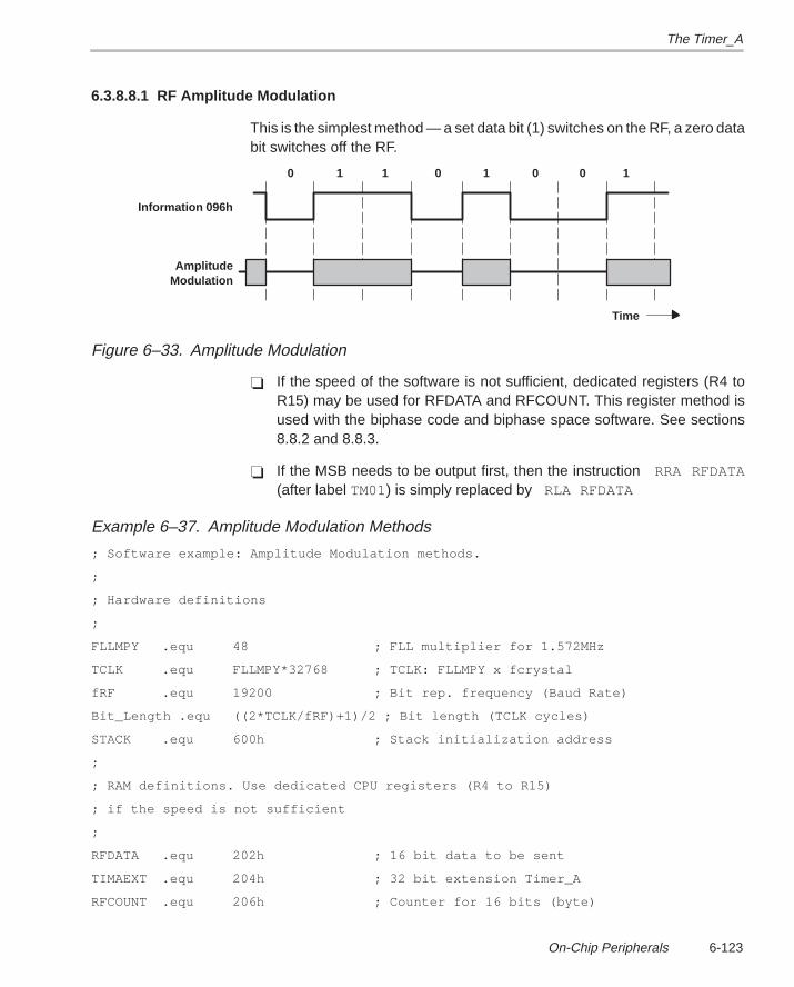
The Timer_A
6-123On-Chip Peripherals
6.3.8.8.1 RF Amplitude Modulation
This is the simplest method — a set data bit (1) switches on the RF, a zero databit switches off the RF.
0 1 1 0 1 0 0 1
Information 096h
AmplitudeModulation
Time
Figure 6–33. Amplitude Modulation
If the speed of the software is not sufficient, dedicated registers (R4 toR15) may be used for RFDATA and RFCOUNT. This register method isused with the biphase code and biphase space software. See sections8.8.2 and 8.8.3.
If the MSB needs to be output first, then the instruction RRA RFDATA(after label TM01) is simply replaced by RLA RFDATA
Example 6–37. Amplitude Modulation Methods
; Software example: Amplitude Modulation methods.
;
; Hardware definitions
;
FLLMPY .equ 48 ; FLL multiplier for 1.572MHz
TCLK .equ FLLMPY*32768 ; TCLK: FLLMPY x fcrystal
fRF .equ 19200 ; Bit rep. frequency (Baud Rate)
Bit_Length .equ ((2*TCLK/fRF)+1)/2 ; Bit length (TCLK cycles)
STACK .equ 600h ; Stack initialization address
;
; RAM definitions. Use dedicated CPU registers (R4 to R15)
; if the speed is not sufficient
;
RFDATA .equ 202h ; 16 bit data to be sent
TIMAEXT .equ 204h ; 32 bit extension Timer_A
RFCOUNT .equ 206h ; Counter for 16 bits (byte)
The Timer_A
6-124
;
.text 0F000h ; Software start address
;
INIT MOV #STACK,SP ; Initialize Stack Pointer
CALL #INITSR ; Init. FLL and RAM
;
; Initialize the Timer_A: MCLK, Cont. Mode, no INTRPT
;
MOV #ISMCLK+CLR,&TACTL
MOV #OMOO,&CCTL0 ; Reset TA0, INTRPT off
MOV.B #TA0,&P3SEL ; Define TA0 output
;
CLR TIMAEXT ; Clear TAR extension
MOV.B #3,&CBCTL ; Output ACLK/2 at XBUF pin
BIS #MCONT,&TACTL ; Start Timer
EINT ; Enable interrupt
MAINLOOP ... ; Continue in background
;
; A 16 bit value is to be output. R5 contains data
;
MOV R5,RFDATA ; Value into data word
MOV.B #16+2,RFCOUNT ; Bit count+2 to RFCOUNT
MOV &TAR,&CCR0 ; For fast response:
ADD #100,&CCR0 ; Time of 1st bit test
MOV #OMOO+CCIE,&CCTL0 ; Enable interrupt for CCR0
... ; Continue in background
;
; Test in background if 16 bits are output: RFCOUNT = 0
;
TST.B RFCOUNT ; Output completed?
JZ BPC_MADE ; Yes, interrupt bit is reset
... ; No continue
;
; Interrupt handler for Capture/Compare Block 0.
; Data in RFDATA is output: LSB first
;
The Timer_A
6-125On-Chip Peripherals
TIMMOD0 .EQU $ ; Start of CCR0 handler
ADD #Bit_Length,&CCR0 ; Time of next bit change
DEC.B RFCOUNT ; Bit count – 1
JNZ TM01 ; Not zero: continue
MOV #OMR,&CCTL0 ; Finish output: reset TA0
RETI ; INTRPT off
;
TM01 RRA RFDATA ; Next bit of RFDATA
JC TM02 ; Bit is one
MOV #OMR+CCIE,&CCTL0 ; Bit is 0: prepare reset
RETI
;
TM02 MOV #OMSET+CCIE,&CCTL0 ; Bit is 1: prepare set
RETI ;
;
.sect ”TIMVEC”,0FFF2h ; Timer_A Interrupt Vector
.word TIMMOD0 ; Vector for Timer Block 0
.sect ”INITVEC”,0FFFEh ; Reset Vector
.word INIT
The example results in a maximum (worst case) CPU loading uCPU (rangingfrom 0 to 1) by the Timer_A activities:
u =1
f n
f
33 19200
1.572E60.44CPU
MCLKintrpt rep = =( )
Where: fMCLK Frequency of the system clock (DCO) [Hz]nintrpt Number of cycles executed by the interrupt handlerfrep Repetition rate of the interrupt handler [Hz]
The RF amplitude modulation loads the CPU to 44% of its capacity when run-ning with 1.572 MHz.
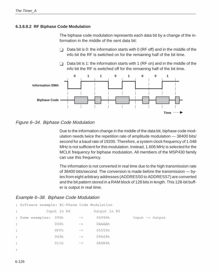
The Timer_A
6-126
6.3.8.8.2 RF Biphase Code Modulation
The biphase code modulation represents each data bit by a change of the in-formation in the middle of the sent data bit:
Data bit is 0: the information starts with 0 (RF off) and in the middle of theinfo bit the RF is switched on for the remaining half of the bit time.
Data bit is 1: the information starts with 1 (RF on) and in the middle of theinfo bit the RF is switched off for the remaining half of the bit time.
0 1 1 0 1 0 0 1
Information 096h
Biphase Code
Time
Figure 6–34. Biphase Code Modulation
Due to the information change in the middle of the data bit, biphase code mod-ulation needs twice the repetition rate of amplitude modulation — 38400 bits/second for a baud rate of 19200. Therefore, a system clock frequency of 1.048MHz is not sufficient for this modulation. Instead, 1.606 MHz is selected for theMCLK frequency for biphase modulation. All members of the MSP430 familycan use this frequency.
The information is not converted in real time due to the high transmission rateof 38400 bits/second. The conversion is made before the transmission — by-tes from eight arbitrary addresses (ADDRESS0 to ADDRESS7) are convertedand the bit pattern stored in a RAM block of 128 bits in length. This 128-bit buff-er is output in real time.
Example 6–38. Biphase Code Modulation
; Software example: Bi–Phase Code Modulation
; Input in R6 Output in R5
; Some examples: 096h –> 06996h Input –> Output
; 000h –> 0AAAAh
; 0FFh –> 05555h
; 069h –> 09669h
; 011h –> 0A9A9h
;
The Timer_A
6-127On-Chip Peripherals
; Hardware definitions
;
FLLMPY .equ 49 ; FLL multiplier for 1.606MHz
TCLK .equ FLLMPY*32768 ; TCLK: FLLMPY x fcrystal
fRF .equ 38400 ; Bit rep. frequency
Bit_Length .equ ((2*TCLK/fRF)+1)/2 ; Bit length (TCLK cycles)
STACK .equ 600h ; Stack initialization address
;
; RAM Definitions
;
RF_BLK .equ 202h ; Converted data 16 bytes
TIMAEXT .equ 212h ; 32 bit extension Timer_A
.text 0F000h ; Software start address
;
INIT MOV #STACK,SP ; Initialize Stack Pointer
CALL #INITSR ; Init. FLL and RAM
;
; Initialize the Timer_A: MCLK, Cont. Mode, INTRPT on
;
MOV #ISMCLK+TAIE+CLR,&TACTL
MOV #OMOO,&CCTL0 ; Reset TA0, INTRPT off
MOV.B #TA0,&P3SEL ; Define TA0 output
;
CLR TIMAEXT ; Clear TAR extension
MOV.B #3,&CBCTL ; Output ACLK/2 at XBUF pin
BIS #MCONT,&TACTL ; Start Timer
EINT ; Enable interrupt
MAINLOOP ... ; Continue in background
;
; 64 bits of data is to be output with Bi–Phase Code Modul.
; The data is converted into a 128–bit RAM block with the
; Bi–Phase Code sequence
;
CLR R5 ; For Bi–Phase Space necessary
MOV #RF_BLK,R8 ; Address 8 word send block
MOV.B ADDRESS0,R6 ; 1st data byte to R6
The Timer_A
6-128
CALL #BI_PHASE_CODE ; Convert it to 16 bits
MOV R5,0(R8) ; Converted data to RF–Block
... ; Convert next 6 bytes same way
MOV.B ADDRESS7,R6 ; 8th data byte to convert to R6
CALL #BI_PHASE_CODE ; Convert to 16 bits
MOV R5,14(R8) ; Converted data to RF–Block
;
MOV #RF_BLK+16,R9 ; 1st word after RF_BLK
MOV #16+1,R6 ; Bit count for 1st 16 bits
MOV @R8+,R5 ; 1st 16 bits for output
;
; Switch off all interrupts to allow exact RF timing. This is
; not necessary if ALL OTHER interrupt handlers start with
; an EINT instruction
;
...
;
MOV &TAR,&CCR0 ; For fast response:
ADD #100,&CCR0 ; Time of 1st bit test
MOV #OMOO+CCIE,&CCTL0 ; Enable interrupt for CCR0
... ; Continue in background
;
; Test in background if 128 bits are output: INTRPT of Timer
; Block 0 is switched off by the INTRPT handler
;
BIT #CCIE,&CCTL0 ; Output completed?
JZ BPC_MADE ; Yes
... ; No continue
;
; Interrupt handler for Capture/Compare Block 0
; Data in RF_BLK is output: LSB first
;
TIMMOD0 .EQU $ ; Start of CCR0 handler
ADD #Bit_Length,&CCR0 ; For next INTRPT
DEC R6 ; Bit count – 1
JNZ TM01 ; Not zero: continue
The Timer_A
6-129On-Chip Peripherals
MOV @R8+,R5 ; Next 16 bits for output
MOV #16,R6 ; Bit count
CMP R9,R8 ; End of buffer reached?
JHS TM03 ; Yes, finish output
;
TM01 RRC R5 ; Next data bit to carry
JC TM02 ; Bit is one
MOV #OMR+CCIE,&CCTL0 ; Bit is 0: prepare reset
RETI
;
TM02 MOV #OMSET+CCIE,&CCTL0 ; Bit is 1: prepare set
RETI
;
TM03 MOV #OMR,&CCTL0 ; Output complete:
RETI ; Reset TA0, INTRPT off
;
; Subroutine transforms the data byte in R6 (8 bits) to
; Bi–Phase Code in R5 (16 bits). CALL + 86 cycles/byte
;
BI_PHASE_CODE .equ $ ; Conversion routine
MOV #8,R7 ; Convert 8 bits
BIPL RRA R6 ; LSB to Carry
RRC R5 ; Bit to R5 MSB
BIT #8000h,R5 ; Copy bit once more
RRC R5 ; to R5
XOR #8000h,R5 ; and invert it
DEC R7 ; Bit count – 1
JNZ BIPL ; 8 bits not yet converted
RET ; 16 info bits in R5
;
.sect ”TIMVEC”,0FFF2h ; Timer_A Interrupt Vector
.word TIMMOD0 ; Vector for Timer Block 0
.sect ”INITVEC”,0FFFEh ; Reset Vector
.word INIT
The example results in a CPU loading uCPU (ranging from 0 to 1) by the Tim-er_A activities:
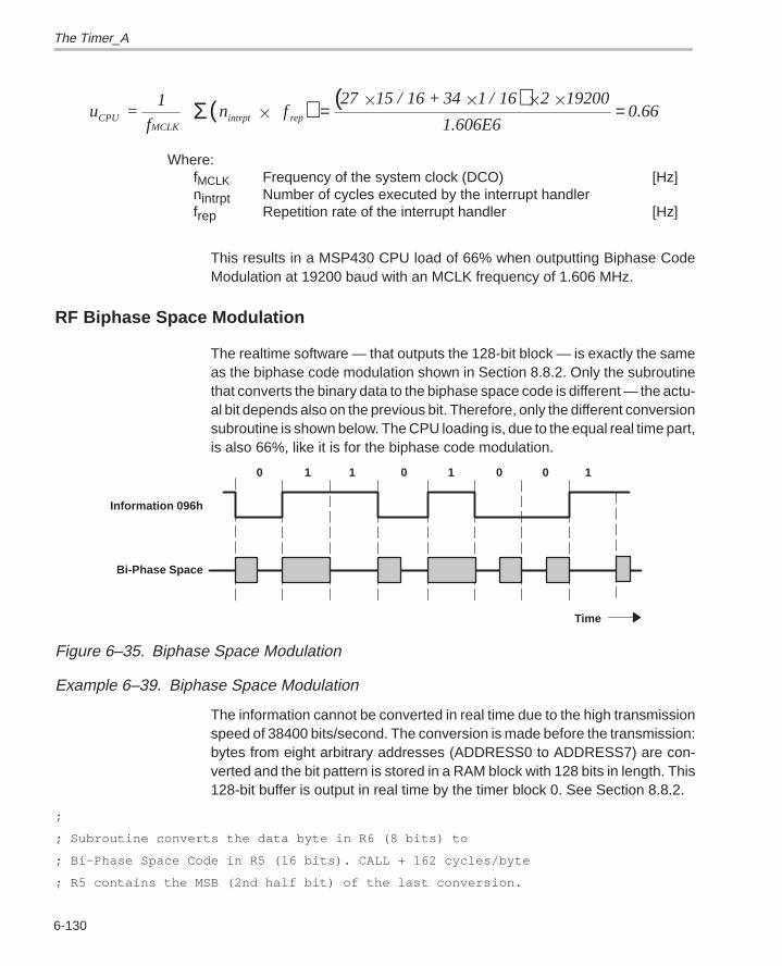
The Timer_A
6-130
( )u =
1
f n
f
27 15 / 16 + 34 1 / 16 2 19200
1.606E60.66CPU
MCLKintrpt rep =
=Σ( )
Where: fMCLK Frequency of the system clock (DCO) [Hz]nintrpt Number of cycles executed by the interrupt handlerfrep Repetition rate of the interrupt handler [Hz]
This results in a MSP430 CPU load of 66% when outputting Biphase CodeModulation at 19200 baud with an MCLK frequency of 1.606 MHz.
RF Biphase Space Modulation
The realtime software — that outputs the 128-bit block — is exactly the sameas the biphase code modulation shown in Section 8.8.2. Only the subroutinethat converts the binary data to the biphase space code is different — the actu-al bit depends also on the previous bit. Therefore, only the different conversionsubroutine is shown below. The CPU loading is, due to the equal real time part,is also 66%, like it is for the biphase code modulation.
0 1 1 0 1 0 0 1
Information 096h
Bi-Phase Space
Time
Figure 6–35. Biphase Space Modulation
Example 6–39. Biphase Space Modulation
The information cannot be converted in real time due to the high transmissionspeed of 38400 bits/second. The conversion is made before the transmission:bytes from eight arbitrary addresses (ADDRESS0 to ADDRESS7) are con-verted and the bit pattern is stored in a RAM block with 128 bits in length. This128-bit buffer is output in real time by the timer block 0. See Section 8.8.2.
;
; Subroutine converts the data byte in R6 (8 bits) to
; Bi–Phase Space Code in R5 (16 bits). CALL + 162 cycles/byte
; R5 contains the MSB (2nd half bit) of the last conversion.
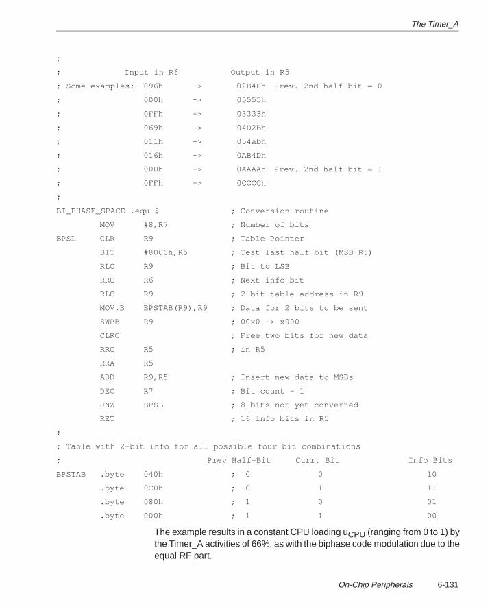
The Timer_A
6-131On-Chip Peripherals
;
; Input in R6 Output in R5
; Some examples: 096h –> 02B4Dh Prev. 2nd half bit = 0
; 000h –> 05555h
; 0FFh –> 03333h
; 069h –> 04D2Bh
; 011h –> 054abh
; 016h –> 0AB4Dh
; 000h –> 0AAAAh Prev. 2nd half bit = 1
; 0FFh –> 0CCCCh
;
BI_PHASE_SPACE .equ $ ; Conversion routine
MOV #8,R7 ; Number of bits
BPSL CLR R9 ; Table Pointer
BIT #8000h,R5 ; Test last half bit (MSB R5)
RLC R9 ; Bit to LSB
RRC R6 ; Next info bit
RLC R9 ; 2 bit table address in R9
MOV.B BPSTAB(R9),R9 ; Data for 2 bits to be sent
SWPB R9 ; 00x0 –> x000
CLRC ; Free two bits for new data
RRC R5 ; in R5
RRA R5
ADD R9,R5 ; Insert new data to MSBs
DEC R7 ; Bit count – 1
JNZ BPSL ; 8 bits not yet converted
RET ; 16 info bits in R5
;
; Table with 2–bit info for all possible four bit combinations
; Prev Half–Bit Curr. Bit Info Bits
BPSTAB .byte 040h ; 0 0 10
.byte 0C0h ; 0 1 11
.byte 080h ; 1 0 01
.byte 000h ; 1 1 00
The example results in a constant CPU loading uCPU (ranging from 0 to 1) bythe Timer_A activities of 66%, as with the biphase code modulation due to theequal RF part.
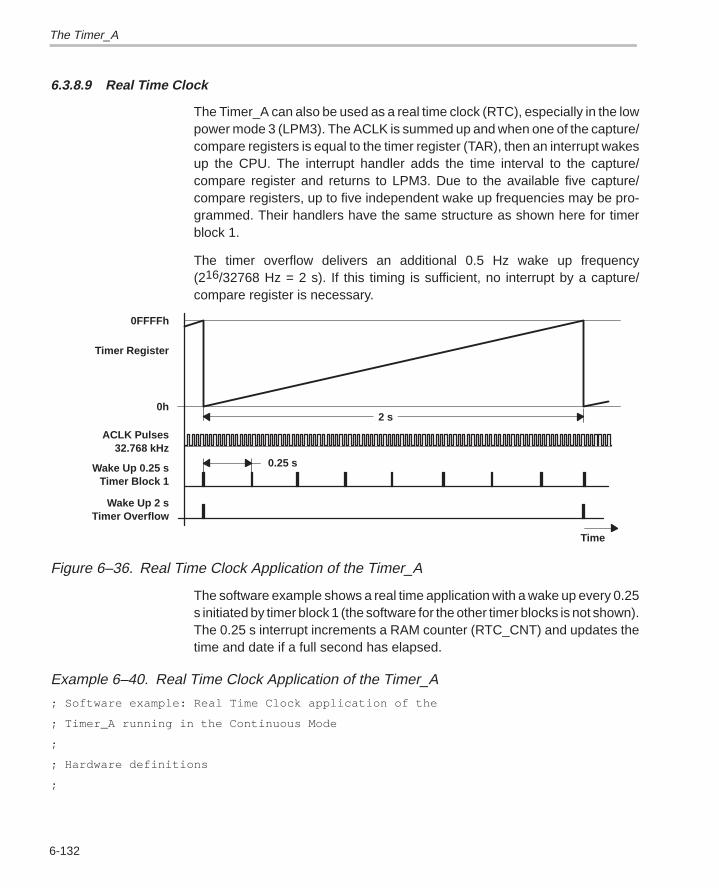
The Timer_A
6-132
6.3.8.9 Real Time Clock
The Timer_A can also be used as a real time clock (RTC), especially in the lowpower mode 3 (LPM3). The ACLK is summed up and when one of the capture/compare registers is equal to the timer register (TAR), then an interrupt wakesup the CPU. The interrupt handler adds the time interval to the capture/compare register and returns to LPM3. Due to the available five capture/compare registers, up to five independent wake up frequencies may be pro-grammed. Their handlers have the same structure as shown here for timerblock 1.
The timer overflow delivers an additional 0.5 Hz wake up frequency(216/32768 Hz = 2 s). If this timing is sufficient, no interrupt by a capture/compare register is necessary.
0.25 s
2 s
Time
0FFFFh
Timer Register
0h
ACLK Pulses32.768 kHz
Wake Up 0.25 sTimer Block 1
Wake Up 2 sTimer Overflow
Figure 6–36. Real Time Clock Application of the Timer_A
The software example shows a real time application with a wake up every 0.25s initiated by timer block 1 (the software for the other timer blocks is not shown).The 0.25 s interrupt increments a RAM counter (RTC_CNT) and updates thetime and date if a full second has elapsed.
Example 6–40. Real Time Clock Application of the Timer_A
; Software example: Real Time Clock application of the
; Timer_A running in the Continuous Mode
;
; Hardware definitions
;
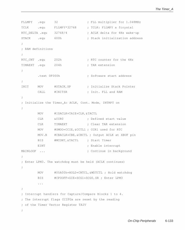
The Timer_A
6-133On-Chip Peripherals
FLLMPY .equ 32 ; FLL multiplier for 1.048MHz
TCLK .equ FLLMPY*32768 ; TCLK: FLLMPY x fcrystal
RTC_DELTA .equ 32768/4 ; ACLK delta for 4Hz wake–up
STACK .equ 600h ; Stack initialization address
;
; RAM definitions
;
RTC_CNT .equ 202h ; RTC counter for the 4Hz
TIMAEXT .equ 204h ; TAR extension
;
.text 0F000h ; Software start address
;
INIT MOV #STACK,SP ; Initialize Stack Pointer
CALL #INITSR ; Init. FLL and RAM
;
; Initialize the Timer_A: ACLK, Cont. Mode, INTRPT on
;
MOV #ISACLK+TAIE+CLR,&TACTL
CLR &CCR0 ; Defined start value
CLR TIMAEXT ; Clear TAR extension
MOV #OMOO+CCIE,&CCTL1 ; CCR1 used for RTC
MOV.B #CBACLK+CBE,&CBCTL ; Output ACLK at XBUF pin
BIS #MCONT,&TACTL ; Start Timer
EINT ; Enable interrupt
MAINLOOP ... ; Continue in background
;
; Enter LPM3. The watchdog must be held (ACLK continues)
;
MOV #05A00h+HOLD+CNTCL,&WDTCTL ; Hold watchdog
BIS #CPUOFF+GIE+SCG1+SCG0,SR ; Enter LPM3
...
;
; Interrupt handlers for Capture/Compare Blocks 1 to 4.
; The interrupt flags CCIFGx are reset by the reading
; of the Timer Vector Register TAIV
;
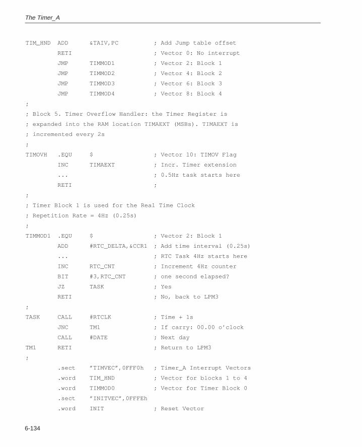
The Timer_A
6-134
TIM_HND ADD &TAIV,PC ; Add Jump table offset
RETI ; Vector 0: No interrupt
JMP TIMMOD1 ; Vector 2: Block 1
JMP TIMMOD2 ; Vector 4: Block 2
JMP TIMMOD3 ; Vector 6: Block 3
JMP TIMMOD4 ; Vector 8: Block 4
;
; Block 5. Timer Overflow Handler: the Timer Register is
; expanded into the RAM location TIMAEXT (MSBs). TIMAEXT is
; incremented every 2s
;
TIMOVH .EQU $ ; Vector 10: TIMOV Flag
INC TIMAEXT ; Incr. Timer extension
... ; 0.5Hz task starts here
RETI ;
;
; Timer Block 1 is used for the Real Time Clock
; Repetition Rate = 4Hz (0.25s)
;
TIMMOD1 .EQU $ ; Vector 2: Block 1
ADD #RTC_DELTA,&CCR1 ; Add time interval (0.25s)
... ; RTC Task 4Hz starts here
INC RTC_CNT ; Increment 4Hz counter
BIT #3,RTC_CNT ; one second elapsed?
JZ TASK ; Yes
RETI ; No, back to LPM3
;
TASK CALL #RTCLK ; Time + 1s
JNC TM1 ; If carry: 00.00 o’clock
CALL #DATE ; Next day
TM1 RETI ; Return to LPM3
;
.sect ”TIMVEC”,0FFF0h ; Timer_A Interrupt Vectors
.word TIM_HND ; Vector for blocks 1 to 4
.word TIMMOD0 ; Vector for Timer Block 0
.sect ”INITVEC”,0FFFEh
.word INIT ; Reset Vector
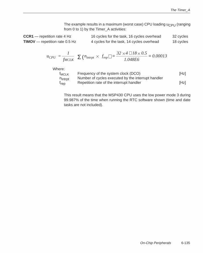
The Timer_A
6-135On-Chip Peripherals
The example results in a maximum (worst case) CPU loading uCPU (rangingfrom 0 to 1) by the Timer_A activities:
CCR1 — repetition rate 4 Hz 16 cycles for the task, 16 cycles overhead 32 cyclesTIMOV — repetition rate 0.5 Hz 4 cycles for the task, 14 cycles overhead 18 cycles
u =1
f n f
32 4 18 0.5
1.048E60.00013CPU
MCLKintrpt rep = + =Σ ( )
Where: fMCLK Frequency of the system clock (DCO) [Hz]nintrpt Number of cycles executed by the interrupt handlerfrep Repetition rate of the interrupt handler [Hz]
This result means that the MSP430 CPU uses the low power mode 3 during99.987% of the time when running the RTC software shown (time and datetasks are not included).
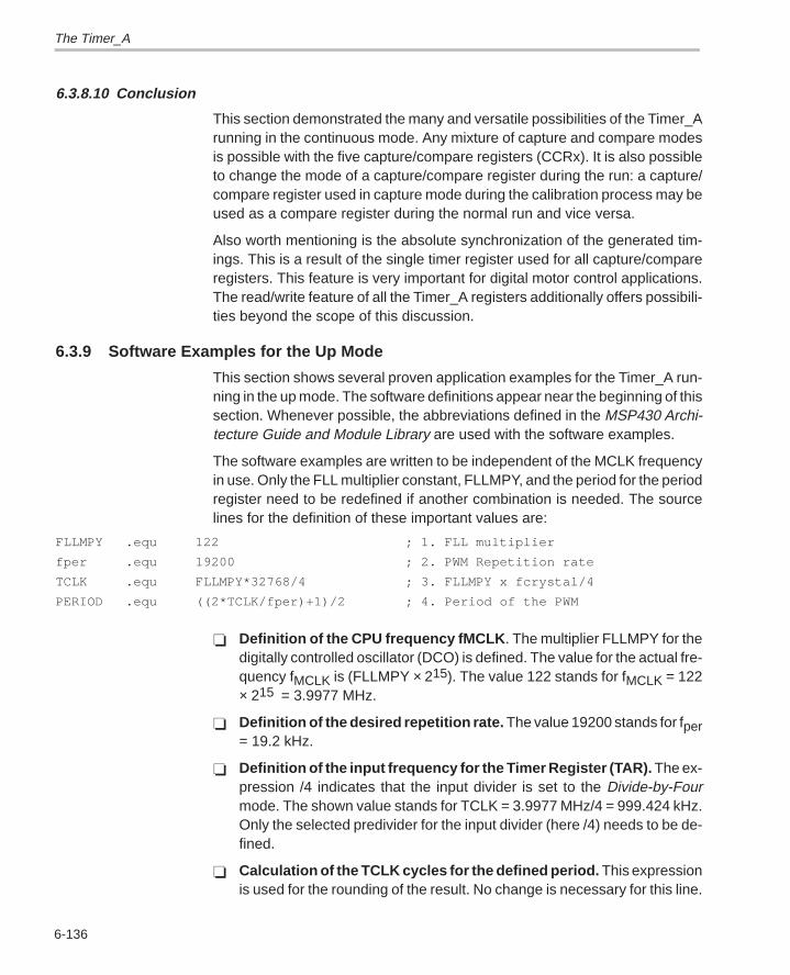
The Timer_A
6-136
6.3.8.10 Conclusion
This section demonstrated the many and versatile possibilities of the Timer_Arunning in the continuous mode. Any mixture of capture and compare modesis possible with the five capture/compare registers (CCRx). It is also possibleto change the mode of a capture/compare register during the run: a capture/compare register used in capture mode during the calibration process may beused as a compare register during the normal run and vice versa.
Also worth mentioning is the absolute synchronization of the generated tim-ings. This is a result of the single timer register used for all capture/compareregisters. This feature is very important for digital motor control applications.The read/write feature of all the Timer_A registers additionally offers possibili-ties beyond the scope of this discussion.
6.3.9 Software Examples for the Up Mode
This section shows several proven application examples for the Timer_A run-ning in the up mode. The software definitions appear near the beginning of thissection. Whenever possible, the abbreviations defined in the MSP430 Archi-tecture Guide and Module Library are used with the software examples.
The software examples are written to be independent of the MCLK frequencyin use. Only the FLL multiplier constant, FLLMPY, and the period for the periodregister need to be redefined if another combination is needed. The sourcelines for the definition of these important values are:
FLLMPY .equ 122 ; 1. FLL multiplier
fper .equ 19200 ; 2. PWM Repetition rate
TCLK .equ FLLMPY*32768/4 ; 3. FLLMPY x fcrystal/4
PERIOD .equ ((2*TCLK/fper)+1)/2 ; 4. Period of the PWM
Definition of the CPU frequency fMCLK . The multiplier FLLMPY for thedigitally controlled oscillator (DCO) is defined. The value for the actual fre-quency fMCLK is (FLLMPY × 215). The value 122 stands for fMCLK = 122× 215 = 3.9977 MHz.
Definition of the desired repetition rate. The value 19200 stands for fper= 19.2 kHz.
Definition of the input frequency for the Timer Register (TAR). The ex-pression /4 indicates that the input divider is set to the Divide-by-Fourmode. The shown value stands for TCLK = 3.9977 MHz/4 = 999.424 kHz.Only the selected predivider for the input divider (here /4) needs to be de-fined.
Calculation of the TCLK cycles for the defined period. This expressionis used for the rounding of the result. No change is necessary for this line.
The Timer_A
6-137On-Chip Peripherals
6.3.9.1 Common Remarks
The up mode is designed primarily for pulse width modulation (PWM) or DCgeneration applications. If none of these applications is needed, then the con-tinuous mode, with its five independent timings, should be used.
Advantages of the Up Mode:
Free run without CPU load for stable PWM values (e.g. DAC, PWM)
High PWM frequency is possible due to the pure hardware control
Clever selected timings are usable for more than one real time job
Disadvantages of the Up Mode:
Dominance of the period register — it defines the time frame for all othercapture/compare blocks (C/C Blocks)
Current switching occurs at the same time for all PWM outputs — this isthe case when the timer register (TAR) equals the period register CCR0
6.3.9.1.1 Initialization
The initialization subroutine, INITSR, is used in all examples. This subroutinewas described in Section 6.3.8.1. It includes the following tasks:
Checks the reason for the initialization (switch on of the supply voltage,watchdog interrupt, or activation of the RESET input)
Clears the RAM — or not — depending on the result of the above check.
Programs the system clock oscillator (multiplication factor N and optimumcurrent switch FN_2, FN_3, or FN_4)
Allows the digitally controlled oscillator to settle at the appropriate tap, pro-viding the correct MCLK frequency
6.3.9.1.2 Timer Clock
The information in this section is also valid for the continuous mode and theup/down mode.
All software examples use the value FLLMPY — it defines the master clockfrequency, fMCLK.
The Timer_A
6-138
f =
FLLMPY fMCLK crystal
If this frequency, fMCLK is too high for the application (it causes values for thetimer registers exceeding the range from 0 to 65535, for example), then theinput divider of the Timer_A may be used. This allows a prescaling of 1, 2, 4,or 8 for the timer input frequencies (fMCLK, fACLK or fTACLK)
Example 6–41. Prescaling Factor of 2
For a required prescaling of 2, the definitions at the start of each example aresimply changed to:
FLLMPY .equ 100 ; FLL multiplier for 3.2768MHz
TCLK .equ FLLMPY*32768/2 ; Timer Clock = 1.6384MHz
;
; Input Divider D2 is used to get MCLK/2 for the TCLK
;
MOV #ISMCLK+D2+MUP+TAIE+CLR,&TACTL ; Use /2 divider
The examples normally use an internally generated timer clock — the MCLKor the ACLK. It is also possible to use an external clock. This clock signal isconnected to the TACLK terminal and selected with the following code se-quence during the initialization:
; Ext. clock, Up Mode, Interrupt enabled, Timer Reg. cleared
;
MOV #ISTACLK+MUP+TAIE+CLR,&TACTL
BIS.B #TACLK,&P3SEL ; External clock to Timer_A
6.3.9.1.3 Timing Considerations
The five independent timings provided by the continuous mode are not pos-sible anymore in the noncontinuous modes because the period register(CCR0) dictates the timing frame for all other capture/compare blocks. There-fore, the period of the timer must be chosen very carefully to allow all the nec-essary timings. For example, a period chosen for PWM with 19.2 kHz also al-lows the timing for a software UART running at 2400 baud (19200/8) or 4800baud (19200/4).
The Timer_A
6-139On-Chip Peripherals
To allow comparison and capturing also with the noncontinuous modes, it isa good practice to have not only a register that counts the overflows (periodcounter) — like TIMAEXT used with the continuous mode — but also a 16-bitor 32-bit register that counts the TCLK cycles. This allows the use of simpleadditions for the calculation of a time point. Otherwise, a multiplication is nec-essary (period counter × period length) to get the elapsed time. The examplesgiven use both registers:
TIMACNT Period counter counts the number of full periodsTIMACYCx Cycle counter counts the cycles of the timing (one or more words)
See also figure 6–43; the contents of these two registers are shown there foran example.
Frequencies used by the CPU and the Timer_A . The following software ex-amples are (nearly) independent of the MCLK and timer clock frequency inuse. During the assembly, the new values for the period register and the timerclock frequency are calculated. A worst case calculation is necessary if afMCLK that is too low is used.
Update of Extension Registers . Unlike the case with the continuous mode,the update of these extension registers is made with the interrupt handler ofthe period register (CCR0). This has three reasons:
The interrupt of the period register occurs one cycle before the TIMOV in-terrupt
The period register (CCR0) has the highest interrupt priority of all Timer_Ainterrupts
A dedicated interrupt vector (address FFF2h) allows the fastest responseto interrupt requests
Real Time Environment. For all applications of the Timer_A running in oneof the noncontinuous modes and using interrupt frequencies in the kilohertzrange, it is recommended that strict real time environment programming beused. Otherwise, interrupt handlers are delayed and information may be lost.To achieve a real time environment, the following simple rules should be ap-plied to all interrupt handlers:
The first instruction after the processing of time critical data — Timer_Arelated data for the Timer_A handlers, for example — should be the EINT(Enable Interrupt) instruction. This allows nested interrupts, a feature pos-sible due to the stack architecture of the MSP430 family.
Interrupt handlers should be as short as possible. Only the absolutely nec-essary tasks should be executed (incrementing of counters, update of the
The Timer_A
6-140
status bytes, etc.). The time consuming main tasks should be shifted to thebackground, where the software executes them according to the statusbyte information.
Output Units. The PWM examples shown all use the set/reset mode or thereset/set mode of the output units. This has the advantage — compared to theuse of toggling — that no incorrect pulse widths can be generated during thechange of the pulse width.
6.3.9.1.4 Interrupt Overhead
The calculations for the CPU loading that are appended to the software exam-ples split the necessary cycles for each capture/compare block into two parts:
Overhead — This part sums the cycles that are necessary for the CPUto execute the interrupt (saving of the program counter and the status reg-ister, decision on which interrupt needs to be served, restoring of the CPUregisters).
Update or Task — This part actually does the work that needs to be done(incrementing of counters, changing of status bytes, etc.).
The number of overhead cycles shown with the examples are derived from thefollowing sequences:
Interrupt of the period register CCR0 (or other interrupt sources with adedicated vector):
Cycles from interrupt request to 1st instruction of the interrupt handler: 6 cyclesReturn from Interrupt instruction: RETI 5 cyclesSum of overhead 11 cycles
Interrupt of capture/compare registers CCR1 to CCR4:
Cycles from interrupt request to 1st instruction of the interrupt handler: 6 cyclesDecision which source caused the interrupt: ADD &TAIV,PC 3 cyclesAddressed jump instruction: JMP TIMMODx 2 cyclesReturn from Interrupt instruction RETI 5 cyclesSum of overhead 16 cycles
Interrupt of the timer register TIMOV:
This interrupt needs the same number of cycles as the interrupt ofthe capture/compare registers, but without the JMP TIMMODx in-struction. This results in 14 cycles overhead.
The Timer_A
6-141On-Chip Peripherals
6.3.9.2 Update of the Capture/Compare Registers
If the capture/compare registers are updated asynchronously with the periodictiming of the Timer_A, the output pulses may become too long or may be miss-ing. Therefore, a synchronous update should be used, which means the PWMvalue is written into a buffer, read out from this buffer at the correct time, andthen written into the capture/compare register. Three possibilities exist for thesynchronous update:
1) Frequent update by the appropriate Interrupt Handler
2) Infrequent update by the appropriate Interrupt Handler
3) Update by the interrupt handler of capture/compare block 0
The three possibilities are described in the following paragraphs. To find theappropriate solution for a given timing problem, the following decision pathmay be used:
Is an individual interrupt task necessary for one ore more than one of thecapture/compare blocks? If yes, use solution 1, otherwise continue.
Is a very fast update of the capture/compare registers necessary? If yes,use solution 1, otherwise solution 2.
Frequent Update by the Appropriate Interrupt Handler
The interrupt handler of capture/compare block x updates the capture/compare register CCRx with the repetition rate defined by the period register(CCR0). This method is necessary if an additional task is to be executed bythe interrupt handler — medium preparation effort in the background, fast C/Cregister change.
This method is used with Generation of Asymmetric Pulse Width Modulationand RF Timing Generation. The following software examples refer to the firstapplication.
If the range for the PWM output values is limited from 1 cycle to (period–1)cycles, then the following simple update sequence may be used:
; R6 contains new PWM info for CCR2. Range: 1 to (period–1).
;
MOV.B R6,TA2PWM ; Actualize PWM buffer
If the PWM output values 0% or 100% are actually used (CCRx = 0 resp. CCRx≥ period), then a special treatment is necessary due to the not-generated inter-rupt request of the capture/compare block x under these circumstances. The
The Timer_A
6-142
new CCRx value is then written immediately. To determine these specialcases, the following update sequence may be used:
; R6 contains new PWM info for CCR2. Range: 0 to full period.
; Check if an immediate update is necessary:
; This is the case for CCR2 = 0 .or. CCR2 >= period
; Software is written for a constant Period Register CCR0
;
CMP #PERIOD,&CCR2 ; CCR2 actually >= period?
JHS L$21 ; Yes, update CCR2 immediately
TST &CCR2 ; No, CCR2 = 0?
JNZ L$22 ; CCR2 > 0: normal procedure
L$21 MOV R6,&CCR2 ; No interrupt: immed. update
L$22 MOV.B R6,TA2PWM ; Actualize TA2PWM buffer
... ; Continue
Infrequent Update by the Appropriate Interrupt Handler
The interrupt handler of capture/compare block x updates the capture/compare register (CCRx) with a repetition rate given by the calculation speedof the background program. If a new PWM value is calculated for a capture/compare block, then an individual flag is set and the interrupt for this capture/compare block is enabled. The first asynchronous interrupt is rejected and thesecond one (synchronous) is used for the update of the capture/compare reg-ister x. An interrupt task is possible only with the update repetition rate. Thismethod is used if the PWM values for the update are not available at the sametime — minimum interrupt overhead, individual C/C register change.
This method is used with Digital–to–Analog Conversion and TRIAC Control.The following software examples refer to the first application.
If the range for the PWM output values is limited from 1 cycle to (period–1)cycles, then the following simple update sequence may be used:
; R6 contains new PWM info for CCR2. Range: 1 to (period–1).
;
MOV R6,DAC0OV ; Actualize DAC0 pulse length
BIS.B #1,FLAG ; Set update flag for DAC0
BIS #CCIE,&CCTL2 ; Enable interrupt for DAC0
.... ; Continue in background
The Timer_A
6-143On-Chip Peripherals
If the output values 0% or 100% are actually used (CCRx = 0 resp. CCRx ≥.period), then a special treatment is necessary. The interrupt of the capture/compare block x is not generated in these cases. To determine these specialcases, the following update sequence may be used:
; R6 contains the new PWM info for CCR2. Range: 0 to period.
; The interrupt is enabled individually for the update.
; A check is made if a special treatment is necessary:
; CCR2 = 0 .or. CCR2 >= period
; Software is written for a variable Period Register CCR0
;
MOV R6,DAC0OV ; Actualize DAC0 pulse length
CMP &CCR2,&CCR0 ; CCR2 >= period actually?
JLO L$21 ; Yes, update CCR2 immediat.
TST &CCR2 ; No, is CCR2 = 0 actually?
JNZ L$22 ; No, proceed normally
L$21 MOV R6,&CCR2 ; Update CCR2 immediately
JMP L$23 ; Update made, no interrupt
L$22 BIS.B #1,FLAG ; Set update flag for DAC0
BIS #CCIE,&CCTL2 ; Enable interrupt for DAC0
L$23 .... ; Continue in background
For a constant period register (CCR0), the sequence is:
; Software is written for a constant period register CCR0
;
MOV R6,DAC0OV ; Actualize DAC0 pulse length
CMP #PERIOD,&CCR2 ; CCR2 >= period actually?
JHS L$21 ; Yes, update CCR2 immediat.
TST &CCR2 ; No, is CCR2 = 0 actually?
.... ; Same as above;
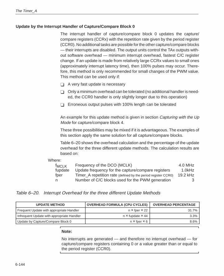
The Timer_A
6-144
Update by the Interrupt Handler of Capture/Compare Block 0
The interrupt handler of capture/compare block 0 updates the capture/compare registers (CCRx) with the repetition rate given by the period register(CCR0). No additional tasks are possible for the other capture/compare blocks— their interrupts are disabled. The output units control the TAx outputs with-out software overhead — minimum interrupt overhead, fastest C/C registerchange. If an update is made from relatively large CCRx values to small ones(approximately interrupt latency time), then 100% pulses may occur. There-fore, this method is only recommended for small changes of the PWM value.This method can be used only if:
A very fast update is necessary
Only a minimum overhead can be tolerated (no additional handler is need-ed, the CCR0 handler is only slightly longer due to this operation)
Erroneous output pulses with 100% length can be tolerated
An example for this update method is given in section Capturing with the UpMode for capture/compare block 4.
These three possibilities may be mixed if it is advantageous. The examples ofthis section apply the same solution for all capture/compare blocks.
Table 6–20 shows the overhead calculation and the percentage of the updateoverhead for the three different update methods. The calculation results arebased on:
Where: fMCLK Frequency of the DCO (MCLK) 4.0 MHzfupdate Update frequency for the capture/compare registers 1.0kHzfper Timer_A repetition rate (defined by the period register CCR0) 19.2 kHzn Number of C/C blocks used for the PWM generation 3
Table 6–20. Interrupt Overhead for the three different Update Methods
UPDATE METHOD OVERHEAD FORMULA (CPU CYCLES) OVERHEAD PERCENTAGE
Frequent Update with appropriate Handler n × fper × 22 31.7%
Infrequent Update with appropriate Handler n × fupdate × 44 3.3%
Update by Capture/Compare Block 0 n × fper × 6 8.6%
Note:
No interrupts are generated — and therefore no interrupt overhead — forcapture/compare registers containing 0 or a value greater than or equal tothe period register (CCR0).
The Timer_A
6-145On-Chip Peripherals
6.3.9.3 Generation of Asymmetric Pulse Width Modulation (PWM)
The medium output voltage VPWM at the pin TAx resp. the necessary registercontent nccrx for a given voltage VPWM is:
( )V Vccn
n + 1Vcc
tn
V
Vccn + 1PWM
CCRx
CCR0CCRx
PWMCCR0
pw= × = × → ×=
tper
Where: VPWM Medium output voltage at the TAx pin [V]VCC Supply voltage of the system [V]nCCR0 Content of the period register CCR0nCCRx Content of the capture/compare register CCRxtpw Time generated by the capture/compare register [s]tper Period generated by the period register CCR0 [s]
Table 6–21 shows the necessary content of a capture/compare register CCRxto get some defined unsigned output values for VPWM:
Table 6–21. Output Voltages for unsigned PWM
OUTPUT VOLTAGE (VPWM) CONTENT OF CCRx nCCRx0 V 0
0.25 VCC (nCCR0 + 1) 0.25
0.5 VCC (nCCR0 + 1) 0.5
0.75 VCC (nCCR0 + 1) 0.75
VCC (nCCR0 + 1)
If the output voltage is seen as a signed voltage — like for 3-phase digital motorcontrol — then the voltage 0.5 × VCC is seen as the 0 point. The signed outputvoltage VPWM gets:
( )V Vccn
n + 10.5 n
V
Vcc0.5 n + 1PWM
CCRx
CCR0CCRx
PWMCCR0= – = + ( ( ))
Table 6–22 shows the contents of a capture/compare register (CCRx) requiredto get some defined values for a signed output voltage VPWM:
The Timer_A
6-146
Table 6–22. Output Voltages for Signed PWM
OUTPUT VOLTAGE (VPWM) CONTENT OF CCRx nCCRx COMMENT
–0.5 VCC 0 Most negative output voltage
–0.25 VCC (nCCR0 + 1) 0.25 Half negative output voltage
0 V (nCCR0 + 1) 0.5 0 voltage
0.25 VCC (nCCR0 + 1) 0.75 Half positive output voltage
0.5 VCC nCCR0 + 1 Most positive output voltage
Example 6–42. Generation of Two PWM Output Signals
The software example shows the generation of two PWM output signals at theoutput terminals TA1 and TA2:
Output Pin TA1 — a positive PWM signal. The length of the active highpart is defined in the RAM location TA1PWM (TCLK cycles).
Output Pin TA2 — a negative PWM signal. The length of the active lowpart is defined in the RAM location TA2PWM (TCLK cycles).
Additional tasks need to be executed by the interrupt handlers of the capture/compare blocks 1 and 2, therefore an individual handler is used for both ofthem.
The system clock frequency in use is 4 MHz (exactly fMCLK = 122 × 32768 =3.9977 MHz), and the pulse repetition frequency is 19.2 kHz to allow the useof this frequency for other timings as well (a software UART with 4800 baud= 19.2 kHz/4, for example). For this application, bytes are sufficient forTA1PWM and TA2PWM because the maximum possible value of its contentis 209. (4.0 MHz/19200 = 208.33).
The output unit 0 outputs 9600 Hz without any overhead. This signal may beused for peripherals or for synchronization — the signal is always present,even if the signals at TA1 and TA2 disappear due to an output signal with 0%or 100% pulse width.
The example uses the Frequent Update by the Appropriate Interrupt Handler.See Section 6.3.9.2 for details.
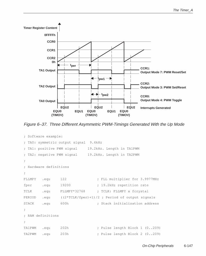
The Timer_A
6-147On-Chip Peripherals
0FFFFh
CCR0
CCR1
CCR20h
TA1 Output
TA2 Output
TA0 Output
EQU1 EQU1 EQU0(TIMOV)
EQU2 EQU2 EQU2
CCR1:Output Mode 7: PWM Reset/Set
CCR2:Output Mode 3: PWM Set/Reset
CCR0:Output Mode 4: PWM Toggle
Interrupts GeneratedEQU0
(TIMOV)EQU0
(TIMOV)
Timer Register Content
tper
tpw1
tpw2
Figure 6–37. Three Different Asymmetric PWM-Timings Generated With the Up Mode
; Software example:
; TA0: symmetric output signal 9.6kHz
; TA1: positive PWM signal 19.2kHz. Length in TA1PWM
; TA2: negative PWM signal 19.2kHz. Length in TA2PWM
;
; Hardware definitions
;
FLLMPY .equ 122 ; FLL multiplier for 3.9977MHz
fper .equ 19200 ; 19.2kHz repetition rate
TCLK .equ FLLMPY*32768 ; TCLK: FLLMPY x fcrystal
PERIOD .equ ((2*TCLK/fper)+1)/2 ; Period of output signals
STACK .equ 600h ; Stack initialization address
;
; RAM definitions
;
TA1PWM .equ 202h ; Pulse length Block 1 (0..209)
TA2PWM .equ 203h ; Pulse length Block 2 (0..209)
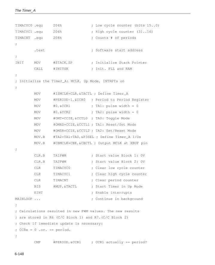
The Timer_A
6-148
TIMACYC0 .equ 204h ; Low cycle counter (bits 15..0)
TIMACYC1 .equ 206h ; High cycle counter (31..16)
TIMACNT .equ 208h ; Counts # of periods
;
.text ; Software start address
;
INIT MOV #STACK,SP ; Initialize Stack Pointer
CALL #INITSR ; Init. FLL and RAM
;
; Initialize the Timer_A: MCLK, Up Mode, INTRPTs on
;
MOV #ISMCLK+CLR,&TACTL ; Define Timer_A
MOV #PERIOD–1,&CCR0 ; Period to Period Register
MOV #0,&CCR1 ; TA1: pulse width = 0
MOV #0,&CCR2 ; TA2: pulse width = 0
MOV #OMT+CCIE,&CCTL0 ; TA0: Toggle Mode
MOV #OMRS+CCIE,&CCTL1 ; TA1: Reset/Set Mode
MOV #OMSR+CCIE,&CCTL2 ; TA2: Set/Reset Mode
MOV.B #TA2+TA1+TA0,&P3SEL ; Define Timer_A I/Os
MOV.B #CBMCLK+CBE,&CBCTL ; Output MCLK at XBUF pin
;
CLR.B TA1PWM ; Start value Block 1: 0V
CLR.B TA2PWM ; Start value Block 2: 0V
CLR TIMACYC0 ; Clear low cycle counter
CLR TIMACYC1 ; Clear high cycle counter
CLR TIMACNT ; Clear period counter
BIS #MUP,&TACTL ; Start Timer in Up Mode
EINT ; Enable interrupts
MAINLOOP ... ; Continue in background
;
; Calculations resulted in new PWM values. The new results
; are stored in R6 (C/C Block 1) and R7.(C/C Block 2)
; Check if immediate update is necessary:
; CCRx = 0 .or. >= period.
;
CMP #PERIOD,&CCR1 ; CCR1 actually >= period?
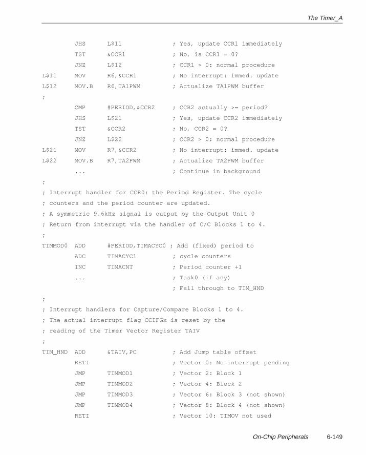
The Timer_A
6-149On-Chip Peripherals
JHS L$11 ; Yes, update CCR1 immediately
TST &CCR1 ; No, is CCR1 = 0?
JNZ L$12 ; CCR1 > 0: normal procedure
L$11 MOV R6,&CCR1 ; No interrupt: immed. update
L$12 MOV.B R6,TA1PWM ; Actualize TA1PWM buffer
;
CMP #PERIOD,&CCR2 ; CCR2 actually >= period?
JHS L$21 ; Yes, update CCR2 immediately
TST &CCR2 ; No, CCR2 = 0?
JNZ L$22 ; CCR2 > 0: normal procedure
L$21 MOV R7,&CCR2 ; No interrupt: immed. update
L$22 MOV.B R7,TA2PWM ; Actualize TA2PWM buffer
... ; Continue in background
;
; Interrupt handler for CCR0: the Period Register. The cycle
; counters and the period counter are updated.
; A symmetric 9.6kHz signal is output by the Output Unit 0
; Return from interrupt via the handler of C/C Blocks 1 to 4.
;
TIMMOD0 ADD #PERIOD,TIMACYC0 ; Add (fixed) period to
ADC TIMACYC1 ; cycle counters
INC TIMACNT ; Period counter +1
... ; Task0 (if any)
; Fall through to TIM_HND
;
; Interrupt handlers for Capture/Compare Blocks 1 to 4.
; The actual interrupt flag CCIFGx is reset by the
; reading of the Timer Vector Register TAIV
;
TIM_HND ADD &TAIV,PC ; Add Jump table offset
RETI ; Vector 0: No interrupt pending
JMP TIMMOD1 ; Vector 2: Block 1
JMP TIMMOD2 ; Vector 4: Block 2
JMP TIMMOD3 ; Vector 6: Block 3 (not shown)
JMP TIMMOD4 ; Vector 8: Block 4 (not shown)
RETI ; Vector 10: TIMOV not used
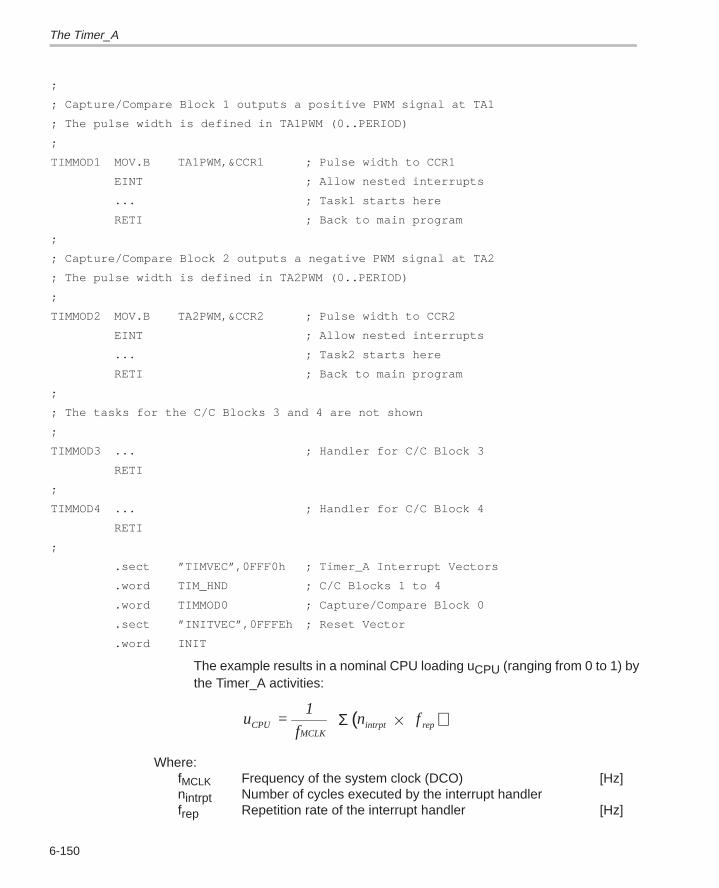
The Timer_A
6-150
;
; Capture/Compare Block 1 outputs a positive PWM signal at TA1
; The pulse width is defined in TA1PWM (0..PERIOD)
;
TIMMOD1 MOV.B TA1PWM,&CCR1 ; Pulse width to CCR1
EINT ; Allow nested interrupts
... ; Task1 starts here
RETI ; Back to main program
;
; Capture/Compare Block 2 outputs a negative PWM signal at TA2
; The pulse width is defined in TA2PWM (0..PERIOD)
;
TIMMOD2 MOV.B TA2PWM,&CCR2 ; Pulse width to CCR2
EINT ; Allow nested interrupts
... ; Task2 starts here
RETI ; Back to main program
;
; The tasks for the C/C Blocks 3 and 4 are not shown
;
TIMMOD3 ... ; Handler for C/C Block 3
RETI
;
TIMMOD4 ... ; Handler for C/C Block 4
RETI
;
.sect ”TIMVEC”,0FFF0h ; Timer_A Interrupt Vectors
.word TIM_HND ; C/C Blocks 1 to 4
.word TIMMOD0 ; Capture/Compare Block 0
.sect ”INITVEC”,0FFFEh ; Reset Vector
.word INIT
The example results in a nominal CPU loading uCPU (ranging from 0 to 1) bythe Timer_A activities:
u =1
f n
f CPU
MCLKintrpt repΣ ( )
Where: fMCLK Frequency of the system clock (DCO) [Hz]nintrpt Number of cycles executed by the interrupt handlerfrep Repetition rate of the interrupt handler [Hz]
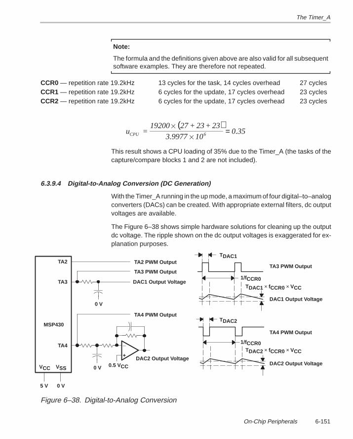
The Timer_A
6-151On-Chip Peripherals
Note:
The formula and the definitions given above are also valid for all subsequentsoftware examples. They are therefore not repeated.
CCR0 — repetition rate 19.2kHz 13 cycles for the task, 14 cycles overhead 27 cyclesCCR1 — repetition rate 19.2kHz 6 cycles for the update, 17 cycles overhead 23 cyclesCCR2 — repetition rate 19.2kHz 6 cycles for the update, 17 cycles overhead 23 cycles
( )u =
19200 27 + 23+ 23
3.9977 100.35CPU 6
=
This result shows a CPU loading of 35% due to the Timer_A (the tasks of thecapture/compare blocks 1 and 2 are not included).
6.3.9.4 Digital-to-Analog Conversion (DC Generation)
With the Timer_A running in the up mode, a maximum of four digital–to–analogconverters (DACs) can be created. With appropriate external filters, dc outputvoltages are available.
The Figure 6–38 shows simple hardware solutions for cleaning up the outputdc voltage. The ripple shown on the dc output voltages is exaggerated for ex-planation purposes.
_
+DAC2 Output Voltage
0 V
TA3
TA4
VCC VSS
0 V5 V
TA4 PWM Output
MSP430
0.5 VCC
TDAC1
1/fCCR0TDAC1 × fCCR0 × VCC
DAC1 Output Voltage
TA3 PWM Output
0 V
TA2
DAC1 Output Voltage
TA3 PWM Output
TA2 PWM Output
1/fCCR0
TDAC2
TA4 PWM Output
TDAC2 × fCCR0 × VCC
DAC2 Output Voltage
Figure 6–38. Digital-to-Analog Conversion
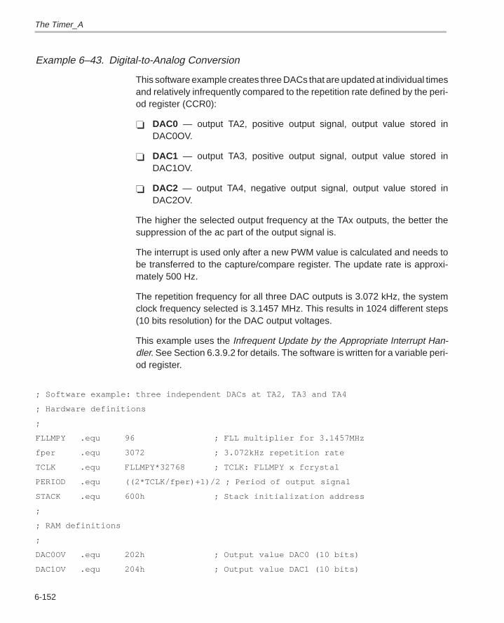
The Timer_A
6-152
Example 6–43. Digital-to-Analog Conversion
This software example creates three DACs that are updated at individual timesand relatively infrequently compared to the repetition rate defined by the peri-od register (CCR0):
DAC0 — output TA2, positive output signal, output value stored inDAC0OV.
DAC1 — output TA3, positive output signal, output value stored inDAC1OV.
DAC2 — output TA4, negative output signal, output value stored inDAC2OV.
The higher the selected output frequency at the TAx outputs, the better thesuppression of the ac part of the output signal is.
The interrupt is used only after a new PWM value is calculated and needs tobe transferred to the capture/compare register. The update rate is approxi-mately 500 Hz.
The repetition frequency for all three DAC outputs is 3.072 kHz, the systemclock frequency selected is 3.1457 MHz. This results in 1024 different steps(10 bits resolution) for the DAC output voltages.
This example uses the Infrequent Update by the Appropriate Interrupt Han-dler. See Section 6.3.9.2 for details. The software is written for a variable peri-od register.
; Software example: three independent DACs at TA2, TA3 and TA4
; Hardware definitions
;
FLLMPY .equ 96 ; FLL multiplier for 3.1457MHz
fper .equ 3072 ; 3.072kHz repetition rate
TCLK .equ FLLMPY*32768 ; TCLK: FLLMPY x fcrystal
PERIOD .equ ((2*TCLK/fper)+1)/2 ; Period of output signal
STACK .equ 600h ; Stack initialization address
;
; RAM definitions
;
DAC0OV .equ 202h ; Output value DAC0 (10 bits)
DAC1OV .equ 204h ; Output value DAC1 (10 bits)
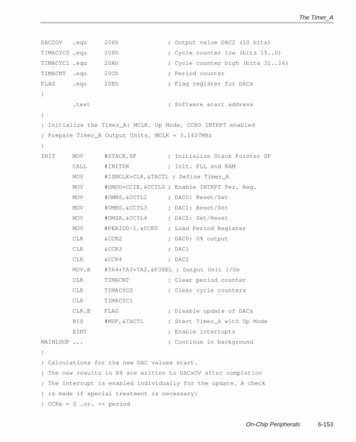
The Timer_A
6-153On-Chip Peripherals
DAC2OV .equ 206h ; Output value DAC2 (10 bits)
TIMACYC0 .equ 208h ; Cycle counter low (bits 15..0)
TIMACYC1 .equ 20Ah ; Cycle counter high (bits 31..16)
TIMACNT .equ 20Ch ; Period counter
FLAG .equ 20Eh ; Flag register for DACs
;
.text ; Software start address
;
; Initialize the Timer_A: MCLK, Up Mode, CCR0 INTRPT enabled
; Prepare Timer_A Output Units, MCLK = 3.1457MHz
;
INIT MOV #STACK,SP ; Initialize Stack Pointer SP
CALL #INITSR ; Init. FLL and RAM
MOV #ISMCLK+CLR,&TACTL ; Define Timer_A
MOV #OMOO+CCIE,&CCTL0 ; Enable INTRPT Per. Reg.
MOV #OMRS,&CCTL2 ; DAC0: Reset/Set
MOV #OMRS,&CCTL3 ; DAC1: Reset/Set
MOV #OMSR,&CCTL4 ; DAC2: Set/Reset
MOV #PERIOD–1,&CCR0 ; Load Period Register
CLR &CCR2 ; DAC0: 0% output
CLR &CCR3 ; DAC1
CLR &CCR4 ; DAC2
MOV.B #TA4+TA3+TA2,&P3SEL ; Output Unit I/Os
CLR TIMACNT ; Clear period counter
CLR TIMACYC0 ; Clear cycle counters
CLR TIMACYC1
CLR.B FLAG ; Disable update of DACs
BIS #MUP,&TACTL ; Start Timer_A with Up Mode
EINT ; Enable interrupts
MAINLOOP ... ; Continue in background
;
; Calculations for the new DAC values start.
; The new results in R6 are written to DACxOV after completion
; The interrupt is enabled individually for the update. A check
; is made if special treatment is necessary:
; CCRx = 0 .or. >= period
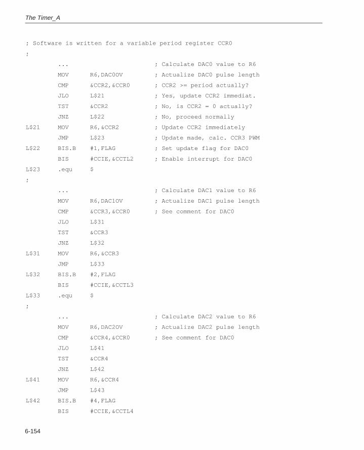
The Timer_A
6-154
; Software is written for a variable period register CCR0
;
... ; Calculate DAC0 value to R6
MOV R6,DAC0OV ; Actualize DAC0 pulse length
CMP &CCR2,&CCR0 ; CCR2 >= period actually?
JLO L$21 ; Yes, update CCR2 immediat.
TST &CCR2 ; No, is CCR2 = 0 actually?
JNZ L$22 ; No, proceed normally
L$21 MOV R6,&CCR2 ; Update CCR2 immediately
JMP L$23 ; Update made, calc. CCR3 PWM
L$22 BIS.B #1,FLAG ; Set update flag for DAC0
BIS #CCIE,&CCTL2 ; Enable interrupt for DAC0
L$23 .equ $
;
... ; Calculate DAC1 value to R6
MOV R6,DAC1OV ; Actualize DAC1 pulse length
CMP &CCR3,&CCR0 ; See comment for DAC0
JLO L$31
TST &CCR3
JNZ L$32
L$31 MOV R6,&CCR3
JMP L$33
L$32 BIS.B #2,FLAG
BIS #CCIE,&CCTL3
L$33 .equ $
;
... ; Calculate DAC2 value to R6
MOV R6,DAC2OV ; Actualize DAC2 pulse length
CMP &CCR4,&CCR0 ; See comment for DAC0
JLO L$41
TST &CCR4
JNZ L$42
L$41 MOV R6,&CCR4
JMP L$43
L$42 BIS.B #4,FLAG
BIS #CCIE,&CCTL4
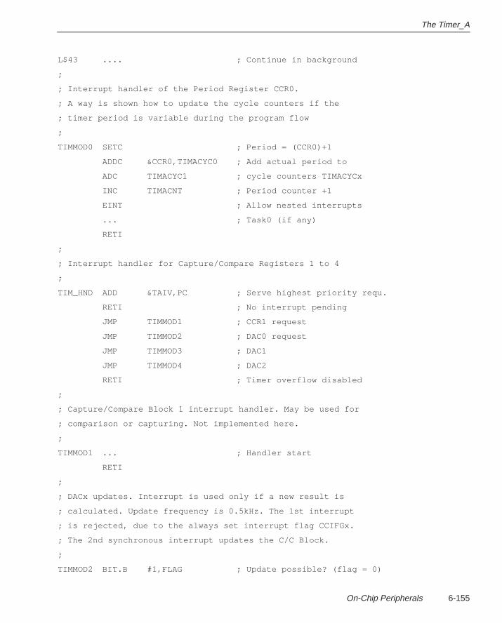
The Timer_A
6-155On-Chip Peripherals
L$43 .... ; Continue in background
;
; Interrupt handler of the Period Register CCR0.
; A way is shown how to update the cycle counters if the
; timer period is variable during the program flow
;
TIMMOD0 SETC ; Period = (CCR0)+1
ADDC &CCR0,TIMACYC0 ; Add actual period to
ADC TIMACYC1 ; cycle counters TIMACYCx
INC TIMACNT ; Period counter +1
EINT ; Allow nested interrupts
... ; Task0 (if any)
RETI
;
; Interrupt handler for Capture/Compare Registers 1 to 4
;
TIM_HND ADD &TAIV,PC ; Serve highest priority requ.
RETI ; No interrupt pending
JMP TIMMOD1 ; CCR1 request
JMP TIMMOD2 ; DAC0 request
JMP TIMMOD3 ; DAC1
JMP TIMMOD4 ; DAC2
RETI ; Timer overflow disabled
;
; Capture/Compare Block 1 interrupt handler. May be used for
; comparison or capturing. Not implemented here.
;
TIMMOD1 ... ; Handler start
RETI
;
; DACx updates. Interrupt is used only if a new result is
; calculated. Update frequency is 0.5kHz. The 1st interrupt
; is rejected, due to the always set interrupt flag CCIFGx.
; The 2nd synchronous interrupt updates the C/C Block.
;
TIMMOD2 BIT.B #1,FLAG ; Update possible? (flag = 0)
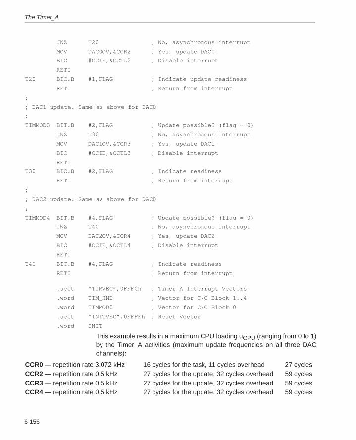
The Timer_A
6-156
JNZ T20 ; No, asynchronous interrupt
MOV DAC0OV,&CCR2 ; Yes, update DAC0
BIC #CCIE,&CCTL2 ; Disable interrupt
RETI
T20 BIC.B #1,FLAG ; Indicate update readiness
RETI ; Return from interrupt
;
; DAC1 update. Same as above for DAC0
;
TIMMOD3 BIT.B #2,FLAG ; Update possible? (flag = 0)
JNZ T30 ; No, asynchronous interrupt
MOV DAC1OV,&CCR3 ; Yes, update DAC1
BIC #CCIE,&CCTL3 ; Disable interrupt
RETI
T30 BIC.B #2,FLAG ; Indicate readiness
RETI ; Return from interrupt
;
; DAC2 update. Same as above for DAC0
;
TIMMOD4 BIT.B #4,FLAG ; Update possible? (flag = 0)
JNZ T40 ; No, asynchronous interrupt
MOV DAC2OV,&CCR4 ; Yes, update DAC2
BIC #CCIE,&CCTL4 ; Disable interrupt
RETI
T40 BIC.B #4,FLAG ; Indicate readiness
RETI ; Return from interrupt
.sect ”TIMVEC”,0FFF0h ; Timer_A Interrupt Vectors
.word TIM_HND ; Vector for C/C Block 1..4
.word TIMMOD0 ; Vector for C/C Block 0
.sect ”INITVEC”,0FFFEh ; Reset Vector
.word INIT
This example results in a maximum CPU loading uCPU (ranging from 0 to 1)by the Timer_A activities (maximum update frequencies on all three DACchannels):
CCR0 — repetition rate 3.072 kHz 16 cycles for the task, 11 cycles overhead 27 cyclesCCR2 — repetition rate 0.5 kHz 27 cycles for the update, 32 cycles overhead 59 cyclesCCR3 — repetition rate 0.5 kHz 27 cycles for the update, 32 cycles overhead 59 cyclesCCR4 — repetition rate 0.5 kHz 27 cycles for the update, 32 cycles overhead 59 cycles
The Timer_A
6-157On-Chip Peripherals
( )u =
3072 27 500 59 59 59
3.1457 100.055CPU 6
+ + +
=
Note that an update for the capture/compare blocks 2 to 4 needs two interruptservices. The above result means a worst case CPU loading of approximate5.5% due to the three DACs.
If all three tasks are updated with a 100 Hz update rate, then the CPU is loadedwith only 3.2%.
6.3.9.5 TRIAC Control
TRIAC control for electric motors (DMC) or other loads is also possible withthe up mode of the Timer_A. But the time frame, defined by the period register,does not allow the same resolution as with the continuous mode. The controlsoftware now counts the number of periods and fires the TRIAC after thereaching of the programmed number.
The medium resolution pmed is:
p 1
2 f tmed
perMAINS=
Where: fMAINS AC Line frequency [Hz]tper Period of the Timer_A, defined by CCR0 [s]
The integrated energy E of a sine half wave dependent on the time t is de-scribed by the equation:
E 1 cos t = 1 cos 2 f t t = 0 ...1
2f – –ω π
Due to this nonlinear energy increase, the worst case resolution pmin — nearthe angle π/4 (90) — is reduced by a factor of π/2 (1.57) compared to the me-dium resolution pmed:
p 1
2 f tper / 2 min
MAINS=
π
The TRIAC control software contains fewer security features than the versionshown for the continuous mode:
The zero crossing part (P0.0 handler) immediately switches the gate sig-nal off by setting terminal TA0 to high. This prevents the firing for the nexthalf wave.
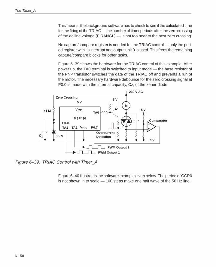
The Timer_A
6-158
This means, the background software has to check to see if the calculated timefor the firing of the TRIAC — the number of timer periods after the zero crossingof the ac line voltage (FIRANGL) — is not too near to the next zero crossing.
No capture/compare register is needed for the TRIAC control — only the peri-od register with its interrupt and output unit 0 is used. This frees the remainingcapture/compare blocks for other tasks.
Figure 6–39 shows the hardware for the TRIAC control of this example. Afterpower up, the TA0 terminal is switched to input mode — the base resistor ofthe PNP transistor switches the gate of the TRIAC off and prevents a run ofthe motor. The necessary hardware debounce for the zero crossing signal atP0.0 is made with the internal capacity, Cz, of the zener diode.
Zero Crossing
3.5 V
MSP430
TA0
5 V
TA2
VCC
VSS
5 V
0 V
M
OvercurrentDetection
P0.7_
+
Comparator
5 V
230 V AC
TA1
PWM Output 2
PWM Output 1
P0.0
Cz
>1 M
Figure 6–39. TRIAC Control with Timer_A
Figure 6–40 illustrates the software example given below. The period of CCR0is not shown in to scale — 160 steps make one half wave of the 50 Hz line.
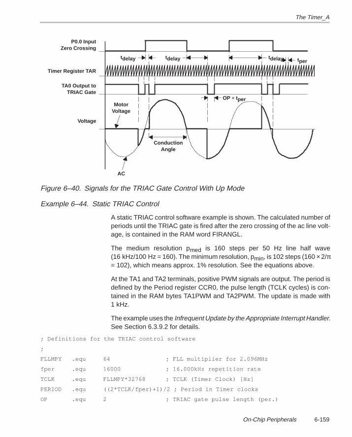
The Timer_A
6-159On-Chip Peripherals
tdelay tdelay tdelay
MotorVoltage
AC
ConductionAngle
P0.0 InputZero Crossing
Timer Register TAR
TA0 Output toTRIAC Gate
Voltage
tper
OP × tper
Figure 6–40. Signals for the TRIAC Gate Control With Up Mode
Example 6–44. Static TRIAC Control
A static TRIAC control software example is shown. The calculated number ofperiods until the TRIAC gate is fired after the zero crossing of the ac line volt-age, is contained in the RAM word FIRANGL.
The medium resolution pmed is 160 steps per 50 Hz line half wave(16 kHz/100 Hz = 160). The minimum resolution, pmin, is 102 steps (160 × 2/π= 102), which means approx. 1% resolution. See the equations above.
At the TA1 and TA2 terminals, positive PWM signals are output. The period isdefined by the Period register CCR0, the pulse length (TCLK cycles) is con-tained in the RAM bytes TA1PWM and TA2PWM. The update is made with1 kHz.
The example uses the Infrequent Update by the Appropriate Interrupt Handler.See Section 6.3.9.2 for details.
; Definitions for the TRIAC control software
;
FLLMPY .equ 64 ; FLL multiplier for 2.096MHz
fper .equ 16000 ; 16.000kHz repetition rate
TCLK .equ FLLMPY*32768 ; TCLK (Timer Clock) [Hz]
PERIOD .equ ((2*TCLK/fper)+1)/2 ; Period in Timer clocks
OP .equ 2 ; TRIAC gate pulse length (per.)
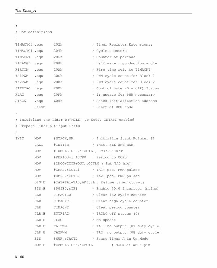
The Timer_A
6-160
;
; RAM definitions
;
TIMACYC0 .equ 202h ; Timer Register Extensions:
TIMACYC1 .equ 204h ; Cycle counters
TIMACNT .equ 206h ; Counter of periods
FIRANGL .equ 208h ; Half wave – conduction angle
FIRTIM .equ 20Ah ; Fire time rel. to TIMACNT
TA1PWM .equ 20Ch ; PWM cycle count for Block 1
TA2PWM .equ 20Dh ; PWM cycle count for Block 2
STTRIAC .equ 20Eh ; Control byte (0 = off) Status
FLAG .equ 20Fh ; 1: update for PWM necessary
STACK .equ 600h ; Stack initialization address
.text ; Start of ROM code
;
; Initialize the Timer_A: MCLK, Up Mode, INTRPT enabled
; Prepare Timer_A Output Units
;
INIT MOV #STACK,SP ; Initialize Stack Pointer SP
CALL #INITSR ; Init. FLL and RAM
MOV #ISMCLK+CLR,&TACTL ; Init. Timer
MOV #PERIOD–1,&CCR0 ; Period to CCR0
MOV #OMOO+CCIE+OUT,&CCTL0 ; Set TA0 high
MOV #OMRS,&CCTL1 ; TA1: pos. PWM pulses
MOV #OMRS,&CCTL2 ; TA2: pos. PWM pulses
BIS.B #TA2+TA1+TA0,&P3SEL ; Define timer outputs
BIS.B #P0IE0,&IE1 ; Enable P0.0 interrupt (mains)
CLR TIMACYC0 ; Clear low cycle counter
CLR TIMACYC1 ; Clear high cycle counter
CLR TIMACNT ; Clear period counter
CLR.B STTRIAC ; TRIAC off status (0)
CLR.B FLAG ; No update
CLR.B TA1PWM ; TA1: no output (0% duty cycle)
CLR.B TA2PWM ; TA2: no output (0% duty cycle)
BIS #MUP,&TACTL ; Start Timer_A in Up Mode
MOV.B #CBMCLK+CBE,&CBCTL ; MCLK at XBUF pin
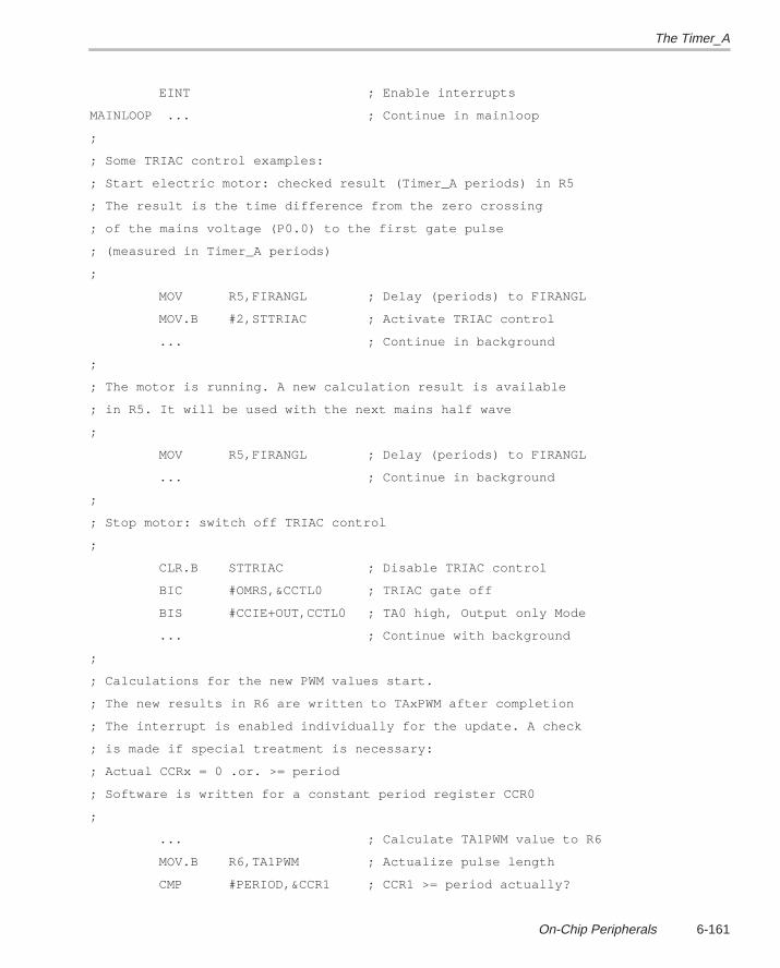
The Timer_A
6-161On-Chip Peripherals
EINT ; Enable interrupts
MAINLOOP ... ; Continue in mainloop
;
; Some TRIAC control examples:
; Start electric motor: checked result (Timer_A periods) in R5
; The result is the time difference from the zero crossing
; of the mains voltage (P0.0) to the first gate pulse
; (measured in Timer_A periods)
;
MOV R5,FIRANGL ; Delay (periods) to FIRANGL
MOV.B #2,STTRIAC ; Activate TRIAC control
... ; Continue in background
;
; The motor is running. A new calculation result is available
; in R5. It will be used with the next mains half wave
;
MOV R5,FIRANGL ; Delay (periods) to FIRANGL
... ; Continue in background
;
; Stop motor: switch off TRIAC control
;
CLR.B STTRIAC ; Disable TRIAC control
BIC #OMRS,&CCTL0 ; TRIAC gate off
BIS #CCIE+OUT,CCTL0 ; TA0 high, Output only Mode
... ; Continue with background
;
; Calculations for the new PWM values start.
; The new results in R6 are written to TAxPWM after completion
; The interrupt is enabled individually for the update. A check
; is made if special treatment is necessary:
; Actual CCRx = 0 .or. >= period
; Software is written for a constant period register CCR0
;
... ; Calculate TA1PWM value to R6
MOV.B R6,TA1PWM ; Actualize pulse length
CMP #PERIOD,&CCR1 ; CCR1 >= period actually?
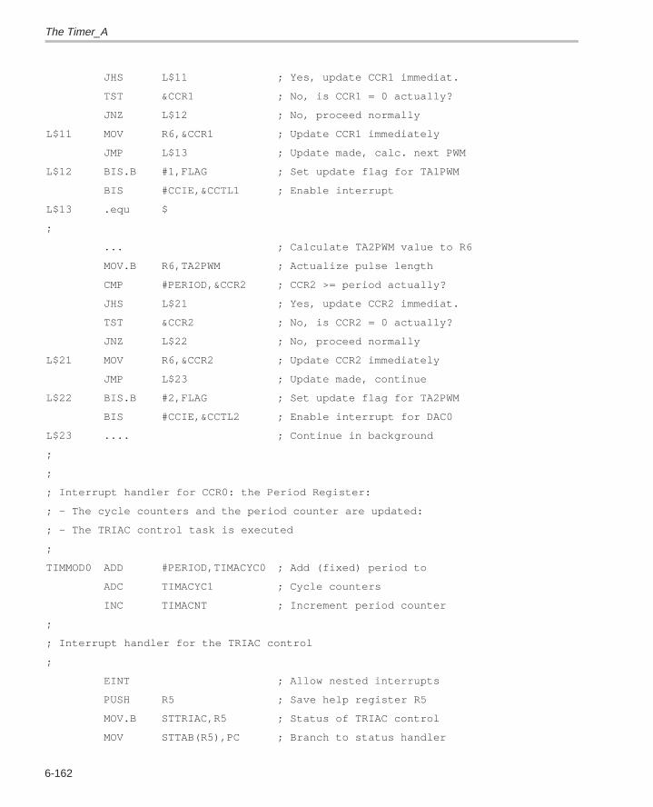
The Timer_A
6-162
JHS L$11 ; Yes, update CCR1 immediat.
TST &CCR1 ; No, is CCR1 = 0 actually?
JNZ L$12 ; No, proceed normally
L$11 MOV R6,&CCR1 ; Update CCR1 immediately
JMP L$13 ; Update made, calc. next PWM
L$12 BIS.B #1,FLAG ; Set update flag for TA1PWM
BIS #CCIE,&CCTL1 ; Enable interrupt
L$13 .equ $
;
... ; Calculate TA2PWM value to R6
MOV.B R6,TA2PWM ; Actualize pulse length
CMP #PERIOD,&CCR2 ; CCR2 >= period actually?
JHS L$21 ; Yes, update CCR2 immediat.
TST &CCR2 ; No, is CCR2 = 0 actually?
JNZ L$22 ; No, proceed normally
L$21 MOV R6,&CCR2 ; Update CCR2 immediately
JMP L$23 ; Update made, continue
L$22 BIS.B #2,FLAG ; Set update flag for TA2PWM
BIS #CCIE,&CCTL2 ; Enable interrupt for DAC0
L$23 .... ; Continue in background
;
;
; Interrupt handler for CCR0: the Period Register:
; – The cycle counters and the period counter are updated:
; – The TRIAC control task is executed
;
TIMMOD0 ADD #PERIOD,TIMACYC0 ; Add (fixed) period to
ADC TIMACYC1 ; Cycle counters
INC TIMACNT ; Increment period counter
;
; Interrupt handler for the TRIAC control
;
EINT ; Allow nested interrupts
PUSH R5 ; Save help register R5
MOV.B STTRIAC,R5 ; Status of TRIAC control
MOV STTAB(R5),PC ; Branch to status handler
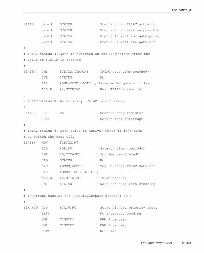
The Timer_A
6-163On-Chip Peripherals
STTAB .word STATE0 ; Status 0: No TRIAC activity
.word STATE0 ; Status 2: activation possible
.word STATE4 ; Status 4: wait for gate pulse
.word STATE6 ; Status 6: wait for gate off
;
; TRIAC status 4: gate is switched on for OP periods after the
; value in FIRTIM is reached
;
STATE4 CMP FIRTIM,TIMACNT ; TRIAC gate time reached?
JNE STATE0 ; No
BIS #OMR+CCIE,&CCTL0 ; Prepare for gate on pulse
ADD.B #2,STTRIAC ; Next TRIAC status (6)
;
; TRIAC status 0: No activity. TRIAC is off always
;
STATE0 POP R5 ; Restore help register
RETI ; Return from interrupt
;
; TRIAC status 6: gate pulse is active. Check if it’s time
; to switch the gate off.
STATE6 MOV FIRTIM,R5
ADD #OP,R5 ; Gate–on time (periods)
CMP R5,TIMACNT ; On–time terminated?
JLO STATE0 ; No
BIC #OMRS,&CCTL0 ; Yes, prepare TRIAC Gate off
BIS #OMSET+CCIE,&CCTL0;
MOV.B #2,STTRIAC ; TRIAC status:
JMP STATE0 ; Wait for next zero crossing
;
; Interrupt handler for Capture/Compare Blocks 1 to 4
;
TIM_HND ADD &TAIV,PC ; Serve highest priority requ.
RETI ; No interrupt pending
JMP TIMMOD1 ; PWM 1 request
JMP TIMMOD2 ; PWM 2 request
RETI ; Not used
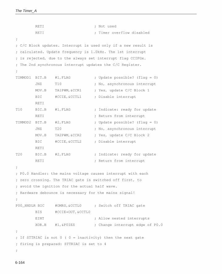
The Timer_A
6-164
RETI ; Not used
RETI ; Timer overflow disabled
;
; C/C Block updates. Interrupt is used only if a new result is
; calculated. Update frequency is 1.0kHz. The 1st interrupt
; is rejected, due to the always set interrupt flag CCIFGx.
; The 2nd synchronous interrupt updates the C/C Register.
;
TIMMOD1 BIT.B #1,FLAG ; Update possible? (flag = 0)
JNZ T10 ; No, asynchronous interrupt
MOV.B TA1PWM,&CCR1 ; Yes, update C/C Block 1
BIC #CCIE,&CCTL1 ; Disable interrupt
RETI
T10 BIC.B #1,FLAG ; Indicate: ready for update
RETI ; Return from interrupt
TIMMOD2 BIT.B #2,FLAG ; Update possible? (flag = 0)
JNZ T20 ; No, asynchronous interrupt
MOV.B TA2PWM,&CCR2 ; Yes, update C/C Block 2
BIC #CCIE,&CCTL2 ; Disable interrupt
RETI
T20 BIC.B #2,FLAG ; Indicate: ready for update
RETI ; Return from interrupt
;
; P0.0 Handler: the mains voltage causes interrupt with each
; zero crossing. The TRIAC gate is switched off first, to
; avoid the ignition for the actual half wave.
; Hardware debounce is necessary for the mains signal!
;
P00_HNDLR BIC #OMRS,&CCTL0 ; Switch off TRIAC gate
BIS #CCIE+OUT,&CCTL0
EINT ; Allow nested interrupts
XOR.B #1,&P0IES ; Change interrupt edge of P0.0
;
; If STTRIAC is not 0 ( 0 = inactivity) then the next gate
; firing is prepared: STTRIAC is set to 4
;
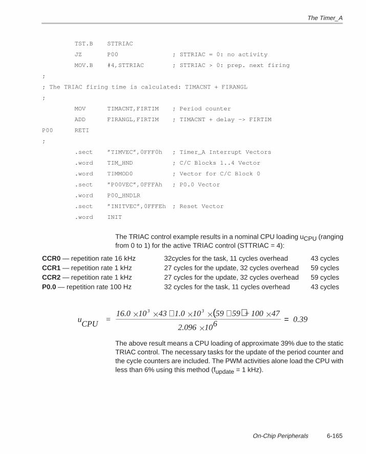
The Timer_A
6-165On-Chip Peripherals
TST.B STTRIAC
JZ P00 ; STTRIAC = 0: no activity
MOV.B #4,STTRIAC ; STTRIAC > 0: prep. next firing
;
; The TRIAC firing time is calculated: TIMACNT + FIRANGL
;
MOV TIMACNT,FIRTIM ; Period counter
ADD FIRANGL,FIRTIM ; TIMACNT + delay –> FIRTIM
P00 RETI
;
.sect ”TIMVEC”,0FFF0h ; Timer_A Interrupt Vectors
.word TIM_HND ; C/C Blocks 1..4 Vector
.word TIMMOD0 ; Vector for C/C Block 0
.sect ”P00VEC”,0FFFAh ; P0.0 Vector
.word P00_HNDLR
.sect ”INITVEC”,0FFFEh ; Reset Vector
.word INIT
The TRIAC control example results in a nominal CPU loading uCPU (rangingfrom 0 to 1) for the active TRIAC control (STTRIAC = 4):
CCR0 — repetition rate 16 kHz 32cycles for the task, 11 cycles overhead 43 cyclesCCR1 — repetition rate 1 kHz 27 cycles for the update, 32 cycles overhead 59 cyclesCCR2 — repetition rate 1 kHz 27 cycles for the update, 32 cycles overhead 59 cyclesP0.0 — repetition rate 100 Hz 32 cycles for the task, 11 cycles overhead 43 cycles
( )uCPU
=16.0 10 43 1.0 10 59 59 + 100 47
2.096 106 0.39
3 3 + +
=
The above result means a CPU loading of approximate 39% due to the staticTRIAC control. The necessary tasks for the update of the period counter andthe cycle counters are included. The PWM activities alone load the CPU withless than 6% using this method (fupdate = 1 kHz).
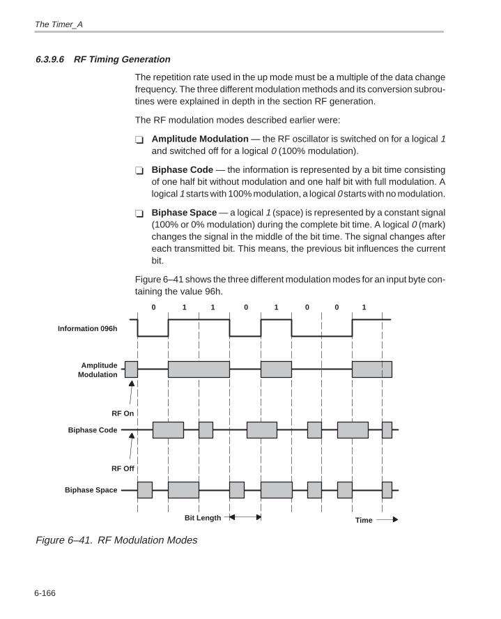
The Timer_A
6-166
6.3.9.6 RF Timing Generation
The repetition rate used in the up mode must be a multiple of the data changefrequency. The three different modulation methods and its conversion subrou-tines were explained in depth in the section RF generation.
The RF modulation modes described earlier were:
Amplitude Modulation — the RF oscillator is switched on for a logical 1and switched off for a logical 0 (100% modulation).
Biphase Code — the information is represented by a bit time consistingof one half bit without modulation and one half bit with full modulation. Alogical 1 starts with 100% modulation, a logical 0 starts with no modulation.
Biphase Space — a logical 1 (space) is represented by a constant signal(100% or 0% modulation) during the complete bit time. A logical 0 (mark)changes the signal in the middle of the bit time. The signal changes aftereach transmitted bit. This means, the previous bit influences the currentbit.
Figure 6–41 shows the three different modulation modes for an input byte con-taining the value 96h.
RF Off
0 1 1 0 1 0 0 1
RF On
Information 096h
AmplitudeModulation
Biphase Code
Biphase Space
Bit Length Time
Figure 6–41. RF Modulation Modes
The Timer_A
6-167On-Chip Peripherals
The capture/compare block 0 is used with the software example due to twofacts:
The fastest possible response. Decision making with the timer vector reg-ister is not necessary for the capture/compare block 0 — it uses its own,dedicated interrupt vector. The vector address is 0FFF2h.
The capture/compare block 0 delivers the necessary timing anyway. Theuse of the period register therefore frees the remaining capture/compareregisters for other tasks.
Example 6–45. RF Modulation Modes
The real time task common to all three modulation modes is given below. Thebackground software prepares a 128-bit block starting at address RF_BLK,containing the information to be output in the desired coding format. This128-bit buffer is output in real time with the same handler for all three modula-tion modes.
The selected half-bit repetition frequency is 19200 Hz, because 38400 Hz istoo high a PWM frequency (increased switching losses, too few resolutionsteps).
The capture/compare blocks 1 to 3 are used for the PWM generation. Thetable processing used allows (nearly) simultaneous update of all three cap-ture/compare blocks. The method used is the fastest one for updating. Thenumber range for the PWM is from 1 to (period–1), therefore, the fast update— without range checks — is possible.
The CPU registers R5 and R8 are reserved for the RF timing. R5 contains thedata to be output currently, R8 points to the next data word. They must not beoverwritten by other tasks.
The conversion subroutines for the biphase code and biphase space modula-tion are described in the section RF Generation.
The example uses the Frequent Update by the Appropriate Interrupt Handler.See Section 6.3.9.2 for details.
; Hardware definitions
;
FLLMPY .equ 122 ; FLL multiplier for 3.998MHz
fRF .equ 19200 ; Half–bit rep. frequency
TCLK .equ FLLMPY*32768 ; TCLK: FLLMPY x fcrystal
PERIOD .equ ((2*TCLK/fRF)+1)/2 ; Bit length (TCLK cycles)
The Timer_A
6-168
STACK .equ 600h ; Stack initialization address
;
; RAM Definitions
;
RF_BLK .equ 202h ; Converted data 128 bits
TIMACYC .equ 212h ; Cycle counter Timer_A
TIMACNT .equ 214h ; Period counter Timer_A
RFSTAT .equ 216h ; Status of RF transmission
TA1PWM .equ 217h ; Value for C/C Block 1
TA2PWM .equ 218h ; Value for C/C Block 2
TA3PWM .equ 219h ; Value for C/C Block 3
.text ; Software start address
;
INIT MOV #STACK,SP ; Initialize Stack Pointer
CALL #INITSR ; Init. FLL and RAM
;
; Initialize the Timer_A: MCLK, Up Mode, INTRPT on for CCRx
;
MOV #ISMCLK+CLR,&TACTL ; MCLK, TIMOV off
MOV #OMOO+CCIE,&CCTL0 ; Reset TA0, INTRPT on
MOV #OMSR+CCIE,&CCTL1 ; TA1: Set/Reset
MOV #OMSR+CCIE,&CCTL2 ; TA2: Set/Reset
MOV #OMSR+CCIE,&CCTL3 ; TA3: Set/Reset
MOV #PERIOD–1,&CCR0 ; 19.2kHz period
MOV.B #1,&CCR1 ; Minimum PWM length
MOV.B #1,&CCR2
MOV.B #1,&CCR3
MOV.B #TA3+TA2+TA1+TA0,&P3SEL ; Define timer outputs
;
CLR TIMACYC ; Clear cycle counter
CLR TIMACNT ; Clear period counter
MOV.B #1,TA1PWM ; Minimum PWM output
MOV.B #1,TA2PWM ;
MOV.B #1,TA3PWM ;
MOV.B #CBMCLK,&CBCTL ; Output MCLK at XBUF pin
CLR.B RFSTAT ; RF status = 0
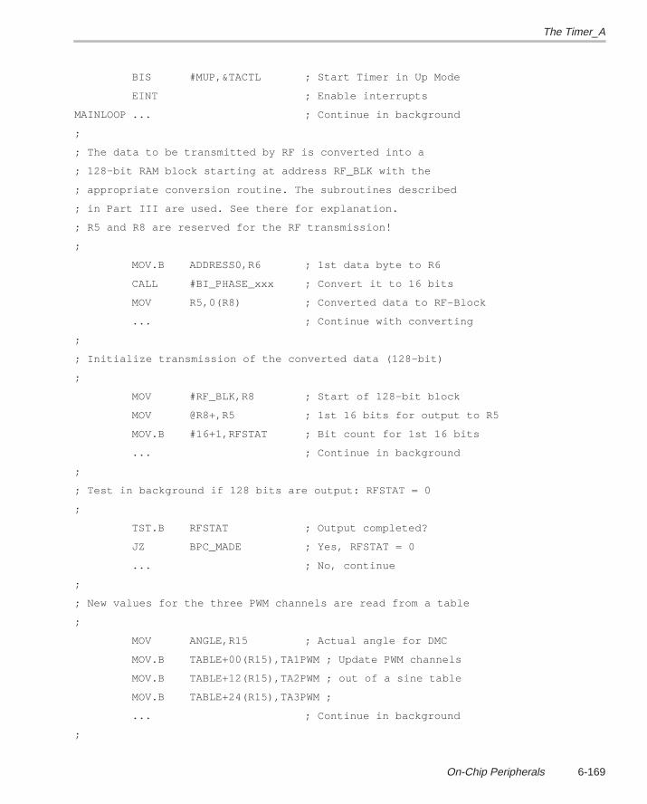
The Timer_A
6-169On-Chip Peripherals
BIS #MUP,&TACTL ; Start Timer in Up Mode
EINT ; Enable interrupts
MAINLOOP ... ; Continue in background
;
; The data to be transmitted by RF is converted into a
; 128–bit RAM block starting at address RF_BLK with the
; appropriate conversion routine. The subroutines described
; in Part III are used. See there for explanation.
; R5 and R8 are reserved for the RF transmission!
;
MOV.B ADDRESS0,R6 ; 1st data byte to R6
CALL #BI_PHASE_xxx ; Convert it to 16 bits
MOV R5,0(R8) ; Converted data to RF–Block
... ; Continue with converting
;
; Initialize transmission of the converted data (128–bit)
;
MOV #RF_BLK,R8 ; Start of 128–bit block
MOV @R8+,R5 ; 1st 16 bits for output to R5
MOV.B #16+1,RFSTAT ; Bit count for 1st 16 bits
... ; Continue in background
;
; Test in background if 128 bits are output: RFSTAT = 0
;
TST.B RFSTAT ; Output completed?
JZ BPC_MADE ; Yes, RFSTAT = 0
... ; No, continue
;
; New values for the three PWM channels are read from a table
;
MOV ANGLE,R15 ; Actual angle for DMC
MOV.B TABLE+00(R15),TA1PWM ; Update PWM channels
MOV.B TABLE+12(R15),TA2PWM ; out of a sine table
MOV.B TABLE+24(R15),TA3PWM ;
... ; Continue in background
;
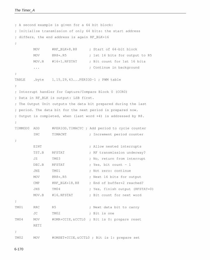
The Timer_A
6-170
; A second example is given for a 64 bit block:
; Initialize transmission of only 64 bits: the start address
; differs, the end address is again RF_BLK+16
;
MOV #RF_BLK+8,R8 ; Start of 64–bit block
MOV @R8+,R5 ; 1st 16 bits for output to R5
MOV.B #16+1,RFSTAT ; Bit count for 1st 16 bits
... ; Continue in background
;
TABLE .byte 1,15,29,43...PERIOD–1 ; PWM table
;
; Interrupt handler for Capture/Compare Block 0 (CCR0)
; Data in RF_BLK is output: LSB first.
; The Output Unit outputs the data bit prepared during the last
; period. The data bit for the next period is prepared now.
; Output is completed, when (last word +4) is addressed by R8.
;
TIMMOD0 ADD #PERIOD,TIMACYC ; Add period to cycle counter
INC TIMACNT ; Increment period counter
;
EINT ; Allow nested interrupts
TST.B RFSTAT ; RF transmission underway?
JZ TM03 ; No, return from interrupt
DEC.B RFSTAT ; Yes, bit count – 1
JNZ TM01 ; Not zero: continue
MOV @R8+,R5 ; Next 16 bits for output
CMP #RF_BLK+18,R8 ; End of buffer+2 reached?
JHS TM04 ; Yes, finish output (RFSTAT=0)
MOV.B #16,RFSTAT ; Bit count for next word
;
TM01 RRC R5 ; Next data bit to carry
JC TM02 ; Bit is one
TM04 MOV #OMR+CCIE,&CCTL0 ; Bit is 0: prepare reset
RETI
;
TM02 MOV #OMSET+CCIE,&CCTL0 ; Bit is 1: prepare set
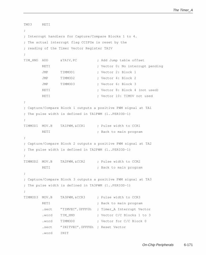
The Timer_A
6-171On-Chip Peripherals
TM03 RETI
;
; Interrupt handlers for Capture/Compare Blocks 1 to 4.
; The actual interrupt flag CCIFGx is reset by the
; reading of the Timer Vector Register TAIV
;
TIM_HND ADD &TAIV,PC ; Add Jump table offset
RETI ; Vector 0: No interrupt pending
JMP TIMMOD1 ; Vector 2: Block 1
JMP TIMMOD2 ; Vector 4: Block 2
JMP TIMMOD3 ; Vector 6: Block 3
RETI ; Vector 8: Block 4 (not used)
RETI ; Vector 10: TIMOV not used
;
; Capture/Compare Block 1 outputs a positive PWM signal at TA1
; The pulse width is defined in TA1PWM (1..PERIOD–1)
;
TIMMOD1 MOV.B TA1PWM,&CCR1 ; Pulse width to CCR1
RETI ; Back to main program
;
; Capture/Compare Block 2 outputs a positive PWM signal at TA2
; The pulse width is defined in TA2PWM (1..PERIOD–1)
;
TIMMOD2 MOV.B TA2PWM,&CCR2 ; Pulse width to CCR2
RETI ; Back to main program
;
; Capture/Compare Block 3 outputs a positive PWM signal at TA3
; The pulse width is defined in TA3PWM (1..PERIOD–1)
;
TIMMOD3 MOV.B TA3PWM,&CCR3 ; Pulse width to CCR3
RETI ; Back to main program
.sect ”TIMVEC”,0FFF0h ; Timer_A Interrupt Vector
.word TIM_HND ; Vector C/C Blocks 1 to 3
.word TIMMOD0 ; Vector for C/C Block 0
.sect ”INITVEC”,0FFFEh ; Reset Vector
.word INIT
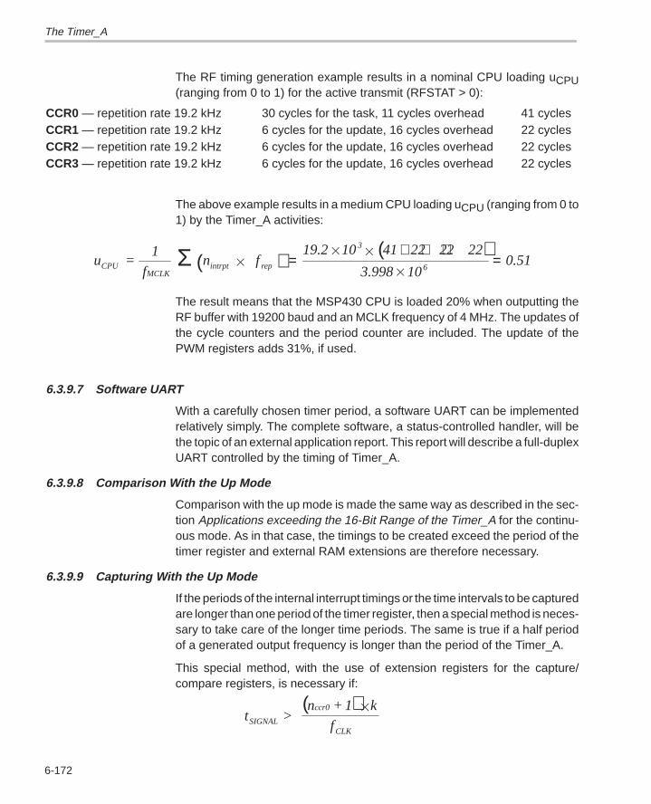
The Timer_A
6-172
The RF timing generation example results in a nominal CPU loading uCPU(ranging from 0 to 1) for the active transmit (RFSTAT > 0):
CCR0 — repetition rate 19.2 kHz 30 cycles for the task, 11 cycles overhead 41 cyclesCCR1 — repetition rate 19.2 kHz 6 cycles for the update, 16 cycles overhead 22 cyclesCCR2 — repetition rate 19.2 kHz 6 cycles for the update, 16 cycles overhead 22 cyclesCCR3 — repetition rate 19.2 kHz 6 cycles for the update, 16 cycles overhead 22 cycles
The above example results in a medium CPU loading uCPU (ranging from 0 to1) by the Timer_A activities:
( )u =
1
f n
f
19.2 10 41 22 22 22
3.998 10 0.51CPU
MCLKintrpt rep
3
6 =
+ + +
=Σ ( )
The result means that the MSP430 CPU is loaded 20% when outputting theRF buffer with 19200 baud and an MCLK frequency of 4 MHz. The updates ofthe cycle counters and the period counter are included. The update of thePWM registers adds 31%, if used.
6.3.9.7 Software UART
With a carefully chosen timer period, a software UART can be implementedrelatively simply. The complete software, a status-controlled handler, will bethe topic of an external application report. This report will describe a full-duplexUART controlled by the timing of Timer_A.
6.3.9.8 Comparison With the Up Mode
Comparison with the up mode is made the same way as described in the sec-tion Applications exceeding the 16-Bit Range of the Timer_A for the continu-ous mode. As in that case, the timings to be created exceed the period of thetimer register and external RAM extensions are therefore necessary.
6.3.9.9 Capturing With the Up Mode
If the periods of the internal interrupt timings or the time intervals to be capturedare longer than one period of the timer register, then a special method is neces-sary to take care of the longer time periods. The same is true if a half periodof a generated output frequency is longer than the period of the Timer_A.
This special method, with the use of extension registers for the capture/compare registers, is necessary if:
( )t >
n + 1 k
fSIGNAL
ccr0
CLK
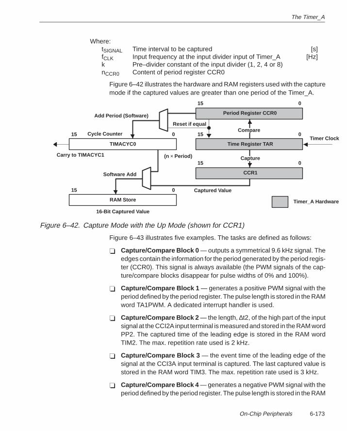
The Timer_A
6-173On-Chip Peripherals
Where: tSIGNAL Time interval to be captured [s]fCLK Input frequency at the input divider input of Timer_A [Hz]k Pre–divider constant of the input divider (1, 2, 4 or 8)nCCR0 Content of period register CCR0
Figure 6–42 illustrates the hardware and RAM registers used with the capturemode if the captured values are greater than one period of the Timer_A.
TIMACYC0
015
Period Register CCR0
015
Time Register TAR
015
015
CCR1
Compare
Timer Clock
RAM Store
015
Add Period (Software)
Cycle Counter
Software Add
Carry to TIMACYC1
16-Bit Captured Value
Timer_A Hardware
(n × Period)
Captured Value
Reset if equal
Capture
Figure 6–42. Capture Mode with the Up Mode (shown for CCR1)
Figure 6–43 illustrates five examples. The tasks are defined as follows:
Capture/Compare Block 0 — outputs a symmetrical 9.6 kHz signal. Theedges contain the information for the period generated by the period regis-ter (CCR0). This signal is always available (the PWM signals of the cap-ture/compare blocks disappear for pulse widths of 0% and 100%).
Capture/Compare Block 1 — generates a positive PWM signal with theperiod defined by the period register. The pulse length is stored in the RAMword TA1PWM. A dedicated interrupt handler is used.
Capture/Compare Block 2 — the length, ∆t2, of the high part of the inputsignal at the CCI2A input terminal is measured and stored in the RAM wordPP2. The captured time of the leading edge is stored in the RAM wordTIM2. The max. repetition rate used is 2 kHz.
Capture/Compare Block 3 — the event time of the leading edge of thesignal at the CCI3A input terminal is captured. The last captured value isstored in the RAM word TIM3. The max. repetition rate used is 3 kHz.
Capture/Compare Block 4 — generates a negative PWM signal with theperiod defined by the period register. The pulse length is stored in the RAM

The Timer_A
6-174
word TA4PWM. Update is made with the interrupt handler of capture/compare block 0.
For the example, 3.801 MHz is used. The resolution is 224 steps due to therepetition frequency of 16.969 kHz (3.801 MHz/16.969 kHz = 224).
Table 6–23. Short Description of the Capture and PWM Mix
C/C BLOCK TIME INTERVAL TIMER I/Os COMMENT
0 Doubled period Outputs 0.5 PWM Frequency
Period register CCR0. Output of a symmetrical 8.484 kHz signal
1 Period Outputs PWM1 .. PERIOD–1
Generation of PWM. Pulse length stored in TA1PWM. Dedicatedinterrupt handler for update.
2 External event Input pin CCI2Ais used
Measures high signal part ∆t2. Length of positive signal part isstored in PP2. Maximum input frequency is 2 kHz.
3 External event Input pin CCI3Ais used
Captures event time t3 of the trailing edge of the input signal.Event time t3 stored in TIM3. Maximum input frequency is 3 kHz.
4 Period Outputs PWM 0–100%
Generation of PWM. Pulse length stored in TA4PWM. Update bycapture/compare block 0.
Note:
The maximum input frequencies for capturing purposes shown above areused for the overhead calculation only. The limits of the Timer_A hardwareallow it to capture much higher input frequencies.
Figure 6–43 illustrates the four tasks described above — they are not shownto scale.
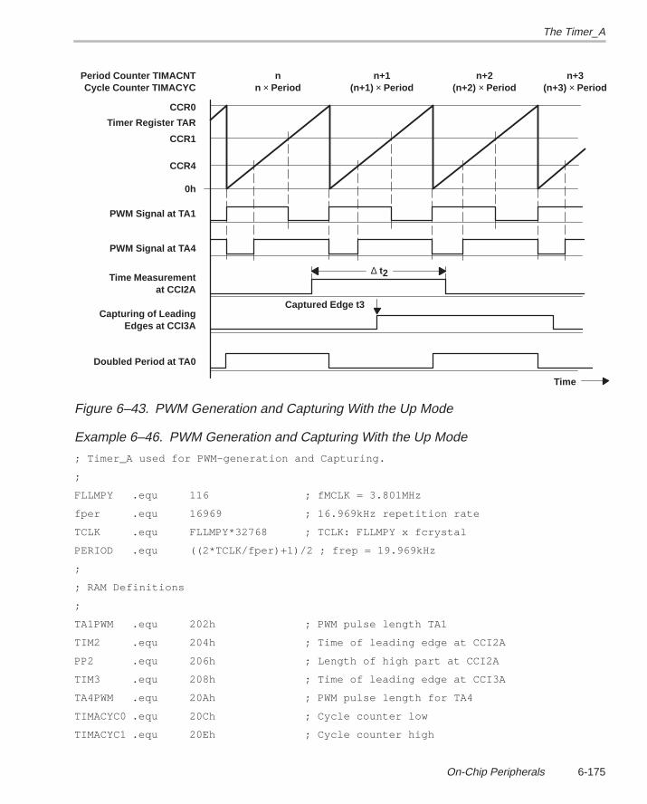
The Timer_A
6-175On-Chip Peripherals
nn × Period
n+1(n+1) × Period
n+2(n+2) × Period
n+3(n+3) × Period
Period Counter TIMACNTCycle Counter TIMACYC
CCR0
CCR1
Timer Register TAR
CCR4
0h
PWM Signal at TA1
PWM Signal at TA4
Time Measurementat CCI2A
Capturing of LeadingEdges at CCI3A
Doubled Period at TA0
∆ t2
Captured Edge t3
Time
Figure 6–43. PWM Generation and Capturing With the Up Mode
Example 6–46. PWM Generation and Capturing With the Up Mode
; Timer_A used for PWM–generation and Capturing.
;
FLLMPY .equ 116 ; fMCLK = 3.801MHz
fper .equ 16969 ; 16.969kHz repetition rate
TCLK .equ FLLMPY*32768 ; TCLK: FLLMPY x fcrystal
PERIOD .equ ((2*TCLK/fper)+1)/2 ; frep = 19.969kHz
;
; RAM Definitions
;
TA1PWM .equ 202h ; PWM pulse length TA1
TIM2 .equ 204h ; Time of leading edge at CCI2A
PP2 .equ 206h ; Length of high part at CCI2A
TIM3 .equ 208h ; Time of leading edge at CCI3A
TA4PWM .equ 20Ah ; PWM pulse length for TA4
TIMACYC0 .equ 20Ch ; Cycle counter low
TIMACYC1 .equ 20Eh ; Cycle counter high
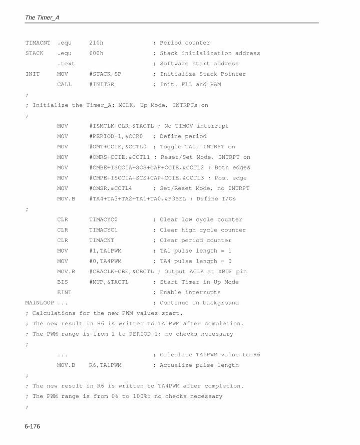
The Timer_A
6-176
TIMACNT .equ 210h ; Period counter
STACK .equ 600h ; Stack initialization address
.text ; Software start address
INIT MOV #STACK,SP ; Initialize Stack Pointer
CALL #INITSR ; Init. FLL and RAM
;
; Initialize the Timer_A: MCLK, Up Mode, INTRPTs on
;
MOV #ISMCLK+CLR,&TACTL ; No TIMOV interrupt
MOV #PERIOD–1,&CCR0 ; Define period
MOV #OMT+CCIE,&CCTL0 ; Toggle TA0, INTRPT on
MOV #OMRS+CCIE,&CCTL1 ; Reset/Set Mode, INTRPT on
MOV #CMBE+ISCCIA+SCS+CAP+CCIE,&CCTL2 ; Both edges
MOV #CMPE+ISCCIA+SCS+CAP+CCIE,&CCTL3 ; Pos. edge
MOV #OMSR,&CCTL4 ; Set/Reset Mode, no INTRPT
MOV.B #TA4+TA3+TA2+TA1+TA0,&P3SEL ; Define I/Os
;
CLR TIMACYC0 ; Clear low cycle counter
CLR TIMACYC1 ; Clear high cycle counter
CLR TIMACNT ; Clear period counter
MOV #1,TA1PWM ; TA1 pulse length = 1
MOV #0,TA4PWM ; TA4 pulse length = 0
MOV.B #CBACLK+CBE,&CBCTL ; Output ACLK at XBUF pin
BIS #MUP,&TACTL ; Start Timer in Up Mode
EINT ; Enable interrupts
MAINLOOP ... ; Continue in background
; Calculations for the new PWM values start.
; The new result in R6 is written to TA1PWM after completion.
; The PWM range is from 1 to PERIOD–1: no checks necessary
;
... ; Calculate TA1PWM value to R6
MOV.B R6,TA1PWM ; Actualize pulse length
;
; The new result in R6 is written to TA4PWM after completion.
; The PWM range is from 0% to 100%: no checks necessary
;
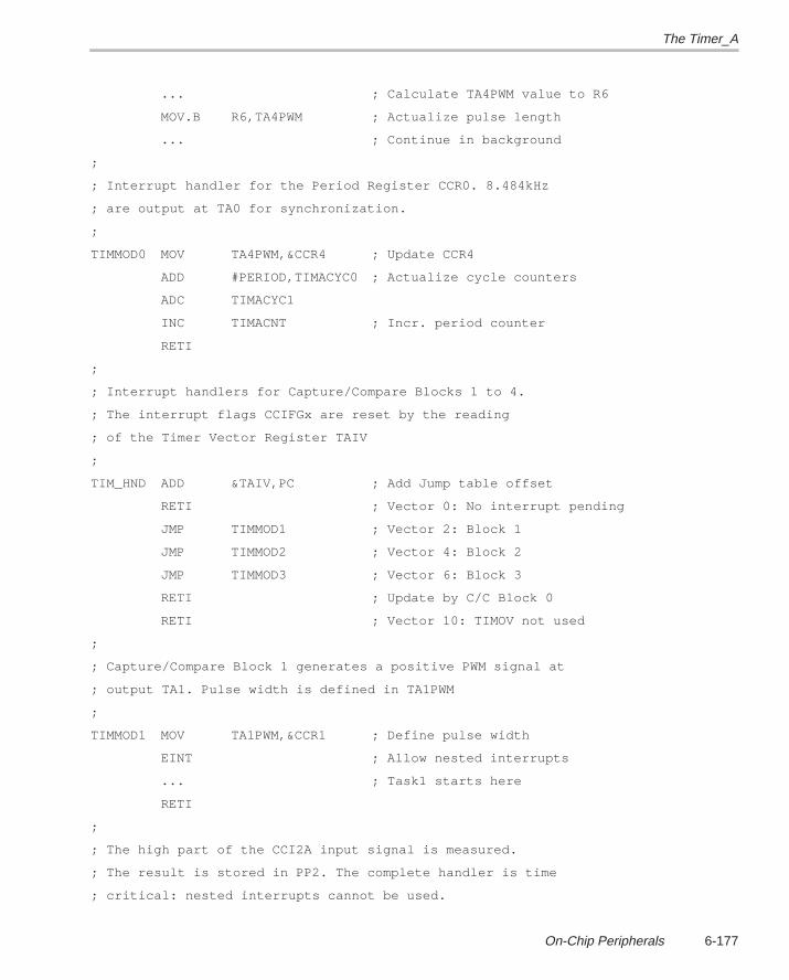
The Timer_A
6-177On-Chip Peripherals
... ; Calculate TA4PWM value to R6
MOV.B R6,TA4PWM ; Actualize pulse length
... ; Continue in background
;
; Interrupt handler for the Period Register CCR0. 8.484kHz
; are output at TA0 for synchronization.
;
TIMMOD0 MOV TA4PWM,&CCR4 ; Update CCR4
ADD #PERIOD,TIMACYC0 ; Actualize cycle counters
ADC TIMACYC1
INC TIMACNT ; Incr. period counter
RETI
;
; Interrupt handlers for Capture/Compare Blocks 1 to 4.
; The interrupt flags CCIFGx are reset by the reading
; of the Timer Vector Register TAIV
;
TIM_HND ADD &TAIV,PC ; Add Jump table offset
RETI ; Vector 0: No interrupt pending
JMP TIMMOD1 ; Vector 2: Block 1
JMP TIMMOD2 ; Vector 4: Block 2
JMP TIMMOD3 ; Vector 6: Block 3
RETI ; Update by C/C Block 0
RETI ; Vector 10: TIMOV not used
;
; Capture/Compare Block 1 generates a positive PWM signal at
; output TA1. Pulse width is defined in TA1PWM
;
TIMMOD1 MOV TA1PWM,&CCR1 ; Define pulse width
EINT ; Allow nested interrupts
... ; Task1 starts here
RETI
;
; The high part of the CCI2A input signal is measured.
; The result is stored in PP2. The complete handler is time
; critical: nested interrupts cannot be used.
The Timer_A
6-178
; First a check is made if the cycle counter TIMACYC0 contains
; the value corresponding to the captured value in CCR2, or if
; TIMACYC0 is yet updated due to interrupt latency time.
;
TIMMOD2 CMP &CCR2,&TAR ; Occurred overflow of TAR?
JHS TM20 ; No, Timer Reg. > capt. value
BIT #CCIFG,&CCTL0 ; Yes, TIMACYC0 yet updated?
JNZ TM20 ; No, value matches with CCR2
SUB #PERIOD,&CCR2 ; Yes, use CCR2 for correction
;
TM20 BIT #CCI,&CCTL2 ; Input signal high?
JZ TM21 ; No, time for calculation
MOV TIMACYC0,TIM2 ; Yes, store cycle counter
ADD &CCR2,TIM2 ; Time for leading edge in TIM2
RETI
; ; High part is calculated:
TM21 MOV TIMACYC0,PP2 ; Event time of trailing edge
ADD &CCR2,PP2 ; Add captured time
SUB TIM2,PP2 ; Subtr. time of leading edge
RETI ; Length of high part in PP2
;
; Capture/Compare Block 3 captures the time of trailing edges
; at CCI3A. TIM3 stores the time of the actual edge
;
TIMMOD3 CMP &CCR3,&TAR ; Occurred overflow of TAR?
JHS TM30 ; No, Timer Reg. > capt. value
BIT #CCIFG,CCTL0 ; Yes, TIMACYC0 yet updated?
JNZ TM30 ; No, value matches with CCR3
SUB #PERIOD,&CCR3 ; Yes, use CCR3 for correction
;
TM30 MOV TIMACYC0,TIM3 ; Store sum of cycle counter
ADD &CCR3,TIM3 ; and captured event time
RETI
;
.sect ”TIMVEC”,0FFF0h ; Timer_A Interrupt Vectors
.word TIM_HND ; C/C Blocks 1..4 Vector
The Timer_A
6-179On-Chip Peripherals
.word TIMMOD0 ; Vector for C/C Block 0
.sect ”INITVEC”,0FFFEh ; Reset Vector
.word INIT
The above example results in a maximum (worst case) CPU loading uCPU(ranging from 0 to 1) by the Timer_A activities:
CCR0 — repetition rate 16.969 kHz 19 cycles for the task, 11 cycles overhead 30 cyclesCCR1 — repetition rate 16.969 kHz 6 cycles for the update, 17 cycles overhead 23 cyclesCCR2 — repetition rate max. 2 kHz 60 cycles for the update, 32 cycles overhead 92 cyclesCCR3 — repetition rate max. 3 kHz 20 cycles for the update, 16 cycles overhead 36 cyclesCCR4 — repetition rate 16.969 kHz 6 cycles for the update, 0 cycles overhead 6 cycles
( )u =
16.969 10 30 23 6 2.0 10 92 3.0 10 36
3.801 100.34CPU
6 3 3
6
+ + + +
=
The above result means a worst case CPU loading of approximate 34% dueto the Timer_A activities (the tasks of the capture/compare blocks 2, 3 and 4are not included).
6.3.9.10 Conclusion
This section demonstrated the possibilities of the Timer_A running in the upmode. Despite the dominance of the period register (CCR0) it is possible tocapture signals, compare time intervals, and create timings in a real-time envi-ronment — all this in parallel with the pulse width modulation generated withthe up mode.
The Timer_A
6-180
6.3.10 Software Examples for the Up/Down Mode
This section shows several proven application examples for the Timer_A run-ning in the up/down mode. Software definitions appear in the appendix. When-ever possible, the abbreviations defined in the MSP430 Architecture Guideand Module Library are used.
The software examples are independent of the MCLK frequency in use. Onlythe FLL multiplier constant, FLLMPY, and the repetition rate, fper, need to beredefined if another combination is needed. The source lines for the definitionof these important values are:
FLLMPY .equ 122 ; 1. FLL multiplier
fper .equ 19200 ; 2. PWM Repetition rate
TCLK .equ FLLMPY*32768/4 ; 3. FLLMPY x fcrystal/4
HLFPER .equ (TCLK/fper)/2 ; 4. Half Period of the PWM
Note:
The definitions assume an external crystal or an external frequency at theXIN input with a frequency of 32.768 kHz (215 Hz).
1) Definition of the CPU frequency f MCLK. The multiplier FLLMPY for thedigitally controlled oscillator (DCO) is defined. The value for the actual fre-quency fMCLK is (FLLMPY × 215). The value 122 stands for fMCLK = 122× 215 = 3.9977 MHz.
2) Definition of the desired repetition rate. The value 19200 stands for arepetition rate of 19.2 kHz, which means 19200 complete up and downcounts of the timer register TAR.
3) Definition of the input frequency for the Timer Register (TAR) . The ex-pression /4 indicates that the input divider is switched to the Divide–by–Four mode. The value shown stands for TCLK = 3.9977 MHz /4 = 999.424kHz. Only the predivider used for the input divider (here /4) needs to bedefined.
4) Calculation of the TCLK cycles for the defined half period. The full pe-riod consists of the half period counting up to the content of the period reg-ister CCR0 and the one counting down to 0 again. No change is necessaryfor this line.
The Timer_A
6-181On-Chip Peripherals
6.3.10.1 Common Remarks
The up/down mode should be considered only for pulse width modulation(PWM) or DC generation. The advantage of this special PWM mode is the con-tributed switching of the output signals — unlike the up mode that switches onall output pulses at exactly the same time (when the timer register TAR is resetto 0), the up/down mode switches on and off the output pulses symmetrical tothe 0 content of the timer register. See figure 6–44. If this feature is not needed,then the up mode with its simpler handling or the continuous mode with its fiveindependent timings should be used.
Advantages of the Up/Down Mode:
Distributed current switching (e.g. for digital motor control (DMC) applica-tions)
Free run without CPU loading for fixed PWM values (DAC, DMC)
High PWM frequency possible due to pure hardware control
Clever timings of the period register are usable for more than one real-timejob
For a given PWM repetition rate, an equally spaced second interrupt isavailable from the timer overflow interrupt, TIMOV. This doubles the avail-able resolution for some applications
Disadvantages of the Up/Down Mode:
Dominance of the period register — defines the time frame
Direction change of the period register during the run needs special soft-ware handling. Interrupt-driven count direction indication is necessary forthe software.
Capturing has an inherent uncertainty for capturing values near the zeropoint (TAR = 0) and the middle of the period (TAR = CCR0).
RAM extension for the timer register is necessary due to the normally shortperiod.
Change of the pulse width may cause an erroneous signal during one peri-od.
The Timer_A
6-182
6.3.10.1.1 Initialization
The initialization subroutine INITSR is used by all examples. This subroutinewas explained and included in section Software Examples of the ContinuousMode. It includes the following tasks:
Checks the reason for the initialization (switch on of the supply voltage,watchdog interrupt, or activation of the RESET input)
Clears the RAM — or not — depending on the result of the check above
Programs the system clock oscillator (multiplication factor N and optimumcurrent switch FN_2, FN_3, or FN_4)
Allows the digitally controlled oscillator to settle at the appropriate tap, pro-viding the correct MCLK frequency
6.3.10.1.2 Timer Clock
For the timer clock, there is no difference between the up mode and the up/down mode. See section Software Examples for the Up Mode for details.
6.3.10.1.3 Timing Considerations
As with the up mode, the independence of the five timings provided by the con-tinuous mode is not possible with the up/down mode. The period register(CCR0) dictates the timing frame for all other capture/compare blocks. Withthe up/down mode, things are a little bit more complex due to the count direc-tion change of the timer register (TAR) when it reaches the content of the peri-od register (CCR0).
Two additional RAM registers — as with the up mode — are used for the man-agement of the compared or captured data:
TIMACNT — Period counter. This register counts the number of half peri-ods. Its bit 0 (LSB) functions as the count direction bit for the timer registerTAR:
TIMACNT.0 = 0 — Timer register counts upward to nCCR0
TIMACNT.0 = 1 — Timer register counts downward to 0
TIMACYCx — Cycle counter. Counts the TCLK cycles of the timing (oneor more words)
See also figure 6–48. The contents of these two registers, including the countdirection bit, are shown there for an example. Figure 6–52 gives an explana-tion of the update of these two registers.
The Timer_A
6-183On-Chip Peripherals
Update of Extension Registers — Unlike with the continuous mode and theup mode, the update of these extension registers is made with the interrupthandlers of both the period register (CCR0) and the timer overflow interrupt(TIMOV). The reason is the count direction bit that needs to be updated eachhalf period (up and down count direction). The main part is executed by theinterrupt handler of the period register due to its higher interrupt priority andfaster interrupt response. The method used for the update of the extensionregisters allows an automatic self synchronization:
BIS #1,TIMACNT ; CCR0: TIMACNT always odd
...
INC TIMACNT ; Timer Overflow: increment
Real Time Environment — See section Software Examples for the Up Modefor details. There is no difference between the up mode and the up/downmode.
Output Units — The shown PWM examples all use the toggle/reset mode(positive output pulses) or the toggle/set mode (negative output pulses) of theoutput units. The other output modes are not applicable for PWM generationin the up/down mode.
6.3.10.1.4 Interrupt Overhead
The calculations for the CPU loading that are appended to the software exam-ples split the necessary cycles for an interrupt into two parts:
Overhead — This part sums the cycles that are necessary for the CPUto execute the interrupt (saving of the program counter and the status reg-ister, decision as to which interrupt needs to be serviced, and restoring ofthe CPU registers).
Update or Task — This actually does the work that needs to be done (in-crementing of counters, changing of status bytes, reading of input informa-tion, etc.).
Like it is for the up mode, the number of overhead cycles is:
Interrupt of the period register CCR0 11 MCLK cyclesInterrupt of capture/compare registers x: 16 MCLK cyclesInterrupt of the timer register overflow: 14 MCLK cycles
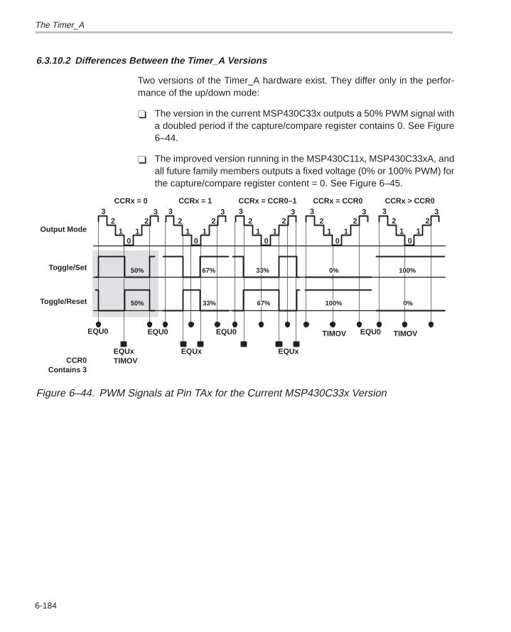
The Timer_A
6-184
6.3.10.2 Differences Between the Timer_A Versions
Two versions of the Timer_A hardware exist. They differ only in the perfor-mance of the up/down mode:
The version in the current MSP430C33x outputs a 50% PWM signal witha doubled period if the capture/compare register contains 0. See Figure6–44.
The improved version running in the MSP430C11x, MSP430C33xA, andall future family members outputs a fixed voltage (0% or 100% PWM) forthe capture/compare register content = 0. See Figure 6–45.
EQUxTIMOV
01 1
2 23 3
01 1
2 23 3
01 1
2 23 3
01 1
2 23 3
01 1
2 23 3
CCRx = 0 CCRx = 1 CCRx = CCR0–1 CCRx = CCR0 CCRx > CCR0
50% 67% 0% 100%
50% 33% 0%100%
EQU0 EQU0 EQU0 EQU0
EQUx EQUx
Output Mode
Toggle/Set
Toggle/Reset
33%
67%
CCR0Contains 3
TIMOV TIMOV
Figure 6–44. PWM Signals at Pin TAx for the Current MSP430C33x Version
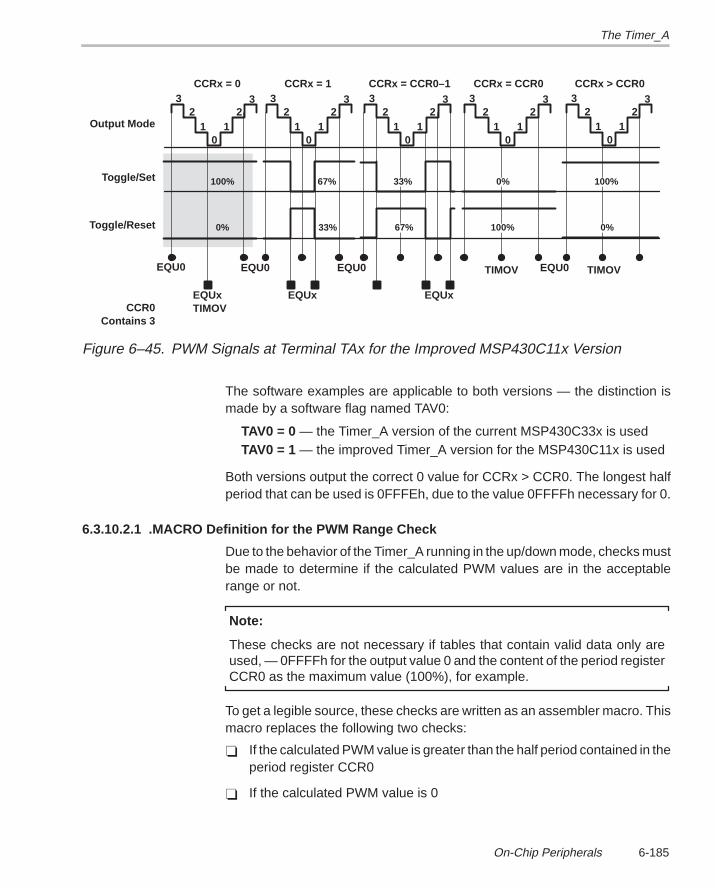
The Timer_A
6-185On-Chip Peripherals
EQUxTIMOV
01 1
2 23 3
01 1
2 23 3
01 1
2 23 3
01 1
2 23 3
01 1
2 23 3
CCRx = 0 CCRx = 1 CCRx = CCR0–1 CCRx = CCR0 CCRx > CCR0
67% 0% 100%
33% 0%100%
EQU0 EQU0 EQU0 EQU0
EQUx EQUx
Output Mode
Toggle/Set
Toggle/Reset
33%
67%
CCR0Contains 3
0%
100%
TIMOV TIMOV
Figure 6–45. PWM Signals at Terminal TAx for the Improved MSP430C11x Version
The software examples are applicable to both versions — the distinction ismade by a software flag named TAV0:
TAV0 = 0 — the Timer_A version of the current MSP430C33x is usedTAV0 = 1 — the improved Timer_A version for the MSP430C11x is used
Both versions output the correct 0 value for CCRx > CCR0. The longest halfperiod that can be used is 0FFFEh, due to the value 0FFFFh necessary for 0.
6.3.10.2.1 .MACRO Definition for the PWM Range Check
Due to the behavior of the Timer_A running in the up/down mode, checks mustbe made to determine if the calculated PWM values are in the acceptablerange or not.
Note:
These checks are not necessary if tables that contain valid data only areused, — 0FFFFh for the output value 0 and the content of the period registerCCR0 as the maximum value (100%), for example.
To get a legible source, these checks are written as an assembler macro. Thismacro replaces the following two checks:
If the calculated PWM value is greater than the half period contained in theperiod register CCR0
If the calculated PWM value is 0
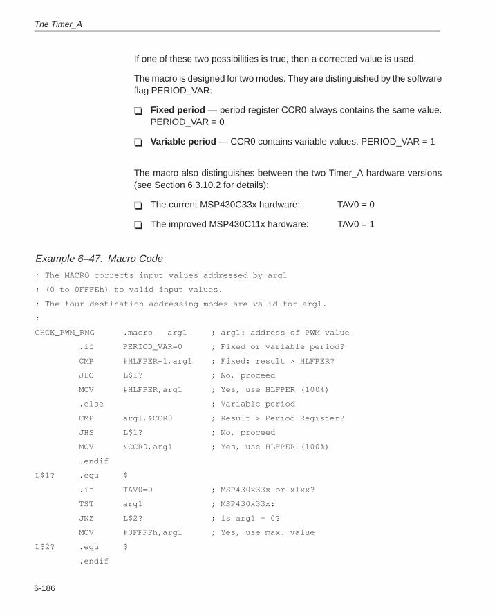
The Timer_A
6-186
If one of these two possibilities is true, then a corrected value is used.
The macro is designed for two modes. They are distinguished by the softwareflag PERIOD_VAR:
Fixed period — period register CCR0 always contains the same value.PERIOD_VAR = 0
Variable period — CCR0 contains variable values. PERIOD_VAR = 1
The macro also distinguishes between the two Timer_A hardware versions(see Section 6.3.10.2 for details):
The current MSP430C33x hardware: TAV0 = 0
The improved MSP430C11x hardware: TAV0 = 1
Example 6–47. Macro Code
; The MACRO corrects input values addressed by arg1
; (0 to 0FFFEh) to valid input values.
; The four destination addressing modes are valid for arg1.
;
CHCK_PWM_RNG .macro arg1 ; arg1: address of PWM value
.if PERIOD_VAR=0 ; Fixed or variable period?
CMP #HLFPER+1,arg1 ; Fixed: result > HLFPER?
JLO L$1? ; No, proceed
MOV #HLFPER,arg1 ; Yes, use HLFPER (100%)
.else ; Variable period
CMP arg1,&CCR0 ; Result > Period Register?
JHS L$1? ; No, proceed
MOV &CCR0,arg1 ; Yes, use HLFPER (100%)
.endif
L$1? .equ $
.if TAV0=0 ; MSP430x33x or x1xx?
TST arg1 ; MSP430x33x:
JNZ L$2? ; is arg1 = 0?
MOV #0FFFFh,arg1 ; Yes, use max. value
L$2? .equ $
.endif
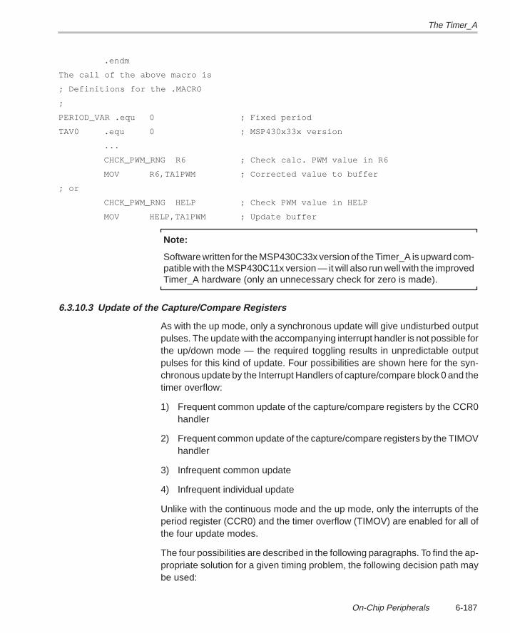
The Timer_A
6-187On-Chip Peripherals
.endm
The call of the above macro is
; Definitions for the .MACRO
;
PERIOD_VAR .equ 0 ; Fixed period
TAV0 .equ 0 ; MSP430x33x version
...
CHCK_PWM_RNG R6 ; Check calc. PWM value in R6
MOV R6,TA1PWM ; Corrected value to buffer
; or
CHCK_PWM_RNG HELP ; Check PWM value in HELP
MOV HELP,TA1PWM ; Update buffer
Note:
Software written for the MSP430C33x version of the Timer_A is upward com-patible with the MSP430C11x version — it will also run well with the improvedTimer_A hardware (only an unnecessary check for zero is made).
6.3.10.3 Update of the Capture/Compare Registers
As with the up mode, only a synchronous update will give undisturbed outputpulses. The update with the accompanying interrupt handler is not possible forthe up/down mode — the required toggling results in unpredictable outputpulses for this kind of update. Four possibilities are shown here for the syn-chronous update by the Interrupt Handlers of capture/compare block 0 and thetimer overflow:
1) Frequent common update of the capture/compare registers by the CCR0handler
2) Frequent common update of the capture/compare registers by the TIMOVhandler
3) Infrequent common update
4) Infrequent individual update
Unlike with the continuous mode and the up mode, only the interrupts of theperiod register (CCR0) and the timer overflow (TIMOV) are enabled for all ofthe four update modes.
The four possibilities are described in the following paragraphs. To find the ap-propriate solution for a given timing problem, the following decision path maybe used:
The Timer_A
6-188
Is a very fast update of the capture/compare registers necessary? If yes,use solution 1 or 2, if no, continue.
Are all of the new update values available at the same time? If yes, usesolution 3, otherwise use solution 4.
6.3.10.3.1 Frequent Common Update by CCR0
The interrupt handler of capture/compare block 0 updates the capture/compare registers CCRx with the repetition rate defined by the period registerCCR0.
This update mode is used for the Digital Motor Control with Symmetric PulseWidth Modulation.
If the range for the PWM output values is limited from 1 cycle to (CCR0) cycles,then the following simple update sequence may be used:
; R6 contains new PWM info for CCR2. Range: 1 to (CCR0).
;
MOV R6,TA2PWM ; Actualize PWM buffer
If the calculation results for the PWM output values can be 0% or >100%:
CCRx > CCR0 .or. CCRx = 0 for the current MSP430C330x
CCRx > CCR0 for the MSP430C110x,
then a special treatment is necessary due to the special behavior of the cap-ture/compare logic under these circumstances. The capture/compare registerx value then needs to be modified. To determine these special cases, the fol-lowing update sequence may be used (the macro CHCK_PWM_RNG is ex-plained in Section 6.3.10.2.1 .MACRO Definition for the PWM Range Check):
; R6 contains the calculated PWM info for CCR2.
; Range: 0 to HLFPER+x. Check if a modification is necessary
; Software is written for a constant Period Register CCR0
;
PERIOD_VAR .equ 0 ; Constant period
TAV0 .equ 0 ; MSP430x33x version
...
CHCK_PWM_RNG R6 ; Correct R6 if out of range
MOV R6,TA2PWM ; Actualize TA2PWM buffer
... ; Continue
The Timer_A
6-189On-Chip Peripherals
If a variable period is used — the content of the period register CCR0 changesduring the program flow — then the lines above change to:
; R6 contains the calculated PWM info for CCR2.
; Range: 0 to HLFPER+x. Check if a modification is necessary
; Software is written for a variable Period Register CCR0
;
PERIOD_VAR .equ 1 ; Variable period
TAV0 .equ 0 ; MSP430x33x version
...
CHCK_PWM_RNG R6 ; Correct R6 if out of range
MOV R6,TA2PWM ; Actualize TA2PWM buffer
... ; Continue
The part of the code that modifies the PWM values of the Timer_A looks likethis:
; Handler of the Period Register CCR0
;
TIMMOD0 MOV TA1PWM,&CCR1 ; Modify C/C Block 1 synchr.
MOV TA2PWM,&CCR2 ; Modify C/C Block 2 synchr.
MOV TA3PWM,&CCR3 ; Modify C/C Block 3 synchr.
ADD #2*HLFPER,TIMACYC0
... ; Other tasks of the handler
RETI
6.3.10.3.2 Frequent Common Update by the Timer Overflow TIMOV
If the interrupt handler of the period register CCR0 has to perform many tasks,then it is advised to shift one half of these tasks to the interrupt handler of thetimer overflow (TIMOV). This handler has the lowest interrupt priority, but withthe up/down mode, this does not play a role because the interrupts of the cap-ture/compare blocks 1 to 4 are normally disabled. The same background soft-ware is used as is shown with the update by the period register (CCR0) (themacro CHCK_PWM_RNG is explained in Section 6.3.10.2.1 .MACRO Defini-tion for the PWM Range Check).
;
PERIOD_VAR .equ 0 ; Fixed period
TAV0 .equ 1 ; MSP430x11x version
... ; Calc. PWM value in R7
The Timer_A
6-190
CHCK_PWM_RNG R7 ; Correct R7 if out of range
MOV R7,TA2PWM ; Actualize TA2PWM buffer
... ; Continue
The part of the code that modifies the PWM values of the Timer_A looks likethis:
TIM_HND ADD &TAIV,PC ; Serve highest Timer_A request
RETI ; No request
RETI ; C/C Block 1: INTRPT disabled
RETI ; C/C Block 2: INTRPT disabled
RETI ; C/C Block 3: INTRPT disabled
JMP TIMMOD4 ; C/C Block 4: Capturing
;
; Handler of the Timer Overflow TIMOV
;
TIMOV MOV TA1PWM,&CCR1 ; Timer_A reached zero:
MOV TA2PWM,&CCR2 ; Modify C/C Blocks x
MOV TA3PWM,&CCR3
INC TIMACNT ; Actualize half period counter
RETI
6.3.10.3.3 Infrequent Common Update
The interrupt handlers of the capture/compare block 0 or the timer overflow up-date the capture/compare registers CCRx with a repetition rate given by thecalculation speed of the background program. If new PWM values are calcu-lated or read for all capture/compare blocks, then a common flag is set and theupdate is enabled in this way. This solution is used if the PWM values for theupdate are available at (nearly) the same time — by table processing, for ex-ample.
This update mode is used with the example TRIAC Control.
If the range for the calculated PWM output values is limited from 1 cycle to(CCR0) cycles, then the following simple update sequence may be used:
; R6 to R8 contain new PWM info for Output Units 1 to 3
; Range: 1 to (CCR0).
;
The Timer_A
6-191On-Chip Peripherals
MOV R6,TA1PWM ; Actualize CCR1 pulse length
MOV R7,TA2PWM ; CCR2
MOV R8,TA3PWM ; CCR3
BIS.B #1,FLAG ; Set update flag
... ; Intrpt handler resets FLAG
If the output values 0% or >100% are actually used, then a special treatmentis necessary. To correct these special cases, the following update sequencemay be used (the macro CHCK_PWM_RNG is explained in Section 6.3.10.2.1.MACRO Definition for the PWM Range Check):
; R6 to R8 contain new PWM info for Output Units 1 to 3.
; Range: 0 to (CCR0)+x.
; Check if a correction is necessary.
;
CHK_PWM_RNG R6 ; Check the PWM range
MOV R6,TA1PWM ; Write corrected R6 to buffer
CHK_PWM_RNG R7 ; Check the PWM range
MOV R7,TA2PWM ; Write corrected R7 to buffer
CHK_PWM_RNG R8 ; Check the PWM range
MOV R8,TA3PWM ; Write corrected R8 to buffer
BIS.B #1,FLAG ; Start common update
... ; Continue in background
The update part of the code in the interrupt handlers of the period registerCCR0 or the timer overflow TIMOV looks like this:
BIT.B #1,FLAG ; Is update flag set?
JZ L$1 ; No, continue
MOV TA1PWM,&CCR1 ; Actualize CCR1 pulse length
MOV TA2PWM,&CCR2 ; dito CCR2
MOV TA3PWM,&CCR3 ; dito CCR3
BIC.B #1,FLAG ; Reset update flag
L$1 ... ; Continue INTRPT handler
If the other seven bits of the RAM byte FLAG are not used, then a faster versionof the above update sequence may be used. The resetting of the bit is not nec-essary and saves 4 cycles.
RRA.B FLAG ; Is update flag FLAG.0 set?
The Timer_A
6-192
JNC L$1 ; No, continue
MOV TA1PWM,&CCR1 ; Actualize CCR1 pulse length
MOV TA2PWM,&CCR2 ; dito CCR2
MOV TA3PWM,&CCR3 , dito CCR3
L$1 ... ; Continue INTRPT handler
6.3.10.3.4 Infrequent Individual Update
The interrupt handler of the period register or the Timer Overflow update thecapture/compare register CCRx with a repetition rate given by the calculationspeed of the background program. If a new PWM value is calculated for a cap-ture/compare block, then an individual flag is set and the update for this cap-ture/compare block is made. This method is used if the PWM values for theupdate are not available at the same time. This update mode is used with theexample Capturing with the Up/Down Mode. It is the update mode with the low-est overhead. The macro CHCK_PWM_RNG is detailed in Section 6.3.10.2.1.MACRO Definition for the PWM Range Check.
; R6 contains new PWM info for CCR1. Range: 0 to (CCR0)+x.
; Check if a modification is necessary:
; Software is written for a variable Period Register CCR0
;
TAV0 .equ 0 ; MSP430X33x version
PERIOD_VAR .equ 1 ; Variable period
...
CHK_PWM_RNG R6 ; Check/correct result in R6
MOV R6,TA1PWM ; Actualize TA1PWM buffer
BIS #2,FLAG ; Start update of CCR1
... ; Start calculation for CCR2
;
; R6 contains new PWM info for CCR2. Range: 0 to (CCR0)+x
;
CHK_PWM_RNG R6
MOV R6,TA2PWM ; Actualize TA2PWM buffer
BIS #4,FLAG ; Start update of CCR2
... ; Continue
The interrupt handler of the period register CCR0 or the timer overflow (TI-MOV) decodes the necessary task as follows (4 to 20 MCLK cycles are need-ed):
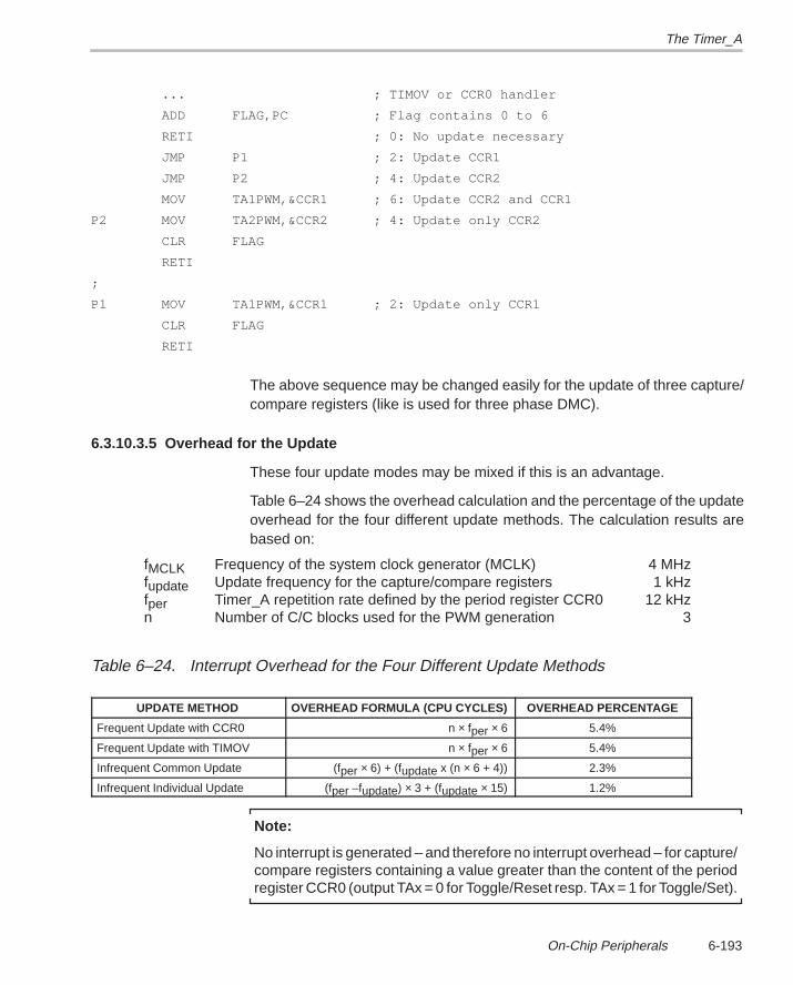
The Timer_A
6-193On-Chip Peripherals
... ; TIMOV or CCR0 handler
ADD FLAG,PC ; Flag contains 0 to 6
RETI ; 0: No update necessary
JMP P1 ; 2: Update CCR1
JMP P2 ; 4: Update CCR2
MOV TA1PWM,&CCR1 ; 6: Update CCR2 and CCR1
P2 MOV TA2PWM,&CCR2 ; 4: Update only CCR2
CLR FLAG
RETI
;
P1 MOV TA1PWM,&CCR1 ; 2: Update only CCR1
CLR FLAG
RETI
The above sequence may be changed easily for the update of three capture/compare registers (like is used for three phase DMC).
6.3.10.3.5 Overhead for the Update
These four update modes may be mixed if this is an advantage.
Table 6–24 shows the overhead calculation and the percentage of the updateoverhead for the four different update methods. The calculation results arebased on:
fMCLK Frequency of the system clock generator (MCLK) 4 MHzfupdate Update frequency for the capture/compare registers 1 kHzfper Timer_A repetition rate defined by the period register CCR0 12 kHzn Number of C/C blocks used for the PWM generation 3
Table 6–24. Interrupt Overhead for the Four Different Update Methods
UPDATE METHOD OVERHEAD FORMULA (CPU CYCLES) OVERHEAD PERCENTAGE
Frequent Update with CCR0 n × fper × 6 5.4%
Frequent Update with TIMOV n × fper × 6 5.4%
Infrequent Common Update (fper × 6) + (fupdate x (n × 6 + 4)) 2.3%
Infrequent Individual Update (fper –fupdate) × 3 + (fupdate × 15) 1.2%
Note:
No interrupt is generated – and therefore no interrupt overhead – for capture/compare registers containing a value greater than the content of the periodregister CCR0 (output TAx = 0 for Toggle/Reset resp. TAx = 1 for Toggle/Set).
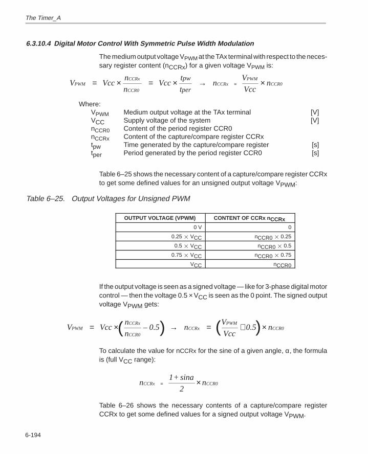
The Timer_A
6-194
6.3.10.4 Digital Motor Control With Symmetric Pulse Width Modulation
The medium output voltage VPWM at the TAx terminal with respect to the neces-sary register content (nCCRx) for a given voltage VPWM is:
V Vccn
nVcc
tn
V
VccnPWM
CCRx
CCR0CCRx
PWMCCR0
pw= × = × → ×=tper
Where: VPWM Medium output voltage at the TAx terminal [V]VCC Supply voltage of the system [V]nCCR0 Content of the period register CCR0nCCRx Content of the capture/compare register CCRxtpw Time generated by the capture/compare register [s]tper Period generated by the period register CCR0 [s]
Table 6–25 shows the necessary content of a capture/compare register CCRxto get some defined values for an unsigned output voltage VPWM:
Table 6–25. Output Voltages for Unsigned PWM
OUTPUT VOLTAGE (VPWM) CONTENT OF CCRx nCCRx0 V 0
0.25 VCC nCCR0 0.25
0.5 VCC nCCR0 0.5
0.75 VCC nCCR0 0.75
VCC nCCR0
If the output voltage is seen as a signed voltage — like for 3-phase digital motorcontrol — then the voltage 0.5 × VCC is seen as the 0 point. The signed outputvoltage VPWM gets:
V Vccn
n0.5 n
V
Vcc0.5 nPWM
CCRx
CCR0CCRx
PWMCCR0= × – → = + ×( ( ))
To calculate the value for nCCRx for the sine of a given angle, α, the formulais (full VCC range):
n1+ sina
2nCCRx CCR0= ×
Table 6–26 shows the necessary contents of a capture/compare registerCCRx to get some defined values for a signed output voltage VPWM.
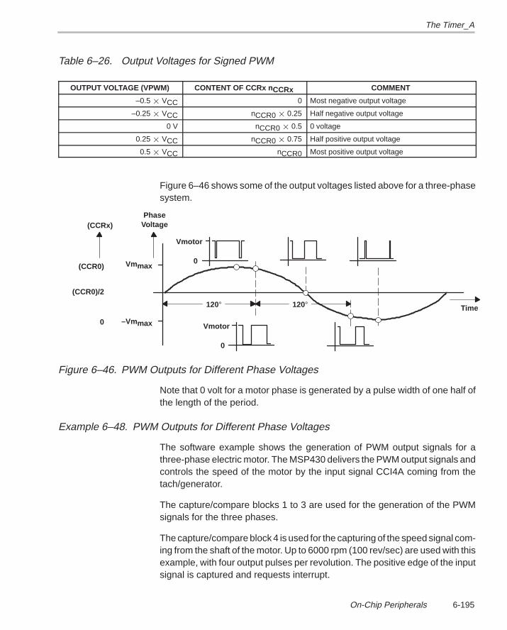
The Timer_A
6-195On-Chip Peripherals
Table 6–26. Output Voltages for Signed PWM
OUTPUT VOLTAGE (VPWM) CONTENT OF CCRx nCCRx COMMENT
–0.5 VCC 0 Most negative output voltage
–0.25 VCC nCCR0 0.25 Half negative output voltage
0 V nCCR0 0.5 0 voltage
0.25 VCC nCCR0 0.75 Half positive output voltage
0.5 VCC nCCR0 Most positive output voltage
Figure 6–46 shows some of the output voltages listed above for a three-phasesystem.
Vmmax
–Vmmax
120° 120° Time
PhaseVoltage
Vmotor
0
(CCRx)
(CCR0)
(CCR0)/2
0
Vmotor
0
Figure 6–46. PWM Outputs for Different Phase Voltages
Note that 0 volt for a motor phase is generated by a pulse width of one half ofthe length of the period.
Example 6–48. PWM Outputs for Different Phase Voltages
The software example shows the generation of PWM output signals for athree-phase electric motor. The MSP430 delivers the PWM output signals andcontrols the speed of the motor by the input signal CCI4A coming from thetach/generator.
The capture/compare blocks 1 to 3 are used for the generation of the PWMsignals for the three phases.
The capture/compare block 4 is used for the capturing of the speed signal com-ing from the shaft of the motor. Up to 6000 rpm (100 rev/sec) are used with thisexample, with four output pulses per revolution. The positive edge of the inputsignal is captured and requests interrupt.
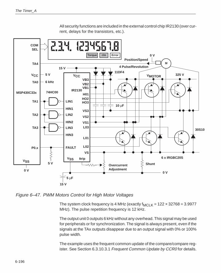
The Timer_A
6-196
All security functions are included in the external control chip IR2130 (over cur-rent, delays for the transistors, etc.).
VSS
COMSEL
M
5 V
Torque r/m Error
HIN1
LIN1TA1
HIN2
LIN2TA2
HIN3
LIN3TA3
FAULTP0.x
5 V
0 V
VB3VB2VB1
H01HO2HO3
VS3
VS2
VS1L03
L01
L02
VS
ItripVSSShuntOvercurrent
Adjustment
6 x IRGBC20S
30S10
325 V
Position/Speed
15 V
VCC11DF4
10 µF
15 V
5 µF
0 V
TA4
VMOTOR
0 V
74HC00
4 Pulse/Revolution
6 kHzTA0
VCC
IR2130MSP430C33x
Figure 6–47. PWM Motors Control for High Motor Voltages
The system clock frequency is 4 MHz (exactly fMCLK = 122 × 32768 = 3.9977MHz). The pulse repetition frequency is 12 kHz.
The output unit 0 outputs 6 kHz without any overhead. This signal may be usedfor peripherals or for synchronization. The signal is always present, even if thesignals at the TAx outputs disappear due to an output signal with 0% or 100%pulse width.
The example uses the frequent common update of the compare/compare reg-ister. See Section 6.3.10.3.1 Frequent Common Update by CCR0 for details.
The Timer_A
6-197On-Chip Peripherals
Figure 6–48 shows the output signals at the times that they have phase shiftsof 0, +120 and –120.
thlfper
tpw1tpw2
tpw3
TIMOV EQU0 TIMOV EQU0 TIMOV
0°(0.5 × Vmotor)
120°(0.93 × Vmotor)
–120°(0.07 × Vmotor)
2n × thlfper0
2n
(2n + 2) × thlfper1
2n + 1
0
2n + 2
(2n + 4) × thlfper1
2n + 3
0
2n + 4
TIMACYC0
Direction Bit
TIMACNT
0FFFFh
CCR0CCR2
CCR1
CCR30h
TA1 Output
TA2 Output
TA3 Output
Interrupts
Figure 6–48. Symmetric PWM Timings Generated With the Up/Down Mode
Example 6–49. Symmetric PWM Timings Generated With the Up/Down Mode
; Software example:
; TA0: symmetric output signal 6.0kHz
; TA1: positive PWM signal 12.0kHz. Length in TA1PWM
; TA2: positive PWM signal 12.0kHz. Length in TA2PWM
; TA3: positive PWM signal 12.0kHz. Length in TA3PWM
;
; Hardware definitions
;
FLLMPY .equ 122 ; FLL multiplier for 3.9977MHz
fper .equ 12000 ; 12.0kHz repetition rate
TCLK .equ FLLMPY*32768 ; TCLK: FLLMPY x fcrystal
HLFPER .equ (TCLK/fper)/2 ; Period of output signals
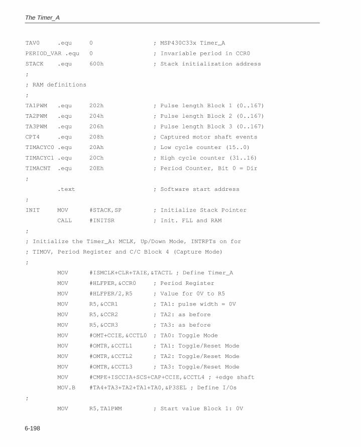
The Timer_A
6-198
TAV0 .equ 0 ; MSP430C33x Timer_A
PERIOD_VAR .equ 0 ; Invariable period in CCR0
STACK .equ 600h ; Stack initialization address
;
; RAM definitions
;
TA1PWM .equ 202h ; Pulse length Block 1 (0..167)
TA2PWM .equ 204h ; Pulse length Block 2 (0..167)
TA3PWM .equ 206h ; Pulse length Block 3 (0..167)
CPT4 .equ 208h ; Captured motor shaft events
TIMACYC0 .equ 20Ah ; Low cycle counter (15..0)
TIMACYC1 .equ 20Ch ; High cycle counter (31..16)
TIMACNT .equ 20Eh ; Period Counter, Bit 0 = Dir
;
.text ; Software start address
;
INIT MOV #STACK,SP ; Initialize Stack Pointer
CALL #INITSR ; Init. FLL and RAM
;
; Initialize the Timer_A: MCLK, Up/Down Mode, INTRPTs on for
; TIMOV, Period Register and C/C Block 4 (Capture Mode)
;
MOV #ISMCLK+CLR+TAIE,&TACTL ; Define Timer_A
MOV #HLFPER,&CCR0 ; Period Register
MOV #HLFPER/2,R5 ; Value for 0V to R5
MOV R5,&CCR1 ; TA1: pulse width = 0V
MOV R5,&CCR2 ; TA2: as before
MOV R5,&CCR3 ; TA3: as before
MOV #OMT+CCIE,&CCTL0 ; TA0: Toggle Mode
MOV #OMTR,&CCTL1 ; TA1: Toggle/Reset Mode
MOV #OMTR,&CCTL2 ; TA2: Toggle/Reset Mode
MOV #OMTR,&CCTL3 ; TA3: Toggle/Reset Mode
MOV #CMPE+ISCCIA+SCS+CAP+CCIE,&CCTL4 ; +edge shaft
MOV.B #TA4+TA3+TA2+TA1+TA0,&P3SEL ; Define I/Os
;
MOV R5,TA1PWM ; Start value Block 1: 0V
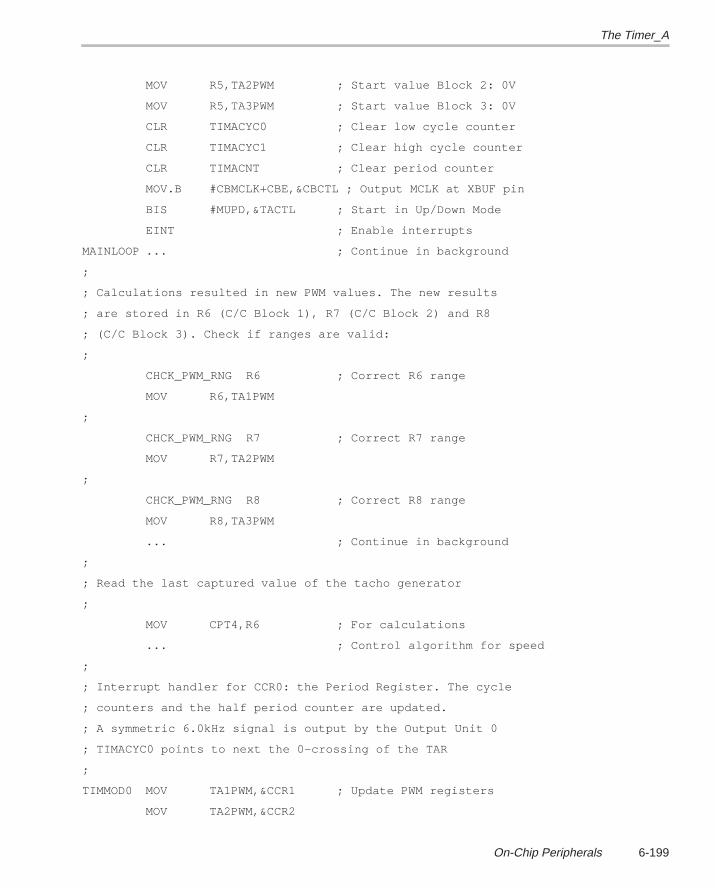
The Timer_A
6-199On-Chip Peripherals
MOV R5,TA2PWM ; Start value Block 2: 0V
MOV R5,TA3PWM ; Start value Block 3: 0V
CLR TIMACYC0 ; Clear low cycle counter
CLR TIMACYC1 ; Clear high cycle counter
CLR TIMACNT ; Clear period counter
MOV.B #CBMCLK+CBE,&CBCTL ; Output MCLK at XBUF pin
BIS #MUPD,&TACTL ; Start in Up/Down Mode
EINT ; Enable interrupts
MAINLOOP ... ; Continue in background
;
; Calculations resulted in new PWM values. The new results
; are stored in R6 (C/C Block 1), R7 (C/C Block 2) and R8
; (C/C Block 3). Check if ranges are valid:
;
CHCK_PWM_RNG R6 ; Correct R6 range
MOV R6,TA1PWM
;
CHCK_PWM_RNG R7 ; Correct R7 range
MOV R7,TA2PWM
;
CHCK_PWM_RNG R8 ; Correct R8 range
MOV R8,TA3PWM
... ; Continue in background
;
; Read the last captured value of the tacho generator
;
MOV CPT4,R6 ; For calculations
... ; Control algorithm for speed
;
; Interrupt handler for CCR0: the Period Register. The cycle
; counters and the half period counter are updated.
; A symmetric 6.0kHz signal is output by the Output Unit 0
; TIMACYC0 points to next the 0–crossing of the TAR
;
TIMMOD0 MOV TA1PWM,&CCR1 ; Update PWM registers
MOV TA2PWM,&CCR2
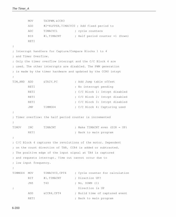
The Timer_A
6-200
MOV TA3PWM,&CCR3
ADD #2*HLFPER,TIMACYC0 ; Add fixed period to
ADC TIMACYC1 ; cycle counters
BIS #1,TIMACNT ; Half period counter +1 (Down)
RETI
;
; Interrupt handlers for Capture/Compare Blocks 1 to 4
; and Timer Overflow.
; Only the timer overflow interrupt and the C/C Block 4 are
; used. The other interrupts are disabled. The PWM generation
; is made by the timer hardware and updated by the CCR0 intrpt
;
TIM_HND ADD &TAIV,PC ; Add Jump table offset
RETI ; No interrupt pending
RETI ; C/C Block 1: Intrpt disabled
RETI ; C/C Block 2: Intrpt disabled
RETI ; C/C Block 3: Intrpt disabled
JMP TIMMOD4 ; C/C Block 4: Capturing used
;
; Timer overflow: the half period counter is incremented
;
TIMOV INC TIMACNT ; Make TIMACNT even (DIR = UP)
RETI ; Back to main program
;
; C/C Block 4 captures the revolutions of the motor. Dependent
; on the count direction of TAR, CCR4 is added or subtracted.
; The positive edge of the input signal at TA4 is captured
; and requests interrupt. Time out cannot occur due to
; low input frequency.
;
TIMMOD4 MOV TIMACYC0,CPT4 ; Cycle counter for calculation
BIT #1,TIMACNT ; Direction UP?
JNZ T40 ; No, DOWN (1)
; Direction is UP
ADD &CCR4,CPT4 ; Build time of captured event
RETI ; Back to main program
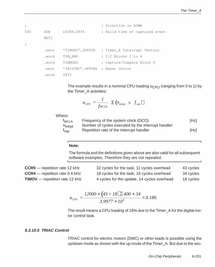
The Timer_A
6-201On-Chip Peripherals
; ; Direction is DOWN
T40 SUB &CCR4,CPT4 ; Build time of captured event
RETI
;
.sect ”TIMVEC”,0FFF0h ; Timer_A Interrupt Vectors
.word TIM_HND ; C/C Blocks 1 to 4
.word TIMMOD0 ; Capture/Compare Block 0
.sect ”INITVEC”,0FFFEh ; Reset Vector
.word INIT
The example results in a nominal CPU loading uCPU (ranging from 0 to 1) bythe Timer_A activities:
u =1
f n
f CPU
MCLKintrpt repΣ ( )
Where: fMCLK Frequency of the system clock (DCO) [Hz]nintrpt Number of cycles executed by the interrupt handlerfrep Repetition rate of the interrupt handler [Hz]
Note:
The formula and the definitions given above are also valid for all subsequentsoftware examples. Therefore they are not repeated.
CCR0 — repetition rate 12 kHz 32 cycles for the task, 11 cycles overhead 43 cyclesCCR4 — repetition rate 0.4 kHz 18 cycles for the task, 16 cycles overhead 34 cyclesTIMOV — repetition rate 12 kHz 4 cycles for the update, 14 cycles overhead 18 cycles
( )u =
12000 43 + 18 400 34
3.9977 100.186CPU 6
× + ××
=
The result means a CPU loading of 19% due to the Timer_A for the digital mo-tor control task.
6.3.10.5 TRIAC Control
TRIAC control for electric motors (DMC) or other loads is possible using theup/down mode as shown with the up mode of the Timer_A. But due to the sec-
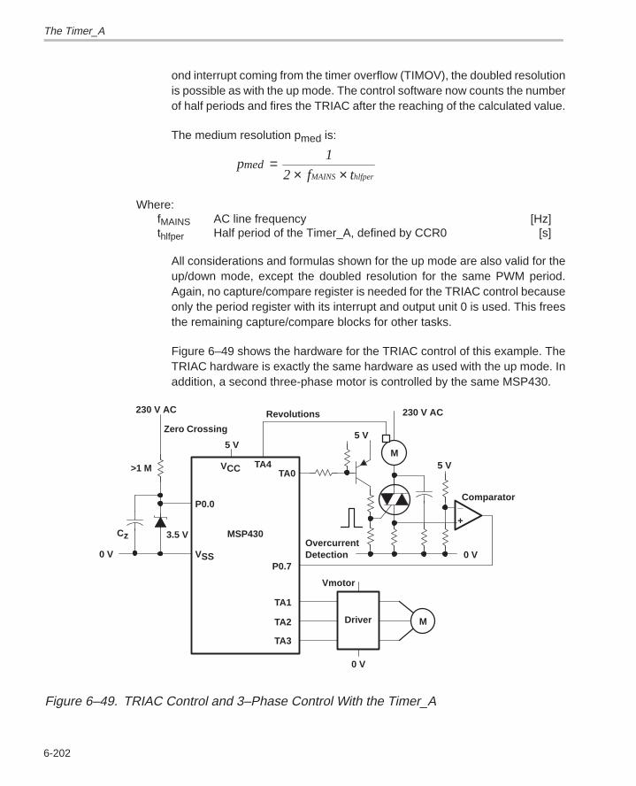
The Timer_A
6-202
ond interrupt coming from the timer overflow (TIMOV), the doubled resolutionis possible as with the up mode. The control software now counts the numberof half periods and fires the TRIAC after the reaching of the calculated value.
The medium resolution pmed is:
p 1
2 f tmed
MAINS hlfper=
× ×
Where: fMAINS AC line frequency [Hz]thlfper Half period of the Timer_A, defined by CCR0 [s]
All considerations and formulas shown for the up mode are also valid for theup/down mode, except the doubled resolution for the same PWM period.Again, no capture/compare register is needed for the TRIAC control becauseonly the period register with its interrupt and output unit 0 is used. This freesthe remaining capture/compare blocks for other tasks.
Figure 6–49 shows the hardware for the TRIAC control of this example. TheTRIAC hardware is exactly the same hardware as used with the up mode. Inaddition, a second three-phase motor is controlled by the same MSP430.
Zero Crossing
3.5 V MSP430
TA0
5 V
VCC
5 V
0 V
M
OvercurrentDetection
P0.7
_
+
Comparator
5 V
230 V AC
P0.0
Cz
>1 M TA4
230 V AC
MDriver
Vmotor
TA1
TA2
TA3
0 V
VSS0 V
Revolutions
Figure 6–49. TRIAC Control and 3–Phase Control With the Timer_A
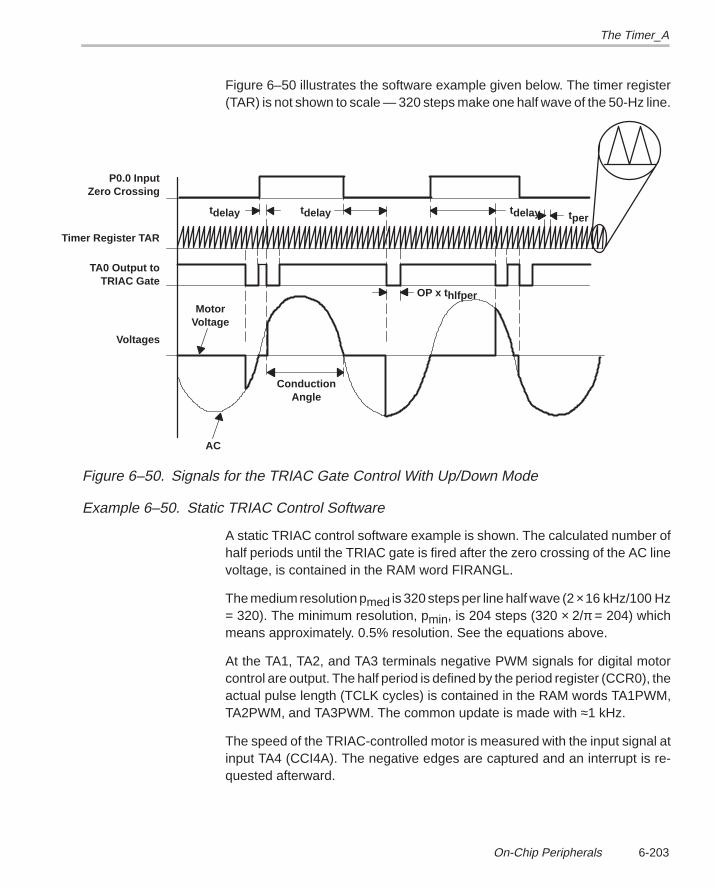
The Timer_A
6-203On-Chip Peripherals
Figure 6–50 illustrates the software example given below. The timer register(TAR) is not shown to scale — 320 steps make one half wave of the 50-Hz line.
tdelay tdelay tdelay
MotorVoltage
AC
ConductionAngle
P0.0 InputZero Crossing
Timer Register TAR
TA0 Output toTRIAC Gate
Voltages
tper
OP x thlfper
Figure 6–50. Signals for the TRIAC Gate Control With Up/Down Mode
Example 6–50. Static TRIAC Control Software
A static TRIAC control software example is shown. The calculated number ofhalf periods until the TRIAC gate is fired after the zero crossing of the AC linevoltage, is contained in the RAM word FIRANGL.
The medium resolution pmed is 320 steps per line half wave (2 ×16 kHz/100 Hz= 320). The minimum resolution, pmin, is 204 steps (320 × 2/π = 204) whichmeans approximately. 0.5% resolution. See the equations above.
At the TA1, TA2, and TA3 terminals negative PWM signals for digital motorcontrol are output. The half period is defined by the period register (CCR0), theactual pulse length (TCLK cycles) is contained in the RAM words TA1PWM,TA2PWM, and TA3PWM. The common update is made with ≈1 kHz.
The speed of the TRIAC-controlled motor is measured with the input signal atinput TA4 (CCI4A). The negative edges are captured and an interrupt is re-quested afterward.
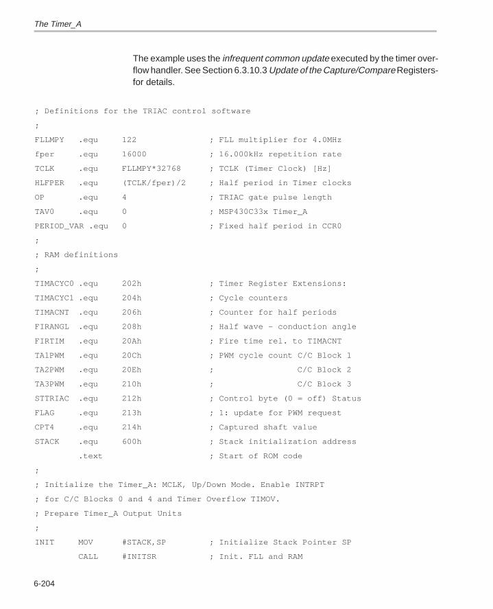
The Timer_A
6-204
The example uses the infrequent common update executed by the timer over-flow handler. See Section 6.3.10.3 Update of the Capture/Compare Registers-for details.
; Definitions for the TRIAC control software
;
FLLMPY .equ 122 ; FLL multiplier for 4.0MHz
fper .equ 16000 ; 16.000kHz repetition rate
TCLK .equ FLLMPY*32768 ; TCLK (Timer Clock) [Hz]
HLFPER .equ (TCLK/fper)/2 ; Half period in Timer clocks
OP .equ 4 ; TRIAC gate pulse length
TAV0 .equ 0 ; MSP430C33x Timer_A
PERIOD_VAR .equ 0 ; Fixed half period in CCR0
;
; RAM definitions
;
TIMACYC0 .equ 202h ; Timer Register Extensions:
TIMACYC1 .equ 204h ; Cycle counters
TIMACNT .equ 206h ; Counter for half periods
FIRANGL .equ 208h ; Half wave – conduction angle
FIRTIM .equ 20Ah ; Fire time rel. to TIMACNT
TA1PWM .equ 20Ch ; PWM cycle count C/C Block 1
TA2PWM .equ 20Eh ; C/C Block 2
TA3PWM .equ 210h ; C/C Block 3
STTRIAC .equ 212h ; Control byte (0 = off) Status
FLAG .equ 213h ; 1: update for PWM request
CPT4 .equ 214h ; Captured shaft value
STACK .equ 600h ; Stack initialization address
.text ; Start of ROM code
;
; Initialize the Timer_A: MCLK, Up/Down Mode. Enable INTRPT
; for C/C Blocks 0 and 4 and Timer Overflow TIMOV.
; Prepare Timer_A Output Units
;
INIT MOV #STACK,SP ; Initialize Stack Pointer SP
CALL #INITSR ; Init. FLL and RAM
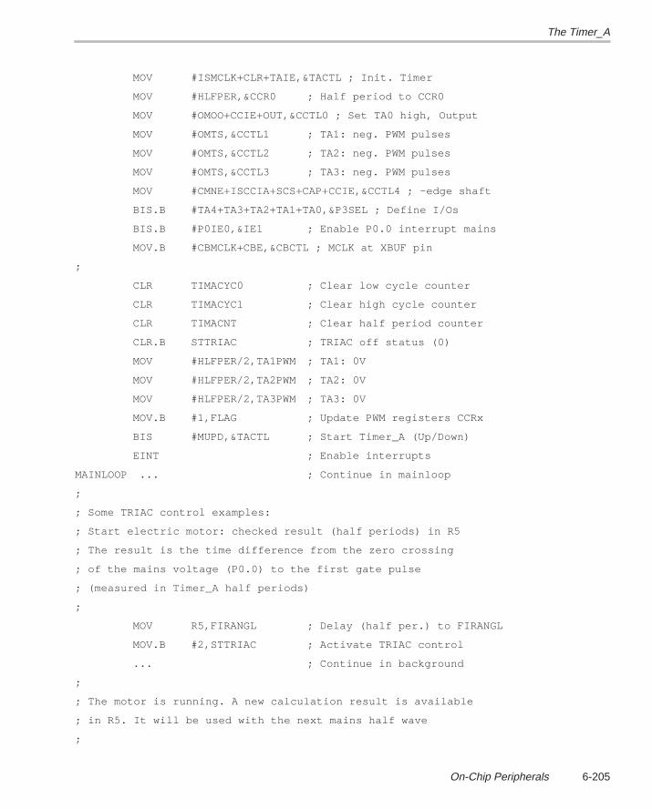
The Timer_A
6-205On-Chip Peripherals
MOV #ISMCLK+CLR+TAIE,&TACTL ; Init. Timer
MOV #HLFPER,&CCR0 ; Half period to CCR0
MOV #OMOO+CCIE+OUT,&CCTL0 ; Set TA0 high, Output
MOV #OMTS,&CCTL1 ; TA1: neg. PWM pulses
MOV #OMTS,&CCTL2 ; TA2: neg. PWM pulses
MOV #OMTS,&CCTL3 ; TA3: neg. PWM pulses
MOV #CMNE+ISCCIA+SCS+CAP+CCIE,&CCTL4 ; –edge shaft
BIS.B #TA4+TA3+TA2+TA1+TA0,&P3SEL ; Define I/Os
BIS.B #P0IE0,&IE1 ; Enable P0.0 interrupt mains
MOV.B #CBMCLK+CBE,&CBCTL ; MCLK at XBUF pin
;
CLR TIMACYC0 ; Clear low cycle counter
CLR TIMACYC1 ; Clear high cycle counter
CLR TIMACNT ; Clear half period counter
CLR.B STTRIAC ; TRIAC off status (0)
MOV #HLFPER/2,TA1PWM ; TA1: 0V
MOV #HLFPER/2,TA2PWM ; TA2: 0V
MOV #HLFPER/2,TA3PWM ; TA3: 0V
MOV.B #1,FLAG ; Update PWM registers CCRx
BIS #MUPD,&TACTL ; Start Timer_A (Up/Down)
EINT ; Enable interrupts
MAINLOOP ... ; Continue in mainloop
;
; Some TRIAC control examples:
; Start electric motor: checked result (half periods) in R5
; The result is the time difference from the zero crossing
; of the mains voltage (P0.0) to the first gate pulse
; (measured in Timer_A half periods)
;
MOV R5,FIRANGL ; Delay (half per.) to FIRANGL
MOV.B #2,STTRIAC ; Activate TRIAC control
... ; Continue in background
;
; The motor is running. A new calculation result is available
; in R5. It will be used with the next mains half wave
;
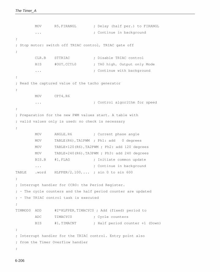
The Timer_A
6-206
MOV R5,FIRANGL ; Delay (half per.) to FIRANGL
... ; Continue in background
;
; Stop motor: switch off TRIAC control, TRIAC gate off
;
CLR.B STTRIAC ; Disable TRIAC control
BIS #OUT,CCTL0 ; TA0 high, Output only Mode
... ; Continue with background
;
; Read the captured value of the tacho generator
;
MOV CPT4,R6
... ; Control algorithm for speed
;
; Preparation for the new PWM values start. A table with
; valid values only is used: no check is necessary
;
MOV ANGLE,R6 ; Current phase angle
MOV TABLE(R6),TA1PWM ; Ph1: add 0 degrees
MOV TABLE+120(R6),TA2PWM ; Ph2: add 120 degrees
MOV TABLE+240(R6),TA3PWM ; Ph3: add 240 degrees
BIS.B #1,FLAG ; Initiate common update
... ; Continue in background
TABLE .word HLFPER/2,100,... ; sin 0 to sin 600
;
; Interrupt handler for CCR0: the Period Register.
; – The cycle counters and the half period counter are updated
; – The TRIAC control task is executed
;
TIMMOD0 ADD #2*HLFPER,TIMACYC0 ; Add (fixed) period to
ADC TIMACYC0 ; Cycle counters
BIS #1,TIMACNT ; Half period counter +1 (Down)
;
; Interrupt handler for the TRIAC control. Entry point also
; from the Timer Overflow handler
;
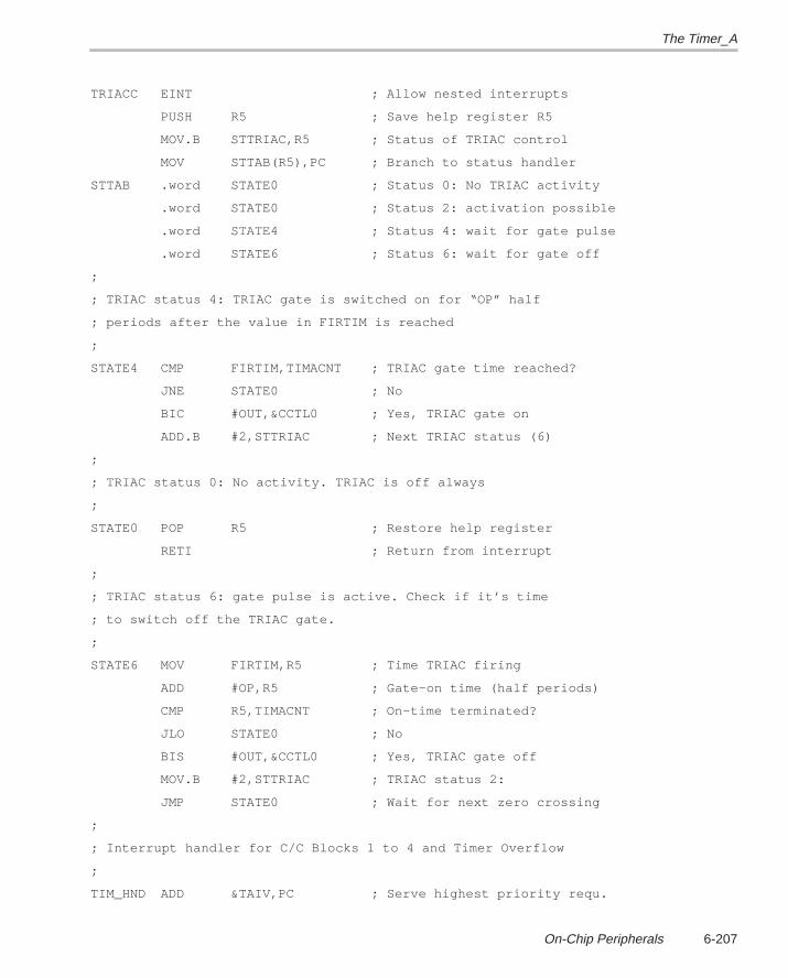
The Timer_A
6-207On-Chip Peripherals
TRIACC EINT ; Allow nested interrupts
PUSH R5 ; Save help register R5
MOV.B STTRIAC,R5 ; Status of TRIAC control
MOV STTAB(R5),PC ; Branch to status handler
STTAB .word STATE0 ; Status 0: No TRIAC activity
.word STATE0 ; Status 2: activation possible
.word STATE4 ; Status 4: wait for gate pulse
.word STATE6 ; Status 6: wait for gate off
;
; TRIAC status 4: TRIAC gate is switched on for “OP” half
; periods after the value in FIRTIM is reached
;
STATE4 CMP FIRTIM,TIMACNT ; TRIAC gate time reached?
JNE STATE0 ; No
BIC #OUT,&CCTL0 ; Yes, TRIAC gate on
ADD.B #2,STTRIAC ; Next TRIAC status (6)
;
; TRIAC status 0: No activity. TRIAC is off always
;
STATE0 POP R5 ; Restore help register
RETI ; Return from interrupt
;
; TRIAC status 6: gate pulse is active. Check if it’s time
; to switch off the TRIAC gate.
;
STATE6 MOV FIRTIM,R5 ; Time TRIAC firing
ADD #OP,R5 ; Gate–on time (half periods)
CMP R5,TIMACNT ; On–time terminated?
JLO STATE0 ; No
BIS #OUT,&CCTL0 ; Yes, TRIAC gate off
MOV.B #2,STTRIAC ; TRIAC status 2:
JMP STATE0 ; Wait for next zero crossing
;
; Interrupt handler for C/C Blocks 1 to 4 and Timer Overflow
;
TIM_HND ADD &TAIV,PC ; Serve highest priority requ.
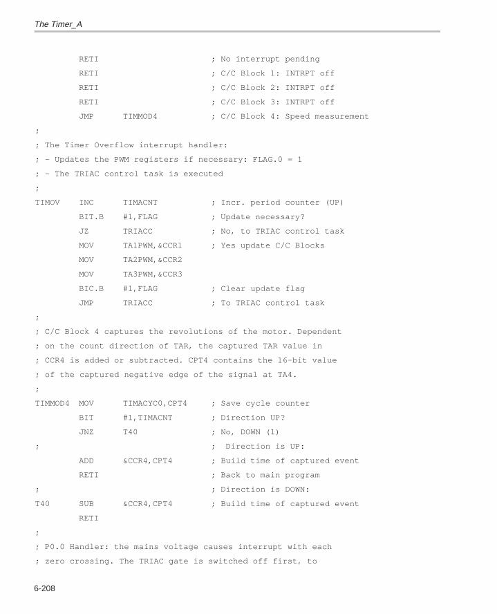
The Timer_A
6-208
RETI ; No interrupt pending
RETI ; C/C Block 1: INTRPT off
RETI ; C/C Block 2: INTRPT off
RETI ; C/C Block 3: INTRPT off
JMP TIMMOD4 ; C/C Block 4: Speed measurement
;
; The Timer Overflow interrupt handler:
; – Updates the PWM registers if necessary: FLAG.0 = 1
; – The TRIAC control task is executed
;
TIMOV INC TIMACNT ; Incr. period counter (UP)
BIT.B #1,FLAG ; Update necessary?
JZ TRIACC ; No, to TRIAC control task
MOV TA1PWM,&CCR1 ; Yes update C/C Blocks
MOV TA2PWM,&CCR2
MOV TA3PWM,&CCR3
BIC.B #1,FLAG ; Clear update flag
JMP TRIACC ; To TRIAC control task
;
; C/C Block 4 captures the revolutions of the motor. Dependent
; on the count direction of TAR, the captured TAR value in
; CCR4 is added or subtracted. CPT4 contains the 16–bit value
; of the captured negative edge of the signal at TA4.
;
TIMMOD4 MOV TIMACYC0,CPT4 ; Save cycle counter
BIT #1,TIMACNT ; Direction UP?
JNZ T40 ; No, DOWN (1)
; ; Direction is UP:
ADD &CCR4,CPT4 ; Build time of captured event
RETI ; Back to main program
; ; Direction is DOWN:
T40 SUB &CCR4,CPT4 ; Build time of captured event
RETI
;
; P0.0 Handler: the mains voltage causes interrupt with each
; zero crossing. The TRIAC gate is switched off first, to
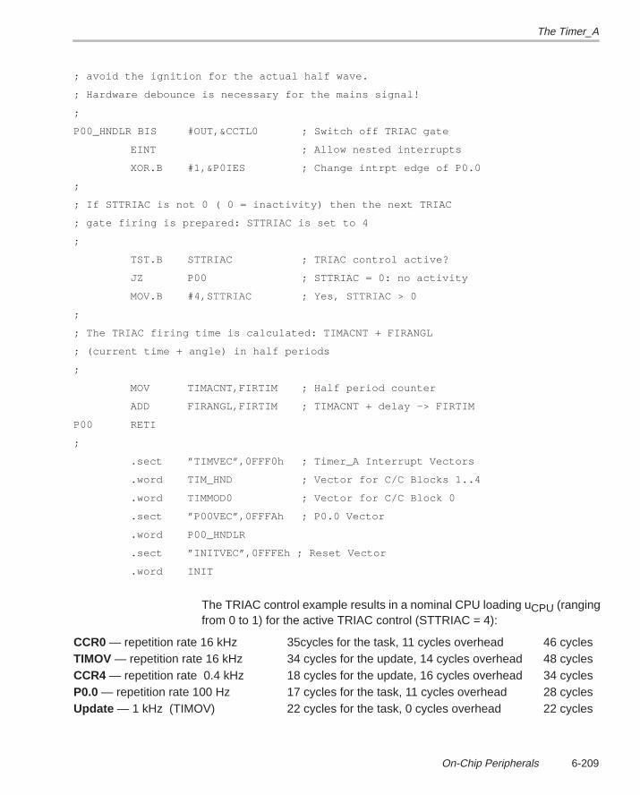
The Timer_A
6-209On-Chip Peripherals
; avoid the ignition for the actual half wave.
; Hardware debounce is necessary for the mains signal!
;
P00_HNDLR BIS #OUT,&CCTL0 ; Switch off TRIAC gate
EINT ; Allow nested interrupts
XOR.B #1,&P0IES ; Change intrpt edge of P0.0
;
; If STTRIAC is not 0 ( 0 = inactivity) then the next TRIAC
; gate firing is prepared: STTRIAC is set to 4
;
TST.B STTRIAC ; TRIAC control active?
JZ P00 ; STTRIAC = 0: no activity
MOV.B #4,STTRIAC ; Yes, STTRIAC > 0
;
; The TRIAC firing time is calculated: TIMACNT + FIRANGL
; (current time + angle) in half periods
;
MOV TIMACNT,FIRTIM ; Half period counter
ADD FIRANGL,FIRTIM ; TIMACNT + delay –> FIRTIM
P00 RETI
;
.sect ”TIMVEC”,0FFF0h ; Timer_A Interrupt Vectors
.word TIM_HND ; Vector for C/C Blocks 1..4
.word TIMMOD0 ; Vector for C/C Block 0
.sect ”P00VEC”,0FFFAh ; P0.0 Vector
.word P00_HNDLR
.sect ”INITVEC”,0FFFEh ; Reset Vector
.word INIT
The TRIAC control example results in a nominal CPU loading uCPU (rangingfrom 0 to 1) for the active TRIAC control (STTRIAC = 4):
CCR0 — repetition rate 16 kHz 35cycles for the task, 11 cycles overhead 46 cyclesTIMOV — repetition rate 16 kHz 34 cycles for the update, 14 cycles overhead 48 cyclesCCR4 — repetition rate 0.4 kHz 18 cycles for the update, 16 cycles overhead 34 cyclesP0.0 — repetition rate 100 Hz 17 cycles for the task, 11 cycles overhead 28 cyclesUpdate — 1 kHz (TIMOV) 22 cycles for the task, 0 cycles overhead 22 cycles
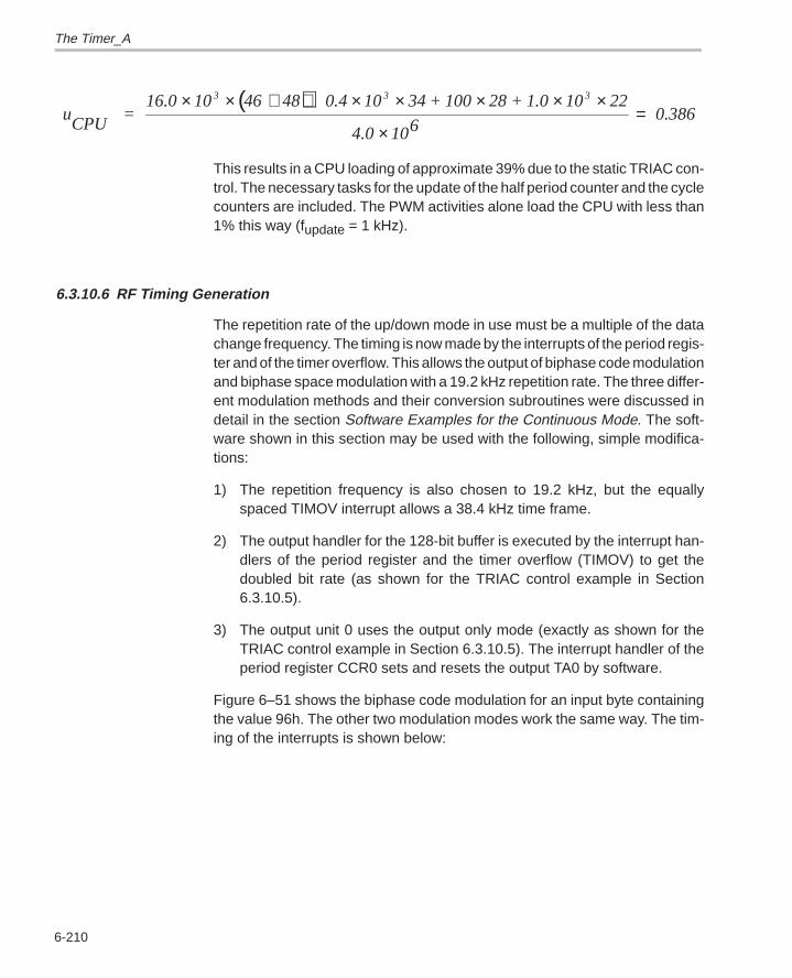
The Timer_A
6-210
( )uCPU
=16.0 10 46 48 0.4 10 34 + 100 28 + 1.0 10 22
4.0 106 0.386
3 3 3× × + + × × × × ×
×=
This results in a CPU loading of approximate 39% due to the static TRIAC con-trol. The necessary tasks for the update of the half period counter and the cyclecounters are included. The PWM activities alone load the CPU with less than1% this way (fupdate = 1 kHz).
6.3.10.6 RF Timing Generation
The repetition rate of the up/down mode in use must be a multiple of the datachange frequency. The timing is now made by the interrupts of the period regis-ter and of the timer overflow. This allows the output of biphase code modulationand biphase space modulation with a 19.2 kHz repetition rate. The three differ-ent modulation methods and their conversion subroutines were discussed indetail in the section Software Examples for the Continuous Mode. The soft-ware shown in this section may be used with the following, simple modifica-tions:
1) The repetition frequency is also chosen to 19.2 kHz, but the equallyspaced TIMOV interrupt allows a 38.4 kHz time frame.
2) The output handler for the 128-bit buffer is executed by the interrupt han-dlers of the period register and the timer overflow (TIMOV) to get thedoubled bit rate (as shown for the TRIAC control example in Section6.3.10.5).
3) The output unit 0 uses the output only mode (exactly as shown for theTRIAC control example in Section 6.3.10.5). The interrupt handler of theperiod register CCR0 sets and resets the output TA0 by software.
Figure 6–51 shows the biphase code modulation for an input byte containingthe value 96h. The other two modulation modes work the same way. The tim-ing of the interrupts is shown below:
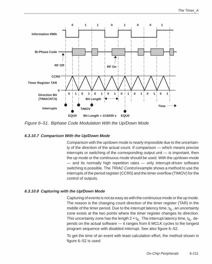
The Timer_A
6-211On-Chip Peripherals
RF Off
0 1 1 0 1 0 0 1
RF On
Information 096h
Bi-Phase Code
Timer Register TAR
Bit Length
Time
0 1 0 1 0 1 0 1 0 1 0 1 0 1 0 1Direction Bit(TIMACNT.0)
Interrupts
EQU0
TIMOV
EQU0Bit Length = 1/19200 s
CCR0
0
Figure 6–51. Biphase Code Modulation With the Up/Down Mode
6.3.10.7 Comparison With the Up/Down Mode
Comparison with the up/down mode is nearly impossible due to the uncertain-ty of the direction of the actual count. If comparison — which means preciseinterrupts or switching of the corresponding output unit — is important, thenthe up mode or the continuous mode should be used. With the up/down mode— and its normally high repetition rates — only interrupt-driven softwareswitching is possible. The TRIAC Control example shows a method to use theinterrupts of the period register (CCR0) and the timer overflow (TIMOV) for thecontrol of outputs.
6.3.10.8 Capturing with the Up/Down Mode
Capturing of events is not as easy as with the continuous mode or the up mode.The reason is the changing count direction of the timer register (TAR) in themiddle of the timer period. Due to the interrupt latency time, tIL, an uncertaintyzone exists at the two points where the timer register changes its direction.This uncertainty zone has the length 2 × tIL. The interrupt latency time, tIL, de-pends on the actual software — it ranges from 6 MCLK cycles to the longestprogram sequence with disabled interrupt. See also figure 6–52.
To get the time of an event with least calculation effort, the method shown infigure 6–52 is used:
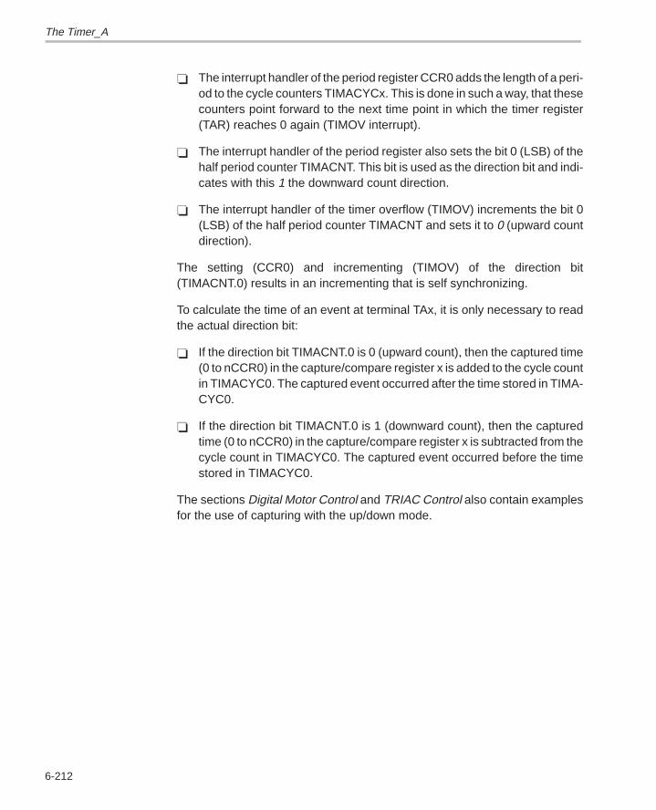
The Timer_A
6-212
The interrupt handler of the period register CCR0 adds the length of a peri-od to the cycle counters TIMACYCx. This is done in such a way, that thesecounters point forward to the next time point in which the timer register(TAR) reaches 0 again (TIMOV interrupt).
The interrupt handler of the period register also sets the bit 0 (LSB) of thehalf period counter TIMACNT. This bit is used as the direction bit and indi-cates with this 1 the downward count direction.
The interrupt handler of the timer overflow (TIMOV) increments the bit 0(LSB) of the half period counter TIMACNT and sets it to 0 (upward countdirection).
The setting (CCR0) and incrementing (TIMOV) of the direction bit(TIMACNT.0) results in an incrementing that is self synchronizing.
To calculate the time of an event at terminal TAx, it is only necessary to readthe actual direction bit:
If the direction bit TIMACNT.0 is 0 (upward count), then the captured time(0 to nCCR0) in the capture/compare register x is added to the cycle countin TIMACYC0. The captured event occurred after the time stored in TIMA-CYC0.
If the direction bit TIMACNT.0 is 1 (downward count), then the capturedtime (0 to nCCR0) in the capture/compare register x is subtracted from thecycle count in TIMACYC0. The captured event occurred before the timestored in TIMACYC0.
The sections Digital Motor Control and TRIAC Control also contain examplesfor the use of capturing with the up/down mode.
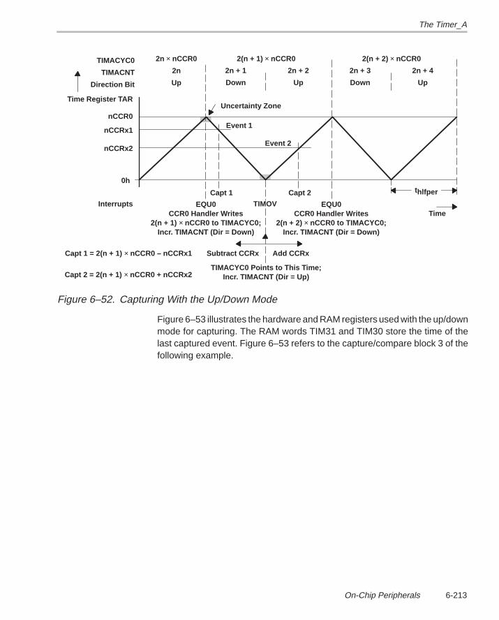
The Timer_A
6-213On-Chip Peripherals
EQU0CCR0 Handler Writes
2(n + 1) × nCCR0 to TIMACYC0;Incr. TIMACNT (Dir = Down)
TIMACYC0 Points to This Time;Incr. TIMACNT (Dir = Up)
2n × nCCR0
2n
Up
2(n + 1) × nCCR0
2n + 1
Down
2n + 2
Up
2(n + 2) × nCCR0TIMACYC0
TIMACNT
Direction Bit
Time Register TAR
nCCR0
nCCRx1
nCCRx2
0h
Interrupts
Capt 1 = 2(n + 1) × nCCR0 – nCCRx1
Uncertainty Zone
2n + 3
Down
2n + 4
Up
Event 1
Event 2
Capt 1 Capt 2 thlfper
TIMOV EQU0CCR0 Handler Writes
2(n + 2) × nCCR0 to TIMACYC0;Incr. TIMACNT (Dir = Down)
Subtract CCRx Add CCRx
Capt 2 = 2(n + 1) × nCCR0 + nCCRx2
Time
Figure 6–52. Capturing With the Up/Down Mode
Figure 6–53 illustrates the hardware and RAM registers used with the up/downmode for capturing. The RAM words TIM31 and TIM30 store the time of thelast captured event. Figure 6–53 refers to the capture/compare block 3 of thefollowing example.
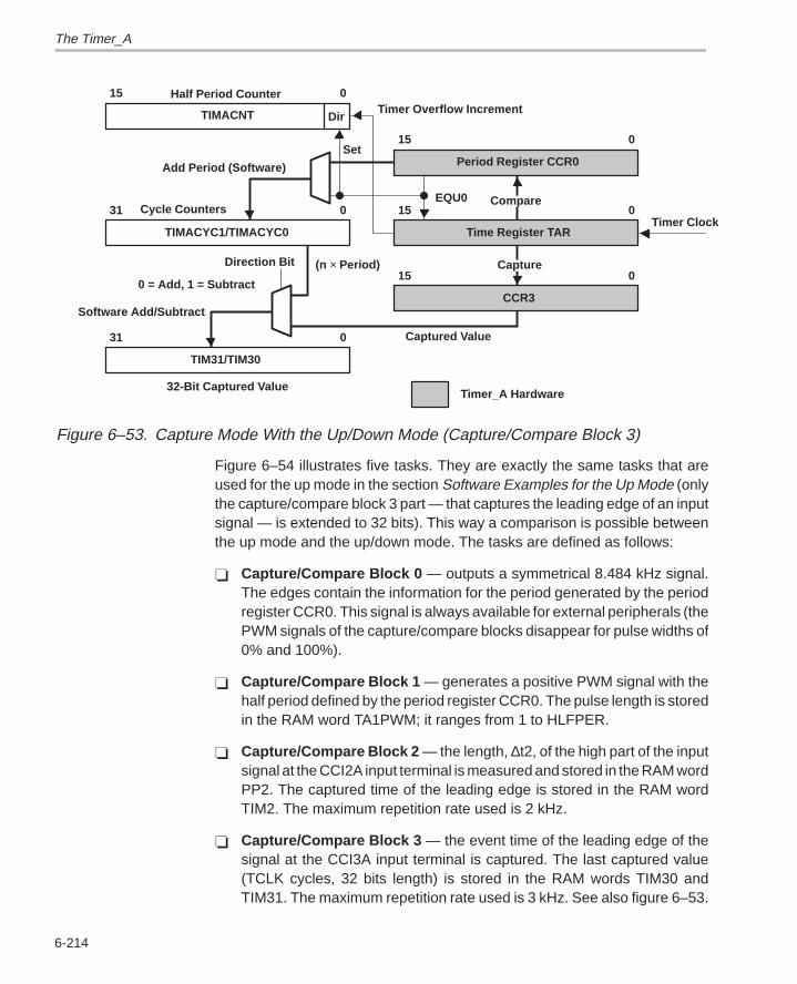
The Timer_A
6-214
TIMACYC1/TIMACYC0
031
Period Register CCR0
015
Time Register TAR
015
015
CCR3
Compare
Timer Clock
Capture
TIM31/TIM30
031
Add Period (Software)
Cycle Counters
Software Add/Subtract
32-Bit Captured ValueTimer_A Hardware
TIMACNT
015
Dir
Set
Timer Overflow Increment
EQU0
Captured Value
Direction Bit
0 = Add, 1 = Subtract
(n × Period)
Half Period Counter
Figure 6–53. Capture Mode With the Up/Down Mode (Capture/Compare Block 3)
Figure 6–54 illustrates five tasks. They are exactly the same tasks that areused for the up mode in the section Software Examples for the Up Mode (onlythe capture/compare block 3 part — that captures the leading edge of an inputsignal — is extended to 32 bits). This way a comparison is possible betweenthe up mode and the up/down mode. The tasks are defined as follows:
Capture/Compare Block 0 — outputs a symmetrical 8.484 kHz signal.The edges contain the information for the period generated by the periodregister CCR0. This signal is always available for external peripherals (thePWM signals of the capture/compare blocks disappear for pulse widths of0% and 100%).
Capture/Compare Block 1 — generates a positive PWM signal with thehalf period defined by the period register CCR0. The pulse length is storedin the RAM word TA1PWM; it ranges from 1 to HLFPER.
Capture/Compare Block 2 — the length, ∆t2, of the high part of the inputsignal at the CCI2A input terminal is measured and stored in the RAM wordPP2. The captured time of the leading edge is stored in the RAM wordTIM2. The maximum repetition rate used is 2 kHz.
Capture/Compare Block 3 — the event time of the leading edge of thesignal at the CCI3A input terminal is captured. The last captured value(TCLK cycles, 32 bits length) is stored in the RAM words TIM30 andTIM31. The maximum repetition rate used is 3 kHz. See also figure 6–53.

The Timer_A
6-215On-Chip Peripherals
Capture/Compare Block 4 — generates a negative PWM signal with theperiod defined by the period register. The pulse length is stored in the RAMword TA4PWM; it ranges from 0 to HLFPER.
For the example, 3.801 MHz is used. The resolution for the PWM is 224 stepsdue to the repetition frequency of 16.969 kHz (3.801 MHz/16.969 kHz = 224).The Infrequent Individual Update Mode is used. See Section 6.3.10.3 for de-tails.
The maximum input frequencies for capturing purposes mentioned above areused for the overhead calculation only. The limits of the Timer_A hardware al-low the capture much of higher input frequencies.
Figure 6–54 illustrates the four tasks described above — they are not shownto scale:
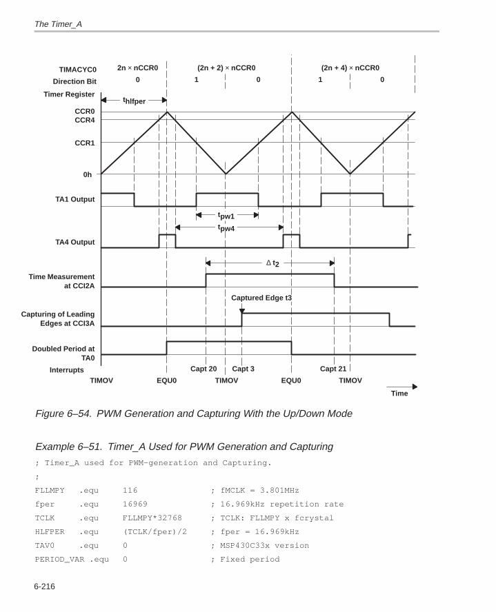
The Timer_A
6-216
thlfper
tpw1tpw4
TIMOV EQU0 TIMOV EQU0 TIMOV
2n × nCCR0
0
(2n + 2) × nCCR0
1 0
(2n + 4) × nCCR0
1 0TIMACYC0
Direction Bit
Timer Register
CCR0CCR4
CCR1
0h
TA1 Output
TA4 Output
Time Measurementat CCI2A
∆ t2
Captured Edge t3
Capt 20 Capt 3 Capt 21
Time
Interrupts
Capturing of LeadingEdges at CCI3A
Doubled Period atTA0
Figure 6–54. PWM Generation and Capturing With the Up/Down Mode
Example 6–51. Timer_A Used for PWM Generation and Capturing
; Timer_A used for PWM–generation and Capturing.
;
FLLMPY .equ 116 ; fMCLK = 3.801MHz
fper .equ 16969 ; 16.969kHz repetition rate
TCLK .equ FLLMPY*32768 ; TCLK: FLLMPY x fcrystal
HLFPER .equ (TCLK/fper)/2 ; fper = 16.969kHz
TAV0 .equ 0 ; MSP430C33x version
PERIOD_VAR .equ 0 ; Fixed period
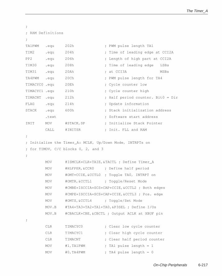
The Timer_A
6-217On-Chip Peripherals
;
; RAM Definitions
;
TA1PWM .equ 202h ; PWM pulse length TA1
TIM2 .equ 204h ; Time of leading edge at CCI2A
PP2 .equ 206h ; Length of high part at CCI2A
TIM30 .equ 208h ; Time of leading edge LSBs
TIM31 .equ 20Ah ; at CCI3A MSBs
TA4PWM .equ 20Ch ; PWM pulse length for TA4
TIMACYC0 .equ 20Eh ; Cycle counter low
TIMACYC1 .equ 210h ; Cycle counter high
TIMACNT .equ 212h ; Half period counter. Bit0 = Dir
FLAG .equ 214h ; Update information
STACK .equ 600h ; Stack initialization address
.text ; Software start address
INIT MOV #STACK,SP ; Initialize Stack Pointer
CALL #INITSR ; Init. FLL and RAM
;
; Initialize the Timer_A: MCLK, Up/Down Mode, INTRPTs on
; for TIMOV, C/C blocks 0, 2, and 3
;
MOV #ISMCLK+CLR+TAIE,&TACTL ; Define Timer_A
MOV #HLFPER,&CCR0 ; Define half period
MOV #OMT+CCIE,&CCTL0 ; Toggle TA0, INTRPT on
MOV #OMTR,&CCTL1 ; Toggle/Reset Mode
MOV #CMBE+ISCCIA+SCS+CAP+CCIE,&CCTL2 ; Both edges
MOV #CMPE+ISCCIA+SCS+CAP+CCIE,&CCTL3 ; Pos. edge
MOV #OMTS,&CCTL4 ; Toggle/Set Mode
MOV.B #TA4+TA3+TA2+TA1+TA0,&P3SEL ; Define I/Os
MOV.B #CBACLK+CBE,&CBCTL ; Output ACLK at XBUF pin
;
CLR TIMACYC0 ; Clear low cycle counter
CLR TIMACYC1 ; Clear high cycle counter
CLR TIMACNT ; Clear half period counter
MOV #1,TA1PWM ; TA1 pulse length = 1
MOV #0,TA4PWM ; TA4 pulse length = 0
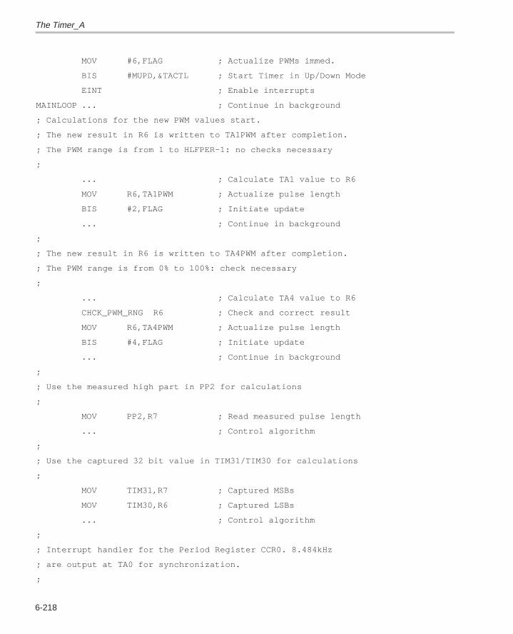
The Timer_A
6-218
MOV #6,FLAG ; Actualize PWMs immed.
BIS #MUPD,&TACTL ; Start Timer in Up/Down Mode
EINT ; Enable interrupts
MAINLOOP ... ; Continue in background
; Calculations for the new PWM values start.
; The new result in R6 is written to TA1PWM after completion.
; The PWM range is from 1 to HLFPER–1: no checks necessary
;
... ; Calculate TA1 value to R6
MOV R6,TA1PWM ; Actualize pulse length
BIS #2,FLAG ; Initiate update
... ; Continue in background
;
; The new result in R6 is written to TA4PWM after completion.
; The PWM range is from 0% to 100%: check necessary
;
... ; Calculate TA4 value to R6
CHCK_PWM_RNG R6 ; Check and correct result
MOV R6,TA4PWM ; Actualize pulse length
BIS #4,FLAG ; Initiate update
... ; Continue in background
;
; Use the measured high part in PP2 for calculations
;
MOV PP2,R7 ; Read measured pulse length
... ; Control algorithm
;
; Use the captured 32 bit value in TIM31/TIM30 for calculations
;
MOV TIM31,R7 ; Captured MSBs
MOV TIM30,R6 ; Captured LSBs
... ; Control algorithm
;
; Interrupt handler for the Period Register CCR0. 8.484kHz
; are output at TA0 for synchronization.
;
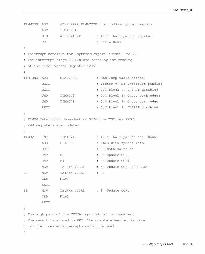
The Timer_A
6-219On-Chip Peripherals
TIMMOD0 ADD #2*HLFPER,TIMACYC0 ; Actualize cycle counters
ADC TIMACYC1
BIS #1,TIMACNT ; Incr. half period counter
RETI ; Dir = Down
;
; Interrupt handlers for Capture/Compare Blocks 1 to 4.
; The interrupt flags CCIFGx are reset by the reading
; of the Timer Vector Register TAIV
;
TIM_HND ADD &TAIV,PC ; Add Jump table offset
RETI ; Vector 0: No interrupt pending
RETI ; C/C Block 1: INTRPT disabled
JMP TIMMOD2 ; C/C Block 2: Capt. both edges
JMP TIMMOD3 ; C/C Block 3: Capt. pos. edge
RETI ; C/C Block 4: INTRPT disabled
;
; TIMOV Interrupt: dependent on FLAG the CCR1 and CCR4
; PWM registers are updated.
;
TIMOV INC TIMACNT ; Incr. half period cnt (Down)
ADD FLAG,PC ; FLAG with update info
RETI ; 0: Nothing to do
JMP P1 ; 2: Update CCR1
JMP P4 ; 4: Update CCR4
MOV TA1PWM,&CCR1 ; 6: Update CCR1 and CCR4
P4 MOV TA4PWM,&CCR4 ; 4:
CLR FLAG
RETI
P1 MOV TA1PWM,&CCR1 ; 2: Update CCR1
CLR FLAG
RETI
;
; The high part of the CCI2A input signal is measured.
; The result is stored in PP2. The complete handler is time
; critical: nested interrupts cannot be used.
;
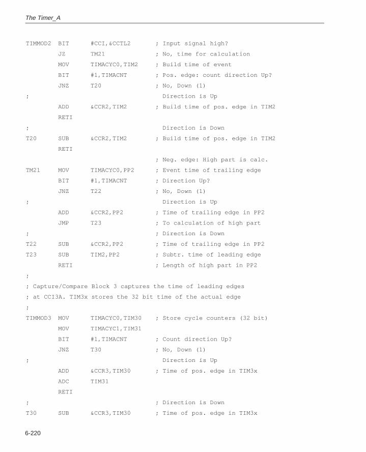
The Timer_A
6-220
TIMMOD2 BIT #CCI,&CCTL2 ; Input signal high?
JZ TM21 ; No, time for calculation
MOV TIMACYC0,TIM2 ; Build time of event
BIT #1,TIMACNT ; Pos. edge: count direction Up?
JNZ T20 ; No, Down (1)
; Direction is Up
ADD &CCR2,TIM2 ; Build time of pos. edge in TIM2
RETI
; Direction is Down
T20 SUB &CCR2,TIM2 ; Build time of pos. edge in TIM2
RETI
; Neg. edge: High part is calc.
TM21 MOV TIMACYC0,PP2 ; Event time of trailing edge
BIT #1,TIMACNT ; Direction Up?
JNZ T22 ; No, Down (1)
; Direction is Up
ADD &CCR2,PP2 ; Time of trailing edge in PP2
JMP T23 ; To calculation of high part
; ; Direction is Down
T22 SUB &CCR2,PP2 ; Time of trailing edge in PP2
T23 SUB TIM2,PP2 ; Subtr. time of leading edge
RETI ; Length of high part in PP2
;
; Capture/Compare Block 3 captures the time of leading edges
; at CCI3A. TIM3x stores the 32 bit time of the actual edge
;
TIMMOD3 MOV TIMACYC0,TIM30 ; Store cycle counters (32 bit)
MOV TIMACYC1,TIM31
BIT #1,TIMACNT ; Count direction Up?
JNZ T30 ; No, Down (1)
; Direction is Up
ADD &CCR3,TIM30 ; Time of pos. edge in TIM3x
ADC TIM31
RETI
; ; Direction is Down
T30 SUB &CCR3,TIM30 ; Time of pos. edge in TIM3x
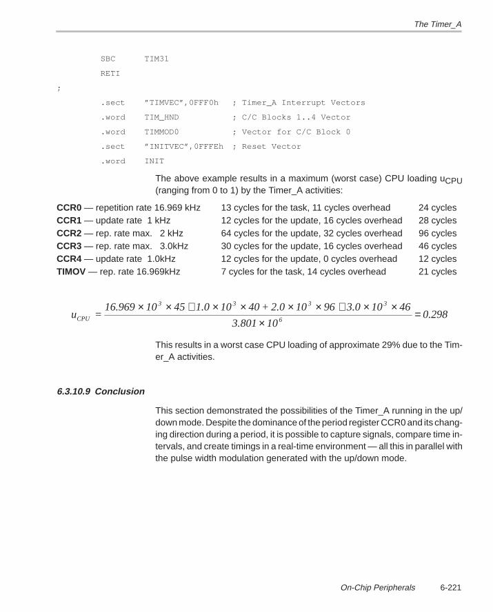
The Timer_A
6-221On-Chip Peripherals
SBC TIM31
RETI
;
.sect ”TIMVEC”,0FFF0h ; Timer_A Interrupt Vectors
.word TIM_HND ; C/C Blocks 1..4 Vector
.word TIMMOD0 ; Vector for C/C Block 0
.sect ”INITVEC”,0FFFEh ; Reset Vector
.word INIT
The above example results in a maximum (worst case) CPU loading uCPU(ranging from 0 to 1) by the Timer_A activities:
CCR0 — repetition rate 16.969 kHz 13 cycles for the task, 11 cycles overhead 24 cyclesCCR1 — update rate 1 kHz 12 cycles for the update, 16 cycles overhead 28 cyclesCCR2 — rep. rate max. 2 kHz 64 cycles for the update, 32 cycles overhead 96 cyclesCCR3 — rep. rate max. 3.0kHz 30 cycles for the update, 16 cycles overhead 46 cyclesCCR4 — update rate 1.0kHz 12 cycles for the update, 0 cycles overhead 12 cyclesTIMOV — rep. rate 16.969kHz 7 cycles for the task, 14 cycles overhead 21 cycles
u =16.969 10 45 1.0 10 40 + 2.0 10 96 3.0 10 46
3.801 100.298CPU
3 3 3 3
6
× × + × × × × + × ××
=
This results in a worst case CPU loading of approximate 29% due to the Tim-er_A activities.
6.3.10.9 Conclusion
This section demonstrated the possibilities of the Timer_A running in the up/down mode. Despite the dominance of the period register CCR0 and its chang-ing direction during a period, it is possible to capture signals, compare time in-tervals, and create timings in a real-time environment — all this in parallel withthe pulse width modulation generated with the up/down mode.

The Hardware Multiplier
6-222
6.4 The Hardware Multiplier
The 16 × 16-bit hardware multiplier of the MSP430 family is detailed in the fol-lowing sections. Function and modes are discussed, and proven applicationexamples are given for this fast and versatile peripheral. Also shown is a com-parison of the speed of solutions using this peripheral compared to pure soft-ware solutions. The hardware multiplier can also execute the Signed Multiplyand Accumulate function. The register to be used for the Operand 1 has theaddress 136h. The function is the same as for the Signed Multiply function, ex-cept that the new product is added to the accumulated sum in the SumHi/Sum-Lo registers. The SumExt register indicates the sign of the accumulated sum.It is the user’s responsibilty to ensure that no overflow can occur (by worst-case calculation of the factors used).
6.4.1 Function of the Hardware Multiplier
The hardware multiplier allows three different multiply operations (modes):
The multiplication for unsigned 16-bit and 8-bit operands
The multiplication for signed 16-bit and 8-bit operands
The multiply-and-accumulate function (MAC) for unsigned 16-bit and 8-bitoperands
Any mixture of operand lengths (16 bits and 8 bits) is possible. If assisting soft-ware is used, other operations are also possible — the signed Multiply-and-Accumulate function, for example.
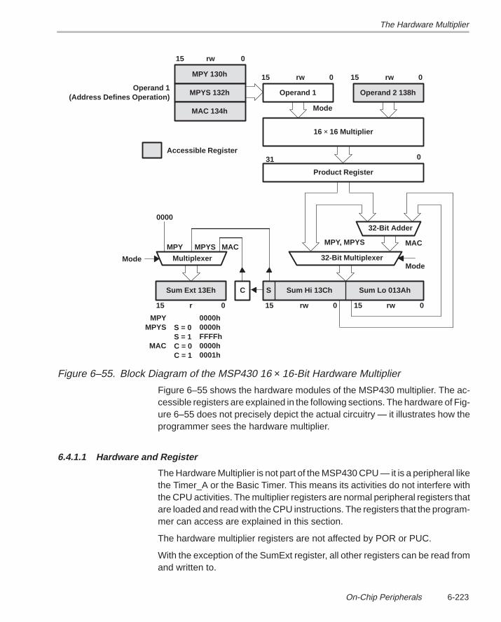
The Hardware Multiplier
6-223On-Chip Peripherals
MPY 130h
32-Bit Adder
Multiplexer
Operand 2 138hOperand 1
Mode
16 × 16 Multiplier
031
32-Bit MultiplexerMode
MPY, MPYS
Product Register
Sum Hi 13ChS Sum Lo 013Ah
15 0rw 15 0rw
CSum Ext 13Eh
MACMPYSMPY
MPYS 132h
MAC 134h
0000
Mode
Accessible Register
Operand 1(Address Defines Operation)
MPYMPYS
MAC
S = 0S = 1C = 0C = 1
0000h0000hFFFFh0000h0001h
15 0r
15 0rw
15 0rw 15 0rw
MAC
Figure 6–55. Block Diagram of the MSP430 16 × 16-Bit Hardware Multiplier
Figure 6–55 shows the hardware modules of the MSP430 multiplier. The ac-cessible registers are explained in the following sections. The hardware of Fig-ure 6–55 does not precisely depict the actual circuitry — it illustrates how theprogrammer sees the hardware multiplier.
6.4.1.1 Hardware and Register
The Hardware Multiplier is not part of the MSP430 CPU — it is a peripheral likethe Timer_A or the Basic Timer. This means its activities do not interfere withthe CPU activities. The multiplier registers are normal peripheral registers thatare loaded and read with the CPU instructions. The registers that the program-mer can access are explained in this section.
The hardware multiplier registers are not affected by POR or PUC.
With the exception of the SumExt register, all other registers can be read fromand written to.
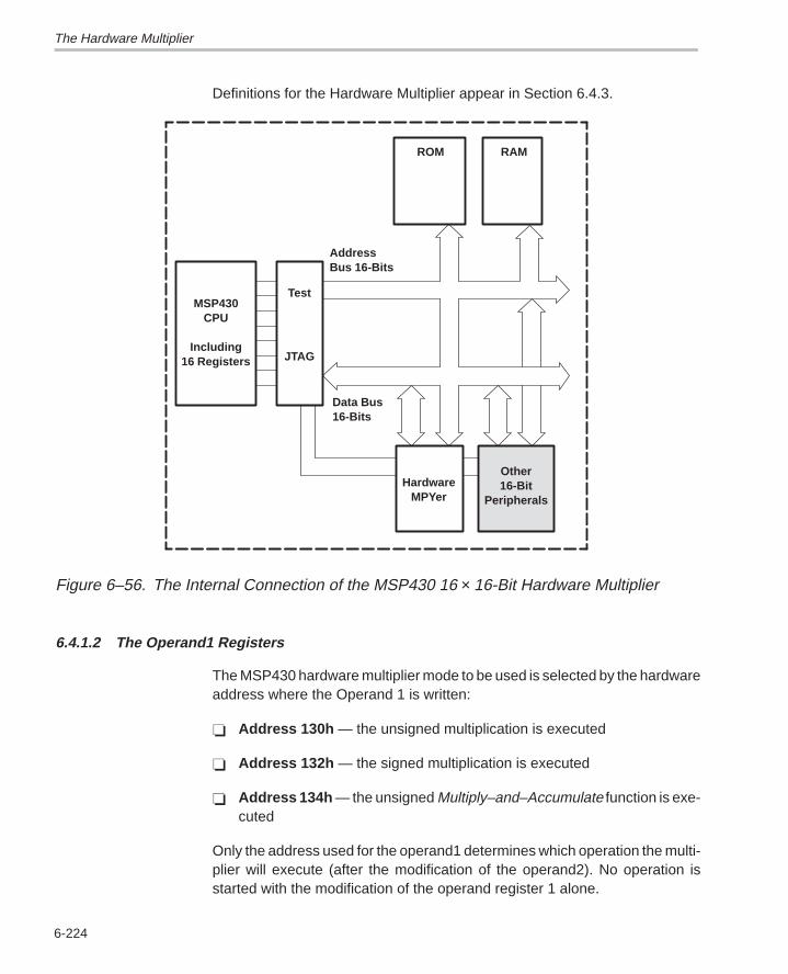
The Hardware Multiplier
6-224
Definitions for the Hardware Multiplier appear in Section 6.4.3.
Data Bus16-Bits
AddressBus 16-Bits
HardwareMPYer
Other16-Bit
Peripherals
MSP430CPU
Including16 Registers
Test
JTAG
ROM RAM
Figure 6–56. The Internal Connection of the MSP430 16 × 16-Bit Hardware Multiplier
6.4.1.2 The Operand1 Registers
The MSP430 hardware multiplier mode to be used is selected by the hardwareaddress where the Operand 1 is written:
Address 130h — the unsigned multiplication is executed
Address 132h — the signed multiplication is executed
Address 134h — the unsigned Multiply–and–Accumulate function is exe-cuted
Only the address used for the operand1 determines which operation the multi-plier will execute (after the modification of the operand2). No operation isstarted with the modification of the operand register 1 alone.
The Hardware Multiplier
6-225On-Chip Peripherals
Example 6–52. Multiply Unsigned
A MPY (multiply unsigned) operation is defined and started. The two operandsreside in R14 and R15.
MOV R15,&130h ; Define MPY operation
MOV R14,&138h ; Start MPY with operand 2
... ; Product in SumHi|SumLo
6.4.1.3 The Operand2 Register
The operand register 2 (at address 138h) is common for all three multipliermodes. The modification of this register (normally with a MOV instruction)starts the selected multiplication of the two operands contained in the operand1 and 2 registers. The result is written immediately into the three hardware reg-isters: SumExt, SumHi, and SumLo. The result can be accessed with the nextinstruction unless the indirect addressing modes are used for the source ad-dressing.
6.4.1.4 The SumLo Register
This 16-bit register contains the lower 16 bits of the calculated product orsummed result. All instructions may be used to access or modify the SumLoregister. The high byte cannot be accessed with byte instructions.
6.4.1.5 The SumHi Register
This 16-bit register contains — dependent on the previously executed opera-tion — the following information:
MPY Unsigned Multiply — the most significant word of the calculatedproduct.
MPYS Signed Multiply — the most significant word including the sign ofthe calculated product. Two’s complement notation is used for the product.
MAC Unsigned Multiply-and-Accumulate — the most significant wordof the calculated sum.
All instructions may be used with the SumHi register. The high byte cannot beaccessed with byte instructions.
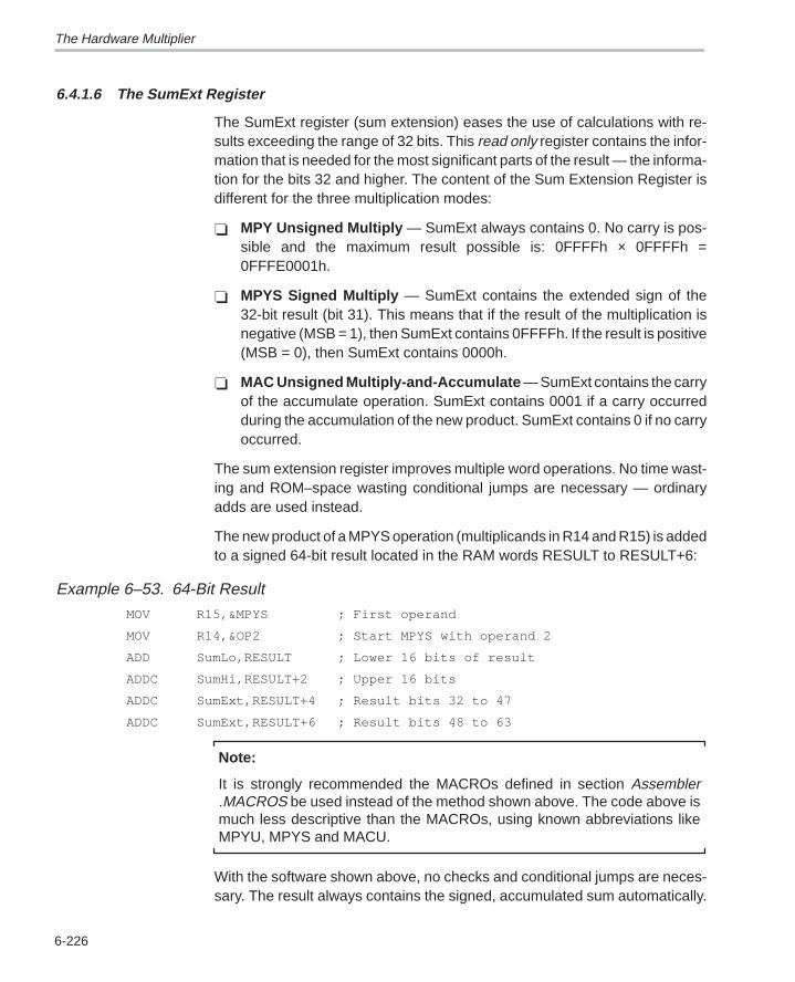
The Hardware Multiplier
6-226
6.4.1.6 The SumExt Register
The SumExt register (sum extension) eases the use of calculations with re-sults exceeding the range of 32 bits. This read only register contains the infor-mation that is needed for the most significant parts of the result — the informa-tion for the bits 32 and higher. The content of the Sum Extension Register isdifferent for the three multiplication modes:
MPY Unsigned Multiply — SumExt always contains 0. No carry is pos-sible and the maximum result possible is: 0FFFFh × 0FFFFh =0FFFE0001h.
MPYS Signed Multiply — SumExt contains the extended sign of the32-bit result (bit 31). This means that if the result of the multiplication isnegative (MSB = 1), then SumExt contains 0FFFFh. If the result is positive(MSB = 0), then SumExt contains 0000h.
MAC Unsigned Multiply-and-Accumulate — SumExt contains the carryof the accumulate operation. SumExt contains 0001 if a carry occurredduring the accumulation of the new product. SumExt contains 0 if no carryoccurred.
The sum extension register improves multiple word operations. No time wast-ing and ROM–space wasting conditional jumps are necessary — ordinaryadds are used instead.
The new product of a MPYS operation (multiplicands in R14 and R15) is addedto a signed 64-bit result located in the RAM words RESULT to RESULT+6:
Example 6–53. 64-Bit ResultMOV R15,&MPYS ; First operand
MOV R14,&OP2 ; Start MPYS with operand 2
ADD SumLo,RESULT ; Lower 16 bits of result
ADDC SumHi,RESULT+2 ; Upper 16 bits
ADDC SumExt,RESULT+4 ; Result bits 32 to 47
ADDC SumExt,RESULT+6 ; Result bits 48 to 63
Note:
It is strongly recommended the MACROs defined in section Assembler.MACROS be used instead of the method shown above. The code above ismuch less descriptive than the MACROs, using known abbreviations likeMPYU, MPYS and MACU.
With the software shown above, no checks and conditional jumps are neces-sary. The result always contains the signed, accumulated sum automatically.
The Hardware Multiplier
6-227On-Chip Peripherals
6.4.1.7 Rules for the Hardware Multiplier
The hardware multiplier is a word module. The hardware registers can beaddressed in word mode or in byte mode, but the byte mode can addressthe lower bytes only (the upper byte cannot be addressed).
The operand registers of the hardware multiplier (addresses 0130h,0132h, 0134h and 0138h) behave like the CPU working registers R0 toR15 if modified in byte mode — the upper byte is cleared in this case. Thisallows 8-bit and 16-bit multiplications in any mixture. See the examples inSection 6.4.2.4.
The foating point package (FPP) version 4 uses the hardware multiplierif the variable HW_MPY is defined as 1:
HW_MPY .equ 1
See chapter 5.6 for details.
If the result of a hardware multiplier operation is addressed with indirectmode or indirect-autoincrement mode, a NOP instruction is necessary af-ter the multiplication to allow the completion of the multiplication. See theexamples in Section 6.4.3.1.
6.4.2 Multiplication Modes
Three different multiplication modes are available. They are explained in thefollowing sections.
6.4.2.1 Unsigned Multiply
The two operands written to the operand registers 1 and 2 are treated as un-signed numbers with:
00000h as the smallest number
0FFFFh as the largest number.
The maximum possible result is reached for the operands:
0FFFFh × 0FFFFh = 0FFFE0001h
No carry is possible, the SumExt register always contains 0. Table 6–27 showsthe products for some special multiplicands.
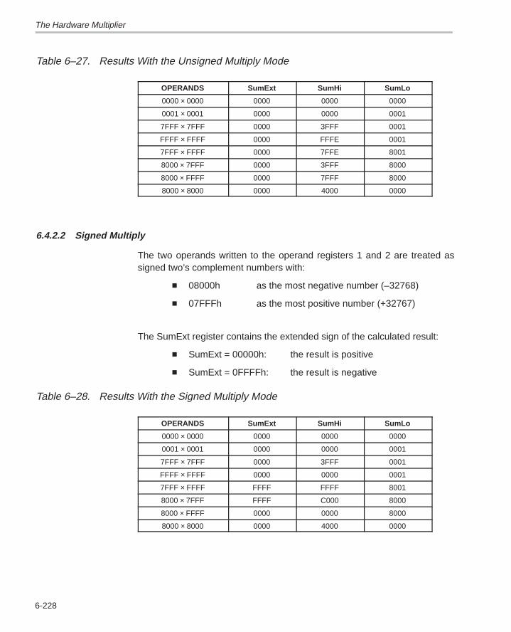
The Hardware Multiplier
6-228
Table 6–27. Results With the Unsigned Multiply Mode
OPERANDS SumExt SumHi SumLo
0000 × 0000 0000 0000 0000
0001 × 0001 0000 0000 0001
7FFF × 7FFF 0000 3FFF 0001
FFFF × FFFF 0000 FFFE 0001
7FFF × FFFF 0000 7FFE 8001
8000 × 7FFF 0000 3FFF 8000
8000 × FFFF 0000 7FFF 8000
8000 × 8000 0000 4000 0000
6.4.2.2 Signed Multiply
The two operands written to the operand registers 1 and 2 are treated assigned two’s complement numbers with:
08000h as the most negative number (–32768)
07FFFh as the most positive number (+32767)
The SumExt register contains the extended sign of the calculated result:
SumExt = 00000h: the result is positive
SumExt = 0FFFFh: the result is negative
Table 6–28. Results With the Signed Multiply Mode
OPERANDS SumExt SumHi SumLo
0000 × 0000 0000 0000 0000
0001 × 0001 0000 0000 0001
7FFF × 7FFF 0000 3FFF 0001
FFFF × FFFF 0000 0000 0001
7FFF × FFFF FFFF FFFF 8001
8000 × 7FFF FFFF C000 8000
8000 × FFFF 0000 0000 8000
8000 × 8000 0000 4000 0000
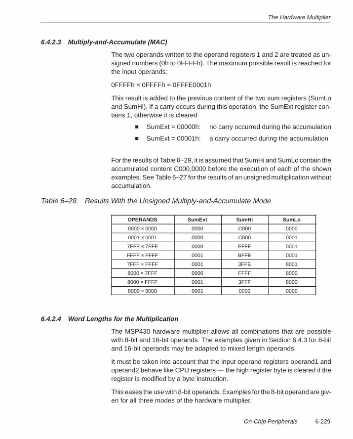
The Hardware Multiplier
6-229On-Chip Peripherals
6.4.2.3 Multiply-and-Accumulate (MAC)
The two operands written to the operand registers 1 and 2 are treated as un-signed numbers (0h to 0FFFFh). The maximum possible result is reached forthe input operands:
0FFFFh × 0FFFFh = 0FFFE0001h
This result is added to the previous content of the two sum registers (SumLoand SumHi). If a carry occurs during this operation, the SumExt register con-tains 1, otherwise it is cleared.
SumExt = 00000h: no carry occurred during the accumulation
SumExt = 00001h: a carry occurred during the accumulation
For the results of Table 6–29, it is assumed that SumHi and SumLo contain theaccumulated content C000,0000 before the execution of each of the shownexamples. See Table 6–27 for the results of an unsigned multiplication withoutaccumulation.
Table 6–29. Results With the Unsigned Multiply-and-Accumulate Mode
OPERANDS SumExt SumHi SumLo
0000 × 0000 0000 C000 0000
0001 × 0001 0000 C000 0001
7FFF × 7FFF 0000 FFFF 0001
FFFF × FFFF 0001 BFFE 0001
7FFF × FFFF 0001 3FFE 8001
8000 × 7FFF 0000 FFFF 8000
8000 × FFFF 0001 3FFF 8000
8000 × 8000 0001 0000 0000
6.4.2.4 Word Lengths for the Multiplication
The MSP430 hardware multiplier allows all combinations that are possiblewith 8-bit and 16-bit operands. The examples given in Section 6.4.3 for 8-bitand 16-bit operands may be adapted to mixed length operands.
It must be taken into account that the input operand registers operand1 andoperand2 behave like CPU registers — the high register byte is cleared if theregister is modified by a byte instruction.
This eases the use with 8-bit operands. Examples for the 8-bit operand are giv-en for all three modes of the hardware multiplier.
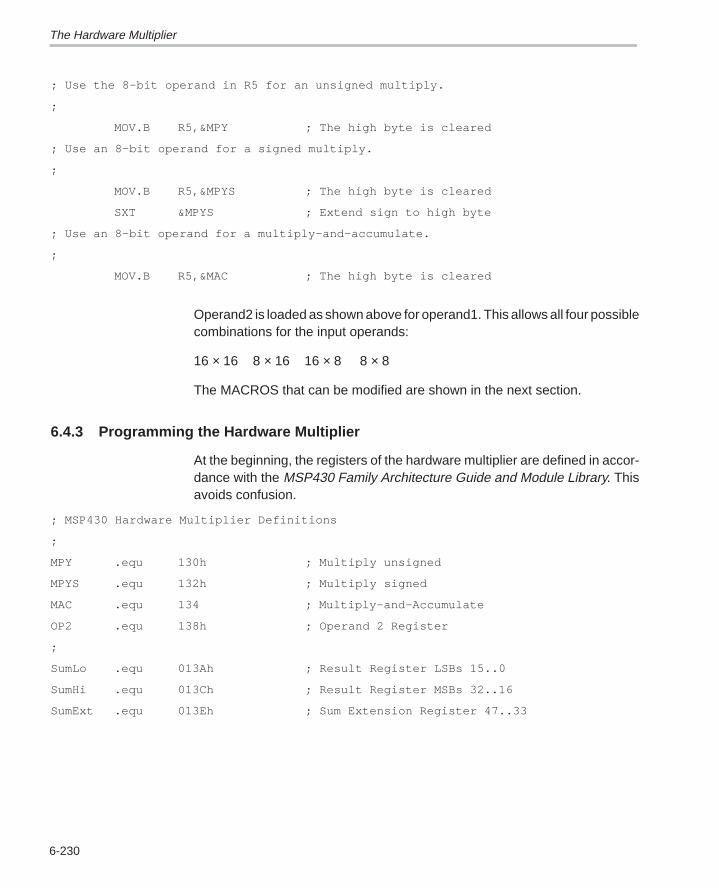
The Hardware Multiplier
6-230
; Use the 8–bit operand in R5 for an unsigned multiply.
;
MOV.B R5,&MPY ; The high byte is cleared
; Use an 8–bit operand for a signed multiply.
;
MOV.B R5,&MPYS ; The high byte is cleared
SXT &MPYS ; Extend sign to high byte
; Use an 8–bit operand for a multiply–and–accumulate.
;
MOV.B R5,&MAC ; The high byte is cleared
Operand2 is loaded as shown above for operand1. This allows all four possiblecombinations for the input operands:
16 × 16 8 × 16 16 × 8 8 × 8
The MACROS that can be modified are shown in the next section.
6.4.3 Programming the Hardware Multiplier
At the beginning, the registers of the hardware multiplier are defined in accor-dance with the MSP430 Family Architecture Guide and Module Library. Thisavoids confusion.
; MSP430 Hardware Multiplier Definitions
;
MPY .equ 130h ; Multiply unsigned
MPYS .equ 132h ; Multiply signed
MAC .equ 134 ; Multiply–and–Accumulate
OP2 .equ 138h ; Operand 2 Register
;
SumLo .equ 013Ah ; Result Register LSBs 15..0
SumHi .equ 013Ch ; Result Register MSBs 32..16
SumExt .equ 013Eh ; Sum Extension Register 47..33
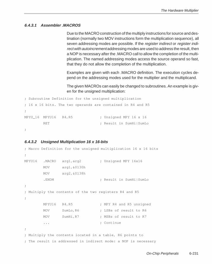
The Hardware Multiplier
6-231On-Chip Peripherals
6.4.3.1 Assembler .MACROS
Due to the MACRO construction of the multiply instructions for source and des-tination (normally two MOV instructions form the multiplication sequence), allseven addressing modes are possible. If the register indirect or register indi-rect with autoincrement addressing modes are used to address the result, thena NOP is necessary after the .MACRO call to allow the completion of the multi-plication. The named addressing modes access the source operand so fast,that they do not allow the completion of the multiplication.
Examples are given with each .MACRO definition. The execution cycles de-pend on the addressing modes used for the multiplier and the multiplicand.
The given MACROs can easily be changed to subroutines. An example is giv-en for the unsigned multiplication:
; Subroutine Definition for the unsigned multiplication
; 16 x 16 bits. The two operands are contained in R4 and R5
;
MPYU_16 MPYU16 R4,R5 ; Unsigned MPY 16 x 16
RET ; Result in SumHi|SumLo
;
6.4.3.2 Unsigned Multiplication 16 x 16-bits
; Macro Definition for the unsigned multiplication 16 x 16 bits
;
MPYU16 .MACRO arg1,arg2 ; Unsigned MPY 16x16
MOV arg1,&0130h
MOV arg2,&0138h
.ENDM ; Result in SumHi|SumLo
;
; Multiply the contents of the two registers R4 and R5
;
MPYU16 R4,R5 ; MPY R4 and R5 unsigned
MOV SumLo,R6 ; LSBs of result to R6
MOV SumHi,R7 ; MSBs of result to R7
... ; Continue
;
; Multiply the contents located in a table, R6 points to
; The result is addressed in indirect mode: a NOP is necessary
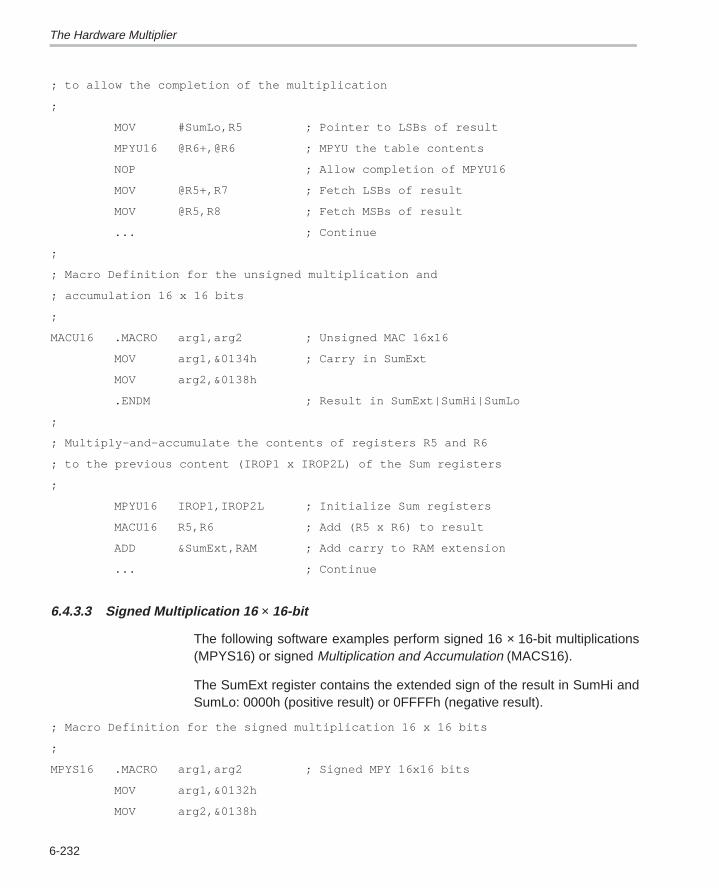
The Hardware Multiplier
6-232
; to allow the completion of the multiplication
;
MOV #SumLo,R5 ; Pointer to LSBs of result
MPYU16 @R6+,@R6 ; MPYU the table contents
NOP ; Allow completion of MPYU16
MOV @R5+,R7 ; Fetch LSBs of result
MOV @R5,R8 ; Fetch MSBs of result
... ; Continue
;
; Macro Definition for the unsigned multiplication and
; accumulation 16 x 16 bits
;
MACU16 .MACRO arg1,arg2 ; Unsigned MAC 16x16
MOV arg1,&0134h ; Carry in SumExt
MOV arg2,&0138h
.ENDM ; Result in SumExt|SumHi|SumLo
;
; Multiply–and–accumulate the contents of registers R5 and R6
; to the previous content (IROP1 x IROP2L) of the Sum registers
;
MPYU16 IROP1,IROP2L ; Initialize Sum registers
MACU16 R5,R6 ; Add (R5 x R6) to result
ADD &SumExt,RAM ; Add carry to RAM extension
... ; Continue
6.4.3.3 Signed Multiplication 16 × 16-bit
The following software examples perform signed 16 × 16-bit multiplications(MPYS16) or signed Multiplication and Accumulation (MACS16).
The SumExt register contains the extended sign of the result in SumHi andSumLo: 0000h (positive result) or 0FFFFh (negative result).
; Macro Definition for the signed multiplication 16 x 16 bits
;
MPYS16 .MACRO arg1,arg2 ; Signed MPY 16x16 bits
MOV arg1,&0132h
MOV arg2,&0138h
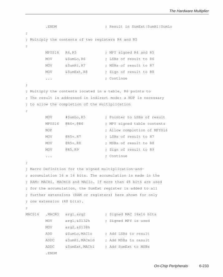
The Hardware Multiplier
6-233On-Chip Peripherals
.ENDM ; Result in SumExt|SumHi|SumLo
;
; Multiply the contents of two registers R4 and R5
;
MPYS16 R4,R5 ; MPY signed R4 and R5
MOV &SumLo,R6 ; LSBs of result to R6
MOV &SumHi,R7 ; MSBs of result to R7
MOV &SumExt,R8 ; Sign of result to R8
... ; Continue
;
; Multiply the contents located in a table, R6 points to
; The result is addressed in indirect mode: a NOP is necessary
; to allow the completion of the multiplication
;
MOV #SumLo,R5 ; Pointer to LSBs of result
MPYS16 @R6+,@R6 ; MPY signed table contents
NOP ; Allow completion of MPYS16
MOV @R5+,R7 ; LSBs of result to R7
MOV @R5+,R8 ; MSBs of result to R8
MOV @R5,R9 ; Sign of result to R9
... ; Continue
;
; Macro Definition for the signed multiplication–and–
; accumulation 16 x 16 bits. The accumulation is made in the
; RAM: MACHi, MACmid and MAClo. If more than 48 bits are used
; for the accumulation, the SumExt register is added to all
; further extensions (RAM or registers) here shown for only
; one extension (48 bits).
;
MACS16 .MACRO arg1,arg2 ; Signed MAC 16x16 bits
MOV arg1,&0132h ; Signed MPY is used
MOV arg2,&0138h
ADD &SumLo,MAClo ; Add LSBs to result
ADDC &SumHi,MACmid ; Add MSBs to result
ADDC &SumExt,MAChi ; Add SumExt to MSBs
.ENDM
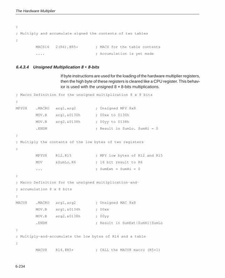
The Hardware Multiplier
6-234
;
; Multiply and accumulate signed the contents of two tables
;
MACS16 2(R6),@R5+ ; MACS for the table contents
.... ; Accumulation is yet made
6.4.3.4 Unsigned Multiplication 8 × 8-bits
If byte instructions are used for the loading of the hardware multiplier registers,then the high byte of these registers is cleared like a CPU register. This behav-ior is used with the unsigned 8 × 8-bits multiplications.
; Macro Definition for the unsigned multiplication 8 x 8 bits
;
MPYU8 .MACRO arg1,arg2 ; Unsigned MPY 8x8
MOV.B arg1,&0130h ; 00xx to 0130h
MOV.B arg2,&0138h ; 00yy to 0138h
.ENDM ; Result in SumLo. SumHi = 0
;
; Multiply the contents of the low bytes of two registers
;
MPYU8 R12,R15 ; MPY low bytes of R12 and R15
MOV &SumLo,R6 ; 16 bit result to R6
... ; SumExt = SumHi = 0
;
; Macro Definition for the unsigned multiplication–and–
; accumulation 8 x 8 bits
;
MACU8 .MACRO arg1,arg2 ; Unsigned MAC 8x8
MOV.B arg1,&0134h ; 00xx
MOV.B arg2,&0138h ; 00yy
.ENDM ; Result in SumExt|SumHi|SumLo
;
; Multiply–and–accumulate the low bytes of R14 and a table
;
MACU8 R14,@R5+ ; CALL the MACU8 macro (R5+1)
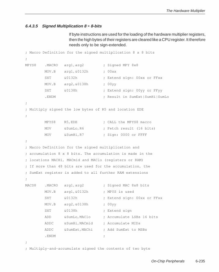
The Hardware Multiplier
6-235On-Chip Peripherals
6.4.3.5 Signed Multiplication 8 × 8-bits
If byte instructions are used for the loading of the hardware multiplier registers,then the high bytes of their registers are cleared like a CPU register. It thereforeneeds only to be sign-extended.
; Macro Definition for the signed multiplication 8 x 8 bits
;
MPYS8 .MACRO arg1,arg2 ; Signed MPY 8x8
MOV.B arg1,&0132h ; 00xx
SXT &0132h ; Extend sign: 00xx or FFxx
MOV.B arg2,&0138h ; 00yy
SXT &0138h ; Extend sign: 00yy or FFyy
.ENDM ; Result in SumExt|SumHi|SumLo
;
; Multiply signed the low bytes of R5 and location EDE
;
MPYS8 R5,EDE ; CALL the MPYS8 macro
MOV &SumLo,R6 ; Fetch result (16 bits)
MOV &SumHi,R7 ; Sign: 0000 or FFFF
;
; Macro Definition for the signed multiplication and
; accumulation 8 x 8 bits. The accumulation is made in the
; locations MACHi, MACmid and MAClo (registers or RAM)
; If more than 48 bits are used for the accumulation, the
; SumExt register is added to all further RAM extensions
;
MACS8 .MACRO arg1,arg2 ; Signed MAC 8x8 bits
MOV.B arg1,&0132h ; MPYS is used
SXT &0132h ; Extend sign: 00xx or FFxx
MOV.B arg2,&0138h ; 00yy
SXT &0138h ; Extend sign
ADD &SumLo,MAClo ; Accumulate LSBs 16 bits
ADDC &SumHi,MACmid ; Accumulate MIDs
ADDC &SumExt,MAChi ; Add SumExt to MSBs
.ENDM ;
;
; Multiply–and–accumulate signed the contents of two byte
The Hardware Multiplier
6-236
; tables
;
MACS8 2(R6),@R5+ ; CALL the MACS8 macro (R5+1)
.... ; Accumulation is yet made
6.4.3.6 Interrupt Usage
Operating in the foreground only (interrupt handlers), the hardware multipliercan be used freely. If the hardware multiplier is used in the foreground and thebackground, or in nested interrupt handlers, however, there are additional con-siderations.
The hardware multiplier may be used in interrupt handlers and in the back-ground (which is not typical real-time programming practice),if three rules areobserved:
The loading of the two registers operand1 (MPY, MPYS and MAC) and op-erand2 may not be separated by an interrupt using the multiplier. The inputinformation for operand1 cannot be restored due to the three input regis-ters that are possible. See the example below.
The registers operand1 and operand2 cannot be reread by the back-ground software — they may be overwritten by the interrupt handler.
The operand1 information cannot be used for more than one multiplication— only the operand2 register is changed for the next multiplication. Thefloating point package, FPP4, uses this method to speed up the calcula-tion, so it must be changed. The place is indicated.
; Background: multiplication is used together with interrupt
; The interrupt latency time is increased by 9 cycles.
; The NOP is necessary: one additional instruction may
; be executed after the DINT instruction
;
DINT ; Ensure non–interrupted –
NOP ; load of the MPYer registers
MPYU16 R4,R6 ; (R4) x (R6) –> Sum
EINT ; Allow interrupts again
... ; Continue with result
; The interrupt handler must save and restore the Sum registers
;
INTRPT_H PUSH &SumLo ; Save the SumLo register
The Hardware Multiplier
6-237On-Chip Peripherals
PUSH &SumHi ; Save the SumHi register
PUSH &SumExt ; Save the SumExt register
MPYU16 #X,C1 ; Call unsigned MPY: X x C1
.... ; Continue with MPYer result
POP &SumExt ; Restore SumExt register
POP &SumHi ; SumHi register
POP &SumLo ; SumLo register
RETI ; Return to background
6.4.3.7 Speed Comparison with Software Multiplication
Table 6–30 shows the speed increase for the different 16 × 16-bit multiplicationmodes.
The cycles given for the software loop include the subroutine call (CALL#MULxx), the subroutine itself, and the RET instruction. Only CPU regis-ters are used for the multiplication.
The cycles given for the hardware multiplier include the loading of the mul-tiplier operand registers operand1 and operand2 from CPU registers, and— in the case of the signed MAC operation — the accumulation of the48-bit result to three CPU registers (see Section 6.4.3.1.2).
Table 6–30. CPU Cycles Needed for the Different Multiplication Modes
OPERATION SOFTWARE LOOP HARDWARE MPYer SPEED INCREASE
Unsigned Multiply MPY 139...171 8 17.4...21.4
Unsigned MAC 137...169 8 17.1...21.1
Signed Multiply MPY 145...179 8 18.1...22.4
Signed MAC 143...177 17 8.4...10.4
6.4.3.8 Software Hints
If the operand1 is used for more than one multiplication in sequence, then itis not necessary to move it again into the operand1 register. The first exampleshows two unsigned multiplications with the content of address TONI. Four by-tes and six CPU cycles are saved compared to the normal procedure.
; Multiply TONI x R6 and TONI x R5. Results to diff. locations
;
MPYU16 TONI,R6 ; TONI x R6 –> SumHi|SumLo
The Hardware Multiplier
6-238
MOV &SumLo,R7 ; Result to R8|R7
MOV &SumHi,R8
MOV R5,&0138h ; TONI still in &0130h
MOV &SumLo,RESULT ; TONI x R5 –> SumHi|SumLo
MOV &SumHi,RESULT+2; Result to RESULT+2|RESULT
The second example shows three multiply-and-accumulate operations withthe same operand1. The three operands2 cannot be added simply and multi-plied once — their sum may exceed the range of 16 bits. Eight ROM bytes andtwelve CPU cycles are saved by using this method compared to the normalprocedure.
; Multiply–and accumulate TONI x R6, TONI x R5 and TONI x EDE
; The accumulated result is moved to RESULT..RESULT+4
;
... ; Initialize SumXxx registers
MACU16 TONI,R6 ; TONI x R6 + SumHi|SumLo
ADD &SumExt,RESULT+4 ; Add carry to extension
MOV R5,&0138h ; Add TONI x R5 to SumXxx
ADD &SumExt,RESULT+4 ; Add carry to extension
MOV EDE,&0138h ; Add TONI x EDE to SumXxx
MOV &SumLo,RESULT ; TONI x (R5+R6+EDE) in SumXxx
MOV &SumHi,RESULT+2 ; Result to RESULT..RESULT+4
ADD &SumExt,RESULT+4
6.4.3.9 Speed Increase for the Floating Point Package
The hardware multiplier only increases the speed of floating point multiplica-tion. For the speed evaluation shown, the variables X and Y are used. Theyare defined as follows:
.if DOUBLE=0 ; 32–bit format
X .float 3.1416 ; 3.1416
Y .float 3.1416*100 ; 314.16
.else ; 48–bit format
X .double 3.1416 ; 3.1416
Y .double 3.1416*100 ; 314.16
.endif
The execution cycles shown include the addressing of one operand and thesubroutine CALL, itself:
The Hardware Multiplier
6-239On-Chip Peripherals
MOV #X,RPRES ; Address 1st operand
MOV #Y,RPARG ; Address 2nd operand
CALL #FLT_MUL ; Call the MPY subroutine
.... ; Product X x Y on TOS
Table 6–31 shows the number of necessary cycles needed for themultiplication:
Table 6–31. CPU Cycles Needed for the FPP Multiplication (FLT_MUL)
OPERATION .FLOAT .DOUBLE COMMENT
Multiplication X × Y 395 692 Software loop
Multiplication X × Y 153 213 Hardware MPYer used
Speed increase 2.58 3.25 SW cycles/HW cycles
Due to the speed advantage of the hardware multiplier only for multiplication,it is recommended that divisions be replaced by multiplications wherever pos-sible. This is most simple for divisions by constants, like is shown in the nextexample.
Example 6–54. Division by Multiplication
The division of the last result — on top of the stack — by the constant2.7182818 is replaced by a multiplication with the constant 1/2.7182818. Thisreduces the calculation time by a factor of 405/153 = 2.65. First, the originalsequence:
DOUBLE .equ 0 ; Use the .FLOAT format
HW_MPY .equ 1 ; Use the HW–MPYer
...
MOV #FLTe,RPARG ; Address constant e
CALL #FLT_DIV ; TOS/e: Division 405 cycl.
.... ; Quotient on TOS
FLTe .float 2.7182818 ; Constant e
The above division is replaced by a multiplication using the hardwaremultiplier:
HW_MPY .equ 1 ; Use the HW–MPYer
...
MOV #FLTei,RPARG ; Address constant 1/e
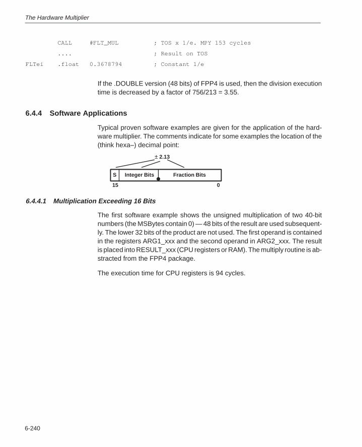
The Hardware Multiplier
6-240
CALL #FLT_MUL ; TOS x 1/e. MPY 153 cycles
.... ; Result on TOS
FLTei .float 0.3678794 ; Constant 1/e
If the .DOUBLE version (48 bits) of FPP4 is used, then the division executiontime is decreased by a factor of 756/213 = 3.55.
6.4.4 Software Applications
Typical proven software examples are given for the application of the hard-ware multiplier. The comments indicate for some examples the location of the(think hexa–) decimal point:
Integer Bits
015
Fraction Bits
± 2.13
S
6.4.4.1 Multiplication Exceeding 16 Bits
The first software example shows the unsigned multiplication of two 40-bitnumbers (the MSBytes contain 0) — 48 bits of the result are used subsequent-ly. The lower 32 bits of the product are not used. The first operand is containedin the registers ARG1_xxx and the second operand in ARG2_xxx. The resultis placed into RESULT_xxx (CPU registers or RAM). The multiply routine is ab-stracted from the FPP4 package.
The execution time for CPU registers is 94 cycles.
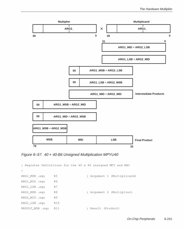
The Hardware Multiplier
6-241On-Chip Peripherals
39 0
Multiplier
ARG1_
39 0
×ARG2_
Multiplicand
ARG1_MID × ARG2_LSB
31 0
ARG1_LSB × ARG2_MID
ARG1_MSB × ARG2_LSB
ARG1_LSB × ARG2_MSB
00
00
ARG1_MID × ARG2_MID
ARG1_MSB × ARG2_MID
ARG1_MID × ARG2_MSB
00
00
ARG1_MSB × ARG2_MSB
MIDMSB LSB
79 32
Final Product
Intermediate Products
Figure 6–57. 40 × 40-Bit Unsigned Multiplication MPYU40
; Register Definitions for the 40 x 40 unsigned MPY and MAC
;
ARG1_MSB .equ R5 ; Argument 1 (Multiplicand)
ARG1_MID .equ R6
ARG1_LSB .equ R7
ARG2_MSB .equ R8 ; Argument 2 (Multiplier)
ARG2_MID .equ R9
ARG2_LSB .equ R10
RESULT_MSB .equ R11 ; Result (Product)
The Hardware Multiplier
6-242
RESULT_MID .equ R12
RESULT_LSB .equ R13
;
MPYU40 CLR RESULT_MSB ; Clear Result
CLR RESULT_MID
CLR RESULT_LSB
;
MACU40 MPYU16 ARG2_LSB,ARG1_MID ; Bits 16 to 47
MACU16 ARG1_LSB,ARG2_MID
ADD &SumHi,RESULT_LSB
ADDC &SumExt,RESULT_MID
MPYU16 ARG1_MSB,ARG2_LSB ; Bits 32 to 63
MACU16 ARG1_LSB,ARG2_MSB
MACU16 ARG1_MID,ARG2_MID
ADD &SumLo,RESULT_LSB
ADDC &SumHi,RESULT_MID
ADDC &SumExt,RESULT_MSB
MPYU16 ARG1_MSB,ARG2_MID ; Bits 48 to 79
MACU16 ARG2_MSB,ARG1_MID
ADD &SumLo,RESULT_MID
ADDC &SumHi,RESULT_MSB
MPYU16 ARG1_MSB,ARG2_MSB ; Bits 64 to 79
ADD &SumLo,RESULT_MSB
RET ; 48 MSBs in result
The second software example shows all four possible multiplication routinesfor two 32-bit numbers; the full 64-bit result may be used afterward. The signed16 ×16-bit hardware multiplication MPYS cannot be used; it is designed for thespecial case of 16 × 16 bits. So the unsigned multiplication MPY is used witha correction of the final sum at the start of the subroutine.
Execution times (without CALL):
MACU32 58 cycles unsigned MACMPYU32 64 cycles unsigned MPYMACS32 64 to 68 cycles signed MACMPYS32 68 to 72 cycles signed MPY
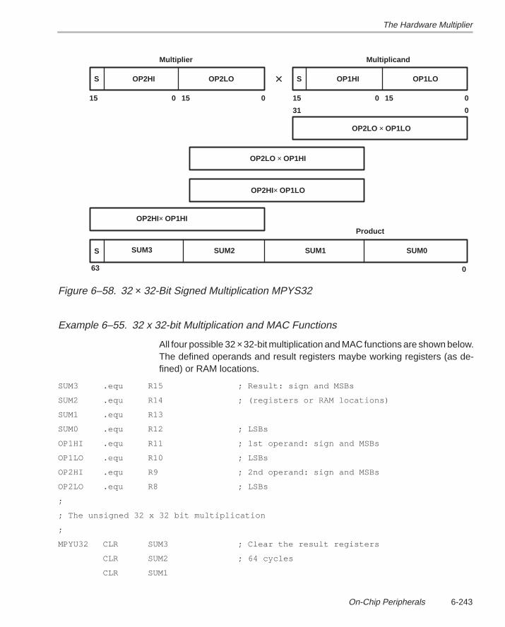
The Hardware Multiplier
6-243On-Chip Peripherals
Multiplier
15 0
×OP2HI
Multiplicand
SUM2SUM3 SUM1
63 0
S S
S
OP2LO OP1HI OP1LO
0 15 15 00 15
OP2LO × OP1LO
31 0
OP2LO × OP1HI
OP2HI× OP1LO
OP2HI× OP1HI
SUM0
Product
Figure 6–58. 32 × 32-Bit Signed Multiplication MPYS32
Example 6–55. 32 x 32-bit Multiplication and MAC Functions
All four possible 32 × 32-bit multiplication and MAC functions are shown below.The defined operands and result registers maybe working registers (as de-fined) or RAM locations.
SUM3 .equ R15 ; Result: sign and MSBs
SUM2 .equ R14 ; (registers or RAM locations)
SUM1 .equ R13
SUM0 .equ R12 ; LSBs
OP1HI .equ R11 ; 1st operand: sign and MSBs
OP1LO .equ R10 ; LSBs
OP2HI .equ R9 ; 2nd operand: sign and MSBs
OP2LO .equ R8 ; LSBs
;
; The unsigned 32 x 32 bit multiplication
;
MPYU32 CLR SUM3 ; Clear the result registers
CLR SUM2 ; 64 cycles
CLR SUM1
The Hardware Multiplier
6-244
CLR SUM0
JMP MS321 ; Proceed at common part
;
; The signed 32 x 32 bit multiplication
;
MPYS32 CLR SUM3 ; Clear the result registers
CLR SUM2 ; 68 to 72 cycles
CLR SUM1
CLR SUM0
;
; The signed 32–bit “Multiply–and–Accumulate” subroutine
; The final result is corrected. 64 to 68 cycles
;
MACS32 TST OP1HI ; Operand1 negative?
JGE MS320 ; No
SUB OP2LO,SUM2 ; Yes, correct final sum
SUBC OP2HI,SUM3
MS320 TST OP2HI ; Operand2 negative?
JGE MS321 ; No
SUB OP1LO,SUM2 ; Yes, correct final sum
SUBC OP1HI,SUM3
;
; The unsigned 32–bit “Multiply–and–Accumulate” subroutine
;
MACU32 .equ $ ; 58 cycles
;
; Main part for all multiplication subroutines
;
MS321 MPYU16 OP1LO,OP2LO ; LSBs x LSBs
ADD &SumLo,Sum0 ; Add product to result
ADDC &SumHi,Sum1
;
ADC Sum2 ; Necessary only for MACx32
ADC Sum3 ;
;
MPYU16 OP1LO,OP2HI ; LSBs x MSBs
The Hardware Multiplier
6-245On-Chip Peripherals
MACU16 OP2LO,OP1HI ; LSBs x MSBs
ADD &SumLo,Sum1 ; Add accumulated products
ADDC &SumHi,Sum2 ; to result
;
ADDC &SumExt,Sum3 ; Necessary only for MACx32
;
MPYU16 OP1HI,OP2HI ; MSBs x MSBs
ADD &SumLo,Sum2 ; Add product to final result
ADDC &SumHi,Sum3
RET
6.4.4.2 Sensor Characteristics
For many applications, the digital values delivered by analog-to-digital con-verters, I/O ports, or calculation results must be corrected or adapted. A com-mon method is to use polynomials for this purpose. For example a cubic poly-nomial to calculate the corrected output value y from the input value x is:
y = a a a a3 2 1 0× + × + × +x x x3 2
With the hardware multiplier, a common solution may look like the followingcode. This subroutine is written for the highest possible speed — the coeffi-cients a3 to a0 have decreasing numbers of bits after the (think hexa–) decimalpoint. If this cannot be tolerated, then shifts and stores between the multiplica-tions are necessary. The input value x stays in operand1 (MPYS 0132h) andis used for all three multiplications.
Example 6–56. Value Correction
The output value of the ADC is corrected with a cubic polynomial. All valuesare scaled to values less than 1 to get the maximum resolution. The coeffi-cients an used for correction are:
a3: +0.01 a2: –0.25 a1: –0.5 a0: +0.999
The HORNER scheme is used for the computation:
( )( )( )y = a a a a3 2 1 0× + × + × +x x x
The numbers +–a.b in the code comments indicate the bits before and afterthe decimal point of the numbers used.
Execution time (without CALL): 45 cycles
The Hardware Multiplier
6-246
;
; Polynomial Calculation for y = a3x^3 +a2x^2 +a1x^1 +a0x^0
; Result in SumHi register
;
POLYNOM MPYS16 X,A3 ; +–0.15 x +–0.15 (+–1.14)
ADD A2,&SumHi ; +–1.14 + +–1.14 –> +–1.14
MOV &SumHi,&OP2 ; +–1.14 x +–0.15 (+–2.13)
ADD A1,&SumHi ; +–2.13 + +–2.13 –> +–2.13
MOV &SumHi,&OP2 ; +–2.13 x +–0.15 (+–3.12)
ADD A0,&SumHi ; +–3.12 + +–3.12 –> +–3.12
RET ; SumHi: +–3.12
;
; Table of coefficients
;
A3 .word +100*08000h/10000 ; +0.01 (+–0.15)
A2 .word –2500*04000h/10000 ; –0.25 (+–1.14)
A1 .word –5000*02000h/10000 ; –0.5 (+–2.13)
A0 .word +9999*01000h/10000 ; +0.9999 (+–3.12)
6.4.4.3 Table Calculation
The .MACRO instructions used for the different multiplication possibilities (8bits versus 16 bits, signed and unsigned, multiply and multiply-and-accumu-late) have the advantage to allow all seven addressing modes of the MSP430architecture for source and destination. Therefore, the MPY instructions areideal for table processing — both operands of a multiply instruction can alsobe addressed indirectly. An example for the table calculation is given in Section6.4.4.5
6.4.4.4 Wave Digital Filters
The main advantage of wave digital filters is that for fixed coefficients, no multi-plication is needed. Instead, an optimized shift-and-add sequence is used forthe filter algorithm. But this optimization is not possible if Adaptive Filter Algo-rithms are used, which means changing coefficients. In this case, a hardwaremultiplier has significant advantages — the calculation time is independent ofthe coefficients used.
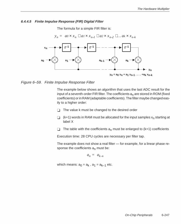
The Hardware Multiplier
6-247On-Chip Peripherals
6.4.4.5 Finite Impulse Response (FIR) Digital Filter
The formula for a simple FIR filter is:
y = a a a an 0 n 1 n–1 2 n–2 k n–k× + × + × + ×x x x x...
Z–1 Z–1 Z–1
a0 a1 ak-1 ak
xn
yn
yn = a0 xn + a1 xn-1 . . . . +ak xn-k
Figure 6–59. Finite Impulse Response Filter
The example below shows an algorithm that uses the last ADC result for theinput of a seventh-order FIR filter. The coefficients an are stored in ROM (fixedcoefficients) or in RAM (adaptable coefficients). The filter maybe changed eas-ily to a higher order:
The value k must be changed to the desired order
(k+1) words in RAM must be allocated for the input samples xn starting atlabel X
The table with the coefficients an must be enlarged to (k+1) coefficients
Execution time: 28 CPU cycles are necessary per filter tap.
The example does not show a real filter — for example, for a linear phase re-sponse the coefficients an must be:
a = n k–na
which means: a0 = ak , a1 = ak–1 etc.
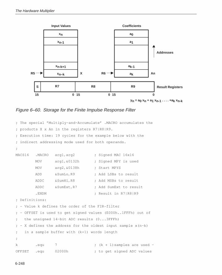
The Hardware Multiplier
6-248
R8R7 R9
15 0
S
xn
xn-1
xn-k+1
xn–k
Input Values
R5 X
a0
a1
ak-1
ak
Coefficients
R6 An
Addresses
Result Registers
00 15 15
yn = a0 xn + a1 xn-1 . . . . +ak xn-k
Figure 6–60. Storage for the Finite Impulse Response Filter
; The special ”Multiply–and–Accumulate” .MACRO accumulates the
; products X x An in the registers R7|R8|R9.
; Execution time: 19 cycles for the example below with the
; indirect addressing mode used for both operands.
;
MACS16 .MACRO arg1,arg2 ; Signed MAC 16x16
MOV arg1,&0132h ; Signed MPY is used
MOV arg2,&0138h ; Start MPYS
ADD &SumLo,R9 ; Add LSBs to result
ADDC &SumHi,R8 ; Add MSBs to result
ADDC &SumExt,R7 ; Add SumExt to result
.ENDM ; Result in R7|R8|R9
; Definitions:
; – Value k defines the order of the FIR–filter
; – OFFSET is used to get signed values (E000h..1FFFh) out of
; the unsigned 14–bit ADC results (0...3FFFh)
; – X defines the address for the oldest input sample x(n–k)
; in a sample buffer with (k+1) words length
;
k .equ 7 ; (k + 1)samples are used –
OFFSET .equ 02000h ; to get signed ADC values
The Hardware Multiplier
6-249On-Chip Peripherals
X .equ 0200h ; x(n–k) sample address
;
; With the Timer_A interrupt the calculation is made
;
TIMA_INT PUSH R5 ; Save R5 and R6
PUSH R6
MOV #X,R5 ; Address xn buffer (oldest x)
MOV #An,R6 ; Address a n constants (ak)
MOV &ADAT,2*k(R5) ; New ADC sample to xn
SUB #OFFSET, 2*k(R5) ; Create signed value for xn
CLR R7 ; Clear result reg. (MSBs)
CLR R8
CLR R9
TA00 MACS16 @R5+,@R6+ ; ak * xn–k added to R7|R8|R9
MOV @R5,–2(R5) ; xn–k+1 –> xn–k
CMP #X+2+(2*k),R5 ; Through? (R5 points outside)
JNE TA00 ; No, once more
POP R6 ; Restore R5 and R6
POP R5
BIS #CS,&ACTL ; Start next ADC conversion
RETI ; Result: +–17.30 (3 words)
;
; The constants An are fixed in ROM. Format: +–0.15
; (1 bit sign, 15 bits fraction)
; Range: –0.99996 to +0.99996
;
An .word +9999*8000h/10000 ; ak +0.9999
.word –9999*8000h/10000 ; ak–1 –0.9999
... ; ak–2 to a2
.word +5000*8000h/10000 ; a1 +0.5
.word –5000*8000h/10000 ; a0 –0.5
The Hardware Multiplier
6-250
6.4.4.6 Fast Fourier Transform Algorithm
The buffer — located in the RAM — the pointer that pQR points to, is trans-formed and overwritten with the result of the fast Fourier transformation (FFT).The formula used for each block consists of real and imaginary numbers:
PRi’ = (PRi + (QRi × WRi + QIi × WIi)/2 real part of PiPIi’ = (PIi + (QIi × WRi – QRi × WIi)/2 imaginary part of PiQRi’ = (PRi – (QRi × WRi + QIi × WIi)/2 real part of QiQIi’ = (PIi – (QIi × WRi – QRi × WIi)/2 imaginary part of Qi
Where: WRi cos (i × 2 π /N) = cos (ω × i)WIi sin (i × 2 π /N) = sin (ω × i)ω 2πfi Index numberPRi Real part of PRi before FFTPRi’ Real part of PRi after FFT
Figure 6–61 shows the allocation of the three tables in the RAM and ROM ofthe MSP430.
Execution time: the buffer shown, with eight complex numbers each for the Pand Q part, needs 717 cycles (without CALL) for the transformation (185 µs@ 4 MHz).
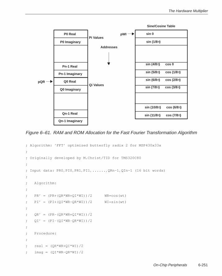
The Hardware Multiplier
6-251On-Chip Peripherals
P0 Real
P0 Imaginary
pQRQi Values
Sine/Cosine Table
Addresses
Pn-1 Real
Pn-1 Imaginary
Q0 Real
Q0 Imaginary
Qn-1 Real
Qn-1 Imaginary
Pi ValuespWI sin 0
sin (1/8 π)
sin (4/8 π) cos 0
sin (5/8 π) cos (1/8 π)
sin (6/8 π) cos (2/8 π)
sin (7/8 π) cos (3/8 π)
sin (10/8 π) cos (6/8 π)
sin (11/8 π) cos (7/8 π)
Figure 6–61. RAM and ROM Allocation for the Fast Fourier Transformation Algorithm
; Algorithm: ’FFT’ optimized butterfly radix 2 for MSP430x33x
;
; Originally developed by M.Christ/TID for TMS320C80
;
; Input data: PR0,PI0,PR1,PI1,......,QRn–1,QIn–1 (16 bit words)
;
; Algorithm:
;
; PR’ = (PR+(QR*WR+QI*WI))/2 WR=cos(wt)
; PI’ = (PI+(QI*WR–QR*WI))/2 WI=sin(wt)
;
; QR’ = (PR–(QR*WR+QI*WI))/2
; QI’ = (PI–(QI*WR–QR*WI))/2
;
; Procedure:
;
; real = (QR*WR+QI*WI)/2
; imag = (QI*WR–QR*WI)/2
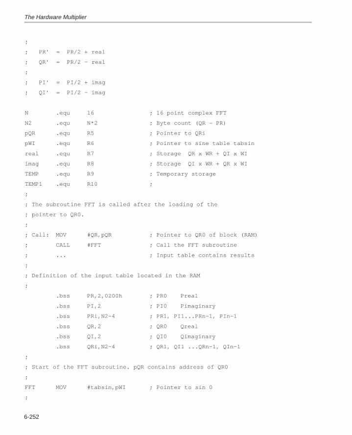
The Hardware Multiplier
6-252
;
; PR’ = PR/2 + real
; QR’ = PR/2 – real
;
; PI’ = PI/2 + imag
; QI’ = PI/2 – imag
N .equ 16 ; 16 point complex FFT
N2 .equ N*2 ; Byte count (QR – PR)
pQR .equ R5 ; Pointer to QRi
pWI .equ R6 ; Pointer to sine table tabsin
real .equ R7 ; Storage QR x WR + QI x WI
imag .equ R8 ; Storage QI x WR + QR x WI
TEMP .equ R9 ; Temporary storage
TEMP1 .equ R10 ;
;
; The subroutine FFT is called after the loading of the
; pointer to QR0.
;
; Call: MOV #QR,pQR ; Pointer to QR0 of block (RAM)
; CALL #FFT ; Call the FFT subroutine
; ... ; Input table contains results
;
; Definition of the input table located in the RAM
;
.bss PR,2,0200h ; PR0 Preal
.bss PI,2 ; PI0 Pimaginary
.bss PRi,N2–4 ; PR1, PI1...PRn–1, PIn–1
.bss QR,2 ; QR0 Qreal
.bss QI,2 ; QI0 Qimaginary
.bss QRi,N2–4 ; QR1, QI1 ...QRn–1, QIn–1
;
; Start of the FFT subroutine. pQR contains address of QR0
;
FFT MOV #tabsin,pWI ; Pointer to sin 0
;
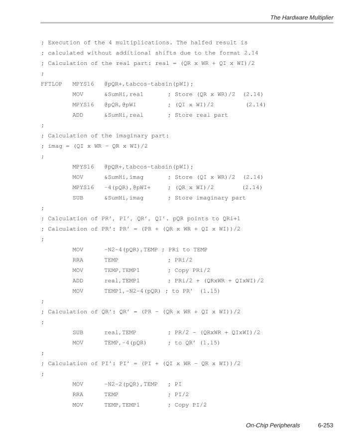
The Hardware Multiplier
6-253On-Chip Peripherals
; Execution of the 4 multiplications. The halfed result is
; calculated without additional shifts due to the format 2.14
; Calculation of the real part: real = (QR x WR + QI x WI)/2
;
FFTLOP MPYS16 @pQR+,tabcos–tabsin(pWI);
MOV &SumHi,real ; Store (QR x WR)/2 (2.14)
MPYS16 @pQR,@pWI ; (QI x WI)/2 (2.14)
ADD &SumHi,real ; Store real part
;
; Calculation of the imaginary part:
; imag = (QI x WR – QR x WI)/2
;
MPYS16 @pQR+,tabcos–tabsin(pWI);
MOV &SumHi,imag ; Store (QI x WR)/2 (2.14)
MPYS16 –4(pQR),@pWI+ ; (QR x WI)/2 (2.14)
SUB &SumHi,imag ; Store imaginary part
;
; Calculation of PR’, PI’, QR’, QI’. pQR points to QRi+1
; Calculation of PR’: PR’ = (PR + (QR x WR + QI x WI))/2
;
MOV –N2–4(pQR),TEMP ; PRi to TEMP
RRA TEMP ; PRi/2
MOV TEMP,TEMP1 ; Copy PRi/2
ADD real,TEMP1 ; PRi/2 + (QRxWR + QIxWI)/2
MOV TEMP1,–N2–4(pQR) ; to PR’ (1.15)
;
; Calculation of QR’: QR’ = (PR – (QR x WR + QI x WI))/2
;
SUB real,TEMP ; PR/2 – (QRxWR + QIxWI)/2
MOV TEMP,–4(pQR) ; to QR’ (1.15)
;
; Calculation of PI’: PI’ = (PI + (QI x WR – QR x WI))/2
;
MOV –N2–2(pQR),TEMP ; PI
RRA TEMP ; PI/2
MOV TEMP,TEMP1 ; Copy PI/2
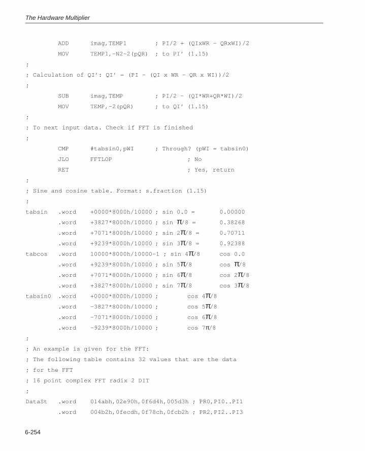
The Hardware Multiplier
6-254
ADD imag,TEMP1 ; PI/2 + (QIxWR – QRxWI)/2
MOV TEMP1,–N2–2(pQR) ; to PI’ (1.15)
;
; Calculation of QI’: QI’ = (PI – (QI x WR – QR x WI))/2
;
SUB imag,TEMP ; PI/2 – (QI*WR+QR*WI)/2
MOV TEMP,–2(pQR) ; to QI’ (1.15)
;
; To next input data. Check if FFT is finished
;
CMP #tabsin0,pWI ; Through? (pWI = tabsin0)
JLO FFTLOP ; No
RET ; Yes, return
;
; Sine and cosine table. Format: s.fraction (1.15)
;
tabsin .word +0000*8000h/10000 ; sin 0.0 = 0.00000
.word +3827*8000h/10000 ; sin π/8 = 0.38268
.word +7071*8000h/10000 ; sin 2 π/8 = 0.70711
.word +9239*8000h/10000 ; sin 3 π/8 = 0.92388
tabcos .word 10000*8000h/10000–1 ; sin 4 π/8 cos 0.0
.word +9239*8000h/10000 ; sin 5 π/8 cos π/8
.word +7071*8000h/10000 ; sin 6 π/8 cos 2 π/8
.word +3827*8000h/10000 ; sin 7 π/8 cos 3 π/8
tabsin0 .word +0000*8000h/10000 ; cos 4 π/8
.word –3827*8000h/10000 ; cos 5 π/8
.word –7071*8000h/10000 ; cos 6 π/8
.word –9239*8000h/10000 ; cos 7 π/8
;
; An example is given for the FFT:
; The following table contains 32 values that are the data
; for the FFT
; 16 point complex FFT radix 2 DIT
;
DataSt .word 014abh,02e90h,0f6d4h,005d3h ; PR0,PI0..PI1
.word 004b2h,0fecdh,0f78ch,0fcb2h ; PR2,PI2..PI3
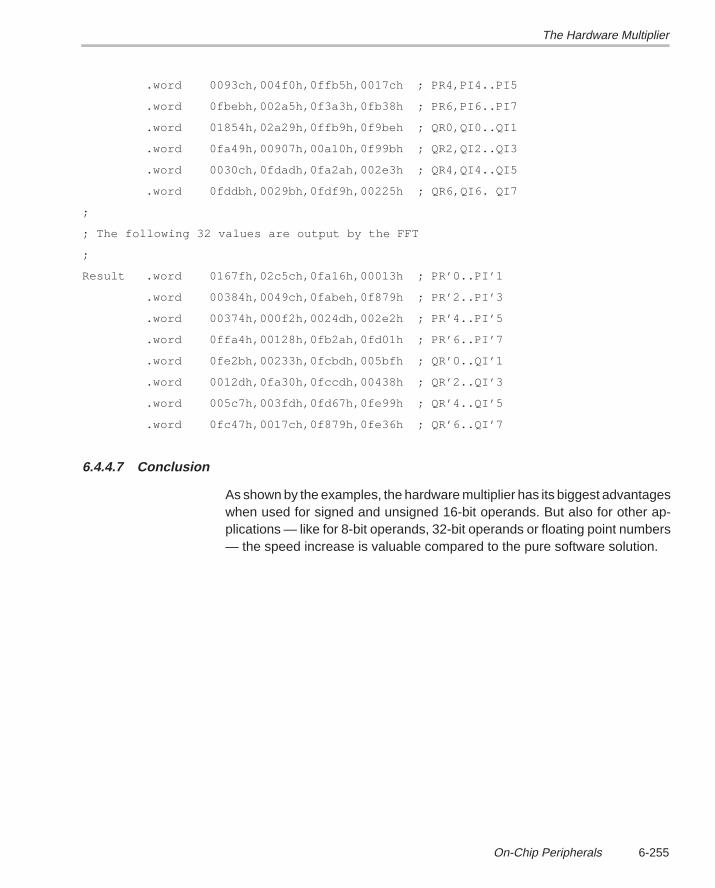
The Hardware Multiplier
6-255On-Chip Peripherals
.word 0093ch,004f0h,0ffb5h,0017ch ; PR4,PI4..PI5
.word 0fbebh,002a5h,0f3a3h,0fb38h ; PR6,PI6..PI7
.word 01854h,02a29h,0ffb9h,0f9beh ; QR0,QI0..QI1
.word 0fa49h,00907h,00a10h,0f99bh ; QR2,QI2..QI3
.word 0030ch,0fdadh,0fa2ah,002e3h ; QR4,QI4..QI5
.word 0fddbh,0029bh,0fdf9h,00225h ; QR6,QI6. QI7
;
; The following 32 values are output by the FFT
;
Result .word 0167fh,02c5ch,0fa16h,00013h ; PR’0..PI’1
.word 00384h,0049ch,0fabeh,0f879h ; PR’2..PI’3
.word 00374h,000f2h,0024dh,002e2h ; PR’4..PI’5
.word 0ffa4h,00128h,0fb2ah,0fd01h ; PR’6..PI’7
.word 0fe2bh,00233h,0fcbdh,005bfh ; QR’0..QI’1
.word 0012dh,0fa30h,0fccdh,00438h ; QR’2..QI’3
.word 005c7h,003fdh,0fd67h,0fe99h ; QR’4..QI’5
.word 0fc47h,0017ch,0f879h,0fe36h ; QR’6..QI’7
6.4.4.7 Conclusion
As shown by the examples, the hardware multiplier has its biggest advantageswhen used for signed and unsigned 16-bit operands. But also for other ap-plications — like for 8-bit operands, 32-bit operands or floating point numbers— the speed increase is valuable compared to the pure software solution.
The System Clock Generator
6-256
6.5 The System Clock Generator
The system clock generator of the MSP430 family provides many features notavailable with other microcomputers. To allow the full use of all the possibilities,some basics concerning the function of the oscillator are needed. A detaileddescription of the hardware is given in the MSP430 Family Architecture User’sGuide and Module Library, chapter Oscillator and System Clock Generator.
The output frequency, MCLK, of the system clock generator is generated in adigitally controlled oscillator (DCO), having 32 taps. Each one of these tapsrepresents a typical output frequency ranging from 500 kHz to 4 MHz. Thesetap frequencies depend on temperature and supply voltage, and referencingto a crystal is therefore necessary.
; Software definitions for the programming examples
;
SCG1 .equ 080h ; System Clock Generator Control Bit 1
SCG0 .equ 040h ; System Clock Generator Control Bit 0
OSCoff .equ 020h ; If 1: Oscillator off
CPUoff .equ 010h ; If 1: CPU off
GIE .equ 008h ; General Interrupt Enable Bit
SCFI0 .equ 050h ; System Clock Frequency Integrator Reg.
FN_2 .equ 004h ; DCO current switch for 2 x fnom
SCFI1 .equ 051h ; DCO tap register 2^9 to 2^2
TAP .equ 008h ; 2^5 bit in SCFI1
SCFQCTL .equ 052h ; System Clock Frequency Control Register
M .equ 080h ; Modulation Bit in SCFQCTL. M = 1: off
6.5.1 Initialization
After the application of the supply voltage, VCC, the system clock frequencyfsystem is initialized to 1.024 MHz, if a 32.768 kHz crystal is used. This is auto-matically made by setting of the multiplication factor, N, to 32 and clearing ofthe FN_x bits in the control bytes SCFI0 and SCFI1. If the CPU is always onafterward and 1.024 MHz is the desired frequency, then there is nothing elseto do.
6.5.1.1 First Setting of the DCO Taps during Initialization
The digitally controlled oscillator of the MSP430 starts at tap 0, which meansat the lowest possible frequency (≈ 500 kHz). To get from one tap to the next
The System Clock Generator
6-257On-Chip Peripherals
one, 210 (1024) cycles are needed. Thirty-two taps are implemented, so 32 ×1024 cycles are needed, worst case, to get to the correct DCO tap. The initiali-zation routine should therefore have a length of 32000 cycles. If this is not thecase, a delay routine should be added to guarantee this length. An exampleis given below:
INIT ... ; Loop Control is on (SCG1 = SCG0 = 0)
MOV #11000,R5 ; Init delay to allow DCO setting
L$1 DEC R5 ; 11000 x 3 cycles = 33000 cycles
JNZ L$1 ;
BR #MAINLOOP ; Start program
6.5.2 Entering of Low Power Mode 3
The low power mode 3 (LPM3 —crystal on, DCO and loop control off) is thenormal mode for battery-powered systems. Enabled interrupts (e.g. the basictimer) wake up the CPU. LPM3 is entered with the following source code:
BIS #CPUoff+GIE+SCG1+SCG0,SR ; Enter LPM3
6.5.3 Wake-Up From Interrupts in Low Power Mode 3
Wake-up from LPM3 clears only bit SCG1 (LPM1). Due to the set bit SCG0,the loop control of the DCO is off. Normal interrupt routines are too short to al-low the loop control to adjust the DCO tap — 1024 cycles are necessary to getfrom one tap to the other one. It is not necessary, therefore, to switch on theloop control. The CPU uses the DCO tap set during the last adaptation. A nor-mal, short interrupt routine looks like this:
BT_HAND INC COUNTER ; LPM1: Loop Control stays off:
RETI ; DCO is on for 17 cycles only
If woken–up from LPM3, the interrupt latency time (6 cycles) is increased bytyp. 2 µs @ 1 MHz versus 1 µs @ 2 MHz (if FN_2 = 1). This means 8 cyclesare typically needed from the interrupt event to the start of the interrupt han-dler. The time the DCO needs to settle to the nominal frequency is typically 4cycles. This means interrupt handlers are processed with the correct frequen-cy.
6.5.4 Adaptation of the DCO Tap During Calculations
The DCO tap of the system clock generator should be updated during longeron times of the CPU (e.g. during calculations). This is necessary especially if
The System Clock Generator
6-258
accurate timing of the instructions is needed. During all calculations that ex-ceed 100 cycles in length, the loop control of the DCO should be switched on.The way to do this is to reset the SCG0 bit in the status register after the wake–up:
; Calculations are necessary. Allow adaptation of the DCO tap
;
BIC #SCG0,SR ; Switch on DCO loop control
... ; Calculate energy (>100 cycles)
RETI ; Return to LPM3 with adapted DCO tap
The RETI instruction restores the CPU mode from the stack as it was whenthe interrupt occurred.
6.5.5 Wake–Up From Interrupts in Low Power Mode 4
The low power mode 4 normally lasts much longer than the low power mode3 — it may last for months until a stored module is woken–up for calibration.This means that the environment temperature may have changed seriously.If the LPM4 was entered at a high temperature, the used DCO tap will be a rela-tively high one due to the negative temperature coefficient of the DCO. If thenthe device is woken–up at a low temperature and the crystal turns on fast, thishigh DCO tap may lead to a very high DCO frequency, a frequency the systemcannot operate with. Therefore, it is a good programming practice, to programa low DCO tap before entering LPM4:
; Enter Low Power Mode 4: Set DCO tap to 2
;
MOV.B #TAP*2,&SCFI1 ; Set DCO tap to 2
BIS #CPUoff+OSCoff+GIE+SCG1+SCG0,SR ; Enter LPM4
If woken–up from LPM4, it may last up to seconds until the crystal has reachedits nominal frequency. The frequency integrator counts down continuously aslong as the crystal oscillator has not started its operation. This lasts until thelowest DCO tap (with the lowest system frequency) is reached. After the startof the crystal oscillator, the loop control will set the system frequency to its cor-rect value by stepping up the taps.
The System Clock Generator
6-259On-Chip Peripherals
6.5.6 Change of the System Frequency
The system clock frequency fsystem depends on two values:
f N fsystem crystal= ×
Where: N Multiplication factor of the DCO loop (SCFQCTL contains N–1)fcrystal Frequency of the crystal (normally 32.768 kHz)
The normal way to change the system clock frequency is to change the multi-plication factor N. The system clock frequency control register SCFQCTL isloaded with (N–1) to get the new frequency. To allow the DCO to work alwaysin one of the center taps (13 to 18), three switches FN_2 to FN_4 are imple-mented in the register SCFI0. It gives a safety not to be at the frequency limitsof the DCO. These switches increase the internal current of the DCO and allowhigher output frequencies if set. The switch nearest to the programmed DCOoutput frequency should be used.
The switches FN_x typically settle within ±1 tap if the change is from the nomi-nal frequency of one switch to the nominal frequency of the other one. For ex-ample, if in the example below, the initial system frequency is 1 MHz, then thenew tap is one of the neighboring taps. This means, to settle at 2 MHz, needsa maximum of 1024 cycles (0.5 ms) only. If FN_2 is not used, it would take upto 16 x 1024 cycles (8 ms) because the misalignment could be up to 16 taps.
Note:
The switches FN_2, FN_3, and FN_4 need to be set correctly in dependenceof the system clock frequency, fsystem. Otherwise, erroneous behavior of thesystem will result. Only one switch may be in use at the same time — the onethat is nearest to the actual frequency should be used. FN_2 controls fre-quencies near 2 MHz, FN_3 controls frequencies around 3 MHz, and FN_4controls frequencies around 4 MHz.
; Change system frequency to 2.048MHz (fcrystal = 32.768kHz)
; N = 64 : Multiply 32kHz by 64 to get 2.048MHz
; FN_2 = 1: Adjust DCO current to 2MHz output frequency
; M = 0 : Switch on modulation
;
MOV.B #64–1,&SCFQCTL ; 64 x 32kHz = 2.048MHz, M = 0
MOV.B #FN_2,&SCFI0 ; Adjust DCO current to 2MHz
The System Clock Generator
6-260
6.5.7 The Modulation Bit M
The modulation bit M (SCFQCTL.7) switches off and on the influence of the5 LSBs (NDCOmod) of the system clock frequency integrator:
M = 0 — the modulation is on. This means all 10 bits of the integrator influ-ence the DCO. The used tap of the DCO may be changed with every clockcycle to get the correct system clock frequency. This is the case if the pro-grammed frequency lies exactly between two tap frequencies.
M = 1 — the modulation is off. This means only the 5 MSBs (NDCO) of theintegrator influence the DCO. The used tap of the DCO is changed onlyafter 1024 clock cycles (for fsystem = 1 MHz) to get the correct system clockfrequency. If the programmed frequency lies exactly between two tap fre-quencies, then 1024 cycles are output with the lower tap frequency and1024 cycles are output with the upper tap frequency.
In any case, independent of the modulation status, the integral error of theDCO will be zero.
The modulation may be switched off if a series of MCLK cycles is needed withexactly the same length (for measurements with the universal timer/port mod-ule, for example). To get this, the loop control also should be switched off.
; Ensure stable, non regulated output pulses with equal length:
;
BIS.B #SCG0,SR ; Switch off loop control
BIS.B #M,&SCFQCTL ; Switch off modulation
... ; Use non–regulated MCLK
;
; Return to a regulated MCLK with closed loop and modulation
;
BIC.B #SCG0,SR ; Switch on loop control
BIC.B #M,&SCFQCTL ; Switch on modulation
The System Clock Generator
6-261On-Chip Peripherals
6.5.8 Use Without Crystal
If for an application, no precise timing is necessary, then the crystal may beomitted. If no ACLK is present (due to the missing crystal), then the DCO willrun with its lowest frequency, which is approximately 500 kHz. No special in-structions are necessary to get this behavior.
If this lowest DCO frequency is too low, then a higher DCO tap (eg. 10) maybe used. This tap normally results in an MCLK frequency near 1MHz. It is im-portant to switch off the FLL loop, otherwise the FLL control will step down totap 0 slowly. The software for this use of the DCO follows:
; Initialization of the DCO for non–crystal mode:
; Loop control off, tap number = 10: MCLK ≈ 1MHz
;
BIS.B #SCG0,SR ; Switch off loop control
CLR.B &SCFI0 ; Reset FN_x bits
MOV.B #050h,&SCFI1 ; Set bits for tap number 10
If an external reference like the ac line is available, then the actual MCLK fre-quency can be controlled simply by the counting of the MCLK output with oneof the timers (e.g. for one ac line period). An example is given in section TheTimer_A where the control of an LCD is also shown without a crystal and miss-ing LCD control frequency due to the missing ACLK.
6.5.9 High System Frequencies Together With the 14-bit ADC
The maximum MCLK without input division is 1.5 MHz (132 cycles are neededfor a conversion). To allow the full range of the system clock MCLK, togetherwith the active ADC, a clock divider is included in the ADC module. It allowsthe division of the system frequency MCLK by factors of 1, 2, 3, and 4. Seesection Analog-to-Digital Converters for examples.
6.5.10 Dependencies of the System Clock Generator
If the DCO runs with an open loop, its frequency depends on the temperatureand the supply voltage, VCC. Nominal values for these dependencies are:
Temperature dependence: –5.6 kHz/(C × MHz)
Voltage dependence: +60 kHz/(V × MHz)
These two dependencies are brought to zero if the DCO loop is closed (SR–bits: SCG0 = SCG1 = OscOff = 0). See the next section for short term devi-ations of the system clock generator (MCLK).
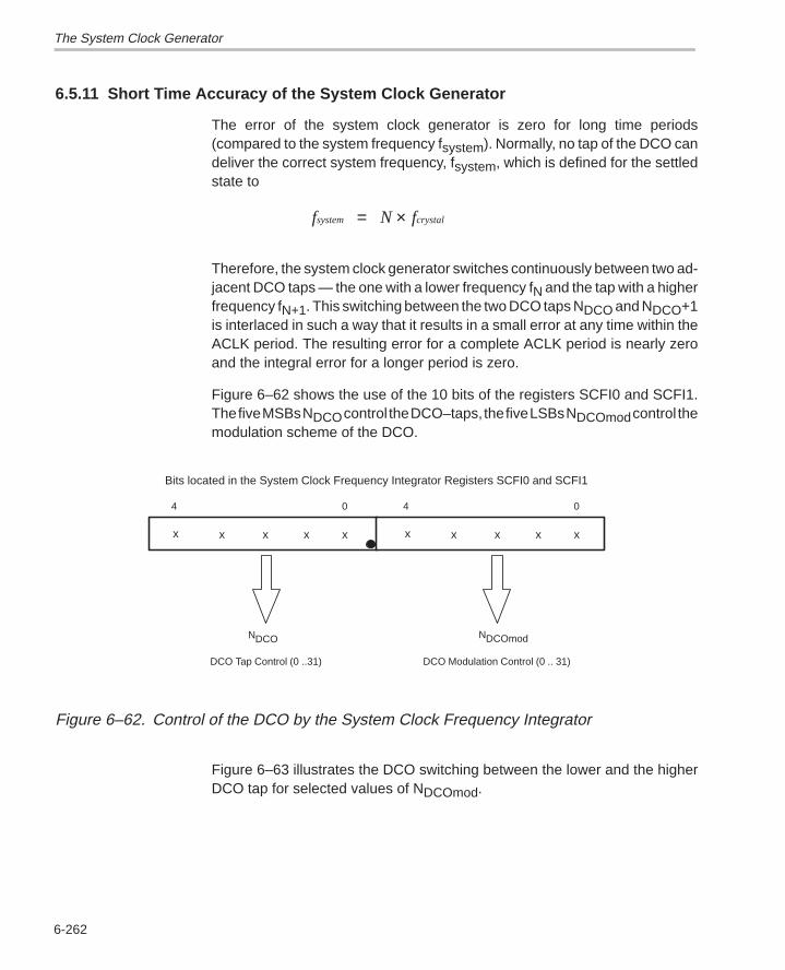
The System Clock Generator
6-262
6.5.11 Short Time Accuracy of the System Clock Generator
The error of the system clock generator is zero for long time periods(compared to the system frequency fsystem). Normally, no tap of the DCO candeliver the correct system frequency, fsystem, which is defined for the settledstate to
f N fsystem crystal= ×
Therefore, the system clock generator switches continuously between two ad-jacent DCO taps — the one with a lower frequency fN and the tap with a higherfrequency fN+1. This switching between the two DCO taps NDCO and NDCO+1is interlaced in such a way that it results in a small error at any time within theACLK period. The resulting error for a complete ACLK period is nearly zeroand the integral error for a longer period is zero.
Figure 6–62 shows the use of the 10 bits of the registers SCFI0 and SCFI1.The five MSBs NDCO control the DCO–taps, the five LSBs NDCOmod control themodulation scheme of the DCO.
4 0
x x x x x
4 0
x x x x x
NDCO
DCO Tap Control (0 ..31) DCO Modulation Control (0 .. 31)
Bits located in the System Clock Frequency Integrator Registers SCFI0 and SCFI1
NDCOmod
Figure 6–62. Control of the DCO by the System Clock Frequency Integrator
Figure 6–63 illustrates the DCO switching between the lower and the higherDCO tap for selected values of NDCOmod.
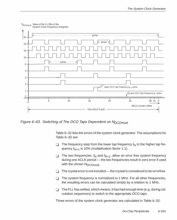
The System Clock Generator
6-263On-Chip Peripherals
Value of the 5 LSBs of theSystem Clock Frequency Integrator
0
1
2
3
4
5
15
16
24
05 10 15 3020 25 31 0
MCLK Cycles 1MHz
Upper DCO Tap Frequency f active
One ACLK Cycle
31
DCOmodN
max∆
max∆
max∆
N+1
Lower DCO Tap Frequency f activeN
Figure 6–63. Switching of The DCO Taps Dependent on NDCOmod
Table 6–32 lists the errors of the system clock generator. The assumptions forTable 6–32 are:
The frequency step from the lower tap frequency fN to the higher tap fre-quency fN+1 is 10% (multiplication factor 1.1).
The two frequencies, fN and fN+1, allow an error free system frequencyduring one ACLK period — the two frequencies result in zero error if usedwith the shown NDCOmod.
The crystal error is not included — the crystal is considered to be errorfree.
The system frequency is normalized to 1 MHz. For all other frequencies,the resulting errors can be calculated simply by a relation to 1 MHz.
The FLL has settled, which means, it has had enough time (e.g. during cal-culation sequences) to switch to the appropriate DCO taps.
Three errors of the system clock generator are calculated in Table 6–32:
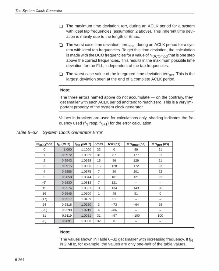
The System Clock Generator
6-264
The maximum time deviation, terr, during an ACLK period for a systemwith ideal tap frequencies (assumption 2 above). This inherent time devi-ation is mainly due to the length of ∆max.
The worst case time deviation, terrmax, during an ACLK period for a sys-tem with ideal tap frequencies. To get this time deviation, the calculationis made with the DCO frequencies for a value of NDCOmod that is one stepabove the correct frequencies. This results in the maximum possible timedeviation for the FLL, independent of the tap frequencies.
The worst case value of the integrated time deviation terrper. This is thelargest deviation seen at the end of a complete ACLK period.
Note:
The three errors named above do not accumulate — on the contrary, theyget smaller with each ACLK period and tend to reach zero. This is a very im-portant property of the system clock generator.
Values in brackets are used for calculations only, shading indicates the fre-quency used (fN resp. fN+1) for the error calculation.
Table 6–32. System Clock Generator Error
NDCO mod fN (MHz) fN+1 (MHz) ∆max terr (ns) terr max (ns) terr per (ns)
0 1.000 1.1000 32 0 89 91
1 0.9972 1.0969 31 87 177 91
2 0.9943 1.0938 15 86 129 91
3 0.9915 1.0906 15 128 172 93
4 0.9886 1.0875 7 80 101 92
5 0.9858 1.0844 7 101 121 92
(6) 0.9830 1.0813 7 121 – –
15 0.9574 1.0531 3 134 143 96
16 0.9545 1.0500 1 48 51 0
(17) 0.9517 1.0469 1 51 – –
24 0.9318 1.0250 3 –73 –64 98
(25) 0.9290 1.0219 4 –86 – –
31 0.9119 1.0031 31 –97 –100 100
(0) 0.9091 1.0000 32 0 – –
Note:
The values shown in Table 6–32 get smaller with increasing frequency. If fNis 2 MHz, for example, the values are only one-half of the table values.
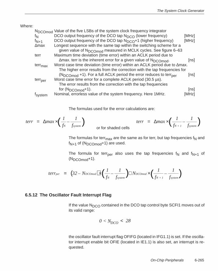
The System Clock Generator
6-265On-Chip Peripherals
Where: NDCOmod Value of the five LSBs of the system clock frequency integratorfN DCO output frequency of the DCO tap NDCO (lower frequency) [MHz]fN+1 DCO output frequency of the DCO tap NDCO+1 (higher frequency) [MHz]∆max Longest sequence with the same tap within the switching scheme for a
given value of NDCOmod measured in MCLK cycles. See figure 6–63terr Maximum time deviation (time error) within an ACLK period due to
∆max. terr is the inherent error for a given value of NDCOmod. [ns]terrmax Worst case time deviation (time error) within an ACLK period due to ∆max.
The higher error results from the correction with the tap frequencies for (NDCOmod +1). For a full ACLK period the error reduces to terrper [ns]
terrper Worst case time error for a complete ACLK period (30.5 µs). The error results from the correction with the tap frequencies for (NDCOmod+1). [ns]
fsystem Nominal, errorless value of the system frequency. Here 1MHz. [MHz]
The formulas used for the error calculations are:
terr max1
f
1
fN system= × –∆ ( )
or for shaded cells terr max
1
f
1
fN + 1 system= × –∆ ( )
The formulas for terrmax are the same as for terr, but tap frequencies fN andfN+1 of (NDCOmod+1) are used.
The formula for terrper also uses the tap frequencies fN and fN+1 of(NDCOmod+1).
( )terr 32 N1
f
1
fN
1
f
1
fper DCOmod
N systemDCOmod
N + 1 system= – × – + × –)( )(
6.5.12 The Oscillator Fault Interrupt Flag
If the value NDCO contained in the DCO tap control byte SCFI1 moves out ofits valid range:
28<0 < NDCO
the oscillator fault interrupt flag OFIFG (located in IFG1.1) is set. If the oscilla-tor interrupt enable bit OFIE (located in IE1.1) is also set, an interrupt is re-quested.
The System Clock Generator
6-266
Note:
The interrupt vector of the oscillator fault interrupt flag is shared with the nonmaskable interrupt (NMI). It is necessary, therefore, to test the oscillator faultinterrupt flag first to determine the cause of the interrupt.
The oscillator fault interrupt flag is set after the supply voltage is applied to theMSP43, due to the start of the DCO at the lowest frequency (NDCO = 0). Whenthe interrupt is granted, the oscillator interrupt enable bit OFIE is reset auto-matically to disable further interrupt requests. The oscillator fault interrupt flagOFIFG must be reset by software.
6.5.13 Conclusion
The time deviations listed in Table 6–32 demonstrate the small errorintroduced by the modulation of the DCO. The largest time deviation inside ofone ACLK period is 177 ns. This is relatively small compared to the inherentdigital uncertainty, which is one MCLK cycle (1 µs @ 1 MHz). The time devi-ations of the system clock generator do not accumulate, but get smaller withthe next ACLK period. Therefore, the overall error tends to move toward zerofor a longer time period. The system clock generator, with its output frequencyfsystem (MCLK), is therefore usable for precise time measurements like a nor-mal crystal oscillator.
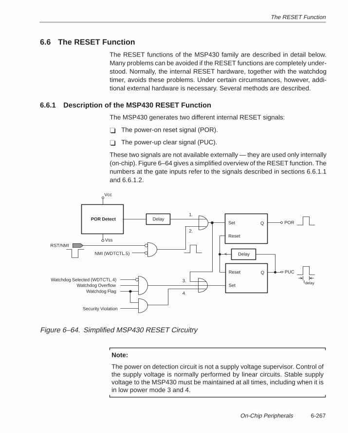
The RESET Function
6-267On-Chip Peripherals
6.6 The RESET Function
The RESET functions of the MSP430 family are described in detail below.Many problems can be avoided if the RESET functions are completely under-stood. Normally, the internal RESET hardware, together with the watchdogtimer, avoids these problems. Under certain circumstances, however, addi-tional external hardware is necessary. Several methods are described.
6.6.1 Description of the MSP430 RESET Function
The MSP430 generates two different internal RESET signals:
The power-on reset signal (POR).
The power-up clear signal (PUC).
These two signals are not available externally — they are used only internally(on-chip). Figure 6–64 gives a simplified overview of the RESET function. Thenumbers at the gate inputs refer to the signals described in sections 6.6.1.1and 6.6.1.2.
Watchdog Selected (WDTCTL.4)
Watchdog Overflow
NMI (WDTCTL.5)
Vcc
POR Detect
RST/NMI
Set
Vss
Reset
Q POR
Reset
Set
Q PUC
Delay
Watchdog Flag
Security Violation
tdelay
Delay1.
2.
3.
4.
Figure 6–64. Simplified MSP430 RESET Circuitry
Note:
The power on detection circuit is not a supply voltage supervisor. Control ofthe supply voltage is normally performed by linear circuits. Stable supplyvoltage to the MSP430 must be maintained at all times, including when it isin low power mode 3 and 4.
The RESET Function
6-268
6.6.1.1 The Power–On Reset Signal
The power-on reset signal, POR, is caused by two completely different exter-nal events:
The power-on detection circuitry detects the rise of the supply voltage,VCC (power-on signal).
The RST/NMI terminal is reset to VSS and set to VCC afterward. This is thecase only if the reset terminal is switched to the RESET function (defaultafter power-on) and not to the NMI function. The RESET function is usedif WDTCTL.5 = 0.
(NMI stands for non maskable interrupt, an external interrupt input that cannotbe disabled by the interrupt enable bit (GIE) in the status register (SR). Eachinterrupt event will request an interrupt. The NMI function is used if WDTCTL.5= 1).
6.6.1.2 The Power-Up Clear Signal
The power-up clear signal, PUC, can be caused by several events:
The power-on detection circuitry detects the rise of the supply voltage(VCC). This event also causes the POR signal.
The RST/NMI terminal is reset to VSS and then set to VCC afterward (seeabove). This event also causes the POR signal.
The expiring of the Watchdog Tmer if programmed to the watchdog mode(WDTCTL.4 = 0). The watchdog function is always active after PUC andPOR.
The use of an invalid password for the writing to the watchdog control wordWDTCTL (security violation). This reset generation is independent of thewatchdog function — it also occurs if the watchdog is used in timer mode(WDTCTL.4 = 1)
6.6.1.3 Common Operations for Power–Up and Power–On Reset
If one of the events described above occurs, the following operations arestarted:
The digital I/O ports (Port0 to Port4) are set to the input direction.
The I/O flags are set to 0 as discussed in the description of the peripherals.
The address contained in the vector at address 0FFFEh is written into theProgram Counter PC (software start address).
The RESET Function
6-269On-Chip Peripherals
The Status Register SR of the CPU is reset to 0. This means:
The CPU is set to the active mode.
The maskable interrupts are disabled by the reset GIE–bit (SR.4).
The loop control for the system clock generator is switched on (theFLL is active).
The system clock generator is set to an MCLK frequency of 1 MHz @fACLK = 32.768 kHz.
The digitally controlled oscillator (DCO) in the system clock generator(FLL for MCLK) is set to its lowest output frequency (DCO tap 0). The rea-son for this is to also include the possible malfunction of the system clockgenerator. Otherwise the erroneous FLL frequency is also active duringthe restoring phase of the system functionality with a fatal effect: the sys-tem cannot come up correctly.
The RST/NMI terminal is configured to the RESET function.
The Watchdog Timer is configured as a watchdog driven by the systemclock MCLK.
The CPU starts operation at the address written into the Program Counter(from address 0FFFEh) after the RST/NMI terminal is set to VCC voltage.
6.6.1.4 Differences Between Power-Up Reset and Power-On Reset
The few differences between the two reset signals are detailed below.
6.6.1.4.1 Peculiar to The Power-On Reset Signal
The power-on reset signal (POR) also generates the PUC signal.
The power-on reset signal sets (1) or resets (0) the peripheral bits en-closed in round brackets (see Architecture User’s Guide). These bits (allof the peripheral bits of the 16-Bit Timer_A, for example) are not influencedby the PUC signal. For example, rw–(0) means a readable and writableperipheral bit that is set to 0 by the POR signal only, but not by the PUCsignal.
The reason is that some functions may not be modified by watchdog events.These functions are mostly controlled by software.
6.6.1.4.2 Peculiar to The Power-Up Clear Signal
The power-up clear signal (PUC) does not also generate the POR signal.
The RESET Function
6-270
The power-up clear signal (PUC) sets or resets the peripheral bits not en-closed in round brackets (see Architecture User’s Guide). For example,rw–0 means a readable and writable bit that is set to 0 by the POR andPUC signals.
6.6.1.5 The RST/NMI Terminal Hardware
Some important facts that need to be considered when using the MSP430RST/NMI terminal:
The RST/NMI terminal does not have a pulldown or pullup resistor. Theuser must ensure a stable DVCC or VCC voltage level at the RST/NMI ter-minal during normal operation. Otherwise, hum or noise will generate arbi-trary system resets if the terminal is left unconnected (floating).
The RST/NMI terminal is an input pin only. No RESET signal is output ifan internal RESET occurs (by a watchdog overflow, for example). If exter-nal devices must also be reset, then two possibilities exist (see Figure6–65, right side):
An O-output is used. This output is set and reset by a short softwareroutine during the initialization phase following the RESET signal. Thestate of an O-output is not defined after the power up.
An I/O terminal (one of Port0 to Port4) or a TP terminal is used. Thisterminal is connected to VSS (DVSS) with a resistor (≈10 kΩ). While theRESET signal is active, the pin is switched to the input direction(compared to the HI–Z state) and the resistor pulls down the I/O termi-nal. This low signal resets all external devices immediately. The sub-sequent initialization software switches the terminal to an active highsignal. The external RESET signal is terminated. (A positive RESETsignal can be generated in the same way. The resistor is connected tothe supply voltage VCC, the initialization software outputs an activelow signal.)
The power-on detection circuitry is only able to detect a new, slow rise ofthe supply voltage (VCC) after a power fail, if VCC falls below a defined volt-age, VCCmin. If this cannot be guaranteed, external hardware is recom-mended. See the next section for the details of this hardware.
To guarantee a successful RESET, the low signal at the RST/NMI terminalneeds a minimum length of time (treset). This minimum time is 2 µs.
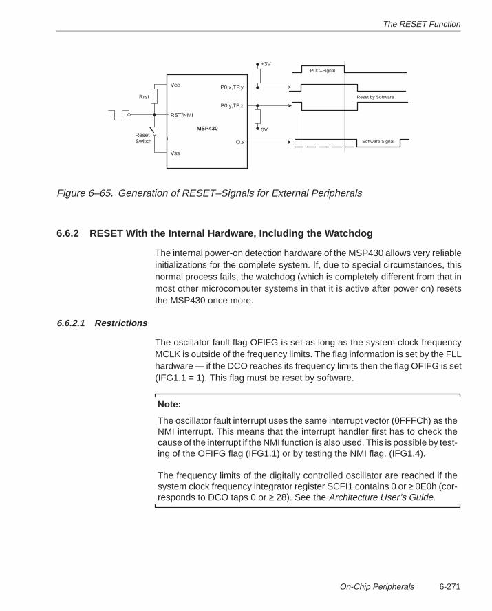
The RESET Function
6-271On-Chip Peripherals
Vss
Vcc
MSP430
RST/NMI
Rrst
P0.x,TP.y
O.x
ResetSwitch
+3V
P0.y,TP.z
0V
PUC–Signal
Software Signal
Reset by Software
Figure 6–65. Generation of RESET–Signals for External Peripherals
6.6.2 RESET With the Internal Hardware, Including the Watchdog
The internal power-on detection hardware of the MSP430 allows very reliableinitializations for the complete system. If, due to special circumstances, thisnormal process fails, the watchdog (which is completely different from that inmost other microcomputer systems in that it is active after power on) resetsthe MSP430 once more.
6.6.2.1 Restrictions
The oscillator fault flag OFIFG is set as long as the system clock frequencyMCLK is outside of the frequency limits. The flag information is set by the FLLhardware — if the DCO reaches its frequency limits then the flag OFIFG is set(IFG1.1 = 1). This flag must be reset by software.
Note:
The oscillator fault interrupt uses the same interrupt vector (0FFFCh) as theNMI interrupt. This means that the interrupt handler first has to check thecause of the interrupt if the NMI function is also used. This is possible by test-ing of the OFIFG flag (IFG1.1) or by testing the NMI flag. (IFG1.4).
The frequency limits of the digitally controlled oscillator are reached if thesystem clock frequency integrator register SCFI1 contains 0 or ≥ 0E0h (cor-responds to DCO taps 0 or ≥ 28). See the Architecture User’s Guide.
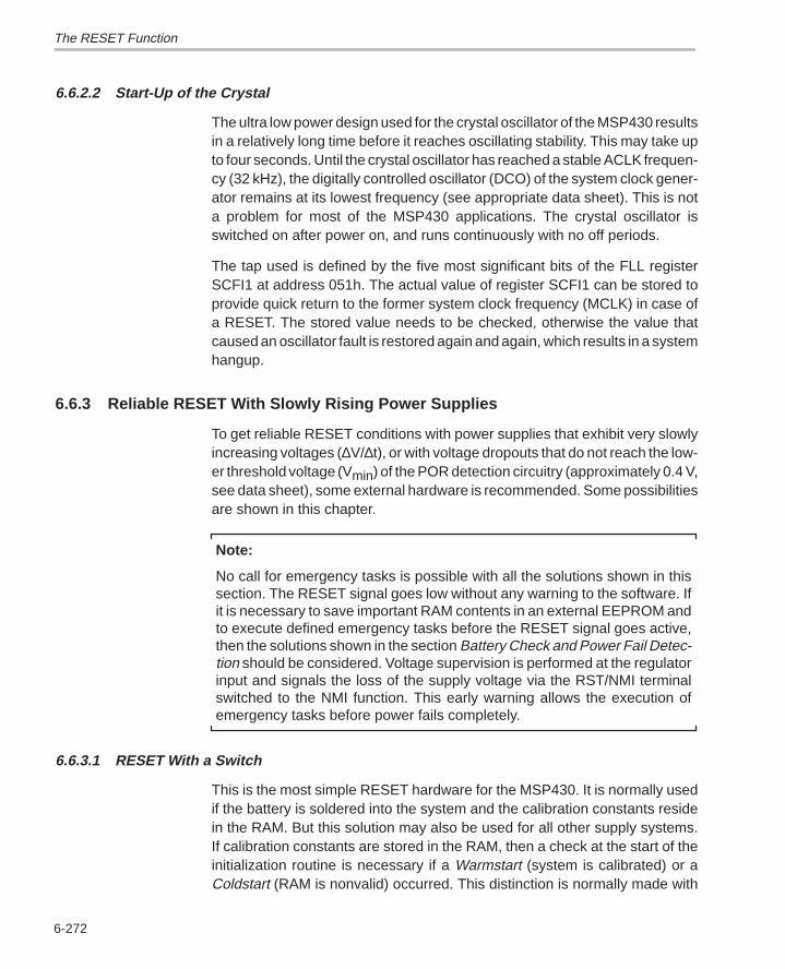
The RESET Function
6-272
6.6.2.2 Start-Up of the Crystal
The ultra low power design used for the crystal oscillator of the MSP430 resultsin a relatively long time before it reaches oscillating stability. This may take upto four seconds. Until the crystal oscillator has reached a stable ACLK frequen-cy (32 kHz), the digitally controlled oscillator (DCO) of the system clock gener-ator remains at its lowest frequency (see appropriate data sheet). This is nota problem for most of the MSP430 applications. The crystal oscillator isswitched on after power on, and runs continuously with no off periods.
The tap used is defined by the five most significant bits of the FLL registerSCFI1 at address 051h. The actual value of register SCFI1 can be stored toprovide quick return to the former system clock frequency (MCLK) in case ofa RESET. The stored value needs to be checked, otherwise the value thatcaused an oscillator fault is restored again and again, which results in a systemhangup.
6.6.3 Reliable RESET With Slowly Rising Power Supplies
To get reliable RESET conditions with power supplies that exhibit very slowlyincreasing voltages (∆V/∆t), or with voltage dropouts that do not reach the low-er threshold voltage (Vmin) of the POR detection circuitry (approximately 0.4 V,see data sheet), some external hardware is recommended. Some possibilitiesare shown in this chapter.
Note:
No call for emergency tasks is possible with all the solutions shown in thissection. The RESET signal goes low without any warning to the software. Ifit is necessary to save important RAM contents in an external EEPROM andto execute defined emergency tasks before the RESET signal goes active,then the solutions shown in the section Battery Check and Power Fail Detec-tion should be considered. Voltage supervision is performed at the regulatorinput and signals the loss of the supply voltage via the RST/NMI terminalswitched to the NMI function. This early warning allows the execution ofemergency tasks before power fails completely.
6.6.3.1 RESET With a Switch
This is the most simple RESET hardware for the MSP430. It is normally usedif the battery is soldered into the system and the calibration constants residein the RAM. But this solution may also be used for all other supply systems.If calibration constants are stored in the RAM, then a check at the start of theinitialization routine is necessary if a Warmstart (system is calibrated) or aColdstart (RAM is nonvalid) occurred. This distinction is normally made with
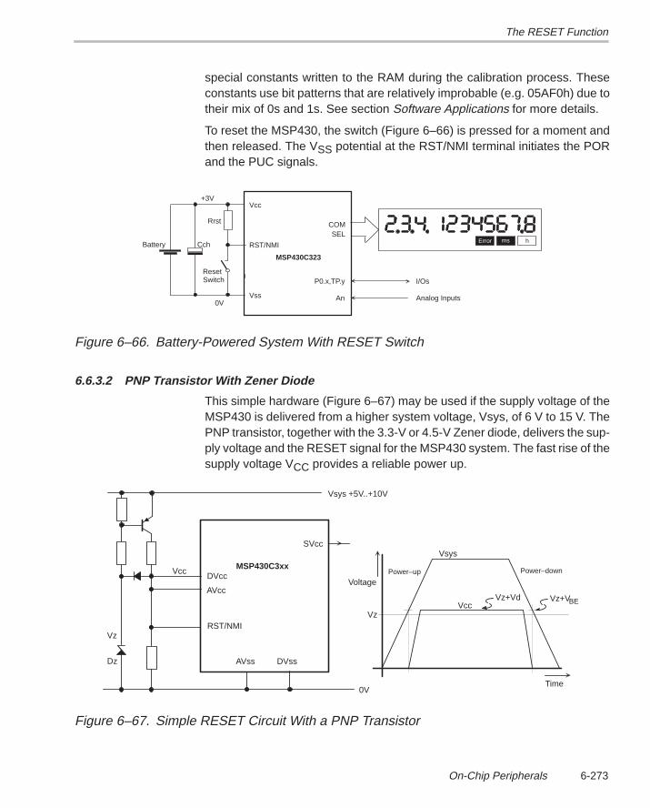
The RESET Function
6-273On-Chip Peripherals
special constants written to the RAM during the calibration process. Theseconstants use bit patterns that are relatively improbable (e.g. 05AF0h) due totheir mix of 0s and 1s. See section Software Applications for more details.
To reset the MSP430, the switch (Figure 6–66) is pressed for a moment andthen released. The VSS potential at the RST/NMI terminal initiates the PORand the PUC signals.
Vss
Vcc
MSP430C323
RST/NMI
Rrst
COMSEL
Error ms h
P0.x,TP.y I/Os
+3V
0V
Cch
An Analog Inputs
ResetSwitch
Battery
Figure 6–66. Battery-Powered System With RESET Switch
6.6.3.2 PNP Transistor With Zener Diode
This simple hardware (Figure 6–67) may be used if the supply voltage of theMSP430 is delivered from a higher system voltage, Vsys, of 6 V to 15 V. ThePNP transistor, together with the 3.3-V or 4.5-V Zener diode, delivers the sup-ply voltage and the RESET signal for the MSP430 system. The fast rise of thesupply voltage VCC provides a reliable power up.
AVss
SVcc
MSP430C3xx
DVss
AVcc
DVcc
Vsys +5V..+10V
0V
RST/NMIVz
Vsys
Vcc
Time
Voltage
Vz
Dz
Vcc Power–up Power–down
Vz+Vd Vz+VBE
Figure 6–67. Simple RESET Circuit With a PNP Transistor
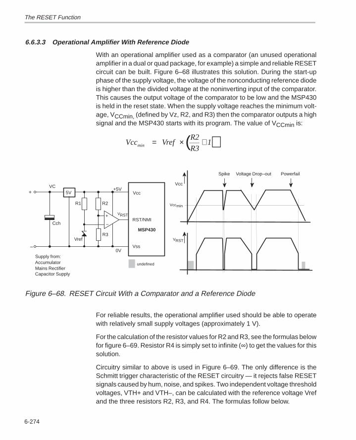
The RESET Function
6-274
6.6.3.3 Operational Amplifier With Reference Diode
With an operational amplifier used as a comparator (an unused operationalamplifier in a dual or quad package, for example) a simple and reliable RESETcircuit can be built. Figure 6–68 illustrates this solution. During the start-upphase of the supply voltage, the voltage of the nonconducting reference diodeis higher than the divided voltage at the noninverting input of the comparator.This causes the output voltage of the comparator to be low and the MSP430is held in the reset state. When the supply voltage reaches the minimum volt-age, VCCmin, (defined by Vz, R2, and R3) then the comparator outputs a highsignal and the MSP430 starts with its program. The value of VCCmin is:
Vcc VrefR2
R31min = × +( )
5V
Cch
Vss
Vcc
RST/NMI
MSP430
R2
+
–
R3
R1
+5VVC
Vref
+
–
Supply from:AccumulatorMains RectifierCapacitor Supply
0V
Vcc
Powerfail
Vcc
min
Voltage Drop–out
VRST
VRST
Spike
undefined
Figure 6–68. RESET Circuit With a Comparator and a Reference Diode
For reliable results, the operational amplifier used should be able to operatewith relatively small supply voltages (approximately 1 V).
For the calculation of the resistor values for R2 and R3, see the formulas belowfor figure 6–69. Resistor R4 is simply set to infinite (∞) to get the values for thissolution.
Circuitry similar to above is used in Figure 6–69. The only difference is theSchmitt trigger characteristic of the RESET circuitry — it rejects false RESETsignals caused by hum, noise, and spikes. Two independent voltage thresholdvoltages, VTH+ and VTH–, can be calculated with the reference voltage Vrefand the three resistors R2, R3, and R4. The formulas follow below.
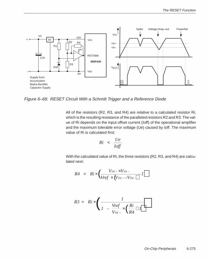
The RESET Function
6-275On-Chip Peripherals
5V
Cch
Vss
Vcc
RST/NMI
MSP430
R2
+
–
R3
R1
+5VVC
Vref
+
–
Supply from:AccumulatorMains RectifierCapacitor Supply
0V
Vcc
Powerfail
Vth+
Voltage Drop–out
VRST
R4
Vth–
Spike
+5V
Figure 6–69. RESET Circuit With a Schmitt Trigger and a Reference Diode
All of the resistors (R2, R3, and R4) are relative to a calculated resistor Ri,which is the resulting resistance of the paralleled resistors R2 and R3. The val-ue of Ri depends on the input offset current (Ioff) of the operational amplifierand the maximum tolerable error voltage (Ue) caused by Ioff. The maximumvalue of Ri is calculated first:
Ri
Ue
Ioff<
With the calculated value of Ri, the three resistors (R2, R3, and R4) are calcu-lated next:
( )R4 RiV V
Vref V V1
TH + TH –
TH + TH –= × ×
× ––( )
R3 Ri1
1 –Vref
V
Ri
R41
TH +
= ×× +( ))(
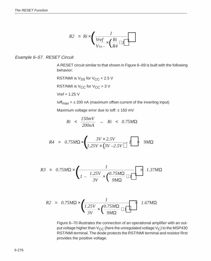
The RESET Function
6-276
R2 Ri1
Vref
V
Ri
R41
TH +
= ×× +( ))(
Example 6–57. RESET Circuit
A RESET circuit similar to that shown in Figure 6–69 is built with the followingbehavior:
RST/NMI is VSS for VCC < 2.5 V
RST/NMI is VCC for VCC > 3 V
Vref = 1.25 V
Ioffmax = ± 200 nA (maximum offset current of the inverting input)
Maximum voltage error due to Ioff: ± 150 mV
Ri
150mV
200nARi 0.75M< → < Ω
( )R4 0.75M3V 2.5V
1.25V 3V –2.5V1 9M= ×
××
– =Ω Ω( )
R3 0.75M1
1 –1.25V
3V
0.75M
9M1
1.37M= ×× +
=ΩΩ
Ω
Ω
( )( )
R2 0.75M1
1.25V
3V
0.75M
9M1
1.67M= ×× +
=ΩΩ
Ω
Ω( ))(Figure 6–70 illustrates the connection of an operational amplifier with an out-put voltage higher than VCC (here the unregulated voltage VC) to the MSP430RST/NMI terminal. The diode protects the RST/NMI terminal and resistor Rrstprovides the positive voltage.
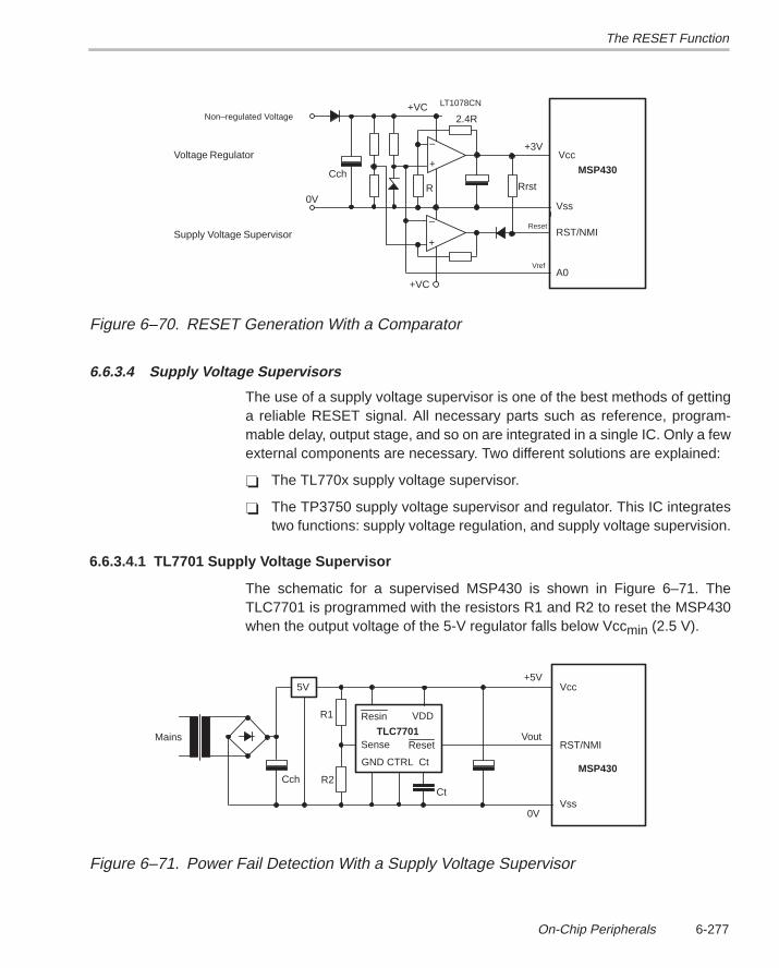
The RESET Function
6-277On-Chip Peripherals
Vss
Vcc
RST/NMI
MSP430
0V
Cch+
–
–
+VC
+3V
R
2.4R
Vref
Reset
A0
+
LT1078CN
+VC
Rrst
Voltage Regulator
Supply Voltage Supervisor
Non–regulated Voltage
Figure 6–70. RESET Generation With a Comparator
6.6.3.4 Supply Voltage Supervisors
The use of a supply voltage supervisor is one of the best methods of gettinga reliable RESET signal. All necessary parts such as reference, program-mable delay, output stage, and so on are integrated in a single IC. Only a fewexternal components are necessary. Two different solutions are explained:
The TL770x supply voltage supervisor.
The TP3750 supply voltage supervisor and regulator. This IC integratestwo functions: supply voltage regulation, and supply voltage supervision.
6.6.3.4.1 TL7701 Supply Voltage Supervisor
The schematic for a supervised MSP430 is shown in Figure 6–71. TheTLC7701 is programmed with the resistors R1 and R2 to reset the MSP430when the output voltage of the 5-V regulator falls below Vccmin (2.5 V).
Cch
Mains
Vss
Vcc
RST/NMI
MSP430
+5V5V
TLC7701 Vout
VDDResin
GND CTRL
Reset
Ct
Sense
R1
R2Ct
0V
Figure 6–71. Power Fail Detection With a Supply Voltage Supervisor
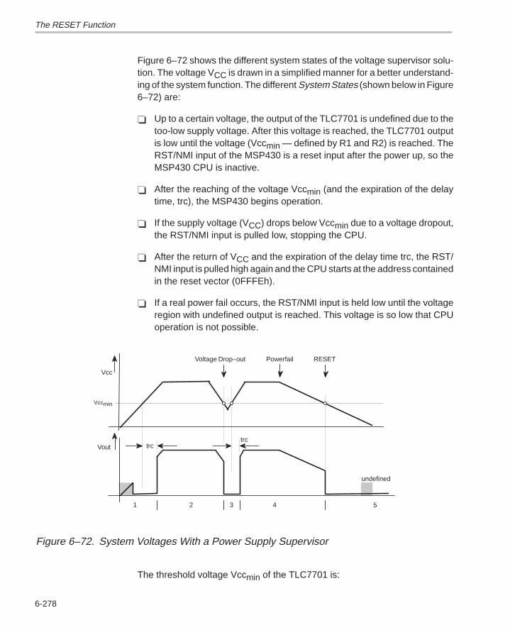
The RESET Function
6-278
Figure 6–72 shows the different system states of the voltage supervisor solu-tion. The voltage VCC is drawn in a simplified manner for a better understand-ing of the system function. The different System States (shown below in Figure6–72) are:
Up to a certain voltage, the output of the TLC7701 is undefined due to thetoo-low supply voltage. After this voltage is reached, the TLC7701 outputis low until the voltage (Vccmin — defined by R1 and R2) is reached. TheRST/NMI input of the MSP430 is a reset input after the power up, so theMSP430 CPU is inactive.
After the reaching of the voltage Vccmin (and the expiration of the delaytime, trc), the MSP430 begins operation.
If the supply voltage (VCC) drops below Vccmin due to a voltage dropout,the RST/NMI input is pulled low, stopping the CPU.
After the return of VCC and the expiration of the delay time trc, the RST/NMI input is pulled high again and the CPU starts at the address containedin the reset vector (0FFFEh).
If a real power fail occurs, the RST/NMI input is held low until the voltageregion with undefined output is reached. This voltage is so low that CPUoperation is not possible.
Vout
Vcc
Powerfail
Vcc
trctrc
min
54321
undefined
Voltage Drop–out RESET
Figure 6–72. System Voltages With a Power Supply Supervisor
The threshold voltage Vccmin of the TLC7701 is:
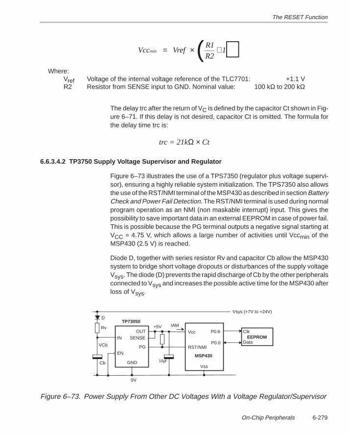
The RESET Function
6-279On-Chip Peripherals
Vcc VrefR1
R21min = × +( )
Where: Vref Voltage of the internal voltage reference of the TLC7701: +1.1 VR2 Resistor from SENSE input to GND. Nominal value: 100 kΩ to 200 kΩ
The delay trc after the return of VC is defined by the capacitor Ct shown in Fig-ure 6–71. If this delay is not desired, capacitor Ct is omitted. The formula forthe delay time trc is:
trc = 21kΩ × Ct
6.6.3.4.2 TP3750 Supply Voltage Supervisor and Regulator
Figure 6–73 illustrates the use of a TPS7350 (regulator plus voltage supervi-sor), ensuring a highly reliable system initialization. The TPS7350 also allowsthe use of the RST/NMI terminal of the MSP430 as described in section BatteryCheck and Power Fail Detection. The RST/NMI terminal is used during normalprogram operation as an NMI (non maskable interrupt) input. This gives thepossibility to save important data in an external EEPROM in case of power fail.This is possible because the PG terminal outputs a negative signal starting atVCC = 4.75 V, which allows a large number of activities until Vccmin of theMSP430 (2.5 V) is reached.
Diode D, together with series resistor Rv and capacitor Cb allow the MSP430system to bridge short voltage dropouts or disturbances of the supply voltageVsys. The diode (D) prevents the rapid discharge of Cb by the other peripheralsconnected to Vsys and increases the possible active time for the MSP430 afterloss of Vsys.
CbVss
Vcc
MSP430
+5V
VCb
IN
IAM
ENPG RST/NMI
SENSEOUT
GND
TP73050Rv
10µF
D
0V
P0.6
P0.0
Clk
DataEEPROM
Vsys (+7V to +24V)
Figure 6–73. Power Supply From Other DC Voltages With a Voltage Regulator/Supervisor

The RESET Function
6-280
6.6.4 Conclusion
It is an old truth that many difficulties are caused by the implementation of theRESET sections of projects. The hardware of the MSP430 family is designedto minimize these difficulties as much as possible without special consider-ations or external components. But when special circumstances exceed thebuiltin capabilities of the MSP430, the solutions shown in this section may helpto significantly simplify the development phase of a project.
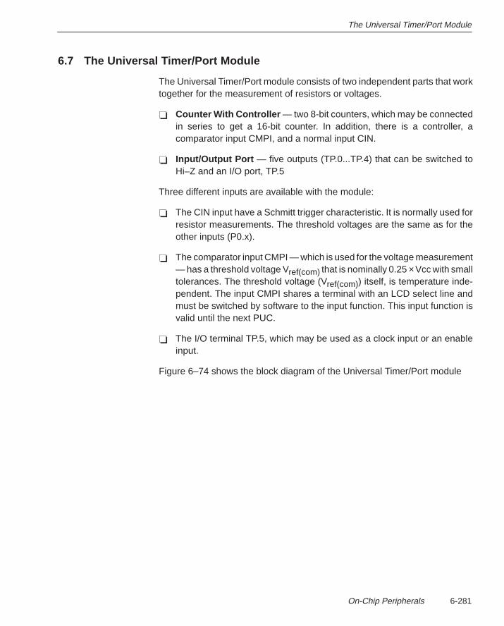
The Universal Timer/Port Module
6-281On-Chip Peripherals
6.7 The Universal Timer/Port Module
The Universal Timer/Port module consists of two independent parts that worktogether for the measurement of resistors or voltages.
Counter With Controller — two 8-bit counters, which may be connectedin series to get a 16-bit counter. In addition, there is a controller, acomparator input CMPI, and a normal input CIN.
Input/Output Port — five outputs (TP.0...TP.4) that can be switched toHi–Z and an I/O port, TP.5
Three different inputs are available with the module:
The CIN input have a Schmitt trigger characteristic. It is normally used forresistor measurements. The threshold voltages are the same as for theother inputs (P0.x).
The comparator input CMPI — which is used for the voltage measurement— has a threshold voltage Vref(com) that is nominally 0.25 ×Vcc with smalltolerances. The threshold voltage (Vref(com)) itself, is temperature inde-pendent. The input CMPI shares a terminal with an LCD select line andmust be switched by software to the input function. This input function isvalid until the next PUC.
The I/O terminal TP.5, which may be used as a clock input or an enableinput.
Figure 6–74 shows the block diagram of the Universal Timer/Port module
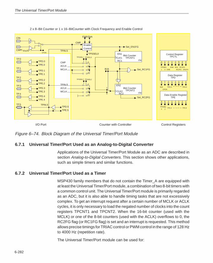
The Universal Timer/Port Module
6-282
TPIN.5
Enable
ControlSet_EN1FG
EN1
RC1
TPSSEL0
Set_RC1FGB16
TPIN.5
MCLK
ACLKEN2
CLK2
CLK18bit Counter
TPCNT1
RC2
8bit CounterTPCNT2
r/w
CIN ENB ENA
TPD.0
TPE.0
TPD.1
TPE.1
TPD.2
TPE.2
TPD.3
TPE.3
TPD.4
TPE.4
TPD.5
TPE.5
Data RegisterTPD
Data Enable RegisterTPE
Control RegisterTPCTL
r/w
Set_RC2FG
TPSSEL3 TPSSEL2
TPD.0TPD.5
TPE.0TPE.5
EN1
ENB
TPSSEL
B16
ENA
0
3 2
1 EN1FGRC2FG
RC1FG
TP.0
TP.1
TP.5
TP.3
TP.4
TP.2
TPIN.5
TPSSEL
0
1
2
3
CMP
MCLK
ACLK
TPSSEL1 TPSSEL0
0
1
2
3
CMP
CPON
Vcc/4CPON
0
1
+–
I/O Port
2 x 8–Bit Counter or 1 x 16–BitCounter with Clock Frequency and Enable Control
Control Registers
Counter with Controller
CMPI
Figure 6–74. Block Diagram of the Universal Timer/Port Module
6.7.1 Universal Timer/Port Used as an Analog-to-Digital Converter
Applications of the Universal Timer/Port Module as an ADC are described insection Analog-to-Digital Converters. This section shows other applications,such as simple timers and similar functions.
6.7.2 Universal Timer/Port Used as a Timer
MSP430 family members that do not contain the Timer_A are equipped withat least the Universal Timer/Port module, a combination of two 8-bit timers witha common control unit. The Universal Timer/Port module is primarily regardedas an ADC, but it is also able to handle timing tasks that are not excessivelycomplex. To get an interrupt request after a certain number of MCLK or ACLKcycles, it is only necessary to load the negated number of clocks into the countregisters TPCNT1 and TPCNT2. When the 16-bit counter (used with theMCLK) or one of the 8-bit counters (used with the ACLK) overflows to 0, theRC2FG flag (or RC1FG flag) is set and an interrupt is requested. This methodallows precise timings for TRIAC control or PWM control in the range of 128 Hzto 4000 Hz (repetition rate).
The Universal Timer/Port module can be used for:
The Universal Timer/Port Module
6-283On-Chip Peripherals
Low frequency pulse width modulation: up to two independent PWM–out-puts.
Measurement of the MCLK frequency e.g. if used without crystal (see sec-tion Use Without Crystal)
Triggering: time measurement starting with the zero crossing of the mainsvoltage
Other time measurements
8–bit Counter TPCNT1Clk
70
LSB Data
Event Count
ACLK
MCLK
MCLK
CMP
MCLKACLK
TPSSEL1 TPSSEL0
0
1
2
3MCLK RC1
0 0
0 1
1 0
1 1
8–bit Counter TPCNT2Clk
158
MSB Data
RC2EN1 EN2
Vcc Set RC2FG–Flag
Carry:
Figure 6–75. Block Diagram of the Universal Timer/Port Module (16-Bit Timer Mode)
6.7.2.1 Continuous Mode
The Universal Timer/Port module can be used like the Timer_A in continuousmode, allowing it to measure time differences. The 16-bit value is read out andcorrected if an overflow to 0 occurred between the readings of the low and highbytes. The input frequency may be the ACLK or the MCLK.
; Read–out of the UTP/M running as a 16–bit timer
;
MOV.B &TPCNT1,R5 ; Read LSBs 00xx
MOV.B &TPCNT2,R6 ; Read MSBs 00yy
CMP.B R5,&TPCNT1 ; TPCNT1 still >= R5?
JHS L$1 ; Yes, no overflow
;
; Transition from 0FFh to 0 occured, read actual MSB;
; it now has the correct (value + 1).
;
MOV.B &TPCNT2,R6 ; Read actual MSBs 00yy
DEC.B R6 ; MSB – 1 is correct
L$1 SWPB R6 ; MSBs to high byte yy00
ADD R5,R6 ; Build 16–bit value in R6 yyxx
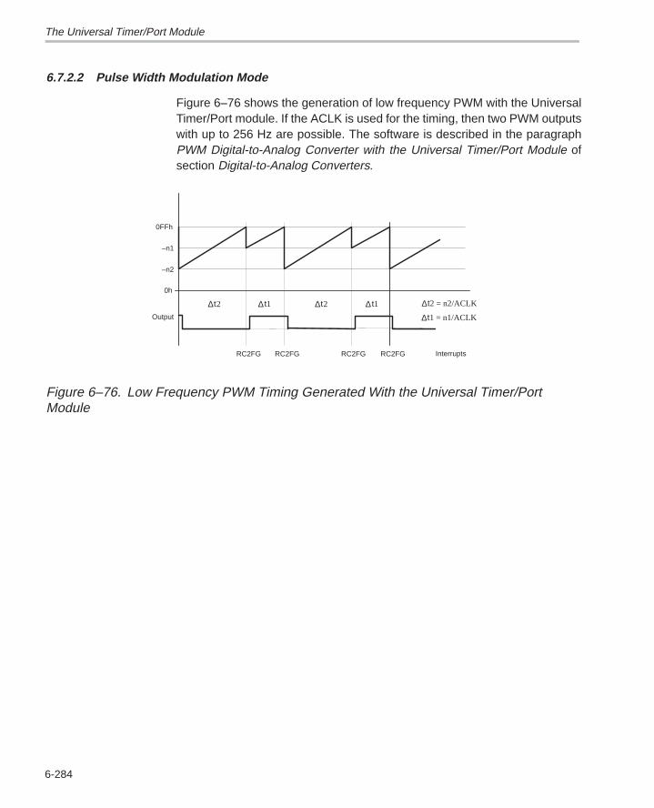
The Universal Timer/Port Module
6-284
6.7.2.2 Pulse Width Modulation Mode
Figure 6–76 shows the generation of low frequency PWM with the UniversalTimer/Port module. If the ACLK is used for the timing, then two PWM outputswith up to 256 Hz are possible. The software is described in the paragraphPWM Digital-to-Analog Converter with the Universal Timer/Port Module ofsection Digital-to-Analog Converters.
0FFh
0h
–n1
–n2
Output
RC2FG RC2FG RC2FG RC2FG
1∆ t 2∆t
Interrupts
2 = n2/ACLK∆t
1 = n1/ACLK∆t
1∆ t2∆t
Figure 6–76. Low Frequency PWM Timing Generated With the Universal Timer/PortModule
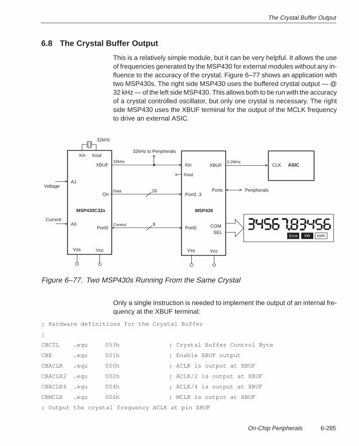
The Crystal Buffer Output
6-285On-Chip Peripherals
6.8 The Crystal Buffer Output
This is a relatively simple module, but it can be very helpful. It allows the useof frequencies generated by the MSP430 for external modules without any in-fluence to the accuracy of the crystal. Figure 6–77 shows an application withtwo MSP430s. The right side MSP430 uses the buffered crystal output — @32 kHz — of the left side MSP430. This allows both to be run with the accuracyof a crystal controlled oscillator, but only one crystal is necessary. The rightside MSP430 uses the XBUF terminal for the output of the MCLK frequencyto drive an external ASIC.
Vss Vcc
Xin
Port2..3
COMSEL
Ports
MSP430
PeripheralsData
Vss Vcc
32kHz
On
MSP430C32x
A1
A0
Voltage
Current
Error kW kWh
Xin Xout
XBUF32kHz
16
Port0Control
Port08
XBUF3.2MHz
CLK ASIC
Xout
32kHz to Peripherals
Figure 6–77. Two MSP430s Running From the Same Crystal
Only a single instruction is needed to implement the output of an internal fre-quency at the XBUF terminal:
; Hardware definitions for the Crystal Buffer
;
CBCTL .equ 053h ; Crystal Buffer Control Byte
CBE .equ 001h ; Enable XBUF output
CBACLK .equ 000h ; ACLK is output at XBUF
CBACLK2 .equ 002h ; ACLK/2 is output at XBUF
CBACLK4 .equ 004h ; ACLK/4 is output at XBUF
CBMCLK .equ 006h ; MCLK is output at XBUF
; Output the crystal frequency ACLK at pin XBUF
The Crystal Buffer Output
6-286
;
MOV.B #CBACLK+CBE,&CBCTL ; ACLK to XBUF pin
;
; Output the half crystal frequency ACLK/2 at pin XBUF
;
MOV.B #CBACLK2+CBE,&CBCTL ; ACLK/2 to XBUF pin
;
; Output the crystal frequency ACLK divided by four at pin XBUF
;
MOV.B #CBACLK4+CBE,&CBCTL ; ACLK/4 to XBUF pin
;
; Output the MCLK frequency at pin XBUF
;
MOV.B #CBMCLK+CBE,&CBCTL ; MCLK to XBUF pin
As shown with the previous definitions, four different frequencies can be outputat terminal XBUF. With the CBE bit, these four frequencies can be enabled ordisabled. The four possible frequencies are:
MCLK The frequency of the system clock generator (DCO): 500 kHzto 4MHz
ACLK The frequency of the crystal (normally 32768 Hz)
ACLK/2 The halved crystal frequency (normally 16384 Hz)
ACLK/4 The crystal frequency divided by 4 (normally 8192 Hz)
The crystal buffer control byte CBCTL is a write-only byte. This means the fullinformation must always be written to it. The following code sequence providesan output of ACLK and not — as it is intended — to output the MCLK frequency:
; Switch off and on the MCLK at pin XBUF
;
MOV.B #CBMCLK+CBE,&CBCTL ; MCLK to XBUF pin
BIC.B #CBE,&CBCTL ; MCLK off
BIS.B #CBE,&CBCTL ; WRONG: ACLK is output NOT MCLK
;
MOV.B #CBMCLK+CBE,&CBCTL ; CORRECT: MCLK on again
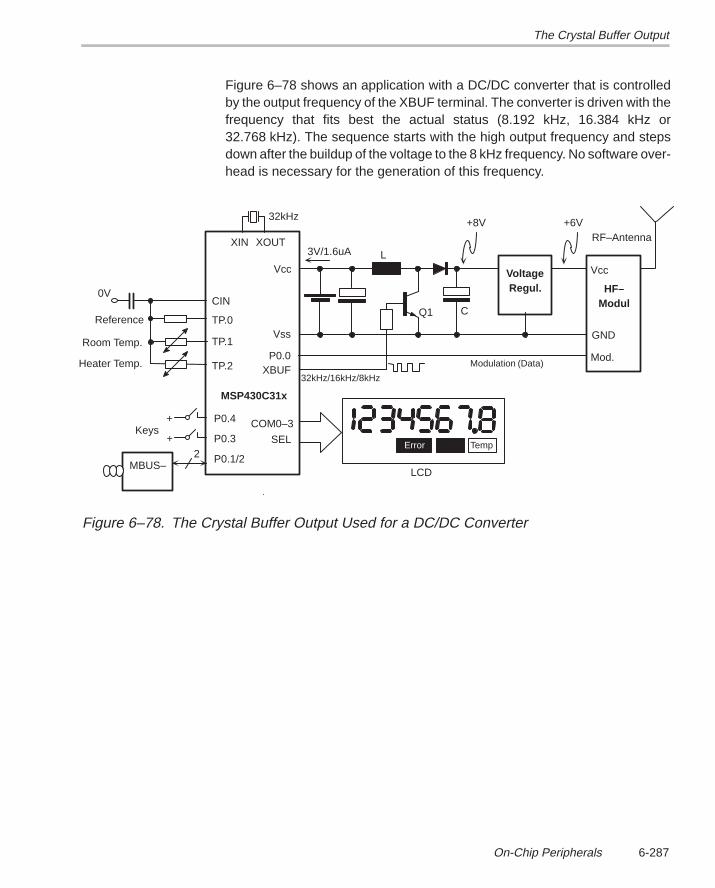
The Crystal Buffer Output
6-287On-Chip Peripherals
Figure 6–78 shows an application with a DC/DC converter that is controlledby the output frequency of the XBUF terminal. The converter is driven with thefrequency that fits best the actual status (8.192 kHz, 16.384 kHz or32.768 kHz). The sequence starts with the high output frequency and stepsdown after the buildup of the voltage to the 8 kHz frequency. No software over-head is necessary for the generation of this frequency.
CIN
TP.0
TP.1
TP.2
COM0–3
SEL
LCD
32kHz
+
+
P0.1/22MBUS–
P0.4
P0.3
3V/1.6uA
Heater Temp.
Reference
MSP430C31x
Room Temp.
Keys
0V
Error Temp
RF–Antenna
XBUFModulation (Data)
L
C
HF–Modul
Mod.
VoltageRegul.
+6V+8V
GND
Vcc
Vcc
Vss
P0.0
Q1
XIN XOUT
32kHz/16kHz/8kHz
Figure 6–78. The Crystal Buffer Output Used for a DC/DC Converter

The USART Module
6-288
6.9 The USART Module
The universal synchronous asynchronous receive/transmit communication in-terface (USART) — whose block diagram is shown in figure 6–79 — can workin two different modes: the asynchronous mode and the synchronous mode.This section describes the software routines usable for the asynchronousmode (SCI, RS232).
Note:
It is recommended to also consult the data book MSP430 Family Architec-ture Guide and Module Library. The hardware-related information giventhere is very valuable and complements the information given in this section.
The examples and the hardware definitions shown use the addresses of theMSP430x33x. Future MSP430 family members may have different hard-ware addresses — especially for the I/O ports used.
The hardware features of the USART module substantially exceed the exam-ples shown in this section. To get the USART running quickly, the UART modeis recommended, with or without the interrupt capability. The most often usedfeatures are included in the examples given.
Figure 6–79 shows the block diagram of the MSP430 USART module.
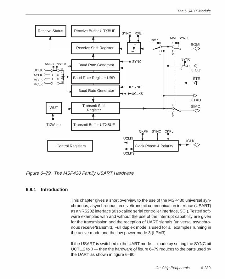
The USART Module
6-289On-Chip Peripherals
Receive Buffer URXBUF
Receive Shift Register
Baud Rate Generator
Transmit ShiftRegister
Transmit Buffer UTXBUF
Receive Status
WUT
TXWake
RXE
CKPL
UCLKI
MCLK
ACLK
SSEL1 SSEL0
0
12
3MCLK
Baud Rate Generator
Baud Rate Register UBR
SYNC
Listen0 1 SOMI
1 0
1 SIMO
0
MM
UCLKClock Phase & Polarity
CKPH
UCLKI
UCLKS
SYNC
UCLKS
SYNC
SYNC
URXD
UTXD
SYNC
0
SYNC
STE
Control Registers
Figure 6–79. The MSP430 Family USART Hardware
6.9.1 Introduction
This chapter gives a short overview to the use of the MSP430 universal syn-chronous, asynchronous receive/transmit communication interface (USART)as an RS232 interface (also called serial controller interface, SCI). Tested soft-ware examples with and without the use of the interrupt capability are givenfor the transmission and the reception of UART signals (universal asynchro-nous receive/transmit). Full duplex mode is used for all examples running inthe active mode and the low power mode 3 (LPM3).
If the USART is switched to the UART mode — made by setting the SYNC bitUCTL.2 to 0 — then the hardware of figure 6–79 reduces to the parts used bythe UART as shown in figure 6–80.
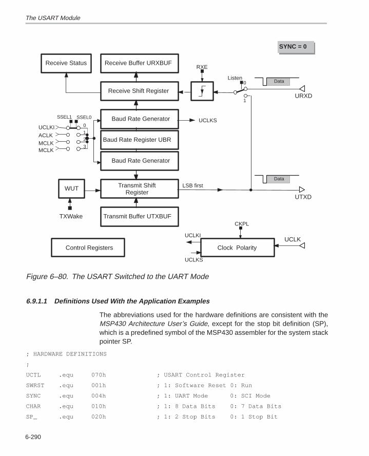
The USART Module
6-290
Receive Buffer URXBUF
Receive Shift Register
Baud Rate Generator
Transmit ShiftRegister
Transmit Buffer UTXBUF
Receive Status
WUT
TXWake
RXE
CKPL
UCLKI
MCLKACLK
SSEL1 SSEL0
0
12
3MCLK
Baud Rate Generator
Baud Rate Register UBR
Listen0
1
UCLKClock Polarity
UCLKI
UCLKS
UCLKS
URXD
UTXD
LSB first
SYNC = 0
Control Registers
Data
Data
Figure 6–80. The USART Switched to the UART Mode
6.9.1.1 Definitions Used With the Application Examples
The abbreviations used for the hardware definitions are consistent with theMSP430 Architecture User’s Guide, except for the stop bit definition (SP),which is a predefined symbol of the MSP430 assembler for the system stackpointer SP.
; HARDWARE DEFINITIONS
;
UCTL .equ 070h ; USART Control Register
SWRST .equ 001h ; 1: Software Reset 0: Run
SYNC .equ 004h ; 1: UART Mode 0: SCI Mode
CHAR .equ 010h ; 1: 8 Data Bits 0: 7 Data Bits
SP_ .equ 020h ; 1: 2 Stop Bits 0: 1 Stop Bit
The USART Module
6-291On-Chip Peripherals
PEV .equ 040h ; 1: Even Parity 0: Odd Parity
PENA .equ 080h ; 1: Parity enabled 0: Parity dis.
;
UTCTL .equ 071h ; Transmit Control Register
TXEPT .equ 001h ; 1: Transmitter empty
URXSE .equ 008h ;
SSEL0 .equ 010h ; Clock Selection 0: Ext. Clock
SSEL1 .equ 020h ; 1: ACLK 2,3: MCLK
;
URCTL .equ 072h ; Receive Control Register
RXERR .equ 001h ; 1: Receive Error 0: No Error
URXEIE .equ 008h ; 1: all Char. 0: only w/o Error
BRK .equ 010h ; 1: Break detected 0: ok
OE .equ 020h ; 1: Overrun Error 0: ok
PE .equ 040h ; 1: Parity Error 0: ok
FE .equ 080h ; 1: Frame Error 0: ok
;
UMCTL .equ 073h ; Modulation Control Reg. m7..m0
UBR0 .equ 074h ; Baud Rate Register 0
UBR1 .equ 075h ; Baud Rate Register 1
URXBUF .equ 076h ; Receive Buffer
UTXBUF .equ 077h ; Transmit Buffer
;
IFG2 .equ 003h ; SFRs: Flags
URXIFG .equ 001h ; Receive Flag IFG2.0
UTXIFG .equ 002h ; Transmit Flag IFG2.1
;
IE2 .equ 001h ; SFRs: Interrupt Enable Bits
URXIE .equ 001h ; Receive Intrpt Enable Bit IE2.0
UTXIE .equ 002h ; Transmit Intrpt Enable Bit IE2.1
;
ME2 .equ 005h ; SFRs: Mode Enable Bits
URXE .equ 001h ; Receiver Module Enable Bit ME2.0
UTXE .equ 002h ; Transmitter Mod. Enable Bit ME2.1
;
P4SEL .equ 01Fh ; Port4 Sel. Reg. (I/O <–> USART)
The USART Module
6-292
URXD .equ 080h ; Receive Input P4.7
UTXD .equ 040h ; Transmit Output P4.6
;
SCG1 .equ 080h ; Low Power Mode bit 1
SCG0 .equ 040h ; Low Power Mode bit 0
CPUoff .equ 010h ; Switches CPU off
GIE .equ 008h ; General Interrupt Enable Bit
;
SCFQCTL .equ 052h ; FLL multiplier and M bit
SCFI0 .equ 050h ; FLL current switches
FN_2 .equ 004h ; Switch for 2 MHz
FN_3 .equ 008h ; Switch for 3 MHz
FN_4 .equ 010h ; Switch for 4 MHz
6.9.1.2 MSP430 UART Attributes
A short overview to the USART running in the UART mode is given below:
7-bit and 8-bit data length is selectable
Error detection for the receive path:
Frame error. The stop bits have space potential.
Parity error. Parity is enabled and the parity bit has the wrong value.
Overrun error. The next character is read in before the last one is readout by the software.
Break detect. The URXD terminal has low potential for more than 10bits
Baud rate generation possible also from 32 kHz crystal due to the modula-tion register
Interrupt-driven transmit and receive functions
Two independent interrupt vectors, one for transmit and one for receive
Full functionality also during LPM3
End-of-frame flag usable with interrupt or polling
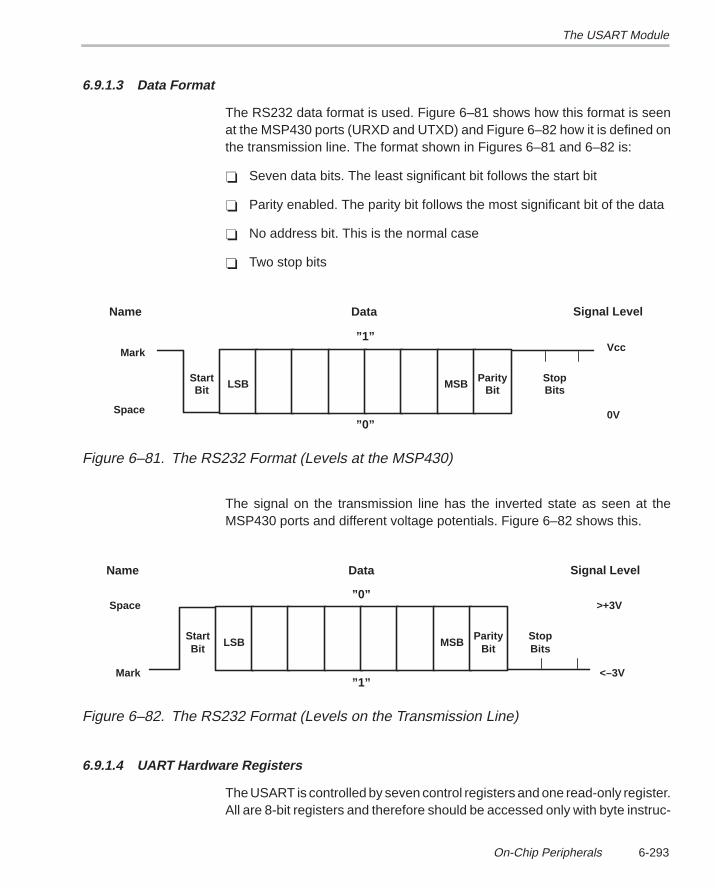
The USART Module
6-293On-Chip Peripherals
6.9.1.3 Data Format
The RS232 data format is used. Figure 6–81 shows how this format is seenat the MSP430 ports (URXD and UTXD) and Figure 6–82 how it is defined onthe transmission line. The format shown in Figures 6–81 and 6–82 is:
Seven data bits. The least significant bit follows the start bit
Parity enabled. The parity bit follows the most significant bit of the data
No address bit. This is the normal case
Two stop bits
Space
Mark Vcc
0V
StartBit LSB MSB Parity
BitStopBits
”1”
”0”
DataName Signal Level
Figure 6–81. The RS232 Format (Levels at the MSP430)
The signal on the transmission line has the inverted state as seen at theMSP430 ports and different voltage potentials. Figure 6–82 shows this.
Mark
Space
<–3V
>+3V
StartBit
LSB MSBParity
BitStopBits
”0”
”1”
DataName Signal Level
Figure 6–82. The RS232 Format (Levels on the Transmission Line)
6.9.1.4 UART Hardware Registers
The USART is controlled by seven control registers and one read-only register.All are 8-bit registers and therefore should be accessed only with byte instruc-
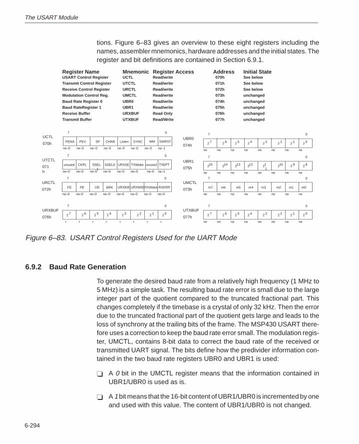
The USART Module
6-294
tions. Figure 6–83 gives an overview to these eight registers including thenames, assembler mnemonics, hardware addresses and the initial states. Theregister and bit definitions are contained in Section 6.9.1.
Register Name Mnemonic Register Access Address Initial StateUSART Control Register UCTL Read/write 070h See below
Transmit Control Register UTCTL Read/write 071h See below
Receive Control Register URCTL Read/write 072h See below
Modulation Control Reg. UMCTL Read/write 073h unchanged
Baud Rate Register 0 UBR0 Read/write 074h unchanged
Baud RateRegister 1 UBR1 Read/write 075h unchanged
Receive Buffer URXBUF Read Only 076h unchanged
Transmit Buffer UTXBUF Read/Write 077h unchanged
UCTL
rw–0 rw–0 rw–0 rw–0 rw–0 rw–0 rw–0 rw–1070h
7 0
SWRSTMMSYNCListenCHARSPPEVPENA
UTCTL
rw–0 rw–0 rw–0 rw–0 rw–0 rw–0 rw–0 rw–1071h
7 0
TXEPTTXWakeURXSESSEL1
CKPL SSEL0 unusedunused
URCTL
rw–0 rw–0 rw–0 rw–0 rw–0 rw–0 rw–0 rw–0072h
7 0
RXERRRXWakeOEPEFE BRK URXEIE URXWIE
UBR0
rw rw rw rw rw rw rw rw074h
7 0
2
UBR1
rw rw rw rw rw rw rw rw075h
7 0
7 2 6 2 5 2 4 2 3 2 2 2 1 2 0
215 214 213 212 211
210 2 9 2 8
UMCTL
rw rw rw rw rw rw rw rw073h
7 0
m7 m6 m4 m3 m2 m1 m0m5
URXBUF
r r r r r r r r076h
7 0
2 7 2 6 2 5 2 4 2 3 2 2 2 1 2 0UTXBUF
rw rw rw rw rw rw rw rw077h
7 0
2 7 2 6 2 5 2 4 2 3 2 2 2 1 2 0
Figure 6–83. USART Control Registers Used for the UART Mode
6.9.2 Baud Rate Generation
To generate the desired baud rate from a relatively high frequency (1 MHz to5 MHz) is a simple task. The resulting baud rate error is small due to the largeinteger part of the quotient compared to the truncated fractional part. Thischanges completely if the timebase is a crystal of only 32 kHz. Then the errordue to the truncated fractional part of the quotient gets large and leads to theloss of synchrony at the trailing bits of the frame. The MSP430 USART there-fore uses a correction to keep the baud rate error small. The modulation regis-ter, UMCTL, contains 8-bit data to correct the baud rate of the received ortransmitted UART signal. The bits define how the predivider information con-tained in the two baud rate registers UBR0 and UBR1 is used:
A 0 bit in the UMCTL register means that the information contained inUBR1/UBR0 is used as is.
A 1 bit means that the 16-bit content of UBR1/UBR0 is incremented by oneand used with this value. The content of UBR1/UBR0 is not changed.
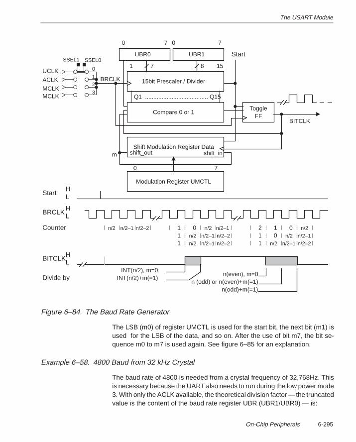
The USART Module
6-295On-Chip Peripherals
1n/2 n/2–1
15bit Prescaler / Divider
151
UBR0 UBR1
0 7 0 7
Q1 ...................................... Q15
Compare 0 or 1
7 8
Shift Modulation Register Data
Modulation Register UMCTL
UCLK
MCLK
ACLK
SSEL1 SSEL0
0
12
3MCLK
BRCLKHL
StartHL
Counter
BRCLK
BITCLK
BITCLKHL
0 7
m
Divide by
0n/2–2
n/2
n/2
n/2–1
12 0n/2
n/2
n/2–11 0n/2 n/2–1 n/2 n/2–1
11
n(even), m=0n (odd) or n(even)+m(=1)
n(odd)+m(=1)
Start
INT(n/2), m=0INT(n/2)+m(=1)
n/2–21
n/2–1
n/2–2
n/2–2
shift_inshift_out
ToggleFF
Figure 6–84. The Baud Rate Generator
The LSB (m0) of register UMCTL is used for the start bit, the next bit (m1) isused for the LSB of the data, and so on. After the use of bit m7, the bit se-quence m0 to m7 is used again. See figure 6–85 for an explanation.
Example 6–58. 4800 Baud from 32 kHz Crystal
The baud rate of 4800 is needed from a crystal frequency of 32,768Hz. Thisis necessary because the UART also needs to run during the low power mode3. With only the ACLK available, the theoretical division factor — the truncatedvalue is the content of the baud rate register UBR (UBR1/UBR0) — is:
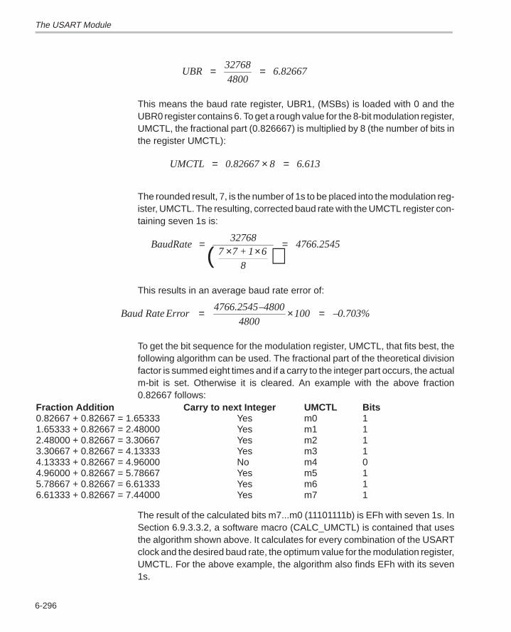
The USART Module
6-296
UBR32768
48006.82667= =
This means the baud rate register, UBR1, (MSBs) is loaded with 0 and theUBR0 register contains 6. To get a rough value for the 8-bit modulation register,UMCTL, the fractional part (0.826667) is multiplied by 8 (the number of bits inthe register UMCTL):
UMCTL 0.82667 8 6.613= × =
The rounded result, 7, is the number of 1s to be placed into the modulation reg-ister, UMCTL. The resulting, corrected baud rate with the UMCTL register con-taining seven 1s is:
BaudRate32768
7 7 + 1 68
4766.2545=× ×
=( )
This results in an average baud rate error of:
Baud Rate Error4766.2545–4800
4800100 –0.703%= × =
To get the bit sequence for the modulation register, UMCTL, that fits best, thefollowing algorithm can be used. The fractional part of the theoretical divisionfactor is summed eight times and if a carry to the integer part occurs, the actualm-bit is set. Otherwise it is cleared. An example with the above fraction0.82667 follows:
Fraction Addition Carry to next Integer UMCTL Bits0.82667 + 0.82667 = 1.65333 Yes m0 11.65333 + 0.82667 = 2.48000 Yes m1 12.48000 + 0.82667 = 3.30667 Yes m2 13.30667 + 0.82667 = 4.13333 Yes m3 14.13333 + 0.82667 = 4.96000 No m4 04.96000 + 0.82667 = 5.78667 Yes m5 15.78667 + 0.82667 = 6.61333 Yes m6 16.61333 + 0.82667 = 7.44000 Yes m7 1
The result of the calculated bits m7...m0 (11101111b) is EFh with seven 1s. InSection 6.9.3.3.2, a software macro (CALC_UMCTL) is contained that usesthe algorithm shown above. It calculates for every combination of the USARTclock and the desired baud rate, the optimum value for the modulation register,UMCTL. For the above example, the algorithm also finds EFh with its seven1s.
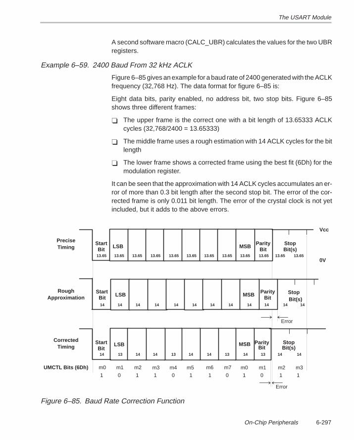
The USART Module
6-297On-Chip Peripherals
A second software macro (CALC_UBR) calculates the values for the two UBRregisters.
Example 6–59. 2400 Baud From 32 kHz ACLK
Figure 6–85 gives an example for a baud rate of 2400 generated with the ACLKfrequency (32,768 Hz). The data format for figure 6–85 is:
Eight data bits, parity enabled, no address bit, two stop bits. Figure 6–85shows three different frames:
The upper frame is the correct one with a bit length of 13.65333 ACLKcycles (32,768/2400 = 13.65333)
The middle frame uses a rough estimation with 14 ACLK cycles for the bitlength
The lower frame shows a corrected frame using the best fit (6Dh) for themodulation register.
It can be seen that the approximation with 14 ACLK cycles accumulates an er-ror of more than 0.3 bit length after the second stop bit. The error of the cor-rected frame is only 0.011 bit length. The error of the crystal clock is not yetincluded, but it adds to the above errors.
LSB
13 14 14 13 14 14
Precise
Vcc
0V
StartBit LSB MSB Parity
BitStopBit(s)
StartBit LSB Stop
Bit(s)MSB
StartBit
ParityBit
StopBit(s)
Bit
MSB
14 14 14 14 14 14 14 14 1414
14 13 14 13 14
14
UMCTL Bits (6Dh) m0 m1 m2 m3 m4 m5 m6 m7 m0 m1 m2
14
Parity
13.6513.65 13.65 13.65 13.65 13.65 13.65 13.65 13.65 13.65 13.65 13.65
MSB
14
m3
Timing
RoughApproximation
CorrectedTiming
Error
Error
01 1 1 0 1 1 0 1 0 1 1
Figure 6–85. Baud Rate Correction Function
The USART Module
6-298
Tables 6–33 and 6–34 contain the average errors (full frame) for the normallyused baud rates when produced with the described baud rate generation.
The software examples contain software MACROs that automatically insertthe correct values for the UBR registers and the modulation register, UMCTL.The software MACROs — that do not need ROM or RAM — may be hiddenin the listing by a .mnolist assembler directive. See Section 6.9.3.3.2.
6.9.2.1 Baud Rate Generation With the MCLK
Table 6–33 shows the optimum values for the UBR and UMCTL registers. TheUART clock is the MCLK (1,048 MHz). The values for the UMCTL andUBR1/UBR0 registers are calculated by the software MACROs in Section6.9.3.3.2. The crystal error is not included.
Table 6–33 contains the following columns:
Baud Rate — The baud rate for the data exchange (transmit and receive usethe same baud rate)
Division Factor — The quotient UARTCLK/baud rate
UBR1/UBR0 Content — The truncated 16-bit hexadecimal result of the divi-sion factor (UARTCLK/baud rate). The value is calculated by the softwaremacro CALC_UBR. The high byte is the UBR1 value, the low byte is the UBR0value
Calculated UMCTL Content — The 8-bit result that fits best for the modula-tion register. It is calculated by the software macro CALC_UMCTL.
Used Fraction — The number of 1s in the Modulation Register divided byeight. It is an approximation to the truncated fractional part of the division fac-tor.
Mean Error — The resulting error of a complete character caused by theapproximation to the division factor
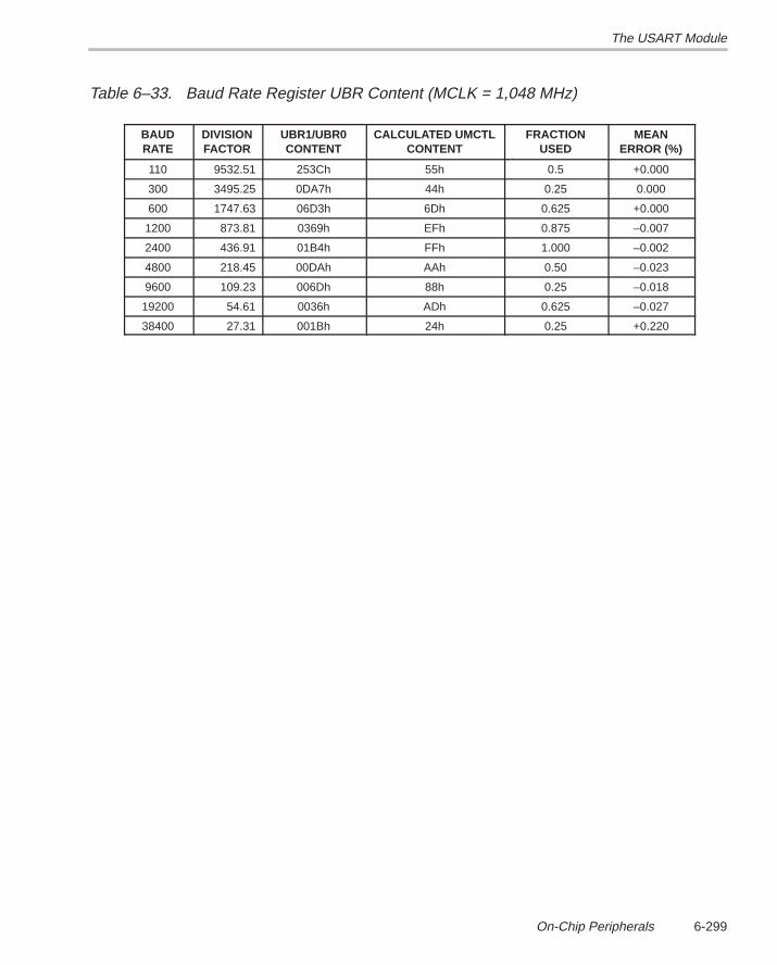
The USART Module
6-299On-Chip Peripherals
Table 6–33. Baud Rate Register UBR Content (MCLK = 1,048 MHz)
BAUDRATE
DIVISIONFACTOR
UBR1/UBR0CONTENT
CALCULATED UMCTLCONTENT
FRACTIONUSED
MEANERROR (%)
110 9532.51 253Ch 55h 0.5 +0.000
300 3495.25 0DA7h 44h 0.25 0.000
600 1747.63 06D3h 6Dh 0.625 +0.000
1200 873.81 0369h EFh 0.875 –0.007
2400 436.91 01B4h FFh 1.000 –0.002
4800 218.45 00DAh AAh 0.50 –0.023
9600 109.23 006Dh 88h 0.25 –0.018
19200 54.61 0036h ADh 0.625 –0.027
38400 27.31 001Bh 24h 0.25 +0.220
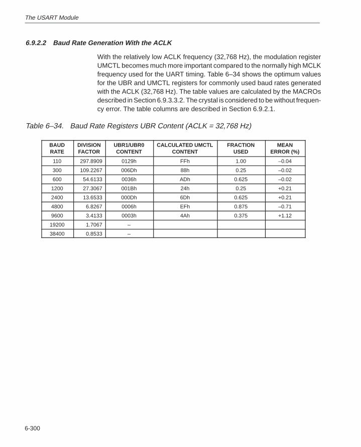
The USART Module
6-300
6.9.2.2 Baud Rate Generation With the ACLK
With the relatively low ACLK frequency (32,768 Hz), the modulation registerUMCTL becomes much more important compared to the normally high MCLKfrequency used for the UART timing. Table 6–34 shows the optimum valuesfor the UBR and UMCTL registers for commonly used baud rates generatedwith the ACLK (32,768 Hz). The table values are calculated by the MACROsdescribed in Section 6.9.3.3.2. The crystal is considered to be without frequen-cy error. The table columns are described in Section 6.9.2.1.
Table 6–34. Baud Rate Registers UBR Content (ACLK = 32,768 Hz)
BAUDRATE
DIVISIONFACTOR
UBR1/UBR0CONTENT
CALCULATED UMCTLCONTENT
FRACTIONUSED
MEANERROR (%)
110 297.8909 0129h FFh 1.00 –0.04
300 109.2267 006Dh 88h 0.25 –0.02
600 54.6133 0036h ADh 0.625 –0.02
1200 27.3067 001Bh 24h 0.25 +0.21
2400 13.6533 000Dh 6Dh 0.625 +0.21
4800 6.8267 0006h EFh 0.875 –0.71
9600 3.4133 0003h 4Ah 0.375 +1.12
19200 1.7067 –
38400 0.8533 –
The USART Module
6-301On-Chip Peripherals
6.9.3 Software Routines
The following sections show proven software routines, subroutines, and soft-ware MACROs for the UART mode of the USART.
Note:
The program sequence for the initialization of the UART is important. As longas the SWRST bit (UCTL.0) is set, the receive and transmit control registersURCTL and UTCTL cannot be initialized. The program sequences given inthe software examples comply with this fact and are therefore recommen-ded.
As long as the SWRST bit is set, the following control bits are held in the 0state: TXWAKE, RXERROR, RXWAKE, BRK, OE, FE, PE, URXIFG, URXIE,UTXIE.
The following control bits are held in the 1 state: UTXIFG, TXEPT
6.9.3.1 NonInterrupt Processing
The simplest way to use the USART is in the UART mode. The interrupt is notenabled, the software checks if it is possible to output the next byte (UTXIFG= 1) and it checks if a new character is received (URXIFG = 1).
Example 6–60. Full Duplex Modem
A full duplex UART software running without the use of the UART interrupt isshown. It is designed for:
Baud rate: 1200 baud
The MCLK (1.048 MHz) is used for the UART clock
Eight data bits
Two stop bits
Parity enabled with odd parity
Receive of errorfree characters only
STACK .equ 0600h ; Stack start address
;
; Definitions for the UART part: user defined
;
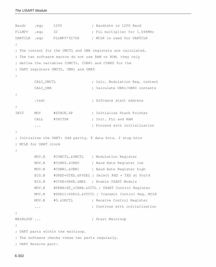
The USART Module
6-302
Baudr .equ 1200 ; Baudrate is 1200 Baud
FLLMPY .equ 32 ; FLL multiplier for 1,048MHz
UARTCLK .equ FLLMPY*32768 ; MCLK is used for UARTCLK
;
; The content for the UMCTL and UBR registers are calculated.
; The two software macros do not use RAM or ROM, they only
; define the variables CUMCTL, CUBR1 and CUBR0 for the
; UART registers UMCTL, UBR1 and UBR0
;
CALC_UMCTL ; Calc. Modulation Reg. content
CALC_UBR ; Calculate UBR1/UBR0 contents
;
.text ; Software start address
;
INIT MOV #STACK,SP ; Initialize Stack Pointer
CALL #INITSR ; Init. FLL and RAM
... ; Proceed with initialization
;
; Initialize the UART: Odd parity, 8 data bits, 2 stop bits
; MCLK for UART clock
;
MOV.B #CUMCTL,&UMCTL ; Modulation Register
MOV.B #CUBR0,&UBR0 ; Baud Rate Register low
MOV.B #CUBR1,&UBR1 ; Baud Rate Register high
BIS.B #URXD+UTXD,&P4SEL ; Select RXD + TXD at Port4
BIS.B #UTXE+URXE,&ME2 ; Enable USART Moduls
MOV.B #PENA+SP_+CHAR,&UCTL ; USART Control Register
MOV.B #SSEL1+SSEL0,&UTCTL ; Transmit Control Reg. MCLK
MOV.B #0,&URCTL ; Receive Control Register
... ; Continue with initialization
;
MAINLOOP ... ; Start Mainloop
;
; UART parts within the mainloop.
; The software checks these two parts regularly.
; UART Receive part:
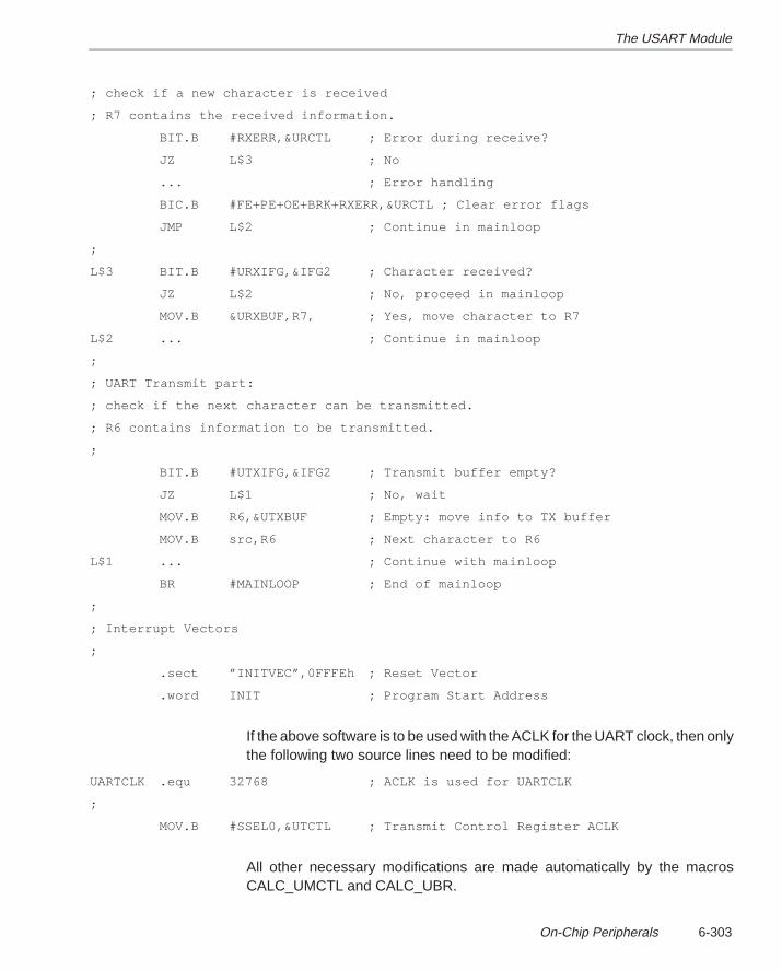
The USART Module
6-303On-Chip Peripherals
; check if a new character is received
; R7 contains the received information.
BIT.B #RXERR,&URCTL ; Error during receive?
JZ L$3 ; No
... ; Error handling
BIC.B #FE+PE+OE+BRK+RXERR,&URCTL ; Clear error flags
JMP L$2 ; Continue in mainloop
;
L$3 BIT.B #URXIFG,&IFG2 ; Character received?
JZ L$2 ; No, proceed in mainloop
MOV.B &URXBUF,R7, ; Yes, move character to R7
L$2 ... ; Continue in mainloop
;
; UART Transmit part:
; check if the next character can be transmitted.
; R6 contains information to be transmitted.
;
BIT.B #UTXIFG,&IFG2 ; Transmit buffer empty?
JZ L$1 ; No, wait
MOV.B R6,&UTXBUF ; Empty: move info to TX buffer
MOV.B src,R6 ; Next character to R6
L$1 ... ; Continue with mainloop
BR #MAINLOOP ; End of mainloop
;
; Interrupt Vectors
;
.sect ”INITVEC”,0FFFEh ; Reset Vector
.word INIT ; Program Start Address
If the above software is to be used with the ACLK for the UART clock, then onlythe following two source lines need to be modified:
UARTCLK .equ 32768 ; ACLK is used for UARTCLK
;
MOV.B #SSEL0,&UTCTL ; Transmit Control Register ACLK
All other necessary modifications are made automatically by the macrosCALC_UMCTL and CALC_UBR.
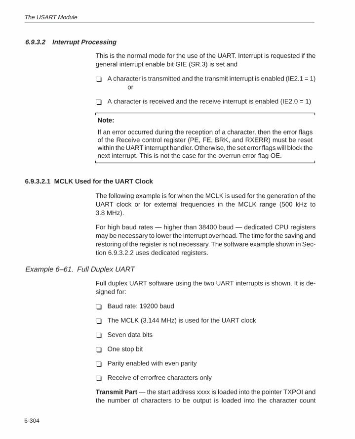
The USART Module
6-304
6.9.3.2 Interrupt Processing
This is the normal mode for the use of the UART. Interrupt is requested if thegeneral interrupt enable bit GIE (SR.3) is set and
A character is transmitted and the transmit interrupt is enabled (IE2.1 = 1) or
A character is received and the receive interrupt is enabled (IE2.0 = 1)
Note:
If an error occurred during the reception of a character, then the error flagsof the Receive control register (PE, FE, BRK, and RXERR) must be resetwithin the UART interrupt handler. Otherwise, the set error flags will block thenext interrupt. This is not the case for the overrun error flag OE.
6.9.3.2.1 MCLK Used for the UART Clock
The following example is for when the MCLK is used for the generation of theUART clock or for external frequencies in the MCLK range (500 kHz to3.8 MHz).
For high baud rates — higher than 38400 baud — dedicated CPU registersmay be necessary to lower the interrupt overhead. The time for the saving andrestoring of the register is not necessary. The software example shown in Sec-tion 6.9.3.2.2 uses dedicated registers.
Example 6–61. Full Duplex UART
Full duplex UART software using the two UART interrupts is shown. It is de-signed for:
Baud rate: 19200 baud
The MCLK (3.144 MHz) is used for the UART clock
Seven data bits
One stop bit
Parity enabled with even parity
Receive of errorfree characters only
Transmit Part — the start address xxxx is loaded into the pointer TXPOI andthe number of characters to be output is loaded into the character count
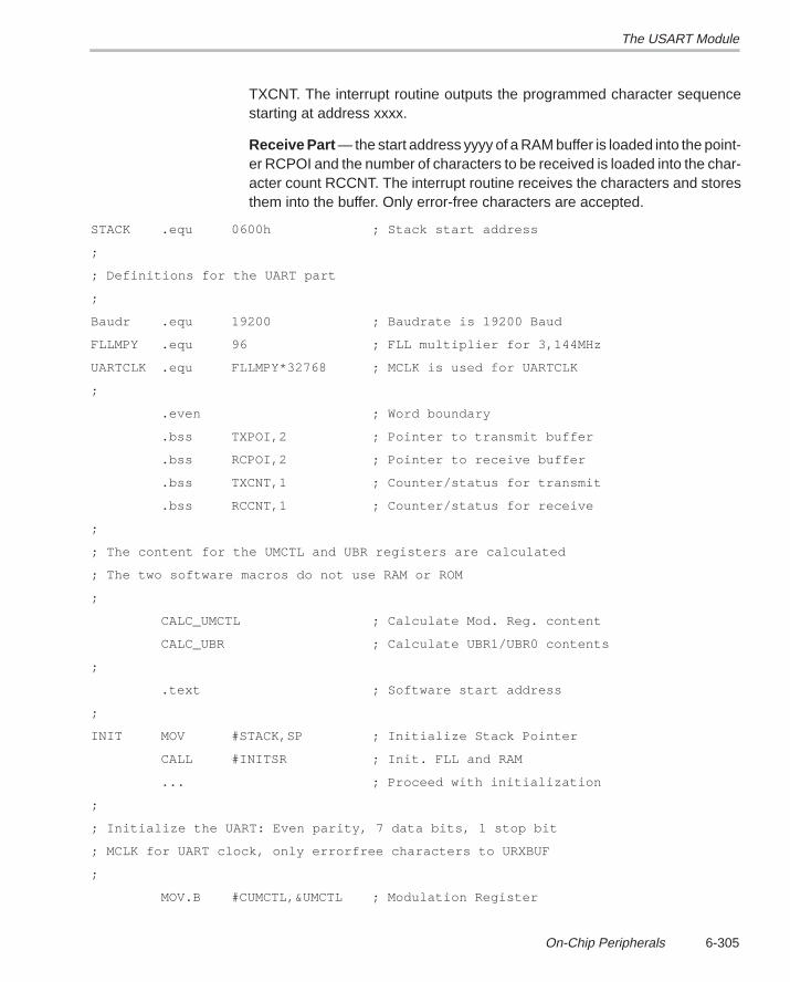
The USART Module
6-305On-Chip Peripherals
TXCNT. The interrupt routine outputs the programmed character sequencestarting at address xxxx.
Receive Part — the start address yyyy of a RAM buffer is loaded into the point-er RCPOI and the number of characters to be received is loaded into the char-acter count RCCNT. The interrupt routine receives the characters and storesthem into the buffer. Only error-free characters are accepted.
STACK .equ 0600h ; Stack start address
;
; Definitions for the UART part
;
Baudr .equ 19200 ; Baudrate is 19200 Baud
FLLMPY .equ 96 ; FLL multiplier for 3,144MHz
UARTCLK .equ FLLMPY*32768 ; MCLK is used for UARTCLK
;
.even ; Word boundary
.bss TXPOI,2 ; Pointer to transmit buffer
.bss RCPOI,2 ; Pointer to receive buffer
.bss TXCNT,1 ; Counter/status for transmit
.bss RCCNT,1 ; Counter/status for receive
;
; The content for the UMCTL and UBR registers are calculated
; The two software macros do not use RAM or ROM
;
CALC_UMCTL ; Calculate Mod. Reg. content
CALC_UBR ; Calculate UBR1/UBR0 contents
;
.text ; Software start address
;
INIT MOV #STACK,SP ; Initialize Stack Pointer
CALL #INITSR ; Init. FLL and RAM
... ; Proceed with initialization
;
; Initialize the UART: Even parity, 7 data bits, 1 stop bit
; MCLK for UART clock, only errorfree characters to URXBUF
;
MOV.B #CUMCTL,&UMCTL ; Modulation Register
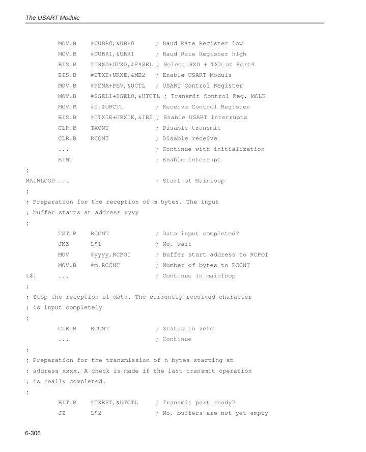
The USART Module
6-306
MOV.B #CUBR0,&UBR0 ; Baud Rate Register low
MOV.B #CUBR1,&UBR1 ; Baud Rate Register high
BIS.B #URXD+UTXD,&P4SEL ; Select RXD + TXD at Port4
BIS.B #UTXE+URXE,&ME2 ; Enable USART Moduls
MOV.B #PENA+PEV,&UCTL ; USART Control Register
MOV.B #SSEL1+SSEL0,&UTCTL ; Transmit Control Reg. MCLK
MOV.B #0,&URCTL ; Receive Control Register
BIS.B #UTXIE+URXIE,&IE2 ; Enable USART interrupts
CLR.B TXCNT ; Disable transmit
CLR.B RCCNT ; Disable receive
... ; Continue with initialization
EINT ; Enable interrupt
;
MAINLOOP ... ; Start of Mainloop
;
; Preparation for the reception of m bytes. The input
; buffer starts at address yyyy
;
TST.B RCCNT ; Data input completed?
JNZ L$1 ; No, wait
MOV #yyyy,RCPOI ; Buffer start address to RCPOI
MOV.B #m,RCCNT ; Number of bytes to RCCNT
L$1 ... ; Continue in mainloop
;
; Stop the reception of data. The currently received character
; is input completely
;
CLR.B RCCNT ; Status to zero
... ; Continue
;
; Preparation for the transmission of n bytes starting at
; address xxxx. A check is made if the last transmit operation
; is really completed.
;
BIT.B #TXEPT,&UTCTL ; Transmit part ready?
JZ L$2 ; No, buffers are not yet empty
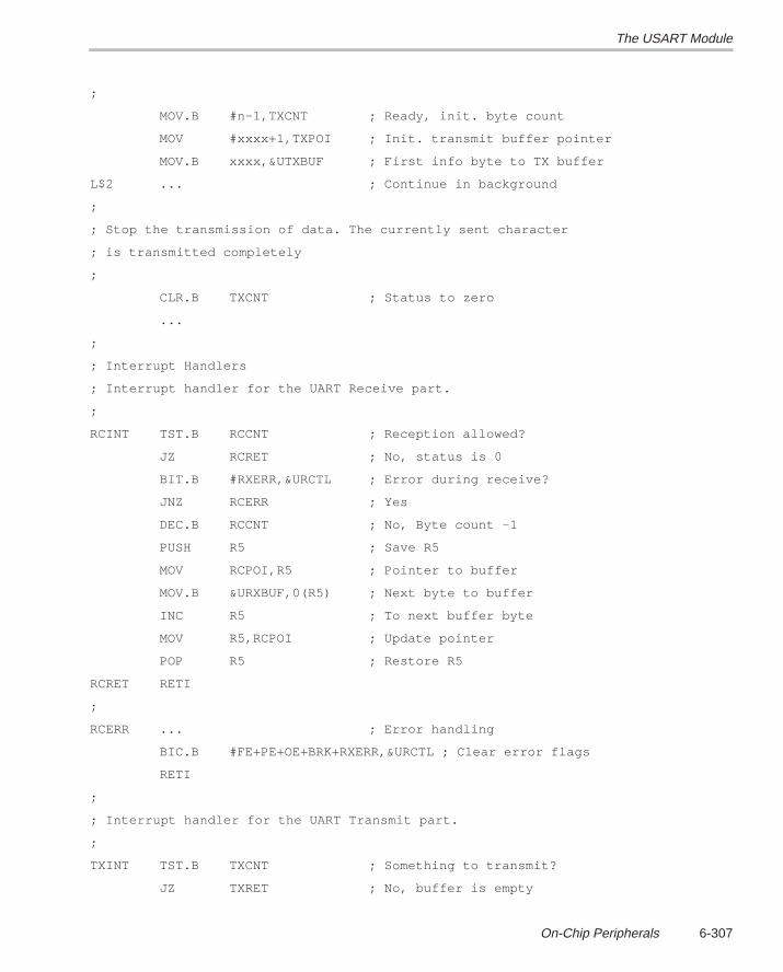
The USART Module
6-307On-Chip Peripherals
;
MOV.B #n–1,TXCNT ; Ready, init. byte count
MOV #xxxx+1,TXPOI ; Init. transmit buffer pointer
MOV.B xxxx,&UTXBUF ; First info byte to TX buffer
L$2 ... ; Continue in background
;
; Stop the transmission of data. The currently sent character
; is transmitted completely
;
CLR.B TXCNT ; Status to zero
...
;
; Interrupt Handlers
; Interrupt handler for the UART Receive part.
;
RCINT TST.B RCCNT ; Reception allowed?
JZ RCRET ; No, status is 0
BIT.B #RXERR,&URCTL ; Error during receive?
JNZ RCERR ; Yes
DEC.B RCCNT ; No, Byte count –1
PUSH R5 ; Save R5
MOV RCPOI,R5 ; Pointer to buffer
MOV.B &URXBUF,0(R5) ; Next byte to buffer
INC R5 ; To next buffer byte
MOV R5,RCPOI ; Update pointer
POP R5 ; Restore R5
RCRET RETI
;
RCERR ... ; Error handling
BIC.B #FE+PE+OE+BRK+RXERR,&URCTL ; Clear error flags
RETI
;
; Interrupt handler for the UART Transmit part.
;
TXINT TST.B TXCNT ; Something to transmit?
JZ TXRET ; No, buffer is empty
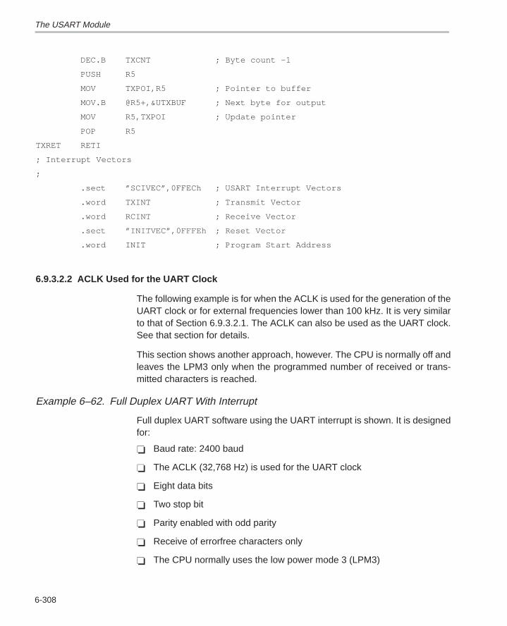
The USART Module
6-308
DEC.B TXCNT ; Byte count –1
PUSH R5
MOV TXPOI,R5 ; Pointer to buffer
MOV.B @R5+,&UTXBUF ; Next byte for output
MOV R5,TXPOI ; Update pointer
POP R5
TXRET RETI
; Interrupt Vectors
;
.sect ”SCIVEC”,0FFECh ; USART Interrupt Vectors
.word TXINT ; Transmit Vector
.word RCINT ; Receive Vector
.sect ”INITVEC”,0FFFEh ; Reset Vector
.word INIT ; Program Start Address
6.9.3.2.2 ACLK Used for the UART Clock
The following example is for when the ACLK is used for the generation of theUART clock or for external frequencies lower than 100 kHz. It is very similarto that of Section 6.9.3.2.1. The ACLK can also be used as the UART clock.See that section for details.
This section shows another approach, however. The CPU is normally off andleaves the LPM3 only when the programmed number of received or trans-mitted characters is reached.
Example 6–62. Full Duplex UART With Interrupt
Full duplex UART software using the UART interrupt is shown. It is designedfor:
Baud rate: 2400 baud
The ACLK (32,768 Hz) is used for the UART clock
Eight data bits
Two stop bit
Parity enabled with odd parity
Receive of errorfree characters only
The CPU normally uses the low power mode 3 (LPM3)
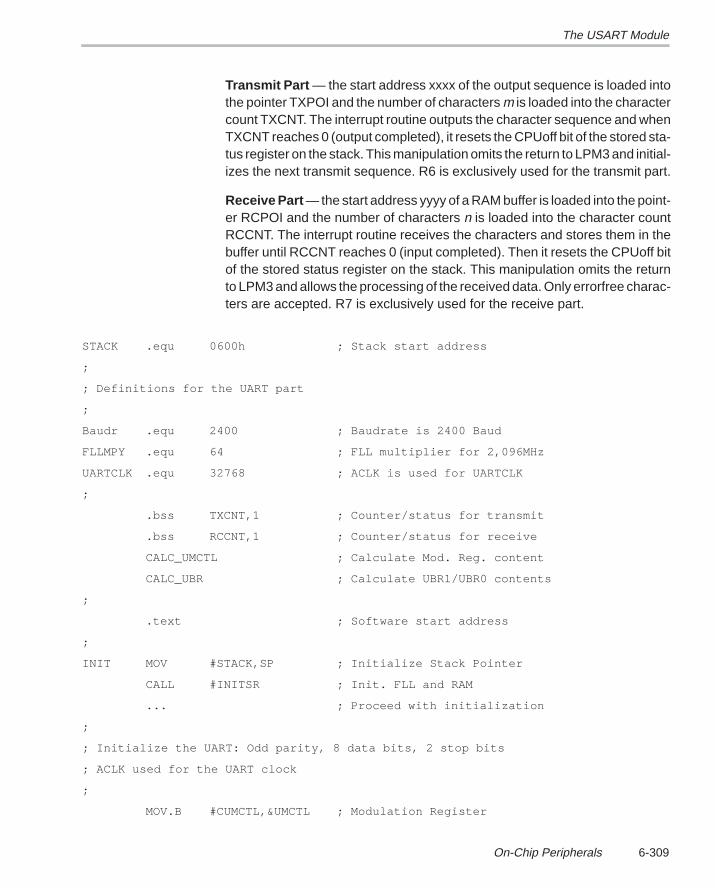
The USART Module
6-309On-Chip Peripherals
Transmit Part — the start address xxxx of the output sequence is loaded intothe pointer TXPOI and the number of characters m is loaded into the charactercount TXCNT. The interrupt routine outputs the character sequence and whenTXCNT reaches 0 (output completed), it resets the CPUoff bit of the stored sta-tus register on the stack. This manipulation omits the return to LPM3 and initial-izes the next transmit sequence. R6 is exclusively used for the transmit part.
Receive Part — the start address yyyy of a RAM buffer is loaded into the point-er RCPOI and the number of characters n is loaded into the character countRCCNT. The interrupt routine receives the characters and stores them in thebuffer until RCCNT reaches 0 (input completed). Then it resets the CPUoff bitof the stored status register on the stack. This manipulation omits the returnto LPM3 and allows the processing of the received data. Only errorfree charac-ters are accepted. R7 is exclusively used for the receive part.
STACK .equ 0600h ; Stack start address
;
; Definitions for the UART part
;
Baudr .equ 2400 ; Baudrate is 2400 Baud
FLLMPY .equ 64 ; FLL multiplier for 2,096MHz
UARTCLK .equ 32768 ; ACLK is used for UARTCLK
;
.bss TXCNT,1 ; Counter/status for transmit
.bss RCCNT,1 ; Counter/status for receive
CALC_UMCTL ; Calculate Mod. Reg. content
CALC_UBR ; Calculate UBR1/UBR0 contents
;
.text ; Software start address
;
INIT MOV #STACK,SP ; Initialize Stack Pointer
CALL #INITSR ; Init. FLL and RAM
... ; Proceed with initialization
;
; Initialize the UART: Odd parity, 8 data bits, 2 stop bits
; ACLK used for the UART clock
;
MOV.B #CUMCTL,&UMCTL ; Modulation Register
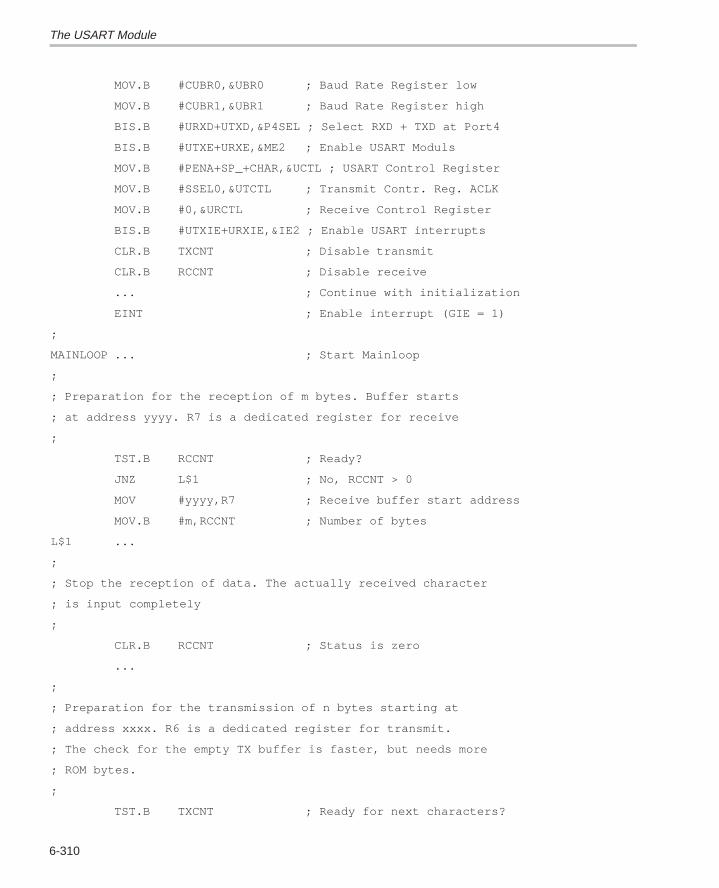
The USART Module
6-310
MOV.B #CUBR0,&UBR0 ; Baud Rate Register low
MOV.B #CUBR1,&UBR1 ; Baud Rate Register high
BIS.B #URXD+UTXD,&P4SEL ; Select RXD + TXD at Port4
BIS.B #UTXE+URXE,&ME2 ; Enable USART Moduls
MOV.B #PENA+SP_+CHAR,&UCTL ; USART Control Register
MOV.B #SSEL0,&UTCTL ; Transmit Contr. Reg. ACLK
MOV.B #0,&URCTL ; Receive Control Register
BIS.B #UTXIE+URXIE,&IE2 ; Enable USART interrupts
CLR.B TXCNT ; Disable transmit
CLR.B RCCNT ; Disable receive
... ; Continue with initialization
EINT ; Enable interrupt (GIE = 1)
;
MAINLOOP ... ; Start Mainloop
;
; Preparation for the reception of m bytes. Buffer starts
; at address yyyy. R7 is a dedicated register for receive
;
TST.B RCCNT ; Ready?
JNZ L$1 ; No, RCCNT > 0
MOV #yyyy,R7 ; Receive buffer start address
MOV.B #m,RCCNT ; Number of bytes
L$1 ...
;
; Stop the reception of data. The actually received character
; is input completely
;
CLR.B RCCNT ; Status is zero
...
;
; Preparation for the transmission of n bytes starting at
; address xxxx. R6 is a dedicated register for transmit.
; The check for the empty TX buffer is faster, but needs more
; ROM bytes.
;
TST.B TXCNT ; Ready for next characters?
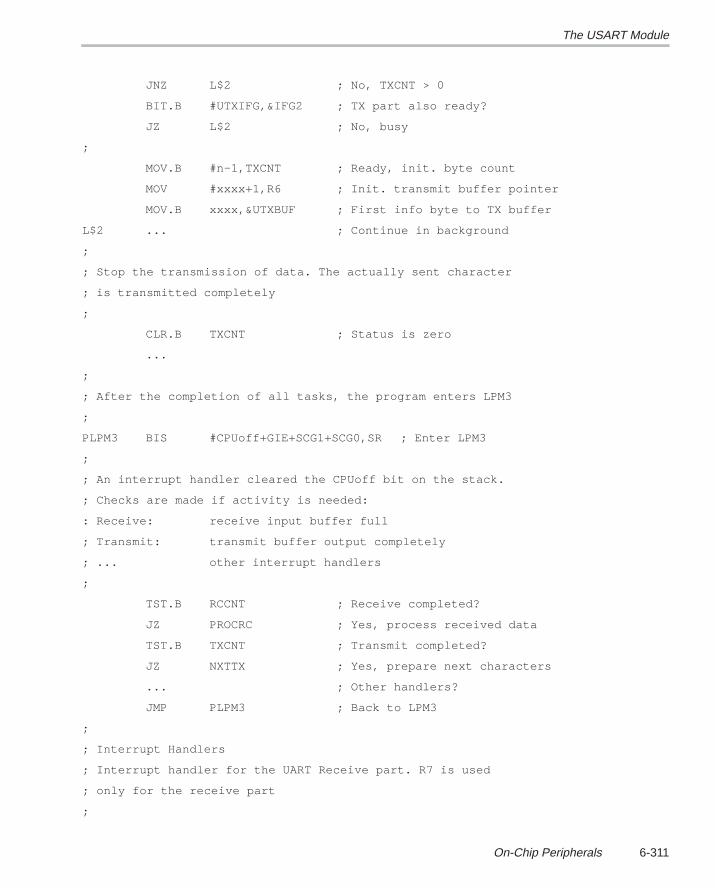
The USART Module
6-311On-Chip Peripherals
JNZ L$2 ; No, TXCNT > 0
BIT.B #UTXIFG,&IFG2 ; TX part also ready?
JZ L$2 ; No, busy
;
MOV.B #n–1,TXCNT ; Ready, init. byte count
MOV #xxxx+1,R6 ; Init. transmit buffer pointer
MOV.B xxxx,&UTXBUF ; First info byte to TX buffer
L$2 ... ; Continue in background
;
; Stop the transmission of data. The actually sent character
; is transmitted completely
;
CLR.B TXCNT ; Status is zero
...
;
; After the completion of all tasks, the program enters LPM3
;
PLPM3 BIS #CPUoff+GIE+SCG1+SCG0,SR ; Enter LPM3
;
; An interrupt handler cleared the CPUoff bit on the stack.
; Checks are made if activity is needed:
: Receive: receive input buffer full
; Transmit: transmit buffer output completely
; ... other interrupt handlers
;
TST.B RCCNT ; Receive completed?
JZ PROCRC ; Yes, process received data
TST.B TXCNT ; Transmit completed?
JZ NXTTX ; Yes, prepare next characters
... ; Other handlers?
JMP PLPM3 ; Back to LPM3
;
; Interrupt Handlers
; Interrupt handler for the UART Receive part. R7 is used
; only for the receive part
;
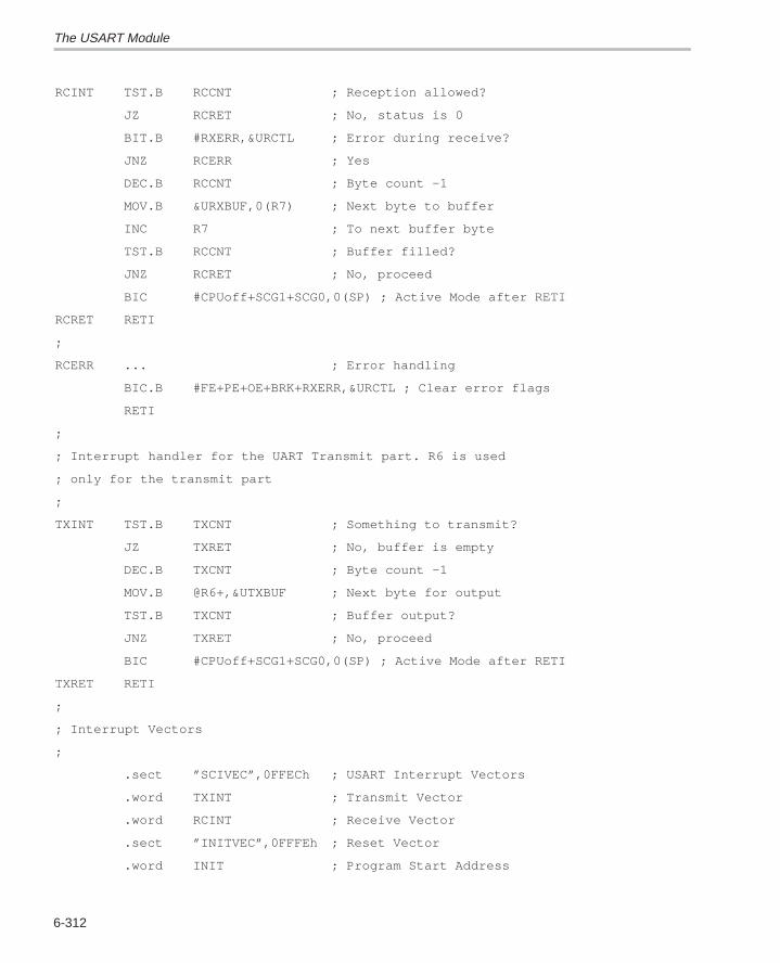
The USART Module
6-312
RCINT TST.B RCCNT ; Reception allowed?
JZ RCRET ; No, status is 0
BIT.B #RXERR,&URCTL ; Error during receive?
JNZ RCERR ; Yes
DEC.B RCCNT ; Byte count –1
MOV.B &URXBUF,0(R7) ; Next byte to buffer
INC R7 ; To next buffer byte
TST.B RCCNT ; Buffer filled?
JNZ RCRET ; No, proceed
BIC #CPUoff+SCG1+SCG0,0(SP) ; Active Mode after RETI
RCRET RETI
;
RCERR ... ; Error handling
BIC.B #FE+PE+OE+BRK+RXERR,&URCTL ; Clear error flags
RETI
;
; Interrupt handler for the UART Transmit part. R6 is used
; only for the transmit part
;
TXINT TST.B TXCNT ; Something to transmit?
JZ TXRET ; No, buffer is empty
DEC.B TXCNT ; Byte count –1
MOV.B @R6+,&UTXBUF ; Next byte for output
TST.B TXCNT ; Buffer output?
JNZ TXRET ; No, proceed
BIC #CPUoff+SCG1+SCG0,0(SP) ; Active Mode after RETI
TXRET RETI
;
; Interrupt Vectors
;
.sect ”SCIVEC”,0FFECh ; USART Interrupt Vectors
.word TXINT ; Transmit Vector
.word RCINT ; Receive Vector
.sect ”INITVEC”,0FFFEh ; Reset Vector
.word INIT ; Program Start Address
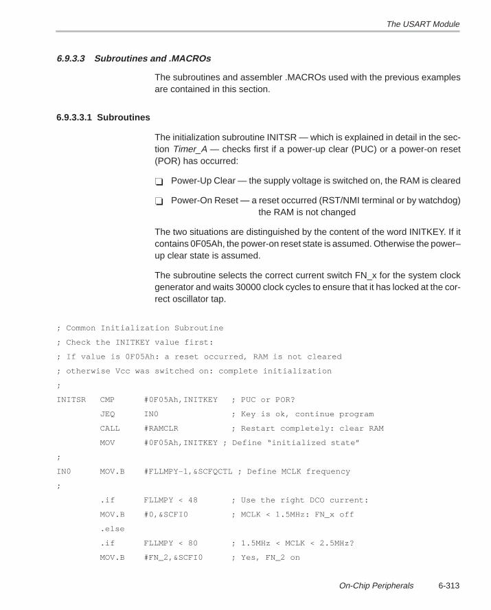
The USART Module
6-313On-Chip Peripherals
6.9.3.3 Subroutines and .MACROs
The subroutines and assembler .MACROs used with the previous examplesare contained in this section.
6.9.3.3.1 Subroutines
The initialization subroutine INITSR — which is explained in detail in the sec-tion Timer_A — checks first if a power-up clear (PUC) or a power-on reset(POR) has occurred:
Power-Up Clear — the supply voltage is switched on, the RAM is cleared
Power-On Reset — a reset occurred (RST/NMI terminal or by watchdog)the RAM is not changed
The two situations are distinguished by the content of the word INITKEY. If itcontains 0F05Ah, the power-on reset state is assumed. Otherwise the power–up clear state is assumed.
The subroutine selects the correct current switch FN_x for the system clockgenerator and waits 30000 clock cycles to ensure that it has locked at the cor-rect oscillator tap.
; Common Initialization Subroutine
; Check the INITKEY value first:
; If value is 0F05Ah: a reset occurred, RAM is not cleared
; otherwise Vcc was switched on: complete initialization
;
INITSR CMP #0F05Ah,INITKEY ; PUC or POR?
JEQ IN0 ; Key is ok, continue program
CALL #RAMCLR ; Restart completely: clear RAM
MOV #0F05Ah,INITKEY ; Define “initialized state”
;
IN0 MOV.B #FLLMPY–1,&SCFQCTL ; Define MCLK frequency
;
.if FLLMPY < 48 ; Use the right DCO current:
MOV.B #0,&SCFI0 ; MCLK < 1.5MHz: FN_x off
.else
.if FLLMPY < 80 ; 1.5MHz < MCLK < 2.5MHz?
MOV.B #FN_2,&SCFI0 ; Yes, FN_2 on
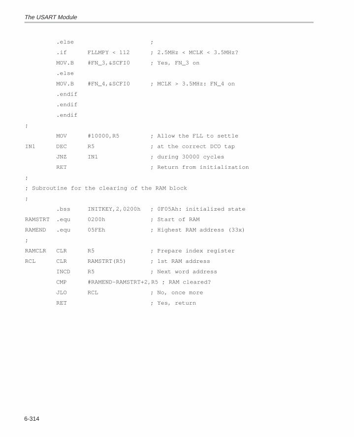
The USART Module
6-314
.else ;
.if FLLMPY < 112 ; 2.5MHz < MCLK < 3.5MHz?
MOV.B #FN_3,&SCFI0 ; Yes, FN_3 on
.else
MOV.B #FN_4,&SCFI0 ; MCLK > 3.5MHz: FN_4 on
.endif
.endif
.endif
;
MOV #10000,R5 ; Allow the FLL to settle
IN1 DEC R5 ; at the correct DCO tap
JNZ IN1 ; during 30000 cycles
RET ; Return from initialization
;
; Subroutine for the clearing of the RAM block
;
.bss INITKEY,2,0200h ; 0F05Ah: initialized state
RAMSTRT .equ 0200h ; Start of RAM
RAMEND .equ 05FEh ; Highest RAM address (33x)
;
RAMCLR CLR R5 ; Prepare index register
RCL CLR RAMSTRT(R5) ; 1st RAM address
INCD R5 ; Next word address
CMP #RAMEND–RAMSTRT+2,R5 ; RAM cleared?
JLO RCL ; No, once more
RET ; Yes, return
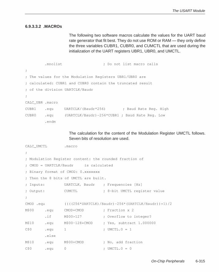
The USART Module
6-315On-Chip Peripherals
6.9.3.3.2 .MACROs
The following two software macros calculate the values for the UART baudrate generator that fit best. They do not use ROM or RAM — they only definethe three variables CUBR1, CUBR0, and CUMCTL that are used during theinitialization of the UART registers UBR1, UBR0, and UMCTL.
.mnolist ; Do not list macro calls
;
; The values for the Modulation Registers UBR1/UBR0 are
; calculated: CUBR1 and CUBR0 contain the truncated result
; of the division UARTCLK/Baudr
;
CALC_UBR .macro
CUBR1 .equ UARTCLK/(Baudr*256) ; Baud Rate Reg. High
CUBR0 .equ (UARTCLK/Baudr)–256*CUBR1 ; Baud Rate Reg. Low
.endm
The calculation for the content of the Modulation Register UMCTL follows.Seven bits of resolution are used.
CALC_UMCTL .macro
;
; Modulation Register content: the rounded fraction of
; CMOD = UARTCLK/Baudr is calculated
; Binary format of CMOD: 0.xxxxxxx
; Then the 8 bits of UMCTL are built.
; Inputs: UARTCLK, Baudr ; Frequencies [Hz]
; Output: CUMCTL ; 8–bit UMCTL register value
;
CMOD .equ ((((256*UARTCLK)/Baudr)–256*(UARTCLK/Baudr))+1)/2
M$00 .equ CMOD+CMOD ; Fraction x 2
.if M$00>127 ; Overflow to integer?
M$10 .equ M$00–128+CMOD ; Yes, subtract 1.000000
C$0 .equ 1 ; UMCTL.0 = 1
.else
M$10 .equ M$00+CMOD ; No, add fraction
C$0 .equ 0 ; UMCTL.0 = 0
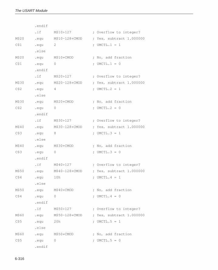
The USART Module
6-316
.endif
.if M$10>127 ; Overflow to integer?
M$20 .equ M$10–128+CMOD ; Yes, subtract 1.000000
C$1 .equ 2 ; UMCTL.1 = 1
.else
M$20 .equ M$10+CMOD ; No, add fraction
C$1 .equ 0 ; UMCTL.1 = 0
.endif
.if M$20>127 ; Overflow to integer?
M$30 .equ M$20–128+CMOD ; Yes, subtract 1.000000
C$2 .equ 4 ; UMCTL.2 = 1
.else
M$30 .equ M$20+CMOD ; No, add fraction
C$2 .equ 0 ; UMCTL.2 = 0
.endif
.if M$30>127 ; Overflow to integer?
M$40 .equ M$30–128+CMOD ; Yes, subtract 1.000000
C$3 .equ 8 ; UMCTL.3 = 1
.else
M$40 .equ M$30+CMOD ; No, add fraction
C$3 .equ 0 ; UMCTL.3 = 0
.endif
.if M$40>127 ; Overflow to integer?
M$50 .equ M$40–128+CMOD ; Yes, subtract 1.000000
C$4 .equ 10h ; UMCTL.4 = 1
.else
M$50 .equ M$40+CMOD ; No, add fraction
C$4 .equ 0 ; UMCTL.4 = 0
.endif
.if M$50>127 ; Overflow to integer?
M$60 .equ M$50–128+CMOD ; Yes, subtract 1.000000
C$5 .equ 20h ; UMCTL.5 = 1
.else
M$60 .equ M$50+CMOD ; No, add fraction
C$5 .equ 0 ; UMCTL.5 = 0
.endif
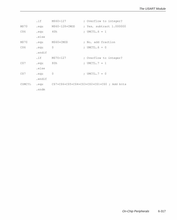
The USART Module
6-317On-Chip Peripherals
.if M$60>127 ; Overflow to integer?
M$70 .equ M$60–128+CMOD ; Yes, subtract 1.000000
C$6 .equ 40h ; UMCTL.6 = 1
.else
M$70 .equ M$60+CMOD ; No, add fraction
C$6 .equ 0 ; UMCTL.6 = 0
.endif
.if M$70>127 ; Overflow to integer?
C$7 .equ 80h ; UMCTL.7 = 1
.else
C$7 .equ 0 ; UMCTL.7 = 0
.endif
CUMCTL .equ C$7+C$6+C$5+C$4+C$3+C$2+C$1+C$0 ; Add bits
.endm
The 8-Bit Interval Timer/Counter
6-318
6.10 The 8-Bit Interval Timer/Counter
6.10.1 Introduction
The 8-Bit Interval Timer/Counter peripheral is included in all members of theMSP430x3xx family. This timer/counter — its block diagram is shown in Figure6–86 — can work, like its name suggests, in two different modes: the timermode and the counter mode. This section describes software routines usablefor the UART mode (SCI, RS232) that use the timer mode of the 8-Bit Timer/Counter. The software examples shown in the subsequent sections adaptthemselves to the needs defined by the user (number of data bits, number ofstop bits, baud rate, error detection and handling, clock frequency, and so on).This self-adaptation is accomplished through the use of the conditional as-sembly feature of the MSP430 assembler.
The hardware of the 8-Bit Interval Timer/Counter module supports the receiveand transmit of UART data on a bit basis: one data bit is received or transmittedbetween two interrupts, not a complete frame consisting of a start bit, data bits,a parity bit and stop bits. This means that the interrupt overhead is relativelylarge due to the interrupt request after each received or transmitted data bit.On the other hand, the advantage is the complete flexibility of the data format— only software defines the number and meaning of the transferred bits. Anyprotocol is possible.
Figure 6–86 shows the block diagram of the complete MSP430 8-Bit IntervalTimer/Counter module.
The 8-Bit Interval Timer/Counter module allows only the half duplex mode.This means that the module can receive data or it can transmit data, but notreceive and transmit data simultaneously. The user software must thereforedetermine which mode should be active. In the following software examples,this is accomplished by the initialization subroutines.
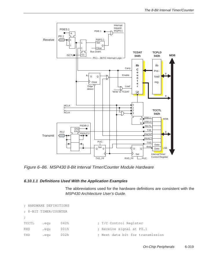
The 8-Bit Interval Timer/Counter
6-319On-Chip Peripherals
MDB
Edgedetect
0123ACLK
MCLK
8
8
Interval/TimerControl Register
A
B
DQSet
Load
Carry
D Q
TXD
RXD LSB
MSB
RXACT
TXE
ISCTL
SSEL0
SSEL1
Clear
D+
QEnable
8
8b
Counter
Clk
8b
Pre–
load
reg.
Data
TXD_FF RXD_FF PUC
PUC
’Write’ to TCDAT
ENCNT
Set
P0.1A
1_1
P0IES.1
ISCTL
1_
1
G1
Set
ClearQ
P0IFG.1
InterruptrequestIRQP0.1
Bus Grant
P0IE.1
P0.1 – 8bT/C Interrupt Logic
P0.2EN1EN2
P0DIR.2
P0OUT.2Transmit
Receive
Data
TCDAT TCPLD043h044h
TCCTL042h
Figure 6–86. MSP430 8-Bit Interval Timer/Counter Module Hardware
6.10.1.1 Definitions Used With the Application Examples
The abbreviations used for the hardware definitions are consistent with theMSP430 Architecture User’s Guide.
; HARDWARE DEFINITIONS
; 8–BIT TIMER/COUNTER
;
TCCTL .equ 042h ; T/C Control Register
RXD .equ 001h ; Receive signal at P0.1
TXD .equ 002h ; Next data bit for transmission
The 8-Bit Interval Timer/Counter
6-320
RXACT .equ 004h ; 1: detect start bit 0: off, reset FF
ENCNT .equ 008h ; Counter TCDAT enabled
TXE .equ 010h ; 1: TXD to P0.2 0: P0OUT.2 to P0.2
ISCTL .equ 020h ; Intrpt source: 0: P0.1 1: Carry TCDAT
SSEL0 .equ 040h ; Clock source. 0: P0.1
SSEL1 .equ 080h ; 1: MCLK 2: ACLK 3: P0.1 .and. MCLK
;
TCPLD .equ 043h ; T/C 8–Bit Pre–load Register
;
TCDAT .equ 044h ; T/C 8–Bit Counter
;
; OTHER DEFINITIONS
;
IE1 .equ 0 ; Interrupt Enable Register 1
P0IE1 .equ 8 ; P0.1 Interrupt Enable Bit (RCV)
P0IES .equ 014h ; P0 Interrupt Edge Select Register
;
SCG1 .equ 080h ; Low Power Mode bit 1
SCG0 .equ 040h ; Low Power Mode bit 0
CPUoff .equ 010h ; Switches CPU off
GIE .equ 008h ; General Interrupt Enable Bit
6.10.1.2 Attributes of a UART Implemented with the 8-Bit Timer/Counter
A short overview to the UART mode of the 8-Bit Timer/Counter module ap-pears below:
Half duplex mode — either transmit or receive mode is possible, but notboth simultaneously.
Any data length and format is possible. This is due to the software con-trolled data sequence.
Error detection made by software:
Frame error — The stop bits have space potential or the start bit hasmark potential in its middle
Parity error — Parity is enabled and the parity bit has the wrong value.
Overrun error — The next character is read in before the last one isread out by the software. This is not possible with the given software.
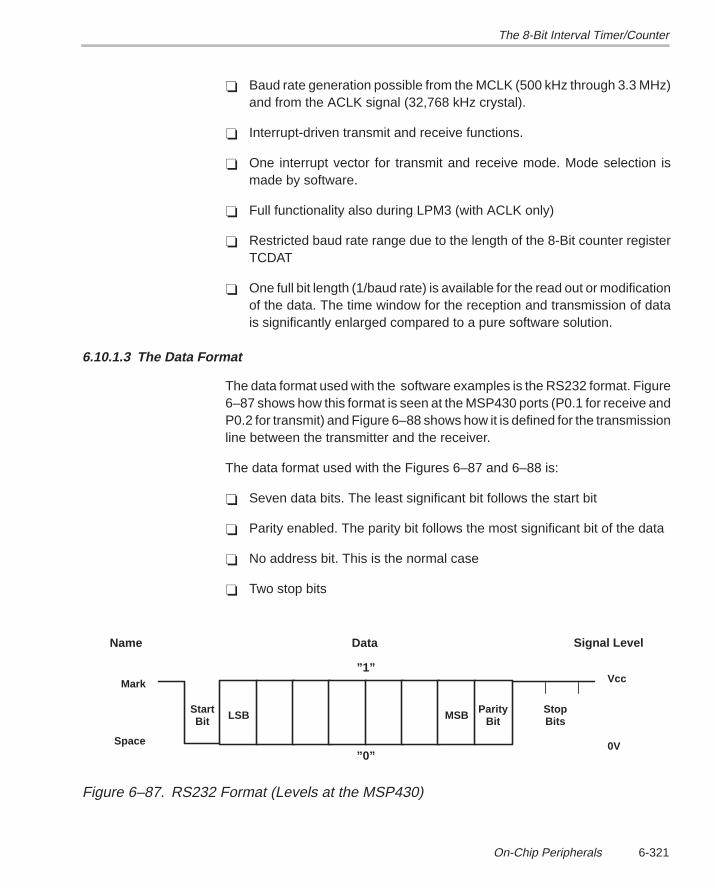
The 8-Bit Interval Timer/Counter
6-321On-Chip Peripherals
Baud rate generation possible from the MCLK (500 kHz through 3.3 MHz)and from the ACLK signal (32,768 kHz crystal).
Interrupt-driven transmit and receive functions.
One interrupt vector for transmit and receive mode. Mode selection ismade by software.
Full functionality also during LPM3 (with ACLK only)
Restricted baud rate range due to the length of the 8-Bit counter registerTCDAT
One full bit length (1/baud rate) is available for the read out or modificationof the data. The time window for the reception and transmission of datais significantly enlarged compared to a pure software solution.
6.10.1.3 The Data Format
The data format used with the software examples is the RS232 format. Figure6–87 shows how this format is seen at the MSP430 ports (P0.1 for receive andP0.2 for transmit) and Figure 6–88 shows how it is defined for the transmissionline between the transmitter and the receiver.
The data format used with the Figures 6–87 and 6–88 is:
Seven data bits. The least significant bit follows the start bit
Parity enabled. The parity bit follows the most significant bit of the data
No address bit. This is the normal case
Two stop bits
Space
Mark Vcc
0V
StartBit LSB MSB Parity
BitStopBits
”1”
”0”
DataName Signal Level
Figure 6–87. RS232 Format (Levels at the MSP430)
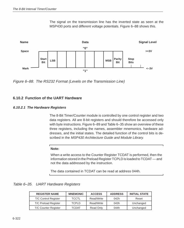
The 8-Bit Interval Timer/Counter
6-322
The signal on the transmission line has the inverted state as seen at theMSP430 ports and different voltage potentials. Figure 6–88 shows this.
Mark
Space
<–3V
>+3V
StartBit
LSB MSBParity
BitStopBits
”0”
”1”
DataName Signal Level
Figure 6–88. The RS232 Format (Levels on the Transmission Line)
6.10.2 Function of the UART Hardware
6.10.2.1 The Hardware Registers
The 8-Bit Timer/Counter module is controlled by one control register and twodata registers. All are 8-bit registers and should therefore be accessed onlywith byte instructions. Figure 6–89 and Table 6–35 show an overview of thesethree registers, including the names, assembler mnemonics, hardware ad-dresses, and the initial states. The detailed function of the control bits is de-scribed in the MSP430 Architecture Guide and Module Library.
Note:
When a write access to the Counter Register TCDAT is performed, then theinformation stored in the Preload Register TCPLD is loaded to TCDAT — andnot the data addressed by the instruction.
The data contained in TCDAT can be read at address 044h.
Table 6–35. UART Hardware Registers
REGISTER NAME MNEMONIC ACCESS ADDRESS INITIAL STATE
T/C Control Register TCCTL Read/Write 042h Reset
T/C Preload Register TCPLD Read/Write 043h Unchanged
T/C Counter Register TCDAT Read Only 044h Unchanged
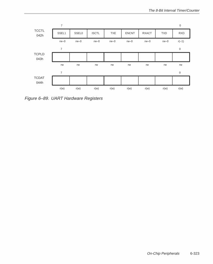
The 8-Bit Interval Timer/Counter
6-323On-Chip Peripherals
07
rw–0 rw–0 rw–0 rw–0rw–0 rw–0 r(–1)rw–0
TCCTL
042hRXDTXDENCNT RXACTTXEISCTLSSEL0SSEL1
07
rw rw rw rwrw rw rwrw
TCPLD
043h
07
r(w) r(w) r(w) r(w)r(w) r(w) r(w)r(w)
TCDAT
044h
Figure 6–89. UART Hardware Registers
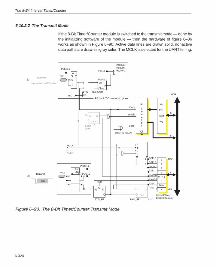
The 8-Bit Interval Timer/Counter
6-324
6.10.2.2 The Transmit Mode
If the 8-Bit Timer/Counter module is switched to the transmit mode — done bythe initializing software of the module — then the hardware of figure 6–86works as shown in Figure 6–90. Active data lines are drawn solid, nonactivedata paths are drawn in gray color. The MCLK is selected for the UART timing.
MDB
Edgedetect
0123ACLK
MCLK
8
8
Interval/TimerControl Register
A
B
DQSet
Load
Carry
D Q
TXD
RXD
ENCNT
LSB
MSB
RXACT
TXE
ISCTL
SSEL0
SSEL1
Clear
D+ Q Enable8
8b
Counter
Clk
8b
Pre–
load
reg.
1
1
1
0
Data
X
P0.2
TXD_FF RXD_FF
’Write’ to TCDAT
1
Set
PUC
PUC
0 –> 1
P0.1A
1_1
P0IES.1
ISCTL
1_
1
G1
Set
ClearQ
P0IFG.1
InterruptRequestIRQP0.1
Bus Grant
P0IE.1
P0.1 – 8bT/C Interrupt Logic
EN1EN2
P0DIR.2
P0OUT.2
Data
Transmit
Receive
Not active: Half Duplex
Figure 6–90. The 8-Bit Timer/Counter Transmit Mode

The 8-Bit Interval Timer/Counter
6-325On-Chip Peripherals
Initialization for the transmit mode is done by the subroutine TXINIT. The mainsteps for the transmission of a character are:
Loading of the data word RTDATA with the character to be transmitted, in-cluding the address bit information (if defined)
Initializing of the 8-Bit Timer/Counter and the RAM bytes RTERR andRTSTAT
Selecting of the clock frequency for the counter TCDAT (MCLK orACLK) (SSELx bits)
Activation of the interrupt request by the carry of the 8-bit counter reg-ister TCDAT (ISCTL = 1)
Selecting of the TXD output data instead of the P0.2 output registerdata for the P0.2 pin (TXE = 1)
Setting of the TXD bit to mark (1) (TXD = 1). This value is transferredto the TXD output with the first counter interrupt. It guarantees a lead-ing mark signal of at least one bit time.
Enabling of the 8-Bit Timer/Counter: the counter starts with the se-lected clock (ENCNT = 1)
Loading of the counter with one half of a bit time. After this time inter-val, the TXD output is set to mark (1) if not yet set
Loading of the pre-load register TCPLD with a full bit time interval(1/baud rate). This time interval is used for the leading mark before thestart bit
Loading of the transmit status byte RTSTAT with the status for the startbit
Loading of the error byte RTERR with a start value (0 resp. 1) that de-livers the correct parity bit of the complete character
Enabling of the interrupt for the 8-Bit Timer/Counter. Interrupt is re-quested now approximately after each time interval 1/baud rate. Thistime can change from bit to bit. See Section 6.10.3 Baud Rate Genera-tion and Correction.
Loading of the TXD bit during the interrupt handler with the information ofthe next but one bit to be output (start bit, data bits, address bit, parity bit,stop bits)
Sampling of the information for the parity bit, if parity is enabled.
Output of the nondata signals (start bit, parity bit, stop bits) dependent onthe selected format
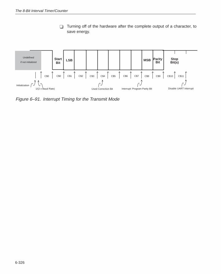
The 8-Bit Interval Timer/Counter
6-326
Turning off of the hardware after the complete output of a character, tosave energy.
LSBStartBit
ParityBit
StopBit(s)
MSB
C$0 C$1 C$2 C$3 C$4 C$5 C$6 C$7 C$8 C$9 C$10 C$11
Interrupt: Program Parity BitUsed Correction Bit
C$0
Initialization1/(2 x Baud Rate)
Undefined
if not initialized
Disable UART Interrupt
Figure 6–91. Interrupt Timing for the Transmit Mode
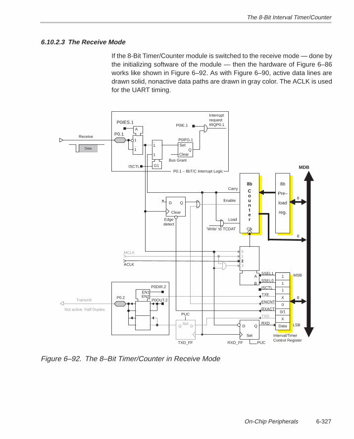
The 8-Bit Interval Timer/Counter
6-327On-Chip Peripherals
6.10.2.3 The Receive Mode
If the 8-Bit Timer/Counter module is switched to the receive mode — done bythe initializing software of the module — then the hardware of Figure 6–86works like shown in Figure 6–92. As with Figure 6–90, active data lines aredrawn solid, nonactive data paths are drawn in gray color. The ACLK is usedfor the UART timing.
MDB
Edgedetect
0123ACLK
MCLK
8
8
Interval/TimerControl Register
A
B
DQSet
Load
Carry
D Q
TXD
RXD LSB
MSB
RXACT
TXE
ISCTL
SSEL0
SSEL1
Clear
D+
QEnable
8
8b
Counter
Clk
8b
Pre–
load
reg.
1
1
1
0/1
X
Data
TXD_FF RXD_FF
X
PUC
PUC
’Write’ to TCDAT
ENCNT0
Set
P0.1A
1_1
P0IES.1
ISCTL
1_
1
G1
Set
ClearQ
P0IFG.1
InterruptrequestIRQP0.1
Bus Grant
P0IE.1
P0.1 – 8bT/C Interrupt Logic
P0.2EN1EN2
P0DIR.2
P0OUT.2
Receive
Transmit
Not active: Half Duplex
Data
Figure 6–92. The 8–Bit Timer/Counter in Receive Mode
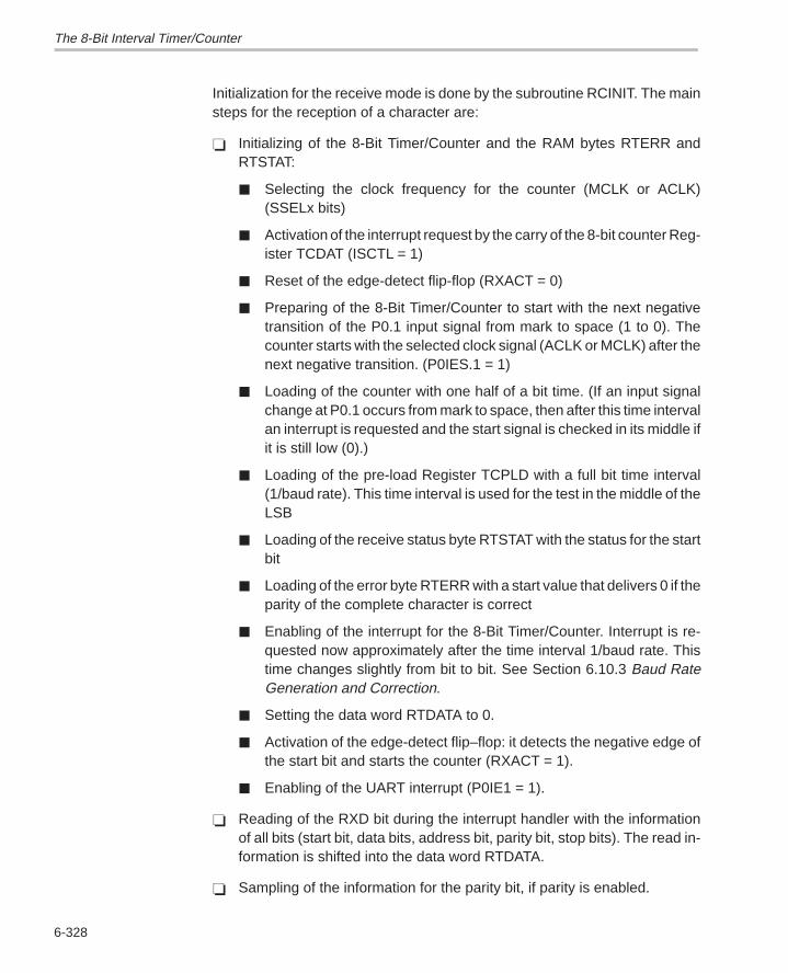
The 8-Bit Interval Timer/Counter
6-328
Initialization for the receive mode is done by the subroutine RCINIT. The mainsteps for the reception of a character are:
Initializing of the 8-Bit Timer/Counter and the RAM bytes RTERR andRTSTAT:
Selecting the clock frequency for the counter (MCLK or ACLK)(SSELx bits)
Activation of the interrupt request by the carry of the 8-bit counter Reg-ister TCDAT (ISCTL = 1)
Reset of the edge-detect flip-flop (RXACT = 0)
Preparing of the 8-Bit Timer/Counter to start with the next negativetransition of the P0.1 input signal from mark to space (1 to 0). Thecounter starts with the selected clock signal (ACLK or MCLK) after thenext negative transition. (P0IES.1 = 1)
Loading of the counter with one half of a bit time. (If an input signalchange at P0.1 occurs from mark to space, then after this time intervalan interrupt is requested and the start signal is checked in its middle ifit is still low (0).)
Loading of the pre-load Register TCPLD with a full bit time interval(1/baud rate). This time interval is used for the test in the middle of theLSB
Loading of the receive status byte RTSTAT with the status for the startbit
Loading of the error byte RTERR with a start value that delivers 0 if theparity of the complete character is correct
Enabling of the interrupt for the 8-Bit Timer/Counter. Interrupt is re-quested now approximately after the time interval 1/baud rate. Thistime changes slightly from bit to bit. See Section 6.10.3 Baud RateGeneration and Correction.
Setting the data word RTDATA to 0.
Activation of the edge-detect flip–flop: it detects the negative edge ofthe start bit and starts the counter (RXACT = 1).
Enabling of the UART interrupt (P0IE1 = 1).
Reading of the RXD bit during the interrupt handler with the informationof all bits (start bit, data bits, address bit, parity bit, stop bits). The read in-formation is shifted into the data word RTDATA.
Sampling of the information for the parity bit, if parity is enabled.
The 8-Bit Interval Timer/Counter
6-329On-Chip Peripherals
Check of the nondata signals (start bit, parity bit, stop bits), dependent onthe selected format
Setting of the error bits TCPE and TCFE dependent on the bit check. If noerror occurred, the error byte RTERR contains 0
Turning off of the timer/counter hardware after the complete reception ofa character: interrupt and clock are switched off.
LSBStartBit
ParityBit
StopBit(s)
MSB
C$1 C$2 C$3 C$4 C$5 C$6 C$7 C$8 C$9 C$10
Interrupt: Program Time Interval ts
Used Correction Bit
C$0
Interrupt in Middle1/(2 x Baud Rate) Disable UART Interrupt
Initialization
of the Start Bit
ts
C$11
Figure 6–93. Interrupt Timing for the Receive Mode
The 8-Bit Interval Timer/Counter
6-330
6.10.3 The Baud Rate Generation and Correction
The short counter register TCDAT of the 8-bit timer/counter allows the use ofthe MCLK for only very few baud rates. For all other baud rates, the maximumvalue 255 for the quotient MCLK/baud rate is exceeded. Therefore, the use ofthe ACLK (32,768 Hz) is necessary for most of the usual baud rates. But theuse of the ACLK frequency causes another problem:
Generating the desired baud rate from a relatively high frequency (1 MHz to5 MHz) is a simple task. The resulting baud rate error is small due to the largeinteger part of the quotient compared to the truncated fractional part. Thischanges completely if the time base is a crystal of only 32 kHz. Then the errordue to the truncated fractional part of the quotient grows large and leads to theloss of synchrony at the trailing bits of the frame. The MSP430 UART softwaretherefore uses a correction to keep the baud rate error small. The baud ratecorrection calculates correction information (9 to 13 bits, dependent on theframe length) as to how to correct the baud rate of the received or transmittedUART signal. The calculated bits C$0 to C$12 define how the predivider infor-mation contained in the baud rate registers TCPLD and TCDAT is used:
C$x = 0 — the calculated time interval is used as is.
C$x = 1 — the calculated time interval is prolonged by one timer period(MCLK or ACLK) and used with this value.
The value C$0 is used for the start bit, the value C$1 for the LSB of the data,and so on. See Figure 6–94 for an explanation.
Example 6–63. Baud Rate Generation
A baud rate of 2400 baud is needed from a crystal frequency of 32,768 Hz. Theframe length used is the minimum length: start bit, seven data bits, no addressbit, no parity, and one stop bit. This results in a frame length of nine bits. Theuse of the ACLK is necessary due to two reasons:
The UART also needs to run during the low power mode 3, when theMCLK is not available.
The maximum MCLK frequency would be 255 × 2400 = 612 kHz. This fre-quency is too low for most of the applications (and cannot be guaranteedfor the system clock generator).
With only the ACLK available, the theoretical division factor UBR — the trun-cated value is the base for one of the two contents of the Pre–Load RegisterTCPLD — is:
UBR32768
240013.653333= =
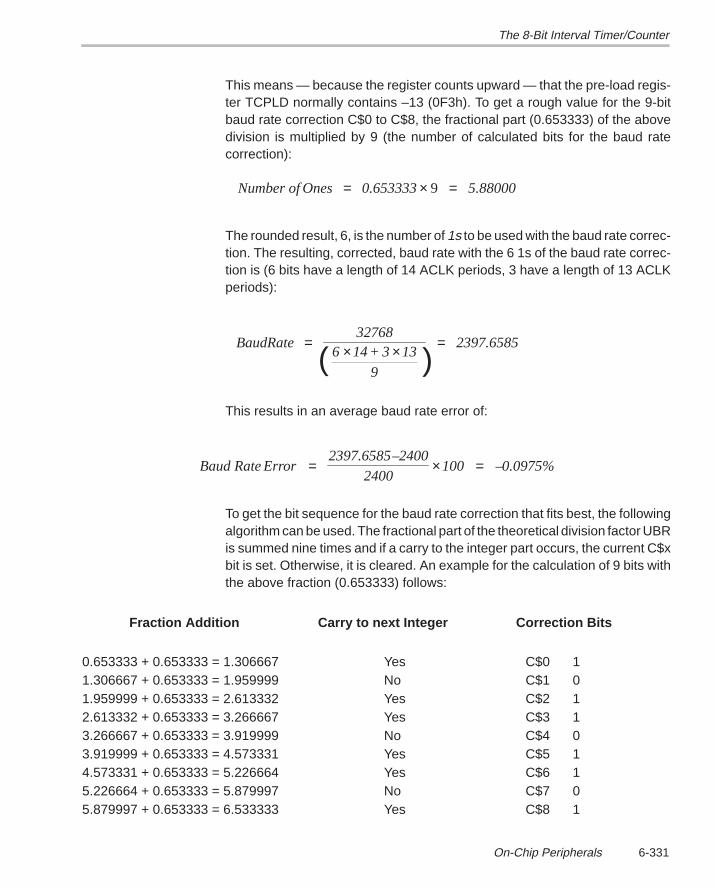
The 8-Bit Interval Timer/Counter
6-331On-Chip Peripherals
This means — because the register counts upward — that the pre-load regis-ter TCPLD normally contains –13 (0F3h). To get a rough value for the 9-bitbaud rate correction C$0 to C$8, the fractional part (0.653333) of the abovedivision is multiplied by 9 (the number of calculated bits for the baud ratecorrection):
Number of Ones 0.653333 5.88000= × =9
The rounded result, 6, is the number of 1s to be used with the baud rate correc-tion. The resulting, corrected, baud rate with the 6 1s of the baud rate correc-tion is (6 bits have a length of 14 ACLK periods, 3 have a length of 13 ACLKperiods):
BaudRate32768
6 14 + 3 13
9
2397.6585= × × =( )
This results in an average baud rate error of:
Baud Rate Error2397.6585–2400
2400100 –0.0975%= × =
To get the bit sequence for the baud rate correction that fits best, the followingalgorithm can be used. The fractional part of the theoretical division factor UBRis summed nine times and if a carry to the integer part occurs, the current C$xbit is set. Otherwise, it is cleared. An example for the calculation of 9 bits withthe above fraction (0.653333) follows:
Fraction Addition Carry to next Integer Correction Bits
0.653333 + 0.653333 = 1.306667 Yes C$0 11.306667 + 0.653333 = 1.959999 No C$1 01.959999 + 0.653333 = 2.613332 Yes C$2 12.613332 + 0.653333 = 3.266667 Yes C$3 13.266667 + 0.653333 = 3.919999 No C$4 03.919999 + 0.653333 = 4.573331 Yes C$5 14.573331 + 0.653333 = 5.226664 Yes C$6 15.226664 + 0.653333 = 5.879997 No C$7 05.879997 + 0.653333 = 6.533333 Yes C$8 1

The 8-Bit Interval Timer/Counter
6-332
The result of the calculated bits C$8...C$0 (1 0110 1101b) is 16Dh with sixones. The software example contains a macro loop (starting at label MODTAB)that uses the algorithm shown above and calculates, for every combination ofthe UART clock and the desired baud rate, the optimum value for the baud ratecorrection. For the above example (9 bit frame length), the macro also deter-mines 16Dh with its six ones.
Example 6–64. 2400 Baud From ACLK
Figure 6–94 gives an example for a baud rate of 2400 baud generated with theACLK frequency (32,768 Hz). The data format for figure 6–94 is:
Eight data bits, parity enabled, no address bit, and two stop bits. Figure 6–94shows three different frames:
The upper frame is the correct one with a bit length of 13.65333 ACLKcycles (32,768/2400 = 13.65333)
The middle frame uses a rough estimation with 14 ACLK cycles for the bitlength
The lower frame uses a corrected frame with the best fit(C$11...C$0 = 0B6Dh) for the baud rate correction.
It can be seen that the approximation with 14 ACLK cycles accumulates an er-ror of more than 0.3 bit length after the second stop bit. The error of the cor-rected frame is only 0.001 bit length. The error of the crystal clock is not yetincluded, and it adds to the above errors.
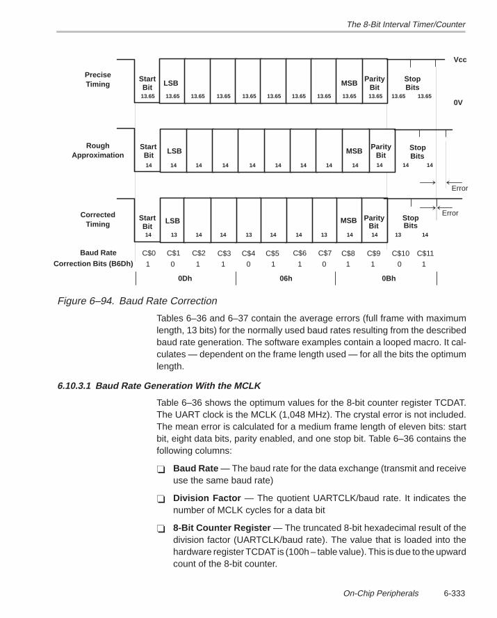
The 8-Bit Interval Timer/Counter
6-333On-Chip Peripherals
LSB
13 14 14 13 14 14
Precise
Vcc
0V
StartBit LSB MSB Parity
BitStopBits
StartBit LSB Stop
BitsMSB
StartBit
ParityBit
StopBits
Bit
MSB
14 14 14 14 14 14 14 14 1414
14 13 14 14 13
14
Correction Bits (B6Dh)C$0 C$1 C$2 C$3 C$4 C$5 C$6 C$7 C$8 C$9 C$10
14
Parity
13.6513.65 13.65 13.65 13.65 13.65 13.65 13.65 13.65 13.65 13.65 13.65
MSB
14
C$11
Timing
RoughApproximation
CorrectedTiming
Error
Error
01 1 1 0 1 1 0 1 1 0 1
Baud Rate
0Dh 06h 0Bh
Figure 6–94. Baud Rate Correction
Tables 6–36 and 6–37 contain the average errors (full frame with maximumlength, 13 bits) for the normally used baud rates resulting from the describedbaud rate generation. The software examples contain a looped macro. It cal-culates — dependent on the frame length used — for all the bits the optimumlength.
6.10.3.1 Baud Rate Generation With the MCLK
Table 6–36 shows the optimum values for the 8-bit counter register TCDAT.The UART clock is the MCLK (1,048 MHz). The crystal error is not included.The mean error is calculated for a medium frame length of eleven bits: startbit, eight data bits, parity enabled, and one stop bit. Table 6–36 contains thefollowing columns:
Baud Rate — The baud rate for the data exchange (transmit and receiveuse the same baud rate)
Division Factor — The quotient UARTCLK/baud rate. It indicates thenumber of MCLK cycles for a data bit
8-Bit Counter Register — The truncated 8-bit hexadecimal result of thedivision factor (UARTCLK/baud rate). The value that is loaded into thehardware register TCDAT is (100h – table value). This is due to the upwardcount of the 8-bit counter.
The 8-Bit Interval Timer/Counter
6-334
Baud Rate Correction — The 13-bit result that fits best for the baud ratecorrection. It is calculated by the software macro starting at label MOD-TAB. If frames with less than 13 bits are used, then the MSBs of this num-ber are omitted.
Used Fraction — The number of 1s in the baud rate correction sequencedivided by eleven (the frame length used for the calculation). It is anapproximation of the truncated fractional part of the division factor.
Mean Error — The resulting error of a complete character caused by theapproximation of the division factor
The length of the 8-bit counter register allows only a very limited range for thebaud rate. An MCLK frequency of 1.048 MHz is assumed. For other frequen-cies, the baud rates change accordingly (e.g. for 2.096 MHz the usable baudrates are 9600 and 19200 baud). The reasons for this restriction are:
From 110 baud to 2400 baud, the 8-bit counter register is too small to holdthe necessary number for the result of the division MCLK/baud rate: thenumber contained in the column 8-Bit Counter Register is greater than0FFh.
Beginning at 9600 baud, the CPU cycles between two UART interrupts aretoo few for correct handling (e.g. only 54 CPU cycles @ 1.048 MHz for19200 baud). See Section 4.4. The maximum baud rate depends stronglyon the amount of interrupt activity due to the other peripherals.
Note:
The assembler outputs an error message if the resulting value for the TCDATregister is greater than 255. This is an indication of a baud rate that is too low.
Note:
Baud rates that result in TCDAT register values lower than 100 make strictlyreal time processing rules necessary. Interrupt handlers must be as short aspossible and interruptible. See Section 4.4 for hints how to speed-up theUART.
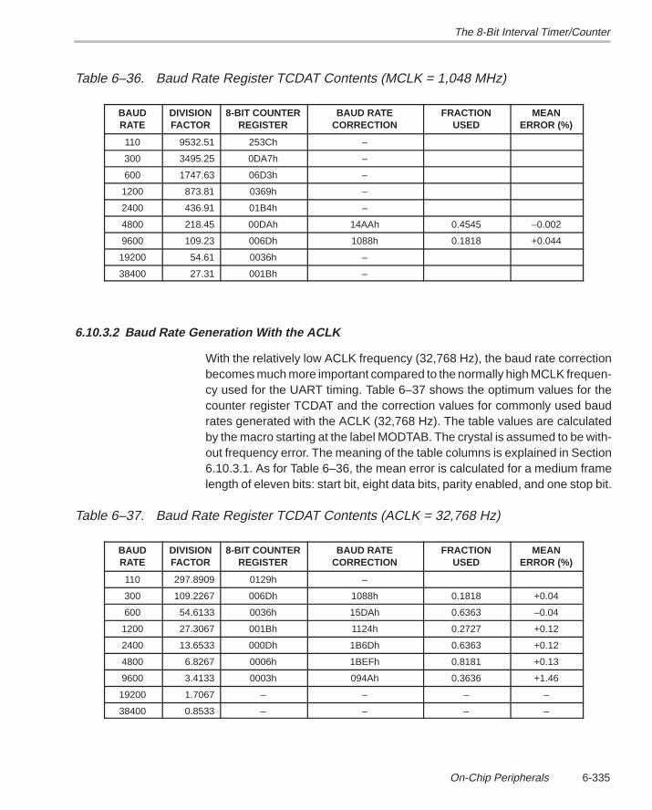
The 8-Bit Interval Timer/Counter
6-335On-Chip Peripherals
Table 6–36. Baud Rate Register TCDAT Contents (MCLK = 1,048 MHz)
BAUDRATE
DIVISIONFACTOR
8-BIT COUNTERREGISTER
BAUD RATECORRECTION
FRACTIONUSED
MEANERROR (%)
110 9532.51 253Ch –
300 3495.25 0DA7h –
600 1747.63 06D3h –
1200 873.81 0369h –
2400 436.91 01B4h –
4800 218.45 00DAh 14AAh 0.4545 –0.002
9600 109.23 006Dh 1088h 0.1818 +0.044
19200 54.61 0036h –
38400 27.31 001Bh –
6.10.3.2 Baud Rate Generation With the ACLK
With the relatively low ACLK frequency (32,768 Hz), the baud rate correctionbecomes much more important compared to the normally high MCLK frequen-cy used for the UART timing. Table 6–37 shows the optimum values for thecounter register TCDAT and the correction values for commonly used baudrates generated with the ACLK (32,768 Hz). The table values are calculatedby the macro starting at the label MODTAB. The crystal is assumed to be with-out frequency error. The meaning of the table columns is explained in Section6.10.3.1. As for Table 6–36, the mean error is calculated for a medium framelength of eleven bits: start bit, eight data bits, parity enabled, and one stop bit.
Table 6–37. Baud Rate Register TCDAT Contents (ACLK = 32,768 Hz)
BAUDRATE
DIVISIONFACTOR
8-BIT COUNTERREGISTER
BAUD RATECORRECTION
FRACTIONUSED
MEANERROR (%)
110 297.8909 0129h –
300 109.2267 006Dh 1088h 0.1818 +0.04
600 54.6133 0036h 15DAh 0.6363 –0.04
1200 27.3067 001Bh 1124h 0.2727 +0.12
2400 13.6533 000Dh 1B6Dh 0.6363 +0.12
4800 6.8267 0006h 1BEFh 0.8181 +0.13
9600 3.4133 0003h 094Ah 0.3636 +1.46
19200 1.7067 – – – –
38400 0.8533 – – – –
The 8-Bit Interval Timer/Counter
6-336
6.10.4 Software Routines
The following sections show proven software routines for the UART mode ofthe 8-Bit Timer/Counter.
Note:
The program sequences for the initialization of the UART software are impor-tant. The example code should not be modified. See the subroutines TXINITand RCINIT.
Note:
Any protocol is possible due to the software control for the data sequence.It is only necessary to adapt the two tables RTTAB and MODTAB of the twosoftware examples that follow.
The software routines are shown for interrupt use only. It makes no sense touse the noninterrupt solution (polling) because the time intervals between twosignal bits are relatively short — a 100% loading of the CPU would be the re-sult. This is due to the bit orientation of the 8-Bit Timer/Counter hardware.
The initialization subroutine INITSR and the RAM initialization subroutineRAMCLR are explained in detail in section The Timer_A, paragraph CommonInitialization Routine.
6.10.4.1 MCLK Used for UART Clock
The following example is for use when MCLK used for the generation of theUART clock. For high baud rates — higher than 9600 baud @ 1 MHz — dedi-cated CPU registers may be necessary to lower the interrupt overhead. Thetime for the saving and restoring of the register is not necessary. See Section6.10.4.4.
Example 6–65. Half Duplex UART with Interrupt
Half duplex UART software using the interrupt of the 8-Bit Timer/Counter isshown below. The software is designed for:
Baud rate: 4800 baud
The MCLK (1,048 MHz) is used for the UART clock
The active mode of the CPU is used
Seven data bits
The 8-Bit Interval Timer/Counter
6-337On-Chip Peripherals
Parity enabled with even parity
No address bit included
One stop bit
Reception of all characters (the error byte RTERR contains an error indi-cation)
UART signals like shown in figure 6–87 (mark = VCC, space = VSS)
The following seven software switches and the value for the UARTCLK needto be defined for the UART operation (see also the examples in the softwarepart). Functions that are not enabled, do not use memory space: the adjacentcode is left out by Conditional Assembly.
UARTCLK If the MCLK is used for the UART timing, then the MCLK frequency must be given here.Normally the MCLK is defined by multiplication of the crystal frequency with the FLL multi-plier.
Baudr Baud rate used [Hz]. For 1.048 MHz MCLK frequency, the range is from 4800 baud to9600 baud. With special care, 19200 baud is also possible. The range of usable baudrates increases linearly with the MCLK frequency used.
CHARC Number of data bits. The UART software allows 7 and 8 data bits, but the table structureof the software eases the adaptation to other bit counts.
ADDR Inclusion of an address bit (1) or not (0). See the MSP430 Architecture Guide for an ex-planation of this feature.
PAR Enables (1) or disables (0) a parity check. A parity error sets bit TCPE (RTERR.0).
PAREV If parity is enabled (PAR = 1), even (1) or odd (0) parity is used for the data check.
STB Defines the number of stop bits. Possible values are 1 or 2 stop bits
TCERRT Defines the treatment of detected errors. If the received character is correct, the byteRTERR contains 0. The possible values for the switch TCERRT are:
TCERRT = 0: the current, erroneous character is discarded and the receive function is initializedfor a new start bit check. This means the software tries to find a valid start bit.
TCERRT = 1: the error is indicated in byte RTERR, the reception of the current character contin-ues.
Possible errors are:
TCPE (RTERR.0) = 1 — parity error. The sum of 1s contained in the data bits, the address bit, and theparity bit is not correct. It is not odd for odd parity OR even for even parity
TCFE (RTERR.1) = 1 — frame error. This means the middle of the start bit is high, or one of the stopbits is low. This error is normally caused by a software start inside of a character frame.
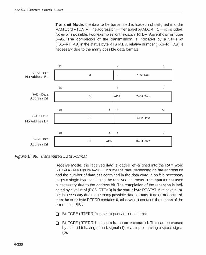
The 8-Bit Interval Timer/Counter
6-338
Transmit Mode: the data to be transmitted is loaded right-aligned into theRAM word RTDATA. The address bit — if enabled by ADDR = 1 — is included.No error is possible. Four examples for the data in RTDATA are shown in figure6–95. The completion of the transmission is indicated by a value of(TX6–RTTAB) in the status byte RTSTAT. A relative number (TX6–RTTAB) isnecessary due to the many possible data formats.
015
7–Bit DataNo Address Bit
7
00 7–Bit Data
015
7–Bit DataAddress Bit
7
0 7–Bit Data
015
8–Bit Data
No Address Bit
7
0 8–Bit Data
8
ADR
015
8–Bit Data
Address Bit
7
ADR0 8–Bit Data
8
Figure 6–95. Transmitted Data Format
Receive Mode: the received data is loaded left-aligned into the RAM wordRTDATA (see Figure 6–96). This means that, depending on the address bitand the number of data bits contained in the data word, a shift is necessaryto get a single byte containing the received character. The input format usedis necessary due to the address bit. The completion of the reception is indi-cated by a value of (RC6–RTTAB) in the status byte RTSTAT. A relative num-ber is necessary due to the many possible data formats. If no error occurred,then the error byte RTERR contains 0, otherwise it contains the reason of theerror in its LSBs:
Bit TCPE (RTERR.0) is set: a parity error occurred
Bit TCFE (RTERR.1) is set: a frame error occurred. This can be causedby a start bit having a mark signal (1) or a stop bit having a space signal(0).
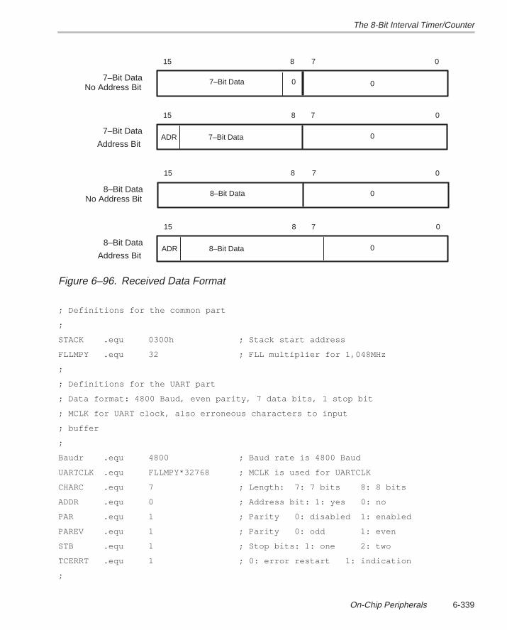
The 8-Bit Interval Timer/Counter
6-339On-Chip Peripherals
015
7–Bit DataNo Address Bit
7
07–Bit Data
015
7–Bit Data
Address Bit
7
ADR
0
7–Bit Data
8
0
8
015
8–Bit DataNo Address Bit
7
8–Bit Data
015
8–Bit Data
Address Bit
7
ADR
0
8–Bit Data
8
0
8
Figure 6–96. Received Data Format
; Definitions for the common part
;
STACK .equ 0300h ; Stack start address
FLLMPY .equ 32 ; FLL multiplier for 1,048MHz
;
; Definitions for the UART part
; Data format: 4800 Baud, even parity, 7 data bits, 1 stop bit
; MCLK for UART clock, also erroneous characters to input
; buffer
;
Baudr .equ 4800 ; Baud rate is 4800 Baud
UARTCLK .equ FLLMPY*32768 ; MCLK is used for UARTCLK
CHARC .equ 7 ; Length: 7: 7 bits 8: 8 bits
ADDR .equ 0 ; Address bit: 1: yes 0: no
PAR .equ 1 ; Parity 0: disabled 1: enabled
PAREV .equ 1 ; Parity 0: odd 1: even
STB .equ 1 ; Stop bits: 1: one 2: two
TCERRT .equ 1 ; 0: error restart 1: indication
;
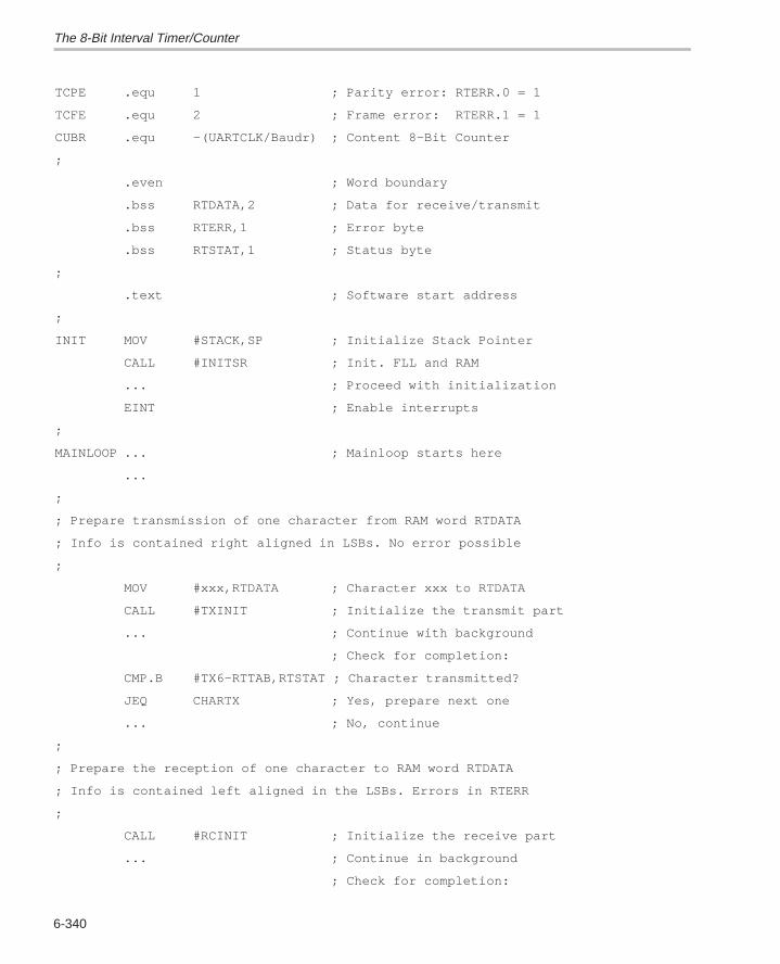
The 8-Bit Interval Timer/Counter
6-340
TCPE .equ 1 ; Parity error: RTERR.0 = 1
TCFE .equ 2 ; Frame error: RTERR.1 = 1
CUBR .equ –(UARTCLK/Baudr) ; Content 8–Bit Counter
;
.even ; Word boundary
.bss RTDATA,2 ; Data for receive/transmit
.bss RTERR,1 ; Error byte
.bss RTSTAT,1 ; Status byte
;
.text ; Software start address
;
INIT MOV #STACK,SP ; Initialize Stack Pointer
CALL #INITSR ; Init. FLL and RAM
... ; Proceed with initialization
EINT ; Enable interrupts
;
MAINLOOP ... ; Mainloop starts here
...
;
; Prepare transmission of one character from RAM word RTDATA
; Info is contained right aligned in LSBs. No error possible
;
MOV #xxx,RTDATA ; Character xxx to RTDATA
CALL #TXINIT ; Initialize the transmit part
... ; Continue with background
; Check for completion:
CMP.B #TX6–RTTAB,RTSTAT ; Character transmitted?
JEQ CHARTX ; Yes, prepare next one
... ; No, continue
;
; Prepare the reception of one character to RAM word RTDATA
; Info is contained left aligned in the LSBs. Errors in RTERR
;
CALL #RCINIT ; Initialize the receive part
... ; Continue in background
; Check for completion:
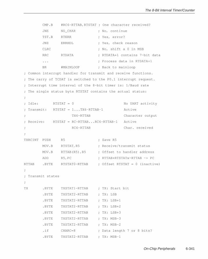
The 8-Bit Interval Timer/Counter
6-341On-Chip Peripherals
CMP.B #RC6–RTTAB,RTSTAT ; One character received?
JNE NO_CHAR ; No, continue
TST.B RTERR ; Yes, error?
JNZ ERRHDL ; Yes, check reason
CLRC ; No, shift a 0 in MSB
RRC RTDATA ; RTDATA+1 contains 7–bit data
... ; Process data in RTDATA+1
BR #MAINLOOP ; Back to mainloop
; Common interrupt handler for transmit and receive functions.
; The carry of TCDAT is switched to the P0.1 interrupt request.
; Interrupt time interval of the 8–bit timer is: 1/Baud rate
; The single status byte RTSTAT contains the actual status:
;
; Idle: RTSTAT = 0 No UART activity
; Transmit: RTSTAT = 1...TX6–RTTAB–1 Active
; TX6–RTTAB Character output
; Receive: RTSTAT = RC–RTTAB...RC6–RTTAB–1 Active
; RC6–RTTAB Char. received
;
TXRCINT PUSH R5 ; Save R5
MOV.B RTSTAT,R5 ; Receive/transmit status
MOV.B RTTAB(R5),R5 ; Offset to handler address
ADD R5,PC ; RTTAB+RTSTATx–RTTAB –> PC
RTTAB .BYTE RTSTAT0–RTTAB ; Offset RTSTAT = 0 (inactive)
;
; Transmit states
;
TX .BYTE TXSTAT1–RTTAB ; TX: Start bit
.BYTE TXSTAT2–RTTAB ; TX: LSB
.BYTE TXSTAT2–RTTAB ; TX: LSB+1
.BYTE TXSTAT2–RTTAB ; TX: LSB+2
.BYTE TXSTAT2–RTTAB ; TX: LSB+3
.BYTE TXSTAT2–RTTAB ; TX: MSB–3
.BYTE TXSTAT2–RTTAB ; TX: MSB–2
.if CHARC=8 ; Data length 7 or 8 bits?
.BYTE TXSTAT2–RTTAB ; TX: MSB–1
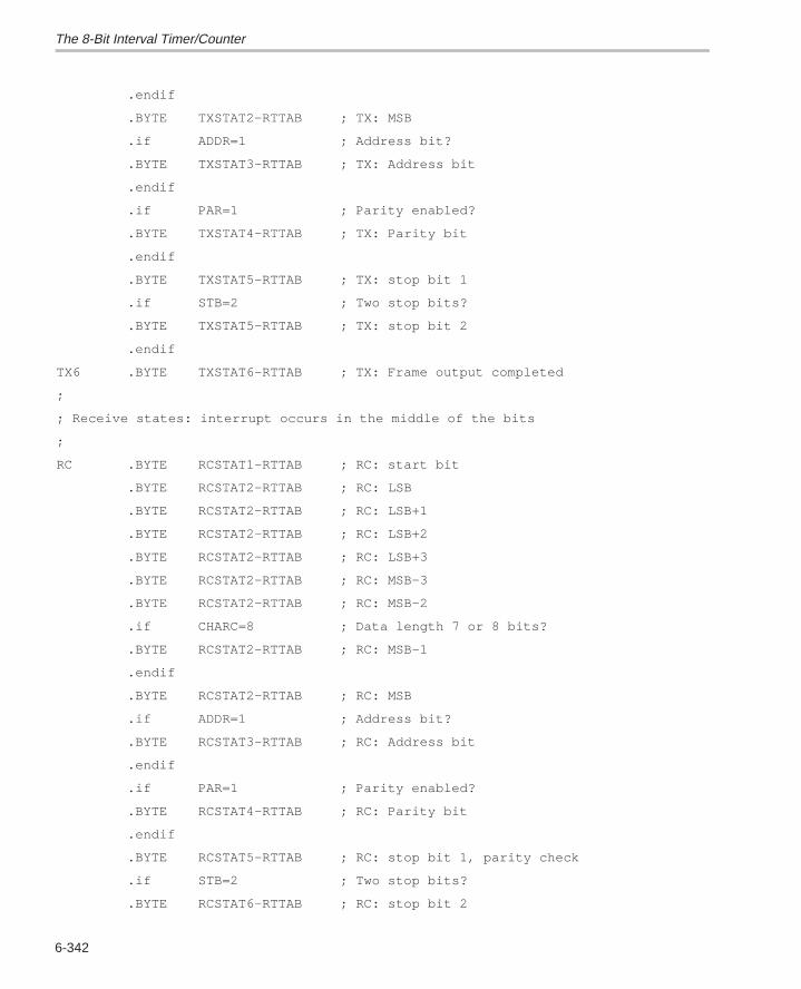
The 8-Bit Interval Timer/Counter
6-342
.endif
.BYTE TXSTAT2–RTTAB ; TX: MSB
.if ADDR=1 ; Address bit?
.BYTE TXSTAT3–RTTAB ; TX: Address bit
.endif
.if PAR=1 ; Parity enabled?
.BYTE TXSTAT4–RTTAB ; TX: Parity bit
.endif
.BYTE TXSTAT5–RTTAB ; TX: stop bit 1
.if STB=2 ; Two stop bits?
.BYTE TXSTAT5–RTTAB ; TX: stop bit 2
.endif
TX6 .BYTE TXSTAT6–RTTAB ; TX: Frame output completed
;
; Receive states: interrupt occurs in the middle of the bits
;
RC .BYTE RCSTAT1–RTTAB ; RC: start bit
.BYTE RCSTAT2–RTTAB ; RC: LSB
.BYTE RCSTAT2–RTTAB ; RC: LSB+1
.BYTE RCSTAT2–RTTAB ; RC: LSB+2
.BYTE RCSTAT2–RTTAB ; RC: LSB+3
.BYTE RCSTAT2–RTTAB ; RC: MSB–3
.BYTE RCSTAT2–RTTAB ; RC: MSB–2
.if CHARC=8 ; Data length 7 or 8 bits?
.BYTE RCSTAT2–RTTAB ; RC: MSB–1
.endif
.BYTE RCSTAT2–RTTAB ; RC: MSB
.if ADDR=1 ; Address bit?
.BYTE RCSTAT3–RTTAB ; RC: Address bit
.endif
.if PAR=1 ; Parity enabled?
.BYTE RCSTAT4–RTTAB ; RC: Parity bit
.endif
.BYTE RCSTAT5–RTTAB ; RC: stop bit 1, parity check
.if STB=2 ; Two stop bits?
.BYTE RCSTAT6–RTTAB ; RC: stop bit 2
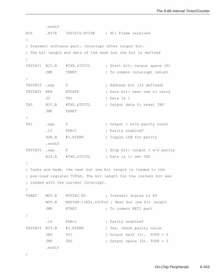
The 8-Bit Interval Timer/Counter
6-343On-Chip Peripherals
.endif
RC6 .BYTE TXSTAT6–RTTAB ; RC: Frame received
;
; Transmit software part. Interrupt after output bit.
; The bit length and data of the next but one bit is defined
;
TXSTAT1 BIC.B #TXD,&TCCTL ; Start bit: output space (0)
JMP TXRET ; To common interrupt return
;
TXSTAT3 .equ $ ; Address bit (if defined)
TXSTAT2 RRA RTDATA ; Data bit: next one to carry
JC TX1 ; Data is 1
TX0 BIC.B #TXD,&TCCTL ; Output data 0: reset TXD
JMP TXRET
;
TX1 .equ $ ; Output 1 with parity count
.if PAR=1 ; Parity enabled?
XOR.B #1,RTERR ; Toggle LSB for parity
.endif
TXSTAT5 .equ $ ; Stop bit: output 1 w/o parity
BIS.B #TXD,&TCCTL ; Data is 1: set TXD
;
; Tasks are made, the next but one bit length is loaded to the
; pre–load register TCPLD. The bit length for the current bit was
; loaded with the current interrupt.
;
TXRET MOV.B RTSTAT,R5 ; Transmit status to R5
MOV.B MODTAB–1(R5),&TCPLD ; Next but one bit length
JMP RTRET ; To common RETI part
;
.if PAR=1 ; Parity enabled?
TXSTAT4 BIT.B #1,RTERR ; Yes, check parity value
JNZ TX1 ; Output mark (1). TCPE = 0
JMP TX0 ; Output space (0). TCPE = 0
.endif
;
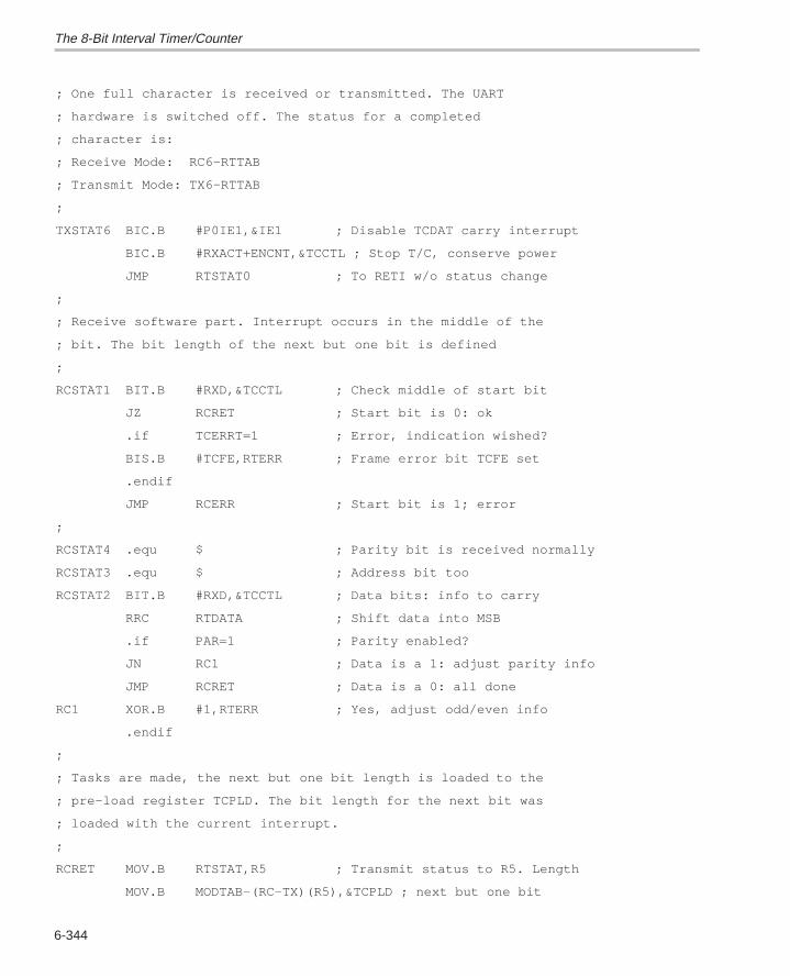
The 8-Bit Interval Timer/Counter
6-344
; One full character is received or transmitted. The UART
; hardware is switched off. The status for a completed
; character is:
; Receive Mode: RC6–RTTAB
; Transmit Mode: TX6–RTTAB
;
TXSTAT6 BIC.B #P0IE1,&IE1 ; Disable TCDAT carry interrupt
BIC.B #RXACT+ENCNT,&TCCTL ; Stop T/C, conserve power
JMP RTSTAT0 ; To RETI w/o status change
;
; Receive software part. Interrupt occurs in the middle of the
; bit. The bit length of the next but one bit is defined
;
RCSTAT1 BIT.B #RXD,&TCCTL ; Check middle of start bit
JZ RCRET ; Start bit is 0: ok
.if TCERRT=1 ; Error, indication wished?
BIS.B #TCFE,RTERR ; Frame error bit TCFE set
.endif
JMP RCERR ; Start bit is 1; error
;
RCSTAT4 .equ $ ; Parity bit is received normally
RCSTAT3 .equ $ ; Address bit too
RCSTAT2 BIT.B #RXD,&TCCTL ; Data bits: info to carry
RRC RTDATA ; Shift data into MSB
.if PAR=1 ; Parity enabled?
JN RC1 ; Data is a 1: adjust parity info
JMP RCRET ; Data is a 0: all done
RC1 XOR.B #1,RTERR ; Yes, adjust odd/even info
.endif
;
; Tasks are made, the next but one bit length is loaded to the
; pre–load register TCPLD. The bit length for the next bit was
; loaded with the current interrupt.
;
RCRET MOV.B RTSTAT,R5 ; Transmit status to R5. Length
MOV.B MODTAB–(RC–TX)(R5),&TCPLD ; next but one bit
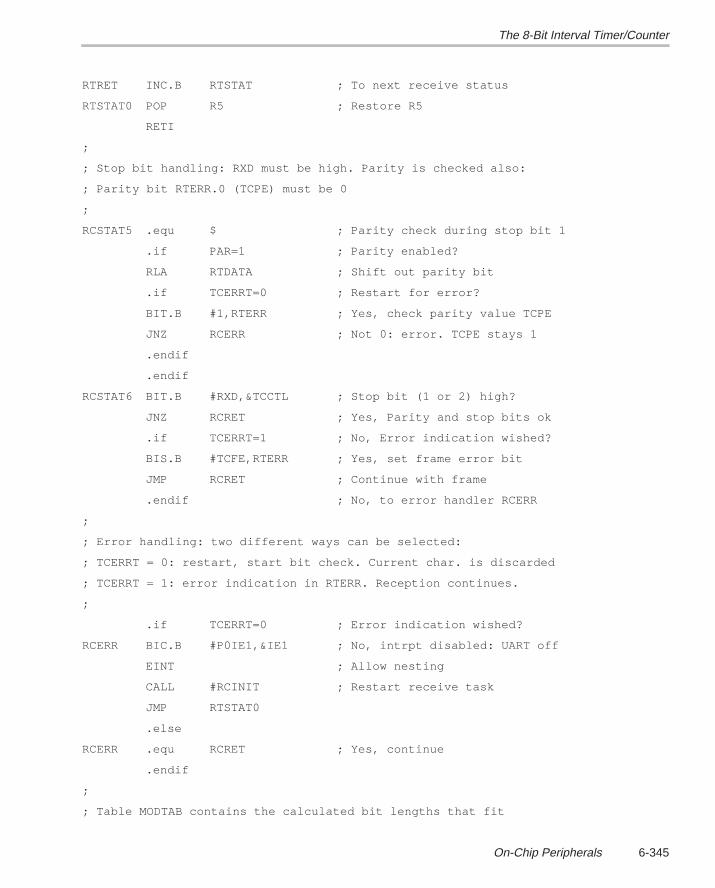
The 8-Bit Interval Timer/Counter
6-345On-Chip Peripherals
RTRET INC.B RTSTAT ; To next receive status
RTSTAT0 POP R5 ; Restore R5
RETI
;
; Stop bit handling: RXD must be high. Parity is checked also:
; Parity bit RTERR.0 (TCPE) must be 0
;
RCSTAT5 .equ $ ; Parity check during stop bit 1
.if PAR=1 ; Parity enabled?
RLA RTDATA ; Shift out parity bit
.if TCERRT=0 ; Restart for error?
BIT.B #1,RTERR ; Yes, check parity value TCPE
JNZ RCERR ; Not 0: error. TCPE stays 1
.endif
.endif
RCSTAT6 BIT.B #RXD,&TCCTL ; Stop bit (1 or 2) high?
JNZ RCRET ; Yes, Parity and stop bits ok
.if TCERRT=1 ; No, Error indication wished?
BIS.B #TCFE,RTERR ; Yes, set frame error bit
JMP RCRET ; Continue with frame
.endif ; No, to error handler RCERR
;
; Error handling: two different ways can be selected:
; TCERRT = 0: restart, start bit check. Current char. is discarded
; TCERRT = 1: error indication in RTERR. Reception continues.
;
.if TCERRT=0 ; Error indication wished?
RCERR BIC.B #P0IE1,&IE1 ; No, intrpt disabled: UART off
EINT ; Allow nesting
CALL #RCINIT ; Restart receive task
JMP RTSTAT0
.else
RCERR .equ RCRET ; Yes, continue
.endif
;
; Table MODTAB contains the calculated bit lengths that fit
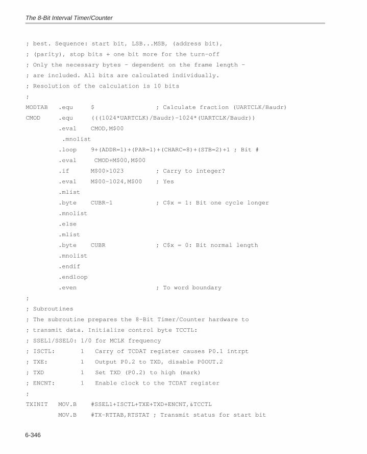
The 8-Bit Interval Timer/Counter
6-346
; best. Sequence: start bit, LSB...MSB, (address bit),
; (parity), stop bits + one bit more for the turn–off
; Only the necessary bytes – dependent on the frame length –
; are included. All bits are calculated individually.
; Resolution of the calculation is 10 bits
;
MODTAB .equ $ ; Calculate fraction (UARTCLK/Baudr)
CMOD .equ (((1024*UARTCLK)/Baudr)–1024*(UARTCLK/Baudr))
.eval CMOD,M$00
.mnolist
.loop 9+(ADDR=1)+(PAR=1)+(CHARC=8)+(STB=2)+1 ; Bit #
.eval CMOD+M$00,M$00
.if M$00>1023 ; Carry to integer?
.eval M$00–1024,M$00 ; Yes
.mlist
.byte CUBR–1 ; C$x = 1: Bit one cycle longer
.mnolist
.else
.mlist
.byte CUBR ; C$x = 0: Bit normal length
.mnolist
.endif
.endloop
.even ; To word boundary
;
; Subroutines
; The subroutine prepares the 8–Bit Timer/Counter hardware to
; transmit data. Initialize control byte TCCTL:
; SSEL1/SSEL0: 1/0 for MCLK frequency
; ISCTL: 1 Carry of TCDAT register causes P0.1 intrpt
; TXE: 1 Output P0.2 to TXD, disable P0OUT.2
; TXD 1 Set TXD (P0.2) to high (mark)
; ENCNT: 1 Enable clock to the TCDAT register
;
TXINIT MOV.B #SSEL1+ISCTL+TXE+TXD+ENCNT,&TCCTL
MOV.B #TX–RTTAB,RTSTAT ; Transmit status for start bit
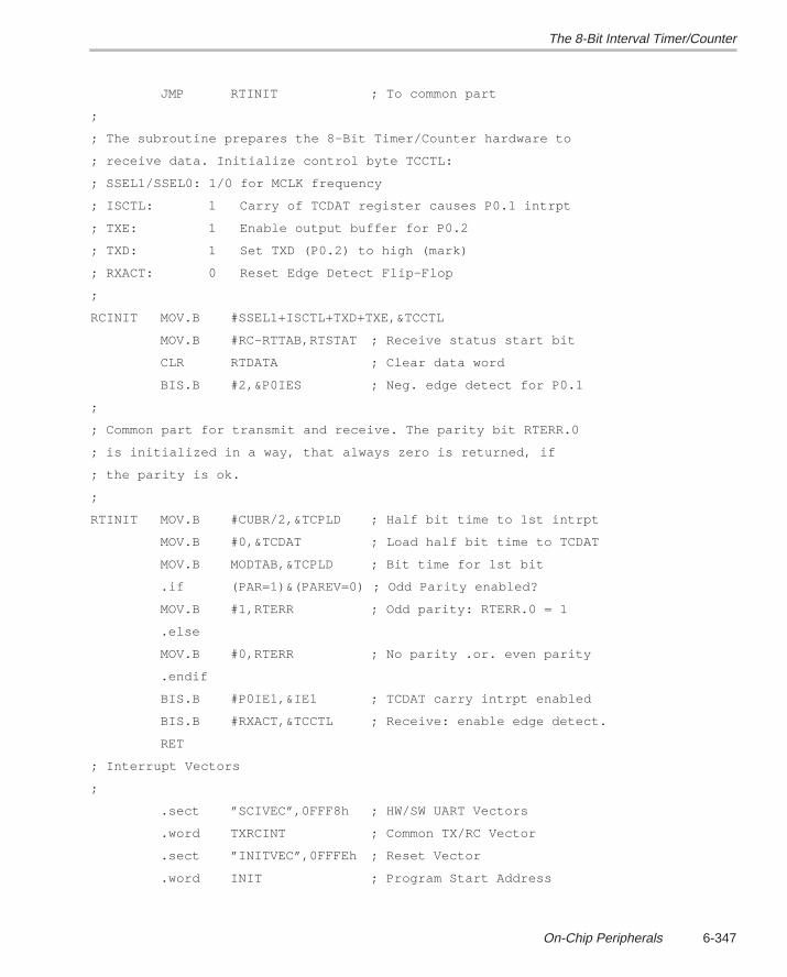
The 8-Bit Interval Timer/Counter
6-347On-Chip Peripherals
JMP RTINIT ; To common part
;
; The subroutine prepares the 8–Bit Timer/Counter hardware to
; receive data. Initialize control byte TCCTL:
; SSEL1/SSEL0: 1/0 for MCLK frequency
; ISCTL: 1 Carry of TCDAT register causes P0.1 intrpt
; TXE: 1 Enable output buffer for P0.2
; TXD: 1 Set TXD (P0.2) to high (mark)
; RXACT: 0 Reset Edge Detect Flip–Flop
;
RCINIT MOV.B #SSEL1+ISCTL+TXD+TXE,&TCCTL
MOV.B #RC–RTTAB,RTSTAT ; Receive status start bit
CLR RTDATA ; Clear data word
BIS.B #2,&P0IES ; Neg. edge detect for P0.1
;
; Common part for transmit and receive. The parity bit RTERR.0
; is initialized in a way, that always zero is returned, if
; the parity is ok.
;
RTINIT MOV.B #CUBR/2,&TCPLD ; Half bit time to 1st intrpt
MOV.B #0,&TCDAT ; Load half bit time to TCDAT
MOV.B MODTAB,&TCPLD ; Bit time for 1st bit
.if (PAR=1)&(PAREV=0) ; Odd Parity enabled?
MOV.B #1,RTERR ; Odd parity: RTERR.0 = 1
.else
MOV.B #0,RTERR ; No parity .or. even parity
.endif
BIS.B #P0IE1,&IE1 ; TCDAT carry intrpt enabled
BIS.B #RXACT,&TCCTL ; Receive: enable edge detect.
RET
; Interrupt Vectors
;
.sect ”SCIVEC”,0FFF8h ; HW/SW UART Vectors
.word TXRCINT ; Common TX/RC Vector
.sect ”INITVEC”,0FFFEh ; Reset Vector
.word INIT ; Program Start Address
The 8-Bit Interval Timer/Counter
6-348
6.10.4.2 ACLK Used for the UART Clock
With the ACLK used for the UART clock, two different methods are possible.
ACLK used with the active mode — the only difference to the last sectionis the use of the ACLK instead of the MCLK.
ACLK used with the low power mode 3 — The CPU is switched off normal-ly (LPM3) but the UART activity continues. This method is necessary forlow power applications.
The two different methods are described in the next two sections.
6.10.4.2.1 ACLK With the Active Mode
The ACLK can be used for the UART clock in very much the same way as theMCLK (see Section 6.10.4.1 for details). The use of the ACLK may be neces-sary if the needed baud rate is too low for the MCLK frequency in use. For ex-ample, with an MCLK of 1.048 MHz, the lowest (usual) baud rate is 4800 baud.
To use the ACLK with the active mode, it is only necessary to change two partsof the software example of Section 6.10.4.1:
The definition line for the UART clock:
UARTCLK .equ 32768 ; ACLK is used for UARTCLK
The initialization subroutines TXINIT and RCINIT. Instead of the MCLK,the ACLK needs to be defined with the initialization subroutines (SSEL0= 1, SSEL1 = 0). The simplest way is to use the subroutines of this Section(6.10.4.2).
6.10.4.2.2 ACLK With the Low Power Mode 3
This section shows another approach. With this example, the CPU is normallyoff and leaves the LPM3 only for the interrupt handling and after a completecharacter is received or transmitted.
Example 6–66. Half duplex UART With Interrupt
Half duplex UART software using the UART interrupt is shown. It is designedfor:
Baud rate: 2400 baud
The 8-Bit Interval Timer/Counter
6-349On-Chip Peripherals
The ACLK (32,768 Hz) is used for the UART clock
Eight data bits
Parity enabled with odd parity
Address bit included
Two stop bits
Reception of correct characters only (no error indication, restart instead)
The CPU normally uses the low power mode 3 (LPM3)
UART signals like shown in figure 6–87 (mark = VCC, space = VSS)
The software switches have the same function as described in Section6.10.4.1. The UARTCLK is defined with the crystal frequency.
Also, this example uses a looped calculation for the correction of the bits. Notonly eight different bits are calculated, but all of the bits of a frame (9 to 13) arecalculated individually. See the software part starting at the label MODTAB.
Transmit Mode: the data to be transmitted is loaded right-aligned into theRAM word RTDATA. The address bit — if enabled by ADDR = 1 — is included.No error is possible. Four examples for the data in RTDATA are shown in figure6–95. The completion of the transmission is indicated by the value(TX6–RTTAB) in the status byte RTSTAT. The interrupt routine outputs thecharacter and resets after the completion the CPUoff bit and the SCG1 andSCG0 bits of the stored status register on the stack. This manipulation omitsthe return to LPM3 and initializes the next transmit sequence.
Receive Mode: the received data is loaded left-aligned into the RAM wordRTDATA. This means that depending on the address bit and the number ofdata bits contained in the data word, a shift is necessary to get a single bytecontaining the received character. Examples for the data are shown in figure6–96. The input format used is necessary due to the address bit. The comple-tion of the reception is indicated by the value (RC6–RTTAB) in the status byteRTSTAT. After the reception of a complete character, the interrupt handler re-sets the CPUoff bit and the SCG1 and SCG0 bits of the stored status registeron the stack. This manipulation omits the return to LPM3 and allows the proc-essing of the received data. The error handling is the same as shown for theexample in Section 6.10.4.1.
The 8-Bit Interval Timer/Counter
6-350
; Definitions for the common part
;
STACK .equ 0300h ; Stack start address
FLLMPY .equ 32 ; FLL multiplier for 1,048MHz
;
; Definitions for the UART. Data format:
; odd parity, 8 data bits, address bit, 2 stop bits
; ACLK for UART clock, only correct characters to input buffer
;
Baudr .equ 2400 ; Baud rate is 2400 Baud
UARTCLK .equ 32768 ; ACLK is used for UARTCLK
CHARC .equ 8 ; Length: 7: 7 bits 8: 8 bits
ADDR .equ 1 ; Address bit: 1 yes 0 no
PAR .equ 1 ; Parity 0: disabled 1: enabled
PAREV .equ 0 ; Parity 0: odd 1: even
STB .equ 2 ; Stop bits: 1: one 2: two
TCERRT .equ 0 ; 0: error restart 1: indication
;
TCPE .equ 1 ; Parity error: RTERR.0 = 1
TCFE .equ 2 ; Frame error: RTERR.1 = 1
CUBR .equ –(UARTCLK/Baudr) ; Content 8–Bit Counter
;
.even ; Word boundary
.bss RTDATA,2 ; Data for receive/transmit
.bss RTERR,1 ; Error byte
.bss RTSTAT,1 ; Status byte
;
.text ; Software start address
;
INIT MOV #STACK,SP ; Initialize Stack Pointer
CALL #INITSR ; Init. FLL and RAM
... ; Proceed with initialization
EINT ; Enable interrupts
...
;
; Prepare the transmission of one character from RAM word
The 8-Bit Interval Timer/Counter
6-351On-Chip Peripherals
; RTDATA. Info is contained right aligned in the LSBs. No error
; is possible
;
MOV #xxx,RTDATA ; Character xxx to RTDATA
CALL #TXINIT ; Initialize the transmit part
... ; Continue with background
;
; Prepare the reception of one character to RAM word RTDATA
;
CALL #RCINIT ; Initialize the receive part
... ; Continue in background
;
; After the completion of all background tasks, enter LPM3
;
PLPM3 BIS #CPUoff+GIE+SCG1+SCG0,SR ; Enter LPM3
;
; An interrupt handler cleared the CPUoff, SCG1 and SCG0 bits
; of the SR on the stack. Checks are made if activity is
; needed:
; Receive Mode: one character is received
; Transmit Mode: one character is output completely
; ... other interrupt handlers
;
CMP.B #RC6–RTTAB,RTSTAT ; One character received?
JEQ CHAR_RC ; Yes, process character
CMP.B #TX6–RTTAB,RTSTAT ; One character transmitted?
JEQ CHAR_TX ; Yes, prepare next one
... ; Check other reasons
JMP PLPM3 ; Back to LPM3
;
; Common interrupt handler for transmit and receive functions.
; The carry of TCDAT is switched to the P0.1 interrupt request
; Interrupt time interval of the 8–bit timer is: 1/Baud rate
; The single status byte RTSTAT contains the actual status:
; Idle: RTSTAT = 0 No activity
; Transmit: RTSTAT = 1...TX6–RTTAB–1 Active
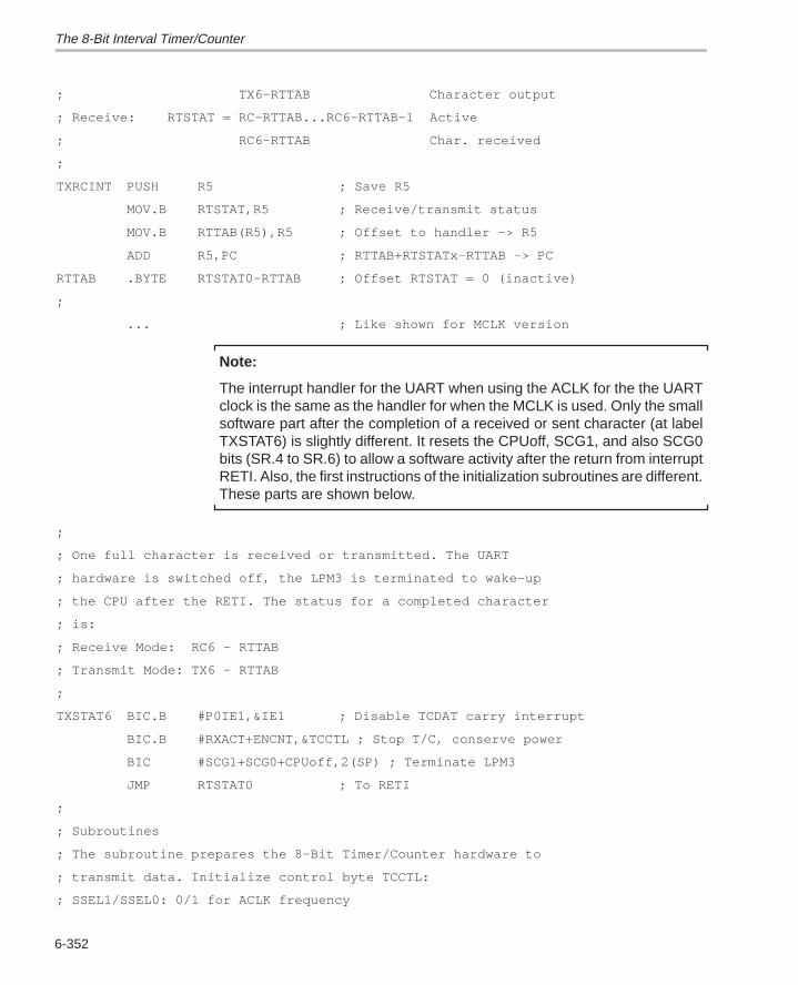
The 8-Bit Interval Timer/Counter
6-352
; TX6–RTTAB Character output
; Receive: RTSTAT = RC–RTTAB...RC6–RTTAB–1 Active
; RC6–RTTAB Char. received
;
TXRCINT PUSH R5 ; Save R5
MOV.B RTSTAT,R5 ; Receive/transmit status
MOV.B RTTAB(R5),R5 ; Offset to handler –> R5
ADD R5,PC ; RTTAB+RTSTATx–RTTAB –> PC
RTTAB .BYTE RTSTAT0–RTTAB ; Offset RTSTAT = 0 (inactive)
;
... ; Like shown for MCLK version
Note:
The interrupt handler for the UART when using the ACLK for the the UARTclock is the same as the handler for when the MCLK is used. Only the smallsoftware part after the completion of a received or sent character (at labelTXSTAT6) is slightly different. It resets the CPUoff, SCG1, and also SCG0bits (SR.4 to SR.6) to allow a software activity after the return from interruptRETI. Also, the first instructions of the initialization subroutines are different.These parts are shown below.
;
; One full character is received or transmitted. The UART
; hardware is switched off, the LPM3 is terminated to wake–up
; the CPU after the RETI. The status for a completed character
; is:
; Receive Mode: RC6 – RTTAB
; Transmit Mode: TX6 – RTTAB
;
TXSTAT6 BIC.B #P0IE1,&IE1 ; Disable TCDAT carry interrupt
BIC.B #RXACT+ENCNT,&TCCTL ; Stop T/C, conserve power
BIC #SCG1+SCG0+CPUoff,2(SP) ; Terminate LPM3
JMP RTSTAT0 ; To RETI
;
; Subroutines
; The subroutine prepares the 8–Bit Timer/Counter hardware to
; transmit data. Initialize control byte TCCTL:
; SSEL1/SSEL0: 0/1 for ACLK frequency
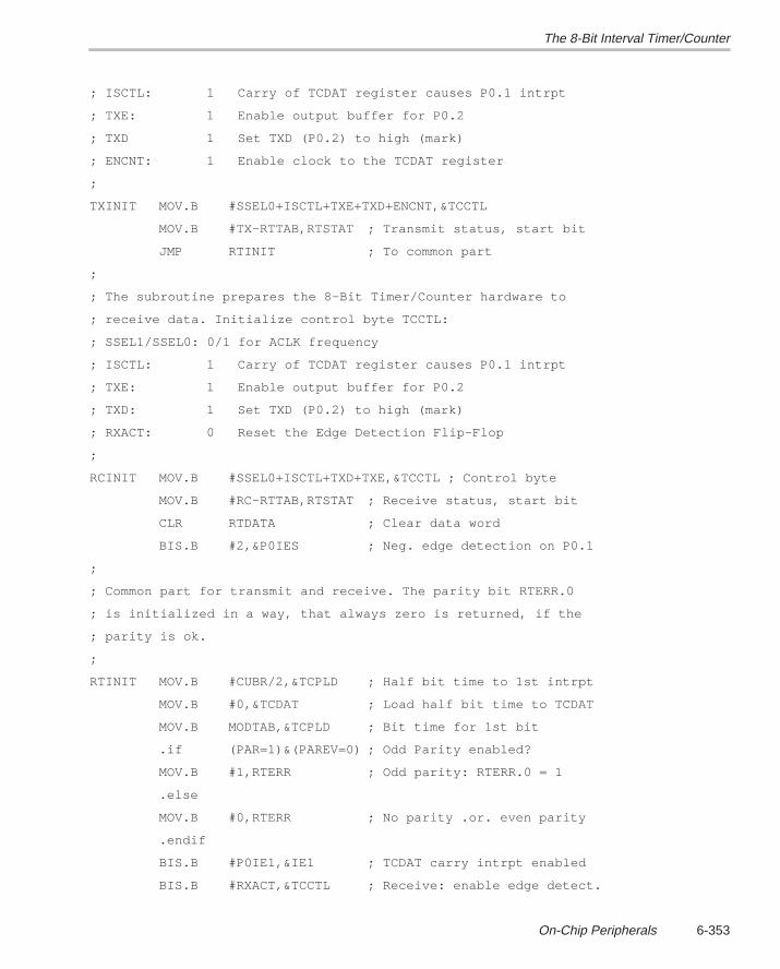
The 8-Bit Interval Timer/Counter
6-353On-Chip Peripherals
; ISCTL: 1 Carry of TCDAT register causes P0.1 intrpt
; TXE: 1 Enable output buffer for P0.2
; TXD 1 Set TXD (P0.2) to high (mark)
; ENCNT: 1 Enable clock to the TCDAT register
;
TXINIT MOV.B #SSEL0+ISCTL+TXE+TXD+ENCNT,&TCCTL
MOV.B #TX–RTTAB,RTSTAT ; Transmit status, start bit
JMP RTINIT ; To common part
;
; The subroutine prepares the 8–Bit Timer/Counter hardware to
; receive data. Initialize control byte TCCTL:
; SSEL1/SSEL0: 0/1 for ACLK frequency
; ISCTL: 1 Carry of TCDAT register causes P0.1 intrpt
; TXE: 1 Enable output buffer for P0.2
; TXD: 1 Set TXD (P0.2) to high (mark)
; RXACT: 0 Reset the Edge Detection Flip–Flop
;
RCINIT MOV.B #SSEL0+ISCTL+TXD+TXE,&TCCTL ; Control byte
MOV.B #RC–RTTAB,RTSTAT ; Receive status, start bit
CLR RTDATA ; Clear data word
BIS.B #2,&P0IES ; Neg. edge detection on P0.1
;
; Common part for transmit and receive. The parity bit RTERR.0
; is initialized in a way, that always zero is returned, if the
; parity is ok.
;
RTINIT MOV.B #CUBR/2,&TCPLD ; Half bit time to 1st intrpt
MOV.B #0,&TCDAT ; Load half bit time to TCDAT
MOV.B MODTAB,&TCPLD ; Bit time for 1st bit
.if (PAR=1)&(PAREV=0) ; Odd Parity enabled?
MOV.B #1,RTERR ; Odd parity: RTERR.0 = 1
.else
MOV.B #0,RTERR ; No parity .or. even parity
.endif
BIS.B #P0IE1,&IE1 ; TCDAT carry intrpt enabled
BIS.B #RXACT,&TCCTL ; Receive: enable edge detect.
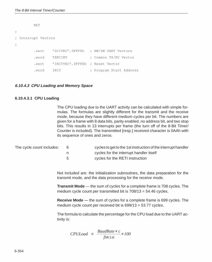
The 8-Bit Interval Timer/Counter
6-354
RET
;
; Interrupt Vectors
;
.sect ”SCIVEC”,0FFF8h ; HW/SW UART Vectors
.word TXRCINT ; Common TX/RC Vector
.sect ”INITVEC”,0FFFEh ; Reset Vector
.word INIT ; Program Start Address
6.10.4.3 CPU Loading and Memory Space
6.10.4.3.1 CPU Loading
The CPU loading due to the UART activity can be calculated with simple for-mulas. The formulas are slightly different for the transmit and the receivemode, because they have different medium cycles per bit. The numbers aregiven for a frame with 8 data bits, parity enabled, no address bit, and two stopbits. This results in 13 interrupts per frame (the turn off of the 8-Bit Timer/Counter is included). The transmitted [resp.] received character is 0AAh withits sequence of ones and zeros.
The cycle count includes: 6 cycles to get to the 1st instruction of the interrupt handlern cycles for the interrupt handler itself5 cycles for the RETI instruction
Not included are: the initialization subroutines, the data preparation for thetransmit mode, and the data processing for the receive mode.
Transmit Mode — the sum of cycles for a complete frame is 708 cycles. Themedium cycle count per transmitted bit is 708/13 = 54.46 cycles.
Receive Mode — the sum of cycles for a complete frame is 699 cycles. Themedium cycle count per received bit is 699/13 = 53.77 cycles.
The formula to calculate the percentage for the CPU load due to the UART ac-tivity is:
CPULoadBaudRate c
f100
MCLK= × ×
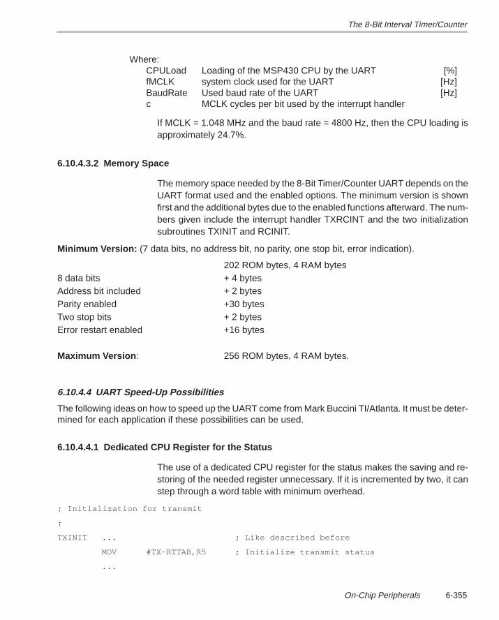
The 8-Bit Interval Timer/Counter
6-355On-Chip Peripherals
Where: CPULoad Loading of the MSP430 CPU by the UART [%]fMCLK system clock used for the UART [Hz]BaudRate Used baud rate of the UART [Hz]c MCLK cycles per bit used by the interrupt handler
If MCLK = 1.048 MHz and the baud rate = 4800 Hz, then the CPU loading isapproximately 24.7%.
6.10.4.3.2 Memory Space
The memory space needed by the 8-Bit Timer/Counter UART depends on theUART format used and the enabled options. The minimum version is shownfirst and the additional bytes due to the enabled functions afterward. The num-bers given include the interrupt handler TXRCINT and the two initializationsubroutines TXINIT and RCINIT.
Minimum Version: (7 data bits, no address bit, no parity, one stop bit, error indication).
202 ROM bytes, 4 RAM bytes8 data bits + 4 bytesAddress bit included + 2 bytesParity enabled +30 bytesTwo stop bits + 2 bytesError restart enabled +16 bytes
Maximum Version : 256 ROM bytes, 4 RAM bytes.
6.10.4.4 UART Speed-Up Possibilities
The following ideas on how to speed up the UART come from Mark Buccini TI/Atlanta. It must be deter-mined for each application if these possibilities can be used.
6.10.4.4.1 Dedicated CPU Register for the Status
The use of a dedicated CPU register for the status makes the saving and re-storing of the needed register unnecessary. If it is incremented by two, it canstep through a word table with minimum overhead.
; Initialization for transmit
;
TXINIT ... ; Like described before
MOV #TX–RTTAB,R5 ; Initialize transmit status
...
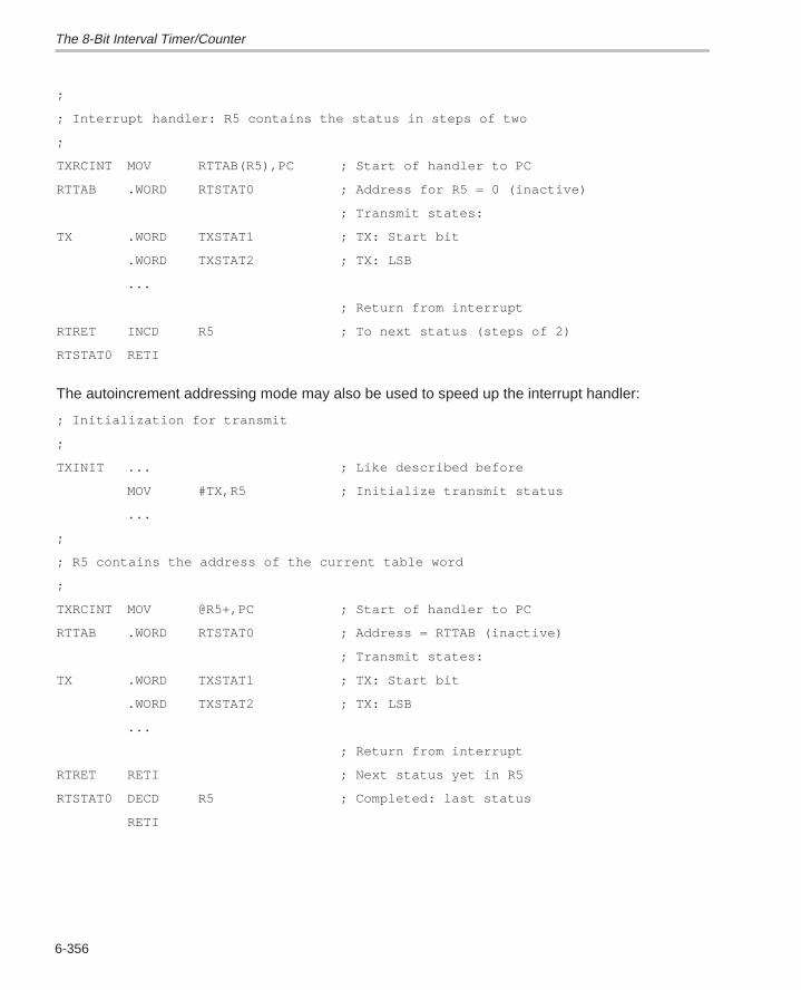
The 8-Bit Interval Timer/Counter
6-356
;
; Interrupt handler: R5 contains the status in steps of two
;
TXRCINT MOV RTTAB(R5),PC ; Start of handler to PC
RTTAB .WORD RTSTAT0 ; Address for R5 = 0 (inactive)
; Transmit states:
TX .WORD TXSTAT1 ; TX: Start bit
.WORD TXSTAT2 ; TX: LSB
...
; Return from interrupt
RTRET INCD R5 ; To next status (steps of 2)
RTSTAT0 RETI
The autoincrement addressing mode may also be used to speed up the interrupt handler:
; Initialization for transmit
;
TXINIT ... ; Like described before
MOV #TX,R5 ; Initialize transmit status
...
;
; R5 contains the address of the current table word
;
TXRCINT MOV @R5+,PC ; Start of handler to PC
RTTAB .WORD RTSTAT0 ; Address = RTTAB (inactive)
; Transmit states:
TX .WORD TXSTAT1 ; TX: Start bit
.WORD TXSTAT2 ; TX: LSB
...
; Return from interrupt
RTRET RETI ; Next status yet in R5
RTSTAT0 DECD R5 ; Completed: last status
RETI
The 8-Bit Interval Timer/Counter
6-357On-Chip Peripherals
6.10.4.4.2 No Baud Rate Correction
No baud rate correction is needed if the MCLK is used for the baud rate Gener-ation. This allows a shorter interrupt handler with fewer cycles and less pro-gram space.
6.10.4.4.3 Word Table Instead of a Byte Table
If a word table instead of the byte table is used for the distribution at the startof the interrupt handler, then more program space is needed, but the executionis faster. See Section 6.10.4.4.1.
6.10.4.4.4 Mixture of the Methods
The two sources for the UART clock are detailed in sections 6.10.4.1 (MCLK)and 6.10.4.2 (ACLK) may be mixed to get the best of both worlds:
Transmit Mode — the program normally uses the LPM3. If a character needsto be output, then the active mode with its MCLK is used. The software is identi-cal to the transmit mode shown in Section 6.10.4.1.
Receive Mode — the program normally uses the LPM3 with the interrupt ofthe P0.1 pin activated on negative edges (start bit).
The initialization subroutine is the same as shown in Section 6.10.4.1 withthe exception of:
The bit ISCTL in the control register TCCTL is reset to enable the inter-rupt at pin P0.1 for negative edges.
The next start bit wakes up the MSP430, which starts the following activi-ties:
The control loop of the system clock generator is closed to get a con-trolled MCLK frequency (SCG0 = 0)
The interrupt source is switched from the input pin P0.1 to the carry ofthe 8-bit counter (ISCTL = 1)
The MCLK stays active until the complete character is received. TheLPM3 is activated again after the processing of the received data.
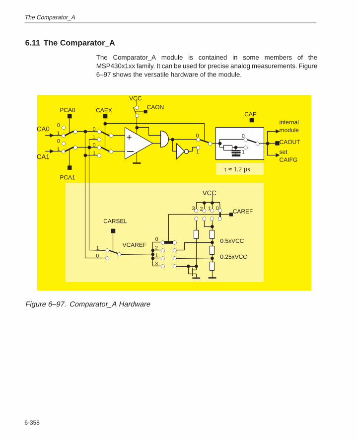
The Comparator_A
6-358
6.11 The Comparator_A
The Comparator_A module is contained in some members of theMSP430x1xx family. It can be used for precise analog measurements. Figure6–97 shows the versatile hardware of the module.
CAOUT
CAON
+
–
VCC
0
1
0
1
CAEX
0
12
CAREF
VCC
0.5xVCC
0.25xVCC
13 2
01 VCAREF
CARSEL
0
1
0
1
CAF
0
1
0
1
PCA0
PCA1
setCAIFG
τ ≈ 1.2 µs
CA0
CA1
internalmodule
3
0
Figure 6–97. Comparator_A Hardware
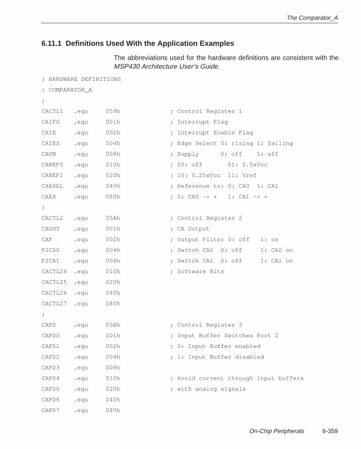
The Comparator_A
6-359On-Chip Peripherals
6.11.1 Definitions Used With the Application Examples
The abbreviations used for the hardware definitions are consistent with theMSP430 Architecture User’s Guide.
; HARDWARE DEFINITIONS
; COMPARATOR_A
;
CACTL1 .equ 059h ; Control Register 1
CAIFG .equ 001h ; Interrupt Flag
CAIE .equ 002h ; Interrupt Enable Flag
CAIES .equ 004h ; Edge Select 0: rising 1: falling
CAON .equ 008h ; Supply 0: off 1: off
CAREF0 .equ 010h ; 00: off 01: 0.5xVcc
CAREF1 .equ 020h ; 10: 0.25xVcc 11: Vref
CARSEL .equ 040h ; Reference to: 0: CA0 1: CA1
CAEX .equ 080h ; 0: CA0 –> + 1: CA1 –> +
;
CACTL2 .equ 05Ah ; Control Register 2
CAOUT .equ 001h ; CA Output
CAF .equ 002h ; Output Filter 0: off 1: on
P2CA0 .equ 004h ; Switch CA0 0: off 1: CA0 on
P2CA1 .equ 008h ; Switch CA1 0: off 1: CA1 on
CACTL24 .equ 010h ; Software Bits
CACTL25 .equ 020h
CACTL26 .equ 040h
CACTL27 .equ 080h
;
CAPD .equ 05Bh ; Control Register 3
CAPD0 .equ 001h ; Input Buffer Switches Port 2
CAPD1 .equ 002h ; 0: Input Buffer enabled
CAPD2 .equ 004h ; 1: Input Buffer disabled
CAPD3 .equ 008h
CAPD4 .equ 010h ; Avoid current through input buffers
CAPD5 .equ 020h ; with analog signals
CAPD6 .equ 040h
CAPD7 .equ 080h

The Comparator_A
6-360
6.11.1.1 Attributes of the Comparator_A
The hardware allows all combinations of comparisons. The bit CAOUT(CACTL.0) contains the result of the comparison:
Comparison of two external inputs
Comparison of each external input with 0.25 × VCC or 0.5 × VCC
Comparison of each external input with an internal reference voltage
An analog filter can be switched to the CAOUT output
The module has interrupt capability for the leading and the trailing edgeof the output signal CAOUT
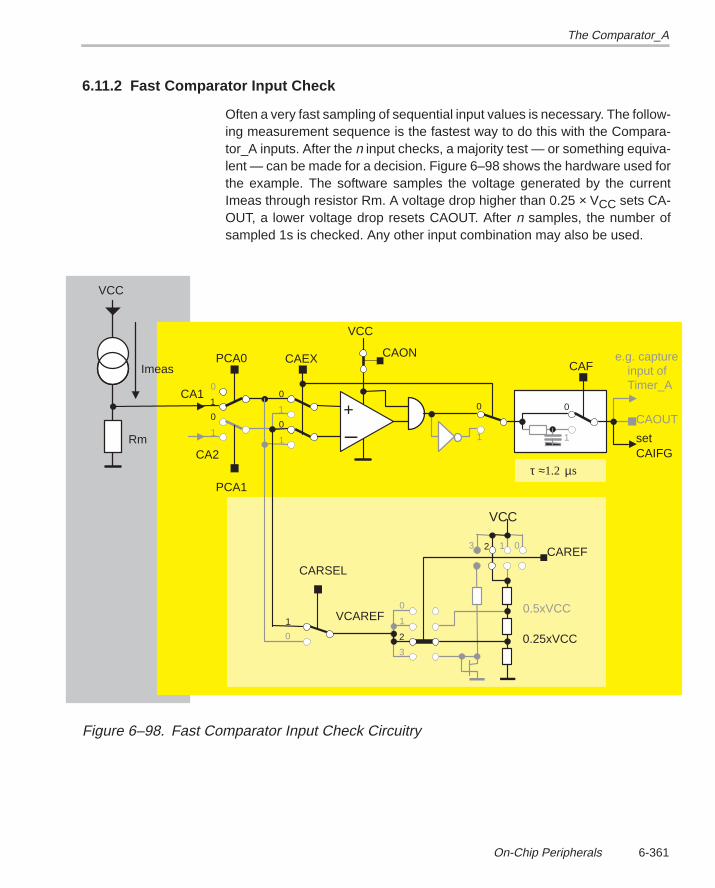
The Comparator_A
6-361On-Chip Peripherals
6.11.2 Fast Comparator Input Check
Often a very fast sampling of sequential input values is necessary. The follow-ing measurement sequence is the fastest way to do this with the Compara-tor_A inputs. After the n input checks, a majority test — or something equiva-lent — can be made for a decision. Figure 6–98 shows the hardware used forthe example. The software samples the voltage generated by the currentImeas through resistor Rm. A voltage drop higher than 0.25 × VCC sets CA-OUT, a lower voltage drop resets CAOUT. After n samples, the number ofsampled 1s is checked. Any other input combination may also be used.
CAOUT
CAON
+
–
VCC
0
1
0
1
CAEX
0
1
2
CAREF
VCC
0.5xVCC
0.25xVCC
013 2
0
1 VCAREF
CARSEL
0
1
0
1
CAF
0
1
0
1
PCA0
PCA1
setCAIFG
τ ≈1.2 µs
CA1
CA2
3
e.g. captureinput ofTimer_A
VCC
Imeas
Rm
Figure 6–98. Fast Comparator Input Check Circuitry
The Comparator_A
6-362
; Fast test for the state of the Comparator_A input
;
MOV.B #CARSEL+CAREF1+CAON,&CACTL1 ; Define Comp_A mode
MOV.B #PCA0,&CACTL2
MOV #CACTL2,R15 ; Prepare pointer to reg. CACTL2
...
MOV.B @R15,R5 ; Sample CAOUT (CAOUT = CACTL2.0)
ADD.B @R15,R5 ; Add next sample
... ; Add following samples
ADD.B @R15,R5 ; Add sample n
;
; Test if CAOUT showed more than n/2 times a positive result
;
SUB #n*PCA0,R5 ; Correct result
CMP.B #1+(n/2),R5 ; R5 – (1+n/2)
JHS POS ; More samples are 1
... ; More samples are 0
or an even faster decision:
; Test if CAOUT showed more than n/2 times a positive result
;
CMP.B #n*PCA0+1+(n/2),R5 ; R5–n*PCA0+(1+n/2)
JHS POS ; More samples are 1
... ; More samples are 0
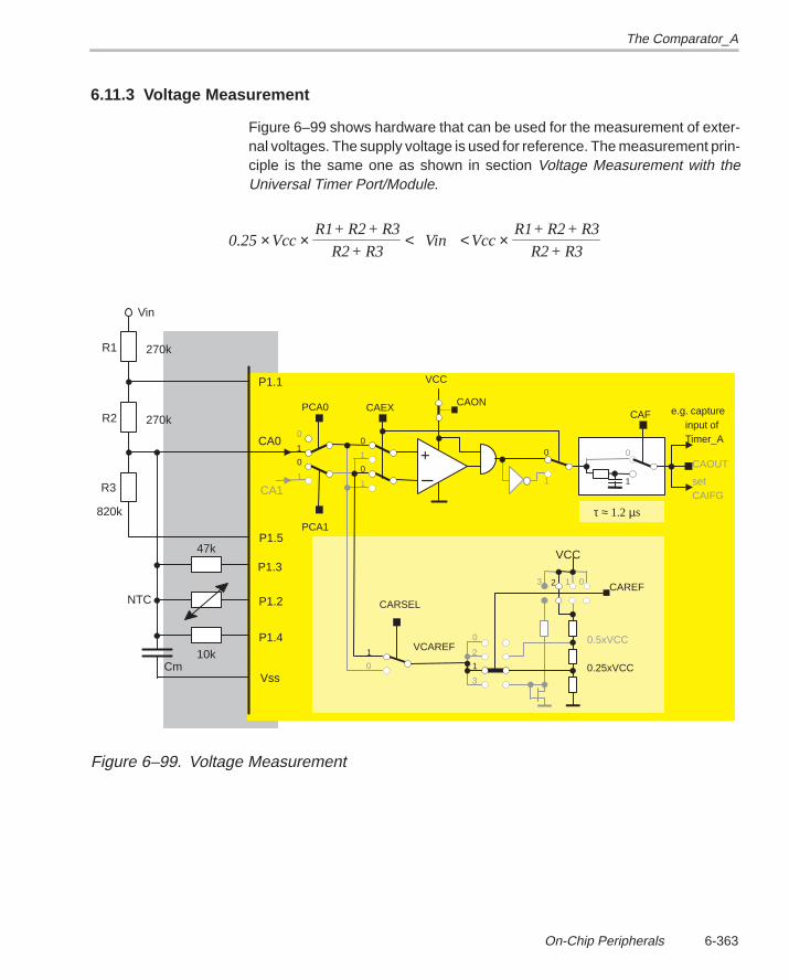
The Comparator_A
6-363On-Chip Peripherals
6.11.3 Voltage Measurement
Figure 6–99 shows hardware that can be used for the measurement of exter-nal voltages. The supply voltage is used for reference. The measurement prin-ciple is the same one as shown in section Voltage Measurement with theUniversal Timer Port/Module.
0.25 VccR1+ R2+ R3
R2+ R3Vin Vcc
R1+ R2+ R3
R2+ R3× × < < ×
CAOUT
CAON
+
–
VCC
0
1
0
1
CAEX
0
1
2
CAREF
VCC
0.5xVCC
0.25xVCC
013 2
0
1VCAREF
CARSEL
0
1
0
1
CAF
0
1
0
1
PCA0
PCA1
setCAIFG
τ ≈ 1.2 µs
CA0
CA1
3
e.g. captureinput ofTimer_A
Vin
P1.1
P1.5
P1.3
P1.2
P1.4
270k
270k
820k
47k
10kCm
NTC
Vss
R1
R2
R3
Figure 6–99. Voltage Measurement

The Comparator_A
6-364

7-1
Hints and Recommendations
Chapter 7
Hints and Recommendations
7-2
7.1 Hints and Recommendations
During the software development for the first MSP430 projects, a lot of experi-ence was acquired. The following hints and recommendations are for all pro-grammers and system designers having more experience with 4-bit and 8-bitmicrocomputers than with 16-bit systems. Also mentioned are deviations theMSP430 family shows when compared to other 16-bit architectures (e.g., thefunction of the carry bit as an inverted zero bit with some instructions).
Frequently Used Bits : these bits should always be located in bit positions0, 1, 2, 3, 7, or 15. The first four bits can be set, reset, and tested withconstants coming from the constant generator (1, 2, 4, 8), and the last twocan be easily tested with the conditional jump instructions JN and JGE:
TST.B RSTAT ; TEST Bit7 (OV <– 0)
JGE BIT7LO ; JUMP IF MSB OF BYTE IS 0
TST MSTAT ; TEST Bit15 (OV <– 0)
JN BIT15HI ; JUMP IF MSB OF WORD IS 1
Use of BCD arithmetic : If simple up/down counters are used and are tobe displayed. This saves time and ROM space because no unnecessarybinary–BCD conversion is needed.
EXAMPLE: Counter1 (four BCD digits) is incremented. Counter2 (eight BCDdigits) is decremented by one.
CLRC ; DADD adds Carry bit too!
DADD #0001,COUNTER1 ; INCREMENT COUNTER1 DECIMALLY
CLRC
DADD #9999h,COUNTER2 ; DECREMENT 8 DIGIT COUNTER2
DADD #9999h,COUNTER2+2 ;DECIMALLY
Conditional Assembly : This feature of the MSP430 assembler allowsmore than one version out of one source of code. This drastically reducesthe effort to maintain software. Only one version needs to be updated ifchanges are necessary. See Section 9.2.1, Conditional Assembly andFloating Point Software Examples.
Use of Bytes : Use bytes wherever appropriate. The MSP430 allows theuse of every instruction with bytes. The only exceptions are the instruc-tions SWPB, SXT, and CALL.
Use of Status Bytes or Words : Use status bytes or words, not flags forthe storage of states. This allows extremely fast branching with only oneinstruction to the appropriate handler. Otherwise, a time (and ROM) con-suming skip chain is necessary (also see Section 9.2).
Hints and Recommendations
7-3Hints and Recommendations
Computing Software : Use integer routines if speed is essential. Use thefloating point package if complex or very accurate calculations are need-ed.
Bit Handling Instructions :
With the bit handling instructions (BIS, BIT and BIC) more than one bit canbe handled simultaneously. Up to 16 bits can be handled with a single in-struction.
The BIS instruction is equivalent to the logical OR and can be used thisway.
The BIC instruction is equivalent to the logical AND with the invertedsource and can be used this way.
Use of the Addressing Modes :
Use the symbolic mode for random accesses
Use the absolute mode for fixed hardware addresses such as peripheraladdresses
Use the indexed mode for random accesses in tables
Use the register mode for time critical processing and as the normal one
Use assigned registers for extremely critical purposes. If a register alwayscontains the same information, then it is not necessary to save it and toload it afterwards. The same is true for the restoring of the register whenthe task is done.
Stack Operations :
All items on the stack can be accessed directly with the indexed mode.This allows completely new applications compared with architectures thathave only simple hardware stacks.
The stack size is limited only by the available RAM, not by hardware regis-ter limitations.
Note:
The previously mentioned possibilities make strict housekeeping necessary.Every program part that uses the stack has to ensure that only relevant infor-mation remains on the stack and that all irrelevant data is removed. If this ruleis not used consequently, the stack will overflow or underflow. If complexstack handling is used, it is advised to draw the stack with its items and thestack pointer as shown with the examples Argument Transfer with Subrou-tine Calls in Chapter 9. The drawn stack allocation gives a good overview.
Hints and Recommendations
7-4
The Program Counter (PC) : The PC can be accessed as every other reg-ister with all instructions and all addressing modes. Be very careful whenusing this feature. Do not use byte instructions when accessing the PC,due to the clearing of the upper byte when used.
The Status Register (SR) : The SR can be accessed in register modeonly. Every status bit can be set or reset alone or together. This feature canbe used for status transfer in subroutines. The FPP uses this type of statustransfer.
Enabling of the General Interrupt : The instruction that follows the enab-ling of the interrupt is executed before an interrupt is accepted:
EINT ; Enable interrupt (GIE)
CLRC ; This instruction is executed before
ADC R5 ; the 1st interrupt is accepted
High–Speed Multiplication : If the fastest possible speed is necessary formultiplications and the hardware multiplier is not available, then the loopoverhead can be omitted.
Straight through programming: the effort used for the looping can besaved if the shifts and adds are programmed straight through. The routineends at the known MSB of the multiplicand (here, at bit 13 due to an ADCresult (14 bits) that is multiplied):
;
; EXECUTION TIMES FOR REGISTER USE (CYCLES, CALL not included):
;
; TASK CYCLES EXAMPLE
;–––––––––––––––––––––––––––––––––––––––––––––––––––––––––––––
; MINIMUM 80 00000h x 00000h = 000000000h
; MEDIUM 96 0A5A5h x 05A5Ah = 03A763E02h
; MAXIMUM 112 0FFFFh x 0FFFFh = 0FFFE0001h
; Fast Multiplication Routine: Part used by signed and unsigned
; Multiplications. R5 x R4 –> R8|R7
;
MACUF CLR R6 ; MSBs MULTIPLIER
;
RRA R4 ; LSB to carry
JNC L$01 ; IF ZERO: SKIP ADD
ADD R5,R7 ; IF ONE: ADD MULTIPLIER TO RESULT
ADDC R6,R8
L$01 RLA R5 ; MULTIPLIER x 2
RLC R6 ;;
Hints and Recommendations
7-5Hints and Recommendations
RRA R4 ; LSB+1 to carry
JNC L$02 ;
ADD R5,R7 ;
ADDC R6,R8
L$02 RLA R5 ;
RLC R6 ;
.... ; same way for bits 2 to 12
;
RRA R4 ; MSB to carry (here bit13)
JNC L$014 ;
ADD R5,R7 ;
ADDC R6,R8 ; No shift for multiplier necessary
L$014 RET ; Return with result in R8|R7
;
Emulation of Jump if Positive : No jump if positive is provided, only ajump if negative. But after several instructions it is possible to use the jumpif greater than or equal (JGE) for this purpose. But it must be certain thatthe instruction preceding the JGE resets the overflow bit V. The followinginstructions ensure this:
TST, SXT, RRA, BIT, AND.
The use of this emulation should be noted in the comment field to easesoftware modifications.
Special Use of the Carry Bit : The following instructions have a specialfeature that is valuable during serial to parallel conversion. The carry actsas an inverted zero bit. This means if the result of an operation is zero thenthe carry is reset and vice versa. The instructions having this feature are:
XOR, SXT, INV, BIT, AND.
Without using this feature a typical sequence for the conversion of an I/O-port bit to a parallel word would look like the following:
RLA R5 ; Free bit 0 for next info
BIT #1,&IOIN ; PO.0 high ?
JZ L$111
INC R5 ; Yes, set bit 0
L$111 ... ; Info in bit 0
Using this feature, the previous sequence is shortened to two instructions:
BIT #1,&IOIN ; PO.0 high ? .NOT.Zero –> carry
RLC R5 ; Shift bit (in Carry) into R5
Hints and Recommendations
7-6
The Carry Bit Used for Increments : The carry bit can be used if incre-ments by one are necessary.
EXAMPLE: If the RAM word COUNT is greater than or equal to the value 1000then a word COUNTER is to be incremented by one.
CMP #1000,COUNT ; COUNT >= 1000
ADC COUNTER ; If yes, (C = 1) incr. COUNTER
Immediate Addition of the Carry Bit : The carry bit can be added immedi-ately. No conditional jumps are necessary for counters longer than 16 bits.A 48-bit counter is incremented.
ADD R5,COUNT ; Low part of COUNT
ADC COUNT+2 ; Medium part
ADC COUNT+4 ; High part of 48–bit counter
Fall Through Programming : ROM space is saved if a subroutine call thatis located immediately before a RET instruction is changed. The calledsubroutine is located after the instruction before the CALL, and the pro-gram falls through it. This saves 6 bytes of ROM: The CALL itself and theRET instruction. The I2C handler uses this mode.
; Normal way: SUBR2 is called, afterwards returned
;
SUBR1 ...
MOV R5,R6
CALL #SUBR2 ; Call subroutine
RET
;
; ”Fall Through” solution: SUBR2 is located after SUBR1
;
SUBR1 ...
MOV R5,R6 ; Fall through to SUBR2
;
SUBR2 ... ; Start of subroutine SUBR2
RET
Shift Operations for 32–Bit Numbers : If shifts with numbers greater than16 bits are necessary, the shift operations for the upper words must beRLC or RRC. If RLA or RRA are used then only zeroes are shifted in
RLA R11 ; MSB of low byte to carry
RLC R12 ; RLA is wrong here!
RRA R12 ; LSB of high byte to carry
RRC R11 ; RRA is wrong here!
Interrupt Handlers : The length of interrupt handlers should be kept asshort as possible. All necessary calculations should be made in the back-ground program (main program). The activation and control can be madeeasily with status bytes.
Hints and Recommendations
7-7Hints and Recommendations
Decimal Subtraction : No instruction is provided, but a simple way is pos-sible. The copy instruction is only necessary if the minuend may not bemodified.
EXAMPLE: OP1 is subtracted from OP2 decimally
MOV OP1,R5 ; Copy Op1
ADD #6666h,R5 ; OP1 into range 6666h to FFFFh
INV R5 ; Build 9999 complement
SETC
DADD R5,OP2 ; OP2 – OP1 –> OP2 (dec.)
Timer Wake–Up Out of Low Power Modes : The two 8-bit counters of theuniversal timer/port can also be used during the low power modes 3 and4. If a counter is incremented by an external signal (inputs CIN, CMP, orTPIN.5) from 0FFh to 0h, then the appertaining RCxFG-flag is set. If aninterrupt is enabled, the CPU wakes up.

Design Checklist
7-8
7.2 Design Checklist
Several steps are necessary to complete a system consisting of an MSP430and its peripherals with the necessary performance. Typical and recom-mended development steps are shown in the following. All of the tasks men-tioned should be done carefully in order to prevent trouble later on.
1) Definition of the tasks to be performed by the MSP430 and its peripherals
2) Selection of the MSP430 version that fits best
3) Worst case timing considerations for all of the tasks to be done (interrupttiming, calculation times, I/O etc.)
4) Drawing of a complete hardware schematic. Deciding which hardware op-tions are used (supply voltage, pull-downs at the I/O-ports, etc.)
5) Worst case design for all of the external components
6) Organization of the RAM and — if present — of the external EEPROM
7) Flowcharting of the complete software
8) Coding of the software with an editor
9) Assembling of the program with the ASM430 Assembler
10) Removing of the logical errors found by the ASM430 Assembler
11) Testing of the software with the SIM430 Simulator and an emulation board
12) Repetition of the steps 7 to 10 until the software is free of errors

Most Frequent Software Errors
7-9Hints and Recommendations
7.3 Most Frequent Software Errors
During software development, the same errors are made by nearly all assem-bler programmers. The following list contains the errors which are most oftenheard of and experienced.
Missing Housekeeping During Stack Operations : If items are removedfrom or placed onto the stack during subroutines or interrupt handlers, itis mandatory to keep track of these operations. Any wrong positioning ofthe stack pointer will lead to a program crash, due to the wrong data writteninto the program counter.
Missing Initialization of the Stack Pointer : The stack pointer needs tobe initialized before the EINT instruction is executed or a CALL is used.The normal instruction to be used is:
MOV #0300h,SP ; Locate stack at high RAM
Use of the Wrong Jump Instructions : The conditional jump instructionsJLO and JLT, or JHS, and JGE, give different results if used for numbersabove 07FFFh. It is therefore necessary to always distinguish betweensigned and unsigned jump instructions.
Wrong Completion Instructions . Despite their virtual similarity, subrou-tines and interrupt handlers need completely different actions for comple-tion.
Subroutines end with the RET instruction. Only the address of the nextinstruction (the one following the subroutine call) is popped from thestack.
Interrupt handlers end with the RETI instruction. Two items arepopped from the stack, first the status register is restored and after-wards the address (the address of the next instruction after the inter-rupted one) is popped from the stack to the program counter.
If RETI and RET are used incorrectly, a wrong item is written into thePC. This means that the software will continue at random addressesand will hang–up.
Addition and Subtraction of Numbers With Differently Located Deci-mal Points : if numbers with virtual decimal points are used the additionor subtraction of numbers with different fractional bits leads to errors. It isnecessary to shift one of the operands in a way to achieve fractional partsof equal length. See ”Rules for the Integer Subroutines.”
Byte Instructions Applied to Working Registers : byte instructions al-ways clear the upper byte of the used working register (except CMP.B,TST.B, BIT.B). It is necessary therefore to use word instructions if opera-tions in working registers can exceed the byte range.
Most Frequent Software Errors
7-10
Use of Byte Instructions With the Program Counter as DestinationRegister : if the PC is the destination register byte instructions do not makesense. The clearing of the PC high byte is certainly wrong in any case.Instead, a register is to be used before the modification of the PC with thebyte information. See 9.2.5.
Use of Falsely Addressed Branches and Subroutine Calls : The des-tination of branches and calls is used indirectly, and this means the contentof the destination is used as the address. These errors occur most oftenwith the symbolic mode and the absolute mode:
CALL MAIN ; Subroutine’s address is stored in MAIN
CALL #MAIN ; Subroutine starts at address MAIN
The real behavior is easily seen when looking to the branch instruction. It isan emulated instruction using the MOV instruction:
BR MAIN ; Emulated instruction BR
MOV MAIN,PC ; Emulation by MOV instruction
The addressing for the CALL instruction is exactly the same as for the BRinstruction.
Counters and Timers Longer Than 16-Bits : If counters or timers longerthan 16 bits are modified by the foreground (interrupt routines) and usedby the background, it is necessary to disable the timer interrupt (most sim-ply with the GIE bit in SR) during the reading of these words. If this is notdone, the foreground can modify these words between the reading of twowords. This would mean that one word read contains the old value and theother one the modified value.
EXAMPLE: The timer interrupt handler increments a 32–bit timer. The back-ground software uses this timer for calculations. The disabling of the interruptsprevents the timer interrupt that occurs between the reading of TIMLO andTIMHI, which can falsify the read information. This can be the case if TIMLOoverflows from 0FFFFh to 0000h during the interrupt routine. TIMLO is readwith the old information 0FFFFh and TIMHI contains the new information x+1.
BT_HAN INC TIMLO ; Incr. LO word
ADC TIMHI ; Incr. HI word
RETI
...
;
; Background part copies TIMxx for calculations
;
DINT ; GIE <– 0
Most Frequent Software Errors
7-11Hints and Recommendations
NOP ; DINT needs 2 cycles
MOV TIMLO,R4 ; Copy LSDs
MOV TIMHI,R5 ; COPY MSDs
EINT ; Enable interrupt again
Counters Used by Foreground and Background : If counters are modi-fied by the foreground and read and cleared by the background, care isto be taken that no counts are lost. With the following example, it is pos-sible to loose a count if the interrupt occurs between the MOV and the CLRinstruction. The additional count is not recognized because CNTR (withits content 1) is cleared.
; First the WRONG sequence is shown:
;
INT_HAN INC CNTR ; Incr. counter CNTR WRONG!
RETI ; by interrupts
... ; Background program
MOV CNTR,STORE ; Read CNTR
CLR CNTR ; A count may be lost!
...
To avoid loosing a count, the following solutions are possible for the back-ground part.
; Background part switches off the interrupt during reading
;
DINT ; GIE <– 0 (inactive after MOV)
MOV CNTR,STORE ; Read CNTR
CLR CNTR ; Clear unmodified CNTR
EINT ; Enable interrupt again
;
; Background part uses difference of contents. If interrupt occurs
; after the PUSH instruction, 1 remains in CNTR.
;
PUSH CNTR ; Copy CNTR
SUB @SP,CNTR ; Subtract read number from CNTR
POP STORE ; Place read info to STORE
;
; Simplified version of above: if CNTR is yet changed it contains
; despite correct value (1)
;
MOV CNTR,STORE ; Copy CNTR to STORE
SUB STORE,CNTR ; Subtract STORE of current CNTR
Use of the PUSH Instruction : When using sophisticated stack process-ing, it is often overlooked that the PUSH instruction decrements the stackpointer first and moves the item afterwards.
Most Frequent Software Errors
7-12
EXAMPLE: The return address stored at TOS is to be moved one word downto free space for an argument.
PUSH @SP ; WRONG! 1st free word (TOS–2) is copied
; on itself
PUSH 2(SP) ; Correct, old TOS is pushed 1 word down
EXAMPLE: The stored SP does not point to the same stack address after therestoring. It points to the (address –2) afterwards.
PUSH SP ; Store SP–2 on stack
POP SP ; Restore SP–2 to SP !!
Use of the Autoincrement Mode : The source register is incremented im-mediately after the reading of the source operand. This means if thesource register is also used for the addressing of the destination operand,it contains the incremented value when used.
Register Overflow : If registers do not have the necessary length, nega-tive numbers (MSB = 1) or too small numbers (register is reset to zero byoverflow) can result. The length of registers needs to be evaluated withworst case methods.
Interrupt Blocking : Long interrupt routines should be avoided. If they arenecessary, the GIE bit located in the SR should be set (instruction EINT)at the start of these routines. Otherwise, the disabled interrupt blocks allother interrupt sources.
Real Time Processing : If the algorithm used is longer than the time slotthat is available, errors will occur. Worst case evaluations are necessaryto ensure the algorithm fits into the time slot.
Write-Only Registers : The complete information always needs to be writ-ten to these registers. Otherwise, the bits not included in the source of theinstruction are reset. The crystal buffer control register (CBCTL) is an ex-ample for this register type.
Port Select Registers : I/O ports with dual functions – like the Port3 for theTimer_A (MSP430C33x) – must be switched to the second function.Otherwise, the normal port function is active. To switch Port3 completelyto the Timer_A functions, the following code is needed during the initializa-tion routine. If the Basic Timer is not initialized, the LCD will not work cor-rectly.
MOV.B #TACLK+TA4+TA3+TA2+TA1+TA0,&P3SEL ; Init. Timer_A
If the basic timer is not initialized, the LCD will not work properly.

Most Frequent Hardware Errors
7-13Hints and Recommendations
7.4 Most Frequent Hardware Errors
Crystal Connection : The crystal oscillator is connected to AVCC andAVSS. This means that these two terminals must be connected to DVCCand DVSS, otherwise the crystal will not oscillate.
Open Inputs : Every input must have a defined potential. Otherwise, humand noise will influence the program flow. In addition, the supply currentincreases. See Section 4.9.4, Correct Termination of Unused Terminals.
Crystal Turnon Time : If woken-up from the low power mode 4, the crystalneeds a relatively long time until it runs with the correct frequency. This canlast up to four seconds. Correct timing is not possible until the crystalreached its nominal frequency. Until this, the DCO steps down to its lowestfrequency (≈ 500 kHz). See Section 6.5, The System Clock Generator.
Frequency–locked loop considerations
FLL Turnon Time: If woken-up from LPM3, the FLL needs approxi-mately 6 cycles to reach the nominal frequency. This also means, the1st instruction of an interrupt handler is executed with the correct fre-quency.
Setting Time : The FLL needs a certain non-interrupted time to set thecontrol value of the digitally-controlled oscillator (DCO). If this time isnot provided, no control for the DCO is possible. It remains at the sametap. This time is best spent during initialization by a software loop witha worst case length of 28 x 32 x 30.5 µs = 27.3 ms. To allow the systemclock the adaptation of the DCO to the eventually changed tap, theFLL-loop should be closed during longer calculations. This is donesimply with the instruction:
BIC #SCG0,SR ; Turn on FLL–loop control
Supply Voltage for Battery-Powered Systems : if certain batteries areused the supply voltage may fall below the lower voltage limit during ActiveMode (especially if the ADC is used) due to the high internal resistance ofthese batteries. A capacitor is necessary then in parallel with the battery.
Supply Voltage for AC-Powered Systems : No hum, noise, or spikes areallowed. If these are present, the reliability of the system and the accuracyof the ADC will decrease.
EEPROM Clocking : For some EEPROMs, the minimum clock durationis longer than one MSP430 instruction. This means that NOPs have to beincluded into the clock timing. See the specification of the EEPROM used.

Checklist for Problems
7-14
7.5 Checklist for Problems
7.5.1 Hardware Related Problems
1) Initialization circuit connected? An RC circuit is not sufficient in mostcases.
2) Fan–out of bus or outputs taken into account?
3) Open inputs (interrupt, init, inputs etc.): every input must be connected toa defined voltage level. Otherwise, undefined signals (normally the ac fre-quency) are seen at the inputs. See Section 4.9.4, Correct Termination ofUnused Terminals.
4) Crystal turn–on time not taken into account (may be up to seconds for low–power devices)?
5) Correct levels at all inputs? (low and high levels)
6) Input signals in specified limits: thresholds, frequency and edges?
7) Supply voltage in specified limits, no spikes, no noise etc.
8) External interrupt signals too short (no response from interrupted system)
9) External EEPROM, clock out of the MSP430 too fast or too short? See EE-PROM specification.
10) RESET signals with spikes or false voltage levels? This is an often occur-ring reason for problems.
7.5.2 Software Related Problems
1) Register overflow (registers, memory and peripheral registers) causesnegative numbers or sawtooth characteristic of results (numbers are toosmall then)
2) PWM applications: loading of the pulse length register needs to be syn-chronized to the output change. Otherwise, undefined pulses are outputduring the change of this register
3) Output frequency too high? (register load time longer than pulse length?)
4) Real-time applications: is used algorithm shorter than the available timeinterval also under worst case conditions?
5) Conditional jumps: signed and unsigned jumps used correctly? For exam-ple JHS and JGE are completely different instructions. The same is truefor JLO and JLT.
Run Time Estimation
7-15Hints and Recommendations
6) Missing housekeeping during stack operations? If the return values for theSR and the PC – stored on the stack during an interrupt – are overwrittenwith data: this can cause the setting of the OSCoff bit in the SR during theRETI instruction. Which means, the program execution ceases.
7) Read–out of two–word–registers without disabling the interrupt? (if over-flow occurs one word may contain the old number, the other one the newnumber)
8) Multiple word shifts: correct shift instruction used for the MSBs (no arith-metic shifts: they shift in always zeroes)
9) SP Initialization: forgotten or made after the interrupt enabling with EINT?
10) Interrupt handlers: long lasting parts without enabling the interrupt again(blocks all other interrupt activities)?
11) If the second function of a port register is used: are the select bits in thePxSEL register set?
12) Are all the peripherals initialized?
7.6 Run Time Estimation
To get a quick overview concerning the speed of a given piece of software, thefollowing estimations may be used:
If the code contains all addressing modes then the estimation for the need-ed runtime trun is:
trun ≈ 0.75 cycles/byte
If the code contains only or predominant register mode addressing thenthe estimation for the needed runtime trun is:
trun ≈ 0.5 cycles/byte

Run Time Estimation
7-16

8-1
Architecture and Instruction Set
Chapter 8

Introduction
8-2
8.1 Introduction
The instruction set of the ultra low power-microcomputer MSP430 family dif-fers strongly from the instruction sets used by other 8-bit and 16-bit microcom-puters. The reasons why this instruction set is appreciated though, are ex-plained in the following pages in detail. It is the return to clarity and especiallythe return to orthogonality, an attribute of microcomputer architectures thathas disappeared more and more during the last 20 years. A customer com-mented that it is an instruction set to fall in love with.
The MSP430 Family was developed to fulfill the ever increasing requirementsof Texas Instruments Ultra Low Power microcomputers. It was not possible toincrease the computing power and the real-time processing capability of theMSP430 predecessor (TSS400) as far as was needed. Therefore, a completenew 16-bit architecture was developed to stay competitive and be viable forseveral years.
The benchmark numbers shown in relation to competition’s products (bytesused, number of program lines) are taken from an unbiased comparison exe-cuted by a British software consultant.
Reasons for the Popularity of the MSP430
8-3Architecture and Instruction Set
8.2 Reasons for the Popularity of the MSP430
The following sections are intended to explain the different reasons why theMSP430 instruction set, which closely mirrors the architecture, has becomeso popular.
8.2.1 Orthogonality
This notation of computer science means that a single operand instruction canuse any addressing mode or that any double operand instruction can use anycombination of source and destination addressing modes. Figure 8–1 showsthis graphically: the existing combinations fill the complete possible space.
Instructions
Addressing Modes Source
Addressing ModesDestination
Figure 8–1. Orthogonal Architecture (Double Operand Instructions)
The opposite of orthogonal, a non-orthogonal architecture is shown in Figure8–2. Any instruction can use only a part of the existing addressing modes. Thepossible combinations are arranged like small blocks in the available space.
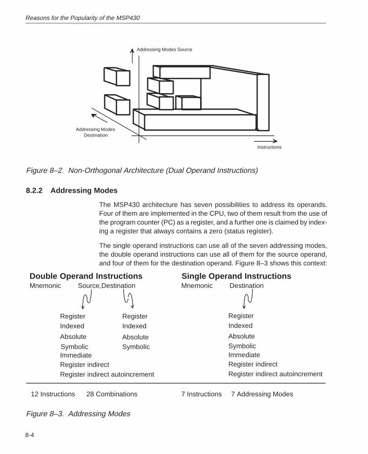
Reasons for the Popularity of the MSP430
8-4
Instructions
Addressing Modes Source
Addressing ModesDestination
Figure 8–2. Non-Orthogonal Architecture (Dual Operand Instructions)
8.2.2 Addressing Modes
The MSP430 architecture has seven possibilities to address its operands.Four of them are implemented in the CPU, two of them result from the use ofthe program counter (PC) as a register, and a further one is claimed by index-ing a register that always contains a zero (status register).
The single operand instructions can use all of the seven addressing modes,the double operand instructions can use all of them for the source operand,and four of them for the destination operand. Figure 8–3 shows this context:
Double Operand Instructions Single Operand InstructionsMnemonic Source,Destination Mnemonic Destination
Register
Register indirectRegister indirect autoincrement
Indexed
Immediate
Absolute
RegisterIndexed
AbsoluteSymbolic Symbolic
Register
Register indirectRegister indirect autoincrement
Indexed
Immediate
AbsoluteSymbolic
12 Instructions 28 Combinations 7 Instructions 7 Addressing Modes
Figure 8–3. Addressing Modes
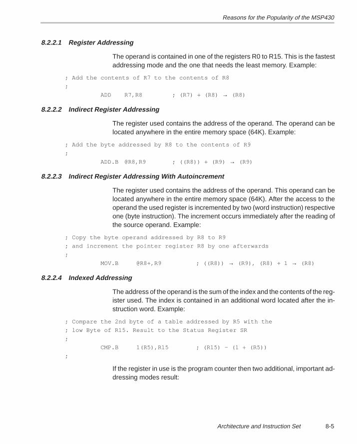
Reasons for the Popularity of the MSP430
8-5Architecture and Instruction Set
8.2.2.1 Register Addressing
The operand is contained in one of the registers R0 to R15. This is the fastestaddressing mode and the one that needs the least memory. Example:
; Add the contents of R7 to the contents of R8
;
ADD R7,R8 ; (R7) + (R8) → (R8)
8.2.2.2 Indirect Register Addressing
The register used contains the address of the operand. The operand can belocated anywhere in the entire memory space (64K). Example:
; Add the byte addressed by R8 to the contents of R9
;
ADD.B @R8,R9 ; ((R8)) + (R9) → (R9)
8.2.2.3 Indirect Register Addressing With Autoincrement
The register used contains the address of the operand. This operand can belocated anywhere in the entire memory space (64K). After the access to theoperand the used register is incremented by two (word instruction) respectiveone (byte instruction). The increment occurs immediately after the reading ofthe source operand. Example:
; Copy the byte operand addressed by R8 to R9
; and increment the pointer register R8 by one afterwards
;
MOV.B @R8+,R9 ; ((R8)) → (R9), (R8) + 1 → (R8)
8.2.2.4 Indexed Addressing
The address of the operand is the sum of the index and the contents of the reg-ister used. The index is contained in an additional word located after the in-struction word. Example:
; Compare the 2nd byte of a table addressed by R5 with the
; low Byte of R15. Result to the Status Register SR
;
CMP.B 1(R5),R15 ; (R15) – (1 + (R5))
;
If the register in use is the program counter then two additional, important ad-dressing modes result:
Reasons for the Popularity of the MSP430
8-6
8.2.2.5 Immediate Addressing
Any 16-bit or 8-bit constant can be used with an instruction. The PC points tothe following word after reading the instruction word. By the use of the registerindirect autoincrement addressing mode, this word (the immediate value) canbe read and the PC is incremented by two afterwards. The word after the in-struction word is treated this way as an 8-bit or a 16-bit immediate value. Ex-ample:
; Test bit 8 in the 3rd word of a table R10 points to.
; Start address of the table is 0(R10), 3rd word is 4(R10)
;
BIT #0100h,4(R10) ; Bit 8 = 1?
;
; The assembler inserts for the instruction above:
;
BIT @PC+,4(R10) ; Executed instruction
.WORD 0100h ; Source constant 0100h
.WORD 0004h ; Index 4 of the destination
8.2.2.6 Symbolic Addressing
This is the normal addressing mode for the random access to the entire 64Kmemory space. The word located after the instruction word contains the differ-ence in bytes to the destination address relative to the PC. This difference canbe seen as an index to the PC. Any address in the 64K memory map is ad-dressable this way, both as a source and as a destination.
Example: $ = address the PC points to
; Subtract the contents of the ROM word EDE from the contents
; of the RAM word TONI
;
SUB EDE,TONI ; (TONI) – (EDE) → (TONI)
;
; The assembler inserts for the instruction above:
;
SUB X(PC),Y(PC) ; Executed instruction
.WORD X ; Index X = EDE–$
.WORD Y ; Index Y = TONI–$
Reasons for the Popularity of the MSP430
8-7Architecture and Instruction Set
8.2.2.7 Absolute Addressing
Addresses that are fixed (e.g., the hardware addresses of the peripherals likeADC, UART) can be addressed absolutely. The absolute addressing mode isa special case of the indexed addressing mode. The register used (SR) alwayscontains a zero in this case (without loosing its former information!). Example:
; Set the Power Down Bit in the ADC Control Register ACTL
;
BIS #PD,&ACTL ; Power Down Bit ADC <– 1
;
; The assembler inserts for the instruction above:
;
BIS @PC+,X(SR) ; Executed instruction
.WORD 01000h ; PD Bit Hardware Address
.WORD 00114h ; X: Hardware Address of ACTL
8.2.3 RISC Architecture Without RISC Disadvantages
Classic RISC architectures provide several addressing modes only for theLOAD and STORE instructions; all other instructions can only access the (nu-merous) registers. The MSP430 can be programmed this way too. An exampleof this programming style is the floating point package FPP4. The registers areloaded during the initialization, the calculations are made exclusively in theregisters, and the result is placed onto the stack.
In real time applications, this kind of programming is less usable, here it is im-portant to access operands at random addresses without any delays. An ex-ample of this is the incrementing of a counter during an interrupt service rou-tine:
; Pure RISC program sequence for the incrementing of a counter
;
INT_HND PUSH R5 ; Save register
LOAD R5,COUNTER ; Load COUNTER to register
INC R5 ; Increment this register
STORE R5,COUNTER ; Store back the result
POP R5 ; Restore used register
RETI ; Return from interrupt
;
; The MSP430 program sequence for the incrementing of a counter
;
INT_HND INC COUNTER ; Increment COUNTER
RETI ; Return from interrupt
As shown in the previous example, the pure RISC architecture is not optimalin cases with few calculations, but necessary for fast access to the memory.
Reasons for the Popularity of the MSP430
8-8
Here, the MSP430 architecture is advantageous due to the random access tothe entire memory (64K) with any instruction, seven source addressing modesand four destination addressing modes.
8.2.4 Constant Generator
One of the reasons for the high code efficiency of the MSP430 architecture isthe constant generator. The constants, appearing most often in assemblersoftware, are small numbers. Out of these, six were chosen for the constantgenerator:
Table 8–1. Constants implemented in the Constant GeneratorCONSTANT HEX REPRESENTATION USE
–1 0FFFFh Constant, all bits are one
0 00000h Constant, all bits are zero
+1 00001h Constant, increment for byte addresses
+2 00002h Constant, increment for word addresses
+4 00004h Constant, value for bit tests
+8 00008h Constant, value for bit tests
These six constants can also be used for byte processing. Only the lower byteis in use then.
The use of numbers out of the constant generator has two advantages:
Memory Space : The constant does not need an additional 16 bit word as itis the case with the normal immediate mode. Two useless addressing modesof the status registers SR and all four addressing modes of the otherwise un-serviceable register R3 are used.
Speed : The constant generator is implemented inside the CPU which resultsin an access time similar to a general purpose register (shortest access time).
Most of the emulated instructions use the constant generator. See ChapterThe MSP430 Instruction Set for examples.
8.2.5 Status Bits
The influence of the instructions to the status bits contained in SR is not as uni-form as the instructions appear. Dependent on the main use of the instruction,the status bits are influenced in one of the following three ways shown:
1) Not at all, the status bits are not affected. This is, for example, the casewith the instructions bit clear, bit set and move.
Reasons for the Popularity of the MSP430
8-9Architecture and Instruction Set
2) Normal: the status bits reflect the result of the last instruction. This is usedwith all arithmetical and logical instructions (except bit set and bit clear)
3) Normal, but the carry bit contains the inverted zero bit. The logical instruc-tions XOR (exclusive or), BIT (bit test) and AND use the carry bit for thenon-zero information. This feature can save ROM space and time. Nopreparations or conditional jumps are necessary. The tested information,which is contained in the carry bit, is simply shifted into a register or a RAMword respective byte.
8.2.6 Stack Processing
The stack processing capability of the MSP430 allows any nesting of inter-rupts, subroutines, and user data. It is only necessary to have enough RAMspace. Due to the function of the SP as a general purpose register, it is possibleto use all seven of the addressing modes for the SP. This allows any neededmanipulation of data on the stack. Any word or byte on the stack can be ad-dressed and may therefore be read and written. (The addressing modes im-plemented for the MSP430 were chosen primarily for the addressing of thestack; but they proved to be very effective also for the other registers).
8.2.7 Usability of the Jumps
Remarkable is the uncommonly wide reach of the jumps which is ±512 words.This value is eight times the reach of other architectures that use normally±128 bytes. Inside program parts it is, therefore, necessary only very rarely touse the branch instruction with its normal two memory words and longer exe-cution time. The implemented eight jumps are classified in three categories:
1) Signed jumps: Numbers range from –32768 to +32767 (word instructions)respective –128 to +127 (byte instructions)
2) Unsigned jumps: Numbers range from 0 to 65535 respective 0 to 255
3) Unconditional jump: (replaces the branch instruction normally)
8.2.8 Byte and Word Processor
Any MSP430 instruction is implemented for byte and word processing. Excep-tions are only the instructions where a byte instruction would not make sense(subroutine call CALL, return from interrupt RETI) or instructions that are usedas an interface between words and bytes (swap bytes SWPB, sign extensionSXT). The addressable memory of the MSP430 is divided into bytes and wordsas shown in Figure 8–4.
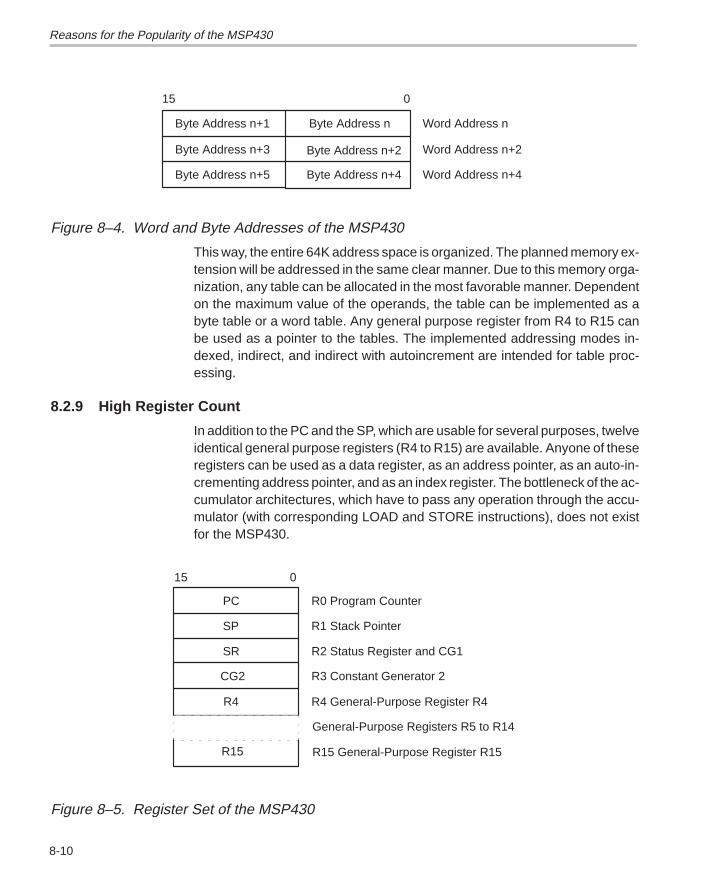
Reasons for the Popularity of the MSP430
8-10
Word Address n
Byte Address n
Word Address n+2
Word Address n+4
Byte Address n+2
Byte Address n+4
Byte Address n+3
Byte Address n+1
Byte Address n+5
015
Figure 8–4. Word and Byte Addresses of the MSP430
This way, the entire 64K address space is organized. The planned memory ex-tension will be addressed in the same clear manner. Due to this memory orga-nization, any table can be allocated in the most favorable manner. Dependenton the maximum value of the operands, the table can be implemented as abyte table or a word table. Any general purpose register from R4 to R15 canbe used as a pointer to the tables. The implemented addressing modes in-dexed, indirect, and indirect with autoincrement are intended for table proc-essing.
8.2.9 High Register Count
In addition to the PC and the SP, which are usable for several purposes, twelveidentical general purpose registers (R4 to R15) are available. Anyone of theseregisters can be used as a data register, as an address pointer, as an auto-in-crementing address pointer, and as an index register. The bottleneck of the ac-cumulator architectures, which have to pass any operation through the accu-mulator (with corresponding LOAD and STORE instructions), does not existfor the MSP430.
R0 Program Counter
SP
PC
SR
R4
CG2
R15
R1 Stack Pointer
R2 Status Register and CG1
R3 Constant Generator 2
R4 General-Purpose Register R4
15 0
General-Purpose Registers R5 to R14
R15 General-Purpose Register R15
Figure 8–5. Register Set of the MSP430

Reasons for the Popularity of the MSP430
8-11Architecture and Instruction Set
8.2.10 Emulation of Non-Implemented Instructions
The 27 implemented instructions allow the emulation of additional 24 instruc-tions. This is normally reached with the help of the constant generator, but oth-er ways are used also. As the constants used are taken from the constant gen-erator, no additional memory space is needed.
The assembler automatically inserts the correct instructions if emulated in-structions are used. The emulation of the 24 instructions led to a remarkablesmaller central processing unit. The MSP430 CPU is even smaller than some4-bit CPUs. The emulated instructions are completely listed in Section 8.4.2,Emulated Instructions.
8.2.11 No Paging
The 16-bit architecture of the MSP430 allows the direct addressing of the en-tire 64K memory bytes without paging of the memory. This feature greatly sim-plifies the development of software.

Effects and Advantages of the MSP430 Architecture
8-12
8.3 Effects and Advantages of the MSP430 Architecture
The reasons for the popularity of the MSP430 instruction set (and by it its archi-tecture) shown in Section 8.2, have effects and advantages that also result inmoney saved. These effects and advantages are shown and explained in thefollowing.
8.3.1 Less Program Space
The direct access to any address, without loading of the previous address intoa register, together with the constant generator results in program lengths fora given task that are between 55% and 90% compared to other microcomput-ers. This means that with the MSP430, a 4K version may be sufficient wherewith other microcomputers a 6K or 8K version is needed.
8.3.2 Shorter Programs
Any necessary code line is a source of errors. The less code lines that are nec-essary for a given task, the simpler a program is to read, understand, and ser-vice. The MSP430 needs between 33% and 55% of the code lines comparedto its competition’s products. The reason for this is the same as described pre-viously. Any address can be accessed directly and that both for the source op-erand and for the destination operand. It is not necessary to create trouble-some 16-bit addresses, handle the operands byte-wise, and store the final re-sult afterwards indirectly via a composed destination address. All this happenswith only one MSP430 instruction.
8.3.3 Reduced Development Time
The clearly smaller program length and the less troublesome access to ROM,RAM, and other peripherals reduce the necessary development time. In addi-tion to that advantage, the considerations omit completely how the actualproblem can be solved at all with the given architecture. A part that can takeup to one third of the development time with other architectures. (Whoever hasdeveloped with 4-bit microcomputers knows what is meant).
8.3.4 Effective Code Without Compressing
The clear assembler language of the MSP430 allows, from the start, the writingof dense and legible code. If the developed program is well prepared andcoded clearly, it is nearly impossible to reduce the program length seriouslyafterwards by compressing. This is no disadvantage, it simply means that opti-mized code was developed from the start.

Effects and Advantages of the MSP430 Architecture
8-13Architecture and Instruction Set
8.3.5 Optimum C Code
The C compiler of a microcomputer can use only the instructions that have aregular structure. Typical CISC (complex instruction set computer) instruc-tions, which normally show strong addressing mode restrictions, are not usedby the compilers. Instead, the compilers emulate the complex instructions withseveral of the simple instructions, resulting in a use of only 30% (!) of the imple-mented instructions.
This is completely different with the MSP430. As the instructions (apart fromthe executed operation) are completely uniform, 100% of them are used by thecompiler and not just 30%. As logical and arithmetical operations are executeddirectly and not by composed instructions, the execution time of the compiledcode is shorter and less memory space is needed. Therefore, the same advan-tages that are valid for assembler programming are valid also for high-levellanguage programming.
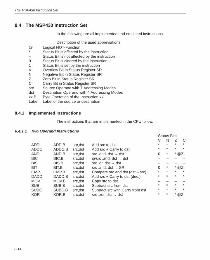
The MSP430 Instruction Set
8-14
8.4 The MSP430 Instruction Set
In the following are all implemented and emulated instructions.
Description of the used abbreviations:@ Logical NOT-Function* Status Bit is affected by the instruction– Status Bit is not affected by the instruction0 Status Bit is cleared by the instruction1 Status Bit is set by the instructionV Overflow Bit in Status Register SRN Negative Bit in Status Register SRZ Zero Bit in Status Register SRC Carry Bit in Status Register SRsrc Source Operand with 7 Addressing Modesdst Destination Operand with 4 Addressing Modesxx.B Byte Operation of the Instruction xxLabel Label of the source or destination
8.4.1 Implemented Instructions
The instructions that are implemented in the CPU follow.
8.4.1.1 Two Operand InstructionsStatus BitsV N Z C
ADD ADD.B src,dst Add src to dst * * * *ADDC ADDC.B src,dst Add src + Carry to dst * * * *AND AND.B src,dst src .and. dst → dst 0 * * @ZBIC BIC.B src,dst @src .and. dst → dst – – – –BIS BIS.B src,dst src .or. dst → dst – – – –BIT BIT.B src,dst src .and. dst → SR 0 * * @ZCMP CMP.B src,dst Compare src and dst (dst – src) * * * *DADD DADD.B src,dst Add src + Carry to dst (dec.) * * * *MOV MOV.B src,dst Copy src to dst – – – –SUB SUB.B src,dst Subtract src from dst * * * *SUBC SUBC.B src,dst Subtract src with Carry from dst * * * *XOR XOR.B src,dst src .xor. dst → dst * * * @Z
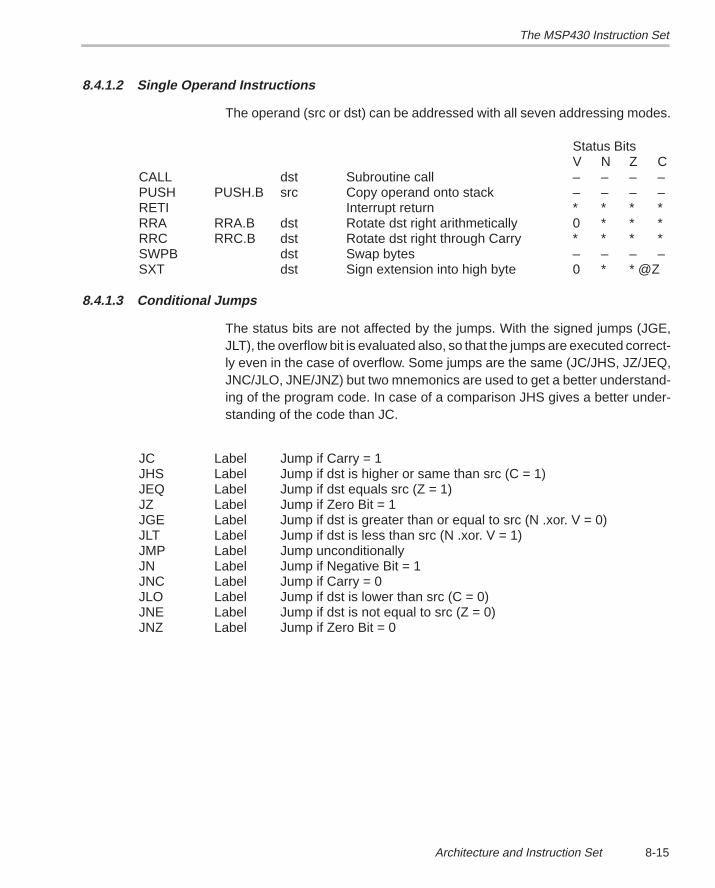
The MSP430 Instruction Set
8-15Architecture and Instruction Set
8.4.1.2 Single Operand Instructions
The operand (src or dst) can be addressed with all seven addressing modes.
Status BitsV N Z C
CALL dst Subroutine call – – – –PUSH PUSH.B src Copy operand onto stack – – – –RETI Interrupt return * * * *RRA RRA.B dst Rotate dst right arithmetically 0 * * *RRC RRC.B dst Rotate dst right through Carry * * * *SWPB dst Swap bytes – – – –SXT dst Sign extension into high byte 0 * * @Z
8.4.1.3 Conditional Jumps
The status bits are not affected by the jumps. With the signed jumps (JGE,JLT), the overflow bit is evaluated also, so that the jumps are executed correct-ly even in the case of overflow. Some jumps are the same (JC/JHS, JZ/JEQ,JNC/JLO, JNE/JNZ) but two mnemonics are used to get a better understand-ing of the program code. In case of a comparison JHS gives a better under-standing of the code than JC.
JC Label Jump if Carry = 1JHS Label Jump if dst is higher or same than src (C = 1)JEQ Label Jump if dst equals src (Z = 1)JZ Label Jump if Zero Bit = 1JGE Label Jump if dst is greater than or equal to src (N .xor. V = 0)JLT Label Jump if dst is less than src (N .xor. V = 1)JMP Label Jump unconditionallyJN Label Jump if Negative Bit = 1JNC Label Jump if Carry = 0JLO Label Jump if dst is lower than src (C = 0)JNE Label Jump if dst is not equal to src (Z = 0)JNZ Label Jump if Zero Bit = 0
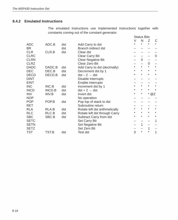
The MSP430 Instruction Set
8-16
8.4.2 Emulated Instructions
The emulated instructions use implemented instructions together withconstants coming out of the constant generator.
Status BitsV N Z C
ADC ADC.B dst Add Carry to dst * * * *BR dst Branch indirect dst – – – –CLR CLR.B dst Clear dst – – – –CLRC Clear Carry Bit – – – 0CLRN Clear Negative Bit – 0 – –CLRZ Clear Zero Bit – – 0 –DADC DADC.B dst Add Carry to dst (decimally) * * * *DEC DEC.B dst Decrement dst by 1 * * * *DECD DECD.B dst dst – 2 → dst * * * *DINT Disable interrupts – – – –EINT Enable interrupts – – – –INC INC.B dst Increment dst by 1 * * * *INCD INCD.B dst dst + 2 → dst * * * *INV INV.B dst Invert dst * * * @ZNOP No operation – – – –POP POP.B dst Pop top of stack to dst – – – –RET Subroutine return – – – –RLA RLA.B dst Rotate left dst arithmetically * * * *RLC RLC.B dst Rotate left dst through Carry * * * *SBC SBC.B dst Subtract Carry from dst * * * *SETC Set Carry Bit – – – 1SETN Set Negative Bit – 1 – –SETZ Set Zero Bit – – 1 –TST TST.B dst Test dst 0 * * 1
Benefits
8-17Architecture and Instruction Set
8.5 Benefits
The specification for the architecture of the MSP430 CPU contains the follow-ing requirements in order of importance:
1) High processing speed2) Small CPU area on-chip3) High ROM efficiency4) Easy software development5) Usable into the future6) High flexibility7) Usable for modern programming techniques
The following shows the finding of the optimum architecture out of the previouslist of priorities. Several of the listed solutions affect more than one item of thelist of priorities; these are shown at the item where they have the biggest im-pact.
8.5.1 High Processing Speed
To increase the processing speed to a multiple of the speed of 4-bit or 8-bit mi-crocomputers, software and hardware related attributes were chosen.
Hardware related attributes
Using 16-bit words, the analog-to-digital converter result can be pro-cessed immediately. Two operands (source and destination) are possiblein one instruction.
No microcoding: every instruction is decoded separately and allows one-cycle instructions. This is the case for register-to-register addressing, thenormal addressing mode used for time critical software parts.
Interrupt capability for anyone of the 8 I/O-Ports: The periodical polling ofthe inputs is not necessary.
Vectored interrupts: This allows the fastest reaction to interrupts.
Software related attributes
Implementation of the constant generator: The six most often usedconstants (–1, 0, 1, 2, 4, 8) are retrieved from the CPU with the highestpossible speed.
High register count: Twelve commonly usable registers allow the storageof all time critical values to achieve the fastest possible access.
Benefits
8-18
8.5.2 Small CPU Area
To get low overall cost for the MSP430, the smallest CPU without limiting itsprocessing capability was achieved:
Use of a RISC structure: With few but strong instructions, any algorithmcan be processed. Together with the constant generator, all commonlyused instructions, not contained in the implemented instructions, areexecutable.
Use of 100% orthogonality: Every instruction inside one of the three in-struction formats is completely similar to the other ones. This results in astrongly simplified CPU.
Only three instruction formats: Restriction to dual operand instructions,single operand instructions, and conditional jumps.
8.5.3 High ROM Efficiency
To solve a given task with a small ROM, the following steps were taken:
Implementation of seven addressing modes: The possibility to select outof seven addressing modes for the source and out of four addressingmodes for the destination allows direct access to all operands without anyintermediate operations necessary.
Placing of PC, SP, and SR inside of the register set: The possibility to ad-dress these as registers saves ROM space.
Wide reach of the conditional jumps: Due to the eightfold jump distanceof the MSP430 compared to other microcomputers, in most cases abranch instruction, that normally needs two words, is not necessary.
Use of a byte/word structure: ROM and RAM are addressable both as by-tes and as words. This allows the selection of the most favorable format.
8.5.4 Easy Software Development
Nearly all of the previously mentioned attributes of the architecture ease thedevelopment of software for the MSP430.
8.5.5 Usability on Into the Future
The chosen von-Neumann-architecture allows a simple system expansion farbeyond the currently addressable 64K bytes. If necessary, memory expansionup to 16M bytes is possible.
Conclusion
8-19Architecture and Instruction Set
8.5.6 Flexibility of the Architecture
To ensure that all intended peripheral modules, including currently unknownones, can be connected easily to the MSP430 system. The following defini-tions were made:
Placing of the peripheral control registers into the memory space (memorymapped I/O). The use of the normal instructions for the peripheral mod-ules makes special peripheral instructions superfluous.
All of the control registers and data registers of the peripheral modules canbe read and written to.
8.5.7 Usable for Modern Programming Techniques
Programming techniques like position independent coding (PIC), reentrantcoding, recursive coding, or the use of high-level languages like C force theimplementation of a stack pointer. The system SP is therefore implementedas a CPU register.
8.6 Conclusion
This section demonstrates that the instruction set and the architecture of theMSP430 are easy to understand and that it is easy too to write software for theMSP430. Everyone who has written large program parts with the MSP430 as-sembler language has an antipathy to adapt again to the more or less unstruc-tured architectures of the other 4-bit, 8-bit, and 16-bit microcomputers.

8-20

9-1
CPU Registers
Chapter 9
CPU Registers
9-2
9.1 CPU Registers
All of the MSP430 CPU registers can be used with all instructions.
9.1.1 The Program Counter PC
One of the main differences from other microcomputer architectures relatesto the Program Counter (CPU register R0) that can be used as a normal regis-ter with the MSP430. This means that all of the instructions and addressingmodes can be used with the Program Counter too. A branch, for example, ismade by simply moving an address into the PC:
MOV #LABEL,PC ; Branch to address LABELMOV LABEL,PC ; Branch to the address contained in address LABELMOV @R14,PC ; Branch indirect, indirect R14
Note:
The Program Counter always points to even addresses. This means that theLSB is always zero. The software has to ensure that no odd addresses areused if the Program Counter is involved. Odd PC addresses will result in non-predictable behavior.
9.1.2 Stack Processing
9.1.2.1 Use of the System Stack Pointer (SP)
The system stack pointer (CPU register R1) is a normal register like the others.This means it can use the same addressing modes. This gives good accessto all items on the stack, not only to the one on the top of the stack.
The system stack pointer (SP) is used for the storage of the following items:
Interrupt return addresses and status register contents Subroutine return addresses Intermediate results Variables for subroutines, floating point package etc.
When using the system stack, remember that the microcomputer hardwarealso uses the stack pointer for interrupts and subroutine calls. To ensure theerror-free running of the program it is necessary to do exact housekeeping forthe system stack.
Note:
The Stack Pointer always points to even addresses. This means the LSB isalways zero. The software has to ensure that no odd addresses are used ifthe Stack Pointer is involved. Odd SP addresses will end up in non-predict-able results.
CPU Registers
9-3CPU Registers
If bytes are pushed on the system stack, only the lower byte is used, the upperbyte is not modified.
PUSH #05h ; 0005h –> TOSPUSH.B #05h ; xx05h –> TOSMOV.B 1(SP),R5 ; Address odd byte
9.1.2.2 Software Stacks
Every register from R4 to R15 can be used as a software stack pointer. Thisallows independent stacks for jobs that have a need for this. Every part of theRAM can be used for these software stacks.
EXAMPLE: R4 is to be used as a software stack pointer.
MOV #SW_STACK,R4 ; Init. SW stack pointer...DECD R4 ; Decrement stack pointerMOV item,0(R4) ; Push item on stack... ; ProceedMOV @R4+,item2 ; Pop item from stack
Software stacks can be organized as byte stacks also. This is not possible forthe system stack, which always uses 16-bit words. The example shows R4used as a byte stack pointer:
MOV #SW_STACK,R4 ; Init. SW stack pointer...DEC R4 ; Decrement stack pointerMOV.B item,0(R4) ; Push item on stack... ; ProceedMOV.B @R4+,item2 ; Pop item from stack
9.1.3 Byte and Word Handling
Every memory word is addressable by three addresses as shown in theFigure 9–1:
The word address: An even address N The lower byte address: An even address N The upper byte address: An odd address N+1
If byte addressing is used, only the addressed byte is affected. No carry oroverflow can affect the other byte.
Note:
Registers R0 to R15 do not have an address but are treated in a special way.Byte addressing always uses the lower byte of the register. The upper byteis set to zero if the instruction modifies the destination. Therefore, all instruc-tions clear the upper byte of a destination register except CMP.B, TST.B,BIT.B and PUSH.B. The source is never affected.
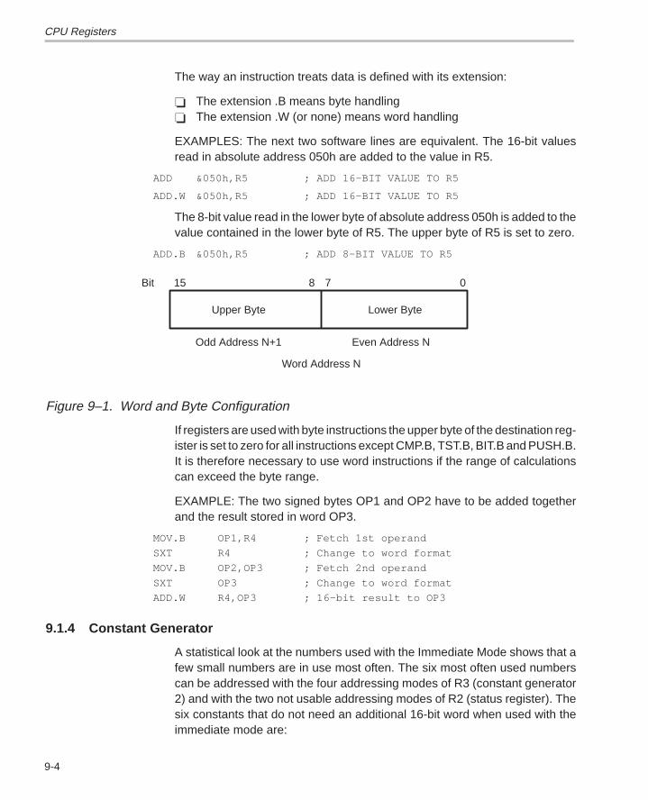
CPU Registers
9-4
The way an instruction treats data is defined with its extension:
The extension .B means byte handling The extension .W (or none) means word handling
EXAMPLES: The next two software lines are equivalent. The 16-bit valuesread in absolute address 050h are added to the value in R5.
ADD &050h,R5 ; ADD 16–BIT VALUE TO R5
ADD.W &050h,R5 ; ADD 16–BIT VALUE TO R5
The 8-bit value read in the lower byte of absolute address 050h is added to thevalue contained in the lower byte of R5. The upper byte of R5 is set to zero.
ADD.B &050h,R5 ; ADD 8–BIT VALUE TO R5
Upper Byte Lower Byte
Bit 15 8 7 0
Odd Address N+1
Word Address N
Even Address N
Figure 9–1. Word and Byte Configuration
If registers are used with byte instructions the upper byte of the destination reg-ister is set to zero for all instructions except CMP.B, TST.B, BIT.B and PUSH.B.It is therefore necessary to use word instructions if the range of calculationscan exceed the byte range.
EXAMPLE: The two signed bytes OP1 and OP2 have to be added togetherand the result stored in word OP3.
MOV.B OP1,R4 ; Fetch 1st operand
SXT R4 ; Change to word format
MOV.B OP2,OP3 ; Fetch 2nd operand
SXT OP3 ; Change to word format
ADD.W R4,OP3 ; 16–bit result to OP3
9.1.4 Constant Generator
A statistical look at the numbers used with the Immediate Mode shows that afew small numbers are in use most often. The six most often used numberscan be addressed with the four addressing modes of R3 (constant generator2) and with the two not usable addressing modes of R2 (status register). Thesix constants that do not need an additional 16-bit word when used with theimmediate mode are:
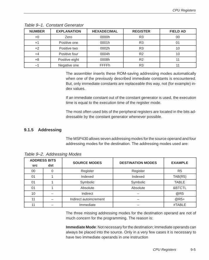
CPU Registers
9-5CPU Registers
Table 9–1. Constant GeneratorNUMBER EXPLANATION HEXADECIMAL REGISTER FIELD AD
+0 Zero 0000h R3 00
+1 Positive one 0001h R3 01
+2 Positive two 0002h R3 10
+4 Positive four 0004h R2 10
+8 Positive eight 0008h R2 11
–1 Negative one FFFFh R3 11
The assembler inserts these ROM-saving addressing modes automaticallywhen one of the previously described immediate constants is encountered.But, only immediate constants are replaceable this way, not (for example) in-dex values.
If an immediate constant out of the constant generator is used, the executiontime is equal to the execution time of the register mode.
The most often used bits of the peripheral registers are located in the bits ad-dressable by the constant generator whenever possible.
9.1.5 Addressing
The MSP430 allows seven addressing modes for the source operand and fouraddressing modes for the destination. The addressing modes used are:
Table 9–2. Addressing ModesADDRESS BITS
src dstSOURCE MODES DESTINATION MODES EXAMPLE
00 0 Register Register R5
01 1 Indexed Indexed TAB(R5)
01 1 Symbolic Symbolic TABLE
01 1 Absolute Absolute &BTCTL
10 – Indirect – @R5
11 – Indirect autoincrement – @R5+
11 – Immediate – #TABLE
The three missing addressing modes for the destination operand are not ofmuch concern for the programming. The reason is:
Immediate Mode : Not necessary for the destination; immediate operands canalways be placed into the source. Only in a very few cases it is necessary tohave two immediate operands in one instruction
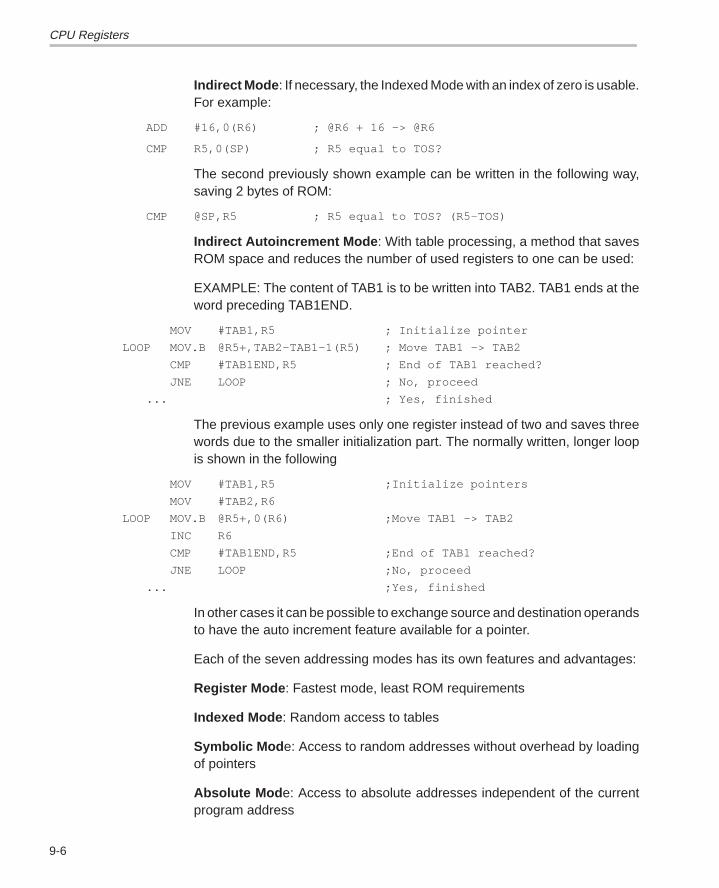
CPU Registers
9-6
Indirect Mode : If necessary, the Indexed Mode with an index of zero is usable.For example:
ADD #16,0(R6) ; @R6 + 16 –> @R6
CMP R5,0(SP) ; R5 equal to TOS?
The second previously shown example can be written in the following way,saving 2 bytes of ROM:
CMP @SP,R5 ; R5 equal to TOS? (R5–TOS)
Indirect Autoincrement Mode : With table processing, a method that savesROM space and reduces the number of used registers to one can be used:
EXAMPLE: The content of TAB1 is to be written into TAB2. TAB1 ends at theword preceding TAB1END.
MOV #TAB1,R5 ; Initialize pointer
LOOP MOV.B @R5+,TAB2–TAB1–1(R5) ; Move TAB1 –> TAB2
CMP #TAB1END,R5 ; End of TAB1 reached?
JNE LOOP ; No, proceed
... ; Yes, finished
The previous example uses only one register instead of two and saves threewords due to the smaller initialization part. The normally written, longer loopis shown in the following
MOV #TAB1,R5 ;Initialize pointers
MOV #TAB2,R6
LOOP MOV.B @R5+,0(R6) ;Move TAB1 –> TAB2
INC R6
CMP #TAB1END,R5 ;End of TAB1 reached?
JNE LOOP ;No, proceed
... ;Yes, finished
In other cases it can be possible to exchange source and destination operandsto have the auto increment feature available for a pointer.
Each of the seven addressing modes has its own features and advantages:
Register Mode : Fastest mode, least ROM requirements
Indexed Mode : Random access to tables
Symbolic Mod e: Access to random addresses without overhead by loadingof pointers
Absolute Mod e: Access to absolute addresses independent of the currentprogram address
CPU Registers
9-7CPU Registers
Indirect Mode : Table addressing via register; code saving access to often ref-erenced addresses
Indirect Autoincrement Mode : Table addressing with code saving automaticstepping; for transfer routines
Immediate Mode : Loading of pointers, addresses or constants within the in-struction,
With the use of the symbolic mode an interrupt routine can be as short as pos-sible. An interrupt routine is shown that has to increment a RAM word COUNT-ER and to do a comparison if a status byte STATUS has reached the value 5.If this is the case, the status byte is cleared. Otherwise, the interrupt routineterminates:
INTRPT INC COUNTER ;Increment counter
CMP.B #5,STATUS ;STATUS = 5?
JNE INTRET ;
CLR.B STATUS ;STATUS = 5: clear it
INTRET RETI
No loading of pointers or saving and restoring of registers is necessary. Theaction is done immediately, without any overhead.
9.1.6 Program Flow Control
9.1.6.1 Computed Branches and Calls
The branch instruction is an emulated instruction that moves the destinationaddress into the program counter:
MOV dst,PC ; EMULATION FOR BR @dst
The ability to access the program counter in the same way as all other registersprovides interesting options:
1) The destination address can be taken from tables: see Section 9.2.52) The destination address can be calculated3) The destination address can be a constant. This is the usual method of
getting the address.
9.1.6.2 Nesting of Subroutines
Due to the stack orientation of the MSP430, one of the main problems of otherarchitectures does not play a role here at all. Subroutine nesting can proceedas long as RAM is available. There is no need to keep track of the subroutinecalls as long as all subroutines terminate with the Return from Subroutine in-
CPU Registers
9-8
struction RET. If subroutines are left without the RET instruction, some house-keeping is necessary; popping of the return address or addresses from thestack.
9.1.6.3 Nesting of Interrupts
Nesting of interrupts gives no problem at all, provided there is enough RAMfor the stack. For every occurring interrupt, two words on the stack are neededfor the storage of the status register and the return address. To enable nestedinterrupts, it is necessary to only include an EINT instruction into the interrupthandler. If the interrupt handlers are as short as possible (a good real-timepractice), nesting may not be necessary.
EXAMPLE: The basic timer interrupt handler is woken-up with 1 Hz only, buthas to do a lot of things. The interrupt nesting is therefore used. The latencytime is 8 clock cycles only.
; Interrupt handler for Basic Timer: Wake–up with 1Hz
;
BT_HAN EINT ; Enable interrupt for nesting
INC.B SECCNT ; Counter for seconds +1
CMP.B #60,SECCNT ; 1 minute elapsed?
JHS MIN1 ; Yes, do necessary tasks
RETI ; No return to LPM3
;
; One minute elapsed: Return is removed from stack, a branch to
; the necessary tasks is made. There it is decided how to proceed
;
MIN1 INC MINCNT ; Minute counter +1
CLR SECCNT ; 0 –> SECCNT
... ; Start of necessary tasks
RETI ; Tasks completed
9.1.6.4 Jumps
Jumps allow the conditional or unconditional leaving of the linear program flow.Jumps cannot reach every address of the address space. But they have theadvantage of needing only one word and only two MCLK cycles. The 10-bitoffset field allows jumps of 512 words maximum forward and 511 words, maxi-mum, backwards. This is four to eight times the normal reach of a jump. Onlyin a few cases, the 2-word branch is necessary.
Eight Jumps are possible with the MSP430; four of them have two mnemonicsto allow better readability:
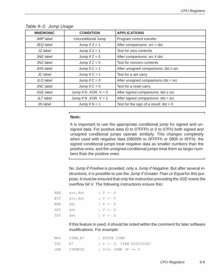
CPU Registers
9-9CPU Registers
Table 9–3. Jump UsageMNEMONIC CONDITION APPLICATIONS
JMP label Unconditional Jump Program control transfer
JEQ label Jump if Z = 1 After comparisons: src = dst
JZ label Jump if Z = 1 Test for zero contents
JNE label Jump if Z = 0 After comparisons: src # dst
JNZ label Jump if Z = 0 Test for nonzero contents
JHS label Jump if C = 1 After unsigned comparisons: dst ≥ src
JC label Jump if C = 1 Test for a set carry
JLO label Jump if C = 0 After unsigned comparisons dst < src
JNC label Jump if C = 0 Test for a reset carry
JGE label Jump if N .XOR. V = 0 After signed comparisons: dst ≥ src
JLT label Jump if N .XOR. V = 1 After signed comparisons: dst < src
JN label Jump if N = 1 Test for the sign of a result: dst < 0
Note:
It is important to use the appropriate conditional jump for signed and un-signed data. For positive data (0 to 07FFFh or 0 to 07Fh) both signed andunsigned conditional jumps operate similarly. This changes completelywhen used with negative data (08000h to 0FFFFh or 080h to 0FFh): thesigned conditional jumps treat negative data as smaller numbers than thepositive ones, and the unsigned conditional jumps treat them as larger num-bers than the positive ones.
No Jump if Positive is provided, only a Jump if Negative. But after several in-structions, it is possible to use the Jump if Greater Than or Equal for this pur-pose. It must be ensured that only the instruction preceding the JGE resets theoverflow bit V. The following instructions ensure this:
AND src,dst ; V <– 0
BIT src,dst ; V <– 0
RRA dst ; V <– 0
SXT dst ; V <– 0
TST dst ; V <– 0
If this feature is used, it should be noted within the comment for later softwaremodifications. For example:
MOV ITEM,R7 ; FETCH ITEM
TST R7 ; V <– 0, ITEM POSITIVE?
JGE ITEMPOS ; V=0: JUMP IF >= 0
CPU Registers
9-10
Note:
If addresses are computed only the unsigned jumps are adequate. Address-es are always unsigned, positive numbers.
No Jump if Overflow is provided. If the status of the overflow bit is needed fromthe software, a simple bit test can be used (the BIT instruction clears the over-flow bit, but its state is read correctly before):
OV .EQU 0100h ; Bit address in SR
;
BIT #OV,SR ; Test Overflow Bit and clear it
JNZ OVFL ; If OV = 1 branch to label OVFL
... ; If OV = 0 continue here
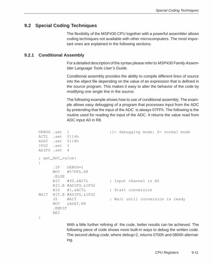
Special Coding Techniques
9-11CPU Registers
9.2 Special Coding Techniques
The flexibility of the MSP430 CPU together with a powerful assembler allowscoding techniques not available with other microcomputers. The most impor-tant ones are explained in the following sections.
9.2.1 Conditional Assembly
For a detailed description of the syntax please refer to MSP430 Family Assem-bler Language Tools User’s Guide.
Conditional assembly provides the ability to compile different lines of sourceinto the object file depending on the value of an expression that is defined inthe source program. This makes it easy to alter the behavior of the code bymodifying one single line in the source.
The following example shows how to use of conditional assembly. The exam-ple allows easy debugging of a program that processes input from the ADCby pretending that the input of the ADC is always 07FFh. The following is theroutine used for reading the input of the ADC. It returns the value read fromADC input A0 in R8.
DEBUG .set 1 ;1= debugging mode; 0= normal modeACTL .set 0114hADAT .set 0118hIFG2 .set 3ADIFG .set 4
; get_ADC_value:;
.IF DEBUG=1MOV #07FFh,R8.ELSEBIC #60,&ACTL ; Input channel is A0BIC.B #ADIFG,&IFG2BIS #1,&ACTL ; Start conversion
WAIT BIT.B #ADIFG,&IFG2JZ WAIT ; Wait until conversion is readyMOV &ADAT,R8.ENDIFRET
;
With a little further refining of the code, better results can be achieved. Thefollowing piece of code shows more built-in ways to debug the written code.The second debug code, where debug=2, returns 0700h and 0800h alternat-ing.
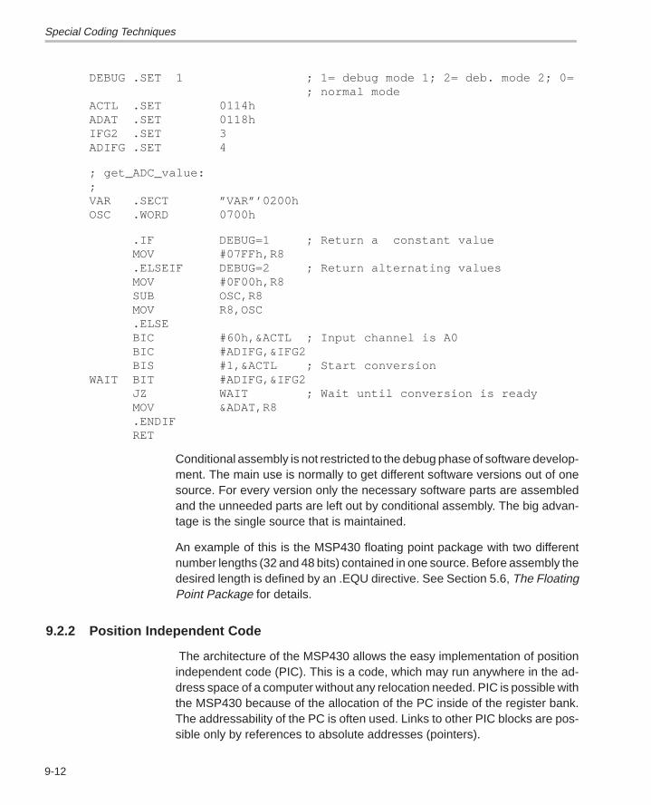
Special Coding Techniques
9-12
DEBUG .SET 1 ; 1= debug mode 1; 2= deb. mode 2; 0=; normal mode
ACTL .SET 0114hADAT .SET 0118hIFG2 .SET 3ADIFG .SET 4
; get_ADC_value:;VAR .SECT ”VAR”’0200hOSC .WORD 0700h
.IF DEBUG=1 ; Return a constant valueMOV #07FFh,R8.ELSEIF DEBUG=2 ; Return alternating valuesMOV #0F00h,R8SUB OSC,R8MOV R8,OSC.ELSEBIC #60h,&ACTL ; Input channel is A0BIC #ADIFG,&IFG2BIS #1,&ACTL ; Start conversion
WAIT BIT #ADIFG,&IFG2JZ WAIT ; Wait until conversion is readyMOV &ADAT,R8.ENDIFRET
Conditional assembly is not restricted to the debug phase of software develop-ment. The main use is normally to get different software versions out of onesource. For every version only the necessary software parts are assembledand the unneeded parts are left out by conditional assembly. The big advan-tage is the single source that is maintained.
An example of this is the MSP430 floating point package with two differentnumber lengths (32 and 48 bits) contained in one source. Before assembly thedesired length is defined by an .EQU directive. See Section 5.6, The FloatingPoint Package for details.
9.2.2 Position Independent Code
The architecture of the MSP430 allows the easy implementation of positionindependent code (PIC). This is a code, which may run anywhere in the ad-dress space of a computer without any relocation needed. PIC is possible withthe MSP430 because of the allocation of the PC inside of the register bank.The addressability of the PC is often used. Links to other PIC blocks are pos-sible only by references to absolute addresses (pointers).
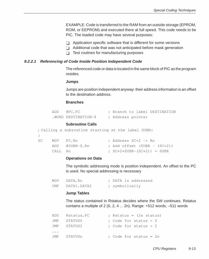
Special Coding Techniques
9-13CPU Registers
EXAMPLE: Code is transferred to the RAM from an outside storage (EPROM,ROM, or EEPROM) and executed there at full speed. This code needs to bePIC. The loaded code may have several purposes:
Application specific software that is different for some versions Additional code that was not anticipated before mask generation Test routines for manufacturing purposes
9.2.2.1 Referencing of Code Inside Position Independent Code
The referenced code or data is located in the same block of PIC as the programresides.
Jumps
Jumps are position independent anyway: their address information is an offsetto the destination address.
Branches
ADD @PC,PC ; Branch to label DESTINATION
.WORD DESTINATION–$ ; Address pointer
Subroutine Calls; Calling a subroutine starting at the label SUBR:
;
SC MOV PC,Rn ; Address SC+2 –> Rn
ADD #SUBR–$,Rn ; Add offset (SUBR – (SC+2))
CALL Rn ; SC+2+SUBR–(SC+2)) = SUBR
Operations on Data
The symbolic addressing mode is position independent. An offset to the PCis used. No special addressing is necessary
MOV DATA,Rn ; DATA is addressed
CMP DATA1,DATA2 ; symbolically
Jump Tables
The status contained in Rstatus decides where the SW continues. Rstatuscontains a multiple of 2 (0, 2, 4 ... 2n). Range: +512 words, –511 words
ADD Rstatus,PC ; Rstatus = (2x status)
JMP STATUS0 ; Code for status = 0
JMP STATUS2 ; Code for status = 2
...
JMP STATUSn ; Code for status = 2n
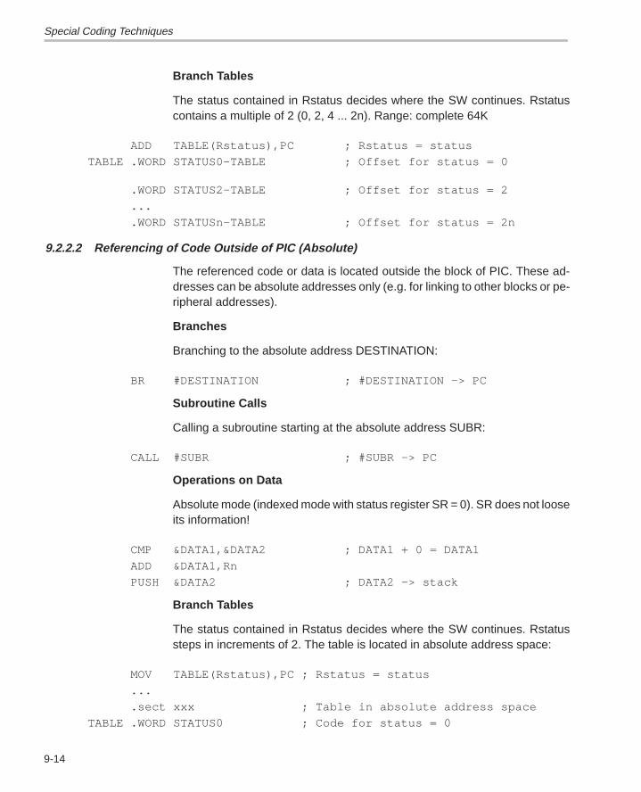
Special Coding Techniques
9-14
Branch Tables
The status contained in Rstatus decides where the SW continues. Rstatuscontains a multiple of 2 (0, 2, 4 ... 2n). Range: complete 64K
ADD TABLE(Rstatus),PC ; Rstatus = status
TABLE .WORD STATUS0–TABLE ; Offset for status = 0
.WORD STATUS2–TABLE ; Offset for status = 2
...
.WORD STATUSn–TABLE ; Offset for status = 2n
9.2.2.2 Referencing of Code Outside of PIC (Absolute)
The referenced code or data is located outside the block of PIC. These ad-dresses can be absolute addresses only (e.g. for linking to other blocks or pe-ripheral addresses).
Branches
Branching to the absolute address DESTINATION:
BR #DESTINATION ; #DESTINATION –> PC
Subroutine Calls
Calling a subroutine starting at the absolute address SUBR:
CALL #SUBR ; #SUBR –> PC
Operations on Data
Absolute mode (indexed mode with status register SR = 0). SR does not looseits information!
CMP &DATA1,&DATA2 ; DATA1 + 0 = DATA1
ADD &DATA1,Rn
PUSH &DATA2 ; DATA2 –> stack
Branch Tables
The status contained in Rstatus decides where the SW continues. Rstatussteps in increments of 2. The table is located in absolute address space:
MOV TABLE(Rstatus),PC ; Rstatus = status
...
.sect xxx ; Table in absolute address space
TABLE .WORD STATUS0 ; Code for status = 0
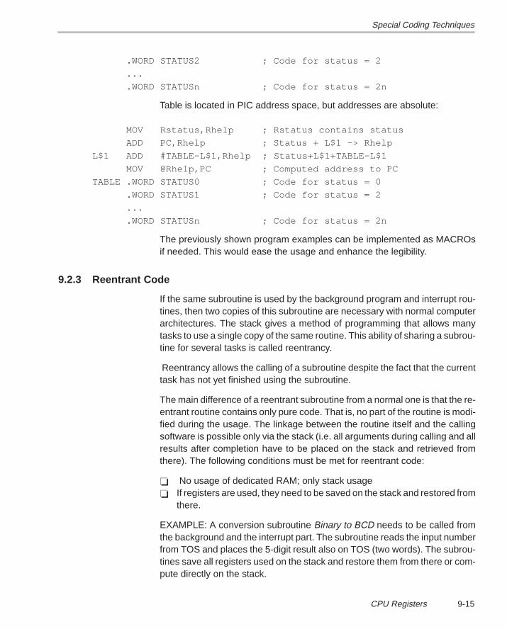
Special Coding Techniques
9-15CPU Registers
.WORD STATUS2 ; Code for status = 2
...
.WORD STATUSn ; Code for status = 2n
Table is located in PIC address space, but addresses are absolute:
MOV Rstatus,Rhelp ; Rstatus contains status
ADD PC,Rhelp ; Status + L$1 –> Rhelp
L$1 ADD #TABLE–L$1,Rhelp ; Status+L$1+TABLE–L$1
MOV @Rhelp,PC ; Computed address to PC
TABLE .WORD STATUS0 ; Code for status = 0
.WORD STATUS1 ; Code for status = 2
...
.WORD STATUSn ; Code for status = 2n
The previously shown program examples can be implemented as MACROsif needed. This would ease the usage and enhance the legibility.
9.2.3 Reentrant Code
If the same subroutine is used by the background program and interrupt rou-tines, then two copies of this subroutine are necessary with normal computerarchitectures. The stack gives a method of programming that allows manytasks to use a single copy of the same routine. This ability of sharing a subrou-tine for several tasks is called reentrancy.
Reentrancy allows the calling of a subroutine despite the fact that the currenttask has not yet finished using the subroutine.
The main difference of a reentrant subroutine from a normal one is that the re-entrant routine contains only pure code. That is, no part of the routine is modi-fied during the usage. The linkage between the routine itself and the callingsoftware is possible only via the stack (i.e. all arguments during calling and allresults after completion have to be placed on the stack and retrieved fromthere). The following conditions must be met for reentrant code:
No usage of dedicated RAM; only stack usage If registers are used, they need to be saved on the stack and restored from
there.
EXAMPLE: A conversion subroutine Binary to BCD needs to be called fromthe background and the interrupt part. The subroutine reads the input numberfrom TOS and places the 5-digit result also on TOS (two words). The subrou-tines save all registers used on the stack and restore them from there or com-pute directly on the stack.
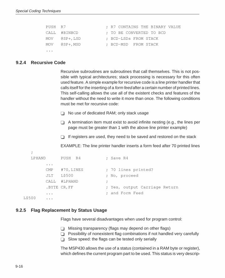
Special Coding Techniques
9-16
PUSH R7 ; R7 CONTAINS THE BINARY VALUE
CALL #BINBCD ; TO BE CONVERTED TO BCD
MOV @SP+,LSD ; BCD–LSDs FROM STACK
MOV @SP+,MSD ; BCD–MSD FROM STACK
...
9.2.4 Recursive Code
Recursive subroutines are subroutines that call themselves. This is not pos-sible with typical architectures; stack processing is necessary for this oftenused feature. A simple example for recursive code is a line printer handler thatcalls itself for the inserting of a form feed after a certain number of printed lines.This self-calling allows the use all of the existent checks and features of thehandler without the need to write it more than once. The following conditionsmust be met for recursive code:
No use of dedicated RAM; only stack usage
A termination item must exist to avoid infinite nesting (e.g., the lines perpage must be greater than 1 with the above line printer example)
If registers are used, they need to be saved and restored on the stack
EXAMPLE: The line printer handler inserts a form feed after 70 printed lines
;
LPHAND PUSH R4 ; Save R4
...
CMP #70,LINES ; 70 lines printed?
JLT L$500 ; No, proceed
CALL #LPHAND ;
.BYTE CR,FF ; Yes, output Carriage Return
... ; and Form FeedL$500 ...
9.2.5 Flag Replacement by Status Usage
Flags have several disadvantages when used for program control:
Missing transparency (flags may depend on other flags) Possibility of nonexistent flag combinations if not handled very carefully Slow speed: the flags can be tested only serially
The MSP430 allows the use of a status (contained in a RAM byte or register),which defines the current program part to be used. This status is very descrip-
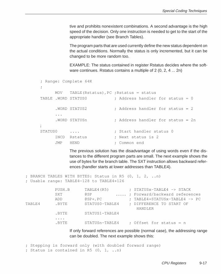
Special Coding Techniques
9-17CPU Registers
tive and prohibits nonexistent combinations. A second advantage is the highspeed of the decision. Only one instruction is needed to get to the start of theappropriate handler (see Branch Tables).
The program parts that are used currently define the new status dependent onthe actual conditions. Normally the status is only incremented, but it can bechanged to be more random too.
EXAMPLE: The status contained in register Rstatus decides where the soft-ware continues. Rstatus contains a multiple of 2 (0, 2, 4 ... 2n)
; Range: Complete 64K
;
MOV TABLE(Rstatus),PC ;Rstatus = status
TABLE .WORD STATUS0 ; Address handler for status = 0
.WORD STATUS2 ; Address handler for status = 2
...
.WORD STATUSn ; Address handler for status = 2n
;STATUS0 .... ; Start handler status 0
INCD Rstatus ; Next status is 2
JMP HEND ; Common end
The previous solution has the disadvantage of using words even if the dis-tances to the different program parts are small. The next example shows theuse of bytes for the branch table. The SXT instruction allows backward refer-ences (handler starts at lower addresses than TABLE4).
; BRANCH TABLES WITH BYTES: Status in R5 (0, 1, 2, ..n); Usable range: TABLE4–128 to TABLE4+126
PUSH.B TABLE4(R5) ; STATUSx–TABLE4 –> STACKSXT @SP ; Forward/backward references. . . . . ADD @SP+,PC ; TABLE4+STATUSx–TABLE4 –> PC
TABLE4 .BYTE STATUS0–TABLE4 ; DIFFERENCE TO START OF HANDLER
.BYTE STATUS1–TABLE4
....
.BYTE STATUSn–TABLE4 ; Offset for status = n
If only forward references are possible (normal case), the addressing rangecan be doubled. The next example shows this:
; Stepping is forward only (with doubled forward range); Status is contained in R5 (0, 1, ..n)
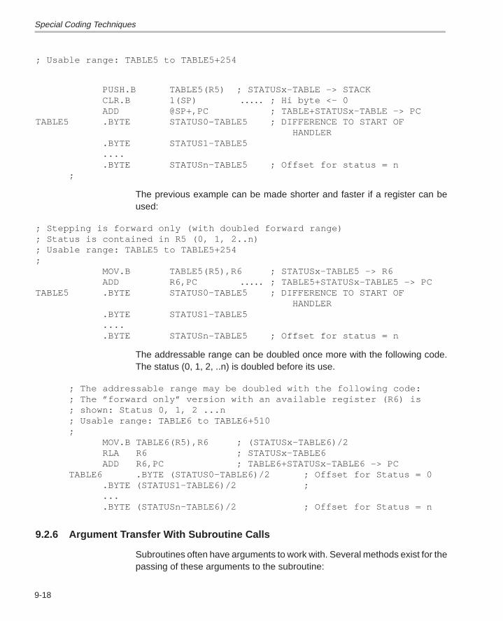
Special Coding Techniques
9-18
; Usable range: TABLE5 to TABLE5+254
PUSH.B TABLE5(R5) ; STATUSx–TABLE –> STACKCLR.B 1(SP) ; Hi byte <– 0. . . . . ADD @SP+,PC ; TABLE+STATUSx–TABLE –> PC
TABLE5 .BYTE STATUS0–TABLE5 ; DIFFERENCE TO START OF HANDLER
.BYTE STATUS1–TABLE5
....
.BYTE STATUSn–TABLE5 ; Offset for status = n;
The previous example can be made shorter and faster if a register can beused:
; Stepping is forward only (with doubled forward range); Status is contained in R5 (0, 1, 2..n); Usable range: TABLE5 to TABLE5+254;
MOV.B TABLE5(R5),R6 ; STATUSx–TABLE5 –> R6ADD R6,PC ; TABLE5+STATUSx–TABLE5 –> PC. . . . .
TABLE5 .BYTE STATUS0–TABLE5 ; DIFFERENCE TO START OF HANDLER
.BYTE STATUS1–TABLE5
....
.BYTE STATUSn–TABLE5 ; Offset for status = n
The addressable range can be doubled once more with the following code.The status (0, 1, 2, ..n) is doubled before its use.
; The addressable range may be doubled with the following code:; The ”forward only” version with an available register (R6) is; shown: Status 0, 1, 2 ...n; Usable range: TABLE6 to TABLE6+510;
MOV.B TABLE6(R5),R6 ; (STATUSx–TABLE6)/2RLA R6 ; STATUSx–TABLE6ADD R6,PC ; TABLE6+STATUSx–TABLE6 –> PC
TABLE6 .BYTE (STATUS0–TABLE6)/2 ; Offset for Status = 0.BYTE (STATUS1–TABLE6)/2 ;....BYTE (STATUSn–TABLE6)/2 ; Offset for Status = n
9.2.6 Argument Transfer With Subroutine Calls
Subroutines often have arguments to work with. Several methods exist for thepassing of these arguments to the subroutine:
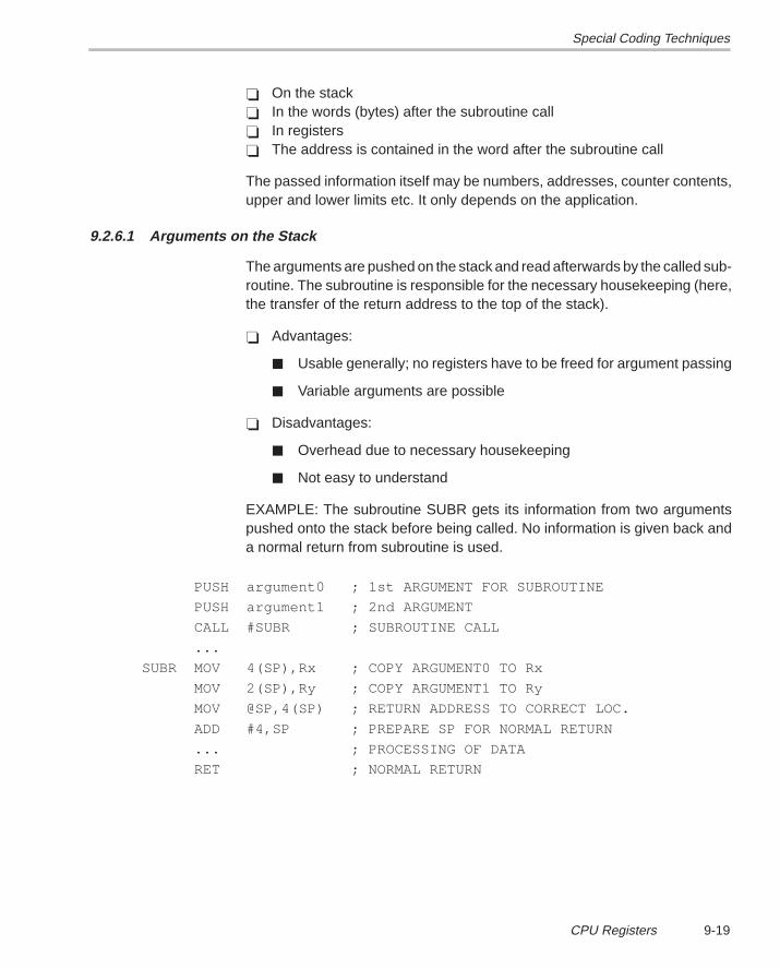
Special Coding Techniques
9-19CPU Registers
On the stack In the words (bytes) after the subroutine call In registers The address is contained in the word after the subroutine call
The passed information itself may be numbers, addresses, counter contents,upper and lower limits etc. It only depends on the application.
9.2.6.1 Arguments on the Stack
The arguments are pushed on the stack and read afterwards by the called sub-routine. The subroutine is responsible for the necessary housekeeping (here,the transfer of the return address to the top of the stack).
Advantages:
Usable generally; no registers have to be freed for argument passing
Variable arguments are possible
Disadvantages:
Overhead due to necessary housekeeping
Not easy to understand
EXAMPLE: The subroutine SUBR gets its information from two argumentspushed onto the stack before being called. No information is given back anda normal return from subroutine is used.
PUSH argument0 ; 1st ARGUMENT FOR SUBROUTINE
PUSH argument1 ; 2nd ARGUMENT
CALL #SUBR ; SUBROUTINE CALL
...
SUBR MOV 4(SP),Rx ; COPY ARGUMENT0 TO Rx
MOV 2(SP),Ry ; COPY ARGUMENT1 TO Ry
MOV @SP,4(SP) ; RETURN ADDRESS TO CORRECT LOC.
ADD #4,SP ; PREPARE SP FOR NORMAL RETURN
... ; PROCESSING OF DATA
RET ; NORMAL RETURN
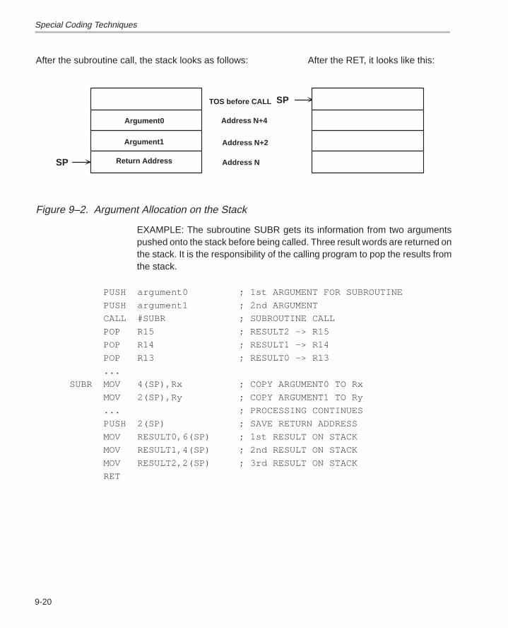
Special Coding Techniques
9-20
After the subroutine call, the stack looks as follows: After the RET, it looks like this:
SP
Argument0
Argument1
Return Address
TOS before CALL
Address N
Address N+4
Address N+2
SP
Figure 9–2. Argument Allocation on the Stack
EXAMPLE: The subroutine SUBR gets its information from two argumentspushed onto the stack before being called. Three result words are returned onthe stack. It is the responsibility of the calling program to pop the results fromthe stack.
PUSH argument0 ; 1st ARGUMENT FOR SUBROUTINE
PUSH argument1 ; 2nd ARGUMENT
CALL #SUBR ; SUBROUTINE CALL
POP R15 ; RESULT2 –> R15
POP R14 ; RESULT1 –> R14
POP R13 ; RESULT0 –> R13
...
SUBR MOV 4(SP),Rx ; COPY ARGUMENT0 TO Rx
MOV 2(SP),Ry ; COPY ARGUMENT1 TO Ry
... ; PROCESSING CONTINUES
PUSH 2(SP) ; SAVE RETURN ADDRESS
MOV RESULT0,6(SP) ; 1st RESULT ON STACK
MOV RESULT1,4(SP) ; 2nd RESULT ON STACK
MOV RESULT2,2(SP) ; 3rd RESULT ON STACK
RET
Special Coding Techniques
9-21CPU Registers
After the subroutine call, the stack looks as follows: After the RET, it looks like this:
SP
Argument0
Argument1
Return Address
TOS before CALL
Address N
Address N+4
Address N+2
SP
Result0
Result1
Result2
Figure 9–3. Argument and Result Allocation on the Stack
Note:
If the stack is involved during data transfers, it is very important to have inmind that only data at or above the top of stack (TOS, the word the SP pointsto) is protected against overwriting by enabled interrupts. This does not allowthe SP to move above the last item on the stack. Indexed addressing is need-ed instead.
9.2.6.2 Arguments Following the Subroutine Call
The arguments follow the subroutine call and are read by the called subrou-tine. The subroutine is responsible for the necessary housekeeping (here, theadaptation of the return address on the stack to the 1st word after the argu-ments).
Advantages:
Very clear and easily readable interface
Disadvantages:
Overhead due to necessary housekeeping
Only fixed arguments possible
EXAMPLE: The subroutine SUBR gets its information from two arguments fol-lowing the subroutine call. Information can be given back on the stack or in reg-isters.
CALL #SUBR ; SUBROUTINE CALL
.WORD START ; START OF TABLE
.BYTE 24,0 ; LENGTH OF TABLE, FLAGS
Special Coding Techniques
9-22
... ; 1st instruction after CALL
SUBR MOV @SP,R5 ; COPY ADDRESS 1st ARGUMENT TO R5
MOV @R5+,R6 ; MOVE 1st ARGUMENT TO R6
MOV @R5+,R7 ; MOVE ARGUMENT BYTES TO R7
MOV R5,0(SP) ; ADJUST RETURN ADDRESS ON STACK
... ; PROCESSING OF DATA
RET ; NORMAL RETURN
9.2.6.3 Arguments in Registers
The arguments are moved into defined registers and used afterwards by thesubroutine.
Advantages:
Simple interface and easy to understand Very fast Variable arguments are possible
Disadvantages:
Registers have to be freed
EXAMPLE: The subroutine SUBR gets its information from two registers whichare loaded before the calling. Information can be given back, or not with thesame registers.
MOV arg0,R5 ; 1st ARGUMENT FOR SUBROUTINE
MOV arg1,R6 ; 2nd ARGUMENT
CALL #SUBR ; SUBROUTINE CALL
...
SUBR ... ; PROCESSING OF DATA
RET ; NORMAL RETURN
9.2.7 Interrupt Vectors in RAM
If the destination address of an interrupt changes with the program run, it isvaluable to have the ability to modify the pointer. The vector itself (which re-sides in ROM) cannot be changed but a second pointer residing in RAM canbe used for this purpose.
EXAMPLE: The interrupt handler for the basic timer starts at location BTHAN1after initialization and at BTHAN2 when a certain condition is met (for example,when a calibration is made).
; BASIC TIMER INTERRUPT GOES TO ADDRESS BTVEC. THE INSTRUCTION

Special Coding Techniques
9-23CPU Registers
; ”MOV @PC,PC” WRITES THE ADDRESS IN BTVEC+2 INTO THE PC:
; THE PROGRAM CONTINUES AT THAT ADDRESS
;
.sect ”VAR”,0200h ; RAM START
BTVEC .word 0 ; OPCODE ”MOV @PC,PC”
.word 0 ; ACTUAL HANDLER START ADDR.
; THE SOFTWARE VECTOR BTVEC IS INITIALIZED:
;
INIT MOV #04020h,BTVEC ; OPCODE ”MOV @PC,PC
MOV #BTHAN1,BTVEC+2 ; START WITH HANDLER BTHAN1
... ; INITIALIZATION CONTINUES
;
; THE CONDITION IS MET: THE BASIC TIMER INTERRUPT IS HANDLED
; AT ADDRESS BTHAN2 STARTING NOW
MOV #BTHAN2,BTVEC+2 ; CONT. WITH ANOTHER HANDLER
...
;
; THE INTERRUPT VECTOR FOR THE BASIC TIMER CONTAINS THE RAM
; ADDRESS OF THE SOFTWARE VECTOR BTVEC:
.sect ”BTVect”,0FFE2h ; VECTOR ADDRESS BASIC TIMER
.WORD BTVEC ; FETCH ACTUAL VECTOR THERE
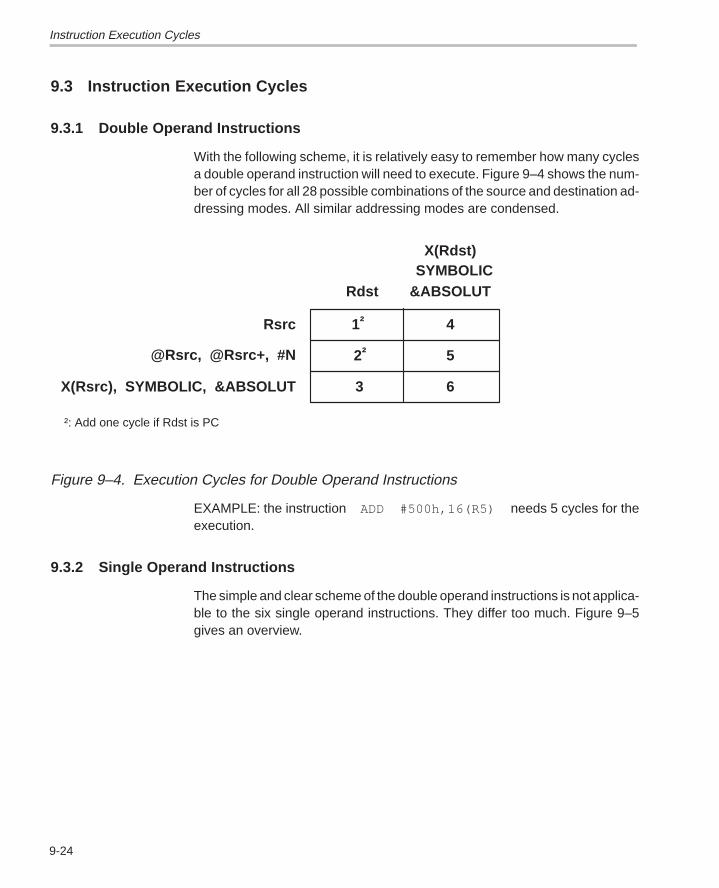
Instruction Execution Cycles
9-24
9.3 Instruction Execution Cycles
9.3.1 Double Operand Instructions
With the following scheme, it is relatively easy to remember how many cyclesa double operand instruction will need to execute. Figure 9–4 shows the num-ber of cycles for all 28 possible combinations of the source and destination ad-dressing modes. All similar addressing modes are condensed.
Argument0
Argument1
Rdst
X(Rdst)
1†
2†
3
4
5
6
Rsrc
@Rsrc, @Rsrc+, #N
SYMBOLIC&ABSOLUT
X(Rsrc), SYMBOLIC, &ABSOLUT
†: Add one cycle if Rdst is PC
Figure 9–4. Execution Cycles for Double Operand Instructions
EXAMPLE: the instruction ADD #500h,16(R5) needs 5 cycles for theexecution.
9.3.2 Single Operand Instructions
The simple and clear scheme of the double operand instructions is not applica-ble to the six single operand instructions. They differ too much. Figure 9–5gives an overview.
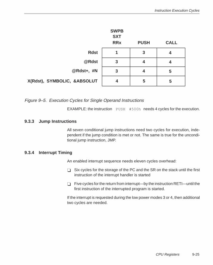
Instruction Execution Cycles
9-25CPU Registers
Argument0
Argument1
RRx CALL
1
3
3
3
4
4
Rdst
@Rdst
PUSH
X(Rdst), SYMBOLIC, &ABSOLUT
SXTSWPB
4 5
@Rdst+, #N
4
4
5
5
Figure 9–5. Execution Cycles for Single Operand Instructions
EXAMPLE: the instruction PUSH #500h needs 4 cycles for the execution.
9.3.3 Jump Instructions
All seven conditional jump instructions need two cycles for execution, inde-pendent if the jump condition is met or not. The same is true for the uncondi-tional jump instruction, JMP.
9.3.4 Interrupt Timing
An enabled interrupt sequence needs eleven cycles overhead:
Six cycles for the storage of the PC and the SR on the stack until the firstinstruction of the interrupt handler is started
Five cycles for the return from interrupt—by the instruction RETI—until thefirst instruction of the interrupted program is started.
If the interrupt is requested during the low power modes 3 or 4, then additionaltwo cycles are needed.


![MSP430 Microcontroller Basics - pudn.comread.pudn.com/.../771051/[Book.2008]MSP430_Microcontroller_Basics.pdf · MSP430 Microcontroller Basics John H. Davies AMSTERDAM •BOSTON HEIDELBERG](https://img.pdfslide.net/doc/110x75/5c04dd1009d3f296388c8709/msp430-microcontroller-basics-pudn-book2008msp430microcontrollerbasicspdf.jpg)


![Vortrag zur Seminarphase der PG „Solar Doorplate“ MSP430 ... · MSP430 – Wichtigste Grundlagen von David Tondorf. 2 ... MSP430 microcontroller basics. Oxford: Newnes [4] MSP430](https://img.pdfslide.net/doc/110x75/5b6f6a9b7f8b9af12d8c481e/vortrag-zur-seminarphase-der-pg-solar-doorplate-msp430-msp430-.jpg)