Embed Size (px)
Citation preview
Product
Folder
Order
Now
Technical
Documents
Tools &
Software
Support &Community
An IMPORTANT NOTICE at the end of this data sheet addresses availability, warranty, changes, use in safety-critical applications,intellectual property matters and other important disclaimers. PRODUCTION DATA.
MSP432E411YSLASEK6 –OCTOBER 2017
MSP432E411Y SimpleLink™ Ethernet Microcontroller
1 Device Overview
1
1.1 Features1
• Core– 120-MHz Arm® Cortex®-M4F Processor Core
With Floating-Point Unit (FPU)• Connectivity
– Ethernet MAC: 10/100 Ethernet MAC WithMedia Independent Interface (MII) and ReducedMII (RMII)
– Ethernet PHY: PHY With IEEE 1588 PTPHardware Support
– Universal Serial Bus (USB): USB 2.0 OTG,Host, or Device With ULPI Interface Option andLink Power Management (LPM)
– Eight Universal AsynchronousReceivers/Transmitters (UARTs), Each WithIndependently Clocked Transmitter andReceiver
– Four Quad Synchronous Serial Interface (QSSI):With Bi-, Quad-, and Advanced-SSI Support
– Ten Inter-Integrated Circuit (I2C) Modules WithHigh-Speed Mode Support
– Two CAN 2.0 A and B Controllers: MulticastShared Serial-Bus Standard
– One 1-Wire Module With a Bidirectional SerialCommunication Protocol Provides Both Powerand Data Over a Single Wire
• Memories– 1024KB of Flash Memory With 4-Bank
Configuration Supports an Independent CodeProtection for Each Bank
– 256KB of SRAM With Single-Cycle Access,Provides Nearly 2-GB/s Memory Bandwidth at120-MHz Clock Frequency
– 6KB of EEPROM: 500-kwrite per 2 Page Block,Leveling, Lock Protection
– Internal ROM: Loaded With SimpleLink™ SDKSoftware– Peripheral Driver Library– Bootloader
– External Peripheral Interface (EPI): 8-, 16-, or32-Bit Dedicated Parallel Interface to AccessExternal Devices and Memory (SDRAM, Flash,or SRAM)
• Security– Advanced Encryption Standard (AES):
Hardware Accelerated Data Encryption andDecryption Based on 128-, 192-, and 256-BitKeys
– Data Encryption Standard (DES): HardwareAccelerated Data Encryption and DecryptionSupported by Block Cipher Implementation With168-Bit Effective Key Length
– Secure Hash Algorithm/Message DigestAlgorithm (SHA/MD5): Advanced Hash EngineThat Supports SHA-1, SHA-2, and MD5 HashComputation
– Cyclical Redundancy Check (CRC) Hardware– Tamper: Support for Four Tamper Inputs and
Configurable Tamper Event Response• Analog
– Two 12-Bit SAR-Based ADC Modules, EachSupports Up to 2 Million Samples per Second(2 Msps)
– Three Independent Analog ComparatorControllers
– 16 Digital Comparators• System Management
– JTAG and Serial Wire Debug (SWD): One JTAGModule With Integrated Arm SWD Provides aMeans of Accessing and Controlling Design-for-Test Features Such as I/O Pin Observation andControl, Scan Testing, and Debugging.
• Development Kits and Software (See Tools andSoftware)– SimpleLink™ MSP-EXP432E401Y
LaunchPad™ Development Kit– SimpleLink MSP432E4 Software Development
Kit (SDK)• Package Information
– Package: 212-Ball NFBGA (ZAD)– Extended Operating Temperature (Ambient)
Range: –40°C to 105°C
2
MSP432E411YSLASEK6 –OCTOBER 2017 www.ti.com
Submit Documentation FeedbackProduct Folder Links: MSP432E411Y
Device Overview Copyright © 2017, Texas Instruments Incorporated
1.2 Applications• Industrial Ethernet Gateway• Industrial Smart Gateway• Zone Controllers for Building Automation• Factory Automation Data Collectors and Gateway• Data Concentrators for Grid Infrastructure• Wireless to Ethernet Gateway
1.3 DescriptionThe SimpleLink MSP432E411Y Arm® Cortex®-M4F microcontrollers provide top performance andadvanced integration. The product family is positioned for cost-effective applications requiring significantcontrol processing and connectivity capabilities.
The MSP432E411Y microcontrollers integrate a large variety of rich communication features to enable anew class of highly connected designs with the ability to allow critical real-time control betweenperformance and power. The microcontrollers feature integrated communication peripherals along withother high-performance analog and digital functions to offer a strong foundation for many different targetuses, spanning from human-machine interface (HMI) to networked system management controllers.
In addition, the MSP432E411Y microcontrollers offer the advantages of widely available developmenttools, system-on-chip (SoC) infrastructure, and a large user community for Arm-based microcontrollers.Additionally, these microcontrollers use the Arm Thumb®-compatible Thumb-2® instruction set to reducememory requirements and, thereby, cost. When using the SimpleLink MSP432™ SDK, the MSP432E411Ymicrocontroller is code compatible with all members of the extensive SimpleLink family, providing flexibilityto fit precise needs.
The MSP432E411Y device is part of the SimpleLink microcontroller (MCU) platform, which consists of Wi-Fi®, Bluetooth® low energy, Sub-1 GHz, Ethernet, Zigbee, Thread, and host MCUs, which all share acommon, easy-to-use development environment with a single core software development kit (SDK) andrich tool set. A one-time integration of the SimpleLink platform enables you to add any combination of theportfolio's devices into your design, allowing 100 percent code reuse when your design requirementschange. For more information, visit www.ti.com/simplelink.
(1) For more information, see Section 9, Mechanical, Packaging, and Orderable Information.
Device Information (1)
PART NUMBER PACKAGE BODY SIZEMSP432E411YTZAD NFBGA (212) 10 mm × 10 mm
ArmCortex-M4F
(120 MHz)
NVIC MPU
FPUETM Flash
(1024KB)
BootloaderDriverLibAES and CRCEthernet Bootloader
ROM
DCode bus
ICode bus
JTAG, SWD
SystemControl and
Clocks(with Precision
Oscillator)
Bus Matrix
System Bus
SRAM(256KB)
SYSTEM PERIPHERALS
WatchdogTimer
(2 Units)DMA
HibernationModule
Tamper
EEPROM(6K)
General-Purpose
Timer (8 Units)
GPIOs(140)
ExternalPeripheralInterface
CRCModule
AESModule
DESModule
SHA/MD5Module
TFT LCDController
SERIAL PERIPHERALS
UART(8 Units)
USB OTG(FS PHYor ULPI)
I2C(10 Units)
SSI(4 Units)
CANController(2 Units)
EthernetMAC, PHY, MII
ANALOG PERIPHERALS
12-Bit ADC(2 Units,
24 Channels)
AnalogComparator
(3 Units)
MOTION CONTROL PERIPHERALS
QEI(1 Unit)
PWM(1 Unit,
8 Signals)
SMC PERIPHERALS
1-Wire(1 Unit)
Advanced
Periphera
lB
us
(AP
B)
Advanced
Hig
h-P
erf
orm
ance
Bus
(AH
B)
Copyright © 2017, Texas Instruments Incorporated
3
MSP432E411Ywww.ti.com SLASEK6 –OCTOBER 2017
Submit Documentation FeedbackProduct Folder Links: MSP432E411Y
Device OverviewCopyright © 2017, Texas Instruments Incorporated
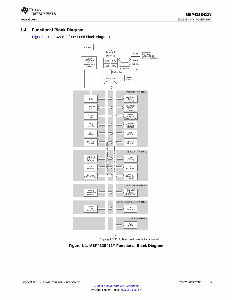
1.4 Functional Block DiagramFigure 1-1 shows the functional block diagram.
Figure 1-1. MSP432E411Y Functional Block Diagram
4
MSP432E411YSLASEK6 –OCTOBER 2017 www.ti.com
Submit Documentation FeedbackProduct Folder Links: MSP432E411Y
Table of Contents Copyright © 2017, Texas Instruments Incorporated
Table of Contents1 Device Overview ......................................... 1
1.1 Features .............................................. 11.2 Applications........................................... 21.3 Description............................................ 21.4 Functional Block Diagram ............................ 3
2 Revision History ......................................... 53 Device Characteristics.................................. 6
3.1 Related Products ..................................... 74 Terminal Configuration and Functions.............. 8
4.1 Pin Diagram .......................................... 84.2 Pin Attributes ......................................... 94.3 Signal Descriptions.................................. 254.4 GPIO Pin Multiplexing............................... 454.5 Buffer Type.......................................... 504.6 Connections for Unused Pins ....................... 50
5 Specifications ........................................... 525.1 Absolute Maximum Ratings ......................... 525.2 ESD Ratings ........................................ 525.3 Recommended Operating Conditions............... 525.4 Recommended DC Operating Conditions .......... 525.5 Recommended GPIO Operating Characteristics ... 525.6 Recommended Fast GPIO Pad Operating
Conditions ........................................... 535.7 Recommended Slow GPIO Pad Operating
Conditions ........................................... 535.8 GPIO Current Restrictions .......................... 545.9 I/O Reliability ........................................ 545.10 Current Consumption ............................... 55
5.11 Peripheral Current Consumption.................... 585.12 LDO Regulator Characteristics...................... 585.13 Power Dissipation ................................... 595.14 Thermal Resistance Characteristics, 212-Pin ZAD
(NFBGA) Package .................................. 595.15 Timing and Switching Characteristics ............... 60
6 Detailed Description.................................. 1306.1 Overview ........................................... 1306.2 Functional Block Diagram ......................... 1316.3 Arm Cortex-M4F Processor Core .................. 1326.4 On-Chip Memory................................... 1366.5 Peripherals ......................................... 1386.6 Identification........................................ 1816.7 Boot Modes ........................................ 182
7 Applications, Implementation, and Layout ...... 1837.1 System Design Guidelines......................... 183
8 Device and Documentation Support .............. 1848.1 Getting Started and Next Steps ................... 1848.2 Device Nomenclature .............................. 1848.3 Tools and Software ................................ 1868.4 Documentation Support............................ 1878.5 Community Resources............................. 1888.6 Trademarks ........................................ 1888.7 Electrostatic Discharge Caution ................... 1888.8 Export Control Notice .............................. 1888.9 Glossary............................................ 188
9 Mechanical, Packaging, and OrderableInformation ............................................. 189

5
MSP432E411Ywww.ti.com SLASEK6 –OCTOBER 2017
Submit Documentation FeedbackProduct Folder Links: MSP432E411Y
Revision HistoryCopyright © 2017, Texas Instruments Incorporated
2 Revision HistoryNOTE: Page numbers for previous revisions may differ from page numbers in the current version.
DATE REVISION NOTESOctober 2017 * Initial Release
6
MSP432E411YSLASEK6 –OCTOBER 2017 www.ti.com
Submit Documentation FeedbackProduct Folder Links: MSP432E411Y
Device Characteristics Copyright © 2017, Texas Instruments Incorporated
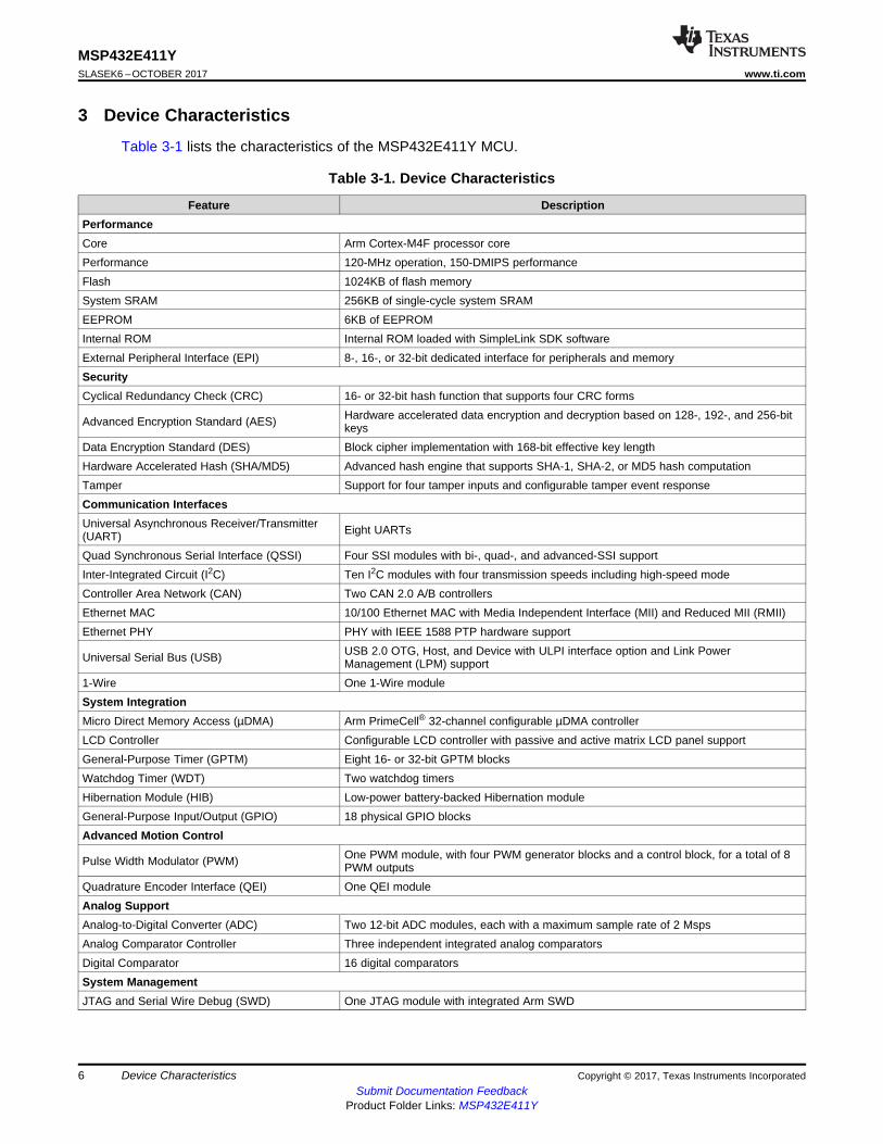
3 Device Characteristics
Table 3-1 lists the characteristics of the MSP432E411Y MCU.
Table 3-1. Device Characteristics
Feature DescriptionPerformanceCore Arm Cortex-M4F processor corePerformance 120-MHz operation, 150-DMIPS performanceFlash 1024KB of flash memorySystem SRAM 256KB of single-cycle system SRAMEEPROM 6KB of EEPROMInternal ROM Internal ROM loaded with SimpleLink SDK softwareExternal Peripheral Interface (EPI) 8-, 16-, or 32-bit dedicated interface for peripherals and memorySecurityCyclical Redundancy Check (CRC) 16- or 32-bit hash function that supports four CRC forms
Advanced Encryption Standard (AES) Hardware accelerated data encryption and decryption based on 128-, 192-, and 256-bitkeys
Data Encryption Standard (DES) Block cipher implementation with 168-bit effective key lengthHardware Accelerated Hash (SHA/MD5) Advanced hash engine that supports SHA-1, SHA-2, or MD5 hash computationTamper Support for four tamper inputs and configurable tamper event responseCommunication InterfacesUniversal Asynchronous Receiver/Transmitter(UART) Eight UARTs
Quad Synchronous Serial Interface (QSSI) Four SSI modules with bi-, quad-, and advanced-SSI supportInter-Integrated Circuit (I2C) Ten I2C modules with four transmission speeds including high-speed modeController Area Network (CAN) Two CAN 2.0 A/B controllersEthernet MAC 10/100 Ethernet MAC with Media Independent Interface (MII) and Reduced MII (RMII)Ethernet PHY PHY with IEEE 1588 PTP hardware support
Universal Serial Bus (USB) USB 2.0 OTG, Host, and Device with ULPI interface option and Link PowerManagement (LPM) support
1-Wire One 1-Wire moduleSystem IntegrationMicro Direct Memory Access (µDMA) Arm PrimeCell® 32-channel configurable µDMA controllerLCD Controller Configurable LCD controller with passive and active matrix LCD panel supportGeneral-Purpose Timer (GPTM) Eight 16- or 32-bit GPTM blocksWatchdog Timer (WDT) Two watchdog timersHibernation Module (HIB) Low-power battery-backed Hibernation moduleGeneral-Purpose Input/Output (GPIO) 18 physical GPIO blocksAdvanced Motion Control
Pulse Width Modulator (PWM) One PWM module, with four PWM generator blocks and a control block, for a total of 8PWM outputs
Quadrature Encoder Interface (QEI) One QEI moduleAnalog SupportAnalog-to-Digital Converter (ADC) Two 12-bit ADC modules, each with a maximum sample rate of 2 MspsAnalog Comparator Controller Three independent integrated analog comparatorsDigital Comparator 16 digital comparatorsSystem ManagementJTAG and Serial Wire Debug (SWD) One JTAG module with integrated Arm SWD
7
MSP432E411Ywww.ti.com SLASEK6 –OCTOBER 2017
Submit Documentation FeedbackProduct Folder Links: MSP432E411Y
Device CharacteristicsCopyright © 2017, Texas Instruments Incorporated
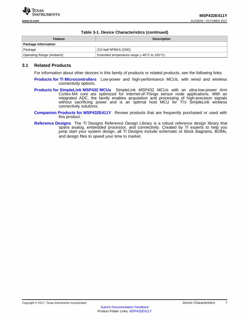
Table 3-1. Device Characteristics (continued)Feature Description
Package InformationPackage 212-ball NFBGA (ZAD)Operating Range (Ambient) Extended temperature range (–40°C to 105°C)
3.1 Related ProductsFor information about other devices in this family of products or related products, see the following links.Products for TI Microcontrollers Low-power and high-performance MCUs, with wired and wireless
connectivity options.Products for SimpleLink MSP432 MCUs SimpleLink MSP432 MCUs with an ultra-low-power Arm
Cortex-M4 core are optimized for Internet-of-Things sensor node applications. With anintegrated ADC, the family enables acquisition and processing of high-precision signalswithout sacrificing power and is an optimal host MCU for TI's SimpleLink wirelessconnectivity solutions.
Companion Products for MSP432E411Y Review products that are frequently purchased or used withthis product.
Reference Designs The TI Designs Reference Design Library is a robust reference design library thatspans analog, embedded processor, and connectivity. Created by TI experts to help youjump start your system design, all TI Designs include schematic or block diagrams, BOMs,and design files to speed your time to market.
8
MSP432E411YSLASEK6 –OCTOBER 2017 www.ti.com
Submit Documentation FeedbackProduct Folder Links: MSP432E411Y
Terminal Configuration and Functions Copyright © 2017, Texas Instruments Incorporated
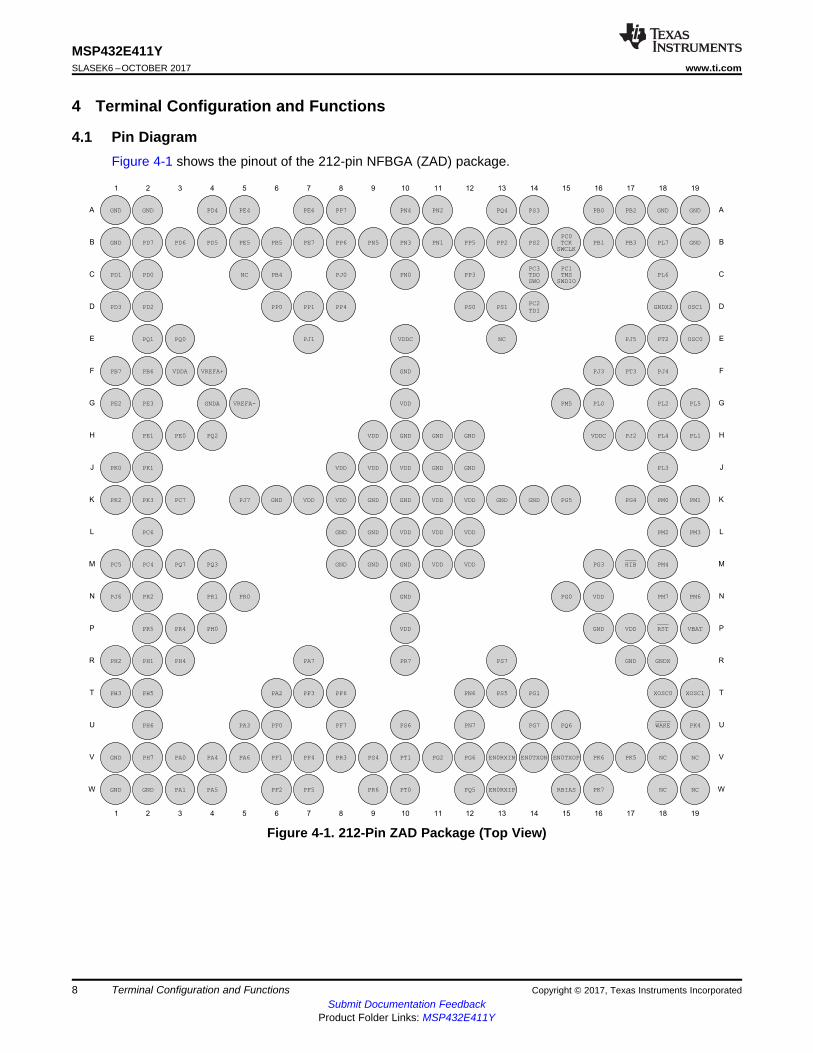
4 Terminal Configuration and Functions
4.1 Pin DiagramFigure 4-1 shows the pinout of the 212-pin NFBGA (ZAD) package.
Figure 4-1. 212-Pin ZAD Package (Top View)
9
MSP432E411Ywww.ti.com SLASEK6 –OCTOBER 2017
Submit Documentation FeedbackProduct Folder Links: MSP432E411Y
Terminal Configuration and FunctionsCopyright © 2017, Texas Instruments Incorporated
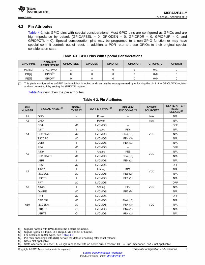
(1) This pin is configured as a GPIO by default but is locked and can only be reprogrammed by unlocking the pin in the GPIOLOCK registerand uncommitting it by setting the GPIOCR register.
4.2 Pin AttributesTable 4-1 lists GPIO pins with special considerations. Most GPIO pins are configured as GPIOs and arehigh-impedance by default (GPIOAFSEL = 0, GPIODEN = 0, GPIOPDR = 0, GPIOPUR = 0, andGPIOPCTL = 0). Special consideration pins may be programed to a non-GPIO function or may havespecial commit controls out of reset. In addition, a POR returns these GPIOs to their original specialconsideration state.
Table 4-1. GPIO Pins With Special Considerations
GPIO PINS DEFAULTRESET STATE GPIOAFSEL GPIODEN GPIOPDR GPIOPUR GPIOPCTL GPIOCR
PC[3:0] JTAG/SWD 1 1 0 1 0x1 0PD[7] GPIO (1) 0 0 0 0 0x0 0PE[7] GPIO (1) 0 0 0 0 0x0 0
(1) Signals names with (PN) denote the default pin name.(2) Signal Types: I = Input, O = Output, I/O = Input or Output.(3) For details on buffer types, see Table 4-5.(4) Pin mux encodings with (RD) denote the default encoding after reset release.(5) N/A = Not applicable(6) State after reset release: PU = High impedance with an active pullup resistor, OFF = High impedance, N/A = not applicable
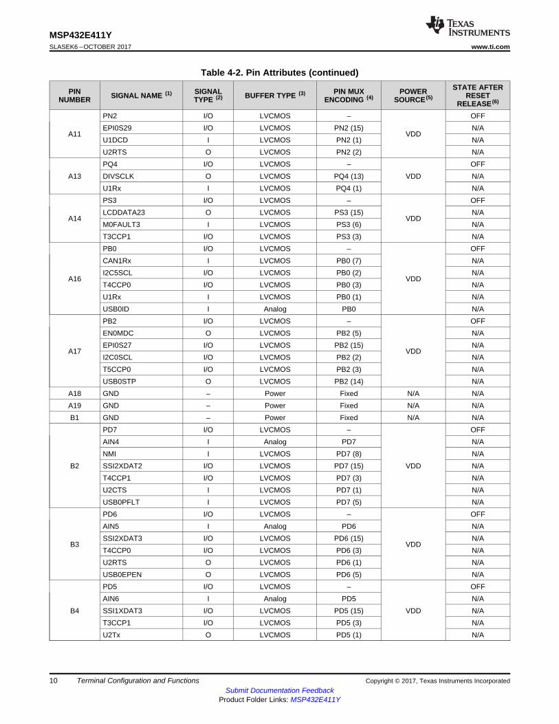
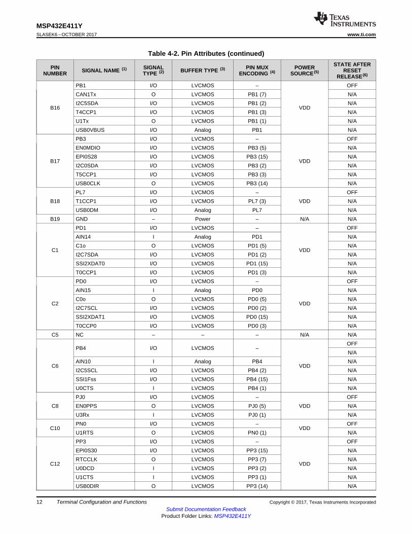
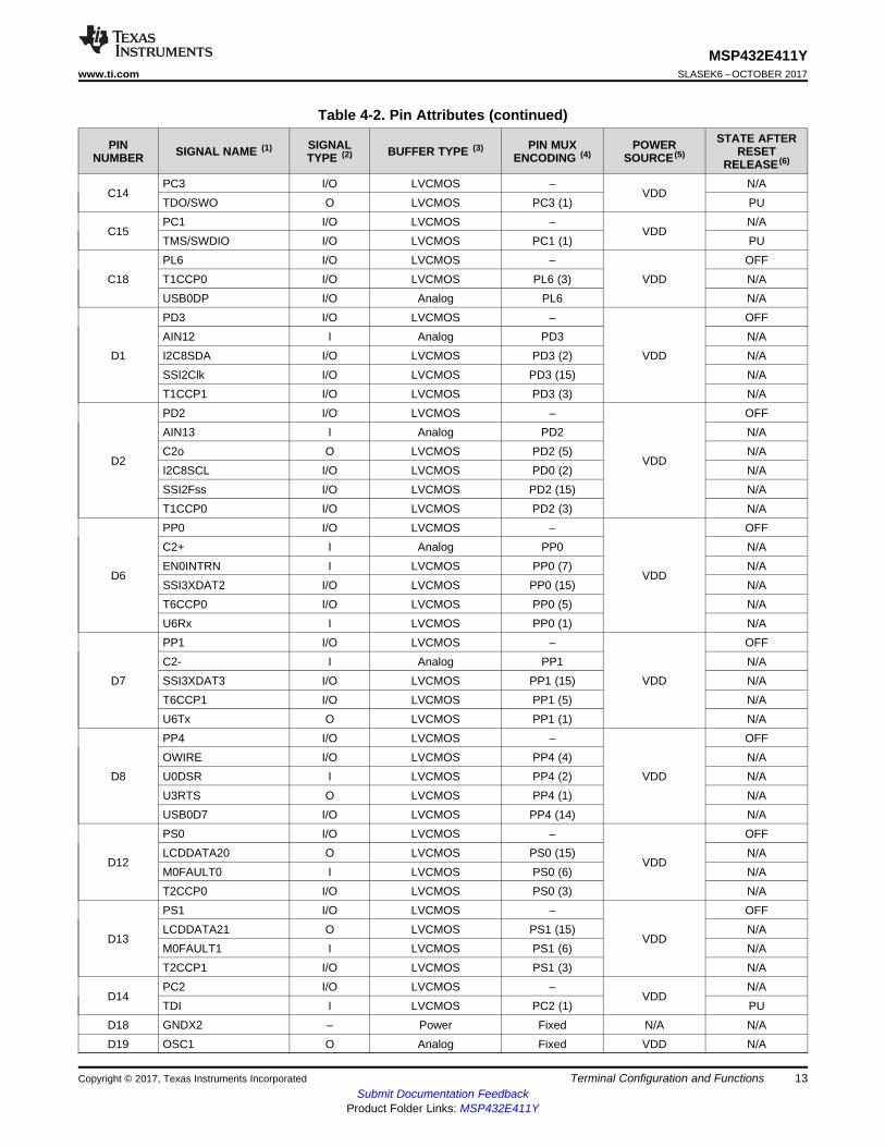
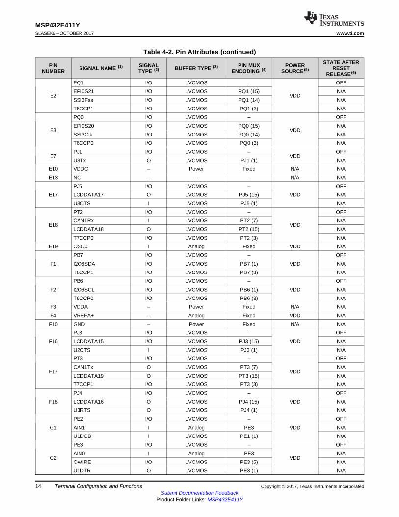
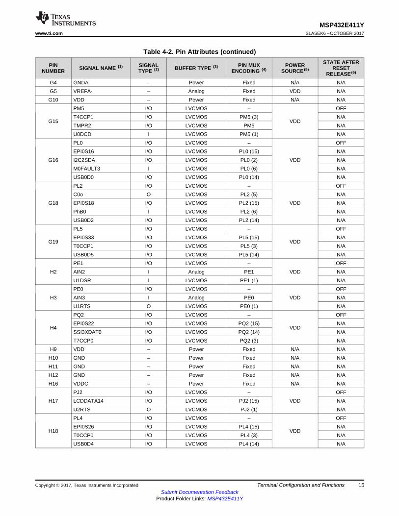
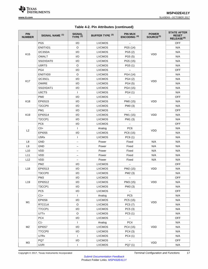
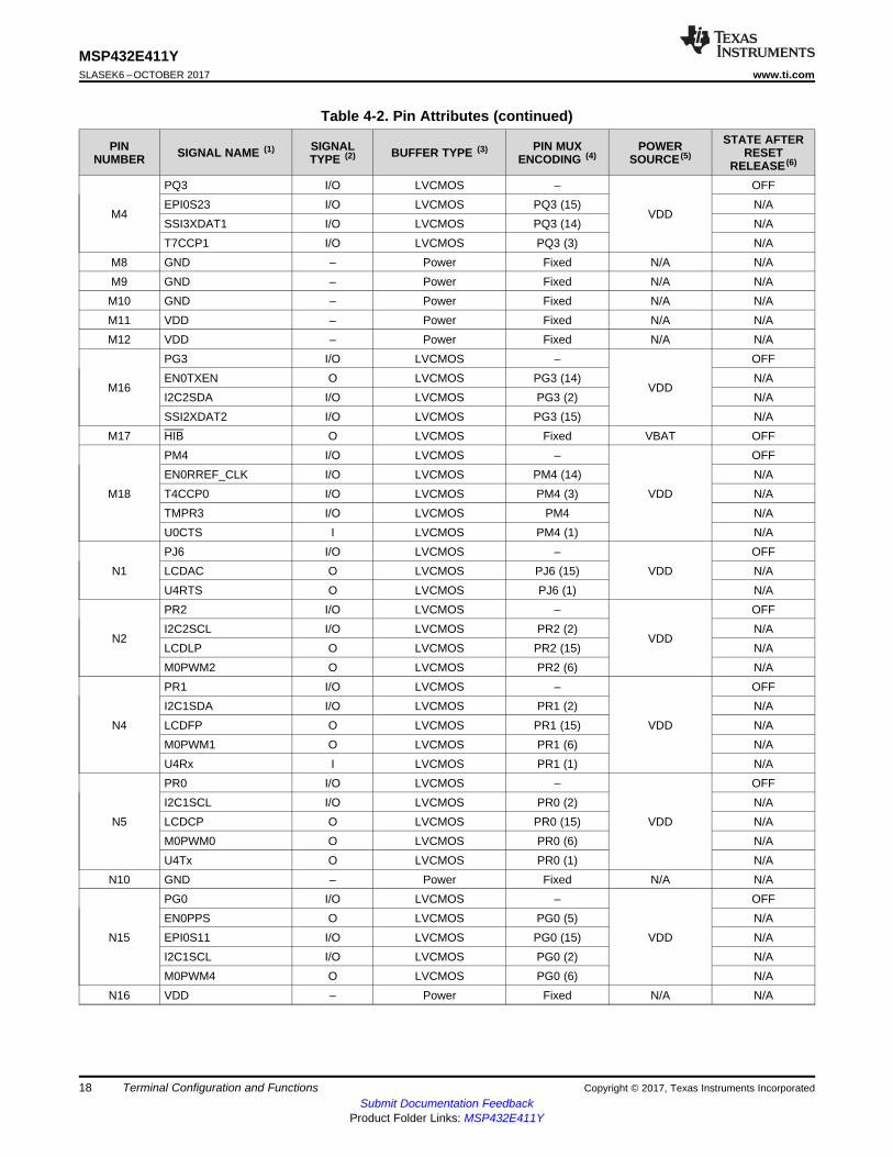
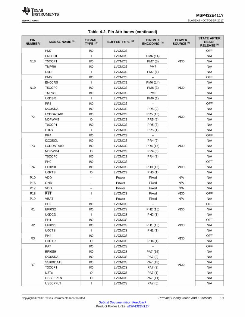
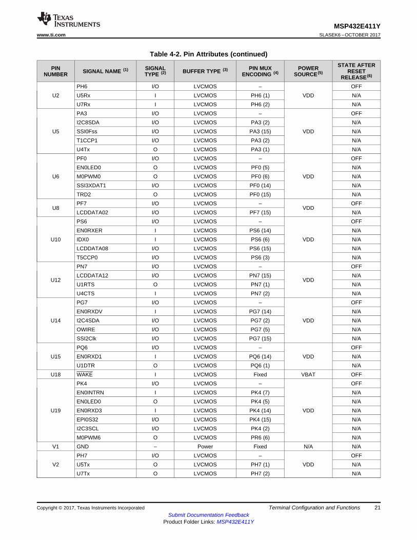
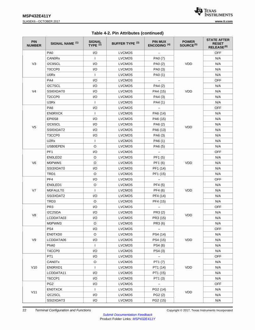
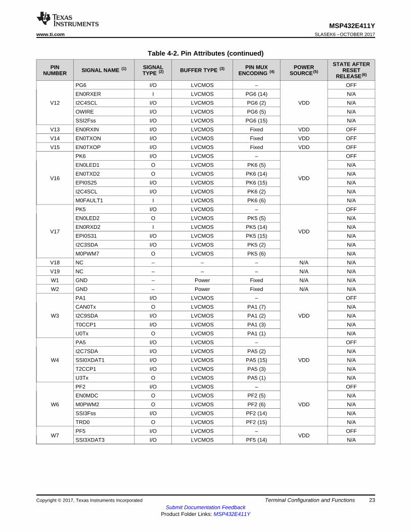
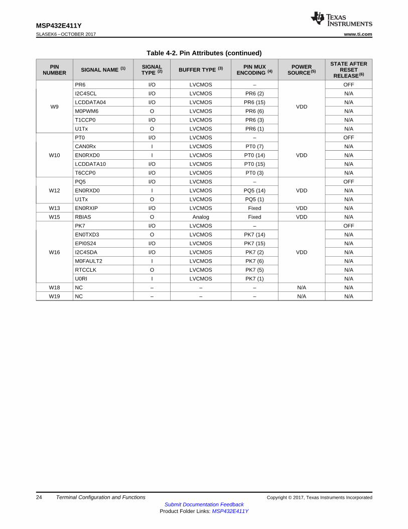
Table 4-2 describes the pin attributes.
Table 4-2. Pin Attributes
PINNUMBER SIGNAL NAME (1) SIGNAL
TYPE (2) BUFFER TYPE (3) PIN MUXENCODING (4)
POWERSOURCE (5)
STATE AFTERRESET
RELEASE (6)
A1 GND – Power – N/A N/AA2 GND – Power – N/A N/A
A4
PD4 I/O LVCMOS –
VDD
OFFAIN7 I Analog PD4 N/ASSI1XDAT2 I/O LVCMOS PD4 (15) N/AT3CCP0 I/O LVCMOS PD4 (3) N/AU2Rx I LVCMOS PD4 (1) N/A
A5
PE4 I/O LVCMOS –
VDD
OFFAIN9 I Analog PE5 N/ASSI1XDAT0 I/O LVCMOS PE4 (15) N/AU1RI I LVCMOS PE4 (1) N/A
A7
PE6 I/O LVCMOS –
VDD
OFFAIN20 I Analog PE6 N/AI2C9SCL I/O LVCMOS PE6 (2) N/AU0CTS I LVCMOS PE6 (1) N/A
A8PP7 I/O LVCMOS –
VDDOFF
AIN22 I Analog PP7 N/AOWIRE I/O LVCMOS PP7 (5) N/A
A10
PN4 I/O LVCMOS –
VDD
OFFEPI0S34 I/O LVCMOS PN4 (15) N/AI2C2SDA I/O LVCMOS PN4 (3) N/AU1DTR O LVCMOS PN4 (1) N/AU3RTS O LVCMOS PN4 (2) N/A
10
MSP432E411YSLASEK6 –OCTOBER 2017 www.ti.com
Submit Documentation FeedbackProduct Folder Links: MSP432E411Y
Terminal Configuration and Functions Copyright © 2017, Texas Instruments Incorporated
Table 4-2. Pin Attributes (continued)
PINNUMBER SIGNAL NAME (1) SIGNAL
TYPE (2) BUFFER TYPE (3) PIN MUXENCODING (4)
POWERSOURCE (5)
STATE AFTERRESET
RELEASE (6)
A11
PN2 I/O LVCMOS –
VDD
OFFEPI0S29 I/O LVCMOS PN2 (15) N/AU1DCD I LVCMOS PN2 (1) N/AU2RTS O LVCMOS PN2 (2) N/A
A13PQ4 I/O LVCMOS –
VDDOFF
DIVSCLK O LVCMOS PQ4 (13) N/AU1Rx I LVCMOS PQ4 (1) N/A
A14
PS3 I/O LVCMOS –
VDD
OFFLCDDATA23 O LVCMOS PS3 (15) N/AM0FAULT3 I LVCMOS PS3 (6) N/AT3CCP1 I/O LVCMOS PS3 (3) N/A
A16
PB0 I/O LVCMOS –
VDD
OFFCAN1Rx I LVCMOS PB0 (7) N/AI2C5SCL I/O LVCMOS PB0 (2) N/AT4CCP0 I/O LVCMOS PB0 (3) N/AU1Rx I LVCMOS PB0 (1) N/AUSB0ID I Analog PB0 N/A
A17
PB2 I/O LVCMOS –
VDD
OFFEN0MDC O LVCMOS PB2 (5) N/AEPI0S27 I/O LVCMOS PB2 (15) N/AI2C0SCL I/O LVCMOS PB2 (2) N/AT5CCP0 I/O LVCMOS PB2 (3) N/AUSB0STP O LVCMOS PB2 (14) N/A
A18 GND – Power Fixed N/A N/AA19 GND – Power Fixed N/A N/AB1 GND – Power Fixed N/A N/A
B2
PD7 I/O LVCMOS –
VDD
OFFAIN4 I Analog PD7 N/ANMI I LVCMOS PD7 (8) N/ASSI2XDAT2 I/O LVCMOS PD7 (15) N/AT4CCP1 I/O LVCMOS PD7 (3) N/AU2CTS I LVCMOS PD7 (1) N/AUSB0PFLT I LVCMOS PD7 (5) N/A
B3
PD6 I/O LVCMOS –
VDD
OFFAIN5 I Analog PD6 N/ASSI2XDAT3 I/O LVCMOS PD6 (15) N/AT4CCP0 I/O LVCMOS PD6 (3) N/AU2RTS O LVCMOS PD6 (1) N/AUSB0EPEN O LVCMOS PD6 (5) N/A
B4
PD5 I/O LVCMOS –
VDD
OFFAIN6 I Analog PD5 N/ASSI1XDAT3 I/O LVCMOS PD5 (15) N/AT3CCP1 I/O LVCMOS PD5 (3) N/AU2Tx O LVCMOS PD5 (1) N/A

11
MSP432E411Ywww.ti.com SLASEK6 –OCTOBER 2017
Submit Documentation FeedbackProduct Folder Links: MSP432E411Y
Terminal Configuration and FunctionsCopyright © 2017, Texas Instruments Incorporated
Table 4-2. Pin Attributes (continued)
PINNUMBER SIGNAL NAME (1) SIGNAL
TYPE (2) BUFFER TYPE (3) PIN MUXENCODING (4)
POWERSOURCE (5)
STATE AFTERRESET
RELEASE (6)
B5PE5 I/O LVCMOS –
VDDOFF
AIN8 I Analog PE5 N/ASSI1XDAT1 I/O LVCMOS PE5 (15) N/A
B6
PB5 I/O LVCMOS –
VDD
OFFAIN11 I Analog PB5 N/AI2C5SDA I/O LVCMOS PB5 (2) N/ASSI1Clk I/O LVCMOS PB5 (15) N/AU0RTS O LVCMOS PB5 (1) N/A
B7
PE7 I/O LVCMOS –
VDD
OFFAIN21 I Analog PE7 N/AI2C9SDA I/O LVCMOS PE7 (2) N/ANMI I LVCMOS PE7 (8) N/AU0RTS O LVCMOS PE7 (1) N/A
B8
PP6 I/O LVCMOS –
VDD
OFFAIN23 I Analog PP6 N/AI2C2SDA I/O LVCMOS PP6 (2) N/AU1DCD I LVCMOS PP6 (1) N/A
B9
PN5 I/O LVCMOS –
VDD
OFFEPI0S35 I/O LVCMOS PN5 (15) N/AI2C2SCL I/O LVCMOS PN5 (3) N/AU1RI I LVCMOS PN5 (1) N/AU3CTS I LVCMOS PN5 (2) N/A
B10
PN3 I/O LVCMOS –
VDD
OFFEPI0S30 I/O LVCMOS PN3 (15) N/AU1DSR I LVCMOS PN3 (1) N/AU2CTS I LVCMOS PN3 (2) N/A
B11PN1 I/O LVCMOS –
VDDOFF
U1CTS I LVCMOS PN1 (1) N/A
B12
PP5 I/O LVCMOS –
VDD
OFFI2C2SCL I/O LVCMOS PP5 (2) N/AOWALT I/O LVCMOS PP5 (4) N/AU3CTS I LVCMOS PP5 (1) N/AUSB0D6 I/O LVCMOS PP5 (14) N/A
B13
PP2 I/O LVCMOS –
VDD
OFFEPI0S29 I/O LVCMOS PP2 (15) N/AU0DTR O LVCMOS PP2 (1) N/AUSB0NXT O LVCMOS PP2 (14) N/A
B14
PS2 I/O LVCMOS –
VDD
OFFLCDDATA22 O LVCMOS PS2 (15) N/AM0FAULT2 I LVCMOS PS2 (6) N/AT3CCP0 I/O LVCMOS PS2 (3) N/AU1DSR I LVCMOS PS2 (1) N/A
B15PC0 I/O LVCMOS –
VDDN/A
TCLK/SWCLK I LVCMOS PC0 (1) PU
12
MSP432E411YSLASEK6 –OCTOBER 2017 www.ti.com
Submit Documentation FeedbackProduct Folder Links: MSP432E411Y
Terminal Configuration and Functions Copyright © 2017, Texas Instruments Incorporated
Table 4-2. Pin Attributes (continued)
PINNUMBER SIGNAL NAME (1) SIGNAL
TYPE (2) BUFFER TYPE (3) PIN MUXENCODING (4)
POWERSOURCE (5)
STATE AFTERRESET
RELEASE (6)
B16
PB1 I/O LVCMOS –
VDD
OFFCAN1Tx O LVCMOS PB1 (7) N/AI2C5SDA I/O LVCMOS PB1 (2) N/AT4CCP1 I/O LVCMOS PB1 (3) N/AU1Tx O LVCMOS PB1 (1) N/AUSB0VBUS I/O Analog PB1 N/A
B17
PB3 I/O LVCMOS –
VDD
OFFEN0MDIO I/O LVCMOS PB3 (5) N/AEPI0S28 I/O LVCMOS PB3 (15) N/AI2C0SDA I/O LVCMOS PB3 (2) N/AT5CCP1 I/O LVCMOS PB3 (3) N/AUSB0CLK O LVCMOS PB3 (14) N/A
B18PL7 I/O LVCMOS –
VDDOFF
T1CCP1 I/O LVCMOS PL7 (3) N/AUSB0DM I/O Analog PL7 N/A
B19 GND – Power – N/A N/A
C1
PD1 I/O LVCMOS –
VDD
OFFAIN14 I Analog PD1 N/AC1o O LVCMOS PD1 (5) N/AI2C7SDA I/O LVCMOS PD1 (2) N/ASSI2XDAT0 I/O LVCMOS PD1 (15) N/AT0CCP1 I/O LVCMOS PD1 (3) N/A
C2
PD0 I/O LVCMOS –
VDD
OFFAIN15 I Analog PD0 N/AC0o O LVCMOS PD0 (5) N/AI2C7SCL I/O LVCMOS PD0 (2) N/ASSI2XDAT1 I/O LVCMOS PD0 (15) N/AT0CCP0 I/O LVCMOS PD0 (3) N/A
C5 NC – – – N/A N/A
C6
PB4 I/O LVCMOS –
VDD
OFFN/A
AIN10 I Analog PB4 N/AI2C5SCL I/O LVCMOS PB4 (2) N/ASSI1Fss I/O LVCMOS PB4 (15) N/AU0CTS I LVCMOS PB4 (1) N/A
C8PJ0 I/O LVCMOS –
VDDOFF
EN0PPS O LVCMOS PJ0 (5) N/AU3Rx I LVCMOS PJ0 (1) N/A
C10PN0 I/O LVCMOS –
VDDOFF
U1RTS O LVCMOS PN0 (1) N/A
C12
PP3 I/O LVCMOS –
VDD
OFFEPI0S30 I/O LVCMOS PP3 (15) N/ARTCCLK O LVCMOS PP3 (7) N/AU0DCD I LVCMOS PP3 (2) N/AU1CTS I LVCMOS PP3 (1) N/AUSB0DIR O LVCMOS PP3 (14) N/A
13
MSP432E411Ywww.ti.com SLASEK6 –OCTOBER 2017
Submit Documentation FeedbackProduct Folder Links: MSP432E411Y
Terminal Configuration and FunctionsCopyright © 2017, Texas Instruments Incorporated
Table 4-2. Pin Attributes (continued)
PINNUMBER SIGNAL NAME (1) SIGNAL
TYPE (2) BUFFER TYPE (3) PIN MUXENCODING (4)
POWERSOURCE (5)
STATE AFTERRESET
RELEASE (6)
C14PC3 I/O LVCMOS –
VDDN/A
TDO/SWO O LVCMOS PC3 (1) PU
C15PC1 I/O LVCMOS –
VDDN/A
TMS/SWDIO I/O LVCMOS PC1 (1) PU
C18PL6 I/O LVCMOS –
VDDOFF
T1CCP0 I/O LVCMOS PL6 (3) N/AUSB0DP I/O Analog PL6 N/A
D1
PD3 I/O LVCMOS –
VDD
OFFAIN12 I Analog PD3 N/AI2C8SDA I/O LVCMOS PD3 (2) N/ASSI2Clk I/O LVCMOS PD3 (15) N/AT1CCP1 I/O LVCMOS PD3 (3) N/A
D2
PD2 I/O LVCMOS –
VDD
OFFAIN13 I Analog PD2 N/AC2o O LVCMOS PD2 (5) N/AI2C8SCL I/O LVCMOS PD0 (2) N/ASSI2Fss I/O LVCMOS PD2 (15) N/AT1CCP0 I/O LVCMOS PD2 (3) N/A
D6
PP0 I/O LVCMOS –
VDD
OFFC2+ I Analog PP0 N/AEN0INTRN I LVCMOS PP0 (7) N/ASSI3XDAT2 I/O LVCMOS PP0 (15) N/AT6CCP0 I/O LVCMOS PP0 (5) N/AU6Rx I LVCMOS PP0 (1) N/A
D7
PP1 I/O LVCMOS –
VDD
OFFC2- I Analog PP1 N/ASSI3XDAT3 I/O LVCMOS PP1 (15) N/AT6CCP1 I/O LVCMOS PP1 (5) N/AU6Tx O LVCMOS PP1 (1) N/A
D8
PP4 I/O LVCMOS –
VDD
OFFOWIRE I/O LVCMOS PP4 (4) N/AU0DSR I LVCMOS PP4 (2) N/AU3RTS O LVCMOS PP4 (1) N/AUSB0D7 I/O LVCMOS PP4 (14) N/A
D12
PS0 I/O LVCMOS –
VDD
OFFLCDDATA20 O LVCMOS PS0 (15) N/AM0FAULT0 I LVCMOS PS0 (6) N/AT2CCP0 I/O LVCMOS PS0 (3) N/A
D13
PS1 I/O LVCMOS –
VDD
OFFLCDDATA21 O LVCMOS PS1 (15) N/AM0FAULT1 I LVCMOS PS1 (6) N/AT2CCP1 I/O LVCMOS PS1 (3) N/A
D14PC2 I/O LVCMOS –
VDDN/A
TDI I LVCMOS PC2 (1) PUD18 GNDX2 – Power Fixed N/A N/AD19 OSC1 O Analog Fixed VDD N/A
14
MSP432E411YSLASEK6 –OCTOBER 2017 www.ti.com
Submit Documentation FeedbackProduct Folder Links: MSP432E411Y
Terminal Configuration and Functions Copyright © 2017, Texas Instruments Incorporated
Table 4-2. Pin Attributes (continued)
PINNUMBER SIGNAL NAME (1) SIGNAL
TYPE (2) BUFFER TYPE (3) PIN MUXENCODING (4)
POWERSOURCE (5)
STATE AFTERRESET
RELEASE (6)
E2
PQ1 I/O LVCMOS –
VDD
OFFEPI0S21 I/O LVCMOS PQ1 (15) N/ASSI3Fss I/O LVCMOS PQ1 (14) N/AT6CCP1 I/O LVCMOS PQ1 (3) N/A
E3
PQ0 I/O LVCMOS –
VDD
OFFEPI0S20 I/O LVCMOS PQ0 (15) N/ASSI3Clk I/O LVCMOS PQ0 (14) N/AT6CCP0 I/O LVCMOS PQ0 (3) N/A
E7PJ1 I/O LVCMOS –
VDDOFF
U3Tx O LVCMOS PJ1 (1) N/AE10 VDDC – Power Fixed N/A N/AE13 NC – – – N/A N/A
E17PJ5 I/O LVCMOS –
VDDOFF
LCDDATA17 O LVCMOS PJ5 (15) N/AU3CTS I LVCMOS PJ5 (1) N/A
E18
PT2 I/O LVCMOS –
VDD
OFFCAN1Rx I LVCMOS PT2 (7) N/ALCDDATA18 O LVCMOS PT2 (15) N/AT7CCP0 I/O LVCMOS PT2 (3) N/A
E19 OSC0 I Analog Fixed VDD N/A
F1PB7 I/O LVCMOS –
VDDOFF
I2C6SDA I/O LVCMOS PB7 (1) N/AT6CCP1 I/O LVCMOS PB7 (3) N/A
F2PB6 I/O LVCMOS –
VDDOFF
I2C6SCL I/O LVCMOS PB6 (1) N/AT6CCP0 I/O LVCMOS PB6 (3) N/A
F3 VDDA – Power Fixed N/A N/AF4 VREFA+ – Analog Fixed VDD N/AF10 GND – Power Fixed N/A N/A
F16PJ3 I/O LVCMOS –
VDDOFF
LCDDATA15 I/O LVCMOS PJ3 (15) N/AU2CTS I LVCMOS PJ3 (1) N/A
F17
PT3 I/O LVCMOS –
VDD
OFFCAN1Tx O LVCMOS PT3 (7) N/ALCDDATA19 O LVCMOS PT3 (15) N/AT7CCP1 I/O LVCMOS PT3 (3) N/A
F18PJ4 I/O LVCMOS –
VDDOFF
LCDDATA16 O LVCMOS PJ4 (15) N/AU3RTS O LVCMOS PJ4 (1) N/A
G1PE2 I/O LVCMOS –
VDDOFF
AIN1 I Analog PE3 N/AU1DCD I LVCMOS PE1 (1) N/A
G2
PE3 I/O LVCMOS –
VDD
OFFAIN0 I Analog PE3 N/AOWIRE I/O LVCMOS PE3 (5) N/AU1DTR O LVCMOS PE3 (1) N/A
15
MSP432E411Ywww.ti.com SLASEK6 –OCTOBER 2017
Submit Documentation FeedbackProduct Folder Links: MSP432E411Y
Terminal Configuration and FunctionsCopyright © 2017, Texas Instruments Incorporated
Table 4-2. Pin Attributes (continued)
PINNUMBER SIGNAL NAME (1) SIGNAL
TYPE (2) BUFFER TYPE (3) PIN MUXENCODING (4)
POWERSOURCE (5)
STATE AFTERRESET
RELEASE (6)
G4 GNDA – Power Fixed N/A N/AG5 VREFA- – Analog Fixed VDD N/AG10 VDD – Power Fixed N/A N/A
G15
PM5 I/O LVCMOS –
VDD
OFFT4CCP1 I/O LVCMOS PM5 (3) N/ATMPR2 I/O LVCMOS PM5 N/AU0DCD I LVCMOS PM5 (1) N/A
G16
PL0 I/O LVCMOS –
VDD
OFFEPI0S16 I/O LVCMOS PL0 (15) N/AI2C2SDA I/O LVCMOS PL0 (2) N/AM0FAULT3 I LVCMOS PL0 (6) N/AUSB0D0 I/O LVCMOS PL0 (14) N/A
G18
PL2 I/O LVCMOS –
VDD
OFFC0o O LVCMOS PL2 (5) N/AEPI0S18 I/O LVCMOS PL2 (15) N/APhB0 I LVCMOS PL2 (6) N/AUSB0D2 I/O LVCMOS PL2 (14) N/A
G19
PL5 I/O LVCMOS –
VDD
OFFEPI0S33 I/O LVCMOS PL5 (15) N/AT0CCP1 I/O LVCMOS PL5 (3) N/AUSB0D5 I/O LVCMOS PL5 (14) N/A
H2PE1 I/O LVCMOS –
VDDOFF
AIN2 I Analog PE1 N/AU1DSR I LVCMOS PE1 (1) N/A
H3PE0 I/O LVCMOS –
VDDOFF
AIN3 I Analog PE0 N/AU1RTS O LVCMOS PE0 (1) N/A
H4
PQ2 I/O LVCMOS –
VDD
OFFEPI0S22 I/O LVCMOS PQ2 (15) N/ASSI3XDAT0 I/O LVCMOS PQ2 (14) N/AT7CCP0 I/O LVCMOS PQ2 (3) N/A
H9 VDD – Power Fixed N/A N/AH10 GND – Power Fixed N/A N/AH11 GND – Power Fixed N/A N/AH12 GND – Power Fixed N/A N/AH16 VDDC – Power Fixed N/A N/A
H17PJ2 I/O LVCMOS –
VDDOFF
LCDDATA14 I/O LVCMOS PJ2 (15) N/AU2RTS O LVCMOS PJ2 (1) N/A
H18
PL4 I/O LVCMOS –
VDD
OFFEPI0S26 I/O LVCMOS PL4 (15) N/AT0CCP0 I/O LVCMOS PL4 (3) N/AUSB0D4 I/O LVCMOS PL4 (14) N/A

16
MSP432E411YSLASEK6 –OCTOBER 2017 www.ti.com
Submit Documentation FeedbackProduct Folder Links: MSP432E411Y
Terminal Configuration and Functions Copyright © 2017, Texas Instruments Incorporated
Table 4-2. Pin Attributes (continued)
PINNUMBER SIGNAL NAME (1) SIGNAL
TYPE (2) BUFFER TYPE (3) PIN MUXENCODING (4)
POWERSOURCE (5)
STATE AFTERRESET
RELEASE (6)
H19
PL1 I/O LVCMOS –
VDD
OFFEPI0S17 I/O LVCMOS PL1 (15) N/AI2C2SCL I/O LVCMOS PL1 (2) N/APhA0 I LVCMOS PL1 (6) N/AUSB0D1 I/O LVCMOS PL1 (14) N/A
J1
PK0 I/O LVCMOS –
VDD
OFFAIN16 I Analog PK0 N/AEPI0S0 I/O LVCMOS PK0 (15) N/AU4Rx I LVCMOS PK0 (1) N/A
J2
PK1 I/O LVCMOS –
VDD
OFFAIN17 I Analog PK1 N/AEPI0S1 I/O LVCMOS PK1 (15) N/AU4Tx O LVCMOS PK1 (1) N/A
J8 VDD – Power Fixed N/A N/AJ9 VDD – Power Fixed N/A N/AJ10 VDD – Power Fixed N/A N/AJ11 GND – Power Fixed N/A N/AJ12 GND – Power Fixed N/A N/A
J18
PL3 I/O LVCMOS –
VDD
OFFC1o O LVCMOS PL3 (5) N/AEPI0S19 I/O LVCMOS PL3 (15) N/AIDX0 I LVCMOS PL3 (6) N/AUSB0D3 I/O LVCMOS PL3 (14) N/A
K1
PK2 I/O LVCMOS –
VDD
OFFAIN18 I Analog PK2 N/AEPI0S2 I/O LVCMOS PK2 (15) N/AU4RTS O LVCMOS PK2 (1) N/A
K2
PK3 I/O LVCMOS –
VDD
OFFAIN19 I Analog PK3 N/AEPI0S3 I/O LVCMOS PK3 (15) N/AU4CTS I LVCMOS PK3 (1) N/A
K3
PC7 I/O LVCMOS –
VDD
OFFC0- I Analog PC7 N/AEPI0S4 I/O LVCMOS PC7 (15) N/AU5Tx O LVCMOS PC7 (1) N/A
K5PJ7 I/O LVCMOS –
VDDOFF
U4CTS I LVCMOS PK3 (1) N/AK6 GND – Power Fixed N/A N/AK7 VDD – Power Fixed N/A N/AK8 VDD – Power Fixed N/A N/AK9 GND – Power Fixed N/A N/AK10 GND – Power Fixed N/A N/AK11 VDD – Power Fixed N/A N/AK12 VDD – Power Fixed N/A N/AK13 GND – Power Fixed N/A N/AK14 GND – Power Fixed N/A N/A
17
MSP432E411Ywww.ti.com SLASEK6 –OCTOBER 2017
Submit Documentation FeedbackProduct Folder Links: MSP432E411Y
Terminal Configuration and FunctionsCopyright © 2017, Texas Instruments Incorporated
Table 4-2. Pin Attributes (continued)
PINNUMBER SIGNAL NAME (1) SIGNAL
TYPE (2) BUFFER TYPE (3) PIN MUXENCODING (4)
POWERSOURCE (5)
STATE AFTERRESET
RELEASE (6)
K15
PG5 I/O LVCMOS –
VDD
OFFEN0TXD1 O LVCMOS PG5 (14) N/AI2C3SDA I/O LVCMOS PG5 (2) N/AOWALT I/O LVCMOS PG5 (5) N/ASSI2XDAT0 I/O LVCMOS PG5 (15) N/AU0RTS O LVCMOS PG5 (1) N/A
K17
PG4 I/O LVCMOS –
VDD
OFFEN0TXD0 O LVCMOS PG4 (14) N/AI2C3SCL I/O LVCMOS PG4 (2) N/AOWIRE I/O LVCMOS PG4 (5) N/ASSI2XDAT1 I/O LVCMOS PG4 (15) N/AU0CTS I LVCMOS PG4 (1) N/A
K18PM0 I/O LVCMOS –
VDDOFF
EPI0S15 I/O LVCMOS PM0 (15) N/AT2CCP0 I/O LVCMOS PM0 (3) N/A
K19PM1 I/O LVCMOS –
VDDOFF
EPI0S14 I/O LVCMOS PM1 (15) N/AT2CCP1 I/O LVCMOS PM1 (3) N/A
L2
PC6 I/O LVCMOS –
VDD
OFFC0+ I Analog PC6 N/AEPI0S5 I/O LVCMOS PC6 (15) N/AU5Rx I LVCMOS PC6 (1) N/A
L8 GND – Power Fixed N/A N/AL9 GND – Power Fixed N/A N/AL10 VDD – Power Fixed N/A N/AL11 VDD – Power Fixed N/A N/AL12 VDD – Power Fixed N/A N/A
L18PM2 I/O LVCMOS –
VDDOFF
EPI0S13 I/O LVCMOS PM2 (15) N/AT3CCP0 I/O LVCMOS PM2 (3) N/A
L19PM3 I/O LVCMOS –
VDDOFF
EPI0S12 I/O LVCMOS PM3 (15) N/AT3CCP1 I/O LVCMOS PM3 (3) N/A
M1
PC5 I/O LVCMOS –
VDD
OFFC1+ I Analog PC5 N/AEPI0S6 I/O LVCMOS PC5 (15) N/ARTCCLK O LVCMOS PC5 (7) N/AT7CCP1 I/O LVCMOS PC5 (3) N/AU7Tx O LVCMOS PC5 (1) N/A
M2
PC4 I/O LVCMOS –
VDD
OFFC1- I Analog PC4 N/AEPI0S7 I/O LVCMOS PC4 (15) N/AT7CCP0 I/O LVCMOS PC4 (3) N/AU7Rx I LVCMOS PC4 (1) N/A
M3PQ7 I/O LVCMOS –
VDDOFF
U1RI I LVCMOS PQ7 (1) N/A
18
MSP432E411YSLASEK6 –OCTOBER 2017 www.ti.com
Submit Documentation FeedbackProduct Folder Links: MSP432E411Y
Terminal Configuration and Functions Copyright © 2017, Texas Instruments Incorporated
Table 4-2. Pin Attributes (continued)
PINNUMBER SIGNAL NAME (1) SIGNAL
TYPE (2) BUFFER TYPE (3) PIN MUXENCODING (4)
POWERSOURCE (5)
STATE AFTERRESET
RELEASE (6)
M4
PQ3 I/O LVCMOS –
VDD
OFFEPI0S23 I/O LVCMOS PQ3 (15) N/ASSI3XDAT1 I/O LVCMOS PQ3 (14) N/AT7CCP1 I/O LVCMOS PQ3 (3) N/A
M8 GND – Power Fixed N/A N/AM9 GND – Power Fixed N/A N/AM10 GND – Power Fixed N/A N/AM11 VDD – Power Fixed N/A N/AM12 VDD – Power Fixed N/A N/A
M16
PG3 I/O LVCMOS –
VDD
OFFEN0TXEN O LVCMOS PG3 (14) N/AI2C2SDA I/O LVCMOS PG3 (2) N/ASSI2XDAT2 I/O LVCMOS PG3 (15) N/A
M17 HIB O LVCMOS Fixed VBAT OFF
M18
PM4 I/O LVCMOS –
VDD
OFFEN0RREF_CLK I/O LVCMOS PM4 (14) N/AT4CCP0 I/O LVCMOS PM4 (3) N/ATMPR3 I/O LVCMOS PM4 N/AU0CTS I LVCMOS PM4 (1) N/A
N1PJ6 I/O LVCMOS –
VDDOFF
LCDAC O LVCMOS PJ6 (15) N/AU4RTS O LVCMOS PJ6 (1) N/A
N2
PR2 I/O LVCMOS –
VDD
OFFI2C2SCL I/O LVCMOS PR2 (2) N/ALCDLP O LVCMOS PR2 (15) N/AM0PWM2 O LVCMOS PR2 (6) N/A
N4
PR1 I/O LVCMOS –
VDD
OFFI2C1SDA I/O LVCMOS PR1 (2) N/ALCDFP O LVCMOS PR1 (15) N/AM0PWM1 O LVCMOS PR1 (6) N/AU4Rx I LVCMOS PR1 (1) N/A
N5
PR0 I/O LVCMOS –
VDD
OFFI2C1SCL I/O LVCMOS PR0 (2) N/ALCDCP O LVCMOS PR0 (15) N/AM0PWM0 O LVCMOS PR0 (6) N/AU4Tx O LVCMOS PR0 (1) N/A
N10 GND – Power Fixed N/A N/A
N15
PG0 I/O LVCMOS –
VDD
OFFEN0PPS O LVCMOS PG0 (5) N/AEPI0S11 I/O LVCMOS PG0 (15) N/AI2C1SCL I/O LVCMOS PG0 (2) N/AM0PWM4 O LVCMOS PG0 (6) N/A
N16 VDD – Power Fixed N/A N/A
19
MSP432E411Ywww.ti.com SLASEK6 –OCTOBER 2017
Submit Documentation FeedbackProduct Folder Links: MSP432E411Y
Terminal Configuration and FunctionsCopyright © 2017, Texas Instruments Incorporated
Table 4-2. Pin Attributes (continued)
PINNUMBER SIGNAL NAME (1) SIGNAL
TYPE (2) BUFFER TYPE (3) PIN MUXENCODING (4)
POWERSOURCE (5)
STATE AFTERRESET
RELEASE (6)
N18
PM7 I/O LVCMOS –
VDD
OFFEN0COL I LVCMOS PM6 (14) N/AT5CCP1 I/O LVCMOS PM7 (3) N/ATMPR0 I/O LVCMOS PM7 N/AU0RI I LVCMOS PM7 (1) N/A
N19
PM6 I/O LVCMOS –
VDD
OFFEN0CRS I LVCMOS PM6 (14) N/AT5CCP0 I/O LVCMOS PM6 (3) N/ATMPR1 I/O LVCMOS PM6 N/AU0DSR I LVCMOS PM6 (1) N/A
P2
PR5 I/O LVCMOS –
VDD
OFFI2C3SDA I/O LVCMOS PR5 (2) N/ALCDDATA01 I/O LVCMOS PR5 (15) N/AM0PWM5 O LVCMOS PR5 (6) N/AT0CCP1 I/O LVCMOS PR5 (3) N/AU1Rx I LVCMOS PR5 (1) N/A
P3
PR4 I/O LVCMOS –
VDD
OFFI2C3SCL I/O LVCMOS PR4 (2) N/ALCDDATA00 I/O LVCMOS PR4 (15) N/AM0PWM4 O LVCMOS PR4 (6) N/AT0CCP0 I/O LVCMOS PR4 (3) N/A
P4PH0 I/O LVCMOS –
VDDOFF
EPI0S0 I/O LVCMOS PH0 (15) N/AU0RTS O LVCMOS PH0 (1) N/A
P10 VDD – Power Fixed N/A N/AP16 GND – Power Fixed N/A N/AP17 VDD – Power Fixed N/A N/AP18 RST I LVCMOS Fixed VDD OFFP19 VBAT – Power Fixed N/A N/A
R1PH2 I/O LVCMOS –
VDDOFF
EPI0S2 I/O LVCMOS PH2 (15) N/AU0DCD I LVCMOS PH2 (1) N/A
R2PH1 I/O LVCMOS –
VDDOFF
EPI0S1 I/O LVCMOS PH1 (15) N/AU0CTS I LVCMOS PH1 (1) N/A
R3PH4 I/O LVCMOS –
VDDOFF
U0DTR O LVCMOS PH4 (1) N/A
R7
PA7 I/O LVCMOS –
VDD
OFFEPI0S9 I/O LVCMOS PA7 (15) N/AI2C6SDA I/O LVCMOS PA7 (2) N/ASSI0XDAT3 I/O LVCMOS PA7 (13) N/AT3CCP1 I/O LVCMOS PA7 (3) N/AU2Tx O LVCMOS PA7 (1) N/AUSB0EPEN O LVCMOS PA7 (11) N/AUSB0PFLT I LVCMOS PA7 (5) N/A

20
MSP432E411YSLASEK6 –OCTOBER 2017 www.ti.com
Submit Documentation FeedbackProduct Folder Links: MSP432E411Y
Terminal Configuration and Functions Copyright © 2017, Texas Instruments Incorporated
Table 4-2. Pin Attributes (continued)
PINNUMBER SIGNAL NAME (1) SIGNAL
TYPE (2) BUFFER TYPE (3) PIN MUXENCODING (4)
POWERSOURCE (5)
STATE AFTERRESET
RELEASE (6)
R10
PR7 I/O LVCMOS –
VDD
OFFEN0TXEN O LVCMOS PR7 (14) N/AI2C4SDA I/O LVCMOS PR7 (2) N/ALCDDATA05 I/O LVCMOS PR7 (15) N/AM0PWM7 O LVCMOS PR7 (6) N/AT1CCP1 I/O LVCMOS PR7 (3) N/A
R13
PS7 I/O LVCMOS –
VDD
OFFEN0RXDV I LVCMOS PS7 (14) N/ALCDDATA09 I/O LVCMOS PS7 (15) N/AT5CCP1 I/O LVCMOS PS7 (3) N/A
R17 GND – Power Fixed N/A N/AR18 GNDX – Power Fixed N/A N/A
T1PH3 I/O LVCMOS –
VDDOFF
EPI0S3 I/O LVCMOS PH3 (15) N/AU0DSR I LVCMOS PH3 (1) N/A
T2PH5 I/O LVCMOS –
VDDOFF
EN0PPS O LVCMOS PH5 (15) N/AU0RI I LVCMOS PH5 (1) N/A
T6
PA2 I/O LVCMOS –
VDD
OFFI2C8SCL I/O LVCMOS PA2 (2) N/ASSI0Clk I/O LVCMOS PA2 (15) N/AT1CCP0 I/O LVCMOS PA2 (3) N/AU4Rx I LVCMOS PA2 (1) N/A
T7
PF3 I/O LVCMOS –
VDD
OFFEN0MDIO I/O LVCMOS PF3 (5) N/AM0PWM3 O LVCMOS PF3 (6) N/ASSI3Clk I/O LVCMOS PF3 (14) N/ATRCLK O LVCMOS PF3 (15) N/A
T8PF6 I/O LVCMOS –
VDDOFF
LCDMCLK O LVCMOS PF6 (15) N/A
T12
PN6 I/O LVCMOS –
VDD
OFFEN0TXER O LVCMOS PN6 (14) N/ALCDDATA13 I/O LVCMOS PN6 (15) N/AU4RTS O LVCMOS PN6 (2) N/A
T13
PS5 I/O LVCMOS –
VDD
OFFEN0TXD1 O LVCMOS PS5 (14) N/ALCDDATA07 I/O LVCMOS PS5 (15) N/APhB0 I LVCMOS PS5 (6) N/AT4CCP1 I/O LVCMOS PS5 (3) N/A
G14
PG1 I/O LVCMOS –
VDD
OFFEPI0S10 I/O LVCMOS PG1 (15) N/AI2C1SDA I/O LVCMOS PG1 (2) N/AM0PWM5 O LVCMOS PG1 (6) N/A
T18 XOSC0 I Analog Fixed VBAT N/AT19 XOSC1 O Analog Fixed VBAT N/A
21
MSP432E411Ywww.ti.com SLASEK6 –OCTOBER 2017
Submit Documentation FeedbackProduct Folder Links: MSP432E411Y
Terminal Configuration and FunctionsCopyright © 2017, Texas Instruments Incorporated
Table 4-2. Pin Attributes (continued)
PINNUMBER SIGNAL NAME (1) SIGNAL
TYPE (2) BUFFER TYPE (3) PIN MUXENCODING (4)
POWERSOURCE (5)
STATE AFTERRESET
RELEASE (6)
U2PH6 I/O LVCMOS –
VDDOFF
U5Rx I LVCMOS PH6 (1) N/AU7Rx I LVCMOS PH6 (2) N/A
U5
PA3 I/O LVCMOS –
VDD
OFFI2C8SDA I/O LVCMOS PA3 (2) N/ASSI0Fss I/O LVCMOS PA3 (15) N/AT1CCP1 I/O LVCMOS PA3 (2) N/AU4Tx O LVCMOS PA3 (1) N/A
U6
PF0 I/O LVCMOS –
VDD
OFFEN0LED0 O LVCMOS PF0 (5) N/AM0PWM0 O LVCMOS PF0 (6) N/ASSI3XDAT1 I/O LVCMOS PF0 (14) N/ATRD2 O LVCMOS PF0 (15) N/A
U8PF7 I/O LVCMOS –
VDDOFF
LCDDATA02 I/O LVCMOS PF7 (15) N/A
U10
PS6 I/O LVCMOS –
VDD
OFFEN0RXER I LVCMOS PS6 (14) N/AIDX0 I LVCMOS PS6 (6) N/ALCDDATA08 I/O LVCMOS PS6 (15) N/AT5CCP0 I/O LVCMOS PS6 (3) N/A
U12
PN7 I/O LVCMOS –
VDD
OFFLCDDATA12 I/O LVCMOS PN7 (15) N/AU1RTS O LVCMOS PN7 (1) N/AU4CTS I LVCMOS PN7 (2) N/A
U14
PG7 I/O LVCMOS –
VDD
OFFEN0RXDV I LVCMOS PG7 (14) N/AI2C4SDA I/O LVCMOS PG7 (2) N/AOWIRE I/O LVCMOS PG7 (5) N/ASSI2Clk I/O LVCMOS PG7 (15) N/A
U15PQ6 I/O LVCMOS –
VDDOFF
EN0RXD1 I LVCMOS PQ6 (14) N/AU1DTR O LVCMOS PQ6 (1) N/A
U18 WAKE I LVCMOS Fixed VBAT OFF
U19
PK4 I/O LVCMOS –
VDD
OFFEN0INTRN I LVCMOS PK4 (7) N/AEN0LED0 O LVCMOS PK4 (5) N/AEN0RXD3 I LVCMOS PK4 (14) N/AEPI0S32 I/O LVCMOS PK4 (15) N/AI2C3SCL I/O LVCMOS PK4 (2) N/AM0PWM6 O LVCMOS PR6 (6) N/A
V1 GND – Power Fixed N/A N/A
V2PH7 I/O LVCMOS –
VDDOFF
U5Tx O LVCMOS PH7 (1) N/AU7Tx O LVCMOS PH7 (2) N/A
22
MSP432E411YSLASEK6 –OCTOBER 2017 www.ti.com
Submit Documentation FeedbackProduct Folder Links: MSP432E411Y
Terminal Configuration and Functions Copyright © 2017, Texas Instruments Incorporated
Table 4-2. Pin Attributes (continued)
PINNUMBER SIGNAL NAME (1) SIGNAL
TYPE (2) BUFFER TYPE (3) PIN MUXENCODING (4)
POWERSOURCE (5)
STATE AFTERRESET
RELEASE (6)
V3
PA0 I/O LVCMOS –
VDD
OFFCAN0Rx I LVCMOS PA0 (7) N/AI2C9SCL I/O LVCMOS PA0 (2) N/AT0CCP0 I/O LVCMOS PA0 (3) N/AU0Rx I LVCMOS PA0 (1) N/A
V4
PA4 I/O LVCMOS –
VDD
OFFI2C7SCL I/O LVCMOS PA4 (2) N/ASSI0XDAT0 I/O LVCMOS PA4 (15) N/AT2CCP0 I/O LVCMOS PA4 (3) N/AU3Rx I LVCMOS PA4 (1) N/A
V5
PA6 I/O LVCMOS –
VDD
OFFEN0RXCK I LVCMOS PA6 (14) N/AEPI0S8 I/O LVCMOS PA6 (15) N/AI2C6SCL I/O LVCMOS PA6 (2) N/ASSI0XDAT2 I/O LVCMOS PA6 (13) N/AT3CCP0 I/O LVCMOS PA6 (3) N/AU2Rx I LVCMOS PA6 (1) N/AUSB0EPEN O LVCMOS PA6 (5) N/A
V6
PF1 I/O LVCMOS –
VDD
OFFEN0LED2 O LVCMOS PF1 (5) N/AM0PWM1 O LVCMOS PF1 (6) N/ASSI3XDAT0 I/O LVCMOS PF1 (14) N/ATRD1 O LVCMOS PF1 (15) N/A
V7
PF4 I/O LVCMOS –
VDD
OFFEN0LED1 O LVCMOS PF4 (5) N/AM0FAULT0 I LVCMOS PF4 (6) N/ASSI3XDAT2 I/O LVCMOS PF4 (14) N/ATRD3 O LVCMOS PF4 (15) N/A
V8
PR3 I/O LVCMOS –
VDD
OFFI2C2SDA I/O LVCMOS PR3 (2) N/ALCDDATA03 I/O LVCMOS PR3 (15) N/AM0PWM3 O LVCMOS PR3 (6) N/A
V9
PS4 I/O LVCMOS –
VDD
OFFEN0TXD0 O LVCMOS PS4 (14) N/ALCDDATA06 I/O LVCMOS PS4 (15) N/APhA0 I LVCMOS PS4 (6) N/AT4CCP0 I/O LVCMOS PS4 (3) N/A
V10
PT1 I/O LVCMOS –
VDD
OFFCAN0Tx O LVCMOS PT1 (7) N/AEN0RXD1 I LVCMOS PT1 (14) N/ALCDDATA11 I/O LVCMOS PT1 (15) N/AT6CCP1 I/O LVCMOS PT1 (3) N/A
V11
PG2 I/O LVCMOS –
VDD
OFFEN0TXCK I LVCMOS PG2 (14) N/AI2C2SCL I/O LVCMOS PG2 (2) N/ASSI2XDAT3 I/O LVCMOS PG2 (15) N/A
23
MSP432E411Ywww.ti.com SLASEK6 –OCTOBER 2017
Submit Documentation FeedbackProduct Folder Links: MSP432E411Y
Terminal Configuration and FunctionsCopyright © 2017, Texas Instruments Incorporated
Table 4-2. Pin Attributes (continued)
PINNUMBER SIGNAL NAME (1) SIGNAL
TYPE (2) BUFFER TYPE (3) PIN MUXENCODING (4)
POWERSOURCE (5)
STATE AFTERRESET
RELEASE (6)
V12
PG6 I/O LVCMOS –
VDD
OFFEN0RXER I LVCMOS PG6 (14) N/AI2C4SCL I/O LVCMOS PG6 (2) N/AOWIRE I/O LVCMOS PG6 (5) N/ASSI2Fss I/O LVCMOS PG6 (15) N/A
V13 EN0RXIN I/O LVCMOS Fixed VDD OFFV14 EN0TXON I/O LVCMOS Fixed VDD OFFV15 EN0TXOP I/O LVCMOS Fixed VDD OFF
V16
PK6 I/O LVCMOS –
VDD
OFFEN0LED1 O LVCMOS PK6 (5) N/AEN0TXD2 O LVCMOS PK6 (14) N/AEPI0S25 I/O LVCMOS PK6 (15) N/AI2C4SCL I/O LVCMOS PK6 (2) N/AM0FAULT1 I LVCMOS PK6 (6) N/A
V17
PK5 I/O LVCMOS –
VDD
OFFEN0LED2 O LVCMOS PK5 (5) N/AEN0RXD2 I LVCMOS PK5 (14) N/AEPI0S31 I/O LVCMOS PK5 (15) N/AI2C3SDA I/O LVCMOS PK5 (2) N/AM0PWM7 O LVCMOS PK5 (6) N/A
V18 NC – – – N/A N/AV19 NC – – – N/A N/AW1 GND – Power Fixed N/A N/AW2 GND – Power Fixed N/A N/A
W3
PA1 I/O LVCMOS –
VDD
OFFCAN0Tx O LVCMOS PA1 (7) N/AI2C9SDA I/O LVCMOS PA1 (2) N/AT0CCP1 I/O LVCMOS PA1 (3) N/AU0Tx O LVCMOS PA1 (1) N/A
W4
PA5 I/O LVCMOS –
VDD
OFFI2C7SDA I/O LVCMOS PA5 (2) N/ASSI0XDAT1 I/O LVCMOS PA5 (15) N/AT2CCP1 I/O LVCMOS PA5 (3) N/AU3Tx O LVCMOS PA5 (1) N/A
W6
PF2 I/O LVCMOS –
VDD
OFFEN0MDC O LVCMOS PF2 (5) N/AM0PWM2 O LVCMOS PF2 (6) N/ASSI3Fss I/O LVCMOS PF2 (14) N/ATRD0 O LVCMOS PF2 (15) N/A
W7PF5 I/O LVCMOS –
VDDOFF
SSI3XDAT3 I/O LVCMOS PF5 (14) N/A
24
MSP432E411YSLASEK6 –OCTOBER 2017 www.ti.com
Submit Documentation FeedbackProduct Folder Links: MSP432E411Y
Terminal Configuration and Functions Copyright © 2017, Texas Instruments Incorporated
Table 4-2. Pin Attributes (continued)
PINNUMBER SIGNAL NAME (1) SIGNAL
TYPE (2) BUFFER TYPE (3) PIN MUXENCODING (4)
POWERSOURCE (5)
STATE AFTERRESET
RELEASE (6)
W9
PR6 I/O LVCMOS –
VDD
OFFI2C4SCL I/O LVCMOS PR6 (2) N/ALCDDATA04 I/O LVCMOS PR6 (15) N/AM0PWM6 O LVCMOS PR6 (6) N/AT1CCP0 I/O LVCMOS PR6 (3) N/AU1Tx O LVCMOS PR6 (1) N/A
W10
PT0 I/O LVCMOS –
VDD
OFFCAN0Rx I LVCMOS PT0 (7) N/AEN0RXD0 I LVCMOS PT0 (14) N/ALCDDATA10 I/O LVCMOS PT0 (15) N/AT6CCP0 I/O LVCMOS PT0 (3) N/A
W12PQ5 I/O LVCMOS –
VDDOFF
EN0RXD0 I LVCMOS PQ5 (14) N/AU1Tx O LVCMOS PQ5 (1) N/A
W13 EN0RXIP I/O LVCMOS Fixed VDD N/AW15 RBIAS O Analog Fixed VDD N/A
W16
PK7 I/O LVCMOS –
VDD
OFFEN0TXD3 O LVCMOS PK7 (14) N/AEPI0S24 I/O LVCMOS PK7 (15) N/AI2C4SDA I/O LVCMOS PK7 (2) N/AM0FAULT2 I LVCMOS PK7 (6) N/ARTCCLK O LVCMOS PK7 (5) N/AU0RI I LVCMOS PK7 (1) N/A
W18 NC – – – N/A N/AW19 NC – – – N/A N/A
25
MSP432E411Ywww.ti.com SLASEK6 –OCTOBER 2017
Submit Documentation FeedbackProduct Folder Links: MSP432E411Y
Terminal Configuration and FunctionsCopyright © 2017, Texas Instruments Incorporated
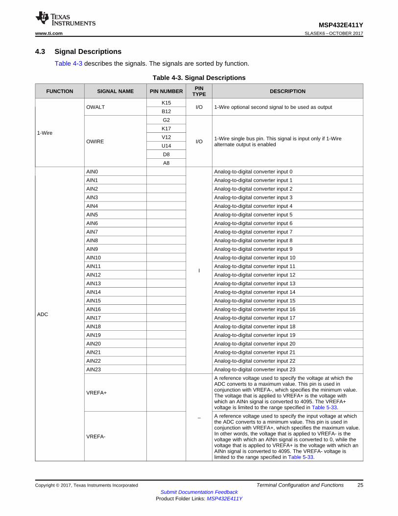
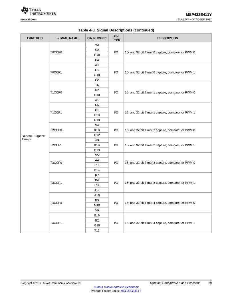
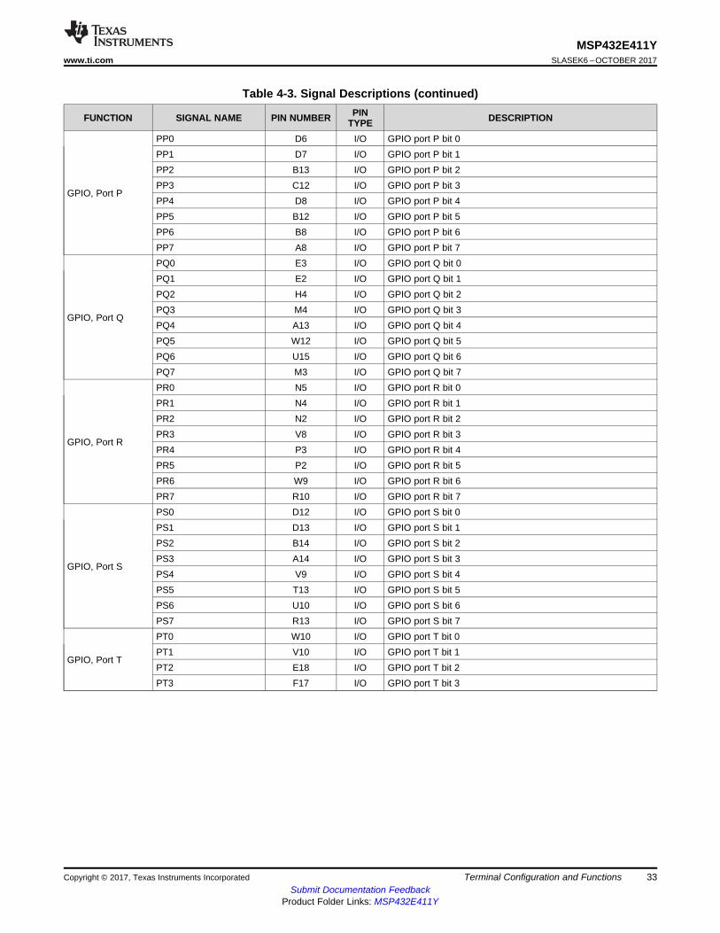
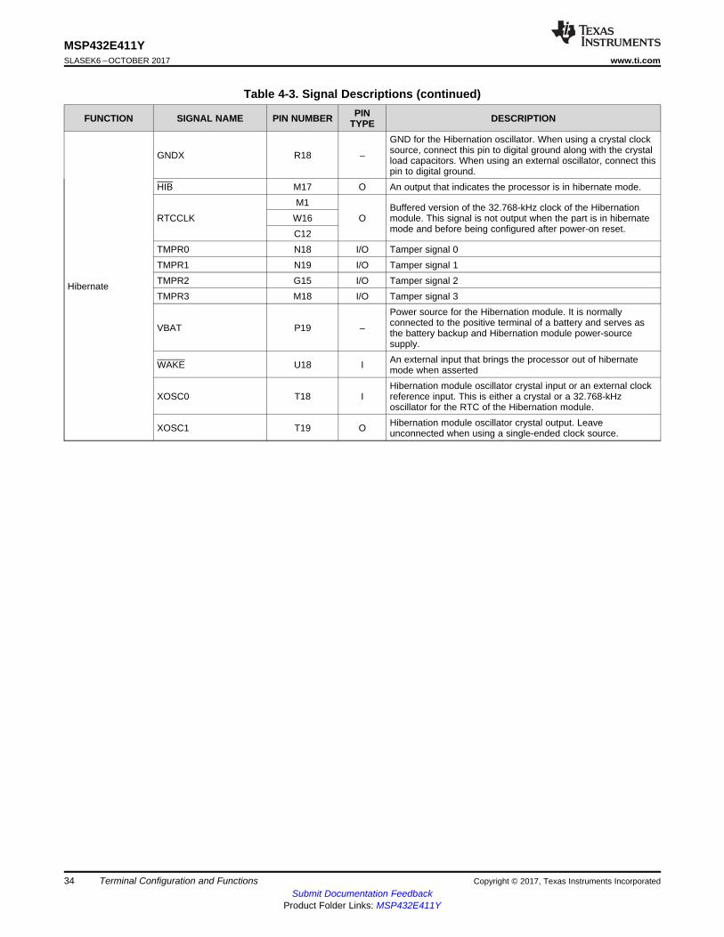
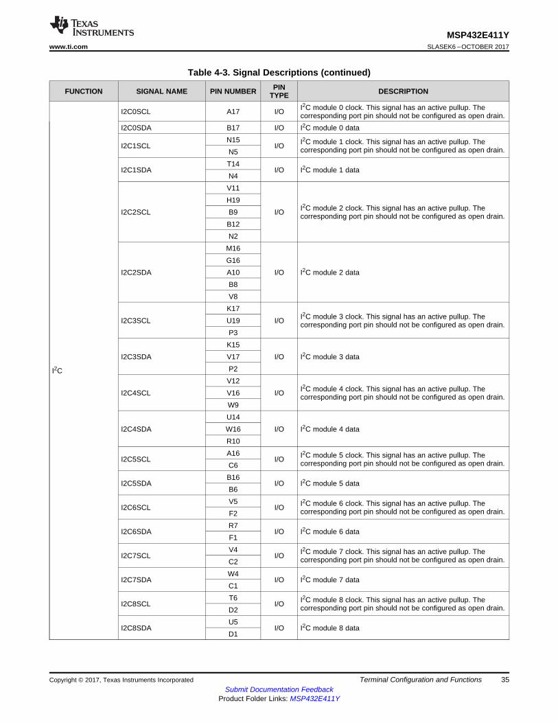
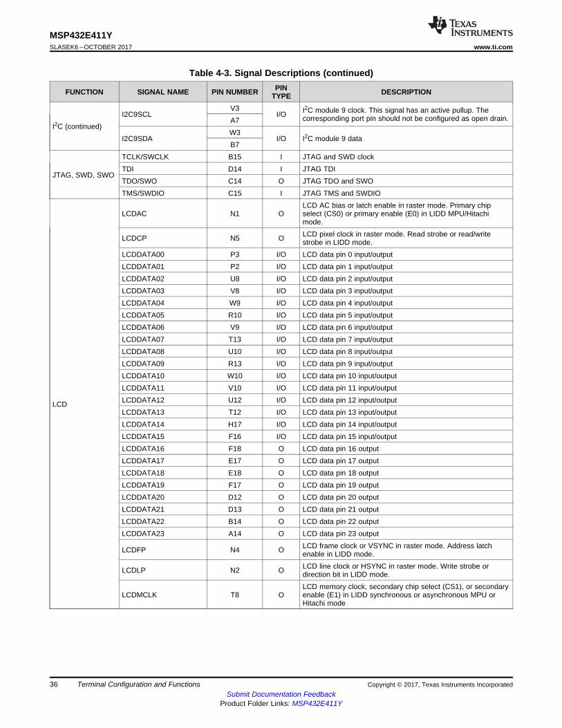
4.3 Signal DescriptionsTable 4-3 describes the signals. The signals are sorted by function.
Table 4-3. Signal Descriptions
FUNCTION SIGNAL NAME PIN NUMBER PINTYPE DESCRIPTION
1-Wire
OWALTK15
I/O 1-Wire optional second signal to be used as outputB12
OWIRE
G2
I/O 1-Wire single bus pin. This signal is input only if 1-Wirealternate output is enabled
K17V12U14D8A8
ADC
AIN0
I
Analog-to-digital converter input 0AIN1 Analog-to-digital converter input 1AIN2 Analog-to-digital converter input 2AIN3 Analog-to-digital converter input 3AIN4 Analog-to-digital converter input 4AIN5 Analog-to-digital converter input 5AIN6 Analog-to-digital converter input 6AIN7 Analog-to-digital converter input 7AIN8 Analog-to-digital converter input 8AIN9 Analog-to-digital converter input 9AIN10 Analog-to-digital converter input 10AIN11 Analog-to-digital converter input 11AIN12 Analog-to-digital converter input 12AIN13 Analog-to-digital converter input 13AIN14 Analog-to-digital converter input 14AIN15 Analog-to-digital converter input 15AIN16 Analog-to-digital converter input 16AIN17 Analog-to-digital converter input 17AIN18 Analog-to-digital converter input 18AIN19 Analog-to-digital converter input 19AIN20 Analog-to-digital converter input 20AIN21 Analog-to-digital converter input 21AIN22 Analog-to-digital converter input 22AIN23 Analog-to-digital converter input 23
VREFA+
–
A reference voltage used to specify the voltage at which theADC converts to a maximum value. This pin is used inconjunction with VREFA-, which specifies the minimum value.The voltage that is applied to VREFA+ is the voltage withwhich an AINn signal is converted to 4095. The VREFA+voltage is limited to the range specified in Table 5-33.
VREFA-
A reference voltage used to specify the input voltage at whichthe ADC converts to a minimum value. This pin is used inconjunction with VREFA+, which specifies the maximum value.In other words, the voltage that is applied to VREFA- is thevoltage with which an AINn signal is converted to 0, while thevoltage that is applied to VREFA+ is the voltage with which anAINn signal is converted to 4095. The VREFA- voltage islimited to the range specified in Table 5-33.
26
MSP432E411YSLASEK6 –OCTOBER 2017 www.ti.com
Submit Documentation FeedbackProduct Folder Links: MSP432E411Y
Terminal Configuration and Functions Copyright © 2017, Texas Instruments Incorporated
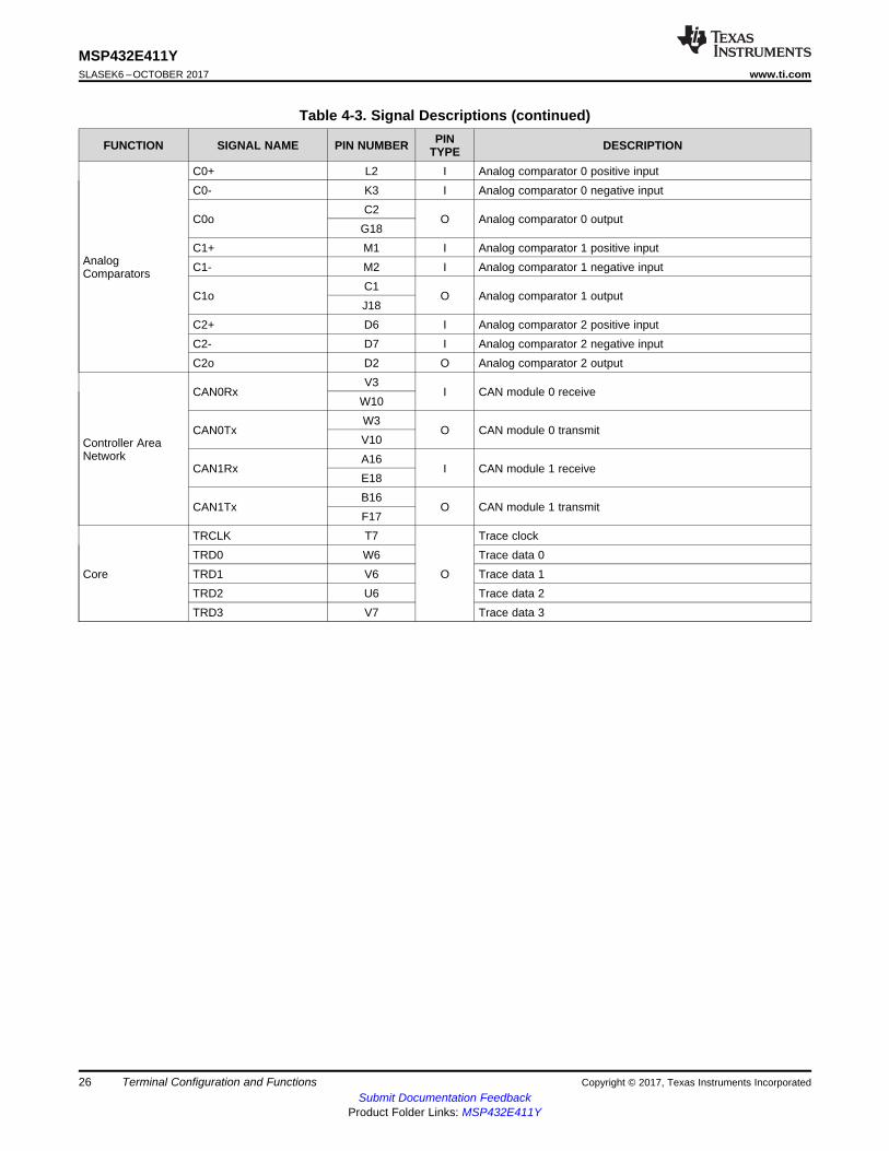
Table 4-3. Signal Descriptions (continued)
FUNCTION SIGNAL NAME PIN NUMBER PINTYPE DESCRIPTION
AnalogComparators
C0+ L2 I Analog comparator 0 positive inputC0- K3 I Analog comparator 0 negative input
C0oC2
O Analog comparator 0 outputG18
C1+ M1 I Analog comparator 1 positive inputC1- M2 I Analog comparator 1 negative input
C1oC1
O Analog comparator 1 outputJ18
C2+ D6 I Analog comparator 2 positive inputC2- D7 I Analog comparator 2 negative inputC2o D2 O Analog comparator 2 output
Controller AreaNetwork
CAN0RxV3
I CAN module 0 receiveW10
CAN0TxW3
O CAN module 0 transmitV10
CAN1RxA16
I CAN module 1 receiveE18
CAN1TxB16
O CAN module 1 transmitF17
Core
TRCLK T7
O
Trace clockTRD0 W6 Trace data 0TRD1 V6 Trace data 1TRD2 U6 Trace data 2TRD3 V7 Trace data 3
27
MSP432E411Ywww.ti.com SLASEK6 –OCTOBER 2017
Submit Documentation FeedbackProduct Folder Links: MSP432E411Y
Terminal Configuration and FunctionsCopyright © 2017, Texas Instruments Incorporated
Table 4-3. Signal Descriptions (continued)
FUNCTION SIGNAL NAME PIN NUMBER PINTYPE DESCRIPTION
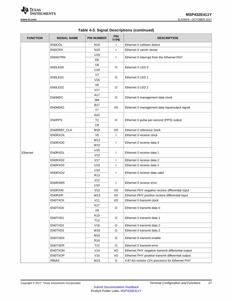
Ethernet
EN0COL N18 I Ethernet 0 collision detectEN0CRS N19 I Ethernet 0 carrier sense
EN0INTRNU19
I Ethernet 0 interrupt from the Ethernet PHYD6
EN0LED0U6
O Ethernet 0 LED 0U19
EN0LED1V7
O Ethernet 0 LED 1V16
EN0LED2V6
O Ethernet 0 LED 2V17
EN0MDCA17
O Ethernet 0 management data clockW6
EN0MDIOB17
I/O Ethernet 0 management data input/output signalT7
EN0PPSN15
O Ethernet 0 pulse-per-second (PPS) outputT2C8
EN0RREF_CLK M18 I/O Ethernet 0 reference clockEN0RXCK V5 I Ethernet 0 receive clock
EN0RXD0W12
I Ethernet 0 receive data 0W10
EN0RXD1U15
I Ethernet 0 receive data 1V10
EN0RXD2 V17 I Ethernet 0 receive data 2EN0RXD3 U19 I Ethernet 0 receive data 3
EN0RXDVU14
I Ethernet 0 receive data validR13
EN0RXERV12
I Ethernet 0 receive errorU10
EN0RXIN V13 I/O Ethernet PHY negative receive differential inputEN0RXIP W13 I/O Ethernet PHY positive receive differential inputEN0TXCK V11 I/O Ethernet 0 transmit clock
EN0TXD0K17
O Ethernet 0 transmit data 0V9
EN0TXD1K15
O Ethernet 0 transmit data 1T13
EN0TXD2 V16 O Ethernet 0 transmit data 2EN0TXD3 W16 O Ethernet 0 transmit data 3
EN0TXENM16
O Ethernet 0 transmit enableR10
EN0TXER T12 O Ethernet 0 transmit errorEN0TXON V14 I/O Ethernet PHY negative transmit differential outputEN0TXOP V15 I/O Ethernet PHY positive transmit differential outputRBIAS W15 O 4.87-kΩ resistor (1% precision) for Ethernet PHY
28
MSP432E411YSLASEK6 –OCTOBER 2017 www.ti.com
Submit Documentation FeedbackProduct Folder Links: MSP432E411Y
Terminal Configuration and Functions Copyright © 2017, Texas Instruments Incorporated
Table 4-3. Signal Descriptions (continued)
FUNCTION SIGNAL NAME PIN NUMBER PINTYPE DESCRIPTION
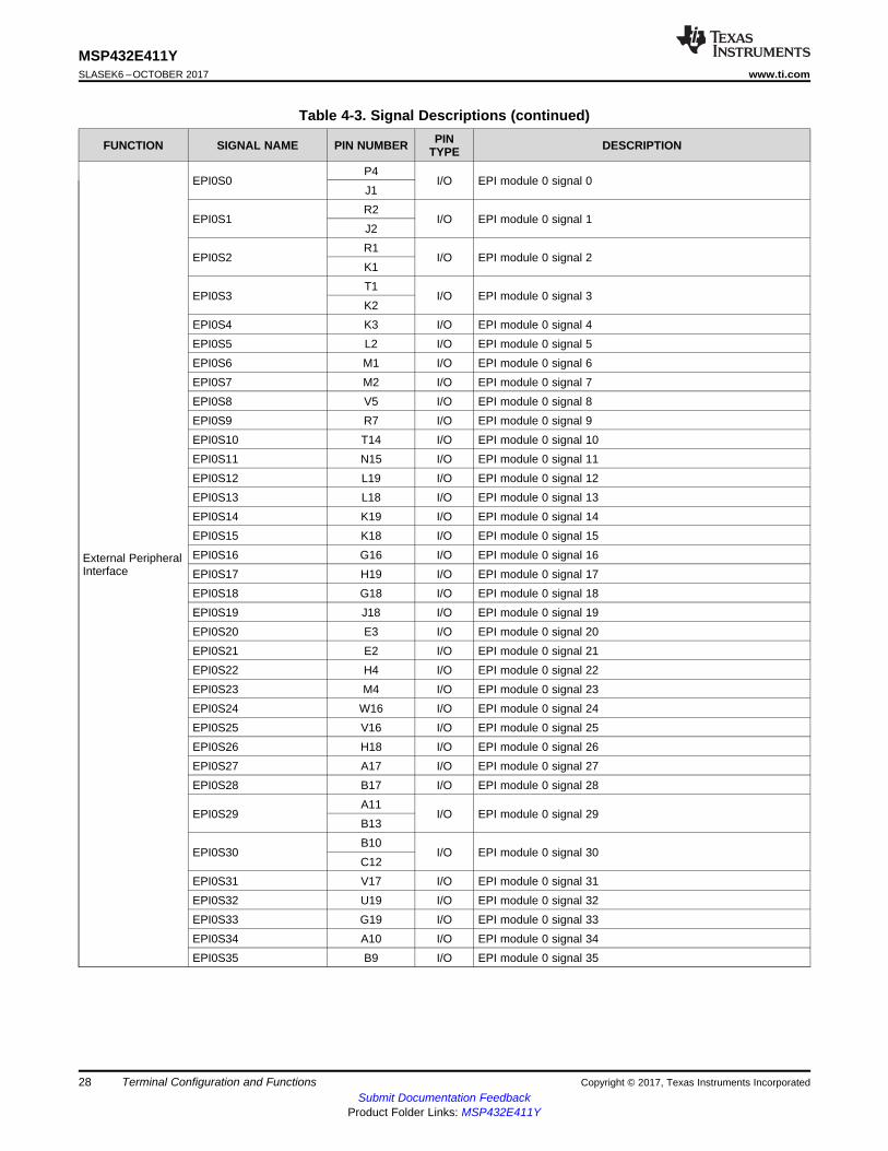
External PeripheralInterface
EPI0S0P4
I/O EPI module 0 signal 0J1
EPI0S1R2
I/O EPI module 0 signal 1J2
EPI0S2R1
I/O EPI module 0 signal 2K1
EPI0S3T1
I/O EPI module 0 signal 3K2
EPI0S4 K3 I/O EPI module 0 signal 4EPI0S5 L2 I/O EPI module 0 signal 5EPI0S6 M1 I/O EPI module 0 signal 6EPI0S7 M2 I/O EPI module 0 signal 7EPI0S8 V5 I/O EPI module 0 signal 8EPI0S9 R7 I/O EPI module 0 signal 9EPI0S10 T14 I/O EPI module 0 signal 10EPI0S11 N15 I/O EPI module 0 signal 11EPI0S12 L19 I/O EPI module 0 signal 12EPI0S13 L18 I/O EPI module 0 signal 13EPI0S14 K19 I/O EPI module 0 signal 14EPI0S15 K18 I/O EPI module 0 signal 15EPI0S16 G16 I/O EPI module 0 signal 16EPI0S17 H19 I/O EPI module 0 signal 17EPI0S18 G18 I/O EPI module 0 signal 18EPI0S19 J18 I/O EPI module 0 signal 19EPI0S20 E3 I/O EPI module 0 signal 20EPI0S21 E2 I/O EPI module 0 signal 21EPI0S22 H4 I/O EPI module 0 signal 22EPI0S23 M4 I/O EPI module 0 signal 23EPI0S24 W16 I/O EPI module 0 signal 24EPI0S25 V16 I/O EPI module 0 signal 25EPI0S26 H18 I/O EPI module 0 signal 26EPI0S27 A17 I/O EPI module 0 signal 27EPI0S28 B17 I/O EPI module 0 signal 28
EPI0S29A11
I/O EPI module 0 signal 29B13
EPI0S30B10
I/O EPI module 0 signal 30C12
EPI0S31 V17 I/O EPI module 0 signal 31EPI0S32 U19 I/O EPI module 0 signal 32EPI0S33 G19 I/O EPI module 0 signal 33EPI0S34 A10 I/O EPI module 0 signal 34EPI0S35 B9 I/O EPI module 0 signal 35
29
MSP432E411Ywww.ti.com SLASEK6 –OCTOBER 2017
Submit Documentation FeedbackProduct Folder Links: MSP432E411Y
Terminal Configuration and FunctionsCopyright © 2017, Texas Instruments Incorporated
Table 4-3. Signal Descriptions (continued)
FUNCTION SIGNAL NAME PIN NUMBER PINTYPE DESCRIPTION
General-PurposeTimers
T0CCP0
V3
I/O 16- and 32-bit Timer 0 capture, compare, or PWM 0C2H18P3
T0CCP1
W3
I/O 16- and 32-bit Timer 0 capture, compare, or PWM 1C1
G19P2
T1CCP0
T6
I/O 16- and 32-bit Timer 1 capture, compare, or PWM 0D2C18W9
T1CCP1
U5
I/O 16- and 32-bit Timer 1 capture, compare, or PWM 1D1B18R10
T2CCP0V4
I/O 16- and 32-bit Timer 2 capture, compare, or PWM 0K18D12
T2CCP1W4
I/O 16- and 32-bit Timer 2 capture, compare, or PWM 1K19D13
T3CCP0
V5
I/O 16- and 32-bit Timer 3 capture, compare, or PWM 0A4L18B14
T3CCP1
R7
I/O 16- and 32-bit Timer 3 capture, compare, or PWM 1B4L19A14
T4CCP0
A16
I/O 16- and 32-bit Timer 4 capture, compare, or PWM 0B3
M18V9
T4CCP1
B16
I/O 16- and 32-bit Timer 4 capture, compare, or PWM 1B2
G15T13
30
MSP432E411YSLASEK6 –OCTOBER 2017 www.ti.com
Submit Documentation FeedbackProduct Folder Links: MSP432E411Y
Terminal Configuration and Functions Copyright © 2017, Texas Instruments Incorporated
Table 4-3. Signal Descriptions (continued)
FUNCTION SIGNAL NAME PIN NUMBER PINTYPE DESCRIPTION
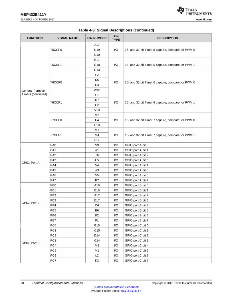
General-PurposeTimers (continued)
T5CCP0A17
I/O 16- and 32-bit Timer 5 capture, compare, or PWM 0N19U10
T5CCP1B17
I/O 16- and 32-bit Timer 5 capture, compare, or PWM 1N18R13
T6CCP0
F2
I/O 16- and 32-bit Timer 6 capture, compare, or PWM 0D6E3
W10
T6CCP1
F1
I/O 16- and 32-bit Timer 6 capture, compare, or PWM 1D7E2V10
T7CCP0M2
I/O 16- and 32-bit Timer 7 capture, compare, or PWM 0H4E18
T7CCP1M1
I/O 16- and 32-bit Timer 7 capture, compare, or PWM 1M4F17
GPIO, Port A
PA0 V3 I/O GPIO port A bit 0PA1 W3 I/O GPIO port A bit 1PA2 T6 I/O GPIO port A bit 2PA3 U5 I/O GPIO port A bit 3PA4 V4 I/O GPIO port A bit 4PA5 W4 I/O GPIO port A bit 5PA6 V5 I/O GPIO port A bit 6PA7 R7 I/O GPIO port A bit 7
GPIO, Port B
PB0 A16 I/O GPIO port B bit 0PB1 B16 I/O GPIO port B bit 1PB2 A17 I/O GPIO port B bit 2PB3 B17 I/O GPIO port B bit 3PB4 C6 I/O GPIO port B bit 4PB5 B6 I/O GPIO port B bit 5PB6 F2 I/O GPIO port B bit 6PB7 F1 I/O GPIO port B bit 7
GPIO, Port C
PC0 B15 I/O GPIO port C bit 0PC1 C15 I/O GPIO port C bit 1PC2 D14 I/O GPIO port C bit 2PC3 C14 I/O GPIO port C bit 3PC4 M2 I/O GPIO port C bit 4PC5 M1 I/O GPIO port C bit 5PC6 L2 I/O GPIO port C bit 6PC7 K3 I/O GPIO port C bit 7
31
MSP432E411Ywww.ti.com SLASEK6 –OCTOBER 2017
Submit Documentation FeedbackProduct Folder Links: MSP432E411Y
Terminal Configuration and FunctionsCopyright © 2017, Texas Instruments Incorporated
Table 4-3. Signal Descriptions (continued)
FUNCTION SIGNAL NAME PIN NUMBER PINTYPE DESCRIPTION
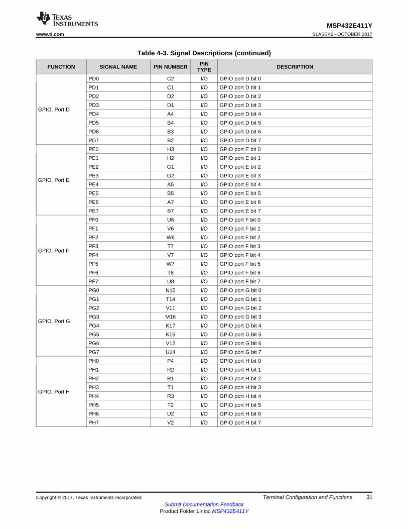
GPIO, Port D
PD0 C2 I/O GPIO port D bit 0PD1 C1 I/O GPIO port D bit 1PD2 D2 I/O GPIO port D bit 2PD3 D1 I/O GPIO port D bit 3PD4 A4 I/O GPIO port D bit 4PD5 B4 I/O GPIO port D bit 5PD6 B3 I/O GPIO port D bit 6PD7 B2 I/O GPIO port D bit 7
GPIO, Port E
PE0 H3 I/O GPIO port E bit 0PE1 H2 I/O GPIO port E bit 1PE2 G1 I/O GPIO port E bit 2PE3 G2 I/O GPIO port E bit 3PE4 A5 I/O GPIO port E bit 4PE5 B5 I/O GPIO port E bit 5PE6 A7 I/O GPIO port E bit 6PE7 B7 I/O GPIO port E bit 7
GPIO, Port F
PF0 U6 I/O GPIO port F bit 0PF1 V6 I/O GPIO port F bit 1PF2 W6 I/O GPIO port F bit 2PF3 T7 I/O GPIO port F bit 3PF4 V7 I/O GPIO port F bit 4PF5 W7 I/O GPIO port F bit 5PF6 T8 I/O GPIO port F bit 6PF7 U8 I/O GPIO port F bit 7
GPIO, Port G
PG0 N15 I/O GPIO port G bit 0PG1 T14 I/O GPIO port G bit 1PG2 V11 I/O GPIO port G bit 2PG3 M16 I/O GPIO port G bit 3PG4 K17 I/O GPIO port G bit 4PG5 K15 I/O GPIO port G bit 5PG6 V12 I/O GPIO port G bit 6PG7 U14 I/O GPIO port G bit 7
GPIO, Port H
PH0 P4 I/O GPIO port H bit 0PH1 R2 I/O GPIO port H bit 1PH2 R1 I/O GPIO port H bit 2PH3 T1 I/O GPIO port H bit 3PH4 R3 I/O GPIO port H bit 4PH5 T2 I/O GPIO port H bit 5PH6 U2 I/O GPIO port H bit 6PH7 V2 I/O GPIO port H bit 7
32
MSP432E411YSLASEK6 –OCTOBER 2017 www.ti.com
Submit Documentation FeedbackProduct Folder Links: MSP432E411Y
Terminal Configuration and Functions Copyright © 2017, Texas Instruments Incorporated
Table 4-3. Signal Descriptions (continued)
FUNCTION SIGNAL NAME PIN NUMBER PINTYPE DESCRIPTION
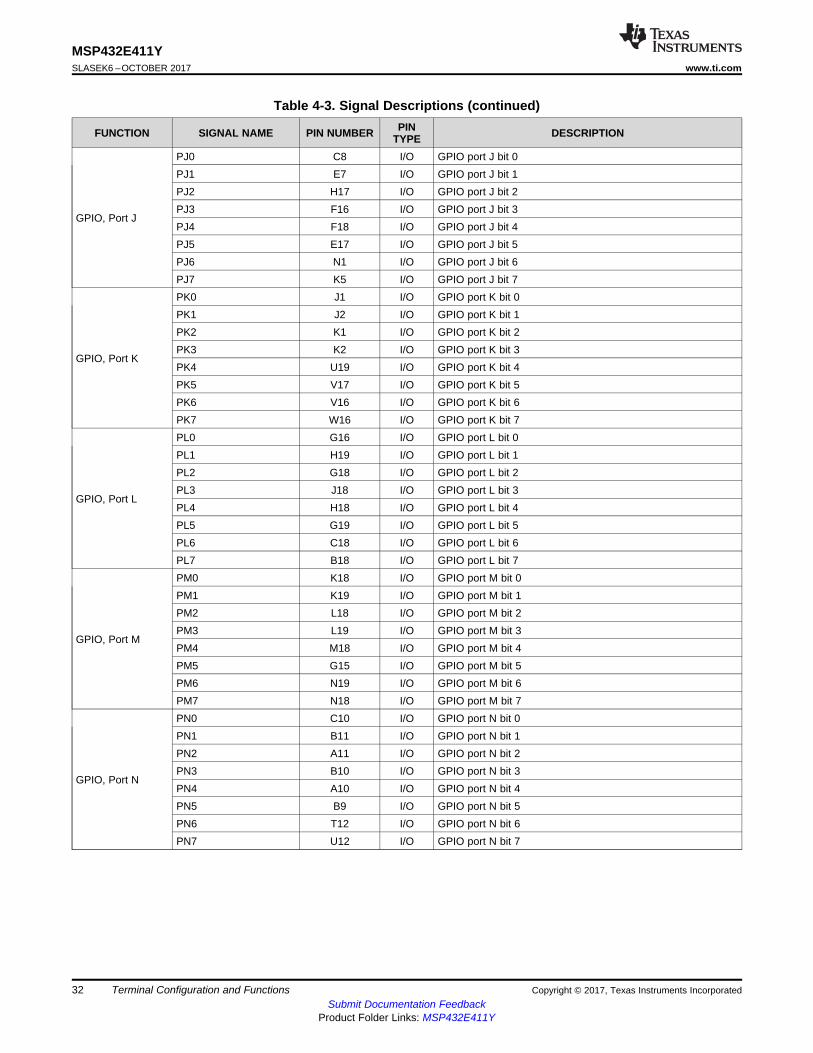
GPIO, Port J
PJ0 C8 I/O GPIO port J bit 0PJ1 E7 I/O GPIO port J bit 1PJ2 H17 I/O GPIO port J bit 2PJ3 F16 I/O GPIO port J bit 3PJ4 F18 I/O GPIO port J bit 4PJ5 E17 I/O GPIO port J bit 5PJ6 N1 I/O GPIO port J bit 6PJ7 K5 I/O GPIO port J bit 7
GPIO, Port K
PK0 J1 I/O GPIO port K bit 0PK1 J2 I/O GPIO port K bit 1PK2 K1 I/O GPIO port K bit 2PK3 K2 I/O GPIO port K bit 3PK4 U19 I/O GPIO port K bit 4PK5 V17 I/O GPIO port K bit 5PK6 V16 I/O GPIO port K bit 6PK7 W16 I/O GPIO port K bit 7
GPIO, Port L
PL0 G16 I/O GPIO port L bit 0PL1 H19 I/O GPIO port L bit 1PL2 G18 I/O GPIO port L bit 2PL3 J18 I/O GPIO port L bit 3PL4 H18 I/O GPIO port L bit 4PL5 G19 I/O GPIO port L bit 5PL6 C18 I/O GPIO port L bit 6PL7 B18 I/O GPIO port L bit 7
GPIO, Port M
PM0 K18 I/O GPIO port M bit 0PM1 K19 I/O GPIO port M bit 1PM2 L18 I/O GPIO port M bit 2PM3 L19 I/O GPIO port M bit 3PM4 M18 I/O GPIO port M bit 4PM5 G15 I/O GPIO port M bit 5PM6 N19 I/O GPIO port M bit 6PM7 N18 I/O GPIO port M bit 7
GPIO, Port N
PN0 C10 I/O GPIO port N bit 0PN1 B11 I/O GPIO port N bit 1PN2 A11 I/O GPIO port N bit 2PN3 B10 I/O GPIO port N bit 3PN4 A10 I/O GPIO port N bit 4PN5 B9 I/O GPIO port N bit 5PN6 T12 I/O GPIO port N bit 6PN7 U12 I/O GPIO port N bit 7
33
MSP432E411Ywww.ti.com SLASEK6 –OCTOBER 2017
Submit Documentation FeedbackProduct Folder Links: MSP432E411Y
Terminal Configuration and FunctionsCopyright © 2017, Texas Instruments Incorporated
Table 4-3. Signal Descriptions (continued)
FUNCTION SIGNAL NAME PIN NUMBER PINTYPE DESCRIPTION
GPIO, Port P
PP0 D6 I/O GPIO port P bit 0PP1 D7 I/O GPIO port P bit 1PP2 B13 I/O GPIO port P bit 2PP3 C12 I/O GPIO port P bit 3PP4 D8 I/O GPIO port P bit 4PP5 B12 I/O GPIO port P bit 5PP6 B8 I/O GPIO port P bit 6PP7 A8 I/O GPIO port P bit 7
GPIO, Port Q
PQ0 E3 I/O GPIO port Q bit 0PQ1 E2 I/O GPIO port Q bit 1PQ2 H4 I/O GPIO port Q bit 2PQ3 M4 I/O GPIO port Q bit 3PQ4 A13 I/O GPIO port Q bit 4PQ5 W12 I/O GPIO port Q bit 5PQ6 U15 I/O GPIO port Q bit 6PQ7 M3 I/O GPIO port Q bit 7
GPIO, Port R
PR0 N5 I/O GPIO port R bit 0PR1 N4 I/O GPIO port R bit 1PR2 N2 I/O GPIO port R bit 2PR3 V8 I/O GPIO port R bit 3PR4 P3 I/O GPIO port R bit 4PR5 P2 I/O GPIO port R bit 5PR6 W9 I/O GPIO port R bit 6PR7 R10 I/O GPIO port R bit 7
GPIO, Port S
PS0 D12 I/O GPIO port S bit 0PS1 D13 I/O GPIO port S bit 1PS2 B14 I/O GPIO port S bit 2PS3 A14 I/O GPIO port S bit 3PS4 V9 I/O GPIO port S bit 4PS5 T13 I/O GPIO port S bit 5PS6 U10 I/O GPIO port S bit 6PS7 R13 I/O GPIO port S bit 7
GPIO, Port T
PT0 W10 I/O GPIO port T bit 0PT1 V10 I/O GPIO port T bit 1PT2 E18 I/O GPIO port T bit 2PT3 F17 I/O GPIO port T bit 3
34
MSP432E411YSLASEK6 –OCTOBER 2017 www.ti.com
Submit Documentation FeedbackProduct Folder Links: MSP432E411Y
Terminal Configuration and Functions Copyright © 2017, Texas Instruments Incorporated
Table 4-3. Signal Descriptions (continued)
FUNCTION SIGNAL NAME PIN NUMBER PINTYPE DESCRIPTION
Hibernate
GNDX R18 –
GND for the Hibernation oscillator. When using a crystal clocksource, connect this pin to digital ground along with the crystalload capacitors. When using an external oscillator, connect thispin to digital ground.
HIB M17 O An output that indicates the processor is in hibernate mode.
RTCCLKM1
OBuffered version of the 32.768-kHz clock of the Hibernationmodule. This signal is not output when the part is in hibernatemode and before being configured after power-on reset.
W16C12
TMPR0 N18 I/O Tamper signal 0TMPR1 N19 I/O Tamper signal 1TMPR2 G15 I/O Tamper signal 2TMPR3 M18 I/O Tamper signal 3
VBAT P19 –
Power source for the Hibernation module. It is normallyconnected to the positive terminal of a battery and serves asthe battery backup and Hibernation module power-sourcesupply.
WAKE U18 I An external input that brings the processor out of hibernatemode when asserted
XOSC0 T18 IHibernation module oscillator crystal input or an external clockreference input. This is either a crystal or a 32.768-kHzoscillator for the RTC of the Hibernation module.
XOSC1 T19 O Hibernation module oscillator crystal output. Leaveunconnected when using a single-ended clock source.
35
MSP432E411Ywww.ti.com SLASEK6 –OCTOBER 2017
Submit Documentation FeedbackProduct Folder Links: MSP432E411Y
Terminal Configuration and FunctionsCopyright © 2017, Texas Instruments Incorporated
Table 4-3. Signal Descriptions (continued)
FUNCTION SIGNAL NAME PIN NUMBER PINTYPE DESCRIPTION
I2C
I2C0SCL A17 I/O I2C module 0 clock. This signal has an active pullup. Thecorresponding port pin should not be configured as open drain.
I2C0SDA B17 I/O I2C module 0 data
I2C1SCLN15
I/O I2C module 1 clock. This signal has an active pullup. Thecorresponding port pin should not be configured as open drain.N5
I2C1SDAT14
I/O I2C module 1 dataN4
I2C2SCL
V11
I/O I2C module 2 clock. This signal has an active pullup. Thecorresponding port pin should not be configured as open drain.
H19B9B12N2
I2C2SDA
M16
I/O I2C module 2 dataG16A10B8V8
I2C3SCLK17
I/O I2C module 3 clock. This signal has an active pullup. Thecorresponding port pin should not be configured as open drain.U19
P3
I2C3SDAK15
I/O I2C module 3 dataV17P2
I2C4SCLV12
I/O I2C module 4 clock. This signal has an active pullup. Thecorresponding port pin should not be configured as open drain.V16
W9
I2C4SDAU14
I/O I2C module 4 dataW16R10
I2C5SCLA16
I/O I2C module 5 clock. This signal has an active pullup. Thecorresponding port pin should not be configured as open drain.C6
I2C5SDAB16
I/O I2C module 5 dataB6
I2C6SCLV5
I/O I2C module 6 clock. This signal has an active pullup. Thecorresponding port pin should not be configured as open drain.F2
I2C6SDAR7
I/O I2C module 6 dataF1
I2C7SCLV4
I/O I2C module 7 clock. This signal has an active pullup. Thecorresponding port pin should not be configured as open drain.C2
I2C7SDAW4
I/O I2C module 7 dataC1
I2C8SCLT6
I/O I2C module 8 clock. This signal has an active pullup. Thecorresponding port pin should not be configured as open drain.D2
I2C8SDAU5
I/O I2C module 8 dataD1
36
MSP432E411YSLASEK6 –OCTOBER 2017 www.ti.com
Submit Documentation FeedbackProduct Folder Links: MSP432E411Y
Terminal Configuration and Functions Copyright © 2017, Texas Instruments Incorporated
Table 4-3. Signal Descriptions (continued)
FUNCTION SIGNAL NAME PIN NUMBER PINTYPE DESCRIPTION
I2C (continued)I2C9SCL
V3I/O I2C module 9 clock. This signal has an active pullup. The
corresponding port pin should not be configured as open drain.A7
I2C9SDAW3
I/O I2C module 9 dataB7
JTAG, SWD, SWO
TCLK/SWCLK B15 I JTAG and SWD clockTDI D14 I JTAG TDITDO/SWO C14 O JTAG TDO and SWOTMS/SWDIO C15 I JTAG TMS and SWDIO
LCD
LCDAC N1 OLCD AC bias or latch enable in raster mode. Primary chipselect (CS0) or primary enable (E0) in LIDD MPU/Hitachimode.
LCDCP N5 O LCD pixel clock in raster mode. Read strobe or read/writestrobe in LIDD mode.
LCDDATA00 P3 I/O LCD data pin 0 input/outputLCDDATA01 P2 I/O LCD data pin 1 input/outputLCDDATA02 U8 I/O LCD data pin 2 input/outputLCDDATA03 V8 I/O LCD data pin 3 input/outputLCDDATA04 W9 I/O LCD data pin 4 input/outputLCDDATA05 R10 I/O LCD data pin 5 input/outputLCDDATA06 V9 I/O LCD data pin 6 input/outputLCDDATA07 T13 I/O LCD data pin 7 input/outputLCDDATA08 U10 I/O LCD data pin 8 input/outputLCDDATA09 R13 I/O LCD data pin 9 input/outputLCDDATA10 W10 I/O LCD data pin 10 input/outputLCDDATA11 V10 I/O LCD data pin 11 input/outputLCDDATA12 U12 I/O LCD data pin 12 input/outputLCDDATA13 T12 I/O LCD data pin 13 input/outputLCDDATA14 H17 I/O LCD data pin 14 input/outputLCDDATA15 F16 I/O LCD data pin 15 input/outputLCDDATA16 F18 O LCD data pin 16 outputLCDDATA17 E17 O LCD data pin 17 outputLCDDATA18 E18 O LCD data pin 18 outputLCDDATA19 F17 O LCD data pin 19 outputLCDDATA20 D12 O LCD data pin 20 outputLCDDATA21 D13 O LCD data pin 21 outputLCDDATA22 B14 O LCD data pin 22 outputLCDDATA23 A14 O LCD data pin 23 output
LCDFP N4 O LCD frame clock or VSYNC in raster mode. Address latchenable in LIDD mode.
LCDLP N2 O LCD line clock or HSYNC in raster mode. Write strobe ordirection bit in LIDD mode.
LCDMCLK T8 OLCD memory clock, secondary chip select (CS1), or secondaryenable (E1) in LIDD synchronous or asynchronous MPU orHitachi mode
37
MSP432E411Ywww.ti.com SLASEK6 –OCTOBER 2017
Submit Documentation FeedbackProduct Folder Links: MSP432E411Y
Terminal Configuration and FunctionsCopyright © 2017, Texas Instruments Incorporated
Table 4-3. Signal Descriptions (continued)
FUNCTION SIGNAL NAME PIN NUMBER PINTYPE DESCRIPTION
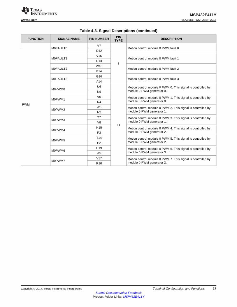
PWM
M0FAULT0V7
I
Motion control module 0 PWM fault 0D12
M0FAULT1V16
Motion control module 0 PWM fault 1D13
M0FAULT2W16
Motion control module 0 PWM fault 2B14
M0FAULT3G16
Motion control module 0 PWM fault 3A14
M0PWM0U6
O
Motion control module 0 PWM 0. This signal is controlled bymodule 0 PWM generator 0.N5
M0PWM1V6 Motion control module 0 PWM 1. This signal is controlled by
module 0 PWM generator 0.N4
M0PWM2W6 Motion control module 0 PWM 2. This signal is controlled by
module 0 PWM generator 1.N2
M0PWM3T7 Motion control module 0 PWM 3. This signal is controlled by
module 0 PWM generator 1.V8
M0PWM4N15 Motion control module 0 PWM 4. This signal is controlled by
module 0 PWM generator 2.P3
M0PWM5T14 Motion control module 0 PWM 5. This signal is controlled by
module 0 PWM generator 2.P2
M0PWM6U19 Motion control module 0 PWM 6. This signal is controlled by
module 0 PWM generator 3.W9
M0PWM7V17 Motion control module 0 PWM 7. This signal is controlled by
module 0 PWM generator 3.R10
38
MSP432E411YSLASEK6 –OCTOBER 2017 www.ti.com
Submit Documentation FeedbackProduct Folder Links: MSP432E411Y
Terminal Configuration and Functions Copyright © 2017, Texas Instruments Incorporated
Table 4-3. Signal Descriptions (continued)
FUNCTION SIGNAL NAME PIN NUMBER PINTYPE DESCRIPTION
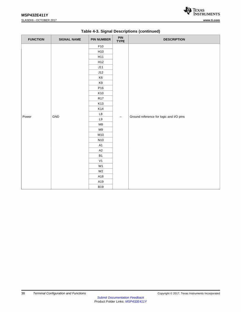
Power GND
F10
– Ground reference for logic and I/O pins
H10H11H12J11J12K6K9P16K10R17K13K14L8L9M8M9M10N10A1A2B1V1W1W2A18A19B19

39
MSP432E411Ywww.ti.com SLASEK6 –OCTOBER 2017
Submit Documentation FeedbackProduct Folder Links: MSP432E411Y
Terminal Configuration and FunctionsCopyright © 2017, Texas Instruments Incorporated
Table 4-3. Signal Descriptions (continued)
FUNCTION SIGNAL NAME PIN NUMBER PINTYPE DESCRIPTION
Power (continued)
GNDA G4 –
The ground reference for the analog circuits (ADC, AnalogComparators, and so on). These are separated from GND tominimize the electrical noise contained on VDD from affectingthe analog functions.
VDD
G10
– Positive supply for I/O and some logic
H9J8J9
J10K7K8K11N16P17K12L10L11L12M11M12P10
VDDA F3 –
The positive supply for the analog circuits (for example, ADCand analog comparators). These are separated from VDD tominimize the electrical noise contained on VDD from affectingthe analog functions. VDDA pins must be supplied with avoltage that meets the specification in Section 5.4, regardlessof system implementation.
VDDC
H16
–
Positive supply for most of the logic function, including theprocessor core and most peripherals. The voltage on this pin is1.2 V and is supplied by the on-chip LDO. The VDDC pinsshould only be connected to each other and an externalcapacitor as specified in Section 5.12.
E10
QEI
IDX0J18
I QEI module 0 indexU10
PhA0H19
I QEI module 0 phase AV9
PhB0G18
I QEI module 0 phase BT13

40
MSP432E411YSLASEK6 –OCTOBER 2017 www.ti.com
Submit Documentation FeedbackProduct Folder Links: MSP432E411Y
Terminal Configuration and Functions Copyright © 2017, Texas Instruments Incorporated
Table 4-3. Signal Descriptions (continued)
FUNCTION SIGNAL NAME PIN NUMBER PINTYPE DESCRIPTION
SSI
SSI0Clk T6
I/O
SSI module 0 clockSSI0Fss U5 SSI module 0 frame signal
SSI0XDAT0 V4 SSI Module 0 bidirectional data pin 0 (SSI0TX in Legacy SSIMode)
SSI0XDAT1 W4 SSI Module 0 bidirectional data pin 1 (SSI0RX in Legacy SSIMode)
SSI0XDAT2 V5 SSI Module 0 bidirectional data pin 2SSI0XDAT3 R7 SSI Module 0 bidirectional data pin 3SSI1Clk B6 SSI module 1 clockSSI1Fss C6 SSI module 1 frame signal
SSI1XDAT0 A5 SSI Module 1 bidirectional data pin 0 (SSI1TX in Legacy SSIMode)
SSI1XDAT1 B5 SSI Module 1 bidirectional data pin 1 (SSI1RX in Legacy SSIMode)
SSI1XDAT2 A4 SSI Module 1 bidirectional data pin 2SSI1XDAT3 B4 SSI Module 1 bidirectional data pin 3
SSI2ClkD1
SSI module 2 clockU14
SSI2FssD2
SSI module 2 frame signalV12
SSI2XDAT0C1 SSI Module 2 bidirectional data pin 0 (SSI2TX in Legacy SSI
Mode)K15
SSI2XDAT1C2 SSI Module 2 bidirectional data pin 1 (SSI2RX in Legacy SSI
Mode)K17
SSI2XDAT2B2
SSI Module 2 bidirectional data pin 2M16
SSI2XDAT3B3
SSI Module 2 bidirectional data pin 3V11
SSI3ClkT7
SSI module 3 clockE3
SSI3FssW6
SSI module 3 frame signalE2
SSI3XDAT0V6 SSI Module 3 bidirectional data pin 0 (SSI3TX in Legacy SSI
Mode)H4
SSI3XDAT1U6 SSI Module 3 bidirectional data pin 1 (SSI3RX in Legacy SSI
Mode)M4
SSI3XDAT2V7
SSI Module 3 bidirectional data pin 2D6
SSI3XDAT3W7
SSI Module 3 bidirectional data pin 3D7
41
MSP432E411Ywww.ti.com SLASEK6 –OCTOBER 2017
Submit Documentation FeedbackProduct Folder Links: MSP432E411Y
Terminal Configuration and FunctionsCopyright © 2017, Texas Instruments Incorporated
Table 4-3. Signal Descriptions (continued)
FUNCTION SIGNAL NAME PIN NUMBER PINTYPE DESCRIPTION
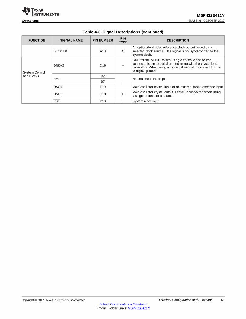
System Controland Clocks
DIVSCLK A13 OAn optionally divided reference clock output based on aselected clock source. This signal is not synchronized to thesystem clock.
GNDX2 D18 –
GND for the MOSC. When using a crystal clock source,connect this pin to digital ground along with the crystal loadcapacitors. When using an external oscillator, connect this pinto digital ground.
NMIB2
INonmaskable interrupt
B7OSC0 E19 Main oscillator crystal input or an external clock reference input
OSC1 D19 O Main oscillator crystal output. Leave unconnected when usinga single-ended clock source.
RST P18 I System reset input
42
MSP432E411YSLASEK6 –OCTOBER 2017 www.ti.com
Submit Documentation FeedbackProduct Folder Links: MSP432E411Y
Terminal Configuration and Functions Copyright © 2017, Texas Instruments Incorporated
Table 4-3. Signal Descriptions (continued)
FUNCTION SIGNAL NAME PIN NUMBER PINTYPE DESCRIPTION
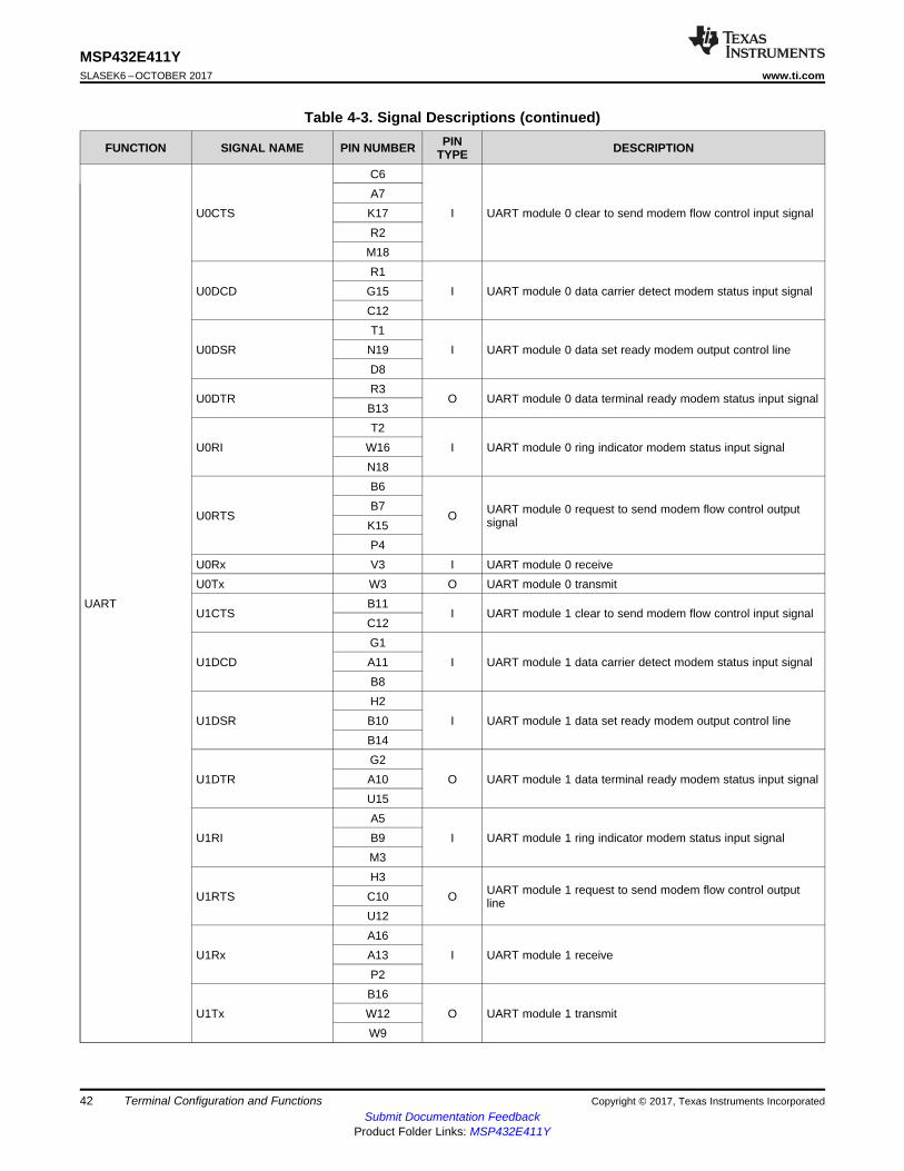
UART
U0CTS
C6
I UART module 0 clear to send modem flow control input signalA7K17R2
M18
U0DCDR1
I UART module 0 data carrier detect modem status input signalG15C12
U0DSRT1
I UART module 0 data set ready modem output control lineN19D8
U0DTRR3
O UART module 0 data terminal ready modem status input signalB13
U0RIT2
I UART module 0 ring indicator modem status input signalW16N18
U0RTS
B6
O UART module 0 request to send modem flow control outputsignal
B7K15P4
U0Rx V3 I UART module 0 receiveU0Tx W3 O UART module 0 transmit
U1CTSB11
I UART module 1 clear to send modem flow control input signalC12
U1DCDG1
I UART module 1 data carrier detect modem status input signalA11B8
U1DSRH2
I UART module 1 data set ready modem output control lineB10B14
U1DTRG2
O UART module 1 data terminal ready modem status input signalA10U15
U1RIA5
I UART module 1 ring indicator modem status input signalB9M3
U1RTSH3
O UART module 1 request to send modem flow control outputlineC10
U12
U1RxA16
I UART module 1 receiveA13P2
U1TxB16
O UART module 1 transmitW12W9
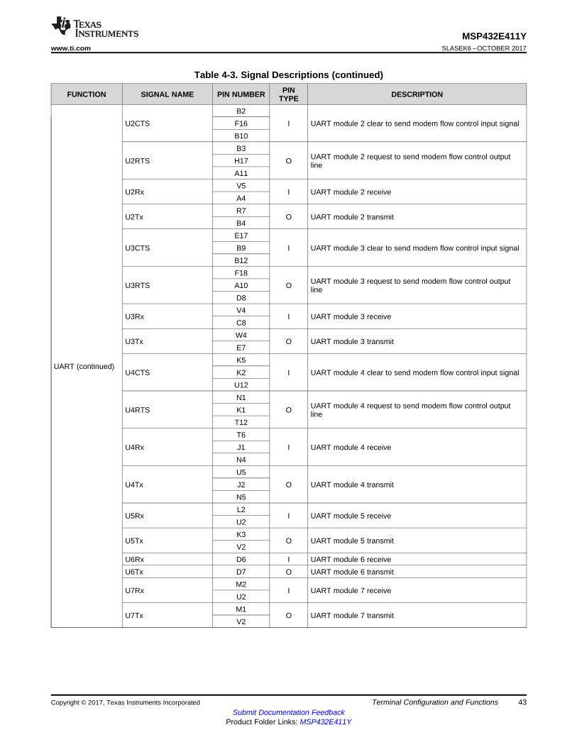
43
MSP432E411Ywww.ti.com SLASEK6 –OCTOBER 2017
Submit Documentation FeedbackProduct Folder Links: MSP432E411Y
Terminal Configuration and FunctionsCopyright © 2017, Texas Instruments Incorporated
Table 4-3. Signal Descriptions (continued)
FUNCTION SIGNAL NAME PIN NUMBER PINTYPE DESCRIPTION
UART (continued)
U2CTSB2
I UART module 2 clear to send modem flow control input signalF16B10
U2RTSB3
O UART module 2 request to send modem flow control outputlineH17
A11
U2RxV5
I UART module 2 receiveA4
U2TxR7
O UART module 2 transmitB4
U3CTSE17
I UART module 3 clear to send modem flow control input signalB9B12
U3RTSF18
O UART module 3 request to send modem flow control outputlineA10
D8
U3RxV4
I UART module 3 receiveC8
U3TxW4
O UART module 3 transmitE7
U4CTSK5
I UART module 4 clear to send modem flow control input signalK2U12
U4RTSN1
O UART module 4 request to send modem flow control outputlineK1
T12
U4RxT6
I UART module 4 receiveJ1N4
U4TxU5
O UART module 4 transmitJ2N5
U5RxL2
I UART module 5 receiveU2
U5TxK3
O UART module 5 transmitV2
U6Rx D6 I UART module 6 receiveU6Tx D7 O UART module 6 transmit
U7RxM2
I UART module 7 receiveU2
U7TxM1
O UART module 7 transmitV2
44
MSP432E411YSLASEK6 –OCTOBER 2017 www.ti.com
Submit Documentation FeedbackProduct Folder Links: MSP432E411Y
Terminal Configuration and Functions Copyright © 2017, Texas Instruments Incorporated
Table 4-3. Signal Descriptions (continued)
FUNCTION SIGNAL NAME PIN NUMBER PINTYPE DESCRIPTION
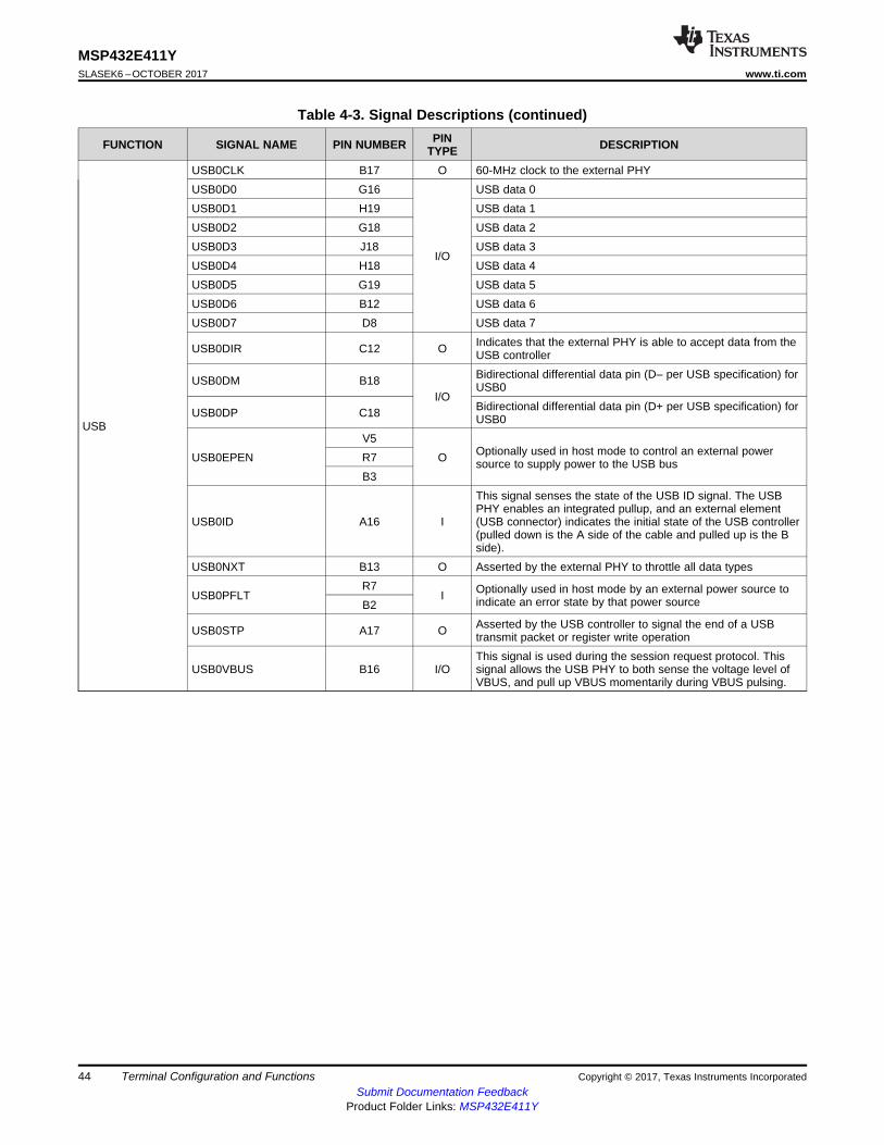
USB
USB0CLK B17 O 60-MHz clock to the external PHYUSB0D0 G16
I/O
USB data 0USB0D1 H19 USB data 1USB0D2 G18 USB data 2USB0D3 J18 USB data 3USB0D4 H18 USB data 4USB0D5 G19 USB data 5USB0D6 B12 USB data 6USB0D7 D8 USB data 7
USB0DIR C12 O Indicates that the external PHY is able to accept data from theUSB controller
USB0DM B18I/O
Bidirectional differential data pin (D– per USB specification) forUSB0
USB0DP C18 Bidirectional differential data pin (D+ per USB specification) forUSB0
USB0EPENV5
O Optionally used in host mode to control an external powersource to supply power to the USB busR7
B3
USB0ID A16 I
This signal senses the state of the USB ID signal. The USBPHY enables an integrated pullup, and an external element(USB connector) indicates the initial state of the USB controller(pulled down is the A side of the cable and pulled up is the Bside).
USB0NXT B13 O Asserted by the external PHY to throttle all data types
USB0PFLTR7
I Optionally used in host mode by an external power source toindicate an error state by that power sourceB2
USB0STP A17 O Asserted by the USB controller to signal the end of a USBtransmit packet or register write operation
USB0VBUS B16 I/OThis signal is used during the session request protocol. Thissignal allows the USB PHY to both sense the voltage level ofVBUS, and pull up VBUS momentarily during VBUS pulsing.
Copyright © 2017, Texas Instruments Incorporated Terminal Configuration and FunctionsSubmit Documentation Feedback
Product Folder Links: MSP432E411Y
45
MSP432E411Ywww.ti.com SLASEK6 –OCTOBER 2017
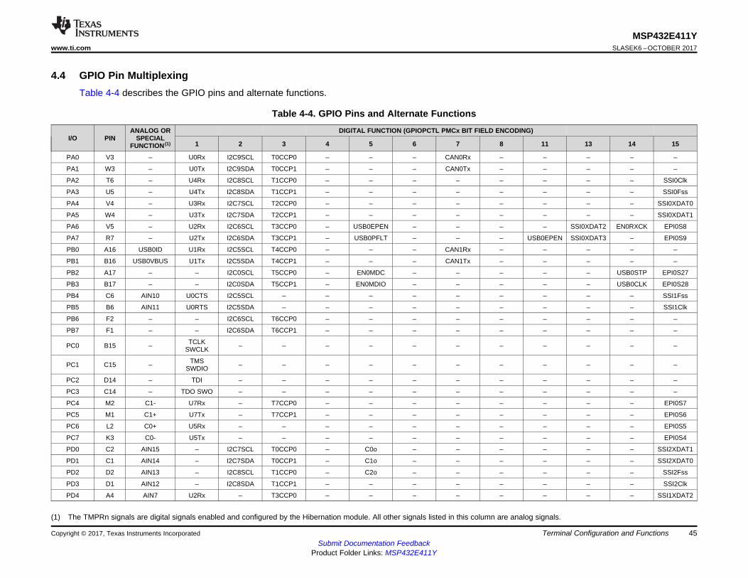
4.4 GPIO Pin MultiplexingTable 4-4 describes the GPIO pins and alternate functions.
(1) The TMPRn signals are digital signals enabled and configured by the Hibernation module. All other signals listed in this column are analog signals.
Table 4-4. GPIO Pins and Alternate Functions
I/O PINANALOG OR
SPECIALFUNCTION (1)
DIGITAL FUNCTION (GPIOPCTL PMCx BIT FIELD ENCODING)
1 2 3 4 5 6 7 8 11 13 14 15
PA0 V3 – U0Rx I2C9SCL T0CCP0 – – – CAN0Rx – – – – –
PA1 W3 – U0Tx I2C9SDA T0CCP1 – – – CAN0Tx – – – – –
PA2 T6 – U4Rx I2C8SCL T1CCP0 – – – – – – – – SSI0Clk
PA3 U5 – U4Tx I2C8SDA T1CCP1 – – – – – – – – SSI0Fss
PA4 V4 – U3Rx I2C7SCL T2CCP0 – – – – – – – – SSI0XDAT0
PA5 W4 – U3Tx I2C7SDA T2CCP1 – – – – – – – – SSI0XDAT1
PA6 V5 – U2Rx I2C6SCL T3CCP0 – USB0EPEN – – – – SSI0XDAT2 EN0RXCK EPI0S8
PA7 R7 – U2Tx I2C6SDA T3CCP1 – USB0PFLT – – – USB0EPEN SSI0XDAT3 – EPI0S9
PB0 A16 USB0ID U1Rx I2C5SCL T4CCP0 – – – CAN1Rx – – – – –
PB1 B16 USB0VBUS U1Tx I2C5SDA T4CCP1 – – – CAN1Tx – – – – –
PB2 A17 – – I2C0SCL T5CCP0 – EN0MDC – – – – – USB0STP EPI0S27
PB3 B17 – – I2C0SDA T5CCP1 – EN0MDIO – – – – – USB0CLK EPI0S28
PB4 C6 AIN10 U0CTS I2C5SCL – – – – – – – – – SSI1Fss
PB5 B6 AIN11 U0RTS I2C5SDA – – – – – – – – – SSI1Clk
PB6 F2 – – I2C6SCL T6CCP0 – – – – – – – – –
PB7 F1 – – I2C6SDA T6CCP1 – – – – – – – – –
PC0 B15 – TCLKSWCLK – – – – – – – – – – –
PC1 C15 – TMSSWDIO – – – – – – – – – – –
PC2 D14 – TDI – – – – – – – – – – –
PC3 C14 – TDO SWO – – – – – – – – – – –
PC4 M2 C1- U7Rx – T7CCP0 – – – – – – – – EPI0S7
PC5 M1 C1+ U7Tx – T7CCP1 – – – – – – – – EPI0S6
PC6 L2 C0+ U5Rx – – – – – – – – – – EPI0S5
PC7 K3 C0- U5Tx – – – – – – – – – – EPI0S4
PD0 C2 AIN15 – I2C7SCL T0CCP0 – C0o – – – – – – SSI2XDAT1
PD1 C1 AIN14 – I2C7SDA T0CCP1 – C1o – – – – – – SSI2XDAT0
PD2 D2 AIN13 – I2C8SCL T1CCP0 – C2o – – – – – – SSI2Fss
PD3 D1 AIN12 – I2C8SDA T1CCP1 – – – – – – – – SSI2Clk
PD4 A4 AIN7 U2Rx – T3CCP0 – – – – – – – – SSI1XDAT2
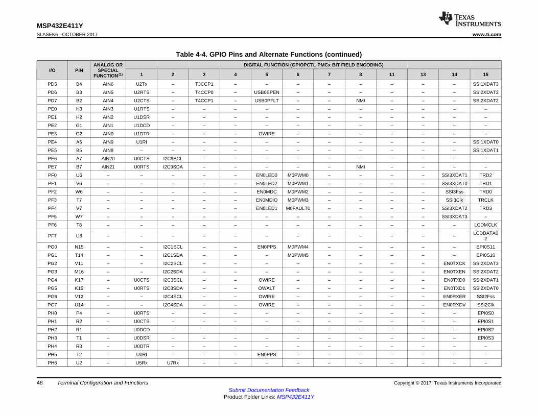
Copyright © 2017, Texas Instruments IncorporatedTerminal Configuration and FunctionsSubmit Documentation Feedback
Product Folder Links: MSP432E411Y
46
MSP432E411YSLASEK6 –OCTOBER 2017 www.ti.com
Table 4-4. GPIO Pins and Alternate Functions (continued)
I/O PINANALOG OR
SPECIALFUNCTION (1)
DIGITAL FUNCTION (GPIOPCTL PMCx BIT FIELD ENCODING)
1 2 3 4 5 6 7 8 11 13 14 15
PD5 B4 AIN6 U2Tx – T3CCP1 – – – – – – – – SSI1XDAT3
PD6 B3 AIN5 U2RTS – T4CCP0 – USB0EPEN – – – – – – SSI2XDAT3
PD7 B2 AIN4 U2CTS – T4CCP1 – USB0PFLT – – NMI – – – SSI2XDAT2
PE0 H3 AIN3 U1RTS – – – – – – – – – – –
PE1 H2 AIN2 U1DSR – – – – – – – – – – –
PE2 G1 AIN1 U1DCD – – – – – – – – – – –
PE3 G2 AIN0 U1DTR – – – OWIRE – – – – – – –
PE4 A5 AIN9 U1RI – – – – – – – – – – SSI1XDAT0
PE5 B5 AIN8 – – – – – – – – – – – SSI1XDAT1
PE6 A7 AIN20 U0CTS I2C9SCL – – – – – – – – – –
PE7 B7 AIN21 U0RTS I2C9SDA – – – – – NMI – – – –
PF0 U6 – – – – – EN0LED0 M0PWM0 – – – – SSI3XDAT1 TRD2
PF1 V6 – – – – – EN0LED2 M0PWM1 – – – – SSI3XDAT0 TRD1
PF2 W6 – – – – – EN0MDC M0PWM2 – – – – SSI3Fss TRD0
PF3 T7 – – – – – EN0MDIO M0PWM3 – – – – SSI3Clk TRCLK
PF4 V7 – – – – – EN0LED1 M0FAULT0 – – – – SSI3XDAT2 TRD3
PF5 W7 – – – – – – – – – – – SSI3XDAT3 –
PF6 T8 – – – – – – – – – – – – LCDMCLK
PF7 U8 – – – – – – – – – – – – LCDDATA02
PG0 N15 – – I2C1SCL – – EN0PPS M0PWM4 – – – – – EPI0S11
PG1 T14 – – I2C1SDA – – – M0PWM5 – – – – – EPI0S10
PG2 V11 – – I2C2SCL – – – – – – – – EN0TXCK SSI2XDAT3
PG3 M16 – – I2C2SDA – – – – – – – – EN0TXEN SSI2XDAT2
PG4 K17 – U0CTS I2C3SCL – – OWIRE – – – – – EN0TXD0 SSI2XDAT1
PG5 K15 – U0RTS I2C3SDA – – OWALT – – – – – EN0TXD1 SSI2XDAT0
PG6 V12 – – I2C4SCL – – OWIRE – – – – – EN0RXER SSI2Fss
PG7 U14 – – I2C4SDA – – OWIRE – – – – – EN0RXDV SSI2Clk
PH0 P4 – U0RTS – – – – – – – – – – EPI0S0
PH1 R2 – U0CTS – – – – – – – – – – EPI0S1
PH2 R1 – U0DCD – – – – – – – – – – EPI0S2
PH3 T1 – U0DSR – – – – – – – – – – EPI0S3
PH4 R3 – U0DTR – – – – – – – – – – –
PH5 T2 – U0RI – – – EN0PPS – – – – – – –
PH6 U2 – U5Rx U7Rx – – – – – – – – – –
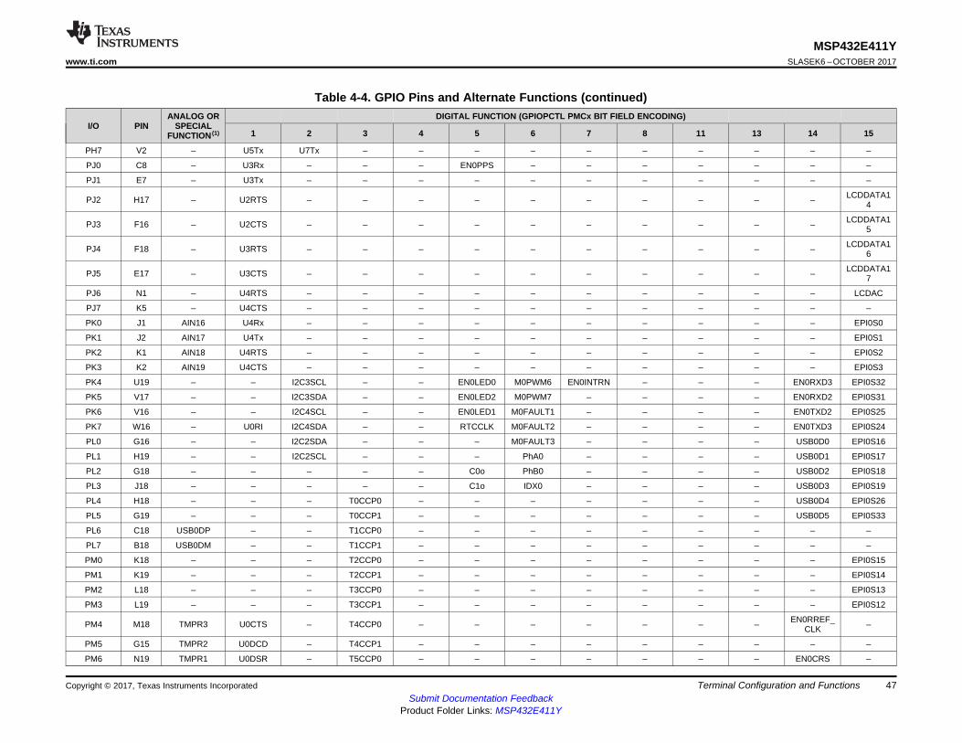
Copyright © 2017, Texas Instruments Incorporated Terminal Configuration and FunctionsSubmit Documentation Feedback
Product Folder Links: MSP432E411Y
47
MSP432E411Ywww.ti.com SLASEK6 –OCTOBER 2017
Table 4-4. GPIO Pins and Alternate Functions (continued)
I/O PINANALOG OR
SPECIALFUNCTION (1)
DIGITAL FUNCTION (GPIOPCTL PMCx BIT FIELD ENCODING)
1 2 3 4 5 6 7 8 11 13 14 15
PH7 V2 – U5Tx U7Tx – – – – – – – – – –
PJ0 C8 – U3Rx – – – EN0PPS – – – – – – –
PJ1 E7 – U3Tx – – – – – – – – – – –
PJ2 H17 – U2RTS – – – – – – – – – – LCDDATA14
PJ3 F16 – U2CTS – – – – – – – – – – LCDDATA15
PJ4 F18 – U3RTS – – – – – – – – – – LCDDATA16
PJ5 E17 – U3CTS – – – – – – – – – – LCDDATA17
PJ6 N1 – U4RTS – – – – – – – – – – LCDAC
PJ7 K5 – U4CTS – – – – – – – – – – –
PK0 J1 AIN16 U4Rx – – – – – – – – – – EPI0S0
PK1 J2 AIN17 U4Tx – – – – – – – – – – EPI0S1
PK2 K1 AIN18 U4RTS – – – – – – – – – – EPI0S2
PK3 K2 AIN19 U4CTS – – – – – – – – – – EPI0S3
PK4 U19 – – I2C3SCL – – EN0LED0 M0PWM6 EN0INTRN – – – EN0RXD3 EPI0S32
PK5 V17 – – I2C3SDA – – EN0LED2 M0PWM7 – – – – EN0RXD2 EPI0S31
PK6 V16 – – I2C4SCL – – EN0LED1 M0FAULT1 – – – – EN0TXD2 EPI0S25
PK7 W16 – U0RI I2C4SDA – – RTCCLK M0FAULT2 – – – – EN0TXD3 EPI0S24
PL0 G16 – – I2C2SDA – – – M0FAULT3 – – – – USB0D0 EPI0S16
PL1 H19 – – I2C2SCL – – – PhA0 – – – – USB0D1 EPI0S17
PL2 G18 – – – – – C0o PhB0 – – – – USB0D2 EPI0S18
PL3 J18 – – – – – C1o IDX0 – – – – USB0D3 EPI0S19
PL4 H18 – – – T0CCP0 – – – – – – – USB0D4 EPI0S26
PL5 G19 – – – T0CCP1 – – – – – – – USB0D5 EPI0S33
PL6 C18 USB0DP – – T1CCP0 – – – – – – – – –
PL7 B18 USB0DM – – T1CCP1 – – – – – – – – –
PM0 K18 – – – T2CCP0 – – – – – – – – EPI0S15
PM1 K19 – – – T2CCP1 – – – – – – – – EPI0S14
PM2 L18 – – – T3CCP0 – – – – – – – – EPI0S13
PM3 L19 – – – T3CCP1 – – – – – – – – EPI0S12
PM4 M18 TMPR3 U0CTS – T4CCP0 – – – – – – – EN0RREF_CLK –
PM5 G15 TMPR2 U0DCD – T4CCP1 – – – – – – – – –
PM6 N19 TMPR1 U0DSR – T5CCP0 – – – – – – – EN0CRS –
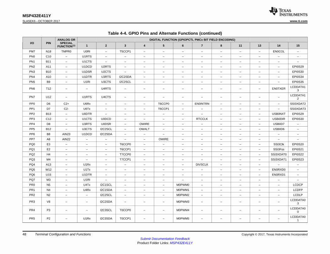
Copyright © 2017, Texas Instruments IncorporatedTerminal Configuration and FunctionsSubmit Documentation Feedback
Product Folder Links: MSP432E411Y
48
MSP432E411YSLASEK6 –OCTOBER 2017 www.ti.com
Table 4-4. GPIO Pins and Alternate Functions (continued)
I/O PINANALOG OR
SPECIALFUNCTION (1)
DIGITAL FUNCTION (GPIOPCTL PMCx BIT FIELD ENCODING)
1 2 3 4 5 6 7 8 11 13 14 15
PM7 N18 TMPR0 U0RI – T5CCP1 – – – – – – – EN0COL –
PN0 C10 – U1RTS – – – – – – – – – – –
PN1 B11 – U1CTS – – – – – – – – – – –
PN2 A11 – U1DCD U2RTS – – – – – – – – – EPI0S29
PN3 B10 – U1DSR U2CTS – – – – – – – – – EPI0S30
PN4 A10 – U1DTR U3RTS I2C2SDA – – – – – – – – EPI0S34
PN5 B9 – U1RI U3CTS I2C2SCL – – – – – – – – EPI0S35
PN6 T12 – – U4RTS – – – – – – – – EN0TXER LCDDATA13
PN7 U12 – U1RTS U4CTS – – – – – – – – – LCDDATA12
PP0 D6 C2+ U6Rx – – – T6CCP0 – EN0INTRN – – – – SSI3XDAT2
PP1 D7 C2- U6Tx – – – T6CCP1 – – – – – – SSI3XDAT3
PP2 B13 – U0DTR – – – – – – – – – USB0NXT EPI0S29
PP3 C12 – U1CTS U0DCD – – – – RTCCLK – – – USB0DIR EPI0S30
PP4 D8 – U3RTS U0DSR – OWIRE – – – – – – USB0D7 –
PP5 B12 – U3CTS I2C2SCL – OWALT – – – – – – USB0D6 –
PP6 B8 AIN23 U1DCD I2C2SDA – – – – – – – – – –
PP7 A8 AIN22 – – – – OWIRE – – – – – – –
PQ0 E3 – – – T6CCP0 – – – – – – – SSI3Clk EPI0S20
PQ1 E2 – – – T6CCP1 – – – – – – – SSI3Fss EPI0S21
PQ2 H4 – – – T7CCP0 – – – – – – – SSI3XDAT0 EPI0S22
PQ3 M4 – – – T7CCP1 – – – – – – – SSI3XDAT1 EPI0S23
PQ4 A13 – U1Rx – – – – – DIVSCLK – – – – –
PQ5 W12 – U1Tx – – – – – – – – – EN0RXD0 –
PQ6 U15 – U1DTR – – – – – – – – – EN0RXD1 –
PQ7 M3 – U1RI – – – – – – – – – – –
PR0 N5 – U4Tx I2C1SCL – – – M0PWM0 – – – – – LCDCP
PR1 N4 – U4Rx I2C1SDA – – – M0PWM1 – – – – – LCDFP
PR2 N2 – – I2C2SCL – – – M0PWM2 – – – – – LCDLP
PR3 V8 – – I2C2SDA – – – M0PWM3 – – – – – LCDDATA03
PR4 P3 – – I2C3SCL T0CCP0 – – M0PWM4 – – – – – LCDDATA00
PR5 P2 – U1Rx I2C3SDA T0CCP1 – – M0PWM5 – – – – – LCDDATA01
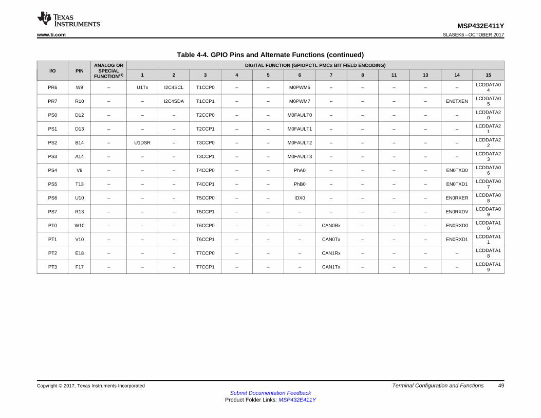
Copyright © 2017, Texas Instruments Incorporated Terminal Configuration and FunctionsSubmit Documentation Feedback
Product Folder Links: MSP432E411Y
49
MSP432E411Ywww.ti.com SLASEK6 –OCTOBER 2017
Table 4-4. GPIO Pins and Alternate Functions (continued)
I/O PINANALOG OR
SPECIALFUNCTION (1)
DIGITAL FUNCTION (GPIOPCTL PMCx BIT FIELD ENCODING)
1 2 3 4 5 6 7 8 11 13 14 15
PR6 W9 – U1Tx I2C4SCL T1CCP0 – – M0PWM6 – – – – – LCDDATA04
PR7 R10 – – I2C4SDA T1CCP1 – – M0PWM7 – – – – EN0TXEN LCDDATA05
PS0 D12 – – – T2CCP0 – – M0FAULT0 – – – – – LCDDATA20
PS1 D13 – – – T2CCP1 – – M0FAULT1 – – – – – LCDDATA21
PS2 B14 – U1DSR – T3CCP0 – – M0FAULT2 – – – – – LCDDATA22
PS3 A14 – – – T3CCP1 – – M0FAULT3 – – – – – LCDDATA23
PS4 V9 – – – T4CCP0 – – PhA0 – – – – EN0TXD0 LCDDATA06
PS5 T13 – – – T4CCP1 – – PhB0 – – – – EN0TXD1 LCDDATA07
PS6 U10 – – – T5CCP0 – – IDX0 – – – – EN0RXER LCDDATA08
PS7 R13 – – – T5CCP1 – – – – – – – EN0RXDV LCDDATA09
PT0 W10 – – – T6CCP0 – – – CAN0Rx – – – EN0RXD0 LCDDATA10
PT1 V10 – – – T6CCP1 – – – CAN0Tx – – – EN0RXD1 LCDDATA11
PT2 E18 – – – T7CCP0 – – – CAN1Rx – – – – LCDDATA18
PT3 F17 – – – T7CCP1 – – – CAN1Tx – – – – LCDDATA19
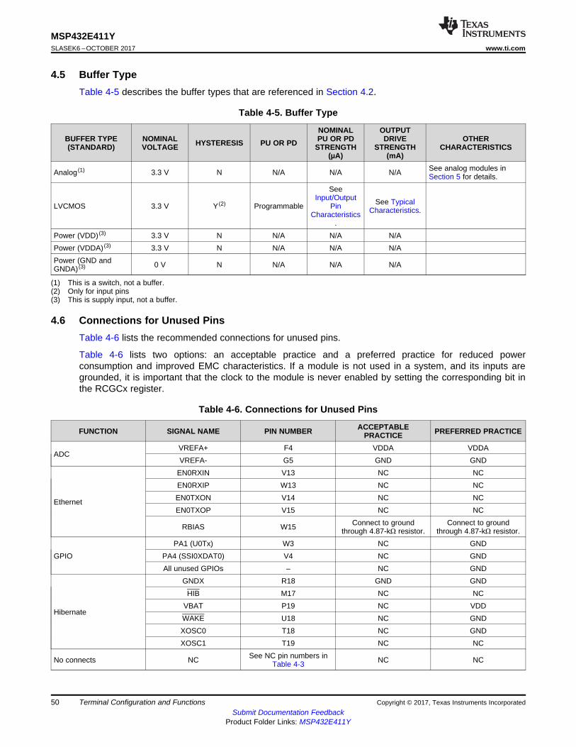
50
MSP432E411YSLASEK6 –OCTOBER 2017 www.ti.com
Submit Documentation FeedbackProduct Folder Links: MSP432E411Y
Terminal Configuration and Functions Copyright © 2017, Texas Instruments Incorporated
(1) This is a switch, not a buffer.(2) Only for input pins(3) This is supply input, not a buffer.
4.5 Buffer TypeTable 4-5 describes the buffer types that are referenced in Section 4.2.
Table 4-5. Buffer Type
BUFFER TYPE(STANDARD)
NOMINALVOLTAGE HYSTERESIS PU OR PD
NOMINALPU OR PD
STRENGTH(µA)
OUTPUTDRIVE
STRENGTH(mA)
OTHERCHARACTERISTICS
Analog (1) 3.3 V N N/A N/A N/A See analog modules inSection 5 for details.
LVCMOS 3.3 V Y (2) Programmable
SeeInput/Output
PinCharacteristics
.
See TypicalCharacteristics.
Power (VDD) (3) 3.3 V N N/A N/A N/APower (VDDA) (3) 3.3 V N N/A N/A N/APower (GND andGNDA) (3) 0 V N N/A N/A N/A
4.6 Connections for Unused PinsTable 4-6 lists the recommended connections for unused pins.
Table 4-6 lists two options: an acceptable practice and a preferred practice for reduced powerconsumption and improved EMC characteristics. If a module is not used in a system, and its inputs aregrounded, it is important that the clock to the module is never enabled by setting the corresponding bit inthe RCGCx register.
Table 4-6. Connections for Unused Pins
FUNCTION SIGNAL NAME PIN NUMBER ACCEPTABLEPRACTICE PREFERRED PRACTICE
ADCVREFA+ F4 VDDA VDDAVREFA- G5 GND GND
Ethernet
EN0RXIN V13 NC NCEN0RXIP W13 NC NCEN0TXON V14 NC NCEN0TXOP V15 NC NC
RBIAS W15 Connect to groundthrough 4.87-kΩ resistor.
Connect to groundthrough 4.87-kΩ resistor.
GPIOPA1 (U0Tx) W3 NC GND
PA4 (SSI0XDAT0) V4 NC GNDAll unused GPIOs – NC GND
Hibernate
GNDX R18 GND GNDHIB M17 NC NC
VBAT P19 NC VDDWAKE U18 NC GNDXOSC0 T18 NC GNDXOSC1 T19 NC NC
No connects NC See NC pin numbers inTable 4-3 NC NC
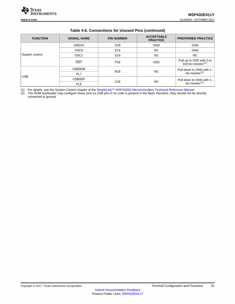
51
MSP432E411Ywww.ti.com SLASEK6 –OCTOBER 2017
Submit Documentation FeedbackProduct Folder Links: MSP432E411Y
Terminal Configuration and FunctionsCopyright © 2017, Texas Instruments Incorporated
Table 4-6. Connections for Unused Pins (continued)
FUNCTION SIGNAL NAME PIN NUMBER ACCEPTABLEPRACTICE PREFERRED PRACTICE
(1) For details, see the System Control chapter of the SimpleLink™ MSP432E4 Microcontrollers Technical Reference Manual(2) The ROM bootloader may configure these pins as USB pins if no code is present in the flash; therefore, they should not be directly
connected to ground.
System control
GNDX2 D18 GND GNDOSC0 E19 NC GNDOSC1 D19 NC NC
RST P18 VDD Pull up to VDD with 0 to100-kΩ resistor (1).
USB
USB0DMB18 NC Pull down to GND with 1-
kΩ resistor (2).PL7USB0DP
C18 NC Pull down to GND with 1-kΩ resistor (2).PL6
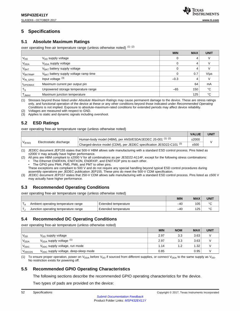
52
MSP432E411YSLASEK6 –OCTOBER 2017 www.ti.com
Submit Documentation FeedbackProduct Folder Links: MSP432E411Y
Specifications Copyright © 2017, Texas Instruments Incorporated
(1) Stresses beyond those listed under Absolute Maximum Ratings may cause permanent damage to the device. These are stress ratingsonly, and functional operation of the device at these or any other conditions beyond those indicated under Recommended OperatingConditions is not implied. Exposure to absolute-maximum-rated conditions for extended periods may affect device reliability.
(2) Voltages are measured with respect to GND.(3) Applies to static and dynamic signals including overshoot.
5 Specifications
5.1 Absolute Maximum Ratingsover operating free-air temperature range (unless otherwise noted) (1) (2)
MIN MAX UNITVDD VDD supply voltage 0 4 VVDDA VDDA supply voltage 0 4 VVBAT VBAT battery supply voltage 0 4 VVBATRMP VBAT battery supply voltage ramp time 0 0.7 V/µsVIN_GPIO Input voltage (3) –0.3 4 VIGPIOMAX Maximum current per output pin 64 mATS Unpowered storage temperature range –65 150 °CTJMAX Maximum junction temperature 125 °C
(1) JEDEC document JEP155 states that 500-V HBM allows safe manufacturing with a standard ESD control process. Pins listed as±2000 V may actually have higher performance.
(2) All pins are HBM compliant to ±2000 V for all combinations as per JESD22-A114F, except for the following stress combinations:• The Ethernet EN0RXIN, EN0TXON, EN0RXIP, and EN0TXOP pins to each other.• The GPIO pins PM4, PM5, PM6, and PM7 to other pins.These exceptions are compliant to 500 V and do not require any special handling beyond typical ESD control procedures duringassembly operations per JEDEC publication JEP155. These pins do meet the 500-V CDM specification.
(3) JEDEC document JEP157 states that 250-V CDM allows safe manufacturing with a standard ESD control process. Pins listed as ±500 Vmay actually have higher performance.
5.2 ESD Ratingsover operating free-air temperature range (unless otherwise noted)
VALUE UNIT
V(ESD) Electrostatic dischargeHuman-body model (HBM), per ANSI/ESDA/JEDEC JS‑001 (1) (2) ±2000
VCharged-device model (CDM), per JEDEC specification JESD22‑C101 (3) ±500
5.3 Recommended Operating Conditionsover operating free-air temperature range (unless otherwise noted)
MIN MAX UNITTA Ambient operating temperature range Extended temperature –40 105 °CTJ Junction operating temperature range Extended temperature –40 125 °C
(1) To ensure proper operation, power on VDDA before VDD if sourced from different supplies, or connect VDDA to the same supply as VDD.No restriction exists for powering off.
5.4 Recommended DC Operating Conditionsover operating free-air temperature (unless otherwise noted)
MIN NOM MAX UNITVDD VDD supply voltage 2.97 3.3 3.63 VVDDA VDDA supply voltage (1) 2.97 3.3 3.63 VVDDC VDDC supply voltage, run mode 1.14 1.2 1.32 VVDDCDS VDDC supply voltage, deep-sleep mode 0.85 0.95 V
5.5 Recommended GPIO Operating CharacteristicsThe following sections describe the recommended GPIO operating characteristics for the device.
Two types of pads are provided on the device:
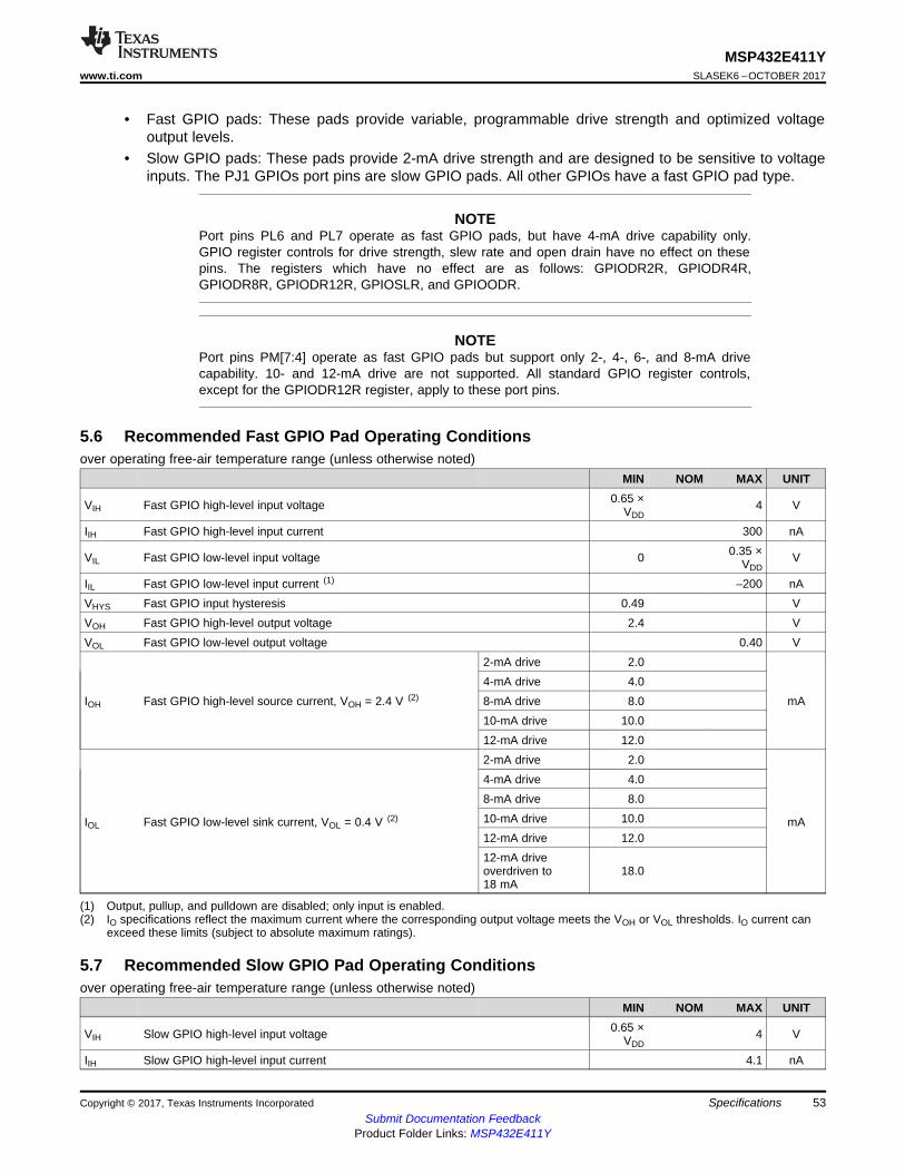
53
MSP432E411Ywww.ti.com SLASEK6 –OCTOBER 2017
Submit Documentation FeedbackProduct Folder Links: MSP432E411Y
SpecificationsCopyright © 2017, Texas Instruments Incorporated
(1) Output, pullup, and pulldown are disabled; only input is enabled.(2) IO specifications reflect the maximum current where the corresponding output voltage meets the VOH or VOL thresholds. IO current can
exceed these limits (subject to absolute maximum ratings).
• Fast GPIO pads: These pads provide variable, programmable drive strength and optimized voltageoutput levels.
• Slow GPIO pads: These pads provide 2-mA drive strength and are designed to be sensitive to voltageinputs. The PJ1 GPIOs port pins are slow GPIO pads. All other GPIOs have a fast GPIO pad type.
NOTEPort pins PL6 and PL7 operate as fast GPIO pads, but have 4-mA drive capability only.GPIO register controls for drive strength, slew rate and open drain have no effect on thesepins. The registers which have no effect are as follows: GPIODR2R, GPIODR4R,GPIODR8R, GPIODR12R, GPIOSLR, and GPIOODR.
NOTEPort pins PM[7:4] operate as fast GPIO pads but support only 2-, 4-, 6-, and 8-mA drivecapability. 10- and 12-mA drive are not supported. All standard GPIO register controls,except for the GPIODR12R register, apply to these port pins.
5.6 Recommended Fast GPIO Pad Operating Conditionsover operating free-air temperature range (unless otherwise noted)
MIN NOM MAX UNIT
VIH Fast GPIO high-level input voltage 0.65 ×VDD
4 V
IIH Fast GPIO high-level input current 300 nA
VIL Fast GPIO low-level input voltage 0 0.35 ×VDD
V
IIL Fast GPIO low-level input current (1) –200 nAVHYS Fast GPIO input hysteresis 0.49 VVOH Fast GPIO high-level output voltage 2.4 VVOL Fast GPIO low-level output voltage 0.40 V
IOH Fast GPIO high-level source current, VOH = 2.4 V (2)
2-mA drive 2.0
mA4-mA drive 4.08-mA drive 8.010-mA drive 10.012-mA drive 12.0
IOL Fast GPIO low-level sink current, VOL = 0.4 V (2)
2-mA drive 2.0
mA
4-mA drive 4.08-mA drive 8.010-mA drive 10.012-mA drive 12.012-mA driveoverdriven to18 mA
18.0
5.7 Recommended Slow GPIO Pad Operating Conditionsover operating free-air temperature range (unless otherwise noted)
MIN NOM MAX UNIT
VIH Slow GPIO high-level input voltage 0.65 ×VDD
4 V
IIH Slow GPIO high-level input current 4.1 nA

54
MSP432E411YSLASEK6 –OCTOBER 2017 www.ti.com
Submit Documentation FeedbackProduct Folder Links: MSP432E411Y
Specifications Copyright © 2017, Texas Instruments Incorporated
Recommended Slow GPIO Pad Operating Conditions (continued)over operating free-air temperature range (unless otherwise noted)
MIN NOM MAX UNIT
(1) Output, pullup, and pulldown are disabled; only input is enabled.(2) IO specifications reflect the maximum current where the corresponding output voltage meets the VOH or VOL thresholds. IO current can
exceed these limits (subject to absolute maximum ratings).
VIL Slow GPIO low-level input voltage 0 0.35 ×VDD
V
IIL Slow GPIO low-level input current (1) –1 nAVHYS Slow GPIO input hysteresis 0.49 VVOH Slow GPIO high-level output voltage 2.4 VVOL Slow GPIO low-level output voltage 0.4 VIOH Slow GPIO high-level source current, VOH = 2.4 V, 2-mA drive 2.0 mAIOL Slow GPIO low-level sink current, VOL = 0.4 V (2), 2-mA drive 2.0 mA
(1) Based on design simulations, not tested in production.(2) Sum of sink and source current for GPIOs as listed in Table 5-1.
5.8 GPIO Current Restrictionsover operating free-air temperature range (unless otherwise noted) (1)
MIN NOM MAX UNITIMAXL Cumulative maximum GPIO current per side, left 110 mAIMAXB Cumulative maximum GPIO current per side, bottom (2) 116 mAIMAXR Cumulative maximum GPIO current per side, right (2) 110 mAIMAXT Cumulative maximum GPIO current per side, top (2) 88 mA
Table 5-1. Maximum GPIO Package Side Assignments
SIDE GPIOsLeft PB[6-7], PC[4-7], PD[0-3], PE[0-3], PH[0-7], PJ[6-7], PK[0-3], PQ[0-3,7], PR[0-5]Bottom PA[0-7], PF[0-7], PG[0-7], PK[4-7], PN[6-7], PR[3,6-7], PQ[5-6], PS[4-7], PT[0-1]Right PB[0-3], PJ[2-5], PL[0-5,6-7], PM[0-7], PT[2-3]Top PB[4-5], PC[0-3], PD[4-7], PE[4-7], PJ[0-1], PN[0-5], PP[0-7], PQ[4], PS[0-3]
5.9 I/O ReliabilityFor typical continuous drive applications, I/O pins configured in the range from 2 mA to 12 mA andoperating at –40°C to 85°C meet the standard 10-year lifetime reliability. If a continuous current sink of 18mA is required, then operation is limited to 0 to 75°C to meet the standard 10-year reliability.
At 105°C, I/O pins configured for continuous drive meet the standard 2.5-year lifetime reliability.
In typical switching applications (40% switch rate) operating at –40°C to 85°C, all I/O configurations except2 mA meet the standard 10-year lifetime reliability with 50-pF loading. By limiting the capacitive loading to20 pF for an I/O configured to 2 mA, the 10-year lifetime reliability can be met at –40°C to 85°C.
In typical switching applications (40% switch rate) operating at 105°C, all I/O configurations except 2 mAmeet the standard 2.5-year lifetime reliability. By reducing the capacitive loading to 20 pF with a typicalswitching rate at 105°C, a 2-mA I/O configuration meets a 2.5-year lifetime reliability.

55
MSP432E411Ywww.ti.com SLASEK6 –OCTOBER 2017
Submit Documentation FeedbackProduct Folder Links: MSP432E411Y
SpecificationsCopyright © 2017, Texas Instruments Incorporated
(1) Section 5.11 lists the current consumption that specific peripherals contribute to the run mode current consumption in Section 5.10. Ifthese peripherals are not powered, then the peripheral current consumption can be subtracted from the run mode consumption inSection 5.10.
(2) Applicable to extended temperature devices only.
5.10 Current Consumptionover operating free-air temperature (unless otherwise noted) (1)
PARAMETER TEST CONDITIONSSYSTEM CLOCK TYP MAX
UNITFREQ CLOCK
SOURCE –40°C 25°C 85°C 105°C 85°C 105°C(2)
IDD_RUN
Run mode(flash loop)
VDD = 3.3 V,VDDA = 3.3 V,Peripherals = All onincluding MAC and PHY
120 MHz MOSC withPLL 96.4 105.3 107.2 108.7 129.9 140.0
mA
60 MHz MOSC withPLL 67.4 76.6 78.6 79.9 100.3 112.5
16 MHz PIOSC 11.9 24.4 25.5 26.7 45.0 56.4
1 MHz PIOSC 5.75 10.9 12.1 13.3 31.3 42.6
VDD = 3.3 V,VDDA = 3.3 V,Peripherals = All onincluding MAC but notPHY
120 MHz MOSC withPLL 69.9 77.8 79.6 80.8 98.8 108.4
60 MHz MOSC withPLL 40.9 49.2 50.9 52.1 69.2 80.8
16 MHz PIOSC 11.3 23.6 25.0 26.2 43.1 54.3
1 MHz PIOSC 5.10 10.1 11.5 12.7 29.3 40.5
VDD = 3.3 V,VDDA = 3.3 V,Peripherals = All onexcept MAC and PHY
120 MHz MOSC withPLL 68.1 76.0 77.6 78.6 96.6 106.0
60 MHz MOSC withPLL 40.0 48.2 49.8 50.8 67.9 79.2
16 MHz PIOSC 11.1 23.3 24.6 25.6 42.5 53.3
1 MHz PIOSC 5.07 10.1 11.3 12.3 29.0 39.8
VDD = 3.3 V,VDDA = 3.3 V,Peripherals = All off
120 MHz MOSC withPLL 35.2 39.1 40.4 41.5 55.8 65.3
60 MHz MOSC withPLL 23.2 29.4 30.7 31.7 45.8 55.5
16 MHz PIOSC 7.38 17.9 19.0 20.0 34.5 44.1
1 MHz PIOSC 4.12 9.13 10.3 11.4 25.7 35.5
Run mode(SRAM loop)
VDD = 3.3 V,VDDA = 3.3 V,Peripherals = All onincluding MAC and PHY
120 MHz MOSC withPLL 93.8 103.6 111.6 113.2 133.4 144.6
60 MHz MOSC withPLL 66.9 76.7 78.7 80.0 100.0 111.9
16 MHz PIOSC 12.6 19.0 20.1 21.3 39.1 50.3
1 MHz PIOSC 5.73 10.6 11.7 12.8 30.9 42.2
VDD = 3.3 V,VDDA = 3.3 V,Peripherals = All onincluding MAC but notPHY
120 MHz MOSC withPLL 67.2 76.1 84.0 85.4 102.3 113.0
60 MHz MOSC withPLL 40.3 49.2 50.9 52.2 68.9 80.2
16 MHz PIOSC 11.9 18.2 19.6 20.8 37.2 48.2
1 MHz PIOSC 5.08 9.79 11.2 12.3 28.9 40.1
VDD = 3.3 V,VDDA = 3.3 V,Peripherals =All onexcept MAC and PHY
120 MHz MOSC withPLL 65.4 74.3 82.0 83.2 100.1 110.6
60 MHz MOSC withPLL 39.4 48.2 49.8 50.9 67.6 78.6
16 MHz PIOSC 11.7 17.9 19.2 20.2 36.6 47.2
1 MHz PIOSC 5.05 9.75 11.0 11.9 28.6 39.4
VDD = 3.3 V,VDDA = 3.3 V,Peripherals = All off
120 MHz MOSC withPLL 35.4 43.3 44.7 45.8 59.8 69.0
60 MHz MOSC withPLL 23.4 29.4 30.7 31.7 45.5 54.9
16 MHz PIOSC 7.08 12.4 13.6 14.6 28.7 38.0
1 MHz PIOSC 4.60 8.78 10.0 11.0 25.3 34.9
56
MSP432E411YSLASEK6 –OCTOBER 2017 www.ti.com
Submit Documentation FeedbackProduct Folder Links: MSP432E411Y
Specifications Copyright © 2017, Texas Instruments Incorporated
Current Consumption (continued)over operating free-air temperature (unless otherwise noted) (1)
PARAMETER TEST CONDITIONSSYSTEM CLOCK TYP MAX
UNITFREQ CLOCK
SOURCE –40°C 25°C 85°C 105°C 85°C 105°C(2)
(3) If the MOSC is the source of the run-mode system clock and is powered down in sleep mode, wake time is increased by tMOSC_SETTLE.
IDD_SLEEP
Sleep mode(FLASHPM =0x0)
VDD = 3.3 V,VDDA = 3.3 V,Peripherals = All onincluding MAC and PHY,LDO = 1.2 V
120 MHz MOSC withPLL 82.8 94.8 96.8 98.1 117.9 129.1
mA
60 MHz MOSC withPLL 60.8 69.2 71.2 72.3 91.8 102.9
16 MHz PIOSC 11.2 16.8 18.1 19.1 35.4 45.9
1 MHz PIOSC (3) 5.10 10.3 11.5 12.6 28.9 39.6
VDD = 3.3 V,VDDA = 3.3 V,Peripherals = All onincluding MAC but notPHY,LDO = 1.2 V
120 MHz MOSC withPLL 56.2 67.4 69.1 70.3 87.1 97.8
60 MHz MOSC withPLL 34.4 41.9 43.4 44.5 60.7 71.6
16 MHz PIOSC (3) 10.6 16.2 17.5 18.5 34.5 45.1
1 MHz PIOSC (3) 4.47 9.60 10.9 12.0 28.0 38.7
VDD = 3.3 V,VDDA = 3.3 V,Peripherals = All onexcept MAC and PHY,LDO = 1.2 V
120 MHz MOSC withPLL 54.4 65.6 67.1 68.1 84.9 95.4
60 MHz MOSC withPLL 33.5 40.9 42.3 43.2 59.4 70.0
16 MHz PIOSC (3) 10.4 15.9 17.1 17.9 33.9 44.1
1 MHz PIOSC (3) 4.44 9.56 10.7 11.6 27.7 38.0
VDD = 3.3 V,VDDA = 3.3 V,Peripherals = All off,LDO = 1.2 V
120 MHz MOSC withPLL 22.0 28.6 29.8 30.7 44.1 53.1
60 MHz MOSC withPLL 16.3 22.0 23.2 24.1 37.5 46.6
16 MHz PIOSC (3) 5.37 10.4 11.5 12.4 26.1 35.1
1 MHz PIOSC (3) 4.37 8.60 9.71 10.6 24.6 33.9
Sleep mode(FLASHPM =0x2)
VDD = 3.3 V,VDDA = 3.3 V,Peripherals = All onincluding MAC and PHY,LDO = 1.2 V
120 MHz MOSC withPLL 86.5 89.0 91.2 92.5 112.1 123.5
60 MHz MOSC withPLL 61.6 63.4 65.6 66.7 86.0 97.2
16 MHz PIOSC (3) 10.4 11.1 12.4 13.5 29.8 40.4
1 MHz PIOSC (3) 4.45 4.49 5.83 6.98 23.4 34.2
VDD = 3.3 V,VDDA = 3.3 V,Peripherals = All onincluding MAC but notPHY,LDO = 1.2 V
120 MHz MOSC withPLL 59.9 61.7 63.4 64.7 81.3 92.1
60 MHz MOSC withPLL 35.1 36.1 37.8 38.9 54.9 66.0
16 MHz PIOSC (3) 9.75 10.4 11.8 12.9 28.9 39.6
1 MHz PIOSC (3) 3.82 3.82 5.25 6.38 22.5 33.4
VDD = 3.3 V,VDDA = 3.3 V,Peripherals = All onexcept MAC and PHY,LDO = 1.2 V
120 MHz MOSC withPLL 58.1 59.9 61.4 62.5 79.1 89.7
60 MHz MOSC withPLL 34.2 35.1 36.7 37.6 53.6 64.4
16 MHz PIOSC (3) 9.50 10.1 11.4 12.3 28.3 38.6
1 MHz PIOSC (3) 3.79 3.78 5.06 5.96 22.2 32.7
VDD = 3.3 V,VDDA = 3.3 V,Peripherals = All off,LDO = 1.2 V
120 MHz MOSC withPLL 22.0 22.8 24.1 25.1 38.2 47.4
60 MHz MOSC withPLL 15.7 16.2 17.5 18.5 31.7 40.9
16 MHz PIOSC (3) 4.50 4.60 5.80 6.80 20.5 29.8
1 MHz PIOSC (3) 3.00 2.80 4.10 5.20 19.1 28.7
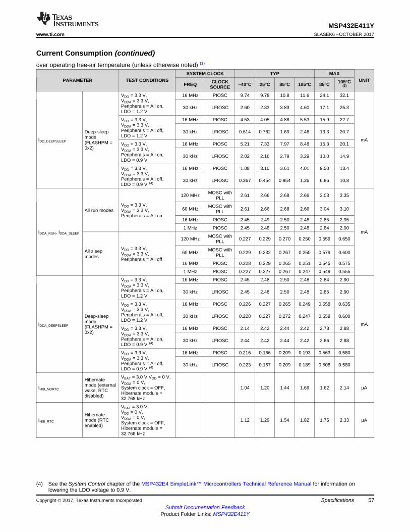
57
MSP432E411Ywww.ti.com SLASEK6 –OCTOBER 2017
Submit Documentation FeedbackProduct Folder Links: MSP432E411Y
SpecificationsCopyright © 2017, Texas Instruments Incorporated
Current Consumption (continued)over operating free-air temperature (unless otherwise noted) (1)
PARAMETER TEST CONDITIONSSYSTEM CLOCK TYP MAX
UNITFREQ CLOCK
SOURCE –40°C 25°C 85°C 105°C 85°C 105°C(2)
(4) See the System Control chapter of the MSP432E4 SimpleLink™ Microcontrollers Technical Reference Manual for information onlowering the LDO voltage to 0.9 V.
IDD_DEEPSLEEP
Deep-sleepmode(FLASHPM =0x2)
VDD = 3.3 V,VDDA = 3.3 V,Peripherals = All on,LDO = 1.2 V
16 MHz PIOSC 9.74 9.78 10.8 11.6 24.1 32.1
mA
30 kHz LFIOSC 2.60 2.83 3.83 4.60 17.1 25.3
VDD = 3.3 V,VDDA = 3.3 V,Peripherals = All off,LDO = 1.2 V
16 MHz PIOSC 4.53 4.05 4.88 5.53 15.9 22.7
30 kHz LFIOSC 0.614 0.762 1.69 2.46 13.3 20.7
VDD = 3.3 V,VDDA = 3.3 V,Peripherals = All on,LDO = 0.9 V
16 MHz PIOSC 5.21 7.33 7.97 8.48 15.3 20.1
30 kHz LFIOSC 2.02 2.16 2.79 3.29 10.0 14.9
VDD = 3.3 V,VDDA = 3.3 V,Peripherals = All off,LDO = 0.9 V (4)
16 MHz PIOSC 1.08 3.10 3.61 4.01 9.50 13.4
30 kHz LFIOSC 0.367 0.454 0.954 1.36 6.86 10.8
IDDA_RUN, IDDA_SLEEP
All run modesVDD = 3.3 V,VDDA = 3.3 V,Peripherals = All on
120 MHz MOSC withPLL 2.61 2.66 2.68 2.66 3.03 3.35
mA
60 MHz MOSC withPLL 2.61 2.66 2.68 2.66 3.04 3.10
16 MHz PIOSC 2.45 2.49 2.50 2.48 2.85 2.95
1 MHz PIOSC 2.45 2.48 2.50 2.48 2.84 2.90
All sleepmodes
VDD = 3.3 V,VDDA = 3.3 V,Peripherals = All off
120 MHz MOSC withPLL 0.227 0.229 0.270 0.250 0.559 0.650
60 MHz MOSC withPLL 0.229 0.232 0.267 0.250 0.579 0.600
16 MHz PIOSC 0.228 0.229 0.265 0.251 0.545 0.575
1 MHz PIOSC 0.227 0.227 0.267 0.247 0.549 0.555
IDDA_DEEPSLEEP
Deep-sleepmode(FLASHPM =0x2)
VDD = 3.3 V,VDDA = 3.3 V,Peripherals = All on,LDO = 1.2 V
16 MHz PIOSC 2.45 2.48 2.50 2.48 2.84 2.90
mA
30 kHz LFIOSC 2.45 2.48 2.50 2.48 2.85 2.90
VDD = 3.3 V,VDDA = 3.3 V,Peripherals = All off,LDO = 1.2 V
16 MHz PIOSC 0.226 0.227 0.265 0.249 0.558 0.635
30 kHz LFIOSC 0.228 0.227 0.272 0.247 0.558 0.600
VDD = 3.3 V,VDDA = 3.3 V,Peripherals = All on,LDO = 0.9 V (4)
16 MHz PIOSC 2.14 2.42 2.44 2.42 2.78 2.88
30 kHz LFIOSC 2.44 2.42 2.44 2.42 2.86 2.88
VDD = 3.3 V,VDDA = 3.3 V,Peripherals = All off,LDO = 0.9 V (4)
16 MHz PIOSC 0.216 0.166 0.209 0.193 0.563 0.580
30 kHz LFIOSC 0.223 0.167 0.209 0.189 0.508 0.580
IHIB_NORTC
Hibernatemode (externalwake, RTCdisabled)
VBAT = 3.0 V VDD = 0 V,VDDA = 0 V,System clock = OFF,Hibernate module =32.768 kHz
1.04 1.20 1.44 1.69 1.62 2.14 µA
IHIB_RTC
Hibernatemode (RTCenabled)
VBAT = 3.0 V,VDD = 0 V,VDDA = 0 V,System clock = OFF,Hibernate module =32.768 kHz
1.12 1.29 1.54 1.82 1.75 2.33 µA
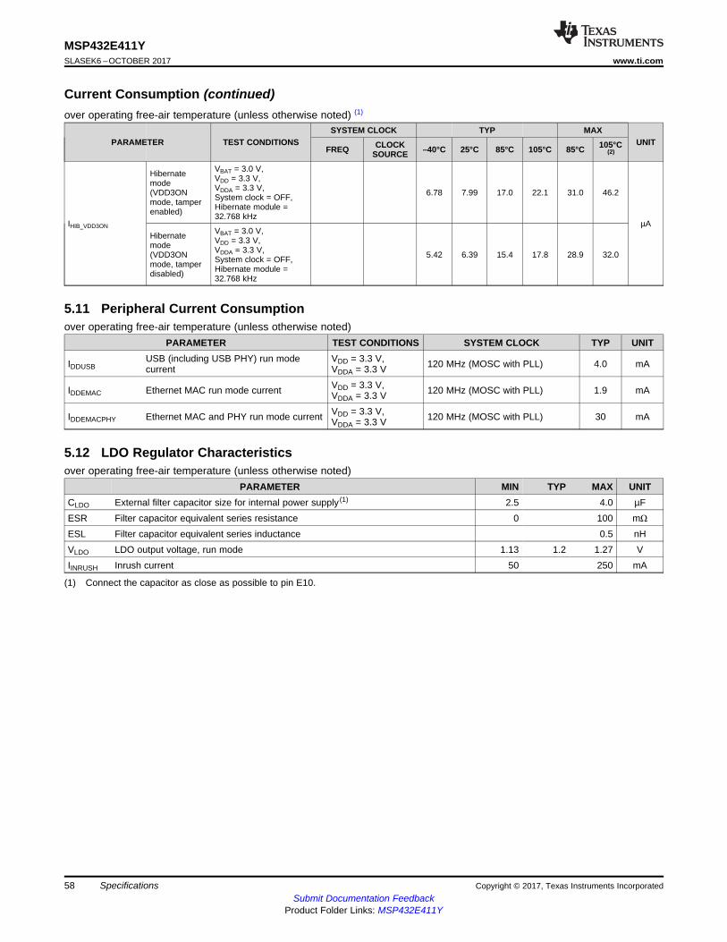
58
MSP432E411YSLASEK6 –OCTOBER 2017 www.ti.com
Submit Documentation FeedbackProduct Folder Links: MSP432E411Y
Specifications Copyright © 2017, Texas Instruments Incorporated
Current Consumption (continued)over operating free-air temperature (unless otherwise noted) (1)
PARAMETER TEST CONDITIONSSYSTEM CLOCK TYP MAX
UNITFREQ CLOCK
SOURCE –40°C 25°C 85°C 105°C 85°C 105°C(2)
IHIB_VDD3ON
Hibernatemode(VDD3ONmode, tamperenabled)
VBAT = 3.0 V,VDD = 3.3 V,VDDA = 3.3 V,System clock = OFF,Hibernate module =32.768 kHz
6.78 7.99 17.0 22.1 31.0 46.2
µAHibernatemode(VDD3ONmode, tamperdisabled)
VBAT = 3.0 V,VDD = 3.3 V,VDDA = 3.3 V,System clock = OFF,Hibernate module =32.768 kHz
5.42 6.39 15.4 17.8 28.9 32.0
5.11 Peripheral Current Consumptionover operating free-air temperature (unless otherwise noted)
PARAMETER TEST CONDITIONS SYSTEM CLOCK TYP UNIT
IDDUSBUSB (including USB PHY) run modecurrent
VDD = 3.3 V,VDDA = 3.3 V 120 MHz (MOSC with PLL) 4.0 mA
IDDEMAC Ethernet MAC run mode current VDD = 3.3 V,VDDA = 3.3 V 120 MHz (MOSC with PLL) 1.9 mA
IDDEMACPHY Ethernet MAC and PHY run mode current VDD = 3.3 V,VDDA = 3.3 V 120 MHz (MOSC with PLL) 30 mA
(1) Connect the capacitor as close as possible to pin E10.
5.12 LDO Regulator Characteristicsover operating free-air temperature (unless otherwise noted)
PARAMETER MIN TYP MAX UNITCLDO External filter capacitor size for internal power supply (1) 2.5 4.0 µFESR Filter capacitor equivalent series resistance 0 100 mΩ
ESL Filter capacitor equivalent series inductance 0.5 nHVLDO LDO output voltage, run mode 1.13 1.2 1.27 VIINRUSH Inrush current 50 250 mA
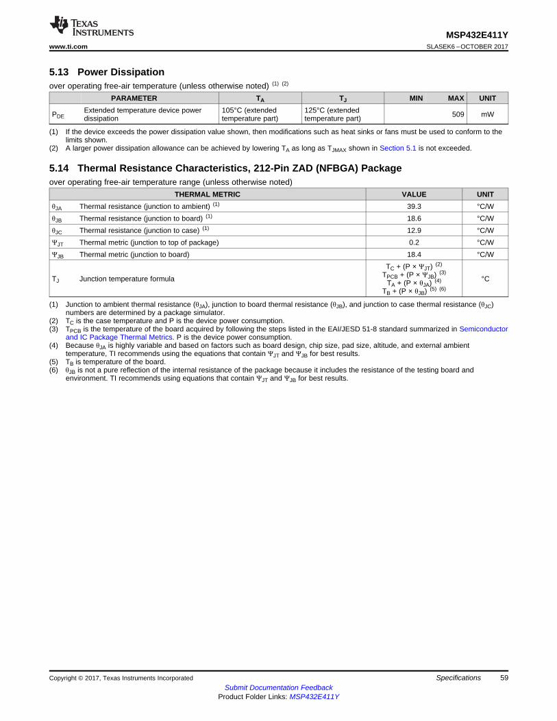
59
MSP432E411Ywww.ti.com SLASEK6 –OCTOBER 2017
Submit Documentation FeedbackProduct Folder Links: MSP432E411Y
SpecificationsCopyright © 2017, Texas Instruments Incorporated
(1) If the device exceeds the power dissipation value shown, then modifications such as heat sinks or fans must be used to conform to thelimits shown.
(2) A larger power dissipation allowance can be achieved by lowering TA as long as TJMAX shown in Section 5.1 is not exceeded.
5.13 Power Dissipationover operating free-air temperature (unless otherwise noted) (1) (2)
PARAMETER TA TJ MIN MAX UNIT
PDEExtended temperature device powerdissipation
105°C (extendedtemperature part)
125°C (extendedtemperature part) 509 mW
(1) Junction to ambient thermal resistance (θJA), junction to board thermal resistance (θJB), and junction to case thermal resistance (θJC)numbers are determined by a package simulator.
(2) TC is the case temperature and P is the device power consumption.(3) TPCB is the temperature of the board acquired by following the steps listed in the EAI/JESD 51-8 standard summarized in Semiconductor
and IC Package Thermal Metrics. P is the device power consumption.(4) Because θJA is highly variable and based on factors such as board design, chip size, pad size, altitude, and external ambient
temperature, TI recommends using the equations that contain ΨJT and ΨJB for best results.(5) TB is temperature of the board.(6) θJB is not a pure reflection of the internal resistance of the package because it includes the resistance of the testing board and
environment. TI recommends using equations that contain ΨJT and ΨJB for best results.
5.14 Thermal Resistance Characteristics, 212-Pin ZAD (NFBGA) Packageover operating free-air temperature range (unless otherwise noted)
THERMAL METRIC VALUE UNITθJA Thermal resistance (junction to ambient) (1) 39.3 °C/WθJB Thermal resistance (junction to board) (1) 18.6 °C/WθJC Thermal resistance (junction to case) (1) 12.9 °C/WΨJT Thermal metric (junction to top of package) 0.2 °C/WΨJB Thermal metric (junction to board) 18.4 °C/W
TJ Junction temperature formula
TC + (P × ΨJT) (2)
TPCB + (P × ΨJB) (3)
TA + (P × θJA) (4)
TB + (P × θJB) (5) (6)
°C
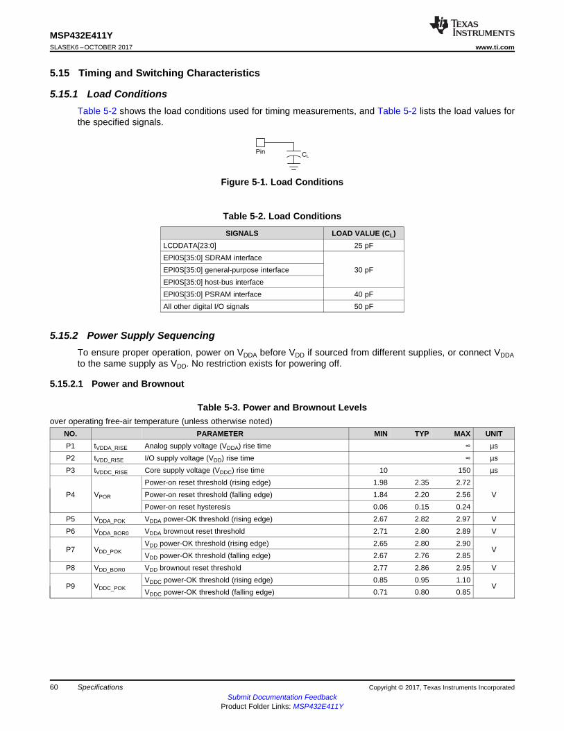
CLPin
60
MSP432E411YSLASEK6 –OCTOBER 2017 www.ti.com
Submit Documentation FeedbackProduct Folder Links: MSP432E411Y
Specifications Copyright © 2017, Texas Instruments Incorporated
5.15 Timing and Switching Characteristics
5.15.1 Load ConditionsTable 5-2 shows the load conditions used for timing measurements, and Table 5-2 lists the load values forthe specified signals.
Figure 5-1. Load Conditions
Table 5-2. Load Conditions
SIGNALS LOAD VALUE (CL)LCDDATA[23:0] 25 pFEPI0S[35:0] SDRAM interface
30 pFEPI0S[35:0] general-purpose interfaceEPI0S[35:0] host-bus interfaceEPI0S[35:0] PSRAM interface 40 pFAll other digital I/O signals 50 pF
5.15.2 Power Supply SequencingTo ensure proper operation, power on VDDA before VDD if sourced from different supplies, or connect VDDAto the same supply as VDD. No restriction exists for powering off.
5.15.2.1 Power and Brownout
Table 5-3. Power and Brownout Levelsover operating free-air temperature (unless otherwise noted)
NO. PARAMETER MIN TYP MAX UNITP1 tVDDA_RISE Analog supply voltage (VDDA) rise time ∞ µsP2 tVDD_RISE I/O supply voltage (VDD) rise time ∞ µsP3 tVDDC_RISE Core supply voltage (VDDC) rise time 10 150 µs
P4 VPOR
Power-on reset threshold (rising edge) 1.98 2.35 2.72VPower-on reset threshold (falling edge) 1.84 2.20 2.56
Power-on reset hysteresis 0.06 0.15 0.24P5 VDDA_POK VDDA power-OK threshold (rising edge) 2.67 2.82 2.97 VP6 VDDA_BOR0 VDDA brownout reset threshold 2.71 2.80 2.89 V
P7 VDD_POKVDD power-OK threshold (rising edge) 2.65 2.80 2.90
VVDD power-OK threshold (falling edge) 2.67 2.76 2.85
P8 VDD_BOR0 VDD brownout reset threshold 2.77 2.86 2.95 V
P9 VDDC_POKVDDC power-OK threshold (rising edge) 0.85 0.95 1.10
VVDDC power-OK threshold (falling edge) 0.71 0.80 0.85
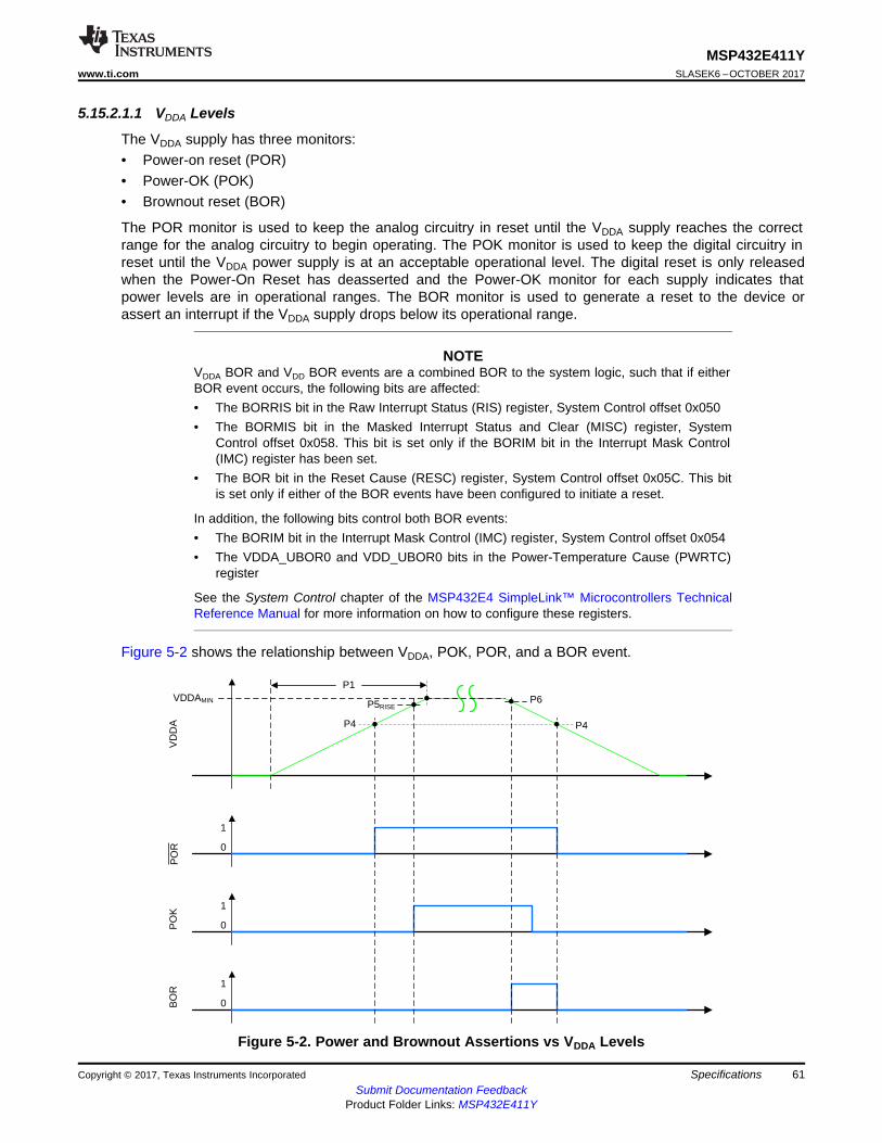
P1
VD
DA
P5RISE
P4
PO
KB
OR
P4
1
VDDAMIN
1
1
0
0
0
P6
PO
R
61
MSP432E411Ywww.ti.com SLASEK6 –OCTOBER 2017
Submit Documentation FeedbackProduct Folder Links: MSP432E411Y
SpecificationsCopyright © 2017, Texas Instruments Incorporated
5.15.2.1.1 VDDA Levels
The VDDA supply has three monitors:• Power-on reset (POR)• Power-OK (POK)• Brownout reset (BOR)
The POR monitor is used to keep the analog circuitry in reset until the VDDA supply reaches the correctrange for the analog circuitry to begin operating. The POK monitor is used to keep the digital circuitry inreset until the VDDA power supply is at an acceptable operational level. The digital reset is only releasedwhen the Power-On Reset has deasserted and the Power-OK monitor for each supply indicates thatpower levels are in operational ranges. The BOR monitor is used to generate a reset to the device orassert an interrupt if the VDDA supply drops below its operational range.
NOTEVDDA BOR and VDD BOR events are a combined BOR to the system logic, such that if eitherBOR event occurs, the following bits are affected:• The BORRIS bit in the Raw Interrupt Status (RIS) register, System Control offset 0x050• The BORMIS bit in the Masked Interrupt Status and Clear (MISC) register, System
Control offset 0x058. This bit is set only if the BORIM bit in the Interrupt Mask Control(IMC) register has been set.
• The BOR bit in the Reset Cause (RESC) register, System Control offset 0x05C. This bitis set only if either of the BOR events have been configured to initiate a reset.
In addition, the following bits control both BOR events:• The BORIM bit in the Interrupt Mask Control (IMC) register, System Control offset 0x054• The VDDA_UBOR0 and VDD_UBOR0 bits in the Power-Temperature Cause (PWRTC)
register
See the System Control chapter of the MSP432E4 SimpleLink™ Microcontrollers TechnicalReference Manual for more information on how to configure these registers.
Figure 5-2 shows the relationship between VDDA, POK, POR, and a BOR event.
Figure 5-2. Power and Brownout Assertions vs VDDA Levels
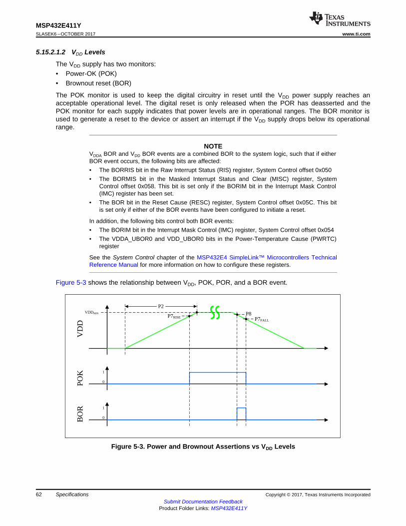
P2
VD
D
P7RISEP8
POK
VDDMIN
1
0
P7FALL
BO
R 1
0
62
MSP432E411YSLASEK6 –OCTOBER 2017 www.ti.com
Submit Documentation FeedbackProduct Folder Links: MSP432E411Y
Specifications Copyright © 2017, Texas Instruments Incorporated
5.15.2.1.2 VDD Levels
The VDD supply has two monitors:• Power-OK (POK)• Brownout reset (BOR)
The POK monitor is used to keep the digital circuitry in reset until the VDD power supply reaches anacceptable operational level. The digital reset is only released when the POR has deasserted and thePOK monitor for each supply indicates that power levels are in operational ranges. The BOR monitor isused to generate a reset to the device or assert an interrupt if the VDD supply drops below its operationalrange.
NOTEVDDA BOR and VDD BOR events are a combined BOR to the system logic, such that if eitherBOR event occurs, the following bits are affected:• The BORRIS bit in the Raw Interrupt Status (RIS) register, System Control offset 0x050• The BORMIS bit in the Masked Interrupt Status and Clear (MISC) register, System
Control offset 0x058. This bit is set only if the BORIM bit in the Interrupt Mask Control(IMC) register has been set.
• The BOR bit in the Reset Cause (RESC) register, System Control offset 0x05C. This bitis set only if either of the BOR events have been configured to initiate a reset.
In addition, the following bits control both BOR events:• The BORIM bit in the Interrupt Mask Control (IMC) register, System Control offset 0x054• The VDDA_UBOR0 and VDD_UBOR0 bits in the Power-Temperature Cause (PWRTC)
register
See the System Control chapter of the MSP432E4 SimpleLink™ Microcontrollers TechnicalReference Manual for more information on how to configure these registers.
Figure 5-3 shows the relationship between VDD, POK, POR, and a BOR event.
Figure 5-3. Power and Brownout Assertions vs VDD Levels
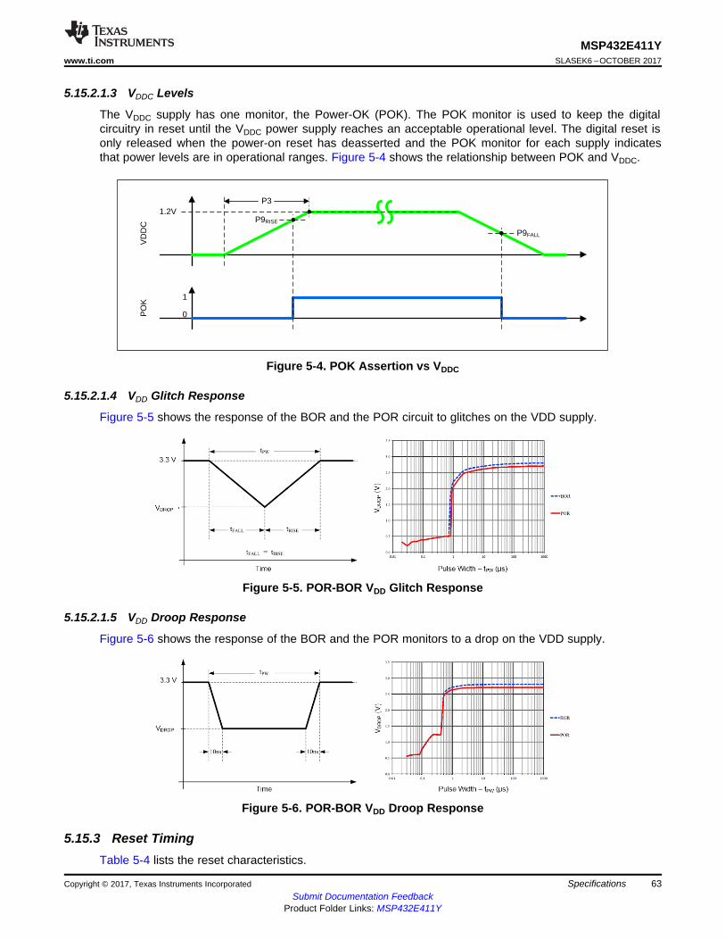
P3
VD
DC
P9RISE
PO
K
1.2V
1
0
P9FALL
63
MSP432E411Ywww.ti.com SLASEK6 –OCTOBER 2017
Submit Documentation FeedbackProduct Folder Links: MSP432E411Y
SpecificationsCopyright © 2017, Texas Instruments Incorporated
5.15.2.1.3 VDDC Levels
The VDDC supply has one monitor, the Power-OK (POK). The POK monitor is used to keep the digitalcircuitry in reset until the VDDC power supply reaches an acceptable operational level. The digital reset isonly released when the power-on reset has deasserted and the POK monitor for each supply indicatesthat power levels are in operational ranges. Figure 5-4 shows the relationship between POK and VDDC.
Figure 5-4. POK Assertion vs VDDC
5.15.2.1.4 VDD Glitch Response
Figure 5-5 shows the response of the BOR and the POR circuit to glitches on the VDD supply.
Figure 5-5. POR-BOR VDD Glitch Response
5.15.2.1.5 VDD Droop Response
Figure 5-6 shows the response of the BOR and the POR monitors to a drop on the VDD supply.
Figure 5-6. POR-BOR VDD Droop Response
5.15.3 Reset TimingTable 5-4 lists the reset characteristics.
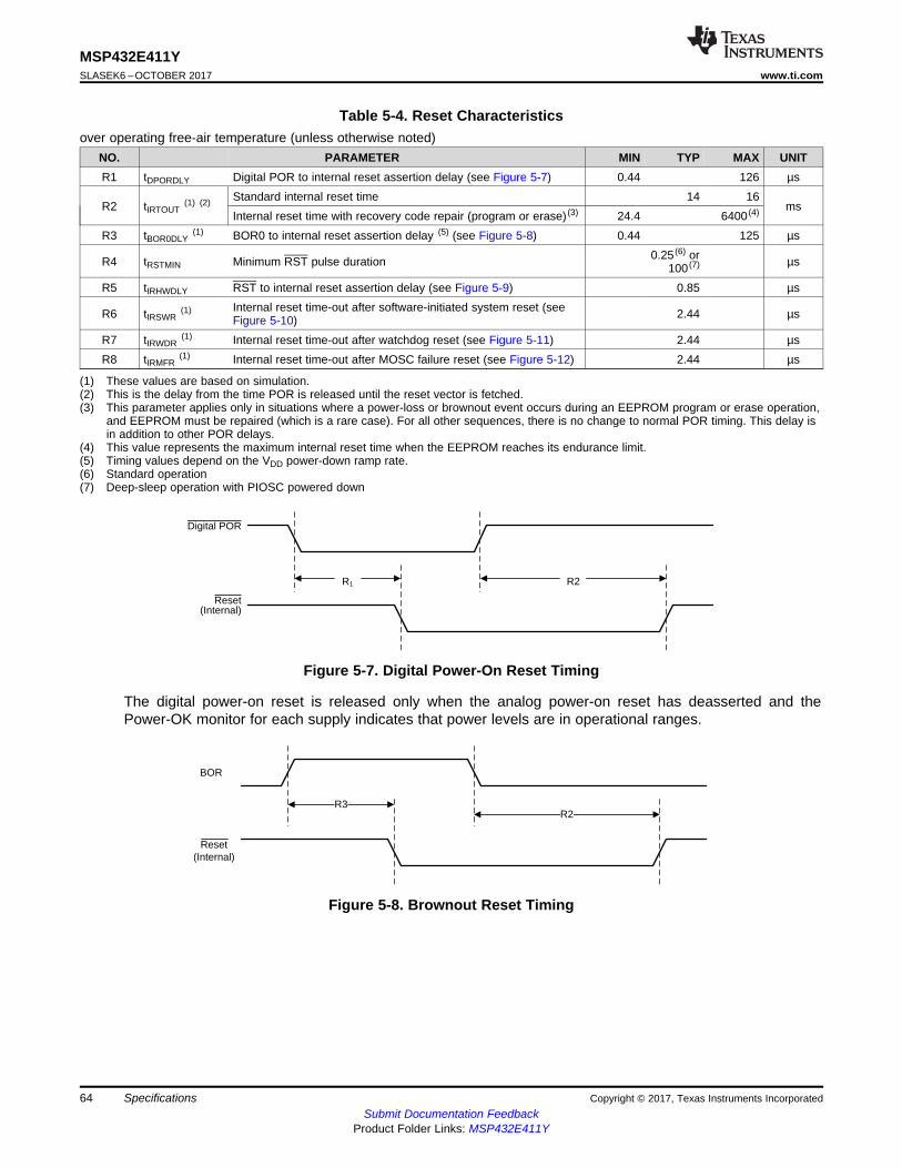
BOR
R3R2
Reset(Internal)
R2R1
Digital POR
Reset(Internal)
64
MSP432E411YSLASEK6 –OCTOBER 2017 www.ti.com
Submit Documentation FeedbackProduct Folder Links: MSP432E411Y
Specifications Copyright © 2017, Texas Instruments Incorporated
(1) These values are based on simulation.(2) This is the delay from the time POR is released until the reset vector is fetched.(3) This parameter applies only in situations where a power-loss or brownout event occurs during an EEPROM program or erase operation,
and EEPROM must be repaired (which is a rare case). For all other sequences, there is no change to normal POR timing. This delay isin addition to other POR delays.
(4) This value represents the maximum internal reset time when the EEPROM reaches its endurance limit.(5) Timing values depend on the VDD power-down ramp rate.(6) Standard operation(7) Deep-sleep operation with PIOSC powered down
Table 5-4. Reset Characteristicsover operating free-air temperature (unless otherwise noted)
NO. PARAMETER MIN TYP MAX UNITR1 tDPORDLY Digital POR to internal reset assertion delay (see Figure 5-7) 0.44 126 µs
R2 tIRTOUT(1) (2) Standard internal reset time 14 16
msInternal reset time with recovery code repair (program or erase) (3) 24.4 6400 (4)
R3 tBOR0DLY(1) BOR0 to internal reset assertion delay (5) (see Figure 5-8) 0.44 125 µs
R4 tRSTMIN Minimum RST pulse duration 0.25 (6) or100 (7) µs
R5 tIRHWDLY RST to internal reset assertion delay (see Figure 5-9) 0.85 µs
R6 tIRSWR(1) Internal reset time-out after software-initiated system reset (see
Figure 5-10) 2.44 µs
R7 tIRWDR(1) Internal reset time-out after watchdog reset (see Figure 5-11) 2.44 µs
R8 tIRMFR(1) Internal reset time-out after MOSC failure reset (see Figure 5-12) 2.44 µs
Figure 5-7. Digital Power-On Reset Timing
The digital power-on reset is released only when the analog power-on reset has deasserted and thePower-OK monitor for each supply indicates that power levels are in operational ranges.
Figure 5-8. Brownout Reset Timing
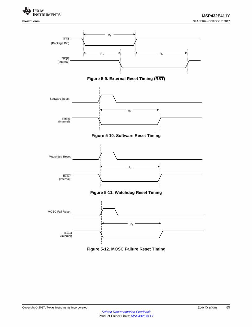
MOSC Fail Reset
R8
Reset(Internal)
Watchdog Reset
R7
Reset(Internal)
Software Reset
R6
Reset(Internal)
R4
R5 R2
Reset(Internal)
RST(Package Pin)
65
MSP432E411Ywww.ti.com SLASEK6 –OCTOBER 2017
Submit Documentation FeedbackProduct Folder Links: MSP432E411Y
SpecificationsCopyright © 2017, Texas Instruments Incorporated
Figure 5-9. External Reset Timing (RST)
Figure 5-10. Software Reset Timing
Figure 5-11. Watchdog Reset Timing
Figure 5-12. MOSC Failure Reset Timing
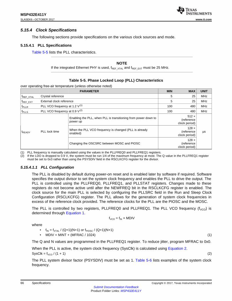
66
MSP432E411YSLASEK6 –OCTOBER 2017 www.ti.com
Submit Documentation FeedbackProduct Folder Links: MSP432E411Y
Specifications Copyright © 2017, Texas Instruments Incorporated
5.15.4 Clock SpecificationsThe following sections provide specifications on the various clock sources and mode.
5.15.4.1 PLL Specifications
Table 5-5 lists the PLL characteristics.
NOTEIf the integrated Ethernet PHY is used, fREF_XTAL and fREF_EXT must be 25 MHz.
(1) PLL frequency is manually calculated using the values in the PLLFREQ0 and PLLFREQ1 registers.(2) If the LDO is dropped to 0.9 V, the system must be run 1/4 of the maximum frequency at most. The Q value in the PLLFREQ1 register
must be set to 0x3 rather than using the PSYSDIV field in the RSCLKCFG register for the divisor.
Table 5-5. Phase Locked Loop (PLL) Characteristicsover operating free-air temperature (unless otherwise noted)
PARAMETER MIN MAX UNITfREF_XTAL Crystal reference 5 25 MHzfREF_EXT External clock reference 5 25 MHzfPLLR PLL VCO frequency at 1.2 V (1) 100 480 MHzfPLLS PLL VCO frequency at 0.9 V (2) 100 480 MHz
tREADY PLL lock time
Enabling the PLL, when PLL is transitioning from power down topower up
512 ×(reference
clock period)
µsWhen the PLL VCO frequency is changed (PLL is alreadyenabled)
128 ×(reference
clock period)
Changing the OSCSRC between MOSC and PIOSC128 ×
(referenceclock period)
5.15.4.1.1 PLL Configuration
The PLL is disabled by default during power-on reset and is enabled later by software if required. Softwarespecifies the output divisor to set the system clock frequency and enables the PLL to drive the output. ThePLL is controlled using the PLLFREQ0, PLLFREQ1, and PLLSTAT registers. Changes made to theseregisters do not become active until after the NEWFREQ bit in the RSCLKCFG register is enabled. Theclock source for the main PLL is selected by configuring the PLLSRC field in the Run and Sleep ClockConfiguration (RSCLKCFG) register. The PLL allows for the generation of system clock frequencies inexcess of the reference clock provided. The reference clocks for the PLL are the PIOSC and the MOSC.
The PLL is controlled by two registers, PLLFREQ0 and PLLFREQ1. The PLL VCO frequency (fVCO) isdetermined through Equation 1.
fVCO = fIN × MDIV
where• fIN = fXTAL / (Q+1)(N+1) or fPIOSC / (Q+1)(N+1)• MDIV = MINT + (MFRAC / 1024) (1)
The Q and N values are programmed in the PLLFREQ1 register. To reduce jitter, program MFRAC to 0x0.
When the PLL is active, the system clock frequency (SysClk) is calculated using Equation 2.SysClk = fVCO / (1 + 1) (2)
The PLL system divisor factor (PSYSDIV) must be set as 1. Table 5-6 lists examples of the system clockfrequency.
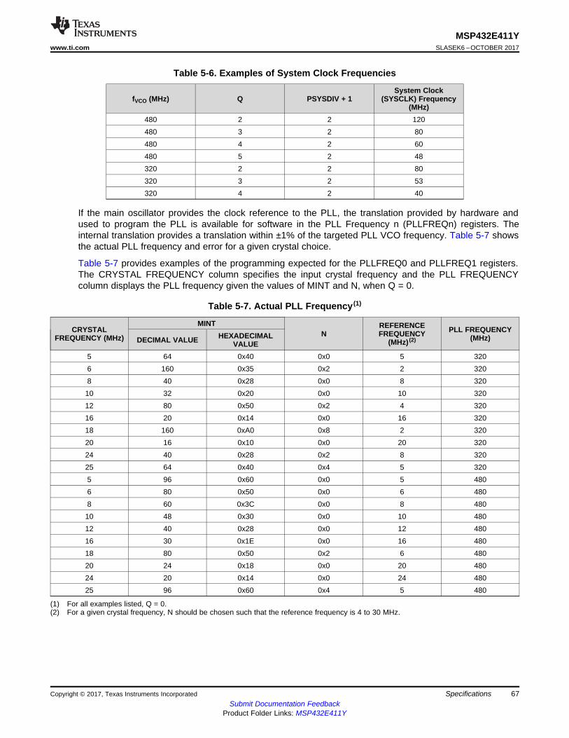
67
MSP432E411Ywww.ti.com SLASEK6 –OCTOBER 2017
Submit Documentation FeedbackProduct Folder Links: MSP432E411Y
SpecificationsCopyright © 2017, Texas Instruments Incorporated
Table 5-6. Examples of System Clock Frequencies
fVCO (MHz) Q PSYSDIV + 1System Clock
(SYSCLK) Frequency(MHz)
480 2 2 120480 3 2 80480 4 2 60480 5 2 48320 2 2 80320 3 2 53320 4 2 40
(1) For all examples listed, Q = 0.(2) For a given crystal frequency, N should be chosen such that the reference frequency is 4 to 30 MHz.
If the main oscillator provides the clock reference to the PLL, the translation provided by hardware andused to program the PLL is available for software in the PLL Frequency n (PLLFREQn) registers. Theinternal translation provides a translation within ±1% of the targeted PLL VCO frequency. Table 5-7 showsthe actual PLL frequency and error for a given crystal choice.
Table 5-7 provides examples of the programming expected for the PLLFREQ0 and PLLFREQ1 registers.The CRYSTAL FREQUENCY column specifies the input crystal frequency and the PLL FREQUENCYcolumn displays the PLL frequency given the values of MINT and N, when Q = 0.
Table 5-7. Actual PLL Frequency (1)
CRYSTALFREQUENCY (MHz)
MINTN
REFERENCEFREQUENCY
(MHz) (2)PLL FREQUENCY
(MHz)DECIMAL VALUE HEXADECIMALVALUE
5 64 0x40 0x0 5 3206 160 0x35 0x2 2 3208 40 0x28 0x0 8 32010 32 0x20 0x0 10 32012 80 0x50 0x2 4 32016 20 0x14 0x0 16 32018 160 0xA0 0x8 2 32020 16 0x10 0x0 20 32024 40 0x28 0x2 8 32025 64 0x40 0x4 5 3205 96 0x60 0x0 5 4806 80 0x50 0x0 6 4808 60 0x3C 0x0 8 48010 48 0x30 0x0 10 48012 40 0x28 0x0 12 48016 30 0x1E 0x0 16 48018 80 0x50 0x2 6 48020 24 0x18 0x0 20 48024 20 0x14 0x0 24 48025 96 0x60 0x4 5 480
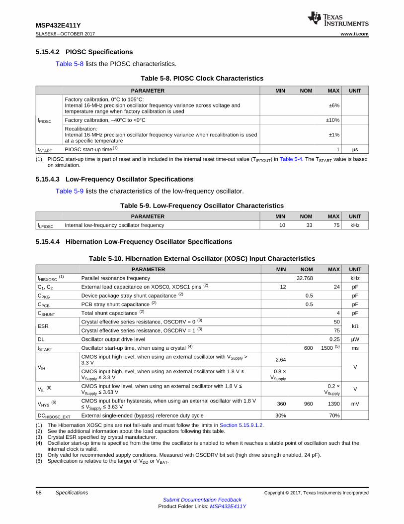
68
MSP432E411YSLASEK6 –OCTOBER 2017 www.ti.com
Submit Documentation FeedbackProduct Folder Links: MSP432E411Y
Specifications Copyright © 2017, Texas Instruments Incorporated
(1) PIOSC start-up time is part of reset and is included in the internal reset time-out value (TIRTOUT) in Table 5-4. The TSTART value is basedon simulation.
5.15.4.2 PIOSC Specifications
Table 5-8 lists the PIOSC characteristics.
Table 5-8. PIOSC Clock Characteristics
PARAMETER MIN NOM MAX UNIT
fPIOSC
Factory calibration, 0°C to 105°C:Internal 16-MHz precision oscillator frequency variance across voltage andtemperature range when factory calibration is used
±6%
Factory calibration, –40°C to <0°C ±10%Recalibration:Internal 16-MHz precision oscillator frequency variance when recalibration is usedat a specific temperature
±1%
tSTART PIOSC start-up time (1) 1 µs
5.15.4.3 Low-Frequency Oscillator Specifications
Table 5-9 lists the characteristics of the low-frequency oscillator.
Table 5-9. Low-Frequency Oscillator CharacteristicsPARAMETER MIN NOM MAX UNIT
fLFIOSC Internal low-frequency oscillator frequency 10 33 75 kHz
5.15.4.4 Hibernation Low-Frequency Oscillator Specifications
(1) The Hibernation XOSC pins are not fail-safe and must follow the limits in Section 5.15.9.1.2.(2) See the additional information about the load capacitors following this table.(3) Crystal ESR specified by crystal manufacturer.(4) Oscillator start-up time is specified from the time the oscillator is enabled to when it reaches a stable point of oscillation such that the
internal clock is valid.(5) Only valid for recommended supply conditions. Measured with OSCDRV bit set (high drive strength enabled, 24 pF).(6) Specification is relative to the larger of VDD or VBAT.
Table 5-10. Hibernation External Oscillator (XOSC) Input CharacteristicsPARAMETER MIN NOM MAX UNIT
fHIBXOSC(1) Parallel resonance frequency 32.768 kHz
C1, C2 External load capacitance on XOSC0, XOSC1 pins (2) 12 24 pFCPKG Device package stray shunt capacitance (2) 0.5 pFCPCB PCB stray shunt capacitance (2) 0.5 pFCSHUNT Total shunt capacitance (2) 4 pF
ESRCrystal effective series resistance, OSCDRV = 0 (3) 50
kΩCrystal effective series resistance, OSCDRV = 1 (3) 75
DL Oscillator output drive level 0.25 µWtSTART Oscillator start-up time, when using a crystal (4) 600 1500 (5) ms
VIH
CMOS input high level, when using an external oscillator with VSupply >3.3 V 2.64
VCMOS input high level, when using an external oscillator with 1.8 V ≤VSupply ≤ 3.3 V
0.8 ×VSupply
VIL(6) CMOS input low level, when using an external oscillator with 1.8 V ≤
VSupply ≤ 3.63 V0.2 ×
VSupplyV
VHYS(6) CMOS input buffer hysteresis, when using an external oscillator with 1.8 V
≤ VSupply ≤ 3.63 V 360 960 1390 mV
DCHIBOSC_EXT External single-ended (bypass) reference duty cycle 30% 70%
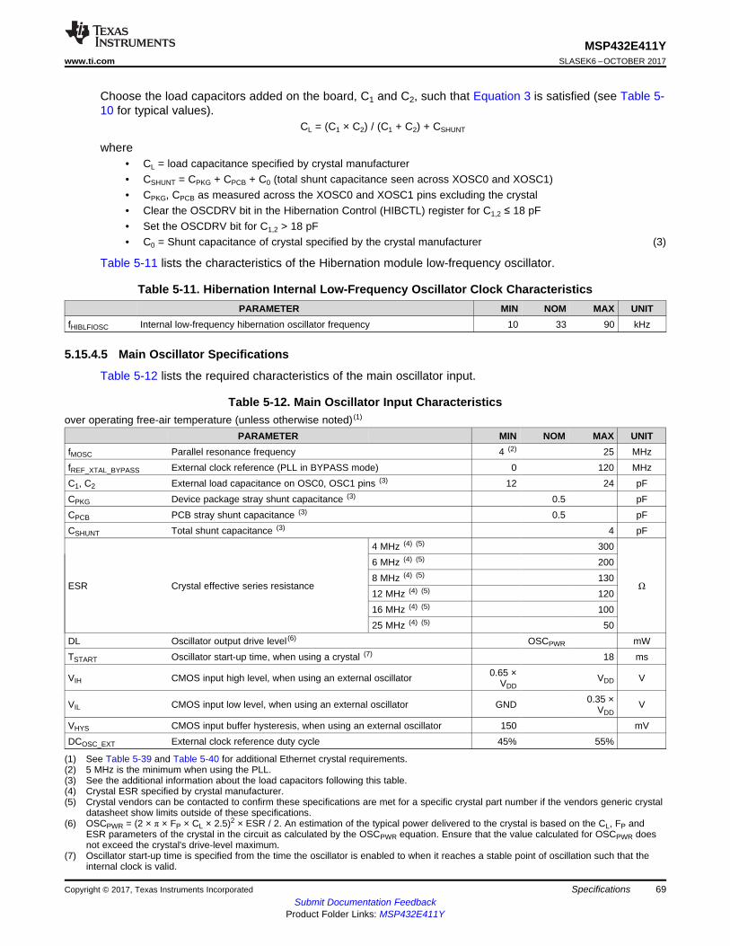
69
MSP432E411Ywww.ti.com SLASEK6 –OCTOBER 2017
Submit Documentation FeedbackProduct Folder Links: MSP432E411Y
SpecificationsCopyright © 2017, Texas Instruments Incorporated
Choose the load capacitors added on the board, C1 and C2, such that Equation 3 is satisfied (see Table 5-10 for typical values).
CL = (C1 × C2) / (C1 + C2) + CSHUNT
where• CL = load capacitance specified by crystal manufacturer• CSHUNT = CPKG + CPCB + C0 (total shunt capacitance seen across XOSC0 and XOSC1)• CPKG, CPCB as measured across the XOSC0 and XOSC1 pins excluding the crystal• Clear the OSCDRV bit in the Hibernation Control (HIBCTL) register for C1,2 ≤ 18 pF• Set the OSCDRV bit for C1,2 > 18 pF• C0 = Shunt capacitance of crystal specified by the crystal manufacturer (3)
Table 5-11 lists the characteristics of the Hibernation module low-frequency oscillator.
Table 5-11. Hibernation Internal Low-Frequency Oscillator Clock CharacteristicsPARAMETER MIN NOM MAX UNIT
fHIBLFIOSC Internal low-frequency hibernation oscillator frequency 10 33 90 kHz
5.15.4.5 Main Oscillator Specifications
Table 5-12 lists the required characteristics of the main oscillator input.
(1) See Table 5-39 and Table 5-40 for additional Ethernet crystal requirements.(2) 5 MHz is the minimum when using the PLL.(3) See the additional information about the load capacitors following this table.(4) Crystal ESR specified by crystal manufacturer.(5) Crystal vendors can be contacted to confirm these specifications are met for a specific crystal part number if the vendors generic crystal
datasheet show limits outside of these specifications.(6) OSCPWR = (2 × π × FP × CL × 2.5)2 × ESR / 2. An estimation of the typical power delivered to the crystal is based on the CL, FP and
ESR parameters of the crystal in the circuit as calculated by the OSCPWR equation. Ensure that the value calculated for OSCPWR doesnot exceed the crystal's drive-level maximum.
(7) Oscillator start-up time is specified from the time the oscillator is enabled to when it reaches a stable point of oscillation such that theinternal clock is valid.
Table 5-12. Main Oscillator Input Characteristicsover operating free-air temperature (unless otherwise noted) (1)
PARAMETER MIN NOM MAX UNITfMOSC Parallel resonance frequency 4 (2) 25 MHzfREF_XTAL_BYPASS External clock reference (PLL in BYPASS mode) 0 120 MHzC1, C2 External load capacitance on OSC0, OSC1 pins (3) 12 24 pFCPKG Device package stray shunt capacitance (3) 0.5 pFCPCB PCB stray shunt capacitance (3) 0.5 pFCSHUNT Total shunt capacitance (3) 4 pF
ESR Crystal effective series resistance
4 MHz (4) (5) 300
Ω
6 MHz (4) (5) 2008 MHz (4) (5) 13012 MHz (4) (5) 12016 MHz (4) (5) 10025 MHz (4) (5) 50
DL Oscillator output drive level (6) OSCPWR mWTSTART Oscillator start-up time, when using a crystal (7) 18 ms
VIH CMOS input high level, when using an external oscillator 0.65 ×VDD
VDD V
VIL CMOS input low level, when using an external oscillator GND 0.35 ×VDD
V
VHYS CMOS input buffer hysteresis, when using an external oscillator 150 mVDCOSC_EXT External clock reference duty cycle 45% 55%
70
MSP432E411YSLASEK6 –OCTOBER 2017 www.ti.com
Submit Documentation FeedbackProduct Folder Links: MSP432E411Y
Specifications Copyright © 2017, Texas Instruments Incorporated
The load capacitors added on the board, C1 and C2, should be chosen such that Equation 4 is satisfied(see Table 5-12 for typical values and Table 5-13 for detailed crystal parameter information).
CL = (C1 × C2) / (C1 + C2) + CSHUNT
where• CL = load capacitance specified by crystal manufacturer• CSHUNT = C0 + CPKG + CPCB (total shunt capacitance seen across OSC0 and OSC1 crystal inputs)• CPKG, CPCB = Mutual capacitance as measured across the OSC0 and OSC1 pins excluding the crystal• C0 = Shunt capacitance of crystal specified by the crystal manufacturer (4)
Table 5-13 lists part numbers of crystals that have been simulated and confirmed to operate within thespecifications in Table 5-12. Other crystals that have nearly identical crystal parameters can be expectedto work as well.
In Table 5-13, the crystal parameters labeled C0, C1, and L1 are values that are obtained from the crystalmanufacturer. These numbers are usually a result of testing a relevant batch of crystals on a networkanalyzer. The parameters labeled ESR, DL, and CL are maximum numbers usually available in the datasheet for a crystal.
Table 5-13 also includes three columns of Recommended Component Values. These values apply tosystem board components. C1 and C2 are the values in picofarads of the load capacitors that should beput on each leg of the crystal pins to ensure oscillation at the correct frequency. Rs is the value in kΩ of aresistor that is placed in series with the crystal between the OSC1 pin and the crystal pin. Rs dissipatessome of the power so the Max Dl crystal parameter is not exceeded. Only use the recommended C1, C2,and Rs values with the associated crystal part. The values in the table were used in the simulation toensure crystal start-up and to determine the worst-case drive level (WC DL). The value in the WC DLcolumn should not be greater than the Max DL crystal parameter. The WC DL value can be used todetermine if a crystal with similar parameter values but a lower Max DL value is acceptable.
Copyright © 2017, Texas Instruments Incorporated SpecificationsSubmit Documentation Feedback
Product Folder Links: MSP432E411Y
71
MSP432E411Ywww.ti.com SLASEK6 –OCTOBER 2017
(1) RS values as low as 0 Ω can be used. Using a lower RS value causes the WC DL to increase toward the maximum DL of the crystal.(2) Although this ESR value is outside of the recommended crystal ESR maximum for this frequency, this crystal has been simulated to confirm proper operation and is valid for use with this
device.
Table 5-13. Crystal Parameters
Manufacturer Manufacturer PartNumber Holder Package Size
(mm × mm)Frequency
(MHz)
CrystalSpecification(Tolerance /
Stability)
Crystal Parameters RecommendedComponent Values WC
DL(µW)
Typical Values Max Values
C0(pF)
C1(fF) L1 (mH) ESR
(Ω)MaxDL
(µW)CL (pf) C1
(pF)C2
(pF)Rs
(kΩ)
NDK NX8045GB-4.000M-STD-CJL-5 NX8045GB 8 × 4.5 4 30 / 50 ppm 1.00 2.70 598.10 300 500 8 12 12 0 132
FOX FQ1045A-4 2-SMD 10 × 4.5 4 30 / 30 ppm 1.18 4.05 396.00 150 500 10 14 14 0 103
NDK NX8045GB-5.000M-STD-CSF-4 NX8045GB 8 × 4.5 5 30 / 50 ppm 1.00 2.80 356.50 250 500 8 12 12 0 164
NDK NX8045GB-6.000M-STD-CSF-4 NX8045GB 8 × 4.5 6 30 / 50 ppm 1.30 4.10 173.20 250 500 8 12 12 0 214
FOX FQ1045A-6 2-SMD 10 × 4.5 6 30 / 30 ppm 1.37 6.26 112.30 150 500 10 14 14 0 209
NDK NX8045GB-8.000M-STD-CSF-6 NX8045GB 8 × 4.5 8 30 / 50 ppm 1.00 2.80 139.30 200 500 8 12 12 0 277
FOX FQ7050B-8 4-SMD 7 × 5 8 30 / 30 ppm 1.95 6.69 59.10 80 500 10 14 14 0 217
ECS ECS-80-16-28A-TR HC49/US 12.5 × 4.85 8 50 / 30 ppm 1.82 4.90 85.70 80 500 16 24 24 0 298
Abracon AABMM-12.0000MHz-10-D-1-X-T ABMM 7.2 × 5.2 12 10 / 20 ppm 2.37 8.85 20.5 50 500 10 12 12 2.0 (1) 124
NDK NX3225GA-12.000MHZ-STD-CRG-2 NX3225GA 3.2 × 2.5 12 20 / 30 ppm 0.70 2.20 81.00 100 200 8 12 12 2.5 147
NDK NX5032GA-12.000MHZ-LN-CD-1 NX5032GA 5 × 3.2 12 30 / 50 ppm 0.93 3.12 56.40 120 500 8 12 12 0 362
FOX FQ5032B-12 4-SMD 5 × 3.2 12 30 / 30 ppm 1.16 4.16 42.30 80 500 10 14 14 0 370
Abracon AABMM-16.0000MHz-10-D-1-X-T ABMM 7.2 × 5.2 16 10 / 20 ppm 3.00 11.00 9.30 50 500 10 12 12 2.0 (1) 143
Ecliptek ECX-6595-16.000M HC-49/UP 13.3 × 4.85 16 15 / 30 ppm 3.00 12.7 8.1 50 1000 10 12 12 2.0 (1) 139
NDK NX3225GA-16.000MHZ-STD-CRG-2 NX3225GA 3.2 × 2.5 16 20 / 30 ppm 1.00 2.90 33.90 80 200 8 12 12 2 188
NDK NX5032GA-16.000MHZ-LN-CD-1 NX5032GA 5 × 3.2 16 30 / 50 ppm 1.02 3.82 25.90 120 (2) 500 8 10 10 0 437
ECS ECS-160-9-42-CKM-TR ECX-42 4 × 2.5 16 10 / 10 ppm 1.47 3.90 25.84 60 300 9 12 12 0.5 289
Abracon AABMM-25.0000MHz-10-D-1-X-T ABMM 7.2 × 5.2 25 10 / 20 ppm 3.00 11.00 3.70 50 500 10 12 12 2.0 (1) 158
Ecliptek ECX-6593-25.000M HC-49/UP 13.3 × 4.85 25 15 / 30 ppm 3.00 12.8 3.2 40 1000 10 12 12 1.5 (1) 159
NDK NX3225GA-25.000MHZ-STD-CRG-2 NX3225GA 3.2 × 2.5 25 20 / 30 ppm 1.10 4.70 8.70 50 200 8 12 12 2 181

Copyright © 2017, Texas Instruments IncorporatedSpecificationsSubmit Documentation Feedback
Product Folder Links: MSP432E411Y
72
MSP432E411YSLASEK6 –OCTOBER 2017 www.ti.com
Table 5-13. Crystal Parameters (continued)
Manufacturer Manufacturer PartNumber Holder Package Size
(mm × mm)Frequency
(MHz)
CrystalSpecification(Tolerance /
Stability)
Crystal Parameters RecommendedComponent Values WC
DL(µW)
Typical Values Max Values
C0(pF)
C1(fF) L1 (mH) ESR
(Ω)MaxDL
(µW)CL (pf) C1
(pF)C2
(pF)Rs
(kΩ)
(3) RS values as low as 500 Ω can be used. Using a lower RS value causes the WC DL to increase toward the maximum DL of the crystal.
NDK NX5032GA-25.000MHZ-LD-CD-1 NX5032GA 5 × 3.2 25 30 / 50 ppm 1.3 5.1 7.1 70 500 8
10 10 1.0 (1) 216
12 12 0.75(3) 269
AURIS Q-25.000M-HC3225/4-F-30-30-E-12-TR HC3225/4 3.2 × 2.5 25 30 / 30 ppm 1.58 5.01 8.34 50 500 12 16 16 1 331
FOX FQ5032B-25 4-SMD 5 × 3.2 25 30 / 30 ppm 1.69 7.92 5.13 50 500 10 14 14 0.5 433
TXC 7A2570018 NX5032GA 5 × 3.2 25 20 / 25 ppm 2.0 6.7 6.1 30 350 10 12 12 2.0 (3) 124
73
MSP432E411Ywww.ti.com SLASEK6 –OCTOBER 2017
Submit Documentation FeedbackProduct Folder Links: MSP432E411Y
SpecificationsCopyright © 2017, Texas Instruments Incorporated
5.15.4.6 Main Oscillator Specification WIth ADC
Table 5-14 lists the system clock characteristics with ADC operation.
Table 5-14. System Clock Characteristics With ADC OperationPARAMETER MIN NOM MAX UNIT
fsysadcSystem clock frequency when the ADC module is operating (when PLL isbypassed) 16 MHz
5.15.4.7 System Clock Characteristics With USB Operation
Table 5-15 lists the system clock characteristics with USB operation.
Table 5-15. System Clock Characteristics With USB OperationPARAMETER MIN NOM MAX UNIT
fsysusbSystem clock frequency when the USB module is operating (MOSC must be theclock source, either with or without using the PLL) 30 MHz
5.15.5 Sleep ModesThe following tables can be used to calculate the maximum wake time from sleep or deep sleep mode,depending on the specific application. Depending on the application configuration, each parameter, exceptfor tFLASH, adds sequential latency to the wake time. Flash restoration happens in parallel to the otherwake processes, and its wake time is normally absorbed by the other latencies. As an example, the waketime for a device in deep sleep mode with the PIOSC and PLL turned off and the flash and SRAM in low-power mode is calculated by Equation 5.Wake Time = tPIOSCDS + tPLLDS + tSRAMLPDS (5)
tFLASH does not contribute to this equation because the values of the other parameters are greater.
In sleep mode, the wake time due to a clock source is zero because the device uses the same clockconfiguration in run mode; thus, there is no latency involved with respect to the clocks.
Table 5-16 lists the wake-up times from sleep mode.
Table 5-16. Wake From Sleep Characteristicsover operating free-air temperature (unless otherwise noted)
NO. PARAMETER MIN TYP MAX UNITD1 tPIOSC Time to restore PIOSC as system clock in sleep mode N/A µsD2 tMOSC Time to restore MOSC as system clock in sleep mode N/A µsD3 tPLL Time to restore PLL as system clock in sleep mode N/A µsD4 tLDO Time to restore LDO to 1.2 V in sleep mode 39 µsD5 tFLASH Time to restore flash to active state from low-power state in sleep mode 96 µsD6 tSRAMLP Time to restore SRAM to active state from low-power state in sleep mode 15 µsD7 tSRAMSTBY Time to restore SRAM to active state from standby state in sleep mode 15 µs
74
MSP432E411YSLASEK6 –OCTOBER 2017 www.ti.com
Submit Documentation FeedbackProduct Folder Links: MSP432E411Y
Specifications Copyright © 2017, Texas Instruments Incorporated
Table 5-16 lists the wake-up times from deep sleep mode.
(1) Deep sleep clock can vary. See the System Control chapter of the MSP432E4 SimpleLink™ Microcontrollers Technical ReferenceManual for the deep sleep clock options.
Table 5-17. Wake From Deep Sleep Characteristicsover operating free-air temperature (unless otherwise noted)
NO. PARAMETER MIN TYP MAX UNIT
D8 tPIOSCDS Time to restore PIOSC as system clock in deep sleep mode 14
deep-sleepclockcycles
D9 tMOSCDS Time to restore MOSC as system clock in deep sleep mode 18 ms
D10 tPLLDS Time to restore PLL as system clock in deep sleep mode
1 cycle ofdeep sleepclock + 512
cycles of PLLreference
clock (1)
clockcycles
D11 tLDODS Time to restore LDO to 1.2 V in deep sleep mode 39 µsD12 tFLASHLPDS Time to restore flash to active state from low-power state 96 µsD13 tSRAMLPDS Time to restore SRAM to active state from low-power state 15 µsD14 tSRAMSTBYDS Time to restore SRAM to active state from standby state 15 µs
5.15.6 Hibernation ModuleThe Hibernation module requires special system implementation considerations because it is intended topower down all other sections of its host device. See the Hibernation Module chapter of the MSP432E4SimpleLink™ Microcontrollers Technical Reference Manual.
Table 5-18 lists the required characteristics of the Hibernation module battery.
Table 5-18. Hibernation Module Battery Characteristicsover operating free-air temperature (unless otherwise noted)
PARAMETER MIN NOM MAX UNITVBAT Battery supply voltage 1.8 3.0 3.6 VVBATRMP VBAT battery supply voltage ramp time 0 0.7 V/µs
VLOWBAT Low-battery detect voltage
VBATSEL = 0x0 1.8 1.9 2.0
VVBATSEL = 0x1 2.0 2.1 2.2VBATSEL = 0x2 2.2 2.3 2.4VBATSEL = 0x3 2.4 2.5 2.6
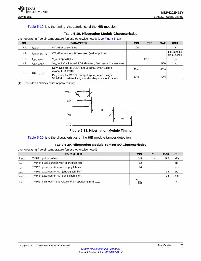
H2
H3
H4
H1WAKE
HIB
POR
VDD
75
MSP432E411Ywww.ti.com SLASEK6 –OCTOBER 2017
Submit Documentation FeedbackProduct Folder Links: MSP432E411Y
SpecificationsCopyright © 2017, Texas Instruments Incorporated
Table 5-19 lists the timing characteristics of the HIB module.
(1) Depends on characteristics of power supply.
Table 5-19. Hibernation Module Characteristicsover operating free-air temperature (unless otherwise noted) (see Figure 5-13)
NO. PARAMETER MIN TYP MAX UNITH1 tWAKE WAKE assertion time 100 ns
H2 tWAKE_TO_HIB WAKE assert to HIB desassert (wake-up time) 1 HIB moduleclock period
H3 tVDD_RAMP VDD ramp to 3.0 V See (1) µsH4 tVDD_CODE VDD at 3 V to internal POR deassert; first instruction executes 500 µs
H5 DCRTCCLK
Duty cycle for RTCCLK output signal, when using a32.768‑kHz crystal 40% 60%
Duty cycle for RTCCLK output signal, when using a32.768‑kHz external single-ended (bypass) clock source 30% 70%
Figure 5-13. Hibernation Module Timing
Table 5-20 lists the characteristics of the HIB module tamper detection.
Table 5-20. Hibernation Module Tamper I/O Characteristicsover operating free-air temperature (unless otherwise noted)
PARAMETER MIN TYP MAX UNITRTPU TMPRn pullup resistor 3.5 4.4 5.2 MΩ
tSP TMPRn pulse duration with short glitch filter 62 µstLP TMPRn pulse duration with long glitch filter 94 mstNMIS TMPRn assertion to NMI (short glitch filter) 95 µstNMIL TMPRn assertion to NMI (long glitch filter) 94 ms
VIH TMPRn high-level input voltage when operating from VBATVBAT× 0.8 V
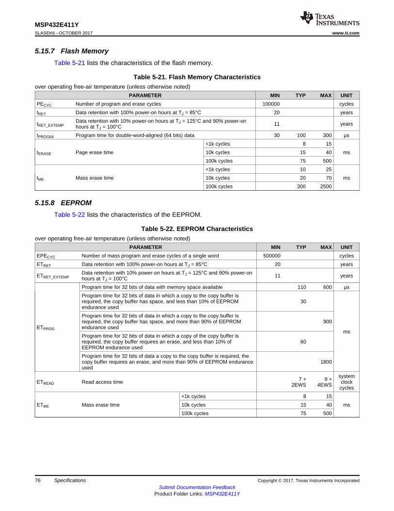
76
MSP432E411YSLASEK6 –OCTOBER 2017 www.ti.com
Submit Documentation FeedbackProduct Folder Links: MSP432E411Y
Specifications Copyright © 2017, Texas Instruments Incorporated
5.15.7 Flash MemoryTable 5-21 lists the characteristics of the flash memory.
Table 5-21. Flash Memory Characteristicsover operating free-air temperature (unless otherwise noted)
PARAMETER MIN TYP MAX UNITPECYC Number of program and erase cycles 100000 cyclestRET Data retention with 100% power-on hours at TJ = 85°C 20 years
tRET_EXTEMPData retention with 10% power-on hours at TJ = 125°C and 90% power-onhours at TJ = 100°C 11 years
tPROG64 Program time for double-word-aligned (64 bits) data 30 100 300 µs
tERASE Page erase time<1k cycles 8 15
ms10k cycles 15 40100k cycles 75 500
tME Mass erase time<1k cycles 10 25
ms10k cycles 20 70100k cycles 300 2500
5.15.8 EEPROMTable 5-22 lists the characteristics of the EEPROM.
Table 5-22. EEPROM Characteristicsover operating free-air temperature (unless otherwise noted)
PARAMETER MIN TYP MAX UNITEPECYC Number of mass program and erase cycles of a single word 500000 cyclesETRET Data retention with 100% power-on hours at TJ = 85°C 20 years
ETRET_EXTEMPData retention with 10% power-on hours at TJ = 125°C and 90% power-onhours at TJ = 100°C 11 years
ETPROG
Program time for 32 bits of data with memory space available 110 600 µsProgram time for 32 bits of data in which a copy to the copy buffer isrequired, the copy buffer has space, and less than 10% of EEPROMendurance used
30
ms
Program time for 32 bits of data in which a copy to the copy buffer isrequired, the copy buffer has space, and more than 90% of EEPROMendurance used
900
Program time for 32 bits of data in which a copy of the copy buffer isrequired, the copy buffer requires an erase, and less than 10% ofEEPROM endurance used
60
Program time for 32 bits of data a copy to the copy buffer is required, thecopy buffer requires an erase, and more than 90% of EEPROM enduranceused
1800
ETREAD Read access time 7 +2EWS
9 +4EWS
systemclockcycles
ETME Mass erase time<1k cycles 8 15
ms10k cycles 15 40100k cycles 75 500
77
MSP432E411Ywww.ti.com SLASEK6 –OCTOBER 2017
Submit Documentation FeedbackProduct Folder Links: MSP432E411Y
SpecificationsCopyright © 2017, Texas Instruments Incorporated
5.15.9 Input/Output Pin Characteristics
NOTEAll GPIO signals are 3.3-V tolerant, except for PB1 (USB0VBUS) which is 5-V tolerant. Seethe General-Purpose Input/Outputs (GPIOs) chapter of the MSP432E4 SimpleLink™Microcontrollers Technical Reference Manual for more information on GPIO configuration.
Two types of pads are provided on the device:• Fast GPIO pads: These pads provide variable, programmable drive strength and optimized voltage
output levels.• Slow GPIO pads: These pads provide 2-mA drive strength and are designed to be sensitive to voltage
inputs. The following GPIOs port pins are designed with slow GPIO pads:– PJ1
NOTEPort pins PL6 and PL7 operate as fast GPIO pads, but have 4-mA drive capability only.GPIO register controls for drive strength, slew rate, and open drain have no effect on thesepins. The following registers have no effect: GPIODR2R, GPIODR4R, GPIODR8R,GPIODR12R, GPIOSLR, and GPIOODR.
NOTEPort pins PM[7:4] operate as fast GPIO pads but support only 2-, 4-, 6-, and 8-mA drivecapability. All standard GPIO register controls, except for the GPIODR12R register, apply tothese port pins.

78
MSP432E411YSLASEK6 –OCTOBER 2017 www.ti.com
Submit Documentation FeedbackProduct Folder Links: MSP432E411Y
Specifications Copyright © 2017, Texas Instruments Incorporated
Table 5-23 lists the characteristics of the fast GPIOs.
(1) VDD must be within the range specified in Section 5.4.(2) Leakage and Injection current characteristics specified in this table also apply to XOSC0 and XOSC1 inputs.(3) For the external reference inputs of the ADC, avoid a current-limiting resistor (see the IVREF specification in Table 5-33).(4) I/O pads should be protected if the I/O voltage may go outside the limits shown in the table. If the part is unpowered, the I/O pad voltage
or current must be limited (as shown in this table) to avoid powering the part through the I/O pad, which can potentially causeirreversible damage.
(5) See the individual peripheral sections for specific loading information.(6) This value includes all GPIO except for port pins PL6 and PL7.(7) The leakage current is measured with VIN applied to the corresponding pins. The leakage of digital port pins is measured individually.
The port pin is configured as an input and the pullup/pulldown resistor is disabled.(8) If the I/O pad is not voltage limited, it should be current limited (to IINJ + and IINJ-) if there is any possibility of the pad voltage exceeding
the VIO limits (including transient behavior during supply ramp up, or at any time when the part is unpowered).(9) Time measured from 20% to 80% of VDD.(10) Time measured from 80% to 20% of VDD.
Table 5-23. Fast GPIO Module Characteristicsover operating free-air temperature (unless otherwise noted) (1) (2) (3) (4)
PARAMETER MIN TYP MAX UNITCLGPIO Capacitive loading for measurements given in this table (5) 50 pFRGPIOPU Fast GPIO internal pullup resistor (6) 12.1 16.0 20.2 kΩRGPIOPU4MA Fast GPIO PL6 and PL7 (4 mA only) pullup resistor 25 40 kΩRGPIOPD Fast GPIO internal pulldown resistor (6) 13.0 20.5 35.5 kΩRGPIOPD4MA Fast GPIO PL6 and PL7 (4 mA only) pulldown resistor 10 14.3 17 kΩ
ILKG+
Fast GPIO input leakage current, 0 V ≤ VIN ≤ VDD GPIO pins (7) 400nAFast GPIO input leakage current, 0 V < VIN ≤ VDD, fast GPIO pins configured
as ADC or analog comparator inputs 400
IINJ- DC injection current, VIN ≤ 0 V 60 µAIMAXINJ- Maximum negative injection if not voltage protected (8) –0.5 mA
tGPIOR Fast GPIO rise time (9)
2-mA drive 7.85 11.73
ns
4-mA drive 4.15 6.358-mA drive 2.33 3.738-mA drive with slew ratecontrol 3.77 5.76
10-mA drive 1.98 3.2212-mA drive 1.75 2.9
tGPIOF Fast GPIO fall time (10)
2-mA drive 10.3 16.5
ns
4-mA drive 5.15 8.298-mA drive 2.58 4.168-mA drive with slew ratecontrol 3.54 5.55
10-mA drive 2.07 3.3412-mA drive 1.73 2.78
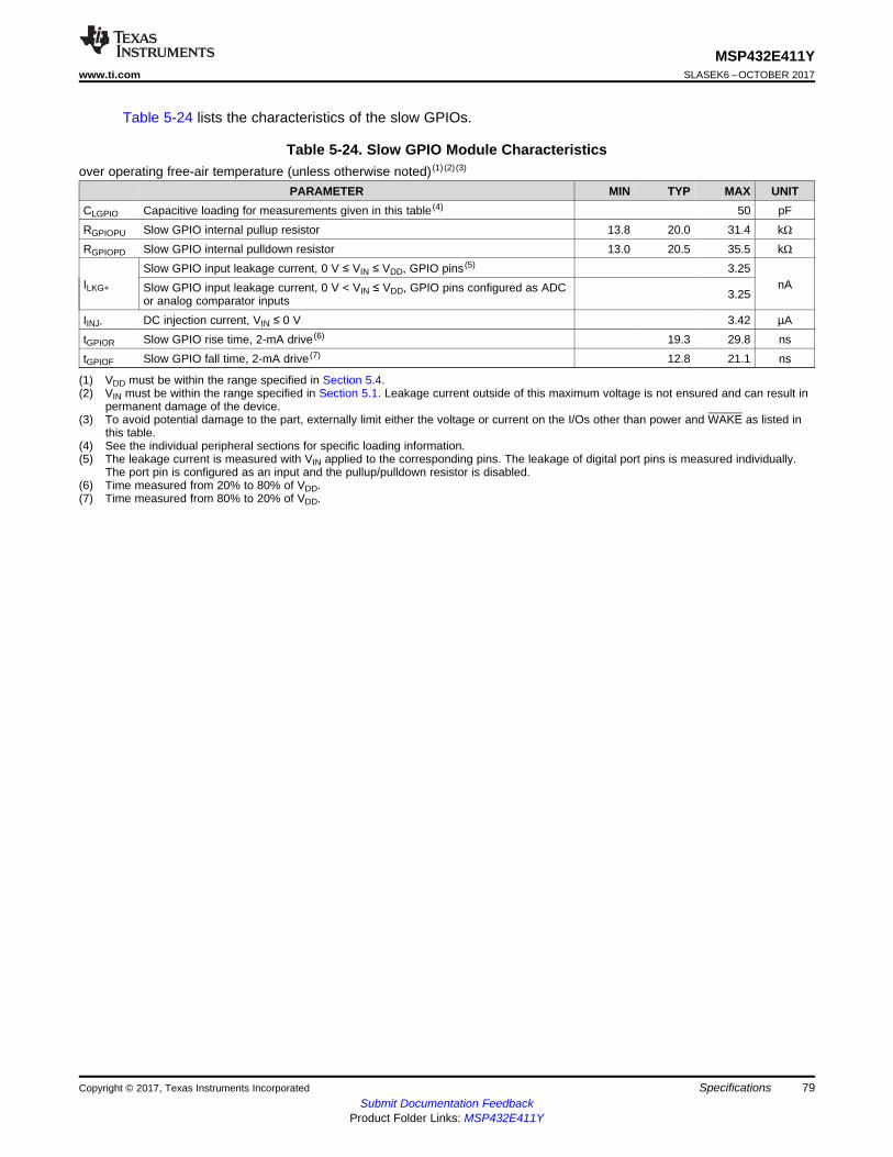
79
MSP432E411Ywww.ti.com SLASEK6 –OCTOBER 2017
Submit Documentation FeedbackProduct Folder Links: MSP432E411Y
SpecificationsCopyright © 2017, Texas Instruments Incorporated
Table 5-24 lists the characteristics of the slow GPIOs.
(1) VDD must be within the range specified in Section 5.4.(2) VIN must be within the range specified in Section 5.1. Leakage current outside of this maximum voltage is not ensured and can result in
permanent damage of the device.(3) To avoid potential damage to the part, externally limit either the voltage or current on the I/Os other than power and WAKE as listed in
this table.(4) See the individual peripheral sections for specific loading information.(5) The leakage current is measured with VIN applied to the corresponding pins. The leakage of digital port pins is measured individually.
The port pin is configured as an input and the pullup/pulldown resistor is disabled.(6) Time measured from 20% to 80% of VDD.(7) Time measured from 80% to 20% of VDD.
Table 5-24. Slow GPIO Module Characteristicsover operating free-air temperature (unless otherwise noted) (1) (2) (3)
PARAMETER MIN TYP MAX UNITCLGPIO Capacitive loading for measurements given in this table (4) 50 pFRGPIOPU Slow GPIO internal pullup resistor 13.8 20.0 31.4 kΩRGPIOPD Slow GPIO internal pulldown resistor 13.0 20.5 35.5 kΩ
ILKG+
Slow GPIO input leakage current, 0 V ≤ VIN ≤ VDD, GPIO pins (5) 3.25nASlow GPIO input leakage current, 0 V < VIN ≤ VDD, GPIO pins configured as ADC
or analog comparator inputs 3.25
IINJ- DC injection current, VIN ≤ 0 V 3.42 µAtGPIOR Slow GPIO rise time, 2-mA drive (6) 19.3 29.8 nstGPIOF Slow GPIO fall time, 2-mA drive (7) 12.8 21.1 ns
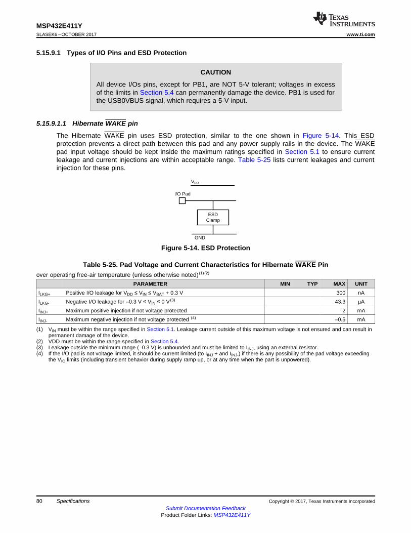
ESDClamp
I/O Pad
VDD
GND
80
MSP432E411YSLASEK6 –OCTOBER 2017 www.ti.com
Submit Documentation FeedbackProduct Folder Links: MSP432E411Y
Specifications Copyright © 2017, Texas Instruments Incorporated
5.15.9.1 Types of I/O Pins and ESD Protection
CAUTION
All device I/Os pins, except for PB1, are NOT 5-V tolerant; voltages in excessof the limits in Section 5.4 can permanently damage the device. PB1 is used forthe USB0VBUS signal, which requires a 5-V input.
5.15.9.1.1 Hibernate WAKE pin
The Hibernate WAKE pin uses ESD protection, similar to the one shown in Figure 5-14. This ESDprotection prevents a direct path between this pad and any power supply rails in the device. The WAKEpad input voltage should be kept inside the maximum ratings specified in Section 5.1 to ensure currentleakage and current injections are within acceptable range. Table 5-25 lists current leakages and currentinjection for these pins.
Figure 5-14. ESD Protection
(1) VIN must be within the range specified in Section 5.1. Leakage current outside of this maximum voltage is not ensured and can result inpermanent damage of the device.
(2) VDD must be within the range specified in Section 5.4.(3) Leakage outside the minimum range (–0.3 V) is unbounded and must be limited to IINJ- using an external resistor.(4) If the I/O pad is not voltage limited, it should be current limited (to IINJ + and IINJ-) if there is any possibility of the pad voltage exceeding
the VIO limits (including transient behavior during supply ramp up, or at any time when the part is unpowered).
Table 5-25. Pad Voltage and Current Characteristics for Hibernate WAKE Pinover operating free-air temperature (unless otherwise noted) (1) (2)
PARAMETER MIN TYP MAX UNITILKG+ Positive I/O leakage for VDD ≤ VIN ≤ VBAT + 0.3 V 300 nAILKG- Negative I/O leakage for –0.3 V ≤ VIN ≤ 0 V (3) 43.3 µAIINJ+ Maximum positive injection if not voltage protected 2 mAIINJ- Maximum negative injection if not voltage protected (4) –0.5 mA
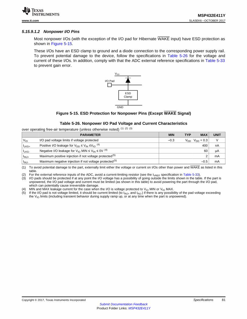
ESDClamp
I/O Pad
VDD
GND
81
MSP432E411Ywww.ti.com SLASEK6 –OCTOBER 2017
Submit Documentation FeedbackProduct Folder Links: MSP432E411Y
SpecificationsCopyright © 2017, Texas Instruments Incorporated
5.15.9.1.2 Nonpower I/O Pins
Most nonpower I/Os (with the exception of the I/O pad for Hibernate WAKE input) have ESD protection asshown in Figure 5-15.
These I/Os have an ESD clamp to ground and a diode connection to the corresponding power supply rail.To prevent potential damage to the device, follow the specifications in Table 5-26 for the voltage andcurrent of these I/Os. In addition, comply with that the ADC external reference specifications in Table 5-33to prevent gain error.
Figure 5-15. ESD Protection for Nonpower Pins (Except WAKE Signal)
(1) To avoid potential damage to the part, externally limit either the voltage or current on I/Os other than power and WAKE as listed in thistable.
(2) For the external reference inputs of the ADC, avoid a current-limiting resistor (see the IVREF specification in Table 5-33).(3) I/O pads should be protected if at any point the I/O voltage has a possibility of going outside the limits shown in the table. If the part is
unpowered, the I/O pad voltage and current must be limited (as shown in this table) to avoid powering the part through the I/O pad,which can potentially cause irreversible damage.
(4) MIN and MAX leakage current for the case when the I/O is voltage protected to VIO MIN or VIO MAX.(5) If the I/O pad is not voltage limited, it should be current limited (to IINJ+ and IINJ-) if there is any possibility of the pad voltage exceeding
the VIO limits (including transient behavior during supply ramp up, or at any time when the part is unpowered).
Table 5-26. Nonpower I/O Pad Voltage and Current Characteristicsover operating free-air temperature (unless otherwise noted) (1) (2) (3)
PARAMETER MIN TYP MAX UNITVIO I/O pad voltage limits if voltage protected –0.3 VDD VDD + 0.3 VILKG+ Positive I/O leakage for VDD ≤ VIN ≤VIO
(4) 400 nAILKG- Negative I/O leakage for VIO MIN ≤ VIN ≤ 0V (4) 60 µAIINJ+ Maximum positive injection if not voltage protected (5) 2 mAIINJ- Maximum negative injection if not voltage protected (5) –0.5 mA
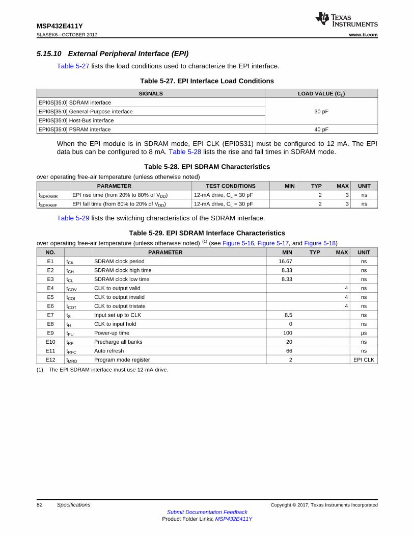
82
MSP432E411YSLASEK6 –OCTOBER 2017 www.ti.com
Submit Documentation FeedbackProduct Folder Links: MSP432E411Y
Specifications Copyright © 2017, Texas Instruments Incorporated
5.15.10 External Peripheral Interface (EPI)Table 5-27 lists the load conditions used to characterize the EPI interface.
Table 5-27. EPI Interface Load Conditions
SIGNALS LOAD VALUE (CL)EPI0S[35:0] SDRAM interface
30 pFEPI0S[35:0] General-Purpose interfaceEPI0S[35:0] Host-Bus interfaceEPI0S[35:0] PSRAM interface 40 pF
When the EPI module is in SDRAM mode, EPI CLK (EPI0S31) must be configured to 12 mA. The EPIdata bus can be configured to 8 mA. Table 5-28 lists the rise and fall times in SDRAM mode.
Table 5-28. EPI SDRAM Characteristicsover operating free-air temperature (unless otherwise noted)
PARAMETER TEST CONDITIONS MIN TYP MAX UNITtSDRAMR EPI rise time (from 20% to 80% of VDD) 12-mA drive, CL = 30 pF 2 3 nstSDRAMF EPI fall time (from 80% to 20% of VDD) 12-mA drive, CL = 30 pF 2 3 ns
Table 5-29 lists the switching characteristics of the SDRAM interface.
(1) The EPI SDRAM interface must use 12-mA drive.
Table 5-29. EPI SDRAM Interface Characteristicsover operating free-air temperature (unless otherwise noted) (1) (see Figure 5-16, Figure 5-17, and Figure 5-18)
NO. PARAMETER MIN TYP MAX UNITE1 tCK SDRAM clock period 16.67 nsE2 tCH SDRAM clock high time 8.33 nsE3 tCL SDRAM clock low time 8.33 nsE4 tCOV CLK to output valid 4 nsE5 tCOI CLK to output invalid 4 nsE6 tCOT CLK to output tristate 4 nsE7 tS Input set up to CLK 8.5 nsE8 tH CLK to input hold 0 nsE9 tPU Power-up time 100 µsE10 tRP Precharge all banks 20 nsE11 tRFC Auto refresh 66 nsE12 tMRD Program mode register 2 EPI CLK
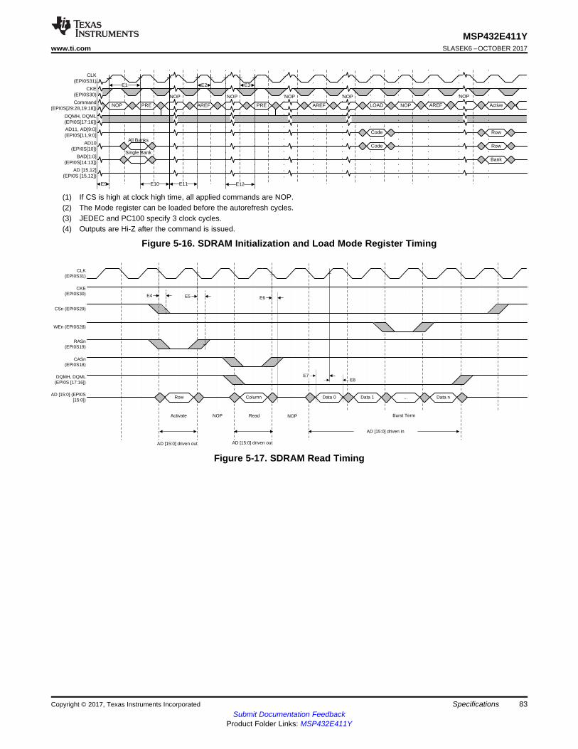
Row Column Data 0 Data 1 ... Data n
CLK(EPI0S31)
CKE(EPI0S30)
CSn (EPI0S29)
WEn (EPI0S28)
RASn (EPI0S19)
CASn (EPI0S18)
DQMH, DQML (EPI0S [17:16])
AD [15:0] (EPI0S [15:0])
Activate NOP Read NOP Burst Term
AD [15:0] driven in
AD [15:0] driven out AD [15:0] driven out
E4 E5 E6
E7E8
CLK(EPI0S31)
CKE(EPI0S30)
Command (EPI0S[29:28,19:18])
DQMH, DQML (EPI0S[17:16])
AD11, AD[9:0] (EPI0S[11,9:0]
AD10(EPI0S[10])
BAD[1:0](EPI0S[14:13])
AD [15,12] (EPI0S [15,12])
NOP PRE
NOP
AREF
NOP
PRE
NOP
AREF
NOP
LOAD
Code
All Banks
Single BankCode
E9 E10 E11 E12
E1 E2 E3
NOP AREF
NOP
Active
Row
Row
Bank
83
MSP432E411Ywww.ti.com SLASEK6 –OCTOBER 2017
Submit Documentation FeedbackProduct Folder Links: MSP432E411Y
SpecificationsCopyright © 2017, Texas Instruments Incorporated
(1) If CS is high at clock high time, all applied commands are NOP.(2) The Mode register can be loaded before the autorefresh cycles.(3) JEDEC and PC100 specify 3 clock cycles.(4) Outputs are Hi-Z after the command is issued.
Figure 5-16. SDRAM Initialization and Load Mode Register Timing
Figure 5-17. SDRAM Read Timing

Row Column-1 Data 0 Data 1 ... Data n
CLK(EPI0S31)
CKE(EPI0S30)
CSn (EPI0S29)
WEn (EPI0S28)
RASn (EPI0S19)
CASn (EPI0S18)
DQMH, DQML (EPI0S [17:16])
AD [15:0] (EPI0S [15:0])
Activate NOP Write Burst Term
AD [15:0] driven out
AD [15:0] driven out
E4 E5 E6
84
MSP432E411YSLASEK6 –OCTOBER 2017 www.ti.com
Submit Documentation FeedbackProduct Folder Links: MSP432E411Y
Specifications Copyright © 2017, Texas Instruments Incorporated
Figure 5-18. SDRAM Write Timing
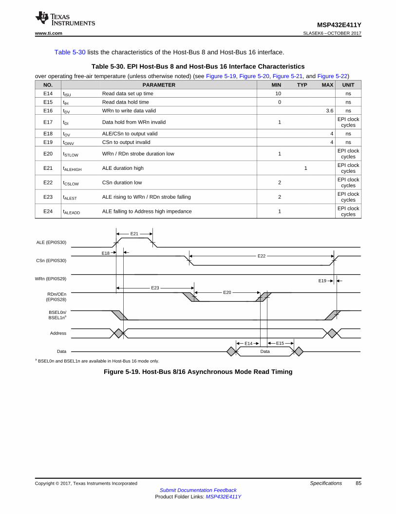
Data
ALE (EPI0S30)
CSn (EPI0S30)
WRn (EPI0S29)
RDn/OEn (EPI0S28)
Address
Data
BSEL0n/BSEL1na
a BSEL0n and BSEL1n are available in Host-Bus 16 mode only.
E21
E18E22
E19
E20
E14 E15
E23
85
MSP432E411Ywww.ti.com SLASEK6 –OCTOBER 2017
Submit Documentation FeedbackProduct Folder Links: MSP432E411Y
SpecificationsCopyright © 2017, Texas Instruments Incorporated
Table 5-30 lists the characteristics of the Host-Bus 8 and Host-Bus 16 interface.
Table 5-30. EPI Host-Bus 8 and Host-Bus 16 Interface Characteristicsover operating free-air temperature (unless otherwise noted) (see Figure 5-19, Figure 5-20, Figure 5-21, and Figure 5-22)
NO. PARAMETER MIN TYP MAX UNITE14 tISU Read data set up time 10 nsE15 tIH Read data hold time 0 nsE16 tDV WRn to write data valid 3.6 ns
E17 tDI Data hold from WRn invalid 1 EPI clockcycles
E18 tOV ALE/CSn to output valid 4 nsE19 tOINV CSn to output invalid 4 ns
E20 tSTLOW WRn / RDn strobe duration low 1 EPI clockcycles
E21 tALEHIGH ALE duration high 1 EPI clockcycles
E22 tCSLOW CSn duration low 2 EPI clockcycles
E23 tALEST ALE rising to WRn / RDn strobe falling 2 EPI clockcycles
E24 tALEADD ALE falling to Address high impedance 1 EPI clockcycles
Figure 5-19. Host-Bus 8/16 Asynchronous Mode Read Timing
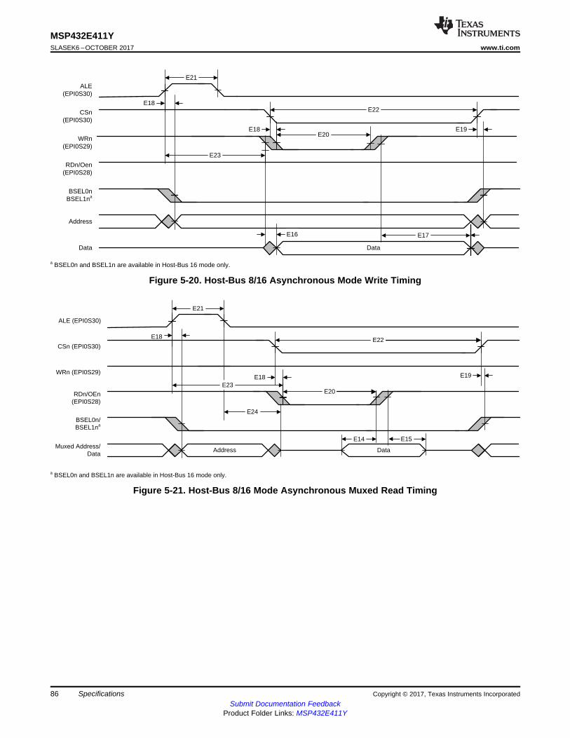
Address Data
ALE (EPI0S30)
CSn (EPI0S30)
WRn (EPI0S29)
RDn/OEn (EPI0S28)
E15
E18
E18
E14
E19
E20
E21
E22
BSEL0n/BSEL1na
Muxed Address/Data
E24
E23
a BSEL0n and BSEL1n are available in Host-Bus 16 mode only.
Data
ALE(EPI0S30)
CSn(EPI0S30)
WRn(EPI0S29)
RDn/Oen(EPI0S28)
Address
Data
E18
E18
E16
E20E19
E21
E22
E23
BSEL0nBSEL1na
a BSEL0n and BSEL1n are available in Host-Bus 16 mode only.
E17
86
MSP432E411YSLASEK6 –OCTOBER 2017 www.ti.com
Submit Documentation FeedbackProduct Folder Links: MSP432E411Y
Specifications Copyright © 2017, Texas Instruments Incorporated
Figure 5-20. Host-Bus 8/16 Asynchronous Mode Write Timing
Figure 5-21. Host-Bus 8/16 Mode Asynchronous Muxed Read Timing
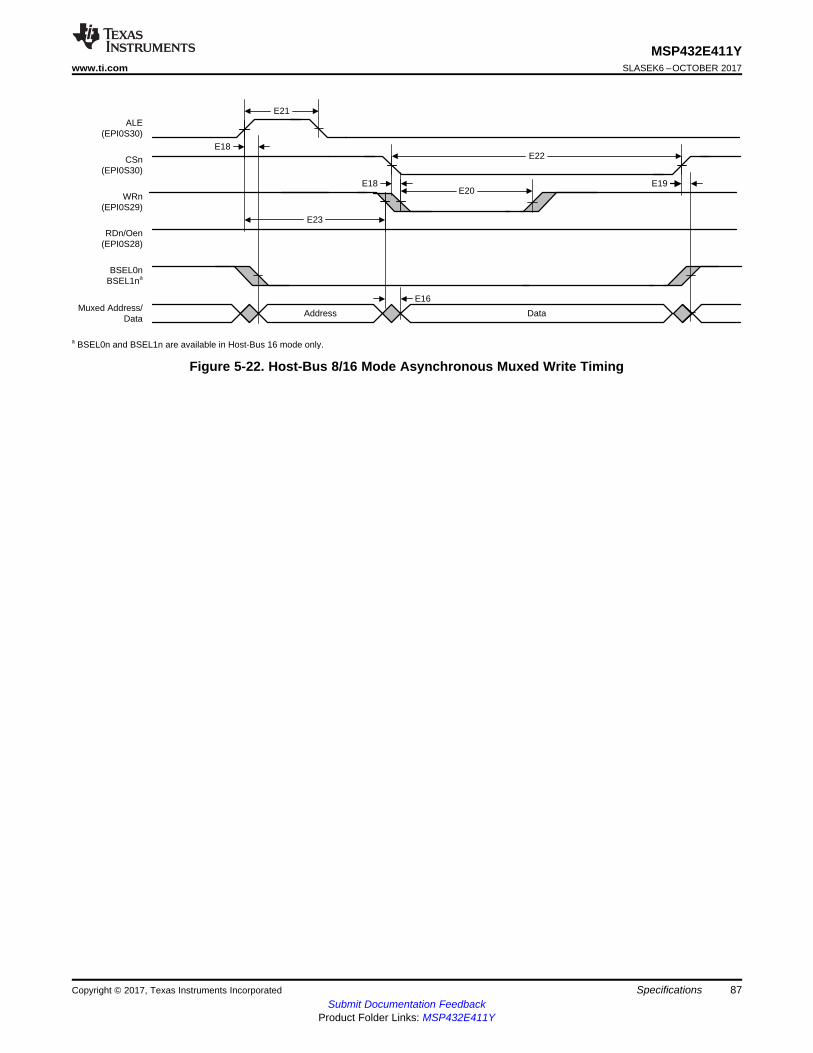
ALE(EPI0S30)
CSn(EPI0S30)
WRn(EPI0S29)
RDn/Oen(EPI0S28)
E18
E18
E16
E20E19
E21
E22
E23
BSEL0nBSEL1na
DataMuxed Address/
DataAddress
a BSEL0n and BSEL1n are available in Host-Bus 16 mode only.
87
MSP432E411Ywww.ti.com SLASEK6 –OCTOBER 2017
Submit Documentation FeedbackProduct Folder Links: MSP432E411Y
SpecificationsCopyright © 2017, Texas Instruments Incorporated
Figure 5-22. Host-Bus 8/16 Mode Asynchronous Muxed Write Timing
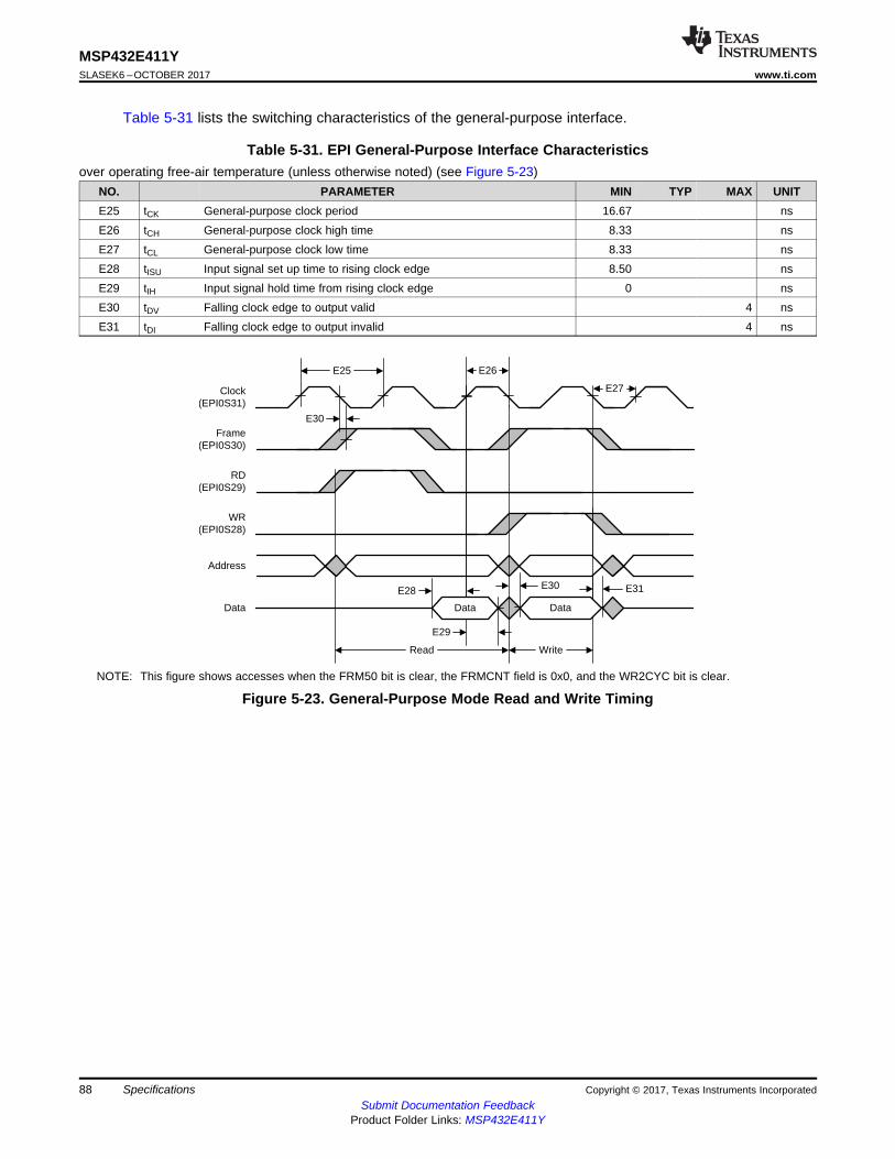
Read
E28 E31
E25
E27
E30
Clock(EPI0S31)
Frame(EPI0S30)
RD(EPI0S29)
WR(EPI0S28)
Address
Data
E29
E30
Write
Data Data
E26
88
MSP432E411YSLASEK6 –OCTOBER 2017 www.ti.com
Submit Documentation FeedbackProduct Folder Links: MSP432E411Y
Specifications Copyright © 2017, Texas Instruments Incorporated
Table 5-31 lists the switching characteristics of the general-purpose interface.
Table 5-31. EPI General-Purpose Interface Characteristicsover operating free-air temperature (unless otherwise noted) (see Figure 5-23)
NO. PARAMETER MIN TYP MAX UNITE25 tCK General-purpose clock period 16.67 nsE26 tCH General-purpose clock high time 8.33 nsE27 tCL General-purpose clock low time 8.33 nsE28 tISU Input signal set up time to rising clock edge 8.50 nsE29 tIH Input signal hold time from rising clock edge 0 nsE30 tDV Falling clock edge to output valid 4 nsE31 tDI Falling clock edge to output invalid 4 ns
NOTE: This figure shows accesses when the FRM50 bit is clear, the FRMCNT field is 0x0, and the WR2CYC bit is clear.
Figure 5-23. General-Purpose Mode Read and Write Timing
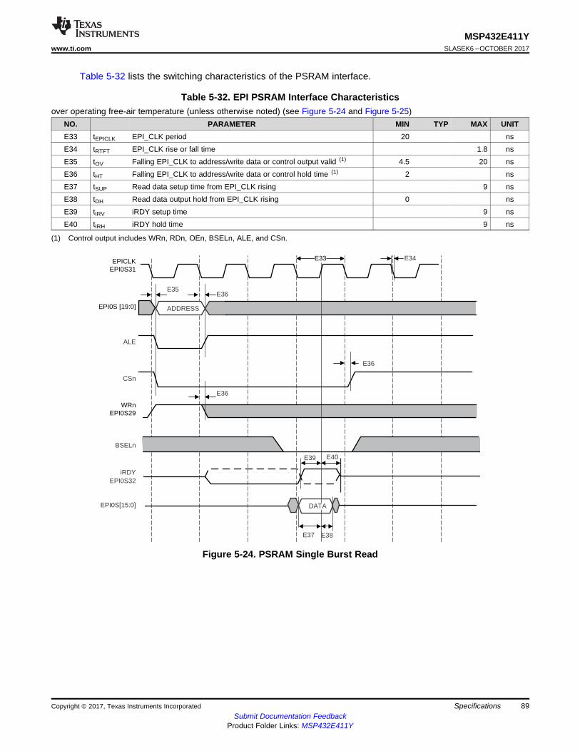
ALE
CSn
EPI0S[15:0]
ADDRESS
E34
E36
E39
BSELn
iRDYEPI0S32
DATA
E35
E40
E37 E38
E36
E36
EPICLKEPI0S31
EPI0S [19:0]
WRnEPI0S29
E33
89
MSP432E411Ywww.ti.com SLASEK6 –OCTOBER 2017
Submit Documentation FeedbackProduct Folder Links: MSP432E411Y
SpecificationsCopyright © 2017, Texas Instruments Incorporated
Table 5-32 lists the switching characteristics of the PSRAM interface.
(1) Control output includes WRn, RDn, OEn, BSELn, ALE, and CSn.
Table 5-32. EPI PSRAM Interface Characteristicsover operating free-air temperature (unless otherwise noted) (see Figure 5-24 and Figure 5-25)
NO. PARAMETER MIN TYP MAX UNITE33 tEPICLK EPI_CLK period 20 nsE34 tRTFT EPI_CLK rise or fall time 1.8 nsE35 tOV Falling EPI_CLK to address/write data or control output valid (1) 4.5 20 nsE36 tHT Falling EPI_CLK to address/write data or control hold time (1) 2 nsE37 tSUP Read data setup time from EPI_CLK rising 9 nsE38 tDH Read data output hold from EPI_CLK rising 0 nsE39 tIRV iRDY setup time 9 nsE40 tIRH iRDY hold time 9 ns
Figure 5-24. PSRAM Single Burst Read
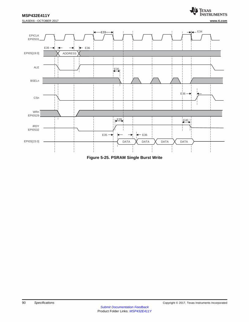
EPICLKEPI0S31
EPI0S[19:0]
ALE
CSn
EPI0S[15:0]
WRnEPI0S29
BSELn
iRDYEPI0S32
ADDRESS
DATA DATA DATA DATA
E36
E34
E35
E35
E35 E36
E36
E39 E40
E33
90
MSP432E411YSLASEK6 –OCTOBER 2017 www.ti.com
Submit Documentation FeedbackProduct Folder Links: MSP432E411Y
Specifications Copyright © 2017, Texas Instruments Incorporated
Figure 5-25. PSRAM Single Burst Write
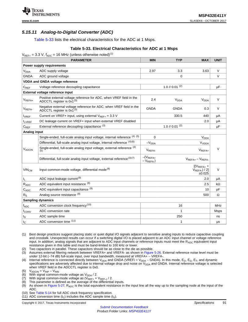
91
MSP432E411Ywww.ti.com SLASEK6 –OCTOBER 2017
Submit Documentation FeedbackProduct Folder Links: MSP432E411Y
SpecificationsCopyright © 2017, Texas Instruments Incorporated
5.15.11 Analog-to-Digital Converter (ADC)Table 5-33 lists the electrical characteristics for the ADC at 1 Msps.
(1) Best design practices suggest placing static or quiet digital I/O signals adjacent to sensitive analog inputs to reduce capacitive couplingand crosstalk. Unexpected results can occur if a switching digital I/O is placed adjacent to an ADC input channel or voltage referenceinput. In addition, analog signals that are adjacent to ADC input channels or reference inputs must meet the RADC equivalent inputresistance given in this table and must be band-limited to 100 kHz or lower.
(2) Two capacitors in parallel. These capacitors should be as close to the die as possible.(3) Assumes external filtering network between VREFA+ and VREFA- as shown in Figure 5-26. External reference noise level must be
under 12-bit (–74 dB) full-scale input, over input bandwidth, measured at VREFA+ – VREFA-.(4) Internal reference is connected directly between VDDA and GNDA (VREFi = VDDA – GNDA). In this mode, EO, EG, ET, and dynamic
specifications are adversely affected due to internal voltage drop and noise on VDDA and GNDA. Internal reference voltage is selectedwhen VREF field in the ADCCTL register is 0x0.
(5) VADCIN = VINP – VINN(6) With signal common-mode voltage as VDDA / 2.(7) With signal common-mode voltage as (VREF+ + VREF–) / 2.(8) This parameter is defined as the average of the differential inputs.(9) As shown in Figure 5-27, RADC is the total equivalent resistance in the input line all the way up to the sampling node at the input of the
ADC.(10) See Table 5-14 for full ADC clock frequency specification.(11) ADC conversion time (tC) includes the ADC sample time (tS).
Table 5-33. Electrical Characteristics for ADC at 1 MspsVREF+ = 3.3 V, fADC = 16 MHz (unless otherwise noted) (1)
PARAMETER MIN TYP MAX UNITPower supply requirementsVDDA ADC supply voltage 2.97 3.3 3.63 VGNDA ADC ground voltage 0 VVDDA and GNDA voltage referenceCREF Voltage reference decoupling capacitance 1.0 // 0.01 (2) µFExternal voltage reference input
VREFA+Positive external voltage reference for ADC, when VREF field in theADCCTL register is 0x1 (3) 2.4 VDDA VDDA V
VREFA-Negative external voltage reference for ADC, when VREF field in theADCCTL register is 0x1 (3) GNDA GNDA 0.3 V
IVREF Current on VREF+ input, using external VREF+ = 3.3 V 330.5 440 µAILVREF DC leakage current on VREF+ input when external VREF disabled 2.0 µACREF External reference decoupling capacitance (3) 1.0 // 0.01 (2) µFAnalog input
VADCIN
Single-ended, full-scale analog input voltage, internal reference (4) (5) 0 VDDA
V
Differential, full-scale analog input voltage, internal reference (4) (6) –VDDA VVDDA
Single-ended, full-scale analog input voltage, external reference (3)(5) VREFA- VREFA+
Differential, full-scale analog input voltage, external reference (3) (7) –(VREFA+– VREFA-)
VREFA+ – VREFA-
VINCM Input common-mode voltage, differential mode (8)[(VREFA+ +
VREFA-) / 2]±0.025
V
IL ADC input leakage current (9) 2.0 µARADC ADC equivalent input resistance (9) 2.5 kΩCADC ADC equivalent input capacitance (9) 10 pFRS Analog source resistance (9) 500 Ω
Sampling dynamicsfADC ADC conversion clock frequency (10) 16 MHzfCONV ADC conversion rate 1 MspstS ADC sample time 250 nstC ADC conversion time (11) 1 µs

92
MSP432E411YSLASEK6 –OCTOBER 2017 www.ti.com
Submit Documentation FeedbackProduct Folder Links: MSP432E411Y
Specifications Copyright © 2017, Texas Instruments Incorporated
Table 5-33. Electrical Characteristics for ADC at 1 Msps (continued)VREF+ = 3.3 V, fADC = 16 MHz (unless otherwise noted)(1)
PARAMETER MIN TYP MAX UNIT
(12) A low-noise environment is assumed to obtain values close to specifications. The board must have good ground isolation betweenanalog and digital grounds and a clean reference voltage. The input signal must be band-limited to Nyquist bandwidth. No antialiasingfilter is provided internally.
(13) ADC static measurements taken by averaging over several samples. At least 20-sample averaging is assumed to obtain expectedtypical or maximum specification values.
(14) 12-bit DNL(15) Gain error is measured at maximum code after compensating for offset. Gain error is equivalent to the full-scale error. It can be given
in % of slope error, or in LSB, as done here.(16) Total unadjusted error is the maximum error at any one code versus the ideal ADC curve. It includes all other errors (offset error, gain
error and INL) at any given ADC code.(17) ADC dynamic characteristics are measured using low-noise board design, with low-noise reference voltage (< –74-dB noise level in
signal bandwidth) and low-noise analog supply voltage. Board noise and ground bouncing couple into the ADC and affect dynamiccharacteristics. A clean external reference must be used to achieve the listed specifications.
(18) Differential signal with correct common-mode voltage, applied between two ADC inputs.(19) SDR = –THD in dB.(20) For higher-frequency inputs, expect degradation in SDR.(21) SNDR = S/(N+D) = SINAD (in dB)(22) Effective number of bits (ENOB) can be calculated from SNDR: ENOB = (SNDR – 1.76) / 6.02.(23) Single-ended inputs are more sensitive to board and trace noise than differential inputs; SNR and SNDR measurements on single-
ended inputs are highly dependent on how clean the test setup is. If the input signal is not well isolated on the board, higher noise thanspecified could be seen at the ADC output.
tLT Latency from trigger to start of conversion 2ADCclockcycles
System performance when using external reference (12) (13)
N Resolution 12 bitsINL Integral nonlinearity error, over full input range ±1.5 ±3.0 LSBDNL Differential nonlinearity error, over full input range ±0.8 +2.0/–1.0 (14) LSBEO Offset error ±1.0 ±3.0 LSBEG Gain error (15) ±2.0 ±3.0 LSBET Total unadjusted error, over full input range (16) ±2.5 ±4.0 LSBSystem performance when using internal referenceN Resolution 12 bitsINL Integral nonlinearity error, over full input range ±1.5 ±3.0 LSBDNL Differential nonlinearity error, over full input range ±0.8 +2.0/–1.0 (14) LSBEO Offset error ±5.0 ±15.0 LSBEG Gain error (15) ±10.0 ±30.0 LSBET Total unadjusted error, over full input range (16) ±10.0 ±30.0 LSBDynamic characteristics (12) (17)
SNRD Signal-to-noise-ratio, Differential input, VADCIN: –20 dB FS, 1 kHz (18) 70 72 dB
SDRDSignal-to-distortion ratio, Differential input, VADCIN: –3 dB FS, 1 kHz(18) (19) (20) 72 75 dB
SNDRDSignal-to-Noise+Distortion ratio, Differential input, VADCIN: –3 dB FS,1 kHz (18) (21) (22) 68 70 dB
SNRSSignal-to-noise-ratio, Single-ended input, VADCIN: –20 dB FS, 1 kHz(23) 60 65 dB
SDRSSignal-to-distortion ratio, Single-ended input, VADCIN: –3 dB FS, 1kHz (19) (20) 70 72 dB
SNDRSSignal-to-Noise+Distortion ratio, Single-ended input, VADCIN: –3 dBFS, 1 kHz (23) (21) (22) 60 63 dB
Temperature sensorVTSENS Temperature sensor voltage, junction temperature 25°C 1.633 V
STSENSTemperature sensor slope at:–40°C to 105°C ambient (extended temperature part) –13.3 mV/°C
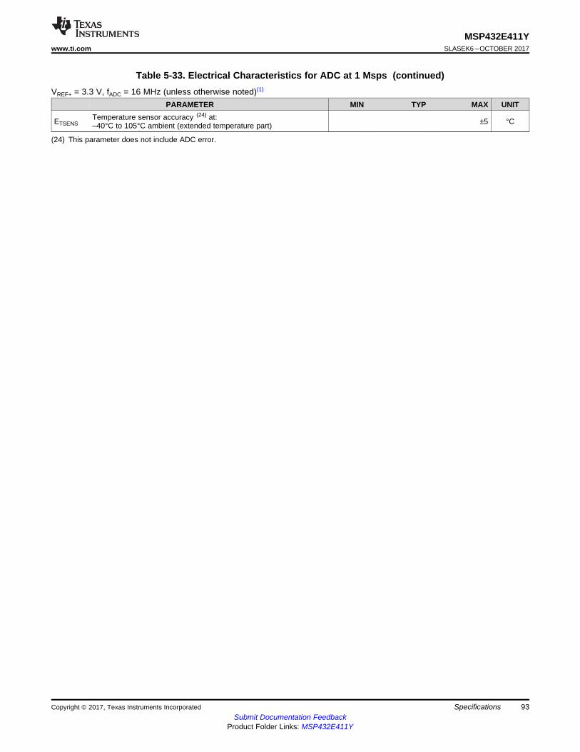
93
MSP432E411Ywww.ti.com SLASEK6 –OCTOBER 2017
Submit Documentation FeedbackProduct Folder Links: MSP432E411Y
SpecificationsCopyright © 2017, Texas Instruments Incorporated
Table 5-33. Electrical Characteristics for ADC at 1 Msps (continued)VREF+ = 3.3 V, fADC = 16 MHz (unless otherwise noted)(1)
PARAMETER MIN TYP MAX UNIT
(24) This parameter does not include ADC error.
ETSENSTemperature sensor accuracy (24) at:–40°C to 105°C ambient (extended temperature part) ±5 °C
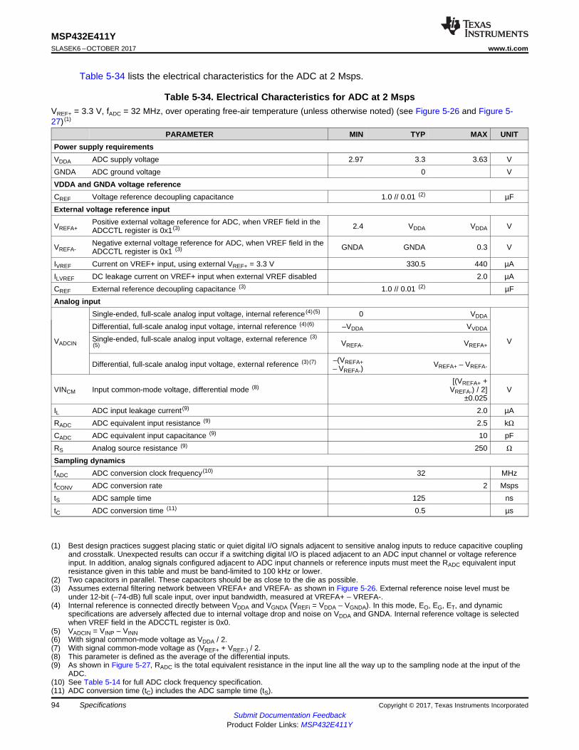
94
MSP432E411YSLASEK6 –OCTOBER 2017 www.ti.com
Submit Documentation FeedbackProduct Folder Links: MSP432E411Y
Specifications Copyright © 2017, Texas Instruments Incorporated
Table 5-34 lists the electrical characteristics for the ADC at 2 Msps.
(1) Best design practices suggest placing static or quiet digital I/O signals adjacent to sensitive analog inputs to reduce capacitive couplingand crosstalk. Unexpected results can occur if a switching digital I/O is placed adjacent to an ADC input channel or voltage referenceinput. In addition, analog signals configured adjacent to ADC input channels or reference inputs must meet the RADC equivalent inputresistance given in this table and must be band-limited to 100 kHz or lower.
(2) Two capacitors in parallel. These capacitors should be as close to the die as possible.(3) Assumes external filtering network between VREFA+ and VREFA- as shown in Figure 5-26. External reference noise level must be
under 12-bit (–74-dB) full scale input, over input bandwidth, measured at VREFA+ – VREFA-.(4) Internal reference is connected directly between VDDA and VGNDA (VREFi = VDDA – VGNDA). In this mode, EO, EG, ET, and dynamic
specifications are adversely affected due to internal voltage drop and noise on VDDA and GNDA. Internal reference voltage is selectedwhen VREF field in the ADCCTL register is 0x0.
(5) VADCIN = VINP – VINN(6) With signal common-mode voltage as VDDA / 2.(7) With signal common-mode voltage as (VREF+ + VREF-) / 2.(8) This parameter is defined as the average of the differential inputs.(9) As shown in Figure 5-27, RADC is the total equivalent resistance in the input line all the way up to the sampling node at the input of the
ADC.(10) See Table 5-14 for full ADC clock frequency specification.(11) ADC conversion time (tC) includes the ADC sample time (tS).
Table 5-34. Electrical Characteristics for ADC at 2 MspsVREF+ = 3.3 V, fADC = 32 MHz, over operating free-air temperature (unless otherwise noted) (see Figure 5-26 and Figure 5-27) (1)
PARAMETER MIN TYP MAX UNITPower supply requirementsVDDA ADC supply voltage 2.97 3.3 3.63 VGNDA ADC ground voltage 0 VVDDA and GNDA voltage referenceCREF Voltage reference decoupling capacitance 1.0 // 0.01 (2) µFExternal voltage reference input
VREFA+Positive external voltage reference for ADC, when VREF field in theADCCTL register is 0x1 (3) 2.4 VDDA VDDA V
VREFA-Negative external voltage reference for ADC, when VREF field in theADCCTL register is 0x1 (3) GNDA GNDA 0.3 V
IVREF Current on VREF+ input, using external VREF+ = 3.3 V 330.5 440 µAILVREF DC leakage current on VREF+ input when external VREF disabled 2.0 µACREF External reference decoupling capacitance (3) 1.0 // 0.01 (2) µFAnalog input
VADCIN
Single-ended, full-scale analog input voltage, internal reference (4) (5) 0 VDDA
V
Differential, full-scale analog input voltage, internal reference (4) (6) –VDDA VVDDA
Single-ended, full-scale analog input voltage, external reference (3)(5) VREFA- VREFA+
Differential, full-scale analog input voltage, external reference (3) (7) –(VREFA+– VREFA-)
VREFA+ – VREFA-
VINCM Input common-mode voltage, differential mode (8)[(VREFA+ +
VREFA-) / 2]±0.025
V
IL ADC input leakage current (9) 2.0 µARADC ADC equivalent input resistance (9) 2.5 kΩCADC ADC equivalent input capacitance (9) 10 pFRS Analog source resistance (9) 250 Ω
Sampling dynamicsfADC ADC conversion clock frequency (10) 32 MHzfCONV ADC conversion rate 2 MspstS ADC sample time 125 nstC ADC conversion time (11) 0.5 µs
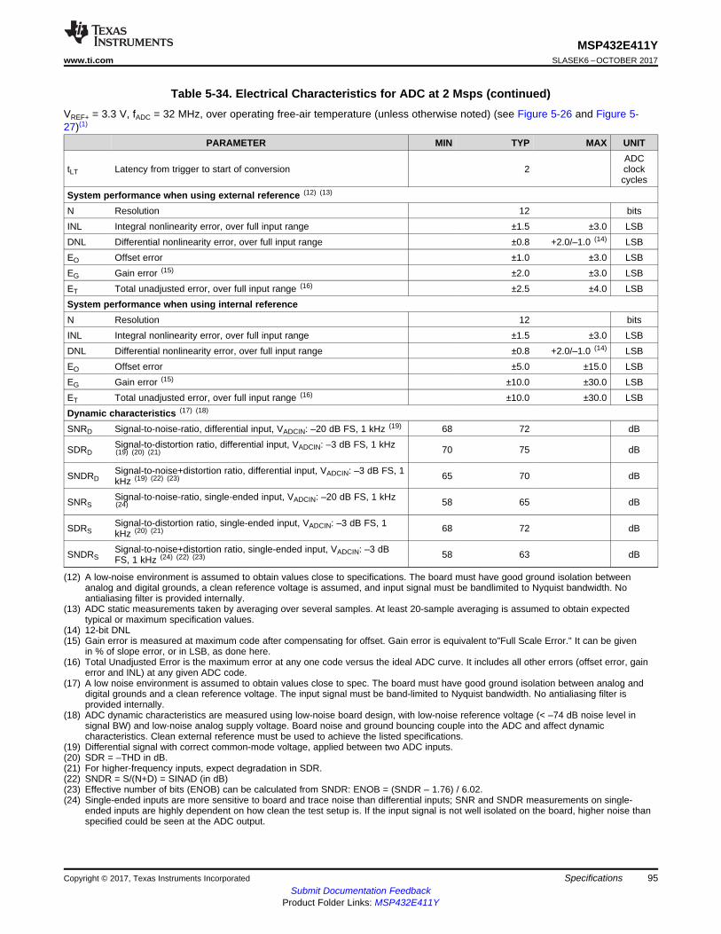
95
MSP432E411Ywww.ti.com SLASEK6 –OCTOBER 2017
Submit Documentation FeedbackProduct Folder Links: MSP432E411Y
SpecificationsCopyright © 2017, Texas Instruments Incorporated
Table 5-34. Electrical Characteristics for ADC at 2 Msps (continued)VREF+ = 3.3 V, fADC = 32 MHz, over operating free-air temperature (unless otherwise noted) (see Figure 5-26 and Figure 5-27)(1)
PARAMETER MIN TYP MAX UNIT
(12) A low-noise environment is assumed to obtain values close to specifications. The board must have good ground isolation betweenanalog and digital grounds, a clean reference voltage is assumed, and input signal must be bandlimited to Nyquist bandwidth. Noantialiasing filter is provided internally.
(13) ADC static measurements taken by averaging over several samples. At least 20-sample averaging is assumed to obtain expectedtypical or maximum specification values.
(14) 12-bit DNL(15) Gain error is measured at maximum code after compensating for offset. Gain error is equivalent to"Full Scale Error." It can be given
in % of slope error, or in LSB, as done here.(16) Total Unadjusted Error is the maximum error at any one code versus the ideal ADC curve. It includes all other errors (offset error, gain
error and INL) at any given ADC code.(17) A low noise environment is assumed to obtain values close to spec. The board must have good ground isolation between analog and
digital grounds and a clean reference voltage. The input signal must be band-limited to Nyquist bandwidth. No antialiasing filter isprovided internally.
(18) ADC dynamic characteristics are measured using low-noise board design, with low-noise reference voltage (< –74 dB noise level insignal BW) and low-noise analog supply voltage. Board noise and ground bouncing couple into the ADC and affect dynamiccharacteristics. Clean external reference must be used to achieve the listed specifications.
(19) Differential signal with correct common-mode voltage, applied between two ADC inputs.(20) SDR = –THD in dB.(21) For higher-frequency inputs, expect degradation in SDR.(22) SNDR = S/(N+D) = SINAD (in dB)(23) Effective number of bits (ENOB) can be calculated from SNDR: ENOB = (SNDR – 1.76) / 6.02.(24) Single-ended inputs are more sensitive to board and trace noise than differential inputs; SNR and SNDR measurements on single-
ended inputs are highly dependent on how clean the test setup is. If the input signal is not well isolated on the board, higher noise thanspecified could be seen at the ADC output.
tLT Latency from trigger to start of conversion 2ADCclockcycles
System performance when using external reference (12) (13)
N Resolution 12 bitsINL Integral nonlinearity error, over full input range ±1.5 ±3.0 LSBDNL Differential nonlinearity error, over full input range ±0.8 +2.0/–1.0 (14) LSBEO Offset error ±1.0 ±3.0 LSBEG Gain error (15) ±2.0 ±3.0 LSBET Total unadjusted error, over full input range (16) ±2.5 ±4.0 LSBSystem performance when using internal referenceN Resolution 12 bitsINL Integral nonlinearity error, over full input range ±1.5 ±3.0 LSBDNL Differential nonlinearity error, over full input range ±0.8 +2.0/–1.0 (14) LSBEO Offset error ±5.0 ±15.0 LSBEG Gain error (15) ±10.0 ±30.0 LSBET Total unadjusted error, over full input range (16) ±10.0 ±30.0 LSBDynamic characteristics (17) (18)
SNRD Signal-to-noise-ratio, differential input, VADCIN: –20 dB FS, 1 kHz (19) 68 72 dB
SDRDSignal-to-distortion ratio, differential input, VADCIN: –3 dB FS, 1 kHz(19) (20) (21) 70 75 dB
SNDRDSignal-to-noise+distortion ratio, differential input, VADCIN: –3 dB FS, 1kHz (19) (22) (23) 65 70 dB
SNRSSignal-to-noise-ratio, single-ended input, VADCIN: –20 dB FS, 1 kHz(24) 58 65 dB
SDRSSignal-to-distortion ratio, single-ended input, VADCIN: –3 dB FS, 1kHz (20) (21) 68 72 dB
SNDRSSignal-to-noise+distortion ratio, single-ended input, VADCIN: –3 dBFS, 1 kHz (24) (22) (23) 58 63 dB
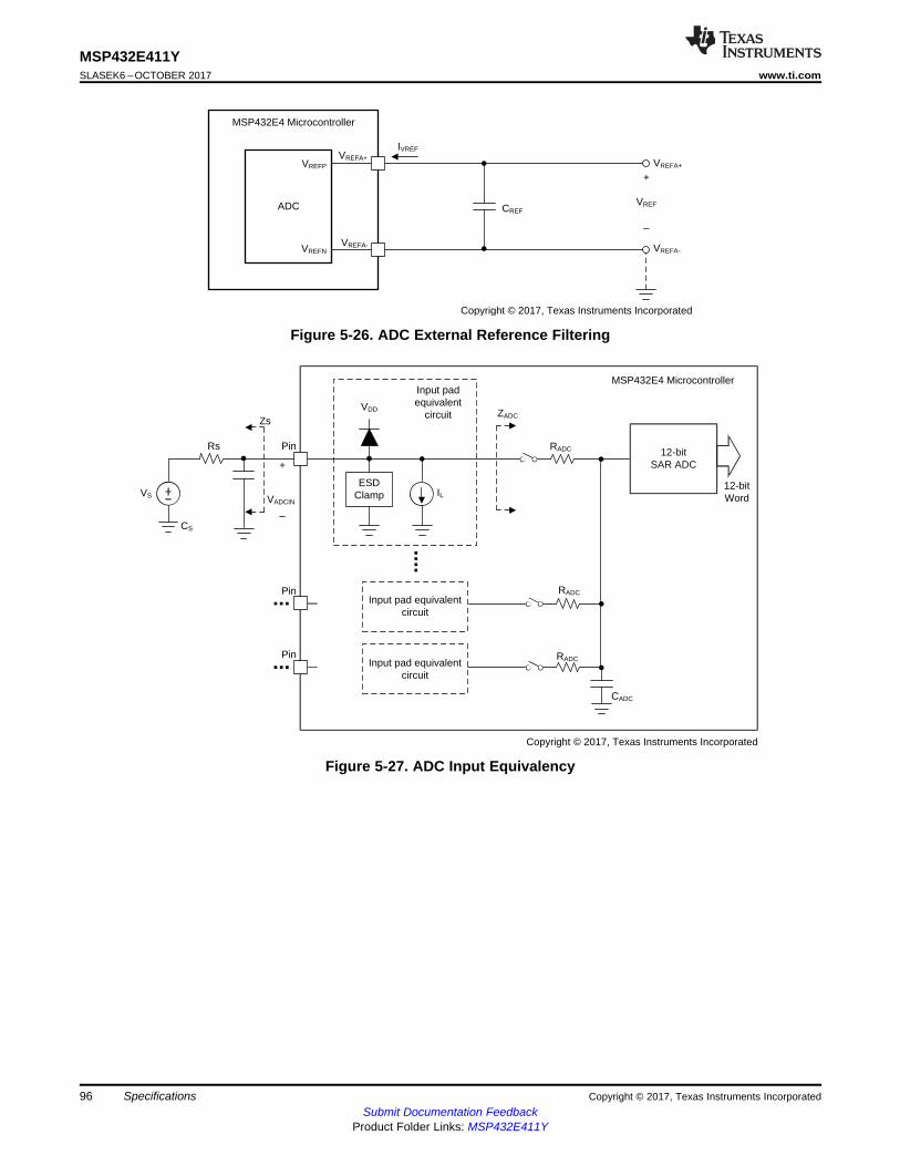
Rs Pin
IL
Zs
Input pad equivalent
circuit
12-bit SAR ADC
Pin
Pin
12-bit WordVADCIN
ESDClamp
Input pad equivalent circuit
Input pad equivalent circuit
MSP432E4 Microcontroller
CADC
RADC
RADC
RADC
ZADC
VS
CS
+
VDD
Copyright © 2017, Texas Instruments Incorporated
IVREF
CREF
VREFA-
VREFA+
VREF
+
_
ADC
VREFP
VREFN
MSP432E4 Microcontroller
VREFA+
VREFA-
Copyright © 2017, Texas Instruments Incorporated
96
MSP432E411YSLASEK6 –OCTOBER 2017 www.ti.com
Submit Documentation FeedbackProduct Folder Links: MSP432E411Y
Specifications Copyright © 2017, Texas Instruments Incorporated
Figure 5-26. ADC External Reference Filtering
Figure 5-27. ADC Input Equivalency
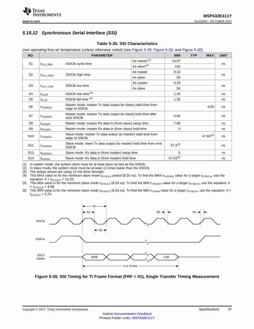
SSIClk
SSIFss
SSITxSSIRx
MSB LSB
S2
S3
S1
S5
4 to 16 bits
S4
97
MSP432E411Ywww.ti.com SLASEK6 –OCTOBER 2017
Submit Documentation FeedbackProduct Folder Links: MSP432E411Y
SpecificationsCopyright © 2017, Texas Instruments Incorporated
5.15.12 Synchronous Serial Interface (SSI)
(1) In master mode, the system clock must be at least twice as fast as the SSIClk.(2) In slave mode, the system clock must be at least 12 times faster than the SSIClk.(3) The delays shown are using 12-mA drive strength.(4) This MAX value is for the minimum slave mode tSYSCLK period (8.33 ns). To find the MAX tTXDSOV value for a larger tSYSCLK, use the
equation: 4 × tSYSCLK + 14.25.(5) This MIN value is for the minimum slave mode tSYSCLK (8.33 ns). To find the MIN tTXDSOH value for a larger tSYSCLK, use the equation: 4
× tSYSCLK + 4.08.(6) This MIN value is for the minimum slave mode tSYSCLK (8.33 ns). To find the MIN tTXDSH value for a larger tSYSCLK, use the equation: 4 ×
tSYSCLK + 3.70.
Table 5-35. SSI Characteristicsover operating free-air temperature (unless otherwise noted) (see Figure 5-28, Figure 5-29, and Figure 5-30)
NO. PARAMETER MIN TYP MAX UNIT
S1 tCLK_PER SSIClk cycle timeAs master (1) 16.67
nsAs slave (2) 100
S2 tCLK_HIGH SSIClk high timeAs master 8.33
nsAs slave 50
S3 tCLK_LOW SSIClk low timeAs master 8.33
nsAs slave 50
S4 tCLKR SSIClk rise time (3) 1.25 nsS5 tCLKF SSIClk fall time (3) 1.25 ns
S6 tTXDMOVMaster mode: master Tx data output (to slave) valid time fromedge of SSIClk 4.00 ns
S7 tTXDMOHMaster mode: master Tx data output (to slave) hold time afternext SSIClk 0.60 ns
S8 tRXDMS Master mode: master Rx data In (from slave) setup time 7.89 nsS9 tRXDMH Master mode: master Rx data In (from slave) hold time 0 ns
S10 tTXDSOVSlave mode: master Tx data output (to master) valid time fromedge of SSIClk 47.60 (4) ns
S11 tTXDSOHSlave mode: slave Tx data output (to master) hold time from nextSSIClk 37.4 (5) ns
S13 tRXDSSU Slave mode: Rx data in (from master) setup time 0 nsS14 tRXDSH Slave mode: Rx data in (from master) hold time 37.03 (6) ns
Figure 5-28. SSI Timing for TI Frame Format (FRF = 01), Single Transfer Timing Measurement
SSIClk(SPO=0)
SSITx(to master)
SSIRx( from master)
SSIClk(SPO=1)
S2
S1
S5
SSIFss
LSB
S3
S12
S10 S11
S13
MSB
S4
LSBMSB
S3
SSIClk(SPO=0)
SSITx(to slave)
SSIRx(from slave)
SSIClk(SPO=1)
S2
S1S5
SSIFss
LSB
S3
S8
S6 S7
S 9
MSB
S4
LSBMSB
98
MSP432E411YSLASEK6 –OCTOBER 2017 www.ti.com
Submit Documentation FeedbackProduct Folder Links: MSP432E411Y
Specifications Copyright © 2017, Texas Instruments Incorporated
Figure 5-29. Master Mode SSI Timing for SPI Frame Format (FRF = 00), With SPH = 1
Figure 5-30. Slave Mode SSI Timing for SPI Frame Format (FRF = 00), With SPH = 1
99
MSP432E411Ywww.ti.com SLASEK6 –OCTOBER 2017
Submit Documentation FeedbackProduct Folder Links: MSP432E411Y
SpecificationsCopyright © 2017, Texas Instruments Incorporated
Table 5-36 lists the characteristics for Bi-SSI and Quad-SSI.
(1) Parameters S15 to S23 correspond to parameters S1 to S9 in Figure 5-28 and Figure 5-29.(2) In master mode, the system clock must be at least twice as fast as the SSIClk.(3) The delays shown are using 12-mA drive strength.
Table 5-36. Bi- and Quad-SSI Characteristics (1)
over operating free-air temperature (unless otherwise noted)NO. PARAMETER MIN TYP MAX UNITS15 tCLK_PER SSIClk cycle time, as master (2) 16.67 nsS16 tCLK_HIGH SSIClk high time, as master 8.33 nsS17 tCLK_LOW SSIClk low time, as master 8.33 nsS18 tCLKR SSIClk rise time (3) 1.25 nsS19 tCLKF SSIClk fall time (3) 1.25 ns
S20 tTXDMOVMaster mode: master SSInXDATn data output (to slave) valid timefrom edge of SSIClk 4.04 ns
S21 tTXDMOHMaster mode: master SSInXDATn data output (to slave) hold timeafter next SSIClk 0.60 ns
S22 tRXDMS Master mode: master SSInXDATn data in (from slave) setup time 5.78 nsS23 tRXDMH Master mode: master SSInXDATn data in (from slave) hold time 0 ns
I2CSCL
I2CSDA
I1
I2 I6
I7 I8
I5
I3 I9I4
I10
100
MSP432E411YSLASEK6 –OCTOBER 2017 www.ti.com
Submit Documentation FeedbackProduct Folder Links: MSP432E411Y
Specifications Copyright © 2017, Texas Instruments Incorporated
5.15.13 Inter-Integrated Circuit (I2C) InterfaceTable 5-37 lists the characteristics for the I2C interface.
(1) Values depend on the value programmed into the TPR bit in the I2C Master Timer Period (I2CMTPR) register; a TPR programmed forthe maximum I2CSCL frequency (TPR = 0x2) results in a minimum output timing listed in this table. The I2C interface is designed toscale the actual data transition time to move it to the middle of the I2CSCL low period. The actual position is affected by the valueprogrammed into the TPR; however, the values in this table are minimum values.
(2) Because I2CSCL and I2CSDA operate as open-drain-type signals, which the controller can only actively drive low, the time I2CSCL orI2CSDA takes to reach a high level depends on external signal capacitance and pullup resistor values.
(3) Specified at a nominal 50-pF load
Table 5-37. I2C Characteristicsover operating free-air temperature (unless otherwise noted) (see Figure 5-31)
NO. PARAMETER MIN TYP MAX UNIT
I1 (1) tSCH Start condition hold time 36systemclockcycles
I2 (1) tLP Clock low period 36systemclockcycles
I3 (2) tSRT I2CSCL and I2CSDA rise time (VIL = 0.5 V to V IH = 2.4 V) See (2) ns
I4 tDH Data hold timeSlave 2 system
clockcyclesMaster 7
I5 (3) tSFT I2CSCL and I2CSDA fall time (VIH = 2.4 V to V IL = 0.5 V) 9 10 ns
I6 (1) tHT Clock high time 24systemclockcycles
I7 tDS Data setup time 18systemclockcycles
I8 (1) tSCSR Start condition setup time (for repeated start condition only) 36systemclockcycles
I9 (1) tSCS Stop condition setup time 24systemclockcycles
I10 tDV Data valid
Slave 2systemclockcycles
Master(6 × (1 +TPR)) +
1
systemclockcycles
Figure 5-31. I2C Timing

OSC0
N1
101
MSP432E411Ywww.ti.com SLASEK6 –OCTOBER 2017
Submit Documentation FeedbackProduct Folder Links: MSP432E411Y
SpecificationsCopyright © 2017, Texas Instruments Incorporated
5.15.14 Ethernet Controller
5.15.14.1 DC Characteristics
The parameters listed in Table 5-38, with the exception of RBIAS, apply to transmit pins of the EthernetPHY, which are generally the EN0TXOP and EN0TXON signals during standard operation but can also bethe EN0RXIN and EN0RXIP signals if Auto-MDIX is enabled.
Table 5-38. Ethernet PHY DC Characteristicsover operating free-air temperature (unless otherwise noted)
PARAMETER MIN TYP MAX UNITRBIAS Value of the pulldown resistor on the RBIAS pin 4.82 4.87 4.92 kΩVTPTD_100 100M transmit voltage 0.95 1 1.05 VVTPTDSYM 100M transmit voltage symmetry –2% 2%VOVRSHT Output overshoot 5%VTPTD_10 10M transmit voltage 2.2 2.5 2.8 VVTH1 10Base-T Receive threshold 200 mV
5.15.14.2 Clock Characteristics for Ethernet
Table 5-39 lists the specifications of the MOSC 25-MHz crystal.
(1) See Table 5-12 for additional MOSC requirements.
Table 5-39. MOSC 25-MHz Crystal Specification (1)
over operating free-air temperature (unless otherwise noted) (see Figure 5-32)NO. PARAMETER MIN TYP MAX UNITN1 fMOSC25 Frequency 25 MHz
fTOL Frequency tolerance at operational temperature 0 ±50 ppmfSTA Frequency stability at 1-year aging ±5 ppm
Figure 5-32. MOSC Crystal Characteristics for Ethernet
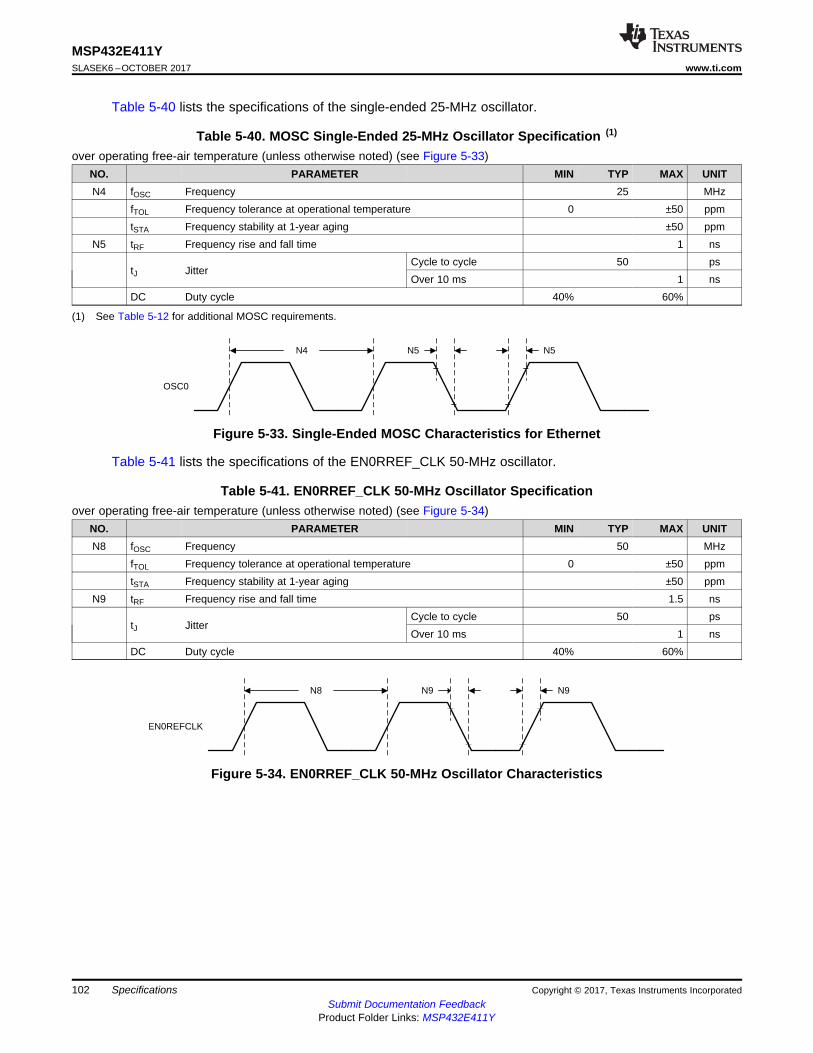
EN0REFCLK
N8 N9 N9
OSC0
N4 N5 N5
102
MSP432E411YSLASEK6 –OCTOBER 2017 www.ti.com
Submit Documentation FeedbackProduct Folder Links: MSP432E411Y
Specifications Copyright © 2017, Texas Instruments Incorporated
Table 5-40 lists the specifications of the single-ended 25-MHz oscillator.
(1) See Table 5-12 for additional MOSC requirements.
Table 5-40. MOSC Single-Ended 25-MHz Oscillator Specification (1)
over operating free-air temperature (unless otherwise noted) (see Figure 5-33)NO. PARAMETER MIN TYP MAX UNITN4 fOSC Frequency 25 MHz
fTOL Frequency tolerance at operational temperature 0 ±50 ppmtSTA Frequency stability at 1-year aging ±50 ppm
N5 tRF Frequency rise and fall time 1 ns
tJ JitterCycle to cycle 50 psOver 10 ms 1 ns
DC Duty cycle 40% 60%
Figure 5-33. Single-Ended MOSC Characteristics for Ethernet
Table 5-41 lists the specifications of the EN0RREF_CLK 50-MHz oscillator.
Table 5-41. EN0RREF_CLK 50-MHz Oscillator Specificationover operating free-air temperature (unless otherwise noted) (see Figure 5-34)
NO. PARAMETER MIN TYP MAX UNITN8 fOSC Frequency 50 MHz
fTOL Frequency tolerance at operational temperature 0 ±50 ppmtSTA Frequency stability at 1-year aging ±50 ppm
N9 tRF Frequency rise and fall time 1.5 ns
tJ JitterCycle to cycle 50 psOver 10 ms 1 ns
DC Duty cycle 40% 60%
Figure 5-34. EN0RREF_CLK 50-MHz Oscillator Characteristics
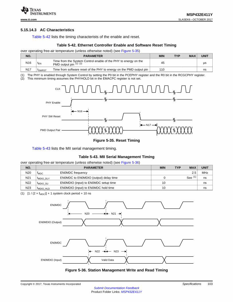
EN0MDC
EN0MDIO (Input) Valid Data
N23N22
EN0MDC
EN0MDIO (Output)
N20 N21
CLK
N16
PMD Output Pair
PHY Enable
PHY SW Reset
N17
103
MSP432E411Ywww.ti.com SLASEK6 –OCTOBER 2017
Submit Documentation FeedbackProduct Folder Links: MSP432E411Y
SpecificationsCopyright © 2017, Texas Instruments Incorporated
(1) The PHY is enabled through System Control by setting the P0 bit in the PCEPHY register and the R0 bit in the RCGCPHY register.(2) This minimum timing assumes the PHYHOLD bit in the EMACPC register is not set.
5.15.14.3 AC Characteristics
Table 5-42 lists the timing characterists of the enable and reset.
Table 5-42. Ethernet Controller Enable and Software Reset Timingover operating free-air temperature (unless otherwise noted) (see Figure 5-35)
NO. PARAMETER MIN TYP MAX UNIT
N16 tENTime from the System Control enable of the PHY to energy on thePMD output pin (1) (2) 45 µs
N17 tSWRST Time from software reset of the PHY to energy on the PMD output pin 110 ns
(1) [1 / (2 × fMDC)] + 1 system clock period + 10 ns
Figure 5-35. Reset Timing
Table 5-43 lists the MII serial management timing.
Table 5-43. MII Serial Management Timingover operating free-air temperature (unless otherwise noted) (see Figure 5-36)
NO. PARAMETER MIN TYP MAX UNITN20 fMDC EN0MDC frequency 2.5 MHzN21 tMDIO_DLY EN0MDC to EN0MDIO (output) delay time 0 See (1) nsN22 tMDIO_SU EN0MDIO (input) to EN0MDC setup time 10 nsN23 tMDIO_HLD EN0MDIO (input) to EN0MDC hold time 10 ns
Figure 5-36. Station Management Write and Read Timing
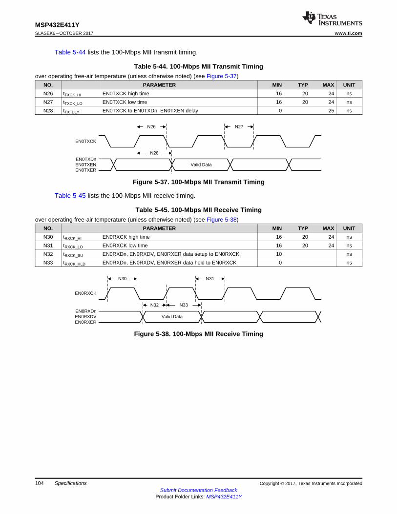
EN0RXCK
EN0RXDnEN0RXDVEN0RXER
Valid Data
N30 N31
N33N32
EN0TXCK
EN0TXDnEN0TXENEN0TXER
Valid Data
N26 N27
N28
104
MSP432E411YSLASEK6 –OCTOBER 2017 www.ti.com
Submit Documentation FeedbackProduct Folder Links: MSP432E411Y
Specifications Copyright © 2017, Texas Instruments Incorporated
Table 5-44 lists the 100-Mbps MII transmit timing.
Table 5-44. 100-Mbps MII Transmit Timingover operating free-air temperature (unless otherwise noted) (see Figure 5-37)
NO. PARAMETER MIN TYP MAX UNITN26 tTXCK_HI EN0TXCK high time 16 20 24 nsN27 tTXCK_LO EN0TXCK low time 16 20 24 nsN28 tTX_DLY EN0TXCK to EN0TXDn, EN0TXEN delay 0 25 ns
Figure 5-37. 100-Mbps MII Transmit Timing
Table 5-45 lists the 100-Mbps MII receive timing.
Table 5-45. 100-Mbps MII Receive Timingover operating free-air temperature (unless otherwise noted) (see Figure 5-38)
NO. PARAMETER MIN TYP MAX UNITN30 tRXCK_HI EN0RXCK high time 16 20 24 nsN31 tRXCK_LO EN0RXCK low time 16 20 24 nsN32 tRXCK_SU EN0RXDn, EN0RXDV, EN0RXER data setup to EN0RXCK 10 nsN33 tRXCK_HLD EN0RXDn, EN0RXDV, EN0RXER data hold to EN0RXCK 0 ns
Figure 5-38. 100-Mbps MII Receive Timing
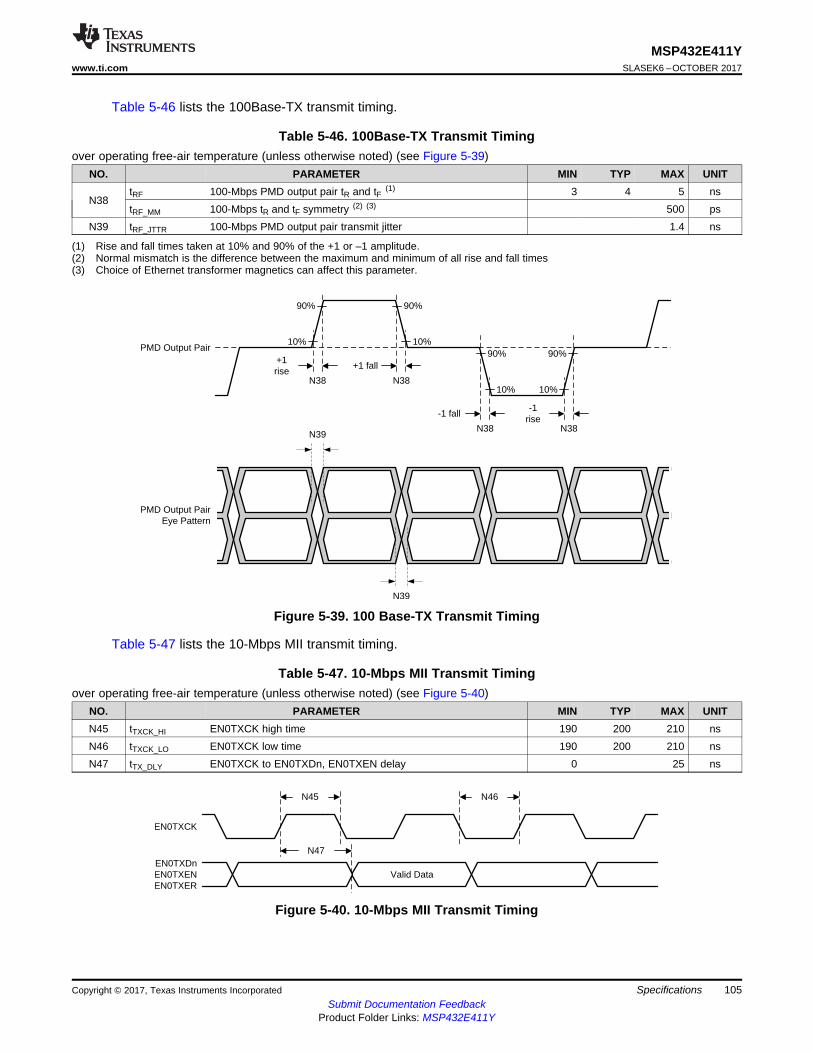
EN0TXCK
EN0TXDnEN0TXENEN0TXER
Valid Data
N45 N46
N47
N39
N39
PMD Output PairEye Pattern
N38
PMD Output Pair
90%
10%90%
10%
90%
10%
90%
10%
N38
N38 N38
+1 rise
+1 fall
-1 fall-1
rise
105
MSP432E411Ywww.ti.com SLASEK6 –OCTOBER 2017
Submit Documentation FeedbackProduct Folder Links: MSP432E411Y
SpecificationsCopyright © 2017, Texas Instruments Incorporated
(1) Rise and fall times taken at 10% and 90% of the +1 or –1 amplitude.(2) Normal mismatch is the difference between the maximum and minimum of all rise and fall times(3) Choice of Ethernet transformer magnetics can affect this parameter.
Table 5-46 lists the 100Base-TX transmit timing.
Table 5-46. 100Base-TX Transmit Timingover operating free-air temperature (unless otherwise noted) (see Figure 5-39)
NO. PARAMETER MIN TYP MAX UNIT
N38tRF 100-Mbps PMD output pair tR and tF (1) 3 4 5 nstRF_MM 100-Mbps tR and tF symmetry (2) (3) 500 ps
N39 tRF_JTTR 100-Mbps PMD output pair transmit jitter 1.4 ns
Figure 5-39. 100 Base-TX Transmit Timing
Table 5-47 lists the 10-Mbps MII transmit timing.
Table 5-47. 10-Mbps MII Transmit Timingover operating free-air temperature (unless otherwise noted) (see Figure 5-40)
NO. PARAMETER MIN TYP MAX UNITN45 tTXCK_HI EN0TXCK high time 190 200 210 nsN46 tTXCK_LO EN0TXCK low time 190 200 210 nsN47 tTX_DLY EN0TXCK to EN0TXDn, EN0TXEN delay 0 25 ns
Figure 5-40. 10-Mbps MII Transmit Timing
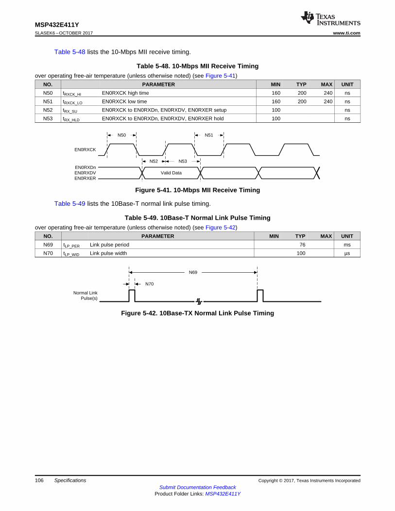
N70
Normal Link Pulse(s)
N69
EN0RXCK
EN0RXDnEN0RXDVEN0RXER
Valid Data
N50 N51
N53N52
106
MSP432E411YSLASEK6 –OCTOBER 2017 www.ti.com
Submit Documentation FeedbackProduct Folder Links: MSP432E411Y
Specifications Copyright © 2017, Texas Instruments Incorporated
Table 5-48 lists the 10-Mbps MII receive timing.
Table 5-48. 10-Mbps MII Receive Timingover operating free-air temperature (unless otherwise noted) (see Figure 5-41)
NO. PARAMETER MIN TYP MAX UNITN50 tRXCK_HI EN0RXCK high time 160 200 240 nsN51 tRXCK_LO EN0RXCK low time 160 200 240 nsN52 tRX_SU EN0RXCK to EN0RXDn, EN0RXDV, EN0RXER setup 100 nsN53 tRX_HLD EN0RXCK to EN0RXDn, EN0RXDV, EN0RXER hold 100 ns
Figure 5-41. 10-Mbps MII Receive Timing
Table 5-49 lists the 10Base-T normal link pulse timing.
Table 5-49. 10Base-T Normal Link Pulse Timingover operating free-air temperature (unless otherwise noted) (see Figure 5-42)
NO. PARAMETER MIN TYP MAX UNITN69 tLP_PER Link pulse period 76 msN70 tLP_WID Link pulse width 100 µs
Figure 5-42. 10Base-TX Normal Link Pulse Timing
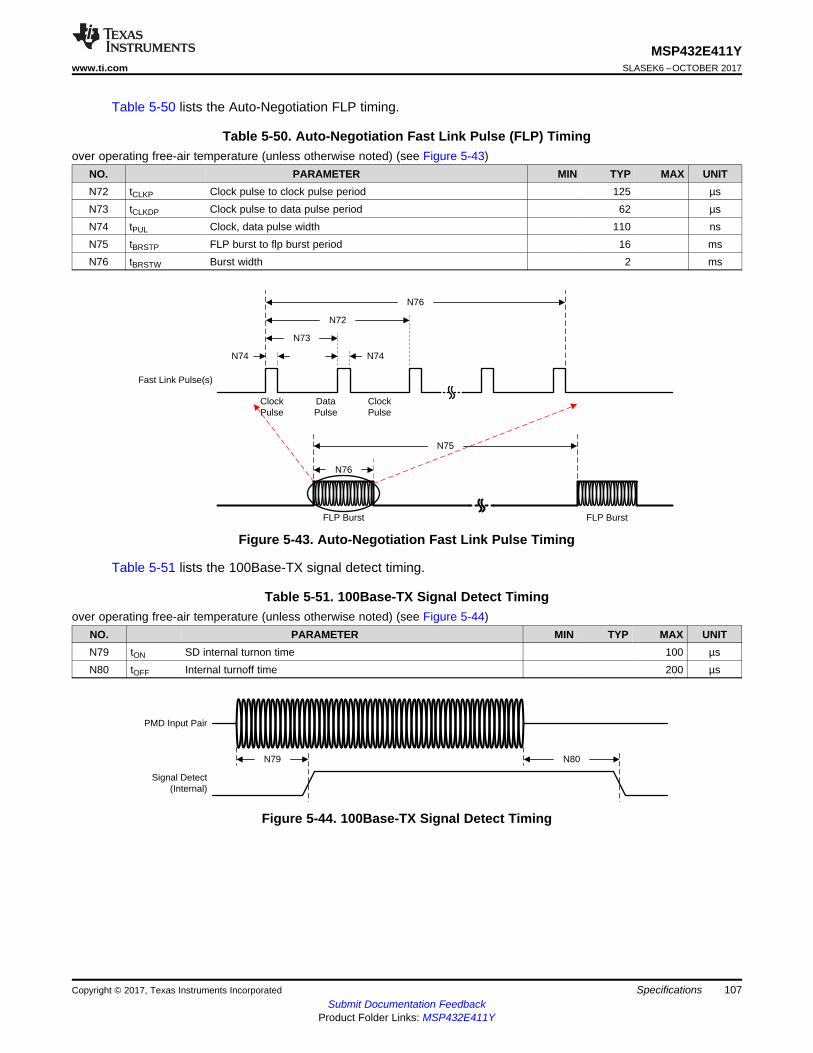
N79
PMD Input Pair
Signal Detect (Internal)
N80
Fast Link Pulse(s)
N75
FLP Burst
Clock Pulse
Data Pulse
Clock Pulse
N74 N74
N73
N72
FLP Burst
N76
N76
107
MSP432E411Ywww.ti.com SLASEK6 –OCTOBER 2017
Submit Documentation FeedbackProduct Folder Links: MSP432E411Y
SpecificationsCopyright © 2017, Texas Instruments Incorporated
Table 5-50 lists the Auto-Negotiation FLP timing.
Table 5-50. Auto-Negotiation Fast Link Pulse (FLP) Timingover operating free-air temperature (unless otherwise noted) (see Figure 5-43)
NO. PARAMETER MIN TYP MAX UNITN72 tCLKP Clock pulse to clock pulse period 125 µsN73 tCLKDP Clock pulse to data pulse period 62 µsN74 tPUL Clock, data pulse width 110 nsN75 tBRSTP FLP burst to flp burst period 16 msN76 tBRSTW Burst width 2 ms
Figure 5-43. Auto-Negotiation Fast Link Pulse Timing
Table 5-51 lists the 100Base-TX signal detect timing.
Table 5-51. 100Base-TX Signal Detect Timingover operating free-air temperature (unless otherwise noted) (see Figure 5-44)
NO. PARAMETER MIN TYP MAX UNITN79 tON SD internal turnon time 100 µsN80 tOFF Internal turnoff time 200 µs
Figure 5-44. 100Base-TX Signal Detect Timing
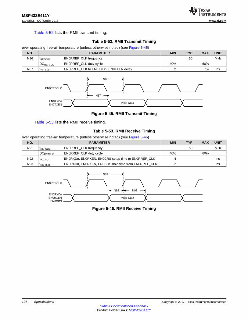
EN0REFCLK
EN0RXDnEN0RXEN
EN0CRSValid Data
N91
N92 N93
EN0REFCLK
EN0TXDnEN0TXEN
Valid Data
N86
N87
108
MSP432E411YSLASEK6 –OCTOBER 2017 www.ti.com
Submit Documentation FeedbackProduct Folder Links: MSP432E411Y
Specifications Copyright © 2017, Texas Instruments Incorporated
Table 5-52 lists the RMII transmit timing.
Table 5-52. RMII Transmit Timingover operating free-air temperature (unless otherwise noted) (see Figure 5-45)
NO. PARAMETER MIN TYP MAX UNITN86 fREFCLK EN0RREF_CLK frequency 50 MHz
DCREFCLK EN0RREF_CLK duty cycle 40% 60%N87 tTX_DLY EN0RREF_CLK to EN0TXDn, EN0TXEN delay 2 14 ns
Figure 5-45. RMII Transmit Timing
Table 5-53 lists the RMII receive timing.
Table 5-53. RMII Receive Timingover operating free-air temperature (unless otherwise noted) (see Figure 5-46)
NO. PARAMETER MIN TYP MAX UNITN91 fREFCLK EN0RREF_CLK frequency 50 MHz
DCREFCLK EN0RREF_CLK duty cycle 40% 60%N92 tRX_SU EN0RXDn, EN0RXEN, EN0CRS setup time to EN0RREF_CLK 4 nsN93 tRX_HLD EN0RXDn, EN0RXEN, EN0CRS hold time from EN0RREF_CLK 2 ns
Figure 5-46. RMII Receive Timing
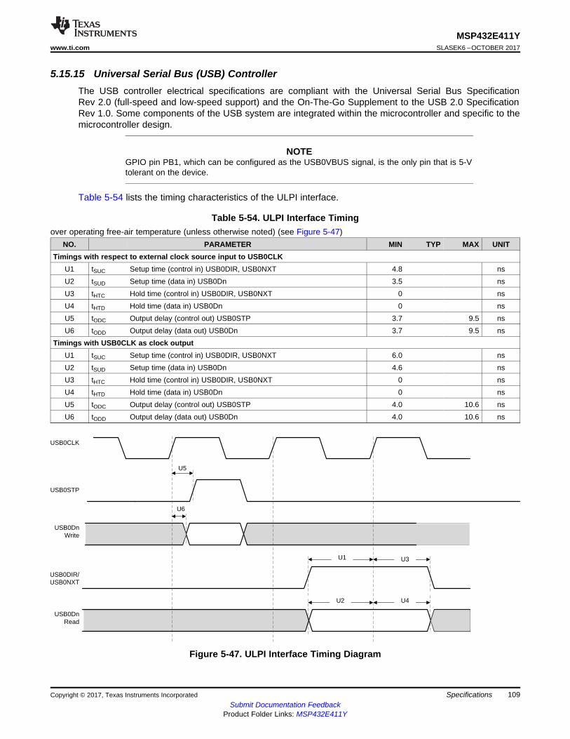
USB0CLK
USB0STP
USB0Dn Write
USB0DIR/USB0NXT
USB0Dn Read
U1
U2
U3
U4
U5
U6
109
MSP432E411Ywww.ti.com SLASEK6 –OCTOBER 2017
Submit Documentation FeedbackProduct Folder Links: MSP432E411Y
SpecificationsCopyright © 2017, Texas Instruments Incorporated
5.15.15 Universal Serial Bus (USB) ControllerThe USB controller electrical specifications are compliant with the Universal Serial Bus SpecificationRev 2.0 (full-speed and low-speed support) and the On-The-Go Supplement to the USB 2.0 SpecificationRev 1.0. Some components of the USB system are integrated within the microcontroller and specific to themicrocontroller design.
NOTEGPIO pin PB1, which can be configured as the USB0VBUS signal, is the only pin that is 5-Vtolerant on the device.
Table 5-54 lists the timing characteristics of the ULPI interface.
Table 5-54. ULPI Interface Timingover operating free-air temperature (unless otherwise noted) (see Figure 5-47)
NO. PARAMETER MIN TYP MAX UNITTimings with respect to external clock source input to USB0CLK
U1 tSUC Setup time (control in) USB0DIR, USB0NXT 4.8 nsU2 tSUD Setup time (data in) USB0Dn 3.5 nsU3 tHTC Hold time (control in) USB0DIR, USB0NXT 0 nsU4 tHTD Hold time (data in) USB0Dn 0 nsU5 tODC Output delay (control out) USB0STP 3.7 9.5 nsU6 tODD Output delay (data out) USB0Dn 3.7 9.5 ns
Timings with USB0CLK as clock outputU1 tSUC Setup time (control in) USB0DIR, USB0NXT 6.0 nsU2 tSUD Setup time (data in) USB0Dn 4.6 nsU3 tHTC Hold time (control in) USB0DIR, USB0NXT 0 nsU4 tHTD Hold time (data in) USB0Dn 0 nsU5 tODC Output delay (control out) USB0STP 4.0 10.6 nsU6 tODD Output delay (data out) USB0Dn 4.0 10.6 ns
Figure 5-47. ULPI Interface Timing Diagram
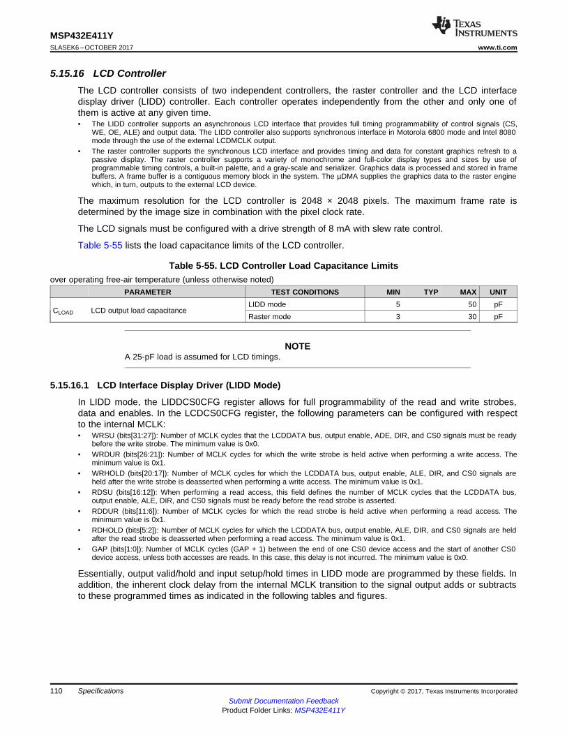
110
MSP432E411YSLASEK6 –OCTOBER 2017 www.ti.com
Submit Documentation FeedbackProduct Folder Links: MSP432E411Y
Specifications Copyright © 2017, Texas Instruments Incorporated
5.15.16 LCD ControllerThe LCD controller consists of two independent controllers, the raster controller and the LCD interfacedisplay driver (LIDD) controller. Each controller operates independently from the other and only one ofthem is active at any given time.• The LIDD controller supports an asynchronous LCD interface that provides full timing programmability of control signals (CS,
WE, OE, ALE) and output data. The LIDD controller also supports synchronous interface in Motorola 6800 mode and Intel 8080mode through the use of the external LCDMCLK output.
• The raster controller supports the synchronous LCD interface and provides timing and data for constant graphics refresh to apassive display. The raster controller supports a variety of monochrome and full-color display types and sizes by use ofprogrammable timing controls, a built-in palette, and a gray-scale and serializer. Graphics data is processed and stored in framebuffers. A frame buffer is a contiguous memory block in the system. The µDMA supplies the graphics data to the raster enginewhich, in turn, outputs to the external LCD device.
The maximum resolution for the LCD controller is 2048 × 2048 pixels. The maximum frame rate isdetermined by the image size in combination with the pixel clock rate.
The LCD signals must be configured with a drive strength of 8 mA with slew rate control.
Table 5-55 lists the load capacitance limits of the LCD controller.
Table 5-55. LCD Controller Load Capacitance Limitsover operating free-air temperature (unless otherwise noted)
PARAMETER TEST CONDITIONS MIN TYP MAX UNIT
CLOAD LCD output load capacitanceLIDD mode 5 50 pFRaster mode 3 30 pF
NOTEA 25-pF load is assumed for LCD timings.
5.15.16.1 LCD Interface Display Driver (LIDD Mode)
In LIDD mode, the LIDDCS0CFG register allows for full programmability of the read and write strobes,data and enables. In the LCDCS0CFG register, the following parameters can be configured with respectto the internal MCLK:• WRSU (bits[31:27]): Number of MCLK cycles that the LCDDATA bus, output enable, ADE, DIR, and CS0 signals must be ready
before the write strobe. The minimum value is 0x0.• WRDUR (bits[26:21]): Number of MCLK cycles for which the write strobe is held active when performing a write access. The
minimum value is 0x1.• WRHOLD (bits[20:17]): Number of MCLK cycles for which the LCDDATA bus, output enable, ALE, DIR, and CS0 signals are
held after the write strobe is deasserted when performing a write access. The minimum value is 0x1.• RDSU (bits[16:12]): When performing a read access, this field defines the number of MCLK cycles that the LCDDATA bus,
output enable, ALE, DIR, and CS0 signals must be ready before the read strobe is asserted.• RDDUR (bits[11:6]): Number of MCLK cycles for which the read strobe is held active when performing a read access. The
minimum value is 0x1.• RDHOLD (bits[5:2]): Number of MCLK cycles for which the LCDDATA bus, output enable, ALE, DIR, and CS0 signals are held
after the read strobe is deasserted when performing a read access. The minimum value is 0x1.• GAP (bits[1:0]): Number of MCLK cycles (GAP + 1) between the end of one CS0 device access and the start of another CS0
device access, unless both accesses are reads. In this case, this delay is not incurred. The minimum value is 0x0.
Essentially, output valid/hold and input setup/hold times in LIDD mode are programmed by these fields. Inaddition, the inherent clock delay from the internal MCLK transition to the signal output adds or subtractsto these programmed times as indicated in the following tables and figures.
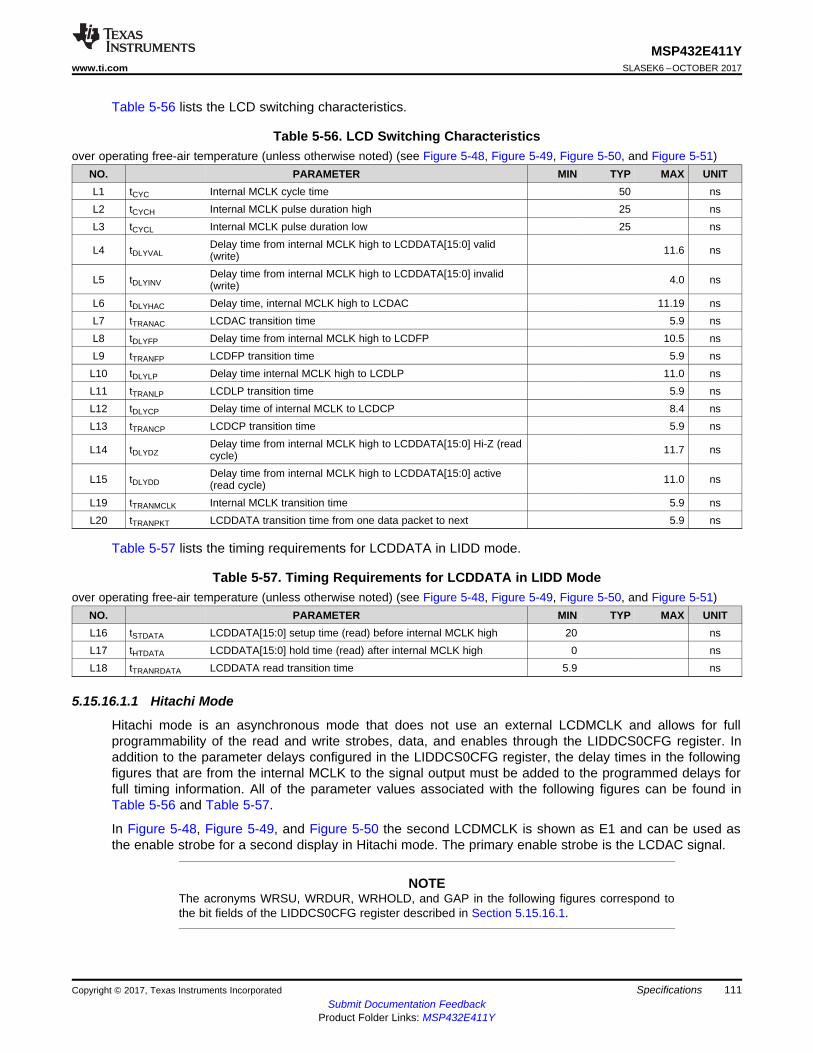
111
MSP432E411Ywww.ti.com SLASEK6 –OCTOBER 2017
Submit Documentation FeedbackProduct Folder Links: MSP432E411Y
SpecificationsCopyright © 2017, Texas Instruments Incorporated
Table 5-56 lists the LCD switching characteristics.
Table 5-56. LCD Switching Characteristicsover operating free-air temperature (unless otherwise noted) (see Figure 5-48, Figure 5-49, Figure 5-50, and Figure 5-51)
NO. PARAMETER MIN TYP MAX UNITL1 tCYC Internal MCLK cycle time 50 nsL2 tCYCH Internal MCLK pulse duration high 25 nsL3 tCYCL Internal MCLK pulse duration low 25 ns
L4 tDLYVALDelay time from internal MCLK high to LCDDATA[15:0] valid(write) 11.6 ns
L5 tDLYINVDelay time from internal MCLK high to LCDDATA[15:0] invalid(write) 4.0 ns
L6 tDLYHAC Delay time, internal MCLK high to LCDAC 11.19 nsL7 tTRANAC LCDAC transition time 5.9 nsL8 tDLYFP Delay time from internal MCLK high to LCDFP 10.5 nsL9 tTRANFP LCDFP transition time 5.9 ns
L10 tDLYLP Delay time internal MCLK high to LCDLP 11.0 nsL11 tTRANLP LCDLP transition time 5.9 nsL12 tDLYCP Delay time of internal MCLK to LCDCP 8.4 nsL13 tTRANCP LCDCP transition time 5.9 ns
L14 tDLYDZDelay time from internal MCLK high to LCDDATA[15:0] Hi-Z (readcycle) 11.7 ns
L15 tDLYDDDelay time from internal MCLK high to LCDDATA[15:0] active(read cycle) 11.0 ns
L19 tTRANMCLK Internal MCLK transition time 5.9 nsL20 tTRANPKT LCDDATA transition time from one data packet to next 5.9 ns
Table 5-57 lists the timing requirements for LCDDATA in LIDD mode.
Table 5-57. Timing Requirements for LCDDATA in LIDD Modeover operating free-air temperature (unless otherwise noted) (see Figure 5-48, Figure 5-49, Figure 5-50, and Figure 5-51)
NO. PARAMETER MIN TYP MAX UNITL16 tSTDATA LCDDATA[15:0] setup time (read) before internal MCLK high 20 nsL17 tHTDATA LCDDATA[15:0] hold time (read) after internal MCLK high 0 nsL18 tTRANRDATA LCDDATA read transition time 5.9 ns
5.15.16.1.1 Hitachi Mode
Hitachi mode is an asynchronous mode that does not use an external LCDMCLK and allows for fullprogrammability of the read and write strobes, data, and enables through the LIDDCS0CFG register. Inaddition to the parameter delays configured in the LIDDCS0CFG register, the delay times in the followingfigures that are from the internal MCLK to the signal output must be added to the programmed delays forfull timing information. All of the parameter values associated with the following figures can be found inTable 5-56 and Table 5-57.
In Figure 5-48, Figure 5-49, and Figure 5-50 the second LCDMCLK is shown as E1 and can be used asthe enable strobe for a second display in Hitachi mode. The primary enable strobe is the LCDAC signal.
NOTEThe acronyms WRSU, WRDUR, WRHOLD, and GAP in the following figures correspond tothe bit fields of the LIDDCS0CFG register described in Section 5.15.16.1.
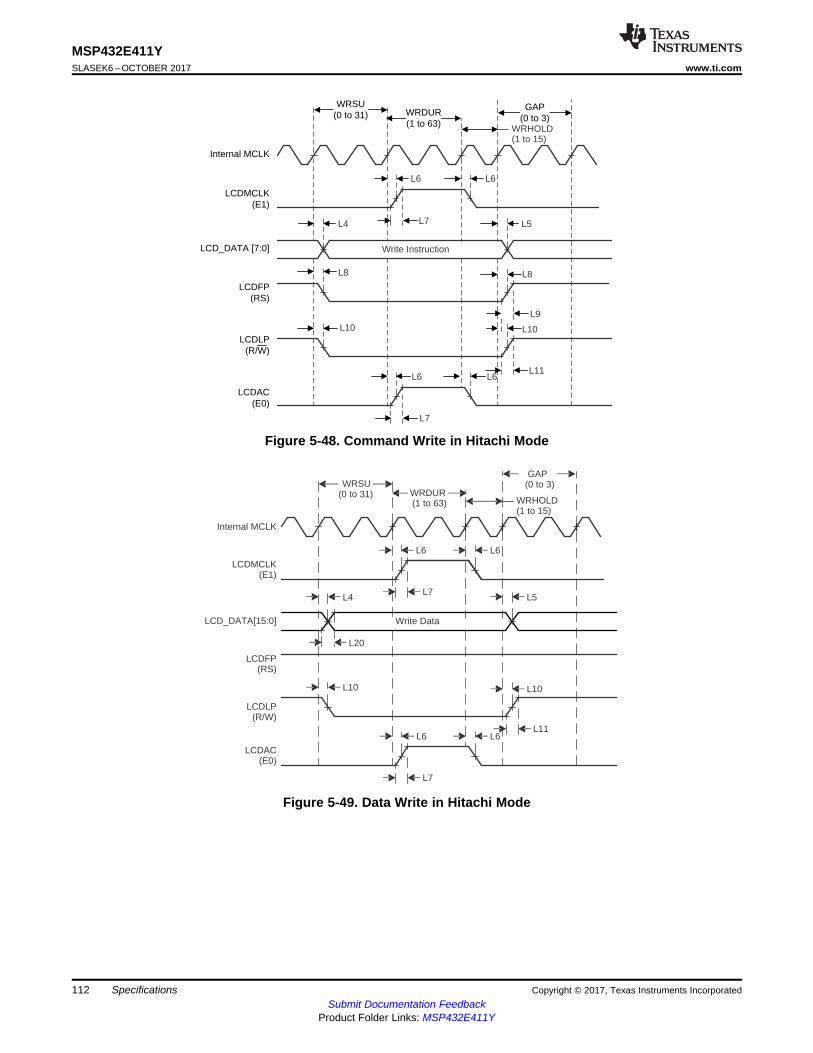
LCDAC(E0)
WRSU(0 to 31) WRDUR
(1 to 63) WRHOLD(1 to 15)
GAP(0 to 3)
Internal MCLK
L4
Write Data
L5
L10
L6
LCD_DATA[15:0]
LCDFP(RS)
LCDLP(R/W)
LCDMCLK(E1)
L20
L6
L7
L10
L11
L6 L6
L7
WRHOLD(1 to 15)
L4
Write Instruction
L5
L10
L6 L6
L7
L10
L11
L6 L6
L7
L8 L8
L9
GAP(0 to 3)
WRDUR(1 to 63)
WRSU(0 to 31)
Internal MCLK
LCDMCLK(E1)
LCD_DATA [7:0]
LCDFP(RS)
LCDLP(R/W)
LCDAC(E0)
112
MSP432E411YSLASEK6 –OCTOBER 2017 www.ti.com
Submit Documentation FeedbackProduct Folder Links: MSP432E411Y
Specifications Copyright © 2017, Texas Instruments Incorporated
Figure 5-48. Command Write in Hitachi Mode
Figure 5-49. Data Write in Hitachi Mode
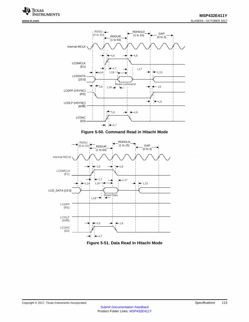
RDSU(0 to 31)
L14 L16L17
L15
Read Data
LCDAC(E0)
Internal MCLK
LCDFP(RS)
LCDLP(R/ )W
LCDMCLK(E1)
L6
L7
L6
L6
L7
L6
L18
GAP(0 to 3)
RDHOLD(1 to 15)RDDUR
(1 to 63)
LCD_DATA [15:0]
RDSU(0 to 31)
L14 L16L17
L15
L8Read Command
L6
L7
L6
L6
L7
L6
L18 L8
L9
Internal MCLK
LCDMCLK(E1)
LCDDATA [15:0]
LCDFP (VSYNC)(RS)
LCDLP (HSYNC)(R/W)
LCDAC(E0)
GAP(0 to 3)
RDHOLD(1 to 15)RDDUR
(1 to 63)
113
MSP432E411Ywww.ti.com SLASEK6 –OCTOBER 2017
Submit Documentation FeedbackProduct Folder Links: MSP432E411Y
SpecificationsCopyright © 2017, Texas Instruments Incorporated
Figure 5-50. Command Read in Hitachi Mode
Figure 5-51. Data Read in Hitachi Mode
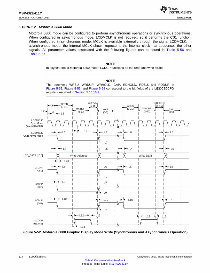
Write Address Write Data
L6 L6 L6L19
L4
L20
L6
L8
L10
L12 L12
L6 L6
L8
L10
L7
L9
11
L13
L12
L10 L10
L6
L5 L4 L5
L6
L3L2
L12
L7
WRSU(0-31) WRDUR
(0-63)
WRHOLD(0-15)
GAP(0-3)
RDHOLD(1-15)
GAP(0-3)
WRDUR(0-63)
WRSU(0-31)
L1
LCDAC(CS0)
LCDFP(ALE)
LCDLP(DIR)
LCDCP(RS/WS)
LCDMCLKSync Mode
(internal MCLK)
LCDMCLK(CS1) Async Mode
LCD_DATA [15:0]
114
MSP432E411YSLASEK6 –OCTOBER 2017 www.ti.com
Submit Documentation FeedbackProduct Folder Links: MSP432E411Y
Specifications Copyright © 2017, Texas Instruments Incorporated
5.15.16.1.2 Motorola 6800 Mode
Motorola 6800 mode can be configured to perform asynchronous operations or synchronous operations.When configured in asynchronous mode, LCDMCLK is not required, so it performs the CS1 function.When configured in synchronous mode, MCLK is available externally through the signal LCDMCLK. Inasynchronous mode, the internal MCLK shown represents the internal clock that sequences the othersignals. All parameter values associated with the following figures can be found in Table 5-56 andTable 5-57.
NOTEIn asynchronous Motorola 6800 mode, LCDCP functions as the read and write strobe.
NOTEThe acronyms WRSU, WRDUR, WRHOLD, GAP, RDHOLD, RDSU, and RDDUR inFigure 5-52, Figure 5-53, and Figure 5-54 correspond to the bit fields of the LIDDCS0CFGregister described in Section 5.15.16.1.
Figure 5-52. Motorola 6800 Graphic Display Mode Write (Synchronous and Asynchronous Operation)
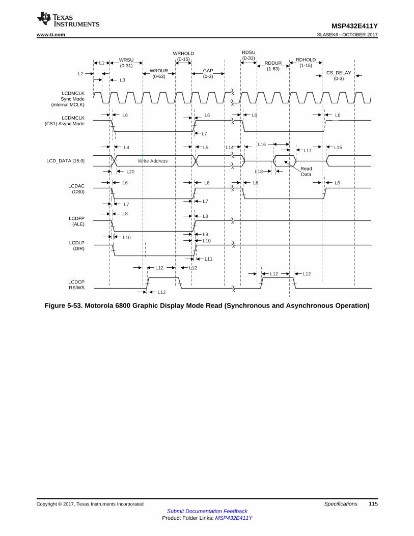
L10
Write Address
L6 L6 L6
L4
L20
L6
L8
L6 L6
L8
L7
L6
L5 L14 L15
L6
L16
L18
L17
L3L2
WRSU(0-31)
WRDUR(0-63)
WRHOLD(0-15)
GAP(0-3)
RDDUR(1-63)
L1RDHOLD
(1-15)
ReadData
LCDMCLKSync Mode
(internal MCLK)
RDSU(0-31)
LCDMCLK(CS1) Async Mode
LCD_DATA [15:0]
LCDAC(CS0)
L7
L7
L9L10
L12L12
L12
L12 L12
CS_DELAY(0-3)
L11
LCDLP(DIR)
LCDCPRS/WS
LCDFP(ALE)
115
MSP432E411Ywww.ti.com SLASEK6 –OCTOBER 2017
Submit Documentation FeedbackProduct Folder Links: MSP432E411Y
SpecificationsCopyright © 2017, Texas Instruments Incorporated
Figure 5-53. Motorola 6800 Graphic Display Mode Read (Synchronous and Asynchronous Operation)

LCDAC(CS0)
LCDFP(ALE)
LCDLP(DIR)
LCDCP(RS/WS)
ReadStatus
L6
L6
L12 L12
L6
L14 L15
L6
L16
L18
L17
L8 L8
L13
L9
L7
L3
L2
L7
L19
GAP(0 to 3)
RDHOLD(1 to 15)RDDUR
(1 to 63)
RDSU(0 to 31)
L1
LCDMCLKSync Mode
(internal MCLK)
LCDMCLK(CS1) Async Mode
LCD_DATA [15:0]
116
MSP432E411YSLASEK6 –OCTOBER 2017 www.ti.com
Submit Documentation FeedbackProduct Folder Links: MSP432E411Y
Specifications Copyright © 2017, Texas Instruments Incorporated
Figure 5-54. Motorola 6800 Graphic Display Mode Status (Synchronous and Asynchronous Operation)
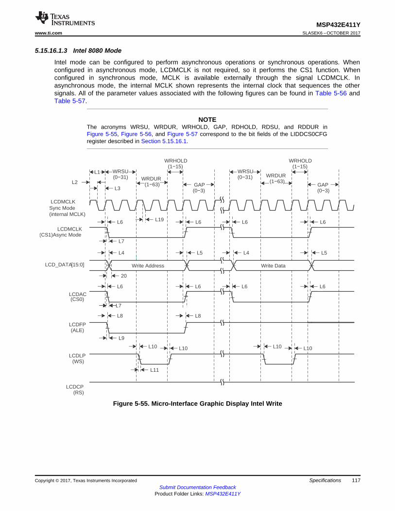
LCD_D [15:0]ATA
LCDAC(CS0)
LCDFP(ALE)
LCDLP(WS)
LCDCP(RS)
WRSU(0í31) WRDUR
(1í63)
WRHOLD(1í15)
GAP(0í3)
Write Address Write Data
LCDMCLK(CS1)Async Mode
L6 L6 L6L19
L4
20
L6
L8
L10
L6 L6
L8
L10
L7
L6
L5 L4 L5
L6
WRSU(0í31) WRDUR
(1í63)
WRHOLD(1í15)
GAP(0í3)
L1
L3L2
L9
L11
L10 L10
L7
LCDMCLKSync Mode(internal MCLK)
117
MSP432E411Ywww.ti.com SLASEK6 –OCTOBER 2017
Submit Documentation FeedbackProduct Folder Links: MSP432E411Y
SpecificationsCopyright © 2017, Texas Instruments Incorporated
5.15.16.1.3 Intel 8080 Mode
Intel mode can be configured to perform asynchronous operations or synchronous operations. Whenconfigured in asynchronous mode, LCDMCLK is not required, so it performs the CS1 function. Whenconfigured in synchronous mode, MCLK is available externally through the signal LCDMCLK. Inasynchronous mode, the internal MCLK shown represents the internal clock that sequences the othersignals. All of the parameter values associated with the following figures can be found in Table 5-56 andTable 5-57.
NOTEThe acronyms WRSU, WRDUR, WRHOLD, GAP, RDHOLD, RDSU, and RDDUR inFigure 5-55, Figure 5-56, and Figure 5-57 correspond to the bit fields of the LIDDCS0CFGregister described in Section 5.15.16.1.
Figure 5-55. Micro-Interface Graphic Display Intel Write
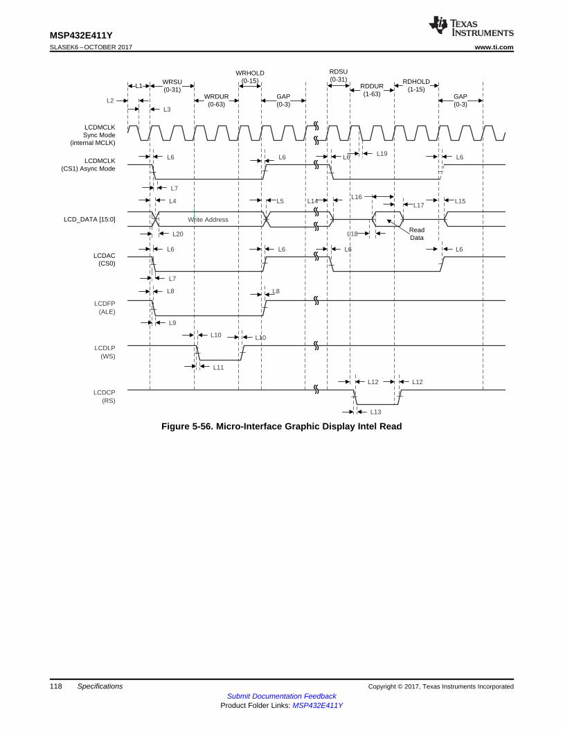
LCDFP(ALE)
LCDLP(WS)
LCDCP(RS)
Write Address
L6 L6 L6 L19
L4
L20
L6
L8
L10
L6 L6
L8
L10
L7
L12 L12
L6
L5 L14 L15
L6
L16
L18
L17
L3L2
L9
L11
L13
L7
WRSU(0-31)
WRDUR(0-63)
WRHOLD(0-15)
GAP(0-3)
RDDUR(1-63)
L1RDHOLD
(1-15)GAP(0-3)
ReadData
LCDMCLKSync Mode
(internal MCLK)
RDSU(0-31)
LCDMCLK(CS1) Async Mode
LCD_DATA [15:0]
LCDAC(CS0)
118
MSP432E411YSLASEK6 –OCTOBER 2017 www.ti.com
Submit Documentation FeedbackProduct Folder Links: MSP432E411Y
Specifications Copyright © 2017, Texas Instruments Incorporated
Figure 5-56. Micro-Interface Graphic Display Intel Read
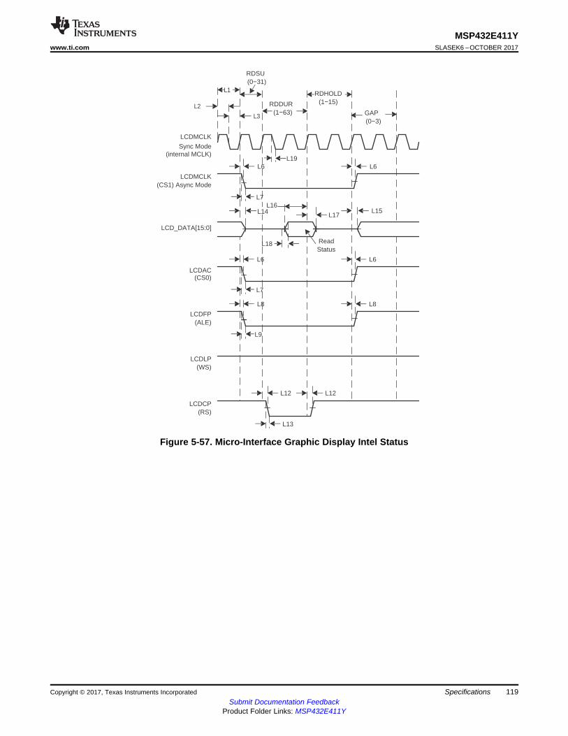
LCD_DATA[15:0]
LCDAC(CS0)
LCDFP(ALE)
LCDLP(WS)
LCDCP(RS)
ReadStatus
LCDMCLK(CS1) Async Mode
L6
L6
L12 L12
L6
L14 L15
L6
RDSU(0í31)
RDDUR(1í63) GAP
(0í3)
RDHOLD(1í15)
L16
L18
L17
L8 L8
L13
L9
L7
L1
L3
L2
L19
L7
LCDMCLK
Sync Mode(internal MCLK)
119
MSP432E411Ywww.ti.com SLASEK6 –OCTOBER 2017
Submit Documentation FeedbackProduct Folder Links: MSP432E411Y
SpecificationsCopyright © 2017, Texas Instruments Incorporated
Figure 5-57. Micro-Interface Graphic Display Intel Status
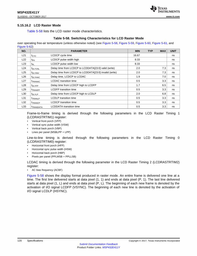
120
MSP432E411YSLASEK6 –OCTOBER 2017 www.ti.com
Submit Documentation FeedbackProduct Folder Links: MSP432E411Y
Specifications Copyright © 2017, Texas Instruments Incorporated
5.15.16.2 LCD Raster Mode
Table 5-58 lists the LCD raster mode characteristics.
Table 5-58. Switching Characteristics for LCD Raster Modeover operating free-air temperature (unless otherwise noted) (see Figure 5-58, Figure 5-59, Figure 5-60, Figure 5-61, andFigure 5-62)
NO. PARAMETER MIN TYP MAX UNITL21 tCYC LCDCP cycle time 16.67 nsL22 tPH LCDCP pulse width high 8.33 nsL23 tPL LCDCP pulse width low 8.33 nsL24 tDLYVAL Delay time from LCDCP to LCDDATA[23:0] valid (write) 2.0 7.3 nsL25 tDLYINV Delay time from LCDCP to LCDDATA[23:0] invalid (write) 2.0 7.3 nsL26 tDLYHAC Delay time, LCDCP to LCDAC 1.9 7.0 nsL27 tTRANAC LCDAC transition time 0.5 3.3 nsL28 tDLYFP Delay time from LCDCP high to LCDFP 1.7 6.5 nsL29 tTRANFP LCDFP transition time 0.5 3.3 nsL30 tDLYLP Delay time from LCDCP high to LCDLP 2.0 6.8 nsL31 tTRANLP LCDLP transition time 0.5 3.3 nsL32 tTRANCP LCDCP transition time 0.5 3.3 nsL33 tTRANDATA LCDDATA transition time 0.5 3.3 ns
Frame-to-frame timing is derived through the following parameters in the LCD Raster Timing 1(LCDRASTRTIM1) register:• Vertical front porch (VFP)• Vertical sync pulse width (VSW)• Vertical back porch (VBP)• Lines per panel (MSBLPP + LPP)
Line-to-line timing is derived through the following parameters in the LCD Raster Timing 0(LCDRASTRTIM0) register:• Horizontal front porch (HFP)• Horizontal sync pulse width (HSW)• Horizontal back porch (HBP)• Pixels per panel (PPLMSB + PPLLSB)
LCDAC timing is derived through the following parameter in the LCD Raster Timing 2 (LCDRASTRTIM2)register:• AC bias frequency (ACBF)
Figure 5-58 shows the display format produced in raster mode. An entire frame is delivered one line at atime. The first line delivered starts at data pixel (1, 1) and ends at data pixel (P, 1). The last line deliveredstarts at data pixel (1, L) and ends at data pixel (P, L). The beginning of each new frame is denoted by theactivation of I/O signal LCDFP (VSYNC). The beginning of each new line is denoted by the activation ofI/O signal LCDLP (HSYNC).
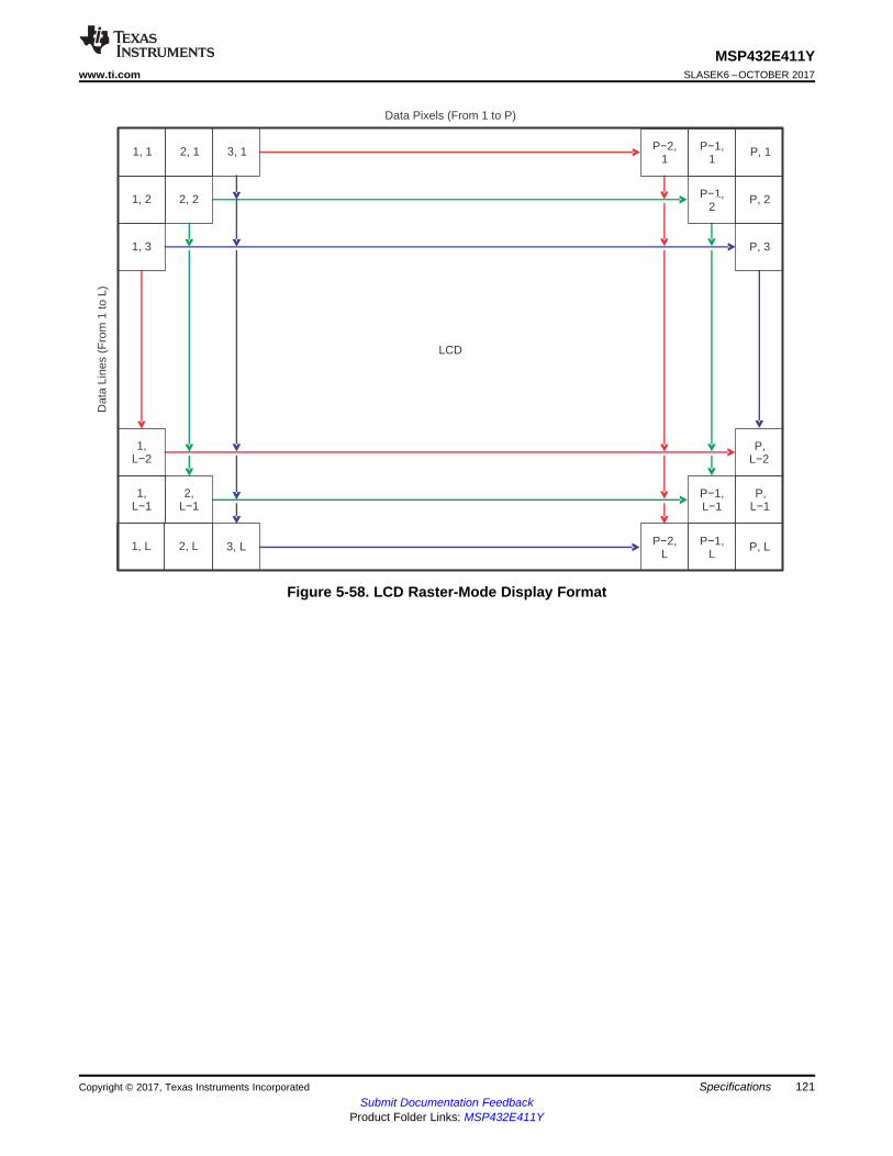
LCD
1, 1
1, 2 2, 2
1, 3
P, 1Pí1,1
Pí2,1
P, 2Pí1,2
P, 3
1, L
1,Lí2
3, L2, L P, L
Pí1,Lí1
P,Lí1
Pí1,L
P,Lí2
Pí2,L
Data Pixels (From 1 to P)D
ata
Line
s (F
rom
1 to
L)
2, 1 3, 1
1,Lí1
2,Lí1
121
MSP432E411Ywww.ti.com SLASEK6 –OCTOBER 2017
Submit Documentation FeedbackProduct Folder Links: MSP432E411Y
SpecificationsCopyright © 2017, Texas Instruments Incorporated
Figure 5-58. LCD Raster-Mode Display Format

LCDLP (HSYNC)
LCDFP (VSYNC)
(1 to 64)
VSW
(0 to 255)
VFP
(1 to 2048)
MSBLPP + LPP
1, 1P, 1
1, 2 P, 2
1, LP, L
1, L-1P, L-1
Line
Time
L30 L30
LCDCP
1, 1 2, 2 P, 2P, 12, 1 1, 2
PPLMSB + PPLLSB
16 × (1 to 2048)
HBP
(1 to 256)
Line 1
(1 to 256)
HFP
(1 to 64)
HSW PPLMSB + PPLLSB
16 × (1 to 2048)
Line 2
L31
LCDLP (HSYNC)
Frame Time
VSW(1 to 64)
VBP(0 to 255)
LCDAC(ACTVID)
LCD_D ATA [23:0]
LCD_D ATA [23:0]
LCDAC(ACTVID)
122
MSP432E411YSLASEK6 –OCTOBER 2017 www.ti.com
Submit Documentation FeedbackProduct Folder Links: MSP432E411Y
Specifications Copyright © 2017, Texas Instruments Incorporated
Figure 5-59. LCD Raster-Mode Active

LCDLP (HSYNC)
LCDFP (VSYNC)
(1 to 2048)
Frame Time
LCDDATA[7:0]
1, Lí2P, Lí2
1, Lí4P, Lí4
Line
Time
LCDLP (HSYNC)
L30 L30
LCDCP
LCDDATA[7:0] 1, 5 2, 6 P, 6P, 52, 5 1, 6
PPLMSB + PPLLSB
16 x (1 to 2048)
HBP
(1 to 256)
Line 5
HFP
(1 to 64)
HSW PPLMSB + PPLLSB
16 x (1 to 2048)
Line 6
1, 1:P, 1
1, 5:P, 5
1, Lí1P, Lí1
1, L
1, Lí1P, Lí1
1, Lí3P, Lí3
VBP = 0VFP = 0
VSW = 1
Data
LCDAC
ACB
(0 to 255)
ACB
(0 to 255)
1, 4:P, 4
1, 3:P, 3
1, 2:P, 2
1, L:P, L
1, 6:P, 6
1, 2P, 2
1, 1P, 1
1, LP, L
(1 to 256)
L31
MSBLPP + LPP
123
MSP432E411Ywww.ti.com SLASEK6 –OCTOBER 2017
Submit Documentation FeedbackProduct Folder Links: MSP432E411Y
SpecificationsCopyright © 2017, Texas Instruments Incorporated
Figure 5-60. LCD Raster-Mode Passive
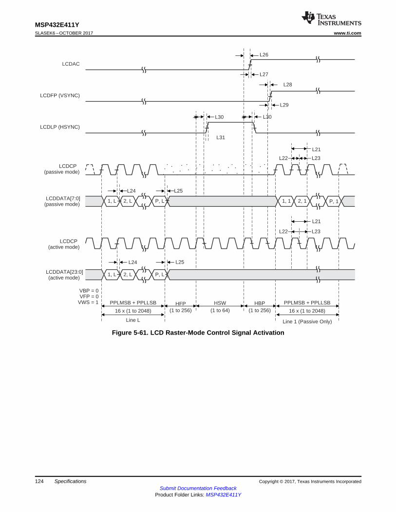
LCDLP (HSYNC)
LCDCP(active mode)
LCDDATA[23:0](active mode)
1, L P, L2, L
PPLMSB + PPLLSB
16 x (1 to 2048)
HBP(1 to 256)
Line L
(1 to 256)HFP
(1 to 64)HSW
Line 1 (Passive Only)
LCDFP (VSYNC)
LCDCP(passive mode)
LCDAC
LCDDATA[7:0](passive mode)
1, L 2, 1 P, 1P, L2, L 1, 1
L30 L30
L28
L26
L24 L25
L21
L22 L23
VBP = 0VFP = 0
VWS = 1
L21
L22 L23
L24 L25
PPLMSB + PPLLSB
16 x (1 to 2048)
L27
L29
L31
124
MSP432E411YSLASEK6 –OCTOBER 2017 www.ti.com
Submit Documentation FeedbackProduct Folder Links: MSP432E411Y
Specifications Copyright © 2017, Texas Instruments Incorporated
Figure 5-61. LCD Raster-Mode Control Signal Activation
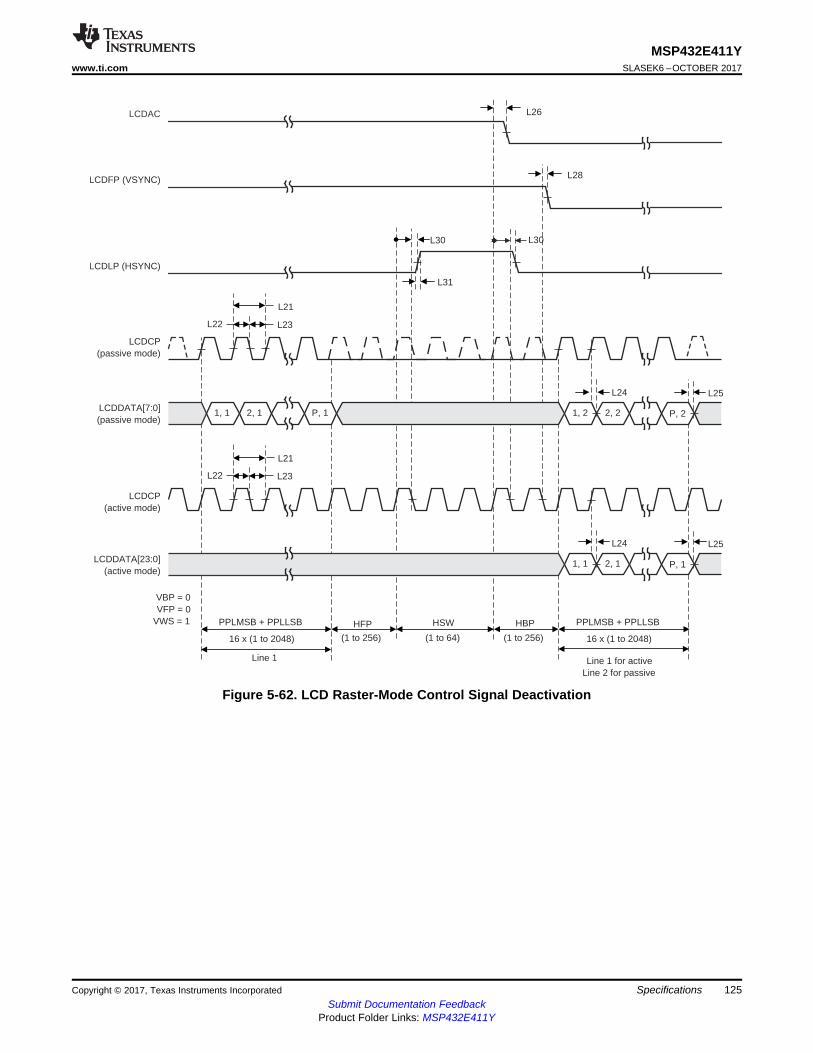
LCDLP (HSYNC)
LCDCP(active mode)
LCDDATA[23:0](active mode)
PPLMSB + PPLLSB
16 x (1 to 2048)
HBP
(1 to 256)
Line 1
(1 to 256)
HFP
(1 to 64)
HSW
Line 1 for activeLine 2 for passive
LCDFP (VSYNC)
LCDCP(passive mode)
LCDAC
LCDDATA[7:0](passive mode)
1, 1 2, 2 P, 2P, 12, 1 1, 2
L30 L30
L28
L26
L24 L25
L21
L22 L23
VBP = 0VFP = 0
VWS = 1 PPLMSB + PPLLSB
16 x (1 to 2048)
L31
L21
L22 L23
2, 1 P, 11, 1
L24 L25
125
MSP432E411Ywww.ti.com SLASEK6 –OCTOBER 2017
Submit Documentation FeedbackProduct Folder Links: MSP432E411Y
SpecificationsCopyright © 2017, Texas Instruments Incorporated
Figure 5-62. LCD Raster-Mode Control Signal Deactivation
126
MSP432E411YSLASEK6 –OCTOBER 2017 www.ti.com
Submit Documentation FeedbackProduct Folder Links: MSP432E411Y
Specifications Copyright © 2017, Texas Instruments Incorporated
5.15.17 Analog ComparatorTable 5-59 lists the characteristics of the comparator.
(1) Best design practices suggest placing static or quiet digital I/O signals adjacent to sensitive analog inputs to reduce capacitive couplingand crosstalk.
(2) To achieve best analog results, keep the source resistance driving the analog inputs, VINP and VINN, low.(3) The external voltage inputs to the analog comparator are designed to be highly sensitive and can be affected by external noise on the
board. For this reason, VINP and VINN must be set to different voltage levels during idle states to ensure the analog comparator triggersare not enabled. If an internal voltage reference is used, it should be set to a mid-supply level. When operating in sleep or deep-sleepmodes, disable the analog comparator module or set the external voltage inputs to different levels (greater than the input offset voltage)to achieve minimum current draw.
(4) Measured at VREF = 100 mV(5) Measured at external VREF = 100 mV, input signal switching from 75 mV to 125 mV
Table 5-59. Analog Comparator Characteristicsover operating free-air temperature (unless otherwise noted) (1) (2)
PARAMETER MIN TYP MAX UNITVINP,VINN
(3) Input voltage range GNDA VDDA V
VCM Input common-mode voltage range GNDA VDDA VVOS Input offset voltage ±10 ±50 (4) mVIINP, IINN Input leakage current over full voltage range 2.0 µACMRR Common-mode rejection ratio 50 dBtRT Response time 1.0 (5) µstMC Comparator mode change to output valid 10 µs
Table 5-60 lists the characteristics for the comparator.
Table 5-60. Analog Comparator Characteristicsover operating free-air temperature (unless otherwise noted)
PARAMETER MIN TYP MAX UNITRHR Resolution in high range VDDA / 29.4 VRLR Resolution in low range VDDA / 22.12 VAHR Absolute accuracy high range ±RHR / 2 VALR Absolute accuracy low range ±RLR / 2 V
127
MSP432E411Ywww.ti.com SLASEK6 –OCTOBER 2017
Submit Documentation FeedbackProduct Folder Links: MSP432E411Y
SpecificationsCopyright © 2017, Texas Instruments Incorporated
Table 5-61 and Table 5-62 list the reference voltages for the comparator under different conditions.
Table 5-61. Analog Comparator Voltage Reference CharacteristicsVDDA = 3.3 V, EN = 1, RNG = 0, over operating free-air temperature (unless otherwise noted)
PARAMETER TEST CONDITIONS MIN TYP MAX UNIT
VIREF Reference voltage
VREF = 0x0 0.731 0.786 0.841
V
VREF = 0x1 0.843 0.898 0.953VREF = 0x2 0.955 1.010 1.065VREF = 0x3 1.067 1.122 1.178VREF = 0x4 1.180 1.235 1.290VREF = 0x5 1.292 1.347 1.402VREF = 0x6 1.404 1.459 1.514VREF = 0x7 1.516 1.571 1.627VREF = 0x8 1.629 1.684 1.739VREF = 0x9 1.741 1.796 1.851VREF = 0xA 1.853 1.908 1.963VREF = 0xB 1.965 2.020 2.076VREF = 0xC 2.078 2.133 2.188VREF = 0xD 2.190 2.245 2.300VREF = 0xE 2.302 2.357 2.412VREF = 0xF 2.414 2.469 2.525
Table 5-62. Analog Comparator Voltage Reference CharacteristicsVDDA = 3.3 V, EN = 1, RNG = 1, over operating free-air temperature (unless otherwise noted)
PARAMETER TEST CONDITIONS MIN TYP MAX UNIT
VIREF Reference voltage
VREF = 0x0 0.000 0.000 0.074
V
VREF = 0x1 0.076 0.149 0.223VREF = 0x2 0.225 0.298 0.372VREF = 0x3 0.374 0.448 0.521VREF = 0x4 0.523 0.597 0.670VREF = 0x5 0.672 0.746 0.820VREF = 0x6 0.822 0.895 0.969VREF = 0x7 0.971 1.044 1.118VREF = 0x8 1.120 1.193 1.267VREF = 0x9 1.269 1.343 1.416VREF = 0xA 1.418 1.492 1.565VREF = 0xB 1.567 1.641 1.715VREF = 0xC 1.717 1.790 1.864VREF = 0xD 1.866 1.939 2.013VREF = 0xE 2.015 2.089 2.162VREF = 0xF 2.164 2.238 2.311
128
MSP432E411YSLASEK6 –OCTOBER 2017 www.ti.com
Submit Documentation FeedbackProduct Folder Links: MSP432E411Y
Specifications Copyright © 2017, Texas Instruments Incorporated
(1) This parameter value can vary depending on the PWM clock frequency which is controlled by the System Clock and a programmabledivider field in the PWMCC register.
(2) The latch and minimum fault period functions that can be enabled in the PWMnCTL register can change the timing of this parameter.
5.15.18 Pulse-Width Modulator (PWM)Table 5-63 lists the PWM timing characteristics.
Table 5-63. PWM Timing Characteristicsover operating free-air temperature (unless otherwise noted)
PARAMETER MIN TYP MAX UNIT
tFLTW Minimum fault pulse width 2PWMclock
periods
tFLTMAX MnFAULTn assertion to PWM inactive (1)24 + (1
PWMclock)
ns
tFLTMIN MnFAULTn deassertion to PWM active (2) 5 ns
5.15.19 Emulation and DebugTable 5-64 lists the JTAG characteristics.
Table 5-64. JTAG Characteristicsover operating free-air temperature (unless otherwise noted) (see Figure 5-63 and Figure 5-64)
NO. PARAMETER MIN TYP MAX UNITJ1 fTCK TCK operational clock frequency 0 10 MHzJ2 tTCK TCK operational clock period 100 nsJ3 tTCK_LOW TCK clock low time tTCK / 2 nsJ4 tTCK_HIGH TCK clock high time tTCK / 2 nsJ5 tTCK_R TCK rise time 0 10 nsJ6 tTCK_F TCK fall time 0 10 nsJ7 tTMS_SU TMS setup time to TCK rise 8 nsJ8 tTMS_HLD TMS hold time from TCK rise 4 nsJ9 tTDI_SU TDI setup time to TCK rise 18 nsJ10 tTDI_HLD TDI hold time from TCK rise 4 ns
J11 tTDO_ZDV TCK fall to data valid from Hi-Z
2-mA drive 13 35
ns
4-mA drive 9 268-mA drive 8 268-mA drive with slew rate control 10 2910-mA drive 11 1312-mA drive 11 14
J12 tTDO_DVTCK fall to data valid fromdata valid
2-mA drive 14 20
ns
4-mA drive 10 268-mA drive 8 218-mA drive with slew rate control 10 2610-mA drive 12 1412-mA drive 12 15
J13 tTDO_DVZ TCK fall to Hi-Z from data valid
2-mA drive 7 16
ns
4-mA drive 7 168-mA drive 7 168-mA drive with slew rate control 8 1910-mA drive 20 2212-mA drive 20 25
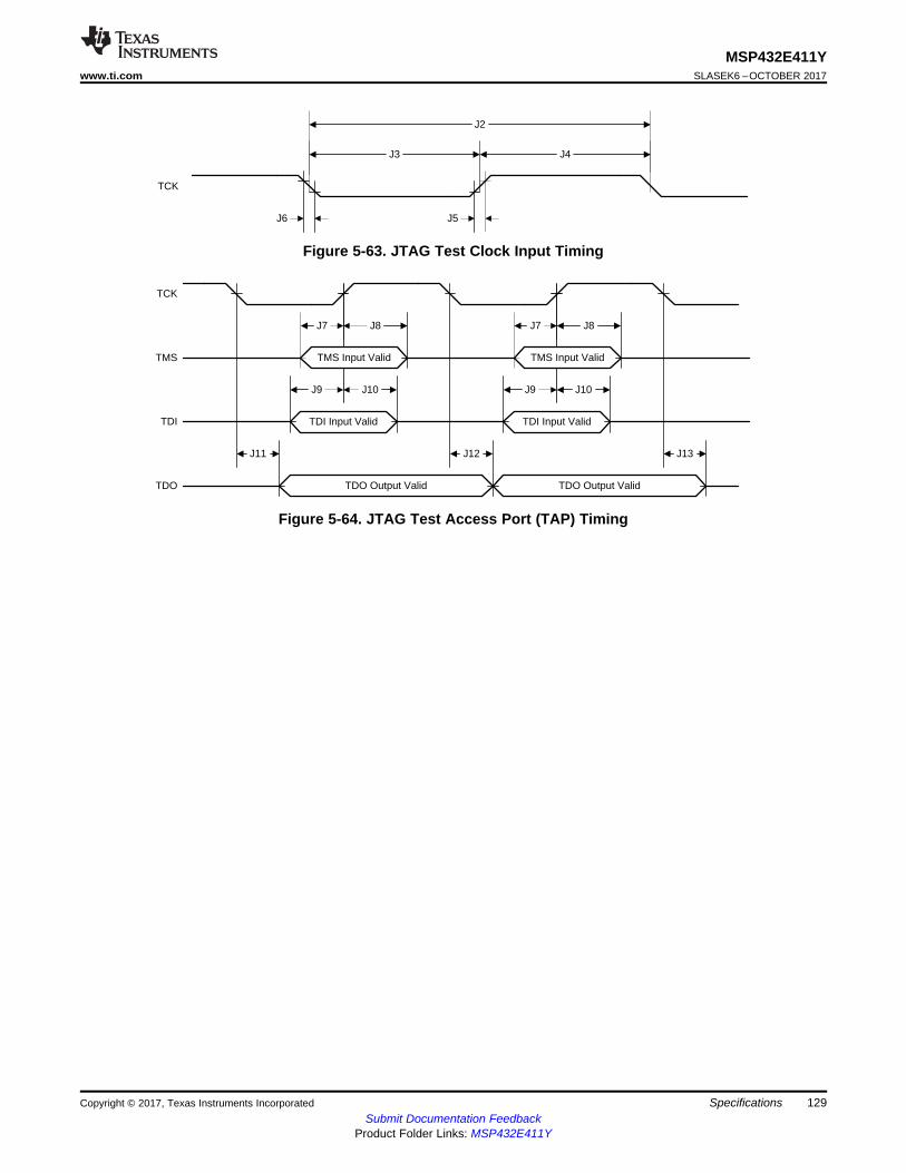
TDO Output Valid
TCK
TDO Output Valid
J12
TDO
TDI
TMS
TDI Input Valid TDI Input Valid
J13
J9 J10
TMS Input Valid
J9 J10
TMS Input Valid
J11
J7 J8J8J7
TCK
J6 J5
J3 J4
J2
129
MSP432E411Ywww.ti.com SLASEK6 –OCTOBER 2017
Submit Documentation FeedbackProduct Folder Links: MSP432E411Y
SpecificationsCopyright © 2017, Texas Instruments Incorporated
Figure 5-63. JTAG Test Clock Input Timing
Figure 5-64. JTAG Test Access Port (TAP) Timing
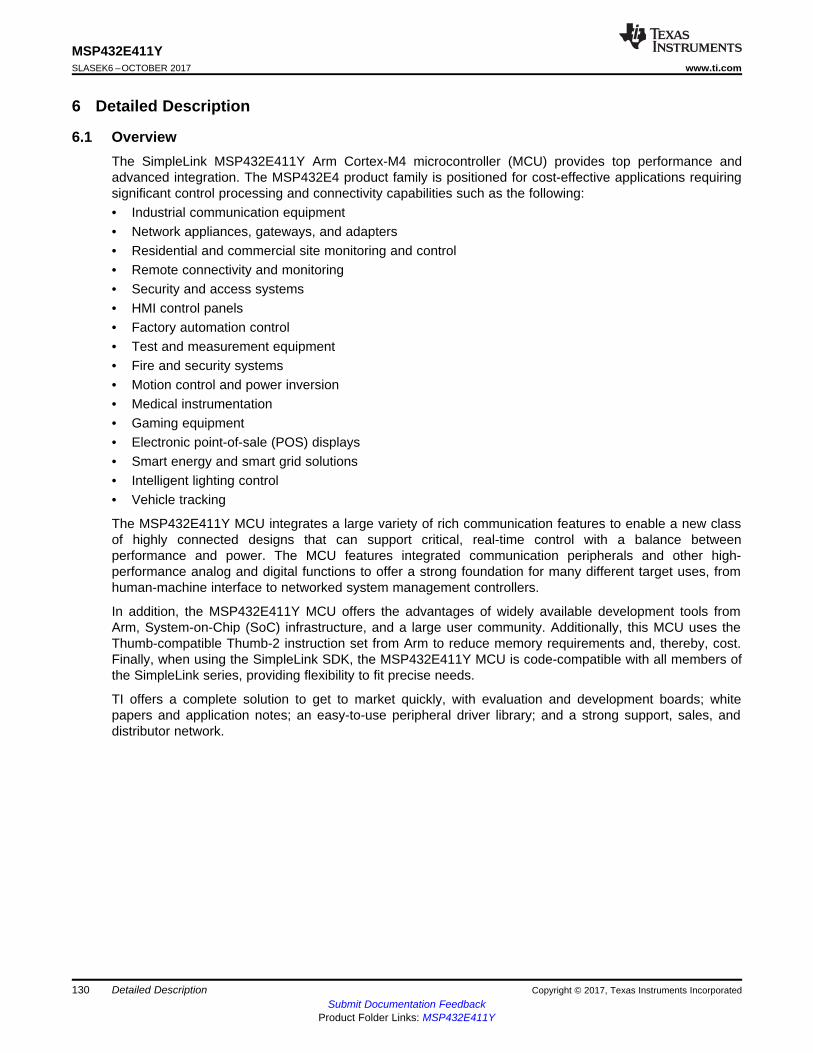
130
MSP432E411YSLASEK6 –OCTOBER 2017 www.ti.com
Submit Documentation FeedbackProduct Folder Links: MSP432E411Y
Detailed Description Copyright © 2017, Texas Instruments Incorporated
6 Detailed Description
6.1 OverviewThe SimpleLink MSP432E411Y Arm Cortex-M4 microcontroller (MCU) provides top performance andadvanced integration. The MSP432E4 product family is positioned for cost-effective applications requiringsignificant control processing and connectivity capabilities such as the following:• Industrial communication equipment• Network appliances, gateways, and adapters• Residential and commercial site monitoring and control• Remote connectivity and monitoring• Security and access systems• HMI control panels• Factory automation control• Test and measurement equipment• Fire and security systems• Motion control and power inversion• Medical instrumentation• Gaming equipment• Electronic point-of-sale (POS) displays• Smart energy and smart grid solutions• Intelligent lighting control• Vehicle tracking
The MSP432E411Y MCU integrates a large variety of rich communication features to enable a new classof highly connected designs that can support critical, real-time control with a balance betweenperformance and power. The MCU features integrated communication peripherals and other high-performance analog and digital functions to offer a strong foundation for many different target uses, fromhuman-machine interface to networked system management controllers.
In addition, the MSP432E411Y MCU offers the advantages of widely available development tools fromArm, System-on-Chip (SoC) infrastructure, and a large user community. Additionally, this MCU uses theThumb-compatible Thumb-2 instruction set from Arm to reduce memory requirements and, thereby, cost.Finally, when using the SimpleLink SDK, the MSP432E411Y MCU is code-compatible with all members ofthe SimpleLink series, providing flexibility to fit precise needs.
TI offers a complete solution to get to market quickly, with evaluation and development boards; whitepapers and application notes; an easy-to-use peripheral driver library; and a strong support, sales, anddistributor network.
ArmCortex-M4F
(120 MHz)
NVIC MPU
FPUETM Flash
(1024KB)
BootloaderDriverLibAES and CRCEthernet Bootloader
ROM
DCode bus
ICode bus
JTAG, SWD
SystemControl and
Clocks(with Precision
Oscillator)
Bus Matrix
System Bus
SRAM(256KB)
SYSTEM PERIPHERALS
WatchdogTimer
(2 Units)DMA
HibernationModule
Tamper
EEPROM(6K)
General-Purpose
Timer (8 Units)
GPIOs(140)
ExternalPeripheralInterface
CRCModule
AESModule
DESModule
SHA/MD5Module
TFT LCDController
SERIAL PERIPHERALS
UART(8 Units)
USB OTG(FS PHYor ULPI)
I2C(10 Units)
SSI(4 Units)
CANController(2 Units)
EthernetMAC, PHY, MII
ANALOG PERIPHERALS
12-Bit ADC(2 Units,
24 Channels)
AnalogComparator
(3 Units)
MOTION CONTROL PERIPHERALS
QEI(1 Unit)
PWM(1 Unit,
8 Signals)
SMC PERIPHERALS
1-Wire(1 Unit)
Advanced
Periphera
lB
us
(AP
B)
Advanced
Hig
h-P
erf
orm
ance
Bus
(AH
B)
Copyright © 2017, Texas Instruments Incorporated
131
MSP432E411Ywww.ti.com SLASEK6 –OCTOBER 2017
Submit Documentation FeedbackProduct Folder Links: MSP432E411Y
Detailed DescriptionCopyright © 2017, Texas Instruments Incorporated
6.2 Functional Block DiagramFigure 6-1 shows the features on the MSP432E411Y MCU. Two on-chip buses connect the core to theperipherals. The Advanced Peripheral Bus (APB) bus is the legacy bus. The Advanced High-PerformanceBus (AHB) bus provides better back-to-back access performance than the APB bus.
Figure 6-1. MSP432E411Y High-Level Block Diagram
132
MSP432E411YSLASEK6 –OCTOBER 2017 www.ti.com
Submit Documentation FeedbackProduct Folder Links: MSP432E411Y
Detailed Description Copyright © 2017, Texas Instruments Incorporated
6.3 Arm Cortex-M4F Processor CoreAll members of the MSP432E4 family are designed around an Arm Cortex-M processor core. The ArmCortex-M processor provides the core for a high-performance low-cost platform that meets the needs ofminimal memory implementation, reduced pin count, and low power consumption, while deliveringoutstanding computational performance and exceptional system response to interrupts.
6.3.1 Processor CoreFeatures of the processor core include:• 32-bit Arm Cortex-M4F architecture optimized for small-footprint embedded applications• 120-MHz operation; 150 DMIPS performance• Outstanding processing performance combined with fast interrupt handling• Thumb-2 mixed 16- and 32-bit instruction set delivers the high performance expected of a 32-bit Arm
core in a compact memory size usually associated with 8- and 16-bit devices, typically in the range ofa few kilobytes of memory for MCU-class applications.– Single-cycle multiply instruction and hardware divide– Atomic bit manipulation (bit-banding), delivering maximum memory use and streamlined peripheral
control– Unaligned data access, enabling data to be efficiently packed into memory
• IEEE 754-compliant single-precision floating-point unit (FPU)• 16-bit SIMD vector processing unit• Fast code execution permits slower processor clock or increases sleep mode time• Harvard architecture characterized by separate buses for instruction and data• Efficient processor core, system, and memories• Hardware division and fast digital-signal-processing orientated multiply accumulate• Saturating arithmetic for signal processing• Deterministic high-performance interrupt handling for time-critical applications• Memory protection unit (MPU) to provide a privileged mode for protected operating system functionality• Enhanced system debug with extensive breakpoint and trace capabilities• Serial Wire Debug and Serial Wire Trace reduce the number of pins required for debugging and tracing• Migration from the Arm7® processor family for better performance and power efficiency• Optimized for single-cycle flash memory use up to specific frequencies; see the Internal Memory
chapter of the MSP432E4 SimpleLink™ Microcontrollers Technical Reference Manual for moreinformation.
• Ultra-low-power consumption with integrated sleep modes
6.3.2 System Timer (SysTick)SysTick provides a simple, 24-bit, clear-on-write, decrementing, wrap-on-zero counter with a flexiblecontrol mechanism. The counter can be used in several different ways, for example:• An RTOS tick timer that fires at a programmable rate (for example, 100 Hz) and invokes a SysTick
routine• A high-speed alarm timer using the system clock• A variable rate alarm or signal timer—the duration is range-dependent on the reference clock used and
the dynamic range of the counter• A simple counter used to measure time to completion and time used• An internal clock-source control based on missing or meeting durations
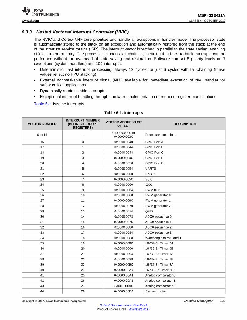
133
MSP432E411Ywww.ti.com SLASEK6 –OCTOBER 2017
Submit Documentation FeedbackProduct Folder Links: MSP432E411Y
Detailed DescriptionCopyright © 2017, Texas Instruments Incorporated
6.3.3 Nested Vectored Interrupt Controller (NVIC)The NVIC and Cortex-M4F core prioritize and handle all exceptions in handler mode. The processor stateis automatically stored to the stack on an exception and automatically restored from the stack at the endof the interrupt service routine (ISR). The interrupt vector is fetched in parallel to the state saving, enablingefficient interrupt entry. The processor supports tail-chaining, meaning that back-to-back interrupts can beperformed without the overhead of state saving and restoration. Software can set 8 priority levels on 7exceptions (system handlers) and 109 interrupts.• Deterministic, fast interrupt processing: always 12 cycles, or just 6 cycles with tail-chaining (these
values reflect no FPU stacking)• External nonmaskable interrupt signal (NMI) available for immediate execution of NMI handler for
safety critical applications• Dynamically reprioritizable interrupts• Exceptional interrupt handling through hardware implementation of required register manipulations
Table 6-1 lists the interrupts.
Table 6-1. Interrupts
VECTOR NUMBERINTERRUPT NUMBER
(BIT IN INTERRUPTREGISTERS)
VECTOR ADDRESS OROFFSET DESCRIPTION
0 to 15 – 0x0000.0000 to0x0000.003C Processor exceptions
16 0 0x0000.0040 GPIO Port A17 1 0x0000.0044 GPIO Port B18 2 0x0000.0048 GPIO Port C19 3 0x0000.004C GPIO Port D20 4 0x0000.0050 GPIO Port E21 5 0x0000.0054 UART022 6 0x0000.0058 UART123 7 0x0000.005C SSI024 8 0x0000.0060 I2C025 9 0x0000.0064 PWM fault26 10 0x0000.0068 PWM generator 027 11 0x0000.006C PWM generator 128 12 0x0000.0070 PWM generator 229 13 0x0000.0074 QEI030 14 0x0000.0078 ADC0 sequence 031 15 0x0000.007C ADC0 sequence 132 16 0x0000.0080 ADC0 sequence 233 17 0x0000.0084 ADC0 sequence 334 18 0x0000.0088 Watchdog timers 0 and 135 19 0x0000.008C 16-/32-Bit Timer 0A36 20 0x0000.0090 16-/32-Bit Timer 0B37 21 0x0000.0094 16-/32-Bit Timer 1A38 22 0x0000.0098 16-/32-Bit Timer 1B39 23 0x0000.009C 16-/32-Bit Timer 2A40 24 0x0000.00A0 16-/32-Bit Timer 2B41 25 0x0000.00A4 Analog comparator 042 26 0x0000.00A8 Analog comparator 143 27 0x0000.00AC Analog comparator 244 28 0x0000.00B0 System control
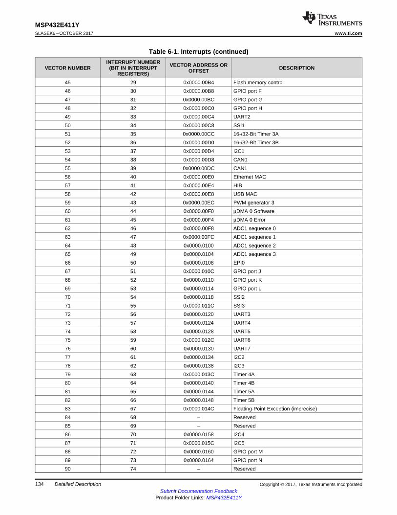
134
MSP432E411YSLASEK6 –OCTOBER 2017 www.ti.com
Submit Documentation FeedbackProduct Folder Links: MSP432E411Y
Detailed Description Copyright © 2017, Texas Instruments Incorporated
Table 6-1. Interrupts (continued)
VECTOR NUMBERINTERRUPT NUMBER
(BIT IN INTERRUPTREGISTERS)
VECTOR ADDRESS OROFFSET DESCRIPTION
45 29 0x0000.00B4 Flash memory control46 30 0x0000.00B8 GPIO port F47 31 0x0000.00BC GPIO port G48 32 0x0000.00C0 GPIO port H49 33 0x0000.00C4 UART250 34 0x0000.00C8 SSI151 35 0x0000.00CC 16-/32-Bit Timer 3A52 36 0x0000.00D0 16-/32-Bit Timer 3B53 37 0x0000.00D4 I2C154 38 0x0000.00D8 CAN055 39 0x0000.00DC CAN156 40 0x0000.00E0 Ethernet MAC57 41 0x0000.00E4 HIB58 42 0x0000.00E8 USB MAC59 43 0x0000.00EC PWM generator 360 44 0x0000.00F0 µDMA 0 Software61 45 0x0000.00F4 µDMA 0 Error62 46 0x0000.00F8 ADC1 sequence 063 47 0x0000.00FC ADC1 sequence 164 48 0x0000.0100 ADC1 sequence 265 49 0x0000.0104 ADC1 sequence 366 50 0x0000.0108 EPI067 51 0x0000.010C GPIO port J68 52 0x0000.0110 GPIO port K69 53 0x0000.0114 GPIO port L70 54 0x0000.0118 SSI271 55 0x0000.011C SSI372 56 0x0000.0120 UART373 57 0x0000.0124 UART474 58 0x0000.0128 UART575 59 0x0000.012C UART676 60 0x0000.0130 UART777 61 0x0000.0134 I2C278 62 0x0000.0138 I2C379 63 0x0000.013C Timer 4A80 64 0x0000.0140 Timer 4B81 65 0x0000.0144 Timer 5A82 66 0x0000.0148 Timer 5B83 67 0x0000.014C Floating-Point Exception (imprecise)84 68 – Reserved85 69 – Reserved86 70 0x0000.0158 I2C487 71 0x0000.015C I2C588 72 0x0000.0160 GPIO port M89 73 0x0000.0164 GPIO port N90 74 – Reserved
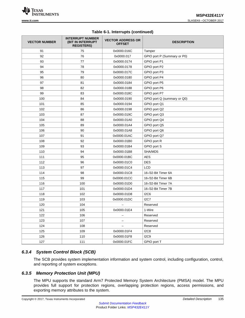
135
MSP432E411Ywww.ti.com SLASEK6 –OCTOBER 2017
Submit Documentation FeedbackProduct Folder Links: MSP432E411Y
Detailed DescriptionCopyright © 2017, Texas Instruments Incorporated
Table 6-1. Interrupts (continued)
VECTOR NUMBERINTERRUPT NUMBER
(BIT IN INTERRUPTREGISTERS)
VECTOR ADDRESS OROFFSET DESCRIPTION
91 75 0x0000.016C Tamper92 76 0x0000.017 GPIO port P (Summary or P0)93 77 0x0000.0174 GPIO port P194 78 0x0000.0178 GPIO port P295 79 0x0000.017C GPIO port P396 80 0x0000.0180 GPIO port P497 81 0x0000.0184 GPIO port P598 82 0x0000.0188 GPIO port P699 83 0x0000.018C GPIO port P7100 84 0x0000.0190 GPIO port Q (summary or Q0)101 85 0x0000.0194 GPIO port Q1102 86 0x0000.0198 GPIO port Q2103 87 0x0000.019C GPIO port Q3104 88 0x0000.01A0 GPIO port Q4105 89 0x0000.01A4 GPIO port Q5106 90 0x0000.01A8 GPIO port Q6107 91 0x0000.01AC GPIO port Q7108 92 0x0000.01B0 GPIO port R109 93 0x0000.01B4 GPIO port S110 94 0x0000.01B8 SHA/MD5111 95 0x0000.01BC AES112 96 0x0000.01C0 DES113 97 0x0000.01C4 LCD114 98 0x0000.01C8 16-/32-Bit Timer 6A115 99 0x0000.01CC 16-/32-Bit Timer 6B116 100 0x0000.01D0 16-/32-Bit Timer 7A117 101 0x0000.01D4 16-/32-Bit Timer 7B118 102 0x0000.01D8 I2C6119 103 0x0000.01DC I2C7120 104 – Reserved121 105 0x0000.01E4 1-Wire122 106 – Reserved123 107 – Reserved124 108 – Reserved125 109 0x0000.01F4 I2C8126 110 0x0000.01F8 I2C9127 111 0x0000.01FC GPIO port T
6.3.4 System Control Block (SCB)The SCB provides system implementation information and system control, including configuration, control,and reporting of system exceptions.
6.3.5 Memory Protection Unit (MPU)The MPU supports the standard Arm7 Protected Memory System Architecture (PMSA) model. The MPUprovides full support for protection regions, overlapping protection regions, access permissions, andexporting memory attributes to the system.
136
MSP432E411YSLASEK6 –OCTOBER 2017 www.ti.com
Submit Documentation FeedbackProduct Folder Links: MSP432E411Y
Detailed Description Copyright © 2017, Texas Instruments Incorporated
6.3.6 Floating-Point Unit (FPU)The FPU fully supports single-precision add, subtract, multiply, divide, multiply-and-accumulate, andsquare root operations. It also provides conversions between fixed-point and floating-point data formats,and floating-point constant instructions.• 32-bit instructions for single-precision (C float) data-processing operations• Combined multiply and accumulate instructions for increased precision (fused MAC)• Hardware support for conversion, addition, subtraction, multiplication with optional accumulate,
division, and square-root• Hardware support for denormals and all IEEE rounding modes• 32 dedicated 32-bit single-precision registers, also addressable as 16 double-word registers• Decoupled 3-stage pipeline
6.4 On-Chip MemoryThe following on-chip memories are supported:• 256KB of single-cycle SRAM• 1024KB of flash memory• 6KB of EEPROM• Internal ROM loaded with SimpleLink SDK software:
– Peripheral driver library– Bootloader
6.4.1 SRAMThe MSP432E411Y MCU provides 256KB of single-cycle on-chip SRAM. The internal SRAM of the deviceis at offset 0x2000.0000 of the device memory map.
The SRAM is implemented using four 32-bit-wide interleaving SRAM banks (separate SRAM arrays),which allow for increased speed between memory accesses. The SRAM memory provides nearly 2 GBpsof memory bandwidth at a 120-MHz clock frequency.
Because read-modify-write (RMW) operations are time consuming, Arm has introduced bit-bandingtechnology in the Cortex-M4F processor. With a bit-band-enabled processor, certain regions in thememory map (SRAM and peripheral space) can use address aliases to access individual bits in an atomicoperation.
Data can be transferred to and from SRAM by the following masters:• µDMA• USB• LCD controller• Ethernet controller
6.4.2 Flash MemoryThe MSP432E411Y MCU provides 1024KB of on-chip flash memory. The flash memory is configured asfour banks of 16K × 128 bits (4 × 256KB total) that are 2-way interleaved. Memory blocks can be markedas read only or execute only, providing different levels of code protection. Read-only blocks cannot beerased or programmed, protecting the contents of those blocks from being modified. Execute-only blockscannot be erased or programmed, and can only be read by the controller instruction fetch mechanism,protecting the contents of those blocks from being read by either the controller or a debugger.
Two sets of instruction prefetch buffers provide enhanced performance and power savings. Each prefetchbuffer is 2 × 256 bits and can be combined as a 4 × 256-bit prefetch buffer.
The flash can also be accessed by the µDMA in run mode.
137
MSP432E411Ywww.ti.com SLASEK6 –OCTOBER 2017
Submit Documentation FeedbackProduct Folder Links: MSP432E411Y
Detailed DescriptionCopyright © 2017, Texas Instruments Incorporated
6.4.3 ROMThe ROM is preprogrammed with the following software and programs:• Peripheral driver library• Bootloader
The SimpleLink MSP432E4 SDK driver library is a royalty-free software library for controlling on-chipperipherals with a bootloader capability. The library performs both peripheral initialization and controlfunctions, with a choice of polled or interrupt-driven peripheral support. In addition, the library is designedto take full advantage of the stellar interrupt performance of the Arm Cortex-M4F core. No specialpragmas or custom assembly code prologue or epilogue functions are required. For applications thatrequire in-field programmability, the royalty-free bootloader can act as an application loader and supportin-field firmware updates.
6.4.4 EEPROMThe EEPROM includes the following features:• 6KB of memory accessible as 1536 32-bit words• 96 blocks of 16 words (64 bytes) each• Built-in wear leveling• Access protection per block• Lock protection option for the whole peripheral as well as per block using 32-bit to 96-bit unlock codes
(application selectable)• Interrupt support for write completion to avoid polling• Endurance of 500k writes (when writing at fixed offset in every alternate page in circular fashion) to
15M operations (when cycling through two pages) per each 2-page block.
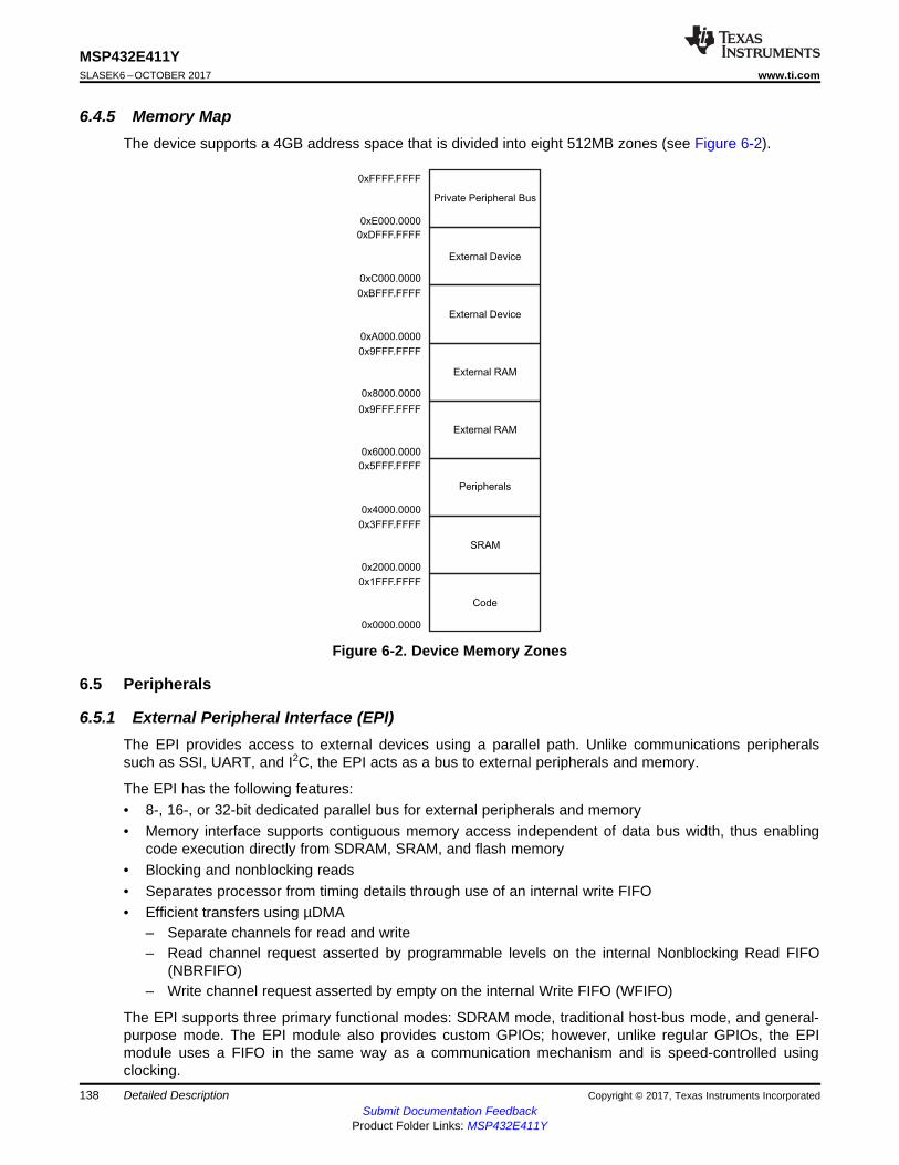
Code
SRAM
Peripherals
External RAM
External RAM
External Device
External Device
Private Peripheral Bus
0x0000.0000
0x1FFF.FFFF
0x3FFF.FFFF
0x5FFF.FFFF
0x9FFF.FFFF
0x9FFF.FFFF
0xBFFF.FFFF
0xDFFF.FFFF
0xFFFF.FFFF
0x2000.0000
0x4000.0000
0x6000.0000
0x8000.0000
0xA000.0000
0xC000.0000
0xE000.0000
138
MSP432E411YSLASEK6 –OCTOBER 2017 www.ti.com
Submit Documentation FeedbackProduct Folder Links: MSP432E411Y
Detailed Description Copyright © 2017, Texas Instruments Incorporated
6.4.5 Memory MapThe device supports a 4GB address space that is divided into eight 512MB zones (see Figure 6-2).
Figure 6-2. Device Memory Zones
6.5 Peripherals
6.5.1 External Peripheral Interface (EPI)The EPI provides access to external devices using a parallel path. Unlike communications peripheralssuch as SSI, UART, and I2C, the EPI acts as a bus to external peripherals and memory.
The EPI has the following features:• 8-, 16-, or 32-bit dedicated parallel bus for external peripherals and memory• Memory interface supports contiguous memory access independent of data bus width, thus enabling
code execution directly from SDRAM, SRAM, and flash memory• Blocking and nonblocking reads• Separates processor from timing details through use of an internal write FIFO• Efficient transfers using µDMA
– Separate channels for read and write– Read channel request asserted by programmable levels on the internal Nonblocking Read FIFO
(NBRFIFO)– Write channel request asserted by empty on the internal Write FIFO (WFIFO)
The EPI supports three primary functional modes: SDRAM mode, traditional host-bus mode, and general-purpose mode. The EPI module also provides custom GPIOs; however, unlike regular GPIOs, the EPImodule uses a FIFO in the same way as a communication mechanism and is speed-controlled usingclocking.
139
MSP432E411Ywww.ti.com SLASEK6 –OCTOBER 2017
Submit Documentation FeedbackProduct Folder Links: MSP432E411Y
Detailed DescriptionCopyright © 2017, Texas Instruments Incorporated
• SDRAM mode– Supports ×16 (single data rate) SDRAM at up to 60 MHz– Supports low-cost SDRAMs up to 64MB (512 Mb)– Includes automatic refresh and access to all banks and rows– Includes a sleep (standby) mode to keep contents active with minimal power draw– Multiplexed address and data interface for reduced pin count
• Host-bus mode– Traditional ×8 and ×16 MCU bus interface capabilities– Similar device compatibility options as PIC, ATmega, 8051, and others– Access to SRAM, NOR flash memory, and other devices, with up to 1MB of addressing in
nonmultiplexed mode and 256MB in multiplexed mode (512MB in host bus 16 mode with no byteselects)
– Support for up to 512Mb PSRAM in quad chip select mode, with dedicated configuration registerread and write enable
– Support of both muxed and demuxed address and data– Access to a range of devices supporting the nonaddress FIFO ×8 and ×16 interface variant, with
support for external FIFO (XFIFO) EMPTY and FULL signals– Speed controlled, with read and write data wait-state counters– Support for read or write burst mode to Host Bus– Multiple chip-select modes including single, dual, and quad chip selects, with and without ALE– External iRDY signal provided for stall capability of reads and writes– Manual chip-enable (or use extra address pins)
• General-purpose mode– Wide parallel interfaces for fast communications with CPLDs and FPGAs– Data widths up to 32 bits– Data rates up to 150 MB/second– Optional "address" sizes from 4 bits to 20 bits– Optional clock output, read and write strobes, framing (with counter-based size), and clock-enable
input• General parallel GPIO
– 1 to 32 bits, FIFO with speed control– Useful for custom peripherals or for digital data acquisition and actuator controls
6.5.2 Cyclical Redundancy Check (CRC)The CRC computation module is for uses such as message transfer and safety system checks. Thismodule can be used with the AES and DES modules. The CRC has the following features:• Support four major CRC forms:
– CRC16-CCITT as used by CCITT/ITU X.25– CRC16-IBM as used by USB and ANSI– CRC32-IEEE as used by IEEE 802.3 and MPEG-2– CRC32C as used by G.Hn
• Allows word and byte feed• Supports automatic initialization and manual initialization• Supports MSb and LSb• Supports CCITT post-processing• Can be fed by µDMA, flash memory, and code
140
MSP432E411YSLASEK6 –OCTOBER 2017 www.ti.com
Submit Documentation FeedbackProduct Folder Links: MSP432E411Y
Detailed Description Copyright © 2017, Texas Instruments Incorporated
6.5.3 Advanced Encryption Standard (AES) AcceleratorThe AES accelerator module provides hardware-accelerated data encryption and decryption operationsbased on a binary key. The AES module is a symmetric cipher module that supports a 128-, 192-, or 256-bit key in hardware for both encryption and decryption.
The AES has following features:• Support for basic AES encryption and decryption operations:
– Galois/counter mode (GCM) with basic GHASH operation– Counter mode with CBC-MAC (CCM)– XTS mode
• Availability of the following feedback operating modes:– Electronic code book mode (ECB)– Cipher block chaining mode (CBC)– Counter mode (CTR)– Cipher feedback mode (CFB), 128-bit– F8 mode
• Key sizes 128-, 192-, and 256-bits• Support for CBC_MAC and Fedora 9 (F9) authentication modes• Basic GHASH operation (when selecting no encryption)• Key scheduling in hardware• Support for µDMA transfers• Fully synchronous design
6.5.4 Data Encryption Standard (DES) AcceleratorThe DES module provides hardware accelerated data encryption and decryption functions. The moduleruns either the single DES or the triple DES (3DES) algorithm and supports electronic codebook (ECB),cipher block chaining (CBC), and cipher feedback (CFB) modes of operation.
The DES accelerator includes the following main features:• DES/3DES encryption and decryption algorithm compliant with the FIPS 180-3 standard• Feedback modes: ECB, CBC, CFB• Host interrupt or µDMA driven modes of operation. µDMA support for data and context in and result
out• Fully synchronous design• Internal wide-bus interface
6.5.5 Secure Hash Algorithm/Message Digest Algorithm (SHA/MD5) AcceleratorThe SHA/MD5 module provides hardware-accelerated hash functions and can run:• MD5 message digest algorithm developed by Ron Rivest in 1991• SHA-1 algorithm compliant with the FIPS 180-3 standard• SHA-2 (SHA-224 and SHA-256) algorithm compliant with the FIPS 180-3 standard• Hash message authentication code (HMAC) operation
The algorithms produce a condensed representation of a message or a data file, which can then be usedto verify the message integrity.
The SHA/MD5 accelerator module includes the following main features:• Hashing of 0 to (233 – 2) bytes of data [of which (232 – 1) bytes are in one pass] using the MD5, SHA-
1, SHA-224, or SHA-256 hash algorithm (byte granularity only, no support for bit granularity)• Automatic HMAC key preprocessing for HMAC keys up to 64 bytes
141
MSP432E411Ywww.ti.com SLASEK6 –OCTOBER 2017
Submit Documentation FeedbackProduct Folder Links: MSP432E411Y
Detailed DescriptionCopyright © 2017, Texas Instruments Incorporated
• Host-assisted HMAC key preprocessing for HMAC keys larger than 64 bytes• HMAC from precomputes (inner and outer digest) for improved performance on small blocks• Supports µDMA operation for data and context in and result out transfers• Supports interrupt to read the digest (signature)
6.5.6 Serial Communications PeripheralsBoth asynchronous and synchronous serial communications are supported with:• 10/100 Ethernet MAC with advanced IEEE 1588 PTP hardware and both media independent interface
(MII) and reduced MII (RMII) support; integrated PHY provided• Two CAN 2.0 A and B controllers• USB 2.0 controller OTG, host, or device with optional high speed using external PHY through ULPI
interface• Eight UARTs with IrDA, 9-bit, and ISO 7816 support• 1-wire master module that can provide power and data over one bidirectional wire• Ten I2C modules with four transmission speeds including high-speed mode• Four Quad Synchronous Serial Interface (QSSI) modules with bi- and quad-SSI support
The following sections provide more detail on each of these communications functions.
6.5.6.1 Ethernet MAC and PHY
The Ethernet controller consists of a fully integrated media access controller (MAC) and network physical(PHY) interface with the following features:• Conforms to the IEEE 802.3 specification
– 10BASE-T and 100BASE-TX IEEE-802.3 compliant– Supports 10- and 100-Mbps data transmission rates– Supports full-duplex and half-duplex (CSMA/CD) operation– Supports flow control and back pressure– Full-featured and enhanced auto-negotiation– Supports IEEE 802.1Q VLAN tag detection
• Conforms to IEEE 1588-2002 timestamp PTP protocol and the IEEE 1588-2008 advanced timestampspecification– Transmit and receive frame timestamping– Precision time protocol– Flexible pulse per second output– Supports coarse and fine correction methods
• Multiple addressing modes– Four MAC address filters– Programmable 64-bit hash filter for multicast address filtering– Promiscuous mode support
• Processor offloading– Programmable insertion (TX) or deletion (RX) of preamble and start-of-frame data– Programmable generation (TX) or deletion (RX) of CRC and pad data– IP header and hardware checksum checking (IPv4, IPv6, TCP, UDP, ICMP)
• Highly configurable– LED activity selection– Supports network statistics with RMON and MIB counters– Supports magic packet and wake-up frames

142
MSP432E411YSLASEK6 –OCTOBER 2017 www.ti.com
Submit Documentation FeedbackProduct Folder Links: MSP432E411Y
Detailed Description Copyright © 2017, Texas Instruments Incorporated
• Efficient transfers using integrated µDMA– Dual-buffer (ring) or linked-list (chained) descriptors– Round-robin or fixed priority arbitration between TX and RX– Descriptors support transfer blocks size up to 8KB– Programmable interrupts for flexible system implementation
• Physical media manipulation– MDI/MDI-X cross-over support– Register-programmable transmit amplitude– Automatic polarity correction and 10BASE-T signal reception
• MII and RMII support
6.5.6.2 Controller Area Network (CAN)
CAN is a multicast shared serial-bus standard for connecting electronic control units (ECUs). CAN wasspecifically designed to be robust in electromagnetically noisy environments and can use a differentialbalanced line like RS-485 or twisted-pair wire. Originally created for automotive purposes, it is now used inmany embedded control applications (for example, industrial or medical). Bit rates up to 1 Mbps arepossible at network lengths below 40 meters. Decreased bit rates allow longer network distances (forexample, 125 kbps at 500 m).
A transmitter sends a message to all CAN nodes (broadcasting). Each node decides on the basis of theidentifier received whether it should process the message. The identifier also determines the priority thatthe message enjoys in competition for bus access. Each CAN message can transmit from 0 to 8 bytes ofuser information.
Each of the two CAN units includes the following features:• CAN protocol version 2.0 part A/B• Bit rates up to 1 Mbps• 32 message objects with individual identifier masks• Maskable interrupt• Disable Automatic Retransmission mode for Time-Triggered CAN (TTCAN) applications• Programmable loopback mode for self-test operation• Programmable FIFO mode enables storage of multiple message objects• Gluelessly attaches to an external CAN transceiver through the CANnTX and CANnRX signals
6.5.6.3 Universal Serial Bus (USB)
USB is a serial bus standard designed to allow connection and disconnection of peripherals using astandardized interface without rebooting the system.
One USB controller supports high-speed and full-speed multiple-point communications and complies withthe USB 2.0 standard for high-speed function. The USB controller can have three configurations: USBdevice, USB host, and USB OTG (negotiated on-the-go as host or device when connected to other USB-enabled systems). Support for full-speed communication is provided by using the integrated USB PHY oroptionally, a high-speed ULPI can communicate to an external PHY.
The USB module has the following features:• Complies with USB-IF (Implementer's Forum) certification standards• USB 2.0 high-speed (480 Mbps) operation with the integrated ULPI communicating with an external
PHY• Link power-management support that uses link-state awareness to reduce power usage• Four transfer types: control, interrupt, bulk, and isochronous

143
MSP432E411Ywww.ti.com SLASEK6 –OCTOBER 2017
Submit Documentation FeedbackProduct Folder Links: MSP432E411Y
Detailed DescriptionCopyright © 2017, Texas Instruments Incorporated
• 16 endpoints– 1 dedicated control IN endpoint and 1 dedicated control OUT endpoint– 7 configurable IN endpoints and 7 configurable OUT endpoints
• 4KB of dedicated endpoint memory: one endpoint may be defined for double-buffered 1023-byteisochronous packet size
• VBUS droop detection and interrupt• Integrated USB DMA with bus master capability
– Up to eight RX endpoint channels and up to eight TX endpoint channels are available.– Each channel can be separately programmed to operate in different modes.– Incremental burst transfers of 4, 8, 16, or unspecified length supported
6.5.6.4 Universal Asynchronous Receiver/Transmitter (UART)
A UART is an integrated circuit used for RS-232C serial communications, containing a transmitter(parallel-to-serial converter) and a receiver (serial-to-parallel converter), each clocked separately.
Eight fully programmable 16C550-type UARTs are integrated. Although the functionality is similar to a16C550 UART, this UART design is not register compatible. The UART can generate individually maskedinterrupts from the RX, TX, modem flow control, modem status, and error conditions. The modulegenerates one combined interrupt when any of the interrupts are asserted and are unmasked.
The UARTs have the following features:• Programmable baud-rate generator allowing speeds up to 7.5 Mbps for regular speed (divide by 16)
and 15 Mbps for high speed (divide by 8)• Separate 16×8 transmit (TX) and receive (RX) FIFOs to reduce CPU interrupt service loading• Programmable FIFO length, including a 1-byte-deep operation providing conventional double-buffered
interface• FIFO trigger levels of 1/8, 1/4, 1/2, 3/4, and 7/8• Standard asynchronous communication bits for start, stop, and parity• Line-break generation and detection• Fully programmable serial interface characteristics
– 5, 6, 7, or 8 data bits– Even, odd, stick, or no-parity bit generation/detection– 1 or 2 stop bit generation
• IrDA serial-IR (SIR) encoder and decoder providing– Programmable use of IrDA Serial Infrared (SIR) or UART I/O– Support of IrDA SIR encoder and decoder functions for data rates up to 115.2 kbps half-duplex– Support of normal 3/16 and low-power (1.41 to 2.23 µs) bit durations– Programmable internal clock generator enabling division of reference clock by 1 to 256 for low-
power mode bit duration• Support for communication with ISO 7816 smart cards• Modem functionality available on the following UARTs:
– UART0 (modem flow control and modem status)– UART1 (modem flow control and modem status)– UART2 (modem flow control)– UART3 (modem flow control)– UART4 (modem flow control)
• EIA-485 9-bit support• Standard FIFO-level and end-of-transmission interrupts
144
MSP432E411YSLASEK6 –OCTOBER 2017 www.ti.com
Submit Documentation FeedbackProduct Folder Links: MSP432E411Y
Detailed Description Copyright © 2017, Texas Instruments Incorporated
• Efficient transfers using µDMA– Separate channels for transmit and receive– Receive single request asserted when data is in the FIFO; burst request asserted at programmed
FIFO level– Transmit single request asserted when there is space in the FIFO; burst request asserted at
programmed FIFO level• The Global Alternate Clock (ALTCLK) resource or System Clock (SYSCLK) can be used to generate
the baud clock
6.5.6.5 1-Wire Master Module
1-Wire is a bidirectional serial communication protocol that provides both power and data over one wire.The 1-Wire Master module can interface with a multiple variety of slaves such as thermometers, mixed-signal devices, memory, and authentication devices.
The 1-Wire Master module supports the following features:• Supports standard and overdrive speeds, including a late-sample mechanism• Allows transfers of send, receive, and bidirectional bits• Data size transfers of 1, 2, 3, or 4 bytes with subbyte search and enumeration support• Interrupt capability for transaction pacing and line error• Optional 2-wire support for isolated lines and high-voltage use• Efficient transfers using µDMA
6.5.6.6 Inter-Integrated Circuit (I2C)
The I2C bus provides bidirectional data transfer through a 2-wire design (a serial data line SDA and aserial clock line SCL). The I2C bus interfaces to external I2C devices such as serial memory (RAMs andROMs), networking devices, LCDs, tone generators, and so on. The I2C bus can also be used for systemtesting and diagnostic purposes in product development and manufacture.
Each device on the I2C bus can be designated as either a master or a slave. The I2C module supportsboth sending and receiving data as either a master or a slave and can operate simultaneously as both amaster and a slave. Both the I2C master and slave can generate interrupts.
The I2C modules include the following features:• Devices on the I2C bus can be designated as either a master or a slave
– Supports both transmitting and receiving data as either a master or a slave– Supports simultaneous master and slave operation
• Four I2C modes– Master transmit– Master receive– Slave transmit– Slave receive
• Two 8-entry FIFOs for receive and transmit data– FIFOs can be independently assigned to master or slave
• Four transmission speeds:– Standard (100 kbps)– Fast-mode (400 kbps)– Fast-mode plus (1 Mbps)– High-speed mode (3.33 Mbps)
• Glitch suppression
145
MSP432E411Ywww.ti.com SLASEK6 –OCTOBER 2017
Submit Documentation FeedbackProduct Folder Links: MSP432E411Y
Detailed DescriptionCopyright © 2017, Texas Instruments Incorporated
• SMBus support through software– Clock low time-out interrupt– Dual slave address capability– Quick command capability
• Master and slave interrupt generation– Master generates interrupts when a transmit or receive operation completes (or aborts due to an
error)– Slave generates interrupts when data has been transferred or requested by a master or when a
START or STOP condition is detected• Master with arbitration and clock synchronization, multiple-master support, and 7-bit addressing mode• Efficient transfers using µDMA
– Separate channels for transmit and receive– Ability to execute single data transfers or burst data transfers using the RX and TX FIFOs in the I2C
6.5.6.7 Quad Synchronous Serial Interface (QSSI)
QSSI is a bidirectional communications interface that converts data between parallel and serial. The QSSImodule performs serial-to-parallel conversion on data received from a peripheral device and performsparallel-to-serial conversion on data transmitted to a peripheral device. The QSSI module can beconfigured as either a master or slave device. As a slave device, the QSSI module can also be configuredto disable its output, which allows a master device to be coupled with multiple slave devices. The TX andRX paths are buffered with separate internal FIFOs.
The QSSI module also includes a programmable bit rate clock divider and prescaler to generate theoutput serial clock derived from the input clock of the QSSI module. Bit rates are generated based on theinput clock, and the maximum bit rate is determined by the connected peripheral.
The four QSSI modules each support the following features:• Four QSSI channels with advanced, bi-SSI, and quad-SSI functionality• Programmable interface operation for Freescale SPI or TI synchronous serial interfaces in legacy
mode. Support for Freescale interface in Bi- and Quad-SSI mode.• Master or slave operation• Programmable clock bit rate and prescaler• Separate transmit and receive FIFOs, each 16 bits wide and 8 locations deep• Programmable data frame size from 4 to 16 bits• Internal loopback test mode for diagnostic/debug testing• Standard FIFO-based interrupts and end-of-transmission interrupt• Efficient transfers using µDMA
– Separate channels for transmit and receive– Receive single request asserted when data is in the FIFO; burst request asserted when FIFO
contains four entries– Transmit single request asserted when there is space in the FIFO; burst request asserted when
four or more entries are available to be written in the FIFO– Maskable µDMA interrupts for receive and transmit complete
• Global alternate clock (ALTCLK) resource or system clock (SYSCLK) can be used to generate baudclock.
6.5.7 System IntegrationA variety of standard system functions are integrated into the device, including:• Direct memory access (DMA) controller (see Section 6.5.7.1)• System control and clocks including on-chip precision 16-MHz oscillator (see Section 6.5.7.2)
146
MSP432E411YSLASEK6 –OCTOBER 2017 www.ti.com
Submit Documentation FeedbackProduct Folder Links: MSP432E411Y
Detailed Description Copyright © 2017, Texas Instruments Incorporated
• Eight 32-bit timers (each timer can be configured as two 16-bit timers) (see Section 6.5.7.3)• Lower-power battery-backed Hibernation module (see Section 6.5.7.5)• RTC in Hibernation module• Two watchdog timers (see Section 6.5.7.6)
– One timer runs off the main oscillator.– One timer runs off the precision internal oscillator.
• 140 GPIOs, depending on configuration (see Section 6.5.7.7)– Highly flexible pin multiplexing allows use as GPIO or one of several peripheral functions.– GPIOs are independently configurable to 2-, 4-, 8-, 10-, or 12-mA drive capability.– Up to 4 GPIOs can have 18-mA drive capability.
6.5.7.1 Direct Memory Access (DMA)
The DMA controller is known as micro-DMA (µDMA). The µDMA controller provides a way to offload datatransfer tasks from the Cortex-M4F processor, allowing for more efficient use of the processor and theavailable bus bandwidth. The µDMA controller can perform transfers between memory and peripherals. Ithas dedicated channels for each supported on-chip module and can be programmed to automaticallyperform transfers between peripherals and memory as the peripheral is ready to transfer more data. TheµDMA controller provides the following features:• Arm PrimeCell 32-channel configurable µDMA controller• Support for memory-to-memory, memory-to-peripheral, and peripheral-to-memory in multiple transfer
modes– Basic for simple transfer scenarios– Ping-pong for continuous data flow– Scatter-gather for a programmable list of up to 256 arbitrary transfers initiated from one request
• Highly flexible and configurable channel operation– Independently configured and operated channels– Dedicated channels for supported on-chip modules– Flexible channel assignments– One channel each for receive and transmit path for bidirectional modules– Dedicated channel for software-initiated transfers– Per-channel configurable priority scheme– Optional software-initiated requests for any channel
• Two levels of priority• Design optimizations for improved bus access performance between µDMA controller and the
processor core– µDMA controller access is subordinate to core access– RAM striping– Peripheral bus segmentation
• Data sizes of 8, 16, and 32 bits• Transfer size is programmable in binary steps from 1 to 1024• Source and destination address increment size of byte, halfword, word, or no increment• Maskable peripheral requests• Interrupt on transfer completion, with a separate interrupt per channel
Each DMA channel has up to nine possible assignments that are selected using the DMA Channel MapSelect n (DMACHMAPn) registers with 4-bit assignment fields for each µDMA channel.
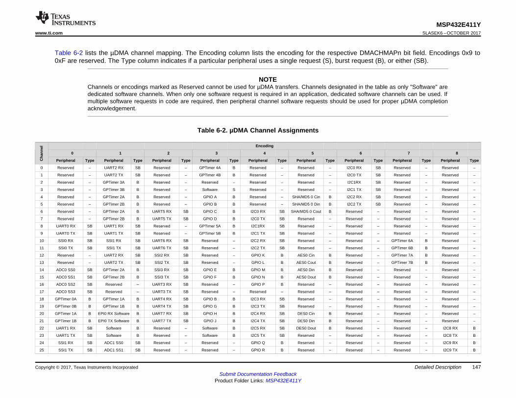
Copyright © 2017, Texas Instruments Incorporated Detailed DescriptionSubmit Documentation Feedback
Product Folder Links: MSP432E411Y
147
MSP432E411Ywww.ti.com SLASEK6 –OCTOBER 2017
Table 6-2 lists the µDMA channel mapping. The Encoding column lists the encoding for the respective DMACHMAPn bit field. Encodings 0x9 to0xF are reserved. The Type column indicates if a particular peripheral uses a single request (S), burst request (B), or either (SB).
NOTEChannels or encodings marked as Reserved cannot be used for µDMA transfers. Channels designated in the table as only "Software" arededicated software channels. When only one software request is required in an application, dedicated software channels can be used. Ifmultiple software requests in code are required, then peripheral channel software requests should be used for proper µDMA completionacknowledgement.
Table 6-2. µDMA Channel Assignments
Cha
nnel Encoding
0 1 2 3 4 5 6 7 8
Peripheral Type Peripheral Type Peripheral Type Peripheral Type Peripheral Type Peripheral Type Peripheral Type Peripheral Type Peripheral Type
0 Reserved – UART2 RX SB Reserved – GPTimer 4A B Reserved – Reserved – I2C0 RX SB Reserved – Reserved –
1 Reserved – UART2 TX SB Reserved – GPTimer 4B B Reserved – Reserved – I2C0 TX SB Reserved – Reserved –
2 Reserved – GPTimer 3A B Reserved – Reserved – Reserved – Reserved – I2C1RX SB Reserved – Reserved –
3 Reserved – GPTimer 3B B Reserved – Software S Reserved – Reserved – I2C1 TX SB Reserved – Reserved –
4 Reserved – GPTimer 2A B Reserved – GPIO A B Reserved – SHA/MD5 0 Cin B I2C2 RX SB Reserved – Reserved –
5 Reserved – GPTimer 2B B Reserved – GPIO B B Reserved – SHA/MD5 0 Din B I2C2 TX SB Reserved – Reserved –
6 Reserved – GPTimer 2A B UART5 RX SB GPIO C B I2C0 RX SB SHA/MD5 0 Cout B Reserved – Reserved – Reserved –
7 Reserved – GPTimer 2B B UART5 TX SB GPIO D B I2C0 TX SB Reserved – Reserved – Reserved – Reserved –
8 UART0 RX SB UART1 RX SB Reserved – GPTimer 5A B I2C1RX SB Reserved – Reserved – Reserved – Reserved –
9 UART0 TX SB UART1 TX SB Reserved – GPTimer 5B B I2C1 TX SB Reserved – Reserved – Reserved – Reserved –
10 SSI0 RX SB SSI1 RX SB UART6 RX SB Reserved – I2C2 RX SB Reserved – Reserved – GPTimer 6A B Reserved –
11 SSI0 TX SB SSI1 TX SB UART6 TX SB Reserved – I2C2 TX SB Reserved – Reserved – GPTimer 6B B Reserved –
12 Reserved – UART2 RX SB SSI2 RX SB Reserved – GPIO K B AES0 Cin B Reserved – GPTimer 7A B Reserved –
13 Reserved – UART2 TX SB SSI2 TX SB Reserved – GPIO L B AES0 Cout B Reserved – GPTimer 7B B Reserved –
14 ADC0 SS0 SB GPTimer 2A B SSI3 RX SB GPIO E B GPIO M B AES0 Din B Reserved – Reserved – Reserved –
15 ADC0 SS1 SB GPTimer 2B B SSI3 TX SB GPIO F B GPIO N B AES0 Dout B Reserved – Reserved – Reserved –
16 ADC0 SS2 SB Reserved – UART3 RX SB Reserved – GPIO P B Reserved – Reserved – Reserved – Reserved –
17 ADC0 SS3 SB Reserved – UART3 TX SB Reserved – Reserved – Reserved – Reserved – Reserved – Reserved –
18 GPTimer 0A B GPTimer 1A B UART4 RX SB GPIO B B I2C3 RX SB Reserved – Reserved – Reserved – Reserved –
19 GPTimer 0B B GPTimer 1B B UART4 TX SB GPIO G B I2C3 TX SB Reserved – Reserved – Reserved – Reserved –
20 GPTimer 1A B EPI0 RX Software B UART7 RX SB GPIO H B I2C4 RX SB DES0 Cin B Reserved – Reserved – Reserved –
21 GPTimer 1B B EPI0 TX Software B UART7 TX SB GPIO J B I2C4 TX SB DES0 Din B Reserved – Reserved – Reserved –
22 UART1 RX SB Software B Reserved – Software B I2C5 RX SB DES0 Dout B Reserved – Reserved – I2C8 RX B
23 UART1 TX SB Software B Reserved – Software B I2C5 TX SB Reserved – Reserved – Reserved – I2C8 TX B
24 SSI1 RX SB ADC1 SS0 SB Reserved – Reserved – GPIO Q B Reserved – Reserved – Reserved – I2C9 RX B
25 SSI1 TX SB ADC1 SS1 SB Reserved – Reserved – GPIO R B Reserved – Reserved – Reserved – I2C9 TX B
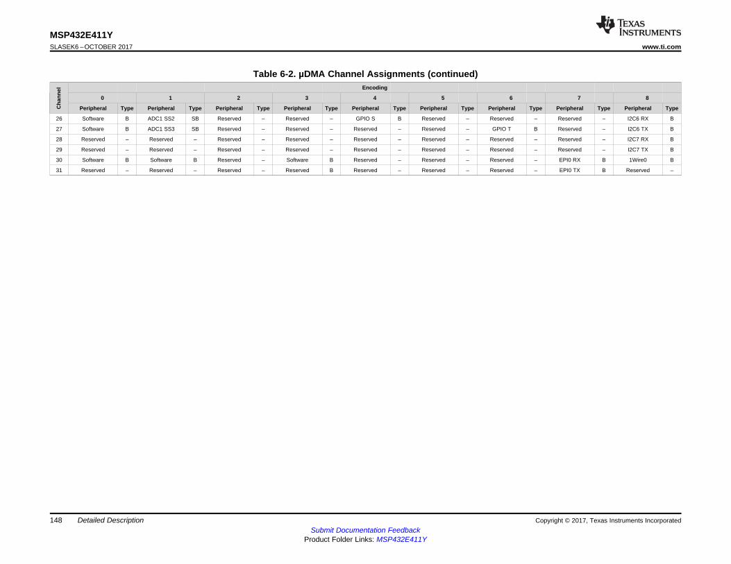
Copyright © 2017, Texas Instruments IncorporatedDetailed DescriptionSubmit Documentation Feedback
Product Folder Links: MSP432E411Y
148
MSP432E411YSLASEK6 –OCTOBER 2017 www.ti.com
Table 6-2. µDMA Channel Assignments (continued)
Cha
nnel Encoding
0 1 2 3 4 5 6 7 8
Peripheral Type Peripheral Type Peripheral Type Peripheral Type Peripheral Type Peripheral Type Peripheral Type Peripheral Type Peripheral Type
26 Software B ADC1 SS2 SB Reserved – Reserved – GPIO S B Reserved – Reserved – Reserved – I2C6 RX B
27 Software B ADC1 SS3 SB Reserved – Reserved – Reserved – Reserved – GPIO T B Reserved – I2C6 TX B
28 Reserved – Reserved – Reserved – Reserved – Reserved – Reserved – Reserved – Reserved – I2C7 RX B
29 Reserved – Reserved – Reserved – Reserved – Reserved – Reserved – Reserved – Reserved – I2C7 TX B
30 Software B Software B Reserved – Software B Reserved – Reserved – Reserved – EPI0 RX B 1Wire0 B
31 Reserved – Reserved – Reserved – Reserved B Reserved – Reserved – Reserved – EPI0 TX B Reserved –
149
MSP432E411Ywww.ti.com SLASEK6 –OCTOBER 2017
Submit Documentation FeedbackProduct Folder Links: MSP432E411Y
Detailed DescriptionCopyright © 2017, Texas Instruments Incorporated
6.5.7.2 System Control and Clocks
System control determines the overall operation of the device. It provides information about the device,controls power-saving features, controls the clocking of the device and individual peripherals, and handlesreset detection and reporting.• Device identification information: version, part number, SRAM size, flash memory size, and so on• Power control
– On-chip fixed low dropout (LDO) voltage regulator– Hibernation module manages the power-up and power-down 3.3-V sequencing and control for the
core digital logic and analog circuits– Low-power options for MCU: sleep and deep-sleep modes with clock gating– Low-power options for on-chip modules: software controls shutdown of individual peripherals and
memory– 3.3-V supply brownout detection and reporting through interrupt or reset
• Multiple clock sources for the system clock. The MCU is clocked by the system clock (SYSCLK) that isdistributed to the processor and integrated peripherals after clock gating. The SYSCLK frequency isbased on the frequency of the clock source and a divisor factor. A PLL is provided for the generation ofsystem clock frequencies in excess of the reference clock provided. The reference clocks for the PLLare the PIOSC and the main crystal oscillator. The following clock sources are provided to the MCU:– 16-MHz precision oscillator (PIOSC)– Main oscillator (MOSC): A frequency-accurate clock source by one of two means: an external
single-ended clock source is connected to the OSC0 input pin, or an external crystal is connectedacross the OSC0 input and OSC1 output pins.
– Low-frequency internal oscillator (LFIOSC): On-chip resource used during power-saving modes.– Hibernate RTC oscillator (RTCOSC): A clock that can be configured to be the 32.768-kHz external
oscillator source from the HIB module or the HIB low-frequency clock source (HIB LFIOSC), whichis in the HIB module.
• Flexible reset sources– Power-on reset (POR)– Reset pin assertion– Brownout reset (BOR) detector alerts to system power drops– Software reset– Watchdog timer reset– Hibernation module event– MOSC failure
• 128-bit unique identifier for individual device identification
6.5.7.3 Programmable Timers
Programmable timers can be used to count or time external events that drive the Timer input pins. Each16- or 32-bit General-Purpose Timer Module (GPTM) block provides two 16-bit timers/counters that canbe configured to operate independently as timers or event counters. These two timers/counters can alsobe configured to operate as one 32-bit timer or one 32-bit RTC. Timers can also be used to trigger analog-to-digital conversions and DMA transfers.
The GPTM contains eight 16- or 32-bit GPTM blocks with the following functional options:
150
MSP432E411YSLASEK6 –OCTOBER 2017 www.ti.com
Submit Documentation FeedbackProduct Folder Links: MSP432E411Y
Detailed Description Copyright © 2017, Texas Instruments Incorporated
• Operating modes– 16- or 32-bit programmable one-shot timer– 16- or 32-bit programmable periodic timer– 16-bit general-purpose timer with an 8-bit prescaler– 32-bit RTC when using an external 32.768-kHz clock as the input– 16-bit input-edge count- or time-capture modes with an 8-bit prescaler– 16-bit PWM mode with an 8-bit prescaler and software-programmable output inversion of the PWM
signal• Count up or down• Sixteen 16- or 32-bit capture/compare PWM (CCP) pins• Daisy-chaining of timer modules lets one timer initiate multiple timing events• Timer synchronization lets selected timers start counting on the same clock cycle• ADC event trigger• User-enabled stalling when the MCU asserts the CPU halt flag during debug (excluding RTC mode)• Can determine the elapsed time between the assertion of the timer interrupt and entry into the ISR• Efficient transfers using µDMA
– Dedicated channel for each timer– Burst request generated on timer interrupt
6.5.7.4 Capture Compare PWM (CCP) Pins
CCP pins can be used by the General-Purpose Timer module to time or count external events using theCCP pin as an input. Alternatively, the GPTM can generate a simple PWM output on the CCP pin.
The 16/32-bit CCP pins can be programmed to operate in the following modes:• Capture: The GP timer is incremented or decremented by programmed events on the CCP input. The
GP timer captures and stores the current timer value when a programmed event occurs.• Compare: The GP timer is incremented or decremented by programmed events on the CCP input. The
GP timer compares the current value with a stored value and generates an interrupt when a matchoccurs.
• PWM: The GP timer is incremented or decremented by the system clock. A PWM signal is generatedbased on a match between the counter value and a value stored in a match register and is output onthe CCP pin.
6.5.7.5 Hibernation (HIB) Module
The HIB module provides logic to switch power off to the main processor and peripherals and to wake onexternal or time-based events. The HIB module includes power-sequencing logic and has the followingfeatures:• 32-bit RTC with 1/32768-second resolution and a 15-bit subseconds counter
– 32-bit RTC seconds match register and a 15-bit subseconds match for timed wakeup and interruptgeneration with 1/32768-second resolution
– RTC predivider trim for making fine adjustments to the clock rate• Hardware calendar function
– Year, month, day, day of week, hours, minutes, and seconds– Four-year leap compensation– 24-hour or AM and PM configuration
• Two mechanisms for power control– System power control using a discrete external regulator– On-chip power control using internal switches under register control
• VDD supplies power when valid, even if VBAT > VDD
151
MSP432E411Ywww.ti.com SLASEK6 –OCTOBER 2017
Submit Documentation FeedbackProduct Folder Links: MSP432E411Y
Detailed DescriptionCopyright © 2017, Texas Instruments Incorporated
• Dedicated pin for wake using an external signal• Can configure the external reset (RST) pin or up to four GPIO port pins as wake sources, with
programmable wake level• Tamper functionality
– Support for four tamper inputs– Configurable level, weak pullup, and glitch filter– Configurable tamper event response– Logging of up to four tamper events– Optional BBRAM erase on tamper detection– Tamper detection and wake-from-hibernate capability– Hibernation clock input failure detect with a switch to the internal oscillator on detection
• RTC operational and hibernation memory valid as long as VDD or VBAT is valid• Low-battery detection, signaling, and interrupt generation, with optional wake on low battery• GPIO pin state can be retained during hibernation• Clock source from an internal low-frequency oscillator (HIB LFIOSC) or a 32.768-kHz external crystal
or oscillator• Sixteen 32-bit words of battery-backed memory to save state during hibernation• Programmable interrupts for:
– RTC match– External wake– Low battery
6.5.7.6 Watchdog Timers
A watchdog timer is used to regain control when a system has failed due to a software error or to thefailure of an external device to respond in the expected way. The watchdog timer can generate aninterrupt, a nonmaskable interrupt, or a reset when a time-out value is reached. In addition, the watchdogtimer is Arm FiRM-compliant and can be configured to generate an interrupt to the MCU on its first time-out, and to generate a reset signal on its second time-out. After the watchdog timer has been configured,the lock register can be written to prevent inadvertently altering the timer configuration.
Two watchdog timer modules are supported: Watchdog Timer 0 uses the system clock for its timer clock;Watchdog Timer 1 uses the PIOSC as its timer clock. The watchdog timer module has the followingfeatures:• 32-bit down counter with a programmable load register• Separate watchdog clock with an enable• Programmable interrupt generation logic with interrupt masking and optional NMI function• Lock register protection from runaway software• Reset generation logic with an enable/disable• User-enabled stalling when the MCU asserts the CPU Halt flag during debug
6.5.7.7 Programmable GPIOs
General-purpose input/output (GPIO) pins offer flexibility for a variety of connections. The GPIO module iscomposed of 18 physical GPIO blocks, each corresponding to an individual GPIO port. The GPIO moduleis FiRM-compliant (compliant to the Arm Foundation IP for Real-Time MCUs specification) and supports 0to 140 programmable I/O pins. The number of GPIOs available depends on the peripherals being used.• Up to 140 GPIOs, depending on configuration• Highly flexible pin multiplexing allows use as GPIO or one of several peripheral functions• 3.3-V tolerant in input configuration
152
MSP432E411YSLASEK6 –OCTOBER 2017 www.ti.com
Submit Documentation FeedbackProduct Folder Links: MSP432E411Y
Detailed Description Copyright © 2017, Texas Instruments Incorporated
• Advanced high-performance bus (AHB) accesses all ports:– Ports A to H, J to N, and P to T
• Fast toggle capable of a change every clock cycle for ports on AHB• Programmable control for GPIO interrupts
– Interrupt generation masking– Edge-triggered on rising, falling, or both– Level-sensitive on high or low values– Per-pin interrupts available on port P and port Q
• Bit masking in both read and write operations through address lines• Can be used to initiate an ADC sample sequence or a µDMA transfer• Pin state can be retained during hibernation mode; pins on port P can be programmed to wake on
level in hibernation mode• Pins configured as digital inputs are Schmitt triggered• Programmable control for GPIO pad configuration
– Weak pullup or pulldown resistors– 2-, 4-, 6-, 8-, 10-, or 12-mA pad drive for digital communication; up to four pads can sink 18-mA for
high-current applications– Slew rate control for 8-, 10-, and 12-mA pad drive– Open-drain enables– Digital-input enables
6.5.8 LCD ControllerThe LCD controller supports the following features:• Character-based panels
– Support for two character panels (CS0 and CS1) with independent and programmable bus timingparameters when in asynchronous Hitachi, Motorola, and Intel modes
– Support for one character panel (CS0) with programmable bus timing parameters when insynchronous Motorola and Intel modes
– Can be used as a generic 16-bit address and data interleaved MPU bus master with no externalstall
• Passive matrix LCD panels– Panel types including STN, DSTN, and C-DSTN– AC Bias Control
• Active matrix LCD panels– Panel types including TN TFT– 1, 2, 4, or 8 bits per pixel with palette RAM and 16 or 24 bits per pixel without palette RAM
• OLED panels– Passive matrix (PM OLED) with frame buffer and controller IC inside the panel– Active matrix (AM OLED)
• Bus mastering from either system SRAM or EPI memory
6.5.9 Advanced Motion ControlThe motion control functions that are integrated into the device support the following features:• Eight advanced PWM outputs for motion and energy applications• Four fault inputs to promote low-latency shutdown• One quadrature encoder input (QEI)
The following sections provides more detail on these motion control functions.
153
MSP432E411Ywww.ti.com SLASEK6 –OCTOBER 2017
Submit Documentation FeedbackProduct Folder Links: MSP432E411Y
Detailed DescriptionCopyright © 2017, Texas Instruments Incorporated
6.5.9.1 Pulse Width Modulation (PWM)
PWM is a powerful technique for digitally encoding analog signal levels. High-resolution counters are usedto generate a square wave, and the duty cycle of the square wave is modulated to encode an analogsignal. Typical applications include switching power supplies and motor control.
One PWM module is included, with four PWM generator blocks and a control block, for a total of eightPWM outputs. Each PWM generator block contains one timer (16-bit down or up/down counter), twocomparators, a PWM signal generator, a dead-band generator, and an interrupt or ADC-trigger selector.
Each PWM generator block produces two PWM signals that can be either independent signals or a pair ofcomplementary signals with dead-band delays inserted.
Each PWM generator has the following features:• Four fault-condition handling inputs to quickly provide low-latency shutdown and prevent damage to
the motor being controlled• One 16-bit counter
– Runs in down or up/down mode– Output frequency controlled by a 16-bit load value– Synchronized load value updates– Produces output signals at zero and load value
• Two PWM comparators– Synchronized comparator value updates– Produces output signals on match
• PWM signal generator– Output PWM signal is constructed based on actions taken as a result of the counter and PWM
comparator output signals.– Produces two independent PWM signals
• Dead-band generator– Produces two PWM signals with programmable dead-band delays suitable for driving a half-H
bridge– Can be bypassed, leaving input PWM signals unmodified
• Can initiate an ADC sample sequence
The control block determines the polarity of the PWM signals and which signals are passed through to thepins. The output of the PWM generation blocks are managed by the output control block before beingpassed to the device pins. The PWM control block has the following options:• PWM output enable of each PWM signal• Optional output inversion of each PWM signal (polarity control)• Optional fault handling for each PWM signal• Synchronization of timers in the PWM generator blocks• Synchronization of timer/comparator updates across the PWM generator blocks• Extended PWM synchronization of timer/comparator updates across the PWM generator blocks• Interrupt status summary of the PWM generator blocks• Extended PWM fault handling, with multiple fault signals, programmable polarities, and filtering• PWM generators can be operated independently or synchronized with other generators
154
MSP432E411YSLASEK6 –OCTOBER 2017 www.ti.com
Submit Documentation FeedbackProduct Folder Links: MSP432E411Y
Detailed Description Copyright © 2017, Texas Instruments Incorporated
6.5.9.2 Quadrature Encoder With Index (QEI) Module
A quadrature encoder, also known as a 2-channel incremental encoder, converts linear displacement intoa pulse signal. By monitoring both the number of pulses and the relative phase of the two signals, theposition, direction of rotation, and speed can be tracked. In addition, a third channel, or index signal, canbe used to reset the position counter. The QEI module interprets the code produced by a quadratureencoder wheel to integrate position over time and determine direction of rotation. In addition, it cancapture a running estimate of the velocity of the encoder wheel. The input frequency of the QEI inputsmay be as high as 1/4 of the system frequency (for example, 30 MHz for a 120-MHz system).
One QEI module provides control of one motor with the following features:• Position integrator that tracks the encoder position• Programmable noise filter on the inputs• Velocity capture using built-in timer• The input frequency of the QEI inputs may be as high as 1/4 of the system frequency (for example,
12.5 MHz for a 50-MHz system)• Interrupt generation on:
– Index pulse– Velocity-timer expiration– Direction change– Quadrature error detection
6.5.10 AnalogIntegrated analog functions include:• Two 12-bit ADCs with a total of 24 analog input channels and each with a sample rate of 2 Msps (see
Section 6.5.10.1)• Three analog comparators (see Section 6.5.10.2)• On-chip voltage regulator
6.5.10.1 ADC
An ADC is a peripheral that converts a continuous analog voltage to a discrete digital number. The ADCmodule features 12-bit conversion resolution and supports 24 input channels plus an internal temperaturesensor. Four buffered sample sequencers allow rapid sampling of up to 24 analog input sources withoutcontroller intervention. Each sample sequencer provides flexible programming with fully configurable inputsource, trigger events, interrupt generation, and sequencer priority. Each ADC module has a digitalcomparator function that lets the conversion value be sent to a comparison unit that provides eight digitalcomparators.
Both ADC modules support the following features:• 24 shared analog input channels• 12-bit precision ADC• Single-ended and differential-input configurations• On-chip internal temperature sensor• Maximum sample rate of two million samples/second• Optional, programmable phase delay• Sample and hold window programmability• Four programmable sample conversion sequencers from one to eight entries long, with corresponding
conversion result FIFOs
155
MSP432E411Ywww.ti.com SLASEK6 –OCTOBER 2017
Submit Documentation FeedbackProduct Folder Links: MSP432E411Y
Detailed DescriptionCopyright © 2017, Texas Instruments Incorporated
• Flexible trigger control– Controller (software)– Timers– Analog comparators– PWM– GPIO
• Hardware averaging of up to 64 samples• Eight digital comparators• Converter uses two external reference signals (VREFA+ and VREFA–) or VDDA and GNDA as the
voltage reference• Power and ground for the analog circuitry is separate from the digital power and ground• Efficient transfers using µDMA
– Dedicated channel for each sample sequencer– ADC module uses burst requests for DMA
• Global Alternate Clock (ALTCLK) resource or System Clock (SYSCLK) can be used to generate ADCclock.
6.5.10.2 Analog Comparators
An analog comparator is a peripheral that compares two analog voltages and provides a logical outputthat signals the comparison result. The independent integrated analog comparators can be configured todrive an output or generate an interrupt or ADC event.
The comparator can provide its output to a device pin, acting as a replacement for an analog comparatoron the board, or it can be used to signal the application via interrupts or triggers to the ADC to cause it tostart capturing a sample sequence. The interrupt generation and ADC triggering logic is separate. Thismeans, for example, that an interrupt can be generated on a rising edge and the ADC triggered on afalling edge.
Each analog comparator supports the following functions:• Compare external pin input to external pin input or to internal programmable voltage reference• Compare a test voltage against any one of the following voltages:
– An individual external reference voltage– A shared single external reference voltage– A shared internal reference voltage
6.5.11 JTAG and Arm Serial Wire DebugThe Joint Test Action Group (JTAG) port is an IEEE standard that defines a Test Access Port (TAP) andBoundary Scan Architecture for digital integrated circuits and provides a standardized serial interface forcontrolling the associated test logic. The TAP, Instruction Register (IR), and Data Register (DR) can beused to test the interconnections of assembled printed circuit boards and obtain manufacturing informationon the components. The JTAG port also provides a means of accessing and controlling design-for-testfeatures such as I/O pin observation and control, scan testing, and debugging. TI replaces the Arm SW-DP and JTAG-DP with the Arm Serial Wire JTAG Debug Port (SWJ-DP) interface. The SWJ-DP interfacecombines the SWD and JTAG debug ports into one module. This module provides the standard JTAGdebug and test functionality plus real-time access to system memory without halting the core or requiringany target resident code. The SWJ-DP interface has the following features:• IEEE 1149.1-1990 compatible TAP controller• Four-bit IR chain for storing JTAG instructions• IEEE standard instructions: BYPASS, IDCODE, SAMPLE/PRELOAD, and EXTEST• Arm additional instructions: APACC, DPACC, and ABORT
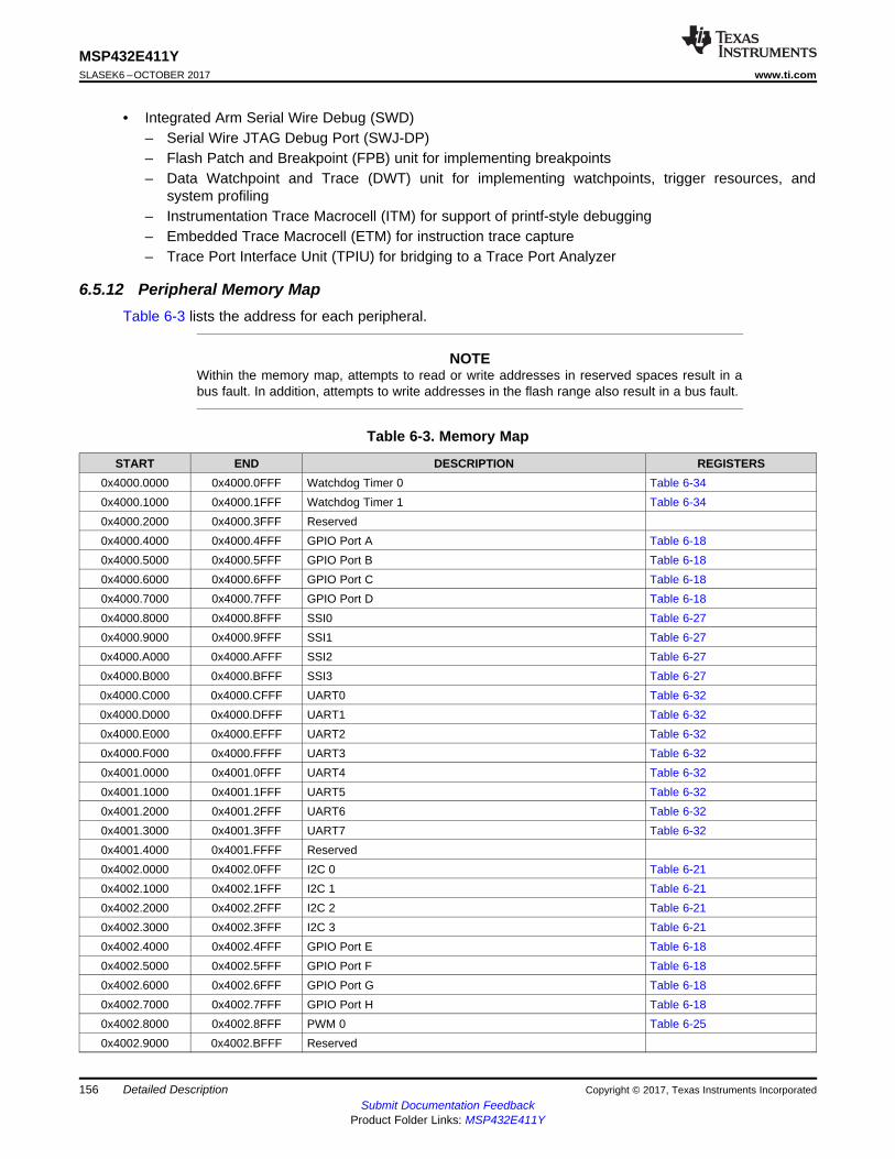
156
MSP432E411YSLASEK6 –OCTOBER 2017 www.ti.com
Submit Documentation FeedbackProduct Folder Links: MSP432E411Y
Detailed Description Copyright © 2017, Texas Instruments Incorporated
• Integrated Arm Serial Wire Debug (SWD)– Serial Wire JTAG Debug Port (SWJ-DP)– Flash Patch and Breakpoint (FPB) unit for implementing breakpoints– Data Watchpoint and Trace (DWT) unit for implementing watchpoints, trigger resources, and
system profiling– Instrumentation Trace Macrocell (ITM) for support of printf-style debugging– Embedded Trace Macrocell (ETM) for instruction trace capture– Trace Port Interface Unit (TPIU) for bridging to a Trace Port Analyzer
6.5.12 Peripheral Memory MapTable 6-3 lists the address for each peripheral.
NOTEWithin the memory map, attempts to read or write addresses in reserved spaces result in abus fault. In addition, attempts to write addresses in the flash range also result in a bus fault.
Table 6-3. Memory Map
START END DESCRIPTION REGISTERS0x4000.0000 0x4000.0FFF Watchdog Timer 0 Table 6-340x4000.1000 0x4000.1FFF Watchdog Timer 1 Table 6-340x4000.2000 0x4000.3FFF Reserved0x4000.4000 0x4000.4FFF GPIO Port A Table 6-180x4000.5000 0x4000.5FFF GPIO Port B Table 6-180x4000.6000 0x4000.6FFF GPIO Port C Table 6-180x4000.7000 0x4000.7FFF GPIO Port D Table 6-180x4000.8000 0x4000.8FFF SSI0 Table 6-270x4000.9000 0x4000.9FFF SSI1 Table 6-270x4000.A000 0x4000.AFFF SSI2 Table 6-270x4000.B000 0x4000.BFFF SSI3 Table 6-270x4000.C000 0x4000.CFFF UART0 Table 6-320x4000.D000 0x4000.DFFF UART1 Table 6-320x4000.E000 0x4000.EFFF UART2 Table 6-320x4000.F000 0x4000.FFFF UART3 Table 6-320x4001.0000 0x4001.0FFF UART4 Table 6-320x4001.1000 0x4001.1FFF UART5 Table 6-320x4001.2000 0x4001.2FFF UART6 Table 6-320x4001.3000 0x4001.3FFF UART7 Table 6-320x4001.4000 0x4001.FFFF Reserved0x4002.0000 0x4002.0FFF I2C 0 Table 6-210x4002.1000 0x4002.1FFF I2C 1 Table 6-210x4002.2000 0x4002.2FFF I2C 2 Table 6-210x4002.3000 0x4002.3FFF I2C 3 Table 6-210x4002.4000 0x4002.4FFF GPIO Port E Table 6-180x4002.5000 0x4002.5FFF GPIO Port F Table 6-180x4002.6000 0x4002.6FFF GPIO Port G Table 6-180x4002.7000 0x4002.7FFF GPIO Port H Table 6-180x4002.8000 0x4002.8FFF PWM 0 Table 6-250x4002.9000 0x4002.BFFF Reserved
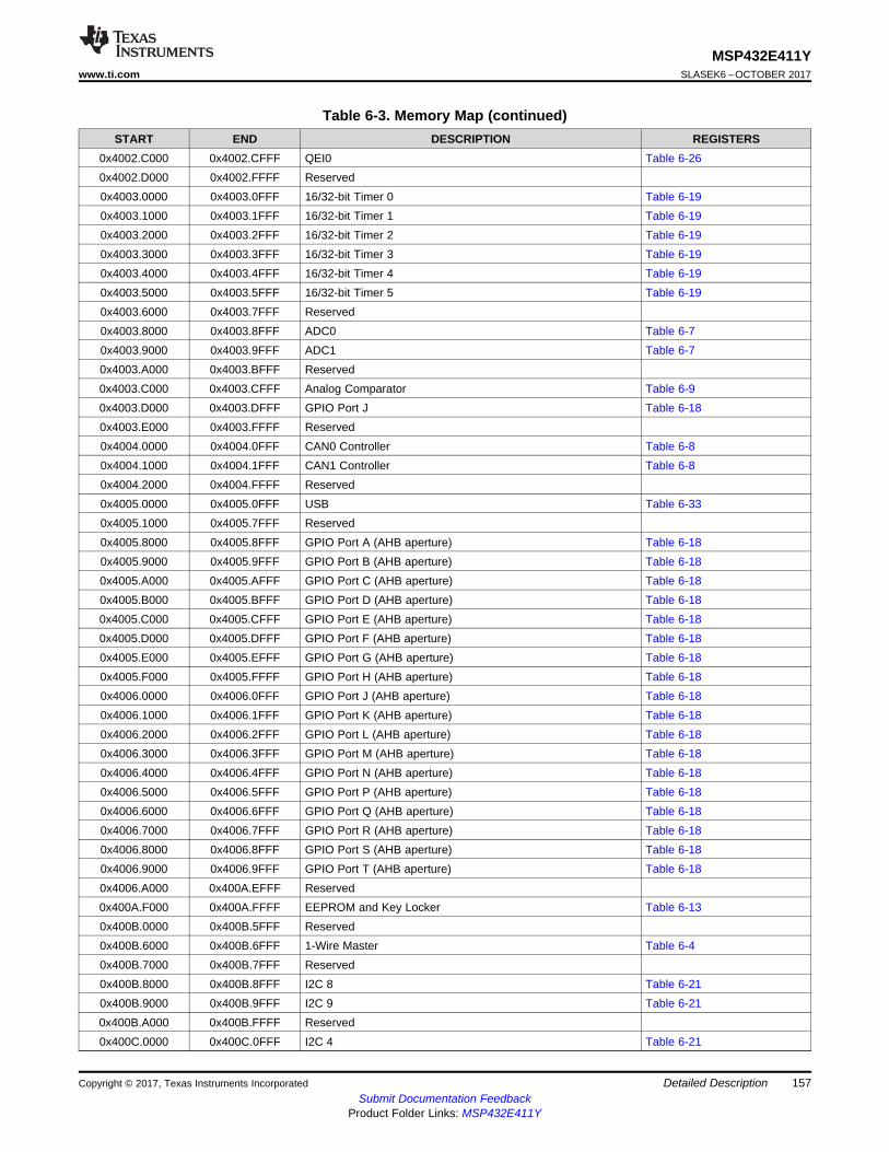
157
MSP432E411Ywww.ti.com SLASEK6 –OCTOBER 2017
Submit Documentation FeedbackProduct Folder Links: MSP432E411Y
Detailed DescriptionCopyright © 2017, Texas Instruments Incorporated
Table 6-3. Memory Map (continued)START END DESCRIPTION REGISTERS
0x4002.C000 0x4002.CFFF QEI0 Table 6-260x4002.D000 0x4002.FFFF Reserved0x4003.0000 0x4003.0FFF 16/32-bit Timer 0 Table 6-190x4003.1000 0x4003.1FFF 16/32-bit Timer 1 Table 6-190x4003.2000 0x4003.2FFF 16/32-bit Timer 2 Table 6-190x4003.3000 0x4003.3FFF 16/32-bit Timer 3 Table 6-190x4003.4000 0x4003.4FFF 16/32-bit Timer 4 Table 6-190x4003.5000 0x4003.5FFF 16/32-bit Timer 5 Table 6-190x4003.6000 0x4003.7FFF Reserved0x4003.8000 0x4003.8FFF ADC0 Table 6-70x4003.9000 0x4003.9FFF ADC1 Table 6-70x4003.A000 0x4003.BFFF Reserved0x4003.C000 0x4003.CFFF Analog Comparator Table 6-90x4003.D000 0x4003.DFFF GPIO Port J Table 6-180x4003.E000 0x4003.FFFF Reserved0x4004.0000 0x4004.0FFF CAN0 Controller Table 6-80x4004.1000 0x4004.1FFF CAN1 Controller Table 6-80x4004.2000 0x4004.FFFF Reserved0x4005.0000 0x4005.0FFF USB Table 6-330x4005.1000 0x4005.7FFF Reserved0x4005.8000 0x4005.8FFF GPIO Port A (AHB aperture) Table 6-180x4005.9000 0x4005.9FFF GPIO Port B (AHB aperture) Table 6-180x4005.A000 0x4005.AFFF GPIO Port C (AHB aperture) Table 6-180x4005.B000 0x4005.BFFF GPIO Port D (AHB aperture) Table 6-180x4005.C000 0x4005.CFFF GPIO Port E (AHB aperture) Table 6-180x4005.D000 0x4005.DFFF GPIO Port F (AHB aperture) Table 6-180x4005.E000 0x4005.EFFF GPIO Port G (AHB aperture) Table 6-180x4005.F000 0x4005.FFFF GPIO Port H (AHB aperture) Table 6-180x4006.0000 0x4006.0FFF GPIO Port J (AHB aperture) Table 6-180x4006.1000 0x4006.1FFF GPIO Port K (AHB aperture) Table 6-180x4006.2000 0x4006.2FFF GPIO Port L (AHB aperture) Table 6-180x4006.3000 0x4006.3FFF GPIO Port M (AHB aperture) Table 6-180x4006.4000 0x4006.4FFF GPIO Port N (AHB aperture) Table 6-180x4006.5000 0x4006.5FFF GPIO Port P (AHB aperture) Table 6-180x4006.6000 0x4006.6FFF GPIO Port Q (AHB aperture) Table 6-180x4006.7000 0x4006.7FFF GPIO Port R (AHB aperture) Table 6-180x4006.8000 0x4006.8FFF GPIO Port S (AHB aperture) Table 6-180x4006.9000 0x4006.9FFF GPIO Port T (AHB aperture) Table 6-180x4006.A000 0x400A.EFFF Reserved0x400A.F000 0x400A.FFFF EEPROM and Key Locker Table 6-130x400B.0000 0x400B.5FFF Reserved0x400B.6000 0x400B.6FFF 1-Wire Master Table 6-40x400B.7000 0x400B.7FFF Reserved0x400B.8000 0x400B.8FFF I2C 8 Table 6-210x400B.9000 0x400B.9FFF I2C 9 Table 6-210x400B.A000 0x400B.FFFF Reserved0x400C.0000 0x400C.0FFF I2C 4 Table 6-21

158
MSP432E411YSLASEK6 –OCTOBER 2017 www.ti.com
Submit Documentation FeedbackProduct Folder Links: MSP432E411Y
Detailed Description Copyright © 2017, Texas Instruments Incorporated
Table 6-3. Memory Map (continued)START END DESCRIPTION REGISTERS
0x400C.1000 0x400C.1FFF I2C 5 Table 6-210x400C.2000 0x400C.2FFF I2C 6 Table 6-210x400C.3000 0x400C.3FFF I2C 7 Table 6-210x400C.4000 0x400C.FFFF Reserved0x400D.0000 0x400D.0FFF EPI0 Table 6-140x400D.1000 0x400D.FFFF Reserved0x400E.0000 0x400E.0FFF 16/32-bit Timer 6 Table 6-190x400E.1000 0x400E.1FFF 16/32-bit Timer 7 Table 6-190x400E.2000 0x400E.BFFF Reserved0x400E.C000 0x400E.CFFF Ethernet Controller Table 6-150x400E.D000 0x400F.8FFF Reserved0x400F.9000 0x400F.9FFF System Exception Table 6-310x400F.A000 0x400F.BFFF Reserved0x400F.C000 0x400F.CFFF Hibernation Table 6-200x400F.D000 0x400F.DFFF Flash Memory Control Table 6-170x400F.E000 0x400F.EFFF System Control Table 6-300x400F.F000 0x400F.FFFF µDMA Table 6-230x4010.0000 0x41FF.FFFF Reserved0x4200.0000 0x43FF.FFFF Bit-banded alias of 0x4000.0000 through 0x400F.FFFF0x4400.0000 0x4402.FFFF Reserved0x4403.0000 0x4403.0FFF CRC and Cryptographic Control Table 6-100x4403.1000 0x4403.1FFF Reserved (4KB)0x4403.2000 0x4403.3FFF Reserved (8KB)0x4403.4000 0x4403.5FFF SHA/MD5 Table 6-280x4403.6000 0x4403.7FFF AES Table 6-5, Table 6-60x4403.8000 0x4403.9FFF DES Table 6-11, Table 6-120x4403.A000 0x4403.EFFF Reserved0x4403.F000 0x4403.FFFF Reserved (4KB)0x4404.0000 0x4404.FFFF Reserved (64KB)0x4405.0000 0x4405.0FFF LCD Table 6-220x4405.1000 0x4405.3FFF Reserved0x4405.4000 0x4405.4FFF EPHY 0 Table 6-160x4405.5000 0x5FFF.FFFF Reserved0x6000.0000 0xDFFF.FFFF EPI0 Mapped Peripheral and RAM Table 6-14
Table 6-4. 1-Wire Master Registers
OFFSET ACRONYM REGISTER NAME0x0 ONEWIRECS 1-Wire Control and Status0x4 ONEWIRETIM 1-Wire Timing Override0x8 ONEWIREDATW 1-Wire Data Write0xC ONEWIREDATR 1-Wire Data Read0x100 ONEWIREIM 1-Wire Interrupt Mask0x104 ONEWIRERIS 1-Wire Raw Interrupt Status0x108 ONEWIREMIS 1-Wire Masked Interrupt Status0x10C ONEWIREICR 1-Wire Interrupt Clear0x120 ONEWIREDMA 1-Wire µDMA Control0xFC0 ONEWIREPP 1-Wire Peripheral Properties
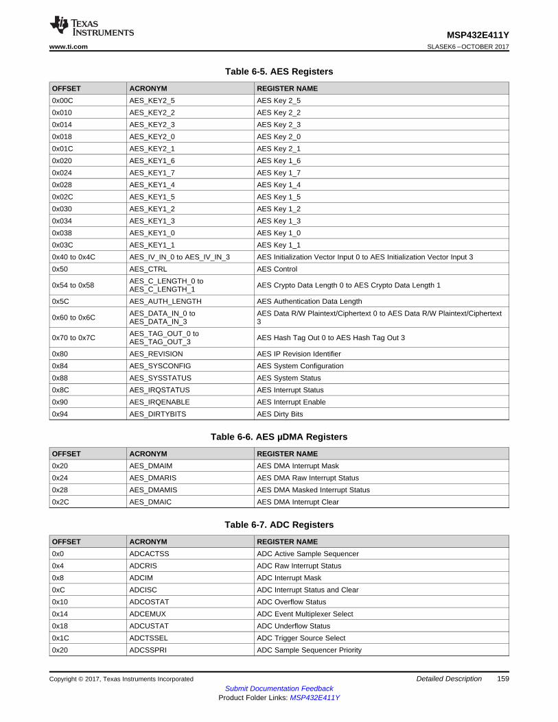
159
MSP432E411Ywww.ti.com SLASEK6 –OCTOBER 2017
Submit Documentation FeedbackProduct Folder Links: MSP432E411Y
Detailed DescriptionCopyright © 2017, Texas Instruments Incorporated
Table 6-5. AES Registers
OFFSET ACRONYM REGISTER NAME0x00C AES_KEY2_5 AES Key 2_50x010 AES_KEY2_2 AES Key 2_20x014 AES_KEY2_3 AES Key 2_30x018 AES_KEY2_0 AES Key 2_00x01C AES_KEY2_1 AES Key 2_10x020 AES_KEY1_6 AES Key 1_60x024 AES_KEY1_7 AES Key 1_70x028 AES_KEY1_4 AES Key 1_40x02C AES_KEY1_5 AES Key 1_50x030 AES_KEY1_2 AES Key 1_20x034 AES_KEY1_3 AES Key 1_30x038 AES_KEY1_0 AES Key 1_00x03C AES_KEY1_1 AES Key 1_10x40 to 0x4C AES_IV_IN_0 to AES_IV_IN_3 AES Initialization Vector Input 0 to AES Initialization Vector Input 30x50 AES_CTRL AES Control
0x54 to 0x58 AES_C_LENGTH_0 toAES_C_LENGTH_1 AES Crypto Data Length 0 to AES Crypto Data Length 1
0x5C AES_AUTH_LENGTH AES Authentication Data Length
0x60 to 0x6C AES_DATA_IN_0 toAES_DATA_IN_3
AES Data R/W Plaintext/Ciphertext 0 to AES Data R/W Plaintext/Ciphertext3
0x70 to 0x7C AES_TAG_OUT_0 toAES_TAG_OUT_3 AES Hash Tag Out 0 to AES Hash Tag Out 3
0x80 AES_REVISION AES IP Revision Identifier0x84 AES_SYSCONFIG AES System Configuration0x88 AES_SYSSTATUS AES System Status0x8C AES_IRQSTATUS AES Interrupt Status0x90 AES_IRQENABLE AES Interrupt Enable0x94 AES_DIRTYBITS AES Dirty Bits
Table 6-6. AES µDMA Registers
OFFSET ACRONYM REGISTER NAME0x20 AES_DMAIM AES DMA Interrupt Mask0x24 AES_DMARIS AES DMA Raw Interrupt Status0x28 AES_DMAMIS AES DMA Masked Interrupt Status0x2C AES_DMAIC AES DMA Interrupt Clear
Table 6-7. ADC Registers
OFFSET ACRONYM REGISTER NAME0x0 ADCACTSS ADC Active Sample Sequencer0x4 ADCRIS ADC Raw Interrupt Status0x8 ADCIM ADC Interrupt Mask0xC ADCISC ADC Interrupt Status and Clear0x10 ADCOSTAT ADC Overflow Status0x14 ADCEMUX ADC Event Multiplexer Select0x18 ADCUSTAT ADC Underflow Status0x1C ADCTSSEL ADC Trigger Source Select0x20 ADCSSPRI ADC Sample Sequencer Priority
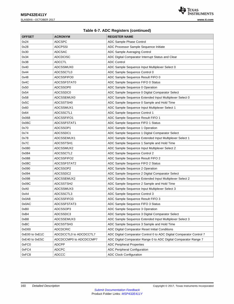
160
MSP432E411YSLASEK6 –OCTOBER 2017 www.ti.com
Submit Documentation FeedbackProduct Folder Links: MSP432E411Y
Detailed Description Copyright © 2017, Texas Instruments Incorporated
Table 6-7. ADC Registers (continued)OFFSET ACRONYM REGISTER NAME0x24 ADCSPC ADC Sample Phase Control0x28 ADCPSSI ADC Processor Sample Sequence Initiate0x30 ADCSAC ADC Sample Averaging Control0x34 ADCDCISC ADC Digital Comparator Interrupt Status and Clear0x38 ADCCTL ADC Control0x40 ADCSSMUX0 ADC Sample Sequence Input Multiplexer Select 00x44 ADCSSCTL0 ADC Sample Sequence Control 00x48 ADCSSFIFO0 ADC Sample Sequence Result FIFO 00x4C ADCSSFSTAT0 ADC Sample Sequence FIFO 0 Status0x50 ADCSSOP0 ADC Sample Sequence 0 Operation0x54 ADCSSDC0 ADC Sample Sequence 0 Digital Comparator Select0x58 ADCSSEMUX0 ADC Sample Sequence Extended Input Multiplexer Select 00x5C ADCSSTSH0 ADC Sample Sequence 0 Sample and Hold Time0x60 ADCSSMUX1 ADC Sample Sequence Input Multiplexer Select 10x64 ADCSSCTL1 ADC Sample Sequence Control 10x068 ADCSSFIFO1 ADC Sample Sequence Result FIFO 10x06C ADCSSFSTAT1 ADC Sample Sequence FIFO 1 Status0x70 ADCSSOP1 ADC Sample Sequence 1 Operation0x74 ADCSSDC1 ADC Sample Sequence 1 Digital Comparator Select0x78 ADCSSEMUX1 ADC Sample Sequence Extended Input Multiplexer Select 10x7C ADCSSTSH1 ADC Sample Sequence 1 Sample and Hold Time0x080 ADCSSMUX2 ADC Sample Sequence Input Multiplexer Select 20x084 ADCSSCTL2 ADC Sample Sequence Control 20x088 ADCSSFIFO2 ADC Sample Sequence Result FIFO 20x08C ADCSSFSTAT2 ADC Sample Sequence FIFO 2 Status0x090 ADCSSOP2 ADC Sample Sequence 2 Operation0x094 ADCSSDC2 ADC Sample Sequence 2 Digital Comparator Select0x098 ADCSSEMUX2 ADC Sample Sequence Extended Input Multiplexer Select 20x09C ADCSSTSH2 ADC Sample Sequence 2 Sample and Hold Time0xA0 ADCSSMUX3 ADC Sample Sequence Input Multiplexer Select 30xA4 ADCSSCTL3 ADC Sample Sequence Control 30x0A8 ADCSSFIFO3 ADC Sample Sequence Result FIFO 30x0AC ADCSSFSTAT3 ADC Sample Sequence FIFO 3 Status0xB0 ADCSSOP3 ADC Sample Sequence 3 Operation0xB4 ADCSSDC3 ADC Sample Sequence 3 Digital Comparator Select0xB8 ADCSSEMUX3 ADC Sample Sequence Extended Input Multiplexer Select 30xBC ADCSSTSH3 ADC Sample Sequence 3 Sample and Hold Time0xD00 ADCDCRIC ADC Digital Comparator Reset Initial Conditions0xE00 to 0xE1C ADCDCCTL0 to ADCDCCTL7 ADC Digital Comparator Control 0 to ADC Digital Comparator Control 70xE40 to 0xE5C ADCDCCMP0 to ADCDCCMP7 ADC Digital Comparator Range 0 to ADC Digital Comparator Range 70xFC0 ADCPP ADC Peripheral Properties0xFC4 ADCPC ADC Peripheral Configuration0xFC8 ADCCC ADC Clock Configuration
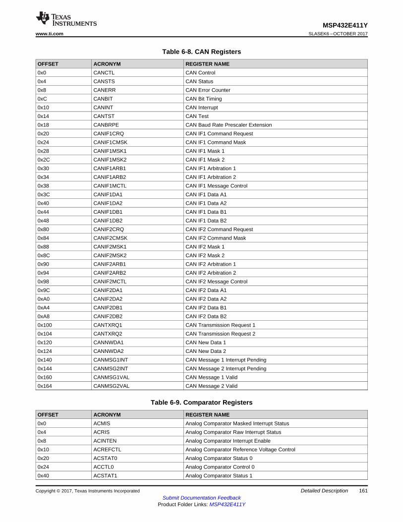
161
MSP432E411Ywww.ti.com SLASEK6 –OCTOBER 2017
Submit Documentation FeedbackProduct Folder Links: MSP432E411Y
Detailed DescriptionCopyright © 2017, Texas Instruments Incorporated
Table 6-8. CAN Registers
OFFSET ACRONYM REGISTER NAME0x0 CANCTL CAN Control0x4 CANSTS CAN Status0x8 CANERR CAN Error Counter0xC CANBIT CAN Bit Timing0x10 CANINT CAN Interrupt0x14 CANTST CAN Test0x18 CANBRPE CAN Baud Rate Prescaler Extension0x20 CANIF1CRQ CAN IF1 Command Request0x24 CANIF1CMSK CAN IF1 Command Mask0x28 CANIF1MSK1 CAN IF1 Mask 10x2C CANIF1MSK2 CAN IF1 Mask 20x30 CANIF1ARB1 CAN IF1 Arbitration 10x34 CANIF1ARB2 CAN IF1 Arbitration 20x38 CANIF1MCTL CAN IF1 Message Control0x3C CANIF1DA1 CAN IF1 Data A10x40 CANIF1DA2 CAN IF1 Data A20x44 CANIF1DB1 CAN IF1 Data B10x48 CANIF1DB2 CAN IF1 Data B20x80 CANIF2CRQ CAN IF2 Command Request0x84 CANIF2CMSK CAN IF2 Command Mask0x88 CANIF2MSK1 CAN IF2 Mask 10x8C CANIF2MSK2 CAN IF2 Mask 20x90 CANIF2ARB1 CAN IF2 Arbitration 10x94 CANIF2ARB2 CAN IF2 Arbitration 20x98 CANIF2MCTL CAN IF2 Message Control0x9C CANIF2DA1 CAN IF2 Data A10xA0 CANIF2DA2 CAN IF2 Data A20xA4 CANIF2DB1 CAN IF2 Data B10xA8 CANIF2DB2 CAN IF2 Data B20x100 CANTXRQ1 CAN Transmission Request 10x104 CANTXRQ2 CAN Transmission Request 20x120 CANNWDA1 CAN New Data 10x124 CANNWDA2 CAN New Data 20x140 CANMSG1INT CAN Message 1 Interrupt Pending0x144 CANMSG2INT CAN Message 2 Interrupt Pending0x160 CANMSG1VAL CAN Message 1 Valid0x164 CANMSG2VAL CAN Message 2 Valid
Table 6-9. Comparator Registers
OFFSET ACRONYM REGISTER NAME0x0 ACMIS Analog Comparator Masked Interrupt Status0x4 ACRIS Analog Comparator Raw Interrupt Status0x8 ACINTEN Analog Comparator Interrupt Enable0x10 ACREFCTL Analog Comparator Reference Voltage Control0x20 ACSTAT0 Analog Comparator Status 00x24 ACCTL0 Analog Comparator Control 00x40 ACSTAT1 Analog Comparator Status 1
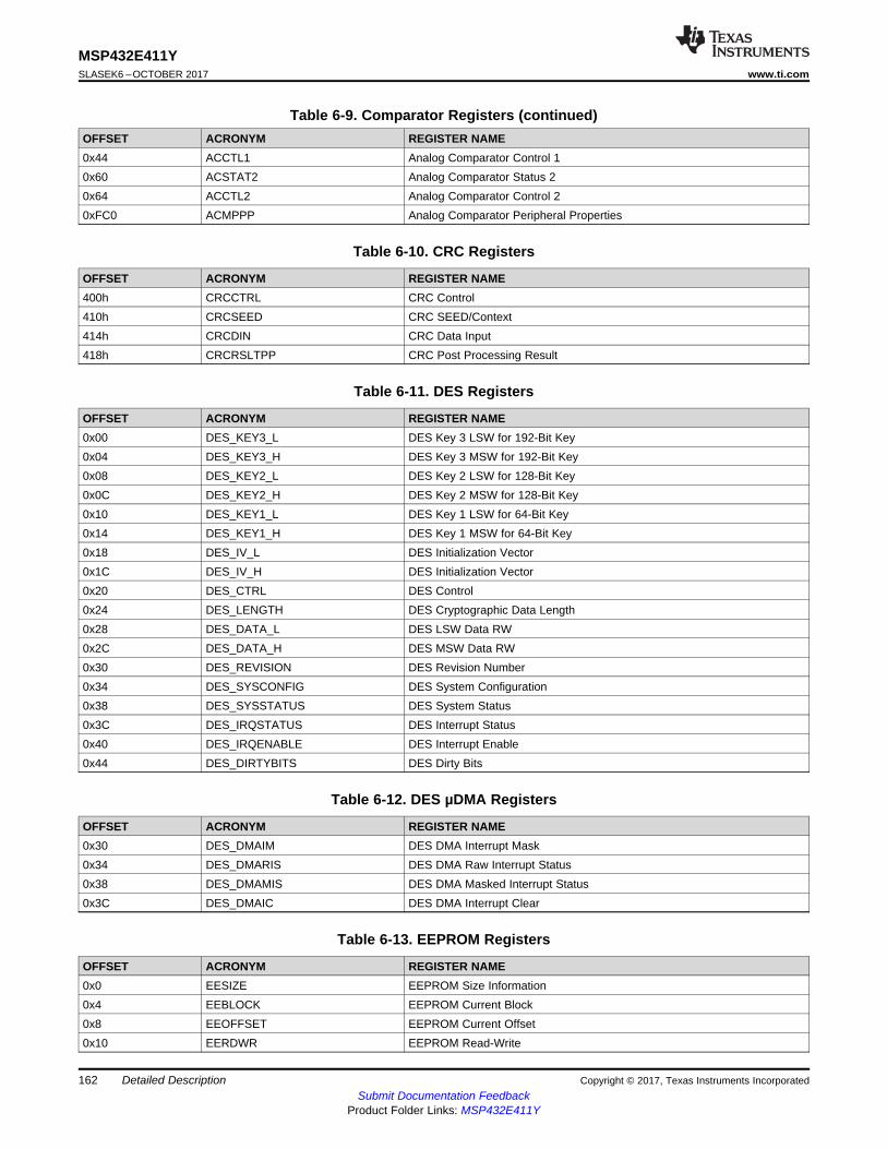
162
MSP432E411YSLASEK6 –OCTOBER 2017 www.ti.com
Submit Documentation FeedbackProduct Folder Links: MSP432E411Y
Detailed Description Copyright © 2017, Texas Instruments Incorporated
Table 6-9. Comparator Registers (continued)OFFSET ACRONYM REGISTER NAME0x44 ACCTL1 Analog Comparator Control 10x60 ACSTAT2 Analog Comparator Status 20x64 ACCTL2 Analog Comparator Control 20xFC0 ACMPPP Analog Comparator Peripheral Properties
Table 6-10. CRC Registers
OFFSET ACRONYM REGISTER NAME400h CRCCTRL CRC Control410h CRCSEED CRC SEED/Context414h CRCDIN CRC Data Input418h CRCRSLTPP CRC Post Processing Result
Table 6-11. DES Registers
OFFSET ACRONYM REGISTER NAME0x00 DES_KEY3_L DES Key 3 LSW for 192-Bit Key0x04 DES_KEY3_H DES Key 3 MSW for 192-Bit Key0x08 DES_KEY2_L DES Key 2 LSW for 128-Bit Key0x0C DES_KEY2_H DES Key 2 MSW for 128-Bit Key0x10 DES_KEY1_L DES Key 1 LSW for 64-Bit Key0x14 DES_KEY1_H DES Key 1 MSW for 64-Bit Key0x18 DES_IV_L DES Initialization Vector0x1C DES_IV_H DES Initialization Vector0x20 DES_CTRL DES Control0x24 DES_LENGTH DES Cryptographic Data Length0x28 DES_DATA_L DES LSW Data RW0x2C DES_DATA_H DES MSW Data RW0x30 DES_REVISION DES Revision Number0x34 DES_SYSCONFIG DES System Configuration0x38 DES_SYSSTATUS DES System Status0x3C DES_IRQSTATUS DES Interrupt Status0x40 DES_IRQENABLE DES Interrupt Enable0x44 DES_DIRTYBITS DES Dirty Bits
Table 6-12. DES µDMA Registers
OFFSET ACRONYM REGISTER NAME0x30 DES_DMAIM DES DMA Interrupt Mask0x34 DES_DMARIS DES DMA Raw Interrupt Status0x38 DES_DMAMIS DES DMA Masked Interrupt Status0x3C DES_DMAIC DES DMA Interrupt Clear
Table 6-13. EEPROM Registers
OFFSET ACRONYM REGISTER NAME0x0 EESIZE EEPROM Size Information0x4 EEBLOCK EEPROM Current Block0x8 EEOFFSET EEPROM Current Offset0x10 EERDWR EEPROM Read-Write
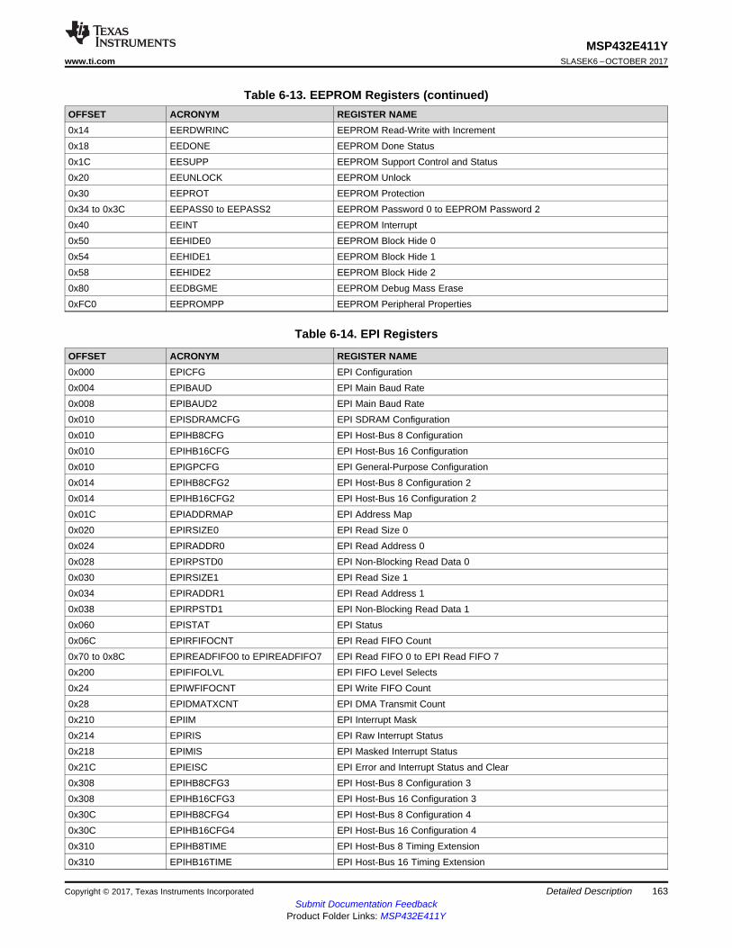
163
MSP432E411Ywww.ti.com SLASEK6 –OCTOBER 2017
Submit Documentation FeedbackProduct Folder Links: MSP432E411Y
Detailed DescriptionCopyright © 2017, Texas Instruments Incorporated
Table 6-13. EEPROM Registers (continued)OFFSET ACRONYM REGISTER NAME0x14 EERDWRINC EEPROM Read-Write with Increment0x18 EEDONE EEPROM Done Status0x1C EESUPP EEPROM Support Control and Status0x20 EEUNLOCK EEPROM Unlock0x30 EEPROT EEPROM Protection0x34 to 0x3C EEPASS0 to EEPASS2 EEPROM Password 0 to EEPROM Password 20x40 EEINT EEPROM Interrupt0x50 EEHIDE0 EEPROM Block Hide 00x54 EEHIDE1 EEPROM Block Hide 10x58 EEHIDE2 EEPROM Block Hide 20x80 EEDBGME EEPROM Debug Mass Erase0xFC0 EEPROMPP EEPROM Peripheral Properties
Table 6-14. EPI Registers
OFFSET ACRONYM REGISTER NAME0x000 EPICFG EPI Configuration0x004 EPIBAUD EPI Main Baud Rate0x008 EPIBAUD2 EPI Main Baud Rate0x010 EPISDRAMCFG EPI SDRAM Configuration0x010 EPIHB8CFG EPI Host-Bus 8 Configuration0x010 EPIHB16CFG EPI Host-Bus 16 Configuration0x010 EPIGPCFG EPI General-Purpose Configuration0x014 EPIHB8CFG2 EPI Host-Bus 8 Configuration 20x014 EPIHB16CFG2 EPI Host-Bus 16 Configuration 20x01C EPIADDRMAP EPI Address Map0x020 EPIRSIZE0 EPI Read Size 00x024 EPIRADDR0 EPI Read Address 00x028 EPIRPSTD0 EPI Non-Blocking Read Data 00x030 EPIRSIZE1 EPI Read Size 10x034 EPIRADDR1 EPI Read Address 10x038 EPIRPSTD1 EPI Non-Blocking Read Data 10x060 EPISTAT EPI Status0x06C EPIRFIFOCNT EPI Read FIFO Count0x70 to 0x8C EPIREADFIFO0 to EPIREADFIFO7 EPI Read FIFO 0 to EPI Read FIFO 70x200 EPIFIFOLVL EPI FIFO Level Selects0x24 EPIWFIFOCNT EPI Write FIFO Count0x28 EPIDMATXCNT EPI DMA Transmit Count0x210 EPIIM EPI Interrupt Mask0x214 EPIRIS EPI Raw Interrupt Status0x218 EPIMIS EPI Masked Interrupt Status0x21C EPIEISC EPI Error and Interrupt Status and Clear0x308 EPIHB8CFG3 EPI Host-Bus 8 Configuration 30x308 EPIHB16CFG3 EPI Host-Bus 16 Configuration 30x30C EPIHB8CFG4 EPI Host-Bus 8 Configuration 40x30C EPIHB16CFG4 EPI Host-Bus 16 Configuration 40x310 EPIHB8TIME EPI Host-Bus 8 Timing Extension0x310 EPIHB16TIME EPI Host-Bus 16 Timing Extension
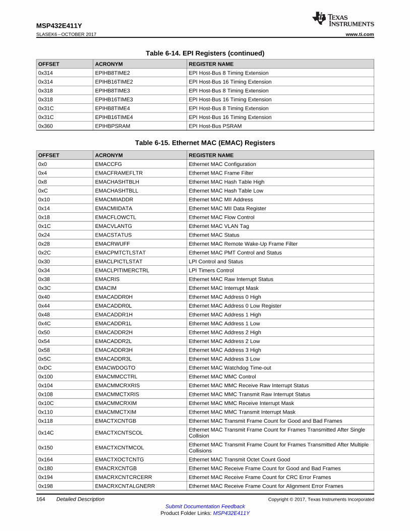
164
MSP432E411YSLASEK6 –OCTOBER 2017 www.ti.com
Submit Documentation FeedbackProduct Folder Links: MSP432E411Y
Detailed Description Copyright © 2017, Texas Instruments Incorporated
Table 6-14. EPI Registers (continued)OFFSET ACRONYM REGISTER NAME0x314 EPIHB8TIME2 EPI Host-Bus 8 Timing Extension0x314 EPIHB16TIME2 EPI Host-Bus 16 Timing Extension0x318 EPIHB8TIME3 EPI Host-Bus 8 Timing Extension0x318 EPIHB16TIME3 EPI Host-Bus 16 Timing Extension0x31C EPIHB8TIME4 EPI Host-Bus 8 Timing Extension0x31C EPIHB16TIME4 EPI Host-Bus 16 Timing Extension0x360 EPIHBPSRAM EPI Host-Bus PSRAM
Table 6-15. Ethernet MAC (EMAC) Registers
OFFSET ACRONYM REGISTER NAME0x0 EMACCFG Ethernet MAC Configuration0x4 EMACFRAMEFLTR Ethernet MAC Frame Filter0x8 EMACHASHTBLH Ethernet MAC Hash Table High0xC EMACHASHTBLL Ethernet MAC Hash Table Low0x10 EMACMIIADDR Ethernet MAC MII Address0x14 EMACMIIDATA Ethernet MAC MII Data Register0x18 EMACFLOWCTL Ethernet MAC Flow Control0x1C EMACVLANTG Ethernet MAC VLAN Tag0x24 EMACSTATUS Ethernet MAC Status0x28 EMACRWUFF Ethernet MAC Remote Wake-Up Frame Filter0x2C EMACPMTCTLSTAT Ethernet MAC PMT Control and Status0x30 EMACLPICTLSTAT LPI Control and Status0x34 EMACLPITIMERCTRL LPI Timers Control0x38 EMACRIS Ethernet MAC Raw Interrupt Status0x3C EMACIM Ethernet MAC Interrupt Mask0x40 EMACADDR0H Ethernet MAC Address 0 High0x44 EMACADDR0L Ethernet MAC Address 0 Low Register0x48 EMACADDR1H Ethernet MAC Address 1 High0x4C EMACADDR1L Ethernet MAC Address 1 Low0x50 EMACADDR2H Ethernet MAC Address 2 High0x54 EMACADDR2L Ethernet MAC Address 2 Low0x58 EMACADDR3H Ethernet MAC Address 3 High0x5C EMACADDR3L Ethernet MAC Address 3 Low0xDC EMACWDOGTO Ethernet MAC Watchdog Time-out0x100 EMACMMCCTRL Ethernet MAC MMC Control0x104 EMACMMCRXRIS Ethernet MAC MMC Receive Raw Interrupt Status0x108 EMACMMCTXRIS Ethernet MAC MMC Transmit Raw Interrupt Status0x10C EMACMMCRXIM Ethernet MAC MMC Receive Interrupt Mask0x110 EMACMMCTXIM Ethernet MAC MMC Transmit Interrupt Mask0x118 EMACTXCNTGB Ethernet MAC Transmit Frame Count for Good and Bad Frames
0x14C EMACTXCNTSCOL Ethernet MAC Transmit Frame Count for Frames Transmitted After SingleCollision
0x150 EMACTXCNTMCOL Ethernet MAC Transmit Frame Count for Frames Transmitted After MultipleCollisions
0x164 EMACTXOCTCNTG Ethernet MAC Transmit Octet Count Good0x180 EMACRXCNTGB Ethernet MAC Receive Frame Count for Good and Bad Frames0x194 EMACRXCNTCRCERR Ethernet MAC Receive Frame Count for CRC Error Frames0x198 EMACRXCNTALGNERR Ethernet MAC Receive Frame Count for Alignment Error Frames
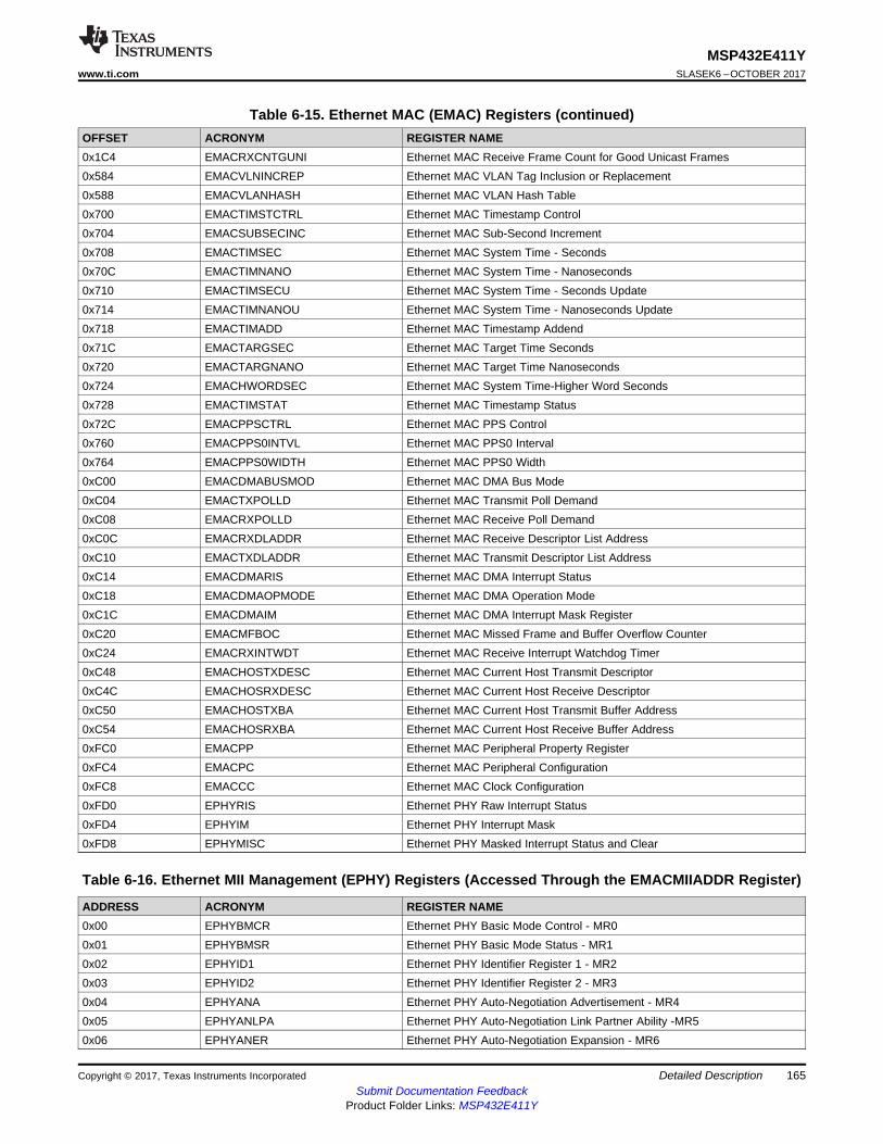
165
MSP432E411Ywww.ti.com SLASEK6 –OCTOBER 2017
Submit Documentation FeedbackProduct Folder Links: MSP432E411Y
Detailed DescriptionCopyright © 2017, Texas Instruments Incorporated
Table 6-15. Ethernet MAC (EMAC) Registers (continued)OFFSET ACRONYM REGISTER NAME0x1C4 EMACRXCNTGUNI Ethernet MAC Receive Frame Count for Good Unicast Frames0x584 EMACVLNINCREP Ethernet MAC VLAN Tag Inclusion or Replacement0x588 EMACVLANHASH Ethernet MAC VLAN Hash Table0x700 EMACTIMSTCTRL Ethernet MAC Timestamp Control0x704 EMACSUBSECINC Ethernet MAC Sub-Second Increment0x708 EMACTIMSEC Ethernet MAC System Time - Seconds0x70C EMACTIMNANO Ethernet MAC System Time - Nanoseconds0x710 EMACTIMSECU Ethernet MAC System Time - Seconds Update0x714 EMACTIMNANOU Ethernet MAC System Time - Nanoseconds Update0x718 EMACTIMADD Ethernet MAC Timestamp Addend0x71C EMACTARGSEC Ethernet MAC Target Time Seconds0x720 EMACTARGNANO Ethernet MAC Target Time Nanoseconds0x724 EMACHWORDSEC Ethernet MAC System Time-Higher Word Seconds0x728 EMACTIMSTAT Ethernet MAC Timestamp Status0x72C EMACPPSCTRL Ethernet MAC PPS Control0x760 EMACPPS0INTVL Ethernet MAC PPS0 Interval0x764 EMACPPS0WIDTH Ethernet MAC PPS0 Width0xC00 EMACDMABUSMOD Ethernet MAC DMA Bus Mode0xC04 EMACTXPOLLD Ethernet MAC Transmit Poll Demand0xC08 EMACRXPOLLD Ethernet MAC Receive Poll Demand0xC0C EMACRXDLADDR Ethernet MAC Receive Descriptor List Address0xC10 EMACTXDLADDR Ethernet MAC Transmit Descriptor List Address0xC14 EMACDMARIS Ethernet MAC DMA Interrupt Status0xC18 EMACDMAOPMODE Ethernet MAC DMA Operation Mode0xC1C EMACDMAIM Ethernet MAC DMA Interrupt Mask Register0xC20 EMACMFBOC Ethernet MAC Missed Frame and Buffer Overflow Counter0xC24 EMACRXINTWDT Ethernet MAC Receive Interrupt Watchdog Timer0xC48 EMACHOSTXDESC Ethernet MAC Current Host Transmit Descriptor0xC4C EMACHOSRXDESC Ethernet MAC Current Host Receive Descriptor0xC50 EMACHOSTXBA Ethernet MAC Current Host Transmit Buffer Address0xC54 EMACHOSRXBA Ethernet MAC Current Host Receive Buffer Address0xFC0 EMACPP Ethernet MAC Peripheral Property Register0xFC4 EMACPC Ethernet MAC Peripheral Configuration0xFC8 EMACCC Ethernet MAC Clock Configuration0xFD0 EPHYRIS Ethernet PHY Raw Interrupt Status0xFD4 EPHYIM Ethernet PHY Interrupt Mask0xFD8 EPHYMISC Ethernet PHY Masked Interrupt Status and Clear
Table 6-16. Ethernet MII Management (EPHY) Registers (Accessed Through the EMACMIIADDR Register)
ADDRESS ACRONYM REGISTER NAME0x00 EPHYBMCR Ethernet PHY Basic Mode Control - MR00x01 EPHYBMSR Ethernet PHY Basic Mode Status - MR10x02 EPHYID1 Ethernet PHY Identifier Register 1 - MR20x03 EPHYID2 Ethernet PHY Identifier Register 2 - MR30x04 EPHYANA Ethernet PHY Auto-Negotiation Advertisement - MR40x05 EPHYANLPA Ethernet PHY Auto-Negotiation Link Partner Ability -MR50x06 EPHYANER Ethernet PHY Auto-Negotiation Expansion - MR6
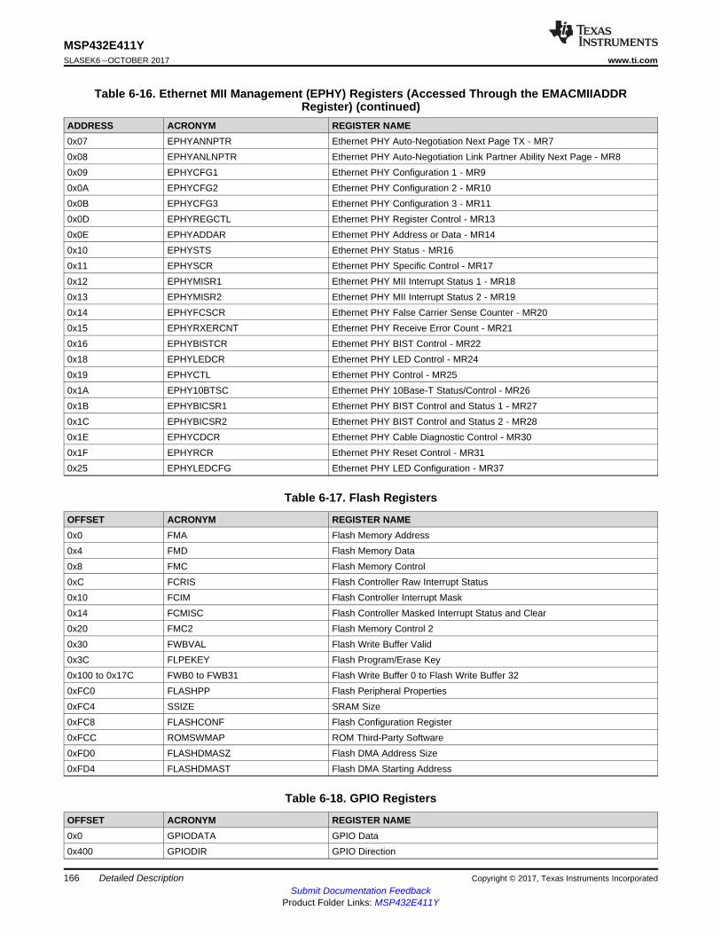
166
MSP432E411YSLASEK6 –OCTOBER 2017 www.ti.com
Submit Documentation FeedbackProduct Folder Links: MSP432E411Y
Detailed Description Copyright © 2017, Texas Instruments Incorporated
Table 6-16. Ethernet MII Management (EPHY) Registers (Accessed Through the EMACMIIADDRRegister) (continued)
ADDRESS ACRONYM REGISTER NAME0x07 EPHYANNPTR Ethernet PHY Auto-Negotiation Next Page TX - MR70x08 EPHYANLNPTR Ethernet PHY Auto-Negotiation Link Partner Ability Next Page - MR80x09 EPHYCFG1 Ethernet PHY Configuration 1 - MR90x0A EPHYCFG2 Ethernet PHY Configuration 2 - MR100x0B EPHYCFG3 Ethernet PHY Configuration 3 - MR110x0D EPHYREGCTL Ethernet PHY Register Control - MR130x0E EPHYADDAR Ethernet PHY Address or Data - MR140x10 EPHYSTS Ethernet PHY Status - MR160x11 EPHYSCR Ethernet PHY Specific Control - MR170x12 EPHYMISR1 Ethernet PHY MII Interrupt Status 1 - MR180x13 EPHYMISR2 Ethernet PHY MII Interrupt Status 2 - MR190x14 EPHYFCSCR Ethernet PHY False Carrier Sense Counter - MR200x15 EPHYRXERCNT Ethernet PHY Receive Error Count - MR210x16 EPHYBISTCR Ethernet PHY BIST Control - MR220x18 EPHYLEDCR Ethernet PHY LED Control - MR240x19 EPHYCTL Ethernet PHY Control - MR250x1A EPHY10BTSC Ethernet PHY 10Base-T Status/Control - MR260x1B EPHYBICSR1 Ethernet PHY BIST Control and Status 1 - MR270x1C EPHYBICSR2 Ethernet PHY BIST Control and Status 2 - MR280x1E EPHYCDCR Ethernet PHY Cable Diagnostic Control - MR300x1F EPHYRCR Ethernet PHY Reset Control - MR310x25 EPHYLEDCFG Ethernet PHY LED Configuration - MR37
Table 6-17. Flash Registers
OFFSET ACRONYM REGISTER NAME0x0 FMA Flash Memory Address0x4 FMD Flash Memory Data0x8 FMC Flash Memory Control0xC FCRIS Flash Controller Raw Interrupt Status0x10 FCIM Flash Controller Interrupt Mask0x14 FCMISC Flash Controller Masked Interrupt Status and Clear0x20 FMC2 Flash Memory Control 20x30 FWBVAL Flash Write Buffer Valid0x3C FLPEKEY Flash Program/Erase Key0x100 to 0x17C FWB0 to FWB31 Flash Write Buffer 0 to Flash Write Buffer 320xFC0 FLASHPP Flash Peripheral Properties0xFC4 SSIZE SRAM Size0xFC8 FLASHCONF Flash Configuration Register0xFCC ROMSWMAP ROM Third-Party Software0xFD0 FLASHDMASZ Flash DMA Address Size0xFD4 FLASHDMAST Flash DMA Starting Address
Table 6-18. GPIO Registers
OFFSET ACRONYM REGISTER NAME0x0 GPIODATA GPIO Data0x400 GPIODIR GPIO Direction
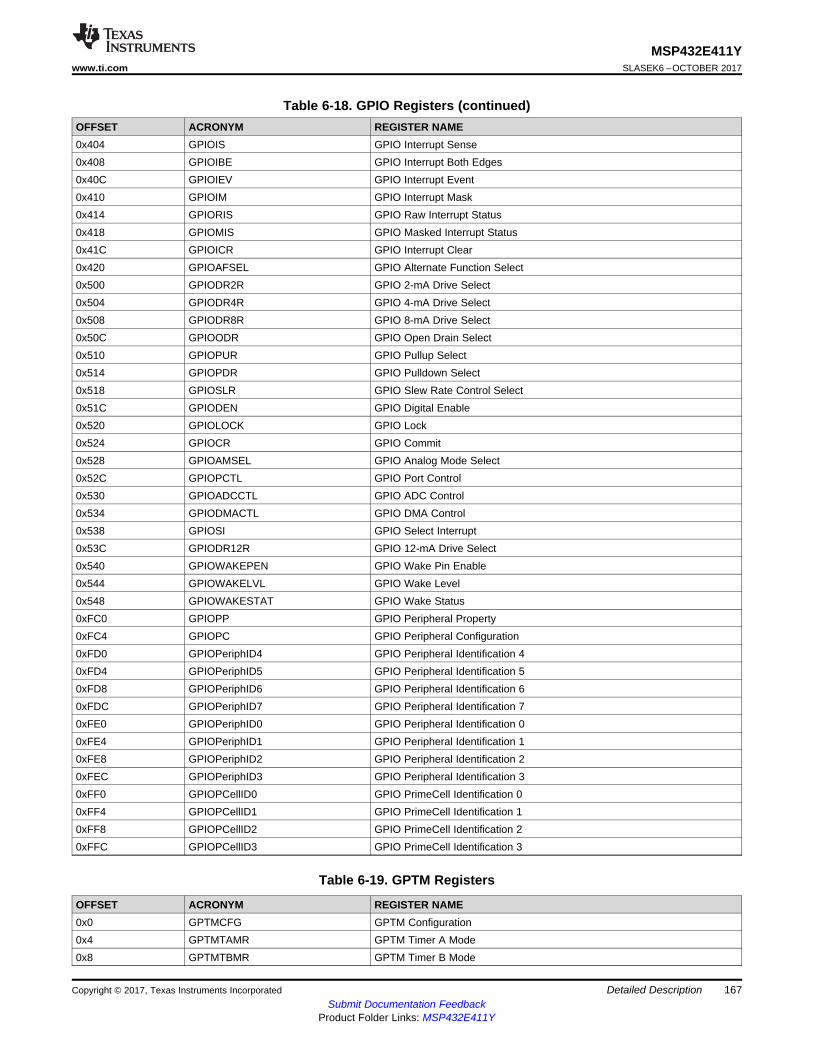
167
MSP432E411Ywww.ti.com SLASEK6 –OCTOBER 2017
Submit Documentation FeedbackProduct Folder Links: MSP432E411Y
Detailed DescriptionCopyright © 2017, Texas Instruments Incorporated
Table 6-18. GPIO Registers (continued)OFFSET ACRONYM REGISTER NAME0x404 GPIOIS GPIO Interrupt Sense0x408 GPIOIBE GPIO Interrupt Both Edges0x40C GPIOIEV GPIO Interrupt Event0x410 GPIOIM GPIO Interrupt Mask0x414 GPIORIS GPIO Raw Interrupt Status0x418 GPIOMIS GPIO Masked Interrupt Status0x41C GPIOICR GPIO Interrupt Clear0x420 GPIOAFSEL GPIO Alternate Function Select0x500 GPIODR2R GPIO 2-mA Drive Select0x504 GPIODR4R GPIO 4-mA Drive Select0x508 GPIODR8R GPIO 8-mA Drive Select0x50C GPIOODR GPIO Open Drain Select0x510 GPIOPUR GPIO Pullup Select0x514 GPIOPDR GPIO Pulldown Select0x518 GPIOSLR GPIO Slew Rate Control Select0x51C GPIODEN GPIO Digital Enable0x520 GPIOLOCK GPIO Lock0x524 GPIOCR GPIO Commit0x528 GPIOAMSEL GPIO Analog Mode Select0x52C GPIOPCTL GPIO Port Control0x530 GPIOADCCTL GPIO ADC Control0x534 GPIODMACTL GPIO DMA Control0x538 GPIOSI GPIO Select Interrupt0x53C GPIODR12R GPIO 12-mA Drive Select0x540 GPIOWAKEPEN GPIO Wake Pin Enable0x544 GPIOWAKELVL GPIO Wake Level0x548 GPIOWAKESTAT GPIO Wake Status0xFC0 GPIOPP GPIO Peripheral Property0xFC4 GPIOPC GPIO Peripheral Configuration0xFD0 GPIOPeriphID4 GPIO Peripheral Identification 40xFD4 GPIOPeriphID5 GPIO Peripheral Identification 50xFD8 GPIOPeriphID6 GPIO Peripheral Identification 60xFDC GPIOPeriphID7 GPIO Peripheral Identification 70xFE0 GPIOPeriphID0 GPIO Peripheral Identification 00xFE4 GPIOPeriphID1 GPIO Peripheral Identification 10xFE8 GPIOPeriphID2 GPIO Peripheral Identification 20xFEC GPIOPeriphID3 GPIO Peripheral Identification 30xFF0 GPIOPCellID0 GPIO PrimeCell Identification 00xFF4 GPIOPCellID1 GPIO PrimeCell Identification 10xFF8 GPIOPCellID2 GPIO PrimeCell Identification 20xFFC GPIOPCellID3 GPIO PrimeCell Identification 3
Table 6-19. GPTM Registers
OFFSET ACRONYM REGISTER NAME0x0 GPTMCFG GPTM Configuration0x4 GPTMTAMR GPTM Timer A Mode0x8 GPTMTBMR GPTM Timer B Mode
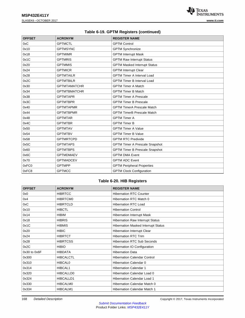
168
MSP432E411YSLASEK6 –OCTOBER 2017 www.ti.com
Submit Documentation FeedbackProduct Folder Links: MSP432E411Y
Detailed Description Copyright © 2017, Texas Instruments Incorporated
Table 6-19. GPTM Registers (continued)OFFSET ACRONYM REGISTER NAME0xC GPTMCTL GPTM Control0x10 GPTMSYNC GPTM Synchronize0x18 GPTMIMR GPTM Interrupt Mask0x1C GPTMRIS GPTM Raw Interrupt Status0x20 GPTMMIS GPTM Masked Interrupt Status0x24 GPTMICR GPTM Interrupt Clear0x28 GPTMTAILR GPTM Timer A Interval Load0x2C GPTMTBILR GPTM Timer B Interval Load0x30 GPTMTAMATCHR GPTM Timer A Match0x34 GPTMTBMATCHR GPTM Timer B Match0x38 GPTMTAPR GPTM Timer A Prescale0x3C GPTMTBPR GPTM Timer B Prescale0x40 GPTMTAPMR GPTM TimerA Prescale Match0x44 GPTMTBPMR GPTM TimerB Prescale Match0x48 GPTMTAR GPTM Timer A0x4C GPTMTBR GPTM Timer B0x50 GPTMTAV GPTM Timer A Value0x54 GPTMTBV GPTM Timer B Value0x58 GPTMRTCPD GPTM RTC Predivide0x5C GPTMTAPS GPTM Timer A Prescale Snapshot0x60 GPTMTBPS GPTM Timer B Prescale Snapshot0x6C GPTMDMAEV GPTM DMA Event0x70 GPTMADCEV GPTM ADC Event0xFC0 GPTMPP GPTM Peripheral Properties0xFC8 GPTMCC GPTM Clock Configuration
Table 6-20. HIB Registers
OFFSET ACRONYM REGISTER NAME0x0 HIBRTCC Hibernation RTC Counter0x4 HIBRTCM0 Hibernation RTC Match 00xC HIBRTCLD Hibernation RTC Load0x10 HIBCTL Hibernation Control0x14 HIBIM Hibernation Interrupt Mask0x18 HIBRIS Hibernation Raw Interrupt Status0x1C HIBMIS Hibernation Masked Interrupt Status0x20 HIBIC Hibernation Interrupt Clear0x24 HIBRTCT Hibernation RTC Trim0x28 HIBRTCSS Hibernation RTC Sub Seconds0x2C HIBIO Hibernation IO Configuration0x30 to 0x6F HIBDATA Hibernation Data0x300 HIBCALCTL Hibernation Calendar Control0x310 HIBCAL0 Hibernation Calendar 00x314 HIBCAL1 Hibernation Calendar 10x320 HIBCALLD0 Hibernation Calendar Load 00x324 HIBCALLD1 Hibernation Calendar Load 10x330 HIBCALM0 Hibernation Calendar Match 00x334 HIBCALM1 Hibernation Calendar Match 1
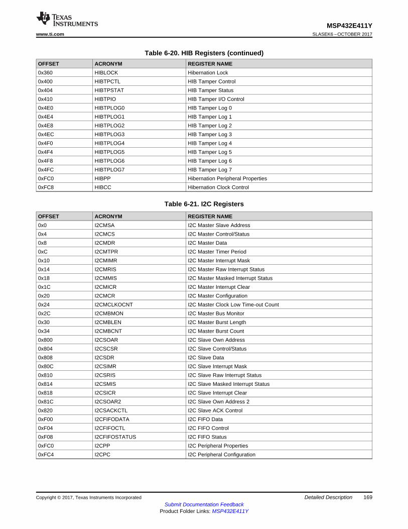
169
MSP432E411Ywww.ti.com SLASEK6 –OCTOBER 2017
Submit Documentation FeedbackProduct Folder Links: MSP432E411Y
Detailed DescriptionCopyright © 2017, Texas Instruments Incorporated
Table 6-20. HIB Registers (continued)OFFSET ACRONYM REGISTER NAME0x360 HIBLOCK Hibernation Lock0x400 HIBTPCTL HIB Tamper Control0x404 HIBTPSTAT HIB Tamper Status0x410 HIBTPIO HIB Tamper I/O Control0x4E0 HIBTPLOG0 HIB Tamper Log 00x4E4 HIBTPLOG1 HIB Tamper Log 10x4E8 HIBTPLOG2 HIB Tamper Log 20x4EC HIBTPLOG3 HIB Tamper Log 30x4F0 HIBTPLOG4 HIB Tamper Log 40x4F4 HIBTPLOG5 HIB Tamper Log 50x4F8 HIBTPLOG6 HIB Tamper Log 60x4FC HIBTPLOG7 HIB Tamper Log 70xFC0 HIBPP Hibernation Peripheral Properties0xFC8 HIBCC Hibernation Clock Control
Table 6-21. I2C Registers
OFFSET ACRONYM REGISTER NAME0x0 I2CMSA I2C Master Slave Address0x4 I2CMCS I2C Master Control/Status0x8 I2CMDR I2C Master Data0xC I2CMTPR I2C Master Timer Period0x10 I2CMIMR I2C Master Interrupt Mask0x14 I2CMRIS I2C Master Raw Interrupt Status0x18 I2CMMIS I2C Master Masked Interrupt Status0x1C I2CMICR I2C Master Interrupt Clear0x20 I2CMCR I2C Master Configuration0x24 I2CMCLKOCNT I2C Master Clock Low Time-out Count0x2C I2CMBMON I2C Master Bus Monitor0x30 I2CMBLEN I2C Master Burst Length0x34 I2CMBCNT I2C Master Burst Count0x800 I2CSOAR I2C Slave Own Address0x804 I2CSCSR I2C Slave Control/Status0x808 I2CSDR I2C Slave Data0x80C I2CSIMR I2C Slave Interrupt Mask0x810 I2CSRIS I2C Slave Raw Interrupt Status0x814 I2CSMIS I2C Slave Masked Interrupt Status0x818 I2CSICR I2C Slave Interrupt Clear0x81C I2CSOAR2 I2C Slave Own Address 20x820 I2CSACKCTL I2C Slave ACK Control0xF00 I2CFIFODATA I2C FIFO Data0xF04 I2CFIFOCTL I2C FIFO Control0xF08 I2CFIFOSTATUS I2C FIFO Status0xFC0 I2CPP I2C Peripheral Properties0xFC4 I2CPC I2C Peripheral Configuration
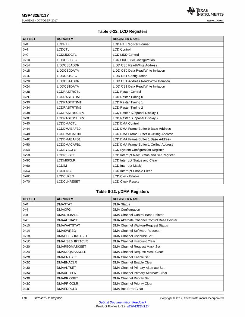
170
MSP432E411YSLASEK6 –OCTOBER 2017 www.ti.com
Submit Documentation FeedbackProduct Folder Links: MSP432E411Y
Detailed Description Copyright © 2017, Texas Instruments Incorporated
Table 6-22. LCD Registers
OFFSET ACRONYM REGISTER NAME0x0 LCDPID LCD PID Register Format0x4 LCDCTL LCD Control0xC LCDLIDDCTL LCD LIDD Control0x10 LIDDCS0CFG LCD LIDD CS0 Configuration0x14 LIDDCS0ADDR LIDD CS0 Read/Write Address0x18 LIDDCS0DATA LIDD CS0 Data Read/Write Initiation0x1C LIDDCS1CFG LIDD CS1 Configuration0x20 LIDDCS1ADDR LIDD CS1 Address Read/Write Initiation0x24 LIDDCS1DATA LIDD CS1 Data Read/Write Initiation0x28 LCDRASTRCTL LCD Raster Control0x2C LCDRASTRTIM0 LCD Raster Timing 00x30 LCDRASTRTIM1 LCD Raster Timing 10x34 LCDRASTRTIM2 LCD Raster Timing 20x38 LCDRASTRSUBP1 LCD Raster Subpanel Display 10x3C LCDRASTRSUBP2 LCD Raster Subpanel Display 20x40 LCDDMACTL LCD DMA Control0x44 LCDDMABAFB0 LCD DMA Frame Buffer 0 Base Address0x48 LCDDMACAFB0 LCD DMA Frame Buffer 0 Ceiling Address0x4C LCDDMABAFB1 LCD DMA Frame Buffer 1 Base Address0x50 LCDDMACAFB1 LCD DMA Frame Buffer 1 Ceiling Address0x54 LCDSYSCFG LCD System Configuration Register0x58 LCDRISSET LCD Interrupt Raw Status and Set Register0x5C LCDMISCLR LCD Interrupt Status and Clear0x60 LCDIM LCD Interrupt Mask0x64 LCDIENC LCD Interrupt Enable Clear0x6C LCDCLKEN LCD Clock Enable0x70 LCDCLKRESET LCD Clock Resets
Table 6-23. µDMA Registers
OFFSET ACRONYM REGISTER NAME0x0 DMASTAT DMA Status0x4 DMACFG DMA Configuration0x8 DMACTLBASE DMA Channel Control Base Pointer0xC DMAALTBASE DMA Alternate Channel Control Base Pointer0x10 DMAWAITSTAT DMA Channel Wait-on-Request Status0x14 DMASWREQ DMA Channel Software Request0x18 DMAUSEBURSTSET DMA Channel Useburst Set0x1C DMAUSEBURSTCLR DMA Channel Useburst Clear0x20 DMAREQMASKSET DMA Channel Request Mask Set0x24 DMAREQMASKCLR DMA Channel Request Mask Clear0x28 DMAENASET DMA Channel Enable Set0x2C DMAENACLR DMA Channel Enable Clear0x30 DMAALTSET DMA Channel Primary Alternate Set0x34 DMAALTCLR DMA Channel Primary Alternate Clear0x38 DMAPRIOSET DMA Channel Priority Set0x3C DMAPRIOCLR DMA Channel Priority Clear0x4C DMAERRCLR DMA Bus Error Clear
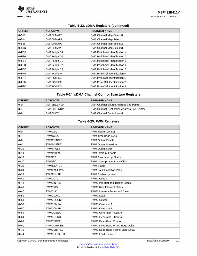
171
MSP432E411Ywww.ti.com SLASEK6 –OCTOBER 2017
Submit Documentation FeedbackProduct Folder Links: MSP432E411Y
Detailed DescriptionCopyright © 2017, Texas Instruments Incorporated
Table 6-23. µDMA Registers (continued)OFFSET ACRONYM REGISTER NAME0x510 DMACHMAP0 DMA Channel Map Select 00x514 DMACHMAP1 DMA Channel Map Select 10x518 DMACHMAP2 DMA Channel Map Select 20x51C DMACHMAP3 DMA Channel Map Select 30xFD0 DMAPeriphID4 DMA Peripheral Identification 40xFE0 DMAPeriphID0 DMA Peripheral Identification 00xFE4 DMAPeriphID1 DMA Peripheral Identification 10xFE8 DMAPeriphID2 DMA Peripheral Identification 20xFEC DMAPeriphID3 DMA Peripheral Identification 30xFF0 DMAPCellID0 DMA PrimeCell Identification 00xFF4 DMAPCellID1 DMA PrimeCell Identification 10xFF8 DMAPCellID2 DMA PrimeCell Identification 20xFFC DMAPCellID3 DMA PrimeCell Identification 3
Table 6-24. µDMA Channel Control Structure Registers
OFFSET ACRONYM REGISTER NAME0x0 DMASRCENDP DMA Channel Source Address End Pointer0x4 DMADSTENDP DMA Channel Destination Address End Pointer0x8 DMACHCTL DMA Channel Control Word
Table 6-25. PWM Registers
OFFSET ACRONYM REGISTER NAME0x0 PWMCTL PWM Master Control0x4 PWMSYNC PWM Time Base Sync0x8 PWMENABLE PWM Output Enable0xC PWMINVERT PWM Output Inversion0x10 PWMFAULT PWM Output Fault0x14 PWMINTEN PWM Interrupt Enable0x18 PWMRIS PWM Raw Interrupt Status0x1C PWMISC PWM Interrupt Status and Clear0x20 PWMSTATUS PWM Status0x24 PWMFAULTVAL PWM Fault Condition Value0x28 PWMENUPD PWM Enable Update0x40 PWM0CTL PWM0 Control0x44 PWM0INTEN PWM0 Interrupt and Trigger Enable0x48 PWM0RIS PWM0 Raw Interrupt Status0x4C PWM0ISC PWM0 Interrupt Status and Clear0x50 PWM0LOAD PWM0 Load0x54 PWM0COUNT PWM0 Counter0x58 PWM0CMPA PWM0 Compare A0x5C PWM0CMPB PWM0 Compare B0x60 PWM0GENA PWM0 Generator A Control0x64 PWM0GENB PWM0 Generator B Control0x68 PWM0DBCTL PWM0 Dead-Band Control0x6C PWM0DBRISE PWM0 Dead-Band Rising-Edge Delay0x70 PWM0DBFALL PWM0 Dead-Band Falling-Edge-Delay0x74 PWM0FLTSRC0 PWM0 Fault Source 0
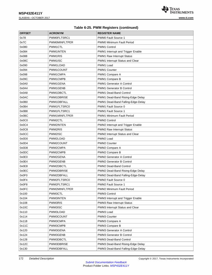
172
MSP432E411YSLASEK6 –OCTOBER 2017 www.ti.com
Submit Documentation FeedbackProduct Folder Links: MSP432E411Y
Detailed Description Copyright © 2017, Texas Instruments Incorporated
Table 6-25. PWM Registers (continued)OFFSET ACRONYM REGISTER NAME0x78 PWM0FLTSRC1 PWM0 Fault Source 10x7C PWM0MINFLTPER PWM0 Minimum Fault Period0x080 PWM1CTL PWM1 Control0x084 PWM1INTEN PWM1 Interrupt and Trigger Enable0x088 PWM1RIS PWM1 Raw Interrupt Status0x08C PWM1ISC PWM1 Interrupt Status and Clear0x090 PWM1LOAD PWM1 Load0x094 PWM1COUNT PWM1 Counter0x098 PWM1CMPA PWM1 Compare A0x09C PWM1CMPB PWM1 Compare B0x0A0 PWM1GENA PWM1 Generator A Control0x0A4 PWM1GENB PWM1 Generator B Control0x0A8 PWM1DBCTL PWM1 Dead-Band Control0x0AC PWM1DBRISE PWM1 Dead-Band Rising-Edge Delay0x0B0 PWM1DBFALL PWM1 Dead-Band Falling-Edge-Delay0x0B4 PWM1FLTSRC0 PWM1 Fault Source 00x0B8 PWM1FLTSRC1 PWM1 Fault Source 10x0BC PWM1MINFLTPER PWM1 Minimum Fault Period0x0C0 PWM2CTL PWM2 Control0x0C4 PWM2INTEN PWM2 Interrupt and Trigger Enable0x0C8 PWM2RIS PWM2 Raw Interrupt Status0x0CC PWM2ISC PWM2 Interrupt Status and Clear0x0D0 PWM2LOAD PWM2 Load0x0D4 PWM2COUNT PWM2 Counter0x0D8 PWM2CMPA PWM2 Compare A0x0DC PWM2CMPB PWM2 Compare B0x0E0 PWM2GENA PWM2 Generator A Control0x0E4 PWM2GENB PWM2 Generator B Control0x0E8 PWM2DBCTL PWM2 Dead-Band Control0x0EC PWM2DBRISE PWM2 Dead-Band Rising-Edge Delay0x0F0 PWM2DBFALL PWM2 Dead-Band Falling-Edge-Delay0x0F4 PWM2FLTSRC0 PWM2 Fault Source 00x0F8 PWM2FLTSRC1 PWM2 Fault Source 10x0FC PWM2MINFLTPER PWM2 Minimum Fault Period0x100 PWM3CTL PWM3 Control0x104 PWM3INTEN PWM3 Interrupt and Trigger Enable0x108 PWM3RIS PWM3 Raw Interrupt Status0x10C PWM3ISC PWM3 Interrupt Status and Clear0x110 PWM3LOAD PWM3 Load0x114 PWM3COUNT PWM3 Counter0x118 PWM3CMPA PWM3 Compare A0x11C PWM3CMPB PWM3 Compare B0x120 PWM3GENA PWM3 Generator A Control0x124 PWM3GENB PWM3 Generator B Control0x128 PWM3DBCTL PWM3 Dead-Band Control0x12C PWM3DBRISE PWM3 Dead-Band Rising-Edge Delay0x130 PWM3DBFALL PWM3 Dead-Band Falling-Edge-Delay
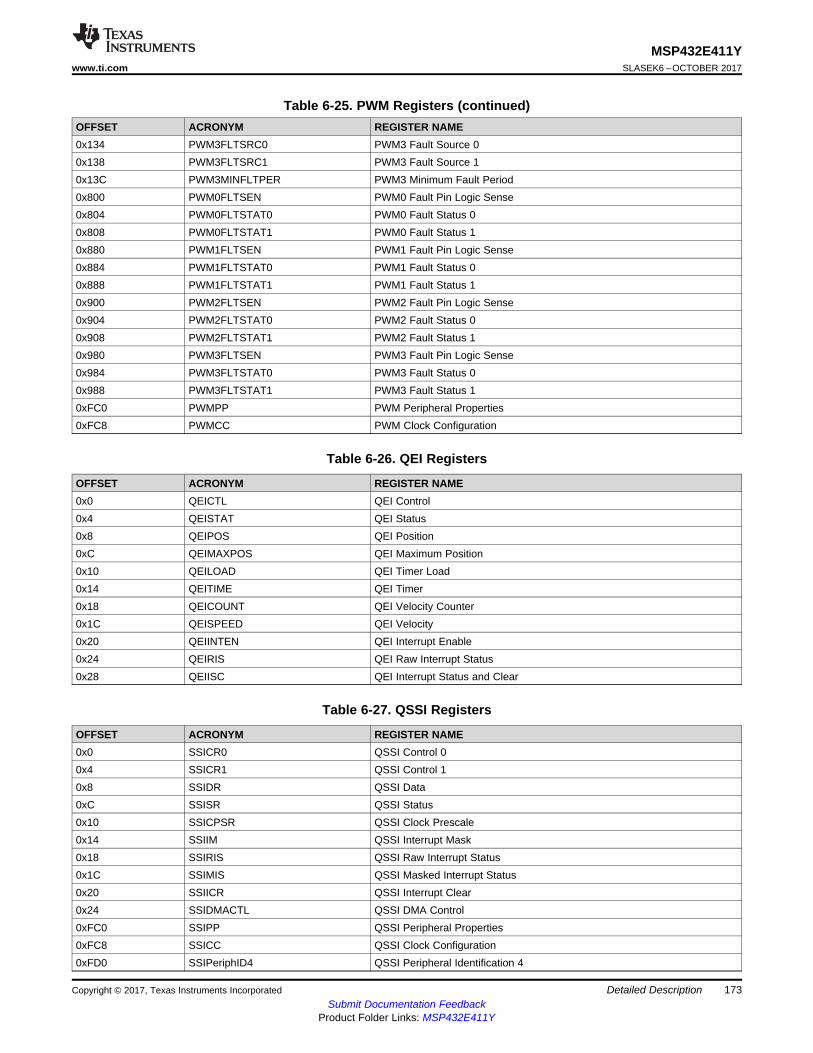
173
MSP432E411Ywww.ti.com SLASEK6 –OCTOBER 2017
Submit Documentation FeedbackProduct Folder Links: MSP432E411Y
Detailed DescriptionCopyright © 2017, Texas Instruments Incorporated
Table 6-25. PWM Registers (continued)OFFSET ACRONYM REGISTER NAME0x134 PWM3FLTSRC0 PWM3 Fault Source 00x138 PWM3FLTSRC1 PWM3 Fault Source 10x13C PWM3MINFLTPER PWM3 Minimum Fault Period0x800 PWM0FLTSEN PWM0 Fault Pin Logic Sense0x804 PWM0FLTSTAT0 PWM0 Fault Status 00x808 PWM0FLTSTAT1 PWM0 Fault Status 10x880 PWM1FLTSEN PWM1 Fault Pin Logic Sense0x884 PWM1FLTSTAT0 PWM1 Fault Status 00x888 PWM1FLTSTAT1 PWM1 Fault Status 10x900 PWM2FLTSEN PWM2 Fault Pin Logic Sense0x904 PWM2FLTSTAT0 PWM2 Fault Status 00x908 PWM2FLTSTAT1 PWM2 Fault Status 10x980 PWM3FLTSEN PWM3 Fault Pin Logic Sense0x984 PWM3FLTSTAT0 PWM3 Fault Status 00x988 PWM3FLTSTAT1 PWM3 Fault Status 10xFC0 PWMPP PWM Peripheral Properties0xFC8 PWMCC PWM Clock Configuration
Table 6-26. QEI Registers
OFFSET ACRONYM REGISTER NAME0x0 QEICTL QEI Control0x4 QEISTAT QEI Status0x8 QEIPOS QEI Position0xC QEIMAXPOS QEI Maximum Position0x10 QEILOAD QEI Timer Load0x14 QEITIME QEI Timer0x18 QEICOUNT QEI Velocity Counter0x1C QEISPEED QEI Velocity0x20 QEIINTEN QEI Interrupt Enable0x24 QEIRIS QEI Raw Interrupt Status0x28 QEIISC QEI Interrupt Status and Clear
Table 6-27. QSSI Registers
OFFSET ACRONYM REGISTER NAME0x0 SSICR0 QSSI Control 00x4 SSICR1 QSSI Control 10x8 SSIDR QSSI Data0xC SSISR QSSI Status0x10 SSICPSR QSSI Clock Prescale0x14 SSIIM QSSI Interrupt Mask0x18 SSIRIS QSSI Raw Interrupt Status0x1C SSIMIS QSSI Masked Interrupt Status0x20 SSIICR QSSI Interrupt Clear0x24 SSIDMACTL QSSI DMA Control0xFC0 SSIPP QSSI Peripheral Properties0xFC8 SSICC QSSI Clock Configuration0xFD0 SSIPeriphID4 QSSI Peripheral Identification 4
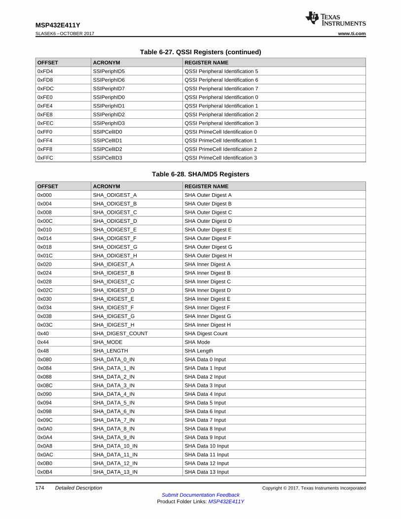
174
MSP432E411YSLASEK6 –OCTOBER 2017 www.ti.com
Submit Documentation FeedbackProduct Folder Links: MSP432E411Y
Detailed Description Copyright © 2017, Texas Instruments Incorporated
Table 6-27. QSSI Registers (continued)OFFSET ACRONYM REGISTER NAME0xFD4 SSIPeriphID5 QSSI Peripheral Identification 50xFD8 SSIPeriphID6 QSSI Peripheral Identification 60xFDC SSIPeriphID7 QSSI Peripheral Identification 70xFE0 SSIPeriphID0 QSSI Peripheral Identification 00xFE4 SSIPeriphID1 QSSI Peripheral Identification 10xFE8 SSIPeriphID2 QSSI Peripheral Identification 20xFEC SSIPeriphID3 QSSI Peripheral Identification 30xFF0 SSIPCellID0 QSSI PrimeCell Identification 00xFF4 SSIPCellID1 QSSI PrimeCell Identification 10xFF8 SSIPCellID2 QSSI PrimeCell Identification 20xFFC SSIPCellID3 QSSI PrimeCell Identification 3
Table 6-28. SHA/MD5 Registers
OFFSET ACRONYM REGISTER NAME0x000 SHA_ODIGEST_A SHA Outer Digest A0x004 SHA_ODIGEST_B SHA Outer Digest B0x008 SHA_ODIGEST_C SHA Outer Digest C0x00C SHA_ODIGEST_D SHA Outer Digest D0x010 SHA_ODIGEST_E SHA Outer Digest E0x014 SHA_ODIGEST_F SHA Outer Digest F0x018 SHA_ODIGEST_G SHA Outer Digest G0x01C SHA_ODIGEST_H SHA Outer Digest H0x020 SHA_IDIGEST_A SHA Inner Digest A0x024 SHA_IDIGEST_B SHA Inner Digest B0x028 SHA_IDIGEST_C SHA Inner Digest C0x02C SHA_IDIGEST_D SHA Inner Digest D0x030 SHA_IDIGEST_E SHA Inner Digest E0x034 SHA_IDIGEST_F SHA Inner Digest F0x038 SHA_IDIGEST_G SHA Inner Digest G0x03C SHA_IDIGEST_H SHA Inner Digest H0x40 SHA_DIGEST_COUNT SHA Digest Count0x44 SHA_MODE SHA Mode0x48 SHA_LENGTH SHA Length0x080 SHA_DATA_0_IN SHA Data 0 Input0x084 SHA_DATA_1_IN SHA Data 1 Input0x088 SHA_DATA_2_IN SHA Data 2 Input0x08C SHA_DATA_3_IN SHA Data 3 Input0x090 SHA_DATA_4_IN SHA Data 4 Input0x094 SHA_DATA_5_IN SHA Data 5 Input0x098 SHA_DATA_6_IN SHA Data 6 Input0x09C SHA_DATA_7_IN SHA Data 7 Input0x0A0 SHA_DATA_8_IN SHA Data 8 Input0x0A4 SHA_DATA_9_IN SHA Data 9 Input0x0A8 SHA_DATA_10_IN SHA Data 10 Input0x0AC SHA_DATA_11_IN SHA Data 11 Input0x0B0 SHA_DATA_12_IN SHA Data 12 Input0x0B4 SHA_DATA_13_IN SHA Data 13 Input
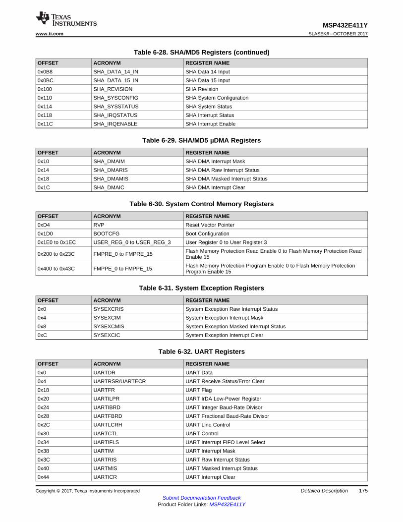
175
MSP432E411Ywww.ti.com SLASEK6 –OCTOBER 2017
Submit Documentation FeedbackProduct Folder Links: MSP432E411Y
Detailed DescriptionCopyright © 2017, Texas Instruments Incorporated
Table 6-28. SHA/MD5 Registers (continued)OFFSET ACRONYM REGISTER NAME0x0B8 SHA_DATA_14_IN SHA Data 14 Input0x0BC SHA_DATA_15_IN SHA Data 15 Input0x100 SHA_REVISION SHA Revision0x110 SHA_SYSCONFIG SHA System Configuration0x114 SHA_SYSSTATUS SHA System Status0x118 SHA_IRQSTATUS SHA Interrupt Status0x11C SHA_IRQENABLE SHA Interrupt Enable
Table 6-29. SHA/MD5 µDMA Registers
OFFSET ACRONYM REGISTER NAME0x10 SHA_DMAIM SHA DMA Interrupt Mask0x14 SHA_DMARIS SHA DMA Raw Interrupt Status0x18 SHA_DMAMIS SHA DMA Masked Interrupt Status0x1C SHA_DMAIC SHA DMA Interrupt Clear
Table 6-30. System Control Memory Registers
OFFSET ACRONYM REGISTER NAME0xD4 RVP Reset Vector Pointer0x1D0 BOOTCFG Boot Configuration0x1E0 to 0x1EC USER_REG_0 to USER_REG_3 User Register 0 to User Register 3
0x200 to 0x23C FMPRE_0 to FMPRE_15 Flash Memory Protection Read Enable 0 to Flash Memory Protection ReadEnable 15
0x400 to 0x43C FMPPE_0 to FMPPE_15 Flash Memory Protection Program Enable 0 to Flash Memory ProtectionProgram Enable 15
Table 6-31. System Exception Registers
OFFSET ACRONYM REGISTER NAME0x0 SYSEXCRIS System Exception Raw Interrupt Status0x4 SYSEXCIM System Exception Interrupt Mask0x8 SYSEXCMIS System Exception Masked Interrupt Status0xC SYSEXCIC System Exception Interrupt Clear
Table 6-32. UART Registers
OFFSET ACRONYM REGISTER NAME0x0 UARTDR UART Data0x4 UARTRSR/UARTECR UART Receive Status/Error Clear0x18 UARTFR UART Flag0x20 UARTILPR UART IrDA Low-Power Register0x24 UARTIBRD UART Integer Baud-Rate Divisor0x28 UARTFBRD UART Fractional Baud-Rate Divisor0x2C UARTLCRH UART Line Control0x30 UARTCTL UART Control0x34 UARTIFLS UART Interrupt FIFO Level Select0x38 UARTIM UART Interrupt Mask0x3C UARTRIS UART Raw Interrupt Status0x40 UARTMIS UART Masked Interrupt Status0x44 UARTICR UART Interrupt Clear
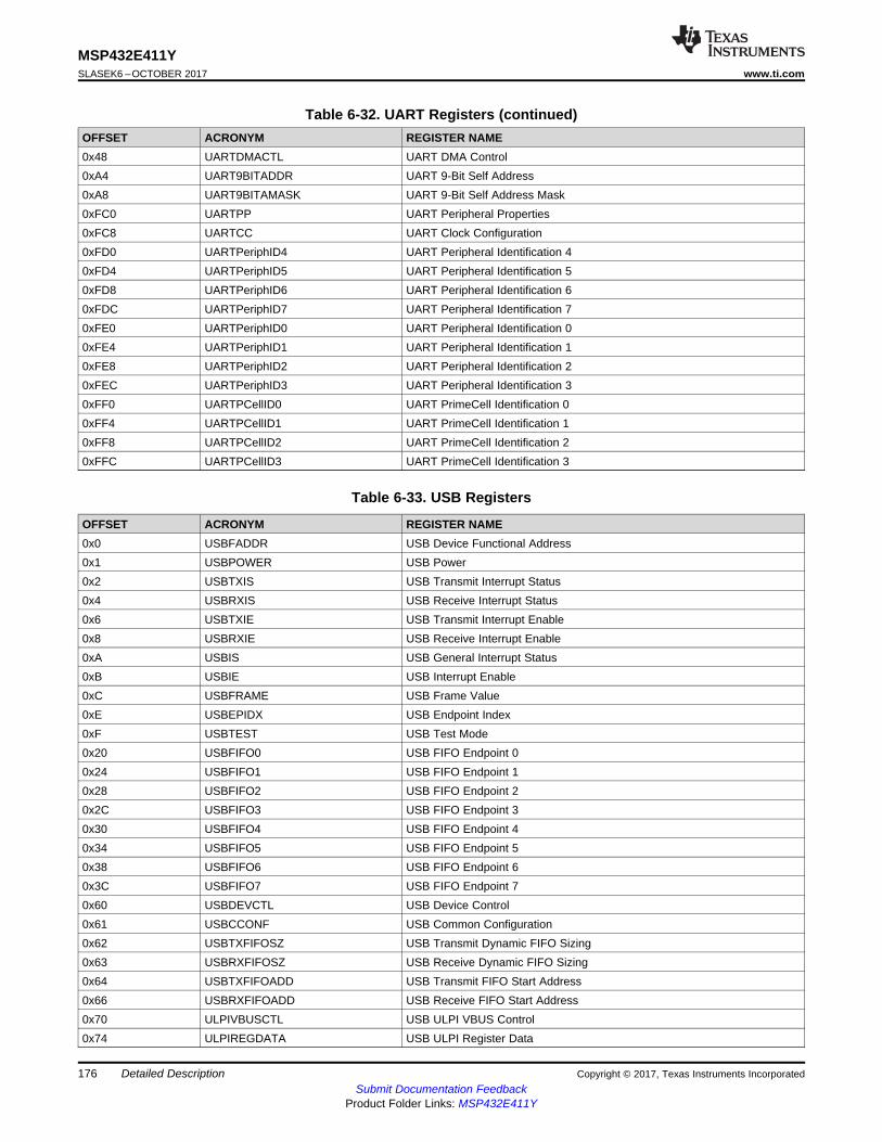
176
MSP432E411YSLASEK6 –OCTOBER 2017 www.ti.com
Submit Documentation FeedbackProduct Folder Links: MSP432E411Y
Detailed Description Copyright © 2017, Texas Instruments Incorporated
Table 6-32. UART Registers (continued)OFFSET ACRONYM REGISTER NAME0x48 UARTDMACTL UART DMA Control0xA4 UART9BITADDR UART 9-Bit Self Address0xA8 UART9BITAMASK UART 9-Bit Self Address Mask0xFC0 UARTPP UART Peripheral Properties0xFC8 UARTCC UART Clock Configuration0xFD0 UARTPeriphID4 UART Peripheral Identification 40xFD4 UARTPeriphID5 UART Peripheral Identification 50xFD8 UARTPeriphID6 UART Peripheral Identification 60xFDC UARTPeriphID7 UART Peripheral Identification 70xFE0 UARTPeriphID0 UART Peripheral Identification 00xFE4 UARTPeriphID1 UART Peripheral Identification 10xFE8 UARTPeriphID2 UART Peripheral Identification 20xFEC UARTPeriphID3 UART Peripheral Identification 30xFF0 UARTPCellID0 UART PrimeCell Identification 00xFF4 UARTPCellID1 UART PrimeCell Identification 10xFF8 UARTPCellID2 UART PrimeCell Identification 20xFFC UARTPCellID3 UART PrimeCell Identification 3
Table 6-33. USB Registers
OFFSET ACRONYM REGISTER NAME0x0 USBFADDR USB Device Functional Address0x1 USBPOWER USB Power0x2 USBTXIS USB Transmit Interrupt Status0x4 USBRXIS USB Receive Interrupt Status0x6 USBTXIE USB Transmit Interrupt Enable0x8 USBRXIE USB Receive Interrupt Enable0xA USBIS USB General Interrupt Status0xB USBIE USB Interrupt Enable0xC USBFRAME USB Frame Value0xE USBEPIDX USB Endpoint Index0xF USBTEST USB Test Mode0x20 USBFIFO0 USB FIFO Endpoint 00x24 USBFIFO1 USB FIFO Endpoint 10x28 USBFIFO2 USB FIFO Endpoint 20x2C USBFIFO3 USB FIFO Endpoint 30x30 USBFIFO4 USB FIFO Endpoint 40x34 USBFIFO5 USB FIFO Endpoint 50x38 USBFIFO6 USB FIFO Endpoint 60x3C USBFIFO7 USB FIFO Endpoint 70x60 USBDEVCTL USB Device Control0x61 USBCCONF USB Common Configuration0x62 USBTXFIFOSZ USB Transmit Dynamic FIFO Sizing0x63 USBRXFIFOSZ USB Receive Dynamic FIFO Sizing0x64 USBTXFIFOADD USB Transmit FIFO Start Address0x66 USBRXFIFOADD USB Receive FIFO Start Address0x70 ULPIVBUSCTL USB ULPI VBUS Control0x74 ULPIREGDATA USB ULPI Register Data
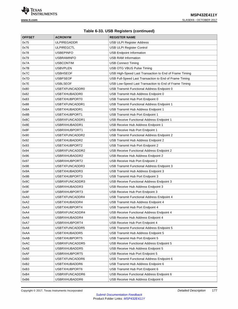
177
MSP432E411Ywww.ti.com SLASEK6 –OCTOBER 2017
Submit Documentation FeedbackProduct Folder Links: MSP432E411Y
Detailed DescriptionCopyright © 2017, Texas Instruments Incorporated
Table 6-33. USB Registers (continued)OFFSET ACRONYM REGISTER NAME0x75 ULPIREGADDR USB ULPI Register Address0x76 ULPIREGCTL USB ULPI Register Control0x78 USBEPINFO USB Endpoint Information0x79 USBRAMINFO USB RAM Information0x7A USBCONTIM USB Connect Timing0x7B USBVPLEN USB OTG VBUS Pulse Timing0x7C USBHSEOF USB High-Speed Last Transaction to End of Frame Timing0x7D USBFSEOF USB Full-Speed Last Transaction to End of Frame Timing0x7E USBLSEOF USB Low-Speed Last Transaction to End of Frame Timing0x80 USBTXFUNCADDR0 USB Transmit Functional Address Endpoint 00x82 USBTXHUBADDR0 USB Transmit Hub Address Endpoint 00x83 USBTXHUBPORT0 USB Transmit Hub Port Endpoint 00x88 USBTXFUNCADDR1 USB Transmit Functional Address Endpoint 10x8A USBTXHUBADDR1 USB Transmit Hub Address Endpoint 10x8B USBTXHUBPORT1 USB Transmit Hub Port Endpoint 10x8C USBRXFUNCADDR1 USB Receive Functional Address Endpoint 10x8E USBRXHUBADDR1 USB Receive Hub Address Endpoint 10x8F USBRXHUBPORT1 USB Receive Hub Port Endpoint 10x90 USBTXFUNCADDR2 USB Transmit Functional Address Endpoint 20x92 USBTXHUBADDR2 USB Transmit Hub Address Endpoint 20x93 USBTXHUBPORT2 USB Transmit Hub Port Endpoint 20x94 USBRXFUNCADDR2 USB Receive Functional Address Endpoint 20x96 USBRXHUBADDR2 USB Receive Hub Address Endpoint 20x97 USBRXHUBPORT2 USB Receive Hub Port Endpoint 20x98 USBTXFUNCADDR3 USB Transmit Functional Address Endpoint 30x9A USBTXHUBADDR3 USB Transmit Hub Address Endpoint 30x9B USBTXHUBPORT3 USB Transmit Hub Port Endpoint 30x9C USBRXFUNCADDR3 USB Receive Functional Address Endpoint 30x9E USBRXHUBADDR3 USB Receive Hub Address Endpoint 30x9F USBRXHUBPORT3 USB Receive Hub Port Endpoint 30xA0 USBTXFUNCADDR4 USB Transmit Functional Address Endpoint 40xA2 USBTXHUBADDR4 USB Transmit Hub Address Endpoint 40xA3 USBTXHUBPORT4 USB Transmit Hub Port Endpoint 40xA4 USBRXFUNCADDR4 USB Receive Functional Address Endpoint 40xA6 USBRXHUBADDR4 USB Receive Hub Address Endpoint 40xA7 USBRXHUBPORT4 USB Receive Hub Port Endpoint 40xA8 USBTXFUNCADDR5 USB Transmit Functional Address Endpoint 50xAA USBTXHUBADDR5 USB Transmit Hub Address Endpoint 50xAB USBTXHUBPORT5 USB Transmit Hub Port Endpoint 50xAC USBRXFUNCADDR5 USB Receive Functional Address Endpoint 50xAE USBRXHUBADDR5 USB Receive Hub Address Endpoint 50xAF USBRXHUBPORT5 USB Receive Hub Port Endpoint 50xB0 USBTXFUNCADDR6 USB Transmit Functional Address Endpoint 60xB2 USBTXHUBADDR6 USB Transmit Hub Address Endpoint 60xB3 USBTXHUBPORT6 USB Transmit Hub Port Endpoint 60xB4 USBRXFUNCADDR6 USB Receive Functional Address Endpoint 60xB6 USBRXHUBADDR6 USB Receive Hub Address Endpoint 6
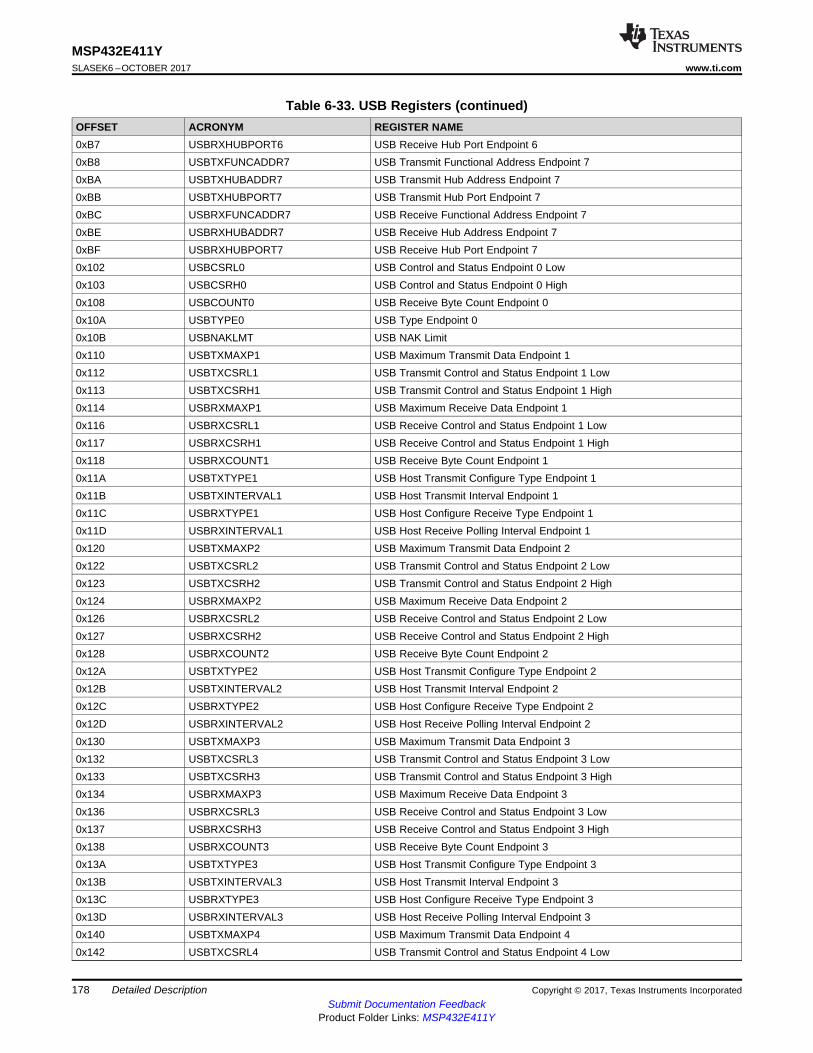
178
MSP432E411YSLASEK6 –OCTOBER 2017 www.ti.com
Submit Documentation FeedbackProduct Folder Links: MSP432E411Y
Detailed Description Copyright © 2017, Texas Instruments Incorporated
Table 6-33. USB Registers (continued)OFFSET ACRONYM REGISTER NAME0xB7 USBRXHUBPORT6 USB Receive Hub Port Endpoint 60xB8 USBTXFUNCADDR7 USB Transmit Functional Address Endpoint 70xBA USBTXHUBADDR7 USB Transmit Hub Address Endpoint 70xBB USBTXHUBPORT7 USB Transmit Hub Port Endpoint 70xBC USBRXFUNCADDR7 USB Receive Functional Address Endpoint 70xBE USBRXHUBADDR7 USB Receive Hub Address Endpoint 70xBF USBRXHUBPORT7 USB Receive Hub Port Endpoint 70x102 USBCSRL0 USB Control and Status Endpoint 0 Low0x103 USBCSRH0 USB Control and Status Endpoint 0 High0x108 USBCOUNT0 USB Receive Byte Count Endpoint 00x10A USBTYPE0 USB Type Endpoint 00x10B USBNAKLMT USB NAK Limit0x110 USBTXMAXP1 USB Maximum Transmit Data Endpoint 10x112 USBTXCSRL1 USB Transmit Control and Status Endpoint 1 Low0x113 USBTXCSRH1 USB Transmit Control and Status Endpoint 1 High0x114 USBRXMAXP1 USB Maximum Receive Data Endpoint 10x116 USBRXCSRL1 USB Receive Control and Status Endpoint 1 Low0x117 USBRXCSRH1 USB Receive Control and Status Endpoint 1 High0x118 USBRXCOUNT1 USB Receive Byte Count Endpoint 10x11A USBTXTYPE1 USB Host Transmit Configure Type Endpoint 10x11B USBTXINTERVAL1 USB Host Transmit Interval Endpoint 10x11C USBRXTYPE1 USB Host Configure Receive Type Endpoint 10x11D USBRXINTERVAL1 USB Host Receive Polling Interval Endpoint 10x120 USBTXMAXP2 USB Maximum Transmit Data Endpoint 20x122 USBTXCSRL2 USB Transmit Control and Status Endpoint 2 Low0x123 USBTXCSRH2 USB Transmit Control and Status Endpoint 2 High0x124 USBRXMAXP2 USB Maximum Receive Data Endpoint 20x126 USBRXCSRL2 USB Receive Control and Status Endpoint 2 Low0x127 USBRXCSRH2 USB Receive Control and Status Endpoint 2 High0x128 USBRXCOUNT2 USB Receive Byte Count Endpoint 20x12A USBTXTYPE2 USB Host Transmit Configure Type Endpoint 20x12B USBTXINTERVAL2 USB Host Transmit Interval Endpoint 20x12C USBRXTYPE2 USB Host Configure Receive Type Endpoint 20x12D USBRXINTERVAL2 USB Host Receive Polling Interval Endpoint 20x130 USBTXMAXP3 USB Maximum Transmit Data Endpoint 30x132 USBTXCSRL3 USB Transmit Control and Status Endpoint 3 Low0x133 USBTXCSRH3 USB Transmit Control and Status Endpoint 3 High0x134 USBRXMAXP3 USB Maximum Receive Data Endpoint 30x136 USBRXCSRL3 USB Receive Control and Status Endpoint 3 Low0x137 USBRXCSRH3 USB Receive Control and Status Endpoint 3 High0x138 USBRXCOUNT3 USB Receive Byte Count Endpoint 30x13A USBTXTYPE3 USB Host Transmit Configure Type Endpoint 30x13B USBTXINTERVAL3 USB Host Transmit Interval Endpoint 30x13C USBRXTYPE3 USB Host Configure Receive Type Endpoint 30x13D USBRXINTERVAL3 USB Host Receive Polling Interval Endpoint 30x140 USBTXMAXP4 USB Maximum Transmit Data Endpoint 40x142 USBTXCSRL4 USB Transmit Control and Status Endpoint 4 Low
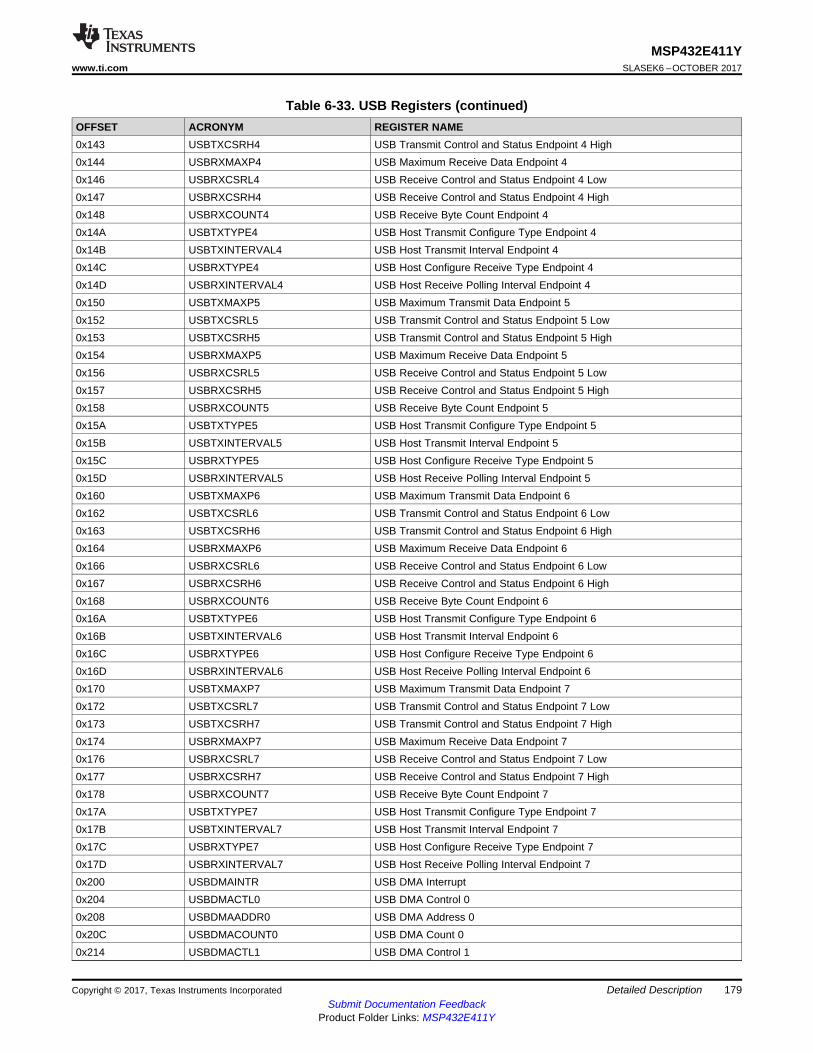
179
MSP432E411Ywww.ti.com SLASEK6 –OCTOBER 2017
Submit Documentation FeedbackProduct Folder Links: MSP432E411Y
Detailed DescriptionCopyright © 2017, Texas Instruments Incorporated
Table 6-33. USB Registers (continued)OFFSET ACRONYM REGISTER NAME0x143 USBTXCSRH4 USB Transmit Control and Status Endpoint 4 High0x144 USBRXMAXP4 USB Maximum Receive Data Endpoint 40x146 USBRXCSRL4 USB Receive Control and Status Endpoint 4 Low0x147 USBRXCSRH4 USB Receive Control and Status Endpoint 4 High0x148 USBRXCOUNT4 USB Receive Byte Count Endpoint 40x14A USBTXTYPE4 USB Host Transmit Configure Type Endpoint 40x14B USBTXINTERVAL4 USB Host Transmit Interval Endpoint 40x14C USBRXTYPE4 USB Host Configure Receive Type Endpoint 40x14D USBRXINTERVAL4 USB Host Receive Polling Interval Endpoint 40x150 USBTXMAXP5 USB Maximum Transmit Data Endpoint 50x152 USBTXCSRL5 USB Transmit Control and Status Endpoint 5 Low0x153 USBTXCSRH5 USB Transmit Control and Status Endpoint 5 High0x154 USBRXMAXP5 USB Maximum Receive Data Endpoint 50x156 USBRXCSRL5 USB Receive Control and Status Endpoint 5 Low0x157 USBRXCSRH5 USB Receive Control and Status Endpoint 5 High0x158 USBRXCOUNT5 USB Receive Byte Count Endpoint 50x15A USBTXTYPE5 USB Host Transmit Configure Type Endpoint 50x15B USBTXINTERVAL5 USB Host Transmit Interval Endpoint 50x15C USBRXTYPE5 USB Host Configure Receive Type Endpoint 50x15D USBRXINTERVAL5 USB Host Receive Polling Interval Endpoint 50x160 USBTXMAXP6 USB Maximum Transmit Data Endpoint 60x162 USBTXCSRL6 USB Transmit Control and Status Endpoint 6 Low0x163 USBTXCSRH6 USB Transmit Control and Status Endpoint 6 High0x164 USBRXMAXP6 USB Maximum Receive Data Endpoint 60x166 USBRXCSRL6 USB Receive Control and Status Endpoint 6 Low0x167 USBRXCSRH6 USB Receive Control and Status Endpoint 6 High0x168 USBRXCOUNT6 USB Receive Byte Count Endpoint 60x16A USBTXTYPE6 USB Host Transmit Configure Type Endpoint 60x16B USBTXINTERVAL6 USB Host Transmit Interval Endpoint 60x16C USBRXTYPE6 USB Host Configure Receive Type Endpoint 60x16D USBRXINTERVAL6 USB Host Receive Polling Interval Endpoint 60x170 USBTXMAXP7 USB Maximum Transmit Data Endpoint 70x172 USBTXCSRL7 USB Transmit Control and Status Endpoint 7 Low0x173 USBTXCSRH7 USB Transmit Control and Status Endpoint 7 High0x174 USBRXMAXP7 USB Maximum Receive Data Endpoint 70x176 USBRXCSRL7 USB Receive Control and Status Endpoint 7 Low0x177 USBRXCSRH7 USB Receive Control and Status Endpoint 7 High0x178 USBRXCOUNT7 USB Receive Byte Count Endpoint 70x17A USBTXTYPE7 USB Host Transmit Configure Type Endpoint 70x17B USBTXINTERVAL7 USB Host Transmit Interval Endpoint 70x17C USBRXTYPE7 USB Host Configure Receive Type Endpoint 70x17D USBRXINTERVAL7 USB Host Receive Polling Interval Endpoint 70x200 USBDMAINTR USB DMA Interrupt0x204 USBDMACTL0 USB DMA Control 00x208 USBDMAADDR0 USB DMA Address 00x20C USBDMACOUNT0 USB DMA Count 00x214 USBDMACTL1 USB DMA Control 1
180
MSP432E411YSLASEK6 –OCTOBER 2017 www.ti.com
Submit Documentation FeedbackProduct Folder Links: MSP432E411Y
Detailed Description Copyright © 2017, Texas Instruments Incorporated
Table 6-33. USB Registers (continued)OFFSET ACRONYM REGISTER NAME0x218 USBDMAADDR1 USB DMA Address 10x21C USBDMACOUNT1 USB DMA Count 10x224 USBDMACTL2 USB DMA Control 20x228 USBDMAADDR2 USB DMA Address 20x22C USBDMACOUNT2 USB DMA Count 20x234 USBDMACTL3 USB DMA Control 30x238 USBDMAADDR3 USB DMA Address 30x23C USBDMACOUNT3 USB DMA Count 30x244 USBDMACTL4 USB DMA Control 40x248 USBDMAADDR4 USB DMA Address 40x24C USBDMACOUNT4 USB DMA Count 40x254 USBDMACTL5 USB DMA Control 50x258 USBDMAADDR5 USB DMA Address 50x25C USBDMACOUNT5 USB DMA Count 50x264 USBDMACTL6 USB DMA Control 60x268 USBDMAADDR6 USB DMA Address 60x26C USBDMACOUNT6 USB DMA Count 60x274 USBDMACTL7 USB DMA Control 70x278 USBDMAADDR7 USB DMA Address 70x27C USBDMACOUNT7 USB DMA Count 70x304 USBRQPKTCOUNT1 USB Request Packet Count in Block Transfer Endpoint 10x308 USBRQPKTCOUNT2 USB Request Packet Count in Block Transfer Endpoint 20x30C USBRQPKTCOUNT3 USB Request Packet Count in Block Transfer Endpoint 30x310 USBRQPKTCOUNT4 USB Request Packet Count in Block Transfer Endpoint 40x314 USBRQPKTCOUNT5 USB Request Packet Count in Block Transfer Endpoint 50x318 USBRQPKTCOUNT6 USB Request Packet Count in Block Transfer Endpoint 60x31C USBRQPKTCOUNT7 USB Request Packet Count in Block Transfer Endpoint 70x340 USBRXDPKTBUFDIS USB Receive Double Packet Buffer Disable0x342 USBTXDPKTBUFDIS USB Transmit Double Packet Buffer Disable0x344 USBCTO USB Chirp Time-out0x346 USBHHSRTN USB High Speed to UTM Operating Delay0x348 USBHSBT USB High Speed Time-out Adder0x360 USBLPMATTR USB LPM Attributes0x362 USBLPMCNTRL USB LPM Control0x363 USBLPMIM USB LPM Interrupt Mask0x364 USBLPMRIS USB LPM Raw Interrupt Status0x365 USBLPMFADDR USB LPM Function Address0x400 USBEPC USB External Power Control0x404 USBEPCRIS USB External Power Control Raw Interrupt Status0x408 USBEPCIM USB External Power Control Interrupt Mask0x40C USBEPCISC USB External Power Control Interrupt Status and Clear0x410 USBDRRIS USB Device RESUME Raw Interrupt Status0x414 USBDRIM USB Device RESUME Interrupt Mask0x418 USBDRISC USB Device RESUME Interrupt Status and Clear0x41C USBGPCS USB General-Purpose Control and Status0x430 USBVDC USB VBUS Droop Control0x434 USBVDCRIS USB VBUS Droop Control Raw Interrupt Status
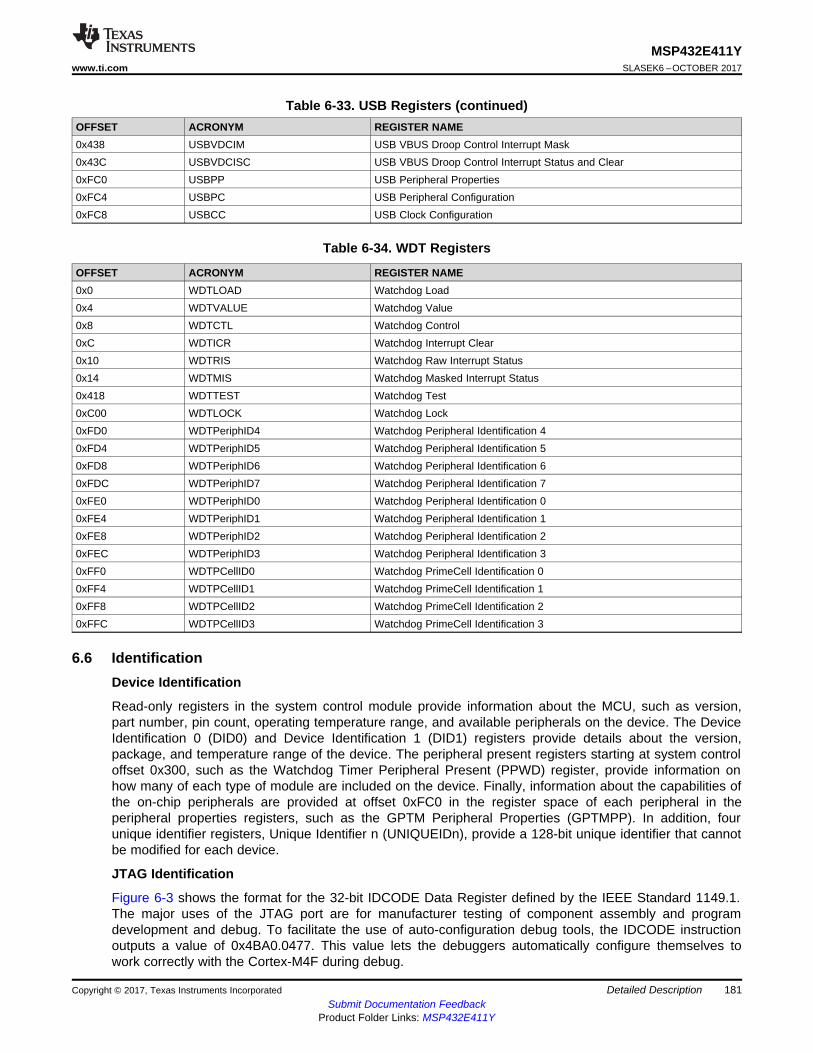
181
MSP432E411Ywww.ti.com SLASEK6 –OCTOBER 2017
Submit Documentation FeedbackProduct Folder Links: MSP432E411Y
Detailed DescriptionCopyright © 2017, Texas Instruments Incorporated
Table 6-33. USB Registers (continued)OFFSET ACRONYM REGISTER NAME0x438 USBVDCIM USB VBUS Droop Control Interrupt Mask0x43C USBVDCISC USB VBUS Droop Control Interrupt Status and Clear0xFC0 USBPP USB Peripheral Properties0xFC4 USBPC USB Peripheral Configuration0xFC8 USBCC USB Clock Configuration
Table 6-34. WDT Registers
OFFSET ACRONYM REGISTER NAME0x0 WDTLOAD Watchdog Load0x4 WDTVALUE Watchdog Value0x8 WDTCTL Watchdog Control0xC WDTICR Watchdog Interrupt Clear0x10 WDTRIS Watchdog Raw Interrupt Status0x14 WDTMIS Watchdog Masked Interrupt Status0x418 WDTTEST Watchdog Test0xC00 WDTLOCK Watchdog Lock0xFD0 WDTPeriphID4 Watchdog Peripheral Identification 40xFD4 WDTPeriphID5 Watchdog Peripheral Identification 50xFD8 WDTPeriphID6 Watchdog Peripheral Identification 60xFDC WDTPeriphID7 Watchdog Peripheral Identification 70xFE0 WDTPeriphID0 Watchdog Peripheral Identification 00xFE4 WDTPeriphID1 Watchdog Peripheral Identification 10xFE8 WDTPeriphID2 Watchdog Peripheral Identification 20xFEC WDTPeriphID3 Watchdog Peripheral Identification 30xFF0 WDTPCellID0 Watchdog PrimeCell Identification 00xFF4 WDTPCellID1 Watchdog PrimeCell Identification 10xFF8 WDTPCellID2 Watchdog PrimeCell Identification 20xFFC WDTPCellID3 Watchdog PrimeCell Identification 3
6.6 IdentificationDevice Identification
Read-only registers in the system control module provide information about the MCU, such as version,part number, pin count, operating temperature range, and available peripherals on the device. The DeviceIdentification 0 (DID0) and Device Identification 1 (DID1) registers provide details about the version,package, and temperature range of the device. The peripheral present registers starting at system controloffset 0x300, such as the Watchdog Timer Peripheral Present (PPWD) register, provide information onhow many of each type of module are included on the device. Finally, information about the capabilities ofthe on-chip peripherals are provided at offset 0xFC0 in the register space of each peripheral in theperipheral properties registers, such as the GPTM Peripheral Properties (GPTMPP). In addition, fourunique identifier registers, Unique Identifier n (UNIQUEIDn), provide a 128-bit unique identifier that cannotbe modified for each device.
JTAG Identification
Figure 6-3 shows the format for the 32-bit IDCODE Data Register defined by the IEEE Standard 1149.1.The major uses of the JTAG port are for manufacturer testing of component assembly and programdevelopment and debug. To facilitate the use of auto-configuration debug tools, the IDCODE instructionoutputs a value of 0x4BA0.0477. This value lets the debuggers automatically configure themselves towork correctly with the Cortex-M4F during debug.
Version Part Number Manufacturer ID 1
31 28 27 12 11 1 0
TDOTDI
182
MSP432E411YSLASEK6 –OCTOBER 2017 www.ti.com
Submit Documentation FeedbackProduct Folder Links: MSP432E411Y
Detailed Description Copyright © 2017, Texas Instruments Incorporated
Figure 6-3. IDCODE Register Format
ROM Version
The internal ROM is at address 0x0100.0000 of the device memory map.
6.7 Boot ModesAfter POR and device initialization occurs, the hardware loads the stack pointer from either flash or ROM,based on the presence of an application in flash and the state of the EN bit in the BOOTCFG register.
If the flash address 0x0000.0004 contains an erased word (value 0xFFFF.FFFF) or the EN bit is of theBOOTCFG register is clear, the stack pointer and reset vector pointer are loaded from ROM at address0x0100.0000 and 0x0100.0004, respectively. The bootloader executes and configures the available bootslave interfaces and waits for a programmer, host PC, or boot server to load its software. The bootloaderuses a simple packet interface to provide synchronous communication with the device for I2C, SSI, andUART. The speed of the bootloader is determined by the frequency of the internal oscillator (PIOSC) orexternal crystal (if connected).
The ROM invokes the USB and Ethernet bootloader only when an external crystal is detected. Also, theEthernet bootloader works only when a 25-MHz crystal is detected.
The following serial interfaces can be used:• UART0• SSI0• I2C0• USB• Ethernet MAC and Integrated PHY
If the check of the flash at address 0x0000.0004 contains a valid reset vector value and the EN bit in theBOOTCFG register is set, the stack pointer and reset vector values are fetched from the beginning offlash. This application stack pointer and reset vector are loaded and the processor executes theapplication directly. Otherwise, the stack pointer and reset vector values are fetched from the beginning ofROM.
183
MSP432E411Ywww.ti.com SLASEK6 –OCTOBER 2017
Submit Documentation FeedbackProduct Folder Links: MSP432E411Y
Applications, Implementation, and LayoutCopyright © 2017, Texas Instruments Incorporated
7 Applications, Implementation, and Layout
NOTEInformation in the following Applications section is not part of the TI component specification,and TI does not warrant its accuracy or completeness. TI's customers are responsible fordetermining suitability of components for their purposes. Customers should validate and testtheir design implementation to confirm system functionality.
7.1 System Design GuidelinesThe SimpleLink MSP432E4 microcontrollers are highly-integrated system-on-chip (SoC) devices withextensive interface and processing capabilities. Consequently, there are many factors to consider whencreating a schematic and designing a circuit board. By following the recommendations in this designguide, your confidence will increase that the board will work successfully upon initial power up.
System Design Guidelines for MSP432E4 SimpleLink™ Microcontrollers
184
MSP432E411YSLASEK6 –OCTOBER 2017 www.ti.com
Submit Documentation FeedbackProduct Folder Links: MSP432E411Y
Device and Documentation Support Copyright © 2017, Texas Instruments Incorporated
8 Device and Documentation Support
8.1 Getting Started and Next StepsTI offers an extensive line of development tools. Tools and software to evaluate the performance of thedevice, generate code, and develop solutions follow.
8.2 Device NomenclatureTo designate the stages in the product development cycle, TI assigns prefixes to the part numbers of allmicroprocessors (MPUs) and support tools. Each device has one of three prefixes: XMS, PMS, or MSP.These prefixes represent evolutionary stages of product development from engineering prototypes throughfully qualified production devices and tools.
Device development evolutionary flow:XMS Experimental device that is not necessarily representative of the final device's electrical
specifications and may not use production assembly flow.PMS Prototype device that is not necessarily the final silicon die and may not necessarily meet
final electrical specifications.MSP Production version of the silicon die that is fully qualified.
Experimental devices and tools are shipped against the following disclaimer:
"Developmental product is intended for internal evaluation purposes."
Production devices and development-support tools have been characterized fully, and the quality andreliability of the device have been demonstrated fully. TI's standard warranty applies.
Predictions show that prototype devices have a greater failure rate than the standard production devices.TI recommends that these devices not be used in any production system because their expected end-usefailure rate still is undefined. Only qualified production devices are to be used.
TI device nomenclature also includes a suffix with the device family name. This suffix indicates thepackage type (for example, ZAD) and the temperature range (for example, blank is the default commercialtemperature range). Figure 8-1 shows a legend for reading the complete device name for the device.
For orderable part numbers of the device, see the Package Option Addendum of this document, ti.com, orcontact your TI sales representative.
For additional description of the device nomenclature markings on the die, see the device-specific siliconerrata.
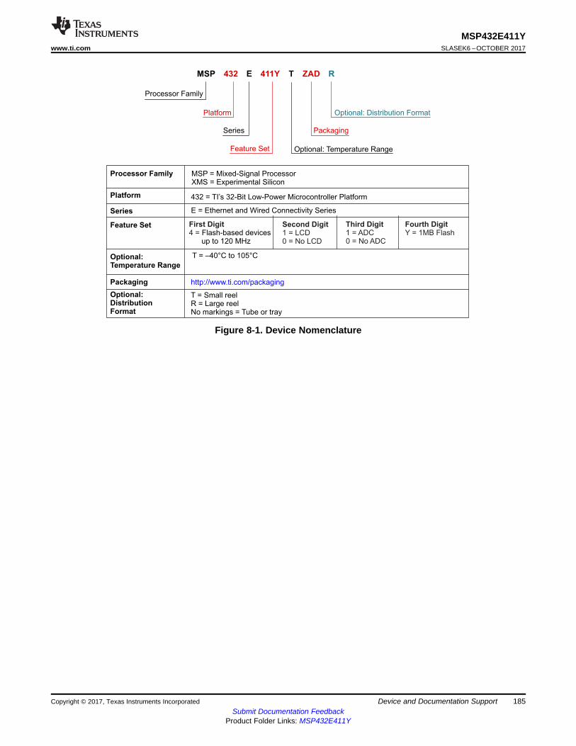
Processor Family MSP = Mixed-Signal ProcessorXMS = Experimental Silicon
Platform 432 = T ’s 32-Bit Low-Power Microcontroller PlatformI
Series E = Ethernet and Wired Connectivity Series
Feature Set
Optional:Temperature Range
T = –40 C to 105 C° °
Packaging http://www.ti.com/packaging
Optional:DistributionFormat
T = Small reelR = Large reelNo markings = Tube or tray
MSP 432 E 411Y T ZAD R
Processor Family
Series
Optional: Temperature Range
Platform
Packaging
Optional: Distribution Format
Feature Set
First Digit4 = Flash-based devices
up to 120 MHz
Second Digit1 = LCD0 = No LCD
Third Digit1 = ADC0 = No ADC
Fourth DigitY = 1MB Flash
185
MSP432E411Ywww.ti.com SLASEK6 –OCTOBER 2017
Submit Documentation FeedbackProduct Folder Links: MSP432E411Y
Device and Documentation SupportCopyright © 2017, Texas Instruments Incorporated
Figure 8-1. Device Nomenclature
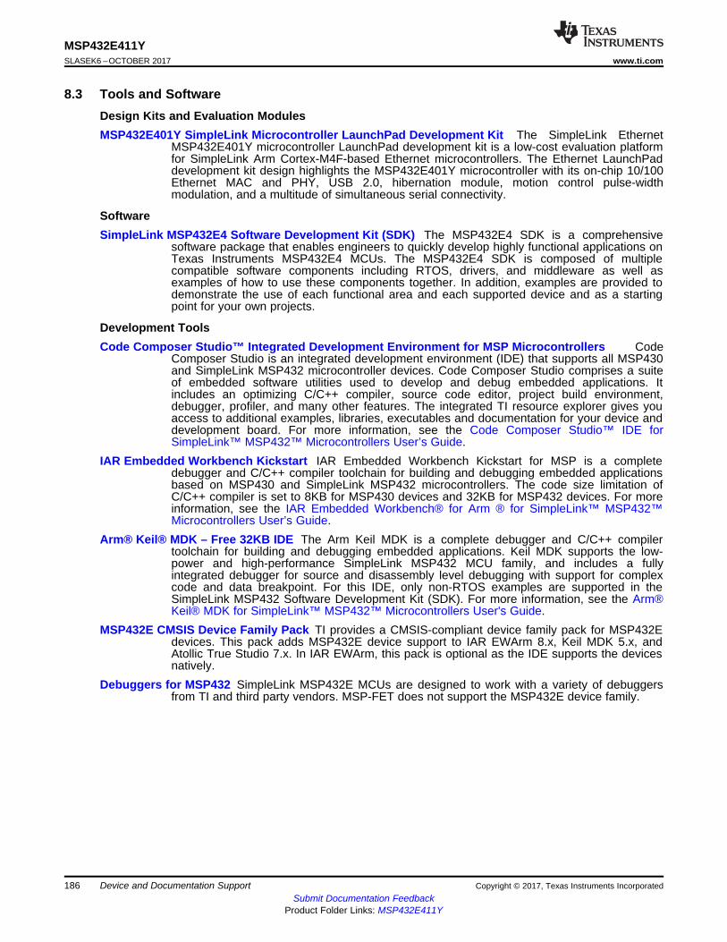
186
MSP432E411YSLASEK6 –OCTOBER 2017 www.ti.com
Submit Documentation FeedbackProduct Folder Links: MSP432E411Y
Device and Documentation Support Copyright © 2017, Texas Instruments Incorporated
8.3 Tools and SoftwareDesign Kits and Evaluation ModulesMSP432E401Y SimpleLink Microcontroller LaunchPad Development Kit The SimpleLink Ethernet
MSP432E401Y microcontroller LaunchPad development kit is a low-cost evaluation platformfor SimpleLink Arm Cortex-M4F-based Ethernet microcontrollers. The Ethernet LaunchPaddevelopment kit design highlights the MSP432E401Y microcontroller with its on-chip 10/100Ethernet MAC and PHY, USB 2.0, hibernation module, motion control pulse-widthmodulation, and a multitude of simultaneous serial connectivity.
SoftwareSimpleLink MSP432E4 Software Development Kit (SDK) The MSP432E4 SDK is a comprehensive
software package that enables engineers to quickly develop highly functional applications onTexas Instruments MSP432E4 MCUs. The MSP432E4 SDK is composed of multiplecompatible software components including RTOS, drivers, and middleware as well asexamples of how to use these components together. In addition, examples are provided todemonstrate the use of each functional area and each supported device and as a startingpoint for your own projects.
Development ToolsCode Composer Studio™ Integrated Development Environment for MSP Microcontrollers Code
Composer Studio is an integrated development environment (IDE) that supports all MSP430and SimpleLink MSP432 microcontroller devices. Code Composer Studio comprises a suiteof embedded software utilities used to develop and debug embedded applications. Itincludes an optimizing C/C++ compiler, source code editor, project build environment,debugger, profiler, and many other features. The integrated TI resource explorer gives youaccess to additional examples, libraries, executables and documentation for your device anddevelopment board. For more information, see the Code Composer Studio™ IDE forSimpleLink™ MSP432™ Microcontrollers User’s Guide.
IAR Embedded Workbench Kickstart IAR Embedded Workbench Kickstart for MSP is a completedebugger and C/C++ compiler toolchain for building and debugging embedded applicationsbased on MSP430 and SimpleLink MSP432 microcontrollers. The code size limitation ofC/C++ compiler is set to 8KB for MSP430 devices and 32KB for MSP432 devices. For moreinformation, see the IAR Embedded Workbench® for Arm ® for SimpleLink™ MSP432™Microcontrollers User’s Guide.
Arm® Keil® MDK – Free 32KB IDE The Arm Keil MDK is a complete debugger and C/C++ compilertoolchain for building and debugging embedded applications. Keil MDK supports the low-power and high-performance SimpleLink MSP432 MCU family, and includes a fullyintegrated debugger for source and disassembly level debugging with support for complexcode and data breakpoint. For this IDE, only non-RTOS examples are supported in theSimpleLink MSP432 Software Development Kit (SDK). For more information, see the Arm®Keil® MDK for SimpleLink™ MSP432™ Microcontrollers User's Guide.
MSP432E CMSIS Device Family Pack TI provides a CMSIS-compliant device family pack for MSP432Edevices. This pack adds MSP432E device support to IAR EWArm 8.x, Keil MDK 5.x, andAtollic True Studio 7.x. In IAR EWArm, this pack is optional as the IDE supports the devicesnatively.
Debuggers for MSP432 SimpleLink MSP432E MCUs are designed to work with a variety of debuggersfrom TI and third party vendors. MSP-FET does not support the MSP432E device family.
187
MSP432E411Ywww.ti.com SLASEK6 –OCTOBER 2017
Submit Documentation FeedbackProduct Folder Links: MSP432E411Y
Device and Documentation SupportCopyright © 2017, Texas Instruments Incorporated
8.4 Documentation SupportTo receive notification of documentation updates, navigate to the device product folder on ti.com. In theupper-right corner, click on Alert me to register and receive a weekly digest of any product information thathas changed. For change details, review the revision history included in any revised document.
The following documentation describes the MCU, related peripherals, and other technical collateral.
ErrataMSP432E4 SimpleLink™ Microcontrollers Silicon Errata Describes silicon behavior that differs from
the published specifications
Application ReportsSystem Design Guidelines for SimpleLink™ MSP432E4 Microcontrollers The SimpleLink MSP432E4
microcontrollers are highly-integrated system-on-chip (SOC) devices with extensive interfaceand processing capabilities. Consequently, there are many factors to consider when creatinga schematic and designing a circuit board. By following the recommendations in this designguide, you will increase your confidence that the board will work successfully the first time itis powered it up.
Using Feature Set of I2C Master on SimpleLink MSP432E4 Microcontrollers The inter-integratedcircuit (I2C) is a multiple-master, multiple-slave, single-ended bus that is typically used forattaching lower-speed peripheral ICs to processors and microcontrollers. The type of slavedevices range from nonvolatile memory to data-acquisition devices like analog-to-digitalconverters (ADC), sensors, and so forth. This application report demonstrates how to usethe feature rich I2C master on the SimpleLink MSP432E4 microcontrollers to communicatewith a host of slave devices in a system.
Using SimpleLink MSP432E4 Microcontrollers Over JTAG Interface The IEEE Standard 1149.1-1990,IEEE Standard Test Access Port and Boundary-Scan Architecture (JTAG) is a method forverifying designs and testing printed circuit boards after assembly. It is used as the primarymeans for transferring data to a nonvolatile memory of an embedded system and debuggingembedded software. This application report describes the physical connections for JTAG anddesign considerations to be taken into account for a custom board. It also shows how to usethe JTAG interface on the SimpleLink MSP432E4 LaunchPad development kit for debuggingthe onboard microcontroller using an external debugger, or by using the onboard debuggerfor debugging an off-board microcontroller.
User's GuidesMSP432E4 SimpleLink™ Microcontrollers Technical Reference Manual Describes the MSP432E4
family of microcontrollers, including the functional blocks of the system-on-chip (SoC) devicedesigned around the Arm Cortex-M4F core.
Bootloader for MSP432E4 SimpleLink™ Microcontrollers User's Guide The bootloader is a smallpiece of code that can be programmed at the beginning of flash to act as an applicationloader as well as an update mechanism for applications running on a SimpleLink MSP432E4Arm Cortex-M4-based microcontroller. The bootloader can be built to use the UART, SSI,I2C, CAN, Ethernet, or USB ports to update the code on the microcontroller. The bootloaderis customizable through source code modifications, or simply deciding at compile time whichroutines to include. Because full source code is provided, the bootloader can be completelycustomized
188
MSP432E411YSLASEK6 –OCTOBER 2017 www.ti.com
Submit Documentation FeedbackProduct Folder Links: MSP432E411Y
Device and Documentation Support Copyright © 2017, Texas Instruments Incorporated
8.5 Community ResourcesThe following links connect to TI community resources. Linked contents are provided "AS IS" by therespective contributors. They do not constitute TI specifications and do not necessarily reflect TI's views;see TI's Terms of Use.TI E2E™ Online Community The TI engineer-to-engineer (E2E) community was created to foster
collaboration among engineers. At e2e.ti.com, you can ask questions, share knowledge,explore ideas and help solve problems with fellow engineers.
TI Embedded Processors Wiki Established to help developers get started with Embedded Processorsfrom Texas Instruments and to foster innovation and growth of general knowledge about thehardware and software surrounding these devices.
8.6 TrademarksSimpleLink, LaunchPad, MSP432, E2E are trademarks of Texas Instruments.Arm, Cortex, Thumb, Thumb-2, PrimeCell, Arm7 are registered trademarks of Arm Limited.Bluetooth is a registered trademark of Bluetooth SIG.Wi-Fi is a registered trademark of Wi-Fi Alliance.All other trademarks are the property of their respective owners.
8.7 Electrostatic Discharge CautionThis integrated circuit can be damaged by ESD. Texas Instruments recommends that all integrated circuits be handled withappropriate precautions. Failure to observe proper handling and installation procedures can cause damage.
ESD damage can range from subtle performance degradation to complete device failure. Precision integrated circuits may be moresusceptible to damage because very small parametric changes could cause the device not to meet its published specifications.
8.8 Export Control NoticeRecipient agrees to not knowingly export or re-export, directly or indirectly, any product or technical data(as defined by the U.S., EU, and other Export Administration Regulations) including software, or anycontrolled product restricted by other applicable national regulations, received from disclosing party undernondisclosure obligations (if any), or any direct product of such technology, to any destination to whichsuch export or re-export is restricted or prohibited by U.S. or other applicable laws, without obtaining priorauthorization from U.S. Department of Commerce and other competent Government authorities to theextent required by those laws.
8.9 GlossaryTI Glossary This glossary lists and explains terms, acronyms, and definitions.
189
MSP432E411Ywww.ti.com SLASEK6 –OCTOBER 2017
Submit Documentation FeedbackProduct Folder Links: MSP432E411Y
Mechanical, Packaging, and Orderable InformationCopyright © 2017, Texas Instruments Incorporated
9 Mechanical, Packaging, and Orderable Information
The following pages include mechanical, packaging, and orderable information. This information is themost current data available for the designated devices. This data is subject to change without notice andrevision of this document. For browser-based versions of this data sheet, refer to the left-hand navigation.

190
MSP432E411YSLASEK6 –OCTOBER 2017 www.ti.com
Submit Documentation FeedbackProduct Folder Links: MSP432E411Y
Mechanical, Packaging, and Orderable Information Copyright © 2017, Texas Instruments Incorporated
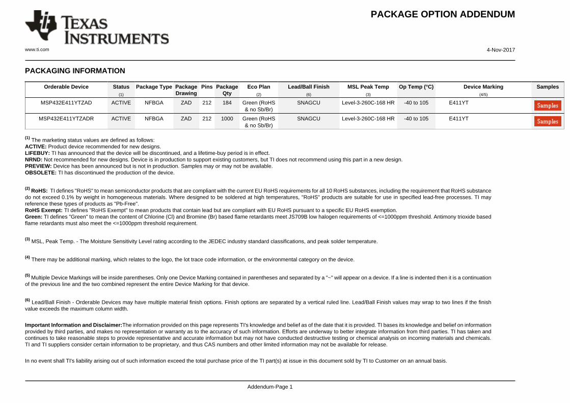
PACKAGE OPTION ADDENDUM
www.ti.com 4-Nov-2017
Addendum-Page 1
PACKAGING INFORMATION
Orderable Device Status(1)
Package Type PackageDrawing
Pins PackageQty
Eco Plan(2)
Lead/Ball Finish(6)
MSL Peak Temp(3)
Op Temp (°C) Device Marking(4/5)
Samples
MSP432E411YTZAD ACTIVE NFBGA ZAD 212 184 Green (RoHS& no Sb/Br)
SNAGCU Level-3-260C-168 HR -40 to 105 E411YT
MSP432E411YTZADR ACTIVE NFBGA ZAD 212 1000 Green (RoHS& no Sb/Br)
SNAGCU Level-3-260C-168 HR -40 to 105 E411YT
(1) The marketing status values are defined as follows:ACTIVE: Product device recommended for new designs.LIFEBUY: TI has announced that the device will be discontinued, and a lifetime-buy period is in effect.NRND: Not recommended for new designs. Device is in production to support existing customers, but TI does not recommend using this part in a new design.PREVIEW: Device has been announced but is not in production. Samples may or may not be available.OBSOLETE: TI has discontinued the production of the device.
(2) RoHS: TI defines "RoHS" to mean semiconductor products that are compliant with the current EU RoHS requirements for all 10 RoHS substances, including the requirement that RoHS substancedo not exceed 0.1% by weight in homogeneous materials. Where designed to be soldered at high temperatures, "RoHS" products are suitable for use in specified lead-free processes. TI mayreference these types of products as "Pb-Free".RoHS Exempt: TI defines "RoHS Exempt" to mean products that contain lead but are compliant with EU RoHS pursuant to a specific EU RoHS exemption.Green: TI defines "Green" to mean the content of Chlorine (Cl) and Bromine (Br) based flame retardants meet JS709B low halogen requirements of <=1000ppm threshold. Antimony trioxide basedflame retardants must also meet the <=1000ppm threshold requirement.
(3) MSL, Peak Temp. - The Moisture Sensitivity Level rating according to the JEDEC industry standard classifications, and peak solder temperature.
(4) There may be additional marking, which relates to the logo, the lot trace code information, or the environmental category on the device.
(5) Multiple Device Markings will be inside parentheses. Only one Device Marking contained in parentheses and separated by a "~" will appear on a device. If a line is indented then it is a continuationof the previous line and the two combined represent the entire Device Marking for that device.
(6) Lead/Ball Finish - Orderable Devices may have multiple material finish options. Finish options are separated by a vertical ruled line. Lead/Ball Finish values may wrap to two lines if the finishvalue exceeds the maximum column width.
Important Information and Disclaimer:The information provided on this page represents TI's knowledge and belief as of the date that it is provided. TI bases its knowledge and belief on informationprovided by third parties, and makes no representation or warranty as to the accuracy of such information. Efforts are underway to better integrate information from third parties. TI has taken andcontinues to take reasonable steps to provide representative and accurate information but may not have conducted destructive testing or chemical analysis on incoming materials and chemicals.TI and TI suppliers consider certain information to be proprietary, and thus CAS numbers and other limited information may not be available for release.
In no event shall TI's liability arising out of such information exceed the total purchase price of the TI part(s) at issue in this document sold by TI to Customer on an annual basis.
PACKAGE OPTION ADDENDUM
www.ti.com 4-Nov-2017
Addendum-Page 2
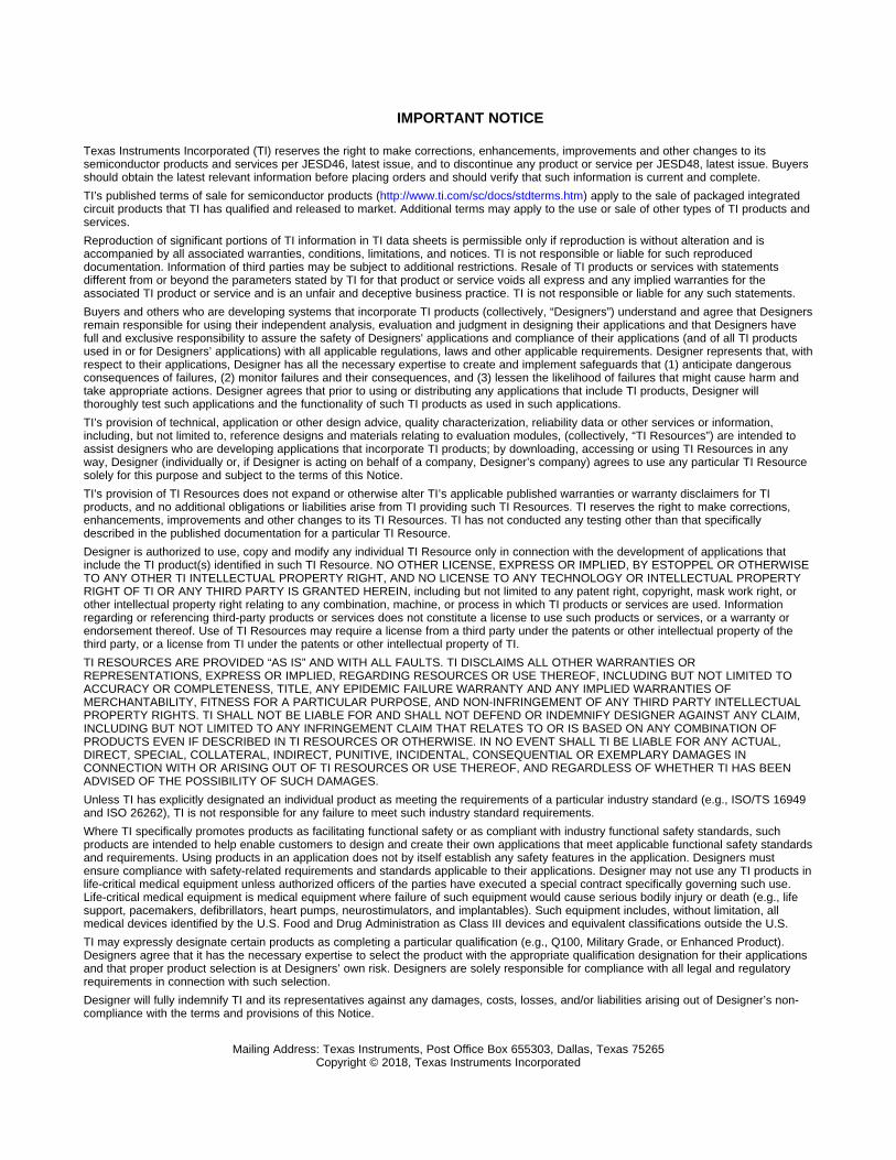
IMPORTANT NOTICE
Texas Instruments Incorporated (TI) reserves the right to make corrections, enhancements, improvements and other changes to itssemiconductor products and services per JESD46, latest issue, and to discontinue any product or service per JESD48, latest issue. Buyersshould obtain the latest relevant information before placing orders and should verify that such information is current and complete.TI’s published terms of sale for semiconductor products (http://www.ti.com/sc/docs/stdterms.htm) apply to the sale of packaged integratedcircuit products that TI has qualified and released to market. Additional terms may apply to the use or sale of other types of TI products andservices.Reproduction of significant portions of TI information in TI data sheets is permissible only if reproduction is without alteration and isaccompanied by all associated warranties, conditions, limitations, and notices. TI is not responsible or liable for such reproduceddocumentation. Information of third parties may be subject to additional restrictions. Resale of TI products or services with statementsdifferent from or beyond the parameters stated by TI for that product or service voids all express and any implied warranties for theassociated TI product or service and is an unfair and deceptive business practice. TI is not responsible or liable for any such statements.Buyers and others who are developing systems that incorporate TI products (collectively, “Designers”) understand and agree that Designersremain responsible for using their independent analysis, evaluation and judgment in designing their applications and that Designers havefull and exclusive responsibility to assure the safety of Designers' applications and compliance of their applications (and of all TI productsused in or for Designers’ applications) with all applicable regulations, laws and other applicable requirements. Designer represents that, withrespect to their applications, Designer has all the necessary expertise to create and implement safeguards that (1) anticipate dangerousconsequences of failures, (2) monitor failures and their consequences, and (3) lessen the likelihood of failures that might cause harm andtake appropriate actions. Designer agrees that prior to using or distributing any applications that include TI products, Designer willthoroughly test such applications and the functionality of such TI products as used in such applications.TI’s provision of technical, application or other design advice, quality characterization, reliability data or other services or information,including, but not limited to, reference designs and materials relating to evaluation modules, (collectively, “TI Resources”) are intended toassist designers who are developing applications that incorporate TI products; by downloading, accessing or using TI Resources in anyway, Designer (individually or, if Designer is acting on behalf of a company, Designer’s company) agrees to use any particular TI Resourcesolely for this purpose and subject to the terms of this Notice.TI’s provision of TI Resources does not expand or otherwise alter TI’s applicable published warranties or warranty disclaimers for TIproducts, and no additional obligations or liabilities arise from TI providing such TI Resources. TI reserves the right to make corrections,enhancements, improvements and other changes to its TI Resources. TI has not conducted any testing other than that specificallydescribed in the published documentation for a particular TI Resource.Designer is authorized to use, copy and modify any individual TI Resource only in connection with the development of applications thatinclude the TI product(s) identified in such TI Resource. NO OTHER LICENSE, EXPRESS OR IMPLIED, BY ESTOPPEL OR OTHERWISETO ANY OTHER TI INTELLECTUAL PROPERTY RIGHT, AND NO LICENSE TO ANY TECHNOLOGY OR INTELLECTUAL PROPERTYRIGHT OF TI OR ANY THIRD PARTY IS GRANTED HEREIN, including but not limited to any patent right, copyright, mask work right, orother intellectual property right relating to any combination, machine, or process in which TI products or services are used. Informationregarding or referencing third-party products or services does not constitute a license to use such products or services, or a warranty orendorsement thereof. Use of TI Resources may require a license from a third party under the patents or other intellectual property of thethird party, or a license from TI under the patents or other intellectual property of TI.TI RESOURCES ARE PROVIDED “AS IS” AND WITH ALL FAULTS. TI DISCLAIMS ALL OTHER WARRANTIES ORREPRESENTATIONS, EXPRESS OR IMPLIED, REGARDING RESOURCES OR USE THEREOF, INCLUDING BUT NOT LIMITED TOACCURACY OR COMPLETENESS, TITLE, ANY EPIDEMIC FAILURE WARRANTY AND ANY IMPLIED WARRANTIES OFMERCHANTABILITY, FITNESS FOR A PARTICULAR PURPOSE, AND NON-INFRINGEMENT OF ANY THIRD PARTY INTELLECTUALPROPERTY RIGHTS. TI SHALL NOT BE LIABLE FOR AND SHALL NOT DEFEND OR INDEMNIFY DESIGNER AGAINST ANY CLAIM,INCLUDING BUT NOT LIMITED TO ANY INFRINGEMENT CLAIM THAT RELATES TO OR IS BASED ON ANY COMBINATION OFPRODUCTS EVEN IF DESCRIBED IN TI RESOURCES OR OTHERWISE. IN NO EVENT SHALL TI BE LIABLE FOR ANY ACTUAL,DIRECT, SPECIAL, COLLATERAL, INDIRECT, PUNITIVE, INCIDENTAL, CONSEQUENTIAL OR EXEMPLARY DAMAGES INCONNECTION WITH OR ARISING OUT OF TI RESOURCES OR USE THEREOF, AND REGARDLESS OF WHETHER TI HAS BEENADVISED OF THE POSSIBILITY OF SUCH DAMAGES.Unless TI has explicitly designated an individual product as meeting the requirements of a particular industry standard (e.g., ISO/TS 16949and ISO 26262), TI is not responsible for any failure to meet such industry standard requirements.Where TI specifically promotes products as facilitating functional safety or as compliant with industry functional safety standards, suchproducts are intended to help enable customers to design and create their own applications that meet applicable functional safety standardsand requirements. Using products in an application does not by itself establish any safety features in the application. Designers mustensure compliance with safety-related requirements and standards applicable to their applications. Designer may not use any TI products inlife-critical medical equipment unless authorized officers of the parties have executed a special contract specifically governing such use.Life-critical medical equipment is medical equipment where failure of such equipment would cause serious bodily injury or death (e.g., lifesupport, pacemakers, defibrillators, heart pumps, neurostimulators, and implantables). Such equipment includes, without limitation, allmedical devices identified by the U.S. Food and Drug Administration as Class III devices and equivalent classifications outside the U.S.TI may expressly designate certain products as completing a particular qualification (e.g., Q100, Military Grade, or Enhanced Product).Designers agree that it has the necessary expertise to select the product with the appropriate qualification designation for their applicationsand that proper product selection is at Designers’ own risk. Designers are solely responsible for compliance with all legal and regulatoryrequirements in connection with such selection.Designer will fully indemnify TI and its representatives against any damages, costs, losses, and/or liabilities arising out of Designer’s non-compliance with the terms and provisions of this Notice.
Mailing Address: Texas Instruments, Post Office Box 655303, Dallas, Texas 75265Copyright © 2018, Texas Instruments Incorporated


![CC3200 SimpleLink Wi-Fi and IoT Solution with MCU ... · CC3200 SimpleLink™ Wi-Fi® and IoT Solution with MCU LaunchPad Hardware ... 3.1 Development Environment ... 0] 100 = Flash](https://img.pdfslide.net/doc/110x75/5b735eac7f8b9a58028e618c/cc3200-simplelink-wi-fi-and-iot-solution-with-mcu-cc3200-simplelink-wi-fi.jpg)