Embed Size (px)
Citation preview
European Synchrotron Radiation Facility
Computing Services - Electronics Group
CS/EL/01-02
N110 4 channel Time to Digital Converter
User's manual
updated 03/08/04 by C. Hervé
Table of contents
1 - General description 2 - Specifications 3 - Front and back panel description 4 - Registers description and rotary switches setting 5 - Controlling N110 TDC via serial line 6 - Advanced configurations 7- DIO-HS32 adapter 8- 2D setup typical procedure (step by step)
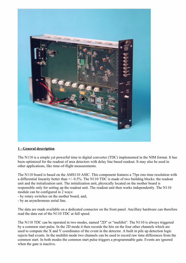
1 - General description
The N110 is a simple yet powerful time to digital converter (TDC) implemented in the NIM format. It has been optimized for the readout of area detectors with delay line based readout. It may also be used in other applications, like time-of-flight measurements.
The N110 board is based on the AMS110 ASIC. This component features a 75ps rms time resolution with a differential linearity better than +/- 0.5%. The N110 TDC is made of two building blocks: the readout unit and the initialization unit. The initialization unit, physically located on the mother board is responsible only for setting up the readout unit. The readout unit then works independently. The N110 module can be configured in 2 ways: - by rotary switches on the mother board, and, - by an asynchronous serial line.
The data are made available on a dedicated connector on the front panel. Ancillary hardware can therefore read the data out of the N110 TDC at full speed.
The N110 TDC can be operated in two modes, named "2D" or "multihit". The N110 is always triggered by a common start pulse. In the 2D mode it then records the hits on the four other channels which are used to compute the X and Y coordinates of the event in the detector. A built in pile up detection logic rejects bad events. In the multihit mode two channels can be used to record raw time differences from the common start. In both modes the common start pulse triggers a programmable gate. Events are ignored when the gate is inactive.
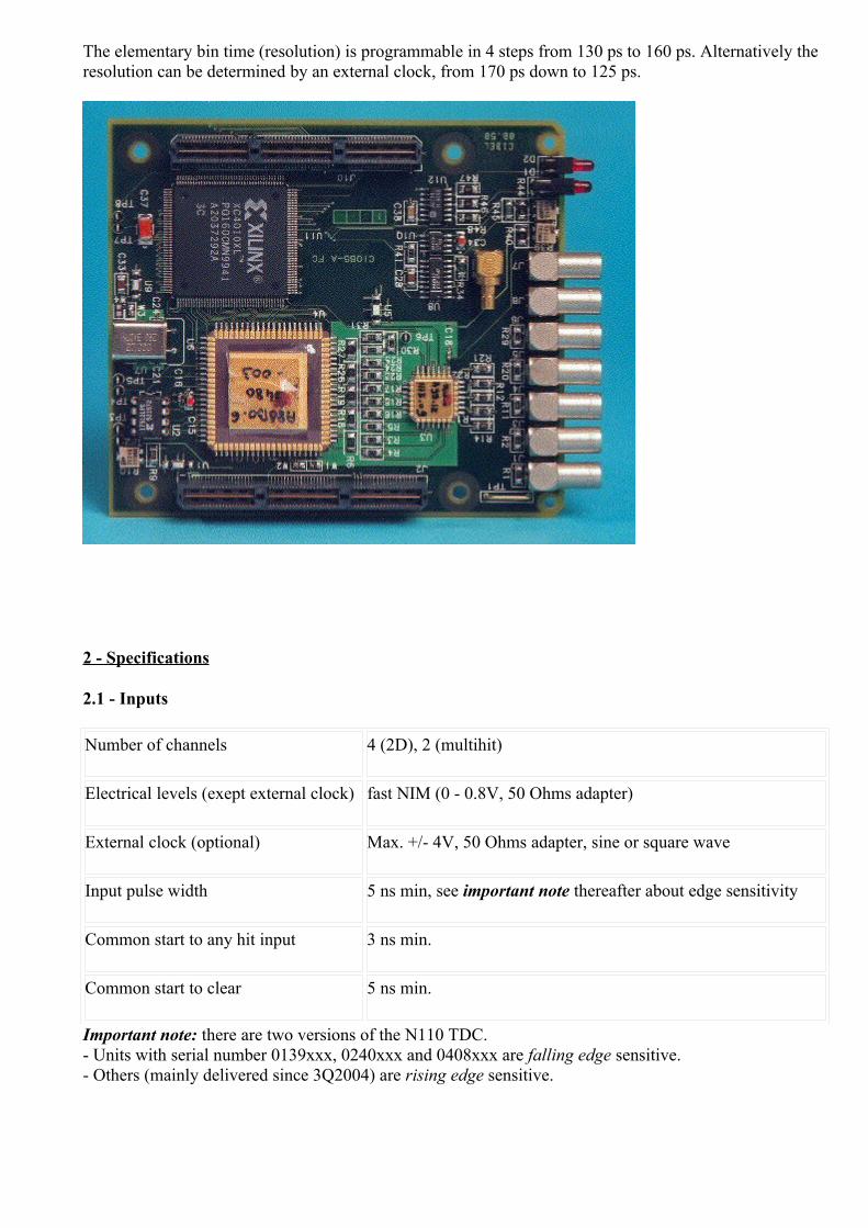
The elementary bin time (resolution) is programmable in 4 steps from 130 ps to 160 ps. Alternatively the resolution can be determined by an external clock, from 170 ps down to 125 ps.
2 - Specifications
2.1 - Inputs Number of channels 4 (2D), 2 (multihit)
Electrical levels (exept external clock) fast NIM (0 - 0.8V, 50 Ohms adapter)
External clock (optional) Max. +/- 4V, 50 Ohms adapter, sine or square wave
Input pulse width 5 ns min, see important note thereafter about edge sensitivity
Common start to any hit input 3 ns min.
Common start to clear 5 ns min.
Important note: there are two versions of the N110 TDC. - Units with serial number 0139xxx, 0240xxx and 0408xxx are falling edge sensitive. - Others (mainly delivered since 3Q2004) are rising edge sensitive.
2.2 - Time coding characteristics Resolution (bin time, in ps) 130.2, 136.4, 144.7 or 158.9 programmable
Differential non linearity (DNL) +/- 1%
Dynamic range (2D) 12 bits (about 600 ns)
Dynamic range (multihit) 14 bits (about 2.4 us)
Dead time (2D) 40 ns
Dead time (multihit) 40 ns two first hits, then 120 ns max.depending on event statistics
2.3 - Readout throughput 2D, gate length 150 ns 4 Mevents/s max.
Multihit 10 Mevents/s max., depending on gate duration and event statistics
2.4 - Gating characteristics Resolution 25 ns
Duration 75 ns to 3 us, programmable
Jitter +/- 7 ns
2.5 - Power requirements
Power supply +6 Volts @ 0.8 Amp max. -12 Volts @ 0.1 Amp max.
2.6 - Front panel outputs Data port HE10/34 pins, TTL levels
Gate signal Positive slow NIM
3 - Front and back panel description
3.1 - LED indicators FAIL NIM red Internal mother board hardware error. Briefly on following a system reset, then
normally off.
FAIL TDC red Internal mezzanine hardware error. Briefly on following a system reset, then normally
off, shortly after FAIL NIM be off.
RDY green Data ready (strobe on the front panel)
MHIT red Dual purpose: signal pile up condition (2D only) or PLL mis-locked
GATE green Copy of the GATE signal also available on a coax connector
3.2 - Front panel connectors
From top to bottom: X1 NIM, coax in X1 (2D) or X (multihit)
X2 NIM, coax in X2 (2D)
Y1 NIM, coax in Y1 (2D) or Y (multihit)
Y2 NIM, coax in Y2 (2D)
COM NIM, coax in Common start
CLR NIM, coax in Fast clear, cancels the events until end of GATE activity, edge sensitive
GATE Positive slow NIM, coax out Gate activity
unlabeled Positive slow NIM, coax out Copy of the STROBE signal,
also available on the parallel readout port
OUT TTL, HE10/34 out Data, see pinout next
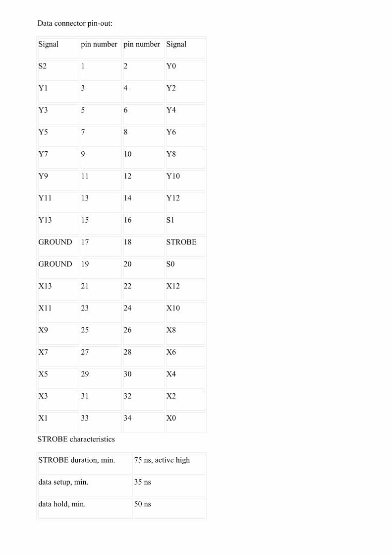
Data connector pin-out: Signal pin number pin number Signal
S2 1 2 Y0
Y1 3 4 Y2
Y3 5 6 Y4
Y5 7 8 Y6
Y7 9 10 Y8
Y9 11 12 Y10
Y11 13 14 Y12
Y13 15 16 S1
GROUND 17 18 STROBE
GROUND 19 20 S0
X13 21 22 X12
X11 23 24 X10
X9 25 26 X8
X7 27 28 X6
X5 29 30 X4
X3 31 32 X2
X1 33 34 X0
STROBE characteristics STROBE duration, min. 75 ns, active high
data setup, min. 35 ns
data hold, min. 50 ns
3.3 - Front panel trimmers
Two trimmers are accessible through holes in the front panel. The are used to set the discriminators input level. Top trimmer is related to the COM, X1, X2, Y1 and Y2 inputs. Range 0 to -2.5 V. Factory set at - 0.4V (fast NIM). Bottom trimmer is related to the fast CLEAR input. Range 2V to -1V. Factory set at - 0.4V (fast NIM). The CLEAR input accepts positive voltage. This is NOT the case with the COM, X and Y inputs which must be negative voltage only.
3.4 - Back panel connectors SUB-D 9 pins
Asynchronous serial line, RS232, IBM/PC compatible
coax External clock input (optional)
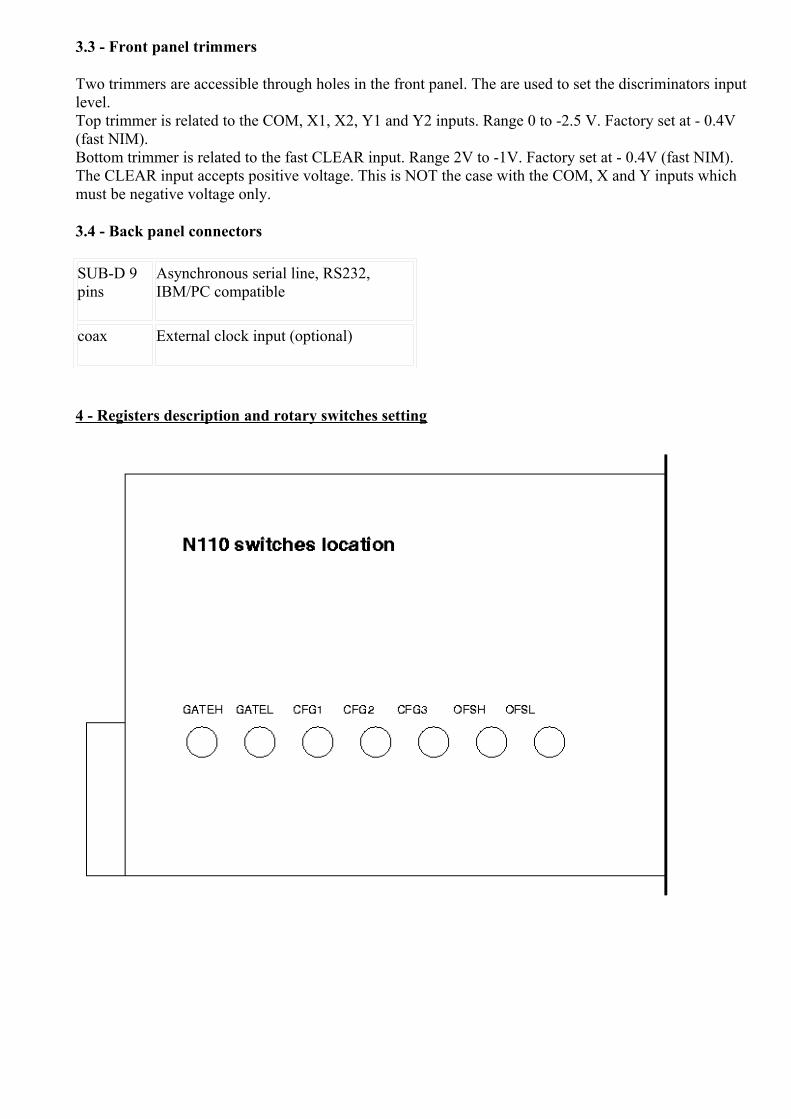
4 - Registers description and rotary switches setting
4.1 - Architecture overview
The readout unit is responsible for the time coding and processing of the raw values before passing the results to the output port on the front panel. This is implemented partly in the AMS110 ASIC and partly in a FPGA which are all physically located on a mezzanine. This document describes the present functionalities of the N110 TDC. New functionalities could be developed upon request by modifying the FPGAs boot programs.
The N110 always operates in the "common start" configuration whereby the COM signal initiates an acquisition sequence. - An internal gate is generated. Its duration is determined by the time-out register value. - Time coding is done on the fly by latching the status of a free running counter with a typical bin time of 150 ps. In 2D mode this yields 5 values: Z (COM start), X1, X2, Y1 and Y2. In multihit mode X2 and Y2 are discarded, just leaving 3 values Z, X1 and Y1. They are stored in a small FIFO memory in the ASIC. - Data are extracted from the ASIC and fed to an arithmetic unit which computes the results. The computations depends on the mode of operation.
In 2D mode: X = X1 - X2 + OffsetX Y = Y1 - Y2 + OffsetY (the offset is discussed below; Z value is not used)
In multihit mode: X = X1 - Z Y = Y1 - Z
- The X and Y results are latched as a single word onto the front panel output port. In 2D mode the results are 12 bit wide, whereas in multihit mode the dynamic range is extended to 14 bits.
It is assumed that the results are read out at full speed by the back end electronics (using a PC, for example). Therefore no handshake has been implemented at this port. The peak output rate is 10 MHz in multihit mode and 4 MHz in 2D mode (assuming a 150 ns gate length). Typically a readout throughput of 500 Kevents/s can be achieved safely by most readily available processors. This includes basic processing like sorting the data to build up a histogram in memory. A dedicated cabling adapter (ref. CI984) fits the HS32 digital input board from National Instruments. Otherwise the N110 output port is directly compatible with the VME VISTA (ESRF design).
Next paragraphs describe the resources that are involved in the readout procedure. The full description is given with reference to programming through the serial line (see 5). When using the rotary switches several options have been removed for the sake of simplicity. Some bits may therefore map differently. The rotary switch setting is documented along with each register description.
4.2 - Time-out register
This 8 bit register determines the internal gate duration, by step of 25 ns. A zero value is not valid. The gate duration is related to N, the time-out register contents, by the following formula:
GATE (ns) = 50 + 25 * N
Rotary switches: Label Value
GATEL 4 LSbits
GATEH 4 MSbits
Example: GATEL = 2, GATEH = 1 results in a 50 + 25 ( 2 + 16) = 500 ns gate duration.
4.3 - Offset registers
These are only relevant in 2D mode of operation. In multihit mode, both offset registers must be initialized to zero.
There are separate offset registers for the X and Y channels. The offsets are used to shift the results of the subtractions X1-X2 and Y1-Y2 so that the results are always positive binary encoded values. This fits the requirement of a delay line based detector. Indeed, given DL the delay line length, it is expected that the time encoded differences are in the range minus DL (left end side) to plus DL (right end side). The offset register is used to bias the result to always yield positive values from 0 to 2 DL. This simplifies the updating of images in the back-end electronics and/or host software.
It is noteworthy that the X and Y offsets may be different to fit non square geometry of the detector.
Although the offset value often conceptually duplicates the time-out value (they are linked to the physical length of the lelay lines), it is set independently because - it may be secure to program a gate duration slightly larger than the exact delay line length, and, - the time out value increments by steps of 25 ns, which is too coarse for setting the offset bias. Actually the offset value increments by steps of 16 times the time coding resolution. The typical pitch is therefore 16 * 150 ps = 2.4 ns.
Application example, for a 250 ns delay line based square detector, follows.
Time-out value = 250 - 50 (pedestal) / 25 = 8 The programming value 9 could be used to ensure that events are well captured (tradeoff at the expense of dead time). Otherwise events could be missed because of the gate jitter (typically 7 ns).
OffsetX = OffsetY = 250 / 2.4 = 104 (assuming a resolution of 150 ps, see 4.6 how to select the resolution) These values should be fine tuned experimentally to fit the exact delay line lengths, often slighly different in the X and Y dimensions.
Both offset registers reset to zero after power up.
Rotary switches: There is a single set of switches for both X and Y offsets, which restricts the programming to equal values. Label Value
OFFL 4 LSbits
OFFH 4 MSbits
Example: OFFL = 8, OFFH = 6 to get 104 decimal, as in the above application.
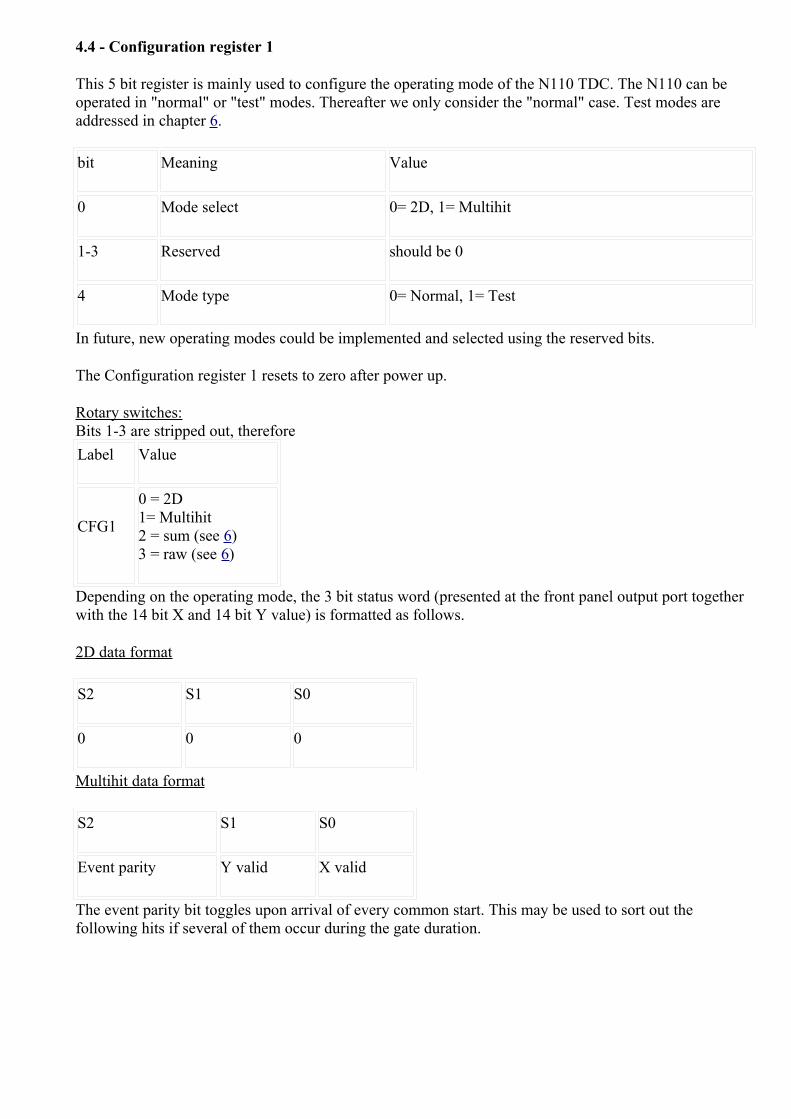
4.4 - Configuration register 1
This 5 bit register is mainly used to configure the operating mode of the N110 TDC. The N110 can be operated in "normal" or "test" modes. Thereafter we only consider the "normal" case. Test modes are addressed in chapter 6. bit Meaning Value
0 Mode select 0= 2D, 1= Multihit
1-3 Reserved should be 0
4 Mode type 0= Normal, 1= Test
In future, new operating modes could be implemented and selected using the reserved bits.
The Configuration register 1 resets to zero after power up.
Rotary switches: Bits 1-3 are stripped out, therefore Label Value
CFG1
0 = 2D 1= Multihit 2 = sum (see 6) 3 = raw (see 6)
Depending on the operating mode, the 3 bit status word (presented at the front panel output port together with the 14 bit X and 14 bit Y value) is formatted as follows.
2D data format S2 S1 S0
0 0 0
Multihit data format S2 S1 S0
Event parity Y valid X valid
The event parity bit toggles upon arrival of every common start. This may be used to sort out the following hits if several of them occur during the gate duration.
4.5 - Configuration register 2
This 6 bit register is used to configure the AMS110 ASIC. For more informations, please refer to the AMS110 documentation (CS/EL/99-02). bit Meaning Value
0 AMS110 MASK4 (readout common start time value) 0= Keep (multihit), 1= Discard (2D)
1 AMS110 STYLE03 (internal gate management)
1= Gate level, 0= Stop edge ; Must always set to zero in current N110 implementations
2 AMS110 MUXSEL (ASIC monitor output select) 0= Counter highest bit, 1= MASK4 copy
3 AMS110 power saving 0= up, 1= down
4 AMS110 pile up X enable 0= Disable
5 AMS110 pile up Y enable 0= Disable
Bits 4 and 5 (pile up enable) are only relevant in 2D mode. In this case an event is valid only when the following conditions have been met: - no second start is detected before the end of the gate; - there is exactly one, and only one, hit on each channel (X1 and X2 if pileup X enable, Y1 and Y2 if pileup Y enable). In the case of "true"area detectors (that means bi-dimensional) both X and Y pileup must be enabled. For a linear detector the pileup detection must be disabled on the unused channels (the operating mode still being "2D").
Rotary switches: Bits 0-3 are stripped out (the AMS110 programming is done automatically according to the configuration register 1), therefore Label Value
CFG2
0 = pile up disable 1 = X pile up 2 = Y pile up 3 = X & Y pile up enable
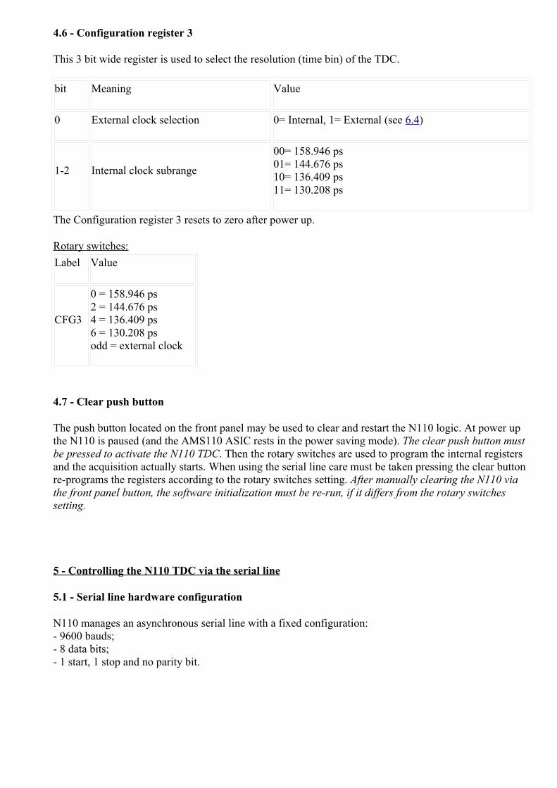
4.6 - Configuration register 3
This 3 bit wide register is used to select the resolution (time bin) of the TDC. bit Meaning Value
0 External clock selection 0= Internal, 1= External (see 6.4)
1-2 Internal clock subrange
00= 158.946 ps 01= 144.676 ps 10= 136.409 ps 11= 130.208 ps
The Configuration register 3 resets to zero after power up.
Rotary switches: Label Value
CFG3
0 = 158.946 ps 2 = 144.676 ps 4 = 136.409 ps 6 = 130.208 ps odd = external clock
4.7 - Clear push button
The push button located on the front panel may be used to clear and restart the N110 logic. At power up the N110 is paused (and the AMS110 ASIC rests in the power saving mode). The clear push button must be pressed to activate the N110 TDC. Then the rotary switches are used to program the internal registers and the acquisition actually starts. When using the serial line care must be taken pressing the clear button re-programs the registers according to the rotary switches setting. After manually clearing the N110 via the front panel button, the software initialization must be re-run, if it differs from the rotary switches setting.
5 - Controlling the N110 TDC via the serial line
5.1 - Serial line hardware configuration
N110 manages an asynchronous serial line with a fixed configuration: - 9600 bauds; - 8 data bits; - 1 start, 1 stop and no parity bit.
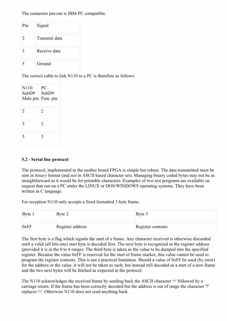
The connector pin-out is IBM-PC compatible. Pin Signal
2 Transmit data
3 Receive data
5 Ground
The correct cable to link N110 to a PC is therefore as follows. N110 SubD9 Male pin
PC SubD9 Fem. pin
2 2
3 3
5 5
5.2 - Serial line protocol
The protocol, implemented in the mother board FPGA is simple but robust. The data transmitted must be sent in binary format (and not in ASCII based character set). Managing binary coded bytes may not be as straightforward as it would be for printable characters. Examples of two test programs are available on request that run on a PC under the LINUX or DOS/WINDOWS operating systems. They have been written in C language.
For reception N110 only accepts a fixed formatted 3 byte frame. Byte 1 Byte 2 Byte 3
0xFF Register address Register contents
The first byte is a flag which signals the start of a frame. Any character received is otherwise discarded until a valid (all bits one) start byte is decoded first. The next byte is recognized as the register address (provided it is in the 0 to 6 range). The third byte is taken as the value to be dumped into the specified register. Because the value 0xFF is reserved for the start of frame marker, this value cannot be used to program the register contents. This is not a practical limitation. Should a value of 0xFF be used (by error) for the address or the value, it will not be taken as such, but instead still decoded as a start of a new frame and the two next bytes will be fetched as expected in the protocol.
The N110 acknowledges the received frame by sending back the ASCII character '=' followed by a carriage return. If the frame has been correctly decoded but the address is out of range the character '?' replaces '='. Otherwise N110 does not send anything back.
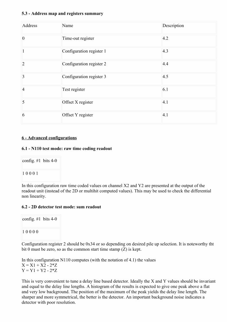
5.3 - Address map and registers summary Address Name Description
0 Time-out register 4.2
1 Configuration register 1 4.3
2 Configuration register 2 4.4
3 Configuration register 3 4.5
4 Test register 6.1
5 Offset X register 4.1
6 Offset Y register 4.1
6 - Advanced configurations
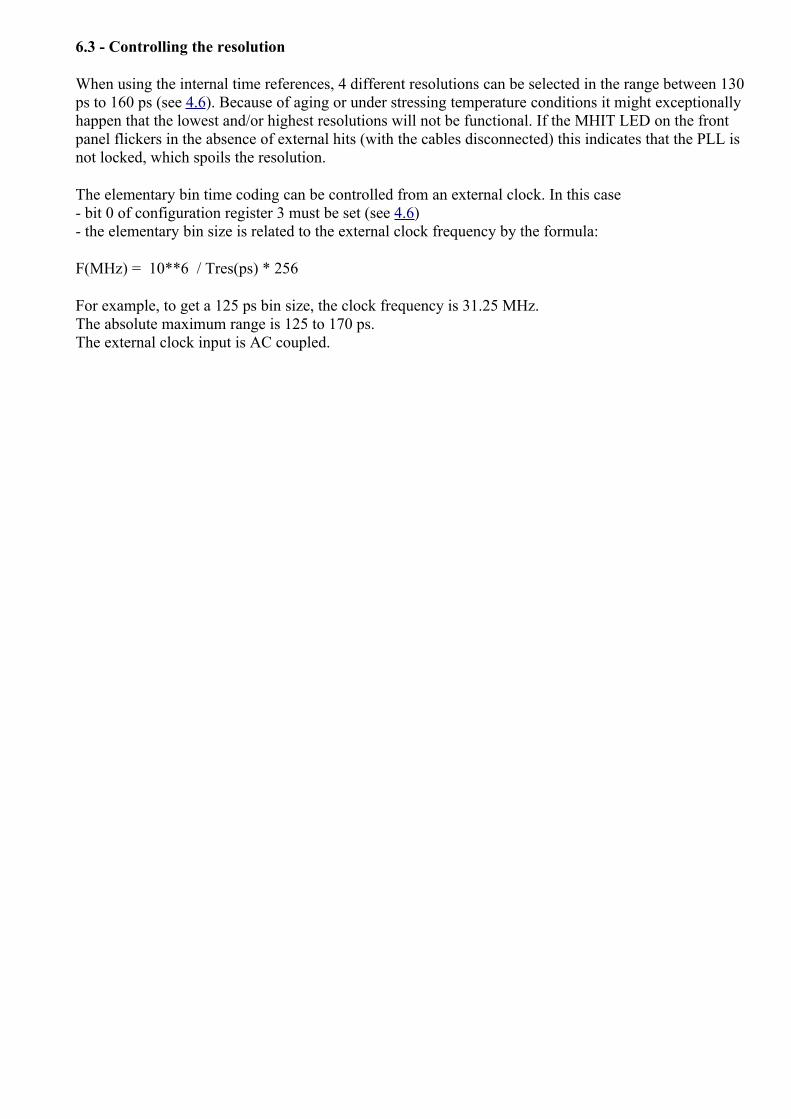
6.1 - N110 test mode: raw time coding readout config. #1 bits 4-0
1 0 0 0 1
In this configuration raw time coded values on channel X2 and Y2 are presented at the output of the readout unit (instead of the 2D or multihit computed values). This may be used to check the differential non linearity.
6.2 - 2D detector test mode: sum readout config. #1 bits 4-0
1 0 0 0 0
Configuration register 2 should be 0x34 or so depending on desired pile up selection. It is noteworthy tht bit 0 must be zero, so as the common start time stamp (Z) is kept.
In this configuration N110 computes (with the notation of 4.1) the values X = X1 + X2 - 2*Z Y = Y1 + Y2 - 2*Z
This is very convenient to tune a delay line based detector. Ideally the X and Y values should be invariant and equal to the delay line lengths. A histogram of the results is expected to give one peak above a flat and very low background. The position of the maximum of the peak yields the delay line length. The sharper and more symmetrical, the better is the detector. An important background noise indicates a detector with poor resolution.
6.3 - Controlling the resolution
When using the internal time references, 4 different resolutions can be selected in the range between 130 ps to 160 ps (see 4.6). Because of aging or under stressing temperature conditions it might exceptionally happen that the lowest and/or highest resolutions will not be functional. If the MHIT LED on the front panel flickers in the absence of external hits (with the cables disconnected) this indicates that the PLL is not locked, which spoils the resolution.
The elementary bin time coding can be controlled from an external clock. In this case - bit 0 of configuration register 3 must be set (see 4.6) - the elementary bin size is related to the external clock frequency by the formula:
F(MHz) = 10**6 / Tres(ps) * 256
For example, to get a 125 ps bin size, the clock frequency is 31.25 MHz. The absolute maximum range is 125 to 170 ps. The external clock input is AC coupled.
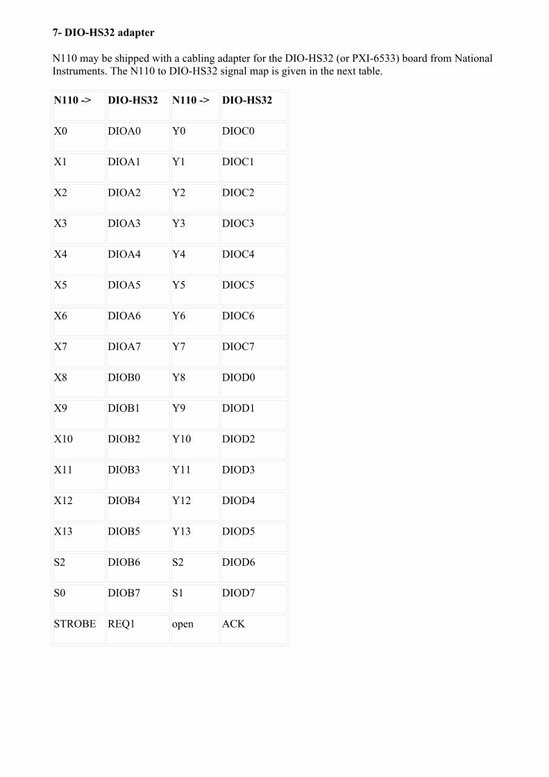
7- DIO-HS32 adapter
N110 may be shipped with a cabling adapter for the DIO-HS32 (or PXI-6533) board from National Instruments. The N110 to DIO-HS32 signal map is given in the next table. N110 -> DIO-HS32 N110 -> DIO-HS32
X0 DIOA0 Y0 DIOC0
X1 DIOA1 Y1 DIOC1
X2 DIOA2 Y2 DIOC2
X3 DIOA3 Y3 DIOC3
X4 DIOA4 Y4 DIOC4
X5 DIOA5 Y5 DIOC5
X6 DIOA6 Y6 DIOC6
X7 DIOA7 Y7 DIOC7
X8 DIOB0 Y8 DIOD0
X9 DIOB1 Y9 DIOD1
X10 DIOB2 Y10 DIOD2
X11 DIOB3 Y11 DIOD3
X12 DIOB4 Y12 DIOD4
X13 DIOB5 Y13 DIOD5
S2 DIOB6 S2 DIOD6
S0 DIOB7 S1 DIOD7
STROBE REQ1 open ACK
8 - 2D setup typical procedure (step by step)
This is an example on how to operate N110 for 2D detector readout.
1) Detector/Discriminators preliminary check Make sure you get correct fast NIM pulses from the anode (COM N110 input) and the cathodes (X1, X2, Y1, Y2). N110 has internal 50 Ohms adapters. Check the serial number to know the edge sensitivity. Minimum pulse width is 5 ns; usual pulse width is 10 to 20 ns. Minimum COMmon start (anode) to any cathode is 3 ns. A 1 meter long cable does the job, otherwise a few events will be lost (rejected by the pile-up detection logic).
2) N110 preliminary check Red led FAIL NIM on: the mother board is dead (in general TDC FAIL will be a consequence). Red led FAIL TDC on: the mezzanine board is dead. Cycle power off/on. If it persists, N110 fails. After power is just on, N110 enters a power saving sequence and is not operational yet. Both FAIL leds must be off (as explained above) and PUP led must be on, and nothing else is happening. To wake up the N110 TDC you must either press the front panel button or, by using the serial line, reset bit 3 in the configuration register 2. So press the initialization button. If the red led PUP remains on (all inputs being otherwise disconnected), the clock PLL does not lock. Make sure you are selecting a correct clock reference (see next). Try internal medium speed clock (like CFG3 = 2). If it persists, N110 fails. PUP led is normally off.
3) Set up the resolution Select one out of the internal references. CFG3 (serial line address 3) even number. Odd number would require an external reference.
4) Set up 2D operating mode CFG1 (serial line address 1) = 0
5) Set the gate length GATE (serial line address 0) = delay line length (in 25 ns units minus 50 ns offset, see 4.2). Connect the anode to the COM input. Observe the green led GATE. It is on when anode pulses are detected. Since this is proportional to the actual event rate, this can be hardly seen below 10K events/s. Monitor (oscilloscope) the GATE OUT signal (positive voltage), triggered by COM, duration as programmed.
6) Disable the pile up rejection logic For troubleshooting, expert users may skip that. CFG2 (rotary switch) = 0. CFG2 (serial line address 2) = 0x05 (beware serial differs from switch).
7) Check (again) the cathodes Make sure (oscilloscope) you get X1, X2, Y1, Y2 during the GATE activity. Connect them to N110. Observe the green led RDY. It is on when events have been recorded. This one is memorized (and therefore mostly independent of the actual event rate) so that it should be visible even at low counting rate (but not very low, like below 10Hz). Monitor (oscilloscope) the (unfortunately) unlabeled bottom coax output (positive voltage). This is a copy of the STROBE signal, also available on the output port. The STROBE typically occurs 200 ns after the GATE terminates.
8) Activate the pile up rejection logic CFG2 (rotary switch) = 3. CFG2 (serial line address 2) = 0x35 (beware serial differs from switch). Now the red led PUP flags the rejected events.

Green led GATE continues has before. Green led RDY should continue almost has before, but in the case most events are being rejected. For an accurate monitoring of the pile up rejection you may count the GATE output (detected events) versus the STROBE output (accepted events). At high counting rate (above 0.5 MHz) you may monitor the direct anode from the detector versus the GATE from N110. This measures the dead time of the N110 (plus some pile up activity).
9) Set up the offset registers Depending on your acquisition system you may use (or not) the offset registers. See 4.3. When used, fine tunning is necessary which is best achieved through a remote computer and the serial line.
10) Use our favorite acquisition system It works. Congratulations! It does not work. It is clearly a software issue. Call the Expert(s).
11) take a coffee break. It never hurts.
12) Back from the coffee break It still works. You are an Expert, too. It still does not work. Check the cable to the acquisition system (just in case the software would work).
13) Beam lost That's life. Back to home or next step.
14) Is the detector (so) good? A nice feature of N110 is the sum recording mode of operation (see 6.2). CFG1 (rotary switch) = 2. CFG1 (serial line address 1) = 0x10 (beware serial differs from switch). CFG2 (serial line address 2) = 0x34 (beware serial differs from switch). You should observe peaks (one for X, one for Y), the position of which is a measurement of the delay line length. The sharper and more symetrical the best. You don't get anything: did you used a Fe source in replacement of the (lost) beam?


![User's Manual PK200 CURRENT-TO-PNEUMATIC CONVERTER [Style…cdn2.us.yokogawa.com/IM21B03D01-01E.pdf · User's Manual PK200 CURRENT-TO-PNEUMATIC CONVERTER [Style:S2] IM 21B03D01-01E](https://img.pdfslide.net/doc/110x75/5a9c19d97f8b9ad96f8e52be/users-manual-pk200-current-to-pneumatic-converter-stylecdn2us-s-manual-pk200.jpg)