Embed Size (px)
DESCRIPTION
Â
Citation preview
The project was initiated by:
Prof. Peretz Lavie, The president of the Technion, Haifa, Israel
Pedagogical advisor: Assistant Prof. Miri Barak
All rights reserved 2013 ©
Introduction to Nanotechnology
Prof. Hossam Haick
Nanotechnology and Nanosensors

1 | P a g e
TABLE OF CONTENTS Table of Contents ...........................................1
Table of Figures .............................................5
Chapter 1 Introduction to Nanotechnology ... 11
Introduction ................................................. 11
Definition ................................................. 11
What does nano mean? ........................... 12
Surface Area to Volume Ratio .................. 12
Nanostructures ............................................ 13
0-D nanostructures .................................. 13
1-D nanostructures .................................. 14
2-D nanostructures .................................. 15
3-D nanostructures .................................. 15
Chapter 2 Introduction to Nanotechnology - continued .................................................... 17
Atomic force microscopy (AFM) .................. 17
AFM modes .............................................. 17
AFM images .............................................. 19
Scanning Electron microscopy (SEM) ........... 19
Transmission electron microscopy (TEM) .... 20
Nanoscale structure fabrication .................. 21
Top-Down Fabrication.............................. 21
Bottom-up Fabrication ............................. 24
Chapter 3 Introduction to Sensor’s Science and Technology .................................................. 28
Senses .......................................................... 28
Vision ........................................................ 28
Hearing ..................................................... 28
Smell ......................................................... 29
Sensors ......................................................... 29
Classification of sensors ............................... 30
Optical sensors ......................................... 30
Chemical sensors...................................... 30
Electrochemical sensors .......................... 31
Mass sensitive sensors ............................. 31
Biosensors ................................................ 32
Parameters for characterizing sensors ........ 32
Electronic nose ............................................ 33
Optoelectronic nose ................................ 34
Sensors for Electronic Applications ......... 35
Machine learning ..................................... 35
Chapter 4 Metal Nanoparticle-Based Sensors 37
Nanoparticles/Quantum Dots ..................... 37
Types of Metal Nanoparticles .................. 37
Shapes of Metal Nanoparticles ................ 38
Molecular Modifications of Metal Nanoparticles ........................................... 38
Controlled Binding Between Adjacent Metal Nanoparticles ................................ 38
Characteristics of Molecularly Modified Metal Nanoparticles ................................ 39
Production of Metal Nanoparticles ............. 39
Production of Nanoparticles by Laser Ablation.................................................... 39
Production of Nanoparticles by Chemical Route ....................................................... 40
Production of Encapsulated Metal Nanoparticles ........................................... 40
Shape Control of Produced Nanoparticles ................................................................. 41
Programmed Assembly of Functionalized Nanoparticles ........................................... 41
Chemiresistors Based on Molecularly Modified Metal ............................................ 44
Effect of Chain Length .............................. 45
Sensing Mechanism in Chemiresistors of Nanoparticles ........................................... 45
Effect of Cross-Linking on Chemiresistors of Nanoparticles ........................................... 46

2 | P a g e
Effect of Nanoparticle Shape on the Related Chemiresistors ............................ 47
Medical and Biological Applications of Gold Nanoparticles ............................................... 48
Attachment of Gold Nanoparticles to Cell Surfaces .................................................... 48
Gene and siRNA Delivery ......................... 49
Drug Delivery............................................ 49
Nanoparticles as Cancer Diagnostic & Therapeutic Agents .................................. 49
Nanoshells for Cancer Treatment ............ 50
Imaging and Hyperthermia using (Au/SiO2) Nanoshells ................................................ 50
Chapter 5 Quantum Dot Sensors .................. 51
Definition and Main Properties ................... 51
Quantum Size Effect ................................. 51
Functionalization of Quantum Dots ......... 52
Synthesis of Quantum Dots ......................... 53
Synthesis of Quantum Dot Heterostructures ...................................... 54
Self-Organized Quantum Materials ......... 55
Surface Modification of Quantum Dots ... 57
Sensing and Imaging Application With Quantum Dots .............................................. 57
Temperature Sensors Based on Quantum Dots .......................................................... 57
Chemical Sensors based on Quantum Dots ................................................................. 58
Biosensors Based on Quantum Dots ........ 59
Quantum Dots and Imaging ..................... 59
Chapter 6 Nanowire-based Sensors .............. 62
What is a Nanowire? .................................... 62
Properties of Nanowires .......................... 62
Fabrication of Nanowires ............................. 65
Top-Down ................................................. 65
Bottom-Up ............................................... 66
Fabrication of Nanowire Devices by e-beam Lithography .................................... 67
Roll-Transfer of Nanowires ...................... 68
Nanowires in Sensing Application in Liquid or In-vivo Environments ................................... 68
Electrical Transport in Si NWs .................. 68
Surface Modification of Si NWs ............... 69
Chemically Sensitive Field Effect Transistors ............................................... 69
Si NW pH Sensors..................................... 70
3D Kinked Nanowire Probes .................... 71
Optical Detection of Relative Humidity ... 71
Semiconducting Nanowire Sensors for Gas Sensing Applications .................................... 72
Gas Sensor based on FET with Single Si NW ................................................................. 72
Elimination of Trap States by Attaching Dense Receptors via Si-O-Si Bond ............ 73
Polar and Nonpolar Sensing using Si NW FETs .......................................................... 73
Effect of Functional (End) Group on the Gas Sensing of Si NW FETs ....................... 74
Effect of Chain Length on the Gas Sensing of Si NW FETs ........................................... 75
Sensing Mechanism ................................. 76
Chapter 7 Carbon Nanotube-based Sensors .. 77
Structure and Properties of Carbon Nanotubes ................................................... 77
Electrical Properties of CNTs ................... 78
CNT Strength and Elasticity ..................... 78
CNTs Thermal Conductivity and Expansion ................................................................. 78
CNT High Aspect Ratio ............................. 79
Carbon Nanotubes Synthesis ....................... 79
Chemical Vapor Deposition (CVD) ........... 79
Arc Discharge ........................................... 81

3 | P a g e
Laser Ablation .......................................... 81
Functionalized Carbon Nanotubes ........... 82
Carbon Nanotubes for Sensing Applications82
CNT-based Electrical Sensors ................... 82
DNA Sensing by FETs Based on Networks of Carbon Nanotubes ................................... 82
Detection of Explosives & Toxins in Water by CNT FETs .............................................. 83
CNT- based Biosensors ............................. 83
CNT-based Electrochemical Sensors ........ 84
CNT-based Optical Sensors ...................... 85
Magnetic Particle-Based Sandwich Sensors with CNTs ................................................. 85
Nanoscale Mass Sensor based on CNTs ... 86
CNTs as Sensors for Gaseous Species .......... 86
Sensing Mechanism of Bare CNT-based Electrical Gas Sensors .............................. 86
CNT-based Electrical Gas Sensor .............. 87
A Single-Walled Carbon Nanotube Network Gas Sensing Device................................... 88
Sensors Based on Composites of CNTs and Non-Polymeric Materials ......................... 89
Minimizing the Humidity Effect on CNT-based Electrical Sensors ........................... 89
A Tunable Photosensor based on CNTs ... 89
An ultrasensitive Nanomechanical Mass Sensor based on a single CNT .................. 90
Chapter 8 Sensors based on Nanostructures of Metal Oxide ................................................. 92
Production and Classification of Metal Oxide Nanostructures ............................................ 92
Classifications of Metal Oxide Nanostructures ........................................ 92
Production of Metal Oxide Nanostructures ................................................................. 93
Sensing Mechanisms of Metal Oxide Gas Sensors ......................................................... 97
The Effect of Chemisorption on the Metal Oxide Sensors .......................................... 97
NO2 Reaction Mechanism ........................ 98
H2 Reaction Mechanism ........................... 99
Resistive Oxygen Sensors......................... 99
Improvements in Sensitivity of Metal Oxide Sensors ......................................................... 99
Thin Film Gas Sensors .............................. 99
Sacrificial Microsphere Templates ......... 100
Nanowire and Nanofiber (1D) Metal Oxide Sensors ................................................... 100
Chapter 9 Sensors based on Polymeric Nanostructures .......................................... 103
Properties of Polymeric Nanostructures ... 103
Conducting Polymers ............................. 104
Synthesis and Production Approaches of Polymeric Nanostructures ......................... 106
Hard Template Approach ...................... 106
Soft Template Approaches .................... 107
Electrospinning Technique .................... 109
Polymeric Nanostructure-based Sensors .. 109
Electrical Sensors ................................... 109
Biosensors (Liquid Phase) ...................... 109
Mechanical Sensors in a Liquid Solution 112
polymeric nanostructures for gas sensing applications ................................................ 113
molecularly imprinted polymers (MIPs) 113
Polycyclic Aromatic Hydrocarbons (PAHs) ............................................................... 113
Chapter 10 Electronic Skin based on Nanotechnology ........................................ 119
Properties of the Human Skin .................... 119
Flexible Electronics .................................... 119
Electronic Skin for Robots ...................... 119
Touch Sensors for Prosthetics ............... 120

4 | P a g e
Surgical Robotics .................................... 120
Electronic Skin for Health Monitoring.... 120
Electronic Skin Based on Nanowires and Organic Field Effect Transistors ................. 122
Organic FETs for Electronic Skin Applications ............................................ 122
Strategies To Enable Tactile Sensing for Organic Electronics ................................ 124
Nanowire Active Matrix ......................... 124
Gold Nanoparticles and Carbon Nanotubes based Pressure Sensors ............................. 125
Nanoparticle-based Strain Sensors ........ 125
Nanoparticle-based Multi-Purpose Sensors ............................................................... 126
Carbon Nanotube Strain Sensor for Human-Motion Detection ...................... 126
CNT Skin-like Pressure and Strain Sensors ............................................................... 127
Conclusions ................................................ 128
5 | P a g e
TABLE OF FIGURES Figure 1-1: An image of the Old Testament engraved on a tiny chip .................................... 12
Figure 1-2: Illustration describing different types of nanostructures ............................................. 13
Figure 1-3: Modified SEM image of a coaxial Si nanowire. ......................................................... 14
Figure 1-4: Scanning tunneling microscop image of a self-assembled monolayer on Au ............. 15
Figure 1-5: Transmission electron microscopy image of a superlattice .................................... 15
Figure 1-6: Illustration of three catagories of nanostructured bulk materials ........................ 16
Figure 1-7: Computer model of a nanocomposite comprised of polymer and silica nanoparticles. .................................................. 16
Figure 2-1: Scheme describing the main components of an AFM system ....................... 17
Figure 2-2: Illustration of an AFM tip used in static/contact mode. ........................................ 18
Figure 2-3: Illustration of an AFM tip used in non-contact mode............................................ 18
Figure 2-4: Illustration of an AFM tip used in tapping mode. .................................................. 19
Figure 2-5: AFM image portraying Cu nanowires. ......................................................................... 19
Figure 2-6: High resolution AFM image of Ge network on Si ................................................... 19
Figure 2-7: Scheme illustrating the working setup of a SEM system ..................................... 20
Figure 2-8: Scheme illustrating the working setup of a TEM system ..................................... 21
Figure 2-9: Scheme illustrating the FIB operation process ............................................................. 22
Figure 2-10: Scheme describing the steps of a typical photolithography process. ................... 23
Figure 2-11: Illustration of the steps involved in the EBL process ................................................ 24
Figure 2-12: Nanoscale patterns fabricated on a silicon substrate. .............................................. 24
Figure 2-13: Multi-component nano-structures with tunable optical properties. ...................... 26
Figure 2-14: Self-assembly of monolayers. The head groups are anchored onto the substrate while the tail groups assemble together far from the substrate. .......................................... 26
Figure 3-1: Analogy between the human sensing system and artificial sensors. ........................... 30
Figure 3-2: Illustration of chemiresistors with receptors, the binding of bio-molecule with net electrical charges changes the channel conductance. ................................................... 31
Figure 3-3: Illustration of an electrochemical sensor. ............................................................. 31
Figure 3-4: Illustration of three types of mass sensitive sensors. ............................................. 31
Figure 3-5: Accuracy and precision analogous in arrow and target. ............................................. 32
Figure 3-6: Figure illustrating the definitions of limit of detection and limit of quantitation. .... 33
Figure 3-7: Illustration of a hysteresis graph. .. 33
Figure 3-8: Selective vs. cross reactive sensing approach .......................................................... 34
Figure 3-9: Classification process for electronic nose detection. ................................................ 34
Figure 3-10: Optoelectronic nose response to volatile organic compounds. ........................... 35
Figure 4-1: Ancient stained-glass makers knew that by putting varying, tiny amounts of gold and silver in the glass, they could produce the red and yellow found in stained-glass windows.. ......................................................................... 37
Figure 4-2: Gold nanoparticles of various sizes and shapes ....................................................... 38
Figure 4-3: Schematic illustration of thin film assembly of nanoparticles (NPs) with capping molecules that are mediated by different molecular linkers. ............................................ 39
6 | P a g e
Figure 4-4: Different chain length ligands connected to nanoparticles. ............................ 39
Figure 4-5: Illustration of nanoparticles production via a chemical route. ..................... 40
Figure 4-6: Two-step process nanoparticle synthesis approach, ‘‘seed-mediated growth’’, for the production of controlled shape nanoparticles ................................................... 41
Figure 4-7: Nanoparticles for the detection of a specific DNA.. ................................................... 42
Figure 4-8: Temperature effect on DNA modified nanoparticles. ................................... 42
Figure 4-9: DNA-capped gold nanoparticles for the detection of DNA strands.. ........................ 43
Figure 4-10: Nanoparticle-based bio-bar codes for ultra-sensitive protein detection. ............... 44
Figure 4-11: Effect of chain length on sensor response.. ......................................................... 45
Figure 4-12: Average resistance-based sensitivities, sR, for the organothiol-capped Au-NPs exposed to 13 analytes at 0.001 < P/P⁰ <0.0200. ........................................................... 45
Figure 4-13: Description of suggested model of film growth. ...................................................... 46
Figure 4-14: Schematic representation of the reversible pH change-induced swelling of gold nanoparticles coated poly(vinylpyridine) polymer brushes. ............................................. 46
Figure 4-15: Illustration of a chemiresistor array with thin film assemblies of Au and AuAg nanoparticles mediated by linkers of different chain lengths .................................................... 46
Figure 4-16: Response sensitivities of a sensor array with ADT-Au and DCA-AuAg thin films of different chain length in response to vapors. .. 47
Figure 4-17: The voids between adjacent spherical Pt NPs range between 0.4 to 3.3 nm. ......................................................................... 47
Figure 4-18: Comparison between response of cubic and spherical nanoparticle-based
chemiresistors upon exposure to undecane, octane and ethanol .......................................... 48
Figure 4-19: Illustration demonstrating binding of gold nanoparticles functionalized with herceptin antibodies, which recognize receptors on the cell surface. .......................................... 49
Figure 4-20: Scheme of gene or DNA delivery process using functionalized nanoparticles ..... 49
Figure 4-21: Nanoshells for cancer treatment. 50
Figure 4-22: Imaging and hyperthermia using nanoparticles ................................................... 50
Figure 5-1: Solutions of colloidal QDs of varying size and composition, exhibiting photoluminescence under optical (ultraviolet) excitation. ........................................................ 52
Figure 5-2: Quantum dots sensors for the detection of biomolecules ............................... 53
Figure 5-3: Scheme illustrating high-temperature coordinating solvent synthesis... 54
Figure 5-4: Schematic of mechanisms leading to the formation of core and shell nanocrystals. . 54
Figure 5-5: Schematic of mechanisms leading to the formation of core and shell nanocrystals - continued ......................................................... 55
Figure 5-6: Illustration of the stages of strain relief in Stranski–Krastanov growth when the lattice constant of the film exceeds that of the substrate .......................................................... 55
Figure 5-7: Self-assembled quantum dots visualized with AFM. ........................................ 56
Figure 5-8: Selective metalo-organic chemical vapor deposition (MOCVD) growth of single-crystal dense GaAs quantum dot array using cylinder-forming diblock copolymers. ............. 56
Figure 5-9: Examples of ~25 nm quantum dots produced by block copolymer process. ........... 57
Figure 5-10: Illustration of a QD-based temperature sensor.. ....................................... 57
Figure 5-11: Response of QDs-based temperature sensors ....................................... 58

7 | P a g e
Figure 5-12: Illustration of QD coincidence detection. ......................................................... 58
Figure 5-13: Modified QDs for potassium ion detection). ........................................................ 59
Figure 5-14: Illustration of strategies for developing stable water dispersions of luminescent QDs .............................................. 59
Figure 5-15: Images of mice injected with water-soluble QDs. .......................................... 60
Figure 5-16: Qtracker intracellular QD delivery quantified by flow cytometry and imaged with brightfield and fluorescent microscopy). ......... 60
Figure 6-1: Systems utilizing the unique electrical, optical, thermal and mechanical properties of nanowires. .................................. 63
Figure 6-2: Illustration of a transverse thermoelectric device ...................................... 64
Figure 6-3: Electron microscopy images of air-suspended PbTe nanowires. ............................ 64
Figure 6-4: Elongation process of type II-zinc oxide nanowire ................................................ 65
Figure 6-5: SEM images of the Si NW arrays fabricated by electrochemical etching. ............ 65
Figure 6-6: Illustration of the SiNW and SiNH array fabrication process. ................................ 66
Figure 6-7: Schematic describing the VLS growth process. ............................................................ 66
Figure 6-8: Illustration of nanowire fabrication of via e-beam lithography. ............................... 67
Figure 6-9: Illustration of nanowire fabrication via photo lithography. ...................................... 67
Figure 6-10: Main steps of roll-transfer process. ......................................................................... 68
Figure 6-11: Electrical transfer in Si NW .......... 69
Figure 6-12: Antibody modification on Si NW, including ........................................................... 69
Figure 6-13: Chemical sensor based on a silicon nanowire field-effect transistor that allows rapid, multiplexed detection of many markers with high selectivity and sensitivity. ................ 70
Figure 6-14: Silicon nanowire pH sensor ......... 70
Figure 6-15: Optical humidity sensor .............. 72
Figure 6-16: Gas sensor based on FET with single silicon nanowire .................................... 72
Figure 6-17: Logarithmic and linear Ids−Vbgs characteristics of Si NW FETs scanned forward and backward .................................................. 73
Figure 6-18: Counter map of the relative conductivity changes at various gate voltages for multiple polar and non-polar VOC concentrations. ................................................ 74
Figure 6-19: Typical electrical and sensing characteristics of sensor COOCH3-APTES upon exposure to different concentrations .............. 74
Figure 6-20: ΔVth response upon exposure to different VOCs in different concentrations vs. functional group. ............................................. 75
Figure 6-21: Δµh response of Si NW FETs with different functional groups. ............................. 75
Figure 6-22: ΔVth responses of Si NW FETs with different chain lengths..................................... 76
Figure 6-23: Δµh response of Si NW FETs with different chain lengths..................................... 76
Figure 7-1: The (n,m) nanotube naming scheme can be thought of as a vector (Ch) in an infinite graphene sheet that describes how to "roll up" the graphene sheet to make the nanotube. ... 77
Figure 7-2: Illustration of different types of CNTs ......................................................................... 78
Figure 7-3: Graph illustrating the relationship between CNT bandgap and radius.................. 78
Figure 7-4: CNTs randomly dispersed in epoxy. ......................................................................... 79
Figure 7-5: Scheme illustrating the CVD process. ......................................................................... 79
Figure 7-6: An illustration of a chamber used for CNT synthesis. ................................................. 80
Figure 7-7: CNT growth systems ...................... 80
Figure 7-8: Illustration of graphene growth mechanism....................................................... 80

8 | P a g e
Figure 7-9: TEM images of different types of CNTs ................................................................. 81
Figure 7-10: Illustration of arc discharge ......... 81
Figure 7-11: Laser ablation or vaporization method for lab synthesis of buckyballs, single walled and multi walled (SWNT and MWNT) nanotubes. ....................................................... 81
Figure 7-12: Functionalization of CNTs. ........... 82
Figure 7-13: FETs based on CNT networks for DNA sensing ..................................................... 83
Figure 7-14: Flexible chemical sensor for the detection of toxins and explosives in water. ... 83
Figure 7-15: Electrochemical microelectrode for detection of analytes ....................................... 84
Figure 7-16: CNT-based electrochemical sensors ......................................................................... 84
Figure 7-17: CNT-based optical sensors ........... 85
Figure 7-18: DNA detection with coupled sandwich probe of magnetic particles and CNTs.. ............................................................... 86
Figure 7-19: NEMS based mass sensor ............ 86
Figure 7-20: Mechanism of interactions of polar gas molecules with surface-modified carbon nanotubes. ....................................................... 87
Figure 7-21: Field-effect transistor with a semiconducting SWCNT contacted by two electrodes decorated with nickel nanoparticles. ......................................................................... 87
Figure 7-22: Valence electron density plot showing NO2 molecules adsorbing onto a (10,0) semiconducting SWNT ..................................... 88
Figure 7-23: Response to different concentrations of NO2, expressed as the relative change in conductance. ...................... 88
Figure 7-24: SWCNT network based sensor for the detection of chemical gases. ..................... 88
Figure 7-25: Composite CNTs and non-polymeric materials based sensor .................................... 89
Figure 7-26: PAH/SWCNT sensors. ................... 89
Figure 7-27: Tunable CNT based photosensor 90
Figure 7-28: Mass sensor ................................. 91
Figure 7-29: Adsorbent fluctuations on the surface of a CNT-based nanoelectromechanical resonator.. ....................................................... 91
Figure 8-1: Metal oxide nanowires that function with different transduction mechanisms. ....... 93
Figure 8-2: Illustration of a sol-gel synthesis process ............................................................. 94
Figure 8-3: Examples of nanostructures produced using sol-gel synthesis ..................... 94
Figure 8-4: Scheme illustustrating an electrospinning setup. ..................................... 94
Figure 8-5: Description of the process of producing a microscopic solid-material structure through chemically reacting vapor- or gas-phase reactants on a heated surface. ....... 95
Figure 8-6: Appearance of various ZnO nanotubes ........................................................ 95
Figure 8-7: ZnO nanoneedle arrays grown at different DAP concentrations on three seed layers ................................................................ 96
Figure 8-8: Illustration of the PVD process…..96
Figure 8-9: The hydrogen sensing mechanism of resistance based semiconducting metal oxide sensors. ............................................................ 97
Figure 8-10: Effect of chemisorption on metal oxide sensors. .................................................. 97
Figure 8-11: Metal-oxide sensor sensitivity ..... 98
Figure 8-12: NO2 reaction mechanism. ........... 98
Figure 8-13: H2 reaction mechanism. .............. 99
Figure 8-14: Illustration of a resistive oxygen sensor .............................................................. 99
Figure 8-15: SEM images of the sacrificial microsphere template process. ..................... 100
Figure 8-16: TiOx egg shell structure response upon exposure to nitrogen dioxide. .............. 100
Figure 8-17: Nanowire-based metal oxide sensor ............................................................ 101
9 | P a g e
Figure 8-18: Nanofiber semiconducting metal oxide sensor ................................................... 101
Figure 9-1: SEM images depicting (a) nanofibers (b) nanorods (c) core/shell structures (d) nanotubes (e) nanoplates (f) nanospheres .... 103
Figure 9-2: Ragone plot .................................. 104
Figure 9-3: P3HT nanowires ........................... 105
Figure 9-4: Actuators based on polyaniline nanofibers ...................................................... 106
Figure 9-5: Hard template approach.............. 106
Figure 9-7: Mechanisms of soft template synthesis of different conducting polymer nanostructures) .............................................. 108
Figure 9-8: Illustration of the process utilizing surfactants as a soft template). ..................... 108
Figure 9-9: The electrospinning processn. ..... 109
Figure 9-10: Scheme of a conducting polymer based electric sensor. .................................... 109
Figure 9-11: Conducting polymer nanostructures ............................................... 110
Figure 9-12: Polymer nanojunction sensor for glucose detection ........................................... 110
Figure 9-13 : Two-terminal copolymer nanowire sensor ............................................................. 111
Figure 9-14: PET-fluoro-iono-phore and MOF based ions sensor ........................................... 111
Figure 9-15: Excitation and emission spectra of the FI in acetonitrile with different sodium ion concentrations and constant FI concentration. ....................................................................... 111
Figure 9-16: Fluorescence sensor based on dual-fluorescent composite nanoparticles with inorganic semiconductor cores and shells of polymer semiconductor layers, for the detection of the redox-active metalloprotein cytochrome c. ................................................ 112
Figure 9-17: Influence of cytochrome c (from 0 to 950 nM with concentration increments of 50 nM) on the fluorescence spectra of dual-fluorescent nanocomposite of the silicon
nanoparticles and conjugated polyelectrolytesthe arrow indicates the direction of change in emission intensity with increasing concentration of cytochrome c. ... 112
Figure 9-18: pH nanosensor........................... 112
Figure 9-19: TNT sensor.. ............................... 113
Figure 9-20: SEM image of PAH on a silicon wafer (with a microscope picture in the insert) of one PAH derivative on a silicon wafer, as well as snail-like pathways connecting the electrodes submerged into the silicon. ........................... 114
Figure 9-21: PAH/SWCNT sensor.. ................ 114
Figure 9-22: Sensitivity of different PAH/SWCNT sensors. .......................................................... 115
Figure 9-23: Ellipsometer system. ................. 115
Figure 9-24: QCM system.. ............................ 115
Figure 9-25: Physical and optical properties changes in PAH-6 film. ................................... 116
Figure 9-26: Physical and optical properties changes in PAH-7 film. ................................... 116
Figure 9-27: PAH based field effect transistor (FET) scheme.. ................................................ 116
Figure 9-28: Current vs. voltage curve, indicating the 4 features using for analysis ... 117
Figure 9-29: Normalized Vth feature from exposures to different concentrations of ethylbenzene ................................................. 117
Figure 9-30: PAH-FET experiment results. ..... 117
Figure 9-31: PAH-FET sensors VOCs separation ability.. ........................................................... 118
Figure 10-1: The da Vinci Surgical System ..... 120
Figure 10-2: Wearable electronic skin based health monitoring system. ............................. 121
Figure 10-3: Multifunctional epidermal electronic system (EES) on skin ..................... 121
Figure 10-4: A flexible electronic device attaches to the skin like a bandage tape and can be used to acquire physiological information without bulky electrodes. ........................................... 122
10 | P a g e
Figure 10-5: Data obtained from electronic skin for health applications.. ................................. 122
Figure 10-6: A schematic demonstrating multiple specifically “tuned” functional layers of human skin. .................................................... 123
Figure 10-7: Scheme depicting muliple materials with high potentials in bio-electronic FET-based devices. .......................................................... 123
Figure 10-8: PDMS films. ............................... 124
Figure 10-9: Nanowire active matrix.............. 125
Figure 10-10: Nanowire-based pixel .............. 125
Figure 10-11: Schematic illustration of the geometry of a film made of nanoparticles. ... 126
Figure 10-12: Flexible nanoparticles based sensor. ............................................................ 126
Figure 10-13: SWCNT-film strain sensor ........ 127
Figure 10-14: Stretchable wearable devices .. 127
Figure 10-15: Revolution of morphology of carbon nanotubes films. ................................ 128
Figure 10-16: Images showing the characteristics of a 64- pixel array of compressible pressure sensor. ...................... 128
11 | P a g e
Chapter 1 INTRODUCTION TO
NANOTECHNOLOGY
INTRODUCTION
This chapter presents an introduction to the field of nanotechnology, including essential definitions, the presentation of the key unique features of the materials and technologies that exist at the nanoscale level, and concluding with a general presentation on the main categories of the nanomaterials.
DEFINITION
The prefix “nano” is derived from the ancient Greek “nanos”, meaning "dwarf”. Today, “nano” is used as a prefix that means “billionth” or a factor of 10−9. Coupling the word “nano” with the unit “meter” brings the term “nanometer”, which indicates a unit of spatial measurement that is one billionth of a meter. With this in mind, nanotechnology shall be defined as the science, engineering, and technology conducted at the scale that range between 1 to 100 nanometers.
The idea and concept behind the nanotechnology started with a talk entitled “There’s Plenty of Room at the Bottom” by the physicist Richard Feynman at the American Physical Society meeting at the California Institute of Technology (CalTech) in 1959. In his talk, Feynman described a process in which scientists would be able to manipulate and control individual atoms and molecules. Over a
decade later, Professor Norio Taniguchi coined the term nanotechnology, during his explorations of ultra-precise machining processes. However, the modern era of nanotechnology began only in 1981, when the scanning tunneling microscope that could "see" individual atoms was developed and used.
To get the length-scale of the nanometer in perspective, we can examine the units or measures used in daily life. If we cut a meter stick up into 100 equal pieces, each piece would be one centimeter in size. This is equivalent to the size of a pinky finger or a sugar cube.
If we cut up centimeter into ten equal pieces, each piece would be one millimeter. A one cent coin is approximately 1.5 mm thick and a grain of sand ranges from 0.1 mm to 2 mm in size. Objects as small as a millimeter can be seen with the naked eye, but when object dimensions fall below a millimeter, they can be hard to discern.
If we cut up a millimeter into one thousand equal pieces, each piece would be a micrometer long. In other words, a micrometer is equal to one millionth of a meter. The diameter of a hair is about forty to fifty micrometers wide. Red blood cells are six to ten micrometers in diameter. Many types of bacteria typically measure five to twenty micrometers. Things on this scale usually can't be seen with our eyes, but rather can be visualized with a magnifying glass or light microscope.
If we cut a micrometer up into one thousand equal pieces, each piece would be a nanometer long. In other words, a nanometer is equal to one-billionth of a meter. When things are this small, we can't observe them with our eyes or a light microscope. Objects this small require a special tool for imaging. Things on the nanometer scale include viruses (30-50 nm), DNA (2 nm), buckyballs (1 nm in diameter), and carbon nanotubes (~1 nm in diameter). Atoms are smaller than a nanometer. One atom measures ~0.1-0.3 nm, depending on the element type.
12 | P a g e
Here are some objects from our daily life measured in nanometers:
- One inch equals 25.4 million nanometers.
- A sheet of paper is about 100,000 nanometers thick.
- A human hair measures roughly 50,000 to 100,000 nanometers in diameter.
- Our fingernails grow one nanometer every second.
WHAT DOES NANO MEAN?
A video that illustrates the meaning of “nano” can be found in the following link:
http://www.youtube.com/watch?v=Dxq-ffp3jqA
As an example of the importance of the miniaturization ability of nanotechnology, we can look back on how cellphones developed from the bulky walkie-talkie to today’s miniaturized architecture. In 1985, mobile phones were relatively large in size with long antenna. Presently, we have smartphones, which are simultaneously a computer, GPS, radio, a lifeline to the internet - and still able to fit in our pocket. With the help of nanotechnology, mobile phones will further evolve in terms of performance and features. Potential features include (but are not limited to) augmented reality, flexible screens, in-built projectors, seamless voice control, 3D screens and holograms, and remote medical diagnosis features.
Nanotechnology, in one sense, is the natural continuation of the revolution that we have witnessed over the last decade, in which millionth of a meter electronics (micro-electronics) have become commonplace, enabling the construction of higher quality materials and devices, and allowing the localization of multiple applications on equivalent or even smaller areas.
So far, the miniaturization ability of microelectronics has allowed the integration or placement of thousands of chips into areas no larger than those used previously. Further
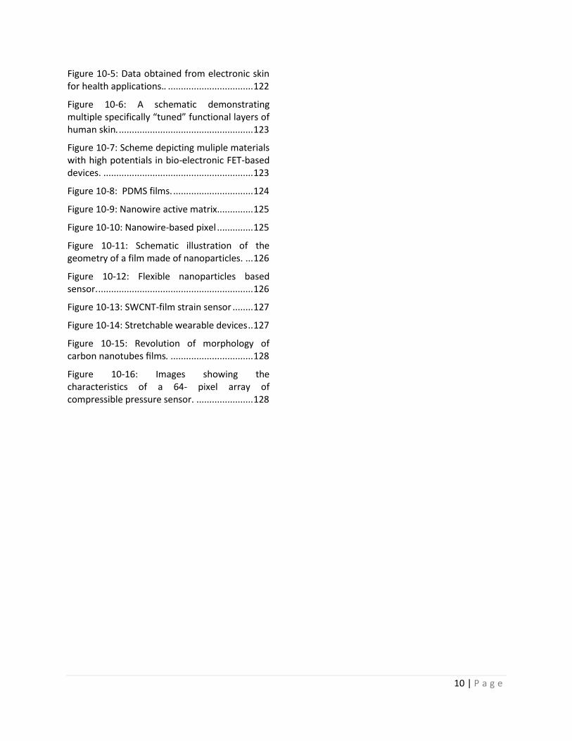
miniaturization with the help of nano-technology would allow the placement of millions of currently available electronic devices over an area with dimensions in the millimeters. In another pertinent example, a team from the Technion leveraged the power of nanotechnology to engrave the content of the Old Testament on a piece of silicon smaller than 1 mm x 1 mm (Figure 1-1).
Figure 1-1: An image of the Old Testament engraved on a tiny chip. Image courtesy of www.technion.ac.il
SURFACE AREA TO VOLUME RATIO
One of the parameters that is strongly connected to miniaturization and nano-technology is surface-to-volume ratio. This parameter is of fundamental importance in applications involving chemical catalysis and nucleation of physical processes.
In general, surface area to volume ratio increases with a decrease in the characteristic dimensions of a material, and vice versa. Therefore, as the material size decreases, a greater portion of the atoms are found at the surface compared to those inside. Because growth and catalytic chemical reactions occur at material surfaces, a given mass of nanomaterial will be much more reactive than the same mass of material made up of larger particles. It has also been found that some materials that are inert in their bulk form are reactive when produced in a nanoscale form.
To demonstrate the relationship between the miniaturization of materials and the surface-to-volume ratio, let’s consider a cube made of silicon with a characteristic size of 10 nm. The number of unit cells in this nanocube is estimated to be 6250, which is equivalent to
13 | P a g e
50,000 atoms. On the other hand, the number of the unit cells that are located on each face is 340, giving 680 atoms in each face of the nanocube and 4080 atoms on all the nanocube faces. Dividing the number of atoms available on the surface of the nanocube (4080) by the number of atoms available in all parts of the nanocube (50,000) bring to the conclusion that approximately 10% of the atoms in the nanocube are located on the surface.
Applying similar considerations with a piece of
silicon of 10 cm2 and a thickness of 1 m lead to the conclusion that only 0.03% of the silicon atoms in this structure are available on the surface.
Therefore, nanomaterials have a much greater surface area per unit volume compared with larger particles. This leads to nanoparticles that are more chemically reactive, because molecules at the surface of a material do not have full allocation of covalent bonds and are in an energetically unstable state. Since many more molecules located at the surface are in energetically unstable states, nanomaterials are more reactive compared to the non-nanoscale material. With the high reactivity, almost all types of nanomaterials are capable of catalyzing reactions and free nanomaterials tend to agglomerate into bigger particles.
Owing to the specific physiochemical properties of nanoparticles, they are expected to interact with substances such as proteins, lipids, carbohydrates, nucleic acids, ions, minerals and water present in food, biological, or desalination processes. Other potential applications for this reactivity are drug delivery, clothing insulation, and more.
NANOSTRUCTURES
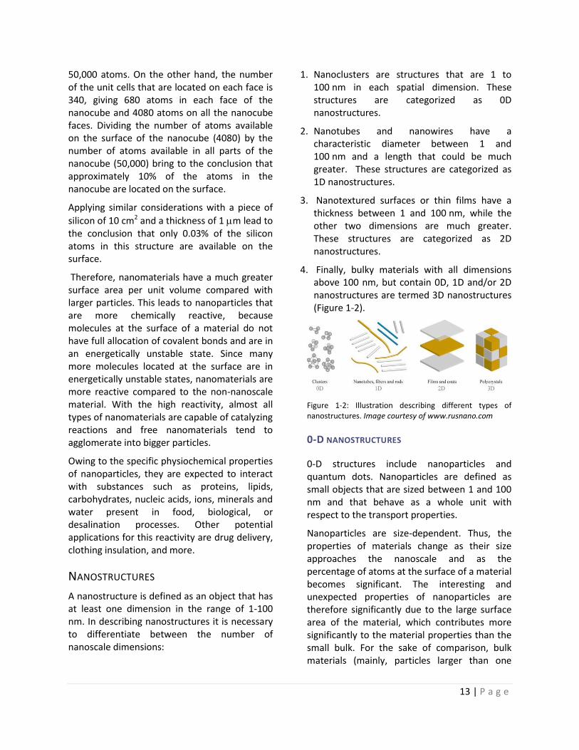
A nanostructure is defined as an object that has at least one dimension in the range of 1-100 nm. In describing nanostructures it is necessary to differentiate between the number of nanoscale dimensions:
1. Nanoclusters are structures that are 1 to 100 nm in each spatial dimension. These structures are categorized as 0D nanostructures.
2. Nanotubes and nanowires have a characteristic diameter between 1 and 100 nm and a length that could be much greater. These structures are categorized as 1D nanostructures.
3. Nanotextured surfaces or thin films have a thickness between 1 and 100 nm, while the other two dimensions are much greater. These structures are categorized as 2D nanostructures.
4. Finally, bulky materials with all dimensions above 100 nm, but contain 0D, 1D and/or 2D nanostructures are termed 3D nanostructures (Figure 1-2).
Figure 1-2: Illustration describing different types of nanostructures. Image courtesy of www.rusnano.com
0-D NANOSTRUCTURES
0-D structures include nanoparticles and quantum dots. Nanoparticles are defined as small objects that are sized between 1 and 100 nm and that behave as a whole unit with respect to the transport properties.
Nanoparticles are size-dependent. Thus, the properties of materials change as their size approaches the nanoscale and as the percentage of atoms at the surface of a material becomes significant. The interesting and unexpected properties of nanoparticles are therefore significantly due to the large surface area of the material, which contributes more significantly to the material properties than the small bulk. For the sake of comparison, bulk materials (mainly, particles larger than one
14 | P a g e
micrometer) contain an insignificant percentage of atoms at the surface in relation to the number of atoms in the bulk of the material, and therefore do not exhibit size-dependent changes in their physical properties.
Nanoparticles often possess unexpected optical properties as they are small enough to confine their electrons and produce quantum effects. The size-dependent color of the nanoparticles was utilized unknowingly by artists as far back as the 9th century for generating glitter effects on the surface of pots or in colors used for stained glass. The unique physical properties nanoparticles allow much higher absorption of solar radiation in photovoltaic cells that are composed of nanoparticles than it in thin films of continuous sheets of the same material. Other size-dependent property changes include quantum confinement in semiconductor particles, surface plasmon resonance in some metal particles, and chemical reactivity that are utilized for image formation in photography field.
1-D NANOSTRUCTURES
1-D structures include (but are not limited to) nanowires, quantum wires, nanorods and nanotubes. A nanowire is a nanostructure with a diameter of nanoscale dimensions. Alternatively, nanowires can be defined as structures that have a thickness or diameter constrained to tens of nanometers or less and an unconstrained length. At these scales, quantum mechanical effects are significant — which lead to the coining of the term "quantum wires".
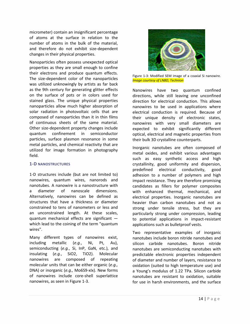
Many different types of nanowires exist, including metallic (e.g., Ni, Pt, Au), semiconducting (e.g., Si, InP, GaN, etc.), and insulating (e.g., SiO2, TiO2). Molecular nanowires are composed of repeating molecular units that can be either organic (e.g., DNA) or inorganic (e.g., Mo6S9-xIx). New forms of nanowires include core-shell superlattice nanowires, as seen in Figure 1-3.
Figure 1-3: Modified SEM image of a coaxial Si nanowire. Image courtesy of LNBD, Technion
Nanowires have two quantum confined directions, while still leaving one unconfined direction for electrical conduction. This allows nanowires to be used in applications where electrical conduction is required. Because of their unique density of electronic states, nanowires with very small diameters are expected to exhibit significantly different optical, electrical and magnetic properties from their bulk 3D crystalline counterparts.
Inorganic nanotubes are often composed of metal oxides, and exhibit various advantages such as easy synthetic access and high crystallinity, good uniformity and dispersion, predefined electrical conductivity, good adhesion to a number of polymers and high impact resistance. They are therefore promising candidates as fillers for polymer composites with enhanced thermal, mechanical, and electrical properties. Inorganic nanotubes are heavier than carbon nanotubes and not as strong under tensile stress, but they are particularly strong under compression, leading to potential applications in impact-resistant applications such as bulletproof vests.
Two representative examples of inorganic nanotubes include boron nitride nanotubes and silicon carbide nanotubes. Boron nitride nanotubes are semiconducting nanotubes with predictable electronic properties independent of diameter and number of layers, resistance to oxidation (suited to high temperature use) and a Young’s modulus of 1.22 TPa. Silicon carbide nanotubes are resistant to oxidation, suitable for use in harsh environments, and the surface
15 | P a g e
silicon atoms comprise an exterior that can be easily functionalized.
2-D NANOSTRUCTURES
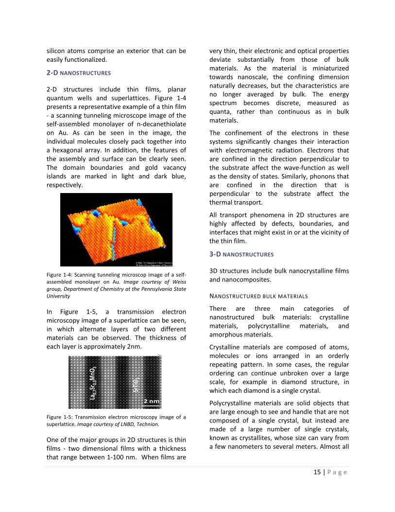
2-D structures include thin films, planar quantum wells and superlattices. Figure 1-4 presents a representative example of a thin film - a scanning tunneling microscope image of the self-assembled monolayer of n-decanethiolate on Au. As can be seen in the image, the individual molecules closely pack together into a hexagonal array. In addition, the features of the assembly and surface can be clearly seen. The domain boundaries and gold vacancy islands are marked in light and dark blue, respectively.
Figure 1-4: Scanning tunneling microscop image of a self-assembled monolayer on Au. Image courtesy of Weiss group, Department of Chemistry at the Pennsylvania State University
In Figure 1-5, a transmission electron microscopy image of a superlattice can be seen, in which alternate layers of two different materials can be observed. The thickness of each layer is approximately 2nm.
Figure 1-5: Transmission electron microscopy image of a superlattice. Image courtesy of LNBD, Technion.
One of the major groups in 2D structures is thin films - two dimensional films with a thickness that range between 1-100 nm. When films are
very thin, their electronic and optical properties deviate substantially from those of bulk materials. As the material is miniaturized towards nanoscale, the confining dimension naturally decreases, but the characteristics are no longer averaged by bulk. The energy spectrum becomes discrete, measured as quanta, rather than continuous as in bulk materials.
The confinement of the electrons in these systems significantly changes their interaction with electromagnetic radiation. Electrons that are confined in the direction perpendicular to the substrate affect the wave-function as well as the density of states. Similarly, phonons that are confined in the direction that is perpendicular to the substrate affect the thermal transport.
All transport phenomena in 2D structures are highly affected by defects, boundaries, and interfaces that might exist in or at the vicinity of the thin film.
3-D NANOSTRUCTURES
3D structures include bulk nanocrystalline films and nanocomposites.
NANOSTRUCTURED BULK MATERIALS
There are three main categories of nanostructured bulk materials: crystalline materials, polycrystalline materials, and amorphous materials.
Crystalline materials are composed of atoms, molecules or ions arranged in an orderly repeating pattern. In some cases, the regular ordering can continue unbroken over a large scale, for example in diamond structure, in which each diamond is a single crystal.
Polycrystalline materials are solid objects that are large enough to see and handle that are not composed of a single crystal, but instead are made of a large number of single crystals, known as crystallites, whose size can vary from a few nanometers to several meters. Almost all
16 | P a g e
common metals, and many ceramics, are polycrystalline.
Amorphous materials, or non-crystalline solids, are solids that lack the long-range order characteristic of a crystal. However, amorphous materials have some short-range order at the atomic length scale due to the nature of chemical bonding. Such solids include glass, plastics and gels.
Figure 1-6: Illustration of three catagories of nanostructured bulk materials. Image courtesy of LNBD, Technion.
NANOCOMPOSITES
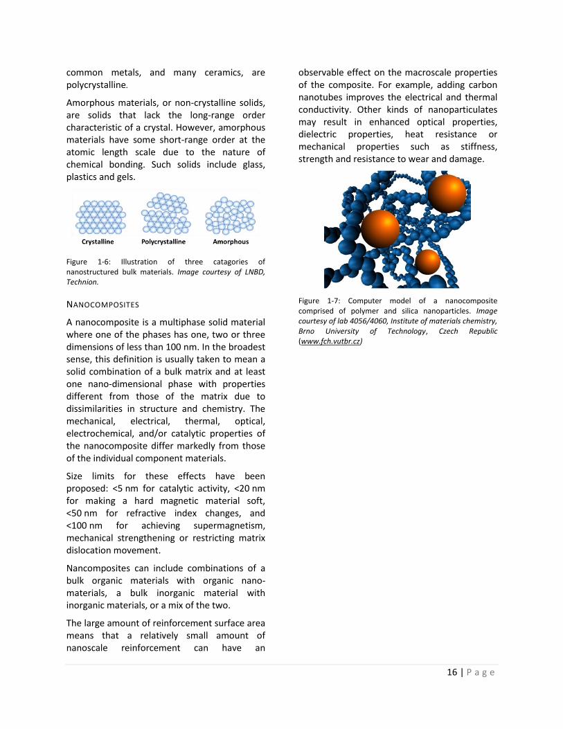
A nanocomposite is a multiphase solid material where one of the phases has one, two or three dimensions of less than 100 nm. In the broadest sense, this definition is usually taken to mean a solid combination of a bulk matrix and at least one nano-dimensional phase with properties different from those of the matrix due to dissimilarities in structure and chemistry. The mechanical, electrical, thermal, optical, electrochemical, and/or catalytic properties of the nanocomposite differ markedly from those of the individual component materials.
Size limits for these effects have been proposed: <5 nm for catalytic activity, <20 nm for making a hard magnetic material soft, <50 nm for refractive index changes, and <100 nm for achieving supermagnetism, mechanical strengthening or restricting matrix dislocation movement.
Nancomposites can include combinations of a bulk organic materials with organic nano-materials, a bulk inorganic material with inorganic materials, or a mix of the two.
The large amount of reinforcement surface area means that a relatively small amount of nanoscale reinforcement can have an
observable effect on the macroscale properties of the composite. For example, adding carbon nanotubes improves the electrical and thermal conductivity. Other kinds of nanoparticulates may result in enhanced optical properties, dielectric properties, heat resistance or mechanical properties such as stiffness, strength and resistance to wear and damage.
Figure 1-7: Computer model of a nanocomposite comprised of polymer and silica nanoparticles. Image courtesy of lab 4056/4060, Institute of materials chemistry, Brno University of Technology, Czech Republic (www.fch.vutbr.cz)
17 | P a g e
Chapter 2 INTRODUCTION TO
NANOTECHNOLOGY - CONTINUED
In this chapter we will see how scientists make observations in the extremely small world of nanotechnology. Nanoscientists utilize high-powered micro-scopes that use unique methods to allow the visualization of surface features on the atomic scale, effectively opening the door to modern nanotechnology.
ATOMIC FORCE MICROSCOPY (AFM)
Atomic force microscopy (AFM) or scanning force microscopy (SFM) is a very high-resolution type of scanning probe microscopy. This category of microscopy demonstrates a resolution on the order of fractions of a nanometer, more than 1000 times smaller than the optical diffraction limit. The information in AFM is gathered by "feeling" the surface with a mechanical probe. Piezoelectric elements that facilitate accurate and precise tiny movements enable very precise scanning. In some variations, electric potentials can also be scanned using conducting cantilevers.
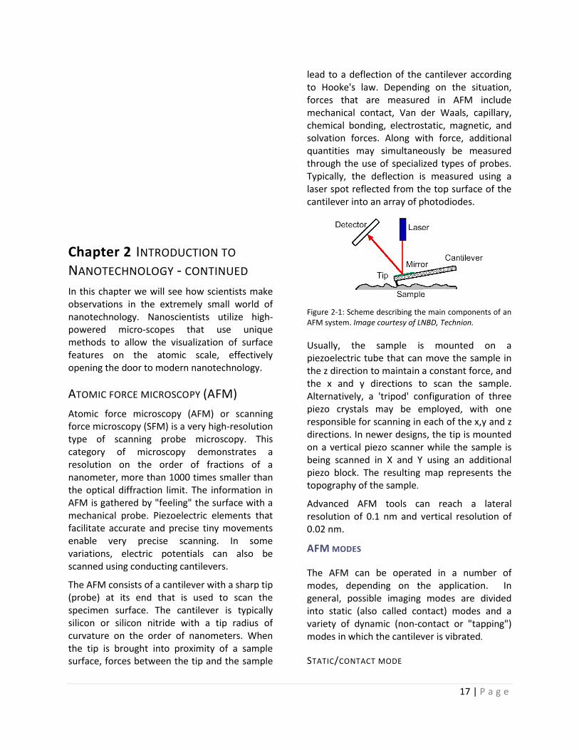
The AFM consists of a cantilever with a sharp tip (probe) at its end that is used to scan the specimen surface. The cantilever is typically silicon or silicon nitride with a tip radius of curvature on the order of nanometers. When the tip is brought into proximity of a sample surface, forces between the tip and the sample
lead to a deflection of the cantilever according to Hooke's law. Depending on the situation, forces that are measured in AFM include mechanical contact, Van der Waals, capillary, chemical bonding, electrostatic, magnetic, and solvation forces. Along with force, additional quantities may simultaneously be measured through the use of specialized types of probes. Typically, the deflection is measured using a laser spot reflected from the top surface of the cantilever into an array of photodiodes.
Figure 2-1: Scheme describing the main components of an AFM system. Image courtesy of LNBD, Technion.
Usually, the sample is mounted on a piezoelectric tube that can move the sample in the z direction to maintain a constant force, and the x and y directions to scan the sample. Alternatively, a 'tripod' configuration of three piezo crystals may be employed, with one responsible for scanning in each of the x,y and z directions. In newer designs, the tip is mounted on a vertical piezo scanner while the sample is being scanned in X and Y using an additional piezo block. The resulting map represents the topography of the sample.
Advanced AFM tools can reach a lateral resolution of 0.1 nm and vertical resolution of 0.02 nm.
AFM MODES
The AFM can be operated in a number of modes, depending on the application. In general, possible imaging modes are divided into static (also called contact) modes and a variety of dynamic (non-contact or "tapping") modes in which the cantilever is vibrated.
STATIC/CONTACT MODE
18 | P a g e
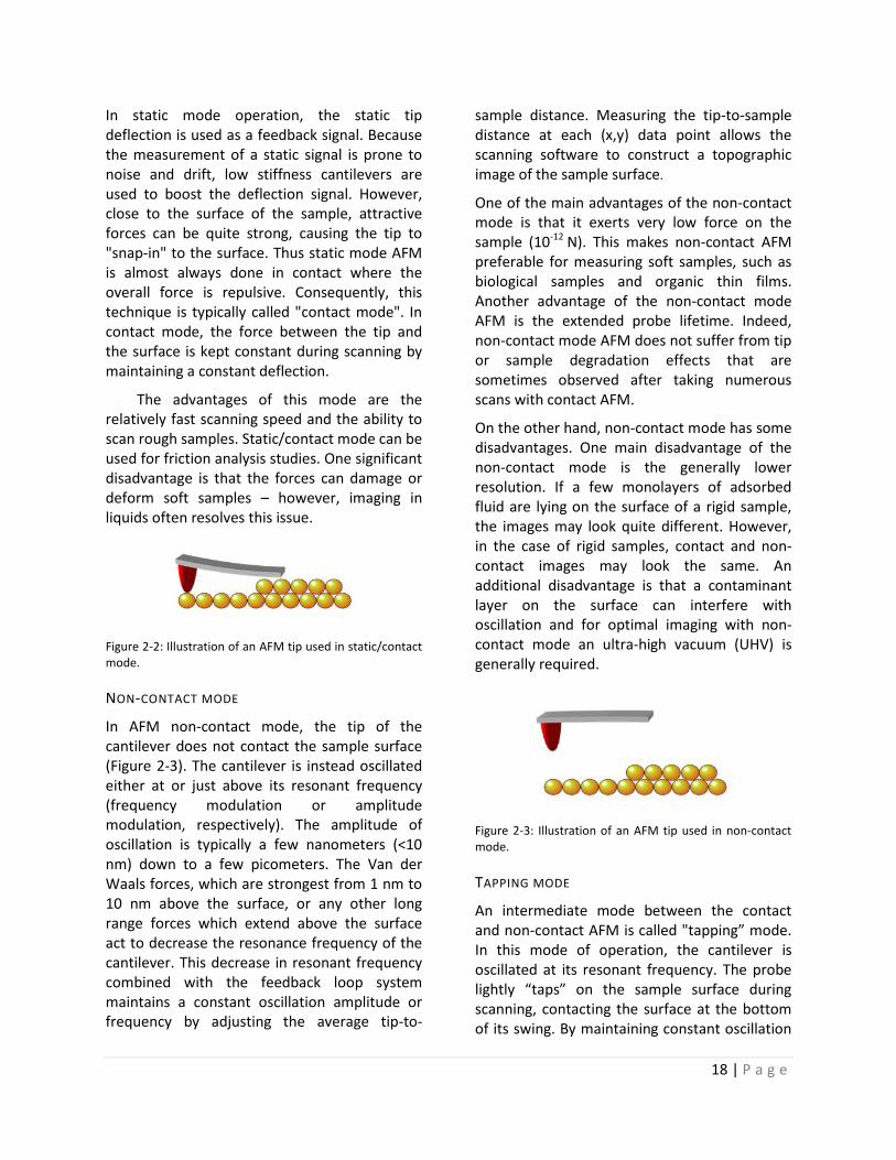
In static mode operation, the static tip deflection is used as a feedback signal. Because the measurement of a static signal is prone to noise and drift, low stiffness cantilevers are used to boost the deflection signal. However, close to the surface of the sample, attractive forces can be quite strong, causing the tip to "snap-in" to the surface. Thus static mode AFM is almost always done in contact where the overall force is repulsive. Consequently, this technique is typically called "contact mode". In contact mode, the force between the tip and the surface is kept constant during scanning by maintaining a constant deflection.
The advantages of this mode are the relatively fast scanning speed and the ability to scan rough samples. Static/contact mode can be used for friction analysis studies. One significant disadvantage is that the forces can damage or deform soft samples – however, imaging in liquids often resolves this issue.
Figure 2-2: Illustration of an AFM tip used in static/contact mode.
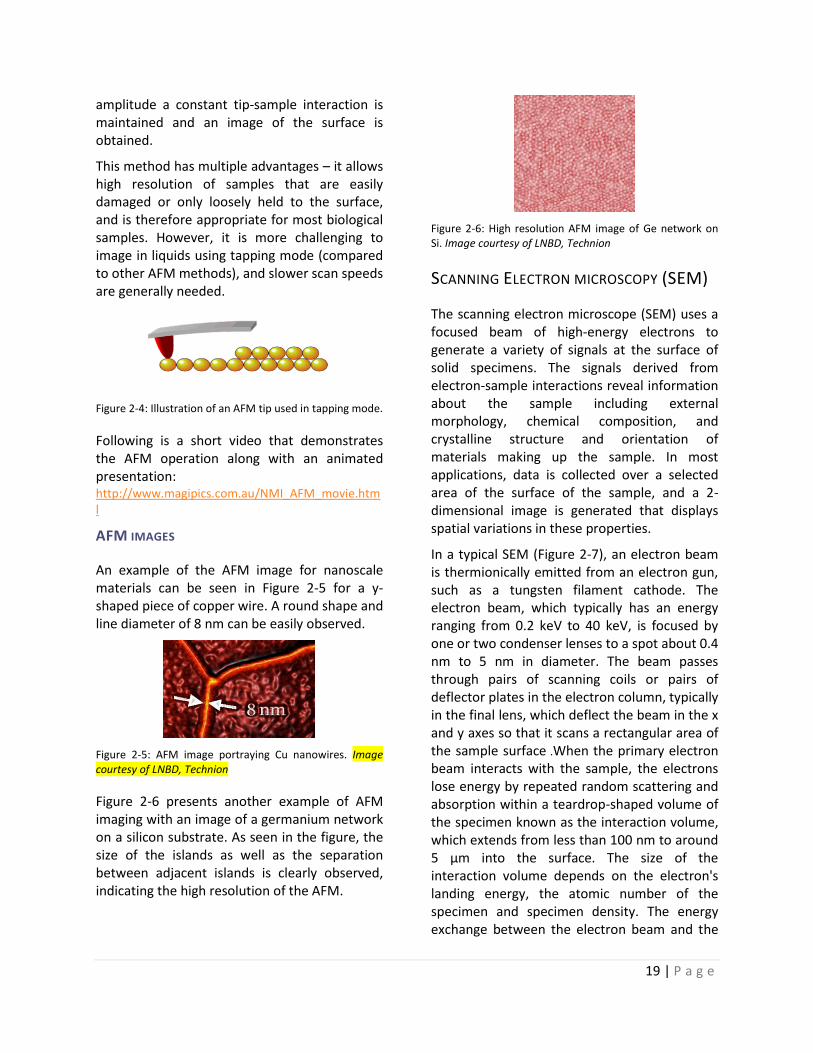
NON-CONTACT MODE
In AFM non-contact mode, the tip of the cantilever does not contact the sample surface (Figure 2-3). The cantilever is instead oscillated either at or just above its resonant frequency (frequency modulation or amplitude modulation, respectively). The amplitude of oscillation is typically a few nanometers (<10 nm) down to a few picometers. The Van der Waals forces, which are strongest from 1 nm to 10 nm above the surface, or any other long range forces which extend above the surface act to decrease the resonance frequency of the cantilever. This decrease in resonant frequency combined with the feedback loop system maintains a constant oscillation amplitude or frequency by adjusting the average tip-to-
sample distance. Measuring the tip-to-sample distance at each (x,y) data point allows the scanning software to construct a topographic image of the sample surface.
One of the main advantages of the non-contact mode is that it exerts very low force on the sample (10-12 N). This makes non-contact AFM preferable for measuring soft samples, such as biological samples and organic thin films. Another advantage of the non-contact mode AFM is the extended probe lifetime. Indeed, non-contact mode AFM does not suffer from tip or sample degradation effects that are sometimes observed after taking numerous scans with contact AFM.
On the other hand, non-contact mode has some disadvantages. One main disadvantage of the non-contact mode is the generally lower resolution. If a few monolayers of adsorbed fluid are lying on the surface of a rigid sample, the images may look quite different. However, in the case of rigid samples, contact and non-contact images may look the same. An additional disadvantage is that a contaminant layer on the surface can interfere with oscillation and for optimal imaging with non-contact mode an ultra-high vacuum (UHV) is generally required.
Figure 2-3: Illustration of an AFM tip used in non-contact mode.
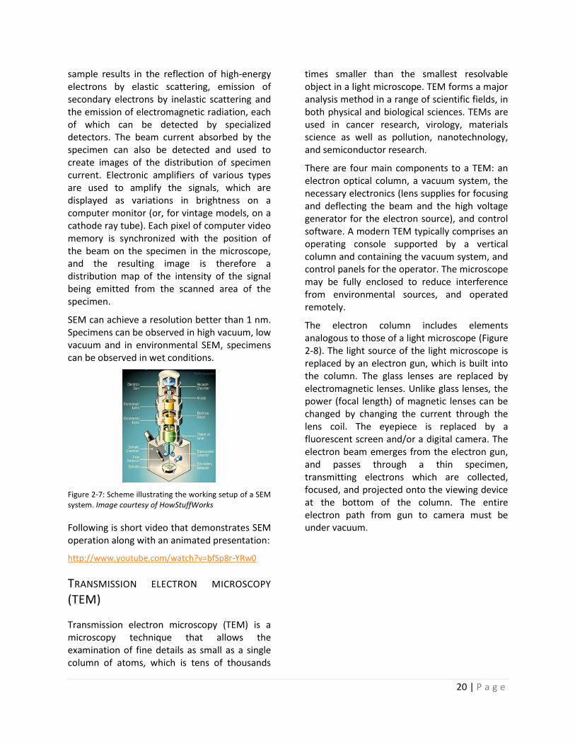
TAPPING MODE
An intermediate mode between the contact and non-contact AFM is called "tapping” mode. In this mode of operation, the cantilever is oscillated at its resonant frequency. The probe lightly “taps” on the sample surface during scanning, contacting the surface at the bottom of its swing. By maintaining constant oscillation
19 | P a g e
amplitude a constant tip-sample interaction is maintained and an image of the surface is obtained.
This method has multiple advantages – it allows high resolution of samples that are easily damaged or only loosely held to the surface, and is therefore appropriate for most biological samples. However, it is more challenging to image in liquids using tapping mode (compared to other AFM methods), and slower scan speeds are generally needed.
Figure 2-4: Illustration of an AFM tip used in tapping mode.
Following is a short video that demonstrates the AFM operation along with an animated presentation: http://www.magipics.com.au/NMI_AFM_movie.html
AFM IMAGES
An example of the AFM image for nanoscale materials can be seen in Figure 2-5 for a y-shaped piece of copper wire. A round shape and line diameter of 8 nm can be easily observed.
Figure 2-5: AFM image portraying Cu nanowires. Image courtesy of LNBD, Technion
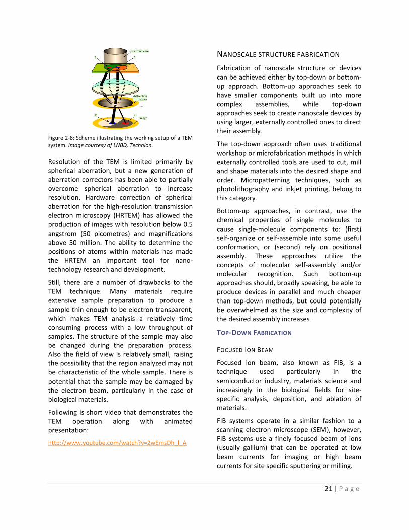
Figure 2-6 presents another example of AFM imaging with an image of a germanium network on a silicon substrate. As seen in the figure, the size of the islands as well as the separation between adjacent islands is clearly observed, indicating the high resolution of the AFM.
Figure 2-6: High resolution AFM image of Ge network on Si. Image courtesy of LNBD, Technion
SCANNING ELECTRON MICROSCOPY (SEM)
The scanning electron microscope (SEM) uses a focused beam of high-energy electrons to generate a variety of signals at the surface of solid specimens. The signals derived from electron-sample interactions reveal information about the sample including external morphology, chemical composition, and crystalline structure and orientation of materials making up the sample. In most applications, data is collected over a selected area of the surface of the sample, and a 2-dimensional image is generated that displays spatial variations in these properties.
In a typical SEM (Figure 2-7), an electron beam is thermionically emitted from an electron gun, such as a tungsten filament cathode. The electron beam, which typically has an energy ranging from 0.2 keV to 40 keV, is focused by one or two condenser lenses to a spot about 0.4 nm to 5 nm in diameter. The beam passes through pairs of scanning coils or pairs of deflector plates in the electron column, typically in the final lens, which deflect the beam in the x and y axes so that it scans a rectangular area of the sample surface .When the primary electron beam interacts with the sample, the electrons lose energy by repeated random scattering and absorption within a teardrop-shaped volume of the specimen known as the interaction volume, which extends from less than 100 nm to around 5 µm into the surface. The size of the interaction volume depends on the electron's landing energy, the atomic number of the specimen and specimen density. The energy exchange between the electron beam and the
20 | P a g e
sample results in the reflection of high-energy electrons by elastic scattering, emission of secondary electrons by inelastic scattering and the emission of electromagnetic radiation, each of which can be detected by specialized detectors. The beam current absorbed by the specimen can also be detected and used to create images of the distribution of specimen current. Electronic amplifiers of various types are used to amplify the signals, which are displayed as variations in brightness on a computer monitor (or, for vintage models, on a cathode ray tube). Each pixel of computer video memory is synchronized with the position of the beam on the specimen in the microscope, and the resulting image is therefore a distribution map of the intensity of the signal being emitted from the scanned area of the specimen.
SEM can achieve a resolution better than 1 nm. Specimens can be observed in high vacuum, low vacuum and in environmental SEM, specimens can be observed in wet conditions.
Figure 2-7: Scheme illustrating the working setup of a SEM system. Image courtesy of HowStuffWorks
Following is short video that demonstrates SEM operation along with an animated presentation:
http://www.youtube.com/watch?v=bfSp8r-YRw0
TRANSMISSION ELECTRON MICROSCOPY
(TEM)
Transmission electron microscopy (TEM) is a microscopy technique that allows the examination of fine details as small as a single column of atoms, which is tens of thousands
times smaller than the smallest resolvable object in a light microscope. TEM forms a major analysis method in a range of scientific fields, in both physical and biological sciences. TEMs are used in cancer research, virology, materials science as well as pollution, nanotechnology, and semiconductor research.
There are four main components to a TEM: an electron optical column, a vacuum system, the necessary electronics (lens supplies for focusing and deflecting the beam and the high voltage generator for the electron source), and control software. A modern TEM typically comprises an operating console supported by a vertical column and containing the vacuum system, and control panels for the operator. The microscope may be fully enclosed to reduce interference from environmental sources, and operated remotely.
The electron column includes elements analogous to those of a light microscope (Figure 2-8). The light source of the light microscope is replaced by an electron gun, which is built into the column. The glass lenses are replaced by electromagnetic lenses. Unlike glass lenses, the power (focal length) of magnetic lenses can be changed by changing the current through the lens coil. The eyepiece is replaced by a fluorescent screen and/or a digital camera. The electron beam emerges from the electron gun, and passes through a thin specimen, transmitting electrons which are collected, focused, and projected onto the viewing device at the bottom of the column. The entire electron path from gun to camera must be under vacuum.
21 | P a g e
Figure 2-8: Scheme illustrating the working setup of a TEM system. Image courtesy of LNBD, Technion.
Resolution of the TEM is limited primarily by spherical aberration, but a new generation of aberration correctors has been able to partially overcome spherical aberration to increase resolution. Hardware correction of spherical aberration for the high-resolution transmission electron microscopy (HRTEM) has allowed the production of images with resolution below 0.5 angstrom (50 picometres) and magnifications above 50 million. The ability to determine the positions of atoms within materials has made the HRTEM an important tool for nano-technology research and development.
Still, there are a number of drawbacks to the TEM technique. Many materials require extensive sample preparation to produce a sample thin enough to be electron transparent, which makes TEM analysis a relatively time consuming process with a low throughput of samples. The structure of the sample may also be changed during the preparation process. Also the field of view is relatively small, raising the possibility that the region analyzed may not be characteristic of the whole sample. There is potential that the sample may be damaged by the electron beam, particularly in the case of biological materials.
Following is short video that demonstrates the TEM operation along with animated presentation:
http://www.youtube.com/watch?v=2wEmsDh_l_A
NANOSCALE STRUCTURE FABRICATION
Fabrication of nanoscale structure or devices can be achieved either by top-down or bottom-up approach. Bottom-up approaches seek to have smaller components built up into more complex assemblies, while top-down approaches seek to create nanoscale devices by using larger, externally controlled ones to direct their assembly.
The top-down approach often uses traditional workshop or microfabrication methods in which externally controlled tools are used to cut, mill and shape materials into the desired shape and order. Micropatterning techniques, such as photolithography and inkjet printing, belong to this category.
Bottom-up approaches, in contrast, use the chemical properties of single molecules to cause single-molecule components to: (first) self-organize or self-assemble into some useful conformation, or (second) rely on positional assembly. These approaches utilize the concepts of molecular self-assembly and/or molecular recognition. Such bottom-up approaches should, broadly speaking, be able to produce devices in parallel and much cheaper than top-down methods, but could potentially be overwhelmed as the size and complexity of the desired assembly increases.
TOP-DOWN FABRICATION
FOCUSED ION BEAM
Focused ion beam, also known as FIB, is a technique used particularly in the semiconductor industry, materials science and increasingly in the biological fields for site-specific analysis, deposition, and ablation of materials.
FIB systems operate in a similar fashion to a scanning electron microscope (SEM), however, FIB systems use a finely focused beam of ions (usually gallium) that can be operated at low beam currents for imaging or high beam currents for site specific sputtering or milling.
22 | P a g e
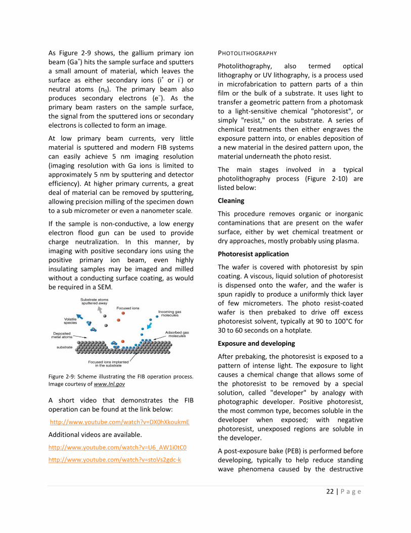
As Figure 2-9 shows, the gallium primary ion beam (Ga+) hits the sample surface and sputters a small amount of material, which leaves the surface as either secondary ions (i+ or i-) or neutral atoms (n0). The primary beam also produces secondary electrons (e–). As the primary beam rasters on the sample surface, the signal from the sputtered ions or secondary electrons is collected to form an image.
At low primary beam currents, very little material is sputtered and modern FIB systems can easily achieve 5 nm imaging resolution (imaging resolution with Ga ions is limited to approximately 5 nm by sputtering and detector efficiency). At higher primary currents, a great deal of material can be removed by sputtering, allowing precision milling of the specimen down to a sub micrometer or even a nanometer scale.
If the sample is non-conductive, a low energy electron flood gun can be used to provide charge neutralization. In this manner, by imaging with positive secondary ions using the positive primary ion beam, even highly insulating samples may be imaged and milled without a conducting surface coating, as would be required in a SEM.
Figure 2-9: Scheme illustrating the FIB operation process. Image courtesy of www.Inl.gov
A short video that demonstrates the FIB operation can be found at the link below:
http://www.youtube.com/watch?v=DX0hXkoukmE
Additional videos are available.
http://www.youtube.com/watch?v=U6_AW1i0tC0
http://www.youtube.com/watch?v=stoVs2gdc-k
PHOTOLITHOGRAPHY
Photolithography, also termed optical lithography or UV lithography, is a process used in microfabrication to pattern parts of a thin film or the bulk of a substrate. It uses light to transfer a geometric pattern from a photomask to a light-sensitive chemical "photoresist", or simply "resist," on the substrate. A series of chemical treatments then either engraves the exposure pattern into, or enables deposition of a new material in the desired pattern upon, the material underneath the photo resist.
The main stages involved in a typical photolithography process (Figure 2-10) are listed below:
Cleaning
This procedure removes organic or inorganic contaminations that are present on the wafer surface, either by wet chemical treatment or dry approaches, mostly probably using plasma.
Photoresist application
The wafer is covered with photoresist by spin coating. A viscous, liquid solution of photoresist is dispensed onto the wafer, and the wafer is spun rapidly to produce a uniformly thick layer of few micrometers. The photo resist-coated wafer is then prebaked to drive off excess photoresist solvent, typically at 90 to 100°C for 30 to 60 seconds on a hotplate.
Exposure and developing
After prebaking, the photoresist is exposed to a pattern of intense light. The exposure to light causes a chemical change that allows some of the photoresist to be removed by a special solution, called "developer" by analogy with photographic developer. Positive photoresist, the most common type, becomes soluble in the developer when exposed; with negative photoresist, unexposed regions are soluble in the developer.
A post-exposure bake (PEB) is performed before developing, typically to help reduce standing wave phenomena caused by the destructive
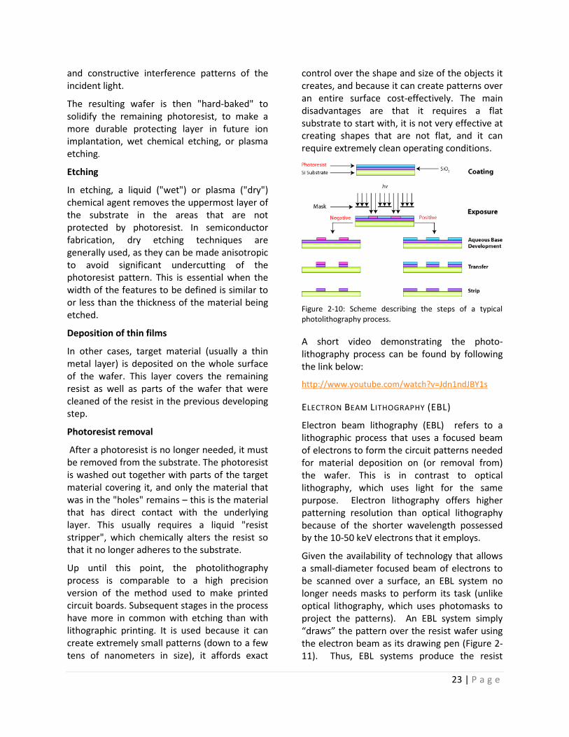
23 | P a g e
and constructive interference patterns of the incident light.
The resulting wafer is then "hard-baked" to solidify the remaining photoresist, to make a more durable protecting layer in future ion implantation, wet chemical etching, or plasma etching.
Etching
In etching, a liquid ("wet") or plasma ("dry") chemical agent removes the uppermost layer of the substrate in the areas that are not protected by photoresist. In semiconductor fabrication, dry etching techniques are generally used, as they can be made anisotropic to avoid significant undercutting of the photoresist pattern. This is essential when the width of the features to be defined is similar to or less than the thickness of the material being etched.
Deposition of thin films
In other cases, target material (usually a thin metal layer) is deposited on the whole surface of the wafer. This layer covers the remaining resist as well as parts of the wafer that were cleaned of the resist in the previous developing step.
Photoresist removal
After a photoresist is no longer needed, it must be removed from the substrate. The photoresist is washed out together with parts of the target material covering it, and only the material that was in the "holes" remains – this is the material that has direct contact with the underlying layer. This usually requires a liquid "resist stripper", which chemically alters the resist so that it no longer adheres to the substrate.
Up until this point, the photolithography process is comparable to a high precision version of the method used to make printed circuit boards. Subsequent stages in the process have more in common with etching than with lithographic printing. It is used because it can create extremely small patterns (down to a few tens of nanometers in size), it affords exact
control over the shape and size of the objects it creates, and because it can create patterns over an entire surface cost-effectively. The main disadvantages are that it requires a flat substrate to start with, it is not very effective at creating shapes that are not flat, and it can require extremely clean operating conditions.
Figure 2-10: Scheme describing the steps of a typical photolithography process.
A short video demonstrating the photo-lithography process can be found by following the link below:
http://www.youtube.com/watch?v=Jdn1ndJBY1s
ELECTRON BEAM LITHOGRAPHY (EBL)
Electron beam lithography (EBL) refers to a lithographic process that uses a focused beam of electrons to form the circuit patterns needed for material deposition on (or removal from) the wafer. This is in contrast to optical lithography, which uses light for the same purpose. Electron lithography offers higher patterning resolution than optical lithography because of the shorter wavelength possessed by the 10-50 keV electrons that it employs.
Given the availability of technology that allows a small-diameter focused beam of electrons to be scanned over a surface, an EBL system no longer needs masks to perform its task (unlike optical lithography, which uses photomasks to project the patterns). An EBL system simply “draws” the pattern over the resist wafer using the electron beam as its drawing pen (Figure 2-11). Thus, EBL systems produce the resist
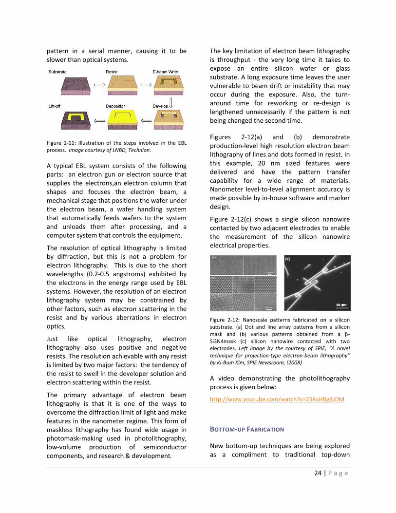
24 | P a g e
pattern in a serial manner, causing it to be slower than optical systems.
Figure 2-11: Illustration of the steps involved in the EBL process. Image courtesy of LNBD, Technion.
A typical EBL system consists of the following parts: an electron gun or electron source that supplies the electrons,an electron column that shapes and focuses the electron beam, a mechanical stage that positions the wafer under the electron beam, a wafer handling system that automatically feeds wafers to the system and unloads them after processing, and a computer system that controls the equipment.
The resolution of optical lithography is limited by diffraction, but this is not a problem for electron lithography. This is due to the short wavelengths (0.2-0.5 angstroms) exhibited by the electrons in the energy range used by EBL systems. However, the resolution of an electron lithography system may be constrained by other factors, such as electron scattering in the resist and by various aberrations in electron optics.
Just like optical lithography, electron lithography also uses positive and negative resists. The resolution achievable with any resist is limited by two major factors: the tendency of the resist to swell in the developer solution and electron scattering within the resist.
The primary advantage of electron beam lithography is that it is one of the ways to overcome the diffraction limit of light and make features in the nanometer regime. This form of maskless lithography has found wide usage in photomask-making used in photolithography, low-volume production of semiconductor components, and research & development.
The key limitation of electron beam lithography is throughput - the very long time it takes to expose an entire silicon wafer or glass substrate. A long exposure time leaves the user vulnerable to beam drift or instability that may occur during the exposure. Also, the turn-around time for reworking or re-design is lengthened unnecessarily if the pattern is not being changed the second time.
Figures 2-12(a) and (b) demonstrate production-level high resolution electron beam lithography of lines and dots formed in resist. In this example, 20 nm sized features were delivered and have the pattern transfer capability for a wide range of materials. Nanometer level-to-level alignment accuracy is made possible by in-house software and marker design.
Figure 2-12(c) shows a single silicon nanowire contacted by two adjacent electrodes to enable the measurement of the silicon nanowire electrical properties.
Figure 2-12: Nanoscale patterns fabricated on a silicon substrate. (a) Dot and line array patterns from a silicon mask and (b) various patterns obtained from a β-Si3N4mask (c) silicon nanowire contacted with two electrodes. Left image by the courtesy of SPIE, “A novel technique for projection-type electron-beam lithography” by Ki-Bum Kim, SPIE Newsroom, (2008)
A video demonstrating the photolithography process is given below:
http://www.youtube.com/watch?v=25AsHRgBJDM
BOTTOM-UP FABRICATION
New bottom-up techniques are being explored as a compliment to traditional top-down
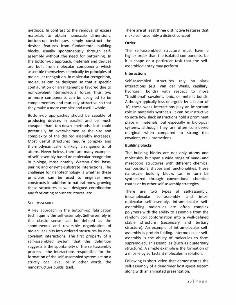
25 | P a g e
methods. In contrast to the removal of excess materials to obtain nanoscale dimensions, bottom-up techniques simply construct the desired features from fundamental building blocks, usually spontaneously through self-assembly without the need for patterning. In the bottom-up approach, materials and devices are built from molecular components which assemble themselves chemically by principles of molecular recognition. In molecular recognition, molecules can be designed so that a specific configuration or arrangement is favored due to non-covalent intermolecular forces. Thus, two or more components can be designed to be complementary and mutually attractive so that they make a more complex and useful whole.
Bottom-up approaches should be capable of producing devices in parallel and be much cheaper than top-down methods, but could potentially be overwhelmed as the size and complexity of the desired assembly increases. Most useful structures require complex and thermodynamically unlikely arrangements of atoms. Nevertheless, there are many examples of self-assembly based on molecular recognition in biology, most notably Watson–Crick base-pairing and enzyme-substrate interactions. The challenge for nanotechnology is whether these principles can be used to engineer new constructs in addition to natural ones, growing these structures in well-designed coordination and fabricating robust structures, etc.
SELF-ASSEMBLY
A key approach in the bottom-up fabrication technique is the self-assembly. Self-assembly in the classic sense can be defined as the spontaneous and reversible organization of molecular units into ordered structures by non-covalent interactions. The first property of a self-assembled system that this definition suggests is the spontaneity of the self-assembly process - the interactions responsible for the formation of the self-assembled system act on a strictly local level, or in other words, the nanostructure builds itself.
There are at least three distinctive features that make self-assembly a distinct concept:
Order
The self-assembled structure must have a higher order than the isolated components, be it a shape or a particular task that the self-assembled entity may perform.
Interactions
Self-assembled structures rely on slack interactions (e.g. Van der Waals, capillary, hydrogen bonds) with respect to more "traditional" covalent, ionic, or metallic bonds. Although typically less energetic by a factor of 10, these weak interactions play an important role in materials synthesis. It can be instructive to note how slack interactions hold a prominent place in materials, but especially in biological systems, although they are often considered marginal when compared to strong (i.e. covalent, etc.) interactions.
Building blocks
The building blocks are not only atoms and molecules, but span a wide range of nano- and mesocopic structures with different chemical compositions, shapes and functionalities. These nanoscale building blocks can in turn be synthesized through conventional chemical routes or by other self-assembly strategies.
There are two types of self-assembly: intramolecular self-assembly and inter-molecular self-assembly. Intramolecular self-assembling molecules are often complex polymers with the ability to assemble from the random coil conformation into a well-defined stable structure (secondary and tertiary structure). An example of intramolecular self-assembly is protein folding. Intermolecular self-assembly is the ability of molecules to form supramolecular assemblies (such as quaternary structure). A simple example is the formation of a micelle by surfactant molecules in solution.
Following is short video that demonstrates the self-assembly of a dendrimer host-guest system along with an animated presentation.
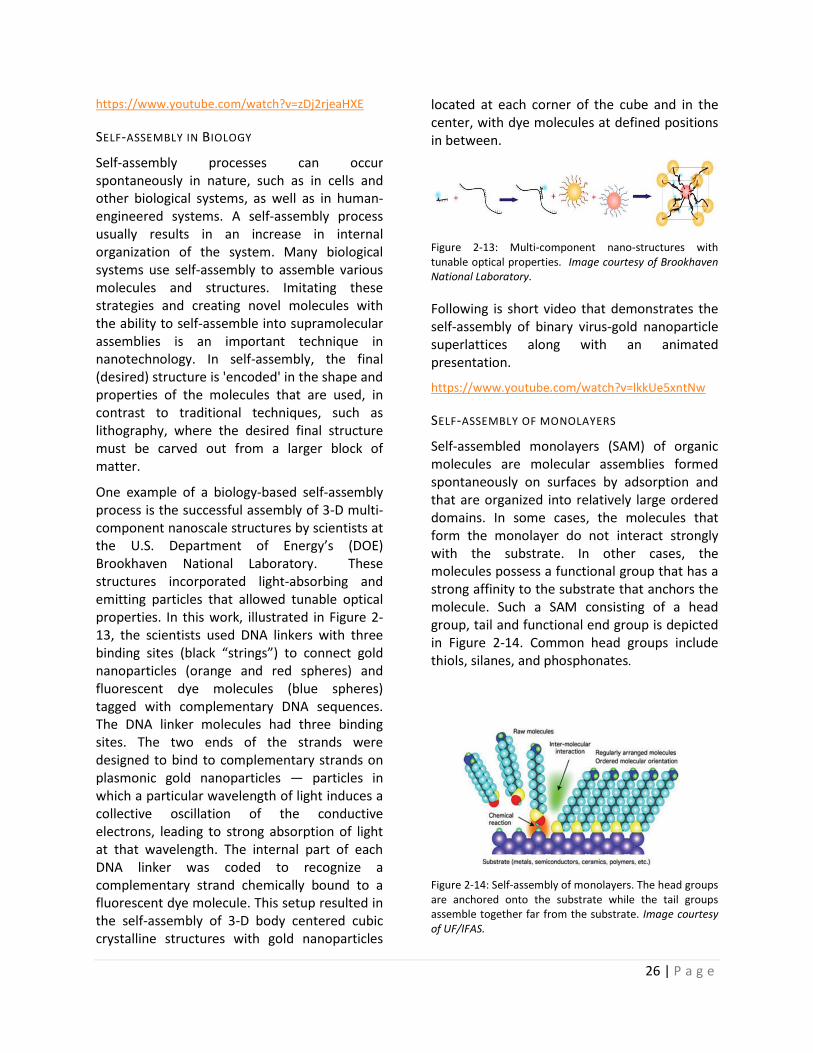
26 | P a g e
https://www.youtube.com/watch?v=zDj2rjeaHXE
SELF-ASSEMBLY IN BIOLOGY
Self-assembly processes can occur spontaneously in nature, such as in cells and other biological systems, as well as in human-engineered systems. A self-assembly process usually results in an increase in internal organization of the system. Many biological systems use self-assembly to assemble various molecules and structures. Imitating these strategies and creating novel molecules with the ability to self-assemble into supramolecular assemblies is an important technique in nanotechnology. In self-assembly, the final (desired) structure is 'encoded' in the shape and properties of the molecules that are used, in contrast to traditional techniques, such as lithography, where the desired final structure must be carved out from a larger block of matter.
One example of a biology-based self-assembly process is the successful assembly of 3-D multi-component nanoscale structures by scientists at the U.S. Department of Energy’s (DOE) Brookhaven National Laboratory. These structures incorporated light-absorbing and emitting particles that allowed tunable optical properties. In this work, illustrated in Figure 2-13, the scientists used DNA linkers with three binding sites (black “strings”) to connect gold nanoparticles (orange and red spheres) and fluorescent dye molecules (blue spheres) tagged with complementary DNA sequences. The DNA linker molecules had three binding sites. The two ends of the strands were designed to bind to complementary strands on plasmonic gold nanoparticles — particles in which a particular wavelength of light induces a collective oscillation of the conductive electrons, leading to strong absorption of light at that wavelength. The internal part of each DNA linker was coded to recognize a complementary strand chemically bound to a fluorescent dye molecule. This setup resulted in the self-assembly of 3-D body centered cubic crystalline structures with gold nanoparticles
located at each corner of the cube and in the center, with dye molecules at defined positions in between.
Figure 2-13: Multi-component nano-structures with tunable optical properties. Image courtesy of Brookhaven National Laboratory.
Following is short video that demonstrates the self-assembly of binary virus-gold nanoparticle superlattices along with an animated presentation.
https://www.youtube.com/watch?v=lkkUe5xntNw
SELF-ASSEMBLY OF MONOLAYERS
Self-assembled monolayers (SAM) of organic molecules are molecular assemblies formed spontaneously on surfaces by adsorption and that are organized into relatively large ordered domains. In some cases, the molecules that form the monolayer do not interact strongly with the substrate. In other cases, the molecules possess a functional group that has a strong affinity to the substrate that anchors the molecule. Such a SAM consisting of a head group, tail and functional end group is depicted in Figure 2-14. Common head groups include thiols, silanes, and phosphonates.
Figure 2-14: Self-assembly of monolayers. The head groups are anchored onto the substrate while the tail groups assemble together far from the substrate. Image courtesy of UF/IFAS.
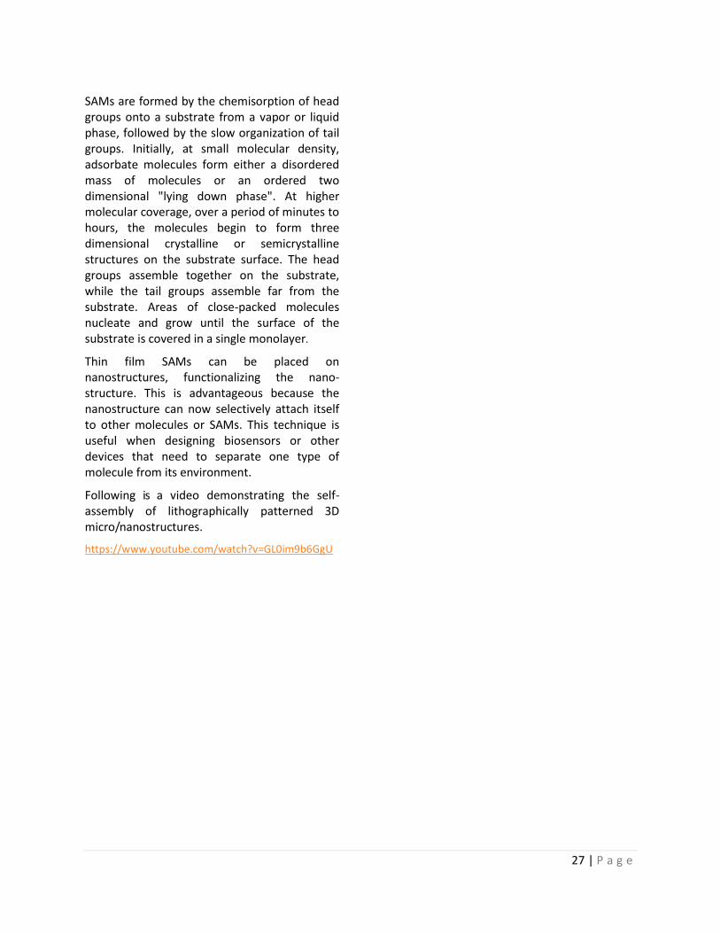
27 | P a g e
SAMs are formed by the chemisorption of head groups onto a substrate from a vapor or liquid phase, followed by the slow organization of tail groups. Initially, at small molecular density, adsorbate molecules form either a disordered mass of molecules or an ordered two dimensional "lying down phase". At higher molecular coverage, over a period of minutes to hours, the molecules begin to form three dimensional crystalline or semicrystalline structures on the substrate surface. The head groups assemble together on the substrate, while the tail groups assemble far from the substrate. Areas of close-packed molecules nucleate and grow until the surface of the substrate is covered in a single monolayer.
Thin film SAMs can be placed on nanostructures, functionalizing the nano-structure. This is advantageous because the nanostructure can now selectively attach itself to other molecules or SAMs. This technique is useful when designing biosensors or other devices that need to separate one type of molecule from its environment.
Following is a video demonstrating the self-assembly of lithographically patterned 3D micro/nanostructures.
https://www.youtube.com/watch?v=GL0im9b6GgU

28 | P a g e
Chapter 3 INTRODUCTION TO
SENSOR’S SCIENCE AND TECHNOLOGY
In this chapter we will learn about the basic principles that allow us to sense the world around us.
Thanks to our senses, we can visualize how to move our hands to grab an object like a hammer. We can smell a fire from far away. We can taste if food is ripe and ready to eat. We hear a car coming and feel when it’s cold. These are our five senses: sight, hearing, touch, smell and taste.
SENSES
In daily life, we use many different products such as cars, phones and computers. These products have senses that we call sensors, including temperature sensors, pressure sensors and light sensors. That’s how an object like an automatic door knows when you want to pass through it. But wouldn’t be great if these products could discern what we want to do? A phone that knows you are in a meeting and can independently silence itself. A car that helps you search for a spacious enough parking spot. A computer that knows exactly what you want to do and helps you to do just that. To perform any of these applications, these products need a range of sensors and very clever designs. More and more of these types of products are being developed - for example, cars that see a
pedestrian and stop automatically if you don’t do it on time. Game consoles that know how you want to hit the ball in a virtual game of tennis and health-measuring devices that alarm a doctor in times of need.
A broadly acceptable definition of a sense would be:
"A system that consists of a group of sensory cell types that responds to a specific physical or chemical phenomena, and that corresponds to a particular group of regions within the brain where the signals are received and interpreted."
The senses can be roughly divided into two groups: senses that respond to chemical signals (e.g. - the sense of smell is a response to organic molecules), and senses that respond to physical phenomena, (e.g. - hearing is a response to sound waves).
VISION
In order for one to see, a light source is required. Without light, everything is black. Light emits particles called photons, which are scattered in all directions and eventually reach the eye. The tissues that they pass through must be transparent to allow clear vision. First, photons pass through the cornea located at the front of the eye to the crystalline lens behind the pupil, then through the vitreous body in the eye center. Finally, the photons reach the retina – the eye photographic plate – and complete their journey at the retinal pigment epithelium where they initiate nerve pulses. These pulses are directed towards the optic nerve, and then the optic pathways, before arriving at the occipital brain where the image is formed. This process is what enables us to taken the world around us.
Following is an animation video that demonstrates the process described above
https://www.youtube.com/watch?v=TnQWr2f2Wps
HEARING
The ear consists of three parts: the outer ear, the middle ear and the inner ear. These
29 | P a g e
components all work together to pass sound through the ear and to the brain. First, the pinna acts like a funnel to collect the sound waves. These sounds waves pass through the ear canal and reach the eardrum and cause it to vibrate. The higher the pitch or the frequency of the sound, the faster the eardrum will vibrate. These vibrations then pass on to the middle ear. The middle ear contains three tiny bones called the ossicles. These are joined together and connected to the eardrum. They amplify the sound waves and pass them on to the middle ear. The vibrations from the ossicles pass through a small window and into a part in the middle ear called the cochlea. Sound waves pass through the fluid of the cochlea and move the tiny hairs inside, initiating an electrical signal that varies depending on sound pitch and volume. The signal travels through the auditory nerve to the brain, where it is interpreted.
The following video illustrates the process described above:
https://www.youtube.com/watch?v=ahCbGjasm_E
SMELL
Like all the other systems in the human body, the sense of smell has an extremely complex design. The smell detecting nasal cavity is located beneath the eyes and contains a sticky nucleus fluid; this nucleus membrane is only six hundredths of a millimeter thick.
Olfactory nerve cells are another part of the smelling system. These cells are tasked with the transportation of messages from smell molecules to the olfactory bulbs. Each small cell is comprised of three main parts - the cell body in centered between tiny hairs called cilia on one end and nerve extensions called axons on the other. These axons, numbering between 10 to 100, work together to transport the cell signal to the olfactory bulb inside the brain. They form a bundle that reaches the olfactory bulbs and as a group, pass through a porous, paper thin bone called the cribriform plate. This bone has pores in it through which the olfactory neurons pass. The bone design allows
connections between neurons and makes smelling possible.
The olfactory bulb is another important part of the smell system. It lies on the front side of the brain above the nasal cavity. There are two olfactory lobes in the brain just as the nose has two nasal cavities. Each of these lobes is approximately as large as a pea. The olfactory lobes work like a news room – all the signals coming in from the olfactory receptors gather in the center. Millions of pieces of information are reorganized here. Later they are sent to the relevant parts of the brain.
Following is an illustrative video of the operation principle of the sense of smell:
https://www.youtube.com/watch?v=Po2GiZCAdG8
SENSORS
A sensor is a transducer that converts a measurement (a quantity or parameter) into a signal that carries information.
Chemical sensors usually contain two basic components connected in series: a chemical (molecular) recognition (receptor) and a physicochemical transducer. In the majority of chemical sensors, the receptor interacts with the analyte molecules. As a result, the physical properties are altered in such a way that the appending transducer can gain an electrical signal. In some cases, a single physical object acts as a receptor and as a transducer.
Sensors can be designed as an analog to the human senses. In both cases, signals are collected from the environment and converted into a signal by sensory receptors in humans or by receptor and transducer systems in sensor systems. In the amplification and processing stage, the sensory nerve system is comparable to an analog circuit. The processing stage, which is obviously in the brain for humans, can be performed by a computer in the case of sensor system (Figure 3-1).
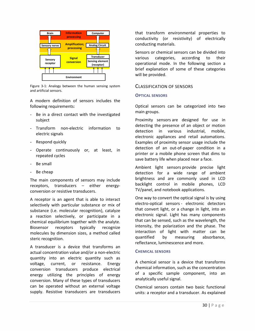
30 | P a g e
Figure 3-1: Analogy between the human sensing system and artificial sensors.
A modern definition of sensors includes the following requirements:
- Be in a direct contact with the investigated subject
- Transform non-electric information to electric signals
- Respond quickly
- Operate continuously or, at least, in repeated cycles
- Be small
- Be cheap
The main components of sensors may include receptors, transducers – either energy-conversion or resistive transducers.
A receptor is an agent that is able to interact selectively with particular substance or mix of substance (i.e. molecular recognition), catalyze a reaction selectively, or participate in a chemical equilibrium together with the analyte. Biosensor receptors typically recognize molecules by dimension sizes, a method called steric recognition.
A transducer is a device that transforms an actual concentration value and/or a non-electric quantity into an electric quantity such as voltage, current, or resistance. Energy conversion transducers produce electrical energy utilizing the principles of energy conversion. Many of these types of transducers can be operated without an external voltage supply. Resistive transducers are transducers
that transform environmental properties to conductivity (or resistivity) of electrically conducting materials.
Sensors or chemical sensors can be divided into various categories, according to their operational mode. In the following section a brief explanation of some of these categories will be provided.
CLASSIFICATION OF SENSORS
OPTICAL SENSORS
Optical sensors can be categorized into two main groups.
Proximity sensors are designed for use in detecting the presence of an object or motion detection in various industrial, mobile, electronic appliances and retail automations. Examples of proximity sensor usage include the detection of an out-of-paper condition in a printer or a mobile phone screen that dims to save battery life when placed near a face.
Ambient light sensors provide precise light detection for a wide range of ambient brightness and are commonly used in LCD backlight control in mobile phones, LCD TV/panel, and notebook applications.
One way to convert the optical signal is by using electro-optical sensors - electronic detectors that convert light, or a change in light, into an electronic signal. Light has many components that can be sensed, such as the wavelength, the intensity, the polarization and the phase. The interaction of light with matter can be quantified by measuring absorbance, reflectance, luminescence and more.
CHEMICAL SENSORS
A chemical sensor is a device that transforms chemical information, such as the concentration of a specific sample component, into an analytically useful signal.
Chemical sensors contain two basic functional units: a receptor and a transducer. As explained
Sensory receptor
Sensing element (receptor)
Transducer
Analog CircuitSensory nerve
Signal conversion
Amplification; processing
Brain ComputerInformation processing
Environment
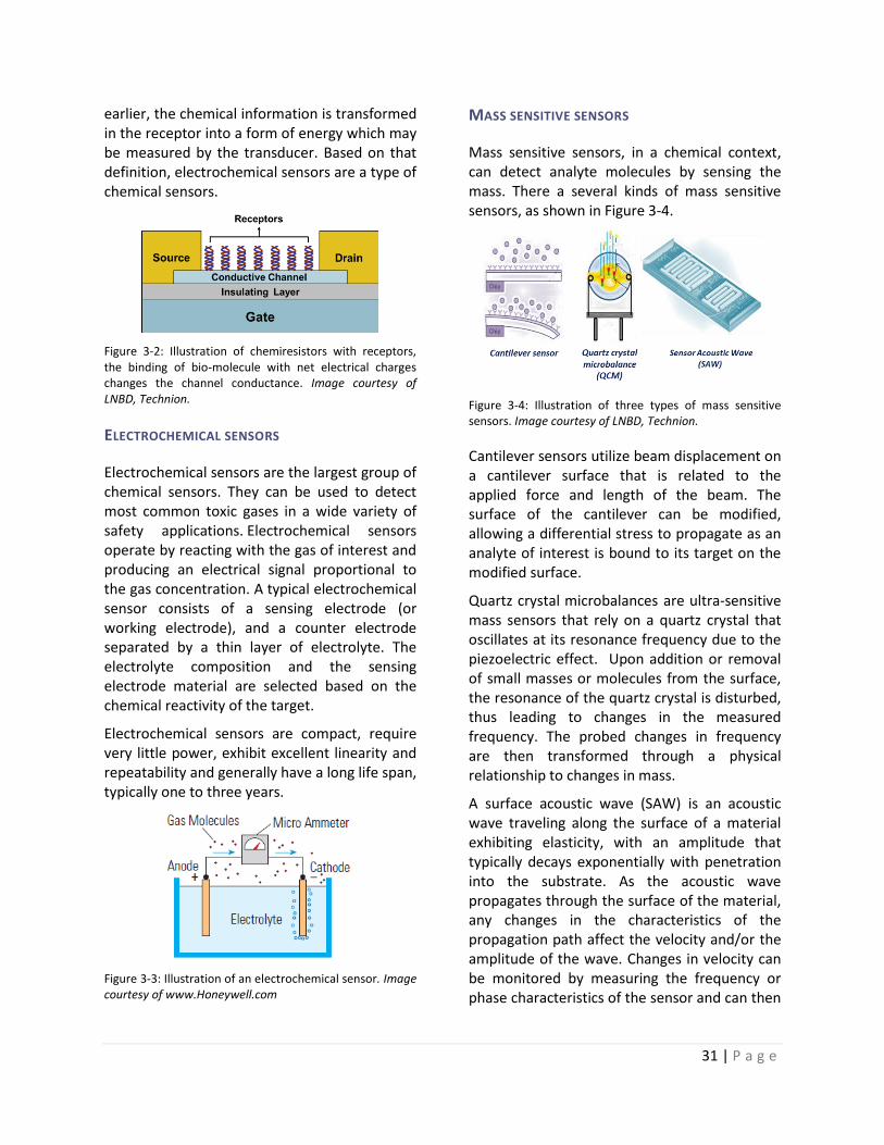
31 | P a g e
earlier, the chemical information is transformed in the receptor into a form of energy which may be measured by the transducer. Based on that definition, electrochemical sensors are a type of chemical sensors.
Figure 3-2: Illustration of chemiresistors with receptors, the binding of bio-molecule with net electrical charges changes the channel conductance. Image courtesy of LNBD, Technion.
ELECTROCHEMICAL SENSORS
Electrochemical sensors are the largest group of chemical sensors. They can be used to detect most common toxic gases in a wide variety of safety applications. Electrochemical sensors operate by reacting with the gas of interest and producing an electrical signal proportional to the gas concentration. A typical electrochemical sensor consists of a sensing electrode (or working electrode), and a counter electrode separated by a thin layer of electrolyte. The electrolyte composition and the sensing electrode material are selected based on the chemical reactivity of the target.
Electrochemical sensors are compact, require very little power, exhibit excellent linearity and repeatability and generally have a long life span, typically one to three years.
Figure 3-3: Illustration of an electrochemical sensor. Image courtesy of www.Honeywell.com
MASS SENSITIVE SENSORS
Mass sensitive sensors, in a chemical context, can detect analyte molecules by sensing the mass. There a several kinds of mass sensitive sensors, as shown in Figure 3-4.
Figure 3-4: Illustration of three types of mass sensitive sensors. Image courtesy of LNBD, Technion.
Cantilever sensors utilize beam displacement on a cantilever surface that is related to the applied force and length of the beam. The surface of the cantilever can be modified, allowing a differential stress to propagate as an analyte of interest is bound to its target on the modified surface.
Quartz crystal microbalances are ultra-sensitive mass sensors that rely on a quartz crystal that oscillates at its resonance frequency due to the piezoelectric effect. Upon addition or removal of small masses or molecules from the surface, the resonance of the quartz crystal is disturbed, thus leading to changes in the measured frequency. The probed changes in frequency are then transformed through a physical relationship to changes in mass.
A surface acoustic wave (SAW) is an acoustic wave traveling along the surface of a material exhibiting elasticity, with an amplitude that typically decays exponentially with penetration into the substrate. As the acoustic wave propagates through the surface of the material, any changes in the characteristics of the propagation path affect the velocity and/or the amplitude of the wave. Changes in velocity can be monitored by measuring the frequency or phase characteristics of the sensor and can then
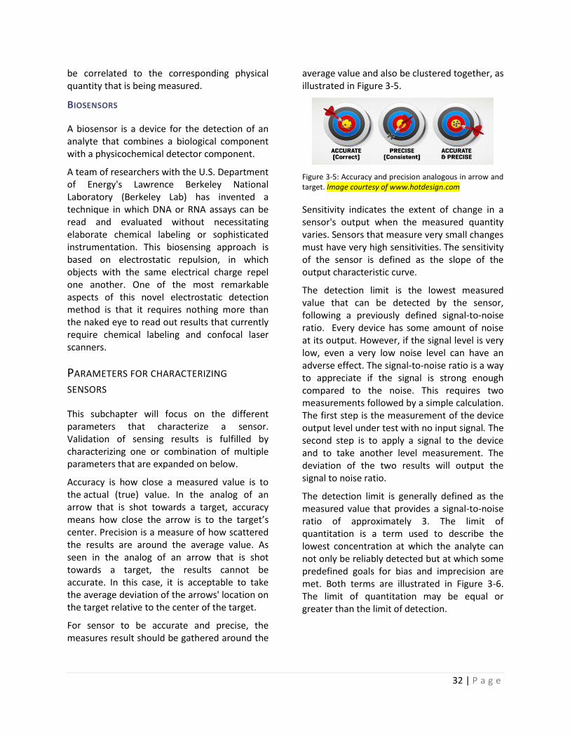
32 | P a g e
be correlated to the corresponding physical quantity that is being measured.
BIOSENSORS
A biosensor is a device for the detection of an analyte that combines a biological component with a physicochemical detector component.
A team of researchers with the U.S. Department of Energy's Lawrence Berkeley National Laboratory (Berkeley Lab) has invented a technique in which DNA or RNA assays can be read and evaluated without necessitating elaborate chemical labeling or sophisticated instrumentation. This biosensing approach is based on electrostatic repulsion, in which objects with the same electrical charge repel one another. One of the most remarkable aspects of this novel electrostatic detection method is that it requires nothing more than the naked eye to read out results that currently require chemical labeling and confocal laser scanners.
PARAMETERS FOR CHARACTERIZING
SENSORS
This subchapter will focus on the different parameters that characterize a sensor. Validation of sensing results is fulfilled by characterizing one or combination of multiple parameters that are expanded on below.
Accuracy is how close a measured value is to the actual (true) value. In the analog of an arrow that is shot towards a target, accuracy means how close the arrow is to the target’s center. Precision is a measure of how scattered the results are around the average value. As seen in the analog of an arrow that is shot towards a target, the results cannot be accurate. In this case, it is acceptable to take the average deviation of the arrows' location on the target relative to the center of the target.
For sensor to be accurate and precise, the measures result should be gathered around the
average value and also be clustered together, as illustrated in Figure 3-5.
Figure 3-5: Accuracy and precision analogous in arrow and target. Image courtesy of www.hotdesign.com
Sensitivity indicates the extent of change in a sensor's output when the measured quantity varies. Sensors that measure very small changes must have very high sensitivities. The sensitivity of the sensor is defined as the slope of the output characteristic curve.
The detection limit is the lowest measured value that can be detected by the sensor, following a previously defined signal-to-noise ratio. Every device has some amount of noise at its output. However, if the signal level is very low, even a very low noise level can have an adverse effect. The signal-to-noise ratio is a way to appreciate if the signal is strong enough compared to the noise. This requires two measurements followed by a simple calculation. The first step is the measurement of the device output level under test with no input signal. The second step is to apply a signal to the device and to take another level measurement. The deviation of the two results will output the signal to noise ratio.
The detection limit is generally defined as the measured value that provides a signal-to-noise ratio of approximately 3. The limit of quantitation is a term used to describe the lowest concentration at which the analyte can not only be reliably detected but at which some predefined goals for bias and imprecision are met. Both terms are illustrated in Figure 3-6. The limit of quantitation may be equal or greater than the limit of detection.
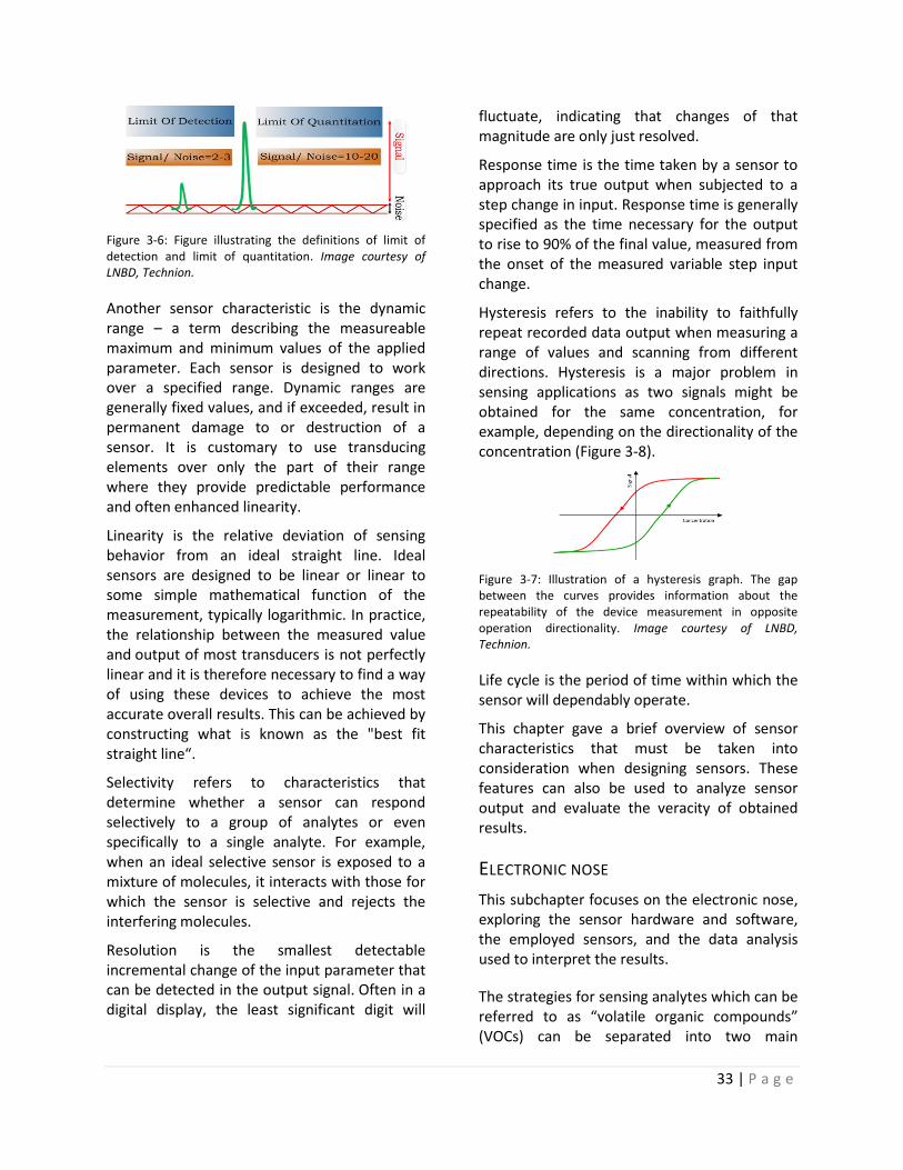
33 | P a g e
Figure 3-6: Figure illustrating the definitions of limit of detection and limit of quantitation. Image courtesy of LNBD, Technion.
Another sensor characteristic is the dynamic range – a term describing the measureable maximum and minimum values of the applied parameter. Each sensor is designed to work over a specified range. Dynamic ranges are generally fixed values, and if exceeded, result in permanent damage to or destruction of a sensor. It is customary to use transducing elements over only the part of their range where they provide predictable performance and often enhanced linearity.
Linearity is the relative deviation of sensing behavior from an ideal straight line. Ideal sensors are designed to be linear or linear to some simple mathematical function of the measurement, typically logarithmic. In practice, the relationship between the measured value and output of most transducers is not perfectly linear and it is therefore necessary to find a way of using these devices to achieve the most accurate overall results. This can be achieved by constructing what is known as the "best fit straight line“.
Selectivity refers to characteristics that determine whether a sensor can respond selectively to a group of analytes or even specifically to a single analyte. For example, when an ideal selective sensor is exposed to a mixture of molecules, it interacts with those for which the sensor is selective and rejects the interfering molecules.
Resolution is the smallest detectable incremental change of the input parameter that can be detected in the output signal. Often in a digital display, the least significant digit will
fluctuate, indicating that changes of that magnitude are only just resolved.
Response time is the time taken by a sensor to approach its true output when subjected to a step change in input. Response time is generally specified as the time necessary for the output to rise to 90% of the final value, measured from the onset of the measured variable step input change.
Hysteresis refers to the inability to faithfully repeat recorded data output when measuring a range of values and scanning from different directions. Hysteresis is a major problem in sensing applications as two signals might be obtained for the same concentration, for example, depending on the directionality of the concentration (Figure 3-8).
Figure 3-7: Illustration of a hysteresis graph. The gap between the curves provides information about the repeatability of the device measurement in opposite operation directionality. Image courtesy of LNBD, Technion.
Life cycle is the period of time within which the sensor will dependably operate.
This chapter gave a brief overview of sensor characteristics that must be taken into consideration when designing sensors. These features can also be used to analyze sensor output and evaluate the veracity of obtained results.
ELECTRONIC NOSE
This subchapter focuses on the electronic nose, exploring the sensor hardware and software, the employed sensors, and the data analysis used to interpret the results.
The strategies for sensing analytes which can be referred to as “volatile organic compounds” (VOCs) can be separated into two main
34 | P a g e
techniques: selective sensing and cross-reactive array sensing, as illustrated in Figure 3-9.
Selective sensing employs a highly selective receptor/detector that is designed to specifically bind to or detect an analyte of interest. This approach is suitable for detecting a well-defined target analyte in the presence of interfering species and/or background. While most selective sensing techniques for disease detection are aimed at non-volatile compounds, there are a number of well-defined sensors that target specific VOCs of well-characterized diseases.
An emerging strategy that is complementary to the selective sensing approach is the cross-reactive, nanomaterial-based sensors array. This bio-inspired approach detects analytes using an array of broadly cross-reactive sensors in conjunction with pattern recognition methods. In contrast to the selective sensing approach, each sensor in the cross-reactive array is broadly responsive to a variety of VOCs. In this architecture, each VOC produces a distinct fingerprint from the sensor. This allows a considerable expansion in the variety of compounds to which a given matrix is sensitive, an increase in the degree of component identification and, in specific cases, the performance of individual components analysis in complex multi-component (bio)chemical media. Pattern recognition algorithms can then be used to obtain information regarding the identity, properties and concentration of the vapor exposed to the sensor array.
Figure 3-8: Selective vs. cross reactive sensing approach. VOC and PC stands for volatile organic compound and
principle component, respectively. Broza et al, Nanomedicine (2013).
One of the most important developments in gas sensor technology is the transition from a single sensor element to an array of sensors. A single sensor is typically designed to detect a single gas specie in controlled environments. An array of multiple sensors can be used when multicomponent gas analysis is required - for example, if one wanted to distinguish a good wine from a bad wine based on their aromas. This approach mimics the olfaction mechanism of humans and dogs (as well as of other animals) and it is therefore known as “machine olfaction” or simply as an “electronic nose”.
Scientists have been designing and building electronic noses for more than 20 years. Electronic noses include three major parts: a sample delivery system, a detection system, and a computing system. One of the challenges of the practical application of electronic noses is that the gases of interest are part of a complex background including water vapor that can complicate detection.
Electronic nose applications can be relevant for multiple disciplines including, but not limited to, process control, food and medical industries, and environmental monitoring.
The system is illustrated in Figure 3-10.
Figure 3-9: Classification process for electronic nose detection. Image courtesy of LNBD, Technion.
OPTOELECTRONIC NOSE
An optoelectronic nose is presented in Figure 3-11. At first glance, the device looks like a computer chip covered in neat rows of dots.
Sensor array
Time
Re
sp
on
se
Signal
preprocessing
f1
f2
odor 1
odor 2
odor 3
Classification
Raw
measurements
Normalized
measurements
Feature
vector
Dimensionality
reduction
f1
f2
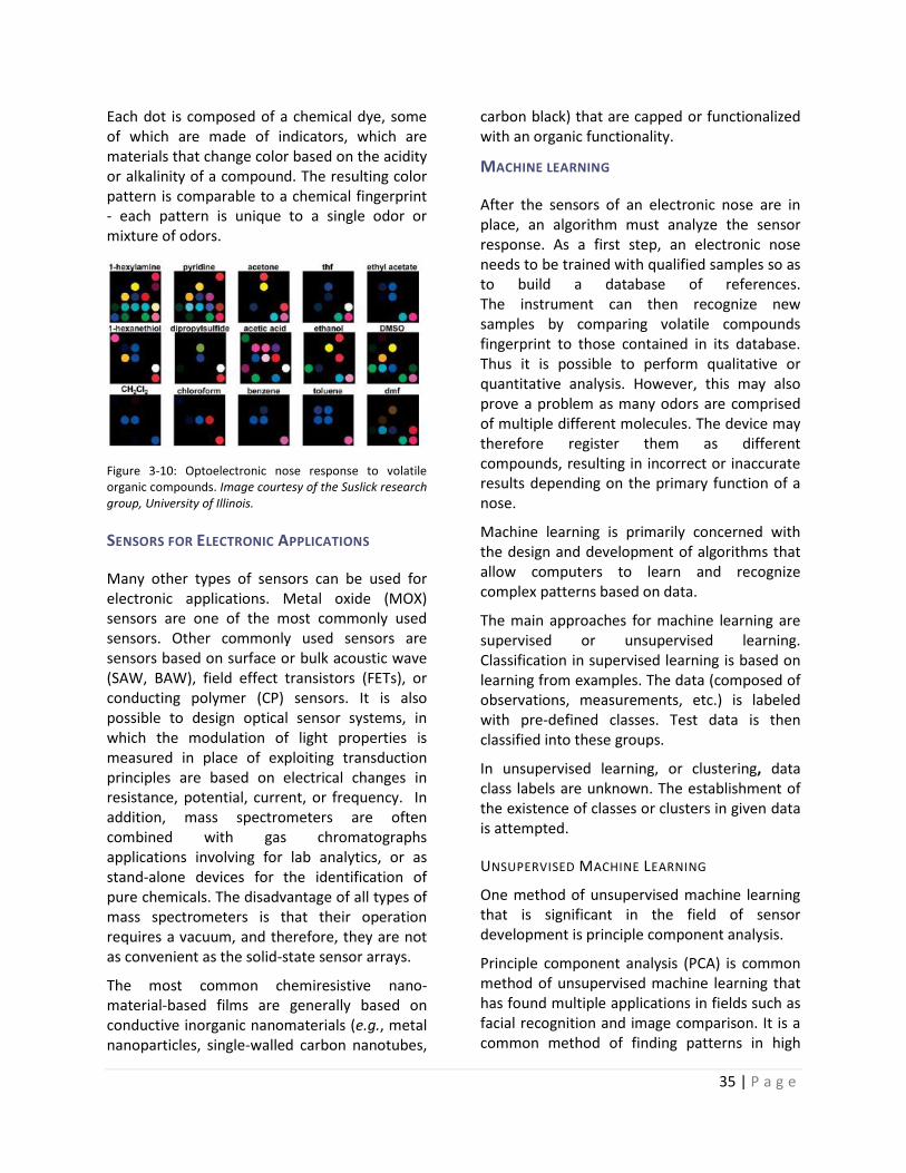
35 | P a g e
Each dot is composed of a chemical dye, some of which are made of indicators, which are materials that change color based on the acidity or alkalinity of a compound. The resulting color pattern is comparable to a chemical fingerprint - each pattern is unique to a single odor or mixture of odors.
Figure 3-10: Optoelectronic nose response to volatile organic compounds. Image courtesy of the Suslick research group, University of Illinois.
SENSORS FOR ELECTRONIC APPLICATIONS
Many other types of sensors can be used for electronic applications. Metal oxide (MOX) sensors are one of the most commonly used sensors. Other commonly used sensors are sensors based on surface or bulk acoustic wave (SAW, BAW), field effect transistors (FETs), or conducting polymer (CP) sensors. It is also possible to design optical sensor systems, in which the modulation of light properties is measured in place of exploiting transduction principles are based on electrical changes in resistance, potential, current, or frequency. In addition, mass spectrometers are often combined with gas chromatographs applications involving for lab analytics, or as stand-alone devices for the identification of pure chemicals. The disadvantage of all types of mass spectrometers is that their operation requires a vacuum, and therefore, they are not as convenient as the solid-state sensor arrays.
The most common chemiresistive nano-material-based films are generally based on conductive inorganic nanomaterials (e.g., metal nanoparticles, single-walled carbon nanotubes,
carbon black) that are capped or functionalized with an organic functionality.
MACHINE LEARNING
After the sensors of an electronic nose are in place, an algorithm must analyze the sensor response. As a first step, an electronic nose needs to be trained with qualified samples so as to build a database of references. The instrument can then recognize new samples by comparing volatile compounds fingerprint to those contained in its database. Thus it is possible to perform qualitative or quantitative analysis. However, this may also prove a problem as many odors are comprised of multiple different molecules. The device may therefore register them as different compounds, resulting in incorrect or inaccurate results depending on the primary function of a nose.
Machine learning is primarily concerned with the design and development of algorithms that allow computers to learn and recognize complex patterns based on data.
The main approaches for machine learning are supervised or unsupervised learning. Classification in supervised learning is based on learning from examples. The data (composed of observations, measurements, etc.) is labeled with pre-defined classes. Test data is then classified into these groups.
In unsupervised learning, or clustering, data class labels are unknown. The establishment of the existence of classes or clusters in given data is attempted.
UNSUPERVISED MACHINE LEARNING
One method of unsupervised machine learning that is significant in the field of sensor development is principle component analysis.
Principle component analysis (PCA) is common method of unsupervised machine learning that has found multiple applications in fields such as facial recognition and image comparison. It is a common method of finding patterns in high

36 | P a g e
dimensional data. The aim is the achievement of lower dimensional representation and visualization of the collected data in terms of scores on (uncorrelated) principle components, a so-called “score plot”.
This method enables the interpretation of a large data set using a smaller number of components. Because patterns in data can be hard to find in high-dimension data, and there is no way to graphically represent high-dimension data, PCA is a powerful tool for data analysis.
Following is a short video of an intuitive way to understand PCA:
https://www.youtube.com/watch?v=BfTMmoDFXyE
SUPERVISED MACHINE LEARNING
As explained earlier, supervised learning takes a known set of input data and known responses to the data, and seeks to build a predictor model that generates reasonable predictions for the response to new data. In order to solve a given problem of supervised learning, one has to perform the following steps.
The first step is to determine the type of training examples. Before doing anything else, the user should decide what kind of data is to be used as a training set. In the case of hand-writing analysis, for example, this might be a single hand-written character, an entire hand-written word, or an entire line of handwriting.
The second step is to gather a training set. The training set needs to be representative of the real-world use of the function. Thus, a set of input objects is gathered and corresponding outputs are also gathered, either from human experts or from measurements.
The third step is to determine the input feature representation of the learned function. The accuracy of the learned function depends strongly on how the input object is represented. Typically, the input object is transformed into a feature vector, which contains a number of features that are descriptive of the object. The number of features should not be too large, because of the curse of dimensionality, but
should contain enough information to accurately predict the output.
The fourth step is to determine the structure of the learned function and corresponding learning algorithm.
The fifth step is to complete the design, namely to run the learning algorithm on the gathered training set. Some supervised learning algorithms require the user to determine certain control parameters. These parameters may be adjusted by optimizing performance on a subset (called a validation set) of the training set, or via cross-validation.
The sixth step is to evaluate the accuracy of the learned function. After parameter adjustment and learning, the performance of the resulting function should be measured on a test set that is separate from the training set.
A wide range of supervised learning algorithms is available, each with its strengths and weaknesses. There is no single learning algorithm that works best on all supervised learning problems.
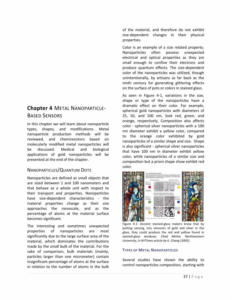
37 | P a g e
Chapter 4 METAL NANOPARTICLE-BASED SENSORS
In this chapter we will learn about nanoparticle types, shapes, and modifications. Metal nanoparticle production methods will be reviewed, and chemiresistors based on molecularly modified metal nanoparticles will be discussed. Medical and biological applications of gold nanoparticles will be presented at the end of the chapter.
NANOPARTICLES/QUANTUM DOTS
Nanoparticles are defined as small objects that are sized between 1 and 100 nanometers and that behave as a whole unit with respect to their transport and properties. Nanoparticles have size-dependent characteristics - the material properties change as their size approaches the nanoscale, and as the percentage of atoms at the material surface becomes significant.
The interesting and sometimes unexpected properties of nanoparticles are most significantly due to the large surface area of the material, which dominates the contributions made by the small bulk of the material. For the sake of comparison, bulk materials (mainly, particles larger than one micrometer) contain insignificant percentage of atoms at the surface in relation to the number of atoms in the bulk
of the material, and therefore do not exhibit size-dependent changes in their physical properties.
Color is an example of a size related property. Nanoparticles often possess unexpected electrical and optical properties as they are small enough to confine their electrons and produce quantum effects. The size-dependent color of the nanoparticles was utilized, though unintentionally, by artisans as far back as the ninth century for generating glittering effects on the surface of pots or colors in stained glass.
As seen in Figure 4-1, variations in the size, shape or type of the nanoparticles have a dramatic effect on their color. For example, spherical gold nanoparticles with diameters of 25, 50, and 100 nm, look red, green, and orange, respectively. Composition also affects color - spherical silver nanoparticles with a 100 nm diameter exhibit a yellow color, compared to the orange color exhibited by gold nanoparticles of a similar shape and size. Shape is also significant - spherical silver nanoparticles that have 100 nm in diameter exhibit yellow color, while nanoparticles of a similar size and composition but a prism shape show exhibit red color.
Figure 4-1: Ancient stained-glass makers knew that by putting varying, tiny amounts of gold and silver in the glass, they could produce the red and yellow found in stained-glass windows. Chad Mirkin, Northwestern University, in NYTimes article by K. Chang (2005).
TYPES OF METAL NANOPARTICLES
Several studies have shown the ability to control nanoparticles composition, starting with
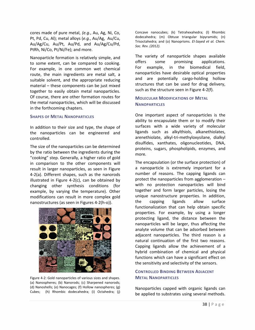
38 | P a g e
cores made of pure metal, (e.g., Au, Ag, Ni, Co, Pt, Pd, Cu, Al); metal alloys (e.g., Au/Ag, Au/Cu, Au/Ag/Cu, Au/Pt, Au/Pd, and Au/Ag/Cu/Pd, PtRh, Ni/Co, Pt/Ni/Fe); and more.
Nanoparticle formation is relatively simple, and to some extent, can be compared to cooking. For example, in one common wet chemical route, the main ingredients are metal salt, a suitable solvent, and the appropriate reducing material – these components can be just mixed together to easily obtain metal nanoparticles. Of course, there are other formation routes for the metal nanoparticles, which will be discussed in the forthcoming chapters.
SHAPES OF METAL NANOPARTICLES
In addition to their size and type, the shape of the nanoparticles can be engineered and controlled.
The size of the nanoparticles can be determined by the ratio between the ingredients during the “cooking” step. Generally, a higher ratio of gold in comparison to the other components will result in larger nanoparticles, as seen in Figure 4-2(a). Different shapes, such as the nanorods illustrated in Figure 4-2(c), can be obtained by changing other synthesis conditions (for example, by varying the temperature). Other modifications can result in more complex gold nanostructures (as seen in Figures 4-2(h-o)).
Figure 4-2: Gold nanoparticles of various sizes and shapes. (a) Nanospheres; (b) Nanorods; (c) Sharpened nanorods; (d) Nanoshells; (e) Nanocages; (f) Hollow nanospheres; (g) Cubes; (h) Rhombic dodecahedra; (i) Octahedra; (j)
Concave nanocubes; (k) Tetrahexahedra; (l) Rhombic dodecahedra; (m) Obtuse triangular bipyramids; (n) Trisoctahedra; and (o) Nanoprisms. El-Sayed et al. Chem. Soc. Rev. (2012).
The variety of nanoparticle shapes available offers some promising applications. For example, in the biomedical field, nanoparticles have desirable optical properties and are potentially cargo-holding hollow structures that can be used for drug delivery, such as the structure seen in Figure 4-2(f).
MOLECULAR MODIFICATIONS OF METAL
NANOPARTICLES
One important aspect of nanoparticles is the ability to encapsulate them or to modify their surfaces with a wide variety of molecular ligands such as alkylthiols, alkanethiolates, arenethiolate, alkyl-tri-methyloxysilane, dialkyl disulfides, xanthates, oligonucleotides, DNA, proteins, sugars, phospholipids, enzymes, and more.
The encapsulation (or the surface protection) of a nanoparticle is extremely important for a number of reasons. The capping ligands can protect the nanoparticles from agglomeration – with no protection nanoparticles will bind together and form larger particles, losing the unique nanostructure properties. In addition, the capping ligands allow surface functionalization that can help obtain specific properties. For example, by using a longer protecting ligand, the distance between the nanoparticles will be larger, thus affecting the analyte volume that can be adsorbed between adjacent nanoparticles. The third reason is a natural continuation of the first two reasons. Capping ligands allow the achievement of a hybrid combination of chemical and physical functions which can have a significant effect on the sensitivity and selectivity of the sensors.
CONTROLLED BINDING BETWEEN ADJACENT
METAL NANOPARTICLES
Nanoparticles capped with organic ligands can be applied to substrates using several methods.
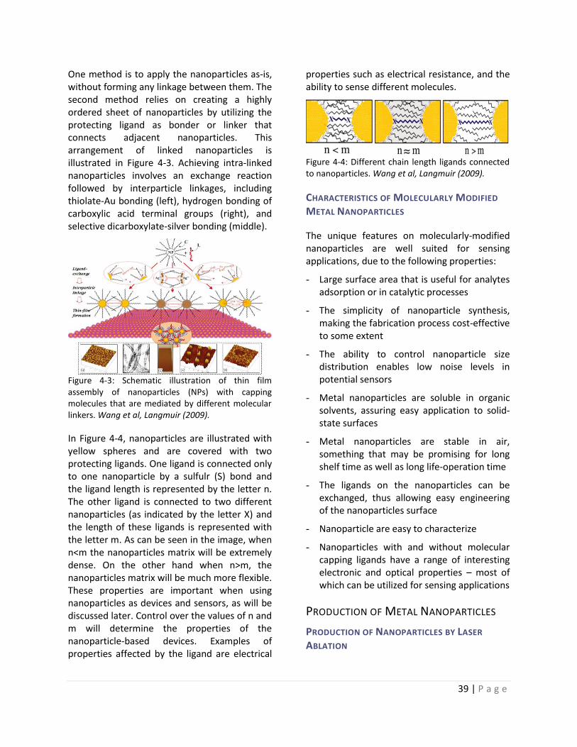
39 | P a g e
One method is to apply the nanoparticles as-is, without forming any linkage between them. The second method relies on creating a highly ordered sheet of nanoparticles by utilizing the protecting ligand as bonder or linker that connects adjacent nanoparticles. This arrangement of linked nanoparticles is illustrated in Figure 4-3. Achieving intra-linked nanoparticles involves an exchange reaction followed by interparticle linkages, including thiolate-Au bonding (left), hydrogen bonding of carboxylic acid terminal groups (right), and selective dicarboxylate-silver bonding (middle).
Figure 4-3: Schematic illustration of thin film assembly of nanoparticles (NPs) with capping molecules that are mediated by different molecular linkers. Wang et al, Langmuir (2009).
In Figure 4-4, nanoparticles are illustrated with yellow spheres and are covered with two protecting ligands. One ligand is connected only to one nanoparticle by a sulfulr (S) bond and the ligand length is represented by the letter n. The other ligand is connected to two different nanoparticles (as indicated by the letter X) and the length of these ligands is represented with the letter m. As can be seen in the image, when n<m the nanoparticles matrix will be extremely dense. On the other hand when n>m, the nanoparticles matrix will be much more flexible. These properties are important when using nanoparticles as devices and sensors, as will be discussed later. Control over the values of n and m will determine the properties of the nanoparticle-based devices. Examples of properties affected by the ligand are electrical
properties such as electrical resistance, and the ability to sense different molecules.
Figure 4-4: Different chain length ligands connected to nanoparticles. Wang et al, Langmuir (2009).
CHARACTERISTICS OF MOLECULARLY MODIFIED
METAL NANOPARTICLES
The unique features on molecularly-modified nanoparticles are well suited for sensing applications, due to the following properties:
- Large surface area that is useful for analytes adsorption or in catalytic processes
- The simplicity of nanoparticle synthesis, making the fabrication process cost-effective to some extent
- The ability to control nanoparticle size distribution enables low noise levels in potential sensors
- Metal nanoparticles are soluble in organic solvents, assuring easy application to solid-state surfaces
- Metal nanoparticles are stable in air, something that may be promising for long shelf time as well as long life-operation time
- The ligands on the nanoparticles can be exchanged, thus allowing easy engineering of the nanoparticles surface
- Nanoparticle are easy to characterize
- Nanoparticles with and without molecular capping ligands have a range of interesting electronic and optical properties – most of which can be utilized for sensing applications
PRODUCTION OF METAL NANOPARTICLES
PRODUCTION OF NANOPARTICLES BY LASER
ABLATION
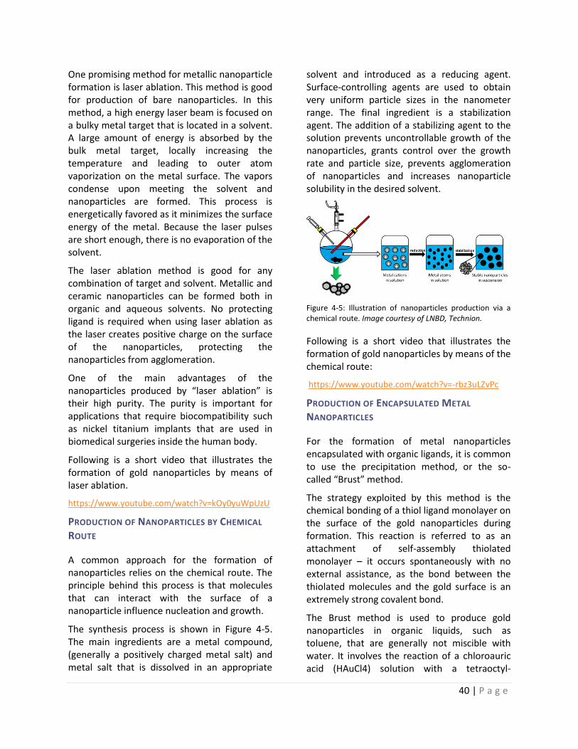
40 | P a g e
One promising method for metallic nanoparticle formation is laser ablation. This method is good for production of bare nanoparticles. In this method, a high energy laser beam is focused on a bulky metal target that is located in a solvent. A large amount of energy is absorbed by the bulk metal target, locally increasing the temperature and leading to outer atom vaporization on the metal surface. The vapors condense upon meeting the solvent and nanoparticles are formed. This process is energetically favored as it minimizes the surface energy of the metal. Because the laser pulses are short enough, there is no evaporation of the solvent.
The laser ablation method is good for any combination of target and solvent. Metallic and ceramic nanoparticles can be formed both in organic and aqueous solvents. No protecting ligand is required when using laser ablation as the laser creates positive charge on the surface of the nanoparticles, protecting the nanoparticles from agglomeration.
One of the main advantages of the nanoparticles produced by “laser ablation” is their high purity. The purity is important for applications that require biocompatibility such as nickel titanium implants that are used in biomedical surgeries inside the human body.
Following is a short video that illustrates the formation of gold nanoparticles by means of laser ablation.
https://www.youtube.com/watch?v=kOy0yuWpUzU
PRODUCTION OF NANOPARTICLES BY CHEMICAL
ROUTE
A common approach for the formation of nanoparticles relies on the chemical route. The principle behind this process is that molecules that can interact with the surface of a nanoparticle influence nucleation and growth.
The synthesis process is shown in Figure 4-5. The main ingredients are a metal compound, (generally a positively charged metal salt) and metal salt that is dissolved in an appropriate
solvent and introduced as a reducing agent. Surface-controlling agents are used to obtain very uniform particle sizes in the nanometer range. The final ingredient is a stabilization agent. The addition of a stabilizing agent to the solution prevents uncontrollable growth of the nanoparticles, grants control over the growth rate and particle size, prevents agglomeration of nanoparticles and increases nanoparticle solubility in the desired solvent.
Figure 4-5: Illustration of nanoparticles production via a chemical route. Image courtesy of LNBD, Technion.
Following is a short video that illustrates the formation of gold nanoparticles by means of the chemical route:
https://www.youtube.com/watch?v=-rbz3uLZvPc
PRODUCTION OF ENCAPSULATED METAL
NANOPARTICLES
For the formation of metal nanoparticles encapsulated with organic ligands, it is common to use the precipitation method, or the so-called “Brust” method.
The strategy exploited by this method is the chemical bonding of a thiol ligand monolayer on the surface of the gold nanoparticles during formation. This reaction is referred to as an attachment of self-assembly thiolated monolayer – it occurs spontaneously with no external assistance, as the bond between the thiolated molecules and the gold surface is an extremely strong covalent bond.
The Brust method is used to produce gold nanoparticles in organic liquids, such as toluene, that are generally not miscible with water. It involves the reaction of a chloroauric acid (HAuCl4) solution with a tetraoctyl-
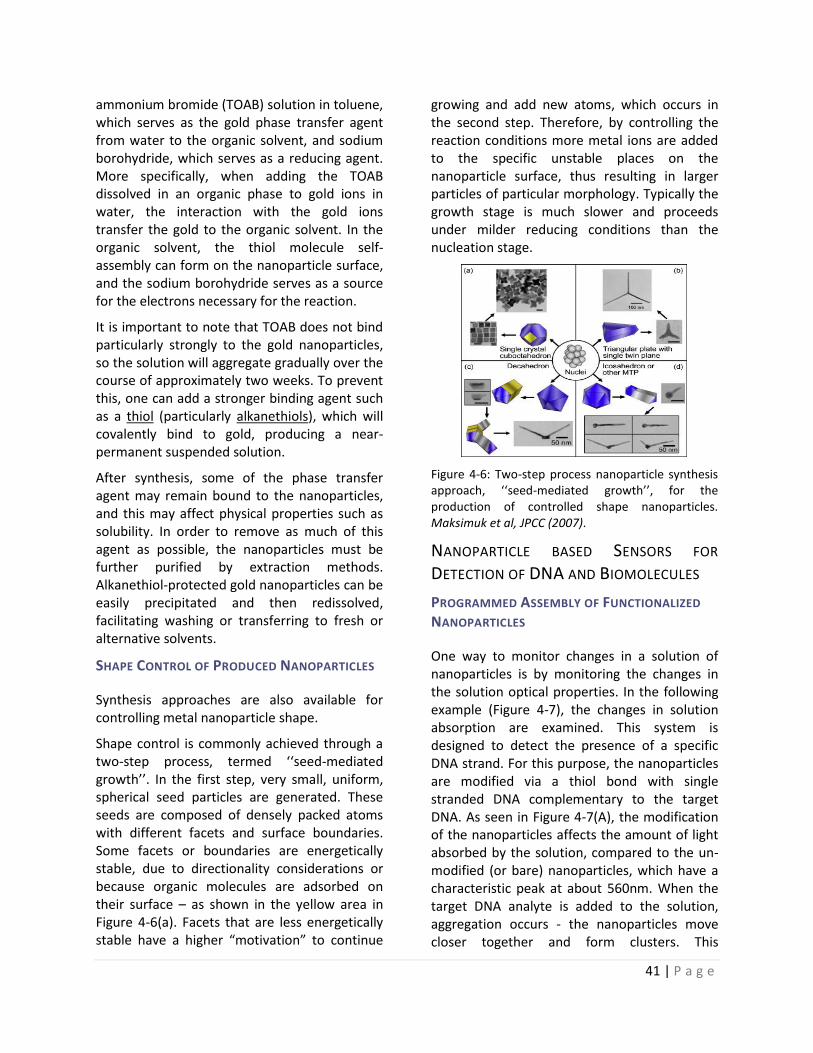
41 | P a g e
ammonium bromide (TOAB) solution in toluene, which serves as the gold phase transfer agent from water to the organic solvent, and sodium borohydride, which serves as a reducing agent. More specifically, when adding the TOAB dissolved in an organic phase to gold ions in water, the interaction with the gold ions transfer the gold to the organic solvent. In the organic solvent, the thiol molecule self-assembly can form on the nanoparticle surface, and the sodium borohydride serves as a source for the electrons necessary for the reaction.
It is important to note that TOAB does not bind particularly strongly to the gold nanoparticles, so the solution will aggregate gradually over the course of approximately two weeks. To prevent this, one can add a stronger binding agent such as a thiol (particularly alkanethiols), which will covalently bind to gold, producing a near-permanent suspended solution.
After synthesis, some of the phase transfer agent may remain bound to the nanoparticles, and this may affect physical properties such as solubility. In order to remove as much of this agent as possible, the nanoparticles must be further purified by extraction methods. Alkanethiol-protected gold nanoparticles can be easily precipitated and then redissolved, facilitating washing or transferring to fresh or alternative solvents.
SHAPE CONTROL OF PRODUCED NANOPARTICLES
Synthesis approaches are also available for controlling metal nanoparticle shape.
Shape control is commonly achieved through a two-step process, termed ‘‘seed-mediated growth’’. In the first step, very small, uniform, spherical seed particles are generated. These seeds are composed of densely packed atoms with different facets and surface boundaries. Some facets or boundaries are energetically stable, due to directionality considerations or because organic molecules are adsorbed on their surface – as shown in the yellow area in Figure 4-6(a). Facets that are less energetically stable have a higher “motivation” to continue
growing and add new atoms, which occurs in the second step. Therefore, by controlling the reaction conditions more metal ions are added to the specific unstable places on the nanoparticle surface, thus resulting in larger particles of particular morphology. Typically the growth stage is much slower and proceeds under milder reducing conditions than the nucleation stage.
Figure 4-6: Two-step process nanoparticle synthesis approach, ‘‘seed-mediated growth’’, for the production of controlled shape nanoparticles. Maksimuk et al, JPCC (2007).
NANOPARTICLE BASED SENSORS FOR
DETECTION OF DNA AND BIOMOLECULES
PROGRAMMED ASSEMBLY OF FUNCTIONALIZED
NANOPARTICLES
One way to monitor changes in a solution of nanoparticles is by monitoring the changes in the solution optical properties. In the following example (Figure 4-7), the changes in solution absorption are examined. This system is designed to detect the presence of a specific DNA strand. For this purpose, the nanoparticles are modified via a thiol bond with single stranded DNA complementary to the target DNA. As seen in Figure 4-7(A), the modification of the nanoparticles affects the amount of light absorbed by the solution, compared to the un-modified (or bare) nanoparticles, which have a characteristic peak at about 560nm. When the target DNA analyte is added to the solution, aggregation occurs - the nanoparticles move closer together and form clusters. This
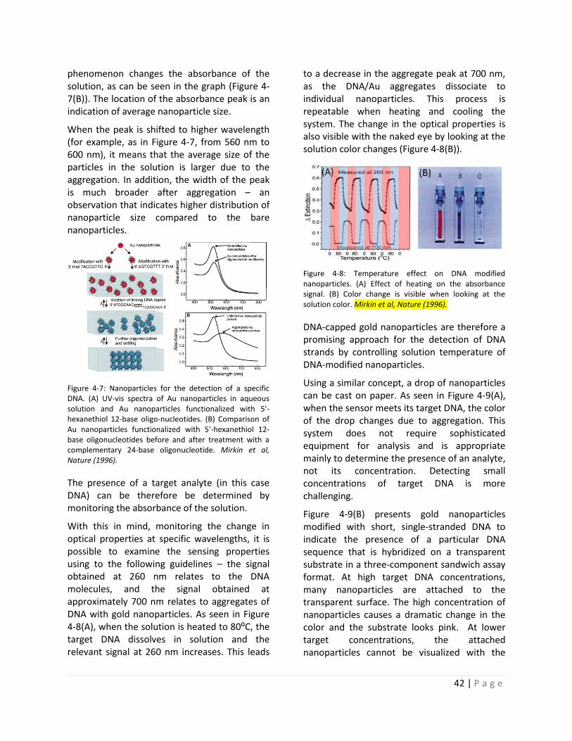
42 | P a g e
phenomenon changes the absorbance of the solution, as can be seen in the graph (Figure 4-7(B)). The location of the absorbance peak is an indication of average nanoparticle size.
When the peak is shifted to higher wavelength (for example, as in Figure 4-7, from 560 nm to 600 nm), it means that the average size of the particles in the solution is larger due to the aggregation. In addition, the width of the peak is much broader after aggregation – an observation that indicates higher distribution of nanoparticle size compared to the bare nanoparticles.
Figure 4-7: Nanoparticles for the detection of a specific DNA. (A) UV-vis spectra of Au nanoparticles in aqueous solution and Au nanoparticles functionalized with 5'-hexanethiol 12-base oligo-nucleotides. (B) Comparison of Au nanoparticles functionalized with 5'-hexanethiol 12-base oligonucleotides before and after treatment with a complementary 24-base oligonucleotide. Mirkin et al, Nature (1996).
The presence of a target analyte (in this case DNA) can be therefore be determined by monitoring the absorbance of the solution.
With this in mind, monitoring the change in optical properties at specific wavelengths, it is possible to examine the sensing properties using to the following guidelines – the signal obtained at 260 nm relates to the DNA molecules, and the signal obtained at approximately 700 nm relates to aggregates of DNA with gold nanoparticles. As seen in Figure 4-8(A), when the solution is heated to 80⁰C, the target DNA dissolves in solution and the relevant signal at 260 nm increases. This leads
to a decrease in the aggregate peak at 700 nm, as the DNA/Au aggregates dissociate to individual nanoparticles. This process is repeatable when heating and cooling the system. The change in the optical properties is also visible with the naked eye by looking at the solution color changes (Figure 4-8(B)).
Figure 4-8: Temperature effect on DNA modified nanoparticles. (A) Effect of heating on the absorbance signal. (B) Color change is visible when looking at the solution color. Mirkin et al, Nature (1996).
DNA-capped gold nanoparticles are therefore a promising approach for the detection of DNA strands by controlling solution temperature of DNA-modified nanoparticles.
Using a similar concept, a drop of nanoparticles can be cast on paper. As seen in Figure 4-9(A), when the sensor meets its target DNA, the color of the drop changes due to aggregation. This system does not require sophisticated equipment for analysis and is appropriate mainly to determine the presence of an analyte, not its concentration. Detecting small concentrations of target DNA is more challenging.
Figure 4-9(B) presents gold nanoparticles modified with short, single-stranded DNA to indicate the presence of a particular DNA sequence that is hybridized on a transparent substrate in a three-component sandwich assay format. At high target DNA concentrations, many nanoparticles are attached to the transparent surface. The high concentration of nanoparticles causes a dramatic change in the color and the substrate looks pink. At lower target concentrations, the attached nanoparticles cannot be visualized with the
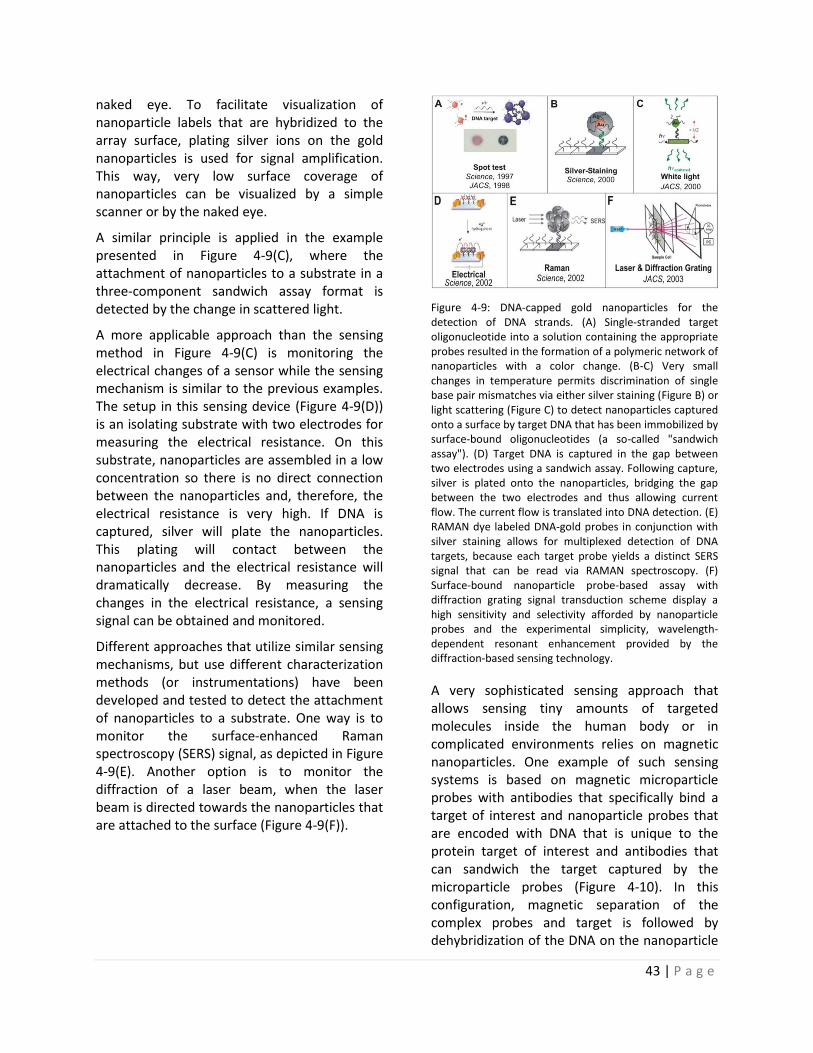
43 | P a g e
naked eye. To facilitate visualization of nanoparticle labels that are hybridized to the array surface, plating silver ions on the gold nanoparticles is used for signal amplification. This way, very low surface coverage of nanoparticles can be visualized by a simple scanner or by the naked eye.
A similar principle is applied in the example presented in Figure 4-9(C), where the attachment of nanoparticles to a substrate in a three-component sandwich assay format is detected by the change in scattered light.
A more applicable approach than the sensing method in Figure 4-9(C) is monitoring the electrical changes of a sensor while the sensing mechanism is similar to the previous examples. The setup in this sensing device (Figure 4-9(D)) is an isolating substrate with two electrodes for measuring the electrical resistance. On this substrate, nanoparticles are assembled in a low concentration so there is no direct connection between the nanoparticles and, therefore, the electrical resistance is very high. If DNA is captured, silver will plate the nanoparticles. This plating will contact between the nanoparticles and the electrical resistance will dramatically decrease. By measuring the changes in the electrical resistance, a sensing signal can be obtained and monitored.
Different approaches that utilize similar sensing mechanisms, but use different characterization methods (or instrumentations) have been developed and tested to detect the attachment of nanoparticles to a substrate. One way is to monitor the surface-enhanced Raman spectroscopy (SERS) signal, as depicted in Figure 4-9(E). Another option is to monitor the diffraction of a laser beam, when the laser beam is directed towards the nanoparticles that are attached to the surface (Figure 4-9(F)).
Figure 4-9: DNA-capped gold nanoparticles for the detection of DNA strands. (A) Single-stranded target oligonucleotide into a solution containing the appropriate probes resulted in the formation of a polymeric network of nanoparticles with a color change. (B-C) Very small changes in temperature permits discrimination of single base pair mismatches via either silver staining (Figure B) or light scattering (Figure C) to detect nanoparticles captured onto a surface by target DNA that has been immobilized by surface-bound oligonucleotides (a so-called "sandwich assay"). (D) Target DNA is captured in the gap between two electrodes using a sandwich assay. Following capture, silver is plated onto the nanoparticles, bridging the gap between the two electrodes and thus allowing current flow. The current flow is translated into DNA detection. (E) RAMAN dye labeled DNA-gold probes in conjunction with silver staining allows for multiplexed detection of DNA targets, because each target probe yields a distinct SERS signal that can be read via RAMAN spectroscopy. (F) Surface-bound nanoparticle probe-based assay with diffraction grating signal transduction scheme display a high sensitivity and selectivity afforded by nanoparticle probes and the experimental simplicity, wavelength-dependent resonant enhancement provided by the diffraction-based sensing technology.
A very sophisticated sensing approach that allows sensing tiny amounts of targeted molecules inside the human body or in complicated environments relies on magnetic nanoparticles. One example of such sensing systems is based on magnetic microparticle probes with antibodies that specifically bind a target of interest and nanoparticle probes that are encoded with DNA that is unique to the protein target of interest and antibodies that can sandwich the target captured by the microparticle probes (Figure 4-10). In this configuration, magnetic separation of the complex probes and target is followed by dehybridization of the DNA on the nanoparticle
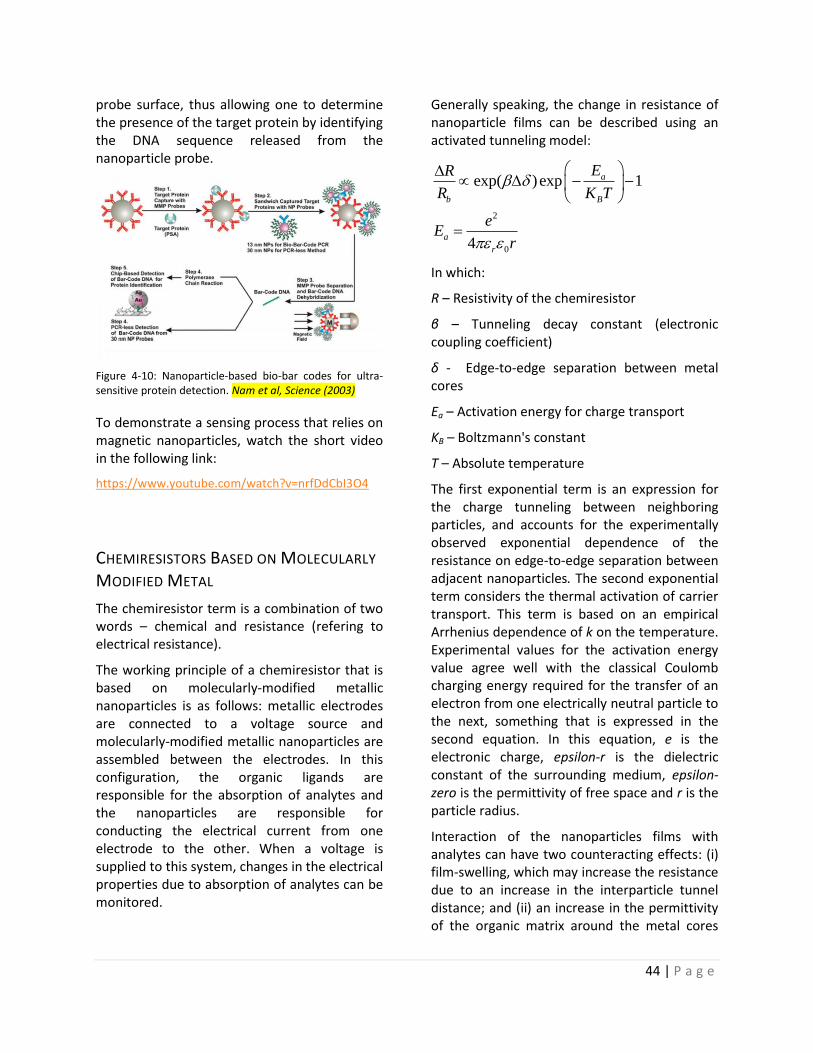
44 | P a g e
probe surface, thus allowing one to determine the presence of the target protein by identifying the DNA sequence released from the nanoparticle probe.
Figure 4-10: Nanoparticle-based bio-bar codes for ultra-sensitive protein detection. Nam et al, Science (2003)
To demonstrate a sensing process that relies on magnetic nanoparticles, watch the short video in the following link:
https://www.youtube.com/watch?v=nrfDdCbI3O4
CHEMIRESISTORS BASED ON MOLECULARLY
MODIFIED METAL
The chemiresistor term is a combination of two words – chemical and resistance (refering to electrical resistance).
The working principle of a chemiresistor that is based on molecularly-modified metallic nanoparticles is as follows: metallic electrodes are connected to a voltage source and molecularly-modified metallic nanoparticles are assembled between the electrodes. In this configuration, the organic ligands are responsible for the absorption of analytes and the nanoparticles are responsible for conducting the electrical current from one electrode to the other. When a voltage is supplied to this system, changes in the electrical properties due to absorption of analytes can be monitored.
Generally speaking, the change in resistance of nanoparticle films can be described using an activated tunneling model:
2
0
exp( )exp 1
4
a
b B
a
r
ER
R K T
eE
r
In which:
R – Resistivity of the chemiresistor
β – Tunneling decay constant (electronic coupling coefficient)
δ - Edge-to-edge separation between metal cores
Ea – Activation energy for charge transport
KB – Boltzmann's constant
T – Absolute temperature
The first exponential term is an expression for the charge tunneling between neighboring particles, and accounts for the experimentally observed exponential dependence of the resistance on edge-to-edge separation between adjacent nanoparticles. The second exponential term considers the thermal activation of carrier transport. This term is based on an empirical Arrhenius dependence of k on the temperature. Experimental values for the activation energy value agree well with the classical Coulomb charging energy required for the transfer of an electron from one electrically neutral particle to the next, something that is expressed in the second equation. In this equation, e is the electronic charge, epsilon-r is the dielectric constant of the surrounding medium, epsilon-zero is the permittivity of free space and r is the particle radius.
Interaction of the nanoparticles films with analytes can have two counteracting effects: (i) film-swelling, which may increase the resistance due to an increase in the interparticle tunnel distance; and (ii) an increase in the permittivity of the organic matrix around the metal cores
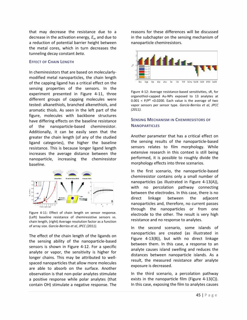
45 | P a g e
that may decrease the resistance due to a decrease in the activation energy, Ea, and due to a reduction of potential barrier height between the metal cores, which in turn decreases the tunneling decay constant beta.
EFFECT OF CHAIN LENGTH
In chemiresistors that are based on molecularly-modified metal nanoparticles, the chain length of the capping ligand has a critical effect on the sensing properties of the sensors. In the experiment presented in Figure 4-11, three different groups of capping molecules were tested: alkanethiols, branched alkenethiols, and aromatic thiols. As seen in the left part of the figure, molecules with backbone structures have differing effects on the baseline resistance of the nanoparticle-based chemiresistor. Additionally, it can be easily seen that the greater the chain length (of any of the studied ligand categories), the higher the baseline resistance. This is because longer ligand length increases the average distance between the nanoparticle, increasing the chemiresistor baseline.
Figure 4-11: Effect of chain length on sensor response. (Left) baseline resistance of chemiresistive sensors vs. chain length, (right) Average resolution factor as a function of array size. García-Berríos et al, JPCC (2011).
The effect of the chain length of the ligands on the sensing ability of the nanoparticle-based sensors is shown in Figure 4-12. For a specific analyte or vapor, the sensitivity is higher for longer chains. This may be attributed to well-spaced nanoparticles that allow more molecules are able to absorb on the surface. Another observation is that non-polar analytes stimulate a positive response while polar analytes (that contain OH) stimulate a negative response. The
reasons for these differences will be discussed in the subchapter on the sensing mechanism of nanoparticle chemiresistors.
Figure 4-12: Average resistance-based sensitivities, sR, for organothiol-capped Au-NPs exposed to 13 analytes at 0.001 < P/P⁰ <0.0200. Each value is the average of two vapor sensors per sensor type. García-Berríos et al, JPCC (2011).
SENSING MECHANISM IN CHEMIRESISTORS OF
NANOPARTICLES
Another parameter that has a critical effect on the sensing results of the nanoparticle-based sensors relates to film morphology. While extensive research in this context is still being performed, it is possible to roughly divide the morphology effects into three scenarios.
In the first scenario, the nanoparticle-based chemiresistor contains only a small number of nanoparticles (as illustrated in Figure 4-13(A)), with no percolation pathway connecting between the electrodes. In this case, there is no direct linkage between the adjacent nanoparticles and, therefore, no current passes through the nanoparticles or from one electrode to the other. The result is very high resistance and no response to analytes.
In the second scenario, some islands of nanoparticles are created (as illustrated in Figure 4-13(B)), but with no direct linkage between them. In this case, a response to an analyte causes island swelling and reduces the distances between nanoparticle islands. As a result, the measured resistance after analyte exposure is decreased.
In the third scenario, a percolation pathway exists in the nanoparticle film (Figure 4-13(C)). In this case, exposing the film to analytes causes
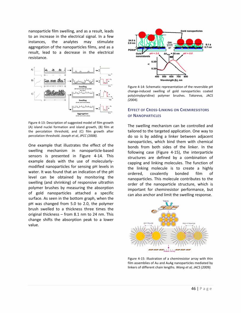
46 | P a g e
nanoparticle film swelling, and as a result, leads to an increase in the electrical signal. In a few instances, the analytes may stimulate aggregation of the nanoparticles films, and as a result, lead to a decrease in the electrical resistance.
Figure 4-13: Description of suggested model of film growth (A) island nuclei formation and island growth, (B) film at the percolation threshold, and (C) film growth after percolation threshold. Joseph et al, JPCC (2008).
One example that illustrates the effect of the swelling mechanism in nanoparticle-based sensors is presented in Figure 4-14. This example deals with the use of molecularly-modified nanoparticles for sensing pH levels in water. It was found that an indication of the pH level can be obtained by monitoring the swelling (and shrinking) of responsive ultrathin polymer brushes by measuring the absorption of gold nanoparticles attached a specific surface. As seen in the bottom graph, when the pH was changed from 5.0 to 2.0, the polymer brush swelled to a thickness three times the original thickness – from 8.1 nm to 24 nm. This change shifts the absorption peak to a lower value.
Figure 4-14: Schematic representation of the reversible pH change-induced swelling of gold nanoparticles coated poly(vinylpyridine) polymer brushes. Tokareva, JACS (2004).
EFFECT OF CROSS-LINKING ON CHEMIRESISTORS
OF NANOPARTICLES
The swelling mechanism can be controlled and tailored to the targeted application. One way to do so is by adding a linker between adjacent nanoparticles, which bind them with chemical bonds from both sides of the linker. In the following case (Figure 4-15), the interparticle structures are defined by a combination of capping and linking molecules. The function of the linking molecule is to create a highly ordered, covalently bonded film of nanoparticles. This molecule contributes to the order of the nanoparticle structure, which is important for chemiresistor performance, but can also anchor and limit the swelling response.
Figure 4-15: Illustration of a chemiresistor array with thin film assemblies of Au and AuAg nanoparticles mediated by linkers of different chain lengths. Wang et al, JACS (2009).
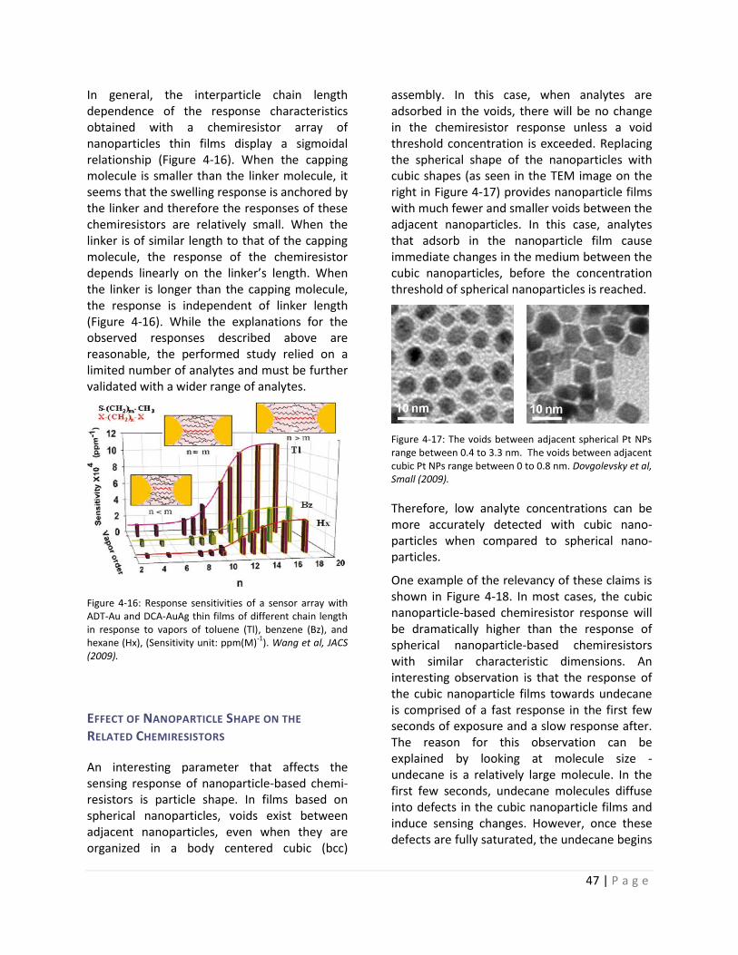
47 | P a g e
In general, the interparticle chain length dependence of the response characteristics obtained with a chemiresistor array of nanoparticles thin films display a sigmoidal relationship (Figure 4-16). When the capping molecule is smaller than the linker molecule, it seems that the swelling response is anchored by the linker and therefore the responses of these chemiresistors are relatively small. When the linker is of similar length to that of the capping molecule, the response of the chemiresistor depends linearly on the linker’s length. When the linker is longer than the capping molecule, the response is independent of linker length (Figure 4-16). While the explanations for the observed responses described above are reasonable, the performed study relied on a limited number of analytes and must be further validated with a wider range of analytes.
Figure 4-16: Response sensitivities of a sensor array with ADT-Au and DCA-AuAg thin films of different chain length in response to vapors of toluene (Tl), benzene (Bz), and hexane (Hx), (Sensitivity unit: ppm(M)
-1). Wang et al, JACS
(2009).
EFFECT OF NANOPARTICLE SHAPE ON THE
RELATED CHEMIRESISTORS
An interesting parameter that affects the sensing response of nanoparticle-based chemi-resistors is particle shape. In films based on spherical nanoparticles, voids exist between adjacent nanoparticles, even when they are organized in a body centered cubic (bcc)
assembly. In this case, when analytes are adsorbed in the voids, there will be no change in the chemiresistor response unless a void threshold concentration is exceeded. Replacing the spherical shape of the nanoparticles with cubic shapes (as seen in the TEM image on the right in Figure 4-17) provides nanoparticle films with much fewer and smaller voids between the adjacent nanoparticles. In this case, analytes that adsorb in the nanoparticle film cause immediate changes in the medium between the cubic nanoparticles, before the concentration threshold of spherical nanoparticles is reached.
Figure 4-17: The voids between adjacent spherical Pt NPs range between 0.4 to 3.3 nm. The voids between adjacent cubic Pt NPs range between 0 to 0.8 nm. Dovgolevsky et al, Small (2009).
Therefore, low analyte concentrations can be more accurately detected with cubic nano-particles when compared to spherical nano-particles.
One example of the relevancy of these claims is shown in Figure 4-18. In most cases, the cubic nanoparticle-based chemiresistor response will be dramatically higher than the response of spherical nanoparticle-based chemiresistors with similar characteristic dimensions. An interesting observation is that the response of the cubic nanoparticle films towards undecane is comprised of a fast response in the first few seconds of exposure and a slow response after. The reason for this observation can be explained by looking at molecule size - undecane is a relatively large molecule. In the first few seconds, undecane molecules diffuse into defects in the cubic nanoparticle films and induce sensing changes. However, once these defects are fully saturated, the undecane begins
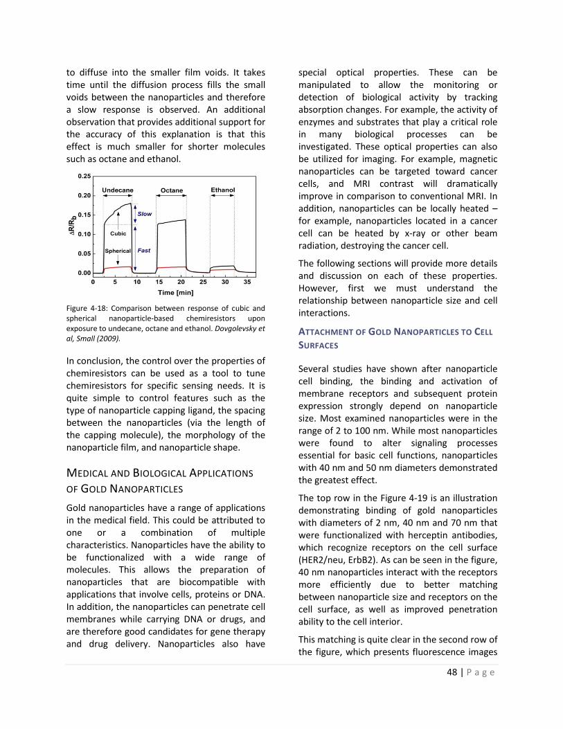
48 | P a g e
to diffuse into the smaller film voids. It takes time until the diffusion process fills the small voids between the nanoparticles and therefore a slow response is observed. An additional observation that provides additional support for the accuracy of this explanation is that this effect is much smaller for shorter molecules such as octane and ethanol.
Figure 4-18: Comparison between response of cubic and spherical nanoparticle-based chemiresistors upon exposure to undecane, octane and ethanol. Dovgolevsky et al, Small (2009).
In conclusion, the control over the properties of chemiresistors can be used as a tool to tune chemiresistors for specific sensing needs. It is quite simple to control features such as the type of nanoparticle capping ligand, the spacing between the nanoparticles (via the length of the capping molecule), the morphology of the nanoparticle film, and nanoparticle shape.
MEDICAL AND BIOLOGICAL APPLICATIONS
OF GOLD NANOPARTICLES
Gold nanoparticles have a range of applications in the medical field. This could be attributed to one or a combination of multiple characteristics. Nanoparticles have the ability to be functionalized with a wide range of molecules. This allows the preparation of nanoparticles that are biocompatible with applications that involve cells, proteins or DNA. In addition, the nanoparticles can penetrate cell membranes while carrying DNA or drugs, and are therefore good candidates for gene therapy and drug delivery. Nanoparticles also have
special optical properties. These can be manipulated to allow the monitoring or detection of biological activity by tracking absorption changes. For example, the activity of enzymes and substrates that play a critical role in many biological processes can be investigated. These optical properties can also be utilized for imaging. For example, magnetic nanoparticles can be targeted toward cancer cells, and MRI contrast will dramatically improve in comparison to conventional MRI. In addition, nanoparticles can be locally heated – for example, nanoparticles located in a cancer cell can be heated by x-ray or other beam radiation, destroying the cancer cell.
The following sections will provide more details and discussion on each of these properties. However, first we must understand the relationship between nanoparticle size and cell interactions.
ATTACHMENT OF GOLD NANOPARTICLES TO CELL
SURFACES
Several studies have shown after nanoparticle cell binding, the binding and activation of membrane receptors and subsequent protein expression strongly depend on nanoparticle size. Most examined nanoparticles were in the range of 2 to 100 nm. While most nanoparticles were found to alter signaling processes essential for basic cell functions, nanoparticles with 40 nm and 50 nm diameters demonstrated the greatest effect.
The top row in the Figure 4-19 is an illustration demonstrating binding of gold nanoparticles with diameters of 2 nm, 40 nm and 70 nm that were functionalized with herceptin antibodies, which recognize receptors on the cell surface (HER2/neu, ErbB2). As can be seen in the figure, 40 nm nanoparticles interact with the receptors more efficiently due to better matching between nanoparticle size and receptors on the cell surface, as well as improved penetration ability to the cell interior.
This matching is quite clear in the second row of the figure, which presents fluorescence images
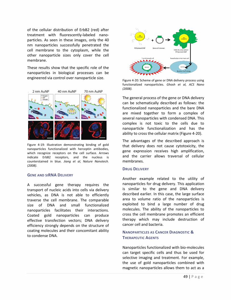
49 | P a g e
of the cellular distribution of ErbB2 (red) after treatment with fluorescently-labeled nano-particles. As seen in these images, only the 40 nm nanoparticles successfully penetrated the cell membrane to the cytoplasm, while the other nanoparticle sizes only cover the cell membrane.
These results show that the specific role of the nanoparticles in biological processes can be engineered via control over nanoparticle size.
Figure 4-19: Illustration demonstrating binding of gold nanoparticles functionalized with herceptin antibodies, which recognize receptors on the cell surface. Arrows indicate ErbB2 receptors, and the nucleus is counterstained in blue. Jiang et al, Nature Nanotech. (2008).
GENE AND SIRNA DELIVERY
A successful gene therapy requires the transport of nucleic acids into cells via delivery vehicles, as DNA is not able to efficiently traverse the cell membrane. The comparable size of DNA and small functionalized nanoparticles facilitates their interactions. Coated gold nanoparticles can produce effective transfection vectors; DNA delivery efficiency strongly depends on the structure of coating molecules and their concomitant ability to condense DNA.
Figure 4-20: Scheme of gene or DNA delivery process using functionalized nanoparticles. Ghosh et al, ACS Nano (2008).
The general process of the gene or DNA delivery can be schematically described as follows: the functionalized nanoparticles and the bare DNA are mixed together to form a complex of several nanoparticles with condensed DNA. This complex is not toxic to the cells due to nanoparticle functionalization and has the ability to cross the cellular matrix (Figure 4-20).
The advantages of the described approach is that delivery does not cause cytotoxicity, the gene expression receives high amplification, and the carrier allows traversal of cellular membranes.
DRUG DELIVERY
Another example related to the utility of nanoparticles for drug delivery. This application is similar to the gene and DNA delivery described earlier. In this case, the large surface area to volume ratio of the nanoparticles is exploited to bind a large number of drug molecules. The ability of the nanoparticles to cross the cell membrane promotes an efficient therapy which may include destruction of cancer cell and bacteria.
NANOPARTICLES AS CANCER DIAGNOSTIC &
THERAPEUTIC AGENTS
Nanoparticles functionalized with bio-molecules can target specific cells and thus be used for selective imaging and treatment. For example, the use of gold nanoparticles combined with magnetic nanoparticles allows them to act as a
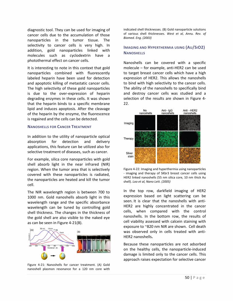
50 | P a g e
diagnostic tool. They can be used for imaging of cancer cells due to the accumulation of those nanoparticles in the tumor tissue. The selectivity to cancer cells is very high. In addition, gold nanoparticles linked with molecules such as cyclodextrin have a photothermal effect on cancer cells.
It is interesting to note in this context that gold nanoparticles combined with fluorescently labeled heparin have been used for detection and apoptotic killing of metastatic cancer cells. The high selectivity of these gold nanoparticles is due to the over-expression of heparin degrading enzymes in these cells. It was shown that the heparin binds to a specific membrane lipid and induces apoptosis. After the cleavage of the heparin by the enzyme, the fluorescence is regained and the cells can be detected.
NANOSHELLS FOR CANCER TREATMENT
In addition to the utility of nanoparticle optical absorption for detection and delivery applications, this feature can be utilized also for selective treatment of diseases, such as cancer.
For example, silica core nanoparticles with gold shell absorb light in the near infrared (NIR) region. When the tumor area that is selectively covered with these nanoparticles is radiated, the nanoparticles are heated and kill the tumor cell.
The NIR wavelength region is between 700 to 1000 nm. Gold nanoshells absorb light in this wavelength range and the specific absorbance wavelength can be tuned by controlling gold shell thickness. The changes in the thickness of the gold shell are also visible to the naked eye as can be seen in Figure 4-21(B).
Figure 4-21: Nanoshells for cancer treatment. (A) Gold nanoshell plasmon resonance for a 120 nm core with
indicated shell thicknesses. (B) Gold nanoparticle solutions of various shell thicknesses. West et al, Annu. Rev. of Biomed. Eng. (2003)
IMAGING AND HYPERTHERMIA USING (AU/SIO2)
NANOSHELLS
Nanoshells can be covered with a specific molecule – for example, anti-HER2 can be used to target breast cancer cells which have a high expression of HER2. This allows the nanoshells to bind with high selectivity to the cancer cells. The ability of the nanoshells to specifically bind and destroy cancer cells was studied and a selection of the results are shown in Figure 4-22.
Figure 4-22: Imaging and hyperthermia using nanoparticles - imaging and therapy of SKbr3 breast cancer cells using HER2 linked nanoshells (55 nm silica core, 10 nm thick Au shell). Loo et al, Nano Lett. (2005)
In the top row, darkfield imaging of HER2 expression based on light scattering can be seen. It is clear that the nanoshells with anti-HER2 are highly concentrated in the cancer cells, when compared with the control nanoshells. In the bottom row, the results of cell viability assessed with calcein staining with exposure to ~820 nm NIR are shown. Cell death was observed only in cells treated with anti-HER2 nanoshells.
Because these nanoparticles are not adsorbed on the healthy cells, the nanoparticle-induced damage is limited only to the cancer cells. This approach raises expectation for selective cancer
51 | P a g e
treatment in the future that will potentially be much more efficient and free from side effects.
An illustration of a nanoparticle-based approach that can be used for cancer treatment can be found in the following video:
https://www.youtube.com/watch?v=vg4b7WztpmQ
In conclusion, nanoparticles have great potential for clinical imaging and selective treatment. Yet the toxicity of the nanoparticles is still under investigation and many additional experiments and clinical trials should be performed before these methods are widely implemented.
Chapter 5 QUANTUM DOT
SENSORS
This chapter defines quantum dots and examines their unique properties. Synthesis methods are introduced and the imaging and sensing applications of quantum dots are explored, such as quantum dot-based temperature sensors, chemical sensors and biosensors.
DEFINITION AND MAIN PROPERTIES
Quantum dots (QDs) are small semiconducting particles with typical size ranging from 1 nm to 10 nm. These are artificial clusters of semiconductive atoms that have the ability to confine electron motion due to their small size. One of the most important properties of
quantum dots is the ability to tune their band gap and therefore to control their light absorbance and emission frequencies. This occurs because of energy level quantization. In this way it is possible for their optical and electrical properties to be adjusted as needed.
Quantum dots absorb photons of light and then re-emit longer wavelength photons for a period of time. The high controllability of quantum dot size provides very precise control over the wavelength of the re-emitted photon. Therefore the color of the light emitted from the quantum dot can be manipulated without significant cost or the use of high-end technology. Following this procedure, a full range of quantum dots can be manufactured, each with a narrow distinct emission spectrum.
In addition to confinement in all three dimensions (such as is observed in quantum dots), one can find other quantum confined semiconductors, including quantum wires, which confine electrons or holes in two spatial dimensions and allow free propagation in the third, and quantum wells, which confine electrons or holes in one dimension and allow free propagation in two dimensions.
QUANTUM SIZE EFFECT
To understand the mechanisms behind quantum dot electrical characteristics, we must first recall that electrons exist in discrete energy levels in bulk semiconductors. In these materials, there is a forbidden range of energy levels known as a band gap. The lower energy level below the band gap is called the valence band, and the energy level above the band gap is called the conduction band. By absorbing some sort of stimulus (in light or heat form), an electron can rise to the conduction band from the valence band. This action leaves behind a “hole” in the valence band. The hole and the electron together are called an exciton.
The average distance between an electron and a hole in an exciton is called the exciton Bohr radius. When the size of the semiconductor falls
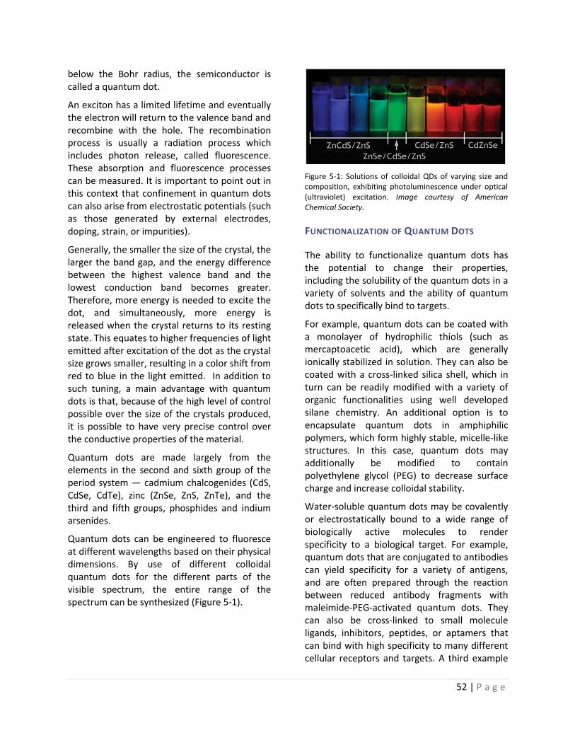
52 | P a g e
below the Bohr radius, the semiconductor is called a quantum dot.
An exciton has a limited lifetime and eventually the electron will return to the valence band and recombine with the hole. The recombination process is usually a radiation process which includes photon release, called fluorescence. These absorption and fluorescence processes can be measured. It is important to point out in this context that confinement in quantum dots can also arise from electrostatic potentials (such as those generated by external electrodes, doping, strain, or impurities).
Generally, the smaller the size of the crystal, the larger the band gap, and the energy difference between the highest valence band and the lowest conduction band becomes greater. Therefore, more energy is needed to excite the dot, and simultaneously, more energy is released when the crystal returns to its resting state. This equates to higher frequencies of light emitted after excitation of the dot as the crystal size grows smaller, resulting in a color shift from red to blue in the light emitted. In addition to such tuning, a main advantage with quantum dots is that, because of the high level of control possible over the size of the crystals produced, it is possible to have very precise control over the conductive properties of the material.
Quantum dots are made largely from the elements in the second and sixth group of the period system — cadmium chalcogenides (CdS, CdSe, CdTe), zinc (ZnSe, ZnS, ZnTe), and the third and fifth groups, phosphides and indium arsenides.
Quantum dots can be engineered to fluoresce at different wavelengths based on their physical dimensions. By use of different colloidal quantum dots for the different parts of the visible spectrum, the entire range of the spectrum can be synthesized (Figure 5-1).
Figure 5-1: Solutions of colloidal QDs of varying size and composition, exhibiting photoluminescence under optical (ultraviolet) excitation. Image courtesy of American Chemical Society.
FUNCTIONALIZATION OF QUANTUM DOTS
The ability to functionalize quantum dots has the potential to change their properties, including the solubility of the quantum dots in a variety of solvents and the ability of quantum dots to specifically bind to targets.
For example, quantum dots can be coated with a monolayer of hydrophilic thiols (such as mercaptoacetic acid), which are generally ionically stabilized in solution. They can also be coated with a cross-linked silica shell, which in turn can be readily modified with a variety of organic functionalities using well developed silane chemistry. An additional option is to encapsulate quantum dots in amphiphilic polymers, which form highly stable, micelle-like structures. In this case, quantum dots may additionally be modified to contain polyethylene glycol (PEG) to decrease surface charge and increase colloidal stability.
Water-soluble quantum dots may be covalently or electrostatically bound to a wide range of biologically active molecules to render specificity to a biological target. For example, quantum dots that are conjugated to antibodies can yield specificity for a variety of antigens, and are often prepared through the reaction between reduced antibody fragments with maleimide-PEG-activated quantum dots. They can also be cross-linked to small molecule ligands, inhibitors, peptides, or aptamers that can bind with high specificity to many different cellular receptors and targets. A third example
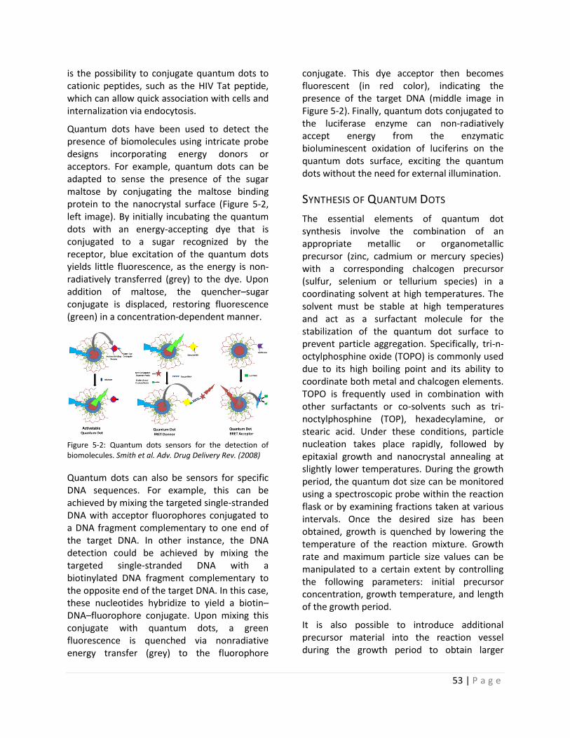
53 | P a g e
is the possibility to conjugate quantum dots to cationic peptides, such as the HIV Tat peptide, which can allow quick association with cells and internalization via endocytosis.
Quantum dots have been used to detect the presence of biomolecules using intricate probe designs incorporating energy donors or acceptors. For example, quantum dots can be adapted to sense the presence of the sugar maltose by conjugating the maltose binding protein to the nanocrystal surface (Figure 5-2, left image). By initially incubating the quantum dots with an energy-accepting dye that is conjugated to a sugar recognized by the receptor, blue excitation of the quantum dots yields little fluorescence, as the energy is non-radiatively transferred (grey) to the dye. Upon addition of maltose, the quencher–sugar conjugate is displaced, restoring fluorescence (green) in a concentration-dependent manner.
Figure 5-2: Quantum dots sensors for the detection of biomolecules. Smith et al. Adv. Drug Delivery Rev. (2008)
Quantum dots can also be sensors for specific DNA sequences. For example, this can be achieved by mixing the targeted single-stranded DNA with acceptor fluorophores conjugated to a DNA fragment complementary to one end of the target DNA. In other instance, the DNA detection could be achieved by mixing the targeted single-stranded DNA with a biotinylated DNA fragment complementary to the opposite end of the target DNA. In this case, these nucleotides hybridize to yield a biotin–DNA–fluorophore conjugate. Upon mixing this conjugate with quantum dots, a green fluorescence is quenched via nonradiative energy transfer (grey) to the fluorophore
conjugate. This dye acceptor then becomes fluorescent (in red color), indicating the presence of the target DNA (middle image in Figure 5-2). Finally, quantum dots conjugated to the luciferase enzyme can non-radiatively accept energy from the enzymatic bioluminescent oxidation of luciferins on the quantum dots surface, exciting the quantum dots without the need for external illumination.
SYNTHESIS OF QUANTUM DOTS
The essential elements of quantum dot synthesis involve the combination of an appropriate metallic or organometallic precursor (zinc, cadmium or mercury species) with a corresponding chalcogen precursor (sulfur, selenium or tellurium species) in a coordinating solvent at high temperatures. The solvent must be stable at high temperatures and act as a surfactant molecule for the stabilization of the quantum dot surface to prevent particle aggregation. Specifically, tri-n-octylphosphine oxide (TOPO) is commonly used due to its high boiling point and its ability to coordinate both metal and chalcogen elements. TOPO is frequently used in combination with other surfactants or co-solvents such as tri-noctylphosphine (TOP), hexadecylamine, or stearic acid. Under these conditions, particle nucleation takes place rapidly, followed by epitaxial growth and nanocrystal annealing at slightly lower temperatures. During the growth period, the quantum dot size can be monitored using a spectroscopic probe within the reaction flask or by examining fractions taken at various intervals. Once the desired size has been obtained, growth is quenched by lowering the temperature of the reaction mixture. Growth rate and maximum particle size values can be manipulated to a certain extent by controlling the following parameters: initial precursor concentration, growth temperature, and length of the growth period.
It is also possible to introduce additional precursor material into the reaction vessel during the growth period to obtain larger
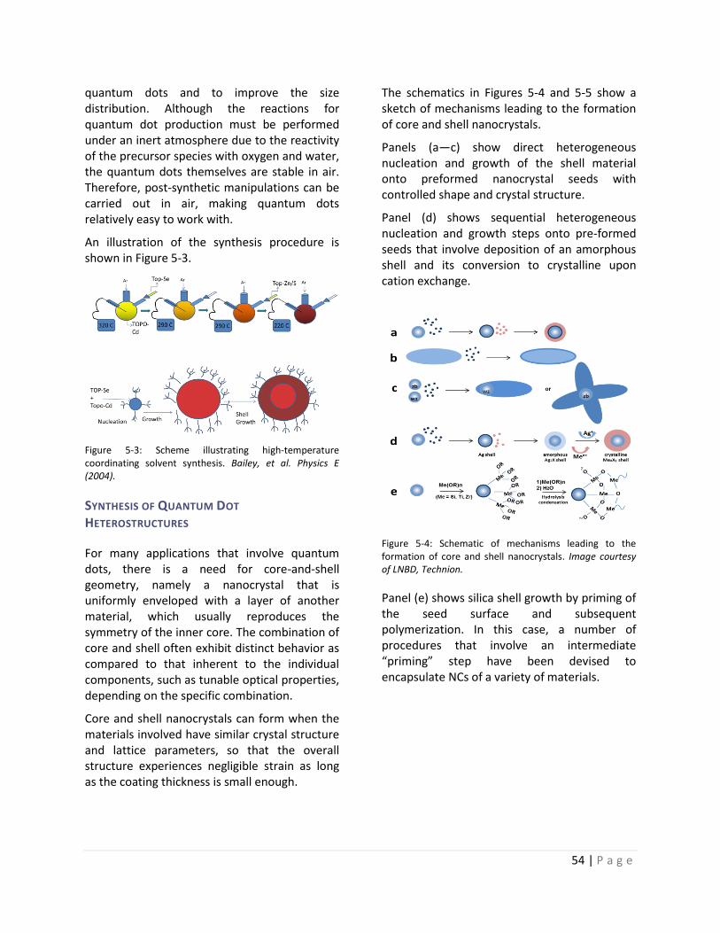
54 | P a g e
quantum dots and to improve the size distribution. Although the reactions for quantum dot production must be performed under an inert atmosphere due to the reactivity of the precursor species with oxygen and water, the quantum dots themselves are stable in air. Therefore, post-synthetic manipulations can be carried out in air, making quantum dots relatively easy to work with.
An illustration of the synthesis procedure is shown in Figure 5-3.
Figure 5-3: Scheme illustrating high-temperature coordinating solvent synthesis. Bailey, et al. Physics E (2004).
SYNTHESIS OF QUANTUM DOT
HETEROSTRUCTURES
For many applications that involve quantum dots, there is a need for core-and-shell geometry, namely a nanocrystal that is uniformly enveloped with a layer of another material, which usually reproduces the symmetry of the inner core. The combination of core and shell often exhibit distinct behavior as compared to that inherent to the individual components, such as tunable optical properties, depending on the specific combination.
Core and shell nanocrystals can form when the materials involved have similar crystal structure and lattice parameters, so that the overall structure experiences negligible strain as long as the coating thickness is small enough.
The schematics in Figures 5-4 and 5-5 show a sketch of mechanisms leading to the formation of core and shell nanocrystals.
Panels (a—c) show direct heterogeneous nucleation and growth of the shell material onto preformed nanocrystal seeds with controlled shape and crystal structure.
Panel (d) shows sequential heterogeneous nucleation and growth steps onto pre-formed seeds that involve deposition of an amorphous shell and its conversion to crystalline upon cation exchange.
Figure 5-4: Schematic of mechanisms leading to the formation of core and shell nanocrystals. Image courtesy of LNBD, Technion.
Panel (e) shows silica shell growth by priming of the seed surface and subsequent polymerization. In this case, a number of procedures that involve an intermediate “priming” step have been devised to encapsulate NCs of a variety of materials.
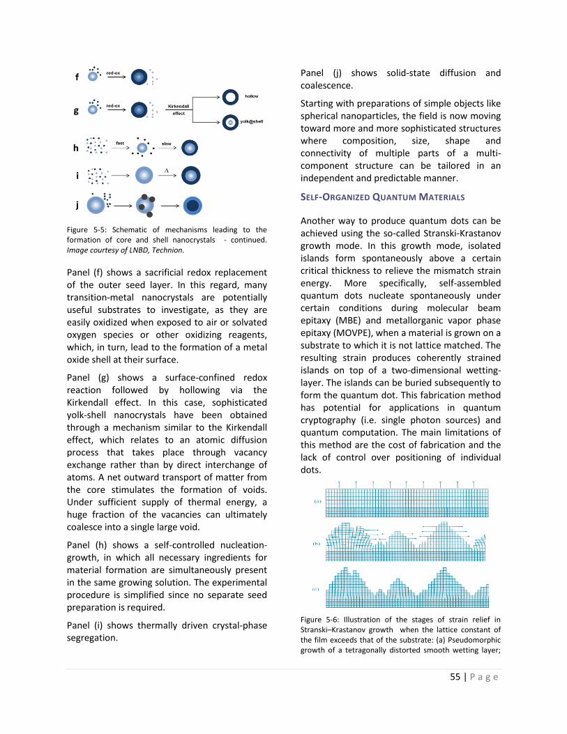
55 | P a g e
Figure 5-5: Schematic of mechanisms leading to the formation of core and shell nanocrystals - continued. Image courtesy of LNBD, Technion.
Panel (f) shows a sacrificial redox replacement of the outer seed layer. In this regard, many transition-metal nanocrystals are potentially useful substrates to investigate, as they are easily oxidized when exposed to air or solvated oxygen species or other oxidizing reagents, which, in turn, lead to the formation of a metal oxide shell at their surface.
Panel (g) shows a surface-confined redox reaction followed by hollowing via the Kirkendall effect. In this case, sophisticated yolk-shell nanocrystals have been obtained through a mechanism similar to the Kirkendall effect, which relates to an atomic diffusion process that takes place through vacancy exchange rather than by direct interchange of atoms. A net outward transport of matter from the core stimulates the formation of voids. Under sufficient supply of thermal energy, a huge fraction of the vacancies can ultimately coalesce into a single large void.
Panel (h) shows a self-controlled nucleation-growth, in which all necessary ingredients for material formation are simultaneously present in the same growing solution. The experimental procedure is simplified since no separate seed preparation is required.
Panel (i) shows thermally driven crystal-phase segregation.
Panel (j) shows solid-state diffusion and coalescence.
Starting with preparations of simple objects like spherical nanoparticles, the field is now moving toward more and more sophisticated structures where composition, size, shape and connectivity of multiple parts of a multi-component structure can be tailored in an independent and predictable manner.
SELF-ORGANIZED QUANTUM MATERIALS
Another way to produce quantum dots can be achieved using the so-called Stranski-Krastanov growth mode. In this growth mode, isolated islands form spontaneously above a certain critical thickness to relieve the mismatch strain energy. More specifically, self-assembled quantum dots nucleate spontaneously under certain conditions during molecular beam epitaxy (MBE) and metallorganic vapor phase epitaxy (MOVPE), when a material is grown on a substrate to which it is not lattice matched. The resulting strain produces coherently strained islands on top of a two-dimensional wetting-layer. The islands can be buried subsequently to form the quantum dot. This fabrication method has potential for applications in quantum cryptography (i.e. single photon sources) and quantum computation. The main limitations of this method are the cost of fabrication and the lack of control over positioning of individual dots.
Figure 5-6: Illustration of the stages of strain relief in Stranski–Krastanov growth when the lattice constant of the film exceeds that of the substrate: (a) Pseudomorphic growth of a tetragonally distorted smooth wetting layer;
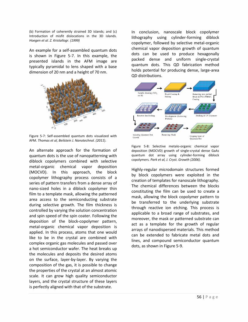
56 | P a g e
(b) Formation of coherently strained 3D islands; and (c) Introduction of misfit dislocations in the 3D islands. Hoegen et al. Z. Kristallogr. (1999)
An example for a self-assembled quantum dots is shown in Figure 5-7. In this example, the presented islands in the AFM image are typically pyramidal to lens shaped with a base dimension of 20 nm and a height of 70 nm.
Figure 5-7: Self-assembled quantum dots visualized with AFM. Thomas et al, Beilstein J. Nanotechnol. (2011).
An alternate approach for the formation of quantum dots is the use of nanopatterning with diblock copolymers combined with selective metal-organic chemical vapor deposition (MOCVD). In this approach, the block copolymer lithography process consists of a series of pattern transfers from a dense array of nano-sized holes in a diblock copolymer thin film to a template mask, allowing the patterned area access to the semiconducting substrate during selective growth. The film thickness is controlled by varying the solution concentration and spin speed of the spin coater. Following the deposition of the block-copolymer pattern, metal-organic chemical vapor deposition is applied. In this process, atoms that one would like to be in the crystal are combined with complex organic gas molecules and passed over a hot semiconductor wafer. The heat breaks up the molecules and deposits the desired atoms on the surface, layer-by-layer. By varying the composition of the gas, it is possible to change the properties of the crystal at an almost atomic scale. It can grow high quality semiconductor layers, and the crystal structure of these layers is perfectly aligned with that of the substrate.
In conclusion, nanoscale block copolymer lithography using cylinder-forming diblock copolymer, followed by selective metal-organic chemical vapor deposition growth of quantum dots can be used to produce hexagonally packed dense and uniform single-crystal quantum dots. This QD fabrication method holds potential for producing dense, large-area QD distributions.
Figure 5-8: Selective metalo-organic chemical vapor deposition (MOCVD) growth of single-crystal dense GaAs quantum dot array using cylinder-forming diblock copolymers. Park et al, J. Cryst. Growth (2006).
Highly-regular microdomain structures formed by block copolymers were exploited in the creation of templates for nanoscale lithography. The chemical differences between the blocks constituting the film can be used to create a mask, allowing the block copolymer pattern to be transferred to the underlying substrate through reactive ion etching. This process is applicable to a broad range of substrates, and moreover, the mask or patterned substrate can act as a template for the growth of regular arrays of nanodispersed materials. This method can be extended to fabricate metal dots and lines, and compound semiconductor quantum dots, as shown in Figure 5-9.
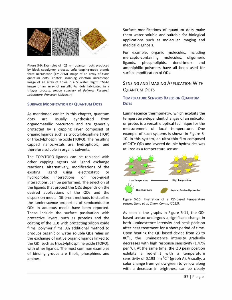
57 | P a g e
Figure 5-9: Examples of ~25 nm quantum dots produced by block copolymer process. Left: tapping-mode atomic force microscope (TM-AFM) image of an array of GaAs quantum dots. Center: scanning electron microscope image of an array of holes in a Si wafer. Right: TM-AF image of an array of metallic Au dots fabricated in a trilayer process. Image courtesy of Polymer Research Laboratory, Princeton University
SURFACE MODIFICATION OF QUANTUM DOTS
As mentioned earlier in this chapter, quantum dots are usually synthesized from organometallic precursors and are generally protected by a capping layer composed of organic ligands such as trioctylphosphine (TOP) or trioctylphosphine oxide (TOPO). The resulting capped nanocrystals are hydrophobic, and therefore soluble in organic solvents.
The TOP/TOPO ligands can be replaced with other capping agents via ligand exchange reactions. Alternatively, modifications of the existing ligand using electrostatic or hydrophobic interactions, or host–guest interactions, can be performed. The selection of the ligands that protect the QDs depends on the desired applications of the QDs and the dispersion media. Different methods to stabilize the luminescence properties of semiconductor QDs in aqueous media have been reported. These include the surface passivation with protective layers, such as proteins and the coating of the QDs with protecting silicon oxide films, polymer films. An additional method to produce organic or water soluble QDs relies on the exchange of native organic ligands linked to the QD, such as trioctylphosphine oxide (TOPO), with other ligands. The most common examples of binding groups are thiols, phosphines and amines.
Surface modifications of quantum dots make them water soluble and suitable for biological applications such as molecular imaging and medical diagnosis.
For example, organic molecules, including mercapto-containing molecules, oligomeric ligands, phospholipids, dendrimers and amphiphilic polymers have all been used for surface modification of QDs.
SENSING AND IMAGING APPLICATION WITH
QUANTUM DOTS
TEMPERATURE SENSORS BASED ON QUANTUM
DOTS
Luminescence thermometry, which exploits the temperature-dependent changes of an indicator or probe, is a versatile optical technique for the measurement of local temperature. One example of such systems is shown in Figure 5-10. In this system, an ultra-thin film composed of CdTe QDs and layered double hydroxides was utilized as a temperature sensor.
Figure 5-10: Illustration of a QD-based temperature sensor. Liang et al, Chem. Comm. (2012).
As seen in the graphs in Figure 5-11, the QD-based sensor undergoes a significant change in both luminescence intensity and peak position after heat treatment for a short period of time. Upon heating the QD based device from 23 to 800C, the luminescence intensity gradually decreases with high response sensitivity (1.47% per 0C). At the same time, the QD peak position exhibits a red-shift with a temperature sensitivity of 0.193 nm 0C-1 (graph A). Visually, a color change from yellow-green to yellow along with a decrease in brightness can be clearly
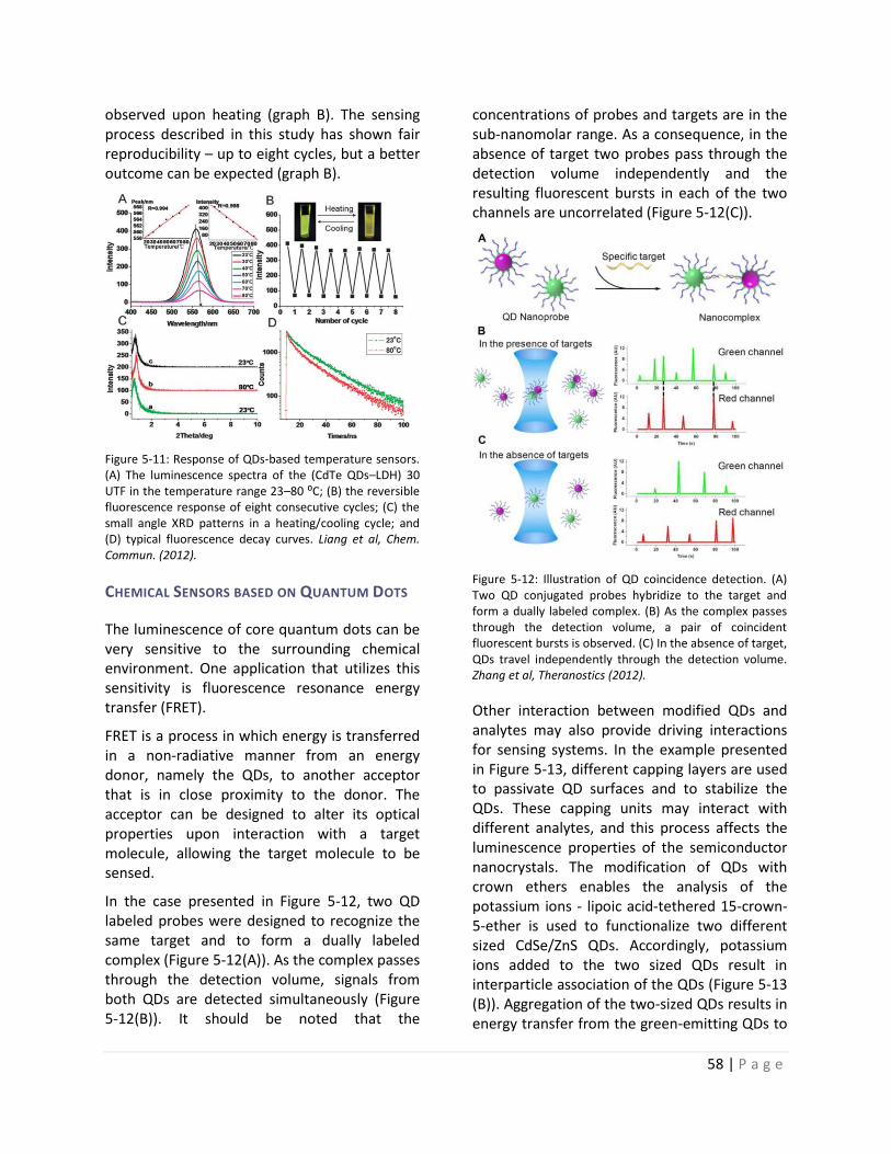
58 | P a g e
observed upon heating (graph B). The sensing process described in this study has shown fair reproducibility – up to eight cycles, but a better outcome can be expected (graph B).
Figure 5-11: Response of QDs-based temperature sensors. (A) The luminescence spectra of the (CdTe QDs–LDH) 30 UTF in the temperature range 23–80 ⁰C; (B) the reversible fluorescence response of eight consecutive cycles; (C) the small angle XRD patterns in a heating/cooling cycle; and (D) typical fluorescence decay curves. Liang et al, Chem. Commun. (2012).
CHEMICAL SENSORS BASED ON QUANTUM DOTS
The luminescence of core quantum dots can be very sensitive to the surrounding chemical environment. One application that utilizes this sensitivity is fluorescence resonance energy transfer (FRET).
FRET is a process in which energy is transferred in a non-radiative manner from an energy donor, namely the QDs, to another acceptor that is in close proximity to the donor. The acceptor can be designed to alter its optical properties upon interaction with a target molecule, allowing the target molecule to be sensed.
In the case presented in Figure 5-12, two QD labeled probes were designed to recognize the same target and to form a dually labeled complex (Figure 5-12(A)). As the complex passes through the detection volume, signals from both QDs are detected simultaneously (Figure 5-12(B)). It should be noted that the
concentrations of probes and targets are in the sub-nanomolar range. As a consequence, in the absence of target two probes pass through the detection volume independently and the resulting fluorescent bursts in each of the two channels are uncorrelated (Figure 5-12(C)).
Figure 5-12: Illustration of QD coincidence detection. (A) Two QD conjugated probes hybridize to the target and form a dually labeled complex. (B) As the complex passes through the detection volume, a pair of coincident fluorescent bursts is observed. (C) In the absence of target, QDs travel independently through the detection volume. Zhang et al, Theranostics (2012).
Other interaction between modified QDs and analytes may also provide driving interactions for sensing systems. In the example presented in Figure 5-13, different capping layers are used to passivate QD surfaces and to stabilize the QDs. These capping units may interact with different analytes, and this process affects the luminescence properties of the semiconductor nanocrystals. The modification of QDs with crown ethers enables the analysis of the potassium ions - lipoic acid-tethered 15-crown-5-ether is used to functionalize two different sized CdSe/ZnS QDs. Accordingly, potassium ions added to the two sized QDs result in interparticle association of the QDs (Figure 5-13 (B)). Aggregation of the two-sized QDs results in energy transfer from the green-emitting QDs to
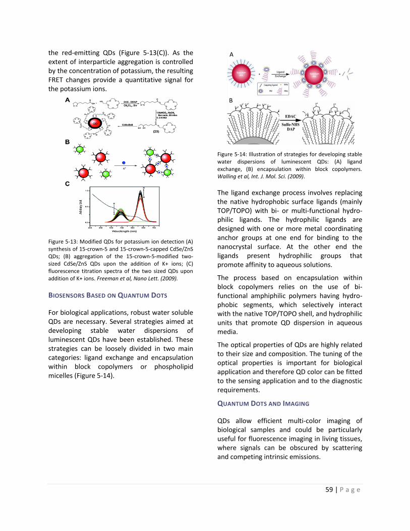
59 | P a g e
the red-emitting QDs (Figure 5-13(C)). As the extent of interparticle aggregation is controlled by the concentration of potassium, the resulting FRET changes provide a quantitative signal for the potassium ions.
Figure 5-13: Modified QDs for potassium ion detection (A) synthesis of 15-crown-5 and 15-crown-5-capped CdSe/ZnS QDs; (B) aggregation of the 15-crown-5-modified two-sized CdSe/ZnS QDs upon the addition of K+ ions; (C) fluorescence titration spectra of the two sized QDs upon addition of K+ ions. Freeman et al, Nano Lett. (2009).
BIOSENSORS BASED ON QUANTUM DOTS
For biological applications, robust water soluble QDs are necessary. Several strategies aimed at developing stable water dispersions of luminescent QDs have been established. These strategies can be loosely divided in two main categories: ligand exchange and encapsulation within block copolymers or phospholipid micelles (Figure 5-14).
Figure 5-14: Illustration of strategies for developing stable water dispersions of luminescent QDs: (A) ligand exchange, (B) encapsulation within block copolymers. Walling et al, Int. J. Mol. Sci. (2009).
The ligand exchange process involves replacing the native hydrophobic surface ligands (mainly TOP/TOPO) with bi- or multi-functional hydro-philic ligands. The hydrophilic ligands are designed with one or more metal coordinating anchor groups at one end for binding to the nanocrystal surface. At the other end the ligands present hydrophilic groups that promote affinity to aqueous solutions.
The process based on encapsulation within block copolymers relies on the use of bi-functional amphiphilic polymers having hydro-phobic segments, which selectively interact with the native TOP/TOPO shell, and hydrophilic units that promote QD dispersion in aqueous media.
The optical properties of QDs are highly related to their size and composition. The tuning of the optical properties is important for biological application and therefore QD color can be fitted to the sensing application and to the diagnostic requirements.
QUANTUM DOTS AND IMAGING
QDs allow efficient multi-color imaging of biological samples and could be particularly useful for fluorescence imaging in living tissues, where signals can be obscured by scattering and competing intrinsic emissions.
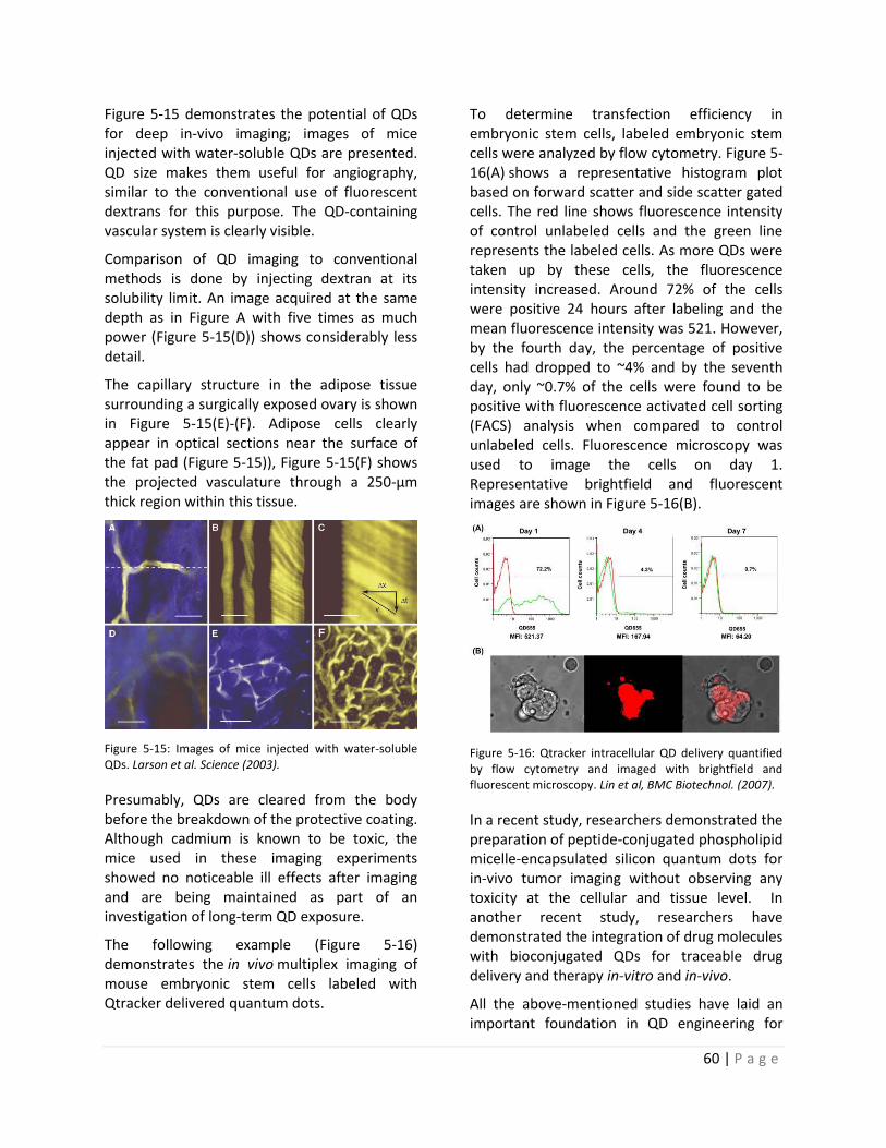
60 | P a g e
Figure 5-15 demonstrates the potential of QDs for deep in-vivo imaging; images of mice injected with water-soluble QDs are presented. QD size makes them useful for angiography, similar to the conventional use of fluorescent dextrans for this purpose. The QD-containing vascular system is clearly visible.
Comparison of QD imaging to conventional methods is done by injecting dextran at its solubility limit. An image acquired at the same depth as in Figure A with five times as much power (Figure 5-15(D)) shows considerably less detail.
The capillary structure in the adipose tissue surrounding a surgically exposed ovary is shown in Figure 5-15(E)-(F). Adipose cells clearly appear in optical sections near the surface of the fat pad (Figure 5-15)), Figure 5-15(F) shows the projected vasculature through a 250-μm thick region within this tissue.
Figure 5-15: Images of mice injected with water-soluble QDs. Larson et al. Science (2003).
Presumably, QDs are cleared from the body before the breakdown of the protective coating. Although cadmium is known to be toxic, the mice used in these imaging experiments showed no noticeable ill effects after imaging and are being maintained as part of an investigation of long-term QD exposure.
The following example (Figure 5-16) demonstrates the in vivo multiplex imaging of mouse embryonic stem cells labeled with Qtracker delivered quantum dots.
To determine transfection efficiency in embryonic stem cells, labeled embryonic stem cells were analyzed by flow cytometry. Figure 5-16(A) shows a representative histogram plot based on forward scatter and side scatter gated cells. The red line shows fluorescence intensity of control unlabeled cells and the green line represents the labeled cells. As more QDs were taken up by these cells, the fluorescence intensity increased. Around 72% of the cells were positive 24 hours after labeling and the mean fluorescence intensity was 521. However, by the fourth day, the percentage of positive cells had dropped to ~4% and by the seventh day, only ~0.7% of the cells were found to be positive with fluorescence activated cell sorting (FACS) analysis when compared to control unlabeled cells. Fluorescence microscopy was used to image the cells on day 1. Representative brightfield and fluorescent images are shown in Figure 5-16(B).
Figure 5-16: Qtracker intracellular QD delivery quantified by flow cytometry and imaged with brightfield and fluorescent microscopy. Lin et al, BMC Biotechnol. (2007).
In a recent study, researchers demonstrated the preparation of peptide-conjugated phospholipid micelle-encapsulated silicon quantum dots for in-vivo tumor imaging without observing any toxicity at the cellular and tissue level. In another recent study, researchers have demonstrated the integration of drug molecules with bioconjugated QDs for traceable drug delivery and therapy in-vitro and in-vivo.
All the above-mentioned studies have laid an important foundation in QD engineering for
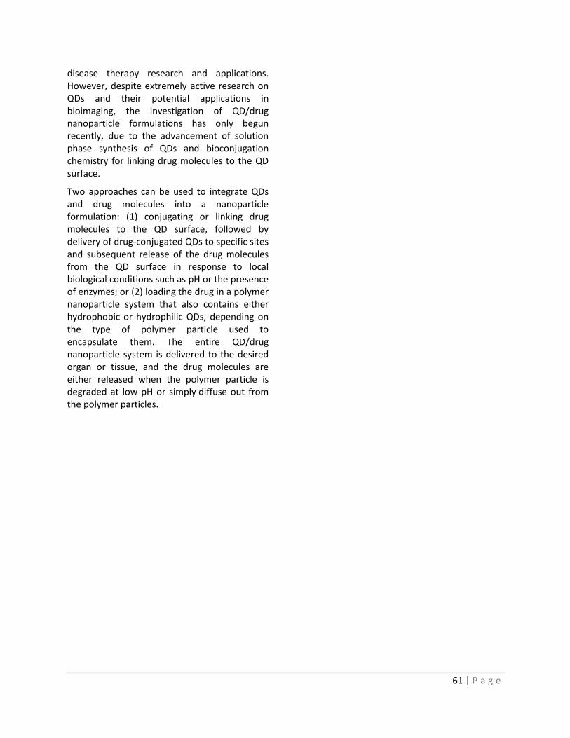
61 | P a g e
disease therapy research and applications. However, despite extremely active research on QDs and their potential applications in bioimaging, the investigation of QD/drug nanoparticle formulations has only begun recently, due to the advancement of solution phase synthesis of QDs and bioconjugation chemistry for linking drug molecules to the QD surface.
Two approaches can be used to integrate QDs and drug molecules into a nanoparticle formulation: (1) conjugating or linking drug molecules to the QD surface, followed by delivery of drug-conjugated QDs to specific sites and subsequent release of the drug molecules from the QD surface in response to local biological conditions such as pH or the presence of enzymes; or (2) loading the drug in a polymer nanoparticle system that also contains either hydrophobic or hydrophilic QDs, depending on the type of polymer particle used to encapsulate them. The entire QD/drug nanoparticle system is delivered to the desired organ or tissue, and the drug molecules are either released when the polymer particle is degraded at low pH or simply diffuse out from the polymer particles.
62 | P a g e
Chapter 6 NANOWIRE-BASED
SENSORS
Another type of sensors is presented in this chapter: nanowire- based sensors. This chapter begins with relevant definitions, and then presents nanowire properties and fabrication methods. The second part of this chapter deals with the sensing applications in liquid and in-vivo environments, and gas sensing using semiconducting nanowires
WHAT IS A NANOWIRE?
A nanowire (NW) is defined as any solid material in the form of wire with diameter of 1 to 100 nm. An important property of the nanowire is the aspect ratio, which is the length divided by the diameter. Typical nanowires exhibit aspect ratios of 1000 or more, meaning that the length of the nanowire is 1000 time larger than the diameter. At these dimensions, quantum mechanical effects are important.
Many different types of nanowires exist, including metallic nanowires (e.g., Ni, Pt, Au), semiconducting nanowires (e.g., Si, InP, GaN, etc.), and insulating nanowires (e.g., SiO2, TiO2). Molecular nanowires are composed of either organic or inorganic repeating molecular units. New forms of nanowires include core-shell superlattice nanowires.
Compared to other low dimensional systems, nanowires have two quantum confined
directions, while still leaving one unconfined direction for electrical conduction. This allows nanowires to be used in applications where electrical conduction, rather than tunneling transport, is required. Due to their unique density of electronic states, nanowires are expected to exhibit significantly different optical, electrical and magnetic properties than their bulk counterparts.
PROPERTIES OF NANOWIRES
Nanowires are promising materials for many novel applications due to their unique electrical, optical, thermal, and mechanical properties. The large nanowire surface-to-volume ratio allows the creation of extremely sensitive charge/field sensors in chemical and biological systems for the detection of charged particles and molecules at low concentration (Figure 6-1, upper left image). Nanowires also possess interesting optical properties when they are fabricated from semiconducting materials, absorbing and emitting light efficiently over a very broad energy range from the UV to visible to IR wavelengths. They are the basis for commercial products such as visible LEDs and blue laser diodes. Recently, 1D nanostructures based on III-nitride semiconductors, including nanowires and nanorods, have attracted attention as potential nanoscale building blocks for enhanced performance or functionality for optoelectronics, sensing, photovoltaics, and electronic applications (Figure 6-1, upper right image).
In few instances, nanowires possess thermoelectric power (called the Seebeck coefficient) - a measure of the magnitude of an induced thermoelectric voltage in response to a temperature difference across that material. A representative example of this property is the hierarchical nanowire structure that is made of Indium telluride (Figure 6-1, bottom left image). This nanowire exhibits a remarkable increase in the Seebeck coefficient of approximately 43% above that of the reported corresponding thin film at room temperature.
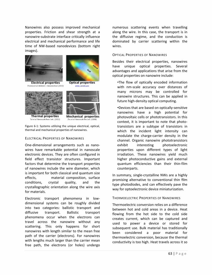
63 | P a g e
Nanowires also possess improved mechanical properties. Friction and shear strength at a nanowire-substrate interface critically influence electrical and mechanical performance and life time of NW-based nanodevices (bottom right images).
Figure 6-1: Systems utilizing the unique electrical, optical, thermal and mechanical properties of nanowires.
ELECTRICAL PROPERTIES OF NANOWIRES
One-dimensional arrangements such as nano-wires have remarkable potential in nanoscale electronic devices. They are often configured in field effect transistor structures. Important factors that determine the transport properties of nanowires include the wire diameter, which is important for both classical and quantum size effects, material composition, surface conditions, crystal quality, and the crystallographic orientation along the wire axis for materials.
Electronic transport phenomena in low-dimensional systems can be roughly divided into two categories: ballistic transport and diffusive transport. Ballistic transport phenomena occur when the electrons can travel across the nanowire without any scattering. This only happens for short nanowires with length similar to the mean free path of the carrier (electrons). For nanowires with lengths much larger than the carrier mean free path, the electrons (or holes) undergo
numerous scattering events when travelling along the wire. In this case, the transport is in the diffusive regime, and the conduction is dominated by carrier scattering within the wires.
OPTICAL PROPERTIES OF NANOWIRES
Besides their electrical properties, nanowires have unique optical properties. Several advantages and applications that arise from the optical properties on nanowire include:
•The flow of optically encoded information with nm-scale accuracy over distances of many microns may be controlled for nanowire structures. This can be applied in future high-density optical computing.
•Devices that are based on optically-sensitive nanowires have a high potential for photovoltaic cells or phototransistors. In this context, it is important to note that photo-transistors are a subtype of transistors in which the incident light intensity can modulate the charge-carrier density in the channel. Organic nanowire phototransistors exhibit interesting photoelectronic properties upon different types of light irradiation. These nanowires yield much higher photoconductive gains and external quantum efficiencies than their thin-film counterparts.
In summary, single-crystalline NWs are a highly promising alternative to conventional thin film type photodiodes, and can effectively pave the way for optoelectronic device miniaturization.
THERMOELECTRIC PROPERTIES OF NANOWIRES
Thermoelectric conversion relies on a difference between hot and cold areas in a device. Heat flowing from the hot side to the cold side creates current, which can be captured and used to power a device or stored for subsequent use. Bulk material has traditionally been considered a poor material for thermoelectric conversion, because the thermal conductivity is too high. Heat travels across it so
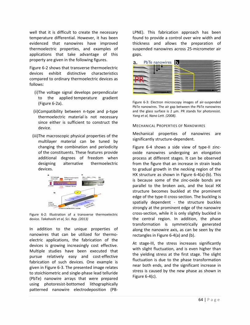
64 | P a g e
well that it is difficult to create the necessary temperature differential. However, it has been evidenced that nanowires have improved thermoelectric properties, and examples of applications that take advantage of this property are given in the following figures.
Figure 6-2 shows that transverse thermoelectric devices exhibit distinctive characteristics compared to ordinary thermoelectric devices as follows:
(i)The voltage signal develops perpendicular to the applied temperature gradient (Figure 6-2a).
(ii)Compatibility between n-type and p-type thermoelectric material is not necessary since either is sufficient to construct the device.
(iii)The macroscopic physical properties of the multilayer material can be tuned by changing the combination and periodicity of the constituents. These features provide additional degrees of freedom when designing alternative thermoelectric devices.
Figure 6-2: Illustration of a transverse thermoelectric device. Takahashi et al, Sci. Rep. (2013)
In addition to the unique properties of nanowires that can be utilized for thermo-electric applications, the fabrication of the devices is growing increasingly cost effective. Multiple studies have been executed that pursue relatively easy and cost-effective fabrication of such devices. One example is given in Figure 6-3. The presented image relates to stoichiometric and single-phase lead telluride (PbTe) nanowire arrays that were prepared using photoresist-bottomed lithographically patterned nanowire electrodeposition (PB-
LPNE). This fabrication approach has been found to provide a control over wire width and thickness and allows the preparation of suspended nanowires across 25-micrometer air gaps.
Figure 6-3: Electron microscopy images of air-suspended PbTe nanowires. The air gap between the PbTe nanowires and the glass surface is 2 µm. PR stands for photoresist. Yang et al, Nano Lett. (2008).
MECHANICAL PROPERTIES OF NANOWIRES
Mechanical properties of nanowires are significantly structure-dependent.
Figure 6-4 shows a side view of type-II zinc-oxide nanowires undergoing an elongation process at different stages. It can be observed from the figure that an increase in strain leads to gradual growth in the necking region of the HX structure as shown in Figure 6-4(a)-(b). This is because some of the zinc-oxide bonds are parallel to the broken axis, and the local HX structure becomes buckled at the prominent edge of the type-II cross-section. The buckling is spatially dependent - the structure buckles strongly at the prominent edge of the nanowire cross-section, while it is only slightly buckled in the central region. In addition, the phase transformation is symmetrically generated along the nanowire axis, as can be seen by the rectangles in Figure 6-4(a) and (b).
At stage-III, the stress increases significantly with slight fluctuation, and is even higher than the yielding stress at the first stage. The slight fluctuation is due to the phase transformation near both ends, and the significant increase in stress is caused by the new phase as shown in Figure 6-4(c).
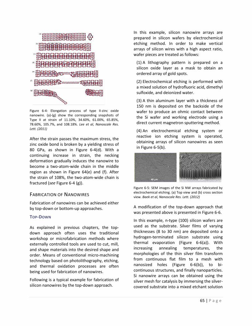
65 | P a g e
Figure 6-4: Elongation process of type II-zinc oxide nanowire. (a)-(g) show the corresponding snapshots of Type II at strain of 11.10%, 34.60%, 61.00%, 65.85%, 78.60%, 105.7%, and 108.18%. Lee et al, Nanoscale Res. Lett. (2011)
After the strain passes the maximum stress, the zinc oxide bond is broken by a yielding stress of 80 GPa, as shown in Figure 6-4(d). With a continuing increase in strain, the necking deformation gradually induces the nanowire to become a two-atom-wide chain in the middle region as shown in Figure 64(e) and (f). After the strain of 108%, the two-atom-wide chain is fractured (see Figure 6-4 (g)).
FABRICATION OF NANOWIRES
Fabrication of nanowires can be achieved either by top-down or bottom-up approaches.
TOP-DOWN
As explained in previous chapters, the top-down approach often uses the traditional workshop or microfabrication methods where externally controlled tools are used to cut, mill, and shape materials into the desired shape and order. Means of conventional micro-machining technology based on photolithography, etching, and thermal oxidation processes are often being used for fabrication of nanowires.
Following is a typical example for fabrication of silicon nanowires by the top-down approach.
In this example, silicon nanowire arrays are prepared in silicon wafers by electrochemical etching method. In order to make vertical arrays of silicon wires with a high aspect ratio, wafer pieces are treated as follows:
(1) A lithography pattern is prepared on a silicon oxide layer as a mask to obtain an ordered array of gold spots.
(2) Electrochemical etching is performed with a mixed solution of hydrofluoric acid, dimethyl sulfoxide, and deionized water.
(3) A thin aluminum layer with a thickness of 150 nm is deposited on the backside of the wafer to produce an ohmic contact between the Si wafer and working electrode using a direct current magnetron sputtering method.
(4) An electrochemical etching system or reactive ion etching system is operated, obtaining arrays of silicon nanowires as seen in Figure 6-5(b).
Figure 6-5: SEM images of the Si NW arrays fabricated by electrochemical etching. (a) Top view and (b) cross section view. Baek et al, Nanoscale Res. Lett. (2012)
A modification of the top-down approach that was presented above is presented in Figure 6-6.
In this example, n-type (100) silicon wafers are used as the substrate. Silver films of varying thicknesses (8 to 30 nm) are deposited onto a hydrogen-terminated silicon substrate using thermal evaporation (Figure 6-6(a)). With increasing annealing temperatures, the morphologies of the thin silver film transform from continuous flat film to a mesh with nanosized holes (Figure 6-6(b)), to bi-continuous structures, and finally nanoparticles. Si nanowire arrays can be obtained using the silver mesh for catalysis by immersing the silver-covered substrate into a mixed etchant solution
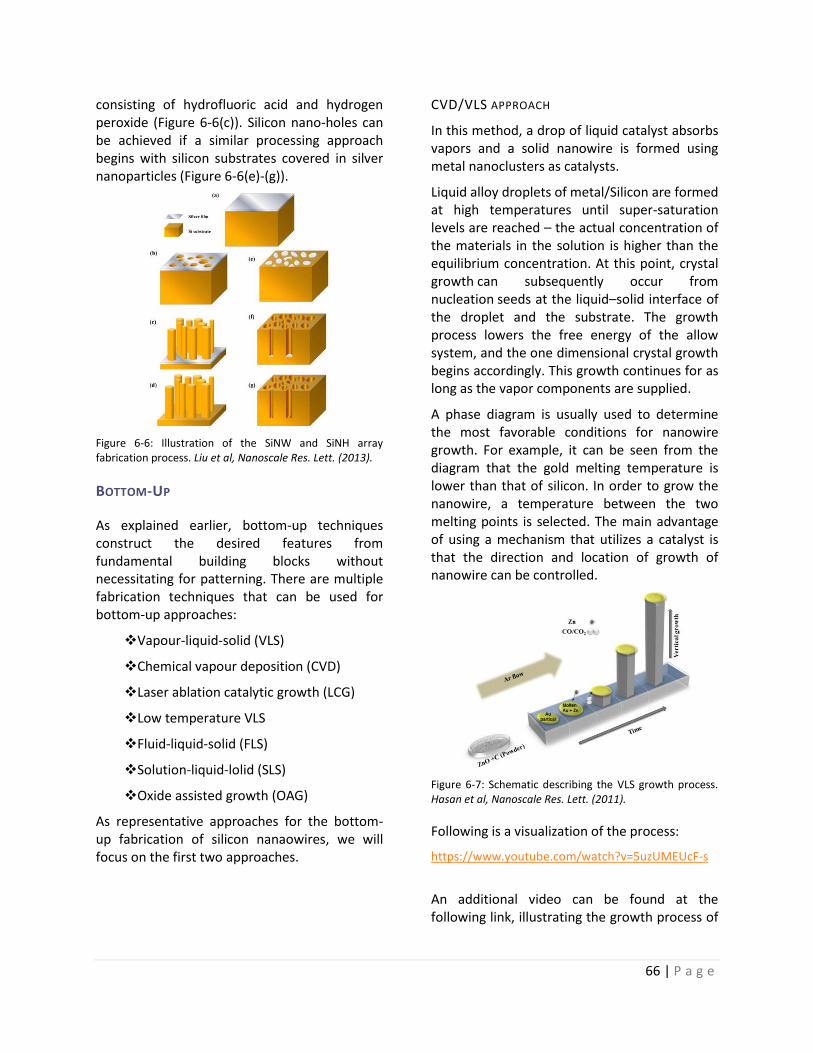
66 | P a g e
consisting of hydrofluoric acid and hydrogen peroxide (Figure 6-6(c)). Silicon nano-holes can be achieved if a similar processing approach begins with silicon substrates covered in silver nanoparticles (Figure 6-6(e)-(g)).
Figure 6-6: Illustration of the SiNW and SiNH array fabrication process. Liu et al, Nanoscale Res. Lett. (2013).
BOTTOM-UP
As explained earlier, bottom-up techniques construct the desired features from fundamental building blocks without necessitating for patterning. There are multiple fabrication techniques that can be used for bottom-up approaches:
Vapour-liquid-solid (VLS)
Chemical vapour deposition (CVD)
Laser ablation catalytic growth (LCG)
Low temperature VLS
Fluid-liquid-solid (FLS)
Solution-liquid-lolid (SLS)
Oxide assisted growth (OAG)
As representative approaches for the bottom-up fabrication of silicon nanaowires, we will focus on the first two approaches.
CVD/VLS APPROACH
In this method, a drop of liquid catalyst absorbs vapors and a solid nanowire is formed using metal nanoclusters as catalysts.
Liquid alloy droplets of metal/Silicon are formed at high temperatures until super-saturation levels are reached – the actual concentration of the materials in the solution is higher than the equilibrium concentration. At this point, crystal growth can subsequently occur from nucleation seeds at the liquid–solid interface of the droplet and the substrate. The growth process lowers the free energy of the allow system, and the one dimensional crystal growth begins accordingly. This growth continues for as long as the vapor components are supplied.
A phase diagram is usually used to determine the most favorable conditions for nanowire growth. For example, it can be seen from the diagram that the gold melting temperature is lower than that of silicon. In order to grow the nanowire, a temperature between the two melting points is selected. The main advantage of using a mechanism that utilizes a catalyst is that the direction and location of growth of nanowire can be controlled.
Figure 6-7: Schematic describing the VLS growth process. Hasan et al, Nanoscale Res. Lett. (2011).
Following is a visualization of the process:
https://www.youtube.com/watch?v=5uzUMEUcF-s
An additional video can be found at the following link, illustrating the growth process of
67 | P a g e
Si nanowires from gold nanoparticles filmed inside an electron micro-scope.
https://www.youtube.com/watch?v=0YFxg8tqT9k
FABRICATION OF NANOWIRE DEVICES BY E-BEAM
LITHOGRAPHY
In many cases, the synthesized silicon nanowires have to be translated to allow integration with solid-state devices.
One of the main approaches for fabricating nanowire-based devices relies on e-beam lithography. As explained in the previous chapters, electron beam lithography is a specialized technique for creating extremely fine patterns. A beam of electrons scans across a surface covered in a resist film that is sensitive to electron radiation. Energy from the electron beam is deposited in the desired pattern on the resist film. The removal of the undesired resist is similar to the process used in standard photo-lithography procedures. For example, in positive lithography only the chemically altered e-resist can be dissolved in a specific solvent.
In direct-write e-beam lithography, an optical lithographic processing step is used to define e-beam alignment marks. The nanowires are then transferred from their growth substrate by suspending them in a solvent such as isopropanol. This suspension can be achieved with short sonication of the growth substrate in a solvent. The suspension is then applied to the wafer and the nanowires adhere to the oxide surface in a random dispersion across the wafer.
After the deposition of the nanowires, scanning electron microscopy images are obtained to locate the nanowires before resist spinning. Patterns are then created with e-beam litho-graphy, defining electrodes for each nanowire device.
The resist is exposed using typical electron lithography, and a mixture of chemicals is used for development. The metal is then evaporated and lift-off is achieved using a hot solvent, such as acetone at 60 °C. At the end of this process, a
nanowire that is contacted with adjacent electrodes is achieved as seen in Figure 6-8.
Figure 6-8: Illustration of nanowire fabrication of via e-beam lithography. Image courtesy of LNBD, Technion.
The main advantages of the e-beam fabrication approach of nanowires are the very high resolution that can be obtained with the e-beam, and the flexibility of the technique that allows the usage of a variety of materials and architectures. However, disadvantages exist as well. The procedure is one or more orders of magnitude slower than optical lithography. In addition, it is an expensive and complicated procedure.
Occasionally, individual nanowires or arrays of well-aligned nanowires can be integrated by means of photolithography process. Figure 6-9 describes such a process.
Figure 6-9: Illustration of nanowire fabrication via photo lithography.
Nanowires are first placed randomly on a silicon wafer below an insulating SiO2. A photoresist is then spin-coated on the SiO2 surface and the nanowire positions are inspected. The resist is
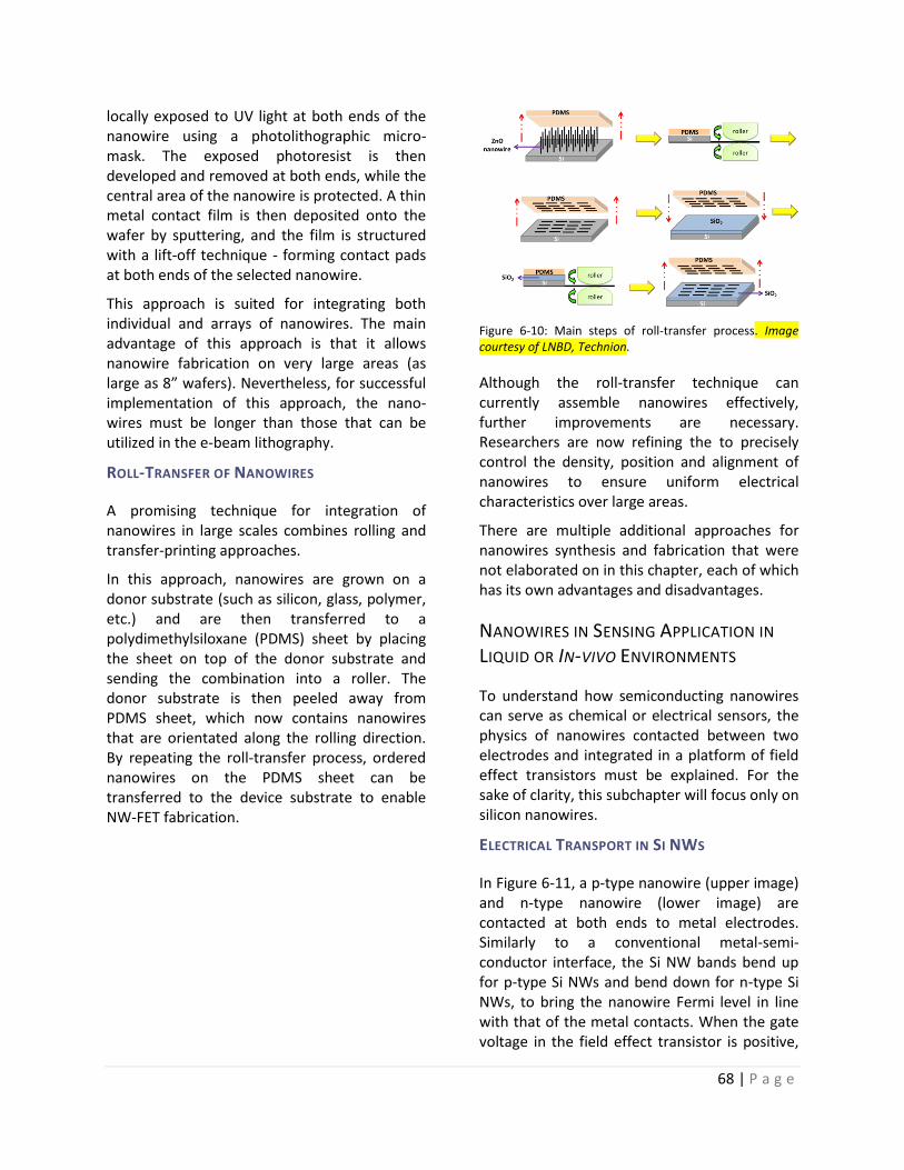
68 | P a g e
locally exposed to UV light at both ends of the nanowire using a photolithographic micro-mask. The exposed photoresist is then developed and removed at both ends, while the central area of the nanowire is protected. A thin metal contact film is then deposited onto the wafer by sputtering, and the film is structured with a lift-off technique - forming contact pads at both ends of the selected nanowire.
This approach is suited for integrating both individual and arrays of nanowires. The main advantage of this approach is that it allows nanowire fabrication on very large areas (as large as 8” wafers). Nevertheless, for successful implementation of this approach, the nano-wires must be longer than those that can be utilized in the e-beam lithography.
ROLL-TRANSFER OF NANOWIRES
A promising technique for integration of nanowires in large scales combines rolling and transfer-printing approaches.
In this approach, nanowires are grown on a donor substrate (such as silicon, glass, polymer, etc.) and are then transferred to a polydimethylsiloxane (PDMS) sheet by placing the sheet on top of the donor substrate and sending the combination into a roller. The donor substrate is then peeled away from PDMS sheet, which now contains nanowires that are orientated along the rolling direction. By repeating the roll-transfer process, ordered nanowires on the PDMS sheet can be transferred to the device substrate to enable NW-FET fabrication.
Figure 6-10: Main steps of roll-transfer process. Image courtesy of LNBD, Technion.
Although the roll-transfer technique can currently assemble nanowires effectively, further improvements are necessary. Researchers are now refining the to precisely control the density, position and alignment of nanowires to ensure uniform electrical characteristics over large areas.
There are multiple additional approaches for nanowires synthesis and fabrication that were not elaborated on in this chapter, each of which has its own advantages and disadvantages.
NANOWIRES IN SENSING APPLICATION IN
LIQUID OR IN-VIVO ENVIRONMENTS
To understand how semiconducting nanowires can serve as chemical or electrical sensors, the physics of nanowires contacted between two electrodes and integrated in a platform of field effect transistors must be explained. For the sake of clarity, this subchapter will focus only on silicon nanowires.
ELECTRICAL TRANSPORT IN SI NWS
In Figure 6-11, a p-type nanowire (upper image) and n-type nanowire (lower image) are contacted at both ends to metal electrodes. Similarly to a conventional metal-semi-conductor interface, the Si NW bands bend up for p-type Si NWs and bend down for n-type Si NWs, to bring the nanowire Fermi level in line with that of the metal contacts. When the gate voltage in the field effect transistor is positive,
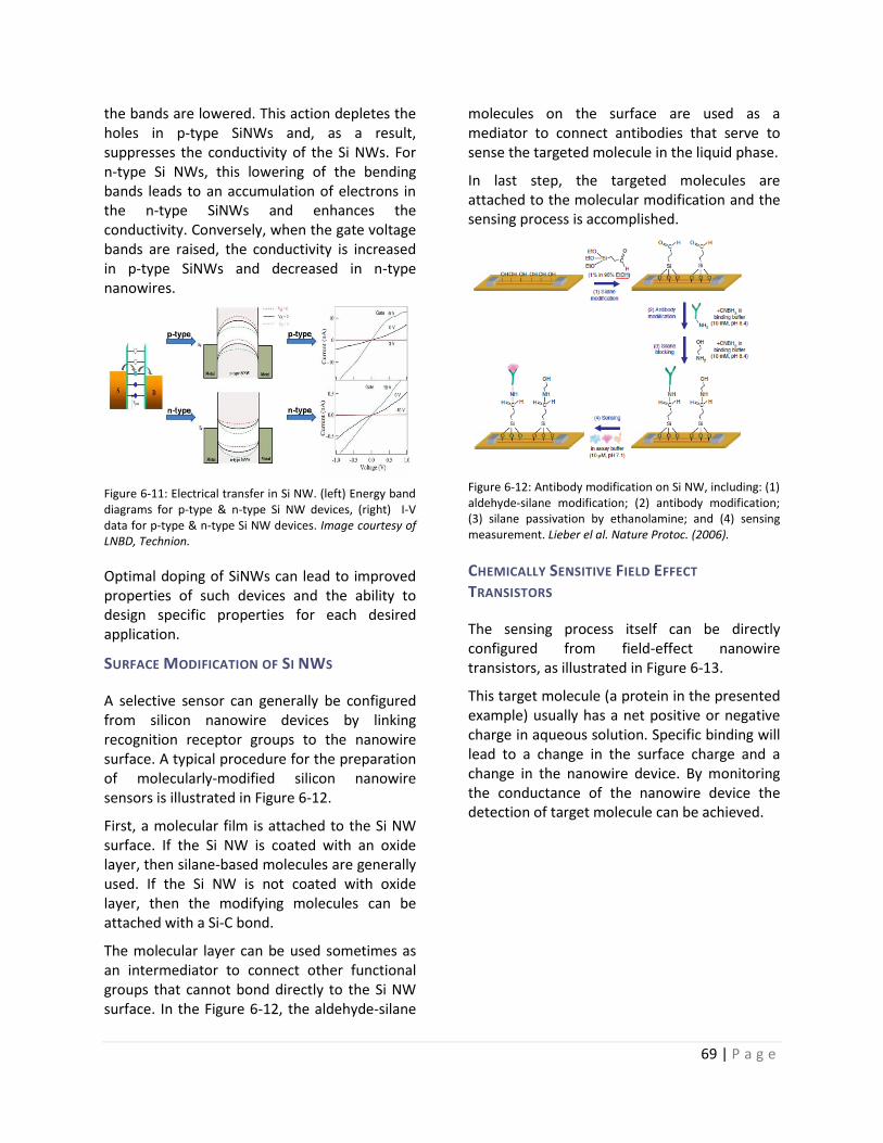
69 | P a g e
the bands are lowered. This action depletes the holes in p-type SiNWs and, as a result, suppresses the conductivity of the Si NWs. For n-type Si NWs, this lowering of the bending bands leads to an accumulation of electrons in the n-type SiNWs and enhances the conductivity. Conversely, when the gate voltage bands are raised, the conductivity is increased in p-type SiNWs and decreased in n-type nanowires.
Figure 6-11: Electrical transfer in Si NW. (left) Energy band diagrams for p-type & n-type Si NW devices, (right) I-V data for p-type & n-type Si NW devices. Image courtesy of LNBD, Technion.
Optimal doping of SiNWs can lead to improved properties of such devices and the ability to design specific properties for each desired application.
SURFACE MODIFICATION OF SI NWS
A selective sensor can generally be configured from silicon nanowire devices by linking recognition receptor groups to the nanowire surface. A typical procedure for the preparation of molecularly-modified silicon nanowire sensors is illustrated in Figure 6-12.
First, a molecular film is attached to the Si NW surface. If the Si NW is coated with an oxide layer, then silane-based molecules are generally used. If the Si NW is not coated with oxide layer, then the modifying molecules can be attached with a Si-C bond.
The molecular layer can be used sometimes as an intermediator to connect other functional groups that cannot bond directly to the Si NW surface. In the Figure 6-12, the aldehyde-silane
molecules on the surface are used as a mediator to connect antibodies that serve to sense the targeted molecule in the liquid phase.
In last step, the targeted molecules are attached to the molecular modification and the sensing process is accomplished.
Figure 6-12: Antibody modification on Si NW, including: (1) aldehyde-silane modification; (2) antibody modification; (3) silane passivation by ethanolamine; and (4) sensing measurement. Lieber el al. Nature Protoc. (2006).
CHEMICALLY SENSITIVE FIELD EFFECT
TRANSISTORS
The sensing process itself can be directly configured from field-effect nanowire transistors, as illustrated in Figure 6-13.
This target molecule (a protein in the presented example) usually has a net positive or negative charge in aqueous solution. Specific binding will lead to a change in the surface charge and a change in the nanowire device. By monitoring the conductance of the nanowire device the detection of target molecule can be achieved.
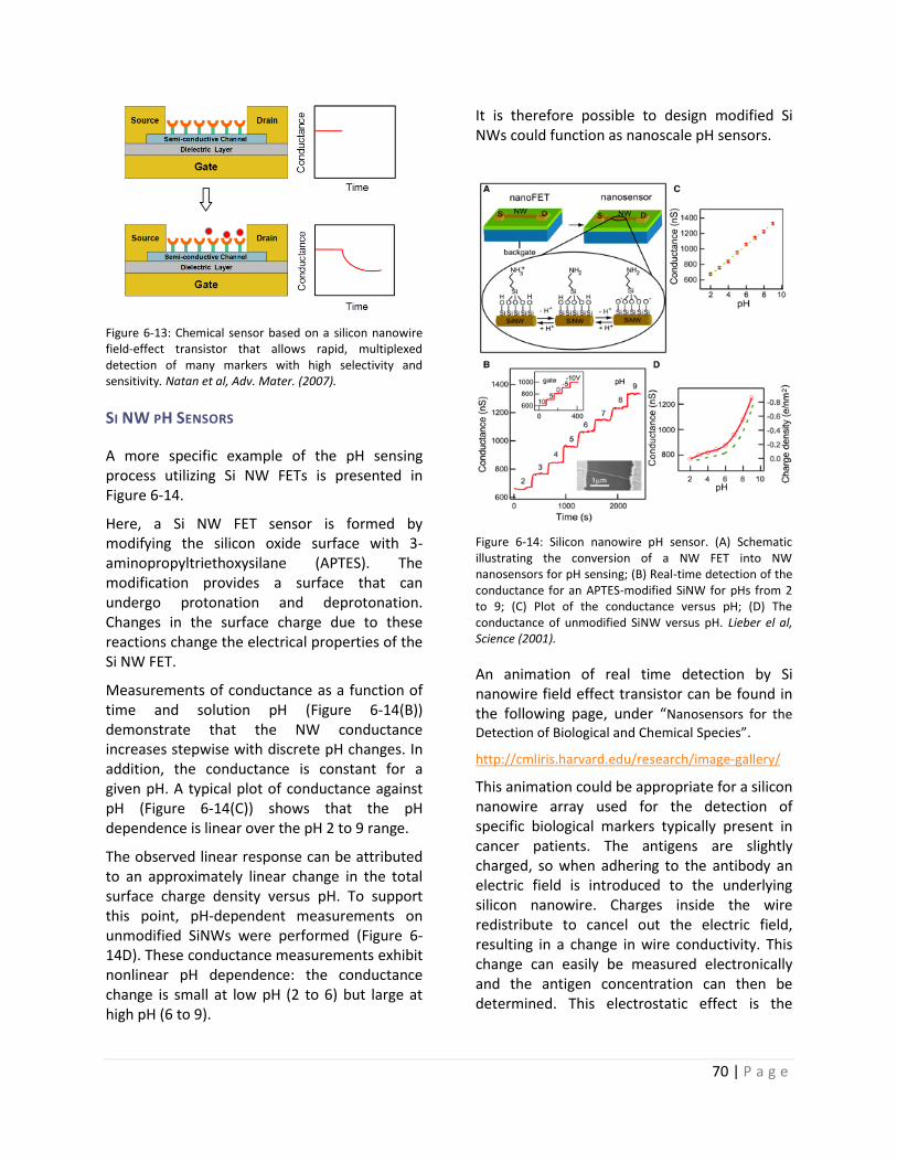
70 | P a g e
Figure 6-13: Chemical sensor based on a silicon nanowire field-effect transistor that allows rapid, multiplexed detection of many markers with high selectivity and sensitivity. Natan et al, Adv. Mater. (2007).
SI NW PH SENSORS
A more specific example of the pH sensing process utilizing Si NW FETs is presented in Figure 6-14.
Here, a Si NW FET sensor is formed by modifying the silicon oxide surface with 3-aminopropyltriethoxysilane (APTES). The modification provides a surface that can undergo protonation and deprotonation. Changes in the surface charge due to these reactions change the electrical properties of the Si NW FET.
Measurements of conductance as a function of time and solution pH (Figure 6-14(B)) demonstrate that the NW conductance increases stepwise with discrete pH changes. In addition, the conductance is constant for a given pH. A typical plot of conductance against pH (Figure 6-14(C)) shows that the pH dependence is linear over the pH 2 to 9 range.
The observed linear response can be attributed to an approximately linear change in the total surface charge density versus pH. To support this point, pH-dependent measurements on unmodified SiNWs were performed (Figure 6-14D). These conductance measurements exhibit nonlinear pH dependence: the conductance change is small at low pH (2 to 6) but large at high pH (6 to 9).
It is therefore possible to design modified Si NWs could function as nanoscale pH sensors.
Figure 6-14: Silicon nanowire pH sensor. (A) Schematic illustrating the conversion of a NW FET into NW nanosensors for pH sensing; (B) Real-time detection of the conductance for an APTES-modified SiNW for pHs from 2 to 9; (C) Plot of the conductance versus pH; (D) The conductance of unmodified SiNW versus pH. Lieber el al, Science (2001).
An animation of real time detection by Si nanowire field effect transistor can be found in the following page, under “Nanosensors for the
Detection of Biological and Chemical Species”.
http://cmliris.harvard.edu/research/image-gallery/
This animation could be appropriate for a silicon nanowire array used for the detection of specific biological markers typically present in cancer patients. The antigens are slightly charged, so when adhering to the antibody an electric field is introduced to the underlying silicon nanowire. Charges inside the wire redistribute to cancel out the electric field, resulting in a change in wire conductivity. This change can easily be measured electronically and the antigen concentration can then be determined. This electrostatic effect is the
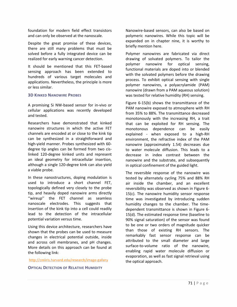
71 | P a g e
foundation for modern field effect transistors and can only be observed at the nanoscale.
Despite the great promise of these devices, there are still many problems that must be solved before a fully integrated device can be realized for early warning cancer detection.
It should be mentioned that this FET-based sensing approach has been extended to hundreds of various target molecules and applications. Nevertheless, the principle is more or less similar.
3D KINKED NANOWIRE PROBES
A promising Si NW-based sensor for in-vivo or cellular applications was recently developed and tested.
Researchers have demonstrated that kinked nanowire structures in which the active FET channels are encoded at or close to the kink tip can be synthesized in a straightforward and high-yield manner. Probes synthesized with 60-degree tip angles can be formed from two cis-linked 120-degree kinked units and represent an ideal geometry for intracellular insertion, although a single 120-degree kink can also yield a viable probe.
In these nanostructures, doping modulation is used to introduce a short channel FET, topologically defined very closely to the probe tip, and heavily doped nanowire arms directly ‘‘wireup’’ the FET channel as seamless nanoscale electrodes. This suggests that insertion of the kink tip into a cell could readily lead to the detection of the intracellular potential variation versus time.
Using this device architecture, researchers have shown that the probes can be used to measure changes in electrical potential outside, inside and across cell membranes, and pH changes. More details on this approach can be found at the following link:
http://cmliris.harvard.edu/research/image-gallery
OPTICAL DETECTION OF RELATIVE HUMIDITY
Nanowire-based sensors, can also be based on polymeric nanowires. While this topic will be expanded on in chapter nine, it is worthy to briefly mention here.
Polymer nanowires are fabricated via direct drawing of solvated polymers. To tailor the polymer nanowire for optical sensing, functional materials are doped into or blended with the solvated polymers before the drawing process. To exhibit optical sensing with single polymer nanowires, a polyacrylamide (PAM) nanowire (drawn from a PAM aqueous solution) was tested for relative humidity (RH) sensing.
Figure 6-15(b) shows the transmittance of the PAM nanowire exposed to atmosphere with RH from 35% to 88%. The transmittance decreased monotonously with the increasing RH, a trait that can be exploited for RH sensing. The monotonous dependence can be easily explained - when exposed to a high-RH environment, the refractive index of the PAM nanowire (approximately 1.54) decreases due to water molecule diffusion. This leads to a decrease in index contrast between the nanowire and the substrate, and subsequently in optical confinement of the guided light.
The reversible response of the nanowire was tested by alternately cycling 75% and 88% RH air inside the chamber, and an excellent reversibility was observed as shown in Figure 6-15(c). The nanowire humidity sensor response time was investigated by introducing sudden humidity changes to the chamber. The time-dependent transmittance is shown in Figure 6-15(d). The estimated response time (baseline to 90% signal saturation) of the sensor was found to be one or two orders of magnitude quicker than those of existing RH sensors. The remarkably fast sensor response can be attributed to the small diameter and large surface-to-volume ratio of the nanowire, enabling rapid water molecule diffusion or evaporation, as well as fast signal retrieval using the optical approach.
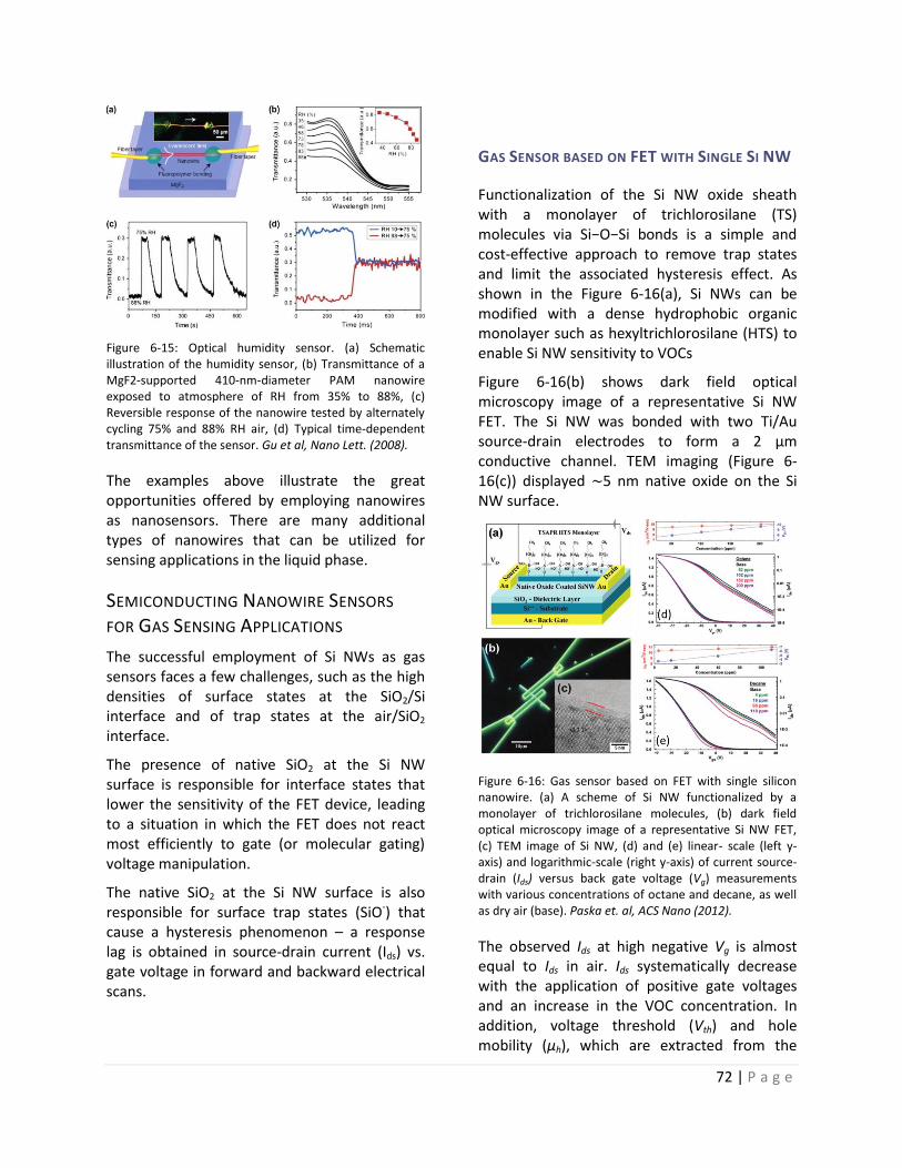
72 | P a g e
Figure 6-15: Optical humidity sensor. (a) Schematic illustration of the humidity sensor, (b) Transmittance of a MgF2-supported 410-nm-diameter PAM nanowire exposed to atmosphere of RH from 35% to 88%, (c) Reversible response of the nanowire tested by alternately cycling 75% and 88% RH air, (d) Typical time-dependent transmittance of the sensor. Gu et al, Nano Lett. (2008).
The examples above illustrate the great opportunities offered by employing nanowires as nanosensors. There are many additional types of nanowires that can be utilized for sensing applications in the liquid phase.
SEMICONDUCTING NANOWIRE SENSORS
FOR GAS SENSING APPLICATIONS
The successful employment of Si NWs as gas sensors faces a few challenges, such as the high densities of surface states at the SiO2/Si interface and of trap states at the air/SiO2 interface.
The presence of native SiO2 at the Si NW surface is responsible for interface states that lower the sensitivity of the FET device, leading to a situation in which the FET does not react most efficiently to gate (or molecular gating) voltage manipulation.
The native SiO2 at the Si NW surface is also responsible for surface trap states (SiO-) that cause a hysteresis phenomenon – a response lag is obtained in source-drain current (Ids) vs. gate voltage in forward and backward electrical scans.
GAS SENSOR BASED ON FET WITH SINGLE SI NW
Functionalization of the Si NW oxide sheath with a monolayer of trichlorosilane (TS) molecules via Si−O−Si bonds is a simple and cost-effective approach to remove trap states and limit the associated hysteresis effect. As shown in the Figure 6-16(a), Si NWs can be modified with a dense hydrophobic organic monolayer such as hexyltrichlorosilane (HTS) to enable Si NW sensitivity to VOCs
Figure 6-16(b) shows dark field optical microscopy image of a representative Si NW FET. The Si NW was bonded with two Ti/Au source-drain electrodes to form a 2 μm conductive channel. TEM imaging (Figure 6-16(c)) displayed ∼5 nm native oxide on the Si NW surface.
Figure 6-16: Gas sensor based on FET with single silicon nanowire. (a) A scheme of Si NW functionalized by a monolayer of trichlorosilane molecules, (b) dark field optical microscopy image of a representative Si NW FET, (c) TEM image of Si NW, (d) and (e) linear- scale (left y-axis) and logarithmic-scale (right y-axis) of current source-drain (Ids) versus back gate voltage (Vg) measurements with various concentrations of octane and decane, as well as dry air (base). Paska et. al, ACS Nano (2012).
The observed Ids at high negative Vg is almost equal to Ids in air. Ids systematically decrease with the application of positive gate voltages and an increase in the VOC concentration. In addition, voltage threshold (Vth) and hole mobility (μh), which are extracted from the
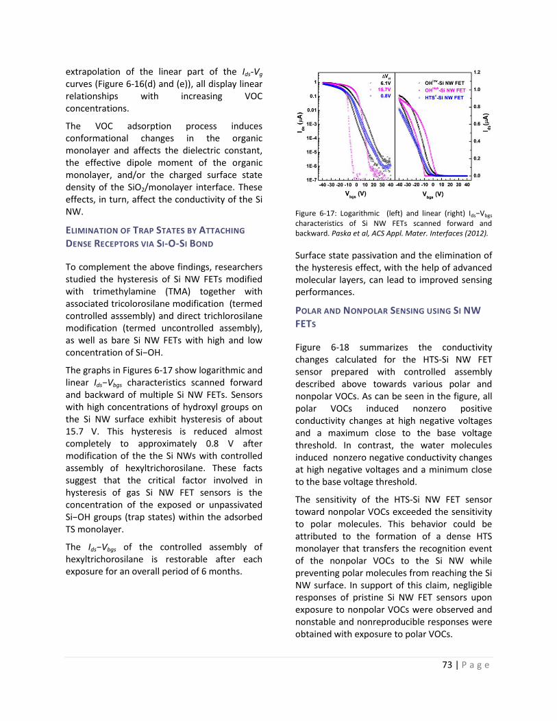
73 | P a g e
extrapolation of the linear part of the Ids-Vg curves (Figure 6-16(d) and (e)), all display linear relationships with increasing VOC concentrations.
The VOC adsorption process induces conformational changes in the organic monolayer and affects the dielectric constant, the effective dipole moment of the organic monolayer, and/or the charged surface state density of the SiO2/monolayer interface. These effects, in turn, affect the conductivity of the Si NW.
ELIMINATION OF TRAP STATES BY ATTACHING
DENSE RECEPTORS VIA SI-O-SI BOND
To complement the above findings, researchers studied the hysteresis of Si NW FETs modified with trimethylamine (TMA) together with associated tricolorosilane modification (termed controlled asssembly) and direct trichlorosilane modification (termed uncontrolled assembly), as well as bare Si NW FETs with high and low concentration of Si−OH.
The graphs in Figures 6-17 show logarithmic and linear Ids−Vbgs characteristics scanned forward and backward of multiple Si NW FETs. Sensors with high concentrations of hydroxyl groups on the Si NW surface exhibit hysteresis of about 15.7 V. This hysteresis is reduced almost completely to approximately 0.8 V after modification of the the Si NWs with controlled assembly of hexyltrichorosilane. These facts suggest that the critical factor involved in hysteresis of gas Si NW FET sensors is the concentration of the exposed or unpassivated Si−OH groups (trap states) within the adsorbed TS monolayer.
The Ids−Vbgs of the controlled assembly of hexyltrichorosilane is restorable after each exposure for an overall period of 6 months.
Figure 6-17: Logarithmic (left) and linear (right) Ids−Vbgs characteristics of Si NW FETs scanned forward and backward. Paska et al, ACS Appl. Mater. Interfaces (2012).
Surface state passivation and the elimination of the hysteresis effect, with the help of advanced molecular layers, can lead to improved sensing performances.
POLAR AND NONPOLAR SENSING USING SI NW
FETS
Figure 6-18 summarizes the conductivity changes calculated for the HTS-Si NW FET sensor prepared with controlled assembly described above towards various polar and nonpolar VOCs. As can be seen in the figure, all polar VOCs induced nonzero positive conductivity changes at high negative voltages and a maximum close to the base voltage threshold. In contrast, the water molecules induced nonzero negative conductivity changes at high negative voltages and a minimum close to the base voltage threshold.
The sensitivity of the HTS-Si NW FET sensor toward nonpolar VOCs exceeded the sensitivity to polar molecules. This behavior could be attributed to the formation of a dense HTS monolayer that transfers the recognition event of the nonpolar VOCs to the Si NW while preventing polar molecules from reaching the Si NW surface. In support of this claim, negligible responses of pristine Si NW FET sensors upon exposure to nonpolar VOCs were observed and nonstable and nonreproducible responses were obtained with exposure to polar VOCs.
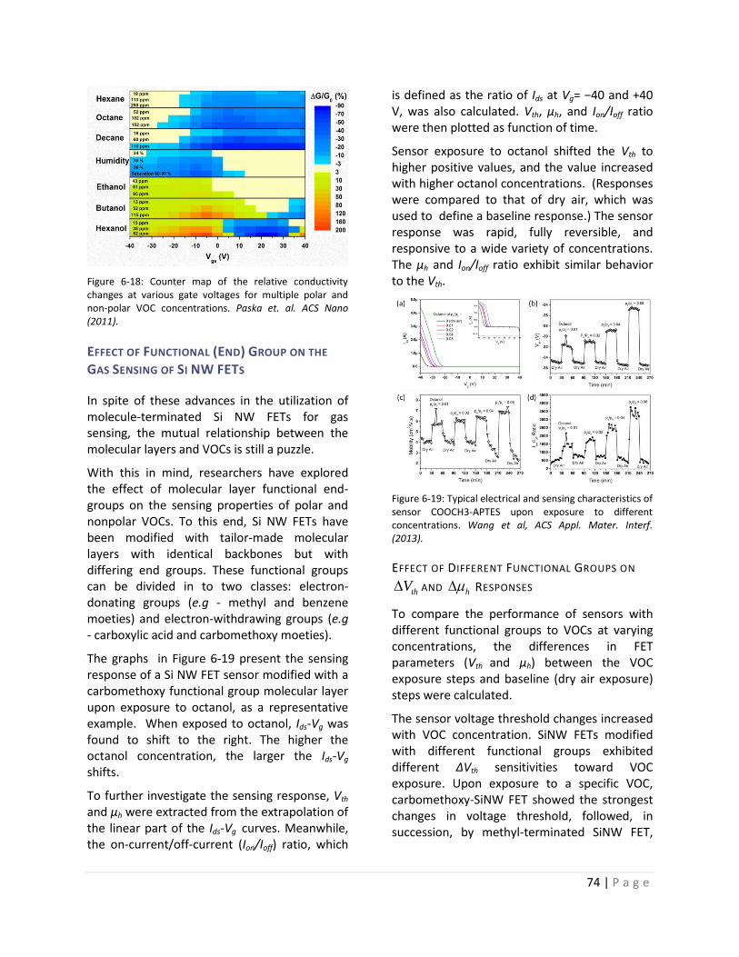
74 | P a g e
Figure 6-18: Counter map of the relative conductivity changes at various gate voltages for multiple polar and non-polar VOC concentrations. Paska et. al. ACS Nano (2011).
EFFECT OF FUNCTIONAL (END) GROUP ON THE
GAS SENSING OF SI NW FETS
In spite of these advances in the utilization of molecule-terminated Si NW FETs for gas sensing, the mutual relationship between the molecular layers and VOCs is still a puzzle.
With this in mind, researchers have explored the effect of molecular layer functional end-groups on the sensing properties of polar and nonpolar VOCs. To this end, Si NW FETs have been modified with tailor-made molecular layers with identical backbones but with differing end groups. These functional groups can be divided in to two classes: electron-donating groups (e.g - methyl and benzene moeties) and electron-withdrawing groups (e.g - carboxylic acid and carbomethoxy moeties).
The graphs in Figure 6-19 present the sensing response of a Si NW FET sensor modified with a carbomethoxy functional group molecular layer upon exposure to octanol, as a representative example. When exposed to octanol, Ids-Vg was found to shift to the right. The higher the octanol concentration, the larger the Ids-Vg shifts.
To further investigate the sensing response, Vth and μh were extracted from the extrapolation of the linear part of the Ids-Vg curves. Meanwhile, the on-current/off-current (Ion/Ioff) ratio, which
is defined as the ratio of Ids at Vg= −40 and +40 V, was also calculated. Vth, μh, and Ion/Ioff ratio were then plotted as function of time.
Sensor exposure to octanol shifted the Vth to higher positive values, and the value increased with higher octanol concentrations. (Responses were compared to that of dry air, which was used to define a baseline response.) The sensor response was rapid, fully reversible, and responsive to a wide variety of concentrations. The μh and Ion/Ioff ratio exhibit similar behavior to the Vth.
Figure 6-19: Typical electrical and sensing characteristics of sensor COOCH3-APTES upon exposure to different concentrations. Wang et al, ACS Appl. Mater. Interf. (2013).
EFFECT OF DIFFERENT FUNCTIONAL GROUPS ON
thV AND h RESPONSES
To compare the performance of sensors with different functional groups to VOCs at varying concentrations, the differences in FET parameters (Vth and μh) between the VOC exposure steps and baseline (dry air exposure) steps were calculated.
The sensor voltage threshold changes increased with VOC concentration. SiNW FETs modified with different functional groups exhibited different ΔVth sensitivities toward VOC exposure. Upon exposure to a specific VOC, carbomethoxy-SiNW FET showed the strongest changes in voltage threshold, followed, in succession, by methyl-terminated SiNW FET,
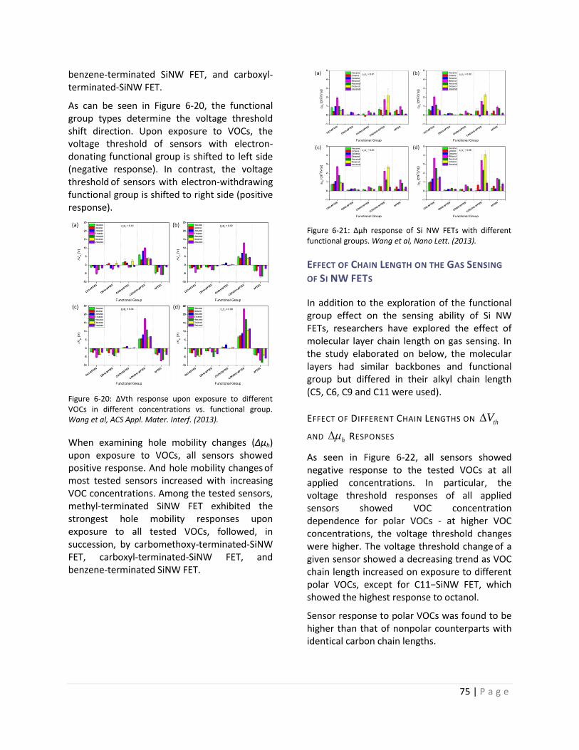
75 | P a g e
benzene-terminated SiNW FET, and carboxyl-terminated-SiNW FET.
As can be seen in Figure 6-20, the functional group types determine the voltage threshold
shift direction. Upon exposure to VOCs, the voltage threshold of sensors with electron-donating functional group is shifted to left side (negative response). In contrast, the voltage threshold of sensors with electron-withdrawing functional group is shifted to right side (positive response).
Figure 6-20: ΔVth response upon exposure to different VOCs in different concentrations vs. functional group. Wang et al, ACS Appl. Mater. Interf. (2013).
When examining hole mobility changes (Δμh) upon exposure to VOCs, all sensors showed positive response. And hole mobility changes of most tested sensors increased with increasing VOC concentrations. Among the tested sensors, methyl-terminated SiNW FET exhibited the strongest hole mobility responses upon exposure to all tested VOCs, followed, in succession, by carbomethoxy-terminated-SiNW FET, carboxyl-terminated-SiNW FET, and benzene-terminated SiNW FET.
Figure 6-21: Δµh response of Si NW FETs with different functional groups. Wang et al, Nano Lett. (2013).
EFFECT OF CHAIN LENGTH ON THE GAS SENSING
OF SI NW FETS
In addition to the exploration of the functional group effect on the sensing ability of Si NW FETs, researchers have explored the effect of molecular layer chain length on gas sensing. In the study elaborated on below, the molecular layers had similar backbones and functional group but differed in their alkyl chain length (C5, C6, C9 and C11 were used).
EFFECT OF DIFFERENT CHAIN LENGTHS ON thV
AND h RESPONSES
As seen in Figure 6-22, all sensors showed negative response to the tested VOCs at all applied concentrations. In particular, the voltage threshold responses of all applied sensors showed VOC concentration dependence for polar VOCs - at higher VOC concentrations, the voltage threshold changes were higher. The voltage threshold change of a given sensor showed a decreasing trend as VOC chain length increased on exposure to different polar VOCs, except for C11−SiNW FET, which showed the highest response to octanol.
Sensor response to polar VOCs was found to be higher than that of nonpolar counterparts with identical carbon chain lengths.
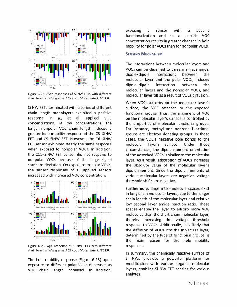
76 | P a g e
Figure 6-22: ΔVth responses of Si NW FETs with different chain lengths. Wang et al, ACS Appl. Mater. Interf. (2013).
Si NW FETs terminated with a series of different chain length monolayers exhibited a positive response in μh at all applied VOC concentrations. At low concentrations, the longer nonpolar VOC chain length induced a greater hole mobility response of the C5−SiNW FET and C9−SiNW FET. However, the C6−SiNW FET sensor exhibited nearly the same response when exposed to nonpolar VOCs. In addition, the C11−SiNW FET sensor did not respond to nonpolar VOCs because of the large signal standard deviation. On exposure to polar VOCs, the sensor responses of all applied sensors increased with increased VOC concentration.
Figure 6-23: Δµh response of Si NW FETs with different chain lengths. Wang et al, ACS Appl. Mater. Interf. (2013).
The hole mobility response (Figure 6-23) upon exposure to different polar VOCs decreases as VOC chain length increased. In addition,
exposing a sensor with a specific functionalization and to a specific VOC concentration results in greater changes in hole mobility for polar VOCs than for nonpolar VOCs.
SENSING MECHANISM
The interactions between molecular layers and VOCs can be classified to three main scenarios: dipole−dipole interactions between the molecular layer and the polar VOCs, induced dipole−dipole interaction between the molecular layers and the nonpolar VOCs, and molecular layer tilt as a result of VOCs diffusion.
When VOCs adsorbs on the molecular layer’s surface, the VOC attaches to the exposed functional groups. Thus, the alignment of VOC on the molecular layer’s surface is controlled by the properties of molecular functional groups. For instance, methyl and benzene functional groups are electron donating groups. In these cases, the VOC’s negative pole bonds to the molecular layer’s surface. Under these circumstances, the dipole moment orientation of the adsorbed VOCs is similar to the molecular layer. As a result, adsorption of VOCs increases the absolute value of the molecular layer’s dipole moment. Since the dipole moments of various molecular layers are negative, voltage threshold shifts are negative.
Furthermore, large inter-molecule spaces exist in long chain molecular layers, due to the longer chain length of the molecular layer and relative low second layer amide reaction ratio. These spaces enable the layer to adsorb more VOC molecules than the short chain molecular layer, thereby increasing the voltage threshold response to VOCs. Additionally, it is likely that the diffusion of VOCs into the molecular layer, determined by the type of functional groups, is the main reason for the hole mobility responses.
In summary, the chemically reactive surface of Si NWs provides a powerful platform for modification with various organic molecular layers, enabling Si NW FET sensing for various analytes.

77 | P a g e
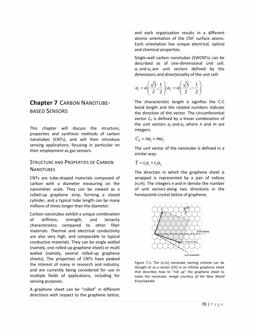
78 | P a g e
Chapter 7 CARBON NANOTUBE-BASED SENSORS
This chapter will discuss the structure, properties and synthesis methods of carbon nanotubes (CNTs), and will then introduce sensing applications, focusing in particular on their employment as gas sensors.
STRUCTURE AND PROPERTIES OF CARBON
NANOTUBES
CNTs are tube-shaped materials composed of carbon with a diameter measuring on the nanometer scale. They can be viewed as a rolled-up graphene strip, forming a closed cylinder, and a typical tube length can be many millions of times longer than the diameter.
Carbon nanotubes exhibit a unique combination of stiffness, strength, and tenacity characteristics compared to other fiber materials. Thermal and electrical conductivity are also very high, and comparable to typical conductive materials. They can be single walled (namely, one rolled-up graphene sheet) or multi walled (namely, several rolled-up graphene sheets). The properties of CNTs have peaked the interest of many in research and industry, and are currently being considered for use in multiple fields of applications, including for sensing purposes.
A graphene sheet can be “rolled” in different directions with respect to the graphene lattice,
and each organization results in a different atomic orientation of the CNT surface atoms. Each orientation has unique electrical, optical and chemical properties.
Single-wall carbon nanotubes (SWCNTs) can be described as of one-dimensional unit cell. a1 and a2 are unit vectors defined by the dimensions and directionality of the unit cell:
1 2
3 1 3 1, ; ,
2 2 2 2a a a a
The characteristic length a signifies the C-C bond length and the related numbers indicate the direction of the vector. The circumferential vector Ch is defined by a linear combination of the unit vectors a1 and a2, where n and m are integers:
1 2hC na ma
The unit vector of the nanotube is defined in a similar way:
1 1 2 2T t a t a
The direction in which the graphene sheet is wrapped is represented by a pair of indices (n,m). The integers n and m denote the number of unit vectors along two directions in the honeycomb crystal lattice of graphene.
Figure 7-1: The (n,m) nanotube naming scheme can be thought of as a vector (Ch) in an infinite graphene sheet that describes how to "roll up" the graphene sheet to make the nanotube. Image courtesy of the New World Encyclopedia.
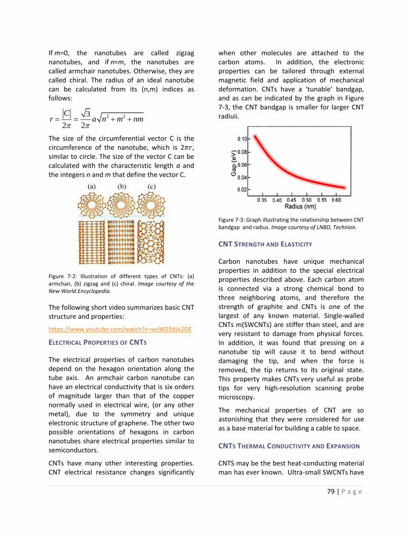
79 | P a g e
If m=0, the nanotubes are called zigzag nanotubes, and if n=m, the nanotubes are called armchair nanotubes. Otherwise, they are called chiral. The radius of an ideal nanotube can be calculated from its (n,m) indices as follows:
2 23
2 2
Cr a n m nm
The size of the circumferential vector C is the circumference of the nanotube, which is 2 , similar to circle. The size of the vector C can be calculated with the characteristic length a and the integers n and m that define the vector C.
Figure 7-2: Illustration of different types of CNTs: (a) armchair, (b) zigzag and (c) chiral. Image courtesy of the New World Encyclopedia.
The following short video summarizes basic CNT structure and properties:
https://www.youtube.com/watch?v=wsWD5dJv2OE
ELECTRICAL PROPERTIES OF CNTS
The electrical properties of carbon nanotubes depend on the hexagon orientation along the tube axis. An armchair carbon nanotube can have an electrical conductivity that is six orders of magnitude larger than that of the copper normally used in electrical wire, (or any other metal), due to the symmetry and unique electronic structure of graphene. The other two possible orientations of hexagons in carbon nanotubes share electrical properties similar to semiconductors.
CNTs have many other interesting properties. CNT electrical resistance changes significantly
when other molecules are attached to the carbon atoms. In addition, the electronic properties can be tailored through external magnetic field and application of mechanical deformation. CNTs have a ‘tunable’ bandgap, and as can be indicated by the graph in Figure 7-3, the CNT bandgap is smaller for larger CNT radiuii.
Figure 7-3: Graph illustrating the relationship between CNT bandgap and radius. Image courtesy of LNBD, Technion.
CNT STRENGTH AND ELASTICITY
Carbon nanotubes have unique mechanical properties in addition to the special electrical properties described above. Each carbon atom is connected via a strong chemical bond to three neighboring atoms, and therefore the strength of graphite and CNTs is one of the largest of any known material. Single-walled CNTs m(SWCNTs) are stiffer than steel, and are very resistant to damage from physical forces. In addition, it was found that pressing on a nanotube tip will cause it to bend without damaging the tip, and when the force is removed, the tip returns to its original state. This property makes CNTs very useful as probe tips for very high-resolution scanning probe microscopy.
The mechanical properties of CNT are so astonishing that they were considered for use as a base material for building a cable to space.
CNTS THERMAL CONDUCTIVITY AND EXPANSION
CNTS may be the best heat-conducting material man has ever known. Ultra-small SWCNTs have
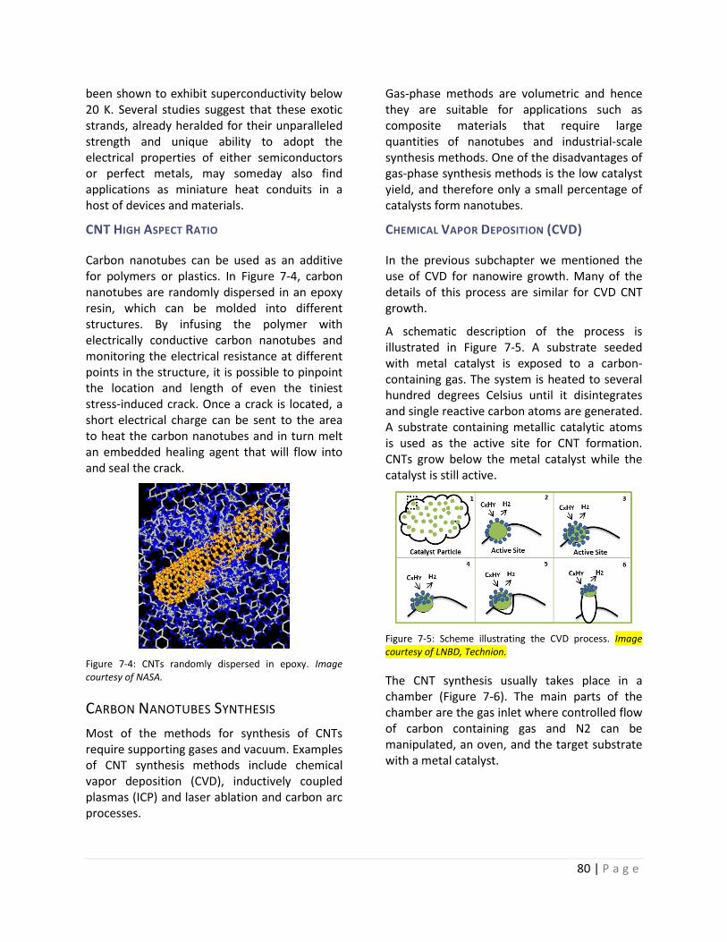
80 | P a g e
been shown to exhibit superconductivity below 20 K. Several studies suggest that these exotic strands, already heralded for their unparalleled strength and unique ability to adopt the electrical properties of either semiconductors or perfect metals, may someday also find applications as miniature heat conduits in a host of devices and materials.
CNT HIGH ASPECT RATIO
Carbon nanotubes can be used as an additive for polymers or plastics. In Figure 7-4, carbon nanotubes are randomly dispersed in an epoxy resin, which can be molded into different structures. By infusing the polymer with electrically conductive carbon nanotubes and monitoring the electrical resistance at different points in the structure, it is possible to pinpoint the location and length of even the tiniest stress-induced crack. Once a crack is located, a short electrical charge can be sent to the area to heat the carbon nanotubes and in turn melt an embedded healing agent that will flow into and seal the crack.
Figure 7-4: CNTs randomly dispersed in epoxy. Image courtesy of NASA.
CARBON NANOTUBES SYNTHESIS
Most of the methods for synthesis of CNTs require supporting gases and vacuum. Examples of CNT synthesis methods include chemical vapor deposition (CVD), inductively coupled plasmas (ICP) and laser ablation and carbon arc processes.
Gas-phase methods are volumetric and hence they are suitable for applications such as composite materials that require large quantities of nanotubes and industrial-scale synthesis methods. One of the disadvantages of gas-phase synthesis methods is the low catalyst yield, and therefore only a small percentage of catalysts form nanotubes.
CHEMICAL VAPOR DEPOSITION (CVD)
In the previous subchapter we mentioned the use of CVD for nanowire growth. Many of the details of this process are similar for CVD CNT growth.
A schematic description of the process is illustrated in Figure 7-5. A substrate seeded with metal catalyst is exposed to a carbon-containing gas. The system is heated to several hundred degrees Celsius until it disintegrates and single reactive carbon atoms are generated. A substrate containing metallic catalytic atoms is used as the active site for CNT formation. CNTs grow below the metal catalyst while the catalyst is still active.
Figure 7-5: Scheme illustrating the CVD process. Image courtesy of LNBD, Technion.
The CNT synthesis usually takes place in a chamber (Figure 7-6). The main parts of the chamber are the gas inlet where controlled flow of carbon containing gas and N2 can be manipulated, an oven, and the target substrate with a metal catalyst.
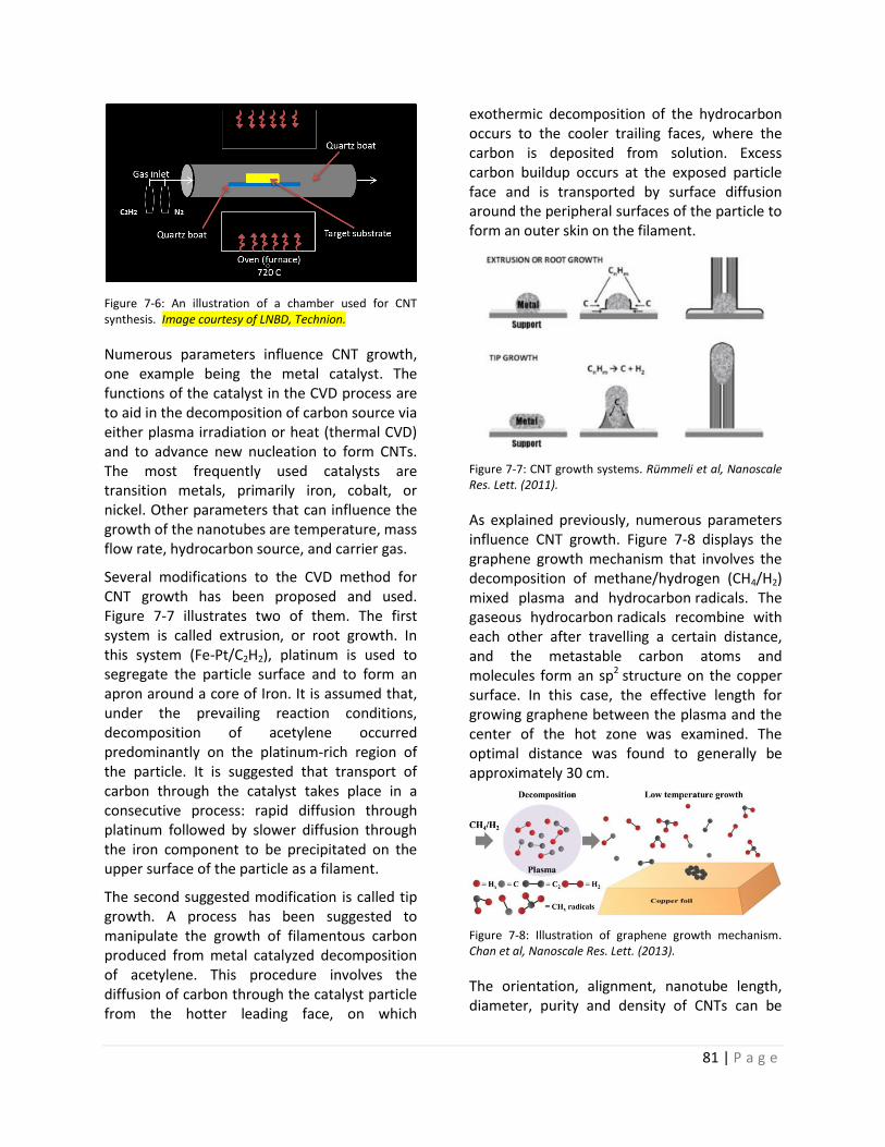
81 | P a g e
Figure 7-6: An illustration of a chamber used for CNT synthesis. Image courtesy of LNBD, Technion.
Numerous parameters influence CNT growth, one example being the metal catalyst. The functions of the catalyst in the CVD process are to aid in the decomposition of carbon source via either plasma irradiation or heat (thermal CVD) and to advance new nucleation to form CNTs. The most frequently used catalysts are transition metals, primarily iron, cobalt, or nickel. Other parameters that can influence the growth of the nanotubes are temperature, mass flow rate, hydrocarbon source, and carrier gas.
Several modifications to the CVD method for CNT growth has been proposed and used. Figure 7-7 illustrates two of them. The first system is called extrusion, or root growth. In this system (Fe-Pt/C2H2), platinum is used to segregate the particle surface and to form an apron around a core of Iron. It is assumed that, under the prevailing reaction conditions, decomposition of acetylene occurred predominantly on the platinum-rich region of the particle. It is suggested that transport of carbon through the catalyst takes place in a consecutive process: rapid diffusion through platinum followed by slower diffusion through the iron component to be precipitated on the upper surface of the particle as a filament.
The second suggested modification is called tip growth. A process has been suggested to manipulate the growth of filamentous carbon produced from metal catalyzed decomposition of acetylene. This procedure involves the diffusion of carbon through the catalyst particle from the hotter leading face, on which
exothermic decomposition of the hydrocarbon occurs to the cooler trailing faces, where the carbon is deposited from solution. Excess carbon buildup occurs at the exposed particle face and is transported by surface diffusion around the peripheral surfaces of the particle to form an outer skin on the filament.
Figure 7-7: CNT growth systems. Rümmeli et al, Nanoscale Res. Lett. (2011).
As explained previously, numerous parameters influence CNT growth. Figure 7-8 displays the graphene growth mechanism that involves the decomposition of methane/hydrogen (CH4/H2) mixed plasma and hydrocarbon radicals. The gaseous hydrocarbon radicals recombine with each other after travelling a certain distance, and the metastable carbon atoms and molecules form an sp2 structure on the copper surface. In this case, the effective length for growing graphene between the plasma and the center of the hot zone was examined. The optimal distance was found to generally be approximately 30 cm.
Figure 7-8: Illustration of graphene growth mechanism. Chan et al, Nanoscale Res. Lett. (2013).
The orientation, alignment, nanotube length, diameter, purity and density of CNTs can be
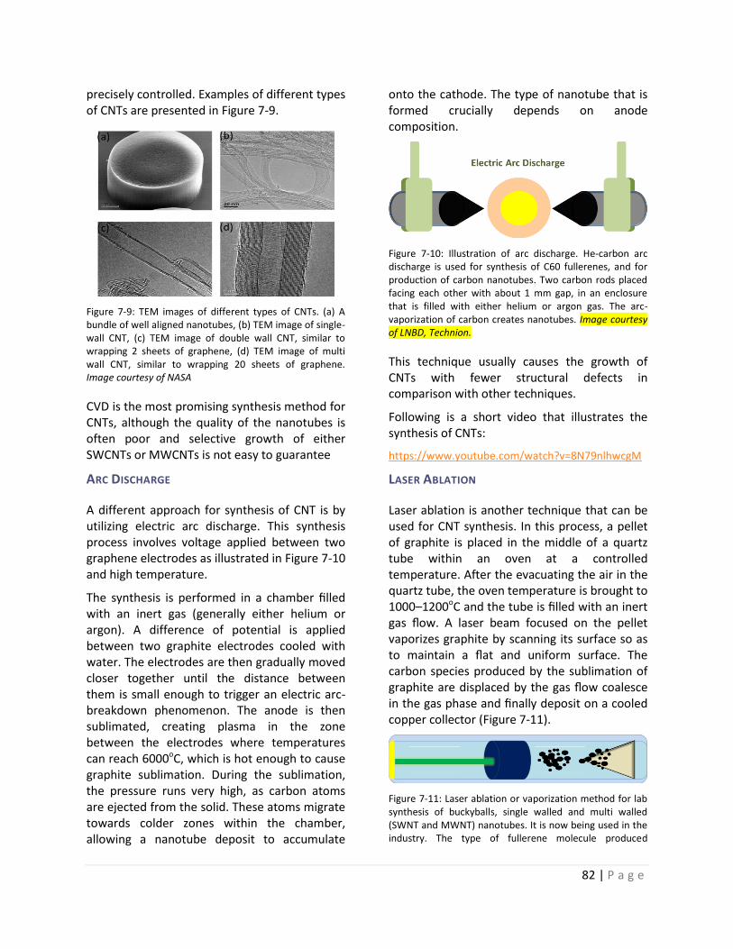
82 | P a g e
precisely controlled. Examples of different types of CNTs are presented in Figure 7-9.
Figure 7-9: TEM images of different types of CNTs. (a) A bundle of well aligned nanotubes, (b) TEM image of single-wall CNT, (c) TEM image of double wall CNT, similar to wrapping 2 sheets of graphene, (d) TEM image of multi wall CNT, similar to wrapping 20 sheets of graphene. Image courtesy of NASA
CVD is the most promising synthesis method for CNTs, although the quality of the nanotubes is often poor and selective growth of either SWCNTs or MWCNTs is not easy to guarantee
ARC DISCHARGE
A different approach for synthesis of CNT is by utilizing electric arc discharge. This synthesis process involves voltage applied between two graphene electrodes as illustrated in Figure 7-10 and high temperature.
The synthesis is performed in a chamber filled with an inert gas (generally either helium or argon). A difference of potential is applied between two graphite electrodes cooled with water. The electrodes are then gradually moved closer together until the distance between them is small enough to trigger an electric arc-breakdown phenomenon. The anode is then sublimated, creating plasma in the zone between the electrodes where temperatures can reach 6000oC, which is hot enough to cause graphite sublimation. During the sublimation, the pressure runs very high, as carbon atoms are ejected from the solid. These atoms migrate towards colder zones within the chamber, allowing a nanotube deposit to accumulate
onto the cathode. The type of nanotube that is formed crucially depends on anode composition.
Figure 7-10: Illustration of arc discharge. He-carbon arc discharge is used for synthesis of C60 fullerenes, and for production of carbon nanotubes. Two carbon rods placed facing each other with about 1 mm gap, in an enclosure that is filled with either helium or argon gas. The arc-vaporization of carbon creates nanotubes. Image courtesy of LNBD, Technion.
This technique usually causes the growth of CNTs with fewer structural defects in comparison with other techniques.
Following is a short video that illustrates the synthesis of CNTs:
https://www.youtube.com/watch?v=8N79nlhwcgM
LASER ABLATION
Laser ablation is another technique that can be used for CNT synthesis. In this process, a pellet of graphite is placed in the middle of a quartz tube within an oven at a controlled temperature. After the evacuating the air in the quartz tube, the oven temperature is brought to 1000–1200oC and the tube is filled with an inert gas flow. A laser beam focused on the pellet vaporizes graphite by scanning its surface so as to maintain a flat and uniform surface. The carbon species produced by the sublimation of graphite are displaced by the gas flow coalesce in the gas phase and finally deposit on a cooled copper collector (Figure 7-11).
Figure 7-11: Laser ablation or vaporization method for lab synthesis of buckyballs, single walled and multi walled (SWNT and MWNT) nanotubes. It is now being used in the industry. The type of fullerene molecule produced
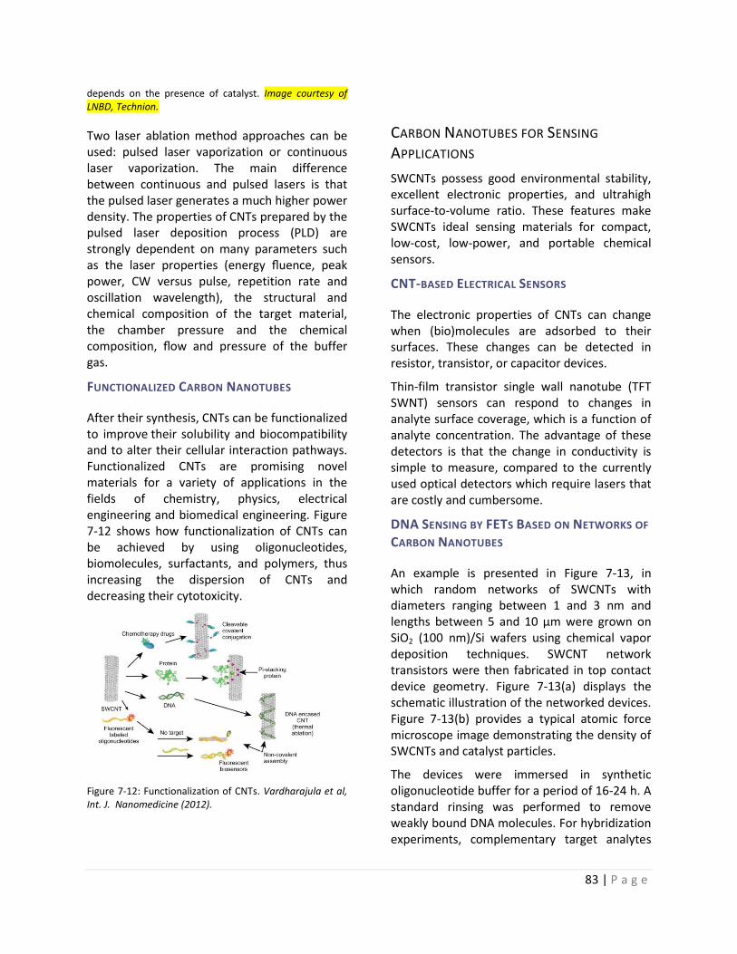
83 | P a g e
depends on the presence of catalyst. Image courtesy of LNBD, Technion.
Two laser ablation method approaches can be used: pulsed laser vaporization or continuous laser vaporization. The main difference between continuous and pulsed lasers is that the pulsed laser generates a much higher power density. The properties of CNTs prepared by the pulsed laser deposition process (PLD) are strongly dependent on many parameters such as the laser properties (energy fluence, peak power, CW versus pulse, repetition rate and oscillation wavelength), the structural and chemical composition of the target material, the chamber pressure and the chemical composition, flow and pressure of the buffer gas.
FUNCTIONALIZED CARBON NANOTUBES
After their synthesis, CNTs can be functionalized to improve their solubility and biocompatibility and to alter their cellular interaction pathways. Functionalized CNTs are promising novel materials for a variety of applications in the fields of chemistry, physics, electrical engineering and biomedical engineering. Figure 7-12 shows how functionalization of CNTs can be achieved by using oligonucleotides, biomolecules, surfactants, and polymers, thus increasing the dispersion of CNTs and decreasing their cytotoxicity.
Figure 7-12: Functionalization of CNTs. Vardharajula et al, Int. J. Nanomedicine (2012).
CARBON NANOTUBES FOR SENSING
APPLICATIONS
SWCNTs possess good environmental stability, excellent electronic properties, and ultrahigh surface-to-volume ratio. These features make SWCNTs ideal sensing materials for compact, low-cost, low-power, and portable chemical sensors.
CNT-BASED ELECTRICAL SENSORS
The electronic properties of CNTs can change when (bio)molecules are adsorbed to their surfaces. These changes can be detected in resistor, transistor, or capacitor devices.
Thin-film transistor single wall nanotube (TFT SWNT) sensors can respond to changes in analyte surface coverage, which is a function of analyte concentration. The advantage of these detectors is that the change in conductivity is simple to measure, compared to the currently used optical detectors which require lasers that are costly and cumbersome.
DNA SENSING BY FETS BASED ON NETWORKS OF
CARBON NANOTUBES
An example is presented in Figure 7-13, in which random networks of SWCNTs with diameters ranging between 1 and 3 nm and lengths between 5 and 10 μm were grown on SiO2 (100 nm)/Si wafers using chemical vapor deposition techniques. SWCNT network transistors were then fabricated in top contact device geometry. Figure 7-13(a) displays the schematic illustration of the networked devices. Figure 7-13(b) provides a typical atomic force microscope image demonstrating the density of SWCNTs and catalyst particles.
The devices were immersed in synthetic oligonucleotide buffer for a period of 16-24 h. A standard rinsing was performed to remove weakly bound DNA molecules. For hybridization experiments, complementary target analytes
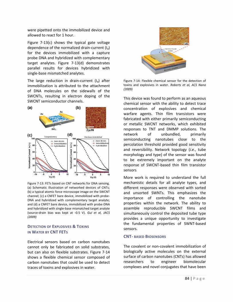
84 | P a g e
were pipetted onto the immobilized device and allowed to react for 1 hour.
Figure 7-13(c) shows the typical gate voltage dependence of the normalized drain-current (Id) for the devices immobilized with a capture probe DNA and hybridized with complementary target analytes. Figure 7-13(d) demonstrates parallel results for devices hybridized with single-base mismatched analytes.
The large reduction in drain-current (Id) after immobilization is attributed to the attachment of DNA molecules on the sidewalls of the SWCNTs, resulting in electron doping of the SWCNT semiconductor channels.
Figure 7-13: FETs based on CNT networks for DNA sensing. (a) Schematic illustration of networked devices of CNTs; (b) a typical atomic force microscope image on the SWCNT channel; (c) a CNFET bare device, immobilized with probe-DNA and hybridized with complementary target analyte; and (d) a CNFET bare device, immobilized with probe-DNA and hybridized with single-base mismatched target analyte (source-drain bias was kept at -0.5 V). Gui et al, JACS (2009)
DETECTION OF EXPLOSIVES & TOXINS IN WATER BY CNT FETS
Electrical sensors based on carbon nanotubes cannot only be fabricated on solid substrates, but can also on flexible substrates. Figure 7-14 shows a flexible chemical sensor composed of carbon nanotubes that could be used to detect traces of toxins and explosives in water.
Figure 7-14: Flexible chemical sensor for the detection of toxins and explosives in water. Roberts et al, ACS Nano (2009)
This device was found to perform as an aqueous chemical sensor with the ability to detect trace concentration of explosives and chemical warfare agents. Thin film transistors were fabricated with either primarily semiconducting or metallic SWCNT networks, which exhibited responses to TNT and DMMP solutions. The network of unbundled, primarily semiconducting nanotubes close to the percolation threshold provided good sensitivity and reversibility. Network topology (i.e., tube morphology and type) of the sensor was found to be extremely important on the analyte response of SWCNT-based thin film transistor sensors
More work is required to understand the full mechanistic details for all analyte types, and different responses were observed with sorted and unsorted SWNTs. This emphasizes the importance of controlling the nanotube properties within the network. The ability to assemble reproducible SWCNT films and simultaneously control the deposited tube type provides a unique opportunity to investigate the fundamental properties of SWNT-based sensors.
CNT- BASED BIOSENSORS
The covalent or non-covalent immobilization of biologically active molecules on the external surface of carbon nanotubes (CNTs) has allowed researchers to engineer biomolecular complexes and novel conjugates that have been
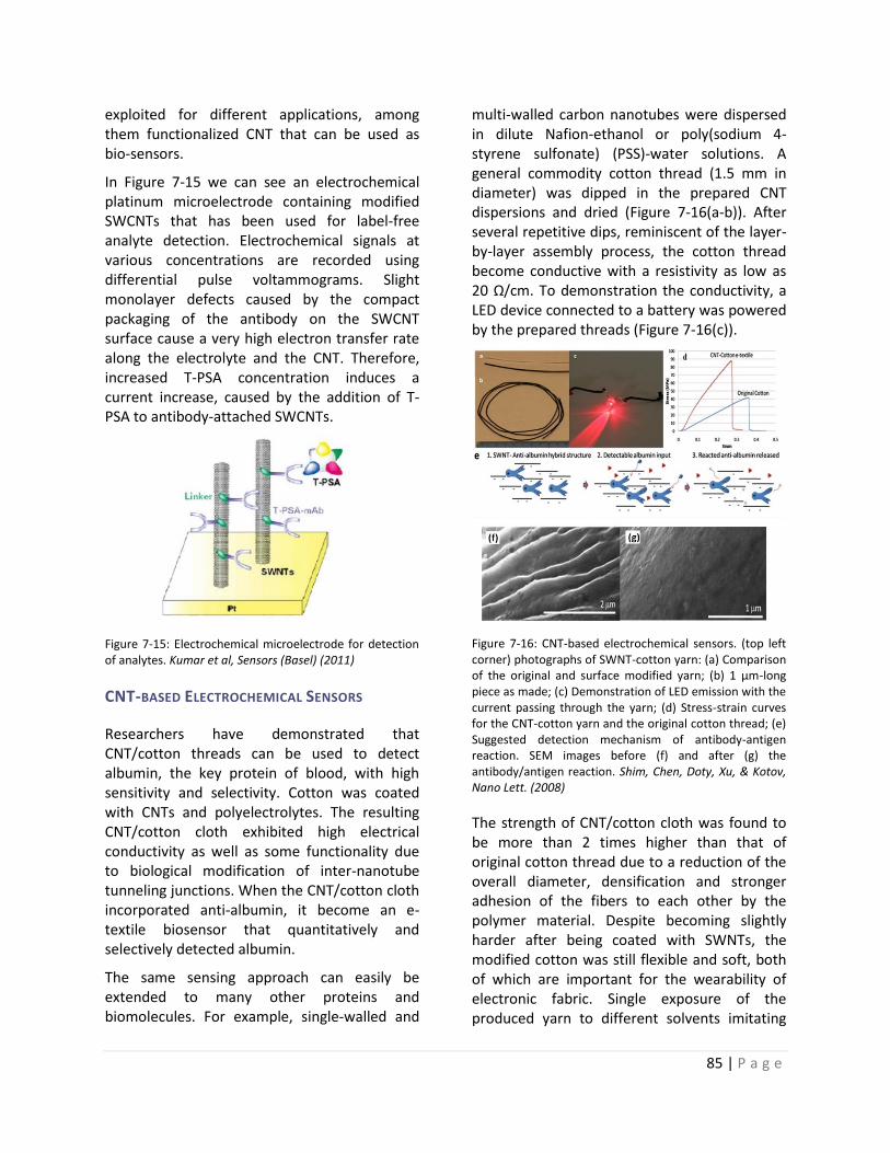
85 | P a g e
exploited for different applications, among them functionalized CNT that can be used as bio-sensors.
In Figure 7-15 we can see an electrochemical platinum microelectrode containing modified SWCNTs that has been used for label-free analyte detection. Electrochemical signals at various concentrations are recorded using differential pulse voltammograms. Slight monolayer defects caused by the compact packaging of the antibody on the SWCNT surface cause a very high electron transfer rate along the electrolyte and the CNT. Therefore, increased T-PSA concentration induces a current increase, caused by the addition of T-PSA to antibody-attached SWCNTs.
Figure 7-15: Electrochemical microelectrode for detection of analytes. Kumar et al, Sensors (Basel) (2011)
CNT-BASED ELECTROCHEMICAL SENSORS
Researchers have demonstrated that CNT/cotton threads can be used to detect albumin, the key protein of blood, with high sensitivity and selectivity. Cotton was coated with CNTs and polyelectrolytes. The resulting CNT/cotton cloth exhibited high electrical conductivity as well as some functionality due to biological modification of inter-nanotube tunneling junctions. When the CNT/cotton cloth incorporated anti-albumin, it become an e-textile biosensor that quantitatively and selectively detected albumin.
The same sensing approach can easily be extended to many other proteins and biomolecules. For example, single-walled and
multi-walled carbon nanotubes were dispersed in dilute Nafion-ethanol or poly(sodium 4-styrene sulfonate) (PSS)-water solutions. A general commodity cotton thread (1.5 mm in diameter) was dipped in the prepared CNT dispersions and dried (Figure 7-16(a-b)). After several repetitive dips, reminiscent of the layer-by-layer assembly process, the cotton thread become conductive with a resistivity as low as 20 Ω/cm. To demonstration the conductivity, a LED device connected to a battery was powered by the prepared threads (Figure 7-16(c)).
Figure 7-16: CNT-based electrochemical sensors. (top left corner) photographs of SWNT-cotton yarn: (a) Comparison of the original and surface modified yarn; (b) 1 μm-long piece as made; (c) Demonstration of LED emission with the current passing through the yarn; (d) Stress-strain curves for the CNT-cotton yarn and the original cotton thread; (e) Suggested detection mechanism of antibody-antigen reaction. SEM images before (f) and after (g) the antibody/antigen reaction. Shim, Chen, Doty, Xu, & Kotov, Nano Lett. (2008)
The strength of CNT/cotton cloth was found to be more than 2 times higher than that of original cotton thread due to a reduction of the overall diameter, densification and stronger adhesion of the fibers to each other by the polymer material. Despite becoming slightly harder after being coated with SWNTs, the modified cotton was still flexible and soft, both of which are important for the wearability of electronic fabric. Single exposure of the produced yarn to different solvents imitating
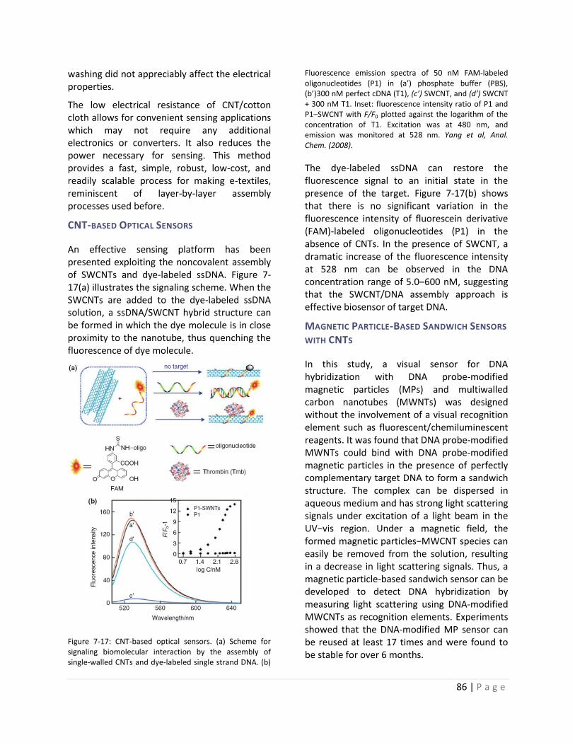
86 | P a g e
washing did not appreciably affect the electrical properties.
The low electrical resistance of CNT/cotton cloth allows for convenient sensing applications which may not require any additional electronics or converters. It also reduces the power necessary for sensing. This method provides a fast, simple, robust, low-cost, and readily scalable process for making e-textiles, reminiscent of layer-by-layer assembly processes used before.
CNT-BASED OPTICAL SENSORS
An effective sensing platform has been presented exploiting the noncovalent assembly of SWCNTs and dye-labeled ssDNA. Figure 7-17(a) illustrates the signaling scheme. When the SWCNTs are added to the dye-labeled ssDNA solution, a ssDNA/SWCNT hybrid structure can be formed in which the dye molecule is in close proximity to the nanotube, thus quenching the fluorescence of dye molecule.
Figure 7-17: CNT-based optical sensors. (a) Scheme for signaling biomolecular interaction by the assembly of single-walled CNTs and dye-labeled single strand DNA. (b)
Fluorescence emission spectra of 50 nM FAM-labeled oligonucleotides (P1) in (a’) phosphate buffer (PBS), (b’)300 nM perfect cDNA (T1), (c’) SWCNT, and (d’) SWCNT + 300 nM T1. Inset: fluorescence intensity ratio of P1 and P1–SWCNT with F/F0 plotted against the logarithm of the concentration of T1. Excitation was at 480 nm, and emission was monitored at 528 nm. Yang et al, Anal. Chem. (2008).
The dye-labeled ssDNA can restore the fluorescence signal to an initial state in the presence of the target. Figure 7-17(b) shows that there is no significant variation in the fluorescence intensity of fluorescein derivative (FAM)-labeled oligonucleotides (P1) in the absence of CNTs. In the presence of SWCNT, a dramatic increase of the fluorescence intensity at 528 nm can be observed in the DNA concentration range of 5.0–600 nM, suggesting that the SWCNT/DNA assembly approach is effective biosensor of target DNA.
MAGNETIC PARTICLE-BASED SANDWICH SENSORS
WITH CNTS
In this study, a visual sensor for DNA hybridization with DNA probe-modified magnetic particles (MPs) and multiwalled carbon nanotubes (MWNTs) was designed without the involvement of a visual recognition element such as fluorescent/chemiluminescent reagents. It was found that DNA probe-modified MWNTs could bind with DNA probe-modified magnetic particles in the presence of perfectly complementary target DNA to form a sandwich structure. The complex can be dispersed in aqueous medium and has strong light scattering signals under excitation of a light beam in the UV−vis region. Under a magnetic field, the formed magnetic particles−MWCNT species can easily be removed from the solution, resulting in a decrease in light scattering signals. Thus, a magnetic particle-based sandwich sensor can be developed to detect DNA hybridization by measuring light scattering using DNA-modified MWCNTs as recognition elements. Experiments showed that the DNA-modified MP sensor can be reused at least 17 times and were found to be stable for over 6 months.
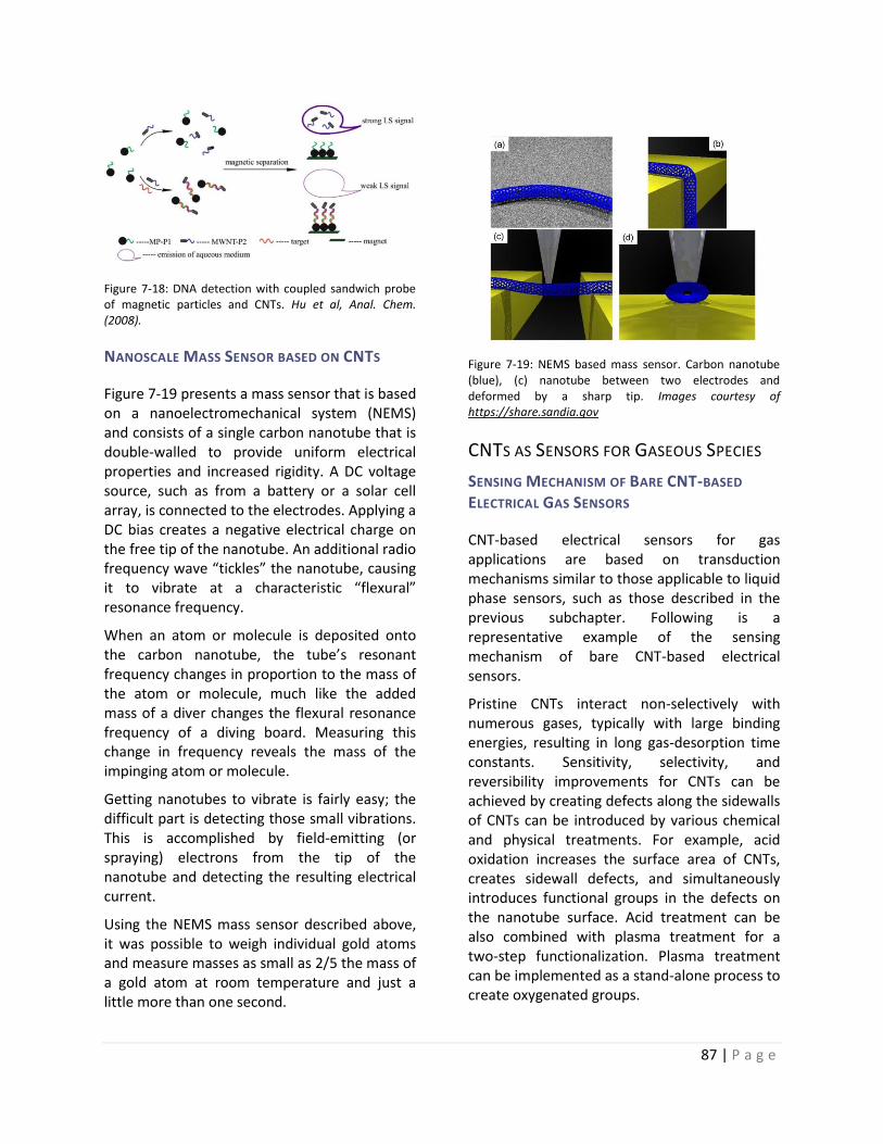
87 | P a g e
Figure 7-18: DNA detection with coupled sandwich probe of magnetic particles and CNTs. Hu et al, Anal. Chem. (2008).
NANOSCALE MASS SENSOR BASED ON CNTS
Figure 7-19 presents a mass sensor that is based on a nanoelectromechanical system (NEMS) and consists of a single carbon nanotube that is double-walled to provide uniform electrical properties and increased rigidity. A DC voltage source, such as from a battery or a solar cell array, is connected to the electrodes. Applying a DC bias creates a negative electrical charge on the free tip of the nanotube. An additional radio frequency wave “tickles” the nanotube, causing it to vibrate at a characteristic “flexural” resonance frequency.
When an atom or molecule is deposited onto the carbon nanotube, the tube’s resonant frequency changes in proportion to the mass of the atom or molecule, much like the added mass of a diver changes the flexural resonance frequency of a diving board. Measuring this change in frequency reveals the mass of the impinging atom or molecule.
Getting nanotubes to vibrate is fairly easy; the difficult part is detecting those small vibrations. This is accomplished by field-emitting (or spraying) electrons from the tip of the nanotube and detecting the resulting electrical current.
Using the NEMS mass sensor described above, it was possible to weigh individual gold atoms and measure masses as small as 2/5 the mass of a gold atom at room temperature and just a little more than one second.
Figure 7-19: NEMS based mass sensor. Carbon nanotube (blue), (c) nanotube between two electrodes and deformed by a sharp tip. Images courtesy of https://share.sandia.gov
CNTS AS SENSORS FOR GASEOUS SPECIES
SENSING MECHANISM OF BARE CNT-BASED
ELECTRICAL GAS SENSORS
CNT-based electrical sensors for gas applications are based on transduction mechanisms similar to those applicable to liquid phase sensors, such as those described in the previous subchapter. Following is a representative example of the sensing mechanism of bare CNT-based electrical sensors.
Pristine CNTs interact non-selectively with numerous gases, typically with large binding energies, resulting in long gas-desorption time constants. Sensitivity, selectivity, and reversibility improvements for CNTs can be achieved by creating defects along the sidewalls of CNTs can be introduced by various chemical and physical treatments. For example, acid oxidation increases the surface area of CNTs, creates sidewall defects, and simultaneously introduces functional groups in the defects on the nanotube surface. Acid treatment can be also combined with plasma treatment for a two-step functionalization. Plasma treatment can be implemented as a stand-alone process to create oxygenated groups.
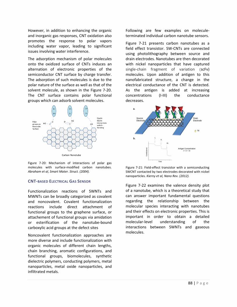
88 | P a g e
However, in addition to enhancing the organic and inorganic gas responses, CNT oxidation also promotes the response to polar vapors including water vapor, leading to significant issues involving water interference.
The adsorption mechanism of polar molecules onto the oxidized surface of CNTs induces an alternation of electronic properties of the semiconductor CNT surface by charge transfer. The adsorption of such molecules is due to the polar nature of the surface as well as that of the solvent molecule, as shown in the Figure 7-20. The CNT surface contains polar functional groups which can adsorb solvent molecules.
Figure 7-20: Mechanism of interactions of polar gas molecules with surface-modified carbon nanotubes. Abraham et al, Smart Mater. Struct. (2004).
CNT-BASED ELECTRICAL GAS SENSOR
Functionalization reactions of SWNTs and MWNTs can be broadly categorized as covalent and noncovalent. Covalent functionalization reactions include direct attachment of functional groups to the graphene surface, or attachement of functional groups via amidation or esterification of the nanotube-bound carboxylic acid groups at the defect sites
Noncovalent functionalization approaches are more diverse and include functionalization with organic molecules of different chain lengths, chain branching, aromatic configurations, and functional groups, biomolecules, synthetic dielectric polymers, conducting polymers, metal nanoparticles, metal oxide nanoparticles, and infiltrated metals.
Following are few examples on molecule-terminated individual carbon nanotube sensors.
Figure 7-21 presents carbon nanotubes as a field effect transistor. SW-CNTs are connected using photolithography between source and drain electrodes. Nanotubes are then decorated with nickel nanoparticles that have captured single-chain fragment of variation (scFv) molecules. Upon addition of antigen to this nanofabricated structure, a change in the electrical conductance of the CNT is detected. As the antigen is added at increasing concentrations (I-III) the conductance decreases.
Figure 7-21: Field-effect transistor with a semiconducting SWCNT contacted by two electrodes decorated with nickel nanoparticles. Kierny et al, Nano Rev. (2012).
Figure 7-22 examines the valence density plot of a nanotube, which is a theoretical study that can answer important fundamental questions regarding the relationship between the molecular species interacting with nanotubes and their effects on electronic properties. This is important in order to obtain a detailed molecular-level understanding of the interactions between SWNTs and gaseous molecules.
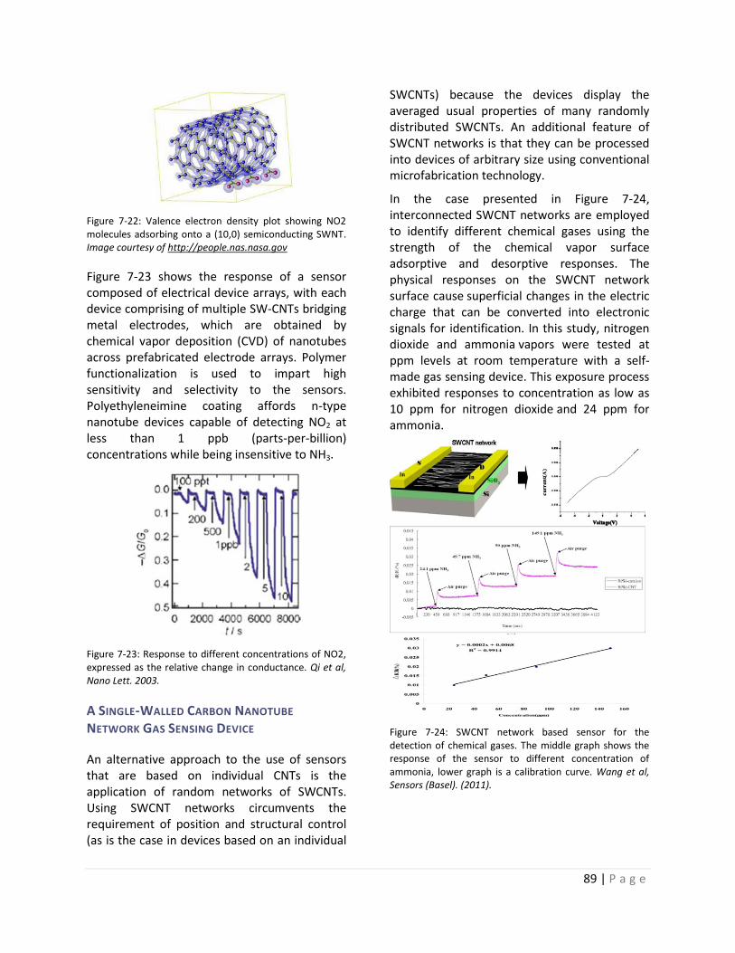
89 | P a g e
Figure 7-22: Valence electron density plot showing NO2 molecules adsorbing onto a (10,0) semiconducting SWNT. Image courtesy of http://people.nas.nasa.gov
Figure 7-23 shows the response of a sensor composed of electrical device arrays, with each device comprising of multiple SW-CNTs bridging metal electrodes, which are obtained by chemical vapor deposition (CVD) of nanotubes across prefabricated electrode arrays. Polymer functionalization is used to impart high sensitivity and selectivity to the sensors. Polyethyleneimine coating affords n-type nanotube devices capable of detecting NO2 at less than 1 ppb (parts-per-billion) concentrations while being insensitive to NH3.
Figure 7-23: Response to different concentrations of NO2, expressed as the relative change in conductance. Qi et al, Nano Lett. 2003.
A SINGLE-WALLED CARBON NANOTUBE
NETWORK GAS SENSING DEVICE
An alternative approach to the use of sensors that are based on individual CNTs is the application of random networks of SWCNTs. Using SWCNT networks circumvents the requirement of position and structural control (as is the case in devices based on an individual
SWCNTs) because the devices display the averaged usual properties of many randomly distributed SWCNTs. An additional feature of SWCNT networks is that they can be processed into devices of arbitrary size using conventional microfabrication technology.
In the case presented in Figure 7-24, interconnected SWCNT networks are employed to identify different chemical gases using the strength of the chemical vapor surface adsorptive and desorptive responses. The physical responses on the SWCNT network surface cause superficial changes in the electric charge that can be converted into electronic signals for identification. In this study, nitrogen dioxide and ammonia vapors were tested at ppm levels at room temperature with a self-made gas sensing device. This exposure process exhibited responses to concentration as low as 10 ppm for nitrogen dioxide and 24 ppm for ammonia.
Figure 7-24: SWCNT network based sensor for the detection of chemical gases. The middle graph shows the response of the sensor to different concentration of ammonia, lower graph is a calibration curve. Wang et al, Sensors (Basel). (2011).
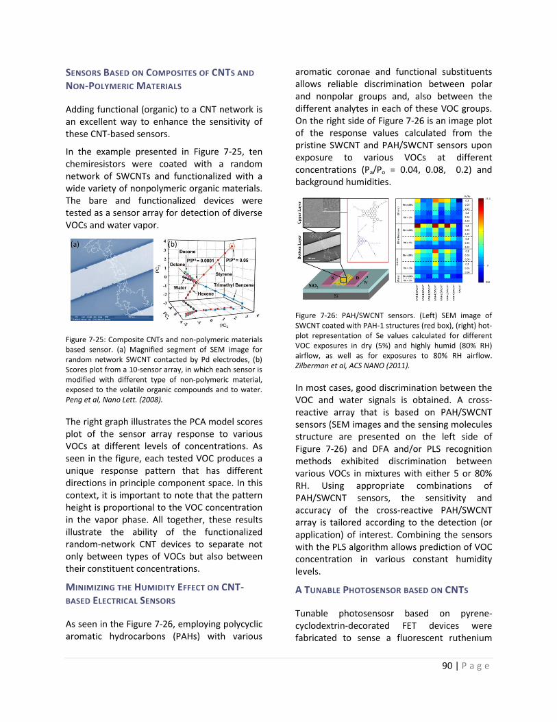
90 | P a g e
SENSORS BASED ON COMPOSITES OF CNTS AND
NON-POLYMERIC MATERIALS
Adding functional (organic) to a CNT network is an excellent way to enhance the sensitivity of these CNT-based sensors.
In the example presented in Figure 7-25, ten chemiresistors were coated with a random network of SWCNTs and functionalized with a wide variety of nonpolymeric organic materials. The bare and functionalized devices were tested as a sensor array for detection of diverse VOCs and water vapor.
Figure 7-25: Composite CNTs and non-polymeric materials based sensor. (a) Magnified segment of SEM image for random network SWCNT contacted by Pd electrodes, (b) Scores plot from a 10-sensor array, in which each sensor is modified with different type of non-polymeric material, exposed to the volatile organic compounds and to water. Peng et al, Nano Lett. (2008).
The right graph illustrates the PCA model scores plot of the sensor array response to various VOCs at different levels of concentrations. As seen in the figure, each tested VOC produces a unique response pattern that has different directions in principle component space. In this context, it is important to note that the pattern height is proportional to the VOC concentration in the vapor phase. All together, these results illustrate the ability of the functionalized random-network CNT devices to separate not only between types of VOCs but also between their constituent concentrations.
MINIMIZING THE HUMIDITY EFFECT ON CNT-BASED ELECTRICAL SENSORS
As seen in the Figure 7-26, employing polycyclic aromatic hydrocarbons (PAHs) with various
aromatic coronae and functional substituents allows reliable discrimination between polar and nonpolar groups and, also between the different analytes in each of these VOC groups. On the right side of Figure 7-26 is an image plot of the response values calculated from the pristine SWCNT and PAH/SWCNT sensors upon exposure to various VOCs at different concentrations (Pa/Po = 0.04, 0.08, 0.2) and background humidities.
Figure 7-26: PAH/SWCNT sensors. (Left) SEM image of SWCNT coated with PAH-1 structures (red box), (right) hot-plot representation of Se values calculated for different VOC exposures in dry (5%) and highly humid (80% RH) airflow, as well as for exposures to 80% RH airflow. Zilberman et al, ACS NANO (2011).
In most cases, good discrimination between the VOC and water signals is obtained. A cross-reactive array that is based on PAH/SWCNT sensors (SEM images and the sensing molecules structure are presented on the left side of Figure 7-26) and DFA and/or PLS recognition methods exhibited discrimination between various VOCs in mixtures with either 5 or 80% RH. Using appropriate combinations of PAH/SWCNT sensors, the sensitivity and accuracy of the cross-reactive PAH/SWCNT array is tailored according to the detection (or application) of interest. Combining the sensors with the PLS algorithm allows prediction of VOC concentration in various constant humidity levels.
A TUNABLE PHOTOSENSOR BASED ON CNTS
Tunable photosensosr based on pyrene-cyclodextrin-decorated FET devices were fabricated to sense a fluorescent ruthenium
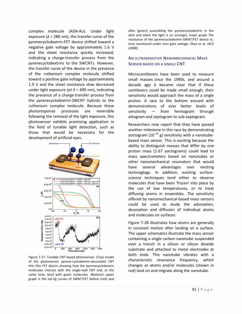
91 | P a g e
complex molecule (ADA-Ru). Under light exposure (λ = 280 nm), the transfer curve of the pyrenecyclodextrin-FET device shifted toward a negative gate voltage by approximately 1.6 V and the sheet resistance quickly increased, indicating a charge-transfer process from the pyrenecyclodextrins to the SWCNTs. However, the transfer curve of the device in the presence of the ruthenium complex molecule shifted toward a positive gate voltage by approximately 1.9 V and the sheet resistance slow decreased under light exposure (at λ = 490 nm), indicating the presence of a charge-transfer process from the pyrenecyclodextrin-SWCNT hybrids to the ruthenium complex molecule. Because these photoresponse processes are reversible following the removal of the light exposure, this photosensor exhibits promising application in the field of tunable light detection, such as those that would be necessary for the development of artificial eyes.
Figure 7-27: Tunable CNT based photosensor. (Top) model of the photosensor pyrene-cyclodextrin-decorated CNT thin film FET device showing how the pyrenecyclodextrin molecules interact with the single-wall CNT and, at the same time, bind with guest molecules. (Bottom) upper graph is the Isd-Vg curves of SWNT/FET before (red) and
after (green) assembling the pyrenecyclodextrin in the dark and when the light is on (orange), lower graph The resistance of the pyrenecyclodextrin-SWNT/FET device vs. time monitored under zero gate voltage. Zhao et al, JACS (2008).
AN ULTRASENSITIVE NANOMECHANICAL MASS
SENSOR BASED ON A SINGLE CNT
Microcantilevers have been used to measure small masses since the 1990s, and around a decade ago it became clear that if these cantilevers could be made small enough, their sensitivity would approach the mass of a single proton. A race to the bottom ensued with demonstrations of ever better levels of sensitivity — from femtogram through attogram and zeptogram to sub-zeptogram.
Researchers now report that they have passed another milestone in this race by demonstrating yoctogram (10−24 g) sensitivity with a nanotube-based mass sensor. This is exciting because the ability to distinguish masses that differ by one proton mass (1.67 yoctograms) could lead to mass spectrometers based on nanotubes or other nanomechanical resonators that would have several advantages over existing technoglogy. In addition, existing surface-science techniques tend either to observe molecules that have been 'frozen' into place by the use of low temperatures, or to treat diffusing atoms in ensembles. The sensitivity offered by nanomechanical-based mass sensors could be used to study the adsorption, desorption and diffusion of individual atoms and molecules on surfaces.
Figure 7-28 illustrates how atoms are generally in constant motion after landing on a surface. The upper schematics illustrate the mass sensor containing a single carbon nanotube suspended over a trench in a silicon or silicon dioxide substrate and attached to metal electrodes at both ends. This nanotube vibrates with a characteristic resonance frequency, which changes as atoms and/or molecules (shown in red) land on and migrate along the nanotube.
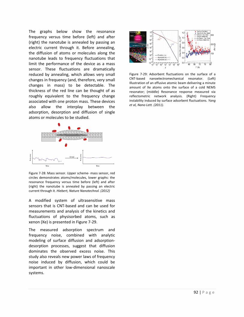
92 | P a g e
The graphs below show the resonance frequency versus time before (left) and after (right) the nanotube is annealed by passing an electric current through it. Before annealing, the diffusion of atoms or molecules along the nanotube leads to frequency fluctuations that limit the performance of the device as a mass sensor. These fluctuations are dramatically reduced by annealing, which allows very small changes in frequency (and, therefore, very small changes in mass) to be detectable. The thickness of the red line can be thought of as roughly equivalent to the frequency change associated with one proton mass. These devices also allow the interplay between the adsorption, desorption and diffusion of single atoms or molecules to be studied.
Figure 7-28: Mass sensor. Upper scheme- mass sensor, red circles demonstrates atoms/molecules, lower graphs: the resonance frequency versus time before (left) and after (right) the nanotube is annealed by passing an electric current through it. Hiebert, Nature Nanotechnol. (2012)
A modified system of ultrasensitive mass sensors that is CNT-based and can be used for measurements and analysis of the kinetics and fluctuations of physisorbed atoms, such as xenon (Xe) is presented in Figure 7-29.
The measured adsorption spectrum and frequency noise, combined with analytic modeling of surface diffusion and adsorption-desorption processes, suggest that diffusion dominates the observed excess noise. This study also reveals new power laws of frequency noise induced by diffusion, which could be important in other low-dimensional nanoscale systems.
Figure 7-29: Adsorbent fluctuations on the surface of a CNT-based nanoelectromechanical resonator. (Left) Illustration of an effusive atomic beam delivering a minute amount of Xe atoms onto the surface of a cold NEMS resonator; (middle) Resonance response measured via reflectometric network analysis. (Right) Frequency instability induced by surface adsorbent fluctuations. Yang et al, Nano Lett. (2011).
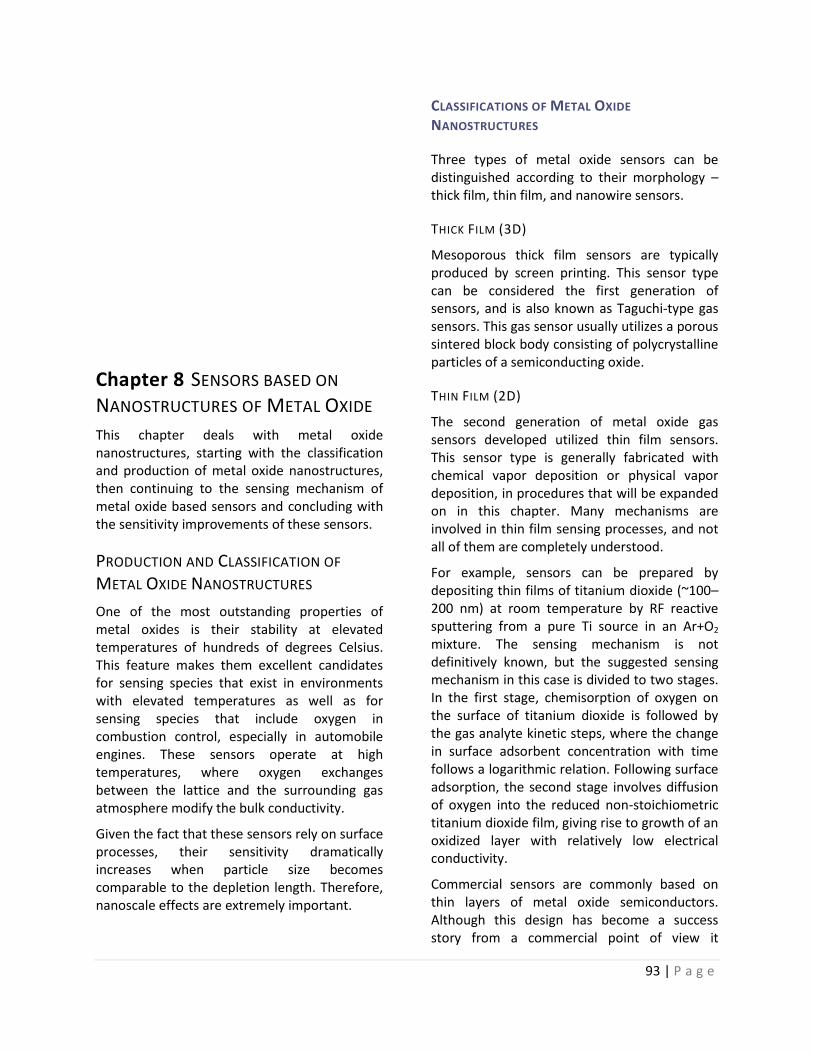
93 | P a g e
Chapter 8 SENSORS BASED ON
NANOSTRUCTURES OF METAL OXIDE
This chapter deals with metal oxide nanostructures, starting with the classification and production of metal oxide nanostructures, then continuing to the sensing mechanism of metal oxide based sensors and concluding with the sensitivity improvements of these sensors.
PRODUCTION AND CLASSIFICATION OF
METAL OXIDE NANOSTRUCTURES
One of the most outstanding properties of metal oxides is their stability at elevated temperatures of hundreds of degrees Celsius. This feature makes them excellent candidates for sensing species that exist in environments with elevated temperatures as well as for sensing species that include oxygen in combustion control, especially in automobile engines. These sensors operate at high temperatures, where oxygen exchanges between the lattice and the surrounding gas atmosphere modify the bulk conductivity.
Given the fact that these sensors rely on surface processes, their sensitivity dramatically increases when particle size becomes comparable to the depletion length. Therefore, nanoscale effects are extremely important.
CLASSIFICATIONS OF METAL OXIDE
NANOSTRUCTURES
Three types of metal oxide sensors can be distinguished according to their morphology – thick film, thin film, and nanowire sensors.
THICK FILM (3D)
Mesoporous thick film sensors are typically produced by screen printing. This sensor type can be considered the first generation of sensors, and is also known as Taguchi-type gas sensors. This gas sensor usually utilizes a porous sintered block body consisting of polycrystalline particles of a semiconducting oxide.
THIN FILM (2D)
The second generation of metal oxide gas sensors developed utilized thin film sensors. This sensor type is generally fabricated with chemical vapor deposition or physical vapor deposition, in procedures that will be expanded on in this chapter. Many mechanisms are involved in thin film sensing processes, and not all of them are completely understood.
For example, sensors can be prepared by depositing thin films of titanium dioxide (~100–200 nm) at room temperature by RF reactive sputtering from a pure Ti source in an Ar+O2 mixture. The sensing mechanism is not definitively known, but the suggested sensing mechanism in this case is divided to two stages. In the first stage, chemisorption of oxygen on the surface of titanium dioxide is followed by the gas analyte kinetic steps, where the change in surface adsorbent concentration with time follows a logarithmic relation. Following surface adsorption, the second stage involves diffusion of oxygen into the reduced non-stoichiometric titanium dioxide film, giving rise to growth of an oxidized layer with relatively low electrical conductivity.
Commercial sensors are commonly based on thin layers of metal oxide semiconductors. Although this design has become a success story from a commercial point of view it
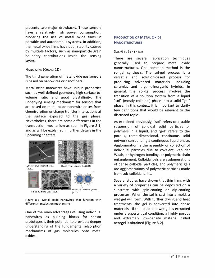
94 | P a g e
presents two major drawbacks. These sensors have a relatively high power consumption, hindering the use of metal oxide films in portable and autonomous systems. In addition, the metal oxide films have poor stability caused by multiple factors, such as nanoparticle grain boundary contributions inside the sensing layers.
NANOWIRE (QUASI 1D)
The third generation of metal oxide gas sensors is based on nanowires or nanofibers.
Metal oxide nanowires have unique properties such as well-defined geometry, high surface-to-volume ratio and good crystallinity. The underlying sensing mechanism for sensors that are based on metal-oxide nanowire arises from chemisorption or charge transfer interactions at the surface exposed to the gas phase. Nevertheless, there are some differences in the transduction mechanism as seen in Figure 8-1, and as will be explained in further details in the upcoming chapters.
Figure 8-1: Metal oxide nanowires that function with different transduction mechanisms.
One of the main advantages of using individual nanowires as building blocks for sensor prototypes is their potential to provide a deeper understanding of the fundamental adsorption mechanisms of gas molecules onto metal oxides.
PRODUCTION OF METAL OXIDE
NANOSTRUCTURES
SOL-GEL SYNTHESIS
There are several fabrication techniques generally used to prepare metal oxide nanostructures. One common method is the sol-gel synthesis. The sol-gel process is a versatile and solution-based process for producing advanced materials, including ceramics and organic-inorganic hybrids. In general, the sol-gel process involves the transition of a solution system from a liquid "sol" (mostly colloidal) phase into a solid "gel" phase. In this context, it is important to clarify few definitions that would be relevant to the discussed topic.
As explained previously, “sol” refers to a stable suspension of colloidal solid particles or polymers in a liquid, and "gel" refers to the porous, three-dimensional, continuous solid network surrounding a continuous liquid phase. Agglomeration is the assembly or collection of individual particles due to covalent, Van der Waals, or hydrogen bonding, or polymeric chain entanglement. Colloidal gels are agglomerations of dense colloidal particles, and polymeric gels are agglomerations of polymeric particles made from sub-colloidal units.
Several studies have shown that thin films with a variety of properties can be deposited on a substrate with spin-coating or dip-coating processes. When the sol is cast into a mold, a wet gel will form. With further drying and heat treatments, the gel is converted into dense materials. If the liquid in a wet gel is extracted under a supercritical condition, a highly porous and extremely low-density material called aerogel is obtained (Figure 8-2).
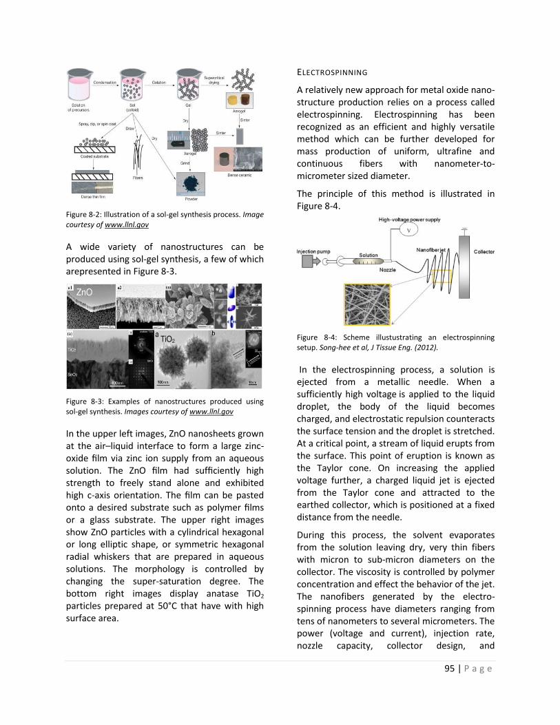
95 | P a g e
Figure 8-2: Illustration of a sol-gel synthesis process. Image courtesy of www.llnl.gov
A wide variety of nanostructures can be produced using sol-gel synthesis, a few of which arepresented in Figure 8-3.
Figure 8-3: Examples of nanostructures produced using sol-gel synthesis. Images courtesy of www.llnl.gov
In the upper left images, ZnO nanosheets grown at the air–liquid interface to form a large zinc-oxide film via zinc ion supply from an aqueous solution. The ZnO film had sufficiently high strength to freely stand alone and exhibited high c-axis orientation. The film can be pasted onto a desired substrate such as polymer films or a glass substrate. The upper right images show ZnO particles with a cylindrical hexagonal or long elliptic shape, or symmetric hexagonal radial whiskers that are prepared in aqueous solutions. The morphology is controlled by changing the super-saturation degree. The bottom right images display anatase TiO2 particles prepared at 50°C that have with high surface area.
ELECTROSPINNING
A relatively new approach for metal oxide nano-structure production relies on a process called electrospinning. Electrospinning has been recognized as an efficient and highly versatile method which can be further developed for mass production of uniform, ultrafine and continuous fibers with nanometer-to-micrometer sized diameter.
The principle of this method is illustrated in Figure 8-4.
Figure 8-4: Scheme illustustrating an electrospinning setup. Song-hee et al, J Tissue Eng. (2012).
In the electrospinning process, a solution is ejected from a metallic needle. When a sufficiently high voltage is applied to the liquid droplet, the body of the liquid becomes charged, and electrostatic repulsion counteracts the surface tension and the droplet is stretched. At a critical point, a stream of liquid erupts from the surface. This point of eruption is known as the Taylor cone. On increasing the applied voltage further, a charged liquid jet is ejected from the Taylor cone and attracted to the earthed collector, which is positioned at a fixed distance from the needle.
During this process, the solvent evaporates from the solution leaving dry, very thin fibers with micron to sub-micron diameters on the collector. The viscosity is controlled by polymer concentration and effect the behavior of the jet. The nanofibers generated by the electro-spinning process have diameters ranging from tens of nanometers to several micrometers. The power (voltage and current), injection rate, nozzle capacity, collector design, and
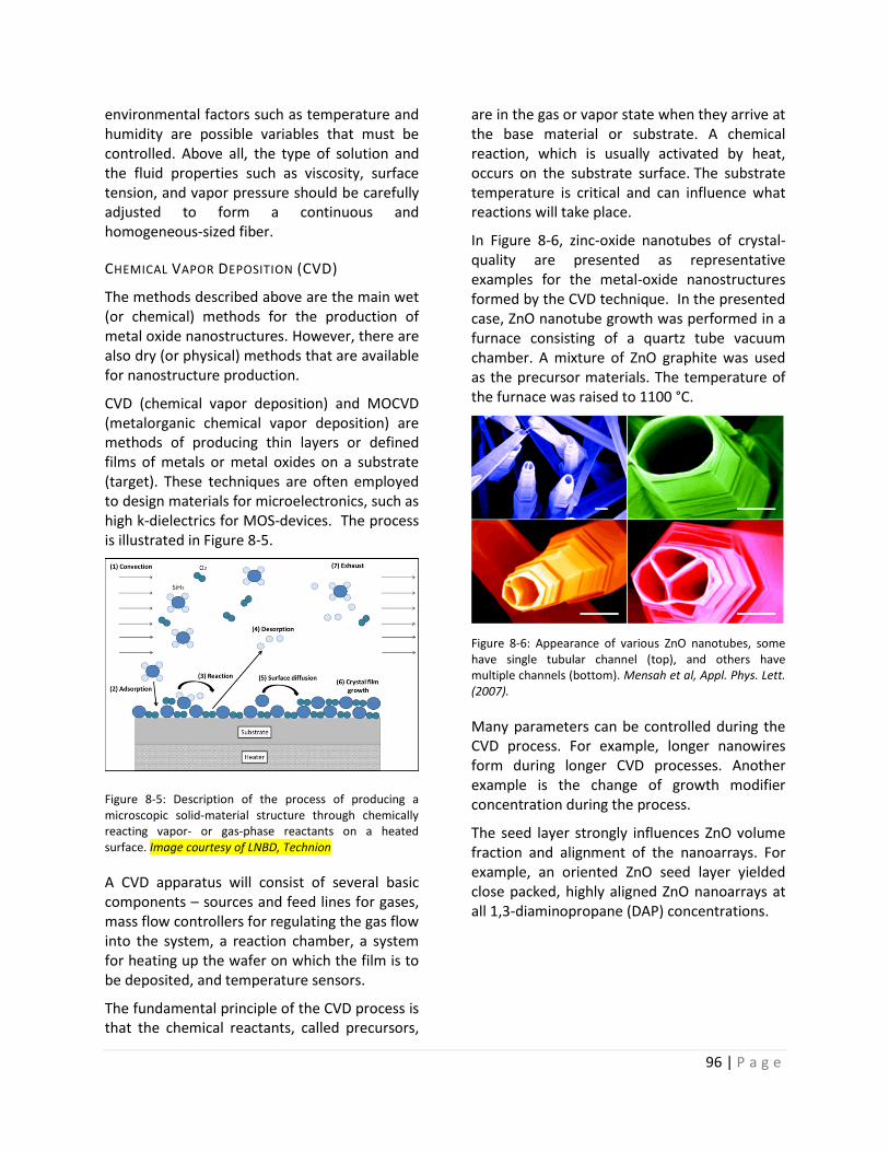
96 | P a g e
environmental factors such as temperature and humidity are possible variables that must be controlled. Above all, the type of solution and the fluid properties such as viscosity, surface tension, and vapor pressure should be carefully adjusted to form a continuous and homogeneous-sized fiber.
CHEMICAL VAPOR DEPOSITION (CVD)
The methods described above are the main wet (or chemical) methods for the production of metal oxide nanostructures. However, there are also dry (or physical) methods that are available for nanostructure production.
CVD (chemical vapor deposition) and MOCVD (metalorganic chemical vapor deposition) are methods of producing thin layers or defined films of metals or metal oxides on a substrate (target). These techniques are often employed to design materials for microelectronics, such as high k-dielectrics for MOS-devices. The process is illustrated in Figure 8-5.
Figure 8-5: Description of the process of producing a microscopic solid-material structure through chemically reacting vapor- or gas-phase reactants on a heated surface. Image courtesy of LNBD, Technion
A CVD apparatus will consist of several basic components – sources and feed lines for gases, mass flow controllers for regulating the gas flow into the system, a reaction chamber, a system for heating up the wafer on which the film is to be deposited, and temperature sensors.
The fundamental principle of the CVD process is that the chemical reactants, called precursors,
are in the gas or vapor state when they arrive at the base material or substrate. A chemical reaction, which is usually activated by heat, occurs on the substrate surface. The substrate temperature is critical and can influence what reactions will take place.
In Figure 8-6, zinc-oxide nanotubes of crystal-quality are presented as representative examples for the metal-oxide nanostructures formed by the CVD technique. In the presented case, ZnO nanotube growth was performed in a furnace consisting of a quartz tube vacuum chamber. A mixture of ZnO graphite was used as the precursor materials. The temperature of the furnace was raised to 1100 °C.
Figure 8-6: Appearance of various ZnO nanotubes, some have single tubular channel (top), and others have multiple channels (bottom). Mensah et al, Appl. Phys. Lett. (2007).
Many parameters can be controlled during the CVD process. For example, longer nanowires form during longer CVD processes. Another example is the change of growth modifier concentration during the process.
The seed layer strongly influences ZnO volume fraction and alignment of the nanoarrays. For example, an oriented ZnO seed layer yielded close packed, highly aligned ZnO nanoarrays at all 1,3-diaminopropane (DAP) concentrations.
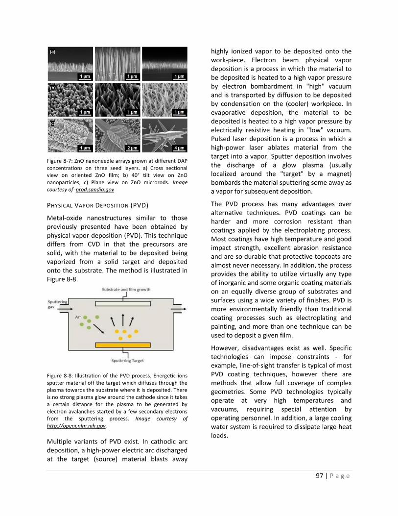
97 | P a g e
Figure 8-7: ZnO nanoneedle arrays grown at different DAP concentrations on three seed layers. a) Cross sectional view on oriented ZnO film; b) 40° tilt view on ZnO nanoparticles; c) Plane view on ZnO microrods. Image courtesy of prod.sandia.gov
PHYSICAL VAPOR DEPOSITION (PVD)
Metal-oxide nanostructures similar to those previously presented have been obtained by physical vapor deposition (PVD). This technique differs from CVD in that the precursors are solid, with the material to be deposited being vaporized from a solid target and deposited onto the substrate. The method is illustrated in Figure 8-8.
Figure 8-8: Illustration of the PVD process. Energetic ions sputter material off the target which diffuses through the plasma towards the substrate where it is deposited. There is no strong plasma glow around the cathode since it takes a certain distance for the plasma to be generated by electron avalanches started by a few secondary electrons from the sputtering process. Image courtesy of http://openi.nlm.nih.gov.
Multiple variants of PVD exist. In cathodic arc deposition, a high-power electric arc discharged at the target (source) material blasts away
highly ionized vapor to be deposited onto the work-piece. Electron beam physical vapor deposition is a process in which the material to be deposited is heated to a high vapor pressure by electron bombardment in "high" vacuum and is transported by diffusion to be deposited by condensation on the (cooler) workpiece. In evaporative deposition, the material to be deposited is heated to a high vapor pressure by electrically resistive heating in "low" vacuum. Pulsed laser deposition is a process in which a high-power laser ablates material from the target into a vapor. Sputter deposition involves the discharge of a glow plasma (usually localized around the "target" by a magnet) bombards the material sputtering some away as a vapor for subsequent deposition.
The PVD process has many advantages over alternative techniques. PVD coatings can be harder and more corrosion resistant than coatings applied by the electroplating process. Most coatings have high temperature and good impact strength, excellent abrasion resistance and are so durable that protective topcoats are almost never necessary. In addition, the process provides the ability to utilize virtually any type of inorganic and some organic coating materials on an equally diverse group of substrates and surfaces using a wide variety of finishes. PVD is more environmentally friendly than traditional coating processes such as electroplating and painting, and more than one technique can be used to deposit a given film.
However, disadvantages exist as well. Specific technologies can impose constraints - for example, line-of-sight transfer is typical of most PVD coating techniques, however there are methods that allow full coverage of complex geometries. Some PVD technologies typically operate at very high temperatures and vacuums, requiring special attention by operating personnel. In addition, a large cooling water system is required to dissipate large heat loads.
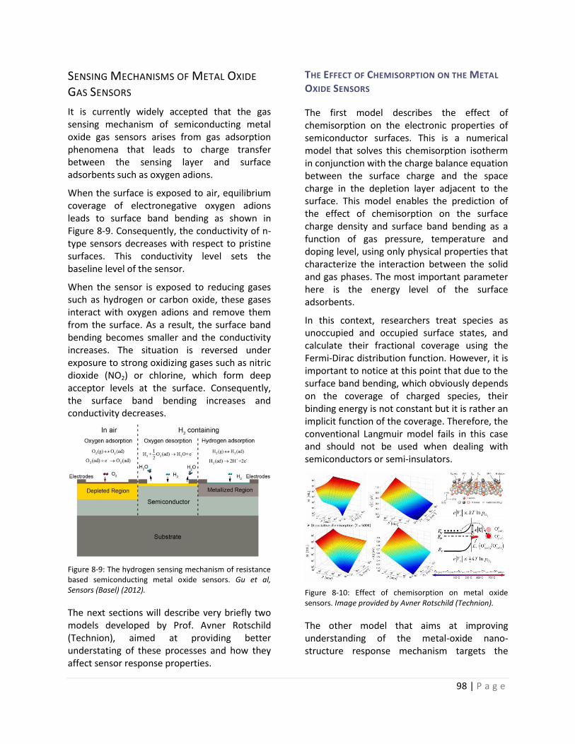
98 | P a g e
SENSING MECHANISMS OF METAL OXIDE
GAS SENSORS
It is currently widely accepted that the gas sensing mechanism of semiconducting metal oxide gas sensors arises from gas adsorption phenomena that leads to charge transfer between the sensing layer and surface adsorbents such as oxygen adions.
When the surface is exposed to air, equilibrium coverage of electronegative oxygen adions leads to surface band bending as shown in Figure 8-9. Consequently, the conductivity of n-type sensors decreases with respect to pristine surfaces. This conductivity level sets the baseline level of the sensor.
When the sensor is exposed to reducing gases such as hydrogen or carbon oxide, these gases interact with oxygen adions and remove them from the surface. As a result, the surface band bending becomes smaller and the conductivity increases. The situation is reversed under exposure to strong oxidizing gases such as nitric dioxide (NO2) or chlorine, which form deep acceptor levels at the surface. Consequently, the surface band bending increases and conductivity decreases.
Figure 8-9: The hydrogen sensing mechanism of resistance based semiconducting metal oxide sensors. Gu et al, Sensors (Basel) (2012).
The next sections will describe very briefly two models developed by Prof. Avner Rotschild (Technion), aimed at providing better understating of these processes and how they affect sensor response properties.
THE EFFECT OF CHEMISORPTION ON THE METAL
OXIDE SENSORS
The first model describes the effect of chemisorption on the electronic properties of semiconductor surfaces. This is a numerical model that solves this chemisorption isotherm in conjunction with the charge balance equation between the surface charge and the space charge in the depletion layer adjacent to the surface. This model enables the prediction of the effect of chemisorption on the surface charge density and surface band bending as a function of gas pressure, temperature and doping level, using only physical properties that characterize the interaction between the solid and gas phases. The most important parameter here is the energy level of the surface adsorbents.
In this context, researchers treat species as unoccupied and occupied surface states, and calculate their fractional coverage using the Fermi-Dirac distribution function. However, it is important to notice at this point that due to the surface band bending, which obviously depends on the coverage of charged species, their binding energy is not constant but it is rather an implicit function of the coverage. Therefore, the conventional Langmuir model fails in this case and should not be used when dealing with semiconductors or semi-insulators.
Figure 8-10: Effect of chemisorption on metal oxide sensors. Image provided by Avner Rotschild (Technion).
The other model that aims at improving understanding of the metal-oxide nano-structure response mechanism targets the
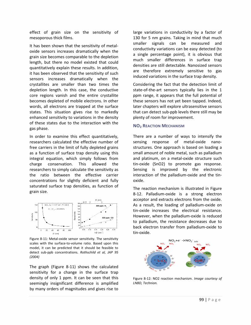
99 | P a g e
effect of grain size on the sensitivity of mesoporous thick films.
It has been shown that the sensitivity of metal-oxide sensors increases dramatically when the grain size becomes comparable to the depletion length, but there no model existed that could quantitatively explain these results. In addition, it has been observed that the sensitivity of such sensors increases dramatically when the crystallites are smaller than two times the depletion length. In this case, the conductive core regions vanish and the entire crystallite becomes depleted of mobile electrons. In other words, all electrons are trapped at the surface states. This situation gives rise to markedly enhanced sensitivity to variations in the density of these states due to the interaction with the gas phase.
In order to examine this effect quantitatively, researchers calculated the effective number of free carriers in the limit of fully depleted grains as a function of surface trap density using this integral equation, which simply follows from charge conservation. This allowed the researchers to simply calculate the sensitivity as the ratio between the effective carrier concentrations for slightly deficient and fully saturated surface trap densities, as function of grain size.
Figure 8-11: Metal-oxide sensor sensitivity. The sensitivity scales with the surface-to-volume ratio. Based upon this model, it can be predicted that it should be feasible to detect sub-ppb concentrations. Rothschild et al, JAP 95 (2004)
The graph (Figure 8-11) shows the calculated sensitivity for a change in the surface trap density of only 1 ppm. It can be seen that this seemingly insignificant difference is amplified by many orders of magnitudes and gives rise to
large variations in conductivity by a factor of 130 for 5 nm grains. Taking in mind that much smaller signals can be measured and conductivity variations can be easy detected (to a single percentage point), it is obvious that much smaller differences in surface trap densities are still detectable. Nanosized sensors are therefore extremely sensitive to gas induced variations in the surface trap density.
Considering the fact that the detection limit of state-of-the-art sensors typically lies in the 1 ppm range, it appears that the full potential of these sensors has not yet been tapped. Indeed, later chapters will explore ultrasensitive sensors that can detect sub-ppb levels there still may be plenty of room for improvement.
NO2 REACTION MECHANISM
There are a number of ways to intensify the sensing response of metal-oxide nano-structures. One approach is based on loading a small amount of noble metal, such as palladium and platinum, on a metal-oxide structure such tin-oxide (SnO2) to promote gas response. Sensing is improved by the electronic interaction of the palladium-oxide and the tin-oxide.
The reaction mechanism is illustrated in Figure 8-12. Palladium-oxide is a strong electron acceptor and extracts electrons from the oxide. As a result, the loading of palladium-oxide on tin-oxide increases the electrical resistance. However, when the palladium-oxide is reduced to palladium, the resistance decreases due to back electron transfer from palladium-oxide to tin-oxide.
Figure 8-12: NO2 reaction mechanism. Image courtesy of LNBD, Technion.
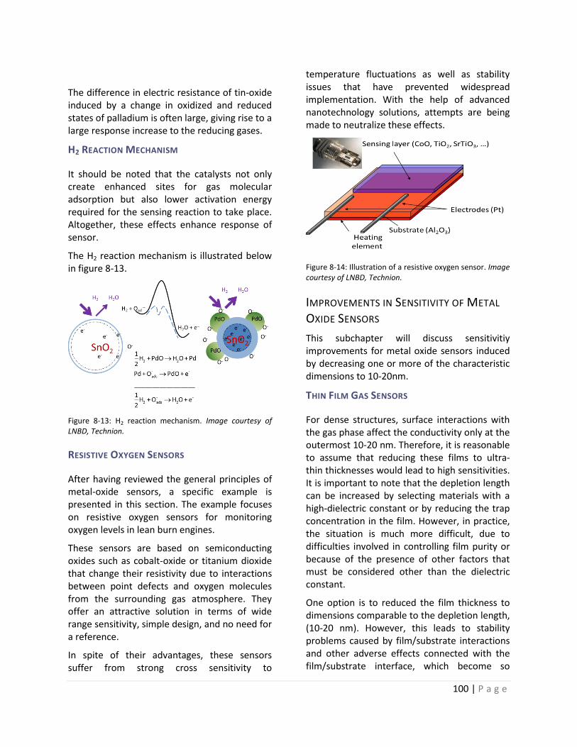
100 | P a g e
The difference in electric resistance of tin-oxide induced by a change in oxidized and reduced states of palladium is often large, giving rise to a large response increase to the reducing gases.
H2 REACTION MECHANISM
It should be noted that the catalysts not only create enhanced sites for gas molecular adsorption but also lower activation energy required for the sensing reaction to take place. Altogether, these effects enhance response of sensor.
The H2 reaction mechanism is illustrated below in figure 8-13.
Figure 8-13: H2 reaction mechanism. Image courtesy of LNBD, Technion.
RESISTIVE OXYGEN SENSORS
After having reviewed the general principles of metal-oxide sensors, a specific example is presented in this section. The example focuses on resistive oxygen sensors for monitoring oxygen levels in lean burn engines.
These sensors are based on semiconducting oxides such as cobalt-oxide or titanium dioxide that change their resistivity due to interactions between point defects and oxygen molecules from the surrounding gas atmosphere. They offer an attractive solution in terms of wide range sensitivity, simple design, and no need for a reference.
In spite of their advantages, these sensors suffer from strong cross sensitivity to
temperature fluctuations as well as stability issues that have prevented widespread implementation. With the help of advanced nanotechnology solutions, attempts are being made to neutralize these effects.
Figure 8-14: Illustration of a resistive oxygen sensor. Image courtesy of LNBD, Technion.
IMPROVEMENTS IN SENSITIVITY OF METAL
OXIDE SENSORS
This subchapter will discuss sensitivitiy improvements for metal oxide sensors induced by decreasing one or more of the characteristic dimensions to 10-20nm.
THIN FILM GAS SENSORS
For dense structures, surface interactions with the gas phase affect the conductivity only at the outermost 10-20 nm. Therefore, it is reasonable to assume that reducing these films to ultra-thin thicknesses would lead to high sensitivities. It is important to note that the depletion length can be increased by selecting materials with a high-dielectric constant or by reducing the trap concentration in the film. However, in practice, the situation is much more difficult, due to difficulties involved in controlling film purity or because of the presence of other factors that must be considered other than the dielectric constant.
One option is to reduced the film thickness to dimensions comparable to the depletion length, (10-20 nm). However, this leads to stability problems caused by film/substrate interactions and other adverse effects connected with the film/substrate interface, which become so
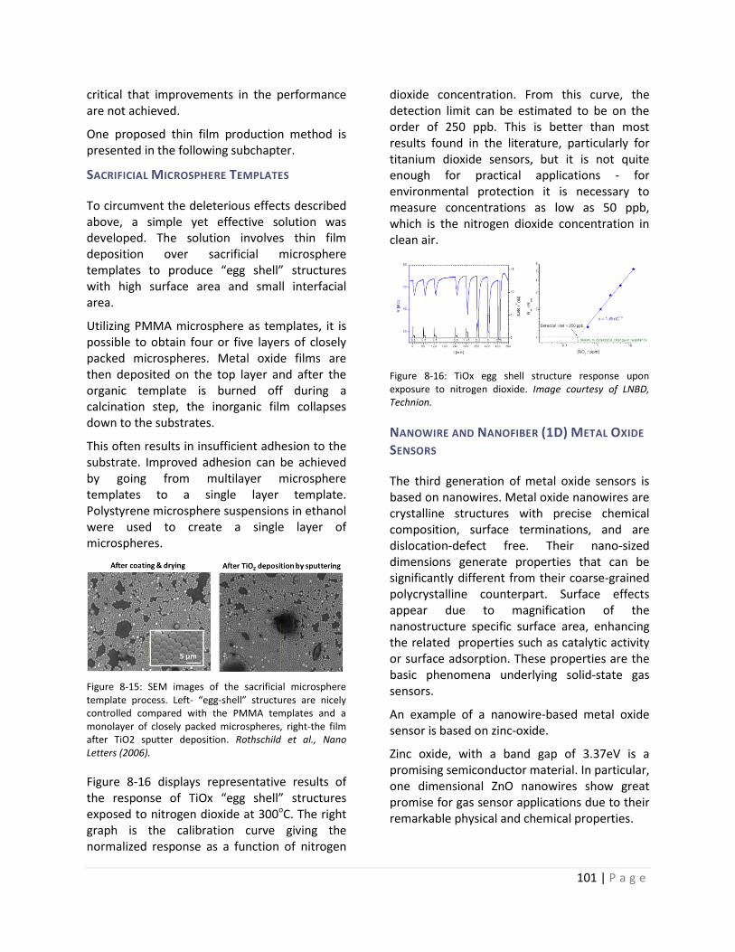
101 | P a g e
critical that improvements in the performance are not achieved.
One proposed thin film production method is presented in the following subchapter.
SACRIFICIAL MICROSPHERE TEMPLATES
To circumvent the deleterious effects described above, a simple yet effective solution was developed. The solution involves thin film deposition over sacrificial microsphere templates to produce “egg shell” structures with high surface area and small interfacial area.
Utilizing PMMA microsphere as templates, it is possible to obtain four or five layers of closely packed microspheres. Metal oxide films are then deposited on the top layer and after the organic template is burned off during a calcination step, the inorganic film collapses down to the substrates.
This often results in insufficient adhesion to the substrate. Improved adhesion can be achieved by going from multilayer microsphere templates to a single layer template. Polystyrene microsphere suspensions in ethanol were used to create a single layer of microspheres.
Figure 8-15: SEM images of the sacrificial microsphere template process. Left- “egg-shell” structures are nicely controlled compared with the PMMA templates and a monolayer of closely packed microspheres, right-the film after TiO2 sputter deposition. Rothschild et al., Nano Letters (2006).
Figure 8-16 displays representative results of the response of TiOx “egg shell” structures exposed to nitrogen dioxide at 300oC. The right graph is the calibration curve giving the normalized response as a function of nitrogen
dioxide concentration. From this curve, the detection limit can be estimated to be on the order of 250 ppb. This is better than most results found in the literature, particularly for titanium dioxide sensors, but it is not quite enough for practical applications - for environmental protection it is necessary to measure concentrations as low as 50 ppb, which is the nitrogen dioxide concentration in clean air.
Figure 8-16: TiOx egg shell structure response upon exposure to nitrogen dioxide. Image courtesy of LNBD, Technion.
NANOWIRE AND NANOFIBER (1D) METAL OXIDE
SENSORS
The third generation of metal oxide sensors is based on nanowires. Metal oxide nanowires are crystalline structures with precise chemical composition, surface terminations, and are dislocation-defect free. Their nano-sized dimensions generate properties that can be significantly different from their coarse-grained polycrystalline counterpart. Surface effects appear due to magnification of the nanostructure specific surface area, enhancing the related properties such as catalytic activity or surface adsorption. These properties are the basic phenomena underlying solid-state gas sensors.
An example of a nanowire-based metal oxide sensor is based on zinc-oxide.
Zinc oxide, with a band gap of 3.37eV is a promising semiconductor material. In particular, one dimensional ZnO nanowires show great promise for gas sensor applications due to their remarkable physical and chemical properties.
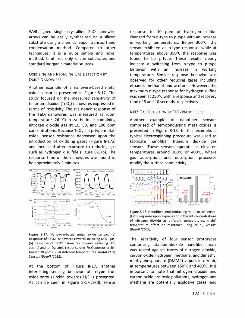
102 | P a g e
Well-aligned single crystalline ZnO nanowire arrays can be easily synthesized on a silicon substrate using a chemical vapor transport and condensation method. Compared to other techniques, it is a quite simple and novel method. It utilizes only silicon substrates and standard inorganic material sources.
OXIDIZING AND REDUCING GAS DETECTION BY
OXIDE NANOWIRES
Another example of a nanowire-based metal oxide sensor is presented in Figure 8-17. The study focused on the measured sensitivity of tellurium dioxide (TeO2) nanowires expressed in terms of resistivity. The resistance response of the TeO2 nanowires was measured at room temperature (26 °C) in synthetic air containing nitrogen dioxide gas at 10, 50, and 100 ppm concentrations. Because TeO2 is a p-type metal-oxide, sensor resistance decreased upon the introduction of oxidizing gases (Figure 8-17a) and increased after exposure to reducing gas such as hydrogen disulfide (Figure 8-17b). The response time of the nanowires was found to be approximately 2 minutes.
Figure 8-17: Nanowire-based metal oxide sensor. (a) Response of TeO2 nanowires towards oxidizing NO2 gas, (b) Response of TeO2 nanowires towards reducing H2S gas, (c) and (d) Dynamic response of α-Fe2O3 porous urchin toward 10 ppm H2S at different temperatures. Arafat et al, Sensors (Basel) (2012).
At the bottom of Figure 8-17, another interesting sensing behavior of n-type iron oxide porous urchin towards H2S is presented. As can be seen in Figure 8-17(c)-(d), sensor
response to 10 ppm of hydrogen sulfide changed from n-type to p-type with an increase in working temperatures. Below 300°C, the sensor exhibited an n-type response, while at temperatures above 350°C the response was found to be p-type. These results clearly indicate a switching from n-type to p-type behavior with an increase in working temperature. Similar response behavior was observed for other reducing gases including ethanol, methanol and acetone. However, the maximum n-type response for hydrogen sulfide was seen at 250°C with a response and recovery time of 5 and 10 seconds, respectively.
NO2 GAS DETECTION BY TIO2 NANOFIBERS
Another example of nanofiber sensors comprised of semiconducting metal-oxides is presented in Figure 8-18. In this example, a typical electrospinning procedure was used to fabricate nanofiber titanium dioxide gas sensors. These sensors operate at elevated temperatures around 300oC or 400oC, where gas adsorption and desorption processes modify the surface conductivity.
Figure 8-18: Nanofiber semiconducting metal oxide sensor. (Left) response upon exposure to different concentrations of nitrogen dioxide at different temperatures, (right) temperature effect on resistance. Ding et al, Sensors (Basel) (2009).
The sensitivity of four sensor prototypes comprising titanium-dioxide nanofiber mats was tested against traces of nitrogen dioxide, carbon oxide, hydrogen, methane, and dimethyl methylphosphonate (DMMP) vapors in dry air, at temperatures between 150°C and 400°C. It is important to note that nitrogen dioxide and carbon oxide are toxic pollutants, hydrogen and methane are potentially explosive gases, and
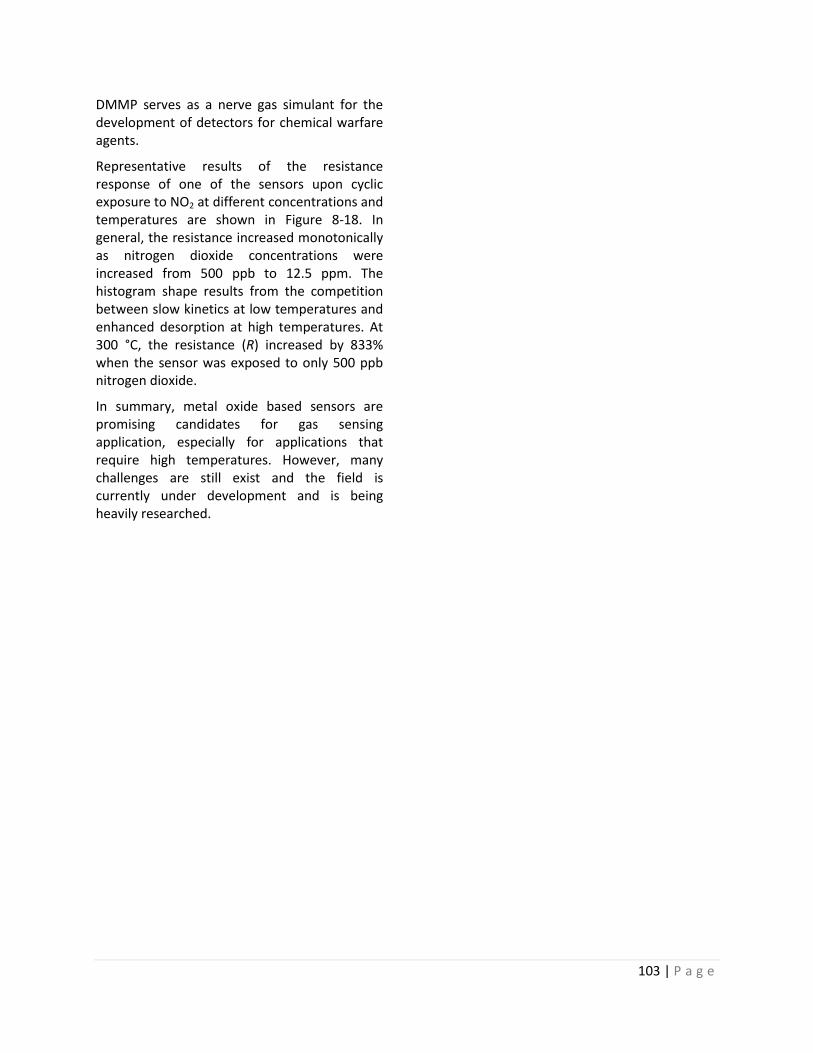
103 | P a g e
DMMP serves as a nerve gas simulant for the development of detectors for chemical warfare agents.
Representative results of the resistance response of one of the sensors upon cyclic exposure to NO2 at different concentrations and temperatures are shown in Figure 8-18. In general, the resistance increased monotonically as nitrogen dioxide concentrations were increased from 500 ppb to 12.5 ppm. The histogram shape results from the competition between slow kinetics at low temperatures and enhanced desorption at high temperatures. At 300 °C, the resistance (R) increased by 833% when the sensor was exposed to only 500 ppb nitrogen dioxide.
In summary, metal oxide based sensors are promising candidates for gas sensing application, especially for applications that require high temperatures. However, many challenges are still exist and the field is currently under development and is being heavily researched.
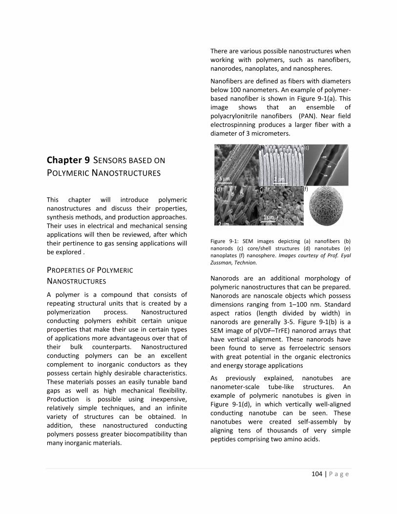
104 | P a g e
Chapter 9 SENSORS BASED ON
POLYMERIC NANOSTRUCTURES
This chapter will introduce polymeric nanostructures and discuss their properties, synthesis methods, and production approaches. Their uses in electrical and mechanical sensing applications will then be reviewed, after which their pertinence to gas sensing applications will be explored .
PROPERTIES OF POLYMERIC
NANOSTRUCTURES
A polymer is a compound that consists of repeating structural units that is created by a polymerization process. Nanostructured conducting polymers exhibit certain unique properties that make their use in certain types of applications more advantageous over that of their bulk counterparts. Nanostructured conducting polymers can be an excellent complement to inorganic conductors as they possess certain highly desirable characteristics. These materials posses an easily tunable band gaps as well as high mechanical flexibility. Production is possible using inexpensive, relatively simple techniques, and an infinite variety of structures can be obtained. In addition, these nanostructured conducting polymers possess greater biocompatibility than many inorganic materials.
There are various possible nanostructures when working with polymers, such as nanofibers, nanorodes, nanoplates, and nanospheres.
Nanofibers are defined as fibers with diameters below 100 nanometers. An example of polymer-based nanofiber is shown in Figure 9-1(a). This image shows that an ensemble of polyacrylonitrile nanofibers (PAN). Near field electrospinning produces a larger fiber with a diameter of 3 micrometers.
Figure 9-1: SEM images depicting (a) nanofibers (b) nanorods (c) core/shell structures (d) nanotubes (e) nanoplates (f) nanosphere. Images courtesy of Prof. Eyal Zussman, Technion.
Nanorods are an additional morphology of polymeric nanostructures that can be prepared. Nanorods are nanoscale objects which possess dimensions ranging from 1–100 nm. Standard aspect ratios (length divided by width) in nanorods are generally 3-5. Figure 9-1(b) is a SEM image of p(VDF–TrFE) nanorod arrays that have vertical alignment. These nanorods have been found to serve as ferroelectric sensors with great potential in the organic electronics and energy storage applications
As previously explained, nanotubes are nanometer-scale tube-like structures. An example of polymeric nanotubes is given in Figure 9-1(d), in which vertically well-aligned conducting nanotube can be seen. These nanotubes were created self-assembly by aligning tens of thousands of very simple peptides comprising two amino acids.
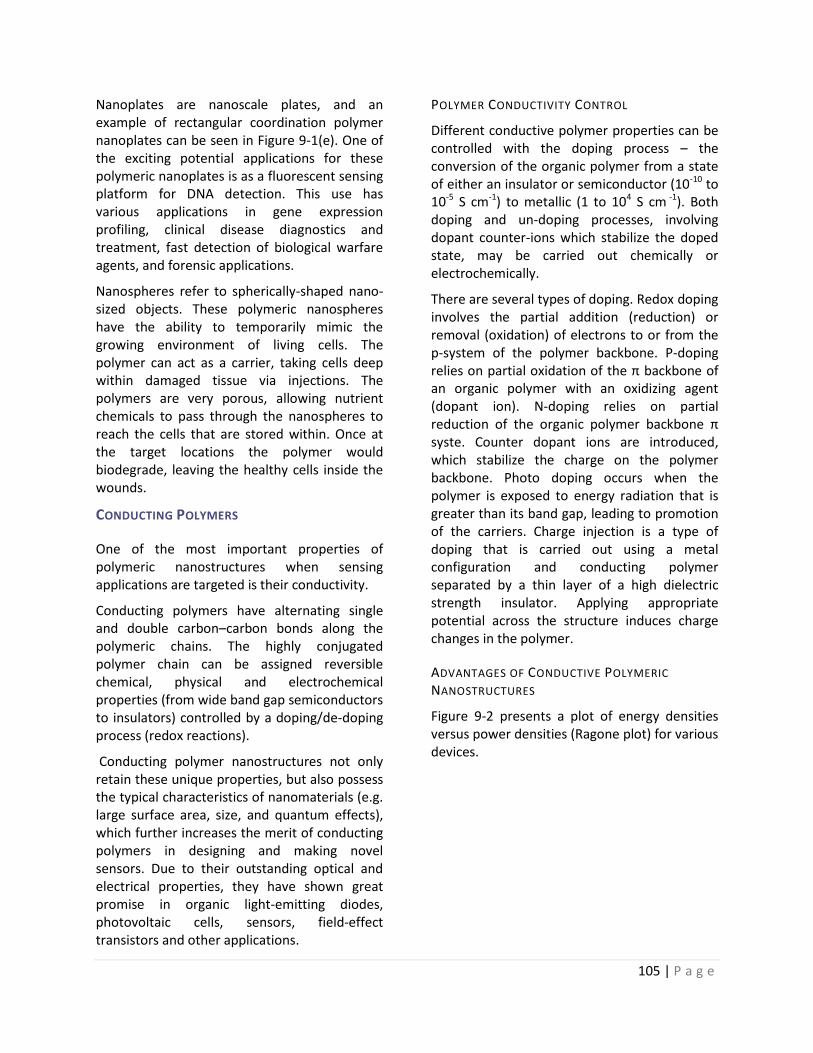
105 | P a g e
Nanoplates are nanoscale plates, and an example of rectangular coordination polymer nanoplates can be seen in Figure 9-1(e). One of the exciting potential applications for these polymeric nanoplates is as a fluorescent sensing platform for DNA detection. This use has various applications in gene expression profiling, clinical disease diagnostics and treatment, fast detection of biological warfare agents, and forensic applications.
Nanospheres refer to spherically-shaped nano-sized objects. These polymeric nanospheres have the ability to temporarily mimic the growing environment of living cells. The polymer can act as a carrier, taking cells deep within damaged tissue via injections. The polymers are very porous, allowing nutrient chemicals to pass through the nanospheres to reach the cells that are stored within. Once at the target locations the polymer would biodegrade, leaving the healthy cells inside the wounds.
CONDUCTING POLYMERS
One of the most important properties of polymeric nanostructures when sensing applications are targeted is their conductivity.
Conducting polymers have alternating single and double carbon–carbon bonds along the polymeric chains. The highly conjugated polymer chain can be assigned reversible chemical, physical and electrochemical properties (from wide band gap semiconductors to insulators) controlled by a doping/de-doping process (redox reactions).
Conducting polymer nanostructures not only retain these unique properties, but also possess the typical characteristics of nanomaterials (e.g. large surface area, size, and quantum effects), which further increases the merit of conducting polymers in designing and making novel sensors. Due to their outstanding optical and electrical properties, they have shown great promise in organic light-emitting diodes, photovoltaic cells, sensors, field-effect transistors and other applications.
POLYMER CONDUCTIVITY CONTROL
Different conductive polymer properties can be controlled with the doping process – the conversion of the organic polymer from a state of either an insulator or semiconductor (10-10 to 10-5 S cm-1) to metallic (1 to 104 S cm -1). Both doping and un-doping processes, involving dopant counter-ions which stabilize the doped state, may be carried out chemically or electrochemically.
There are several types of doping. Redox doping involves the partial addition (reduction) or removal (oxidation) of electrons to or from the p-system of the polymer backbone. P-doping relies on partial oxidation of the π backbone of an organic polymer with an oxidizing agent (dopant ion). N-doping relies on partial reduction of the organic polymer backbone π syste. Counter dopant ions are introduced, which stabilize the charge on the polymer backbone. Photo doping occurs when the polymer is exposed to energy radiation that is greater than its band gap, leading to promotion of the carriers. Charge injection is a type of doping that is carried out using a metal configuration and conducting polymer separated by a thin layer of a high dielectric strength insulator. Applying appropriate potential across the structure induces charge changes in the polymer.
ADVANTAGES OF CONDUCTIVE POLYMERIC
NANOSTRUCTURES
Figure 9-2 presents a plot of energy densities versus power densities (Ragone plot) for various devices.
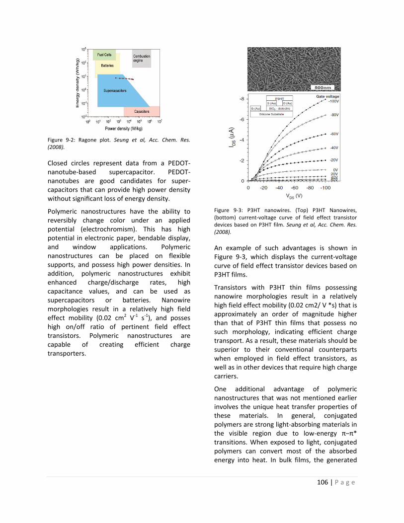
106 | P a g e
Figure 9-2: Ragone plot. Seung et al, Acc. Chem. Res. (2008).
Closed circles represent data from a PEDOT-nanotube-based supercapacitor. PEDOT-nanotubes are good candidates for super-capacitors that can provide high power density without significant loss of energy density.
Polymeric nanostructures have the ability to reversibly change color under an applied potential (electrochromism). This has high potential in electronic paper, bendable display, and window applications. Polymeric nanostructures can be placed on flexible supports, and possess high power densities. In addition, polymeric nanostructures exhibit enhanced charge/discharge rates, high capacitance values, and can be used as supercapacitors or batteries. Nanowire morphologies result in a relatively high field effect mobility (0.02 cm2 V-1 s-1), and posses high on/off ratio of pertinent field effect transistors. Polymeric nanostructures are capable of creating efficient charge transporters.
Figure 9-3: P3HT nanowires. (Top) P3HT Nanowires, (bottom) current-voltage curve of field effect transistor devices based on P3HT film. Seung et al, Acc. Chem. Res. (2008).
An example of such advantages is shown in Figure 9-3, which displays the current-voltage curve of field effect transistor devices based on P3HT films.
Transistors with P3HT thin films possessing nanowire morphologies result in a relatively high field effect mobility (0.02 cm2/ V *s) that is approximately an order of magnitude higher than that of P3HT thin films that possess no such morphology, indicating efficient charge transport. As a result, these materials should be superior to their conventional counterparts when employed in field effect transistors, as well as in other devices that require high charge carriers.
One additional advantage of polymeric nanostructures that was not mentioned earlier involves the unique heat transfer properties of these materials. In general, conjugated polymers are strong light-absorbing materials in the visible region due to low-energy π–π* transitions. When exposed to light, conjugated polymers can convert most of the absorbed energy into heat. In bulk films, the generated
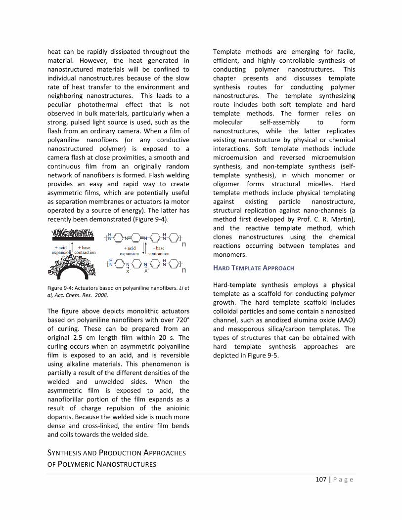
107 | P a g e
heat can be rapidly dissipated throughout the material. However, the heat generated in nanostructured materials will be confined to individual nanostructures because of the slow rate of heat transfer to the environment and neighboring nanostructures. This leads to a peculiar photothermal effect that is not observed in bulk materials, particularly when a strong, pulsed light source is used, such as the flash from an ordinary camera. When a film of polyaniline nanofibers (or any conductive nanostructured polymer) is exposed to a camera flash at close proximities, a smooth and continuous film from an originally random network of nanofibers is formed. Flash welding provides an easy and rapid way to create asymmetric films, which are potentially useful as separation membranes or actuators (a motor operated by a source of energy). The latter has recently been demonstrated (Figure 9-4).
Figure 9-4: Actuators based on polyaniline nanofibers. Li et al, Acc. Chem. Res. 2008.
The figure above depicts monolithic actuators based on polyaniline nanofibers with over 720° of curling. These can be prepared from an original 2.5 cm length film within 20 s. The curling occurs when an asymmetric polyaniline film is exposed to an acid, and is reversible using alkaline materials. This phenomenon is partially a result of the different densities of the welded and unwelded sides. When the asymmetric film is exposed to acid, the nanofibrillar portion of the film expands as a result of charge repulsion of the anioinic dopants. Because the welded side is much more dense and cross-linked, the entire film bends and coils towards the welded side.
SYNTHESIS AND PRODUCTION APPROACHES
OF POLYMERIC NANOSTRUCTURES
Template methods are emerging for facile, efficient, and highly controllable synthesis of conducting polymer nanostructures. This chapter presents and discusses template synthesis routes for conducting polymer nanostructures. The template synthesizing route includes both soft template and hard template methods. The former relies on molecular self-assembly to form nanostructures, while the latter replicates existing nanostructure by physical or chemical interactions. Soft template methods include microemulsion and reversed microemulsion synthesis, and non-template synthesis (self-template synthesis), in which monomer or oligomer forms structural micelles. Hard template methods include physical templating against existing particle nanostructure, structural replication against nano-channels (a method first developed by Prof. C. R. Martin), and the reactive template method, which clones nanostructures using the chemical reactions occurring between templates and monomers.
HARD TEMPLATE APPROACH
Hard-template synthesis employs a physical template as a scaffold for conducting polymer growth. The hard template scaffold includes colloidal particles and some contain a nanosized channel, such as anodized alumina oxide (AAO) and mesoporous silica/carbon templates. The types of structures that can be obtained with hard template synthesis approaches are depicted in Figure 9-5.
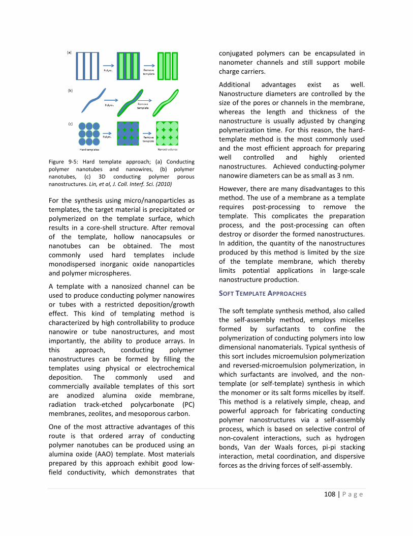
108 | P a g e
Figure 9-5: Hard template approach; (a) Conducting polymer nanotubes and nanowires, (b) polymer nanotubes, (c) 3D conducting polymer porous nanostructures. Lin, et al, J. Coll. Interf. Sci. (2010)
For the synthesis using micro/nanoparticles as templates, the target material is precipitated or polymerized on the template surface, which results in a core-shell structure. After removal of the template, hollow nanocapsules or nanotubes can be obtained. The most commonly used hard templates include monodispersed inorganic oxide nanoparticles and polymer microspheres.
A template with a nanosized channel can be used to produce conducting polymer nanowires or tubes with a restricted deposition/growth effect. This kind of templating method is characterized by high controllability to produce nanowire or tube nanostructures, and most importantly, the ability to produce arrays. In this approach, conducting polymer nanostructures can be formed by filling the templates using physical or electrochemical deposition. The commonly used and commercially available templates of this sort are anodized alumina oxide membrane, radiation track-etched polycarbonate (PC) membranes, zeolites, and mesoporous carbon.
One of the most attractive advantages of this route is that ordered array of conducting polymer nanotubes can be produced using an alumina oxide (AAO) template. Most materials prepared by this approach exhibit good low-field conductivity, which demonstrates that
conjugated polymers can be encapsulated in nanometer channels and still support mobile charge carriers.
Additional advantages exist as well. Nanostructure diameters are controlled by the size of the pores or channels in the membrane, whereas the length and thickness of the nanostructure is usually adjusted by changing polymerization time. For this reason, the hard-template method is the most commonly used and the most efficient approach for preparing well controlled and highly oriented nanostructures. Achieved conducting-polymer nanowire diameters can be as small as 3 nm.
However, there are many disadvantages to this method. The use of a membrane as a template requires post-processing to remove the template. This complicates the preparation process, and the post-processing can often destroy or disorder the formed nanostructures. In addition, the quantity of the nanostructures produced by this method is limited by the size of the template membrane, which thereby limits potential applications in large-scale nanostructure production.
SOFT TEMPLATE APPROACHES
The soft template synthesis method, also called the self-assembly method, employs micelles formed by surfactants to confine the polymerization of conducting polymers into low dimensional nanomaterials. Typical synthesis of this sort includes microemulsion polymerization and reversed-microemulsion polymerization, in which surfactants are involved, and the non-template (or self-template) synthesis in which the monomer or its salt forms micelles by itself. This method is a relatively simple, cheap, and powerful approach for fabricating conducting polymer nanostructures via a self-assembly process, which is based on selective control of non-covalent interactions, such as hydrogen bonds, Van der Waals forces, pi-pi stacking interaction, metal coordination, and dispersive forces as the driving forces of self-assembly.
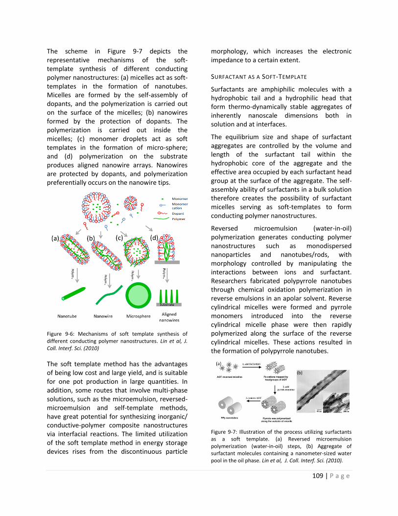
109 | P a g e
The scheme in Figure 9-7 depicts the representative mechanisms of the soft-template synthesis of different conducting polymer nanostructures: (a) micelles act as soft-templates in the formation of nanotubes. Micelles are formed by the self-assembly of dopants, and the polymerization is carried out on the surface of the micelles; (b) nanowires formed by the protection of dopants. The polymerization is carried out inside the micelles; (c) monomer droplets act as soft templates in the formation of micro-sphere; and (d) polymerization on the substrate produces aligned nanowire arrays. Nanowires are protected by dopants, and polymerization preferentially occurs on the nanowire tips.
Figure 9-6: Mechanisms of soft template synthesis of different conducting polymer nanostructures. Lin et al, J. Coll. Interf. Sci. (2010)
The soft template method has the advantages of being low cost and large yield, and is suitable for one pot production in large quantities. In addition, some routes that involve multi-phase solutions, such as the microemulsion, reversed-microemulsion and self-template methods, have great potential for synthesizing inorganic/ conductive-polymer composite nanostructures via interfacial reactions. The limited utilization of the soft template method in energy storage devices rises from the discontinuous particle
morphology, which increases the electronic impedance to a certain extent.
SURFACTANT AS A SOFT-TEMPLATE
Surfactants are amphiphilic molecules with a hydrophobic tail and a hydrophilic head that form thermo-dynamically stable aggregates of inherently nanoscale dimensions both in solution and at interfaces.
The equilibrium size and shape of surfactant aggregates are controlled by the volume and length of the surfactant tail within the hydrophobic core of the aggregate and the effective area occupied by each surfactant head group at the surface of the aggregate. The self-assembly ability of surfactants in a bulk solution therefore creates the possibility of surfactant micelles serving as soft-templates to form conducting polymer nanostructures.
Reversed microemulsion (water-in-oil) polymerization generates conducting polymer nanostructures such as monodispersed nanoparticles and nanotubes/rods, with morphology controlled by manipulating the interactions between ions and surfactant. Researchers fabricated polypyrrole nanotubes through chemical oxidation polymerization in reverse emulsions in an apolar solvent. Reverse cylindrical micelles were formed and pyrrole monomers introduced into the reverse cylindrical micelle phase were then rapidly polymerized along the surface of the reverse cylindrical micelles. These actions resulted in the formation of polypyrrole nanotubes.
Figure 9-7: Illustration of the process utilizing surfactants as a soft template. (a) Reversed microemulsion polymerization (water-in-oil) steps, (b) Aggregate of surfactant molecules containing a nanometer-sized water pool in the oil phase. Lin et al, J. Coll. Interf. Sci. (2010).
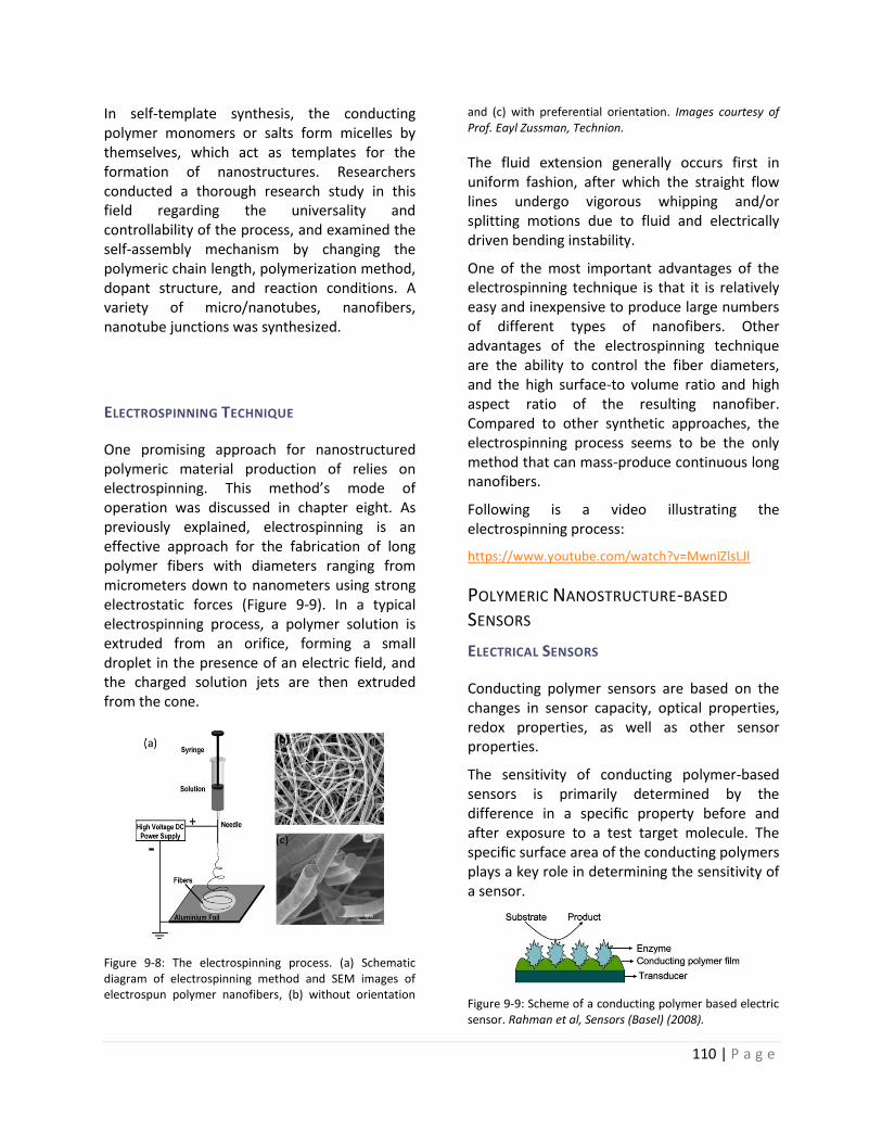
110 | P a g e
In self-template synthesis, the conducting polymer monomers or salts form micelles by themselves, which act as templates for the formation of nanostructures. Researchers conducted a thorough research study in this field regarding the universality and controllability of the process, and examined the self-assembly mechanism by changing the polymeric chain length, polymerization method, dopant structure, and reaction conditions. A variety of micro/nanotubes, nanofibers, nanotube junctions was synthesized.
ELECTROSPINNING TECHNIQUE
One promising approach for nanostructured polymeric material production of relies on electrospinning. This method’s mode of operation was discussed in chapter eight. As previously explained, electrospinning is an effective approach for the fabrication of long polymer fibers with diameters ranging from micrometers down to nanometers using strong electrostatic forces (Figure 9-9). In a typical electrospinning process, a polymer solution is extruded from an orifice, forming a small droplet in the presence of an electric field, and the charged solution jets are then extruded from the cone.
Figure 9-8: The electrospinning process. (a) Schematic diagram of electrospinning method and SEM images of electrospun polymer nanofibers, (b) without orientation
and (c) with preferential orientation. Images courtesy of Prof. Eayl Zussman, Technion.
The fluid extension generally occurs first in uniform fashion, after which the straight flow lines undergo vigorous whipping and/or splitting motions due to fluid and electrically driven bending instability.
One of the most important advantages of the electrospinning technique is that it is relatively easy and inexpensive to produce large numbers of different types of nanofibers. Other advantages of the electrospinning technique are the ability to control the fiber diameters, and the high surface-to volume ratio and high aspect ratio of the resulting nanofiber. Compared to other synthetic approaches, the electrospinning process seems to be the only method that can mass-produce continuous long nanofibers.
Following is a video illustrating the electrospinning process:
https://www.youtube.com/watch?v=MwniZlsLJl
POLYMERIC NANOSTRUCTURE-BASED
SENSORS
ELECTRICAL SENSORS
Conducting polymer sensors are based on the changes in sensor capacity, optical properties, redox properties, as well as other sensor properties.
The sensitivity of conducting polymer-based sensors is primarily determined by the difference in a specific property before and after exposure to a test target molecule. The specific surface area of the conducting polymers plays a key role in determining the sensitivity of a sensor.
Figure 9-9: Scheme of a conducting polymer based electric sensor. Rahman et al, Sensors (Basel) (2008).
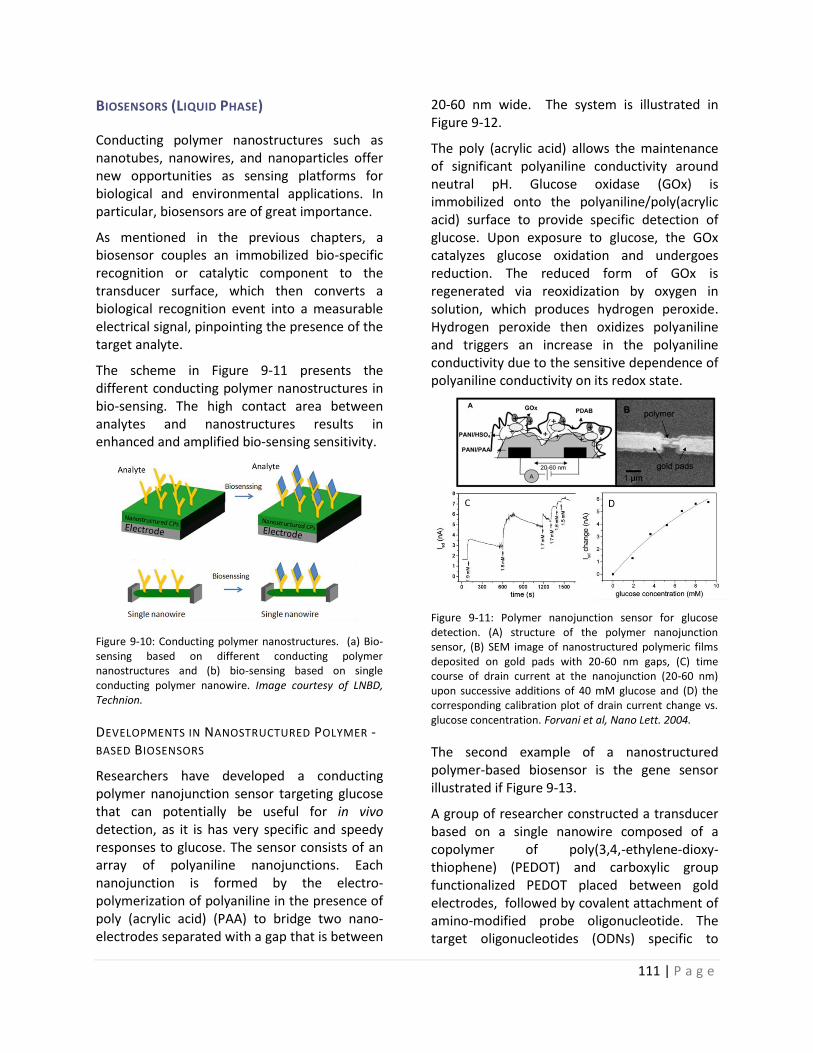
111 | P a g e
BIOSENSORS (LIQUID PHASE)
Conducting polymer nanostructures such as nanotubes, nanowires, and nanoparticles offer new opportunities as sensing platforms for biological and environmental applications. In particular, biosensors are of great importance.
As mentioned in the previous chapters, a biosensor couples an immobilized bio-specific recognition or catalytic component to the transducer surface, which then converts a biological recognition event into a measurable electrical signal, pinpointing the presence of the target analyte.
The scheme in Figure 9-11 presents the different conducting polymer nanostructures in bio-sensing. The high contact area between analytes and nanostructures results in enhanced and amplified bio-sensing sensitivity.
Figure 9-10: Conducting polymer nanostructures. (a) Bio-sensing based on different conducting polymer nanostructures and (b) bio-sensing based on single conducting polymer nanowire. Image courtesy of LNBD, Technion.
DEVELOPMENTS IN NANOSTRUCTURED POLYMER -BASED BIOSENSORS
Researchers have developed a conducting polymer nanojunction sensor targeting glucose that can potentially be useful for in vivo detection, as it is has very specific and speedy responses to glucose. The sensor consists of an array of polyaniline nanojunctions. Each nanojunction is formed by the electro-polymerization of polyaniline in the presence of poly (acrylic acid) (PAA) to bridge two nano-electrodes separated with a gap that is between
20-60 nm wide. The system is illustrated in Figure 9-12.
The poly (acrylic acid) allows the maintenance of significant polyaniline conductivity around neutral pH. Glucose oxidase (GOx) is immobilized onto the polyaniline/poly(acrylic acid) surface to provide specific detection of glucose. Upon exposure to glucose, the GOx catalyzes glucose oxidation and undergoes reduction. The reduced form of GOx is regenerated via reoxidization by oxygen in solution, which produces hydrogen peroxide. Hydrogen peroxide then oxidizes polyaniline and triggers an increase in the polyaniline conductivity due to the sensitive dependence of polyaniline conductivity on its redox state.
Figure 9-11: Polymer nanojunction sensor for glucose detection. (A) structure of the polymer nanojunction sensor, (B) SEM image of nanostructured polymeric films deposited on gold pads with 20-60 nm gaps, (C) time course of drain current at the nanojunction (20-60 nm) upon successive additions of 40 mM glucose and (D) the corresponding calibration plot of drain current change vs. glucose concentration. Forvani et al, Nano Lett. 2004.
The second example of a nanostructured polymer-based biosensor is the gene sensor illustrated if Figure 9-13.
A group of researcher constructed a transducer based on a single nanowire composed of a copolymer of poly(3,4,-ethylene-dioxy-thiophene) (PEDOT) and carboxylic group functionalized PEDOT placed between gold electrodes, followed by covalent attachment of amino-modified probe oligonucleotide. The target oligonucleotides (ODNs) specific to
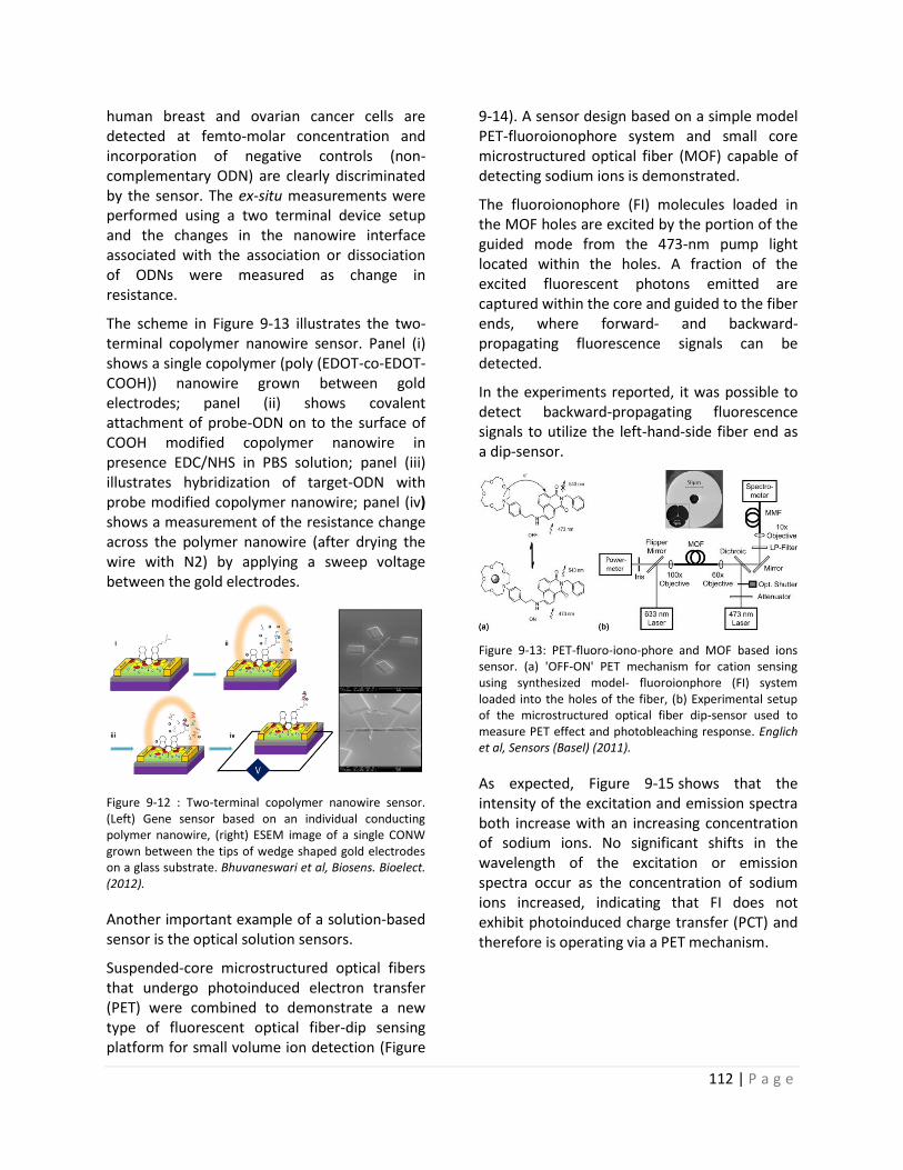
112 | P a g e
human breast and ovarian cancer cells are detected at femto-molar concentration and incorporation of negative controls (non-complementary ODN) are clearly discriminated by the sensor. The ex-situ measurements were performed using a two terminal device setup and the changes in the nanowire interface associated with the association or dissociation of ODNs were measured as change in resistance.
The scheme in Figure 9-13 illustrates the two-terminal copolymer nanowire sensor. Panel (i) shows a single copolymer (poly (EDOT-co-EDOT-COOH)) nanowire grown between gold electrodes; panel (ii) shows covalent attachment of probe-ODN on to the surface of COOH modified copolymer nanowire in presence EDC/NHS in PBS solution; panel (iii) illustrates hybridization of target-ODN with probe modified copolymer nanowire; panel (iv) shows a measurement of the resistance change across the polymer nanowire (after drying the wire with N2) by applying a sweep voltage between the gold electrodes.
Figure 9-12 : Two-terminal copolymer nanowire sensor. (Left) Gene sensor based on an individual conducting polymer nanowire, (right) ESEM image of a single CONW grown between the tips of wedge shaped gold electrodes on a glass substrate. Bhuvaneswari et al, Biosens. Bioelect. (2012).
Another important example of a solution-based sensor is the optical solution sensors.
Suspended-core microstructured optical fibers that undergo photoinduced electron transfer (PET) were combined to demonstrate a new type of fluorescent optical fiber-dip sensing platform for small volume ion detection (Figure
9-14). A sensor design based on a simple model PET-fluoroionophore system and small core microstructured optical fiber (MOF) capable of detecting sodium ions is demonstrated.
The fluoroionophore (FI) molecules loaded in the MOF holes are excited by the portion of the guided mode from the 473-nm pump light located within the holes. A fraction of the excited fluorescent photons emitted are captured within the core and guided to the fiber ends, where forward- and backward-propagating fluorescence signals can be detected.
In the experiments reported, it was possible to detect backward-propagating fluorescence signals to utilize the left-hand-side fiber end as a dip-sensor.
Figure 9-13: PET-fluoro-iono-phore and MOF based ions sensor. (a) 'OFF-ON' PET mechanism for cation sensing using synthesized model- fluoroionphore (FI) system loaded into the holes of the fiber, (b) Experimental setup of the microstructured optical fiber dip-sensor used to measure PET effect and photobleaching response. Englich et al, Sensors (Basel) (2011).
As expected, Figure 9-15 shows that the intensity of the excitation and emission spectra both increase with an increasing concentration of sodium ions. No significant shifts in the wavelength of the excitation or emission spectra occur as the concentration of sodium ions increased, indicating that FI does not exhibit photoinduced charge transfer (PCT) and therefore is operating via a PET mechanism.
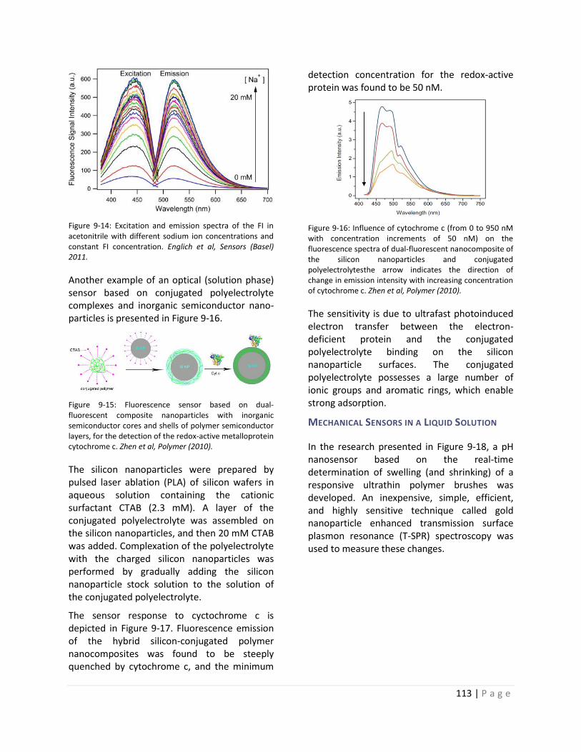
113 | P a g e
Figure 9-14: Excitation and emission spectra of the FI in acetonitrile with different sodium ion concentrations and constant FI concentration. Englich et al, Sensors (Basel) 2011.
Another example of an optical (solution phase) sensor based on conjugated polyelectrolyte complexes and inorganic semiconductor nano-particles is presented in Figure 9-16.
Figure 9-15: Fluorescence sensor based on dual-fluorescent composite nanoparticles with inorganic semiconductor cores and shells of polymer semiconductor layers, for the detection of the redox-active metalloprotein cytochrome c. Zhen et al, Polymer (2010).
The silicon nanoparticles were prepared by pulsed laser ablation (PLA) of silicon wafers in aqueous solution containing the cationic surfactant CTAB (2.3 mM). A layer of the conjugated polyelectrolyte was assembled on the silicon nanoparticles, and then 20 mM CTAB was added. Complexation of the polyelectrolyte with the charged silicon nanoparticles was performed by gradually adding the silicon nanoparticle stock solution to the solution of the conjugated polyelectrolyte.
The sensor response to cyctochrome c is depicted in Figure 9-17. Fluorescence emission of the hybrid silicon-conjugated polymer nanocomposites was found to be steeply quenched by cytochrome c, and the minimum
detection concentration for the redox-active protein was found to be 50 nM.
Figure 9-16: Influence of cytochrome c (from 0 to 950 nM with concentration increments of 50 nM) on the fluorescence spectra of dual-fluorescent nanocomposite of the silicon nanoparticles and conjugated polyelectrolytesthe arrow indicates the direction of change in emission intensity with increasing concentration of cytochrome c. Zhen et al, Polymer (2010).
The sensitivity is due to ultrafast photoinduced electron transfer between the electron-deficient protein and the conjugated polyelectrolyte binding on the silicon nanoparticle surfaces. The conjugated polyelectrolyte possesses a large number of ionic groups and aromatic rings, which enable strong adsorption.
MECHANICAL SENSORS IN A LIQUID SOLUTION
In the research presented in Figure 9-18, a pH nanosensor based on the real-time determination of swelling (and shrinking) of a responsive ultrathin polymer brushes was developed. An inexpensive, simple, efficient, and highly sensitive technique called gold nanoparticle enhanced transmission surface plasmon resonance (T-SPR) spectroscopy was used to measure these changes.
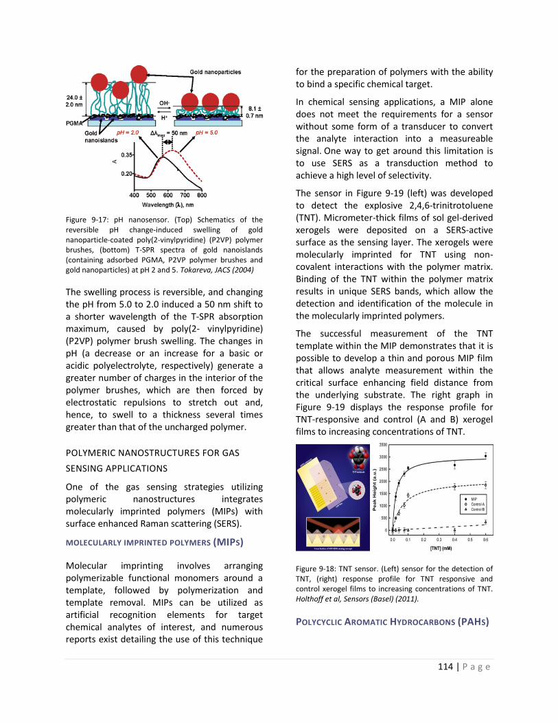
114 | P a g e
Figure 9-17: pH nanosensor. (Top) Schematics of the reversible pH change-induced swelling of gold nanoparticle-coated poly(2-vinylpyridine) (P2VP) polymer brushes, (bottom) T-SPR spectra of gold nanoislands (containing adsorbed PGMA, P2VP polymer brushes and gold nanoparticles) at pH 2 and 5. Tokareva, JACS (2004)
The swelling process is reversible, and changing the pH from 5.0 to 2.0 induced a 50 nm shift to a shorter wavelength of the T-SPR absorption maximum, caused by poly(2- vinylpyridine) (P2VP) polymer brush swelling. The changes in pH (a decrease or an increase for a basic or acidic polyelectrolyte, respectively) generate a greater number of charges in the interior of the polymer brushes, which are then forced by electrostatic repulsions to stretch out and, hence, to swell to a thickness several times greater than that of the uncharged polymer.
POLYMERIC NANOSTRUCTURES FOR GAS
SENSING APPLICATIONS
One of the gas sensing strategies utilizing polymeric nanostructures integrates molecularly imprinted polymers (MIPs) with surface enhanced Raman scattering (SERS).
MOLECULARLY IMPRINTED POLYMERS (MIPS)
Molecular imprinting involves arranging polymerizable functional monomers around a template, followed by polymerization and template removal. MIPs can be utilized as artificial recognition elements for target chemical analytes of interest, and numerous reports exist detailing the use of this technique
for the preparation of polymers with the ability to bind a specific chemical target.
In chemical sensing applications, a MIP alone does not meet the requirements for a sensor without some form of a transducer to convert the analyte interaction into a measureable signal. One way to get around this limitation is to use SERS as a transduction method to achieve a high level of selectivity.
The sensor in Figure 9-19 (left) was developed to detect the explosive 2,4,6-trinitrotoluene (TNT). Micrometer-thick films of sol gel-derived xerogels were deposited on a SERS-active surface as the sensing layer. The xerogels were molecularly imprinted for TNT using non-covalent interactions with the polymer matrix. Binding of the TNT within the polymer matrix results in unique SERS bands, which allow the detection and identification of the molecule in the molecularly imprinted polymers.
The successful measurement of the TNT template within the MIP demonstrates that it is possible to develop a thin and porous MIP film that allows analyte measurement within the critical surface enhancing field distance from the underlying substrate. The right graph in Figure 9-19 displays the response profile for TNT-responsive and control (A and B) xerogel films to increasing concentrations of TNT.
Figure 9-18: TNT sensor. (Left) sensor for the detection of TNT, (right) response profile for TNT responsive and control xerogel films to increasing concentrations of TNT. Holthoff et al, Sensors (Basel) (2011).
POLYCYCLIC AROMATIC HYDROCARBONS (PAHS)
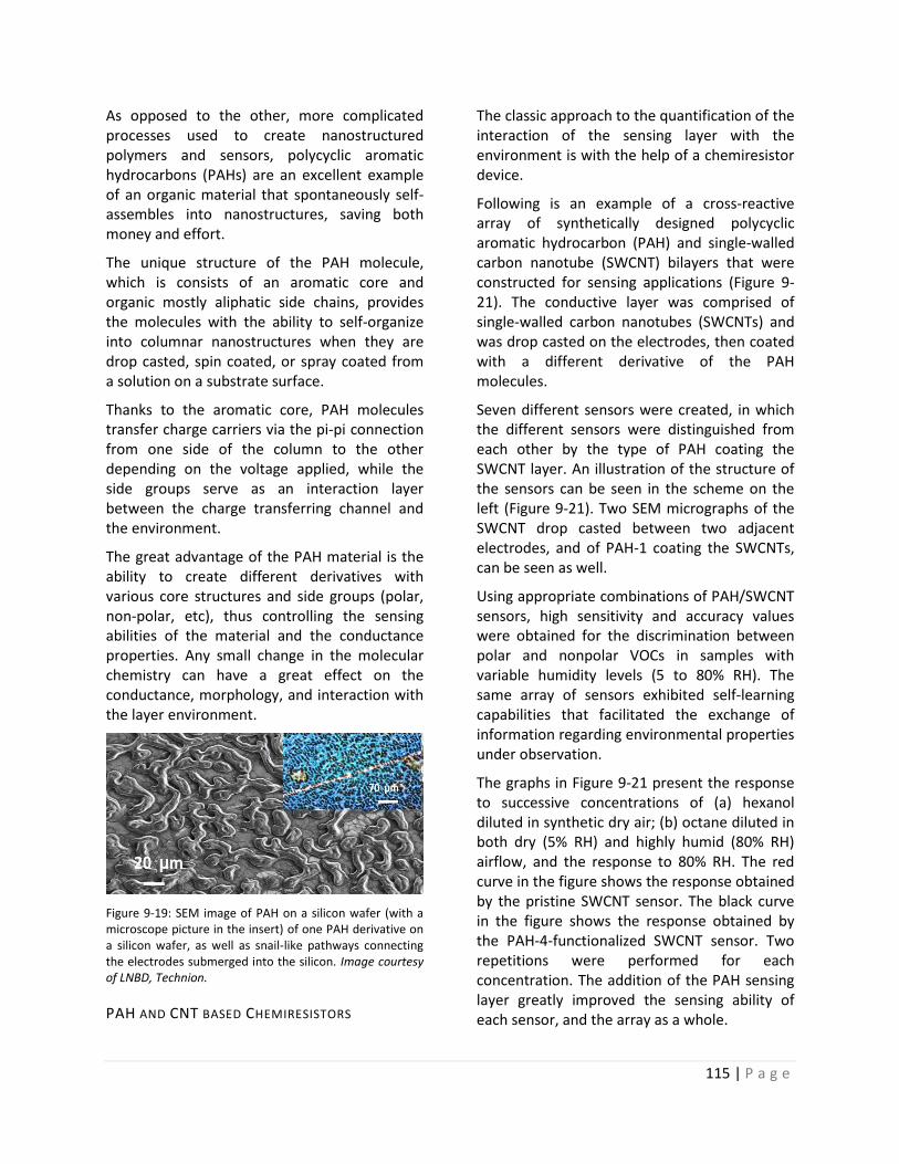
115 | P a g e
As opposed to the other, more complicated processes used to create nanostructured polymers and sensors, polycyclic aromatic hydrocarbons (PAHs) are an excellent example of an organic material that spontaneously self-assembles into nanostructures, saving both money and effort.
The unique structure of the PAH molecule, which is consists of an aromatic core and organic mostly aliphatic side chains, provides the molecules with the ability to self-organize into columnar nanostructures when they are drop casted, spin coated, or spray coated from a solution on a substrate surface.
Thanks to the aromatic core, PAH molecules transfer charge carriers via the pi-pi connection from one side of the column to the other depending on the voltage applied, while the side groups serve as an interaction layer between the charge transferring channel and the environment.
The great advantage of the PAH material is the ability to create different derivatives with various core structures and side groups (polar, non-polar, etc), thus controlling the sensing abilities of the material and the conductance properties. Any small change in the molecular chemistry can have a great effect on the conductance, morphology, and interaction with the layer environment.
Figure 9-19: SEM image of PAH on a silicon wafer (with a microscope picture in the insert) of one PAH derivative on a silicon wafer, as well as snail-like pathways connecting the electrodes submerged into the silicon. Image courtesy of LNBD, Technion.
PAH AND CNT BASED CHEMIRESISTORS
The classic approach to the quantification of the interaction of the sensing layer with the environment is with the help of a chemiresistor device.
Following is an example of a cross-reactive array of synthetically designed polycyclic aromatic hydrocarbon (PAH) and single-walled carbon nanotube (SWCNT) bilayers that were constructed for sensing applications (Figure 9-21). The conductive layer was comprised of single-walled carbon nanotubes (SWCNTs) and was drop casted on the electrodes, then coated with a different derivative of the PAH molecules.
Seven different sensors were created, in which the different sensors were distinguished from each other by the type of PAH coating the SWCNT layer. An illustration of the structure of the sensors can be seen in the scheme on the left (Figure 9-21). Two SEM micrographs of the SWCNT drop casted between two adjacent electrodes, and of PAH-1 coating the SWCNTs, can be seen as well.
Using appropriate combinations of PAH/SWCNT sensors, high sensitivity and accuracy values were obtained for the discrimination between polar and nonpolar VOCs in samples with variable humidity levels (5 to 80% RH). The same array of sensors exhibited self-learning capabilities that facilitated the exchange of information regarding environmental properties under observation.
The graphs in Figure 9-21 present the response to successive concentrations of (a) hexanol diluted in synthetic dry air; (b) octane diluted in both dry (5% RH) and highly humid (80% RH) airflow, and the response to 80% RH. The red curve in the figure shows the response obtained by the pristine SWCNT sensor. The black curve in the figure shows the response obtained by the PAH-4-functionalized SWCNT sensor. Two repetitions were performed for each concentration. The addition of the PAH sensing layer greatly improved the sensing ability of each sensor, and the array as a whole.
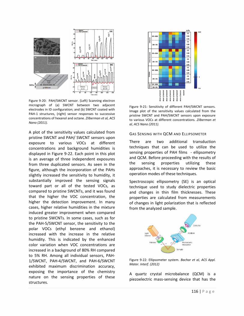
116 | P a g e
Figure 9-20: PAH/SWCNT sensor. (Left) Scanning electron micrograph of (a) SWCNT between two adjacent electrodes in ID configuration; and (b) SWCNT coated with PAH-1 structures, (right) sensor responses to successive concentrations of hexanol and octane. Zilberman et al, ACS Nano (2011).
A plot of the sensitivity values calculated from pristine SWCNT and PAH/ SWCNT sensors upon exposure to various VOCs at different concentrations and background humidities is displayed in Figure 9-22. Each point in this plot is an average of three independent exposures from three duplicated sensors. As seen in the figure, although the incorporation of the PAHs slightly increased the sensitivity to humidity, it substantially improved the sensing signals toward part or all of the tested VOCs, as compared to pristine SWCNTs, and it was found that the higher the VOC concentration, the higher the detection improvement. In many cases, higher relative humidities in the mixture induced greater improvement when compared to pristine SWCNTs. In some cases, such as for the PAH-5/SWCNT sensor, the sensitivity to the polar VOCs (ethyl benzene and ethanol) increased with the increase in the relative humidity. This is indicated by the enhanced color variation when VOC concentrations are increased in a background of 80% RH compared to 5% RH. Among all individual sensors, PAH-1/SWCNT, PAH-4/SWCNT, and PAH-6/SWCNT exhibited maximum discrimination accuracy, exposing the importance of the chemistry nature on the sensing properties of these structures.
Figure 9-21: Sensitivity of different PAH/SWCNT sensors. Image plot of the sensitivity values calculated from the pristine SWCNT and PAH/SWCNT sensors upon exposure to various VOCs at different concentrations. Zilberman et al, ACS Nano (2011).
GAS SENSING WITH QCM AND ELLIPSOMETER
There are two additional transduction techniques that can be used to utilize the sensing properties of PAH films - ellipsometry and QCM. Before proceeding with the results of the sensing properties utilizing these approaches, it is necessary to review the basic operation modes of these techniques.
Spectroscopic ellipsometry (SE) is an optical technique used to study dielectric properties and changes in thin film thicknesses. These properties are calculated from measurements of changes in light polarization that is reflected from the analyzed sample.
Figure 9-22: Ellipsometer system. Bachar et al, ACS Appl. Mater. Interf. (2012)
A quartz crystal microbalance (QCM) is a piezoelectric mass-sensing device that has the
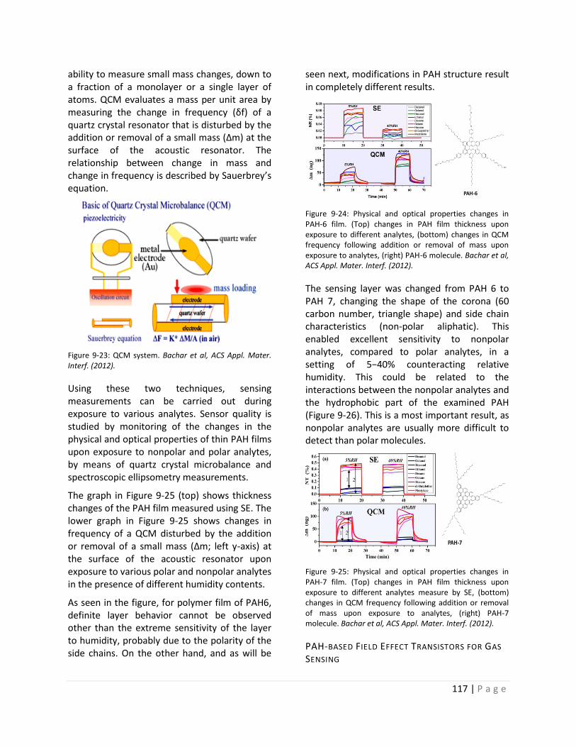
117 | P a g e
ability to measure small mass changes, down to a fraction of a monolayer or a single layer of atoms. QCM evaluates a mass per unit area by measuring the change in frequency (δf) of a quartz crystal resonator that is disturbed by the addition or removal of a small mass (Δm) at the surface of the acoustic resonator. The relationship between change in mass and change in frequency is described by Sauerbrey’s equation.
Figure 9-23: QCM system. Bachar et al, ACS Appl. Mater. Interf. (2012).
Using these two techniques, sensing measurements can be carried out during exposure to various analytes. Sensor quality is studied by monitoring of the changes in the physical and optical properties of thin PAH films upon exposure to nonpolar and polar analytes, by means of quartz crystal microbalance and spectroscopic ellipsometry measurements.
The graph in Figure 9-25 (top) shows thickness changes of the PAH film measured using SE. The lower graph in Figure 9-25 shows changes in frequency of a QCM disturbed by the addition or removal of a small mass (Δm; left y-axis) at the surface of the acoustic resonator upon exposure to various polar and nonpolar analytes in the presence of different humidity contents.
As seen in the figure, for polymer film of PAH6, definite layer behavior cannot be observed other than the extreme sensitivity of the layer to humidity, probably due to the polarity of the side chains. On the other hand, and as will be
seen next, modifications in PAH structure result in completely different results.
Figure 9-24: Physical and optical properties changes in PAH-6 film. (Top) changes in PAH film thickness upon exposure to different analytes, (bottom) changes in QCM frequency following addition or removal of mass upon exposure to analytes, (right) PAH-6 molecule. Bachar et al, ACS Appl. Mater. Interf. (2012).
The sensing layer was changed from PAH 6 to PAH 7, changing the shape of the corona (60 carbon number, triangle shape) and side chain characteristics (non-polar aliphatic). This enabled excellent sensitivity to nonpolar analytes, compared to polar analytes, in a setting of 5−40% counteracting relative humidity. This could be related to the interactions between the nonpolar analytes and the hydrophobic part of the examined PAH (Figure 9-26). This is a most important result, as nonpolar analytes are usually more difficult to detect than polar molecules.
Figure 9-25: Physical and optical properties changes in PAH-7 film. (Top) changes in PAH film thickness upon exposure to different analytes measure by SE, (bottom) changes in QCM frequency following addition or removal of mass upon exposure to analytes, (right) PAH-7 molecule. Bachar et al, ACS Appl. Mater. Interf. (2012).
PAH-BASED FIELD EFFECT TRANSISTORS FOR GAS
SENSING
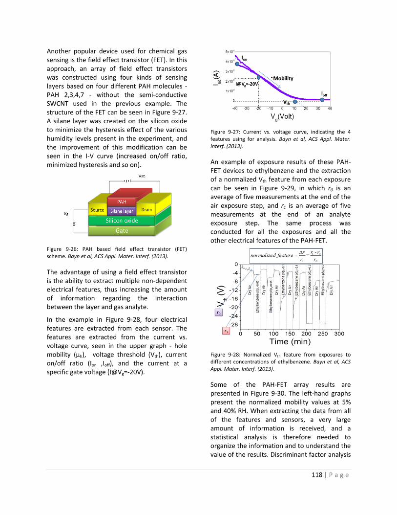
118 | P a g e
Another popular device used for chemical gas sensing is the field effect transistor (FET). In this approach, an array of field effect transistors was constructed using four kinds of sensing layers based on four different PAH molecules - PAH 2,3,4,7 - without the semi-conductive SWCNT used in the previous example. The structure of the FET can be seen in Figure 9-27. A silane layer was created on the silicon oxide to minimize the hysteresis effect of the various humidity levels present in the experiment, and the improvement of this modification can be seen in the I-V curve (increased on/off ratio, minimized hysteresis and so on).
Figure 9-26: PAH based field effect transistor (FET) scheme. Bayn et al, ACS Appl. Mater. Interf. (2013).
The advantage of using a field effect transistor is the ability to extract multiple non-dependent electrical features, thus increasing the amount of information regarding the interaction between the layer and gas analyte.
In the example in Figure 9-28, four electrical features are extracted from each sensor. The features are extracted from the current vs. voltage curve, seen in the upper graph - hole mobility (µh), voltage threshold (Vth), current on/off ratio (Ion ,Ioff), and the current at a specific gate voltage (I@Vg=-20V).
Figure 9-27: Current vs. voltage curve, indicating the 4 features using for analysis. Bayn et al, ACS Appl. Mater. Interf. (2013).
An example of exposure results of these PAH-FET devices to ethylbenzene and the extraction of a normalized Vth feature from each exposure can be seen in Figure 9-29, in which r0 is an average of five measurements at the end of the air exposure step, and r1 is an average of five measurements at the end of an analyte exposure step. The same process was conducted for all the exposures and all the other electrical features of the PAH-FET.
Figure 9-28: Normalized Vth feature from exposures to different concentrations of ethylbenzene. Bayn et al, ACS Appl. Mater. Interf. (2013).
Some of the PAH-FET array results are presented in Figure 9-30. The left-hand graphs present the normalized mobility values at 5% and 40% RH. When extracting the data from all of the features and sensors, a very large amount of information is received, and a statistical analysis is therefore needed to organize the information and to understand the value of the results. Discriminant factor analysis
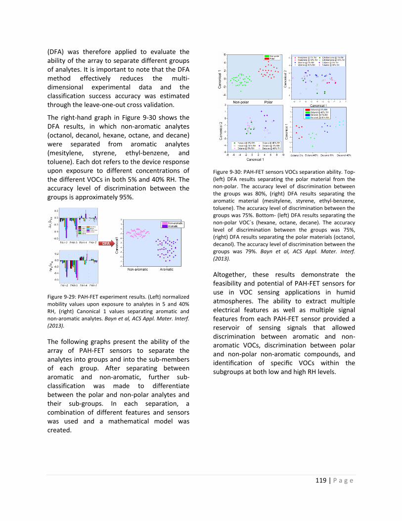
119 | P a g e
(DFA) was therefore applied to evaluate the ability of the array to separate different groups of analytes. It is important to note that the DFA method effectively reduces the multi-dimensional experimental data and the classification success accuracy was estimated through the leave-one-out cross validation.
The right-hand graph in Figure 9-30 shows the DFA results, in which non-aromatic analytes (octanol, decanol, hexane, octane, and decane) were separated from aromatic analytes (mesitylene, styrene, ethyl-benzene, and toluene). Each dot refers to the device response upon exposure to different concentrations of the different VOCs in both 5% and 40% RH. The accuracy level of discrimination between the groups is approximately 95%.
Figure 9-29: PAH-FET experiment results. (Left) normalized mobility values upon exposure to analytes in 5 and 40% RH, (right) Canonical 1 values separating aromatic and non-aromatic analytes. Bayn et al, ACS Appl. Mater. Interf. (2013).
The following graphs present the ability of the array of PAH-FET sensors to separate the analytes into groups and into the sub-members of each group. After separating between aromatic and non-aromatic, further sub-classification was made to differentiate between the polar and non-polar analytes and their sub-groups. In each separation, a combination of different features and sensors was used and a mathematical model was created.
Figure 9-30: PAH-FET sensors VOCs separation ability. Top- (left) DFA results separating the polar material from the non-polar. The accuracy level of discrimination between the groups was 80%, (right) DFA results separating the aromatic material (mesitylene, styrene, ethyl-benzene, toluene). The accuracy level of discrimination between the groups was 75%. Bottom- (left) DFA results separating the non-polar VOC`s (hexane, octane, decane). The accuracy level of discrimination between the groups was 75%, (right) DFA results separating the polar materials (octanol, decanol). The accuracy level of discrimination between the groups was 79%. Bayn et al, ACS Appl. Mater. Interf. (2013).
Altogether, these results demonstrate the feasibility and potential of PAH-FET sensors for use in VOC sensing applications in humid atmospheres. The ability to extract multiple electrical features as well as multiple signal features from each PAH-FET sensor provided a reservoir of sensing signals that allowed discrimination between aromatic and non-aromatic VOCs, discrimination between polar and non-polar non-aromatic compounds, and identification of specific VOCs within the subgroups at both low and high RH levels.
120 | P a g e
Chapter 10 ELECTRONIC SKIN
BASED ON NANOTECHNOLOGY
This chapter presents an example of a sensor mimicking one of the human senses, focusing on a system that imitates the human skin, known as electronic or artificial skin.
PROPERTIES OF THE HUMAN SKIN
The skin is the largest organ of the body, with a total area of approximately 20 square feet. The skin protects us from microbes, prevents infection and manufactures vitamin-D for the conversion of calcium into healthy bones.
The skin is a huge sensor packed with nerves that keeps the brain in touch with the outside world. At the same time, our skin allows us free movement, proving itself to be an amazingly versatile organ. The skin also helps regulate body temperature and permits the sensations of touch, heat, and cold.
The skin is composed of two distinct layers of tissues - the epidermis and the dermis. The epidermis consists of an outer shell of dead cells called the stratum corneum and a deeper layer of rapidly divided cells called the basal layer. When dead cells are damaged during body activity, cells from the basal layer rise to replace them. The epidermis serves as the body’s initial barrier to invading foreign substances. Directly below the basal layer, the
thicker dermis layer is composed of dense connective tissues.
There are several kinds of important sensory receptors embedded within the dermis, including thermal receptors, which detect temperature change, touch sensors and free nerve ending, which detect pain and tissue damage. The dermis also contains many other structures including hair follicles and blood vessels.
FLEXIBLE ELECTRONICS
There is a great need to mimic the human skin in a way that can be applied to sophisticated applications. This system is known as electronic or artificial skin. Indeed, cost-effective, light-weight, easy-to-fabricate and versatile electronic skin that is based on bendable and stretchable sensors is expected to revolutionize sensing technology and replace conventional, rigid sensors in existing applications. Additionally, these systems can potentially spur the development of totally new smart sensing applications.
The next section provides a general review of the potential and futuristic electronic skin applications, without delving into the technical issues relating to each presented application.
ELECTRONIC SKIN FOR ROBOTS
The electronic skin concept was initially developed for robotic applications. Robots could be provided with pressure sensing (“touch”) that would allow them to grip objects securely without damaging them. The simplest action for human can be extremely complex for robots. One example is the “picking up an egg” problem - a robot with no sense of touch would have difficulty applying the specific force on the egg necessary to pick it up without dropping or breaking it.
The development of touch sensors for robots is currently in its early stages. Today’s state-of-the-art skilled robotic hands cannot even preform simple tasks like tying a shoelace or
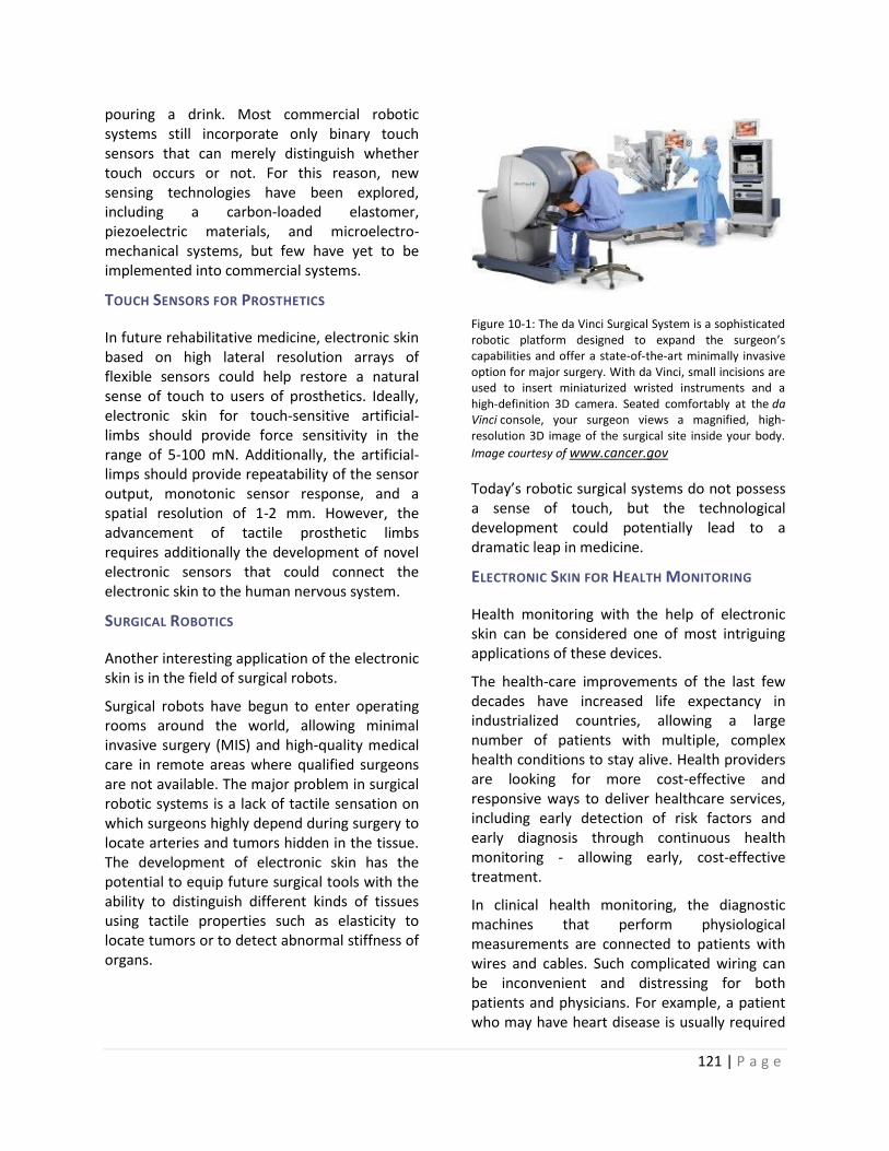
121 | P a g e
pouring a drink. Most commercial robotic systems still incorporate only binary touch sensors that can merely distinguish whether touch occurs or not. For this reason, new sensing technologies have been explored, including a carbon-loaded elastomer, piezoelectric materials, and microelectro-mechanical systems, but few have yet to be implemented into commercial systems.
TOUCH SENSORS FOR PROSTHETICS
In future rehabilitative medicine, electronic skin based on high lateral resolution arrays of flexible sensors could help restore a natural sense of touch to users of prosthetics. Ideally, electronic skin for touch-sensitive artificial-limbs should provide force sensitivity in the range of 5-100 mN. Additionally, the artificial-limps should provide repeatability of the sensor output, monotonic sensor response, and a spatial resolution of 1-2 mm. However, the advancement of tactile prosthetic limbs requires additionally the development of novel electronic sensors that could connect the electronic skin to the human nervous system.
SURGICAL ROBOTICS
Another interesting application of the electronic skin is in the field of surgical robots.
Surgical robots have begun to enter operating rooms around the world, allowing minimal invasive surgery (MIS) and high-quality medical care in remote areas where qualified surgeons are not available. The major problem in surgical robotic systems is a lack of tactile sensation on which surgeons highly depend during surgery to locate arteries and tumors hidden in the tissue. The development of electronic skin has the potential to equip future surgical tools with the ability to distinguish different kinds of tissues using tactile properties such as elasticity to locate tumors or to detect abnormal stiffness of organs.
Figure 10-1: The da Vinci Surgical System is a sophisticated robotic platform designed to expand the surgeon’s capabilities and offer a state-of-the-art minimally invasive option for major surgery. With da Vinci, small incisions are used to insert miniaturized wristed instruments and a high-definition 3D camera. Seated comfortably at the da Vinci console, your surgeon views a magnified, high-resolution 3D image of the surgical site inside your body.
Image courtesy of www.cancer.gov
Today’s robotic surgical systems do not possess a sense of touch, but the technological development could potentially lead to a dramatic leap in medicine.
ELECTRONIC SKIN FOR HEALTH MONITORING
Health monitoring with the help of electronic skin can be considered one of most intriguing applications of these devices.
The health-care improvements of the last few decades have increased life expectancy in industrialized countries, allowing a large number of patients with multiple, complex health conditions to stay alive. Health providers are looking for more cost-effective and responsive ways to deliver healthcare services, including early detection of risk factors and early diagnosis through continuous health monitoring - allowing early, cost-effective treatment.
In clinical health monitoring, the diagnostic machines that perform physiological measurements are connected to patients with wires and cables. Such complicated wiring can be inconvenient and distressing for both patients and physicians. For example, a patient who may have heart disease is usually required
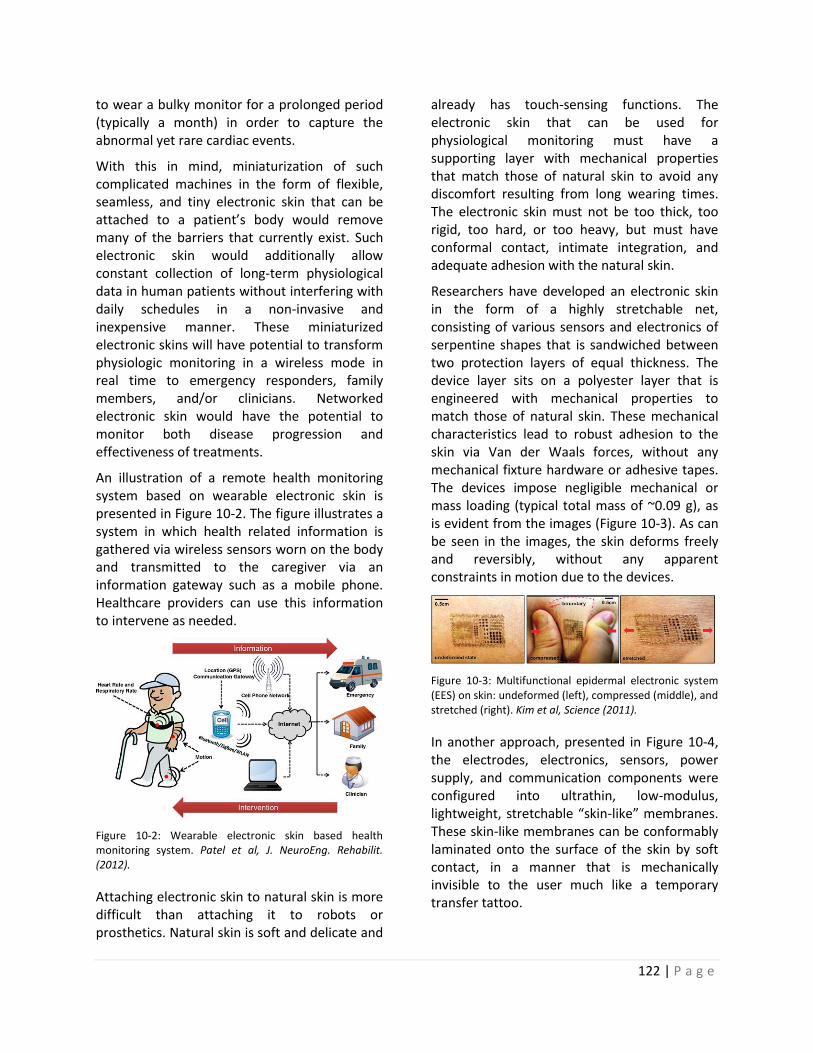
122 | P a g e
to wear a bulky monitor for a prolonged period (typically a month) in order to capture the abnormal yet rare cardiac events.
With this in mind, miniaturization of such complicated machines in the form of flexible, seamless, and tiny electronic skin that can be attached to a patient’s body would remove many of the barriers that currently exist. Such electronic skin would additionally allow constant collection of long-term physiological data in human patients without interfering with daily schedules in a non-invasive and inexpensive manner. These miniaturized electronic skins will have potential to transform physiologic monitoring in a wireless mode in real time to emergency responders, family members, and/or clinicians. Networked electronic skin would have the potential to monitor both disease progression and effectiveness of treatments.
An illustration of a remote health monitoring system based on wearable electronic skin is presented in Figure 10-2. The figure illustrates a system in which health related information is gathered via wireless sensors worn on the body and transmitted to the caregiver via an information gateway such as a mobile phone. Healthcare providers can use this information to intervene as needed.
Figure 10-2: Wearable electronic skin based health monitoring system. Patel et al, J. NeuroEng. Rehabilit. (2012).
Attaching electronic skin to natural skin is more difficult than attaching it to robots or prosthetics. Natural skin is soft and delicate and
already has touch-sensing functions. The electronic skin that can be used for physiological monitoring must have a supporting layer with mechanical properties that match those of natural skin to avoid any discomfort resulting from long wearing times. The electronic skin must not be too thick, too rigid, too hard, or too heavy, but must have conformal contact, intimate integration, and adequate adhesion with the natural skin.
Researchers have developed an electronic skin in the form of a highly stretchable net, consisting of various sensors and electronics of serpentine shapes that is sandwiched between two protection layers of equal thickness. The device layer sits on a polyester layer that is engineered with mechanical properties to match those of natural skin. These mechanical characteristics lead to robust adhesion to the skin via Van der Waals forces, without any mechanical fixture hardware or adhesive tapes. The devices impose negligible mechanical or mass loading (typical total mass of ~0.09 g), as is evident from the images (Figure 10-3). As can be seen in the images, the skin deforms freely and reversibly, without any apparent constraints in motion due to the devices.
Figure 10-3: Multifunctional epidermal electronic system (EES) on skin: undeformed (left), compressed (middle), and stretched (right). Kim et al, Science (2011).
In another approach, presented in Figure 10-4, the electrodes, electronics, sensors, power supply, and communication components were configured into ultrathin, low-modulus, lightweight, stretchable “skin-like” membranes. These skin-like membranes can be conformably laminated onto the surface of the skin by soft contact, in a manner that is mechanically invisible to the user much like a temporary transfer tattoo.
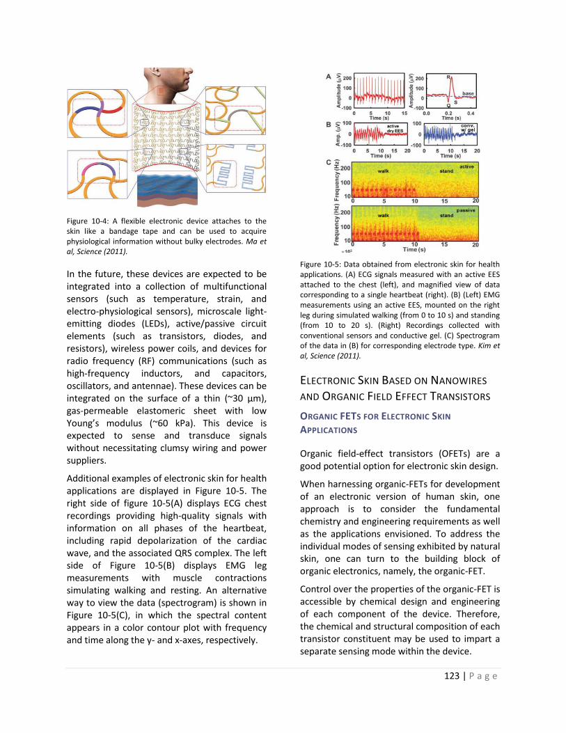
123 | P a g e
Figure 10-4: A flexible electronic device attaches to the skin like a bandage tape and can be used to acquire physiological information without bulky electrodes. Ma et al, Science (2011).
In the future, these devices are expected to be integrated into a collection of multifunctional sensors (such as temperature, strain, and electro-physiological sensors), microscale light-emitting diodes (LEDs), active/passive circuit elements (such as transistors, diodes, and resistors), wireless power coils, and devices for radio frequency (RF) communications (such as high-frequency inductors, and capacitors, oscillators, and antennae). These devices can be integrated on the surface of a thin (~30 μm), gas-permeable elastomeric sheet with low Young’s modulus (~60 kPa). This device is expected to sense and transduce signals without necessitating clumsy wiring and power suppliers.
Additional examples of electronic skin for health applications are displayed in Figure 10-5. The right side of figure 10-5(A) displays ECG chest recordings providing high-quality signals with information on all phases of the heartbeat, including rapid depolarization of the cardiac wave, and the associated QRS complex. The left side of Figure 10-5(B) displays EMG leg measurements with muscle contractions simulating walking and resting. An alternative way to view the data (spectrogram) is shown in Figure 10-5(C), in which the spectral content appears in a color contour plot with frequency and time along the y- and x-axes, respectively.
Figure 10-5: Data obtained from electronic skin for health applications. (A) ECG signals measured with an active EES attached to the chest (left), and magnified view of data corresponding to a single heartbeat (right). (B) (Left) EMG measurements using an active EES, mounted on the right leg during simulated walking (from 0 to 10 s) and standing (from 10 to 20 s). (Right) Recordings collected with conventional sensors and conductive gel. (C) Spectrogram of the data in (B) for corresponding electrode type. Kim et al, Science (2011).
ELECTRONIC SKIN BASED ON NANOWIRES
AND ORGANIC FIELD EFFECT TRANSISTORS
ORGANIC FETS FOR ELECTRONIC SKIN
APPLICATIONS
Organic field-effect transistors (OFETs) are a good potential option for electronic skin design.
When harnessing organic-FETs for development of an electronic version of human skin, one approach is to consider the fundamental chemistry and engineering requirements as well as the applications envisioned. To address the individual modes of sensing exhibited by natural skin, one can turn to the building block of organic electronics, namely, the organic-FET.
Control over the properties of the organic-FET is accessible by chemical design and engineering of each component of the device. Therefore, the chemical and structural composition of each transistor constituent may be used to impart a separate sensing mode within the device.
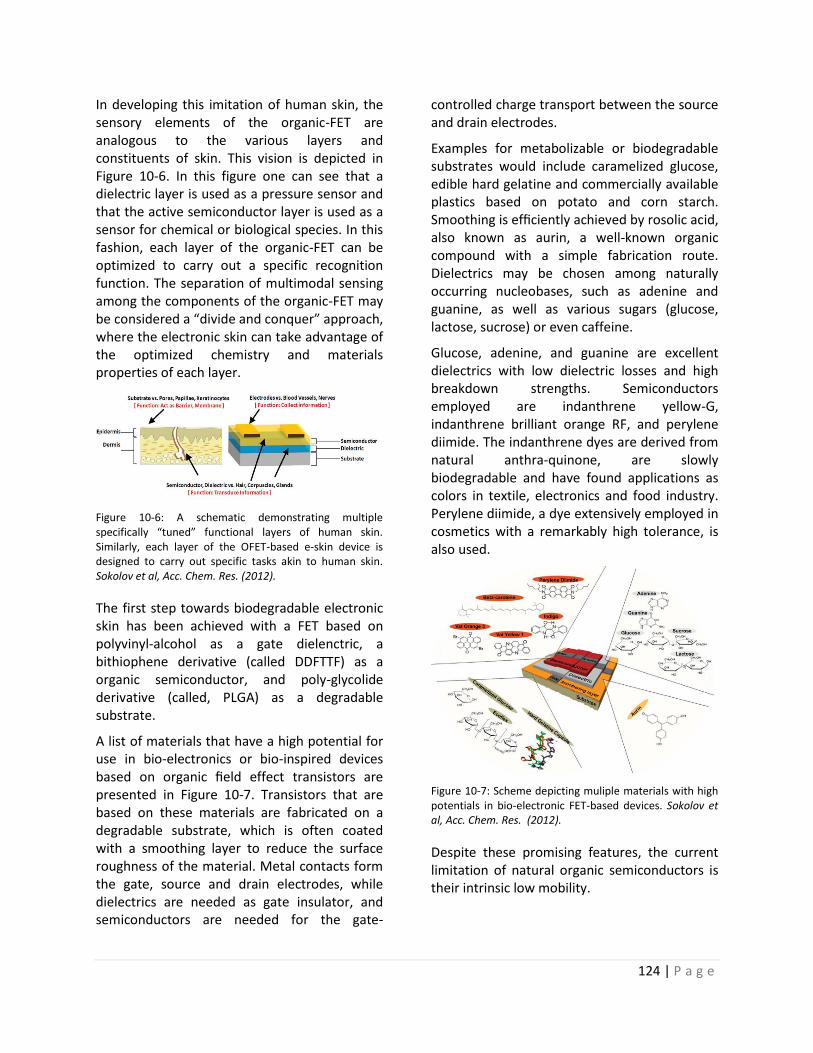
124 | P a g e
In developing this imitation of human skin, the sensory elements of the organic-FET are analogous to the various layers and constituents of skin. This vision is depicted in Figure 10-6. In this figure one can see that a dielectric layer is used as a pressure sensor and that the active semiconductor layer is used as a sensor for chemical or biological species. In this fashion, each layer of the organic-FET can be optimized to carry out a specific recognition function. The separation of multimodal sensing among the components of the organic-FET may be considered a “divide and conquer” approach, where the electronic skin can take advantage of the optimized chemistry and materials properties of each layer.
Figure 10-6: A schematic demonstrating multiple specifically “tuned” functional layers of human skin. Similarly, each layer of the OFET-based e-skin device is designed to carry out specific tasks akin to human skin. Sokolov et al, Acc. Chem. Res. (2012).
The first step towards biodegradable electronic skin has been achieved with a FET based on polyvinyl-alcohol as a gate dielenctric, a bithiophene derivative (called DDFTTF) as a organic semiconductor, and poly-glycolide derivative (called, PLGA) as a degradable substrate.
A list of materials that have a high potential for use in bio-electronics or bio-inspired devices based on organic field effect transistors are presented in Figure 10-7. Transistors that are based on these materials are fabricated on a degradable substrate, which is often coated with a smoothing layer to reduce the surface roughness of the material. Metal contacts form the gate, source and drain electrodes, while dielectrics are needed as gate insulator, and semiconductors are needed for the gate-
controlled charge transport between the source and drain electrodes.
Examples for metabolizable or biodegradable substrates would include caramelized glucose, edible hard gelatine and commercially available plastics based on potato and corn starch. Smoothing is efficiently achieved by rosolic acid, also known as aurin, a well-known organic compound with a simple fabrication route. Dielectrics may be chosen among naturally occurring nucleobases, such as adenine and guanine, as well as various sugars (glucose, lactose, sucrose) or even caffeine.
Glucose, adenine, and guanine are excellent dielectrics with low dielectric losses and high breakdown strengths. Semiconductors employed are indanthrene yellow-G, indanthrene brilliant orange RF, and perylene diimide. The indanthrene dyes are derived from natural anthra-quinone, are slowly biodegradable and have found applications as colors in textile, electronics and food industry. Perylene diimide, a dye extensively employed in cosmetics with a remarkably high tolerance, is also used.
Figure 10-7: Scheme depicting muliple materials with high potentials in bio-electronic FET-based devices. Sokolov et al, Acc. Chem. Res. (2012).
Despite these promising features, the current limitation of natural organic semiconductors is their intrinsic low mobility.
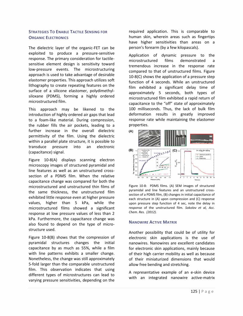
125 | P a g e
STRATEGIES TO ENABLE TACTILE SENSING FOR
ORGANIC ELECTRONICS
The dielectric layer of the organic-FET can be exploited to produce a pressure-sensitive response. The primary consideration for tactile-sensitive element design is sensitivity toward low-pressure events. The microstructuring approach is used to take advantage of desirable elastomer properties. This approach utilizes soft lithography to create repeating features on the surface of a silicone elastomer, polydimethyl-siloxane (PDMS), forming a highly ordered microstructured film.
This approach may be likened to the introduction of highly ordered air gaps that lead to a foam-like material. During compression, the rubber fills the air pockets, leading to a further increase in the overall dielectric permittivity of the film. Using the dielectric within a parallel plate structure, it is possible to transduce pressure into an electronic (capacitance) signal.
Figure 10-8(A) displays scanning electron microscopy images of structured pyramidal and line features as well as an unstructured cross-section of a PDMS film. When the relative capacitance change was compared for both the microstructured and unstructured thin films of the same thickness, the unstructured film exhibited little response even at higher pressure values, higher than 5 kPa, while the microstructured films showed a significant response at low pressure values of less than 2 kPa. Furthermore, the capacitance change was also found to depend on the type of micro-structure used.
Figure 10-8(B) shows that the compression of pyramidal structures changes the initial capacitance by as much as 55%, while a film with line patterns exhibits a smaller change. Nonetheless, the change was still approximately 5-fold larger than the comparable unstructured film. This observation indicates that using different types of microstructures can lead to varying pressure sensitivities, depending on the
required application. This is comparable to human skin, wherein areas such as fingertips have higher sensitivities than areas on a person's forearm (by a few kilopascals).
Application of dynamic pressure to the microstructured films demonstrated a tremendous increase in the response rate compared to that of unstructured films. Figure 10-8(C) shows the application of a pressure step function of 4 seconds. While an unstructured film exhibited a significant delay time of approximately 5 seconds, both types of microstructured film exhibited a rapid return of capacitance to the “off” state of approximately 100 milliseconds. Thus, the lack of bulk film deformation results in greatly improved response rate while maintaining the elastomer properties.
Figure 10-8: PDMS films. (A) SEM images of structured pyramidal and line features and an unstructured cross-section of a PDMS film, (B) changes in initial capacitance of each structure in (A) upon compression and (C) response upon pressure step function of 4 sec, note the delay in response of the unstructured film. Sokolov et al, Acc. Chem. Res. (2012).
NANOWIRE ACTIVE MATRIX
Another possibility that could be of utility for electronic skin applications is the use of nanowires. Nanowires are excellent candidates for electronic skin applications, mainly because of their high carrier mobility as well as because of their miniaturized dimensions that would allow free bending and stretching.
A representative example of an e-skin device with an integrated nanowire active-matrix
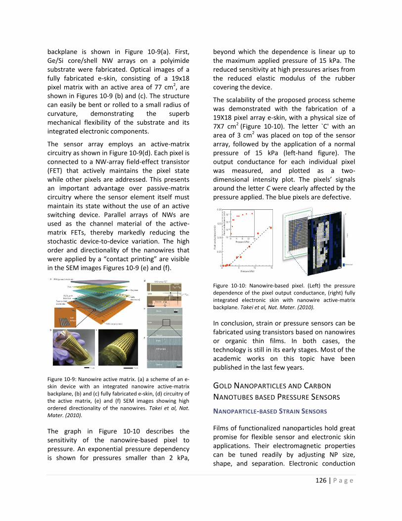
126 | P a g e
backplane is shown in Figure 10-9(a). First, Ge/Si core/shell NW arrays on a polyimide substrate were fabricated. Optical images of a fully fabricated e-skin, consisting of a 19x18 pixel matrix with an active area of 77 cm2, are shown in Figures 10-9 (b) and (c). The structure can easily be bent or rolled to a small radius of curvature, demonstrating the superb mechanical flexibility of the substrate and its integrated electronic components.
The sensor array employs an active-matrix circuitry as shown in Figure 10-9(d). Each pixel is connected to a NW-array field-effect transistor (FET) that actively maintains the pixel state while other pixels are addressed. This presents an important advantage over passive-matrix circuitry where the sensor element itself must maintain its state without the use of an active switching device. Parallel arrays of NWs are used as the channel material of the active-matrix FETs, thereby markedly reducing the stochastic device-to-device variation. The high order and directionality of the nanowires that were applied by a “contact printing” are visible in the SEM images Figures 10-9 (e) and (f).
Figure 10-9: Nanowire active matrix. (a) a scheme of an e-skin device with an integrated nanowire active-matrix backplane, (b) and (c) fully fabricated e-skin, (d) circuitry of the active matrix, (e) and (f) SEM images showing high ordered directionality of the nanowires. Takei et al, Nat. Mater. (2010).
The graph in Figure 10-10 describes the sensitivity of the nanowire-based pixel to pressure. An exponential pressure dependency is shown for pressures smaller than 2 kPa,
beyond which the dependence is linear up to the maximum applied pressure of 15 kPa. The reduced sensitivity at high pressures arises from the reduced elastic modulus of the rubber covering the device.
The scalability of the proposed process scheme was demonstrated with the fabrication of a 19X18 pixel array e-skin, with a physical size of 7X7 cm2 (Figure 10-10). The letter `C' with an area of 3 cm2 was placed on top of the sensor array, followed by the application of a normal pressure of 15 kPa (left-hand figure). The output conductance for each individual pixel was measured, and plotted as a two-dimensional intensity plot. The pixels’ signals around the letter C were clearly affected by the pressure applied. The blue pixels are defective.
Figure 10-10: Nanowire-based pixel. (Left) the pressure dependence of the pixel output conductance, (right) fully integrated electronic skin with nanowire active-matrix backplane. Takei et al, Nat. Mater. (2010).
In conclusion, strain or pressure sensors can be fabricated using transistors based on nanowires or organic thin films. In both cases, the technology is still in its early stages. Most of the academic works on this topic have been published in the last few years.
GOLD NANOPARTICLES AND CARBON
NANOTUBES BASED PRESSURE SENSORS
NANOPARTICLE-BASED STRAIN SENSORS
Films of functionalized nanoparticles hold great promise for flexible sensor and electronic skin applications. Their electromagnetic properties can be tuned readily by adjusting NP size, shape, and separation. Electronic conduction
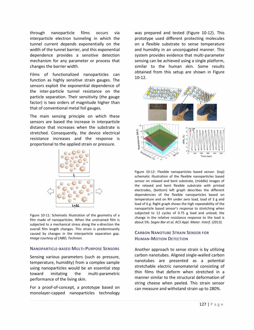
127 | P a g e
through nanoparticle films occurs via interparticle electron tunneling in which the tunnel current depends exponentially on the width of the tunnel barrier, and this exponential dependence provides a sensitive detection mechanism for any parameter or process that changes the barrier width.
Films of functionalized nanoparticles can function as highly sensitive strain gauges. The sensors exploit the exponential dependence of the inter-particle tunnel resistance on the particle separation. Their sensitivity (the gauge factor) is two orders of magnitude higher than that of conventional metal foil gauges.
The main sensing principle on which these sensors are based the increase in interparticle distance that increases when the substrate is stretched. Consequently, the device electrical resistance increases and the response is proportional to the applied strain or pressure.
Figure 10-11: Schematic illustration of the geometry of a film made of nanoparticles. When the unstrained film is subjected to a mechanical stress along the x-direction the overall film length changes. This strain is predominantly caused by changes in the interparticle separation gap. Image courtesy of LNBD, Technion.
NANOPARTICLE-BASED MULTI-PURPOSE SENSORS
Sensing various parameters (such as pressure, temperature, humidity) from a complex sample using nanoparticles would be an essential step toward imitating the multi-parametric performance of the living skin.
For a proof-of-concept, a prototype based on monolayer-capped nanoparticles technology
was prepared and tested (Figure 10-12). This prototype used different protecting molecules on a flexible substrate to sense temperature and humidity in an unconjugated manner. This system provides evidence that multi-parameter sensing can be achieved using a single platform, similar to the human skin. Some results obtained from this setup are shown in Figure 10-12.
Figure 10-12: Flexible nanoparticles based sensor. (top) schematic illustration of the flexible nanoparticles based sensor on relaxed and bent substrate, (middle) images of the relaxed and bent flexible substrate with printed electrodes, (bottom) left graph describes the different dependencies of the flexible nanoparticles based on temperature and on RH under zero load, load of 3 g and load of 6 g. Right graph shows the high repeatability of the nanoparticle based sensor’s response to stretching when subjected to 12 cycles of 0.75 g load and unload; the change in the relative resistance response to the load is about 5%. Segev Bar et al, ACS Appl. Mater. Interf. (2013).
CARBON NANOTUBE STRAIN SENSOR FOR
HUMAN-MOTION DETECTION
Another approach to sense strain is by utilizing carbon nanotubes. Aligned single-walled carbon nanotubes are presented as a potential stretchable electric nanomaterial consisting of thin films that deform when stretched in a manner similar to the structural deformation of string cheese when peeled. This strain sensor can measure and withstand strain up to 280%.
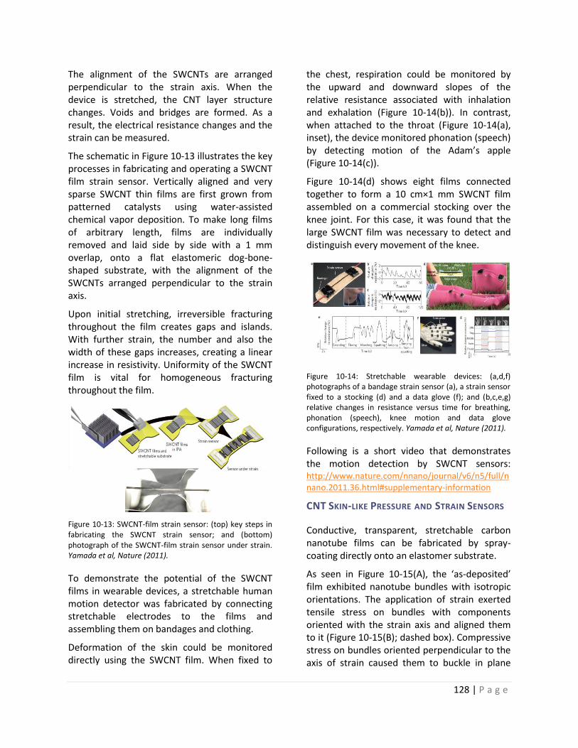
128 | P a g e
The alignment of the SWCNTs are arranged perpendicular to the strain axis. When the device is stretched, the CNT layer structure changes. Voids and bridges are formed. As a result, the electrical resistance changes and the strain can be measured.
The schematic in Figure 10-13 illustrates the key processes in fabricating and operating a SWCNT film strain sensor. Vertically aligned and very sparse SWCNT thin films are first grown from patterned catalysts using water-assisted chemical vapor deposition. To make long films of arbitrary length, films are individually removed and laid side by side with a 1 mm overlap, onto a flat elastomeric dog-bone-shaped substrate, with the alignment of the SWCNTs arranged perpendicular to the strain axis.
Upon initial stretching, irreversible fracturing throughout the film creates gaps and islands. With further strain, the number and also the width of these gaps increases, creating a linear increase in resistivity. Uniformity of the SWCNT film is vital for homogeneous fracturing throughout the film.
Figure 10-13: SWCNT-film strain sensor: (top) key steps in fabricating the SWCNT strain sensor; and (bottom) photograph of the SWCNT-film strain sensor under strain. Yamada et al, Nature (2011).
To demonstrate the potential of the SWCNT films in wearable devices, a stretchable human motion detector was fabricated by connecting stretchable electrodes to the films and assembling them on bandages and clothing.
Deformation of the skin could be monitored directly using the SWCNT film. When fixed to
the chest, respiration could be monitored by the upward and downward slopes of the relative resistance associated with inhalation and exhalation (Figure 10-14(b)). In contrast, when attached to the throat (Figure 10-14(a), inset), the device monitored phonation (speech) by detecting motion of the Adam’s apple (Figure 10-14(c)).
Figure 10-14(d) shows eight films connected together to form a 10 cm×1 mm SWCNT film assembled on a commercial stocking over the knee joint. For this case, it was found that the large SWCNT film was necessary to detect and distinguish every movement of the knee.
Figure 10-14: Stretchable wearable devices: (a,d,f) photographs of a bandage strain sensor (a), a strain sensor fixed to a stocking (d) and a data glove (f); and (b,c,e,g) relative changes in resistance versus time for breathing, phonation (speech), knee motion and data glove configurations, respectively. Yamada et al, Nature (2011).
Following is a short video that demonstrates the motion detection by SWCNT sensors: http://www.nature.com/nnano/journal/v6/n5/full/nnano.2011.36.html#supplementary-information
CNT SKIN-LIKE PRESSURE AND STRAIN SENSORS
Conductive, transparent, stretchable carbon nanotube films can be fabricated by spray-coating directly onto an elastomer substrate.
As seen in Figure 10-15(A), the ‘as-deposited’ film exhibited nanotube bundles with isotropic orientations. The application of strain exerted tensile stress on bundles with components oriented with the strain axis and aligned them to it (Figure 10-15(B); dashed box). Compressive stress on bundles oriented perpendicular to the axis of strain caused them to buckle in plane
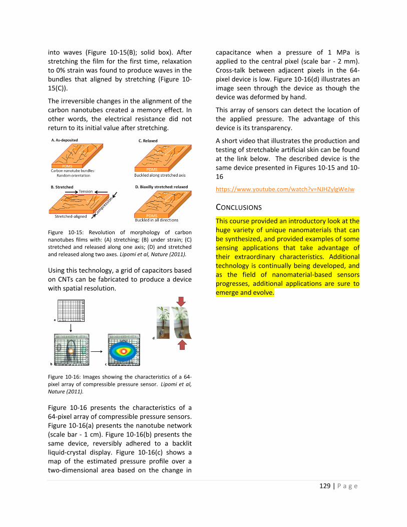
129 | P a g e
into waves (Figure 10-15(B); solid box). After stretching the film for the first time, relaxation to 0% strain was found to produce waves in the bundles that aligned by stretching (Figure 10-15(C)).
The irreversible changes in the alignment of the carbon nanotubes created a memory effect. In other words, the electrical resistance did not return to its initial value after stretching.
Figure 10-15: Revolution of morphology of carbon nanotubes films with: (A) stretching; (B) under strain; (C) stretched and released along one axis; (D) and stretched and released along two axes. Lipomi et al, Nature (2011).
Using this technology, a grid of capacitors based on CNTs can be fabricated to produce a device with spatial resolution.
Figure 10-16: Images showing the characteristics of a 64- pixel array of compressible pressure sensor. Lipomi et al, Nature (2011).
Figure 10-16 presents the characteristics of a 64-pixel array of compressible pressure sensors. Figure 10-16(a) presents the nanotube network (scale bar - 1 cm). Figure 10-16(b) presents the same device, reversibly adhered to a backlit liquid-crystal display. Figure 10-16(c) shows a map of the estimated pressure profile over a two-dimensional area based on the change in
capacitance when a pressure of 1 MPa is applied to the central pixel (scale bar - 2 mm). Cross-talk between adjacent pixels in the 64-pixel device is low. Figure 10-16(d) illustrates an image seen through the device as though the device was deformed by hand.
This array of sensors can detect the location of the applied pressure. The advantage of this device is its transparency.
A short video that illustrates the production and testing of stretchable artificial skin can be found at the link below. The described device is the same device presented in Figures 10-15 and 10-16
https://www.youtube.com/watch?v=NJHZylgWeJw
CONCLUSIONS
This course provided an introductory look at the huge variety of unique nanomaterials that can be synthesized, and provided examples of some sensing applications that take advantage of their extraordinary characteristics. Additional technology is continually being developed, and as the field of nanomaterial-based sensors progresses, additional applications are sure to emerge and evolve.


![Nano Materials [Compatibility Mode]](https://img.pdfslide.net/doc/110x75/5527156f497959f60f8b479d/nano-materials-compatibility-mode.jpg)