Embed Size (px)
Citation preview
1
Supplementary Information for
Nanofocusing in a metal-insulator-metal gap plasmon waveguide
with a 3-dimensional linear taper
by Hyuck Choo et al.
1. Surface-Plasmon-Polarion (SPP) Modes in MIM Gap Plasmon Waveguide
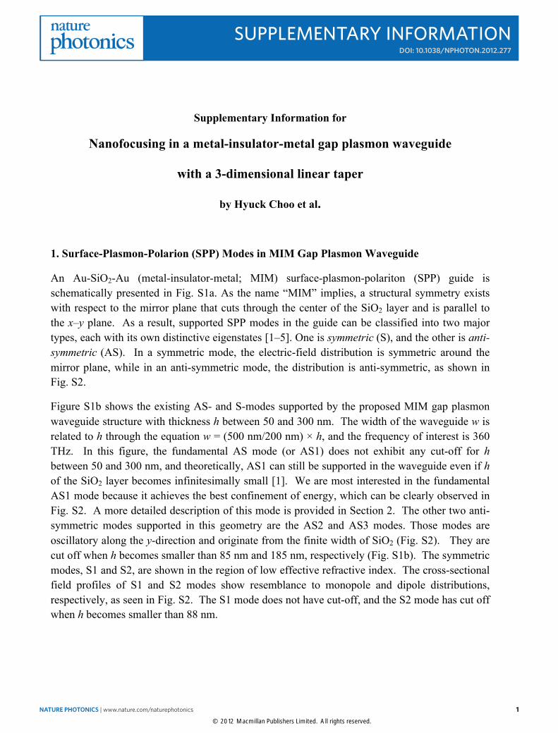
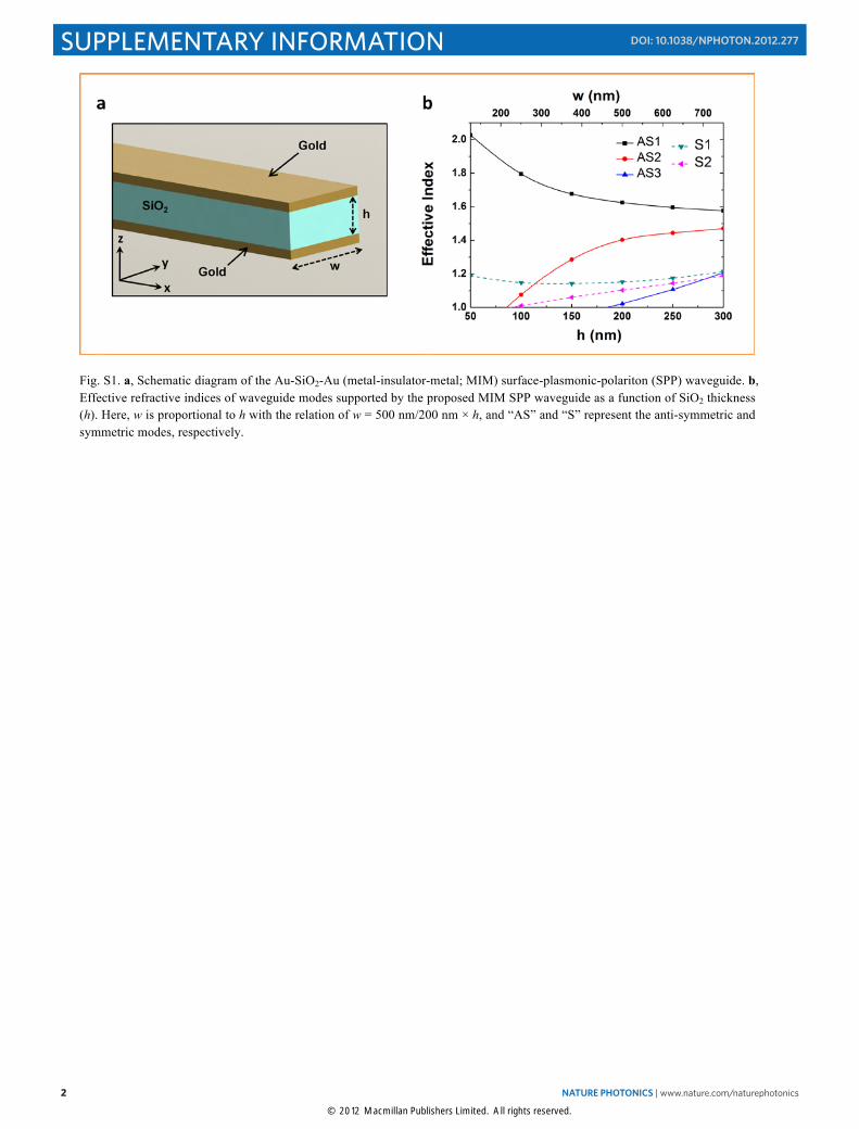
An Au-SiO2-Au (metal-insulator-metal; MIM) surface-plasmon-polariton (SPP) guide is schematically presented in Fig. S1a. As the name “MIM” implies, a structural symmetry exists with respect to the mirror plane that cuts through the center of the SiO2 layer and is parallel to the x–y plane. As a result, supported SPP modes in the guide can be classified into two major types, each with its own distinctive eigenstates [1–5]. One is symmetric (S), and the other is anti-symmetric (AS). In a symmetric mode, the electric-field distribution is symmetric around the mirror plane, while in an anti-symmetric mode, the distribution is anti-symmetric, as shown in Fig. S2.
Figure S1b shows the existing AS- and S-modes supported by the proposed MIM gap plasmon waveguide structure with thickness h between 50 and 300 nm. The width of the waveguide w is related to h through the equation w = (500 nm/200 nm) × h, and the frequency of interest is 360 THz. In this figure, the fundamental AS mode (or AS1) does not exhibit any cut-off for h between 50 and 300 nm, and theoretically, AS1 can still be supported in the waveguide even if h of the SiO2 layer becomes infinitesimally small [1]. We are most interested in the fundamental AS1 mode because it achieves the best confinement of energy, which can be clearly observed in Fig. S2. A more detailed description of this mode is provided in Section 2. The other two anti-symmetric modes supported in this geometry are the AS2 and AS3 modes. Those modes are oscillatory along the y-direction and originate from the finite width of SiO2 (Fig. S2). They are cut off when h becomes smaller than 85 nm and 185 nm, respectively (Fig. S1b). The symmetric modes, S1 and S2, are shown in the region of low effective refractive index. The cross-sectional field profiles of S1 and S2 modes show resemblance to monopole and dipole distributions, respectively, as seen in Fig. S2. The S1 mode does not have cut-off, and the S2 mode has cut off when h becomes smaller than 88 nm.
SUPPLEMENTARY INFORMATIONDOI: 10.1038/NPHOTON.2012.277
NATURE PHOTONICS | www.nature.com/naturephotonics 1
© 2012 Macmillan Publishers Limited. All rights reserved.
2
Fig. S1. a, Schematic diagram of the Au-SiO2-Au (metal-insulator-metal; MIM) surface-plasmonic-polariton (SPP) waveguide. b, Effective refractive indices of waveguide modes supported by the proposed MIM SPP waveguide as a function of SiO2 thickness (h). Here, w is proportional to h with the relation of w = 500 nm/200 nm × h, and “AS” and “S” represent the anti-symmetric and symmetric modes, respectively.
2 NATURE PHOTONICS | www.nature.com/naturephotonics
SUPPLEMENTARY INFORMATION DOI: 10.1038/NPHOTON.2012.277
© 2012 Macmillan Publishers Limited. All rights reserved.
3
Fig. S2. Cross-sectional side views of the E2 profiles (logarithmic scale) of MIM SPP waveguide modes along the x–z plane, when h = 200 nm and w = 500 nm. The electric-field vector plots are overlaid.
NATURE PHOTONICS | www.nature.com/naturephotonics 3
SUPPLEMENTARY INFORMATIONDOI: 10.1038/NPHOTON.2012.277
© 2012 Macmillan Publishers Limited. All rights reserved.
4
2. Fundamental Anti-symmetric MIM SPP Waveguide Mode (AS1 Mode)
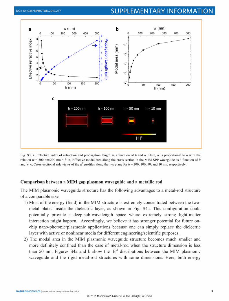
We specifically utilized the fundamental AS1 mode shown in Figs. S1 and S2. Please remember that theoretically the fundamental AS1 mode does not have cut-off even for the sub-nanoscale dielectric thickness/width. Figure S3a shows the effective refractive indices and the propagation lengths as a function of the SiO2 thickness (h). The width of SiO2 (w) is related to h through the following equation: w = 500/200 × h. The effective index of refraction rapidly increases as the cross-sectional area (w × h) decreases because the smaller cross-sectional area of the insulator pushes the propagating waves deeper into the metal layer during propagation [1–6]. This deeper submersion of the propagating waves also causes the propagation length (Lm) to decrease more rapidly due to the higher absorption loss in the metal. The propagation length and the effective refractive index of the MIM SPP mode with an area of 500 × 200 nm2 were calculated to be 7.2 µm and 1.63, respectively. As the cross-sectional area was reduced to 10 × 4 nm2, for example, the effective refractive index jumped to 7.7 whereas the propagation length dropped to 225 nm. Figure S1c shows the effective modal areas (Am) of the AS1 mode as a function of h and w. As the cross-sectional dimensions of the MIM SPP waveguide taper linearly, the size of the modal area decreases much more rapidly in a nonlinear manner. This implies that the photons will be more tightly confined in an extremely small area. When the cross-sectional dimensions of the modal area decrease from 500 × 200 nm2 to 10 × 4 nm2 (or by a factor of 50), the modal area changes from 4.4 × 10⁴ nm2 and 8.0 nm2 (or by a factor of 5500, which is much larger than 502). The intensity profiles of the electric field for h = 200, 100, 50, 10 nm are shown in Fig. S3C.
Definitions of the modal area (Am) and the propagation length (Lm)
The modal area (Am) is defined as the ratio of the total mode energy to the peak energy density,
( ) / max{ ( )}m totalA W r dA W r= ∫ ,
where W(r) is the electromagnetic energy density given by the following relation:
( )( ) 2 20
)1( ) | ( ) | | ( ) |2d r
W r E r H rdε ω
µω
⎛ ⎞= +⎜ ⎟⎜ ⎟
⎝ ⎠.
The propagation length (Lm) is defined as the distance at which the intensity of the propagating wave decays to 1/e and expressed as
( )1/ 2Im( )m mL k= ,
where km is the complex wave-vector component in the propagation direction.
4 NATURE PHOTONICS | www.nature.com/naturephotonics
SUPPLEMENTARY INFORMATION DOI: 10.1038/NPHOTON.2012.277
© 2012 Macmillan Publishers Limited. All rights reserved.
5
Fig. S3. a, Effective index of refraction and propagation length as a function of h and w. Here, w is proportional to h with the relation w = 500 nm/200 nm × h. b, Effective modal area along the cross section in the MIM SPP waveguide as a function of h and w. c, Cross-sectional side views of the E2 profiles along the y–z plane for h = 200, 100, 50, and 10 nm, respectively.
Comparison between a MIM gap plasmon waveguide and a metallic rod
The MIM plasmonic waveguide structure has the following advantages to a metal-rod structure of a comparable size.
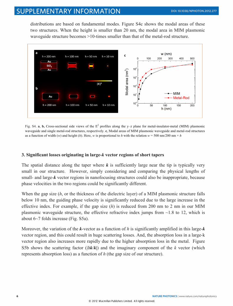
1) Most of the energy (field) in the MIM structure is extremely concentrated between the two-metal plates inside the dielectric layer, as shown in Fig. S4a. This configuration could potentially provide a deep-sub-wavelength space where extremely strong light-matter interaction might happen. Accordingly, we believe it has stronger potential for future on-chip nano-photonic/plasmonic applications because one can simply replace the dielectric layer with active or nonlinear media for different engineering/scientific purposes.
2) The modal area in the MIM plasmonic waveguide structure becomes much smaller and more definitely confined than the case of metal-rod when the structure dimension is less than 50 nm. Figures S4a and b show the |E|2 distributions between the MIM plasmonic waveguide and the rigid metal-rod structures with same dimensions. Here, both energy
NATURE PHOTONICS | www.nature.com/naturephotonics 5
SUPPLEMENTARY INFORMATIONDOI: 10.1038/NPHOTON.2012.277
© 2012 Macmillan Publishers Limited. All rights reserved.
6
distributions are based on fundamental modes. Figure S4c shows the modal areas of these two structures. When the height is smaller than 20 nm, the modal area in MIM plasmonic waveguide structure becomes >10-times smaller than that of the metal-rod structure.
Fig. S4. a, b, Cross-sectional side views of the E2 profiles along the y–z plane for metal-insulator-metal (MIM) plasmonic waveguide and single metal-rod structures, respectively. c, Modal areas of MIM plasmonic waveguide and metal-rod structures as a function of width (w) and height (h). Here, w is proportional to h with the relation w = 500 nm/200 nm × h
3. Significant losses originating in large-k vector regions of short tapers
The spatial distance along the taper where k is sufficiently large near the tip is typically very small in our structure. However, simply considering and comparing the physical lengths of small- and large-k vector regions in nanofocusing structures could also be inappropriate, because phase velocities in the two regions could be significantly different.
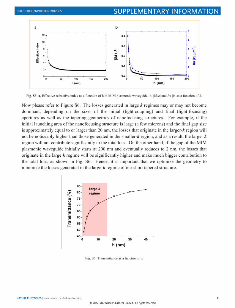
When the gap size (h, or the thickness of the dielectric layer) of a MIM plasmonic structure falls below 10 nm, the guiding phase velocity is significantly reduced due to the large increase in the effective index. For example, if the gap size (h) is reduced from 200 nm to 2 nm in our MIM plasmonic waveguide structure, the effective refractive index jumps from ~1.8 to 12, which is about 6~7 folds increase (Fig. S5a).
Moreover, the variation of the k-vector as a function of h is significantly amplified in this large-k vector region, and this could result in huge scattering losses. And, the absorption loss in a large-k vector region also increases more rapidly due to the higher absorption loss in the metal. Figure S5b shows the scattering factor (|δk/k|) and the imaginary component of the k vector (which represents absorption loss) as a function of h (the gap size of our structure).
6 NATURE PHOTONICS | www.nature.com/naturephotonics
SUPPLEMENTARY INFORMATION DOI: 10.1038/NPHOTON.2012.277
© 2012 Macmillan Publishers Limited. All rights reserved.
7
Fig. S5. a, Effective refractive index as a function of h in MIM plasmonic waveguide. b, |δk/k| and Im |k| as a function of h.
Now please refer to Figure S6. The losses generated in large k regimes may or may not become dominant, depending on the sizes of the initial (light-coupling) and final (light-focusing) apertures as well as the tapering geometries of nanofocusing structures. For example, if the initial launching area of the nanofocusing structure is large (a few microns) and the final gap size is approximately equal to or larger than 20 nm, the losses that originate in the larger-k region will not be noticeably higher than those generated in the smaller-k region, and as a result, the larger k region will not contribute significantly to the total loss. On the other hand, if the gap of the MIM plasmonic waveguide initially starts at 200 nm and eventually reduces to 2 nm, the losses that originate in the large k regime will be significantly higher and make much bigger contribution to the total loss, as shown in Fig. S6. Hence, it is important that we optimize the geometry to minimize the losses generated in the large-k regime of our short tapered structure.
Fig. S6. Transmittance as a function of h
NATURE PHOTONICS | www.nature.com/naturephotonics 7
SUPPLEMENTARY INFORMATIONDOI: 10.1038/NPHOTON.2012.277
© 2012 Macmillan Publishers Limited. All rights reserved.
8
4. Losses in Linearly Tapered MIM Gap Plasmon Waveguide
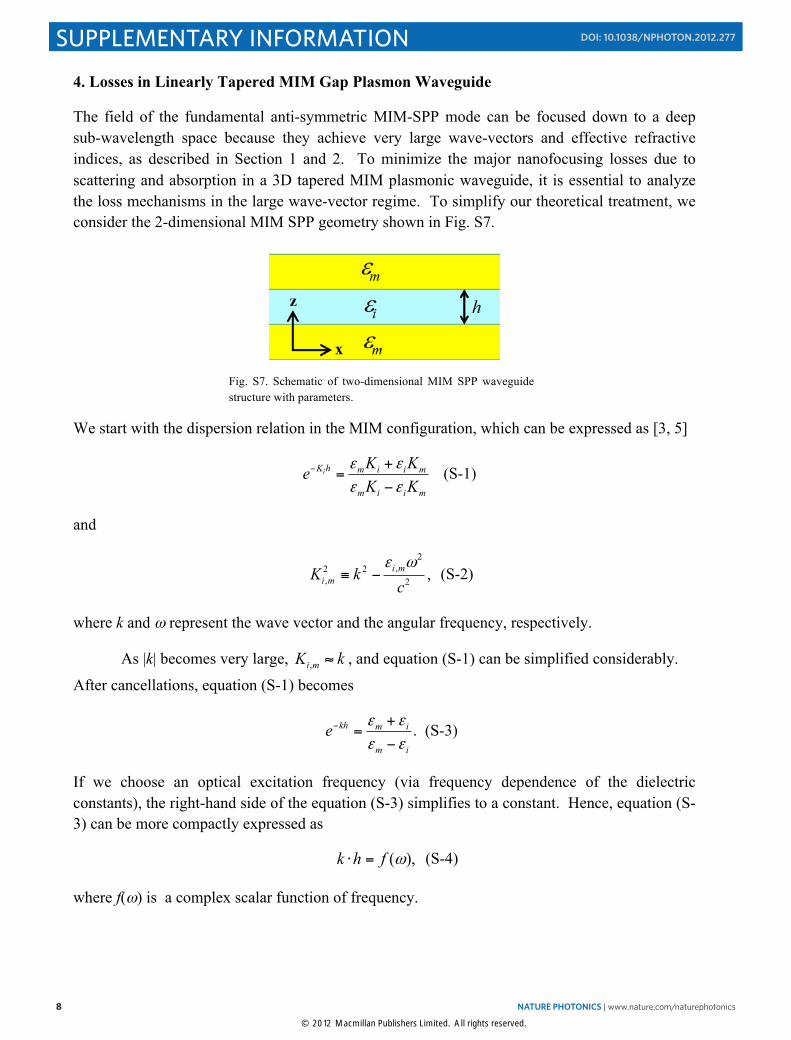
The field of the fundamental anti-symmetric MIM-SPP mode can be focused down to a deep sub-wavelength space because they achieve very large wave-vectors and effective refractive indices, as described in Section 1 and 2. To minimize the major nanofocusing losses due to scattering and absorption in a 3D tapered MIM plasmonic waveguide, it is essential to analyze the loss mechanisms in the large wave-vector regime. To simplify our theoretical treatment, we consider the 2-dimensional MIM SPP geometry shown in Fig. S7.
Fig. S7. Schematic of two-dimensional MIM SPP waveguide structure with parameters.
We start with the dispersion relation in the MIM configuration, which can be expressed as [3, 5]
iK h m i i m
m i i m
K KeK K
ε εε ε
− +=
− (S-1)
and
2
,2 2, 2 ,i mi mK k
cε ω
≡ − (S-2)
where k and ω represent the wave vector and the angular frequency, respectively.
As |k| becomes very large, ,i mK k≈ , and equation (S-1) can be simplified considerably.
After cancellations, equation (S-1) becomes
kh m i
m i
e ε εε ε
− +=
−. (S-3)
If we choose an optical excitation frequency (via frequency dependence of the dielectric constants), the right-hand side of the equation (S-3) simplifies to a constant. Hence, equation (S-3) can be more compactly expressed as
( ),k h f ω⋅ = (S-4)
where f(ω) is a complex scalar function of frequency.
8 NATURE PHOTONICS | www.nature.com/naturephotonics
SUPPLEMENTARY INFORMATION DOI: 10.1038/NPHOTON.2012.277
© 2012 Macmillan Publishers Limited. All rights reserved.
9
Putting Re[k] as 2 /π λ in equation (3-4), we obtain the relation
12 Re[ ( )] ( )f h F hλ π ω ω−= ⋅ ⋅ = ⋅ , (S-5)
where F(ω) is a real scalar function of frequency.
From equations (S-4) and (S-5), we obtain another meaningful scalar relation:
1Im[ ] Im[ ( )] ( ) ( )k f F Gλ ω ω ω−⋅ = ⋅ = . (S-6)
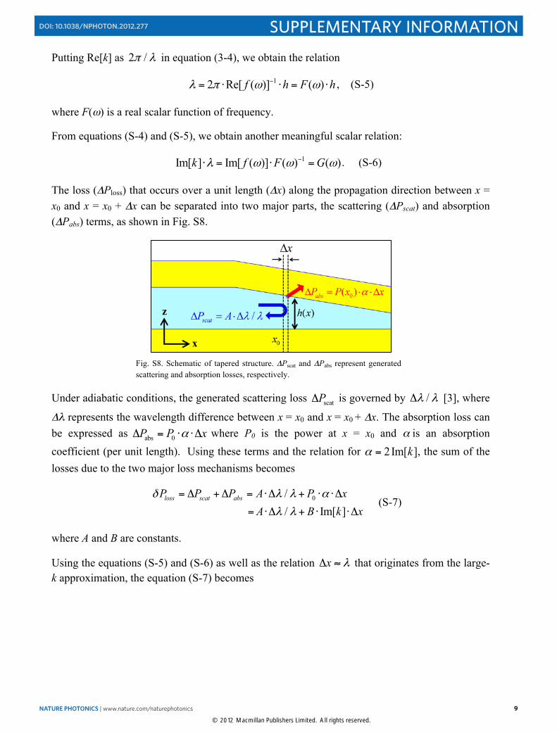
The loss (ΔPloss) that occurs over a unit length (Δx) along the propagation direction between x = x0 and x = x0 + Δx can be separated into two major parts, the scattering (ΔPscat) and absorption (ΔPabs) terms, as shown in Fig. S8.
Fig. S8. Schematic of tapered structure. ΔPscat and ΔPabs represent generated scattering and absorption losses, respectively.
Under adiabatic conditions, the generated scattering loss scatPΔ is governed by /λ λΔ [3], where
Δλ represents the wavelength difference between x = x0 and x = x0 + Δx. The absorption loss can be expressed as abs 0P P xαΔ = ⋅ ⋅Δ where P0 is the power at x = x0 and α is an absorption coefficient (per unit length). Using these terms and the relation for 2Im[ ]kα = , the sum of the losses due to the two major loss mechanisms becomes
0// Im[ ]
loss scat absP P P A P xA B k x
δ λ λ α
λ λ
= Δ +Δ = ⋅Δ + ⋅ ⋅Δ
= ⋅Δ + ⋅ ⋅Δ (S-7)
where A and B are constants.
Using the equations (S-5) and (S-6) as well as the relation x λΔ ≈ that originates from the large-k approximation, the equation (S-7) becomes
NATURE PHOTONICS | www.nature.com/naturephotonics 9
SUPPLEMENTARY INFORMATIONDOI: 10.1038/NPHOTON.2012.277
© 2012 Macmillan Publishers Limited. All rights reserved.
10
( )1
loss ( ) / Im[ ]
,
P A F h x B k
hC Dx
ω λ−Δ ≈ ⋅ ⋅ Δ Δ + ⋅ ⋅
Δ⎛ ⎞= ⋅ +⎜ ⎟Δ⎝ ⎠
(S-8)
where C and D are constants for a fixed frequency .
The loss term ΔPloss in (S-8), which includes the two major losses due to scattering and absorption, will be minimized when the first derivative with respect to x is 0:
( ) 0loss
hd C Dd P xdx dx
⎛ Δ ⎞⎛ ⎞⋅ +⎜ ⎟⎜ ⎟Δ Δ⎝ ⎠⎝ ⎠≈ = (S-9)
This implies that the term ( )/h xΔ Δ , which represents the slope of the taper, has to be constant
or, in other words, the tapering geometry must be linear. Hence, employing an optimized linear taper in the MIM plasmonic waveguide could significantly minimize the major losses that occur in a large-k regime during nanofocusing.
5. Maximum Intensity Enhancement in Deep Sub-wavelength-scale Resonant Cavity
The maximum intensity of a Fabry–Perot oscillation is known to be proportional to the photon density, which can simply be expressed with the value of Q/V in the cavity mode, where Q and V are the cavity quality factor and modal volume, respectively. So, the relation is
. (S-9)
For a Fabry–Perot oscillation in deep sub-wavelength spaces, the modal area (Aeff) changes rapidly as a function of h, especially in the sub-100nm region, as shown in Figure S3b of the supplementary information. Accordingly, the smaller Aeff makes the relation |E|2 more sensitive to the variation of L, even over one period of the Fabry–Perot oscillations . In the
cases shown in Fig. 3b of the main article, the modal areas decreased rapidly as a function of h: 8 nm2, 46 nm2, and 230 nm2 for h = 5, 10, 15 nm, respectively. The absorption quality factor Q, which is given by / 2effn κ , remains roughly constant because neff and κ (loss term, the imaginary
part of the index) increase simultaneously.
The slope of a line interpolating the peak intensities in Fig. 3b of the main article can be approximated by differentiating Eq. (S-9):
( )2max| | / / /effE Q V Q A L∝ =
/ 2 effL nλΔ =
10 NATURE PHOTONICS | www.nature.com/naturephotonics
SUPPLEMENTARY INFORMATION DOI: 10.1038/NPHOTON.2012.277
© 2012 Macmillan Publishers Limited. All rights reserved.
11
. (S-10)
Equation (S-10) explains why the slope of the intensity enhancement in Fig. 3b of the main article becomes steeper as h (or Aeff) is reduced.
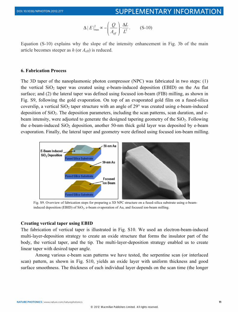
6. Fabrication Process
The 3D taper of the nanoplasmonic photon compressor (NPC) was fabricated in two steps: (1) the vertical SiO2 taper was created using e-beam-induced deposition (EBID) on the Au flat surface; and (2) the lateral taper was defined using focused ion-beam (FIB) milling, as shown in Fig. S9, following the gold evaporation. On top of an evaporated gold film on a fused-silica coverslip, a vertical SiO2 taper structure with an angle of 29° was created using e-beam-induced deposition of SiO2. The deposition parameters, including the scan patterns, scan duration, and e-beam intensity, were adjusted to generate the designed tapering geometry of the SiO2. Following the e-beam-induced SiO2 deposition, another 50-nm thick gold layer was deposited by e-beam evaporation. Finally, the lateral taper and geometry were defined using focused ion-beam milling.
Fig. S9. Overview of fabrication steps for preparing a 3D NPC structure on a fused-silica substrate using e-beam-induced deposition (EBID) of SiO2, e-beam evaporation of Au, and focused ion-beam milling.
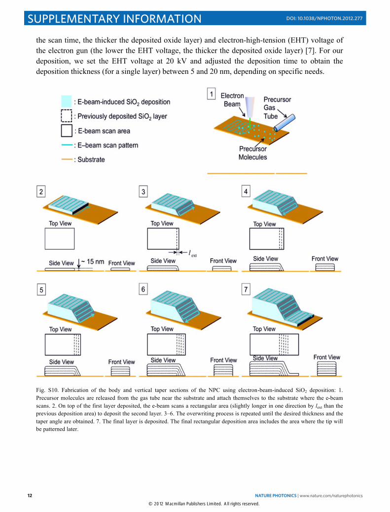
Creating vertical taper using EBID The fabrication of vertical taper is illustrated in Fig. S10. We used an electron-beam-induced multi-layer-deposition strategy to create an oxide structure that forms the insulator part of the body, the vertical taper, and the tip. The multi-layer-deposition strategy enabled us to create linear taper with desired taper angle.
Among various e-beam scan patterns we have tested, the serpentine scan (or interlaced scan) pattern, as shown in Fig. S10, yields an oxide layer with uniform thickness and good surface smoothness. The thickness of each individual layer depends on the scan time (the longer
2max 2| |
eff
Q LEA L
⎛ ⎞ ΔΔ ∝ − ⋅⎜ ⎟⎜ ⎟
⎝ ⎠
NATURE PHOTONICS | www.nature.com/naturephotonics 11
SUPPLEMENTARY INFORMATIONDOI: 10.1038/NPHOTON.2012.277
© 2012 Macmillan Publishers Limited. All rights reserved.
12
the scan time, the thicker the deposited oxide layer) and electron-high-tension (EHT) voltage of the electron gun (the lower the EHT voltage, the thicker the deposited oxide layer) [7]. For our deposition, we set the EHT voltage at 20 kV and adjusted the deposition time to obtain the deposition thickness (for a single layer) between 5 and 20 nm, depending on specific needs.
Fig. S10. Fabrication of the body and vertical taper sections of the NPC using electron-beam-induced SiO2 deposition: 1. Precursor molecules are released from the gas tube near the substrate and attach themselves to the substrate where the e-beam scans. 2. On top of the first layer deposited, the e-beam scans a rectangular area (slightly longer in one direction by lext than the previous deposition area) to deposit the second layer. 3–6. The overwriting process is repeated until the desired thickness and the taper angle are obtained. 7. The final layer is deposited. The final rectangular deposition area includes the area where the tip will be patterned later.
12 NATURE PHOTONICS | www.nature.com/naturephotonics
SUPPLEMENTARY INFORMATION DOI: 10.1038/NPHOTON.2012.277
© 2012 Macmillan Publishers Limited. All rights reserved.
13
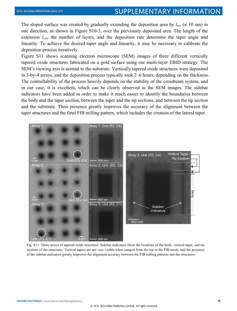
The sloped surface was created by gradually extending the deposition area by lext (≤ 10 nm) in one direction, as shown in Figure S10-3, over the previously deposited area. The length of the extension lext, the number of layers, and the deposition rate determine the taper angle and linearity. To achieve the desired taper angle and linearity, it may be necessary to calibrate the deposition process iteratively. Figure S11 shows scanning electron microscope (SEM) images of three different vertically tapered oxide structures fabricated on a gold surface using our multi-layer EBID strategy. The SEM’s viewing axis is normal to the substrate. Vertically tapered oxide structures were deposited in 3-by-4 arrays, and the deposition process typically took 2–6 hours, depending on the thickness. The controllability of the process heavily depends on the stability of the crossbeam system, and in our case, it is excellent, which can be clearly observed in the SEM images. The sidebar indicators have been added in order to make it much easier to identify the boundaries between the body and the taper section, between the taper and the tip sections, and between the tip section and the substrate. Their presence greatly improves the accuracy of the alignment between the taper structures and the final FIB milling pattern, which includes the creation of the lateral taper.
Fig. S11. Three arrays of tapered oxide structures: Sidebar indicators show the locations of the body, vertical taper, and tip sections of the structures. Vertical tapers are not very visible when imaged from the top in the FIB mode, and the presence of the sidebar indicators greatly improves the alignment accuracy between the FIB milling patterns and the structures.
nm
NATURE PHOTONICS | www.nature.com/naturephotonics 13
SUPPLEMENTARY INFORMATIONDOI: 10.1038/NPHOTON.2012.277
© 2012 Macmillan Publishers Limited. All rights reserved.
14
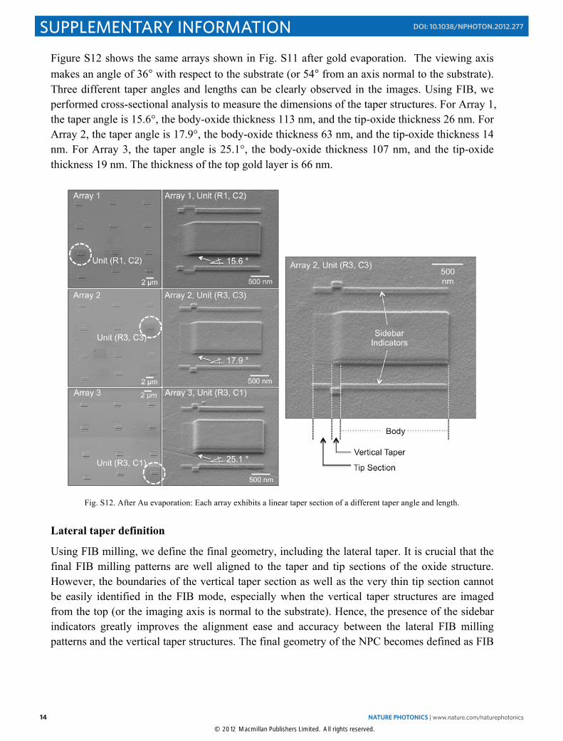
Figure S12 shows the same arrays shown in Fig. S11 after gold evaporation. The viewing axis makes an angle of 36° with respect to the substrate (or 54° from an axis normal to the substrate). Three different taper angles and lengths can be clearly observed in the images. Using FIB, we performed cross-sectional analysis to measure the dimensions of the taper structures. For Array 1, the taper angle is 15.6°, the body-oxide thickness 113 nm, and the tip-oxide thickness 26 nm. For Array 2, the taper angle is 17.9°, the body-oxide thickness 63 nm, and the tip-oxide thickness 14 nm. For Array 3, the taper angle is 25.1°, the body-oxide thickness 107 nm, and the tip-oxide thickness 19 nm. The thickness of the top gold layer is 66 nm.
Fig. S12. After Au evaporation: Each array exhibits a linear taper section of a different taper angle and length.
Lateral taper definition
Using FIB milling, we define the final geometry, including the lateral taper. It is crucial that the final FIB milling patterns are well aligned to the taper and tip sections of the oxide structure. However, the boundaries of the vertical taper section as well as the very thin tip section cannot be easily identified in the FIB mode, especially when the vertical taper structures are imaged from the top (or the imaging axis is normal to the substrate). Hence, the presence of the sidebar indicators greatly improves the alignment ease and accuracy between the lateral FIB milling patterns and the vertical taper structures. The final geometry of the NPC becomes defined as FIB
14 NATURE PHOTONICS | www.nature.com/naturephotonics
SUPPLEMENTARY INFORMATION DOI: 10.1038/NPHOTON.2012.277
© 2012 Macmillan Publishers Limited. All rights reserved.
15
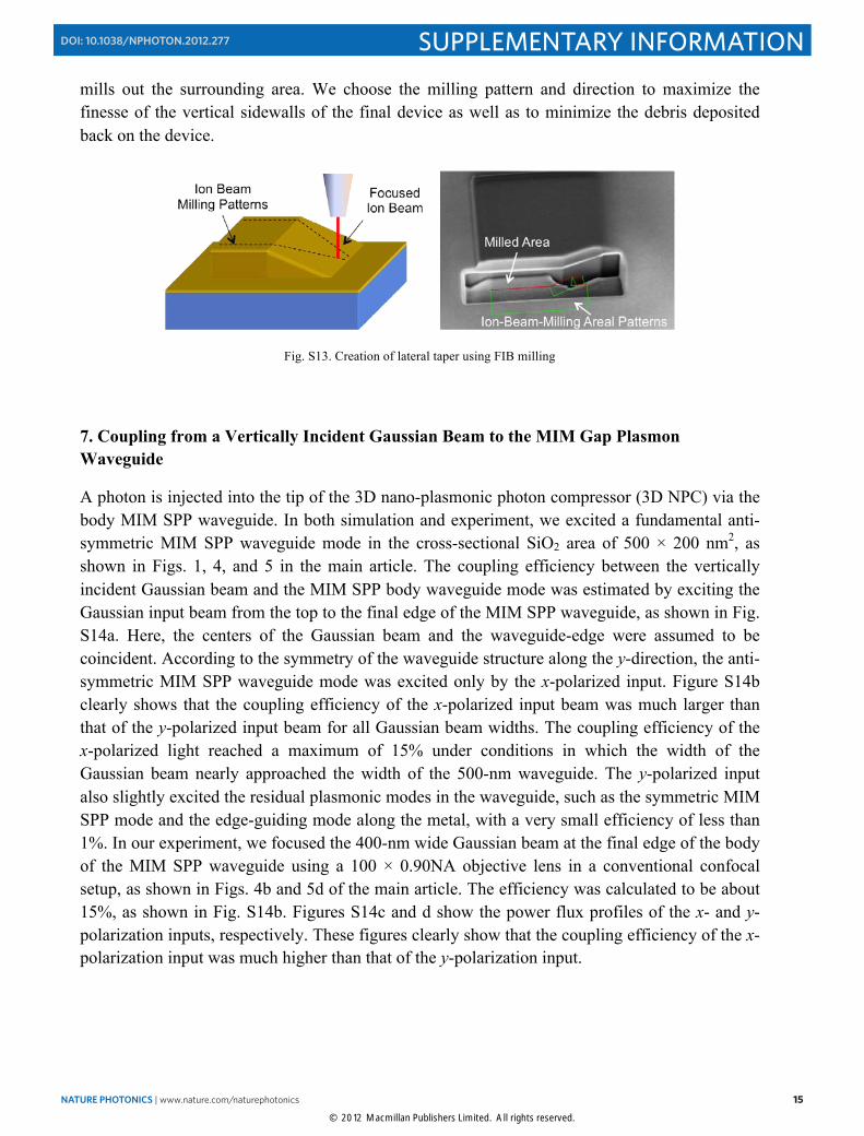
mills out the surrounding area. We choose the milling pattern and direction to maximize the finesse of the vertical sidewalls of the final device as well as to minimize the debris deposited back on the device.
Fig. S13. Creation of lateral taper using FIB milling
7. Coupling from a Vertically Incident Gaussian Beam to the MIM Gap Plasmon Waveguide
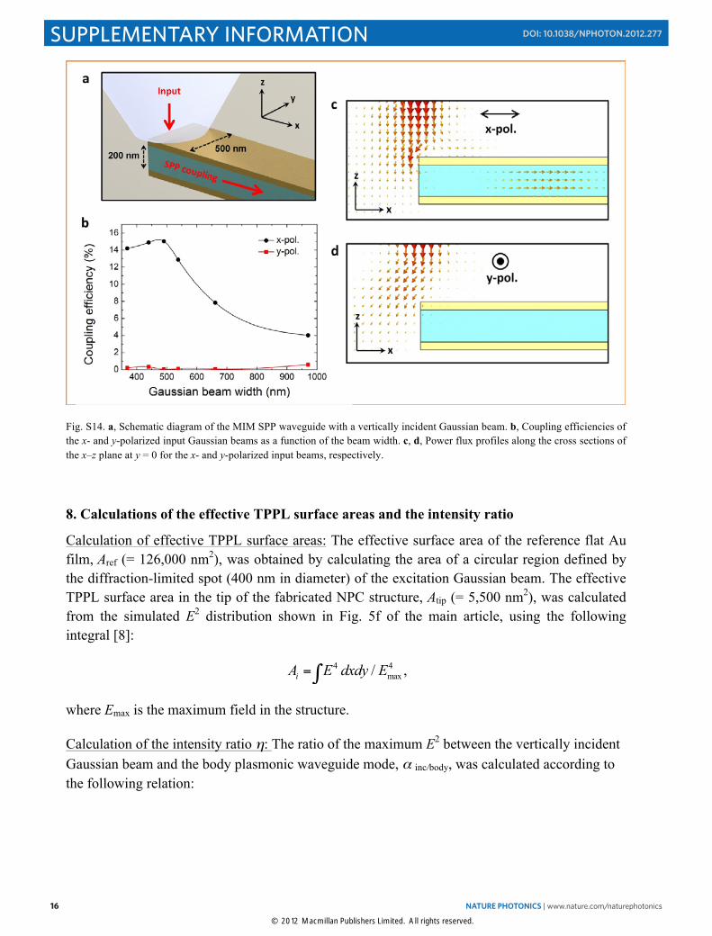
A photon is injected into the tip of the 3D nano-plasmonic photon compressor (3D NPC) via the body MIM SPP waveguide. In both simulation and experiment, we excited a fundamental anti-symmetric MIM SPP waveguide mode in the cross-sectional SiO2 area of 500 × 200 nm2, as shown in Figs. 1, 4, and 5 in the main article. The coupling efficiency between the vertically incident Gaussian beam and the MIM SPP body waveguide mode was estimated by exciting the Gaussian input beam from the top to the final edge of the MIM SPP waveguide, as shown in Fig. S14a. Here, the centers of the Gaussian beam and the waveguide-edge were assumed to be coincident. According to the symmetry of the waveguide structure along the y-direction, the anti-symmetric MIM SPP waveguide mode was excited only by the x-polarized input. Figure S14b clearly shows that the coupling efficiency of the x-polarized input beam was much larger than that of the y-polarized input beam for all Gaussian beam widths. The coupling efficiency of the x-polarized light reached a maximum of 15% under conditions in which the width of the Gaussian beam nearly approached the width of the 500-nm waveguide. The y-polarized input also slightly excited the residual plasmonic modes in the waveguide, such as the symmetric MIM SPP mode and the edge-guiding mode along the metal, with a very small efficiency of less than 1%. In our experiment, we focused the 400-nm wide Gaussian beam at the final edge of the body of the MIM SPP waveguide using a 100 × 0.90NA objective lens in a conventional confocal setup, as shown in Figs. 4b and 5d of the main article. The efficiency was calculated to be about 15%, as shown in Fig. S14b. Figures S14c and d show the power flux profiles of the x- and y-polarization inputs, respectively. These figures clearly show that the coupling efficiency of the x-polarization input was much higher than that of the y-polarization input.
NATURE PHOTONICS | www.nature.com/naturephotonics 15
SUPPLEMENTARY INFORMATIONDOI: 10.1038/NPHOTON.2012.277
© 2012 Macmillan Publishers Limited. All rights reserved.
16
Fig. S14. a, Schematic diagram of the MIM SPP waveguide with a vertically incident Gaussian beam. b, Coupling efficiencies of the x- and y-polarized input Gaussian beams as a function of the beam width. c, d, Power flux profiles along the cross sections of the x–z plane at y = 0 for the x- and y-polarized input beams, respectively.
8. Calculations of the effective TPPL surface areas and the intensity ratio
Calculation of effective TPPL surface areas: The effective surface area of the reference flat Au film, Aref (= 126,000 nm2), was obtained by calculating the area of a circular region defined by the diffraction-limited spot (400 nm in diameter) of the excitation Gaussian beam. The effective TPPL surface area in the tip of the fabricated NPC structure, Atip (= 5,500 nm2), was calculated from the simulated E2 distribution shown in Fig. 5f of the main article, using the following integral [8]:
,
where Emax is the maximum field in the structure.
Calculation of the intensity ratio η: The ratio of the maximum E2 between the vertically incident Gaussian beam and the body plasmonic waveguide mode, α inc/body, was calculated according to the following relation:
4 4max/iA E dxdy E= ∫
16 NATURE PHOTONICS | www.nature.com/naturephotonics
SUPPLEMENTARY INFORMATION DOI: 10.1038/NPHOTON.2012.277
© 2012 Macmillan Publishers Limited. All rights reserved.
17
.
9. Estimation of Transmittance from Experimental Measurement
In order to estimate the pure coupling efficiency (transmittance) through the tapered section in the fabricated 3D NPC structure, we converted the measured value of intensity enhancement (~400) to an enhancement without the cavity effect. Based on Fig. 3b of the main article, the intensity is enhanced by a factor of ~4 when the tip of finite length is present instead of an infinite sub-100 nm waveguide. Hence, dividing the measured enhancement value by 4, we obtain the intensity enhancement over 100, which is in excellent agreement with the calculated |E|2 enhancement value for h = 14 nm shown in Fig. 2c of the main article. We can also estimate the coupling efficiency (transmittance) through the tapered section into the sub-100 nm-scale infinite waveguide (without the cavity effect) using Fig. 2c of the main article, which is slightly over −1.3dB (74%).
10. Detecting Second Harmonic Generation (SHG) from the 3D NPC with a Finite Tip
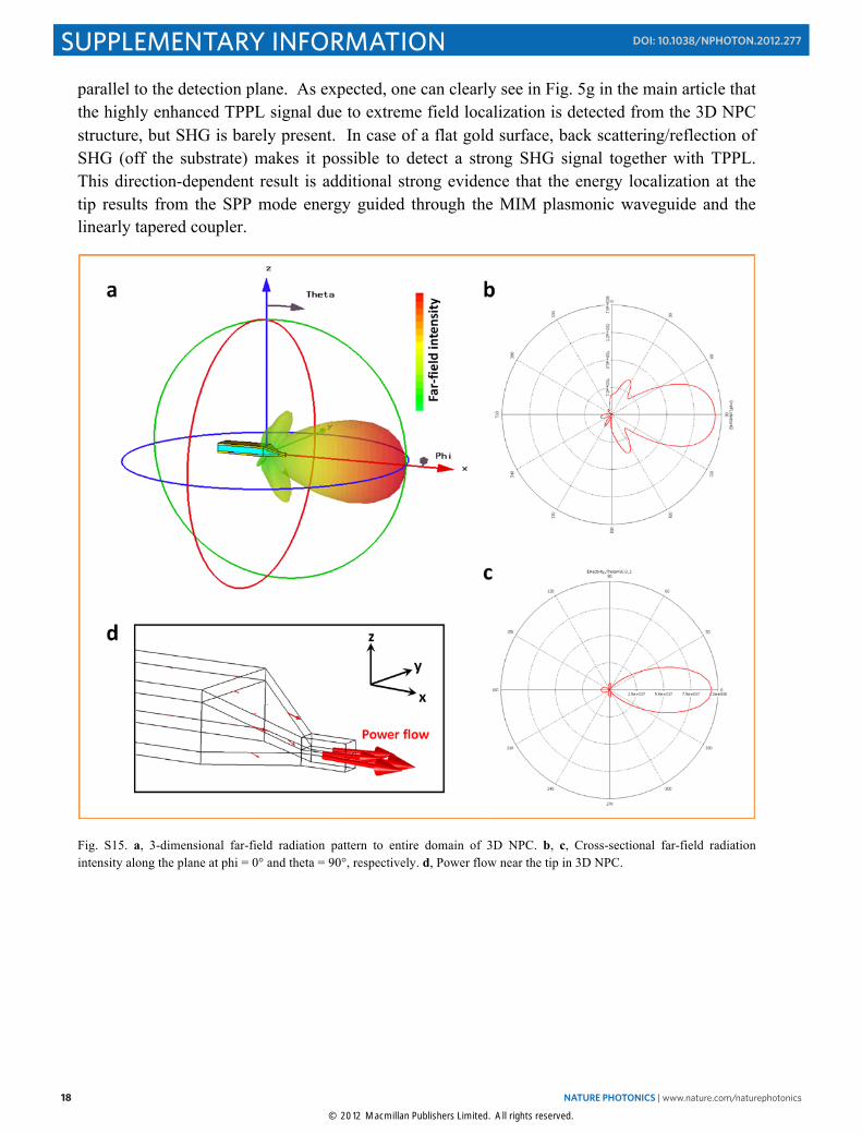
Figures S15a–c show the far-field radiation pattern to the surrounding space of 3D NPC, while Figure S15d shows the power flow near the tip. The frequency of interest is 360 THz, and the excitation light enters the structure through the rectangular aperture at the left end of the waveguide. As shown in Fig. S15, most of the output is radiated to the waveguide direction (x-direction) within a solid angle of ±45°. From the far-field calculation, the ratio between the power emitted within the ±45° solid angle to the total radiation power is calculated to be larger than 75%.
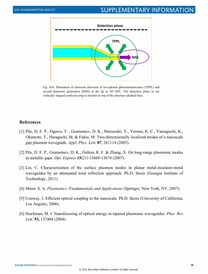
Using a confocal setup the perpendicularly aligned to the sample substrate (Fig. 4b in the main article), we measured both the two-photon photoluminescence (TPPL) and the second harmonic generation (SHG) in order to confirm the energy localization at the tip (Fig. 5g in the main article). Since the intensity of SHG is maximized for the phase matching condition of
[9], the direction of SHG emission strongly follows the radiation pattern (or dominant wave-vector composition) in the 3D NPC structure, which is highly anisotropic (see the radiation pattern in Fig. S15). In other words, SHG is highly directional and mostly emits and propagates in the same direction as the excitation beam. In contrast, the emission pattern of TPPL is highly isotropic compared to that of SHG [10]. These different emission characteristics of TPPL and SHG are illustrated in Fig. S16. If the energy localization at the tip of the 3D NPC results from the supported SPP mode in the waveguide, one will expect that TPPL can be readily detected in our setup, while most of SHG will escape the detector because our confocal detection system is oriented perpendicularly to the sample substrate and the SHG emission direction is
( ) ( ) ( ) ( )( )2 2
2 2 1// / 1/ / /body body body body
body in sio body m in ref eff in body m ref sio effP P E A E A n A A nη ε α ε−= = ⋅ = ⋅
(2 ) ( )k kω ω=r r
NATURE PHOTONICS | www.nature.com/naturephotonics 17
SUPPLEMENTARY INFORMATIONDOI: 10.1038/NPHOTON.2012.277
© 2012 Macmillan Publishers Limited. All rights reserved.
18
parallel to the detection plane. As expected, one can clearly see in Fig. 5g in the main article that the highly enhanced TPPL signal due to extreme field localization is detected from the 3D NPC structure, but SHG is barely present. In case of a flat gold surface, back scattering/reflection of SHG (off the substrate) makes it possible to detect a strong SHG signal together with TPPL. This direction-dependent result is additional strong evidence that the energy localization at the tip results from the SPP mode energy guided through the MIM plasmonic waveguide and the linearly tapered coupler.
Fig. S15. a, 3-dimensional far-field radiation pattern to entire domain of 3D NPC. b, c, Cross-sectional far-field radiation intensity along the plane at phi = 0° and theta = 90°, respectively. d, Power flow near the tip in 3D NPC.
18 NATURE PHOTONICS | www.nature.com/naturephotonics
SUPPLEMENTARY INFORMATION DOI: 10.1038/NPHOTON.2012.277
© 2012 Macmillan Publishers Limited. All rights reserved.
19
Fig. S16. Illustration of emission direction of two-photon photoluminescence (TPPL) and second harmonic generation (SHG) at the tip in 3D NPC. The detection plane in our vertically aligned confocal setup is located on top of the structure (dashed line).
References
[1] Pile, D. F. P., Ogawa, T. , Gramotnev, D. K., Matsuzaki, Y., Vernon, K. C., Yamaguchi, K., Okamoto, T., Haraguchi, M. & Fukui, M. Two-dimensionally localized modes of a nanoscale gap plasmon waveguide. Appl. Phys. Lett. 87, 261114 (2005).
[2] Pile, D. F. P., Gramotnev, D. K., Oulton, R. F. & Zhang, X. On long-range plasmonic modes in metallic gaps. Opt. Express 15(21) 13669-13674 (2007).
[3] Lin, C. Characterization of the surface plasmon modes in planar metal-insulator-metal waveguides by an attenuated total reflection approach. Ph.D. thesis (Georgia Institute of Technology, 2011)
[4] Maier, S. A. Plasmonics: Fundamentals and Applications (Springer, New York, NY, 2007).
[5] Conway, J. Efficient optical coupling to the nanoscale. Ph.D. thesis (University of California, Los Angeles, 2006).
[6] Stockman, M. I. Nanofocusing of optical energy in tapered plasmonic waveguides. Phys. Rev. Lett. 93, 137404 (2004).
NATURE PHOTONICS | www.nature.com/naturephotonics 19
SUPPLEMENTARY INFORMATIONDOI: 10.1038/NPHOTON.2012.277
© 2012 Macmillan Publishers Limited. All rights reserved.

20
[7] Utke, I., Hoffman, P., and Melngailis, J. Gas-assisted focused electron beam and ion beam processing and fabrication. J. Vacuum Sci. Tech. B, 26(4), 1197–1276 (2008).
[8] Schuck, P. J., Fromm, D. P., Sundaramurthy, A., Kino, G. S. & Moerner, W. E. Improving the mismatch between light and nanoscale objects with gold bowtie nanoantennas. Phys. Rev. Lett. 94, 017402 (2005).
[9] Haus, H. Waves and Fields in Optoelectronics (Prentice-Hall, Englewood Cliffs NJ, 1984).
[10] Beversluis, M. R., Bouhelier, A. and Novotny, L. Continuum generation from single gold nanostructures through near-field mediated intraband transitions. Phys. Rev. B 68, 115433 (2003).
20 NATURE PHOTONICS | www.nature.com/naturephotonics
SUPPLEMENTARY INFORMATION DOI: 10.1038/NPHOTON.2012.277
© 2012 Macmillan Publishers Limited. All rights reserved.