Embed Size (px)
Citation preview
February 2008 Rev 15 1/21
21
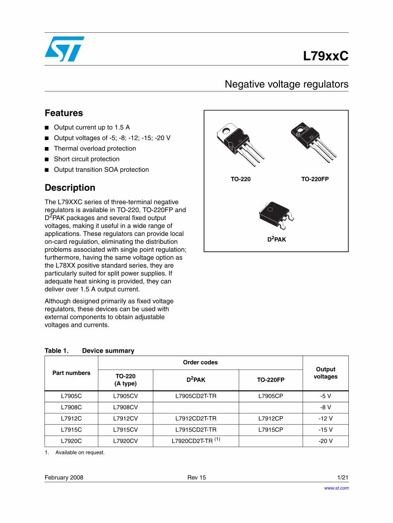
L79xxC
Negative voltage regulators
Features■ Output current up to 1.5 A
■ Output voltages of -5; -8; -12; -15; -20 V
■ Thermal overload protection
■ Short circuit protection
■ Output transition SOA protection
DescriptionThe L79XXC series of three-terminal negative regulators is available in TO-220, TO-220FP and D2PAK packages and several fixed output voltages, making it useful in a wide range of applications. These regulators can provide local on-card regulation, eliminating the distribution problems associated with single point regulation; furthermore, having the same voltage option as the L78XX positive standard series, they are particularly suited for split power supplies. If adequate heat sinking is provided, they can deliver over 1.5 A output current.
Although designed primarily as fixed voltage regulators, these devices can be used with external components to obtain adjustable voltages and currents.
TO-220FP
D2PAK
TO-220
Table 1. Device summary
Part numbers
Order codesOutput
voltagesTO-220(A type)
D2PAK TO-220FP
L7905C L7905CV L7905CD2T-TR L7905CP -5 V
L7908C L7908CV -8 V
L7912C L7912CV L7912CD2T-TR L7912CP -12 V
L7915C L7915CV L7915CD2T-TR L7915CP -15 V
L7920C L7920CV L7920CD2T-TR (1) -20 V
1. Available on request.
www.st.com
Contents L79xxC
2/21
Contents
1 Diagram . . . . . . . . . . . . . . . . . . . . . . . . . . . . . . . . . . . . . . . . . . . . . . . . . . . 3
2 Pin configuration . . . . . . . . . . . . . . . . . . . . . . . . . . . . . . . . . . . . . . . . . . . 4
3 Maximum ratings . . . . . . . . . . . . . . . . . . . . . . . . . . . . . . . . . . . . . . . . . . . . 5
4 Test circuit . . . . . . . . . . . . . . . . . . . . . . . . . . . . . . . . . . . . . . . . . . . . . . . . 6
5 Electrical characteristics . . . . . . . . . . . . . . . . . . . . . . . . . . . . . . . . . . . . . 7
6 Application information . . . . . . . . . . . . . . . . . . . . . . . . . . . . . . . . . . . . . 10
7 Package mechanical data . . . . . . . . . . . . . . . . . . . . . . . . . . . . . . . . . . . . 12
8 Revision history . . . . . . . . . . . . . . . . . . . . . . . . . . . . . . . . . . . . . . . . . . . 20
L79xxC Diagram
3/21
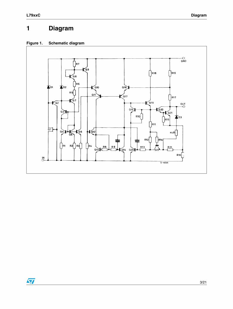
1 Diagram
Figure 1. Schematic diagram
Pin configuration L79xxC
4/21
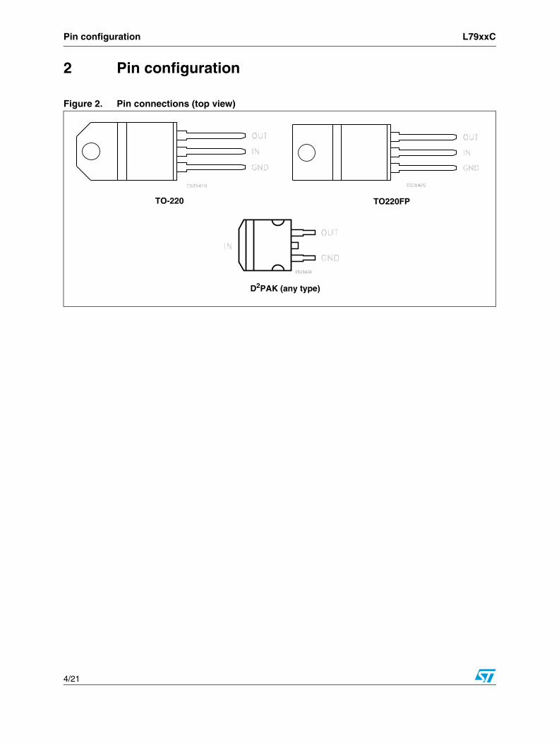
2 Pin configuration
Figure 2. Pin connections (top view)
TO220FPTO-220
D2PAK (any type)
L79xxC Maximum ratings
5/21
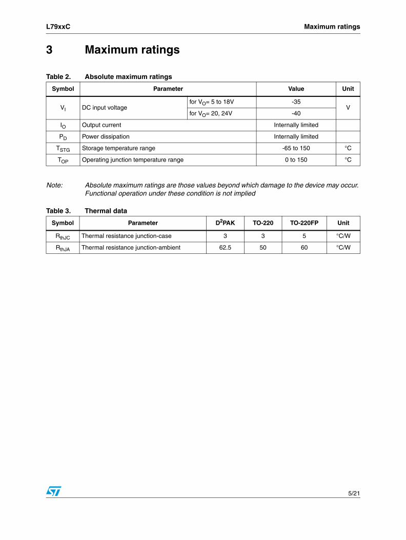
3 Maximum ratings
Note: Absolute maximum ratings are those values beyond which damage to the device may occur. Functional operation under these condition is not implied
Table 2. Absolute maximum ratings
Symbol Parameter Value Unit
VI DC input voltagefor VO= 5 to 18V -35
Vfor VO= 20, 24V -40
IO Output current Internally limited
PD Power dissipation Internally limited
TSTG Storage temperature range -65 to 150 °C
TOP Operating junction temperature range 0 to 150 °C
Table 3. Thermal data
Symbol Parameter D2PAK TO-220 TO-220FP Unit
RthJC Thermal resistance junction-case 3 3 5 °C/W
RthJA Thermal resistance junction-ambient 62.5 50 60 °C/W
Test circuit L79xxC
6/21
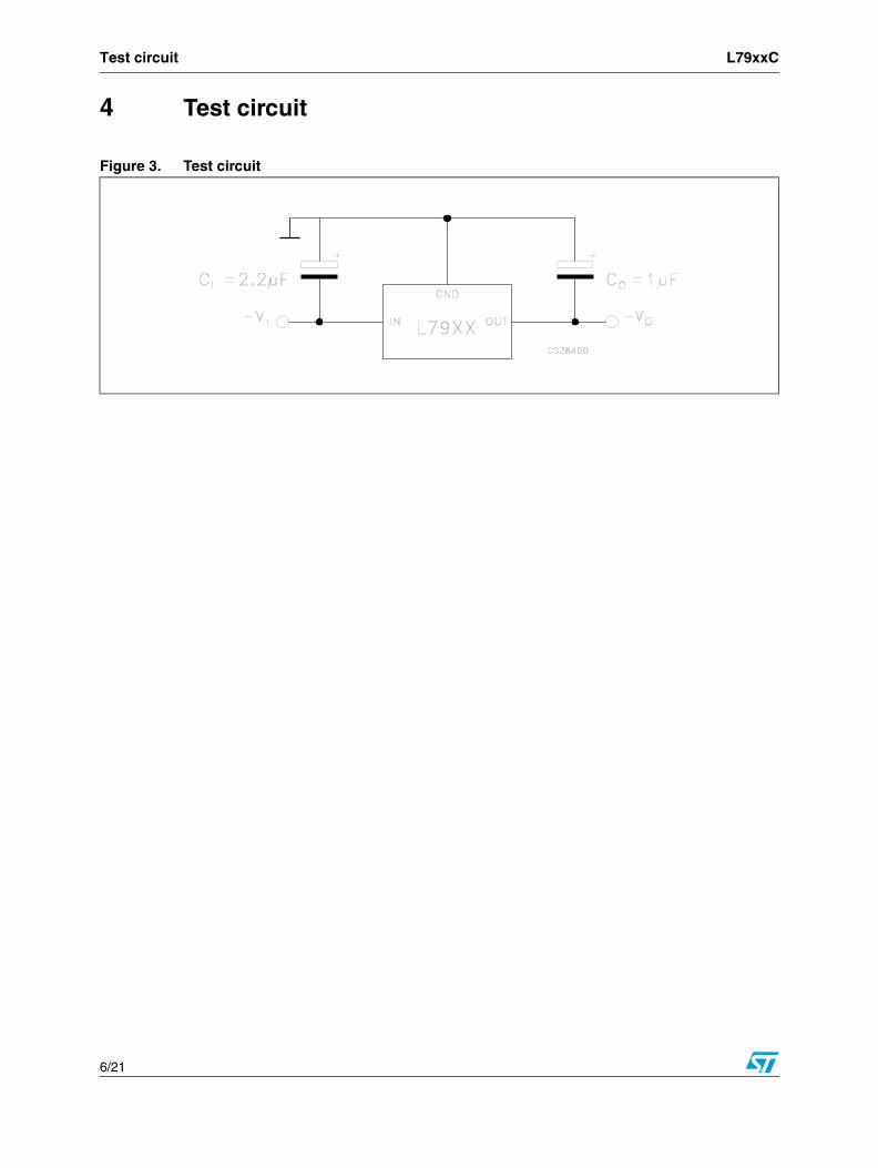
4 Test circuit
Figure 3. Test circuit
L79xxC Electrical characteristics
7/21
5 Electrical characteristics
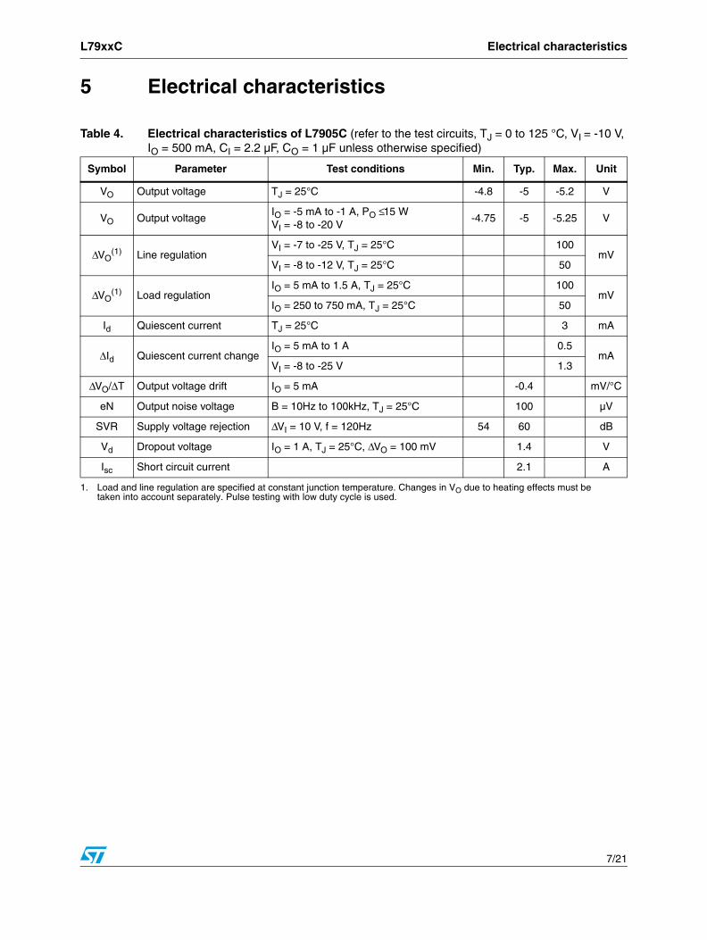
Table 4. Electrical characteristics of L7905C (refer to the test circuits, TJ = 0 to 125 °C, VI = -10 V, IO = 500 mA, CI = 2.2 µF, CO = 1 µF unless otherwise specified)
Symbol Parameter Test conditions Min. Typ. Max. Unit
VO Output voltage TJ = 25°C -4.8 -5 -5.2 V
VO Output voltageIO = -5 mA to -1 A, PO ≤ 15 WVI = -8 to -20 V
-4.75 -5 -5.25 V
ΔVO(1)
1. Load and line regulation are specified at constant junction temperature. Changes in VO due to heating effects must be taken into account separately. Pulse testing with low duty cycle is used.
Line regulationVI = -7 to -25 V, TJ = 25°C 100
mVVI = -8 to -12 V, TJ = 25°C 50
ΔVO(1) Load regulation
IO = 5 mA to 1.5 A, TJ = 25°C 100mV
IO = 250 to 750 mA, TJ = 25°C 50
Id Quiescent current TJ = 25°C 3 mA
ΔId Quiescent current changeIO = 5 mA to 1 A 0.5
mAVI = -8 to -25 V 1.3
ΔVO/ΔT Output voltage drift IO = 5 mA -0.4 mV/°C
eN Output noise voltage B = 10Hz to 100kHz, TJ = 25°C 100 µV
SVR Supply voltage rejection ΔVI = 10 V, f = 120Hz 54 60 dB
Vd Dropout voltage IO = 1 A, TJ = 25°C, ΔVO = 100 mV 1.4 V
Isc Short circuit current 2.1 A
Electrical characteristics L79xxC
8/21
Table 5. Electrical characteristics of L7908C (refer to the test circuits, TJ = 0 to 125 °C, VI = -14 V, IO = 500 mA, CI = 2.2 µF, CO = 1 µF unless otherwise specified)
Symbol Parameter Test conditions Min. Typ. Max. Unit
VO Output voltage TJ = 25°C -7.7 -8 -8.3 V
VO Output voltageIO = -5 mA to -1 A, PO ≤ 15 WVI = -11.5 to -23 V
-7.6 -8 -8.4 V
ΔVO(1) Line regulation
VI = -10.5 to -25 V, TJ = 25°C 160mV
VI = -11 to -17 V, TJ = 25°C 80
ΔVO(1) Load regulation
IO = 5 mA to 1.5 A, TJ = 25°C 160mV
IO = 250 to 750 mA, TJ = 25°C 80
Id Quiescent current TJ = 25°C 3 mA
ΔId Quiescent current changeIO = 5 mA to 1 A 0.5
mAVI = -11.5 to -25 V 1
ΔVO/ΔT Output voltage drift IO = 5 mA -0.6 mV/°C
eN Output noise voltage B = 10Hz to 100kHz, TJ = 25°C 175 µV
SVR Supply voltage rejection ΔVI = 10 V, f = 120Hz 54 60 dB
Vd Dropout voltage IO = 1 A, TJ = 25°C, ΔVO = 100 mV 1.1 V
Isc Short circuit current 1.5 A
1. Load and line regulation are specified at constant junction temperature. Changes in VO due to heating effects must be taken into account separately. Pulse testing with low duty cycle is used.
Table 6. Electrical characteristics of L7912C (refer to the test circuits, TJ = 0 to 125 °C, VI = -19 V, IO = 500 mA, CI = 2.2 µF, CO = 1 µF unless otherwise specified)
Symbol Parameter Test conditions Min. Typ. Max. Unit
VO Output voltage TJ = 25°C -11.5 -12 -12.5 V
VO Output voltageIO = -5 mA to -1 A, PO ≤ 15 WVI = -15.5 to -27 V
-11.4 -12 -12.6 V
ΔVO(1) Line regulation
VI = -14.5 to -30 V, TJ = 25°C 240mV
VI = -16 to -22 V, TJ = 25°C 120
ΔVO(1) Load regulation
IO = 5 mA to 1.5 A, TJ = 25°C 240mV
IO = 250 to 750 mA, TJ = 25°C 120
Id Quiescent current TJ = 25°C 3 mA
ΔId Quiescent current changeIO = 5 mA to 1 A 0.5
mAVI = -15 to -30 V 1
ΔVO/ΔT Output voltage drift IO = 5 mA -0.8 mV/°C
eN Output noise voltage B = 10Hz to 100kHz, TJ = 25°C 200 µV
SVR Supply voltage rejection ΔVI = 10 V, f = 120Hz 54 60 dB
Vd Dropout voltage IO = 1 A, TJ = 25°C, ΔVO = 100 mV 1.1 V
Isc Short circuit current 1.5 A
1. Load and line regulation are specified at constant junction temperature. Changes in VO due to heating effects must be taken into account separately. Pulse testing with low duty cycle is used.
L79xxC Electrical characteristics
9/21
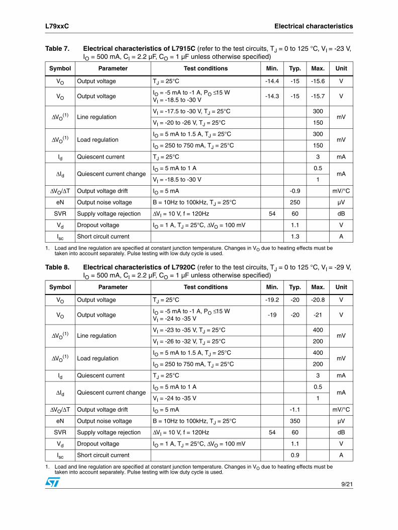
Table 7. Electrical characteristics of L7915C (refer to the test circuits, TJ = 0 to 125 °C, VI = -23 V, IO = 500 mA, CI = 2.2 µF, CO = 1 µF unless otherwise specified)
Symbol Parameter Test conditions Min. Typ. Max. Unit
VO Output voltage TJ = 25°C -14.4 -15 -15.6 V
VO Output voltageIO = -5 mA to -1 A, PO ≤ 15 WVI = -18.5 to -30 V
-14.3 -15 -15.7 V
ΔVO(1) Line regulation
VI = -17.5 to -30 V, TJ = 25°C 300mV
VI = -20 to -26 V, TJ = 25°C 150
ΔVO(1) Load regulation
IO = 5 mA to 1.5 A, TJ = 25°C 300mV
IO = 250 to 750 mA, TJ = 25°C 150
Id Quiescent current TJ = 25°C 3 mA
ΔId Quiescent current changeIO = 5 mA to 1 A 0.5
mAVI = -18.5 to -30 V 1
ΔVO/ΔT Output voltage drift IO = 5 mA -0.9 mV/°C
eN Output noise voltage B = 10Hz to 100kHz, TJ = 25°C 250 µV
SVR Supply voltage rejection ΔVI = 10 V, f = 120Hz 54 60 dB
Vd Dropout voltage IO = 1 A, TJ = 25°C, ΔVO = 100 mV 1.1 V
Isc Short circuit current 1.3 A
1. Load and line regulation are specified at constant junction temperature. Changes in VO due to heating effects must be taken into account separately. Pulse testing with low duty cycle is used.
Table 8. Electrical characteristics of L7920C (refer to the test circuits, TJ = 0 to 125 °C, VI = -29 V, IO = 500 mA, CI = 2.2 µF, CO = 1 µF unless otherwise specified)
Symbol Parameter Test conditions Min. Typ. Max. Unit
VO Output voltage TJ = 25°C -19.2 -20 -20.8 V
VO Output voltageIO = -5 mA to -1 A, PO ≤ 15 WVI = -24 to -35 V
-19 -20 -21 V
ΔVO(1) Line regulation
VI = -23 to -35 V, TJ = 25°C 400mV
VI = -26 to -32 V, TJ = 25°C 200
ΔVO(1) Load regulation
IO = 5 mA to 1.5 A, TJ = 25°C 400mV
IO = 250 to 750 mA, TJ = 25°C 200
Id Quiescent current TJ = 25°C 3 mA
ΔId Quiescent current changeIO = 5 mA to 1 A 0.5
mAVI = -24 to -35 V 1
ΔVO/ΔT Output voltage drift IO = 5 mA -1.1 mV/°C
eN Output noise voltage B = 10Hz to 100kHz, TJ = 25°C 350 µV
SVR Supply voltage rejection ΔVI = 10 V, f = 120Hz 54 60 dB
Vd Dropout voltage IO = 1 A, TJ = 25°C, ΔVO = 100 mV 1.1 V
Isc Short circuit current 0.9 A
1. Load and line regulation are specified at constant junction temperature. Changes in VO due to heating effects must be taken into account separately. Pulse testing with low duty cycle is used.
Application information L79xxC
10/21
6 Application information
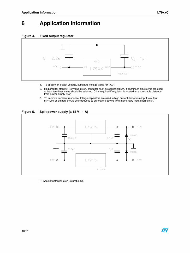
1. To specify an output voltage, substitute voltage value for "XX".
2. Required for stability. For value given, capacitor must be solid tantalum. If aluminium electrolytic are used, at least ten times value should be selected. C1 is required if regulator is located an appreciable distance from power supply filter.
3. To improve transient response. If large capacitors are used, a high current diode from input to output (1N4001 or similar) should be introduced to protect the device from momentary input short circuit.
(*) Against potential latch-up problems.
Figure 4. Fixed output regulator
Figure 5. Split power supply (± 15 V - 1 A)
L79xxC Application information
11/21
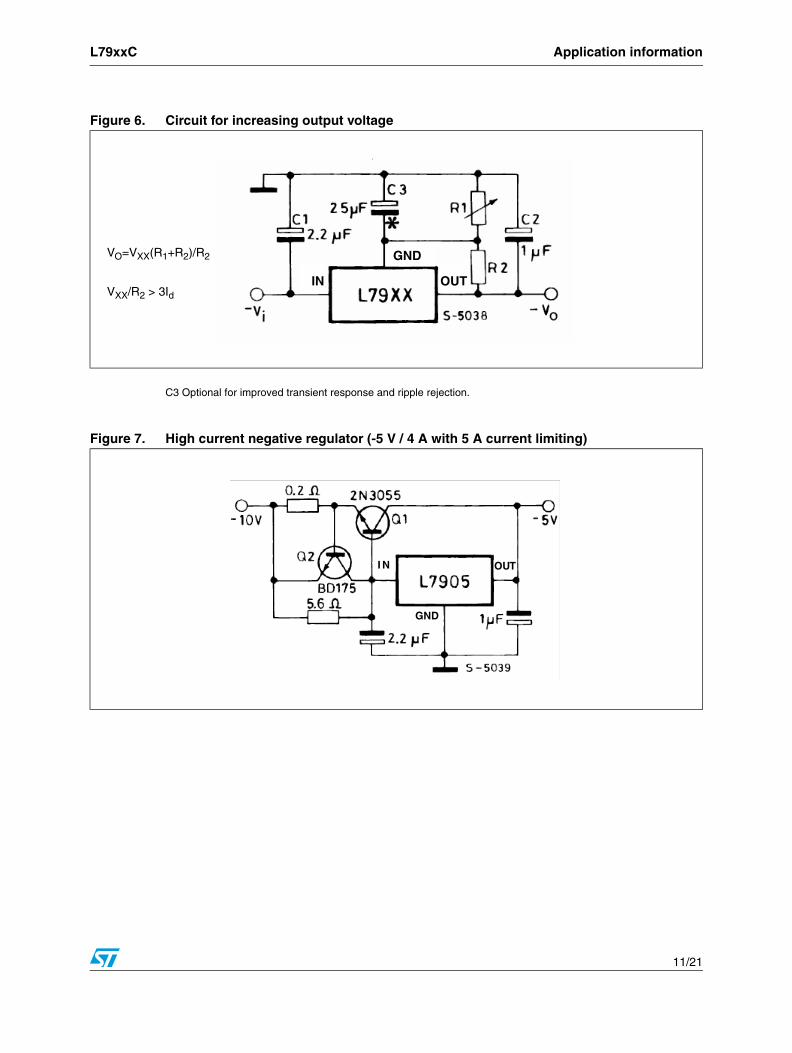
C3 Optional for improved transient response and ripple rejection.
Figure 6. Circuit for increasing output voltage
VXX/R2 > 3Id
VO=VXX(R1+R2)/R2
IN OUT
GND
IN OUT
GND
Figure 7. High current negative regulator (-5 V / 4 A with 5 A current limiting)
I N OUT
GND
I N OUT
GND
Package mechanical data L79xxC
12/21
7 Package mechanical data
In order to meet environmental requirements, ST offers these devices in ECOPACK® packages. These packages have a lead-free second level interconnect. The category of second Level Interconnect is marked on the package and on the inner box label, in compliance with JEDEC Standard JESD97. The maximum ratings related to soldering conditions are also marked on the inner box label. ECOPACK is an ST trademark. ECOPACK specifications are available at: www.st.com.
L79xxC Package mechanical data
13/21
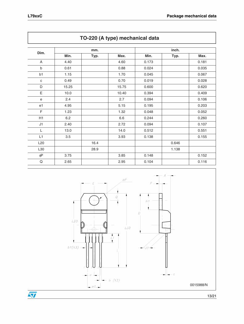
Dim.mm. inch.
Min. Typ. Max. Min. Typ. Max.
A 4.40 4.60 0.173 0.181
b 0.61 0.88 0.024 0.035
b1 1.15 1.70 0.045 0.067
c 0.49 0.70 0.019 0.028
D 15.25 15.75 0.600 0.620
E 10.0 10.40 0.394 0.409
e 2.4 2.7 0.094 0.106
e1 4.95 5.15 0.195 0.203
F 1.23 1.32 0.048 0.052
H1 6.2 6.6 0.244 0.260
J1 2.40 2.72 0.094 0.107
L 13.0 14.0 0.512 0.551
L1 3.5 3.93 0.138 0.155
L20 16.4 0.646
L30 28.9 1.138
φP 3.75 3.85 0.148 0.152
Q 2.65 2.95 0.104 0.116
TO-220 (A type) mechanical data
0015988/N
Package mechanical data L79xxC
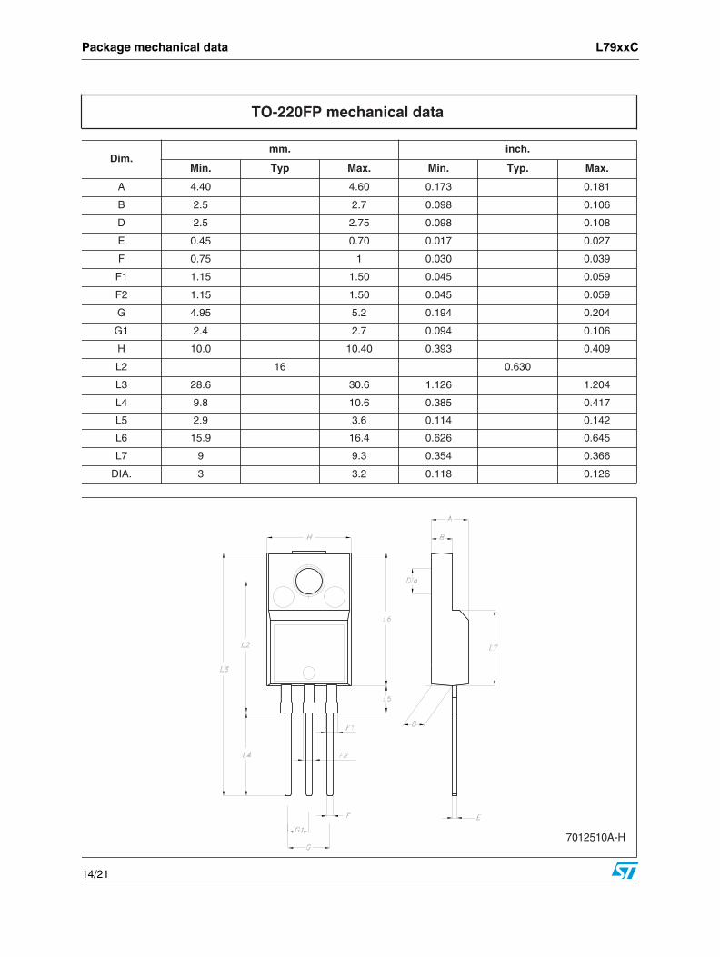
14/21
Dim.mm. inch.
Min. Typ Max. Min. Typ. Max.
A 4.40 4.60 0.173 0.181
B 2.5 2.7 0.098 0.106
D 2.5 2.75 0.098 0.108
E 0.45 0.70 0.017 0.027
F 0.75 1 0.030 0.039
F1 1.15 1.50 0.045 0.059
F2 1.15 1.50 0.045 0.059
G 4.95 5.2 0.194 0.204
G1 2.4 2.7 0.094 0.106
H 10.0 10.40 0.393 0.409
L2 16 0.630
L3 28.6 30.6 1.126 1.204
L4 9.8 10.6 0.385 0.417
L5 2.9 3.6 0.114 0.142
L6 15.9 16.4 0.626 0.645
L7 9 9.3 0.354 0.366
DIA. 3 3.2 0.118 0.126
TO-220FP mechanical data
7012510A-H
L79xxC Package mechanical data
15/21
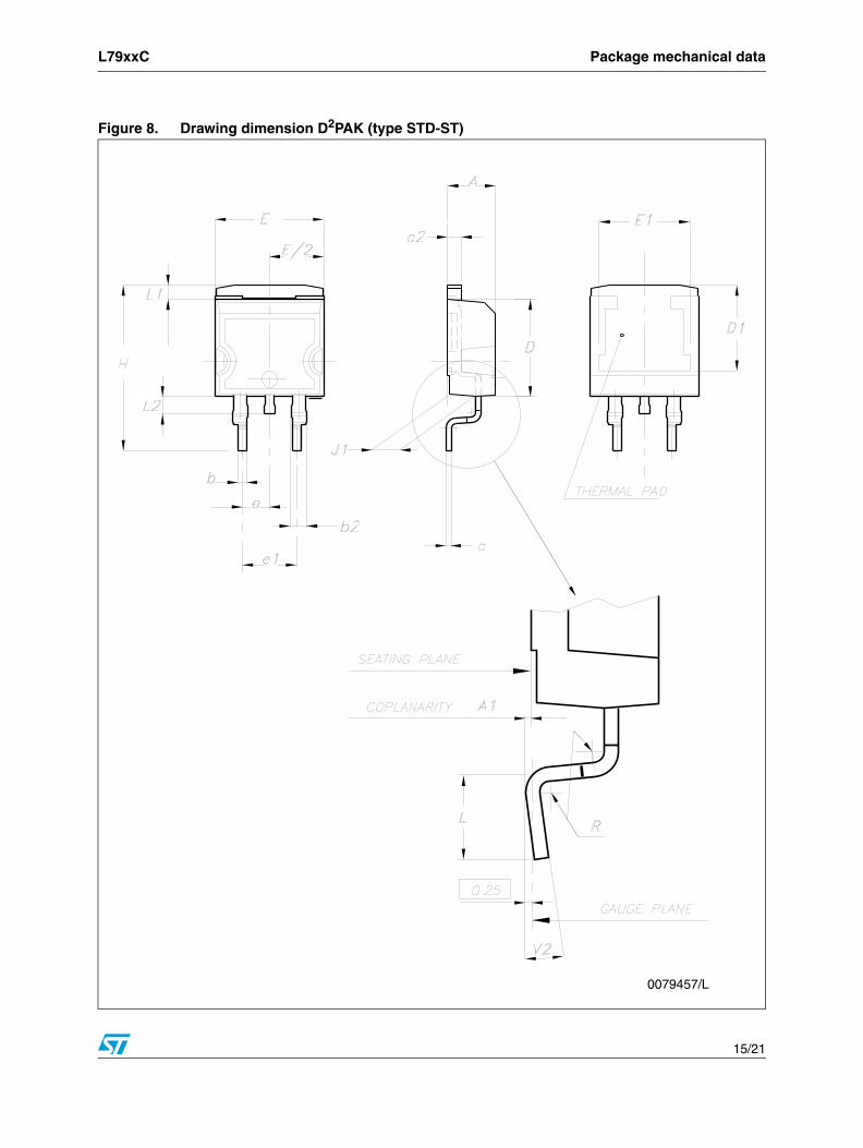
Figure 8. Drawing dimension D2PAK (type STD-ST)
0079457/L
Package mechanical data L79xxC
16/21
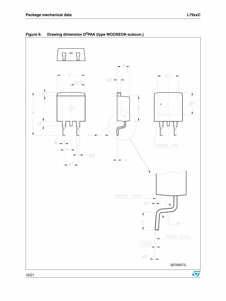
Figure 9. Drawing dimension D2PAK (type WOOSEOK-subcon.)
0079457/L
L79xxC Package mechanical data
17/21
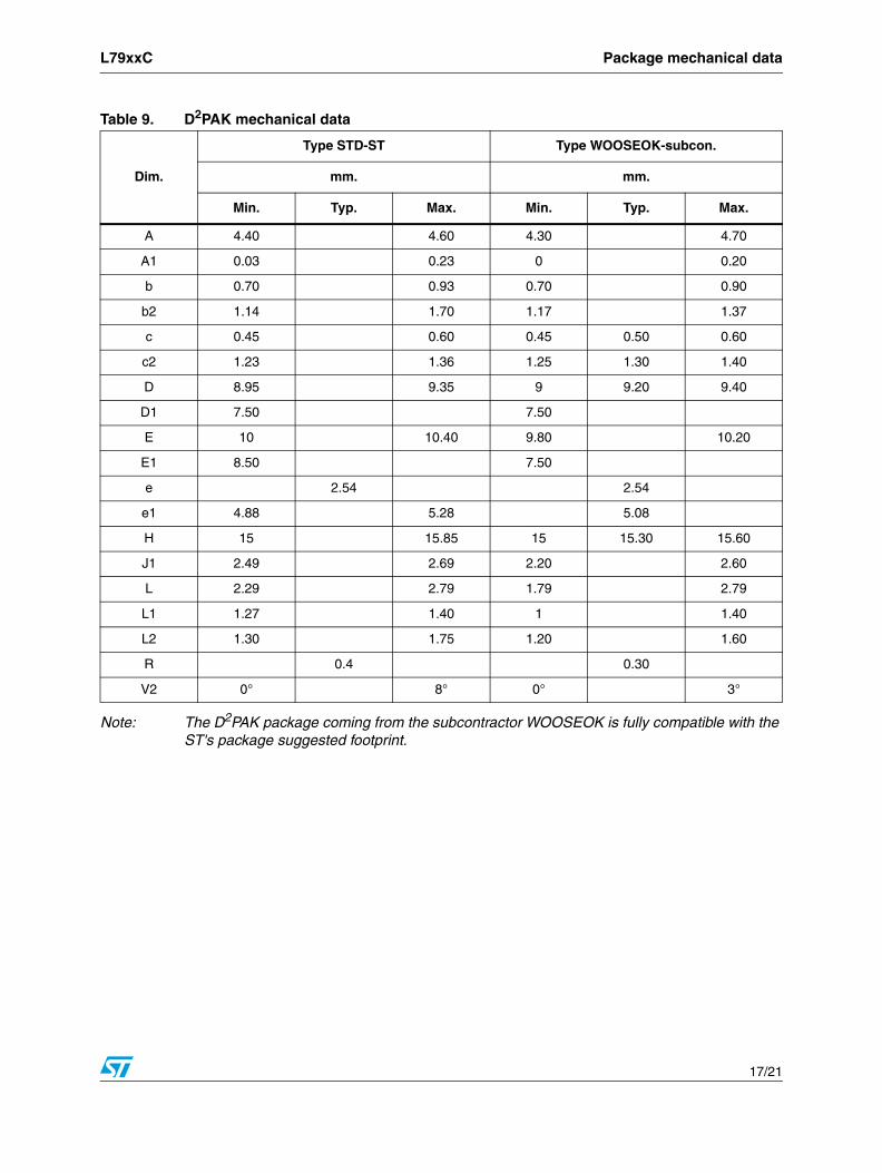
Note: The D2PAK package coming from the subcontractor WOOSEOK is fully compatible with the ST's package suggested footprint.
Table 9. D2PAK mechanical data
Dim.
Type STD-ST Type WOOSEOK-subcon.
mm. mm.
Min. Typ. Max. Min. Typ. Max.
A 4.40 4.60 4.30 4.70
A1 0.03 0.23 0 0.20
b 0.70 0.93 0.70 0.90
b2 1.14 1.70 1.17 1.37
c 0.45 0.60 0.45 0.50 0.60
c2 1.23 1.36 1.25 1.30 1.40
D 8.95 9.35 9 9.20 9.40
D1 7.50 7.50
E 10 10.40 9.80 10.20
E1 8.50 7.50
e 2.54 2.54
e1 4.88 5.28 5.08
H 15 15.85 15 15.30 15.60
J1 2.49 2.69 2.20 2.60
L 2.29 2.79 1.79 2.79
L1 1.27 1.40 1 1.40
L2 1.30 1.75 1.20 1.60
R 0.4 0.30
V2 0° 8° 0° 3°
Package mechanical data L79xxC
18/21
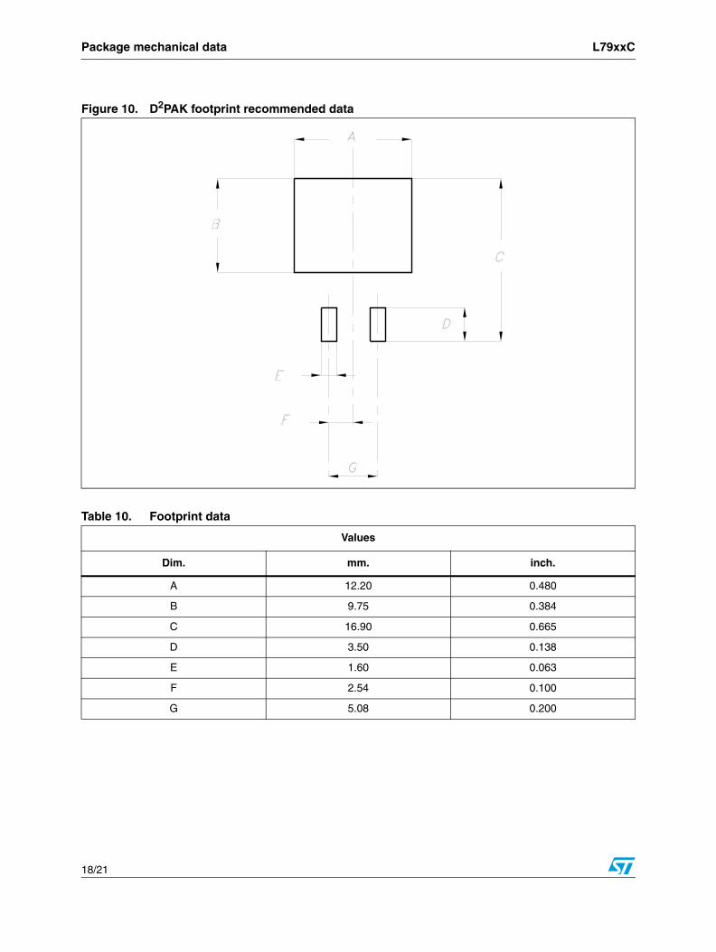
Figure 10. D2PAK footprint recommended data
Table 10. Footprint data
Values
Dim. mm. inch.
A 12.20 0.480
B 9.75 0.384
C 16.90 0.665
D 3.50 0.138
E 1.60 0.063
F 2.54 0.100
G 5.08 0.200
L79xxC Package mechanical data
19/21
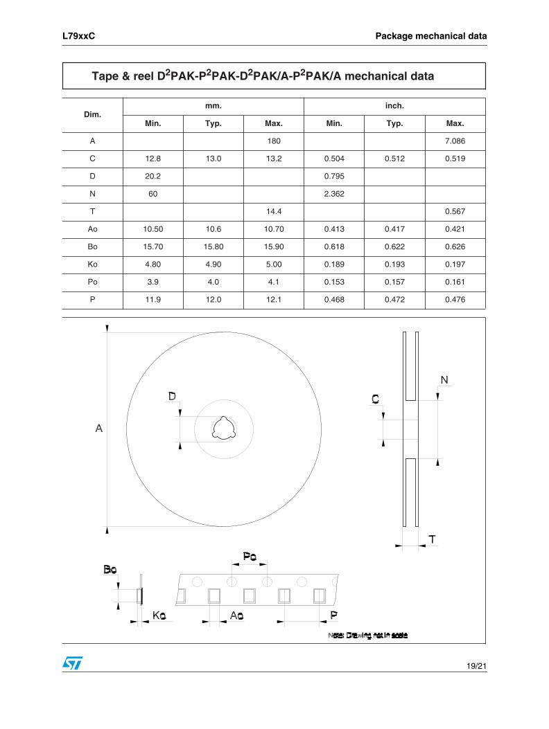
Dim.mm. inch.
Min. Typ. Max. Min. Typ. Max.
A 180 7.086
C 12.8 13.0 13.2 0.504 0.512 0.519
D 20.2 0.795
N 60 2.362
T 14.4 0.567
Ao 10.50 10.6 10.70 0.413 0.417 0.421
Bo 15.70 15.80 15.90 0.618 0.622 0.626
Ko 4.80 4.90 5.00 0.189 0.193 0.197
Po 3.9 4.0 4.1 0.153 0.157 0.161
P 11.9 12.0 12.1 0.468 0.472 0.476
Tape & reel D2PAK-P2PAK-D2PAK/A-P2PAK/A mechanical data
Revision history L79xxC
20/21
8 Revision history
Table 11. Document revision history
Date Revision Changes
22-Jun-2004 9 Order Codes updated Table 3, pag. 3.
31-Aug-2005 10 Add new order codes (TO-220 E Type) on Table 3, pag. 3.
19-Jan-2007 11D2PAK mechanical data has been updated, add footprint data and the document reformatted.
06-Jun-2007 12 Order codes updated.
25-Oct-2007 13 Modified: Figure 3, Figure 4, Figure 6 and Figure 7.
05-Dec-2007 14 Modified: Table 1.
18-Feb-2008 15 Modified: Table 1 on page 1.
L79xxC
21/21
Please Read Carefully:
Information in this document is provided solely in connection with ST products. STMicroelectronics NV and its subsidiaries (“ST”) reserve theright to make changes, corrections, modifications or improvements, to this document, and the products and services described herein at anytime, without notice.
All ST products are sold pursuant to ST’s terms and conditions of sale.
Purchasers are solely responsible for the choice, selection and use of the ST products and services described herein, and ST assumes noliability whatsoever relating to the choice, selection or use of the ST products and services described herein.
No license, express or implied, by estoppel or otherwise, to any intellectual property rights is granted under this document. If any part of thisdocument refers to any third party products or services it shall not be deemed a license grant by ST for the use of such third party productsor services, or any intellectual property contained therein or considered as a warranty covering the use in any manner whatsoever of suchthird party products or services or any intellectual property contained therein.
UNLESS OTHERWISE SET FORTH IN ST’S TERMS AND CONDITIONS OF SALE ST DISCLAIMS ANY EXPRESS OR IMPLIEDWARRANTY WITH RESPECT TO THE USE AND/OR SALE OF ST PRODUCTS INCLUDING WITHOUT LIMITATION IMPLIEDWARRANTIES OF MERCHANTABILITY, FITNESS FOR A PARTICULAR PURPOSE (AND THEIR EQUIVALENTS UNDER THE LAWSOF ANY JURISDICTION), OR INFRINGEMENT OF ANY PATENT, COPYRIGHT OR OTHER INTELLECTUAL PROPERTY RIGHT.
UNLESS EXPRESSLY APPROVED IN WRITING BY AN AUTHORIZED ST REPRESENTATIVE, ST PRODUCTS ARE NOTRECOMMENDED, AUTHORIZED OR WARRANTED FOR USE IN MILITARY, AIR CRAFT, SPACE, LIFE SAVING, OR LIFE SUSTAININGAPPLICATIONS, NOR IN PRODUCTS OR SYSTEMS WHERE FAILURE OR MALFUNCTION MAY RESULT IN PERSONAL INJURY,DEATH, OR SEVERE PROPERTY OR ENVIRONMENTAL DAMAGE. ST PRODUCTS WHICH ARE NOT SPECIFIED AS "AUTOMOTIVEGRADE" MAY ONLY BE USED IN AUTOMOTIVE APPLICATIONS AT USER’S OWN RISK.
Resale of ST products with provisions different from the statements and/or technical features set forth in this document shall immediately voidany warranty granted by ST for the ST product or service described herein and shall not create or extend in any manner whatsoever, anyliability of ST.
ST and the ST logo are trademarks or registered trademarks of ST in various countries.
Information in this document supersedes and replaces all information previously supplied.
The ST logo is a registered trademark of STMicroelectronics. All other names are the property of their respective owners.
© 2008 STMicroelectronics - All rights reserved
STMicroelectronics group of companies
Australia - Belgium - Brazil - Canada - China - Czech Republic - Finland - France - Germany - Hong Kong - India - Israel - Italy - Japan - Malaysia - Malta - Morocco - Singapore - Spain - Sweden - Switzerland - United Kingdom - United States of America
www.st.com