Embed Size (px)
Citation preview
NEW MONTGOMERY MODULAR MULTIPLIER ARCHITECTURE
A THESIS SUBMITTED TO THE GRADUATE SCHOOL OF NATURAL AND APPLIED SCIENCES
OF MIDDLE EAST TECHNICAL UNIVERSITY
BY
MEHMET EMRE ÇİFTÇİBAŞI
IN PARTIAL FULFILLMENT OF THE REQUIREMENTS FOR
THE DEGREE OF MASTER OF SCIENCE IN
ELECTRICAL AND ELECTRONICS ENGINEERING
JANUARY 2006

Approval of the Graduate School of Natural and Applied Sciences
______________________
Prof. Dr. Canan Özgen
Director
I certify that this thesis satisfies all the requirements as a thesis for the
degree of Master of Science.
______________________
Prof. Dr. İsmet Erkmen
Head of Department
This is to certify that we have read this thesis and that in our opinion it is
fully adequate, in scope and quality, as a thesis for the degree of Master of
Science.
___________________________ __________________________
Prof. Dr. Hasan Güran Assoc. Prof. Dr. Melek. D. Yücel
Co – Supervisor Supervisor
Examining Committee Members
Prof. Dr. Mete Severcan (METU, EE) _________________
Assoc. Prof. Dr. Melek D. Yücel (METU, EE) _________________
Prof. Dr. Hasan Güran (METU, EE) _________________
Assist. Prof. Dr. Özgür B. Akan (METU, EE) _________________
M.Sc. Hamdi Erkan (ASELSAN) _________________

iii
I hereby declare that all information in this document has been obtained and presented in accordance with academic rules and ethical conduct. I also declare that, as required by these rules and conduct, I have fully cited and referenced all material and results that are not original to this work.
Mehmet Emre ÇİFTÇİBAŞI
iv
ABSTRACT
NEW MONTGOMERY MODULAR MULTIPLIER ARCHITECTURE
Çiftçibaşı, Mehmet Emre
M.Sc., Department of Electrical and Electronics Engineering
Supervisor : Assoc. Prof. Dr. Melek D. Yücel
Co–Supervisor : Prof. Dr. Hasan Güran
January 2006, 77 pages
This thesis is the real time implementation of the new, unified field, dual–
radix Montgomery modular multiplier architecture presented by Savaş et al,
for performance comparison with standard Montgomery multiplication
algorithms. The unified field architecture operates in both GF(p) and
GF(2n). The dual radix capability enables processing of two bits of the
multiplier in every clock cycle in GF(2n) mode, while one bit of the multiplier
is processed in GF(p) mode.
The new architecture is implemented in a Xilinx FPGA on the custom
printed circuit board. The windows user interface is developed in Borland
Builder environment and the ethernet interface is implemented by Ubicom
IP2022 controller. The algorithms are compared from operating clock
frequency, silicon area cost and multiplication time perspectives. The new
architecture multiplies two times faster in GF(p) and four times faster in
GF(2n), compared to the previous architectures as expected. The operand
length is increased from 8 bits to 1024 bits, with the compromise of
decreasing the operating clock frequency from 150 Mhz down to 15 Mhz.
Keywords: Montgomery Multiplier, Modular Multiplier, FPGA
v
ÖZ
YENİ MONTGOMERY MODÜLER ÇARPMA YAPISI
Çiftçibaşı, Mehmet Emre
Yüksek Lisans, Elektrik Elektronik Mühendisliği Bölümü
Tez Yöneticisi : Doç. Dr. Melek D. Yücel
Ortak Tez Yöneticisi : Prof. Dr. Hasan Güran
Ocak 2006, 77 sayfa
Bu tezde Savaş ve diğer yazarlar tarafından sunulan birleşik cisimler
üzerinde, çoklu seçmeli ikil işleyen yeni bir Montgomery modüler çarpma
mimarisi, standart Montgomery çarpma algoritmaları ile karşılaştırılmak
üzere gerçeklenmiştir. Birleşik cisimli çarpma yapısı GF(p) ve GF(2n) sonlu
cisimlerinde çalışabilmektedir. Çoklu seçmeli ikil işleme özelliği her saat
aralığında GF(2n) modunda çarpanın iki ikilinin işlenebilmesine olanak
tanırken, GF(p) modunda bir ikil işlenmektedir.
Yeni algoritma yapısı, özel üretilen baskı devre kartındaki Xilinx FPGA
üzerine uygulanmıştır. Windows kullanıcı arayüzü Borland Builder
ortamında geliştirilmiş, yerel ağ arayüzü ise Ubicom IP2022 işlemcisi ile
gerçeklenmiştir. Algoritmalar, çalışma saat frekansı, harcanan silikon alanı
ve çarpma süresi açılarından karşılaştırılmıştır. Yeni yapı beklendiği gibi
önceki yapılarla karşılaştırıldığında GF(p) modunda iki kat, GF(2n)
modunda ise dört kat daha hızlı çarpmaktadır. Kelime boyu 8 ikilden 1024
ikile kadar yükseltilmiş, buna karşın çalışma saat frekansı 150 Mhz’den
15 Mhz’e düşmüştür.
Anahtar Kelimeler: Montgomery Çarpma, Modüler Çarpma, FPGA

vi
ACKNOWLEDGEMENTS
For their love, my mother Reyhan Çiftçibaşı, my father Turhan Çiftçibaşı
and my grandmother Cavide Tanaltay are to be remembered. Without their
love, I would be unable to finish this work.
My thesis supervisors Melek D. Yücel and Hasan Güran are to be
mentioned for the patience and support through my work.
I would also like to thank Aselsan A.Ş for supporting me with proper
working conditions during my thesis work.
vii
TABLE OF CONTENTS
PLAGIARISM ............................................................................................. iii
ABSTRACT ................................................................................................ iv
ÖZ ............................................................................................................... v
ACKNOWLEDGEMENTS .......................................................................... vi
TABLE OF CONTENTS ............................................................................ vii
LIST OF FIGURES..................................................................................... ix
LIST OF TABLES........................................................................................ x
LIST OF ABBREVIATIONS........................................................................ xi
CHAPTERS
1 - INTRODUCTION....................................................................................1
1.1 Aim of the Thesis ..........................................................................1
1.2 Cryptography Applications ............................................................2
1.3 Definition of Montgomery Multiplication ........................................3
1.4 History of Montgomery Multiplication ............................................4
1.5 Field Programmable Gate Arrays..................................................6
2 - MODULAR MULTIPLICATION...............................................................8
2.1 Application of Field Theory to Modular Multiplication ....................8
2.2 Types of Cryptographic Algorithms Using Modular Multipliers ......9
2.3 Montgomery Multiplication Algorithm ..........................................11
3 - NEW MULTIPLICATION ALGORITHM................................................17
3.1 Theory of New Montgomery Multiplication Algorithm ..................17
3.1.1 New Algorithm for Prime Fields ...............................................17
3.1.2 New Algorithm for Binary Extension Fields..............................20
3.2 Precomputation in New Multiplication Algorithm .........................21
3.3 New Processing Unit...................................................................22
3.4 Dual Field Adder .........................................................................24
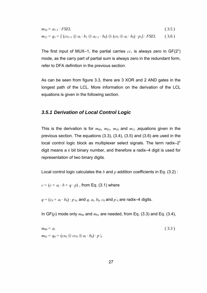
3.5 Local Control Logic of New Processing Unit ...............................25
3.5.1 Derivation of Local Control Logic.............................................27
viii
4 - HARDWARE AND SOFTWARE OF THE MULTIPLIER ......................30
4.1 Montgomery Multiplier Blocks in FPGA.......................................31
4.1.1 Main Unit .................................................................................31
4.1.2 Multiplier Core .........................................................................36
4.1.3 Processing Unit .......................................................................38
4.2 Ethernet Controller Software.......................................................38
4.2.1 Initialization of the IP2022 .......................................................39
4.2.2 Program Flow of the Ethernet Interface...................................39
4.2.3 Data Processing in the Ethernet Controller .............................40
4.3 Multiplier User Interface ..............................................................42
4.3.1 Preparation of the Packet ........................................................43
4.3.2 Receiving Packets...................................................................43
5 - RESULTS ............................................................................................44
5.1 Comparisons of Multiplier Architectures......................................45
5.1.1 Area Comparison ......................................................................46
5.1.2 Clock Frequency Comparison..............................................47
5.1.3 Multiplication Period Comparison ........................................49
5.2 Analysis of the New Architecture ................................................50
6 - CONCLUSIONS...................................................................................54
REFERENCES..........................................................................................56
APPENDICES
A –CIRCUIT BOARD DIAGRAMS.............................................................59
B – MULTIPLIER BOARD.........................................................................65
C – USER INTERFACE FORMS ..............................................................66
ix
LIST OF FIGURES
Figure 2.1 Montgomery Modular Multiplication....................................... 13
Figure 3.1 Processing Unit ..................................................................... 22
Figure 3.2 Dual Field Adder ................................................................... 25
Figure 3.3 Local Control Logic ............................................................... 26
Figure 4.1 Hardware Block Diagram ...................................................... 30
Figure 4.2 Hardware File Tree of the Multiplier ...................................... 31
Figure 4.3 Multiplier I/O State Machine .................................................. 32
Figure 4.4 Multiplier Stage State Machine.............................................. 35
Figure 4.5 Multiplier Core State Machine ............................................... 37
Figure 4.6 Program Flow of the Ethernet Controller ............................... 41
Figure 4.7 Program Flow of the Windows User Interface ....................... 42
Figure 5.1 Area versus Word Length in Spartan FPGAs........................ 51
Figure 5.2 Clock Frequency versus Word Length in Spartan FPGAs .... 52
Figure 5.3 Area versus Word Length in Virtex FPGAs ........................... 53
Figure 5.4 Clock Frequency versus Word Length in Virtex FPGAs........ 53
Figure A.1 Supply Circuitry..................................................................... 59
Figure A.2 XC2S200 FPGA.................................................................... 60
Figure A.3 IP2022 Ethernet Processor................................................... 61
Figure A.4 Uart Buffer ............................................................................ 61
Figure A.5 Clock & Reset Circuitry ......................................................... 62
Figure A.6 IP2022 Programming Circuitry.............................................. 62
Figure A.7 FPGA Programming Circuitry ............................................... 63
Figure A.8 Capacitors............................................................................. 64
Figure B.1 Printed Circuit Board............................................................. 65
Figure C.1 Multiplication User Interface ................................................. 66
Figure C.2 Configuration User Interface................................................. 66
x
LIST OF TABLES
Table 5.1 Multiplier Core Synthesis Results…………………………….... 46
Table 5.2 Multiplier Core Implementation Results……………………….. 46
Table 5.3 Multiplier Core Clock Frequency Results……………………… 48
Table 5.4 Multiplier Core Clock Period Results………………………...... 48
Table 5.5 The Periods of a Single MM Operation in Nanoseconds........ 50
Table 5.6 Effect of Word Length in Spartan FPGAs……………………... 51
Table 5.7 Effect of Word Length in Virtex FPGAs………………….......... 52
xi
LIST OF ABBREVIATIONS
ASSP : Application Specific Standard Product
AES : Advanced Encryption Standard
DES : Data Encryption Standard
DFA : Dual Field Adder
ECC : Elliptic Curve Cryptosystem
FSEL : Field Select
FPGA : Field Programmable Gate Array
GCD : Greatest Common Divisor
GF(p) : Galois Field with p Elements
IC : Integrated Circuit
IP : Internet Protocol
LSB : Least Significant Bit
LCL : Local Control Logic
MUX : Multiplexer
PCB : Printed Circuit Board
PROM : Programmable Read Only Memory
PU : Processing Unit
RSA : Public key algorithm proposed by Rivest, Shamir, Adleman
VHDL : Very High Speed Hardware Description Language
1
CHAPTER 1
INTRODUCTION
1.1 Aim of the Thesis
This thesis is the implementation, verification and testing of a Montgomery
modular multiplication algorithm [1] for the new architecture presented in
[2]. This architecture proposes two improvements on the well–known
Montgomery multiplication algorithm and its previous implementations.
First improvement proposed in [2] is a theoretical modification to the
Montgomery multiplication algorithm [1], which decreases the multiplication
period dramatically. A more detailed proof of the algorithm given in [2],
which will be referred as the “new algorithm” throughout this thesis, is given
in section 3.5.1. Second improvement is a new design perspective applied
to the hardware dataflow of the algorithm, describing the computational
advantage of new cryptosystems such as elliptic curve cryptosystems. This
new design also decreases the time spent during the multiplication for
standard cryptosystems like RSA.
In the framework of this thesis, new unified dual–radix Montgomery
multiplication algorithm is implemented for operand sizes from 8 bits to
1024 bits. The aim here is to compare the new algorithm from clock
frequency, silicon area and clock cycle count points of view. As the FPGA
(field programmable gate array) in the custom printed circuit board has
limited resources, the modular multiplier on the circuit board has maximum
operand width of 48 bits. For better understanding of the cost of operand
2
length in terms of clock frequency and silicon area, the multiplier design
has been verified and compared for up to 1024 bits for larger FPGAs.
The FPGA code is written in very high speed hardware description
language (VHDL) and then synthesized and implemented using Xilinx
tools. The ethernet interface code is written in C language using Ubicom
tools. The user interface is written in C++ language using Borland tools.
Preliminaries of this thesis are introduced in chapter 1. General
introduction to modular multiplication algorithms is given in chapter 2. The
mathematical theory underlying the new Montgomery multiplication
algorithm and the details of the new Montgomery multiplier core are
explained in chapter 3. The hardware design details of the new
Montgomery multiplier, with the ethernet interface application and the user
interface are briefly described in chapter 4. The obtained results are given
in chapter 5 and conclusions are discussed in chapter 6.
1.2 Cryptography Applications
Cryptography is the art of designing and breaking ciphers. Traditionally,
secret–key cryptography was used by the military and diplomatic services
for providing secure communication, in which two communicating parties
share a secret key that should be distributed in some secure way.
Development of mobile internet devices increased the need for
cryptographic techniques for privacy and authentication of digital data. The
invention of public–key cryptography, which assigns two keys (one public
and one private) to each user, provided techniques for key distribution as
well as signing and authenticating digital data.
3
Because of its complexity, public–key cryptography is mainly used for
digital signatures and the management of secret keys between two points.
The encryption of bulk data is mainly established with secret–key
cryptosystems, whereas the secret keys to be shared for a pair of users,
are distributed by public–key cryptosystems. For a standard public–key
cryptosystem to be considered as “secure”, the key length should be about
thousand bits or more.
In public–key cryptography, input and output numbers are selected from
finite element fields. All cryptographic operations are made in these finite
fields, which map to modular multiplication and modular exponentiations in
the digital world. Increasing demand for modular multiplication requires fast
modular multiplication algorithms such as Montgomery multiplication, which
will be described thoroughly in this thesis.
1.3 Definition of Montgomery Multiplication
In [1], Montgomery proposed an algorithm for modular multiplication. This
new algorithm, called Montgomery Multiplication Algorithm, has the
advantage of replacing division operations by bit shift operations. If the
least significant bits to be shifted out are not zero, Montgomery’s algorithm
adds multiples of modulus to clear these bits before shifting them out.
In regular modular multiplication, after all bits of the multiplicand are
processed, modulus is repeatedly subtracted from the result unless the
result is less than the modulus. In Montgomery multiplication, bits are
shifted out as each bit of the multiplicand is processed, leaving no need for
the subtractions.
4
In this thesis Montgomery multiplication is implemented in a unified and
dual–radix architecture. The definitions of the terms unified and dual–radix
are as follows.
Unified Architecture: An architecture is said to be unified when it is able
to work with operands in both prime and binary extension fields using the
same hardware. In [3], it has been shown that a unified multiplier is feasible
with only minor modifications to the multiplier for GF(p) in [4].
Dual–Radix Architecture: A unified multiplier is said to be dual–radix if it
operates with a larger radix value for GF(2n) than the radix used for GF(p).
The term, architecture, is used to represent the hardware of the
Montgomery multiplier.
A radix–2n multiplier processes n bits of the multiplicand in every clock
cycle. A radix (2,4) multiplier stands for a multiplier working in radix–2 for
GF(p) and working in radix–4 for GF(2n). The new architecture in this
thesis is a radix (2,4) multiplier architecture.
Dual radix multiplier design has critical time–area considerations, as the
cost of extra radix should not effect the signal propagation time much while
keeping the silicon area as low as possible.
1.4 History of Montgomery Multiplication
There exist many implementations of high–radix conventional multipliers
[5]; however, there are few implementations of high–radix modular
multipliers in the literature. An example for the high–radix Montgomery
multiplication algorithm is given in [6].
5
A radix–4 implementation of modular multiplication using Brickel's
algorithm [7] has been proposed in [8]. The multiplication is performed
without carry propagation.
A similar algorithm is presented in [9]. The paper presents two possible
architectures, further explained in [6].
The Brickel's algorithm shifts out the most significant bits of the partial
product, after they have been cleared. It has been noted in [9], as shifting
out the least significant bits of the partial product, as it is done in the
Montgomery's algorithm, has advantages (simplifying the longest path)
over the former approach and thus Montgomery’s method is the more
attractive one. Both approaches are compared in [6] with considerations for
high–radix implementations.
The implementation of Montgomery multiplication involves making the
tradeoff between chip area and computational speed [10]. Two main points
to be considered are that with the increasing radix, the multiplier operand is
processed in less clock cycles, however the longest path increases. Thus,
the overall effect on the computational time is a decision to be made for
multiplier core design.
Simplifying the longest path is discussed in [11]. However, with the new
architecture described in this thesis, the longest path has been simplified
and clock cycle count is halved, with the re–design of the processing unit.
A single chip, 1024–bit RSA implementation is given in [8]. The
multiplication part is implemented as an array multiplier. It is noted that this
approach for multiplication requires multiple clock cycles to complete.
Limiting the size of the computing unit has certain advantages as shown in
[5]. Also a cryptographic processor design is demonstrated in [12].
6
Using reconfigurable hardware provides the means of solving problems for
both high– precision and variable–precision computation, as [13, 14, 15] .
A unified multiplier architecture for finite fields GF(p) and GF(2n) is
presented in [16]. It is shown that a Montgomery multiplier can operate in
both fields without significant increase in the silicon area.
1.5 Field Programmable Gate Arrays
Field programmable gate arrays (FPGAs) have a regular, flexible,
programmable architecture of configurable logic blocks, surrounded by a
perimeter of programmable input/output blocks. There may be other
configurable blocks such as delay–locked loops and synchronous block
RAMs. These functional elements are interconnected by a powerful
hierarchy of versatile routing channels.
The FPGA resources are slices, that contain programmable look up tables
and flip flops. tables are used for combinational logic and flip flops are used
for sequential logic.
The power of FPGAs come from the fact that they are in system
programmable, meaning that they can be reconfigured within a few
seconds while they are operational.
Most FPGAs are customized by loading configuration data into internal
static memory cells. Unlimited reprogramming cycles are possible with this
approach. Stored values in these cells determine the logic functions and
interconnections implemented in the FPGAs. Configuration data can be
read from an external serial programmable read only memory (PROM).
7
Cryptographic applications require high throughput, requiring powerful
processors. Even though application specific standard products (ASSPs)
such as the security processors from integrated circuit (IC) vendors offer
high performance for standard security applications, the requirements
might be different. The data rate might be insufficient or the IC might not be
suitable for the specific packaging.
Under these circumstances programmable logic becomes an alternative. A
new modular multiplier core enables the required high–speed design to be
accomplished in a very short time frame at a very low cost.
In this thesis, the new Montgomery multiplier core is implemented in a
Xilinx Spartan 2 series FPGA. The dataflow of FPGA is supported by a
Ubicom IP2022 ethernet controller. Even though the newer FPGAs have
built in ethernet interfaces, this design has turned out to be very effective.
The ethernet controller is not mentioned much in this thesis, as it is only
used to supply ethernet connectivity to the FPGA.
8
CHAPTER 2
MODULAR MULTIPLICATION
In this chapter the mathematical background of modular multiplication is
given, applications using modular multiplication are described and
Montgomery multiplication algorithm is described.
2.1 Application of Field Theory to Modular Multiplication
An algebraic field is, by definition, a set of elements that is closed under
the ordinary arithmetical operations of addition, subtraction, multiplication,
and division. The set of rational numbers is a field, whereas the integers
are not a field, because the integers are not closed under the operation of
division as the result of dividing one integer by another is not necessarily
an integer. It is also possible to construct other fields by means of
extending smaller fields [16], [17], [18].
In cryptographic applications, finite fields, especially prime number fields
GF(p) and binary extension fields GF(2n), have common use as they are
easily applicable to digital systems. Some elliptic curves on these fields
have been strongly suggested by researchers in cryptography institutes.
A finite prime number field is constructed from the integers {0, 1, 2, ..., p–1}
up to an n–bit prime number p. In GF(p), addition and multiplication
operations are defined as modulo p additions and modulo p multiplications.
9
A binary extension field GF(2n) is constructed from binary polynomials of
degree less than n. In this thesis, polynomial basis representation is used
to represent elements of GF(2n), as it is very suitable for the new multiplier
architecture. Similar to the prime modulus p in prime number fields, a
binary prime polynomial of degree n is used to construct GF(2n).
Given the prime binary polynomial
p(x) = xn+ pn–1xn–1+ . . . + p1x + p0
of degree n. Given p(x), all the binary polynomials a(x) of degree less than
n are elements of GF(2n).
GF(2n) = {0, 1, x, x+1, x2, x2+x, x2+1, x2+x+1, … , xn–1, … }
In GF(2n), addition is polynomial addition modulo the prime polynomial p(x),
meaning a bitwise xor’ing of the corresponding coefficients of the input
polynomials. As it is a simple polynomial addition in modulo 2, there is no
carry propagation and the resultant polynomial is at most of degree (n–1).
Multiplication in GF(2n) is also polynomial multiplication modulo p(x).
Similar to that in GF(p), multiplication is performed in two steps, polynomial
multiplication followed by a polynomial division of the intermediate result by
the prime polynomial p(x). Generally these two steps are interleaved.
2.2 Types of Cryptographic Algorithms Using Modular
Multipliers
Cryptographic algorithms use modular multiplication intensively. Most
common algorithms are the RSA Algorithm, named after its inventors
Rivest, Shamir and Adleman, and the newly emerging elliptic curve
cryptosystems (ECC) described in [16].
10
RSA Algorithm
As all public–key algorithms, the RSA algorithm is utilized in applications
where the data to be encrypted is short, such as the private keys of a bulk
data transfer or digital signatures [13]. The key size to be used, as it is
generally about thousand bits or more. The throughput of RSA is much
slower than secret–key algorithms such as DES (Data Encryption
Standard) or AES (Advanced Encryption Standard). In hybrid applications
RSA is usually paired with a secret key algorithm for bulk data transfer, as
the other public key methods.
The RSA algorithm uses modular exponentiation for obtaining and verifying
digital signatures. The computations are performed using exponentiation
algorithms. Modular exponentiation requires implementation of the basic
modular arithmetic operations: addition, subtraction, and multiplication.
As mentioned here, modulus must be preferably 1024 bits or more, which
requires fast modular multiplications, and very fast multiplications per bit, if
made in a bit serial form. There are many methods of calculating the
modular exponent, including Montgomery’s method which is very efficient
for modular exponentiations.
Elliptic Curve Cryptosystems
The use of elliptic curve cryptosystems is an increasing trend in application
development. There are many issues to consider for making a choice
between an application based on an elliptic curve cryptosystem and one
based on RSA. The important point here is that an elliptic curve
cryptosystem over 160 bits offers the same security as 1024 bit RSA.
Elliptic curves over GF(2n) are more popular due to the efficient algorithms
for doing arithmetic in GF(2n). Elliptic curve cryptosystems based on
11
discrete logarithms seem to provide similar amount of security to that of
RSA, but with relatively shorter key sizes.
The problem of discrete logarithms over a prime field in ECC and the
problem of integer factorization in RSA appear to be of roughly the same
difficulty. Techniques used to solve one problem can be adapted to tackle
the other. There are elliptic curve analogs to RSA but it turns out that these
are chiefly of academic interest since they offer essentially no practical
advantages over RSA. This is primarily the case because elliptic curve
variants of RSA actually rely for their security on the same underlying
problem as RSA, namely the problem of integer factorization [16].
An elliptic curve addition is performed by using a few finite field operations.
Implementation of elliptic curve addition operation requires implementation
of four basic finite field operations: addition, subtraction, multiplication and
inversion. In elliptic curve arithmetic, computations are performed using
exponentiation algorithms.
2.3 Montgomery Multiplication Algorithm
Modular multiplication (Xm) of two integers a and b, simply performs
Xm (a, b) = a · b (mod p)
Instead of computing a · b, Montgomery multiplication (MM) computes
MM (a, b) = a · b · r –1 (mod p)
where r is a special constant. As mentioned in [17] and [18], this is similar
to Montgomery’s method in [1]. If p is an n–bit number, the selection of
constant r = 2n mod p for GF(p) and r(x) = xn mod p(x) for GF(2n) mode of
operation, turns out to be very useful in obtaining fast implementations.
Thus the coınstant value r is represented by the integer r mod p, or the
polynomial r(x) mod p(x). For GF(p) mode of operation, r2 mod p value is an
input from the user interface, while for GF(2n) mode of operation, the
coefficients of r2(x) mod p(x) are input from the user interface.
The Montgomery multiplication method requires r and p to be relatively
prime. This can be achieved by taking odd numbers for p, while r is chosen
as a power of 2. Either in GF(p) and GF(2n), the least significant bit (LSB)
of the modulus is always 1. So GCD (p,r) = 1, since the modulus p is a
prime number, or a prime polynomial.
As can be seen, the Montgomery multiplication algorithm brings an r –1 to
the result. Because of this, the algorithm is not directly applicable to input
operands. From the definition of Montgomery multiplication in [1], all
elements need to be transformed to Montgomery residue field.
Montgomery residue field is used to represent the r–multiplied values of the
operands, as a·r and b·r. In computations of this thesis, the operands a and
b are prime number field elements or binary extension field elements.
Therefore certain transformation operations must be applied to both of the
operands a and b before the multiplication and to the intermediate result c
in order to obtain the final result c.
To transform an input operand to Montgomery residue field, a multiplication
by a constant value is required. This constant value is r2 mod p, where r is
selected as 2n or xn as stated previously. The numbers in the Montgomery
residue field are represented as a ,b and c .
To multiply two numbers from the integer field, four Montgomery
multiplications are needed. First a and b are transformed to their images in
the Montgomery residue field. Then multiplication is performed in the
12
Montgomery residue field, before multiplying the final result by 1, to
transform the result c back to the initial field.
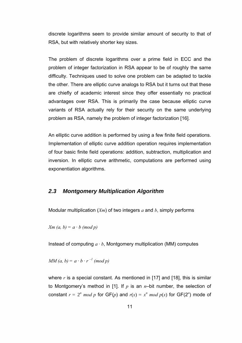
The four step Montgomery multiplication operation is defined as:
a = MM (a, r2) = a · r2 · r –1 (mod p) = a · r (mod p)
b = MM (b, r2) = b · r2 · r –1 (mod p) = b · r (mod p)
c = MM ( a ,b ) = a · r · b · r · r –1 (mod p)= a · b · r (mod p)
c = MM ( c , 1) = a · b · r · r –1 (mod p) = a · b (mod p)
After both numbers are transformed to Montgomery residue field, the
multiplications are performed as many as needed, enabling the MM
operation to be very efficient for performing modular exponentiations. But
the final result has to be transformed back to the input field. To transform
the final result from Montgomery residue field to input operand field, the
result must be Montgomery multiplied by 1. In figure 2.1, Montgomery
multiplication of two integers is illustrated.
Figure 2.1 Montgomery Modular Multiplication
13
14
Montgomery multiplication is not to be performed for a single modular
multiplication, but it is very efficient for modular exponentiations, where
numbers are multiplied many times. The advantage of Montgomery
multiplication is clearly visible, as in conventional modular multiplication
integer division is required.
Montgomery multiplication algorithm differs slightly in mathematical
representation for prime number fields and binary extension fields, so the
two algorithms are given seperately. The following notation will be used for
the description of the Montgomery multiplication.
ai : a single bit of a at position i
ci : a single bit of c at position i
n : number of bits in the operands and modulus
Radix–2 Montgomery multiplication algorithm for GF(p) is given below.
Step 1: c = 0
Step 2: FOR i = 0 TO n – 1
Step 3: c = c + ai · b
Step 4: c = c + c0 · p
Step 5: c = c / 2
END FOR
Step 6: IF c ≥ p THEN c = c – p
In every cycle of the for loop, the multiplicand b is added to the partial
product c depending on the LSB of the multiplier a. The LSB of partial
result must be zeroed before the shift in step 5. If the LSB of c is '1' then
the modulus p, as it is an odd number, is added to c in step 4, before the
right shift. After the last iteration of the loop, the variable c holds the
multiplication result.
15
It can be verified easily that
c = a · b – t · p
where t is composed during the loop iterations depending on the least
significant bits of the partial product. The variable t is simply the number of
times that the modulus is subtracted from the result c, to guarantee that the
result c is bounded with the modulus p. It is shown in [4] that the result c is
bounded between 2p–1 and 0 if p is chosen so that
2N–1 < p < 2N
This is the second requirement for the modulus p, other than the GCD
requirement.
The final result must be a number less than the modulus. Therefore, step 6
is called the final reduction step of the Montgomery multiplication algorithm.
In the final reduction step, c is compared to p and is adjusted if needed.
Because of the boundaries for c, a single subtraction of p is enough to
assure c < p.
16
Bit Level Algorithm for Montgomery Multiplication in GF(2n)
In GF(2n) polynomial representation is used for binary numbers. The
algorithm is the same algorithm in GF(p), with a slight difference that the
additions are binary polynomial additions modulo p(x). Also the final
reduction step is not needed when multiplication is performed in GF(2n).
Input: a(x), b(x), p(x), n
Output: c(x) = a(x) · b(x) · x−n mod p(x)
Step 1: c(x) = 0
Step 2: FOR i = 0 to n – 1 do
Step 3: c(x) = c(x) + ai · b(x)
Step 4: c(x) = c(x) + c0 · p(x)
Step 5: c(x) = c(x) / x
END FOR
CHAPTER 3
NEW MULTIPLICATION ALGORITHM
In this chapter, the new Montgomery multiplication algorithm is introduced,
the new architecture is given and the mathematical proof of the new
algorithm is reviewed by considering some details skipped in [2].
3.1 Theory of New Montgomery Multiplication Algorithm
The theory of new Montgomery multiplication algorithm differs slightly for
prime fields and binary extension fields; hence they are described
separately as Algorithm I for GF(p) and Algorithm II for GF(2n) in the
following subsections.
3.1.1 New Algorithm for Prime Fields
Given two integers a, b, and prime modulus p, the Montgomery
multiplication algorithm computes
c = MM (a, b) = a · b · r−1 (mod p)
where
r = 2n
a, b < p < r, where p is an n–bit prime number.
17
18
If r2 (mod p) is precomputed and saved in a register, a single Montgomery
multiplication operation is enough to carry out each of the transformations
from the input operand field to Montgomery residue field. In the
implementation, r2 value is an input from the user interface, as stated
previously.
As previously stated in chapter 2, because of these transformation
operations, performing a single modular multiplication using Montgomery
multiplication algorithm is not practical. On the other hand, the advantage
of MM algorithm becomes obvious in applications requiring multiplication
intensive calculations such as modular exponentiation and elliptic curve
operations.
The new radix–2n Montgomery multiplication algorithm for GF(p) is given
below. One of the advantages of the new algorithm is that, step 3 and step
4 of the new algorithm can be processed in a single clock cycle, regardless
of the k value. The k value is the number of multiplier bits processed in
each cycle of the loop. The 2k value is called the radix of the architecture.
Simply stating, a radix–2 multiplier architecture processes one bit of the
multiplier in a single clock cycle, while a radix–4 multiplier architecture
processes two bits. The new algorithm for GF(p) is named as Algorithm I.
Algorithm I, for GF(p)
Input: a, b ε [1, p–1], p, n, k
Output: c ε [1, p–1]
Step 1 c = 0
Step 2 for i = 0 to n–1, i = i+k
Step 3 q = (c0 + ai · b0) · (p0) (mod 2k) ( 3.1 )
Step 4 c = (c + ai · b + q · p) / 2k ( 3.2 )
end for
Step 5 if c ≥ p, c = c – p
where p’0 = 2n – p0
–1 (mod 2n).
In Algorithm I, the multiplier a is written with base 2 (radix–2k) and digits ai
so that
∑ −
==
1
0i ·k ·2n
i iaa
where n is the number of digits in operands. In the implementation of this
thesis, the number of digits n is automatically calculated by the modulus
calculator block in the multiplier control main unit.
In step 4, the multiplicand b, the modulus p, and the partial result c are
calculated as full n–bit precision integers. Also q, c0, b0, and p’0 are all n–bit
integers.
The digits of b, p and c are referred to as words when implementing step 4,
and the term digit is used for b0, p’0, and c0 in step 3, when they are in the
same equation with the digits of a. Digits can be easily distinguished from
full n–bit integers by the subscript notation (ai or b0). In addition, the base of
the radix of the multiplier architecture is determined by the base used to
represent the multiplier a.
19
20
3.1.2 New Algorithm for Binary Extension Fields
The radix–2k Montgomery multiplication algorithm for GF(2n) can be
defined as the following:
Algorithm II, for GF(2n)
Input: a(x), b(x), p(x), n, k
Output: c(x)
Step 1 c(x) = 0
Step 2 for i = 0 to n–1, i = i+k
Step 3 q(x) = (c0(x) ⊕ ai(x) · b0(x)) · p’0(x) (mod xk)
Step 4 c(x) = (c(x) ⊕ ai (x) · c(x) ⊕ q(x) · p(x)) / xk
end for
where p’0(x) = p0
–1(x) (mod xk).
It can easily be seen that the two algorithms are almost identical except
that the addition operation in GF(p) becomes a bitwise modulo–2 addition
(simple xor’ing) in GF(2n). Also final reduction step is not needed in GF(2n).
Although the operands are integers in the former algorithm and binary
polynomials in the latter, the representations of both are identical in digital
systems. In Algorithm I, there is also a reduction step at the end to reduce
the result into the desired range, if it is greater than the modulus.
It can be observed that the computations performed in step 3 are of
different nature in two algorithms. Depending on the magnitude of the radix
used, the part of the circuit in charge of implementing step 3 might become
very complicated. However, these computations can be performed in a
unified circuitry for small radices. The circuit, called local control logic, is
described in full detail in section 3.5.
21
In this thesis, the notation introduced in Algorithm I will be used for both
GF(p) and GF(2n) after this section, and the polynomial notation will be left
completely from the representation of field elements in GF(2n). So the
elements of both fields are represented identically in digital systems.
3.2 Precomputation in New Multiplication Algorithm
In this thesis, as previously stated, a new unified dual–radix multiplier
architecture is described. This new architecture has a precomputation
block in order to decrease the longest path delay of the multiplier in [3].
This precomputation block is called Local Control Logic (LCL) block, and
this block is part of the processing unit of the multiplier core.
From Eq. (3.2), step 4 of the Algorithm I computes
c = (c0 + ai · b + q · p) / 2k
where division by 2k is a right shift by k bits, and from Eq. (3.1), q is
previously calculated in step 3. The k–bit operand q can be determined by
the least significant bits of b, p and c, and the k least significant bits of a.
The derivation for q is also given in section 3.5.1.
The multiple of b that is to be added to partial result c is determined solely
by ai. For radix–2 architectures, the operands ai , b0 , c0 and p0 will
determine which one of the values in {0, b, p, b+p } is added to the partial
result c. As the value of b+p is precomputed and saved in a register, the
calculation in step 4 from Eq. (3.2) is significantly simplified.
The precomputation technique simplifies the multiplier design since step 4
can be performed with only one addition. The local control logic block in the
multiplier selects which multiples of b and p participate, and the adder adds
all required multiples at one single step, in the same clock cycle.
This block is naturally on the longest path and this is the most important
part of the multiplier design. Details of LCL are given in section 3.5.
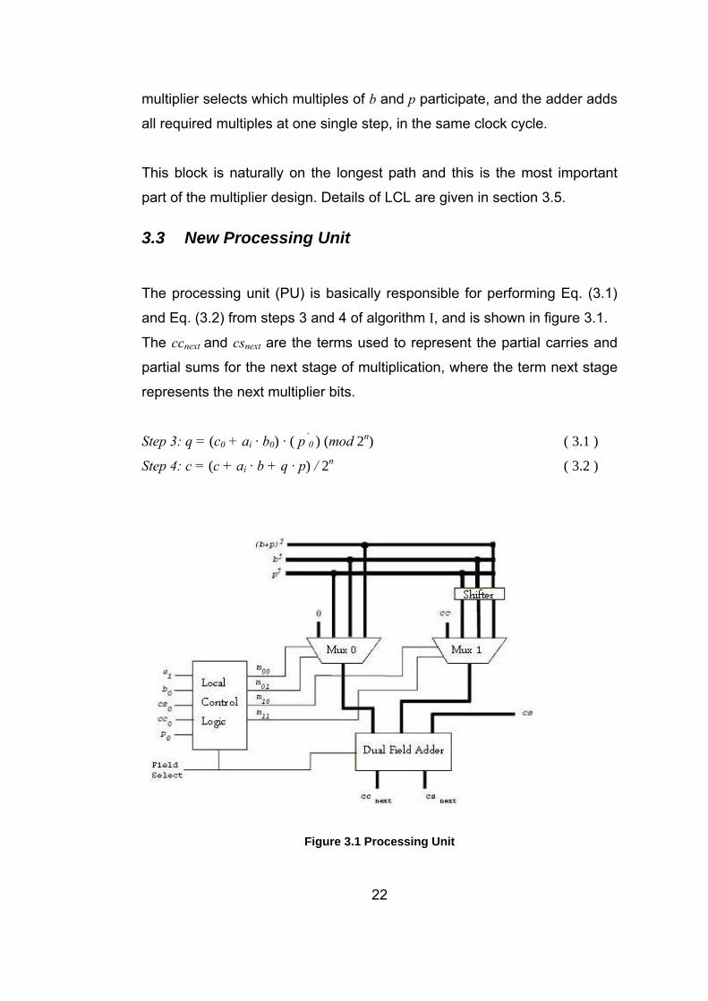
3.3 New Processing Unit
The processing unit (PU) is basically responsible for performing Eq. (3.1)
and Eq. (3.2) from steps 3 and 4 of algorithm I, and is shown in figure 3.1.
The ccnext and csnext are the terms used to represent the partial carries and
partial sums for the next stage of multiplication, where the term next stage
represents the next multiplier bits.
Step 3: q = (c0 + ai · b0) · ( p’0
) (mod 2n) ( 3.1 )
Step 4: c = (c + ai · b + q · p) / 2n ( 3.2 )
Figure 3.1 Processing Unit
22
23
As stated in the previous chapter, the new architecture uses radix–2 for
GF(p) so the LSB of the operands ai, b0, c0 and p0 determine which one of
the values in {0, b, p, b + p} is added to the partial result c.
Multiplication is performed in radix–4 for GF(2n). Therefore, least significant
two bits of a, b, c, and p are needed in order to determine q. The LSB of p is
always 1, causing only p1, the second least significant bit of the modulus, to
be included in the computations. Consequently a0, a1, b0, b1, c0, c1 and p1
determine which one of the values { 0, b, p, b+p, x·b, x·p, x·(b+p) } is added
to the partial result. Recall that ai is the i’ th least significant bit of a.
Multiplication by x results in one bit shifting to the left, so it is identical to
the simple multiplication by 2 in a digital system, as polynomial notation is
used to represent the elements of GF(2n). In this thesis division by xn and 2n
are identical operations and the latter is used to denote the right shift
operation by n bits.
The local control logic block in figure 3.2 contains the selection logic which
generates the signals, m00, m01, m10, and m11. These signals determine
which multiples of b and p will be used in the addition in step 4.
m00 m10 m01 m11 = ( 0 1 1 1 )
2b + 3p
indicates that Eq. (3.2) in step 4 will be
c = (c + 2b + 3p) / 2n .
The implementation details of the selection logic are detailed in the
following sections. cc0 and cs0 in figure 3.2 are the least significant digits of
carry part and sum part of the partial result c.
24
A redundant carry–save representation is used for the partial result in the
processing unit. Partial result equals c = cc + cs, where cc and cs stand for
the carry part and sum part of the partial result. The partial result c is kept
in redundant form during the computations and it must be converted back
to non–redundant form when the multiplication is completed. Because of
this, the register for partial result has twice the width of the other registers.
While the redundant form enables to employ carry–save adders, which are
typically less costly in terms of area and much faster than standard carry
propagate adders, carry–save form brings an extra addition operation,
which is to transform the final result into non–redundant format at the end
of the calculations.
The transformation is a simple addition of the two registers cs and cc. This
adder does not cost any area to the multiplier architecture, as the same
adder will be used for the final reduction operation in GF(p) mode. This
adder is also needed for performing the precomputation of b+p, which is
stated in the previous sections. The only extra silicon area cost for the
precomputation comes from the extra register to store b+p. However, since
the precomputation block eliminates the need for the second layer of
carry–save adders in [3], this extra area cost is compensated.
The longest path of a PU is determined by the addition of LCL delay, MUX
delay and carry–save adder delay.
3.4 Dual Field Adder
Dual Field Adder (DFA) is basically a full–adder capable of doing addition
with or without carry. The DFA input field select (FSEL) enables carry
output. Figure 3.2 shows the implementation of the DFA.
Figure 3.2 Dual Field Adder
If FSEL = 1, DFA performs bitwise addition with carry which enables the
multiplier to do arithmetic in GF(p). If FSEL = 0, the carry output is forced to
0 regardless of the input values.
The local control logic, multiplexers and the DFA are the combinational
logic in the longest path of the multiplier core. This longest path is very
short and allows all computations to be performed in a single clock cycle.
The multiplier core calculates the partial n–radix result in carry–save
redundant form in every clock cycle, c = c + ai · b + q · p.
An important aspect of designing a DFA is to avoid increasing the longest
path of the circuit with respect to a standard full–adder, which would have
an adverse effect on the clock frequency. The area and signal propagation
aspects of a DFA are almost identical to those of a standard full–adder
which would be used in a GF(p) only multiplier. Therefore, this additional
functionality is obtained almost without any cost in area or clock frequency.
3.5 Local Control Logic of New Processing Unit
The LCL of the processing unit determines which of the inputs of MUX–0
and MUX–1 are to be added in the dual field adder in the processing unit.
The LCL for the new dual–radix multiplier, is shown in figure 3.3. 25
Figure 3.3 Local Control Logic
In GF(p) mode, the multiplier uses radix–2, so only mux inputs m00 and m01
need to be calculated. MUX inputs m10 and m11 are forced to be zero, as
input zero of MUX–1 is always selected in this mode, enabling the partial
carries to be added to the partial sum. The following list shows the control
inputs of MUX–0.
m00 = ai ( 3.3 )
m01 = q0 = csi ⊕ cci ⊕ ai · b0 ( 3.4 )
where ⊕ stands for modulo–2 addition in GF(p) mode. In GF(2n) mode the
select inputs of MUX–1 also need to be calculated. The following list shows
the control inputs of MUX–1.
26
27
m10 = ai+1 · FSEL ( 3.5 )
m11 = q1 = [ (csi+1 ⊕ ai · b1 ⊕ ai+1 · b0) ⊕ (csi ⊕ ai · b0) · p1] · FSEL ( 3.6 )
The first input of MUX–1, the partial carries cc, is always zero in GF(2n)
mode, as the carry part of partial sum is always zero in the redundant form,
refer to DFA definition in the previous section.
As can be seen from figure 3.3, there are 3 XOR and 2 AND gates in the
longest path of the LCL. More information on the derivation of the LCL
equations is given in the following section.
3.5.1 Derivation of Local Control Logic
This is the derivation is for m00, m01, m10 and m11 ,equations given in the
previous section. The equations (3.3), (3.4), (3.5) and (3.6) are used in the
local control logic block as multiplexer select signals. The term radix–2k
digit means a k bit binary number, and therefore a radix–4 digit is used for
representation of two binary digits.
Local control logic calculates the b and p addition coefficients in Eq. (3.2) :
c = (c + ai · b + q · p) , from Eq. (3.1) where
q = (c0 + ai · b0) · p’0, and q, ai, b0, c0 and p’
0 are radix–4 digits.
In GF(p) mode only m00 and m01 are needed, from Eq. (3.3) and Eq. (3.4),
m00 = ai ( 3.3 )
m01 = q0 = (cs0 ⊕ cc0 ⊕ ai · b0) · p’0
28
where p’0 = p0 = 1, as p is an odd number, the number to be added to p to
make the least significant bit of the result to be zero, is itself.
m10 and m11 must be forced to 0 in GF(p) mode, as the partial carries are
used in the addition process. In GF(2n) mode, m00, m01, m10, and m11 are
needed. m00 is the same as in the GF(p) mode. m10 = ai+1 · FSEL , as i+1’th
bit is needed for GF(2n) operation in Eq. (3.5).
m01 and m11 are determined by q. To compute q value, p’0 is needed.
p0 · p’0 ≡ 1 (mod x2) ( 3.7 )
This is a critical step in the derivation of local control logic. The k–bit
number p’0 is explained as, the number of times that the two least
significant bits of the modulus is added to the partial sum, in order to clear
the two least significant bits of the partial sum. The Eq. (3.8) is re–written
from [2] for rigorous description.
(p’1 · x + p’0) · (p1 · x + p0) ≡ ( 3.8 )
(p’1 · p1 x2) + (p’1 · p0 + p’0 · p1) x + (p’0 · p0) ≡ 1 (mod x2)
The x2 term is cleared as the equation is in mod x2. Therefore
p’1 · p0 + p’0 · p1 = 0 and p’0 · p0 = 1
As the modulus p is a prime number, p0 = 1. This implies p’0 = 1. Therefore
p’1 + p1 = 0.
As this derivation is for GF(2n) mode, addition is a simple binary xor
operation which implies p’1 ⊕ p1 = 0 , meaning
p’1 = p1. ( 3.9 )
29
So the second least significant bit of the p’ is equal to the second least
significant bit of the modulus p, which turns out to be
p’ (mod x2) = (p1 · x + 1)
In every step the i’th and i+1’th bits of a is multiplied with b.
(ai+1 ai) · b (mod x2) ≡ (ai+1 · x + ai) · (b1 · x + b0) (mod x2)
≡ (ai+1 · b0 + ai · b1) · x + ai · b0 (mod x2)
Therefore from eq (3.1), (c0 + ai · b0) · p’0 (mod x2)
≡ [(cs1 + ai+1 · b0 + ai · b1) · x + (cs0 + ai · b0)] · (p1 · x + 1) (mod x2)
≡ [cs1 + ai+1 · b0 + ai · b1 + (cs0 + ai · b0) · p1] · x + cs0 + ai · b0 (mod x2)
This is the final equation describing the addition in the processing unit.
m01 = cs0 ⊕ ai · b0
m11 = cs1 ⊕ ai+1 · b0 ⊕ ai · b1 + (cs0 ⊕ ai · b0) · p1
Since cc0 is always 0 in GF(2n) mode, m01 = q0 = cs0 ⊕ cc0 ⊕ ai · b0
for both GF(p) mode and GF(2n) mode operations.
m11 is forced to 0 in GF(p) mode, bringing FSEL into m11 eq (3.6).
m11 = q1 = [(cs1 ⊕ ai+1 · b0 ⊕ ai · b1) · FSEL] ⊕ [(cs0 ⊕ ai · b0) · p1 · FSEL]
CHAPTER 4
HARDWARE AND SOFTWARE OF THE MULTIPLIER
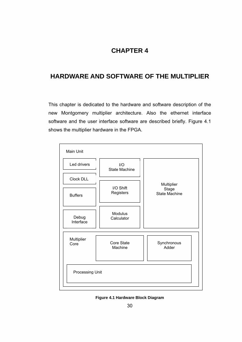
This chapter is dedicated to the hardware and software description of the
new Montgomery multiplier architecture. Also the ethernet interface
software and the user interface software are described briefly. Figure 4.1
shows the multiplier hardware in the FPGA.
30
Main Unit
Led drivers I/O State Machine
Clock DLL Multiplier
I/O Shift Registers
Stage State Machine Buffers
Modulus CalculatorDebug
Interface
Multiplier Core State Machine
Synchronous Core Adder
Processing Unit
Figure 4.1 Hardware Block Diagram
4.1 Montgomery Multiplier Blocks in FPGA
The Montgomery multiplier hardware in FPGA is organized as configurable
blocks. These blocks are designed as variable bit length blocks and the
maximum operand width N is configured at design time. The organization
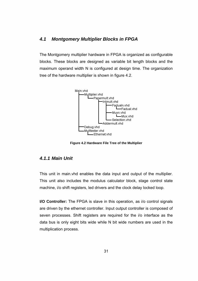
tree of the hardware multiplier is shown in figure 4.2.
Figure 4.2 Hardware File Tree of the Multiplier
4.1.1 Main Unit
This unit in main.vhd enables the data input and output of the multiplier.
This unit also includes the modulus calculator block, stage control state
machine, i/o shift registers, led drivers and the clock delay locked loop.
I/O Controller: The FPGA is slave in this operation, as i/o control signals
are driven by the ethernet controller. Input output controller is composed of
seven processes. Shift registers are required for the i/o interface as the
data bus is only eight bits wide while N bit wide numbers are used in the
multiplication process.
31
Input data is continuously sampled in a process, enabling the
synchronization of input signals with the FPGA internal clock. A similar
process is used to sample i/o control signals: address strobe input (AS),
read/write input (R/W) , address bus input and the bi–directional data bus.
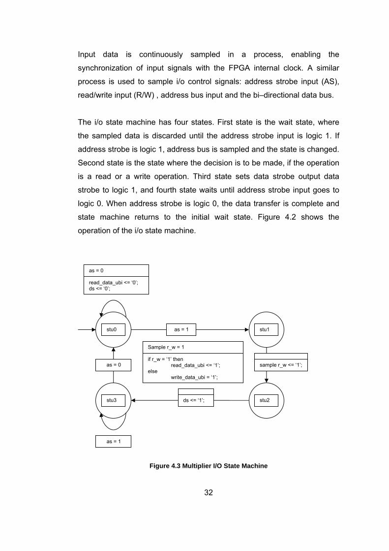
The i/o state machine has four states. First state is the wait state, where
the sampled data is discarded until the address strobe input is logic 1. If
address strobe is logic 1, address bus is sampled and the state is changed.
Second state is the state where the decision is to be made, if the operation
is a read or a write operation. Third state sets data strobe output data
strobe to logic 1, and fourth state waits until address strobe input goes to
logic 0. When address strobe is logic 0, the data transfer is complete and
state machine returns to the initial wait state. Figure 4.2 shows the
operation of the i/o state machine.
32
Figure 4.3 Multiplier I/O State Machine
stu0 stu1
Sample r_w = 1 if r_w = ‘1’ then
read_data_ubi <= ‘1’; else
write_data_ubi = ‘1’;
stu2
as = 0 read_data_ubi <= ‘0’; ds <= ‘0’;
as = 1
stu3
as = 1
sample r_w <= ‘1’; as = 0
ds <= ‘1’;
33
A read operation means that the ethernet controller reads the value of a
register from FPGA. Consequently a write operation is performed when the
ethernet controller writes a value to a register in the FPGA.
In write operations, a separate process writes the value into the shift
register addressed by the address bus. The accessed register is shifted by
eight bits, every time it is accessed for a write operation.
In read operations, the value of the most significant eight bits of the
addressed register in the FPGA is written to the data bus out register. All
read registers in the FPGA are shifted by eight bits, in every read access to
the FPGA.
A separate process drives the three state buffers in the input output blocks
of the FPGA. This process enables the data bus to be used for both read
and write operations.
Modulus Calculator Unit: This unit processes the modulus, and
calculates the bit length of the modulus. The process is implemented for
variable length operands and supports both GF(p) and GF(2n) modes of
operation.
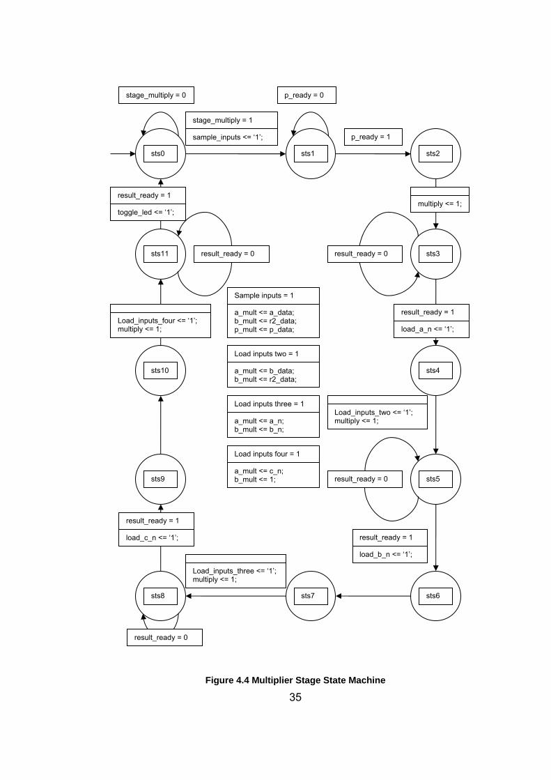
Multiplier Stage State Machine: A single modular multiplication requires
four Montgomery multiplications, as previously described in chapter 2. This
state machine supplies the input operands to the MM kernel.
The state machine waits in state 0, unless the stage multiply bit is set by
the i/o state machine. Then prepares the inputs for the first MM operation,
a multiplied by r2, and waits in state 1 until the modulus count block is done
processing. Then begins first Montgomery multiplication in state 2.
34
The first result is awaited in state 3. After the first result, a·r value, is
registered, second MM operation b multiplied by r2 begins in state 4. State
5 waits unit the result is ready, and registers the b·r value. State 6 is a
dummy state, needed for timing compensation between processes.
Third multiplication, multiplication of a·r with b·r begins in state 7. The result
c·r is awaited in state 8. State 9 is another dummy state for timing
compensation.
Final multiplication, c·r value multiplied with 1, begins in state 10. The state
machine waits for the final result c in state 11 and toggles the led after the
multiplication result is ready. Then the state machine returns to initial state,
state 0, ready for a new MM operation. Figure 4.3 shows the operation of
the multiplier stage state machine.
Debug Interface: Debug interface in debug.vhd is the block that supplies
the intermediate values to the user interface, for the visual display of MM
operations. This interface is not included in the results part in chapter 6, as
this block is not an essential part of the multiplier.
Clock Delay Locked Loop: This unit is a standard block on the FPGA.
Clock delay locked loop improves the timing synchronization of the clock
signal on the circuit board with the FPGA internal clock. This unit also
improves FPGA internal clock distribution, and is not an essential part of
the multiplier.
Led Drivers: There are four leds on the circuit board. Three leds are used
for ethernet and the fourth led is toggled every time a new MM operation is
performed.
Buffers: The clock buffers are used for clock distribution inside the FPGA
and are standard components of every FPGA design.
stage_multiply = 0
35
Figure 4.4 Multiplier Stage State Machine
stage_multiply = 1 sample_inputs <= ‘1’;
p_ready = 0
sts0 sts1
p_ready = 1
sts2
sts3 result_ready = 0
Sample inputs = 1 a_mult <= a_data; b_mult <= r2_data; p_mult <= p_data;
sts4
Load inputs two = 1 a_mult <= b_data; b_mult <= r2_data;
Load_inputs_two <= ‘1’; multiply <= 1;
sts5 result_ready = 0
result_ready = 1 load_b_n <= ‘1’;
sts6 sts7
Load_inputs_three <= ‘1’; multiply <= 1;
sts8
result_ready = 0
sts9
sts10
Load inputs three = 1 a_mult <= a_n; b_mult <= b_n;
Load inputs four = 1 a_mult <= c_n; b_mult <= 1;
sts11
Load_inputs_four <= ‘1’; multiply <= 1;
result_ready = 0
result_ready = 1 toggle_led <= ‘1’;
multiply <= 1;
result_ready = 1 load_a_n <= ‘1’;
result_ready = 1 load_c_n <= ‘1’;
36
4.1.2 Multiplier Core
The multiplier core in papermult.vhd, performs the internal operations of
the MM operation. The multiplier core consists of a state machine, an
adder, a comparator and the new processing unit described in chapter 3.
Multiplier Core State Machine This state machine controls the new processing unit, described previously
in chapter 3. Initially this state machine waits in state 0 unless the multiply
signal becomes logic 1. When the multiply signal becomes logic 1, p+b
register is prepared using the adder, depending on the field. If the field is
GF(2n), the p+b register contains the bitwise xor of the modulus p and the
multiplicand b. If the field is GF(p), the p+b register contains the result of
addition of p and b.
When the p+b register is loaded with the appropriate value, MM operation
begins. The new processing unit processes 2 bits of the multiplier in each
clock cycle in GF(2n) mode and 1 bit of the multiplier in GF(p) mode.
After all the bits of the multiplier are processed, the result ready signal
becomes logic 1 and the MM operation is finished. Figure 4.4 shows the
operation of multiplier core state machine.
37
Figure 4.5 Multiplier Core State Machine
Adder: The adder is a synchronous carry propagate adder. This adder is
not a dual field adder, due to area constraints, so it is controlled by the core
state machine and used only in GF(p) mode of operation.
Comparator: The comparator is a standard comparator needed for the
final reduction operation in GF(p).
start ready st0
st1
prepare_pb = 1 if field = ‘1’ then adder_a_in <= b; adder_b_in <= p; else pb <= b XOR p;
st2 st3
ready <= ‘1’; result <= adder_q;
multiply = 0 result_ready <= ‘0’; mult_busy <= ‘0’; sum <= others => ‘0’; pb <= others => ‘0’;
result_pb = 1 if field = ‘1’ then pb <= adder_q_out;
int_multiply <= 1; result_pb <= ‘1’;
multiply = 1 result_ready <= ‘0’; mult_busy <= ‘1’; sum <= (others => ‘0’); pb <= (others => ‘0’); prepare_pb <= ‘1’;
check_finish = 1 if field = ‘1’ then adder_a_in <= cc_ns; adder_b_in <= cs_ns; else result <= cs_ns;
result_ready_int = 1 field = ‘1’
result_ready_int = 1 field = ‘0’ int_multiply <= ‘0’; check_finish <= ‘1’;
int_multiply <= ‘0’; check_finish <= ‘1’;
result_ready_int = 0
38
4.1.3 Processing Unit
This is the Intmult.vhd, previously mentioned as the processing unit in
chapter 3, refer to figure 3.1. The processing unit includes a dual field
adder, two 4 to 1 multiplexers, local control logic, a counter, and a
comparator. The bit shifts of p, b and p+b registers are done by simple
signal naming, so the 2p, 2b and 2(p+b) values do not consume any
registers. The term N is used to represent the word length of operands.
The summary of the terms described in the previous chapters are shortly
mentioned below for easy reference.
Dual field adder: This adder in Fadualn.vhd is a standard N bit adder.
Multiplexers: These are standard 4 to 1, N bit multiplexers in muxn.vhd.
Local Control Logic: This is the LCL block in Selection.vhd. Counter: The counter is a simple counter that counts the processed bits of
the multiplier. The counter can increment by 1 or 2 depending on the field.
In GF(2n) mode, the counter increments by 2, while in GF(p) mode the
counter increments by 1.
Comparator: The comparator used in the processing unit is a simple
comparator for the bit count operation. It compares the number of
processed multiplier bits with the result of the modulus calculator block,
stating the processing unit to end operation when the result is ready.
4.2 Ethernet Controller Software
The ethernet controller software is written in Ubicom Unity environment
and compiled using Gnu tools. The software supports both dynamic host
configuration protocol (DHCP) and static internet protocol (IP) address
modes for configuration.
The software is composed of 3 files.
39
main.c , contains the initialization functions of the ethernet controller,
interface.h , contains the FPGA i/o functions,
interface.c , contains the ethernet interface code. The interface
functions are listed in this file.
4.2.1 Initialization of the IP2022
Upon boot of the ethernet controller, the initialization function is called. This
function configures the memory heap, initializes the timers, configures the
ethernet memory pages and initializes the protocols. User datagram
protocol (UDP) is used in this thesis for communication between the host
computer and the circuit board.
After the protocol initialization, the configuration is necessary. The internet
protocol address, subnet mask and default gateway address can be
changed remotely as well as a static ip address can be defined.
Following the IP address configuration, the ethernet interface is initialized.
When the ethernet is ready, the ethernet leds start blinking and the
application initializes. The application initialization is finished by the
configuration of the serial communication interface.
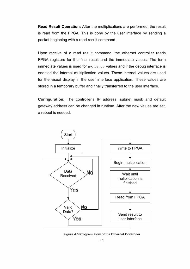
4.2.2 Program Flow of the Ethernet Interface
The program flow is event based. The two main events used are the
ethernet receive event and the serial port receive event.
Ethernet Receive Event: The ethernet receive event stores the received
data packet to a temporary buffer and sends the buffer to the process data
function.
40
Serial Port Receive Event: The serial port receive event stores the
received values to a temporary buffer until the data count is the predefined
value for a specific command. This enables the uart to pass the received
buffer to the process data function as the ethernet receive event.
4.2.3 Data Processing in the Ethernet Controller
The process data function acts as an interface between the FPGA and the
user interface application. The runtime configuration of the ethernet
controller is also managed by this function. All these operations are
performed from either the uart or the ethernet.
Multiply Operation: If the received packet begins with multiply command,
the second byte contains the number of bytes per operand and the third
byte contains the field of operation, 0 for GF(2n) and 1 for GF(p).
Beginning from the fourth byte, the operands a, b, p and r2 follow. As the
operand length is variable, the packet size is also variable. This is
especially important in the serial mode of operation, using the uart receive
event, as the word length can be of any size up to 1024 bits. The word
length is stored in the memory of the ethernet controller for future use.
The write FPGA function in interface.h enables the data to be written to
FPGA registers. As the FPGA registers are shift registers, the operands
are written in loops, thus clearing the address limitations.
Following the load of FPGA registers with operand values, a write to the
FPGA address 5 starts multiplication.
Read Result Operation: After the multiplications are performed, the result
is read from the FPGA. This is done by the user interface by sending a
packet beginning with a read result command.
Upon receive of a read result command, the ethernet controller reads
FPGA registers for the final result and the immediate values. The term
immediate values is used for a·r, b·r, c·r values and if the debug interface is
enabled the internal multiplication values. These internal values are used
for the visual display in the user interface application. These values are
stored in a temporary buffer and finally transferred to the user interface.
Configuration: The controller’s IP address, subnet mask and default
gateway address can be changed in runtime. After the new values are set,
a reboot is needed.
Start
Initialize Write to FPGA
Begin multiplication
Data Received Wait until
muliplication is finished
Read from FPGA
Valid Data?
Send result to user interface
Figure 4.6 Program Flow of the Ethernet Controller
41
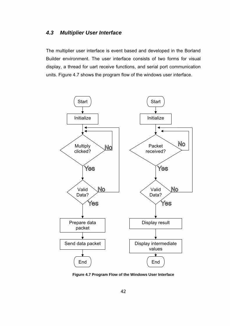
4.3 Multiplier User Interface
The multiplier user interface is event based and developed in the Borland
Builder environment. The user interface consists of two forms for visual
display, a thread for uart receive functions, and serial port communication
units. Figure 4.7 shows the program flow of the windows user interface.
Start
42
Figure 4.7 Program Flow of the Windows User Interface
Initialize
Multiply clicked?
Valid Data?
Send data packet
Prepare data packet
Start
Initialize
Packet received?
Valid Data?
Display result
Display intermediate values
EndEnd
43
4.3.1 Preparation of the Packet
When the multiply button is clicked, the button 1 click function is called.
This function prepares and sends the packet to the ethernet controller.
Serial port can be used in this process as well as the ethernet. This
function converts the operands to 64 bit unsigned integers and prepares
the ethernet packet according to the word length. Rest of the packet is
described in the previous sections but a brief definition follows.
The first byte of the packet contains the multiply command, followed by the
word length and the field value. The field value is 0 for GF(2n) and 1 for
GF(p). The operands a, b, p and r2 follow, beginning with the fourth byte. If
there are no errors in the conversion process, such as operand overflow,
the packet is transferred.
4.3.2 Receiving Packets
The serial port or the ethernet interface can be used for receiving packets.
The received packets are processed according to their first byte. The first
byte informs that the packet contains the result of a multiplication, or the
packet is a configuration response packet. The configuration responses are
displayed in the log as they are received.
The multiplication result packet begins with a read result command. The
initial operands are included in the packet as well as the immediate values
and the final multiplication result. These values are then combined into 64
bit unsigned integers for GF(p) mode of operation. If the multiplication field
is GF(2n), these values are converted to polynomial notation as strings.
Finally these values are displayed.
44
CHAPTER 5
RESULTS
In this chapter, the new Montgomery multiplier architecture is compared
with the previous architectures. The comparisons are made in terms of
silicon area, clock frequency and time required for a single MM operation.
Also the analysis results of the new architecture for different word length
implementations is shown in this chapter.
The silicon area measurements are performed in terms of FPGA slices.
Combinational circuits are represented by look up tables, while
synchronous circuits are represented by flip flops.
Clock frequency is an important aspect of comparisons. The longest path
should be as short as possible for a high clock frequency of operation.
Clock cycle count is the other important comparison perspective in this
thesis. As proven in chapter 3, the clock cycle count of the new algorithm is
half of the standard algorithms for GF(p) and quarter of the standard
algorithms for GF(2n). This improvement makes the new algorithm the
fastest Montgomery multiplication algorithm encountered in the literature by
January 2006.
The compared results are obtained after the synthesis stage and the
implementation stage. The term synthesis result stands for the theoretical
measurements of the tools, while the term implementation result means the
real time operation performance.
45
5.1 Comparisons of Multiplier Architectures
For a realistic comparison perspective, the standard Montgomery multiplier
algorithms are also implemented for the same FPGAs. These are all 5 bit
architectures, and they are compared to the 5 bit implementation of the
new architecture. The 5 bit multiplier architectures are:
A) Standard Montgomery multiplier for GF(p) (single bit per clock cycle)
B) Standard Montgomery multiplier for GF(2n) (single bit per clock cycle)
C) Standard unified field Montgomery multiplier (single bit per clock cycle)
D) New Montgomery multiplier (single bit for GF(p), double bit for GF(2n))
Architecture D is the implementation of the new Montgomery multiplication
algorithm described in chapter 3.
The new algorithm also employs the precomputation block, thus halving
the steps of the for loop in the standard MM algorithm.
These comparisons are made for the multiplier cores with controllers only,
as the i/o blocks add the same amount of area and delay for all
architectures. For simplicity, the multiplier cores with controller blocks are
called as multiplier cores.
These standard Montgomery multipliers represented as architectures A,B
and C perform the MM operation according to the standard MM algorithm
in page 14. The new Montgomery multiplier represented as architecture D
performs the MM algorithm in page 18.
The multiplier cores are compared from silicon area, clock frequency and
time required for a single MM operation perspectives.
46
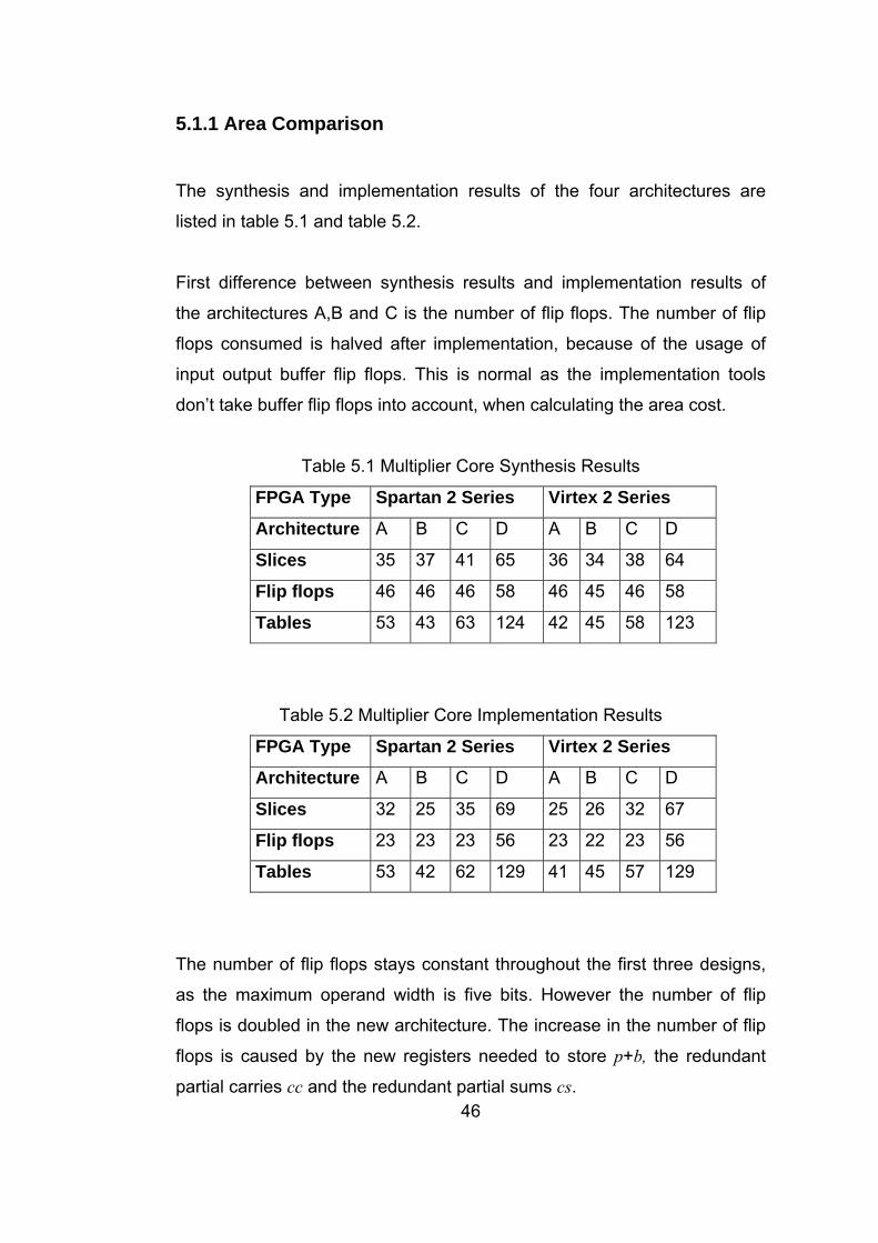
5.1.1 Area Comparison
The synthesis and implementation results of the four architectures are
listed in table 5.1 and table 5.2.
First difference between synthesis results and implementation results of
the architectures A,B and C is the number of flip flops. The number of flip
flops consumed is halved after implementation, because of the usage of
input output buffer flip flops. This is normal as the implementation tools
don’t take buffer flip flops into account, when calculating the area cost.
Table 5.1 Multiplier Core Synthesis Results
FPGA Type Spartan 2 Series Virtex 2 Series
Architecture A B C D A B C D
Slices 35 37 41 65 36 34 38 64
Flip flops 46 46 46 58 46 45 46 58
Tables 53 43 63 124 42 45 58 123
Table 5.2 Multiplier Core Implementation Results
FPGA Type Spartan 2 Series Virtex 2 Series
Architecture A B C D A B C D
Slices 32 25 35 69 25 26 32 67
Flip flops 23 23 23 56 23 22 23 56
Tables 53 42 62 129 41 45 57 129
The number of flip flops stays constant throughout the first three designs,
as the maximum operand width is five bits. However the number of flip
flops is doubled in the new architecture. The increase in the number of flip
flops is caused by the new registers needed to store p+b, the redundant
partial carries cc and the redundant partial sums cs.
47
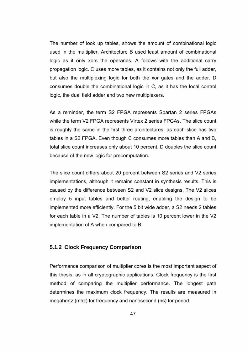
The number of look up tables, shows the amount of combinational logic
used in the multiplier. Architecture B used least amount of combinational
logic as it only xors the operands. A follows with the additional carry
propagation logic. C uses more tables, as it contains not only the full adder,
but also the multiplexing logic for both the xor gates and the adder. D
consumes double the combinational logic in C, as it has the local control
logic, the dual field adder and two new multiplexers.
As a reminder, the term S2 FPGA represents Spartan 2 series FPGAs
while the term V2 FPGA represents Virtex 2 series FPGAs. The slice count
is roughly the same in the first three architectures, as each slice has two
tables in a S2 FPGA. Even though C consumes more tables than A and B,
total slice count increases only about 10 percent. D doubles the slice count
because of the new logic for precomputation.
The slice count differs about 20 percent between S2 series and V2 series
implementations, although it remains constant in synthesis results. This is
caused by the difference between S2 and V2 slice designs. The V2 slices
employ 5 input tables and better routing, enabling the design to be
implemented more efficiently. For the 5 bit wide adder, a S2 needs 2 tables
for each table in a V2. The number of tables is 10 percent lower in the V2
implementation of A when compared to B.
5.1.2 Clock Frequency Comparison
Performance comparison of multiplier cores is the most important aspect of
this thesis, as in all cryptographic applications. Clock frequency is the first
method of comparing the multiplier performance. The longest path
determines the maximum clock frequency. The results are measured in
megahertz (mhz) for frequency and nanosecond (ns) for period.
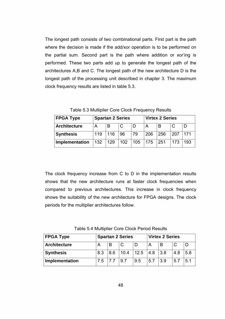
48
The longest path consists of two combinational parts. First part is the path
where the decision is made if the add/xor operation is to be performed on
the partial sum. Second part is the path where addition or xor’ing is
performed. These two parts add up to generate the longest path of the
architectures A,B and C. The longest path of the new architecture D is the
longest path of the processing unit described in chapter 3. The maximum
clock frequency results are listed in table 5.3.
Table 5.3 Multiplier Core Clock Frequency Results
FPGA Type Spartan 2 Series Virtex 2 Series
Architecture A B C D A B C D
Synthesis 119 116 96 79 206 256 207 171
Implementation 132 129 102 105 175 251 173 193
The clock frequency increase from C to D in the implementation results
shows that the new architecture runs at faster clock frequencies when
compared to previous architectures. This increase in clock frequency
shows the suitability of the new architecture for FPGA designs. The clock
periods for the multiplier architectures follow.
Table 5.4 Multiplier Core Clock Period Results
FPGA Type Spartan 2 Series Virtex 2 Series
Architecture A B C D A B C D
Synthesis 8.3 8.6 10.4 12.5 4.8 3.8 4.8 5.8
Implementation 7.5 7.7 9.7 9.5 5.7 3.9 5.7 5.1
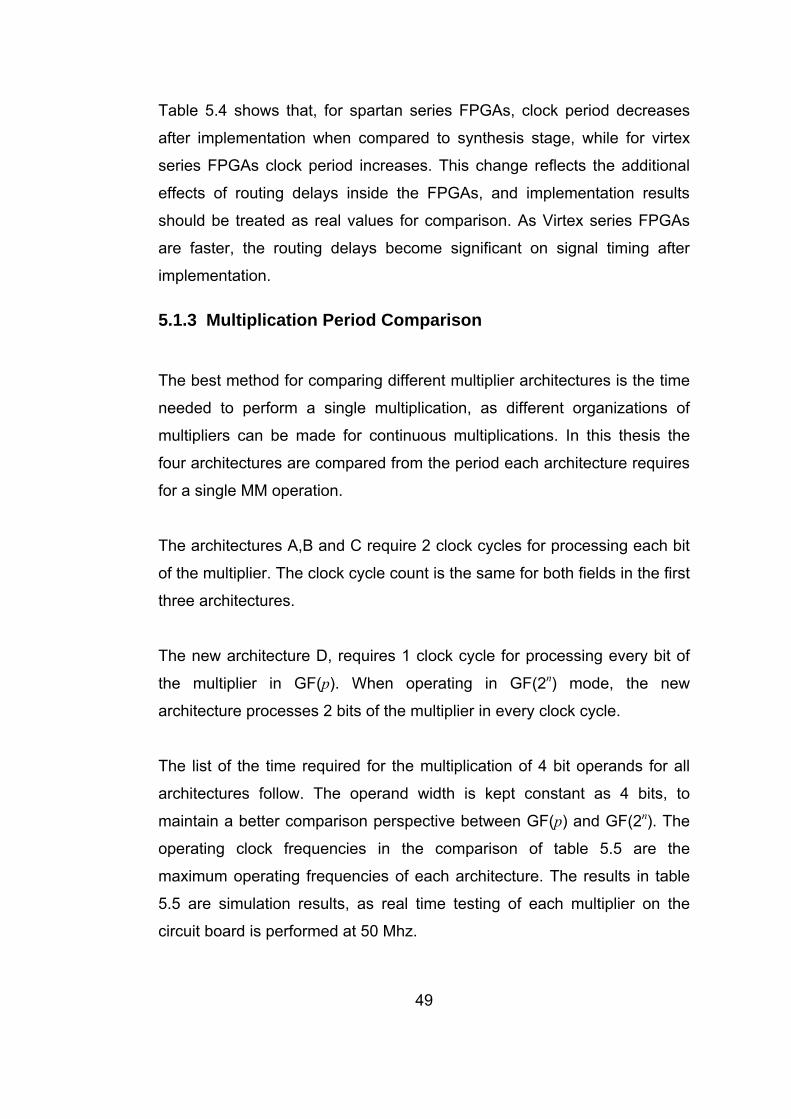
49
Table 5.4 shows that, for spartan series FPGAs, clock period decreases
after implementation when compared to synthesis stage, while for virtex
series FPGAs clock period increases. This change reflects the additional
effects of routing delays inside the FPGAs, and implementation results
should be treated as real values for comparison. As Virtex series FPGAs
are faster, the routing delays become significant on signal timing after
implementation.
5.1.3 Multiplication Period Comparison
The best method for comparing different multiplier architectures is the time
needed to perform a single multiplication, as different organizations of
multipliers can be made for continuous multiplications. In this thesis the
four architectures are compared from the period each architecture requires
for a single MM operation.
The architectures A,B and C require 2 clock cycles for processing each bit
of the multiplier. The clock cycle count is the same for both fields in the first
three architectures.
The new architecture D, requires 1 clock cycle for processing every bit of
the multiplier in GF(p). When operating in GF(2n) mode, the new
architecture processes 2 bits of the multiplier in every clock cycle.
The list of the time required for the multiplication of 4 bit operands for all
architectures follow. The operand width is kept constant as 4 bits, to
maintain a better comparison perspective between GF(p) and GF(2n). The
operating clock frequencies in the comparison of table 5.5 are the
maximum operating frequencies of each architecture. The results in table
5.5 are simulation results, as real time testing of each multiplier on the
circuit board is performed at 50 Mhz.
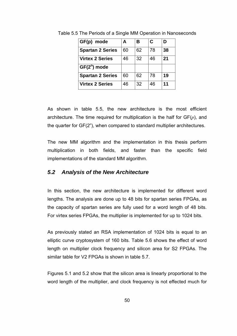
50
Table 5.5 The Periods of a Single MM Operation in Nanoseconds
GF(p) mode A B C D
Spartan 2 Series 60 62 78 38
Virtex 2 Series 46 32 46 21
GF(2n) mode
Spartan 2 Series 60 62 78 19
Virtex 2 Series 46 32 46 11
As shown in table 5.5, the new architecture is the most efficient
architecture. The time required for multiplication is the half for GF(p), and
the quarter for GF(2n), when compared to standard multiplier architectures.
The new MM algorithm and the implementation in this thesis perform
multiplication in both fields, and faster than the specific field
implementations of the standard MM algorithm.
5.2 Analysis of the New Architecture
In this section, the new architecture is implemented for different word
lengths. The analysis are done up to 48 bits for spartan series FPGAs, as
the capacity of spartan series are fully used for a word length of 48 bits.
For virtex series FPGAs, the multiplier is implemented for up to 1024 bits.
As previously stated an RSA implementation of 1024 bits is equal to an
elliptic curve cryptosystem of 160 bits. Table 5.6 shows the effect of word
length on multiplier clock frequency and silicon area for S2 FPGAs. The
similar table for V2 FPGAs is shown in table 5.7.
Figures 5.1 and 5.2 show that the silicon area is linearly proportional to the
word length of the multiplier, and clock frequency is not effected much for
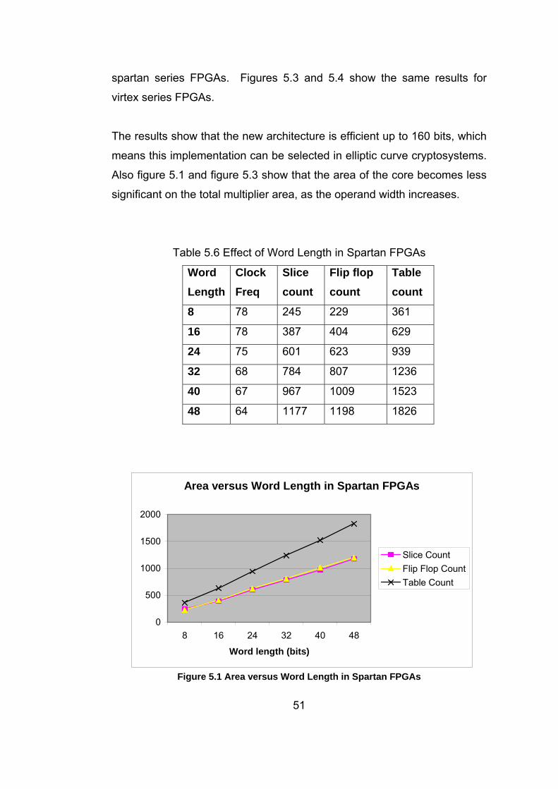
spartan series FPGAs. Figures 5.3 and 5.4 show the same results for
virtex series FPGAs.
The results show that the new architecture is efficient up to 160 bits, which
means this implementation can be selected in elliptic curve cryptosystems.
Also figure 5.1 and figure 5.3 show that the area of the core becomes less
significant on the total multiplier area, as the operand width increases.
Table 5.6 Effect of Word Length in Spartan FPGAs
Word Length
Clock Freq
Slice count
Flip flop count
Table count
8 78 245 229 361
16 78 387 404 629
24 75 601 623 939
32 68 784 807 1236
40 67 967 1009 1523
48 64 1177 1198 1826
Area versus Word Length in Spartan FPGAs
0
500
1000
1500
2000
8 16 24 32 40 48
Word length (bits)
Slice CountFlip Flop CountTable Count
Figure 5.1 Area versus Word Length in Spartan FPGAs
51
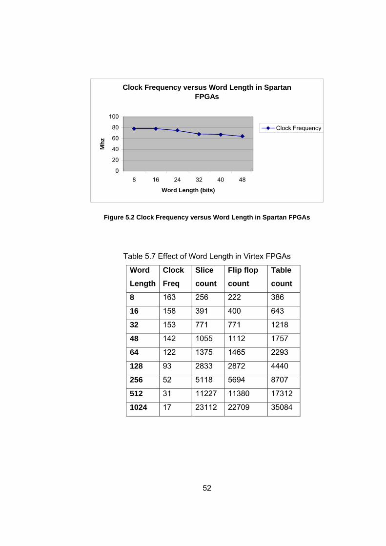
Clock Frequency versus Word Length in Spartan FPGAs
0
20
40
60
80
100
8 16 24 32 40 48
Word Length (bits)
Mhz
Clock Frequency
Figure 5.2 Clock Frequency versus Word Length in Spartan FPGAs
Table 5.7 Effect of Word Length in Virtex FPGAs
Word Length
Clock Freq
Slice count
Flip flop count
Table count
8 163 256 222 386
16 158 391 400 643
32 153 771 771 1218
48 142 1055 1112 1757
64 122 1375 1465 2293
128 93 2833 2872 4440
256 52 5118 5694 8707
512 31 11227 11380 17312
1024 17 23112 22709 35084
52
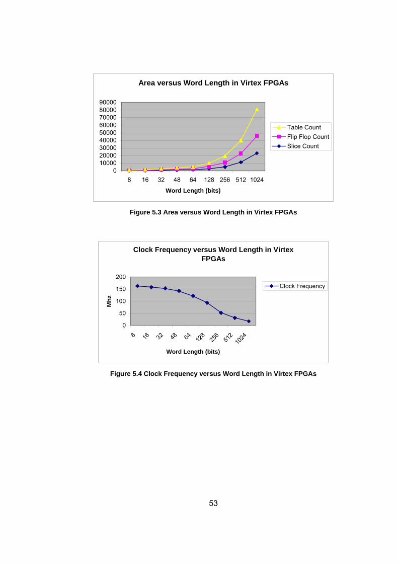
Area versus Word Length in Virtex FPGAs
0100002000030000400005000060000700008000090000
8 16 32 48 64 128 256 512 1024
Word Length (bits)
Table CountFlip Flop CountSlice Count
Figure 5.3 Area versus Word Length in Virtex FPGAs
Clock Frequency versus Word Length in Virtex FPGAs
0
50
100
150
200
8 16 32 48 64 128
256
512
1024
Word Length (bits)
Mhz
Clock Frequency
Figure 5.4 Clock Frequency versus Word Length in Virtex FPGAs
53
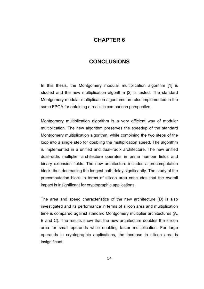
54
CHAPTER 6
CONCLUSIONS
In this thesis, the Montgomery modular multiplication algorithm [1] is
studied and the new multiplication algorithm [2] is tested. The standard
Montgomery modular multiplication algorithms are also implemented in the
same FPGA for obtaining a realistic comparison perspective.
Montgomery multiplication algorithm is a very efficient way of modular
multiplication. The new algorithm preserves the speedup of the standard
Montgomery multiplication algorithm, while combining the two steps of the
loop into a single step for doubling the multiplication speed. The algorithm
is implemented in a unified and dual–radix architecture. The new unified
dual–radix multiplier architecture operates in prime number fields and
binary extension fields. The new architecture includes a precomputation
block, thus decreasing the longest path delay significantly. The study of the
precomputation block in terms of silicon area concludes that the overall
impact is insignificant for cryptographic applications.
The area and speed characteristics of the new architecture (D) is also
investigated and its performance in terms of silicon area and multiplication
time is compared against standard Montgomery multiplier architectures (A,
B and C). The results show that the new architecture doubles the silicon
area for small operands while enabling faster multiplication. For large
operands in cryptographic applications, the increase in silicon area is
insignificant.
55
The operand length is implemented from 8 bits to 1024 bits. It can be
stated that the new architecture operates at about 60 Mhz for 48 bits word
length for Spartan series FPGAs. For Virtex series FPGAs, the multiplier
operates at about 100 Mhz for up to 128 bits word length. For a word
length of 1024 bits, the clock frequency drops to 17 Mhz.
Multiplication period changes in GF(2n) mode of operation when compared
to GF(p) mode. The clock cycle count is halved in GF(2n) mode as two
multiplier bits are processed in every clock cycle. As a conclusion, the new
architecture is two times faster in GF(p) mode and four times faster in
GF(2n) mode, when compared to standard Montgomery multiplication
algorithms.
Conclusions of this study show that the new algorithm can be extended to
process more multiplier bits in each clock cycle. As the proposed unified
dual–radix architecture is a radix(2,4) architecture, the precomputation
block enables the design of increased radices such as radix(4,8) and
radix(8,16). The mathematical proof of the control logic for these
architectures can be an interesting area of study.
56
REFERENCES 1) P. L. Montgomery “Modular multiplication without trial division”,
Mathematics of Computation, vol. 44, no. 170, pages 519–521, April 1985.
2) E. Savaş, A. F. Tenca, M. E. Çiftçibaşı, Ç. K. Koç "Novel Multiplier
Architectures for GF(p) and GF(2n)", IEE Computers and Digital
Techniques Journal, April 2004.
3) E. Savaş, A. F. Tenca, Ç. K. Koç. “A scalable and unified multiplier
architecture for finite fields GF(p) and GF(2n). Cryptographic Hardware and
Embedded Systems – CHES 2000, LNCS 1965, pages 281–296. Springer,
Berlin, Germany, 2000.
4) Ç. K. Koç, A. F. Tenca, “A word–based algorithm and architecture for
Montgomery multiplication” in Cryptographic Hardware and Embedded
Systems, C. Paar, Ç. K. Koç ed., number LNCS 1717, pages 94–108,
Springer, Berlin, Germany, 1999.
5) L.J. Sigal, E.M. Schwarz, R.M. Averill III, “A radix–8 cmos s/390
multiplier” in IEEE 13th Symposium on Computer Arithmetic, pages 2–9,
IEEE Computer Society Press, Los Alamitos, CA, 1997.
6) P. Kornerup, “High–radix modular multiplication for cryptosystems” in
IEEE 11th Symposium on Computer Arithmetic, pages 277–283, IEEE
Computer Society Press, Los Alamitos, CA, 1993.
7) E. F. Brickel, “A fast modular multiplication algorithm with application to
two key cryptography” in Advances in Cryptography – CRYPTO '82, pages.
51–60, Plenum, New York, 1983.
57
8) A. Vandemeulebroecke et al, “A new carry–free decision algorithm and
its application to a single–chip 1024–bit rsa processor” IEEE Journal of
Solid–state Circuits, vol. 25, no. 3, pages. 748–755, June 1990.
9) P. Kornerup, H. Orup, “A high–radix hardware algorithm for calculating
the exponential me modulo n” in IEEE 10th Symposium on Computer
Arithmetic, pages 51–56, IEEE Computer Society Press, CA, 1991.
10) C. D. Walter, “Space/time trade–offs for higher radix modular
multiplication using repeated addition” IEEE Transactions on Computers,
vol. 46, no. 2, pages. 139–141, February 1997.
11) H. Orup, “Simplifying quotient determination in high–radix modular
multiplication” in IEEE 12th Symposium on Computer Arithmetic, pages.
193–199, IEEE Computer Society Press, Los Alamitos, CA, 1995.
12) A. Royo, J. Moran, J. C. Lopez. Design and implementation of a
coprocessor for cryptography applications. In European Design and Test
Conference, pages 213–217, Paris, France, March 17–20 1997.
13) L. Adleman, R.L. Rivest, A. Shamir “A method for obtaining digital
signature and public–key cryptosystems," Comm. ACM, vol. 21, no. 2,
pages. 120–126, February 1978.
14) C. Paar, T. Blum, “Montgomery modular exponentiation on
reconfigurable hardware” in IEEE 14th Symposium on Computer
Arithmetic, pages. 70–77, IEEE Computer Society Press, Los Alamitos,
CA, 1999.
58
15) S. C. Goldstein R. R. Taylor “A high–performance architecture for
cryptography” in Cryptographic Hardware and Embedded Systems, C.
Paar, Ç. K. Koç ed., LNCS 1717, pages. 231–245, Springer, Berlin,
Germany, 1999.
16) N. Koblitz, “Elliptic curve cryptosystems”, Mathematics of Computation,
48(177) pages 203–209, January 1987.
17) Ç. K. Koç, T. Acar, “Montgomery Multiplication in GF(2n)”, in Designs,
Codes and Cryptography, 14(1), pages 57–69, April 1998.
18) R. E. Blahut, Theory and Practice of Error Control Codes, Addison –
Wesley, 1983.
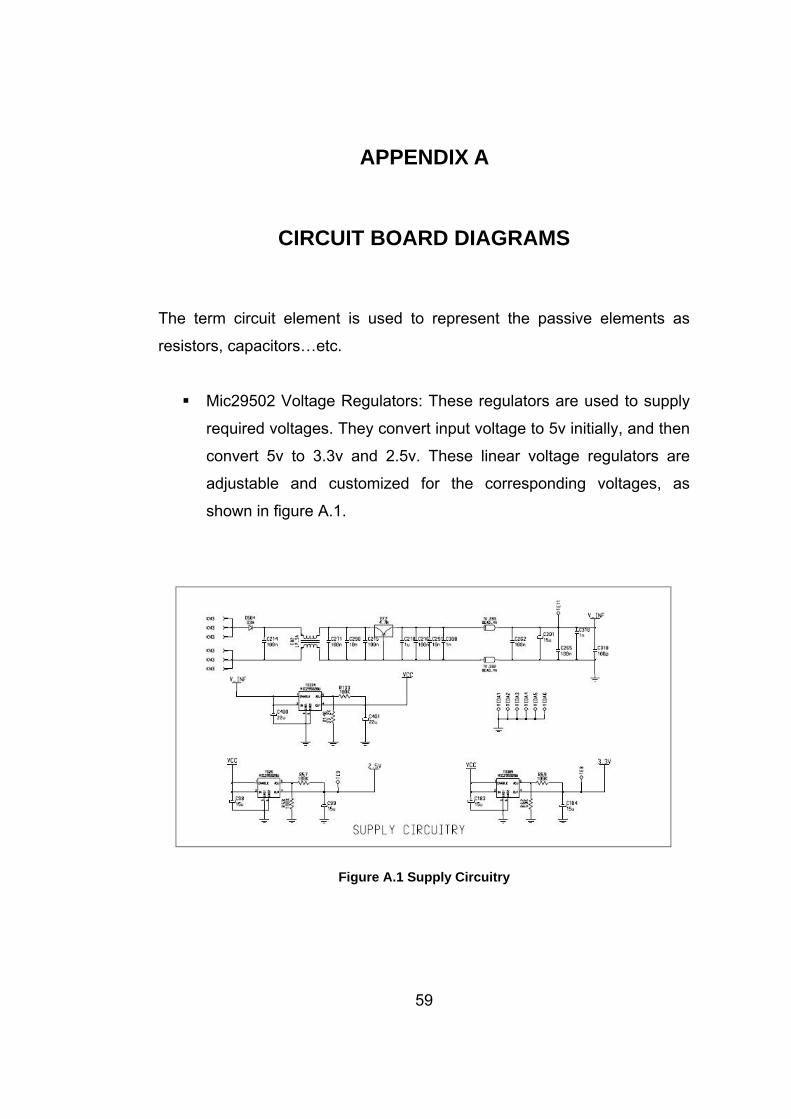
APPENDIX A
CIRCUIT BOARD DIAGRAMS
The term circuit element is used to represent the passive elements as
resistors, capacitors…etc.
Mic29502 Voltage Regulators: These regulators are used to supply
required voltages. They convert input voltage to 5v initially, and then
convert 5v to 3.3v and 2.5v. These linear voltage regulators are
adjustable and customized for the corresponding voltages, as
shown in figure A.1.
Figure A.1 Supply Circuitry
59
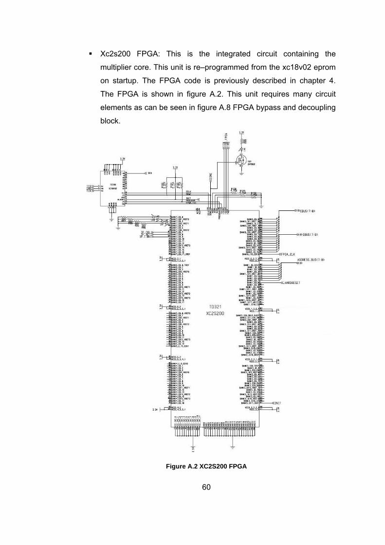
Xc2s200 FPGA: This is the integrated circuit containing the
multiplier core. This unit is re–programmed from the xc18v02 eprom
on startup. The FPGA code is previously described in chapter 4.
The FPGA is shown in figure A.2. This unit requires many circuit
elements as can be seen in figure A.8 FPGA bypass and decoupling
block.
Figure A.2 XC2S200 FPGA
60
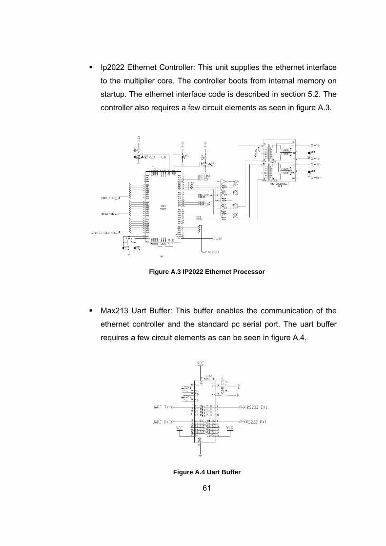
Ip2022 Ethernet Controller: This unit supplies the ethernet interface
to the multiplier core. The controller boots from internal memory on
startup. The ethernet interface code is described in section 5.2. The
controller also requires a few circuit elements as seen in figure A.3.
Figure A.3 IP2022 Ethernet Processor
Max213 Uart Buffer: This buffer enables the communication of the
ethernet controller and the standard pc serial port. The uart buffer
requires a few circuit elements as can be seen in figure A.4.
Figure A.4 Uart Buffer
61
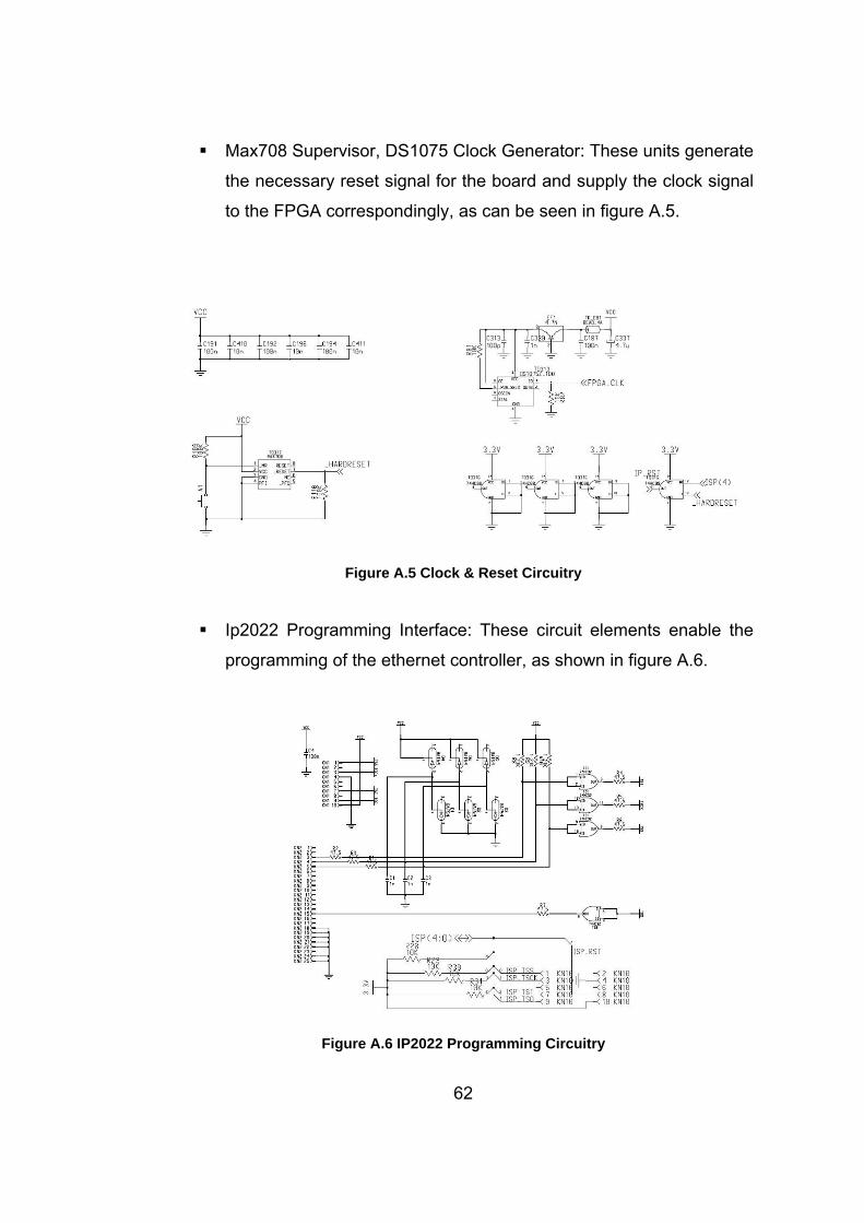
Max708 Supervisor, DS1075 Clock Generator: These units generate
the necessary reset signal for the board and supply the clock signal
to the FPGA correspondingly, as can be seen in figure A.5.
Figure A.5 Clock & Reset Circuitry
Ip2022 Programming Interface: These circuit elements enable the
programming of the ethernet controller, as shown in figure A.6.
Figure A.6 IP2022 Programming Circuitry
62
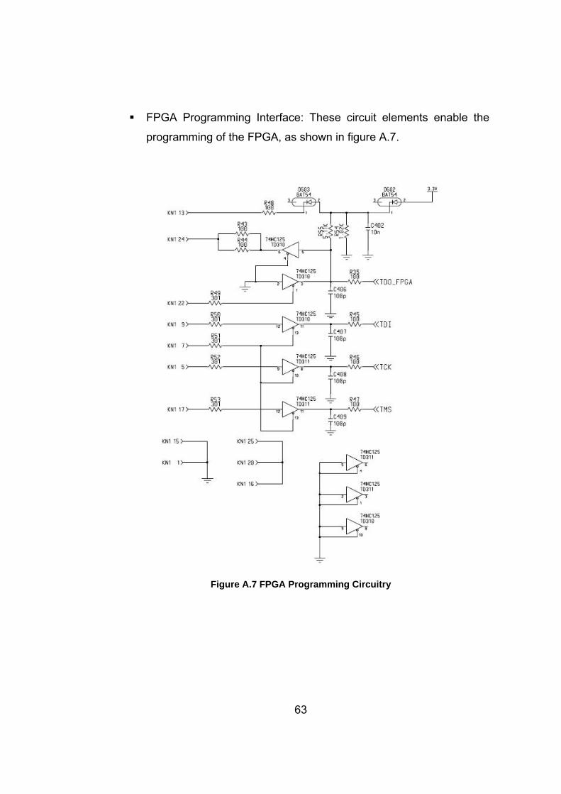
FPGA Programming Interface: These circuit elements enable the
programming of the FPGA, as shown in figure A.7.
Figure A.7 FPGA Programming Circuitry
63
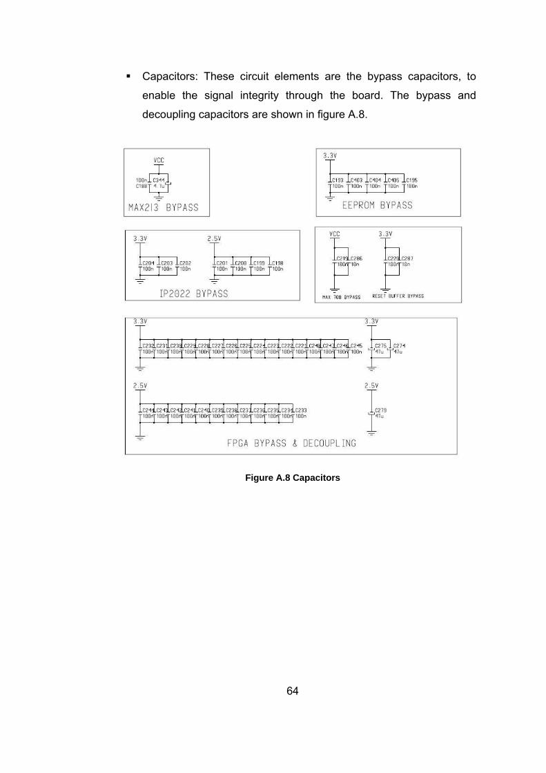
Capacitors: These circuit elements are the bypass capacitors, to
enable the signal integrity through the board. The bypass and
decoupling capacitors are shown in figure A.8.
Figure A.8 Capacitors
64
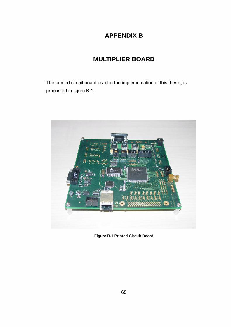
APPENDIX B
MULTIPLIER BOARD The printed circuit board used in the implementation of this thesis, is
presented in figure B.1.
Figure B.1 Printed Circuit Board
65
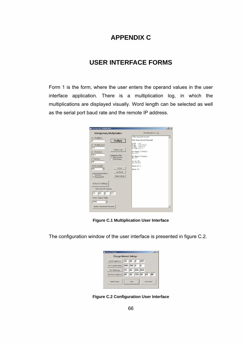
APPENDIX C
USER INTERFACE FORMS
Form 1 is the form, where the user enters the operand values in the user
interface application. There is a multiplication log, in which the
multiplications are displayed visually. Word length can be selected as well
as the serial port baud rate and the remote IP address.
Figure C.1 Multiplication User Interface
The configuration window of the user interface is presented in figure C.2.
Figure C.2 Configuration User Interface
66