Embed Size (px)
Citation preview
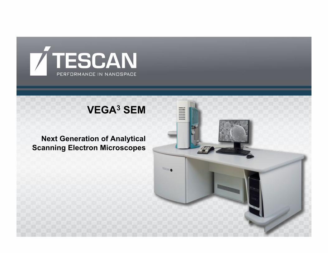
VEGA3 SEM
Next Generation of AnalyticalScanning Electron Microscopes
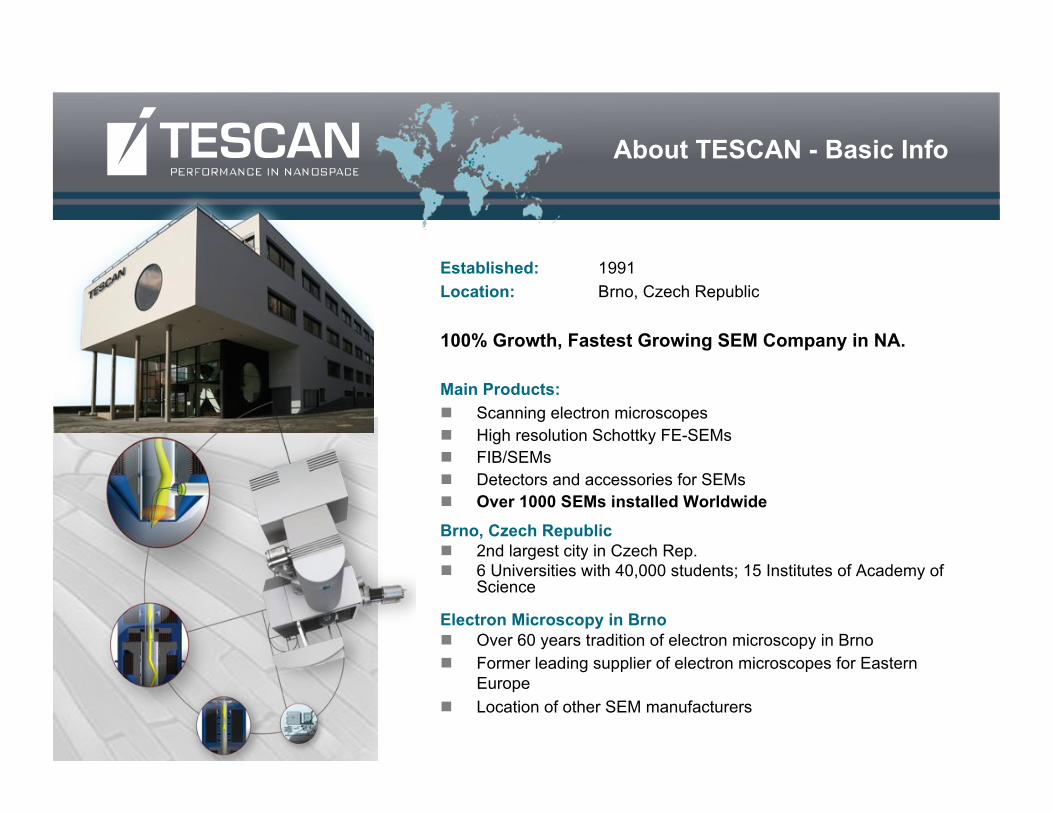
Established: 1991Location: Brno, Czech Republic
100% Growth, Fastest Growing SEM Company in NA.
Main Products:! Scanning electron microscopes! High resolution Schottky FE-SEMs! FIB/SEMs! Detectors and accessories for SEMs! Over 1000 SEMs installed Worldwide
Brno, Czech Republic! 2nd largest city in Czech Rep.! 6 Universities with 40,000 students; 15 Institutes of Academy of
Science
Electron Microscopy in Brno! Over 60 years tradition of electron microscopy in Brno! Former leading supplier of electron microscopes for Eastern
Europe! Location of other SEM manufacturers
About TESCAN - Basic Info
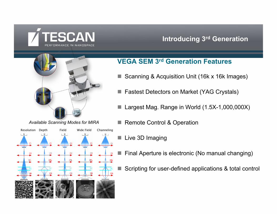
VEGA SEM 3rd Generation Features
! Scanning & Acquisition Unit (16k x 16k Images)
! Fastest Detectors on Market (YAG Crystals)
! Largest Mag. Range in World (1.5X-1,000,000X)
! Remote Control & Operation
! Live 3D Imaging
! Final Aperture is electronic (No manual changing)
! Scripting for user-defined applications & total control
Introducing 3rd Generation
Available Scanning Modes for MIRA
Resolution Depth Field Wide Field Channeling
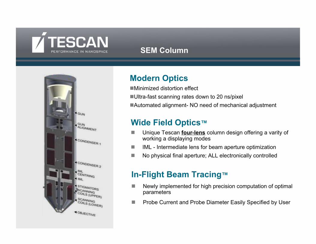
Wide Field Optics™! Unique Tescan four-lens column design offering a varity of
working a displaying modes! IML - Intermediate lens for beam aperture optimization! No physical final aperture; ALL electronically controlled
Modern Optics!Minimized distortion effect!Ultra-fast scanning rates down to 20 ns/pixel!Automated alignment- NO need of mechanical adjustment
SEM Column
In-Flight Beam Tracing™! Newly implemented for high precision computation of optimal
parameters
! Probe Current and Probe Diameter Easily Specified by User
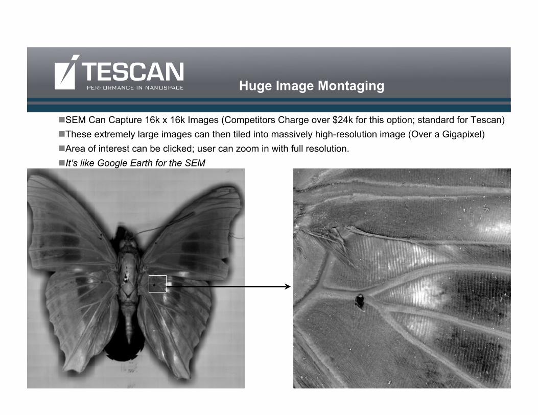
!SEM Can Capture 16k x 16k Images (Competitors Charge over $24k for this option; standard for Tescan)!These extremely large images can then tiled into massively high-resolution image (Over a Gigapixel)!Area of interest can be clicked; user can zoom in with full resolution.!It‘s like Google Earth for the SEM
Huge Image Montaging
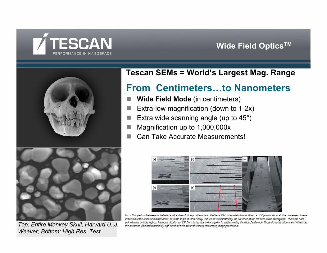
From Centimeters…to Nanometers! Wide Field Mode (in centimeters)! Extra-low magnification (down to 1-2x)! Extra wide scanning angle (up to 45°)! Magnification up to 1,000,000x! Can Take Accurate Measurements!
Tescan SEMs = World’s Largest Mag. Range
Wide Field OpticsTM
Top: Entire Monkey Skull, Harvard U.,J.Weaver; Bottom: High Res. Test
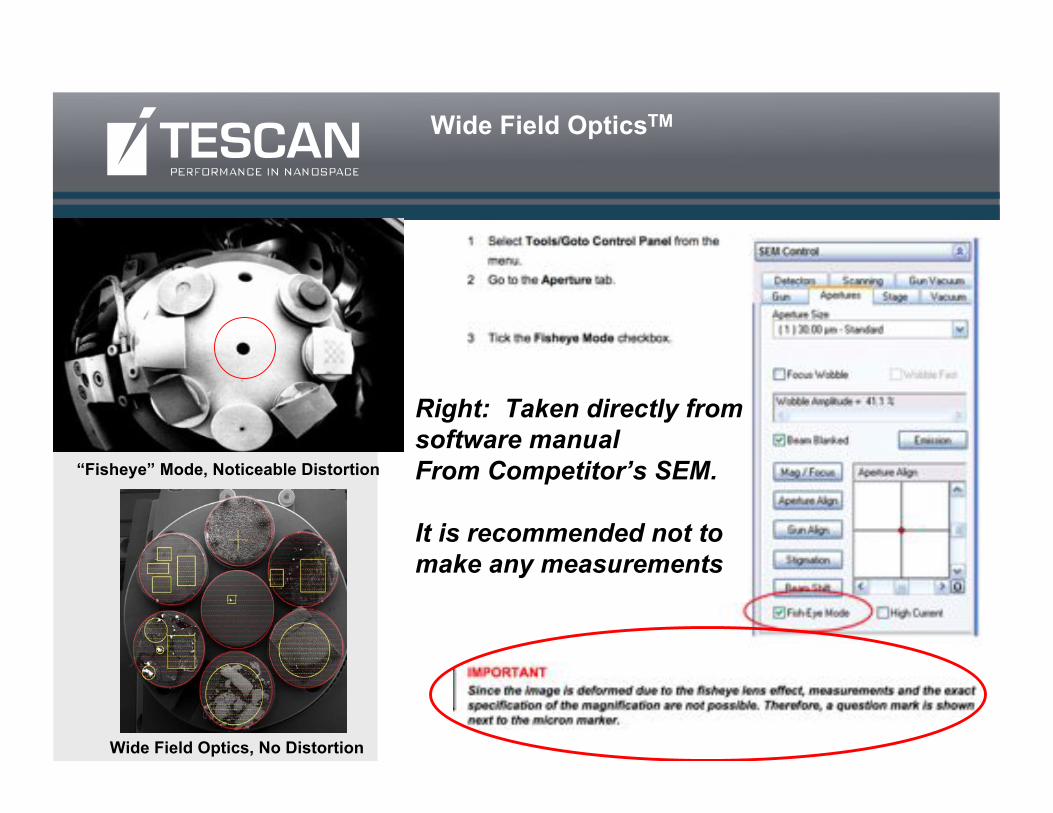
Wide Field OpticsTM
“Fisheye” Mode, Noticeable Distortion
Wide Field Optics, No Distortion
Right: Taken directly fromsoftware manualFrom Competitor’s SEM.
It is recommended not tomake any measurements
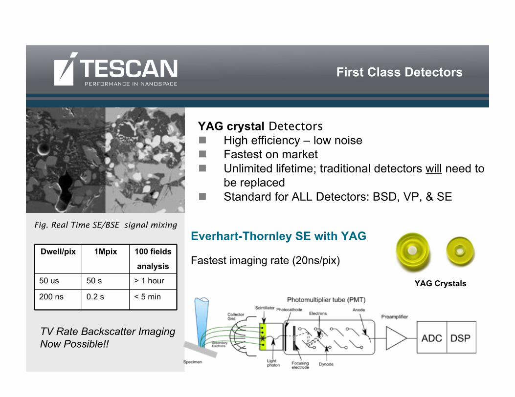
YAG crystal Detectors! High efficiency – low noise! Fastest on market! Unlimited lifetime; traditional detectors will need to
be replaced! Standard for ALL Detectors: BSD, VP, & SE
Fig. Real Time SE/BSE signal mixing
Dwell/pix 1Mpix 100 fields
analysis
50 us 50 s > 1 hour
200 ns 0.2 s < 5 min
TV Rate Backscatter ImagingNow Possible!!
Everhart-Thornley SE with YAG
Fastest imaging rate (20ns/pix)
First Class Detectors
YAG Crystals
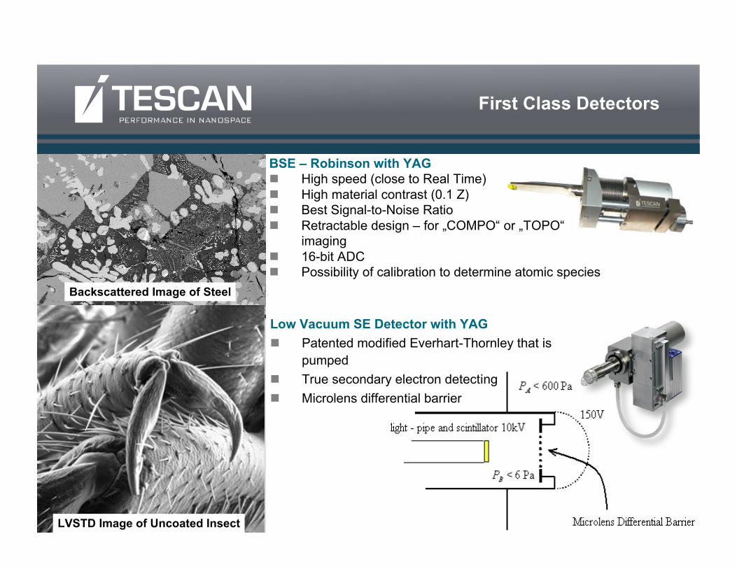
Fig. Phase identification by materialcontrast
BSE – Robinson with YAG! High speed (close to Real Time)! High material contrast (0.1 Z)! Best Signal-to-Noise Ratio! Retractable design – for „COMPO“ or „TOPO“
imaging! 16-bit ADC! Possibility of calibration to determine atomic species
Tescan R-BSE detector
First Class Detectors
Low Vacuum SE Detector with YAG! Patented modified Everhart-Thornley that is
pumped! True secondary electron detecting! Microlens differential barrier
Backscattered Image of Steel
LVSTD Image of Uncoated Insect
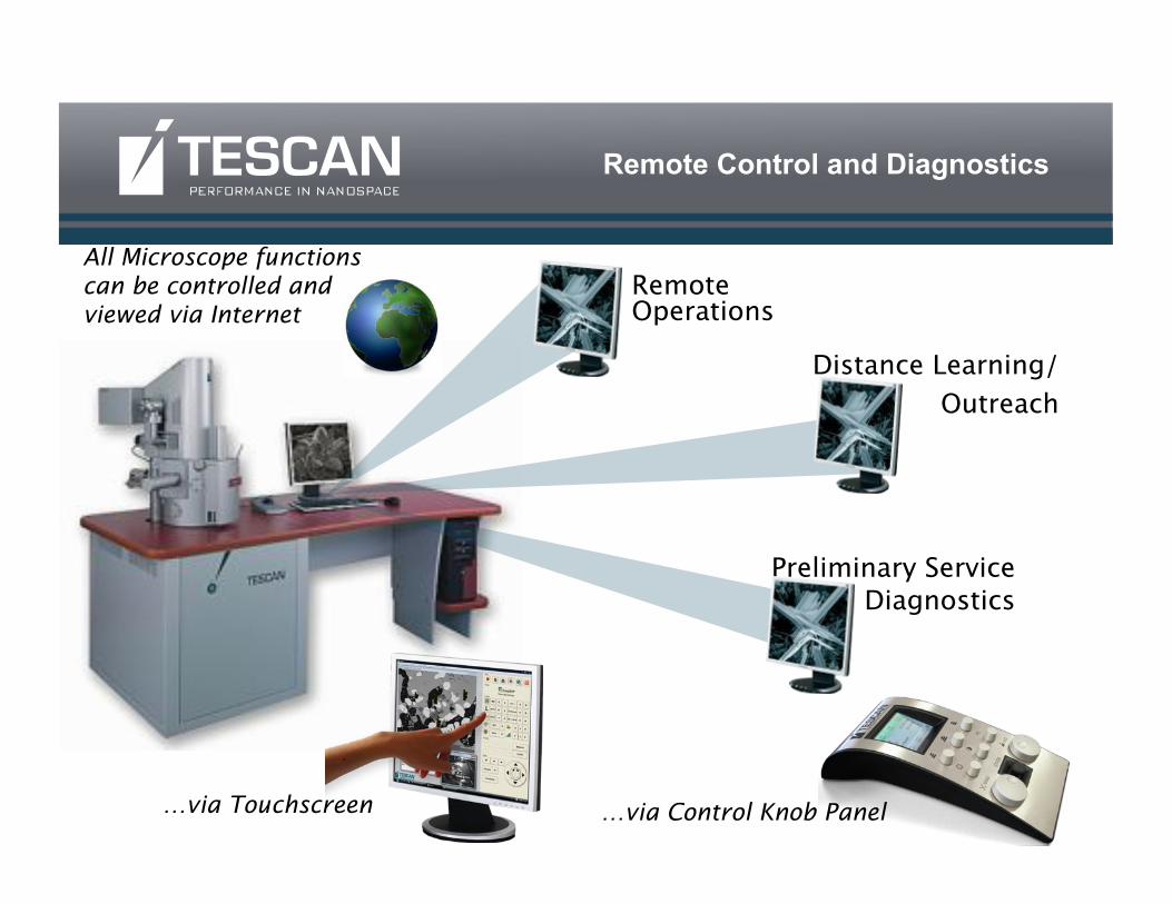
Preliminary ServiceDiagnostics
RemoteOperations
Distance Learning/Outreach
All Microscope functionscan be controlled andviewed via Internet
Remote Control and Diagnostics
…via Touchscreen …via Control Knob Panel
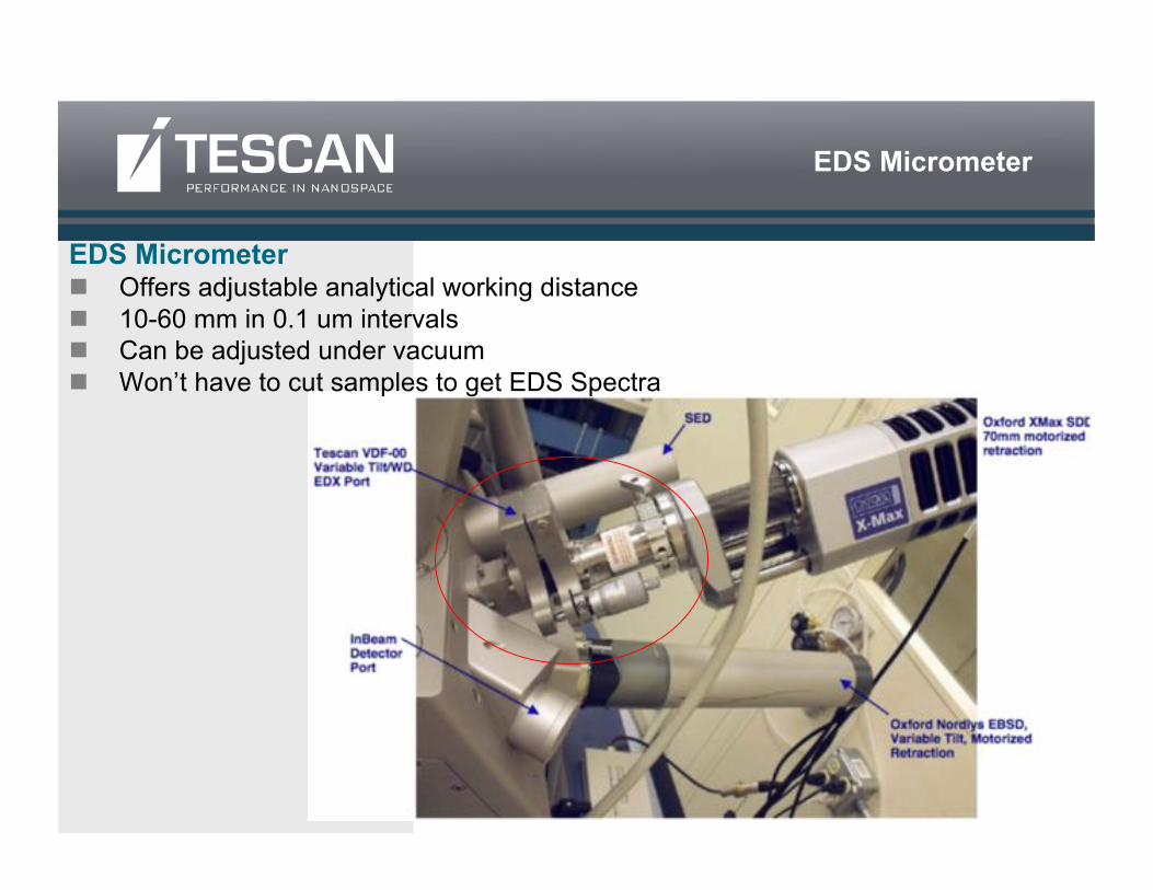
EDS Micrometer
EDS Micrometer! Offers adjustable analytical working distance! 10-60 mm in 0.1 um intervals! Can be adjusted under vacuum! Won’t have to cut samples to get EDS Spectra
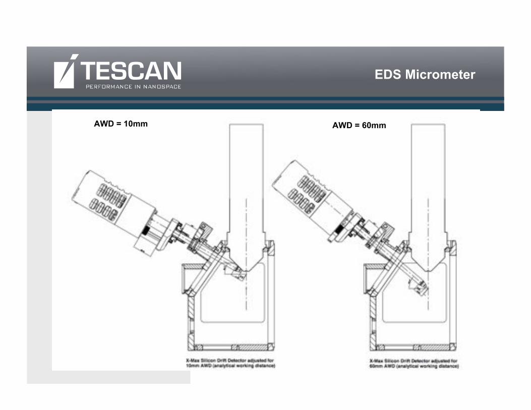
EDS Micrometer
AWD = 10mm AWD = 60mm
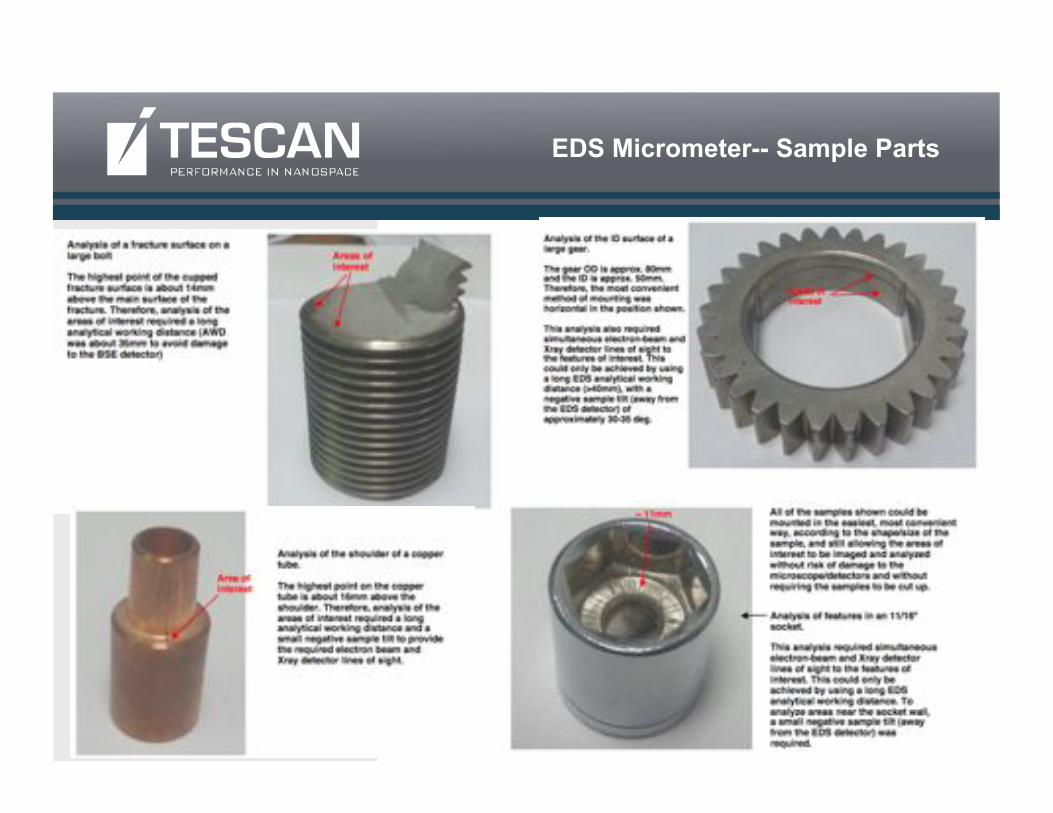
EDS Micrometer-- Sample Parts
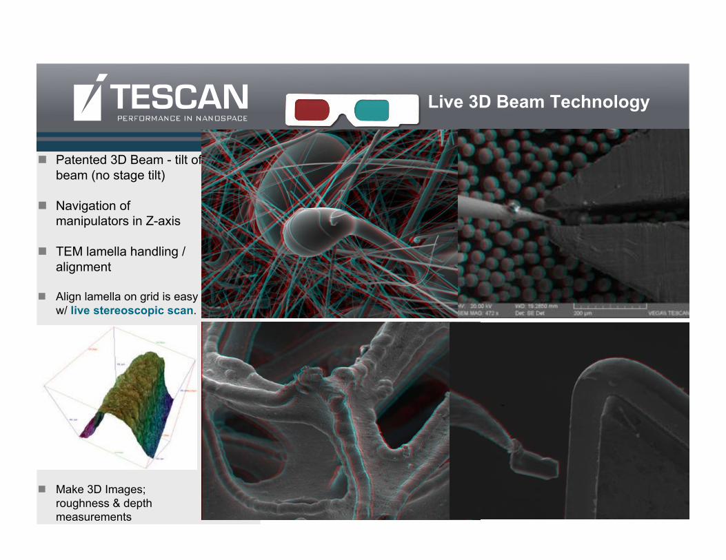
Live Stereoscopic Imaging! Patented 3D Beam - tilt of
beam (no stage tilt)
! Navigation ofmanipulators in Z-axis
! TEM lamella handling /alignment
! Align lamella on grid is easyw/ live stereoscopic scan.
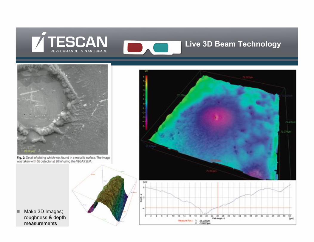
! Make 3D Images;roughness & depthmeasurements
Live 3D Beam Technology
Live Stereoscopic Imaging! Patented 3D Beam - tilt of
beam (no stage tilt)
! Navigation ofmanipulators in Z-axis
! TEM lamella handling /alignment
! Align lamella on grid is easyw/ live stereoscopic scan.
! Make 3D Images;roughness & depthmeasurements
Live 3D Beam Technology
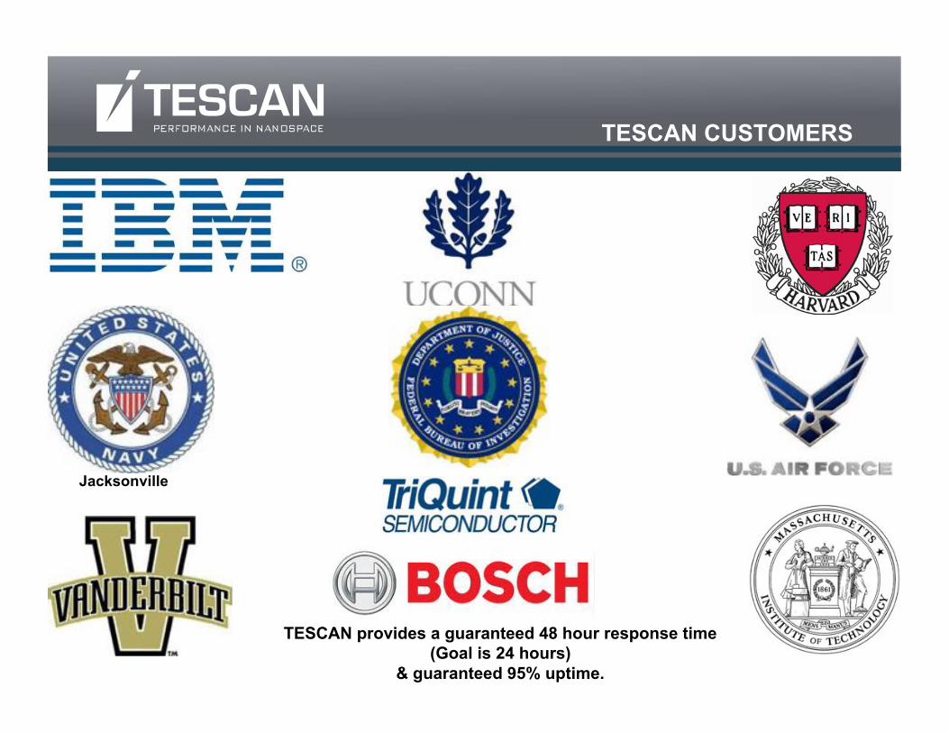
TESCAN CUSTOMERS
Jacksonville
TESCAN provides a guaranteed 48 hour response time(Goal is 24 hours)
& guaranteed 95% uptime.
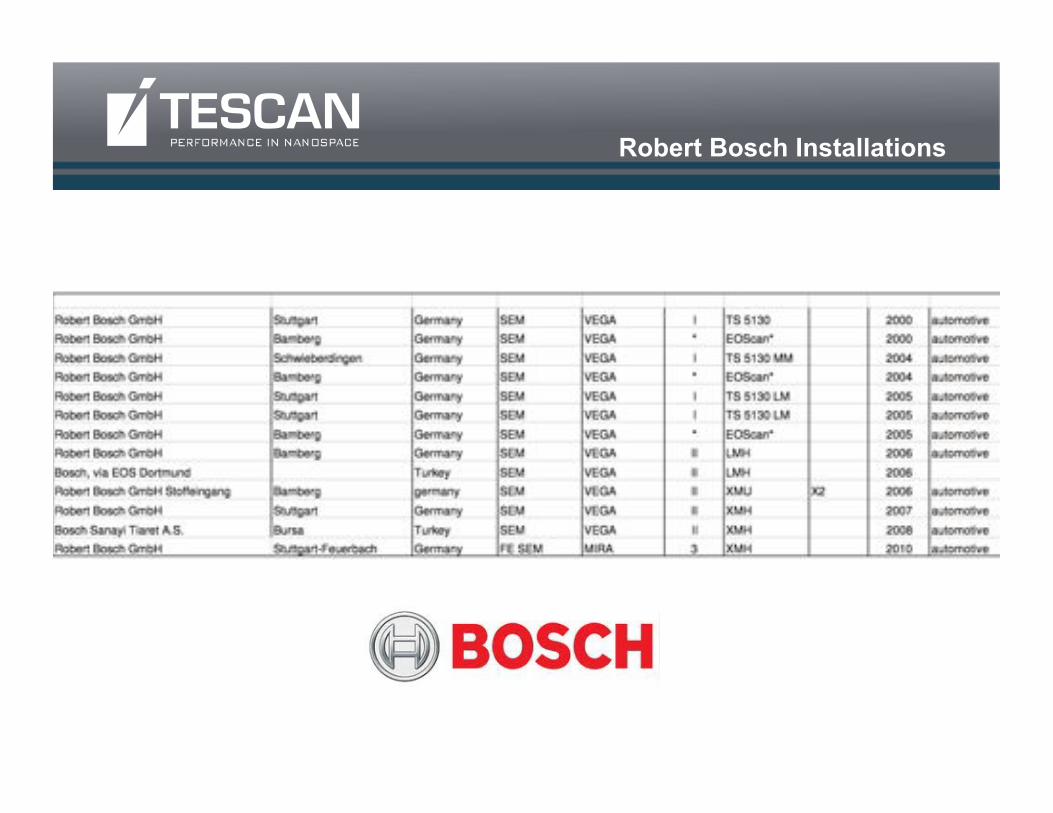
Robert Bosch Installations
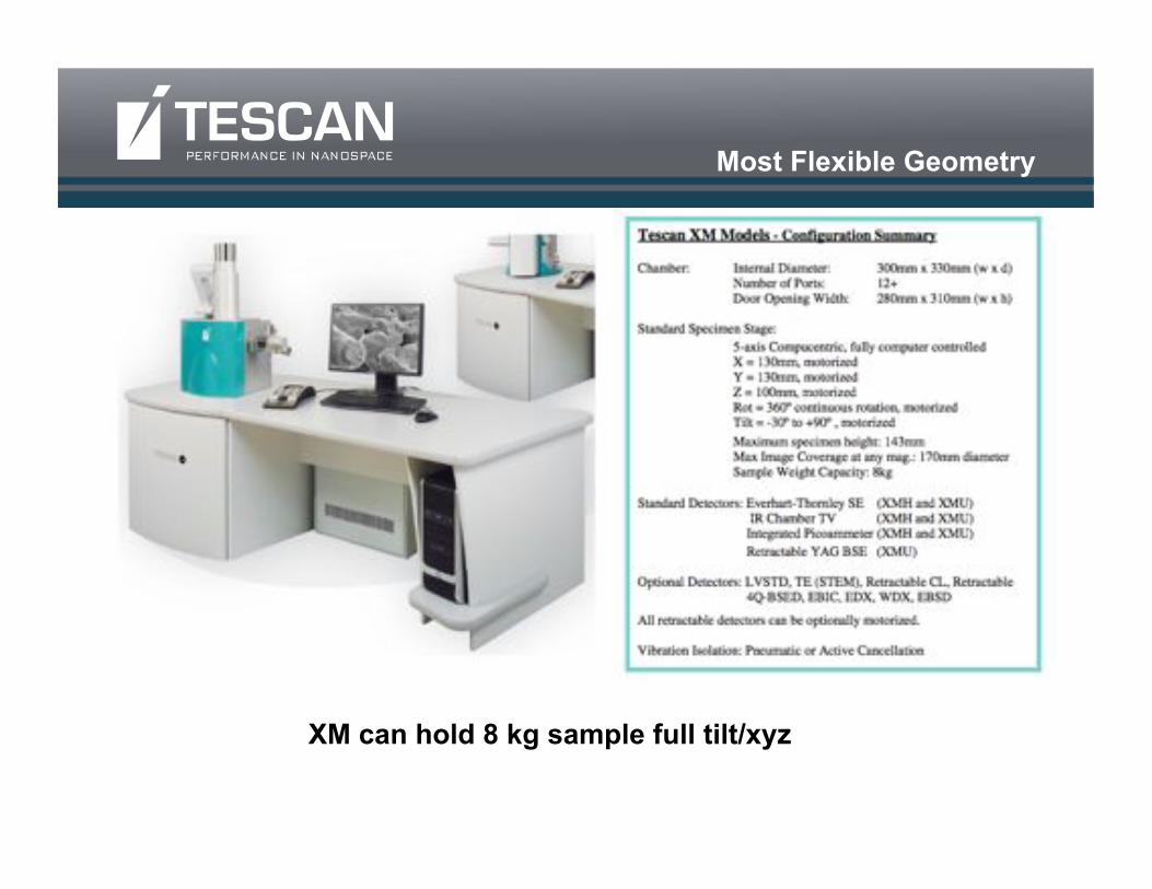
Most Flexible Geometry
XM can hold 8 kg sample full tilt/xyz