Embed Size (px)
Citation preview
MSP430F21x2
www.ti.com SLAS578J –NOVEMBER 2007–REVISED JANUARY 2012
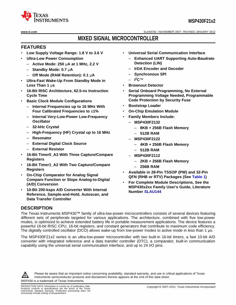
MIXED SIGNAL MICROCONTROLLER1FEATURES2• Low Supply Voltage Range: 1.8 V to 3.6 V • Universal Serial Communication Interface• Ultra-Low Power Consumption – Enhanced UART Supporting Auto-Baudrate
Detection (LIN)– Active Mode: 250 µA at 1 MHz, 2.2 V– IrDA Encoder and Decoder– Standby Mode: 0.7 µA– Synchronous SPI– Off Mode (RAM Retention): 0.1 µA– I2C™• Ultra-Fast Wake-Up From Standby Mode in
Less Than 1 µs • Brownout Detector• 16-Bit RISC Architecture, 62.5-ns Instruction • Serial Onboard Programming, No External
Cycle Time Programming Voltage Needed, ProgrammableCode Protection by Security Fuse• Basic Clock Module Configurations
• Bootstrap Loader– Internal Frequencies up to 16 MHz WithFour Calibrated Frequencies to ±1% • On-Chip Emulation Module
– Internal Very-Low-Power Low-Frequency • Family Members Include:Oscillator – MSP430F2132
– 32-kHz Crystal – 8KB + 256B Flash Memory– High-Frequency (HF) Crystal up to 16 MHz – 512B RAM– Resonator – MSP430F2122– External Digital Clock Source – 4KB + 256B Flash Memory– External Resistor – 512B RAM
• 16-Bit Timer0_A3 With Three Capture/Compare – MSP430F2112Registers – 2KB + 256B Flash Memory
• 16-Bit Timer1_A2 With Two Capture/Compare – 256B RAMRegisters
• Available in 28-Pin TSSOP (PW) and 32-Pin• On-Chip Comparator for Analog Signal QFN (RHB or RTV) Packages (See Table 1)
Compare Function or Slope Analog-to-Digital• For Complete Module Descriptions, See the(A/D) Conversion
MSP430x2xx Family User's Guide, Literature• 10-Bit 200-ksps A/D Converter With Internal Number SLAU144
Reference, Sample-and-Hold, Autoscan, andData Transfer Controller
DESCRIPTIONThe Texas Instruments MSP430™ family of ultra-low-power microcontrollers consists of several devices featuringdifferent sets of peripherals targeted for various applications. The architecture, combined with five low-powermodes, is optimized to achieve extended battery life in portable measurement applications. The device features apowerful 16-bit RISC CPU, 16-bit registers, and constant generators that contribute to maximum code efficiency.The digitally controlled oscillator (DCO) allows wake-up from low-power modes to active mode in less than 1 µs.
The MSP430F21x2 series is an ultra-low-power microcontroller with two built-in 16-bit timers, a fast 10-bit A/Dconverter with integrated reference and a data transfer controller (DTC), a comparator, built-in communicationcapability using the universal serial communication interface, and up to 24 I/O pins.
1
Please be aware that an important notice concerning availability, standard warranty, and use in critical applications of TexasInstruments semiconductor products and disclaimers thereto appears at the end of this data sheet.
2MSP430 is a trademark of Texas Instruments.
PRODUCTION DATA information is current as of publication date. Copyright © 2007–2012, Texas Instruments IncorporatedProducts conform to specifications per the terms of the TexasInstruments standard warranty. Production processing does notnecessarily include testing of all parameters.
MSP430F21x2
SLAS578J –NOVEMBER 2007–REVISED JANUARY 2012 www.ti.com
This integrated circuit can be damaged by ESD. Texas Instruments recommends that all integrated circuits be handled withappropriate precautions. Failure to observe proper handling and installation procedures can cause damage.
ESD damage can range from subtle performance degradation to complete device failure. Precision integrated circuits may be moresusceptible to damage because very small parametric changes could cause the device not to meet its published specifications.
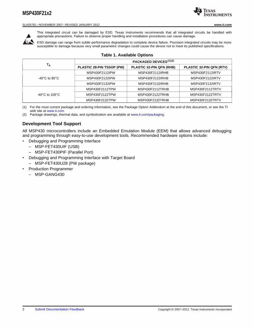
Table 1. Available Options
PACKAGED DEVICES (1) (2)
TAPLASTIC 28-PIN TSSOP (PW) PLASTIC 32-PIN QFN (RHB) PLASTIC 32-PIN QFN (RTV)
MSP430F2112IPW MSP430F2112IRHB MSP430F2112IRTV
-40°C to 85°C MSP430F2122IPW MSP430F2122IRHB MSP430F2122IRTV
MSP430F2132IPW MSP430F2132IRHB MSP430F2132IRTV
MSP430F2112TPW MSP430F2112TRHB MSP430F2112TRTV
-40°C to 105°C MSP430F2122TPW MSP430F2122TRHB MSP430F2122TRTV
MSP430F2132TPW MSP430F2132TRHB MSP430F2132TRTV
(1) For the most current package and ordering information, see the Package Option Addendum at the end of this document, or see the TIweb site at www.ti.com.
(2) Package drawings, thermal data, and symbolization are available at www.ti.com/packaging.
Development Tool Support
All MSP430 microcontrollers include an Embedded Emulation Module (EEM) that allows advanced debuggingand programming through easy-to-use development tools. Recommended hardware options include:• Debugging and Programming Interface
– MSP-FET430UIF (USB)– MSP-FET430PIF (Parallel Port)
• Debugging and Programming Interface with Target Board– MSP-FET430U28 (PW package)
• Production Programmer– MSP-GANG430
2 Submit Documentation Feedback Copyright © 2007–2012, Texas Instruments Incorporated
1
2
3
4
5
6
7
8
9
19
20
21
22
23
24
25
26
27
28TEST/SBWTCK
DVCC
P2.5/R /CA5OSC
DVSS
XOUT/P2.7/CA7
XIN/P2.6/CA6
RST/NMI/SBWTDIO
P2.0/ACLK/A0/CA2
P2.1/TAINCLK/SMCLK/A1/CA3
P2.2/TA0.0/A2/CA4/CAOUT
P1.7/TA0.2/TDO/TDI
P1.6/TA0.1/TDI/TCLK
P1.5/TA0.0/TMS
P1.4/SMCLK/TCK
P1.3/TA0.2
P1.2/TA0.1
P1.1/TA0.0/TA1.0
P1.0/TACLK/ADC10CLK/CAOUT
P2.4/TA0.2/A4/V /Ve /CA1REF+ REF+
P2.3/TA0.1/A3/V /Ve /CA0REF- REF-
10
11
12
13
14
P3.0/UCB0STE/UCA0CLK/A5
P3.1/UCB0SIMO/UCB0SDA
P3.2/UCB0SOMI/UCB0SCL
P3.3/UCB0CLK/UCA0STE 15
16
17
18 P3.7/TA1.1/A7
P3.6/TA1.0/A6
P3.5/UCA0RXD/UCA0SOMI
P3.4/UCA0TXD/UCA0SIMO
1
2
3
4
5
6
7
8
P1.2/TA0.1
P1.1/TA0.0/TA1.0
P1.0/TACLK/ADC10CLK/CAOUT
NC
P2.4/TA0.2/A4/V /Ve /CA1REF+ REF+
P2.3/TA0.1/A3/V /Ve /CA0REF- REF-
NC
P1.3/TA0.2
XOUT/P2.7/CA7
XIN/P2.6/CA6
NC
RST/NMI/SBWTDIO
P2.0/ACLK/A0/CA2
P2.1/TAINCLK/SMCLK/A1/CA3
P2.2/TA0.0/A2/CA4/CAOUT
DVSS
NC
DV
CC
TE
ST
/SB
WT
CK
P1.7
/TA
0.2
/TD
O/T
DI
P1.6
/TA
0.1
/TD
I/T
CLK
P1.5
/TA
0.0
/TM
S
P1.4
/SM
CLK
/TC
K
P2.5
/R/C
A5
OS
C
P3.1
/UC
B0S
IMO
/UC
B0S
DA
P3.2
/UC
B0S
OM
I/U
CB
0S
CL
P3.3
/UC
B0C
LK
/UC
A0S
TE
P3.4
/UC
A0T
XD
/UC
A0S
IMO
P3.5
/UC
A0R
XD
/UC
A0S
OM
I
P3.6
/TA
1.0
/A6
P3.7
/TA
1.1
/A7
P3.0
/UC
B0S
TE
/UC
A0C
LK
/A5
24
23
22
21
20
19
18
17
31 30 29 28 27 26 2532
10 11 12 13 14 15 169
MSP430F21x2
www.ti.com SLAS578J –NOVEMBER 2007–REVISED JANUARY 2012
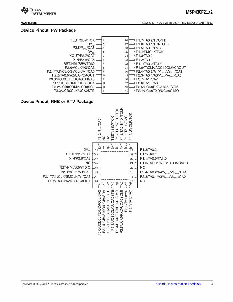
Device Pinout, PW Package
Device Pinout, RHB or RTV Package
Copyright © 2007–2012, Texas Instruments Incorporated Submit Documentation Feedback 3
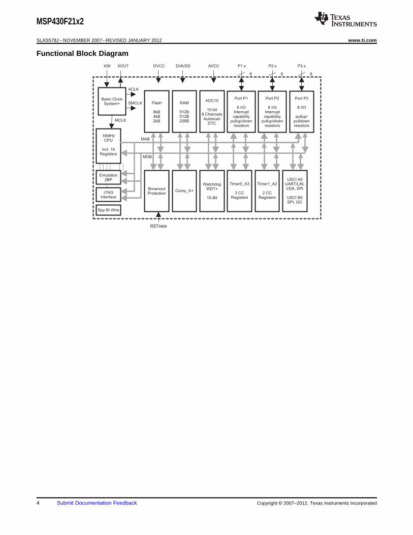
Basic ClockSystem+
BrownoutProtection
RST/NMI
DVCC D/AVSS
MCLK
WatchdogWDT+
15-Bit
Timer0_A3
3 CCRegisters
16MHzCPU
incl. 16Registers
Emulation2BP
JTAGInterface
ADC10
10-bit8 ChannelsAutoscan
DTC
AVCC
SMCLK
ACLK
MDB
MAB
XIN XOUT
RAM
512B512B256B
Flash
8kB4kB2kB
Timer1_A2
2 CCRegisters
USCI A0UART/LIN,IrDA, SPI
USCI B0SPI, I2C
Port P1
8 I/OInterruptcapability
pullup/downresistors
P1.x
8
P2.x
8
Port P2
8 I/OInterruptcapability
pullup/downresistors
Comp_A+
P3.x
8
Port P3
8 I/O
pullup/pulldownresistors
Spy-Bi Wire
MSP430F21x2
SLAS578J –NOVEMBER 2007–REVISED JANUARY 2012 www.ti.com
Functional Block Diagram
4 Submit Documentation Feedback Copyright © 2007–2012, Texas Instruments Incorporated
MSP430F21x2
www.ti.com SLAS578J –NOVEMBER 2007–REVISED JANUARY 2012
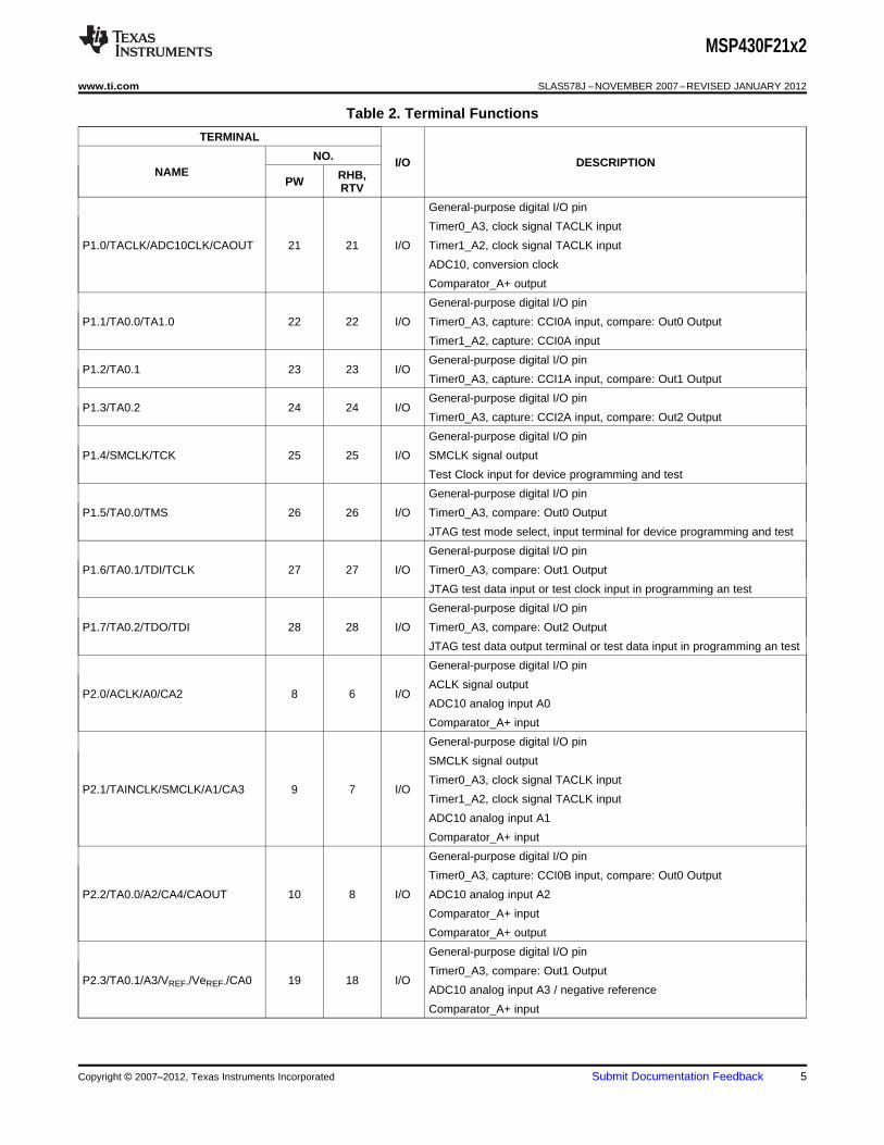
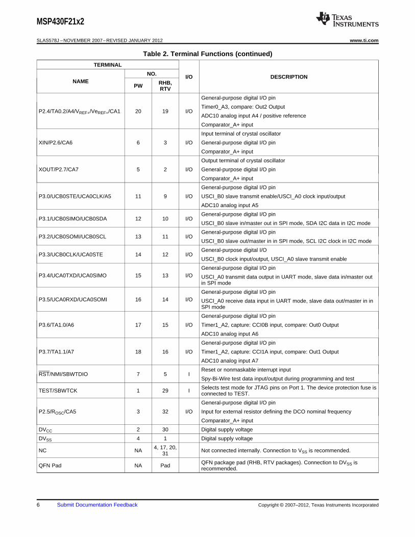
Table 2. Terminal Functions
TERMINAL
NO. I/O DESCRIPTIONNAME RHB,PW RTV
General-purpose digital I/O pin
Timer0_A3, clock signal TACLK input
P1.0/TACLK/ADC10CLK/CAOUT 21 21 I/O Timer1_A2, clock signal TACLK input
ADC10, conversion clock
Comparator_A+ output
General-purpose digital I/O pin
P1.1/TA0.0/TA1.0 22 22 I/O Timer0_A3, capture: CCI0A input, compare: Out0 Output
Timer1_A2, capture: CCI0A input
General-purpose digital I/O pinP1.2/TA0.1 23 23 I/O
Timer0_A3, capture: CCI1A input, compare: Out1 Output
General-purpose digital I/O pinP1.3/TA0.2 24 24 I/O
Timer0_A3, capture: CCI2A input, compare: Out2 Output
General-purpose digital I/O pin
P1.4/SMCLK/TCK 25 25 I/O SMCLK signal output
Test Clock input for device programming and test
General-purpose digital I/O pin
P1.5/TA0.0/TMS 26 26 I/O Timer0_A3, compare: Out0 Output
JTAG test mode select, input terminal for device programming and test
General-purpose digital I/O pin
P1.6/TA0.1/TDI/TCLK 27 27 I/O Timer0_A3, compare: Out1 Output
JTAG test data input or test clock input in programming an test
General-purpose digital I/O pin
P1.7/TA0.2/TDO/TDI 28 28 I/O Timer0_A3, compare: Out2 Output
JTAG test data output terminal or test data input in programming an test
General-purpose digital I/O pin
ACLK signal outputP2.0/ACLK/A0/CA2 8 6 I/O
ADC10 analog input A0
Comparator_A+ input
General-purpose digital I/O pin
SMCLK signal output
Timer0_A3, clock signal TACLK inputP2.1/TAINCLK/SMCLK/A1/CA3 9 7 I/O
Timer1_A2, clock signal TACLK input
ADC10 analog input A1
Comparator_A+ input
General-purpose digital I/O pin
Timer0_A3, capture: CCI0B input, compare: Out0 Output
P2.2/TA0.0/A2/CA4/CAOUT 10 8 I/O ADC10 analog input A2
Comparator_A+ input
Comparator_A+ output
General-purpose digital I/O pin
Timer0_A3, compare: Out1 OutputP2.3/TA0.1/A3/VREF-/VeREF-/CA0 19 18 I/O
ADC10 analog input A3 / negative reference
Comparator_A+ input
Copyright © 2007–2012, Texas Instruments Incorporated Submit Documentation Feedback 5
MSP430F21x2
SLAS578J –NOVEMBER 2007–REVISED JANUARY 2012 www.ti.com
Table 2. Terminal Functions (continued)
TERMINAL
NO. I/O DESCRIPTIONNAME RHB,PW RTV
General-purpose digital I/O pin
Timer0_A3, compare: Out2 OutputP2.4/TA0.2/A4/VREF+/VeREF+/CA1 20 19 I/O
ADC10 analog input A4 / positive reference
Comparator_A+ input
Input terminal of crystal oscillator
XIN/P2.6/CA6 6 3 I/O General-purpose digital I/O pin
Comparator_A+ input
Output terminal of crystal oscillator
XOUT/P2.7/CA7 5 2 I/O General-purpose digital I/O pin
Comparator_A+ input
General-purpose digital I/O pin
P3.0/UCB0STE/UCA0CLK/A5 11 9 I/O USCI_B0 slave transmit enable/USCI_A0 clock input/output
ADC10 analog input A5
General-purpose digital I/O pinP3.1/UCB0SIMO/UCB0SDA 12 10 I/O
USCI_B0 slave in/master out in SPI mode, SDA I2C data in I2C mode
General-purpose digital I/O pinP3.2/UCB0SOMI/UCB0SCL 13 11 I/O
USCI_B0 slave out/master in in SPI mode, SCL I2C clock in I2C mode
General-purpose digital I/OP3.3/UCB0CLK/UCA0STE 14 12 I/O
USCI_B0 clock input/output, USCI_A0 slave transmit enable
General-purpose digital I/O pinP3.4/UCA0TXD/UCA0SIMO 15 13 I/O USCI_A0 transmit data output in UART mode, slave data in/master out
in SPI mode
General-purpose digital I/O pinP3.5/UCA0RXD/UCA0SOMI 16 14 I/O USCI_A0 receive data input in UART mode, slave data out/master in in
SPI mode
General-purpose digital I/O pin
P3.6/TA1.0/A6 17 15 I/O Timer1_A2, capture: CCI0B input, compare: Out0 Output
ADC10 analog input A6
General-purpose digital I/O pin
P3.7/TA1.1/A7 18 16 I/O Timer1_A2, capture: CCI1A input, compare: Out1 Output
ADC10 analog input A7
Reset or nonmaskable interrupt inputRST/NMI/SBWTDIO 7 5 I
Spy-Bi-Wire test data input/output during programming and test
Selects test mode for JTAG pins on Port 1. The device protection fuse isTEST/SBWTCK 1 29 I connected to TEST.
General-purpose digital I/O pin
P2.5/ROSC/CA5 3 32 I/O Input for external resistor defining the DCO nominal frequency
Comparator_A+ input
DVCC 2 30 Digital supply voltage
DVSS 4 1 Digital supply voltage
4, 17, 20,NC NA Not connected internally. Connection to VSS is recommended.31
QFN package pad (RHB, RTV packages). Connection to DVSS isQFN Pad NA Pad recommended.
6 Submit Documentation Feedback Copyright © 2007–2012, Texas Instruments Incorporated
General-Purpose Register
Program Counter
Stack Pointer
Status Register
Constant Generator
General-Purpose Register
General-Purpose Register
General-Purpose Register
PC/R0
SP/R1
SR/CG1/R2
CG2/R3
R4
R5
R12
R13
General-Purpose Register
General-Purpose Register
R6
R7
General-Purpose Register
General-Purpose Register
R8
R9
General-Purpose Register
General-Purpose Register
R10
R11
General-Purpose Register
General-Purpose Register
R14
R15
MSP430F21x2
www.ti.com SLAS578J –NOVEMBER 2007–REVISED JANUARY 2012
SHORT-FORM DESCRIPTION
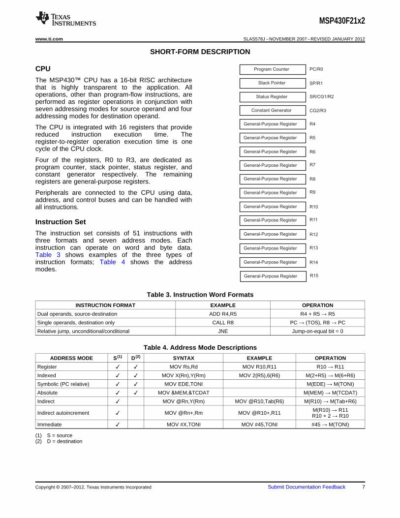
CPU
The MSP430™ CPU has a 16-bit RISC architecturethat is highly transparent to the application. Alloperations, other than program-flow instructions, areperformed as register operations in conjunction withseven addressing modes for source operand and fouraddressing modes for destination operand.
The CPU is integrated with 16 registers that providereduced instruction execution time. Theregister-to-register operation execution time is onecycle of the CPU clock.
Four of the registers, R0 to R3, are dedicated asprogram counter, stack pointer, status register, andconstant generator respectively. The remainingregisters are general-purpose registers.
Peripherals are connected to the CPU using data,address, and control buses and can be handled withall instructions.
Instruction Set
The instruction set consists of 51 instructions withthree formats and seven address modes. Eachinstruction can operate on word and byte data.Table 3 shows examples of the three types ofinstruction formats; Table 4 shows the addressmodes.
Table 3. Instruction Word Formats
INSTRUCTION FORMAT EXAMPLE OPERATION
Dual operands, source-destination ADD R4,R5 R4 + R5 → R5
Single operands, destination only CALL R8 PC → (TOS), R8 → PC
Relative jump, unconditional/conditional JNE Jump-on-equal bit = 0
Table 4. Address Mode Descriptions
ADDRESS MODE S (1) D (2) SYNTAX EXAMPLE OPERATION
Register MOV Rs,Rd MOV R10,R11 R10 → R11
Indexed MOV X(Rn),Y(Rm) MOV 2(R5),6(R6) M(2+R5) → M(6+R6)
Symbolic (PC relative) MOV EDE,TONI M(EDE) → M(TONI)
Absolute MOV &MEM,&TCDAT M(MEM) → M(TCDAT)
Indirect MOV @Rn,Y(Rm) MOV @R10,Tab(R6) M(R10) → M(Tab+R6)
M(R10) → R11Indirect autoincrement MOV @Rn+,Rm MOV @R10+,R11 R10 + 2 → R10
Immediate MOV #X,TONI MOV #45,TONI #45 → M(TONI)
(1) S = source(2) D = destination
Copyright © 2007–2012, Texas Instruments Incorporated Submit Documentation Feedback 7
MSP430F21x2
SLAS578J –NOVEMBER 2007–REVISED JANUARY 2012 www.ti.com
Operating Modes
The MSP430 microcontrollers have one active mode and five software-selectable low-power modes of operation.An interrupt event can wake up the device from any of the five low-power modes, service the request, andrestore back to the low-power mode on return from the interrupt program.
The following six operating modes can be configured by software:• Active mode (AM)
– All clocks are active.• Low-power mode 0 (LPM0)
– CPU is disabled.– ACLK and SMCLK remain active. MCLK is disabled.
• Low-power mode 1 (LPM1)– CPU is disabled ACLK and SMCLK remain active. MCLK is disabled.– DCO dc-generator is disabled if DCO not used in active mode.
• Low-power mode 2 (LPM2)– CPU is disabled.– MCLK and SMCLK are disabled.– DCO dc-generator remains enabled.– ACLK remains active.
• Low-power mode 3 (LPM3)– CPU is disabled.– MCLK and SMCLK are disabled.– DCO dc-generator is disabled.– ACLK remains active.
• Low-power mode 4 (LPM4)– CPU is disabled.– ACLK is disabled.– MCLK and SMCLK are disabled.– DCO dc-generator is disabled.– Crystal oscillator is stopped.
8 Submit Documentation Feedback Copyright © 2007–2012, Texas Instruments Incorporated
MSP430F21x2
www.ti.com SLAS578J –NOVEMBER 2007–REVISED JANUARY 2012
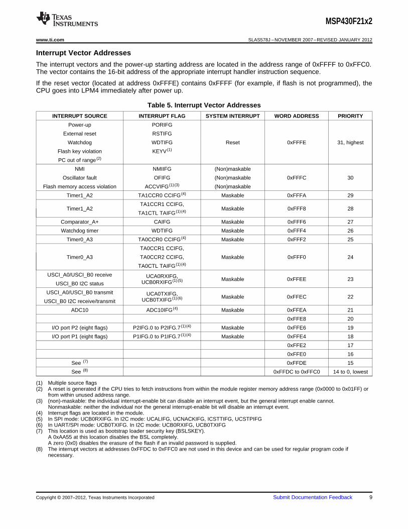
Interrupt Vector Addresses
The interrupt vectors and the power-up starting address are located in the address range of 0xFFFF to 0xFFC0.The vector contains the 16-bit address of the appropriate interrupt handler instruction sequence.
If the reset vector (located at address 0xFFFE) contains 0xFFFF (for example, if flash is not programmed), theCPU goes into LPM4 immediately after power up.
Table 5. Interrupt Vector Addresses
INTERRUPT SOURCE INTERRUPT FLAG SYSTEM INTERRUPT WORD ADDRESS PRIORITY
Power-up PORIFG
External reset RSTIFG
Watchdog WDTIFG Reset 0xFFFE 31, highest
Flash key violation KEYV (1)
PC out of range (2)
NMI NMIIFG (Non)maskable
Oscillator fault OFIFG (Non)maskable 0xFFFC 30
Flash memory access violation ACCVIFG (1) (3) (Non)maskable
Timer1_A2 TA1CCR0 CCIFG (4) Maskable 0xFFFA 29
TA1CCR1 CCIFG,Timer1_A2 Maskable 0xFFF8 28
TA1CTL TAIFG (1) (4)
Comparator_A+ CAIFG Maskable 0xFFF6 27
Watchdog timer WDTIFG Maskable 0xFFF4 26
Timer0_A3 TA0CCR0 CCIFG (4) Maskable 0xFFF2 25
TA0CCR1 CCIFG,
Timer0_A3 TA0CCR2 CCIFG, Maskable 0xFFF0 24
TA0CTL TAIFG (1) (4)
USCI_A0/USCI_B0 receive UCA0RXIFG, Maskable 0xFFEE 23UCB0RXIFG (1) (5)USCI_B0 I2C status
USCI_A0/USCI_B0 transmit UCA0TXIFG, Maskable 0xFFEC 22UCB0TXIFG (1) (6)USCI_B0 I2C receive/transmit
ADC10 ADC10IFG (4) Maskable 0xFFEA 21
0xFFE8 20
I/O port P2 (eight flags) P2IFG.0 to P2IFG.7 (1) (4) Maskable 0xFFE6 19
I/O port P1 (eight flags) P1IFG.0 to P1IFG.7 (1) (4) Maskable 0xFFE4 18
0xFFE2 17
0xFFE0 16
See (7) 0xFFDE 15
See (8) 0xFFDC to 0xFFC0 14 to 0, lowest
(1) Multiple source flags(2) A reset is generated if the CPU tries to fetch instructions from within the module register memory address range (0x0000 to 0x01FF) or
from within unused address range.(3) (non)-maskable: the individual interrupt-enable bit can disable an interrupt event, but the general interrupt enable cannot.
Nonmaskable: neither the individual nor the general interrupt-enable bit will disable an interrupt event.(4) Interrupt flags are located in the module.(5) In SPI mode: UCB0RXIFG. In I2C mode: UCALIFG, UCNACKIFG, ICSTTIFG, UCSTPIFG(6) In UART/SPI mode: UCB0TXIFG. In I2C mode: UCB0RXIFG, UCB0TXIFG(7) This location is used as bootstrap loader security key (BSLSKEY).
A 0xAA55 at this location disables the BSL completely.A zero (0x0) disables the erasure of the flash if an invalid password is supplied.
(8) The interrupt vectors at addresses 0xFFDC to 0xFFC0 are not used in this device and can be used for regular program code ifnecessary.
Copyright © 2007–2012, Texas Instruments Incorporated Submit Documentation Feedback 9
MSP430F21x2
SLAS578J –NOVEMBER 2007–REVISED JANUARY 2012 www.ti.com
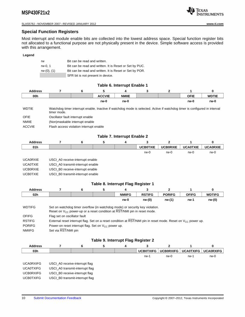
Special Function Registers
Most interrupt and module enable bits are collected into the lowest address space. Special function register bitsnot allocated to a functional purpose are not physically present in the device. Simple software access is providedwith this arrangement.
Legend
rw Bit can be read and written.
rw-0, 1 Bit can be read and written. It is Reset or Set by PUC.
rw-(0), (1) Bit can be read and written. It is Reset or Set by POR.
SFR bit is not present in device.
Table 6. Interrupt Enable 1Address 7 6 5 4 3 2 1 0
00h ACCVIE NMIIE OFIE WDTIE
rw-0 rw-0 rw-0 rw-0
WDTIE Watchdog timer interrupt enable. Inactive if watchdog mode is selected. Active if watchdog timer is configured in intervaltimer mode.
OFIE Oscillator fault interrupt enable
NMIIE (Non)maskable interrupt enable
ACCVIE Flash access violation interrupt enable
Table 7. Interrupt Enable 2Address 7 6 5 4 3 2 1 0
01h UCB0TXIE UCB0RXIE UCA0TXIE UCA0RXIE
rw-0 rw-0 rw-0 rw-0
UCA0RXIE USCI_A0 receive-interrupt enable
UCA0TXIE USCI_A0 transmit-interrupt enable
UCB0RXIE USCI_B0 receive-interrupt enable
UCB0TXIE USCI_B0 transmit-interrupt enable
Table 8. Interrupt Flag Register 1Address 7 6 5 4 3 2 1 0
02h NMIIFG RSTIFG PORIFG OFIFG WDTIFG
rw-0 rw-(0) rw-(1) rw-1 rw-(0)
WDTIFG Set on watchdog timer overflow (in watchdog mode) or security key violation.Reset on VCC power-up or a reset condition at RST/NMI pin in reset mode.
OFIFG Flag set on oscillator fault
RSTIFG External reset interrupt flag. Set on a reset condition at RST/NMI pin in reset mode. Reset on VCC power up.
PORIFG Power-on reset interrupt flag. Set on VCC power up.
NMIIFG Set via RST/NMI pin
Table 9. Interrupt Flag Register 2Address 7 6 5 4 3 2 1 0
03h UCB0TXIFG UCB0RXIFG UCA0TXIFG UCA0RXIFG
rw-1 rw-0 rw-1 rw-0
UCA0RXIFG USCI_A0 receive-interrupt flag
UCA0TXIFG USCI_A0 transmit-interrupt flag
UCB0RXIFG USCI_B0 receive-interrupt flag
UCB0TXIFG USCI_B0 transmit-interrupt flag
10 Submit Documentation Feedback Copyright © 2007–2012, Texas Instruments Incorporated
MSP430F21x2
www.ti.com SLAS578J –NOVEMBER 2007–REVISED JANUARY 2012
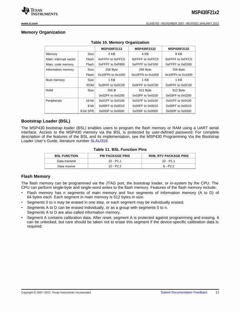
Memory Organization
Table 10. Memory Organization
MSP430F2112 MSP430F2122 MSP430F2132
Memory Size 2 KB 4 KB 8 KB
Main: interrupt vector Flash 0xFFFF to 0xFFC0 0xFFFF to 0xFFC0 0xFFFF to 0xFFC0
Main: code memory Flash 0xFFFF to 0xF800 0xFFFF to 0xF000 0xFFFF to 0xE000
Information memory Size 256 Byte 256 Byte 256 Byte
Flash 0x10FFh to 0x1000 0x10FFh to 0x1000 0x10FFh to 0x1000
Boot memory Size 1 KB 1 KB 1 KB
ROM 0x0FFF to 0x0C00 0x0FFF to 0x0C00 0x0FFF to 0x0C00
RAM Size 256 B 512 Byte 512 Byte
0x02FF to 0x0200 0x03FF to 0x0200 0x03FF to 0x0200
Peripherals 16-bit 0x01FF to 0x0100 0x01FF to 0x0100 0x01FF to 0x0100
8-bit 0x00FF to 0x0010 0x00FF to 0x0010 0x00FF to 0x0010
8-bit SFR 0x000F to 0x0000 0x000F to 0x0000 0x000F to 0x0000
Bootstrap Loader (BSL)
The MSP430 bootstrap loader (BSL) enables users to program the flash memory or RAM using a UART serialinterface. Access to the MSP430 memory via the BSL is protected by user-defined password. For completedescription of the features of the BSL and its implementation, see the MSP430 Programming Via the BootstrapLoader User’s Guide, literature number SLAU319.
Table 11. BSL Function Pins
BSL FUNCTION PW PACKAGE PINS RHB, RTV PACKAGE PINS
Data transmit 22 - P1.1 22 - P1.1
Data receive 10 - P2.2 8 - P2.2
Flash Memory
The flash memory can be programmed via the JTAG port, the bootstrap loader, or in-system by the CPU. TheCPU can perform single-byte and single-word writes to the flash memory. Features of the flash memory include:• Flash memory has n segments of main memory and four segments of information memory (A to D) of
64 bytes each. Each segment in main memory is 512 bytes in size.• Segments 0 to n may be erased in one step, or each segment may be individually erased.• Segments A to D can be erased individually, or as a group with segments 0 to n.
Segments A to D are also called information memory.• Segment A contains calibration data. After reset, segment A is protected against programming and erasing. It
can be unlocked, but care should be taken not to erase this segment if the device-specific calibration data isrequired.
Copyright © 2007–2012, Texas Instruments Incorporated Submit Documentation Feedback 11
MSP430F21x2
SLAS578J –NOVEMBER 2007–REVISED JANUARY 2012 www.ti.com
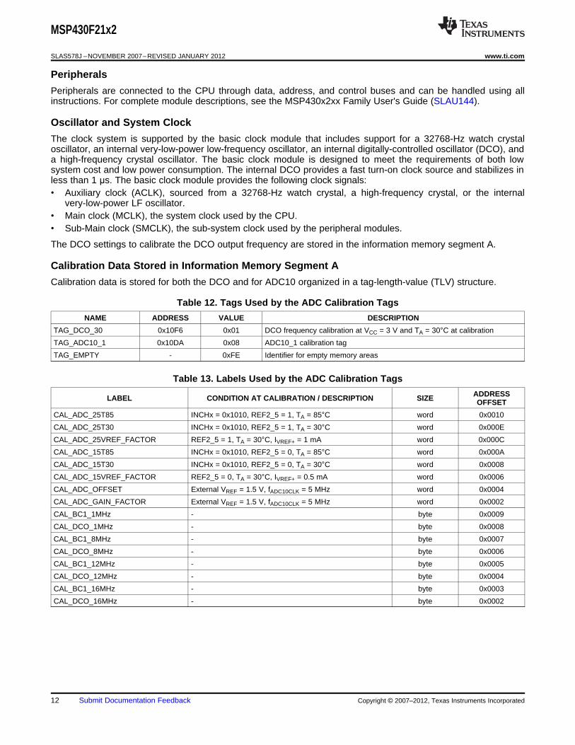
Peripherals
Peripherals are connected to the CPU through data, address, and control buses and can be handled using allinstructions. For complete module descriptions, see the MSP430x2xx Family User's Guide (SLAU144).
Oscillator and System Clock
The clock system is supported by the basic clock module that includes support for a 32768-Hz watch crystaloscillator, an internal very-low-power low-frequency oscillator, an internal digitally-controlled oscillator (DCO), anda high-frequency crystal oscillator. The basic clock module is designed to meet the requirements of both lowsystem cost and low power consumption. The internal DCO provides a fast turn-on clock source and stabilizes inless than 1 µs. The basic clock module provides the following clock signals:• Auxiliary clock (ACLK), sourced from a 32768-Hz watch crystal, a high-frequency crystal, or the internal
very-low-power LF oscillator.• Main clock (MCLK), the system clock used by the CPU.• Sub-Main clock (SMCLK), the sub-system clock used by the peripheral modules.
The DCO settings to calibrate the DCO output frequency are stored in the information memory segment A.
Calibration Data Stored in Information Memory Segment A
Calibration data is stored for both the DCO and for ADC10 organized in a tag-length-value (TLV) structure.
Table 12. Tags Used by the ADC Calibration Tags
NAME ADDRESS VALUE DESCRIPTION
TAG_DCO_30 0x10F6 0x01 DCO frequency calibration at VCC = 3 V and TA = 30°C at calibration
TAG_ADC10_1 0x10DA 0x08 ADC10_1 calibration tag
TAG_EMPTY - 0xFE Identifier for empty memory areas
Table 13. Labels Used by the ADC Calibration Tags
ADDRESSLABEL CONDITION AT CALIBRATION / DESCRIPTION SIZE OFFSET
CAL_ADC_25T85 INCHx = 0x1010, REF2_5 = 1, TA = 85°C word 0x0010
CAL_ADC_25T30 INCHx = 0x1010, REF2_5 = 1, TA = 30°C word 0x000E
CAL_ADC_25VREF_FACTOR REF2_5 = 1, TA = 30°C, IVREF+ = 1 mA word 0x000C
CAL_ADC_15T85 INCHx = 0x1010, REF2_5 = 0, TA = 85°C word 0x000A
CAL_ADC_15T30 INCHx = 0x1010, REF2_5 = 0, TA = 30°C word 0x0008
CAL_ADC_15VREF_FACTOR REF2_5 = 0, TA = 30°C, IVREF+ = 0.5 mA word 0x0006
CAL_ADC_OFFSET External VREF = 1.5 V, fADC10CLK = 5 MHz word 0x0004
CAL_ADC_GAIN_FACTOR External VREF = 1.5 V, fADC10CLK = 5 MHz word 0x0002
CAL_BC1_1MHz - byte 0x0009
CAL_DCO_1MHz - byte 0x0008
CAL_BC1_8MHz - byte 0x0007
CAL_DCO_8MHz - byte 0x0006
CAL_BC1_12MHz - byte 0x0005
CAL_DCO_12MHz - byte 0x0004
CAL_BC1_16MHz - byte 0x0003
CAL_DCO_16MHz - byte 0x0002
12 Submit Documentation Feedback Copyright © 2007–2012, Texas Instruments Incorporated
MSP430F21x2
www.ti.com SLAS578J –NOVEMBER 2007–REVISED JANUARY 2012
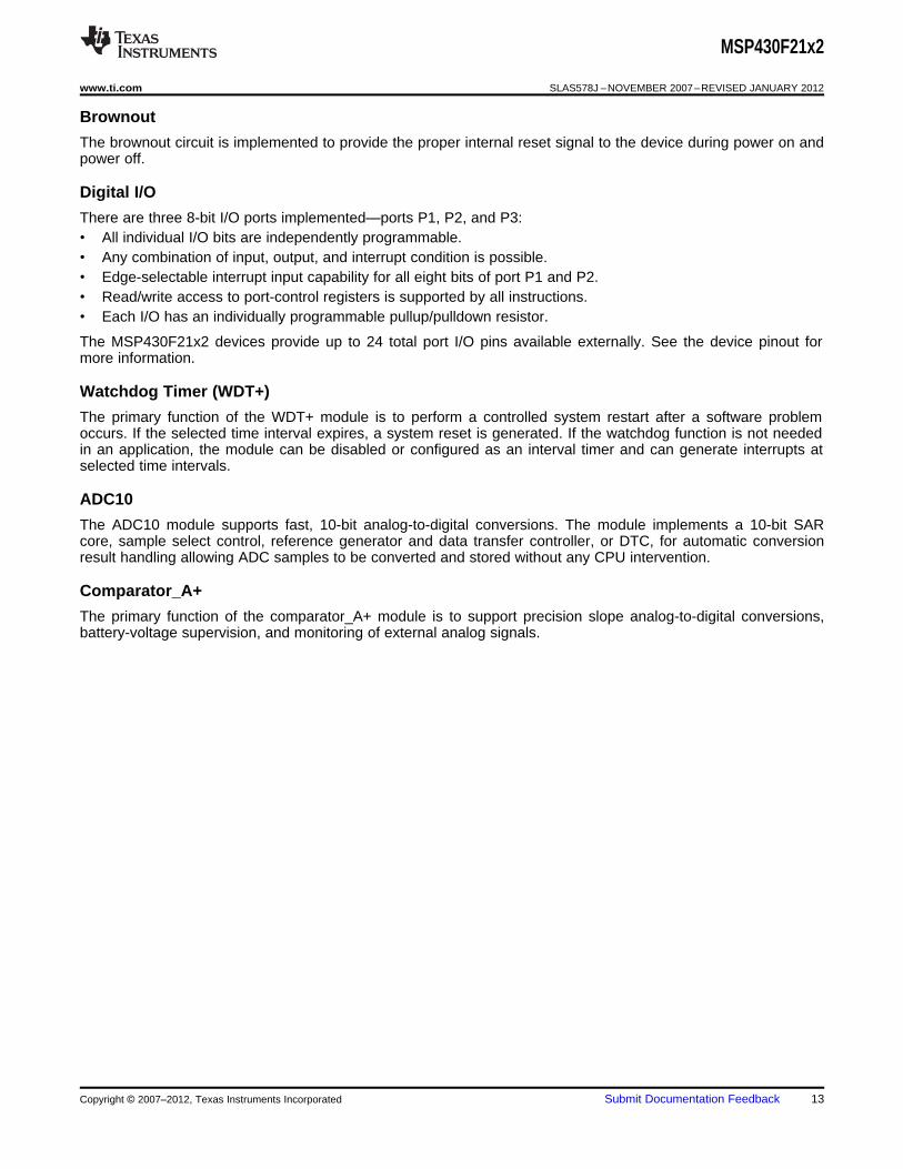
Brownout
The brownout circuit is implemented to provide the proper internal reset signal to the device during power on andpower off.
Digital I/O
There are three 8-bit I/O ports implemented—ports P1, P2, and P3:• All individual I/O bits are independently programmable.• Any combination of input, output, and interrupt condition is possible.• Edge-selectable interrupt input capability for all eight bits of port P1 and P2.• Read/write access to port-control registers is supported by all instructions.• Each I/O has an individually programmable pullup/pulldown resistor.
The MSP430F21x2 devices provide up to 24 total port I/O pins available externally. See the device pinout formore information.
Watchdog Timer (WDT+)
The primary function of the WDT+ module is to perform a controlled system restart after a software problemoccurs. If the selected time interval expires, a system reset is generated. If the watchdog function is not neededin an application, the module can be disabled or configured as an interval timer and can generate interrupts atselected time intervals.
ADC10
The ADC10 module supports fast, 10-bit analog-to-digital conversions. The module implements a 10-bit SARcore, sample select control, reference generator and data transfer controller, or DTC, for automatic conversionresult handling allowing ADC samples to be converted and stored without any CPU intervention.
Comparator_A+
The primary function of the comparator_A+ module is to support precision slope analog-to-digital conversions,battery-voltage supervision, and monitoring of external analog signals.
Copyright © 2007–2012, Texas Instruments Incorporated Submit Documentation Feedback 13
MSP430F21x2
SLAS578J –NOVEMBER 2007–REVISED JANUARY 2012 www.ti.com
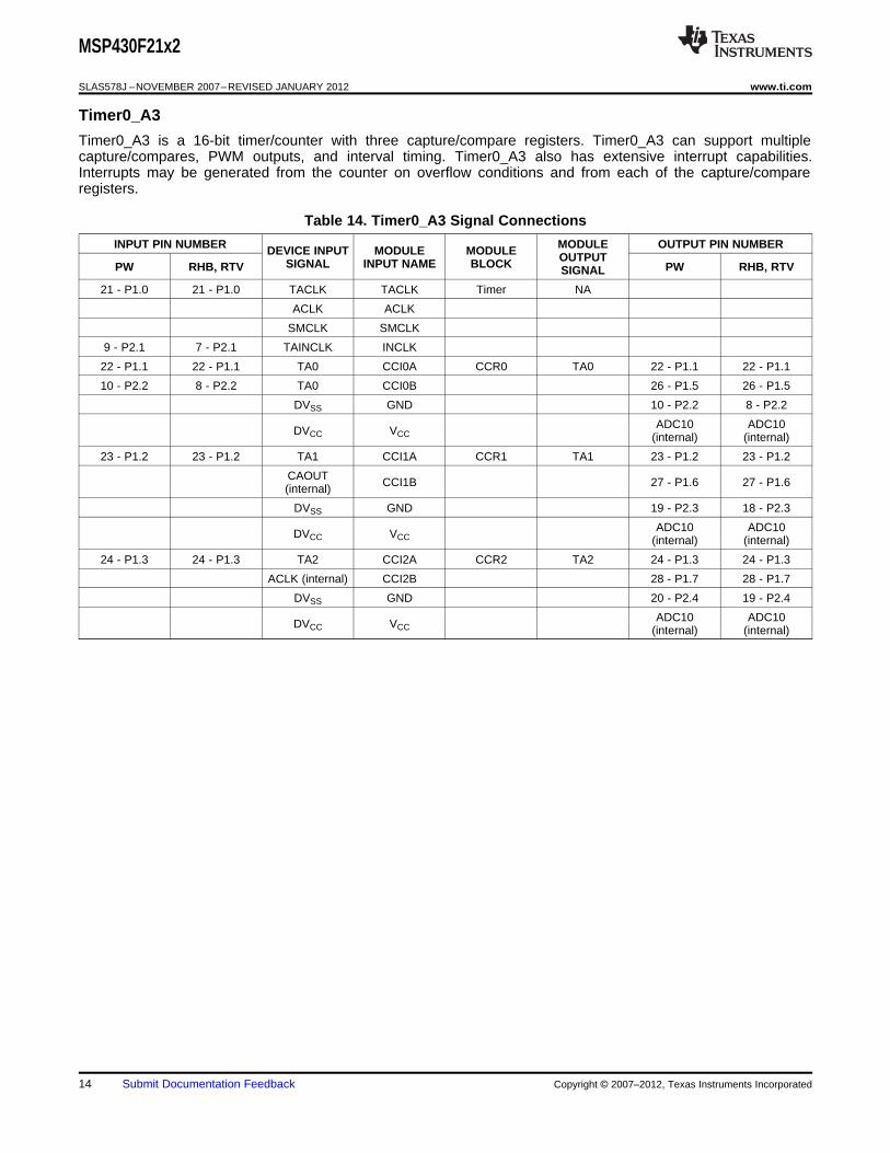
Timer0_A3
Timer0_A3 is a 16-bit timer/counter with three capture/compare registers. Timer0_A3 can support multiplecapture/compares, PWM outputs, and interval timing. Timer0_A3 also has extensive interrupt capabilities.Interrupts may be generated from the counter on overflow conditions and from each of the capture/compareregisters.
Table 14. Timer0_A3 Signal Connections
INPUT PIN NUMBER MODULE OUTPUT PIN NUMBERDEVICE INPUT MODULE MODULE OUTPUTSIGNAL INPUT NAME BLOCKPW RHB, RTV PW RHB, RTVSIGNAL
21 - P1.0 21 - P1.0 TACLK TACLK Timer NA
ACLK ACLK
SMCLK SMCLK
9 - P2.1 7 - P2.1 TAINCLK INCLK
22 - P1.1 22 - P1.1 TA0 CCI0A CCR0 TA0 22 - P1.1 22 - P1.1
10 - P2.2 8 - P2.2 TA0 CCI0B 26 - P1.5 26 - P1.5
DVSS GND 10 - P2.2 8 - P2.2
ADC10 ADC10DVCC VCC (internal) (internal)
23 - P1.2 23 - P1.2 TA1 CCI1A CCR1 TA1 23 - P1.2 23 - P1.2
CAOUT CCI1B 27 - P1.6 27 - P1.6(internal)
DVSS GND 19 - P2.3 18 - P2.3
ADC10 ADC10DVCC VCC (internal) (internal)
24 - P1.3 24 - P1.3 TA2 CCI2A CCR2 TA2 24 - P1.3 24 - P1.3
ACLK (internal) CCI2B 28 - P1.7 28 - P1.7
DVSS GND 20 - P2.4 19 - P2.4
ADC10 ADC10DVCC VCC (internal) (internal)
14 Submit Documentation Feedback Copyright © 2007–2012, Texas Instruments Incorporated
MSP430F21x2
www.ti.com SLAS578J –NOVEMBER 2007–REVISED JANUARY 2012
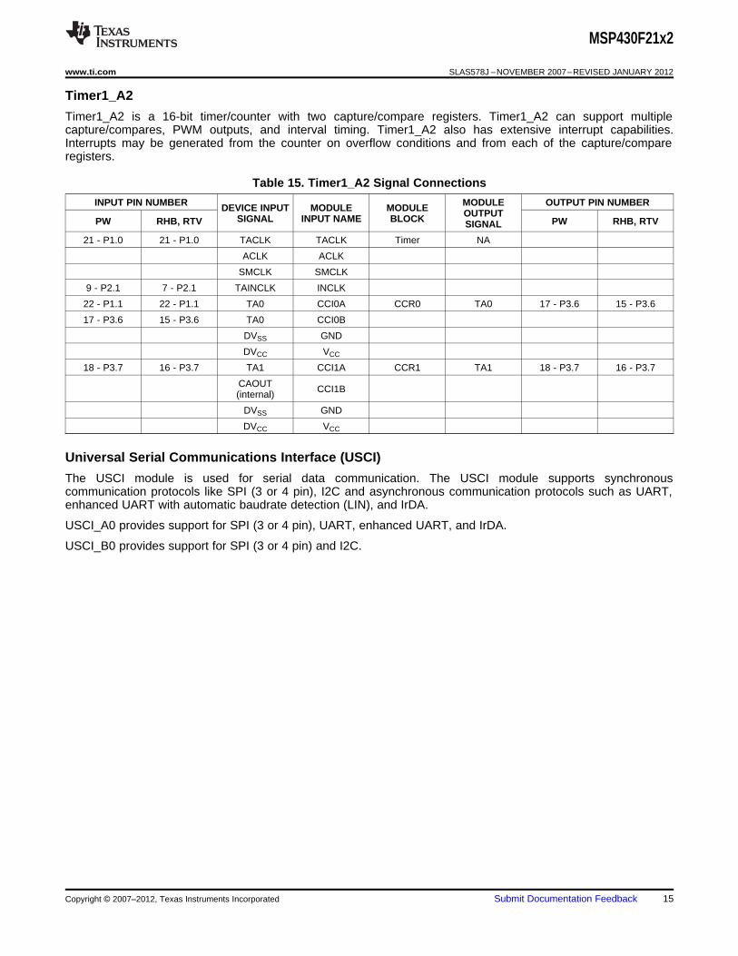
Timer1_A2
Timer1_A2 is a 16-bit timer/counter with two capture/compare registers. Timer1_A2 can support multiplecapture/compares, PWM outputs, and interval timing. Timer1_A2 also has extensive interrupt capabilities.Interrupts may be generated from the counter on overflow conditions and from each of the capture/compareregisters.
Table 15. Timer1_A2 Signal Connections
INPUT PIN NUMBER MODULE OUTPUT PIN NUMBERDEVICE INPUT MODULE MODULE OUTPUTSIGNAL INPUT NAME BLOCKPW RHB, RTV PW RHB, RTVSIGNAL
21 - P1.0 21 - P1.0 TACLK TACLK Timer NA
ACLK ACLK
SMCLK SMCLK
9 - P2.1 7 - P2.1 TAINCLK INCLK
22 - P1.1 22 - P1.1 TA0 CCI0A CCR0 TA0 17 - P3.6 15 - P3.6
17 - P3.6 15 - P3.6 TA0 CCI0B
DVSS GND
DVCC VCC
18 - P3.7 16 - P3.7 TA1 CCI1A CCR1 TA1 18 - P3.7 16 - P3.7
CAOUT CCI1B(internal)
DVSS GND
DVCC VCC
Universal Serial Communications Interface (USCI)
The USCI module is used for serial data communication. The USCI module supports synchronouscommunication protocols like SPI (3 or 4 pin), I2C and asynchronous communication protocols such as UART,enhanced UART with automatic baudrate detection (LIN), and IrDA.
USCI_A0 provides support for SPI (3 or 4 pin), UART, enhanced UART, and IrDA.
USCI_B0 provides support for SPI (3 or 4 pin) and I2C.
Copyright © 2007–2012, Texas Instruments Incorporated Submit Documentation Feedback 15
MSP430F21x2
SLAS578J –NOVEMBER 2007–REVISED JANUARY 2012 www.ti.com
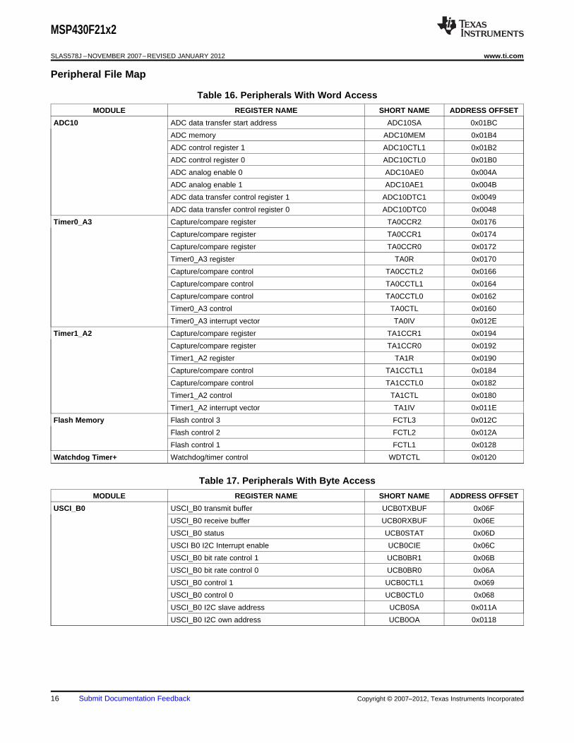
Peripheral File Map
Table 16. Peripherals With Word Access
MODULE REGISTER NAME SHORT NAME ADDRESS OFFSET
ADC10 ADC data transfer start address ADC10SA 0x01BC
ADC memory ADC10MEM 0x01B4
ADC control register 1 ADC10CTL1 0x01B2
ADC control register 0 ADC10CTL0 0x01B0
ADC analog enable 0 ADC10AE0 0x004A
ADC analog enable 1 ADC10AE1 0x004B
ADC data transfer control register 1 ADC10DTC1 0x0049
ADC data transfer control register 0 ADC10DTC0 0x0048
Timer0_A3 Capture/compare register TA0CCR2 0x0176
Capture/compare register TA0CCR1 0x0174
Capture/compare register TA0CCR0 0x0172
Timer0_A3 register TA0R 0x0170
Capture/compare control TA0CCTL2 0x0166
Capture/compare control TA0CCTL1 0x0164
Capture/compare control TA0CCTL0 0x0162
Timer0_A3 control TA0CTL 0x0160
Timer0_A3 interrupt vector TA0IV 0x012E
Timer1_A2 Capture/compare register TA1CCR1 0x0194
Capture/compare register TA1CCR0 0x0192
Timer1_A2 register TA1R 0x0190
Capture/compare control TA1CCTL1 0x0184
Capture/compare control TA1CCTL0 0x0182
Timer1_A2 control TA1CTL 0x0180
Timer1_A2 interrupt vector TA1IV 0x011E
Flash Memory Flash control 3 FCTL3 0x012C
Flash control 2 FCTL2 0x012A
Flash control 1 FCTL1 0x0128
Watchdog Timer+ Watchdog/timer control WDTCTL 0x0120
Table 17. Peripherals With Byte Access
MODULE REGISTER NAME SHORT NAME ADDRESS OFFSET
USCI_B0 USCI_B0 transmit buffer UCB0TXBUF 0x06F
USCI_B0 receive buffer UCB0RXBUF 0x06E
USCI_B0 status UCB0STAT 0x06D
USCI B0 I2C Interrupt enable UCB0CIE 0x06C
USCI_B0 bit rate control 1 UCB0BR1 0x06B
USCI_B0 bit rate control 0 UCB0BR0 0x06A
USCI_B0 control 1 UCB0CTL1 0x069
USCI_B0 control 0 UCB0CTL0 0x068
USCI_B0 I2C slave address UCB0SA 0x011A
USCI_B0 I2C own address UCB0OA 0x0118
16 Submit Documentation Feedback Copyright © 2007–2012, Texas Instruments Incorporated
MSP430F21x2
www.ti.com SLAS578J –NOVEMBER 2007–REVISED JANUARY 2012
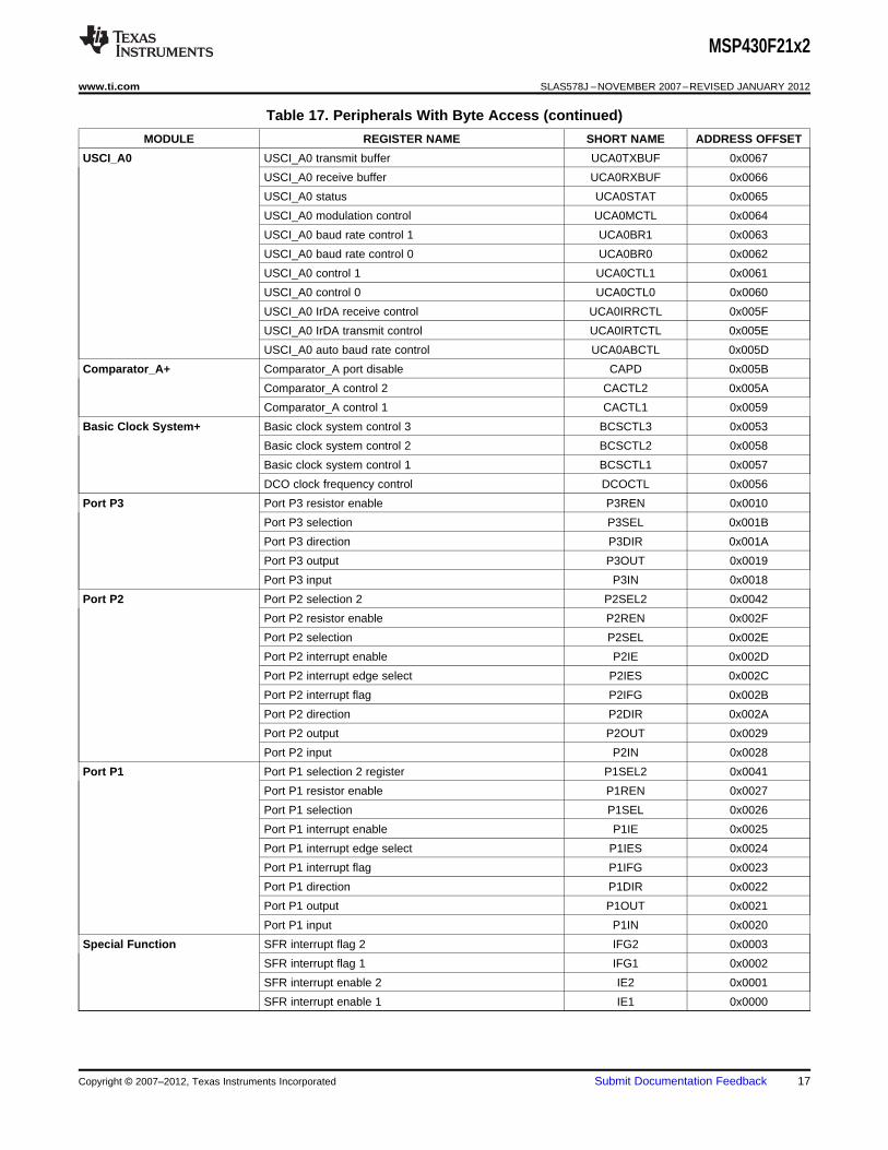
Table 17. Peripherals With Byte Access (continued)
MODULE REGISTER NAME SHORT NAME ADDRESS OFFSET
USCI_A0 USCI_A0 transmit buffer UCA0TXBUF 0x0067
USCI_A0 receive buffer UCA0RXBUF 0x0066
USCI_A0 status UCA0STAT 0x0065
USCI_A0 modulation control UCA0MCTL 0x0064
USCI_A0 baud rate control 1 UCA0BR1 0x0063
USCI_A0 baud rate control 0 UCA0BR0 0x0062
USCI_A0 control 1 UCA0CTL1 0x0061
USCI_A0 control 0 UCA0CTL0 0x0060
USCI_A0 IrDA receive control UCA0IRRCTL 0x005F
USCI_A0 IrDA transmit control UCA0IRTCTL 0x005E
USCI_A0 auto baud rate control UCA0ABCTL 0x005D
Comparator_A+ Comparator_A port disable CAPD 0x005B
Comparator_A control 2 CACTL2 0x005A
Comparator_A control 1 CACTL1 0x0059
Basic Clock System+ Basic clock system control 3 BCSCTL3 0x0053
Basic clock system control 2 BCSCTL2 0x0058
Basic clock system control 1 BCSCTL1 0x0057
DCO clock frequency control DCOCTL 0x0056
Port P3 Port P3 resistor enable P3REN 0x0010
Port P3 selection P3SEL 0x001B
Port P3 direction P3DIR 0x001A
Port P3 output P3OUT 0x0019
Port P3 input P3IN 0x0018
Port P2 Port P2 selection 2 P2SEL2 0x0042
Port P2 resistor enable P2REN 0x002F
Port P2 selection P2SEL 0x002E
Port P2 interrupt enable P2IE 0x002D
Port P2 interrupt edge select P2IES 0x002C
Port P2 interrupt flag P2IFG 0x002B
Port P2 direction P2DIR 0x002A
Port P2 output P2OUT 0x0029
Port P2 input P2IN 0x0028
Port P1 Port P1 selection 2 register P1SEL2 0x0041
Port P1 resistor enable P1REN 0x0027
Port P1 selection P1SEL 0x0026
Port P1 interrupt enable P1IE 0x0025
Port P1 interrupt edge select P1IES 0x0024
Port P1 interrupt flag P1IFG 0x0023
Port P1 direction P1DIR 0x0022
Port P1 output P1OUT 0x0021
Port P1 input P1IN 0x0020
Special Function SFR interrupt flag 2 IFG2 0x0003
SFR interrupt flag 1 IFG1 0x0002
SFR interrupt enable 2 IE2 0x0001
SFR interrupt enable 1 IE1 0x0000
Copyright © 2007–2012, Texas Instruments Incorporated Submit Documentation Feedback 17
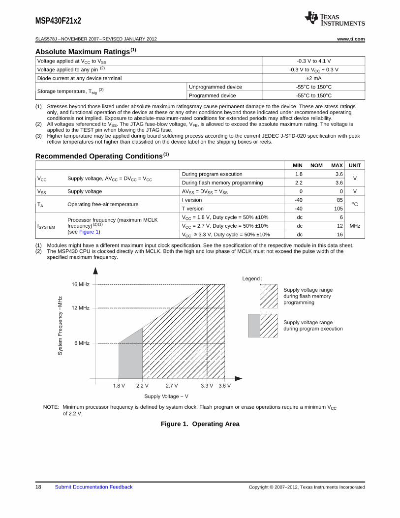
6 MHz
12 MHz
16 MHz
1.8 V 2.2 V 2.7 V 3.3 V 3.6 V
Supply Voltage − V
Syste
mF
reque
ncy
−M
Hz
Supply voltage range
during flash memory
programming
Supply voltage range
during program execution
Legend :
MSP430F21x2
SLAS578J –NOVEMBER 2007–REVISED JANUARY 2012 www.ti.com
Absolute Maximum Ratings (1)
Voltage applied at VCC to VSS -0.3 V to 4.1 V
Voltage applied to any pin (2) -0.3 V to VCC + 0.3 V
Diode current at any device terminal ±2 mA
Unprogrammed device -55°C to 150°CStorage temperature, Tstg
(3)
Programmed device -55°C to 150°C
(1) Stresses beyond those listed under absolute maximum ratingsmay cause permanent damage to the device. These are stress ratingsonly, and functional operation of the device at these or any other conditions beyond those indicated under recommended operatingconditionsis not implied. Exposure to absolute-maximum-rated conditions for extended periods may affect device reliability.
(2) All voltages referenced to VSS. The JTAG fuse-blow voltage, VFB, is allowed to exceed the absolute maximum rating. The voltage isapplied to the TEST pin when blowing the JTAG fuse.
(3) Higher temperature may be applied during board soldering process according to the current JEDEC J-STD-020 specification with peakreflow temperatures not higher than classified on the device label on the shipping boxes or reels.
Recommended Operating Conditions (1)
MIN NOM MAX UNIT
During program execution 1.8 3.6VCC Supply voltage, AVCC = DVCC = VCC V
During flash memory programming 2.2 3.6
VSS Supply voltage AVSS = DVSS = VSS 0 0 V
I version -40 85TA Operating free-air temperature °C
T version -40 105
VCC = 1.8 V, Duty cycle = 50% ±10% dc 6Processor frequency (maximum MCLKfSYSTEM frequency) (2) (1) VCC = 2.7 V, Duty cycle = 50% ±10% dc 12 MHz
(see Figure 1) VCC ≥ 3.3 V, Duty cycle = 50% ±10% dc 16
(1) Modules might have a different maximum input clock specification. See the specification of the respective module in this data sheet.(2) The MSP430 CPU is clocked directly with MCLK. Both the high and low phase of MCLK must not exceed the pulse width of the
specified maximum frequency.
NOTE: Minimum processor frequency is defined by system clock. Flash program or erase operations require a minimum VCCof 2.2 V.
Figure 1. Operating Area
18 Submit Documentation Feedback Copyright © 2007–2012, Texas Instruments Incorporated
0.0
1.0
2.0
3.0
4.0
5.0
6.0
7.0
8.0
1.5 2.0 2.5 3.0 3.5 4.0
VCC − Supply Voltage − V
Active
Mo
de
Cu
rre
nt
−m
A
fDCO = 1 MHz
fDCO = 8 MHz
fDCO = 12 MHz
fDCO = 16 MHz
0.0
1.0
2.0
3.0
4.0
5.0
0.0 4.0 8.0 12.0 16.0
fDCO − DCO Frequency − MHz
Active
Mo
de
Cu
rre
nt
−m
A
TA = 25°C
TA = 85°C
VCC = 2.2 V
VCC = 3 V
TA = 25°C
TA = 85°C
MSP430F21x2
www.ti.com SLAS578J –NOVEMBER 2007–REVISED JANUARY 2012
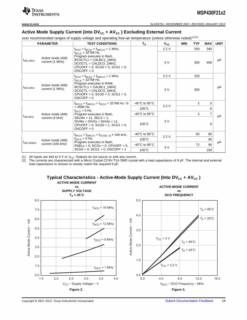
Active Mode Supply Current (into DVCC + AVCC ) Excluding External Currentover recommended ranges of supply voltage and operating free-air temperature (unless otherwise noted) (1) (2)
PARAMETER TEST CONDITIONS TA VCC MIN TYP MAX UNIT
fDCO = fMCLK = fSMCLK = 1 MHz, 2.2 V 250 340fACLK = 32768 Hz,Program executes in flash,Active mode (AM)IAM,1MHz BCSCTL1 = CALBC1_1MHZ, µAcurrent (1 MHz) 3 V 350 450DCOCTL = CALDCO_1MHZ,CPUOFF = 0, SCG0 = 0, SCG1 = 0,OSCOFF = 0
fDCO = fMCLK = fSMCLK = 1 MHz, 2.2 V 220fACLK = 32768 Hz,Program executes in RAM,Active mode (AM)IAM,1MHz BCSCTL1 = CALBC1_1MHZ, µAcurrent (1 MHz) 3 V 300DCOCTL = CALDCO_1MHZ,CPUOFF = 0, SCG0 = 0, SCG1 = 0,OSCOFF = 0
fMCLK = fSMCLK = fACLK = 32768 Hz / 8 -40°C to 85°C 2 52.2 V= 4096 Hz, 105°C 6
fDCO = 0 Hz,-40°C to 85°C 3 7Active mode (AM) Program executes in flash,IAM,4kHz µAcurrent (4 kHz) SELMx = 11, SELS = 1,
3 VDIVMx = DIVSx = DIVAx = 11,105°C 9CPUOFF = 0, SCG0 = 1, SCG1 = 0,
OSCOFF = 0
-40°C to 85°C 60 85fMCLK = fSMCLK = fDCO(0, 0) ≈ 100 kHz,2.2 VfACLK = 0 Hz, 105°C 90Active mode (AM)IAM,100kHz Program executes in flash, µAcurrent (100 kHz) -40°C to 85°C 72 95RSELx = 0, DCOx = 0, CPUOFF = 0, 3 V
SCG0 = 0, SCG1 = 0, OSCOFF = 1 105°C 100
(1) All inputs are tied to 0 V or VCC. Outputs do not source or sink any current.(2) The currents are characterized with a Micro Crystal CC4V-T1A SMD crystal with a load capacitance of 9 pF. The internal and external
load capacitance is chosen to closely match the required 9 pF.
Typical Characteristics - Active-Mode Supply Current (Into DVCC + AVCC )ACTIVE-MODE CURRENT
vs ACTIVE-MODE CURRENTSUPPLY VOLTAGE vs
TA = 25°C DCO FREQUENCY
Figure 2. Figure 3.
Copyright © 2007–2012, Texas Instruments Incorporated Submit Documentation Feedback 19
MSP430F21x2
SLAS578J –NOVEMBER 2007–REVISED JANUARY 2012 www.ti.com
Low-Power-Mode Supply Currents (Into VCC ) Excluding External Current (1) (2)
over recommended ranges of supply voltage and operating free-air temperature (unless otherwise noted)
PARAMETER TEST CONDITIONS TA VCC MIN TYP MAX UNIT
fMCLK = 0 MHz, -40°C to 85°C 55 662.2 VfSMCLK = fDCO = 1 MHz, 105°C 68
fACLK = 32768 Hz,Low-power mode 0 -40°C to 85°C 70 83ILPM0, 1MHz BCSCTL1 = CALBC1_1MHZ, µA(LPM0) current (3)DCOCTL = CALDCO_1MHZ, 3 VCPUOFF = 1, SCG0 = 0, SCG1 = 0, 105°C 90OSCOFF = 0
fMCLK = 0 MHz, -40°C to 85°C 33 422.2 VfSMCLK = fDCO(0, 0) ≈ 100 kHz, 105°C 44
ILPM0, Low-power mode 0 fACLK = 0 Hz, µA-40°C to 85°C 37 46100kHz (LPM0) current (3) RSELx = 0, DCOx = 0,3 VCPUOFF = 1, SCG0 = 0, SCG1 = 0,
105°C 48OSCOFF = 1
fMCLK = fSMCLK = 0 MHz, -40°C to 85°C 20 252.2 VfDCO = 1 MHz, 105°C 27
fACLK = 32768 Hz,Low-power mode 2 -40°C to 85°C 22 27ILPM2 BCSCTL1 = CALBC1_1MHZ, µA(LPM2) current (4)DCOCTL = CALDCO_1MHZ, 3 VCPUOFF = 1, SCG0 = 0, SCG1 = 1, 105°C 31OSCOFF = 0
-40°C to 25°C 0.7 1.2
85°C 2.2 V 1.6 2.3fDCO = fMCLK = fSMCLK = 0 MHz,
105°C 3 6ILPM3, Low-power mode 3 fACLK = 32768 Hz, µALFXT1 (LPM3) current (4) CPUOFF = 1, SCG0 = 1, SCG1 = 1, -40°C to 25°C 0.9 1.9
OSCOFF = 085°C 3 V 1.6 2.8
105°C 3 7
-40°C to 25°C 0.3 0.7
85°C 2.2 V 1.2 1.9fDCO = fMCLK = fSMCLK = 0 MHz,fACLK from internal LF oscillator 105°C 2 5Low-power mode 3ILPM3, VLO (VLO), µAcurrent, (LPM3) (4)
-40°C to 25°C 0.7 0.8CPUOFF = 1, SCG0 = 1, SCG1 = 1,OSCOFF = 0 85°C 3 V 1.4 2.1
105°C 2.5 6
-40°C 0.1 0.5fDCO = fMCLK = fSMCLK = 0 MHz,
25°C 0.1 0.5Low-power mode 4 fACLK = 0 Hz,ILPM4 2.2 V/ 3 V µA(LPM4) current (5) CPUOFF = 1, SCG0 = 1, SCG1 = 1, 85°C 0.8 1.5OSCOFF = 1
105°C 2 4
(1) All inputs are tied to 0 V or VCC. Outputs do not source or sink any current.(2) The currents are characterized with a Micro Crystal CC4V-T1A SMD crystal with a load capacitance of 9 pF. The internal and external
load capacitance is chosen to closely match the required 9 pF.(3) Current for brownout and WDT clocked by SMCLK included.(4) Current for brownout and WDT clocked by ACLK included.(5) Current for brownout included.
20 Submit Documentation Feedback Copyright © 2007–2012, Texas Instruments Incorporated
0.0
0.2
0.4
0.6
0.8
1.0
1.2
1.4
1.6
1.8
2.0
2.2
2.4
−40.0 −20.0 0.0 20.0 40.0 60.0 80.0 100.0
TA − Temperature − °C
VCC = 3.6 V
VCC = 1.8 V
VCC = 3 V
VCC = 2.2 V
I LP
M4
−L
ow
-Po
we
r M
od
e C
urr
en
t−
µA
MSP430F21x2
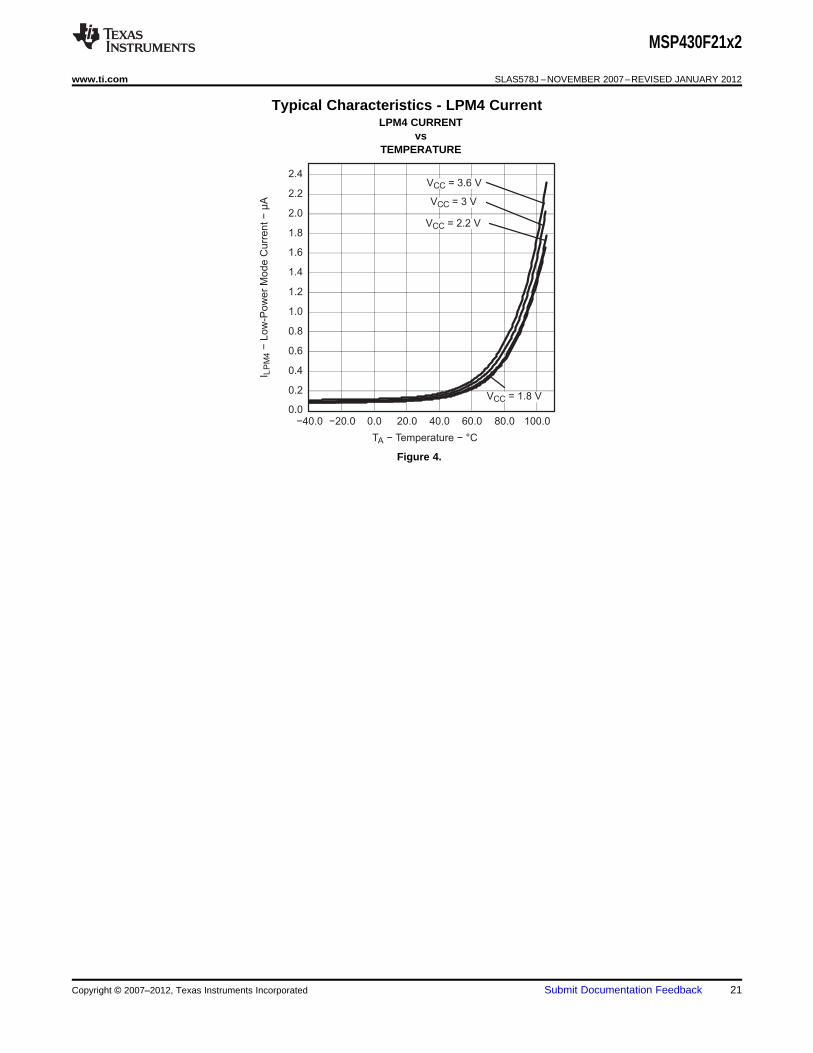
www.ti.com SLAS578J –NOVEMBER 2007–REVISED JANUARY 2012
Typical Characteristics - LPM4 CurrentLPM4 CURRENT
vsTEMPERATURE
Figure 4.
Copyright © 2007–2012, Texas Instruments Incorporated Submit Documentation Feedback 21
MSP430F21x2
SLAS578J –NOVEMBER 2007–REVISED JANUARY 2012 www.ti.com
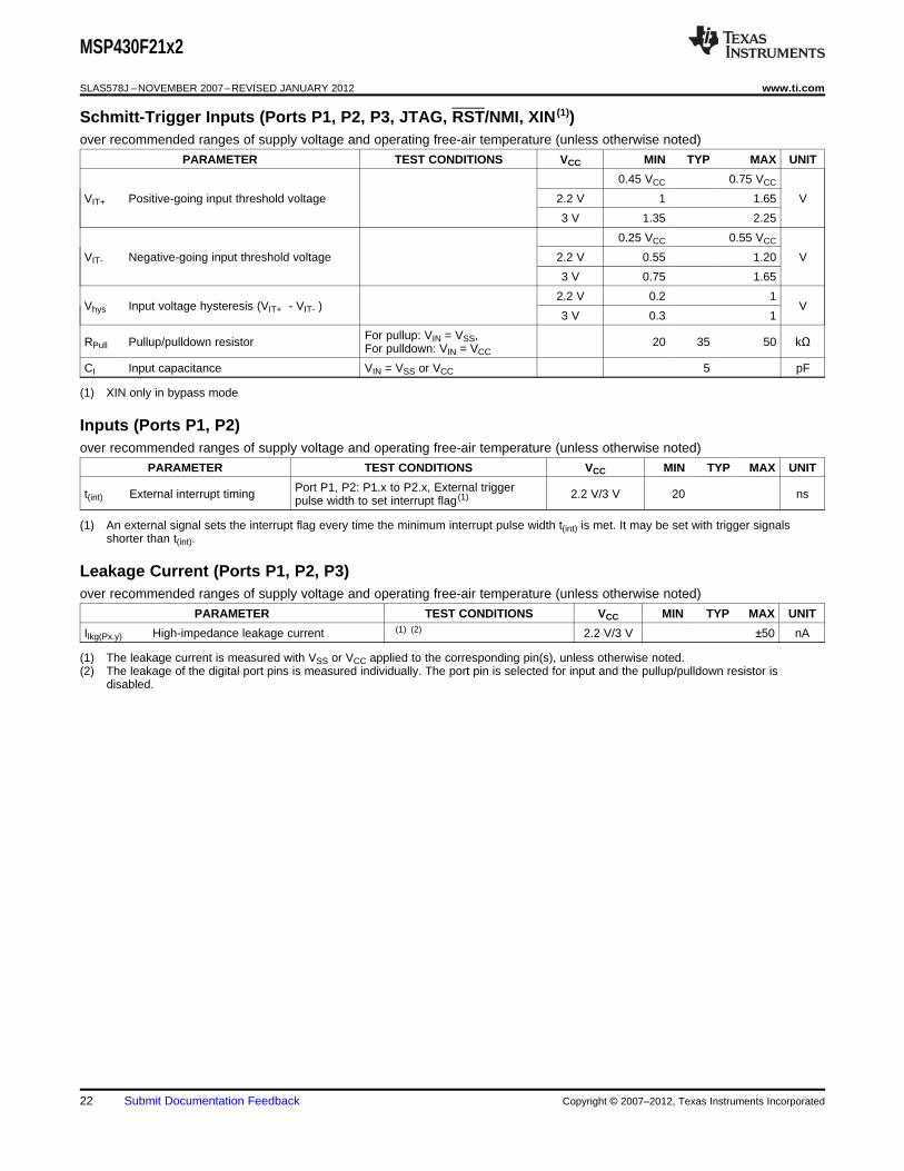
Schmitt-Trigger Inputs (Ports P1, P2, P3, JTAG, RST/NMI, XIN (1))over recommended ranges of supply voltage and operating free-air temperature (unless otherwise noted)
PARAMETER TEST CONDITIONS VCC MIN TYP MAX UNIT
0.45 VCC 0.75 VCC
VIT+ Positive-going input threshold voltage 2.2 V 1 1.65 V
3 V 1.35 2.25
0.25 VCC 0.55 VCC
VIT- Negative-going input threshold voltage 2.2 V 0.55 1.20 V
3 V 0.75 1.65
2.2 V 0.2 1Vhys Input voltage hysteresis (VIT+ - VIT- ) V
3 V 0.3 1
For pullup: VIN = VSS,RPull Pullup/pulldown resistor 20 35 50 kΩFor pulldown: VIN = VCC
CI Input capacitance VIN = VSS or VCC 5 pF
(1) XIN only in bypass mode
Inputs (Ports P1, P2)over recommended ranges of supply voltage and operating free-air temperature (unless otherwise noted)
PARAMETER TEST CONDITIONS VCC MIN TYP MAX UNIT
Port P1, P2: P1.x to P2.x, External triggert(int) External interrupt timing 2.2 V/3 V 20 nspulse width to set interrupt flag (1)
(1) An external signal sets the interrupt flag every time the minimum interrupt pulse width t(int) is met. It may be set with trigger signalsshorter than t(int).
Leakage Current (Ports P1, P2, P3)over recommended ranges of supply voltage and operating free-air temperature (unless otherwise noted)
PARAMETER TEST CONDITIONS VCC MIN TYP MAX UNIT
Ilkg(Px.y) High-impedance leakage current (1) (2) 2.2 V/3 V ±50 nA
(1) The leakage current is measured with VSS or VCC applied to the corresponding pin(s), unless otherwise noted.(2) The leakage of the digital port pins is measured individually. The port pin is selected for input and the pullup/pulldown resistor is
disabled.
22 Submit Documentation Feedback Copyright © 2007–2012, Texas Instruments Incorporated
MSP430F21x2
www.ti.com SLAS578J –NOVEMBER 2007–REVISED JANUARY 2012
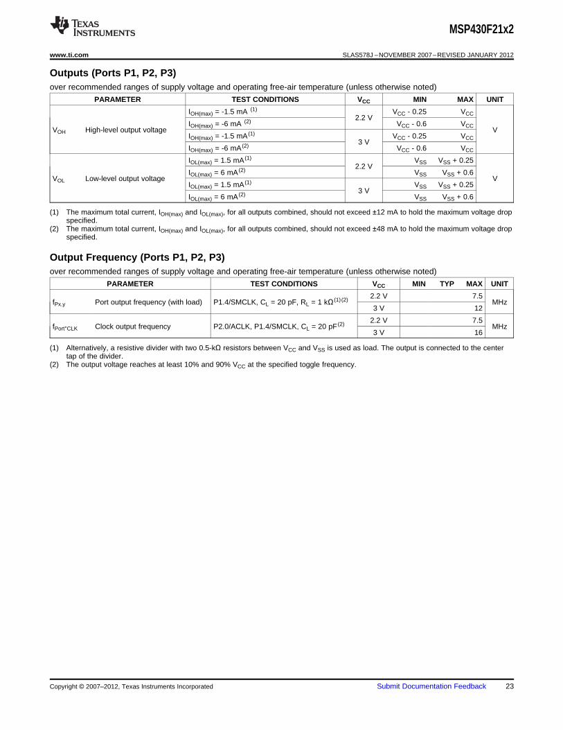
Outputs (Ports P1, P2, P3)over recommended ranges of supply voltage and operating free-air temperature (unless otherwise noted)
PARAMETER TEST CONDITIONS VCC MIN MAX UNIT
IOH(max) = -1.5 mA (1) VCC - 0.25 VCC2.2 V
IOH(max) = -6 mA (2) VCC - 0.6 VCCVOH High-level output voltage V
IOH(max) = -1.5 mA (1) VCC - 0.25 VCC3 V
IOH(max) = -6 mA (2) VCC - 0.6 VCC
IOL(max) = 1.5 mA (1) VSS VSS + 0.252.2 V
IOL(max) = 6 mA (2) VSS VSS + 0.6VOL Low-level output voltage V
IOL(max) = 1.5 mA (1) VSS VSS + 0.253 V
IOL(max) = 6 mA (2) VSS VSS + 0.6
(1) The maximum total current, IOH(max) and IOL(max), for all outputs combined, should not exceed ±12 mA to hold the maximum voltage dropspecified.
(2) The maximum total current, IOH(max) and IOL(max), for all outputs combined, should not exceed ±48 mA to hold the maximum voltage dropspecified.
Output Frequency (Ports P1, P2, P3)over recommended ranges of supply voltage and operating free-air temperature (unless otherwise noted)
PARAMETER TEST CONDITIONS VCC MIN TYP MAX UNIT
2.2 V 7.5fPx.y Port output frequency (with load) P1.4/SMCLK, CL = 20 pF, RL = 1 kΩ (1) (2) MHz
3 V 12
2.2 V 7.5fPort°CLK Clock output frequency P2.0/ACLK, P1.4/SMCLK, CL = 20 pF (2) MHz
3 V 16
(1) Alternatively, a resistive divider with two 0.5-kΩ resistors between VCC and VSS is used as load. The output is connected to the centertap of the divider.
(2) The output voltage reaches at least 10% and 90% VCC at the specified toggle frequency.
Copyright © 2007–2012, Texas Instruments Incorporated Submit Documentation Feedback 23
VOL − Low-Level Output Voltage − V
0.0
5.0
10.0
15.0
20.0
25.0
0.0 0.5 1.0 1.5 2.0 2.5
VCC = 2.2 V
P2.4
TA = 25°C
TA = 85°C
OL
I−
Typic
al Low
-Level O
utp
ut C
urr
ent
−m
A
VOL − Low-Level Output Voltage − V
0.0
10.0
20.0
30.0
40.0
50.0
0.0 0.5 1.0 1.5 2.0 2.5 3.0 3.5
VCC = 3 V
P2.4 TA = 25°C
TA = 85°C
OL
I−
Typic
al Low
-Level O
utp
ut C
urr
ent
−m
A
VOH − High-Level Output Voltage − V
−25.0
−20.0
−15.0
−10.0
−5.0
0.0
0.0 0.5 1.0 1.5 2.0 2.5
VCC = 2.2 V
P2.4
TA = 25°C
TA = 85°C
OH
I−
Typic
al H
igh-L
evel O
utp
ut C
urr
ent
−m
A
VOH − High-Level Output Voltage − V
−50.0
−40.0
−30.0
−20.0
−10.0
0.0
0.0 0.5 1.0 1.5 2.0 2.5 3.0 3.5
VCC = 3 V
P2.4
TA = 25°C
TA = 85°C
OH
I−
Typic
al H
igh-L
evel O
utp
ut C
urr
ent
−m
A
MSP430F21x2
SLAS578J –NOVEMBER 2007–REVISED JANUARY 2012 www.ti.com
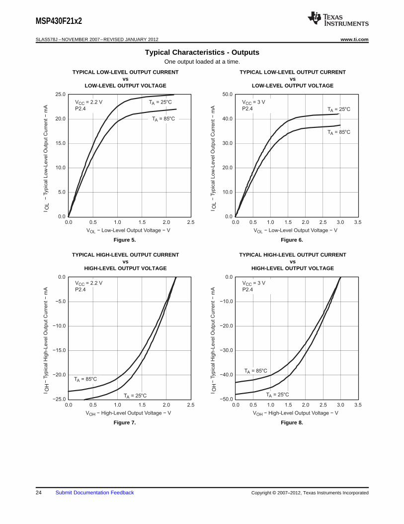
Typical Characteristics - OutputsOne output loaded at a time.
TYPICAL LOW-LEVEL OUTPUT CURRENT TYPICAL LOW-LEVEL OUTPUT CURRENTvs vs
LOW-LEVEL OUTPUT VOLTAGE LOW-LEVEL OUTPUT VOLTAGE
Figure 5. Figure 6.
TYPICAL HIGH-LEVEL OUTPUT CURRENT TYPICAL HIGH-LEVEL OUTPUT CURRENTvs vs
HIGH-LEVEL OUTPUT VOLTAGE HIGH-LEVEL OUTPUT VOLTAGE
Figure 7. Figure 8.
24 Submit Documentation Feedback Copyright © 2007–2012, Texas Instruments Incorporated
0
1
t d(BOR)
VCC
V(B_IT−)
Vhys(B_IT−)
VCC(start)
MSP430F21x2
www.ti.com SLAS578J –NOVEMBER 2007–REVISED JANUARY 2012
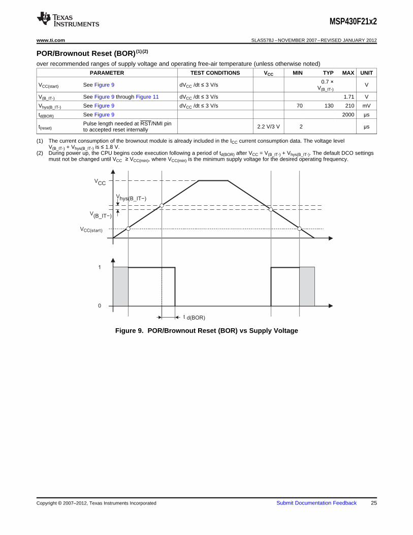
POR/Brownout Reset (BOR) (1) (2)
over recommended ranges of supply voltage and operating free-air temperature (unless otherwise noted)
PARAMETER TEST CONDITIONS VCC MIN TYP MAX UNIT
0.7 ×VCC(start) See Figure 9 dVCC /dt ≤ 3 V/s VV(B_IT-)
V(B_IT-) See Figure 9 through Figure 11 dVCC /dt ≤ 3 V/s 1.71 V
Vhys(B_IT-) See Figure 9 dVCC /dt ≤ 3 V/s 70 130 210 mV
td(BOR) See Figure 9 2000 µs
Pulse length needed at RST/NMI pint(reset) 2.2 V/3 V 2 µsto accepted reset internally
(1) The current consumption of the brownout module is already included in the ICC current consumption data. The voltage levelV(B_IT-) + Vhys(B_IT-) is ≤ 1.8 V.
(2) During power up, the CPU begins code execution following a period of td(BOR) after VCC = V(B_IT-) + Vhys(B_IT-). The default DCO settingsmust not be changed until VCC ≥ VCC(min), where VCC(min) is the minimum supply voltage for the desired operating frequency.
Figure 9. POR/Brownout Reset (BOR) vs Supply Voltage
Copyright © 2007–2012, Texas Instruments Incorporated Submit Documentation Feedback 25
VCC(drop)
VCC
3 V
t pw
0
0.5
1
1.5
2
0.001 1 1000
Typical Conditions
1 ns 1 nstpw − Pulse Width − µs
VC
C(d
rop)
−V
tpw − Pulse Width − µs
VCC = 3 V
VCC
0
0.5
1
1.5
2
VCC(drop)
t pw
tpw − Pulse Width − µs
VC
C(d
rop)
−V
3 V
0.001 1 1000 tf tr
tpw − Pulse Width − µs
tf = tr
Typical Conditions
VCC = 3 V
MSP430F21x2
SLAS578J –NOVEMBER 2007–REVISED JANUARY 2012 www.ti.com
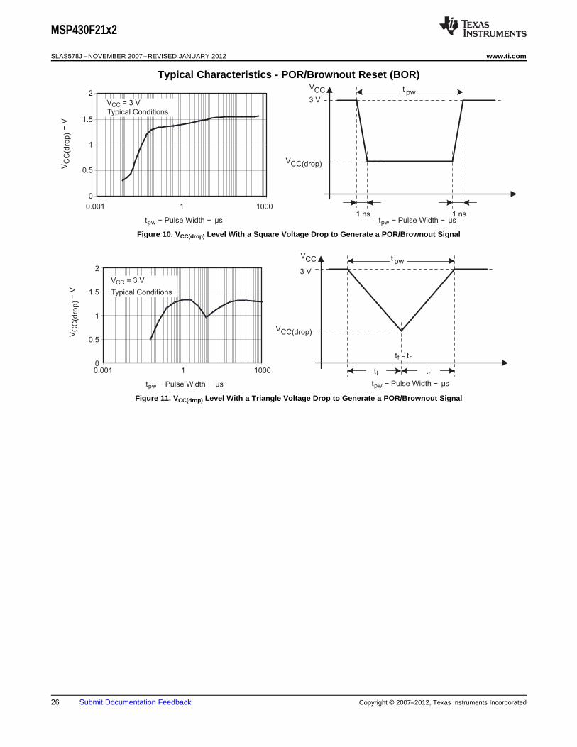
Typical Characteristics - POR/Brownout Reset (BOR)
Figure 10. VCC(drop) Level With a Square Voltage Drop to Generate a POR/Brownout Signal
Figure 11. VCC(drop) Level With a Triangle Voltage Drop to Generate a POR/Brownout Signal
26 Submit Documentation Feedback Copyright © 2007–2012, Texas Instruments Incorporated
DCO(RSEL,DCO) DCO(RSEL,DCO+1)average
DCO(RSEL,DCO) DCO(RSEL,DCO+1)
32 × f × ff =
MOD × f + (32 – MOD) × f
MSP430F21x2
www.ti.com SLAS578J –NOVEMBER 2007–REVISED JANUARY 2012
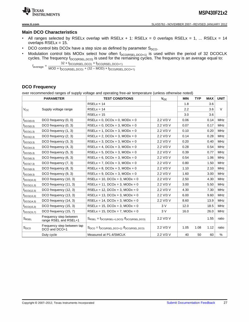
Main DCO Characteristics• All ranges selected by RSELx overlap with RSELx + 1: RSELx = 0 overlaps RSELx = 1, ... RSELx = 14
overlaps RSELx = 15.• DCO control bits DCOx have a step size as defined by parameter SDCO.• Modulation control bits MODx select how often fDCO(RSEL,DCO+1) is used within the period of 32 DCOCLK
cycles. The frequency fDCO(RSEL,DCO) is used for the remaining cycles. The frequency is an average equal to:
DCO Frequencyover recommended ranges of supply voltage and operating free-air temperature (unless otherwise noted)
PARAMETER TEST CONDITIONS VCC MIN TYP MAX UNIT
RSELx < 14 1.8 3.6
VCC Supply voltage range RSELx = 14 2.2 3.6 V
RSELx = 15 3.0 3.6
fDCO(0,0) DCO frequency (0, 0) RSELx = 0, DCOx = 0, MODx = 0 2.2 V/3 V 0.06 0.14 MHz
fDCO(0,3) DCO frequency (0, 3) RSELx = 0, DCOx = 3, MODx = 0 2.2 V/3 V 0.07 0.17 MHz
fDCO(1,3) DCO frequency (1, 3) RSELx = 1, DCOx = 3, MODx = 0 2.2 V/3 V 0.10 0.20 MHz
fDCO(2,3) DCO frequency (2, 3) RSELx = 2, DCOx = 3, MODx = 0 2.2 V/3 V 0.14 0.28 MHz
fDCO(3,3) DCO frequency (3, 3) RSELx = 3, DCOx = 3, MODx = 0 2.2 V/3 V 0.20 0.40 MHz
fDCO(4,3) DCO frequency (4, 3) RSELx = 4, DCOx = 3, MODx = 0 2.2 V/3 V 0.28 0.54 MHz
fDCO(5,3) DCO frequency (5, 3) RSELx = 5, DCOx = 3, MODx = 0 2.2 V/3 V 0.39 0.77 MHz
fDCO(6,3) DCO frequency (6, 3) RSELx = 6, DCOx = 3, MODx = 0 2.2 V/3 V 0.54 1.06 MHz
fDCO(7,3) DCO frequency (7, 3) RSELx = 7, DCOx = 3, MODx = 0 2.2 V/3 V 0.80 1.50 MHz
fDCO(8,3) DCO frequency (8, 3) RSELx = 8, DCOx = 3, MODx = 0 2.2 V/3 V 1.10 2.10 MHz
fDCO(9,3) DCO frequency (9, 3) RSELx = 9, DCOx = 3, MODx = 0 2.2 V/3 V 1.60 3.00 MHz
fDCO(10,3) DCO frequency (10, 3) RSELx = 10, DCOx = 3, MODx = 0 2.2 V/3 V 2.50 4.30 MHz
fDCO(11,3) DCO frequency (11, 3) RSELx = 11, DCOx = 3, MODx = 0 2.2 V/3 V 3.00 5.50 MHz
fDCO(12,3) DCO frequency (12, 3) RSELx = 12, DCOx = 3, MODx = 0 2.2 V/3 V 4.30 7.30 MHz
fDCO(13,3) DCO frequency (13, 3) RSELx = 13, DCOx = 3, MODx = 0 2.2 V/3 V 6.00 9.60 MHz
fDCO(14,3) DCO frequency (14, 3) RSELx = 14, DCOx = 3, MODx = 0 2.2 V/3 V 8.60 13.9 MHz
fDCO(15,3) DCO frequency (15, 3) RSELx = 15, DCOx = 3, MODx = 0 3 V 12.0 18.5 MHz
fDCO(15,7) DCO frequency (15, 7) RSELx = 15, DCOx = 7, MODx = 0 3 V 16.0 26.0 MHz
Frequency step betweenSRSEL SRSEL = fDCO(RSEL+1,DCO) /fDCO(RSEL,DCO) 2.2 V/3 V 1.55 ratiorange RSEL and RSEL+1
Frequency step between tapSDCO SDCO = fDCO(RSEL,DCO+1) /fDCO(RSEL,DCO) 2.2 V/3 V 1.05 1.08 1.12 ratioDCO and DCO+1
Duty cycle Measured at P1.4/SMCLK 2.2 V/3 V 40 50 60 %
Copyright © 2007–2012, Texas Instruments Incorporated Submit Documentation Feedback 27
MSP430F21x2
SLAS578J –NOVEMBER 2007–REVISED JANUARY 2012 www.ti.com
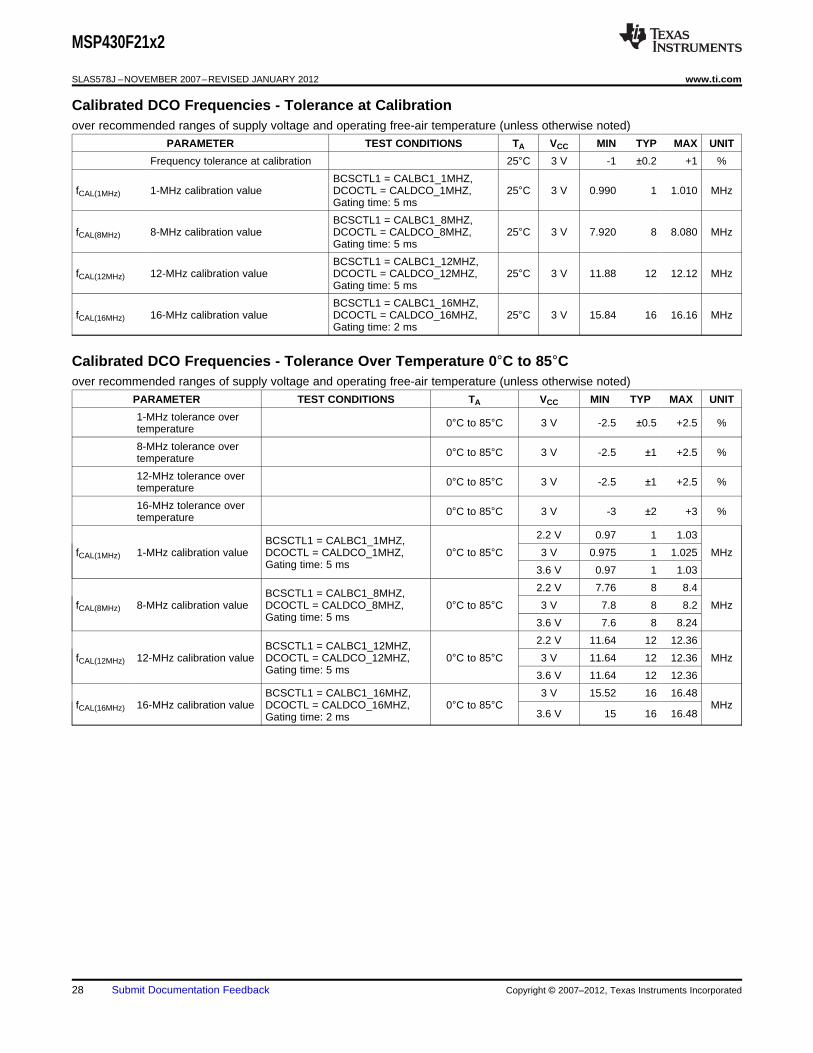
Calibrated DCO Frequencies - Tolerance at Calibrationover recommended ranges of supply voltage and operating free-air temperature (unless otherwise noted)
PARAMETER TEST CONDITIONS TA VCC MIN TYP MAX UNIT
Frequency tolerance at calibration 25°C 3 V -1 ±0.2 +1 %
BCSCTL1 = CALBC1_1MHZ,fCAL(1MHz) 1-MHz calibration value DCOCTL = CALDCO_1MHZ, 25°C 3 V 0.990 1 1.010 MHz
Gating time: 5 ms
BCSCTL1 = CALBC1_8MHZ,fCAL(8MHz) 8-MHz calibration value DCOCTL = CALDCO_8MHZ, 25°C 3 V 7.920 8 8.080 MHz
Gating time: 5 ms
BCSCTL1 = CALBC1_12MHZ,fCAL(12MHz) 12-MHz calibration value DCOCTL = CALDCO_12MHZ, 25°C 3 V 11.88 12 12.12 MHz
Gating time: 5 ms
BCSCTL1 = CALBC1_16MHZ,fCAL(16MHz) 16-MHz calibration value DCOCTL = CALDCO_16MHZ, 25°C 3 V 15.84 16 16.16 MHz
Gating time: 2 ms
Calibrated DCO Frequencies - Tolerance Over Temperature 0°C to 85°Cover recommended ranges of supply voltage and operating free-air temperature (unless otherwise noted)
PARAMETER TEST CONDITIONS TA VCC MIN TYP MAX UNIT
1-MHz tolerance over 0°C to 85°C 3 V -2.5 ±0.5 +2.5 %temperature
8-MHz tolerance over 0°C to 85°C 3 V -2.5 ±1 +2.5 %temperature
12-MHz tolerance over 0°C to 85°C 3 V -2.5 ±1 +2.5 %temperature
16-MHz tolerance over 0°C to 85°C 3 V -3 ±2 +3 %temperature
2.2 V 0.97 1 1.03BCSCTL1 = CALBC1_1MHZ,fCAL(1MHz) 1-MHz calibration value DCOCTL = CALDCO_1MHZ, 0°C to 85°C 3 V 0.975 1 1.025 MHz
Gating time: 5 ms 3.6 V 0.97 1 1.03
2.2 V 7.76 8 8.4BCSCTL1 = CALBC1_8MHZ,fCAL(8MHz) 8-MHz calibration value DCOCTL = CALDCO_8MHZ, 0°C to 85°C 3 V 7.8 8 8.2 MHz
Gating time: 5 ms 3.6 V 7.6 8 8.24
2.2 V 11.64 12 12.36BCSCTL1 = CALBC1_12MHZ,fCAL(12MHz) 12-MHz calibration value DCOCTL = CALDCO_12MHZ, 0°C to 85°C 3 V 11.64 12 12.36 MHz
Gating time: 5 ms 3.6 V 11.64 12 12.36
BCSCTL1 = CALBC1_16MHZ, 3 V 15.52 16 16.48fCAL(16MHz) 16-MHz calibration value DCOCTL = CALDCO_16MHZ, 0°C to 85°C MHz
3.6 V 15 16 16.48Gating time: 2 ms
28 Submit Documentation Feedback Copyright © 2007–2012, Texas Instruments Incorporated
MSP430F21x2
www.ti.com SLAS578J –NOVEMBER 2007–REVISED JANUARY 2012
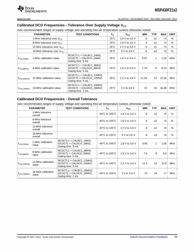
Calibrated DCO Frequencies - Tolerance Over Supply Voltage VCC
over recommended ranges of supply voltage and operating free-air temperature (unless otherwise noted)
PARAMETER TEST CONDITIONS TA VCC MIN TYP MAX UNIT
1-MHz tolerance over VCC 25°C 1.8 V to 3.6 V -3 ±2 +3 %
8-MHz tolerance over VCC 25°C 1.8 V to 3.6 V -3 ±2 +3 %
12-MHz tolerance over VCC 25°C 2.2 V to 3.6 V -3 ±2 +3 %
16-MHz tolerance over VCC 25°C 3 V to 3.6 V -6 ±2 +3 %
BCSCTL1 = CALBC1_1MHZ,fCAL(1MHz) 1-MHz calibration value DCOCTL = CALDCO_1MHZ, 25°C 1.8 V to 3.6 V 0.97 1 1.03 MHz
Gating time: 5 ms
BCSCTL1 = CALBC1_8MHZ,fCAL(8MHz) 8-MHz calibration value DCOCTL = CALDCO_8MHZ, 25°C 1.8 V to 3.6 V 7.76 8 8.24 MHz
Gating time: 5 ms
BCSCTL1 = CALBC1_12MHZ,fCAL(12MHz) 12-MHz calibration value DCOCTL = CALDCO_12MHZ, 25°C 2.2 V to 3.6 V 11.64 12 12.36 MHz
Gating time: 5 ms
BCSCTL1 = CALBC1_16MHZ,fCAL(16MHz) 16-MHz calibration value DCOCTL = CALDCO_16MHZ, 25°C 3 V to 3.6 V 15 16 16.48 MHz
Gating time: 2 ms
Calibrated DCO Frequencies - Overall Toleranceover recommended ranges of supply voltage and operating free-air temperature (unless otherwise noted)
PARAMETER TEST CONDITIONS TA VCC MIN TYP MAX UNIT
1-MHz tolerance -40°C to 105°C 1.8 V to 3.6 V -5 ±2 +5 %overall
8-MHz tolerance -40°C to 105°C 1.8 V to 3.6 V -5 ±2 +5 %overall
12-MHz tolerance -40°C to 105°C 2.2 V to 3.6 V -5 ±2 +5 %overall
16-MHz tolerance -40°C to 105°C 3 V to 3.6 V -6 ±3 +6 %overall
BCSCTL1 = CALBC1_1MHZ,1-MHz calibrationfCAL(1MHz) DCOCTL = CALDCO_1MHZ, -40°C to 105°C 1.8 V to 3.6 V 0.95 1 1.05 MHzvalue Gating time: 5 ms
BCSCTL1 = CALBC1_8MHZ,8-MHz calibrationfCAL(8MHz) DCOCTL = CALDCO_8MHZ, -40°C to 105°C 1.8 V to 3.6 V 7.6 8 8.4 MHzvalue Gating time: 5 ms
BCSCTL1 = CALBC1_12MHZ,12-MHz calibrationfCAL(12MHz) DCOCTL = CALDCO_12MHZ, -40°C to 105°C 2.2 V to 3.6 V 11.4 12 12.6 MHzvalue Gating time: 5 ms
BCSCTL1 = CALBC1_16MHZ,16-MHz calibrationfCAL(16MHz) DCOCTL = CALDCO_16MHZ, -40°C to 105°C 3 V to 3.6 V 15 16 17 MHzvalue Gating time: 2 ms
Copyright © 2007–2012, Texas Instruments Incorporated Submit Documentation Feedback 29
VCC − Supply Voltage − V
0.97
0.98
0.99
1.00
1.01
1.02
1.03
1.5 2.0 2.5 3.0 3.5 4.0
Fre
qu
en
cy
−M
Hz
TA = −40 °C
TA = 25 °C
TA = 85 °C
TA = 105 °C
MSP430F21x2
SLAS578J –NOVEMBER 2007–REVISED JANUARY 2012 www.ti.com
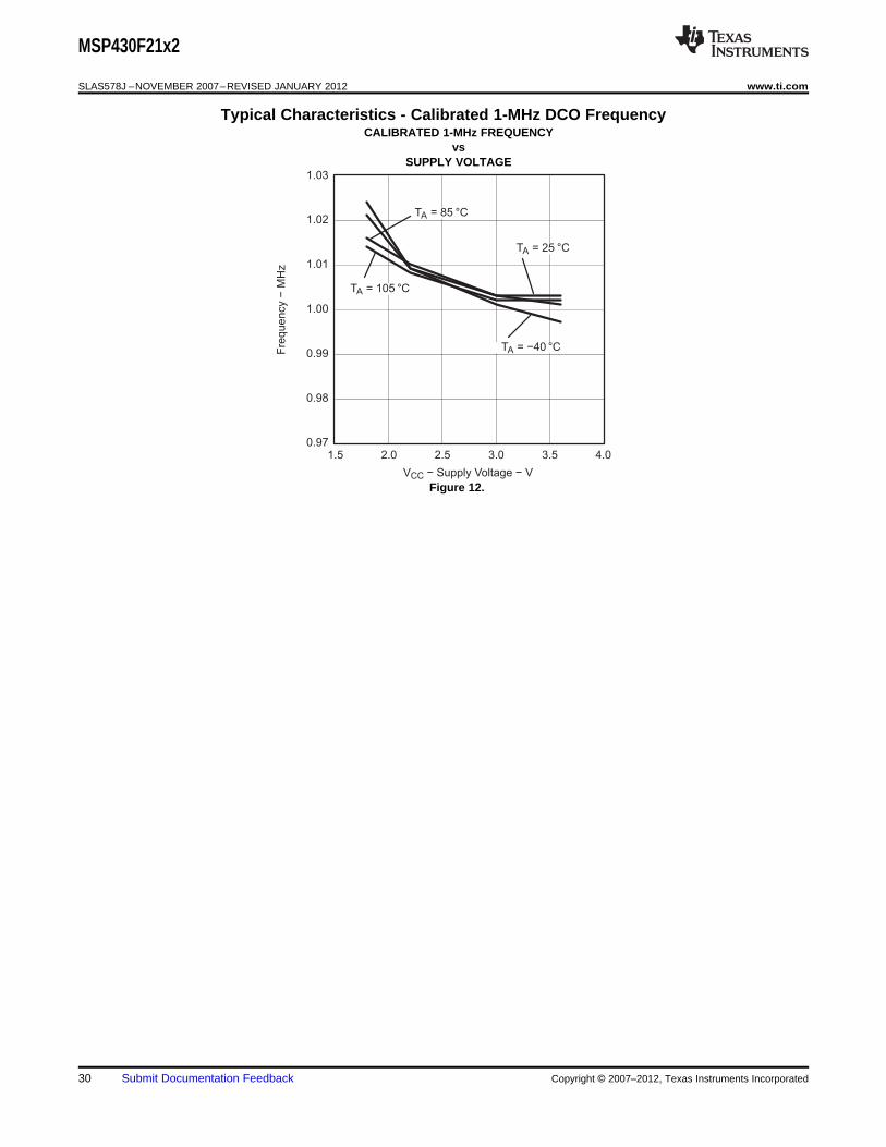
Typical Characteristics - Calibrated 1-MHz DCO FrequencyCALIBRATED 1-MHz FREQUENCY
vsSUPPLY VOLTAGE
Figure 12.
30 Submit Documentation Feedback Copyright © 2007–2012, Texas Instruments Incorporated
DCO Frequency − MHz
0.10
1.00
10.00
0.10 1.00 10.00
DC
O W
ake
Tim
e−
µs
RSELx = 0 to 11RSELx = 12 to 15
MSP430F21x2
www.ti.com SLAS578J –NOVEMBER 2007–REVISED JANUARY 2012
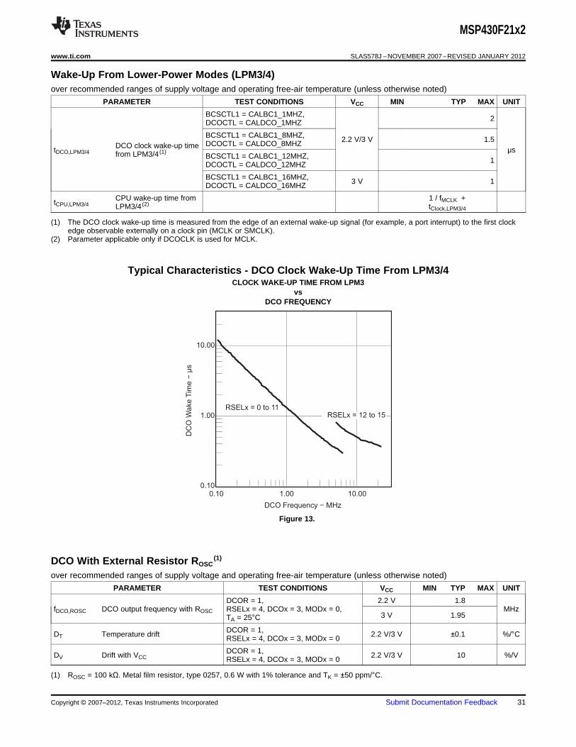
Wake-Up From Lower-Power Modes (LPM3/4)over recommended ranges of supply voltage and operating free-air temperature (unless otherwise noted)
PARAMETER TEST CONDITIONS VCC MIN TYP MAX UNIT
BCSCTL1 = CALBC1_1MHZ, 2DCOCTL = CALDCO_1MHZ
BCSCTL1 = CALBC1_8MHZ, 2.2 V/3 V 1.5DCOCTL = CALDCO_8MHZDCO clock wake-up timetDCO,LPM3/4 µsfrom LPM3/4 (1)BCSCTL1 = CALBC1_12MHZ, 1DCOCTL = CALDCO_12MHZ
BCSCTL1 = CALBC1_16MHZ, 3 V 1DCOCTL = CALDCO_16MHZ
CPU wake-up time from 1 / fMCLK +tCPU,LPM3/4 LPM3/4 (2) tClock,LPM3/4
(1) The DCO clock wake-up time is measured from the edge of an external wake-up signal (for example, a port interrupt) to the first clockedge observable externally on a clock pin (MCLK or SMCLK).
(2) Parameter applicable only if DCOCLK is used for MCLK.
Typical Characteristics - DCO Clock Wake-Up Time From LPM3/4CLOCK WAKE-UP TIME FROM LPM3
vsDCO FREQUENCY
Figure 13.
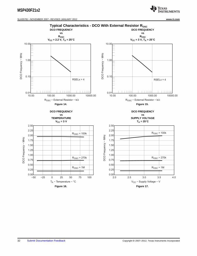
DCO With External Resistor ROSC(1)
over recommended ranges of supply voltage and operating free-air temperature (unless otherwise noted)
PARAMETER TEST CONDITIONS VCC MIN TYP MAX UNIT
DCOR = 1, 2.2 V 1.8fDCO,ROSC DCO output frequency with ROSC RSELx = 4, DCOx = 3, MODx = 0, MHz
3 V 1.95TA = 25°CDCOR = 1,DT Temperature drift 2.2 V/3 V ±0.1 %/°CRSELx = 4, DCOx = 3, MODx = 0
DCOR = 1,DV Drift with VCC 2.2 V/3 V 10 %/VRSELx = 4, DCOx = 3, MODx = 0
(1) ROSC = 100 kΩ. Metal film resistor, type 0257, 0.6 W with 1% tolerance and TK = ±50 ppm/°C.
Copyright © 2007–2012, Texas Instruments Incorporated Submit Documentation Feedback 31
0.01
0.10
1.00
10.00
10.00 100.00 1000.00 10000.00
ROSC − External Resistor − kW
DC
O F
req
ue
ncy
−M
Hz
RSELx = 4
0.01
0.10
1.00
10.00
10.00 100.00 1000.00 10000.00
ROSC − External Resistor − kW
DC
O F
req
ue
ncy
−M
Hz
RSELx = 4
0.00
0.25
0.50
0.75
1.00
1.25
1.50
1.75
2.00
2.25
2.50
−50 −25 0 25 50 75 100
TA − Temperature − °C
DC
O F
requency
−M
Hz
ROSC = 100k
ROSC = 270k
ROSC = 1M
0.00
0.25
0.50
0.75
1.00
1.25
1.50
1.75
2.00
2.25
2.50
2.0 2.5 3.0 3.5 4.0
VCC − Supply Voltage − V
DC
O F
req
ue
ncy
−M
Hz
ROSC = 100k
ROSC = 270k
ROSC = 1M
MSP430F21x2
SLAS578J –NOVEMBER 2007–REVISED JANUARY 2012 www.ti.com
Typical Characteristics - DCO With External Resistor ROSCDCO FREQUENCY DCO FREQUENCY
vs vsROSC ROSC
VCC = 2.2 V, TA = 25°C VCC = 3 V, TA = 25°C
Figure 14. Figure 15.
DCO FREQUENCY DCO FREQUENCYvs vs
TEMPERATURE SUPPLY VOLTAGEVCC = 3 V TA = 25°C
Figure 16. Figure 17.
32 Submit Documentation Feedback Copyright © 2007–2012, Texas Instruments Incorporated
MSP430F21x2
www.ti.com SLAS578J –NOVEMBER 2007–REVISED JANUARY 2012
Crystal Oscillator LFXT1, Low-Frequency Mode (1)
over recommended ranges of supply voltage and operating free-air temperature (unless otherwise noted)
PARAMETER TEST CONDITIONS VCC MIN TYP MAX UNIT
LFXT1 oscillator crystalfLFXT1,LF XTS = 0, LFXT1Sx = 0 or 1 1.8 V to 3.6 V 32768 Hzfrequency, LF mode 0, 1
LFXT1 oscillator logic levelfLFXT1,LF,logic square wave input frequency, XTS = 0, XCAPx = 0, LFXT1Sx = 3 1.8 V to 3.6 V 10000 32768 50000 Hz
LF mode
XTS = 0, LFXT1Sx = 0, 500fLFXT1,LF = 32768 Hz, CL,eff = 6 pFOscillation allowance forOALF kΩLF crystals XTS = 0, LFXT1Sx = 0, 200fLFXT1,LF = 32768 Hz, CL,eff = 12 pF
XTS = 0, XCAPx = 0 1
XTS = 0, XCAPx = 1 5.5Integrated effective loadCL,eff pFcapacitance, LF mode (2)XTS = 0, XCAPx = 2 8.5
XTS = 0, XCAPx = 3 11
XTS = 0, Measured at P2.0/ACLK,Duty cycle, LF mode 2.2 V/3 V 30 50 70 %fLFXT1,LF = 32768 Hz
Oscillator fault frequency, XTS = 0, XCAPx = 0,fFault,LF 2.2 V/3 V 10 10000 HzLF mode (3) LFXT1Sx = 3 (4)
(1) To improve EMI on the XT1 oscillator, the following guidelines should be observed.(a) Keep the trace between the device and the crystal as short as possible.(b) Design a good ground plane around the oscillator pins.(c) Prevent crosstalk from other clock or data lines into oscillator pins XIN and XOUT.(d) Avoid running PCB traces underneath or adjacent to the XIN and XOUT pins.(e) Use assembly materials and praxis to avoid any parasitic load on the oscillator XIN and XOUT pins.(f) If conformal coating is used, ensure that it does not induce capacitive/resistive leakage between the oscillator pins.(g) Do not route the XOUT line to the JTAG header to support the serial programming adapter as shown in other documentation. This
signal is no longer required for the serial programming adapter.(2) Includes parasitic bond and package capacitance (approximately 2 pF per pin).
Because the PCB adds additional capacitance, it is recommended to verify the correct load by measuring the ACLK frequency. For acorrect setup, the effective load capacitance should always match the specification of the crystal that is used.
(3) Frequencies below the MIN specification set the fault flag. Frequencies above the MAX specification do not set the fault flag.Frequencies in between might set the flag.
(4) Measured with logic-level input frequency but also applies to operation with crystals.
Internal Very-Low-Power Low-Frequency Oscillator (VLO)over recommended ranges of supply voltage and operating free-air temperature (unless otherwise noted)
PARAMETER TA VCC MIN TYP MAX UNIT
-40°C to 85°C 4 12 20fVLO VLO frequency 2.2 V/3 V kHz
105°C 22
dfVLO/dT VLO frequency temperature drift (1) 2.2 V/3 V 0.5 %/°CdfVLO/dVCC VLO frequency supply voltage drift (2) 1.8 V to 3.6 V 4 %/V
(1) Calculated using the box method:I version: [MAX(-40...85°C) - MIN(-40...85°C)]/MIN(-40...85°C)/[85°C - (-40°C)]T version: [MAX(-40...105°C) - MIN(-40...105°C)]/MIN(-40...105°C)/[105°C - (-40°C)]
(2) Calculated using the box method: [MAX(1.8...3.6 V) - MIN(1.8...3.6 V)]/MIN(1.8...3.6 V)/(3.6 V - 1.8 V)
Copyright © 2007–2012, Texas Instruments Incorporated Submit Documentation Feedback 33
MSP430F21x2
SLAS578J –NOVEMBER 2007–REVISED JANUARY 2012 www.ti.com
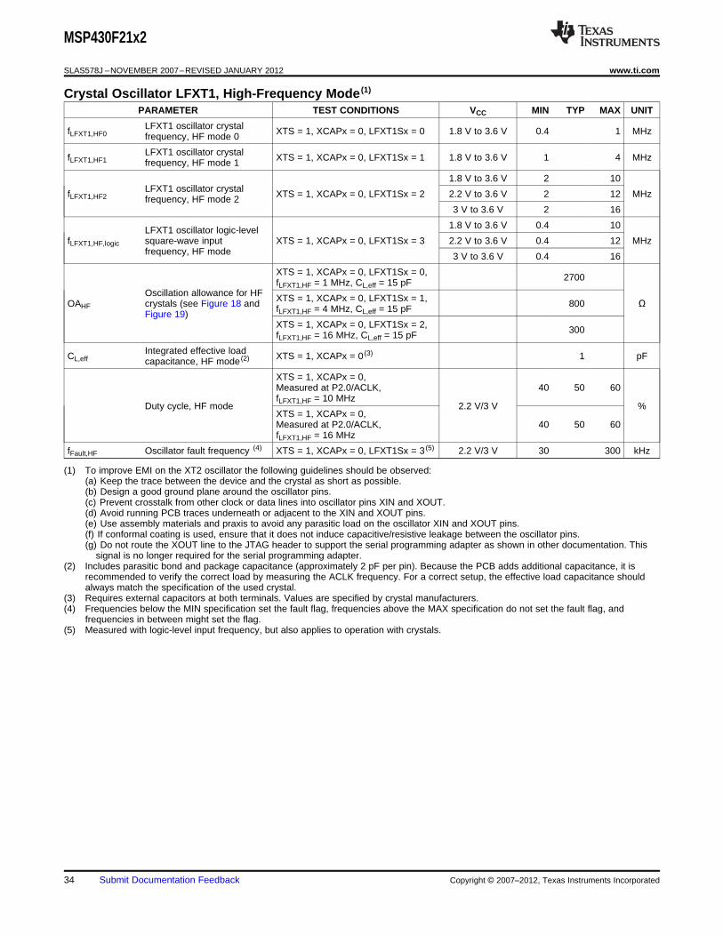
Crystal Oscillator LFXT1, High-Frequency Mode (1)
PARAMETER TEST CONDITIONS VCC MIN TYP MAX UNIT
LFXT1 oscillator crystalfLFXT1,HF0 XTS = 1, XCAPx = 0, LFXT1Sx = 0 1.8 V to 3.6 V 0.4 1 MHzfrequency, HF mode 0
LFXT1 oscillator crystalfLFXT1,HF1 XTS = 1, XCAPx = 0, LFXT1Sx = 1 1.8 V to 3.6 V 1 4 MHzfrequency, HF mode 1
1.8 V to 3.6 V 2 10LFXT1 oscillator crystalfLFXT1,HF2 XTS = 1, XCAPx = 0, LFXT1Sx = 2 2.2 V to 3.6 V 2 12 MHzfrequency, HF mode 2
3 V to 3.6 V 2 16
1.8 V to 3.6 V 0.4 10LFXT1 oscillator logic-levelfLFXT1,HF,logic square-wave input XTS = 1, XCAPx = 0, LFXT1Sx = 3 2.2 V to 3.6 V 0.4 12 MHz
frequency, HF mode 3 V to 3.6 V 0.4 16
XTS = 1, XCAPx = 0, LFXT1Sx = 0, 2700fLFXT1,HF = 1 MHz, CL,eff = 15 pFOscillation allowance for HF XTS = 1, XCAPx = 0, LFXT1Sx = 1,OAHF crystals (see Figure 18 and 800 ΩfLFXT1,HF = 4 MHz, CL,eff = 15 pFFigure 19)
XTS = 1, XCAPx = 0, LFXT1Sx = 2, 300fLFXT1,HF = 16 MHz, CL,eff = 15 pF
Integrated effective loadCL,eff XTS = 1, XCAPx = 0 (3) 1 pFcapacitance, HF mode (2)
XTS = 1, XCAPx = 0,Measured at P2.0/ACLK, 40 50 60fLFXT1,HF = 10 MHz
Duty cycle, HF mode 2.2 V/3 V %XTS = 1, XCAPx = 0,Measured at P2.0/ACLK, 40 50 60fLFXT1,HF = 16 MHz
fFault,HF Oscillator fault frequency (4) XTS = 1, XCAPx = 0, LFXT1Sx = 3 (5) 2.2 V/3 V 30 300 kHz
(1) To improve EMI on the XT2 oscillator the following guidelines should be observed:(a) Keep the trace between the device and the crystal as short as possible.(b) Design a good ground plane around the oscillator pins.(c) Prevent crosstalk from other clock or data lines into oscillator pins XIN and XOUT.(d) Avoid running PCB traces underneath or adjacent to the XIN and XOUT pins.(e) Use assembly materials and praxis to avoid any parasitic load on the oscillator XIN and XOUT pins.(f) If conformal coating is used, ensure that it does not induce capacitive/resistive leakage between the oscillator pins.(g) Do not route the XOUT line to the JTAG header to support the serial programming adapter as shown in other documentation. This
signal is no longer required for the serial programming adapter.(2) Includes parasitic bond and package capacitance (approximately 2 pF per pin). Because the PCB adds additional capacitance, it is
recommended to verify the correct load by measuring the ACLK frequency. For a correct setup, the effective load capacitance shouldalways match the specification of the used crystal.
(3) Requires external capacitors at both terminals. Values are specified by crystal manufacturers.(4) Frequencies below the MIN specification set the fault flag, frequencies above the MAX specification do not set the fault flag, and
frequencies in between might set the flag.(5) Measured with logic-level input frequency, but also applies to operation with crystals.
34 Submit Documentation Feedback Copyright © 2007–2012, Texas Instruments Incorporated
Crystal Frequency − MHz
10.00
100.00
1000.00
10000.00
100000.00
0.10 1.00 10.00 100.00
Oscill
atio
nA
llow
an
ce
−O
hm
s
LFXT1Sx = 0
LFXT1Sx = 2
LFXT1Sx = 1
0.0
200.0
400.0
600.0
800.0
1000.0
1200.0
1400.0
1600.0
1800.0
0.0 4.0 8.0 12.0 16.0 20.0
Crystal Frequency − MHz
XT
Oscill
ato
r S
up
ply
Cu
rre
nt
−u
ALFXT1Sx = 0
LFXT1Sx = 2
LFXT1Sx = 1
MSP430F21x2
www.ti.com SLAS578J –NOVEMBER 2007–REVISED JANUARY 2012
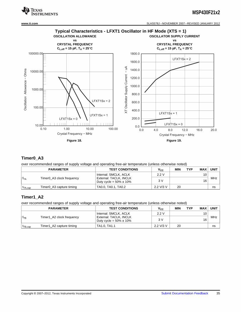
Typical Characteristics - LFXT1 Oscillator in HF Mode (XTS = 1)OSCILLATION ALLOWANCE OSCILLATOR SUPPLY CURRENT
vs vsCRYSTAL FREQUENCY CRYSTAL FREQUENCYCL,eff = 15 pF, TA = 25°C CL,eff = 15 pF, TA = 25°C
Figure 18. Figure 19.
Timer0_A3over recommended ranges of supply voltage and operating free-air temperature (unless otherwise noted)
PARAMETER TEST CONDITIONS VCC MIN TYP MAX UNIT
Internal: SMCLK, ACLK 2.2 V 10fTA Timer0_A3 clock frequency External: TACLK, INCLK MHz
3 V 16Duty cycle = 50% ± 10%
tTA,cap Timer0_A3 capture timing TA0.0, TA0.1, TA0.2 2.2 V/3 V 20 ns
Timer1_A2over recommended ranges of supply voltage and operating free-air temperature (unless otherwise noted)
PARAMETER TEST CONDITIONS VCC MIN TYP MAX UNIT
Internal: SMCLK, ACLK 2.2 V 10fTB Timer1_A2 clock frequency External: TACLK, INCLK MHz
3 V 16Duty cycle = 50% ± 10%
tTB,cap Timer1_A2 capture timing TA1.0, TA1.1 2.2 V/3 V 20 ns
Copyright © 2007–2012, Texas Instruments Incorporated Submit Documentation Feedback 35
MSP430F21x2
SLAS578J –NOVEMBER 2007–REVISED JANUARY 2012 www.ti.com
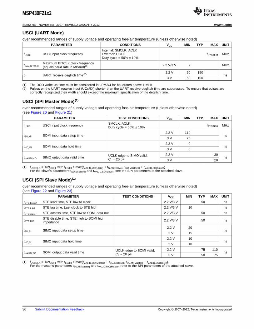
USCI (UART Mode)over recommended ranges of supply voltage and operating free-air temperature (unless otherwise noted)
PARAMETER CONDITIONS VCC MIN TYP MAX UNIT
Internal: SMCLK, ACLKfUSCI USCI input clock frequency External: UCLK fSYSTEM MHz
Duty cycle = 50% ± 10%
Maximum BITCLK clock frequencyfmax,BITCLK 2.2 V/3 V 2 MHz(equals baud rate in MBaud) (1)
2.2 V 50 150tτ UART receive deglitch time (2) ns
3 V 50 100
(1) The DCO wake-up time must be considered in LPM3/4 for baudrates above 1 MHz.(2) Pulses on the UART receive input (UCxRX) shorter than the UART receive deglitch time are suppressed. To ensure that pulses are
correctly recognized their width should exceed the maximum specification of the deglitch time.
USCI (SPI Master Mode) (1)
over recommended ranges of supply voltage and operating free-air temperature (unless otherwise noted)(see Figure 20 and Figure 21)
PARAMETER TEST CONDITIONS VCC MIN TYP MAX UNIT
SMCLK, ACLKfUSCI USCI input clock frequency fSYSTEM MHzDuty cycle = 50% ± 10%
2.2 V 110tSU,MI SOMI input data setup time ns
3 V 75
2.2 V 0tHD,MI SOMI input data hold time ns
3 V 0
2.2 V 30UCLK edge to SIMO valid,tVALID,MO SIMO output data valid time nsCL = 20 pF 3 V 20
(1) fUCxCLK = 1/2tLO/HI with tLO/HI ≥ max(tVALID,MO(USCI) + tSU,SI(Slave), tSU,MI(USCI) + tVALID,SO(Slave)).For the slave's parameters tSU,SI(Slave) and tVALID,SO(Slave), see the SPI parameters of the attached slave.
USCI (SPI Slave Mode) (1)
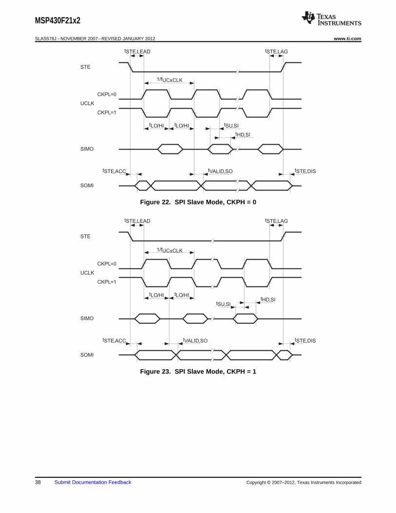
over recommended ranges of supply voltage and operating free-air temperature (unless otherwise noted)(see Figure 22 and Figure 23)
PARAMETER TEST CONDITIONS VCC MIN TYP MAX UNIT
tSTE,LEAD STE lead time, STE low to clock 2.2 V/3 V 50 ns
tSTE,LAG STE lag time, Last clock to STE high 2.2 V/3 V 10 ns
tSTE,ACC STE access time, STE low to SOMI data out 2.2 V/3 V 50 ns
STE disable time, STE high to SOMI hightSTE,DIS 2.2 V/3 V 50 nsimpedance
2.2 V 20tSU,SI SIMO input data setup time ns
3 V 15
2.2 V 10tHD,SI SIMO input data hold time ns
3 V 10
2.2 V 75 110UCLK edge to SOMI valid,tVALID,SO SOMI output data valid time nsCL = 20 pF 3 V 50 75
(1) fUCxCLK = 1/2tLO/HI with tLO/HI ≥ max(tVALID,MO(Master) + tSU,SI(USCI), tSU,MI(Master) + tVALID,SO(USCI)).For the master's parameters tSU,MI(Master) and tVALID,MO(Master) refer to the SPI parameters of the attached slave.
36 Submit Documentation Feedback Copyright © 2007–2012, Texas Instruments Incorporated
UCLK
CKPL=0
CKPL=1
SIMO
1/fUCxCLK
tLO/HI tLO/HI
SOMI
tSU,MI
tHD,MI
tVALID,MO
UCLK
CKPL=0
CKPL=1
SIMO
1/fUCxCLK
tLO/HI tLO/HI
SOMI
tSU,MItHD,MI
tVALID,MO
MSP430F21x2
www.ti.com SLAS578J –NOVEMBER 2007–REVISED JANUARY 2012
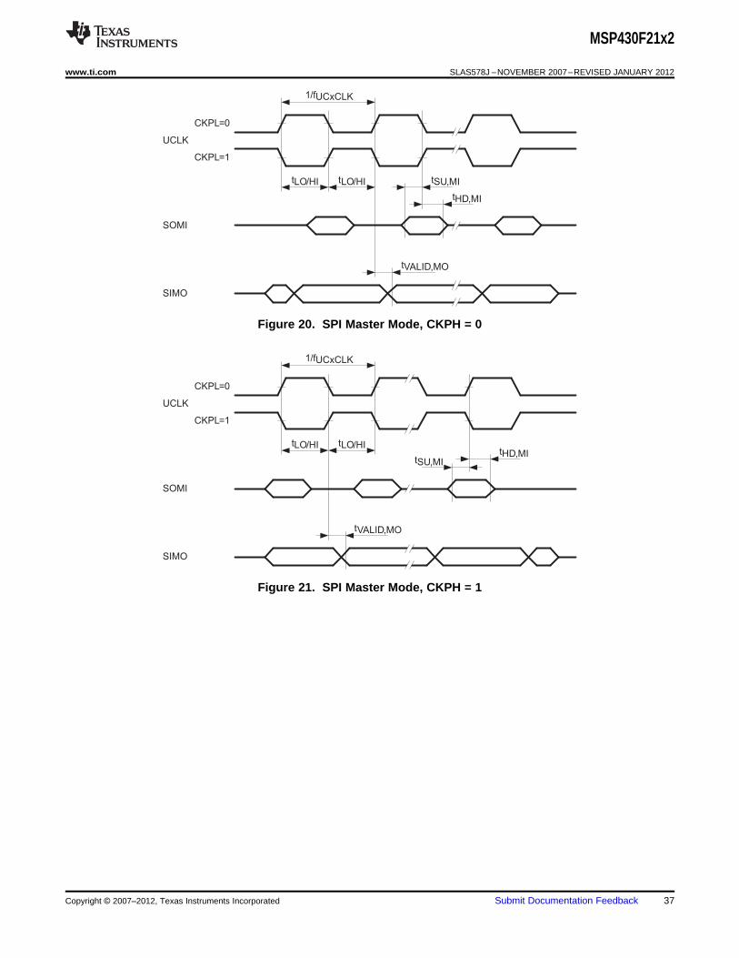
Figure 20. SPI Master Mode, CKPH = 0
Figure 21. SPI Master Mode, CKPH = 1
Copyright © 2007–2012, Texas Instruments Incorporated Submit Documentation Feedback 37
STE
UCLK
CKPL=0
CKPL=1
SOMI
tSTE,ACC tSTE,DIS
1/fUCxCLK
tLO/HI tLO/HI
SIMO
tSU,SI
tHD,SI
tVALID,SO
tSTE,LEAD tSTE,LAG
STE
UCLK
CKPL=0
CKPL=1
tSTE,LEAD tSTE,LAG
tSTE,ACC tSTE,DIS
tLO/HI tLO/HI
tSU,SItHD,SI
tVALID,SO
SOMI
SIMO
1/fUCxCLK
MSP430F21x2
SLAS578J –NOVEMBER 2007–REVISED JANUARY 2012 www.ti.com
Figure 22. SPI Slave Mode, CKPH = 0
Figure 23. SPI Slave Mode, CKPH = 1
38 Submit Documentation Feedback Copyright © 2007–2012, Texas Instruments Incorporated
SDA
SCL
1/fSCL
tHD,DAT
tSU,DAT
tHD,STA tSU,STA tHD,STA
tSU,STO
tSP
MSP430F21x2
www.ti.com SLAS578J –NOVEMBER 2007–REVISED JANUARY 2012
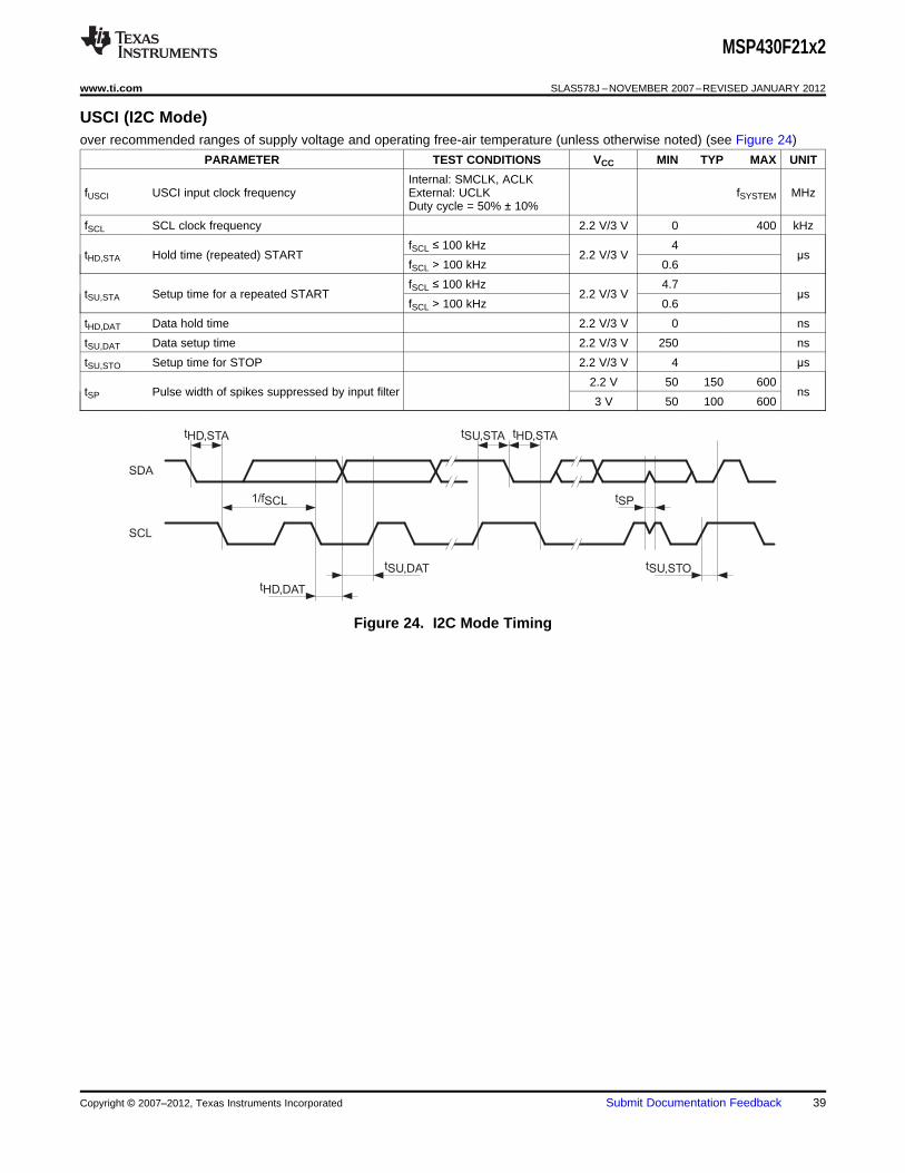
USCI (I2C Mode)over recommended ranges of supply voltage and operating free-air temperature (unless otherwise noted) (see Figure 24)
PARAMETER TEST CONDITIONS VCC MIN TYP MAX UNIT
Internal: SMCLK, ACLKfUSCI USCI input clock frequency External: UCLK fSYSTEM MHz
Duty cycle = 50% ± 10%
fSCL SCL clock frequency 2.2 V/3 V 0 400 kHz
fSCL ≤ 100 kHz 4tHD,STA Hold time (repeated) START 2.2 V/3 V µs
fSCL > 100 kHz 0.6
fSCL ≤ 100 kHz 4.7tSU,STA Setup time for a repeated START 2.2 V/3 V µs
fSCL > 100 kHz 0.6
tHD,DAT Data hold time 2.2 V/3 V 0 ns
tSU,DAT Data setup time 2.2 V/3 V 250 ns
tSU,STO Setup time for STOP 2.2 V/3 V 4 µs
2.2 V 50 150 600tSP Pulse width of spikes suppressed by input filter ns
3 V 50 100 600
Figure 24. I2C Mode Timing
Copyright © 2007–2012, Texas Instruments Incorporated Submit Documentation Feedback 39
MSP430F21x2
SLAS578J –NOVEMBER 2007–REVISED JANUARY 2012 www.ti.com
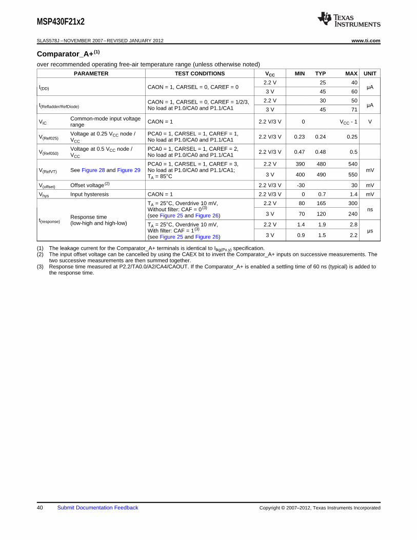
Comparator_A+ (1)
over recommended operating free-air temperature range (unless otherwise noted)
PARAMETER TEST CONDITIONS VCC MIN TYP MAX UNIT
2.2 V 25 40I(DD) CAON = 1, CARSEL = 0, CAREF = 0 µA
3 V 45 60
2.2 V 30 50CAON = 1, CARSEL = 0, CAREF = 1/2/3,I(Refladder/RefDiode) µANo load at P1.0/CA0 and P1.1/CA1 3 V 45 71
Common-mode input voltageVIC CAON = 1 2.2 V/3 V 0 VCC - 1 Vrange
Voltage at 0.25 VCC node / PCA0 = 1, CARSEL = 1, CAREF = 1,V(Ref025) 2.2 V/3 V 0.23 0.24 0.25VCC No load at P1.0/CA0 and P1.1/CA1
Voltage at 0.5 VCC node / PCA0 = 1, CARSEL = 1, CAREF = 2,V(Ref050) 2.2 V/3 V 0.47 0.48 0.5VCC No load at P1.0/CA0 and P1.1/CA1
PCA0 = 1, CARSEL = 1, CAREF = 3, 2.2 V 390 480 540V(RefVT) See Figure 28 and Figure 29 No load at P1.0/CA0 and P1.1/CA1; mV
3 V 400 490 550TA = 85°CV(offset) Offset voltage (2) 2.2 V/3 V -30 30 mV
Vhys Input hysteresis CAON = 1 2.2 V/3 V 0 0.7 1.4 mV
TA = 25°C, Overdrive 10 mV, 2.2 V 80 165 300Without filter: CAF = 0 (3) ns
3 V 70 120 240(see Figure 25 and Figure 26)Response timet(response) (low-high and high-low) TA = 25°C, Overdrive 10 mV, 2.2 V 1.4 1.9 2.8With filter: CAF = 1 (3) µs
3 V 0.9 1.5 2.2(see Figure 25 and Figure 26)
(1) The leakage current for the Comparator_A+ terminals is identical to Ilkg(Px.y) specification.(2) The input offset voltage can be cancelled by using the CAEX bit to invert the Comparator_A+ inputs on successive measurements. The
two successive measurements are then summed together.(3) Response time measured at P2.2/TA0.0/A2/CA4/CAOUT. If the Comparator_A+ is enabled a settling time of 60 ns (typical) is added to
the response time.
40 Submit Documentation Feedback Copyright © 2007–2012, Texas Instruments Incorporated
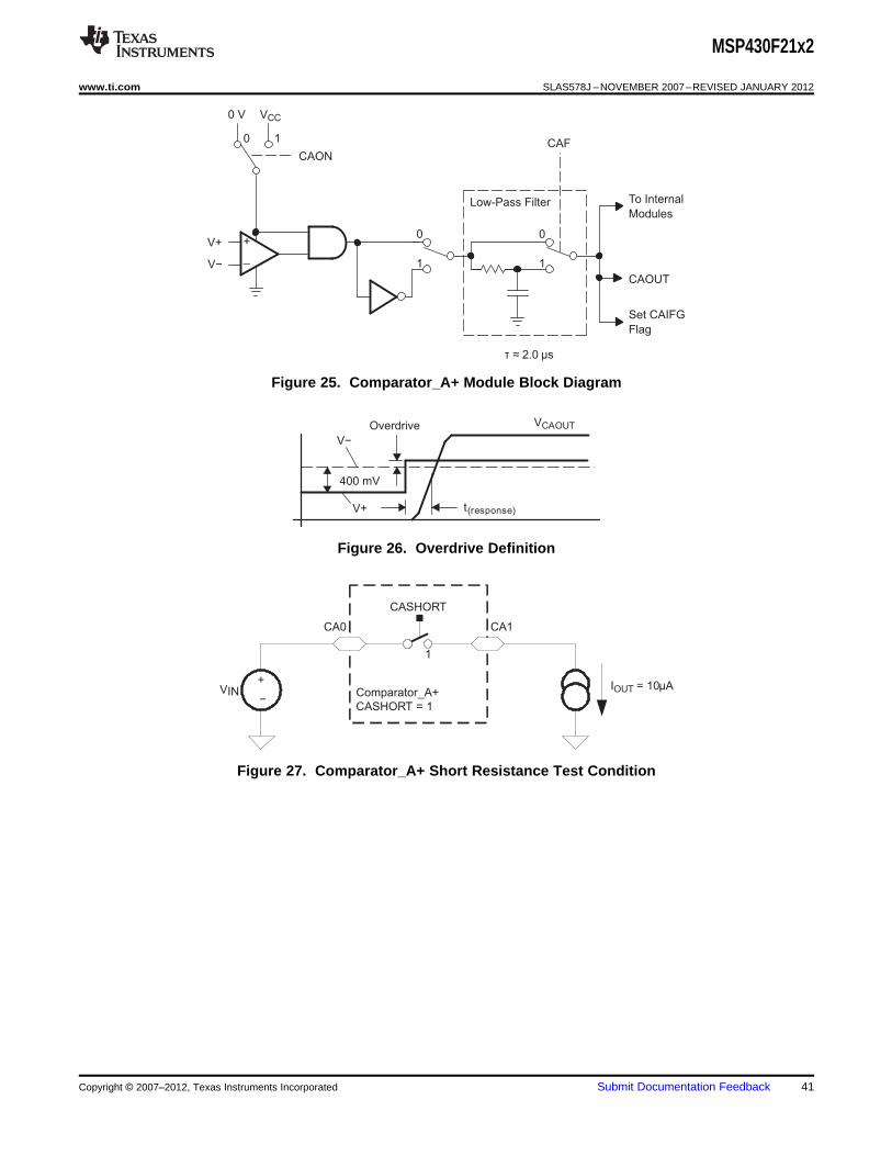
_
+
CAON
0
1
V+0
1
CAF
Low-Pass Filter
τ ≈ 2.0 µs
To Internal
Modules
Set CAIFG
Flag
CAOUT
V−
VCC
1
0 V
0
Overdrive VCAOUT
t(response)V+
V−
400 mV
CASHORT
1
Comparator_A+
CASHORT = 1
CA1CA0
VIN+
−
IOUT = 10µA
MSP430F21x2
www.ti.com SLAS578J –NOVEMBER 2007–REVISED JANUARY 2012
Figure 25. Comparator_A+ Module Block Diagram
Figure 26. Overdrive Definition
Figure 27. Comparator_A+ Short Resistance Test Condition
Copyright © 2007–2012, Texas Instruments Incorporated Submit Documentation Feedback 41
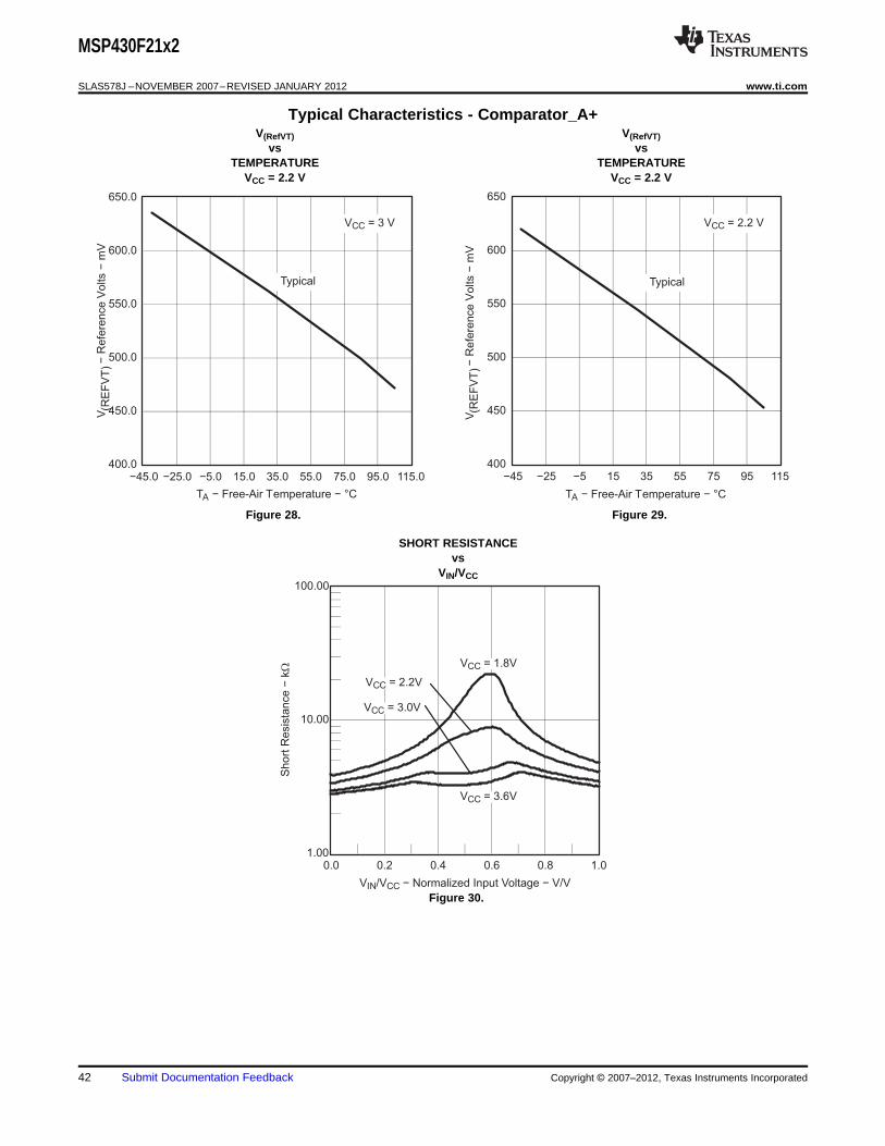
TA − Free-Air Temperature − °C
400.0
450.0
500.0
550.0
600.0
650.0
−45.0 −25.0 −5.0 15.0 35.0 55.0 75.0 95.0 115.0
VCC = 3 V
V(R
EF
VT
)−
Re
fere
nce
Vo
lts
−m
V
Typical
TA − Free-Air Temperature − °C
400
450
500
550
600
650
−45 −25 −5 15 35 55 75 95 115
VCC = 2.2 V
V(R
EF
VT
)−
Refe
rence V
olts
−m
V
Typical
VIN/VCC − Normalized Input Voltage − V/V
1.00
10.00
100.00
0.0 0.2 0.4 0.6 0.8 1.0
Short
Resis
tance
−k
W
VCC = 1.8V
VCC = 3.6V
VCC = 2.2V
VCC = 3.0V
MSP430F21x2
SLAS578J –NOVEMBER 2007–REVISED JANUARY 2012 www.ti.com
Typical Characteristics - Comparator_A+V(RefVT) V(RefVT)
vs vsTEMPERATURE TEMPERATURE
VCC = 2.2 V VCC = 2.2 V
Figure 28. Figure 29.
SHORT RESISTANCEvs
VIN/VCC
Figure 30.
42 Submit Documentation Feedback Copyright © 2007–2012, Texas Instruments Incorporated
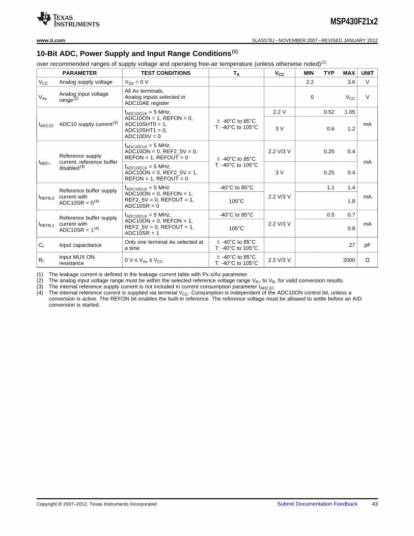
MSP430F21x2
www.ti.com SLAS578J –NOVEMBER 2007–REVISED JANUARY 2012
10-Bit ADC, Power Supply and Input Range Conditions (1)
over recommended ranges of supply voltage and operating free-air temperature (unless otherwise noted) (1)
PARAMETER TEST CONDITIONS TA VCC MIN TYP MAX UNIT
VCC Analog supply voltage VSS = 0 V 2.2 3.6 V
All Ax terminals,Analog input voltageVAx Analog inputs selected in 0 VCC Vrange (2)ADC10AE register
fADC10CLK = 5 MHz, 2.2 V 0.52 1.05ADC10ON = 1, REFON = 0, I: -40°C to 85°CIADC10 ADC10 supply current (3) ADC10SHT0 = 1, mAT: -40°C to 105°C 3 V 0.6 1.2ADC10SHT1 = 0,ADC10DIV = 0
fADC10CLK = 5 MHz,ADC10ON = 0, REF2_5V = 0, 2.2 V/3 V 0.25 0.4
Reference supply REFON = 1, REFOUT = 0 I: -40°C to 85°CIREF+ current, reference buffer mAT: -40°C to 105°CfADC10CLK = 5 MHz,disabled (4)
ADC10ON = 0, REF2_5V = 1, 3 V 0.25 0.4REFON = 1, REFOUT = 0
fADC10CLK = 5 MHz -40°C to 85°C 1.1 1.4Reference buffer supply ADC10ON = 0, REFON = 1,IREFB,0 current with 2.2 V/3 V mAREF2_5V = 0, REFOUT = 1, 105°C 1.8ADC10SR = 0 (4)ADC10SR = 0
fADC10CLK = 5 MHz, -40°C to 85°C 0.5 0.7Reference buffer supply ADC10ON = 0, REFON = 1,IREFB,1 current with 2.2 V/3 V mAREF2_5V = 0, REFOUT = 1, 105°C 0.8ADC10SR = 1 (4)ADC10SR = 1
Only one terminal Ax selected at I: -40°C to 85°CCI Input capacitance 27 pFa time T: -40°C to 105°CInput MUX ON I: -40°C to 85°CRI 0 V ≤ VAx ≤ VCC 2.2 V/3 V 2000 Ωresistance T: -40°C to 105°C
(1) The leakage current is defined in the leakage current table with Px.x/Ax parameter.(2) The analog input voltage range must be within the selected reference voltage range VR+ to VR- for valid conversion results.(3) The internal reference supply current is not included in current consumption parameter IADC10.(4) The internal reference current is supplied via terminal VCC. Consumption is independent of the ADC10ON control bit, unless a
conversion is active. The REFON bit enables the built-in reference. The reference voltage must be allowed to settle before an A/Dconversion is started.
Copyright © 2007–2012, Texas Instruments Incorporated Submit Documentation Feedback 43
MSP430F21x2
SLAS578J –NOVEMBER 2007–REVISED JANUARY 2012 www.ti.com
10-Bit ADC, Built-In Voltage Referenceover recommended ranges of supply voltage and operating free-air temperature (unless otherwise noted)
PARAMETER TEST CONDITIONS VCC MIN TYP MAX UNIT
IVREF+ ≤ 1 mA, REF2_5V = 0 2.2Positive built-inVCC,REF+ reference analog IVREF+ ≤ 0.5 mA, REF2_5V = 1 2.8 V
supply voltage range IVREF+ ≤ 1 mA, REF2_5V = 1 2.9
IVREF+ ≤ IVREF+max, REF2_5V = 0 2.2 V/3 V 1.41 1.5 1.59Positive built-inVREF+ Vreference voltage IVREF+ ≤ IVREF+max, REF2_5V = 1 3 V 2.35 2.5 2.65
2.2 V ±0.5Maximum VREF+ILD,VREF+ mAload current 3 V ±1
IVREF+ = 500 µA ± 100 µA,Analog input voltage VAx ≈ 0.75 V, 2.2 V/3 V ±2REF2_5V = 0VREF+ load LSBregulation IVREF+ = 500 µA ± 100 µA,Analog input voltage VAx ≈ 1.25 V, 3 V ±2REF2_5V = 1
IVREF+ = 100 µA to 900 µA, ADC10SR = 0 400VREF+ load VAx ≈ 0.5 x VREF+,regulation response 3 V nsError of conversion result ADC10SR = 1 2000time ≤1 LSB
MaximumCVREF+ capacitance at pin IVREF+ ≤ ±1 mA, REFON = 1, REFOUT = 1 2.2 V/3 V 100 pF
VREF+(1)
-40°C to 85°C ±100Temperature IVREF+ = constant withTCREF+ 2.2 V/3 V ppm/°Ccoefficient 0 mA ≤ IVREF+ ≤ 1 mA (2)-40°C to 105°C ±110
Settling time of IVREF+ = 0.5 mA, REF2_5V = 0,tREFON internal reference 3.6 V 30 µsREFON = 0 to 1voltage (3)
IVREF+ = 0.5 mA, ADC10SR = 0 1REF2_5V = 0, 2.2 VREFON = 1, ADC10SR = 1 2.5REFBURST = 1Settling time oftREFBURST µsreference buffer (3)IVREF+ = 0.5 mA, ADC10SR = 0 2REF2_5V = 1, 3 VREFON = 1, ADC10SR = 1 4.5REFBURST = 1
(1) The capacitance applied to the internal buffer operational amplifier, if switched to terminal P2.4/TA2/A4/VREF+/VeREF+ (REFOUT = 1),must be limited; otherwise, the reference buffer may become unstable.
(2) Calculated using the box method: ((MAX(VREF(T)) -- MIN(VREF(T))) / MIN(VREF(T)) / (TMAX - TMIN)(3) The condition is that the error in a conversion started after tREFON or tRefBuf is less than ±0.5 LSB.
44 Submit Documentation Feedback Copyright © 2007–2012, Texas Instruments Incorporated
MSP430F21x2
www.ti.com SLAS578J –NOVEMBER 2007–REVISED JANUARY 2012
10-Bit ADC, External Reference (1)
over recommended ranges of supply voltage and operating free-air temperature (unless otherwise noted)
PARAMETER TEST CONDITIONS VCC MIN MAX UNIT
VeREF+ > VeREF-, 1.4 VCCSREF1 = 1, SREF0 = 0Positive external reference inputVeREF+ Vvoltage range (2)VeREF- ≤ VeREF+ ≤ (VCC - 0.15 V), 1.4 3SREF1 = 1, SREF0 = 1 (3)
Negative external reference inputVeREF- VeREF+ > VeREF- 0 1.2 Vvoltage range (4)
Differential external referenceΔVeREF input voltage range VeREF+ > VeREF-
(5) 1.4 VCC VΔVeREF = VeREF+ - VeREF-
0 V ≤ VeREF+ ≤ VCC, ±1SREF1 = 1, SREF0 = 0IVeREF+ Static input current into VeREF+ 2.2 V/3 V µA
0 V ≤ VeREF+ ≤ VCC - 0.15 V ≤ 3 V, 0SREF1 = 1, SREF0 = 1 (3)
IVeREF- Static input current into VeREF- 0 V ≤ VeREF- ≤ VCC 2.2 V/3 V ±1 µA
(1) The external reference is used during conversion to charge and discharge the capacitance array. The input capacitance, CI, is also thedynamic load for an external reference during conversion. The dynamic impedance of the reference supply should follow therecommendations on analog-source impedance to allow the charge to settle for 10-bit accuracy.
(2) The accuracy limits the minimum positive external reference voltage. Lower reference voltage levels may be applied with reducedaccuracy requirements.
(3) Under this condition, the external reference is internally buffered. The reference buffer is active and requires the reference buffer supplycurrent IREFB. The current consumption can be limited to the sample and conversion period with REBURST = 1.
(4) The accuracy limits the maximum negative external reference voltage. Higher reference voltage levels may be applied with reducedaccuracy requirements.
(5) The accuracy limits the minimum external differential reference voltage. Lower differential reference voltage levels may be applied withreduced accuracy requirements.
10-Bit ADC, Timing Parametersover recommended ranges of supply voltage and operating free-air temperature (unless otherwise noted)
PARAMETER TEST CONDITIONS VCC MIN TYP MAX UNIT
ADC10SR = 0 0.45 6.3ADC10 input clock For specified performance offADC10CLK 2.2 V/3 V MHzfrequency ADC10 linearity parameters ADC10SR = 1 0.45 1.5
ADC10 built-in oscillator ADC10DIVx = 0, ADC10SSELx = 0,fADC10OSC 2.2 V/3 V 3.7 6.3 MHzfrequency fADC10CLK = fADC10OSC
ADC10 built-in oscillator, ADC10SSELx = 0, 2.2 V/3 V 2.06 3.51fADC10CLK = fADC10OSCtCONVERT Conversion time µs
fADC10CLK from ACLK, MCLK or SMCLK, 13 × ADC10DIVx ×ADC10SSELx ≠ 0 1 / fADC10CLK
Turn on settling time oftADC10ON See (1) 100 nsthe ADC
(1) The condition is that the error in a conversion started after tADC10ON is less than ±0.5 LSB. The reference and input signal are alreadysettled.
Copyright © 2007–2012, Texas Instruments Incorporated Submit Documentation Feedback 45
MSP430F21x2
SLAS578J –NOVEMBER 2007–REVISED JANUARY 2012 www.ti.com
10-Bit ADC, Linearity Parametersover recommended ranges of supply voltage and operating free-air temperature (unless otherwise noted)
PARAMETER TEST CONDITIONS VCC MIN TYP MAX UNIT
EI Integral linearity error 2.2 V/3 V ±1 LSB
ED Differential linearity error 2.2 V/3 V ±1 LSB
EO Offset error Source impedance RS < 100 Ω 2.2 V/3 V ±1 LSB
SREFx = 010, unbuffered external reference, 2.2 V ±1.1 ±2VeREF+ = 1.5 V
SREFx = 010, unbuffered external reference, 3 V ±1.1 ±2VeREF+ = 2.5 VEG Gain error LSB
SREFx = 011, buffered external reference (1), 2.2 V ±1.1 ±4VeREF+ = 1.5 V
SREFx = 011, buffered external reference (1), 3 V ±1.1 ±3VeREF+ = 2.5 V
SREFx = 010, unbuffered external reference, 2.2 V ±2 ±5VeREF+ = 1.5 V
SREFx = 010, unbuffered external reference, 3 V ±2 ±5VeREF+ = 2.5 VET Total unadjusted error LSB
SREFx = 011, buffered external reference (1), 2.2 V ±2 ±7VeREF+ = 1.5 V
SREFx = 011, buffered external reference (1), 3 V ±2 ±6VeREF+ = 2.5 V
(1) The reference buffer offset adds to the gain and total unadjusted error.
10-Bit ADC, Temperature Sensor and Built-In VMID(1)
over recommended ranges of supply voltage and operating free-air temperature (unless otherwise noted)
PARAMETER TEST CONDITIONS VCC MIN TYP MAX UNIT
2.2 V 40 120Temperature sensor supply REFON = 0, INCHx = 0Ah,ISENSOR µAcurrent (1) ADC10ON = 1, TA = 25°C 3 V 60 160
TCSENSOR ADC10ON = 1, INCHx = 0Ah (2) 2.2 V/3 V 3.55 mV/°CVOffset,Sensor Sensor offset voltage ADC10ON = 1, INCHx = 0Ah (2) -100 +100 mV
Temperature sensor voltage at 1265 1365 1465TA = 105°C (T version only)
Temperature sensor voltage at TA = 85°C 1195 1295 1395VSENSOR Sensor output voltage (3) 2.2 V/3 V mVTemperature sensor voltage at TA = 25°C 985 1085 1185
Temperature sensor voltage at TA = 0°C 895 995 1095
Sample time required if ADC10ON = 1, INCHx = 0Ah,tSENSOR(sample) 2.2 V/3 V 30 µschannel 10 is selected (4) Error of conversion result ≤ 1 LSB
2.2 V N/A (4)Current into divider atIVMID ADC10ON = 1, INCHx = 0Bh µAchannel 11 (4)
3 V N/A (4)
2.2 V 1.06 1.1 1.14ADC10ON = 1, INCHx = 0Bh,VMID VCC divider at channel 11 VVMID ≈ 0.5 × VCC 3 V 1.46 1.5 1.54
2.2 V 1400Sample time required if ADC10ON = 1, INCHx = 0Bh,tVMID(sample) nschannel 11 is selected (5) Error of conversion result ≤ 1 LSB 3 V 1220
(1) The sensor current ISENSOR is consumed if (ADC10ON = 1 and REFON = 1) or (ADC10ON = 1 and INCH = 0Ah and sample signal ishigh). When REFON = 1, ISENSOR is included in IREF+.When REFON = 0, ISENSOR applies during conversion of the temperature sensorinput (INCH = 0Ah).
(2) The following formula can be used to calculate the temperature sensor output voltage:VSensor,typ = TCSensor ( 273 + T [°C] ) + VOffset,sensor [mV] orVSensor,typ = TCSensor T [°C] + VSensor(TA = 0°C) [mV]
(3) Results based on characterization and/or production test, not TCSensor or VOffset,sensor.(4) No additional current is needed. The VMID is used during sampling.(5) The on time, tVMID(on), is included in the sampling time, tVMID(sample); no additional on time is needed.
46 Submit Documentation Feedback Copyright © 2007–2012, Texas Instruments Incorporated
MSP430F21x2
www.ti.com SLAS578J –NOVEMBER 2007–REVISED JANUARY 2012
Flash Memoryover recommended ranges of supply voltage and operating free-air temperature (unless otherwise noted)
PARAMETER TEST CONDITIONS VCC MIN TYP MAX UNIT
VCC (PGM/ERASE) Program and erase supply voltage 2.2 3.6 V
fFTG Flash timing generator frequency 257 476 kHz
IPGM Supply current from VCC during program 2.2 V/3.6 V 1 5 mA
IERASE Supply current from VCC during erase 2.2 V/3.6 V 1 7 mA
tCPT Cumulative program time (1) 2.2 V/3.6 V 10 ms
tCMErase Cumulative mass erase time 2.2 V/3.6 V 20 ms
Program/erase endurance 104 105 cycles
tRetention Data retention duration TJ = 25°C 100 years
tWord Word or byte program time See (2) 30 tFTG
tBlock, 0 Block program time for first byte or word See (2) 25 tFTG
Block program time for each additionaltBlock, 1-63 See (2) 18 tFTGbyte or word
tBlock, End Block program end-sequence wait time See (2) 6 tFTG
tMass Erase Mass erase time See (2) 10593 tFTG
tSeg Erase Segment erase time See (2) 4819 tFTG
(1) The cumulative program time must not be exceeded when writing to a 64-byte flash block. This parameter applies to all programmingmethods: individual word/byte write and block write modes.
(2) These values are hardwired into the flash controller's state machine (tFTG = 1/fFTG).
RAMover recommended ranges of supply voltage and operating free-air temperature (unless otherwise noted)
PARAMETER TEST CONDITIONS MIN MAX UNIT
V(RAMh) RAM retention supply voltage (1) CPU halted 1.6 V
(1) This parameter defines the minimum supply voltage VCC when the data in RAM remains unchanged. No program execution shouldhappen during this supply voltage condition.
Copyright © 2007–2012, Texas Instruments Incorporated Submit Documentation Feedback 47
MSP430F21x2
SLAS578J –NOVEMBER 2007–REVISED JANUARY 2012 www.ti.com
JTAG and Spy-Bi-Wire Interfaceover recommended ranges of supply voltage and operating free-air temperature (unless otherwise noted)
PARAMETER TEST CONDITIONS VCC MIN TYP MAX UNIT
fSBW Spy-Bi-Wire input frequency 2.2 V/3 V 0 20 MHz
tSBW,Low Spy-Bi-Wire low clock pulse length 2.2 V/3 V 0.025 15 µs
Spy-Bi-Wire enable timetSBW,En 2.2 V/3 V 1 µs(TEST high to acceptance of first clock edge (1))
tSBW,Ret Spy-Bi-Wire return to normal operation time 2.2 V/3 V 15 100 µs
2.2 V 0 5 MHzfTCK TCK input frequency (2)
3 V 0 10 MHz
RInternal Internal pulldown resistance on TEST 2.2 V/3 V 25 60 90 kΩ
(1) Tools accessing the Spy-Bi-Wire interface need to wait for the maximum tSBW,En time after pulling the TEST/SBWCLK pin high beforeapplying the first SBWCLK clock edge.
(2) fTCK may be restricted to meet the timing requirements of the module selected.
JTAG Fuse (1)
over recommended ranges of supply voltage and operating free-air temperature (unless otherwise noted)
PARAMETER TEST CONDITIONS MIN MAX UNIT
VCC(FB) Supply voltage during fuse-blow condition TA = 25°C 2.5 V
VFB Voltage level on TEST for fuse blow 6 7 V
IFB Supply current into TEST during fuse blow 100 mA
tFB Time to blow fuse 1 ms
(1) Once the fuse is blown, no further access to the JTAG/Test and emulation features is possible, and the JTAG block is switched tobypass mode.
48 Submit Documentation Feedback Copyright © 2007–2012, Texas Instruments Incorporated
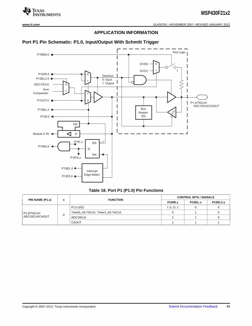
Direction
0: Input
1: Output
P1SEL.0
P1DIR.0
P1IN.0
P1IRQ.0
D
EN
Module X IN
ADC10CLK
P1OUT.0
Interrupt
Edge Select
Q
EN
Set
P1SEL.0
P1IES.0
P1IFG.x
P1IE.x
DVSS
DVCC
P1REN.0Pad Logic
1
1
0
0
1
1
0
P1.0/TACLK/ADC10CLK/CAOUT
1
0
from
Comparator
P1SEL2.0
Bus
Keeper
EN
MSP430F21x2
www.ti.com SLAS578J –NOVEMBER 2007–REVISED JANUARY 2012
APPLICATION INFORMATION
Port P1 Pin Schematic: P1.0, Input/Output With Schmitt Trigger
Table 18. Port P1 (P1.0) Pin Functions
CONTROL BITS / SIGNALSPIN NAME (P1.x) x FUNCTION
P1DIR.x P1SEL.x P1SEL2.x
P1.0 (I/O) I: 0, O: 1 0 0
Timer0_A3.TACLK, Timer1_A2.TACLK 0 1 0P1.0/TACLK/ 0ADC10CLK/CAOUT ADC10CLK 1 1 0
CAOUT 1 1 1
Copyright © 2007–2012, Texas Instruments Incorporated Submit Documentation Feedback 49
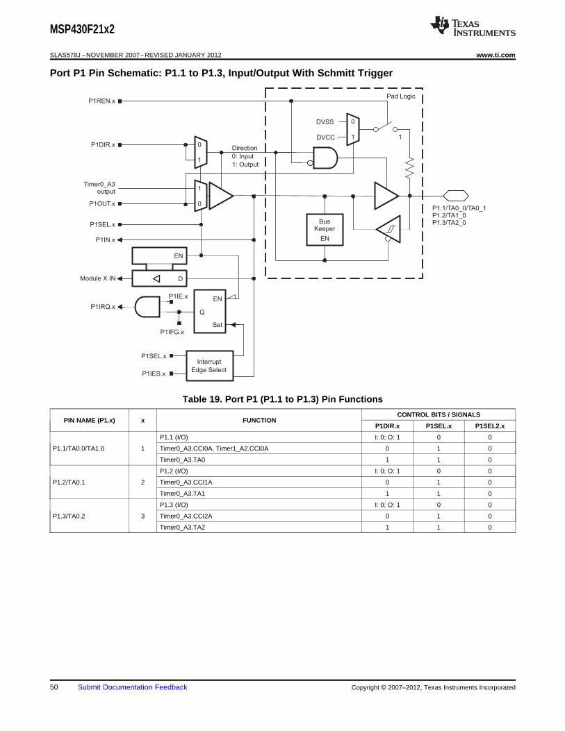
Direction
0: Input
1: Output
P1SEL.x
P1DIR.x
P1IN.x
P1IRQ.x
Module X IN
Timer0_A3output
P1OUT.x
Interrupt
Edge Select
Q
EN
Set
P1SEL.x
P1IES.x
P1IFG.x
P1IE.x
DVSS
DVCC
P1REN.xPad Logic
1
1
0
0
1
1
0
BusKeeper
EN
P1.1/TA0_0/TA0_1P1.2/TA1_0P1.3/TA2_0
D
EN
MSP430F21x2
SLAS578J –NOVEMBER 2007–REVISED JANUARY 2012 www.ti.com
Port P1 Pin Schematic: P1.1 to P1.3, Input/Output With Schmitt Trigger
Table 19. Port P1 (P1.1 to P1.3) Pin Functions
CONTROL BITS / SIGNALSPIN NAME (P1.x) x FUNCTION
P1DIR.x P1SEL.x P1SEL2.x
P1.1 (I/O) I: 0; O: 1 0 0
P1.1/TA0.0/TA1.0 1 Timer0_A3.CCI0A, Timer1_A2.CCI0A 0 1 0
Timer0_A3.TA0 1 1 0
P1.2 (I/O) I: 0; O: 1 0 0
P1.2/TA0.1 2 Timer0_A3.CCI1A 0 1 0
Timer0_A3.TA1 1 1 0
P1.3 (I/O) I: 0; O: 1 0 0
P1.3/TA0.2 3 Timer0_A3.CCI2A 0 1 0
Timer0_A3.TA2 1 1 0
50 Submit Documentation Feedback Copyright © 2007–2012, Texas Instruments Incorporated
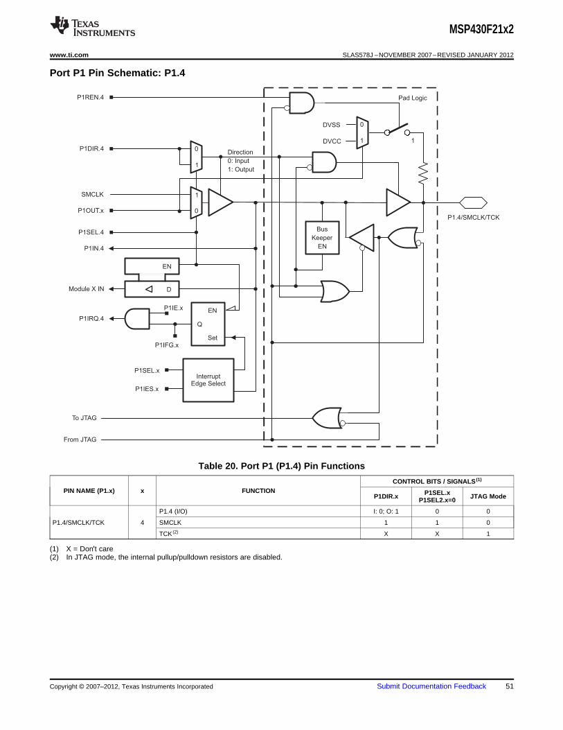
To JTAG
From JTAG
Direction
0: Input
1: Output
P1SEL.4
P1DIR.4
P1IN.4
P1IRQ.4
Module X IN
SMCLK
P1OUT.x
InterruptEdge Select
Q
EN
Set
P1SEL.x
P1IES.x
P1IFG.x
P1IE.x
DVSS
DVCC
P1REN.4 Pad Logic
1
1
0
0
1
1
0
Bus
Keeper
EN
P1.4/SMCLK/TCK
D
EN
MSP430F21x2
www.ti.com SLAS578J –NOVEMBER 2007–REVISED JANUARY 2012
Port P1 Pin Schematic: P1.4
Table 20. Port P1 (P1.4) Pin Functions
CONTROL BITS / SIGNALS (1)
PIN NAME (P1.x) x FUNCTION P1SEL.xP1DIR.x JTAG ModeP1SEL2.x=0
P1.4 (I/O) I: 0; O: 1 0 0
P1.4/SMCLK/TCK 4 SMCLK 1 1 0
TCK (2) X X 1
(1) X = Don't care(2) In JTAG mode, the internal pullup/pulldown resistors are disabled.
Copyright © 2007–2012, Texas Instruments Incorporated Submit Documentation Feedback 51
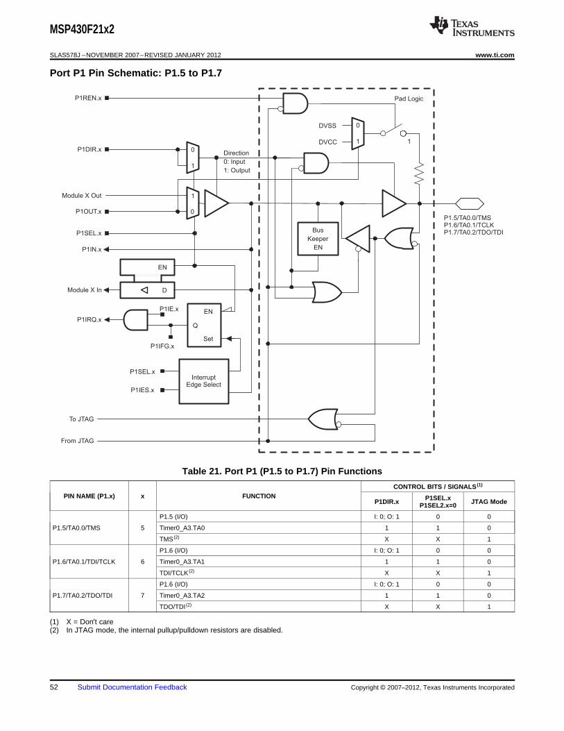
To JTAG
From JTAG
Direction
0: Input
1: Output
P1SEL.x
P1DIR.x
P1IN.x
P1IRQ.x
D
EN
Module X In
Module X Out
P1OUT.x
InterruptEdge Select
Q
EN
Set
P1SEL.x
P1IES.x
P1IFG.x
P1IE.x
DVSS
DVCC
P1REN.x Pad Logic
1
1
0
0
1
1
0
Bus
Keeper
EN
P1.5/TA0.0/TMSP1.6/TA0.1/TCLKP1.7/TA0.2/TDO/TDI
MSP430F21x2
SLAS578J –NOVEMBER 2007–REVISED JANUARY 2012 www.ti.com
Port P1 Pin Schematic: P1.5 to P1.7
Table 21. Port P1 (P1.5 to P1.7) Pin Functions
CONTROL BITS / SIGNALS (1)
PIN NAME (P1.x) x FUNCTION P1SEL.xP1DIR.x JTAG ModeP1SEL2.x=0
P1.5 (I/O) I: 0; O: 1 0 0
P1.5/TA0.0/TMS 5 Timer0_A3.TA0 1 1 0
TMS (2) X X 1
P1.6 (I/O) I: 0; O: 1 0 0
P1.6/TA0.1/TDI/TCLK 6 Timer0_A3.TA1 1 1 0
TDI/TCLK (2) X X 1
P1.6 (I/O) I: 0; O: 1 0 0
P1.7/TA0.2/TDO/TDI 7 Timer0_A3.TA2 1 1 0
TDO/TDI (2) X X 1
(1) X = Don't care(2) In JTAG mode, the internal pullup/pulldown resistors are disabled.
52 Submit Documentation Feedback Copyright © 2007–2012, Texas Instruments Incorporated
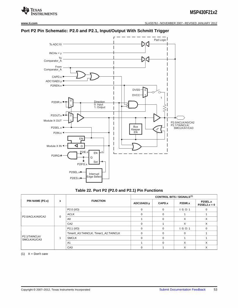
P2.0/ACLK/A0/CA2P2.1/TAINCLK/
SMCLK/A1/CA3
Direction0: Input1: Output
P2SEL.x
P2DIR.x
P2IN.x
P2IRQ.x
D
EN
Module X IN
Module X OUT
P2OUT.x
InterruptEdge Select
Q
EN
Set
P2SEL.x
P2IES.x
P2IFG.x
P2IE.x
DVSS
DVCC
P2REN.x
Pad Logic
1
1
0
1
0
1
0
BusKeeper
EN
CAPD.x
FromComparator_A
ToComparator_A
INCHx = y
To ADC10
ADC10AE0.y
MSP430F21x2
www.ti.com SLAS578J –NOVEMBER 2007–REVISED JANUARY 2012
Port P2 Pin Schematic: P2.0 and P2.1, Input/Output With Schmitt Trigger
Table 22. Port P2 (P2.0 and P2.1) Pin Functions
CONTROL BITS / SIGNALS (1)
PIN NAME (P2.x) x FUNCTION P2SEL.xADC10AE0.y CAPD.x P2DIR.x P2SEL2.x = 0
P2.0 (I/O) 0 0 I: 0; O: 1 0
ACLK 0 0 1 1P2.0/ACLK/A0/CA2 0
A0 1 0 X X
CA2 0 1 X X
P2.1 (I/O) 0 0 I: 0; O: 1 0
Timer0_A3.TAINCLK, Timer1_A2.TAINCLK 0 0 0 1P2.1/TAINCLK/ 1 SMCLK 0 0 1 1SMCLK/A1/CA3
A1 1 0 X X
CA3 0 1 X X
(1) X = Don't care
Copyright © 2007–2012, Texas Instruments Incorporated Submit Documentation Feedback 53
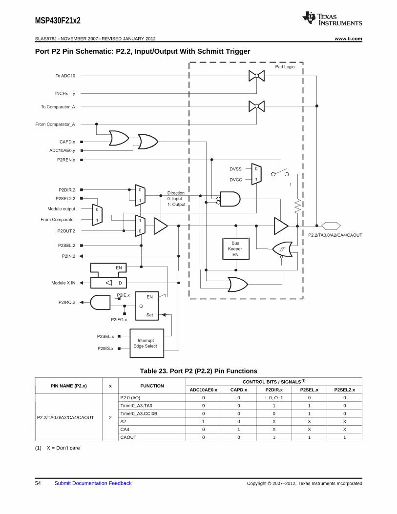
P2.2/TA0.0/A2/CA4/CAOUT
Direction
0: Input
1: Output
P2SEL.2
P2DIR.2
P2IN.2
P2IRQ.2
D
EN
Module X IN
From Comparator
Module output
Interrupt
Edge Select
Q
EN
Set
P2SEL.x
P2IES.x
P2IFG.x
P2IE.x
DVSS
DVCC
P2REN.x
Pad Logic
1
1
0
0
1
1
0
Bus
Keeper
EN
CAPD.x
From Comparator_A
To Comparator_A
INCHx = y
To ADC10
ADC10AE0.y
P2SEL2.2
P2OUT.2
1
0
MSP430F21x2
SLAS578J –NOVEMBER 2007–REVISED JANUARY 2012 www.ti.com
Port P2 Pin Schematic: P2.2, Input/Output With Schmitt Trigger
Table 23. Port P2 (P2.2) Pin Functions
CONTROL BITS / SIGNALS (1)
PIN NAME (P2.x) x FUNCTIONADC10AE0.x CAPD.x P2DIR.x P2SEL.x P2SEL2.x
P2.0 (I/O) 0 0 I: 0; O: 1 0 0
Timer0_A3.TA0 0 0 1 1 0
Timer0_A3.CCI0B 0 0 0 1 0P2.2/TA0.0/A2/CA4/CAOUT 2
A2 1 0 X X X
CA4 0 1 X X X
CAOUT 0 0 1 1 1
(1) X = Don't care
54 Submit Documentation Feedback Copyright © 2007–2012, Texas Instruments Incorporated
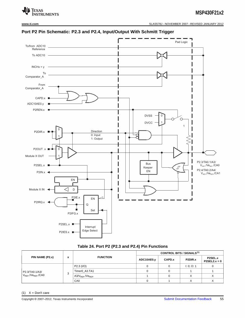
Direction
0: Input
1: Output
P2SEL.x
P2DIR.x
P2IN.x
P2IRQ.x
D
EN
Module X IN
Module X OUT
P2OUT .x
Interrupt
Edge Select
Q
EN
Set
P2SEL.x
P2IES.x
P2IFG.x
P2IE.x
DVSS
DVCC
P2REN.x
Pad Logic
1
1
0
1
0
1
0
Bus
Keeper
EN
CAPD.x
From
Comparator_A
To
Comparator_A
INCHx = y
To ADC10
ADC10AE0.y
To/from ADC10Reference
P2.3/TA0.1/A3/V /Ve /CA0REF− REF−
P2.4/TA0.2/A4/V /Ve /CA1REF+ REF+
MSP430F21x2
www.ti.com SLAS578J –NOVEMBER 2007–REVISED JANUARY 2012
Port P2 Pin Schematic: P2.3 and P2.4, Input/Output With Schmitt Trigger
Table 24. Port P2 (P2.3 and P2.4) Pin Functions
CONTROL BITS / SIGNALS (1)
PIN NAME (P2.x) x FUNCTION P2SEL.xADC10AE0.y CAPD.x P2DIR.x P2SEL2.x = 0
P2.3 (I/O) 0 0 I: 0; O: 1 0
Timer0_A3.TA1 0 0 1 1P2.3/TA0.1/A3/ 3VREF-/VeREF-/CA0 A3/VREF-/VeREF- 1 0 X X
CA0 0 1 X X
(1) X = Don't care
Copyright © 2007–2012, Texas Instruments Incorporated Submit Documentation Feedback 55
MSP430F21x2
SLAS578J –NOVEMBER 2007–REVISED JANUARY 2012 www.ti.com
Table 24. Port P2 (P2.3 and P2.4) Pin Functions (continued)CONTROL BITS / SIGNALS (1)
PIN NAME (P2.x) x FUNCTION P2SEL.xADC10AE0.y CAPD.x P2DIR.x P2SEL2.x = 0
P2.4 (I/O) 0 0 I: 0; O: 1 0
Timer0_A3.TA2 0 0 1 1P2.4/TA0.2/A4/ 4VREF+/VeREF+/CA1 A4/VREF+/VeREF+ 1 0 X X
CA1 0 1 X X
56 Submit Documentation Feedback Copyright © 2007–2012, Texas Instruments Incorporated
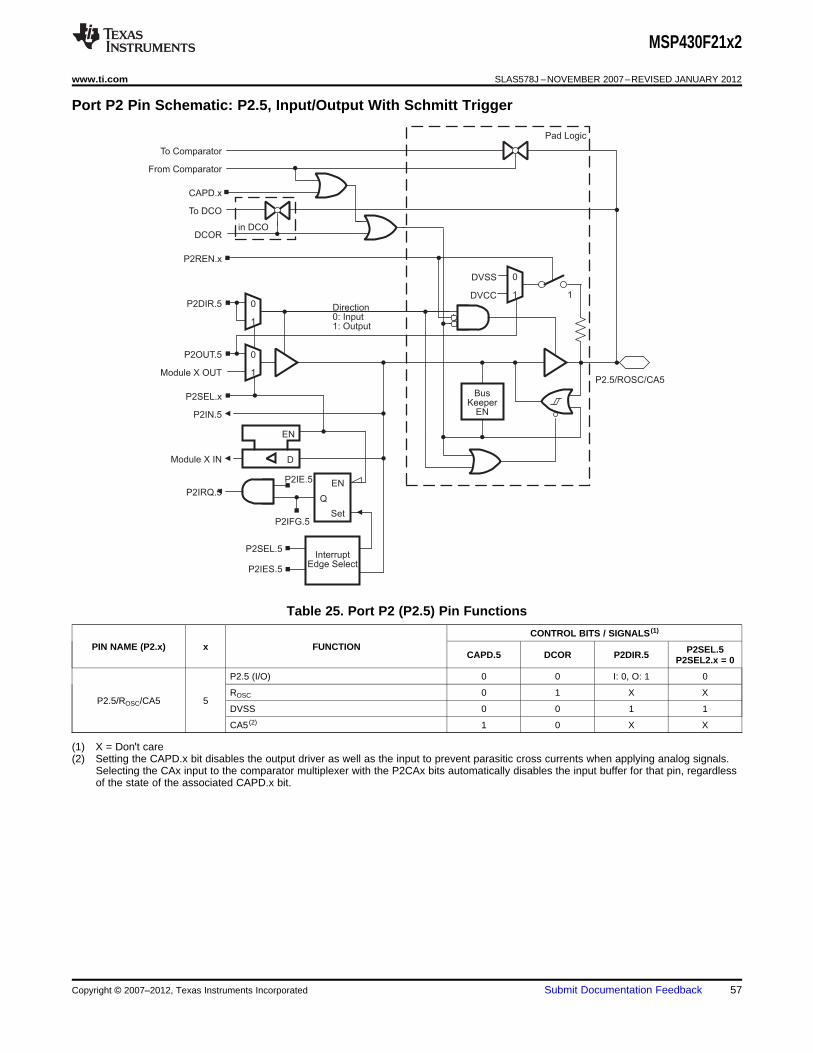
Direction0: Input1: Output
P2SEL.x
P2DIR.5
P2IN.5
P2IRQ.5
D
EN
Module X IN
Module X OUT
P2OUT.5
InterruptEdge Select
Q
EN
Set
P2SEL.5
P2IES.5
P2IFG.5
P2IE.5
P2.5/ROSC/CA5
DVSS
DVCC
P2REN.x
1
1
0
1
0
1
0
BusKeeper
EN
DCOR
To DCO
Pad Logic
From Comparator
To Comparator
CAPD.x
in DCO
MSP430F21x2
www.ti.com SLAS578J –NOVEMBER 2007–REVISED JANUARY 2012
Port P2 Pin Schematic: P2.5, Input/Output With Schmitt Trigger
Table 25. Port P2 (P2.5) Pin Functions
CONTROL BITS / SIGNALS (1)
PIN NAME (P2.x) x FUNCTION P2SEL.5CAPD.5 DCOR P2DIR.5 P2SEL2.x = 0
P2.5 (I/O) 0 0 I: 0, O: 1 0
ROSC 0 1 X XP2.5/ROSC/CA5 5
DVSS 0 0 1 1
CA5 (2) 1 0 X X
(1) X = Don't care(2) Setting the CAPD.x bit disables the output driver as well as the input to prevent parasitic cross currents when applying analog signals.
Selecting the CAx input to the comparator multiplexer with the P2CAx bits automatically disables the input buffer for that pin, regardlessof the state of the associated CAPD.x bit.
Copyright © 2007–2012, Texas Instruments Incorporated Submit Documentation Feedback 57
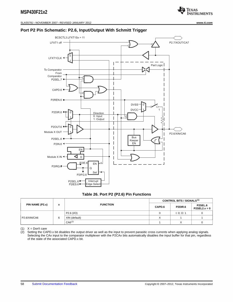
Direction0: Input1: Output
P2SEL.6
P2DIR.6
P2IN.6
P2IRQ.6
D
EN
Module X IN
Module X OUT
P2OUT.6
InterruptEdge Select
Q
EN
Set
P2SEL.6P2IES.6
P2IFG.6
P2IE.6
DVSS
DVCC
P2REN.6
Pad Logic
1
1
0
1
0
1
0
BusKeeper
EN
P2SEL.7
P2.6/XIN/CA6
1
0LFXT1CLK
P2.7/XOUT/CA7LFXT1 off
BCSCTL3.LFXT1Sx = 11
FromComparator
To Comparator
CAPD.6
MSP430F21x2
SLAS578J –NOVEMBER 2007–REVISED JANUARY 2012 www.ti.com
Port P2 Pin Schematic: P2.6, Input/Output With Schmitt Trigger
Table 26. Port P2 (P2.6) Pin Functions
CONTROL BITS / SIGNALS (1)
PIN NAME (P2.x) x FUNCTION P2SEL.6CAPD.6 P2DIR.6 P2SEL2.x = 0
P2.6 (I/O) 0 I: 0; O: 1 0
P2.6/XIN/CA6 6 XIN (default) X 1 1
CA6 (2) 1 X 0
(1) X = Don't care(2) Setting the CAPD.x bit disables the output driver as well as the input to prevent parasitic cross currents when applying analog signals.
Selecting the CAx input to the comparator multiplexer with the P2CAx bits automatically disables the input buffer for that pin, regardlessof the state of the associated CAPD.x bit.
58 Submit Documentation Feedback Copyright © 2007–2012, Texas Instruments Incorporated
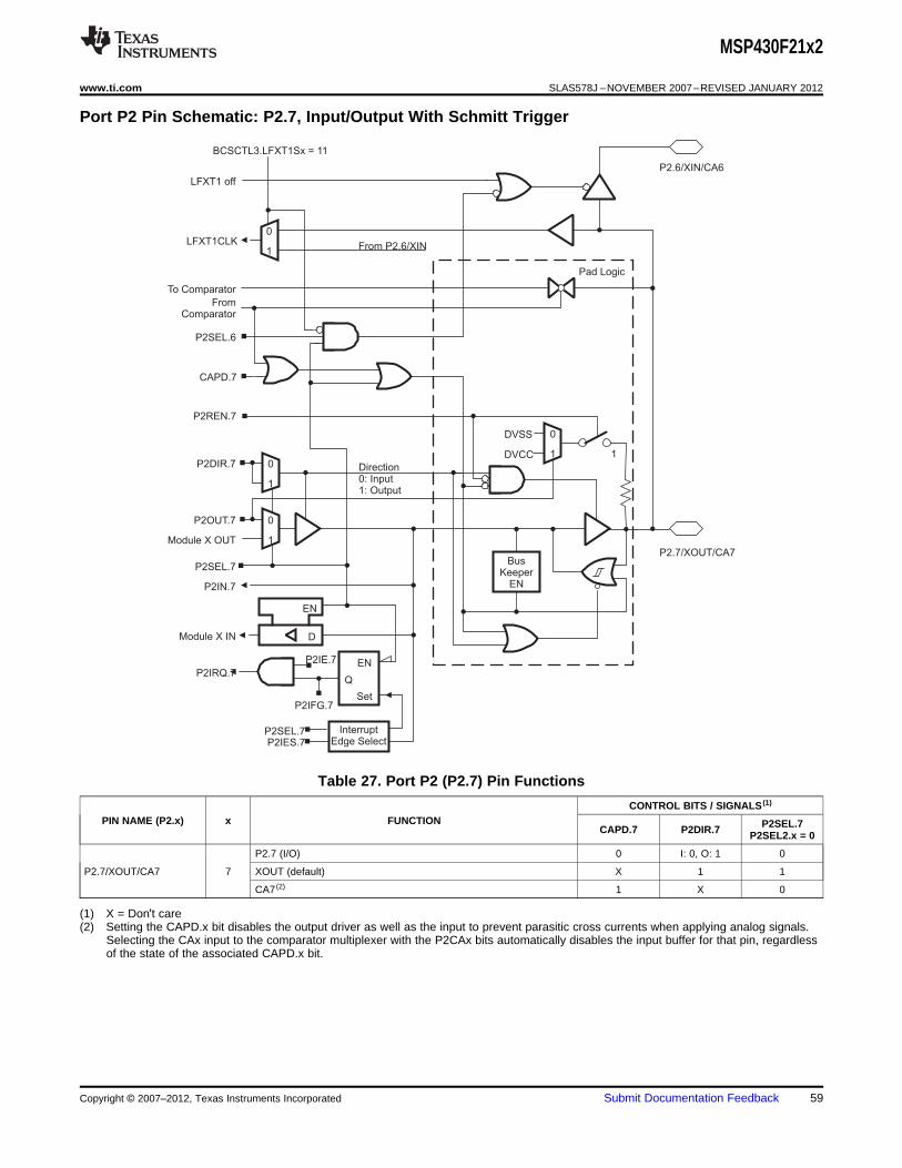
Direction0: Input1: Output
P2SEL.7
P2DIR.7
P2IN.7
P2IRQ.7
D
EN
Module X IN
Module X OUT
P2OUT.7
InterruptEdge Select
Q
EN
Set
P2SEL.7P2IES.7
P2IFG.7
P2IE.7
DVSS
DVCC
Pad Logic
1
1
0
1
0
1
0
BusKeeper
EN
P2.7/XOUT/CA7
1
0LFXT1CLK
P2.6/XIN/CA6
LFXT1 off
BCSCTL3.LFXT1Sx = 11
From P2.6/XIN
FromComparator
To Comparator
P2SEL.6
CAPD.7
P2REN.7
MSP430F21x2
www.ti.com SLAS578J –NOVEMBER 2007–REVISED JANUARY 2012
Port P2 Pin Schematic: P2.7, Input/Output With Schmitt Trigger
Table 27. Port P2 (P2.7) Pin Functions
CONTROL BITS / SIGNALS (1)
PIN NAME (P2.x) x FUNCTION P2SEL.7CAPD.7 P2DIR.7 P2SEL2.x = 0
P2.7 (I/O) 0 I: 0, O: 1 0
P2.7/XOUT/CA7 7 XOUT (default) X 1 1
CA7 (2) 1 X 0
(1) X = Don't care(2) Setting the CAPD.x bit disables the output driver as well as the input to prevent parasitic cross currents when applying analog signals.
Selecting the CAx input to the comparator multiplexer with the P2CAx bits automatically disables the input buffer for that pin, regardlessof the state of the associated CAPD.x bit.
Copyright © 2007–2012, Texas Instruments Incorporated Submit Documentation Feedback 59
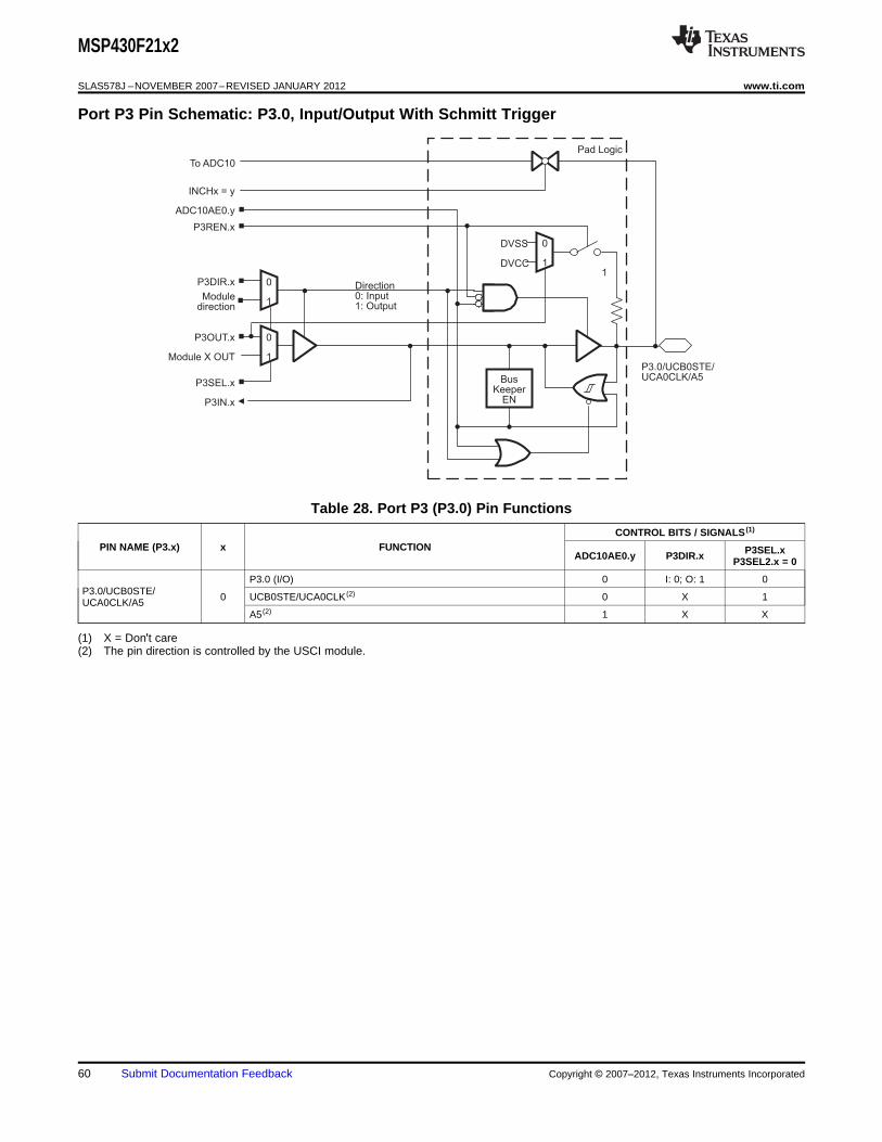
P3.0/UCB0STE/UCA0CLK/A5
Direction0: Input1: Output
P3SEL.x
P3DIR.x
P3IN.x
Module X OUT
P3OUT.x
DVSS
DVCC
P3REN.x
Pad Logic
1
1
0
1
0
1
0
BusKeeper
EN
INCHx = y
To ADC10
ADC10AE0.y
Moduledirection
MSP430F21x2
SLAS578J –NOVEMBER 2007–REVISED JANUARY 2012 www.ti.com
Port P3 Pin Schematic: P3.0, Input/Output With Schmitt Trigger
Table 28. Port P3 (P3.0) Pin Functions
CONTROL BITS / SIGNALS (1)
PIN NAME (P3.x) x FUNCTION P3SEL.xADC10AE0.y P3DIR.x P3SEL2.x = 0
P3.0 (I/O) 0 I: 0; O: 1 0P3.0/UCB0STE/ 0 UCB0STE/UCA0CLK (2) 0 X 1UCA0CLK/A5
A5 (2) 1 X X
(1) X = Don't care(2) The pin direction is controlled by the USCI module.
60 Submit Documentation Feedback Copyright © 2007–2012, Texas Instruments Incorporated
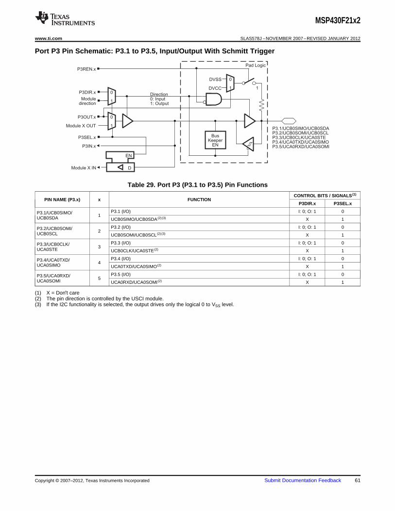
Direction0: Input1: Output
P3SEL.x
P3DIR.x
P3IN.x
D
EN
Module X IN
Module X OUT
P3OUT.x
DVSS
DVCC
Pad Logic
1
1
0
1
0
1
0
P3.1/UCB0SIMO/UCB0SDAP3.2/UCB0SOMI/UCB0SCLP3.3/UCB0CLK/UCA0STEP3.4/UCA0TXD/UCA0SIMOP3.5/UCA0RXD/UCA0SOMI
P3REN.x
Moduledirection
BusKeeper
EN
MSP430F21x2
www.ti.com SLAS578J –NOVEMBER 2007–REVISED JANUARY 2012
Port P3 Pin Schematic: P3.1 to P3.5, Input/Output With Schmitt Trigger
Table 29. Port P3 (P3.1 to P3.5) Pin Functions
CONTROL BITS / SIGNALS (1)
PIN NAME (P3.x) x FUNCTIONP3DIR.x P3SEL.x
P3.1 (I/O) I: 0; O: 1 0P3.1/UCB0SIMO/ 1UCB0SDA UCB0SIMO/UCB0SDA (2) (3) X 1
P3.2 (I/O) I: 0; O: 1 0P3.2/UCB0SOMI/ 2UCB0SCL UCB0SOMI/UCB0SCL (2) (3) X 1
P3.3 (I/O) I: 0; O: 1 0P3.3/UCB0CLK/ 3UCA0STE UCB0CLK/UCA0STE (2) X 1
P3.4 (I/O) I: 0; O: 1 0P3.4/UCA0TXD/ 4UCA0SIMO UCA0TXD/UCA0SIMO (2) X 1
P3.5 (I/O) I: 0; O: 1 0P3.5/UCA0RXD/ 5UCA0SOMI UCA0RXD/UCA0SOMI (2) X 1
(1) X = Don't care(2) The pin direction is controlled by the USCI module.(3) If the I2C functionality is selected, the output drives only the logical 0 to VSS level.
Copyright © 2007–2012, Texas Instruments Incorporated Submit Documentation Feedback 61
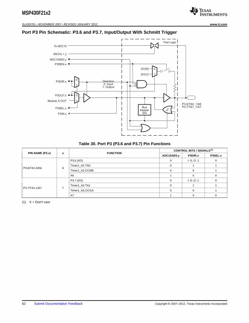
P3.6/TA0_1/A6P3.7/TA1_1/A7
Direction0: Input
1: Output
P3SEL.x
P3DIR.x
P3IN.x
Module X OUT
P3OUT.x
DVSS
DVCC
P3REN.x
Pad Logic
1
0
1
0
1
0
BusKeeper
EN
INCHx = y
To ADC10
ADC10AE0.y
MSP430F21x2
SLAS578J –NOVEMBER 2007–REVISED JANUARY 2012 www.ti.com
Port P3 Pin Schematic: P3.6 and P3.7, Input/Output With Schmitt Trigger
Table 30. Port P3 (P3.6 and P3.7) Pin Functions
CONTROL BITS / SIGNALS (1)
PIN NAME (P3.x) x FUNCTIONADC10AE0.y P3DIR.x P3SEL.x
P3.6 (I/O) 0 I: 0; O: 1 0
Timer1_A2.TA0 0 1 1P3.6/TA1.0/A6 6
Timer1_A2.CCI0B 0 0 1
A6 1 X X
P3.7 (I/O) 0 I: 0; O: 1 0
Timer1_A2.TA1 0 1 1P3.7/TA1.1/A7 7
Timer1_A2.CCI1A 0 0 1
A7 1 X X
(1) X = Don't care
62 Submit Documentation Feedback Copyright © 2007–2012, Texas Instruments Incorporated
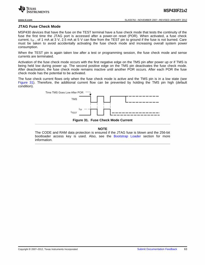
Time TMS Goes Low After POR
TMS
ITF
ITEST
MSP430F21x2
www.ti.com SLAS578J –NOVEMBER 2007–REVISED JANUARY 2012
JTAG Fuse Check Mode
MSP430 devices that have the fuse on the TEST terminal have a fuse check mode that tests the continuity of thefuse the first time the JTAG port is accessed after a power-on reset (POR). When activated, a fuse checkcurrent, ITF , of 1 mA at 3 V, 2.5 mA at 5 V can flow from the TEST pin to ground if the fuse is not burned. Caremust be taken to avoid accidentally activating the fuse check mode and increasing overall system powerconsumption.
When the TEST pin is again taken low after a test or programming session, the fuse check mode and sensecurrents are terminated.
Activation of the fuse check mode occurs with the first negative edge on the TMS pin after power up or if TMS isbeing held low during power up. The second positive edge on the TMS pin deactivates the fuse check mode.After deactivation, the fuse check mode remains inactive until another POR occurs. After each POR the fusecheck mode has the potential to be activated.
The fuse check current flows only when the fuse check mode is active and the TMS pin is in a low state (seeFigure 31). Therefore, the additional current flow can be prevented by holding the TMS pin high (defaultcondition).
Figure 31. Fuse Check Mode Current
NOTEThe CODE and RAM data protection is ensured if the JTAG fuse is blown and the 256-bitbootloader access key is used. Also, see the Bootstrap Loader section for moreinformation.
Copyright © 2007–2012, Texas Instruments Incorporated Submit Documentation Feedback 63
MSP430F21x2
SLAS578J –NOVEMBER 2007–REVISED JANUARY 2012 www.ti.com
REVISION HISTORY
LITERATURE SUMMARYNUMBER
SLAS578 Product Preview data sheet release
SLAS578A Production Data data sheet release
Corrected timer pin names throughout: TA0_0 changed to TA0.0, TA0_1 changed to TA1.0, TA1_0 changed to TA0.1,SLAS578B TA2_0 changed to TA0.2, TA1_1 changed to TA1.1
Added development tool information (page 2).
Corrected TAG_ADC10_1 value from 0x10 to 0x08 (page 14).SLAS578C
Corrected all address offsets in Labels Used By The ADC Calibration Tags table (page 14).
Changed JTAG fuse check mode section (page 73).
Corrected parametric values in active mode supply current (into VCC) excluding external current table (page 20).SLAS578D Corrected parametric values and temperature ranges in low-power mode supply currents (into VCC) excluding external
current table (page 22).
SLAS578E Corrected TAx.y pin names on RHB pinout drawing (page 3).
Changed TDI/TCLK to TEST in Note 2 of absolute maximum ratings table (page 19).SLAS578F Changed lower limit of Storage temperature, Programmed device from -40°C to -55°C in absolute maximum ratings table
(page 19).
In the Labels Used By The ADC Calibration Tags table, changed the Address Offset of CAL_ADC_15T30 from 0x0006 to0x0008 and the Address Offset of CAL_ADC_15VREF_FACTOR from 0x0005 to 0x0006 (page 14).
Changed TDI/TCLK to TEST in the Parameter description for IFB in the JTAG fuse table (page 52).
Updated Port P1 pin schematic: P1.0, input/output with Schmitt trigger (page 53).
Updated Port P1 pin schematic: P1.1 to P1.3, input/output with Schmitt trigger (page 54).
Updated Port P1 (P1.1 to P1.3) pin functions table (page 54).SLAS578G Removed Timer0_A3.CCU0B row from Port P1 (P1.5 to P1.7) pin functions table (page 56).
Updated Port P3 pin schematic: P3.1 to P3.5, input/output with Schmitt trigger (page 69).
Removed P3SEL2.x = 0 from Port P3 (P3.1 to P3.5) pin functions table header row (page 69).
Removed P3SEL2 = 0 from Port P3 (P3.6 and P3.7) pin functions table header row (page 70).
Removed JTAG pins: TMS, TCK, TDI/TCLK, TDO/TDI, input/output with Schmitt trigger (page 71).
Updated JTAG fuse check mode section (page 72).
Corrected schematic drawings for Port 1 and Port 2 (pages 54, 55, 56, 59, 61)SLAS578H
Add information for RTV package options
SLAS578I Changed Storage temperature range limit in Absolute Maximum Ratings
SLAS578J Changed note (4) on 10-Bit ADC, Power Supply and Input Range Conditions.
64 Submit Documentation Feedback Copyright © 2007–2012, Texas Instruments Incorporated
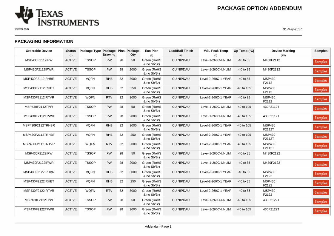
PACKAGE OPTION ADDENDUM
www.ti.com 31-May-2017
Addendum-Page 1
PACKAGING INFORMATION
Orderable Device Status(1)
Package Type PackageDrawing
Pins PackageQty
Eco Plan(2)
Lead/Ball Finish(6)
MSL Peak Temp(3)
Op Temp (°C) Device Marking(4/5)
Samples
MSP430F2112IPW ACTIVE TSSOP PW 28 50 Green (RoHS& no Sb/Br)
CU NIPDAU Level-1-260C-UNLIM -40 to 85 M430F2112
MSP430F2112IPWR ACTIVE TSSOP PW 28 2000 Green (RoHS& no Sb/Br)
CU NIPDAU Level-1-260C-UNLIM -40 to 85 M430F2112
MSP430F2112IRHBR ACTIVE VQFN RHB 32 3000 Green (RoHS& no Sb/Br)
CU NIPDAU Level-2-260C-1 YEAR -40 to 85 MSP430F2112
MSP430F2112IRHBT ACTIVE VQFN RHB 32 250 Green (RoHS& no Sb/Br)
CU NIPDAU Level-2-260C-1 YEAR -40 to 105 MSP430F2112
MSP430F2112IRTVR ACTIVE WQFN RTV 32 3000 Green (RoHS& no Sb/Br)
CU NIPDAU Level-2-260C-1 YEAR -40 to 85 MSP430F2112
MSP430F2112TPW ACTIVE TSSOP PW 28 50 Green (RoHS& no Sb/Br)
CU NIPDAU Level-1-260C-UNLIM -40 to 105 430F2112T
MSP430F2112TPWR ACTIVE TSSOP PW 28 2000 Green (RoHS& no Sb/Br)
CU NIPDAU Level-1-260C-UNLIM -40 to 105 430F2112T
MSP430F2112TRHBR ACTIVE VQFN RHB 32 3000 Green (RoHS& no Sb/Br)
CU NIPDAU Level-2-260C-1 YEAR -40 to 105 MSP430F2112T
MSP430F2112TRHBT ACTIVE VQFN RHB 32 250 Green (RoHS& no Sb/Br)
CU NIPDAU Level-2-260C-1 YEAR -40 to 105 MSP430F2112T
MSP430F2112TRTVR ACTIVE WQFN RTV 32 3000 Green (RoHS& no Sb/Br)
CU NIPDAU Level-2-260C-1 YEAR -40 to 105 MSP430F2112T
MSP430F2122IPW ACTIVE TSSOP PW 28 50 Green (RoHS& no Sb/Br)
CU NIPDAU Level-1-260C-UNLIM -40 to 85 M430F2122
MSP430F2122IPWR ACTIVE TSSOP PW 28 2000 Green (RoHS& no Sb/Br)
CU NIPDAU Level-1-260C-UNLIM -40 to 85 M430F2122
MSP430F2122IRHBR ACTIVE VQFN RHB 32 3000 Green (RoHS& no Sb/Br)
CU NIPDAU Level-2-260C-1 YEAR -40 to 85 MSP430F2122
MSP430F2122IRHBT ACTIVE VQFN RHB 32 250 Green (RoHS& no Sb/Br)
CU NIPDAU Level-2-260C-1 YEAR -40 to 85 MSP430F2122
MSP430F2122IRTVR ACTIVE WQFN RTV 32 3000 Green (RoHS& no Sb/Br)
CU NIPDAU Level-2-260C-1 YEAR -40 to 85 MSP430F2122
MSP430F2122TPW ACTIVE TSSOP PW 28 50 Green (RoHS& no Sb/Br)
CU NIPDAU Level-1-260C-UNLIM -40 to 105 430F2122T
MSP430F2122TPWR ACTIVE TSSOP PW 28 2000 Green (RoHS& no Sb/Br)
CU NIPDAU Level-1-260C-UNLIM -40 to 105 430F2122T
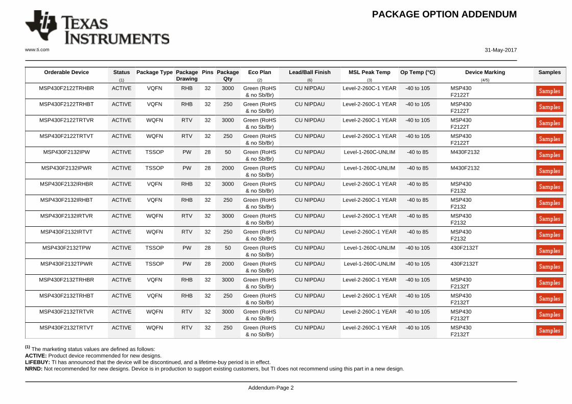
PACKAGE OPTION ADDENDUM
www.ti.com 31-May-2017
Addendum-Page 2
Orderable Device Status(1)
Package Type PackageDrawing
Pins PackageQty
Eco Plan(2)
Lead/Ball Finish(6)
MSL Peak Temp(3)
Op Temp (°C) Device Marking(4/5)
Samples
MSP430F2122TRHBR ACTIVE VQFN RHB 32 3000 Green (RoHS& no Sb/Br)
CU NIPDAU Level-2-260C-1 YEAR -40 to 105 MSP430F2122T
MSP430F2122TRHBT ACTIVE VQFN RHB 32 250 Green (RoHS& no Sb/Br)
CU NIPDAU Level-2-260C-1 YEAR -40 to 105 MSP430F2122T
MSP430F2122TRTVR ACTIVE WQFN RTV 32 3000 Green (RoHS& no Sb/Br)
CU NIPDAU Level-2-260C-1 YEAR -40 to 105 MSP430F2122T
MSP430F2122TRTVT ACTIVE WQFN RTV 32 250 Green (RoHS& no Sb/Br)
CU NIPDAU Level-2-260C-1 YEAR -40 to 105 MSP430F2122T
MSP430F2132IPW ACTIVE TSSOP PW 28 50 Green (RoHS& no Sb/Br)
CU NIPDAU Level-1-260C-UNLIM -40 to 85 M430F2132
MSP430F2132IPWR ACTIVE TSSOP PW 28 2000 Green (RoHS& no Sb/Br)
CU NIPDAU Level-1-260C-UNLIM -40 to 85 M430F2132
MSP430F2132IRHBR ACTIVE VQFN RHB 32 3000 Green (RoHS& no Sb/Br)
CU NIPDAU Level-2-260C-1 YEAR -40 to 85 MSP430F2132
MSP430F2132IRHBT ACTIVE VQFN RHB 32 250 Green (RoHS& no Sb/Br)
CU NIPDAU Level-2-260C-1 YEAR -40 to 85 MSP430F2132
MSP430F2132IRTVR ACTIVE WQFN RTV 32 3000 Green (RoHS& no Sb/Br)
CU NIPDAU Level-2-260C-1 YEAR -40 to 85 MSP430F2132
MSP430F2132IRTVT ACTIVE WQFN RTV 32 250 Green (RoHS& no Sb/Br)
CU NIPDAU Level-2-260C-1 YEAR -40 to 85 MSP430F2132
MSP430F2132TPW ACTIVE TSSOP PW 28 50 Green (RoHS& no Sb/Br)
CU NIPDAU Level-1-260C-UNLIM -40 to 105 430F2132T
MSP430F2132TPWR ACTIVE TSSOP PW 28 2000 Green (RoHS& no Sb/Br)
CU NIPDAU Level-1-260C-UNLIM -40 to 105 430F2132T
MSP430F2132TRHBR ACTIVE VQFN RHB 32 3000 Green (RoHS& no Sb/Br)
CU NIPDAU Level-2-260C-1 YEAR -40 to 105 MSP430F2132T
MSP430F2132TRHBT ACTIVE VQFN RHB 32 250 Green (RoHS& no Sb/Br)
CU NIPDAU Level-2-260C-1 YEAR -40 to 105 MSP430F2132T
MSP430F2132TRTVR ACTIVE WQFN RTV 32 3000 Green (RoHS& no Sb/Br)
CU NIPDAU Level-2-260C-1 YEAR -40 to 105 MSP430F2132T
MSP430F2132TRTVT ACTIVE WQFN RTV 32 250 Green (RoHS& no Sb/Br)
CU NIPDAU Level-2-260C-1 YEAR -40 to 105 MSP430F2132T
(1) The marketing status values are defined as follows:ACTIVE: Product device recommended for new designs.LIFEBUY: TI has announced that the device will be discontinued, and a lifetime-buy period is in effect.NRND: Not recommended for new designs. Device is in production to support existing customers, but TI does not recommend using this part in a new design.
PACKAGE OPTION ADDENDUM
www.ti.com 31-May-2017
Addendum-Page 3
PREVIEW: Device has been announced but is not in production. Samples may or may not be available.OBSOLETE: TI has discontinued the production of the device.
(2) RoHS: TI defines "RoHS" to mean semiconductor products that are compliant with the current EU RoHS requirements for all 10 RoHS substances, including the requirement that RoHS substancedo not exceed 0.1% by weight in homogeneous materials. Where designed to be soldered at high temperatures, "RoHS" products are suitable for use in specified lead-free processes. TI mayreference these types of products as "Pb-Free".RoHS Exempt: TI defines "RoHS Exempt" to mean products that contain lead but are compliant with EU RoHS pursuant to a specific EU RoHS exemption.Green: TI defines "Green" to mean the content of Chlorine (Cl) and Bromine (Br) based flame retardants meet JS709B low halogen requirements of <=1000ppm threshold. Antimony trioxide basedflame retardants must also meet the <=1000ppm threshold requirement.
(3) MSL, Peak Temp. - The Moisture Sensitivity Level rating according to the JEDEC industry standard classifications, and peak solder temperature.
(4) There may be additional marking, which relates to the logo, the lot trace code information, or the environmental category on the device.
(5) Multiple Device Markings will be inside parentheses. Only one Device Marking contained in parentheses and separated by a "~" will appear on a device. If a line is indented then it is a continuationof the previous line and the two combined represent the entire Device Marking for that device.
(6) Lead/Ball Finish - Orderable Devices may have multiple material finish options. Finish options are separated by a vertical ruled line. Lead/Ball Finish values may wrap to two lines if the finishvalue exceeds the maximum column width.
Important Information and Disclaimer:The information provided on this page represents TI's knowledge and belief as of the date that it is provided. TI bases its knowledge and belief on informationprovided by third parties, and makes no representation or warranty as to the accuracy of such information. Efforts are underway to better integrate information from third parties. TI has taken andcontinues to take reasonable steps to provide representative and accurate information but may not have conducted destructive testing or chemical analysis on incoming materials and chemicals.TI and TI suppliers consider certain information to be proprietary, and thus CAS numbers and other limited information may not be available for release.
In no event shall TI's liability arising out of such information exceed the total purchase price of the TI part(s) at issue in this document sold by TI to Customer on an annual basis.
OTHER QUALIFIED VERSIONS OF MSP430F2132 :
• Enhanced Product: MSP430F2132-EP
NOTE: Qualified Version Definitions:
• Enhanced Product - Supports Defense, Aerospace and Medical Applications
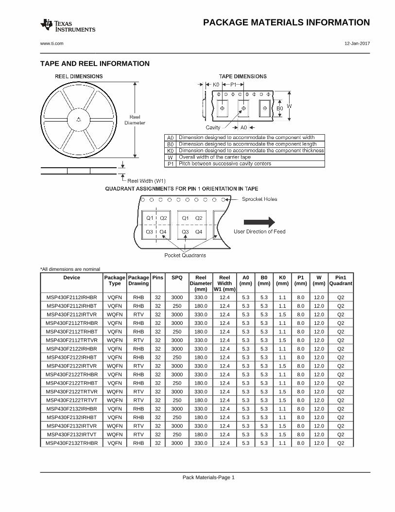
TAPE AND REEL INFORMATION
*All dimensions are nominal
Device PackageType
PackageDrawing
Pins SPQ ReelDiameter
(mm)
ReelWidth
W1 (mm)
A0(mm)
B0(mm)
K0(mm)
P1(mm)
W(mm)
Pin1Quadrant
MSP430F2112IRHBR VQFN RHB 32 3000 330.0 12.4 5.3 5.3 1.1 8.0 12.0 Q2
MSP430F2112IRHBT VQFN RHB 32 250 180.0 12.4 5.3 5.3 1.1 8.0 12.0 Q2
MSP430F2112IRTVR WQFN RTV 32 3000 330.0 12.4 5.3 5.3 1.5 8.0 12.0 Q2
MSP430F2112TRHBR VQFN RHB 32 3000 330.0 12.4 5.3 5.3 1.1 8.0 12.0 Q2
MSP430F2112TRHBT VQFN RHB 32 250 180.0 12.4 5.3 5.3 1.1 8.0 12.0 Q2
MSP430F2112TRTVR WQFN RTV 32 3000 330.0 12.4 5.3 5.3 1.5 8.0 12.0 Q2
MSP430F2122IRHBR VQFN RHB 32 3000 330.0 12.4 5.3 5.3 1.1 8.0 12.0 Q2
MSP430F2122IRHBT VQFN RHB 32 250 180.0 12.4 5.3 5.3 1.1 8.0 12.0 Q2
MSP430F2122IRTVR WQFN RTV 32 3000 330.0 12.4 5.3 5.3 1.5 8.0 12.0 Q2
MSP430F2122TRHBR VQFN RHB 32 3000 330.0 12.4 5.3 5.3 1.1 8.0 12.0 Q2
MSP430F2122TRHBT VQFN RHB 32 250 180.0 12.4 5.3 5.3 1.1 8.0 12.0 Q2
MSP430F2122TRTVR WQFN RTV 32 3000 330.0 12.4 5.3 5.3 1.5 8.0 12.0 Q2
MSP430F2122TRTVT WQFN RTV 32 250 180.0 12.4 5.3 5.3 1.5 8.0 12.0 Q2
MSP430F2132IRHBR VQFN RHB 32 3000 330.0 12.4 5.3 5.3 1.1 8.0 12.0 Q2
MSP430F2132IRHBT VQFN RHB 32 250 180.0 12.4 5.3 5.3 1.1 8.0 12.0 Q2
MSP430F2132IRTVR WQFN RTV 32 3000 330.0 12.4 5.3 5.3 1.5 8.0 12.0 Q2
MSP430F2132IRTVT WQFN RTV 32 250 180.0 12.4 5.3 5.3 1.5 8.0 12.0 Q2
MSP430F2132TRHBR VQFN RHB 32 3000 330.0 12.4 5.3 5.3 1.1 8.0 12.0 Q2
PACKAGE MATERIALS INFORMATION
www.ti.com 12-Jan-2017
Pack Materials-Page 1
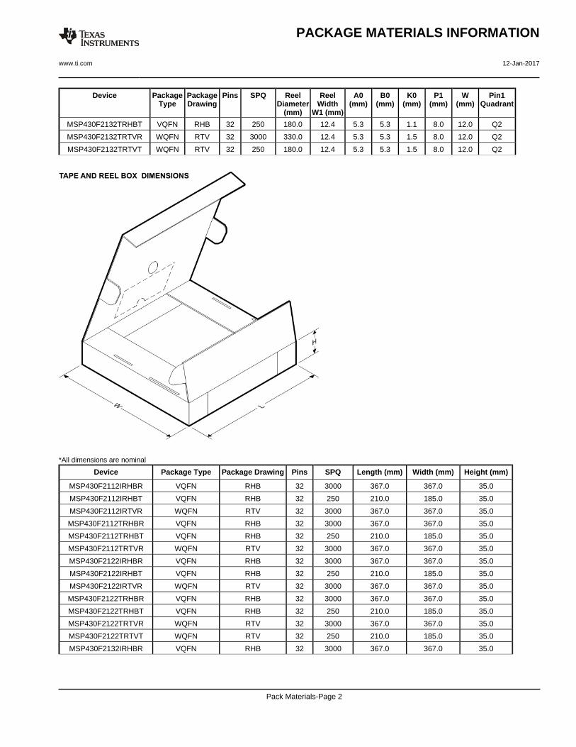
Device PackageType
PackageDrawing
Pins SPQ ReelDiameter
(mm)
ReelWidth
W1 (mm)
A0(mm)
B0(mm)
K0(mm)
P1(mm)
W(mm)
Pin1Quadrant
MSP430F2132TRHBT VQFN RHB 32 250 180.0 12.4 5.3 5.3 1.1 8.0 12.0 Q2
MSP430F2132TRTVR WQFN RTV 32 3000 330.0 12.4 5.3 5.3 1.5 8.0 12.0 Q2
MSP430F2132TRTVT WQFN RTV 32 250 180.0 12.4 5.3 5.3 1.5 8.0 12.0 Q2
*All dimensions are nominal
Device Package Type Package Drawing Pins SPQ Length (mm) Width (mm) Height (mm)
MSP430F2112IRHBR VQFN RHB 32 3000 367.0 367.0 35.0
MSP430F2112IRHBT VQFN RHB 32 250 210.0 185.0 35.0
MSP430F2112IRTVR WQFN RTV 32 3000 367.0 367.0 35.0
MSP430F2112TRHBR VQFN RHB 32 3000 367.0 367.0 35.0
MSP430F2112TRHBT VQFN RHB 32 250 210.0 185.0 35.0
MSP430F2112TRTVR WQFN RTV 32 3000 367.0 367.0 35.0
MSP430F2122IRHBR VQFN RHB 32 3000 367.0 367.0 35.0
MSP430F2122IRHBT VQFN RHB 32 250 210.0 185.0 35.0
MSP430F2122IRTVR WQFN RTV 32 3000 367.0 367.0 35.0
MSP430F2122TRHBR VQFN RHB 32 3000 367.0 367.0 35.0
MSP430F2122TRHBT VQFN RHB 32 250 210.0 185.0 35.0
MSP430F2122TRTVR WQFN RTV 32 3000 367.0 367.0 35.0
MSP430F2122TRTVT WQFN RTV 32 250 210.0 185.0 35.0
MSP430F2132IRHBR VQFN RHB 32 3000 367.0 367.0 35.0
PACKAGE MATERIALS INFORMATION
www.ti.com 12-Jan-2017
Pack Materials-Page 2
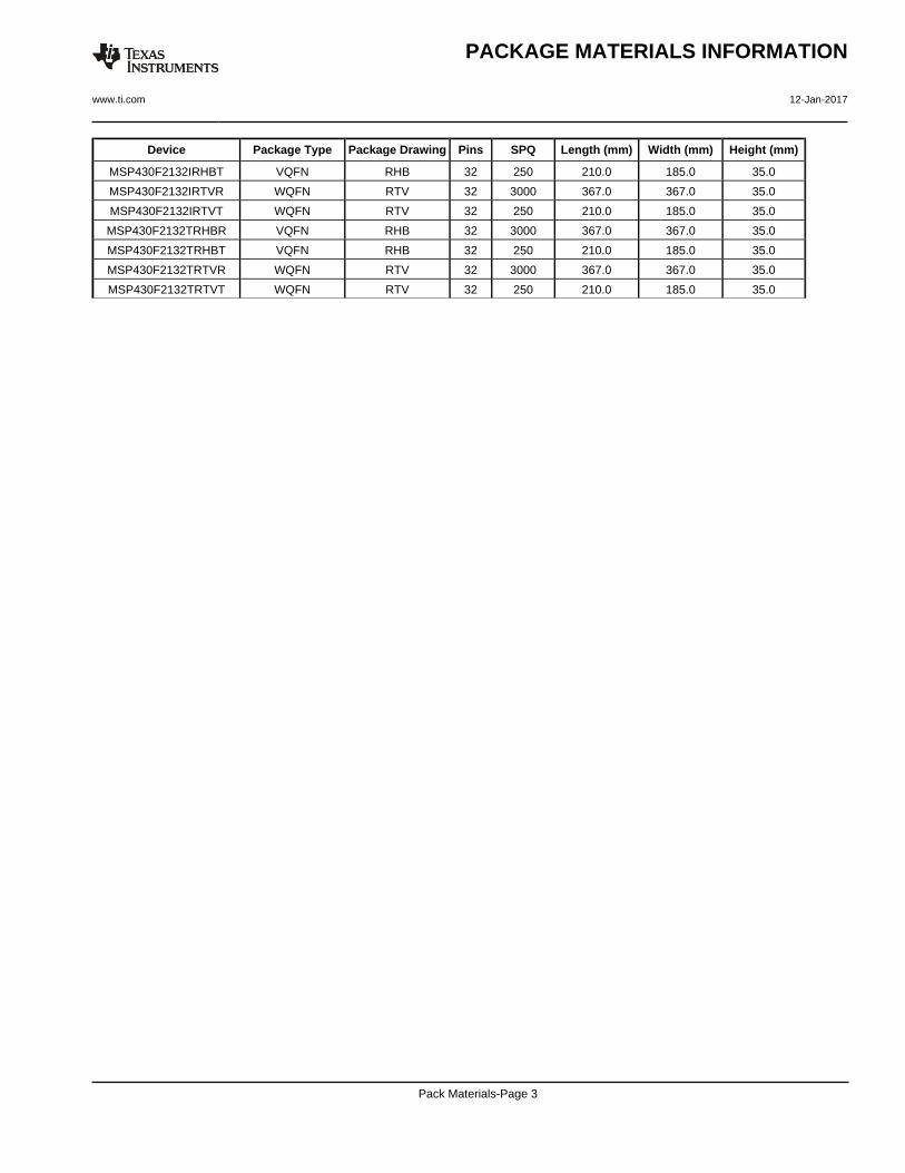
Device Package Type Package Drawing Pins SPQ Length (mm) Width (mm) Height (mm)
MSP430F2132IRHBT VQFN RHB 32 250 210.0 185.0 35.0
MSP430F2132IRTVR WQFN RTV 32 3000 367.0 367.0 35.0
MSP430F2132IRTVT WQFN RTV 32 250 210.0 185.0 35.0
MSP430F2132TRHBR VQFN RHB 32 3000 367.0 367.0 35.0
MSP430F2132TRHBT VQFN RHB 32 250 210.0 185.0 35.0
MSP430F2132TRTVR WQFN RTV 32 3000 367.0 367.0 35.0
MSP430F2132TRTVT WQFN RTV 32 250 210.0 185.0 35.0
PACKAGE MATERIALS INFORMATION
www.ti.com 12-Jan-2017
Pack Materials-Page 3
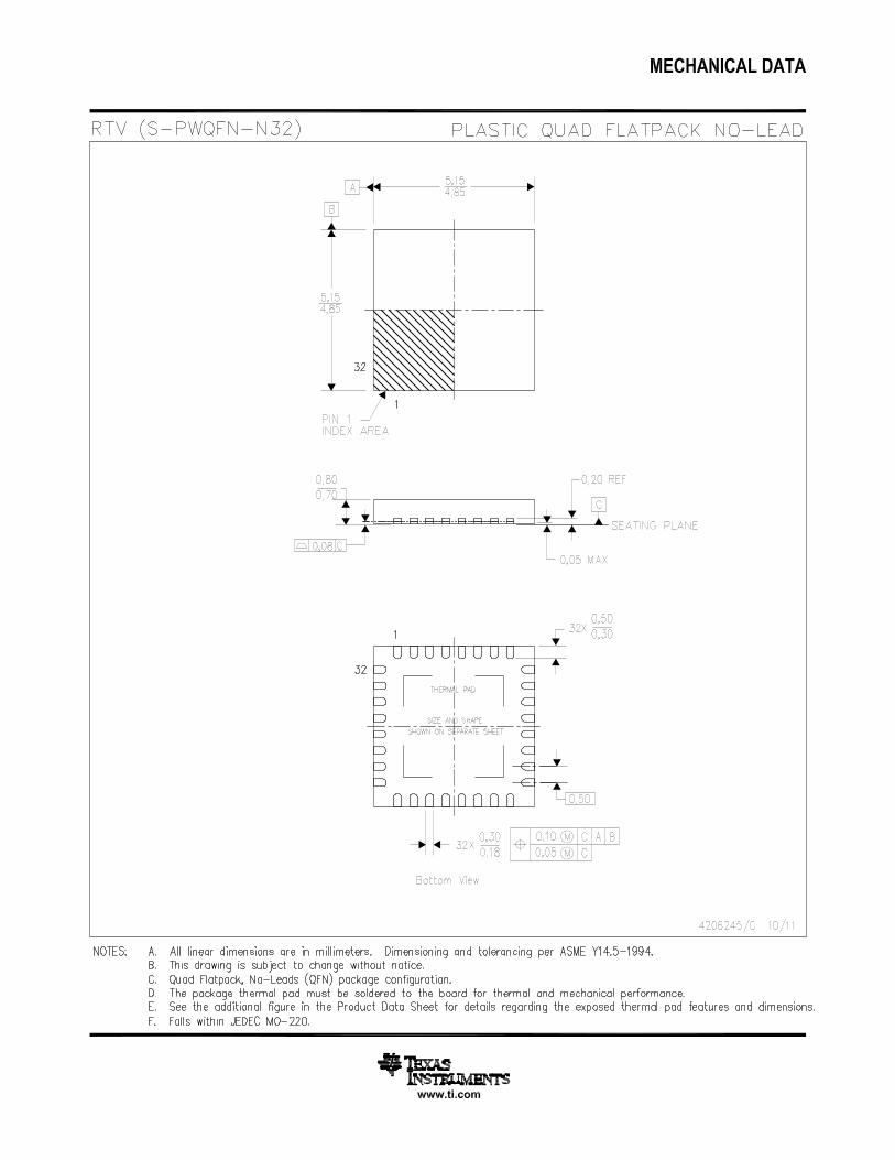
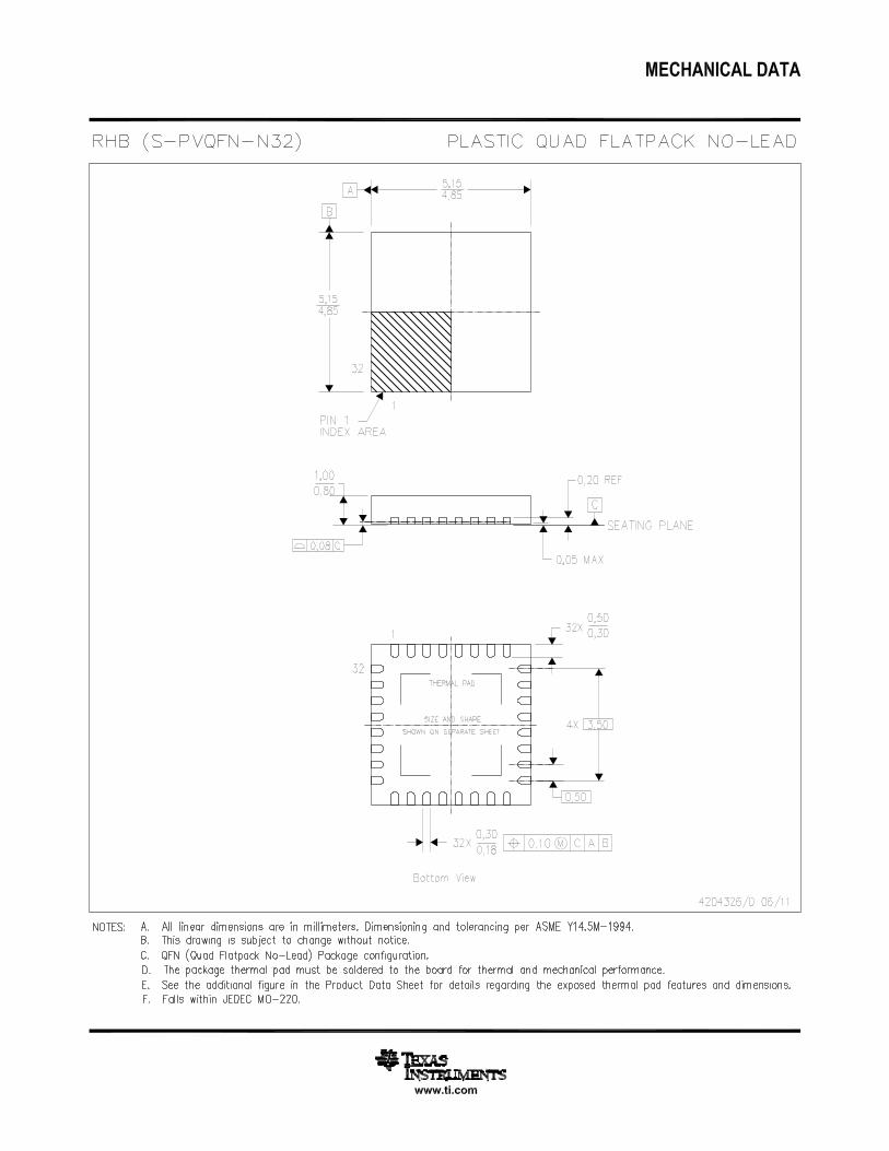
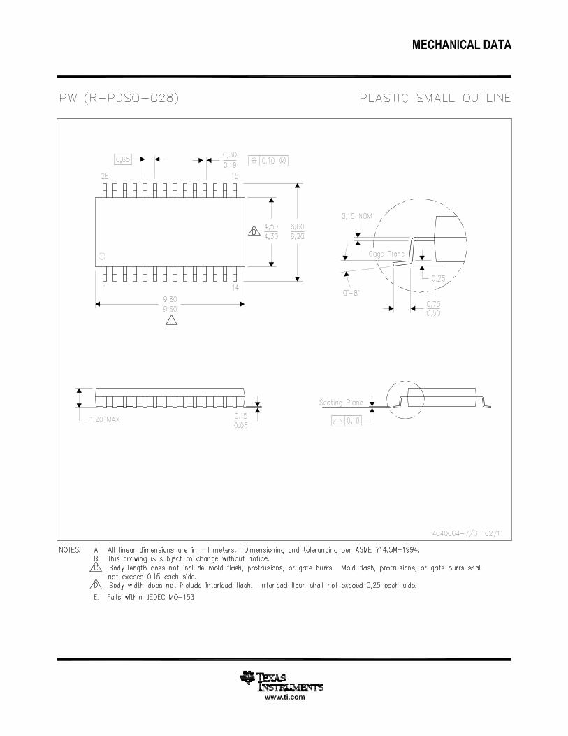
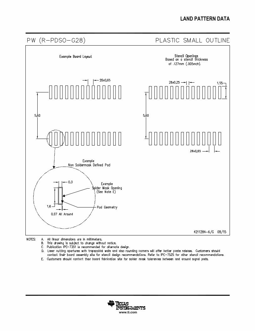
IMPORTANT NOTICE
Texas Instruments Incorporated (TI) reserves the right to make corrections, enhancements, improvements and other changes to itssemiconductor products and services per JESD46, latest issue, and to discontinue any product or service per JESD48, latest issue. Buyersshould obtain the latest relevant information before placing orders and should verify that such information is current and complete.TI’s published terms of sale for semiconductor products (http://www.ti.com/sc/docs/stdterms.htm) apply to the sale of packaged integratedcircuit products that TI has qualified and released to market. Additional terms may apply to the use or sale of other types of TI products andservices.Reproduction of significant portions of TI information in TI data sheets is permissible only if reproduction is without alteration and isaccompanied by all associated warranties, conditions, limitations, and notices. TI is not responsible or liable for such reproduceddocumentation. Information of third parties may be subject to additional restrictions. Resale of TI products or services with statementsdifferent from or beyond the parameters stated by TI for that product or service voids all express and any implied warranties for theassociated TI product or service and is an unfair and deceptive business practice. TI is not responsible or liable for any such statements.Buyers and others who are developing systems that incorporate TI products (collectively, “Designers”) understand and agree that Designersremain responsible for using their independent analysis, evaluation and judgment in designing their applications and that Designers havefull and exclusive responsibility to assure the safety of Designers' applications and compliance of their applications (and of all TI productsused in or for Designers’ applications) with all applicable regulations, laws and other applicable requirements. Designer represents that, withrespect to their applications, Designer has all the necessary expertise to create and implement safeguards that (1) anticipate dangerousconsequences of failures, (2) monitor failures and their consequences, and (3) lessen the likelihood of failures that might cause harm andtake appropriate actions. Designer agrees that prior to using or distributing any applications that include TI products, Designer willthoroughly test such applications and the functionality of such TI products as used in such applications.TI’s provision of technical, application or other design advice, quality characterization, reliability data or other services or information,including, but not limited to, reference designs and materials relating to evaluation modules, (collectively, “TI Resources”) are intended toassist designers who are developing applications that incorporate TI products; by downloading, accessing or using TI Resources in anyway, Designer (individually or, if Designer is acting on behalf of a company, Designer’s company) agrees to use any particular TI Resourcesolely for this purpose and subject to the terms of this Notice.TI’s provision of TI Resources does not expand or otherwise alter TI’s applicable published warranties or warranty disclaimers for TIproducts, and no additional obligations or liabilities arise from TI providing such TI Resources. TI reserves the right to make corrections,enhancements, improvements and other changes to its TI Resources. TI has not conducted any testing other than that specificallydescribed in the published documentation for a particular TI Resource.Designer is authorized to use, copy and modify any individual TI Resource only in connection with the development of applications thatinclude the TI product(s) identified in such TI Resource. NO OTHER LICENSE, EXPRESS OR IMPLIED, BY ESTOPPEL OR OTHERWISETO ANY OTHER TI INTELLECTUAL PROPERTY RIGHT, AND NO LICENSE TO ANY TECHNOLOGY OR INTELLECTUAL PROPERTYRIGHT OF TI OR ANY THIRD PARTY IS GRANTED HEREIN, including but not limited to any patent right, copyright, mask work right, orother intellectual property right relating to any combination, machine, or process in which TI products or services are used. Informationregarding or referencing third-party products or services does not constitute a license to use such products or services, or a warranty orendorsement thereof. Use of TI Resources may require a license from a third party under the patents or other intellectual property of thethird party, or a license from TI under the patents or other intellectual property of TI.TI RESOURCES ARE PROVIDED “AS IS” AND WITH ALL FAULTS. TI DISCLAIMS ALL OTHER WARRANTIES ORREPRESENTATIONS, EXPRESS OR IMPLIED, REGARDING RESOURCES OR USE THEREOF, INCLUDING BUT NOT LIMITED TOACCURACY OR COMPLETENESS, TITLE, ANY EPIDEMIC FAILURE WARRANTY AND ANY IMPLIED WARRANTIES OFMERCHANTABILITY, FITNESS FOR A PARTICULAR PURPOSE, AND NON-INFRINGEMENT OF ANY THIRD PARTY INTELLECTUALPROPERTY RIGHTS. TI SHALL NOT BE LIABLE FOR AND SHALL NOT DEFEND OR INDEMNIFY DESIGNER AGAINST ANY CLAIM,INCLUDING BUT NOT LIMITED TO ANY INFRINGEMENT CLAIM THAT RELATES TO OR IS BASED ON ANY COMBINATION OFPRODUCTS EVEN IF DESCRIBED IN TI RESOURCES OR OTHERWISE. IN NO EVENT SHALL TI BE LIABLE FOR ANY ACTUAL,DIRECT, SPECIAL, COLLATERAL, INDIRECT, PUNITIVE, INCIDENTAL, CONSEQUENTIAL OR EXEMPLARY DAMAGES INCONNECTION WITH OR ARISING OUT OF TI RESOURCES OR USE THEREOF, AND REGARDLESS OF WHETHER TI HAS BEENADVISED OF THE POSSIBILITY OF SUCH DAMAGES.Unless TI has explicitly designated an individual product as meeting the requirements of a particular industry standard (e.g., ISO/TS 16949and ISO 26262), TI is not responsible for any failure to meet such industry standard requirements.Where TI specifically promotes products as facilitating functional safety or as compliant with industry functional safety standards, suchproducts are intended to help enable customers to design and create their own applications that meet applicable functional safety standardsand requirements. Using products in an application does not by itself establish any safety features in the application. Designers mustensure compliance with safety-related requirements and standards applicable to their applications. Designer may not use any TI products inlife-critical medical equipment unless authorized officers of the parties have executed a special contract specifically governing such use.Life-critical medical equipment is medical equipment where failure of such equipment would cause serious bodily injury or death (e.g., lifesupport, pacemakers, defibrillators, heart pumps, neurostimulators, and implantables). Such equipment includes, without limitation, allmedical devices identified by the U.S. Food and Drug Administration as Class III devices and equivalent classifications outside the U.S.TI may expressly designate certain products as completing a particular qualification (e.g., Q100, Military Grade, or Enhanced Product).Designers agree that it has the necessary expertise to select the product with the appropriate qualification designation for their applicationsand that proper product selection is at Designers’ own risk. Designers are solely responsible for compliance with all legal and regulatoryrequirements in connection with such selection.Designer will fully indemnify TI and its representatives against any damages, costs, losses, and/or liabilities arising out of Designer’s non-compliance with the terms and provisions of this Notice.
Mailing Address: Texas Instruments, Post Office Box 655303, Dallas, Texas 75265Copyright © 2017, Texas Instruments Incorporated