Embed Size (px)
Citation preview
NPTEL Syllabus
Fundamental concepts ofsemiconductors - Web course
COURSE OUTLINE
The aim of the course is to develop physics and engineeringstrategies of semiconductor materials and to discuss theirfunctionalities in modern electronic and optoelectronic devices.
COURSE DETAIL
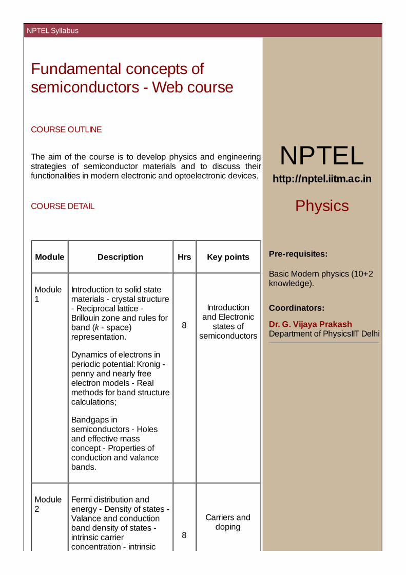
Module Description Hrs Key points
Module1
Introduction to solid statematerials - crystal structure- Reciprocal lattice -Brillouin zone and rules forband (k - space)representation.
Dynamics of electrons inperiodic potential: Kronig -penny and nearly freeelectron models - Realmethods for band structurecalculations;
Bandgaps insemiconductors - Holesand effective massconcept - Properties ofconduction and valancebands.
8
Introductionand Electronic
states ofsemiconductors
Module2
Fermi distribution andenergy - Density of states -Valance and conductionband density of states -intrinsic carrierconcentration - intrinsic
8
Carriers anddoping
NPTELhttp://nptel.iitm.ac.in
Physics
Pre-requisites:
Basic Modern physics (10+2knowledge).
Coordinators:
Dr. G. Vijaya PrakashDepartment of PhysicsIIT Delhi
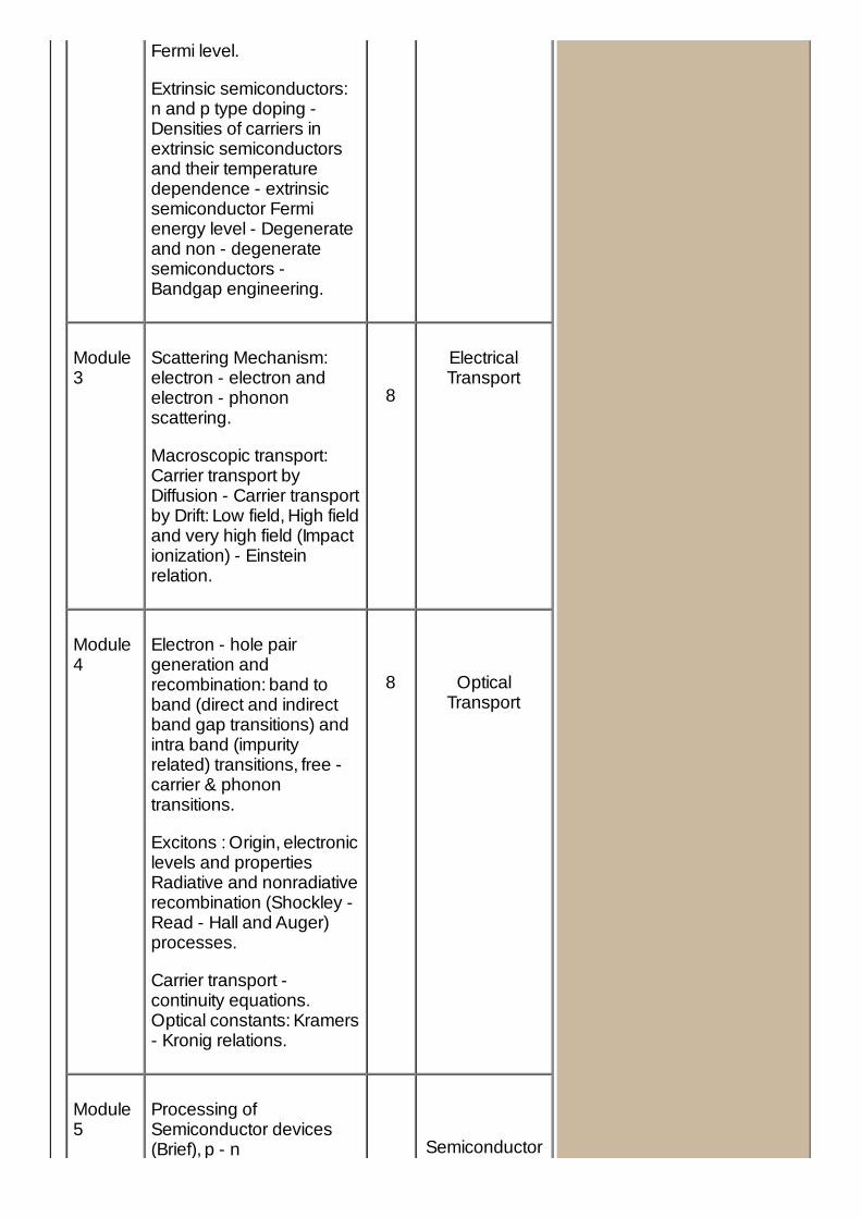
Fermi level.
Extrinsic semiconductors:n and p type doping -Densities of carriers inextrinsic semiconductorsand their temperaturedependence - extrinsicsemiconductor Fermienergy level - Degenerateand non - degeneratesemiconductors -Bandgap engineering.
Module3
Scattering Mechanism:electron - electron andelectron - phononscattering.
Macroscopic transport: Carrier transport byDiffusion - Carrier transportby Drift: Low field, High fieldand very high field (Impactionization) - Einsteinrelation.
8
ElectricalTransport
Module4
Electron - hole pairgeneration andrecombination: band toband (direct and indirectband gap transitions) andintra band (impurityrelated) transitions, free -carrier & phonon transitions.
Excitons : Origin, electroniclevels and propertiesRadiative and nonradiativerecombination (Shockley -Read - Hall and Auger)processes.
Carrier transport -continuity equations.Optical constants: Kramers- Kronig relations.
8
OpticalTransport
Module5
Processing ofSemiconductor devices(Brief), p - n
Semiconductoras device and
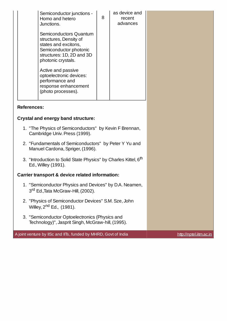
Semiconductor junctions -Homo and heteroJunctions.
Semiconductors Quantumstructures, Density ofstates and excitons,Semiconductor photonicstructures: 1D, 2D and 3Dphotonic crystals.
Active and passiveoptoelectronic devices:performance andresponse enhancement(photo processes).
8as device and
recentadvances
References:
Crystal and energy band structure:
1. "The Physics of Semiconductors" by Kevin F Brennan,Cambridge Univ. Press (1999).
2. "Fundamentals of Semiconductors" by Peter Y Yu andManuel Cardona, Spriger, (1996).
3. "Introduction to Solid State Physics" by Charles Kittel, 6th
Ed., Willey (1991).
Carrier transport & device related information:
1. "Semiconductor Physics and Devices" by D.A. Neamen,3rd Ed.,Tata McGraw-Hill, (2002).
2. "Physics of Semiconductor Devices" S.M. Sze, JohnWilley, 2nd Ed., (1981).
3. "Semiconductor Optoelectronics (Physics andTechnology)", Jasprit Singh, McGraw-hill, (1995).
A joint venture by IISc and IITs, funded by MHRD, Govt of India http://nptel.iitm.ac.in