Embed Size (px)
DESCRIPTION
NuMicro Nano100 (B) Series Product Brief en V1.00
Citation preview
NuMicro Nano100 (B) Series Product Brief
NU
MIC
RO
™ N
AN
O100
TE
CH
NIC
AL R
EF
ER
EN
CE
MA
NU
AL
NuMicro™ Family
Nano100 Series Product Brief
The information described in this document is the exclusive intellectual property of Nuvoton Technology Corporation and shall not be reproduced without permission from Nuvoton.
Nuvoton is providing this document only for reference purposes of NuMicro microcontroller based system design. Nuvoton assumes no responsibility for errors or omissions.
All data and specifications are subject to change without notice.
For additional information or questions, please contact: Nuvoton Technology Corporation.
www.nuvoton.com
NuMicro Nano100 (B) Series Product Brief
Oct 11, 2012 Page 2 of 72 Revision V1.00
NU
MIC
RO
™ N
AN
O100
TE
CH
NIC
AL R
EF
ER
EN
CE
MA
NU
AL
Table of Contents
LIST OF FIGURES ........................................................................................................................... 4 LIST OF TABLES ............................................................................................................................. 5 1 GENERAL DESCRIPTION ..................................................................................................... 6 2 FEATURES ............................................................................................................................. 8
2.1 Nano100 Features – Base Line ................................................................................... 8
2.2 Nano110 Features – LCD Line .................................................................................. 14
2.3 Nano120 Features – USB Connectivity Line ............................................................. 20
2.4 Nano130 Features – Advanced Line .......................................................................... 26
3 PARTS INFORMATION LIST AND PIN CONFIGURATION ................................................ 32
3.1 NuMicro Nano100 Series Selection Code ............................................................... 32
3.2 NuMicro Nano100 Products Selection Guide .......................................................... 33
3.2.1 NuMicro Nano100 Base Line Selection Guide ............................................................. 33 3.2.2 NuMicro Nano110 LCD Line Selection Guide .............................................................. 33 3.2.3 NuMicro Nano120 USB Connectivity Line Selection Guide ......................................... 33 3.2.4 NuMicro Nano130 Advanced Line Selection Guide ..................................................... 33
3.3 Pin Configuration ........................................................................................................ 34
3.3.1 NuMicro Nano100 Pin Diagrams ................................................................................. 34 3.3.2 NuMicro Nano110 Pin Diagrams ................................................................................. 37 3.3.3 NuMicro Nano120 Pin Diagrams ................................................................................. 39 3.3.4 NuMicro Nano130 Pin Diagrams ................................................................................. 42
4 BLOCK DIAGRAM ................................................................................................................ 44 4.1 Nano100 Block Diagram ............................................................................................ 44
4.2 Nano110 Block Diagram ............................................................................................ 45
4.3 Nano120 Block Diagram ............................................................................................ 46
4.4 Nano130 Block Diagram ............................................................................................ 47
5 APPLICATION CIRCUIT ....................................................................................................... 48 5.1 LCD Charge Pump ..................................................................................................... 48
5.1.1 C-type 1/3 Bias ............................................................................................................... 48 5.1.2 C-type 1/2 Bias ............................................................................................................... 48
5.2 ADC Application Circuit .............................................................................................. 49
5.2.1 Voltage Reference Source ............................................................................................. 49 5.3 DAC Application Circuit .............................................................................................. 51
5.3.1 Voltage Reference Source ............................................................................................. 51 5.4 Whole Chip Application Circuit ................................................................................... 53
6 POWER COMSUMPTION .................................................................................................... 54 7 ELECTRICAL CHARACTERISTIC ....................................................................................... 55
7.1 Absolute Maximum Ratings ....................................................................................... 55
7.2 Nano100/Nano110/Nano120/Nano130 DC Electrical Characteristics ....................... 56
7.3 AC Electrical Characteristics ...................................................................................... 61
7.3.1 External Input Clock ....................................................................................................... 61
NuMicro Nano100 (B) Series Product Brief
Oct 11, 2012 Page 3 of 72 Revision V1.00
NU
MIC
RO
™ N
AN
O100
TE
CH
NIC
AL R
EF
ER
EN
CE
MA
NU
AL
7.3.2 External 4~24 MHz XTAL Oscillator ............................................................................... 61 7.3.3 External 32.768 kHz Crystal ........................................................................................... 62 7.3.4 Internal 12 MHz Oscillator .............................................................................................. 62 7.3.5 Internal 10 kHz Oscillator ............................................................................................... 62
7.4 Analog Characteristics ............................................................................................... 63
7.4.1 12-bit ADC ...................................................................................................................... 63 7.4.2 Brown-out Detector......................................................................................................... 63 7.4.3 Power-on Reset .............................................................................................................. 64 7.4.4 Temperature Sensor....................................................................................................... 64 7.4.5 12-bit DAC ...................................................................................................................... 64 7.4.6 LCD ................................................................................................................................ 65 7.4.7 Touch Key (TK) .............................................................................................................. 65 7.4.8 Internal Voltage Reference ............................................................................................. 66 7.4.9 USB PHY Specifications ................................................................................................. 66
8 PACKAGE DIMENSIONS ..................................................................................................... 68 8.1 128L LQFP (14x14x1.4 mm footprint 2.0 mm) ........................................................... 68
8.2 64L LQFP (7x7x1.4 mm footprint 2.0 mm) ................................................................. 69
8.3 48L LQFP (7x7x1.4 mm footprint 2.0 mm) ................................................................. 71
9 REVISION HISTORY ............................................................................................................ 72
NuMicro Nano100 (B) Series Product Brief
Oct 11, 2012 Page 4 of 72 Revision V1.00
NU
MIC
RO
™ N
AN
O100
TE
CH
NIC
AL R
EF
ER
EN
CE
MA
NU
AL
List of Figures Figure 3-1 NuMicro
TM Nano100 Series Selection Code ................................................................ 32
Figure 3-2 NuMicroTM
Nano100 LQFP 128-pin Diagram ............................................................... 34
Figure 3-3 NuMicroTM
Nano100 LQFP 64-pin Diagram ................................................................. 35
Figure 3-4 NuMicroTM
Nano100 LQFP 48-pin Diagram ................................................................. 36
Figure 3-5 NuMicroTM
Nano110 LQFP 128-pin Diagram ............................................................... 37
Figure 3-6 NuMicroTM
Nano110 LQFP 64-pin Diagram ................................................................. 38
Figure 3-7 NuMicroTM
Nano120 LQFP 128-pin Diagram ............................................................... 39
Figure 3-8 NuMicroTM
Nano120 LQFP 64-pin Diagram ................................................................. 40
Figure 3-9 NuMicroTM
Nano120 LQFP 48-pin Diagram ................................................................. 41
Figure 3-10 NuMicroTM
Nano130 LQFP 128-pin Diagram ............................................................. 42
Figure 3-11 NuMicroTM
Nano130 LQFP 64-pin Diagram ............................................................... 43
Figure 4-1 NuMicroTM
Nano100 Block Diagram ............................................................................. 44
Figure 4-2 NuMicroTM
Nano110 Block Diagram ............................................................................. 45
Figure 4-3 NuMicroTM
Nano120 Block Diagram ............................................................................. 46
Figure 4-4 NuMicroTM
Nano130 Block Diagram ............................................................................. 47
Figure 9-1 Typical Crystal Application Circuit ................................................................................ 61
NuMicro Nano100 (B) Series Product Brief
Oct 11, 2012 Page 5 of 72 Revision V1.00
NU
MIC
RO
™ N
AN
O100
TE
CH
NIC
AL R
EF
ER
EN
CE
MA
NU
AL
LIST OF TABLES Table 1-1 Connectivity Support Table .............................................................................................. 7
Table 3-1 Nano100 Base Line Selection Table ............................................................................. 33
Table 3-2 Nano110 LCD Line Selection Table .............................................................................. 33
Table 3-3 Nano120 USB Connectivity Line Selection Table ......................................................... 33
Table 3-4 Nano130 Advanced Line Selection Table ..................................................................... 33
NuMicro Nano100 (B) Series Product Brief
Oct 11, 2012 Page 6 of 72 Revision V1.00
NU
MIC
RO
™ N
AN
O100
TE
CH
NIC
AL R
EF
ER
EN
CE
MA
NU
AL
1 GENERAL DESCRIPTION
The Nano100 series ultra-low power 32-bit microcontroller is embedded with ARM® Cortex™-M0
core operated at a wide voltage range from 1.8V to 3.6V and runs up to 42 MHz frequency with 32K/64K/128K bytes embedded Flash and 8K/16K-byte embedded SRAM. Integrating LCD 4x40 or 6x38 (COM/Segment), USB 2.0 full-speed function, RTC, 12-bit SAR ADC, 12-bit DAC, Capacitive Touch-Key and provides high performance connectivity peripheral interfaces such as UART, SPI, I2C, I2S, GPIOs, EBI (External Bus Interface) for external memory-mapped device access and ISO-7816-3 for Smart card, the Nano100 series supports Brown-out Detector, Power-down mode with RAM retention and fast wake-up via many peripheral interfaces.
The Nano100 series provides low power voltage, low power consumption, low standby current, high integration peripherals, high-efficiency operation, fast wake-up function and the lowest cost 32-bit microcontrollers. The Nano100 series is suitable for a wide range of battery device applications such as:
Portable Data Collector
Portable Medical Monitor
Portable RFID Reader
Portable Barcode Scanner
Security Alarm System
System Supervisors
Power Metering
USB Accessories
Smart Card Reader
Wireless Game Control Device
IPTV Remote Smart Keyboard
Wireless Sensors Node Device (WSN)
Wireless RF4CE Remote Control
Wireless Audio
Wireless Automatic Meter Reader (AMR)
Electronic Toll Collection (ETC)
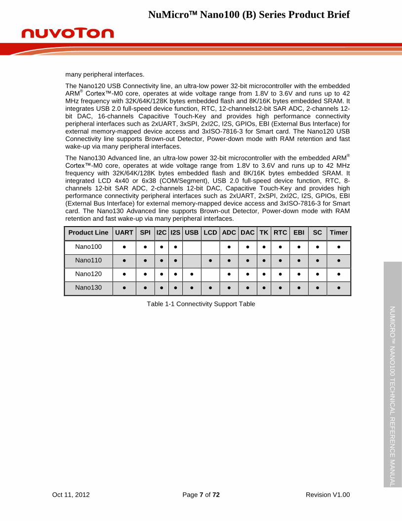
The Nano100 Base line, an ultra-low power 32-bit microcontroller with the embedded ARM®
Cortex™-M0 core, operates at wide voltage range from 1.8V to 3.6V and runs up to 42 MHz frequency with 32K/64K/128K bytes embedded flash and 8K/16K bytes embedded SRAM. It integrates RTC, 12- channels 12-bit SAR ADC, 2-channels 12-bit DAC, 16-channels Capacitive Touch-Key and provides high performance connectivity peripheral interfaces such as 2xUART, 3xSPI, 2xI2C, I2S, GPIOs, EBI (External Bus Interface) for external memory-mapped device access and 3xISO-7816-3 for Smart card. The Nano100 Base line supports Brown-out Detector, Power-down mode with RAM retention and fast wake-up via many peripheral interfaces.
The Nano110 LCD line, an ultra-low power 32-bit microcontroller with the embedded ARM®
Cortex™-M0 core, operates at wide voltage range from 1.8V to 3.6V and runs up to 42 MHz frequency with 32K/64K/128K bytes embedded flash and 8K/16K bytes embedded SRAM. It integrates LCD 4x40 or 6x38 (COM/Segment). RTC, 12-channels 12-bit SAR ADC, 2-channels 12-bit DAC, 16-channels Capacitive Touch-Key and provides high performance connectivity peripheral interfaces such as 2xUART, 2xSPI, 2xI2C, I2S, GPIOs, EBI (External Bus Interface) for external memory-mapped device access and 3xISO-7816-3 for Smart card. The Nano110 LCD line supports Brown-out Detector, Power-down mode with RAM retention and fast wake-up via
NuMicro Nano100 (B) Series Product Brief
Oct 11, 2012 Page 7 of 72 Revision V1.00
NU
MIC
RO
™ N
AN
O100
TE
CH
NIC
AL R
EF
ER
EN
CE
MA
NU
AL
many peripheral interfaces.
The Nano120 USB Connectivity line, an ultra-low power 32-bit microcontroller with the embedded ARM
® Cortex™-M0 core, operates at wide voltage range from 1.8V to 3.6V and runs up to 42
MHz frequency with 32K/64K/128K bytes embedded flash and 8K/16K bytes embedded SRAM. It integrates USB 2.0 full-speed device function, RTC, 12-channels12-bit SAR ADC, 2-channels 12-bit DAC, 16-channels Capacitive Touch-Key and provides high performance connectivity peripheral interfaces such as 2xUART, 3xSPI, 2xI2C, I2S, GPIOs, EBI (External Bus Interface) for external memory-mapped device access and 3xISO-7816-3 for Smart card. The Nano120 USB Connectivity line supports Brown-out Detector, Power-down mode with RAM retention and fast wake-up via many peripheral interfaces.
The Nano130 Advanced line, an ultra-low power 32-bit microcontroller with the embedded ARM®
Cortex™-M0 core, operates at wide voltage range from 1.8V to 3.6V and runs up to 42 MHz frequency with 32K/64K/128K bytes embedded flash and 8K/16K bytes embedded SRAM. It integrated LCD 4x40 or 6x38 (COM/Segment), USB 2.0 full-speed device function, RTC, 8-channels 12-bit SAR ADC, 2-channels 12-bit DAC, Capacitive Touch-Key and provides high performance connectivity peripheral interfaces such as 2xUART, 2xSPI, 2xI2C, I2S, GPIOs, EBI (External Bus Interface) for external memory-mapped device access and 3xISO-7816-3 for Smart card. The Nano130 Advanced line supports Brown-out Detector, Power-down mode with RAM retention and fast wake-up via many peripheral interfaces.
Product Line UART SPI I2C I2S USB LCD ADC DAC TK RTC EBI SC Timer
Nano100 ● ● ● ● ● ● ● ● ● ● ●
Nano110 ● ● ● ● ● ● ● ● ● ● ● ●
Nano120 ● ● ● ● ● ● ● ● ● ● ● ●
Nano130 ● ● ● ● ● ● ● ● ● ● ● ● ●
Table 1-1 Connectivity Support Table
NuMicro Nano100 (B) Series Product Brief
Oct 11, 2012 Page 8 of 72 Revision V1.00
NU
MIC
RO
™ N
AN
O100
TE
CH
NIC
AL R
EF
ER
EN
CE
MA
NU
AL
2 FEATURES
The equipped features are dependent on the product line and their sub products.
2.1 Nano100 Features – Base Line
Core
ARM® Cortex™-M0 core running up to 42 MHz
One 24-bit system timer
Supports Low Power Sleep mode
Single-cycle 32-bit hardware multiplier
NVIC for the 32 interrupt inputs, each with 4-levels of priority
Serial Wire Debug supports with 2 watchpoints/4 breakpoints
Brown-out
Built-in 2.5V/2.0V/1.7V BOD for wide operating voltage range operation
Flash EPROM Memory
Runs up to 42 MHz with zero wait state for discontinuous address read access
64K/32K/123K bytes application program memory (APROM)
4 KB in system programming (ISP) loader program memory (LDROM)
Programmable data flash start address and memory size with 512 bytes page erase unit
In System Program (ISP)/In Application Program (IAP) to update on-chip Flash EPROM
SRAM Memory
16K/8K bytes embedded SRAM
Supports DMA mode
DMA: Supports 8 channels: one VDMA channel, 6 PDMA channels and one CRC channel
VDMA
Memory-to-memory transfer
Supports block transfer with stride
Supports word/half-word/byte boundary address
Supports address direction: increment and decrement
PDMA
Peripheral-to-memory, memory-to-peripheral, and memory-to-memory transfer
Supports word boundary address
Supports word alignment transfer length in memory-to-memory mode
Supports word/half-word/byte alignment transfer length in peripheral-to-memory and memory-to-peripheral mode
Supports word/half-word/byte transfer data width from/to peripheral
NuMicro Nano100 (B) Series Product Brief
Oct 11, 2012 Page 9 of 72 Revision V1.00
NU
MIC
RO
™ N
AN
O100
TE
CH
NIC
AL R
EF
ER
EN
CE
MA
NU
AL
Supports address direction: increment, fixed, and wrap around
CRC
Supports four common polynomials CRC-CCITT, CRC-8, CRC-16, and CRC-32
CRC-CCITT: X16
+ X12
+ X5 + 1
CRC-8: X8 + X
2 + X + 1
CRC-16: X16
+ X15
+ X2 + 1
CRC-32: X32
+ X26
+ X23
+ X22
+ X16
+ X12
+ X11
+ X10
+ X8 + X
7 + X
5 +
X4 + X
2 + X + 1
Clock Control
Flexible selection for different applications
Built-in 12MHz OSC, can be trimmed to 0.25% deviation within all temperature range when turning on auto-trim function (system must have external 32.768 kHz crystal input) otherwise 12MHz OSC has 1 % deviation within all temperarure range.
Low power 10 kHz OSC for watchdog and low power system operation
Supports one PLL, up to 120 MHz, for high performance system operation and USB application (48 MHz).
External 4~24 MHz crystal input for precise timing operation
External 32.768 kHz crystal input for RTC function and low power system operation
GPIO
Three I/O modes:
Push-Pull output
Open-Drain output
Input only with high impendence
All inputs with Schmitt trigger
I/O pin configured as interrupt source with edge/level setting
Supports High Driver and High Sink I/O mode
Supports input 5V tolerance, except PA.0 ~ PA.7, PD.0 ~ PD.1 and PC.6 ~ PC.7
Timer
Supports 4 sets of 32-bit timers, each with 24-bit up-counting timer and one 8-bit pre-scale counter
Independent Clock Source for each timer
Provides one-shot and periodic, and continuous operation modes
Internal trigger event to ADC, DAC module
Supports PDMA mode
Wake system up from Power-down mode
Watchdog Timer
NuMicro Nano100 (B) Series Product Brief
Oct 11, 2012 Page 10 of 72 Revision V1.00
NU
MIC
RO
™ N
AN
O100
TE
CH
NIC
AL R
EF
ER
EN
CE
MA
NU
AL
Clock Source from LIRC (Internal 10 kHz Low Speed Oscillator Clock)
Selectable time-out period from 1.6 ms ~ 26 sec (depending on clock source)
Interrupt or reset selectable when watchdog time-out
Wake system up from Power-down mode
Window Watchdog Timer(WWDT)
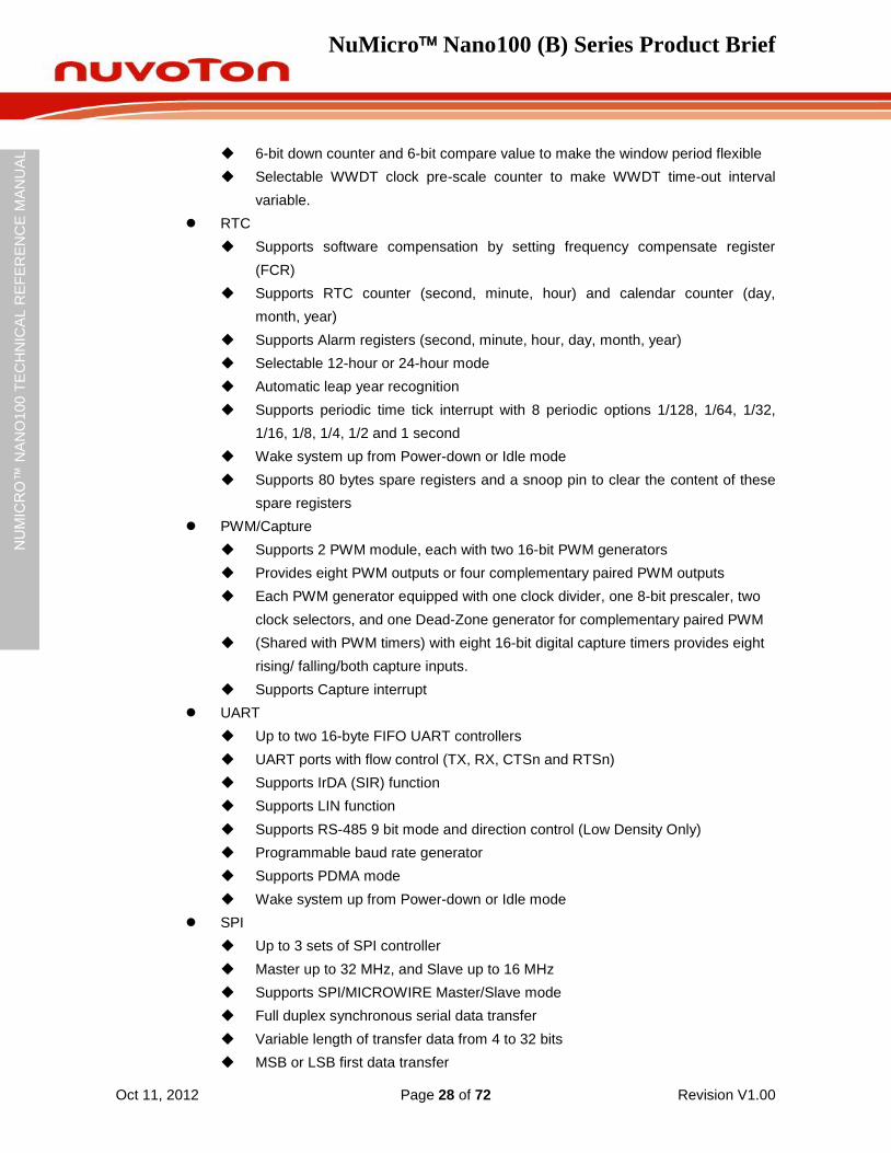
6-bit down counter and 6-bit compare value to make the window period flexible
Selectable WWDT clock pre-scale counter to make WWDT time-out interval variable.
RTC
Supports software compensation by setting frequency compensate register (FCR)
Supports RTC counter (second, minute, hour) and calendar counter (day, month, year)
Supports Alarm registers (second, minute, hour, day, month, year)
Selectable 12-hour or 24-hour mode
Automatic leap year recognition
Supports periodic time tick interrupt with 8 periodic options 1/128, 1/64, 1/32, 1/16, 1/8, 1/4, 1/2 and 1 second
Wake system up from Power-down mode
Supports 80 bytes spare registers and a snoop pin to clear the content of these spare registers
PWM/Capture
Supports 2 PWM modules, each has two 16-bit PWM generators
Provides eight PWM outputs or four complementary paired PWM outputs
Each PWM generator equipped with one clock divider, one 8-bit prescaler, two clock selectors, and one Dead-zone generator for complementary paired PWM
(Shared with PWM timers) with eight 16-bit digital capture timers provides eight rising/ falling/both capture inputs.
Supports One-shot and Continuous mode
Supports Capture interrupt
UART
Up to two 16-byte FIFO UART controllers
UART ports with flow control (TX, RX, CTSn and RTSn)
Supports IrDA (SIR) function
Supports LIN function
Supports RS-485 9 bit mode and direction control.
Programmable baud rate generator
Supports PDMA mode
Wake system up from Power-down mode
NuMicro Nano100 (B) Series Product Brief
Oct 11, 2012 Page 11 of 72 Revision V1.00
NU
MIC
RO
™ N
AN
O100
TE
CH
NIC
AL R
EF
ER
EN
CE
MA
NU
AL
SPI
Up to three sets of SPI controller
Master up to 32 MHz, and Slave up to 16 MHz
Supports SPI/MICROWIRE Master/Slave mode
Full duplex synchronous serial data transfer
Variable length of transfer data from 4 to 32 bits
MSB or LSB first data transfer
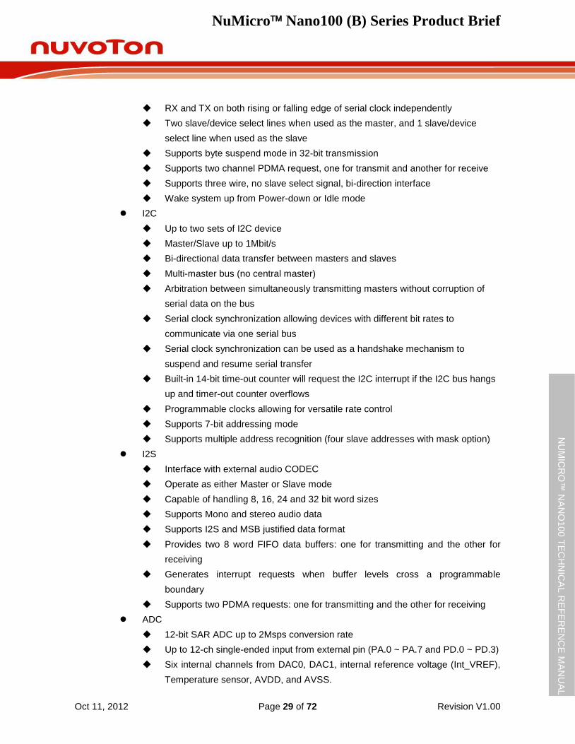
RX and TX on both rising or falling edge of serial clock independently
Two slave/device select lines when SPI controller is used as the master, and 1 slave/device select line when SPI controller is used as the slave
Supports byte suspend mode in 32-bit transmission
Supports two channel PDMA requests, one for transmit and another for receive
Supports three wire mode, no slave select signal, bi-direction interface
Wake system up from Power-down mode
I2C
Up to two sets of I2C device
Master/Slave up to 1 Mbit/s
Bi-directional data transfer between masters and slaves
Multi-master bus (no central master)
Arbitration between simultaneously transmitting masters without corruption of serial data on the bus
Serial clock synchronization allows devices with different bit rates to communicate via one serial bus
Serial clock synchronization used as a handshake mechanism to suspend and resume serial transfer
Built-in 14-bit time-out counter requesting the I2C interrupt if the I2C bus hangs up and timer-out counter overflows
Programmable clocks allowing for versatile rate control
Supports 7-bit addressing mode
Supports multiple address recognition (four slave addresses with mask option)
I2S
Interface with external audio CODEC
Operated as either Master or Slave mode
Capable of handling 8, 16, 24 and 32 bit word sizes
Supports Mono and stereo audio data
Supports I2S and MSB justified data format
Provides two 8 word FIFO data buffers: one for transmitting and the other for receiving
NuMicro Nano100 (B) Series Product Brief
Oct 11, 2012 Page 12 of 72 Revision V1.00
NU
MIC
RO
™ N
AN
O100
TE
CH
NIC
AL R
EF
ER
EN
CE
MA
NU
AL
Generates interrupt requests when buffer levels cross a programmable boundary
Supports two PDMA requests: one for transmitting and the other for receiving
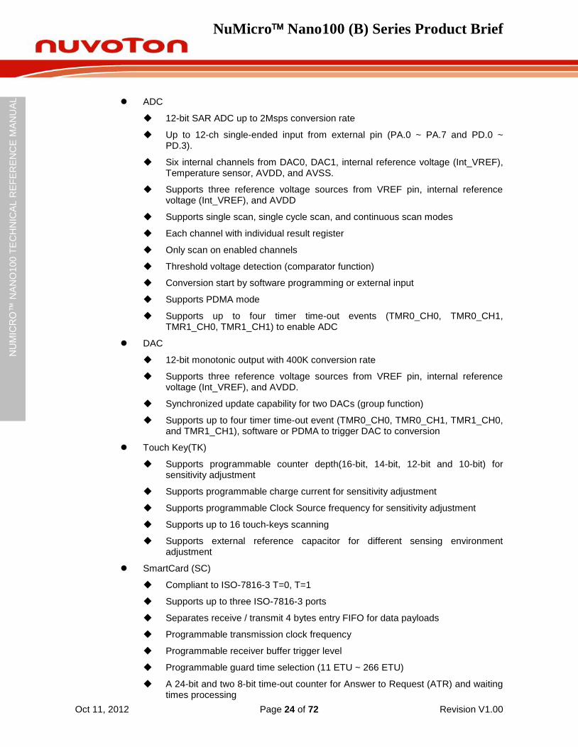
ADC
12-bit SAR ADC up to 2Msps conversion rate
Up to 12-ch single-ended input from external pin (PA.0 ~ PA.7 and PD.0 ~ PD.3)
Six internal channels from DAC0, DAC1, internal reference voltage (Int_VREF), Temperature sensor, AVDD, and AVSS.
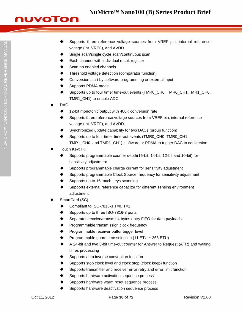
Supports three reference voltage sources from VREF pin, internal reference voltage (Int_VREF), and AVDD.
Supports Single Scan, Single Cycle Scan, and Continuous Scan mode
Each channel with individual result register
Only scan on enabled channels
Threshold voltage detection (comparator function)
Conversion started by software programming or external input
Supports PDMA mode
Supports up to four timer time-out events (TRM0_CH0, TMR0_CH1, TMR1_CH0 and TMR1_CH1) to enable ADC
DAC
12-bit monotonic output with 400K conversion rate
Supports three reference voltage sources from VREF pin, internal reference voltage (Int_VREF), and AVDD.
Synchronized update capability for two DACs (group function)
Supports up to four timer time-out events (TMR0_CH0, TMR0_CH1, TMR1_CH0, TMR1_CH1), software or PDMA to trigger DAC to conversion
Touch Key(TK)
Supports programmable counter depth (16-bit, 14-bit, 12-bit and 10-bit) for sensitivity adjustment
Supports programmable charge current for sensitivity adjustment
Supports programmable Clock Source frequency for sensitivity adjustment
Supports up to 16 touch-keys scanning
Supports external reference capacitor for different sensing environment adjustment
SmartCard (SC)
Compliant to ISO-7816-3 T=0, T=1
Supports up to three ISO-7816-3 ports
Separates receive/transmit 4 bytes entry FIFO for data payloads
Programmable transmission clock frequency
Programmable receiver buffer trigger level
NuMicro Nano100 (B) Series Product Brief
Oct 11, 2012 Page 13 of 72 Revision V1.00
NU
MIC
RO
™ N
AN
O100
TE
CH
NIC
AL R
EF
ER
EN
CE
MA
NU
AL
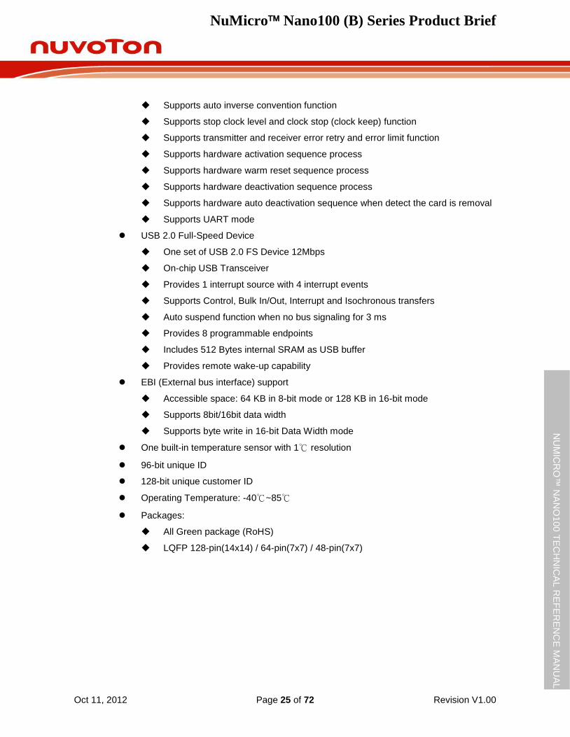
Programmable guard time selection (11 ETU ~ 266 ETU)
A 24-bit and two 8-bit time-out counters for Answer to Request (ATR) and waiting times processing
Supports auto inverse convention function
Supports stop clock level and clock stop (clock keep) function
Supports transmitter and receiver error retry and error limit function
Supports hardware activation sequence process
Supports hardware warm reset sequence process
Supports hardware deactivation sequence process
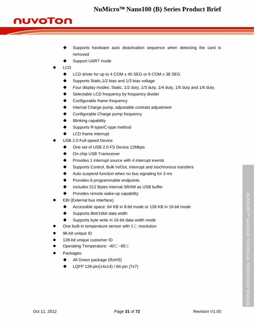
Supports hardware auto deactivation sequence when detect the card is removal
Supports UART mode
EBI (External bus interface) support
Accessible space: 64 KB in 8-bit mode or 128 KB in 16-bit mode
Supports 8bit/16bit data width
Supports byte write in 16-bit Data Width mode
One built-in temperature sensor with 1℃ resolution
96-bit unique ID
128-bit unique customer ID
Operating Temperature: -40℃~85℃
Packages:
All Green package (RoHS)
LQFP 128-pin(14x14) / 64-pin(7x7) / 48-pin(7x7)
NuMicro Nano100 (B) Series Product Brief
Oct 11, 2012 Page 14 of 72 Revision V1.00
NU
MIC
RO
™ N
AN
O100
TE
CH
NIC
AL R
EF
ER
EN
CE
MA
NU
AL
2.2 Nano110 Features – LCD Line
Core
ARM® Cortex™-M0 core running up to 42 MHz
One 24-bit system timer
Supports Low Power Sleep mode
Single-cycle 32-bit hardware multiplier
NVIC for the 32 interrupt inputs, each with 4-levels of priority
Serial Wire Debug supports with 2 watchpoints/4 breakpoints
Brown-out
Built-in 2.5V/2.0V/1.7V BOD for wide operating voltage range operation
Flash EPROM Memory
Runs up to 42 MHz with zero wait state for discontinuous address read access.
64K/32K/123K bytes application program memory (APROM)
4 KB In System Programming (ISP) loader program memory (LDROM)
Programmable data flash start address and memory size with 512 bytes page erase unit
In System Program (ISP)/In Application Program (IAP) to update on chip Flash EPROM
SRAM Memory
16K/8K bytes embedded SRAM
Supports DMA mode
DMA : Supports 8 channels: one VDMA channel,6 PDMA channels, and one CRC channel
VDMA
Memory-to-memory transfer
Supports block transfer with stride
Supports word/half-word/byte boundary address
Supports address direction: increment and decrement
PDMA
Peripheral-to-memory, memory-to-peripheral, and memory-to-memory transfer
Supports word boundary address
Supports word alignment transfer length in memory-to-memory mode
Supports word/half-word/byte alignment transfer length in peripheral-to-memory and memory-to-peripheral mode
Supports word/half-word/byte transfer data width from/to peripheral
Supports address direction: increment, fixed, and wrap around
CRC
NuMicro Nano100 (B) Series Product Brief
Oct 11, 2012 Page 15 of 72 Revision V1.00
NU
MIC
RO
™ N
AN
O100
TE
CH
NIC
AL R
EF
ER
EN
CE
MA
NU
AL
Supports four common polynomials CRC-CCITT, CRC-8, CRC-16, and CRC-32
CRC-CCITT: X16
+ X12
+ X5 + 1
CRC-8: X8 + X
2 + X + 1
CRC-16: X16
+ X15
+ X2 + 1
CRC-32: X32
+ X26
+ X23
+ X22
+ X16
+ X12
+ X11
+ X10
+ X8 + X
7 + X
5 +
X4 + X
2 + X + 1
Clock Control
Flexible selection for different applications
Built-in 12MHz OSC, can be trimmed to 0.25% deviation within all temperature range when turning on auto-trim function (system must have external 32.768 kHz crystal input) otherwise 12MHz OSC has 1 % deviation within all temperarure range.
Low power 10 kHz OSC for watchdog and low power system operation
Supports one PLL, up to 120 MHz, for high performance system operation and USB application (48 MHz).
External 4~24 MHz crystal input for precise timing operation
External 32.768 kHz crystal input for RTC function and low power system operation
GPIO
Three I/O modes:
Push-Pull output
Open-Drain output
Input only with high impendence
All inputs with Schmitt trigger
I/O pin configured as interrupt source with edge/level setting
Supports High Driver and High Sink I/O mode
Supports input 5V tolerance, except PA.0 ~ PA.7, PD.0 ~ PD.1 and PC.6 ~ PC.7)
Timer
Supports 4 sets of 32-bit timers, each with 24-bit up-timer and one 8-bit pre-scale counter
Independent Clock Source for each timer
Provides one-shot and periodic, and continuous operation modes
Internal trigger event to ADC, DAC module
Supports PDMA mode
Wake system up from Power-down mode
Watchdog Timer
Clock Source from LIRC (Internal 10 kHz Low Speed Oscillator Clock)
NuMicro Nano100 (B) Series Product Brief
Oct 11, 2012 Page 16 of 72 Revision V1.00
NU
MIC
RO
™ N
AN
O100
TE
CH
NIC
AL R
EF
ER
EN
CE
MA
NU
AL
Selectable time-out period from 1.6 ms ~ 26 sec (depending on clock source)
Interrupt or reset selectable when watchdog time-out
Wake system up from Power-down mode
Window Watchdog Timer(WWDT)
6-bit down counter and 6-bit compare value to make the window period flexible
Selectable WWDT clock pre-scale counter to make WWDT time-out interval variable.
RTC
Supports software compensation by setting frequency compensate register (FCR)
Supports RTC counter (second, minute, hour) and calendar counter (day, month, year)
Supports Alarm registers (second, minute, hour, day, month, year)
Selectable 12-hour or 24-hour mode
Automatic leap year recognition
Supports periodic time tick interrupt with 8 periodic options 1/128, 1/64, 1/32, 1/16, 1/8, 1/4, 1/2 and 1 second
Wake system up from Power-down mode
Supports 80 bytes spare registers and a snoop pin to clear the content of these spare registers
PWM/Capture
Supports 2 PWM modules, each has two 16-bit PWM generators
Provides eight PWM outputs or four complementary paired PWM outputs
Each PWM generator equipped with one clock divider, one 8-bit prescaler, two clock selectors, and one Dead-zone generator for complementary paired PWM
(Shared with PWM timers) with eight 16-bit digital capture timers provides eight rising/ falling/both capture inputs.
Supports Capture interrupt
UART
Up to two 16-byte FIFO UART controllers
UART ports with flow control (TX, RX, CTSn and RTSn)
Supports IrDA (SIR) function
Supports LIN function
Supports RS-485 9 bit mode and direction control (Low Density Only)
Programmable baud rate generator
Supports PDMA mode
Wake system up from Power-down mode
SPI
Up to three sets of SPI controller
NuMicro Nano100 (B) Series Product Brief
Oct 11, 2012 Page 17 of 72 Revision V1.00
NU
MIC
RO
™ N
AN
O100
TE
CH
NIC
AL R
EF
ER
EN
CE
MA
NU
AL
Master up to 32 MHz, and Slave up to 16 MHz
Supports SPI/MICROWIRE Master/Slave mode
Full duplex synchronous serial data transfer
Variable length of transfer data from 4 to 32 bits
MSB or LSB first data transfer
RX and TX on both rising or falling edge of serial clock independently
Two slave/device select lines when SPI controller is as the master, and 1 slave/device select line when SPI controller is as the slave
Supports byte suspend mode in 32-bit transmission
Supports two channel PDMA requests, one for transmit and another for receive
Supports three wire mode, no slave select signal, bi-direction interface
Wake system up from Power-down mode
I2C
Up to two sets of I2C device
Master/Slave up to 1Mbit/s
Bidirectional data transfer between masters and slaves
Multi-master bus (no central master)
Arbitration between simultaneously transmitting masters without corruption of serial data on the bus
Serial clock synchronization allowing devices with different bit rates to communicate via one serial bus
Serial clock synchronization used as a handshake mechanism to suspend and resume serial transfer
Built-in 14-bit time-out counter requestING the I2C interrupt if the I2C bus hangs up and timer-out counter overflows
Programmable clocks allow versatile rate control
Supports 7-bit addressing mode
Supports multiple address recognition (four slave address with mask option)
I2S
Interface with external audio CODEC
Operated as either Master or Slave mode
Capable of handling 8, 16, 24 and 32 bit word sizes
Supports Mono and stereo audio data
Supports I2S and MSB justified data format
Provides two 8 word FIFO data buffers: one for transmitting and the other for receiving
Generates interrupt requests when buffer levels cross a programmable boundary
Supports two PDMA requests: one for transmitting and the other for receiving
NuMicro Nano100 (B) Series Product Brief
Oct 11, 2012 Page 18 of 72 Revision V1.00
NU
MIC
RO
™ N
AN
O100
TE
CH
NIC
AL R
EF
ER
EN
CE
MA
NU
AL
ADC
12-bit SAR ADC up to 2Msps conversion rate
Up to 12-ch single-ended input from external pin (PA.0 ~ PA.7 and PD.0 ~ PD.3)
Six internal channels from DAC0, DAC1, internal reference voltage (Int_VREF), Temperature sensor, AVDD, and AVSS
Supports three reference voltage sources from VREF pin, internal reference voltage (Int_VREF), and AVDD.
Single scan/single cycle scan/continuous scan
Each channel with individual result register
Only scan on enabled channels
Threshold voltage detection (comparator function)
Conversion start by software programming or external input
Supports PDMA mode
Supports up to four timer time-out events (TMR0_CH0, TMR0_CH1, TMR1_CH0, and TMR1_CH1) to enable ADC
DAC
12-bit monotonic output with 400K conversion rate
Supports three reference voltage sources from VREF pin, internal reference voltage (Int_VREF), and AVDD.
Synchronized update capability for two DACs (group function)
Supports up to four timer time-out events (TMR0_CH0, TMR0_CH1, TMR1_CH0, TMR1_CH1), software or PDMA to trigger DAC to conversion
Touch Key(TK)
Supports programmable counter depth(16-bit, 14-bit, 12-bit and 10-bit) for sensitivity adjustment
Supports programmable charge current for sensitivity adjustment
Supports programmable Clock Source frequency for sensitivity adjustment
Supports up to 16 touch-keys scanning
Supports external reference capacitor for different sensing environment adjustment
SmartCard (SC)
Compliant to ISO-7816-3 T=0, T=1
Supports up to three ISO-7816-3 ports
Separates receive / transmit 4 bytes entry FIFO for data payloads
Programmable transmission clock frequency
Programmable receiver buffer trigger level
Programmable guard time selection (11 ETU ~ 266 ETU)
A 24-bit and two 8-bit time-out counter for Answer to Request (ATR) and waiting times processing
NuMicro Nano100 (B) Series Product Brief
Oct 11, 2012 Page 19 of 72 Revision V1.00
NU
MIC
RO
™ N
AN
O100
TE
CH
NIC
AL R
EF
ER
EN
CE
MA
NU
AL
Supports auto inverse convention function
Supports stop clock level and clock stop (clock keep) function
Supports transmitter and receiver error retry and error limit function
Supports hardware activation sequence process
Supports hardware warm reset sequence process
Supports hardware deactivation sequence process
Supports hardware auto deactivation sequence when detect the card is removal
Supports UART mode
LCD
LCD driver for up to 4 COM x 40 SEG or 6 COM x 38 SEG
Supports Static,1/2 bias and 1/3 bias voltage
Four display modes; Static, 1/2 duty, 1/3 duty,1/4 duty, 1/5 duty and 1/6 duty.
Selectable LCD frequency by frequency divider
Configurable frame frequency
Internal Charge pump, adjustable contrast adjustment
Configurable Charge pump frequency
Blinking capability
Supports R-type/C-type method
LCD frame interrupt
One built-in temperature sensor with 1℃ resolution
96-bit unique ID
128-bit unique customer ID
Operating Temperature: -40℃~85℃
Packages:
All Green package (RoHS)
LQFP 128-pin(14x14) / 64-pin(7x7)

NuMicro Nano100 (B) Series Product Brief
Oct 11, 2012 Page 20 of 72 Revision V1.00
NU
MIC
RO
™ N
AN
O100
TE
CH
NIC
AL R
EF
ER
EN
CE
MA
NU
AL
2.3 Nano120 Features – USB Connectivity Line
Core
ARM® Cortex™-M0 core running up to 42 MHz
One 24-bit system timer
Supports Low Power Sleep mode
Single-cycle 32-bit hardware multiplier
NVIC for the 32 interrupt inputs, each with 4-levels of priority
Serial Wire Debug supports with 2 watchpoints/4 breakpoints
Brown-out
Built-in 2.5V/2.0V/1.7V BOD for wide operating voltage range operation
Flash EPROM Memory
Runs up to 42 MHz with zero wait state for discontinuous address read access.
64K/32K/123K bytes application program memory (APROM)
4KB in system programming (ISP) loader program memory (LDROM)
Programmable data flash start address and memory size with 512 bytes page erase unit
In System Program (ISP)/In Application Program (IAP) to update on chip Flash EPROM
SRAM Memory
16K/8K bytes embedded SRAM
Supports PDMA mode
DMA: Support 8 channels: one VDMA channel, 6 PDMA channels, and one CRC channel
VDMA
Memory-to-memory transfer
Supports block transfer with stride
Supports word/half-word/byte boundary address
Supports address direction: increment and decrement
PDMA
Peripheral-to-memory, memory-to-peripheral, and memory-to-memory transfer
Supports word boundary address
Supports word alignment transfer length in memory-to-memory mode
Supports word/half-word/byte alignment transfer length in peripheral-to-memory and memory-to-peripheral mode
Supports word/half-word/byte transfer data width from/to peripheral
Supports address: increment, fixed, and wrap around
CRC
NuMicro Nano100 (B) Series Product Brief
Oct 11, 2012 Page 21 of 72 Revision V1.00
NU
MIC
RO
™ N
AN
O100
TE
CH
NIC
AL R
EF
ER
EN
CE
MA
NU
AL
Supports four common polynomials CRC-CCITT, CRC-8, CRC-16, and CRC-32
CRC-CCITT: X16
+ X12
+ X5 + 1
CRC-8: X8 + X
2 + X + 1
CRC-16: X16
+ X15
+ X2 + 1
CRC-32: X32
+ X26
+ X23
+ X22
+ X16
+ X12
+ X11
+ X10
+ X8 + X
7 + X
5 +
X4 + X
2 + X + 1
Clock Control
Flexible selection for different applications
Built-in 12MHz OSC, can be trimmed to 0.25% deviation within all temperature range when turning on auto-trim function (system must have external 32.768 kHz crystal input) otherwise 12MHz OSC has 1 % deviation within all temperarure range
Low power 10 kHz OSC for watchdog and low power system operatin
Supports one PLL, up to 120 MHz, for high performance system operation and USB application (48 MHz).
External 4~24 MHz crystal input for precise timing operation
External 32.768 kHz crystal input for RTC function and low power system operation
GPIO
Three I/O modes:
Push-Pull output
Open-Drain output
Input only with high impendence
All inputs with Schmitt trigger
I/O pin can be configured as interrupt source with edge/level setting
High driver and high sink IO mode support
Supports input 5V tolerance (except ADC and DAC shared pins)
Timer
Supports 4 sets of 32-bit timers, each with 24-bit up-timer and one 8-bit pre-scale counter
Independent Clock Source for each timer
Provides one-shot,periodic, and continuous operation modes
Internal trigger event to ADC, DAC module
Supports PDMA mode
Wake system up from Power-down mode
Watchdog Timer
Clock Source from LIRC. (Internal 10 kHz Low Speed Oscillator Clock)
Selectable time-out period from 1.6 ms ~ 26 sec (depending on clock source)
NuMicro Nano100 (B) Series Product Brief
Oct 11, 2012 Page 22 of 72 Revision V1.00
NU
MIC
RO
™ N
AN
O100
TE
CH
NIC
AL R
EF
ER
EN
CE
MA
NU
AL
Interrupt or reset selectable on watchdog time-out
Wake system up from Power-down mode
Window Watchdog Timer(WWDT)
6-bit down counter and 6-bit compare value to make the window period flexible
Selectable WWDT clock pre-scale counter to make WWDT time-out interval variable.
RTC
Supports software compensation by setting frequency compensate register (FCR)
Supports RTC counter (second, minute, hour) and calendar counter (day, month, year)
Supports Alarm registers (second, minute, hour, day, month, year)
Selectable 12-hour or 24-hour mode
Automatic leap year recognition
Supports periodic time tick interrupt with 8 periodic options 1/128, 1/64, 1/32, 1/16, 1/8, 1/4, 1/2 and 1 second
Wake system up from Power-down or Idle mode
Support 80 bytes spare registers and a snoop pin to clear the content of these spare registers
PWM/Capture
Supports 2 PWM module, each has two 16-bit PWM generators
Provide eight PWM outputs or four complementary paired PWM outputs
Each PWM generator equipped with one clock divider, one 8-bit prescaler, two clock selectors, and one Dead-Zone generator for complementary paired PWM
(Shared with PWM timers) with eight 16-bit digital capture timers provides eight rising/ falling/both capture inputs.
Supports one shot and continuous mode
Supports Capture interrupt
UART
Up to two 16-byte FIFO UART controllers
UART ports with flow control (TX, RX, CTSn and RTSn)
Supports IrDA (SIR) function
Supports LIN function
Supports RS-485 9 bit mode and direction control. (Low Density Only)
Programmable baud rate generator
Supports PDMA mode
Wake system up from Power-down mode
SPI
Up to three sets of SPI controller
NuMicro Nano100 (B) Series Product Brief
Oct 11, 2012 Page 23 of 72 Revision V1.00
NU
MIC
RO
™ N
AN
O100
TE
CH
NIC
AL R
EF
ER
EN
CE
MA
NU
AL
Master up to 32 MHz, and Slave up to 16 MHz
Supports SPI/MICROWIRE Master/Slave mode
Full duplex synchronous serial data transfer
Variable length of transfer data from 4 to 32 bits
MSB or LSB first data transfer
RX and TX on both rising or falling edge of serial clock independently
Two slave/device select lines when SPI controller is as the master, and 1 slave/device select line when SPI controller is as the slave
Supports byte suspend mode in 32-bit transmission
Supports two channel PDMA requests, one for transmit and another for receive
Supports three wire, no slave select signal, bi-direction interface
Wake system up from Power-down mode
I2C
Up to two sets of I2C device
Master/Slave up to 1Mbit/s
Bi-directional data transfer between masters and slaves
Multi-master bus (no central master)
Arbitration between simultaneously transmitting masters without corruption of serial data on the bus
Serial clock synchronization allowing devices with different bit rates to communicate via one serial bus
Serial clock synchronization used as a handshake mechanism to suspend and resume serial transfer
Built-in 14-bit time-out counter requesting the I2C interrupt if the I2C bus hangs up and timer-out counter overflows
Programmable clocks allow versatile rate control
Supports 7-bit addressing mode
Supports multiple address recognition (four slave addresses with mask option)
I2S
Interface with external audio CODEC
Operated as either Master or Slave mode
Capable of handling 8, 16, 24 and 32 bit word sizes
Supports Mono and stereo audio data
Supports I2S and MSB justified data format
Provides two 8 word FIFO data buffers: one for transmitting and the other for receiving
Generates interrupt requests when buffer levels cross a programmable boundary
Supports two PDMA requests: one for transmitting and the other for receiving
NuMicro Nano100 (B) Series Product Brief
Oct 11, 2012 Page 24 of 72 Revision V1.00
NU
MIC
RO
™ N
AN
O100
TE
CH
NIC
AL R
EF
ER
EN
CE
MA
NU
AL
ADC
12-bit SAR ADC up to 2Msps conversion rate
Up to 12-ch single-ended input from external pin (PA.0 ~ PA.7 and PD.0 ~ PD.3).
Six internal channels from DAC0, DAC1, internal reference voltage (Int_VREF), Temperature sensor, AVDD, and AVSS.
Supports three reference voltage sources from VREF pin, internal reference voltage (Int_VREF), and AVDD
Supports single scan, single cycle scan, and continuous scan modes
Each channel with individual result register
Only scan on enabled channels
Threshold voltage detection (comparator function)
Conversion start by software programming or external input
Supports PDMA mode
Supports up to four timer time-out events (TMR0_CH0, TMR0_CH1, TMR1_CH0, TMR1_CH1) to enable ADC
DAC
12-bit monotonic output with 400K conversion rate
Supports three reference voltage sources from VREF pin, internal reference voltage (Int_VREF), and AVDD.
Synchronized update capability for two DACs (group function)
Supports up to four timer time-out event (TMR0_CH0, TMR0_CH1, TMR1_CH0, and TMR1_CH1), software or PDMA to trigger DAC to conversion
Touch Key(TK)
Supports programmable counter depth(16-bit, 14-bit, 12-bit and 10-bit) for sensitivity adjustment
Supports programmable charge current for sensitivity adjustment
Supports programmable Clock Source frequency for sensitivity adjustment
Supports up to 16 touch-keys scanning
Supports external reference capacitor for different sensing environment adjustment
SmartCard (SC)
Compliant to ISO-7816-3 T=0, T=1
Supports up to three ISO-7816-3 ports
Separates receive / transmit 4 bytes entry FIFO for data payloads
Programmable transmission clock frequency
Programmable receiver buffer trigger level
Programmable guard time selection (11 ETU ~ 266 ETU)
A 24-bit and two 8-bit time-out counter for Answer to Request (ATR) and waiting times processing
NuMicro Nano100 (B) Series Product Brief
Oct 11, 2012 Page 25 of 72 Revision V1.00
NU
MIC
RO
™ N
AN
O100
TE
CH
NIC
AL R
EF
ER
EN
CE
MA
NU
AL
Supports auto inverse convention function
Supports stop clock level and clock stop (clock keep) function
Supports transmitter and receiver error retry and error limit function
Supports hardware activation sequence process
Supports hardware warm reset sequence process
Supports hardware deactivation sequence process
Supports hardware auto deactivation sequence when detect the card is removal
Supports UART mode
USB 2.0 Full-Speed Device
One set of USB 2.0 FS Device 12Mbps
On-chip USB Transceiver
Provides 1 interrupt source with 4 interrupt events
Supports Control, Bulk In/Out, Interrupt and Isochronous transfers
Auto suspend function when no bus signaling for 3 ms
Provides 8 programmable endpoints
Includes 512 Bytes internal SRAM as USB buffer
Provides remote wake-up capability
EBI (External bus interface) support
Accessible space: 64 KB in 8-bit mode or 128 KB in 16-bit mode
Supports 8bit/16bit data width
Supports byte write in 16-bit Data Width mode
One built-in temperature sensor with 1℃ resolution
96-bit unique ID
128-bit unique customer ID
Operating Temperature: -40℃~85℃
Packages:
All Green package (RoHS)
LQFP 128-pin(14x14) / 64-pin(7x7) / 48-pin(7x7)
NuMicro Nano100 (B) Series Product Brief
Oct 11, 2012 Page 26 of 72 Revision V1.00
NU
MIC
RO
™ N
AN
O100
TE
CH
NIC
AL R
EF
ER
EN
CE
MA
NU
AL
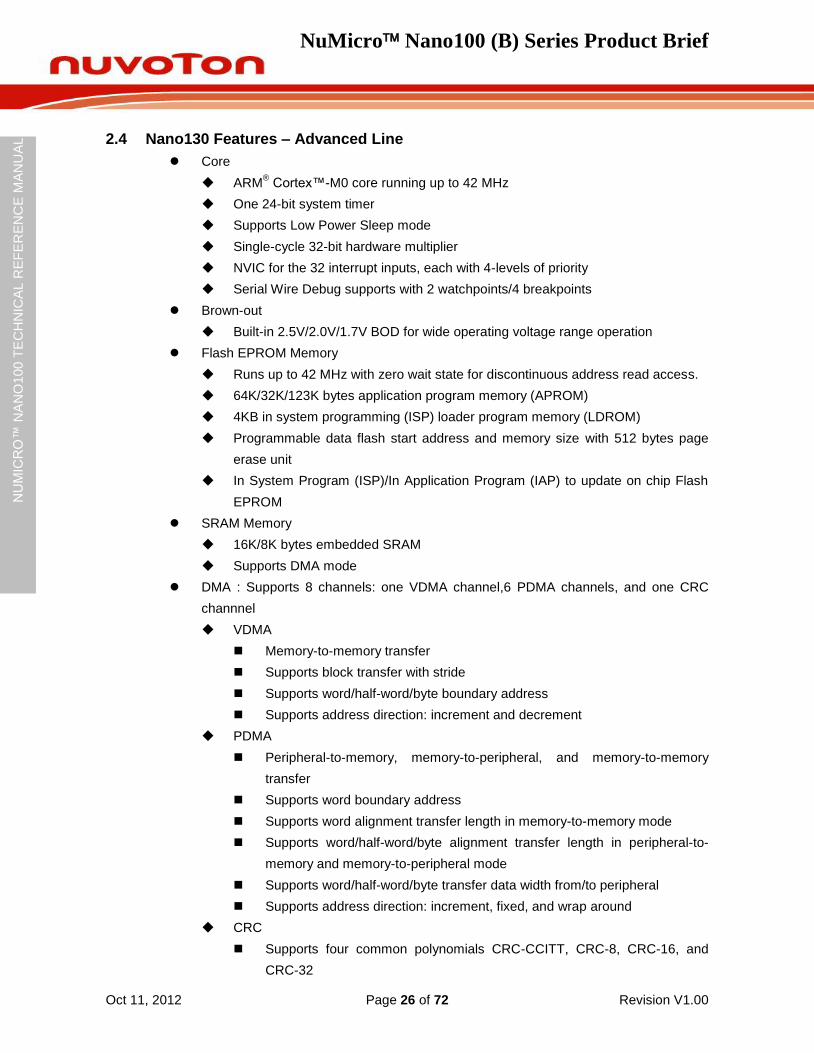
2.4 Nano130 Features – Advanced Line
Core
ARM® Cortex™-M0 core running up to 42 MHz
One 24-bit system timer
Supports Low Power Sleep mode
Single-cycle 32-bit hardware multiplier
NVIC for the 32 interrupt inputs, each with 4-levels of priority
Serial Wire Debug supports with 2 watchpoints/4 breakpoints
Brown-out
Built-in 2.5V/2.0V/1.7V BOD for wide operating voltage range operation
Flash EPROM Memory
Runs up to 42 MHz with zero wait state for discontinuous address read access.
64K/32K/123K bytes application program memory (APROM)
4KB in system programming (ISP) loader program memory (LDROM)
Programmable data flash start address and memory size with 512 bytes page
erase unit
In System Program (ISP)/In Application Program (IAP) to update on chip Flash
EPROM
SRAM Memory
16K/8K bytes embedded SRAM
Supports DMA mode
DMA : Supports 8 channels: one VDMA channel,6 PDMA channels, and one CRC
channnel
VDMA
Memory-to-memory transfer
Supports block transfer with stride
Supports word/half-word/byte boundary address
Supports address direction: increment and decrement
PDMA
Peripheral-to-memory, memory-to-peripheral, and memory-to-memory
transfer
Supports word boundary address
Supports word alignment transfer length in memory-to-memory mode
Supports word/half-word/byte alignment transfer length in peripheral-to-
memory and memory-to-peripheral mode
Supports word/half-word/byte transfer data width from/to peripheral
Supports address direction: increment, fixed, and wrap around
CRC
Supports four common polynomials CRC-CCITT, CRC-8, CRC-16, and
CRC-32
NuMicro Nano100 (B) Series Product Brief
Oct 11, 2012 Page 27 of 72 Revision V1.00
NU
MIC
RO
™ N
AN
O100
TE
CH
NIC
AL R
EF
ER
EN
CE
MA
NU
AL
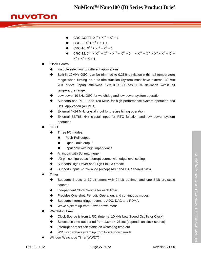
CRC-CCITT: X16
+ X12
+ X5 + 1
CRC-8: X8 + X
2 + X + 1
CRC-16: X16
+ X15
+ X2 + 1
CRC-32: X32
+ X26
+ X23
+ X22
+ X16
+ X12
+ X11
+ X10
+ X8 + X
7 + X
5 +
X4 + X
2 + X + 1
Clock Control
Flexible selection for different applications
Built-in 12MHz OSC, can be trimmed to 0.25% deviation within all temperature
range when turning on auto-trim function (system must have external 32.768
kHz crystal input) otherwise 12MHz OSC has 1 % deviation within all
temperarure range.
Low power 10 kHz OSC for watchdog and low power system operation
Supports one PLL, up to 120 MHz, for high performance system operation and
USB application (48 MHz).
External 4~24 MHz crystal input for precise timing operation
External 32.768 kHz crystal input for RTC function and low power system
operation
GPIO
Three I/O modes:
Push-Pull output
Open-Drain output
Input only with high impendence
All inputs with Schmitt trigger
I/O pin configured as interrupt source with edge/level setting
Supports High Driver and High Sink I/O mode
Supports input 5V tolerance (except ADC and DAC shared pins)
Timer
Supports 4 sets of 32-bit timers with 24-bit up-timer and one 8-bit pre-scale
counter
Independent Clock Source for each timer
Provides One-shot, Periodic Operation, and continuous modes
Supports internal trigger event to ADC, DAC and PDMA
Wake system up from Power-down mode
Watchdog Timer
Clock Source is from LIRC. (Internal 10 kHz Low Speed Oscillator Clock)
Selectable time-out period from 1.6ms ~ 26sec (depends on clock source)
Interrupt or reset selectable on watchdog time-out
WDT can wake system up from Power-down mode
Window Watchdog Timer(WWDT)
NuMicro Nano100 (B) Series Product Brief
Oct 11, 2012 Page 28 of 72 Revision V1.00
NU
MIC
RO
™ N
AN
O100
TE
CH
NIC
AL R
EF
ER
EN
CE
MA
NU
AL
6-bit down counter and 6-bit compare value to make the window period flexible
Selectable WWDT clock pre-scale counter to make WWDT time-out interval
variable.
RTC
Supports software compensation by setting frequency compensate register
(FCR)
Supports RTC counter (second, minute, hour) and calendar counter (day,
month, year)
Supports Alarm registers (second, minute, hour, day, month, year)
Selectable 12-hour or 24-hour mode
Automatic leap year recognition
Supports periodic time tick interrupt with 8 periodic options 1/128, 1/64, 1/32,
1/16, 1/8, 1/4, 1/2 and 1 second
Wake system up from Power-down or Idle mode
Supports 80 bytes spare registers and a snoop pin to clear the content of these
spare registers
PWM/Capture
Supports 2 PWM module, each with two 16-bit PWM generators
Provides eight PWM outputs or four complementary paired PWM outputs
Each PWM generator equipped with one clock divider, one 8-bit prescaler, two
clock selectors, and one Dead-Zone generator for complementary paired PWM
(Shared with PWM timers) with eight 16-bit digital capture timers provides eight
rising/ falling/both capture inputs.
Supports Capture interrupt
UART
Up to two 16-byte FIFO UART controllers
UART ports with flow control (TX, RX, CTSn and RTSn)
Supports IrDA (SIR) function
Supports LIN function
Supports RS-485 9 bit mode and direction control (Low Density Only)
Programmable baud rate generator
Supports PDMA mode
Wake system up from Power-down or Idle mode
SPI
Up to 3 sets of SPI controller
Master up to 32 MHz, and Slave up to 16 MHz
Supports SPI/MICROWIRE Master/Slave mode
Full duplex synchronous serial data transfer
Variable length of transfer data from 4 to 32 bits
MSB or LSB first data transfer
NuMicro Nano100 (B) Series Product Brief
Oct 11, 2012 Page 29 of 72 Revision V1.00
NU
MIC
RO
™ N
AN
O100
TE
CH
NIC
AL R
EF
ER
EN
CE
MA
NU
AL
RX and TX on both rising or falling edge of serial clock independently
Two slave/device select lines when used as the master, and 1 slave/device
select line when used as the slave
Supports byte suspend mode in 32-bit transmission
Supports two channel PDMA request, one for transmit and another for receive
Supports three wire, no slave select signal, bi-direction interface
Wake system up from Power-down or Idle mode
I2C
Up to two sets of I2C device
Master/Slave up to 1Mbit/s
Bi-directional data transfer between masters and slaves
Multi-master bus (no central master)
Arbitration between simultaneously transmitting masters without corruption of
serial data on the bus
Serial clock synchronization allowing devices with different bit rates to
communicate via one serial bus
Serial clock synchronization can be used as a handshake mechanism to
suspend and resume serial transfer
Built-in 14-bit time-out counter will request the I2C interrupt if the I2C bus hangs
up and timer-out counter overflows
Programmable clocks allowing for versatile rate control
Supports 7-bit addressing mode
Supports multiple address recognition (four slave addresses with mask option)
I2S
Interface with external audio CODEC
Operate as either Master or Slave mode
Capable of handling 8, 16, 24 and 32 bit word sizes
Supports Mono and stereo audio data
Supports I2S and MSB justified data format
Provides two 8 word FIFO data buffers: one for transmitting and the other for
receiving
Generates interrupt requests when buffer levels cross a programmable
boundary
Supports two PDMA requests: one for transmitting and the other for receiving
ADC
12-bit SAR ADC up to 2Msps conversion rate
Up to 12-ch single-ended input from external pin (PA.0 ~ PA.7 and PD.0 ~ PD.3)
Six internal channels from DAC0, DAC1, internal reference voltage (Int_VREF),
Temperature sensor, AVDD, and AVSS.
NuMicro Nano100 (B) Series Product Brief
Oct 11, 2012 Page 30 of 72 Revision V1.00
NU
MIC
RO
™ N
AN
O100
TE
CH
NIC
AL R
EF
ER
EN
CE
MA
NU
AL
Supports three reference voltage sources from VREF pin, internal reference
voltage (Int_VREF), and AVDD
Single scan/single cycle scan/continuous scan
Each channel with individual result register
Scan on enabled channels
Threshold voltage detection (comparator function)
Conversion start by software programming or external input
Supports PDMA mode
Supports up to four timer time-out events (TMR0_CH0, TMR0_CH1,TMR1_CH0,
TMR1_CH1) to enable ADC
DAC
12-bit monotonic output with 400K conversion rate
Supports three reference voltage sources from VREF pin, internal reference
voltage (Int_VREF), and AVDD.
Synchronized update capability for two DACs (group function)
Supports up to four timer time-out events (TMR0_CH0, TMR0_CH1,
TMR1_CH0, and TMR1_CH1), software or PDMA to trigger DAC to conversion
Touch Key(TK)
Supports programmable counter depth(16-bit, 14-bit, 12-bit and 10-bit) for
sensitivity adjustment
Supports programmable charge current for sensitivity adjustment
Supports programmable Clock Source frequency for sensitivity adjustment
Supports up to 16 touch-keys scanning
Supports external reference capacitor for different sensing environment
adjustment
SmartCard (SC)
Compliant to ISO-7816-3 T=0, T=1
Supports up to three ISO-7816-3 ports
Separates receive/transmit 4 bytes entry FIFO for data payloads
Programmable transmission clock frequency
Programmable receiver buffer trigger level
Programmable guard time selection (11 ETU ~ 266 ETU)
A 24-bit and two 8-bit time-out counter for Answer to Request (ATR) and waiting
times processing
Supports auto inverse convention function
Supports stop clock level and clock stop (clock keep) function
Supports transmitter and receiver error retry and error limit function
Supports hardware activation sequence process
Supports hardware warm reset sequence process
Supports hardware deactivation sequence process
NuMicro Nano100 (B) Series Product Brief
Oct 11, 2012 Page 31 of 72 Revision V1.00
NU
MIC
RO
™ N
AN
O100
TE
CH
NIC
AL R
EF
ER
EN
CE
MA
NU
AL
Supports hardware auto deactivation sequence when detecting the card is
removed
Support UART mode
LCD
LCD driver for up to 4 COM x 40 SEG or 6 COM x 38 SEG
Supports Static,1/2 bias and 1/3 bias voltage
Four display modes: Static, 1/2 duty, 1/3 duty, 1/4 duty, 1/5 duty and 1/6 duty.
Selectable LCD frequency by frequency divider
Configurable frame frequency
Internal Charge pump, adjustable contrast adjustment
Configurable Charge pump frequency
Blinking capability
Supports R-type/C-type method
LCD frame interrupt
USB 2.0 Full-speed Device
One set of USB 2.0 FS Device 12Mbps
On-chip USB Transceiver
Provides 1 interrupt source with 4 interrupt events
Supports Control, Bulk In/Out, Interrupt and Isochronous transfers
Auto suspend function when no bus signaling for 3 ms
Provides 8 programmable endpoints
Includes 512 Bytes internal SRAM as USB buffer
Provides remote wake-up capability
EBI (External bus interface)
Accessible space: 64 KB in 8-bit mode or 128 KB in 16-bit mode
Supports 8bit/16bit data width
Supports byte write in 16-bit data width mode
One built-in temperature sensor with 1℃ resolution
96-bit unique ID
128-bit unique customer ID
Operating Temperature: -40℃~85℃
Packages:
All Green package (RoHS)
LQFP 128-pin(14x14) / 64-pin (7x7)
NuMicro Nano100 (B) Series Product Brief
Oct 11, 2012 Page 32 of 72 Revision V1.00
NU
MIC
RO
™ N
AN
O100
TE
CH
NIC
AL R
EF
ER
EN
CE
MA
NU
AL
3 PARTS INFORMATION LIST AND PIN CONFIGURATION
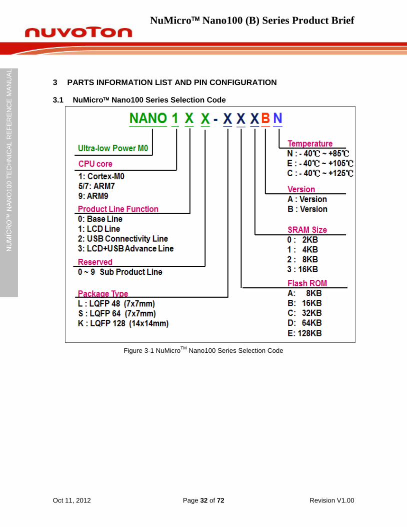
3.1 NuMicro Nano100 Series Selection Code
Figure 3-1 NuMicroTM
Nano100 Series Selection Code
NuMicro Nano100 (B) Series Product Brief
Oct 11, 2012 Page 33 of 72 Revision V1.00
NU
MIC
RO
™ N
AN
O100
TE
CH
NIC
AL R
EF
ER
EN
CE
MA
NU
AL
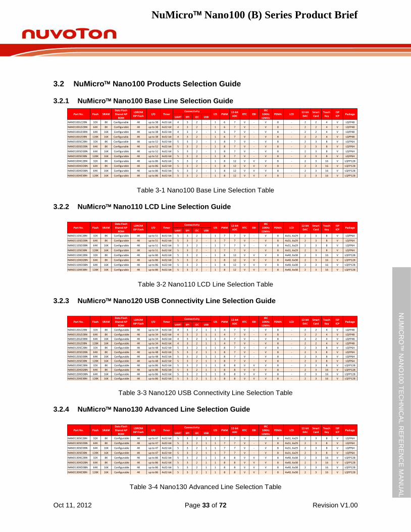
3.2 NuMicro Nano100 Products Selection Guide
3.2.1 NuMicro Nano100 Base Line Selection Guide
UART SPI I2C USB
NANO100LC2BN 32K 8K Configurable 4K up to 38 4x32-bit 4 3 2 - 1 6 7 V - V 8 - 2 2 4 V LQFP48
NANO100LD2BN 64K 8K Configurable 4K up to 38 4x32-bit 4 3 2 - 1 6 7 V - V 8 - 2 2 4 V LQFP48
NANO100LD3BN 64K 16K Configurable 4K up to 38 4x32-bit 4 3 2 - 1 6 7 V - V 8 - 2 2 4 V LQFP48
NANO100LE3BN 128K 16K Configurable 4K up to 38 4x32-bit 4 3 2 - 1 6 7 V - V 8 - 2 2 4 V LQFP48
NANO100SC2BN 32K 8K Configurable 4K up to 52 4x32-bit 5 3 2 - 1 8 7 V - V 8 - 2 3 8 V LQFP64
NANO100SD2BN 64K 8K Configurable 4K up to 52 4x32-bit 5 3 2 - 1 8 7 V - V 8 - 2 3 8 V LQFP64
NANO100SD3BN 64K 16K Configurable 4K up to 52 4x32-bit 5 3 2 - 1 8 7 V - V 8 - 2 3 8 V LQFP64
NANO100SE3BN 128K 16K Configurable 4K up to 52 4x32-bit 5 3 2 - 1 8 7 V - V 8 - 2 3 8 V LQFP64
NANO100KC2BN 32K 8K Configurable 4K up to 86 4x32-bit 5 3 2 - 1 8 12 V V V 8 - 2 3 16 V LQFP128
NANO100KD2BN 64K 8K Configurable 4K up to 86 4x32-bit 5 3 2 - 1 8 12 V V V 8 - 2 3 16 V LQFP128
NANO100KD3BN 64K 16K Configurable 4K up to 86 4x32-bit 5 3 2 - 1 8 12 V V V 8 - 2 3 16 V LQFP128
NANO100KE3BN 128K 16K Configurable 4K up to 86 4x32-bit 5 3 2 - 1 8 12 V V V 8 - 2 3 16 V LQFP128
LCD12-bit
DAC
Smart
Card
Touch
Key
ISP
ICPPackagePWM
12-bit
ADCRTC EBI
IRC
10KHz
12MHz
PDMAPart No. Flash SRAM
Data Flash
Shared AP
ROM
LDROM
ISP FlashI/O Timer
ConnectivityI2S
Table 3-1 Nano100 Base Line Selection Table
3.2.2 NuMicro Nano110 LCD Line Selection Guide
UART SPI I2C USB
NANO110SC2BN 32K 8K Configurable 4K up to 51 4x32-bit 5 3 2 - 1 7 7 V - V 8 4x31, 6x29 2 3 8 V LQFP64
NANO110SD2BN 64K 8K Configurable 4K up to 51 4x32-bit 5 3 2 - 1 7 7 V - V 8 4x31, 6x29 2 3 8 V LQFP64
NANO110SD3BN 64K 16K Configurable 4K up to 51 4x32-bit 5 3 2 - 1 7 7 V - V 8 4x31, 6x29 2 3 8 V LQFP64
NANO110SE3BN 128K 16K Configurable 4K up to 51 4x32-bit 5 3 2 - 1 7 7 V - V 8 4x31, 6x29 2 3 8 V LQFP64
NANO110KC2BN 32K 8K Configurable 4K up to 86 4x32-bit 5 3 2 - 1 8 12 V V V 8 4x40, 6x38 2 3 16 V LQFP128
NANO110KD2BN 64K 8K Configurable 4K up to 86 4x32-bit 5 3 2 - 1 8 12 V V V 8 4x40, 6x38 2 3 16 V LQFP128
NANO110KD3BN 64K 16K Configurable 4K up to 86 4x32-bit 5 3 2 - 1 8 12 V V V 8 4x40, 6x38 2 3 16 V LQFP128
NANO110KE3BN 128K 16K Configurable 4K up to 86 4x32-bit 5 3 2 - 1 8 12 V V V 8 4x40, 6x38 2 3 16 V LQFP128
LCD12-bit
DAC
Smart
Card
Touch
Key
ISP
ICPPackagePWM
12-bit
ADCRTC EBI
IRC
10KHz
12MHz
PDMAPart No. Flash SRAM
Data Flash
Shared AP
ROM
LDROM
ISP FlashI/O Timer
ConnectivityI2S
Table 3-2 Nano110 LCD Line Selection Table
3.2.3 NuMicro Nano120 USB Connectivity Line Selection Guide
UART SPI I2C USB
NANO120LC2BN 32K 8K Configurable 4K up to 34 4x32-bit 4 3 2 1 1 4 7 V - V 8 - 2 2 4 V LQFP48
NANO120LD2BN 64K 8K Configurable 4K up to 34 4x32-bit 4 3 2 1 1 4 7 V - V 8 - 2 2 4 V LQFP48
NANO120LD3BN 64K 16K Configurable 4K up to 34 4x32-bit 4 3 2 1 1 4 7 V - V 8 - 2 2 4 V LQFP48
NANO120LE3BN 128K 16K Configurable 4K up to 34 4x32-bit 4 3 2 1 1 4 7 V - V 8 - 2 2 4 V LQFP48
NANO120SC2BN 32K 8K Configurable 4K up to 48 4x32-bit 5 3 2 1 1 8 7 V - V 8 - 2 3 8 V LQFP64
NANO120SD2BN 64K 8K Configurable 4K up to 48 4x32-bit 5 3 2 1 1 8 7 V - V 8 - 2 3 8 V LQFP64
NANO120SD3BN 64K 16K Configurable 4K up to 48 4x32-bit 5 3 2 1 1 8 7 V - V 8 - 2 3 8 V LQFP64
NANO120SE3BN 128K 16K Configurable 4K up to 48 4x32-bit 5 3 2 1 1 8 7 V - V 8 - 2 3 8 V LQFP64
NANO120KC2BN 32K 8K Configurable 4K up to 86 4x32-bit 5 3 2 1 1 8 8 V V V 8 - 2 3 8 V LQFP128
NANO120KD2BN 64K 8K Configurable 4K up to 86 4x32-bit 5 3 2 1 1 8 8 V V V 8 - 2 3 16 V LQFP128
NANO120KD3BN 64K 16K Configurable 4K up to 86 4x32-bit 5 3 2 1 1 8 8 V V V 8 - 2 3 16 V LQFP128
NANO120KE3BN 128K 16K Configurable 4K up to 86 4x32-bit 5 3 2 1 1 8 8 V V V 8 - 2 3 16 V LQFP128
LCD12-bit
DAC
Smart
Card
Touch
Key
ISP
ICPPackagePWM
12-bit
ADCRTC EBI
IRC
10KHz
12MHz
PDMAPart No. Flash SRAM
Data Flash
Shared AP
ROM
LDROM
ISP FlashI/O Timer
ConnectivityI2S
Table 3-3 Nano120 USB Connectivity Line Selection Table
3.2.4 NuMicro Nano130 Advanced Line Selection Guide
UART SPI I2C USB
NANO130SC2BN 32K 8K Configurable 4K up to 47 4x32-bit 5 3 2 1 1 7 7 V - V 8 4x31, 6x29 2 3 8 V LQFP64
NANO130SD2BN 64K 8K Configurable 4K up to 47 4x32-bit 5 3 2 1 1 7 7 V - V 8 4x31, 6x29 2 3 8 V LQFP64
NANO130SD3BN 64K 16K Configurable 4K up to 47 4x32-bit 5 3 2 1 1 7 7 V - V 8 4x31, 6x29 2 3 8 V LQFP64
NANO130SE3BN 128K 16K Configurable 4K up to 47 4x32-bit 5 3 2 1 1 7 7 V - V 8 4x31, 6x29 2 3 8 V LQFP64
NANO130KC2BN 32K 8K Configurable 4K up to 86 4x32-bit 5 3 2 1 1 8 8 V V V 8 4x40, 6x38 2 3 16 V LQFP128
NANO130KD2BN 64K 8K Configurable 4K up to 86 4x32-bit 5 3 2 1 1 8 8 V V V 8 4x40, 6x38 2 3 16 V LQFP128
NANO130KD3BN 64K 16K Configurable 4K up to 86 4x32-bit 5 3 2 1 1 8 8 V V V 8 4x40, 6x38 2 3 16 V LQFP128
NANO130KE3BN 128K 16K Configurable 4K up to 86 4x32-bit 5 3 2 1 1 8 8 V V V 8 4x40, 6x38 2 3 16 V LQFP128
LCD12-bit
DAC
Smart
Card
Touch
Key
ISP
ICPPackagePWM
12-bit
ADCRTC EBI
IRC
10KHz
12MHz
PDMAPart No. Flash SRAM
Data Flash
Shared AP
ROM
LDROM
ISP FlashI/O Timer
ConnectivityI2S
Table 3-4 Nano130 Advanced Line Selection Table
NuMicro Nano100 (B) Series Product Brief
Oct 11, 2012 Page 34 of 72 Revision V1.00
NU
MIC
RO
™ N
AN
O100
TE
CH
NIC
AL R
EF
ER
EN
CE
MA
NU
AL
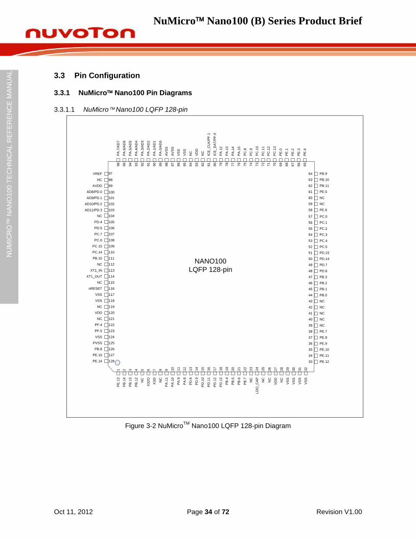
3.3 Pin Configuration
3.3.1 NuMicro Nano100 Pin Diagrams
3.3.1.1 NuMicro Nano100 LQFP 128-pin
NC
PD.4
PD.5
PB
.12
X3
2O
NC
X3
2I
PA
.11
PA
.10
PA
.9
PA
.8
PB
.4
PB
.5
PB
.6
PB
.7
NC
LD
O_
CA
P
NC
NC
nRESET
VSS
VSS
NC
VDD
NC
PF.4
PE.14
PA
.7/A
D7
PA
.6/A
D6
PA
.5/A
D5
PA
.4/A
D4
PA
.3/A
D3
PA
.2/A
D2
AV
SS
AV
SS
VS
S
VS
S
NC
VD
D
NC
ICE
_C
LK
/PF
.1
PC.6
PF.5
VSS
PE.15
PC.5
PD.15
PD.14
PD.7
PB.2
PB.1
PB.0
NC
NC
NC
NC
NC
PE.7
PE.8
PE.9
PE.10
33
34
35
36
37
38
39
40
41
42
43
44
45
46
47
48
128
127
126
125
124
123
122
121
120
119
118
117
116
115
114
113
16
15
14
13
12
11
10
987654321
81
82
83
84
85
86
87
88
89
90
91
92
93
94
95
96
ICE
_D
AT
/PF
.0
PA
.12
NANO100
LQFP 128-pin2
5
24
23
22
21
20
19
18
17
PE
.13
PB
.14
PB
.13
PD
.8
PD
.9
PD
.10
PD
.11
PD
.12
PD
.13
49
50
51
52
53
54
55
56
57
PE.11
PE.12
PD.6
PB.3
PC.0
PC.1
PC.2
PC.3
PC.4
72
73
74
75
76
77
78
79
80
PA
.1/A
D1
PA
.0/A
D0
PA
.13
PA
.14
PA
.15
PC
.8
PC
.9
PC
.10
PC
.11
112
111
110
109
108
107
106
105
104
PVSS
PB.8
PC.15
PC.14
PB.15
NC
XT1_IN
XT1_OUT
PC.7
NC
VD
D
NC
VS
S
VS
S
VS
S
VS
S3
2
31
30
29
28
27
26
NC
PE.658
59
60
61
62
63
64 PB.9
PB.10
PB.11
PE.5
NC
65
66
67
68
69
70
71
PC
.12
PC
.13
PE
.0
PE
.1
PE
.2
PE
.3
PE
.4
VREF
NC
AD8/PD.0
103
102
101
100
99
98
AD9/PD.1
AD10/PD.2
AD11/PD.3
AVDD
97
NC
Figure 3-2 NuMicroTM
Nano100 LQFP 128-pin Diagram
NuMicro Nano100 (B) Series Product Brief
Oct 11, 2012 Page 35 of 72 Revision V1.00
NU
MIC
RO
™ N
AN
O100
TE
CH
NIC
AL R
EF
ER
EN
CE
MA
NU
AL
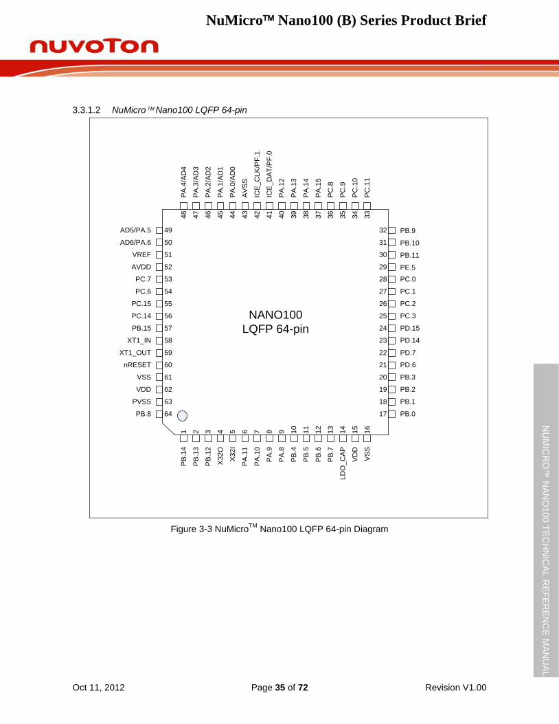
3.3.1.2 NuMicro Nano100 LQFP 64-pin
AD5/PA.5
AD6/PA.6
VREF
PB
.14
PB
.13
PB
.12
X3
2I
X3
2O
PA
.11
PA
.10
PA
.9
PA
.8
PB
.4
PB
.5
PB
.6
PB
.7
LD
O_
CA
P
VD
D
VS
S
PC.7
PC.6
PC.15
PC.14
PB.15
XT1_IN
XT1_OUT
nRESET
PB.8
PA
.4/A
D4
PA
.3/A
D3
PA
.2/A
D2
PA
.1/A
D1
PA
.0/A
D0
AV
SS
ICE
_C
LK
/PF
.1
ICE
_D
AT
/PF
.0
PA
.12
PA
.13
PA
.14
PA
.15
PC
.8
PC
.9
AVDD
VSS
VDD
PVSS
PC.0
PC.1
PC.2
PC.3
17
18
19
20
21
22
23
24
25
26
27
28
29
30
31
32
64
63
62
61
60
59
58
57
56
55
54
53
52
51
50
49
16
15
14
13
12
11
10
987654321
33
34
35
36
37
38
39
40
41
42
43
44
45
46
47
48
PC
.10
PC
.11
PB.9
PB.10
PB.11
PE.5
PD.15
PD.14
PD.7
PD.6
PB.3
PB.2
PB.1
PB.0
NANO100
LQFP 64-pin
Figure 3-3 NuMicroTM
Nano100 LQFP 64-pin Diagram
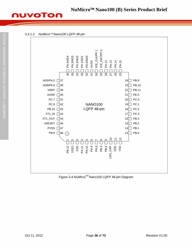
NuMicro Nano100 (B) Series Product Brief
Oct 11, 2012 Page 36 of 72 Revision V1.00
NU
MIC
RO
™ N
AN
O100
TE
CH
NIC
AL R
EF
ER
EN
CE
MA
NU
AL
3.3.1.3 NuMicro Nano100 LQFP 48-pin
AD5/PA.5
AD6/PA.6
VREF
PB
.12
X3
2I
X3
2O
PA
.11
PA
.10
PA
.9
PA
.8
PB
.4
PB
.5
LD
O_
CA
P
VD
D
VS
S
PC.7
PC.6
PB.15
XT1_IN
XT1_OUT
nRESET
PB.8
PA
.4/A
D4
PA
.3/A
D3
PA
.2/A
D2
PA
.1/A
D1
PA
.0/A
D0
AV
SS
ICE
_C
LK
/PF
.1
ICE
_D
AT
/PF
.0
PA
.12
PA
.13
PA
.14
PA
.15
AVDD
PVSS
PB.9
PB.10
PB.11
PE.5
PB.3
PB.2
13
14
15
16
17
18
19
20
21
22
23
24
48
47
46
45
44
43
42
41
40
39
38
37
12
11
10
987654321
25
26
27
28
29
30
31
32
33
34
35
36
NANO100
LQFP 48-pin
PB.1
PB.0
PC.0
PC.1
PC.2
PC.3
Figure 3-4 NuMicroTM
Nano100 LQFP 48-pin Diagram
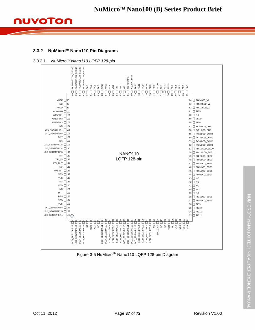
NuMicro Nano100 (B) Series Product Brief
Oct 11, 2012 Page 37 of 72 Revision V1.00
NU
MIC
RO
™ N
AN
O100
TE
CH
NIC
AL R
EF
ER
EN
CE
MA
NU
AL
3.3.2 NuMicro Nano110 Pin Diagrams
3.3.2.1 NuMicro Nano110 LQFP 128-pin
NC
LCD_SEG35/PD.4
LCD_SEG34/PD.5
LC
D_
SE
G2
4/P
B.1
2
X3
2O
NC
X3
2I
LC
D_
SE
G2
3/P
A.1
1
LC
D_
SE
G2
2/P
A.1
0
LC
D_
SE
G2
1/P
A.9
LC
D_
SE
G2
0/P
A.8
LC
D_
SE
G1
3/P
B.4
LC
D_
SE
G1
2/P
B.5
LC
D_
SE
G1
1/P
B.6
LC
D_
SE
G1
0/P
B.7
NC
LD
O_
CA
P
NC
NC
nRESET
VSS
VSS
NC
VDD
NC
PF.4
LCD_SEG28/PE.14
PA
.7/A
D7
/LC
D_
SE
G3
6
PA
.6/A
D6
/LC
D_
SE
G3
7
PA
.5/A
D5
/LC
D_
SE
G3
8
PA
.4/A
D4
/LC
D_
SE
G3
9
PA
.3
PA
.2
AV
SS
AV
SS
VS
S
VS
S
NC
VD
D
NC
ICE
_C
K/P
F.1
PC.6
PF.5
VSS
LCD_SEG29/PE.15
PC.5/LCD_COM3
PD.15/LCD_SEG0
PD.14/LCD_SEG1
PD.7/LCD_SEG2
PB.2/LCD_SEG5
PB.1/LCD_SEG6
PB.0/LCD_SEG7
NC
NC
NC
NC
NC
PE.7/LCD_SEG8
PE.8/LCD_SEG9
PE.9
PE.10
33
34
35
36
37
38
39
40
41
42
43
44
45
46
47
48
128
127
126
125
124
123
122
121
120
119
118
117
116
115
114
113
16
15
14
13
12
11
10
987654321
81
82
83
84
85
86
87
88
89
90
91
92
93
94
95
96
ICE
_D
AT
/PF
.0
PA
.12
NANO110
LQFP 128-pin2
5
24
23
22
21
20
19
18
17
LC
D_
SE
G2
7/P
E.1
3
LC
D_
SE
G2
6//P
B.1
4
LC
D_
SE
G2
5/P
B.1
3
LC
D_
SE
G1
9/P
D.8
LC
D_
SE
G1
8/P
D.9
LC
D_
SE
G1
7/P
D.1
0
LC
D_
SE
G1
6/P
D.1
1
LC
D_
SE
G1
5/P
D.1
2
LC
D_
SE
G1
4/P
D.1
3
49
50
51
52
53
54
55
56
57
PE.11
PE.12
PD.6/LCD_SEG3
PB.3/LCD_SEG4
PC.0/LCD_DH1
PC.1/LCD_DH2
PC.2/LCD_COM0
PC.3/LCD_COM1
PC.4/LCD_COM2
72
73
74
75
76
77
78
79
80
PA
.1
PA
.0
PA
.13
PA
.14
PA
.15
PC
.8
PC
.9
PC
.10
PC
.11
112
111
110
109
108
107
106
105
104
PVSS
LCD_SEG30/PB.8
LCD_SEG33/PC.15
LCD_SEG32/PC.14
LCD_SEG31/PB.15
NC
XT1_IN
XT1_OUT
PC.7
NC
VD
D
NC
VS
S
VS
S
VS
S
VS
S3
2
31
30
29
28
27
26
VLCD
PE.658
59
60
61
62
63
64 PB.9/LCD_V1
PB.10/LCD_V2
PB.11/LCD_V3
PE.5
NC
65
66
67
68
69
70
71
PC
.12
PC
.13
PE
.0
PE
.1
PE
.2
PE
.3
PE
.4
VREF
NC
AD8/PD.0
103
102
101
100
99
98
AD9/PD.1
AD10/PD.2
AD11/PD.3
AVDD
97
NC
Figure 3-5 NuMicroTM
Nano110 LQFP 128-pin Diagram
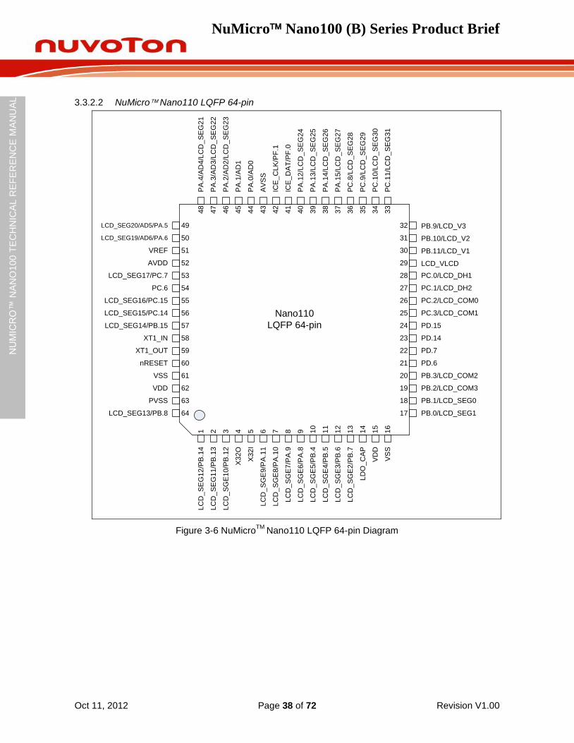
NuMicro Nano100 (B) Series Product Brief
Oct 11, 2012 Page 38 of 72 Revision V1.00
NU
MIC
RO
™ N
AN
O100
TE
CH
NIC
AL R
EF
ER
EN
CE
MA
NU
AL
3.3.2.2 NuMicro Nano110 LQFP 64-pin
LCD_SEG20/AD5/PA.5
LCD_SEG19/AD6/PA.6
VREF
LC
D_
SE
G1
2/P
B.1
4
LC
D_
SE
G1
1/P
B.1
3
LC
D_
SG
E1
0/P
B.1
2
X3
2I
X3
2O
LC
D_
SG
E9
/PA
.11
LC
D_
SG
E8
/PA
.10
LC
D_
SG
E7
/PA
.9
LC
D_
SG
E6
/PA
.8
LC
D_
SG
E5
/PB
.4
LC
D_
SG
E4
/PB
.5
LC
D_
SG
E3
/PB
.6
LC
D_
SG
E2
/PB
.7
LD
O_
CA
P
VD
D
VS
S
LCD_SEG17/PC.7
PC.6
LCD_SEG16/PC.15
LCD_SEG15/PC.14
LCD_SEG14/PB.15
XT1_IN
XT1_OUT
nRESET
LCD_SEG13/PB.8
PA
.4/A
D4
/LC
D_
SE
G2
1
PA
.3/A
D3
/LC
D_
SE
G2
2
PA
.2/A
D2
/LC
D_
SE
G2
3
PA
.1/A
D1
PA
.0/A
D0
AV
SS
ICE
_C
LK
/PF
.1
ICE
_D
AT
/PF
.0
PA
.12
/LC
D_
SE
G2
4
PA
.13
/LC
D_
SE
G2
5
PA
.14
/LC
D_
SE
G2
6
PA
.15
/LC
D_
SE
G2
7
PC
.8/L
CD
_S
EG
28
PC
.9/L
CD
_S
EG
29
AVDD
VSS
VDD
PVSS
PC.0/LCD_DH1
PC.1/LCD_DH2
PC.2/LCD_COM0
PC.3/LCD_COM1
17
18
19
20
21
22
23
24
25
26
27
28
29
30
31
32
64
63
62
61
60
59
58
57
56
55
54
53
52
51
50
49
16
15
14
13
12
11
10
987654321
33
34
35
36
37
38
39
40
41
42
43
44
45
46
47
48
PC
.10
/LC
D_
SE
G3
0
PC
.11
/LC
D_
SE
G3
1
PB.9/LCD_V3
PB.10/LCD_V2
PB.11/LCD_V1
LCD_VLCD
PD.15
PD.14
PD.7
PD.6
PB.3/LCD_COM2
PB.2/LCD_COM3
PB.1/LCD_SEG0
PB.0/LCD_SEG1
Nano110
LQFP 64-pin
Figure 3-6 NuMicroTM
Nano110 LQFP 64-pin Diagram
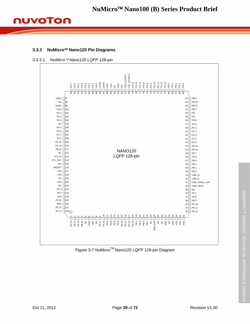
NuMicro Nano100 (B) Series Product Brief
Oct 11, 2012 Page 39 of 72 Revision V1.00
NU
MIC
RO
™ N
AN
O100
TE
CH
NIC
AL R
EF
ER
EN
CE
MA
NU
AL
3.3.3 NuMicro Nano120 Pin Diagrams
3.3.3.1 NuMicro Nano120 LQFP 128-pin
NC
PD.4
PD.5
PB
.12
X3
2O
NC
X3
2I
PA
.11
PA
.10
PA
.9
PA
.8
PB
.4
PB
.5
PB
.6
PB
.7
NC
LD
O_
CA
P
NC
NC
nRESET
VSS
VSS
NC
VDD
NC
PF.4
PE.14
PA
.7
PA
.6
PA
.5
PA
.4
PA
.3
PA
.2
AV
SS
AV
SS
VS
S
VS
S
NC
VD
D
NC
ICE
_C
LK
/PF
.1
PC.6
PF.5
VSS
PE.15
PC.5
PD.15
PD.14
PD.7
PB.2
PB.1
PB.0
USB_D+
USB_D-
USB_VDD33_CAP
USB_VBUS
NC
PE.7
PE.8
PE.9
PE.10
33
34
35
36
37
38
39
40
41
42
43
44
45
46
47
48
128
127
126
125
124
123
122
121
120
119
118
117
116
115
114
113
16
15
14
13
12
11
10
987654321
81
82
83
84
85
86
87
88
89
90
91
92
93
94
95
96
ICE
_D
AT
/PF
.0
PA
.12
NANO120
LQFP 128-pin2
5
24
23
22
21
20
19
18
17
PE
.13
PB
.14
PB
.13
PD
.8
PD
.9
PD
.10
PD
.11
PD
.12
PD
.13
49
50
51
52
53
54
55
56
57
PE.11
PE.12
PD.6
PB.3
PC.0
PC.1
PC.2
PC.3
PC.4
72
73
74
75
76
77
78
79
80
PA
.1
PA
.0
PA
.13
PA
.14
PA
.15
PC
.8
PC
.9
PC
.10
PC
.11
112
111
110
109
108
107
106
105
104
PVSS
PB.8
PC.15
PC.14
PB.15
NC
XT1_IN
XT1_OUT
PC.7
NC
VD
D
NC
VS
S
VS
S
VS
S
VS
S3
2
31
30
29
28
27
26
NC
PE.658
59
60
61
62
63
64 PB.9
PB.10
PB.11
PE.5
NC
65
66
67
68
69
70
71
PC
.12
PC
.13
PE
.0
PE
.1
PE
.2
PE
.3
PE
.4
VREF
NC
PD.0
103
102
101
100
99
98
PD.1
PD.2
PD.3
AVDD
97
NC
Figure 3-7 NuMicroTM
Nano120 LQFP 128-pin Diagram
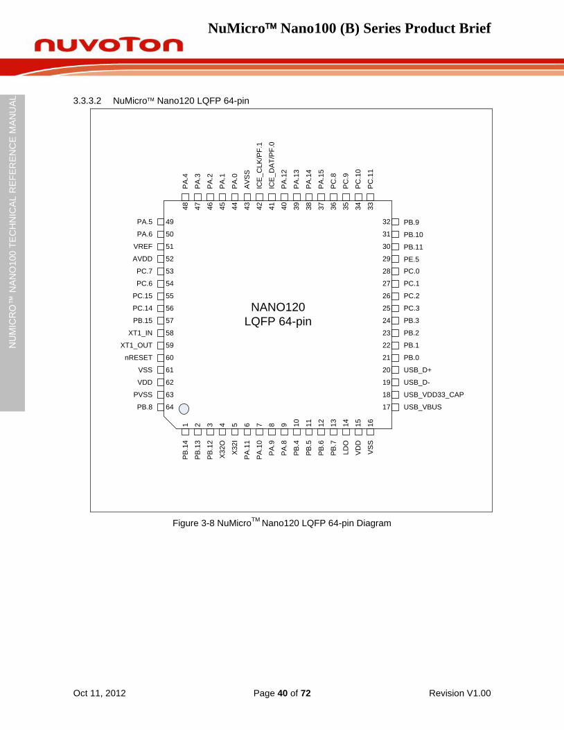
NuMicro Nano100 (B) Series Product Brief
Oct 11, 2012 Page 40 of 72 Revision V1.00
NU
MIC
RO
™ N
AN
O100
TE
CH
NIC
AL R
EF
ER
EN
CE
MA
NU
AL
3.3.3.2 NuMicro Nano120 LQFP 64-pin
PA.5
PA.6
VREF
PB
.14
PB
.13
PB
.12
X3
2I
X3
2O
PA
.11
PA
.10
PA
.9
PA
.8
PB
.4
PB
.5
PB
.6
PB
.7
LD
O
VD
D
VS
S
PC.7
PC.6
PC.15
PC.14
PB.15
XT1_IN
XT1_OUT
nRESET
PB.8
PA
.4
PA
.3
PA
.2
PA
.1
PA
.0
AV
SS
ICE
_C
LK
/PF
.1
ICE
_D
AT
/PF
.0
PA
.12
PA
.13
PA
.14
PA
.15
PC
.8
PC
.9
AVDD
VSS
VDD
PVSS
PC.0
PC.1
PC.2
PC.3
17
18
19
20
21
22
23
24
25
26
27
28
29
30
31
32
64
63
62
61
60
59
58
57
56
55
54
53
52
51
50
49
16
15
14
13
12
11
10
987654321
33
34
35
36
37
38
39
40
41
42
43
44
45
46
47
48
PC
.10
PC
.11
PB.9
PB.10
PB.11
PE.5
PB.3
PB.2
PB.1
PB.0
USB_D+
USB_D-
USB_VDD33_CAP
USB_VBUS
NANO120
LQFP 64-pin
Figure 3-8 NuMicroTM
Nano120 LQFP 64-pin Diagram
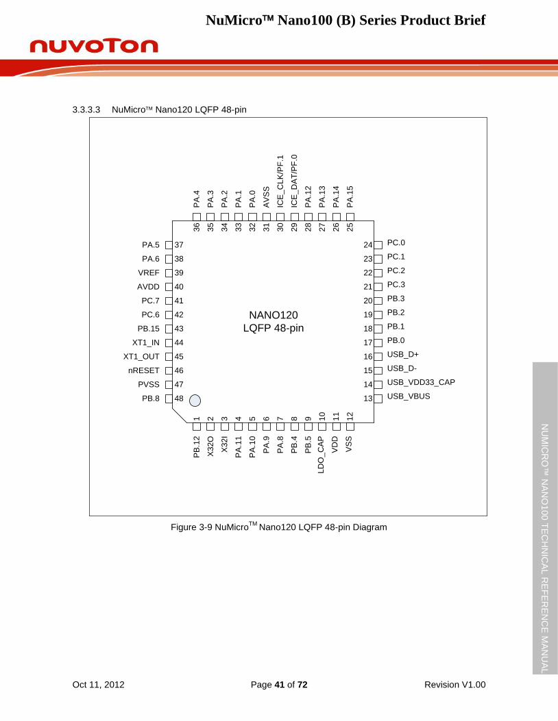
NuMicro Nano100 (B) Series Product Brief
Oct 11, 2012 Page 41 of 72 Revision V1.00
NU
MIC
RO
™ N
AN
O100
TE
CH
NIC
AL R
EF
ER
EN
CE
MA
NU
AL
3.3.3.3 NuMicro Nano120 LQFP 48-pin
PA.5
PA.6
VREF
PB
.12
X3
2I
X3
2O
PA
.11
PA
.10
PA
.9
PA
.8
PB
.4
PB
.5
LD
O_
CA
P
VD
D
VS
S
PC.7
PC.6
PB.15
XT1_IN
XT1_OUT
nRESET
PB.8
PA
.4
PA
.3
PA
.2
PA
.1
PA
.0
AV
SS
ICE
_C
LK
/PF
.1
ICE
_D
AT
/PF
.0
PA
.12
PA
.13
PA
.14
PA
.15
AVDD
PVSS
13
14
15
16
17
18
19
20
21
22
23
24
48
47
46
45
44
43
42
41
40
39
38
37
12
11
10
987654321
25
26
27
28
29
30
31
32
33
34
35
36
NANO120
LQFP 48-pin
PC.0
PC.1
PC.2
PC.3
PB.3
PB.2
PB.1
PB.0
USB_D+
USB_D-
USB_VDD33_CAP
USB_VBUS
Figure 3-9 NuMicroTM
Nano120 LQFP 48-pin Diagram
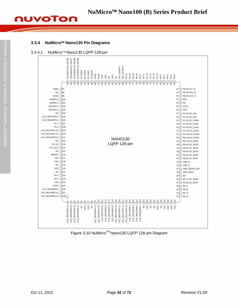
NuMicro Nano100 (B) Series Product Brief
Oct 11, 2012 Page 42 of 72 Revision V1.00
NU
MIC
RO
™ N
AN
O100
TE
CH
NIC
AL R
EF
ER
EN
CE
MA
NU
AL
3.3.4 NuMicro Nano130 Pin Diagrams
3.3.4.1 NuMicro Nano130 LQFP 128-pin
NC
LCD_SEG35/PD.4
LCD_SEG34/PD.5
LC
D_
SE
G2
4/P
B.1
2
X3
2O
NC
X3
2I
LC
D_
SE
G2
3/P
A.1
1
LC
D_
SE
G2
2/P
A.1
0
LC
D_
SE
G2
1/P
A.9
LC
D_
SE
G2
0/P
A.8
LC
D_
SE
T1
3/P
B.4
LC
D_
SE
G1
2/P
B.5
LC
D_
SE
G1
1/P
B.6
LC
D_
SE
G1
0/P
B.7
NC
LD
O
NC
NC
nRESET
VSS
VSS
NC
VDD
NC
PF.4
LCD_SEG28/PE.14
PA
.7/A
D7
/LC
D_
SE
G3
6
PA
.6/A
D6
/LC
D_
SE
G3
7
PA
.5/A
D5
/LC
D_
SE
G3
8
PA
.4/A
D4
/LC
D_
SE
G3
9
PA
.3/A
D3
PA
.2/A
D2
AV
SS
AV
SS
VS
S
VS
S
NC
VD
D
NC
ICE
_C
LK
/PF
.1
PC.6
PF.5
VSS
LCD_SEG29/PE.15
PC.5/LCD_COM3
PD.15/LCD_SEG0
PD.14/LCD_SEG1
PD.7/LCD_SEG2
PB.2/LCD_SEG5
PB.1/LCD_SEG6
PB.0/LCD_SEG7
USB_D+
USB_D-
USB_VDD33_CAP
USB_VBUS
NC
PE.7/LCD_SEG8
PE.8/LCD_SEG9
PE.9
PE.10
33
34
35
36
37
38
39
40
41
42
43
44
45
46
47
48
128
127
126
125
124
123
122
121
120
119
118
117
116
115
114
113
16
15
14
13
12
11
10
987654321
81
82
83
84
85
86
87
88
89
90
91
92
93
94
95
96
ICE
_D
AT
/PF
.0
PA
.12
NANO130
LQFP 128-pin
25
24
23
22
21
20
19
18
17
LC
D_
SE
G2
7/P
E.1
3
LC
D_
SE
G2
6/P
B.1
4
LC
D_
SE
G2
5/P
B.1
3
LC
D_
SE
G1
9/P
D.8
LC
D_
SE
G1
8/P
D.9
LC
D_
SE
G1
7/P
D.1
0
LC
D_
SE
G1
6/P
D.1
1
LC
D_
SE
G1
5/P
D.1
2
LC
D_
SE
G1
4/P
D.1
3
49
50
51
52
53
54
55
56
57
PE.11
PE.12
PD.6/LCD_SEG3
PB.3/LCD_SEG4
PC.0/LCD_DH1
PC.1/LCD_DH2
PC.2/LCD_COM0
PC.3/LCD_COM1
PC.4/LCD_COM2
72
73
74
75
76
77
78
79
80
PA
.1/A
D1
PA
.0/A
D0
PA
.13
PA
.14
PA
.15
PC
.8
PC
.9
PC
.10
PC
.11
112
111
110
109
108
107
106
105
104
PVSS
LCD_SEG30/PB.8
LCD_SEG33/PC.15
LCD_SEG32/PC.14
LCD_SEG31/PB.15
NC
XT1_IN
XT1_OUT
PC.7
NC
VD
D
NC
VS
S
VS
S
VS
S
VS
S3
2
31
30
29
28
27
26
VLCD
PE.658
59
60
61
62
63
64 PB.9/LCD_V3
PB.10/LCD_V2
PB.11/LCD_V1
PE.5
NC
65
66
67
68
69
70
71
PC
.12
PC
.13
PE
.0
PE
.1
PE
.2
PE
.3
PE
.4
VREF
NC
AD8/PD.0
103
102
101
100
99
98
AD9/PD.1
AD10/PD.2
AD11/PD.3
AVDD
97
NC
Figure 3-10 NuMicroTM
Nano130 LQFP 128-pin Diagram
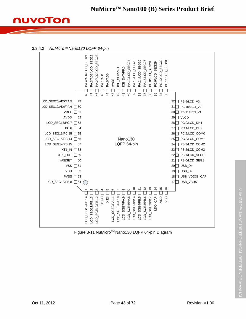
NuMicro Nano100 (B) Series Product Brief
Oct 11, 2012 Page 43 of 72 Revision V1.00
NU
MIC
RO
™ N
AN
O100
TE
CH
NIC
AL R
EF
ER
EN
CE
MA
NU
AL
3.3.4.2 NuMicro Nano130 LQFP 64-pin
LCD_SEG20/AD5/PA.5
LCD_SEG19/AD6/PA.6
VREF
LC
D_
SE
G1
2/P
B.1
4
LC
D_
SE
G1
1/P
B.1
3
LC
D_
SG
E1
0/P
B.1
2
X3
2I
X3
2O
LC
D_
SG
E9
/PA
.11
LC
D_
SG
E8
/PA
.10
LC
D_
SG
E7
/PA
.9
LC
D_
SG
E6
/PA
.8
LC
D_
SG
E5
/PB
.4
LC
D_
SG
E4
/PB
.5
LC
D_
SG
E3
/PB
.6
LC
D_
SG
E2
/PB
.7
LD
O_
CA
P
VD
D
VS
S
LCD_SEG17/PC.7
PC.6
LCD_SEG16/PC.15
LCD_SEG15/PC.14
LCD_SEG14/PB.15
XT1_IN
XT1_OUT
nRESET
LCD_SEG13/PB.8
PA
.4/A
D4
/LC
D_
SE
G2
1
PA
.3/A
D3
/LC
D_
SE
G2
2
PA
.2/A
D2
/LC
D_
SE
G2
3
PA
.1/A
D1
PA
.0/A
D0
AV
SS
ICE
_C
LK
/PF
.1
ICE
_D
AT
/PF
.0
PA
.12
/LC
D_
SE
G2
4
PA
.13
/LC
D_
SE
G2
5
PA
.14
/LC
D_
SE
G2
6
PA
.15
/LC
D_
SE
G2
7
PC
.8/L
CD
_S
EG
28
PC
.9/L
CD
_S
EG
29
AVDD
VSS
VDD
PVSS
PC.0/LCD_DH1
PC.1/LCD_DH2
PC.2/LCD_COM0
PC.3/LCD_COM1
17
18
19
20
21
22
23
24
25
26
27
28
29
30
31
32
64
63
62
61
60
59
58
57
56
55
54
53
52
51
50
49
16
15
14
13
12
11
10
987654321
33
34
35
36
37
38
39
40
41
42
43
44
45
46
47
48
PC
.10/L
CD
_S
EG
30
PC
.11/L
CD
_S
EG
31
PB.9/LCD_V3
PB.10/LCD_V2
PB.11/LCD_V1
VLCD
PB.3/LCD_COM2
PB.2/LCD_COM3
PB.1/LCD_SEG0
PB.0/LCD_SEG1
USB_D+
USB_D-
USB_VDD33_CAP
USB_VBUS
Nano130
LQFP 64-pin
Figure 3-11 NuMicroTM
Nano130 LQFP 64-pin Diagram
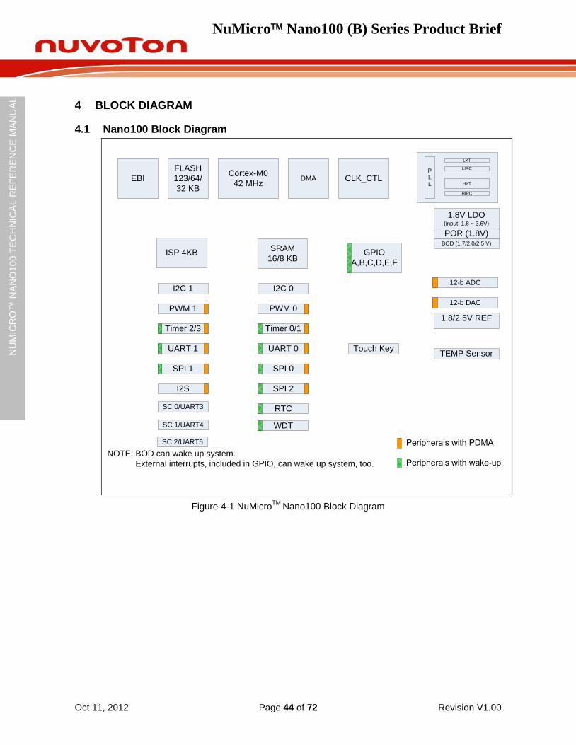
NuMicro Nano100 (B) Series Product Brief
Oct 11, 2012 Page 44 of 72 Revision V1.00
NU
MIC
RO
™ N
AN
O100
TE
CH
NIC
AL R
EF
ER
EN
CE
MA
NU
AL
4 BLOCK DIAGRAM
4.1 Nano100 Block Diagram
Peripherals with PDMA
EBI
FLASH
123/64/
32 KB
Cortex-M0
42 MHzDMA CLK_CTL
ISP 4KBSRAM
16/8 KB
PWM 1
Timer 2/3
UART 1
SPI 1
I2S
I2C 1 I2C 0
PWM 0
Timer 0/1
UART 0
SPI 0
SPI 2
RTC
Touch Key
1.8/2.5V REF
1.8V LDO (input: 1.8 ~ 3.6V)
POR (1.8V)BOD (1.7/2.0/2.5 V)
SC 0/UART3
TEMP Sensor
WDT
Peripherals with wake-up NOTE: BOD can wake up system.
External interrupts, included in GPIO, can wake up system, too.
SC 1/UART4
GPIO
A,B,C,D,E,F
P
L
L HXT
LXT
HIRC
LIRC
12-b ADC
12-b DAC
SC 2/UART5
Figure 4-1 NuMicroTM
Nano100 Block Diagram
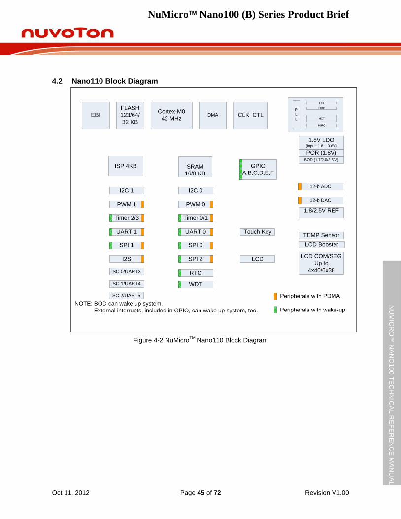
NuMicro Nano100 (B) Series Product Brief
Oct 11, 2012 Page 45 of 72 Revision V1.00
NU
MIC
RO
™ N
AN
O100
TE
CH
NIC
AL R
EF
ER
EN
CE
MA
NU
AL
4.2 Nano110 Block Diagram
Peripherals with PDMA
EBI
FLASH
123/64/
32 KB
Cortex-M0
42 MHzDMA CLK_CTL
ISP 4KB SRAM
16/8 KB
PWM 1
Timer 2/3
UART 1
SPI 1
I2S
I2C 1 I2C 0
PWM 0
Timer 0/1
UART 0
SPI 0
SPI 2
RTC
Touch Key
LCD
1.8/2.5V REF
LCD COM/SEG
Up to
4x40/6x38
1.8V LDO (input: 1.8 ~ 3.6V)
POR (1.8V)BOD (1.7/2.0/2.5 V)
SC 0/UART3
TEMP Sensor
WDT
Peripherals with wake-up NOTE: BOD can wake up system.
External interrupts, included in GPIO, can wake up system, too.
SC 1/UART4
GPIO
A,B,C,D,E,F
LCD Booster
P
L
L HXT
LXT
HIRC
LIRC
12-b ADC
12-b DAC
SC 2/UART5
Figure 4-2 NuMicroTM
Nano110 Block Diagram
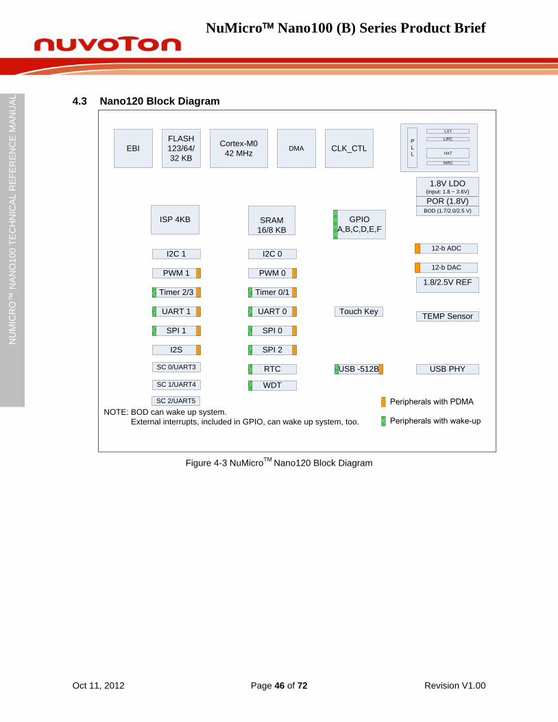
NuMicro Nano100 (B) Series Product Brief
Oct 11, 2012 Page 46 of 72 Revision V1.00
NU
MIC
RO
™ N
AN
O100
TE
CH
NIC
AL R
EF
ER
EN
CE
MA
NU
AL
4.3 Nano120 Block Diagram
Peripherals with PDMA
EBI
FLASH
123/64/
32 KB
Cortex-M0
42 MHzDMA CLK_CTL
ISP 4KB SRAM
16/8 KB
PWM 1
Timer 2/3
UART 1
SPI 1
I2S
I2C 1 I2C 0
PWM 0
Timer 0/1
UART 0
SPI 0
SPI 2
RTC
Touch Key
USB -512B USB PHY
1.8/2.5V REF
1.8V LDO (input: 1.8 ~ 3.6V)
POR (1.8V)BOD (1.7/2.0/2.5 V)
SC 0/UART3
TEMP Sensor
WDT
Peripherals with wake-up NOTE: BOD can wake up system.
External interrupts, included in GPIO, can wake up system, too.
SC 1/UART4
GPIO
A,B,C,D,E,F
P
L
L HXT
LXT
HIRC
LIRC
12-b ADC
12-b DAC
SC 2/UART5
Figure 4-3 NuMicroTM
Nano120 Block Diagram
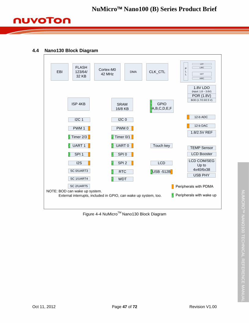
NuMicro Nano100 (B) Series Product Brief
Oct 11, 2012 Page 47 of 72 Revision V1.00
NU
MIC
RO
™ N
AN
O100
TE
CH
NIC
AL R
EF
ER
EN
CE
MA
NU
AL
4.4 Nano130 Block Diagram
Peripherals with PDMA
EBI
FLASH
123/64/
32 KB
Cortex-M0
42 MHzDMA CLK_CTL
ISP 4KB SRAM
16/8 KB
PWM 1
Timer 2/3
UART 1
SPI 1
I2S
I2C 1 I2C 0
PWM 0
Timer 0/1
UART 0
SPI 0
SPI 2
RTC
Touch key
LCD
USB -512BUSB PHY
1.8/2.5V REF
LCD COM/SEG
Up to
4x40/6x38
1.8V LDO (input: 1.8 ~ 3.6V)
POR (1.8V)BOD (1.7/2.0/2.5 V)
SC 0/UART3
TEMP Sensor
WDT
Peripherals with wake up NOTE: BOD can wake up system.
External interrupts, included in GPIO, can wake up system, too.
SC 1/UART4
GPIO
A,B,C,D,E,F
LCD Booster
P
L
L HXT
LXT
HIRC
LIRC
12-b ADC
12-b DAC
SC 2/UART5
Figure 4-4 NuMicroTM
Nano130 Block Diagram
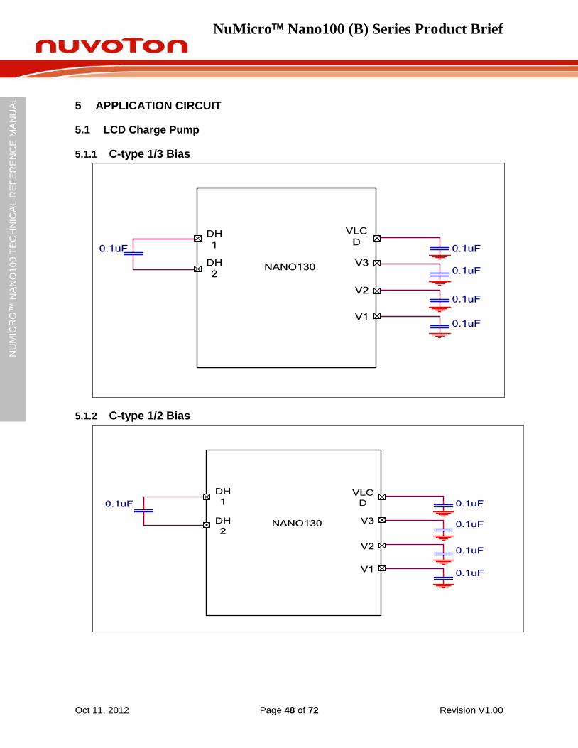
NuMicro Nano100 (B) Series Product Brief
Oct 11, 2012 Page 48 of 72 Revision V1.00
NU
MIC
RO
™ N
AN
O100
TE
CH
NIC
AL R
EF
ER
EN
CE
MA
NU
AL
5 APPLICATION CIRCUIT
5.1 LCD Charge Pump
5.1.1 C-type 1/3 Bias
DH
1
VLC
D0.1uF
V2
DH
2
V1
V3
NANO130 0.1uF
0.1uF
0.1uF
0.1uF
5.1.2 C-type 1/2 Bias
DH
1VLC
D 0.1uF
V2
DH
2
V1
V3
NANO130
0.1uF
0.1uF
0.1uF
0.1uF
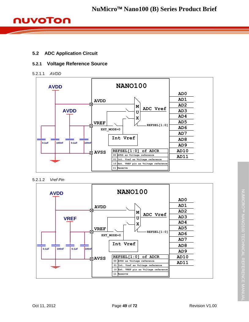
NuMicro Nano100 (B) Series Product Brief
Oct 11, 2012 Page 49 of 72 Revision V1.00
NU
MIC
RO
™ N
AN
O100
TE
CH
NIC
AL R
EF
ER
EN
CE
MA
NU
AL
5.2 ADC Application Circuit
5.2.1 Voltage Reference Source
5.2.1.1 AVDD
AVDD
0.1uF 100nF
AVSS
NANO100
AVDD
VREF
ADC Vref
Int Vref
AD0
AD1
AD2
AD3
AD4
AD5
AD6
AD7
AD8
AD9
AD10
AD11
REFSEL[1:0] of ADCR00 AVDD as Voltage reference
01 Int. Vref as Voltage reference
10 Ext. VREF pin as Voltage reference
11 Reserve
REFSEL[1:0]
M
U
X
EXT_MODE=0
0.1uF 100nF
AVDD
5.2.1.2 Vref Pin
AVDD
AVSS
NANO100
AVDD
VREF
AD0
AD1
AD2
AD3
AD4
AD5
AD6
AD7
AD8
AD9
AD10
AD11
VREF
ADC Vref
Int Vref
REFSEL[1:0] of ADCR00 AVDD as Voltage reference
01 Int. Vref as Voltage reference
10 Ext. VREF pin as Voltage reference
11 Reserve
M
U
X
EXT_MODE=0REFSEL[1:0]
0.1uF 100nF 0.1uF 100nF
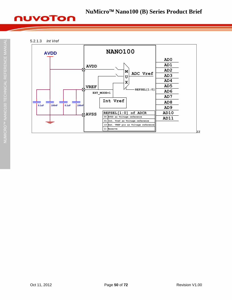
NuMicro Nano100 (B) Series Product Brief
Oct 11, 2012 Page 50 of 72 Revision V1.00
NU
MIC
RO
™ N
AN
O100
TE
CH
NIC
AL R
EF
ER
EN
CE
MA
NU
AL
5.2.1.3 Int Vref
AVDD
AVSS
AVDD
VREF
AD0
AD1
AD2
AD3
AD4
AD5
AD6
AD7
AD8
AD9
AD10
AD11
NANO100
ADC Vref
Int Vref
REFSEL[1:0] of ADCR00 AVDD as Voltage reference
01 Int. Vref as Voltage reference
10 Ext. VREF pin as Voltage reference
11 Reserve
M
U
X
EXT_MODE=1
REFSEL[1:0]
0.1uF 100nF 0.1uF 100nF
zz
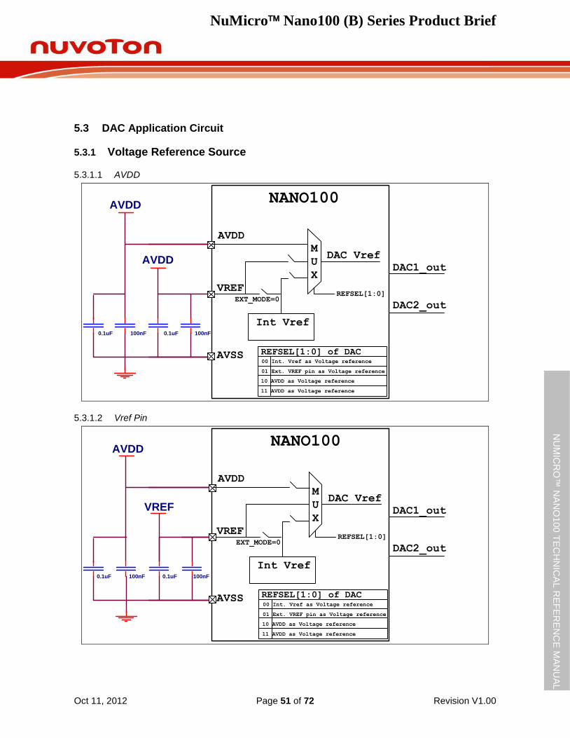
NuMicro Nano100 (B) Series Product Brief
Oct 11, 2012 Page 51 of 72 Revision V1.00
NU
MIC
RO
™ N
AN
O100
TE
CH
NIC
AL R
EF
ER
EN
CE
MA
NU
AL
5.3 DAC Application Circuit
5.3.1 Voltage Reference Source
5.3.1.1 AVDD
AVDD
AVSS
NANO100
VREF
DAC Vref
Int Vref
DAC1_out
DAC2_out
REFSEL[1:0] of DAC
10 AVDD as Voltage reference
00 Int. Vref as Voltage reference
01 Ext. VREF pin as Voltage reference
11 AVDD as Voltage reference
REFSEL[1:0]
M
U
X
EXT_MODE=0
AVDD
AVDD
0.1uF 100nF 0.1uF 100nF
5.3.1.2 Vref Pin
AVDD
AVSS
NANO100
DAC1_out
DAC2_out
VREF
DAC Vref
Int Vref
REFSEL[1:0] of DAC
10 AVDD as Voltage reference
00 Int. Vref as Voltage reference
01 Ext. VREF pin as Voltage reference
11 AVDD as Voltage reference
REFSEL[1:0]
M
U
X
EXT_MODE=0
AVDD
VREF
0.1uF 100nF 0.1uF 100nF
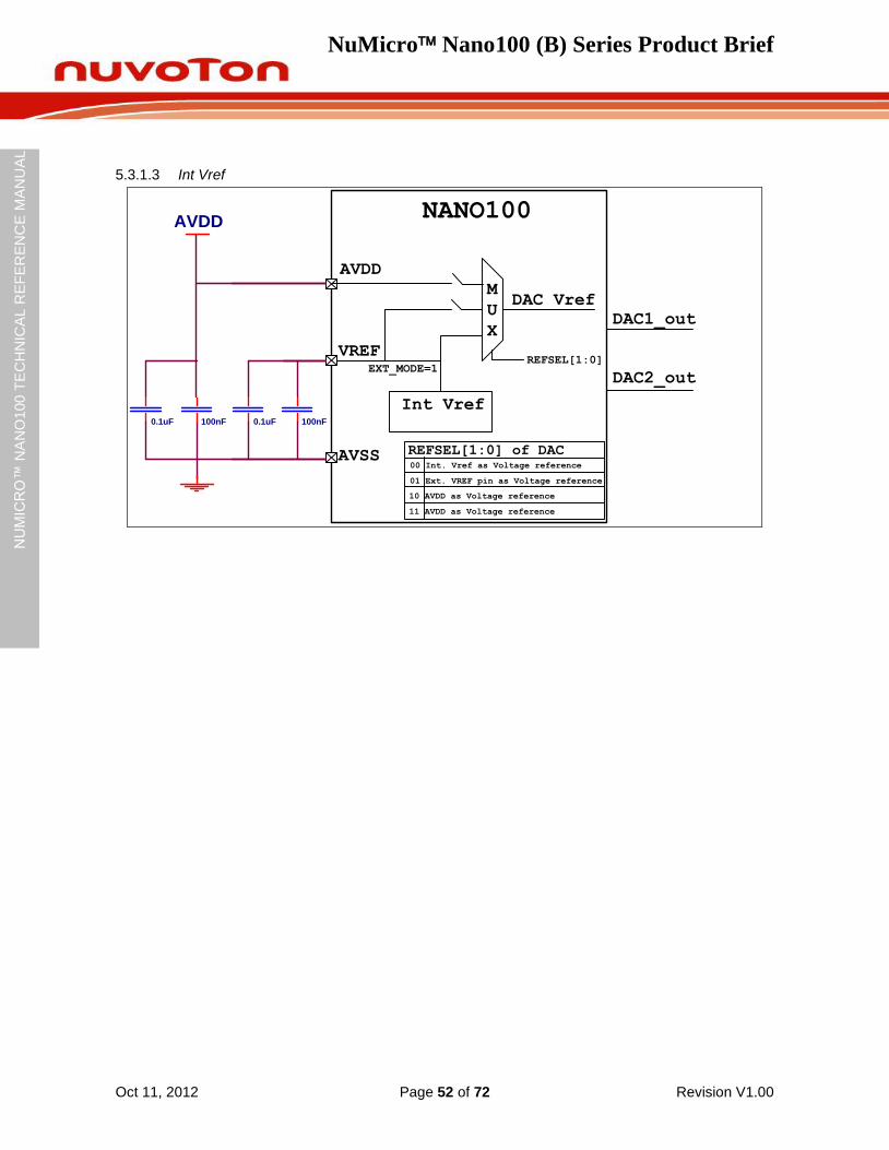
NuMicro Nano100 (B) Series Product Brief
Oct 11, 2012 Page 52 of 72 Revision V1.00
NU
MIC
RO
™ N
AN
O100
TE
CH
NIC
AL R
EF
ER
EN
CE
MA
NU
AL
5.3.1.3 Int Vref
AVDD
AVSS
NANO100
DAC1_out
DAC2_out
VREF
DAC Vref
Int Vref
REFSEL[1:0] of DAC
10 AVDD as Voltage reference
00 Int. Vref as Voltage reference
01 Ext. VREF pin as Voltage reference
11 AVDD as Voltage reference
REFSEL[1:0]
M
U
X
EXT_MODE=1
AVDD
0.1uF 100nF 0.1uF 100nF
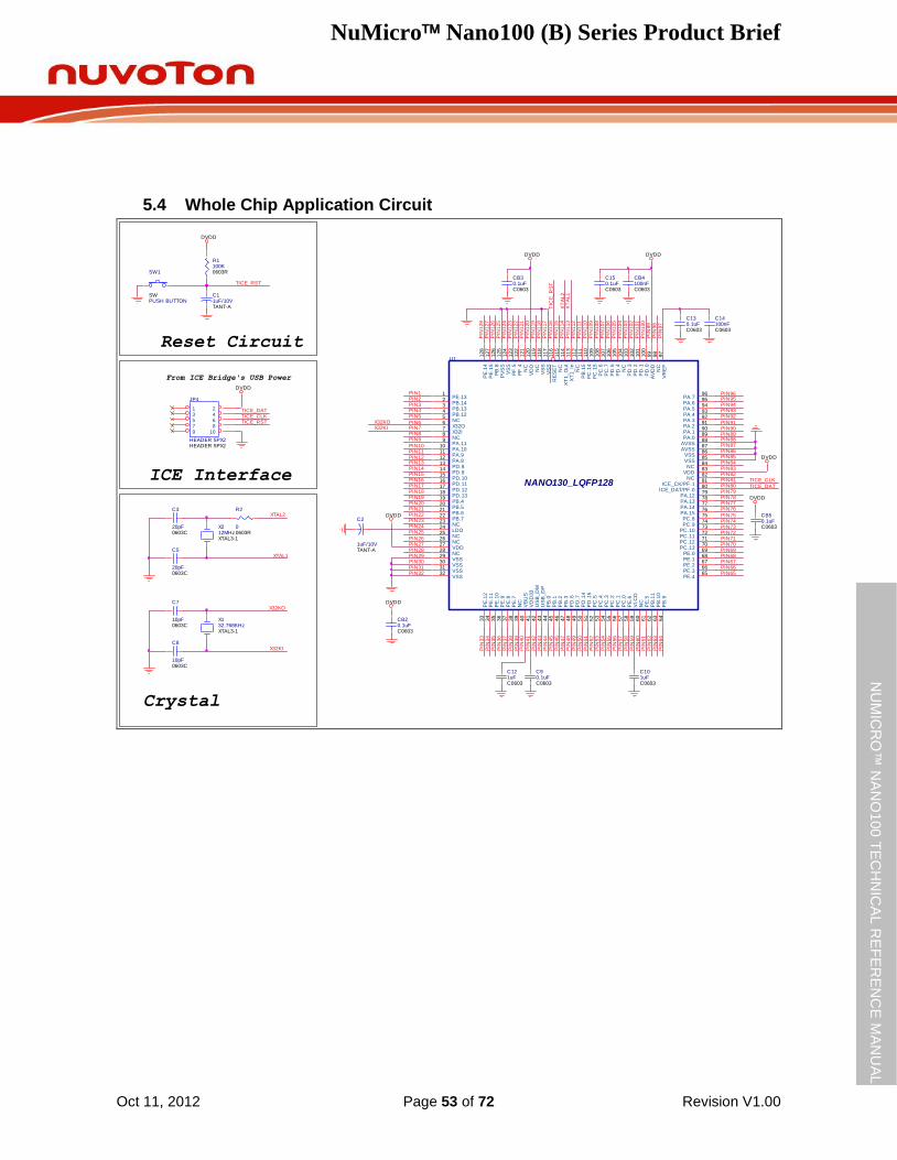
NuMicro Nano100 (B) Series Product Brief
Oct 11, 2012 Page 53 of 72 Revision V1.00
NU
MIC
RO
™ N
AN
O100
TE
CH
NIC
AL R
EF
ER
EN
CE
MA
NU
AL
5.4 Whole Chip Application Circuit
PIN
113
PIN95
PIN65
DVDD
PIN11
PIN
109
PIN85
R2
00603R
PIN8
PIN
37
PIN21
PIN29
CB30.1uFC0603
TIC
E_R
ST
PIN89
DVDD
PIN91
DVDD
PIN12
PIN
111
X32KO
PIN28
PIN
33
PIN19
PIN31
PIN
116
C101uFC0603
PIN74
DVDD
PIN90
PIN13
PIN
110
XTAL1
C14100nFC0603
PIN
36
XT
AL2
PIN22
PIN30
C7
10pF0603C
PIN
122
PIN84
PIN69
PIN14
PIN
126
PIN
40
PIN
41
C3
20pF0603C
PIN
114
PIN
48
PIN83
PIN
127
PIN82
TICE_DAT
CB50.1uFC0603
PIN16P
IN128
PIN
39
DVDD
PIN2
PIN
49
X32KI
PIN
123
PIN81
X132.768KHzXTAL3-1
PIN80PIN17
PIN
112
DVDD
PIN
62
PIN7
PIN
52
PIN
120
C5
20pF0603C
PIN
59
PIN
100
PIN15
PIN
34
PIN
63
X32KI
PIN
46
PIN27
CB20.1uFC0603
DVDD
PIN24
PIN
102
PIN18
PIN
47
C90.1uFC0603
PIN
58
PIN4
PIN
53
PIN32
PIN
44
PIN96
PIN
98
PIN
101
U1
NANO130_LQFP128
64
63
62
60
58
57
56
55
54
53
52
51
50
49
48
47
46
45
44
43
42
41
40
38
37
29
26
23222120191817161514131211109
76
4321
128
127
126
125
123
122
120
117
116
114
113
111
110
109
108
107
106
105
103
102
101
100
98
97
9695949392919089
87
85
828180797877767574737271706968676665
83
86
84
88
99
112
115
118
119
121
124
5
8
2425
2728
303132
33
34
35
36
39
61
59
104
PB
.9P
B.1
0P
B.1
1
NC
PE
.6P
C.0
PC
.1P
C.2
PC
.3P
C.4
PC
.5P
D.1
5P
D.1
4P
D.7
PD
.6P
B.3
PB
.2P
B.1
PB
.0U
SB
_D
PU
SB
_D
MV
DD
33
VB
US
PE
.7P
E.8
VSS
NC
NCPB.7PB.6PB.5PB.4PD.13PD.12PD.11PD.10PD.9PD.8PA.8PA.9PA.10PA.11
X32IX32O
PB.12PB.13PB.14PE.13
PE
.14
PE
.15
PB
.8P
VS
S
PF
.5P
F.4
VD
D
VS
SR
ES
ET
XT
1_O
ut
XT
1_In
PB
.15
PC
.14
PC
.15
PC
.6P
C.7
PD
.5P
D.4
PD
.3P
D.2
PD
.1P
D.0
NC
VR
EF
PA.7PA.6PA.5PA.4PA.3PA.2PA.1PA.0
AVSS
VSS
NCICE_CK/PF.1
ICE_DAT/PF.0PA.12PA.13PA.14PA.15PC.8PC.9
PC.10PC.11PC.12PC.13
PE.0PE.1PE.2PE.3PE.4
VDD
VSS
NC
AVSS
AV
DD
NC
NC
VS
SN
C
NC
VS
S
NC
NC
LDONC
VDDNC
VSSVSSVSS
PE
.12
PE
.11
PE
.10
PE
.9
NC
PE
.5
VLC
D
NC
PIN20
PIN
54
PIN
64
PIN1
PIN
50
PIN
99
TICE_CLK
TICE_DAT
PIN23P
IN121
C11uF/10VTANT-A
PIN
105
PIN
35
PIN
61
PIN9
PIN
45
PIN
125
PIN92
R1100K0603R
PIN
43
PIN25
XTAL2
PIN
104
PIN
106
PIN70
X212MHzXTAL3-1
PIN6
PIN
55
PIN
117
PIN73
TICE_CLK
PIN26
JP4
HEADER 5PX2HEADER 5PX2
1 23 45 67 89 10
From ICE Bridge's USB Power
PIN
103
PIN75
C130.1uFC0603
PIN68
X32KO
PIN
56
PIN
97
PIN93
TICE_RST
PIN
60
ICE Interface
PIN
108
CB4100nFC0603
PIN78
PIN67
C121uFC0603
PIN3
PIN
51
PIN86
PIN76
PIN
42
PIN
118
C150.1uFC0603
Reset Circuit
PIN
107
PIN72PIN71
PIN5
PIN
57
TICE_RST
PIN94
C2
1uF/10VTANT-A
PIN
119
PIN87
Crystal
SW1
PUSH BUTTONSW
XT
AL1
PIN77
DVDD
PIN66
C8
10pF0603C
PIN10
PIN
115
PIN88
PIN79
PIN
38
PIN
124
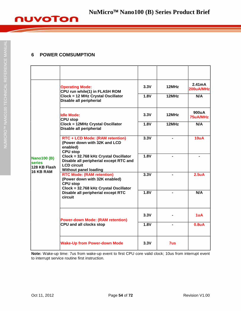
NuMicro Nano100 (B) Series Product Brief
Oct 11, 2012 Page 54 of 72 Revision V1.00
NU
MIC
RO
™ N
AN
O100
TE
CH
NIC
AL R
EF
ER
EN
CE
MA
NU
AL
6 POWER COMSUMPTION
Part No Test Condition VDD CPU Clock Current
Nano100 (B) series 128 KB Flash 16 KB RAM
Operating Mode: CPU run while(1) in FLASH ROM Clock = 12 MHz Crystal Oscillator Disable all peripherial
3.3V 12MHz 2.41mA
200uA/MHz
1.8V 12MHz N/A
Idle Mode: CPU stop Clock = 12MHz Crystal Oscillator Disable all peripherial
3.3V 12MHz 900uA
75uA/MHz
1.8V 12MHz N/A
RTC + LCD Mode: (RAM retention) (Power down with 32K and LCD enabled) CPU stop Clock = 32.768 kHz Crystal Oscillator Disable all peripherial except RTC and LCD circuit Without panel loading
3.3V - 10uA
1.8V - -
RTC Mode: (RAM retention) (Power down with 32K enabled) CPU stop Clock = 32.768 kHz Crystal Oscillator Disable all peripherial except RTC circuit
3.3V - 2.5uA
1.8V - N/A
Power-down Mode: (RAM retention) CPU and all clocks stop
3.3V - 1uA
1.8V - 0.8uA
Wake-Up from Power-down Mode 3.3V 7us
Note: Wake-up time: 7us from wake-up event to first CPU core valid clock; 10us from interrupt event to interrupt service routine first instruction.
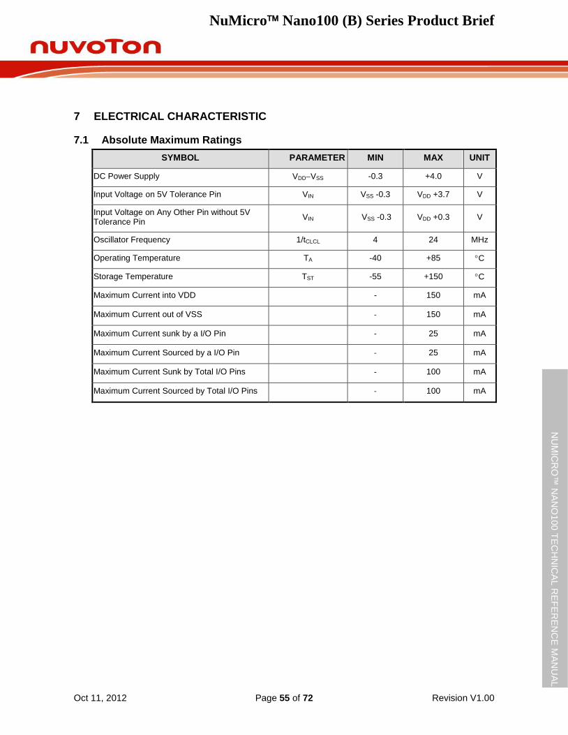
NuMicro Nano100 (B) Series Product Brief
Oct 11, 2012 Page 55 of 72 Revision V1.00
NU
MIC
RO
™ N
AN
O100
TE
CH
NIC
AL R
EF
ER
EN
CE
MA
NU
AL
7 ELECTRICAL CHARACTERISTIC
7.1 Absolute Maximum Ratings
SYMBOL PARAMETER MIN MAX UNIT
DC Power Supply VDDVSS -0.3 +4.0 V
Input Voltage on 5V Tolerance Pin VIN VSS -0.3 VDD +3.7 V
Input Voltage on Any Other Pin without 5V Tolerance Pin
VIN VSS -0.3 VDD +0.3 V
Oscillator Frequency 1/tCLCL 4 24 MHz
Operating Temperature TA -40 +85 C
Storage Temperature TST -55 +150 C
Maximum Current into VDD - 150 mA
Maximum Current out of VSS - 150 mA
Maximum Current sunk by a I/O Pin - 25 mA
Maximum Current Sourced by a I/O Pin - 25 mA
Maximum Current Sunk by Total I/O Pins - 100 mA
Maximum Current Sourced by Total I/O Pins - 100 mA
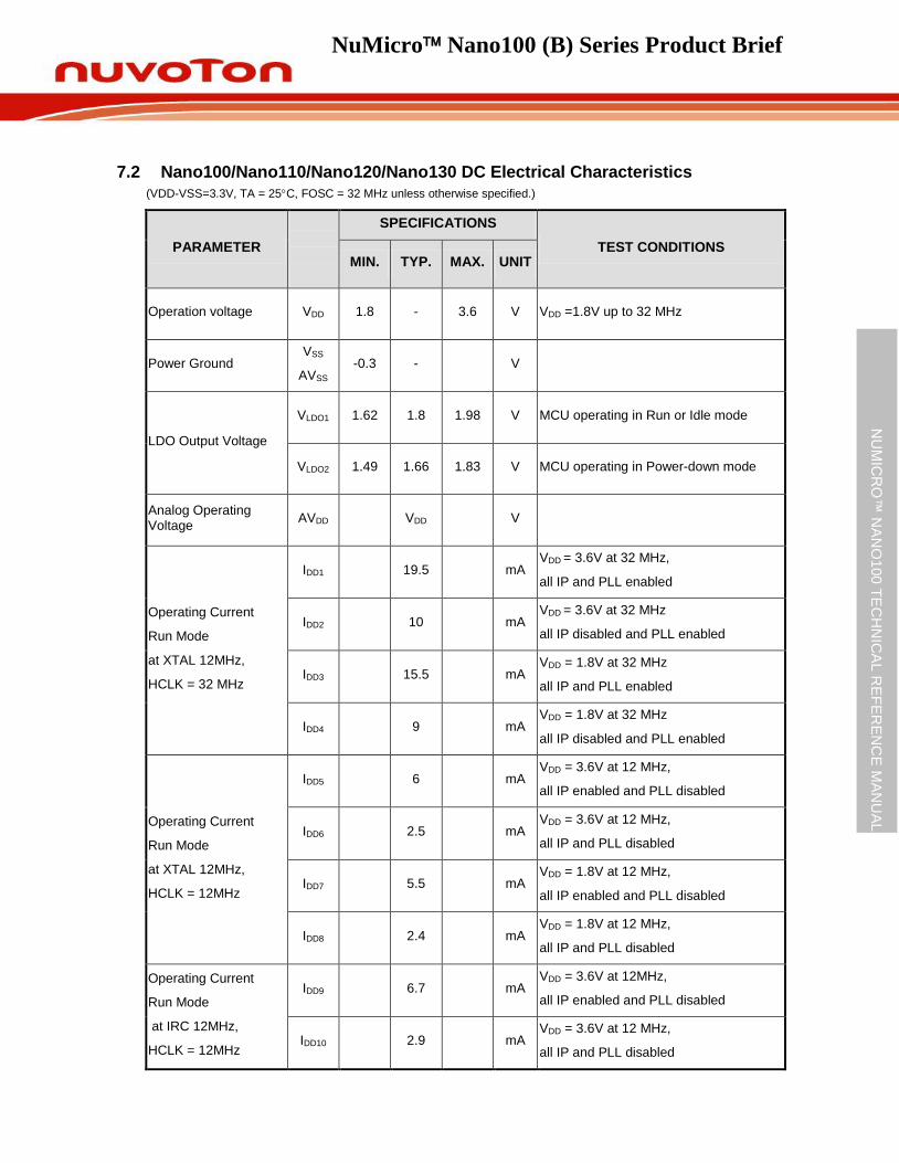
NuMicro Nano100 (B) Series Product Brief
NU
MIC
RO
™ N
AN
O100
TE
CH
NIC
AL R
EF
ER
EN
CE
MA
NU
AL
7.2 Nano100/Nano110/Nano120/Nano130 DC Electrical Characteristics
(VDD-VSS=3.3V, TA = 25C, FOSC = 32 MHz unless otherwise specified.)
PARAMETER
SYM.
SPECIFICATIONS
TEST CONDITIONS MIN. TYP. MAX. UNIT
Operation voltage VDD 1.8 - 3.6 V VDD =1.8V up to 32 MHz
Power Ground VSS
AVSS -0.3 - V
LDO Output Voltage
VLDO1 1.62 1.8 1.98 V MCU operating in Run or Idle mode
VLDO2 1.49 1.66 1.83 V MCU operating in Power-down mode
Analog Operating Voltage
AVDD VDD V
Operating Current
Run Mode
at XTAL 12MHz,
HCLK = 32 MHz
IDD1 19.5 mA VDD = 3.6V at 32 MHz,
all IP and PLL enabled
IDD2 10 mA VDD = 3.6V at 32 MHz
all IP disabled and PLL enabled
IDD3 15.5 mA VDD = 1.8V at 32 MHz
all IP and PLL enabled
IDD4 9 mA VDD = 1.8V at 32 MHz
all IP disabled and PLL enabled
Operating Current
Run Mode
at XTAL 12MHz,
HCLK = 12MHz
IDD5 6 mA VDD = 3.6V at 12 MHz,
all IP enabled and PLL disabled
IDD6 2.5 mA VDD = 3.6V at 12 MHz,
all IP and PLL disabled
IDD7 5.5 mA VDD = 1.8V at 12 MHz,
all IP enabled and PLL disabled
IDD8 2.4 mA VDD = 1.8V at 12 MHz,
all IP and PLL disabled
Operating Current
Run Mode
at IRC 12MHz,
HCLK = 12MHz
IDD9 6.7 mA VDD = 3.6V at 12MHz,
all IP enabled and PLL disabled
IDD10 2.9 mA VDD = 3.6V at 12 MHz,
all IP and PLL disabled
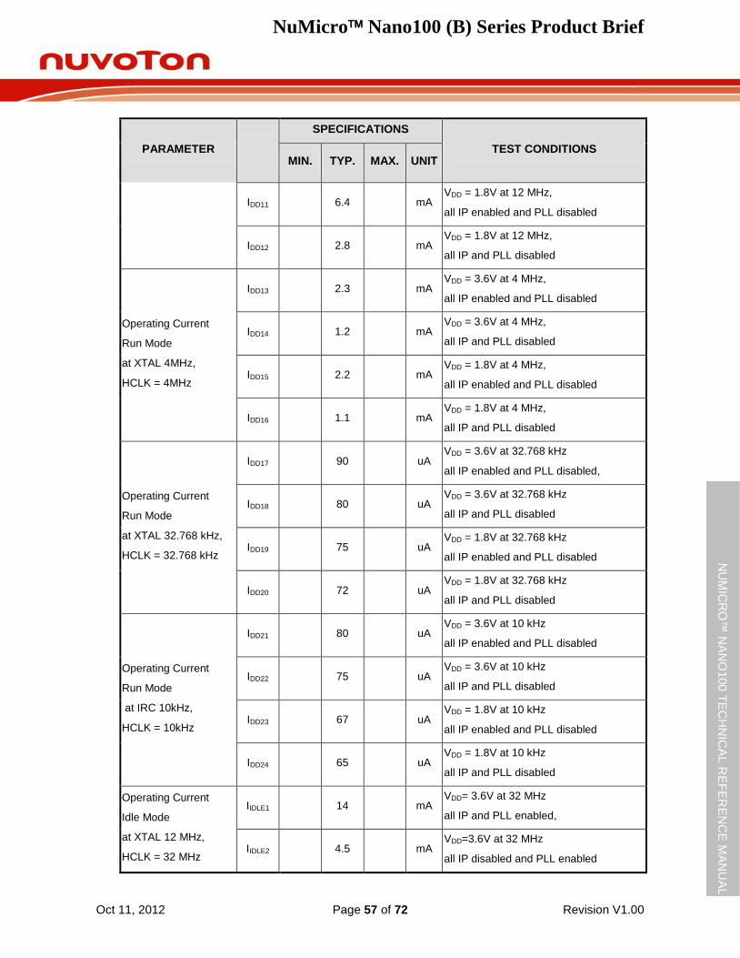
NuMicro Nano100 (B) Series Product Brief
Oct 11, 2012 Page 57 of 72 Revision V1.00
NU
MIC
RO
™ N
AN
O100
TE
CH
NIC
AL R
EF
ER
EN
CE
MA
NU
AL
PARAMETER
SYM.
SPECIFICATIONS
TEST CONDITIONS MIN. TYP. MAX. UNIT
IDD11 6.4 mA VDD = 1.8V at 12 MHz,
all IP enabled and PLL disabled
IDD12 2.8 mA VDD = 1.8V at 12 MHz,
all IP and PLL disabled
Operating Current
Run Mode
at XTAL 4MHz,
HCLK = 4MHz
IDD13 2.3 mA VDD = 3.6V at 4 MHz,
all IP enabled and PLL disabled
IDD14 1.2 mA VDD = 3.6V at 4 MHz,
all IP and PLL disabled
IDD15 2.2 mA VDD = 1.8V at 4 MHz,
all IP enabled and PLL disabled
IDD16 1.1 mA VDD = 1.8V at 4 MHz,
all IP and PLL disabled
Operating Current
Run Mode
at XTAL 32.768 kHz,
HCLK = 32.768 kHz
IDD17 90 uA VDD = 3.6V at 32.768 kHz
all IP enabled and PLL disabled,
IDD18 80 uA VDD = 3.6V at 32.768 kHz
all IP and PLL disabled
IDD19 75 uA VDD = 1.8V at 32.768 kHz
all IP enabled and PLL disabled
IDD20 72 uA VDD = 1.8V at 32.768 kHz
all IP and PLL disabled
Operating Current
Run Mode
at IRC 10kHz,
HCLK = 10kHz
IDD21 80 uA VDD = 3.6V at 10 kHz
all IP enabled and PLL disabled
IDD22 75 uA VDD = 3.6V at 10 kHz
all IP and PLL disabled
IDD23 67 uA VDD = 1.8V at 10 kHz
all IP enabled and PLL disabled
IDD24 65 uA VDD = 1.8V at 10 kHz
all IP and PLL disabled
Operating Current
Idle Mode
at XTAL 12 MHz,
HCLK = 32 MHz
IIDLE1 14 mA VDD= 3.6V at 32 MHz
all IP and PLL enabled,
IIDLE2 4.5 mA VDD=3.6V at 32 MHz
all IP disabled and PLL enabled
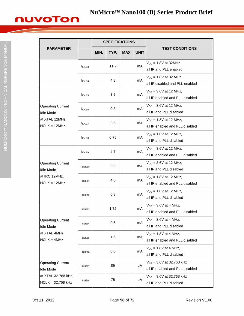
NuMicro Nano100 (B) Series Product Brief
Oct 11, 2012 Page 58 of 72 Revision V1.00
NU
MIC
RO
™ N
AN
O100
TE
CH
NIC
AL R
EF
ER
EN
CE
MA
NU
AL
PARAMETER
SYM.
SPECIFICATIONS
TEST CONDITIONS MIN. TYP. MAX. UNIT
IIDLE3 11.7 mA VDD = 1.8V at 32MHz
all IP and PLL enabled
IIDLE4 4.3 mA VDD = 1.8V at 32 MHz
all IP disabled and PLL enabled
Operating Current
Idle Mode
at XTAL 12MHz,
HCLK = 12MHz
IIDLE5 3.6 mA VDD = 3.6V at 12 MHz,
all IP enabled and PLL disabled
IIDLE6 0.8 mA VDD = 3.6V at 12 MHz,
all IP and PLL disabled
IIDLE7 3.5 mA VDD = 1.8V at 12 MHz,
all IP enabled and PLL disabled
IIDLE8 0.75 mA VDD = 1.8V at 12 MHz,
all IP and PLL disabled
Operating Current
Idle Mode
at IRC 12MHz,
HCLK = 12MHz
IIDLE9 4.7 mA VDD = 3.6V at 12 MHz,
all IP enabled and PLL disabled
IIDLE10 0.9 mA VDD = 3.6V at 12 MHz,
all IP and PLL disabled
IIDLE11 4.6 mA VDD = 1.8V at 12 MHz,
all IP enabled and PLL disabled
IIDLE12 0.8 mA VDD = 1.8V at 12 MHz,
all IP and PLL disabled
Operating Current
Idle Mode
at XTAL 4MHz,
HCLK = 4MHz
IIDLE13 1.72 mA VDD = 3.6V at 4 MHz,
all IP enabled and PLL disabled
IIDLE14 0.6 mA VDD = 3.6V at 4 MHz,
all IP and PLL disabled
IIDLE15 1.6 mA VDD = 1.8V at 4 MHz,
all IP enabled and PLL disabled
IIDLE16 0.6 mA VDD = 1.8V at 4 MHz,
all IP and PLL disabled
Operating Current
Idle Mode
at XTAL 32.768 kHz,
HCLK = 32.768 kHz
IIDLE17 85 uA VDD = 3.6V at 32.768 kHz
all IP enabled and PLL disabled
IIDLE18 75 uA VDD = 3.6V at 32.768 kHz
all IP and PLL disabled
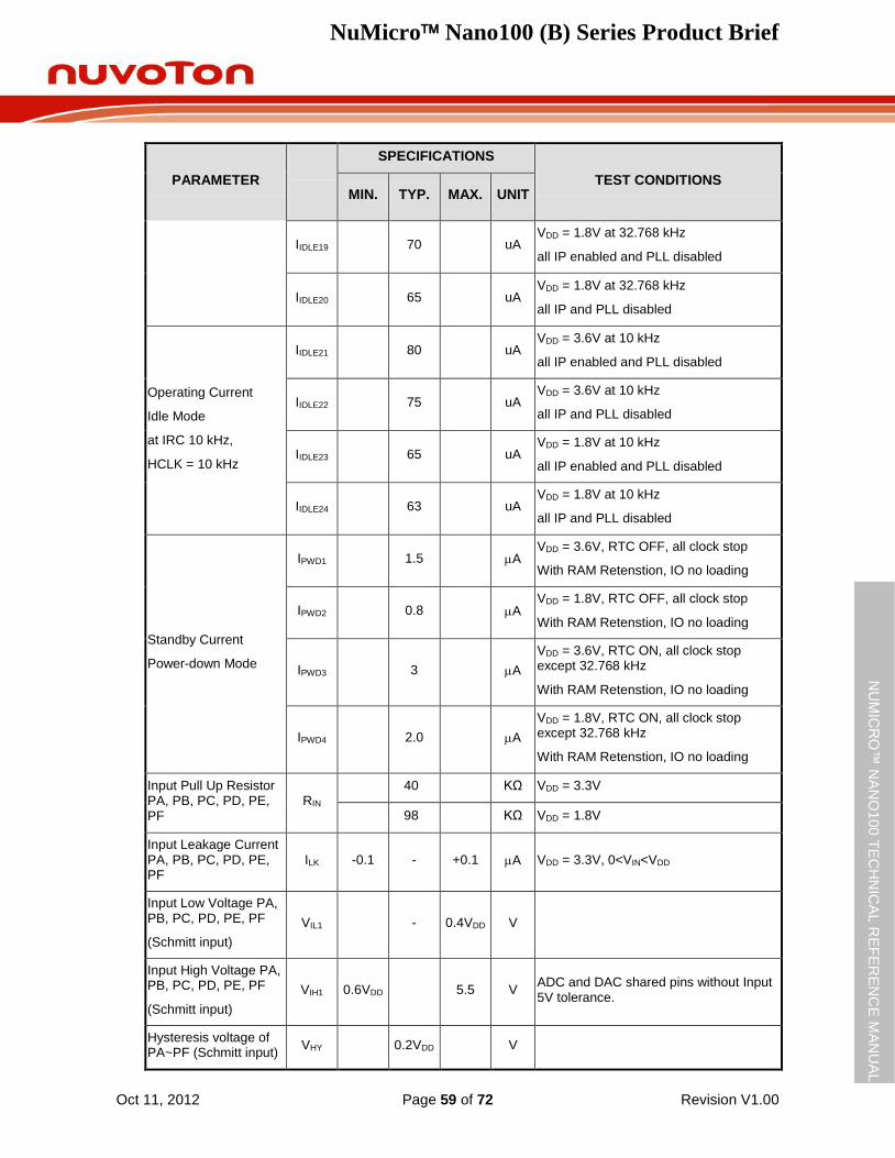
NuMicro Nano100 (B) Series Product Brief
Oct 11, 2012 Page 59 of 72 Revision V1.00
NU
MIC
RO
™ N
AN
O100
TE
CH
NIC
AL R
EF
ER
EN
CE
MA
NU
AL
PARAMETER
SYM.
SPECIFICATIONS
TEST CONDITIONS MIN. TYP. MAX. UNIT
IIDLE19 70 uA VDD = 1.8V at 32.768 kHz
all IP enabled and PLL disabled
IIDLE20 65 uA VDD = 1.8V at 32.768 kHz
all IP and PLL disabled
Operating Current
Idle Mode
at IRC 10 kHz,
HCLK = 10 kHz
IIDLE21 80 uA VDD = 3.6V at 10 kHz
all IP enabled and PLL disabled
IIDLE22 75 uA VDD = 3.6V at 10 kHz
all IP and PLL disabled
IIDLE23 65 uA VDD = 1.8V at 10 kHz
all IP enabled and PLL disabled
IIDLE24 63 uA VDD = 1.8V at 10 kHz
all IP and PLL disabled
Standby Current
Power-down Mode
IPWD1 1.5 A VDD = 3.6V, RTC OFF, all clock stop
With RAM Retenstion, IO no loading
IPWD2 0.8 A VDD = 1.8V, RTC OFF, all clock stop
With RAM Retenstion, IO no loading
IPWD3 3 A
VDD = 3.6V, RTC ON, all clock stop except 32.768 kHz
With RAM Retenstion, IO no loading
IPWD4 2.0 A
VDD = 1.8V, RTC ON, all clock stop except 32.768 kHz
With RAM Retenstion, IO no loading
Input Pull Up Resistor PA, PB, PC, PD, PE, PF
RIN 40 KΩ VDD = 3.3V
98 KΩ VDD = 1.8V
Input Leakage Current PA, PB, PC, PD, PE, PF
ILK -0.1 - +0.1 A VDD = 3.3V, 0<VIN<VDD
Input Low Voltage PA, PB, PC, PD, PE, PF
(Schmitt input)
VIL1 - 0.4VDD V
Input High Voltage PA, PB, PC, PD, PE, PF
(Schmitt input)
VIH1 0.6VDD 5.5 V ADC and DAC shared pins without Input 5V tolerance.
Hysteresis voltage of PA~PF (Schmitt input)
VHY 0.2VDD V
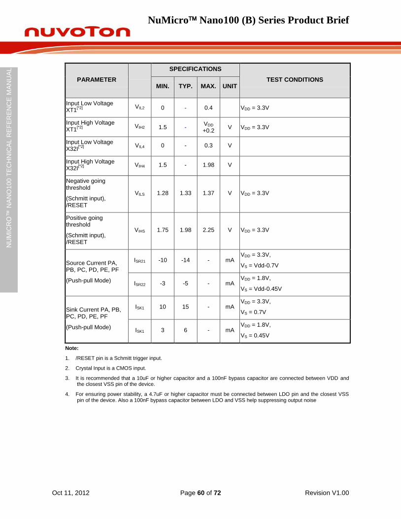
NuMicro Nano100 (B) Series Product Brief
Oct 11, 2012 Page 60 of 72 Revision V1.00
NU
MIC
RO
™ N
AN
O100
TE
CH
NIC
AL R
EF
ER
EN
CE
MA
NU
AL
PARAMETER
SYM.
SPECIFICATIONS
TEST CONDITIONS MIN. TYP. MAX. UNIT
Input Low Voltage XT1
[*2]
VIL2 0 - 0.4 VDD = 3.3V
Input High Voltage XT1
[*2]
VIH2 1.5 - VDD +0.2
V VDD = 3.3V
Input Low Voltage X32I
[*2]
VIL4 0 - 0.3 V
Input High Voltage X32I
[*2]
VIH4 1.5 - 1.98 V
Negative going threshold
(Schmitt input), /RESET
VILS 1.28 1.33 1.37 V VDD = 3.3V
Positive going threshold
(Schmitt input), /RESET
VIHS 1.75 1.98 2.25 V VDD = 3.3V
Source Current PA, PB, PC, PD, PE, PF
(Push-pull Mode)
ISR21 -10 -14 - mA VDD = 3.3V,
VS = Vdd-0.7V
ISR22 -3 -5 - mA VDD = 1.8V,
VS = Vdd-0.45V
Sink Current PA, PB, PC, PD, PE, PF
(Push-pull Mode)
ISK1 10 15 - mA VDD = 3.3V,
VS = 0.7V
ISK1 3 6 - mA VDD = 1.8V,
VS = 0.45V
Note:
1. /RESET pin is a Schmitt trigger input.
2. Crystal Input is a CMOS input.
3. It is recommended that a 10uF or higher capacitor and a 100nF bypass capacitor are connected between VDD and the closest VSS pin of the device.
4. For ensuring power stability, a 4.7uF or higher capacitor must be connected between LDO pin and the closest VSS pin of the device. Also a 100nF bypass capacitor between LDO and VSS help suppressing output noise
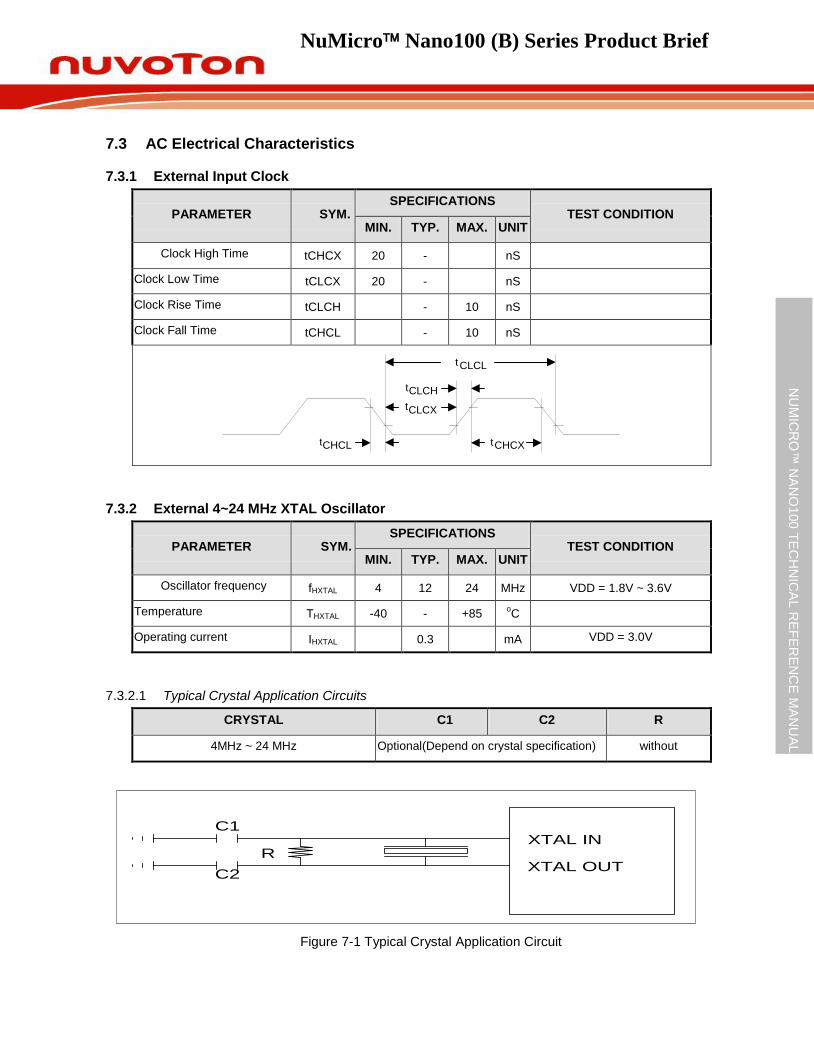
NuMicro Nano100 (B) Series Product Brief
NU
MIC
RO
™ N
AN
O100
TE
CH
NIC
AL R
EF
ER
EN
CE
MA
NU
AL
7.3 AC Electrical Characteristics
7.3.1 External Input Clock
PARAMETER SYM. SPECIFICATIONS
TEST CONDITION MIN. TYP. MAX. UNIT
Clock High Time tCHCX 20 - nS
Clock Low Time tCLCX 20 - nS
Clock Rise Time tCLCH - 10 nS
Clock Fall Time tCHCL - 10 nS
tCLCL
tCLCX
tCHCX
tCLCH
tCHCL
7.3.2 External 4~24 MHz XTAL Oscillator
PARAMETER SYM. SPECIFICATIONS
TEST CONDITION MIN. TYP. MAX. UNIT
Oscillator frequency fHXTAL 4 12 24 MHz VDD = 1.8V ~ 3.6V
Temperature THXTAL -40 - +85 oC
Operating current IHXTAL 0.3 mA VDD = 3.0V
7.3.2.1 Typical Crystal Application Circuits
CRYSTAL C1 C2 R
4MHz ~ 24 MHz Optional(Depend on crystal specification) without
XTAL OUT
XTAL INC1
C2
R
Figure 7-1 Typical Crystal Application Circuit
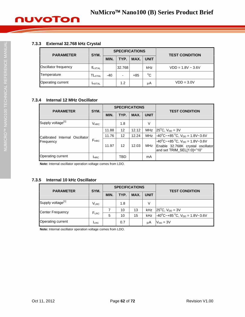
NuMicro Nano100 (B) Series Product Brief
Oct 11, 2012 Page 62 of 72 Revision V1.00
NU
MIC
RO
™ N
AN
O100
TE
CH
NIC
AL R
EF
ER
EN
CE
MA
NU
AL
7.3.3 External 32.768 kHz Crystal
PARAMETER SYM. SPECIFICATIONS
TEST CONDITION MIN. TYP. MAX. UNIT
Oscillator frequency fLXTAL 32.768 kHz VDD = 1.8V ~ 3.6V
Temperature TLXTAL -40 - +85 oC
Operating current IHXTAL 1.2 A VDD = 3.0V
7.3.4 Internal 12 MHz Oscillator
PARAMETER SYM. SPECIFICATIONS
TEST CONDITION MIN. TYP. MAX. UNIT
Supply voltage[1]
VHRC 1.8 V
Calibrated Internal Oscillator Frequency FHRC
11.88 12 12.12 MHz 25oC, VDD = 3V
11.76 12 12.24 MHz -40oC~+85
oC, VDD = 1.8V~3.6V
11.97 12 12.03 MHz
-40oC~+85
oC, VDD = 1.8V~3.6V
Enable 32.768K crystal oscillator and set TRIM_SEL[1:0]=”10”
Operating current IHRC TBD mA
Note: Internal oscillator operation voltage comes from LDO.
7.3.5 Internal 10 kHz Oscillator
PARAMETER SYM. SPECIFICATIONS
TEST CONDITION MIN. TYP. MAX. UNIT
Supply voltage[1]
VLRC 1.8 V
Center Frequency FLRC 7 10 13 kHz 25
oC, VDD = 3V
5 10 15 kHz -40oC~+85
oC, VDD = 1.8V~3.6V
Operating current ILRC 0.7 A VDD = 3V
Note: Internal oscillator operation voltage comes from LDO.
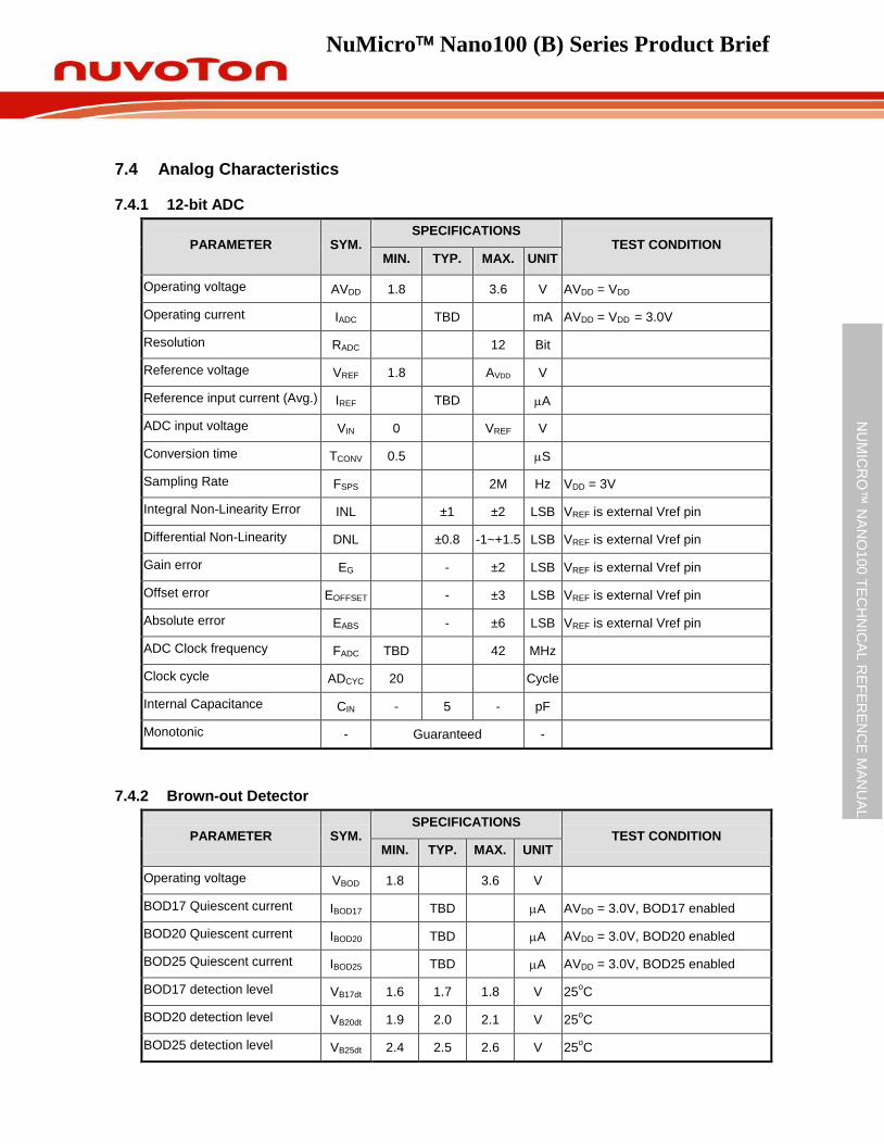
NuMicro Nano100 (B) Series Product Brief
NU
MIC
RO
™ N
AN
O100
TE
CH
NIC
AL R
EF
ER
EN
CE
MA
NU
AL
7.4 Analog Characteristics
7.4.1 12-bit ADC
PARAMETER SYM. SPECIFICATIONS
TEST CONDITION MIN. TYP. MAX. UNIT
Operating voltage AVDD 1.8 3.6 V AVDD = VDD
Operating current IADC TBD mA AVDD = VDD = 3.0V
Resolution RADC 12 Bit
Reference voltage VREF 1.8 AVDD V
Reference input current (Avg.) IREF TBD A
ADC input voltage VIN 0 VREF V
Conversion time TCONV 0.5 S
Sampling Rate FSPS 2M Hz VDD = 3V
Integral Non-Linearity Error INL ±1 ±2 LSB VREF is external Vref pin
Differential Non-Linearity DNL ±0.8 -1~+1.5 LSB VREF is external Vref pin
Gain error EG - ±2 LSB VREF is external Vref pin
Offset error EOFFSET - ±3 LSB VREF is external Vref pin
Absolute error EABS - ±6 LSB VREF is external Vref pin
ADC Clock frequency FADC TBD 42 MHz
Clock cycle ADCYC 20 Cycle
Internal Capacitance CIN - 5 - pF
Monotonic - Guaranteed -
7.4.2 Brown-out Detector
PARAMETER SYM. SPECIFICATIONS
TEST CONDITION MIN. TYP. MAX. UNIT
Operating voltage VBOD 1.8 3.6 V
BOD17 Quiescent current IBOD17 TBD A AVDD = 3.0V, BOD17 enabled
BOD20 Quiescent current IBOD20 TBD A AVDD = 3.0V, BOD20 enabled
BOD25 Quiescent current IBOD25 TBD A AVDD = 3.0V, BOD25 enabled
BOD17 detection level VB17dt 1.6 1.7 1.8 V 25oC
BOD20 detection level VB20dt 1.9 2.0 2.1 V 25oC
BOD25 detection level VB25dt 2.4 2.5 2.6 V 25oC
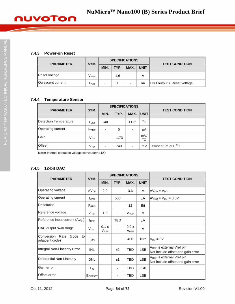
NuMicro Nano100 (B) Series Product Brief
Oct 11, 2012 Page 64 of 72 Revision V1.00
NU
MIC
RO
™ N
AN
O100
TE
CH
NIC
AL R
EF
ER
EN
CE
MA
NU
AL
7.4.3 Power-on Reset
PARAMETER SYM. SPECIFICATIONS
TEST CONDITION MIN. TYP. MAX. UNIT
Reset voltage VPOR - 1.6 - V
Quiescent current IPOR - 1 - nA LDO output > Reset voltage
7.4.4 Temperature Sensor
PARAMETER SYM. SPECIFICATIONS
TEST CONDITION MIN. TYP. MAX. UNIT
Detection Temperature TDET -40 +125 oC
Operating current ITEMP - 5 - A
Gain VTG - -1.73 - mV/
oC
Offset VTO - 740 - mV Tempeature at 0 oC
Note: Internal operation voltage comes form LDO.
7.4.5 12-bit DAC
PARAMETER SYM. SPECIFICATIONS
TEST CONDITION MIN. TYP. MAX. UNIT
Operating voltage AVDD 2.0 3.6 V AVDD = VDD
Operating current IDAC 500 A AVDD = VDD = 3.0V
Resolution RADC 12 Bit
Reference voltage VREF 1.8 AVDD V
Reference input current (Avg.) IREF TBD A
DAC output swin range VOUT 0.1 x VREF
- 0.9 x VREF
V
Conversion Rate (code to adjacent code) FSPS 400 kHz VDD = 3V
Integral Non-Linearity Error INL ±2 TBD LSB VREF is external Vref pin
Not include offset and gain error
Differential Non-Linearity DNL ±1 TBD LSB VREF is external Vref pin
Not include offset and gain error
Gain error EG - TBD LSB
Offset error EOFFSET - TBD LSB
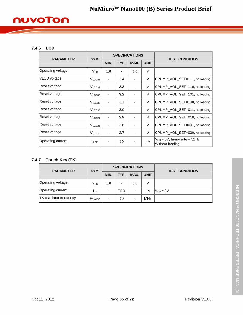
NuMicro Nano100 (B) Series Product Brief
Oct 11, 2012 Page 65 of 72 Revision V1.00
NU
MIC
RO
™ N
AN
O100
TE
CH
NIC
AL R
EF
ER
EN
CE
MA
NU
AL
7.4.6 LCD
PARAMETER SYM. SPECIFICATIONS
TEST CONDITION MIN. TYP. MAX. UNIT
Operating voltage VDD 1.8 - 3.6 V
VLCD voltage VLCD34 - 3.4 - V CPUMP_VOL_SET=111, no loading
Reset voltage VLCD33 - 3.3 - V CPUMP_VOL_SET=110, no loading
Reset voltage VLCD32 - 3.2 - V CPUMP_VOL_SET=101, no loading
Reset voltage VLCD31 - 3.1 - V CPUMP_VOL_SET=100, no loading
Reset voltage VLCD30 - 3.0 - V CPUMP_VOL_SET=011, no loading
Reset voltage VLCD29 - 2.9 - V CPUMP_VOL_SET=010, no loading
Reset voltage VLCD28 - 2.8 - V CPUMP_VOL_SET=001, no loading
Reset voltage VLCD27 - 2.7 - V CPUMP_VOL_SET=000, no loading
Operating current ILCD - 10 - A VDD = 3V, frame rate = 32Hz
Without loading
7.4.7 Touch Key (TK)
PARAMETER SYM. SPECIFICATIONS
TEST CONDITION MIN. TYP. MAX. UNIT
Operating voltage VDD 1.8 - 3.6 V
Operating current ITK - TBD - A VDD = 3V
TK oscillator frequency FTKOSC - 10 - MHz
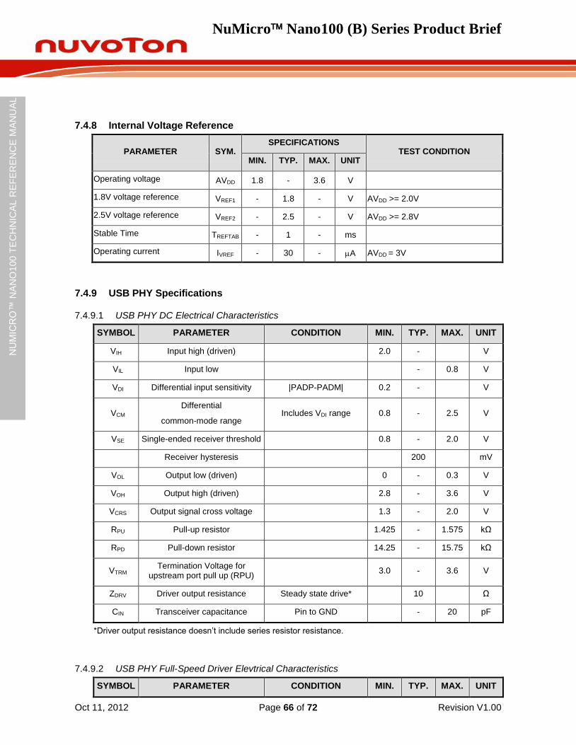
NuMicro Nano100 (B) Series Product Brief
Oct 11, 2012 Page 66 of 72 Revision V1.00
NU
MIC
RO
™ N
AN
O100
TE
CH
NIC
AL R
EF
ER
EN
CE
MA
NU
AL
7.4.8 Internal Voltage Reference
PARAMETER SYM. SPECIFICATIONS
TEST CONDITION MIN. TYP. MAX. UNIT
Operating voltage AVDD 1.8 - 3.6 V
1.8V voltage reference VREF1 - 1.8 - V AVDD >= 2.0V
2.5V voltage reference VREF2 - 2.5 - V AVDD >= 2.8V
Stable Time TREFTAB - 1 - ms
Operating current IVREF - 30 - A AVDD = 3V
7.4.9 USB PHY Specifications
7.4.9.1 USB PHY DC Electrical Characteristics
SYMBOL PARAMETER CONDITION MIN. TYP. MAX. UNIT
VIH Input high (driven) 2.0 - V
VIL Input low - 0.8 V
VDI Differential input sensitivity |PADP-PADM| 0.2 - V
VCM Differential
common-mode range Includes VDI range 0.8 - 2.5 V
VSE Single-ended receiver threshold 0.8 - 2.0 V
Receiver hysteresis 200 mV
VOL Output low (driven) 0 - 0.3 V
VOH Output high (driven) 2.8 - 3.6 V
VCRS Output signal cross voltage 1.3 - 2.0 V
RPU Pull-up resistor 1.425 - 1.575 kΩ
RPD Pull-down resistor 14.25 - 15.75 kΩ
VTRM Termination Voltage for
upstream port pull up (RPU) 3.0 - 3.6 V
ZDRV Driver output resistance Steady state drive* 10 Ω
CIN Transceiver capacitance Pin to GND - 20 pF
*Driver output resistance doesn’t include series resistor resistance.
7.4.9.2 USB PHY Full-Speed Driver Elevtrical Characteristics
SYMBOL PARAMETER CONDITION MIN. TYP. MAX. UNIT
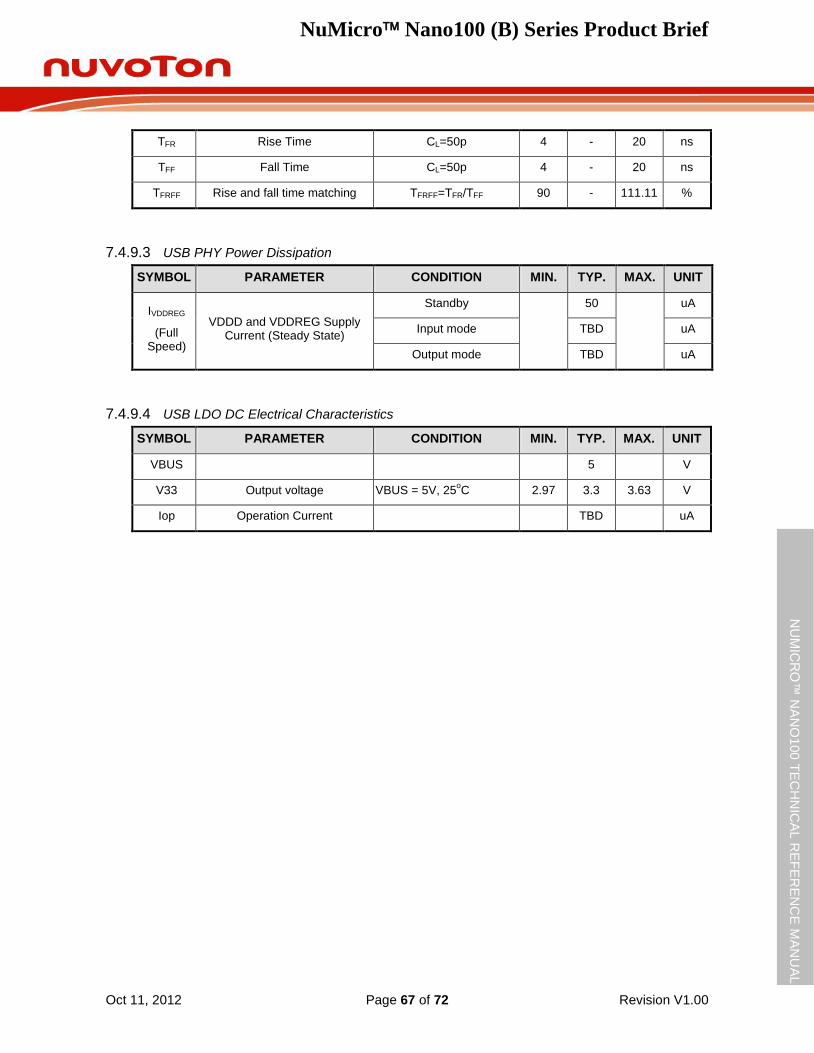
NuMicro Nano100 (B) Series Product Brief
Oct 11, 2012 Page 67 of 72 Revision V1.00
NU
MIC
RO
™ N
AN
O100
TE
CH
NIC
AL R
EF
ER
EN
CE
MA
NU
AL
TFR Rise Time CL=50p 4 - 20 ns
TFF Fall Time CL=50p 4 - 20 ns
TFRFF Rise and fall time matching TFRFF=TFR/TFF 90 - 111.11 %
7.4.9.3 USB PHY Power Dissipation
SYMBOL PARAMETER CONDITION MIN. TYP. MAX. UNIT
IVDDREG
(Full Speed)
VDDD and VDDREG Supply Current (Steady State)
Standby
50
uA
Input mode TBD uA
Output mode TBD uA
7.4.9.4 USB LDO DC Electrical Characteristics
SYMBOL PARAMETER CONDITION MIN. TYP. MAX. UNIT
VBUS 5 V
V33 Output voltage VBUS = 5V, 25oC 2.97 3.3 3.63 V
Iop Operation Current TBD uA
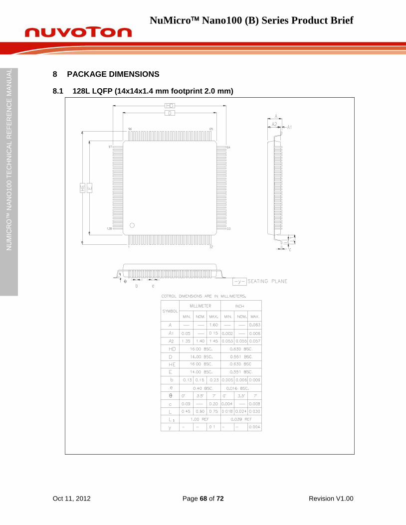
NuMicro Nano100 (B) Series Product Brief
Oct 11, 2012 Page 68 of 72 Revision V1.00
NU
MIC
RO
™ N
AN
O100
TE
CH
NIC
AL R
EF
ER
EN
CE
MA
NU
AL
8 PACKAGE DIMENSIONS
8.1 128L LQFP (14x14x1.4 mm footprint 2.0 mm)
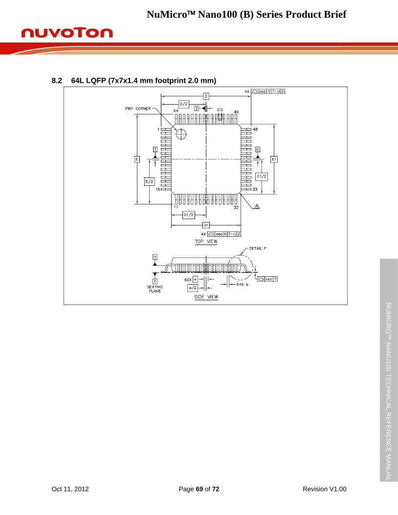
NuMicro Nano100 (B) Series Product Brief
Oct 11, 2012 Page 69 of 72 Revision V1.00
NU
MIC
RO
™ N
AN
O100
TE
CH
NIC
AL R
EF
ER
EN
CE
MA
NU
AL
8.2 64L LQFP (7x7x1.4 mm footprint 2.0 mm)
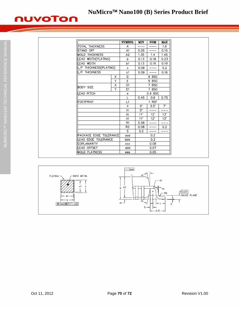
NuMicro Nano100 (B) Series Product Brief
Oct 11, 2012 Page 70 of 72 Revision V1.00
NU
MIC
RO
™ N
AN
O100
TE
CH
NIC
AL R
EF
ER
EN
CE
MA
NU
AL
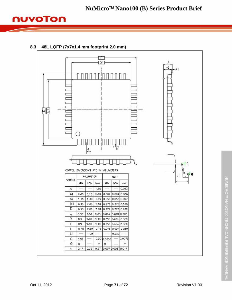
NuMicro Nano100 (B) Series Product Brief
Oct 11, 2012 Page 71 of 72 Revision V1.00
NU
MIC
RO
™ N
AN
O100
TE
CH
NIC
AL R
EF
ER
EN
CE
MA
NU
AL
8.3 48L LQFP (7x7x1.4 mm footprint 2.0 mm)
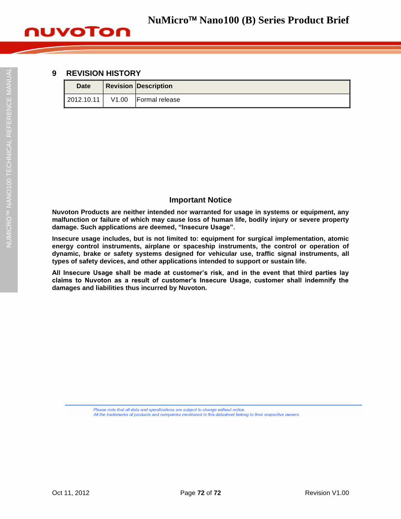
NuMicro Nano100 (B) Series Product Brief
Oct 11, 2012 Page 72 of 72 Revision V1.00
NU
MIC
RO
™ N
AN
O100
TE
CH
NIC
AL R
EF
ER
EN
CE
MA
NU
AL
9 REVISION HISTORY
Date Revision Description
2012.10.11 V1.00 Formal release
Important Notice
Nuvoton Products are neither intended nor warranted for usage in systems or equipment, any malfunction or failure of which may cause loss of human life, bodily injury or severe property damage. Such applications are deemed, “Insecure Usage”.
Insecure usage includes, but is not limited to: equipment for surgical implementation, atomic energy control instruments, airplane or spaceship instruments, the control or operation of dynamic, brake or safety systems designed for vehicular use, traffic signal instruments, all types of safety devices, and other applications intended to support or sustain life.
All Insecure Usage shall be made at customer’s risk, and in the event that third parties lay claims to Nuvoton as a result of customer’s Insecure Usage, customer shall indemnify the damages and liabilities thus incurred by Nuvoton.