Embed Size (px)
Citation preview
NuMicro NUC100/120xxxDN Datasheet
May 13, 2014 Page 1 of 100 Revision V1.00
NU
MIC
RO
™ N
UC
100/120XXXD
N D
ATASHEET
NuMicro™ NUC100 Series NUC100/120xxxDN
Datasheet
The information described in this document is the exclusive intellectual property of Nuvoton Technology Corporation and shall not be reproduced without permission from Nuvoton.
Nuvoton is providing this document only for reference purposes of NuMicroTM microcontroller based system design. Nuvoton assumes no responsibility for errors or omissions.
All data and specifications are subject to change without notice.
For additional information or questions, please contact: Nuvoton Technology Corporation.
www.nuvoton.com
NuMicro NUC100/120xxxDN Datasheet
May 13, 2014 Page 2 of 100 Revision V1.00
NU
MIC
RO
™ N
UC
100/120XXXD
N D
ATASHEET
Table of Contents
List of Figures ..................................................................................... 6
List of Tables ...................................................................................... 7
1 GENERAL DESCRIPTION .............................................................. 8
2 FEATURES ................................................................................ 9
NuMicro NUC100 Features – Advanced Line .......................................... 9 2.1
NuMicro NUC120 Features – USB Line ............................................... 13 2.2
3 PARTS INFORMATION LIST AND PIN CONFIGURATION ..................... 17
NuMicro NUC100/120xxxDN Selection Guide ........................................ 17 3.1
3.1.1 NuMicro NUC100 Advance Line Selection Guide ........................................... 17 3.1.2 NuMicro NUC120 USB Line Selection Guide ................................................ 17
Pin Configuration ............................................................................. 19 3.2
3.2.1 NuMicro NUC100 Pin Diagram ................................................................. 19 3.2.2 NuMicro NUC120 Pin Diagram ................................................................. 22
Pin Description ............................................................................... 25 3.3
3.3.1 NuMicro NUC100 Pin Description ............................................................. 25 3.3.2 NuMicro NUC120 Pin Description ............................................................. 33
4 BLOCK DIAGRAM ...................................................................... 41
NuMicro NUC100 Block Diagram ....................................................... 41 4.1
NuMicro NUC120 Block Diagram ....................................................... 42 4.2
5 FUNCTIONAL DESCRIPTION ........................................................ 43
ARM® Cortex™-M0 Core ................................................................... 43 5.1
System Manager ............................................................................. 45 5.2
5.2.1 Overview ............................................................................................. 45 5.2.2 System Reset........................................................................................ 45 5.2.3 System Power Distribution ........................................................................ 46 5.2.4 System Memory Map ............................................................................... 48 5.2.5 System Timer (SysTick) ........................................................................... 50 5.2.6 Nested Vectored Interrupt Controller (NVIC) ................................................... 51
Clock Controller .............................................................................. 55 5.3
5.3.1 Overview ............................................................................................. 55 5.3.2 Clock Generator ..................................................................................... 57 5.3.3 System Clock and SysTick Clock ................................................................ 58
NuMicro NUC100/120xxxDN Datasheet
May 13, 2014 Page 3 of 100 Revision V1.00
NU
MIC
RO
™ N
UC
100/120XXXD
N D
ATASHEET
5.3.4 Peripherals Clock ................................................................................... 59 5.3.5 Power-down Mode Clock .......................................................................... 59 5.3.6 Frequency Divider Output ......................................................................... 59
USB Device Controller (USB) .............................................................. 61 5.45.4.1 Overview ............................................................................................. 61 5.4.2 Features .............................................................................................. 61
General Purpose I/O (GPIO) ............................................................... 62 5.5
5.5.1 Overview ............................................................................................. 62 5.5.2 Features .............................................................................................. 62
I2C Serial Interface Controller (I2C) ....................................................... 63 5.65.6.1 Overview ............................................................................................. 63 5.6.2 Features .............................................................................................. 64
PWM Generator and Capture Timer (PWM) ............................................ 65 5.7
5.7.1 Overview ............................................................................................. 65 5.7.2 Features .............................................................................................. 66
Real Time Clock (RTC) ..................................................................... 67 5.85.8.1 Overview ............................................................................................. 67 5.8.2 Features .............................................................................................. 67
Serial Peripheral Interface (SPI) ........................................................... 68 5.9
5.9.1 Overview ............................................................................................. 68 5.9.2 Features .............................................................................................. 68
Timer Controller (TMR) ..................................................................... 69 5.105.10.1 Overview .......................................................................................... 69 5.10.2 Features ........................................................................................... 69
Watchdog Timer (WDT)..................................................................... 70 5.11
5.11.1 Overview .......................................................................................... 70 5.11.2 Features ........................................................................................... 70
Window Watchdog Timer (WWDT) ....................................................... 71 5.125.12.1 Overview .......................................................................................... 71 5.12.2 Features ........................................................................................... 71
UART Interface Controller (UART) ........................................................ 72 5.13
5.13.1 Overview .......................................................................................... 72 5.13.2 Features ........................................................................................... 74
PS/2 Device Controller (PS2D) ............................................................ 75 5.14
NuMicro NUC100/120xxxDN Datasheet
May 13, 2014 Page 4 of 100 Revision V1.00
NU
MIC
RO
™ N
UC
100/120XXXD
N D
ATASHEET
5.14.1 Overview .......................................................................................... 75 5.14.2 Features ........................................................................................... 75
I2S Controller (I2S) ........................................................................... 76 5.15
5.15.1 Overview .......................................................................................... 76 5.15.2 Features ........................................................................................... 76
Analog-to-Digital Converter (ADC) ........................................................ 77 5.165.16.1 Overview .......................................................................................... 77 5.16.2 Features ........................................................................................... 77
Analog Comparator (ACMP) ............................................................... 78 5.17
5.17.1 Overview .......................................................................................... 78 5.17.2 Features ........................................................................................... 78
PDMA Controller (PDMA) .................................................................. 79 5.185.18.1 Overview .......................................................................................... 79 5.18.2 Features ........................................................................................... 79
External Bus Interface (EBI) ............................................................... 80 5.19
5.19.1 Overview .......................................................................................... 80 5.19.2 Features ........................................................................................... 80
Smart Card Host Interface (SC) ........................................................... 81 5.205.20.1 Overview .......................................................................................... 81 5.20.2 Features ........................................................................................... 81
FLASH MEMORY CONTROLLER (FMC) ............................................... 82 5.21
5.21.1 Overview .......................................................................................... 82 5.21.2 Features ........................................................................................... 82
6 APPLICATION CIRCUIT ............................................................... 83
7 ELECTRICAL CHARACTERISTICS ................................................. 84
Absolute Maximum Ratings ................................................................ 84 7.1
DC Electrical Characteristics ............................................................... 85 7.2
AC Electrical Characteristics ............................................................... 89 7.3
7.3.1 External 4~24 MHz High Speed Oscillator ..................................................... 89 7.3.2 External 4~24 MHz High Speed Crystal ........................................................ 89 7.3.3 External 32.768 kHz Low Speed Crystal Oscillator ........................................... 90 7.3.4 Internal 22.1184 MHz High Speed Oscillator ................................................... 90 7.3.5 Internal 10 kHz Low Speed Oscillator ........................................................... 90
Analog Characteristics ...................................................................... 91 7.4
NuMicro NUC100/120xxxDN Datasheet
May 13, 2014 Page 5 of 100 Revision V1.00
NU
MIC
RO
™ N
UC
100/120XXXD
N D
ATASHEET
7.4.1 12-bit SARADC Specification ..................................................................... 91 7.4.2 LDO and Power Management Specification.................................................... 91 7.4.3 Low Voltage Reset Specification ................................................................. 92 7.4.4 Brown-out Detector Specification ................................................................ 92 7.4.5 Power-on Reset Specification .................................................................... 92 7.4.6 Temperature Sensor Specification ............................................................... 93 7.4.7 Comparator Specification .......................................................................... 93 7.4.8 USB PHY Specification ............................................................................ 94
Flash DC Electrical Characteristics ....................................................... 96 7.5
8 PACKAGE DIMENSIONS ............................................................. 97
100-pin LQFP (14x14x1.4 mm footprint 2.0 mm) ....................................... 97 8.1
64-pin LQFP (7x7x1.4 mm footprint 2.0 mm) ........................................... 98 8.2
48-pin LQFP (7x7x1.4 mm footprint 2.0 mm) ........................................... 99 8.3
9 REVISION HISTORY .................................................................. 100
NuMicro NUC100/120xxxDN Datasheet
May 13, 2014 Page 6 of 100 Revision V1.00
NU
MIC
RO
™ N
UC
100/120XXXD
N D
ATASHEET
List of Figures
Figure 3-1 NuMicro NUC100 Series Selection Code .................................................................. 18 Figure 3-2 NuMicro NUC100VxxDN LQFP 100-pin Diagram ..................................................... 19 Figure 3-3 NuMicro NUC100RxxDN LQFP 64-pin Diagram ....................................................... 20 Figure 3-4 NuMicro NUC100LxxDN LQFP 48-pin Diagram ........................................................ 21 Figure 3-5 NuMicro NUC120VxxDN LQFP 100-pin Diagram ..................................................... 22 Figure 3-6 NuMicro NUC120RxxDN LQFP 64-pin Diagram ....................................................... 23 Figure 3-7 NuMicro NUC120LxxDN LQFP 48-pin Diagram ........................................................ 24 Figure 4-1 NuMicro NUC100 Block Diagram .............................................................................. 41 Figure 4-2 NuMicro NUC120 Block Diagram .............................................................................. 42 Figure 5-1 Functional Controller Diagram ...................................................................................... 43 Figure 5-2 NuMicro NUC100 Power Distribution Diagram .......................................................... 46 Figure 5-3 NuMicro NUC120 Power Distribution Diagram .......................................................... 47 Figure 5-4 Clock Generator Global View Diagram ......................................................................... 56 Figure 5-5 Clock Generator Block Diagram ................................................................................... 57 Figure 5-6 System Clock Block Diagram ....................................................................................... 58 Figure 5-7 SysTick Clock Control Block Diagram .......................................................................... 58 Figure 5-8 Clock Source of Frequency Divider .............................................................................. 59 Figure 5-9 Frequency Divider Block Diagram ................................................................................ 60 Figure 5-10 I2C Bus Timing ............................................................................................................ 63 Figure 6-1 Typical Crystal Application Circuit ................................................................................ 90
NuMicro NUC100/120xxxDN Datasheet
May 13, 2014 Page 7 of 100 Revision V1.00
NU
MIC
RO
™ N
UC
100/120XXXD
N D
ATASHEET
List of Tables
Table 1-1 NuMicro NUC100 Series Connectivity Support Table .................................................. 8 Table 5-1 Address Space Assignments for On-Chip Controllers ................................................... 49 Table 5-2 Exception Model ............................................................................................................ 52 Table 5-3 System Interrupt Map ..................................................................................................... 53 Table 5-4 Vector Table Format ...................................................................................................... 53 Table 5-10 UART Baud Rate Equation .......................................................................................... 72 Table 5-11 UART Baud Rate Setting Table ................................................................................... 73
NuMicro NUC100/120xxxDN Datasheet
May 13, 2014 Page 8 of 100 Revision V1.00
NU
MIC
RO
™ N
UC
100/120XXXD
N D
ATASHEET
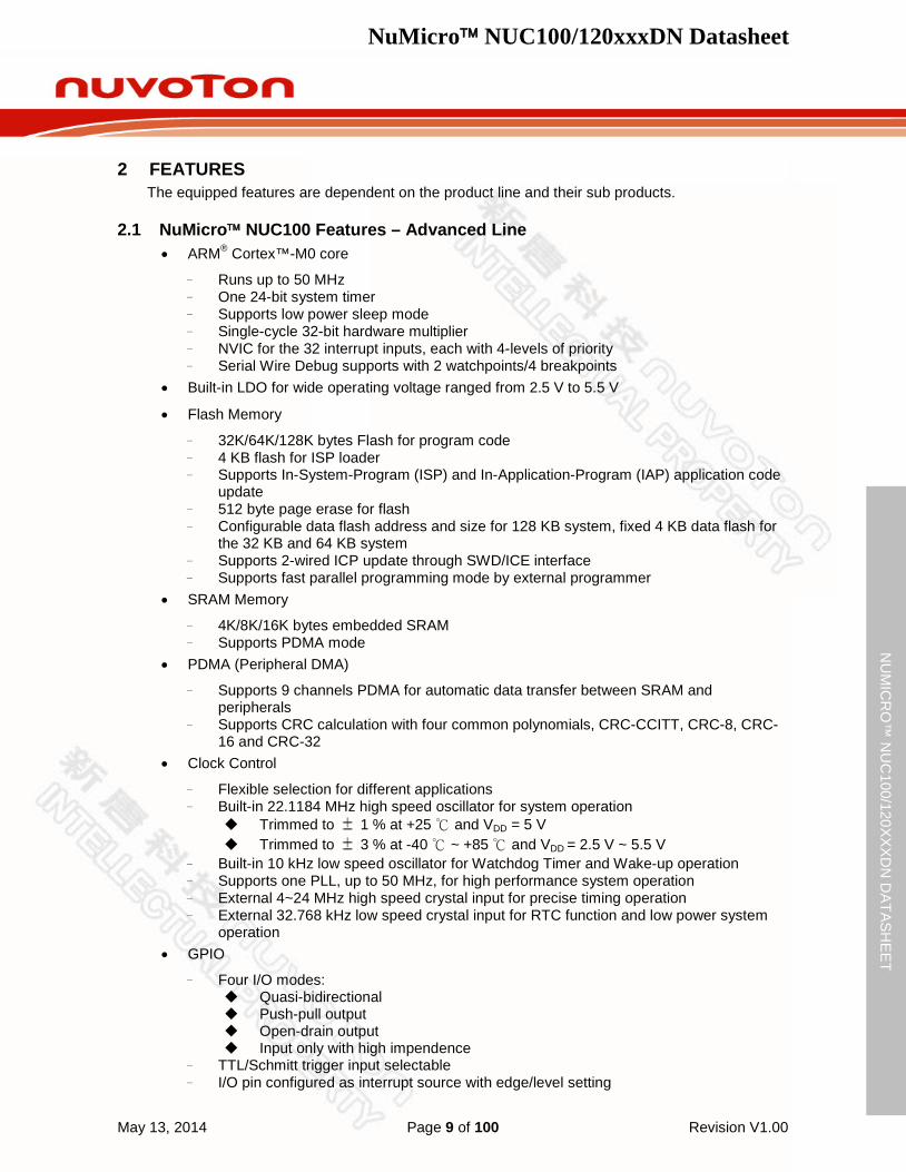
1 GENERAL DESCRIPTION The NuMicro NUC100 Series 32-bit microcontroller is embedded with the newest ARM® Cortex™-M0 core a cost equivalent to traditional 8-bit MCU for industrial control and applications which requiring rich communication interfaces. The NuMicro NUC100 Series includes NUC100, NUC120, NUC130 and NUC140 product lines.
The NuMicro NUC100 Advanced Line is embedded with the Cortex™-M0 core running up to 50 MHz and features 32K/64K/128K bytes flash, 4K/8K/16K bytes embedded SRAM and 4 Kbytes loader ROM for the ISP. It is also equipped with plenty of peripheral devices, such as Timers, Watchdog Timer, Window Watchdog Timer, RTC, PDMA with CRC calculation unit, UART, SPI, I2C, I2S, PWM Timer, GPIO, PS/2, EBI, Smart Card Host, 12-bit ADC, Analog Comparator, Low Voltage Reset Controller and Brown-out Detector.
The NuMicro NUC120 USB Line with USB 2.0 full-speed function is embedded with Cortex™-M0 core running up to 50 MHz and features 32K/64K/128K bytes flash, 4K/8K/16K bytes embedded SRAM and 4 Kbytes loader ROM for the ISP. It is also equipped with plenty of peripheral devices, such as Timers, Watchdog Timer, Window Watchdog Timer, RTC, PDMA with CRC calculation unit, UART, SPI, I2C, I2S, PWM Timer, GPIO, PS/2, EBI, USB 2.0 FS Device, Smart Card Host, 12-bit ADC, Analog Comparator, Low Voltage Reset Controller and Brown-out Detector.
Product Line UART SPI I2C USB LIN CAN PS/2 I2S SC
NUC100xxxDN
NUC120xxxDN
Table 1-1 NuMicro NUC100 Series Connectivity Support Table
NuMicro NUC100/120xxxDN Datasheet
May 13, 2014 Page 9 of 100 Revision V1.00
NU
MIC
RO
™ N
UC
100/120XXXD
N D
ATASHEET
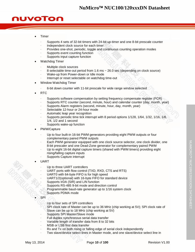
2 FEATURES The equipped features are dependent on the product line and their sub products.
NuMicro NUC100 Features – Advanced Line 2.1• ARM® Cortex™-M0 core
– Runs up to 50 MHz – One 24-bit system timer – Supports low power sleep mode – Single-cycle 32-bit hardware multiplier – NVIC for the 32 interrupt inputs, each with 4-levels of priority – Serial Wire Debug supports with 2 watchpoints/4 breakpoints
• Built-in LDO for wide operating voltage ranged from 2.5 V to 5.5 V
• Flash Memory
– 32K/64K/128K bytes Flash for program code – 4 KB flash for ISP loader – Supports In-System-Program (ISP) and In-Application-Program (IAP) application code
update – 512 byte page erase for flash – Configurable data flash address and size for 128 KB system, fixed 4 KB data flash for
the 32 KB and 64 KB system – Supports 2-wired ICP update through SWD/ICE interface – Supports fast parallel programming mode by external programmer
• SRAM Memory
– 4K/8K/16K bytes embedded SRAM – Supports PDMA mode
• PDMA (Peripheral DMA)
– Supports 9 channels PDMA for automatic data transfer between SRAM and peripherals
– Supports CRC calculation with four common polynomials, CRC-CCITT, CRC-8, CRC-16 and CRC-32
• Clock Control
– Flexible selection for different applications – Built-in 22.1184 MHz high speed oscillator for system operation
Trimmed to 1 % at +25 and VDD = 5 V Trimmed to 3 % at -40 ~ +85 and VDD = 2.5 V ~ 5.5 V
– Built-in 10 kHz low speed oscillator for Watchdog Timer and Wake-up operation – Supports one PLL, up to 50 MHz, for high performance system operation – External 4~24 MHz high speed crystal input for precise timing operation – External 32.768 kHz low speed crystal input for RTC function and low power system
operation • GPIO
– Four I/O modes: Quasi-bidirectional Push-pull output Open-drain output Input only with high impendence
– TTL/Schmitt trigger input selectable – I/O pin configured as interrupt source with edge/level setting
NuMicro NUC100/120xxxDN Datasheet
May 13, 2014 Page 10 of 100 Revision V1.00
NU
MIC
RO
™ N
UC
100/120XXXD
N D
ATASHEET
• Timer
– Supports 4 sets of 32-bit timers with 24-bit up-timer and one 8-bit prescale counter – Independent clock source for each timer – Provides one-shot, periodic, toggle and continuous counting operation modes – Supports event counting function – Supports input capture function
• Watchdog Timer
– Multiple clock sources – 8 selectable time-out period from 1.6 ms ~ 26.0 sec (depending on clock source) – Wake-up from Power-down or Idle mode – Interrupt or reset selectable on watchdog time-out
• Window Watchdog Timer
– 6-bit down counter with 11-bit prescale for wide range window selected • RTC
– Supports software compensation by setting frequency compensate register (FCR) – Supports RTC counter (second, minute, hour) and calendar counter (day, month, year) – Supports Alarm registers (second, minute, hour, day, month, year) – Selectable 12-hour or 24-hour mode – Automatic leap year recognition – Supports periodic time tick interrupt with 8 period options 1/128, 1/64, 1/32, 1/16, 1/8,
1/4, 1/2 and 1 second – Supports wake-up function
• PWM/Capture
– Up to four built-in 16-bit PWM generators providing eight PWM outputs or four complementary paired PWM outputs
– Each PWM generator equipped with one clock source selector, one clock divider, one 8-bit prescaler and one Dead-Zone generator for complementary paired PWM
– Up to eight 16-bit digital capture timers (shared with PWM timers) providing eight rising/falling capture inputs
– Supports Capture interrupt • UART
– Up to three UART controllers – UART ports with flow control (TXD, RXD, CTS and RTS) – UART0 with 64-byte FIFO is for high speed – UART1/2(optional) with 16-byte FIFO for standard device – Supports IrDA (SIR) and LIN function – Supports RS-485 9-bit mode and direction control – Programmable baud-rate generator up to 1/16 system clock – Supports PDMA mode
• SPI
– Up to four sets of SPI controllers – SPI clock rate of Master can be up to 36 MHz (chip working at 5V); SPI clock rate of
Slave can be up to 18 MHz (chip working at 5V) – Supports SPI Master/Slave mode – Full duplex synchronous serial data transfer – Variable length of transfer data from 8 to 32 bits – MSB or LSB first data transfer – Rx and Tx on both rising or falling edge of serial clock independently – Two slave/device select lines in Master mode, and one slave/device select line in
NuMicro NUC100/120xxxDN Datasheet
May 13, 2014 Page 11 of 100 Revision V1.00
NU
MIC
RO
™ N
UC
100/120XXXD
N D
ATASHEET
Slave mode – Supports Byte Suspend mode in 32-bit transmission – Supports PDMA mode – Supports three wire, no slave select signal, bi-direction interface
• I2C
– Up to two sets of I2C device – Master/Slave mode – Bidirectional data transfer between masters and slaves – Multi-master bus (no central master) – Arbitration between simultaneously transmitting masters without corruption of serial
data on the bus – Serial clock synchronization allowing devices with different bit rates to communicate
via one serial bus – Serial clock synchronization used as a handshake mechanism to suspend and resume
serial transfer – Programmable clocks allowing for versatile rate control – Supports multiple address recognition (four slave address with mask option) – Supports wake-up function
• I2S
– Interface with external audio CODEC – Operate as either Master or Slave mode – Capable of handling 8-, 16-, 24- and 32-bit word sizes – Supports mono and stereo audio data – Supports I2S and MSB justified data format – Provides two 8 word FIFO data buffers, one for transmitting and the other for receiving – Generates interrupt requests when buffer levels cross a programmable boundary – Supports two DMA requests, one for transmitting and the other for receiving
• PS/2 Device
– Host communication inhibit and request to send detection – Reception frame error detection – Programmable 1 to 16 bytes transmit buffer to reduce CPU intervention – Double buffer for data reception – Software override bus
• EBI (External bus interface)
– Accessible space: 64 KB in 8-bit mode or 128 KB in 16-bit mode – Supports 8-/16-bit data width – Supports byte write in 16-bit data width mode
• ADC
– 12-bit SAR ADC with 760 kSPS – Up to 8-ch single-end input or 4-ch differential input – Single scan/single cycle scan/continuous scan – Each channel with individual result register – Scan on enabled channels – Threshold voltage detection – Conversion started by software programming or external input – Supports PDMA mode
• Analog Comparator
– Up to two analog comparators – External input or internal Band-gap voltage selectable at negative node – Interrupt when compare results change
NuMicro NUC100/120xxxDN Datasheet
May 13, 2014 Page 12 of 100 Revision V1.00
NU
MIC
RO
™ N
UC
100/120XXXD
N D
ATASHEET
– Supports Power-down wake-up • Smart Card Host (SC)
– Compliant to ISO-7816-3 T=0, T=1 – Supports up to three ISO-7816-3 ports – Separate receive / transmit 4 bytes entry FIFO for data payloads – Programmable transmission clock frequency – Programmable receiver buffer trigger level – Programmable guard time selection (11 ETU ~ 266 ETU) – One 24-bit and two 8-bit time-out counters for Answer to Request (ATR) and waiting
times processing – Supports auto inverse convention function – Supports transmitter and receiver error retry and error limit function – Supports hardware activation sequence process – Supports hardware warm reset sequence process – Supports hardware deactivation sequence process – Supports hardware auto deactivation sequence when detecting the card is removal
• 96-bit unique ID (UID)
• One built-in temperature sensor with 1 resolution
• Brown-out Detector
– With 4 levels: 4.4 V/3.7 V/2.7 V/2.2 V – Supports Brown-out Interrupt and Reset option
• Low Voltage Reset
– Threshold voltage level: 2.0 V • Operating Temperature: -40 ~ 85
• Packages:
– All Green package (RoHS) – LQFP 100-pin / 64-pin / 48-pin
NuMicro NUC100/120xxxDN Datasheet
May 13, 2014 Page 13 of 100 Revision V1.00
NU
MIC
RO
™ N
UC
100/120XXXD
N D
ATASHEET
NuMicro NUC120 Features – USB Line 2.2• ARM® Cortex™-M0 core
– Runs up to 50 MHz – One 24-bit system timer – Supports low power sleep mode – Single-cycle 32-bit hardware multiplier – NVIC for the 32 interrupt inputs, each with 4-levels of priority – Serial Wire Debug supports with 2 watchpoints/4 breakpoints
• Built-in LDO for wide operating voltage ranges from 2.5 V to 5.5 V
• Flash Memory
– 32K/64K/128K bytes Flash for program code – 4 KB flash for ISP loader – Supports In-System-Program (ISP) and In-Application-Program (IAP) application code
update – 512 byte page erase for flash – Configurable data flash address and size for 128 KB system, fixed 4 KB data flash for
the 32 KB and 64 KB system – Supports 2-wired ICP update through SWD/ICE interface – Supports fast parallel programming mode by external programmer
• SRAM Memory
– 4K/8K/16K bytes embedded SRAM – Supports PDMA mode
• PDMA (Peripheral DMA)
– Supports 9 channels PDMA for automatic data transfer between SRAM and peripherals
– Supports CRC calculation with four common polynomials, CRC-CCITT, CRC-8, CRC-16 and CRC-32
• Clock Control
– Flexible selection for different applications – Built-in 22.1184 MHz high speed oscillator for system operation
Trimmed to 1 % at +25 and VDD = 5 V Trimmed to 3 % at -40 ~ +85 and VDD = 2.5 V ~ 5.5 V
– Built-in 10 kHz low speed oscillator for Watchdog Timer and Wake-up operation – Supports one PLL, up to 50 MHz, for high performance system operation – External 4~24 MHz high speed crystal input for USB and precise timing operation – External 32.768 kHz low speed crystal input for RTC function and low power system
operation • GPIO
– Four I/O modes: Quasi-bidirectional Push-pull output Open-drain output Input only with high impendence
– TTL/Schmitt trigger input selectable – I/O pin configured as interrupt source with edge/level setting
• Timer
– Supports 4 sets of 32-bit timers with 24-bit up-timer and one 8-bit prescale counter – Independent clock source for each timer
NuMicro NUC100/120xxxDN Datasheet
May 13, 2014 Page 14 of 100 Revision V1.00
NU
MIC
RO
™ N
UC
100/120XXXD
N D
ATASHEET
– Provides one-shot, periodic, toggle and continuous counting operation modes – Supports event counting function – Supports input capture function
• Watchdog Timer
– Multiple clock sources – 8 selectable time-out period from 1.6 ms ~ 26.0 sec (depending on clock source) – Wake-up from Power-down or Idle mode – Interrupt or reset selectable on watchdog time-out
• Window Watchdog Timer
– 6-bit down counter with 11-bit prescale for wide range window selected • RTC
– Supports software compensation by setting frequency compensate register (FCR) – Supports RTC counter (second, minute, hour) and calendar counter (day, month, year) – Supports Alarm registers (second, minute, hour, day, month, year) – Selectable 12-hour or 24-hour mode – Automatic leap year recognition – Supports periodic time tick interrupt with 8 period options 1/128, 1/64, 1/32, 1/16, 1/8,
1/4, 1/2 and 1 second – Supports wake-up function
• PWM/Capture
– Up to four built-in 16-bit PWM generators providing eight PWM outputs or four complementary paired PWM outputs
– Each PWM generator equipped with one clock source selector, one clock divider, one 8-bit prescaler and one Dead-Zone generator for complementary paired PWM
– Up to eight 16-bit digital capture timers (shared with PWM timers) providing eight rising/falling capture inputs
– Supports Capture interrupt • UART
– Up to three UART controllers – UART ports with flow control (TXD, RXD, CTS and RTS) – UART0 with 64-byte FIFO is for high speed – UART1/2(optional) with 16-byte FIFO for standard device – Supports IrDA (SIR) and LIN function – Supports RS-485 9-bit mode and direction control – Programmable baud-rate generator up to 1/16 system clock – Supports PDMA mode
• SPI
– Up to four sets of SPI controllers – The maximum SPI clock rate of Master can up to 36 MHz (chip working at 5V) – The maximum SPI clock rate of Slave can up to 18 MHz (chip working at 5V) – Supports SPI Master/Slave mode – Full duplex synchronous serial data transfer – Variable length of transfer data from 8 to 32 bits – MSB or LSB first data transfer – Rx and Tx on both rising or falling edge of serial clock independently – Two slave/device select lines in Master mode, and one slave/device select line in
Slave mode – Supports Byte Suspend mode in 32-bit transmission – Supports PDMA mode – Supports three wire, no slave select signal, bi-direction interface
NuMicro NUC100/120xxxDN Datasheet
May 13, 2014 Page 15 of 100 Revision V1.00
NU
MIC
RO
™ N
UC
100/120XXXD
N D
ATASHEET
• I2C
– Up to two sets of I2C device – Master/Slave mode – Bidirectional data transfer between masters and slaves – Multi-master bus (no central master) – Arbitration between simultaneously transmitting masters without corruption of serial
data on the bus – Serial clock synchronization allowing devices with different bit rates to communicate
via one serial bus – Serial clock synchronization used as a handshake mechanism to suspend and resume
serial transfer – Programmable clocks allowing for versatile rate control – Supports multiple address recognition (four slave address with mask option) – Supports wake-up function
• I2S
– Interface with external audio CODEC – Operate as either Master or Slave mode – Capable of handling 8-, 16-, 24- and 32-bit word sizes – Supports mono and stereo audio data – Supports I2S and MSB justified data format – Provides two 8 word FIFO data buffers, one for transmitting and the other for receiving – Generates interrupt requests when buffer levels cross a programmable boundary – Supports two DMA requests, one for transmitting and the other for receiving
• PS/2 Device
– Host communication inhibit and request to send detection – Reception frame error detection – Programmable 1 to 16 bytes transmit buffer to reduce CPU intervention – Double buffer for data reception – Software override bus
• EBI (External bus interface)
– Accessible space: 64 KB in 8-bit mode or 128 KB in 16-bit mode – Supports 8-/16-bit data width – Supports byte write in 16-bit data width mode
• USB 2.0 Full-Speed Device
– One set of USB 2.0 FS Device 12 Mbps – On-chip USB Transceiver – Provides 1 interrupt source with 4 interrupt events – Supports Control, Bulk In/Out, Interrupt and Isochronous transfers – Auto suspend function when no bus signaling for 3 ms – Provides 6 programmable endpoints – Includes 512 Bytes internal SRAM as USB buffer – Provides remote wake-up capability
• ADC
– 12-bit SAR ADC with 760 kSPS – Up to 8-ch single-end input or 4-ch differential input – Single scan/single cycle scan/continuous scan – Each channel with individual result register – Scan on enabled channels – Threshold voltage detection
NuMicro NUC100/120xxxDN Datasheet
May 13, 2014 Page 16 of 100 Revision V1.00
NU
MIC
RO
™ N
UC
100/120XXXD
N D
ATASHEET
– Conversion started by software programming or external input – Supports PDMA mode
• Analog Comparator
– Up to two analog comparators – External input or internal Band-gap voltage selectable at negative node – Interrupt when compare results change – Supports Power-down wake-up
• Smart Card Host (SC)
– Compliant to ISO-7816-3 T=0, T=1 – Supports up to three ISO-7816-3 ports – Separate receive / transmit 4 bytes entry FIFO for data payloads – Programmable transmission clock frequency – Programmable receiver buffer trigger level – Programmable guard time selection (11 ETU ~ 266 ETU) – One 24-bit and two 8-bit time-out counters for Answer to Request (ATR) and waiting
times processing – Supports auto inverse convention function – Supports transmitter and receiver error retry and error limit function – Supports hardware activation sequence process – Supports hardware warm reset sequence process – Supports hardware deactivation sequence process – Supports hardware auto deactivation sequence when detecting the card removal
• 96-bit unique ID (UID)
• One built-in temperature sensor with 1 resolution
• Brown-out Detector
– With 4 levels: 4.4 V/3.7 V/2.7 V/2.2 V – Supports Brown-out Interrupt and Reset option
• Low Voltage Reset
– Threshold voltage level: 2.0 V • Operating Temperature: -40 ~ 85
• Packages:
– All Green package (RoHS) – LQFP 100-pin / 64-pin / 48-pin
NuMicro NUC100/120xxxDN Datasheet
May 13, 2014 Page 17 of 100 Revision V1.00
NU
MIC
RO
™ N
UC
100/120XXXD
N D
ATASHEET
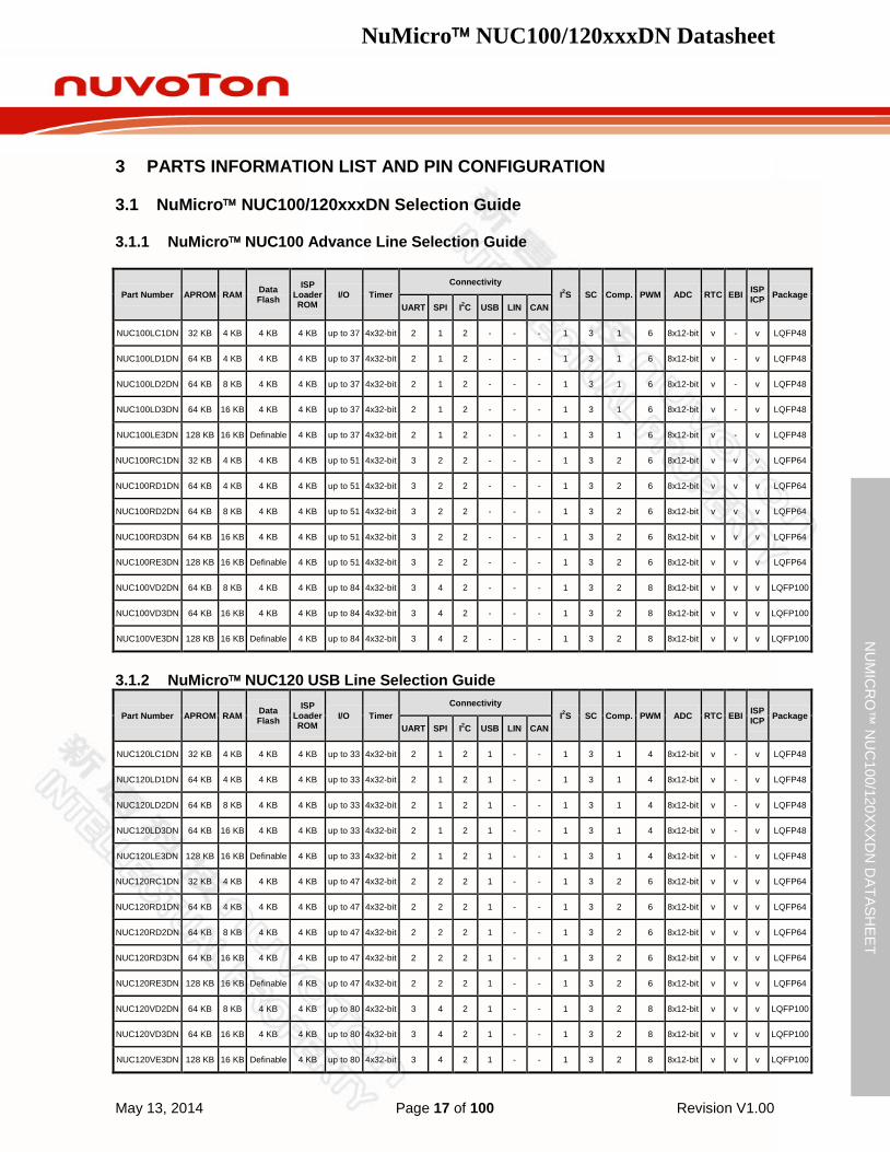
3 PARTS INFORMATION LIST AND PIN CONFIGURATION
NuMicro NUC100/120xxxDN Selection Guide 3.1
3.1.1 NuMicro NUC100 Advance Line Selection Guide
Part Number APROM RAM Data Flash
ISP Loader ROM
I/O Timer Connectivity
I2S SC Comp. PWM ADC RTC EBI ISP ICP Package
UART SPI I2C USB LIN CAN
NUC100LC1DN 32 KB 4 KB 4 KB 4 KB up to 37 4x32-bit 2 1 2 - - - 1 3 1 6 8x12-bit v - v LQFP48
NUC100LD1DN 64 KB 4 KB 4 KB 4 KB up to 37 4x32-bit 2 1 2 - - - 1 3 1 6 8x12-bit v - v LQFP48
NUC100LD2DN 64 KB 8 KB 4 KB 4 KB up to 37 4x32-bit 2 1 2 - - - 1 3 1 6 8x12-bit v - v LQFP48
NUC100LD3DN 64 KB 16 KB 4 KB 4 KB up to 37 4x32-bit 2 1 2 - - - 1 3 1 6 8x12-bit v - v LQFP48
NUC100LE3DN 128 KB 16 KB Definable 4 KB up to 37 4x32-bit 2 1 2 - - - 1 3 1 6 8x12-bit v - v LQFP48
NUC100RC1DN 32 KB 4 KB 4 KB 4 KB up to 51 4x32-bit 3 2 2 - - - 1 3 2 6 8x12-bit v v v LQFP64
NUC100RD1DN 64 KB 4 KB 4 KB 4 KB up to 51 4x32-bit 3 2 2 - - - 1 3 2 6 8x12-bit v v v LQFP64
NUC100RD2DN 64 KB 8 KB 4 KB 4 KB up to 51 4x32-bit 3 2 2 - - - 1 3 2 6 8x12-bit v v v LQFP64
NUC100RD3DN 64 KB 16 KB 4 KB 4 KB up to 51 4x32-bit 3 2 2 - - - 1 3 2 6 8x12-bit v v v LQFP64
NUC100RE3DN 128 KB 16 KB Definable 4 KB up to 51 4x32-bit 3 2 2 - - - 1 3 2 6 8x12-bit v v v LQFP64
NUC100VD2DN 64 KB 8 KB 4 KB 4 KB up to 84 4x32-bit 3 4 2 - - - 1 3 2 8 8x12-bit v v v LQFP100
NUC100VD3DN 64 KB 16 KB 4 KB 4 KB up to 84 4x32-bit 3 4 2 - - - 1 3 2 8 8x12-bit v v v LQFP100
NUC100VE3DN 128 KB 16 KB Definable 4 KB up to 84 4x32-bit 3 4 2 - - - 1 3 2 8 8x12-bit v v v LQFP100
3.1.2 NuMicro NUC120 USB Line Selection Guide
Part Number APROM RAM Data Flash
ISP Loader ROM
I/O Timer Connectivity
I2S SC Comp. PWM ADC RTC EBI ISP ICP Package
UART SPI I2C USB LIN CAN
NUC120LC1DN 32 KB 4 KB 4 KB 4 KB up to 33 4x32-bit 2 1 2 1 - - 1 3 1 4 8x12-bit v - v LQFP48
NUC120LD1DN 64 KB 4 KB 4 KB 4 KB up to 33 4x32-bit 2 1 2 1 - - 1 3 1 4 8x12-bit v - v LQFP48
NUC120LD2DN 64 KB 8 KB 4 KB 4 KB up to 33 4x32-bit 2 1 2 1 - - 1 3 1 4 8x12-bit v - v LQFP48
NUC120LD3DN 64 KB 16 KB 4 KB 4 KB up to 33 4x32-bit 2 1 2 1 - - 1 3 1 4 8x12-bit v - v LQFP48
NUC120LE3DN 128 KB 16 KB Definable 4 KB up to 33 4x32-bit 2 1 2 1 - - 1 3 1 4 8x12-bit v - v LQFP48
NUC120RC1DN 32 KB 4 KB 4 KB 4 KB up to 47 4x32-bit 2 2 2 1 - - 1 3 2 6 8x12-bit v v v LQFP64
NUC120RD1DN 64 KB 4 KB 4 KB 4 KB up to 47 4x32-bit 2 2 2 1 - - 1 3 2 6 8x12-bit v v v LQFP64
NUC120RD2DN 64 KB 8 KB 4 KB 4 KB up to 47 4x32-bit 2 2 2 1 - - 1 3 2 6 8x12-bit v v v LQFP64
NUC120RD3DN 64 KB 16 KB 4 KB 4 KB up to 47 4x32-bit 2 2 2 1 - - 1 3 2 6 8x12-bit v v v LQFP64
NUC120RE3DN 128 KB 16 KB Definable 4 KB up to 47 4x32-bit 2 2 2 1 - - 1 3 2 6 8x12-bit v v v LQFP64
NUC120VD2DN 64 KB 8 KB 4 KB 4 KB up to 80 4x32-bit 3 4 2 1 - - 1 3 2 8 8x12-bit v v v LQFP100
NUC120VD3DN 64 KB 16 KB 4 KB 4 KB up to 80 4x32-bit 3 4 2 1 - - 1 3 2 8 8x12-bit v v v LQFP100
NUC120VE3DN 128 KB 16 KB Definable 4 KB up to 80 4x32-bit 3 4 2 1 - - 1 3 2 8 8x12-bit v v v LQFP100
NuMicro NUC100/120xxxDN Datasheet
May 13, 2014 Page 18 of 100 Revision V1.00
NU
MIC
RO
™ N
UC
100/120XXXD
N D
ATASHEET
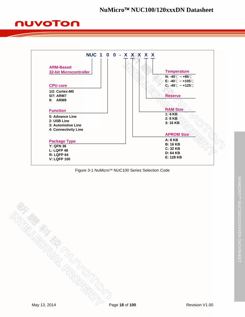
NUC 1 0 - X X
ARM-Based32-bit Microcontroller
0: Advance Line2: USB Line3: Automotive Line4: Connectivity Line
CPU core1/2: Cortex-M05/7: ARM79: ARM9
TemperatureN: -40 ~ +85E: -40 ~ +105C: -40 ~ +125
Reserve
X X
Function
0
Package TypeY: QFN 36L: LQFP 48R: LQFP 64V: LQFP 100
X
RAM Size1: 4 KB2: 8 KB3: 16 KB
APROM SizeA: 8 KBB: 16 KBC: 32 KBD: 64 KBE: 128 KB
Figure 3-1 NuMicro NUC100 Series Selection Code
NuMicro NUC100/120xxxDN Datasheet
May 13, 2014 Page 19 of 100 Revision V1.00
NU
MIC
RO
™ N
UC
100/120XXXD
N D
ATASHEET
Pin Configuration 3.2
3.2.1 NuMicro NUC100 Pin Diagram
NuMicro NUC100VxxDN LQFP 100 pin 3.2.1.1
SC1RST/AD8/ADC5/PA.5
SC1CLK/AD7/ADC6/PA.6
SC1DAT/AD6/ADC7/SPISS21/PA.7
SP
ISS
31/IN
T0/P
B.1
4
AD
1/C
PO
1/P
B.1
3
AD
0/C
LKO
/CP
O0/
PB
.12
X32
I
X32
O
nRD
/I2C
1SC
L/P
A.1
1
nWR
/I2C
1SD
A/P
A.1
0
I2C
0SC
L/P
A.9
I2C
0SD
A/P
A.8
RX
D1/
PB
.4
TXD
1/P
B.5
ALE
/RTS
1/P
B.6
nCS
/CTS
1/P
B.7
LDO
VD
D
VS
S
SC1CD/AD5/CPN0/PC.7
SC0CD/AD4/CPP0/PC.6
AD3/CPN1/PC.15
AD2/CPP1/PC.14
T0EX/INT1/PB.15
XT1_OUT/PF.0
XT1_IN/PF.1
/RESET
TM0/STADC/PB.8
PA
.4/A
DC
4/A
D9/
SC
1PW
R
PA
.3/A
DC
3/A
D10
/SC
0DA
T
PA
.2/A
DC
2/A
D11
/SC
0CLK
PA
.1/A
DC
1/A
D12
/SC
0RS
T
PA
.0/A
DC
0/S
C0P
WR
AV
SS
ICE
_CK
ICE
_DA
T
PA
.12/
PW
M0/
AD
13/S
C2D
AT
PA
.13/
PW
M1/
AD
14/S
C2C
LK
PA
.14/
PW
M2/
AD
15/S
C2R
ST
PA
.15/
PW
M3/
I2S
MC
LK/S
C2P
WR
PC
.8/S
PIS
S10
/MC
LK
PC
.9/S
PIC
LK1
AVDD
VSS
VDD
PVSS
PC.0/SPISS00/I2SLRCLK
PC.1/SPICLK0/I2SBCLK
PC.2/MISO00/I2SDI
PC.3/MOSI00/I2SDO
PD.15/TXD2
PD.14/RXD2
PD.7
PD.6
PB.3/CTS0/T3EX/nWRH/SC2CD
PB.2/RTS0/T2EX/nWRL
PB.1/TXD0
PB.0/RXD0
PE.7
PE.8
PE.9
PE.10
26
27
28
29
30
31
32
33
34
35
36
37
38
39
40
41
100
99
98
97
96
95
94
93
92
91
90
89
88
87
86
85
16151413121110987654321
60616263646566676869707172737475
PC
.10/
MIS
O10
PC
.11/
MO
SI1
0
NUC100VxxDNLQFP 100-pin
252423222120191817
PE
.15
PE
.14
PE
.13
SP
ISS
30/P
D.8
SP
ICLK
3/P
D.9
MIS
O30
/PD
.10
MO
SI3
0/P
D.1
1
MIS
O31
/PD
.12
MO
SI3
1/P
D.1
342
43
44
45
46
47
48
49
50
PE.11
PE.12
PC.4/MISO01
PC.5/MOSI01
PB.9/TM0/SPISS11
PB.10/TM1/SPISS01
PB.11/TM2/PWM4
PE.5/T1EX/PWM5
PE.6
515253545556575859
VS
S
VD
D
PC
.12/
MIS
O11
PC
.13/
MO
SI1
1
PE
.0/P
WM
6
PE
.1/P
WM
7
PE
.2
PE
.3
PE
.4
84
83
82
81
80
79
78
77
76
PS2DAT/PF.2
PS2CLK/PF.3
SPISS20/PD.0
SPICLK2/PD.1
MISO20/PD.2
MOSI20/PD.3
MISO21/PD.4
MOSI21/PD.5
VREF
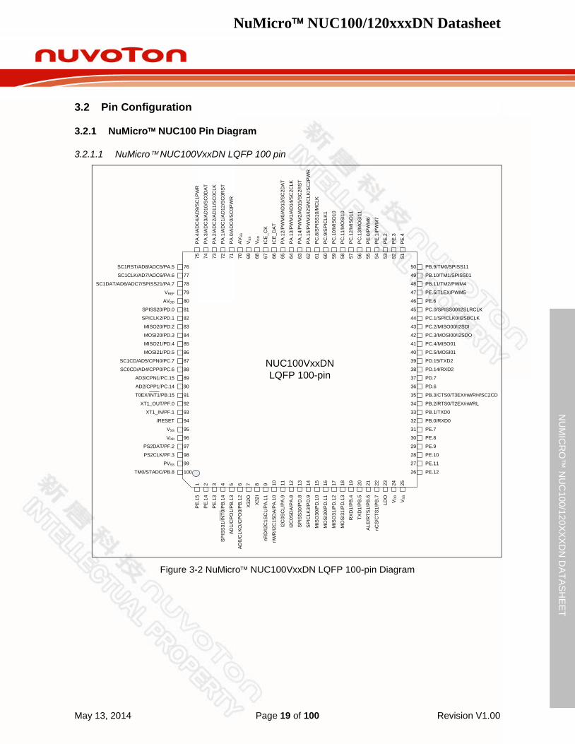
Figure 3-2 NuMicro NUC100VxxDN LQFP 100-pin Diagram

NuMicro NUC100/120xxxDN Datasheet
May 13, 2014 Page 20 of 100 Revision V1.00
NU
MIC
RO
™ N
UC
100/120XXXD
N D
ATASHEET
NuMicro NUC100RxxDN LQFP 64 pin 3.2.1.2
SC1RST/AD8/ADC5/PA.5
SC1CLK/AD7/ADC6/PA.6
SC1DAT/AD6/ADC7/PA.7
INT0
/PB
.14
AD
1/C
PO
1/P
B.1
3
AD
0/C
LKO
/CP
O0/
PB
.12
X32
I
X32
O
nRD
/I2C
1SC
L/P
A.1
1
nWR
/I2C
1SD
A/P
A.1
0
I2C
0SC
L/P
A.9
I2C
0SD
A/P
A.8
RX
D1/
PB
.4
TXD
1/P
B.5
ALE
/RTS
1/P
B.6
nCS
/CTS
1/P
B.7
LDO
VD
D
VS
S
SC1CD/AD5/CPN0/PC.7
SC0CD/AD4/CPP0/PC.6
AD3/CPN1/PC.15
AD2/CPP1/PC.14
T0EX/INT1/PB.15
XT1_OUT/PF.0
XT1_IN/PF.1
/RESET
TM0/STADC/PB.8
PA
.4/A
DC
4/A
D9/
SC
1PW
R
PA
.3/A
DC
3/A
D10
/SC
0DA
T
PA
.2/A
DC
2/A
D11
/SC
0CLK
PA
.1/A
DC
1/A
D12
/SC
0RS
T
PA
.0/A
DC
0/S
C0P
WR
AV
SS
ICE
_CK
ICE
_DA
T
PA
.12/
PW
M0/
AD
13/S
C2D
AT
PA
.13/
PW
M1/
AD
14/S
C2C
LK
PA
.14/
PW
M2/
AD
15/S
C2R
ST
PA
.15/
PW
M3/
I2S
MC
LK/S
C2P
WR
PC
.8/S
PIS
S10
/MC
LK
PC
.9/S
PIC
LK1
AVDD
VSS
VDD
PVSS
PC.0/SPISS00/I2SLRCLK
PC.1/SPICLK0/I2SBCLK
PC.2/MISO00/I2SDI
PC.3/MOSI00/I2SDO
17
18
19
20
21
22
23
24
25
26
27
28
29
30
31
32
64
63
62
61
60
59
58
57
56
55
54
53
52
51
50
49
16151413121110987654321
33343536373839404142434445464748
PC
.10/
MIS
O10
PC
.11/
MO
SI1
0
PB.9/TM1
PB.10/TM2
PB.11/TM3/PWM4
PE.5/T1EX/PWM5
PD.15/TXD2
PD.14/RXD2
PD.7
PD.6
PB.3/CTS0/T3EX/nWRH/SC2CD
PB.2/RTS0/T2EX/nWRL
PB.1/TXD0
PB.0/RXD0
NUC100RxxDNLQFP 64-pin
Figure 3-3 NuMicro NUC100RxxDN LQFP 64-pin Diagram
NuMicro NUC100/120xxxDN Datasheet
May 13, 2014 Page 21 of 100 Revision V1.00
NU
MIC
RO
™ N
UC
100/120XXXD
N D
ATASHEET
NuMicro NUC100LxxDN LQFP 48 pin 3.2.1.3
SC1RST/ADC5/PA.5
SC1CLK/ADC6/PA.6
SC1DAT/ADC7/PA.7
CLK
O/C
PO
0/P
B.1
2
X32
I
X32
O
I2C
1SC
L/P
A.1
1
I2C
1SD
A/P
A.1
0
I2C
0SC
L/P
A.9
I2C
0SD
A/P
A.8
RX
D1/
PB
.4
TXD
1/P
B.5
LDO
VD
D
VS
S
SC1CD/CPN0/PC.7
SC0CD/CPP0/PC.6
T0EX/INT1/PB.15
XT1_OUT/PF.0
XT1_IN/PF.1
/RESET
TM0/STADC/PB.8
PA
.4/A
DC
4/S
C1P
WR
PA
.3/A
DC
3/S
C0D
AT
PA
.2/A
DC
2/S
C0C
LK
PA
.1/A
DC
1/S
C0R
ST
PA
.0/A
DC
0/S
C0P
WR
AV
SS
ICE
_CK
ICE
_DA
T
PA
.12/
PW
M0/
SC
2DA
T
PA
.13/
PW
M1/
SC
2CLK
PA
.14/
PW
M2/
SC
2RS
T
PA
.15/
PW
M3/
I2S
MC
LK/S
C2P
WR
AVDD
PVSS
PB.9/TM1
PB.10/TM2
PB.11/TM3/PWM4
PE.5/T1EX/PWM5
PB.3/CTS0/T3EX/SC2CD
PB.2/RTS0/T2EX
13
14
15
16
17
18
19
20
21
22
23
24
48
47
46
45
44
43
42
41
40
39
38
37
121110987654321
252627282930313233343536
NUC100LxxDNLQFP 48-pin
PB.1/TXD0
PB.0/RXD0
PC.0/SPISS00/I2SLRCLK
PC.1/SPICLK0/I2SBCLK
PC.2/MISO00/I2SDI
PC.3/MOSI00/I2SDO
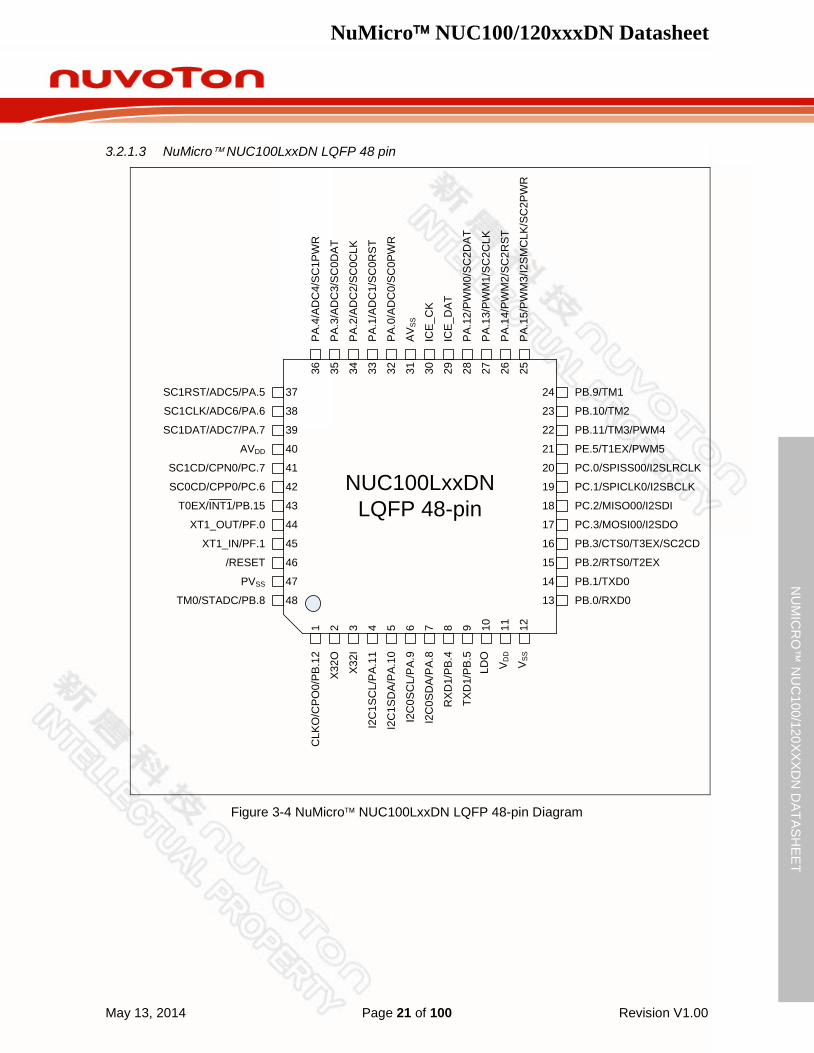
Figure 3-4 NuMicro NUC100LxxDN LQFP 48-pin Diagram
NuMicro NUC100/120xxxDN Datasheet
May 13, 2014 Page 22 of 100 Revision V1.00
NU
MIC
RO
™ N
UC
100/120XXXD
N D
ATASHEET
3.2.2 NuMicro NUC120 Pin Diagram
NuMicro NUC120VxxDN LQFP 100 pin 3.2.2.1
SC1RST/AD8/ADC5/PA.5
SC1CLK/AD7/ADC6/PA.6
SC1DAT/AD6/ADC7/SPISS21/PA.7
SP
ISS
31/IN
T0/P
B.1
4
AD
1/C
PO
1/P
B.1
3
AD
0/C
LKO
/CP
O0/
PB
.12
X32
I
X32
O
nRD
/I2C
1SC
L/P
A.1
1
nWR
/I2C
1SD
A/P
A.1
0
I2C
0SC
L/P
A.9
I2C
0SD
A/P
A.8
RX
D1/
PB
.4
TXD
1/P
B.5
ALE
/RTS
1/P
B.6
nCS
/CTS
1/P
B.7
LDO
VD
D
VS
S
SC1CD/AD5/CPN0/PC.7
SC0CD/AD4/CPP0/PC.6
AD3/CPN1/PC.15
AD2/CPP1/PC.14
T0EX/INT1/PB.15
XT1_OUT/PF.0
XT1_IN/PF.1
/RESET
TM0/STADC/PB.8
PA
.4/A
DC
4/A
D9/
SC
1PW
R
PA
.3/A
DC
3/A
D10
/SC
0DA
T
PA
.2/A
DC
2/A
D11
/SC
0CLK
PA
.1/A
DC
1/A
D12
/SC
0RS
T
PA
.0/A
DC
0/S
C0P
WR
AV
SS
ICE
_CK
ICE
_DA
T
PA
.12/
PW
M0/
AD
13/S
C2D
AT
PA
.13/
PW
M1/
AD
14/S
C2C
LK
PA
.14/
PW
M2/
AD
15/S
C2R
ST
PA
.15/
PW
M3/
I2S
MC
LK/S
C2P
WR
PC
.8/S
PIS
S10
/MC
LK
PC
.9/S
PIC
LK1
AVDD
VSS
VDD
PVSS
PC.0/SPISS00/I2SLRCLK
PC.1/SPICLK0/I2SBCLK
PC.2/MISO00/I2SDI
PC.3/MOSI00/I2SDO
PD.15/TXD2
PD.14/RXD2
PD.7
PD.6
PB.3/CTS0/T3EX/nWRH/SC2CD
PB.2/RTS0/T2EX/nWRL
PB.1/TXD0
PB.0/RXD0
D+
D-
VDD33
VBUS
26
27
28
29
30
31
32
33
34
35
36
37
38
39
40
41
100
99
98
97
96
95
94
93
92
91
90
89
88
87
86
8516151413121110987654321
60616263646566676869707172737475
PC
.10/
MIS
O10
PC
.11/
MO
SI1
0NUC120VxxDNLQFP 100-pin
252423222120191817
PE
.15
PE
.14
PE
.13
SP
ISS
30/P
D.8
SP
ICLK
3/P
D.9
MIS
O30
/PD
.10
MO
SI3
0/P
D.1
1
MIS
O31
/PD
.12
MO
SI3
1/P
D.1
3
42
43
44
45
46
47
48
49
50
PE.7
PE.8
PC.4/MISO01
PC.5/MOSI01
PB.9/TM1/SPISS11
PB.10/TM2/SPISS01
PB.11/TM3/PWM4
PE.5/T1EX/PWM5
PE.6
515253545556575859
VS
S
VD
D
PC
.12/
MIS
O11
PC
.13/
MO
SI1
1
PE
.0/P
WM
6
PE
.1/P
WM
7
PE
.2
PE
.3
PE
.4
84
83
82
81
80
79
78
77
76
PS2DAT/PF.2
PS2CLK/PF.3
SPISS20/PD.0
SPICLK2/PD.1
MISO20/PD.2
MOSI20/PD.3
MISO21/PD.4
MOSI21/PD.5
VREF
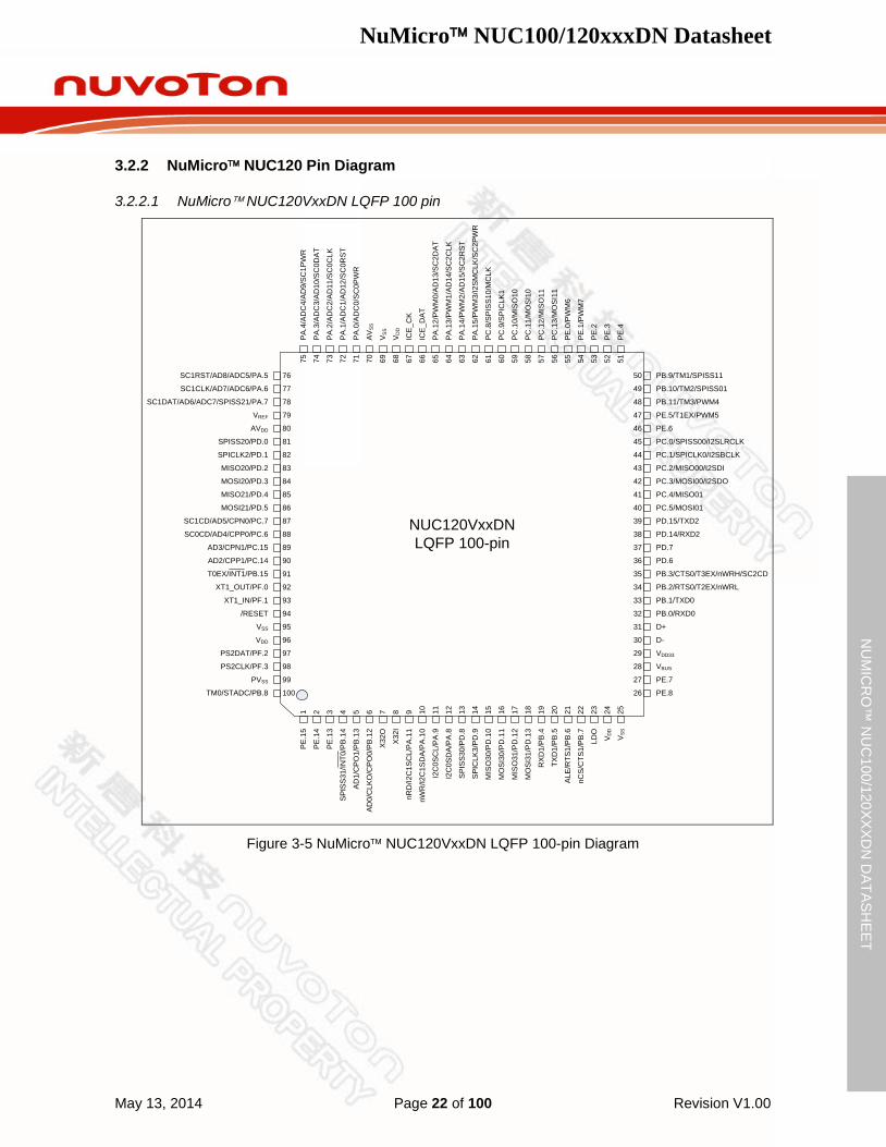
Figure 3-5 NuMicro NUC120VxxDN LQFP 100-pin Diagram
NuMicro NUC100/120xxxDN Datasheet
May 13, 2014 Page 23 of 100 Revision V1.00
NU
MIC
RO
™ N
UC
100/120XXXD
N D
ATASHEET
NuMicro NUC120RxxDN LQFP 64 pin 3.2.2.2
SC1RST/AD8/ADC5/PA.5
SC1CLK/AD7/ADC6/PA.6
SC1DAT/AD6/ADC7/PA.7
INT0
/PB
.14
AD
1/C
PO
1/P
B.1
3
AD
0/C
LKO
/CP
O0/
PB
.12
X32
I
X32
O
nRD
/I2C
1SC
L/P
A.1
1
nWR
/I2C
1SD
A/P
A.1
0
I2C
0SC
L/P
A.9
I2C
0SD
A/P
A.8
RX
D1/
PB
.4
TXD
1/P
B.5
ALE
/RTS
1/P
B.6
nCS
/CTS
1/P
B.7
LDO
VD
D
VS
S
SC1CD/AD5/CPN0/PC.7
SC0CD/AD4/CPP0/PC.6
AD3/CPN1/PC.15
AD2/CPP1/PC.14
T0EX/INT1/PB.15
XT1_OUT/PF.0
XT1_IN/PF.1
/RESET
TM0/STADC/PB.8
PA
.4/A
DC
4/A
D9/
SC
1PW
R
PA
.3/A
DC
3/A
D10
/SC
0DA
T
PA
.2/A
DC
2/A
D11
/SC
0CLK
PA
.1/A
DC
1/A
D12
/SC
0RS
T
PA
.0/A
DC
0/S
C0P
WR
AV
SS
ICE
_CK
ICE
_DA
T
PA
.12/
PW
M0/
AD
13/S
C2D
AT
PA
.13/
PW
M1/
AD
14/S
C2C
LK
PA
.14/
PW
M2/
AD
15/S
C2R
ST
PA
.15/
PW
M3/
I2S
MC
LK/S
C2P
WR
PC
.8/S
PIS
S10
/MC
LK
PC
.9/S
PIC
LK1
AVDD
VSS
VDD
PVSS
PC.0/SPISS00/I2SLRCLK
PC.1/SPICLK0/I2SBCLK
PC.2/MISO00/I2SDI
PC.3/MOSI00/I2SDO
D+
D-
VDD33
VBUS17
18
19
20
21
22
23
24
25
26
27
28
29
30
31
32
64
63
62
61
60
59
58
57
56
55
54
53
52
51
50
49
16151413121110987654321
33343536373839404142434445464748
PC
.10/
MIS
O10
PC
.11/
MO
SI1
0
PB.9/TM1
PB.10/TM2
PB.11/TM3/PWM4
PE.5/T1EX/PWM5
PB.3/CTS0/T3EX/nWRH/SC2CD
PB.2/RTS0/T2EX/nWRL
PB.1/TXD0
PB.0/RXD0
NUC120RxxDNLQFP 64-pin
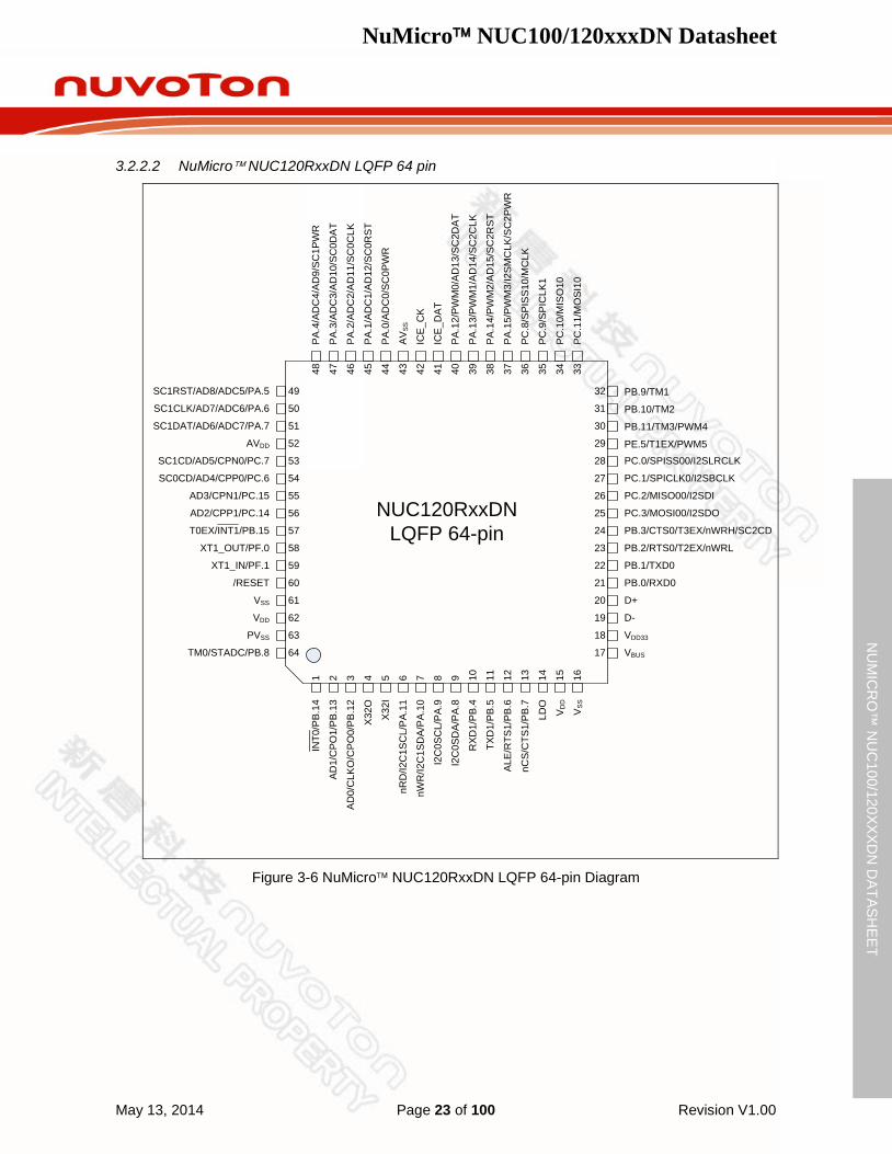
Figure 3-6 NuMicro NUC120RxxDN LQFP 64-pin Diagram
NuMicro NUC100/120xxxDN Datasheet
May 13, 2014 Page 24 of 100 Revision V1.00
NU
MIC
RO
™ N
UC
100/120XXXD
N D
ATASHEET
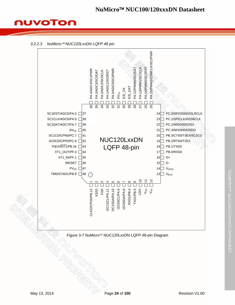
NuMicro NUC120LxxDN LQFP 48 pin 3.2.2.3
SC1RST/ADC5/PA.5
SC1CLK/ADC6/PA.6
SC1DAT/ADC7/PA.7
CLK
O/C
PO
0/P
B.1
2
X32
I
X32
O
I2C
1SC
L/P
A.1
1
I2C
1SD
A/P
A.1
0
I2C
0SC
L/P
A.9
I2C
0SD
A/P
A.8
RX
D1/
PB
.4
TXD
1/P
B.5
LDO
VD
D
VS
S
SC1CD/CPN0/PC.7
SC0CD/CPP0/PC.6
T0EX/INT1/PB.15
XT1_OUT/PF.0
XT1_IN/PF.1
/RESET
TM0/STADC/PB.8
PA
.4/A
DC
4/S
C1P
WR
PA
.3/A
DC
3/S
C0D
AT
PA
.2/A
DC
2/S
C0C
LK
PA
.1/A
DC
1/S
C0R
ST
PA
.0/A
DC
0/S
C0P
WR
AV
SS
ICE
_CK
ICE
_DA
T
PA
.12/
PW
M0/
SC
2DA
T
PA
.13/
PW
M1/
SC
2CLK
PA
.14/
PW
M2/
SC
2RS
T
PA
.15/
PW
M3/
I2S
MC
LK/S
C2P
WR
AVDD
PVSS
PC.0/SPISS00/I2SLRCLK
PC.1/SPICLK0/I2SBCLK
PC.2/MISO00/I2SDI
PC.3/MOSI00/I2SDO
PB.3/CTS0/T3EX/SC2CD
PB.2/RTS0/T2EX
PB.1/TXD0
PB.0/RXD0
D+
D-
VDD33
VBUS13
14
15
16
17
18
19
20
21
22
23
24
48
47
46
45
44
43
42
41
40
39
38
37
121110987654321
252627282930313233343536
NUC120LxxDNLQFP 48-pin
Figure 3-7 NuMicro NUC120LxxDN LQFP 48-pin Diagram
NuMicro NUC100/120xxxDN Datasheet
May 13, 2014 Page 25 of 100 Revision V1.00
NU
MIC
RO
™ N
UC
100/120XXXD
N D
ATASHEET
Pin Description 3.3
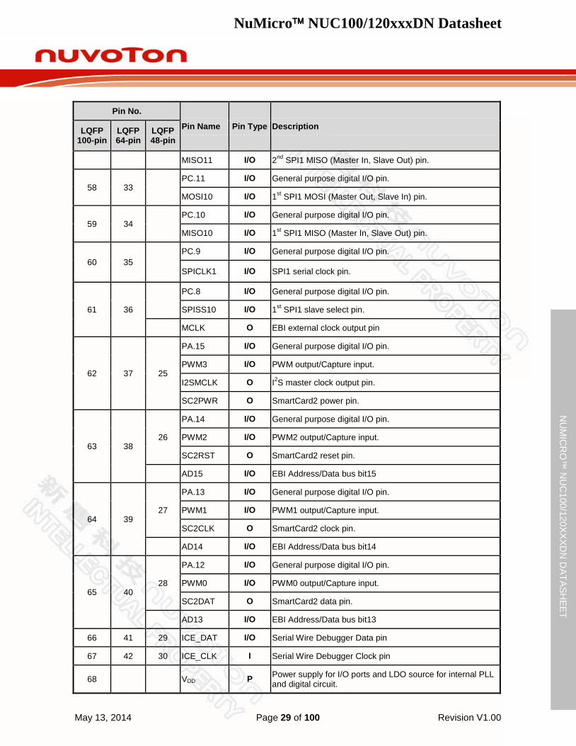
3.3.1 NuMicro NUC100 Pin Description
Pin No.
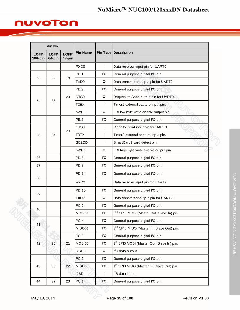
Pin Name Pin Type Description LQFP 100-pin
LQFP 64-pin
LQFP 48-pin
1 PE.15 I/O General purpose digital I/O pin.
2 PE.14 I/O General purpose digital I/O pin.
3 PE.13 I/O General purpose digital I/O pin.
4 1
PB.14 I/O General purpose digital I/O pin.
/INT0 I External interrupt0 input pin.
SPISS31 I/O 2nd SPI3 slave select pin.
5 2
PB.13 I/O General purpose digital I/O pin.
CPO1 O Comparator1 output pin.
AD1 I/O EBI Address/Data bus bit1
6 3 1
PB.12 I/O General purpose digital I/O pin.
CPO0 O Comparator0 output pin
CLKO O Frequency Divider output pin
AD0 I/O EBI Address/Data bus bit0
7 4 2 X32O O External 32.768 kHz low speed crystal output pin
8 5 3 X32I I External 32.768 kHz low speed crystal input pin
9 6 4
PA.11 I/O General purpose digital I/O pin.
I2C1SCL I/O I2C1 clock pin.
nRD O EBI read enable output pin
10 7 5
PA.10 I/O General purpose digital I/O pin.
I2C1SDA I/O I2C1 data input/output pin.
nWR O EBI write enable output pin
11 8 6 PA.9 I/O General purpose digital I/O pin.
I2C0SCL I/O I2C0 clock pin.
12 9 7 PA.8 I/O General purpose digital I/O pin.
I2C0SDA I/O I2C0 data input/output pin.
13 PD.8 I/O General purpose digital I/O pin.
SPISS30 I/O 1st SPI3 slave select pin.
NuMicro NUC100/120xxxDN Datasheet
May 13, 2014 Page 26 of 100 Revision V1.00
NU
MIC
RO
™ N
UC
100/120XXXD
N D
ATASHEET
Pin No.
Pin Name Pin Type Description LQFP 100-pin
LQFP 64-pin
LQFP 48-pin
14 PD.9 I/O General purpose digital I/O pin.
SPICLK3 I/O SPI3 serial clock pin.
15 PD.10 I/O General purpose digital I/O pin.
MISO30 I/O 1st SPI3 MISO (Master In, Slave Out) pin.
16 PD.11 I/O General purpose digital I/O pin.
MOSI30 I/O 1st SPI3 MOSI (Master Out, Slave In) pin.
17 PD.12 I/O General purpose digital I/O pin.
MISO31 I/O 2nd SPI3 MISO (Master In, Slave Out) pin.
18 PD.13 I/O General purpose digital I/O pin.
MOSI31 I/O 2nd SPI3 MOSI (Master Out, Slave In) pin.
19 10 8 PB.4 I/O General purpose digital I/O pin.
RXD1 I Data receiver input pin for UART1.
20 11 9 PB.5 I/O General purpose digital I/O pin.
TXD1 O Data transmitter output pin for UART1.
21 12
PB.6 I/O General purpose digital I/O pin.
RTS1 O Request to Send output pin for UART1.
ALE O EBI address latch enable output pin
22 13
PB.7 I/O General purpose digital I/O pin.
CTS1 I Clear to Send input pin for UART1.
nCS O EBI chip select enable output pin
23 14 10 LDO P LDO output pin
24 15 11 VDD P Power supply for I/O ports and LDO source for internal PLL and digital circuit.
25 16 12 VSS P Ground pin for digital circuit.
26 PE.12 I/O General purpose digital I/O pin.
27 PE.11 I/O General purpose digital I/O pin.
28 PE.10 I/O General purpose digital I/O pin.
29 PE.9 I/O General purpose digital I/O pin.
30 PE.8 I/O General purpose digital I/O pin.
31 PE.7 I/O General purpose digital I/O pin.
NuMicro NUC100/120xxxDN Datasheet
May 13, 2014 Page 27 of 100 Revision V1.00
NU
MIC
RO
™ N
UC
100/120XXXD
N D
ATASHEET
Pin No.
Pin Name Pin Type Description LQFP 100-pin
LQFP 64-pin
LQFP 48-pin
32 17 13 PB.0 I/O General purpose digital I/O pin.
RXD0 I Data receiver input pin for UART0.
33 18 14 PB.1 I/O General purpose digital I/O pin.
TXD0 O Data transmitter output pin for UART0.
34 19 15
PB.2 I/O General purpose digital I/O pin.
RTS0 O Request to Send output pin for UART0.
T2EX I Timer2 external capture input pin.
nWRL O EBI low byte write enable output pin
35 20 16
PB.3 I/O General purpose digital I/O pin.
CTS0 I Clear to Send input pin for UART0.
T3EX I Timer3 external capture input pin.
SC2CD I SmartCard2 card detect pin.
nWRH O EBI high byte write enable output pin
36 21 PD.6 I/O General purpose digital I/O pin.
37 22 PD.7 I/O General purpose digital I/O pin.
38 23 PD.14 I/O General purpose digital I/O pin.
RXD2 I Data receiver input pin for UART2.
39 24 PD.15 I/O General purpose digital I/O pin.
TXD2 O Data transmitter output pin for UART2.
40 PC.5 I/O General purpose digital I/O pin.
MOSI01 I/O 2nd SPI0 MOSI (Master Out, Slave In) pin.
41 PC.4 I/O General purpose digital I/O pin.
MISO01 I/O 2nd SPI0 MISO (Master In, Slave Out) pin.
42 25 17
PC.3 I/O General purpose digital I/O pin.
MOSI00 I/O 1st SPI0 MOSI (Master Out, Slave In) pin.
I2SDO O I2S data output.
43 26 18
PC.2 I/O General purpose digital I/O pin.
MISO00 I/O 1st SPI0 MISO (Master In, Slave Out) pin.
I2SDI I I2S data input.

NuMicro NUC100/120xxxDN Datasheet
May 13, 2014 Page 28 of 100 Revision V1.00
NU
MIC
RO
™ N
UC
100/120XXXD
N D
ATASHEET
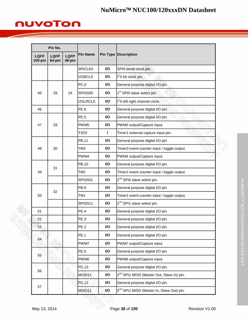
Pin No.
Pin Name Pin Type Description LQFP 100-pin
LQFP 64-pin
LQFP 48-pin
44 27 19
PC.1 I/O General purpose digital I/O pin.
SPICLK0 I/O SPI0 serial clock pin.
I2SBCLK I/O I2S bit clock pin.
45 28 20
PC.0 I/O General purpose digital I/O pin.
SPISS00 I/O 1st SPI0 slave select pin.
I2SLRCLK I/O I2S left right channel clock.
46 PE.6 I/O General purpose digital I/O pin.
47 29 21
PE.5 I/O General purpose digital I/O pin.
PWM5 I/O PWM5 output/Capture input.
T1EX I Timer1 external capture input pin.
48 30 22
PB.11 I/O General purpose digital I/O pin.
TM3 I/O Timer3 event counter input / toggle output.
PWM4 I/O PWM4 output/Capture input.
49 31 23
PB.10 I/O General purpose digital I/O pin.
TM2 I/O Timer2 event counter input / toggle output.
SPISS01 I/O 2nd SPI0 slave select pin.
50 32 24
PB.9 I/O General purpose digital I/O pin.
TM1 I/O Timer1 event counter input / toggle output.
SPISS11 I/O 2nd SPI1 slave select pin.
51 PE.4 I/O General purpose digital I/O pin.
52 PE.3 I/O General purpose digital I/O pin.
53 PE.2 I/O General purpose digital I/O pin.
54 PE.1 I/O General purpose digital I/O pin.
PWM7 I/O PWM7 output/Capture input.
55 PE.0 I/O General purpose digital I/O pin.
PWM6 I/O PWM6 output/Capture input.
56 PC.13 I/O General purpose digital I/O pin.
MOSI11 I/O 2nd SPI1 MOSI (Master Out, Slave In) pin.
57 PC.12 I/O General purpose digital I/O pin.
NuMicro NUC100/120xxxDN Datasheet
May 13, 2014 Page 29 of 100 Revision V1.00
NU
MIC
RO
™ N
UC
100/120XXXD
N D
ATASHEET
Pin No.
Pin Name Pin Type Description LQFP 100-pin
LQFP 64-pin
LQFP 48-pin
MISO11 I/O 2nd SPI1 MISO (Master In, Slave Out) pin.
58 33 PC.11 I/O General purpose digital I/O pin.
MOSI10 I/O 1st SPI1 MOSI (Master Out, Slave In) pin.
59 34 PC.10 I/O General purpose digital I/O pin.
MISO10 I/O 1st SPI1 MISO (Master In, Slave Out) pin.
60 35 PC.9 I/O General purpose digital I/O pin.
SPICLK1 I/O SPI1 serial clock pin.
61 36
PC.8 I/O General purpose digital I/O pin.
SPISS10 I/O 1st SPI1 slave select pin.
MCLK O EBI external clock output pin
62 37 25
PA.15 I/O General purpose digital I/O pin.
PWM3 I/O PWM output/Capture input.
I2SMCLK O I2S master clock output pin.
SC2PWR O SmartCard2 power pin.
63 38 26
PA.14 I/O General purpose digital I/O pin.
PWM2 I/O PWM2 output/Capture input.
SC2RST O SmartCard2 reset pin.
AD15 I/O EBI Address/Data bus bit15
64 39 27
PA.13 I/O General purpose digital I/O pin.
PWM1 I/O PWM1 output/Capture input.
SC2CLK O SmartCard2 clock pin.
AD14 I/O EBI Address/Data bus bit14
65 40 28
PA.12 I/O General purpose digital I/O pin.
PWM0 I/O PWM0 output/Capture input.
SC2DAT O SmartCard2 data pin.
AD13 I/O EBI Address/Data bus bit13
66 41 29 ICE_DAT I/O Serial Wire Debugger Data pin
67 42 30 ICE_CLK I Serial Wire Debugger Clock pin
68 VDD P Power supply for I/O ports and LDO source for internal PLL and digital circuit.

NuMicro NUC100/120xxxDN Datasheet
May 13, 2014 Page 30 of 100 Revision V1.00
NU
MIC
RO
™ N
UC
100/120XXXD
N D
ATASHEET
Pin No.
Pin Name Pin Type Description LQFP 100-pin
LQFP 64-pin
LQFP 48-pin
69 VSS P Ground pin for digital circuit.
70 43 31 AVSS AP Ground pin for analog circuit.
71 44 32
PA.0 I/O General purpose digital I/O pin.
ADC0 AI ADC0 analog input.
SC0PWR O SmartCard0 power pin.
72 45 33
PA.1 I/O General purpose digital I/O pin.
ADC1 AI ADC1 analog input.
SC0RST O SmartCard0 reset pin.
AD12 I/O EBI Address/Data bus bit12
73 46 34
PA.2 I/O General purpose digital I/O pin.
ADC2 AI ADC2 analog input.
SC0CLK O SmartCard0 clock pin.
AD11 I/O EBI Address/Data bus bit11
74 47 35
PA.3 I/O General purpose digital I/O pin.
ADC3 AI ADC3 analog input.
SC0DAT O SmartCard0 data pin.
AD10 I/O EBI Address/Data bus bit10
75 48 36
PA.4 I/O General purpose digital I/O pin.
ADC4 AI ADC4 analog input.
SC1PWR O SmartCard1 power pin.
AD9 I/O EBI Address/Data bus bit9
76 49 37
PA.5 I/O General purpose digital I/O pin.
ADC5 AI ADC5 analog input.
SC1RST O SmartCard1 reset pin.
AD8 I/O EBI Address/Data bus bit8
77 50 38
PA.6 I/O General purpose digital I/O pin.
ADC6 AI ADC6 analog input.
SC1CLK I/O SmartCard1 clock pin.
AD7 I/O EBI Address/Data bus bit7
78 51 39 PA.7 I/O General purpose digital I/O pin.

NuMicro NUC100/120xxxDN Datasheet
May 13, 2014 Page 31 of 100 Revision V1.00
NU
MIC
RO
™ N
UC
100/120XXXD
N D
ATASHEET
Pin No.
Pin Name Pin Type Description LQFP 100-pin
LQFP 64-pin
LQFP 48-pin
ADC7 AI ADC7 analog input.
SC1DAT O SmartCard1 data pin.
SPISS21 I/O 2nd SPI2 slave select pin.
AD6 I/O EBI Address/Data bus bit6
79 VREF AP Voltage reference input for ADC.
80 52 40 AVDD AP Power supply for internal analog circuit.
81 PD.0 I/O General purpose digital I/O pin.
SPISS20 I/O 1st SPI2 slave select pin.
82 PD.1 I/O General purpose digital I/O pin.
SPICLK2 I/O SPI2 serial clock pin.
83 PD.2 I/O General purpose digital I/O pin.
MISO20 I/O 1st SPI2 MISO (Master In, Slave Out) pin.
84 PD.3 I/O General purpose digital I/O pin.
MOSI20 I/O 1st SPI2 MOSI (Master Out, Slave In) pin.
85 PD.4 I/O General purpose digital I/O pin.
MISO21 I/O 2nd SPI2 MISO (Master In, Slave Out) pin.
86 PD.5 I/O General purpose digital I/O pin.
MOSI21 I/O 2nd SPI2 MOSI (Master Out, Slave In) pin.
87 53 41
PC.7 I/O General purpose digital I/O pin.
CPN0 AI Comparator0 negative input pin.
SC1CD I SmartCard1 card detect pin.
AD5 I/O EBI Address/Data bus bit5
88 54 42
PC.6 I/O General purpose digital I/O pin.
CPP0 AI Comparator0 positive input pin.
SC0CD I SmartCard0 card detect pin.
AD4 I/O EBI Address/Data bus bit4
89 55
PC.15 I/O General purpose digital I/O pin.
CPN1 AI Comparator1 negative input pin.
AD3 I/O EBI Address/Data bus bit3
90 56 PC.14 I/O General purpose digital I/O pin.
NuMicro NUC100/120xxxDN Datasheet
May 13, 2014 Page 32 of 100 Revision V1.00
NU
MIC
RO
™ N
UC
100/120XXXD
N D
ATASHEET
Pin No.
Pin Name Pin Type Description LQFP 100-pin
LQFP 64-pin
LQFP 48-pin
CPP1 AI Comparator1 positive input pin.
AD2 I/O EBI Address/Data bus bit2
91 57 43
PB.15 I/O General purpose digital I/O pin.
/INT1 I External interrupt1 input pin.
T0EX I Timer0 external capture input pin.
92 58 44 PF.0 I/O General purpose digital I/O pin.
XT1_OUT O External 4~24 MHz (high speed) crystal output pin.
93 59 45 PF.1 I/O General purpose digital I/O pin.
XT1_IN I External 4~24 MHz (high speed) crystal input pin.
94 60 46 /RESET I External reset input: active LOW, with an internal pull-up. Set this pin low reset chip to initial state.
95 61 VSS P Ground pin for digital circuit.
96 62 VDD P Power supply for I/O ports and LDO source for internal PLL and digital circuit.
97 PF.2 I/O General purpose digital I/O pin.
PS2DAT I/O PS2 data pin.
98 PF.3 I/O General purpose digital I/O pin.
PS2CLK I/O PS2 clock pin.
99 63 47 PVSS P PLL ground.
100 64 48
PB.8 I/O General purpose digital I/O pin.
STADC I ADC external trigger input.
TM0 I/O Timer0 event counter input / toggle output.
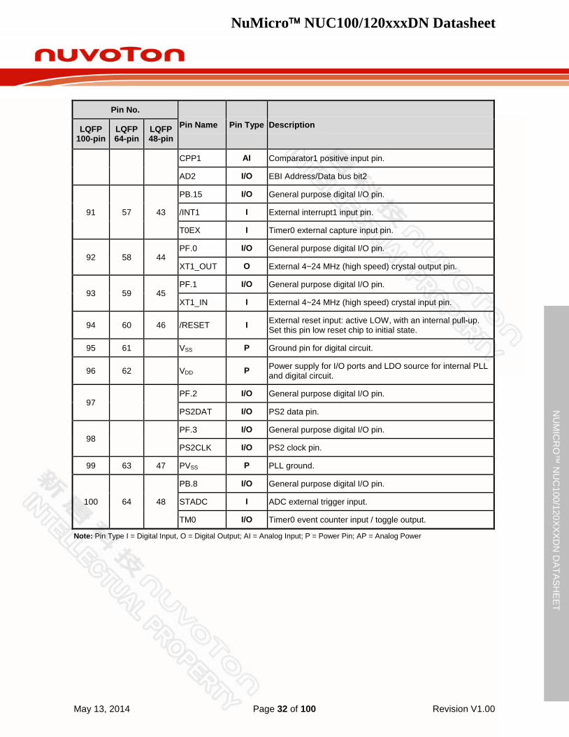
Note: Pin Type I = Digital Input, O = Digital Output; AI = Analog Input; P = Power Pin; AP = Analog Power
NuMicro NUC100/120xxxDN Datasheet
May 13, 2014 Page 33 of 100 Revision V1.00
NU
MIC
RO
™ N
UC
100/120XXXD
N D
ATASHEET
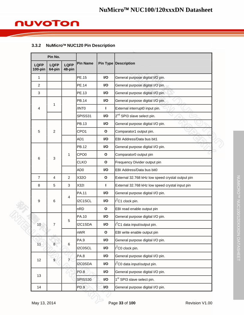
3.3.2 NuMicro NUC120 Pin Description
Pin No.
Pin Name Pin Type Description LQFP 100-pin
LQFP 64-pin
LQFP 48-pin
1 PE.15 I/O General purpose digital I/O pin.
2 PE.14 I/O General purpose digital I/O pin.
3 PE.13 I/O General purpose digital I/O pin.
4 1
PB.14 I/O General purpose digital I/O pin.
/INT0 I External interrupt0 input pin.
SPISS31 I/O 2nd SPI3 slave select pin.
5 2
PB.13 I/O General purpose digital I/O pin.
CPO1 O Comparator1 output pin.
AD1 I/O EBI Address/Data bus bit1
6 3 1
PB.12 I/O General purpose digital I/O pin.
CPO0 O Comparator0 output pin
CLKO O Frequency Divider output pin
AD0 I/O EBI Address/Data bus bit0
7 4 2 X32O O External 32.768 kHz low speed crystal output pin
8 5 3 X32I I External 32.768 kHz low speed crystal input pin
9 6 4
PA.11 I/O General purpose digital I/O pin.
I2C1SCL I/O I2C1 clock pin.
nRD O EBI read enable output pin
10 7 5
PA.10 I/O General purpose digital I/O pin.
I2C1SDA I/O I2C1 data input/output pin.
nWR O EBI write enable output pin
11 8 6 PA.9 I/O General purpose digital I/O pin.
I2C0SCL I/O I2C0 clock pin.
12 9 7 PA.8 I/O General purpose digital I/O pin.
I2C0SDA I/O I2C0 data input/output pin.
13 PD.8 I/O General purpose digital I/O pin.
SPISS30 I/O 1st SPI3 slave select pin.
14 PD.9 I/O General purpose digital I/O pin.
NuMicro NUC100/120xxxDN Datasheet
May 13, 2014 Page 34 of 100 Revision V1.00
NU
MIC
RO
™ N
UC
100/120XXXD
N D
ATASHEET
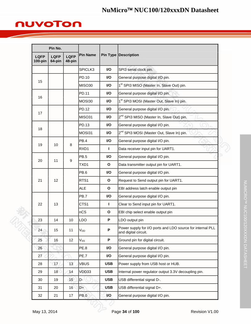
Pin No.
Pin Name Pin Type Description LQFP 100-pin
LQFP 64-pin
LQFP 48-pin
SPICLK3 I/O SPI3 serial clock pin.
15 PD.10 I/O General purpose digital I/O pin.
MISO30 I/O 1st SPI3 MISO (Master In, Slave Out) pin.
16 PD.11 I/O General purpose digital I/O pin.
MOSI30 I/O 1st SPI3 MOSI (Master Out, Slave In) pin.
17 PD.12 I/O General purpose digital I/O pin.
MISO31 I/O 2nd SPI3 MISO (Master In, Slave Out) pin.
18 PD.13 I/O General purpose digital I/O pin.
MOSI31 I/O 2nd SPI3 MOSI (Master Out, Slave In) pin.
19 10 8 PB.4 I/O General purpose digital I/O pin.
RXD1 I Data receiver input pin for UART1.
20 11 9 PB.5 I/O General purpose digital I/O pin.
TXD1 O Data transmitter output pin for UART1.
21 12
PB.6 I/O General purpose digital I/O pin.
RTS1 O Request to Send output pin for UART1.
ALE O EBI address latch enable output pin
22 13
PB.7 I/O General purpose digital I/O pin.
CTS1 I Clear to Send input pin for UART1.
nCS O EBI chip select enable output pin
23 14 10 LDO P LDO output pin
24 15 11 VDD P Power supply for I/O ports and LDO source for internal PLL and digital circuit.
25 16 12 VSS P Ground pin for digital circuit.
26 PE.8 I/O General purpose digital I/O pin.
27 PE.7 I/O General purpose digital I/O pin.
28 17 13 VBUS USB Power supply from USB host or HUB.
29 18 14 VDD33 USB Internal power regulator output 3.3V decoupling pin.
30 19 15 D- USB USB differential signal D-.
31 20 16 D+ USB USB differential signal D+.
32 21 17 PB.0 I/O General purpose digital I/O pin.
NuMicro NUC100/120xxxDN Datasheet
May 13, 2014 Page 35 of 100 Revision V1.00
NU
MIC
RO
™ N
UC
100/120XXXD
N D
ATASHEET
Pin No.
Pin Name Pin Type Description LQFP 100-pin
LQFP 64-pin
LQFP 48-pin
RXD0 I Data receiver input pin for UART0.
33 22 18 PB.1 I/O General purpose digital I/O pin.
TXD0 O Data transmitter output pin for UART0.
34 23 29
PB.2 I/O General purpose digital I/O pin.
RTS0 O Request to Send output pin for UART0.
T2EX I Timer2 external capture input pin.
nWRL O EBI low byte write enable output pin
35 24 20
PB.3 I/O General purpose digital I/O pin.
CTS0 I Clear to Send input pin for UART0.
T3EX I Timer3 external capture input pin.
SC2CD I SmartCard2 card detect pin.
nWRH O EBI high byte write enable output pin
36 PD.6 I/O General purpose digital I/O pin.
37 PD.7 I/O General purpose digital I/O pin.
38 PD.14 I/O General purpose digital I/O pin.
RXD2 I Data receiver input pin for UART2.
39 PD.15 I/O General purpose digital I/O pin.
TXD2 O Data transmitter output pin for UART2.
40 PC.5 I/O General purpose digital I/O pin.
MOSI01 I/O 2nd SPI0 MOSI (Master Out, Slave In) pin.
41 PC.4 I/O General purpose digital I/O pin.
MISO01 I/O 2nd SPI0 MISO (Master In, Slave Out) pin.
42 25 21
PC.3 I/O General purpose digital I/O pin.
MOSI00 I/O 1st SPI0 MOSI (Master Out, Slave In) pin.
I2SDO O I2S data output.
43 26 22
PC.2 I/O General purpose digital I/O pin.
MISO00 I/O 1st SPI0 MISO (Master In, Slave Out) pin.
I2SDI I I2S data input.
44 27 23 PC.1 I/O General purpose digital I/O pin.
NuMicro NUC100/120xxxDN Datasheet
May 13, 2014 Page 36 of 100 Revision V1.00
NU
MIC
RO
™ N
UC
100/120XXXD
N D
ATASHEET
Pin No.
Pin Name Pin Type Description LQFP 100-pin
LQFP 64-pin
LQFP 48-pin
SPICLK0 I/O SPI0 serial clock pin.
I2SBCLK I/O I2S bit clock pin.
45 28 24
PC.0 I/O General purpose digital I/O pin.
SPISS00 I/O 1st SPI0 slave select pin.
I2SLRCLK I/O I2S left right channel clock.
46 PE.6 I/O General purpose digital I/O pin.
47 29
PE.5 I/O General purpose digital I/O pin.
PWM5 I/O PWM5 output/Capture input.
T1EX I Timer1 external capture input pin.
48 30
PB.11 I/O General purpose digital I/O pin.
TM3 I/O Timer3 event counter input / toggle output.
PWM4 I/O PWM4 output/Capture input.
49 31
PB.10 I/O General purpose digital I/O pin.
TM2 I/O Timer2 event counter input / toggle output.
SPISS01 I/O 2nd SPI0 slave select pin.
50 32
PB.9 I/O General purpose digital I/O pin.
TM1 I/O Timer1 event counter input / toggle output.
SPISS11 I/O 2nd SPI1 slave select pin.
51 PE.4 I/O General purpose digital I/O pin.
52 PE.3 I/O General purpose digital I/O pin.
53 PE.2 I/O General purpose digital I/O pin.
54 PE.1 I/O General purpose digital I/O pin.
PWM7 I/O PWM7 output/Capture input.
55 PE.0 I/O General purpose digital I/O pin.
PWM6 I/O PWM6 output/Capture input.
56 PC.13 I/O General purpose digital I/O pin.
MOSI11 I/O 2nd SPI1 MOSI (Master Out, Slave In) pin.
57 PC.12 I/O General purpose digital I/O pin.
MISO11 I/O 2nd SPI1 MISO (Master In, Slave Out) pin.

NuMicro NUC100/120xxxDN Datasheet
May 13, 2014 Page 37 of 100 Revision V1.00
NU
MIC
RO
™ N
UC
100/120XXXD
N D
ATASHEET
Pin No.
Pin Name Pin Type Description LQFP 100-pin
LQFP 64-pin
LQFP 48-pin
58 33 PC.11 I/O General purpose digital I/O pin.
MOSI10 I/O 1st SPI1 MOSI (Master Out, Slave In) pin.
59 34 PC.10 I/O General purpose digital I/O pin.
MISO10 I/O 1st SPI1 MISO (Master In, Slave Out) pin.
60 35 PC.9 I/O General purpose digital I/O pin.
SPICLK1 I/O SPI1 serial clock pin.
61 36
PC.8 I/O General purpose digital I/O pin.
SPISS10 I/O 1st SPI1 slave select pin.
MCLK O EBI external clock output pin
62 37 25
PA.15 I/O General purpose digital I/O pin.
PWM3 I/O PWM output/Capture input.
I2SMCLK O I2S master clock output pin.
SC2PWR O SmartCard2 power pin.
63 38 26
PA.14 I/O General purpose digital I/O pin.
PWM2 I/O PWM2 output/Capture input.
SC2RST O SmartCard2 reset pin.
AD15 I/O EBI Address/Data bus bit15
64 39 27
PA.13 I/O General purpose digital I/O pin.
PWM1 I/O PWM1 output/Capture input.
SC2CLK O SmartCard2 clock pin.
AD14 I/O EBI Address/Data bus bit14
65 40 28
PA.12 I/O General purpose digital I/O pin.
PWM0 I/O PWM0 output/Capture input.
SC2DAT O SmartCard2 data pin.
AD13 I/O EBI Address/Data bus bit13
66 41 29 ICE_DAT I/O Serial Wire Debugger Data pin
67 42 30 ICE_CLK I Serial Wire Debugger Clock pin
68 VDD P Power supply for I/O ports and LDO source for internal PLL and digital circuit.
69 VSS P Ground pin for digital circuit.
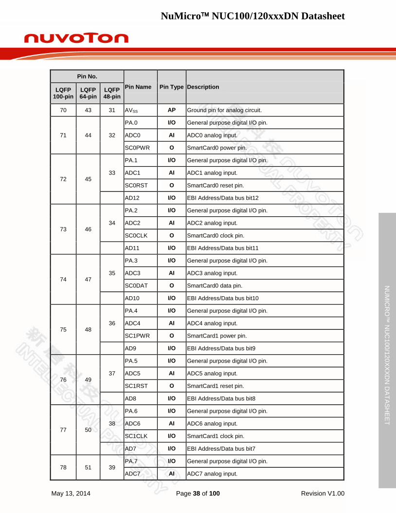
NuMicro NUC100/120xxxDN Datasheet
May 13, 2014 Page 38 of 100 Revision V1.00
NU
MIC
RO
™ N
UC
100/120XXXD
N D
ATASHEET
Pin No.
Pin Name Pin Type Description LQFP 100-pin
LQFP 64-pin
LQFP 48-pin
70 43 31 AVSS AP Ground pin for analog circuit.
71 44 32
PA.0 I/O General purpose digital I/O pin.
ADC0 AI ADC0 analog input.
SC0PWR O SmartCard0 power pin.
72 45 33
PA.1 I/O General purpose digital I/O pin.
ADC1 AI ADC1 analog input.
SC0RST O SmartCard0 reset pin.
AD12 I/O EBI Address/Data bus bit12
73 46 34
PA.2 I/O General purpose digital I/O pin.
ADC2 AI ADC2 analog input.
SC0CLK O SmartCard0 clock pin.
AD11 I/O EBI Address/Data bus bit11
74 47 35
PA.3 I/O General purpose digital I/O pin.
ADC3 AI ADC3 analog input.
SC0DAT O SmartCard0 data pin.
AD10 I/O EBI Address/Data bus bit10
75 48 36
PA.4 I/O General purpose digital I/O pin.
ADC4 AI ADC4 analog input.
SC1PWR O SmartCard1 power pin.
AD9 I/O EBI Address/Data bus bit9
76 49 37
PA.5 I/O General purpose digital I/O pin.
ADC5 AI ADC5 analog input.
SC1RST O SmartCard1 reset pin.
AD8 I/O EBI Address/Data bus bit8
77 50 38
PA.6 I/O General purpose digital I/O pin.
ADC6 AI ADC6 analog input.
SC1CLK I/O SmartCard1 clock pin.
AD7 I/O EBI Address/Data bus bit7
78 51 39 PA.7 I/O General purpose digital I/O pin.
ADC7 AI ADC7 analog input.

NuMicro NUC100/120xxxDN Datasheet
May 13, 2014 Page 39 of 100 Revision V1.00
NU
MIC
RO
™ N
UC
100/120XXXD
N D
ATASHEET
Pin No.
Pin Name Pin Type Description LQFP 100-pin
LQFP 64-pin
LQFP 48-pin
SC1DAT O SmartCard1 data pin.
SPISS21 I/O 2nd SPI2 slave select pin.
AD6 I/O EBI Address/Data bus bit6
79 VREF AP Voltage reference input for ADC.
80 52 40 AVDD AP Power supply for internal analog circuit.
81 PD.0 I/O General purpose digital I/O pin.
SPISS20 I/O 1st SPI2 slave select pin.
82 PD.1 I/O General purpose digital I/O pin.
SPICLK2 I/O SPI2 serial clock pin.
83 PD.2 I/O General purpose digital I/O pin.
MISO20 I/O 1st SPI2 MISO (Master In, Slave Out) pin.
84 PD.3 I/O General purpose digital I/O pin.
MOSI20 I/O 1st SPI2 MOSI (Master Out, Slave In) pin.
85 PD.4 I/O General purpose digital I/O pin.
MISO21 I/O 2nd SPI2 MISO (Master In, Slave Out) pin.
86 PD.5 I/O General purpose digital I/O pin.
MOSI21 I/O 2nd SPI2 MOSI (Master Out, Slave In) pin.
87 53 41
PC.7 I/O General purpose digital I/O pin.
CPN0 AI Comparator0 negative input pin.
SC1CD I SmartCard1 card detect pin.
AD5 I/O EBI Address/Data bus bit5
88 54 42
PC.6 I/O General purpose digital I/O pin.
CPP0 AI Comparator0 positive input pin.
SC0CD I SmartCard0 card detect pin.
AD4 I/O EBI Address/Data bus bit4
89 55
PC.15 I/O General purpose digital I/O pin.
CPN1 AI Comparator1 negative input pin.
AD3 I/O EBI Address/Data bus bit3
90 56 PC.14 I/O General purpose digital I/O pin.
CPP1 AI Comparator1 positive input pin.
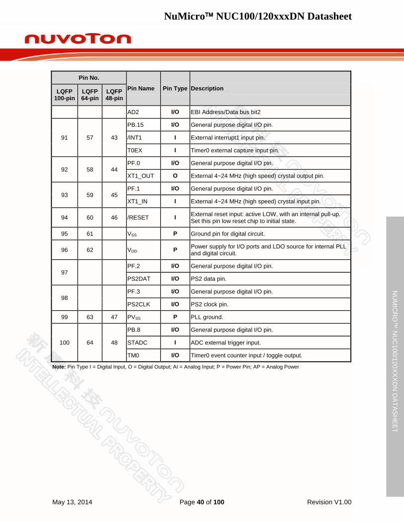
NuMicro NUC100/120xxxDN Datasheet
May 13, 2014 Page 40 of 100 Revision V1.00
NU
MIC
RO
™ N
UC
100/120XXXD
N D
ATASHEET
Pin No.
Pin Name Pin Type Description LQFP 100-pin
LQFP 64-pin
LQFP 48-pin
AD2 I/O EBI Address/Data bus bit2
91 57 43
PB.15 I/O General purpose digital I/O pin.
/INT1 I External interrupt1 input pin.
T0EX I Timer0 external capture input pin.
92 58 44 PF.0 I/O General purpose digital I/O pin.
XT1_OUT O External 4~24 MHz (high speed) crystal output pin.
93 59 45 PF.1 I/O General purpose digital I/O pin.
XT1_IN I External 4~24 MHz (high speed) crystal input pin.
94 60 46 /RESET I External reset input: active LOW, with an internal pull-up. Set this pin low reset chip to initial state.
95 61 VSS P Ground pin for digital circuit.
96 62 VDD P Power supply for I/O ports and LDO source for internal PLL and digital circuit.
97 PF.2 I/O General purpose digital I/O pin.
PS2DAT I/O PS2 data pin.
98 PF.3 I/O General purpose digital I/O pin.
PS2CLK I/O PS2 clock pin.
99 63 47 PVSS P PLL ground.
100 64 48
PB.8 I/O General purpose digital I/O pin.
STADC I ADC external trigger input.
TM0 I/O Timer0 event counter input / toggle output.
Note: Pin Type I = Digital Input, O = Digital Output; AI = Analog Input; P = Power Pin; AP = Analog Power
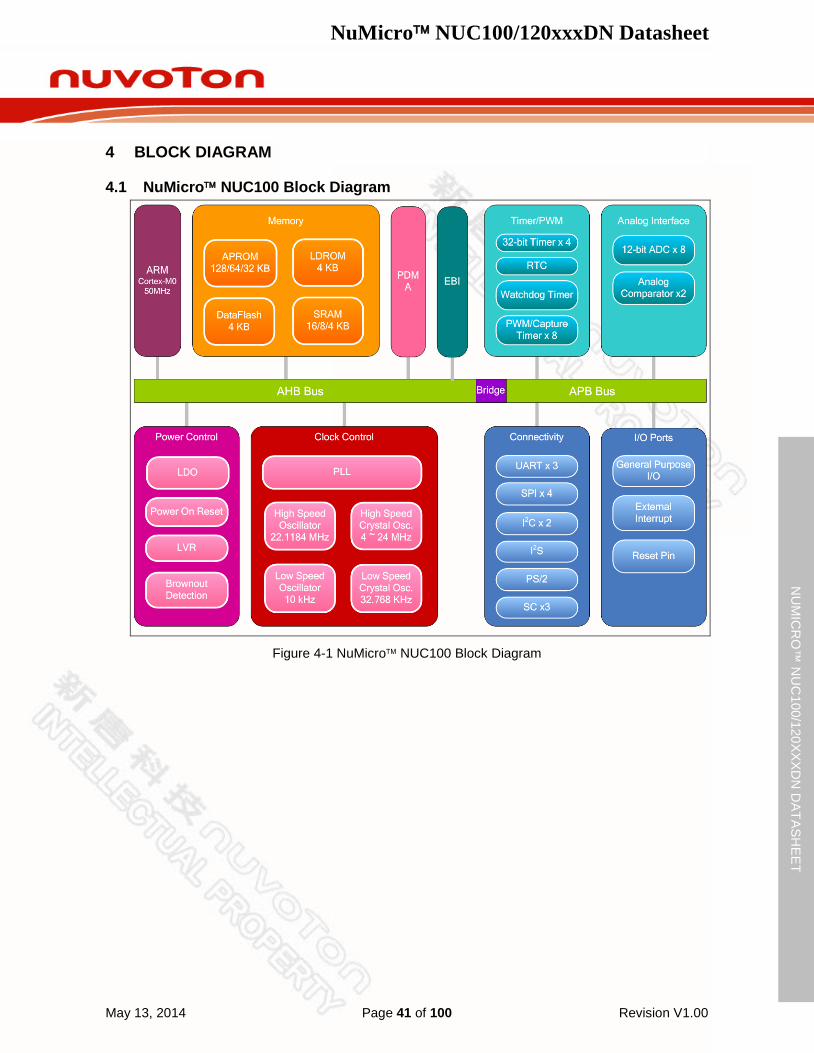
NuMicro NUC100/120xxxDN Datasheet
May 13, 2014 Page 41 of 100 Revision V1.00
NU
MIC
RO
™ N
UC
100/120XXXD
N D
ATASHEET
4 BLOCK DIAGRAM
NuMicro NUC100 Block Diagram 4.1
Figure 4-1 NuMicro NUC100 Block Diagram
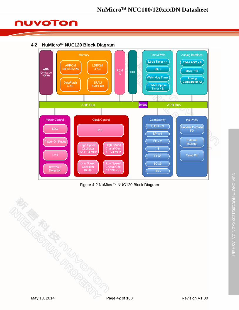
NuMicro NUC100/120xxxDN Datasheet
May 13, 2014 Page 42 of 100 Revision V1.00
NU
MIC
RO
™ N
UC
100/120XXXD
N D
ATASHEET
NuMicro NUC120 Block Diagram 4.2
Figure 4-2 NuMicro NUC120 Block Diagram
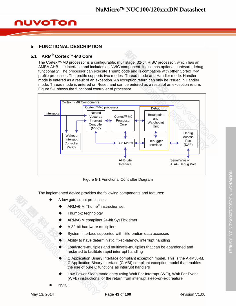
NuMicro NUC100/120xxxDN Datasheet
May 13, 2014 Page 43 of 100 Revision V1.00
NU
MIC
RO
™ N
UC
100/120XXXD
N D
ATASHEET
5 FUNCTIONAL DESCRIPTION
ARM® Cortex™-M0 Core 5.1The Cortex™-M0 processor is a configurable, multistage, 32-bit RISC processor, which has an AMBA AHB-Lite interface and includes an NVIC component. It also has optional hardware debug functionality. The processor can execute Thumb code and is compatible with other Cortex™-M profile processor. The profile supports two modes -Thread mode and Handler mode. Handler mode is entered as a result of an exception. An exception return can only be issued in Handler mode. Thread mode is entered on Reset, and can be entered as a result of an exception return. Figure 5-1 shows the functional controller of processor.
CortexTM-M0Processor
Core
Nested Vectored Interrupt
Controller(NVIC)
Breakpointand
Watchpoint Unit
Debugger InterfaceBus Matrix
Debug Access
Port(DAP)
DebugCortexTM-M0 processorCortexTM-M0 Components
WakeupInterrupt
Controller (WIC)
Interrupts
Serial Wire or JTAG Debug Port
AHB-Lite Interface
Figure 5-1 Functional Controller Diagram
The implemented device provides the following components and features:
A low gate count processor:
ARMv6-M Thumb® instruction set
Thumb-2 technology
ARMv6-M compliant 24-bit SysTick timer
A 32-bit hardware multiplier
System interface supported with little-endian data accesses
Ability to have deterministic, fixed-latency, interrupt handling
Load/store-multiples and multicycle-multiplies that can be abandoned and restarted to facilitate rapid interrupt handling
C Application Binary Interface compliant exception model. This is the ARMv6-M, C Application Binary Interface (C-ABI) compliant exception model that enables the use of pure C functions as interrupt handlers
Low Power Sleep mode entry using Wait For Interrupt (WFI), Wait For Event (WFE) instructions, or the return from interrupt sleep-on-exit feature
NVIC:
NuMicro NUC100/120xxxDN Datasheet
May 13, 2014 Page 44 of 100 Revision V1.00
NU
MIC
RO
™ N
UC
100/120XXXD
N D
ATASHEET
32 external interrupt inputs, each with four levels of priority
Dedicated Non-maskable Interrupt (NMI) input
Supports for both level-sensitive and pulse-sensitive interrupt lines
Supports Wake-up Interrupt Controller (WIC) and, providing Ultra-low Power Sleep mode
Debug support
Four hardware breakpoints
Two watchpoints
Program Counter Sampling Register (PCSR) for non-intrusive code profiling
Single step and vector catch capabilities
Bus interfaces:
Single 32-bit AMBA-3 AHB-Lite system interface that provides simple integration to all system peripherals and memory
Single 32-bit slave port that supports the DAP (Debug Access Port)
NuMicro NUC100/120xxxDN Datasheet
May 13, 2014 Page 45 of 100 Revision V1.00
NU
MIC
RO
™ N
UC
100/120XXXD
N D
ATASHEET
System Manager 5.2
5.2.1 Overview
System management includes the following sections:
System Resets
System Memory Map
System management registers for Part Number ID, chip reset and on-chip controllers reset , multi-functional pin control
System Timer (SysTick)
Nested Vectored Interrupt Controller (NVIC)
System Control registers
5.2.2 System Reset
The system reset can be issued by one of the following listed events. For these reset event flags can be read by RSTSRC register.
Power-on Reset
Low level on the /RESET pin
Watchdog Time-out Reset
Low Voltage Reset
Brown-out Detector Reset
CPU Reset
System Reset
System Reset and Power-on Reset all reset the whole chip including all peripherals. The difference between System Reset and Power-on Reset is external crystal circuit and ISPCON.BS bit. System Reset does not reset external crystal circuit and ISPCON.BS bit, but Power-on Reset does.
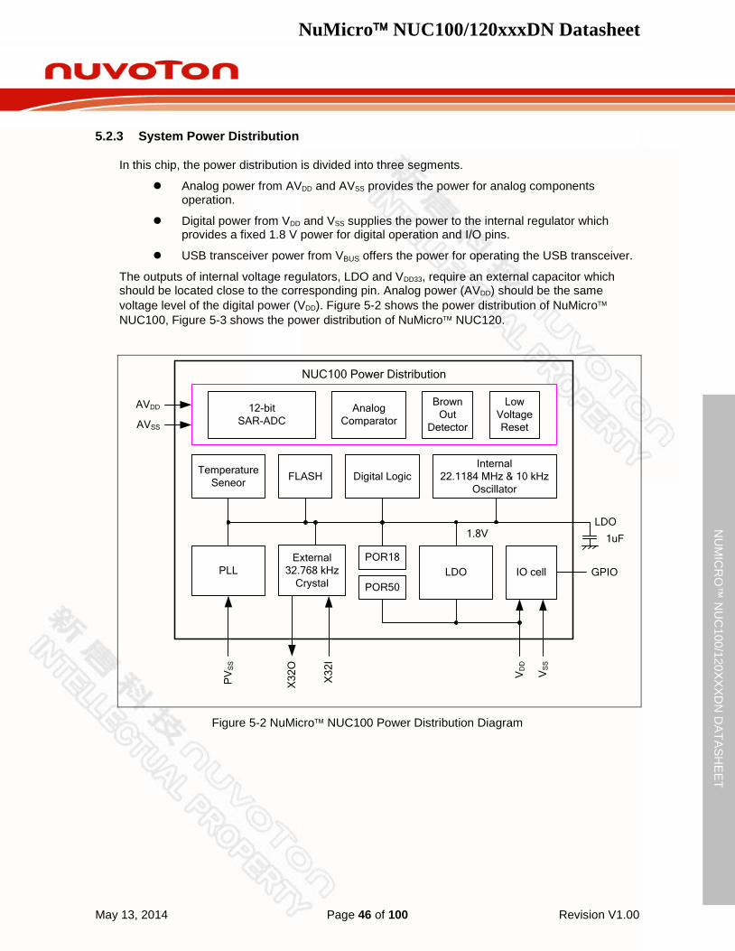
NuMicro NUC100/120xxxDN Datasheet
May 13, 2014 Page 46 of 100 Revision V1.00
NU
MIC
RO
™ N
UC
100/120XXXD
N D
ATASHEET
5.2.3 System Power Distribution
In this chip, the power distribution is divided into three segments.
Analog power from AVDD and AVSS provides the power for analog components operation.
Digital power from VDD and VSS supplies the power to the internal regulator which provides a fixed 1.8 V power for digital operation and I/O pins.
USB transceiver power from VBUS offers the power for operating the USB transceiver.
The outputs of internal voltage regulators, LDO and VDD33, require an external capacitor which should be located close to the corresponding pin. Analog power (AVDD) should be the same voltage level of the digital power (VDD). Figure 5-2 shows the power distribution of NuMicro NUC100, Figure 5-3 shows the power distribution of NuMicro NUC120.
LDOPLL
12-bit SAR-ADC
Brown Out
Detector
POR50
POR18
Low Voltage Reset
External 32.768 kHz
Crystal
Analog Comparator
Temperature Seneor FLASH Digital Logic
1.8V
Internal 22.1184 MHz & 10 kHz
Oscillator
AVDD
AVSS
VD
D
VS
S
LDO
1uF
IO cell GPIO
X32
O
X32
I
PV
SS
NUC100 Power Distribution
Figure 5-2 NuMicro NUC100 Power Distribution Diagram
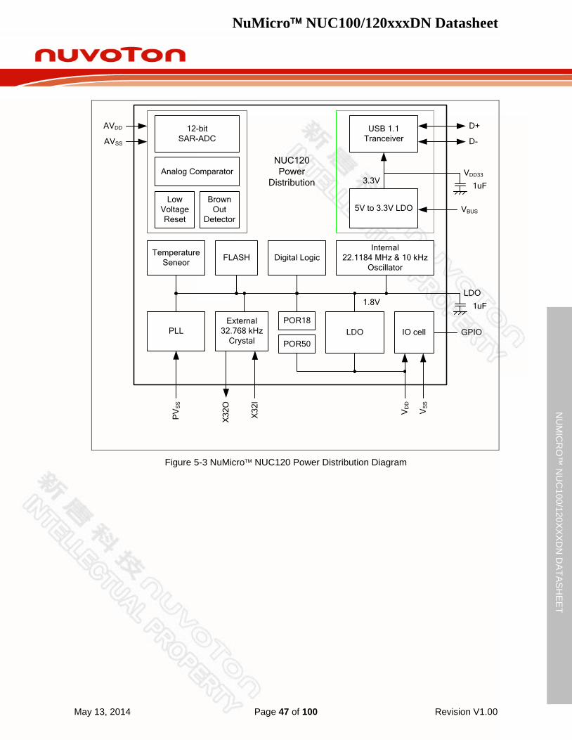
NuMicro NUC100/120xxxDN Datasheet
May 13, 2014 Page 47 of 100 Revision V1.00
NU
MIC
RO
™ N
UC
100/120XXXD
N D
ATASHEET
LDO
USB 1.1 Tranceiver
5V to 3.3V LDO
PLL
12-bit SAR-ADC
Brown Out
Detector
POR50
POR18
Low Voltage Reset
External 32.768 kHz
Crystal
Analog Comparator
Temperature Seneor FLASH Digital Logic
3.3V
1.8V
Internal 22.1184 MHz & 10 kHz
Oscillator
AVDD
AVSS
VD
D
VS
S
VBUS
VDD33
D+
D-
LDO
1uF
1uF
IO cell GPIO
X32
O
X32
I
PV
SS
NUC120 Power
Distribution
Figure 5-3 NuMicro NUC120 Power Distribution Diagram
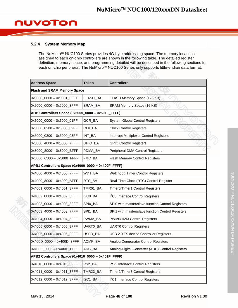
NuMicro NUC100/120xxxDN Datasheet
May 13, 2014 Page 48 of 100 Revision V1.00
NU
MIC
RO
™ N
UC
100/120XXXD
N D
ATASHEET
5.2.4 System Memory Map
The NuMicro NUC100 Series provides 4G-byte addressing space. The memory locations assigned to each on-chip controllers are shown in the following table. The detailed register definition, memory space, and programming detailed will be described in the following sections for each on-chip peripheral. The NuMicro NUC100 Series only supports little-endian data format.
Address Space Token Controllers
Flash and SRAM Memory Space
0x0000_0000 – 0x0001_FFFF FLASH_BA FLASH Memory Space (128 KB)
0x2000_0000 – 0x2000_3FFF SRAM_BA SRAM Memory Space (16 KB)
AHB Controllers Space (0x5000_0000 – 0x501F_FFFF)
0x5000_0000 – 0x5000_01FF GCR_BA System Global Control Registers
0x5000_0200 – 0x5000_02FF CLK_BA Clock Control Registers
0x5000_0300 – 0x5000_03FF INT_BA Interrupt Multiplexer Control Registers
0x5000_4000 – 0x5000_7FFF GPIO_BA GPIO Control Registers
0x5000_8000 – 0x5000_BFFF PDMA_BA Peripheral DMA Control Registers
0x5000_C000 – 0x5000_FFFF FMC_BA Flash Memory Control Registers
APB1 Controllers Space (0x4000_0000 ~ 0x400F_FFFF)
0x4000_4000 – 0x4000_7FFF WDT_BA Watchdog Timer Control Registers
0x4000_8000 – 0x4000_BFFF RTC_BA Real Time Clock (RTC) Control Register
0x4001_0000 – 0x4001_3FFF TMR01_BA Timer0/Timer1 Control Registers
0x4002_0000 – 0x4002_3FFF I2C0_BA I2C0 Interface Control Registers
0x4003_0000 – 0x4003_3FFF SPI0_BA SPI0 with master/slave function Control Registers
0x4003_4000 – 0x4003_7FFF SPI1_BA SPI1 with master/slave function Control Registers
0x4004_0000 – 0x4004_3FFF PWMA_BA PWM0/1/2/3 Control Registers
0x4005_0000 – 0x4005_3FFF UART0_BA UART0 Control Registers
0x4006_0000 – 0x4006_3FFF USBD_BA USB 2.0 FS device Controller Registers
0x400D_0000 – 0x400D_3FFF ACMP_BA Analog Comparator Control Registers
0x400E_0000 – 0x400E_FFFF ADC_BA Analog-Digital-Converter (ADC) Control Registers
APB2 Controllers Space (0x4010_0000 ~ 0x401F_FFFF)
0x4010_0000 – 0x4010_3FFF PS2_BA PS/2 Interface Control Registers
0x4011_0000 – 0x4011_3FFF TMR23_BA Timer2/Timer3 Control Registers
0x4012_0000 – 0x4012_3FFF I2C1_BA I2C1 Interface Control Registers
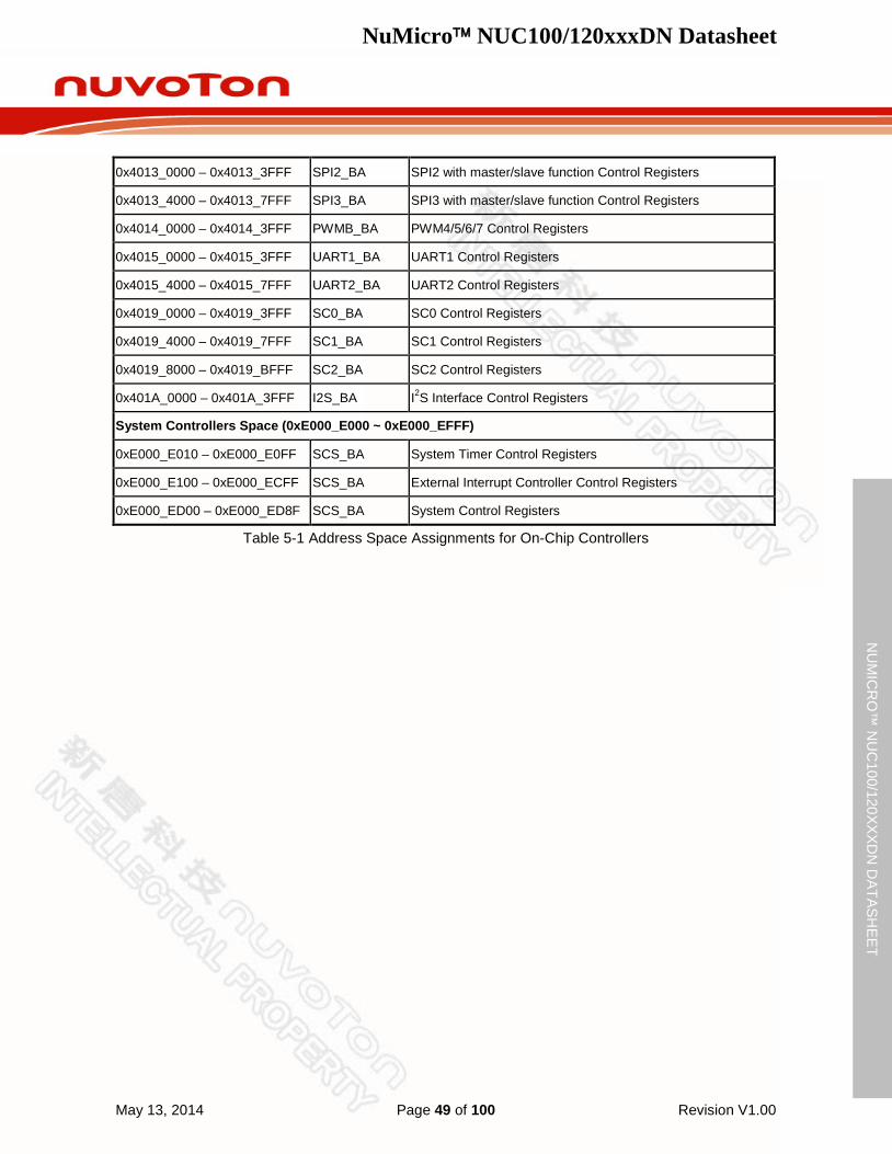
NuMicro NUC100/120xxxDN Datasheet
May 13, 2014 Page 49 of 100 Revision V1.00
NU
MIC
RO
™ N
UC
100/120XXXD
N D
ATASHEET
0x4013_0000 – 0x4013_3FFF SPI2_BA SPI2 with master/slave function Control Registers
0x4013_4000 – 0x4013_7FFF SPI3_BA SPI3 with master/slave function Control Registers
0x4014_0000 – 0x4014_3FFF PWMB_BA PWM4/5/6/7 Control Registers
0x4015_0000 – 0x4015_3FFF UART1_BA UART1 Control Registers
0x4015_4000 – 0x4015_7FFF UART2_BA UART2 Control Registers
0x4019_0000 – 0x4019_3FFF SC0_BA SC0 Control Registers
0x4019_4000 – 0x4019_7FFF SC1_BA SC1 Control Registers
0x4019_8000 – 0x4019_BFFF SC2_BA SC2 Control Registers
0x401A_0000 – 0x401A_3FFF I2S_BA I2S Interface Control Registers
System Controllers Space (0xE000_E000 ~ 0xE000_EFFF)
0xE000_E010 – 0xE000_E0FF SCS_BA System Timer Control Registers
0xE000_E100 – 0xE000_ECFF SCS_BA External Interrupt Controller Control Registers
0xE000_ED00 – 0xE000_ED8F SCS_BA System Control Registers
Table 5-1 Address Space Assignments for On-Chip Controllers
NuMicro NUC100/120xxxDN Datasheet
May 13, 2014 Page 50 of 100 Revision V1.00
NU
MIC
RO
™ N
UC
100/120XXXD
N D
ATASHEET
5.2.5 System Timer (SysTick)
The Cortex™-M0 includes an integrated system timer, SysTick, which provides a simple, 24-bit clear-on-write, decrementing, wrap-on-zero counter with a flexible control mechanism. The counter can be used as a Real Time Operating System (RTOS) tick timer or as a simple counter.
When system timer is enabled, it will count down from the value in the SysTick Current Value Register (SYST_CVR) to 0, and reload (wrap) to the value in the SysTick Reload Value Register (SYST_RVR) on the next clock cycle, then decrement on subsequent clocks. When the counter transitions to 0, the COUNTFLAG status bit is set. The COUNTFLAG bit clears on reads.
The SYST_CVR value is UNKNOWN on reset. Software should write to the register to clear it to 0 before enabling the feature. This ensures the timer will count from the SYST_RVR value rather than an arbitrary value when it is enabled.
If the SYST_RVR is 0, the timer will be maintained with a current value of 0 after it is reloaded with this value. This mechanism can be used to disable the feature independently from the timer enable bit.
NuMicro NUC100/120xxxDN Datasheet
May 13, 2014 Page 51 of 100 Revision V1.00
NU
MIC
RO
™ N
UC
100/120XXXD
N D
ATASHEET
5.2.6 Nested Vectored Interrupt Controller (NVIC)
The Cortex™-M0 provides an interrupt controller as an integral part of the exception mode, named as “Nested Vectored Interrupt Controller (NVIC)”, which is closely coupled to the processor core and provides following features:
Nested and Vectored interrupt support
Automatic processor state saving and restoration
Reduced and deterministic interrupt latency
The NVIC prioritizes and handles all supported exceptions. All exceptions are handled in “Handler Mode”. This NVIC architecture supports 32 (IRQ[31:0]) discrete interrupts with 4 levels of priority. All of the interrupts and most of the system exceptions can be configured to different priority levels. When an interrupt occurs, the NVIC will compare the priority of the new interrupt to the current running one’s priority. If the priority of the new interrupt is higher than the current one, the new interrupt handler will override the current handler.
When an interrupt is accepted, the starting address of the interrupt service routine (ISR) is fetched from a vector table in memory. There is no need to determine which interrupt is accepted and branch to the starting address of the correlated ISR by software. While the starting address is fetched, NVIC will also automatically save processor state including the registers “PC, PSR, LR, R0~R3, R12” to the stack. At the end of the ISR, the NVIC will restore the mentioned registers from stack and resume the normal execution. Thus it will take less and deterministic time to process the interrupt request.
The NVIC supports “Tail Chaining” which handles back-to-back interrupts efficiently without the overhead of states saving and restoration and therefore reduces delay time in switching to pending ISR at the end of current ISR. The NVIC also supports “Late Arrival” which improves the efficiency of concurrent ISRs. When a higher priority interrupt request occurs before the current ISR starts to execute (at the stage of state saving and starting address fetching), the NVIC will give priority to the higher one without delay penalty. Thus it advances the real-time capability.
For more detailed information, please refer to the “ARM® Cortex™-M0 Technical Reference Manual” and “ARM® v6-M Architecture Reference Manual”.
Exception Model and System Interrupt Map 5.2.6.1
The following table lists the exception model supported by NuMicro NUC100 Series. Software can set four levels of priority on some of these exceptions as well as on all interrupts. The highest user-configurable priority is denoted as “0” and the lowest priority is denoted as “3”. The default priority of all the user-configurable interrupts is “0”. Note that priority “0” is treated as the fourth priority on the system, after three system exceptions “Reset”, “NMI” and “Hard Fault”.
Exception Name Vector Number Priority
Reset 1 -3
NMI 2 -2
Hard Fault 3 -1
Reserved 4 ~ 10 Reserved
SVCall 11 Configurable
Reserved 12 ~ 13 Reserved
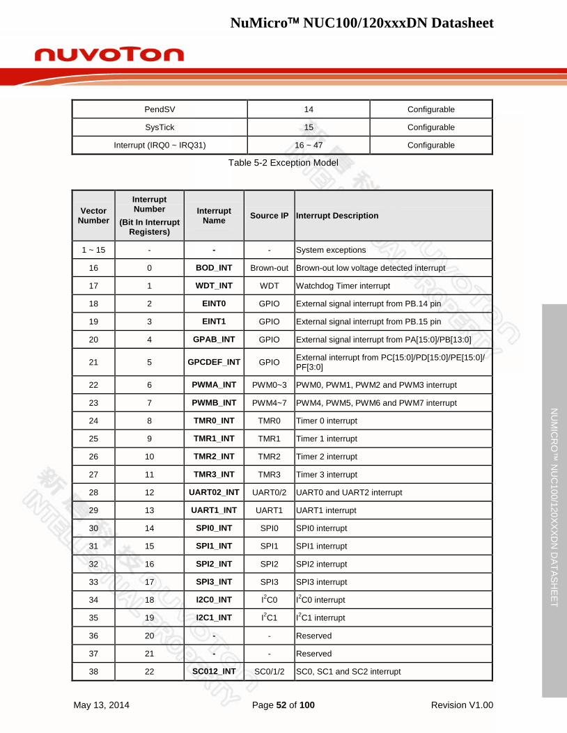
NuMicro NUC100/120xxxDN Datasheet
May 13, 2014 Page 52 of 100 Revision V1.00
NU
MIC
RO
™ N
UC
100/120XXXD
N D
ATASHEET
PendSV 14 Configurable
SysTick 15 Configurable
Interrupt (IRQ0 ~ IRQ31) 16 ~ 47 Configurable
Table 5-2 Exception Model
Vector Number
Interrupt Number
(Bit In Interrupt Registers)
Interrupt Name Source IP Interrupt Description
1 ~ 15 - - - System exceptions
16 0 BOD_INT Brown-out Brown-out low voltage detected interrupt
17 1 WDT_INT WDT Watchdog Timer interrupt
18 2 EINT0 GPIO External signal interrupt from PB.14 pin
19 3 EINT1 GPIO External signal interrupt from PB.15 pin
20 4 GPAB_INT GPIO External signal interrupt from PA[15:0]/PB[13:0]
21 5 GPCDEF_INT GPIO External interrupt from PC[15:0]/PD[15:0]/PE[15:0]/ PF[3:0]
22 6 PWMA_INT PWM0~3 PWM0, PWM1, PWM2 and PWM3 interrupt
23 7 PWMB_INT PWM4~7 PWM4, PWM5, PWM6 and PWM7 interrupt
24 8 TMR0_INT TMR0 Timer 0 interrupt
25 9 TMR1_INT TMR1 Timer 1 interrupt
26 10 TMR2_INT TMR2 Timer 2 interrupt
27 11 TMR3_INT TMR3 Timer 3 interrupt
28 12 UART02_INT UART0/2 UART0 and UART2 interrupt
29 13 UART1_INT UART1 UART1 interrupt
30 14 SPI0_INT SPI0 SPI0 interrupt
31 15 SPI1_INT SPI1 SPI1 interrupt
32 16 SPI2_INT SPI2 SPI2 interrupt
33 17 SPI3_INT SPI3 SPI3 interrupt
34 18 I2C0_INT I2C0 I2C0 interrupt
35 19 I2C1_INT I2C1 I2C1 interrupt
36 20 - - Reserved
37 21 - - Reserved
38 22 SC012_INT SC0/1/2 SC0, SC1 and SC2 interrupt
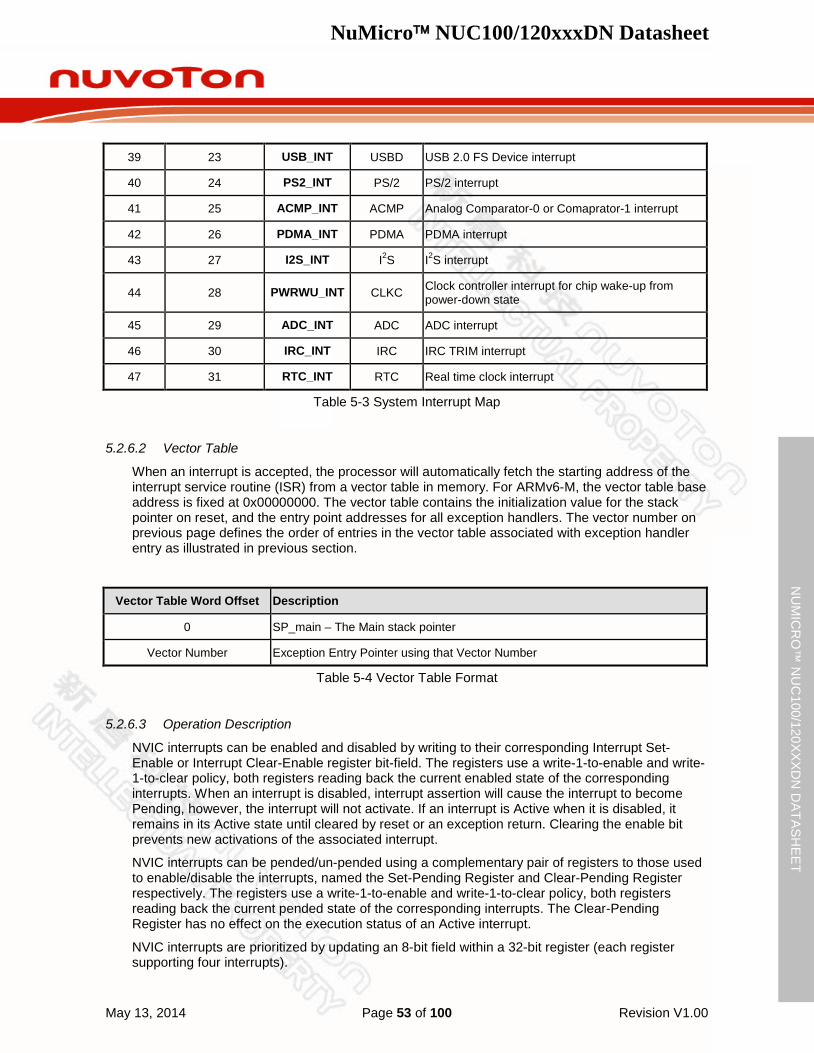
NuMicro NUC100/120xxxDN Datasheet
May 13, 2014 Page 53 of 100 Revision V1.00
NU
MIC
RO
™ N
UC
100/120XXXD
N D
ATASHEET
39 23 USB_INT USBD USB 2.0 FS Device interrupt
40 24 PS2_INT PS/2 PS/2 interrupt
41 25 ACMP_INT ACMP Analog Comparator-0 or Comaprator-1 interrupt
42 26 PDMA_INT PDMA PDMA interrupt
43 27 I2S_INT I2S I2S interrupt
44 28 PWRWU_INT CLKC Clock controller interrupt for chip wake-up from power-down state
45 29 ADC_INT ADC ADC interrupt
46 30 IRC_INT IRC IRC TRIM interrupt
47 31 RTC_INT RTC Real time clock interrupt
Table 5-3 System Interrupt Map
Vector Table 5.2.6.2
When an interrupt is accepted, the processor will automatically fetch the starting address of the interrupt service routine (ISR) from a vector table in memory. For ARMv6-M, the vector table base address is fixed at 0x00000000. The vector table contains the initialization value for the stack pointer on reset, and the entry point addresses for all exception handlers. The vector number on previous page defines the order of entries in the vector table associated with exception handler entry as illustrated in previous section.
Vector Table Word Offset Description
0 SP_main – The Main stack pointer
Vector Number Exception Entry Pointer using that Vector Number
Table 5-4 Vector Table Format
Operation Description 5.2.6.3
NVIC interrupts can be enabled and disabled by writing to their corresponding Interrupt Set-Enable or Interrupt Clear-Enable register bit-field. The registers use a write-1-to-enable and write-1-to-clear policy, both registers reading back the current enabled state of the corresponding interrupts. When an interrupt is disabled, interrupt assertion will cause the interrupt to become Pending, however, the interrupt will not activate. If an interrupt is Active when it is disabled, it remains in its Active state until cleared by reset or an exception return. Clearing the enable bit prevents new activations of the associated interrupt.
NVIC interrupts can be pended/un-pended using a complementary pair of registers to those used to enable/disable the interrupts, named the Set-Pending Register and Clear-Pending Register respectively. The registers use a write-1-to-enable and write-1-to-clear policy, both registers reading back the current pended state of the corresponding interrupts. The Clear-Pending Register has no effect on the execution status of an Active interrupt.
NVIC interrupts are prioritized by updating an 8-bit field within a 32-bit register (each register supporting four interrupts).
NuMicro NUC100/120xxxDN Datasheet
May 13, 2014 Page 54 of 100 Revision V1.00
NU
MIC
RO
™ N
UC
100/120XXXD
N D
ATASHEET
The general registers associated with the NVIC are all accessible from a block of memory in the System Control Space and will be described in next section.
NuMicro NUC100/120xxxDN Datasheet
May 13, 2014 Page 55 of 100 Revision V1.00
NU
MIC
RO
™ N
UC
100/120XXXD
N D
ATASHEET
Clock Controller 5.3
5.3.1 Overview
The clock controller generates the clocks for the whole chip, including system clocks and all peripheral clocks. The clock controller also implements the power control function with the individually clock ON/OFF control, clock source selection and clock divider. The chip enters Power-down mode when Cortex™-M0 core executes the WFI instruction only if the PWR_DOWN_EN (PWRCON[7]) bit and PD_WAIT_CPU (PWRCON[8]) bit are both set to 1. After that, chip enters Power-down mode and wait for wake-up interrupt source triggered to leave Power-down mode. In the Power-down mode, the clock controller turns off the external 4~24 MHz high speed crystal and internal 22.1184 MHz high speed oscillator to reduce the overall system power consumption.
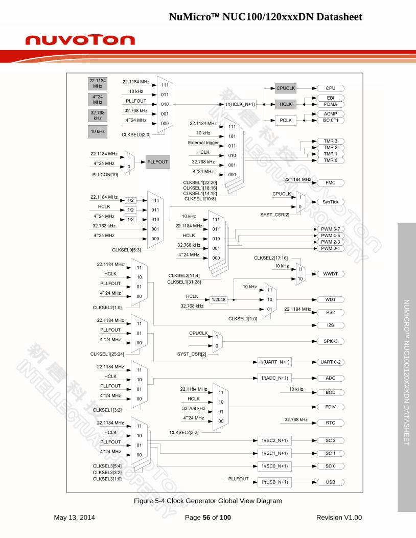
NuMicro NUC100/120xxxDN Datasheet
May 13, 2014 Page 56 of 100 Revision V1.00
NU
MIC
RO
™ N
UC
100/120XXXD
N D
ATASHEET
1
0
PLLCON[19]
22.1184 MHz
4~24 MHz
PLLFOUT
111
011
010
001
4~24 MHz
32.768 kHz
4~24 MHz
HCLK
22.1184 MHz
000
1/2
1/2
1/2
CLKSEL0[5:3]
1
0SysTick
TMR 0
ADC
UART 0-2
PDMA
ACMPI2C 0~1
I2S
RTC
PWM 0-1
WDT
PWM 2-3PWM 4-5PWM 6-7
TMR 3TMR 2TMR 1
CPU
FMC
32.768 kHz
10 kHz
011
010
001
000
HCLK
32.768 kHz
4~24 MHz
111
011
010
001
PLLFOUT
32.768 kHz
4~24 MHz
10 kHz
22.1184 MHz
000
CLKSEL0[2:0]
SYST_CSR[2]
CPUCLK
1/(HCLK_N+1)
PCLK
CPUCLK
HCLK
11
01
00
PLLFOUT
4~24 MHz
HCLK
CLKSEL1[3:2]
External trigger
CLKSEL1[22:20]CLKSEL1[18:16]CLKSEL1[14:12]CLKSEL1[10:8]
11
10
01
00
HCLK
PLLFOUT
4~24 MHz
22.1184 MHz
011
010
001
000
HCLK
4~24 MHz
22.1184 MHz
32.768 kHz
22.1184 MHz
32.768 kHz
WWDT
10 kHz
1/(ADC_N+1)
CLKSEL2[1:0]
11
10
CLKSEL1[1:0]
HCLK1/2048
1/(UART_N+1)
22.1184 MHz
4~24 MHz
0132.768 kHz
11
01
00
PLLFOUT
4~24 MHz
22.1184 MHz
CLKSEL1[25:24]
22.1184 MHz
10
11
01
00
PLLFOUT
4~24 MHz
HCLK
CLKSEL3[5:4]
22.1184 MHz
10SC 21/(SC2_N+1)
CLKSEL3[3:2]CLKSEL3[1:0]
SC 11/(SC1_N+1)
SC 01/(SC0_N+1)
10 kHz
22.1184 MHz
101
111
1
0SPI0-3
SYST_CSR[2]
CPUCLK
USB1/(USB_N+1)PLLFOUT
11
10
01
00
HCLK
4~24 MHz
22.1184 MHz
32.768 kHz
CLKSEL2[3:2]
FDIV
BOD10 kHz
11
10
CLKSEL2[17:16]
10 kHz
CLKSEL2[11:4]CLKSEL1[31:28]
10 kHz111
PS222.1184 MHz
EBI
Figure 5-4 Clock Generator Global View Diagram
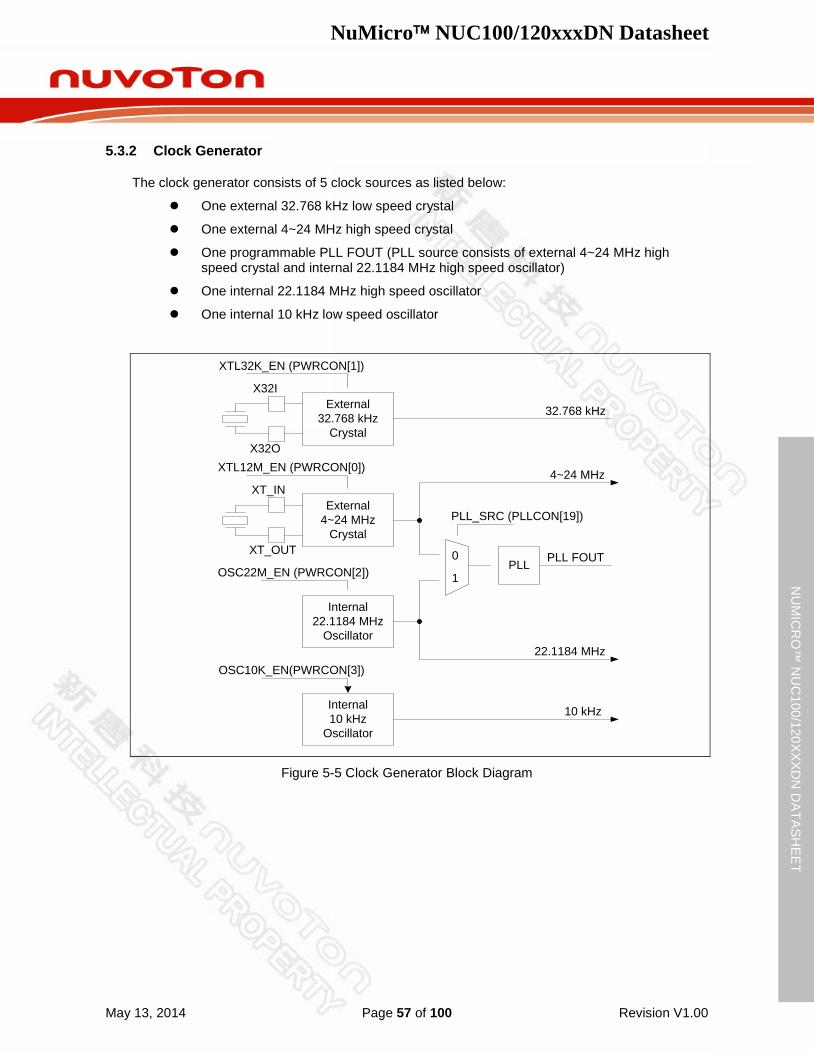
NuMicro NUC100/120xxxDN Datasheet
May 13, 2014 Page 57 of 100 Revision V1.00
NU
MIC
RO
™ N
UC
100/120XXXD
N D
ATASHEET
5.3.2 Clock Generator
The clock generator consists of 5 clock sources as listed below:
One external 32.768 kHz low speed crystal
One external 4~24 MHz high speed crystal
One programmable PLL FOUT (PLL source consists of external 4~24 MHz high speed crystal and internal 22.1184 MHz high speed oscillator)
One internal 22.1184 MHz high speed oscillator
One internal 10 kHz low speed oscillator
XT_OUT
External 4~24 MHz
Crystal
XTL12M_EN (PWRCON[0])
XT_IN
Internal 22.1184 MHz
Oscillator
OSC22M_EN (PWRCON[2])0
1PLL
PLL_SRC (PLLCON[19])
PLL FOUT
X32O
External 32.768 kHz
Crystal
32.768 kHz
XTL32K_EN (PWRCON[1])
X32I
Internal 10 kHz
Oscillator
OSC10K_EN(PWRCON[3])
4~24 MHz
22.1184 MHz
10 kHz
Figure 5-5 Clock Generator Block Diagram
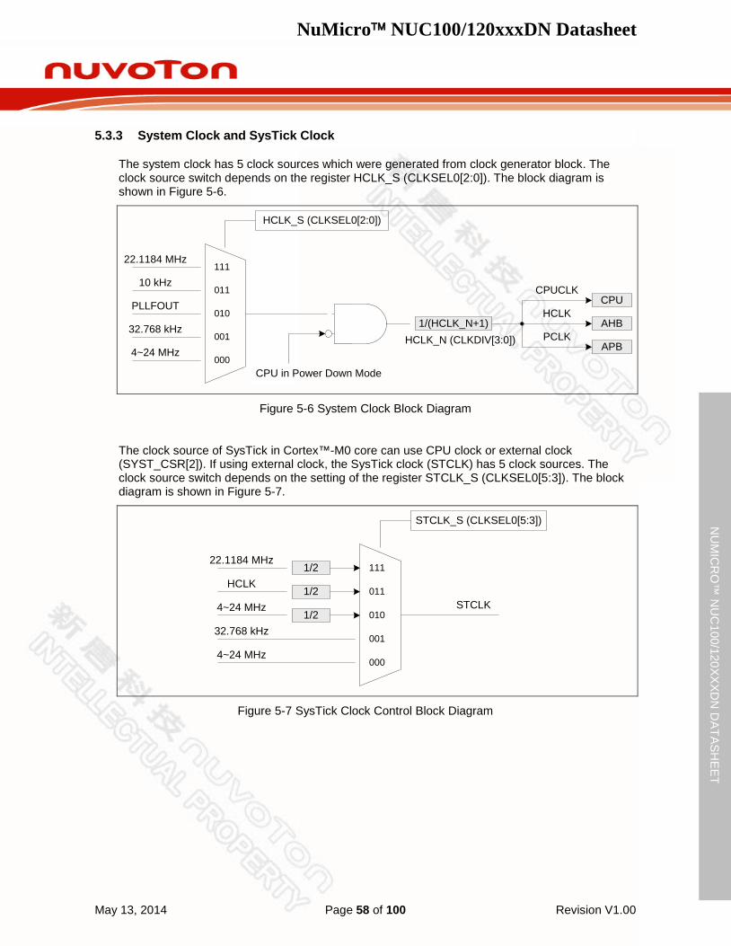
NuMicro NUC100/120xxxDN Datasheet
May 13, 2014 Page 58 of 100 Revision V1.00
NU
MIC
RO
™ N
UC
100/120XXXD
N D
ATASHEET
5.3.3 System Clock and SysTick Clock
The system clock has 5 clock sources which were generated from clock generator block. The clock source switch depends on the register HCLK_S (CLKSEL0[2:0]). The block diagram is shown in Figure 5-6.
111
011
010
001
PLLFOUT
32.768 kHz
4~24 MHz
10 kHz
HCLK_S (CLKSEL0[2:0])
22.1184 MHz
000
1/(HCLK_N+1)HCLK_N (CLKDIV[3:0])
CPU in Power Down Mode
CPU
AHB
APB
CPUCLK
HCLK
PCLK
Figure 5-6 System Clock Block Diagram
The clock source of SysTick in Cortex™-M0 core can use CPU clock or external clock (SYST_CSR[2]). If using external clock, the SysTick clock (STCLK) has 5 clock sources. The clock source switch depends on the setting of the register STCLK_S (CLKSEL0[5:3]). The block diagram is shown in Figure 5-7.
111
011
010
001
4~24 MHz
32.768 kHz
4~24 MHz
HCLK
STCLK_S (CLKSEL0[5:3])
STCLK
22.1184 MHz
000
1/2
1/2
1/2
Figure 5-7 SysTick Clock Control Block Diagram
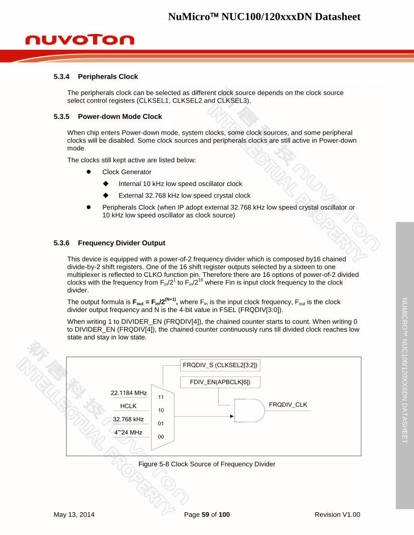
NuMicro NUC100/120xxxDN Datasheet
May 13, 2014 Page 59 of 100 Revision V1.00
NU
MIC
RO
™ N
UC
100/120XXXD
N D
ATASHEET
5.3.4 Peripherals Clock
The peripherals clock can be selected as different clock source depends on the clock source select control registers (CLKSEL1, CLKSEL2 and CLKSEL3).
5.3.5 Power-down Mode Clock
When chip enters Power-down mode, system clocks, some clock sources, and some peripheral clocks will be disabled. Some clock sources and peripherals clocks are still active in Power-down mode.
The clocks still kept active are listed below:
Clock Generator
Internal 10 kHz low speed oscillator clock
External 32.768 kHz low speed crystal clock
Peripherals Clock (when IP adopt external 32.768 kHz low speed crystal oscillator or 10 kHz low speed oscillator as clock source)
5.3.6 Frequency Divider Output
This device is equipped with a power-of-2 frequency divider which is composed by16 chained divide-by-2 shift registers. One of the 16 shift register outputs selected by a sixteen to one multiplexer is reflected to CLKO function pin. Therefore there are 16 options of power-of-2 divided clocks with the frequency from Fin/21 to Fin/216 where Fin is input clock frequency to the clock divider.
The output formula is Fout = Fin/2(N+1), where Fin is the input clock frequency, Fout is the clock divider output frequency and N is the 4-bit value in FSEL (FRQDIV[3:0]).
When writing 1 to DIVIDER_EN (FRQDIV[4]), the chained counter starts to count. When writing 0 to DIVIDER_EN (FRQDIV[4]), the chained counter continuously runs till divided clock reaches low state and stay in low state.
11
10
01
00
HCLK
32.768 kHz
4~24 MHz
22.1184 MHz
FRQDIV_S (CLKSEL2[3:2])
FDIV_EN(APBCLK[6])
FRQDIV_CLK
Figure 5-8 Clock Source of Frequency Divider
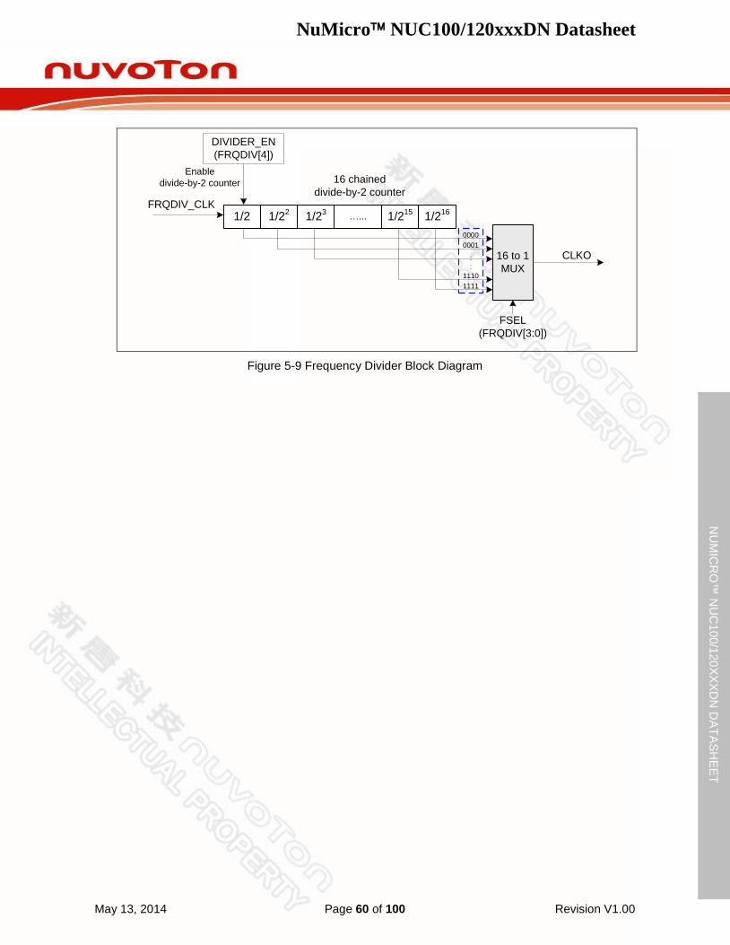
NuMicro NUC100/120xxxDN Datasheet
May 13, 2014 Page 60 of 100 Revision V1.00
NU
MIC
RO
™ N
UC
100/120XXXD
N D
ATASHEET
00000001
11101111
::
16 to 1MUX
1/2 1/22 1/23 1/215 1/216…...
FSEL (FRQDIV[3:0])
CLKO
FRQDIV_CLK
16 chaineddivide-by-2 counter
DIVIDER_EN (FRQDIV[4])
Enabledivide-by-2 counter
Figure 5-9 Frequency Divider Block Diagram
NuMicro NUC100/120xxxDN Datasheet
May 13, 2014 Page 61 of 100 Revision V1.00
NU
MIC
RO
™ N
UC
100/120XXXD
N D
ATASHEET
USB Device Controller (USB) 5.4
5.4.1 Overview
There is one set of USB 2.0 full-speed device controller and transceiver in this device. It is compliant with USB 2.0 full-speed device specification and supports control/bulk/interrupt/ isochronous transfer types.
In this device controller, there are two main interfaces: the APB bus and USB bus which comes from the USB PHY transceiver. For the APB bus, the CPU can program control registers through it. There are 512 bytes internal SRAM as data buffer in this controller. For IN or OUT transfer, it is necessary to write data to SRAM or read data from SRAM through the APB interface or SIE. User needs to set the effective starting address of SRAM for each endpoint buffer through “buffer segmentation register (USB_BUFSEGx)”.
There are 6 endpoints in this controller. Each of the endpoint can be configured as IN or OUT endpoint. All the operations including Control, Bulk, Interrupt and Isochronous transfer are implemented in this block. The block of ENDPOINT CONTROL is also used to manage the data sequential synchronization, endpoint states, current start address, transaction status, and data buffer status for each endpoint.
There are four different interrupt events in this controller. They are the wake-up function, device plug-in or plug-out event, USB events, like IN ACK, OUT ACK etc, and BUS events, like suspend and resume, etc. Any event will cause an interrupt, and users just need to check the related event flags in interrupt event status register (USB_INTSTS) to acknowledge what kind of interrupt occurring, and then check the related USB Endpoint Status Register (USB_EPSTS) to acknowledge what kind of event occurring in this endpoint.
A software-disable function is also supported for this USB controller. It is used to simulate the disconnection of this device from the host. If user enables DRVSE0 bit (USB_DRVSE0), the USB controller will force the output of USB_DP and USB_DM to level low and its function is disabled. After disable the DRVSE0 bit, host will enumerate the USB device again.
Please refer to Universal Serial Bus Specification Revision 1.1
5.4.2 Features
This Universal Serial Bus (USB) performs a serial interface with a single connector type for attaching all USB peripherals to the host system. Following is the feature list of this USB.
Compliant with USB 2.0 Full-Speed specification
Provides 1 interrupt vector with 4 different interrupt events (WAKEUP, FLDET, USB and BUS)
Supports Control/Bulk/Interrupt/Isochronous transfer type
Supports suspend function when no bus activity existing for 3 ms
Provides 6 endpoints for configurable Control/Bulk/Interrupt/Isochronous transfer types and maximum 512 bytes buffer size
Provides remote wake-up capability
NuMicro NUC100/120xxxDN Datasheet
May 13, 2014 Page 62 of 100 Revision V1.00
NU
MIC
RO
™ N
UC
100/120XXXD
N D
ATASHEET
General Purpose I/O (GPIO) 5.5
5.5.1 Overview
The NuMicro NUC100 series has up to 84 General Purpose I/O pins to be shared with other function pins depending on the chip configuration. These 84 pins are arranged in 6 ports named as GPIOA, GPIOB, GPIOC, GPIOD, GPIOE and GPIOF. The GPIOA/B/C/D/E port has the maximum of 16 pins and GPIOF port has the maximum of 4 pins. Each of the 84 pins is independent and has the corresponding register bits to control the pin mode function and data.
The I/O type of each of I/O pins can be configured by software individually as input, output, open-drain or Quasi-bidirectional mode. After reset, the I/O mode of all pins are depending on Config0[10] setting. In Quasi-bidirectional mode, I/O pin has a very weak individual pull-up resistor which is about 110~300 KΩ for VDD is from 5.0 V to 2.5 V.
5.5.2 Features
Four I/O modes:
Quasi-bidirectional
Push-Pull output
Open-Drain output
Input only with high impendence
TTL/Schmitt trigger input selectable by GPx_TYPE[15:0] in GPx_MFP[31:16]
I/O pin configured as interrupt source with edge/level setting
Configurable default I/O mode of all pins after reset by Config0[10] setting
If Config[10] is 0, all GPIO pins in input tri-state mode after chip reset
If Config[10] is 1, all GPIO pins in Quasi-bidirectional mode after chip reset
I/O pin internal pull-up resistor enabled only in Quasi-bidirectional I/O mode
Enabling the pin interrupt function will also enable the pin wake-up function.
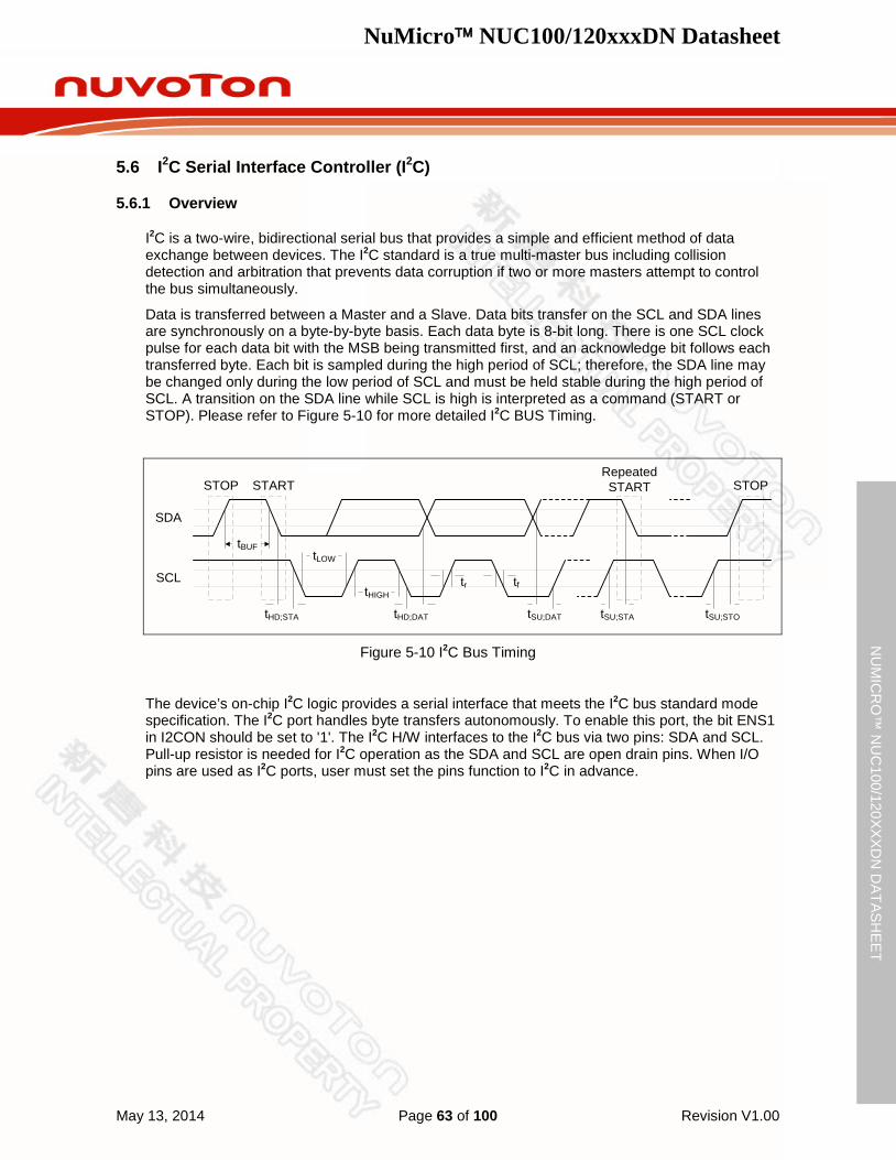
NuMicro NUC100/120xxxDN Datasheet
May 13, 2014 Page 63 of 100 Revision V1.00
NU
MIC
RO
™ N
UC
100/120XXXD
N D
ATASHEET
I2C Serial Interface Controller (I2C) 5.6
5.6.1 Overview
I2C is a two-wire, bidirectional serial bus that provides a simple and efficient method of data exchange between devices. The I2C standard is a true multi-master bus including collision detection and arbitration that prevents data corruption if two or more masters attempt to control the bus simultaneously.
Data is transferred between a Master and a Slave. Data bits transfer on the SCL and SDA lines are synchronously on a byte-by-byte basis. Each data byte is 8-bit long. There is one SCL clock pulse for each data bit with the MSB being transmitted first, and an acknowledge bit follows each transferred byte. Each bit is sampled during the high period of SCL; therefore, the SDA line may be changed only during the low period of SCL and must be held stable during the high period of SCL. A transition on the SDA line while SCL is high is interpreted as a command (START or STOP). Please refer to Figure 5-10 for more detailed I2C BUS Timing.
tBUF
STOP
SDA
SCL
START
tHD;STA
tLOW
tHD;DAT
tHIGHtf
tSU;DAT
Repeated START
tSU;STA tSU;STO
STOP
tr
Figure 5-10 I2C Bus Timing
The device’s on-chip I2C logic provides a serial interface that meets the I2C bus standard mode specification. The I2C port handles byte transfers autonomously. To enable this port, the bit ENS1 in I2CON should be set to '1'. The I2C H/W interfaces to the I2C bus via two pins: SDA and SCL. Pull-up resistor is needed for I2C operation as the SDA and SCL are open drain pins. When I/O pins are used as I2C ports, user must set the pins function to I2C in advance.
NuMicro NUC100/120xxxDN Datasheet
May 13, 2014 Page 64 of 100 Revision V1.00
NU
MIC
RO
™ N
UC
100/120XXXD
N D
ATASHEET
5.6.2 Features
The I2C bus uses two wires (SDA and SCL) to transfer information between devices connected to the bus. The main features of the bus include:
Master/Slave mode
Bidirectional data transfer between masters and slaves
Multi-master bus (no central master)
Arbitration between simultaneously transmitting masters without corruption of serial data on the bus
Serial clock synchronization allowing devices with different bit rates to communicate via one serial bus
Serial clock synchronization used as a handshake mechanism to suspend and resume serial transfer
A built-in 14-bit time-out counter requesting the I2C interrupt if the I2C bus hangs up and timer-out counter overflows
External pull-up resistors needed for high output
Programmable clocks allowing for versatile rate control
Supports 7-bit addressing mode
Supports multiple address recognition (four slave addresses with mask option)
NuMicro NUC100/120xxxDN Datasheet
May 13, 2014 Page 65 of 100 Revision V1.00
NU
MIC
RO
™ N
UC
100/120XXXD
N D
ATASHEET
PWM Generator and Capture Timer (PWM) 5.7
5.7.1 Overview
The NuMicro NUC100 series has 2 sets of PWM group supporting a total of 4 sets of PWM generators that can be configured as 8 independent PWM outputs, PWM0~PWM7, or as 4 complementary PWM pairs, (PWM0, PWM1), (PWM2, PWM3), (PWM4, PWM5) and (PWM6, PWM7) with 4 programmable Dead-zone generators.
Each PWM generator has one 8-bit prescaler, one clock divider with 5 divided frequencies (1, 1/2, 1/4, 1/8, 1/16), two PWM Timers including two clock selectors, two 16-bit PWM counters for PWM period control, two 16-bit comparators for PWM duty control and one Dead-zone generator. The 4 sets of PWM generators provide eight independent PWM interrupt flags set by hardware when the corresponding PWM period down counter reaches 0. Each PWM interrupt source with its corresponding enable bit can cause CPU to request PWM interrupt. The PWM generators can be configured as one-shot mode to produce only one PWM cycle signal or auto-reload mode to output PWM waveform continuously.
When PCR.DZEN01 is set, PWM0 and PWM1 perform complementary PWM paired function; the paired PWM period, duty and Dead-time are determined by PWM0 timer and Dead-zone generator 0. Similarly, the complementary PWM pairs of (PWM2, PWM3), (PWM4, PWM5) and (PWM6, PWM7) are controlled by PWM2, PWM4 and PWM6 timers and Dead-zone generator 2, 4 and 6, respectively.
To prevent PWM driving output pin with unsteady waveform, the 16-bit period down counter and 16-bit comparator are implemented with double buffer. When user writes data to counter/comparator buffer registers the updated value will be load into the 16-bit down counter/ comparator at the time down counter reaching 0. The double buffering feature avoids glitch at PWM outputs.
When the 16-bit period down counter reaches 0, the interrupt request is generated. If PWM-timer is set as auto-reload mode, when the down counter reaches 0, it is reloaded with PWM Counter Register (CNRx) automatically then start decreasing, repeatedly. If the PWM-timer is set as one-shot mode, the down counter will stop and generate one interrupt request when it reaches 0.
The value of PWM counter comparator is used for pulse high width modulation. The counter control logic changes the output to high level when down-counter value matches the value of compare register.
The alternate feature of the PWM-timer is digital input Capture function. If Capture function is enabled the PWM output pin is switched as capture input mode. The Capture0 and PWM0 share one timer which is included in PWM0 and the Capture1 and PWM1 share PWM1 timer, and etc. Therefore user must setup the PWM-timer before enable Capture feature. After capture feature is enabled, the capture always latched PWM-counter to Capture Rising Latch Register (CRLR) when input channel has a rising transition and latched PWM-counter to Capture Falling Latch Register (CFLR) when input channel has a falling transition. Capture channel 0 interrupt is programmable by setting CCR0.CRL_IE0[1] (Rising latch Interrupt enable) and CCR0.CFL_IE0[2]] (Falling latch Interrupt enable) to decide the condition of interrupt occur. Capture channel 1 has the same feature by setting CCR0.CRL_IE1[17] and CCR0.CFL_IE1[18]. And capture channel 2 to channel 3 on each group have the same feature by setting the corresponding control bits in CCR2. For each group, whenever Capture issues Interrupt 0/1/2/3, the PWM counter 0/1/2/3 will be reload at this moment.
The maximum captured frequency that PWM can capture is confined by the capture interrupt latency. When capture interrupt occurred, software will do at least three steps, including: Read PIIR to get interrupt source and Read CRLRx/CFLRx(x=0~3) to get capture value and finally write 1 to clear PIIR to 0. If interrupt latency will take time T0 to finish, the capture signal mustn’t transition during this interval (T0). In this case, the maximum capture frequency will be 1/T0. For
NuMicro NUC100/120xxxDN Datasheet
May 13, 2014 Page 66 of 100 Revision V1.00
NU
MIC
RO
™ N
UC
100/120XXXD
N D
ATASHEET
example:
HCLK = 50 MHz, PWM_CLK = 25 MHz, Interrupt latency is 900 ns
So the maximum capture frequency will be 1/900ns ≈ 1000 kHz
5.7.2 Features
PWM Function: 5.7.2.1
Up to 2 PWM groups (PWMA/PWMB) to support 8 PWM channels or 4 complementary PWM paired channels
Each PWM group has two PWM generators with each PWM generator supporting one 8-bit prescaler, two clock divider, two PWM-timers, one Dead-zone generator and two PWM outputs.
Up to 16-bit resolution
PWM Interrupt request synchronized with PWM period
One-shot or Auto-reload mode PWM
Edge-aligned type or Center-aligned type option
Capture Function: 5.7.2.2
Timing control logic shared with PWM Generators
Supports 8 Capture input channels shared with 8 PWM output channels
Each channel supports one rising latch register (CRLR), one falling latch register (CFLR) and Capture interrupt flag (CAPIFx)
NuMicro NUC100/120xxxDN Datasheet
May 13, 2014 Page 67 of 100 Revision V1.00
NU
MIC
RO
™ N
UC
100/120XXXD
N D
ATASHEET
Real Time Clock (RTC) 5.8
5.8.1 Overview
The Real Time Clock (RTC) controller provides user with the real time and calendar message. The clock source of RTC controller is from an external 32.768 kHz low speed crystal which connected at pins X32I and X32O (refer to pin Description) or from an external 32.768 kHz low speed oscillator output fed at pin X32I. The RTC controller provides the real time message (hour, minute, second) in TLR (RTC Time Loading Register) as well as calendar message (year, month, day) in CLR (RTC Calendar Loading Register). It also offers RTC alarm function that user can preset the alarm time in TAR (RTC Time Alarm Register) and alarm calendar in CAR (RTC Calendar Alarm Register). The data format of RTC time and calendar message are all expressed in BCD format.
The RTC controller supports periodic RTC Time Tick and Alarm Match interrupts. The periodic RTC Time Tick interrupt has 8 period interval options 1/128, 1/64, 1/32, 1/16, 1/8, 1/4, 1/2 and 1 second which are selected by TTR (TTR[2:0] Time Tick Register). When real time and calendar message in TLR and CLR are equal to alarm time and calendar settings in TAR and CAR, the AIF (RIIR [0] RTC Alarm Interrupt Flag) is set to 1 and the RTC alarm interrupt signal is generated if the AIER (RIER [0] Alarm Interrupt Enable) is enabled.
Both RTC Time Tick and Alarm Match interrupt signal can cause chip to wake-up from Idle or Power-down mode if the correlate interrupt enable bit (AIER or TIER) is set to 1 before chip enters Idle or Power-down mode.
5.8.2 Features
Supports real time counter in TLR (hour, minute, second) and calendar counter in CLR (year, month, day) for RTC time and calendar check
Supports alarm time (hour, minute, second) and calendar (year, month, day) settings in TAR and CAR
Selectable 12-hour or 24-hour time scale in TSSR register
Supports Leap Year indication in LIR register
Supports Day of the Week counter in DWR register
Frequency of RTC clock source compensate by FCR register
All time and calendar message expressed in BCD format
Supports periodic RTC Time Tick interrupt with 8 period interval options 1/128, 1/64, 1/32, 1/16, 1/8, 1/4, 1/2 and 1 second
Supports RTC Time Tick and Alarm Match interrupt
Supports chip wake-up from Idle or Power-down mode while a RTC interrupt signal is generated
NuMicro NUC100/120xxxDN Datasheet
May 13, 2014 Page 68 of 100 Revision V1.00
NU
MIC
RO
™ N
UC
100/120XXXD
N D
ATASHEET
Serial Peripheral Interface (SPI) 5.9
5.9.1 Overview
The Serial Peripheral Interface (SPI) is a synchronous serial data communication protocol that operates in full duplex mode. Devices communicate in Master/Slave mode with the 4-wire bi-direction interface. The NuMicro NUC100 series contains up to four sets of SPI controllers performing a serial-to-parallel conversion on data received from a peripheral device, and a parallel-to-serial conversion on data transmitted to a peripheral device. Each set of SPI controller can be configured as a master or a slave device.
The SPI controller supports the variable serial clock function for special applications and 2-bit Transfer mode to connect 2 off-chip slave devices at the same time. This controller also supports the PDMA function to access the data buffer and also supports Dual I/O Transfer mode.
5.9.2 Features
Up to four sets of SPI controllers
Supports Master or Slave mode operation
Supports 2-bit Transfer mode
Supports Dual I/O Transfer mode
Configurable bit length of a transfer word from 8 to 32-bit
Provides separate 8-layer depth transmit and receive FIFO buffers
Supports MSB first or LSB first transfer sequence
Two slave select lines in Master mode
Supports the byte reorder function
Supports Byte or Word Suspend mode
Variable output serial clock frequency in Master mode
Supports PDMA transfer
Supports 3-wire, no slave select signal, bi-direction interface
NuMicro NUC100/120xxxDN Datasheet
May 13, 2014 Page 69 of 100 Revision V1.00
NU
MIC
RO
™ N
UC
100/120XXXD
N D
ATASHEET
Timer Controller (TMR) 5.10
5.10.1 Overview
The timer controller includes four 32-bit timers, TIMER0~TIMER3, allowing user to easily implement a timer control for applications. The timer can perform functions, such as frequency measurement, event counting, interval measurement, clock generation, and delay timing. The timer can generate an interrupt signal upon time-out, or provide the current value during operation.
5.10.2 Features
Four sets of 32-bit timers with 24-bit up counter and one 8-bit prescale counter
Independent clock source for each timer
Provides one-shot, periodic, toggle and continuous counting operation modes
Time-out period = (Period of timer clock input) * (8-bit prescale counter + 1) * (24-bit TCMP)
Maximum counting cycle time = (1 / T MHz) * (28) * (224), T is the period of timer clock
24-bit up counter value is readable through TDR (Timer Data Register)
Supports event counting function to count the event from external pin
Supports external pin capture function for interval measurement
Supports external pin capture function for reset timer counter
Supports chip wake-up from Idle/Power-down mode if a timer interrupt signal is generated (TIF set to 1)
NuMicro NUC100/120xxxDN Datasheet
May 13, 2014 Page 70 of 100 Revision V1.00
NU
MIC
RO
™ N
UC
100/120XXXD
N D
ATASHEET
Watchdog Timer (WDT) 5.11
5.11.1 Overview
The purpose of Watchdog Timer is to perform a system reset when system runs into an unknown state. This prevents system from hanging for an infinite period of time. Besides, this Watchdog Timer supports the function to wake-up system from Idle/Power-down mode.
5.11.2 Features
18-bit free running up counter for Watchdog Timer time-out interval.
Selectable time-out interval (24 ~ 218) and the time-out interval is 104 ms ~ 26.3168 s if WDT_CLK = 10 kHz.
System kept in reset state for a period of (1 / WDT_CLK) * 63
Supports selectable Watchdog Timer reset delay period, it includes (1024+2)、(128+2) 、(16+2) or (1+2) WDT_CLK reset delay period.
Supports force Watchdog Timer enabled after chip powered on or reset while CWDTEN (Config0[31] watchdog enable) bit is set to 0.
Supports Watchdog Timer time-out wake-up function when WDT clock source is selected to 10 kHz low speed oscillator.
NuMicro NUC100/120xxxDN Datasheet
May 13, 2014 Page 71 of 100 Revision V1.00
NU
MIC
RO
™ N
UC
100/120XXXD
N D
ATASHEET
Window Watchdog Timer (WWDT) 5.12
5.12.1 Overview
The purpose of Window Watchdog Timer is to perform a system reset within a specified window period to prevent software run to uncontrollable status by any unpredictable condition.
5.12.2 Features
6-bit down counter (WWDTVAL[5:0]) and 6-bit compare value (WWDTCR[21:16] – WINCMP value) to make the window period flexible
Selectable maximum 11-bit WWDT clock prescale (WWDTCR[11:8] – PERIODSEL value) to make WWDT time-out interval variable
NuMicro NUC100/120xxxDN Datasheet
May 13, 2014 Page 72 of 100 Revision V1.00
NU
MIC
RO
™ N
UC
100/120XXXD
N D
ATASHEET
UART Interface Controller (UART) 5.13The NuMicro NUC100 series provides up to three channels of Universal Asynchronous Receiver/Transmitters (UART). UART0 supports High Speed UART and UART1~2 perform Normal Speed UART. Besides, only UART0 and UART1 support the flow control function.
5.13.1 Overview
The Universal Asynchronous Receiver/Transmitter (UART) performs a serial-to-parallel conversion on data received from the peripheral, and a parallel-to-serial conversion on data transmitted from the CPU. The UART controller also supports IrDA SIR, LIN master/slave mode and RS-485 mode functions. Each UART channel supports seven types of interrupts including:
Transmitter FIFO empty interrupt (INT_THRE)
Receiver threshold level reached interrupt (INT_RDA),
Line status interrupt (parity error or frame error or break interrupt) (INT_RLS),
Receiver buffer time-out interrupt (INT_TOUT),
MODEM/Wake-up status interrupt (INT_MODEM),
Buffer error interrupt (INT_BUF_ERR)
LIN interrupt (INT_LIN)
Interrupts of UART0 and UART2 share the interrupt number 12 (vector number is 28); Interrupt number 13 (vector number is 29) only supports UART1 interrupt. Refer to the Nested Vectored Interrupt Controller chapter for System Interrupt Map.
The UART0 is built-in with a 64-byte transmitter FIFO (TX_FIFO) and a 64-byte receiver FIFO (RX_FIFO) that reduces the number of interrupts presented to the CPU. The UART1~2 are equipped with 16-byte transmitter FIFO (TX_FIFO) and 16-byte receiver FIFO (RX_FIFO). The CPU can read the status of the UART at any time during the operation. The reported status information includes the type and condition of the transfer operations being performed by the UART, as well as 4 error conditions (parity error, frame error, break interrupt and buffer error) probably occur while receiving data. The UART includes a programmable baud rate generator that is capable of dividing clock input by divisors to produce the serial clock that transmitter and receiver need. The baud rate equation is Baud Rate = UART_CLK / M * [BRD + 2], where M and BRD are defined in Baud Rate Divider Register (UA_BAUD). Table 5-10 lists the equations in the various conditions and Table 5-11 lists the UART baud rate setting table.
Mode DIV_X_EN DIV_X_ONE Divider X BRD Baud Rate Equation
0 0 0 Don’t care A UART_CLK / [16 * (A+2)]
1 1 0 B A UART_CLK / [(B+1) * (A+2)] , B must >= 8
2 1 1 Don’t care A UART_CLK / (A+2), A must >=3
Table 5-5 UART Baud Rate Equation
System Clock = Internal 22.1184 MHz High Speed Oscillator
Baud Rate Mode 0 Mode 1 Mode 2
Parameter Register Parameter Register Parameter Register
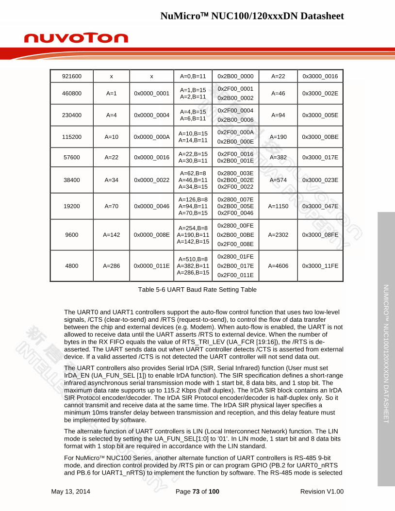
NuMicro NUC100/120xxxDN Datasheet
May 13, 2014 Page 73 of 100 Revision V1.00
NU
MIC
RO
™ N
UC
100/120XXXD
N D
ATASHEET
921600 x x A=0,B=11 0x2B00_0000 A=22 0x3000_0016
460800 A=1 0x0000_0001 A=1,B=15 A=2,B=11
0x2F00_0001 0x2B00_0002
A=46 0x3000_002E
230400 A=4 0x0000_0004 A=4,B=15 A=6,B=11
0x2F00_0004 0x2B00_0006
A=94 0x3000_005E
115200 A=10 0x0000_000A A=10,B=15 A=14,B=11
0x2F00_000A 0x2B00_000E
A=190 0x3000_00BE
57600 A=22 0x0000_0016 A=22,B=15 A=30,B=11
0x2F00_0016 0x2B00_001E A=382 0x3000_017E
38400 A=34 0x0000_0022 A=62,B=8 A=46,B=11 A=34,B=15
0x2800_003E 0x2B00_002E 0x2F00_0022
A=574 0x3000_023E
19200 A=70 0x0000_0046 A=126,B=8 A=94,B=11 A=70,B=15
0x2800_007E 0x2B00_005E 0x2F00_0046
A=1150 0x3000_047E
9600 A=142 0x0000_008E A=254,B=8
A=190,B=11 A=142,B=15
0x2800_00FE 0x2B00_00BE 0x2F00_008E
A=2302 0x3000_08FE
4800 A=286 0x0000_011E A=510,B=8
A=382,B=11 A=286,B=15
0x2800_01FE 0x2B00_017E 0x2F00_011E
A=4606 0x3000_11FE
Table 5-6 UART Baud Rate Setting Table
The UART0 and UART1 controllers support the auto-flow control function that uses two low-level signals, /CTS (clear-to-send) and /RTS (request-to-send), to control the flow of data transfer between the chip and external devices (e.g. Modem). When auto-flow is enabled, the UART is not allowed to receive data until the UART asserts /RTS to external device. When the number of bytes in the RX FIFO equals the value of RTS_TRI_LEV (UA_FCR [19:16]), the /RTS is de-asserted. The UART sends data out when UART controller detects /CTS is asserted from external device. If a valid asserted /CTS is not detected the UART controller will not send data out.
The UART controllers also provides Serial IrDA (SIR, Serial Infrared) function (User must set IrDA_EN (UA_FUN_SEL [1]) to enable IrDA function). The SIR specification defines a short-range infrared asynchronous serial transmission mode with 1 start bit, 8 data bits, and 1 stop bit. The maximum data rate supports up to 115.2 Kbps (half duplex). The IrDA SIR block contains an IrDA SIR Protocol encoder/decoder. The IrDA SIR Protocol encoder/decoder is half-duplex only. So it cannot transmit and receive data at the same time. The IrDA SIR physical layer specifies a minimum 10ms transfer delay between transmission and reception, and this delay feature must be implemented by software.
The alternate function of UART controllers is LIN (Local Interconnect Network) function. The LIN mode is selected by setting the UA_FUN_SEL[1:0] to ’01’. In LIN mode, 1 start bit and 8 data bits format with 1 stop bit are required in accordance with the LIN standard.
For NuMicro NUC100 Series, another alternate function of UART controllers is RS-485 9-bit mode, and direction control provided by /RTS pin or can program GPIO (PB.2 for UART0_nRTS and PB.6 for UART1_nRTS) to implement the function by software. The RS-485 mode is selected
NuMicro NUC100/120xxxDN Datasheet
May 13, 2014 Page 74 of 100 Revision V1.00
NU
MIC
RO
™ N
UC
100/120XXXD
N D
ATASHEET
by setting the UA_FUN_SEL register to select RS-485 function. The RS-485 transceiver control is implemented using the /RTS control signal from an asynchronous serial port to enable the RS-485 transceiver. In RS-485 mode, many characteristics of the receiving and transmitting are same as UART.
5.13.2 Features
Full duplex, asynchronous communications
Separates receive / transmit 64/16/16 bytes (UART0/UART1/UART2) entry FIFO for data payloads
Supports hardware auto flow control/flow control function (CTS, RTS) and programmable RTS flow control trigger level (UART0 and UART1 support)
Programmable receiver buffer trigger level
Supports programmable baud-rate generator for each channel individually
Supports CTS wake-up function (UART0 and UART1 support)
Supports 7-bit receiver buffer time-out detection function
UART0/UART1 can through DMA channels to receive/transmit data
Programmable transmitting data delay time between the last stop and the next start bit by setting UA_TOR [DLY] register
Supports break error, frame error, parity error and receive / transmit buffer overflow detect function
Fully programmable serial-interface characteristics
Programmable data bit length, 5-, 6-, 7-, 8-bit character
Programmable parity bit, even, odd, no parity or stick parity bit generation and detection
Programmable stop bit length, 1, 1.5, or 2 stop bit generation
IrDA SIR function mode
Supports 3-/16-bit duration for normal mode
LIN function mode
Supports LIN master/slave mode
Supports programmable break generation function for transmitter
Supports break detect function for receiver
RS-485 function mode.
Supports RS-485 9-bit mode
Supports hardware or software direct enable control provided by RTS pin
NuMicro NUC100/120xxxDN Datasheet
May 13, 2014 Page 75 of 100 Revision V1.00
NU
MIC
RO
™ N
UC
100/120XXXD
N D
ATASHEET
PS/2 Device Controller (PS2D) 5.14
5.14.1 Overview
PS/2 device controller provides a basic timing control for PS/2 communication. All communication between the device and the host is managed through the CLK and DATA pins. Unlike PS/2 keyboard or mouse device controller, the receive/transmit code needs to be translated as meaningful code by firmware. The device controller generates the CLK signal after receiving a “Request to Send” state, but host has ultimate control over communication. Data of DATA line sent from the host to the device is read on the rising edge and sent from the device to the host is change after rising edge. A 16 bytes FIFO is used to reduce CPU intervention. Software can select 1 to 16 bytes for a continuous transmission.
5.14.2 Features
Host communication inhibit and Request to Send state detection
Reception frame error detection
Programmable 1 to 16 bytes transmit buffer to reduce CPU intervention
Double buffer for data reception
Software override bus
NuMicro NUC100/120xxxDN Datasheet
May 13, 2014 Page 76 of 100 Revision V1.00
NU
MIC
RO
™ N
UC
100/120XXXD
N D
ATASHEET
I2S Controller (I2S) 5.15
5.15.1 Overview
The I2S controller consists of I2S protocol to interface with external audio CODEC. Two 8-word deep FIFO for read path and write path respectively and is capable of handling 8-, 16-, 24- and 32-bit word sizes. PDMA controller handles the data movement between FIFO and memory.
5.15.2 Features
Operated as either Master or Slave
Capable of handling 8-, 16-, 24- and 32-bit word sizes
Supports Mono and stereo audio data
Supports I2S and MSB justified data format
Provides two 8-word FIFO data buffers, one for transmitting and the other for receiving
Generates interrupt requests when buffer levels cross a programmable boundary
Two PDMA requests, one for transmitting and the other for receiving
NuMicro NUC100/120xxxDN Datasheet
May 13, 2014 Page 77 of 100 Revision V1.00
NU
MIC
RO
™ N
UC
100/120XXXD
N D
ATASHEET
Analog-to-Digital Converter (ADC) 5.16
5.16.1 Overview
The NuMicro NUC100 Series contains one 12-bit successive approximation analog-to-digital converters (SAR A/D converter) with 8 input channels. The A/D converter supports three operation modes: single, single-cycle scan and continuous scan mode. The A/D converter can be started by software, PWM Center-aligned trigger and external STADC pin.
5.16.2 Features
Analog input voltage range: 0~VREF
12-bit resolution and 10-bit accuracy is guaranteed
Up to 8 single-end analog input channels or 4 differential analog input channels
Up to 760 kSPS conversion rate as ADC clock frequency is 16 MHz (chip working at 5V)
Three operating modes
Single mode: A/D conversion is performed one time on a specified channel
Single-cycle scan mode: A/D conversion is performed one cycle on all specified channels with the sequence from the smallest numbered channel to the largest numbered channel
Continuous scan mode: A/D converter continuously performs Single-cycle scan mode until software stops A/D conversion
An A/D conversion can be started by:
Writing 1 to ADST bit through software
PWM Center-aligned trigger
External pin STADC
Conversion results are held in data registers for each channel with valid and overrun indicators
Conversion result can be compared with specify value and user can select whether to generate an interrupt when conversion result matches the compare register setting
Channel 7 supports 3 input sources: external analog voltage, internal Band-gap voltage, and internal temperature sensor output
NuMicro NUC100/120xxxDN Datasheet
May 13, 2014 Page 78 of 100 Revision V1.00
NU
MIC
RO
™ N
UC
100/120XXXD
N D
ATASHEET
Analog Comparator (ACMP) 5.17
5.17.1 Overview
The NuMicro NUC100 Series contains two comparators which can be used in a number of different configurations. The comparator output is logic 1 when positive input voltage is greater than negative input voltage; otherwise the output is logic 0. Each comparator can be configured to cause an interrupt when the comparator output value changes.
5.17.2 Features
Analog input voltage range: 0~ VDDA
Supports Hysteresis function
Supports optional internal reference voltage input at negative end for each comparator
NuMicro NUC100/120xxxDN Datasheet
May 13, 2014 Page 79 of 100 Revision V1.00
NU
MIC
RO
™ N
UC
100/120XXXD
N D
ATASHEET
PDMA Controller (PDMA) 5.18
5.18.1 Overview
The NuMicro NUC100 series DMA contains nine-channel peripheral direct memory access (PDMA) controller and a cyclic redundancy check (CRC) generator.
The PDMA that transfers data to and from memory or transfer data to and from APB devices. For PDMA channel (PDMA CH0~CH8), there is one-word buffer as transfer buffer between the Peripherals APB devices and Memory. Software can stop the PDMA operation by disable PDMA PDMA_CSRx[PDMACEN]. The CPU can recognize the completion of a PDMA operation by software polling or when it receives an internal PDMA interrupt. The PDMA controller can increase source or destination address or fixed them as well.
The DMA controller contains a cyclic redundancy check (CRC) generator that can perform CRC calculation with programmable polynomial settings. The CRC engine supports CPU PIO mode and DMA transfer mode.
5.18.2 Features
Supports nine PDMA channels and one CRC channel. Each PDMA channel can support a unidirectional transfer
AMBA AHB master/slave interface compatible, for data transfer and register read/write
Hardware round robin priority scheme. DMA channel 0 has the highest priority and channel 8 has the lowest priority
PDMA operation
Peripheral-to-memory, memory-to-peripheral, and memory-to-memory transfer
Supports word/half-word/byte transfer data width from/to peripheral
Supports address direction: increment, fixed. Cyclic Redundancy Check (CRC)
Supports four common polynomials CRC-CCITT, CRC-8, CRC-16, and CRC-32 - CRC-CCITT: X16 + X12 + X5 + 1
- CRC-8: X8 + X2 + X + 1
- CRC-16: X16 + X15 + X2 + 1
- CRC-32: X32 + X26 + X23 + X22 + X16 + X12 + X11 + X10 + X8 + X7 + X5 + X4 + X2 + X + 1
Supports programmable CRC seed value.
Supports programmable order reverse setting for input data and CRC checksum.
Supports programmable 1’s complement setting for input data and CRC checksum.
Supports CPU PIO mode or DMA transfer mode.
Supports the follows write data length in CPU PIO mode - 8-bit write mode (byte): 1-AHB clock cycle operation.
- 16-bit write mode (half-word): 2-AHB clock cycle operation.
- 32-bit write mode (word): 4-AHB clock cycle operation.
Supports byte alignment transfer data length and word alignment transfer source address in CRC DMA mode.
NuMicro NUC100/120xxxDN Datasheet
May 13, 2014 Page 80 of 100 Revision V1.00
NU
MIC
RO
™ N
UC
100/120XXXD
N D
ATASHEET
External Bus Interface (EBI) 5.19
5.19.1 Overview
The NuMicro NUC100 series LQFP-64 and LQFP-100 package equips an external bus interface (EBI) for access external device.
To save the connections between external device and this chip, EBI supports address bus and data bus multiplex mode. And, address latch enable (ALE) signal is used to differentiate the address and data cycle.
5.19.2 Features
External Bus Interface has the following functions:
Supports external devices with max. 64 KB size (8-bit data width)/128 KB (16-bit data width)
Supports variable external bus base clock (MCLK) which based on HCLK
Supports 8-bit or 16-bit data width
Supports variable data access time (tACC), address latch enable time (tALE) and address hold time (tAHD)
Supports address bus and data bus multiplex mode to save the address pins
Supports configurable idle cycle for different access condition: Write command finish (W2X), Read-to-Read (R2R)
NuMicro NUC100/120xxxDN Datasheet
May 13, 2014 Page 81 of 100 Revision V1.00
NU
MIC
RO
™ N
UC
100/120XXXD
N D
ATASHEET
Smart Card Host Interface (SC) 5.20
5.20.1 Overview
The Smart Card Interface controller (SC controller) is based on ISO/IEC 7816-3 standard and fully compliant with PC/SC Specifications. It also provides status of card insertion/removal.
5.20.2 Features
ISO7816-3 T=0, T=1 compliant
EMV2000 compliant
Supports up to three ISO7816-3 ports
Separates receive/ transmit 4 byte entry buffer for data payloads
Programmable transmission clock frequency
Programmable receiver buffer trigger level
Programmable guard time selection (11 ETU ~ 266 ETU)
One 24-bit and two 8-bit time-out counters for Answer to Request (ATR) and waiting times processing
Supports auto inverse convention function
Supports transmitter and receiver error retry and error retry number limitation function
Supports hardware activation sequence process
Supports hardware warm reset sequence process
Supports hardware deactivation sequence process
Supports hardware auto deactivation sequence when detecting the card removal
NuMicro NUC100/120xxxDN Datasheet
May 13, 2014 Page 82 of 100 Revision V1.00
NU
MIC
RO
™ N
UC
100/120XXXD
N D
ATASHEET
FLASH MEMORY CONTROLLER (FMC) 5.21
5.21.1 Overview
The NuMicro NUC100 Series has 128/64/32K bytes on-chip embedded Flash for application program memory (APROM) that can be updated through ISP procedure. The In-System-Programming (ISP) function enables user to update program memory when chip is soldered on PCB. After chip is powered on, Cortex™-M0 CPU fetches code from APROM or LDROM decided by boot select (CBS) in Config0. By the way, the NuMicro NUC100 Series also provides additional DATA Flash for user to store some application dependent data. For 128K bytes APROM device, the data flash is shared with original 128K program memory and its start address is configurable in Config1. For 64K/32K bytes APROM device, the data flash is fixed at 4K.
5.21.2 Features
Runs up to 50 MHz with zero wait state for continuous address read access
All embedded flash memory supports 512 bytes page erase
128/64/32 KB application program memory (APROM)
4 KB In-System-Programming (ISP) loader program memory (LDROM)
4KB data flash for 64/32 KB APROM device
Configurable data flash size for 128KB APROM device
Configurable or fixed 4 KB data flash with 512 bytes page erase unit
Supports In-Application-Programming (IAP) to switch code between APROM and LDROM without reset
In-System-Programming (ISP) to update on-chip Flash
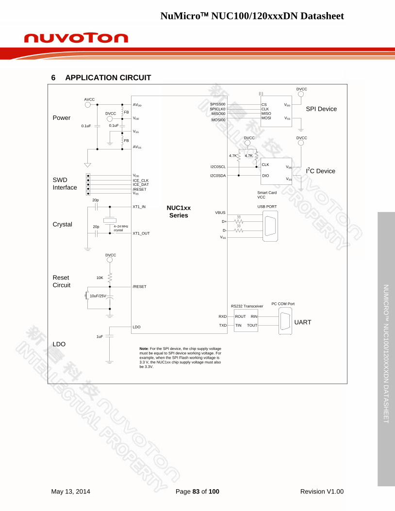
NuMicro NUC100/120xxxDN Datasheet
May 13, 2014 Page 83 of 100 Revision V1.00
NU
MIC
RO
™ N
UC
100/120XXXD
N D
ATASHEET
6 APPLICATION CIRCUIT
AVSS
AVDD
AVCC
DVCC
VSS
VDD
4~24 MHz crystal
0.1uF
FB
FB
20p
20p
DVCC
10uF/25V
10K
Power
Crystal
Reset Circuit /RESET
XT1_OUT
LDO
NUC1xx Series
VDD
VSS
/RESET
ICE_CLKICE_DAT
SWD Interface
1uF
VDD
VSS
I2C DeviceCLK
DIOI2C0SDA
I2C0SCL
4.7K
VDD
VSS
SPI DeviceCSCLKMISO
SPISS00
MOSI
SPICLK0MISO00MOSI00
LDO
RS232 Transceiver
ROUT
TIN
RIN
TOUT
PC COM Port
XT1_IN
0.1uF
DVCC
4.7K
DVCC
DVCC
Note: For the SPI device, the chip supply voltage must be equal to SPI device working voltage. For example, when the SPI Flash working voltage is 3.3 V, the NUC1xx chip supply voltage must also be 3.3V.
UART
[1]
RXD
TXD
Smart Card VCC
USB PORT
D+
D-
33
33
VBUS
VSS
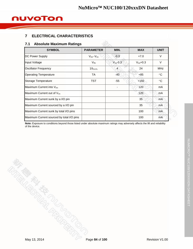
NuMicro NUC100/120xxxDN Datasheet
May 13, 2014 Page 84 of 100 Revision V1.00
NU
MIC
RO
™ N
UC
100/120XXXD
N D
ATASHEET
7 ELECTRICAL CHARACTERISTICS
Absolute Maximum Ratings 7.1SYMBOL PARAMETER MIN. MAX UNIT
DC Power Supply VDD−VSS -0.3 +7.0 V
Input Voltage VIN VSS-0.3 VDD+0.3 V
Oscillator Frequency 1/tCLCL 4 24 MHz
Operating Temperature TA -40 +85 °C
Storage Temperature TST -55 +150 °C
Maximum Current into VDD - 120 mA
Maximum Current out of VSS 120 mA
Maximum Current sunk by a I/O pin 35 mA
Maximum Current sourced by a I/O pin 35 mA
Maximum Current sunk by total I/O pins 100 mA
Maximum Current sourced by total I/O pins 100 mA
Note: Exposure to conditions beyond those listed under absolute maximum ratings may adversely affects the lift and reliability of the device.
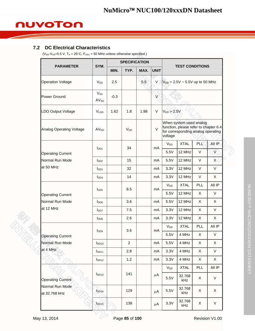
NuMicro NUC100/120xxxDN Datasheet
May 13, 2014 Page 85 of 100 Revision V1.00
NU
MIC
RO
™ N
UC
100/120XXXD
N D
ATASHEET
DC Electrical Characteristics 7.2 (VDD-VSS=5.5 V, TA = 25°C, FOSC = 50 MHz unless otherwise specified.)
PARAMETER SYM. SPECIFICATION
TEST CONDITIONS MIN. TYP. MAX. UNIT
Operation Voltage VDD 2.5 5.5 V VDD = 2.5V ~ 5.5V up to 50 MHz
Power Ground VSS
AVSS -0.3 V
LDO Output Voltage VLDO 1.62 1.8 1.98 V VDD > 2.5V
Analog Operating Voltage AVDD VDD V
When system used analog function, please refer to chapter 6.4 for corresponding analog operating voltage
Operating Current
Normal Run Mode
at 50 MHz
IDD1 34 mA VDD XTAL PLL All IP
5.5V 12 MHz V V
IDD2 15 mA 5.5V 12 MHz V X
IDD3 32 mA 3.3V 12 MHz V V
IDD4 14 mA 3.3V 12 MHz V X
Operating Current
Normal Run Mode
at 12 MHz
IDD5 8.5 mA VDD XTAL PLL All IP
5.5V 12 MHz X V
IDD6 3.6 mA 5.5V 12 MHz X X
IDD7 7.5 mA 3.3V 12 MHz X V
IDD8 2.6 mA 3.3V 12 MHz X X
Operating Current
Normal Run Mode
at 4 MHz
IDD9 3.6 mA VDD XTAL PLL All IP
5.5V 4 MHz X V
IDD10 2 mA 5.5V 4 MHz X X
IDD11 2.8 mA 3.3V 4 MHz X V
IDD12 1.2 mA 3.3V 4 MHz X X
Operating Current
Normal Run Mode
at 32.768 kHz
IDD13 141 µA
VDD XTAL PLL All IP
5.5V 32.768 kHz X V
IDD14 129 µA 5.5V 32.768 kHz X X
IDD15 138 µA 3.3V 32.768 kHz X V
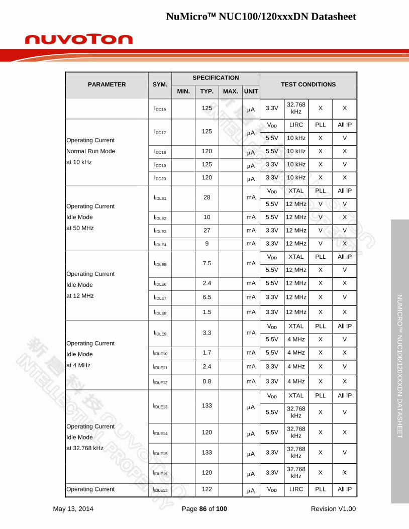
NuMicro NUC100/120xxxDN Datasheet
May 13, 2014 Page 86 of 100 Revision V1.00
NU
MIC
RO
™ N
UC
100/120XXXD
N D
ATASHEET
PARAMETER SYM. SPECIFICATION
TEST CONDITIONS MIN. TYP. MAX. UNIT
IDD16 125 µA 3.3V 32.768 kHz X X
Operating Current
Normal Run Mode
at 10 kHz
IDD17 125 µA VDD LIRC PLL All IP
5.5V 10 kHz X V
IDD18 120 µA 5.5V 10 kHz X X
IDD19 125 µA 3.3V 10 kHz X V
IDD20 120 µA 3.3V 10 kHz X X
Operating Current
Idle Mode
at 50 MHz
IIDLE1 28 mA VDD XTAL PLL All IP
5.5V 12 MHz V V
IIDLE2 10 mA 5.5V 12 MHz V X
IIDLE3 27 mA 3.3V 12 MHz V V
IIDLE4 9 mA 3.3V 12 MHz V X
Operating Current
Idle Mode
at 12 MHz
IIDLE5 7.5 mA VDD XTAL PLL All IP
5.5V 12 MHz X V
IIDLE6 2.4 mA 5.5V 12 MHz X X
IIDLE7 6.5 mA 3.3V 12 MHz X V
IIDLE8 1.5 mA 3.3V 12 MHz X X
Operating Current
Idle Mode
at 4 MHz
IIDLE9 3.3 mA VDD XTAL PLL All IP
5.5V 4 MHz X V
IIDLE10 1.7 mA 5.5V 4 MHz X X
IIDLE11 2.4 mA 3.3V 4 MHz X V
IIDLE12 0.8 mA 3.3V 4 MHz X X
Operating Current
Idle Mode
at 32.768 kHz
IIDLE13 133 µA
VDD XTAL PLL All IP
5.5V 32.768 kHz X V
IIDLE14 120 µA 5.5V 32.768 kHz X X
IIDLE15 133 µA 3.3V 32.768 kHz X V
IIDLE16 120 µA 3.3V 32.768 kHz X X
Operating Current IIDLE13 122 µA VDD LIRC PLL All IP
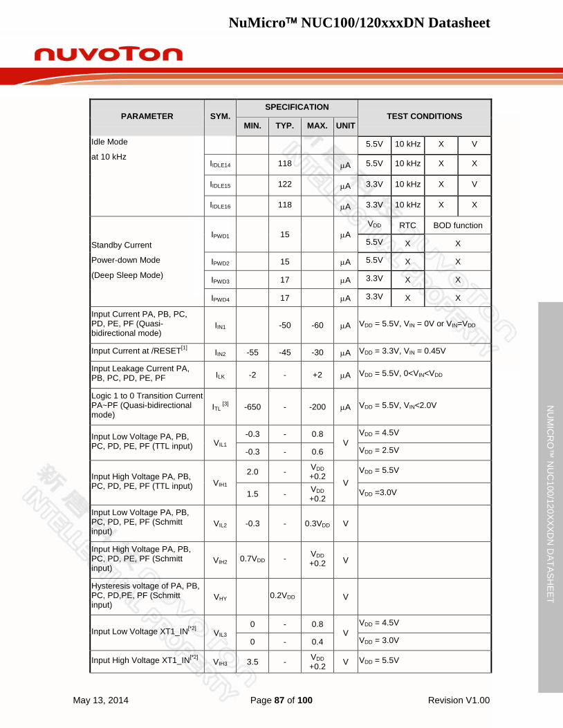
NuMicro NUC100/120xxxDN Datasheet
May 13, 2014 Page 87 of 100 Revision V1.00
NU
MIC
RO
™ N
UC
100/120XXXD
N D
ATASHEET
PARAMETER SYM. SPECIFICATION
TEST CONDITIONS MIN. TYP. MAX. UNIT
Idle Mode
at 10 kHz 5.5V 10 kHz X V
IIDLE14 118 µA 5.5V 10 kHz X X
IIDLE15 122 µA 3.3V 10 kHz X V
IIDLE16 118 µA 3.3V 10 kHz X X
Standby Current
Power-down Mode
(Deep Sleep Mode)
IPWD1 15 µA VDD RTC BOD function
5.5V X X
IPWD2 15 µA 5.5V X X
IPWD3 17 µA 3.3V X X
IPWD4 17 µA 3.3V X X
Input Current PA, PB, PC, PD, PE, PF (Quasi-bidirectional mode)
IIN1 -50 -60 µA VDD = 5.5V, VIN = 0V or VIN=VDD
Input Current at /RESET[1] IIN2 -55 -45 -30 µA VDD = 3.3V, VIN = 0.45V
Input Leakage Current PA, PB, PC, PD, PE, PF ILK -2 - +2 µA VDD = 5.5V, 0<VIN<VDD
Logic 1 to 0 Transition Current PA~PF (Quasi-bidirectional mode)
ITL [3] -650 - -200 µA VDD = 5.5V, VIN<2.0V
Input Low Voltage PA, PB, PC, PD, PE, PF (TTL input) VIL1
-0.3 - 0.8 V
VDD = 4.5V
-0.3 - 0.6 VDD = 2.5V
Input High Voltage PA, PB, PC, PD, PE, PF (TTL input) VIH1
2.0 - VDD +0.2
V VDD = 5.5V
1.5 - VDD +0.2
VDD =3.0V
Input Low Voltage PA, PB, PC, PD, PE, PF (Schmitt input)
VIL2 -0.3 - 0.3VDD V
Input High Voltage PA, PB, PC, PD, PE, PF (Schmitt input)
VIH2 0.7VDD - VDD +0.2 V
Hysteresis voltage of PA, PB, PC, PD,PE, PF (Schmitt input)
VHY 0.2VDD V
Input Low Voltage XT1_IN[*2] VIL3 0 - 0.8
V VDD = 4.5V
0 - 0.4 VDD = 3.0V
Input High Voltage XT1_IN[*2] VIH3 3.5 - VDD +0.2 V VDD = 5.5V
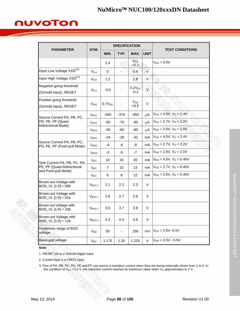
NuMicro NUC100/120xxxDN Datasheet
May 13, 2014 Page 88 of 100 Revision V1.00
NU
MIC
RO
™ N
UC
100/120XXXD
N D
ATASHEET
PARAMETER SYM. SPECIFICATION
TEST CONDITIONS MIN. TYP. MAX. UNIT
2.4 - VDD +0.2 VDD = 3.0V
Input Low Voltage X32I[*2] VIL4 0 - 0.4 v
Input High Voltage X32I[*2] VIH4 1.2 1.8 V
Negative going threshold
(Schmitt input), /RESET VILS -0.5 - 0.2VDD
-0.2 V
Positive going threshold
(Schmitt input), /RESET VIHS 0.7VDD - VDD
+0.5 V
Source Current PA, PB, PC, PD, PE, PF (Quasi-bidirectional Mode)
ISR11 -300 -370 -450 µA VDD = 4.5V, VS = 2.4V
ISR12 -50 -70 -90 µA VDD = 2.7V, VS = 2.2V
ISR12 -40 -60 -80 µA VDD = 2.5V, VS = 2.0V
Source Current PA, PB, PC, PD, PE, PF (Push-pull Mode)
ISR21 -24 -28 -32 mA VDD = 4.5V, VS = 2.4V
ISR22 -4 -6 -8 mA VDD = 2.7V, VS = 2.2V
ISR22 -3 -5 -7 mA VDD = 2.5V, VS = 2.0V
Sink Current PA, PB, PC, PD, PE, PF (Quasi-bidirectional and Push-pull Mode)
ISK1 10 16 20 mA VDD = 4.5V, VS = 0.45V
ISK1 7 10 13 mA VDD = 2.7V, VS = 0.45V
ISK1 6 9 12 mA VDD = 2.5V, VS = 0.45V
Brown-out Voltage with BOD_VL [1:0] = 00b VBO2.2 2.1 2.2 2.3 V
Brown-out Voltage with BOD_VL [1:0] = 01b VBO2.7 2.6 2.7 2.8 V
Brown-out voltage with BOD_VL [1:0] = 10b VBO3.7 3.5 3.7 3.9 V
Brown-out Voltage with BOD_VL [1:0] = 11b VBO4.4 4.2 4.4 4.6 V
Hysteresis range of BOD voltage VBH 30 - 150 mV VDD = 2.5V~5.5V
Band-gap voltage VBG 1.175 1.20 1.225 V VDD = 2.5V - 5.5V
Note:
1. /RESET pin is a Schmitt trigger input.
2. Crystal Input is a CMOS input.
3. Pins of PA, PB, PC, PD, PE and PF can source a transition current when they are being externally driven from 1 to 0. In the condition of VDD = 5.5 V, the transition current reaches its maximum value when VIN approximates to 2 V.
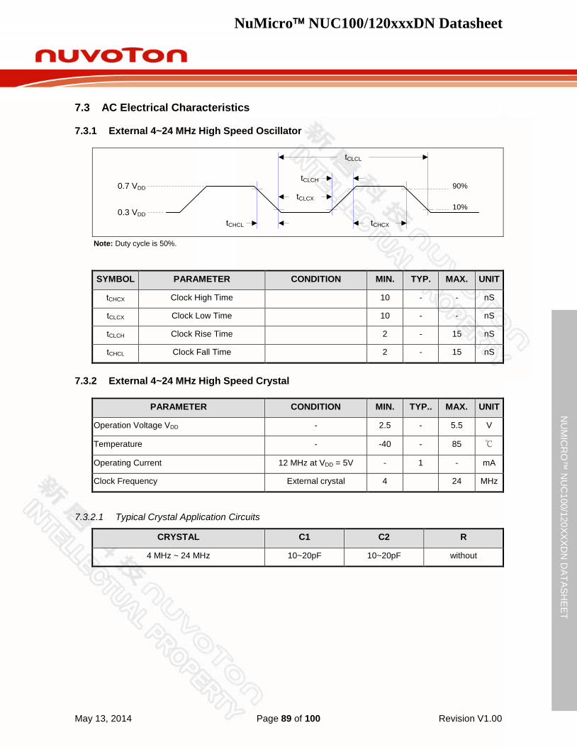
NuMicro NUC100/120xxxDN Datasheet
May 13, 2014 Page 89 of 100 Revision V1.00
NU
MIC
RO
™ N
UC
100/120XXXD
N D
ATASHEET
AC Electrical Characteristics 7.3
7.3.1 External 4~24 MHz High Speed Oscillator
tCHCX
90%
10%
tCLCH
tCHCL
tCLCX
tCLCL
0.3 VDD
0.7 VDD
Note: Duty cycle is 50%.
SYMBOL PARAMETER CONDITION MIN. TYP. MAX. UNIT
tCHCX Clock High Time 10 - - nS
tCLCX Clock Low Time 10 - - nS
tCLCH Clock Rise Time 2 - 15 nS
tCHCL Clock Fall Time 2 - 15 nS
7.3.2 External 4~24 MHz High Speed Crystal
PARAMETER CONDITION MIN. TYP.. MAX. UNIT
Operation Voltage VDD - 2.5 - 5.5 V
Temperature - -40 - 85
Operating Current 12 MHz at VDD = 5V - 1 - mA
Clock Frequency External crystal 4 24 MHz
Typical Crystal Application Circuits 7.3.2.1
CRYSTAL C1 C2 R
4 MHz ~ 24 MHz 10~20pF 10~20pF without
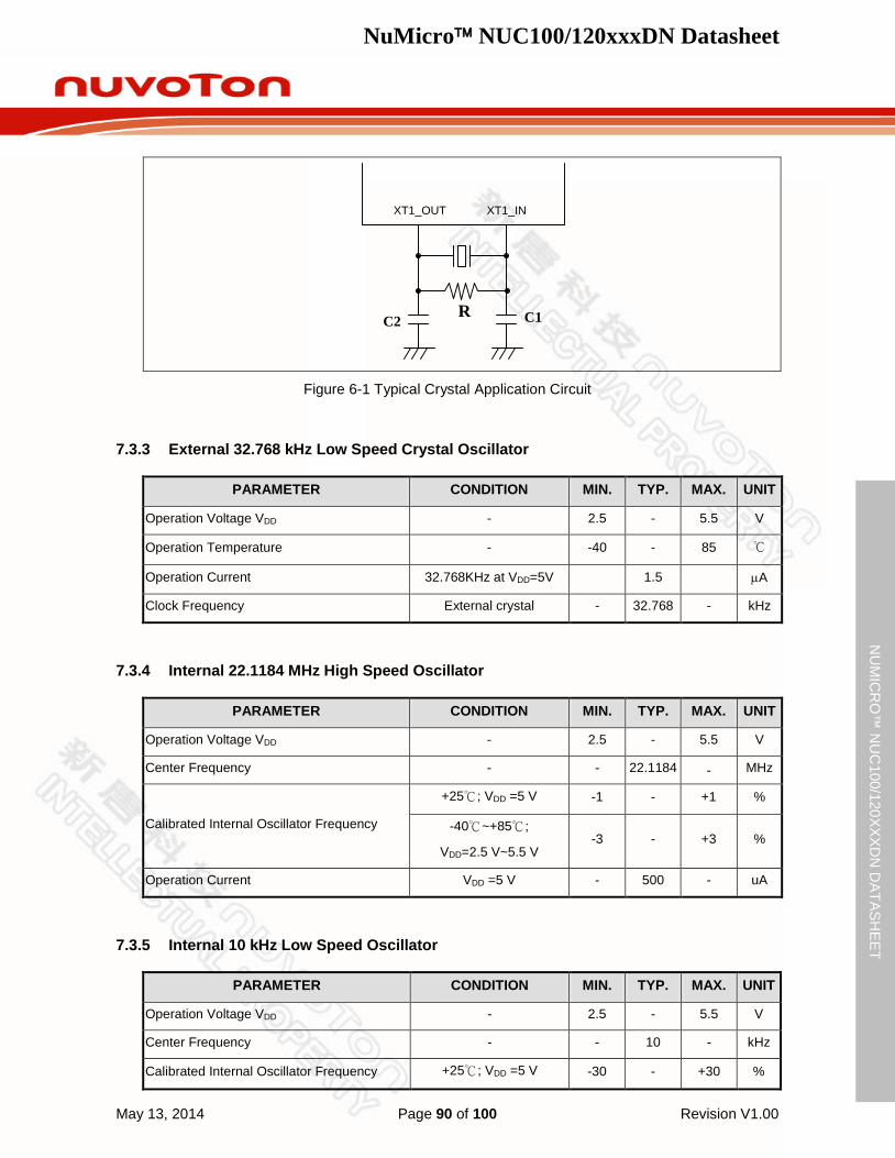
NuMicro NUC100/120xxxDN Datasheet
May 13, 2014 Page 90 of 100 Revision V1.00
NU
MIC
RO
™ N
UC
100/120XXXD
N D
ATASHEET
XT1_INXT1_OUT
C1RC2
Figure 6-1 Typical Crystal Application Circuit
7.3.3 External 32.768 kHz Low Speed Crystal Oscillator
PARAMETER CONDITION MIN. TYP. MAX. UNIT
Operation Voltage VDD - 2.5 - 5.5 V
Operation Temperature - -40 - 85
Operation Current 32.768KHz at VDD=5V 1.5 µA
Clock Frequency External crystal - 32.768 - kHz
7.3.4 Internal 22.1184 MHz High Speed Oscillator
PARAMETER CONDITION MIN. TYP. MAX. UNIT
Operation Voltage VDD - 2.5 - 5.5 V
Center Frequency - - 22.1184 - MHz
Calibrated Internal Oscillator Frequency
+25; VDD =5 V -1 - +1 %
-40~+85;
VDD=2.5 V~5.5 V -3 - +3 %
Operation Current VDD =5 V - 500 - uA
7.3.5 Internal 10 kHz Low Speed Oscillator
PARAMETER CONDITION MIN. TYP. MAX. UNIT
Operation Voltage VDD - 2.5 - 5.5 V
Center Frequency - - 10 - kHz
Calibrated Internal Oscillator Frequency +25; VDD =5 V -30 - +30 %
NuMicro NUC100/120xxxDN Datasheet
May 13, 2014 Page 91 of 100 Revision V1.00
NU
MIC
RO
™ N
UC
100/120XXXD
N D
ATASHEET
-40~+85;
VDD=2.5 V~5.5 V -50 - +50 %
Analog Characteristics 7.4
7.4.1 12-bit SARADC Specification
SYMBOL PARAMETER MIN. TYP. MAX. UNIT
- Resolution - - 12 Bit
DNL Differential nonlinearity error - -1~2 -1~4 LSB
INL Integral nonlinearity error - ±2 ±4 LSB
EO Offset error - ±1 10 LSB
EG Gain error (Transfer gain) - 1 1.005 -
- Monotonic Guaranteed
FADC ADC clock frequency (AVDD = 5V/3V) - - 16/8 MHz
FS Sample rate - - 760 kSPS
VDDA Supply voltage 3 - 5.5 V
IDD Supply current (Avg.)
- 0.5 - mA
IDDA - 1.5 - mA
VREF Reference voltage 3 VDDA V
IREF Reference current (Avg.) - 1 - mA
VIN Input voltage 0 - VREF V
7.4.2 LDO and Power Management Specification
PARAMETER MIN. TYP. MAX. UNIT NOTE
Input Voltage VDD 2.5 5.5 V VDD input voltage
Output Voltage 1.62 1.8 1.98 V VDD > 2.5 V
Operating Temperature -40 25 85
Cbp - 1 - µF RESR = 1 Ω
Note:
1. It is recommended that a 10 uF or higher capacitor and a 100 nF bypass capacitor are connected between VDD and the closest VSS pin of the device.
2. To ensure power stability, a 1 µF or higher capacitor must be connected between LDO_CAP pin and the closest VSS pin of the device.
NuMicro NUC100/120xxxDN Datasheet
May 13, 2014 Page 92 of 100 Revision V1.00
NU
MIC
RO
™ N
UC
100/120XXXD
N D
ATASHEET
7.4.3 Low Voltage Reset Specification
PARAMETER CONDITION MIN. TYP. MAX. UNIT
Operation Voltage - 0 - 5.5 V
Quiescent Current VDD=5.5 V - 1 5 µA
Operation Temperature - -40 25 85
Threshold Voltage
Temperature=25 1.7 2.0 2.3 V
Temperature=-40 - 2.4 - V
Temperature=85 - 1.6 - V
Hysteresis - 0 0 0 V
7.4.4 Brown-out Detector Specification
PARAMETER CONDITION MIN. TYP. MAX. UNIT
Operation Voltage - 0 - 5.5 V
Temperature - -40 25 85
Quiescent Current AVDD=5.5 V - - 125 μA
Brown-out Voltage
BOD_VL[1:0]=11 4.2 4.4 4.6 V
BOD_VL [1:0]=10 3.5 3.7 3.9 V
BOD_VL [1:0]=01 2.6 2.7 2.8 V
BOD_VL [1:0]=00 2.1 2.2 2.3 V
Hysteresis - 30 - 150 mV
7.4.5 Power-on Reset Specification
PARAMETER CONDITION MIN. TYP. MAX. UNIT
Operation Temperature - -40 25 85
Reset Voltage V+ - 2 - V
Quiescent Current Vin > reset voltage - 1 - nA
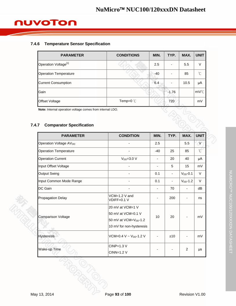
NuMicro NUC100/120xxxDN Datasheet
May 13, 2014 Page 93 of 100 Revision V1.00
NU
MIC
RO
™ N
UC
100/120XXXD
N D
ATASHEET
7.4.6 Temperature Sensor Specification
PARAMETER CONDITIONS MIN. TYP. MAX. UNIT
Operation Voltage[1] 2.5 - 5.5 V
Operation Temperature -40 - 85
Current Consumption 6.4 - 10.5 μA
Gain -1.76 mV/
Offset Voltage Temp=0 720 mV
Note: Internal operation voltage comes from internal LDO.
7.4.7 Comparator Specification
PARAMETER CONDITION MIN. TYP. MAX. UNIT
Operation Voltage AVDD - 2.5 5.5 V
Operation Temperature - -40 25 85
Operation Current VDD=3.0 V - 20 40 μA
Input Offset Voltage - - 5 15 mV
Output Swing - 0.1 - VDD-0.1 V
Input Common Mode Range - 0.1 - VDD-1.2 V
DC Gain - - 70 - dB
Propagation Delay VCM=1.2 V and VDIFF=0.1 V - 200 - ns
Comparison Voltage
20 mV at VCM=1 V
50 mV at VCM=0.1 V
50 mV at VCM=VDD-1.2
10 mV for non-hysteresis
10 20 - mV
Hysteresis VCM=0.4 V ~ VDD-1.2 V - ±10 - mV
Wake-up Time CINP=1.3 V
CINN=1.2 V - - 2 μs
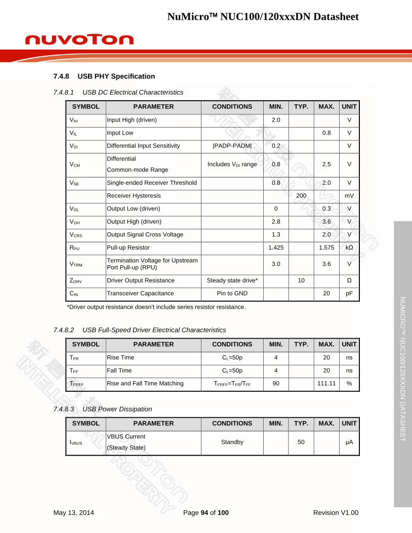
NuMicro NUC100/120xxxDN Datasheet
May 13, 2014 Page 94 of 100 Revision V1.00
NU
MIC
RO
™ N
UC
100/120XXXD
N D
ATASHEET
7.4.8 USB PHY Specification
USB DC Electrical Characteristics 7.4.8.1
SYMBOL PARAMETER CONDITIONS MIN. TYP. MAX. UNIT
VIH Input High (driven) 2.0 V
VIL Input Low 0.8 V
VDI Differential Input Sensitivity |PADP-PADM| 0.2 V
VCM Differential
Common-mode Range Includes VDI range 0.8 2.5 V
VSE Single-ended Receiver Threshold 0.8 2.0 V
Receiver Hysteresis 200 mV
VOL Output Low (driven) 0 0.3 V
VOH Output High (driven) 2.8 3.6 V
VCRS Output Signal Cross Voltage 1.3 2.0 V
RPU Pull-up Resistor 1.425 1.575 kΩ
VTRM Termination Voltage for Upstream Port Pull-up (RPU) 3.0 3.6 V
ZDRV Driver Output Resistance Steady state drive* 10 Ω
CIN Transceiver Capacitance Pin to GND 20 pF
*Driver output resistance doesn’t include series resistor resistance.
USB Full-Speed Driver Electrical Characteristics 7.4.8.2
SYMBOL PARAMETER CONDITIONS MIN. TYP. MAX. UNIT
TFR Rise Time CL=50p 4 20 ns
TFF Fall Time CL=50p 4 20 ns
TFRFF Rise and Fall Time Matching TFRFF=TFR/TFF 90 111.11 %
USB Power Dissipation 7.4.8.3
SYMBOL PARAMETER CONDITIONS MIN. TYP. MAX. UNIT
IVBUS VBUS Current
(Steady State) Standby 50 μA
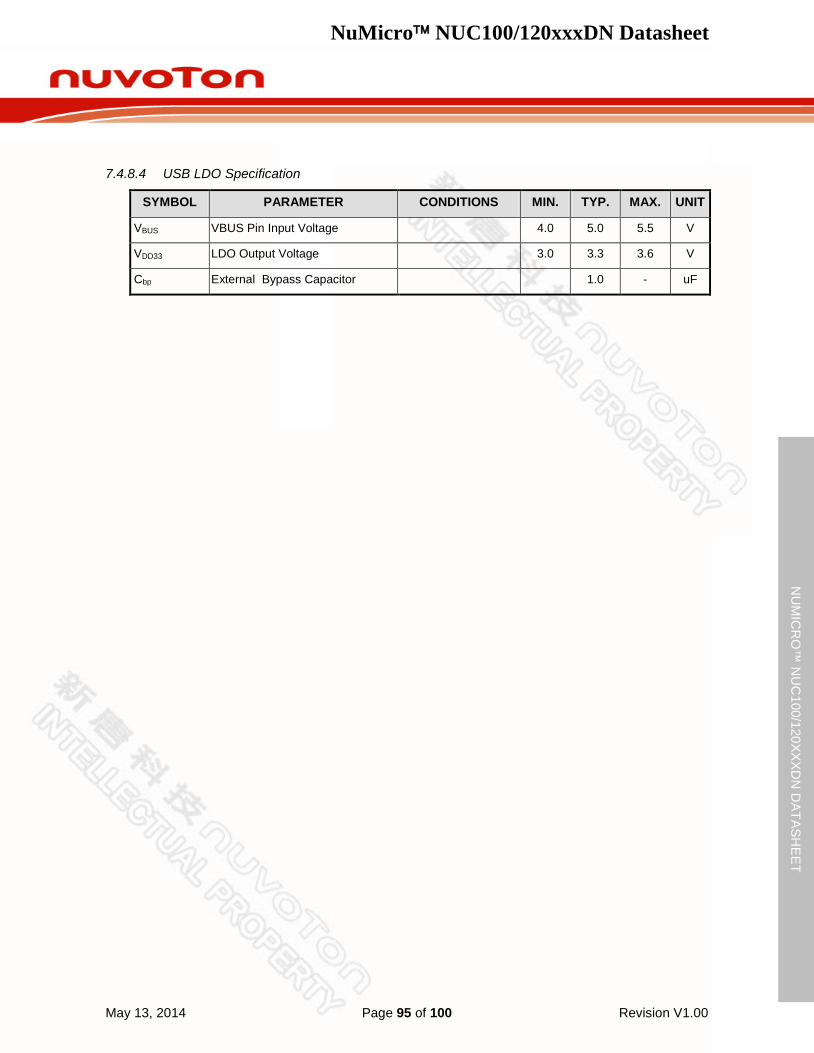
NuMicro NUC100/120xxxDN Datasheet
May 13, 2014 Page 95 of 100 Revision V1.00
NU
MIC
RO
™ N
UC
100/120XXXD
N D
ATASHEET
USB LDO Specification 7.4.8.4
SYMBOL PARAMETER CONDITIONS MIN. TYP. MAX. UNIT
VBUS VBUS Pin Input Voltage 4.0 5.0 5.5 V
VDD33 LDO Output Voltage 3.0 3.3 3.6 V
Cbp External Bypass Capacitor 1.0 - uF
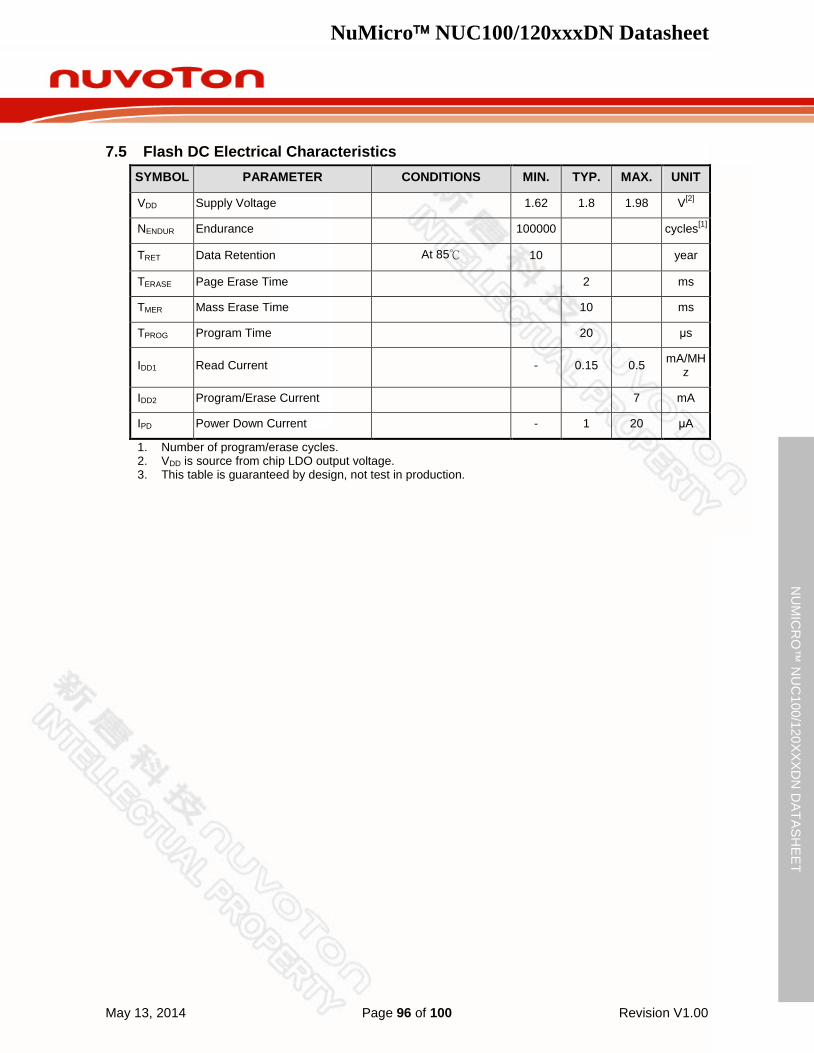
NuMicro NUC100/120xxxDN Datasheet
May 13, 2014 Page 96 of 100 Revision V1.00
NU
MIC
RO
™ N
UC
100/120XXXD
N D
ATASHEET
Flash DC Electrical Characteristics 7.5SYMBOL PARAMETER CONDITIONS MIN. TYP. MAX. UNIT
VDD Supply Voltage 1.62 1.8 1.98 V[2]
NENDUR Endurance 100000 cycles[1]
TRET Data Retention At 85 10 year
TERASE Page Erase Time 2 ms
TMER Mass Erase Time 10 ms
TPROG Program Time 20 μs
IDD1 Read Current - 0.15 0.5 mA/MHz
IDD2 Program/Erase Current 7 mA
IPD Power Down Current - 1 20 μA
1. Number of program/erase cycles. 2. VDD is source from chip LDO output voltage. 3. This table is guaranteed by design, not test in production.
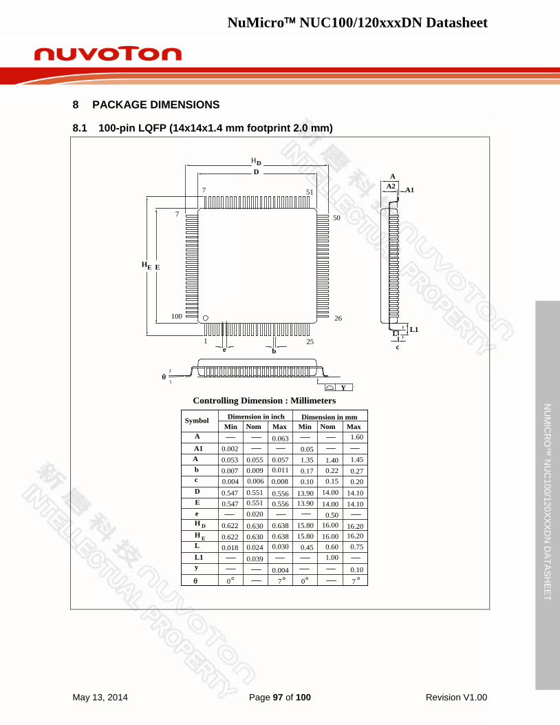
NuMicro NUC100/120xxxDN Datasheet
May 13, 2014 Page 97 of 100 Revision V1.00
NU
MIC
RO
™ N
UC
100/120XXXD
N D
ATASHEET
8 PACKAGE DIMENSIONS
100-pin LQFP (14x14x1.4 mm footprint 2.0 mm) 8.1
Controlling Dimension : Millimeters
0.10070
0.004
1.000.750.600.45
0.039
0.0300.0240.018
0.6380.6300.6220.50
14.100.200.271.45
1.60
14.00
1.40
13.900.100.171.350.05
0.0080.0110.057
0.063
0.055
0.020
0.5560.5510.5470.0040.0070.0530.002
SymbolMin Nom Max MaxNomMinDimension in inch Dimension in mm
A
bcD
eH D
H EL
y
A1A2
L1
E
0.0090.006 0.15
0.22
7
13.90 14.00 14.10
15.80 16.00 16.2015.80 16.00 16.20
0.5560.5510.547
θ
0.6380.6300.622
DD
EE
b
A2 A1
A
L1
e c
L
Y
H
H
1
100
θ
25
26
50
517
7
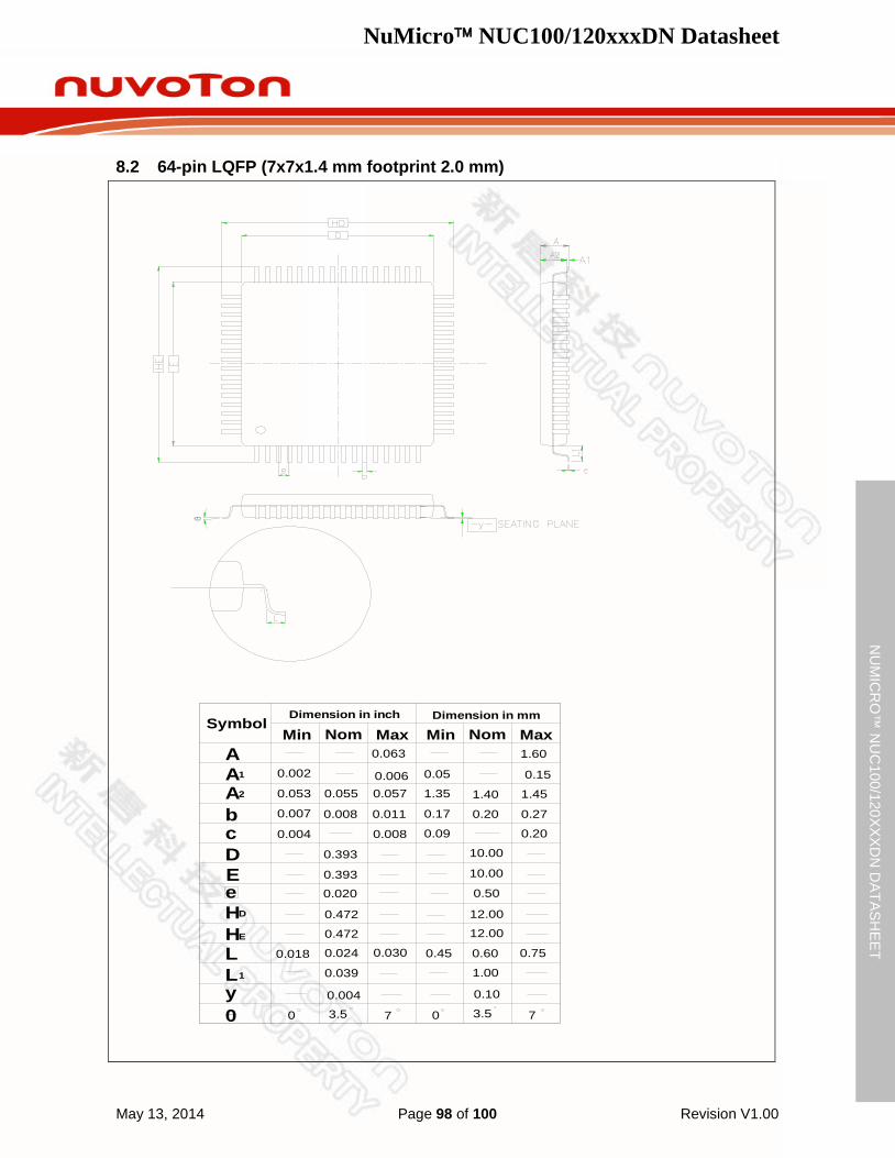
NuMicro NUC100/120xxxDN Datasheet
May 13, 2014 Page 98 of 100 Revision V1.00
NU
MIC
RO
™ N
UC
100/120XXXD
N D
ATASHEET
64-pin LQFP (7x7x1.4 mm footprint 2.0 mm) 8.2
0 70
1.00
0.750.60
12.00
0.45
0.039
0.0300.024
0.472
0.018
0.50
0.20
0.27
1.45
1.60
10.00
1.40
0.09
0.17
1.35
0.05
0.008
0.011
0.057
0.063
0.393
0.055
0.020
0.004
0.007
0.053
0.002
SymbolMin Nom Max MaxNomMinDimension in inch Dimension in mm
A
bcD
eHD
HE
L
y0
AA
L1
1
2
E
0.008 0.20
7
0.393 10.00
0.472 12.00
0.006 0.15
0.004 0.10
3.5 3.5
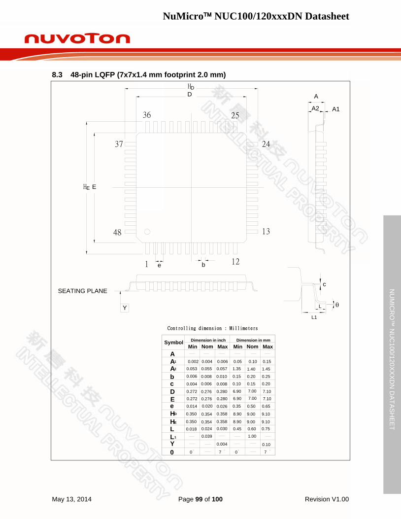
NuMicro NUC100/120xxxDN Datasheet
May 13, 2014 Page 99 of 100 Revision V1.00
NU
MIC
RO
™ N
UC
100/120XXXD
N D
ATASHEET
48-pin LQFP (7x7x1.4 mm footprint 2.0 mm) 8.3
Y
SEATING PLANE
D
E
e b
A2 A1
A
1 12
48
DH
EH
L1
L
c
θ
Controlling dimension : Millimeters
0.10
070
0.004
1.00
0.750.600.45
0.039
0.0300.0240.018
9.109.008.900.3580.3540.350
0.50
0.20
0.25
1.451.40
0.10
0.15
1.35
0.008
0.010
0.0570.055
0.026
7.107.006.900.2800.2760.272
0.004
0.006
0.053
SymbolMin Nom Max MaxNomMin
Dimension in inch Dimension in mm
A
bcD
eHD
HE
L
Y0
AA
L1
1
2
E
0.008
0.006 0.15
0.20
7
0.020 0.35 0.65
0.100.050.002 0.004 0.006 0.15
9.109.008.900.3580.3540.350
7.107.006.900.2800.2760.272
0.014
37
36 25
24
13
NuMicro NUC100/120xxxDN Datasheet
May 13, 2014 Page 100 of 100 Revision V1.00
NU
MIC
RO
™ N
UC
100/120XXXD
N D
ATASHEET
9 REVISION HISTORY REVISION DATE DESCRIPTION
V1.00 May 13, 2014 1. First version
Important Notice Nuvoton Products are neither intended nor warranted for usage in systems or equipment, any malfunction or failure of which may cause loss of human life, bodily injury or severe property damage. Such applications are deemed, “Insecure Usage”.
Insecure usage includes, but is not limited to: equipment for surgical implementation, atomic energy control instruments, airplane or spaceship instruments, the control or operation of dynamic, brake or safety systems designed for vehicular use, traffic signal instruments, all types of safety devices, and other applications intended to support or sustain life.
All Insecure Usage shall be made at customer’s risk, and in the event that third parties lay claims to Nuvoton as a result of customer’s Insecure Usage, customer shall indemnify the damages and liabilities thus incurred by Nuvoton.