Embed Size (px)
Citation preview
NuMicro™ NUC100 Data Sheet
ARM Cortex™-M0
32-BIT MICROCONTROLLER
Publication Release Date: Jan. 2, 2012 - 1 - Revision V2.03
NuMicro™ Family NUC100 Data Sheet
The information described in this document is the exclusive intellectual property of Nuvoton Technology Corporation and shall not be reproduced without permission from Nuvoton.
Nuvoton is providing this document only for reference purposes of NuMicro microcontroller based system design. Nuvoton assumes no responsibility for errors or omissions.
All data and specifications are subject to change without notice.
For additional information or questions, please contact: Nuvoton Technology Corporation.
NuMicro™ NUC100 Data Sheet
Publication Release Date: Jan. 2, 2012 - 2 - Revision V2.03
Contents
1 GENERAL DESCRIPTION ......................................................................................................... 7 2 FEATURES ................................................................................................................................. 8
2.1 NuMicro™ NUC100 Features – Advanced Line.............................................................. 8
3 PARTS INFORMATION LIST AND PIN CONFIGURATION .................................................... 12 3.1 NuMicro™ NUC100 Products Selection Guide............................................................. 12
3.1.1 NuMicro™ NUC100 Medium Density Advance Line Selection Guide .............................12 3.1.2 NuMicro™ NUC100 Low Density Advance Line Selection Guide ...................................12
3.2 Pin Configuration .......................................................................................................... 13
3.2.1 NuMicro™ NUC100 Medium Density Pin Diagram .........................................................13 3.2.2 NuMicro™ NUC100 Low Density Pin Diagram ...............................................................16
4 BLOCK DIAGRAM .................................................................................................................... 18 4.1 NuMicro™ NUC100 Medium Density Block Diagram ................................................... 18
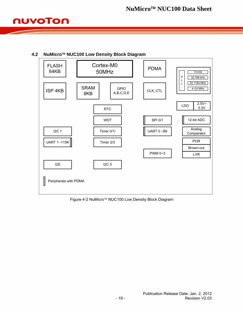
4.2 NuMicro™ NUC100 Low Density Block Diagram.......................................................... 19
5 FUNCTIONAL DESCRIPTION.................................................................................................. 20 5.1 ARM® Cortex™-M0 Core.............................................................................................. 20
5.2 System Manager........................................................................................................... 22 5.2.1 Overview ........................................................................................................................22 5.2.2 System Reset .................................................................................................................22 5.2.3 System Power Distribution .............................................................................................23 5.2.4 System Memory Map......................................................................................................24 5.2.5 System Timer (SysTick) .................................................................................................26 5.2.6 Nested Vectored Interrupt Controller (NVIC) ..................................................................27
5.3 Clock Controller ............................................................................................................ 31 5.3.1 Overview ........................................................................................................................31 5.3.2 Clock Generator .............................................................................................................33 5.3.3 System Clock and SysTick Clock ...................................................................................34 5.3.4 Peripherals Clock ...........................................................................................................35 5.3.5 Power Down Mode Clock ...............................................................................................35 5.3.6 Frequency Divider Output...............................................................................................36
5.4 General Purpose I/O (GPIO) ........................................................................................ 37 5.4.1 Overview ........................................................................................................................37 5.4.2 Features .........................................................................................................................37
5.5 I2C Serial Interface Controller (Master/Slave) (I2C) ...................................................... 38 5.5.1 Overview ........................................................................................................................38 5.5.2 Features .........................................................................................................................39
5.6 PWM Generator and Capture Timer (PWM) ................................................................ 40 5.6.1 Overview ........................................................................................................................40 5.6.2 Features .........................................................................................................................41
5.7 Real Time Clock (RTC)................................................................................................. 42 5.7.1 Overview ........................................................................................................................42
NuMicro™ NUC100 Data Sheet
Publication Release Date: Jan. 2, 2012 - 3 - Revision V2.03
5.7.2 Features .........................................................................................................................42 5.8 Serial Peripheral Interface (SPI) ................................................................................... 43
5.8.1 Overview ........................................................................................................................43 5.8.2 Features .........................................................................................................................43
5.9 Timer Controller (TMR)................................................................................................. 44 5.9.1 Overview ........................................................................................................................44 5.9.2 Features .........................................................................................................................44
5.10 Watchdog Timer (WDT)................................................................................................ 45 5.10.1 Overview ......................................................................................................................45 5.10.2 Features .......................................................................................................................47
5.11 UART Interface Controller (UART) ............................................................................... 47 5.11.1 Overview ......................................................................................................................47 5.11.2 Features .......................................................................................................................49
5.12 PS/2 Device Controller (PS2D)..................................................................................... 50 5.12.1 Overview ......................................................................................................................50 5.12.2 Features .......................................................................................................................50
5.13 I2S Controller (I2S)......................................................................................................... 51 5.13.1 Overview ......................................................................................................................51 5.13.2 Features .......................................................................................................................51
5.14 Analog-to-Digital Converter (ADC) ............................................................................... 52 5.14.1 Overview ......................................................................................................................52 5.14.2 Features .......................................................................................................................52
5.15 Analog Comparator (CMP) ........................................................................................... 53 5.15.1 Overview ......................................................................................................................53 5.15.2 Features .......................................................................................................................53
5.16 PDMA Controller (PDMA) ............................................................................................. 54 5.16.1 Overview ......................................................................................................................54 5.16.2 Features .......................................................................................................................54
5.17 External Bus Interface (EBI) ......................................................................................... 55 5.17.1 Overview ......................................................................................................................55 5.17.2 Features .......................................................................................................................55
6 FLASH MEMORY CONTROLLER (FMC) ................................................................................ 56 6.1 Overview....................................................................................................................... 56
6.2 Features........................................................................................................................ 56
7 ELECTRICAL CHARACTERISTICS......................................................................................... 57 7.1 Absolute Maximum Ratings .......................................................................................... 57
7.2 DC Electrical Characteristics ........................................................................................ 58
7.2.1 NuMicro™ NUC100/NUC120 Medium Density DC Electrical Characteristics .................58 7.2.2 NuMicro™ NUC100/NUC120 Low Density DC Electrical Characteristics .......................63 7.2.3 Operating Current Curve (Test condition: run NOP).......................................................68 7.2.4 Idle Current Curve ..........................................................................................................70 7.2.5 Power Down Current Curve............................................................................................72
NuMicro™ NUC100 Data Sheet
Publication Release Date: Jan. 2, 2012 - 4 - Revision V2.03
7.3 AC Electrical Characteristics ........................................................................................ 73 7.3.1 External 4~24 MHz High Speed Crystal .........................................................................73 7.3.2 External 32.768 kHz Low Speed Crystal ........................................................................74 7.3.3 Internal 22.1184 MHz High Speed Oscillator..................................................................74 7.3.4 Internal 10 kHz Low Speed Oscillator.............................................................................74
7.4 Analog Characteristics.................................................................................................. 75 7.4.1 Specification of 12-bit SARADC .....................................................................................75 7.4.2 Specification of LDO and Power management...............................................................76 7.4.3 Specification of Low Voltage Reset ................................................................................77 7.4.4 Specification of Brown-Out Detector...............................................................................77 7.4.5 Specification of Power-On Reset (5 V) ...........................................................................77 7.4.6 Specification of Temperature Sensor .............................................................................78 7.4.7 Specification of Comparator ...........................................................................................78
7.5 Flash DC Electrical Characteristics .............................................................................. 79
7.6 SPI Dynamic Characteristics ........................................................................................ 80
8 PACKAGE DIMENSIONS......................................................................................................... 82 8.1 100L LQFP (14x14x1.4 mm footprint 2.0mm) .............................................................. 82
8.2 64L LQFP (10x10x1.4mm footprint 2.0 mm) ................................................................ 83
8.3 48L LQFP (7x7x1.4mm footprint 2.0mm) ..................................................................... 84
9 REVISION HISTORY................................................................................................................ 85
NuMicro™ NUC100 Data Sheet
Publication Release Date: Jan. 2, 2012 - 5 - Revision V2.03
Figures
Figure 3-1 NuMicro™ NUC100 Medium Density LQFP 100-pin Pin Diagram ............................... 13
Figure 3-2 NuMicro™ NUC100 Medium Density LQFP 64-pin Pin Diagram ................................. 14
Figure 3-3 NuMicro™ NUC100 Medium Density LQFP 48-pin Pin Diagram ................................. 15
Figure 3-4 NuMicro™ NUC100 Low Density LQFP 64-pin Pin Diagram........................................ 16
Figure 3-5 NuMicro™ NUC100 Low Density LQFP 48-pin Pin Diagram........................................ 17
Figure 4-1 NuMicro™ NUC100 Medium Density Block Diagram ................................................... 18
Figure 4-2 NuMicro™ NUC100 Low Density Block Diagram ......................................................... 19
Figure 5-1 Functional Controller Diagram...................................................................................... 20
Figure 5-3 NuMicro™ NUC100 Power Distribution Diagram.......................................................... 23
Figure 5-4 Clock generator global view diagram ........................................................................... 32
Figure 5-5 Clock generator block diagram..................................................................................... 33
Figure 5-6 System Clock Block Diagram ....................................................................................... 34
Figure 5-7 SysTick Clock Control Block Diagram.......................................................................... 34
Figure 5-8 Clock Source of Frequency Divider .............................................................................. 36
Figure 5-9 Block Diagram of Frequency Divider ............................................................................ 36
Figure 5-10 I2C Bus Timing............................................................................................................ 38
Figure 5-11 Timing of Interrupt and Reset Signal .......................................................................... 46
Figure 7-1 Typical Crystal Application Circuit ................................................................................ 74
Figure 7-2 SPI Master dynamic characteristics timing................................................................... 81
Figure 7-3 SPI Slave dynamic characteristics timing..................................................................... 81
NuMicro™ NUC100 Data Sheet
Publication Release Date: Jan. 2, 2012 - 6 - Revision V2.03
Tables
Table 1-1 Connectivity Supported Table.......................................................................................... 7
Table 5-1 Address Space Assignments for On-Chip Controllers................................................... 25
Table 5-2 Exception Model ............................................................................................................ 28
Table 5-3 System Interrupt Map..................................................................................................... 29
Table 5-4 Vector Table Format ...................................................................................................... 30
Table 5-5 Watchdog Timeout Interval Selection ............................................................................ 45
Table 5-6 UART Baud Rate Equation............................................................................................ 47
Table 5-7 UART Baud Rate Setting Table..................................................................................... 48
NuMicro™ NUC100 Data Sheet
Publication Release Date: Jan. 2, 2012 - 7 - Revision V2.03
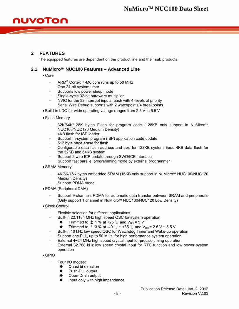
1 GENERAL DESCRIPTION The NuMicro™ NUC100 Series is 32-bit microcontrollers with embedded ARM® Cortex™-M0 core for industrial control and applications which need rich communication interfaces. The Cortex™-M0 is the newest ARM® embedded processor with 32-bit performance and at a cost equivalent to traditional 8-bit microcontroller. NuMicro™ NUC100 Series includes NUC100, NUC120, NUC130 and NUC140 product line.
The NuMicro™ NUC100 Advanced Line embeds Cortex™-M0 core running up to 50 MHz with 32K/64K/128K-byte embedded flash, 4K/8K/16K-byte embedded SRAM, and 4K-byte loader ROM for the ISP. It also equips with plenty of peripheral devices, such as Timers, Watchdog Timer, RTC, PDMA, UART, SPI, I2C, I2S, PWM Timer, GPIO, PS/2, 12-bit ADC, Analog Comparator, Low Voltage Reset Controller and Brown-Out Detector.
Product Line UART SPI I2C USB LIN CAN PS/2 I2S
NUC100 ● ● ● ● ●
NUC120 ● ● ● ● ● ●
NUC130 ● ● ● ● ● ● ●
NUC140 ● ● ● ● ● ● ● ●
Table 1-1 Connectivity Supported Table
NuMicro™ NUC100 Data Sheet
2 FEATURES The equipped features are dependent on the product line and their sub products.
2.1 NuMicro™ NUC100 Features – Advanced Line • Core
– ARM® Cortex™-M0 core runs up to 50 MHz – One 24-bit system timer – Supports low power sleep mode – Single-cycle 32-bit hardware multiplier – NVIC for the 32 interrupt inputs, each with 4-levels of priority – Serial Wire Debug supports with 2 watchpoints/4 breakpoints
• Build-in LDO for wide operating voltage ranges from 2.5 V to 5.5 V
• Flash Memory
– 32K/64K/128K bytes Flash for program code (128KB only support in NuMicro™ NUC100/NUC120 Medium Density)
– 4KB flash for ISP loader – Support In-system program (ISP) application code update – 512 byte page erase for flash – Configurable data flash address and size for 128KB system, fixed 4KB data flash for
the 32KB and 64KB system – Support 2 wire ICP update through SWD/ICE interface – Support fast parallel programming mode by external programmer
• SRAM Memory
– 4K/8K/16K bytes embedded SRAM (16KB only support in NuMicro™ NUC100/NUC120 Medium Density)
– Support PDMA mode • PDMA (Peripheral DMA)
– Support 9 channels PDMA for automatic data transfer between SRAM and peripherals (Only support 1 channel in NuMicro™ NUC100/NUC120 Low Density)
• Clock Control
– Flexible selection for different applications – Built-in 22.1184 MHz high speed OSC for system operation
Trimmed to 1 % at +25 and V℃ DD = 5 V Trimmed to 3 % at -40 ~ +85 and V℃ ℃ DD = 2.5 V ~ 5.5 V
– Built-in 10 kHz low speed OSC for Watchdog Timer and Wake-up operation – Support one PLL, up to 50 MHz, for high performance system operation – External 4~24 MHz high speed crystal input for precise timing operation – External 32.768 kHz low speed crystal input for RTC function and low power system
operation • GPIO
– Four I/O modes: Quasi bi-direction Push-Pull output Open-Drain output Input only with high impendence
Publication Release Date: Jan. 2, 2012 - 8 - Revision V2.03
NuMicro™ NUC100 Data Sheet
Publication Release Date: Jan. 2, 2012 - 9 - Revision V2.03
– TTL/Schmitt trigger input selectable – I/O pin can be configured as interrupt source with edge/level setting – High driver and high sink IO mode support
• Timer
– Support 4 sets of 32-bit timers with 24-bit up-timer and one 8-bit pre-scale counter – Independent clock source for each timer – Provides one-shot, periodic, toggle and continuous counting operation modes
(NuMicro™ NUC100/NUC120 Medium Density only support one-shot and periodic mode)
– Support event counting function (NuMicro™ NUC100/NUC120 Low Density only) • Watchdog Timer
– Multiple clock sources – 8 selectable time out period from 1.6ms ~ 26.0sec (depends on clock source) – WDT can wake-up from power down or idle mode – Interrupt or reset selectable on watchdog time-out
• RTC
– Support software compensation by setting frequency compensate register (FCR) – Support RTC counter (second, minute, hour) and calendar counter (day, month, year) – Support Alarm registers (second, minute, hour, day, month, year) – Selectable 12-hour or 24-hour mode – Automatic leap year recognition – Support periodic time tick interrupt with 8 period options 1/128, 1/64, 1/32, 1/16, 1/8,
1/4, 1/2 and 1 second – Support wake-up function
• PWM/Capture
– Built-in up to four 16-bit PWM generators provide eight PWM outputs or four complementary paired PWM outputs
– Each PWM generator equipped with one clock source selector, one clock divider, one 8-bit prescaler and one Dead-Zone generator for complementary paired PWM
– Up to eight 16-bit digital Capture timers (shared with PWM timers) provide eight rising/falling capture inputs
– Support Capture interrupt • UART
– Up to three UART controllers (NuMicro™ NUC100/NUC120 Low Density only support 2 UART controllers)
– UART ports with flow control (TXD, RXD, CTS and RTS) – UART0 with 63-byte FIFO is for high speed – UART1/2(optional) with 15-byte FIFO for standard device – Support IrDA (SIR) function – Support RS-485 9-bit mode and direction control. (NuMicro™ NUC100/NUC120 Low
Density Only) – Programmable baud-rate generator up to 1/16 system clock – Support PDMA mode
• SPI
– Up to four sets of SPI controller (NuMicro™ NUC100/NUC120 Low Density only support 2 SPI controllers)
– Master up to 16 MHz, and Slave up to 10 MHz (chip working @ 5V) – Support SPI master/slave mode
NuMicro™ NUC100 Data Sheet
Publication Release Date: Jan. 2, 2012 - 10 - Revision V2.03
– Full duplex synchronous serial data transfer – Variable length of transfer data from 1 to 32 bits – MSB or LSB first data transfer – Rx and Tx on both rising or falling edge of serial clock independently – 2 slave/device select lines when it is as the master, and 1 slave/device select line
when it is as the slave – Support byte suspend mode in 32-bit transmission – Support PDMA mode
• I2C
– Up to two sets of I2C device – Master/Slave mode – Bidirectional data transfer between masters and slaves – Multi-master bus (no central master) – Arbitration between simultaneously transmitting masters without corruption of serial
data on the bus – Serial clock synchronization allows devices with different bit rates to communicate via
one serial bus – Serial clock synchronization can be used as a handshake mechanism to suspend and
resume serial transfer – Programmable clocks allow versatile rate control – Support multiple address recognition (four slave address with mask option)
• I2S
– Interface with external audio CODEC – Operate as either master or slave mode – Capable of handling 8-, 16-, 24- and 32-bit word sizes – Mono and stereo audio data supported – I2S and MSB justified data format supported – Two 8 word FIFO data buffers are provided, one for transmit and one for receive – Generates interrupt requests when buffer levels cross a programmable boundary – Support two DMA requests, one for transmit and one for receive
• PS/2 Device Controller
– Host communication inhibit and request to send detection – Reception frame error detection – Programmable 1 to 16 bytes transmit buffer to reduce CPU intervention – Double buffer for data reception – S/W override bus
• EBI (External bus interface) support (NuMicro™ NUC100/NUC120 Low Density 64-pin Package Only)
– Accessible space: 64KB in 8-bit mode or 128KB in 16-bit mode – Support 8-/16-bit data width – Support byte write in 16-bit data width mode
• ADC
– 12-bit SAR ADC with 600K SPS – Up to 8-ch single-end input or 4-ch differential input – Single scan/single cycle scan/continuous scan – Each channel with individual result register – Scan on enabled channels – Threshold voltage detection – Conversion start by software programming or external input – Support PDMA mode
NuMicro™ NUC100 Data Sheet
Publication Release Date: Jan. 2, 2012 - 11 - Revision V2.03
• Analog Comparator
– Up to two analog comparators – External input or internal bandgap voltage selectable at negative node – Interrupt when compare result change – Power down wake-up
• One built-in temperature sensor with 1℃ resolution
• Brown-Out detector
– With 4 levels: 4.5 V/3.8 V/2.7 V/2.2 V – Support Brown-Out Interrupt and Reset option
• Low Voltage Reset
– Threshold voltage levels: 2.0 V • Operating Temperature: -40℃~85℃
• Packages:
– All Green package (RoHS) – LQFP 100-pin / 64-pin / 48-pin (100-pin for NuMicro™ NUC100/NUC120 Medium
Density Only)
NuMicro™ NUC100 Data Sheet
Publication Release Date: Jan. 2, 2012 - 12 - Revision V2.03
3 PARTS INFORMATION LIST AND PIN CONFIGURATION
3.1 NuMicro™ NUC100 Products Selection Guide
3.1.1 NuMicro™ NUC100 Medium Density Advance Line Selection Guide Connectivity
Part number APROM RAM Data Flash
ISP Loader ROM
I/O TimerUART SPI I2C USB LIN CAN
I2S Comp. PWM ADC RTC EBI ISPICP Package
NUC100LD3AN 64 KB 16 KB 4 KB 4 KB up to 35 4x32-bit 2 1 2 - - - 1 1 6 8x12-bit v - v LQFP48
NUC100LE3AN 128 KB 16 KB Definable 4 KB up to 35 4x32-bit 2 1 2 - - - 1 1 6 8x12-bit v - v LQFP48
NUC100RD3AN 64 KB 16 KB 4 KB 4 KB up to 49 4x32-bit 3 2 2 - - - 1 2 6 8x12-bit v - v LQFP64
NUC100RE3AN 128 KB 16 KB Definable 4 KB up to 49 4x32-bit 3 2 2 - - - 1 2 6 8x12-bit v - v LQFP64
NUC100VD2AN 64 KB 8 KB 4 KB 4 KB up to 80 4x32-bit 3 4 2 - - - 1 2 8 8x12-bit v - v LQFP100
NUC100VD3AN 64 KB 16 KB 4 KB 4 KB up to 80 4x32-bit 3 4 2 - - - 1 2 8 8x12-bit v - v LQFP100
NUC100VE3AN 128 KB 16 KB Definable 4 KB up to 80 4x32-bit 3 4 2 - - - 1 2 8 8x12-bit v - v LQFP100
3.1.2 NuMicro™ NUC100 Low Density Advance Line Selection Guide Connectivity
Part number APROM RAM Data Flash
ISP Loader ROM
I/O TimerUART SPI I2C USB LIN CAN
I2S Comp. PWM ADC RTC EBI ISPICP Package
NUC100LC1BN 32 KB 4 KB 4 KB 4 KB up to 35 4x32-bit 2 1 2 - - - 1 1 4 8x12-bit v - v LQFP48
NUC100LD1BN 64 KB 4 KB 4 KB 4 KB up to 35 4x32-bit 2 1 2 - - - 1 1 4 8x12-bit v - v LQFP48
NUC100LD2BN 64 KB 8 KB 4 KB 4 KB up to 35 4x32-bit 2 1 2 - - - 1 1 4 8x12-bit v - v LQFP48
NUC100RC1BN 32 KB 4 KB 4 KB 4 KB up to 49 4x32-bit 2 2 2 - - - 1 2 4 8x12-bit v v v LQFP64
NUC100RD1BN 64 KB 4 KB 4 KB 4 KB up to 49 4x32-bit 2 2 2 - - - 1 2 4 8x12-bit v v v LQFP64
NUC100RD2BN 64 KB 8 KB 4 KB 4 KB up to 49 4x32-bit 2 2 2 - - - 1 2 4 8x12-bit v v v LQFP64
NuMicro™ NUC100 Data Sheet
3.2 Pin Configuration
3.2.1 NuMicro™ NUC100 Medium Density Pin Diagram 3.2.1.1 NuMicro™ NUC100 Medium Density LQFP 100 pin
ADC5/PA.5
ADC6/PA.6
ADC7/SPISS21/PA.7
SPIS
S31/
INT0
/PB
.14
CP
O1/
PB
.13
CLK
O/C
PO0/
PB.1
2
X32
I
X32
O
I2C
1SC
L/PA
.11
I2C
1SD
A/P
A.1
0
I2C
0SC
L/P
A.9
I2C
0SD
A/P
A.8
RX
D1/
PB
.4
TXD
1/P
B.5
RTS
1/P
B.6
CTS
1/P
B.7
LDO
VD
D
VS
S
CPN0/PC.7
CPP0/PC.6
CPN1/PC.15
CPP1/PC.14
INT1/PB.15
XT1_OUT
XT1_IN
/RESET
STADC/PB.8
PA
.4/A
DC
4
PA
.3/A
DC
3
PA
.2/A
DC
2
PA
.1/A
DC
1
PA
.0/A
DC
0
AV
SS
ICE
_CK
ICE
_DA
T
PA
.12/
PW
M0
PA
.13/
PW
M1
PA
.14/
PW
M2
PA
.15/
PW
M3/
I2S
MC
LK
PC
.8/S
PIS
S10
PC
.9/S
PIC
LK1
AVDD
VSS
VDD
PVSS
PC.0/SPISS00/I2SLRCLK
PC.1/SPICLK0/I2SBCLK
PC.2/MISO00/I2SDI
PC.3/MOSI00/I2SDO
PD.15/TXD2
PD.14/RXD2
PD.7
PD.6
PB.3/CTS0
PB.2/RTS0
PB.1/TXD0
PB.0/RXD0
PE.7
PE.8
PE.9
PE.10
26
27
28
29
30
31
32
33
34
35
36
37
38
39
40
41
100
99
98
97
96
95
94
93
92
91
90
89
88
87
86
85
16151413121110987654321
60616263646566676869707172737475
PC
.10/
MIS
O10
PC
.11/
MO
SI1
0
NUC100VxxANMedium DensityLQFP 100-pin
252423222120191817
PE.1
5
PE.1
4
PE.1
3
SP
ISS
30/P
D.8
SP
ICLK
3/P
D.9
MIS
O30
/PD
.10
MO
SI30
/PD
.11
MIS
O31
/PD
.12
MO
SI31
/PD
.13
42
43
44
45
46
47
48
49
50
PE.11
PE.12
PC.4/MISO01
PC.5/MOSI01
PB.9/SPISS11
PB.10/SPISS01
PB.11/PWM4
PE.5/PWM5
PE.6
515253545556575859
VS
S
VD
D
PC
.12/
MIS
O11
PC
.13/
MO
SI1
1
PE
.0/P
WM
6
PE
.1/P
WM
7
PE
.2
PE
.3
PE
.4
84
83
82
81
80
79
78
77
76
PS2DAT
PS2CLK
SPISS20/PD.0
SPICLK2/PD.1
MISO20/PD.2
MOSI20/PD.3
MISO21/PD.4
MOSI21/PD.5
VREF
Figure 3-1 NuMicro™ NUC100 Medium Density LQFP 100-pin Pin Diagram
Publication Release Date: Jan. 2, 2012 - 13 - Revision V2.03
NuMicro™ NUC100 Data Sheet
3.2.1.2 NuMicro™ NUC100 Medium Density LQFP 64 pin
ADC5/PA.5
ADC6/PA.6
ADC7/PA.7
INT0
/PB
.14
CP
O1/
PB
.13
CLK
O/C
PO
0/P
B.1
2
X32
I
X32
O
I2C
1SC
L/P
A.1
1
I2C
1SD
A/P
A.1
0
I2C
0SC
L/P
A.9
I2C
0SD
A/P
A.8
RX
D1/
PB
.4
TXD
1/P
B.5
RTS
1/P
B.6
CTS
1/P
B.7
LDO
V DD
VS
S
CPN0/PC.7
CPP0/PC.6
CPN1/PC.15
CPP1/PC.14
INT1/PB.15
XT1_OUT
XT1_IN
/RESET
STADC/PB.8
PA
.4/A
DC
4
PA
.3/A
DC
3
PA
.2/A
DC
2
PA
.1/A
DC
1
PA
.0/A
DC
0
AV
SS
ICE
_CK
ICE
_DA
T
PA
.12/
PW
M0
PA
.13/
PW
M1
PA
.14/
PW
M2
PA
.15/
PW
M3/
I2S
MC
LK
PC
.8/S
PIS
S10
PC
.9/S
PIC
LK1
AVDD
VSS
VDD
PVSS
PC.0/SPISS00/I2SLRCLK
PC.1/SPICLK0/I2SBCLK
PC.2/MISO00/I2SDI
PC.3/MOSI00/I2SDO
17
18
19
20
21
22
23
24
25
26
27
28
29
30
31
32
64
63
62
61
60
59
58
57
56
55
54
53
52
51
50
49
16151413121110987654321
33343536373839404142434445464748
PC
.10/
MIS
O10
PC
.11/
MO
SI1
0
PB.9
PB.10
PB.11/PWM4
PE.5/PWM5
PD.15/TXD2
PD.14/RXD2
PD.7
PD.6
PB.3/CTS0
PB.2/RTS0
PB.1/TXD0
PB.0/RXD0
NUC100RxxANMedium Density
LQFP 64-pin
Figure 3-2 NuMicro™ NUC100 Medium Density LQFP 64-pin Pin Diagram
Publication Release Date: Jan. 2, 2012 - 14 - Revision V2.03
NuMicro™ NUC100 Data Sheet
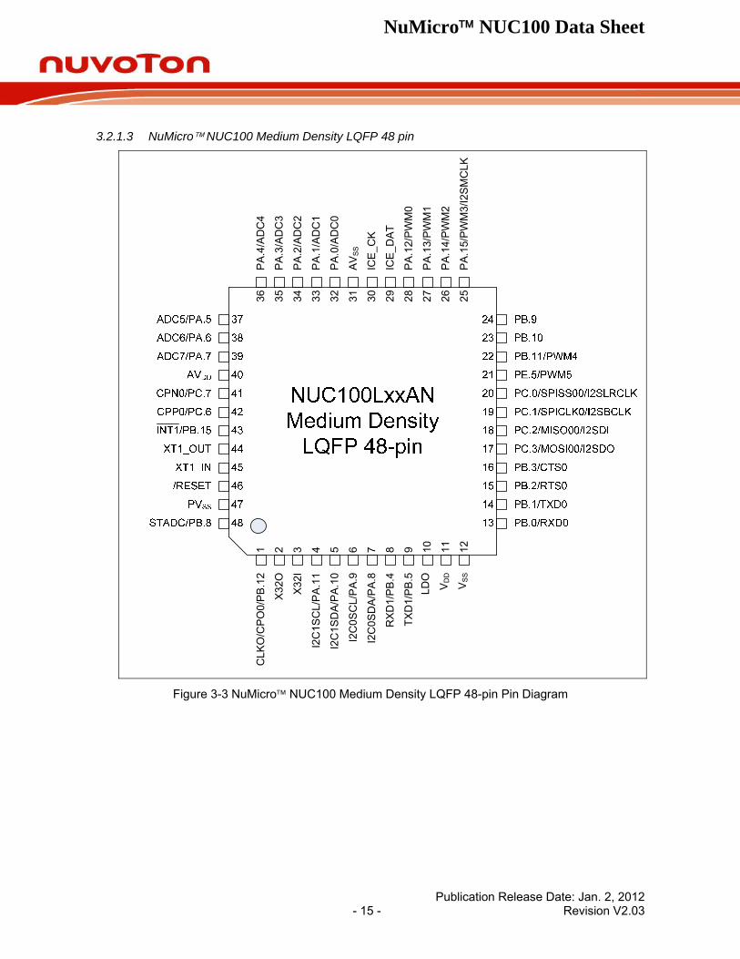
3.2.1.3 NuMicro™ NUC100 Medium Density LQFP 48 pin
CLK
O/C
PO
0/P
B.1
2
X32I
X32
O
I2C
1SC
L/P
A.1
1
I2C
1SD
A/P
A.1
0
I2C
0SC
L/P
A.9
I2C
0SD
A/P
A.8
RXD
1/P
B.4
TXD
1/P
B.5
LDO
VD
D
VS
S
PA
.4/A
DC
4
PA
.3/A
DC
3
PA
.2/A
DC
2
PA
.1/A
DC
1
PA
.0/A
DC
0
AV
SS
ICE
_CK
ICE
_DA
T
PA
.12/
PW
M0
PA
.13/
PW
M1
PA
.14/
PW
M2
PA
.15/
PW
M3/
I2S
MC
LK121110987654321
252627282930313233343536
Figure 3-3 NuMicro™ NUC100 Medium Density LQFP 48-pin Pin Diagram
Publication Release Date: Jan. 2, 2012 - 15 - Revision V2.03
NuMicro™ NUC100 Data Sheet
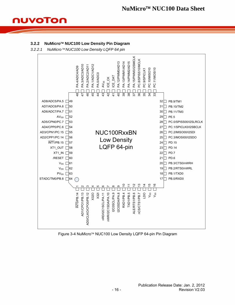
3.2.2 NuMicro™ NUC100 Low Density Pin Diagram 3.2.2.1 NuMicro™ NUC100 Low Density LQFP 64 pin
AD8/ADC5/PA.5
AD7/ADC6/PA.6
AD6/ADC7/PA.7
INT0
/PB
.14
AD
1/C
PO
1/P
B.1
3
AD
0/C
LKO
/CP
O0/
PB
.12
X32
I
X32
O
nRD
/I2C
1SC
L/P
A.1
1
nWR
/I2C
1SD
A/P
A.1
0
I2C
0SC
L/P
A.9
I2C
0SD
A/P
A.8
RX
D1/
PB
.4
TXD
1/P
B.5
ALE
/RTS
1/P
B.6
nCS
/CTS
1/P
B.7
LDO
V DD
VSS
AD5/CPN0/PC.7
AD4/CPP0/PC.6
AD3/CPN1/PC.15
AD2/CPP1/PC.14
INT1/PB.15
XT1_OUT
XT1_IN
/RESET
STADC/TM0/PB.8
PA
.4/A
DC
4/A
D9
PA
.3/A
DC
3/A
D10
PA
.2/A
DC
2/A
D11
PA
.1/A
DC
1/A
D12
PA
.0/A
DC
0
AV
SS
ICE
_CK
ICE
_DA
T
PA
.12/
PW
M0/
AD
13
PA
.13/
PW
M1/
AD
14
PA
.14/
PW
M2/
AD
15
PA
.15/
PW
M3/
I2S
MC
LK
PC
.8/S
PIS
S10
/MC
LK
PC
.9/S
PIC
LK1
AVDD
VSS
VDD
PVSS
PC.0/SPISS00/I2SLRCLK
PC.1/SPICLK0/I2SBCLK
PC.2/MISO00/I2SDI
PC.3/MOSI00/I2SDO
17
18
19
20
21
22
23
24
25
26
27
28
29
30
31
32
64
63
62
61
60
59
58
57
56
55
54
53
52
51
50
49
16151413121110987654321
33343536373839404142434445464748
PC
.10/
MIS
O10
PC
.11/
MO
SI1
0
PB.9/TM1
PB.10/TM2
PB.11/TM3
PE.5
PD.15
PD.14
PD.7
PD.6
PB.3/CTS0/nWRH
PB.2/RTS0/nWRL
PB.1/TXD0
PB.0/RXD0
NUC100RxxBNLow DensityLQFP 64-pin
Figure 3-4 NuMicro™ NUC100 Low Density LQFP 64-pin Pin Diagram
Publication Release Date: Jan. 2, 2012 - 16 - Revision V2.03
NuMicro™ NUC100 Data Sheet
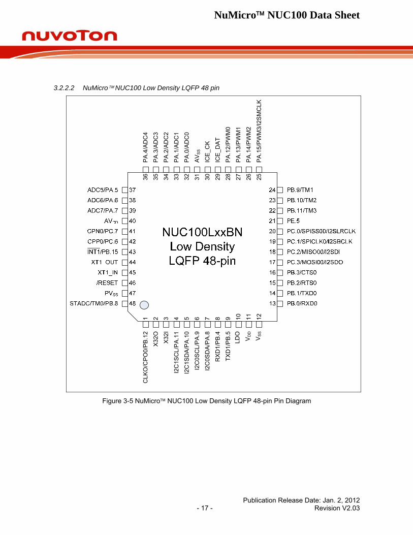
3.2.2.2 NuMicro™ NUC100 Low Density LQFP 48 pin
CLK
O/C
PO
0/P
B.1
2
X32I
X32
O
I2C
1SC
L/P
A.1
1
I2C
1SD
A/P
A.1
0
I2C
0SC
L/P
A.9
I2C
0SD
A/P
A.8
RXD
1/P
B.4
TXD
1/P
B.5
LDO
VD
D
VS
S
PA
.4/A
DC
4
PA
.3/A
DC
3
PA
.2/A
DC
2
PA
.1/A
DC
1
PA
.0/A
DC
0
AV
SS
ICE
_CK
ICE
_DA
T
PA
.12/
PW
M0
PA
.13/
PW
M1
PA
.14/
PW
M2
PA
.15/
PW
M3/
I2S
MC
LK121110987654321
252627282930313233343536
Figure 3-5 NuMicro™ NUC100 Low Density LQFP 48-pin Pin Diagram
Publication Release Date: Jan. 2, 2012 - 17 - Revision V2.03
NuMicro™ NUC100 Data Sheet
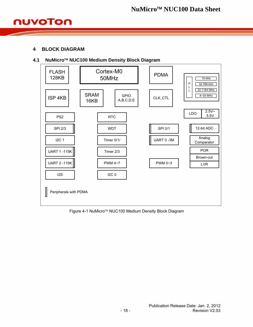
4 BLOCK DIAGRAM
4.1 NuMicro™ NUC100 Medium Density Block Diagram
FLASH128KB
Cortex-M050MHz
CLK_CTL
PDMA
ISP 4KB SRAM16KB
GPIOA,B,C,D,E
UART 1 -115K
I2C 1
Timer 2/3
RTC
WDT
I2C 0
SPI 0/1
UART 0 -3M
PWM 0~3
Timer 0/1/
12-bit ADC
Analog Comparator
POR
Brown-out
LVR
Peripherals with PDMA
I2S
10 kHz
32.768 kHzPLL 22.1184 MHz
4~24 MHz
LDO 2.5V~ 5.5V
PWM 4~7UART 2 -115K
SPI 2/3
PS2
Figure 4-1 NuMicro™ NUC100 Medium Density Block Diagram
Publication Release Date: Jan. 2, 2012 - 18 - Revision V2.03
NuMicro™ NUC100 Data Sheet
4.2 NuMicro™ NUC100 Low Density Block Diagram
FLASH64KB
Cortex-M050MHz
CLK_CTL
PDMA
ISP 4KB SRAM8KB
GPIOA,B,C,D,E
UART 1 -115K
I2C 1
Timer 2/3
RTC
WDT
I2C 0
SPI 0/1
UART 0 -3M
PWM 0~3
Timer 0/1/
12-bit ADC
Analog Comparator
POR
Brown-out
LVR
Peripherals with PDMA
I2S
PLL
LDO 2.5V~ 5.5V
10 kHz
32.768 kHz
22.1184 MHz
4~24 MHz
Figure 4-2 NuMicro™ NUC100 Low Density Block Diagram
Publication Release Date: Jan. 2, 2012 - 19 - Revision V2.03
NuMicro™ NUC100 Data Sheet
5 FUNCTIONAL DESCRIPTION
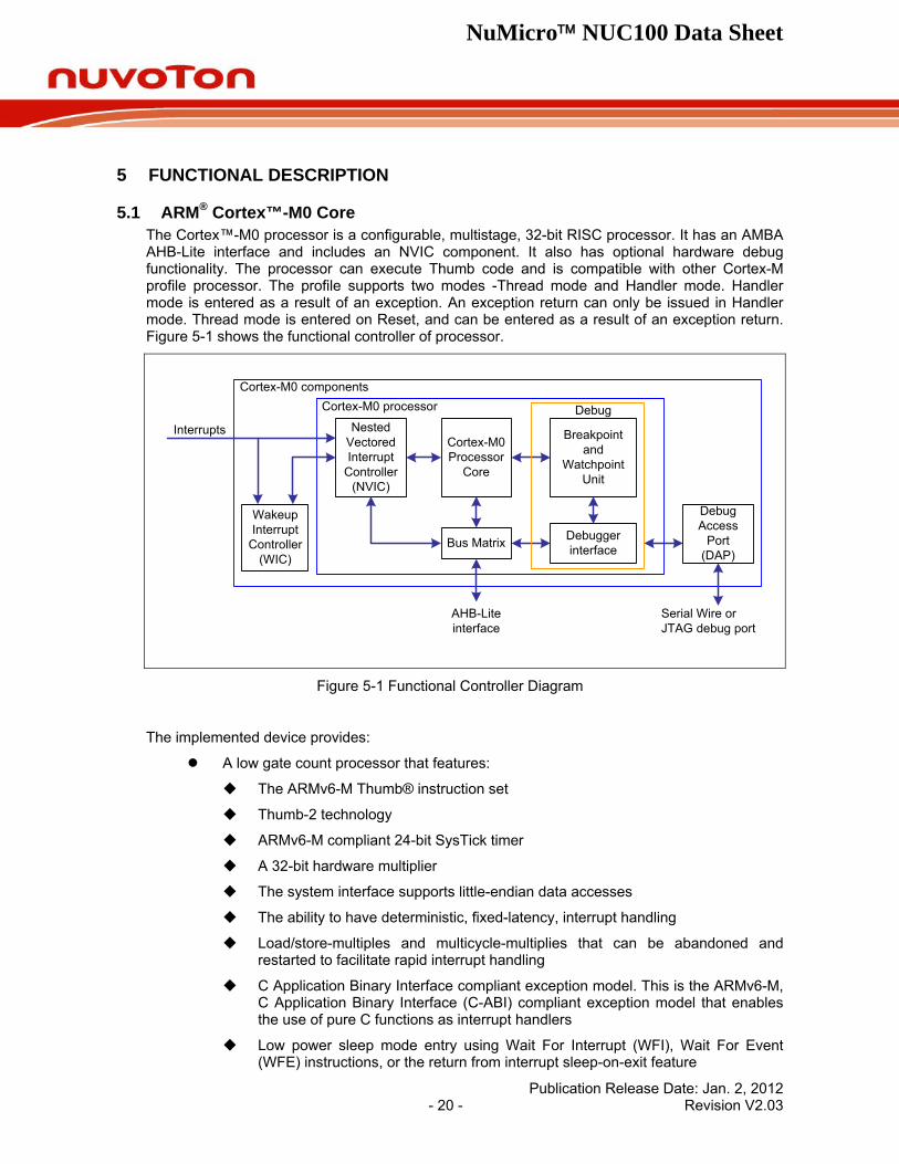
5.1 ARM® Cortex™-M0 Core The Cortex™-M0 processor is a configurable, multistage, 32-bit RISC processor. It has an AMBA AHB-Lite interface and includes an NVIC component. It also has optional hardware debug functionality. The processor can execute Thumb code and is compatible with other Cortex-M profile processor. The profile supports two modes -Thread mode and Handler mode. Handler mode is entered as a result of an exception. An exception return can only be issued in Handler mode. Thread mode is entered on Reset, and can be entered as a result of an exception return. Figure 5-1 shows the functional controller of processor.
Cortex-M0Processor
Core
Nested Vectored Interrupt
Controller(NVIC)
Breakpointand
Watchpoint Unit
Debugger interfaceBus Matrix
Debug Access
Port(DAP)
DebugCortex-M0 processorCortex-M0 components
WakeupInterrupt
Controller (WIC)
Interrupts
Serial Wire or JTAG debug port
AHB-Lite interface
Figure 5-1 Functional Controller Diagram
The implemented device provides:
sor that features:
et
SysTick timer
ts little-endian data accesses
dling
bandoned and
ption model. This is the ARMv6-M,
terrupt (WFI), Wait For Event
A low gate count proces
The ARMv6-M Thumb® instruction s
Thumb-2 technology
ARMv6-M compliant 24-bit
A 32-bit hardware multiplier
The system interface suppor
The ability to have deterministic, fixed-latency, interrupt han
Load/store-multiples and multicycle-multiplies that can be arestarted to facilitate rapid interrupt handling
C Application Binary Interface compliant exceC Application Binary Interface (C-ABI) compliant exception model that enables the use of pure C functions as interrupt handlers
Low power sleep mode entry using Wait For In(WFE) instructions, or the return from interrupt sleep-on-exit feature
Publication Release Date: Jan. 2, 2012 - 20 - Revision V2.03
NuMicro™ NUC100 Data Sheet
Publication Release Date: Jan. 2, 2012 - 21 - Revision V2.03
rrupt inputs, each with four levels of priority
ive interrupt lines
p mode
breakpoints.
pling Register (PCSR) for non-intrusive code profiling.
MBA-3 AHB-Lite system interface that provides simple integration
e DAP (Debug Access Port).
NVIC that features:
32 external inte
Dedicated Non-Maskable Interrupt (NMI) input.
Support for both level-sensitive and pulse-sensit
Wake-up Interrupt Controller (WIC), providing ultra-low power sleesupport.
Debug support
Four hardware
Two watchpoints.
Program Counter Sam
Single step and vector catch capabilities.
Bus interfaces:
Single 32-bit Ato all system peripherals and memory.
Single 32-bit slave port that supports th
NuMicro™ NUC100 Data Sheet
Publication Release Date: Jan. 2, 2012 - 22 - Revision V2.03
5.2 System Manager
5.2.1 Overview System management includes these following sections:
System Resets
System Memory Map
System management registers for Part Number ID, chip reset and on-chip controllers reset , multi-functional pin control
System Timer (SysTick)
Nested Vectored Interrupt Controller (NVIC)
System Control registers
5.2.2 System Reset The system reset can be issued by one of the below listed events. For these reset event flags can be read by RSTSRC register.
The Power-On Reset
The low level on the /RESET pin
Watchdog Time Out Reset
Low Voltage Reset
Brown-Out Detector Reset
CPU Reset
System Reset
System Reset and Power-On Reset all reset the whole chip including all peripherals. The difference between System Reset and Power-On Reset is external crystal circuit and ISPCON.BS bit. System Reset doesn’t reset external crystal circuit and ISPCON.BS bit, but Power-On Reset does.
NuMicro™ NUC100 Data Sheet
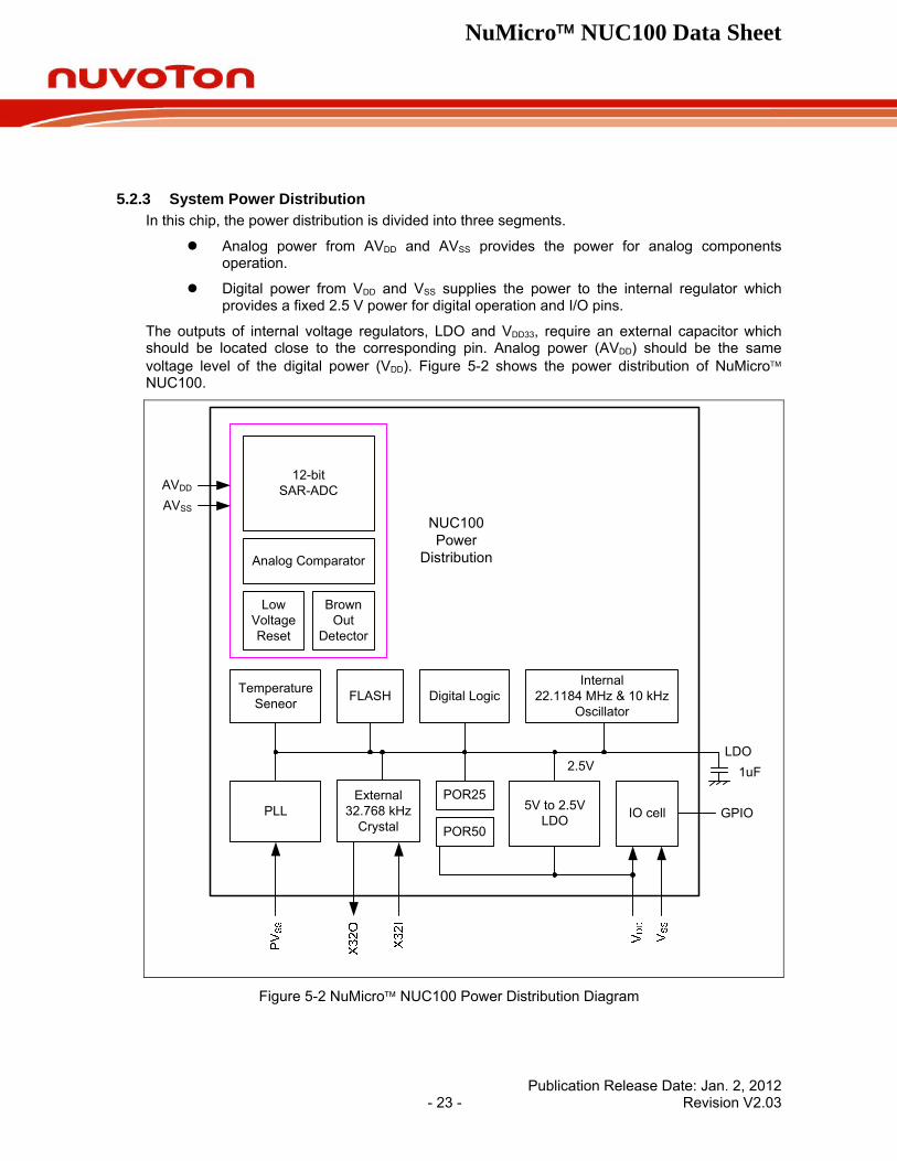
5.2.3 System Power Distribution In this chip, the power distribution is divided into three segments.
Analog power from AVDD and AVSS provides the power for analog components operation.
Digital power from VDD and VSS supplies the power to the internal regulator which provides a fixed 2.5 V power for digital operation and I/O pins.
The outputs of internal voltage regulators, LDO and VDD33, require an external capacitor which should be located close to the corresponding pin. Analog power (AVDD) should be the same voltage level of the digital power (VDD). Figure 5-2 shows the power distribution of NuMicro™ NUC100.
5V to 2.5VLDO
PLL
12-bit SAR-ADC
Brown Out
Detector
POR50
POR25
Low Voltage Reset
External32.768 kHz
Crystal
Analog Comparator
Temperature Seneor FLASH Digital Logic
2.5V
Internal22.1184 MHz & 10 kHz
Oscillator
AVDD
AVSS
LDO1uF
IO cell GPIO
NUC100 Power
Distribution
Figure 5-2 NuMicro™ NUC100 Power Distribution Diagram
Publication Release Date: Jan. 2, 2012 - 23 - Revision V2.03
NuMicro™ NUC100 Data Sheet
Publication Release Date: Jan. 2, 2012 - 24 - Revision V2.03
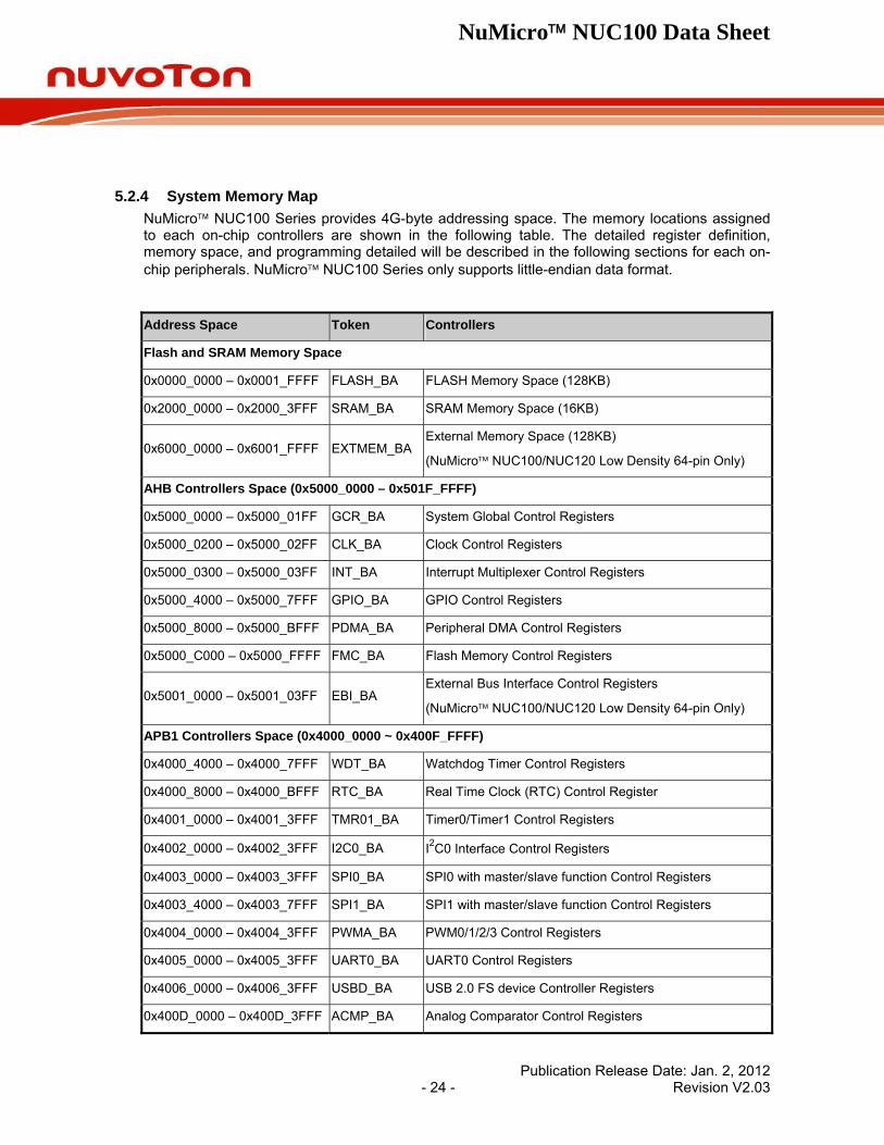
5.2.4 System Memory Map NuMicro™ NUC100 Series provides 4G-byte addressing space. The memory locations assigned to each on-chip controllers are shown in the following table. The detailed register definition, memory space, and programming detailed will be described in the following sections for each on-chip peripherals. NuMicro™ NUC100 Series only supports little-endian data format.
Address Space Token Controllers
Flash and SRAM Memory Space
0x0000_0000 – 0x0001_FFFF FLASH_BA FLASH Memory Space (128KB)
0x2000_0000 – 0x2000_3FFF SRAM_BA SRAM Memory Space (16KB)
0x6000_0000 – 0x6001_FFFF EXTMEM_BAExternal Memory Space (128KB)
(NuMicro™ NUC100/NUC120 Low Density 64-pin Only)
AHB Controllers Space (0x5000_0000 – 0x501F_FFFF)
0x5000_0000 – 0x5000_01FF GCR_BA System Global Control Registers
0x5000_0200 – 0x5000_02FF CLK_BA Clock Control Registers
0x5000_0300 – 0x5000_03FF INT_BA Interrupt Multiplexer Control Registers
0x5000_4000 – 0x5000_7FFF GPIO_BA GPIO Control Registers
0x5000_8000 – 0x5000_BFFF PDMA_BA Peripheral DMA Control Registers
0x5000_C000 – 0x5000_FFFF FMC_BA Flash Memory Control Registers
0x5001_0000 – 0x5001_03FF EBI_BA External Bus Interface Control Registers
(NuMicro™ NUC100/NUC120 Low Density 64-pin Only)
APB1 Controllers Space (0x4000_0000 ~ 0x400F_FFFF)
0x4000_4000 – 0x4000_7FFF WDT_BA Watchdog Timer Control Registers
0x4000_8000 – 0x4000_BFFF RTC_BA Real Time Clock (RTC) Control Register
0x4001_0000 – 0x4001_3FFF TMR01_BA Timer0/Timer1 Control Registers
0x4002_0000 – 0x4002_3FFF I2C0_BA I2C0 Interface Control Registers
0x4003_0000 – 0x4003_3FFF SPI0_BA SPI0 with master/slave function Control Registers
0x4003_4000 – 0x4003_7FFF SPI1_BA SPI1 with master/slave function Control Registers
0x4004_0000 – 0x4004_3FFF PWMA_BA PWM0/1/2/3 Control Registers
0x4005_0000 – 0x4005_3FFF UART0_BA UART0 Control Registers
0x4006_0000 – 0x4006_3FFF USBD_BA USB 2.0 FS device Controller Registers
0x400D_0000 – 0x400D_3FFF ACMP_BA Analog Comparator Control Registers
NuMicro™ NUC100 Data Sheet
Publication Release Date: Jan. 2, 2012 - 25 - Revision V2.03
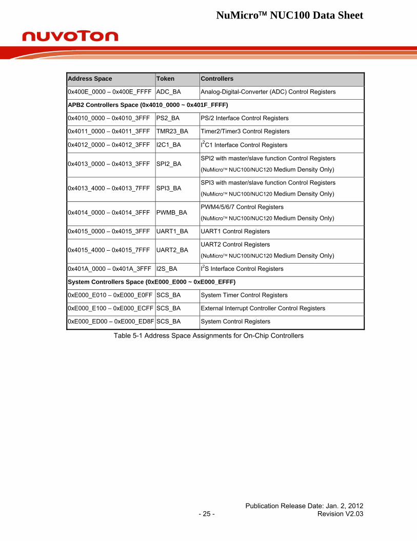
Address Space Token Controllers
0x400E_0000 – 0x400E_FFFF ADC_BA Analog-Digital-Converter (ADC) Control Registers
APB2 Controllers Space (0x4010_0000 ~ 0x401F_FFFF)
0x4010_0000 – 0x4010_3FFF PS2_BA PS/2 Interface Control Registers
0x4011_0000 – 0x4011_3FFF TMR23_BA Timer2/Timer3 Control Registers
0x4012_0000 – 0x4012_3FFF I2C1_BA I2C1 Interface Control Registers
0x4013_0000 – 0x4013_3FFF SPI2_BA SPI2 with master/slave function Control Registers
(NuMicro™ NUC100/NUC120 Medium Density Only)
0x4013_4000 – 0x4013_7FFF SPI3_BA SPI3 with master/slave function Control Registers
(NuMicro™ NUC100/NUC120 Medium Density Only)
0x4014_0000 – 0x4014_3FFF PWMB_BA PWM4/5/6/7 Control Registers
(NuMicro™ NUC100/NUC120 Medium Density Only)
0x4015_0000 – 0x4015_3FFF UART1_BA UART1 Control Registers
0x4015_4000 – 0x4015_7FFF UART2_BA UART2 Control Registers
(NuMicro™ NUC100/NUC120 Medium Density Only)
0x401A_0000 – 0x401A_3FFF I2S_BA I2S Interface Control Registers
System Controllers Space (0xE000_E000 ~ 0xE000_EFFF)
0xE000_E010 – 0xE000_E0FF SCS_BA System Timer Control Registers
0xE000_E100 – 0xE000_ECFF SCS_BA External Interrupt Controller Control Registers
0xE000_ED00 – 0xE000_ED8F SCS_BA System Control Registers
Table 5-1 Address Space Assignments for On-Chip Controllers
NuMicro™ NUC100 Data Sheet
Publication Release Date: Jan. 2, 2012 - 26 - Revision V2.03
5.2.5 System Timer (SysTick) The Cortex-M0 includes an integrated system timer, SysTick. SysTick provides a simple, 24-bit clear-on-write, decrementing, wrap-on-zero counter with a flexible control mechanism. The counter can be used as a Real Time Operating System (RTOS) tick timer or as a simple counter.
When system timer is enabled, it will count down from the value in the SysTick Current Value Register (SYST_CVR) to zero, and reload (wrap) to the value in the SysTick Reload Value Register (SYST_RVR) on the next clock cycle, then decrement on subsequent clocks. When the counter transitions to zero, the COUNTFLAG status bit is set. The COUNTFLAG bit clears on reads.
The SYST_CVR value is UNKNOWN on reset. Software should write to the register to clear it to zero before enabling the feature. This ensures the timer will count from the SYST_RVR value rather than an arbitrary value when it is enabled.
If the SYST_RVR is zero, the timer will be maintained with a current value of zero after it is reloaded with this value. This mechanism can be used to disable the feature independently from the timer enable bit.
For more detailed information, please refer to the documents “ARM® Cortex™-M0 Technical Reference Manual” and “ARM® v6-M Architecture Reference Manual”.
NuMicro™ NUC100 Data Sheet
Publication Release Date: Jan. 2, 2012 - 27 - Revision V2.03
5.2.6 Nested Vectored Interrupt Controller (NVIC) Cortex-M0 provides an interrupt controller as an integral part of the exception mode, named as “Nested Vectored Interrupt Controller (NVIC)”. It is closely coupled to the processor kernel and provides following features:
Nested and Vectored interrupt support
Automatic processor state saving and restoration
Reduced and deterministic interrupt latency
The NVIC prioritizes and handles all supported exceptions. All exceptions are handled in “Handler Mode”. This NVIC architecture supports 32 (IRQ[31:0]) discrete interrupts with 4 levels of priority. All of the interrupts and most of the system exceptions can be configured to different priority levels. When an interrupt occurs, the NVIC will compare the priority of the new interrupt to the current running one’s priority. If the priority of the new interrupt is higher than the current one, the new interrupt handler will override the current handler.
When any interrupts is accepted, the starting address of the interrupt service routine (ISR) is fetched from a vector table in memory. There is no need to determine which interrupt is accepted and branch to the starting address of the correlated ISR by software. While the starting address is fetched, NVIC will also automatically save processor state including the registers “PC, PSR, LR, R0~R3, R12” to the stack. At the end of the ISR, the NVIC will restore the mentioned registers from stack and resume the normal execution. Thus it will take less and deterministic time to process the interrupt request.
The NVIC supports “Tail Chaining” which handles back-to-back interrupts efficiently without the overhead of states saving and restoration and therefore reduces delay time in switching to pending ISR at the end of current ISR. The NVIC also supports “Late Arrival” which improves the efficiency of concurrent ISRs. When a higher priority interrupt request occurs before the current ISR starts to execute (at the stage of state saving and starting address fetching), the NVIC will give priority to the higher one without delay penalty. Thus it advances the real-time capability.
For more detailed information, please refer to the documents “ARM® Cortex™-M0 Technical Reference Manual” and “ARM® v6-M Architecture Reference Manual”.
NuMicro™ NUC100 Data Sheet
Publication Release Date: Jan. 2, 2012 - 28 - Revision V2.03
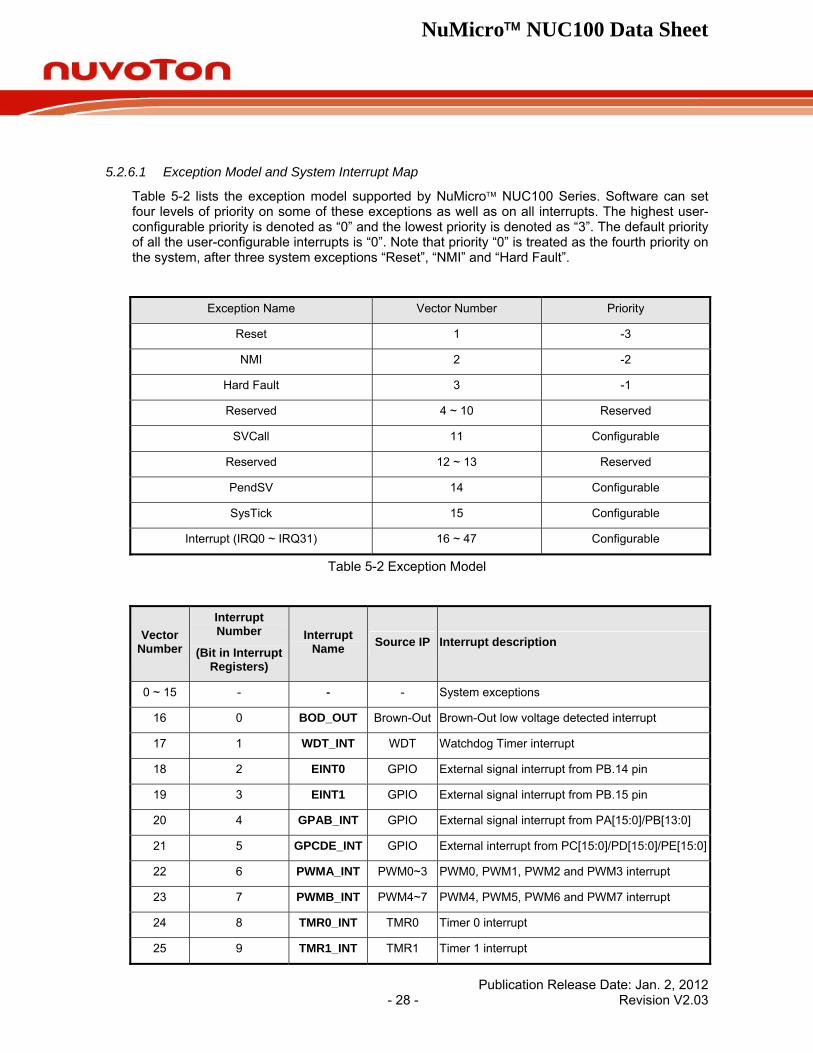
5.2.6.1 Exception Model and System Interrupt Map
Table 5-2 lists the exception model supported by NuMicro™ NUC100 Series. Software can set four levels of priority on some of these exceptions as well as on all interrupts. The highest user-configurable priority is denoted as “0” and the lowest priority is denoted as “3”. The default priority of all the user-configurable interrupts is “0”. Note that priority “0” is treated as the fourth priority on the system, after three system exceptions “Reset”, “NMI” and “Hard Fault”.
Exception Name Vector Number Priority
Reset 1 -3
NMI 2 -2
Hard Fault 3 -1
Reserved 4 ~ 10 Reserved
SVCall 11 Configurable
Reserved 12 ~ 13 Reserved
PendSV 14 Configurable
SysTick 15 Configurable
Interrupt (IRQ0 ~ IRQ31) 16 ~ 47 Configurable
Table 5-2 Exception Model
Vector Number
Interrupt Number
(Bit in Interrupt Registers)
Interrupt Name Source IP Interrupt description
0 ~ 15 - - - System exceptions
16 0 BOD_OUT Brown-Out Brown-Out low voltage detected interrupt
17 1 WDT_INT WDT Watchdog Timer interrupt
18 2 EINT0 GPIO External signal interrupt from PB.14 pin
19 3 EINT1 GPIO External signal interrupt from PB.15 pin
20 4 GPAB_INT GPIO External signal interrupt from PA[15:0]/PB[13:0]
21 5 GPCDE_INT GPIO External interrupt from PC[15:0]/PD[15:0]/PE[15:0]
22 6 PWMA_INT PWM0~3 PWM0, PWM1, PWM2 and PWM3 interrupt
23 7 PWMB_INT PWM4~7 PWM4, PWM5, PWM6 and PWM7 interrupt
24 8 TMR0_INT TMR0 Timer 0 interrupt
25 9 TMR1_INT TMR1 Timer 1 interrupt
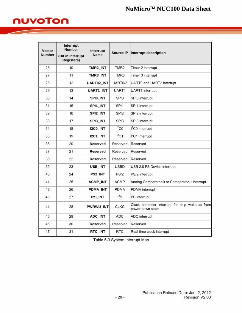
NuMicro™ NUC100 Data Sheet
Publication Release Date: Jan. 2, 2012 - 29 - Revision V2.03
Vector Number
Interrupt Number
(Bit in Interrupt Registers)
Interrupt Name Source IP Interrupt description
26 10 TMR2_INT TMR2 Timer 2 interrupt
27 11 TMR3_INT TMR3 Timer 3 interrupt
28 12 UART02_INT UART0/2 UART0 and UART2 interrupt
29 13 UART1_INT UART1 UART1 interrupt
30 14 SPI0_INT SPI0 SPI0 interrupt
31 15 SPI1_INT SPI1 SPI1 interrupt
32 16 SPI2_INT SPI2 SPI2 interrupt
33 17 SPI3_INT SPI3 SPI3 interrupt
34 18 I2C0_INT I2C0 I2C0 interrupt
35 19 I2C1_INT I2C1 I2C1 interrupt
36 20 Reserved Reserved Reserved
37 21 Reserved Reserved Reserved
38 22 Reserved Reserved Reserved
39 23 USB_INT USBD USB 2.0 FS Device interrupt
40 24 PS2_INT PS/2 PS/2 interrupt
41 25 ACMP_INT ACMP Analog Comparator-0 or Comaprator-1 interrupt
42 26 PDMA_INT PDMA PDMA interrupt
43 27 I2S_INT I2S I2S interrupt
44 28 PWRWU_INT CLKC Clock controller interrupt for chip wake-up from power down state
45 29 ADC_INT ADC ADC interrupt
46 30 Reserved Reserved Reserved
47 31 RTC_INT RTC Real time clock interrupt
Table 5-3 System Interrupt Map
NuMicro™ NUC100 Data Sheet
Publication Release Date: Jan. 2, 2012 - 30 - Revision V2.03
5.2.6.2 Vector Table
When any interrupts is accepted, the processor will automatically fetch the starting address of the interrupt service routine (ISR) from a vector table in memory. For ARMv6-M, the vector table base address is fixed at 0x00000000. The vector table contains the initialization value for the stack pointer on reset, and the entry point addresses for all exception handlers. The vector number on previous page defines the order of entries in the vector table associated with exception handler entry as illustrated in previous section.
Vector Table Word Offset Description
0 SP_main – The Main stack pointer
Vector Number Exception Entry Pointer using that Vector Number
Table 5-4 Vector Table Format
5.2.6.3 Operation Description
NVIC interrupts can be enabled and disabled by writing to their corresponding Interrupt Set-Enable or Interrupt Clear-Enable register bit-field. The registers use a write-1-to-enable and write-1-to-clear policy, both registers reading back the current enabled state of the corresponding interrupts. When an interrupt is disabled, interrupt assertion will cause the interrupt to become Pending, however, the interrupt will not activate. If an interrupt is Active when it is disabled, it remains in its Active state until cleared by reset or an exception return. Clearing the enable bit prevents new activations of the associated interrupt.
NVIC interrupts can be pended/un-pended using a complementary pair of registers to those used to enable/disable the interrupts, named the Set-Pending Register and Clear-Pending Register respectively. The registers use a write-1-to-enable and write-1-to-clear policy, both registers reading back the current pended state of the corresponding interrupts. The Clear-Pending Register has no effect on the execution status of an Active interrupt.
NVIC interrupts are prioritized by updating an 8-bit field within a 32-bit register (each register supporting four interrupts).
The general registers associated with the NVIC are all accessible from a block of memory in the System Control Space and will be described in next section.
NuMicro™ NUC100 Data Sheet
Publication Release Date: Jan. 2, 2012 - 31 - Revision V2.03
5.3 Clock Controller
5.3.1 Overview The clock controller generates the clocks for the whole chip, including system clocks and all peripheral clocks. The clock controller also implements the power control function with the individually clock ON/OFF control, clock source selection and a clock divider. The chip will not enter power down mode until CPU sets the power down enable bit (PWR_DOWN_EN) and Cortex-M0 core executes the WFI instruction. After that, chip enter power down mode and wait for wake-up interrupt source triggered to leave power down mode. In the power down mode, the clock controller turns off the external 4~24 MHz high speed crystal and internal 22.1184 MHz high speed oscillator to reduce the overall system power consumption.
NuMicro™ NUC100 Data Sheet
1
0
PLLCON[19]
22.1184 MHz
4~12 MHz
PLLFOUT
111
011
010
001
4~24 MHz
32.768 kHz
4~24 MHz
HCLK
22.1184 MHz
000
1/2
1/2
1/2
CLKSEL0[5:3]
1
0SysTick
TMR 3
ADC
UART 0-2
PDMA
ACMP
I2C 0~1
SPI 0-3
USB
I2S
RTC
PS2
FDIV
PWM 0-1
WDT
PWM 2-3PWM 4-5PWM 6-7
TMR 0TMR 1TMR 2
CPU
FMC
EBI
32.768 kHz
10 kHz 111
010
001
000
HCLK
32.768 kHz
4~24 MHz
111
011
010
001
PLLFOUT
32.768 kHz
4~24 MHz
10 kHz
22.1184 MHz
000
CLKSEL0[2:0]
SYST_CSR[2]
CPUCLK
1/(HCLK_N+1)
PCLK
CPUCLK
HCLK
11
01
00
PLLFOUT
4~24 MHz
22.1184 MHz
CLKSEL1[3:2]CLKSEL1[25:24]
22.1184 MHz
CLKSEL1[22:20]CLKSEL1[18:16]CLKSEL1[14:12]CLKSEL1[10:8]
1/(USB_N+1)PLLFOUT
11
10
01
00
HCLK
PLLFOUT
4~24 MHz
22.1184 MHz
11
10
01
00
HCLK
4~24 MHz
22.1184 MHz
32.768 kHz
CLKSEL2[7:2]CLKSEL1[31:28]
22.1184 MHz
32.768 kHz
BOD10 kHz
1/(ADC_N+1)
CLKSEL2[1:0]11
10
CLKSEL1[1:0]
HCLK1/2048
1/(UART_N+1)
22.1184 MHz
4~24 MHz
Figure 5-3 Clock generator global view diagram
Publication Release Date: Jan. 2, 2012 - 32 - Revision V2.03
NuMicro™ NUC100 Data Sheet
5.3.2 Clock Generator The clock generator consists of 5 clock sources which are listed below:
One external 32.768 kHz low speed crystal
One external 4~24 MHz high speed crystal
One programmable PLL FOUT(PLL source consists of external 4~24 MHz high speed crystal and internal 22.1184 MHz high speed oscillator)
One internal 22.1184 MHz high speed oscillator
One internal 10 kHz low speed oscillator
XT_OUT
External 4~24 MHz
Crystal
XTL12M_EN (PWRCON[0])
XT_IN
Internal 22.1184 MHz
Oscillator
OSC22M_EN (PWRCON[2])0
1PLL
PLL_SRC (PLLCON[19])
PLL FOUT
X32O
External 32.768 kHz
Crystal
32.768 kHz
XTL32K_EN (PWRCON[1])
X32I
Internal 10 kHz
Oscillator
OSC10K_EN(PWRCON[3])
4~24 MHz
22.1184 MHz
10 kHz
Figure 5-4 Clock generator block diagram
Publication Release Date: Jan. 2, 2012 - 33 - Revision V2.03
NuMicro™ NUC100 Data Sheet
5.3.3 System Clock and SysTick Clock The system clock has 5 clock sources which were generated from clock generator block. The clock source switch depends on the register HCLK_S (CLKSEL0[2:0]). The block diagram is showed in Figure 5-5.
111
011
010
001
PLLFOUT
32.768 kHz
4~24 MHz
10 kHz
HCLK_S (CLKSEL0[2:0])
22.1184 MHz
000
1/(HCLK_N+1)HCLK_N (CLKDIV[3:0])
CPU in Power Down Mode
CPU
AHB
APB
CPUCLK
HCLK
PCLK
Figure 5-5 System Clock Block Diagram
The clock source of Sy PU clock or external clock sTick in Cortex-M0 core can use C(SYST_CSR[2]). If using external clock, the SysTick clock (STCLK) has 5 clock sources. The clock source switch depends on the setting of the register STCLK_S (CLKSEL0[5:3]). The block diagram is showed in Figure 5-6.
Figure 5-6 SysTick Clock Control Block Diagram
Publication Release Date: Jan. 2, 2012 - 34 - Revision V2.03
NuMicro™ NUC100 Data Sheet
Publication Release Date: Jan. 2, 2012 - 35 - Revision V2.03
5.3.4 Peripherals Clock The peripherals clock had different clock source switch setting which depends on the different peripheral. Please refer the CLKSEL1 and CLKSEL2 register description in 5.3.7.
5.3.5 Power Down Mode Clock When chip enters into power down mode, system clocks, some clock sources, and some peripheral clocks will be disabled. Some clock sources and peripherals clock are still active in power down mode.
For theses clocks which still keep active list below:
Clock Generator
Internal 10 kHz low speed oscillator clock
External 32.768 kHz low speed crystal clock
Peripherals Clock (When WDT adopt internal 10 kHz low speed oscillator as clock source and RTC adopt external 32.768 kHz low speed crystal as clock source)
NuMicro™ NUC100 Data Sheet
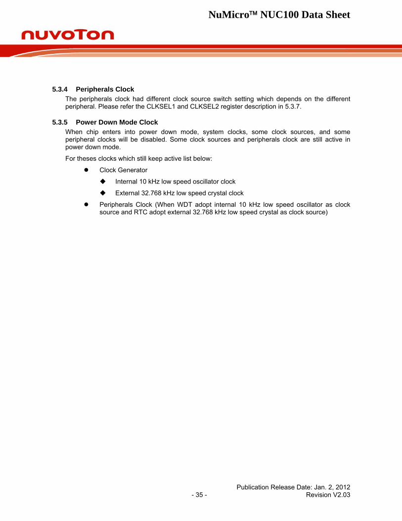
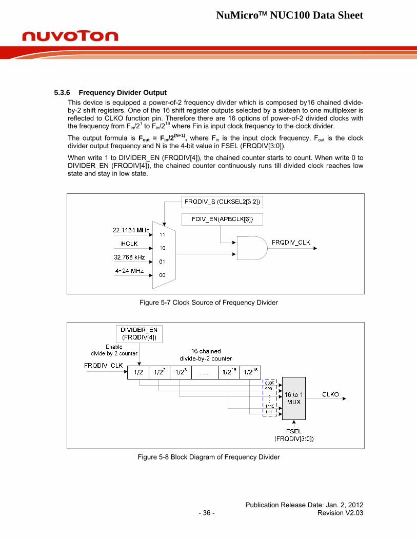
5.3.6 Frequency Divider Output This device is equipped a power-of-2 frequency divider which is composed by16 chained divide-by-2 shift registers. One of the 16 shift register outputs selected by a sixteen to one multiplexer is reflected to CLKO function pin. Therefore there are 16 options of power-of-2 divided clocks with the frequency from Fin/21 to Fin/216 where Fin is input clock frequency to the clock divider.
The output formula is Fout = Fin/2(N+1), where Fin is the input clock frequency, Fout is the clock divider output frequency and N is the 4-bit value in FSEL (FRQDIV[3:0]).
When write 1 to DIVIDER_EN (FRQDIV[4]), the chained counter starts to count. When write 0 to DIVIDER_EN (FRQDIV[4]), the chained counter continuously runs till divided clock reaches low state and stay in low state.
Figure 5-7 Clock Source of Frequency Divider
Figure 5-8 Block Diagram of Frequency Divider
Publication Release Date: Jan. 2, 2012 - 36 - Revision V2.03
NuMicro™ NUC100 Data Sheet
Publication Release Date: Jan. 2, 2012 - 37 - Revision V2.03
5.4 General Purpose I/O (GPIO)
5.4.1 Overview NuMicro™ NUC100/NUC120 Medium Density has up to 80 General Purpose I/O pins can be shared with other function pins; it depends on the chip configuration. These 80 pins are arranged in 5 ports named with GPIOA, GPIOB, GPIOC, GPIOD and GPIOE. Each port equips maximum 16 pins. Each one of the 80 pins is independent and has the corresponding register bits to control the pin mode function and data.
NuMicro™ NUC100/NUC120 Low Density has up to 65 General Purpose I/O pins can be shared with other function pins; it depends on the chip configuration and package. These 65 pins are arranged in 4 ports named with GPIOA, GPIOB, GPIOC and GPIOD with each port equips maximum 16 pins and another port named GPIOE with 1 pins PE.5.
The I/O type of each of I/O pins can be configured by software individually as input, output, open-drain or quasi-bidirectional mode. After reset, the I/O type of all pins stay in quasi-bidirectional mode and port data register GPIOx_DOUT[15:0] resets to 0x0000_FFFF. Each I/O pin equips a very weakly individual pull-up resistor which is about 110KΩ~300KΩ for VDD is from 5.0 V to 2.5 V.
5.4.2 Features Four I/O modes:
Quasi bi-direction
Push-Pull output
Open-Drain output
Input only with high impendence
TTL/Schmitt trigger input selectable
I/O pin can be configured as interrupt source with edge/level setting
High driver and high sink IO mode support
NuMicro™ NUC100 Data Sheet
5.5 I2C Serial Interface Controller (Master/Slave) (I2C)
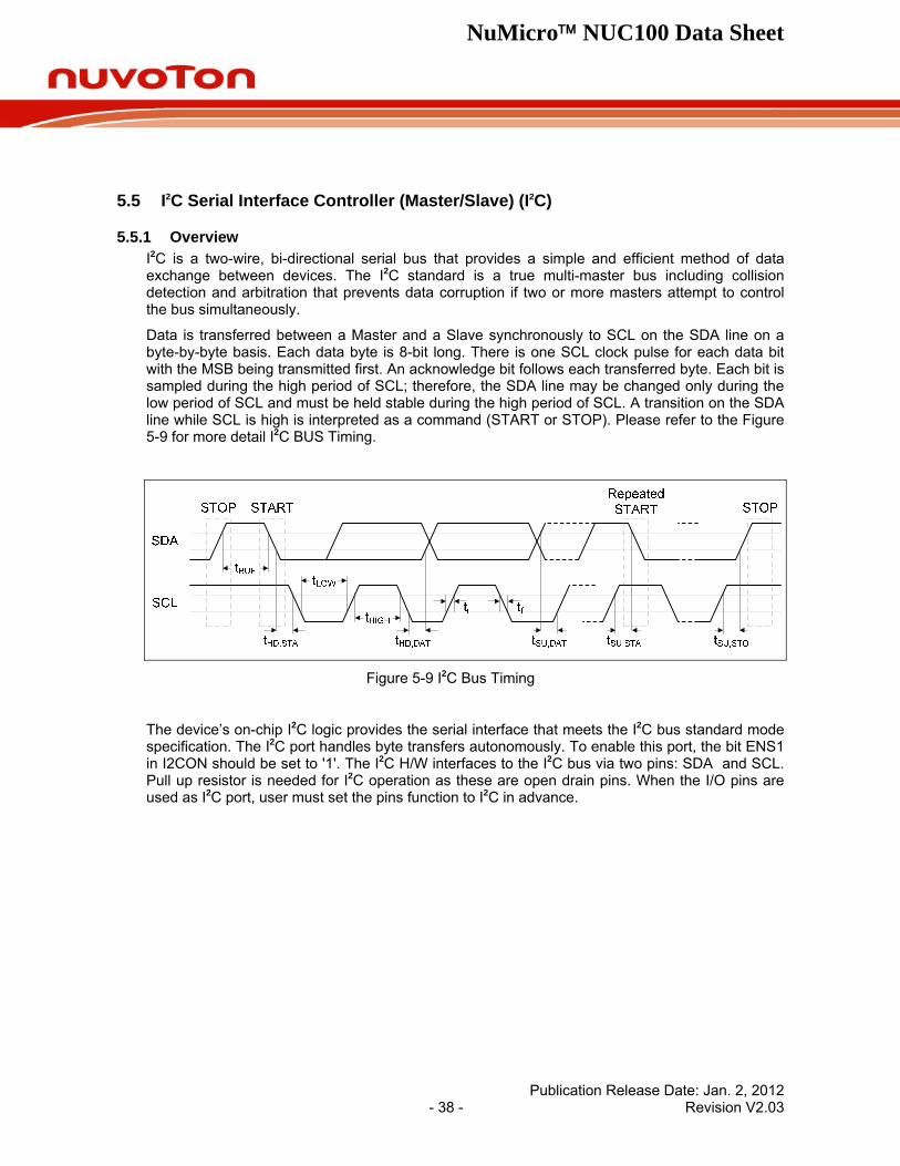
5.5.1 Overview I2C is a two-wire, bi-directional serial bus that provides a simple and efficient method of data exchange between devices. The I2C standard is a true multi-master bus including collision detection and arbitration that prevents data corruption if two or more masters attempt to control the bus simultaneously.
Data is transferred between a Master and a Slave synchronously to SCL on the SDA line on a byte-by-byte basis. Each data byte is 8-bit long. There is one SCL clock pulse for each data bit with the MSB being transmitted first. An acknowledge bit follows each transferred byte. Each bit is sampled during the high period of SCL; therefore, the SDA line may be changed only during the low period of SCL and must be held stable during the high period of SCL. A transition on the SDA line while SCL is high is interpreted as a command (START or STOP). Please refer to the Figure 5-9 for more detail I2C BUS Timing.
Figure 5-9 I2C Bus Timing
The device’s on-chip I2C logic provides the serial interface that meets the I2C bus standard mode specification. The I2C port handles byte transfers autonomously. To enable this port, the bit ENS1 in I2CON should be set to '1'. The I2C H/W interfaces to the I2C bus via two pins: SDA and SCL. Pull up resistor is needed for I2C operation as these are open drain pins. When the I/O pins are used as I2C port, user must set the pins function to I2C in advance.
Publication Release Date: Jan. 2, 2012 - 38 - Revision V2.03
NuMicro™ NUC100 Data Sheet
Publication Release Date: Jan. 2, 2012 - 39 - Revision V2.03
5.5.2 Features The I2C bus uses two wires (SDA and SCL) to transfer information between devices connected to the bus. The main features of the bus are:
Master/Slave mode
Bidirectional data transfer between masters and slaves
Multi-master bus (no central master)
Arbitration between simultaneously transmitting masters without corruption of serial data on the bus
Serial clock synchronization allows devices with different bit rates to communicate via one serial bus
Serial clock synchronization can be used as a handshake mechanism to suspend and resume serial transfer
Built-in a 14-bit time-out counter will request the I2C interrupt if the I2C bus hangs up and timer-out counter overflows.
External pull-up are needed for high output
Programmable clocks allow versatile rate control
Supports 7-bit addressing mode
I2C-bus controllers support multiple address recognition ( Four slave address with mask option)
NuMicro™ NUC100 Data Sheet
Publication Release Date: Jan. 2, 2012 - 40 - Revision V2.03
5.6 PWM Generator and Capture Timer (PWM)
5.6.1 Overview NuMicro™ NUC100/NUC120 Medium Density has 2 sets of PWM group supports total 4 sets of PWM Generators which can be configured as 8 independent PWM outputs, PWM0~PWM7, or as 4 complementary PWM pairs, (PWM0, PWM1), (PWM2, PWM3), (PWM4, PWM5) and (PWM6, PWM7) with 4 programmable dead-zone generators. NuMicro™ NUC100/NUC120 Low Density only support 1 set of PWM group supports total 2 sets of PWM Generators which can be configured as 4 independent PWM outputs, PWM0~PWM3, or as 2 complementary PWM pairs, (PWM0, PWM1) and (PWM2, PWM3) with 2 programmable dead-zone generators.
Each PWM Generator has one 8-bit prescaler, one clock divider with 5 divided frequencies (1, 1/2, 1/4, 1/8, 1/16), two PWM Timers including two clock selectors, two 16-bit PWM down-counters for PWM period control, two 16-bit comparators for PWM duty control and one dead-zone generator. The 4 sets of PWM Generators provide eight independent PWM interrupt flags which are set by hardware when the corresponding PWM period down counter reaches zero. Each PWM interrupt source with its corresponding enable bit can cause CPU to request PWM interrupt. The PWM generators can be configured as one-shot mode to produce only one PWM cycle signal or auto-reload mode to output PWM waveform continuously.
When PCR.DZEN01 is set, PWM0 and PWM1 perform complementary PWM paired function; the paired PWM period, duty and dead-time are determined by PWM0 timer and Dead-zone generator 0. Similarly, the complementary PWM pairs of (PWM2, PWM3), (PWM4, PWM5) and (PWM6, PWM7) are controlled by PWM2, PWM4 and PWM6 timers and Dead-zone generator 2, 4 and 6, respectively.
To prevent PWM driving output pin with unsteady waveform, the 16-bit period down counter and 16-bit comparator are implemented with double buffer. When user writes data to counter/comparator buffer registers the updated value will be load into the 16-bit down counter/ comparator at the time down counter reaching zero. The double buffering feature avoids glitch at PWM outputs.
When the 16-bit period down counter reaches zero, the interrupt request is generated. If PWM-timer is set as auto-reload mode, when the down counter reaches zero, it is reloaded with PWM Counter Register (CNRx) automatically then start decreasing, repeatedly. If the PWM-timer is set as one-shot mode, the down counter will stop and generate one interrupt request when it reaches zero.
The value of PWM counter comparator is used for pulse high width modulation. The counter control logic changes the output to high level when down-counter value matches the value of compare register.
The alternate feature of the PWM-timer is digital input Capture function. If Capture function is enabled the PWM output pin is switched as capture input mode. The Capture0 and PWM0 share one timer which is included in PWM0 and the Capture1 and PWM1 share PWM1 timer, and etc. Therefore user must setup the PWM-timer before enable Capture feature. After capture feature is enabled, the capture always latched PWM-counter to Capture Rising Latch Register (CRLR) when input channel has a rising transition and latched PWM-counter to Capture Falling Latch Register (CFLR) when input channel has a falling transition. Capture channel 0 interrupt is programmable by setting CCR0.CRL_IE0[1] (Rising latch Interrupt enable) and CCR0.CFL_IE0[2]] (Falling latch Interrupt enable) to decide the condition of interrupt occur. Capture channel 1 has the same feature by setting CCR0.CRL_IE1[17] and CCR0.CFL_IE1[18]. And capture channel 2 to channel 3 on each group have the same feature by setting the corresponding control bits in CCR2. For each group, whenever Capture issues Interrupt 0/1/2/3,
NuMicro™ NUC100 Data Sheet
Publication Release Date: Jan. 2, 2012 - 41 - Revision V2.03
the PWM counter 0/1/2/3 will be reload at this moment.
The maximum captured frequency that PWM can capture is confined by the capture interrupt latency. When capture interrupt occurred, software will do at least three steps, they are: Read PIIR to get interrupt source and Read CRLRx/CFLRx(x=0~3) to get capture value and finally write 1 to clear PIIR to zero. If interrupt latency will take time T0 to finish, the capture signal mustn’t transition during this interval (T0). In this case, the maximum capture frequency will be 1/T0. For example:
HCLK = 50 MHz, PWM_CLK = 25 MHz, Interrupt latency is 900 ns
So the maximum capture frequency will is 1/900ns ≈ 1000 kHz
5.6.2 Features 5.6.2.1 PWM function features:
PWM group has two PWM generators. Each PWM generator supports one 8-bit prescaler, one clock divider, two PWM-timers (down counter), one dead-zone generator and two PWM outputs.
Up to 16-bit resolution
PWM Interrupt request synchronized with PWM period
One-shot or Auto-reload mode PWM
Up to 2 PWM group (PWMA/PWMB) to support 8 PWM channels or 4 PWM paired channels (only 1 PWM group support for NuMicro™ NUC100/NUC120 Low Density)
5.6.2.2 Capture Function Features:
Timing control logic shared with PWM Generators
Support 8 Capture input channels shared with 8 PWM output channels (NuMicro™ NUC100/NUC120 Low Density only support 4 Capture input channels shared with 4 PWM output channels)
Each channel supports one rising latch register (CRLR), one falling latch register (CFLR) and Capture interrupt flag (CAPIFx)
NuMicro™ NUC100 Data Sheet
Publication Release Date: Jan. 2, 2012 - 42 - Revision V2.03
5.7 Real Time Clock (RTC)
5.7.1 Overview Real Time Clock (RTC) controller provides user the real time and calendar message. The clock source of RTC is from an external 32.768 kHz low speed crystal connected at pins X32I and X32O (reference to pin descriptions) or from an external 32.768 kHz low speed oscillator output fed at pin X32I. The RTC controller provides the time message (second, minute, hour) in Time Loading Register (TLR) as well as calendar message (day, month, year) in Calendar Loading Register (CLR). The data message is expressed in BCD format. It also offers alarm function that user can preset the alarm time in Time Alarm Register (TAR) and alarm calendar in Calendar Alarm Register (CAR).
The RTC controller supports periodic Time Tick and Alarm Match interrupts. The periodic interrupt has 8 period options 1/128, 1/64, 1/32, 1/16, 1/8, 1/4, 1/2 and 1 second which are selected by TTR (TTR[2:0]). When RTC counter in TLR and CLR is equal to alarm setting time registers TAR and CAR, the alarm interrupt flag (RIIR.AIF) is set and the alarm interrupt is requested if the alarm interrupt is enabled (RIER.AIER=1). Both RTC Time Tick and Alarm Match can cause chip wake-up from power down mode if wake-up function is enabled (TWKE (TTR[3])=1).
5.7.2 Features There is a time counter (second, minute, hour) and calendar counter (day, month, year) for
user to check the time
Alarm register (second, minute, hour, day, month, year)
12-hour or 24-hour mode is selectable
Leap year compensation automatically
Day of week counter
Frequency compensate register (FCR)
All time and calendar message is expressed in BCD code
Support periodic time tick interrupt with 8 period options 1/128, 1/64, 1/32, 1/16, 1/8, 1/4, 1/2 and 1 second
Support RTC Time Tick and Alarm Match interrupt
Support wake-up chip from power down mode
NuMicro™ NUC100 Data Sheet
Publication Release Date: Jan. 2, 2012 - 43 - Revision V2.03
5.8 Serial Peripheral Interface (SPI)
5.8.1 Overview The Serial Peripheral Interface (SPI) is a synchronous serial data communication protocol which operates in full duplex mode. Devices communicate in master/slave mode with 4-wire bi-direction interface. The NuMicro™ NUC100/NUC120 Medium Density contains up to four sets of SPI controller performing a serial-to-parallel conversion on data received from a peripheral device, and a parallel-to-serial conversion on data transmitted to a peripheral device. Each set of SPI controller can be set as a master that can drive up to 2 external peripheral slave devices; it also can be configured as a slave device controlled by an off-chip master device. NuMicro™ NUC100/NUC120 Low Density contains two sets of SPI controller only.
This controller supports a variable serial clock for special application and it also supports 2-bit transfer mode to connect 2 off-chip slave devices at the same time. The SPI controller also supports PDMA function to access the data buffer.
5.8.2 Features Up to four sets of SPI controller for NuMicro™ NUC100/NUC120 Medium Density
Up to two sets of SPI controller for NuMicro™ NUC100/NUC120 Low Density
Support master or slave mode operation
Support 1-bit or 2-bit transfer mode
Configurable bit length up to 32-bit of a transfer word and configurable word numbers up to 2 of a transaction, so the maximum bit length is 64-bit for each data transfer
Provide burst mode operation, transmit/receive can be transferred up to two times word transaction in one transfer
Support MSB or LSB first transfer
2 device/slave select lines in master mode, but 1 device/slave select line in slave mode
Support byte reorder function
Support byte or word suspend mode
Variable output serial clock frequency in master mode
Support two programmable serial clock frequencies in master mode
Support two channel PDMA request, one for transmitter and another for receiver
NuMicro™ NUC100 Data Sheet
Publication Release Date: Jan. 2, 2012 - 44 - Revision V2.03
5.9 Timer Controller (TMR)
5.9.1 Overview The timer controller includes four 32-bit timers, TIMER0~TIMER3, which allows user to easily implement a timer control for applications. The timer can perform functions like frequency measurement, event counting, interval measurement, clock generation, delay timing, and so on. The timer can generates an interrupt signal upon timeout, or provide the current value during operation. Note: toggle mode, continuous counting mode and event counting function only support in NuMicro™ NUC100/NUC120 Low Density.
5.9.2 Features 4 sets of 32-bit timers with 24-bit up-timer and one 8-bit pre-scale counter
Independent clock source for each timer
Provides one-shot, periodic, toggle and continuous counting operation modes (NuMicro™ NUC100/NUC120 Medium Density only support one-shot and periodic mode)
Time out period = (Period of timer clock input) * (8-bit pre-scale counter + 1) * (24-bit TCMP)
Maximum counting cycle time = (1 / T MHz) * (28) * (224), T is the period of timer clock
24-bit timer value is readable through TDR (Timer Data Register)
Support event counting function to count the event from external pin (NuMicro™ NUC100/NUC120 Low Density only)
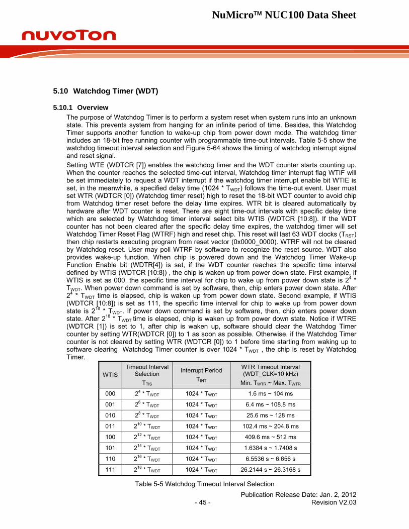
NuMicro™ NUC100 Data Sheet
Publication Release Date: Jan. 2, 2012 - 45 - Revision V2.03
5.10 Watchdog Timer (WDT)
5.10.1 Overview The purpose of Watchdog Timer is to perform a system reset when system runs into an unknown state. This prevents system from hanging for an infinite period of time. Besides, this Watchdog Timer supports another function to wake-up chip from power down mode. The watchdog timer includes an 18-bit free running counter with programmable time-out intervals. Table 5-5 show the watchdog timeout interval selection and Figure 5-64 shows the timing of watchdog interrupt signal and reset signal. Setting WTE (WDTCR [7]) enables the watchdog timer and the WDT counter starts counting up. When the counter reaches the selected time-out interval, Watchdog timer interrupt flag WTIF will be set immediately to request a WDT interrupt if the watchdog timer interrupt enable bit WTIE is set, in the meanwhile, a specified delay time (1024 * TWDT) follows the time-out event. User must set WTR (WDTCR [0]) (Watchdog timer reset) high to reset the 18-bit WDT counter to avoid chip from Watchdog timer reset before the delay time expires. WTR bit is cleared automatically by hardware after WDT counter is reset. There are eight time-out intervals with specific delay time which are selected by Watchdog timer interval select bits WTIS (WDTCR [10:8]). If the WDT counter has not been cleared after the specific delay time expires, the watchdog timer will set Watchdog Timer Reset Flag (WTRF) high and reset chip. This reset will last 63 WDT clocks (TRST) then chip restarts executing program from reset vector (0x0000_0000). WTRF will not be cleared by Watchdog reset. User may poll WTRF by software to recognize the reset source. WDT also provides wake-up function. When chip is powered down and the Watchdog Timer Wake-up Function Enable bit (WDTR[4]) is set, if the WDT counter reaches the specific time interval defined by WTIS (WDTCR [10:8]) , the chip is waken up from power down state. First example, if WTIS is set as 000, the specific time interval for chip to wake up from power down state is 24 * TWDT. When power down command is set by software, then, chip enters power down state. After 24 * TWDT time is elapsed, chip is waken up from power down state. Second example, if WTIS (WDTCR [10:8]) is set as 111, the specific time interval for chip to wake up from power down state is 218 * TWDT. If power down command is set by software, then, chip enters power down state. After 218 * TWDT time is elapsed, chip is waken up from power down state. Notice if WTRE (WDTCR [1]) is set to 1, after chip is waken up, software should clear the Watchdog Timer counter by setting WTR(WDTCR [0]) to 1 as soon as possible. Otherwise, if the Watchdog Timer counter is not cleared by setting WTR (WDTCR [0]) to 1 before time starting from waking up to software clearing Watchdog Timer counter is over 1024 * TWDT , the chip is reset by Watchdog Timer.
WTIS Timeout Interval
Selection TTIS
Interrupt Period TINT
WTR Timeout Interval (WDT_CLK=10 kHz)
Min. TWTR ~ Max. TWTR
000 24 * TWDT 1024 * TWDT 1.6 ms ~ 104 ms
001 26 * TWDT 1024 * TWDT 6.4 ms ~ 108.8 ms
010 28 * TWDT 1024 * TWDT 25.6 ms ~ 128 ms
011 210 * TWDT 1024 * TWDT 102.4 ms ~ 204.8 ms
100 212 * TWDT 1024 * TWDT 409.6 ms ~ 512 ms
101 214 * TWDT 1024 * TWDT 1.6384 s ~ 1.7408 s
110 216 * TWDT 1024 * TWDT 6.5536 s ~ 6.656 s
111 218 * TWDT 1024 * TWDT 26.2144 s ~ 26.3168 s
Table 5-5 Watchdog Timeout Interval Selection
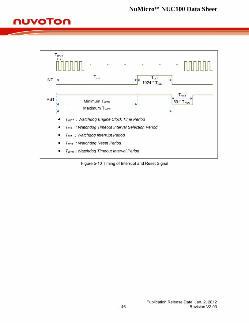
NuMicro™ NUC100 Data Sheet
TTIS
RST
INT 1024 * TWDT
63 * TWDTMinimum TWTR
TINT
TRST
Maximum TWTR
TWDT
TWDT : Watchdog Engine Clock Time Period
TTIS : Watchdog Timeout Interval Selection Period
TINT : Watchdog Interrupt Period
TRST : Watchdog Reset Period
TWTR : Watchdog Timeout Interval Period
Figure 5-10 Timing of Interrupt and Reset Signal
Publication Release Date: Jan. 2, 2012 - 46 - Revision V2.03
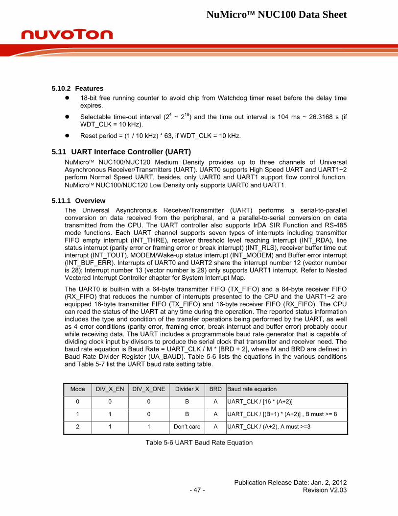
NuMicro™ NUC100 Data Sheet
Publication Release Date: Jan. 2, 2012 - 47 - Revision V2.03
5.10.2 Features 18-bit free running counter to avoid chip from Watchdog timer reset before the delay time
expires.
Selectable time-out interval (24 ~ 218) and the time out interval is 104 ms ~ 26.3168 s (if WDT_CLK = 10 kHz).
Reset period = (1 / 10 kHz) * 63, if WDT_CLK = 10 kHz.
5.11 UART Interface Controller (UART) NuMicro™ NUC100/NUC120 Medium Density provides up to three channels of Universal Asynchronous Receiver/Transmitters (UART). UART0 supports High Speed UART and UART1~2 perform Normal Speed UART, besides, only UART0 and UART1 support flow control function. NuMicro™ NUC100/NUC120 Low Density only supports UART0 and UART1.
5.11.1 Overview The Universal Asynchronous Receiver/Transmitter (UART) performs a serial-to-parallel conversion on data received from the peripheral, and a parallel-to-serial conversion on data transmitted from the CPU. The UART controller also supports IrDA SIR Function and RS-485 mode functions. Each UART channel supports seven types of interrupts including transmitter FIFO empty interrupt (INT_THRE), receiver threshold level reaching interrupt (INT_RDA), line status interrupt (parity error or framing error or break interrupt) (INT_RLS), receiver buffer time out interrupt (INT_TOUT), MODEM/Wake-up status interrupt (INT_MODEM) and Buffer error interrupt (INT_BUF_ERR). Interrupts of UART0 and UART2 share the interrupt number 12 (vector number is 28); Interrupt number 13 (vector number is 29) only supports UART1 interrupt. Refer to Nested Vectored Interrupt Controller chapter for System Interrupt Map.
The UART0 is built-in with a 64-byte transmitter FIFO (TX_FIFO) and a 64-byte receiver FIFO (RX_FIFO) that reduces the number of interrupts presented to the CPU and the UART1~2 are equipped 16-byte transmitter FIFO (TX_FIFO) and 16-byte receiver FIFO (RX_FIFO). The CPU can read the status of the UART at any time during the operation. The reported status information includes the type and condition of the transfer operations being performed by the UART, as well as 4 error conditions (parity error, framing error, break interrupt and buffer error) probably occur while receiving data. The UART includes a programmable baud rate generator that is capable of dividing clock input by divisors to produce the serial clock that transmitter and receiver need. The baud rate equation is Baud Rate = UART_CLK / M * [BRD + 2], where M and BRD are defined in Baud Rate Divider Register (UA_BAUD). Table 5-6 lists the equations in the various conditions and Table 5-7 list the UART baud rate setting table.
Mode DIV_X_EN DIV_X_ONE Divider X BRD Baud rate equation
0 0 0 B A UART_CLK / [16 * (A+2)]
1 1 0 B A UART_CLK / [(B+1) * (A+2)] , B must >= 8
2 1 1 Don’t care A UART_CLK / (A+2), A must >=3
Table 5-6 UART Baud Rate Equation
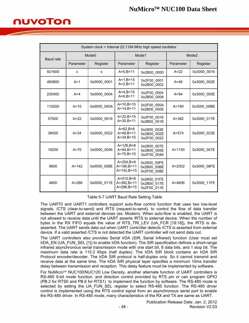
NuMicro™ NUC100 Data Sheet
Publication Release Date: Jan. 2, 2012 - 48 - Revision V2.03
System clock = Internal 22.1184 MHz high speed oscillator
Mode0 Mode1 Mode2 Baud rate
Parameter Register Parameter Register Parameter Register
921600 x x A=0,B=11 0x2B00_0000 A=22 0x3000_0016
460800 A=1 0x0000_0001 A=1,B=15A=2,B=11
0x2F00_00010x2B00_0002
A=46 0x3000_002E
230400 A=4 0x0000_0004 A=4,B=15A=6,B=11
0x2F00_00040x2B00_0006
A=94 0x3000_005E
115200 A=10 0x0000_000A A=10,B=15A=14,B=11
0x2F00_000A0x2B00_000E
A=190 0x3000_00BE
57600 A=22 0x0000_0016 A=22,B=15A=30,B=11
0x2F00_0016 0x2B00_001E
A=382 0x3000_017E
38400 A=34 0x0000_0022A=62,B=8
A=46,B=11A=34,B=15
0x2800_003E 0x2B00_002E 0x2F00_0022
A=574 0x3000_023E
19200 A=70 0x0000_0046A=126,B=8A=94,B=11A=70,B=15
0x2800_007E 0x2B00_005E 0x2F00_0046
A=1150 0x3000_047E
9600 A=142 0x0000_008EA=254,B=8A=190,B=11A=142,B=15
0x2800_00FE0x2B00_00BE0x2F00_008E
A=2302 0x3000_08FE
4800 A=286 0x0000_011EA=510,B=8A=382,B=11A=286,B=15
0x2800_01FE0x2B00_017E0x2F00_011E
A=4606 0x3000_11FE
Table 5-7 UART Baud Rate Setting Table
The UART0 and UART1 controllers support auto-flow control function that uses two low-level signals, /CTS (clear-to-send) and /RTS (request-to-send), to control the flow of data transfer between the UART and external devices (ex: Modem). When auto-flow is enabled, the UART is not allowed to receive data until the UART asserts /RTS to external device. When the number of bytes in the RX FIFO equals the value of RTS_TRI_LEV (UA_FCR [19:16]), the /RTS is de-asserted. The UART sends data out when UART controller detects /CTS is asserted from external device. If a valid asserted /CTS is not detected the UART controller will not send data out. The UART controllers also provides Serial IrDA (SIR, Serial Infrared) function (User must set IrDA_EN (UA_FUN_SEL [1]) to enable IrDA function). The SIR specification defines a short-range infrared asynchronous serial transmission mode with one start bit, 8 data bits, and 1 stop bit. The maximum data rate is 115.2 Kbps (half duplex). The IrDA SIR block contains an IrDA SIR Protocol encoder/decoder. The IrDA SIR protocol is half-duplex only. So it cannot transmit and receive data at the same time. The IrDA SIR physical layer specifies a minimum 10ms transfer delay between transmission and reception. This delay feature must be implemented by software. For NuMicro™ NUC100/NUC120 Low Density, another alternate function of UART controllers is RS-485 9-bit mode function, and direction control provided by RTS pin or can program GPIO (PB.2 for RTS0 and PB.6 for RTS1) to implement the function by software. The RS-485 mode is selected by setting the UA_FUN_SEL register to select RS-485 function. The RS-485 driver control is implemented using the RTS control signal from an asynchronous serial port to enable the RS-485 driver. In RS-485 mode, many characteristics of the RX and TX are same as UART.
NuMicro™ NUC100 Data Sheet
Publication Release Date: Jan. 2, 2012 - 49 - Revision V2.03
5.11.2 Features Full duplex, asynchronous communications
Separate receive / transmit 64/16/16 bytes (UART0/UART1/UART2) entry FIFO for data payloads
Support hardware auto flow control/flow control function (CTS, RTS) and programmable RTS flow control trigger level (UART0 and UART1 support)
Programmable receiver buffer trigger level
Support programmable baud-rate generator for each channel individually
Support CTS wake-up function (UART0 and UART1 support)
Support 7-bit receiver buffer time out detection function
UART0/UART1 can be served by the DMA controller
Programmable transmitting data delay time between the last stop and the next start bit by setting UA_TOR [DLY] register
Support break error, frame error, parity error and receive / transmit buffer overflow detect function
Fully programmable serial-interface characteristics
Programmable number of data bit, 5-, 6-, 7-, 8-bit character
Programmable parity bit, even, odd, no parity or stick parity bit generation and detection
Programmable stop bit, 1, 1.5, or 2 stop bit generation
Support IrDA SIR function mode
Support for 3-/16-bit duration for normal mode
Support RS-485 function mode. (NuMicro™ NUC100/NUC120 Low Density only)
Support RS-485 9-bit mode
Support hardware or software direct enable control provided by RTS pin
NuMicro™ NUC100 Data Sheet
Publication Release Date: Jan. 2, 2012 - 50 - Revision V2.03
5.12 PS/2 Device Controller (PS2D)
5.12.1 Overview PS/2 device controller provides basic timing control for PS/2 communication. All communication between the device and the host is managed through the CLK and DATA pins. Unlike PS/2 keyboard or mouse device controller, the received/transmit code needs to be translated as meaningful code by firmware. The device controller generates the CLK signal after receiving a request to send, but host has ultimate control over communication. DATA sent from the host to the device is read on the rising edge and DATA sent from device to the host is change after rising edge. A 16 bytes FIFO is used to reduce CPU intervention. S/W can select 1 to 16 bytes for a continuous transmission.
5.12.2 Features Host communication inhibit and request to send detection
Reception frame error detection
Programmable 1 to 16 bytes transmit buffer to reduce CPU intervention
Double buffer for data reception
S/W override bus
NuMicro™ NUC100 Data Sheet
Publication Release Date: Jan. 2, 2012 - 51 - Revision V2.03
5.13 I2S Controller (I2S)
5.13.1 Overview The I2S controller consists of IIS protocol to interface with external audio CODEC. Two 8 word deep FIFO for read path and write path respectively and is capable of handling 8 ~ 32 bit word sizes. DMA controller handles the data movement between FIFO and memory.
5.13.2 Features I2S can operate as either master or slave
Capable of handling 8-, 16-, 24- and 32-bit word sizes
Mono and stereo audio data supported
I2S and MSB justified data format supported
Two 8 word FIFO data buffers are provided, one for transmit and one for receive
Generates interrupt requests when buffer levels cross a programmable boundary
Two DMA requests, one for transmit and one for receive
NuMicro™ NUC100 Data Sheet
Publication Release Date: Jan. 2, 2012 - 52 - Revision V2.03
5.14 Analog-to-Digital Converter (ADC)
5.14.1 Overview NuMicro™ NUC100 Series contains one 12-bit successive approximation analog-to-digital converters (SAR A/D converter) with 8 input channels. The A/D converter supports three operation modes: single, single-cycle scan and continuous scan mode. The A/D converters can be started by software and external STADC pin.
5.14.2 Features Analog input voltage range: 0~VREF
12-bit resolution and 10-bit accuracy is guaranteed
Up to 8 single-end analog input channels or 4 differential analog input channels
Maximum ADC clock frequency is 16 MHz
Up to 600K SPS conversion rate
Three operating modes
Single mode: A/D conversion is performed one time on a specified channel
Single-cycle scan mode: A/D conversion is performed one cycle on all specified channels with the sequence from the lowest numbered channel to the highest numbered channel
Continuous scan mode: A/D converter continuously performs Single-cycle scan mode until software stops A/D conversion
An A/D conversion can be started by
Software write 1 to ADST bit
External pin STADC
Conversion results are held in data registers for each channel with valid and overrun indicators
Conversion result can be compared with specify value and user can select whether to generate an interrupt when conversion result is equal to the compare register setting
Channel 7 supports 3 input sources: external analog voltage, internal bandgap voltage, and internal temperature sensor output
Support Self-calibration to minimize conversion error
NuMicro™ NUC100 Data Sheet
Publication Release Date: Jan. 2, 2012 - 53 - Revision V2.03
5.15 Analog Comparator (CMP)
5.15.1 Overview NuMicro™ NUC100 Series contains two comparators. The comparators can be used in a number of different configurations. The comparator output is a logical one when positive input greater than negative input, otherwise the output is a zero. Each comparator can be configured to cause an interrupt when the comparator output value changes. The block diagram is shown in Error! Reference source not found..
5.15.2 Features Analog input voltage range: 0~5.0 V
Hysteresis function supported
Two analog comparators with optional internal reference voltage input at negative end
One interrupt vector for both comparators
NuMicro™ NUC100 Data Sheet
Publication Release Date: Jan. 2, 2012 - 54 - Revision V2.03
5.16 PDMA Controller (PDMA)
5.16.1 Overview NuMicro™ NUC100/NUC120 Medium Density contains a peripheral direct memory access (PDMA) controller that transfers data to and from memory or transfer data to and from APB devices. The PDMA has nine channels of DMA (Peripheral-to-Memory or Memory-to-Peripheral or Memory-to-Memory). For each PDMA channel (PDMA CH0~CH8), there is one word buffer as transfer buffer between the Peripherals APB devices and Memory.
Software can stop the PDMA operation by disable PDMA [PDMACEN]. The CPU can recognize the completion of a PDMA operation by software polling or when it receives an internal PDMA interrupt. The PDMA controller can increase source or destination address or fixed them as well.
Notice: NuMicro™ NUC100/NUC120 Low Density only has 1 PDMA channel (channel 0).
5.16.2 Features Up to nine DMA channels. Each channel can support a unidirectional transfer (NuMicro™
NUC100/NUC120 Low Density only has 1 PDMA channel)
AMBA AHB master/slave interface compatible, for data transfer and register read/write
Support source and destination address increased mode or fixed mode
Hardware channel priority. DMA channel 0 has the highest priority and channel 8 has the lowest priority
NuMicro™ NUC100 Data Sheet
Publication Release Date: Jan. 2, 2012 - 55 - Revision V2.03
5.17 External Bus Interface (EBI)
5.17.1 Overview The NuMicro™ NUC100/NUC120 Low Density LQFP-64 package equips an external bus interface (EBI) for external device used.
To save the connections between external device and this chip, EBI support address bus and data bus multiplex mode. And, address latch enable (ALE) signal supported differentiate the address and data cycle.
5.17.2 Features External Bus Interface has the following functions:
External devices with max. 64K-byte size (8-bit data width)/128K-byte (16-bit data width) supported
Variable external bus base clock (MCLK) supported
8-bit or 16-bit data width supported
Variable data access time (tACC), address latch enable time (tALE) and address hold time (tAHD) supported
Address bus and data bus multiplex mode supported to save the address pins
Configurable idle cycle supported for different access condition: Write command finish (W2X), Read-to-Read (R2R)
NuMicro™ NUC100 Data Sheet
Publication Release Date: Jan. 2, 2012 - 56 - Revision V2.03
6 FLASH MEMORY CONTROLLER (FMC)
6.1 Overview NuMicro™ NUC100 Series equips with 128/64/32K bytes on chip embedded Flash for application program memory (APROM) that can be updated through ISP procedure. In System Programming (ISP) function enables user to update program memory when chip is soldered on PCB. After chip power on, Cortex-M0 CPU fetches code from APROM or LDROM decided by boot select (CBS) in Config0. By the way, NuMicro™ NUC100 Series also provides additional DATA Flash for user, to store some application dependent data before chip power off. For 128K bytes APROM device, the data flash is shared with original 128K program memory and its start address is configurable and defined by user application request in Config1. For 64K/32K bytes APROM device, the data flash is fixed at 4K.
6.2 Features Run up to 50 MHz with zero wait state for continuous address read access
128/64/32KB application program memory (APROM) (NuMicro™ NUC100/NUC120 Low Density only support up to 64KB size)
4KB in system programming (ISP) loader program memory (LDROM)
Configurable or fixed 4KB data flash with 512 bytes page erase unit
Programmable data flash start address for 128K APROM device
In System Program (ISP) to update on chip Flash
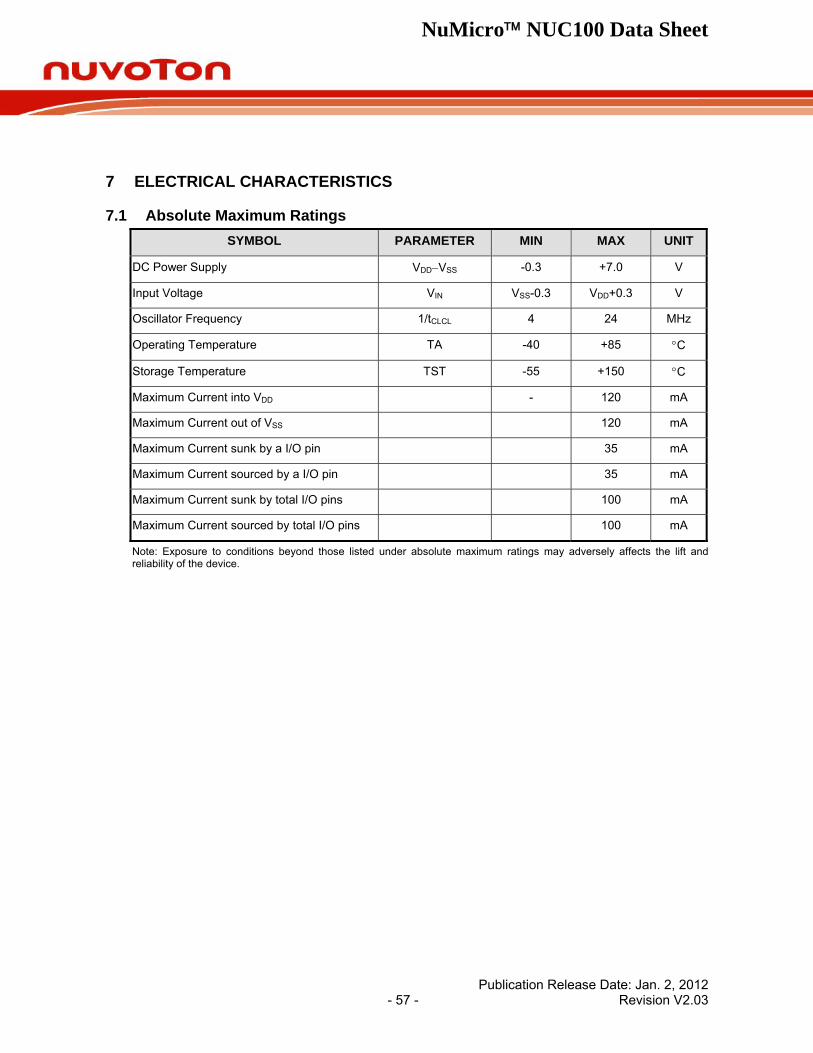
NuMicro™ NUC100 Data Sheet
Publication Release Date: Jan. 2, 2012 - 57 - Revision V2.03
7 ELECTRICAL CHARACTERISTICS
7.1 Absolute Maximum Ratings SYMBOL PARAMETER MIN MAX UNIT
DC Power Supply VDD−VSS -0.3 +7.0 V
Input Voltage VIN VSS-0.3 VDD+0.3 V
Oscillator Frequency 1/tCLCL 4 24 MHz
Operating Temperature TA -40 +85 °C
Storage Temperature TST -55 +150 °C
Maximum Current into VDD - 120 mA
Maximum Current out of VSS 120 mA
Maximum Current sunk by a I/O pin 35 mA
Maximum Current sourced by a I/O pin 35 mA
Maximum Current sunk by total I/O pins 100 mA
Maximum Current sourced by total I/O pins 100 mA
Note: Exposure to conditions beyond those listed under absolute maximum ratings may adversely affects the lift and reliability of the device.
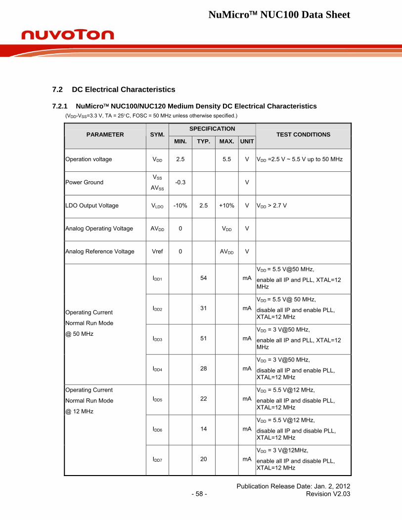
NuMicro™ NUC100 Data Sheet
Publication Release Date: Jan. 2, 2012 - 58 - Revision V2.03
7.2 DC Electrical Characteristics
7.2.1 NuMicro™ NUC100/NUC120 Medium Density DC Electrical Characteristics (VDD-VSS=3.3 V, TA = 25°C, FOSC = 50 MHz unless otherwise specified.)
SPECIFICATION PARAMETER SYM.
MIN. TYP. MAX. UNITTEST CONDITIONS
Operation voltage VDD 2.5 5.5 V VDD =2.5 V ~ 5.5 V up to 50 MHz
Power Ground VSS
AVSS-0.3 V
LDO Output Voltage VLDO -10% 2.5 +10% V VDD > 2.7 V
Analog Operating Voltage AVDD 0 VDD V
Analog Reference Voltage Vref 0 AVDD V
IDD1 54 mAVDD = 5.5 V@50 MHz,
enable all IP and PLL, XTAL=12 MHz
IDD2 31 mAVDD = 5.5 V@ 50 MHz,
disable all IP and enable PLL, XTAL=12 MHz
IDD3 51 mAVDD = 3 V@50 MHz,
enable all IP and PLL, XTAL=12 MHz
Operating Current
Normal Run Mode
@ 50 MHz
IDD4 28 mAVDD = 3 V@50 MHz,
disable all IP and enable PLL, XTAL=12 MHz
IDD5 22 mAVDD = 5.5 V@12 MHz,
enable all IP and disable PLL, XTAL=12 MHz
IDD6 14 mAVDD = 5.5 V@12 MHz,
disable all IP and disable PLL, XTAL=12 MHz
Operating Current
Normal Run Mode
@ 12 MHz
IDD7 20 mAVDD = 3 V@12MHz,
enable all IP and disable PLL, XTAL=12 MHz
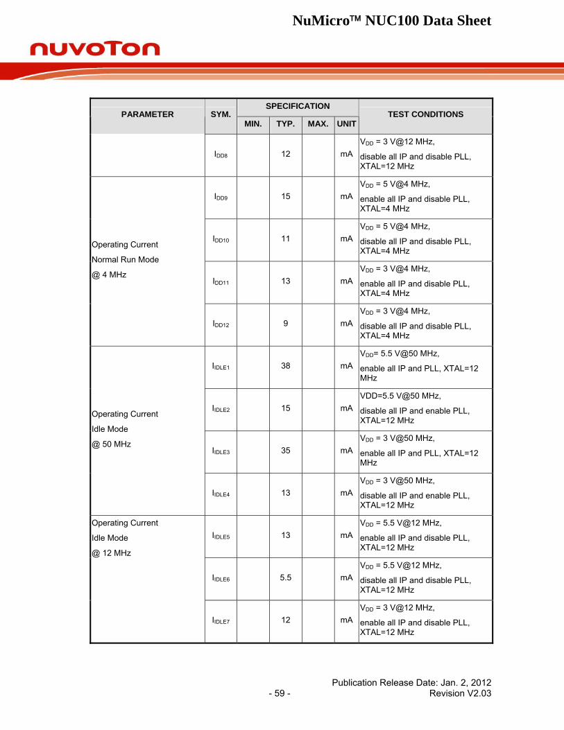
NuMicro™ NUC100 Data Sheet
Publication Release Date: Jan. 2, 2012 - 59 - Revision V2.03
SPECIFICATION PARAMETER SYM.
MIN. TYP. MAX. UNITTEST CONDITIONS
IDD8 12 mAVDD = 3 V@12 MHz,
disable all IP and disable PLL, XTAL=12 MHz
IDD9 15 mAVDD = 5 V@4 MHz,
enable all IP and disable PLL, XTAL=4 MHz
IDD10 11 mAVDD = 5 V@4 MHz,
disable all IP and disable PLL, XTAL=4 MHz
IDD11 13 mAVDD = 3 V@4 MHz,
enable all IP and disable PLL, XTAL=4 MHz
Operating Current
Normal Run Mode
@ 4 MHz
IDD12 9 mAVDD = 3 V@4 MHz,
disable all IP and disable PLL, XTAL=4 MHz
IIDLE1 38 mAVDD= 5.5 V@50 MHz,
enable all IP and PLL, XTAL=12 MHz
IIDLE2 15 mAVDD=5.5 V@50 MHz,
disable all IP and enable PLL, XTAL=12 MHz
IIDLE3 35 mAVDD = 3 V@50 MHz,
enable all IP and PLL, XTAL=12 MHz
Operating Current
Idle Mode
@ 50 MHz
IIDLE4 13 mAVDD = 3 V@50 MHz,
disable all IP and enable PLL, XTAL=12 MHz
IIDLE5 13 mAVDD = 5.5 V@12 MHz,
enable all IP and disable PLL, XTAL=12 MHz
IIDLE6 5.5 mAVDD = 5.5 V@12 MHz,
disable all IP and disable PLL, XTAL=12 MHz
Operating Current
Idle Mode
@ 12 MHz
IIDLE7 12 mAVDD = 3 V@12 MHz,
enable all IP and disable PLL, XTAL=12 MHz
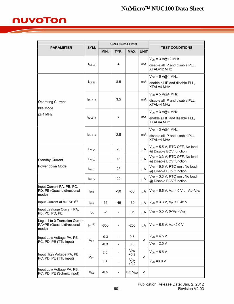
NuMicro™ NUC100 Data Sheet
Publication Release Date: Jan. 2, 2012 - 60 - Revision V2.03
SPECIFICATION PARAMETER SYM.
MIN. TYP. MAX. UNITTEST CONDITIONS
IIDLE8 4 mAVDD = 3 V@12 MHz,
disable all IP and disable PLL, XTAL=12 MHz
IIDLE9 8.5 mAVDD = 5 V@4 MHz,
enable all IP and disable PLL, XTAL=4 MHz
IIDLE10 3.5 mAVDD = 5 V@4 MHz,
disable all IP and disable PLL, XTAL=4 MHz
IIDLE11 7 mAVDD = 3 V@4 MHz,
enable all IP and disable PLL, XTAL=4 MHz
Operating Current
Idle Mode
@ 4 MHz
IIDLE12 2.5 mAVDD = 3 V@4 MHz,
disable all IP and disable PLL, XTAL=4 MHz
IPWD1 23 μAVDD = 5.5 V, RTC OFF, No load @ Disable BOV function
IPWD2 18 μAVDD = 3.3 V, RTC OFF, No load @ Disable BOV function
IPWD3 28 μAVDD = 5.5 V, RTC run , No load @ Disable BOV function
Standby Current
Power down Mode
IPWD4 22 μAVDD = 3.3 V, RTC run , No load @ Disable BOV function
Input Current PA, PB, PC, PD, PE (Quasi-bidirectional mode)
IIN1 -50 -60 μA VDD = 5.5 V, VIN = 0 V or VIN=VDD
Input Current at /RESET[1] IIN2 -55 -45 -30 μA VDD = 3.3 V, VIN = 0.45 V
Input Leakage Current PA, PB, PC, PD, PE ILK -2 - +2 μA VDD = 5.5 V, 0<VIN<VDD
Logic 1 to 0 Transition Current PA~PE (Quasi-bidirectional mode)
ITL [3] -650 - -200 μA VDD = 5.5 V, VIN<2.0 V
-0.3 - 0.8 VDD = 4.5 V Input Low Voltage PA, PB, PC, PD, PE (TTL input) VIL1
-0.3 - 0.6 V
VDD = 2.5 V
2.0 - VDD +0.2
VDD = 5.5 V Input High Voltage PA, PB, PC, PD, PE (TTL input) VIH1
1.5 - VDD +0.2
V VDD =3.0 V
Input Low Voltage PA, PB, PC, PD, PE (Schmitt input) VIL2 -0.5 - 0.2 VDD V
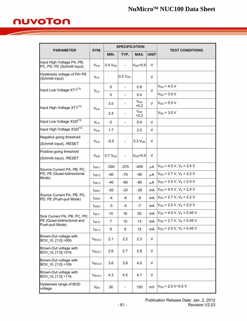
NuMicro™ NUC100 Data Sheet
Publication Release Date: Jan. 2, 2012 - 61 - Revision V2.03
SPECIFICATION PARAMETER SYM.
MIN. TYP. MAX. UNITTEST CONDITIONS
Input High Voltage PA, PB, PC, PD, PE (Schmitt input) VIH2 0.4 VDD - VDD+0.5 V
Hysteresis voltage of PA~PE (Schmitt input) VHY 0.2 VDD V
0 - 0.8 VDD = 4.5 V Input Low Voltage XT1[*2] VIL3
0 - 0.4 V
VDD = 3.0 V
3.5 - VDD +0.2 V VDD = 5.5 V
Input High Voltage XT1[*2] VIH3 2.4 - VDD
+0.2 VDD = 3.0 V
Input Low Voltage X32I[*2] VIL4 0 - 0.4 V
Input High Voltage X32I[*2] VIH4 1.7 2.5 V
Negative going threshold
(Schmitt input), /RESET VILS -0.5 - 0.3 VDD V
Positive going threshold
(Schmitt input), /RESET VIHS 0.7 VDD - VDD+0.5 V
ISR11 -300 -370 -450 μA VDD = 4.5 V, VS = 2.4 V
ISR12 -50 -70 -90 μA VDD = 2.7 V, VS = 2.2 V Source Current PA, PB, PC, PD, PE (Quasi-bidirectional Mode)
ISR13 -40 -60 -80 μA VDD = 2.5 V, VS = 2.0 V
ISR21 -20 -24 -28 mA VDD = 4.5 V, VS = 2.4 V
ISR22 -4 -6 -8 mA VDD = 2.7 V, VS = 2.2 V Source Current PA, PB, PC, PD, PE (Push-pull Mode)
ISR23 -3 -5 -7 mA VDD = 2.5 V, VS = 2.0 V
ISK11 10 16 20 mA VDD = 4.5 V, VS = 0.45 V
ISK12 7 10 13 mA VDD = 2.7 V, VS = 0.45 V Sink Current PA, PB, PC, PD, PE (Quasi-bidirectional and Push-pull Mode)
ISK13 6 9 12 mA VDD = 2.5 V, VS = 0.45 V
Brown-Out voltage with BOV_VL [1:0] =00b VBO2.2 2.1 2.2 2.3 V
Brown-Out voltage with BOV_VL [1:0] =01b VBO2.7 2.6 2.7 2.8 V
Brown-Out voltage with BOV_VL [1:0] =10b VBO3.8 3.6 3.8 4.0 V
Brown-Out voltage with BOV_VL [1:0] =11b VBO4.5 4.3 4.5 4.7 V
Hysteresis range of BOD voltage VBH 30 - 150 mV VDD = 2.5 V~5.5 V
NuMicro™ NUC100 Data Sheet
Publication Release Date: Jan. 2, 2012 - 62 - Revision V2.03
Note:
1. /RESET pin is a Schmitt trigger input.
2. Crystal Input is a CMOS input.
3. Pins of PA, PB, PC, PD and PE can source a transition current when they are being externally driven from 1 to 0. In the condition of VDD=5.5 V, 5he transition current reaches its maximum value when VIN approximates to 2 V.
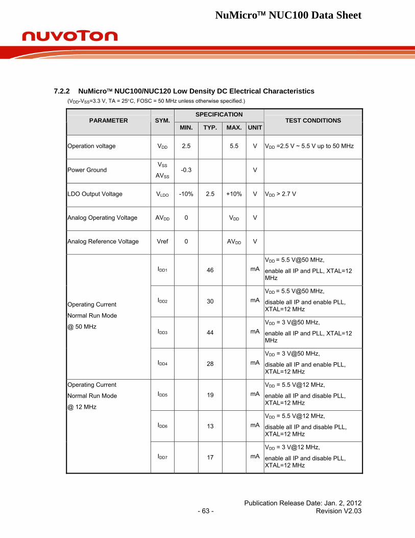
NuMicro™ NUC100 Data Sheet
Publication Release Date: Jan. 2, 2012 - 63 - Revision V2.03
7.2.2 NuMicro™ NUC100/NUC120 Low Density DC Electrical Characteristics (VDD-VSS=3.3 V, TA = 25°C, FOSC = 50 MHz unless otherwise specified.)
SPECIFICATION PARAMETER SYM.
MIN. TYP. MAX. UNITTEST CONDITIONS
Operation voltage VDD 2.5 5.5 V VDD =2.5 V ~ 5.5 V up to 50 MHz
Power Ground VSS
AVSS-0.3 V
LDO Output Voltage VLDO -10% 2.5 +10% V VDD > 2.7 V
Analog Operating Voltage AVDD 0 VDD V
Analog Reference Voltage Vref 0 AVDD V
IDD1 46 mAVDD = 5.5 V@50 MHz,
enable all IP and PLL, XTAL=12 MHz
IDD2 30 mAVDD = 5.5 V@50 MHz,
disable all IP and enable PLL, XTAL=12 MHz
IDD3 44 mAVDD = 3 V@50 MHz,
enable all IP and PLL, XTAL=12 MHz
Operating Current
Normal Run Mode
@ 50 MHz
IDD4 28 mAVDD = 3 V@50 MHz,
disable all IP and enable PLL, XTAL=12 MHz
IDD5 19 mAVDD = 5.5 V@12 MHz,
enable all IP and disable PLL, XTAL=12 MHz
IDD6 13 mAVDD = 5.5 V@12 MHz,
disable all IP and disable PLL, XTAL=12 MHz
Operating Current
Normal Run Mode
@ 12 MHz
IDD7 17 mAVDD = 3 V@12 MHz,
enable all IP and disable PLL, XTAL=12 MHz

NuMicro™ NUC100 Data Sheet
Publication Release Date: Jan. 2, 2012 - 64 - Revision V2.03
SPECIFICATION PARAMETER SYM.
MIN. TYP. MAX. UNITTEST CONDITIONS
IDD8 11.5 mAVDD = 3 V@12 MHz,
disable all IP and disable PLL, XTAL=12 MHz
IDD9 13.5 mAVDD = 5 V@4 MHz,
enable all IP and disable PLL, XTAL=4 MHz
IDD10 10 mAVDD = 5 V@4 MHz,
disable all IP and disable PLL, XTAL=4 MHz
IDD11 12 mAVDD = 3 V@4 MHz,
enable all IP and disable PLL, XTAL=4 MHz
Operating Current
Normal Run Mode
@ 4 MHz
IDD12 8 mAVDD = 3 V@4 MHz,
disable all IP and disable PLL, XTAL=4 MHz
IIDLE1 30 mAVDD= 5.5 V@50 MHz,
enable all IP and PLL, XTAL=12 MHz
IIDLE2 13 mAVDD=5.5 V@50 MHz,
disable all IP and enable PLL, XTAL=12 MHz
IIDLE3 28 mAVDD = 3 V@50 MHz,
enable all IP and PLL, XTAL=12 MHz
Operating Current
Idle Mode
@ 50 MHz
IIDLE4 12 mAVDD = 3 V@50 MHz,
disable all IP and enable PLL, XTAL=12 MHz
IIDLE5 11 mAVDD = 5.5 V@12 MHz,
enable all IP and disable PLL, XTAL=12 MHz
IIDLE6 5 mAVDD = 5.5 V@12 MHz,
disable all IP and disable PLL, XTAL=12 MHz
Operating Current
Idle Mode
@ 12 MHz
IIDLE7 10 mAVDD = 3 V@12 MHz,
enable all IP and disable PLL, XTAL=12 MHz

NuMicro™ NUC100 Data Sheet
Publication Release Date: Jan. 2, 2012 - 65 - Revision V2.03
SPECIFICATION PARAMETER SYM.
MIN. TYP. MAX. UNITTEST CONDITIONS
IIDLE8 4 mAVDD = 3 V@12 MHz,
disable all IP and disable PLL, XTAL=12 MHz
IIDLE9 7 mAVDD = 5 V@4 MHz,
enable all IP and disable PLL, XTAL=4 MHz
IIDLE10 3.5 mAVDD = 5 V@4 MHz,
disable all IP and disable PLL, XTAL=4 MHz
IIDLE11 6 mAVDD = 3 V@4 MHz,
enable all IP and disable PLL, XTAL=4 MHz
Operating Current
Idle Mode
@ 4 MHz
IIDLE12 2.5 mAVDD = 3 V@4 MHz,
disable all IP and disable PLL, XTAL=4 MHz
IPWD1 17 μAVDD = 5.5 V, RTC OFF, No load @ Disable BOV function
IPWD2 14.5 μAVDD = 3.3 V, RTC OFF, No load @ Disable BOV function
IPWD3 20 μAVDD = 5.5 V, RTC run , No load @ Disable BOV function
Standby Current
Power down Mode
IPWD4 17 μAVDD = 3.3 V, RTC run , No load @ Disable BOV function
Input Current PA, PB, PC, PD, PE (Quasi-bidirectional mode)
IIN1 -50 -60 μA VDD = 5.5 V, VIN = 0 V or VIN=VDD
Input Current at /RESET[1] IIN2 -55 -45 -30 μA VDD = 3.3 V, VIN = 0.45 V
Input Leakage Current PA, PB, PC, PD, PE ILK -2 - +2 μA VDD = 5.5 V, 0<VIN<VDD
Logic 1 to 0 Transition Current PA~PE (Quasi-bidirectional mode)
ITL [3] -650 - -200 μA VDD = 5.5 V, VIN<2.0 V
-0.3 - 0.8 VDD = 4.5 V Input Low Voltage PA, PB, PC, PD, PE (TTL input) VIL1
-0.3 - 0.6 V
VDD = 2.5 V
2.0 - VDD +0.2
VDD = 5.5 V Input High Voltage PA, PB, PC, PD, PE (TTL input) VIH1
1.5 - VDD +0.2
V VDD =3.0 V
Input Low Voltage PA, PB, PC, PD, PE (Schmitt input) VIL2 -0.5 - 0.2
VDD V
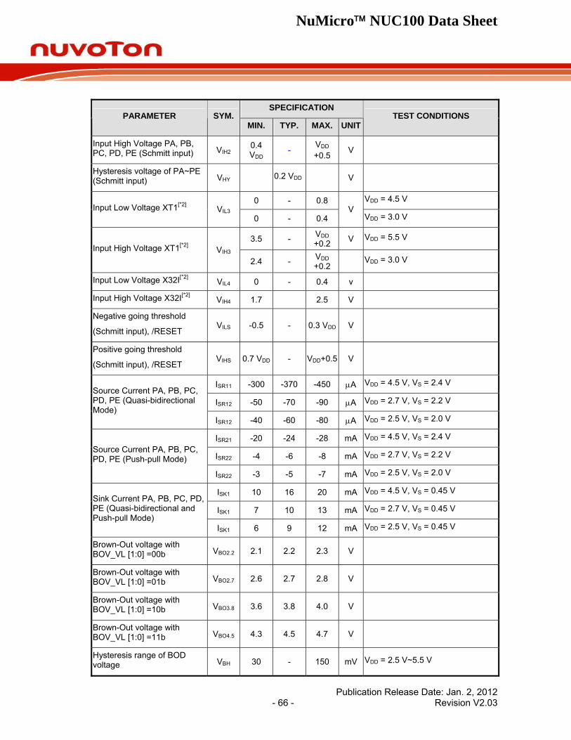
NuMicro™ NUC100 Data Sheet
Publication Release Date: Jan. 2, 2012 - 66 - Revision V2.03
SPECIFICATION PARAMETER SYM.
MIN. TYP. MAX. UNITTEST CONDITIONS
Input High Voltage PA, PB, PC, PD, PE (Schmitt input) VIH2
0.4 VDD - VDD
+0.5 V
Hysteresis voltage of PA~PE (Schmitt input) VHY 0.2 VDD V
0 - 0.8 VDD = 4.5 V Input Low Voltage XT1[*2] VIL3
0 - 0.4 V
VDD = 3.0 V
3.5 - VDD +0.2 V VDD = 5.5 V
Input High Voltage XT1[*2] VIH3 2.4 - VDD
+0.2 VDD = 3.0 V
Input Low Voltage X32I[*2] VIL4 0 - 0.4 v
Input High Voltage X32I[*2] VIH4 1.7 2.5 V
Negative going threshold
(Schmitt input), /RESET VILS -0.5 - 0.3 VDD V
Positive going threshold
(Schmitt input), /RESET VIHS 0.7 VDD - VDD+0.5 V
ISR11 -300 -370 -450 μA VDD = 4.5 V, VS = 2.4 V
ISR12 -50 -70 -90 μA VDD = 2.7 V, VS = 2.2 V Source Current PA, PB, PC, PD, PE (Quasi-bidirectional Mode)
ISR12 -40 -60 -80 μA VDD = 2.5 V, VS = 2.0 V
ISR21 -20 -24 -28 mA VDD = 4.5 V, VS = 2.4 V
ISR22 -4 -6 -8 mA VDD = 2.7 V, VS = 2.2 V Source Current PA, PB, PC, PD, PE (Push-pull Mode)
ISR22 -3 -5 -7 mA VDD = 2.5 V, VS = 2.0 V
ISK1 10 16 20 mA VDD = 4.5 V, VS = 0.45 V
ISK1 7 10 13 mA VDD = 2.7 V, VS = 0.45 V Sink Current PA, PB, PC, PD, PE (Quasi-bidirectional and Push-pull Mode)
ISK1 6 9 12 mA VDD = 2.5 V, VS = 0.45 V
Brown-Out voltage with BOV_VL [1:0] =00b VBO2.2 2.1 2.2 2.3 V
Brown-Out voltage with BOV_VL [1:0] =01b VBO2.7 2.6 2.7 2.8 V
Brown-Out voltage with BOV_VL [1:0] =10b VBO3.8 3.6 3.8 4.0 V
Brown-Out voltage with BOV_VL [1:0] =11b VBO4.5 4.3 4.5 4.7 V
Hysteresis range of BOD voltage VBH 30 - 150 mV VDD = 2.5 V~5.5 V
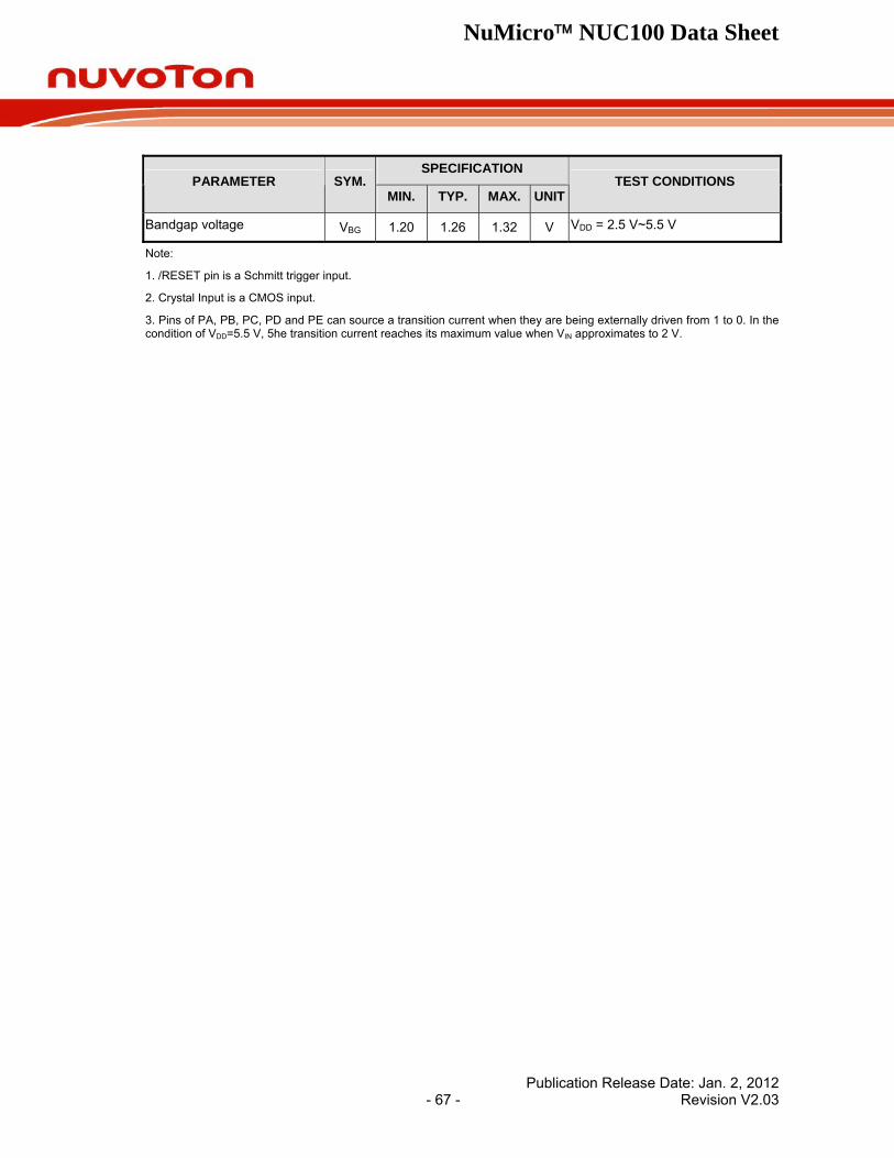
NuMicro™ NUC100 Data Sheet
Publication Release Date: Jan. 2, 2012 - 67 - Revision V2.03
SPECIFICATION PARAMETER SYM.
MIN. TYP. MAX. UNITTEST CONDITIONS
Bandgap voltage VBG 1.20 1.26 1.32 V VDD = 2.5 V~5.5 V
Note:
1. /RESET pin is a Schmitt trigger input.
2. Crystal Input is a CMOS input.
3. Pins of PA, PB, PC, PD and PE can source a transition current when they are being externally driven from 1 to 0. In the condition of VDD=5.5 V, 5he transition current reaches its maximum value when VIN approximates to 2 V.
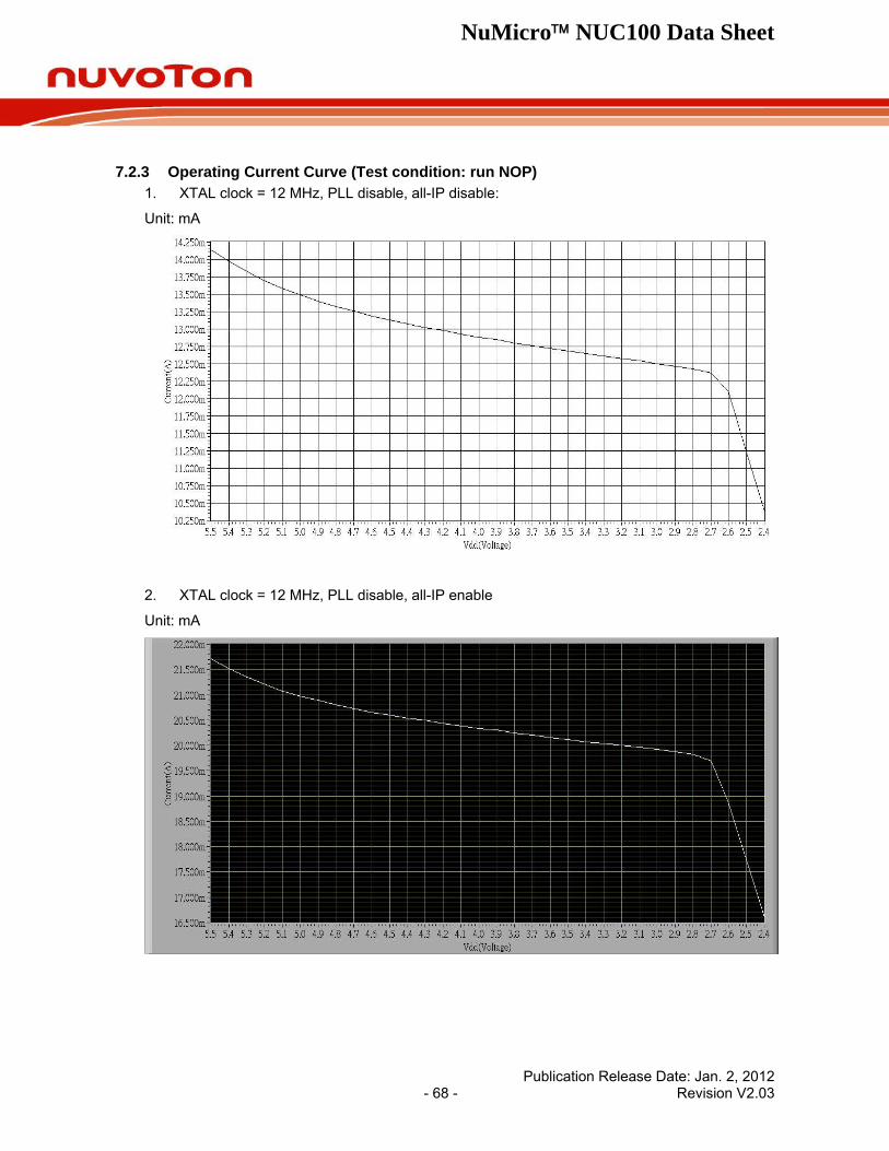
NuMicro™ NUC100 Data Sheet
7.2.3 Operating Current Curve (Test condition: run NOP) 1. XTAL clock = 12 MHz, PLL disable, all-IP disable:
Unit: mA
2. XTAL clock = 12 MHz, PLL disable, all-IP enable
Unit: mA
Publication Release Date: Jan. 2, 2012 - 68 - Revision V2.03
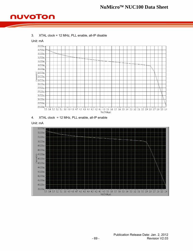
NuMicro™ NUC100 Data Sheet
3. XTAL clock = 12 MHz, PLL enable, all-IP disable
Unit: mA
4. XTAL clock = 12 MHz, PLL enable, all-IP enable
Unit: mA
Publication Release Date: Jan. 2, 2012 - 69 - Revision V2.03
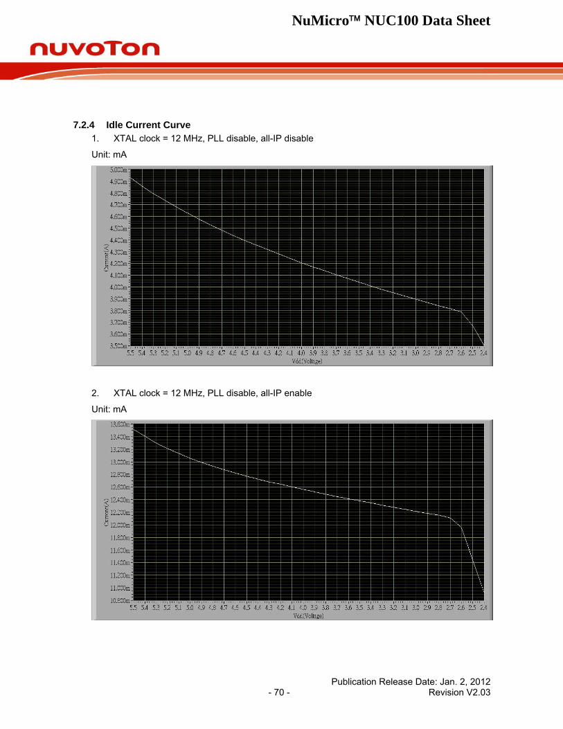
NuMicro™ NUC100 Data Sheet
7.2.4 Idle Current Curve 1. XTAL clock = 12 MHz, PLL disable, all-IP disable
Unit: mA
2. XTAL clock = 12 MHz, PLL disable, all-IP enable
Unit: mA
Publication Release Date: Jan. 2, 2012 - 70 - Revision V2.03
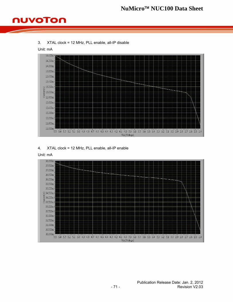
NuMicro™ NUC100 Data Sheet
3. XTAL clock = 12 MHz, PLL enable, all-IP disable
Unit: mA
4. XTAL clock = 12 MHz, PLL enable, all-IP enable
Unit: mA
Publication Release Date: Jan. 2, 2012 - 71 - Revision V2.03
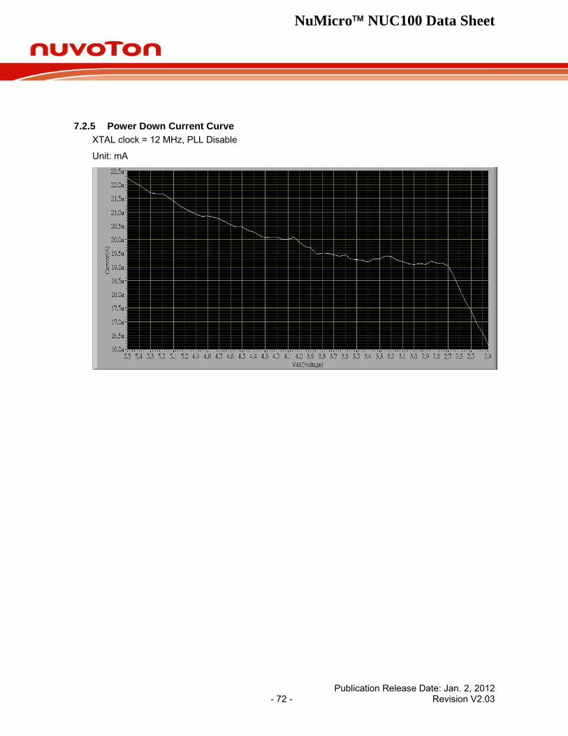
NuMicro™ NUC100 Data Sheet
7.2.5 Power Down Current Curve XTAL clock = 12 MHz, PLL Disable
Unit: mA
Publication Release Date: Jan. 2, 2012 - 72 - Revision V2.03
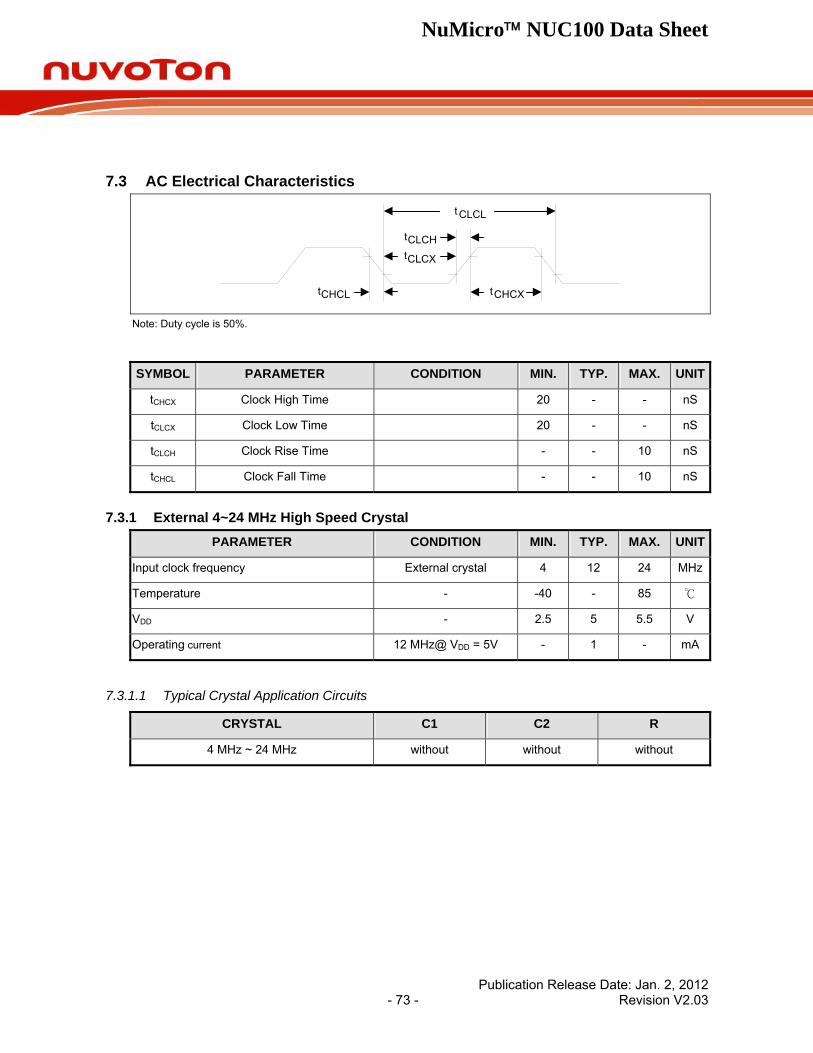
NuMicro™ NUC100 Data Sheet
7.3 AC Electrical Characteristics
t CLCL
tCLCX
tCHCX
tCLCH
tCHCL Note: Duty cycle is 50%.
SYMBOL PARAMETER CONDITION MIN. TYP. MAX. UNIT
tCHCX Clock High Time 20 - - nS
tCLCX Clock Low Time 20 - - nS
tCLCH Clock Rise Time - - 10 nS
tCHCL Clock Fall Time - - 10 nS
7.3.1 External 4~24 MHz High Speed Crystal PARAMETER CONDITION MIN. TYP. MAX. UNIT
Input clock frequency External crystal 4 12 24 MHz
Temperature - -40 - 85 ℃
VDD - 2.5 5 5.5 V
Operating current 12 MHz@ VDD = 5V - 1 - mA
7.3.1.1 Typical Crystal Application Circuits
CRYSTAL C1 C2 R
4 MHz ~ 24 MHz without without without
Publication Release Date: Jan. 2, 2012 - 73 - Revision V2.03
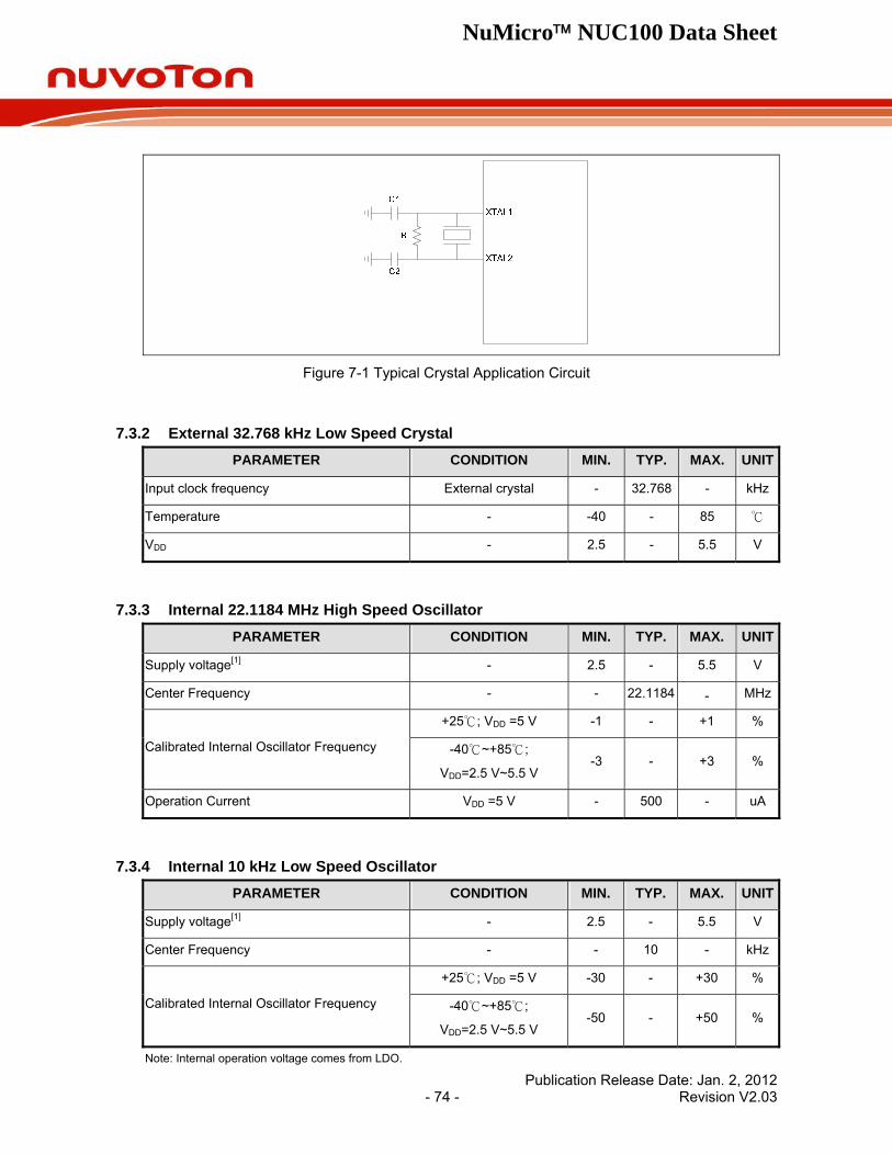
NuMicro™ NUC100 Data Sheet
Figure 7-1 Typical Crystal Application Circuit
7.3.2 External 32.768 kHz Low Speed Crystal PARAMETER CONDITION MIN. TYP. MAX. UNIT
Input clock frequency External crystal - 32.768 - kHz
Temperature - -40 - 85 ℃
VDD - 2.5 - 5.5 V
7.3.3 Internal 22.1184 MHz High Speed Oscillator PARAMETER CONDITION MIN. TYP. MAX. UNIT
Supply voltage[1] - 2.5 - 5.5 V
Center Frequency - - 22.1184 - MHz
+25℃; VDD =5 V -1 - +1 %
Calibrated Internal Oscillator Frequency -40℃~+85℃;
VDD=2.5 V~5.5 V -3 - +3 %
Operation Current VDD =5 V - 500 - uA
7.3.4 Internal 10 kHz Low Speed Oscillator PARAMETER CONDITION MIN. TYP. MAX. UNIT
Supply voltage[1] - 2.5 - 5.5 V
Center Frequency - - 10 - kHz
+25℃; VDD =5 V -30 - +30 %
Calibrated Internal Oscillator Frequency -40℃~+85℃;
VDD=2.5 V~5.5 V -50 - +50 %
Note: Internal operation voltage comes from LDO.
Publication Release Date: Jan. 2, 2012 - 74 - Revision V2.03
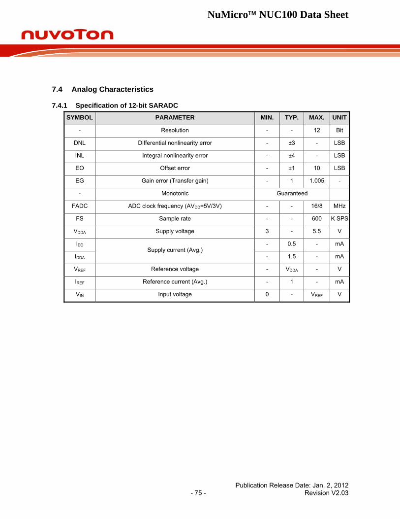
NuMicro™ NUC100 Data Sheet
Publication Release Date: Jan. 2, 2012 - 75 - Revision V2.03
7.4 Analog Characteristics
7.4.1 Specification of 12-bit SARADC SYMBOL PARAMETER MIN. TYP. MAX. UNIT
- Resolution - - 12 Bit
DNL Differential nonlinearity error - ±3 - LSB
INL Integral nonlinearity error - ±4 - LSB
EO Offset error - ±1 10 LSB
EG Gain error (Transfer gain) - 1 1.005 -
- Monotonic Guaranteed
FADC ADC clock frequency (AVDD=5V/3V) - - 16/8 MHz
FS Sample rate - - 600 K SPS
VDDA Supply voltage 3 - 5.5 V
IDD - 0.5 - mA
IDDA Supply current (Avg.)
- 1.5 - mA
VREF Reference voltage - VDDA - V
IREF Reference current (Avg.) - 1 - mA
VIN Input voltage 0 - VREF V
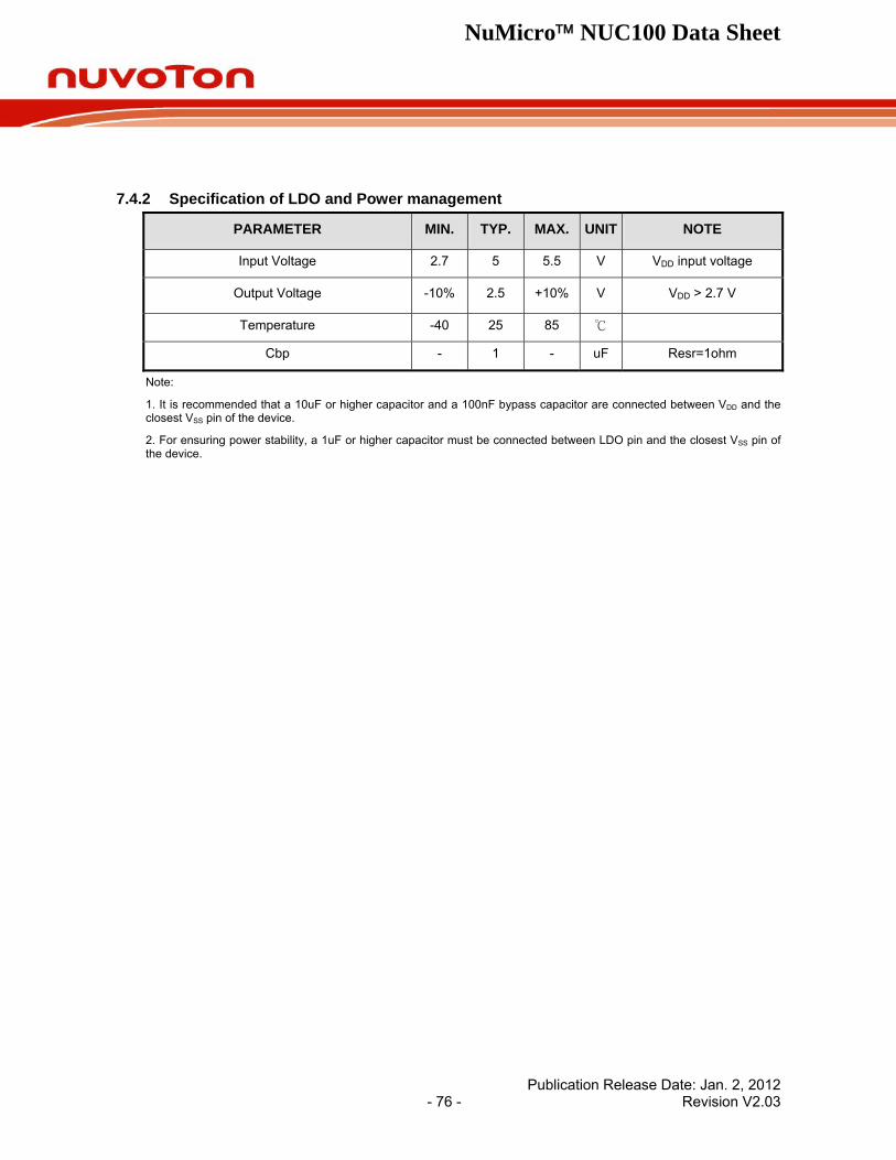
NuMicro™ NUC100 Data Sheet
Publication Release Date: Jan. 2, 2012 - 76 - Revision V2.03
7.4.2 Specification of LDO and Power management
PARAMETER MIN. TYP. MAX. UNIT NOTE
Input Voltage 2.7 5 5.5 V VDD input voltage
Output Voltage -10% 2.5 +10% V VDD > 2.7 V
Temperature -40 25 85 ℃
Cbp - 1 - uF Resr=1ohm
Note:
1. It is recommended that a 10uF or higher capacitor and a 100nF bypass capacitor are connected between VDD and the closest VSS pin of the device.
2. For ensuring power stability, a 1uF or higher capacitor must be connected between LDO pin and the closest VSS pin of the device.
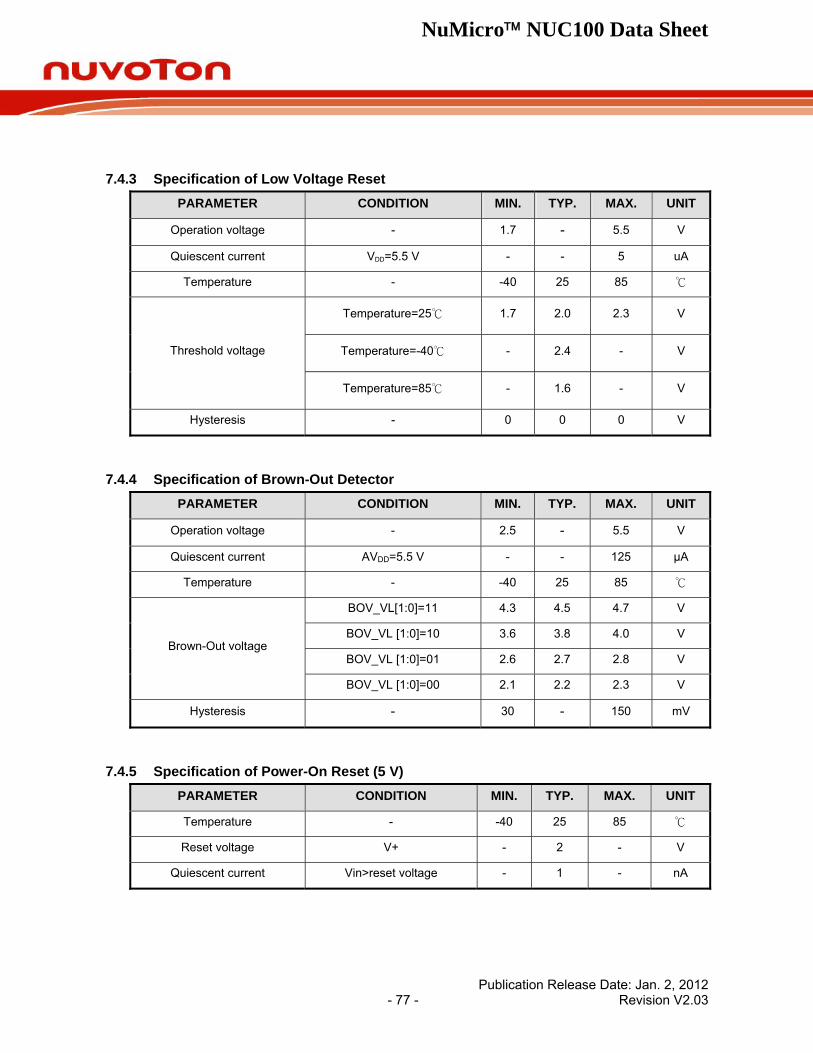
NuMicro™ NUC100 Data Sheet
Publication Release Date: Jan. 2, 2012 - 77 - Revision V2.03
7.4.3 Specification of Low Voltage Reset PARAMETER CONDITION MIN. TYP. MAX. UNIT
Operation voltage - 1.7 - 5.5 V
Quiescent current VDD=5.5 V - - 5 uA
Temperature - -40 25 85 ℃
Temperature=25℃ 1.7 2.0 2.3 V
Temperature=-40℃ - 2.4 - V Threshold voltage
Temperature=85℃ - 1.6 - V
Hysteresis - 0 0 0 V
7.4.4 Specification of Brown-Out Detector PARAMETER CONDITION MIN. TYP. MAX. UNIT
Operation voltage - 2.5 - 5.5 V
Quiescent current AVDD=5.5 V - - 125 μA
Temperature - -40 25 85 ℃
BOV_VL[1:0]=11 4.3 4.5 4.7 V
BOV_VL [1:0]=10 3.6 3.8 4.0 V
BOV_VL [1:0]=01 2.6 2.7 2.8 V Brown-Out voltage
BOV_VL [1:0]=00 2.1 2.2 2.3 V
Hysteresis - 30 - 150 mV
7.4.5 Specification of Power-On Reset (5 V) PARAMETER CONDITION MIN. TYP. MAX. UNIT
Temperature - -40 25 85 ℃
Reset voltage V+ - 2 - V
Quiescent current Vin>reset voltage - 1 - nA
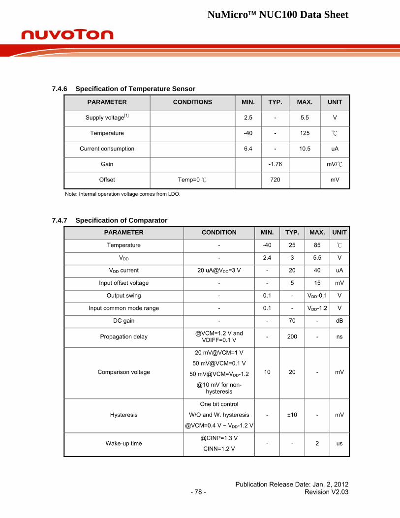
NuMicro™ NUC100 Data Sheet
Publication Release Date: Jan. 2, 2012 - 78 - Revision V2.03
7.4.6 Specification of Temperature Sensor
PARAMETER CONDITIONS MIN. TYP. MAX. UNIT
Supply voltage[1] 2.5 - 5.5 V
Temperature -40 - 125 ℃
Current consumption 6.4 - 10.5 uA
Gain -1.76 mV/℃
Offset Temp=0 ℃ 720 mV
Note: Internal operation voltage comes from LDO.
7.4.7 Specification of Comparator PARAMETER CONDITION MIN. TYP. MAX. UNIT
Temperature - -40 25 85 ℃
VDD - 2.4 3 5.5 V
VDD current 20 uA@VDD=3 V - 20 40 uA
Input offset voltage - - 5 15 mV
Output swing - 0.1 - VDD-0.1 V
Input common mode range - 0.1 - VDD-1.2 V
DC gain - - 70 - dB
Propagation delay @VCM=1.2 V and VDIFF=0.1 V - 200 - ns
Comparison voltage
20 mV@VCM=1 V
50 mV@VCM=0.1 V
50 mV@VCM=VDD-1.2
@10 mV for non-hysteresis
10 20 - mV
Hysteresis
One bit control
W/O and W. hysteresis
@VCM=0.4 V ~ VDD-1.2 V
- ±10 - mV
Wake-up time @CINP=1.3 V
CINN=1.2 V - - 2 us
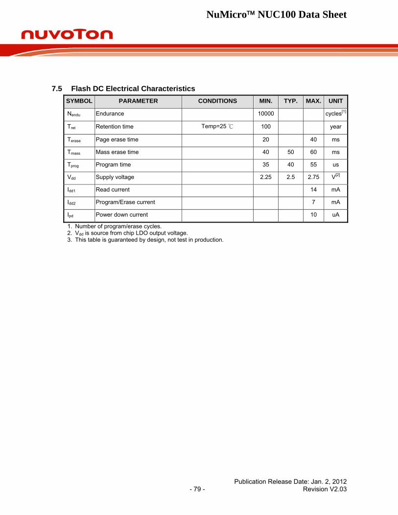
NuMicro™ NUC100 Data Sheet
Publication Release Date: Jan. 2, 2012 - 79 - Revision V2.03
7.5 Flash DC Electrical Characteristics SYMBOL PARAMETER CONDITIONS MIN. TYP. MAX. UNIT
Nendu Endurance 10000 cycles[1]
Tret Retention time Temp=25 ℃ 100 year
Terase Page erase time 20 40 ms
Tmass Mass erase time 40 50 60 ms
Tprog Program time 35 40 55 us
Vdd Supply voltage 2.25 2.5 2.75 V[2]
Idd1 Read current 14 mA
Idd2 Program/Erase current 7 mA
Ipd Power down current 10 uA
1. Number of program/erase cycles. 2. Vdd is source from chip LDO output voltage. 3. This table is guaranteed by design, not test in production.
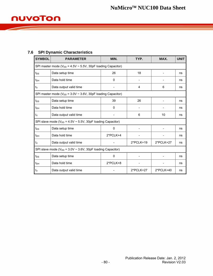
NuMicro™ NUC100 Data Sheet
Publication Release Date: Jan. 2, 2012 - 80 - Revision V2.03
7.6 SPI Dynamic Characteristics SYMBOL PARAMETER MIN. TYP. MAX. UNIT
SPI master mode (VDD = 4.5V ~ 5.5V, 30pF loading Capacitor)
tDS Data setup time 26 18 - ns
tDH Data hold time 0 - - ns
tV Data output valid time - 4 6 ns
SPI master mode (VDD = 3.0V ~ 3.6V, 30pF loading Capacitor)
tDS Data setup time 39 26 - ns
tDH Data hold time 0 - - ns
tV Data output valid time - 6 10 ns
SPI slave mode (VDD = 4.5V ~ 5.5V, 30pF loading Capacitor)
tDS Data setup time 0 - - ns
tDH Data hold time 2*PCLK+4 - - ns
tV Data output valid time - 2*PCLK+19 2*PCLK+27 ns
SPI slave mode (VDD = 3.0V ~ 3.6V, 30pF loading Capacitor)
tDS Data setup time 0 - - ns
tDH Data hold time 2*PCLK+8 - - ns
tV Data output valid time - 2*PCLK+27 2*PCLK+40 ns
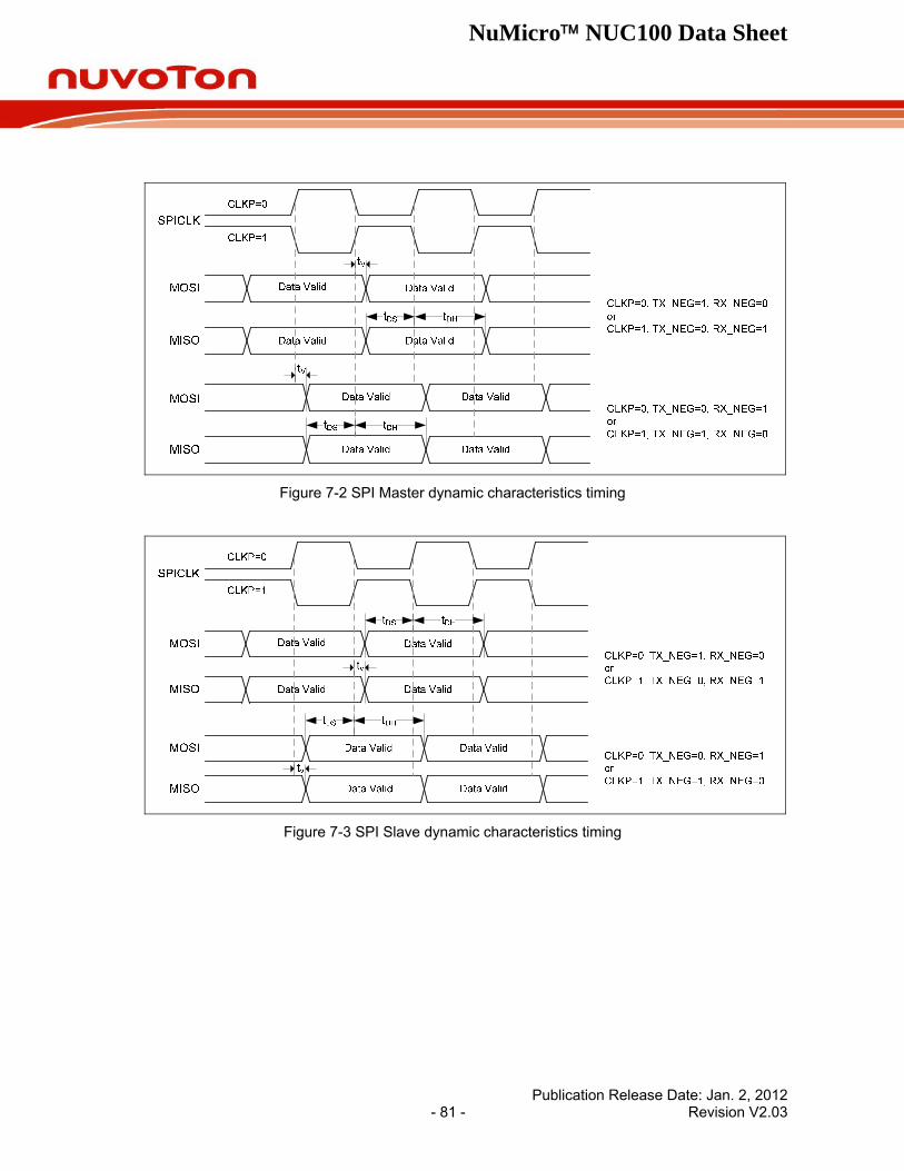
NuMicro™ NUC100 Data Sheet
Figure 7-2 SPI Master dynamic characteristics timing
Figure 7-3 SPI Slave dynamic characteristics timing
Publication Release Date: Jan. 2, 2012 - 81 - Revision V2.03
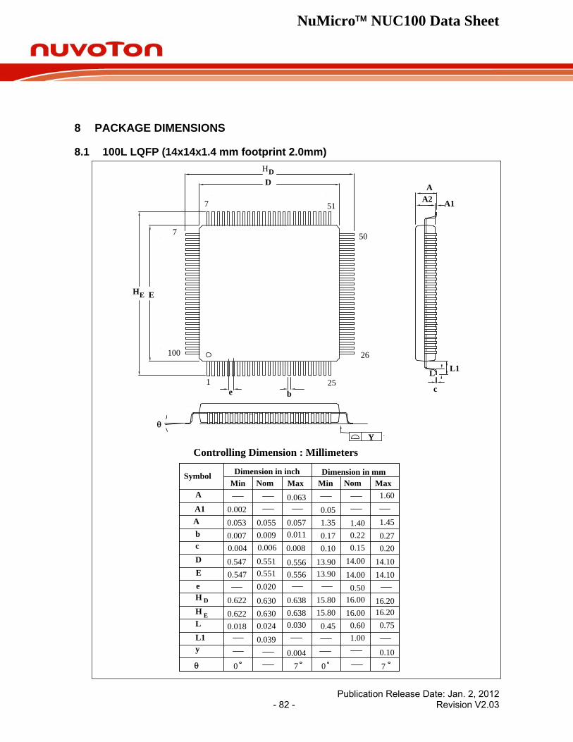
NuMicro™ NUC100 Data Sheet
8 PACKAGE DIMENSIONS
8.1 100L LQFP (14x14x1.4 mm footprint 2.0mm)
Controlling Dimension : Millimeters
0.10070
0.004
1.000.750.600.45
0.039
0.0300.0240.018
0.6380.6300.6220.50
14.100.200.271.45
1.60
14.00
1.40
13.900.100.171.350.05
0.0080.0110.057
0.063
0.055
0.020
0.5560.5510.5470.0040.0070.0530.002
SymbolMin Nom Max MaxNomMinDimension in inch Dimension in mm
A
bcD
eH D
H EL
y
A1A2
L1
E
0.0090.006 0.15
0.22
7
13.90 14.00 14.10
15.80 16.00 16.2015.80 16.00 16.20
0.5560.5510.547
θ
0.6380.6300.622
DD
EE
b
A2 A1
A
L1
e c
L
Y
H
H
1
100
θ
25
26
50
517
7
Publication Release Date: Jan. 2, 2012 - 82 - Revision V2.03
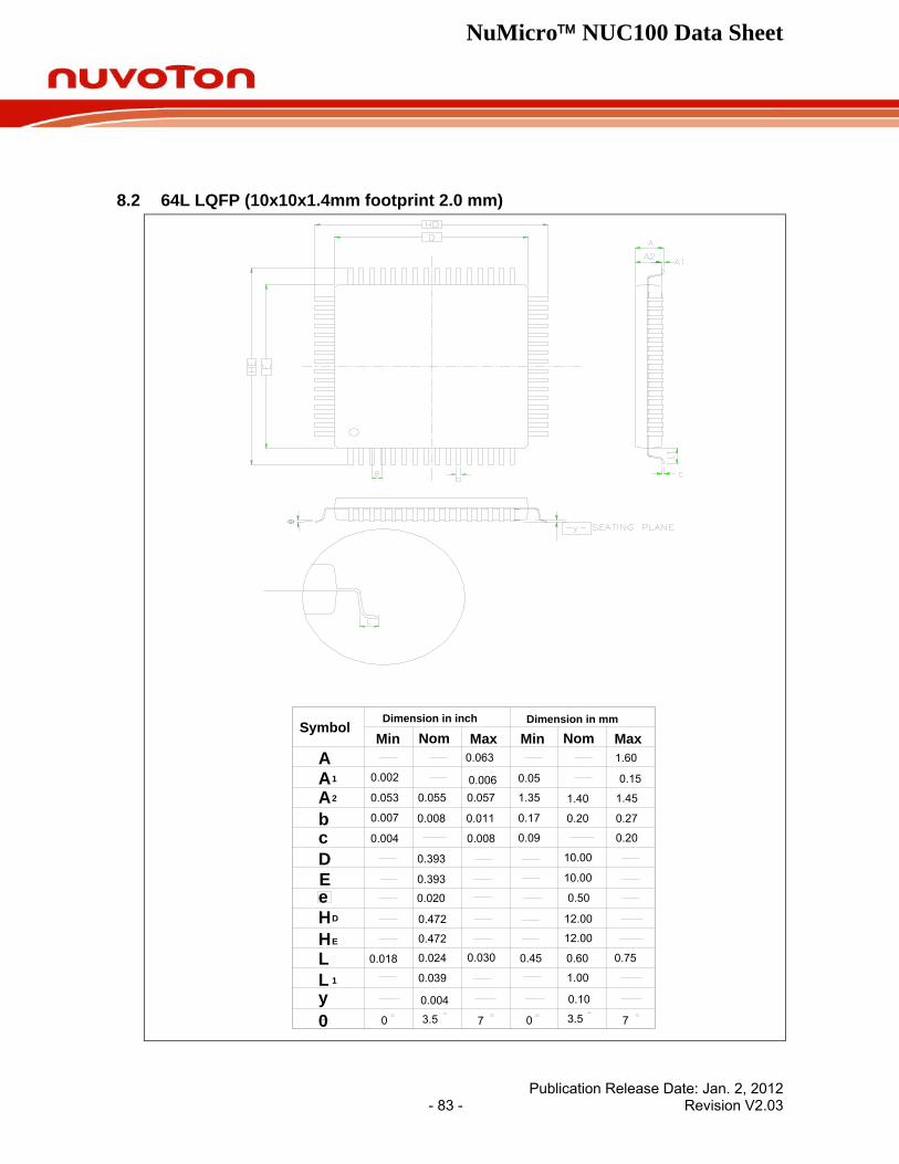
NuMicro™ NUC100 Data Sheet
8.2 64L LQFP (10x10x1.4mm footprint 2.0 mm)
0 70
1.00
0.750.60
12.00
0.45
0.039
0.0300.024
0.472
0.018
0.50
0.20
0.27
1.45
1.60
10.00
1.40
0.09
0.17
1.35
0.05
0.008
0.011
0.057
0.063
0.393
0.055
0.020
0.004
0.007
0.053
0.002
SymbolMin Nom Max MaxNomMin
Dimension in inch Dimension in mm
A
bcD
eHD
HE
L
y0
AA
L 1
1
2
E
0.008 0.20
7
0.393 10.00
0.472 12.00
0.006 0.15
0.004 0.10
3.5 3.5
Publication Release Date: Jan. 2, 2012 - 83 - Revision V2.03
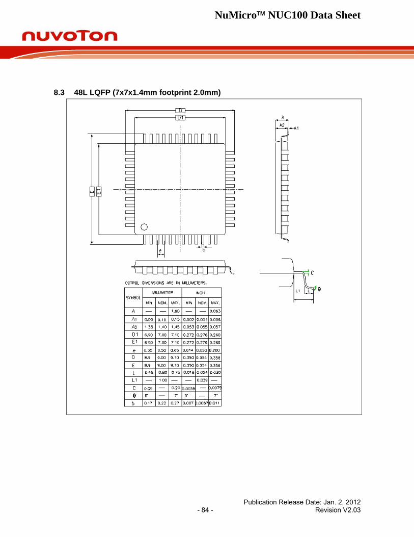
NuMicro™ NUC100 Data Sheet
8.3 48L LQFP (7x7x1.4mm footprint 2.0mm)
Publication Release Date: Jan. 2, 2012 - 84 - Revision V2.03
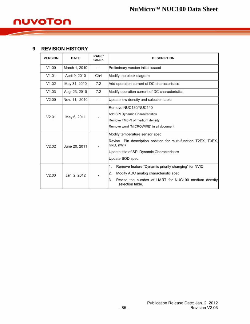
NuMicro™ NUC100 Data Sheet
Publication Release Date: Jan. 2, 2012 - 85 - Revision V2.03
9 REVISION HISTORY
VERSION DATE PAGE/ CHAP. DESCRIPTION
V1.00 March 1, 2010 - Preliminary version initial issued
V1.01 April 9, 2010 Ch4 Modify the block diagram
V1.02 May 31, 2010 7.2 Add operation current of DC characteristics
V1.03 Aug. 23, 2010 7.2 Modify operation current of DC characteristics
V2.00 Nov. 11, 2010 - Update low density and selection table
V2.01 May 6, 2011 -
Remove NUC130/NUC140
Add SPI Dynamic Characteristics
Remove TM0~3 of medium density
Remove word “MICROWIRE” in all document
V2.02 June 20, 2011 -
Modify temperature sensor spec
Revise Pin description position for multi-function T2EX, T3EX, nRD, nWR
Update title of SPI Dynamic Characteristics
Update BOD spec
V2.03 Jan. 2, 2012 -
1. Remove feature “Dynamic priority changing” for NVIC
2. Modify ADC analog characteristic spec
3. Revise the number of UART for NUC100 medium density selection table.
NuMicro™ NUC100 Data Sheet
Important Notice Nuvoton Products are neither intended nor warranted for usage in systems or equipment, any malfunction or failure of which may cause loss of human life, bodily injury or severe property damage. Such applications are deemed, “Insecure Usage”.
Insecure usage includes, but is not limited to: equipment for surgical implementation, atomic energy control instruments, airplane or spaceship instruments, the control or operation of dynamic, brake or safety systems designed for vehicular use, traffic signal instruments, all types of safety devices, and other applications intended to support or sustain life.
All Insecure Usage shall be made at customer’s risk, and in the event that third parties lay claims to Nuvoton as a result of customer’s Insecure Usage, customer shall indemnify the damages and liabilities thus incurred by Nuvoton.
Publication Release Date: Jan. 2, 2012 - 86 - Revision V2.03