Embed Size (px)
Citation preview
1. General description
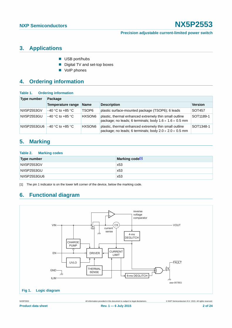
The NX5P2553 is a precision adjustable current-limited power switch. The device includes undervoltage lockout, overtemperature, and reverse bias protection circuits designed to isolate the switch terminals when a fault condition occurs. It also has an overcurrent protection circuit to limit the output current. The device features two power switch terminals, one input (VIN), and one output (VOUT). It also consists of a current limit input (ILIM) for defining the overcurrent limit, an open-drain fault output (FAULT) to indicate when a fault condition has occurred, and an enable input (EN) to control the state of the switch.
The overcurrent limit threshold can be programmed between 85 mA and 1.8 A using an external resistor between the ILIM and GND pins. The device has built-in soft-start. This feature controls the output rise time by minimizing current surges when the switch is enabled.
Designed for operation from 2.5 V to 5.5 V, it is used in power domain isolation applications to protect from out of range operation. The enable input includes integrated logic level translation making the device compatible with lower voltage processors and controllers.
2. Features and benefits
Wide supply voltage range from 2.5 V to 5.5 V
ISW maximum 1.5 A continuous current
6 % current-limit accuracy at 1.8 A (typical)
Meets USB current-limiting requirements
Adjustable current limit from 85 mA to 1800 mA (typical)
Constant current mode in overcurrent situation
Overtemperature protection
Very low ON resistance: 95 m (typical) for TSOP6 package
Fast short-circuit switch-off response (2.0 s typical)
ILIM short detection
Reverse input-output voltage protection
Built-in soft-start
ESD protection:
HBM ANSI/ESDA/JEDEC JS-001-2012 Class 2 exceeds 2000 V
CDM JESD22-C101D exceeds 500 V
IEC61000-4-2 contact discharge exceeds 8 kV for VOUT (with external capacitance)
Specified from 40 C to +85 C ambient temperature
NX5P2553Precision adjustable current-limited power switchRev. 1 — 6 July 2015 Product data sheet
NXP Semiconductors NX5P2553Precision adjustable current-limited power switch
3. Applications
USB port/hubs
Digital TV and set-top boxes
VoIP phones
4. Ordering information
5. Marking
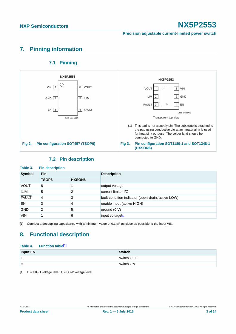
[1] The pin 1 indicator is on the lower left corner of the device, below the marking code.
6. Functional diagram
Table 1. Ordering information
Type number Package
Temperature range Name Description Version
NX5P2553GV 40 C to +85 C TSOP6 plastic surface-mounted package (TSOP6); 6 leads SOT457
NX5P2553GU 40 C to +85 C HXSON6 plastic, thermal enhanced extremely thin small outline package; no leads; 6 terminals; body 1.6 1.6 0.5 mm
SOT1189-1
NX5P2553GU6 40 C to +85 C HXSON6 plastic, thermal enhanced extremely thin small outline package; no leads; 6 terminals; body 2.0 2.0 0.5 mm
SOT1348-1
Table 2. Marking codes
Type number Marking code[1]
NX5P2553GV x53
NX5P2553GU x53
NX5P2553GU6 x53
Fig 1. Logic diagram
CS
aaa-007801
DRIVER CURRENTLIMIT
4-msDEGLITCH
reversevoltagecomparator
currentsense
THERMALSENSE
8-ms DEGLITCH
FAULT
VOUT
CHARGEPUMP
UVLO
VIN
EN
GND
ILIM
NX5P2553 All information provided in this document is subject to legal disclaimers. © NXP Semiconductors N.V. 2015. All rights reserved.
Product data sheet Rev. 1 — 6 July 2015 2 of 24
NXP Semiconductors NX5P2553Precision adjustable current-limited power switch
7. Pinning information
7.1 Pinning
7.2 Pin description
[1] Connect a decoupling capacitance with a minimum value of 0.1 F as close as possible to the input VIN.
8. Functional description
[1] H = HIGH voltage level; L = LOW voltage level.
(1) This pad is not a supply pin. The substrate is attached to the pad using conductive die attach material. It is used for heat sink purpose. The solder land should be connected to GND.
Fig 2. Pin configuration SOT457 (TSOP6) Fig 3. Pin configuration SOT1189-1 and SOT1348-1 (HXSON6)
NX5P2553
VIN VOUT
GND
EN FAULT
aaa-011068
1
2
3
6
ILIM5
4aaa-011069
NX5P2553
Transparent top view
1 6VOUT VIN
2 5ILIM GND
3 4FAULT EN(1)
Table 3. Pin description
Symbol Pin Description
TSOP6 HXSON6
VOUT 6 1 output voltage
ILIM 5 2 current limiter I/O
FAULT 4 3 fault condition indicator (open-drain; active LOW)
EN 3 4 enable input (active HIGH)
GND 2 5 ground (0 V)
VIN 1 6 input voltage[1]
Table 4. Function table[1]
Input EN Switch
L switch OFF
H switch ON
NX5P2553 All information provided in this document is subject to legal disclaimers. © NXP Semiconductors N.V. 2015. All rights reserved.
Product data sheet Rev. 1 — 6 July 2015 3 of 24
NXP Semiconductors NX5P2553Precision adjustable current-limited power switch
8.1 EN input
When EN is set to LOW, the N-channel MOSFET is disabled and the device enters a low-power mode. In low-power mode, all protection circuits are disabled and the FAULT output is set to high-impedance state. When EN is set to HIGH, all protection circuits are enabled. If no fault conditions exist, the N-channel MOSFET is enabled.
8.2 UnderVoltage LockOut (UVLO)
The UVLO circuit is active until VIN > 2.35 V. It disables the N-channel MOSFET and switches the device back to low-power mode. It occurs irrespective of the logic level on the EN pin. Once VIN > 2.35 V, the EN pin controls the N-channel MOSFET state. The UVLO circuit remains active in low-power mode.
8.3 ILIM
The OverCurrent Protection (OCP) circuit trigger value Iocp is set using an external resistor connected to the ILIM pin as shown in Figure 8. If EN is set to HIGH and the ILIM pin is grounded, the N-channel MOSFET is disabled and the FAULT output is set to LOW.
8.4 OverCurrent Protection (OCP)
Three possible overcurrent conditions can occur. They are:
• Overcurrent at start-up, ISW > Iocp when enabling the N-channel MOSFET
• Overcurrent when enabled, ISW > Iocp when the N-channel MOSFET is enabled
• Short-circuit when enabled, ISW > 4 Iocp (typical)
8.4.1 Overcurrent at start-up
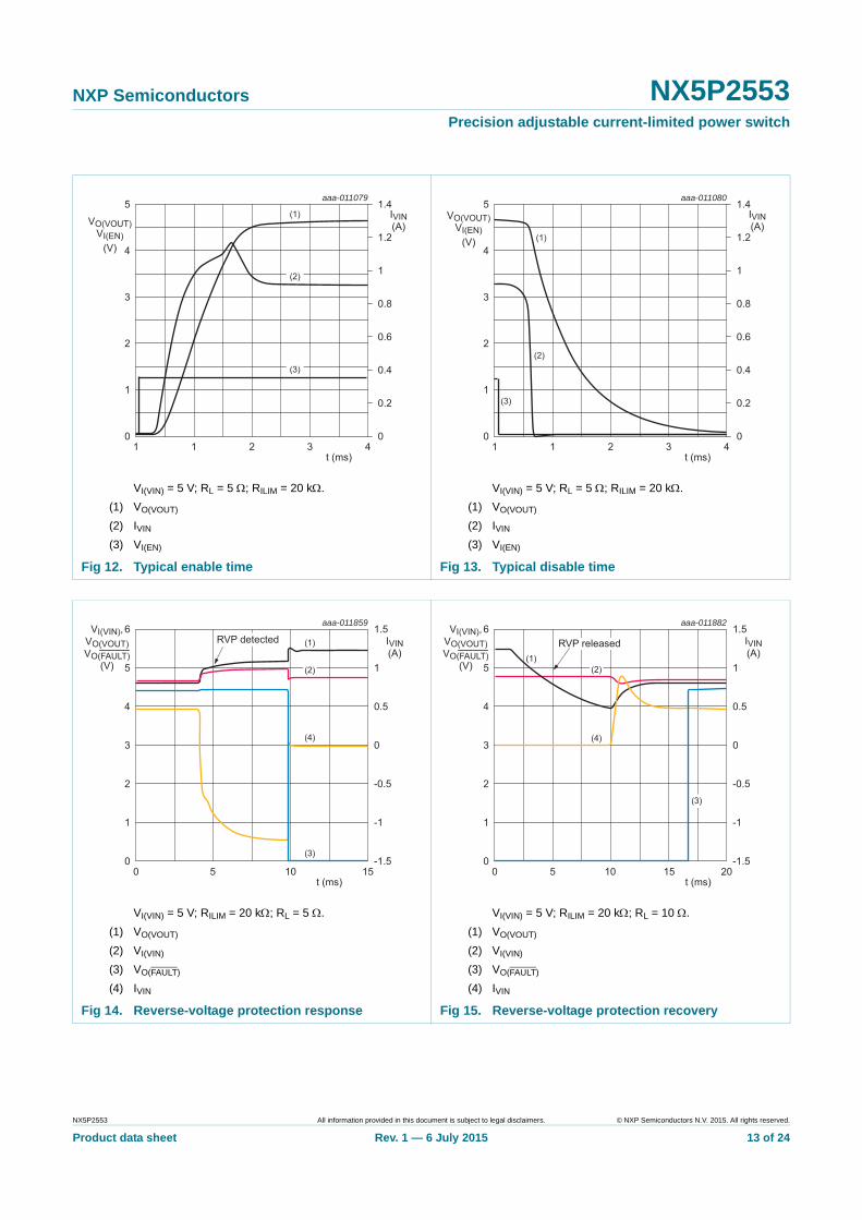
If the device senses a short or overcurrent while enabling the N-channel MOSFET, OCP is triggered. It limits the output current to Iocp and after the deglitch time sets the FAULT output to LOW, as shown in Figure 22. Increased power dissipation combined with the OTP may lead to temperature cycling.
8.4.2 Overcurrent when enabled
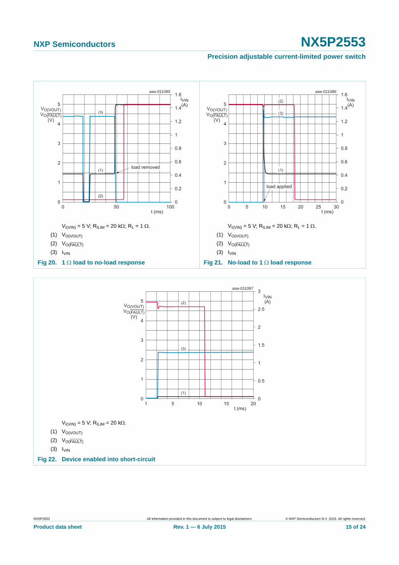
When enabled, if the device senses ISW > Iocp, the OCP is triggered. It limits the output current to Iocp and after the deglitch time sets the FAULT output to LOW. Limiting the output current reduces VO(VOUT), as shown in Figure 20 and Figure 21. Increased power dissipation combined with the OTP may lead to temperature cycling.
8.4.3 Short-circuit when enabled
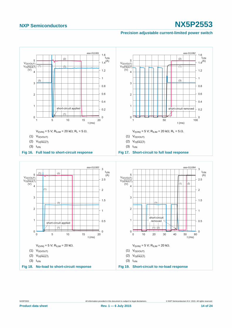
When enabled, if the device senses ISW > 4 Iocp, a short-circuit is detected. The device disables the N-channel MOSFET immediately. It then enables the N-channel MOSFET, output current is limited to Iocp and after the deglitch time, the FAULT output is set to LOW as shown in Figure 16 to Figure 19. Increased power dissipation combined with the OTP may lead to temperature cycling.
8.5 Reverse-Voltage Protection (RVP)
If VOUT exceeds VIN by 140 mV for the deglitch time, RVP protects the device by disabling the N-channel MOSFET. When the reverse voltage condition is removed for the deglitch time, the N-channel MOSFET is enabled as shown in Figure 14 and Figure 15.
NX5P2553 All information provided in this document is subject to legal disclaimers. © NXP Semiconductors N.V. 2015. All rights reserved.
Product data sheet Rev. 1 — 6 July 2015 4 of 24
NXP Semiconductors NX5P2553Precision adjustable current-limited power switch
8.6 FAULT output
The FAULT pin is an open-drain output that requires an external pull-up resistor. If any of the protection circuits are activated, FAULT is set to LOW to indicate that a fault has occurred. It returns to the high-impedance state automatically once the fault condition is removed.
8.7 OverTemperature Protection (OTP)
If the device temperature exceeds 155 C when EN is set HIGH and the device is not in current limit, OTP triggers. It disables the N-channel MOSFET and sets the FAULT pin to LOW. Any transition on the EN pin has no effect. Once the device temperature decreases below 125 C, the device returns to the defined state.
If the device temperature exceeds 130 C when EN is set HIGH and the device is in current limit, OTP triggers. It disables the N-channel MOSFET and sets the FAULT pin to LOW. Any transition on the EN pin has no effect. Once the device temperature decreases below 118 C, the device returns to the defined state.
9. Limiting values
[1] If the input current rating is observed, the minimum input voltage rating may be exceeded.
[2] If the switch clamping current rating is observed, the minimum and maximum switch voltage ratings may be exceeded.
[3] Internally limited.
[4] The (absolute) maximum power dissipation depends on the junction temperature Tj. Higher power dissipation is allowed with lower ambient temperatures. The conditions to determine the specified values are Tamb = 85 C and the use of a two layer PCB.
Table 5. Limiting valuesIn accordance with the Absolute Maximum Rating System (IEC 60134). Voltages are referenced to GND (ground = 0 V).
Symbol Parameter Conditions Min Max Unit
VI input voltage inputs EN and ILIM [1] 0.35 +6.5 V
input VIN [2] 0.35 +6.5 V
VO output voltage output FAULT [1] 0.35 VI(VIN) V
output VOUT [2] 0.35 +6.5 V
VSW switch voltage [2] 6.5 +6.5 V
IIK input clamping current input EN; VI(EN) < 0.35 V 50 - mA
input ILIM; VI(ILIM) < 0.35 V 50 - mA
Isource source current input ILIM - 1 mA
IOK output clamping current VO < 0 V 50 - mA
ISK switch clamping current input VIN; VI(VIN) < 0.35 V 50 - mA
output VOUT; VO(VOUT) < 0.35 V 50 - mA
ISW switch current VSW > 0.35 V [3] - 1900 mA
Tj(max) maximum junction temperature
40 +150 C
Tstg storage temperature 65 +150 C
Ptot total power dissipation NX5P2553GV [4] - 300 mW
NX5P2553GU [4] - 315 mW
NX5P2553GU6 [4] - 340 mW
NX5P2553 All information provided in this document is subject to legal disclaimers. © NXP Semiconductors N.V. 2015. All rights reserved.
Product data sheet Rev. 1 — 6 July 2015 5 of 24
NXP Semiconductors NX5P2553Precision adjustable current-limited power switch
10. Recommended operating conditions
[1] Current-limit threshold resistor range from ILIM to GND.
11. Thermal characteristics
[1] Rth(j-a) is dependent upon board layout. To minimize Rth(j-a), ensure that all pins have a solid connection to larger copper layer areas. In multi-layer PCBs, the second layer should be used to create a large heat spreader area below the device. Avoid using solder-stop varnish under the device.
12. Static characteristics
Table 6. Operating conditions
Symbol Parameter Conditions Min Max Unit
VI input voltage input VIN 2.5 5.5 V
input EN 0 5.5 V
ISW switch current Tj = 40 C to +125 C 0 1.2 A
Tj = 40 C to +105 C 0 1.5 A
IO(sink) output sink current output FAULT 10 - mA
RILIM current limit resistance input ILIM [1] 15 232 k
Cdec decoupling capacitance VIN and VOUT to GND 0.1 - F
Tamb ambient temperature 40 +85 C
Tj junction temperature ISW < 1.2 A 40 +125 C
ISW < 1.5 A 40 +105 C
Table 7. Thermal characteristics
Symbol Parameter Conditions Typ Unit
Rth(j-a) thermal resistance from junction to ambient
NX5P2553GV [1] 133 K/W
NX5P2553GU [1] 105 K/W
NX5P2553GU6 [1] 93 K/W
Table 8. Static characteristicsAt recommended operating conditions; VI(VIN) = VI(EN) and RFAULT = 10 k unless otherwise specified; voltages are referenced to GND (ground = 0 V); see Figure 4, Figure 5, Figure 6, and Figure 11.
Symbol Parameter Conditions Min Typ[1] Max Unit
VIH HIGH-level input voltage EN input; VI(VIN) = 2.5 V to 5.5 V 1.3 - - V
VIL LOW-level input voltage EN input; VI(VIN) = 2.5 V to 5.5 V - - 0.56 V
ILI input leakage current EN input; VI(VIN) = 2.5 V to 5.5 V; VI(EN) = 0 V or 5.5 V
- - 0.5 A
IVIN supply current VOUT open; VI(VIN) = 5.5 V
EN = GND (low-power mode) - 0.3 1 A
EN = VI(VIN); Rext = 20 k - 160 225 A
EN = VI(VIN); Rext = 210 k - 135 200 A
IOFF power-off leakage current VOUT; Tj = 25 C; VI(VIN) = 0 V; VO(VOUT) = 5.5 V
- 0.1 1 A
NX5P2553 All information provided in this document is subject to legal disclaimers. © NXP Semiconductors N.V. 2015. All rights reserved.
Product data sheet Rev. 1 — 6 July 2015 6 of 24
NXP Semiconductors NX5P2553Precision adjustable current-limited power switch
[1] Typical values are measured at Tj = 25 C.
12.1 Graphs
IS(OFF) OFF-state leakage current VOUT; Tj = 25 C; VI(VIN) = 5.5 V; VO(VOUT) = 0 V to 5.5 V
- 0.1 1 A
Vtrip trip level voltage RVP; VI(VIN) = 2.5 V to 5.5 V 80 140 195 mV
VUVLO undervoltage lockout voltage
VIN input - 2.35 2.45 V
Vhys(UVLO) undervoltage lockout hysteresis voltage
- 25 - mV
VOL LOW-level output voltage FAULT; VI(VIN) = 2.5 V to 5.5 V; IO = 1 mA
- - 180 mV
IOZ OFF-state output current FAULT; VI(VIN) = 5.5 V; VO(FAULT) = 5.5 V
- - 1 A
Table 8. Static characteristics …continuedAt recommended operating conditions; VI(VIN) = VI(EN) and RFAULT = 10 k unless otherwise specified; voltages are referenced to GND (ground = 0 V); see Figure 4, Figure 5, Figure 6, and Figure 11.
Symbol Parameter Conditions Min Typ[1] Max Unit
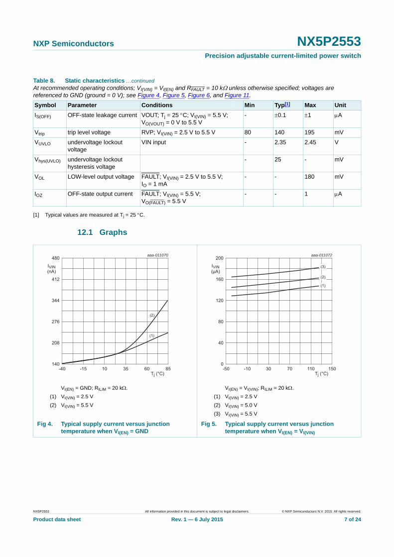
VI(EN) = GND; RILIM = 20 k.
(1) VI(VIN) = 2.5 V
(2) VI(VIN) = 5.5 V
VI(EN) = VI(VIN); RILIM = 20 k.
(1) VI(VIN) = 2.5 V
(2) VI(VIN) = 5.0 V
(3) VI(VIN) = 5.5 V
Fig 4. Typical supply current versus junction temperature when VI(EN) = GND
Fig 5. Typical supply current versus junction temperature when VI(EN) = VI(VIN)
Tj (°C)-40 856010 35-15
aaa-011070
276
344
208
412
480
IVIN(nA)
140
(1)
(2)
Tj (°C)-50 15011030 70-10
aaa-011072
80
120
40
160
200
IVIN(μA)
0
(3)
(2)
(1)
NX5P2553 All information provided in this document is subject to legal disclaimers. © NXP Semiconductors N.V. 2015. All rights reserved.
Product data sheet Rev. 1 — 6 July 2015 7 of 24
NXP Semiconductors NX5P2553Precision adjustable current-limited power switch
12.2 ON resistance
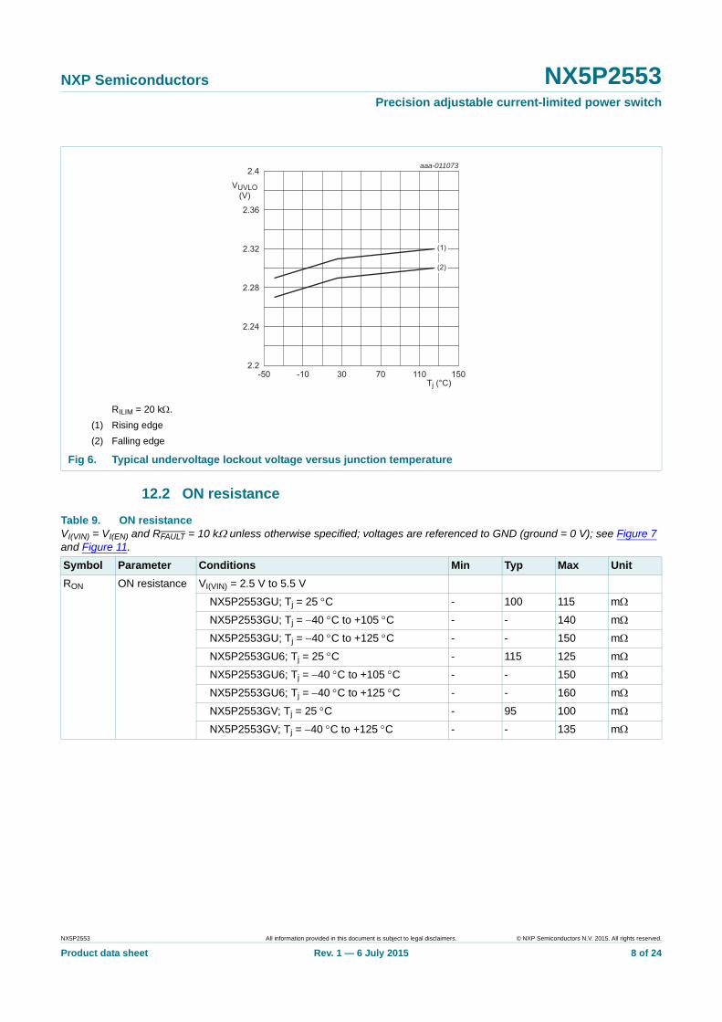
RILIM = 20 k.
(1) Rising edge
(2) Falling edge
Fig 6. Typical undervoltage lockout voltage versus junction temperature
Tj (°C)-50 15011030 70-10
aaa-011073
2.28
2.32
2.24
2.36
2.4
VUVLO(V)
2.2
(2)
(1)
Table 9. ON resistanceVI(VIN) = VI(EN) and RFAULT = 10 k unless otherwise specified; voltages are referenced to GND (ground = 0 V); see Figure 7 and Figure 11.
Symbol Parameter Conditions Min Typ Max Unit
RON ON resistance VI(VIN) = 2.5 V to 5.5 V
NX5P2553GU; Tj = 25 C - 100 115 m
NX5P2553GU; Tj = 40 C to +105 C - - 140 m
NX5P2553GU; Tj = 40 C to +125 C - - 150 m
NX5P2553GU6; Tj = 25 C - 115 125 m
NX5P2553GU6; Tj = 40 C to +105 C - - 150 m
NX5P2553GU6; Tj = 40 C to +125 C - - 160 m
NX5P2553GV; Tj = 25 C - 95 100 m
NX5P2553GV; Tj = 40 C to +125 C - - 135 m
NX5P2553 All information provided in this document is subject to legal disclaimers. © NXP Semiconductors N.V. 2015. All rights reserved.
Product data sheet Rev. 1 — 6 July 2015 8 of 24
NXP Semiconductors NX5P2553Precision adjustable current-limited power switch
12.3 ON resistance graph
12.4 Current limit
[1] Typical values are measured at Tj = 25 C.
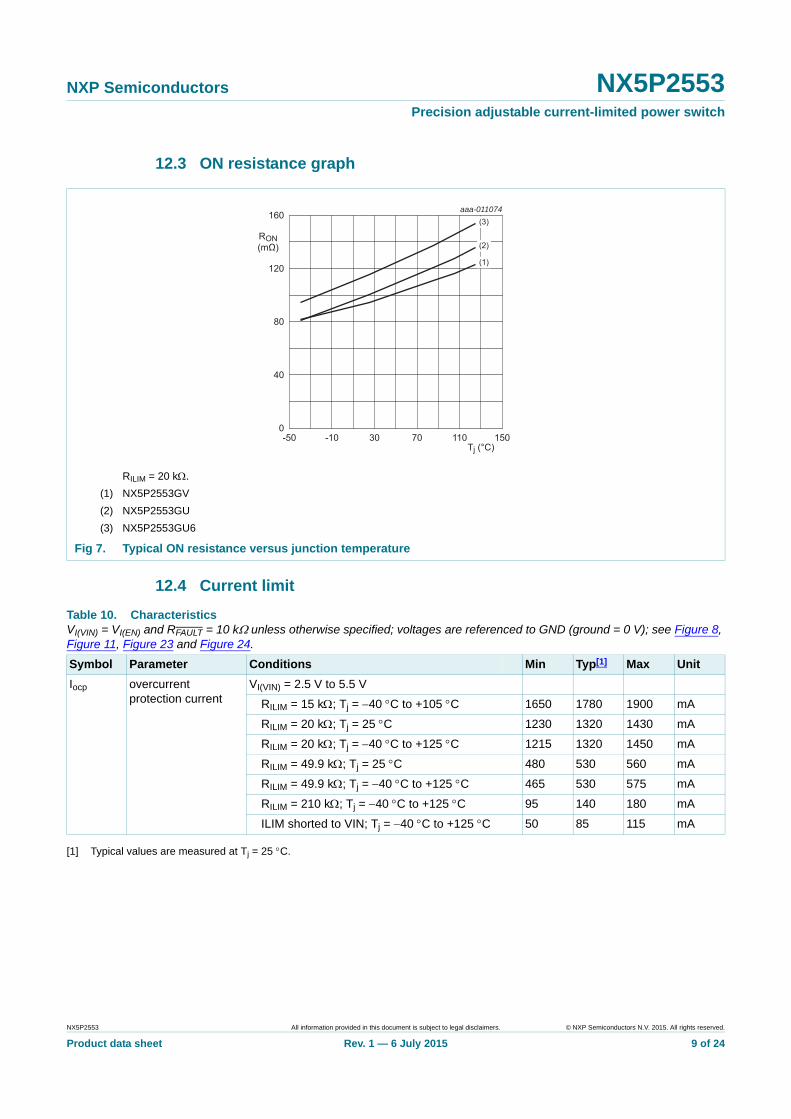
RILIM = 20 k.
(1) NX5P2553GV
(2) NX5P2553GU
(3) NX5P2553GU6
Fig 7. Typical ON resistance versus junction temperature
Tj (°C)-50 15011030 70-10
aaa-011074160
RON(mΩ)
0
40
80
120
(3)
(2)
(1)
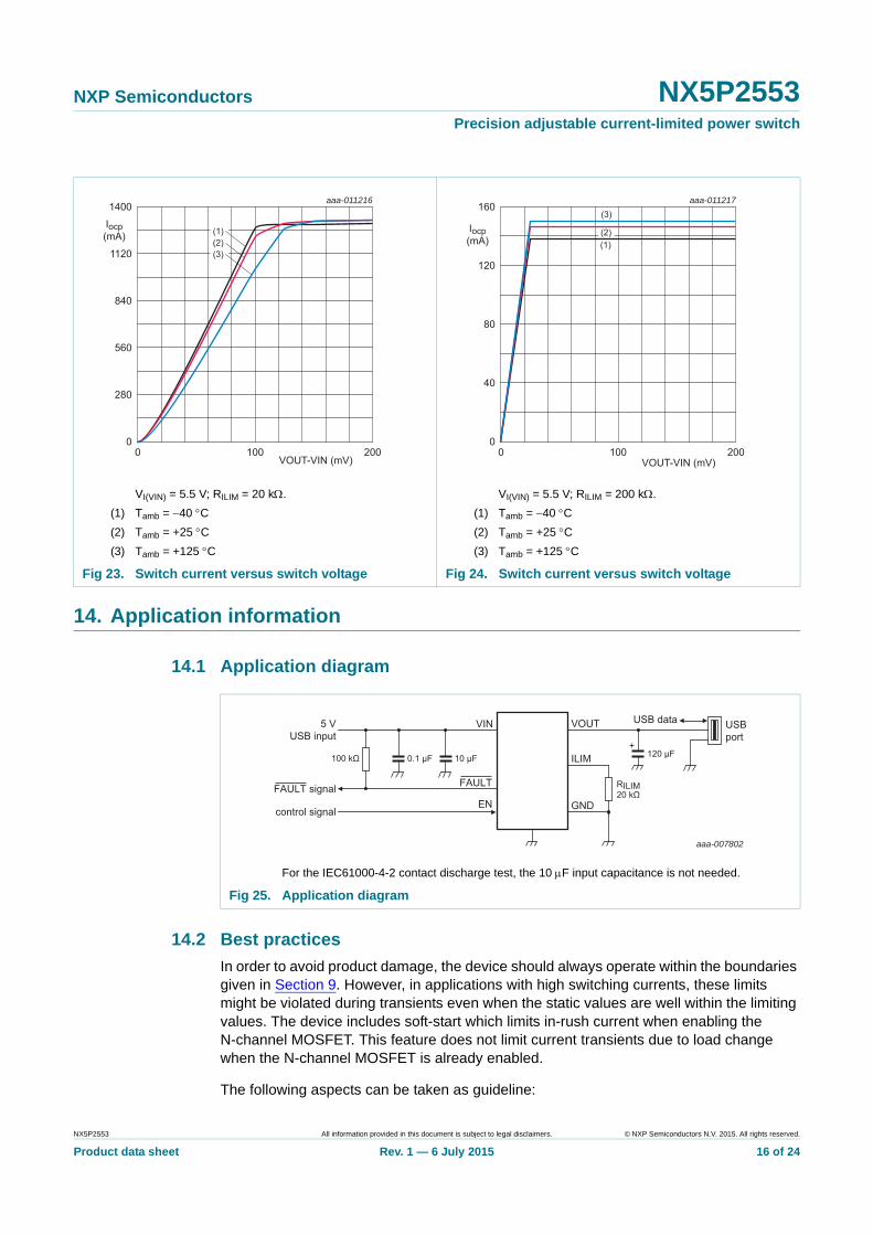
Table 10. CharacteristicsVI(VIN) = VI(EN) and RFAULT = 10 k unless otherwise specified; voltages are referenced to GND (ground = 0 V); see Figure 8, Figure 11, Figure 23 and Figure 24.
Symbol Parameter Conditions Min Typ[1] Max Unit
Iocp overcurrent protection current
VI(VIN) = 2.5 V to 5.5 V
RILIM = 15 k; Tj = 40 C to +105 C 1650 1780 1900 mA
RILIM = 20 k; Tj = 25 C 1230 1320 1430 mA
RILIM = 20 k; Tj = 40 C to +125 C 1215 1320 1450 mA
RILIM = 49.9 k; Tj = 25 C 480 530 560 mA
RILIM = 49.9 k; Tj = 40 C to +125 C 465 530 575 mA
RILIM = 210 k; Tj = 40 C to +125 C 95 140 180 mA
ILIM shorted to VIN; Tj = 40 C to +125 C 50 85 115 mA
NX5P2553 All information provided in this document is subject to legal disclaimers. © NXP Semiconductors N.V. 2015. All rights reserved.
Product data sheet Rev. 1 — 6 July 2015 9 of 24
NXP Semiconductors NX5P2553Precision adjustable current-limited power switch
12.5 Current limit graph
12.6 Thermal shutdown
13. Dynamic characteristics
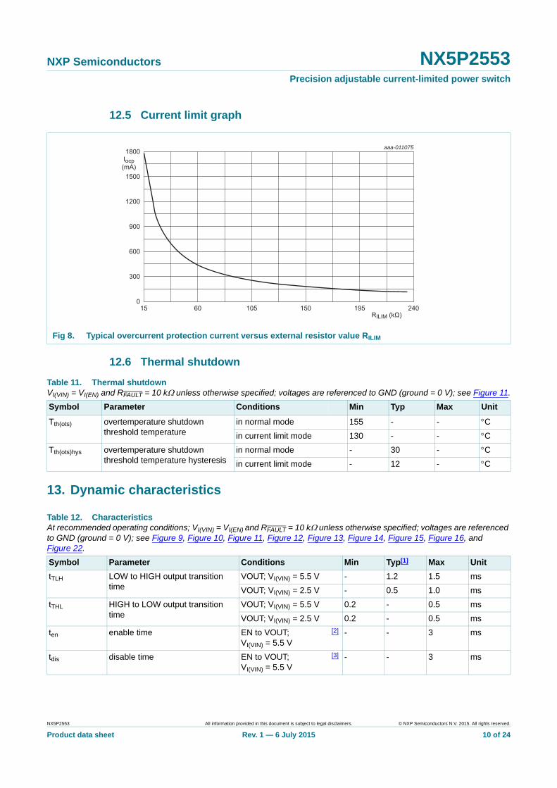
Fig 8. Typical overcurrent protection current versus external resistor value RILIM
RILIM (kΩ)15 240195105 15060
aaa-0110751800
Iocp(mA)
0
300
600
900
1200
1500
Table 11. Thermal shutdownVI(VIN) = VI(EN) and RFAULT = 10 k unless otherwise specified; voltages are referenced to GND (ground = 0 V); see Figure 11.
Symbol Parameter Conditions Min Typ Max Unit
Tth(ots) overtemperature shutdown threshold temperature
in normal mode 155 - - C
in current limit mode 130 - - C
Tth(ots)hys overtemperature shutdown threshold temperature hysteresis
in normal mode - 30 - C
in current limit mode - 12 - C
Table 12. CharacteristicsAt recommended operating conditions; VI(VIN) = VI(EN) and RFAULT = 10 k unless otherwise specified; voltages are referenced to GND (ground = 0 V); see Figure 9, Figure 10, Figure 11, Figure 12, Figure 13, Figure 14, Figure 15, Figure 16, and Figure 22.
Symbol Parameter Conditions Min Typ[1] Max Unit
tTLH LOW to HIGH output transition time
VOUT; VI(VIN) = 5.5 V - 1.2 1.5 ms
VOUT; VI(VIN) = 2.5 V - 0.5 1.0 ms
tTHL HIGH to LOW output transition time
VOUT; VI(VIN) = 5.5 V 0.2 - 0.5 ms
VOUT; VI(VIN) = 2.5 V 0.2 - 0.5 ms
ten enable time EN to VOUT; VI(VIN) = 5.5 V
[2] - - 3 ms
tdis disable time EN to VOUT; VI(VIN) = 5.5 V
[3] - - 3 ms
NX5P2553 All information provided in this document is subject to legal disclaimers. © NXP Semiconductors N.V. 2015. All rights reserved.
Product data sheet Rev. 1 — 6 July 2015 10 of 24
NXP Semiconductors NX5P2553Precision adjustable current-limited power switch
[1] Typical values are measured at Tj = 25 C.
[2] ten is the same as tPZH.
[3] tdis is the same as tPHZ.
13.1 Waveform and test circuits
toff turn-off time short-circuit; VI(VIN) = 5 V
- 2 - s
RVP; VI(VIN) = 5 V 3 5 7 ms
tdegl deglitch time FAULT; OCP; VI(VIN) = 5 V
5 8.7 12 ms
FAULT; RVP; VI(VIN) = 5 V
2 4.4 6 ms
Table 12. Characteristics …continuedAt recommended operating conditions; VI(VIN) = VI(EN) and RFAULT = 10 k unless otherwise specified; voltages are referenced to GND (ground = 0 V); see Figure 9, Figure 10, Figure 11, Figure 12, Figure 13, Figure 14, Figure 15, Figure 16, and Figure 22.
Symbol Parameter Conditions Min Typ[1] Max Unit
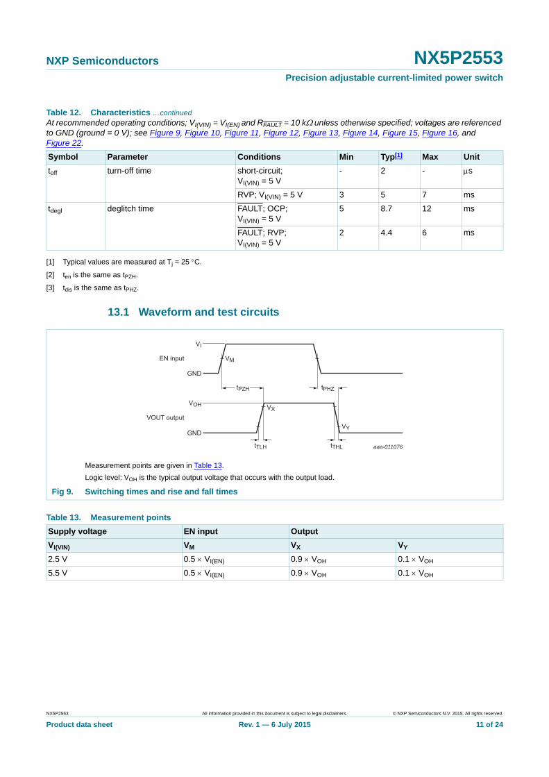
Measurement points are given in Table 13.
Logic level: VOH is the typical output voltage that occurs with the output load.
Fig 9. Switching times and rise and fall times
aaa-011076
VOUT output
EN input
VI
VM
VX
GND
VY
VOH
GND
tPZH tPHZ
tTLH tTHL
Table 13. Measurement points
Supply voltage EN input Output
VI(VIN) VM VX VY
2.5 V 0.5 VI(EN) 0.9 VOH 0.1 VOH
5.5 V 0.5 VI(EN) 0.9 VOH 0.1 VOH
NX5P2553 All information provided in this document is subject to legal disclaimers. © NXP Semiconductors N.V. 2015. All rights reserved.
Product data sheet Rev. 1 — 6 July 2015 11 of 24
NXP Semiconductors NX5P2553Precision adjustable current-limited power switch
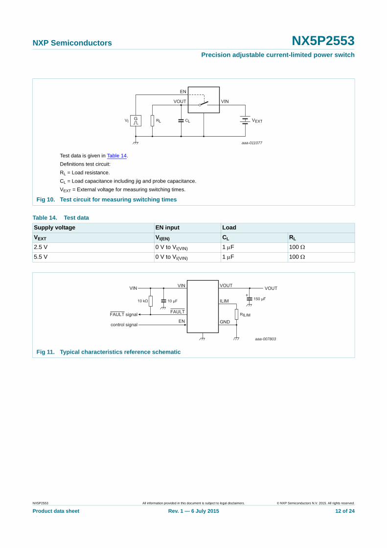
Test data is given in Table 14.
Definitions test circuit:
RL = Load resistance.
CL = Load capacitance including jig and probe capacitance.
VEXT = External voltage for measuring switching times.
Fig 10. Test circuit for measuring switching times
aaa-011077
EN
VOUT
CL
VIN
VEXTGVI RL
Table 14. Test data
Supply voltage EN input Load
VEXT VI(EN) CL RL
2.5 V 0 V to VI(VIN) 1 F 100
5.5 V 0 V to VI(VIN) 1 F 100
Fig 11. Typical characteristics reference schematic
aaa-007803
10 kΩ 10 μF 150 μF
FAULTFAULT signal
VIN
control signalEN
VIN VOUT VOUT
ILIM
GND
RILIM
NX5P2553 All information provided in this document is subject to legal disclaimers. © NXP Semiconductors N.V. 2015. All rights reserved.
Product data sheet Rev. 1 — 6 July 2015 12 of 24
NXP Semiconductors NX5P2553Precision adjustable current-limited power switch
VI(VIN) = 5 V; RL = 5 ; RILIM = 20 k.
(1) VO(VOUT)
(2) IVIN
(3) VI(EN)
VI(VIN) = 5 V; RL = 5 ; RILIM = 20 k.
(1) VO(VOUT)
(2) IVIN
(3) VI(EN)
Fig 12. Typical enable time Fig 13. Typical disable time
IVIN(A)
0
0.2
0.4
0.6
0.8
1
1.2
1.4(1)
t (ms)1 431 2
aaa-011079
2
3
1
4
5
VO(VOUT)VI(EN)
(V)
0
(2)
(3)
IVIN(A)
0
0.2
0.4
0.6
0.8
1
1.2
1.4
(1)
t (ms)1 431 2
aaa-011080
2
3
1
4
5VO(VOUT)
VI(EN)(V)
0
(2)
(3)
VI(VIN) = 5 V; RILIM = 20 k; RL = 5 .
(1) VO(VOUT)
(2) VI(VIN)
(3) VO(FAULT)
(4) IVIN
VI(VIN) = 5 V; RILIM = 20 k; RL = 10 .
(1) VO(VOUT)
(2) VI(VIN)
(3) VO(FAULT)
(4) IVIN
Fig 14. Reverse-voltage protection response Fig 15. Reverse-voltage protection recovery
IVIN(A)
-1.5
1.5
t (ms)0 5 10 15
aaa-0118596VI(VIN),
VO(VOUT)VO(FAULT)
(V)
0
-1
-0.5
0
0.5
1
1
2
3
4
5
(1)
(2)
(4)
(3)
RVP detected IVIN(A)
-1.5
1.5
t (ms)0 5 10 15 20
aaa-0118826VI(VIN),
VO(VOUT)VO(FAULT)
(V)
0
-1
-0.5
0
0.5
1
1
2
3
4
5(1)
(2)
(4)
(3)
RVP released
NX5P2553 All information provided in this document is subject to legal disclaimers. © NXP Semiconductors N.V. 2015. All rights reserved.
Product data sheet Rev. 1 — 6 July 2015 13 of 24
NXP Semiconductors NX5P2553Precision adjustable current-limited power switch
VI(VIN) = 5 V; RILIM = 20 k; RL = 5 .
(1) VO(VOUT)
(2) VO(FAULT)
(3) IVIN
VI(VIN) = 5 V; RILIM = 20 k; RL = 5 .
(1) VO(VOUT)
(2) VO(FAULT)
(3) IVIN
Fig 16. Full load to short-circuit response Fig 17. Short-circuit to full load response
0
1
2
3
4
5IVIN(A)
0
0.2
0.4
0.6
0.8
1
1.2
1.4
1.6
VO(VOUT)VO(FAULT)
(V)
t (ms)1 5 10 15 20
aaa-011081
(1)
(3)(1)
(3)
(2)
short-circuit applied
0
1
2
3
4
5IVIN(A)
0
0.2
0.4
0.6
0.8
1
1.2
1.4
1.6
VO(VOUT)VO(FAULT)
(V)
t (ms)1 50 100
aaa-011082
(2)
(1)
(3)
short-circuit removed
VI(VIN) = 5 V; RILIM = 20 k.
(1) VO(VOUT)
(2) VO(FAULT)
(3) IVIN
VI(VIN) = 5 V; RILIM = 20 k.
(1) VO(VOUT)
(2) VO(FAULT)
(3) IVIN
Fig 18. No-load to short-circuit response Fig 19. Short-circuit to no-load response
IVIN(A)
0
0.5
1
1.5
2
2.5
3
0
1
2
3
4
5VO(VOUT)VO(FAULT)
(V)
t (ms)0 5 10 15 20
aaa-011083
(1)
(1)
(1)
(3)
(2)
short-circuit applied
IVIN(A)
0
0.5
1
1.5
2
2.5
3
0
1
2
3
4
5VO(VOUT)VO(FAULT)
(V)
t (ms)0 10 20 4030 50 60
aaa-011084
(1)
(2)
(2)
(3)
(1)
short-circuitremoved
NX5P2553 All information provided in this document is subject to legal disclaimers. © NXP Semiconductors N.V. 2015. All rights reserved.
Product data sheet Rev. 1 — 6 July 2015 14 of 24
NXP Semiconductors NX5P2553Precision adjustable current-limited power switch
VI(VIN) = 5 V; RILIM = 20 k; RL = 1 .
(1) VO(VOUT)
(2) VO(FAULT)
(3) IVIN
VI(VIN) = 5 V; RILIM = 20 k; RL = 1 .
(1) VO(VOUT)
(2) VO(FAULT)
(3) IVIN
Fig 20. 1 load to no-load response Fig 21. No-load to 1 load response
IVIN(A)
0
0.2
0.4
0.6
0.8
1
1.2
1.4
1.6
0
1
2
3
4
5VO(VOUT)VO(FAULT)
(V)
t (ms)0 50 100
aaa-011085
(2)
(1)
(3)
load removed
IVIN(A)
0
0.2
0.4
0.6
0.8
1
1.2
1.4
1.6
0
1
2
3
4
5VO(VOUT)VO(FAULT)
(V)
t (ms)0 5 10 2015 25 30
aaa-011086
(2)
(3)
(1)
load applied
VI(VIN) = 5 V; RILIM = 20 k.
(1) VO(VOUT)
(2) VO(FAULT)
(3) IVIN
Fig 22. Device enabled into short-circuit
IVIN(A)
0
0.5
1
1.5
2
2.5
3
0
1
2
3
4
5VO(VOUT)VO(FAULT)
(V)
t (ms)1 5 10 15 20
aaa-011087
(1)
(3)
(2)
NX5P2553 All information provided in this document is subject to legal disclaimers. © NXP Semiconductors N.V. 2015. All rights reserved.
Product data sheet Rev. 1 — 6 July 2015 15 of 24
NXP Semiconductors NX5P2553Precision adjustable current-limited power switch
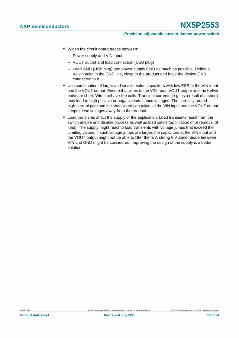
14. Application information
14.1 Application diagram
14.2 Best practices
In order to avoid product damage, the device should always operate within the boundaries given in Section 9. However, in applications with high switching currents, these limits might be violated during transients even when the static values are well within the limiting values. The device includes soft-start which limits in-rush current when enabling the N-channel MOSFET. This feature does not limit current transients due to load change when the N-channel MOSFET is already enabled.
The following aspects can be taken as guideline:
VI(VIN) = 5.5 V; RILIM = 20 k.
(1) Tamb = 40 C
(2) Tamb = +25 C
(3) Tamb = +125 C
VI(VIN) = 5.5 V; RILIM = 200 k.
(1) Tamb = 40 C
(2) Tamb = +25 C
(3) Tamb = +125 C
Fig 23. Switch current versus switch voltage Fig 24. Switch current versus switch voltage
VOUT-VIN (mV)0 200100
aaa-011216
560
840
280
1120
1400
Iocp(mA)
0
(1)(2)(3)
VOUT-VIN (mV)0 200100
aaa-011217160
Iocp(mA)
0
40
80
120
(3)
(2)(1)
For the IEC61000-4-2 contact discharge test, the 10 F input capacitance is not needed.
Fig 25. Application diagram
aaa-007802
100 kΩ 10 μF0.1 μF 120 μF
FAULTFAULT signal
5 VUSB input
control signalEN
VIN VOUT USBport
USB data
ILIM
GND
RILIM20 kΩ
NX5P2553 All information provided in this document is subject to legal disclaimers. © NXP Semiconductors N.V. 2015. All rights reserved.
Product data sheet Rev. 1 — 6 July 2015 16 of 24
NXP Semiconductors NX5P2553Precision adjustable current-limited power switch
• Widen the circuit board traces between:
– Power supply and VIN input
– VOUT output and load connection (USB plug)
– Load GND (USB plug) and power supply GND as much as possible. Define a Kelvin point in the GND line, close to the product and have the device GND connected to it.
• Use combination of larger and smaller value capacitors with low ESR at the VIN input and the VOUT output. Ensure that wires to the VIN input, VOUT output and the Kelvin point are short. Wires behave like coils. Transient currents (e.g. as a result of a short) may lead to high positive or negative inductance voltages. The carefully routed high-current path and the short wired capacitors at the VIN input and the VOUT output keeps these voltages away from the product.
• Load transients affect the supply of the application. Load transients result from the switch enable and disable process as well as load jumps (application of or removal of load). The supply might react to load transients with voltage jumps that exceed the Limiting values. If such voltage jumps are larger, the capacitors at the VIN input and the VOUT output might not be able to filter them. A strong 6 V Zener diode between VIN and GND might be considered. Improving the design of the supply is a better solution.
NX5P2553 All information provided in this document is subject to legal disclaimers. © NXP Semiconductors N.V. 2015. All rights reserved.
Product data sheet Rev. 1 — 6 July 2015 17 of 24
NXP Semiconductors NX5P2553Precision adjustable current-limited power switch
15. Package outline
Fig 26. Package outline SOT457 (TSOP6)
REFERENCESOUTLINEVERSION
EUROPEANPROJECTION ISSUE DATE
IEC JEDEC JEITA
SOT457 SC-74
w BMbp
D
e
pin 1index A
A1
Lp
Q
detail X
HE
E
v M A
AB
y
scale
c
X
1 32
456
0 1 2 mm
Plastic surface-mounted package (TSOP6); 6 leads SOT457
UNIT A1 bp c D E HE Lp Q ywv
mm 0.10.013
0.400.25
3.12.7
0.260.10
1.71.3
e
0.95 3.02.5
0.2 0.10.2
DIMENSIONS (mm are the original dimensions)
0.60.2
0.330.23
A
1.10.9
05-11-0706-03-16
NX5P2553 All information provided in this document is subject to legal disclaimers. © NXP Semiconductors N.V. 2015. All rights reserved.
Product data sheet Rev. 1 — 6 July 2015 18 of 24
NXP Semiconductors NX5P2553Precision adjustable current-limited power switch
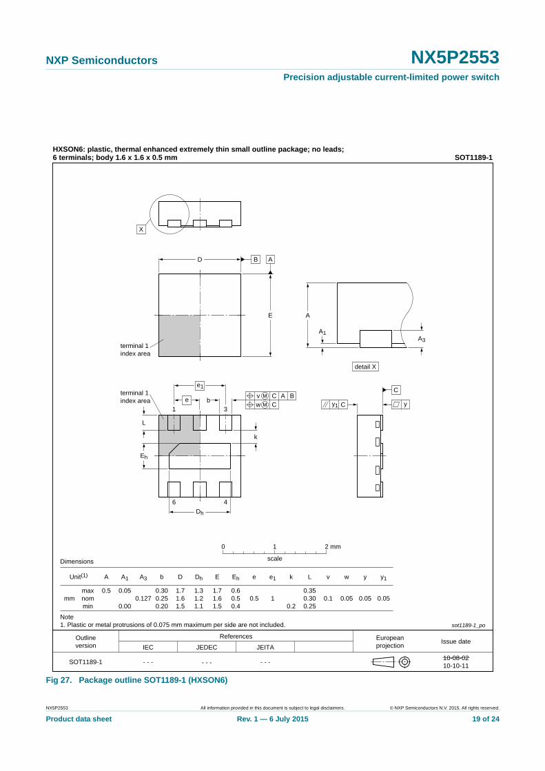
Fig 27. Package outline SOT1189-1 (HXSON6)
ReferencesOutlineversion
Europeanprojection
Issue dateIEC JEDEC JEITA
SOT1189-1 - - -- - -- - -
sot1189-1_po
10-08-0210-10-11
Unit(1)
mmmaxnommin
0.5 0.05
0.00
0.300.250.20
1.71.61.5
1.31.21.1
1.71.61.5
0.5 10.350.300.25
0.05
A
Dimensions
Note1. Plastic or metal protrusions of 0.075 mm maximum per side are not included.
HXSON6: plastic, thermal enhanced extremely thin small outline package; no leads;6 terminals; body 1.6 x 1.6 x 0.5 mm SOT1189-1
A1 A3
0.127
b D Dh E Eh
0.60.50.4
e e1 k
0.2
L v
0.1
w
0.05
y
0.05
y1
0 1 2 mm
scale
D
E
B A
terminal 1index area
X
detail X
A
A1A3
C
yCy1
Dh
Eh
k
L
b
e1
eAC Bv
Cw
terminal 1index area
46
31
NX5P2553 All information provided in this document is subject to legal disclaimers. © NXP Semiconductors N.V. 2015. All rights reserved.
Product data sheet Rev. 1 — 6 July 2015 19 of 24
NXP Semiconductors NX5P2553Precision adjustable current-limited power switch
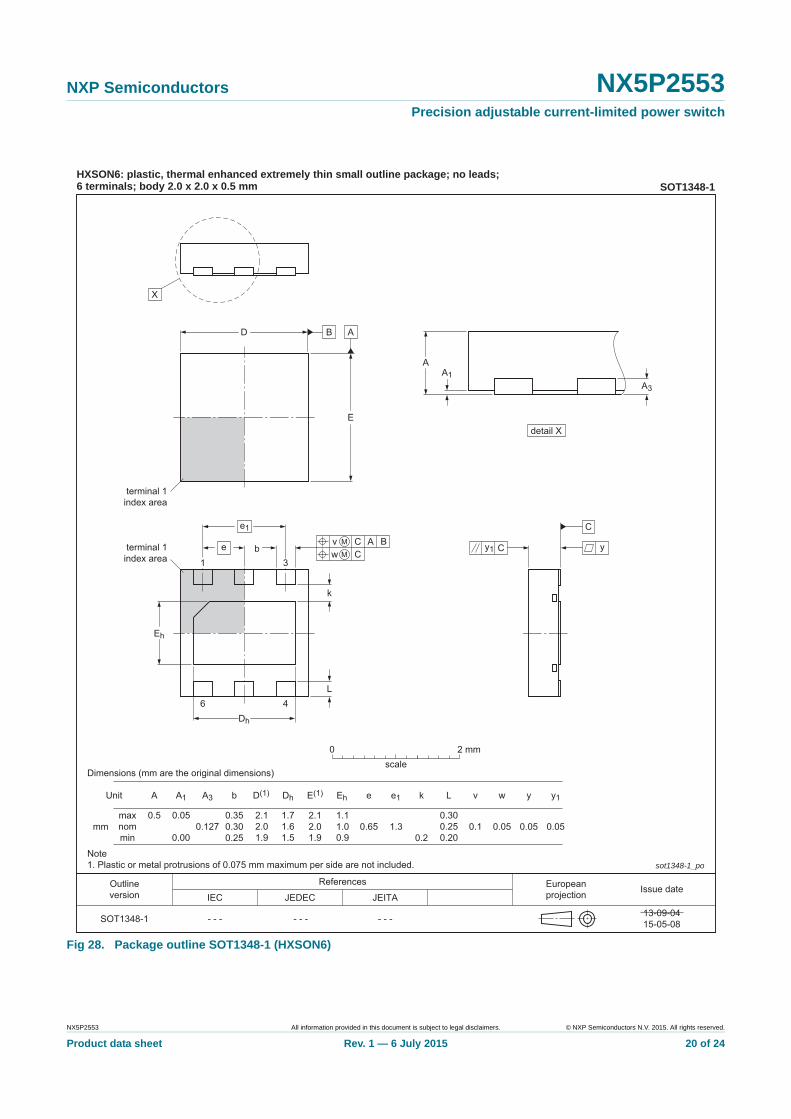
Fig 28. Package outline SOT1348-1 (HXSON6)
ReferencesOutlineversion
Europeanprojection Issue date
IEC JEDEC JEITA
SOT1348-1 - - -
sot1348-1_po
13-09-0415-05-08
Unit
mmmaxnommin
0.5 0.05
A
Dimensions (mm are the original dimensions)
HXSON6: plastic, thermal enhanced extremely thin small outline package; no leads;6 terminals; body 2.0 x 2.0 x 0.5 mm SOT1348-1
A1
0.1271.71.61.5
2.12.01.9
2.02.1
1.01.9 0.9
1.10.65 1.3
A3 b
0.350.300.25
k
0.2
D(1) Dh E(1) Eh e e1
0.300.250.20
L v
0.050.1
w y
0.05
y1
0.05
0 2 mmscale
Note1. Plastic or metal protrusions of 0.075 mm maximum per side are not included.
A
Edetail X
A3
AA1
- - - - - -
X
BD
Dh
6 4
1 3
k
L
bAC Bv
Cw
Eh
e1
e
terminal 1index area
terminal 1index area
C
yCy1
0.00
NX5P2553 All information provided in this document is subject to legal disclaimers. © NXP Semiconductors N.V. 2015. All rights reserved.
Product data sheet Rev. 1 — 6 July 2015 20 of 24
NXP Semiconductors NX5P2553Precision adjustable current-limited power switch
16. Abbreviations
17. Revision history
Table 15. Abbreviations
Acronym Description
CDM Charged Device Model
ESD ElectroStatic Discharge
ESR Equivalent Series Resistance
HBM Human Body Model
MOSFET Metal-Oxide Semiconductor Field-Effect Transistor
OCP OverCurrent Protection
OTP OverTemperature Protection
PCB Printed-Circuit Board
RVP Reverse-Voltage Protection
USB Universal Serial Bus
UVLO UnderVoltage LockOut
VoIP Voice over Internet Protocol
Table 16. Revision history
Document ID Release date Data sheet status Change notice Supersedes
NX5P2553 v.1 20150706 Product data sheet - -
NX5P2553 All information provided in this document is subject to legal disclaimers. © NXP Semiconductors N.V. 2015. All rights reserved.
Product data sheet Rev. 1 — 6 July 2015 21 of 24
NXP Semiconductors NX5P2553Precision adjustable current-limited power switch
18. Legal information
18.1 Data sheet status
[1] Please consult the most recently issued document before initiating or completing a design.
[2] The term ‘short data sheet’ is explained in section “Definitions”.
[3] The product status of device(s) described in this document may have changed since this document was published and may differ in case of multiple devices. The latest product status information is available on the Internet at URL http://www.nxp.com.
18.2 Definitions
Draft — The document is a draft version only. The content is still under internal review and subject to formal approval, which may result in modifications or additions. NXP Semiconductors does not give any representations or warranties as to the accuracy or completeness of information included herein and shall have no liability for the consequences of use of such information.
Short data sheet — A short data sheet is an extract from a full data sheet with the same product type number(s) and title. A short data sheet is intended for quick reference only and should not be relied upon to contain detailed and full information. For detailed and full information see the relevant full data sheet, which is available on request via the local NXP Semiconductors sales office. In case of any inconsistency or conflict with the short data sheet, the full data sheet shall prevail.
Product specification — The information and data provided in a Product data sheet shall define the specification of the product as agreed between NXP Semiconductors and its customer, unless NXP Semiconductors and customer have explicitly agreed otherwise in writing. In no event however, shall an agreement be valid in which the NXP Semiconductors product is deemed to offer functions and qualities beyond those described in the Product data sheet.
18.3 Disclaimers
Limited warranty and liability — Information in this document is believed to be accurate and reliable. However, NXP Semiconductors does not give any representations or warranties, expressed or implied, as to the accuracy or completeness of such information and shall have no liability for the consequences of use of such information. NXP Semiconductors takes no responsibility for the content in this document if provided by an information source outside of NXP Semiconductors.
In no event shall NXP Semiconductors be liable for any indirect, incidental, punitive, special or consequential damages (including - without limitation - lost profits, lost savings, business interruption, costs related to the removal or replacement of any products or rework charges) whether or not such damages are based on tort (including negligence), warranty, breach of contract or any other legal theory.
Notwithstanding any damages that customer might incur for any reason whatsoever, NXP Semiconductors’ aggregate and cumulative liability towards customer for the products described herein shall be limited in accordance with the Terms and conditions of commercial sale of NXP Semiconductors.
Right to make changes — NXP Semiconductors reserves the right to make changes to information published in this document, including without limitation specifications and product descriptions, at any time and without notice. This document supersedes and replaces all information supplied prior to the publication hereof.
Suitability for use — NXP Semiconductors products are not designed, authorized or warranted to be suitable for use in life support, life-critical or safety-critical systems or equipment, nor in applications where failure or malfunction of an NXP Semiconductors product can reasonably be expected to result in personal injury, death or severe property or environmental damage. NXP Semiconductors and its suppliers accept no liability for inclusion and/or use of NXP Semiconductors products in such equipment or applications and therefore such inclusion and/or use is at the customer’s own risk.
Applications — Applications that are described herein for any of these products are for illustrative purposes only. NXP Semiconductors makes no representation or warranty that such applications will be suitable for the specified use without further testing or modification.
Customers are responsible for the design and operation of their applications and products using NXP Semiconductors products, and NXP Semiconductors accepts no liability for any assistance with applications or customer product design. It is customer’s sole responsibility to determine whether the NXP Semiconductors product is suitable and fit for the customer’s applications and products planned, as well as for the planned application and use of customer’s third party customer(s). Customers should provide appropriate design and operating safeguards to minimize the risks associated with their applications and products.
NXP Semiconductors does not accept any liability related to any default, damage, costs or problem which is based on any weakness or default in the customer’s applications or products, or the application or use by customer’s third party customer(s). Customer is responsible for doing all necessary testing for the customer’s applications and products using NXP Semiconductors products in order to avoid a default of the applications and the products or of the application or use by customer’s third party customer(s). NXP does not accept any liability in this respect.
Limiting values — Stress above one or more limiting values (as defined in the Absolute Maximum Ratings System of IEC 60134) will cause permanent damage to the device. Limiting values are stress ratings only and (proper) operation of the device at these or any other conditions above those given in the Recommended operating conditions section (if present) or the Characteristics sections of this document is not warranted. Constant or repeated exposure to limiting values will permanently and irreversibly affect the quality and reliability of the device.
Terms and conditions of commercial sale — NXP Semiconductors products are sold subject to the general terms and conditions of commercial sale, as published at http://www.nxp.com/profile/terms, unless otherwise agreed in a valid written individual agreement. In case an individual agreement is concluded only the terms and conditions of the respective agreement shall apply. NXP Semiconductors hereby expressly objects to applying the customer’s general terms and conditions with regard to the purchase of NXP Semiconductors products by customer.
No offer to sell or license — Nothing in this document may be interpreted or construed as an offer to sell products that is open for acceptance or the grant, conveyance or implication of any license under any copyrights, patents or other industrial or intellectual property rights.
Document status[1][2] Product status[3] Definition
Objective [short] data sheet Development This document contains data from the objective specification for product development.
Preliminary [short] data sheet Qualification This document contains data from the preliminary specification.
Product [short] data sheet Production This document contains the product specification.
NX5P2553 All information provided in this document is subject to legal disclaimers. © NXP Semiconductors N.V. 2015. All rights reserved.
Product data sheet Rev. 1 — 6 July 2015 22 of 24
NXP Semiconductors NX5P2553Precision adjustable current-limited power switch
Export control — This document as well as the item(s) described herein may be subject to export control regulations. Export might require a prior authorization from competent authorities.
Non-automotive qualified products — Unless this data sheet expressly states that this specific NXP Semiconductors product is automotive qualified, the product is not suitable for automotive use. It is neither qualified nor tested in accordance with automotive testing or application requirements. NXP Semiconductors accepts no liability for inclusion and/or use of non-automotive qualified products in automotive equipment or applications.
In the event that customer uses the product for design-in and use in automotive applications to automotive specifications and standards, customer (a) shall use the product without NXP Semiconductors’ warranty of the product for such automotive applications, use and specifications, and (b) whenever customer uses the product for automotive applications beyond
NXP Semiconductors’ specifications such use shall be solely at customer’s own risk, and (c) customer fully indemnifies NXP Semiconductors for any liability, damages or failed product claims resulting from customer design and use of the product for automotive applications beyond NXP Semiconductors’ standard warranty and NXP Semiconductors’ product specifications.
Translations — A non-English (translated) version of a document is for reference only. The English version shall prevail in case of any discrepancy between the translated and English versions.
18.4 TrademarksNotice: All referenced brands, product names, service names and trademarks are the property of their respective owners.
19. Contact information
For more information, please visit: http://www.nxp.com
For sales office addresses, please send an email to: [email protected]
NX5P2553 All information provided in this document is subject to legal disclaimers. © NXP Semiconductors N.V. 2015. All rights reserved.
Product data sheet Rev. 1 — 6 July 2015 23 of 24
NXP Semiconductors NX5P2553Precision adjustable current-limited power switch
20. Contents
1 General description . . . . . . . . . . . . . . . . . . . . . . 1
2 Features and benefits . . . . . . . . . . . . . . . . . . . . 1
3 Applications . . . . . . . . . . . . . . . . . . . . . . . . . . . . 2
4 Ordering information. . . . . . . . . . . . . . . . . . . . . 2
5 Marking . . . . . . . . . . . . . . . . . . . . . . . . . . . . . . . . 2
6 Functional diagram . . . . . . . . . . . . . . . . . . . . . . 2
7 Pinning information. . . . . . . . . . . . . . . . . . . . . . 37.1 Pinning . . . . . . . . . . . . . . . . . . . . . . . . . . . . . . . 37.2 Pin description . . . . . . . . . . . . . . . . . . . . . . . . . 3
8 Functional description . . . . . . . . . . . . . . . . . . . 38.1 EN input . . . . . . . . . . . . . . . . . . . . . . . . . . . . . . 48.2 UnderVoltage LockOut (UVLO) . . . . . . . . . . . . 48.3 ILIM. . . . . . . . . . . . . . . . . . . . . . . . . . . . . . . . . . 48.4 OverCurrent Protection (OCP) . . . . . . . . . . . . . 48.4.1 Overcurrent at start-up . . . . . . . . . . . . . . . . . . . 48.4.2 Overcurrent when enabled . . . . . . . . . . . . . . . . 48.4.3 Short-circuit when enabled . . . . . . . . . . . . . . . . 48.5 Reverse-Voltage Protection (RVP) . . . . . . . . . . 48.6 FAULT output . . . . . . . . . . . . . . . . . . . . . . . . . . 58.7 OverTemperature Protection (OTP) . . . . . . . . . 5
9 Limiting values. . . . . . . . . . . . . . . . . . . . . . . . . . 5
10 Recommended operating conditions. . . . . . . . 6
11 Thermal characteristics . . . . . . . . . . . . . . . . . . 6
12 Static characteristics. . . . . . . . . . . . . . . . . . . . . 612.1 Graphs . . . . . . . . . . . . . . . . . . . . . . . . . . . . . . . 712.2 ON resistance. . . . . . . . . . . . . . . . . . . . . . . . . . 812.3 ON resistance graph. . . . . . . . . . . . . . . . . . . . . 912.4 Current limit . . . . . . . . . . . . . . . . . . . . . . . . . . . 912.5 Current limit graph . . . . . . . . . . . . . . . . . . . . . 1012.6 Thermal shutdown . . . . . . . . . . . . . . . . . . . . . 10
13 Dynamic characteristics . . . . . . . . . . . . . . . . . 1013.1 Waveform and test circuits . . . . . . . . . . . . . . . 11
14 Application information. . . . . . . . . . . . . . . . . . 1614.1 Application diagram . . . . . . . . . . . . . . . . . . . . 1614.2 Best practices . . . . . . . . . . . . . . . . . . . . . . . . . 16
15 Package outline . . . . . . . . . . . . . . . . . . . . . . . . 18
16 Abbreviations. . . . . . . . . . . . . . . . . . . . . . . . . . 21
17 Revision history. . . . . . . . . . . . . . . . . . . . . . . . 21
18 Legal information. . . . . . . . . . . . . . . . . . . . . . . 2218.1 Data sheet status . . . . . . . . . . . . . . . . . . . . . . 2218.2 Definitions. . . . . . . . . . . . . . . . . . . . . . . . . . . . 2218.3 Disclaimers . . . . . . . . . . . . . . . . . . . . . . . . . . . 2218.4 Trademarks. . . . . . . . . . . . . . . . . . . . . . . . . . . 23
19 Contact information. . . . . . . . . . . . . . . . . . . . . 23
20 Contents. . . . . . . . . . . . . . . . . . . . . . . . . . . . . . 24
© NXP Semiconductors N.V. 2015. All rights reserved.
For more information, please visit: http://www.nxp.comFor sales office addresses, please send an email to: [email protected]
Date of release: 6 July 2015
Document identifier: NX5P2553
Please be aware that important notices concerning this document and the product(s)described herein, have been included in section ‘Legal information’.