Embed Size (px)
Citation preview
1. General description
The NX5P3090 is a precision adjustable current-limited power switch for USB PD application. The device includes under voltage lockout, over-temperature protection, and reverse current protection circuits to automatically isolate the switch terminals when a fault condition occurs. The 29 V tolerance on VBUS pin ensures the device is able to work on a USB PD port; a current limit input (ILIM) pin defines the over-current limit threshold; an open-drain fault output (FAULT) indicates when a fault condition has occurred.
The over-current limit threshold can be programmed from 400 mA to 3.3 A, using an external resistor between the ILIM pin and GND pin. In the over current condition, the device will clamp the output current to the value set by ILIM and keep the switch on while assert the FAULT flag. To minimize current surges during turn on, the device has built in soft start which controls the power switch rise time.
Surge protection has been integrated in the device to enhance system robustness. The enable input includes integrated logic level translation making the device compatible with lower voltage processors and controllers.
NX5P3090 is offered in a 12 bump 1.35 x 1.65 mm, 0.4 mm pitch WLCSP package.
2. Features and benefits
VINT supply voltage range from 2.5 V to 5.5 V
29 V tolerance on VBUS and EN pin
Adjustable current limit from 400 mA to 3.3 A
Clamped current output in over-current condition
Very low ON resistance: 34 m (typical)
Active HIGH EN pin with internal pull down resistor
All time Reverse Current Protection
Over Temperature Protection
Surge protection: IEC61000-4-5 exceeds ±80 V on VBUS
Safety approvals
UL 62368-1, 2nd Edition, File no. 20160526-E470128
IEC 62368-1 (ed.2), File no. DK-54536-UL
ESD protection
IEC61000-4-2 contact discharge exceeds 8 kV on VBUS
HBM ANSI/ESDA/JEDEC JS-001 Class 2 exceeds 2 kV
CDM AEC standard Q100-01 (JESD22-C101E) exceeds 500 V
Specified from 40 C to +85 C ambient temperature
NX5P3090USB PD and type C current-limited power switchRev. 1 — 1 August 2016 Product data sheet
NXP Semiconductors NX5P3090USB PD and type C current-limited power switch
3. Applications
Notebook and Ultrabook
USB PD and Type C port/hubs
Tablet and Smart phone
4. Ordering information
4.1 Ordering options
5. Marking
Table 1. Ordering information
Type number Topside marking
Package
Name Description Version
NX5P3090UK X5PT2 WLCSP12 wafer level chip-scale package; 12 bumps; 1.65 x 1.35 x 0.525 mm; 0.4 mm pitch (backside coating included)
SOT1390-5
Table 2. Ordering options
Type number Orderable part number
Package Packing method Minimum order quantity
Temperature
NX5P3090UK NX5P3090UKZ WLCSP12 REEL 7" Q1/T1 *SPECIAL MARK CHIPS DP
3000 Tamb = 40 C to +85 C
Table 3. Marking
Line Marking Description
A X5PT2 basic type name
B mmmmm wafer lot code (mmmmm)
C Z5YWW manufacturing code
Z = foundry location
5 = assembly location
Y = assembly year code
WW = assembly week code
NX5P3090 All information provided in this document is subject to legal disclaimers. © NXP Semiconductors N.V. 2016. All rights reserved.
Product data sheet Rev. 1 — 1 August 2016 2 of 33
NXP Semiconductors NX5P3090USB PD and type C current-limited power switch
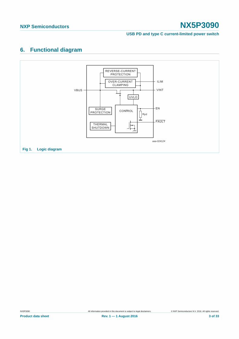
6. Functional diagram
Fig 1. Logic diagram
OVER-CURRENTCLAMPING
EN
VBUS VINT
FAULT
ILIM
REVERSE-CURRENTPROTECTION
UVLO
SURGEPROTECTION
THERMALSHUTDOWN
RpdCONTROL
aaa-024124
NX5P3090 All information provided in this document is subject to legal disclaimers. © NXP Semiconductors N.V. 2016. All rights reserved.
Product data sheet Rev. 1 — 1 August 2016 3 of 33
NXP Semiconductors NX5P3090USB PD and type C current-limited power switch
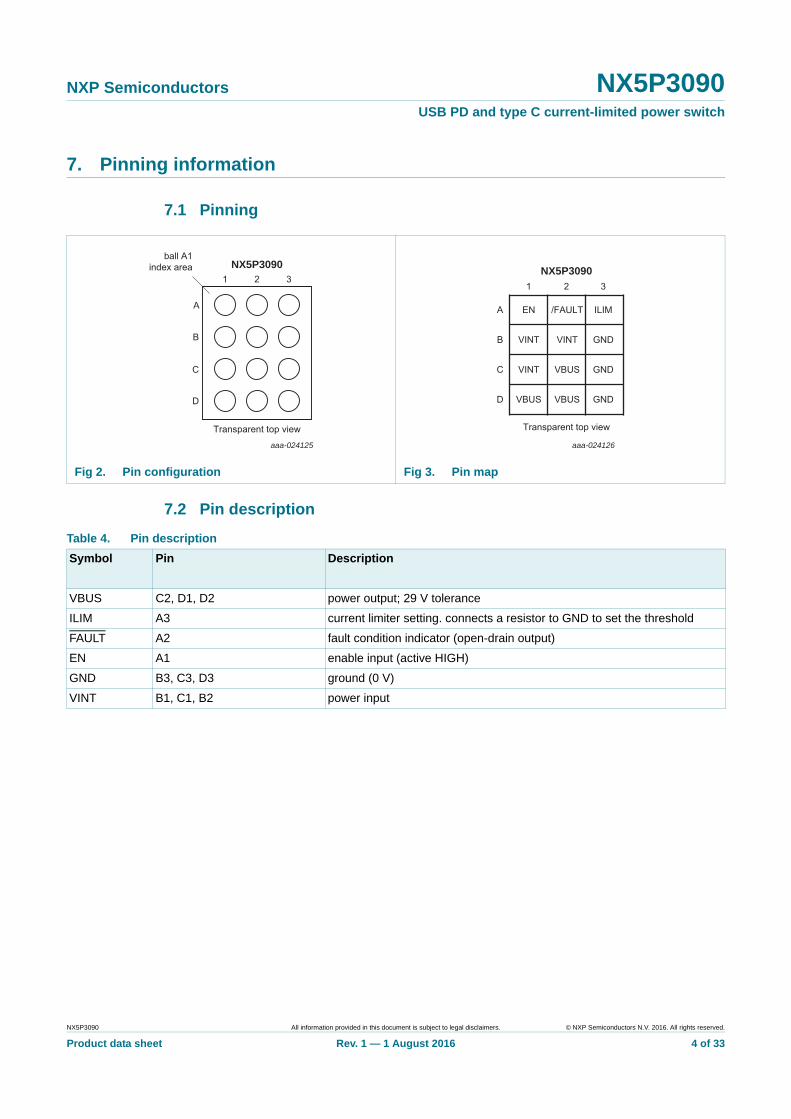
7. Pinning information
7.1 Pinning
7.2 Pin description
Fig 2. Pin configuration Fig 3. Pin map
aaa-024125
A
C
B
D
1 2 3
Transparent top view
ball A1index area NX5P3090
EN /FAULT ILIM
VINT VINT GND
VINT VBUS GND
VBUS VBUS GND
31 2
A
B
C
D
Transparent top view
aaa-024126
NX5P3090
Table 4. Pin description
Symbol Pin Description
VBUS C2, D1, D2 power output; 29 V tolerance
ILIM A3 current limiter setting. connects a resistor to GND to set the threshold
FAULT A2 fault condition indicator (open-drain output)
EN A1 enable input (active HIGH)
GND B3, C3, D3 ground (0 V)
VINT B1, C1, B2 power input
NX5P3090 All information provided in this document is subject to legal disclaimers. © NXP Semiconductors N.V. 2016. All rights reserved.
Product data sheet Rev. 1 — 1 August 2016 4 of 33
NXP Semiconductors NX5P3090USB PD and type C current-limited power switch
8. Functional description
[1] H = HIGH voltage level; L = LOW voltage level.
8.1 EN Input
When the EN pin is set LOW, the N-channel MOSFET will be disabled, the device will enter low-power mode disabling all protection circuits and setting the FAULT pin high impedance. When EN is set HIGH, all protection circuits will be enabled and then, if no fault conditions exist, the N-channel MOSFET will be turn on. There is a 100 us de-glitch time on EN pin from LOW to HIGH.
8.2 Under-voltage lock-out
Independently of the logic level on the EN pin, the under-voltage lockout (UVLO) circuit disables the N-channel MOSFET and enters low power mode until the input voltage reaches the UVLO turn-on threshold level VUVLO.
8.3 ILIM
The over-current protection circuit's (OCP) trigger value Iocp can be set using an external resistor RILIM connected between ILIM pin and GND pin. When EN is HIGH and the ILIM pin is pulled to ground, the N-channel MOSFET will be disabled and the FAULT output set LOW. The detailed IOCP setting is given in Section 8.4.
8.4 Over-current protection (OCP)
The device offers over current protection when enabled, three possible over-current conditions can occur. These conditions are:
• Over-current at start-up, ISW > Iocp when enabling the N-channel MOSFET.
• Over-current after enabled, ISW > Iocp when the N-channel MOSFET is already ON.
• Short circuit after enabled, ISW > 10 A (typical).
In the over current condition, because the device clamps the output current rather than completely shut down the switch, the power dissipation on the device might be increased which could lead to over temperature protection (see Section 8.7).
8.4.1 Over-current at start-up
If the device senses a VBUS short to GND or over-current while enabling the N-channel MOSFET, OCP is triggered. It limits the output current to Iocp and after the de-glitch time sets the FAULT output LOW.
Table 5. Function table[1]
EN VINT VBUS FAULT Switch
X <2.5V X Z under voltage lockout, switch open
L 2.5V to 5.5V X Z disabled; switch open
H 2.5V to 5.5V VBUS=VINT Z enabled; switch closed
H 2.5V to 5.5V 0V to VINT L over-current, clamped current output, switch closed
H 2.5V to 5.5V VBUS>VINT+40mV (>4ms) L reverse current; switch open
H 2.5V to 5.5V Z L Over-temperature; switch open
NX5P3090 All information provided in this document is subject to legal disclaimers. © NXP Semiconductors N.V. 2016. All rights reserved.
Product data sheet Rev. 1 — 1 August 2016 5 of 33
NXP Semiconductors NX5P3090USB PD and type C current-limited power switch
8.4.2 Over-current when enabled
If the device senses ISW > Iocp after enabled, OCP is triggered. It limits the output current to Iocp and after the de-glitch time sets the FAULT output LOW. Limiting the output current reduces VO(VOUT).
8.4.3 Short circuit when enabled
If the device senses ISW > 10 A after enabled, a short circuit is detected. The device disables the N-channel MOSFET immediately. It then re-enables the N-channel MOSFET and limit the output current to Iocp, and after the de-glitch time the FAULT output is set LOW.
8.5 Reverse-Current protection (RCP)
When the VBUS pin voltage exceeds the input voltage by 40 mV (typical) the device will protect itself from damage by switching off the MOSFET after 4 ms de-glitch time.
When the VBUS pin voltage exceeds the VINT voltage by 100 mV, the device will shutdown the FET immediately without any de-glitch time.
FAULT pin will be set LOW in the reverse-current protection condition.
In the RCP state, when the VBUS voltage drops below VINT voltage, the device will exit the RCP state in 128 us and resume normal operation.
Before normal turn on, the device will always check the RCP condition first, if higher voltage is detected on VBUS pin, it will never turn on the power MOSFET even EN pin is pulled HIGH.
8.6 FAULT output
The FAULT output is an open-drain output that requires an external pull-up resistor. If any of the protection circuits is activated, the FAULT output will be set LOW to indicate a fault has occurred. The FAULT output will return to the high impedance state automatically once the fault condition is removed. An internal delay (de-glitch) circuit for the over-current protection (8 ms typical) and reverse-current protection (4 ms typical) is used when entering fault conditions. This ensures that FAULT is not accidentally asserted. Over-temperature condition will not be deglitched, the FAULT signal will be asserted immediately.
8.7 Over-temperature protection
When EN is HIGH, the device junction temperature exceeds 140 °C, the over-temperature protection (OTP) circuit will disable the N-channel MOSFET and indicate a fault condition by setting the FAULT pin LOW. Any transition on the EN pin will have no effect. Once the device temperature decreases below 115 °C the device will return to the defined state.
NX5P3090 All information provided in this document is subject to legal disclaimers. © NXP Semiconductors N.V. 2016. All rights reserved.
Product data sheet Rev. 1 — 1 August 2016 6 of 33
NXP Semiconductors NX5P3090USB PD and type C current-limited power switch
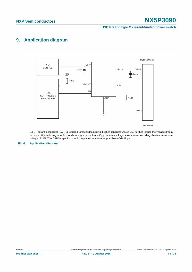
9. Application diagram
0.1 F ceramic capacitor (CINT) is required for local decoupling. Higher capacitor values CINT further reduce the voltage drop at the input. When driving inductive loads, a larger capacitance CINT prevents voltage spikes from exceeding absolute maximum voltage of VIN. The CBUS capacitor should be placed as closer as possible to VBUS pin.
Fig 4. Application diagram
5 VSOURCE
USB connector
VINT
VBUS
ILIM
GND
ENUSB
CONTROLLER/PROCESSOR
VBUS
GND
VDD
47 KΩ
CINT
CBUS
/FAULT
aaa-024128
RILIM
NX5P3090 All information provided in this document is subject to legal disclaimers. © NXP Semiconductors N.V. 2016. All rights reserved.
Product data sheet Rev. 1 — 1 August 2016 7 of 33
NXP Semiconductors NX5P3090USB PD and type C current-limited power switch
10. Limiting values
[1] The minimum input voltage rating may be exceeded if the input current rating is observed.
[2] The minimum and maximum switch voltage ratings may be exceeded if the switch clamping current rating is observed.
[3] Internally limited.
[4] The (absolute) maximum power dissipation depends on the junction temperature Tj. Higher power dissipation is allowed in conjunction
with lower ambient temperatures. The conditions to determine the specified values are Tamb = 25 °C and the use of a two layer PCB.
11. Recommended operating conditions
[1] Current-limit threshold resistor range from ILIM to GND.
Table 6. Limiting valuesIn accordance with the Absolute Maximum Rating System (IEC 60134). Voltages are referenced to GND (ground = 0 V).
Symbol Parameter Conditions Min Max Unit
VI input voltage VBUS, EN [1] 0.5 +29 V
VINT [2] 0.5 +6 V
ILIM 0.5 +6 V
VO output voltage FAULT [1] 0.5 +6 V
IIK input clamping current input EN: VI(EN) < 0.5 V 50 - mA
input ILIM: VI(ILIM) < 0.5 V 50 - mA
II(source) input source current input IILIM - 1 mA
IOK output clamping current VO < 0 V 50 - mA
ISK switch clamping current input VIN: VI(VIN) < 0.5 V 50 - mA
output VOUT: VO(VOUT) < 0.5 V 50 - mA
ISW switch current VSW > 0.5 V [3] - 3.6 A
Tj(max) maximum junction temperature
40 +150 C
Tstg storage temperature 65 +150 C
Ptot total power dissipation [4] - 910 mW
Table 7. Recommended operating conditions
Symbol Parameter Conditions Min Max Unit
VI input voltage VINT 2.5 5.5 V
EN; VBUS (OFF state) 0 20 V
VO Output voltage VBUS 0 5 V
ISW switch current Tj = 40 C to +85 C 0 3 A
IO(sink) output sink current output FAULT 10 - mA
RILIM current limit resistance input ILIM [1] 16 140 k
Cdec decoupling capacitance VIN to GND 0.1 - F
Tamb ambient temperature 40 +85 C
NX5P3090 All information provided in this document is subject to legal disclaimers. © NXP Semiconductors N.V. 2016. All rights reserved.
Product data sheet Rev. 1 — 1 August 2016 8 of 33
NXP Semiconductors NX5P3090USB PD and type C current-limited power switch
12. Thermal characteristics
[1] Rth(j-a) is dependent upon board layout. To minimize Rth(j-a), ensure all pins have a solid connection to larger copper layer areas. In multi-layer PCBs, the second layer should be used to create a large heat spreader area below the device. Avoid using solder-stop varnish under the device.
13. Static characteristics
[1] Typical values are measured at Tamb = 25 C.
Table 8. Thermal characteristics
Symbol Parameter Conditions Typ Unit
Rth(j-a) thermal resistance from junction to ambient [1] 109 K/W
Table 9. Static characteristicsAt recommended operating conditions; VI(VINT) = VI(EN), RFAULT = 10 k unless otherwise specified; Voltages are referenced to GND (ground = 0 V). See Figure 10
Symbol Parameter Conditions Min Typ[1] Max Unit
VIH HIGH-level input voltage
EN input; VI(VINT) = 2.5 V to 5.5 V; 1.2 - - V
VIL LOW-level input voltage
EN input; VIVINT) = 2.5 V to 5.5 V; - - 0.4 V
II input leakage current
EN input; VI(VINT) = 5.0 V; - - 7.5 A
I(VIN) supply current VBUS open; VI(VINT) = 5.0 V
EN = GND (low power mode); - 0.9 5 A
EN = VI(VIN); RILIM = 33 k - 196 280 A
EN = VI(VIN); RILIM = 16 k - 210 290 A
IS(OFF) VBUS OFF-State leakage current
VI(VINT) = 5.0 V; VI(VBUS) = 0 V; EN = LOW - 1 10 A
VINT OFF-state leakage current
VI(VBUS) = 5.0 V; VI(VINT) = 0 V; EN = LOW
- 1 10 A
IS(ON) RCP leakage current
VI(VINT) = 0 V; VI(VBUS) = 5 V; EN = 5 V - 0.9 10 A
Rpd EN pin Pull-down resistance
VI(VINT) = 5 V 1 M
Vtrip trip level voltage RCP; VI(VINT) = 2.5 V to 5.5 V - 40 - mV
VUVLO under voltage lockout voltage
VINT pin - 2.27 2.45 V
Vhys(UVLO) under voltage lockout hysteresis voltage
- 100 - mV
VOL LOW-level output voltage
FAULT; IO = 8 mA - - 0.5 V
CI EN pin - 13.5 - pF
NX5P3090 All information provided in this document is subject to legal disclaimers. © NXP Semiconductors N.V. 2016. All rights reserved.
Product data sheet Rev. 1 — 1 August 2016 9 of 33
NXP Semiconductors NX5P3090USB PD and type C current-limited power switch
13.1 Graphs
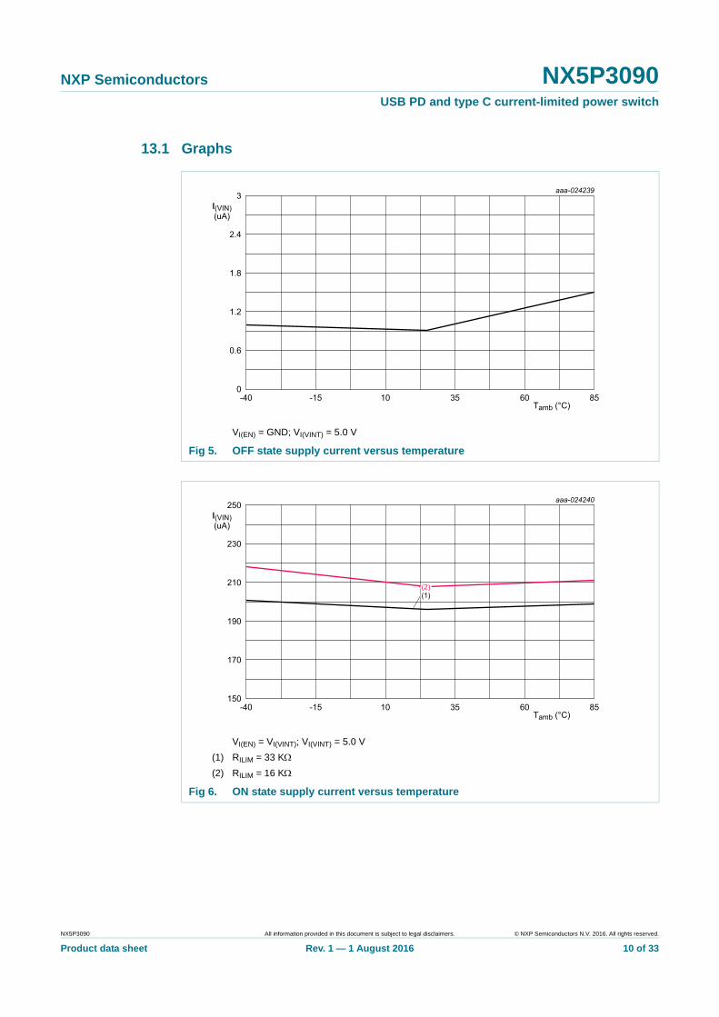
VI(EN) = GND; VI(VINT) = 5.0 V
Fig 5. OFF state supply current versus temperature
VI(EN) = VI(VINT); VI(VINT) = 5.0 V
(1) RILIM = 33 K
(2) RILIM = 16 K
Fig 6. ON state supply current versus temperature
NX5P3090 All information provided in this document is subject to legal disclaimers. © NXP Semiconductors N.V. 2016. All rights reserved.
Product data sheet Rev. 1 — 1 August 2016 10 of 33
NXP Semiconductors NX5P3090USB PD and type C current-limited power switch
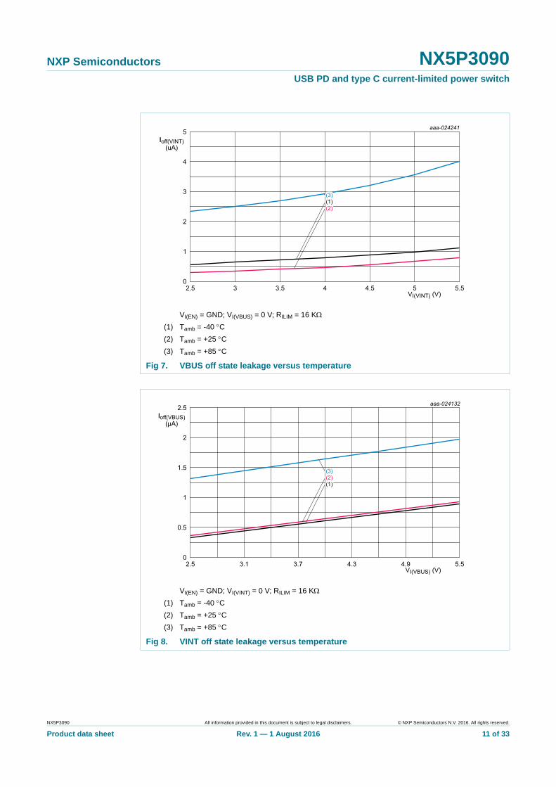
VI(EN) = GND; VI(VBUS) = 0 V; RILIM = 16 K
(1) Tamb = -40 C
(2) Tamb = +25 C
(3) Tamb = +85 C
Fig 7. VBUS off state leakage versus temperature
VI(EN) = GND; VI(VINT) = 0 V; RILIM = 16 K
(1) Tamb = -40 C
(2) Tamb = +25 C
(3) Tamb = +85 C
Fig 8. VINT off state leakage versus temperature
NX5P3090 All information provided in this document is subject to legal disclaimers. © NXP Semiconductors N.V. 2016. All rights reserved.
Product data sheet Rev. 1 — 1 August 2016 11 of 33
NXP Semiconductors NX5P3090USB PD and type C current-limited power switch
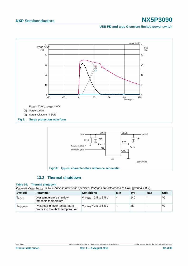
13.2 Thermal shutdown
RILIM = 20 k; VI(VINT) = 0 V
(1) Surge current
(2) Surge voltage on VBUS
Fig 9. Surge protection waveform
Fig 10. Typical characteristics reference schematic
aaa-024133
VINT VBUS
ILIM
GNDEN
FAULT
10 kΩ
RILIM
1 μF
FAULT signal
control signal
VIN VOUT
10 μF
Table 10. Thermal shutdownVI(VINT) = VI(EN), RFAULT = 10 k unless otherwise specified; Voltages are referenced to GND (ground = 0 V).
Symbol Parameter Conditions Min Typ Max Unit
Tth(ots) over temperature shutdown threshold temperature
VI(VINT) = 2.5 to 5.5 V - 140 - C
Tth(otp)hys hysteresis of over temperature protection threshold temperature
VI(VINT) = 2.5 to 5.5 V - 25 - C
NX5P3090 All information provided in this document is subject to legal disclaimers. © NXP Semiconductors N.V. 2016. All rights reserved.
Product data sheet Rev. 1 — 1 August 2016 12 of 33
NXP Semiconductors NX5P3090USB PD and type C current-limited power switch
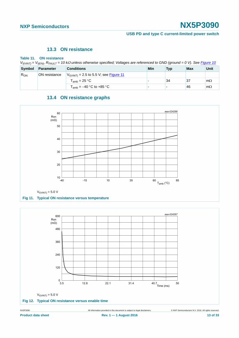
13.3 ON resistance
13.4 ON resistance graphs
Table 11. ON resistanceVI(VINT) = VI(EN), RFAULT = 10 k unless otherwise specified; Voltages are referenced to GND (ground = 0 V). See Figure 10
Symbol Parameter Conditions Min Typ Max Unit
RON ON resistance VI(VINT) = 2.5 to 5.5 V; see Figure 11
Tamb = 25 C - 34 37 m
Tamb = 40 C to +85 C - - 46 m
VI(VINT) = 5.0 V
Fig 11. Typical ON resistance versus temperature
VI(VINT) = 5.0 V
Fig 12. Typical ON resistance versus enable time
NX5P3090 All information provided in this document is subject to legal disclaimers. © NXP Semiconductors N.V. 2016. All rights reserved.
Product data sheet Rev. 1 — 1 August 2016 13 of 33
NXP Semiconductors NX5P3090USB PD and type C current-limited power switch
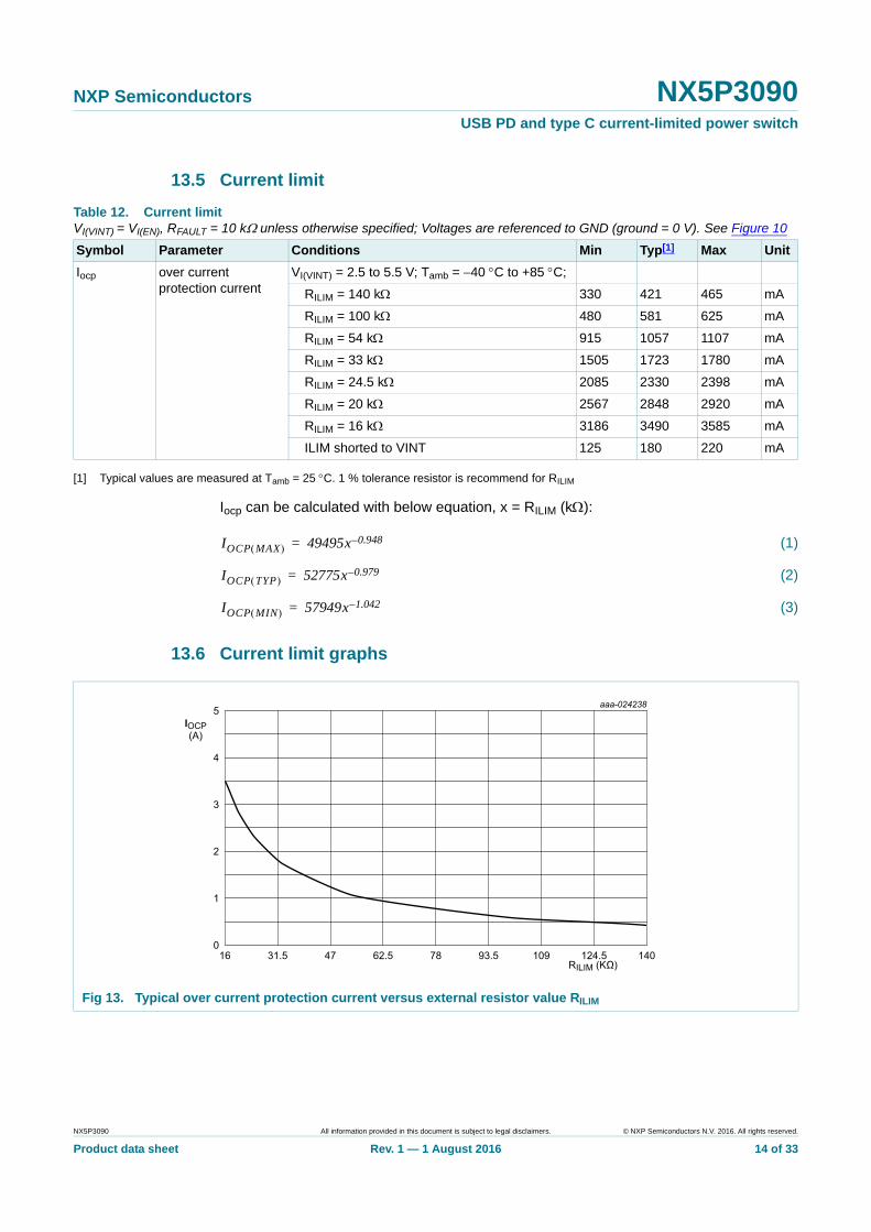
13.5 Current limit
[1] Typical values are measured at Tamb = 25 C. 1 % tolerance resistor is recommend for RILIM
Iocp can be calculated with below equation, x = RILIM (k):
(1)
(2)
(3)
13.6 Current limit graphs
Table 12. Current limitVI(VINT) = VI(EN), RFAULT = 10 k unless otherwise specified; Voltages are referenced to GND (ground = 0 V). See Figure 10
Symbol Parameter Conditions Min Typ[1] Max Unit
Iocp over current protection current
VI(VINT) = 2.5 to 5.5 V; Tamb = 40 C to +85 C;
RILIM = 140 k 330 421 465 mA
RILIM = 100 k 480 581 625 mA
RILIM = 54 k 915 1057 1107 mA
RILIM = 33 k 1505 1723 1780 mA
RILIM = 24.5 k 2085 2330 2398 mA
RILIM = 20 k 2567 2848 2920 mA
RILIM = 16 k 3186 3490 3585 mA
ILIM shorted to VINT 125 180 220 mA
IOCP MAX 49495x 0.948–=
IOCP TYP 52775x 0.979–=
IOCP MIN 57949x 1.042–=
Fig 13. Typical over current protection current versus external resistor value RILIM
NX5P3090 All information provided in this document is subject to legal disclaimers. © NXP Semiconductors N.V. 2016. All rights reserved.
Product data sheet Rev. 1 — 1 August 2016 14 of 33
NXP Semiconductors NX5P3090USB PD and type C current-limited power switch
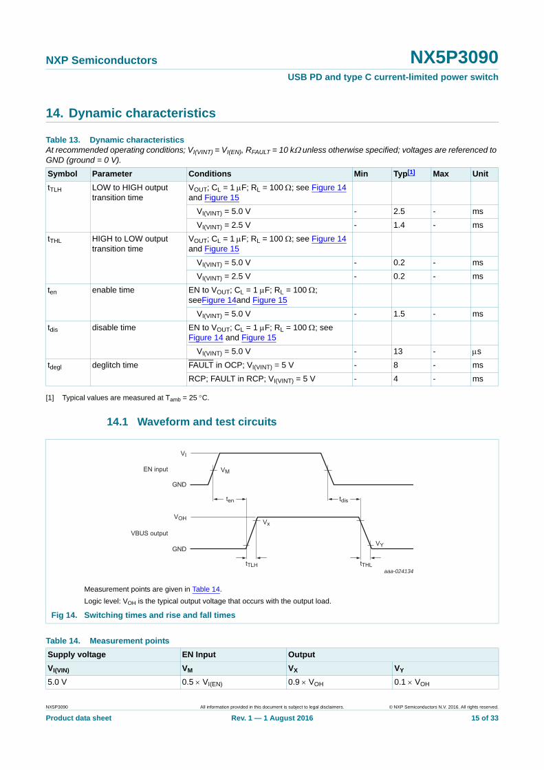
14. Dynamic characteristics
[1] Typical values are measured at Tamb = 25 C.
14.1 Waveform and test circuits
Table 13. Dynamic characteristicsAt recommended operating conditions; VI(VINT) = VI(EN), RFAULT = 10 k unless otherwise specified; voltages are referenced to GND (ground = 0 V).
Symbol Parameter Conditions Min Typ[1] Max Unit
tTLH LOW to HIGH output transition time
VOUT; CL = 1 F; RL = 100 ; see Figure 14 and Figure 15
VI(VINT) = 5.0 V - 2.5 - ms
VI(VINT) = 2.5 V - 1.4 - ms
tTHL HIGH to LOW output transition time
VOUT; CL = 1 F; RL = 100 ; see Figure 14 and Figure 15
VI(VINT) = 5.0 V - 0.2 - ms
VI(VINT) = 2.5 V - 0.2 - ms
ten enable time EN to VOUT; CL = 1 F; RL = 100 ; seeFigure 14and Figure 15
VI(VINT) = 5.0 V - 1.5 - ms
tdis disable time EN to VOUT; CL = 1 F; RL = 100 ; see Figure 14 and Figure 15
VI(VINT) = 5.0 V - 13 - s
tdegl deglitch time FAULT in OCP; VI(VINT) = 5 V - 8 - ms
RCP; FAULT in RCP; VI(VINT) = 5 V - 4 - ms
Measurement points are given in Table 14.
Logic level: VOH is the typical output voltage that occurs with the output load.
Fig 14. Switching times and rise and fall times
aaa-024134
EN input
VBUS output
VI
VM
Vx
VY
ten tdis
tTHLtTLH
VOH
GND
GND
Table 14. Measurement points
Supply voltage EN Input Output
VI(VIN) VM VX VY
5.0 V 0.5 VI(EN) 0.9 VOH 0.1 VOH
NX5P3090 All information provided in this document is subject to legal disclaimers. © NXP Semiconductors N.V. 2016. All rights reserved.
Product data sheet Rev. 1 — 1 August 2016 15 of 33
NXP Semiconductors NX5P3090USB PD and type C current-limited power switch
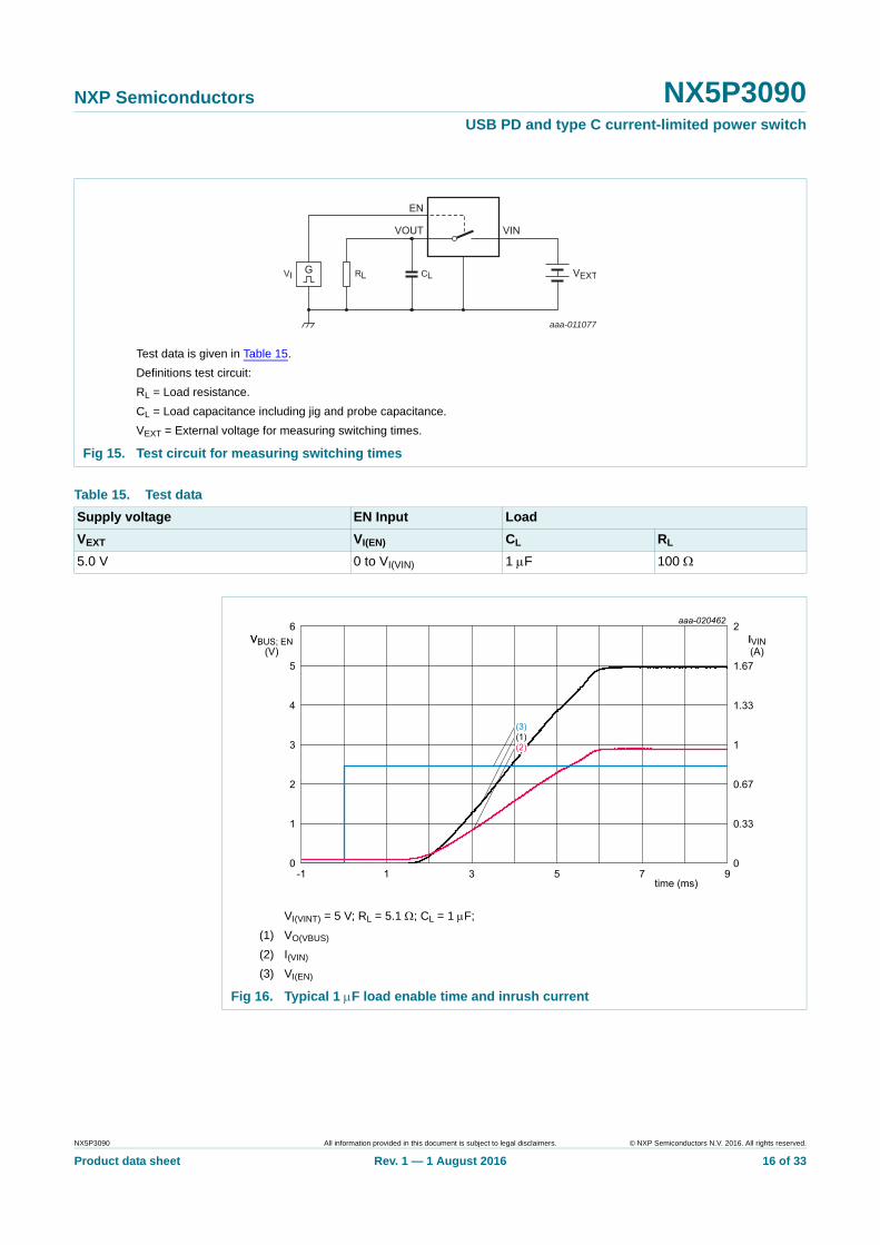
Test data is given in Table 15.
Definitions test circuit:
RL = Load resistance.
CL = Load capacitance including jig and probe capacitance.
VEXT = External voltage for measuring switching times.
Fig 15. Test circuit for measuring switching times
aaa-011077
EN
VOUT
CL
VIN
VEXTGVI RL
Table 15. Test data
Supply voltage EN Input Load
VEXT VI(EN) CL RL
5.0 V 0 to VI(VIN) 1 F 100
VI(VINT) = 5 V; RL = 5.1 ; CL = 1 F;
(1) VO(VBUS)
(2) I(VIN)
(3) VI(EN)
Fig 16. Typical 1 F load enable time and inrush current
NX5P3090 All information provided in this document is subject to legal disclaimers. © NXP Semiconductors N.V. 2016. All rights reserved.
Product data sheet Rev. 1 — 1 August 2016 16 of 33
NXP Semiconductors NX5P3090USB PD and type C current-limited power switch
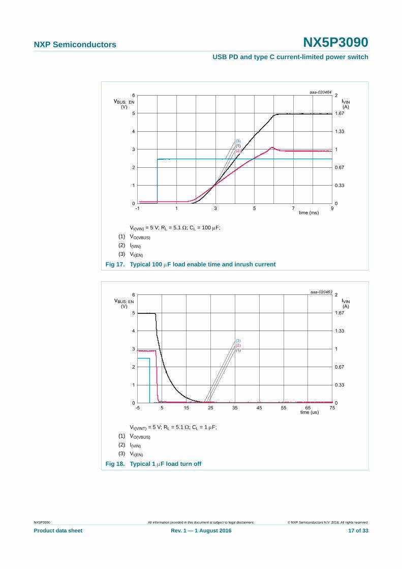
VI(VIN) = 5 V; RL = 5.1 ; CL = 100 F;
(1) VO(VBUS)
(2) I(VIN)
(3) VI(EN)
Fig 17. Typical 100 F load enable time and inrush current
VI(VINT) = 5 V; RL = 5.1 ; CL = 1 F;
(1) VO(VBUS)
(2) I(VIN)
(3) VI(EN)
Fig 18. Typical 1 F load turn off
NX5P3090 All information provided in this document is subject to legal disclaimers. © NXP Semiconductors N.V. 2016. All rights reserved.
Product data sheet Rev. 1 — 1 August 2016 17 of 33
NXP Semiconductors NX5P3090USB PD and type C current-limited power switch
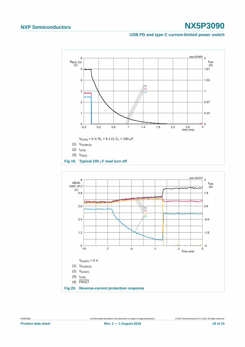
VI(VIN) = 5 V; RL = 5.1 ; CL = 100 F
(1) VO(VBUS)
(2) I(VIN)
(3) VI(EN)
Fig 19. Typical 100 F load turn off
VI(VINT) = 4 V
(1) VO(VBUS)
(2) VI(VINT)
(3) I(VIN)
(4) FAULT
Fig 20. Reverse-current protection response
NX5P3090 All information provided in this document is subject to legal disclaimers. © NXP Semiconductors N.V. 2016. All rights reserved.
Product data sheet Rev. 1 — 1 August 2016 18 of 33
NXP Semiconductors NX5P3090USB PD and type C current-limited power switch
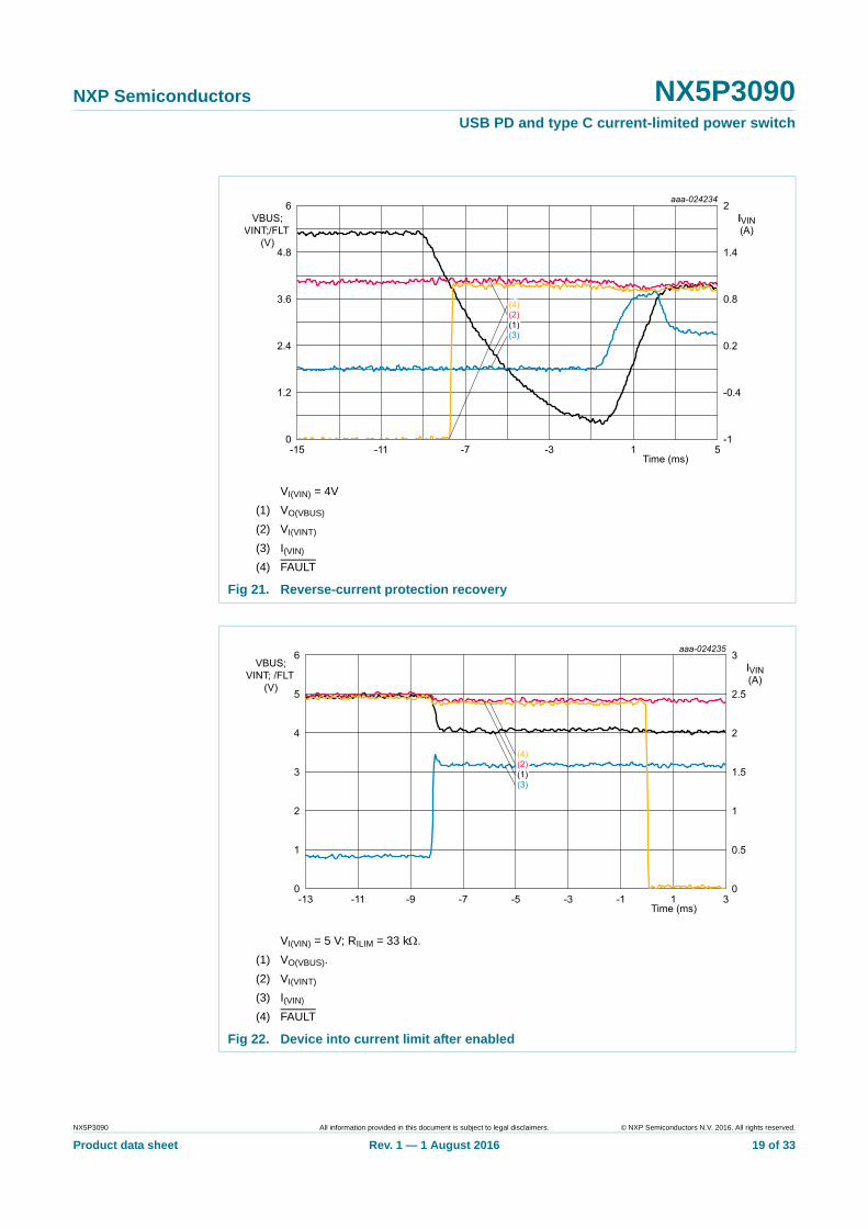
VI(VIN) = 4V
(1) VO(VBUS)
(2) VI(VINT)
(3) I(VIN)
(4) FAULT
Fig 21. Reverse-current protection recovery
VI(VIN) = 5 V; RILIM = 33 k.
(1) VO(VBUS).
(2) VI(VINT)
(3) I(VIN)
(4) FAULT
Fig 22. Device into current limit after enabled
NX5P3090 All information provided in this document is subject to legal disclaimers. © NXP Semiconductors N.V. 2016. All rights reserved.
Product data sheet Rev. 1 — 1 August 2016 19 of 33
NXP Semiconductors NX5P3090USB PD and type C current-limited power switch
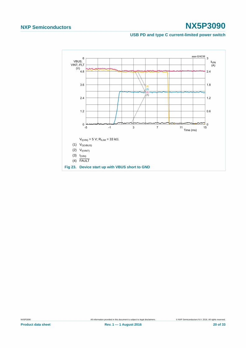
VI(VIN) = 5 V; RILIM = 33 k.
(1) VO(VBUS)
(2) VI(VINT)
(3) I(VIN)
(4) FAULT
Fig 23. Device start up with VBUS short to GND
NX5P3090 All information provided in this document is subject to legal disclaimers. © NXP Semiconductors N.V. 2016. All rights reserved.
Product data sheet Rev. 1 — 1 August 2016 20 of 33
NXP Semiconductors NX5P3090USB PD and type C current-limited power switch
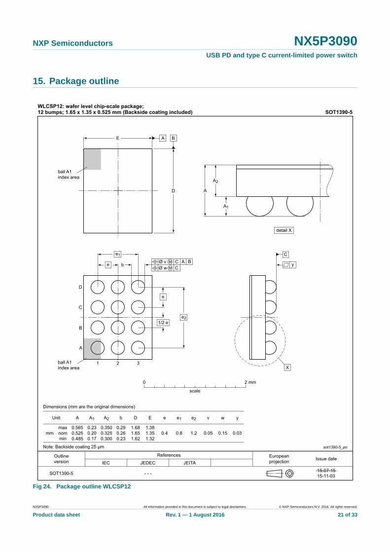
15. Package outline
Fig 24. Package outline WLCSP12
NX5P3090 All information provided in this document is subject to legal disclaimers. © NXP Semiconductors N.V. 2016. All rights reserved.
Product data sheet Rev. 1 — 1 August 2016 21 of 33
NXP Semiconductors NX5P3090USB PD and type C current-limited power switch
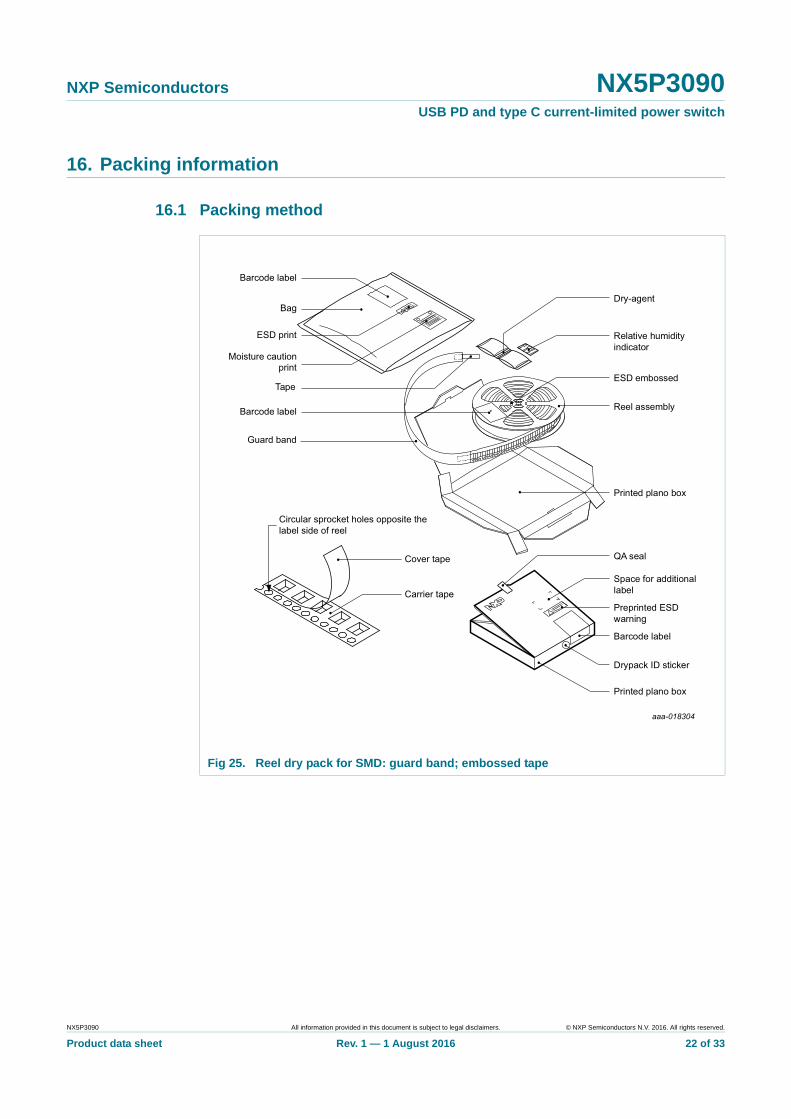
16. Packing information
16.1 Packing method
Fig 25. Reel dry pack for SMD: guard band; embossed tape
NX5P3090 All information provided in this document is subject to legal disclaimers. © NXP Semiconductors N.V. 2016. All rights reserved.
Product data sheet Rev. 1 — 1 August 2016 22 of 33
NXP Semiconductors NX5P3090USB PD and type C current-limited power switch
[1] d = reel diameter; w = tape width.
[2] Packing quantity dependent on specific product type.
View ordering and availability details at NXP order portal, or contact your local NXP representative.
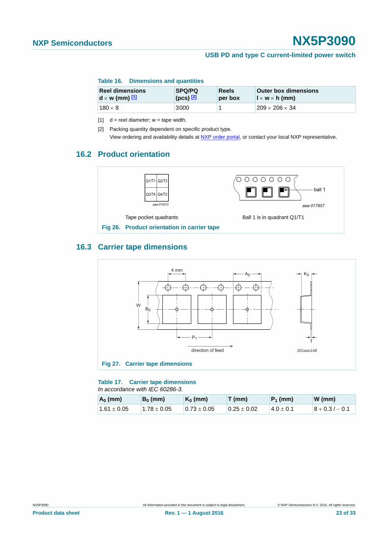
16.2 Product orientation
16.3 Carrier tape dimensions
Table 16. Dimensions and quantities
Reel dimensionsd w (mm) [1]
SPQ/PQ(pcs) [2]
Reelsper box
Outer box dimensionsl w h (mm)
180 8 3000 1 209 206 34
Tape pocket quadrants Ball 1 is in quadrant Q1/T1
Fig 26. Product orientation in carrier tape
Fig 27. Carrier tape dimensions
Table 17. Carrier tape dimensionsIn accordance with IEC 60286-3.
A0 (mm) B0 (mm) K0 (mm) T (mm) P1 (mm) W (mm)
1.61 0.05 1.78 0.05 0.73 0.05 0.25 0.02 4.0 0.1 8 0.3 / 0.1
K0
001aao148
A04 mm
TP1
B0W
direction of feed
NX5P3090 All information provided in this document is subject to legal disclaimers. © NXP Semiconductors N.V. 2016. All rights reserved.
Product data sheet Rev. 1 — 1 August 2016 23 of 33
NXP Semiconductors NX5P3090USB PD and type C current-limited power switch
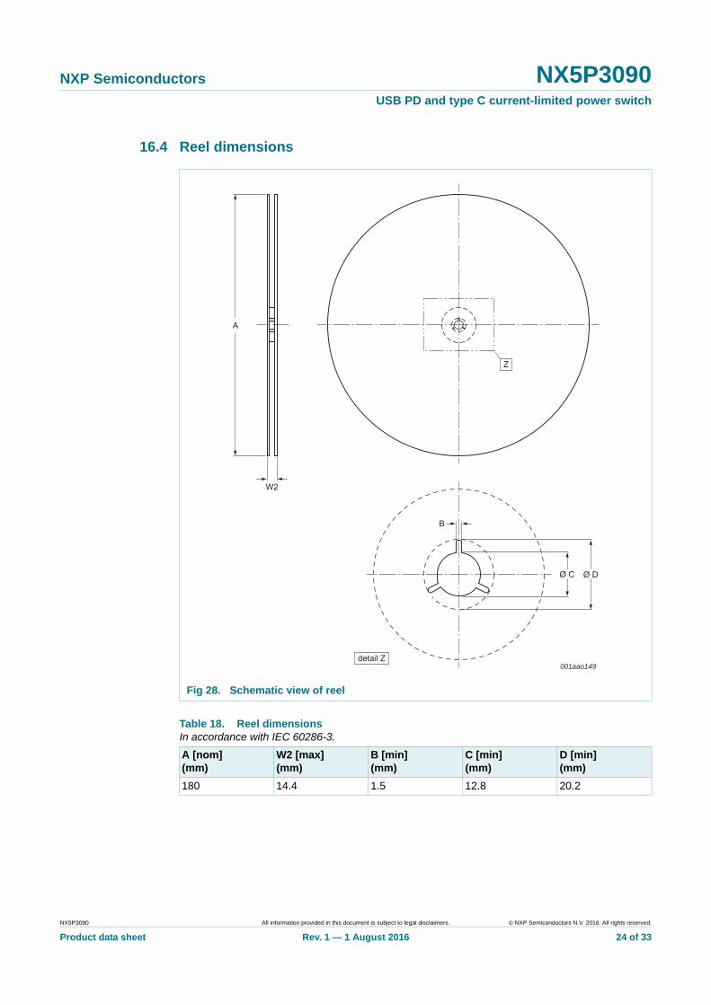
16.4 Reel dimensions
Fig 28. Schematic view of reel
Table 18. Reel dimensionsIn accordance with IEC 60286-3.
A [nom](mm)
W2 [max](mm)
B [min](mm)
C [min](mm)
D [min](mm)
180 14.4 1.5 12.8 20.2
detail Z
B
001aao149
W2
Ø C Ø D
A
Z
NX5P3090 All information provided in this document is subject to legal disclaimers. © NXP Semiconductors N.V. 2016. All rights reserved.
Product data sheet Rev. 1 — 1 August 2016 24 of 33
NXP Semiconductors NX5P3090USB PD and type C current-limited power switch
16.5 Barcode label
Fig 29. Example of typical box and reel information barcode label
Table 19. Barcode label dimensions
Box barcode labell w (mm)
Reel barcode labell w (mm)
100 75 100 75
001aak714
NXP SEMICONDUCTORSMADE IN >COUNTRY<[PRODUCT INFO]
(33T) PUID: B.0987654321(30T) LOT2(30D) DATE2(30Q) QTY2
(31D) REDATE(32T) ORIG(31T) PMC(31P) MSL/PBT
MSL/PBT
Optional product information*
Fixed textCountry of origini.e. "Made in....." or "Diffused in EU [+] Assembled in......Packing unit (PQ) identification
2nd traceability lot number*
Traceability lot numberDate codeWith linear barcode
With linear barcode
With linear barcode
Type numberNXP 12NC
Quantity
2nd (youngest) date code*2nd Quantity*
Re-approval date code*Origin codeProduct Manufacturing CodeMSL at the Peak Body soldertemperature with tin/lead*MSL at the higher lead-freePeak Body Temperature*2D matrix with all data(including the data identifiers)
Additional info if halogenfree productAdditional info on RoHS
Lead-free symbol
HALOGEN FREE
RoHS compliant
(1T) LOT(9D) DATE
(Q) QTY
(30P) TYPE(1P) CODENO
NX5P3090 All information provided in this document is subject to legal disclaimers. © NXP Semiconductors N.V. 2016. All rights reserved.
Product data sheet Rev. 1 — 1 August 2016 25 of 33
NXP Semiconductors NX5P3090USB PD and type C current-limited power switch
17. Soldering of WLCSP packages
17.1 Introduction to soldering WLCSP packages
This text provides a very brief insight into a complex technology. A more in-depth account of soldering WLCSP (Wafer Level Chip-Size Packages) can be found in application note AN10439 “Wafer Level Chip Scale Package” and in application note AN10365 “Surface mount reflow soldering description”.
Wave soldering is not suitable for this package.
All NXP WLCSP packages are lead-free.
17.2 Board mounting
Board mounting of a WLCSP requires several steps:
1. Solder paste printing on the PCB
2. Component placement with a pick and place machine
3. The reflow soldering itself
17.3 Reflow soldering
Key characteristics in reflow soldering are:
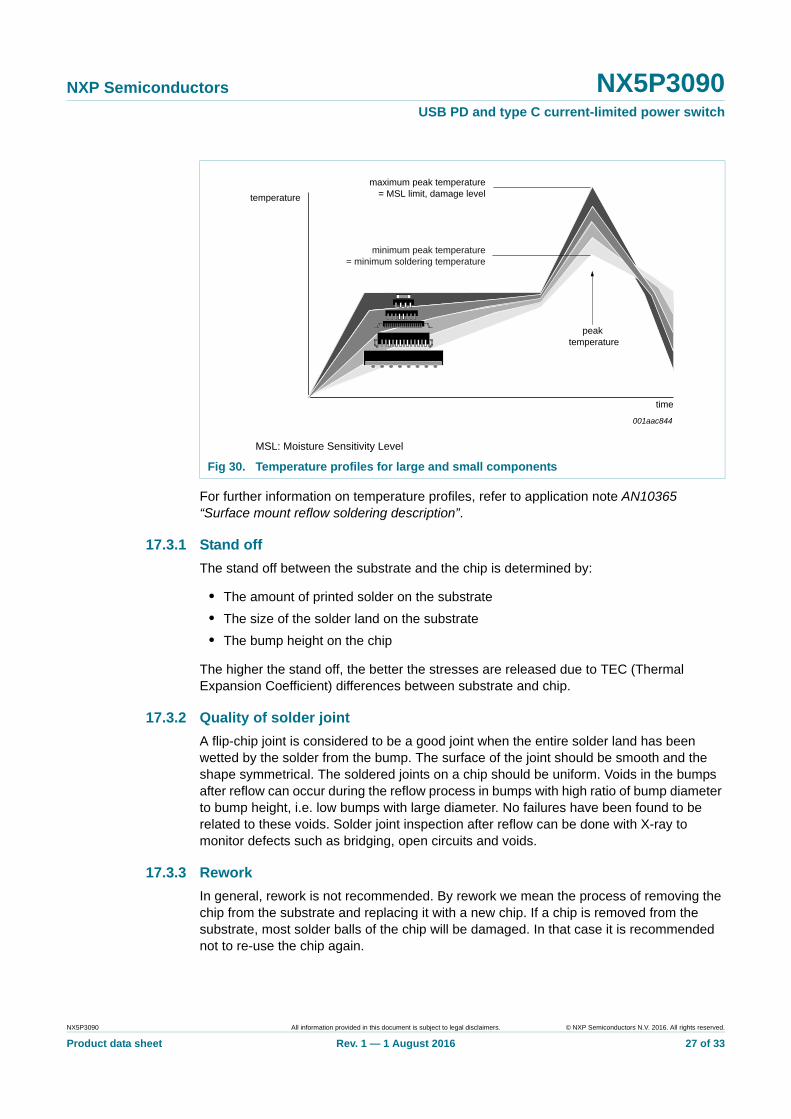
• Lead-free versus SnPb soldering; note that a lead-free reflow process usually leads to higher minimum peak temperatures (see Figure 30) than a SnPb process, thus reducing the process window
• Solder paste printing issues, such as smearing, release, and adjusting the process window for a mix of large and small components on one board
• Reflow temperature profile; this profile includes preheat, reflow (in which the board is heated to the peak temperature), and cooling down. It is imperative that the peak temperature is high enough for the solder to make reliable solder joints (a solder paste characteristic) while being low enough that the packages and/or boards are not damaged. The peak temperature of the package depends on package thickness and volume and is classified in accordance with Table 20.
Moisture sensitivity precautions, as indicated on the packing, must be respected at all times.
Studies have shown that small packages reach higher temperatures during reflow soldering, see Figure 30.
Table 20. Lead-free process (from J-STD-020D)
Package thickness (mm) Package reflow temperature (C)
Volume (mm3)
< 350 350 to 2000 > 2000
< 1.6 260 260 260
1.6 to 2.5 260 250 245
> 2.5 250 245 245
NX5P3090 All information provided in this document is subject to legal disclaimers. © NXP Semiconductors N.V. 2016. All rights reserved.
Product data sheet Rev. 1 — 1 August 2016 26 of 33
NXP Semiconductors NX5P3090USB PD and type C current-limited power switch
For further information on temperature profiles, refer to application note AN10365 “Surface mount reflow soldering description”.
17.3.1 Stand off
The stand off between the substrate and the chip is determined by:
• The amount of printed solder on the substrate
• The size of the solder land on the substrate
• The bump height on the chip
The higher the stand off, the better the stresses are released due to TEC (Thermal Expansion Coefficient) differences between substrate and chip.
17.3.2 Quality of solder joint
A flip-chip joint is considered to be a good joint when the entire solder land has been wetted by the solder from the bump. The surface of the joint should be smooth and the shape symmetrical. The soldered joints on a chip should be uniform. Voids in the bumps after reflow can occur during the reflow process in bumps with high ratio of bump diameter to bump height, i.e. low bumps with large diameter. No failures have been found to be related to these voids. Solder joint inspection after reflow can be done with X-ray to monitor defects such as bridging, open circuits and voids.
17.3.3 Rework
In general, rework is not recommended. By rework we mean the process of removing the chip from the substrate and replacing it with a new chip. If a chip is removed from the substrate, most solder balls of the chip will be damaged. In that case it is recommended not to re-use the chip again.
MSL: Moisture Sensitivity Level
Fig 30. Temperature profiles for large and small components
001aac844
temperature
time
minimum peak temperature= minimum soldering temperature
maximum peak temperature= MSL limit, damage level
peak temperature
NX5P3090 All information provided in this document is subject to legal disclaimers. © NXP Semiconductors N.V. 2016. All rights reserved.
Product data sheet Rev. 1 — 1 August 2016 27 of 33
NXP Semiconductors NX5P3090USB PD and type C current-limited power switch
Device removal can be done when the substrate is heated until it is certain that all solder joints are molten. The chip can then be carefully removed from the substrate without damaging the tracks and solder lands on the substrate. Removing the device must be done using plastic tweezers, because metal tweezers can damage the silicon. The surface of the substrate should be carefully cleaned and all solder and flux residues and/or underfill removed. When a new chip is placed on the substrate, use the flux process instead of solder on the solder lands. Apply flux on the bumps at the chip side as well as on the solder pads on the substrate. Place and align the new chip while viewing with a microscope. To reflow the solder, use the solder profile shown in application note AN10365 “Surface mount reflow soldering description”.
17.3.4 Cleaning
Cleaning can be done after reflow soldering.
NX5P3090 All information provided in this document is subject to legal disclaimers. © NXP Semiconductors N.V. 2016. All rights reserved.
Product data sheet Rev. 1 — 1 August 2016 28 of 33
NXP Semiconductors NX5P3090USB PD and type C current-limited power switch
18. Abbreviations
Table 21. Abbreviations
Acronym Description
ESD ElectroStatic Discharge
CDM Charged Device Model
HBM Human Body Model
USB Universal Serial Bus
VOIP Voice over Internet Protocol
NX5P3090 All information provided in this document is subject to legal disclaimers. © NXP Semiconductors N.V. 2016. All rights reserved.
Product data sheet Rev. 1 — 1 August 2016 29 of 33
NXP Semiconductors NX5P3090USB PD and type C current-limited power switch
19. Revision history
Table 22. Revision history
Document ID Release date Data sheet status Change notice Supersedes
NX5P3090 v.1 20160801 Product data sheet - -
NX5P3090 All information provided in this document is subject to legal disclaimers. © NXP Semiconductors N.V. 2016. All rights reserved.
Product data sheet Rev. 1 — 1 August 2016 30 of 33
NXP Semiconductors NX5P3090USB PD and type C current-limited power switch
20. Legal information
20.1 Data sheet status
[1] Please consult the most recently issued document before initiating or completing a design.
[2] The term ‘short data sheet’ is explained in section “Definitions”.
[3] The product status of device(s) described in this document may have changed since this document was published and may differ in case of multiple devices. The latest product status information is available on the Internet at URL http://www.nxp.com.
20.2 Definitions
Draft — The document is a draft version only. The content is still under internal review and subject to formal approval, which may result in modifications or additions. NXP Semiconductors does not give any representations or warranties as to the accuracy or completeness of information included herein and shall have no liability for the consequences of use of such information.
Short data sheet — A short data sheet is an extract from a full data sheet with the same product type number(s) and title. A short data sheet is intended for quick reference only and should not be relied upon to contain detailed and full information. For detailed and full information see the relevant full data sheet, which is available on request via the local NXP Semiconductors sales office. In case of any inconsistency or conflict with the short data sheet, the full data sheet shall prevail.
Product specification — The information and data provided in a Product data sheet shall define the specification of the product as agreed between NXP Semiconductors and its customer, unless NXP Semiconductors and customer have explicitly agreed otherwise in writing. In no event however, shall an agreement be valid in which the NXP Semiconductors product is deemed to offer functions and qualities beyond those described in the Product data sheet.
20.3 Disclaimers
Limited warranty and liability — Information in this document is believed to be accurate and reliable. However, NXP Semiconductors does not give any representations or warranties, expressed or implied, as to the accuracy or completeness of such information and shall have no liability for the consequences of use of such information. NXP Semiconductors takes no responsibility for the content in this document if provided by an information source outside of NXP Semiconductors.
In no event shall NXP Semiconductors be liable for any indirect, incidental, punitive, special or consequential damages (including - without limitation - lost profits, lost savings, business interruption, costs related to the removal or replacement of any products or rework charges) whether or not such damages are based on tort (including negligence), warranty, breach of contract or any other legal theory.
Notwithstanding any damages that customer might incur for any reason whatsoever, NXP Semiconductors’ aggregate and cumulative liability towards customer for the products described herein shall be limited in accordance with the Terms and conditions of commercial sale of NXP Semiconductors.
Right to make changes — NXP Semiconductors reserves the right to make changes to information published in this document, including without limitation specifications and product descriptions, at any time and without notice. This document supersedes and replaces all information supplied prior to the publication hereof.
Suitability for use — NXP Semiconductors products are not designed, authorized or warranted to be suitable for use in life support, life-critical or safety-critical systems or equipment, nor in applications where failure or malfunction of an NXP Semiconductors product can reasonably be expected to result in personal injury, death or severe property or environmental damage. NXP Semiconductors and its suppliers accept no liability for inclusion and/or use of NXP Semiconductors products in such equipment or applications and therefore such inclusion and/or use is at the customer’s own risk.
Applications — Applications that are described herein for any of these products are for illustrative purposes only. NXP Semiconductors makes no representation or warranty that such applications will be suitable for the specified use without further testing or modification.
Customers are responsible for the design and operation of their applications and products using NXP Semiconductors products, and NXP Semiconductors accepts no liability for any assistance with applications or customer product design. It is customer’s sole responsibility to determine whether the NXP Semiconductors product is suitable and fit for the customer’s applications and products planned, as well as for the planned application and use of customer’s third party customer(s). Customers should provide appropriate design and operating safeguards to minimize the risks associated with their applications and products.
NXP Semiconductors does not accept any liability related to any default, damage, costs or problem which is based on any weakness or default in the customer’s applications or products, or the application or use by customer’s third party customer(s). Customer is responsible for doing all necessary testing for the customer’s applications and products using NXP Semiconductors products in order to avoid a default of the applications and the products or of the application or use by customer’s third party customer(s). NXP does not accept any liability in this respect.
Limiting values — Stress above one or more limiting values (as defined in the Absolute Maximum Ratings System of IEC 60134) will cause permanent damage to the device. Limiting values are stress ratings only and (proper) operation of the device at these or any other conditions above those given in the Recommended operating conditions section (if present) or the Characteristics sections of this document is not warranted. Constant or repeated exposure to limiting values will permanently and irreversibly affect the quality and reliability of the device.
Terms and conditions of commercial sale — NXP Semiconductors products are sold subject to the general terms and conditions of commercial sale, as published at http://www.nxp.com/profile/terms, unless otherwise agreed in a valid written individual agreement. In case an individual agreement is concluded only the terms and conditions of the respective agreement shall apply. NXP Semiconductors hereby expressly objects to applying the customer’s general terms and conditions with regard to the purchase of NXP Semiconductors products by customer.
No offer to sell or license — Nothing in this document may be interpreted or construed as an offer to sell products that is open for acceptance or the grant, conveyance or implication of any license under any copyrights, patents or other industrial or intellectual property rights.
Document status[1][2] Product status[3] Definition
Objective [short] data sheet Development This document contains data from the objective specification for product development.
Preliminary [short] data sheet Qualification This document contains data from the preliminary specification.
Product [short] data sheet Production This document contains the product specification.
NX5P3090 All information provided in this document is subject to legal disclaimers. © NXP Semiconductors N.V. 2016. All rights reserved.
Product data sheet Rev. 1 — 1 August 2016 31 of 33
NXP Semiconductors NX5P3090USB PD and type C current-limited power switch
Export control — This document as well as the item(s) described herein may be subject to export control regulations. Export might require a prior authorization from competent authorities.
Non-automotive qualified products — Unless this data sheet expressly states that this specific NXP Semiconductors product is automotive qualified, the product is not suitable for automotive use. It is neither qualified nor tested in accordance with automotive testing or application requirements. NXP Semiconductors accepts no liability for inclusion and/or use of non-automotive qualified products in automotive equipment or applications.
In the event that customer uses the product for design-in and use in automotive applications to automotive specifications and standards, customer (a) shall use the product without NXP Semiconductors’ warranty of the product for such automotive applications, use and specifications, and (b) whenever customer uses the product for automotive applications beyond
NXP Semiconductors’ specifications such use shall be solely at customer’s own risk, and (c) customer fully indemnifies NXP Semiconductors for any liability, damages or failed product claims resulting from customer design and use of the product for automotive applications beyond NXP Semiconductors’ standard warranty and NXP Semiconductors’ product specifications.
Translations — A non-English (translated) version of a document is for reference only. The English version shall prevail in case of any discrepancy between the translated and English versions.
20.4 TrademarksNotice: All referenced brands, product names, service names and trademarks are the property of their respective owners.
21. Contact information
For more information, please visit: http://www.nxp.com
For sales office addresses, please send an email to: [email protected]
NX5P3090 All information provided in this document is subject to legal disclaimers. © NXP Semiconductors N.V. 2016. All rights reserved.
Product data sheet Rev. 1 — 1 August 2016 32 of 33

NXP Semiconductors NX5P3090USB PD and type C current-limited power switch
22. Contents
1 General description . . . . . . . . . . . . . . . . . . . . . . 1
2 Features and benefits . . . . . . . . . . . . . . . . . . . . 1
3 Applications . . . . . . . . . . . . . . . . . . . . . . . . . . . . 2
4 Ordering information. . . . . . . . . . . . . . . . . . . . . 24.1 Ordering options . . . . . . . . . . . . . . . . . . . . . . . . 2
5 Marking . . . . . . . . . . . . . . . . . . . . . . . . . . . . . . . . 2
6 Functional diagram . . . . . . . . . . . . . . . . . . . . . . 3
7 Pinning information. . . . . . . . . . . . . . . . . . . . . . 47.1 Pinning . . . . . . . . . . . . . . . . . . . . . . . . . . . . . . . 47.2 Pin description . . . . . . . . . . . . . . . . . . . . . . . . . 4
8 Functional description . . . . . . . . . . . . . . . . . . . 58.1 EN Input . . . . . . . . . . . . . . . . . . . . . . . . . . . . . . 58.2 Under-voltage lock-out . . . . . . . . . . . . . . . . . . . 58.3 ILIM. . . . . . . . . . . . . . . . . . . . . . . . . . . . . . . . . . 58.4 Over-current protection (OCP) . . . . . . . . . . . . . 58.4.1 Over-current at start-up . . . . . . . . . . . . . . . . . . 58.4.2 Over-current when enabled . . . . . . . . . . . . . . . 68.4.3 Short circuit when enabled . . . . . . . . . . . . . . . . 68.5 Reverse-Current protection (RCP) . . . . . . . . . . 68.6 FAULT output . . . . . . . . . . . . . . . . . . . . . . . . . . 68.7 Over-temperature protection . . . . . . . . . . . . . . 6
9 Application diagram . . . . . . . . . . . . . . . . . . . . . 7
10 Limiting values. . . . . . . . . . . . . . . . . . . . . . . . . . 8
11 Recommended operating conditions. . . . . . . . 8
12 Thermal characteristics . . . . . . . . . . . . . . . . . . 9
13 Static characteristics. . . . . . . . . . . . . . . . . . . . . 913.1 Graphs . . . . . . . . . . . . . . . . . . . . . . . . . . . . . . 1013.2 Thermal shutdown . . . . . . . . . . . . . . . . . . . . . 1213.3 ON resistance. . . . . . . . . . . . . . . . . . . . . . . . . 1313.4 ON resistance graphs . . . . . . . . . . . . . . . . . . . 1313.5 Current limit . . . . . . . . . . . . . . . . . . . . . . . . . . 1413.6 Current limit graphs . . . . . . . . . . . . . . . . . . . . 14
14 Dynamic characteristics . . . . . . . . . . . . . . . . . 1514.1 Waveform and test circuits . . . . . . . . . . . . . . . 15
15 Package outline . . . . . . . . . . . . . . . . . . . . . . . . 21
16 Packing information . . . . . . . . . . . . . . . . . . . . 2216.1 Packing method . . . . . . . . . . . . . . . . . . . . . . . 2216.2 Product orientation . . . . . . . . . . . . . . . . . . . . . 2316.3 Carrier tape dimensions . . . . . . . . . . . . . . . . . 2316.4 Reel dimensions . . . . . . . . . . . . . . . . . . . . . . . 2416.5 Barcode label . . . . . . . . . . . . . . . . . . . . . . . . . 25
17 Soldering of WLCSP packages. . . . . . . . . . . . 2617.1 Introduction to soldering WLCSP packages . . 2617.2 Board mounting . . . . . . . . . . . . . . . . . . . . . . . 26
17.3 Reflow soldering . . . . . . . . . . . . . . . . . . . . . . 2617.3.1 Stand off . . . . . . . . . . . . . . . . . . . . . . . . . . . . . 2717.3.2 Quality of solder joint . . . . . . . . . . . . . . . . . . . 2717.3.3 Rework. . . . . . . . . . . . . . . . . . . . . . . . . . . . . . 2717.3.4 Cleaning. . . . . . . . . . . . . . . . . . . . . . . . . . . . . 28
18 Abbreviations . . . . . . . . . . . . . . . . . . . . . . . . . 29
19 Revision history . . . . . . . . . . . . . . . . . . . . . . . 30
20 Legal information . . . . . . . . . . . . . . . . . . . . . . 3120.1 Data sheet status . . . . . . . . . . . . . . . . . . . . . . 3120.2 Definitions . . . . . . . . . . . . . . . . . . . . . . . . . . . 3120.3 Disclaimers . . . . . . . . . . . . . . . . . . . . . . . . . . 3120.4 Trademarks . . . . . . . . . . . . . . . . . . . . . . . . . . 32
21 Contact information . . . . . . . . . . . . . . . . . . . . 32
22 Contents. . . . . . . . . . . . . . . . . . . . . . . . . . . . . . 33
© NXP Semiconductors N.V. 2016. All rights reserved.
For more information, please visit: http://www.nxp.comFor sales office addresses, please send an email to: [email protected]
Date of release: 1 August 2016
Document identifier: NX5P3090
Please be aware that important notices concerning this document and the product(s)described herein, have been included in section ‘Legal information’.