Embed Size (px)
Citation preview
Alex Davidson
TI DesignsONET SFP+ 10G LR Reference Design With ONET8551T,ONET1151P, and ONET1151L
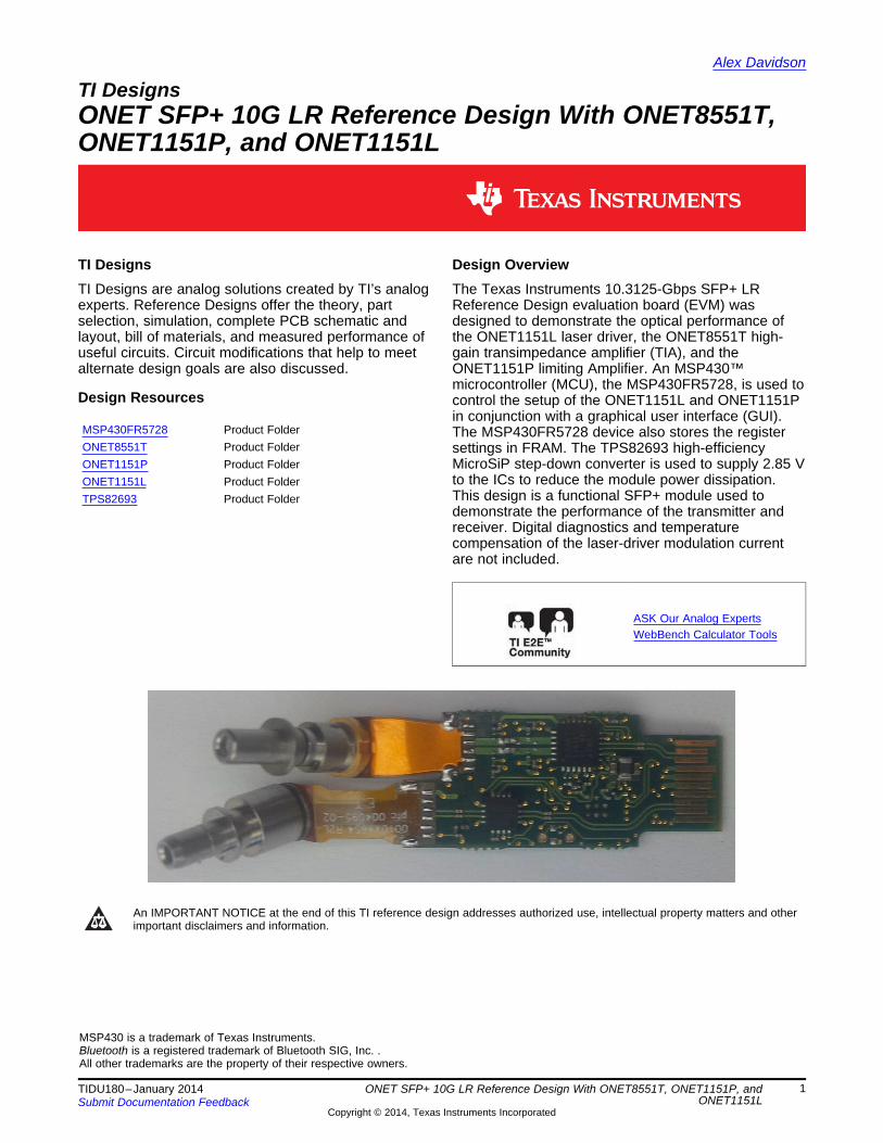
TI Designs Design OverviewTI Designs are analog solutions created by TI’s analog The Texas Instruments 10.3125-Gbps SFP+ LRexperts. Reference Designs offer the theory, part Reference Design evaluation board (EVM) wasselection, simulation, complete PCB schematic and designed to demonstrate the optical performance oflayout, bill of materials, and measured performance of the ONET1151L laser driver, the ONET8551T high-useful circuits. Circuit modifications that help to meet gain transimpedance amplifier (TIA), and thealternate design goals are also discussed. ONET1151P limiting Amplifier. An MSP430™
microcontroller (MCU), the MSP430FR5728, is used toDesign Resources control the setup of the ONET1151L and ONET1151P
in conjunction with a graphical user interface (GUI).MSP430FR5728 Product Folder The MSP430FR5728 device also stores the registerONET8551T Product Folder settings in FRAM. The TPS82693 high-efficiencyONET1151P Product Folder MicroSiP step-down converter is used to supply 2.85 V
to the ICs to reduce the module power dissipation.ONET1151L Product FolderThis design is a functional SFP+ module used toTPS82693 Product Folderdemonstrate the performance of the transmitter andreceiver. Digital diagnostics and temperaturecompensation of the laser-driver modulation currentare not included.
ASK Our Analog ExpertsWebBench Calculator Tools
An IMPORTANT NOTICE at the end of this TI reference design addresses authorized use, intellectual property matters and otherimportant disclaimers and information.
MSP430 is a trademark of Texas Instruments.Bluetooth is a registered trademark of Bluetooth SIG, Inc. .All other trademarks are the property of their respective owners.
1TIDU180–January 2014 ONET SFP+ 10G LR Reference Design With ONET8551T, ONET1151P, andONET1151LSubmit Documentation Feedback
Copyright © 2014, Texas Instruments Incorporated
Limiter
8-Bit RegisterCrosspoint
IMODIBIAS
Settings
Crosspoint Adjust
Crosspoint Adjust
Power-On Reset
Band-Gap, Analog References, Power Supply Monitor, and
Temperature Sensor
Bias Current Generator or Monitor and APC
2-Wire Interface and Control Logic
SDA
SCK
DIS
PD
FLT
BIAS
DIN+
DIN-
BIAS
FLTPD
RZTCRZTC
Settings
8-Bit Register8-Bit Register
10-Bit Register10-Bit Register
8-Bit Register
Output Settings
ADC Settings10-Bit Register
8-Bit Register
ADC
Analog to Digital
Conversion
DC Offset Cancellation
Adjustable Boost
8-Bit Register
Equalizer
MONBMONP
PSMTS
SDA
SCK
DIS
VCC
10 k
COMPCOMP
Limiter Current
8-Bit Register
25
MONB MONBMONP MONP
OUT+
OUT-
Mod. Current
Generator
25
Equalizer
+
+
ADR0
ADR1
ADR0
ADR1
8-Bit Register Bias Current Fault
Amplifier100
3-Bit Register Monitor Settings
8-Bit Register PD Current Fault
VCC
VCCTo all Blocks Except Output
Driver
10 k 10 k
Introduction www.ti.com
1 IntroductionThe 10.3125-Gbps SFP+ LR Reference Design evaluation board evaluates the optical performance of theONET1151L device, the ONET8551T device and the ONET1151P device. The ONET1151L is used todrive a 1310-nm DFB laser in an LC transmit-optical sub-assembly (TOSA). The ONET1151P is used toamplify the signal from the PIN-TIA LC receive-optical sub-assembly (ROSA) which contains theONET8551T TIA.
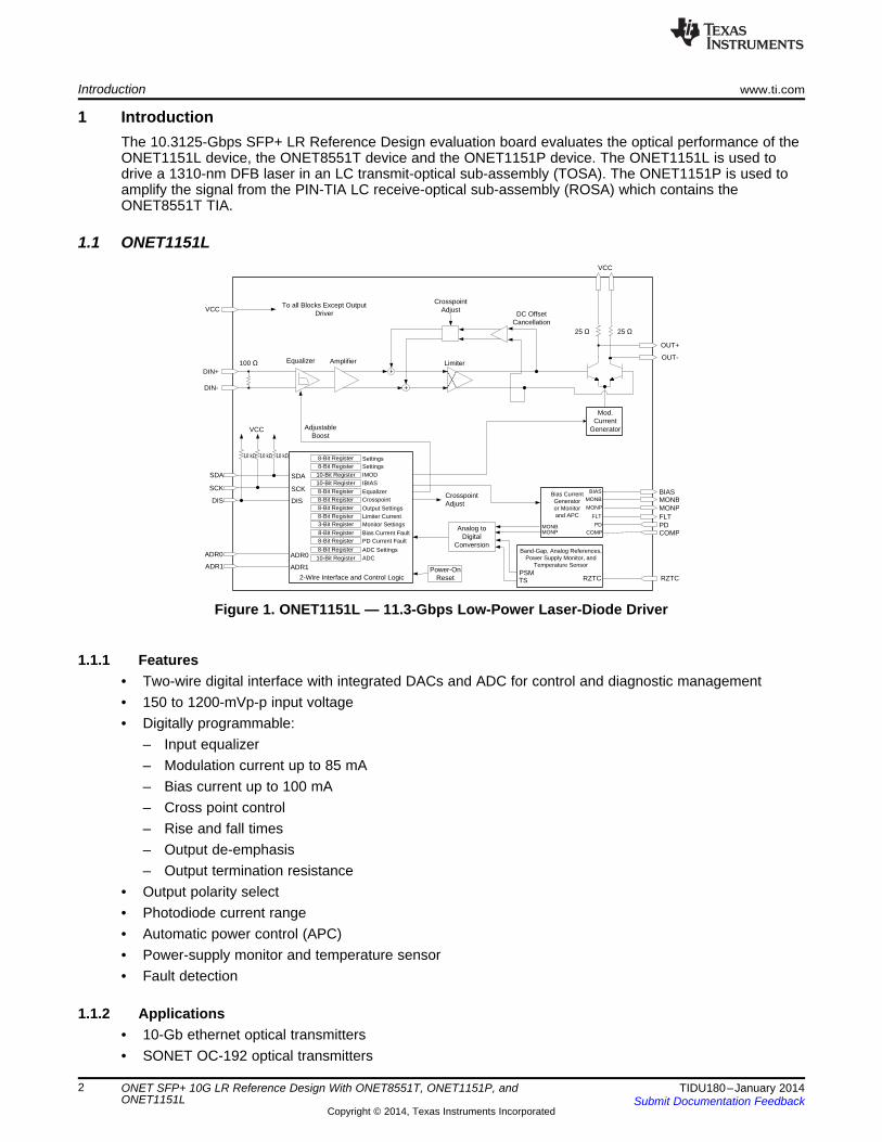
1.1 ONET1151L
Figure 1. ONET1151L — 11.3-Gbps Low-Power Laser-Diode Driver
1.1.1 Features• Two-wire digital interface with integrated DACs and ADC for control and diagnostic management• 150 to 1200-mVp-p input voltage• Digitally programmable:
– Input equalizer– Modulation current up to 85 mA– Bias current up to 100 mA– Cross point control– Rise and fall times– Output de-emphasis– Output termination resistance
• Output polarity select• Photodiode current range• Automatic power control (APC)• Power-supply monitor and temperature sensor• Fault detection
1.1.2 Applications• 10-Gb ethernet optical transmitters• SONET OC-192 optical transmitters
2 ONET SFP+ 10G LR Reference Design With ONET8551T, ONET1151P, and TIDU180–January 2014ONET1151L Submit Documentation Feedback
Copyright © 2014, Texas Instruments Incorporated
OUT+
OUT±
RSSI_EB
VCC_IN
FILTER 1 FILTER 2
GND
RF
IN
TIA
Voltage Amplifier
AGC, RSSI,and DC Offset Cancellation
CML Output Buffer
RSSI_IB
To TIA
To voltage amplifier and output bufferVCC_OUT
BW0
BW1
www.ti.com Introduction
• XFP and SFP+ transceiver modules• XENPAK, XPAK, X2, and 300-pin MSA transponder modules
1.1.3 Benefits• 25-Ω passive back termination reduces sensitivity to laser mismatch• Low power: 400 mW with IMOD = 30 mA and IBIAS = 30 mA• Pin compatible to the ONET1101L• –40°C to 100°C ambient operation
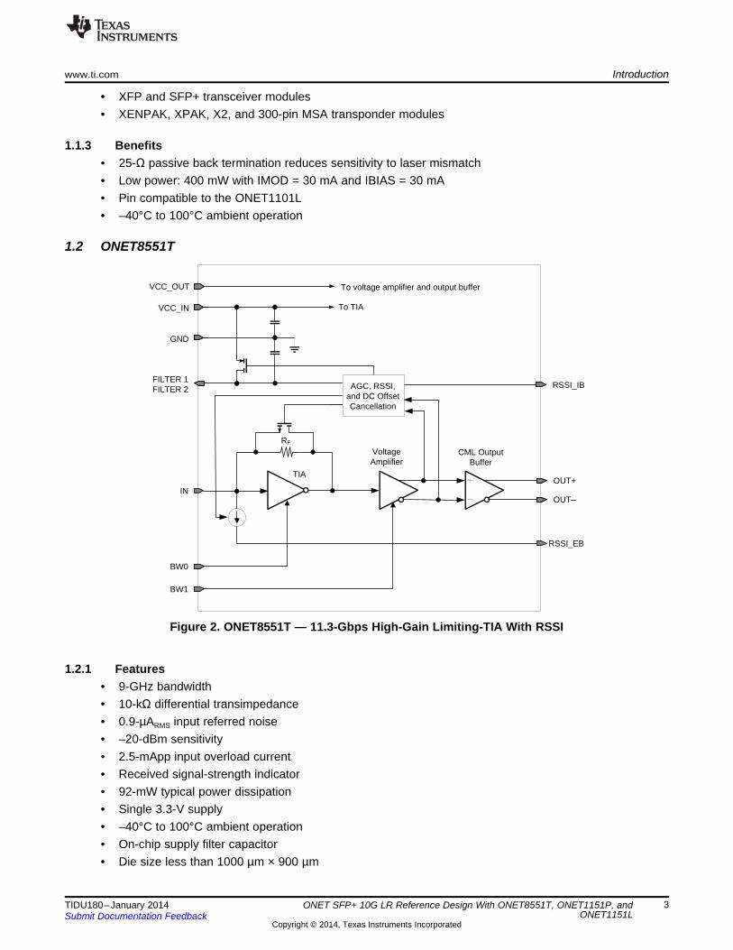
1.2 ONET8551T
Figure 2. ONET8551T — 11.3-Gbps High-Gain Limiting-TIA With RSSI
1.2.1 Features• 9-GHz bandwidth• 10-kΩ differential transimpedance• 0.9-µARMS input referred noise• –20-dBm sensitivity• 2.5-mApp input overload current• Received signal-strength indicator• 92-mW typical power dissipation• Single 3.3-V supply• –40°C to 100°C ambient operation• On-chip supply filter capacitor• Die size less than 1000 µm × 900 µm
3TIDU180–January 2014 ONET SFP+ 10G LR Reference Design With ONET8551T, ONET1151P, andONET1151LSubmit Documentation Feedback
Copyright © 2014, Texas Instruments Incorporated
Output BufferGain
Stage
50 50
VCC
100
Settings
4 Bit
Input Threshold
CPRNG and DE
Amplitude
LOS Adjust
Power-On Reset
Bandgap Voltage Reference and Bias Current Generation
2-Wire Interface and Control Logic
SDA
SCK
DIS
DIN+
DIN-
SDA
SCK
DIS
DOUT+
DOUT-
Gain Stage
Offset Cancellation
8 Bit Register
3 Bit
LOS Detection
LOS
COC1 COC2
VCC
GND
8 Bit Register
8 Bit Register
LOS Masking8 Bit Register
4 Bit
LOS Masking8 Bit Register
Settings8 Bit Register
Input Buffer
Introduction www.ti.com
1.2.2 Applications• 10-Gb ethernet optical receivers• 8x and 10x fibre-channel optical receivers• SONET OC-192 optical receivers• 10G-PON• 6G and 10G CPRI and OBSAI• PIN and APD preamplifiers
1.2.3 Benefits• One TIA for PIN and APD applications• High gain for reduced crosstalk• Low bandwidth and transimpedance variation over temperature• Low power
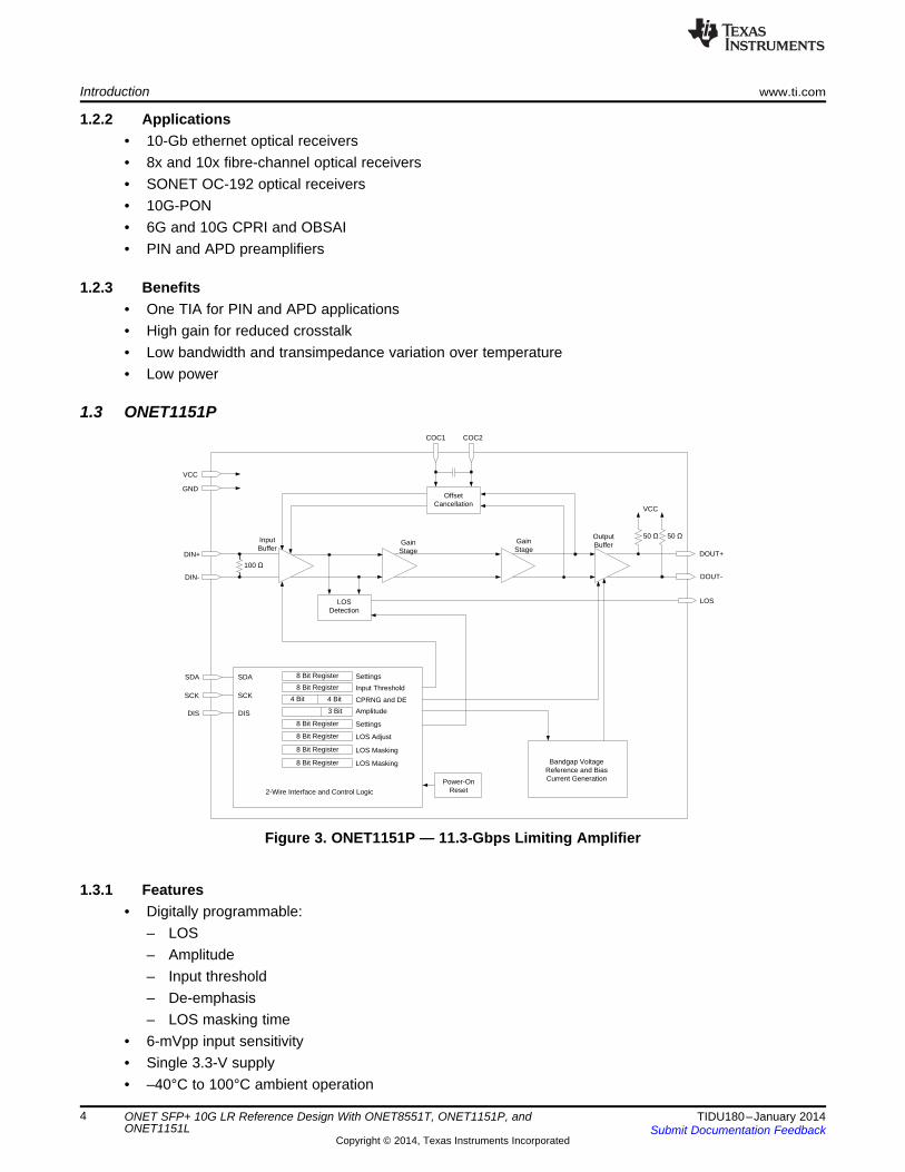
1.3 ONET1151P
Figure 3. ONET1151P — 11.3-Gbps Limiting Amplifier
1.3.1 Features• Digitally programmable:
– LOS– Amplitude– Input threshold– De-emphasis– LOS masking time
• 6-mVpp input sensitivity• Single 3.3-V supply• –40°C to 100°C ambient operation
4 ONET SFP+ 10G LR Reference Design With ONET8551T, ONET1151P, and TIDU180–January 2014ONET1151L Submit Documentation Feedback
Copyright © 2014, Texas Instruments Incorporated
Serial Interfaces
Converters
Peripherals
Memory
Debug
Timers
Power & Clocking
Connectivity
• 32x32 Multiplier
• DMA (3 Ch)
• CRC16
• Comp_D / Vref
• ADC10 (up to 12 ch)
16 / 8 / 4 KB FRAM(with segment protections
For code/data)
Real Time JTAG ,Embedded emulation
Bootstrap Loader
• Universal Serial Comm.Interfaces
• 2 UARTs or SPI• 1 I2C or SPI
Up to 3 1x8 + 1 1x3 I/O Ports
w/ Interrupt / wake up
•Power on Reset
•Brownout Reset
•Low Power Vreg (1.5V)
•XT1
•VLO
•DCO (±2%)
Real Time Clock
• Watch Dog Timer• Timer 0_A3• Timer1_B3• Timer2_A3• Timer 3_B3• Timer 4_B3
MSP430FR57xxUltra Low Power16 – bit MCU
8/24MHz
www.ti.com Introduction
1.3.2 Applications• 10-Gb ethernet optical receivers• 8x and 10x fibre-channel optical receivers• 6G and 10G CPRI and OBSAI• 10G-PON• SONET OC-192 optical receivers
1.3.3 Benefits• Few external components• Programmable masking time for LOS bounce• Low power: 132 mW with 600-mVpp output• Pin compatible to the ONET8501PB
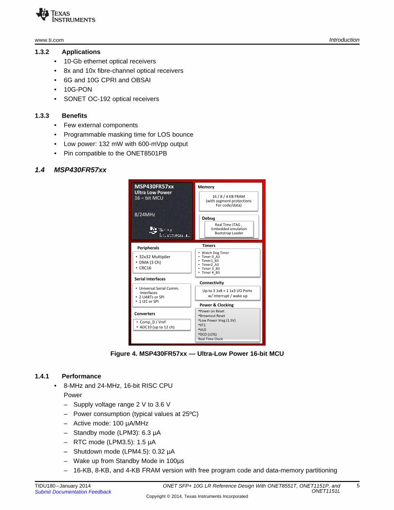
1.4 MSP430FR57xx
Figure 4. MSP430FR57xx — Ultra-Low Power 16-bit MCU
1.4.1 Performance• 8-MHz and 24-MHz, 16-bit RISC CPU
Power– Supply voltage range 2 V to 3.6 V– Power consumption (typical values at 25ºC)– Active mode: 100 µA/MHz– Standby mode (LPM3): 6.3 µA– RTC mode (LPM3.5): 1.5 µA– Shutdown mode (LPM4.5): 0.32 µA– Wake up from Standby Mode in 100µs– 16-KB, 8-KB, and 4-KB FRAM version with free program code and data-memory partitioning
5TIDU180–January 2014 ONET SFP+ 10G LR Reference Design With ONET8551T, ONET1151P, andONET1151LSubmit Documentation Feedback
Copyright © 2014, Texas Instruments Incorporated
VIN SW
FB
MODE
GND
EN
VOUT
2.85 V at 500 mA
CI
TPS82690SIP
L
VBAT
3.25 V to 4.35 V
CO
Mode
SelectionENABLE
DC-DC Converter
GND
Introduction www.ti.com
– 1-KB static random-access memory (SRAM)Package– 24-pin and 40-pin QFN– 38-Pin TSSOP– Temp Range –40ºC to 85ºC
1.4.2 Benefits• FRAM: Ultra-low power, universal memory
– Nearly infinite (1015) write cycles– 160-times faster than Flash (greater than 2 MB/s)– 250-times less power in writes– Flexible as data or program memory
• High performance analog– ADC10: 200 ksps and 150-µA consumption– Versatile analog comparator with 15 external channels, voltage hysteresis, and reference generator
• Cost-efficient system implementation– Fast to program– Less inventory management– Flexible and secure memory partitioningFor more information about the FRAM Series, go to www.ti.com/fram.
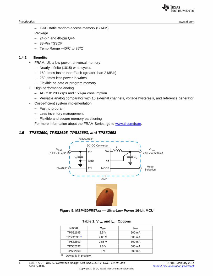
1.5 TPS82690, TPS82695, TPS82693, and TPS82698
Figure 5. MSP430FR57xx — Ultra-Low Power 16-bit MCU
Table 1. VOUT and IOUT Options
Device VOUT IOUT
TPS82695 2.5 V 500 mATPS82690 (1) 2.85 V 500 mATPS82693 2.85 V 800 mATPS82697 2.8 V 800 mATPS82698 3 V 800 mA
(1) Device is in preview.
6 ONET SFP+ 10G LR Reference Design With ONET8551T, ONET1151P, and TIDU180–January 2014ONET1151L Submit Documentation Feedback
Copyright © 2014, Texas Instruments Incorporated
www.ti.com Introduction
1.5.1 Features• Regulated switching frequency: 3 4MHz• All required external components are integrated• High PSRR and fast AC load regulation combined with low-ripple Power Save Mode• Automatic Power Safe Mode transition or forced PWM Mode operation• Input voltage: 2.3 V to 4.35 V• Active power-down sequencing (optional)
1.5.2 Applications• Mid-end to high-end cell phones and smart phones• Digital TV, WLAN, GPS, and Bluetooth®
• Flash memory• Portable audio and video
1.5.3 Benefits• Allows less than 7 mm2 total solution size and therefore provides 75 mA/mm• Reduces hardware-design workload with no more questionable designs• Makes the device an alternative high efficient solution over linear regulators• Allows to choose between high efficiency over entire load range (PSM) or regulated fixed frequency
(PWM)• Supports Li-Ion batteries with extended voltage range• Allows time control for power sequencing and a clear and sharp start-up voltage
7TIDU180–January 2014 ONET SFP+ 10G LR Reference Design With ONET8551T, ONET1151P, andONET1151LSubmit Documentation Feedback
Copyright © 2014, Texas Instruments Incorporated
xxxxxxxxxxxxxxxxxxxxxxxxxxxxxxxxxxxxxxxxxxxxxxxxxxxxxxxxxxxxxxxx
`
xxxxxxxxxxxxxxxxxxxxxxxxxxxxxxxxxxxxxxxxxxxxxxxxxxxxxxxxxxxxxxx
xxxxxxxxxxxxxxxxxxxxxxxxxxxxxxxxxxxxxxxxxxxxxxxxxxxxxxxxxxxxxxx
xxxxxxxxxxxxxxxxxxxxxxxxxxxxxxxxxxxxxxxxxxxxxxxxxxxxxxxxxxxxxxxx
xxxxxxxxxxxxxxxxxxxxxxxxxxxxxxxxxxxxxxxxxxxxxxxxxxxxxxxxxxxxxxxx
xxxxxxxxxxxxxxxxxxxxxxxxxxxxxxxxxxxxxxxxxxxxxxxx
xxxxxx
xxxxxx
xxxxxx
xxxxxx
xxxxxx
xxxxxx
xxxxxxxxxxxxxxxxxxxxxxxxxxxxxxxxxxxxxxxxxxxxxxxxxxxxxxxxxxxxxxxx
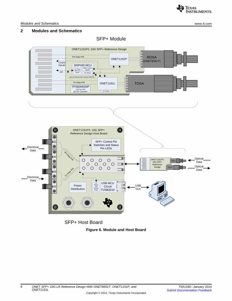
ONET1151P/L 10G SFP+ Reference
Design TOSA
ROSA
USBGUI
USB MCUCircuit
TUSB3210xxxxx
xxxxx
xxxxx
xxxxx
xxxxx
xxxxx
xxxxx
xxxxx
xxxxx
xxxxx
xxxxxxx
xxxxxxx
xxxxxxx
xxxxxxx
xxxxxxx
xxxxxxx
xxxxxxx
xxxxxx
xxxxxx
xxxxxx
xxxxxx
xxxxxx
xxxxxx
xxxxxx
Power Distribution
SFP+ Control Pin Switches and Status
Pin LEDs
ONET1151P/L 10G SFP+ Reference Design Host Board
I2C Master
with Module Board
RX Data P/N
TX Dat
a P/N
ONET1151P/L 10G SFP+ Reference Design
TOSA
MSP430 MCU
ONET1151L
ONET1151P
I2C Slave with Host
Board I2C Master
ONET Control Signals
RX Data P/N
TX Data P/N
I2C
Control Signals
Optional Debug Path to bypass MSP430
ROSA(ONET8551T)
SFP+ Module
OpticalData
ElectricalData
ElectricalData
OpticalData
TPS82693SIP3.3V to 2.5V
DC-DC Converter I2C Master
SFP+ Host Board
Modules and Schematics www.ti.com
2 Modules and Schematics
Figure 6. Module and Host Board
8 ONET SFP+ 10G LR Reference Design With ONET8551T, ONET1151P, and TIDU180–January 2014ONET1151L Submit Documentation Feedback
Copyright © 2014, Texas Instruments Incorporated
0201
0603 47uH
0201
0201
0603 47uH0201
0201
0603 47uH
0201
0603 47uH
0201
0201
BIAS TEE
BIAS TEE
SPI-BI-WIRE PROGRAMMING
PORT FOR MSP430 MCU
0201
0201
0201
0201
0201
0201
0402
0402
0402
0402
0402
0402
0402
0402
0402
0201
0201
0201
0201
0201
0201
0201
0201
0402
0402
0201
0201 0201
0201
0201
0201 0201
0201 0201
0201
0201
0201
0201
0201
0201
0201
0402
0402
0402
0201
0201
0201
0201
0201
0201
0201
0201
0402
0201
0201
0201
MODN
MODN_BT
MODP_BT LD_CATHODE_BT
LD_ANODE_BT
TD_DATA_P
TD_DATA_N
BIAS
PD
CO
C2
CO
C1
PD
RD_DINN
RD_DINP
RD_DATA_N
RD_DATA_P
MO
NB
MO
NP
CO
MP
TX_DISABLE
SCL
SDA
TX_FAULT
TX_FAULT
TDP_DINN
TDP_DINP
RDN_DOUTN
RDN_DOUTP
MODP
TDP
TDN
RDN
RDP
TDP
TDN
RDN
RDP
SC
L1
SD
A1
TX
_D
ISA
BLE
RX_LOS
SD
A1
SC
L1
RX
_LO
S
RSSI
RSSI
VCC_MONITOR
MONP
MONB
TX_DISABLE
RX_DISABLE TX_FAULT
SDA1
SCL1
SDA
SCL
RX
_LO
S
SB
WT
CK
SB
WT
DIO
VCORE
AD
DR
1
AD
DR
0
RZ
TC
RX
_D
ISA
BLE
EN
MODE
VCC_TVCC_T
VCC_T
VCC_T
VCC_R
VCC_T
VCC_3P3V
VCC_T
VCC_MCUVCC_MCU
VCC_3P3V VCC_2P85V VCC_R
VCC_T
VCC_MCU
VCC_T
VCC_R
VCC_MCU
VCC_MCU
VCC_MCU
VCC_R
VCC_R
R2
4.9
9K
L5
BLM15PD121SN1D
C20 0.1uF
L11BLM03HG102SN1D
R1
3D
NI_
10
K
C260.1uF
C330.1uF
C1
02
.2u
FC3410uF
C190.1uF
C2
20
.1u
F
R25
10K
C11
0.1
uF
R6475
C60.1uF
R2
41
0K
C18DNI
R11
10
K
C7
2.2
uF
C1
30
.1u
F
U3
ONET1151P
GND11
DIN+2
DIN-3
GND24
CO
C1
5
CO
C2
6
DIS
7
LO
S8
VCC19
DOUT-10
DOUT+11
VCC212
NC
113
NC
214
SC
K15
SD
A16
GND_PAD17
L14GLFR1608T470M
TOSA
U6
NC7
GND26
LD ANODE5
LD CATHODE4
GND13
PD CATHODE2
GN
D3
8G
ND
1
JMP1
DNI - 2 PIN HEADER
12
R27 DNI_0
C2
90
.1u
F
C23
0.1
uF
R1
4.9
9K
R1428.7K
R20475
L2GLFR1608T470M
R1
94
.99
K
C27
0.1
uF
R15
10K
TOPBOTTOM
P1
SFP+ Edge Connector
GND11
TX_FAULT2
TX_DIS3
SDA4
SCL5
MOD-DEF06
AS07
RX_LOS8
AS19
GND210
GND311
RDN12
RDP13
GND414
VCCR15
VCCT16
GND517
TDP18
TDN19
GND620
L1
BLM15PD121SN1D
C300.1uF
U4
ONET1151L
PD
1
AD
R0
2
AD
R1
3
DIS
4
SC
K5
SD
A6
FLT7
GND18
DIN+9
DIN-10
GND211
RZTC12
MO
NB
13
MO
NP
14
CO
MP
15
VC
C1
16
GN
D3
17
BIA
S18
VCC219
MOD1+20
MOD0+21
MOD0-22
MOD1-23
VCC324
GND_PAD25
C3 0.1uF
C24DNI_4.7uF
L15GLFR1608T470M
C250.1uF
R4
DN
I_1
0K
C1 0.1uF
R1
88
00
C310.1uF
C2
82
.2u
F
R1
2D
NI_
10
KL4GLFR1608T470M
C2 0.1uF
L3
BLM15PD121SN1D
C5 0.1uF
L8BLM03HG102SN1D
C1
22
.2u
F
R21475
R2
61
0K
C320.1uF
C140.1uF
R8
DN
I_4
.99
K
U1
TPS82693SIP
VIN1A2
VIN2A3
GND1C1
GND2C2
GND3C3EN
B2
VOUTA1
MODEB1
R5
DN
I_1
0K
R2210K
L9BLM03HG102SN1D
R3475
C15 0.1uF
C4 0.1uF
C90.1uF
C16 0.1uF
ROSA
U5
VPD7
GND26
DATA_N5
DATA_P4
GND13
VCC2
GN
D3
8G
ND
1
R28 DNI_0
R9
DN
I_4
.99
K
U2
MSP430FR5728IRGE
P1.01
P1.12
P1.23
P1.34
P1.56
PJ.0
7
PJ.1
8
PJ.2
9
PJ.3
10
TE
ST
/SB
WT
CK
11
RS
T/S
BW
TD
IO12
P2.013
P2.114
P2.215
P1.616
P1.717
DV
SS
19
DV
CC
20
PJ.4
21
PJ.5
22
AV
SS
23
AV
CC
24
GN
D_P
AD
25
P1.45
VCORE18
L10BLM03HG102SN1D
C17 0.1uF
C21 0.1uF
C8
0.1
uF
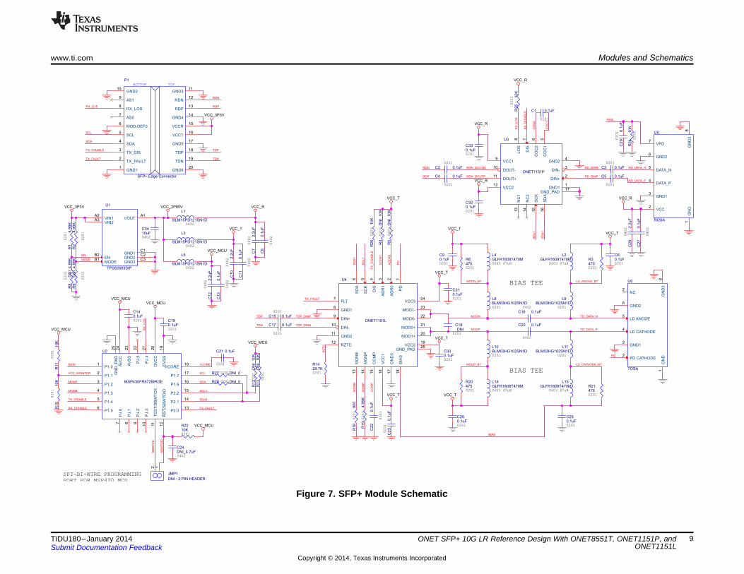
www.ti.com Modules and Schematics
Figure 7. SFP+ Module Schematic
9TIDU180–January 2014 ONET SFP+ 10G LR Reference Design With ONET8551T, ONET1151P, andONET1151LSubmit Documentation Feedback
Copyright © 2014, Texas Instruments Incorporated
MSP430FR5728
ONET1151P ROSA with ONET8551T
ONET1151LTPS82693 TOSA
Modules and Schematics www.ti.com
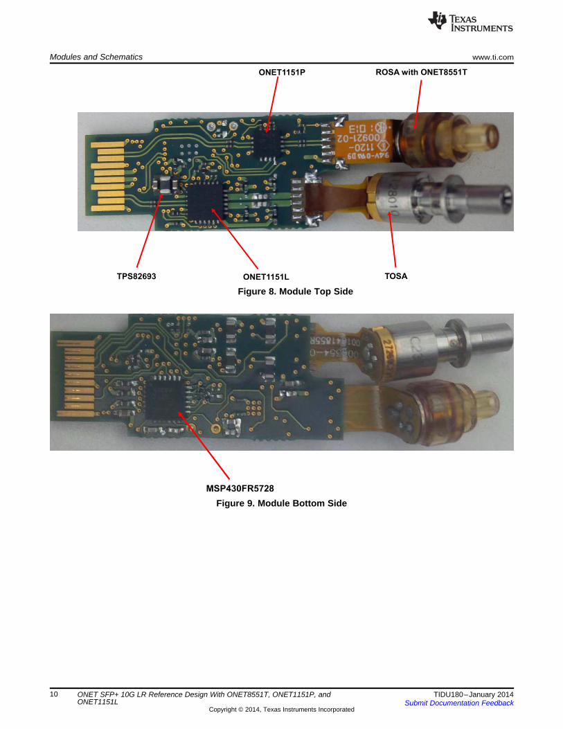
Figure 8. Module Top Side
Figure 9. Module Bottom Side
10 ONET SFP+ 10G LR Reference Design With ONET8551T, ONET1151P, and TIDU180–January 2014ONET1151L Submit Documentation Feedback
Copyright © 2014, Texas Instruments Incorporated
USB Connector
Receiver Outputs
Transmitter Inputs
3.3V Supply
Voltage
SFP+ Connector
Jumper set for
External Supply
Voltage
www.ti.com Modules and Schematics
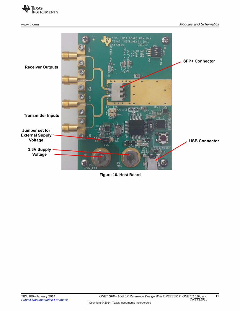
Figure 10. Host Board
11TIDU180–January 2014 ONET SFP+ 10G LR Reference Design With ONET8551T, ONET1151P, andONET1151LSubmit Documentation Feedback
Copyright © 2014, Texas Instruments Incorporated
Bias current
adjustment
Modulation
current
adjustment
Equalizer
adjustment
Quick Set-Up Instructions www.ti.com
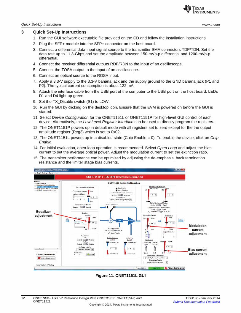
3 Quick Set-Up Instructions1. Run the GUI software executable file provided on the CD and follow the installation instructions.2. Plug the SFP+ module into the SFP+ connector on the host board.3. Connect a differential data-input signal source to the transmitter SMA connectors TDP/TDN. Set the
data rate up to 11.3-Gbps and set the amplitude between 150-mVp-p differential and 1200-mVp-pdifferential.
4. Connect the receiver differential outputs RDP/RDN to the input of an oscilloscope.5. Connect the TOSA output to the input of an oscilloscope.6. Connect an optical source to the ROSA input.7. Apply a 3.3-V supply to the 3.3-V banana jack and the supply ground to the GND banana jack (P1 and
P2). The typical current consumption is about 122 mA.8. Attach the interface cable from the USB port of the computer to the USB port on the host board. LEDs
D1 and D4 light up green.9. Set the TX_Disable switch (S1) to LOW.10. Run the GUI by clicking on the desktop icon. Ensure that the EVM is powered on before the GUI is
started.11. Select Device Configuration for the ONET1151L or ONET1151P for high-level GUI control of each
device. Alternatively, the Low Level Register Interface can be used to directly program the registers.12. The ONET1151P powers up in default mode with all registers set to zero except for the the output
amplitude register (Reg3) which is set to 0x02.13. The ONET1151L powers up in a disabled state (Chip Enable = 0). To enable the device, click on Chip
Enable.14. For initial evaluation, open-loop operation is recommended. Select Open Loop and adjust the bias
current to set the average optical power. Adjust the modulation current to set the extinction ratio.15. The transmitter performance can be optimized by adjusting the de-emphasis, back termination
resistance and the limiter stage bias currents.
Figure 11. ONET1151L GUI
12 ONET SFP+ 10G LR Reference Design With ONET8551T, ONET1151P, and TIDU180–January 2014ONET1151L Submit Documentation Feedback
Copyright © 2014, Texas Instruments Incorporated
www.ti.com Quick Set-Up Instructions
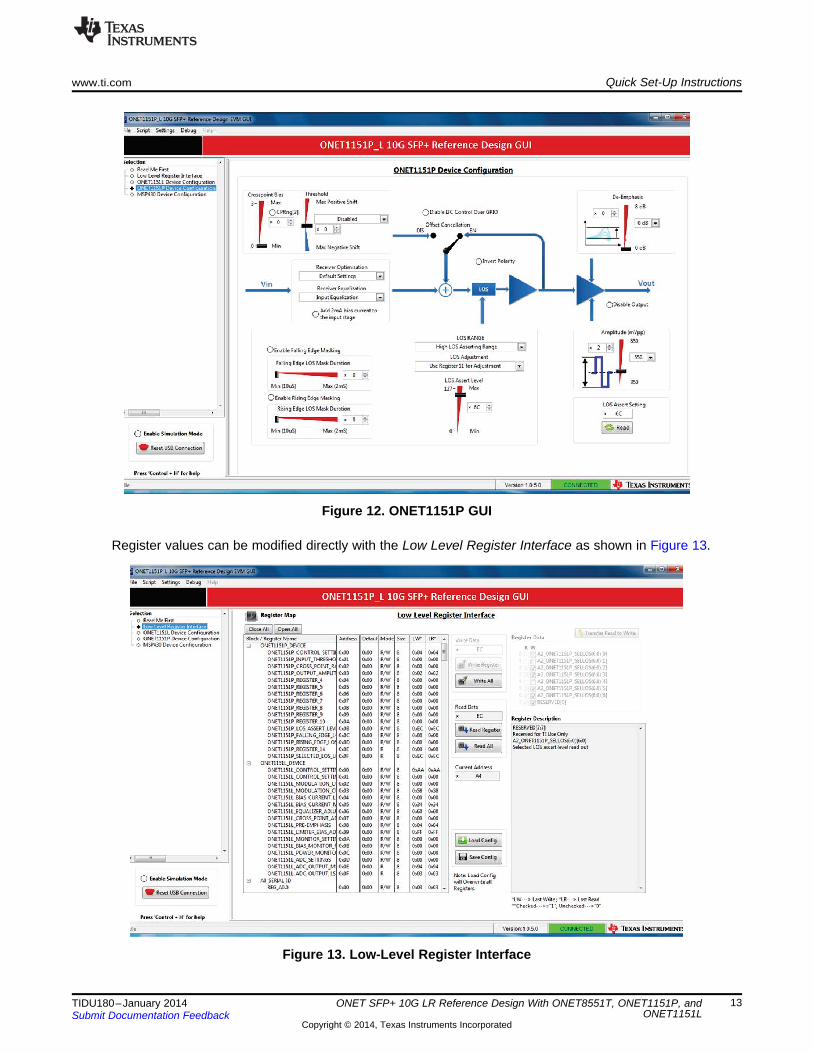
Figure 12. ONET1151P GUI
Register values can be modified directly with the Low Level Register Interface as shown in Figure 13.
Figure 13. Low-Level Register Interface
13TIDU180–January 2014 ONET SFP+ 10G LR Reference Design With ONET8551T, ONET1151P, andONET1151LSubmit Documentation Feedback
Copyright © 2014, Texas Instruments Incorporated
Use these to
transfer register
settings into A2
memory
Transfer A2
memory to FRAM
for permanent
storage
Quick Set-Up Instructions www.ti.com
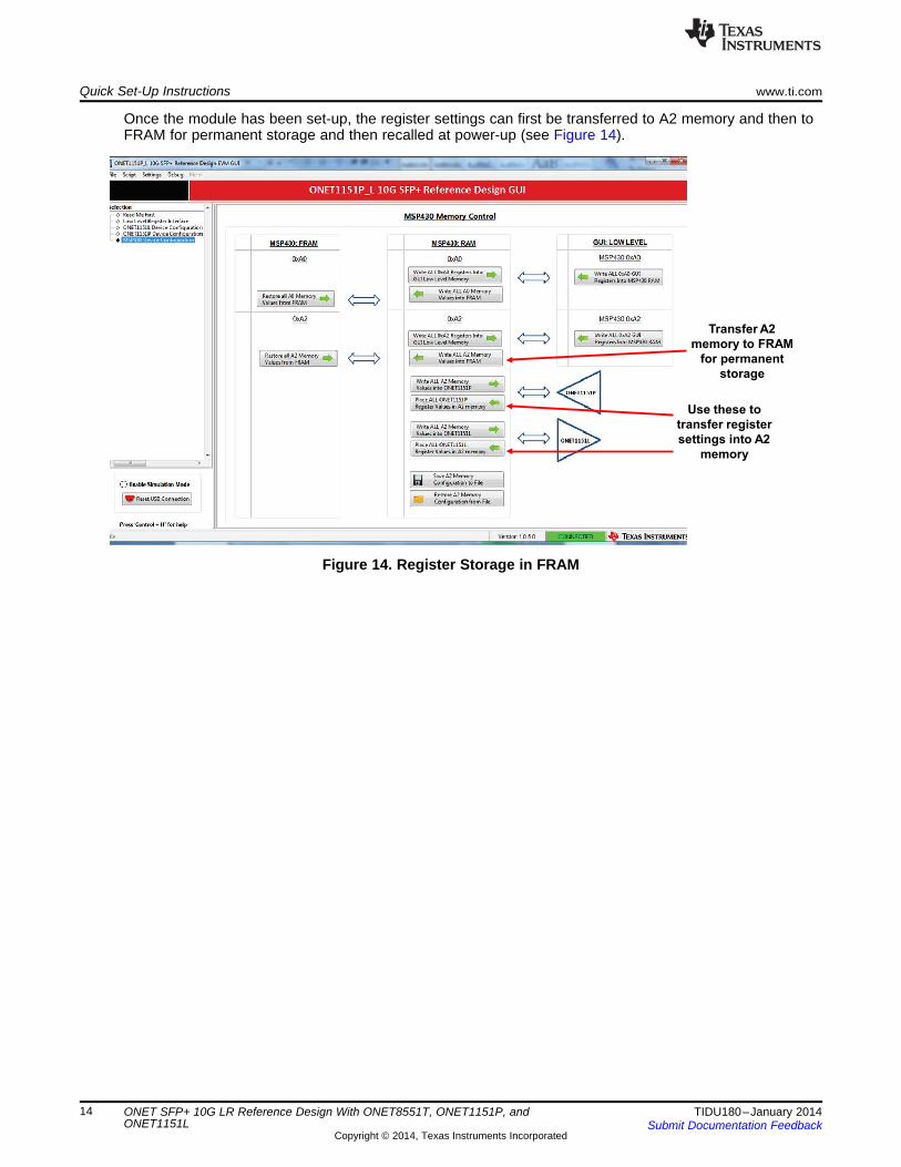
Once the module has been set-up, the register settings can first be transferred to A2 memory and then toFRAM for permanent storage and then recalled at power-up (see Figure 14).
Figure 14. Register Storage in FRAM
14 ONET SFP+ 10G LR Reference Design With ONET8551T, ONET1151P, and TIDU180–January 2014ONET1151L Submit Documentation Feedback
Copyright © 2014, Texas Instruments Incorporated
www.ti.com Test Results
4 Test Results
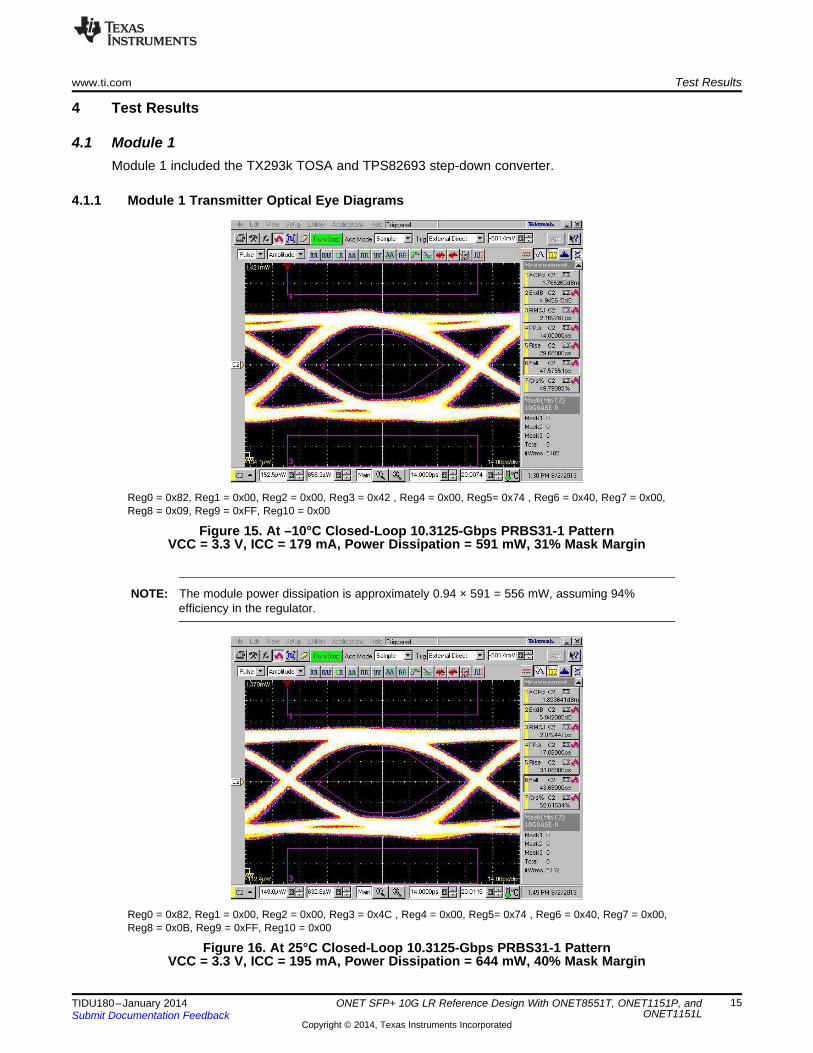
4.1 Module 1Module 1 included the TX293k TOSA and TPS82693 step-down converter.
4.1.1 Module 1 Transmitter Optical Eye Diagrams
Reg0 = 0x82, Reg1 = 0x00, Reg2 = 0x00, Reg3 = 0x42 , Reg4 = 0x00, Reg5= 0x74 , Reg6 = 0x40, Reg7 = 0x00,Reg8 = 0x09, Reg9 = 0xFF, Reg10 = 0x00
Figure 15. At –10°C Closed-Loop 10.3125-Gbps PRBS31-1 PatternVCC = 3.3 V, ICC = 179 mA, Power Dissipation = 591 mW, 31% Mask Margin
NOTE: The module power dissipation is approximately 0.94 × 591 = 556 mW, assuming 94%efficiency in the regulator.
Reg0 = 0x82, Reg1 = 0x00, Reg2 = 0x00, Reg3 = 0x4C , Reg4 = 0x00, Reg5= 0x74 , Reg6 = 0x40, Reg7 = 0x00,Reg8 = 0x0B, Reg9 = 0xFF, Reg10 = 0x00
Figure 16. At 25°C Closed-Loop 10.3125-Gbps PRBS31-1 PatternVCC = 3.3 V, ICC = 195 mA, Power Dissipation = 644 mW, 40% Mask Margin
15TIDU180–January 2014 ONET SFP+ 10G LR Reference Design With ONET8551T, ONET1151P, andONET1151LSubmit Documentation Feedback
Copyright © 2014, Texas Instruments Incorporated
Test Results www.ti.com
NOTE: The module power dissipation is approximately 0.94 × 644 = 605 mW, assuming 94%efficiency in the regulator.
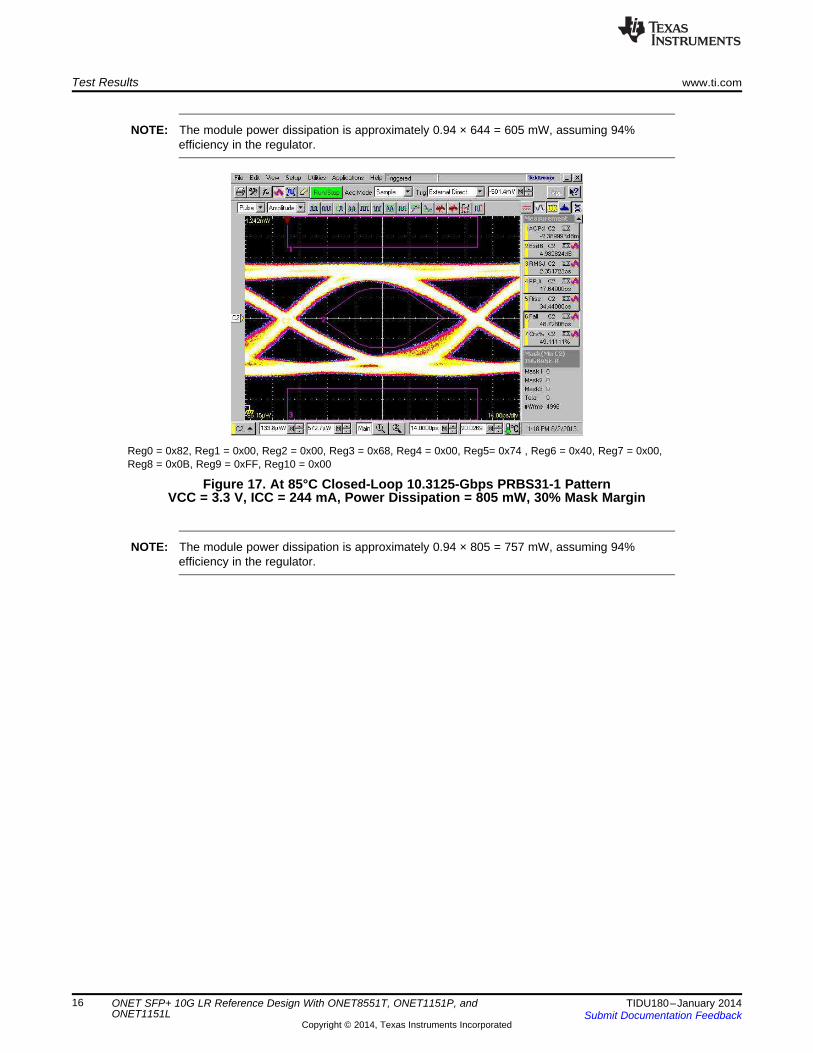
Reg0 = 0x82, Reg1 = 0x00, Reg2 = 0x00, Reg3 = 0x68, Reg4 = 0x00, Reg5= 0x74 , Reg6 = 0x40, Reg7 = 0x00,Reg8 = 0x0B, Reg9 = 0xFF, Reg10 = 0x00
Figure 17. At 85°C Closed-Loop 10.3125-Gbps PRBS31-1 PatternVCC = 3.3 V, ICC = 244 mA, Power Dissipation = 805 mW, 30% Mask Margin
NOTE: The module power dissipation is approximately 0.94 × 805 = 757 mW, assuming 94%efficiency in the regulator.
16 ONET SFP+ 10G LR Reference Design With ONET8551T, ONET1151P, and TIDU180–January 2014ONET1151L Submit Documentation Feedback
Copyright © 2014, Texas Instruments Incorporated
www.ti.com Test Results
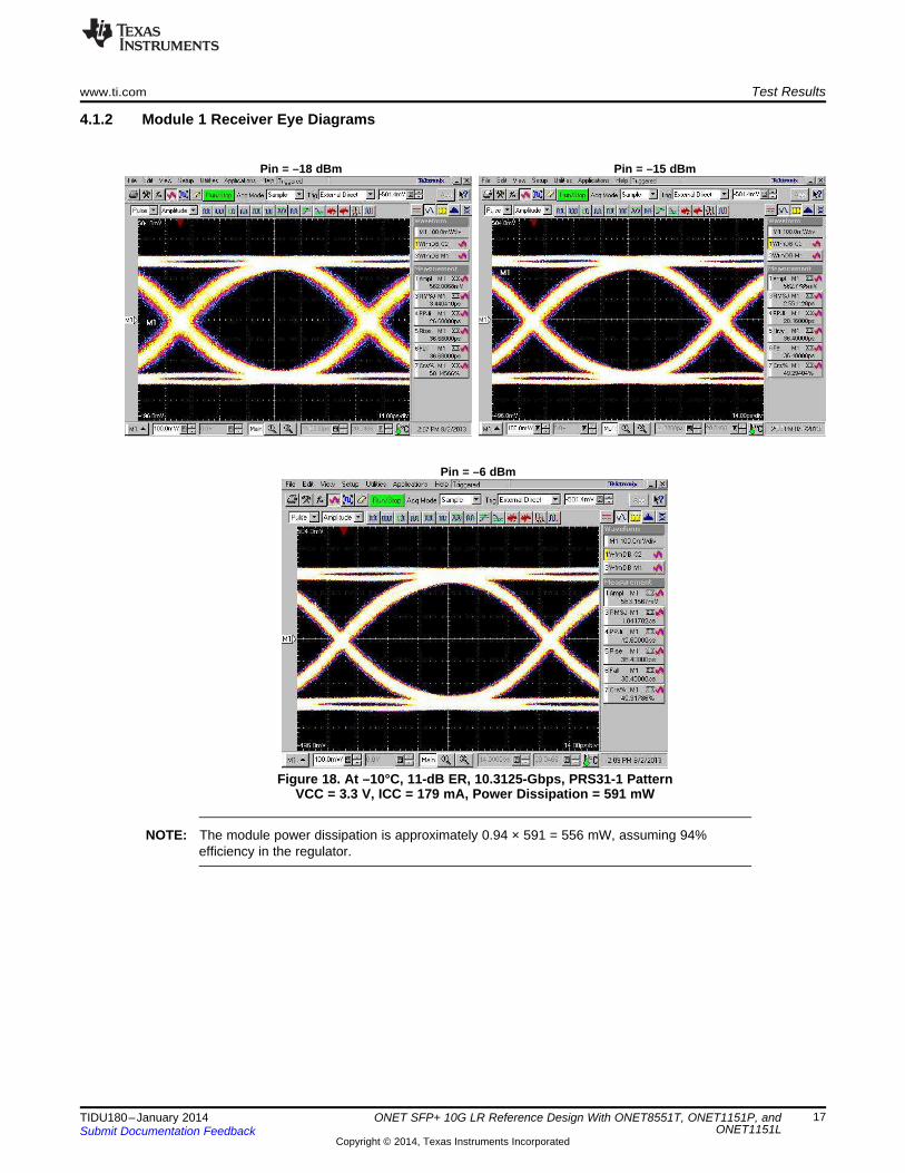
4.1.2 Module 1 Receiver Eye Diagrams
Pin = –18 dBm Pin = –15 dBm
Pin = –6 dBm
Figure 18. At –10°C, 11-dB ER, 10.3125-Gbps, PRS31-1 PatternVCC = 3.3 V, ICC = 179 mA, Power Dissipation = 591 mW
NOTE: The module power dissipation is approximately 0.94 × 591 = 556 mW, assuming 94%efficiency in the regulator.
17TIDU180–January 2014 ONET SFP+ 10G LR Reference Design With ONET8551T, ONET1151P, andONET1151LSubmit Documentation Feedback
Copyright © 2014, Texas Instruments Incorporated
Test Results www.ti.com
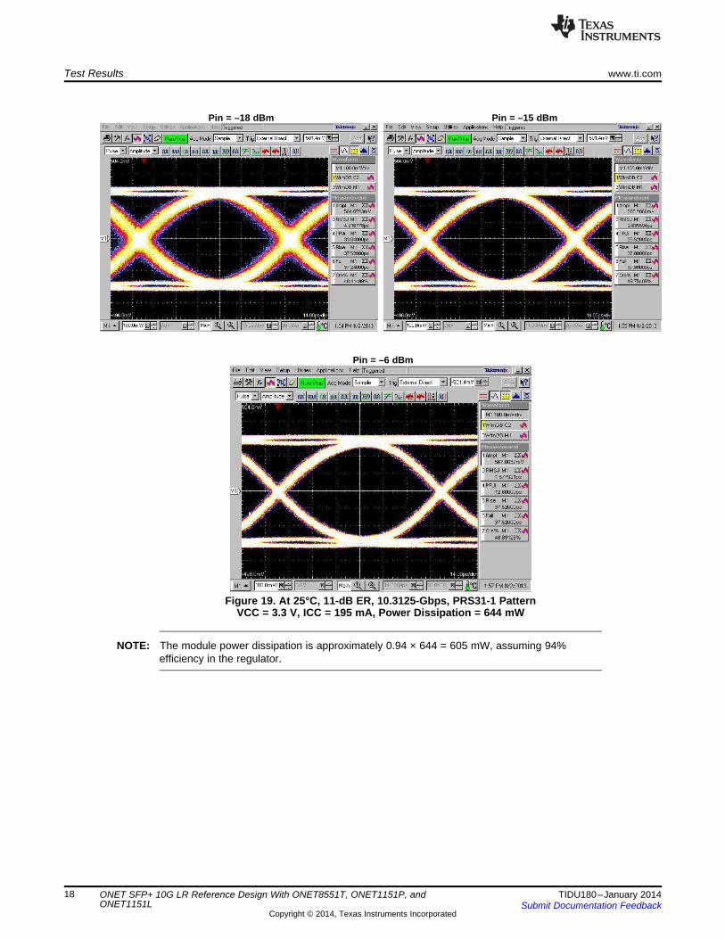
Pin = –18 dBm Pin = –15 dBm
Pin = –6 dBm
Figure 19. At 25°C, 11-dB ER, 10.3125-Gbps, PRS31-1 PatternVCC = 3.3 V, ICC = 195 mA, Power Dissipation = 644 mW
NOTE: The module power dissipation is approximately 0.94 × 644 = 605 mW, assuming 94%efficiency in the regulator.
18 ONET SFP+ 10G LR Reference Design With ONET8551T, ONET1151P, and TIDU180–January 2014ONET1151L Submit Documentation Feedback
Copyright © 2014, Texas Instruments Incorporated
www.ti.com Test Results
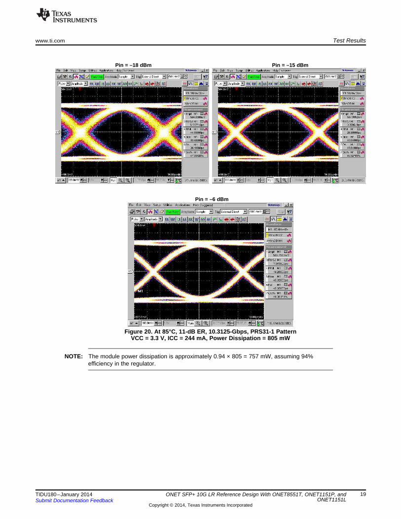
Pin = –18 dBm Pin = –15 dBm
Pin = –6 dBm
Figure 20. At 85°C, 11-dB ER, 10.3125-Gbps, PRS31-1 PatternVCC = 3.3 V, ICC = 244 mA, Power Dissipation = 805 mW
NOTE: The module power dissipation is approximately 0.94 × 805 = 757 mW, assuming 94%efficiency in the regulator.
19TIDU180–January 2014 ONET SFP+ 10G LR Reference Design With ONET8551T, ONET1151P, andONET1151LSubmit Documentation Feedback
Copyright © 2014, Texas Instruments Incorporated
Test Results www.ti.com
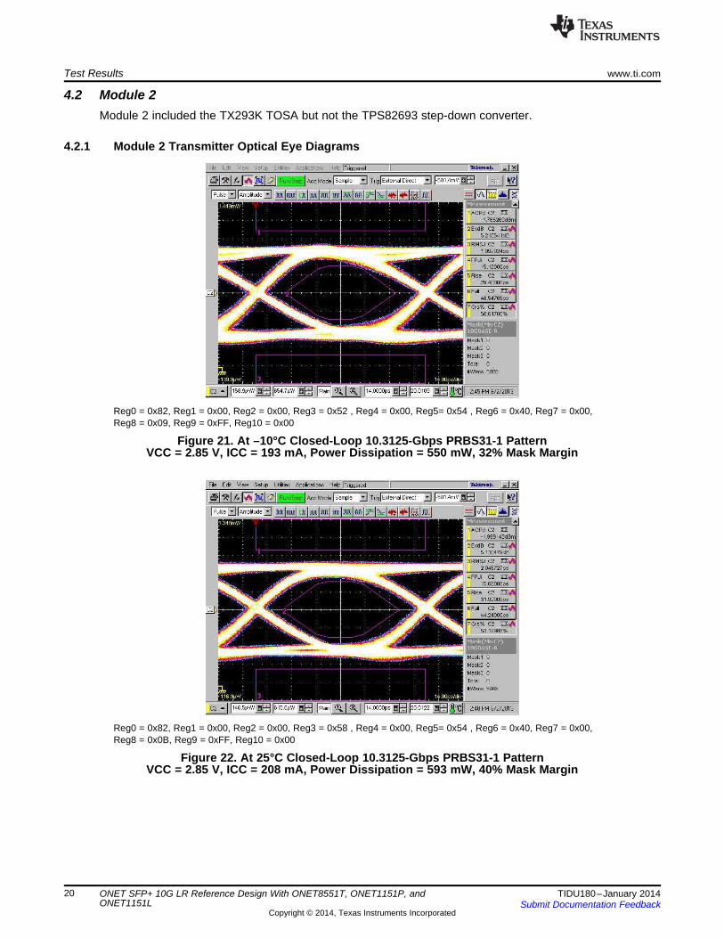
4.2 Module 2Module 2 included the TX293K TOSA but not the TPS82693 step-down converter.
4.2.1 Module 2 Transmitter Optical Eye Diagrams
Reg0 = 0x82, Reg1 = 0x00, Reg2 = 0x00, Reg3 = 0x52 , Reg4 = 0x00, Reg5= 0x54 , Reg6 = 0x40, Reg7 = 0x00,Reg8 = 0x09, Reg9 = 0xFF, Reg10 = 0x00
Figure 21. At –10°C Closed-Loop 10.3125-Gbps PRBS31-1 PatternVCC = 2.85 V, ICC = 193 mA, Power Dissipation = 550 mW, 32% Mask Margin
Reg0 = 0x82, Reg1 = 0x00, Reg2 = 0x00, Reg3 = 0x58 , Reg4 = 0x00, Reg5= 0x54 , Reg6 = 0x40, Reg7 = 0x00,Reg8 = 0x0B, Reg9 = 0xFF, Reg10 = 0x00
Figure 22. At 25°C Closed-Loop 10.3125-Gbps PRBS31-1 PatternVCC = 2.85 V, ICC = 208 mA, Power Dissipation = 593 mW, 40% Mask Margin
20 ONET SFP+ 10G LR Reference Design With ONET8551T, ONET1151P, and TIDU180–January 2014ONET1151L Submit Documentation Feedback
Copyright © 2014, Texas Instruments Incorporated
www.ti.com Test Results
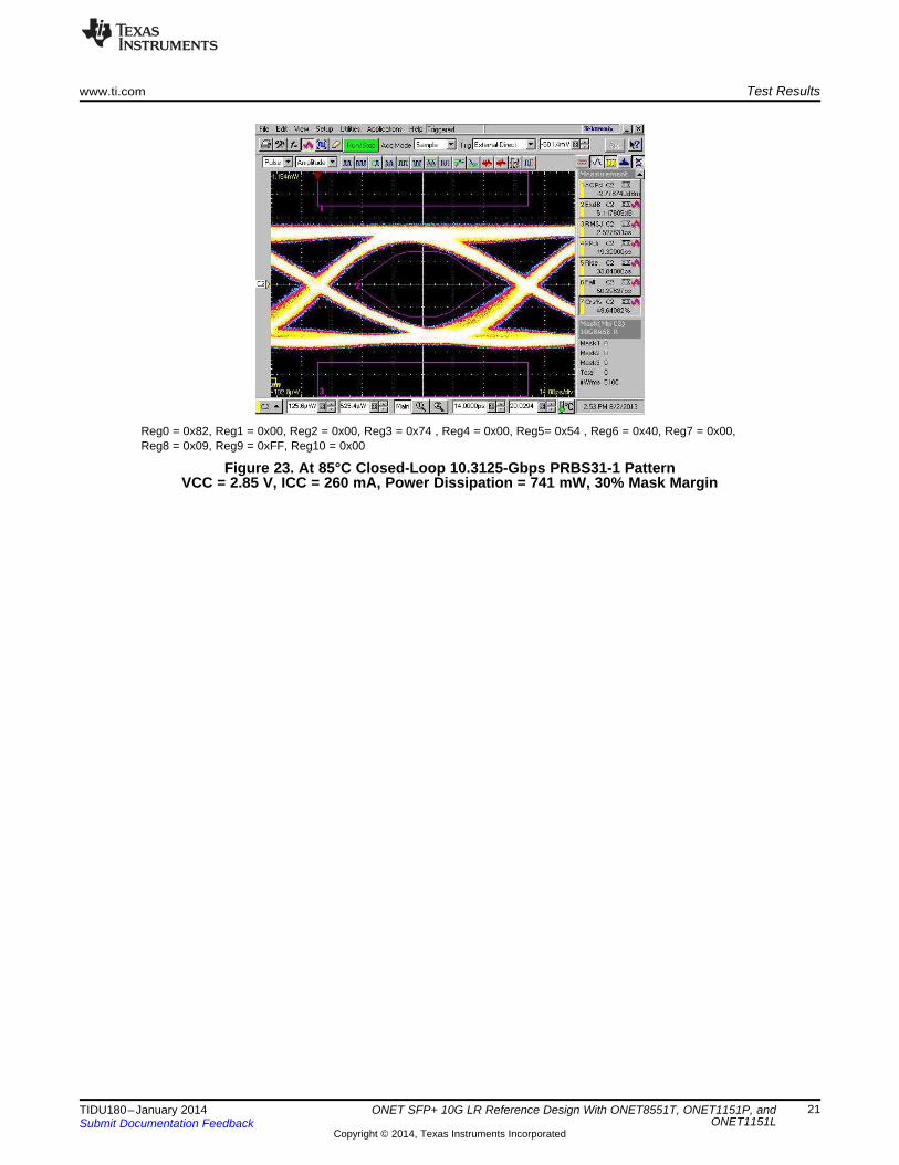
Reg0 = 0x82, Reg1 = 0x00, Reg2 = 0x00, Reg3 = 0x74 , Reg4 = 0x00, Reg5= 0x54 , Reg6 = 0x40, Reg7 = 0x00,Reg8 = 0x09, Reg9 = 0xFF, Reg10 = 0x00
Figure 23. At 85°C Closed-Loop 10.3125-Gbps PRBS31-1 PatternVCC = 2.85 V, ICC = 260 mA, Power Dissipation = 741 mW, 30% Mask Margin
21TIDU180–January 2014 ONET SFP+ 10G LR Reference Design With ONET8551T, ONET1151P, andONET1151LSubmit Documentation Feedback
Copyright © 2014, Texas Instruments Incorporated

Test Results www.ti.com
4.2.2 Module 2 Receiver Eye Diagrams
Pin = –18 dBm Pin = –15 dBm
Pin = –6 dBm
Figure 24. At –10°C, 11-dB ER, 10.3125-Gbps, PRS31-1 PatternVCC = 2.85 V, ICC = 193 mA, Power Dissipation = 550 mW
22 ONET SFP+ 10G LR Reference Design With ONET8551T, ONET1151P, and TIDU180–January 2014ONET1151L Submit Documentation Feedback
Copyright © 2014, Texas Instruments Incorporated
www.ti.com Test Results
Pin = –18 dBm Pin = –15 dBm
Pin = –6 dBm
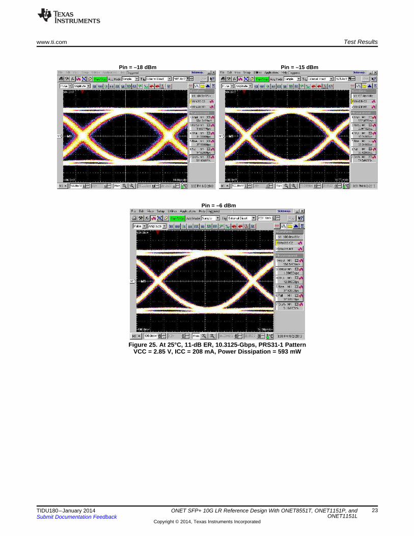
Figure 25. At 25°C, 11-dB ER, 10.3125-Gbps, PRS31-1 PatternVCC = 2.85 V, ICC = 208 mA, Power Dissipation = 593 mW
23TIDU180–January 2014 ONET SFP+ 10G LR Reference Design With ONET8551T, ONET1151P, andONET1151LSubmit Documentation Feedback
Copyright © 2014, Texas Instruments Incorporated
Test Results www.ti.com
Pin = –18 dBm Pin = –15 dBm
Pin = –6 dBm
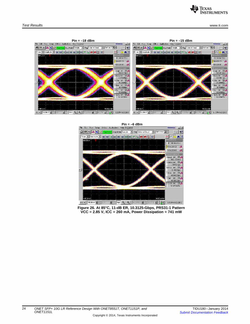
Figure 26. At 85°C, 11-dB ER, 10.3125-Gbps, PRS31-1 PatternVCC = 2.85 V, ICC = 260 mA, Power Dissipation = 741 mW
24 ONET SFP+ 10G LR Reference Design With ONET8551T, ONET1151P, and TIDU180–January 2014ONET1151L Submit Documentation Feedback
Copyright © 2014, Texas Instruments Incorporated
www.ti.com Test Results
4.3 Transmitter Test Results With the NX8349TS TOSA
4.3.1 Transmitter Optical Eye Diagrams
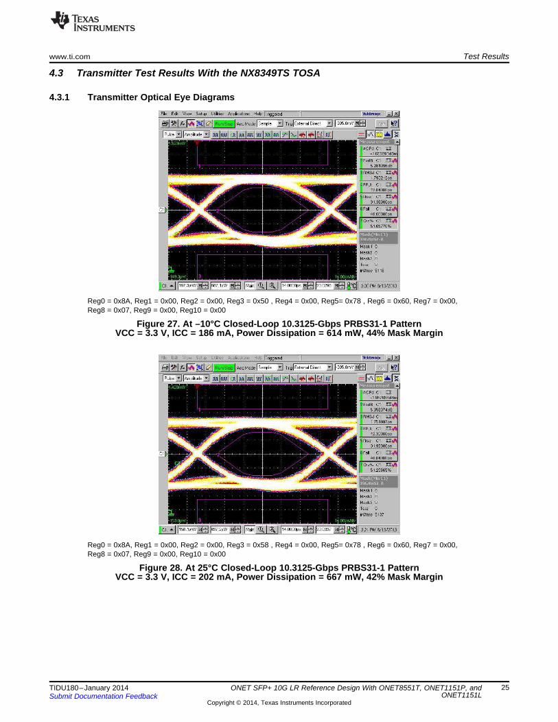
Reg0 = 0x8A, Reg1 = 0x00, Reg2 = 0x00, Reg3 = 0x50 , Reg4 = 0x00, Reg5= 0x78 , Reg6 = 0x60, Reg7 = 0x00,Reg8 = 0x07, Reg9 = 0x00, Reg10 = 0x00
Figure 27. At –10°C Closed-Loop 10.3125-Gbps PRBS31-1 PatternVCC = 3.3 V, ICC = 186 mA, Power Dissipation = 614 mW, 44% Mask Margin
Reg0 = 0x8A, Reg1 = 0x00, Reg2 = 0x00, Reg3 = 0x58 , Reg4 = 0x00, Reg5= 0x78 , Reg6 = 0x60, Reg7 = 0x00,Reg8 = 0x07, Reg9 = 0x00, Reg10 = 0x00
Figure 28. At 25°C Closed-Loop 10.3125-Gbps PRBS31-1 PatternVCC = 3.3 V, ICC = 202 mA, Power Dissipation = 667 mW, 42% Mask Margin
25TIDU180–January 2014 ONET SFP+ 10G LR Reference Design With ONET8551T, ONET1151P, andONET1151LSubmit Documentation Feedback
Copyright © 2014, Texas Instruments Incorporated
Test Results www.ti.com
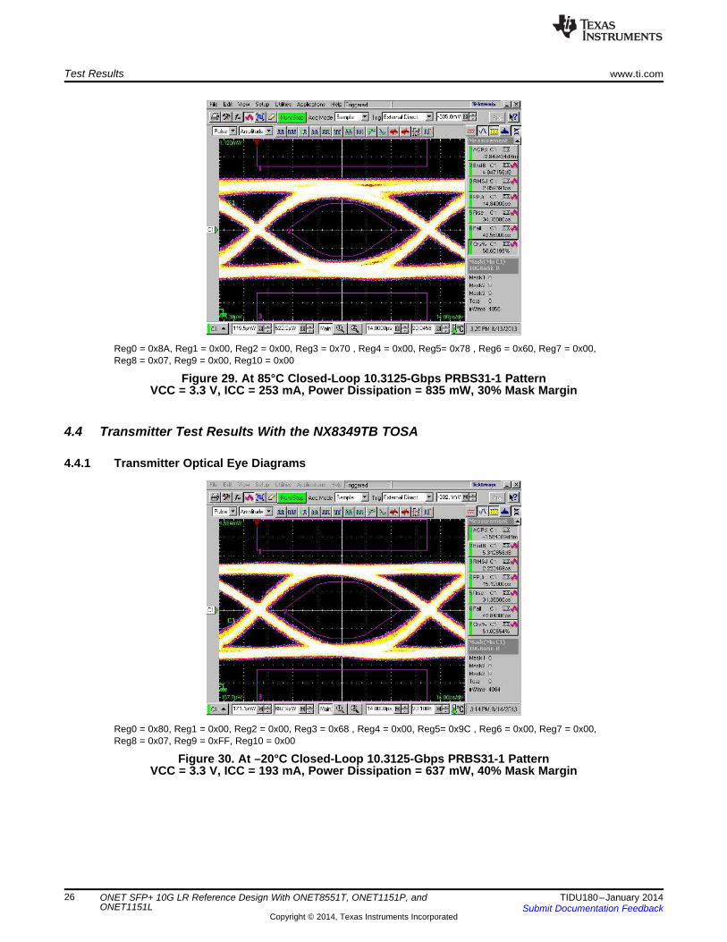
Reg0 = 0x8A, Reg1 = 0x00, Reg2 = 0x00, Reg3 = 0x70 , Reg4 = 0x00, Reg5= 0x78 , Reg6 = 0x60, Reg7 = 0x00,Reg8 = 0x07, Reg9 = 0x00, Reg10 = 0x00
Figure 29. At 85°C Closed-Loop 10.3125-Gbps PRBS31-1 PatternVCC = 3.3 V, ICC = 253 mA, Power Dissipation = 835 mW, 30% Mask Margin
4.4 Transmitter Test Results With the NX8349TB TOSA
4.4.1 Transmitter Optical Eye Diagrams
Reg0 = 0x80, Reg1 = 0x00, Reg2 = 0x00, Reg3 = 0x68 , Reg4 = 0x00, Reg5= 0x9C , Reg6 = 0x00, Reg7 = 0x00,Reg8 = 0x07, Reg9 = 0xFF, Reg10 = 0x00
Figure 30. At –20°C Closed-Loop 10.3125-Gbps PRBS31-1 PatternVCC = 3.3 V, ICC = 193 mA, Power Dissipation = 637 mW, 40% Mask Margin
26 ONET SFP+ 10G LR Reference Design With ONET8551T, ONET1151P, and TIDU180–January 2014ONET1151L Submit Documentation Feedback
Copyright © 2014, Texas Instruments Incorporated
www.ti.com Test Results
Reg0 = 0x80, Reg1 = 0x00, Reg2 = 0x00, Reg3 = 0x70 , Reg4 = 0x00, Reg5= 0x9C , Reg6 = 0x00, Reg7 = 0x00,Reg8 = 0x07, Reg9 = 0xFF, Reg10 = 0x00
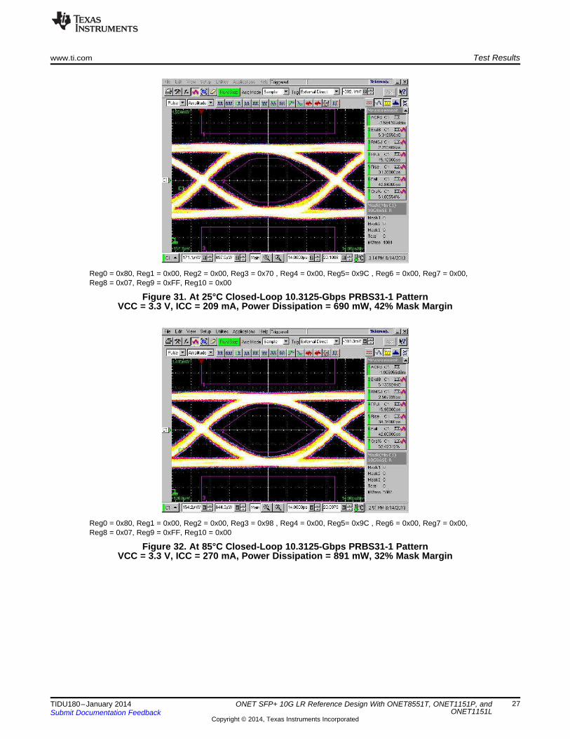
Figure 31. At 25°C Closed-Loop 10.3125-Gbps PRBS31-1 PatternVCC = 3.3 V, ICC = 209 mA, Power Dissipation = 690 mW, 42% Mask Margin
Reg0 = 0x80, Reg1 = 0x00, Reg2 = 0x00, Reg3 = 0x98 , Reg4 = 0x00, Reg5= 0x9C , Reg6 = 0x00, Reg7 = 0x00,Reg8 = 0x07, Reg9 = 0xFF, Reg10 = 0x00
Figure 32. At 85°C Closed-Loop 10.3125-Gbps PRBS31-1 PatternVCC = 3.3 V, ICC = 270 mA, Power Dissipation = 891 mW, 32% Mask Margin
27TIDU180–January 2014 ONET SFP+ 10G LR Reference Design With ONET8551T, ONET1151P, andONET1151LSubmit Documentation Feedback
Copyright © 2014, Texas Instruments Incorporated
Test Results www.ti.com
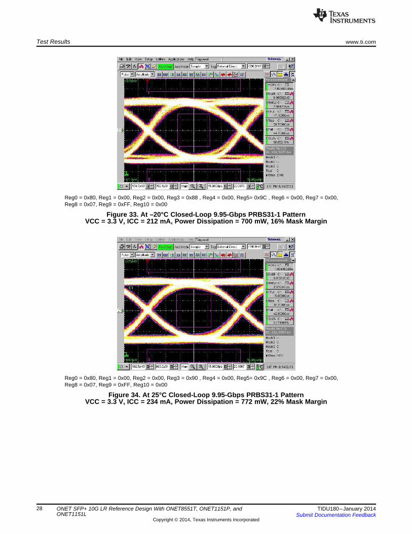
Reg0 = 0x80, Reg1 = 0x00, Reg2 = 0x00, Reg3 = 0x88 , Reg4 = 0x00, Reg5= 0x9C , Reg6 = 0x00, Reg7 = 0x00,Reg8 = 0x07, Reg9 = 0xFF, Reg10 = 0x00
Figure 33. At –20°C Closed-Loop 9.95-Gbps PRBS31-1 PatternVCC = 3.3 V, ICC = 212 mA, Power Dissipation = 700 mW, 16% Mask Margin
Reg0 = 0x80, Reg1 = 0x00, Reg2 = 0x00, Reg3 = 0x90 , Reg4 = 0x00, Reg5= 0x9C , Reg6 = 0x00, Reg7 = 0x00,Reg8 = 0x07, Reg9 = 0xFF, Reg10 = 0x00
Figure 34. At 25°C Closed-Loop 9.95-Gbps PRBS31-1 PatternVCC = 3.3 V, ICC = 234 mA, Power Dissipation = 772 mW, 22% Mask Margin
28 ONET SFP+ 10G LR Reference Design With ONET8551T, ONET1151P, and TIDU180–January 2014ONET1151L Submit Documentation Feedback
Copyright © 2014, Texas Instruments Incorporated
www.ti.com Test Results
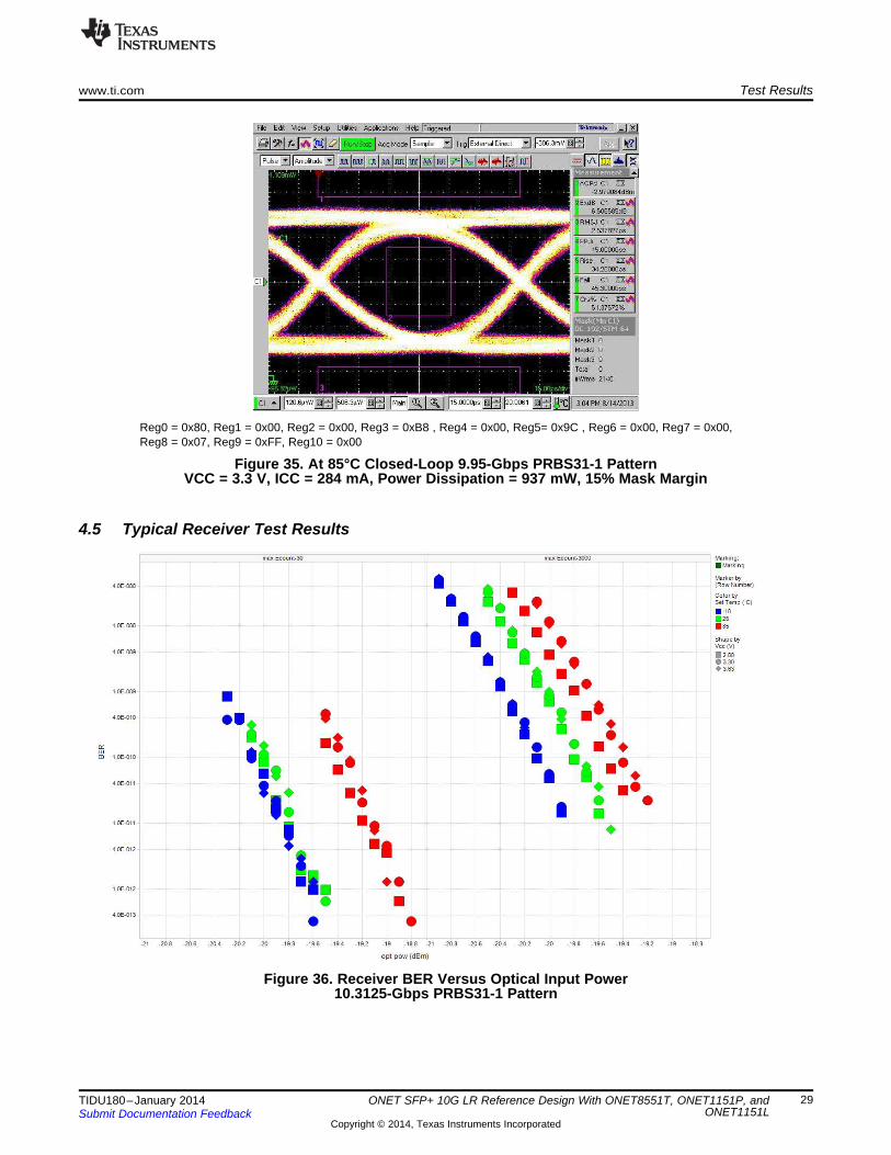
Reg0 = 0x80, Reg1 = 0x00, Reg2 = 0x00, Reg3 = 0xB8 , Reg4 = 0x00, Reg5= 0x9C , Reg6 = 0x00, Reg7 = 0x00,Reg8 = 0x07, Reg9 = 0xFF, Reg10 = 0x00
Figure 35. At 85°C Closed-Loop 9.95-Gbps PRBS31-1 PatternVCC = 3.3 V, ICC = 284 mA, Power Dissipation = 937 mW, 15% Mask Margin
4.5 Typical Receiver Test Results
Figure 36. Receiver BER Versus Optical Input Power10.3125-Gbps PRBS31-1 Pattern
29TIDU180–January 2014 ONET SFP+ 10G LR Reference Design With ONET8551T, ONET1151P, andONET1151LSubmit Documentation Feedback
Copyright © 2014, Texas Instruments Incorporated

IMPORTANT NOTICE FOR TI REFERENCE DESIGNSTexas Instruments Incorporated ("TI") reference designs are solely intended to assist designers (“Buyers”) who are developing systems thatincorporate TI semiconductor products (also referred to herein as “components”). Buyer understands and agrees that Buyer remainsresponsible for using its independent analysis, evaluation and judgment in designing Buyer’s systems and products.TI reference designs have been created using standard laboratory conditions and engineering practices. TI has not conducted anytesting other than that specifically described in the published documentation for a particular reference design. TI may makecorrections, enhancements, improvements and other changes to its reference designs.Buyers are authorized to use TI reference designs with the TI component(s) identified in each particular reference design and to modify thereference design in the development of their end products. HOWEVER, NO OTHER LICENSE, EXPRESS OR IMPLIED, BY ESTOPPELOR OTHERWISE TO ANY OTHER TI INTELLECTUAL PROPERTY RIGHT, AND NO LICENSE TO ANY THIRD PARTY TECHNOLOGYOR INTELLECTUAL PROPERTY RIGHT, IS GRANTED HEREIN, including but not limited to any patent right, copyright, mask work right,or other intellectual property right relating to any combination, machine, or process in which TI components or services are used.Information published by TI regarding third-party products or services does not constitute a license to use such products or services, or awarranty or endorsement thereof. Use of such information may require a license from a third party under the patents or other intellectualproperty of the third party, or a license from TI under the patents or other intellectual property of TI.TI REFERENCE DESIGNS ARE PROVIDED "AS IS". TI MAKES NO WARRANTIES OR REPRESENTATIONS WITH REGARD TO THEREFERENCE DESIGNS OR USE OF THE REFERENCE DESIGNS, EXPRESS, IMPLIED OR STATUTORY, INCLUDING ACCURACY ORCOMPLETENESS. TI DISCLAIMS ANY WARRANTY OF TITLE AND ANY IMPLIED WARRANTIES OF MERCHANTABILITY, FITNESSFOR A PARTICULAR PURPOSE, QUIET ENJOYMENT, QUIET POSSESSION, AND NON-INFRINGEMENT OF ANY THIRD PARTYINTELLECTUAL PROPERTY RIGHTS WITH REGARD TO TI REFERENCE DESIGNS OR USE THEREOF. TI SHALL NOT BE LIABLEFOR AND SHALL NOT DEFEND OR INDEMNIFY BUYERS AGAINST ANY THIRD PARTY INFRINGEMENT CLAIM THAT RELATES TOOR IS BASED ON A COMBINATION OF COMPONENTS PROVIDED IN A TI REFERENCE DESIGN. IN NO EVENT SHALL TI BELIABLE FOR ANY ACTUAL, SPECIAL, INCIDENTAL, CONSEQUENTIAL OR INDIRECT DAMAGES, HOWEVER CAUSED, ON ANYTHEORY OF LIABILITY AND WHETHER OR NOT TI HAS BEEN ADVISED OF THE POSSIBILITY OF SUCH DAMAGES, ARISING INANY WAY OUT OF TI REFERENCE DESIGNS OR BUYER’S USE OF TI REFERENCE DESIGNS.TI reserves the right to make corrections, enhancements, improvements and other changes to its semiconductor products and services perJESD46, latest issue, and to discontinue any product or service per JESD48, latest issue. Buyers should obtain the latest relevantinformation before placing orders and should verify that such information is current and complete. All semiconductor products are soldsubject to TI’s terms and conditions of sale supplied at the time of order acknowledgment.TI warrants performance of its components to the specifications applicable at the time of sale, in accordance with the warranty in TI’s termsand conditions of sale of semiconductor products. Testing and other quality control techniques for TI components are used to the extent TIdeems necessary to support this warranty. Except where mandated by applicable law, testing of all parameters of each component is notnecessarily performed.TI assumes no liability for applications assistance or the design of Buyers’ products. Buyers are responsible for their products andapplications using TI components. To minimize the risks associated with Buyers’ products and applications, Buyers should provideadequate design and operating safeguards.Reproduction of significant portions of TI information in TI data books, data sheets or reference designs is permissible only if reproduction iswithout alteration and is accompanied by all associated warranties, conditions, limitations, and notices. TI is not responsible or liable forsuch altered documentation. Information of third parties may be subject to additional restrictions.Buyer acknowledges and agrees that it is solely responsible for compliance with all legal, regulatory and safety-related requirementsconcerning its products, and any use of TI components in its applications, notwithstanding any applications-related information or supportthat may be provided by TI. Buyer represents and agrees that it has all the necessary expertise to create and implement safeguards thatanticipate dangerous failures, monitor failures and their consequences, lessen the likelihood of dangerous failures and take appropriateremedial actions. Buyer will fully indemnify TI and its representatives against any damages arising out of the use of any TI components inBuyer’s safety-critical applications.In some cases, TI components may be promoted specifically to facilitate safety-related applications. With such components, TI’s goal is tohelp enable customers to design and create their own end-product solutions that meet applicable functional safety standards andrequirements. Nonetheless, such components are subject to these terms.No TI components are authorized for use in FDA Class III (or similar life-critical medical equipment) unless authorized officers of the partieshave executed an agreement specifically governing such use.Only those TI components that TI has specifically designated as military grade or “enhanced plastic” are designed and intended for use inmilitary/aerospace applications or environments. Buyer acknowledges and agrees that any military or aerospace use of TI components thathave not been so designated is solely at Buyer's risk, and Buyer is solely responsible for compliance with all legal and regulatoryrequirements in connection with such use.TI has specifically designated certain components as meeting ISO/TS16949 requirements, mainly for automotive use. In any case of use ofnon-designated products, TI will not be responsible for any failure to meet ISO/TS16949.
Mailing Address: Texas Instruments, Post Office Box 655303, Dallas, Texas 75265Copyright © 2014, Texas Instruments Incorporated