Embed Size (px)
Citation preview
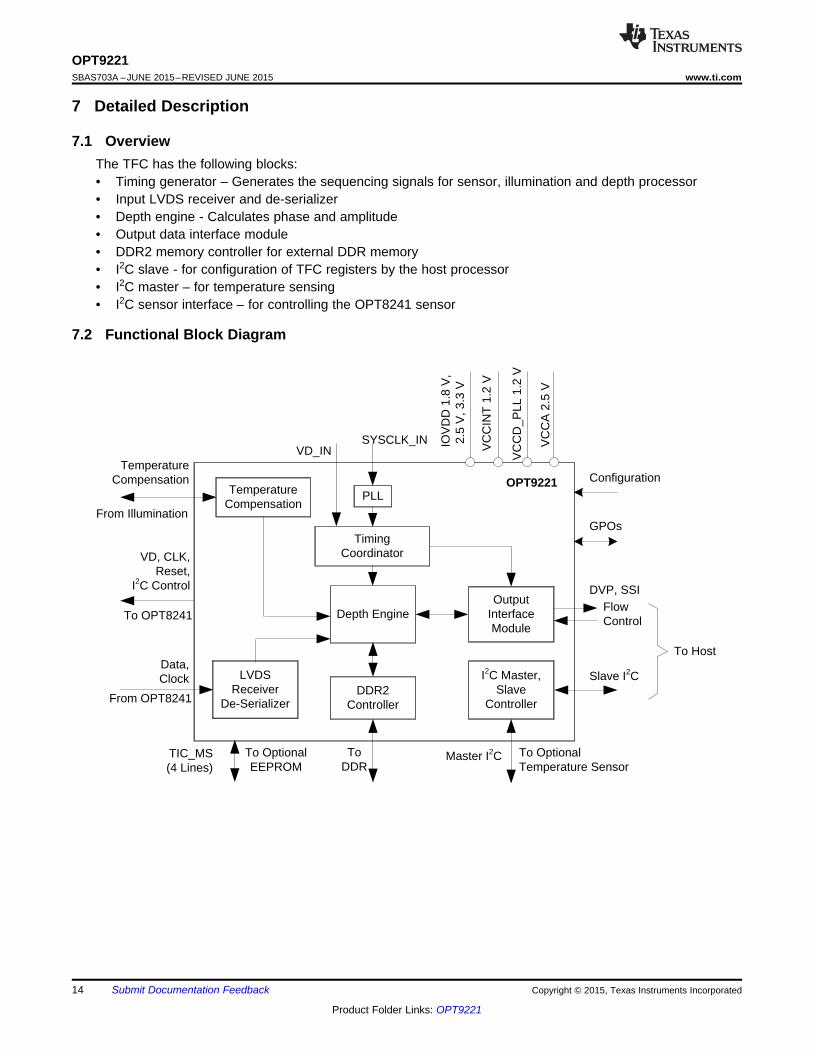
Depth Engine
Timing Coordinator
PLL
LVDS Receiver
De-SerializerDDR2
Controller
I2C Master, Slave
Controller
Output Interface Module
Data, Clock
DVP, SSI
VD_IN
GPOs
Slave I2C
Flow Control
Master I2C
Configuration
TIC_MS (4 Lines)
OPT9221Temperature
Compensation
SYSCLK_IN
VD, CLK, Reset,
I2C Control
Temperature Compensation
From Illumination
To OPT8241
From OPT8241
To DDR
To Optional EEPROM
To Optional Temperature Sensor
To Host
IOV
DD
1.8
V,
2.5
V, 3
.3 V
VC
CIN
T 1
.2 V
VC
CD
_PLL
1.2
V
VC
CA
2.5
V
Product
Folder
Sample &Buy
Technical
Documents
Tools &
Software
Support &Community
An IMPORTANT NOTICE at the end of this data sheet addresses availability, warranty, changes, use in safety-critical applications,intellectual property matters and other important disclaimers. PRODUCTION DATA.
OPT9221SBAS703A –JUNE 2015–REVISED JUNE 2015
OPT9221 Time-of-Flight Controller
1
1 Features1• QVGA 3D ToF Controller: Up to 120 FPS• Depth Data:
– 12-Bit Phase– Up to 12-Bit Amplitude– Up to 4-Bit Ambient– Saturation Detection
• Chipset Interface:– Compatible with TI ToF Sensor (OPT8241)
• Output (CMOS, 8-Lane Data, 8 Control Signals,and Clock):– Digital Video Protocol (DVP)-Compatible:
– Data, VD, HD, Clock– Synchronous Serial Interface (SSI)-Compatible
• Depth Engine:– Pixel Binning– Region of Interest (ROI)– De-Aliasing– Non-linearity Correction– Temperature Compensation– High Dynamic Range Operation– Spatial Filter
• Timing Coordinator:– Sensor Control– Master and Slave Sync Operation
• I2C Slave Interface• Power Supply: 1.2-V Core, 1.8-V I/O, 3.3-V I/O
2.5-V Analog• Package: 256-Pin, 9-mm × 9-mm NFBGA• Operating Temperature: 0°C to 85°C
2 Applications• 3D Imaging:
– Location and Proximity Sensing– 3D Scanning and 3D Machine Vision– Security and Surveillance– Gesture Controls
3 DescriptionThe time-of-flight controller (TFC) is a high-performance, 3D time-of-flight (ToF) sensorcompanion device that computes the depth data fromthe digitized sensor data. Depth data are output via aprogrammable complementary metal-oxide-semiconductor (CMOS) parallel interface.
In addition to depth data, the TFC provides auxiliaryinformation consisting of amplitude, ambient, andflags for each pixel. This information can be used toimplement filters and masks and to dynamicallycontrol the system configuration for the intendedperformance.
The TFC supports a wide range of binning and ROIoptions that help optimize the data throughput thatmust be handled.
The 9-mm × 9-mm NFBGA package enables smallform-factor, 3D, ToF systems that can be embeddedinto a variety of end equipment.
Device Information(1)
PART NUMBER PACKAGE BODY SIZE (NOM)OPT9221 NFBGA (256) 9.00 mm × 9.00 mm
(1) For all available packages, see the orderable addendum atthe end of the datasheet.
Functional Block Diagram
2
OPT9221SBAS703A –JUNE 2015–REVISED JUNE 2015 www.ti.com
Product Folder Links: OPT9221
Submit Documentation Feedback Copyright © 2015, Texas Instruments Incorporated
Table of Contents1 Features .................................................................. 12 Applications ........................................................... 13 Description ............................................................. 14 Revision History..................................................... 25 Pin Configuration and Functions ......................... 36 Specifications....................................................... 10
6.1 Absolute Maximum Ratings ................................... 106.2 ESD Ratings............................................................ 106.3 Recommended Operating Conditions..................... 116.4 Thermal Information ................................................ 116.5 Electrical Characteristics......................................... 126.6 Timing Requirements .............................................. 12
7 Detailed Description ............................................ 147.1 Overview ................................................................. 147.2 Functional Block Diagram ....................................... 147.3 Feature Description................................................. 157.4 Device Functional Modes........................................ 387.5 Programming........................................................... 38
7.6 Register Maps ......................................................... 438 Application and Implementation ........................ 97
8.1 Application Information............................................ 978.2 Typical Application .................................................. 97
9 Power Supply Recommendations ...................... 989.1 Power-Up Sequence ............................................... 98
10 Layout................................................................... 9910.1 Layout Guidelines ................................................. 9910.2 Layout Example .................................................. 100
11 Device and Documentation Support ............... 10111.1 Device Support.................................................... 10111.2 Documentation Support ...................................... 10111.3 Community Resources........................................ 10111.4 Trademarks ......................................................... 10111.5 Electrostatic Discharge Caution.......................... 10111.6 Glossary .............................................................. 101
12 Mechanical, Packaging, and OrderableInformation ......................................................... 101
4 Revision History
Changes from Original (June 2015) to Revision A Page
• Changed from Product Preview to Production Data .............................................................................................................. 1
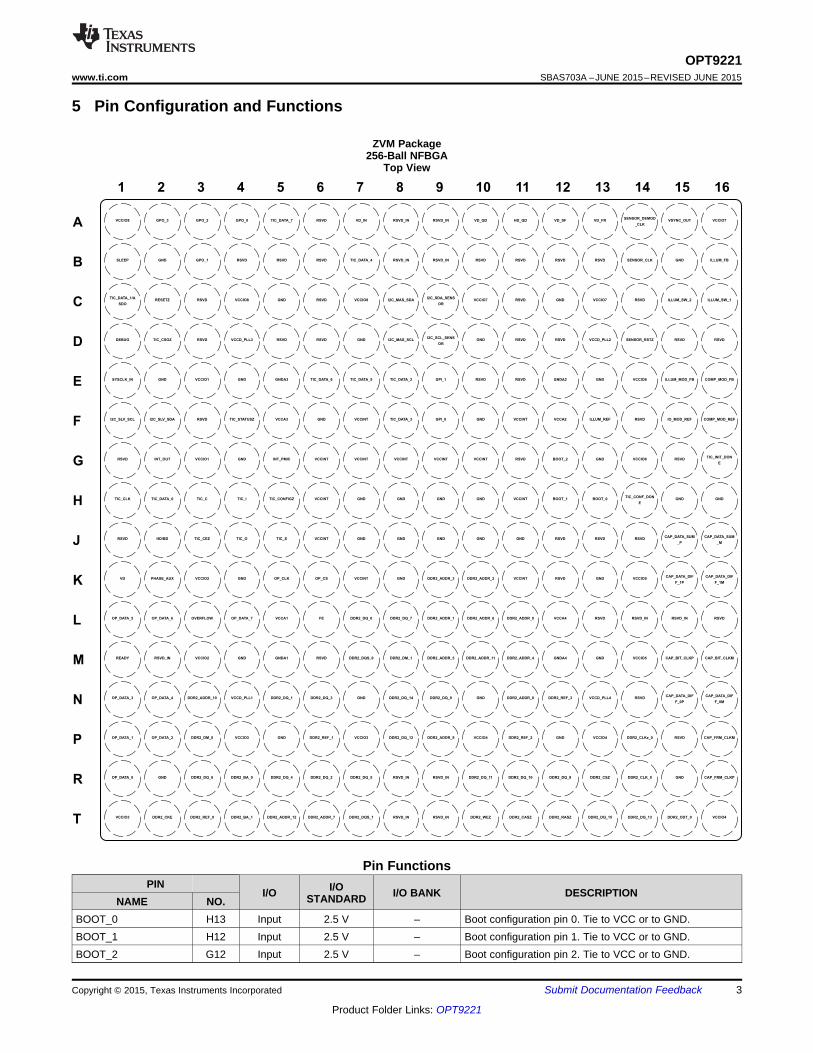
1 2 3 4 5 6 7 8 9 10 11 12 13 14 15 16
A
B
C
D
E
F
G
H
J
K
L
M
N
P
R
T
VCCIO8 GPO_3 GPO_2 GPO_0 TIC_DATA_7 RSVD VD_IN RSVD_IN RSVD_IN VD_QD HD_QD VD_SF VD_FRSENSOR_DEMOD
_CLKVSYNC_OUT VCCIO7
SLEEP GND GPO_1 RSVD RSVD RSVD TIC_DATA_4 RSVD_IN RSVD_IN RSVD RSVD RSVD RSVD SENSOR_CLK GND ILLUM_FB
TIC_DATA_1/A
SDORESETZ RSVD VCCIO8 GND RSVD VCCIO8 I2C_MAS_SDA
I2C_SDA_SENS
ORVCCIO7 RSVD GND VCCIO7 RSVD ILLUM_SW_2 ILLUM_SW_1
DEBUG TIC_CSOZ RSVD VCCD_PLL3 RSVD RSVD GND I2C_MAS_SCLI2C_SCL_SENS
ORGND RSVD RSVD VCCD_PLL2 SENSOR_RSTZ RSVD RSVD
SYSCLK_IN GND VCCIO1 GND GNDA3 TIC_DATA_6 TIC_DATA_5 TIC_DATA_2 GPI_1 RSVD RSVD GNDA2 GND VCCIO6 ILLUM_MOD_FB COMP_MOD_FB
I2C_SLV_SCL I2C_SLV_SDA RSVD TIC_STATUSZ VCCA3 GND VCCINT TIC_DATA_3 GPI_0 GND VCCINT VCCA2 ILLUM_REF RSVD IO_MOD_REF COMP_MOD_REF
RSVD INT_OUT VCCIO1 GND INT_PMIC VCCINT VCCINT VCCINT VCCINT VCCINT RSVD BOOT_2 GND VCCIO6 RSVDTIC_INIT_DON
E
TIC_CLK TIC_DATA_0 TIC_C TIC_I TIC_CONFIGZ VCCINT GND GND GND GND VCCINT BOOT_1 BOOT_0TIC_CONF_DON
EGND GND
RSVD HD/BD TIC_CEZ TIC_O TIC_S VCCINT GND GND GND GND GND RSVD RSVD RSVDCAP_DATA_SUM
_P
CAP_DATA_SUM
_M
VD PHASE_AUX VCCIO2 GND OP_CLK OP_CS VCCINT GND DDR2_ADDR_3 DDR2_ADDR_2 VCCINT RSVD GND VCCIO5CAP_DATA_DIF
F_1P
CAP_DATA_DIF
F_1M
OP_DATA_5 OP_DATA_6 OVERFLOW OP_DATA_7 VCCA1 FE DDR2_DQ_0 DDR2_DQ_7 DDR2_ADDR_1 DDR2_ADDR_6 DDR2_ADDR_0 VCCA4 RSVD RSVD_IN RSVD_IN RSVD
READY RSVD_IN VCCIO2 GND GNDA1 RSVD DDR2_DQS_0 DDR2_DM_1 DDR2_ADDR_5 DDR2_ADDR_11 DDR2_ADDR_4 GNDA4 GND VCCIO5 CAP_BIT_CLKP CAP_BIT_CLKM
OP_DATA_3 OP_DATA_4 DDR2_ADDR_10 VCCD_PLL1 DDR2_DQ_1 DDR2_DQ_3 GND DDR2_DQ_14 DDR2_DQ_9 GND DDR2_ADDR_8 DDR2_REF_3 VCCD_PLL4 RSVDCAP_DATA_DIF
F_0P
CAP_DATA_DIF
F_0M
OP_DATA_1 OP_DATA_2 DDR2_DM_0 VCCIO3 GND DDR2_REF_1 VCCIO3 DDR2_DQ_12 DDR2_ADDR_9 VCCIO4 DDR2_REF_2 GND VCCIO4 DDR2_CLKz_0 RSVD CAP_FRM_CLKM
OP_DATA_0 GND DDR2_DQ_6 DDR2_BA_0 DDR2_DQ_4 DDR2_DQ_2 DDR2_DQ_5 RSVD_IN RSVD_IN DDR2_DQ_11 DDR2_DQ_10 DDR2_DQ_8 DDR2_CSZ DDR2_CLK_0 GND CAP_FRM_CLKP
VCCIO3 DDR2_CKE DDR2_REF_0 DDR2_BA_1 DDR2_ADDR_12 DDR2_ADDR_7 DDR2_DQS_1 RSVD_IN RSVD_IN DDR2_WEZ DDR2_CASZ DDR2_RASZ DDR2_DQ_15 DDR2_DQ_13 DDR2_ODT_0 VCCIO4
3
OPT9221www.ti.com SBAS703A –JUNE 2015–REVISED JUNE 2015
Product Folder Links: OPT9221
Submit Documentation FeedbackCopyright © 2015, Texas Instruments Incorporated
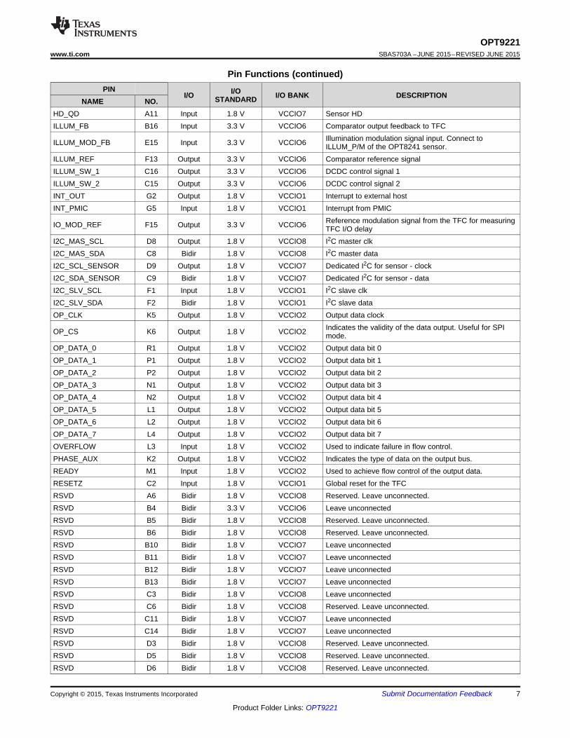
5 Pin Configuration and Functions
ZVM Package256-Ball NFBGA
Top View
Pin FunctionsPIN
I/O I/OSTANDARD I/O BANK DESCRIPTION
NAME NO.BOOT_0 H13 Input 2.5 V – Boot configuration pin 0. Tie to VCC or to GND.BOOT_1 H12 Input 2.5 V – Boot configuration pin 1. Tie to VCC or to GND.BOOT_2 G12 Input 2.5 V – Boot configuration pin 2. Tie to VCC or to GND.
4
OPT9221SBAS703A –JUNE 2015–REVISED JUNE 2015 www.ti.com
Product Folder Links: OPT9221
Submit Documentation Feedback Copyright © 2015, Texas Instruments Incorporated
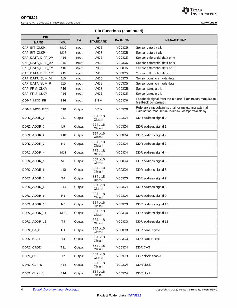
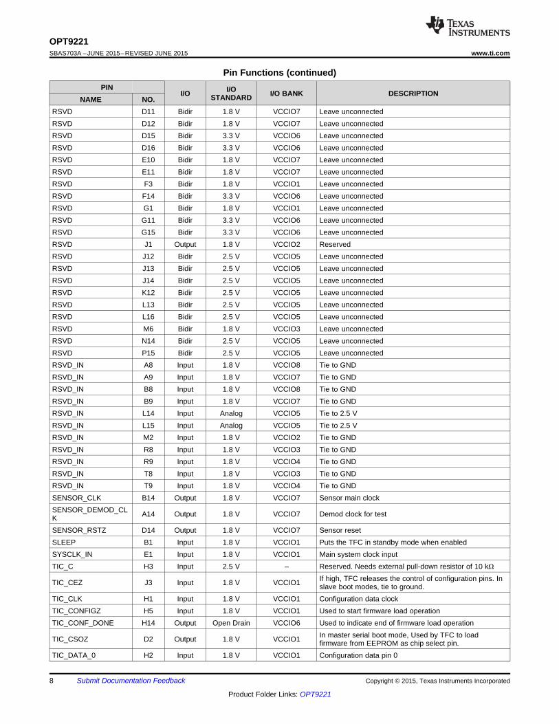
Pin Functions (continued)PIN
I/O I/OSTANDARD I/O BANK DESCRIPTION
NAME NO.CAP_BIT_CLKM M16 Input LVDS VCCIO5 Sensor data bit clkCAP_BIT_CLKP M15 Input LVDS VCCIO5 Sensor data bit clkCAP_DATA_DIFF_0M N16 Input LVDS VCCIO5 Sensor differential data ch 0CAP_DATA_DIFF_0P N15 Input LVDS VCCIO5 Sensor differential data ch 0CAP_DATA_DIFF_1M K16 Input LVDS VCCIO5 Sensor differential data ch 1CAP_DATA_DIFF_1P K15 Input LVDS VCCIO5 Sensor differential data ch 1CAP_DATA_SUM_M J16 Input LVDS VCCIO5 Sensor common mode dataCAP_DATA_SUM_P J15 Input LVDS VCCIO5 Sensor common mode dataCAP_FRM_CLKM P16 Input LVDS VCCIO5 Sensor sample clkCAP_FRM_CLKP R16 Input LVDS VCCIO5 Sensor sample clk
COMP_MOD_FB E16 Input 3.3 V VCCIO6 Feedback signal from the external illumination modulationfeedback comparator.
COMP_MOD_REF F16 Output 3.3 V VCCIO6 Reference modulation signal for measuring externalillumination modulation feedback comparator delay.
DDR2_ADDR_0 L11 Output SSTL-18Class I VCCIO4 DDR address signal 0
DDR2_ADDR_1 L9 Output SSTL-18Class I VCCIO4 DDR address signal 1
DDR2_ADDR_2 K10 Output SSTL-18Class I VCCIO4 DDR address signal 2
DDR2_ADDR_3 K9 Output SSTL-18Class I VCCIO4 DDR address signal 3
DDR2_ADDR_4 M11 Output SSTL-18Class I VCCIO4 DDR address signal 4
DDR2_ADDR_5 M9 Output SSTL-18Class I VCCIO4 DDR address signal 5
DDR2_ADDR_6 L10 Output SSTL-18Class I VCCIO4 DDR address signal 6
DDR2_ADDR_7 T6 Output SSTL-18Class I VCCIO3 DDR address signal 7
DDR2_ADDR_8 N11 Output SSTL-18Class I VCCIO4 DDR address signal 8
DDR2_ADDR_9 P9 Output SSTL-18Class I VCCIO4 DDR address signal 9
DDR2_ADDR_10 N3 Output SSTL-18Class I VCCIO3 DDR address signal 10
DDR2_ADDR_11 M10 Output SSTL-18Class I VCCIO4 DDR address signal 11
DDR2_ADDR_12 T5 Output SSTL-18Class I VCCIO3 DDR address signal 12
DDR2_BA_0 R4 Output SSTL-18Class I VCCIO3 DDR bank signal
DDR2_BA_1 T4 Output SSTL-18Class I VCCIO3 DDR bank signal
DDR2_CASZ T11 Output SSTL-18Class I VCCIO4 DDR CAS
DDR2_CKE T2 Output SSTL-18Class I VCCIO3 DDR clock enable
DDR2_CLK_0 R14 Output SSTL-18Class I VCCIO4 DDR clock
DDR2_CLKz_0 P14 Output SSTL-18Class I VCCIO4 DDR clock
5
OPT9221www.ti.com SBAS703A –JUNE 2015–REVISED JUNE 2015
Product Folder Links: OPT9221
Submit Documentation FeedbackCopyright © 2015, Texas Instruments Incorporated
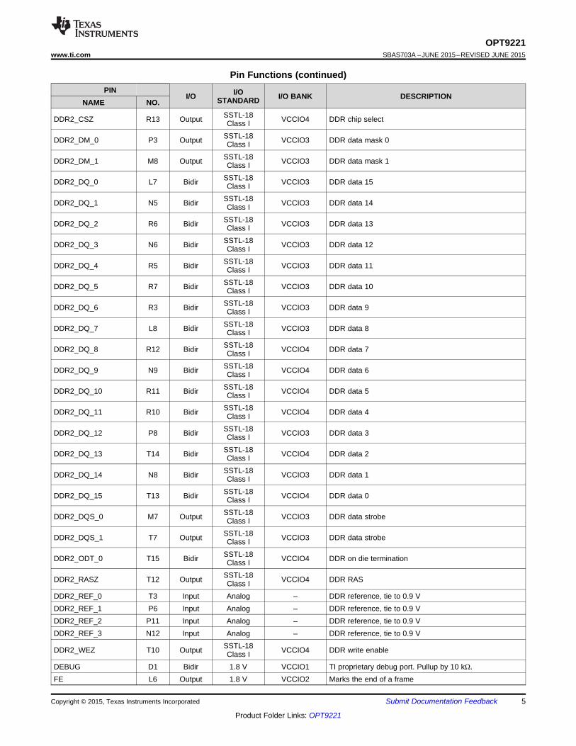
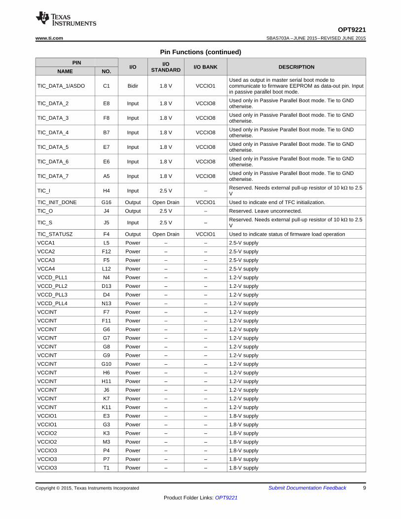
Pin Functions (continued)PIN
I/O I/OSTANDARD I/O BANK DESCRIPTION
NAME NO.
DDR2_CSZ R13 Output SSTL-18Class I VCCIO4 DDR chip select
DDR2_DM_0 P3 Output SSTL-18Class I VCCIO3 DDR data mask 0
DDR2_DM_1 M8 Output SSTL-18Class I VCCIO3 DDR data mask 1
DDR2_DQ_0 L7 Bidir SSTL-18Class I VCCIO3 DDR data 15
DDR2_DQ_1 N5 Bidir SSTL-18Class I VCCIO3 DDR data 14
DDR2_DQ_2 R6 Bidir SSTL-18Class I VCCIO3 DDR data 13
DDR2_DQ_3 N6 Bidir SSTL-18Class I VCCIO3 DDR data 12
DDR2_DQ_4 R5 Bidir SSTL-18Class I VCCIO3 DDR data 11
DDR2_DQ_5 R7 Bidir SSTL-18Class I VCCIO3 DDR data 10
DDR2_DQ_6 R3 Bidir SSTL-18Class I VCCIO3 DDR data 9
DDR2_DQ_7 L8 Bidir SSTL-18Class I VCCIO3 DDR data 8
DDR2_DQ_8 R12 Bidir SSTL-18Class I VCCIO4 DDR data 7
DDR2_DQ_9 N9 Bidir SSTL-18Class I VCCIO4 DDR data 6
DDR2_DQ_10 R11 Bidir SSTL-18Class I VCCIO4 DDR data 5
DDR2_DQ_11 R10 Bidir SSTL-18Class I VCCIO4 DDR data 4
DDR2_DQ_12 P8 Bidir SSTL-18Class I VCCIO3 DDR data 3
DDR2_DQ_13 T14 Bidir SSTL-18Class I VCCIO4 DDR data 2
DDR2_DQ_14 N8 Bidir SSTL-18Class I VCCIO3 DDR data 1
DDR2_DQ_15 T13 Bidir SSTL-18Class I VCCIO4 DDR data 0
DDR2_DQS_0 M7 Output SSTL-18Class I VCCIO3 DDR data strobe
DDR2_DQS_1 T7 Output SSTL-18Class I VCCIO3 DDR data strobe
DDR2_ODT_0 T15 Bidir SSTL-18Class I VCCIO4 DDR on die termination
DDR2_RASZ T12 Output SSTL-18Class I VCCIO4 DDR RAS
DDR2_REF_0 T3 Input Analog – DDR reference, tie to 0.9 VDDR2_REF_1 P6 Input Analog – DDR reference, tie to 0.9 VDDR2_REF_2 P11 Input Analog – DDR reference, tie to 0.9 VDDR2_REF_3 N12 Input Analog – DDR reference, tie to 0.9 V
DDR2_WEZ T10 Output SSTL-18Class I VCCIO4 DDR write enable
DEBUG D1 Bidir 1.8 V VCCIO1 TI proprietary debug port. Pullup by 10 kΩ.FE L6 Output 1.8 V VCCIO2 Marks the end of a frame
6
OPT9221SBAS703A –JUNE 2015–REVISED JUNE 2015 www.ti.com
Product Folder Links: OPT9221
Submit Documentation Feedback Copyright © 2015, Texas Instruments Incorporated
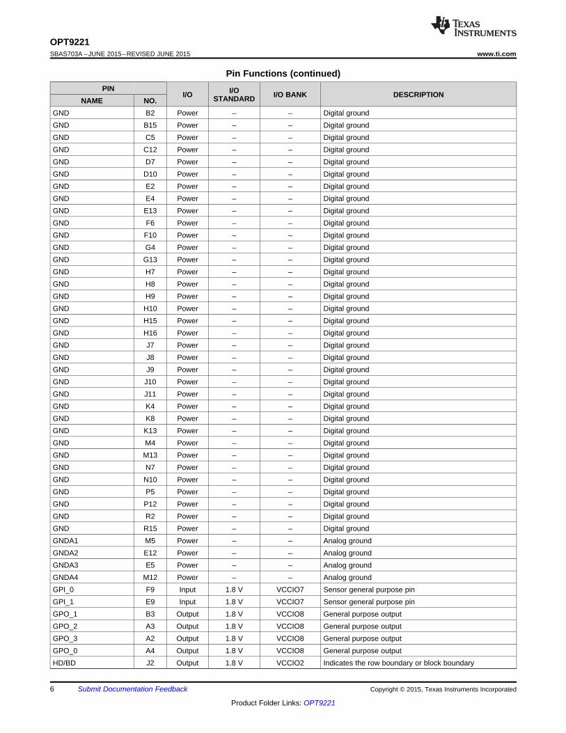
Pin Functions (continued)PIN
I/O I/OSTANDARD I/O BANK DESCRIPTION
NAME NO.GND B2 Power – – Digital groundGND B15 Power – – Digital groundGND C5 Power – – Digital groundGND C12 Power – – Digital groundGND D7 Power – – Digital groundGND D10 Power – – Digital groundGND E2 Power – – Digital groundGND E4 Power – – Digital groundGND E13 Power – – Digital groundGND F6 Power – – Digital groundGND F10 Power – – Digital groundGND G4 Power – – Digital groundGND G13 Power – – Digital groundGND H7 Power – – Digital groundGND H8 Power – – Digital groundGND H9 Power – – Digital groundGND H10 Power – – Digital groundGND H15 Power – – Digital groundGND H16 Power – – Digital groundGND J7 Power – – Digital groundGND J8 Power – – Digital groundGND J9 Power – – Digital groundGND J10 Power – – Digital groundGND J11 Power – – Digital groundGND K4 Power – – Digital groundGND K8 Power – – Digital groundGND K13 Power – – Digital groundGND M4 Power – – Digital groundGND M13 Power – – Digital groundGND N7 Power – – Digital groundGND N10 Power – – Digital groundGND P5 Power – – Digital groundGND P12 Power – – Digital groundGND R2 Power – – Digital groundGND R15 Power – – Digital groundGNDA1 M5 Power – – Analog groundGNDA2 E12 Power – – Analog groundGNDA3 E5 Power – – Analog groundGNDA4 M12 Power – – Analog groundGPI_0 F9 Input 1.8 V VCCIO7 Sensor general purpose pinGPI_1 E9 Input 1.8 V VCCIO7 Sensor general purpose pinGPO_1 B3 Output 1.8 V VCCIO8 General purpose outputGPO_2 A3 Output 1.8 V VCCIO8 General purpose outputGPO_3 A2 Output 1.8 V VCCIO8 General purpose outputGPO_0 A4 Output 1.8 V VCCIO8 General purpose outputHD/BD J2 Output 1.8 V VCCIO2 Indicates the row boundary or block boundary
7
OPT9221www.ti.com SBAS703A –JUNE 2015–REVISED JUNE 2015
Product Folder Links: OPT9221
Submit Documentation FeedbackCopyright © 2015, Texas Instruments Incorporated
Pin Functions (continued)PIN
I/O I/OSTANDARD I/O BANK DESCRIPTION
NAME NO.HD_QD A11 Input 1.8 V VCCIO7 Sensor HDILLUM_FB B16 Input 3.3 V VCCIO6 Comparator output feedback to TFC
ILLUM_MOD_FB E15 Input 3.3 V VCCIO6 Illumination modulation signal input. Connect toILLUM_P/M of the OPT8241 sensor.
ILLUM_REF F13 Output 3.3 V VCCIO6 Comparator reference signalILLUM_SW_1 C16 Output 3.3 V VCCIO6 DCDC control signal 1ILLUM_SW_2 C15 Output 3.3 V VCCIO6 DCDC control signal 2INT_OUT G2 Output 1.8 V VCCIO1 Interrupt to external hostINT_PMIC G5 Input 1.8 V VCCIO1 Interrupt from PMIC
IO_MOD_REF F15 Output 3.3 V VCCIO6 Reference modulation signal from the TFC for measuringTFC I/O delay
I2C_MAS_SCL D8 Output 1.8 V VCCIO8 I2C master clkI2C_MAS_SDA C8 Bidir 1.8 V VCCIO8 I2C master dataI2C_SCL_SENSOR D9 Output 1.8 V VCCIO7 Dedicated I2C for sensor - clockI2C_SDA_SENSOR C9 Bidir 1.8 V VCCIO7 Dedicated I2C for sensor - dataI2C_SLV_SCL F1 Input 1.8 V VCCIO1 I2C slave clkI2C_SLV_SDA F2 Bidir 1.8 V VCCIO1 I2C slave dataOP_CLK K5 Output 1.8 V VCCIO2 Output data clock
OP_CS K6 Output 1.8 V VCCIO2 Indicates the validity of the data output. Useful for SPImode.
OP_DATA_0 R1 Output 1.8 V VCCIO2 Output data bit 0OP_DATA_1 P1 Output 1.8 V VCCIO2 Output data bit 1OP_DATA_2 P2 Output 1.8 V VCCIO2 Output data bit 2OP_DATA_3 N1 Output 1.8 V VCCIO2 Output data bit 3OP_DATA_4 N2 Output 1.8 V VCCIO2 Output data bit 4OP_DATA_5 L1 Output 1.8 V VCCIO2 Output data bit 5OP_DATA_6 L2 Output 1.8 V VCCIO2 Output data bit 6OP_DATA_7 L4 Output 1.8 V VCCIO2 Output data bit 7OVERFLOW L3 Input 1.8 V VCCIO2 Used to indicate failure in flow control.PHASE_AUX K2 Output 1.8 V VCCIO2 Indicates the type of data on the output bus.READY M1 Input 1.8 V VCCIO2 Used to achieve flow control of the output data.RESETZ C2 Input 1.8 V VCCIO1 Global reset for the TFCRSVD A6 Bidir 1.8 V VCCIO8 Reserved. Leave unconnected.RSVD B4 Bidir 3.3 V VCCIO6 Leave unconnectedRSVD B5 Bidir 1.8 V VCCIO8 Reserved. Leave unconnected.RSVD B6 Bidir 1.8 V VCCIO8 Reserved. Leave unconnected.RSVD B10 Bidir 1.8 V VCCIO7 Leave unconnectedRSVD B11 Bidir 1.8 V VCCIO7 Leave unconnectedRSVD B12 Bidir 1.8 V VCCIO7 Leave unconnectedRSVD B13 Bidir 1.8 V VCCIO7 Leave unconnectedRSVD C3 Bidir 1.8 V VCCIO8 Leave unconnectedRSVD C6 Bidir 1.8 V VCCIO8 Reserved. Leave unconnected.RSVD C11 Bidir 1.8 V VCCIO7 Leave unconnectedRSVD C14 Bidir 1.8 V VCCIO7 Leave unconnectedRSVD D3 Bidir 1.8 V VCCIO8 Reserved. Leave unconnected.RSVD D5 Bidir 1.8 V VCCIO8 Reserved. Leave unconnected.RSVD D6 Bidir 1.8 V VCCIO8 Reserved. Leave unconnected.
8
OPT9221SBAS703A –JUNE 2015–REVISED JUNE 2015 www.ti.com
Product Folder Links: OPT9221
Submit Documentation Feedback Copyright © 2015, Texas Instruments Incorporated
Pin Functions (continued)PIN
I/O I/OSTANDARD I/O BANK DESCRIPTION
NAME NO.RSVD D11 Bidir 1.8 V VCCIO7 Leave unconnectedRSVD D12 Bidir 1.8 V VCCIO7 Leave unconnectedRSVD D15 Bidir 3.3 V VCCIO6 Leave unconnectedRSVD D16 Bidir 3.3 V VCCIO6 Leave unconnectedRSVD E10 Bidir 1.8 V VCCIO7 Leave unconnectedRSVD E11 Bidir 1.8 V VCCIO7 Leave unconnectedRSVD F3 Bidir 1.8 V VCCIO1 Leave unconnectedRSVD F14 Bidir 3.3 V VCCIO6 Leave unconnectedRSVD G1 Bidir 1.8 V VCCIO1 Leave unconnectedRSVD G11 Bidir 3.3 V VCCIO6 Leave unconnectedRSVD G15 Bidir 3.3 V VCCIO6 Leave unconnectedRSVD J1 Output 1.8 V VCCIO2 ReservedRSVD J12 Bidir 2.5 V VCCIO5 Leave unconnectedRSVD J13 Bidir 2.5 V VCCIO5 Leave unconnectedRSVD J14 Bidir 2.5 V VCCIO5 Leave unconnectedRSVD K12 Bidir 2.5 V VCCIO5 Leave unconnectedRSVD L13 Bidir 2.5 V VCCIO5 Leave unconnectedRSVD L16 Bidir 2.5 V VCCIO5 Leave unconnectedRSVD M6 Bidir 1.8 V VCCIO3 Leave unconnectedRSVD N14 Bidir 2.5 V VCCIO5 Leave unconnectedRSVD P15 Bidir 2.5 V VCCIO5 Leave unconnectedRSVD_IN A8 Input 1.8 V VCCIO8 Tie to GNDRSVD_IN A9 Input 1.8 V VCCIO7 Tie to GNDRSVD_IN B8 Input 1.8 V VCCIO8 Tie to GNDRSVD_IN B9 Input 1.8 V VCCIO7 Tie to GNDRSVD_IN L14 Input Analog VCCIO5 Tie to 2.5 VRSVD_IN L15 Input Analog VCCIO5 Tie to 2.5 VRSVD_IN M2 Input 1.8 V VCCIO2 Tie to GNDRSVD_IN R8 Input 1.8 V VCCIO3 Tie to GNDRSVD_IN R9 Input 1.8 V VCCIO4 Tie to GNDRSVD_IN T8 Input 1.8 V VCCIO3 Tie to GNDRSVD_IN T9 Input 1.8 V VCCIO4 Tie to GNDSENSOR_CLK B14 Output 1.8 V VCCIO7 Sensor main clockSENSOR_DEMOD_CLK A14 Output 1.8 V VCCIO7 Demod clock for test
SENSOR_RSTZ D14 Output 1.8 V VCCIO7 Sensor resetSLEEP B1 Input 1.8 V VCCIO1 Puts the TFC in standby mode when enabledSYSCLK_IN E1 Input 1.8 V VCCIO1 Main system clock inputTIC_C H3 Input 2.5 V – Reserved. Needs external pull-down resistor of 10 kΩ
TIC_CEZ J3 Input 1.8 V VCCIO1 If high, TFC releases the control of configuration pins. Inslave boot modes, tie to ground.
TIC_CLK H1 Input 1.8 V VCCIO1 Configuration data clockTIC_CONFIGZ H5 Input 1.8 V VCCIO1 Used to start firmware load operationTIC_CONF_DONE H14 Output Open Drain VCCIO6 Used to indicate end of firmware load operation
TIC_CSOZ D2 Output 1.8 V VCCIO1 In master serial boot mode, Used by TFC to loadfirmware from EEPROM as chip select pin.
TIC_DATA_0 H2 Input 1.8 V VCCIO1 Configuration data pin 0
9
OPT9221www.ti.com SBAS703A –JUNE 2015–REVISED JUNE 2015
Product Folder Links: OPT9221
Submit Documentation FeedbackCopyright © 2015, Texas Instruments Incorporated
Pin Functions (continued)PIN
I/O I/OSTANDARD I/O BANK DESCRIPTION
NAME NO.
TIC_DATA_1/ASDO C1 Bidir 1.8 V VCCIO1Used as output in master serial boot mode tocommunicate to firmware EEPROM as data-out pin. Inputin passive parallel boot mode.
TIC_DATA_2 E8 Input 1.8 V VCCIO8 Used only in Passive Parallel Boot mode. Tie to GNDotherwise.
TIC_DATA_3 F8 Input 1.8 V VCCIO8 Used only in Passive Parallel Boot mode. Tie to GNDotherwise.
TIC_DATA_4 B7 Input 1.8 V VCCIO8 Used only in Passive Parallel Boot mode. Tie to GNDotherwise.
TIC_DATA_5 E7 Input 1.8 V VCCIO8 Used only in Passive Parallel Boot mode. Tie to GNDotherwise.
TIC_DATA_6 E6 Input 1.8 V VCCIO8 Used only in Passive Parallel Boot mode. Tie to GNDotherwise.
TIC_DATA_7 A5 Input 1.8 V VCCIO8 Used only in Passive Parallel Boot mode. Tie to GNDotherwise.
TIC_I H4 Input 2.5 V – Reserved. Needs external pull-up resistor of 10 kΩ to 2.5V
TIC_INIT_DONE G16 Output Open Drain VCCIO1 Used to indicate end of TFC initialization.TIC_O J4 Output 2.5 V – Reserved. Leave unconnected.
TIC_S J5 Input 2.5 V – Reserved. Needs external pull-up resistor of 10 kΩ to 2.5V
TIC_STATUSZ F4 Output Open Drain VCCIO1 Used to indicate status of firmware load operationVCCA1 L5 Power – – 2.5-V supplyVCCA2 F12 Power – – 2.5-V supplyVCCA3 F5 Power – – 2.5-V supplyVCCA4 L12 Power – – 2.5-V supplyVCCD_PLL1 N4 Power – – 1.2-V supplyVCCD_PLL2 D13 Power – – 1.2-V supplyVCCD_PLL3 D4 Power – – 1.2-V supplyVCCD_PLL4 N13 Power – – 1.2-V supplyVCCINT F7 Power – – 1.2-V supplyVCCINT F11 Power – – 1.2-V supplyVCCINT G6 Power – – 1.2-V supplyVCCINT G7 Power – – 1.2-V supplyVCCINT G8 Power – – 1.2-V supplyVCCINT G9 Power – – 1.2-V supplyVCCINT G10 Power – – 1.2-V supplyVCCINT H6 Power – – 1.2-V supplyVCCINT H11 Power – – 1.2-V supplyVCCINT J6 Power – – 1.2-V supplyVCCINT K7 Power – – 1.2-V supplyVCCINT K11 Power – – 1.2-V supplyVCCIO1 E3 Power – – 1.8-V supplyVCCIO1 G3 Power – – 1.8-V supplyVCCIO2 K3 Power – – 1.8-V supplyVCCIO2 M3 Power – – 1.8-V supplyVCCIO3 P4 Power – – 1.8-V supplyVCCIO3 P7 Power – – 1.8-V supplyVCCIO3 T1 Power – – 1.8-V supply
10
OPT9221SBAS703A –JUNE 2015–REVISED JUNE 2015 www.ti.com
Product Folder Links: OPT9221
Submit Documentation Feedback Copyright © 2015, Texas Instruments Incorporated
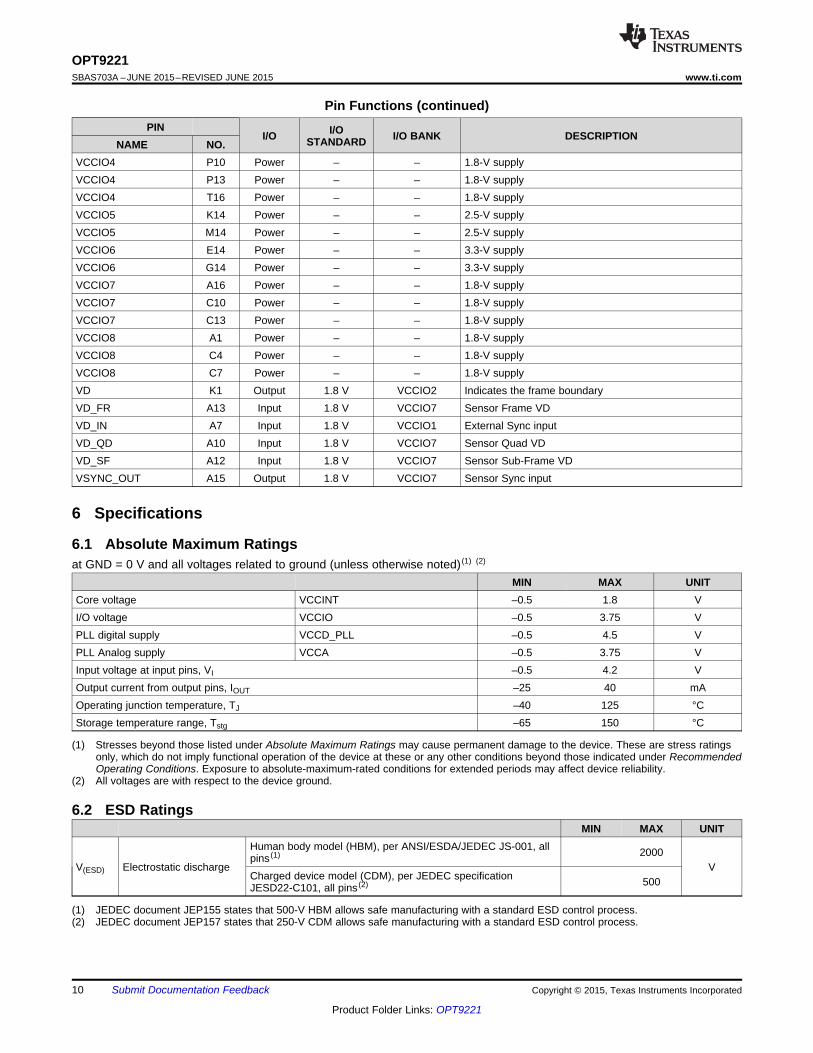
Pin Functions (continued)PIN
I/O I/OSTANDARD I/O BANK DESCRIPTION
NAME NO.VCCIO4 P10 Power – – 1.8-V supplyVCCIO4 P13 Power – – 1.8-V supplyVCCIO4 T16 Power – – 1.8-V supplyVCCIO5 K14 Power – – 2.5-V supplyVCCIO5 M14 Power – – 2.5-V supplyVCCIO6 E14 Power – – 3.3-V supplyVCCIO6 G14 Power – – 3.3-V supplyVCCIO7 A16 Power – – 1.8-V supplyVCCIO7 C10 Power – – 1.8-V supplyVCCIO7 C13 Power – – 1.8-V supplyVCCIO8 A1 Power – – 1.8-V supplyVCCIO8 C4 Power – – 1.8-V supplyVCCIO8 C7 Power – – 1.8-V supplyVD K1 Output 1.8 V VCCIO2 Indicates the frame boundaryVD_FR A13 Input 1.8 V VCCIO7 Sensor Frame VDVD_IN A7 Input 1.8 V VCCIO1 External Sync inputVD_QD A10 Input 1.8 V VCCIO7 Sensor Quad VDVD_SF A12 Input 1.8 V VCCIO7 Sensor Sub-Frame VDVSYNC_OUT A15 Output 1.8 V VCCIO7 Sensor Sync input
(1) Stresses beyond those listed under Absolute Maximum Ratings may cause permanent damage to the device. These are stress ratingsonly, which do not imply functional operation of the device at these or any other conditions beyond those indicated under RecommendedOperating Conditions. Exposure to absolute-maximum-rated conditions for extended periods may affect device reliability.
(2) All voltages are with respect to the device ground.
6 Specifications
6.1 Absolute Maximum Ratingsat GND = 0 V and all voltages related to ground (unless otherwise noted) (1) (2)
MIN MAX UNITCore voltage VCCINT –0.5 1.8 VI/O voltage VCCIO –0.5 3.75 VPLL digital supply VCCD_PLL –0.5 4.5 VPLL Analog supply VCCA –0.5 3.75 VInput voltage at input pins, VI –0.5 4.2 VOutput current from output pins, IOUT –25 40 mAOperating junction temperature, TJ –40 125 °CStorage temperature range, Tstg –65 150 °C
(1) JEDEC document JEP155 states that 500-V HBM allows safe manufacturing with a standard ESD control process.(2) JEDEC document JEP157 states that 250-V CDM allows safe manufacturing with a standard ESD control process.
6.2 ESD RatingsMIN MAX UNIT
V(ESD) Electrostatic discharge
Human body model (HBM), per ANSI/ESDA/JEDEC JS-001, allpins (1) 2000
VCharged device model (CDM), per JEDEC specificationJESD22-C101, all pins (2) 500
11
OPT9221www.ti.com SBAS703A –JUNE 2015–REVISED JUNE 2015
Product Folder Links: OPT9221
Submit Documentation FeedbackCopyright © 2015, Texas Instruments Incorporated
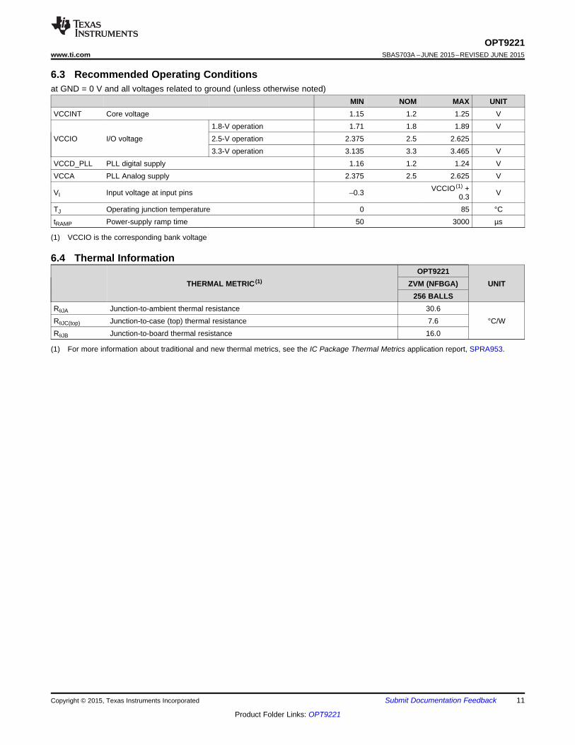
(1) VCCIO is the corresponding bank voltage
6.3 Recommended Operating Conditionsat GND = 0 V and all voltages related to ground (unless otherwise noted)
MIN NOM MAX UNITVCCINT Core voltage 1.15 1.2 1.25 V
VCCIO I/O voltage1.8-V operation 1.71 1.8 1.89 V2.5-V operation 2.375 2.5 2.6253.3-V operation 3.135 3.3 3.465 V
VCCD_PLL PLL digital supply 1.16 1.2 1.24 VVCCA PLL Analog supply 2.375 2.5 2.625 V
VI Input voltage at input pins –0.3 VCCIO (1) +0.3 V
TJ Operating junction temperature 0 85 °CtRAMP Power-supply ramp time 50 3000 µs
(1) For more information about traditional and new thermal metrics, see the IC Package Thermal Metrics application report, SPRA953.
6.4 Thermal Information
THERMAL METRIC (1)OPT9221
UNITZVM (NFBGA)256 BALLS
RθJA Junction-to-ambient thermal resistance 30.6°C/WRθJC(top) Junction-to-case (top) thermal resistance 7.6
RθJB Junction-to-board thermal resistance 16.0
12
OPT9221SBAS703A –JUNE 2015–REVISED JUNE 2015 www.ti.com
Product Folder Links: OPT9221
Submit Documentation Feedback Copyright © 2015, Texas Instruments Incorporated
(1) VCCIO is the corresponding bank voltage.(2) For, 0 < Input voltage < VCCIO.
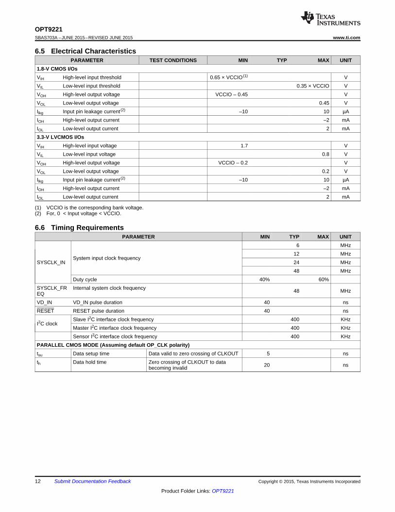
6.5 Electrical CharacteristicsPARAMETER TEST CONDITIONS MIN TYP MAX UNIT
1.8-V CMOS I/OsVIH High-level input threshold 0.65 × VCCIO (1) VVIL Low-level input threshold 0.35 × VCCIO VVOH High-level output voltage VCCIO – 0.45 VVOL Low-level output voltage 0.45 VIlkg Input pin leakage current (2) –10 10 µAIOH High-level output current –2 mAIOL Low-level output current 2 mA3.3-V LVCMOS I/OsVIH High-level input voltage 1.7 VVIL Low-level input voltage 0.8 VVOH High-level output voltage VCCIO – 0.2 VVOL Low-level output voltage 0.2 VIlkg Input pin leakage current (2) –10 10 µAIOH High-level output current –2 mAIOL Low-level output current 2 mA
6.6 Timing RequirementsPARAMETER MIN TYP MAX UNIT
SYSCLK_INSystem input clock frequency
6 MHz12 MHz24 MHz48 MHz
Duty cycle 40% 60%SYSCLK_FREQ
Internal system clock frequency 48 MHz
VD_IN VD_IN pulse duration 40 nsRESET RESET pulse duration 40 ns
I2C clockSlave I2C interface clock frequency 400 KHzMaster I2C interface clock frequency 400 KHzSensor I2C interface clock frequency 400 KHz
PARALLEL CMOS MODE (Assuming default OP_CLK polarity)tsu Data setup time Data valid to zero crossing of CLKOUT 5 nsth Data hold time Zero crossing of CLKOUT to data
becoming invalid 20 ns
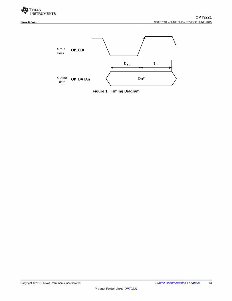
OP_CLKOP_CLK
t sut su
Dn*
t ht h
OP_DATAnOP_DATAnOutput
data
Output
data
Output
clock
Output
clock
13
OPT9221www.ti.com SBAS703A –JUNE 2015–REVISED JUNE 2015
Product Folder Links: OPT9221
Submit Documentation FeedbackCopyright © 2015, Texas Instruments Incorporated
Figure 1. Timing Diagram
Depth Engine
Timing Coordinator
PLL
LVDS Receiver
De-SerializerDDR2
Controller
I2C Master, Slave
Controller
Output Interface Module
Data, Clock
DVP, SSI
VD_IN
GPOs
Slave I2C
Flow Control
Master I2C
Configuration
TIC_MS (4 Lines)
OPT9221Temperature
Compensation
SYSCLK_IN
VD, CLK, Reset,
I2C Control
Temperature Compensation
From Illumination
To OPT8241
From OPT8241
To DDR
To Optional EEPROM
To Optional Temperature Sensor
To Host
IOV
DD
1.8
V,
2.5
V, 3
.3 V
VC
CIN
T 1
.2 V
VC
CD
_PLL
1.2
V
VC
CA
2.5
V
14
OPT9221SBAS703A –JUNE 2015–REVISED JUNE 2015 www.ti.com
Product Folder Links: OPT9221
Submit Documentation Feedback Copyright © 2015, Texas Instruments Incorporated
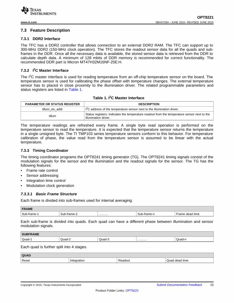
7 Detailed Description
7.1 OverviewThe TFC has the following blocks:• Timing generator – Generates the sequencing signals for sensor, illumination and depth processor• Input LVDS receiver and de-serializer• Depth engine - Calculates phase and amplitude• Output data interface module• DDR2 memory controller for external DDR memory• I2C slave - for configuration of TFC registers by the host processor• I2C master – for temperature sensing• I2C sensor interface – for controlling the OPT8241 sensor
7.2 Functional Block Diagram
15
OPT9221www.ti.com SBAS703A –JUNE 2015–REVISED JUNE 2015
Product Folder Links: OPT9221
Submit Documentation FeedbackCopyright © 2015, Texas Instruments Incorporated
7.3 Feature Description
7.3.1 DDR2 InterfaceThe TFC has a DDR2 controller that allows connection to an external DDR2 RAM. The TFC can support up to300-MHz DDR2 (150-MHz clock operation). The TFC stores the readout sensor data for all the quads and sub-frames in the DDR. Once all the necessary data is available, the stored sensor data is retrieved from the DDR tocalculate depth data. A minimum of 128 mbits of DDR memory is recommended for correct functionality. Therecommended DDR part is Micron MT47H32M16NF-25E:H.
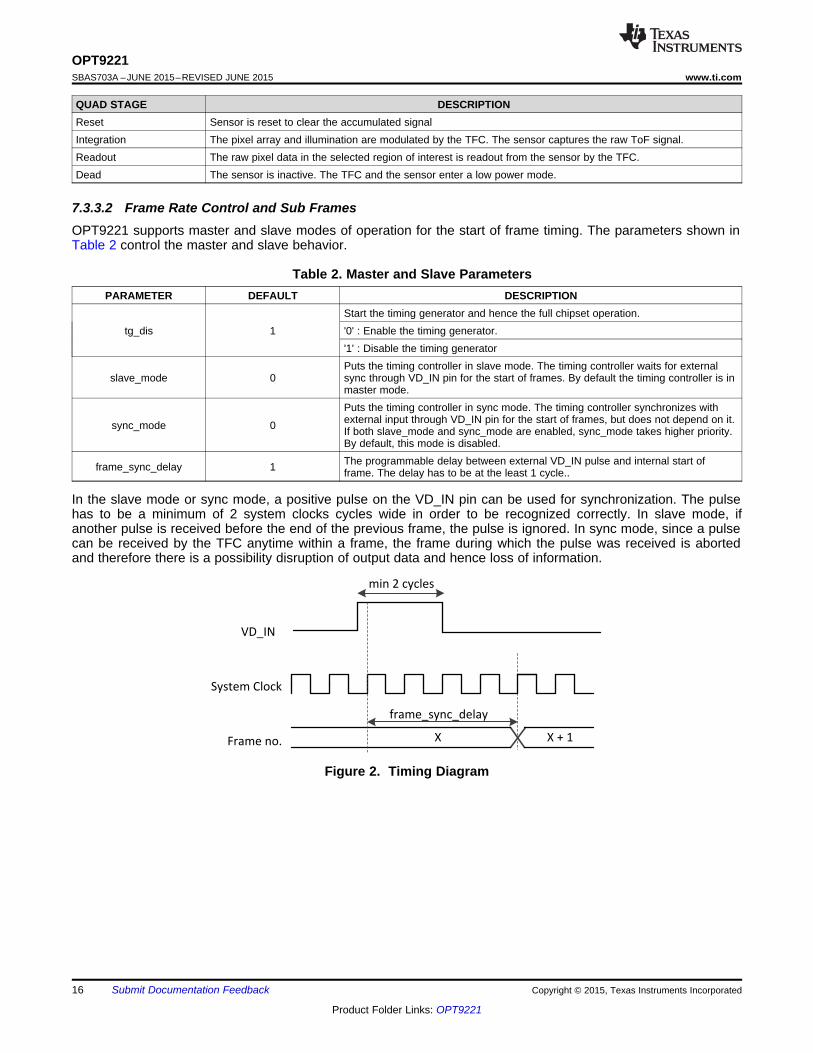
7.3.2 I2C Master InterfaceThe I2C master interface is used for reading temperature from an off-chip temperature sensor on the board. Thetemperature sensor is used for calibrating the phase offset with temperature changes. The external temperaturesensor has to placed in close proximity to the illumination driver. The related programmable parameters andstatus registers are listed in Table 1.
Table 1. I2C Master InterfacePARAMETER OR STATUS REGISTER DESCRIPTION
tillum_slv_addr I2C address of the temperature sensor next to the illumination driver.
tillum Status registers. Indicates the temperature readout from the temperature sensor next to theillumination driver.
The temperature readings are refreshed every frame. A single byte read operation is performed on thetemperature sensor to read the temperature. It is expected that the temperature sensor returns the temperaturein a single unsigned byte. The TI TMP103 series temperature sensors conform to this behavior. For temperaturecalibration of phase, the value read from the temperature sensor is assumed to be linear with the actualtemperature.
7.3.3 Timing CoordinatorThe timing coordinator programs the OPT8241 timing generator (TG). The OPT8241 timing signals consist of themodulation signals for the sensor and the illumination and the readout signals for the sensor. The TG has thefollowing features:• Frame rate control• Sensor addressing• Integration time control• Modulation clock generation
7.3.3.1 Basic Frame StructureEach frame is divided into sub-frames used for internal averaging.
FRAMESub-frame-1 Sub-frame-2 ……… Sub-frame-n Frame dead time
Each sub-frame is divided into quads. Each quad can have a different phase between illumination and sensormodulation signals.
SUBFRAMEQuad-1 Quad-2 Quad-3 ……… Quad-n
Each quad is further split into 4 stages.
QUADReset Integration Readout Quad dead time
min 2 cycles
frame_sync_delay
VD_IN
System Clock
Frame no. X X + 1
16
OPT9221SBAS703A –JUNE 2015–REVISED JUNE 2015 www.ti.com
Product Folder Links: OPT9221
Submit Documentation Feedback Copyright © 2015, Texas Instruments Incorporated
QUAD STAGE DESCRIPTIONReset Sensor is reset to clear the accumulated signalIntegration The pixel array and illumination are modulated by the TFC. The sensor captures the raw ToF signal.Readout The raw pixel data in the selected region of interest is readout from the sensor by the TFC.Dead The sensor is inactive. The TFC and the sensor enter a low power mode.
7.3.3.2 Frame Rate Control and Sub FramesOPT9221 supports master and slave modes of operation for the start of frame timing. The parameters shown inTable 2 control the master and slave behavior.
Table 2. Master and Slave ParametersPARAMETER DEFAULT DESCRIPTION
tg_dis 1Start the timing generator and hence the full chipset operation.'0' : Enable the timing generator.'1' : Disable the timing generator
slave_mode 0Puts the timing controller in slave mode. The timing controller waits for externalsync through VD_IN pin for the start of frames. By default the timing controller is inmaster mode.
sync_mode 0
Puts the timing controller in sync mode. The timing controller synchronizes withexternal input through VD_IN pin for the start of frames, but does not depend on it.If both slave_mode and sync_mode are enabled, sync_mode takes higher priority.By default, this mode is disabled.
frame_sync_delay 1 The programmable delay between external VD_IN pulse and internal start offrame. The delay has to be at the least 1 cycle..
In the slave mode or sync mode, a positive pulse on the VD_IN pin can be used for synchronization. The pulsehas to be a minimum of 2 system clocks cycles wide in order to be recognized correctly. In slave mode, ifanother pulse is received before the end of the previous frame, the pulse is ignored. In sync mode, since a pulsecan be received by the TFC anytime within a frame, the frame during which the pulse was received is abortedand therefore there is a possibility disruption of output data and hence loss of information.
Figure 2. Timing Diagram
17
OPT9221www.ti.com SBAS703A –JUNE 2015–REVISED JUNE 2015
Product Folder Links: OPT9221
Submit Documentation FeedbackCopyright © 2015, Texas Instruments Incorporated
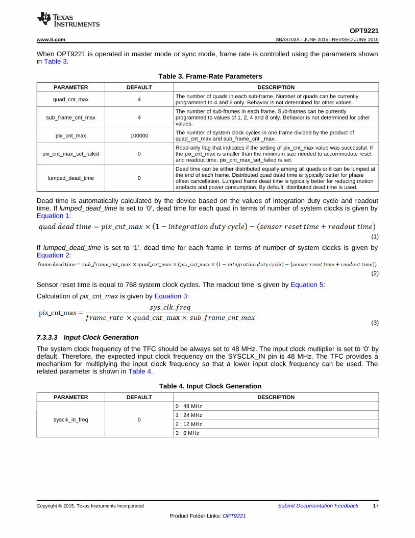
When OPT9221 is operated in master mode or sync mode, frame rate is controlled using the parameters shownin Table 3.
Table 3. Frame-Rate ParametersPARAMETER DEFAULT DESCRIPTION
quad_cnt_max 4 The number of quads in each sub-frame. Number of quads can be currentlyprogrammed to 4 and 6 only. Behavior is not determined for other values.
sub_frame_cnt_max 4The number of sub-frames in each frame. Sub-frames can be currentlyprogrammed to values of 1, 2, 4 and 8 only. Behavior is not determined for othervalues.
pix_cnt_max 100000 The number of system clock cycles in one frame divided by the product ofquad_cnt_max and sub_frame_cnt _max.
pix_cnt_max_set_failed 0Read-only flag that indicates if the setting of pix_cnt_max value was successful. Ifthe pix_cnt_max is smaller than the minimum size needed to accommodate resetand readout time, pix_cnt_max_set_failed is set.
lumped_dead_time 0
Dead time can be either distributed equally among all quads or it can be lumped atthe end of each frame. Distributed quad dead time is typically better for phaseoffset cancellation. Lumped frame dead time is typically better for reducing motionartefacts and power consumption. By default, distributed dead time is used.
Dead time is automatically calculated by the device based on the values of integration duty cycle and readouttime. If lumped_dead_time is set to ‘0’, dead time for each quad in terms of number of system clocks is given byEquation 1:
(1)
If lumped_dead_time is set to ‘1’, dead time for each frame in terms of number of system clocks is given byEquation 2:
(2)
Sensor reset time is equal to 768 system clock cycles. The readout time is given by Equation 5:
Calculation of pix_cnt_max is given by Equation 3:
(3)
7.3.3.3 Input Clock GenerationThe system clock frequency of the TFC should be always set to 48 MHz. The input clock multiplier is set to ‘0’ bydefault. Therefore, the expected input clock frequency on the SYSCLK_IN pin is 48 MHz. The TFC provides amechanism for multiplying the input clock frequency so that a lower input clock frequency can be used. Therelated parameter is shown in Table 4.
Table 4. Input Clock GenerationPARAMETER DEFAULT DESCRIPTION
sysclk_in_freq 0
0 : 48 MHz1 : 24 MHz2 : 12 MHz3 : 6 MHz
18
OPT9221SBAS703A –JUNE 2015–REVISED JUNE 2015 www.ti.com
Product Folder Links: OPT9221
Submit Documentation Feedback Copyright © 2015, Texas Instruments Incorporated
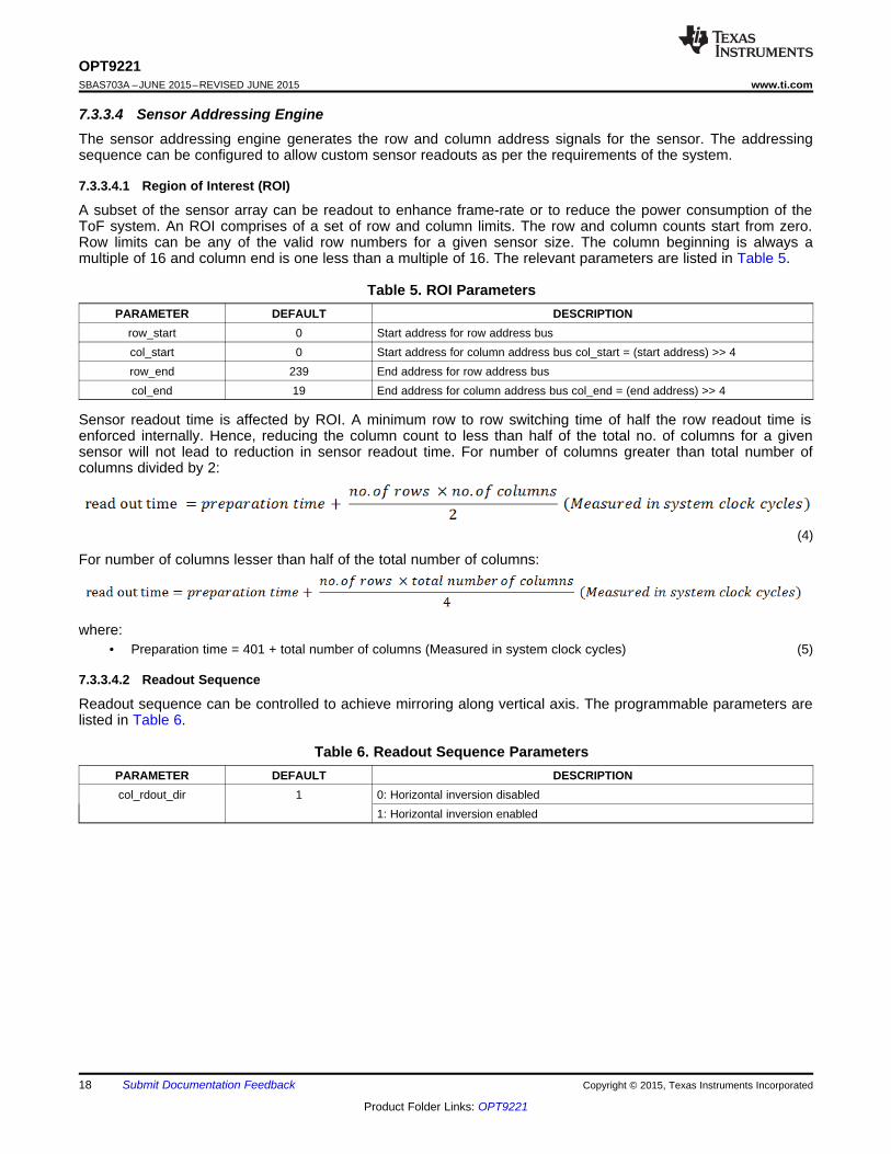
7.3.3.4 Sensor Addressing EngineThe sensor addressing engine generates the row and column address signals for the sensor. The addressingsequence can be configured to allow custom sensor readouts as per the requirements of the system.
7.3.3.4.1 Region of Interest (ROI)
A subset of the sensor array can be readout to enhance frame-rate or to reduce the power consumption of theToF system. An ROI comprises of a set of row and column limits. The row and column counts start from zero.Row limits can be any of the valid row numbers for a given sensor size. The column beginning is always amultiple of 16 and column end is one less than a multiple of 16. The relevant parameters are listed in Table 5.
Table 5. ROI ParametersPARAMETER DEFAULT DESCRIPTION
row_start 0 Start address for row address buscol_start 0 Start address for column address bus col_start = (start address) >> 4row_end 239 End address for row address buscol_end 19 End address for column address bus col_end = (end address) >> 4
Sensor readout time is affected by ROI. A minimum row to row switching time of half the row readout time isenforced internally. Hence, reducing the column count to less than half of the total no. of columns for a givensensor will not lead to reduction in sensor readout time. For number of columns greater than total number ofcolumns divided by 2:
(4)
For number of columns lesser than half of the total number of columns:
where:• Preparation time = 401 + total number of columns (Measured in system clock cycles) (5)
7.3.3.4.2 Readout Sequence
Readout sequence can be controlled to achieve mirroring along vertical axis. The programmable parameters arelisted in Table 6.
Table 6. Readout Sequence ParametersPARAMETER DEFAULT DESCRIPTIONcol_rdout_dir 1 0: Horizontal inversion disabled
1: Horizontal inversion enabled
+JPC_@QPU_?U?HA
2JKNI=H _BNI _EJPC _O?=HA =
+JPACN=PEKJ @QPU ?U?HA × 64
100
19
OPT9221www.ti.com SBAS703A –JUNE 2015–REVISED JUNE 2015
Product Folder Links: OPT9221
Submit Documentation FeedbackCopyright © 2015, Texas Instruments Incorporated
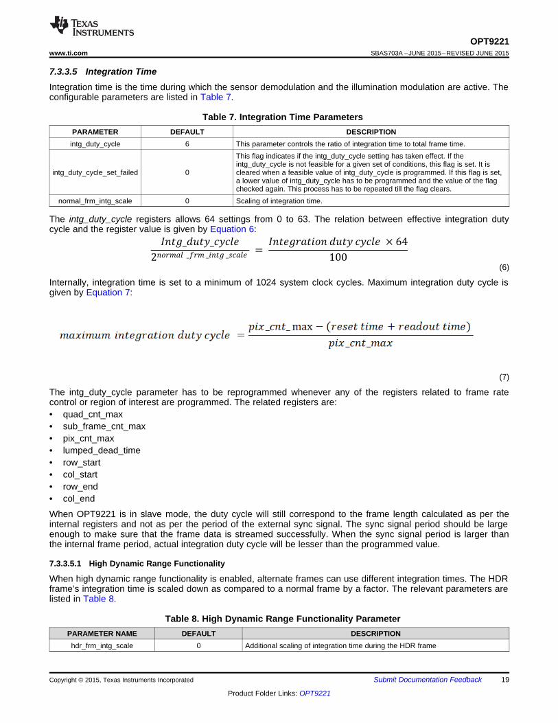
7.3.3.5 Integration TimeIntegration time is the time during which the sensor demodulation and the illumination modulation are active. Theconfigurable parameters are listed in Table 7.
Table 7. Integration Time ParametersPARAMETER DEFAULT DESCRIPTIONintg_duty_cycle 6 This parameter controls the ratio of integration time to total frame time.
intg_duty_cycle_set_failed 0
This flag indicates if the intg_duty_cycle setting has taken effect. If theintg_duty_cycle is not feasible for a given set of conditions, this flag is set. It iscleared when a feasible value of intg_duty_cycle is programmed. If this flag is set,a lower value of intg_duty_cycle has to be programmed and the value of the flagchecked again. This process has to be repeated till the flag clears.
normal_frm_intg_scale 0 Scaling of integration time.
The intg_duty_cycle registers allows 64 settings from 0 to 63. The relation between effective integration dutycycle and the register value is given by Equation 6:
(6)
Internally, integration time is set to a minimum of 1024 system clock cycles. Maximum integration duty cycle isgiven by Equation 7:
(7)
The intg_duty_cycle parameter has to be reprogrammed whenever any of the registers related to frame ratecontrol or region of interest are programmed. The related registers are:• quad_cnt_max• sub_frame_cnt_max• pix_cnt_max• lumped_dead_time• row_start• col_start• row_end• col_end
When OPT9221 is in slave mode, the duty cycle will still correspond to the frame length calculated as per theinternal registers and not as per the period of the external sync signal. The sync signal period should be largeenough to make sure that the frame data is streamed successfully. When the sync signal period is larger thanthe internal frame period, actual integration duty cycle will be lesser than the programmed value.
7.3.3.5.1 High Dynamic Range Functionality
When high dynamic range functionality is enabled, alternate frames can use different integration times. The HDRframe’s integration time is scaled down as compared to a normal frame by a factor. The relevant parameters arelisted in Table 8.
Table 8. High Dynamic Range Functionality ParameterPARAMETER NAME DEFAULT DESCRIPTIONhdr_frm_intg_scale 0 Additional scaling of integration time during the HDR frame
Quad
Integration
ILLUM_EN
ILLUM_P
ILLUM_N
DMIX0
DMIX1
phq
ILLUM_P
ILLUM_N
DMIX0
DMIX1
hdr_frm_intg_scale
normal frame integration timeHDR frame integration time =
2
20
OPT9221SBAS703A –JUNE 2015–REVISED JUNE 2015 www.ti.com
Product Folder Links: OPT9221
Submit Documentation Feedback Copyright © 2015, Texas Instruments Incorporated
(8)
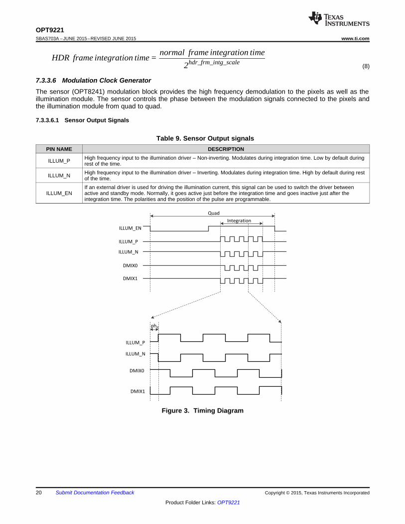
7.3.3.6 Modulation Clock GeneratorThe sensor (OPT8241) modulation block provides the high frequency demodulation to the pixels as well as theillumination module. The sensor controls the phase between the modulation signals connected to the pixels andthe illumination module from quad to quad.
7.3.3.6.1 Sensor Output Signals
Table 9. Sensor Output signalsPIN NAME DESCRIPTION
ILLUM_P High frequency input to the illumination driver – Non-inverting. Modulates during integration time. Low by default duringrest of the time.
ILLUM_N High frequency input to the illumination driver – Inverting. Modulates during integration time. High by default during restof the time.
ILLUM_ENIf an external driver is used for driving the illumination current, this signal can be used to switch the driver betweenactive and standby mode. Normally, it goes active just before the integration time and goes inactive just after theintegration time. The polarities and the position of the pulse are programmable.
Figure 3. Timing Diagram
OPT9221
Output block
8 Data lanes
HD/BD, VD, OP_CS, FE
Ready, Overflow
Data clock
21
OPT9221www.ti.com SBAS703A –JUNE 2015–REVISED JUNE 2015
Product Folder Links: OPT9221
Submit Documentation FeedbackCopyright © 2015, Texas Instruments Incorporated
The phase between illumination modulation and the sensor demodulation signals is stepped automatically as perthe quad number. For example, in the case of one sub-frame having 4 quads, the phase is typically steppedbetween 0º, 90º, 180º and 270º. The phase stepping sequence of the sensor is programmable through TFCregisters. A different sequence can be enabled for odd and even sub-frames. Also, the phase registers for basefrequency and de-aliasing frequency are separately programmable. The programmable parameters are listed inTable 10 and Table 11.
Table 10. Pin ProgrammabilityPARAMETER DEFAULT DESCRIPTION
modulation_hold 0 Disable modulation during integration period. Set to ‘0’ for normal operation.demod_static_pol 0 DC state of illumination pins during integration period if mod_static=’1’.illum_static_pol 0 DC state of illumination pins during integration period if mod_static=’1’. ILLUM_P =
illum_static , ILLUM_N = not (illum_static)illum_en_early 0 Activates the illumination enable signal 15 µs before integration period starts when
set to ‘1’.illum_mod_early 0 Activates the illumination modulation 15 µs before integration period starts when
set to ‘1’.Illum_dc_corr_dir 0 Sets the direction of duty cycle correction for illumination output waveforms. Note
that when duty cycle is increased, ILLUM_P duty cycle increases and ILLUM_Nduty cycle decreases.0: Increase the duty cycle1: Reduce the duty cycle
Illum_dc_corr 0 Illumination duty cycle can be corrected in steps of about 450 ps. The maximumvalue of this register is 11 which results into a total correction of about +/-5 ns.
Table 11. Phase Sequence ProgrammabilityPARAMETER DEFAULT DESCRIPTIONquad_hop_en 0 Enables a different sequence of quads for odd and even frames.
quad_hop_offset_f1 0 The offset of the quad sequence for alternate frames for base frequency.quad_hop_offset_f2 0 The offset of the quad sequence for alternate frames for de-aliasing
frequencyquad_cnt_max 0 The number of quads in each sub-frame
The relative phase of illumination modulation with respect to sensor modulation, phq for any quad, can becalculated as shown in Equation 9:
(9)
Note that the quad number is offset by the flicker cancel offset for that sub-frame.
effective quad number = quad number + quad hop offset
7.3.4 Output InterfaceThe TFC has a programmable parallel CMOS output interface module, which gives an option to connect the TFCto wide variety of host processors.
Figure 4. Output Interface Module
22
OPT9221SBAS703A –JUNE 2015–REVISED JUNE 2015 www.ti.com
Product Folder Links: OPT9221
Submit Documentation Feedback Copyright © 2015, Texas Instruments Incorporated
Table 12. Output Interface PinsPIN NAME FUNCTIONALITY
OP_CLKOutput interface clock. The clk frequency is controlled internally to meet the frame-rate requirement. Alternatively, clockcan be supplied from an external host. All the output interface signals transition on the configured (positive/negative)edge of this clock. By default, the output signals transition on the negative edge of this clock.
OP_DATA [7:0] Output CMOS data pins. By default, all the pins are used for transfer of data. In the 4-lane mode, only Data[3:0] areused. In the 1-lane mode, only Data[0] is used.
HD/BD This signal is used as horizontal sync in the DVP mode to indicate row data transfer. In 8-lane generic CMOS mode, itis used to indicate the validity of the data available on output bus.
VD Frame sync. It used to indicate the beginning of a new frame.
OP_CS Chip select. This signal is used to indicate the validity of the data on the data bus. It can be used in the TI SSI mode asSSIFss.
FE Frame-end. This signal pulses for a single clock cycle to indicate frame end.Ready This signal is used for flow control when enabled. Output data is buffered when the ready signal is not active.
Overflow This signal is used by host processor to indicate buffer overflow. This is used for debug only.
7.3.4.1 Output Data FormatThe depth information can be obtained with varying degrees of detail as per the host application’s requirementsusing register control. The two options available are listed below:
7.3.4.1.1 4-Byte Mode (default)• 12 bits amplitude (C)• 4 bits ambient (A)• 12 bits phase (P)• 4 bits flags (F)
Byte 3 Byte 215 14 13 12 11 10 9 8 7 6 5 4 3 2 1 0
Flags[3:0] Phase[11:0]
Byte 1 Byte 015 14 13 12 11 10 9 8 7 6 5 4 3 2 1 0
Ambient[3:0] Amplitude[11:0]
Ambient and amplitude information together form a 16-bit word with ambient in the MSBs. Flags and phaseinformation together form a 16-bit word with flags in the MSBs.
There are two modes of arrangement possible :
Contiguous
C0, A0 P0, F0 C2, A2 P2, F2 C3, A3 P3, F3 ….......Pixel0 Pixel1 Pixel3 ………
23
OPT9221www.ti.com SBAS703A –JUNE 2015–REVISED JUNE 2015
Product Folder Links: OPT9221
Submit Documentation FeedbackCopyright © 2015, Texas Instruments Incorporated
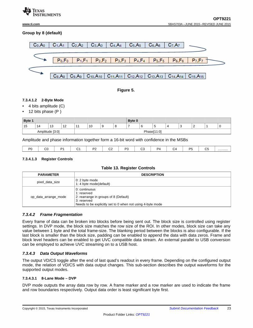
Group by 8 (default)
Figure 5.
7.3.4.1.2 2-Byte Mode• 4 bits amplitude (C)• 12 bits phase (P )
Byte 1 Byte 015 14 13 12 11 10 9 8 7 6 5 4 3 2 1 0
Amplitude [3:0] Phase[11:0]
Amplitude and phase information together form a 16-bit word with confidence in the MSBs
P0 C0 P1 C1 P2 C2 P3 C3 P4 C4 P5 C5 ….......
7.3.4.1.3 Register Controls
Table 13. Register ControlsPARAMETER DESCRIPTION
pixel_data_size 0: 2 byte mode1: 4 byte mode(default)
op_data_arrange_mode
0: continuous1: reserved2: rearrange in groups of 8 (Default)3: reservedNeeds to be explicitly set to 0 when not using 4-byte mode
7.3.4.2 Frame FragmentationEvery frame of data can be broken into blocks before being sent out. The block size is controlled using registersettings. In DVP mode, the block size matches the row size of the ROI. In other modes, block size can take anyvalue between 1 byte and the total frame-size. The blanking period between the blocks is also configurable. If thelast block is smaller than the block size, padding can be enabled to append the data with data zeros. Frame andblock level headers can be enabled to get UVC compatible data stream. An external parallel to USB conversioncan be employed to achieve UVC streaming on to a USB host.
7.3.4.3 Data Output WaveformsThe output VD/CS toggle after the end of last quad’s readout in every frame. Depending on the configured outputmode, the relation of VD/CS with data output changes. This sub-section describes the output waveforms for thesupported output modes.
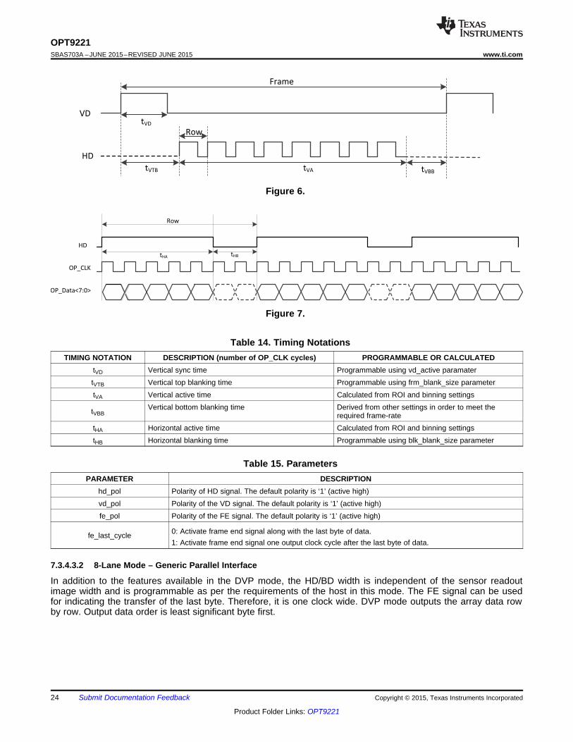
7.3.4.3.1 8-Lane Mode – DVP
DVP mode outputs the array data row by row. A frame marker and a row marker are used to indicate the frameand row boundaries respectively. Output data order is least significant byte first.
Row
tHA tHB
HD
OP_CLK
OP_Data<7:0>
tVBBtVAtVTB
Frame
VD
HD
tVD
Row
24
OPT9221SBAS703A –JUNE 2015–REVISED JUNE 2015 www.ti.com
Product Folder Links: OPT9221
Submit Documentation Feedback Copyright © 2015, Texas Instruments Incorporated
Figure 6.
Figure 7.
Table 14. Timing NotationsTIMING NOTATION DESCRIPTION (number of OP_CLK cycles) PROGRAMMABLE OR CALCULATED
tVD Vertical sync time Programmable using vd_active paramatertVTB Vertical top blanking time Programmable using frm_blank_size parametertVA Vertical active time Calculated from ROI and binning settings
tVBBVertical bottom blanking time Derived from other settings in order to meet the
required frame-ratetHA Horizontal active time Calculated from ROI and binning settingstHB Horizontal blanking time Programmable using blk_blank_size parameter
Table 15. ParametersPARAMETER DESCRIPTION
hd_pol Polarity of HD signal. The default polarity is ‘1’ (active high)vd_pol Polarity of the VD signal. The default polarity is ‘1’ (active high)fe_pol Polarity of the FE signal. The default polarity is ‘1’ (active high)
fe_last_cycle 0: Activate frame end signal along with the last byte of data.1: Activate frame end signal one output clock cycle after the last byte of data.
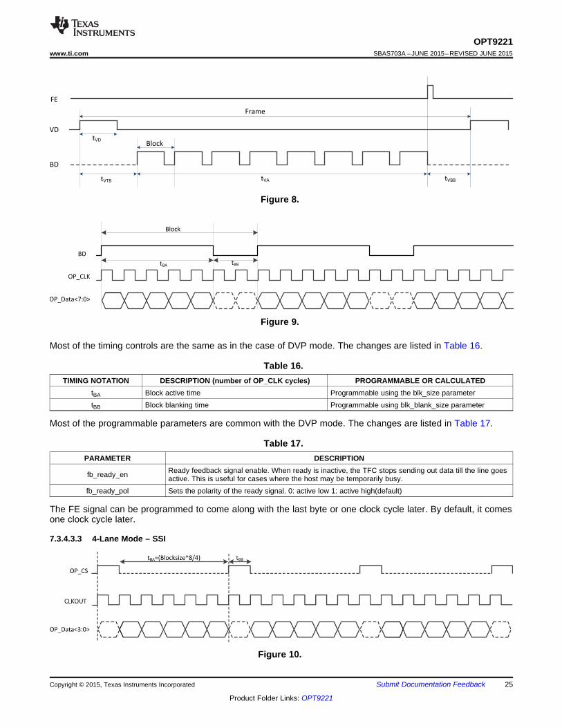
7.3.4.3.2 8-Lane Mode – Generic Parallel Interface
In addition to the features available in the DVP mode, the HD/BD width is independent of the sensor readoutimage width and is programmable as per the requirements of the host in this mode. The FE signal can be usedfor indicating the transfer of the last byte. Therefore, it is one clock wide. DVP mode outputs the array data rowby row. Output data order is least significant byte first.
Block
tBA tBB
BD
OP_CLK
OP_Data<7:0>
Frame
tVD
tVTB tVA tVBB
FE
VD
BD
Block
25
OPT9221www.ti.com SBAS703A –JUNE 2015–REVISED JUNE 2015
Product Folder Links: OPT9221
Submit Documentation FeedbackCopyright © 2015, Texas Instruments Incorporated
Figure 8.
Figure 9.
Most of the timing controls are the same as in the case of DVP mode. The changes are listed in Table 16.
Table 16.TIMING NOTATION DESCRIPTION (number of OP_CLK cycles) PROGRAMMABLE OR CALCULATED
tBA Block active time Programmable using the blk_size parametertBB Block blanking time Programmable using blk_blank_size parameter
Most of the programmable parameters are common with the DVP mode. The changes are listed in Table 17.
Table 17.PARAMETER DESCRIPTION
fb_ready_en Ready feedback signal enable. When ready is inactive, the TFC stops sending out data till the line goesactive. This is useful for cases where the host may be temporarily busy.
fb_ready_pol Sets the polarity of the ready signal. 0: active low 1: active high(default)
The FE signal can be programmed to come along with the last byte or one clock cycle later. By default, it comesone clock cycle later.
7.3.4.3.3 4-Lane Mode – SSI
Figure 10.
CLKOUT
OP_Data<0>
CS
tBA=(Blocksize*8) tBB
26
OPT9221SBAS703A –JUNE 2015–REVISED JUNE 2015 www.ti.com
Product Folder Links: OPT9221
Submit Documentation Feedback Copyright © 2015, Texas Instruments Incorporated
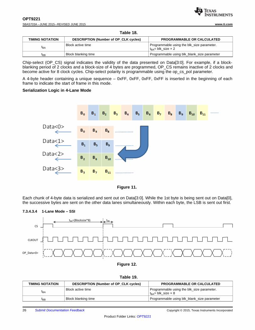
Table 18.TIMING NOTATION DESCRIPTION (Number of OP_CLK cycles) PROGRAMMABLE OR CALCULATED
tBABlock active time Programmable using the blk_size parameter.
tBA= blk_size × 2tBB Block blanking time Programmable using blk_blank_size parameter
Chip-select (OP_CS) signal indicates the validity of the data presented on Data[3:0]. For example, if a block-blanking period of 2 clocks and a block-size of 4 bytes are programmed, OP_CS remains inactive of 2 clocks andbecome active for 8 clock cycles. Chip-select polarity is programmable using the op_cs_pol parameter.
A 4-byte header containing a unique sequence – 0xFF, 0xFF, 0xFF, 0xFF is inserted in the beginning of eachframe to indicate the start of frame in this mode.
Serialization Logic in 4-Lane Mode
Figure 11.
Each chunk of 4-byte data is serialized and sent out on Data[3:0]. While the 1st byte is being sent out on Data[0],the successive bytes are sent on the other data lanes simultaneously. Within each byte, the LSB is sent out first.
7.3.4.3.4 1-Lane Mode – SSI
Figure 12.
Table 19.TIMING NOTATION DESCRIPTION (Number of OP_CLK cycles) PROGRAMMABLE OR CALCULATED
tBABlock active time Programmable using the blk_size parameter.
tBA= blk_size × 8tBB Block blanking time Programmable using blk_blank_size parameter
27
OPT9221www.ti.com SBAS703A –JUNE 2015–REVISED JUNE 2015
Product Folder Links: OPT9221
Submit Documentation FeedbackCopyright © 2015, Texas Instruments Incorporated
Chip-select (OP_CS) indicates the validity of the data presented on Data[0]. For example, if a block-blankingperiod of 2 clocks and a block size of 4 bytes are programmed, OP_CS remains inactive of 2 clocks and remainactive for 32 clock cycles. Chip-select polarity is programmable using the op_cs_pol parameter.
A 4-byte header containing a unique sequence – 0xFF, 0xFF, 0xFF, 0xFF is inserted in the beginning of eachframe to indicate the start of frame in this mode .
Serialization Logic in 1-Lane Mode
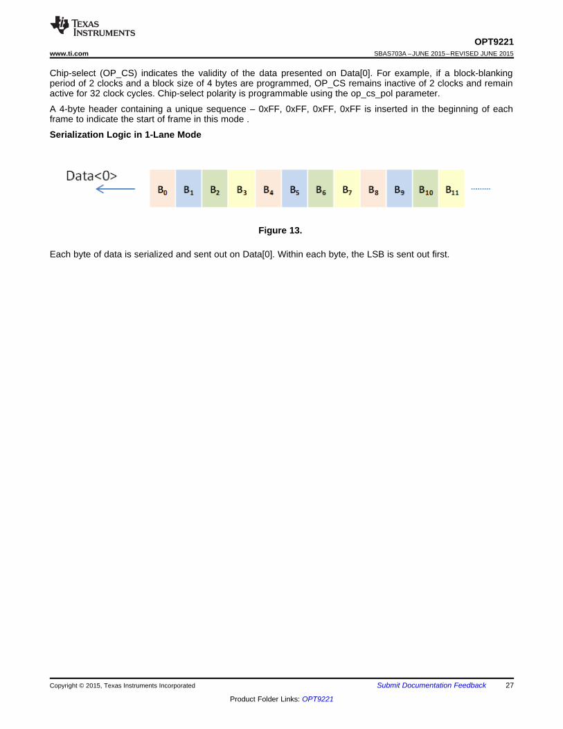
Figure 13.
Each byte of data is serialized and sent out on Data[0]. Within each byte, the LSB is sent out first.
28
OPT9221SBAS703A –JUNE 2015–REVISED JUNE 2015 www.ti.com
Product Folder Links: OPT9221
Submit Documentation Feedback Copyright © 2015, Texas Instruments Incorporated
7.3.4.3.5 Register Controls
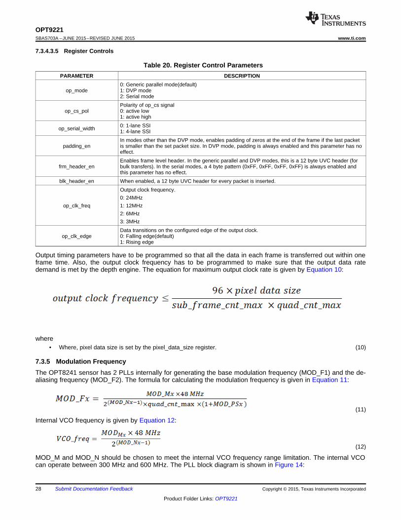
Table 20. Register Control ParametersPARAMETER DESCRIPTION
op_mode0: Generic parallel mode(default)1: DVP mode2: Serial mode
op_cs_polPolarity of op_cs signal0: active low1: active high
op_serial_width 0: 1-lane SSI1: 4-lane SSI
padding_enIn modes other than the DVP mode, enables padding of zeros at the end of the frame if the last packetis smaller than the set packet size. In DVP mode, padding is always enabled and this parameter has noeffect.
frm_header_enEnables frame level header. In the generic parallel and DVP modes, this is a 12 byte UVC header (forbulk transfers). In the serial modes, a 4 byte pattern (0xFF, 0xFF, 0xFF, 0xFF) is always enabled andthis parameter has no effect.
blk_header_en When enabled, a 12 byte UVC header for every packet is inserted.
op_clk_freq
Output clock frequency.0: 24MHz1: 12MHz2: 6MHz3: 3MHz
op_clk_edgeData transitions on the configured edge of the output clock.0: Falling edge(default)1: Rising edge
Output timing parameters have to be programmed so that all the data in each frame is transferred out within oneframe time. Also, the output clock frequency has to be programmed to make sure that the output data ratedemand is met by the depth engine. The equation for maximum output clock rate is given by Equation 10:
where• Where, pixel data size is set by the pixel_data_size register. (10)
7.3.5 Modulation FrequencyThe OPT8241 sensor has 2 PLLs internally for generating the base modulation frequency (MOD_F1) and the de-aliasing frequency (MOD_F2). The formula for calculating the modulation frequency is given in Equation 11:
(11)
Internal VCO frequency is given by Equation 12:
(12)
MOD_M and MOD_N should be chosen to meet the internal VCO frequency range limitation. The internal VCOcan operate between 300 MHz and 600 MHz. The PLL block diagram is shown in Figure 14:
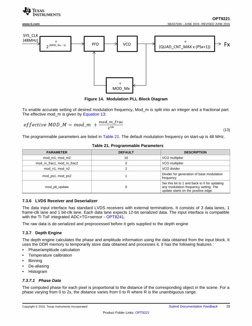
÷
2 (MOD_Nx t 1) PFD VCO
SYS_CLK (48MHz) ÷
(QUAD_CNT_MAX x (PSx+1))
÷
MOD_Mx
Fx
29
OPT9221www.ti.com SBAS703A –JUNE 2015–REVISED JUNE 2015
Product Folder Links: OPT9221
Submit Documentation FeedbackCopyright © 2015, Texas Instruments Incorporated
Figure 14. Modulation PLL Block Diagram
To enable accurate setting of desired modulation frequency, Mod_m is split into an integer and a fractional part.The effective mod_m is given by Equation 13:
(13)
The programmable parameters are listed in Table 21. The default modulation frequency on start-up is 48 MHz.
Table 21. Programmable ParametersPARAMETER DEFAULT DESCRIPTION
mod_m1, mod_m2 16 VCO multipliermod_m_frac1, mod_m_frac2 0 VCO multiplier
mod_n1, mod_n2 2 VCO divider
mod_ps1, mod_ps2 1 Divider for generation of base modulationfrequency
mod_pll_update 0Set this bit to 1 and back to 0 for updatingany modulation frequency setting. Theupdate starts on the positive edge.
7.3.6 LVDS Receiver and DeserializerThe data input interface has standard LVDS receivers with external terminations. It consists of 3 data lanes, 1frame-clk lane and 1 bit-clk lane. Each data lane expects 12-bit serialized data. The input interface is compatiblewith the TI ToF integrated ADC+TG+sensor - OPT8241.
The raw data is de-serialized and preprocessed before it gets supplied to the depth engine
7.3.7 Depth EngineThe depth engine calculates the phase and amplitude information using the data obtained from the input block. Ituses the DDR memory to temporarily store data obtained and processes it. It has the following features :• Phase/amplitude calculation• Temperature calibration• Binning• De-aliasing• Histogram
7.3.7.1 Phase DataThe computed phase for each pixel is proportional to the distance of the corresponding object in the scene. For aphase varying from 0 to 2π, the distance varies from 0 to R where R is the unambiguous range.

§ ·¨ ¸© ¹
¦n=N
nn=0
2�QI = Q Cos
N
§ ·¨ ¸© ¹
¦n=N
nn=0
2�QQ = Q Sin
N
-1 QPhase = tan
I
30
OPT9221SBAS703A –JUNE 2015–REVISED JUNE 2015 www.ti.com
Product Folder Links: OPT9221
Submit Documentation Feedback Copyright © 2015, Texas Instruments Incorporated
(14)
where• C is speed of light• F is the modulation frequency (15)
At the output of the depth processor block, phase of 2π is typically represented by a full 12-bit code. That is, 212.If the application requires knowledge of the distance (in meters) of the points in the scene, it must be calculatedfrom the TFC output using the following formula:
(16)
The above formula assumes that the phase has no offset. If offset correction is not done within the TFC, theformula is:
(17)
The sensor data collected in the quads is used to compute the phase information. The quad information is thenused to compute in-phase and quadrature components as shown in Equation 18:
where• ‘N’ is the number of quads in each sub-frame and ‘n’ is the quad index. The Cos and Sin coefficients need to
be programmed into the TFC as per the number of quads. The default coefficients are programmed for 4quads. (18)
§ ·u ¨ ¸
© ¹
2�Qcos_fx_qn_coeff = 32767 Cos
N
§ ·u ¨ ¸
© ¹
2�Qsin_fx_qn_coeff = 32767 Sin
N
31
OPT9221www.ti.com SBAS703A –JUNE 2015–REVISED JUNE 2015
Product Folder Links: OPT9221
Submit Documentation FeedbackCopyright © 2015, Texas Instruments Incorporated
Each parameter in the register set is a coefficient represented in 16-bits signed representation. The formula forcalculating the parameter is shown in Equation 19:
where• n is the index of the coefficient, ‘x’ represents the frequency (base or de-aliasing frequency). N is the number
of quads (same as quad_cnt_max). (19)
When de-aliasing is not enabled, the default number of quads is 4. To use 6 quads without de-aliasing, thefollowing configuration has to be programmed.• Reduce the number of sub-frames (sub_frame_cnt_max) to 2 or reduce the output clock to 12 MHz
(op_clk_freq).• Program base frequency (f1) to desired value.• Set the number of quads (quad_cnt_max) to 6.• Set ind_freq_data_sel to ‘1’ to use the alternate set of coefficients to process the obtained data.• Set cos_f2_qn_coeff and sin_f2_qn_coeff registers to the appropriate values.
7.3.7.2 De-AliasingUnambiguous range of a ToF system is defined by the modulation frequency (F). It is given by the equationEquation 20:
where• C is the speed of light in the medium. (20)
For example, for a modulation frequency of 50 MHz, R = 3m in open air. If the total range of the application isbeyond the unambiguous range for a given modulation frequency, de-aliasing can be enabled to extend theunambiguous range. This technique employs two modulation frequencies.
The unambiguous range is given by Equation 21:
(21)
The de-aliasing filter implemented in the depth processor computes the unambiguous phase automatically whende-aliasing is enabled.
7.3.7.2.1 Procedure for Enabling the De-Aliasing Mode1. Disable the timing generator using the tg_dis parameter.2. set quad_cnt_max parameter to 6.3. Set the base frequency and de-aliasing modulation frequency as described in Modulation Clock Generator
section. Always ensure that base frequency is lower than the de-aliasing frequency.
32
OPT9221SBAS703A –JUNE 2015–REVISED JUNE 2015 www.ti.com
Product Folder Links: OPT9221
Submit Documentation Feedback Copyright © 2015, Texas Instruments Incorporated
4. Set the de-aliasing coefficients as shown in Setting the De-Aliasing Coefficients.5. Set the phase calibration parameters for each frequency as described in Phase Offset Correction section.6. Set sub_frame_cnt_max count to meet the relation (refer Equation 10) between sub_frame_cnt_max and
quad_cnt_max.7. Set pix_cnt_max to meet frame rate requirements.8. Set dealias_en parameter to 1.9. Enable the timing generator using the tg_enable parameter.
When de-aliasing is enabled, for the purpose of calibration, streaming of individual frequency data can beenabled in place of de-aliased data using the parameters in Table 22.
Table 22.PARAMETER DEFAULT DESCRIPTION
ind_freq_data_en 0Enables streaming of output data corresponding to individual frequencies.0: disabled1: enabled
ind_freq_data_sel 0 0: Stream output data corresponding to base frequency1: Stream output data corresponding to de-aliasing frequency
7.3.7.2.2 Procedure for Disabling the De-Aliasing Mode
1. Disable the timing generator using the tg_dis parameter.2. Set the pix_cnt_max, sub_frame_cnt_max and quad_cnt_max parameters to meet the frame rate
requirements and satisfy Equation 10.3. Set the base frequency as described in Modulation Clock Generator section.4. Set the phase calibration parameter for base frequency as described in Phase Offset Correction section.5. Set dealias_en parameter to 0.6. Enable the timing generator using the tg_dis parameter.
7.3.7.2.3 Setting the De-Aliasing Coefficients
The parameters ma and mb have to be chosen such that the following conditions are met:
(22)
And the parameter freq_ratio has to be programmed to match the ratio between the two frequencies as shown inEquation 23:
(23)
Where, f1 is the base frequency and f2 is the de-aliasing frequency. The coefficients ka and kb have to bechosen such that (ka × ma) - (kb × mb) = 1
7.3.7.2.4 Scaling of Phase
The de-aliased phase is internally masked. The mask is programmable using a register configuration as shownby Equation 24:
(24)
Where,
33
OPT9221www.ti.com SBAS703A –JUNE 2015–REVISED JUNE 2015
Product Folder Links: OPT9221
Submit Documentation FeedbackCopyright © 2015, Texas Instruments Incorporated
(25)
Where, R is the total unambiguous range.
The internal de-aliased phase is 16-bit wide. But the final phase output is only 12 bit. The application of the maskleads to a scaling in the output. Therefore, to correctly calculate the distance, Equation 26 should be used in theexternal host.
(26)
Programmable parameters are listed in Table 23.
Table 23.PARAMETER DEFAULT DESCRIPTION
dealiased_ph_mask 0
The mask for the getting the output phase fromthe calculated de-aliased phase. The mask is16bits wide. The least significant bit of the maskis given by the following relation. LSB=5-dealiased_ph_mask.
Example:
Table 24.F1 = 18 MHz F2 = 24 MHz
ma = 3 mb = 4Unambiguous range = 8.33 m Unambiguous range= 6.25 m
Therefore, the total unambiguous range with de-aliasing is given by Equation 27:
(27)
For a value of 20m, the value of de-aliased phase is given by Equation 28:
(28)
If the default value of dealised_ph_mask is used, the phase output for 20m will be given by Equation 29:
(29)
At the host, the original distance value can be calculated as shown by Equation 30:
(30)
34
OPT9221SBAS703A –JUNE 2015–REVISED JUNE 2015 www.ti.com
Product Folder Links: OPT9221
Submit Documentation Feedback Copyright © 2015, Texas Instruments Incorporated
7.3.7.2.5 LSBs in the De-Aliased Phase
In some applications, it is desirable to get range extension without losing the least significant bits. As explained inthe above sub-section, by default only 12 bits of phase output are available. To get additional 4 LSBs of thephase output, the following parameter can bet set as shown in Table 25.
Table 25.PARAMETER DEFAULT DESCRIPTION
dealias_16bit_op_enable 0Enables 16-bit output of de-aliased data. Thismode is available only if pixel_data_size is setto 4-byte mode.
LSBs of de-aliased phase are available in-place of ambient data. Therefore, ambient data will not be availablewhen using 16-bit de-aliased phase output.
7.3.7.3 BinningMultiple pixel data can be averaged to form a single large pixel data. This feature is useful in cases where theapplication requires lesser pixel resolution but needs better phase noise performance. Any number ofrows/columns can be binned. The programmable parameters are listed in Table 26.
Table 26. Binning ParametersPARAMETER DEFAULT DESCRIPTIONrows_to_merge 1 Number of rows to mergecols_to_merge 1 Number of columns to mergebin_row_count 240 Number of rows after binning.bin_col_count 320 Number of rows after binning
Note that bin_row_count and bin_col_count need to be programmed explicitly. For example, if therows_to_merge=7, bin_row_count = floor(total no of rows / 7) = floor(240/7) = 34.
7.3.7.4 Spatial FilterA simple 3 x 3 spatial filter is implemented inside the TFC. The filter operates on the phase vectors representedby I + jQ. The spatial filter coefficients are arranged as shown in Table 27.
Table 27.0 + 0j Y coefficient 0 + 0j
X coefficient 1 + 0j X coefficient0 + 0j Y coefficient 0 + 0i
The relevant parameters are listed in Table 28.
Table 28.PARAMETER DESCRIPTION
filt_en Enable spatial filterfilt_scale Filters are scaled down by 2(2 + filt_scale).
filt_coeff_x_re _f1,filt_coeff_x_im _f1,filt_coeff_y_re _f1,filt_coeff_y_im _f1,filt_coeff_x_re _f2,filt_coeff_x_im _f2,filt_coeff_y_re _f2,filt_coeff_y_im _f2,
Filter Coefficients. Represented as 8-bit signed numbers
35
OPT9221www.ti.com SBAS703A –JUNE 2015–REVISED JUNE 2015
Product Folder Links: OPT9221
Submit Documentation FeedbackCopyright © 2015, Texas Instruments Incorporated
7.3.7.5 Auxiliary Depth DataAmplitude data represents the amplitude of the received signal at each pixel. If the amplitude is higher, signalamplitude is higher and hence the phase SNR is higher. The value of amplitude output is given by Equation 31.Amplitude = 212 x Signal Amplitude x 1.65
(31)
Where, the signal amplitude is the amplitude of the single ended modulating signal (A or B) generated on thepixel in each quad. When binning is enabled, signal amplitude is the vector sum of the signals of all the binnedpixels divided by the nearest power of two which is greater than the number of pixels binned together.
Ambient data is an indicator of the non-modulating component of voltage on the pixels. It is the sum of theambient light, pixel offsets and the non-demodulated component of ToF illumination. The output ambient datavalues decrease with increase in voltage. Therefore, near zero values indicate pixel saturation.
The TFC provides masking of data based on the value of amplitude and single ended voltage in a pixel for thepurpose of basic filtering. The related parameters are listed in Table 29.
Table 29. Auxiliary Depth Data ParametersPARAMETER DEFAULT DESCRIPTION
amplitude_threshold 0 If the amplitude of the pixel is lower than this number, the pixel phase data is set toFFFh.
iq_scale
0
Left shifts the acquired sensor data by the configured value. The scaling results into anequivalent scaling in amplitude. Care must be taken to avoid bit overflow in the depthprocessor as this scaling is done before the computation of phase and amplitude. If a bitoverflow occurs, it is indicated by digital saturation flag in the flags part of the datastream.
amplitude_post_scale 0 Left shifts the computed amplitude by the configured value. If the amplitude of any pixelexceeds the full scale value, the amplitude is clipped to FFFh.
saturation_threshold 0 Saturation flag is set if the ambient value of the pixel is lesser than or equal to this value.Also, pixel phase data is set to 000h.
Flags[3:0] indicate important pixel data reliability parameters. The flags are described in Table 30.
Table 30. Pixel DataFLAG BIT DESCRIPTION
Flag[3] 0 : No pixel saturation1 : Pixel is saturated
Flag[2]
For the first pixel in the frame :0 : Normal frame1 : HDR frameRemaining pixels:0 : No digital saturation detected1 : Digital pipeline saturated
Flag[1] ReservedFlag[0] Reserved
7.3.8 Calibration
7.3.8.1 Phase Offset CorrectionTime delay between sensor modulation and the illumination modulation manifests itself as a phase offset. Sinceit may vary from one system to another, the offset has to be calibrated individually for each system. Themeasured offset can be programmed into a phase_corr parameter in the TFC registers. The TFC subtracts thephase_corr parameter to the computed phase. The programmable parameters are listed in Table 31.
Table 31. Phase Offset Correction ParametersPARAMETER DESCRIPTIONphase_corr_1 Phase offset correction for base frequencyphase_corr_2 Phase offset correction for de-aliasing frequency
36
OPT9221SBAS703A –JUNE 2015–REVISED JUNE 2015 www.ti.com
Product Folder Links: OPT9221
Submit Documentation Feedback Copyright © 2015, Texas Instruments Incorporated
Table 31. Phase Offset Correction Parameters (continued)hdr_phase_corr_1 Phase offset correction for base frequency during HDR framehdr_phase_corr_2 Phase offset correction for de-aliasing frequency during HDR framedisable_offset_corr Disables phase offset correction in the TFC. Phase offset correction is enabled by default.
Due to temperature variations, system delays in the illumination and sensor modulation path can vary differently.This variation leads to a change in the measured phase. To compensate for phase change vs temperature, theTFC uses two programmable temperature coefficients. The built-in temperature sensor in OPT8241 is used formeasuring the ToF sensor temperature and an external I2C interface based temperature sensor is used formeasuring the illumination driver temperature. The programmable parameters are listed in Table 32.
Table 32. Temperature Coefficient ParametersPARAMETER DESCRIPTION
tillum_calib Illumination driver temperature when phase_corr was measured.tsensor_calib Sensor temperature when phase_corr was measured.
coeff_illum Phase vs temperature coefficients for illumination driver for the base frequency.coeff_sensor Phase vs temperature coefficients for sensor for the base frequency.
disable_temp_corr Disables phase offset correction due to temperature. (Temperature correction is enabled bydefault)
calib_precScales the co-efficients. Default scaling of 16 is applied to the temperature coefficients0 : Scaling by 11 : Scaling by 16
The phase correction due to temperature variation is calculated by the TFC as shown in Equation 32:
(32)
Where, calibration scale is 1 when calib_prec = 0 and 16 when calib_prec = 1 .
When de-aliasing is not used, the final value of phase given out by the TFC is calculated as shown inEquation 33:
(33)
When de-aliasing is used, phase correction on individual frequency measurements is applied before combiningthe phase information to compute the final unambiguous phase. Since individual frequency measurements mayhave different offsets and temperature co-efficients, the TFC provides separate correction blocks formeasurements using each frequency. The temperature coefficients for the de-aliasing frequency are internallycomputed using the coefficients for base frequency. When de-aliasing is enabled, for the purpose of calibration,streaming of individual frequency data can be enabled in place of de-aliased data using the parameters ofTable 33.
Table 33.PARAMETER DEFAULT DESCRIPTION
ind_freq_data_en 0
Enables streaming of output data correspondingto individual frequencies.0: disabled1: enabled
ind_freq_data_sel 0
0: Stream output data corresponding to basefrequency1: Stream output data corresponding to secondfrequency
OPT8241 Driver
+
OPT9221
IO_MOD_REF
External Feedback Circuit
ILLUM_MOD_FB
ILLUM_P
COMP_MOD_REF
COMP_MOD_FB
Illumination source
37
OPT9221www.ti.com SBAS703A –JUNE 2015–REVISED JUNE 2015
Product Folder Links: OPT9221
Submit Documentation FeedbackCopyright © 2015, Texas Instruments Incorporated
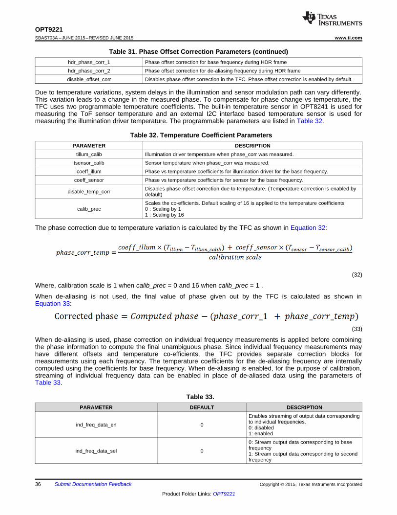
7.3.8.2 Illumination Path Delay Correction Using FeedbackThe illumination modulation path delay can be compensated to reduce the absolute and temperature dependentphase offsets. The illumination modulation path delay is measured using feedback from the sensor and theillumination modulation. The appropriate feedback has to be implemented in the system. A typical block diagramof such a feedback system is shown in Figure 15.
Figure 15.
The delay compensation circuit measures the delay from ILLUM_P to COMP_MOD_FB during the integrationtime and measures the delay of the external feedback circuit from COMP_MOD_REF to COMP_MOD_FB duringsensor readout. For measuring the delay, an internal uncorrelated clock (with a frequency between 10 MHz to 50MHz) is used to sample the feedback waveforms. The difference between the two delays measured is used as aphase offset that is used to correct the obtained phase.
Functional requirements of the feedback circuit:• ILLUM_P output from OPT8241 should be connected to ILLUM_MOD_REF input pin of OPT9221• The output of a feedback ckt that converts illumination current waveform to a square wave must be connected
to COMP_MOD_FB pin.• The same feedback ckt or a replica with similar delays must be driven by COMP_MOD_REF and the output
must be fed back to COMP_MOD_FB pin• The feedback circuit must have a minimum frequency of operation of 48 MHz or the operating modulation
frequency (whichever is higher)
The relevant parameters for configuring the delay correction block are listed in Table 34.
Table 34.PARAMETER DESCRIPTION
delay_fb_corr_mode Enabled phase correction using illumination path delay feedback and set the direction ofcorrection.
delay_fb_dc_corr_mode Enable using the duty cycle of the obtained feedback signal for calculating the phasecompensation and set the direction of correction.
comp_mod_ref_inv Enable inversion of feedback signal in the signal chain before evaluating the delay.
Illum_fb_inv Enable inversion of the signal at ILLUM_FB pin in the signal chain before evaluating thedelay.
fb_error_cnt_threshold Number of errors that can be tolerated in sampling the pulses per 4096 samples.comp_fb_error_cnt Number of pulses not sampled correctly on the COMP_FB pin.illum_fb_error_cnt Number of pulses not sampled correctly on the ILLUM_FB pin.
delay_fb_coeff Ratio of modulation frequency to 24MHz. Refer to Equation 34
The delay coefficients have to be calculated as per the below equations .
When de-aliasing is not enabled:
(34)
38
OPT9221SBAS703A –JUNE 2015–REVISED JUNE 2015 www.ti.com
Product Folder Links: OPT9221
Submit Documentation Feedback Copyright © 2015, Texas Instruments Incorporated
When de-aliasing is enabled:
(35)
7.3.8.3 Phase Non-Linearity CorrectionObtained phase vs distance should be ideally a straight line. But in practice, the function of phase to distancemay be non-linear. To linearize the obtained phase, a lookup table can be programmed into the TFC. The lookuptable is used for converting the obtained phase to linearized phase. The relevant registers are listed in Table 35.
Table 35.PARAMETER DESCRIPTION
phase_lin_corr_enable Enable phase to distance non-linearity correctionphase_lin_corr_period The period after which the non-linearity function repeats.
phase_lin_coeff1_x, phase_lin_coeff2_xThe lookup table. phase_lin_corr_coeff1_x registers correspond to the lookup table for thebase frequency and the phase_lin_corr_coeff2_x registers correspond to the lookup table forthe de-aliasing frequency.
The lookup table provides 16 points that are evenly spread across a period. The 16 points can be spread over90/180/360 degrees. The first entry in the lookup table corresponds to an obtained phase value of zero. The lastpoint in the lookup table corresponds to an obtained phase value of period × (15/16) . The spread of the points indegrees is controlled by the phase_lin_corr_period register. If the period is less than 360 degrees, the samelookup table is repeated for rest of the angles.
7.4 Device Functional Modes
7.4.1 Standby and Low-Power ModesVarious blocks of the ToF chipset can be put in low power mode using the standby functionality. The TFC has astandby pin which when asserted activates the low power operation of the chipset. The same can also beachieved using register settings. The parameters that control the low power operation are listed inTable 36.
Table 36. Parameter DescriptionPARAMETER DESCRIPTION
standby_pin_en Enables the functionality of standby pin when set to ‘1’
standby_pin_pol Selects the active polarity of standby pin. For example, when set to ‘1’ the chipset enters low-power mode whenstandby pin is pulled high. Active only when standby_pin_en is set.
standby 0: Chipset is in normal operation1: Chipset is in standby mode
7.5 Programming
7.5.1 Boot SequenceAfter power up, an internal POR is asserted to reset the TFC. Once the POR is complete, the TFC enters theconfiguration stage. During the configuration stage, the TFC firmware is loaded through one of the configurationmethods. Once the configuration is complete, INT_OUT pin is pulled low to indicate that the TFC is ready fornormal operation.
tRAMP
tPOR tCONF tREADY
INT_OUT
Config Pins
Internal POR
VCCx
TIC_CONF_DONE
39
OPT9221www.ti.com SBAS703A –JUNE 2015–REVISED JUNE 2015
Product Folder Links: OPT9221
Submit Documentation FeedbackCopyright © 2015, Texas Instruments Incorporated
Programming (continued)
(1) Configuration time (tCONF ) depends on the mode of the configuration.
Figure 16. Boot Sequence Timing Diagram
Table 37. Boot Sequence Timing Parameters (1)
PARAMETER MIN MAX UNITtRAMP Supply voltage ramp 50 3000 µstPOR Reset time 50 200 mstCONF Configuration time. Depends on the mode of configuration and the
clock rates. - -
tREADY Time required for TFC to be in operational state after configuration 2 ms
7.5.1.1 ConfigurationAfter the POR is complete, one of the configuration methods is chosen as per the state of the BOOT[2:0] pins.
The recommended modes are listed in Table 38.
Table 38. Recommended Boot ModesBOOT[2:0] MODE DESCRIPTION
011 Master serial configuration Firmware is loaded from an external EEPROM000 Slave serial configuration External host loads the firmware using single data pin111 Slave parallel configuration External host loads the firmware using 8 data pins.
After the configuration is complete and the TFC is ready for operation the TFC pulls the INT_OUT pin low.
7.5.1.1.1 Master Serial Configuration
An external SPI EEPROM can be used to store the TFC firmware. On power-up, if the boot modes areconfigured for master serial configuration, the TFC reads loads the firmware from the EEPROM. During theconfiguration, the TIC_CONF_DONE pin is held low. Once the configuration is done, the TIC_CONF_DONE pinis released.
The recommended connections between TFC and EEPROM are shown in Figure 17. For programming theEEPROM, the TIC_CONFIGZ pin has to be pulled low and TIC_CEz has to be pulled high. This causes the TFCto put its pins in tri-state and the EEPROM can be programmed using the SPI lines. The SPI EEPROM sizeshould be sufficient to hold the firmware. The minimum size required for storing the firmware is 4mbits. Thefirmware has to be programmed in the least significant bit first order into the EEPROM for proper functionality.The recommended EEPROM is W25Q04DWSSIG.
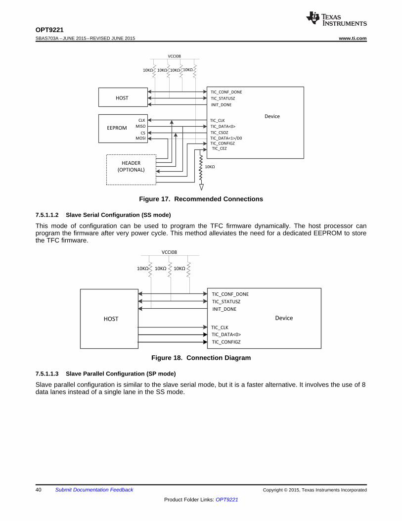
Device
TIC_CONF_DONE
TIC_STATUSZ
INIT_DONE
TIC_CLK
TIC_DATA<0>
TIC_CONFIGZ
HOST
VCCI08
10KQ 10KQ 10KQ
Device
TIC_CONF_DONE
TIC_STATUSZ
INIT_DONE
TIC_CLK
TIC_DATA<0>
TIC_CONFIGZ
HOST
EEPROM
CLK
MISO
CS
HEADER
(OPTIONAL)
MOSI
VCCI08
10KQ 10KQ 10KQ
10KQ
TIC_CSOZ
TIC_DATA<1>/D0
10KQ
TIC_CEZ
40
OPT9221SBAS703A –JUNE 2015–REVISED JUNE 2015 www.ti.com
Product Folder Links: OPT9221
Submit Documentation Feedback Copyright © 2015, Texas Instruments Incorporated
Figure 17. Recommended Connections
7.5.1.1.2 Slave Serial Configuration (SS mode)
This mode of configuration can be used to program the TFC firmware dynamically. The host processor canprogram the firmware after very power cycle. This method alleviates the need for a dedicated EEPROM to storethe TFC firmware.
Figure 18. Connection Diagram
7.5.1.1.3 Slave Parallel Configuration (SP mode)
Slave parallel configuration is similar to the slave serial mode, but it is a faster alternative. It involves the use of 8data lanes instead of a single lane in the SS mode.
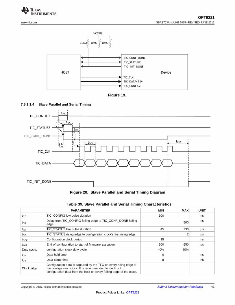
TIC_CONFIGZ
TIC_STATUSZ
TIC_CONF_DONE
TIC_CLK
TIC_DATA
tINIT
tCZ
tSZ
tDC
tCCK
TIC_INIT_DONE
tCR
Device
TIC_CONF_DONE
TIC_STATUSZ
TIC_INIT_DONE
TIC_CLK
TIC_DATA<7:0>
TIC_CONFIGZ
HOST
VCCI08
10KQ 10KQ 10KQ
41
OPT9221www.ti.com SBAS703A –JUNE 2015–REVISED JUNE 2015
Product Folder Links: OPT9221
Submit Documentation FeedbackCopyright © 2015, Texas Instruments Incorporated
Figure 19.
7.5.1.1.4 Slave Parallel and Serial Timing
Figure 20. Slave Parallel and Serial Timing Diagram
Table 39. Slave Parallel and Serial Timing CharacteristicsPARAMETER MIN MAX UNIT
tCZ TIC_CONFIG low pulse duration 500 ns
tCRDelay from TIC_CONFIG falling edge to TIC_CONF_DONE fallingedge 500 ns
tSZ TIC_STATUS low pulse duration 45 230 µstDC TIC_STATUS rising edge to configuration clock’s first rising edge 2 µstCCK Configuration clock period 15 nstINIT End of configuration to start of firmware execution 300 650 µsDuty cycle, configuration clock duty cycle 40% 60%tCH Data hold time 0 nstCS Data setup time 8 ns
Clock edgeConfiguration data is captured by the TFC on every rising edge ofthe configuration clock. It is recommended to clock outconfiguration data from the host on every falling edge of the clock.
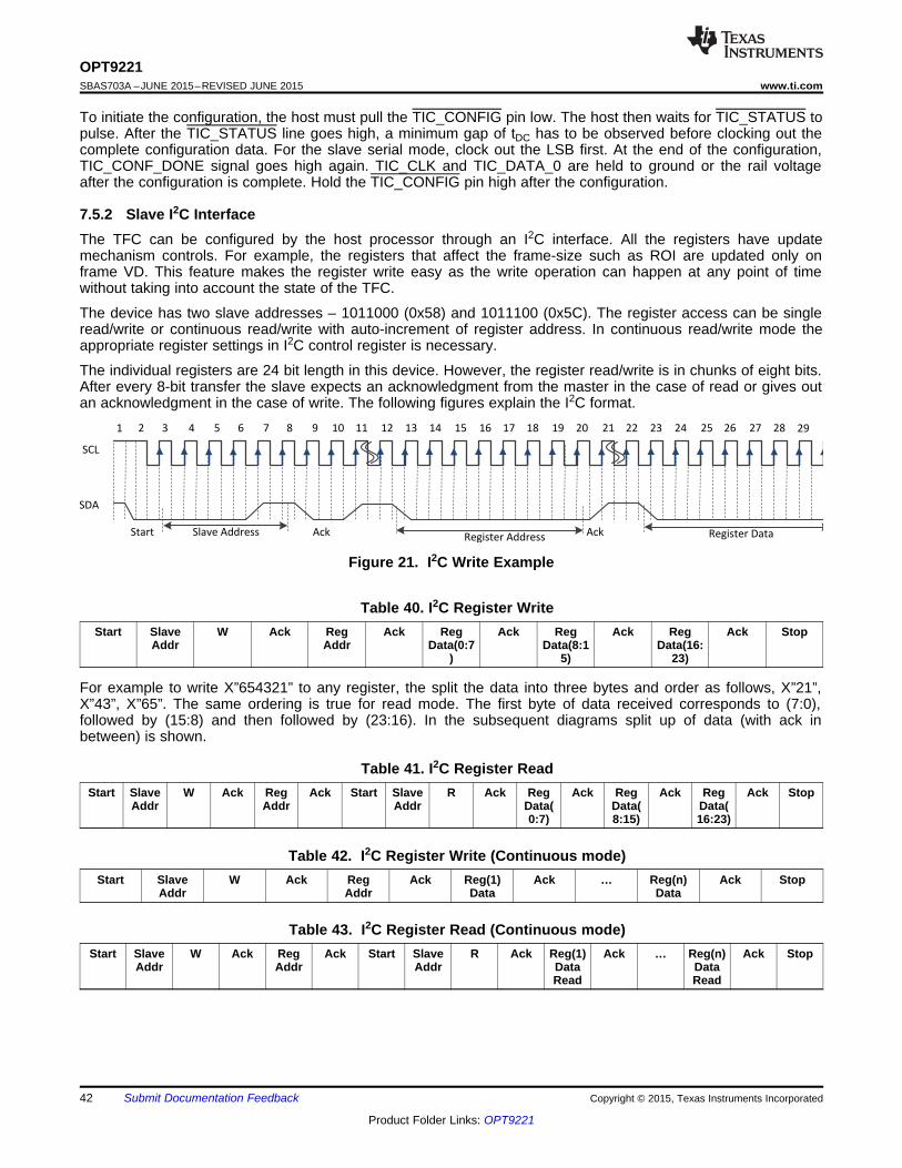
SCL
3 4 5 6 7 8 9 10 11 12 13 14 15 16 17 18 19 20 21 22 23 24 25 26 27 28 29 321
SDA
Start AckSlave Address Register Address Ack Register Data
42
OPT9221SBAS703A –JUNE 2015–REVISED JUNE 2015 www.ti.com
Product Folder Links: OPT9221
Submit Documentation Feedback Copyright © 2015, Texas Instruments Incorporated
To initiate the configuration, the host must pull the TIC_CONFIG pin low. The host then waits for TIC_STATUS topulse. After the TIC_STATUS line goes high, a minimum gap of tDC has to be observed before clocking out thecomplete configuration data. For the slave serial mode, clock out the LSB first. At the end of the configuration,TIC_CONF_DONE signal goes high again. TIC_CLK and TIC_DATA_0 are held to ground or the rail voltageafter the configuration is complete. Hold the TIC_CONFIG pin high after the configuration.
7.5.2 Slave I2C InterfaceThe TFC can be configured by the host processor through an I2C interface. All the registers have updatemechanism controls. For example, the registers that affect the frame-size such as ROI are updated only onframe VD. This feature makes the register write easy as the write operation can happen at any point of timewithout taking into account the state of the TFC.
The device has two slave addresses – 1011000 (0x58) and 1011100 (0x5C). The register access can be singleread/write or continuous read/write with auto-increment of register address. In continuous read/write mode theappropriate register settings in I2C control register is necessary.
The individual registers are 24 bit length in this device. However, the register read/write is in chunks of eight bits.After every 8-bit transfer the slave expects an acknowledgment from the master in the case of read or gives outan acknowledgment in the case of write. The following figures explain the I2C format.
Figure 21. I2C Write Example
Table 40. I2C Register WriteStart Slave
AddrW Ack Reg
AddrAck Reg
Data(0:7)
Ack RegData(8:1
5)
Ack RegData(16:
23)
Ack Stop
For example to write X”654321” to any register, the split the data into three bytes and order as follows, X”21”,X”43”, X”65”. The same ordering is true for read mode. The first byte of data received corresponds to (7:0),followed by (15:8) and then followed by (23:16). In the subsequent diagrams split up of data (with ack inbetween) is shown.
Table 41. I2C Register ReadStart Slave
AddrW Ack Reg
AddrAck Start Slave
AddrR Ack Reg
Data(0:7)
Ack RegData(8:15)
Ack RegData(16:23)
Ack Stop
Table 42. I2C Register Write (Continuous mode)Start Slave
AddrW Ack Reg
AddrAck Reg(1)
DataAck … Reg(n)
DataAck Stop
Table 43. I2C Register Read (Continuous mode)Start Slave
AddrW Ack Reg
AddrAck Start Slave
AddrR Ack Reg(1)
DataRead
Ack … Reg(n)DataRead
Ack Stop
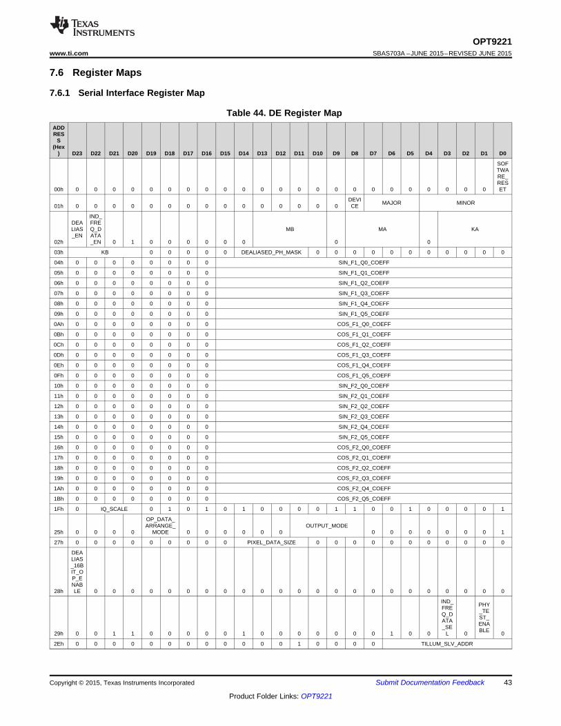
43
OPT9221www.ti.com SBAS703A –JUNE 2015–REVISED JUNE 2015
Product Folder Links: OPT9221
Submit Documentation FeedbackCopyright © 2015, Texas Instruments Incorporated
7.6 Register Maps
7.6.1 Serial Interface Register Map
Table 44. DE Register MapADDRES
S(Hex
) D23 D22 D21 D20 D19 D18 D17 D16 D15 D14 D13 D12 D11 D10 D9 D8 D7 D6 D5 D4 D3 D2 D1 D0
00h 0 0 0 0 0 0 0 0 0 0 0 0 0 0 0 0 0 0 0 0 0 0 0
SOFTWARE_RESET
01h 0 0 0 0 0 0 0 0 0 0 0 0 0 0 0DEVICE MAJOR MINOR
02h
DEALIAS_EN
IND_FREQ_DATA_EN 0 1 0 0 0 0 0 0
MB
0
MA
0
KA
03h KB 0 0 0 0 0 DEALIASED_PH_MASK 0 0 0 0 0 0 0 0 0 0 0
04h 0 0 0 0 0 0 0 0 SIN_F1_Q0_COEFF
05h 0 0 0 0 0 0 0 0 SIN_F1_Q1_COEFF
06h 0 0 0 0 0 0 0 0 SIN_F1_Q2_COEFF
07h 0 0 0 0 0 0 0 0 SIN_F1_Q3_COEFF
08h 0 0 0 0 0 0 0 0 SIN_F1_Q4_COEFF
09h 0 0 0 0 0 0 0 0 SIN_F1_Q5_COEFF
0Ah 0 0 0 0 0 0 0 0 COS_F1_Q0_COEFF
0Bh 0 0 0 0 0 0 0 0 COS_F1_Q1_COEFF
0Ch 0 0 0 0 0 0 0 0 COS_F1_Q2_COEFF
0Dh 0 0 0 0 0 0 0 0 COS_F1_Q3_COEFF
0Eh 0 0 0 0 0 0 0 0 COS_F1_Q4_COEFF
0Fh 0 0 0 0 0 0 0 0 COS_F1_Q5_COEFF
10h 0 0 0 0 0 0 0 0 SIN_F2_Q0_COEFF
11h 0 0 0 0 0 0 0 0 SIN_F2_Q1_COEFF
12h 0 0 0 0 0 0 0 0 SIN_F2_Q2_COEFF
13h 0 0 0 0 0 0 0 0 SIN_F2_Q3_COEFF
14h 0 0 0 0 0 0 0 0 SIN_F2_Q4_COEFF
15h 0 0 0 0 0 0 0 0 SIN_F2_Q5_COEFF
16h 0 0 0 0 0 0 0 0 COS_F2_Q0_COEFF
17h 0 0 0 0 0 0 0 0 COS_F2_Q1_COEFF
18h 0 0 0 0 0 0 0 0 COS_F2_Q2_COEFF
19h 0 0 0 0 0 0 0 0 COS_F2_Q3_COEFF
1Ah 0 0 0 0 0 0 0 0 COS_F2_Q4_COEFF
1Bh 0 0 0 0 0 0 0 0 COS_F2_Q5_COEFF
1Fh 0 IQ_SCALE 0 1 0 1 0 1 0 0 0 0 1 1 0 0 1 0 0 0 0 1
25h 0 0 0 0
OP_DATA_ARRANGE_
MODE 0 0 0 0 0 0OUTPUT_MODE
0 0 0 0 0 0 0 1
27h 0 0 0 0 0 0 0 0 0 PIXEL_DATA_SIZE 0 0 0 0 0 0 0 0 0 0 0
28h
DEALIAS_16BIT_OP_ENABLE 0 0 0 0 0 0 0 0 0 0 0 0 0 0 0 0 0 0 0 0 0 0 0
29h 0 0 1 1 0 0 0 0 0 1 0 0 0 0 0 0 0 1 0 0
IND_FREQ_DATA_SE
L 0
PHY_TEST_ENABLE 0
2Eh 0 0 0 0 0 0 0 0 0 0 0 0 1 0 0 0 0 TILLUM_SLV_ADDR
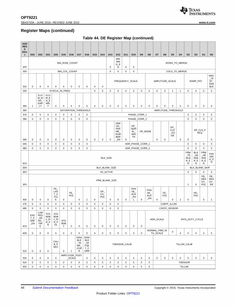
44
OPT9221SBAS703A –JUNE 2015–REVISED JUNE 2015 www.ti.com
Product Folder Links: OPT9221
Submit Documentation Feedback Copyright © 2015, Texas Instruments Incorporated
Register Maps (continued)Table 44. DE Register Map (continued)
ADDRES
S(Hex
) D23 D22 D21 D20 D19 D18 D17 D16 D15 D14 D13 D12 D11 D10 D9 D8 D7 D6 D5 D4 D3 D2 D1 D0
2Fh
BIN_ROW_COUNT
0
BINNING_E
N 0 0
ROWS_TO_MERGE
30h BIN_COL_COUNT 0 0 0 0 COLS_TO_MERGE
31h 0 0 0 0 0 0 0 0 0 0
FREQUENCY_SCALE AMPLITUDE_SCALE RAMP_PAT
MAC_TEST_ENABLE
33h SYSCLK_IN_FREQ 0 0 0 0 0 0 0 0 0 0 1 1 0 0 0 0
35h 1
ILLUM_MOD_EARLY
ILLUM_EN_EARL
Y 0 0 0 0 0 0 0 0 0 0 0 0 0 0 0 0 0 0 0 0 0
36h SATURATION_THRESHOLD AMPLITUDE_THRESHOLD
37h 0 0 0 0 0 0 0 0 PHASE_CORR_1 0 0 0 0
38h 0 0 0 0 0 0 0 0 PHASE_CORR_2 0 0 0 0
39h 0 0 0 0 0 0 0 0 0 0 0
DEBUG_FRAME_NUMBER_EN 0
OP_SERIAL_WIDTH
OP_MODE
0 0
OP_CLK_EDGE
0 0
OP_CLK_FREQ
0
3Ah 0 0 0 0 0 0 0 0 HDR_PHASE_CORR_1 0 0 0 0
3Bh 0 0 0 0 0 0 0 0 HDR_PHASE_CORR_2 0 0 0 0
3Ch
BLK_SIZE
FRM_TRAILER_E
N
BLK_HEADER_E
N
FRM_HEADER_E
N
PADDING_E
N
3Dh BLK_BLANK_SIZE BLK_BLANK_SKIP
3Eh VD_ACTIVE 0 0 0 0
3Fh
FRM_BLANK_SIZE
1 0
FB_READY_POL
FB_READY_EN
40h 0 0 0
FE_LAST_CYCL
E 0
FE_POL
0 1 0
OP_CS_POL
0 0 0
PHASE_AUX_PO
L 0
PHASE_AUX_EN 0
VD_POL
0 1 0
HD_POL
0 1
47h 0 0 0 0 0 0 0 0 0 0 0 0 COEFF_ILLUM
48h 0 0 0 0 0 0 0 0 0 0 0 0 COEFF_SENSOR
4Ch
EASY_CONF_EN
LUMPED_DEAD_TIME
STANDBY_PIN_E
N
STANDBY_PIN_POL
STANDB
Y 0 0 0 0 0 0 0 0 0 0
HDR_SCALE INTG_DUTY_CYCLE
4Dh 0 0 0 0 0 0 0 0 0 0 0 0 0 0 0NORMAL_FRM_IN
TG_SCALE 0 0 0 0 0 0
51h 0 0 0
CALIB_PREC
0 1
DISABLE_TEMP_COR
R
DISABLE_OFFSET_CORR
TSENSOR_CALIB TILLUM_CALIB
52h 0 0 0 0AMPLITUDE_POST
_SCALE 0 0 0 0 0 0 0 0 0 0 0 0 0 0 0 0 0
61h 0 0 0 0 0 0 0 0 0 0 0 0 0 0 0 0 TSENSOR
62h 0 0 0 0 0 0 0 0 0 0 0 0 0 0 0 0 TILLUM
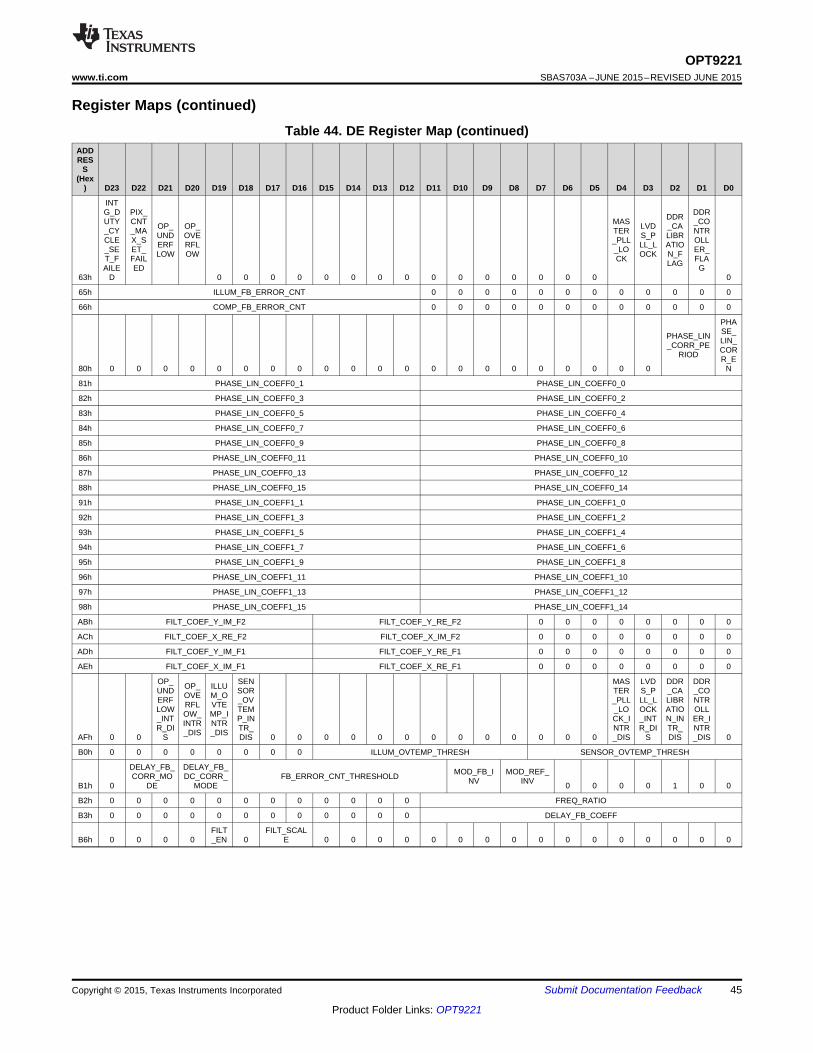
45
OPT9221www.ti.com SBAS703A –JUNE 2015–REVISED JUNE 2015
Product Folder Links: OPT9221
Submit Documentation FeedbackCopyright © 2015, Texas Instruments Incorporated
Register Maps (continued)Table 44. DE Register Map (continued)
ADDRES
S(Hex
) D23 D22 D21 D20 D19 D18 D17 D16 D15 D14 D13 D12 D11 D10 D9 D8 D7 D6 D5 D4 D3 D2 D1 D0
63h
INTG_DUTY_CYCLE_SET_FAILE
D
PIX_CNT_MAX_SET_FAILED
OP_UNDERFLOW
OP_OVERFLOW
0 0 0 0 0 0 0 0 0 0 0 0 0 0 0
MASTER_PLL_LOCK
LVDS_PLL_LOCK
DDR_CALIBRATION_FLAG
DDR_CONTROLLER_FLAG
0
65h ILLUM_FB_ERROR_CNT 0 0 0 0 0 0 0 0 0 0 0 0
66h COMP_FB_ERROR_CNT 0 0 0 0 0 0 0 0 0 0 0 0
80h 0 0 0 0 0 0 0 0 0 0 0 0 0 0 0 0 0 0 0 0 0
PHASE_LIN_CORR_PE
RIOD
PHASE_LIN_CORR_E
N
81h PHASE_LIN_COEFF0_1 PHASE_LIN_COEFF0_0
82h PHASE_LIN_COEFF0_3 PHASE_LIN_COEFF0_2
83h PHASE_LIN_COEFF0_5 PHASE_LIN_COEFF0_4
84h PHASE_LIN_COEFF0_7 PHASE_LIN_COEFF0_6
85h PHASE_LIN_COEFF0_9 PHASE_LIN_COEFF0_8
86h PHASE_LIN_COEFF0_11 PHASE_LIN_COEFF0_10
87h PHASE_LIN_COEFF0_13 PHASE_LIN_COEFF0_12
88h PHASE_LIN_COEFF0_15 PHASE_LIN_COEFF0_14
91h PHASE_LIN_COEFF1_1 PHASE_LIN_COEFF1_0
92h PHASE_LIN_COEFF1_3 PHASE_LIN_COEFF1_2
93h PHASE_LIN_COEFF1_5 PHASE_LIN_COEFF1_4
94h PHASE_LIN_COEFF1_7 PHASE_LIN_COEFF1_6
95h PHASE_LIN_COEFF1_9 PHASE_LIN_COEFF1_8
96h PHASE_LIN_COEFF1_11 PHASE_LIN_COEFF1_10
97h PHASE_LIN_COEFF1_13 PHASE_LIN_COEFF1_12
98h PHASE_LIN_COEFF1_15 PHASE_LIN_COEFF1_14
ABh FILT_COEF_Y_IM_F2 FILT_COEF_Y_RE_F2 0 0 0 0 0 0 0 0
ACh FILT_COEF_X_RE_F2 FILT_COEF_X_IM_F2 0 0 0 0 0 0 0 0
ADh FILT_COEF_Y_IM_F1 FILT_COEF_Y_RE_F1 0 0 0 0 0 0 0 0
AEh FILT_COEF_X_IM_F1 FILT_COEF_X_RE_F1 0 0 0 0 0 0 0 0
AFh 0 0
OP_UNDERFLOW_INTR_DI
S
OP_OVERFLOW_INTR_DIS
ILLUM_OVTEMP_INTR_DIS
SENSOR_OVTEMP_INTR_DIS 0 0 0 0 0 0 0 0 0 0 0 0 0
MASTER_PLL_LOCK_INTR_DIS
LVDS_PLL_LOCK_INTR_DI
S
DDR_CALIBRATION_INTR_DIS
DDR_CONTROLLER_INTR_DIS 0
B0h 0 0 0 0 0 0 0 0 ILLUM_OVTEMP_THRESH SENSOR_OVTEMP_THRESH
B1h 0
DELAY_FB_CORR_MO
DE
DELAY_FB_DC_CORR_
MODEFB_ERROR_CNT_THRESHOLD MOD_FB_I
NVMOD_REF_
INV 0 0 0 0 1 0 0
B2h 0 0 0 0 0 0 0 0 0 0 0 0 FREQ_RATIO
B3h 0 0 0 0 0 0 0 0 0 0 0 0 DELAY_FB_COEFF
B6h 0 0 0 0FILT_EN 0
FILT_SCALE 0 0 0 0 0 0 0 0 0 0 0 0 0 0 0 0
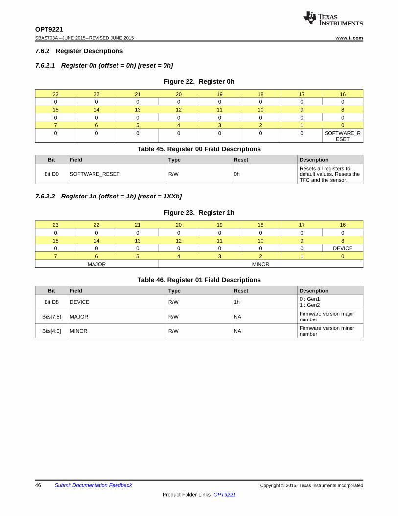
46
OPT9221SBAS703A –JUNE 2015–REVISED JUNE 2015 www.ti.com
Product Folder Links: OPT9221
Submit Documentation Feedback Copyright © 2015, Texas Instruments Incorporated
7.6.2 Register Descriptions
7.6.2.1 Register 0h (offset = 0h) [reset = 0h]
Figure 22. Register 0h
23 22 21 20 19 18 17 160 0 0 0 0 0 0 015 14 13 12 11 10 9 80 0 0 0 0 0 0 07 6 5 4 3 2 1 00 0 0 0 0 0 0 SOFTWARE_R
ESET
Table 45. Register 00 Field DescriptionsBit Field Type Reset Description
Bit D0 SOFTWARE_RESET R/W 0hResets all registers todefault values. Resets theTFC and the sensor.
7.6.2.2 Register 1h (offset = 1h) [reset = 1XXh]
Figure 23. Register 1h
23 22 21 20 19 18 17 160 0 0 0 0 0 0 015 14 13 12 11 10 9 80 0 0 0 0 0 0 DEVICE7 6 5 4 3 2 1 0
MAJOR MINOR
Table 46. Register 01 Field DescriptionsBit Field Type Reset Description
Bit D8 DEVICE R/W 1h 0 : Gen11 : Gen2
Bits[7:5] MAJOR R/W NA Firmware version majornumber
Bits[4:0] MINOR R/W NA Firmware version minornumber
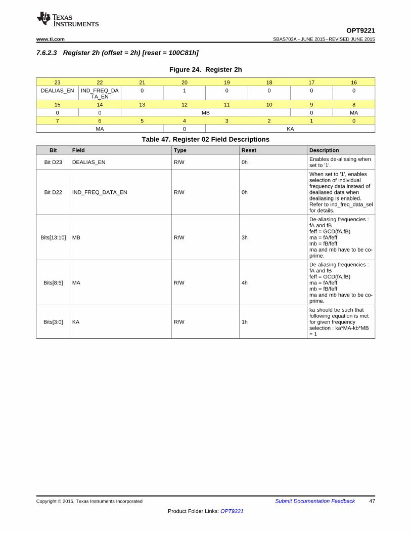
47
OPT9221www.ti.com SBAS703A –JUNE 2015–REVISED JUNE 2015
Product Folder Links: OPT9221
Submit Documentation FeedbackCopyright © 2015, Texas Instruments Incorporated
7.6.2.3 Register 2h (offset = 2h) [reset = 100C81h]
Figure 24. Register 2h
23 22 21 20 19 18 17 16DEALIAS_EN IND_FREQ_DA
TA_EN0 1 0 0 0 0
15 14 13 12 11 10 9 80 0 MB 0 MA7 6 5 4 3 2 1 0
MA 0 KA
Table 47. Register 02 Field DescriptionsBit Field Type Reset Description
Bit D23 DEALIAS_EN R/W 0h Enables de-aliasing whenset to '1'.
Bit D22 IND_FREQ_DATA_EN R/W 0h
When set to '1', enablesselection of individualfrequency data instead ofdealiased data whendealiasing is enabled.Refer to ind_freq_data_selfor details.
Bits[13:10] MB R/W 3h
De-aliasing frequencies :fA and fBfeff = GCD(fA,fB)ma = fA/feffmb = fB/feffma and mb have to be co-prime.
Bits[8:5] MA R/W 4h
De-aliasing frequencies :fA and fBfeff = GCD(fA,fB)ma = fA/feffmb = fB/feffma and mb have to be co-prime.
Bits[3:0] KA R/W 1h
ka should be such thatfollowing equation is metfor given frequencyselection : ka*MA-kb*MB= 1
48
OPT9221SBAS703A –JUNE 2015–REVISED JUNE 2015 www.ti.com
Product Folder Links: OPT9221
Submit Documentation Feedback Copyright © 2015, Texas Instruments Incorporated
7.6.2.4 Register 3h (offset = 3h) [reset = 100000h]
Figure 25. Register 3h
23 22 21 20 19 18 17 16KB 0 0 0 0
15 14 13 12 11 10 9 80 DEALIASED_PH_MASK 0 0 07 6 5 4 3 2 1 00 0 0 0 0 0 0 0
Table 48. Register 03 Field DescriptionsBit Field Type Reset Description
Bits[23:20] KB R/W 1h
kb should be such thatfollowing equation is metfor given frequencyselection : ka*MA-kb*MB= 1
Bits[14:11] DEALIASED_PH_MASK R/W 0h
The mask for the gettingthe output phase from thecalculated dealiasedphase. Signed 2'scomplementrepresentation.The mask is 16bits wide.The lsb of the mask isgiven by the followingrelation.lsb=5-dealiased_ph_mask.
7.6.2.5 Register 4h (offset = 4h) [reset = 0h]
Figure 26. Register 4h
23 22 21 20 19 18 17 160 0 0 0 0 0 0 015 14 13 12 11 10 9 8
SIN_F1_Q0_COEFF7 6 5 4 3 2 1 0
SIN_F1_Q0_COEFF
Table 49. Register 04 Field DescriptionsBit Field Type Reset Description
Bits[15:0] SIN_F1_Q0_COEFF R/W 0h sin(quadcount*2*pi/quad_cnt_max)
49
OPT9221www.ti.com SBAS703A –JUNE 2015–REVISED JUNE 2015
Product Folder Links: OPT9221
Submit Documentation FeedbackCopyright © 2015, Texas Instruments Incorporated
7.6.2.6 Register 5h (offset = 5h) [reset = 7FFFh]
Figure 27. Register 5h
23 22 21 20 19 18 17 160 0 0 0 0 0 0 015 14 13 12 11 10 9 8
SIN_F1_Q1_COEFF7 6 5 4 3 2 1 0
SIN_F1_Q1_COEFF
Table 50. Register 05 Field DescriptionsBit Field Type Reset Description
Bits[15:0] SIN_F1_Q1_COEFF R/W 7FFFh sin(quadcount*2*pi/quad_cnt_max)
7.6.2.7 Register 6h (offset = 6h) [reset = 0h]
Figure 28. Register 6h
23 22 21 20 19 18 17 160 0 0 0 0 0 0 015 14 13 12 11 10 9 8
SIN_F1_Q2_COEFF7 6 5 4 3 2 1 0
SIN_F1_Q2_COEFF
Table 51. Register 06 Field DescriptionsBit Field Type Reset Description
Bits[15:0] SIN_F1_Q2_COEFF R/W 0h sin(quadcount*2*pi/quad_cnt_max)
7.6.2.8 Register 7h (offset = 7h) [reset = 8001h]
Figure 29. Register 7h
23 22 21 20 19 18 17 160 0 0 0 0 0 0 015 14 13 12 11 10 9 8
SIN_F1_Q3_COEFF7 6 5 4 3 2 1 0
SIN_F1_Q3_COEFF
Table 52. Register 07 Field DescriptionsBit Field Type Reset Description
Bits[15:0] SIN_F1_Q3_COEFF R/W 8001h sin(quadcount*2*pi/quad_cnt_max)

50
OPT9221SBAS703A –JUNE 2015–REVISED JUNE 2015 www.ti.com
Product Folder Links: OPT9221
Submit Documentation Feedback Copyright © 2015, Texas Instruments Incorporated
7.6.2.9 Register 8h (offset = 8h) [reset = 0h]
Figure 30. Register 8h
23 22 21 20 19 18 17 160 0 0 0 0 0 0 015 14 13 12 11 10 9 8
SIN_F1_Q4_COEFF7 6 5 4 3 2 1 0
SIN_F1_Q4_COEFF
Table 53. Register 08 Field DescriptionsBit Field Type Reset Description
Bits[15:0] SIN_F1_Q4_COEFF R/W 0h sin(quadcount*2*pi/quad_cnt_max)
7.6.2.10 Register 9h (offset = 9h) [reset = 0h]
Figure 31. Register 9h
23 22 21 20 19 18 17 160 0 0 0 0 0 0 015 14 13 12 11 10 9 8
SIN_F1_Q5_COEFF7 6 5 4 3 2 1 0
SIN_F1_Q5_COEFF
Table 54. Register 09 Field DescriptionsBit Field Type Reset Description
Bits[15:0] SIN_F1_Q5_COEFF R/W 0h sin(quadcount*2*pi/quad_cnt_max)
7.6.2.11 Register Ah (offset = Ah) [reset = 7FFFh]
Figure 32. Register Ah
23 22 21 20 19 18 17 160 0 0 0 0 0 0 015 14 13 12 11 10 9 8
COS_F1_Q0_COEFF7 6 5 4 3 2 1 0
COS_F1_Q0_COEFF
Table 55. Register 0A Field DescriptionsBit Field Type Reset Description
Bits[15:0] COS_F1_Q0_COEFF R/W 7FFFh cos(quadcount*2*pi/quad_cnt_max)
51
OPT9221www.ti.com SBAS703A –JUNE 2015–REVISED JUNE 2015
Product Folder Links: OPT9221
Submit Documentation FeedbackCopyright © 2015, Texas Instruments Incorporated
7.6.2.12 Register Bh (offset = Bh) [reset = 0h]
Figure 33. Register Bh
23 22 21 20 19 18 17 160 0 0 0 0 0 0 015 14 13 12 11 10 9 8
COS_F1_Q1_COEFF7 6 5 4 3 2 1 0
COS_F1_Q1_COEFF
Table 56. Register 0B Field DescriptionsBit Field Type Reset Description
Bits[15:0] COS_F1_Q1_COEFF R/W 0h cos(quadcount*2*pi/quad_cnt_max)
7.6.2.13 Register Ch (offset = Ch) [reset = 8001h]
Figure 34. Register Ch
23 22 21 20 19 18 17 160 0 0 0 0 0 0 015 14 13 12 11 10 9 8
COS_F1_Q2_COEFF7 6 5 4 3 2 1 0
COS_F1_Q2_COEFF
Table 57. Register 0C Field DescriptionsBit Field Type Reset Description
Bits[15:0] COS_F1_Q2_COEFF R/W 8001h cos(quadcount*2*pi/quad_cnt_max)
7.6.2.14 Register Dh (offset = Dh) [reset = 0h]
Figure 35. Register Dh
23 22 21 20 19 18 17 160 0 0 0 0 0 0 015 14 13 12 11 10 9 8
COS_F1_Q3_COEFF7 6 5 4 3 2 1 0
COS_F1_Q3_COEFF
Table 58. Register 0D Field DescriptionsBit Field Type Reset Description
Bits[15:0] COS_F1_Q3_COEFF R/W 0h cos(quadcount*2*pi/quad_cnt_max)
52
OPT9221SBAS703A –JUNE 2015–REVISED JUNE 2015 www.ti.com
Product Folder Links: OPT9221
Submit Documentation Feedback Copyright © 2015, Texas Instruments Incorporated
7.6.2.15 Register Eh (offset = Eh) [reset = 0h]
Figure 36. Register Eh
23 22 21 20 19 18 17 160 0 0 0 0 0 0 015 14 13 12 11 10 9 8
COS_F1_Q4_COEFF7 6 5 4 3 2 1 0
COS_F1_Q4_COEFF
Table 59. Register 0E Field DescriptionsBit Field Type Reset Description
Bits[15:0] COS_F1_Q4_COEFF R/W 0h cos(quadcount*2*pi/quad_cnt_max)
7.6.2.16 Register Fh (offset = Fh) [reset = 0h]
Figure 37. Register Fh
23 22 21 20 19 18 17 160 0 0 0 0 0 0 015 14 13 12 11 10 9 8
COS_F1_Q5_COEFF7 6 5 4 3 2 1 0
COS_F1_Q5_COEFF
Table 60. Register 0F Field DescriptionsBit Field Type Reset Description
Bits[15:0] COS_F1_Q5_COEFF R/W 0h cos(quadcount*2*pi/quad_cnt_max)
7.6.2.17 Register 10h (offset = 10h) [reset = 0h]
Figure 38. Register 10h
23 22 21 20 19 18 17 160 0 0 0 0 0 0 015 14 13 12 11 10 9 8
SIN_F2_Q0_COEFF7 6 5 4 3 2 1 0
SIN_F2_Q0_COEFF
Table 61. Register 10 Field DescriptionsBit Field Type Reset Description
Bits[15:0] SIN_F2_Q0_COEFF R/W 0h sin(quadcount*2*pi/quad_cnt_max)
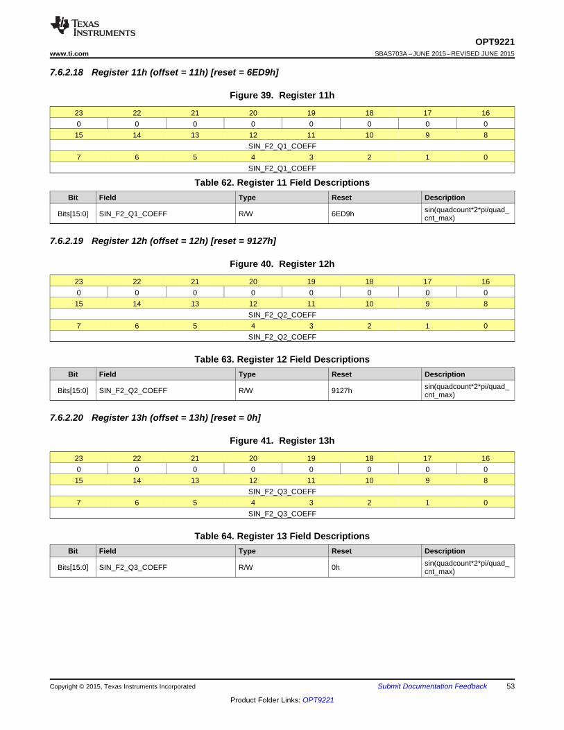
53
OPT9221www.ti.com SBAS703A –JUNE 2015–REVISED JUNE 2015
Product Folder Links: OPT9221
Submit Documentation FeedbackCopyright © 2015, Texas Instruments Incorporated
7.6.2.18 Register 11h (offset = 11h) [reset = 6ED9h]
Figure 39. Register 11h
23 22 21 20 19 18 17 160 0 0 0 0 0 0 015 14 13 12 11 10 9 8
SIN_F2_Q1_COEFF7 6 5 4 3 2 1 0
SIN_F2_Q1_COEFF
Table 62. Register 11 Field DescriptionsBit Field Type Reset Description
Bits[15:0] SIN_F2_Q1_COEFF R/W 6ED9h sin(quadcount*2*pi/quad_cnt_max)
7.6.2.19 Register 12h (offset = 12h) [reset = 9127h]
Figure 40. Register 12h
23 22 21 20 19 18 17 160 0 0 0 0 0 0 015 14 13 12 11 10 9 8
SIN_F2_Q2_COEFF7 6 5 4 3 2 1 0
SIN_F2_Q2_COEFF
Table 63. Register 12 Field DescriptionsBit Field Type Reset Description
Bits[15:0] SIN_F2_Q2_COEFF R/W 9127h sin(quadcount*2*pi/quad_cnt_max)
7.6.2.20 Register 13h (offset = 13h) [reset = 0h]
Figure 41. Register 13h
23 22 21 20 19 18 17 160 0 0 0 0 0 0 015 14 13 12 11 10 9 8
SIN_F2_Q3_COEFF7 6 5 4 3 2 1 0
SIN_F2_Q3_COEFF
Table 64. Register 13 Field DescriptionsBit Field Type Reset Description
Bits[15:0] SIN_F2_Q3_COEFF R/W 0h sin(quadcount*2*pi/quad_cnt_max)
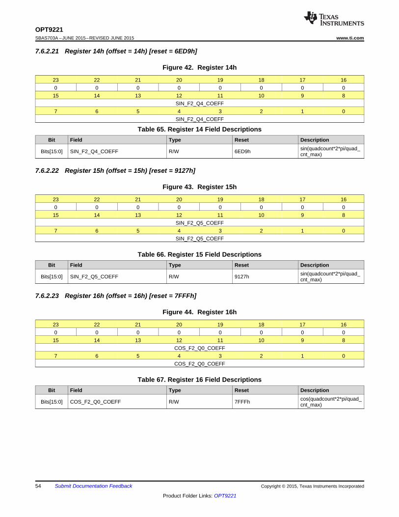
54
OPT9221SBAS703A –JUNE 2015–REVISED JUNE 2015 www.ti.com
Product Folder Links: OPT9221
Submit Documentation Feedback Copyright © 2015, Texas Instruments Incorporated
7.6.2.21 Register 14h (offset = 14h) [reset = 6ED9h]
Figure 42. Register 14h
23 22 21 20 19 18 17 160 0 0 0 0 0 0 015 14 13 12 11 10 9 8
SIN_F2_Q4_COEFF7 6 5 4 3 2 1 0
SIN_F2_Q4_COEFF
Table 65. Register 14 Field DescriptionsBit Field Type Reset Description
Bits[15:0] SIN_F2_Q4_COEFF R/W 6ED9h sin(quadcount*2*pi/quad_cnt_max)
7.6.2.22 Register 15h (offset = 15h) [reset = 9127h]
Figure 43. Register 15h
23 22 21 20 19 18 17 160 0 0 0 0 0 0 015 14 13 12 11 10 9 8
SIN_F2_Q5_COEFF7 6 5 4 3 2 1 0
SIN_F2_Q5_COEFF
Table 66. Register 15 Field DescriptionsBit Field Type Reset Description
Bits[15:0] SIN_F2_Q5_COEFF R/W 9127h sin(quadcount*2*pi/quad_cnt_max)
7.6.2.23 Register 16h (offset = 16h) [reset = 7FFFh]
Figure 44. Register 16h
23 22 21 20 19 18 17 160 0 0 0 0 0 0 015 14 13 12 11 10 9 8
COS_F2_Q0_COEFF7 6 5 4 3 2 1 0
COS_F2_Q0_COEFF
Table 67. Register 16 Field DescriptionsBit Field Type Reset Description
Bits[15:0] COS_F2_Q0_COEFF R/W 7FFFh cos(quadcount*2*pi/quad_cnt_max)
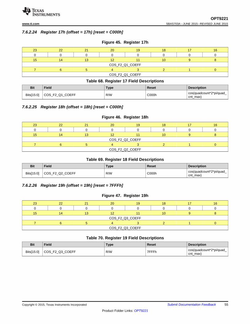
55
OPT9221www.ti.com SBAS703A –JUNE 2015–REVISED JUNE 2015
Product Folder Links: OPT9221
Submit Documentation FeedbackCopyright © 2015, Texas Instruments Incorporated
7.6.2.24 Register 17h (offset = 17h) [reset = C000h]
Figure 45. Register 17h
23 22 21 20 19 18 17 160 0 0 0 0 0 0 015 14 13 12 11 10 9 8
COS_F2_Q1_COEFF7 6 5 4 3 2 1 0
COS_F2_Q1_COEFF
Table 68. Register 17 Field DescriptionsBit Field Type Reset Description
Bits[15:0] COS_F2_Q1_COEFF R/W C000h cos(quadcount*2*pi/quad_cnt_max)
7.6.2.25 Register 18h (offset = 18h) [reset = C000h]
Figure 46. Register 18h
23 22 21 20 19 18 17 160 0 0 0 0 0 0 015 14 13 12 11 10 9 8
COS_F2_Q2_COEFF7 6 5 4 3 2 1 0
COS_F2_Q2_COEFF
Table 69. Register 18 Field DescriptionsBit Field Type Reset Description
Bits[15:0] COS_F2_Q2_COEFF R/W C000h cos(quadcount*2*pi/quad_cnt_max)
7.6.2.26 Register 19h (offset = 19h) [reset = 7FFFh]
Figure 47. Register 19h
23 22 21 20 19 18 17 160 0 0 0 0 0 0 015 14 13 12 11 10 9 8
COS_F2_Q3_COEFF7 6 5 4 3 2 1 0
COS_F2_Q3_COEFF
Table 70. Register 19 Field DescriptionsBit Field Type Reset Description
Bits[15:0] COS_F2_Q3_COEFF R/W 7FFFh cos(quadcount*2*pi/quad_cnt_max)
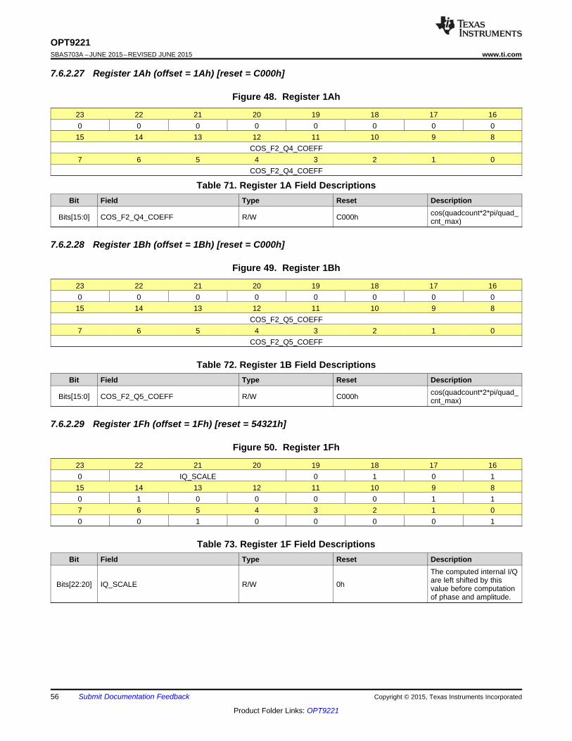
56
OPT9221SBAS703A –JUNE 2015–REVISED JUNE 2015 www.ti.com
Product Folder Links: OPT9221
Submit Documentation Feedback Copyright © 2015, Texas Instruments Incorporated
7.6.2.27 Register 1Ah (offset = 1Ah) [reset = C000h]
Figure 48. Register 1Ah
23 22 21 20 19 18 17 160 0 0 0 0 0 0 015 14 13 12 11 10 9 8
COS_F2_Q4_COEFF7 6 5 4 3 2 1 0
COS_F2_Q4_COEFF
Table 71. Register 1A Field DescriptionsBit Field Type Reset Description
Bits[15:0] COS_F2_Q4_COEFF R/W C000h cos(quadcount*2*pi/quad_cnt_max)
7.6.2.28 Register 1Bh (offset = 1Bh) [reset = C000h]
Figure 49. Register 1Bh
23 22 21 20 19 18 17 160 0 0 0 0 0 0 015 14 13 12 11 10 9 8
COS_F2_Q5_COEFF7 6 5 4 3 2 1 0
COS_F2_Q5_COEFF
Table 72. Register 1B Field DescriptionsBit Field Type Reset Description
Bits[15:0] COS_F2_Q5_COEFF R/W C000h cos(quadcount*2*pi/quad_cnt_max)
7.6.2.29 Register 1Fh (offset = 1Fh) [reset = 54321h]
Figure 50. Register 1Fh
23 22 21 20 19 18 17 160 IQ_SCALE 0 1 0 115 14 13 12 11 10 9 80 1 0 0 0 0 1 17 6 5 4 3 2 1 00 0 1 0 0 0 0 1
Table 73. Register 1F Field DescriptionsBit Field Type Reset Description
Bits[22:20] IQ_SCALE R/W 0h
The computed internal I/Qare left shifted by thisvalue before computationof phase and amplitude.
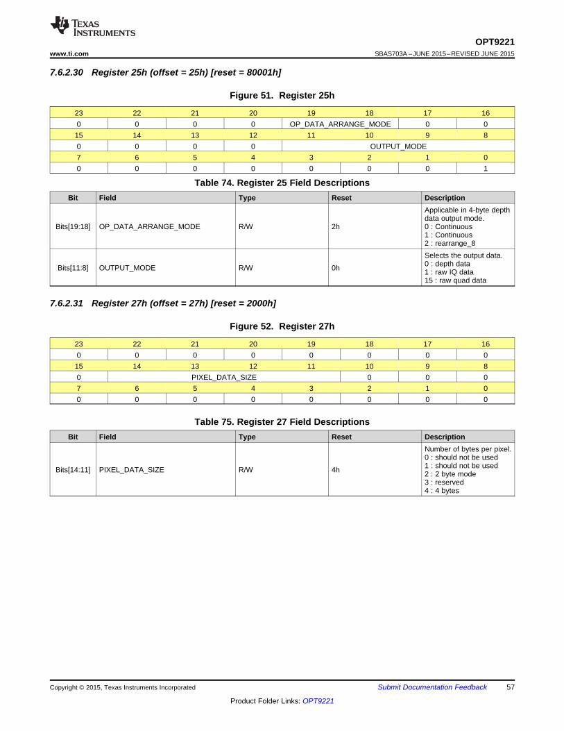
57
OPT9221www.ti.com SBAS703A –JUNE 2015–REVISED JUNE 2015
Product Folder Links: OPT9221
Submit Documentation FeedbackCopyright © 2015, Texas Instruments Incorporated
7.6.2.30 Register 25h (offset = 25h) [reset = 80001h]
Figure 51. Register 25h
23 22 21 20 19 18 17 160 0 0 0 OP_DATA_ARRANGE_MODE 0 015 14 13 12 11 10 9 80 0 0 0 OUTPUT_MODE7 6 5 4 3 2 1 00 0 0 0 0 0 0 1
Table 74. Register 25 Field DescriptionsBit Field Type Reset Description
Bits[19:18] OP_DATA_ARRANGE_MODE R/W 2h
Applicable in 4-byte depthdata output mode.0 : Continuous1 : Continuous2 : rearrange_8
Bits[11:8] OUTPUT_MODE R/W 0h
Selects the output data.0 : depth data1 : raw IQ data15 : raw quad data
7.6.2.31 Register 27h (offset = 27h) [reset = 2000h]
Figure 52. Register 27h
23 22 21 20 19 18 17 160 0 0 0 0 0 0 015 14 13 12 11 10 9 80 PIXEL_DATA_SIZE 0 0 07 6 5 4 3 2 1 00 0 0 0 0 0 0 0
Table 75. Register 27 Field DescriptionsBit Field Type Reset Description
Bits[14:11] PIXEL_DATA_SIZE R/W 4h
Number of bytes per pixel.0 : should not be used1 : should not be used2 : 2 byte mode3 : reserved4 : 4 bytes
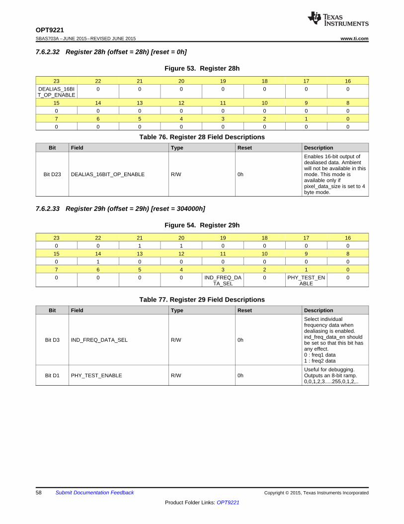
58
OPT9221SBAS703A –JUNE 2015–REVISED JUNE 2015 www.ti.com
Product Folder Links: OPT9221
Submit Documentation Feedback Copyright © 2015, Texas Instruments Incorporated
7.6.2.32 Register 28h (offset = 28h) [reset = 0h]
Figure 53. Register 28h
23 22 21 20 19 18 17 16DEALIAS_16BIT_OP_ENABLE
0 0 0 0 0 0 0
15 14 13 12 11 10 9 80 0 0 0 0 0 0 07 6 5 4 3 2 1 00 0 0 0 0 0 0 0
Table 76. Register 28 Field DescriptionsBit Field Type Reset Description
Bit D23 DEALIAS_16BIT_OP_ENABLE R/W 0h
Enables 16-bit output ofdealiased data. Ambientwill not be available in thismode. This mode isavailable only ifpixel_data_size is set to 4byte mode.
7.6.2.33 Register 29h (offset = 29h) [reset = 304000h]
Figure 54. Register 29h
23 22 21 20 19 18 17 160 0 1 1 0 0 0 015 14 13 12 11 10 9 80 1 0 0 0 0 0 07 6 5 4 3 2 1 00 0 0 0 IND_FREQ_DA
TA_SEL0 PHY_TEST_EN
ABLE0
Table 77. Register 29 Field DescriptionsBit Field Type Reset Description
Bit D3 IND_FREQ_DATA_SEL R/W 0h
Select individualfrequency data whendealiasing is enabled.ind_freq_data_en shouldbe set so that this bit hasany effect.0 : freq1 data1 : freq2 data
Bit D1 PHY_TEST_ENABLE R/W 0hUseful for debugging.Outputs an 8-bit ramp.0,0,1,2,3.....255,0,1,2,..
59
OPT9221www.ti.com SBAS703A –JUNE 2015–REVISED JUNE 2015
Product Folder Links: OPT9221
Submit Documentation FeedbackCopyright © 2015, Texas Instruments Incorporated
7.6.2.34 Register 2Eh (offset = 2Eh) [reset = 871h]
Figure 55. Register 2Eh
23 22 21 20 19 18 17 160 0 0 0 0 0 0 015 14 13 12 11 10 9 80 0 0 0 1 0 0 07 6 5 4 3 2 1 00 TILLUM_SLV_ADDR
Table 78. Register 2E Field DescriptionsBit Field Type Reset Description
Bits[6:0] TILLUM_SLV_ADDR R/W 71h
The illuminationtemperature sensor's I2Cslave address. Thistemperature sensor isassumed to be near theToF illumination driver forcalibration.
7.6.2.35 Register 2Fh (offset = 2Fh) [reset = 3C0001h]
Figure 56. Register 2Fh
23 22 21 20 19 18 17 16BIN_ROW_COUNT
15 14 13 12 11 10 9 8BIN_ROW_COUNT 0 BINNING_EN 0 0 ROWS_TO_MERGE7 6 5 4 3 2 1 0
ROWS_TO_MERGE
Table 79. Register 2F Field DescriptionsBit Field Type Reset Description
Bits[23:14] BIN_ROW_COUNT R/W F0hMust be programmed tofloor(total_rows/rows_to_merge)
Bit D12 BINNING_EN R/W 0h
When set to '1', enablesbinning of output data.Number of rows merged =rows_to_mergeNumber of columnsmerged = cols_to_merge
Bits[9:0] ROWS_TO_MERGE R/W 1h Refer to binning_endescription
60
OPT9221SBAS703A –JUNE 2015–REVISED JUNE 2015 www.ti.com
Product Folder Links: OPT9221
Submit Documentation Feedback Copyright © 2015, Texas Instruments Incorporated
7.6.2.36 Register 30h (offset = 30h) [reset = 500001h]
Figure 57. Register 30h
23 22 21 20 19 18 17 16BIN_COL_COUNT
15 14 13 12 11 10 9 8BIN_COL_COUNT 0 0 0 0 COLS_TO_MERGE7 6 5 4 3 2 1 0
COLS_TO_MERGE
Table 80. Register 30 Field DescriptionsBit Field Type Reset Description
Bits[23:14] BIN_COL_COUNT R/W 140hMust be programmed tofloor(total_rows/cols_to_merge)
Bits[9:0] COLS_TO_MERGE R/W 1h Refer to binning_endescription
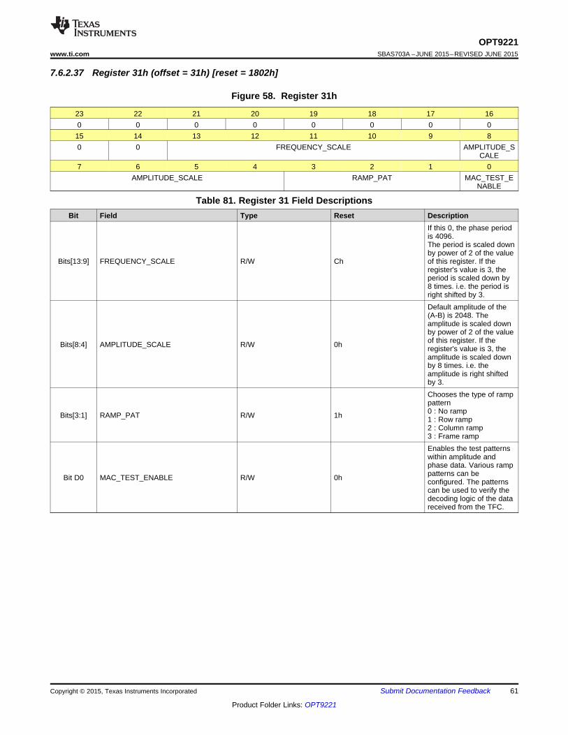
61
OPT9221www.ti.com SBAS703A –JUNE 2015–REVISED JUNE 2015
Product Folder Links: OPT9221
Submit Documentation FeedbackCopyright © 2015, Texas Instruments Incorporated
7.6.2.37 Register 31h (offset = 31h) [reset = 1802h]
Figure 58. Register 31h
23 22 21 20 19 18 17 160 0 0 0 0 0 0 015 14 13 12 11 10 9 80 0 FREQUENCY_SCALE AMPLITUDE_S
CALE7 6 5 4 3 2 1 0
AMPLITUDE_SCALE RAMP_PAT MAC_TEST_ENABLE
Table 81. Register 31 Field DescriptionsBit Field Type Reset Description
Bits[13:9] FREQUENCY_SCALE R/W Ch
If this 0, the phase periodis 4096.The period is scaled downby power of 2 of the valueof this register. If theregister's value is 3, theperiod is scaled down by8 times. i.e. the period isright shifted by 3.
Bits[8:4] AMPLITUDE_SCALE R/W 0h
Default amplitude of the(A-B) is 2048. Theamplitude is scaled downby power of 2 of the valueof this register. If theregister's value is 3, theamplitude is scaled downby 8 times. i.e. theamplitude is right shiftedby 3.
Bits[3:1] RAMP_PAT R/W 1h
Chooses the type of ramppattern0 : No ramp1 : Row ramp2 : Column ramp3 : Frame ramp
Bit D0 MAC_TEST_ENABLE R/W 0h
Enables the test patternswithin amplitude andphase data. Various ramppatterns can beconfigured. The patternscan be used to verify thedecoding logic of the datareceived from the TFC.
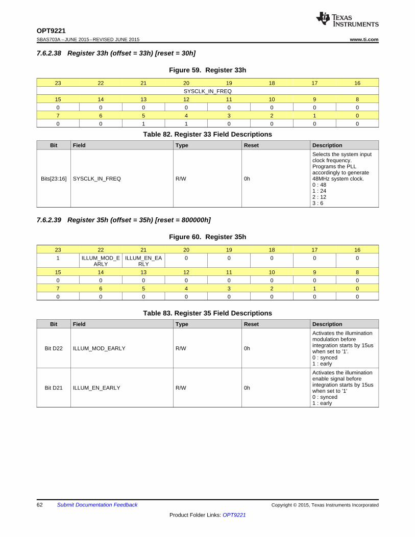
62
OPT9221SBAS703A –JUNE 2015–REVISED JUNE 2015 www.ti.com
Product Folder Links: OPT9221
Submit Documentation Feedback Copyright © 2015, Texas Instruments Incorporated
7.6.2.38 Register 33h (offset = 33h) [reset = 30h]
Figure 59. Register 33h
23 22 21 20 19 18 17 16SYSCLK_IN_FREQ
15 14 13 12 11 10 9 80 0 0 0 0 0 0 07 6 5 4 3 2 1 00 0 1 1 0 0 0 0
Table 82. Register 33 Field DescriptionsBit Field Type Reset Description
Bits[23:16] SYSCLK_IN_FREQ R/W 0h
Selects the system inputclock frequency.Programs the PLLaccordingly to generate48MHz system clock.0 : 481 : 242 : 123 : 6
7.6.2.39 Register 35h (offset = 35h) [reset = 800000h]
Figure 60. Register 35h
23 22 21 20 19 18 17 161 ILLUM_MOD_E
ARLYILLUM_EN_EA
RLY0 0 0 0 0
15 14 13 12 11 10 9 80 0 0 0 0 0 0 07 6 5 4 3 2 1 00 0 0 0 0 0 0 0
Table 83. Register 35 Field DescriptionsBit Field Type Reset Description
Bit D22 ILLUM_MOD_EARLY R/W 0h
Activates the illuminationmodulation beforeintegration starts by 15uswhen set to '1'.0 : synced1 : early
Bit D21 ILLUM_EN_EARLY R/W 0h
Activates the illuminationenable signal beforeintegration starts by 15uswhen set to '1'0 : synced1 : early
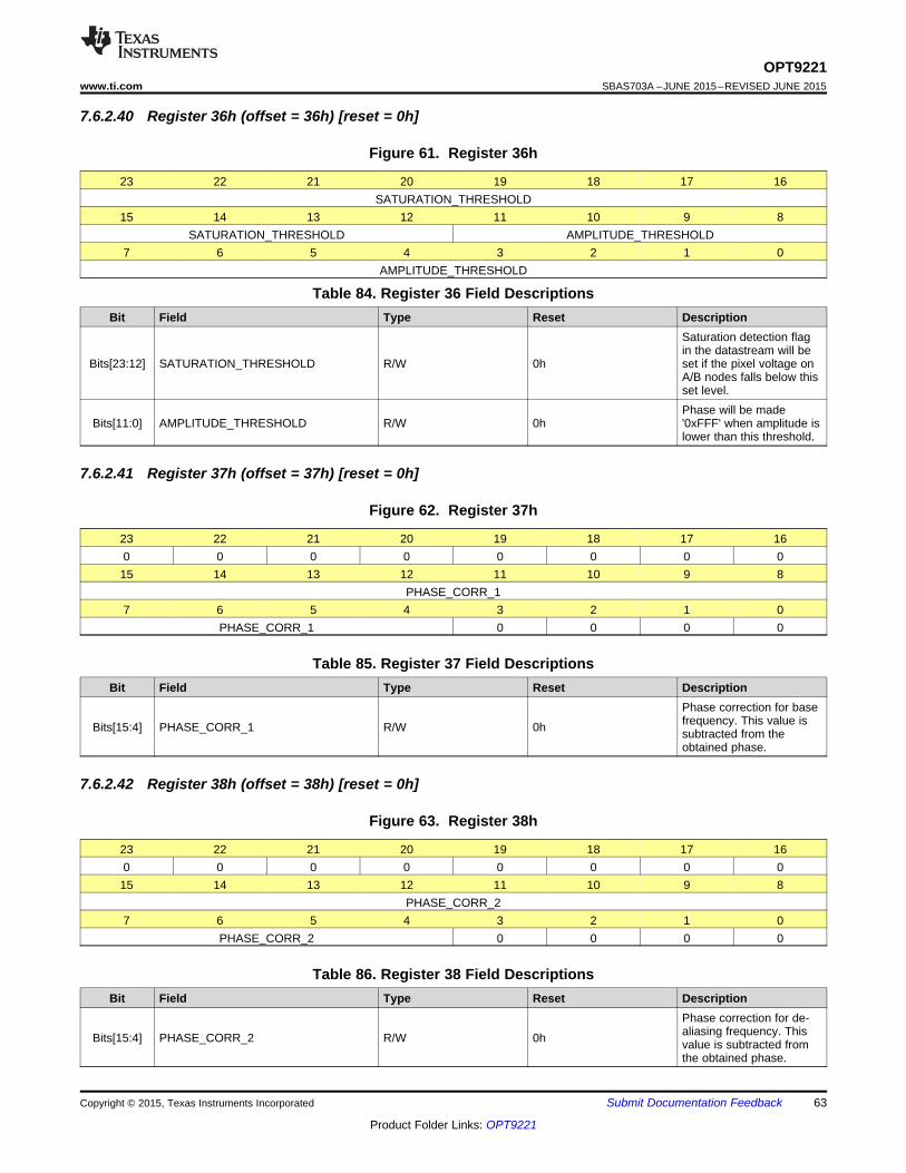
63
OPT9221www.ti.com SBAS703A –JUNE 2015–REVISED JUNE 2015
Product Folder Links: OPT9221
Submit Documentation FeedbackCopyright © 2015, Texas Instruments Incorporated
7.6.2.40 Register 36h (offset = 36h) [reset = 0h]
Figure 61. Register 36h
23 22 21 20 19 18 17 16SATURATION_THRESHOLD
15 14 13 12 11 10 9 8SATURATION_THRESHOLD AMPLITUDE_THRESHOLD
7 6 5 4 3 2 1 0AMPLITUDE_THRESHOLD
Table 84. Register 36 Field DescriptionsBit Field Type Reset Description
Bits[23:12] SATURATION_THRESHOLD R/W 0h
Saturation detection flagin the datastream will beset if the pixel voltage onA/B nodes falls below thisset level.
Bits[11:0] AMPLITUDE_THRESHOLD R/W 0hPhase will be made'0xFFF' when amplitude islower than this threshold.
7.6.2.41 Register 37h (offset = 37h) [reset = 0h]
Figure 62. Register 37h
23 22 21 20 19 18 17 160 0 0 0 0 0 0 015 14 13 12 11 10 9 8
PHASE_CORR_17 6 5 4 3 2 1 0
PHASE_CORR_1 0 0 0 0
Table 85. Register 37 Field DescriptionsBit Field Type Reset Description
Bits[15:4] PHASE_CORR_1 R/W 0h
Phase correction for basefrequency. This value issubtracted from theobtained phase.
7.6.2.42 Register 38h (offset = 38h) [reset = 0h]
Figure 63. Register 38h
23 22 21 20 19 18 17 160 0 0 0 0 0 0 015 14 13 12 11 10 9 8
PHASE_CORR_27 6 5 4 3 2 1 0
PHASE_CORR_2 0 0 0 0
Table 86. Register 38 Field DescriptionsBit Field Type Reset Description
Bits[15:4] PHASE_CORR_2 R/W 0h
Phase correction for de-aliasing frequency. Thisvalue is subtracted fromthe obtained phase.
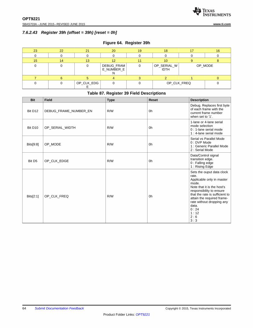
64
OPT9221SBAS703A –JUNE 2015–REVISED JUNE 2015 www.ti.com
Product Folder Links: OPT9221
Submit Documentation Feedback Copyright © 2015, Texas Instruments Incorporated
7.6.2.43 Register 39h (offset = 39h) [reset = 0h]
Figure 64. Register 39h
23 22 21 20 19 18 17 160 0 0 0 0 0 0 015 14 13 12 11 10 9 80 0 0 DEBUG_FRAM
E_NUMBER_EN
0 OP_SERIAL_WIDTH
OP_MODE
7 6 5 4 3 2 1 00 0 OP_CLK_EDG
E0 0 OP_CLK_FREQ 0
Table 87. Register 39 Field DescriptionsBit Field Type Reset Description
Bit D12 DEBUG_FRAME_NUMBER_EN R/W 0h
Debug. Replaces first byteof each frame with thecurrent frame numberwhen set to '1'.
Bit D10 OP_SERIAL_WIDTH R/W 0h
1-lane or 4-lane serialmode selection0 : 1-lane serial mode1 : 4-lane serial mode
Bits[9:8] OP_MODE R/W 0h
Serial vs Parallel Mode0 : DVP Mode1 : Generic Parallel Mode2 : Serial Mode
Bit D5 OP_CLK_EDGE R/W 0h
Data/Control signaltransition edge.0 : Falling edge1 : Rising Edge
Bits[2:1] OP_CLK_FREQ R/W 0h
Sets the ouput data clockrate.Applicable only in mastermode.Note that it is the host'sresponsibility to ensurethat the rate is sufficient toattain the required frame-rate without dropping anydata.0 : 241 : 122 : 63 : 3
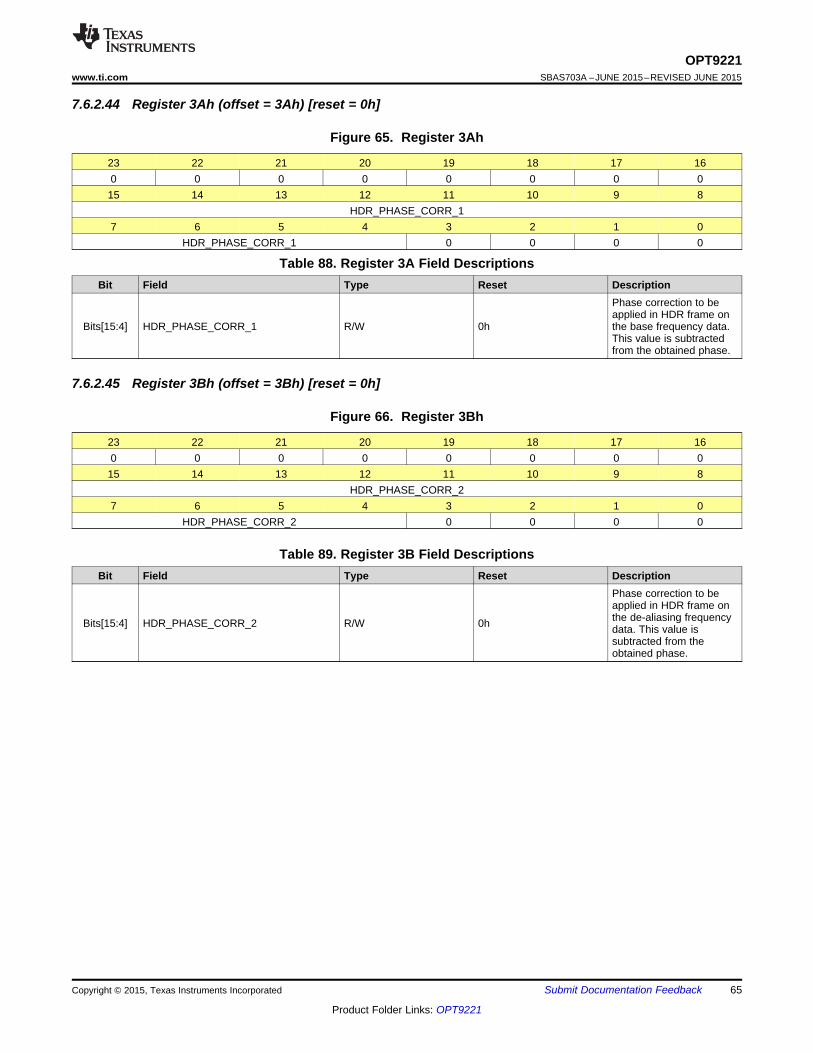
65
OPT9221www.ti.com SBAS703A –JUNE 2015–REVISED JUNE 2015
Product Folder Links: OPT9221
Submit Documentation FeedbackCopyright © 2015, Texas Instruments Incorporated
7.6.2.44 Register 3Ah (offset = 3Ah) [reset = 0h]
Figure 65. Register 3Ah
23 22 21 20 19 18 17 160 0 0 0 0 0 0 015 14 13 12 11 10 9 8
HDR_PHASE_CORR_17 6 5 4 3 2 1 0
HDR_PHASE_CORR_1 0 0 0 0
Table 88. Register 3A Field DescriptionsBit Field Type Reset Description
Bits[15:4] HDR_PHASE_CORR_1 R/W 0h
Phase correction to beapplied in HDR frame onthe base frequency data.This value is subtractedfrom the obtained phase.
7.6.2.45 Register 3Bh (offset = 3Bh) [reset = 0h]
Figure 66. Register 3Bh
23 22 21 20 19 18 17 160 0 0 0 0 0 0 015 14 13 12 11 10 9 8
HDR_PHASE_CORR_27 6 5 4 3 2 1 0
HDR_PHASE_CORR_2 0 0 0 0
Table 89. Register 3B Field DescriptionsBit Field Type Reset Description
Bits[15:4] HDR_PHASE_CORR_2 R/W 0h
Phase correction to beapplied in HDR frame onthe de-aliasing frequencydata. This value issubtracted from theobtained phase.
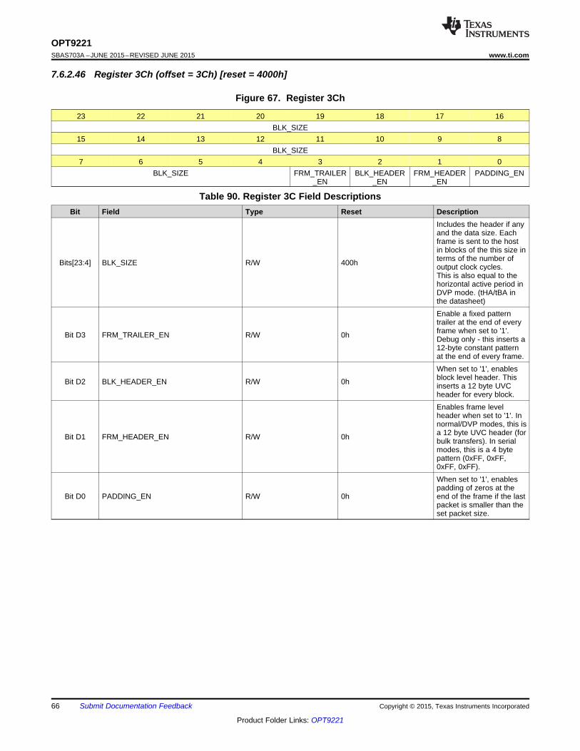
66
OPT9221SBAS703A –JUNE 2015–REVISED JUNE 2015 www.ti.com
Product Folder Links: OPT9221
Submit Documentation Feedback Copyright © 2015, Texas Instruments Incorporated
7.6.2.46 Register 3Ch (offset = 3Ch) [reset = 4000h]
Figure 67. Register 3Ch
23 22 21 20 19 18 17 16BLK_SIZE
15 14 13 12 11 10 9 8BLK_SIZE
7 6 5 4 3 2 1 0BLK_SIZE FRM_TRAILER
_ENBLK_HEADER
_ENFRM_HEADER
_ENPADDING_EN
Table 90. Register 3C Field DescriptionsBit Field Type Reset Description
Bits[23:4] BLK_SIZE R/W 400h
Includes the header if anyand the data size. Eachframe is sent to the hostin blocks of the this size interms of the number ofoutput clock cycles.This is also equal to thehorizontal active period inDVP mode. (tHA/tBA inthe datasheet)
Bit D3 FRM_TRAILER_EN R/W 0h
Enable a fixed patterntrailer at the end of everyframe when set to '1'.Debug only - this inserts a12-byte constant patternat the end of every frame.
Bit D2 BLK_HEADER_EN R/W 0h
When set to '1', enablesblock level header. Thisinserts a 12 byte UVCheader for every block.
Bit D1 FRM_HEADER_EN R/W 0h
Enables frame levelheader when set to '1'. Innormal/DVP modes, this isa 12 byte UVC header (forbulk transfers). In serialmodes, this is a 4 bytepattern (0xFF, 0xFF,0xFF, 0xFF).
Bit D0 PADDING_EN R/W 0h
When set to '1', enablespadding of zeros at theend of the frame if the lastpacket is smaller than theset packet size.
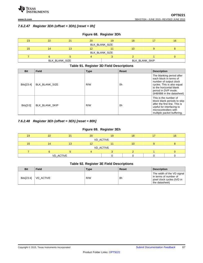
67
OPT9221www.ti.com SBAS703A –JUNE 2015–REVISED JUNE 2015
Product Folder Links: OPT9221
Submit Documentation FeedbackCopyright © 2015, Texas Instruments Incorporated
7.6.2.47 Register 3Dh (offset = 3Dh) [reset = 0h]
Figure 68. Register 3Dh
23 22 21 20 19 18 17 16BLK_BLANK_SIZE
15 14 13 12 11 10 9 8BLK_BLANK_SIZE
7 6 5 4 3 2 1 0BLK_BLANK_SIZE BLK_BLANK_SKIP
Table 91. Register 3D Field DescriptionsBit Field Type Reset Description
Bits[23:4] BLK_BLANK_SIZE R/W 0h
The blanking period aftereach block in terms ofnumber of output clockcycles. This is also equalto the horizontal blankperiod in DVP mode.(tHB/tBB in the datasheet)
Bits[3:0] BLK_BLANK_SKIP R/W 0h
This is the number ofblock blank periods to skipafter the first line. This isuseful for interfacing tomicrocontrollers withmultiple packet buffering.
7.6.2.48 Register 3Eh (offset = 3Eh) [reset = 80h]
Figure 69. Register 3Eh
23 22 21 20 19 18 17 16VD_ACTIVE
15 14 13 12 11 10 9 8VD_ACTIVE
7 6 5 4 3 2 1 0VD_ACTIVE 0 0 0 0
Table 92. Register 3E Field DescriptionsBit Field Type Reset Description
Bits[23:4] VD_ACTIVE R/W 8h
The width of the VD signalin terms of number ofpixel clock cycles (tVD inthe datasheet)
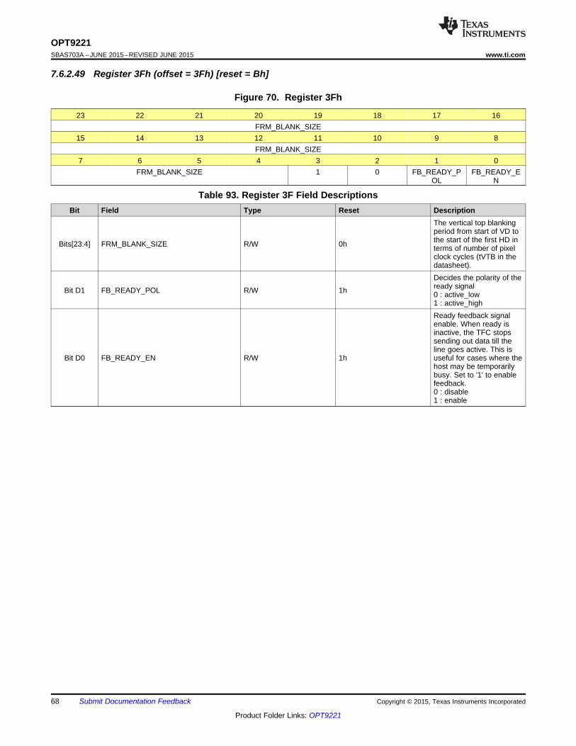
68
OPT9221SBAS703A –JUNE 2015–REVISED JUNE 2015 www.ti.com
Product Folder Links: OPT9221
Submit Documentation Feedback Copyright © 2015, Texas Instruments Incorporated
7.6.2.49 Register 3Fh (offset = 3Fh) [reset = Bh]
Figure 70. Register 3Fh
23 22 21 20 19 18 17 16FRM_BLANK_SIZE
15 14 13 12 11 10 9 8FRM_BLANK_SIZE
7 6 5 4 3 2 1 0FRM_BLANK_SIZE 1 0 FB_READY_P
OLFB_READY_E
N
Table 93. Register 3F Field DescriptionsBit Field Type Reset Description
Bits[23:4] FRM_BLANK_SIZE R/W 0h
The vertical top blankingperiod from start of VD tothe start of the first HD interms of number of pixelclock cycles (tVTB in thedatasheet).
Bit D1 FB_READY_POL R/W 1h
Decides the polarity of theready signal0 : active_low1 : active_high
Bit D0 FB_READY_EN R/W 1h
Ready feedback signalenable. When ready isinactive, the TFC stopssending out data till theline goes active. This isuseful for cases where thehost may be temporarilybusy. Set to '1' to enablefeedback.0 : disable1 : enable
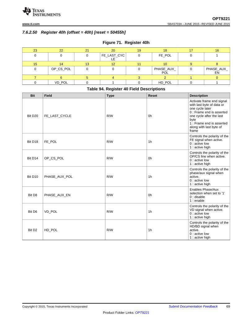
69
OPT9221www.ti.com SBAS703A –JUNE 2015–REVISED JUNE 2015
Product Folder Links: OPT9221
Submit Documentation FeedbackCopyright © 2015, Texas Instruments Incorporated
7.6.2.50 Register 40h (offset = 40h) [reset = 50455h]
Figure 71. Register 40h
23 22 21 20 19 18 17 160 0 0 FE_LAST_CYC
LE0 FE_POL 0 1
15 14 13 12 11 10 9 80 OP_CS_POL 0 0 0 PHASE_AUX_
POL0 PHASE_AUX_
EN7 6 5 4 3 2 1 00 VD_POL 0 1 0 HD_POL 0 1
Table 94. Register 40 Field DescriptionsBit Field Type Reset Description
Bit D20 FE_LAST_CYCLE R/W 0h
Activate frame end signalwith last byte of data orone cycle later0 : Frame end is assertedone cycle after the lastbyte1 : Frame end is assertedalong with last byte offrame
Bit D18 FE_POL R/W 1h
Controls the polarity of theFE signal when active.0 : active low1 : active high
Bit D14 OP_CS_POL R/W 0h
Controls the polarity of theOP/CS line when active.0 : active low1 : active high
Bit D10 PHASE_AUX_POL R/W 1h
Controls the polarity of thephase/aux signal whenactive.0 : active low1 : active high
Bit D8 PHASE_AUX_EN R/W 0h
Enables Phase/Auxselection when set to '1'0 : disable1 : enable
Bit D6 VD_POL R/W 1h
Controls the polarity of theVD signal when active.0 : active low1 : active high
Bit D2 HD_POL R/W 1h
Controls the polarity of theHD/BD signal whenactive.0 : active low1 : active high
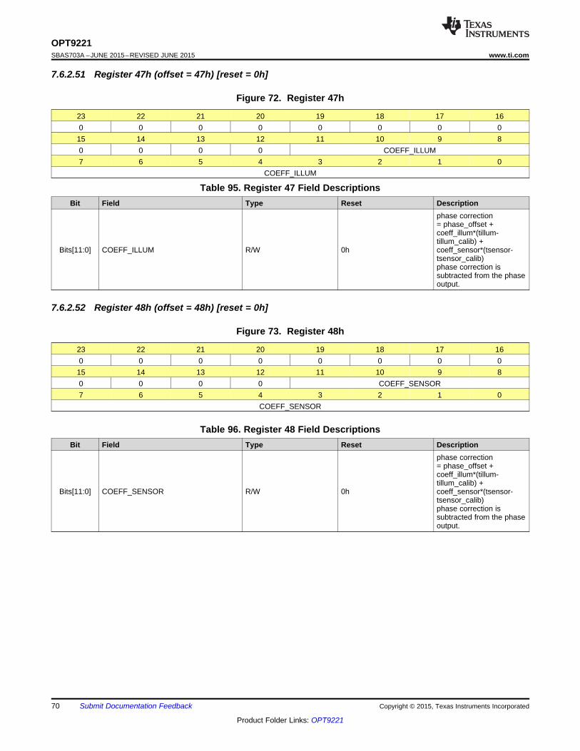
70
OPT9221SBAS703A –JUNE 2015–REVISED JUNE 2015 www.ti.com
Product Folder Links: OPT9221
Submit Documentation Feedback Copyright © 2015, Texas Instruments Incorporated
7.6.2.51 Register 47h (offset = 47h) [reset = 0h]
Figure 72. Register 47h
23 22 21 20 19 18 17 160 0 0 0 0 0 0 015 14 13 12 11 10 9 80 0 0 0 COEFF_ILLUM7 6 5 4 3 2 1 0
COEFF_ILLUM
Table 95. Register 47 Field DescriptionsBit Field Type Reset Description
Bits[11:0] COEFF_ILLUM R/W 0h
phase correction= phase_offset +coeff_illum*(tillum-tillum_calib) +coeff_sensor*(tsensor-tsensor_calib)phase correction issubtracted from the phaseoutput.
7.6.2.52 Register 48h (offset = 48h) [reset = 0h]
Figure 73. Register 48h
23 22 21 20 19 18 17 160 0 0 0 0 0 0 015 14 13 12 11 10 9 80 0 0 0 COEFF_SENSOR7 6 5 4 3 2 1 0
COEFF_SENSOR
Table 96. Register 48 Field DescriptionsBit Field Type Reset Description
Bits[11:0] COEFF_SENSOR R/W 0h
phase correction= phase_offset +coeff_illum*(tillum-tillum_calib) +coeff_sensor*(tsensor-tsensor_calib)phase correction issubtracted from the phaseoutput.
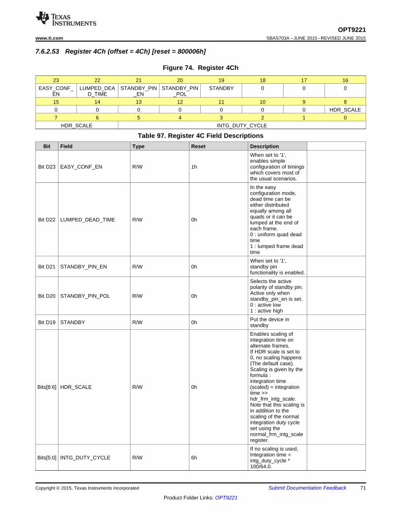
71
OPT9221www.ti.com SBAS703A –JUNE 2015–REVISED JUNE 2015
Product Folder Links: OPT9221
Submit Documentation FeedbackCopyright © 2015, Texas Instruments Incorporated
7.6.2.53 Register 4Ch (offset = 4Ch) [reset = 800006h]
Figure 74. Register 4Ch
23 22 21 20 19 18 17 16EASY_CONF_
ENLUMPED_DEA
D_TIMESTANDBY_PIN
_ENSTANDBY_PIN
_POLSTANDBY 0 0 0
15 14 13 12 11 10 9 80 0 0 0 0 0 0 HDR_SCALE7 6 5 4 3 2 1 0
HDR_SCALE INTG_DUTY_CYCLE
Table 97. Register 4C Field DescriptionsBit Field Type Reset Description
Bit D23 EASY_CONF_EN R/W 1h
When set to '1',enables simpleconfiguration of timingswhich covers most ofthe usual scenarios.
Bit D22 LUMPED_DEAD_TIME R/W 0h
In the easyconfiguration mode,dead time can beeither distributedequally among allquads or it can belumped at the end ofeach frame.0 : uniform quad deadtime1 : lumped frame deadtime
Bit D21 STANDBY_PIN_EN R/W 0hWhen set to '1',standby pinfunctionality is enabled.
Bit D20 STANDBY_PIN_POL R/W 0h
Selects the activepolarity of standby pin.Active only whenstandby_pin_en is set.0 : active low1 : active high
Bit D19 STANDBY R/W 0h Put the device instandby
Bits[8:6] HDR_SCALE R/W 0h
Enables scaling ofintegration time onalternate frames.If HDR scale is set to0, no scaling happens(The default case).Scaling is given by theformula :integration time(scaled) = integrationtime >>hdr_frm_intg_scale.Note that this scaling isin addition to thescaling of the normalintegration duty cycleset using thenormal_frm_intg_scaleregister.
Bits[5:0] INTG_DUTY_CYCLE R/W 6h
If no scaling is used,Integration time =intg_duty_cycle *100/64.0.
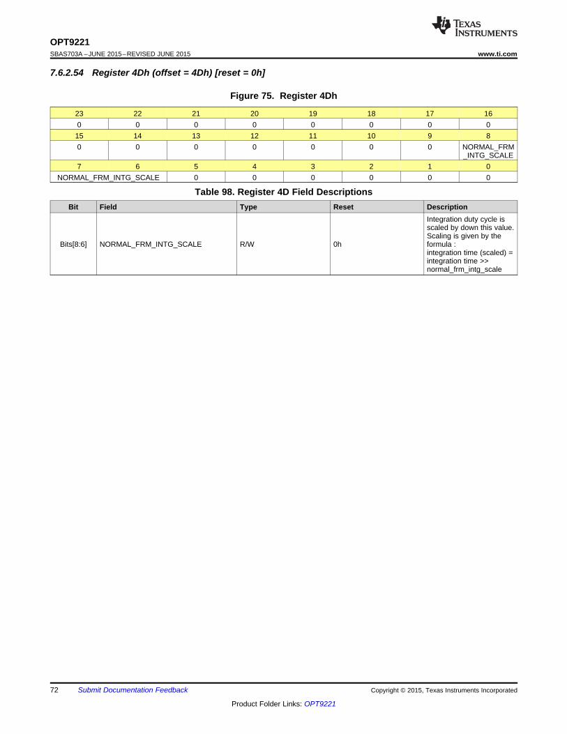
72
OPT9221SBAS703A –JUNE 2015–REVISED JUNE 2015 www.ti.com
Product Folder Links: OPT9221
Submit Documentation Feedback Copyright © 2015, Texas Instruments Incorporated
7.6.2.54 Register 4Dh (offset = 4Dh) [reset = 0h]
Figure 75. Register 4Dh
23 22 21 20 19 18 17 160 0 0 0 0 0 0 015 14 13 12 11 10 9 80 0 0 0 0 0 0 NORMAL_FRM
_INTG_SCALE7 6 5 4 3 2 1 0
NORMAL_FRM_INTG_SCALE 0 0 0 0 0 0
Table 98. Register 4D Field DescriptionsBit Field Type Reset Description
Bits[8:6] NORMAL_FRM_INTG_SCALE R/W 0h
Integration duty cycle isscaled by down this value.Scaling is given by theformula :integration time (scaled) =integration time >>normal_frm_intg_scale
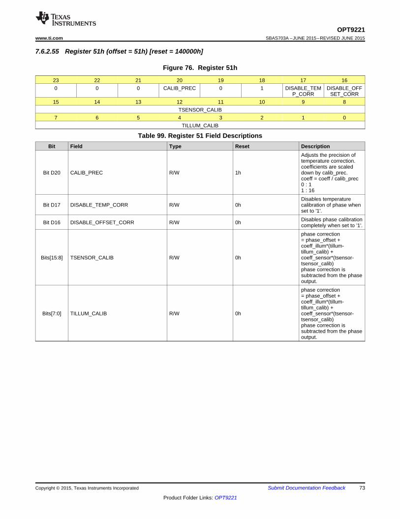
73
OPT9221www.ti.com SBAS703A –JUNE 2015–REVISED JUNE 2015
Product Folder Links: OPT9221
Submit Documentation FeedbackCopyright © 2015, Texas Instruments Incorporated
7.6.2.55 Register 51h (offset = 51h) [reset = 140000h]
Figure 76. Register 51h
23 22 21 20 19 18 17 160 0 0 CALIB_PREC 0 1 DISABLE_TEM
P_CORRDISABLE_OFF
SET_CORR15 14 13 12 11 10 9 8
TSENSOR_CALIB7 6 5 4 3 2 1 0
TILLUM_CALIB
Table 99. Register 51 Field DescriptionsBit Field Type Reset Description
Bit D20 CALIB_PREC R/W 1h
Adjusts the precision oftemperature correction.coefficients are scaleddown by calib_prec.coeff = coeff / calib_prec0 : 11 : 16
Bit D17 DISABLE_TEMP_CORR R/W 0hDisables temperaturecalibration of phase whenset to '1'.
Bit D16 DISABLE_OFFSET_CORR R/W 0h Disables phase calibrationcompletely when set to '1'.
Bits[15:8] TSENSOR_CALIB R/W 0h
phase correction= phase_offset +coeff_illum*(tillum-tillum_calib) +coeff_sensor*(tsensor-tsensor_calib)phase correction issubtracted from the phaseoutput.
Bits[7:0] TILLUM_CALIB R/W 0h
phase correction= phase_offset +coeff_illum*(tillum-tillum_calib) +coeff_sensor*(tsensor-tsensor_calib)phase correction issubtracted from the phaseoutput.
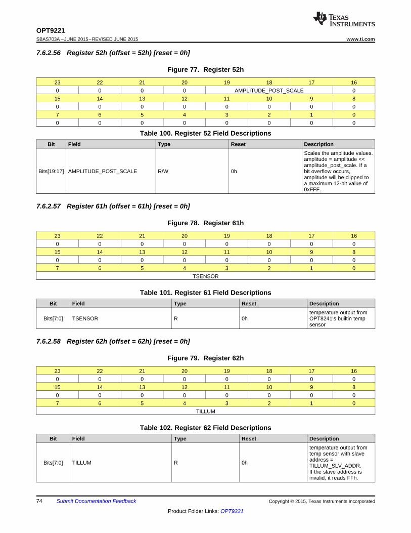
74
OPT9221SBAS703A –JUNE 2015–REVISED JUNE 2015 www.ti.com
Product Folder Links: OPT9221
Submit Documentation Feedback Copyright © 2015, Texas Instruments Incorporated
7.6.2.56 Register 52h (offset = 52h) [reset = 0h]
Figure 77. Register 52h
23 22 21 20 19 18 17 160 0 0 0 AMPLITUDE_POST_SCALE 015 14 13 12 11 10 9 80 0 0 0 0 0 0 07 6 5 4 3 2 1 00 0 0 0 0 0 0 0
Table 100. Register 52 Field DescriptionsBit Field Type Reset Description
Bits[19:17] AMPLITUDE_POST_SCALE R/W 0h
Scales the amplitude values.amplitude = amplitude <<amplitude_post_scale. If abit overflow occurs,amplitude will be clipped toa maximum 12-bit value of0xFFF.
7.6.2.57 Register 61h (offset = 61h) [reset = 0h]
Figure 78. Register 61h
23 22 21 20 19 18 17 160 0 0 0 0 0 0 015 14 13 12 11 10 9 80 0 0 0 0 0 0 07 6 5 4 3 2 1 0
TSENSOR
Table 101. Register 61 Field DescriptionsBit Field Type Reset Description
Bits[7:0] TSENSOR R 0htemperature output fromOPT8241's builtin tempsensor
7.6.2.58 Register 62h (offset = 62h) [reset = 0h]
Figure 79. Register 62h
23 22 21 20 19 18 17 160 0 0 0 0 0 0 015 14 13 12 11 10 9 80 0 0 0 0 0 0 07 6 5 4 3 2 1 0
TILLUM
Table 102. Register 62 Field DescriptionsBit Field Type Reset Description
Bits[7:0] TILLUM R 0h
temperature output fromtemp sensor with slaveaddress =TILLUM_SLV_ADDR.If the slave address isinvalid, it reads FFh.
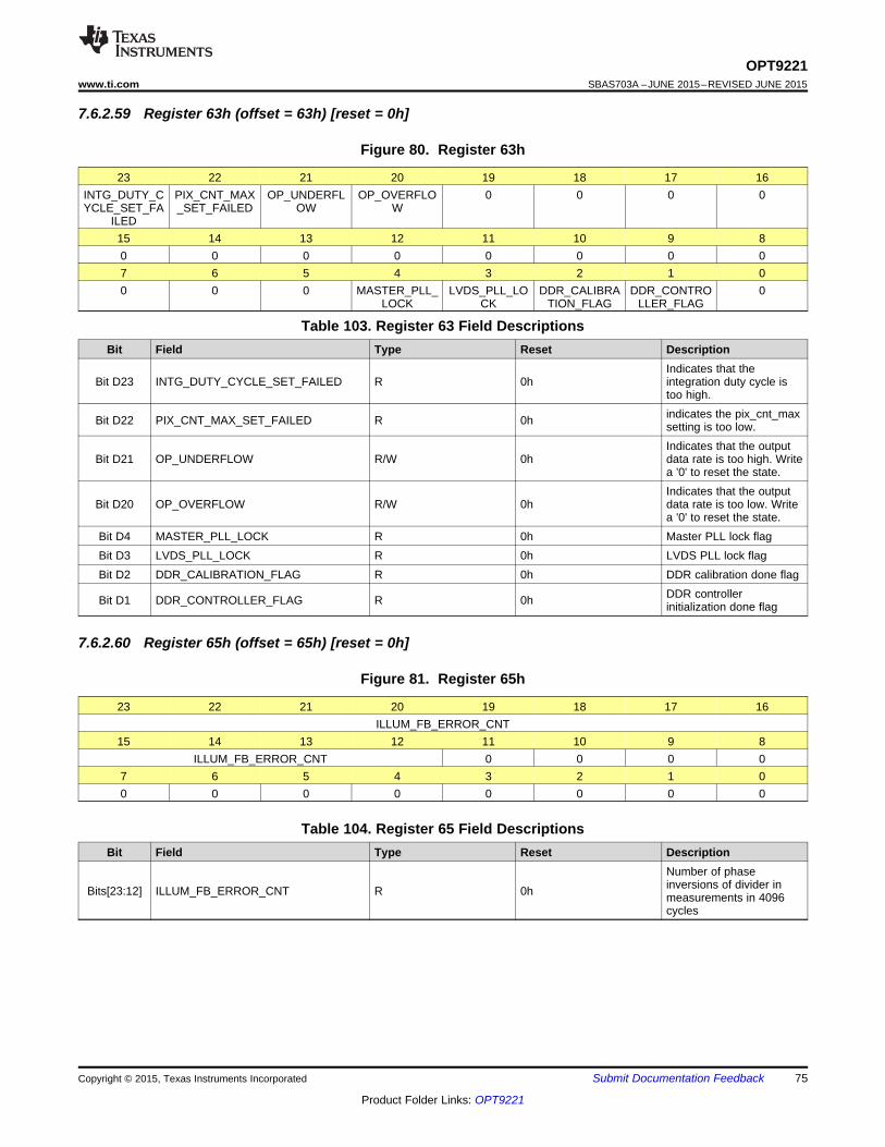
75
OPT9221www.ti.com SBAS703A –JUNE 2015–REVISED JUNE 2015
Product Folder Links: OPT9221
Submit Documentation FeedbackCopyright © 2015, Texas Instruments Incorporated
7.6.2.59 Register 63h (offset = 63h) [reset = 0h]
Figure 80. Register 63h
23 22 21 20 19 18 17 16INTG_DUTY_CYCLE_SET_FA
ILED
PIX_CNT_MAX_SET_FAILED
OP_UNDERFLOW
OP_OVERFLOW
0 0 0 0
15 14 13 12 11 10 9 80 0 0 0 0 0 0 07 6 5 4 3 2 1 00 0 0 MASTER_PLL_
LOCKLVDS_PLL_LO
CKDDR_CALIBRA
TION_FLAGDDR_CONTRO
LLER_FLAG0
Table 103. Register 63 Field DescriptionsBit Field Type Reset Description
Bit D23 INTG_DUTY_CYCLE_SET_FAILED R 0hIndicates that theintegration duty cycle istoo high.
Bit D22 PIX_CNT_MAX_SET_FAILED R 0h indicates the pix_cnt_maxsetting is too low.
Bit D21 OP_UNDERFLOW R/W 0hIndicates that the outputdata rate is too high. Writea '0' to reset the state.
Bit D20 OP_OVERFLOW R/W 0hIndicates that the outputdata rate is too low. Writea '0' to reset the state.
Bit D4 MASTER_PLL_LOCK R 0h Master PLL lock flagBit D3 LVDS_PLL_LOCK R 0h LVDS PLL lock flagBit D2 DDR_CALIBRATION_FLAG R 0h DDR calibration done flag
Bit D1 DDR_CONTROLLER_FLAG R 0h DDR controllerinitialization done flag
7.6.2.60 Register 65h (offset = 65h) [reset = 0h]
Figure 81. Register 65h
23 22 21 20 19 18 17 16ILLUM_FB_ERROR_CNT
15 14 13 12 11 10 9 8ILLUM_FB_ERROR_CNT 0 0 0 0
7 6 5 4 3 2 1 00 0 0 0 0 0 0 0
Table 104. Register 65 Field DescriptionsBit Field Type Reset Description
Bits[23:12] ILLUM_FB_ERROR_CNT R 0h
Number of phaseinversions of divider inmeasurements in 4096cycles
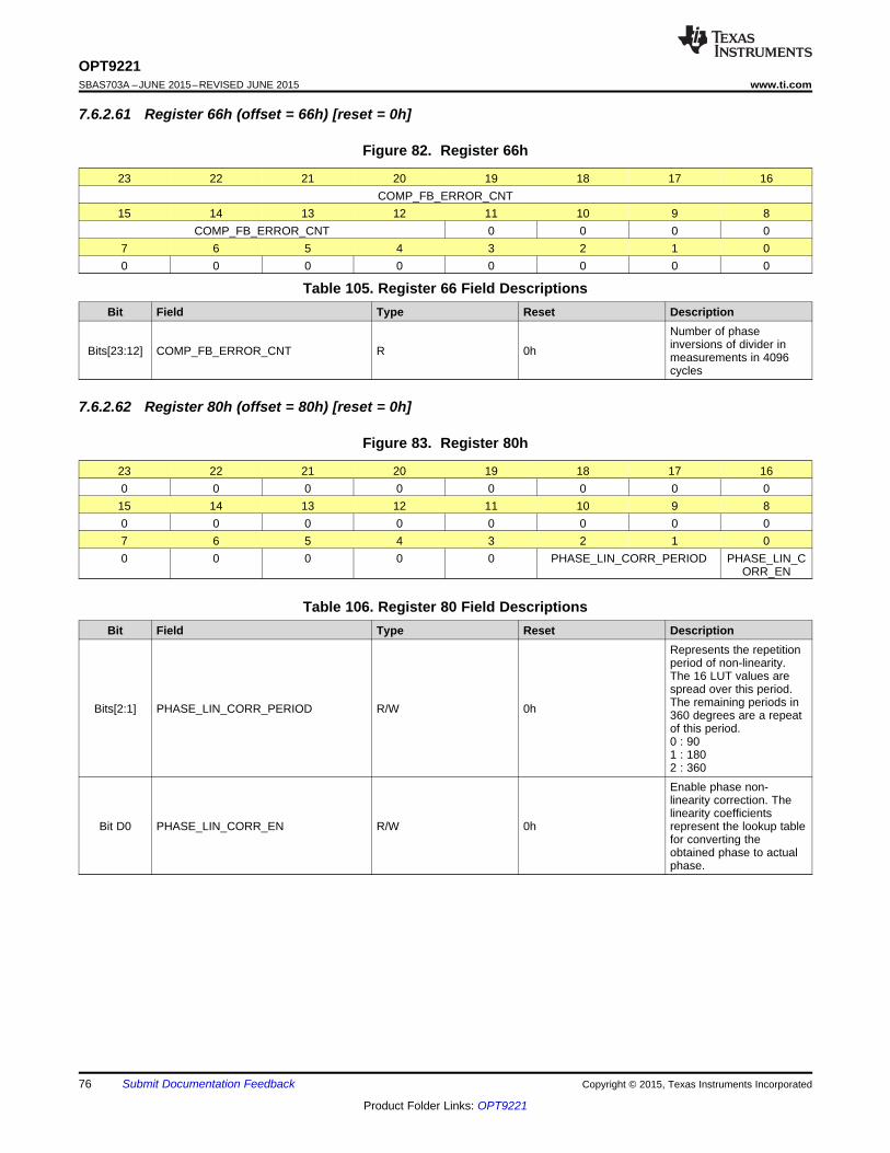
76
OPT9221SBAS703A –JUNE 2015–REVISED JUNE 2015 www.ti.com
Product Folder Links: OPT9221
Submit Documentation Feedback Copyright © 2015, Texas Instruments Incorporated
7.6.2.61 Register 66h (offset = 66h) [reset = 0h]
Figure 82. Register 66h
23 22 21 20 19 18 17 16COMP_FB_ERROR_CNT
15 14 13 12 11 10 9 8COMP_FB_ERROR_CNT 0 0 0 0
7 6 5 4 3 2 1 00 0 0 0 0 0 0 0
Table 105. Register 66 Field DescriptionsBit Field Type Reset Description
Bits[23:12] COMP_FB_ERROR_CNT R 0h
Number of phaseinversions of divider inmeasurements in 4096cycles
7.6.2.62 Register 80h (offset = 80h) [reset = 0h]
Figure 83. Register 80h
23 22 21 20 19 18 17 160 0 0 0 0 0 0 015 14 13 12 11 10 9 80 0 0 0 0 0 0 07 6 5 4 3 2 1 00 0 0 0 0 PHASE_LIN_CORR_PERIOD PHASE_LIN_C
ORR_EN
Table 106. Register 80 Field DescriptionsBit Field Type Reset Description
Bits[2:1] PHASE_LIN_CORR_PERIOD R/W 0h
Represents the repetitionperiod of non-linearity.The 16 LUT values arespread over this period.The remaining periods in360 degrees are a repeatof this period.0 : 901 : 1802 : 360
Bit D0 PHASE_LIN_CORR_EN R/W 0h
Enable phase non-linearity correction. Thelinearity coefficientsrepresent the lookup tablefor converting theobtained phase to actualphase.
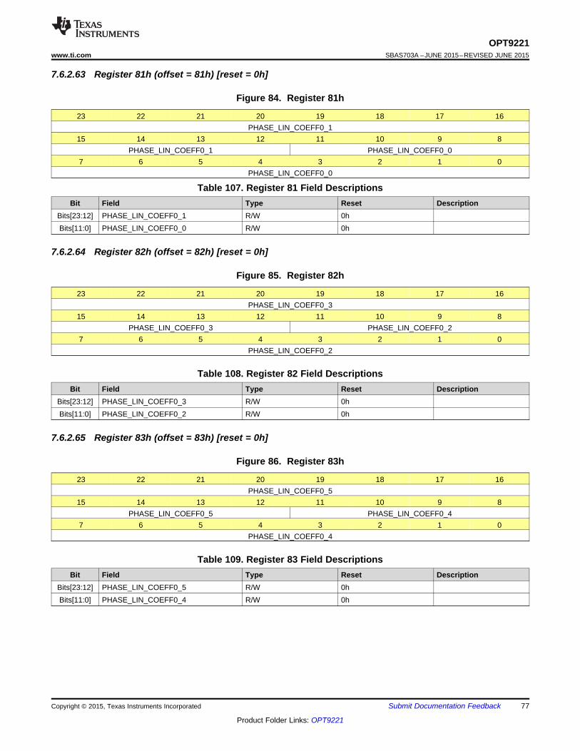
77
OPT9221www.ti.com SBAS703A –JUNE 2015–REVISED JUNE 2015
Product Folder Links: OPT9221
Submit Documentation FeedbackCopyright © 2015, Texas Instruments Incorporated
7.6.2.63 Register 81h (offset = 81h) [reset = 0h]
Figure 84. Register 81h
23 22 21 20 19 18 17 16PHASE_LIN_COEFF0_1
15 14 13 12 11 10 9 8PHASE_LIN_COEFF0_1 PHASE_LIN_COEFF0_0
7 6 5 4 3 2 1 0PHASE_LIN_COEFF0_0
Table 107. Register 81 Field DescriptionsBit Field Type Reset Description
Bits[23:12] PHASE_LIN_COEFF0_1 R/W 0hBits[11:0] PHASE_LIN_COEFF0_0 R/W 0h
7.6.2.64 Register 82h (offset = 82h) [reset = 0h]
Figure 85. Register 82h
23 22 21 20 19 18 17 16PHASE_LIN_COEFF0_3
15 14 13 12 11 10 9 8PHASE_LIN_COEFF0_3 PHASE_LIN_COEFF0_2
7 6 5 4 3 2 1 0PHASE_LIN_COEFF0_2
Table 108. Register 82 Field DescriptionsBit Field Type Reset Description
Bits[23:12] PHASE_LIN_COEFF0_3 R/W 0hBits[11:0] PHASE_LIN_COEFF0_2 R/W 0h
7.6.2.65 Register 83h (offset = 83h) [reset = 0h]
Figure 86. Register 83h
23 22 21 20 19 18 17 16PHASE_LIN_COEFF0_5
15 14 13 12 11 10 9 8PHASE_LIN_COEFF0_5 PHASE_LIN_COEFF0_4
7 6 5 4 3 2 1 0PHASE_LIN_COEFF0_4
Table 109. Register 83 Field DescriptionsBit Field Type Reset Description
Bits[23:12] PHASE_LIN_COEFF0_5 R/W 0hBits[11:0] PHASE_LIN_COEFF0_4 R/W 0h
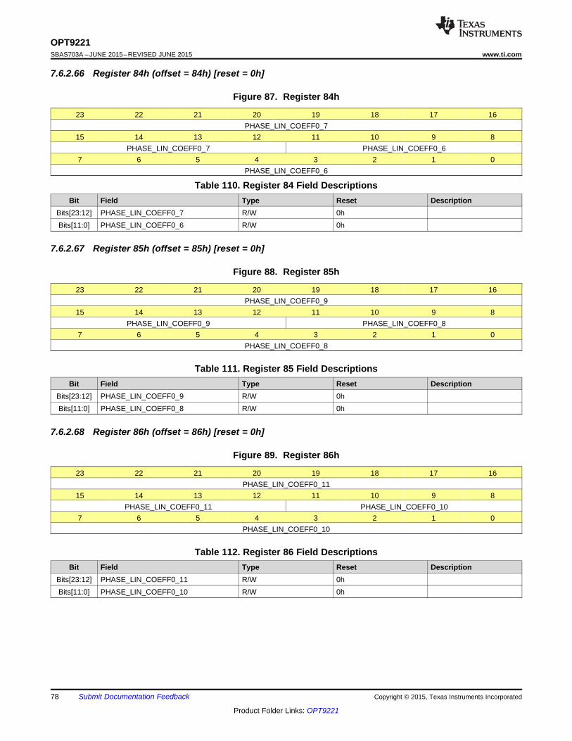
78
OPT9221SBAS703A –JUNE 2015–REVISED JUNE 2015 www.ti.com
Product Folder Links: OPT9221
Submit Documentation Feedback Copyright © 2015, Texas Instruments Incorporated
7.6.2.66 Register 84h (offset = 84h) [reset = 0h]
Figure 87. Register 84h
23 22 21 20 19 18 17 16PHASE_LIN_COEFF0_7
15 14 13 12 11 10 9 8PHASE_LIN_COEFF0_7 PHASE_LIN_COEFF0_6
7 6 5 4 3 2 1 0PHASE_LIN_COEFF0_6
Table 110. Register 84 Field DescriptionsBit Field Type Reset Description
Bits[23:12] PHASE_LIN_COEFF0_7 R/W 0hBits[11:0] PHASE_LIN_COEFF0_6 R/W 0h
7.6.2.67 Register 85h (offset = 85h) [reset = 0h]
Figure 88. Register 85h
23 22 21 20 19 18 17 16PHASE_LIN_COEFF0_9
15 14 13 12 11 10 9 8PHASE_LIN_COEFF0_9 PHASE_LIN_COEFF0_8
7 6 5 4 3 2 1 0PHASE_LIN_COEFF0_8
Table 111. Register 85 Field DescriptionsBit Field Type Reset Description
Bits[23:12] PHASE_LIN_COEFF0_9 R/W 0hBits[11:0] PHASE_LIN_COEFF0_8 R/W 0h
7.6.2.68 Register 86h (offset = 86h) [reset = 0h]
Figure 89. Register 86h
23 22 21 20 19 18 17 16PHASE_LIN_COEFF0_11
15 14 13 12 11 10 9 8PHASE_LIN_COEFF0_11 PHASE_LIN_COEFF0_10
7 6 5 4 3 2 1 0PHASE_LIN_COEFF0_10
Table 112. Register 86 Field DescriptionsBit Field Type Reset Description
Bits[23:12] PHASE_LIN_COEFF0_11 R/W 0hBits[11:0] PHASE_LIN_COEFF0_10 R/W 0h
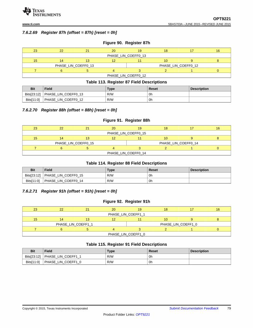
79
OPT9221www.ti.com SBAS703A –JUNE 2015–REVISED JUNE 2015
Product Folder Links: OPT9221
Submit Documentation FeedbackCopyright © 2015, Texas Instruments Incorporated
7.6.2.69 Register 87h (offset = 87h) [reset = 0h]
Figure 90. Register 87h
23 22 21 20 19 18 17 16PHASE_LIN_COEFF0_13
15 14 13 12 11 10 9 8PHASE_LIN_COEFF0_13 PHASE_LIN_COEFF0_12
7 6 5 4 3 2 1 0PHASE_LIN_COEFF0_12
Table 113. Register 87 Field DescriptionsBit Field Type Reset Description
Bits[23:12] PHASE_LIN_COEFF0_13 R/W 0hBits[11:0] PHASE_LIN_COEFF0_12 R/W 0h
7.6.2.70 Register 88h (offset = 88h) [reset = 0h]
Figure 91. Register 88h
23 22 21 20 19 18 17 16PHASE_LIN_COEFF0_15
15 14 13 12 11 10 9 8PHASE_LIN_COEFF0_15 PHASE_LIN_COEFF0_14
7 6 5 4 3 2 1 0PHASE_LIN_COEFF0_14
Table 114. Register 88 Field DescriptionsBit Field Type Reset Description
Bits[23:12] PHASE_LIN_COEFF0_15 R/W 0hBits[11:0] PHASE_LIN_COEFF0_14 R/W 0h
7.6.2.71 Register 91h (offset = 91h) [reset = 0h]
Figure 92. Register 91h
23 22 21 20 19 18 17 16PHASE_LIN_COEFF1_1
15 14 13 12 11 10 9 8PHASE_LIN_COEFF1_1 PHASE_LIN_COEFF1_0
7 6 5 4 3 2 1 0PHASE_LIN_COEFF1_0
Table 115. Register 91 Field DescriptionsBit Field Type Reset Description
Bits[23:12] PHASE_LIN_COEFF1_1 R/W 0hBits[11:0] PHASE_LIN_COEFF1_0 R/W 0h

80
OPT9221SBAS703A –JUNE 2015–REVISED JUNE 2015 www.ti.com
Product Folder Links: OPT9221
Submit Documentation Feedback Copyright © 2015, Texas Instruments Incorporated
7.6.2.72 Register 92h (offset = 92h) [reset = 0h]
Figure 93. Register 92h
23 22 21 20 19 18 17 16PHASE_LIN_COEFF1_3
15 14 13 12 11 10 9 8PHASE_LIN_COEFF1_3 PHASE_LIN_COEFF1_2
7 6 5 4 3 2 1 0PHASE_LIN_COEFF1_2
Table 116. Register 92 Field DescriptionsBit Field Type Reset Description
Bits[23:12] PHASE_LIN_COEFF1_3 R/W 0hBits[11:0] PHASE_LIN_COEFF1_2 R/W 0h
7.6.2.73 Register 93h (offset = 93h) [reset = 0h]
Figure 94. Register 93h
23 22 21 20 19 18 17 16PHASE_LIN_COEFF1_5
15 14 13 12 11 10 9 8PHASE_LIN_COEFF1_5 PHASE_LIN_COEFF1_4
7 6 5 4 3 2 1 0PHASE_LIN_COEFF1_4
Table 117. Register 93 Field DescriptionsBit Field Type Reset Description
Bits[23:12] PHASE_LIN_COEFF1_5 R/W 0hBits[11:0] PHASE_LIN_COEFF1_4 R/W 0h
7.6.2.74 Register 94h (offset = 94h) [reset = 0h]
Figure 95. Register 94h
23 22 21 20 19 18 17 16PHASE_LIN_COEFF1_7
15 14 13 12 11 10 9 8PHASE_LIN_COEFF1_7 PHASE_LIN_COEFF1_6
7 6 5 4 3 2 1 0PHASE_LIN_COEFF1_6
Table 118. Register 94 Field DescriptionsBit Field Type Reset Description
Bits[23:12] PHASE_LIN_COEFF1_7 R/W 0hBits[11:0] PHASE_LIN_COEFF1_6 R/W 0h

81
OPT9221www.ti.com SBAS703A –JUNE 2015–REVISED JUNE 2015
Product Folder Links: OPT9221
Submit Documentation FeedbackCopyright © 2015, Texas Instruments Incorporated
7.6.2.75 Register 95h (offset = 95h) [reset = 0h]
Figure 96. Register 95h
23 22 21 20 19 18 17 16PHASE_LIN_COEFF1_9
15 14 13 12 11 10 9 8PHASE_LIN_COEFF1_9 PHASE_LIN_COEFF1_8
7 6 5 4 3 2 1 0PHASE_LIN_COEFF1_8
Table 119. Register 95 Field DescriptionsBit Field Type Reset Description
Bits[23:12] PHASE_LIN_COEFF1_9 R/W 0hBits[11:0] PHASE_LIN_COEFF1_8 R/W 0h
7.6.2.76 Register 96h (offset = 96h) [reset = 0h]
Figure 97. Register 96h
23 22 21 20 19 18 17 16PHASE_LIN_COEFF1_11
15 14 13 12 11 10 9 8PHASE_LIN_COEFF1_11 PHASE_LIN_COEFF1_10
7 6 5 4 3 2 1 0PHASE_LIN_COEFF1_10
Table 120. Register 96 Field DescriptionsBit Field Type Reset Description
Bits[23:12] PHASE_LIN_COEFF1_11 R/W 0hBits[11:0] PHASE_LIN_COEFF1_10 R/W 0h
7.6.2.77 Register 97h (offset = 97h) [reset = 0h]
Figure 98. Register 97h
23 22 21 20 19 18 17 16PHASE_LIN_COEFF1_13
15 14 13 12 11 10 9 8PHASE_LIN_COEFF1_13 PHASE_LIN_COEFF1_12
7 6 5 4 3 2 1 0PHASE_LIN_COEFF1_12
Table 121. Register 97 Field DescriptionsBit Field Type Reset Description
Bits[23:12] PHASE_LIN_COEFF1_13 R/W 0hBits[11:0] PHASE_LIN_COEFF1_12 R/W 0h
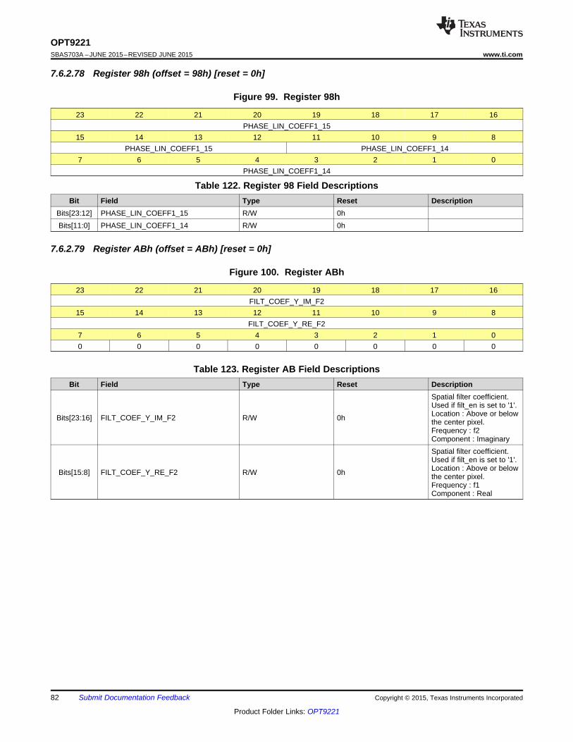
82
OPT9221SBAS703A –JUNE 2015–REVISED JUNE 2015 www.ti.com
Product Folder Links: OPT9221
Submit Documentation Feedback Copyright © 2015, Texas Instruments Incorporated
7.6.2.78 Register 98h (offset = 98h) [reset = 0h]
Figure 99. Register 98h
23 22 21 20 19 18 17 16PHASE_LIN_COEFF1_15
15 14 13 12 11 10 9 8PHASE_LIN_COEFF1_15 PHASE_LIN_COEFF1_14
7 6 5 4 3 2 1 0PHASE_LIN_COEFF1_14
Table 122. Register 98 Field DescriptionsBit Field Type Reset Description
Bits[23:12] PHASE_LIN_COEFF1_15 R/W 0hBits[11:0] PHASE_LIN_COEFF1_14 R/W 0h
7.6.2.79 Register ABh (offset = ABh) [reset = 0h]
Figure 100. Register ABh
23 22 21 20 19 18 17 16FILT_COEF_Y_IM_F2
15 14 13 12 11 10 9 8FILT_COEF_Y_RE_F2
7 6 5 4 3 2 1 00 0 0 0 0 0 0 0
Table 123. Register AB Field DescriptionsBit Field Type Reset Description
Bits[23:16] FILT_COEF_Y_IM_F2 R/W 0h
Spatial filter coefficient.Used if filt_en is set to '1'.Location : Above or belowthe center pixel.Frequency : f2Component : Imaginary
Bits[15:8] FILT_COEF_Y_RE_F2 R/W 0h
Spatial filter coefficient.Used if filt_en is set to '1'.Location : Above or belowthe center pixel.Frequency : f1Component : Real
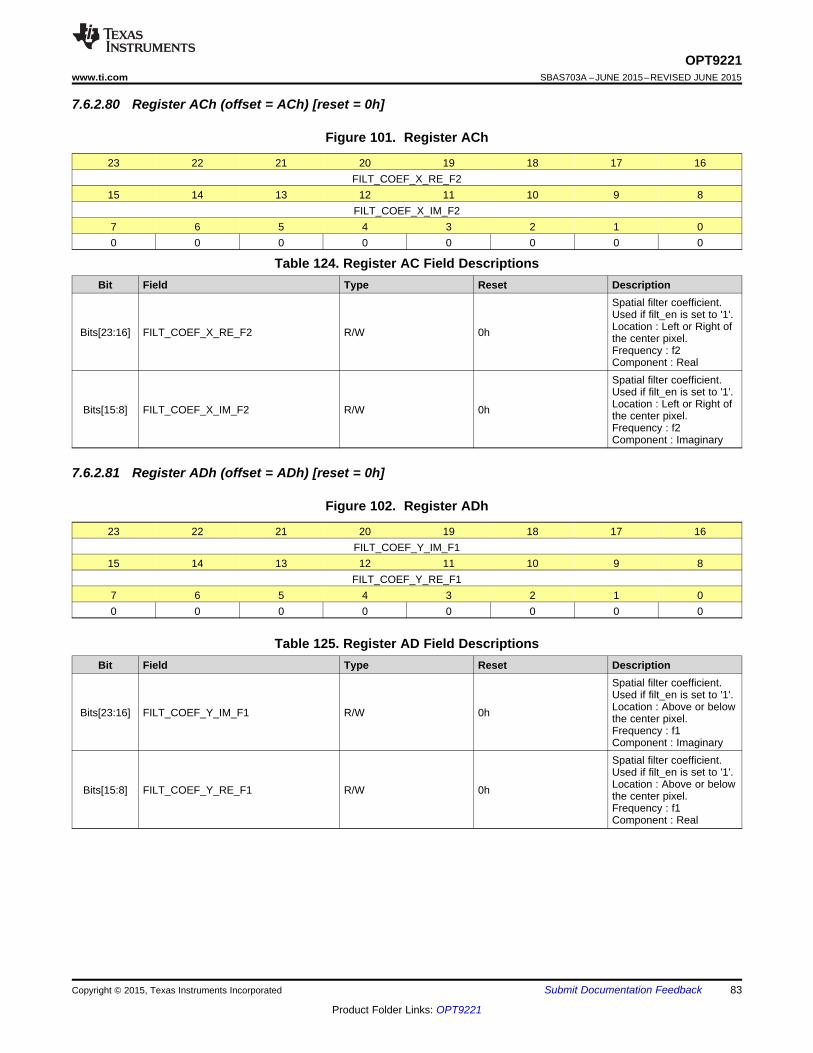
83
OPT9221www.ti.com SBAS703A –JUNE 2015–REVISED JUNE 2015
Product Folder Links: OPT9221
Submit Documentation FeedbackCopyright © 2015, Texas Instruments Incorporated
7.6.2.80 Register ACh (offset = ACh) [reset = 0h]
Figure 101. Register ACh
23 22 21 20 19 18 17 16FILT_COEF_X_RE_F2
15 14 13 12 11 10 9 8FILT_COEF_X_IM_F2
7 6 5 4 3 2 1 00 0 0 0 0 0 0 0
Table 124. Register AC Field DescriptionsBit Field Type Reset Description
Bits[23:16] FILT_COEF_X_RE_F2 R/W 0h
Spatial filter coefficient.Used if filt_en is set to '1'.Location : Left or Right ofthe center pixel.Frequency : f2Component : Real
Bits[15:8] FILT_COEF_X_IM_F2 R/W 0h
Spatial filter coefficient.Used if filt_en is set to '1'.Location : Left or Right ofthe center pixel.Frequency : f2Component : Imaginary
7.6.2.81 Register ADh (offset = ADh) [reset = 0h]
Figure 102. Register ADh
23 22 21 20 19 18 17 16FILT_COEF_Y_IM_F1
15 14 13 12 11 10 9 8FILT_COEF_Y_RE_F1
7 6 5 4 3 2 1 00 0 0 0 0 0 0 0
Table 125. Register AD Field DescriptionsBit Field Type Reset Description
Bits[23:16] FILT_COEF_Y_IM_F1 R/W 0h
Spatial filter coefficient.Used if filt_en is set to '1'.Location : Above or belowthe center pixel.Frequency : f1Component : Imaginary
Bits[15:8] FILT_COEF_Y_RE_F1 R/W 0h
Spatial filter coefficient.Used if filt_en is set to '1'.Location : Above or belowthe center pixel.Frequency : f1Component : Real
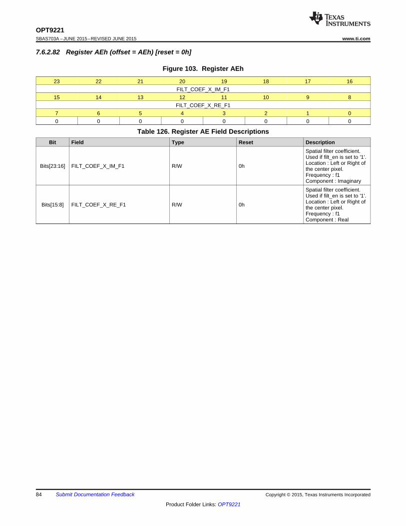
84
OPT9221SBAS703A –JUNE 2015–REVISED JUNE 2015 www.ti.com
Product Folder Links: OPT9221
Submit Documentation Feedback Copyright © 2015, Texas Instruments Incorporated
7.6.2.82 Register AEh (offset = AEh) [reset = 0h]
Figure 103. Register AEh
23 22 21 20 19 18 17 16FILT_COEF_X_IM_F1
15 14 13 12 11 10 9 8FILT_COEF_X_RE_F1
7 6 5 4 3 2 1 00 0 0 0 0 0 0 0
Table 126. Register AE Field DescriptionsBit Field Type Reset Description
Bits[23:16] FILT_COEF_X_IM_F1 R/W 0h
Spatial filter coefficient.Used if filt_en is set to '1'.Location : Left or Right ofthe center pixel.Frequency : f1Component : Imaginary
Bits[15:8] FILT_COEF_X_RE_F1 R/W 0h
Spatial filter coefficient.Used if filt_en is set to '1'.Location : Left or Right ofthe center pixel.Frequency : f1Component : Real
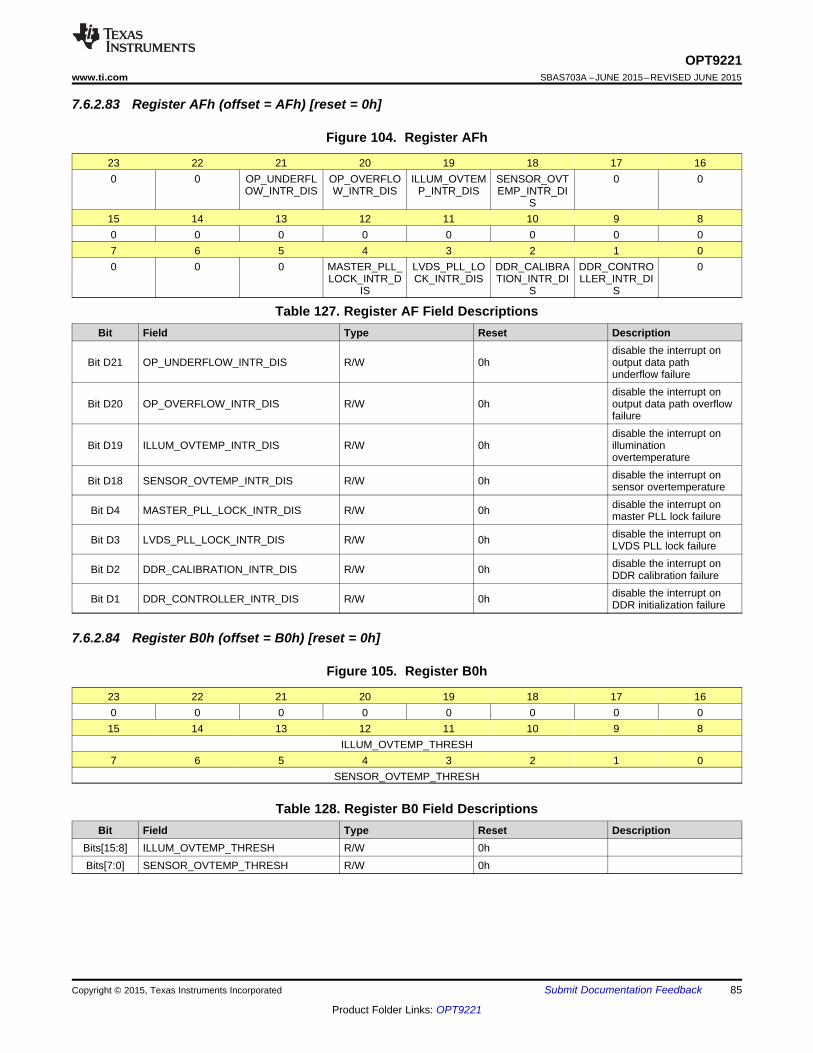
85
OPT9221www.ti.com SBAS703A –JUNE 2015–REVISED JUNE 2015
Product Folder Links: OPT9221
Submit Documentation FeedbackCopyright © 2015, Texas Instruments Incorporated
7.6.2.83 Register AFh (offset = AFh) [reset = 0h]
Figure 104. Register AFh
23 22 21 20 19 18 17 160 0 OP_UNDERFL
OW_INTR_DISOP_OVERFLOW_INTR_DIS
ILLUM_OVTEMP_INTR_DIS
SENSOR_OVTEMP_INTR_DI
S
0 0
15 14 13 12 11 10 9 80 0 0 0 0 0 0 07 6 5 4 3 2 1 00 0 0 MASTER_PLL_
LOCK_INTR_DIS
LVDS_PLL_LOCK_INTR_DIS
DDR_CALIBRATION_INTR_DI
S
DDR_CONTROLLER_INTR_DI
S
0
Table 127. Register AF Field DescriptionsBit Field Type Reset Description
Bit D21 OP_UNDERFLOW_INTR_DIS R/W 0hdisable the interrupt onoutput data pathunderflow failure
Bit D20 OP_OVERFLOW_INTR_DIS R/W 0hdisable the interrupt onoutput data path overflowfailure
Bit D19 ILLUM_OVTEMP_INTR_DIS R/W 0hdisable the interrupt onilluminationovertemperature
Bit D18 SENSOR_OVTEMP_INTR_DIS R/W 0h disable the interrupt onsensor overtemperature
Bit D4 MASTER_PLL_LOCK_INTR_DIS R/W 0h disable the interrupt onmaster PLL lock failure
Bit D3 LVDS_PLL_LOCK_INTR_DIS R/W 0h disable the interrupt onLVDS PLL lock failure
Bit D2 DDR_CALIBRATION_INTR_DIS R/W 0h disable the interrupt onDDR calibration failure
Bit D1 DDR_CONTROLLER_INTR_DIS R/W 0h disable the interrupt onDDR initialization failure
7.6.2.84 Register B0h (offset = B0h) [reset = 0h]
Figure 105. Register B0h
23 22 21 20 19 18 17 160 0 0 0 0 0 0 015 14 13 12 11 10 9 8
ILLUM_OVTEMP_THRESH7 6 5 4 3 2 1 0
SENSOR_OVTEMP_THRESH
Table 128. Register B0 Field DescriptionsBit Field Type Reset Description
Bits[15:8] ILLUM_OVTEMP_THRESH R/W 0hBits[7:0] SENSOR_OVTEMP_THRESH R/W 0h
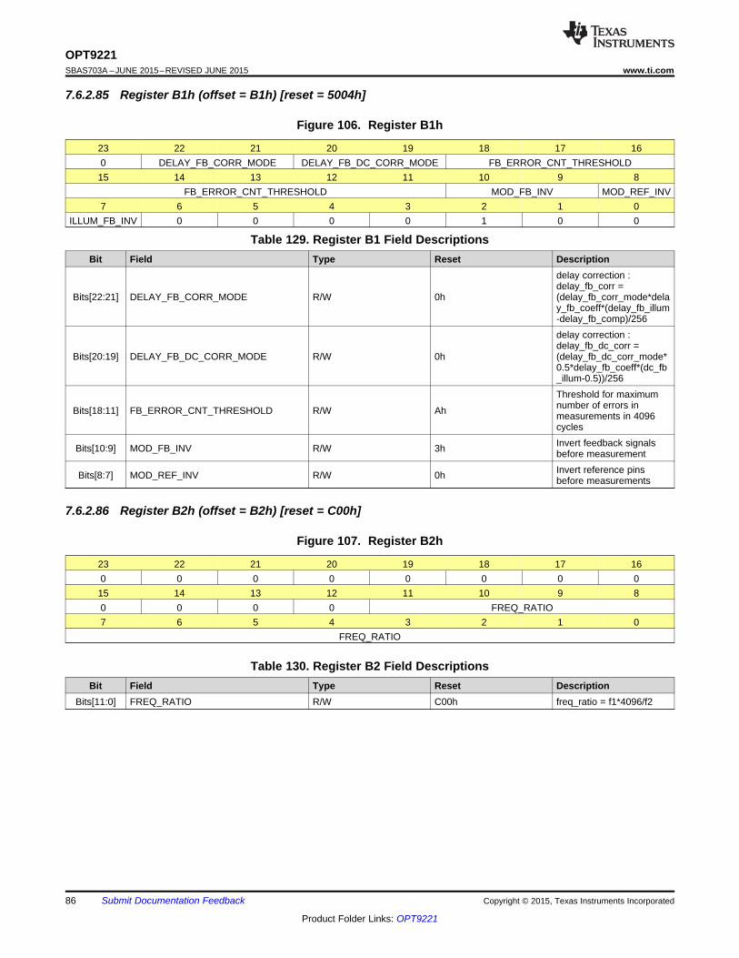
86
OPT9221SBAS703A –JUNE 2015–REVISED JUNE 2015 www.ti.com
Product Folder Links: OPT9221
Submit Documentation Feedback Copyright © 2015, Texas Instruments Incorporated
7.6.2.85 Register B1h (offset = B1h) [reset = 5004h]
Figure 106. Register B1h
23 22 21 20 19 18 17 160 DELAY_FB_CORR_MODE DELAY_FB_DC_CORR_MODE FB_ERROR_CNT_THRESHOLD15 14 13 12 11 10 9 8
FB_ERROR_CNT_THRESHOLD MOD_FB_INV MOD_REF_INV7 6 5 4 3 2 1 0
ILLUM_FB_INV 0 0 0 0 1 0 0
Table 129. Register B1 Field DescriptionsBit Field Type Reset Description
Bits[22:21] DELAY_FB_CORR_MODE R/W 0h
delay correction :delay_fb_corr =(delay_fb_corr_mode*delay_fb_coeff*(delay_fb_illum-delay_fb_comp)/256
Bits[20:19] DELAY_FB_DC_CORR_MODE R/W 0h
delay correction :delay_fb_dc_corr =(delay_fb_dc_corr_mode*0.5*delay_fb_coeff*(dc_fb_illum-0.5))/256
Bits[18:11] FB_ERROR_CNT_THRESHOLD R/W Ah
Threshold for maximumnumber of errors inmeasurements in 4096cycles
Bits[10:9] MOD_FB_INV R/W 3h Invert feedback signalsbefore measurement
Bits[8:7] MOD_REF_INV R/W 0h Invert reference pinsbefore measurements
7.6.2.86 Register B2h (offset = B2h) [reset = C00h]
Figure 107. Register B2h
23 22 21 20 19 18 17 160 0 0 0 0 0 0 015 14 13 12 11 10 9 80 0 0 0 FREQ_RATIO7 6 5 4 3 2 1 0
FREQ_RATIO
Table 130. Register B2 Field DescriptionsBit Field Type Reset Description
Bits[11:0] FREQ_RATIO R/W C00h freq_ratio = f1*4096/f2
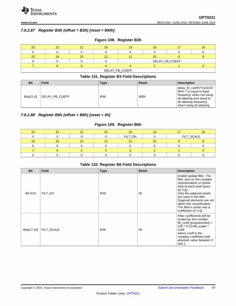
87
OPT9221www.ti.com SBAS703A –JUNE 2015–REVISED JUNE 2015
Product Folder Links: OPT9221
Submit Documentation FeedbackCopyright © 2015, Texas Instruments Incorporated
7.6.2.87 Register B3h (offset = B3h) [reset = 800h]
Figure 108. Register B3h
23 22 21 20 19 18 17 160 0 0 0 0 0 0 015 14 13 12 11 10 9 80 0 0 0 DELAY_FB_COEFF7 6 5 4 3 2 1 0
DELAY_FB_COEFF
Table 131. Register B3 Field DescriptionsBit Field Type Reset Description
Bits[11:0] DELAY_FB_COEFF R/W 800h
delay_fb_coeff=f*1024/24MHz. f is equal to basefrequency when not usingde-aliasing and equal tode-aliasing frequencywhen using de-aliasing.
7.6.2.88 Register B6h (offset = B6h) [reset = 0h]
Figure 109. Register B6h
23 22 21 20 19 18 17 160 0 0 0 FILT_EN 0 FILT_SCALE15 14 13 12 11 10 9 80 0 0 0 0 0 0 07 6 5 4 3 2 1 00 0 0 0 0 0 0 0
Table 132. Register B6 Field DescriptionsBit Field Type Reset Description
Bit D19 FILT_EN R/W 0h
Enable spatial filter. Thefilter acts on the complexrepresentation of phasedata at each pixel givenby I+jQ.Only the adjacent pixelsare used in the filter.Diagonal elements are nottaken into consideration.The filter's center has acoefficient of 1+0j.
Bits[17:16] FILT_SCALE R/W 0h
Filter coefficients will bescaled by this number.filt_coeff (programmed) =128 * 2^(2+filt_scale) *coeffwhere coeff is thecomplex coefficient withabsolute value between 0and 1.
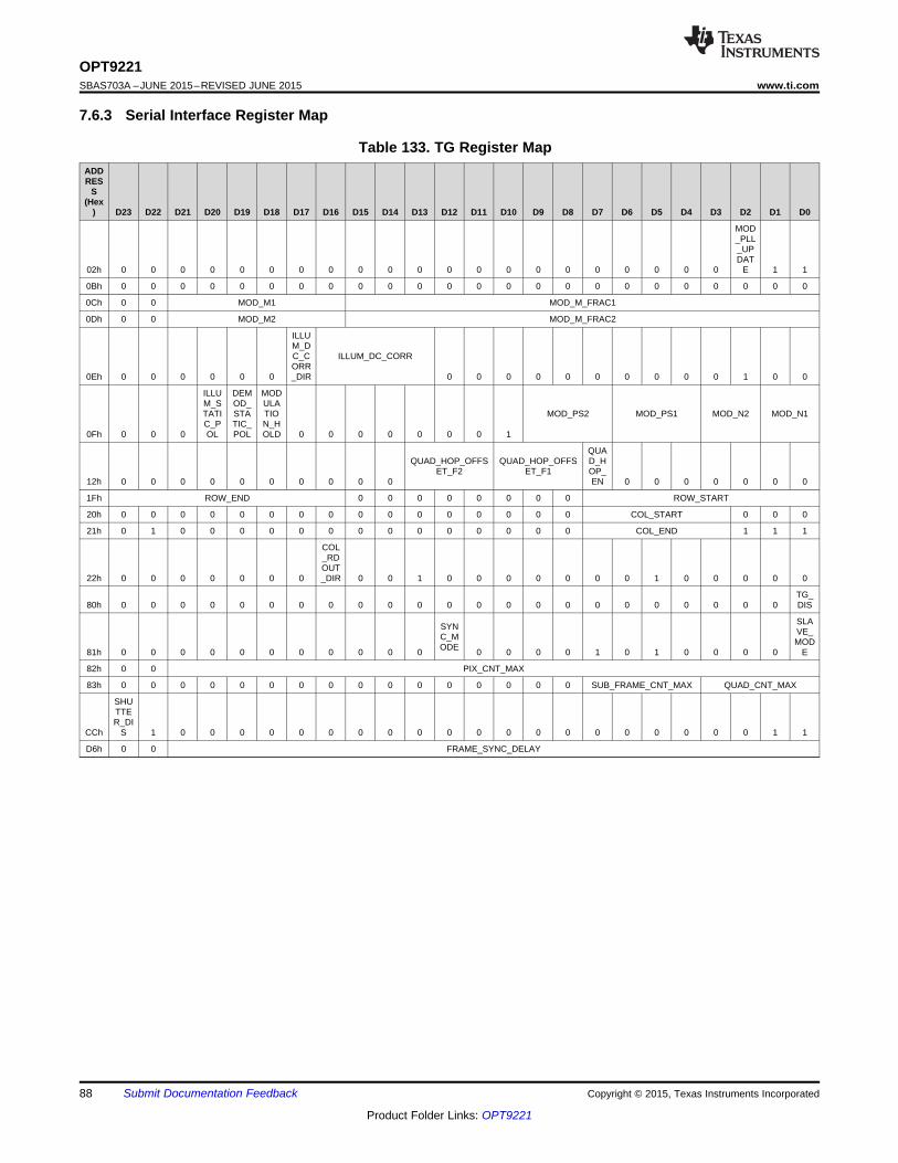
88
OPT9221SBAS703A –JUNE 2015–REVISED JUNE 2015 www.ti.com
Product Folder Links: OPT9221
Submit Documentation Feedback Copyright © 2015, Texas Instruments Incorporated
7.6.3 Serial Interface Register Map
Table 133. TG Register MapADDRES
S(Hex
) D23 D22 D21 D20 D19 D18 D17 D16 D15 D14 D13 D12 D11 D10 D9 D8 D7 D6 D5 D4 D3 D2 D1 D0
02h 0 0 0 0 0 0 0 0 0 0 0 0 0 0 0 0 0 0 0 0 0
MOD_PLL_UPDAT
E 1 1
0Bh 0 0 0 0 0 0 0 0 0 0 0 0 0 0 0 0 0 0 0 0 0 0 0 0
0Ch 0 0 MOD_M1 MOD_M_FRAC1
0Dh 0 0 MOD_M2 MOD_M_FRAC2
0Eh 0 0 0 0 0 0
ILLUM_DC_CORR_DIR
ILLUM_DC_CORR
0 0 0 0 0 0 0 0 0 0 1 0 0
0Fh 0 0 0
ILLUM_STATIC_POL
DEMOD_STATIC_POL
MODULATION_HOLD 0 0 0 0 0 0 0 1
MOD_PS2 MOD_PS1 MOD_N2 MOD_N1
12h 0 0 0 0 0 0 0 0 0 0
QUAD_HOP_OFFSET_F2
QUAD_HOP_OFFSET_F1
QUAD_HOP_EN 0 0 0 0 0 0 0
1Fh ROW_END 0 0 0 0 0 0 0 0 ROW_START
20h 0 0 0 0 0 0 0 0 0 0 0 0 0 0 0 0 COL_START 0 0 0
21h 0 1 0 0 0 0 0 0 0 0 0 0 0 0 0 0 COL_END 1 1 1
22h 0 0 0 0 0 0 0
COL_RDOUT_DIR 0 0 1 0 0 0 0 0 0 0 1 0 0 0 0 0
80h 0 0 0 0 0 0 0 0 0 0 0 0 0 0 0 0 0 0 0 0 0 0 0TG_DIS
81h 0 0 0 0 0 0 0 0 0 0 0
SYNC_MODE 0 0 0 0 1 0 1 0 0 0 0
SLAVE_MOD
E
82h 0 0 PIX_CNT_MAX
83h 0 0 0 0 0 0 0 0 0 0 0 0 0 0 0 0 SUB_FRAME_CNT_MAX QUAD_CNT_MAX
CCh
SHUTTER_DI
S 1 0 0 0 0 0 0 0 0 0 0 0 0 0 0 0 0 0 0 0 0 1 1
D6h 0 0 FRAME_SYNC_DELAY
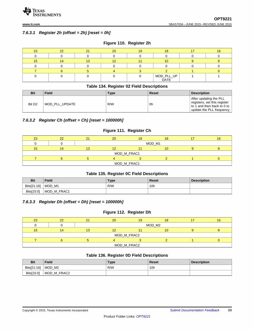
89
OPT9221www.ti.com SBAS703A –JUNE 2015–REVISED JUNE 2015
Product Folder Links: OPT9221
Submit Documentation FeedbackCopyright © 2015, Texas Instruments Incorporated
7.6.3.1 Register 2h (offset = 2h) [reset = 0h]
Figure 110. Register 2h
23 22 21 20 19 18 17 160 0 0 0 0 0 0 015 14 13 12 11 10 9 80 0 0 0 0 0 0 07 6 5 4 3 2 1 00 0 0 0 0 MOD_PLL_UP
DATE1 1
Table 134. Register 02 Field DescriptionsBit Field Type Reset Description
Bit D2 MOD_PLL_UPDATE R/W 0h
After updating the PLLregisters, set this registerto 1 and then back to 0 toupdate the PLL frequency.
7.6.3.2 Register Ch (offset = Ch) [reset = 100000h]
Figure 111. Register Ch
23 22 21 20 19 18 17 160 0 MOD_M115 14 13 12 11 10 9 8
MOD_M_FRAC17 6 5 4 3 2 1 0
MOD_M_FRAC1
Table 135. Register 0C Field DescriptionsBit Field Type Reset Description
Bits[21:16] MOD_M1 R/W 10hBits[15:0] MOD_M_FRAC1
7.6.3.3 Register Dh (offset = Dh) [reset = 100000h]
Figure 112. Register Dh
23 22 21 20 19 18 17 160 0 MOD_M215 14 13 12 11 10 9 8
MOD_M_FRAC27 6 5 4 3 2 1 0
MOD_M_FRAC2
Table 136. Register 0D Field DescriptionsBit Field Type Reset Description
Bits[21:16] MOD_M2 R/W 10hBits[15:0] MOD_M_FRAC2
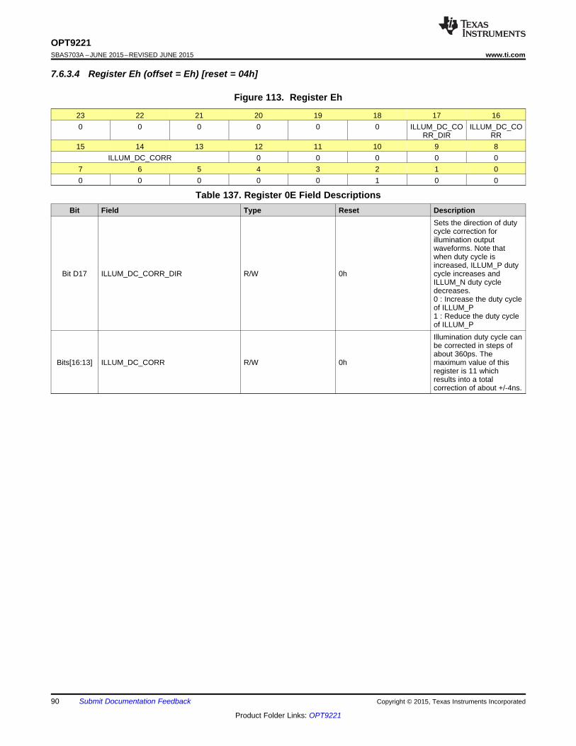
90
OPT9221SBAS703A –JUNE 2015–REVISED JUNE 2015 www.ti.com
Product Folder Links: OPT9221
Submit Documentation Feedback Copyright © 2015, Texas Instruments Incorporated
7.6.3.4 Register Eh (offset = Eh) [reset = 04h]
Figure 113. Register Eh
23 22 21 20 19 18 17 160 0 0 0 0 0 ILLUM_DC_CO
RR_DIRILLUM_DC_CO
RR15 14 13 12 11 10 9 8
ILLUM_DC_CORR 0 0 0 0 07 6 5 4 3 2 1 00 0 0 0 0 1 0 0
Table 137. Register 0E Field DescriptionsBit Field Type Reset Description
Bit D17 ILLUM_DC_CORR_DIR R/W 0h
Sets the direction of dutycycle correction forillumination outputwaveforms. Note thatwhen duty cycle isincreased, ILLUM_P dutycycle increases andILLUM_N duty cycledecreases.0 : Increase the duty cycleof ILLUM_P1 : Reduce the duty cycleof ILLUM_P
Bits[16:13] ILLUM_DC_CORR R/W 0h
Illumination duty cycle canbe corrected in steps ofabout 360ps. Themaximum value of thisregister is 11 whichresults into a totalcorrection of about +/-4ns.
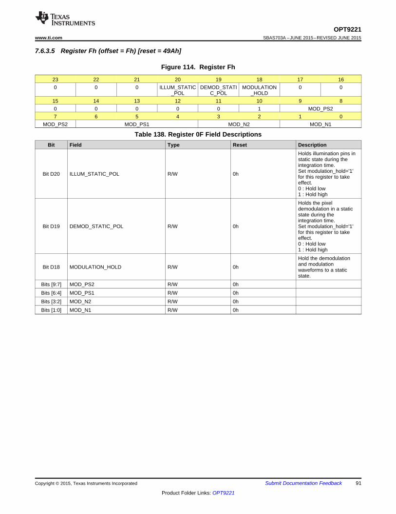
91
OPT9221www.ti.com SBAS703A –JUNE 2015–REVISED JUNE 2015
Product Folder Links: OPT9221
Submit Documentation FeedbackCopyright © 2015, Texas Instruments Incorporated
7.6.3.5 Register Fh (offset = Fh) [reset = 49Ah]
Figure 114. Register Fh
23 22 21 20 19 18 17 160 0 0 ILLUM_STATIC
_POLDEMOD_STATI
C_POLMODULATION
_HOLD0 0
15 14 13 12 11 10 9 80 0 0 0 0 1 MOD_PS27 6 5 4 3 2 1 0
MOD_PS2 MOD_PS1 MOD_N2 MOD_N1
Table 138. Register 0F Field DescriptionsBit Field Type Reset Description
Bit D20 ILLUM_STATIC_POL R/W 0h
Holds illumination pins instatic state during theintegration time.Set modulation_hold='1'for this register to takeeffect.0 : Hold low1 : Hold high
Bit D19 DEMOD_STATIC_POL R/W 0h
Holds the pixeldemodulation in a staticstate during theintegration time.Set modulation_hold='1'for this register to takeeffect.0 : Hold low1 : Hold high
Bit D18 MODULATION_HOLD R/W 0h
Hold the demodulationand modulationwaveforms to a staticstate.
Bits [9:7] MOD_PS2 R/W 0hBits [6:4] MOD_PS1 R/W 0hBits [3:2] MOD_N2 R/W 0hBits [1:0] MOD_N1 R/W 0h
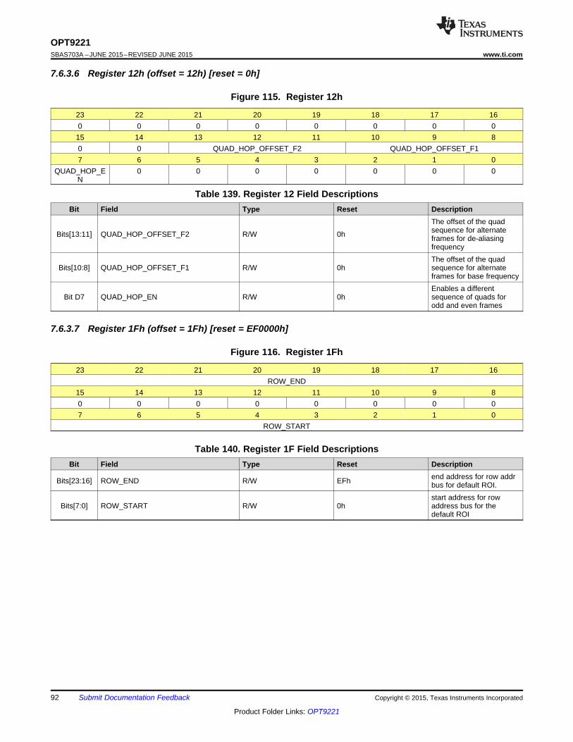
92
OPT9221SBAS703A –JUNE 2015–REVISED JUNE 2015 www.ti.com
Product Folder Links: OPT9221
Submit Documentation Feedback Copyright © 2015, Texas Instruments Incorporated
7.6.3.6 Register 12h (offset = 12h) [reset = 0h]
Figure 115. Register 12h
23 22 21 20 19 18 17 160 0 0 0 0 0 0 015 14 13 12 11 10 9 80 0 QUAD_HOP_OFFSET_F2 QUAD_HOP_OFFSET_F17 6 5 4 3 2 1 0
QUAD_HOP_EN
0 0 0 0 0 0 0
Table 139. Register 12 Field DescriptionsBit Field Type Reset Description
Bits[13:11] QUAD_HOP_OFFSET_F2 R/W 0h
The offset of the quadsequence for alternateframes for de-aliasingfrequency
Bits[10:8] QUAD_HOP_OFFSET_F1 R/W 0hThe offset of the quadsequence for alternateframes for base frequency
Bit D7 QUAD_HOP_EN R/W 0hEnables a differentsequence of quads forodd and even frames
7.6.3.7 Register 1Fh (offset = 1Fh) [reset = EF0000h]
Figure 116. Register 1Fh
23 22 21 20 19 18 17 16ROW_END
15 14 13 12 11 10 9 80 0 0 0 0 0 0 07 6 5 4 3 2 1 0
ROW_START
Table 140. Register 1F Field DescriptionsBit Field Type Reset Description
Bits[23:16] ROW_END R/W EFh end address for row addrbus for default ROI.
Bits[7:0] ROW_START R/W 0hstart address for rowaddress bus for thedefault ROI
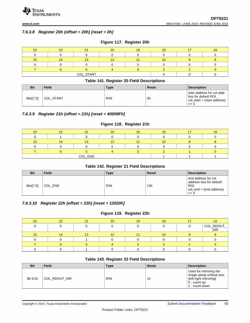
93
OPT9221www.ti.com SBAS703A –JUNE 2015–REVISED JUNE 2015
Product Folder Links: OPT9221
Submit Documentation FeedbackCopyright © 2015, Texas Instruments Incorporated
7.6.3.8 Register 20h (offset = 20h) [reset = 0h]
Figure 117. Register 20h
23 22 21 20 19 18 17 160 0 0 0 0 0 0 015 14 13 12 11 10 9 80 0 0 0 0 0 0 07 6 5 4 3 2 1 0
COL_START 0 0 0
Table 141. Register 20 Field DescriptionsBit Field Type Reset Description
Bits[7:3] COL_START R/W 0h
start address for col addrbus for default ROI.col_start = (start address)>> 4
7.6.3.9 Register 21h (offset = 21h) [reset = 40009Fh]
Figure 118. Register 21h
23 22 21 20 19 18 17 160 1 0 0 0 0 0 015 14 13 12 11 10 9 80 0 0 0 0 0 0 07 6 5 4 3 2 1 0
COL_END 1 1 1
Table 142. Register 21 Field DescriptionsBit Field Type Reset Description
Bits[7:3] COL_END R/W 13h
end address for coladdress bus for defaultROI.col_end = (end address)>> 4
7.6.3.10 Register 22h (offset = 22h) [reset = 12020h]
Figure 119. Register 22h
23 22 21 20 19 18 17 160 0 0 0 0 0 0 COL_RDOUT_
DIR15 14 13 12 11 10 9 80 0 1 0 0 0 0 07 6 5 4 3 2 1 00 0 1 0 0 0 0 0
Table 143. Register 22 Field DescriptionsBit Field Type Reset Description
Bit D16 COL_RDOUT_DIR R/W 1h
Used for mirroring theimage along vertical axis(left-right mirroring)0 : count up1 : count down
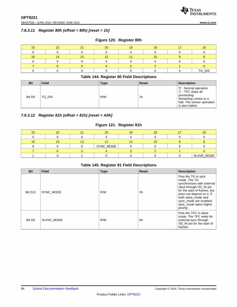
94
OPT9221SBAS703A –JUNE 2015–REVISED JUNE 2015 www.ti.com
Product Folder Links: OPT9221
Submit Documentation Feedback Copyright © 2015, Texas Instruments Incorporated
7.6.3.11 Register 80h (offset = 80h) [reset = 1h]
Figure 120. Register 80h
23 22 21 20 19 18 17 160 0 0 0 0 0 0 015 14 13 12 11 10 9 80 0 0 0 0 0 0 07 6 5 4 3 2 1 00 0 0 0 0 0 0 TG_DIS
Table 144. Register 80 Field DescriptionsBit Field Type Reset Description
Bit D0 TG_DIS R/W 1h
'0' : Normal operation'1' : TFC stops allprocessing.Streaming comes to ahalt. The sensor operationis also halted.
7.6.3.12 Register 81h (offset = 81h) [reset = A0h]
Figure 121. Register 81h
23 22 21 20 19 18 17 160 0 0 0 0 0 0 015 14 13 12 11 10 9 80 0 0 SYNC_MODE 0 0 0 07 6 5 4 3 2 1 01 0 1 0 0 0 0 SLAVE_MODE
Table 145. Register 81 Field DescriptionsBit Field Type Reset Description
Bit D12 SYNC_MODE R/W 0h
Puts the TG in syncmode. The TGsynchronizes with externalinput through VD_IN pinfor the start of frames, butdoes not depend on it. Ifboth slave_mode andsync_mode are enabled,sync_mode takes higherpriority.
Bit D0 SLAVE_MODE R/W 0h
Puts the TFC in slavemode. The TFC waits forexternal sync throughVD_IN pin for the start offrames.
95
OPT9221www.ti.com SBAS703A –JUNE 2015–REVISED JUNE 2015
Product Folder Links: OPT9221
Submit Documentation FeedbackCopyright © 2015, Texas Instruments Incorporated
7.6.3.13 Register 82h (offset = 82h) [reset = 186A0h]
Figure 122. Register 82h
23 22 21 20 19 18 17 160 0 PIX_CNT_MAX15 14 13 12 11 10 9 8
PIX_CNT_MAX7 6 5 4 3 2 1 0
PIX_CNT_MAX
Table 146. Register 82 Field DescriptionsBit Field Type Reset Description
Bits[21:0] PIX_CNT_MAX R/W 186A0h
Total frame time dividedby the number ofsubframes and quads interms of system clockcycles.
7.6.3.14 Register 83h (offset = 83h) [reset = 44h]
Figure 123. Register 83h
23 22 21 20 19 18 17 160 0 0 0 0 0 0 015 14 13 12 11 10 9 80 0 0 0 0 0 0 07 6 5 4 3 2 1 0
SUB_FRAME_CNT_MAX QUAD_CNT_MAX
Table 147. Register 83 Field DescriptionsBit Field Type Reset Description
Bits[7:4] SUB_FRAME_CNT_MAX R/W 4h
Total number of subframes in each frame.Only values of 1,2,4 and 8are valid. The behavior isunpredicatable when setto other values.1 : 12 : 24 : 48 : 8
Bits[3:0] QUAD_CNT_MAX R/W 4h
This indicates the totalnumber of quads in eachsubframe. Only values of4 and 6 are valid.
96
OPT9221SBAS703A –JUNE 2015–REVISED JUNE 2015 www.ti.com
Product Folder Links: OPT9221
Submit Documentation Feedback Copyright © 2015, Texas Instruments Incorporated
7.6.3.15 Register CCh (offset = CCh) [reset = 400003h]
Figure 124. Register CCh
23 22 21 20 19 18 17 16SHUTTER_DIS 1 0 0 0 0 0 0
15 14 13 12 11 10 9 80 0 0 0 0 0 0 07 6 5 4 3 2 1 00 0 0 0 0 0 1 1
Table 148. Register CC Field DescriptionsBit Field Type Reset Description
Bit D23 SHUTTER_DIS R/W 0h
If set to '1', shutterfunctionality is disabled. Ifshutter functionality isdisabled, the pixel chargecontinues to transfer tothe storage node duringthe sensor readout.
7.6.3.16 Register D6h (offset = D6h) [reset = 1h]
Figure 125. Register D6h
23 22 21 20 19 18 17 160 0 FRAME_SYNC_DELAY15 14 13 12 11 10 9 8
FRAME_SYNC_DELAY7 6 5 4 3 2 1 0
FRAME_SYNC_DELAY
Table 149. Register D6 Field DescriptionsBit Field Type Reset Description
Bits[21:0] FRAME_SYNC_DELAY R/W 1h
The programmable delaybetween external vd andsynced vd. The minimumvalue of programmabledelay is 1 cycle.
Timing Generation
+
ADC
ModulationScene
Depth Data
(OPT9221)
Pixel ArrayLens
IlluminationOptics
OPT8241
DDR
Illumination
97
OPT9221www.ti.com SBAS703A –JUNE 2015–REVISED JUNE 2015
Product Folder Links: OPT9221
Submit Documentation FeedbackCopyright © 2015, Texas Instruments Incorporated
8 Application and Implementation
NOTEInformation in the following applications sections is not part of the TI componentspecification, and TI does not warrant its accuracy or completeness. TI’s customers areresponsible for determining suitability of components for their purposes. Customers shouldvalidate and test their design implementation to confirm system functionality.
8.1 Application InformationThe OPT9221 is the companion ToF controller IC for the ToF sensor OPT8241. Standalone use of OPT9221 isnot recommended. Application information is covered as part of the OPT8241 data sheet.
8.2 Typical Application
Figure 126. TFC Application Diagram
98
OPT9221SBAS703A –JUNE 2015–REVISED JUNE 2015 www.ti.com
Product Folder Links: OPT9221
Submit Documentation Feedback Copyright © 2015, Texas Instruments Incorporated
9 Power Supply Recommendations
9.1 Power-Up SequenceThe power rails VCCA, VCCIO, VCCD_PLL, and VCC_INT can come up in any order. All the rails have to risemonotonically to the recommended voltage levels within tRAMP time (see Figure 16). A power on reset (POR) isinternally generated as soon as all the power rails are within the recommended levels.
99
OPT9221www.ti.com SBAS703A –JUNE 2015–REVISED JUNE 2015
Product Folder Links: OPT9221
Submit Documentation FeedbackCopyright © 2015, Texas Instruments Incorporated
10 Layout
10.1 Layout Guidelines
10.1.1 DDR Placement and RoutingThe DDR2 interface on the OPT9221 device works at a frequency of 144 MHz. It is recommended to place theDDR2 memory IC as close as possible to the device to avoid any signal integrity issues. All the nets betweenOPT9221 and the DDR2 memory IC must have a trace length lesser than 50 mm to avoid using terminations.Considering the relatively lower frequency of operation of DDR2 interface and the short trace lengths, terminationresistors on data or address pins may not be necessary for proper functioning of the DDR2 interface.
10.1.2 LVDS ReceiverThe sensor data receiver pins (named CAP_) are LVDS pairs. The OPT9221 device does not have internal 100-Ω differential termination. Termination resistors need to be placed externally as close as possible to theOPT9221 device.
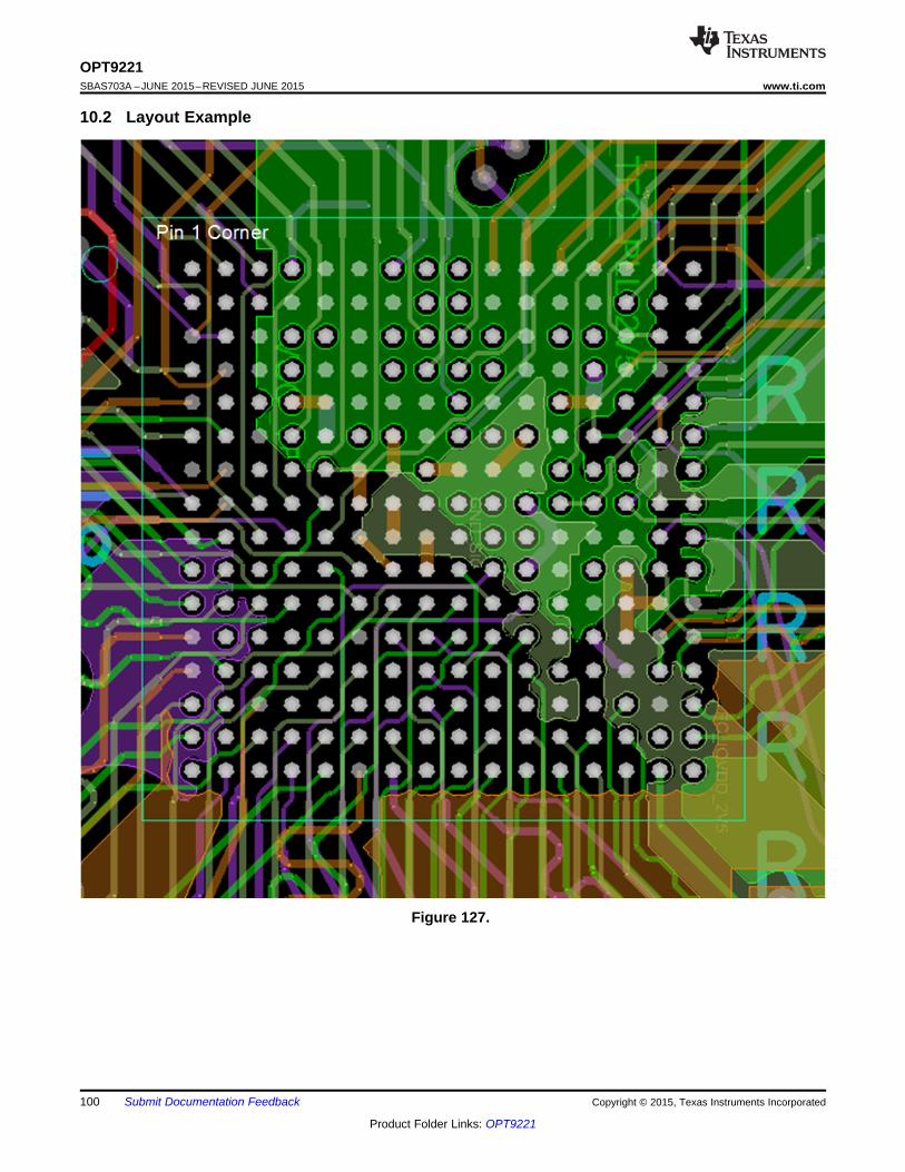
100
OPT9221SBAS703A –JUNE 2015–REVISED JUNE 2015 www.ti.com
Product Folder Links: OPT9221
Submit Documentation Feedback Copyright © 2015, Texas Instruments Incorporated
10.2 Layout Example
Figure 127.
101
OPT9221www.ti.com SBAS703A –JUNE 2015–REVISED JUNE 2015
Product Folder Links: OPT9221
Submit Documentation FeedbackCopyright © 2015, Texas Instruments Incorporated
11 Device and Documentation Support
11.1 Device Support
11.1.1 Third-Party Products DisclaimerTI'S PUBLICATION OF INFORMATION REGARDING THIRD-PARTY PRODUCTS OR SERVICES DOES NOTCONSTITUTE AN ENDORSEMENT REGARDING THE SUITABILITY OF SUCH PRODUCTS OR SERVICESOR A WARRANTY, REPRESENTATION OR ENDORSEMENT OF SUCH PRODUCTS OR SERVICES, EITHERALONE OR IN COMBINATION WITH ANY TI PRODUCT OR SERVICE.
11.2 Documentation Support
11.2.1 Related DocumentationOPT8241 3D Time-of-Flight Sensor Data Sheet, SBAS704
11.3 Community ResourcesThe following links connect to TI community resources. Linked contents are provided "AS IS" by the respectivecontributors. They do not constitute TI specifications and do not necessarily reflect TI's views; see TI's Terms ofUse.
TI E2E™ Online Community TI's Engineer-to-Engineer (E2E) Community. Created to foster collaborationamong engineers. At e2e.ti.com, you can ask questions, share knowledge, explore ideas and helpsolve problems with fellow engineers.
Design Support TI's Design Support Quickly find helpful E2E forums along with design support tools andcontact information for technical support.
11.4 TrademarksE2E is a trademark of Texas Instruments.All other trademarks are the property of their respective owners.
11.5 Electrostatic Discharge CautionThis integrated circuit can be damaged by ESD. Texas Instruments recommends that all integrated circuits be handled withappropriate precautions. Failure to observe proper handling and installation procedures can cause damage.
ESD damage can range from subtle performance degradation to complete device failure. Precision integrated circuits may be moresusceptible to damage because very small parametric changes could cause the device not to meet its published specifications.
11.6 GlossarySLYZ022 — TI Glossary.
This glossary lists and explains terms, acronyms, and definitions.
12 Mechanical, Packaging, and Orderable InformationThe following pages include mechanical, packaging, and orderable information. This information is the mostcurrent data available for the designated devices. This data is subject to change without notice and revision ofthis document. For browser-based versions of this data sheet, refer to the left-hand navigation.
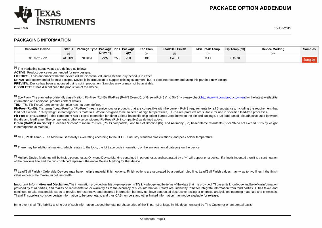
PACKAGE OPTION ADDENDUM
www.ti.com 30-Jun-2015
Addendum-Page 1
PACKAGING INFORMATION
Orderable Device Status(1)
Package Type PackageDrawing
Pins PackageQty
Eco Plan(2)
Lead/Ball Finish(6)
MSL Peak Temp(3)
Op Temp (°C) Device Marking(4/5)
Samples
OPT9221ZVM ACTIVE NFBGA ZVM 256 250 TBD Call TI Call TI 0 to 70
(1) The marketing status values are defined as follows:ACTIVE: Product device recommended for new designs.LIFEBUY: TI has announced that the device will be discontinued, and a lifetime-buy period is in effect.NRND: Not recommended for new designs. Device is in production to support existing customers, but TI does not recommend using this part in a new design.PREVIEW: Device has been announced but is not in production. Samples may or may not be available.OBSOLETE: TI has discontinued the production of the device.
(2) Eco Plan - The planned eco-friendly classification: Pb-Free (RoHS), Pb-Free (RoHS Exempt), or Green (RoHS & no Sb/Br) - please check http://www.ti.com/productcontent for the latest availabilityinformation and additional product content details.TBD: The Pb-Free/Green conversion plan has not been defined.Pb-Free (RoHS): TI's terms "Lead-Free" or "Pb-Free" mean semiconductor products that are compatible with the current RoHS requirements for all 6 substances, including the requirement thatlead not exceed 0.1% by weight in homogeneous materials. Where designed to be soldered at high temperatures, TI Pb-Free products are suitable for use in specified lead-free processes.Pb-Free (RoHS Exempt): This component has a RoHS exemption for either 1) lead-based flip-chip solder bumps used between the die and package, or 2) lead-based die adhesive used betweenthe die and leadframe. The component is otherwise considered Pb-Free (RoHS compatible) as defined above.Green (RoHS & no Sb/Br): TI defines "Green" to mean Pb-Free (RoHS compatible), and free of Bromine (Br) and Antimony (Sb) based flame retardants (Br or Sb do not exceed 0.1% by weightin homogeneous material)
(3) MSL, Peak Temp. - The Moisture Sensitivity Level rating according to the JEDEC industry standard classifications, and peak solder temperature.
(4) There may be additional marking, which relates to the logo, the lot trace code information, or the environmental category on the device.
(5) Multiple Device Markings will be inside parentheses. Only one Device Marking contained in parentheses and separated by a "~" will appear on a device. If a line is indented then it is a continuationof the previous line and the two combined represent the entire Device Marking for that device.
(6) Lead/Ball Finish - Orderable Devices may have multiple material finish options. Finish options are separated by a vertical ruled line. Lead/Ball Finish values may wrap to two lines if the finishvalue exceeds the maximum column width.
Important Information and Disclaimer:The information provided on this page represents TI's knowledge and belief as of the date that it is provided. TI bases its knowledge and belief on informationprovided by third parties, and makes no representation or warranty as to the accuracy of such information. Efforts are underway to better integrate information from third parties. TI has taken andcontinues to take reasonable steps to provide representative and accurate information but may not have conducted destructive testing or chemical analysis on incoming materials and chemicals.TI and TI suppliers consider certain information to be proprietary, and thus CAS numbers and other limited information may not be available for release.
In no event shall TI's liability arising out of such information exceed the total purchase price of the TI part(s) at issue in this document sold by TI to Customer on an annual basis.
PACKAGE OPTION ADDENDUM
www.ti.com 30-Jun-2015
Addendum-Page 2
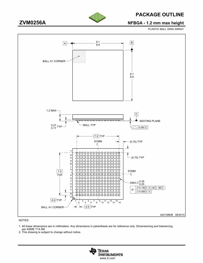
www.ti.com
PACKAGE OUTLINE
C1.2 MAX
TYP0.270.17
7.5TYP
7.5 TYP
0.5 TYP
0.5 TYP
256X 0.350.25
A 9.18.9
B
9.18.9
(0.75) TYP
(0.75) TYP
NFBGA - 1.2 mm max heightZVM0256APLASTIC BALL GRID ARRAY
4221086/B 08/2015
NOTES: 1. All linear dimensions are in millimeters. Any dimensions in parenthesis are for reference only. Dimensioning and tolerancing per ASME Y14.5M. 2. This drawing is subject to change without notice.
11
BALL A1 CORNER
SEATING PLANEBALL TYP
0.08 C
0.15 C A B0.05 C
SYMM
SYMM
BALL A1 CORNER
CDEFGHJKLMNPR
12
34
56
78
910
AB
1213
1415
16
T
SCALE 1.400
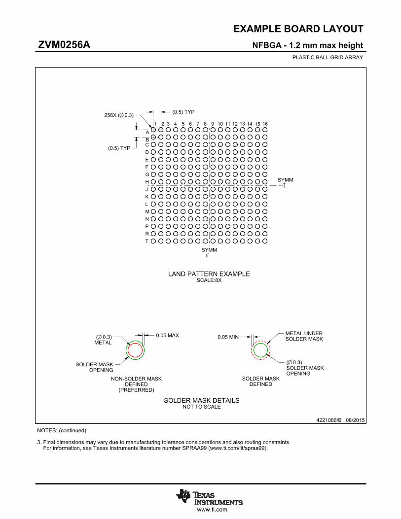
www.ti.com
EXAMPLE BOARD LAYOUT
256X ( )0.3 (0.5) TYP
(0.5) TYP
( )METAL
0.3 0.05 MAX
SOLDER MASKOPENING
METAL UNDERSOLDER MASK
( )SOLDER MASKOPENING
0.3
0.05 MIN
NFBGA - 1.2 mm max heightZVM0256APLASTIC BALL GRID ARRAY
4221086/B 08/2015
NOTES: (continued) 3. Final dimensions may vary due to manufacturing tolerance considerations and also routing constraints. For information, see Texas Instruments literature number SPRAA99 (www.ti.com/lit/spraa99).
SYMM
SYMM
LAND PATTERN EXAMPLESCALE:8X
1 2 3 4 5 6 7 8 9 10 11
BA
CDEFGHJKLMNPRT
12 13 14 15 16
NON-SOLDER MASKDEFINED
(PREFERRED)
SOLDER MASK DETAILSNOT TO SCALE
SOLDER MASKDEFINED
www.ti.com
EXAMPLE STENCIL DESIGN
(0.5) TYP
(0.5) TYP ( ) TYP0.3
NFBGA - 1.2 mm max heightZVM0256APLASTIC BALL GRID ARRAY
4221086/B 08/2015
NOTES: (continued) 4. Laser cutting apertures with trapezoidal walls and rounded corners may offer better paste release.
SYMM
SOLDER PASTE EXAMPLEBASED ON 0.1 mm THICK STENCIL
SCALE:8X
SYMM
1 2 3 4 5 6 7 8 9 10 11
BA
CDEFGHJKLMNPRT
12 13 14 15 16

IMPORTANT NOTICE
Texas Instruments Incorporated and its subsidiaries (TI) reserve the right to make corrections, enhancements, improvements and otherchanges to its semiconductor products and services per JESD46, latest issue, and to discontinue any product or service per JESD48, latestissue. Buyers should obtain the latest relevant information before placing orders and should verify that such information is current andcomplete. All semiconductor products (also referred to herein as “components”) are sold subject to TI’s terms and conditions of salesupplied at the time of order acknowledgment.TI warrants performance of its components to the specifications applicable at the time of sale, in accordance with the warranty in TI’s termsand conditions of sale of semiconductor products. Testing and other quality control techniques are used to the extent TI deems necessaryto support this warranty. Except where mandated by applicable law, testing of all parameters of each component is not necessarilyperformed.TI assumes no liability for applications assistance or the design of Buyers’ products. Buyers are responsible for their products andapplications using TI components. To minimize the risks associated with Buyers’ products and applications, Buyers should provideadequate design and operating safeguards.TI does not warrant or represent that any license, either express or implied, is granted under any patent right, copyright, mask work right, orother intellectual property right relating to any combination, machine, or process in which TI components or services are used. Informationpublished by TI regarding third-party products or services does not constitute a license to use such products or services or a warranty orendorsement thereof. Use of such information may require a license from a third party under the patents or other intellectual property of thethird party, or a license from TI under the patents or other intellectual property of TI.Reproduction of significant portions of TI information in TI data books or data sheets is permissible only if reproduction is without alterationand is accompanied by all associated warranties, conditions, limitations, and notices. TI is not responsible or liable for such altereddocumentation. Information of third parties may be subject to additional restrictions.Resale of TI components or services with statements different from or beyond the parameters stated by TI for that component or servicevoids all express and any implied warranties for the associated TI component or service and is an unfair and deceptive business practice.TI is not responsible or liable for any such statements.Buyer acknowledges and agrees that it is solely responsible for compliance with all legal, regulatory and safety-related requirementsconcerning its products, and any use of TI components in its applications, notwithstanding any applications-related information or supportthat may be provided by TI. Buyer represents and agrees that it has all the necessary expertise to create and implement safeguards whichanticipate dangerous consequences of failures, monitor failures and their consequences, lessen the likelihood of failures that might causeharm and take appropriate remedial actions. Buyer will fully indemnify TI and its representatives against any damages arising out of the useof any TI components in safety-critical applications.In some cases, TI components may be promoted specifically to facilitate safety-related applications. With such components, TI’s goal is tohelp enable customers to design and create their own end-product solutions that meet applicable functional safety standards andrequirements. Nonetheless, such components are subject to these terms.No TI components are authorized for use in FDA Class III (or similar life-critical medical equipment) unless authorized officers of the partieshave executed a special agreement specifically governing such use.Only those TI components which TI has specifically designated as military grade or “enhanced plastic” are designed and intended for use inmilitary/aerospace applications or environments. Buyer acknowledges and agrees that any military or aerospace use of TI componentswhich have not been so designated is solely at the Buyer's risk, and that Buyer is solely responsible for compliance with all legal andregulatory requirements in connection with such use.TI has specifically designated certain components as meeting ISO/TS16949 requirements, mainly for automotive use. In any case of use ofnon-designated products, TI will not be responsible for any failure to meet ISO/TS16949.
Products ApplicationsAudio www.ti.com/audio Automotive and Transportation www.ti.com/automotiveAmplifiers amplifier.ti.com Communications and Telecom www.ti.com/communicationsData Converters dataconverter.ti.com Computers and Peripherals www.ti.com/computersDLP® Products www.dlp.com Consumer Electronics www.ti.com/consumer-appsDSP dsp.ti.com Energy and Lighting www.ti.com/energyClocks and Timers www.ti.com/clocks Industrial www.ti.com/industrialInterface interface.ti.com Medical www.ti.com/medicalLogic logic.ti.com Security www.ti.com/securityPower Mgmt power.ti.com Space, Avionics and Defense www.ti.com/space-avionics-defenseMicrocontrollers microcontroller.ti.com Video and Imaging www.ti.com/videoRFID www.ti-rfid.comOMAP Applications Processors www.ti.com/omap TI E2E Community e2e.ti.comWireless Connectivity www.ti.com/wirelessconnectivity
Mailing Address: Texas Instruments, Post Office Box 655303, Dallas, Texas 75265Copyright © 2016, Texas Instruments Incorporated


![Minicube F4 flight controller integrate Betaflight OSD ...files.banggood.com/2016/12/[SKU668941] Minicube F4... · Minicube F4 flight controller integrate Betaflight OSD Quick user](https://img.pdfslide.net/doc/110x75/601530b8be767643ff180b35/minicube-f4-flight-controller-integrate-betaflight-osd-files-sku668941-minicube.jpg)