Embed Size (px)
Citation preview
OPTIMAL DESIGN OF AN INTERLEAVED DC-DC SWITCH
MODE CONVERTER
Presented ByPrasanna Kumar . C
Dept. of Electrical and Electronics EngineeringPES Institute of Technology, Bangalore
INDIA
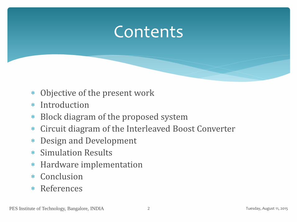
Objective of the present work
Introduction
Block diagram of the proposed system
Circuit diagram of the Interleaved Boost Converter
Design and Development
Simulation Results
Hardware implementation
Conclusion
References
Tuesday, August 11, 2015PES Institute of Technology, Bangalore, INDIA 2
Contents
Design, simulation and hardware implementation ofthe proposed two stage interleaved convertertopology with reduced inductor volume.
Tuesday, August 11, 2015PES Institute of Technology, Bangalore, INDIA 3
Objective of the present work
The voltage levels obtained from renewable energy sourcesare low and unregulated.
These renewable energy systems require a suitableconverter to increase and regulate their output voltagelevel.
Most commonly used converter to accomplish this is aBoost converter.
Tuesday, August 11, 2015PES Institute of Technology, Bangalore, INDIA 4
Introduction
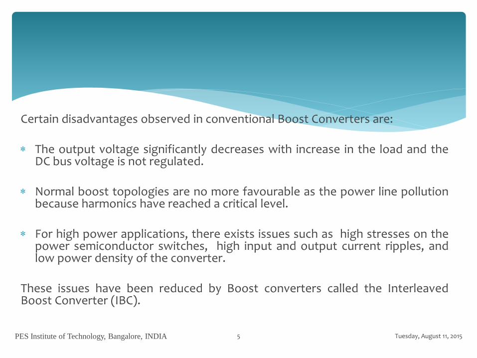
Certain disadvantages observed in conventional Boost Converters are:
The output voltage significantly decreases with increase in the load and theDC bus voltage is not regulated.
Normal boost topologies are no more favourable as the power line pollutionbecause harmonics have reached a critical level.
For high power applications, there exists issues such as high stresses on thepower semiconductor switches, high input and output current ripples, andlow power density of the converter.
These issues have been reduced by Boost converters called the InterleavedBoost Converter (IBC).
Tuesday, August 11, 2015PES Institute of Technology, Bangalore, INDIA 5
Interleaved Boost Converters are specialized boostconverter topologies.
The converter components are paralleled into number ofstages, with the paralleled stages having common sourceand load.
Interleaved Boost Converter consist of two parallel-connected boost power trains operated with a phasedifference of 1800 .
Tuesday, August 11, 2015PES Institute of Technology, Bangalore, INDIA 6
Interleaved Boost Converter
Unlike the continuous conduction mode (CCM) technique,BCM offers inherent zero current switching of the boostdiodes.
This permits the use of less expensive diodes withoutsacrificing efficiency.
For efficient switching of the two MOSFETS and to ensurethat there is no extra heat generated, IC SG3525 has beenused to drive MOSFETS.
Tuesday, August 11, 2015PES Institute of Technology, Bangalore, INDIA 7
Advantages of IBC over traditional single stage boostconverters include:
Substantial reduction in input & output current ripple
Higher power density
Higher current handling capacity
Improved efficiency
Faster response
Tuesday, August 11, 2015PES Institute of Technology, Bangalore, INDIA 8
Tuesday, August 11, 2015PES Institute of Technology, Bangalore, INDIA 9
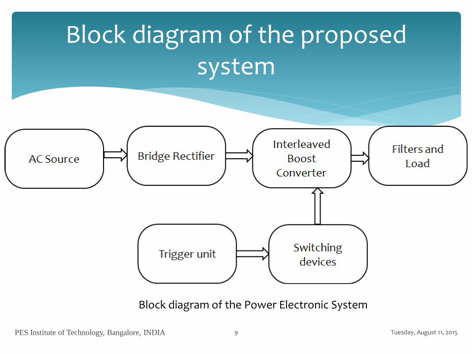
Block diagram of the proposed system
Block diagram of the Power Electronic System
Tuesday, August 11, 2015PES Institute of Technology, Bangalore, INDIA 10
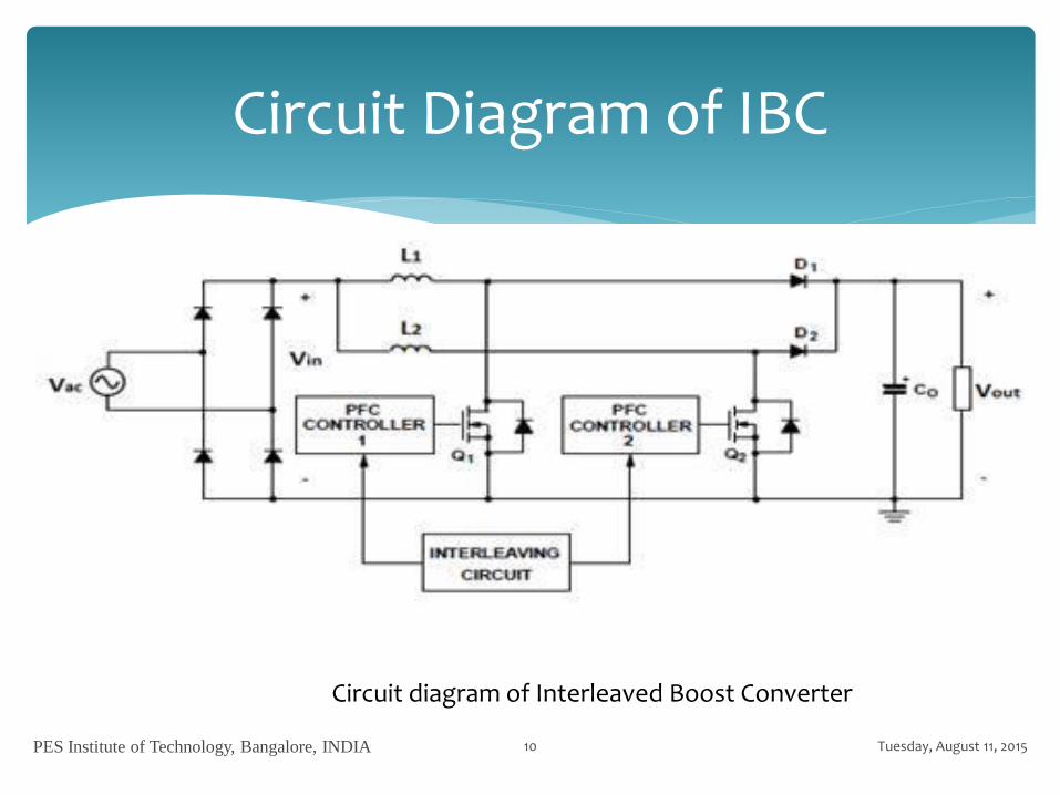
Circuit Diagram of IBC
Circuit diagram of Interleaved Boost Converter
Tuesday, August 11, 2015PES Institute of Technology, Bangalore, INDIA 11
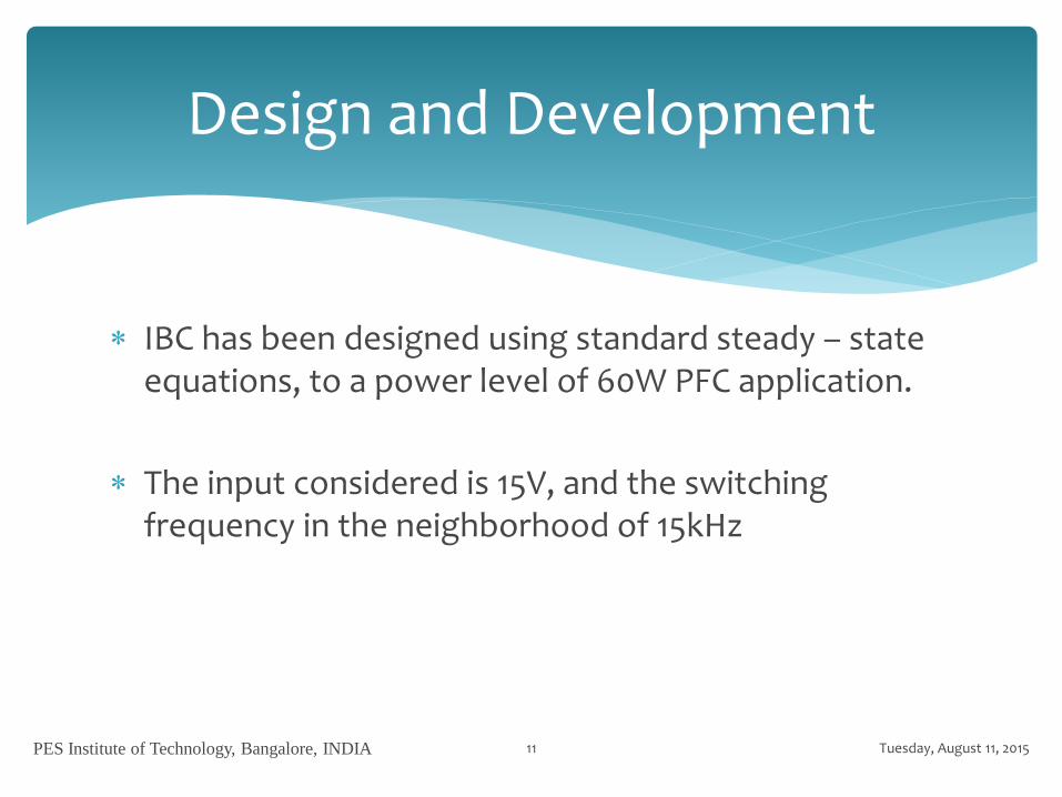
Design and Development
IBC has been designed using standard steady – state equations, to a power level of 60W PFC application.
The input considered is 15V, and the switching frequency in the neighborhood of 15kHz
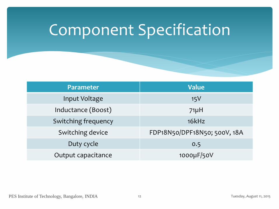
Parameter Value
Input Voltage 15V
Inductance (Boost) 71µH
Switching frequency 16kHz
Switching device FDP18N50/DPF18N50; 500V, 18A
Duty cycle 0.5
Output capacitance 1000µF/50V
Tuesday, August 11, 2015PES Institute of Technology, Bangalore, INDIA 12
Component Specification
Tuesday, August 11, 2015PES Institute of Technology, Bangalore, INDIA 13
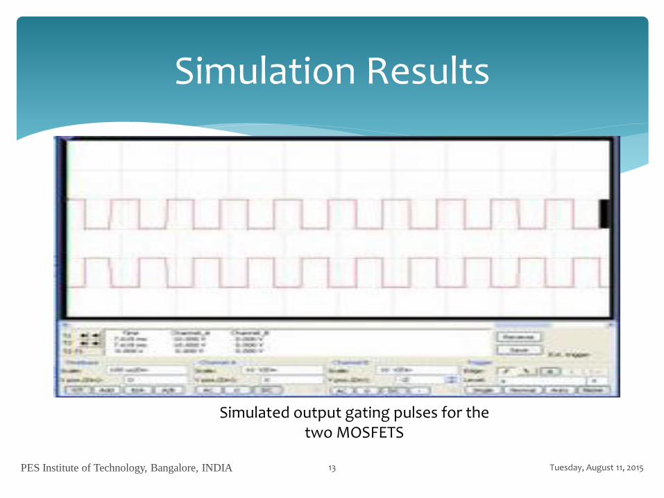
Simulated output gating pulses for the two MOSFETS
Simulation Results
Tuesday, August 11, 2015PES Institute of Technology, Bangalore, INDIA 14
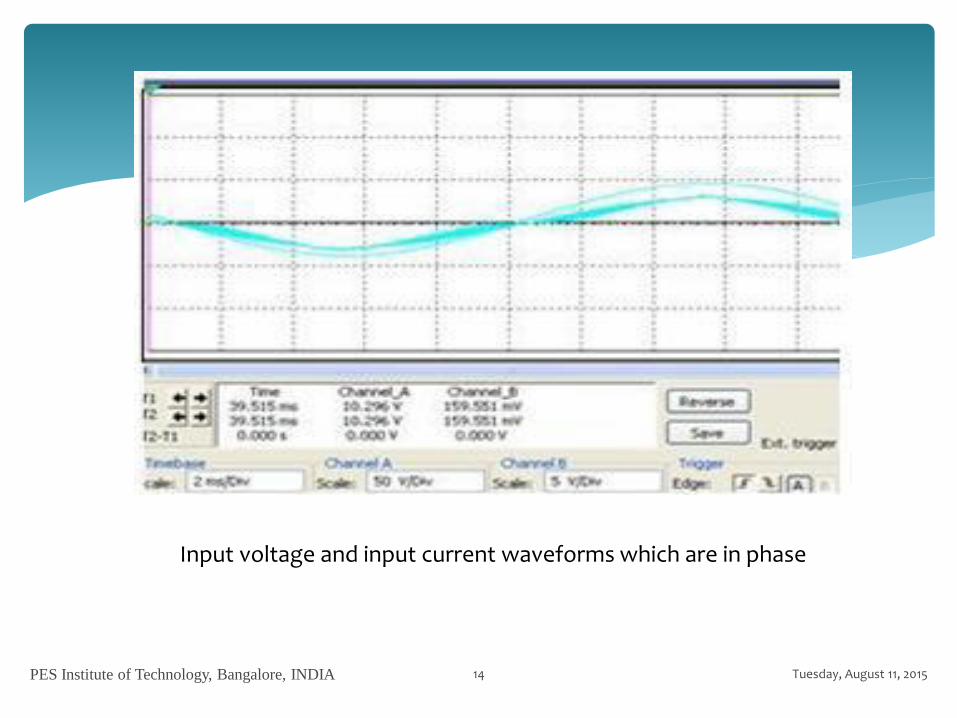
Input voltage and input current waveforms which are in phase
Tuesday, August 11, 2015PES Institute of Technology, Bangalore, INDIA 15
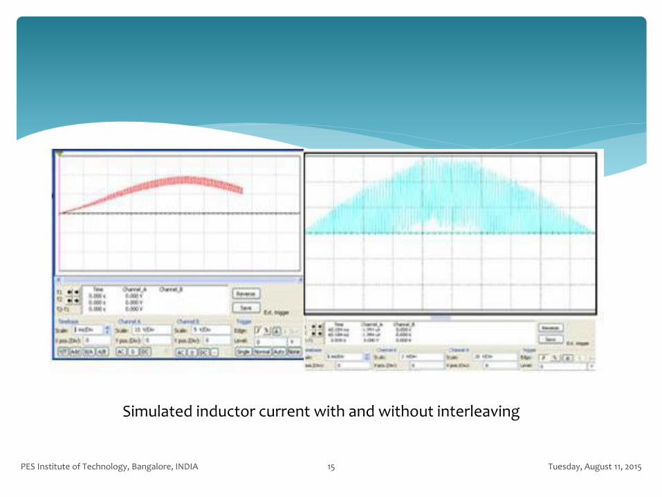
Simulated inductor current with and without interleaving
Tuesday, August 11, 2015PES Institute of Technology, Bangalore, INDIA 16
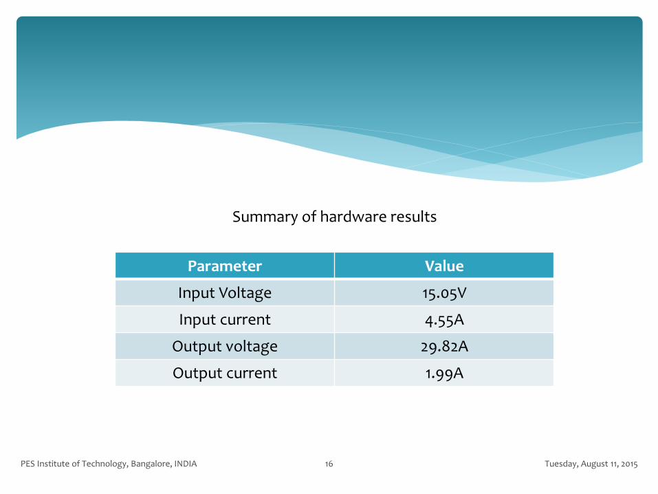
Parameter Value
Input Voltage 15.05V
Input current 4.55A
Output voltage 29.82A
Output current 1.99A
Summary of hardware results
Tuesday, August 11, 2015PES Institute of Technology, Bangalore, INDIA 17
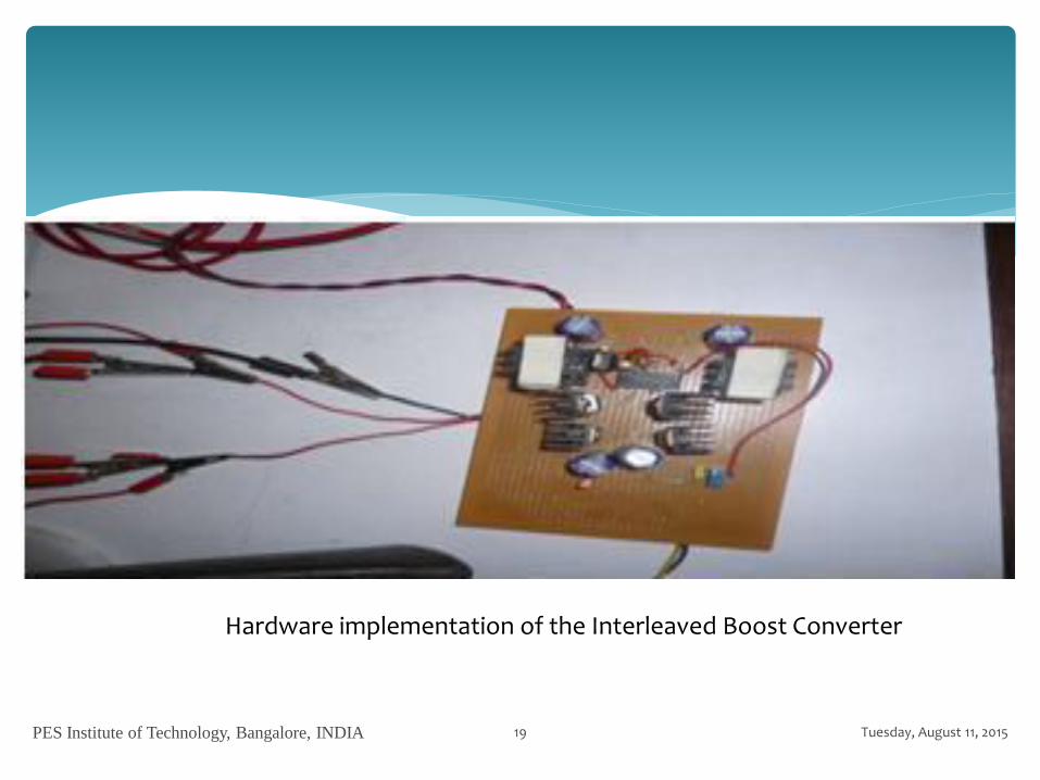
Hardware Implementation
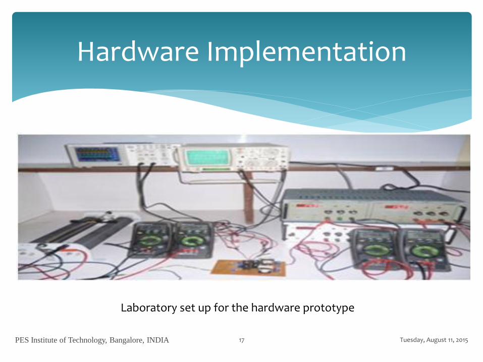
Laboratory set up for the hardware prototype
The designed IBC has been implemented under laboratory set – up and tested up to 60W successfully.
For closed loop control, PWM control IC SG3525 has been used
Switching device used is FDP18N50/DPF18N50 (500V, 18A)
Tuesday, August 11, 2015PES Institute of Technology, Bangalore, INDIA 18
Tuesday, August 11, 2015PES Institute of Technology, Bangalore, INDIA 19
Hardware implementation of the Interleaved Boost Converter
Tuesday, August 11, 2015PES Institute of Technology, Bangalore, INDIA 20
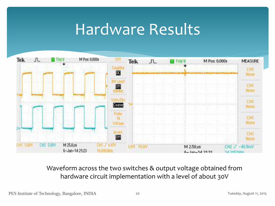
Hardware Results
Waveform across the two switches & output voltage obtained from hardware circuit implementation with a level of about 30V
A power level of 60W was achievable with the realised hardwaresetup.
The design was been able to support a load of 1.99 A and couldachieve an efficiency of above 86.66%.
The input and output filters can be smaller due to ripple currentcancellation and effective doubling of the switching frequency.
It has been seen that the efficiency, size, and cost can beminimized with the proposed topology.
Tuesday, August 11, 2015PES Institute of Technology, Bangalore, INDIA 21
Conclusion
The topology can be modified to drive multiple loadsof higher ratings using an appropriate power switchand suitable heat sink.
The converter can be suitably modified to make useof solar energy as a source with minimum number ofbattery to drive high rated load.
Tuesday, August 11, 2015PES Institute of Technology, Bangalore, INDIA 22
Future Work
[1] Jen-Ta Sul, Chih-Wen Liu, Chuan-Sheng Cheng and Chung-Wen Hung , “A Self Calibration Scheme for
Improved Current Share of Multiphase DC-DC Converter,” IEEE Trans., 978-1-4577-1216, June 2012.
[2] Oun Lee and Gun-Woo Moon, “Soft Switching DC/DC Converter with a full ZVS Range and Reduced Output
Filter for High-VoltageApplications,” IEEE Trans. on power electronics, vol.28, no.1, Jan 2013.
[3] GU Jun-Yin, WU Hong, N Guo, “Research on Photovoltaic Grid-Connected Inverter Based on Soft-Switching
Interleaved Fly back Converter,” 8th International Conference on Power Electronics-ECCE Asia, May 30-June 3,
2011, IEEE Trans.978-1-61284-947, July 2011.
[4] Pyosoo Kim, Sanghyuk Lee, Junsung Park and Sewan Choi, “High Step-Up Interleaved Boost Converters using
Voltage Multiplier Cells,” IEEE Trans. 978-1-4244-5046, June 2010.
[5] C.N.M. Ho, H.Breuninger, S.Pettersson, G.Escobar, L.Serpa and A.Cocci, “Practical Implementation of an
Interleaved Boost Converter using SiC Diode for PV applications,” 8th International Conference on Power
Electronics-ECCE Asia, May 30-June 3,2011, IEEE Trans.978-1-61284-957, July 2010.
Tuesday, August 11, 2015PES Institute of Technology, Bangalore, INDIA 23
References
[6] Xiaojun Xu, Wei Liu and Alex Q. Huang,“Two-Phase Interleaved Critical Mode PFC Boost Converter with
Closed Loop Interleaving Strategy,” IEEE Trans. Power Electronics, vol. 24, pp. 3003 3013, No. 12, December
2009.
[7] Laszlo Huber, Brian T. Irving and Milan M. Jovanovi 𝑐, “Closed-Loop Control Methods for Interleaved
DCM/CCM Boundary Boost PFC Converters, ”IEEE Proc., Applied Power Electronics Conference and
Exposition, 2009, pp. 991 997.
[8] Nadia Smith and Roy McCann, “Analysis and Simulation of aMultiple Input Interleaved Boost Converter for
Renewable Energy Applications,” IEEE Proc., Telecommunications Energy Conf., 2014.
[9] Jo 𝑎oBosco RF. Cabral, Tiago Lemes da Silva, S 𝑒rgio Vidal Garcia Oliveira, YalesR 𝑜mulo de Novaes, “A New
High Gain Non - Isolated Dc-Dc Boost Converter for Photovoltaic Application,” IEEE Proc., Power
Electronics Conf. 2013, pp. 569 574.
[10] Heinz van der Broeck, Ibrahim Tezcan, “1 kW Dual Interleaved Boost Converter for Low Voltage
Applications,” IEEE, IPEMC, 2006.
Tuesday, August 11, 2015PES Institute of Technology, Bangalore, INDIA 24

Tuesday, August 11, 2015PES Institute of Technology, Bangalore, INDIA 25