Embed Size (px)
Citation preview
CMOS-VDPitch (microns)
15 20 25 30 35 40 45
Res
olut
ion
(mic
rons
)
1
1.5
2
2.5
3
3.5
Mimosa 9: resolution vs pitch
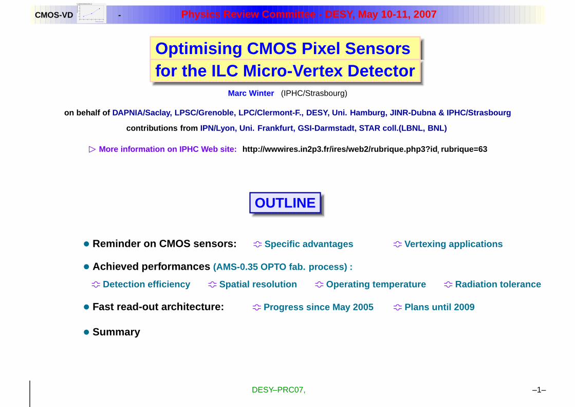
- Physics Review Committee - DESY, May 10-11, 2007
Optimising CMOS Pixel Sensorsfor the ILC Micro-Vertex Detector
Marc Winter (IPHC/Strasbourg)
on behalf of DAPNIA/Saclay, LPSC/Grenoble, LPC/Clermont-F., DESY, Un i. Hamburg, JINR-Dubna & IPHC/Strasbourg
contributions from IPN/Lyon, Uni. Frankfurt, GSI-Darmstadt, STAR coll.(LBNL , BNL)
B More information on IPHC Web site: http://wwwires.in2p3.fr/ires/web2/rubrique.php3?id rubrique=63
OUTLINE
• Reminder on CMOS sensors: m Specific advantages m Vertexing applications
• Achieved performances (AMS-0.35 OPTO fab. process) :
m Detection efficiency m Spatial resolution m Operating temperature m Radiation tolerance
• Fast read-out architecture: m Progress since May 2005 m Plans until 2009
• Summary
DESY–PRC07, –1–
CMOS-VDPitch (microns)
15 20 25 30 35 40 45
Res
olut
ion
(mic
rons
)
1
1.5
2
2.5
3
3.5
Mimosa 9: resolution vs pitch
- Main Features and Advantages of CMOS Sensors
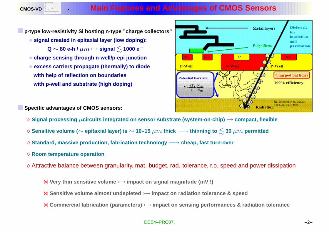
� p-type low-resistivity Si hosting n-type ”charge collecto rs”
• signal created in epitaxial layer (low doping):
Q ∼ 80 e-h / µm 7→ signal . 1000 e−
• charge sensing through n-well/p-epi junction
• excess carriers propagate (thermally) to diode
with help of reflection on boundaries
with p-well and substrate (high doping)
� Specific advantages of CMOS sensors:
� Signal processing µcircuits integrated on sensor substrate (system-on-chip) 7→ compact, flexible
� Sensitive volume ( ∼ epitaxial layer) is ∼ 10–15 µm thick −→ thinning to . 30 µm permitted
� Standard, massive production, fabrication technology −→ cheap, fast turn-over
� Room temperature operation
� Attractive balance between granularity, mat. budget, rad. tolerance, r.o. speed and power dissipation
on Very thin sensitive volume � impact on signal magnitude (mV !)
on Sensitive volume almost undepleted � impact on radiation tolerance & speed
on Commercial fabrication (parameters) � impact on sensing performances & radiation tolerance
DESY–PRC07, –2–
CMOS-VDPitch (microns)
15 20 25 30 35 40 45
Res
olut
ion
(mic
rons
)
1
1.5
2
2.5
3
3.5
Mimosa 9: resolution vs pitch
- Vertexing Applications of MIMOSA Sensors
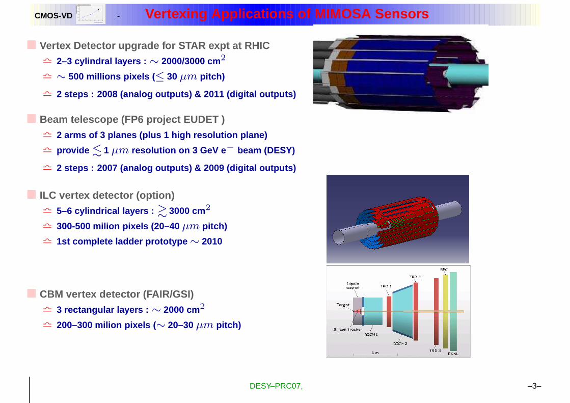
� Vertex Detector upgrade for STAR expt at RHICl 2–3 cylindral layers : ∼ 2000/3000 cm2
l ∼ 500 millions pixels ( ≤ 30 µm pitch)
l 2 steps : 2008 (analog outputs) & 2011 (digital outputs)
� Beam telescope (FP6 project EUDET )l 2 arms of 3 planes (plus 1 high resolution plane)
l provide . 1 µm resolution on 3 GeV e − beam (DESY)
l 2 steps : 2007 (analog outputs) & 2009 (digital outputs)
� ILC vertex detector (option)l 5–6 cylindrical layers : & 3000 cm2
l 300-500 milion pixels (20–40 µm pitch)
l 1st complete ladder prototype ∼ 2010
� CBM vertex detector (FAIR/GSI)l 3 rectangular layers : ∼ 2000 cm2
l 200–300 milion pixels ( ∼ 20–30 µm pitch)
DESY–PRC07, –3–
CMOS-VDPitch (microns)
15 20 25 30 35 40 45
Res
olut
ion
(mic
rons
)
1
1.5
2
2.5
3
3.5
Mimosa 9: resolution vs pitch
- Detection Efficiency
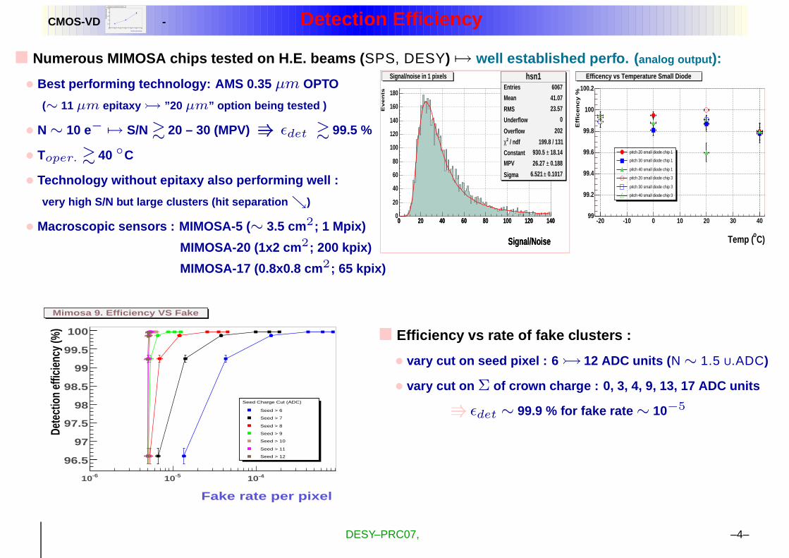
� Numerous MIMOSA chips tested on H.E. beams ( SPS, DESY) 7→ well established perfo. ( analog output ):
• Best performing technology: AMS 0.35 µm OPTO
(∼ 11 µm epitaxy � ”20 µm” option being tested )
• N ∼ 10 e− 7→ S/N & 20 – 30 (MPV) V εdet & 99.5 %
• Toper. & 40 ◦C
• Technology without epitaxy also performing well :
very high S/N but large clusters (hit separation ↘)
• Macroscopic sensors : MIMOSA-5 ( ∼ 3.5 cm2; 1 Mpix)
MIMOSA-20 (1x2 cm 2; 200 kpix)
MIMOSA-17 (0.8x0.8 cm 2; 65 kpix)
Signal/Noise
0 20 40 60 80 100 120 140
hsn1Entries 6067
Mean 41.07
RMS 23.57
Underflow 0
Overflow 202
/ ndf 2χ 199.8 / 131
Constant 18.14± 930.5
MPV 0.188± 26.27
Sigma 0.1017± 6.521
Signal/Noise
0 20 40 60 80 100 120 140
Eve
nts
0
20
40
60
80
100
120
140
160
180
hsn1Entries 6067
Mean 41.07
RMS 23.57
Underflow 0
Overflow 202
/ ndf 2χ 199.8 / 131
Constant 18.14± 930.5
MPV 0.188± 26.27
Sigma 0.1017± 6.521
Signal/noise in 1 pixels
C)oTemp (
-20 -10 0 10 20 30 40
Effic
en
cy %
99
99.2
99.4
99.6
99.8
100
100.2
pitch 20 small diode chip 1
pitch 30 small diode chip 1
pitch 40 small diode chip 1
pitch 20 small diode chip 3
pitch 30 small diode chip 3
pitch 40 small diode chip 3
Efficency vs Temperature Small Diode
� Efficiency vs rate of fake clusters :
• vary cut on seed pixel : 6 � 12 ADC units ( N ∼ 1.5 U.ADC)
• vary cut on Σ of crown charge : 0, 3, 4, 9, 13, 17 ADC units
V εdet ∼ 99.9 % for fake rate ∼ 10−5
Fake rate per pixel
-610 -510 -410
Dete
ction
effic
iency
(%)
96.5
97
97.5
98
98.5
99
99.5
100
Seed Charge Cut (ADC)
Seed > 6
Seed > 7
Seed > 8
Seed > 9
Seed > 10
Seed > 11
Seed > 12
Mimosa 9. Efficiency VS Fake
DESY–PRC07, –4–
CMOS-VDPitch (microns)
15 20 25 30 35 40 45
Res
olut
ion
(mic
rons
)
1
1.5
2
2.5
3
3.5
Mimosa 9: resolution vs pitch
- Spatial Resolution (vs ADC resolution)
Pitch (microns)
15 20 25 30 35 40 45
Res
olut
ion
(mic
rons
)
1
1.5
2
2.5
3
3.5
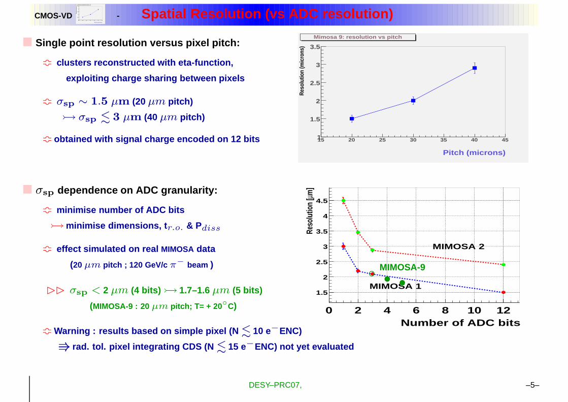
Mimosa 9: resolution vs pitch� Single point resolution versus pixel pitch:
m clusters reconstructed with eta-function,
exploiting charge sharing between pixels
m σsp ∼ 1.5 µm (20 µm pitch)
� σsp . 3 µm (40 µm pitch)
m obtained with signal charge encoded on 12 bits
� σsp dependence on ADC granularity:
m minimise number of ADC bits
� minimise dimensions, t r.o. & Pdiss
m effect simulated on real MIMOSA data
(20 µm pitch ; 120 GeV/c π− beam )
BB σsp < 2 µm (4 bits) � 1.7–1.6 µm (5 bits)
(MIMOSA-9 : 20 µm pitch; T= + 20 ◦C)
m Warning : results based on simple pixel (N . 10 e−ENC)
V rad. tol. pixel integrating CDS (N . 15 e−ENC) not yet evaluated
Number of ADC bits0 2 4 6 8 10 12
m]
µRe
solut
ion [
1.5
2
2.5
3
3.5
4
4.5
MIMOSA 2
MIMOSA 1
◦•
•
MIMOSA-9
DESY–PRC07, –5–
CMOS-VDPitch (microns)
15 20 25 30 35 40 45
Res
olut
ion
(mic
rons
)
1
1.5
2
2.5
3
3.5
Mimosa 9: resolution vs pitch
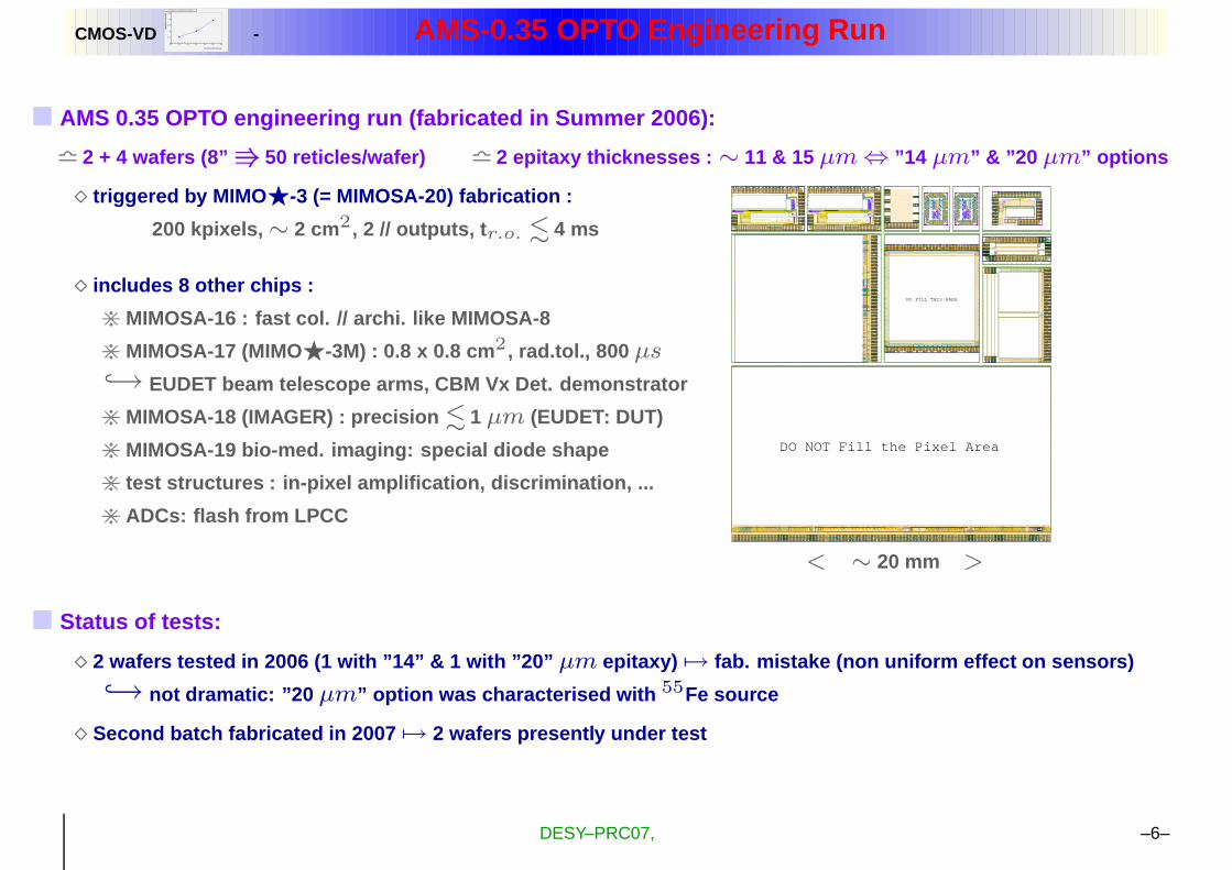
- AMS-0.35 OPTO Engineering Run
� AMS 0.35 OPTO engineering run (fabricated in Summer 2006):
l 2 + 4 wafers (8” V 50 reticles/wafer) l 2 epitaxy thicknesses : ∼ 11 & 15 µm ⇔ ”14 µm” & ”20 µm” options
� triggered by MIMO F-3 (= MIMOSA-20) fabrication :
200 kpixels, ∼ 2 cm2, 2 // outputs, t r.o. . 4 ms
� includes 8 other chips :
> MIMOSA-16 : fast col. // archi. like MIMOSA-8
> MIMOSA-17 (MIMOF-3M) : 0.8 x 0.8 cm 2, rad.tol., 800 µs
↪→ EUDET beam telescope arms, CBM Vx Det. demonstrator
> MIMOSA-18 (IMAGER) : precision . 1 µm (EUDET: DUT)
> MIMOSA-19 bio-med. imaging: special diode shape
> test structures : in-pixel amplification, discrimination, ...
> ADCs: flash from LPCC
< ∼ 20 mm >
DO NOT Fill the Pixel Area
NO FILL THIS AREA
� Status of tests:
� 2 wafers tested in 2006 (1 with ”14” & 1 with ”20” µm epitaxy) 7→ fab. mistake (non uniform effect on sensors)
↪→ not dramatic: ”20 µm” option was characterised with 55Fe source
� Second batch fabricated in 2007 7→ 2 wafers presently under test
DESY–PRC07, –6–
CMOS-VDPitch (microns)
15 20 25 30 35 40 45
Res
olut
ion
(mic
rons
)
1
1.5
2
2.5
3
3.5
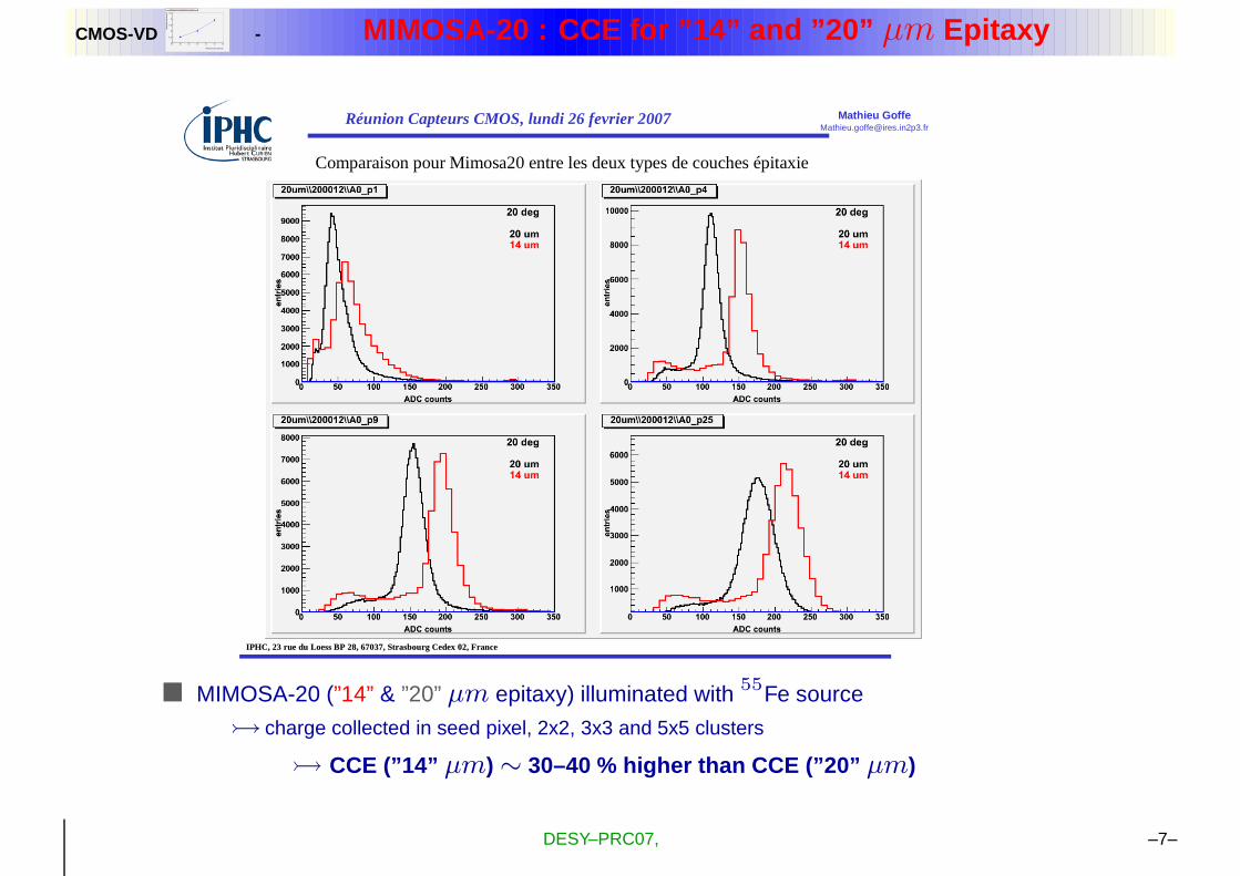
Mimosa 9: resolution vs pitch
- MIMOSA-20 : CCE for ”14” and ”20” µm Epitaxy
Mathieu [email protected]
Réunion Capteurs CMOS, lundi 26 fevrier 2007
IPHC, 23 rue du Loess BP 28, 67037, Strasbourg Cedex 02, FranceIPHC, 23 rue du Loess BP 28, 67037, Strasbourg Cedex 02, France
Comparaison pour Mimosa20 entre les deux types de couches épitaxie
� MIMOSA-20 (”14” & ”20” µm epitaxy) illuminated with 55Fe source
� charge collected in seed pixel, 2x2, 3x3 and 5x5 clusters
� CCE (”14” µm) ∼ 30–40 % higher than CCE (”20” µm)
DESY–PRC07, –7–
CMOS-VDPitch (microns)
15 20 25 30 35 40 45
Res
olut
ion
(mic
rons
)
1
1.5
2
2.5
3
3.5
Mimosa 9: resolution vs pitch
- Radiation Tolerance: AMS-0.35 OPTO Evaluation
� Requirements:
> beamstrahlung ( GuineaPig X 3 ) : . 103 e±BS /cm2/25 µs � . 2·1012e±BS /cm2/yr
↪→ O(100) kRad/yr – O(10 11) neq /cm2/yr (NIEL ∼ 1/30)
> neutron gas: . 1010 neq /cm2 /yr
� Non-ionising radiation tolerance:
> MIMOSA-15 irradiated with O(1 MeV) neutrons tested on DESY e − beams : Very Preliminary results
• T = - 20◦C, tr.o. ∼ 700 µs Fluence 0 0.47 2.1 5.8 (5/2) 5.8 (4/2)
S/N (MPV) 27.8 ± 0.5 21.8 ± 0.5 14.7 ± 0.3 8.7 ± 2. 7.5 ± 2.
Det. Eff. (%) 100. 99.9 ± 0.1 99.3 ± 0.2 77. ± 2 84. ± 2.
◦ 5.8·1012neq /cm2 values derived
with standard and with soft cuts
� Ionising radiation tolerance:
> Pixels modified against hole accumulations (thick oxide) an d leakage current increase (guard ring)
> MIMOSA-15 tested with ∼ 5 GeV e− at DESY after 1 MRad (10 keV X-Ray) exposure : Very Preliminary results
• T = - 20◦C, tr.o. ∼ 180 µs
• tr.o. << 1ms crucial at Troom
Integ. Dose Noise S/N ( MPV) Detection Efficiency
0 9.0 ± 1.1 27.8 ± 0.5 100 %
1 MRad 10.7 ± 0.9 19.5 ± 0.2 99.96 ± 0.04 %
� Preliminary conclusion:
> at least 3 years of running viable at T room (or close to)
> further assessment needed (also with ∼ 10 MeV e−) : sensors with integ. CDS, ADC, ....
DESY–PRC07, –8–
CMOS-VDPitch (microns)
15 20 25 30 35 40 45
Res
olut
ion
(mic
rons
)
1
1.5
2
2.5
3
3.5
Mimosa 9: resolution vs pitch
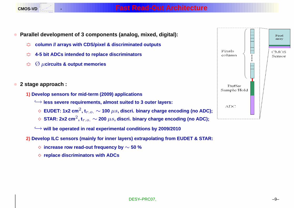
- Fast Read-Out Architecture
• Parallel development of 3 components (analog, mixed, digit al):
m column // arrays with CDS/pixel & discriminated outputs
m 4-5 bit ADCs intended to replace discriminators
m Ø µcircuits & output memories
• 2 stage approach :
1) Develop sensors for mid-term (2009) applications
↪→ less severe requirements, almost suited to 3 outer layers:
� EUDET: 1x2 cm 2, tr.o. ∼ 100 µs, discri. binary charge encoding (no ADC);
� STAR: 2x2 cm 2, tr.o. ∼ 200 µs, discri. binary charge encoding (no ADC);
↪→ will be operated in real experimental conditions by 2009/20 10
2) Develop ILC sensors (mainly for inner layers) extrapolatin g from EUDET & STAR:
� increase row read-out frequency by ∼ 50 %
� replace discriminators with ADCs
DESY–PRC07, –9–
CMOS-VDPitch (microns)
15 20 25 30 35 40 45
Res
olut
ion
(mic
rons
)
1
1.5
2
2.5
3
3.5
Mimosa 9: resolution vs pitch
- High Read-Out Speed Architecture
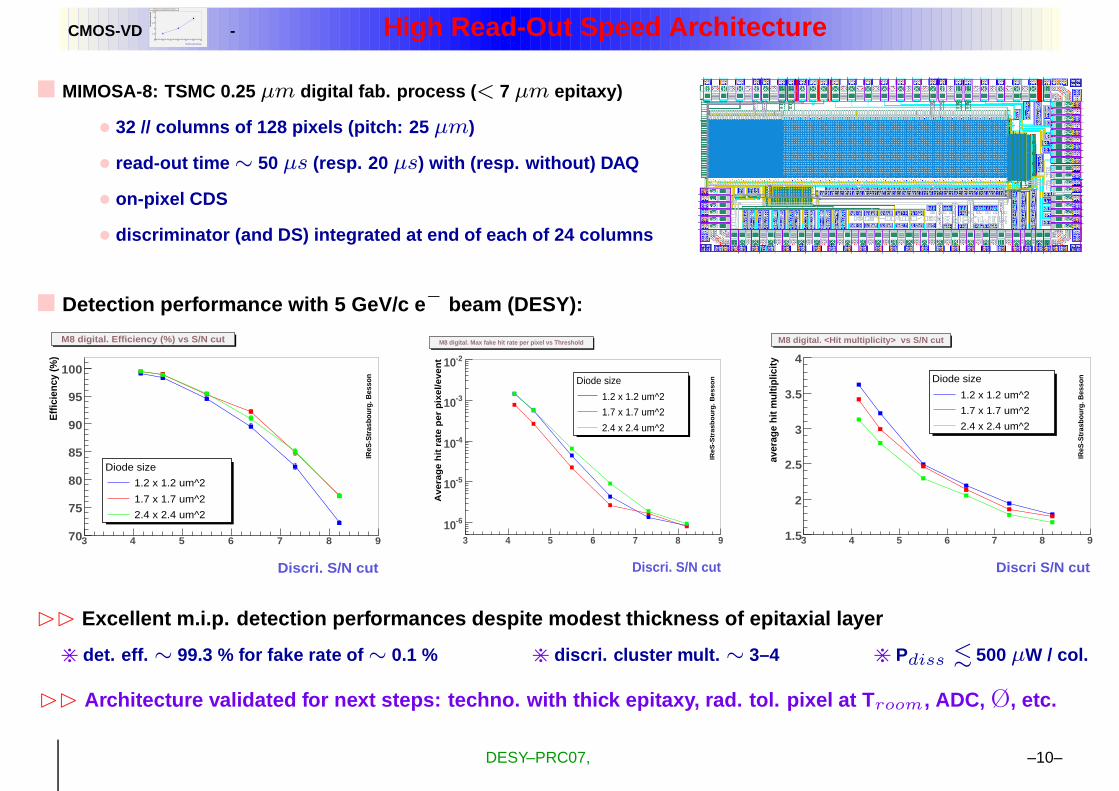
� MIMOSA-8: TSMC 0.25 µm digital fab. process ( < 7 µm epitaxy)
• 32 // columns of 128 pixels (pitch: 25 µm)
• read-out time ∼ 50 µs (resp. 20 µs) with (resp. without) DAQ
• on-pixel CDS
• discriminator (and DS) integrated at end of each of 24 column s
� Detection performance with 5 GeV/c e − beam (DESY):
Discri. S/N cut
3 4 5 6 7 8 9
Effi
cien
cy (%
)
70
75
80
85
90
95
100
Diode size
1.2 x 1.2 um^2
1.7 x 1.7 um^2
2.4 x 2.4 um^2
IReS
-Stra
sbou
rg. B
esso
n
M8 digital. Efficiency (%) vs S/N cut
Discri. S/N cut
3 4 5 6 7 8 9
Ave
rage
hit
rate
per
pix
el/e
vent
-610
-510
-410
-310
-210
IReS
-Str
asbo
urg.
Bes
sonDiode size
1.2 x 1.2 um^2
1.7 x 1.7 um^2
2.4 x 2.4 um^2
M8 digital. Max fake hit rate per pixel vs Threshold
Discri S/N cut
3 4 5 6 7 8 9
aver
age
hit m
ultip
licity
1.5
2
2.5
3
3.5
4
Diode size
1.2 x 1.2 um^2
1.7 x 1.7 um^2
2.4 x 2.4 um^2
IReS
-Stra
sbou
rg. B
esso
n
M8 digital. <Hit multiplicity> vs S/N cut
BB Excellent m.i.p. detection performances despite modest th ickness of epitaxial layer
> det. eff. ∼ 99.3 % for fake rate of ∼ 0.1 % > discri. cluster mult. ∼ 3–4 > Pdiss . 500 µW / col.
BB Architecture validated for next steps: techno. with thick e pitaxy, rad. tol. pixel at T room, ADC, Ø, etc.
DESY–PRC07, –10–
CMOS-VDPitch (microns)
15 20 25 30 35 40 45
Res
olut
ion
(mic
rons
)
1
1.5
2
2.5
3
3.5
Mimosa 9: resolution vs pitch
- Tests of MIMOSA-16
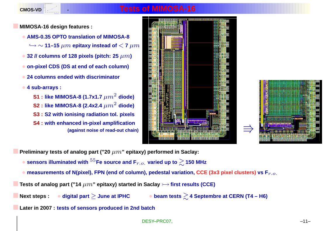
� MIMOSA-16 design features :
• AMS-0.35 OPTO translation of MIMOSA-8
↪→∼ 11–15 µm epitaxy instead of < 7 µm
• 32 // columns of 128 pixels (pitch: 25 µm)
• on-pixel CDS (DS at end of each column)
• 24 columns ended with discriminator
• 4 sub-arrays :
S1 : like MIMOSA-8 (1.7x1.7 µm2 diode)
S2 : like MIMOSA-8 (2.4x2.4 µm2 diode)
S3 : S2 with ionising radiation tol. pixels
S4 : with enhanced in-pixel amplification(against noise of read-out chain) V
� Preliminary tests of analog part (”20 µm” epitaxy) performed in Saclay:
• sensors illuminated with 55Fe source and F r.o. varied up to & 150 MHz
• measurements of N(pixel), FPN (end of column), pedestal var iation, CCE (3x3 pixel clusters) vs Fr.o.
� Tests of analog part (”14 µm” epitaxy) started in Saclay � first results (CCE)
� Next steps : • digital part ≥ June at IPHC • beam tests & 4 Septembre at CERN (T4 – H6)
� Later in 2007 : tests of sensors produced in 2nd batch
DESY–PRC07, –11–
CMOS-VDPitch (microns)
15 20 25 30 35 40 45
Res
olut
ion
(mic
rons
)
1
1.5
2
2.5
3
3.5
Mimosa 9: resolution vs pitch
- MIMOSA-16 Lab Test Results (Analog Part)
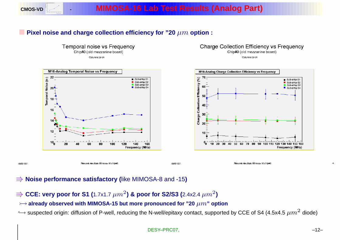
� Pixel noise and charge collection efficiency for ”20 µm option :
V Noise performance satisfactory ( like MIMOSA-8 and -15)
V CCE: very poor for S1 ( 1.7x1.7 µm2) & poor for S2/S3 ( 2.4x2.4 µm2)� already observed with MIMOSA-15 but more pronounced for ”20 µm” option
↪→ suspected origin: diffusion of P-well, reducing the N-well/epitaxy contact, supported by CCE of S4 (4.5x4.5 µm2 diode)
DESY–PRC07, –12–
CMOS-VDPitch (microns)
15 20 25 30 35 40 45
Res
olut
ion
(mic
rons
)
1
1.5
2
2.5
3
3.5
Mimosa 9: resolution vs pitch
- Status of ADC Developments
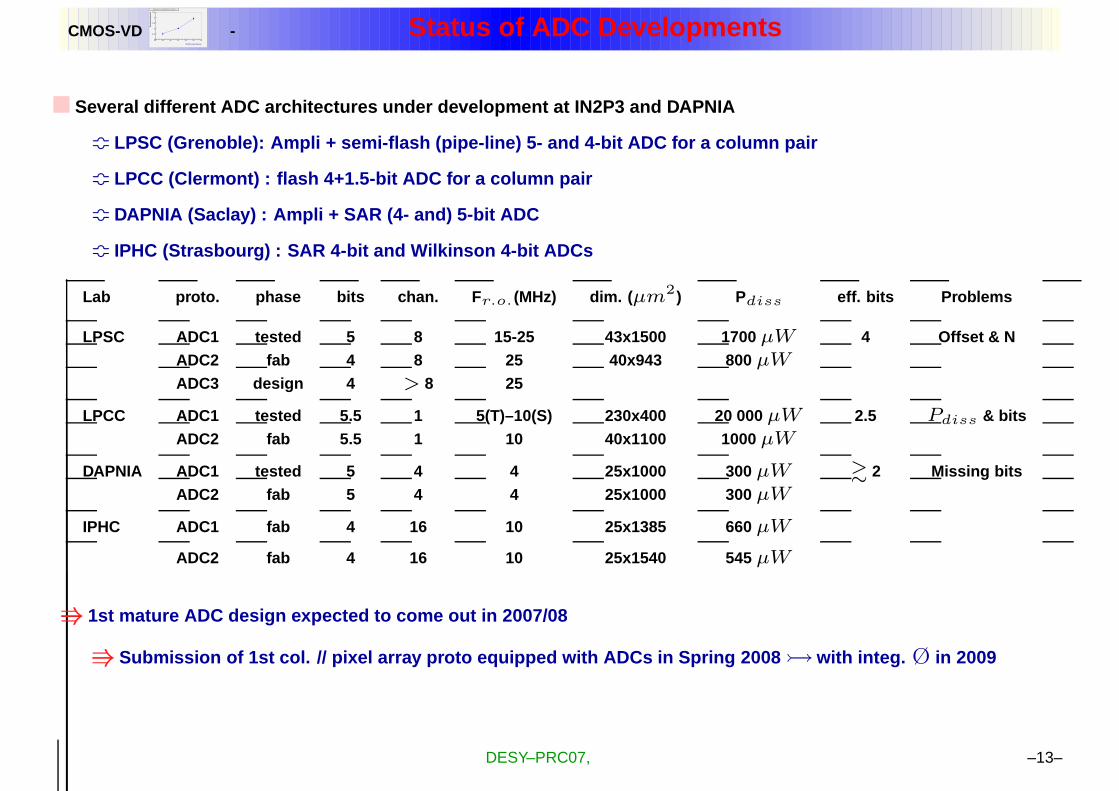
� Several different ADC architectures under development at I N2P3 and DAPNIA
m LPSC (Grenoble): Ampli + semi-flash (pipe-line) 5- and 4-bit ADC for a column pair
m LPCC (Clermont) : flash 4+1.5-bit ADC for a column pair
m DAPNIA (Saclay) : Ampli + SAR (4- and) 5-bit ADC
m IPHC (Strasbourg) : SAR 4-bit and Wilkinson 4-bit ADCs
Lab proto. phase bits chan. Fr.o.(MHz) dim. (µm2) Pdiss eff. bits Problems
LPSC ADC1 tested 5 8 15-25 43x1500 1700 µW 4 Offset & NADC2 fab 4 8 25 40x943 800 µW
ADC3 design 4 > 8 25
LPCC ADC1 tested 5.5 1 5(T)–10(S) 230x400 20 000 µW 2.5 Pdiss & bitsADC2 fab 5.5 1 10 40x1100 1000 µW
DAPNIA ADC1 tested 5 4 4 25x1000 300 µW & 2 Missing bitsADC2 fab 5 4 4 25x1000 300 µW
IPHC ADC1 fab 4 16 10 25x1385 660 µW
ADC2 fab 4 16 10 25x1540 545 µW
V 1st mature ADC design expected to come out in 2007/08
V Submission of 1st col. // pixel array proto equipped with ADC s in Spring 2008 � with integ. Ø in 2009
DESY–PRC07, –13–
CMOS-VDPitch (microns)
15 20 25 30 35 40 45
Res
olut
ion
(mic
rons
)
1
1.5
2
2.5
3
3.5
Mimosa 9: resolution vs pitch
- Zero Suppression Micro-Circuit : Floor Plan
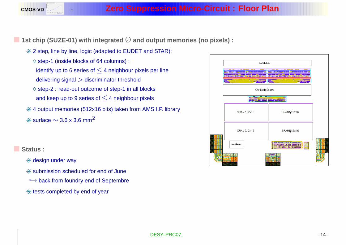
� 1st chip (SUZE-01) with integrated Ø and output memories (no pixels) :
> 2 step, line by line, logic (adapted to EUDET and STAR):
� step-1 (inside blocks of 64 columns) :
identify up to 6 series of ≤ 4 neighbour pixels per line
delivering signal > discriminator threshold
� step-2 : read-out outcome of step-1 in all blocks
and keep up to 9 series of ≤ 4 neighbour pixels
> 4 output memories (512x16 bits) taken from AMS I.P. library
> surface ∼ 3.6 x 3.6 mm2
� Status :
> design under way
> submission scheduled for end of June
↪→ back from foundry end of Septembre
> tests completed by end of year
DESY–PRC07, –14–
CMOS-VDPitch (microns)
15 20 25 30 35 40 45
Res
olut
ion
(mic
rons
)
1
1.5
2
2.5
3
3.5
Mimosa 9: resolution vs pitch
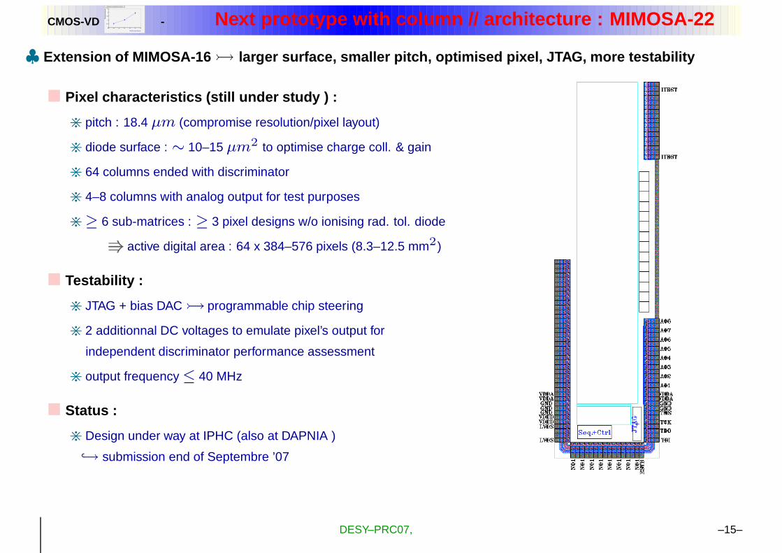
- Next prototype with column // architecture : MIMOSA-22
♣ Extension of MIMOSA-16 � larger surface, smaller pitch, optimised pixel, JTAG, more testability
� Pixel characteristics (still under study ) :
> pitch : 18.4 µm (compromise resolution/pixel layout)
> diode surface : ∼ 10–15 µm2 to optimise charge coll. & gain
> 64 columns ended with discriminator
> 4–8 columns with analog output for test purposes
>≥ 6 sub-matrices : ≥ 3 pixel designs w/o ionising rad. tol. diode
V active digital area : 64 x 384–576 pixels (8.3–12.5 mm2)
� Testability :
> JTAG + bias DAC � programmable chip steering
> 2 additionnal DC voltages to emulate pixel’s output for
independent discriminator performance assessment
> output frequency ≤ 40 MHz
� Status :
> Design under way at IPHC (also at DAPNIA )
↪→ submission end of Septembre ’07
DESY–PRC07, –15–
CMOS-VDPitch (microns)
15 20 25 30 35 40 45
Res
olut
ion
(mic
rons
)
1
1.5
2
2.5
3
3.5
Mimosa 9: resolution vs pitch
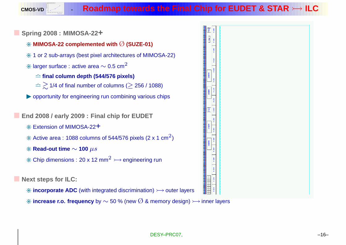
- Roadmap towards the Final Chip for EUDET & STAR � ILC
� Spring 2008 : MIMOSA-22 +> MIMOSA-22 complemented with Ø (SUZE-01)
> 1 or 2 sub-arrays (best pixel architectures of MIMOSA-22)
> larger surface : active area ∼ 0.5 cm2
l final column depth (544/576 pixels)
l & 1/4 of final number of columns (≥ 256 / 1088)
I opportunity for engineering run combining various chips
� End 2008 / early 2009 : Final chip for EUDET
> Extension of MIMOSA-22+> Active area : 1088 columns of 544/576 pixels (2 x 1 cm2)
> Read-out time ∼ 100 µs
> Chip dimensions : 20 x 12 mm2 � engineering run
� Next steps for ILC:
> incorporate ADC (with integrated discrimination) � outer layers
> increase r.o. frequency by ∼ 50 % (new Ø & memory design) � inner layers
DESY–PRC07, –16–
CMOS-VDPitch (microns)
15 20 25 30 35 40 45
Res
olut
ion
(mic
rons
)
1
1.5
2
2.5
3
3.5
Mimosa 9: resolution vs pitch
- SUMMARY
� CMOS sensors are developed for running conditions with beam background >> MC simulations
� Fast read-out sensors progressing steadily :
> col. // architecture with discriminated output operationa l
> ADCs close to final design ( . beginning 2008)
>Ø µcircuits : 1st generation (EUDET, STAR) close to fabricatio n
� AMS-035 OPTO fabrication technology assessed � baseline for R&D :
> detection efficiency (T), radiation tolerance, noise � fake hits, etc.
↪→ equip EUDET, STAR, CBM demonstrators in 2007/2008 with new g eneration of full scale sensors
↪→ real experimental conditions
� Milestones until final chip well identified :
> 1st step : final sensors with discriminated binary charge enc oding for EUDET (2009) and STAR (2010)
> 2nd step : replace discri. with ADC (outer layers) and increa se r.o. frequency by ∼ 50 % (inner layers)
> also: find final fabrication process ( < 0.2 µm feature size)
� Concern :
> system integration issues not covered � prototype ladder ????
DESY–PRC07, –17–
CMOS-VDPitch (microns)
15 20 25 30 35 40 45
Res
olut
ion
(mic
rons
)
1
1.5
2
2.5
3
3.5
Mimosa 9: resolution vs pitch
-
BACK-UP SLIDES
DESY–PRC07, –18–
CMOS-VDPitch (microns)
15 20 25 30 35 40 45
Res
olut
ion
(mic
rons
)
1
1.5
2
2.5
3
3.5
Mimosa 9: resolution vs pitch
- Main R&D Directions
� High r.-o. speed, low noise, low power dissip., highly integ rated signal processing architecture:> analog part (charge collection, pre-amp, CDS, ...) inside p ixel
> mixed (ADC) and digital (sparsification) micro-circuits in tegrated inside pixel or aside of active surface
� Optimal fabrication process:> epitaxial layer thickness > number of metal layers > yield
> (dark current) > cost > life time of ( < 0.2 µm) process
� Radiation Tolerance:
> dark current > doping profile (> latch-up)
� Industrial thinning procedure:
> minimal thickness > mechanical prop. > individual chips rather than wafers (?) > yield
� Room temperature operation:
> minimise cooling requirements > performances after irradiation
DESY–PRC07, –19–
CMOS-VDPitch (microns)
15 20 25 30 35 40 45
Res
olut
ion
(mic
rons
)
1
1.5
2
2.5
3
3.5
Mimosa 9: resolution vs pitch
-
Main Requirements
for the ILC Vertex Detector :
physics & running condition requirements
DESY–PRC07, –20–
CMOS-VDPitch (microns)
15 20 25 30 35 40 45
Res
olut
ion
(mic
rons
)
1
1.5
2
2.5
3
3.5
Mimosa 9: resolution vs pitch
- Constraints from Required σi.p. (1/2)
� σIP = a ⊕ b/p · sin3/2θ with a < 5 µm and b < 10 µm
B limits on a and b are still ”very educated guesses” B SLD: a = 8 µm and b = 33 µm
� Upper bound on a drives the pixel pitch and the radii of the inner and outer lay er of the Vx Det.
� Upper bound on b drives radius and material budget of inner layer (& beam pipe )
� Constraint on σIP satisfies simultaneoulsy requirement on double hit separat ion in inner most layer ( ∼ 30 – 40 µm)
DESY–PRC07, –21–
CMOS-VDPitch (microns)
15 20 25 30 35 40 45
Res
olut
ion
(mic
rons
)
1
1.5
2
2.5
3
3.5
Mimosa 9: resolution vs pitch
- Constraints from Required σi.p. (2/2)
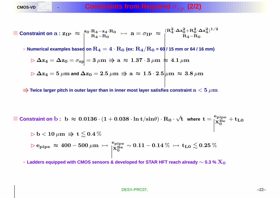
� Constraint on a : zIP ≈z0·R4−z4·R0
R4−R0� a = σIP ≈
(R24·∆z20+R2
0·∆z24)1/2
R4−R0
• Numerical examples based on R4 = 4 · R0 (ex: R4/R0 = 60 / 15 mm or 64 / 16 mm)
B∆z4 = ∆z0 = σsp = 3 µm V a ≈ 1.37 · 3 µm ≈ 4.1 µm
B∆z4 = 5 µm and ∆z0 = 2.5 µm V a ≈ 1.5 · 2.5 µm ≈ 3.8 µm
V Twice larger pitch in outer layer than in inner most layer sat isfies constraint a < 5 µm
� Constraint on b : b ≈ 0.0136 · (1 + 0.038 · ln t/sinθ) · R0 ·√
t where t =epipe
XBe0
+ tL0
Bb < 10 µm V t . 0.4 %
Bepipe ≈ 400 − 500 µm �epipe
XBe0
∼ 0.11 − 0.14 % � tL0 . 0.25 %
• Ladders equipped with CMOS sensors & developed for STAR HFT r each already ∼ 0.3 % X0
DESY–PRC07, –22–
CMOS-VDPitch (microns)
15 20 25 30 35 40 45
Res
olut
ion
(mic
rons
)
1
1.5
2
2.5
3
3.5
Mimosa 9: resolution vs pitch
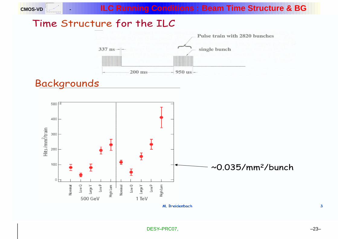
- ILC Running Conditions : Beam Time Structure & BG
DESY–PRC07, –23–
CMOS-VDPitch (microns)
15 20 25 30 35 40 45
Res
olut
ion
(mic
rons
)
1
1.5
2
2.5
3
3.5
Mimosa 9: resolution vs pitch
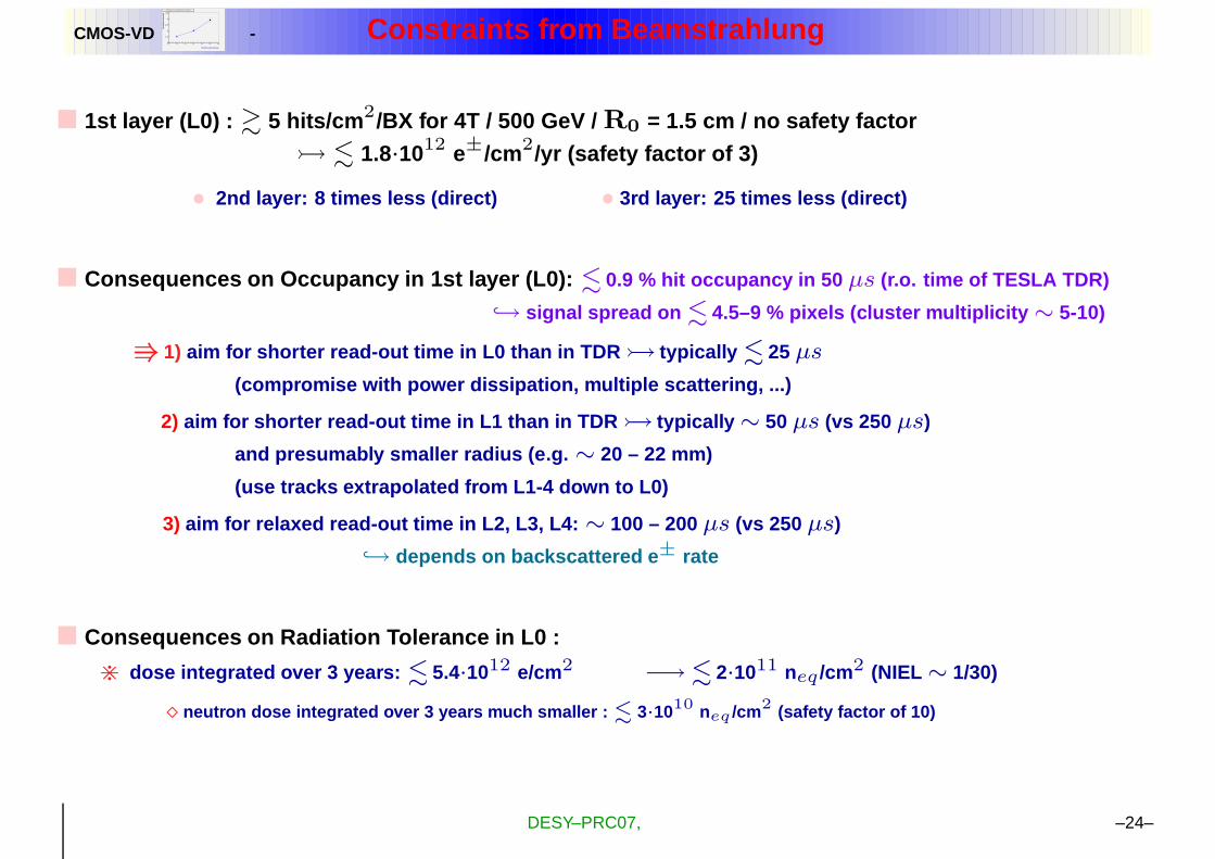
- Constraints from Beamstrahlung
� 1st layer (L0) : & 5 hits/cm 2/BX for 4T / 500 GeV / R0 = 1.5 cm / no safety factor� . 1.8·1012 e±/cm2/yr (safety factor of 3)
• 2nd layer: 8 times less (direct) • 3rd layer: 25 times less (direct)
� Consequences on Occupancy in 1st layer (L0): . 0.9 % hit occupancy in 50 µs (r.o. time of TESLA TDR)
↪→ signal spread on . 4.5–9 % pixels (cluster multiplicity ∼ 5-10)
V 1) aim for shorter read-out time in L0 than in TDR � typically . 25 µs
(compromise with power dissipation, multiple scattering, ...)
2) aim for shorter read-out time in L1 than in TDR � typically ∼ 50 µs (vs 250 µs)
and presumably smaller radius (e.g. ∼ 20 – 22 mm)
(use tracks extrapolated from L1-4 down to L0)
3) aim for relaxed read-out time in L2, L3, L4: ∼ 100 – 200 µs (vs 250 µs)
↪→ depends on backscattered e ± rate
� Consequences on Radiation Tolerance in L0 :
> dose integrated over 3 years: . 5.4·1012 e/cm2 −→ . 2·1011 neq /cm2 (NIEL ∼ 1/30)
� neutron dose integrated over 3 years much smaller : . 3·1010 neq /cm2 (safety factor of 10)
DESY–PRC07, –24–
CMOS-VDPitch (microns)
15 20 25 30 35 40 45
Res
olut
ion
(mic
rons
)
1
1.5
2
2.5
3
3.5
Mimosa 9: resolution vs pitch
- Consequences on Inner Layer Design
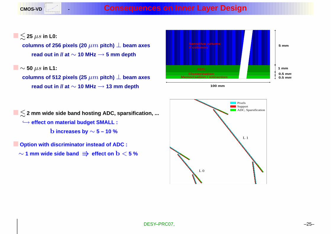
� . 25 µs in L0:
columns of 256 pixels (20 µm pitch) ⊥ beam axes
read out in // at ∼ 10 MHz → 5 mm depth
�∼ 50 µs in L1:
columns of 512 pixels (25 µm pitch) ⊥ beam axes
read out in // at ∼ 10 MHz → 13 mm depth
1 mm
0.5 mm0.5 mm
5 mm
100 mm
ADC
ClusterisationMemorisation / extraction
Sensitive volume// columns
Pixels
ADC, Sparsification
L 1
L 0
Support
� . 2 mm wide side band hosting ADC, sparsification, ...
↪→ effect on material budget SMALL :
b increases by ∼ 5 – 10 %
� Option with discriminator instead of ADC :
∼ 1 mm wide side band V effect on b < 5 %
DESY–PRC07, –25–
CMOS-VDPitch (microns)
15 20 25 30 35 40 45
Res
olut
ion
(mic
rons
)
1
1.5
2
2.5
3
3.5
Mimosa 9: resolution vs pitch
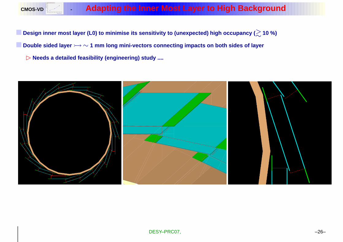
- Adapting the Inner Most Layer to High Background
� Design inner most layer (L0) to minimise its sensitivity to ( unexpected) high occupancy ( & 10 %)
� Double sided layer �∼ 1 mm long mini-vectors connecting impacts on both sides of la yer
B Needs a detailed feasibility (engineering) study ....
DESY–PRC07, –26–
CMOS-VDPitch (microns)
15 20 25 30 35 40 45
Res
olut
ion
(mic
rons
)
1
1.5
2
2.5
3
3.5
Mimosa 9: resolution vs pitch
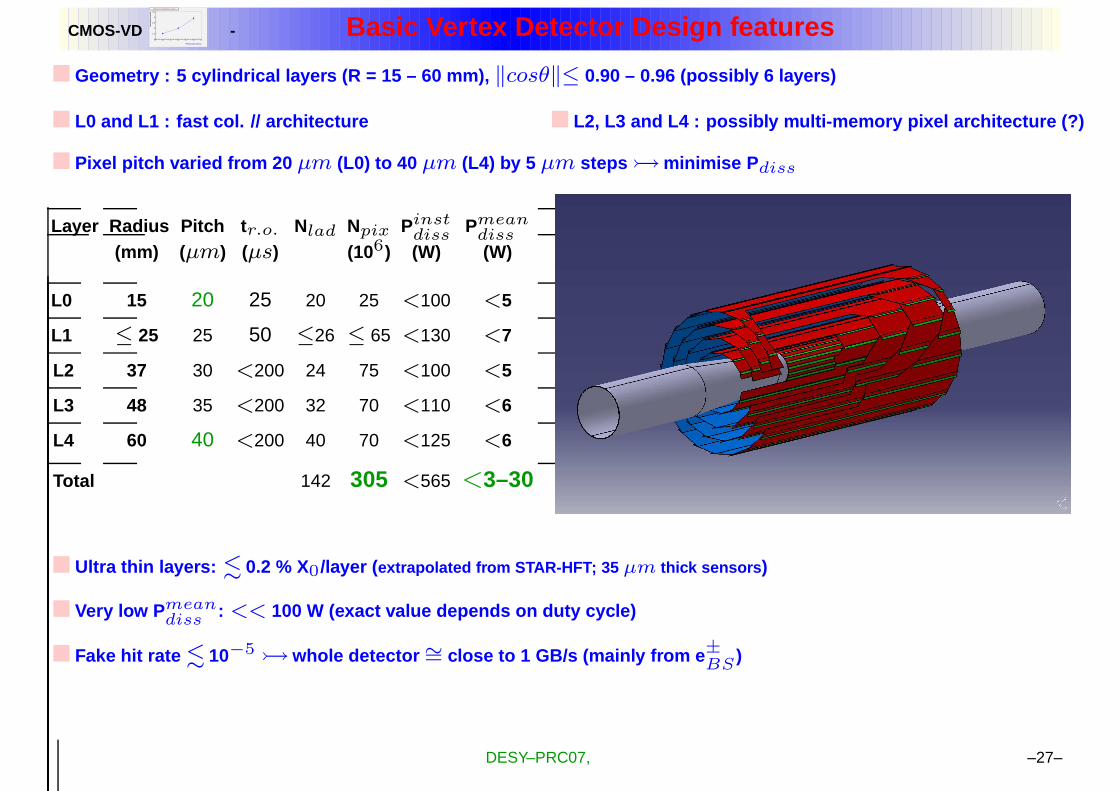
- Basic Vertex Detector Design features
� Geometry : 5 cylindrical layers (R = 15 – 60 mm), ‖cosθ‖≤ 0.90 – 0.96 (possibly 6 layers)
� L0 and L1 : fast col. // architecture � L2, L3 and L4 : possibly multi-memory pixel architecture (?)
� Pixel pitch varied from 20 µm (L0) to 40 µm (L4) by 5 µm steps � minimise P diss
Layer Radius Pitch t r.o. Nlad Npix Pinstdiss Pmean
diss(mm) (µm) (µs) (106) (W) (W)
L0 15 20 25 20 25 <100 <5
L1 ≤ 25 25 50 ≤26 ≤ 65 <130 <7
L2 37 30 <200 24 75 <100 <5
L3 48 35 <200 32 70 <110 <6
L4 60 40 <200 40 70 <125 <6
Total 142 305 <565 <3–30
� Ultra thin layers: . 0.2 % X0/layer ( extrapolated from STAR-HFT; 35 µm thick sensors )
� Very low P meandiss : << 100 W (exact value depends on duty cycle)
� Fake hit rate . 10−5 � whole detector ∼= close to 1 GB/s (mainly from e ±
BS )
DESY–PRC07, –27–
CMOS-VDPitch (microns)
15 20 25 30 35 40 45
Res
olut
ion
(mic
rons
)
1
1.5
2
2.5
3
3.5
Mimosa 9: resolution vs pitch
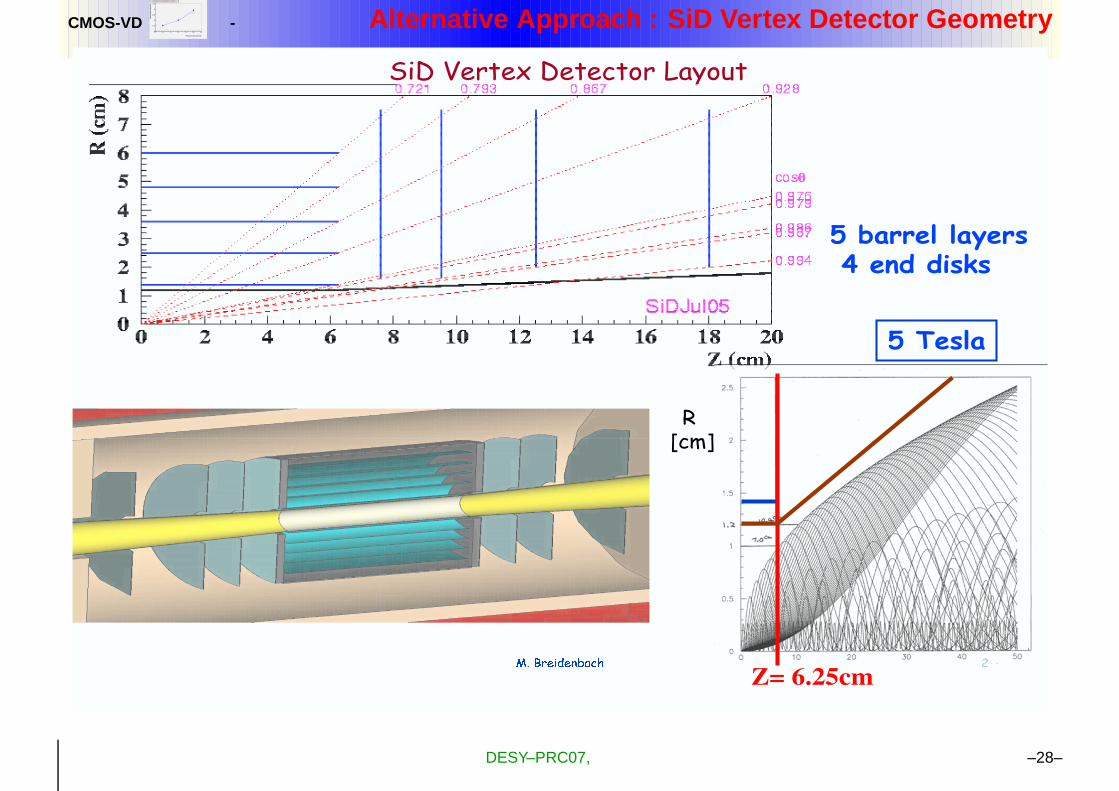
- Alternative Approach : SiD Vertex Detector Geometry
DESY–PRC07, –28–
CMOS-VDPitch (microns)
15 20 25 30 35 40 45
Res
olut
ion
(mic
rons
)
1
1.5
2
2.5
3
3.5
Mimosa 9: resolution vs pitch
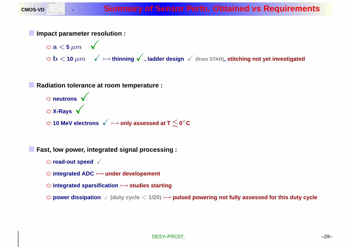
- Summary of Sensor Perfo. Obtained vs Requirements
� Impact parameter resolution :
ma < 5 µm Xmb < 10 µm X � thinning X, ladder design X (from STAR) , stitching not yet investigated
� Radiation tolerance at room temperature :
m neutrons Xm X-Rays Xm 10 MeV electrons X � only assessed at T . 0◦C
� Fast, low power, integrated signal processing :
m read-out speed X
m integrated ADC � under developement
m integrated sparsification � studies starting
m power dissipation X (duty cycle < 1/20) � pulsed powering not fully assessed for this duty cycle
DESY–PRC07, –29–
CMOS-VDPitch (microns)
15 20 25 30 35 40 45
Res
olut
ion
(mic
rons
)
1
1.5
2
2.5
3
3.5
Mimosa 9: resolution vs pitch
- Vertex Detector Issues (from W.Cooper - FNAL)
� Overall geometry :
> matching with neighbour trackers
� Sensor geometry and features
� Heat removal
� Thermal distortions
� Handling thin silicon
� Assembly and alignment procedures
� Connections, cabling, and optical fibers
� Paths for cables, optical fibers, and air flow
� Lorentz forces
V Only few people taking care of so many crucial and delicate to pics
DESY–PRC07, –30–
CMOS-VDPitch (microns)
15 20 25 30 35 40 45
Res
olut
ion
(mic
rons
)
1
1.5
2
2.5
3
3.5
Mimosa 9: resolution vs pitch
-
Observed Radiation Tolerance
of MIMOSA Sensors
DESY–PRC07, –31–
CMOS-VDPitch (microns)
15 20 25 30 35 40 45
Res
olut
ion
(mic
rons
)
1
1.5
2
2.5
3
3.5
Mimosa 9: resolution vs pitch
- Radiation Tolerance: Non-Ionising Radiation
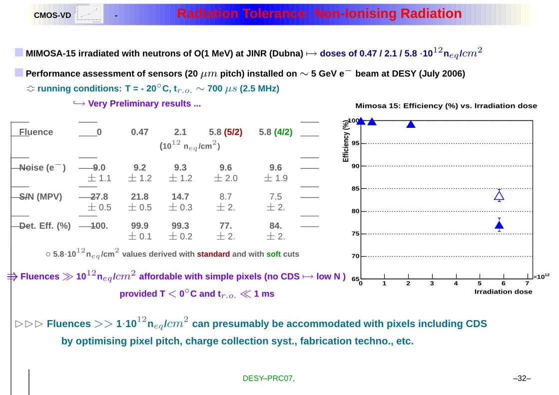
� MIMOSA-15 irradiated with neutrons of O(1 MeV) at JINR (Dubn a) 7→ doses of 0.47 / 2.1 / 5.8 ·1012neq /cm2
� Performance assessment of sensors (20 µm pitch) installed on ∼ 5 GeV e− beam at DESY (July 2006)
m running conditions: T = - 20 ◦C, tr.o. ∼ 700 µs (2.5 MHz)
↪→ Very Preliminary results ...
Irradiation dose0 1 2 3 4 5 6 7
1210×
Effic
ienc
y (%
)
65
70
75
80
85
90
95
100
Mimosa 15: Efficiency (%) vs. Irradiation dose
Fluence 0 0.47 2.1 5.8 (5/2) 5.8 (4/2)
(1012 neq /cm2)
Noise (e−) 9.0 9.2 9.3 9.6 9.6± 1.1 ± 1.2 ± 1.2 ± 2.0 ± 1.9
S/N (MPV) 27.8 21.8 14.7 8.7 7.5± 0.5 ± 0.5 ± 0.3 ± 2. ± 2.
Det. Eff. (%) 100. 99.9 99.3 77. 84.± 0.1 ± 0.2 ± 2. ± 2.
◦ 5.8·1012neq /cm2 values derived with standard and with soft cuts
V Fluences � 1012neq /cm2 affordable with simple pixels (no CDS 7→ low N )
provided T < 0◦C and t r.o. � 1 ms
BBB Fluences >> 1·1012neq /cm2 can presumably be accommodated with pixels including CDS
by optimising pixel pitch, charge collection syst., fabric ation techno., etc.
DESY–PRC07, –32–
CMOS-VDPitch (microns)
15 20 25 30 35 40 45
Res
olut
ion
(mic
rons
)
1
1.5
2
2.5
3
3.5
Mimosa 9: resolution vs pitch
- Radiation Tolerance : Ionising Radiation
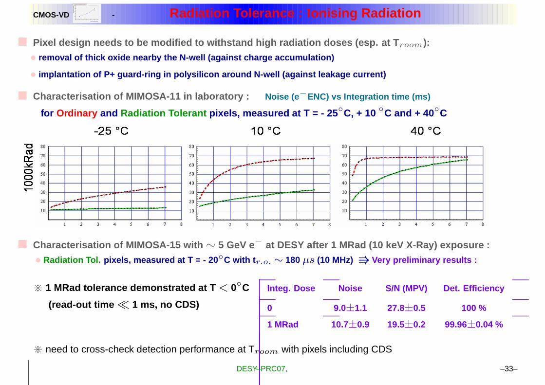
� Pixel design needs to be modified to withstand high radiation doses (esp. at T room):• removal of thick oxide nearby the N-well (against charge acc umulation)
• implantation of P+ guard-ring in polysilicon around N-well (against leakage current)
� Characterisation of MIMOSA-11 in laboratory : Noise (e−ENC) vs Integration time (ms)
for Ordinary and Radiation Tolerant pixels, measured at T = - 25 ◦C, + 10 ◦C and + 40◦C
� Characterisation of MIMOSA-15 with ∼ 5 GeV e− at DESY after 1 MRad (10 keV X-Ray) exposure :• Radiation Tol. pixels, measured at T = - 20 ◦C with t r.o. ∼ 180 µs (10 MHz) V Very preliminary results :
Integ. Dose Noise S/N (MPV) Det. Efficiency
0 9.0±1.1 27.8±0.5 100 %
1 MRad 10.7±0.9 19.5±0.2 99.96±0.04 %
> 1 MRad tolerance demonstrated at T < 0◦C
(read-out time � 1 ms, no CDS)
> need to cross-check detection performance at Troom with pixels including CDS
DESY–PRC07, –33–
CMOS-VDPitch (microns)
15 20 25 30 35 40 45
Res
olut
ion
(mic
rons
)
1
1.5
2
2.5
3
3.5
Mimosa 9: resolution vs pitch
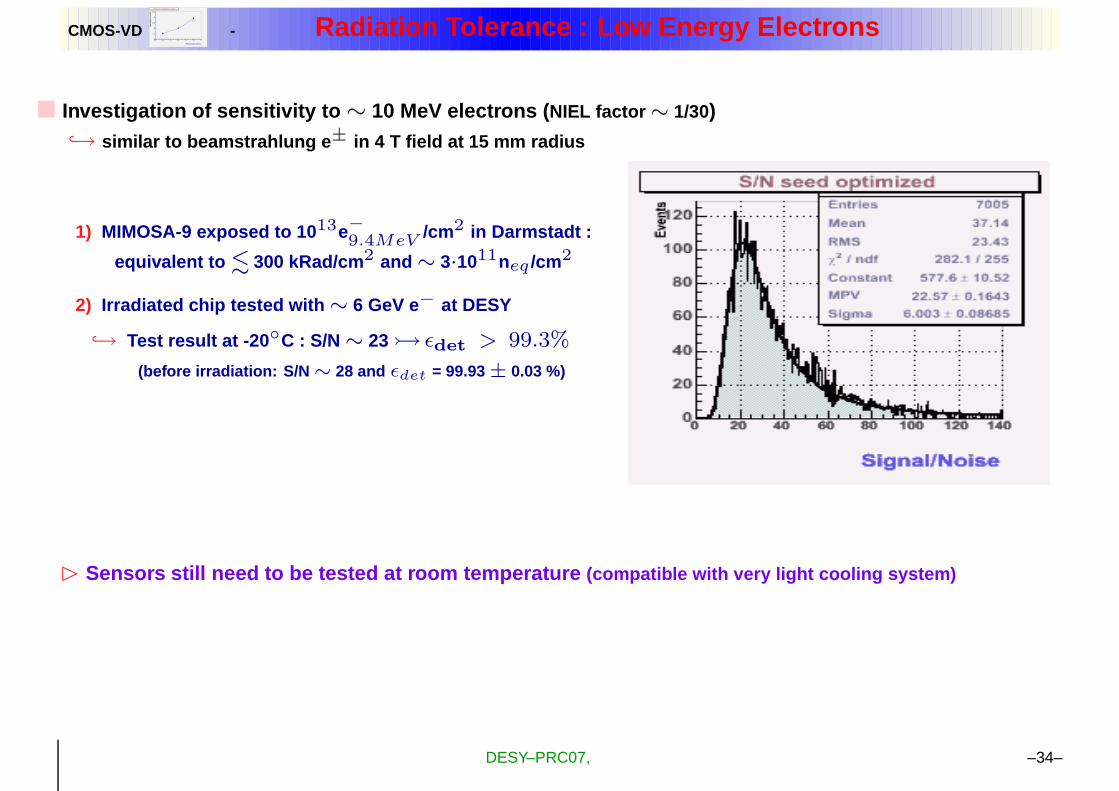
- Radiation Tolerance : Low Energy Electrons
� Investigation of sensitivity to ∼ 10 MeV electrons ( NIEL factor ∼ 1/30)↪→ similar to beamstrahlung e ± in 4 T field at 15 mm radius
1) MIMOSA-9 exposed to 10 13e−9.4MeV /cm2 in Darmstadt :
equivalent to . 300 kRad/cm 2 and ∼ 3·1011neq /cm2
2) Irradiated chip tested with ∼ 6 GeV e− at DESY
↪→ Test result at -20 ◦C : S/N ∼ 23 � εdet > 99.3%
(before irradiation: S/N ∼ 28 and εdet = 99.93 ± 0.03 %)
B Sensors still need to be tested at room temperature (compatible with very light cooling system)
DESY–PRC07, –34–
CMOS-VDPitch (microns)
15 20 25 30 35 40 45
Res
olut
ion
(mic
rons
)
1
1.5
2
2.5
3
3.5
Mimosa 9: resolution vs pitch
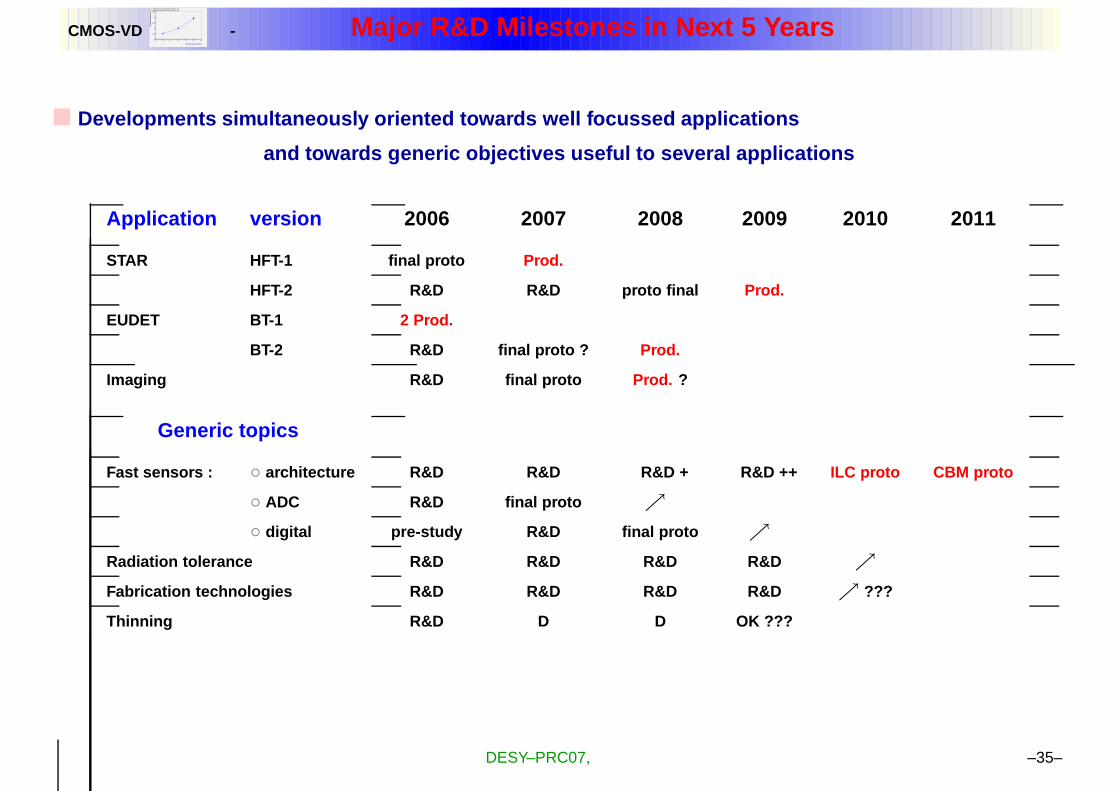
- Major R&D Milestones in Next 5 Years
� Developments simultaneously oriented towards well focuss ed applications
and towards generic objectives useful to several applicati ons
Application version 2006 2007 2008 2009 2010 2011
STAR HFT-1 final proto Prod.
HFT-2 R&D R&D proto final Prod.
EUDET BT-1 2 Prod.
BT-2 R&D final proto ? Prod.
Imaging R&D final proto Prod. ?
Generic topics
Fast sensors : ◦ architecture R&D R&D R&D + R&D ++ ILC proto CBM proto
◦ ADC R&D final proto ↗
◦ digital pre-study R&D final proto ↗
Radiation tolerance R&D R&D R&D R&D ↗
Fabrication technologies R&D R&D R&D R&D ↗ ???
Thinning R&D D D OK ???
DESY–PRC07, –35–