Embed Size (px)
Citation preview
PCB Test & Programming Solutionsfrom the IEEE 1149.1 Boundary-Scan Experts
Company BackgroundJTAG Technologies B.V. is the world’s foremost provider of comprehensive test andin-system programming solutions based on the IEEE Boundary-Scan standard 1149.1.We continuously enhance the value of the applications of this powerful standard withproduct improvements and innovations, based on the needs of our customers. Sinceour founding in 1993, we’ve applied our experience in the development of profes-sional industrial instrumentation resulting in powerful development packages, pro-duction packages, and boundary-scan controller hardware.
We maintain a highly experienced staff of Development Engineers and ApplicationEngineers ready to support your needs. With over 1,200 of our systems in operationaround the world, our engineers have proven themselves in hundreds of real-worldcases, providing everything from introductory training on up to the preparation ofspecific tests and programs to meet exacting customer requirements.
Our corporate headquarters are in Eindhoven, The Netherlands, and we have officesin the United Kingdom and the United States. In addition, we’re represented by aglobal network of authorized distributors and representatives throughout NorthAmerica, Europe, Asia, the Middle East, and Australia.
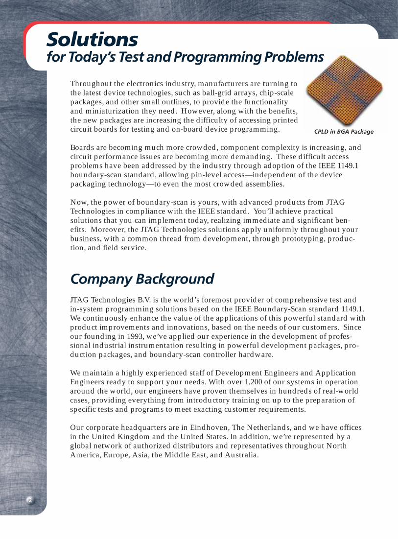
Throughout the electronics industry, manufacturers are turning tothe latest device technologies, such as ball-grid arrays, chip-scalepackages, and other small outlines, to provide the functionalityand miniaturization they need. However, along with the benefits,the new packages are increasing the difficulty of accessing printedcircuit boards for testing and on-board device programming.
Boards are becoming much more crowded, component complexity is increasing, andcircuit performance issues are becoming more demanding. These difficult accessproblems have been addressed by the industry through adoption of the IEEE 1149.1boundary-scan standard, allowing pin-level access––independent of the devicepackaging technology––to even the most crowded assemblies.
Now, the power of boundary-scan is yours, with advanced products from JTAGTechnologies in compliance with the IEEE standard. You’ll achieve practicalsolutions that you can implement today, realizing immediate and significant ben-efits. Moreover, the JTAG Technologies solutions apply uniformly throughout yourbusiness, with a common thread from development, through prototyping, produc-tion, and field service.
2
Solutionsfor Today’s Test and Programming Problems
CPLD in BGA Package
Practical and Powerful– Boundary-Scan from JTAG Technologies
With the JTAG Technologies’ family of software tools and hardware controllers, you can easilyunlock the tremendous power of boundary-scan for your test and programming applications.You’ll find it a simple matter to create your first test or programming application and to addnew ones. Board and system tests, as well as in-system programming routines, will be readybefore the first prototype comes down the line. As a result, you’ll realize significant improve-ment in your product’s time-to-market. The same streamlining applies to handling designchanges and product updates.
What has raised boundary-scan to this level of real-world practicality? JTAG Technologies’development and production systems provide your developers and production personnelwith the assistance they need, simplifying the tasks and allowing them to concentrate on theirmission, not the intricacies of boundary-scan.
Tests, diagnostics, and programming files can be created as soon as you have a schematic andnetlist, without waiting for the board layout or for a complicated bed-of-nails test fixture.Since all the resulting files are compatible between developmentand production, as soon as the tests are verified indevelopment, your factory will be ready to go.
Furthermore, youhave a complete selection
of high-quality boundary-scancontrollers, designed specifically for
critical industrial applications. Your choiceranges from a PC parallel port controller to high-
performance ISA, PCI, USB, and VXI implementations.All of the controllers are designed by JTAG Technologies,
assuring you of complete software and hardware compatibility.
4
To simplify your selection process, we’ve assembled our test and in-system program-ming software into development and production packages. You choose the packagethat’s right for your design or engineering environment and your application, optimiz-ing your investment. Of course, should your needs change, you can add individualsoftware modules at any time.
All of the software packages are available for: 16-bit oriented operating systems (DOS/Windows 3.1x) 32-bit systems such as Windows 95, Windows 98, Windows NT, and UNIX
(SunOS, Solaris, and HP-UNIX) platforms
of the Standard Test Package toquickly generate tests for manufac-turing faults and diagnose themaccurately, significantly reducingthe burden on functional testpreparation and fault analysis.
Boundary-scan also bringssubstantial benefits to users of in-circuit test systems, relieving themof constraints caused by thelimitations of test fixtures. Asboard complexity increases, bed-of-nail access to BGAs and othertypes of packages becomesimpractical or impossible. JTAGTechnologies’ Standard TestDevelopment Package providesyou with the next generation testsolution, solving the accessproblems and requiring only asmall number of test points.
Choose fromFour Test Development Packages
A Full Range ofDevelopment Packages
Standard TestDevelopmentPackage
Building on theinteractive generationof test vectors, theStandard Packageallows you to automate
the generation of test patterns forboundary-scan interconnections,including coverage for inverters,serial resistors, multiplexers, andbuffers that reside between scanelements. The Standard Packagealso provides automatic generationof test patterns through or to boardconnectors. Your test preparationtime is reduced significantly, andfull 100% coverage of the scaninterconnections is achieved.
The Standard Package is a goodchoice to improve a test strategythat, for example, includesfunctional testing for complexsurface-mount designs. In thesesituations, use boundary-scan topre-screen product for manufac-turing faults, quickly weedingthem out, and allow the functionaltest phase to focus on true func-tional faults. Leverage the power
Basic TestDevelopmentPackage
The Basic Test Devel-opment Package is anentry-level system,well suited for applica-tions involving less-
complex PCBs or for companieswith a limited number of newdesigns. The Basic Packagecontains all of the functionalityneeded to create complete bound-ary-scan tests for execution on theproduction floor, at a price for thebudget minded.
The Basic Package providesautomatic generation of testpatterns for the boundary-scaninfrastructure on your board. Testpreparation for interconnectionsand clusters is done interactivelyusing the highly intuitive graphi-cal user interface of PowerVIP.The PowerVIP module alsoperforms syntax and semanticchecking of device BSDL files. Testfailures are reported for analysis ina net-oriented truth-table formatthat engineers prefer and withwhich they are familiar. Since testgeneration is based on a netlist ofthe design, your tests can be readybefore the prototypes come backfrom manufacturing.
ges
5
Full TestDevelopmentPackage
The Full Test Develop-ment Package is idealfor companies produc-ing highly complexPCBs with SRAM,
DRAM and FIFO arrays, whichdesire the highest possible faultcoverage and diagnostic resolution.This package contains all of ourautomatic vector generation toolsincluding boundary-scan infra-structure, interconnections,memory interconnections, and theapplication of fault simulationvectors created on third-party toolsfor logic clusters. It enables you tomove through test developmentrapidly, accommodating a largenumber of new designs at aconsistently high quality level.
problems occur in prototypingor later in production. If yourcompany has adopted design-for-testability as an integral part ofthe design flow, you shouldconsider the Professional TestDevelopment Package.
Additional ValuableProducts
The modularity of our architectureallows you to easily add othervaluable options to any of the fourtest development packages:
Advanced, intelligent diagnos-tics with pinpoint accuracy. Thispowerful fault identification tool isavailable with any of the TestDevelopment Packages. Yourengineers and production techni-cians will realize substantial benefitfrom the timesaving output reports.
Linkage to your EDA schematiccapture environment, an automatedpath between your schematicdesign system and the test and in-system flash programming applica-tion development modules. Thisoption allows timely Design-for-Testability/Programmability priorto prototyping, and is availablewith any of the Test Developmentand Flash Development Packages.
System-level testing andprogramming. All of our test andprogramming products providesystem-level support using devicessuch as National Semiconductor'sSCANBridge™ and Texas Instru-ments' Scan Path Linker.
Professional TestDevelopmentPackage
This package containsall of our automatic testpattern generators plusthe Boundary-Scan FaultCoverage Examiner
(BFCE), empowering you todetermine when all test require-ments have been met. The combi-nation of extensive pattern genera-tion and coverage evaluation enablesthe R&D organization to operate atthe highest quality level.
The Professional Package can be anintegral part of your company’sTotal Quality Management pro-gram. You will have the ability torapidly evaluate test effectivenessduring PCB development, makingadjustments on the spot, before
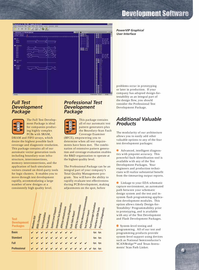
PowerVIP GraphicalUser Interface
Win
dow
s G
UI B
SDL
Chec
king
Te
st C
ompi
latio
n
Te
st E
xecu
tion
Sys
tem
-Lev
el S
uppo
rt
Inte
ract
ive
Test
Gen
erat
ion
ATPG
for I
nfra
stru
ctur
e
In
frast
ruct
ure
Dia
gnos
tics
Tr
uth-
Tabl
e Re
port
A
TPG
for I
nter
conn
ectio
n
A
TPG
for M
emor
y Int
erco
nnec
tion
Te
st P
atte
rn Im
port
F
ault
Cove
rage
Cal
cula
tion
Inte
rfac
e to
EDA
Tool
s
Pin-
Leve
l Dia
gnos
tics
Basic
Standard
Full
Professional
✔ ✔ ✔ ✔ ✔ ✔ ✔ ✔ ✔ Opt. Opt.
✔ ✔ ✔ ✔ ✔ ✔ ✔ ✔ ✔ ✔ Opt. Opt.
✔ ✔ ✔ ✔ ✔ ✔ ✔ ✔ ✔ ✔ ✔ ✔ Opt. Opt.
✔ ✔ ✔ ✔ ✔ ✔ ✔ ✔ ✔ ✔ ✔ ✔ ✔ Opt. Opt.
TestDevelopmentPackages
6
In-system programming of flash memories and PLDs (CPLDs and FPGAs) is quick andeasy using JTAG Technologies’ development tools. Your applications can include anycombination of programmable devices from multiple vendors, because of the broadrange of supported devices, all covered by a uniform toolset.
Standard FlashDevelopmentPackage
Flash memories are themost rapidly growingsegment of the program-mable device market.Now with our Standard
Flash Development Package, youcan configure flash devices on yourboard. The Standard Packageprovides you with a convenientgraphical user interface to designyour application and to script themodules you’ll use later in produc-tion. If you have only a limitednumber of new designs, theStandard Package may be thesolution for you.
Preparation of flash programmingapplications with the StandardPackage is done by integratinginformation representing theboard’s netlist, descriptions of theboundary-scan devices, thecharacteristics of the flash memory,and the desired image data file.
Professional FlashDevelopmentPackage
The ProfessionalPackage is ideal if youhave several designsper year and need torespond rapidly to new
designs. With the ProfessionalPackage, your company maintainsthe flexibility to perform program-ming file generation as needed.
The Professional Package for flashfeatures the industry’s onlyadvanced Boundary-Scan FlashProgramming Generator (BFPG).With it, you’ll quickly developprogramming applications for newdesigns, using the extensiveFlashLib library of the availabledevices, all generated automaticallywithin our graphical user interface.
Standard PLDDevelopmentPackage
The Standard PLDDevelopment Package isbest suited for companiesusing PLDs that supportthe new standardized
formats, or for those who use only asingle family of logic devices. AllPLD devices that use JAM orSTAPL for programming files aresupported by this package. Sup-port options are also available tomatch any of the major CPLDfamilies that use programmingformats other than JAM or STAPL.
Full PLDDevelopmentPackage
The Full PLD Develop-ment Package gives yousupport for all popularformats, includingJEDEC, SVF, and TTF.
The benefit to you is avoidingproliferation of dedicated program-mers, one for each of the vendors inyour products, through the unifieddevice support of the JTAG Tech-nologies platform.
With this package you have thegreatest possible flexibility tosupport a variety of PLD brands inyour systems. This multi-vendorsupport is especially important in amanufacturing environment that iscustomarily confronted withmultiple device sources and needsto avoid multiple tools.
In-System ProgrammingDevelopment Packages
Win
dow
s G
UI B
SDL
Chec
king
A
TPG
for I
nfra
stru
ctur
e
In
frast
ruct
ure
Dia
gnos
tics
Com
pila
tion
Flas
h/PL
D
Exe
cutio
n Fl
ash/
PLD
Auto
Writ
e Su
ppor
t
S
crip
ting
A
utom
atic
Pro
gram
Gen
erat
ion
Flas
h Li
brar
y
I
nter
face
to E
DA to
ols
JA
M, S
TAPL
Pla
yer
S
VF, J
EDEC
, TTF
Sys
tem
-Lev
el S
uppo
rt
✔ ✔ ✔ ✔ ✔ ✔ ✔ ✔ ✔
✔ ✔ ✔ ✔ ✔ ✔ ✔ ✔ ✔ ✔ Opt. ✔
ProgrammingDevelopmentPackages
Standard Flash
Professional Flash
Standard PLD
Full PLD
✔ ✔ ✔ ✔ ✔ ✔ ✔ Opt. Opt.
✔ ✔ ✔ ✔ ✔ ✔ ✔ ✔ Opt.
7
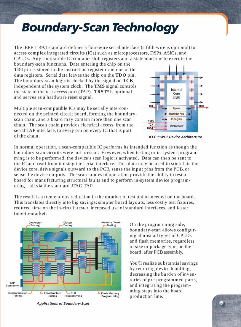
The IEEE 1149.1 standard defines a four-wire serial interface (a fifth wire is optional) toaccess complex integrated circuits (ICs) such as microprocessors, DSPs, ASICs, andCPLDs. Any compatible IC contains shift registers and a state machine to execute theboundary-scan functions. Data entering the chip on theTDI pin is stored in the instruction register or in one of thedata registers. Serial data leaves the chip on the TDO pin.The boundary-scan logic is clocked by the signal on TCK,independent of the system clock. The TMS signal controlsthe state of the test access port (TAP). TRST* is optionaland serves as a hardware reset signal.
Multiple scan-compatible ICs may be serially intercon-nected on the printed circuit board, forming the boundary-scan chain, and a board may contain more than one scanchain. The scan chain provides electrical access, from theserial TAP interface, to every pin on every IC that is partof the chain.
In normal operation, a scan-compatible IC performs its intended function as though theboundary-scan circuits were not present. However, when testing or in-system program-ming is to be performed, the device’s scan logic is activated. Data can then be sent tothe IC and read from it using the serial interface. This data may be used to stimulate thedevice core, drive signals outward to the PCB, sense the input pins from the PCB, orsense the device outputs. The scan modes of operation provide the ability to test aboard for manufacturing structural faults and to perform in-system device program-ming—all via the standard JTAG TAP.
The result is a tremendous reduction in the number of test points needed on the board.This translates directly into big savings: simpler board layouts, less costly test fixtures,reduced time on the in-circuit tester, increased use of standard interfaces, and fastertime-to-market.
On the programming side,boundary-scan allows configur-ing almost all types of CPLDsand flash memories, regardlessof size or package type, on theboard, after PCB assembly.
You’ll realize substantial savingsby reducing device handling,decreasing the burden of inven-tories of pre-programmed parts,and integrating the program-ming steps into the boardproduction line.
InternalCoreLogic
Bypass
Instruction Reg.
ID Register
TAP Controller
TDI TDO
TMSTCK
TRST*
IEEE 1149.1 Device Architecture
Boundary-Scan Technology
Applications of Boundary-Scan
ClusterTesting
ConnectorTesting
Memory ClusterTesting
InterconnectionTesting
PLDProgramming
Flash MemoryProgramming
TAPConnector
InfrastructureTesting
8
Applications created on any of the Test or Programming Development Packages runseamlessly in your production systems. We support a broad range of productionenvironments, from a stand-alone PC- or workstation-based process for test and pro-gramming, to full integration into your production line—an architecture in whichboundary-scan operations take place within another process step, such asfunctional test.
Production Systemsfor Test and In-System Programming
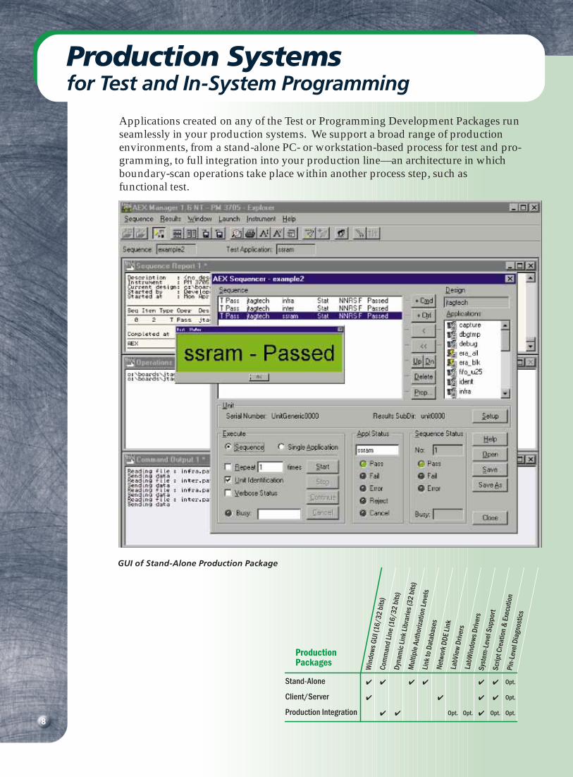
GUI of Stand-Alone Production Package
Win
dow
s G
UI (1
6/32
bits
) C
omm
and
Line
(16/
32 b
its)
D
ynam
ic L
ink
Libr
arie
s (3
2 bi
ts)
Mul
tiple
Aut
horiz
atio
n Le
vels
Lin
k to
Dat
abas
es
Net
wor
k D
DE
Link
LabV
iew
Driv
ers
Lab
Win
dow
s D
river
s
Syst
em-L
evel
Sup
port
S
crip
t Cre
atio
n &
Exe
cutio
n
P
in-L
evel
Dia
gnos
tics
ProductionPackages
Stand-Alone
Client/Server
Production Integration
✔ ✔ ✔ ✔ ✔ ✔ Opt.
✔ ✔ ✔ ✔ Opt.
✔ ✔ Opt. Opt. ✔ Opt. Opt.
9
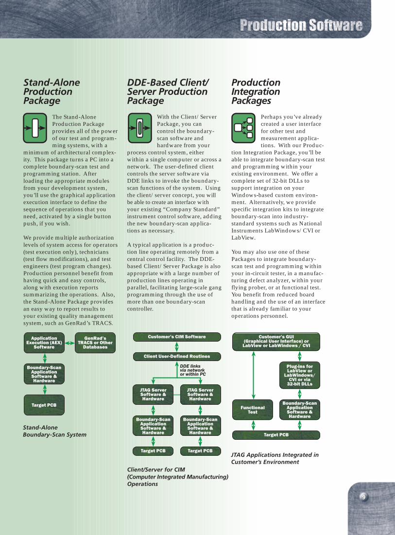
Stand-AloneProductionPackage
The Stand-AloneProduction Packageprovides all of the powerof our test and program-ming systems, with a
minimum of architectural complex-ity. This package turns a PC into acomplete boundary-scan test andprogramming station. Afterloading the appropriate modulesfrom your development system,you’ll use the graphical applicationexecution interface to define thesequence of operations that youneed, activated by a single buttonpush, if you wish.
We provide multiple authorizationlevels of system access for operators(test execution only), technicians(test flow modifications), and testengineers (test program changes).Production personnel benefit fromhaving quick and easy controls,along with execution reportssummarizing the operations. Also,the Stand-Alone Package providesan easy way to report results toyour existing quality managementsystem, such as GenRad’s TRACS.
DDE-Based Client/Server ProductionPackage
With the Client/ServerPackage, you cancontrol the boundary-scan software andhardware from your
process control system, eitherwithin a single computer or across anetwork. The user-defined clientcontrols the server software viaDDE links to invoke the boundary-scan functions of the system. Usingthe client/server concept, you willbe able to create an interface withyour existing “Company Standard”instrument control software, addingthe new boundary-scan applica-tions as necessary.
A typical application is a produc-tion line operating remotely from acentral control facility. The DDE-based Client/Server Package is alsoappropriate with a large number ofproduction lines operating inparallel, facilitating large-scale gangprogramming through the use ofmore than one boundary-scancontroller.
ProductionIntegrationPackages
Perhaps you’ve alreadycreated a user interfacefor other test andmeasurement applica-tions. With our Produc-
tion Integration Package, you’ll beable to integrate boundary-scan testand programming within yourexisting environment. We offer acomplete set of 32-bit DLLs tosupport integration on yourWindows-based custom environ-ment. Alternatively, we providespecific integration kits to integrateboundary-scan into industry-standard systems such as NationalInstruments LabWindows/CVI orLabView.
You may also use one of thesePackages to integrate boundary-scan test and programming withinyour in-circuit tester, in a manufac-turing defect analyzer, within yourflying prober, or at functional test.You benefit from reduced boardhandling and the use of an interfacethat is already familiar to youroperations personnel.
JTAG ServerSoftware &Hardware
Boundary-ScanApplicationSoftware &Hardware
Target PCB
JTAG ServerSoftware &Hardware
Boundary-ScanApplicationSoftware &Hardware
Target PCB
Client User-Defined Routines
Customer’s CIM Software
DDE linksvia networkor within PC
Client/Server for CIM(Computer Integrated Manufacturing)Operations
JTAG Applications Integrated inCustomer’s Environment
Plug-ins forLabView or
LabWindows/CVI or via
32-bit DLLs
Target PCB
Customer’s GUI(Graphical User Interface) or
LabView or LabWindows / CVI
Boundary-ScanApplicationSoftware &Hardware
FunctionalTest
ApplicationExecution (AEX)
Software
Boundary-ScanApplicationSoftware &Hardware
Target PCB
GenRad’sTRACS or Other
Databases
Stand-AloneBoundary-Scan System
Whether you’re using boundary-scan for test, in-system programming, or both, youhave a broad choice of controllers to drive your target system—all designed to meetproduction-level standards for reliability and ruggedness. You’ll choose from threeclasses of performance, depending on your application and throughput requirements.
DataBlasterLite
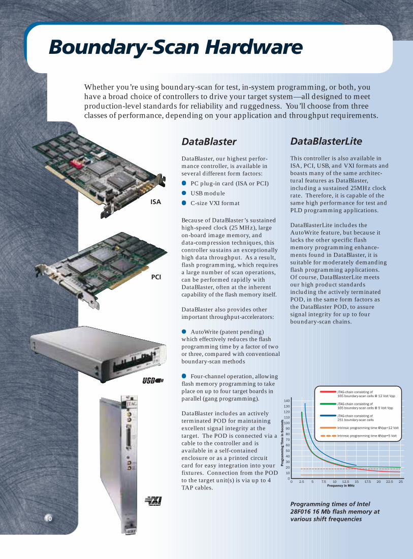
This controller is also available inISA, PCI, USB, and VXI formats andboasts many of the same architec-tural features as DataBlaster,including a sustained 25MHz clockrate. Therefore, it is capable of thesame high performance for test andPLD programming applications.
DataBlasterLite includes theAutoWrite feature, but because itlacks the other specific flashmemory programming enhance-ments found in DataBlaster, it issuitable for moderately demandingflash programming applications.Of course, DataBlasterLite meetsour high product standardsincluding the actively terminatedPOD, in the same form factors asthe DataBlaster POD, to assuresignal integrity for up to fourboundary-scan chains.
ISA
10
Boundary-Scan Hardware
0 2.5 5 7.5 10 12.5 15 17.5 20 22.5 25
Pro
gram
min
g Ti
me
in S
econ
ds
140
130
120
110
100
90
80
70
60
50
40
30
20
10
0
Frequency in MHz
JTAG-chain consisting of165 boundary-scan cells @ 12 Volt Vpp
JTAG-chain consisting of165 boundary-scan cells @ 5 Volt Vpp
JTAG-chain consisting of251 boundary-scan cells
Intrinsic programming time @Vpp=12 Volt
Intrinsic programming time @Vpp=5 Volt
PCI
Programming times of Intel28F016 16 Mb flash memory atvarious shift frequencies
DataBlaster
DataBlaster, our highest perfor-mance controller, is available inseveral different form factors:
PC plug-in card (ISA or PCI)
USB module
C-size VXI format
Because of DataBlaster’s sustainedhigh-speed clock (25 MHz), largeon-board image memory, anddata-compression techniques, thiscontroller sustains an exceptionallyhigh data throughput. As a result,flash programming, which requiresa large number of scan operations,can be performed rapidly withDataBlaster, often at the inherentcapability of the flash memory itself.
DataBlaster also provides otherimportant throughput-accelerators:
AutoWrite (patent pending)which effectively reduces the flashprogramming time by a factor of twoor three, compared with conventionalboundary-scan methods
Four-channel operation, allowingflash memory programming to takeplace on up to four target boards inparallel (gang programming).
DataBlaster includes an activelyterminated POD for maintainingexcellent signal integrity at thetarget. The POD is connected via acable to the controller and isavailable in a self-containedenclosure or as a printed circuitcard for easy integration into yourfixtures. Connection from the PODto the target unit(s) is via up to 4TAP cables.
11
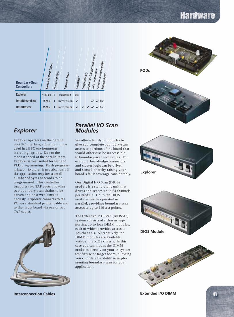
Explorer
Explorer operates on the parallelport PC interface, allowing it to beused in all PC environmentsincluding laptops. Due to themodest speed of the parallel port,Explorer is best suited for test andPLD programming. Flash program-ming on Explorer is practical only ifthe application requires a smallnumber of bytes or words to beprogrammed. This controllersupports two TAP ports allowingtwo boundary-scan chains to bedriven and observed simulta-neously. Explorer connects to thePC via a standard printer cable andto the target board via one or twoTAP cables.
Parallel I/O ScanModules
We offer a family of modules togive you complete boundary-scanaccess to portions of the board thatwould otherwise be inaccessibleto boundary-scan techniques. Forexample, board-edge connectorsand cluster logic can be drivenand sensed, thereby raising yourboard’s fault coverage considerably.
Our Digital I/O Scan (DIOS)module is a stand-alone unit thatdrives and senses up to 64 channelsper module. Up to ten DIOSmodules can be operated inparallel, providing boundary-scanaccess to up to 640 test points.
The Extended I/O Scan (XIOS512)system consists of a chassis sup-porting up to four DIMM modules,each of which provides access to128 channels. Alternatively, theDIMM modules are availablewithout the XIOS chassis. In thiscase you can mount the DIMMmodules directly on your in-systemtest fixture or target board, allowingyou complete flexibility in imple-menting boundary-scan for yourapplication.
Explorer
DataBlasterLite
DataBlaster
Sust
aine
d Cl
ock
Spee
d
Boundary-ScanControllers
≈100 kHz 2 Parallel Port Opt.
Imag
e M
emor
y S
uppo
rt fo
r Gan
g Pr
ogra
mm
ing
D
ata
Com
pres
sion
A
ctiv
e Te
rmin
atio
n (P
OD
)
In
dust
rial P
OD
Num
ber o
f TAP
s
Auto
Writ
e™
Inte
rfac
e Ty
pes
25 MHz 4 ISA/PCI/VXI/USB ✔ ✔ ✔ Opt.
25 MHz 4 ISA/PCI/VXI/USB ✔ ✔ ✔ ✔ ✔ Opt.
PODs
Explorer
DIOS Module
Extended I/O DIMMInterconnection Cables
JTAG Technologies and our authorized dealers are available worldwide to support yourboundary-scan test and programming applications.
For the latest in product information, useful application tips, and the name of the dealernearest you, please find us on the Web at www.jtag.com
To assist you in applying boundary-scan and realizing its significant benefits, JTAGTechnologies offers a full menu of services and support. Our expert support team cantailor services to your needs in the following areas:
The potential benefits of JTAG Technologies’ boundary-scan products to youroperation are significant, with compelling savings in time and money.
Unlock Boundary-Scan and Put It to Work for You
Services from JTAG Technologies
Reduced time-to-marketFaster prototype debugging and faster production ramp-up. Engineers’factory-support effort is reduced.
Reduced capital investmentMore efficient use of conventional ATE using much less expensiveboundary-scan equipment, simplified fixtures, and system commonalityfor test and programming.
Automated creation of test vectors and IC programming filesSpeed the transition from design to factory with JTAG Technologies’advanced program generation products and integration withexisting EDA tools.
Structured approachTools for development and manufacturing are based on an establishedstandard, IEEE 1149.1, avoiding specialized ad-hoc methods.
JTAG Technologies B. V.(Headquarters)Phone: +31 40 295 08 70Fax: +31 40 246 84 71www.jtag.comEmail: [email protected]
UK Sales OfficePhone: 01234 27 22 26Fax: 01234 27 18 71
Boundary-scan tutorials System installation Training for developers and production
personnel Testability reviews In-system programmability reviews
Design and process consultation Turn-key test development and
programming file development On-site product/application support And, other areas according to
your needs
US Sales OfficePhone: (Toll-free)877-FOR-JTAG (367-5824)Fax: 410-604-2109
JTAG Technologies B.V. reserves the right to make changes in design or specification at any time without notice. Data subject to change without notice. Printed August 1999.All brand names or product names mentioned are trademarks or registered trademarks of their respective holders.
Rapid resolution of manufacturing faultsPin-level fault diagnosis is quick and easy with boundary-scan.Access problems are resolved even with surface-mount BGA andchip-scale packages.
Eliminate inventory and handling of pre-programmed ICsFewer process steps, avoids damage to sensitive devices, improvesreliability, supports just-in-time programming, eliminates IC sockets.
No back-driving of IC outputsAvoids potential damage to unit-under-test.
Commonality of method for test and programming throughout theproduct life cycleReduced learning time, improved inter-department process flow withinR&D, production, and service. Improved feedback for corrective action.