Embed Size (px)
DESCRIPTION
Pertemuan 5 Fabrikasi IC CMOS. Matakuliah: H0362/Very Large Scale Integrated Circuits Tahun: 2005 Versi: versi/01. Learning Outcomes. Pada Akhir pertemuan ini, diharapkan mahasiswa akan dapat menyebutkan proses fabrikasiIC CMOS. IC Fabrication. - PowerPoint PPT Presentation
Citation preview
1
Pertemuan 5 Fabrikasi IC CMOS
Matakuliah : H0362/Very Large Scale Integrated CircuitsTahun : 2005Versi : versi/01
2
Learning Outcomes
Pada Akhir pertemuan ini, diharapkan mahasiswa akan dapat menyebutkan proses fabrikasiIC CMOS.
3
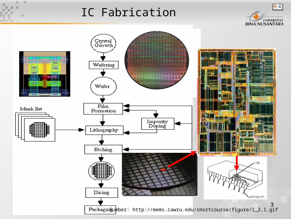
IC Fabrication
Sumber: http://mems.cawru.edu/shortcourse/figure/I_2.1.gif
4
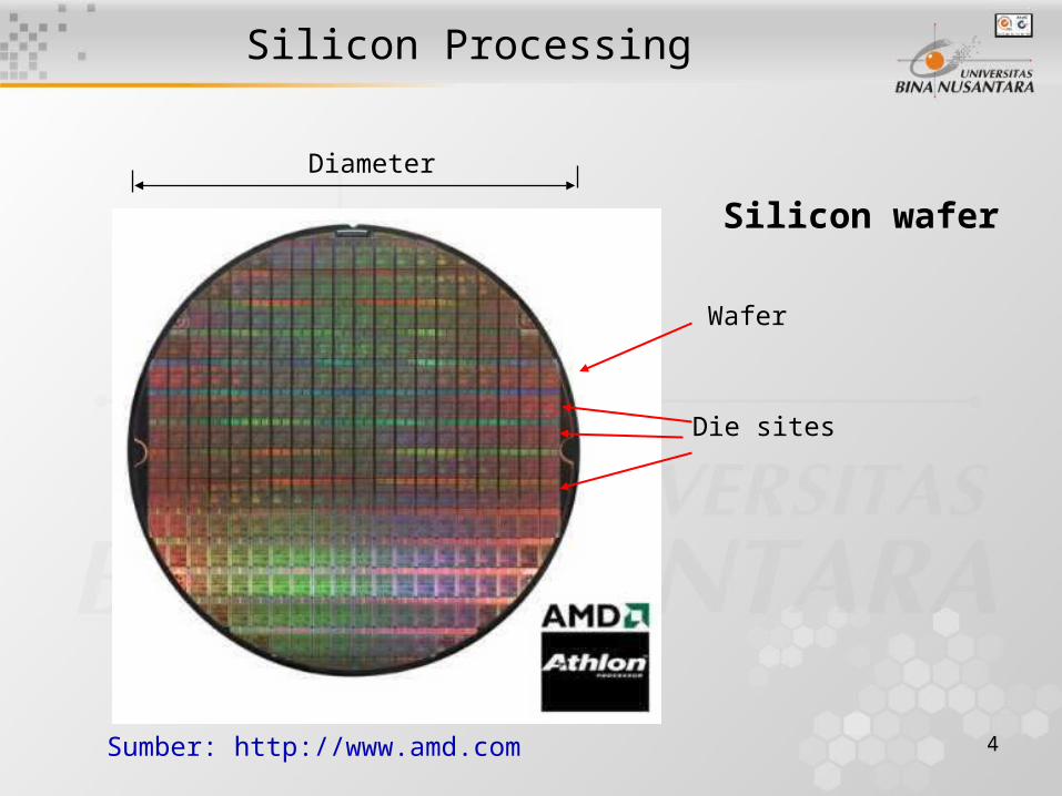
Silicon Processing
2
Silicon wafer
Sumber: http://www.amd.com
Diameter
Wafer
Die sites
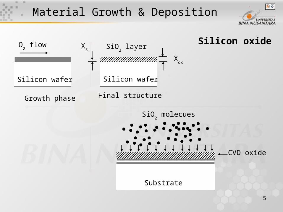
5
Material Growth & Deposition
Silicon oxide
Silicon wafer
O2 flow
Silicon wafer
SiO2 layerXSi
Xox
Growth phase Final structure
Substrate
CVD oxide
SiO2 molecues
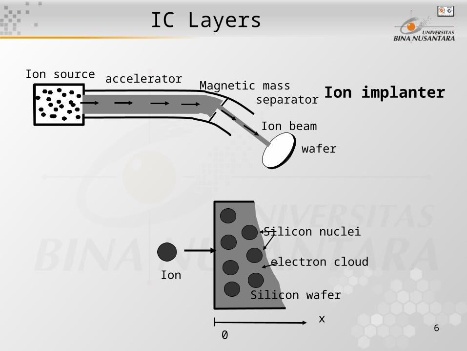
6
IC Layers
Ion implanterIon source accelerator Magnetic mass
separator
Ion beamwafer
IonSilicon wafer
Silicon nuclei
electron cloud
x0
7
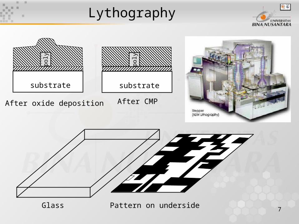
Lythography
poly
substrate
poly
substrate
After oxide deposition After CMP
Glass Pattern on underside
8
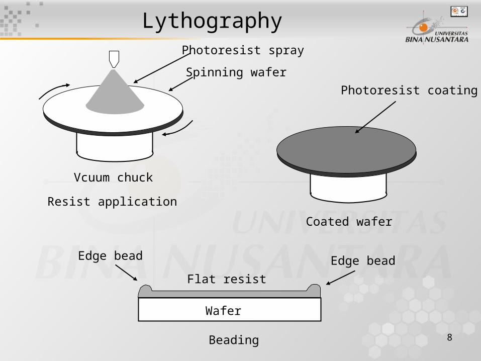
Lythography
Spinning waferPhotoresist spray
Vcuum chuckResist application
Photoresist coating
Coated wafer
Wafer
Flat resistEdge bead Edge bead
Beading
9
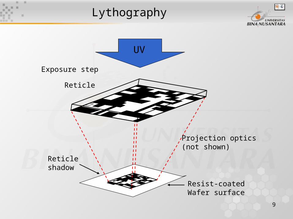
Lythography
UV
Reticle
Resist-coatedWafer surface
Reticleshadow
Projection optics(not shown)
Exposure step
10
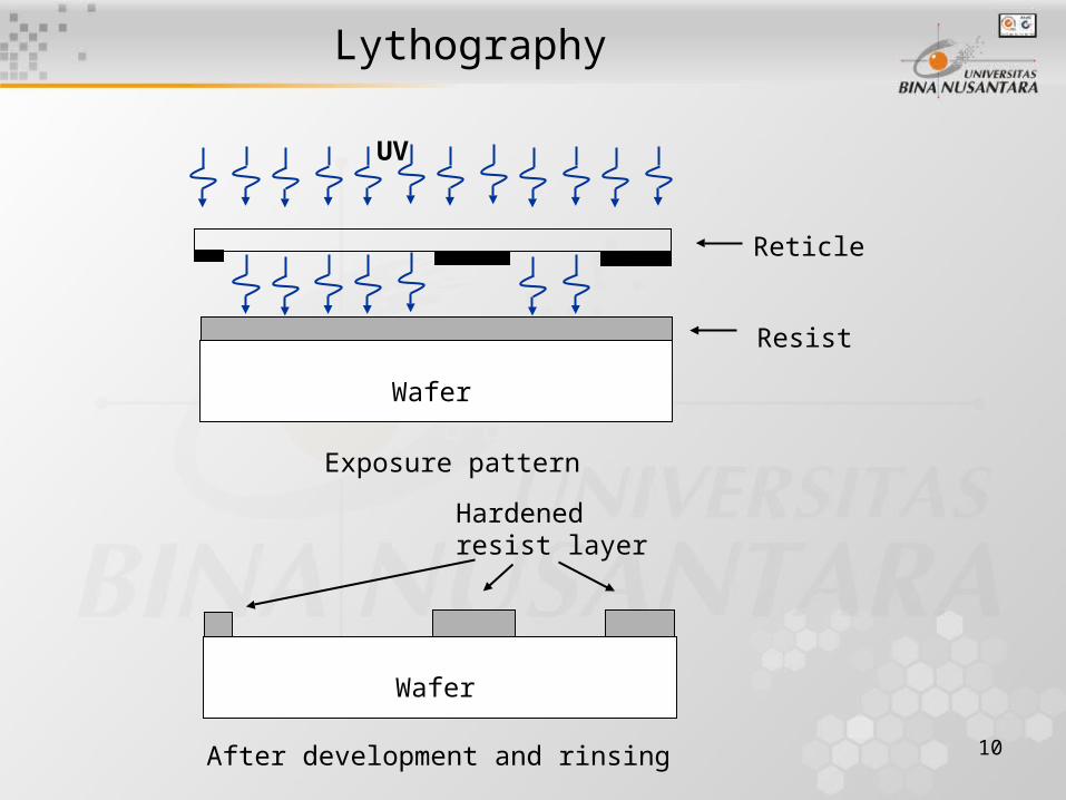
Lythography
Wafer
UV
Reticle
Resist
Exposure pattern
Wafer
After development and rinsing
Hardenedresist layer
11
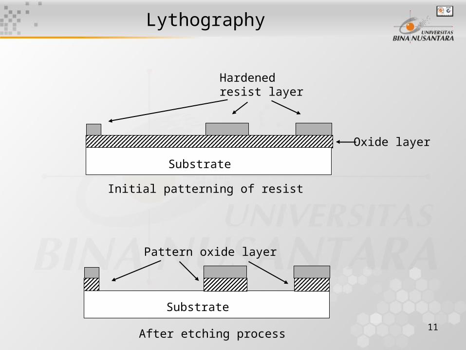
Lythography
Hardenedresist layer
SubstrateInitial patterning of resist
Oxide layer
After etching process
Substrate
Pattern oxide layer
12
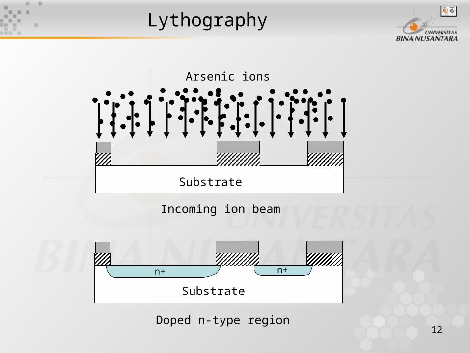
Lythography
Incoming ion beam
Substrate
Arsenic ions
Doped n-type region
Substraten+ n+
13
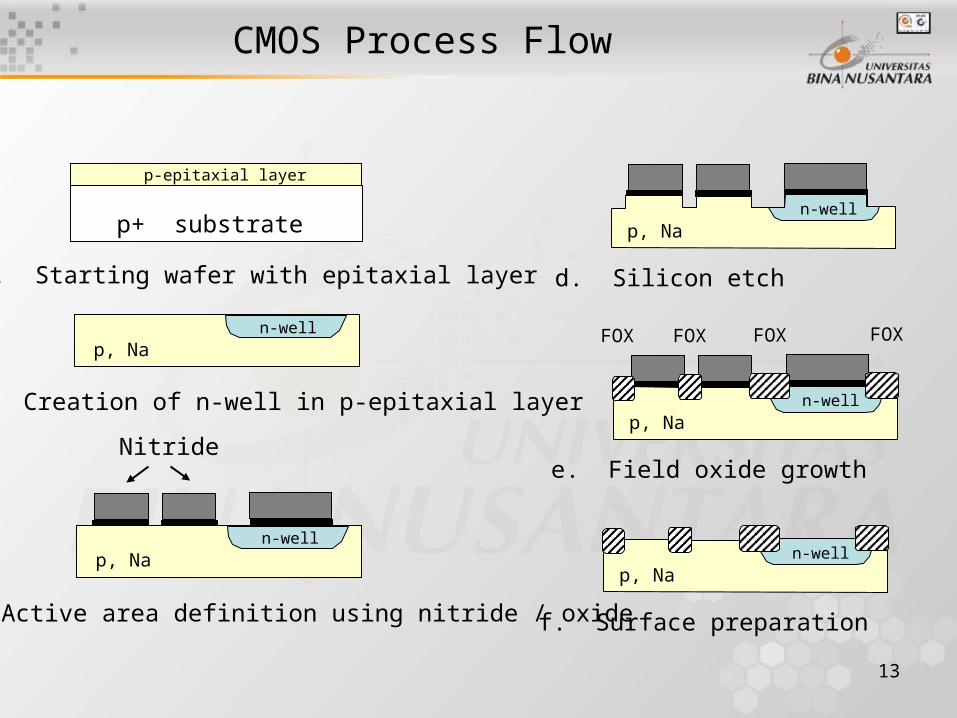
CMOS Process Flow
p-epitaxial layer
p+ substrate
a. Starting wafer with epitaxial layern-well
p, Na
b. Creation of n-well in p-epitaxial layer
n-wellp, Na
c. Active area definition using nitride / oxide
p, Nan-well
d. Silicon etch
Nitridep, Na
n-well
e. Field oxide growth
FOX FOX FOX FOX
p, Nan-well
f. Surface preparation
14
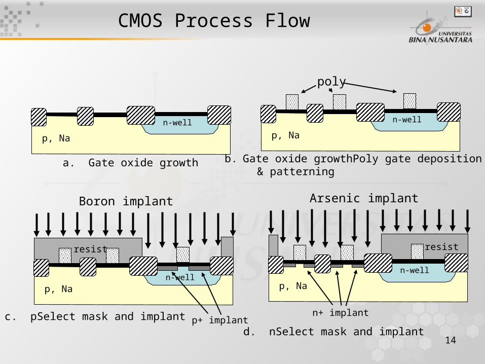
CMOS Process Flow
a. Gate oxide growth
p, Nan-well
b. Gate oxide growthPoly gate deposition & patterning
p, Nan-well
poly
c. pSelect mask and implant
p, Nan-well
resist
Boron implant
p+ implantd. nSelect mask and implant
p, Nan-well
resist
Arsenic implant
n+ implant
15
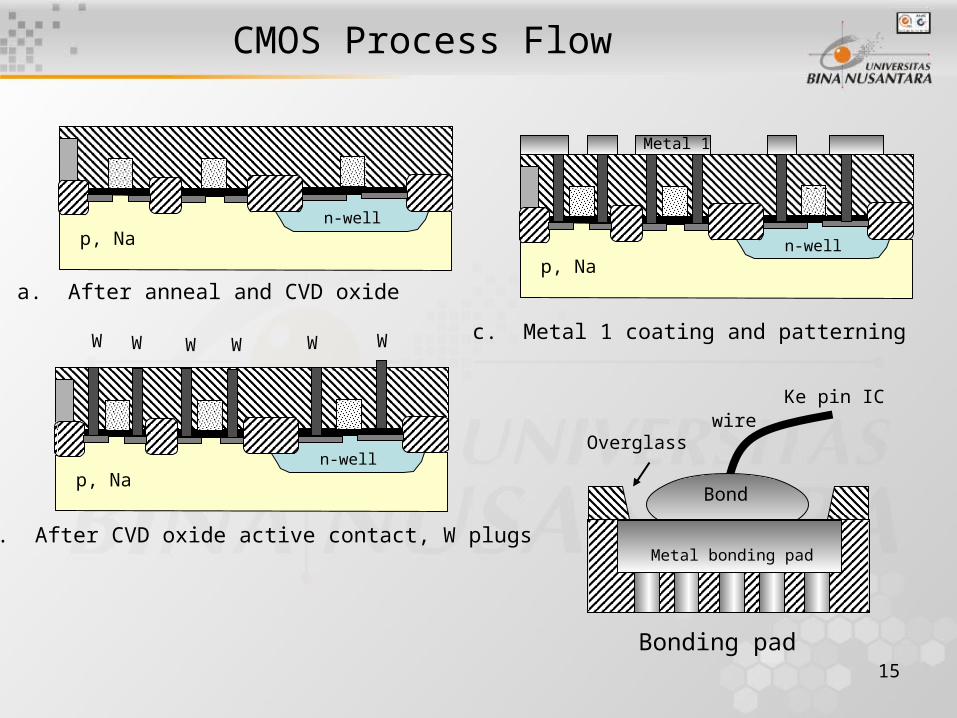
CMOS Process Flow
a. After anneal and CVD oxide
p, Nan-well
b. After CVD oxide active contact, W plugs
p, Nan-well
W W W W W W c. Metal 1 coating and patterning
p, Nan-well
Metal 1
Metal bonding pad
Bond
Bonding pad
Ke pin IC
Overglasswire
16
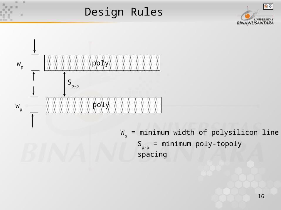
Design Rules
wp
wp
Sp-p
poly
poly
Wp = minimum width of polysilicon lineSp-p = minimum poly-topoly spacing
17
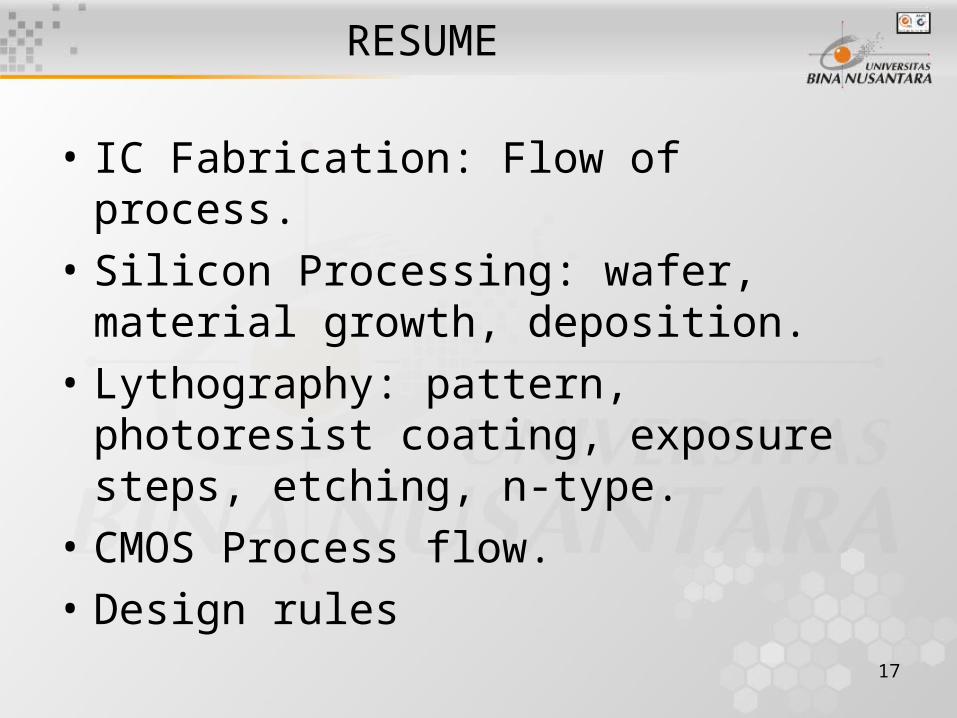
RESUME
• IC Fabrication: Flow of process.• Silicon Processing: wafer, material growth,
deposition.• Lythography: pattern, photoresist coating,
exposure steps, etching, n-type.• CMOS Process flow.• Design rules