Embed Size (px)
Citation preview
UG:122 vicorpower.com Applications Engineering: 800 927.9474 Page 1
PFC MicroSTM
Power Factor Corrected AC-DC Switcher
USER GUIDE | UG:122
October 2012
Overview
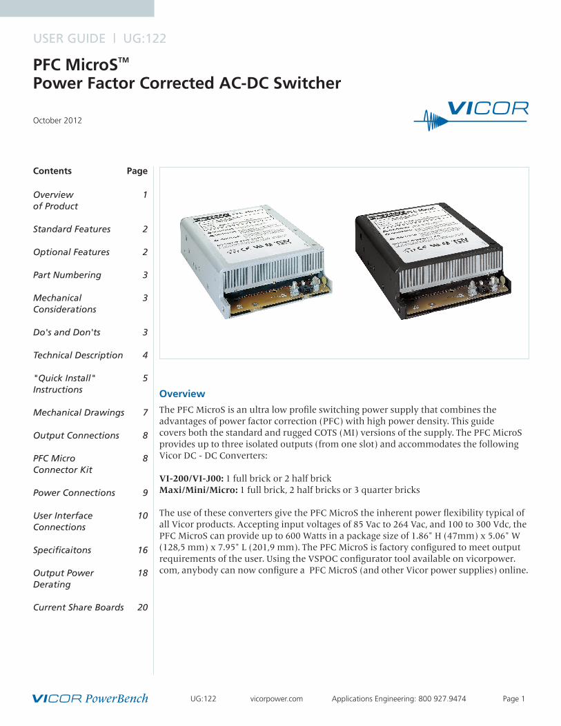
The PFC MicroS is an ultra low profile switching power supply that combines the advantages of power factor correction (PFC) with high power density. This guide covers both the standard and rugged COTS (MI) versions of the supply. The PFC MicroS provides up to three isolated outputs (from one slot) and accommodates the following Vicor DC - DC Converters:
VI-200/VI-J00: 1 full brick or 2 half brick Maxi/Mini/Micro: 1 full brick, 2 half bricks or 3 quarter bricks
The use of these converters give the PFC MicroS the inherent power flexibility typical of all Vicor products. Accepting input voltages of 85 Vac to 264 Vac, and 100 to 300 Vdc, the PFC MicroS can provide up to 600 Watts in a package size of 1.86" H (47mm) x 5.06" W (128,5 mm) x 7.95" L (201,9 mm). The PFC MicroS is factory configured to meet output requirements of the user. Using the VSPOC configurator tool available on vicorpower.com, anybody can now configure a PFC MicroS (and other Vicor power supplies) online.
Contents Page
Overview 1of Product
Standard Features 2
Optional Features 2
Part Numbering 3
Mechanical 3Considerations
Do's and Don'ts 3
Technical Description 4
"Quick Install" 5Instructions
Mechanical Drawings 7
Output Connections 8
PFC Micro 8Connector Kit
Power Connections 9
User Interface 10Connections
Specificaitons 16
Output Power 18Derating
Current Share Boards 20
UG:122 vicorpower.com Applications Engineering: 800 927.9474 Page 2
Standard Features
n Power Factor Correction: Typically 0.98 (>75% Load)
n Universal Input: 85-264 Vac, 47-500 Hz, or 120-300 Vdc
n Power Output: 600 W at 230 Vac (200 Vac minimum input) ; 500 W at 115 Vac (100 Vac minimum input)
n Up to three isolated outputs (one slot)
n Fan cooled
n Full power to 45°C; half power at 65°C
n Soft start for limiting inrush current
n Conducted EMI: FCC Class A EN 55022, Class A (consult factory)
n Harmonic Distortion to EN61000-3-2
n AC Power OK status signal;
n Output Sequencing and General Shutdown
n Autosense (Refer to Page 6 and 14 for more information on Autosense)
n Output overcurrent protection on all outputs
n Output overvoltage protection (not applicable when using VI-J00 DC-DC Converters)
n Output overtemperature limiting (not applicable when using VI-J00 DC-DC Converters )
n Ride-through (holdup) time: >20 ms at 500 W load (nominal line)
n Size: 1.86" H (47,3 mm) x 5.06" W (128,5 mm) x 7.95" L (201,9 mm)
n Safety Agency Approvals: CE Marking, TUV CUE (certain configurations may not have all listed approvals)
n Uses 300 Vdc input VI-200/VI-J00 modules and/or 375 Vdc input Maxi/Mini/Micro modules
n Power good status signal when Maxi, Mini or Micro modules used
Optional Features
n I/T/H-grade output converters
n Current Share Board for unit to unit power sharing- See Pages 20 - 22
n Connector kits (#19-130044)
n MI Chassis specific options:
n Mil-STD 810 for Shock and Vibration
n Mil-STD 704 and 1399 for Overvoltage and Transients
n -40°C operation
n Conformal coating - contact factory
UG:122 vicorpower.com Applications Engineering: 800 927.9474 Page 3
Part Numbering
PFC MicroS PSx1-x2 x3(x4)-xxxx-x5 ex. PS2-20-6544-G
x1 = number of outputs x2 = number of VI-200/VI-J00 modules x3 = number of Maxi/Mini/Micro modules (x4 ) = optional Factory assigned xxxx = sequential number assigned by Vicor -x5 = optional Factory assigned Note: x5 = MI for rugged chassis, = MC for rugged chassis with conformal coating
Mechanical Considerations
The PFC MicroS can be mounted on one of three surfaces using standard 8 - 32 or 4 mm screws. Maximum allowable torque is 5 in. lbs., and the maximum penetration of 0.25 (6 mm) on the sides and 0.125 in. (3 mm) on the bottom.
When selecting a mounting location and orientation, the unit should be positioned so air flow is not restricted. Maintain a 2" (5,1 cm) minimum clearance at both ends of the PFC MicroS, and route all cables so airflow is not obstructed. The power supply draws air in at the fan side/AC input side and exhausts air out the load side. If airflow ducting is used, avoid sharp turns that could create back pressure. The fans move approximately 10 CFM of air.
Avoid excessive bending of output power cables after they are connected to the output terminals. For high-current outputs, use cable ties to support heavy cables and minimize mechanical stress on connectors. Be careful not to short-out to neighboring outputs. The maximum torque recommended on output nuts is 10 in. lbs.
Avoid applications in which the unit is exposed to excessive shock or vibration levels as the unit is designed primarily for office type equipment. In such applications, a shock absorbing mount design is required.
PFC MicroS Do’s and Don’ts
n Do not restrict airflow to the unit. The cooling fan draws air into the unit and forces it out at the output power terminals. A minimum of 2” in front and behind the supply should be maintained in order to prevent air obstructions.
n Run the output (+/–) power cables next to each other to minimize inductance. Use twisted pairs if possible.
n Do not attempt to repair or modify the power supply in any manner. In the event of problems, contact Customer Service at 1-800-735-6200.
n Insert proper fault protection at power supply input terminals (i.e., a fuse).
n Use proper size wires to avoid overheating and excessive voltage drop.
n Output voltages over 60 Vdc, whether from individual modules or series arrays, are considered as hazardous secondary outputs under UL 60950. Appropriate care must be taken in design implementation of the supply.
UG:122 vicorpower.com Applications Engineering: 800 927.9474 Page 4
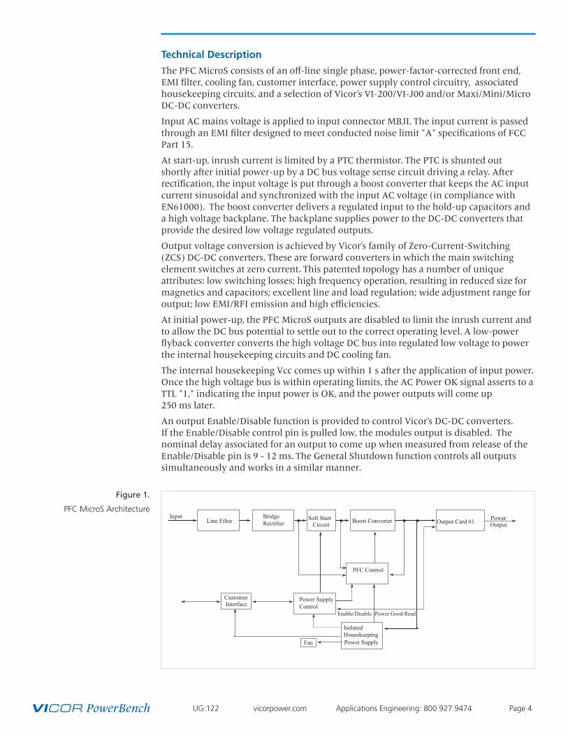
Technical Description
The PFC MicroS consists of an off-line single phase, power-factor-corrected front end, EMI filter, cooling fan, customer interface, power supply control circuitry, associated housekeeping circuits, and a selection of Vicor’s VI-200/VI-J00 and/or Maxi/Mini/Micro DC-DC converters.
Input AC mains voltage is applied to input connector MBJI. The input current is passed through an EMI filter designed to meet conducted noise limit "A" specifications of FCC Part 15.
At start-up, inrush current is limited by a PTC thermistor. The PTC is shunted out shortly after initial power-up by a DC bus voltage sense circuit driving a relay. After rectification, the input voltage is put through a boost converter that keeps the AC input current sinusoidal and synchronized with the input AC voltage (in compliance with EN61000). The boost converter delivers a regulated input to the hold-up capacitors and a high voltage backplane. The backplane supplies power to the DC-DC converters that provide the desired low voltage regulated outputs.
Output voltage conversion is achieved by Vicor’s family of Zero-Current-Switching (ZCS) DC-DC converters. These are forward converters in which the main switching element switches at zero current. This patented topology has a number of unique attributes: low switching losses; high frequency operation, resulting in reduced size for magnetics and capacitors; excellent line and load regulation; wide adjustment range for output; low EMI/RFI emission and high efficiencies.
At initial power-up, the PFC MicroS outputs are disabled to limit the inrush current and to allow the DC bus potential to settle out to the correct operating level. A low-power flyback converter converts the high voltage DC bus into regulated low voltage to power the internal housekeeping circuits and DC cooling fan.
The internal housekeeping Vcc comes up within 1 s after the application of input power. Once the high voltage bus is within operating limits, the AC Power OK signal asserts to a TTL "1," indicating the input power is OK, and the power outputs will come up 250 ms later.
An output Enable/Disable function is provided to control Vicor’s DC-DC converters. If the Enable/Disable control pin is pulled low, the modules output is disabled. The nominal delay associated for an output to come up when measured from release of the Enable/Disable pin is 9 - 12 ms. The General Shutdown function controls all outputs simultaneously and works in a similar manner.
Line FilterBridge
RectifierSoft Start
CircuitBoost Converter
PFC Control
Power Supply
Control
Output Card #1
Fan
Isolated
Housekeeping
Power Supply
Customer Interface
Power Output
Input
Enable/Disable -Power Good Read
Figure 1.
PFC MicroS Architecture
UG:122 vicorpower.com Applications Engineering: 800 927.9474 Page 5
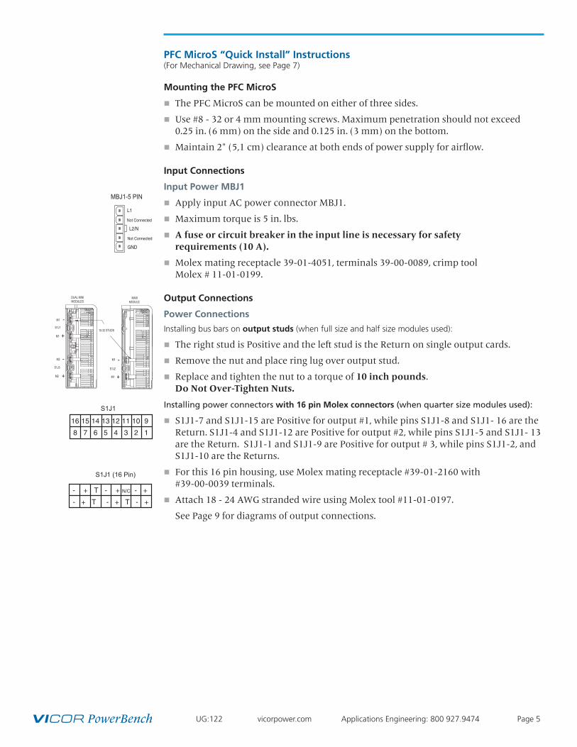
PFC MicroS “Quick Install” Instructions(For Mechanical Drawing, see Page 7)
Mounting the PFC MicroS
n The PFC MicroS can be mounted on either of three sides.
n Use #8 - 32 or 4 mm mounting screws. Maximum penetration should not exceed 0.25 in. (6 mm) on the side and 0.125 in. (3 mm) on the bottom.
n Maintain 2" (5,1 cm) clearance at both ends of power supply for airflow.
Input Connections
Input Power MBJ1
n Apply input AC power connector MBJ1.
n Maximum torque is 5 in. lbs.
n A fuse or circuit breaker in the input line is necessary for safety requirements (10 A).
n Molex mating receptacle 39-01-4051, terminals 39-00-0089, crimp tool Molex # 11-01-0199.
Output Connections
Power Connections
Installing bus bars on output studs (when full size and half size modules used):
n The right stud is Positive and the left stud is the Return on single output cards.
n Remove the nut and place ring lug over output stud.
n Replace and tighten the nut to a torque of 10 inch pounds. Do Not Over-Tighten Nuts.
Installing power connectors with 16 pin Molex connectors (when quarter size modules used):
n S1J1-7 and S1J1-15 are Positive for output #1, while pins S1J1-8 and S1J1- 16 are the Return. S1J1-4 and S1J1-12 are Positive for output #2, while pins S1J1-5 and S1J1- 13 are the Return. S1J1-1 and S1J1-9 are Positive for output # 3, while pins S1J1-2, and S1J1-10 are the Returns.
n For this 16 pin housing, use Molex mating receptacle #39-01-2160 with #39-00-0039 terminals.
n Attach 18 - 24 AWG stranded wire using Molex tool #11-01-0197.
See Page 9 for diagrams of output connections.
MBJ1-5 PIN
Not Connected
GND
L2/N
L1
Not Connected
DUAL MINIMODULES
MAXIMODULE
M1
S1J1
M1
M2
M2
M1
M1
S1J2
-
+
10-32 STUDS
+
-
-
+S1J3
8 7 6 5 4 3 2 1
16 15 14 13 12 11 10 9
S1J1
- + T - + T - +
- + T - + N/C - +
S1J1 (16 Pin)
UG:122 vicorpower.com Applications Engineering: 800 927.9474 Page 6
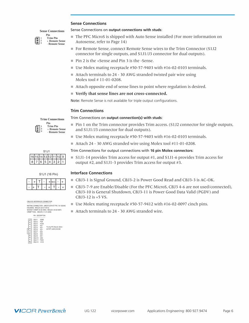
Sense Connections
Sense Connections on output connections with studs:
n The PFC MicroS is shipped with Auto Sense installed (For more information on Autosense, refer to Page 14)
n For Remote Sense, connect Remote Sense wires to the Trim Connector (S1J2 connector for single outputs, and S1J1/J3 connector for dual outputs).
n Pin 2 is the +Sense and Pin 3 is the -Sense.
n Use Molex mating receptacle #50-57-9403 with #16-02-0103 terminals.
n Attach terminals to 24 - 30 AWG stranded twisted pair wire using Molex tool # 11-01-0208.
n Attach opposite end of sense lines to point where regulation is desired.
n Verify that sense lines are not cross-connected.
Note: Remote Sense is not available for triple output configurations.
Trim Connections
Trim Connections on output connection(s) with studs:
n Pin 1 on the Trim connector provides Trim access. (S1J2 connector for single outputs, and S1J1/J3 connector for dual outputs).
n Use Molex mating receptacle #50-57-9403 with #16-02-0103 terminals.
n Attach 24 - 30 AWG stranded wire using Molex tool #11-01-0208.
Trim Connections for output connections with 16 pin Molex connectors:
n S1J1-14 provides Trim access for output #1, and S1J1-6 provides Trim access for output #2, and S1J1-3 provides Trim access for output #3.
Interface Connections
n CBJ3-1 is Signal Ground, CBJ3-2 is Power Good Read and CBJ3-3 is AC-OK.
n CBJ3-7-9 are Enable/Disable (For the PFC MicroS, CBJ3 4-6 are not used/connected), CBJ3-10 is General Shutdown, CBJ3-11 is Power Good Data Valid (PGDV) and CBJ3-12 is +5 VS.
n Use Molex mating receptacle #50-57-9412 with #16-02-0097 cinch pins.
n Attach terminals to 24 - 30 AWG stranded wire.
1 2 3
Sense Connections
Trim Pin+ Remote Sense- Remote Sense
Pin
8 7 6 5 4 3 2 1
16 15 14 13 12 11 10 9
S1J1
1 2 3
Trim Connections
Trim Pin+ Remote Sense- Remote Sense
Pin
- + T - + T - +
- + T - + N/C - +
S1J1 (16 Pin)
CBJ3 E/D INTERFACE CONNECTOR
MATING CONNECTOR: (WESTCOR KIT P/N: 19-130044)HOUSING: MOLEX (50-57-9412)SOCKET CRIMP 24-30 AWG: MOLEX (16-02-0097)CRIMP TOOL: MOLEX (11-01-0209)
PIN DESCRIPTION
CBJ3-1 SGNDCBJ3-2 PGRCBJ3-3 ACOKCBJ3-4 N/C*CBJ3-5 N/C*CBJ3-6 N/C*CBJ3-7 ED3CBJ3-8 ED2CBJ3-9 ED1CBJ3-10 GSDCBJ3-11 PGDVCBJ3-12 +5 VS
*For the PFC MicroS, ED4-6 are NOT used/connected.
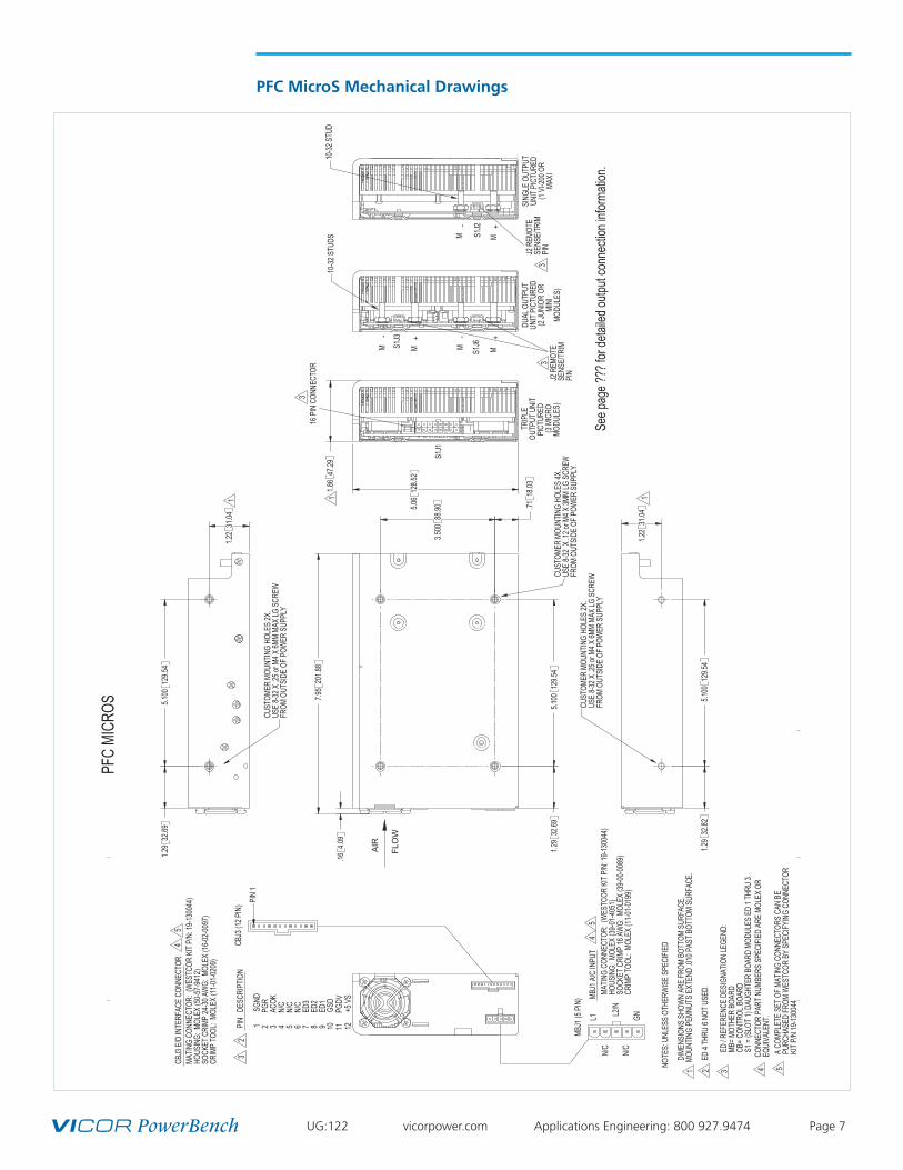
UG:122 vicorpower.com Applications Engineering: 800 927.9474 Page 7
PFC MicroS Mechanical Drawings
TRIP
LE
OUTP
UT U
NIT
PICT
URED
(3
MICR
OMO
DULE
S)
DUAL
OUT
PUT
UNIT
PICT
URED
(2
JUNI
OR O
R MI
NIMO
DULE
S)
SING
LE O
UTPU
T UN
IT PI
CTUR
ED
(1 VI
-200 O
R MA
XI
NOTE
S: U
NLES
S OT
HERW
ISE
SPEC
IFIED
DI
MENS
IONS
SHO
WN
ARE
FROM
BOT
TOM
SURF
ACE.
MOU
NTIN
G PE
MNUT
S EX
TEND
.010
PAS
T BOT
TOM
SURF
ACE.
ED
4 TH
RU 6
NOT U
SED.
1
2
2
MM M M
M M
31.04
1.22
32.82
1.29
129.5
45.1
00
1
CUST
OMER
MOU
NTIN
G HO
LES
2X.
USE
8-32 X
.25 o
r M4 X
6MM
MAX
LG S
CREW
FROM
OUT
SIDE
OF P
OWER
SUP
PLY
32.69
1.29
129.5
45.1
00
18.03
.71
88.90
3.500
201.8
87.9
5
4.09
.16
CUST
OMER
MOU
NTIN
G HO
LES
4X.
USE
8-32
X .12
or M
4 X 3M
M LG
SCR
EWFR
OM O
UTSI
DE O
F POW
ER S
UPPL
Y
31.04
1.22
129.5
45.1
0032
.691.2
9
CUST
OMER
MOU
NTIN
G HO
LES
2X.
USE
8-32 X
.25 o
r M4 X
6MM
MAX
LG S
CREW
FROM
OUT
SIDE
OF P
OWER
SUP
PLY
1
A CO
MPLE
TE S
ET O
F MAT
ING
CONN
ECTO
RS C
AN B
EPU
RCHA
SED
FROM
WES
TCOR
BY
SPEC
IFYIN
G CO
NNEC
TOR
KIT P
/N 19
-1300
44
CONN
ECTO
R PA
RT N
UMBE
RS S
PECI
FIED
ARE
MOLE
X OR
EQUI
VALE
NT.
3
10-32
STU
DS
- +
L1 L2/N
GN
N/C
N/C
3 4 5
MATIN
G CO
NNEC
TOR:
(WES
TCOR
KIT
P/N:
19-13
0044
)HO
USIN
G: M
OLEX
(50-5
7-941
2)SO
CKET
CRI
MP 24
-30 A
WG:
MOL
EX (1
6-02-0
097)
CRIM
P TO
OL: M
OLEX
(11-0
1-020
9)
MATIN
G CO
NNEC
TOR:
(WES
TCOR
KIT
P/N:
19-13
0044
)HO
USIN
G: M
OLEX
(39-0
1-405
1)SO
CKET
CRI
MP 16
AW
G: M
OLEX
(39-0
0-008
9)CR
IMP
TOOL
: MOL
EX (1
1-01-0
199)
PIN
1
45
128.5
25.0
6
47.29
1.86
110
-32 S
TUDS
+- - +
ED / R
EFER
ENCE
DES
IGNA
TION
LEGE
ND:
MB= M
OTHE
R BO
ARD
CB= C
ONTR
OL B
OARD
S1 =
(SLO
T 1) D
AUGH
TER
BOAR
D MO
DULE
S ED
1 TH
RU 3
MBJ1
(5 P
IN) MB
J1 A
/C IN
PUT
CBJ3
(12 P
IN)
CBJ3
E/D
INTE
RFAC
E CO
NNEC
TOR
S1J1
S1J3
S1J6
S1J2
PIN
DES
CRIP
TION
1
SGN
D 2
P
GR 3
A
COK
4
N/C
5
N/C
6
N/C
7
ED3
8
ED2
9
ED1
10
GSD
11
PGD
V12
+
5 VS
J2 R
EMOT
E SE
NSE/
TRIM
PI
N J2
REM
OTE
SENS
E/TR
IM
PIN
16 P
IN C
ONNE
CTOR
See p
age ?
?? fo
r deta
iled o
utput
conn
ectio
n info
rmati
on.
PFC
MICR
OS
AIR
FLO
W
3
33
45
UG:122 vicorpower.com Applications Engineering: 800 927.9474 Page 8
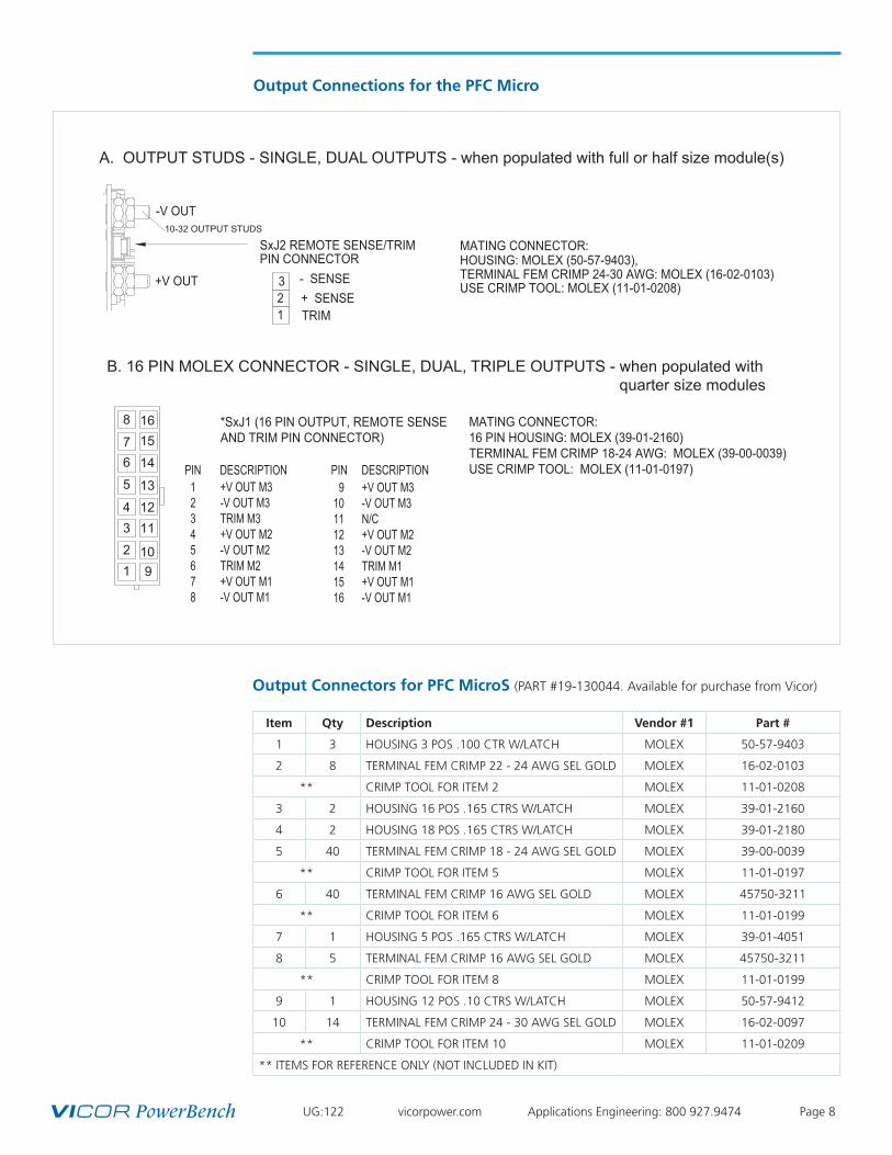
Output Connections for the PFC Micro
10-32 OUTPUT STUDS
TRIM
3
SxJ2 REMOTE SENSE/TRIMPIN CONNECTOR
1
2
- SENSE
+ SENSE
MATING CONNECTOR: HOUSING: MOLEX (50-57-9403),TERMINAL FEM CRIMP 24-30 AWG: MOLEX (16-02-0103)USE CRIMP TOOL: MOLEX (11-01-0208)
A. OUTPUT STUDS - SINGLE, DUAL OUTPUTS - when populated with full or half size module(s)
-V OUT
+V OUT
2
3
4
5
6
7
8
10
11
12
13
14
15
16
1 9
MATING CONNECTOR:
16 PIN HOUSING: MOLEX (39-01-2160)
TERMINAL FEM CRIMP 18-24 AWG: MOLEX (39-00-0039)
USE CRIMP TOOL: MOLEX (11-01-0197)
9 +V OUT M3
10 -V OUT M3
11 N/C
12 +V OUT M2
13 -V OUT M2
14 TRIM M1
15 +V OUT M1
16 -V OUT M1
1 +V OUT M3
2 -V OUT M3
3 TRIM M3
4 +V OUT M2
5 -V OUT M2
6 TRIM M2
7 +V OUT M1
8 -V OUT M1
*SxJ1 (16 PIN OUTPUT, REMOTE SENSE
AND TRIM PIN CONNECTOR)
PIN DESCRIPTION PIN DESCRIPTION
B. 16 PIN MOLEX CONNECTOR - SINGLE, DUAL, TRIPLE OUTPUTS - when populated with
quarter size modules
Output Connectors for PFC MicroS (PART #19-130044. Available for purchase from Vicor)
Item Qty Description Vendor #1 Part #
1 3 HOUSING 3 POS .100 CTR W/LATCH MOLEX 50-57-9403
2 8 TERMINAL FEM CRIMP 22 - 24 AWG SEL GOLD MOLEX 16-02-0103
** CRIMP TOOL FOR ITEM 2 MOLEX 11-01-0208
3 2 HOUSING 16 POS .165 CTRS W/LATCH MOLEX 39-01-2160
4 2 HOUSING 18 POS .165 CTRS W/LATCH MOLEX 39-01-2180
5 40 TERMINAL FEM CRIMP 18 - 24 AWG SEL GOLD MOLEX 39-00-0039
** CRIMP TOOL FOR ITEM 5 MOLEX 11-01-0197
6 40 TERMINAL FEM CRIMP 16 AWG SEL GOLD MOLEX 45750-3211
** CRIMP TOOL FOR ITEM 6 MOLEX 11-01-0199
7 1 HOUSING 5 POS .165 CTRS W/LATCH MOLEX 39-01-4051
8 5 TERMINAL FEM CRIMP 16 AWG SEL GOLD MOLEX 45750-3211
** CRIMP TOOL FOR ITEM 8 MOLEX 11-01-0199
9 1 HOUSING 12 POS .10 CTRS W/LATCH MOLEX 50-57-9412
10 14 TERMINAL FEM CRIMP 24 - 30 AWG SEL GOLD MOLEX 16-02-0097
** CRIMP TOOL FOR ITEM 10 MOLEX 11-01-0209
** ITEMS FOR REFERENCE ONLY (NOT INCLUDED IN KIT)
UG:122 vicorpower.com Applications Engineering: 800 927.9474 Page 9
Power Connections
Chassis Input Power Terminals (MBJ1)
Input AC power is applied through connector MBJI using Molex mating connector 39-01-4051. Use 16 AWG wire with Molex Socket Pin 39-00-0090 and Crimp Tool 11-01-0199.
A fault clearing device, such as a fuse or circuit breaker, with a maximum 10 A rating at the power supply input is required for safety agency compliance. It should be sized to handle the start-up inrush current of 8.5 A peak at 115 Vac and 17 A peak at 230 Vac.
Output Power Connections
There are two types of output power terminals available in the PFC MicroS. For connections using full or half size modules, outputs are terminated at 10 - 32 plated steel bolts. The positive polarity of the output is the right bolt when viewed from the output end. For connections using quarter size modules, outputs are terminated using a single 16 pin Molex connector. Each power output is isolated, so outputs of positive or negative polarity can be configured through proper selection of the output reference terminal.
In order to minimize parasitic cable inductance and reduce EMI, the output power cables should be routed in close proximity to one another, and large current loops should be avoided. To avoid excessive voltage drop, do not undersize power cables, especially for high current outputs. Do not bundle input AC wires with the output wires because this can couple output noise into the input wires which can increase EMI. Excessive cable inductance coupled with large capacitive loading can introduce instability in switching power supplies. This problem can be avoided with proper system design. Consult Vicor’s Applications Engineering Department for assistance with applications that use long cable lengths and excessive load capacitance.
Figure 2.
Input Power Terminal MBJ1
PIN 1
CBJ3-12 PIN
MBJ1 (5 PIN)
L1
L2/N
GND
Not Connected
Not Connected
MATING CONNECTOR: (WESTCOR KIT P/N: 19-130044)HOUSING: MOLEX (39-01-4051)SOCKET CRIMP 16 AWG: MOLEX (39-00-0090)CRIMP TOOL: MOLEX (11-01-0199)
MBJ1 A/C INPUT
UG:122 vicorpower.com Applications Engineering: 800 927.9474 Page 10
Figure 3.
Output Power Connections
User Interface Connections
Signal Ground (CBJ3-1)
Signal Ground on CBJ3-1 is an isolated secondary ground reference for all CBJ3 interfacing signals. This is not the same as Earth Ground on input power connector MBJI.
Bi-directional I/O lines (CBJ3-7 to CBJ3-9) (Enable/Disable or Module Power Good Status)
Enable/Disable Mode
Enable/Disable mode is the default condition for these I/O lines. In this mode, the control pins allow the outputs to be sequenced either ON or OFF. To disable a module, the E/D pin should be pulled low to less than 0.7 V with respect to Signal Ground. The E/D lines will typically source 250 mA (1 mA max.) under this condition. To enable a module, a E/D pin should be open circuited or driven high to a logic high voltage of 3.5 V (40 mA typical) or greater not to exceed 5 V.
The correspondence between a module and its E/D line as seen from the output end of the power supply goes from left to right. The PFC MicroS power supply is a one slot box. E/D1, E/D2, and E/D3 are present in this slot. (E/D4, E/D5, E/D6 are NOT used/connected in the PFC MicroS). See Table 1. E/D1 corresponds with VOUT M1, E/D2 corresponds with VOUT M2 and E/D3 corresponds with VOUT M3.
Slot 1
E/D1 E/D2 E/D3
Maxi Modules X
Mini Modules X X
Micro Modules X X X
VI-200 Modules X
VI-J00 Modules X X
PIN DESCRIPTION
S1J1-1 +V OUT M3 S1J1-2 -V OUT M3 S1J1-3 TRIM M3 S1J1-4 +V OUT M2 S1J1-5 -V OUT M2 S1J1-6 TRIM M2 S1J1-7 +V OUT M1 S1J1-8 -V OUT M1
S1J1 (16 PIN, TRIPLE MICRO MODULES)PIN DESCRIPTION
31J1-9 +V OUT M3S1J1-10 -V OUT M3S1J1-11 N/CS1J1-12 +V OUT M2S1J1-13 -V OUT M2S1J1-14 TRIM M1S1J1-15 +V OUT M1S1J1-16 -V OUT M1
TRIPLE OUTPUT- Quarter size modules used
DUAL OUTPUT-Half size SINGLE OUTPUT - Full size module used
S1J1 REMOTE SENSE/OUTPUT CONNECTORS
MATING CONNECTORS: (WESTCOR KIT P/N: 19-130044)16 PIN HOUSING: MOLEX (39-01-2160)SOCKET CRIMP 18-24 AWG: MOLEX (39-00-0039)CRIMP TOOL: MOLEX (11-01-0197)
M1
S1J1
M1
M2
M2
M1
M1
10-32 STUDS
S1J2
-
+
128.525.06
47.291.86
A3J1
+
-
-
+S1J3
8 7 6 5 4 3 2 1 16 15 14 13 12 11 10 9
- REMOTE SENSE321
+ REMOTE SENSETrim Pin
S1J2 REMOTE SENSE/TRIM PIN ACCESS CONNECTOR
MATING CONNECTOR: (WESTCOR KIT P/N: 19-130044)HOUSING: MOLEX (50-57-9403)
SOCKET CRIMP 24-30 AWG: MOLEX (16-02-0103)CRIMP TOOL: MOLEX (11-01-0208)
S1J1/J3 REMOTE SENSE/TRIM PIN ACCESS CONNECTOR
MATING CONNECTOR: (WESTCOR KIT P/N: 19-130044)HOUSING: MOLEX (50-57-9403)
SOCKET CRIMP 24-30 AWG: MOLEX (16-02-0103)CRIMP TOOL: MOLEX (11-01-0208)
Table 1.
Enable/Disable Mode
UG:122 vicorpower.com Applications Engineering: 800 927.9474 Page 11
Module Power Good Status Mode
The power supply will enter the Power Good Status Mode when logic high (50 mA typical) is applied to Power Good Read (PGR) pin (CBJ3-2). After transitioning to PGR mode the I/O lines (CBJ3-4 to CBJ3-9) will be outputs and will give a onetime readout of the associated module status. These outputs give an indication of the status of the modules of the power supply at the time of transition to PGR. A TTL "1" (>3.5 V) on a line indicates the module is ON and functioning properly, and a TTL "0" (<0.7 V) indicates the module is either OFF or is not functioning properly. The correspondence between the module and the Power Good Status of that module is the same as between a E/D pin and its module. This mode does NOT constantly monitor the module status and must be re-triggered by transitioning the PGR pin from logic low to logic high to get current module status.
Procedurally, certain guidelines must be followed when using this feature. Upon application of a logic high on the Power Good Read (PGR) pin, the user must change its E/D interface (CBJ3-4 to CBJ3-9) from outputs to inputs within 3 ms. The Power Good Status data will be valid on the E/D lines when the Power Good Data Valid (PGDV) pin (CBJ3-11) asserts to a logic high. The power good status measurement takes typically 200ms. While in the Power Good Read Mode (PGR = 1) the individual shutdown lines are not functional. However, General Shut Down (GSD) is functional. Leaving the Power Good Read mode is accomplished by removing the logic high or applying a logic low (<0.7V) to the Power Good Read (PGR) pin (CBJ3-2). The user must change its E/D interface (CBJ3-4 to CBJ3-9) from inputs to outputs between 1 ms and 4 ms of the time the PGR low is applied to pin CBJ3-2.
Note: If any model is disabled by the user when a Power Good Read is requested (PGR = 1), that module will remain off during the Power Good Read and status of said module will be power not good (<0.7 V). Power Good Read status data on open E/D lines are not valid. An open E/D line is a E/D pin where there is no module associated with said E/D line (i.e. A power supply with two Maxi modules, Data on E/D2, E/D3 and E/D5 and E/D6 are NOT valid.
The Power Good Status Mode feature is only valid when Maxi, Mini and/or Micro modules are used.
The following page shows examples of triggering PGR with a 1 Hz square while monitoring PGDV and a selected E/D line with a good module and a defective one.
UG:122 vicorpower.com Applications Engineering: 800 927.9474 Page 12
Figure 4.
PowerGood Read with Good Module
Figure 5.
PowerGood Read with Defective Module
UG:122 vicorpower.com Applications Engineering: 800 927.9474 Page 13
General Shutdown /GSD (CBJ3-10)
The GSD control pin on CBJ3-10 allows simultaneous shutdown of all outputs. This pin must be pulled down to less than 0.7 V, and will typically source 250 mA (1 mA maximum) to shut down all outputs. The GSD pin should be open circuited or driven high to a logic high voltage of 3.5 V or greater when not in use, or when the outputs are to be enabled. Do not apply more than 5 V to this input at any time.
AC OK (CBJ3-3) AC OK is an active high TTL compatible signal and provides a status indication of the AC input power. It is on pin CBJ3-3 and is capable of sinking 5 mA maximum. This signal switches to a TTL "1" when the high voltage bus exceeds low-line condition during turn-on. Upon loss of input power, the bus voltage will drop, causing the AC OK signal to go low. Typically, a 3 ms holdup time is provided for a 500 W load following the loss of the AC OK signal.
Auxiliary Vcc +5V/40mA (CBJ3-12)
The Vcc on CBJ3-12 is an auxiliary 5 V regulated power source. It is +5 Vdc +/–5% with respect to Signal Ground and can supply 40 mA maximum. It is short-circuit-proof, but shorted user interface functionality will be lost.
Power Good Read (PGR, CBJ3-2)
This pin initiates the Power Good Read sequence. A logic high applied to this pin will cause the power supply to enter the Power Good Read status mode. In this mode, the I/O lines (CBJ3-4 to CBJ3-9) will be outputs. These outputs give an indication of the status of the modules of the power supply. A high on an I/O line (CBJ3-4 to CBJ3-9) indicates a module is ON and functioning and a low indicate the module is OFF or in a fault condition. The Power Good Status data will be valid on the ED lines (CBJ3-4 to CBJ3-9) when the Power Good Data Valid (PGDV) pin (CBJ3-11) asserts a logic high. Applying a logic low or opening the PGR pin puts the power supply back in the Enable/Disable mode. Instructions for using this function are on Page 11 under Module Power Good Status Mode.
Power Good Data Valid (PGDV- CBJ3-11)
Upon entering the Power good Read status mode (PGR = 1, CBJ3-2), the data will not be valid on the I/O lines (CBJ3-7 to CBJ3-9) until the PGDV pin asserts itself logic high. This pin can source up to 5 mA. When this pin is logic low, Power Good status data is not valid or the power supply is not in the Power Good Read status mode.
Figure 6.
Auxiliary Vcc
78M05Auxiliary VccCBJ3-12
0.1 µF
Signal Ground
CBJ3
CBJ3-1
+5V/40 mA
UG:122 vicorpower.com Applications Engineering: 800 927.9474 Page 14
+Sense/ –Sense (S1J2 and S1J1/J3 connectors)
The sense lines for the outputs are shipped from the factory with Autosense. Autosense provides the user with automatic sensing of the outputs. With Autosense, the PFC MicroS will operate in a Remote Sense mode when the Remote Sense connections are made. But in the event that the Remote Sense is not connected or needed, no Local Sense selection is necessary - simply hook up the outputs and the PFC MicroS will automatically operate in Local Sense mode. To check if an output has the Autosense feature, measure the impedance from the + Out to + Sense and - Out to - Sense pins. If the impedance is 5 ohms, then the output has Autosense and does not require local sense jumpers.
In the local sense mode (Remote Sense lines not connected), the power supply will regulate the output at the output terminals. The voltage appearing at the load may drop slightly due to voltage drop in the power cables. If it is necessary to compensate for voltage drop along the output power cables, the output can be trimmed up or configured for Remote Sense. Use stranded twisted pair 20 - 22 AWG wire for the Remote Sense lines. Remote Sense can compensate for a voltage drop of up to 0.5 V, or 0.25 V on each leg.
The Sense connector for a single and dual output board is a 3 pin connector providing the +Sense connection on Pin 2 and the -Sense connection on Pin 3.
Remote Sense is not available for triple output configurations.
External Trim (S1/S2 J2)
The Trim pin (S1J2 connector for single outputs, and S1J1/J3 connector for dual outputs) is referenced to the –Sense pin and can be used for external control of the output voltage. For triple output cards, the Trim pins are available on S1J1-14, S1J1-6 and S1J1-3 for outputs 1, 2 and 3 respectively. A 10% increase to the trim pin voltage will result in a 10% increase in output voltage. Reducing the trim pin voltage by 10% will result in a 10% decrease in output voltage.
Output Module Vref RTH
VI-200/VI-J00 ³3.3 V 2.50 V 10.0 kW
VI-200/VI-J00 < 3.3 V 0.97 V 3.88 kW
Maxi (Predefined) 1.23 V 1.0 kW
Maxi ( User defined) 1.23 V Consult Factory
Figure 7.
Remote Sense
Load
+Out
+Sense
-Sense
-Out
Use 20-22 AWG
Twisted Pair Wires
Table 2.
Module Internal Reference Voltages and Thevenin
Resistances
UG:122 vicorpower.com Applications Engineering: 800 927.9474 Page 15
Example:
±10% Trim adjust on a 12 V nominal output.Figure 8 shows a typical variable trim circuit. Using a 10 k trimpot (R7), the resistor values for R6 and R8 can be calculated as follows:
V1= Vref + 10% = 2.75 V Given: Vref = 2.5 V (see Table 2)
IR5 = (2.75 V - Vref)/RTH = (2.75 V - 2.5 V) Given: RTH = 10 kW (see Table 2) /10 kW = 25 mA
Setting the bottom limit:
VR6 = 2.5 V - 10% = 2.25 V
And since IR5 = IR6 = 25 mA,
R6 = VR6/IR6= 2.25 V/25 mA = 90 kW
V2 = V1 + VR6 = 2.75 V + 2.25 V = 5 V
IR7 = V2/R7 = 5 V/10 kW = 500 mA
IR8 = IR7 + IR6 = 525 mA
VR8 = (Vnom +10%) - V2 = 13.2 V - 5 V = 8.2 V Given: Vnom = 12 V
R8 = VR8/IR8 = 8.2 V/525 mA = 15.62 kW
CONSULT APPLICATIONS ENGINEERING WHEN TRIMMING OUTPUTS BELOW 5 V.
Single Output Power Supplies (Arrays)
Vicor's standard configuration for single output power supplies is to set the left module (as seen from looking at the power supply output) as the controlling module of the array.
Figure 8.
External Pin(Remote Sense)
Load
+P +Out
PIN 2 +Sense
PIN 3 -Sense
-P -Out
Use 20-22 AWG Twisted Pair Wires
2.5VRef.
PIN 1R6
R8
R7
To ErrorAmplifier
Use 20-22 AWG Twisted Pair Wires
UG:122 vicorpower.com Applications Engineering: 800 927.9474 Page 16
Specifications (Typical at 25°C, nominal line and 75% load, unless otherwise specified)
General
Number of Outputs 1-3
ModulesVI-200/VI-J00: One VI-200 or Two VI-J00s
Maxi/Mini/Micro: One Maxi, Two Minis or Three Micros
Efficiency Typically > 75%
Safety Agency Approvals
cURus – UL 60950-1, CSA 60950-1;
cTUVus – EN 60950-1, UL 60950-1, CSA 60950-1
CE Mark – Low Voltage Directive, 2006/95/EC
Note: certain wide temp range units will not carry all approvals
Maximum Output Power500 W at 115 Vac, (100 Vac minimum input)[1]
600 W at 230 Vac, (200 Vac minimum input)
Input
Input85 - 264 Vac, 47-500Hz
120 - 300 Vdc (see derating charts on Page 18)
VI-200/VI-J00
Line/Load Regulation
0.2% max. from 10% to full load
0.5% max. from no load to 10% load
Maxi/Mini/Micro
Line Regulation[2]0.20% max to 0.30% max
Maxi/Mini/Micro
Load Regulation[2]0.20% max to 0.70% max
Inrush Current8.5 A peak @ 115 Vac
17 A peak @ 230 Vac
Ride Through Time >20 ms at 500 W load (nominal line)
Conducted EMI
FCC Class A
EN 55022 Class A (consult factory)
Mil-STD 461 requires external filter
Power Factor Typically >.98 (>75% Load)
Transient Burst Immunity EN61000-4-4, Level 3, Performance Criteria A
Surge Immunity
(Common Mode & Normal Mode)
EN 61000-4-5, Level 3, Performance Criteria B
(Temporary loss of output power may occur which is self recoverable.)
Dielectric WithstandPrimary to Chassis GND = 2,121 Vdc
Secondary to Chassis GND = 750 Vdc
Overvoltage and Transients
(MI chassis only)Compliant to Mil-STD 704 and 1399 based on configurtion contact factory
Output (VI-200/VI-J00 Modules)
Parameter Min Typ Max Units Notes
Setpoint Accuracy [3] 0.5 1 % of VNOM
Load/line Regulation 0.05 0.5 %LL to HL,
10% to Full Load
Load/line Regulation 0.2 0.5 %LL to HL,
No Load to 10%
Temperature Regulation 0.01 0.02 %/°C Over rated temp.
Long Term Drift 0.02 %/K hours
Output Ripple & Noise:
£ 10 V out
> 10 V out
100
1.0
mV
% VOUT
20 MHz
bandwidth
Voltage Trim Range:
VI-200/VI-J00 Slots 50-110 % VOUT
± 10% on
10 - 15 VOUT
UG:122 vicorpower.com Applications Engineering: 800 927.9474 Page 17
Specifications (Cont.)
Total Remote Sense
Compensation0.5 Volts
Autosense.
See Pages 6 & 14
OVP Set Point [4] 115 125 135 %VOUT Recycle Power
Current Limit 105 115 125 % of I max Auto Recovery
Short Circuit Current 120 (105 [5]) 130 %
Overtemperature LimitingNot available on
VI-J00
Maxi, Mini and Micro Series Modules
Parameter Min Typ Max Units Notes
Setpoint Accuracy [6] ±0.5 ±1 % of VNOM
Load/line Regulation ±0.08 ±0.45 (±7) % of VNOM 0% to 100%
Temperature Regulation 0.002 0.005 %/°C -20 to 100°C
Long Term Drift 0.02 %/K hours
Output Ripple and noise:
£ 10 V out
> 10 V out
100
1.0
mV
%VOUT
20 MHz
bandwidth
Voltage Trim Range:
Maxi/Mini/Micro Slots 10-110 % Vout
Preload may be
required
Total Remote Sense
Compensation0.5 Volts
Autosense. See
Pages 6 & 14.[7]
OVP Set Point 112 135 % of VOUT Recycle power
Current Limit 102 115 135 % of I max Auto Recovery
Overtemperature Limiting Not available
Enviornmental
Storage Temperature -40°C to +85°C
Operating Temperature
Full Power
Half Power
-20°C to +45°C (-40°C to +45°C option w/ MI chassis)
-20°C to +65°C (-40°C to +60°C option w/ MI chassis)
AltitudeDerate 2.6% total output power for each 1,000 ft to a maximum operating
altitude of 15,000 ft. Non-operating storage maximum altitude is 40 K.
Shock and Vibration Mil-STD 810
Humidity 0 to 95% non condensing
Product Weight 3.1 lbs. (1,4 kg)
Dimensions 1.86" H (47,3 mm) x 5.06" W (128,5 mm) x 7.95" L (201,9 mm)
Warranty[8] 2 years limited warranty. See vicorpower.com for complete warranty statement.
[1] Note: Not to exceed an input current of 7.5 A
[2] See Vicor module specifications. A preload may be necessary for modules trimmed down below 90% of normal output voltage.
[3] For special and adjustable voltages, maximum setpoint accuracy is 2% of VNOM.
[4] 131% Nominal for Booster Modules. No OVP for VI-J00.
[5] VI-J00 modules only.
[6] For special, adjustable voltages and 48 Vdc outputs, maximum setpoint accuracy is 2% of VNOM. Note: See individual module datasheets for specific module specifications.
[7] Note: Micro Modules do not support remote sense.
[8] Opening, repairing or modifying the unit will void the warranty. If you have any problem with the power supply, please contact Customer Service at 1-800-735-6200. If the unit needs to be returned for inspection/analysis, an RMA number will be issued. All units must have a RMA number prior to return.
UG:122 vicorpower.com Applications Engineering: 800 927.9474 Page 18
Output Power Derating
Figure 9.
PFC Micro Output Power vs. AC Input Voltage
Figure 10.
PFC Micro Output Power vs. DC Input Voltage
Input Voltage (DC)
Out
put P
ower
(Wat
ts)
PFC MicroS Output Power vs. DC Input Voltage
100
600
550
500
450
400
350120 140 160 180 200 220 240 260 280 300
Safe Operating Area
Power Limit Exceeded
Input Voltage (VAC)
Out
put P
ower
(Wat
ts)
265
PFC MicroS Output Power vs. AC Input Voltage600
550
500
450
400
3502552452352252152051951851751651551451351251151059585
Power Limit Exceeded
8.33 Watts/VoltSafe Operating Area
UG:122 vicorpower.com Applications Engineering: 800 927.9474 Page 19
Figure 11.
PFC Micro Output Power Temperature Derating
Temperature (degrees)
Out
put (
Wat
ts)
PFC MicroS: Output Power Temperature Derating
0
600
500
400
300
200
100
045 65
1. For all module configurations. The PFC MicroS or an individual output may be limited by module power limitations e.g. 5 V Maxi module is 400 W maximum. One cannot exceed the output power rating of the PFC MicroS regardless of the module capability.
2. Also see Output Power vs Input Voltage charts on Page 18.
UG:122 vicorpower.com Applications Engineering: 800 927.9474 Page 20
Current Share Boards - Optional Feature
"Current sharing" also known as Load Sharing, is the ability to divide the output current evenly across all active power supplies. This greatly reduces stresses on each power supply and allows them to run cooler, resulting in higher reliability. Standard "current sharing" techniques typically utilize shunt resistors or Hall Effect devices to measure the current from each power supply. Power shunt resistors continually dissipate power and require cooling especially when dealing with high output currents of >100 Amps. Hall Effect devices measure magnetic fields generated by current flowing through a conductor and, although they dissipate no power, they tend to be large and expensive.
First developed by Vicor Engineering for paralleling MegaPAC supplies, the Box-to-Box Current Share Board or CSB allows two or more Vicor power supplies to current share by utilizing the inherent voltage drop produced in the negative output return cable. This eliminates the need for additional shunt resistors or expensive Hall Effect devices and provides a simple 5 wire connection method to achieve a +/-1 mV accuracy between the Negative Output power rails. This accuracy translates to a 1% current sharing if there is a total of 100 mV conductional voltage drop in the negative return path.
Constructed as a current source to drive the Trim pin of a Vicor module, the design uses an accurate comparator circuit to monitor the power returns. In addition, the circuit is unidirectional and can only trim an output voltage up. The benefit is that only the supply that is supporting less current is adjusted up. This action balances the currents to the load by matching the output voltages of the supplies. In the case of one supply failing, the circuit will attempt to trim the failed supply only. This will leave the remaining functional supply alone to provide power to the load at its nominal voltage. Thus the circuit also offers simple redundancy. In addition, because CSB functions as a current source, the Trim outputs (T1 and T2) of the CSB can be placed in parallel to create a summing node. This allows current sharing between more than two supplies by paralleling the T2 output of one CSB circuit with the T1 output of the next CSB.
Please Note: The CSB is not intended for use in Hot-swap Applications.
Figure 12.
CSB Interconnect Expample
Supply # 15V @ 120A
+ O U T
+ S
-OUT
-S
T R I M
Supply # 2 5V@ 120A
+ O U T
+ S
-OUT
-S
T R I M
T 1-V1T 2-V2
Power
+VOUT
-VOUT
D*
D*CSB02
BlackWhi te
Brown
Yellow
Red
UG:122 vicorpower.com Applications Engineering: 800 927.9474 Page 21
Current Share Boards - Optional Feature (Cont.)
Requirements:
1. For proper operation, the power supplies being paralleled should be enabled at the same time.
2. –Out conductors must be of equal length and wire gauge. Separate –Out conductors must be used from each supply to the load, or the use of a "Y" connection to a common point must be used as shown in Figure 12. Each leg of the "Y" must have a minimum of a few millivolts of drop in order for proper operation. 50 mV to 100 mV of drop will provide from 5% to 1% accuracy.
3. –V1 and –V2 for all Box-to-Box circuits must be connected directly at the negative output power studs or terminals to achieve accurate current sharing.
4. D* can be added if redundancy is needed. If redundancy is not required, D* can be replaced with direct wire connections.
5. When using D*, the Power input should be connected on the cathode side of the paralleling diodes as shown above.
6. Terminate Sense Leads either locally or remotely as shown in Figure 12.
7. For paralleling more than two supplies, consult factory for assistance.
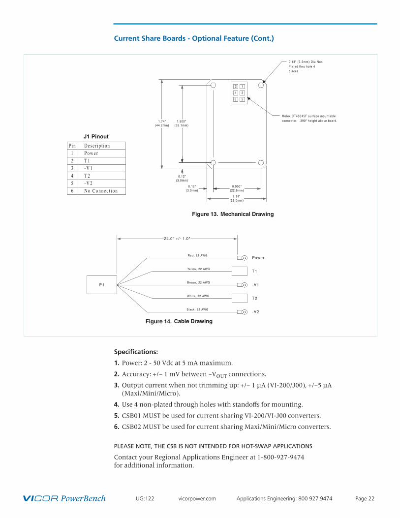
UG:122 vicorpower.com Applications Engineering: 800 927.9474 Page 22
Current Share Boards - Optional Feature (Cont.)
Specifications:
1. Power: 2 - 50 Vdc at 5 mA maximum.
2. Accuracy: +/– 1 mV between –VOUT connections.
3. Output current when not trimming up: +/– 1 µA (VI-200/J00), +/–5 µA (Maxi/Mini/Micro).
4. Use 4 non-plated through holes with standoffs for mounting.
5. CSB01 MUST be used for current sharing VI-200/VI-J00 converters.
6. CSB02 MUST be used for current sharing Maxi/Mini/Micro converters.
PLEASE NOTE, THE CSB IS NOT INTENDED FOR HOT-SWAP APPLICATIONS
Contact your Regional Applications Engineer at 1-800-927-9474 for additional information.
Cable Drawing
P1
24.0" +/- 1.0"
Power
T1
-V1
T2
-V2
Red, 22 AWG
Yellow, 22 AWG
Brown, 22 AWG
White, 22 AWG
Black, 22 AWG
12
34
56
1.74"(44.2mm)
0.12"(3.0mm)
1.500"(38.1mm)
0.12"(3.0mm)
0.900"(22.9mm)
1.14"(29.0mm)
0.13" (3.3mm) Dia NonPlated thru hole 4p laces
Molex CT43045F sur face mountableconnector. .390" height above board.
P i n D e s c r i p t i o n1 P o w e r2 T 13 - V 14 T 25 - V 26 N o C o n n e c t i o n
J1 Pinout
Figure 13. Mechanical Drawing
Figure 14.

UG:122 vicorpower.com Applications Engineering: 800 927.9474 Page 23
NOTES:
The Power Behind Performance
Rev 1.1 12/2014 P/N 03-00049 vicorpower.com Applications Engineering: 800 927.9474 Page 24
For Vicor Global Office Locations, please go to: www.vicorpower.com/contact-us
or call 800-735-6200.
For more information about this or other Vicor products, or for assistance with component-based power
system design, contact the Vicor office nearest you. Vicor's comprehensive line of power solutions includes
modular, high-density DC-DC converters and accessory components, configurable power supplies, and custom
power systems. Vicor, designs and builds configurable power supplies incorporating high density DC-DC
converters and accessory components.
This product line includes:
LoPAC FAMILY:
• PFC MicroS
• PFC Micro
• PFC Mini
MegaPAC FAMILY:
• PFC MegaPAC
• 4kW MegaPAC
• PFC MegaPAC (High Power)
• PFC MegaPAC-EL
• Mini MegaPAC
• ConverterPACs
OTHERS:
• FlatPAC-EN
Rugged COTS versions (MI) are available for the PFC Micro, PFC MicroS, PFC Mini and PFC MegaPAC.
INFORMATION FURNISHED BY VICOR IS BELIEVED TO BE ACCURATE AND RELIABLE. HOWEVER, NO RESPON-SIBILITY IS ASSUMED BY VICOR FOR ITS USE. NO LICENSE IS GRANTED BY IMPLICATION OR OTHERWISE UNDER ANY PATENT OR PATENT RIGHTS OF VICOR. VICOR COMPONENTS ARE NOT DESIGNED TO BE USED IN APPLICATIONS, SUCH AS LIFE SUPPORT SYSTEMS, WHEREIN A FAILURE OR MALFUNCTION COULD RESULT IN INJURY OR DEATH. ALL SALES ARE SUBJECT TO VICOR'S TERMS AND CONDITIONS OF SALE, WHICH ARE AVAILABLE UPON REQUEST.
SPECIFICATIONS ARE SUBJECT TO CHANGE WITHOUT NOTICE. THE LATEST DATA IS AVAILABLE ON THE VICOR WEBSITE AT VICORPOWER.COM

Mouser Electronics
Authorized Distributor
Click to View Pricing, Inventory, Delivery & Lifecycle Information: Vicor:
PS1-01-48 PS1-01-12492 PS1-01-12652-MC PS1-01-12662-MI PS1-01-12663-MI PS1-01-12681-G PS1-01-
12852-MI PS1-01-12991 PS1-01-13045 PS1-01-13092-MC PS1-01-13132-MC PS1-01-13135-G PS1-01-13165-MC
PS1-01-13192-MC PS1-01-13194-MC PS1-01-13222-MI PS1-01-13228 PS1-01-13229-MI PS1-01-13249-MI PS1-
01-13312-MC PS1-01-13313-MC PS1-01-13358-MI PS1-01-13388-G PS1-01-11602-MI PS1-01-11603-MI PS1-01-
11605-MC PS1-01-11606-MI PS1-01-11611-G PS1-01-11612-G PS1-01-11613-G PS1-01-11642-G PS1-01-11665
PS1-01-11710 PS1-01-11762 PS1-01-11782-MC PS1-01-11860 PS1-01-11894 PS1-01-12 PS1-01-12023-G PS1-
01-12024-G PS1-01-13422 PS1-01-010 PS1-01-05 PS1-01-10077 PS1-01-10105-G PS1-01-10179-MI PS1-01-
10180-MC PS1-01-10386-G PS1-01-10397 PS1-01-1082 PS1-01-11056 PS1-01-11189-G PS1-01-11371 PS1-01-
11372-MI PS1-01-14698-G PS1-01-14728 PS1-01-14743 PS1-01-14745-MI PS1-01-14760-G PS1-01-14792 PS1-
01-14823-G PS1-01-14846 PS1-01-14847-G PS1-01-14859-MI PS1-01-14860-MC PS1-01-14866-MI PS1-01-14869
PS1-01-14910 PS1-01-14941-MI PS1-01-14997 PS1-01-15 PS1-01-15008-MI PS1-01-15009 PS1-01-15016-G
PS1-01-15083 PS1-01-15106-MC PS1-01-15113 PS1-01-15176 PS1-01-15194 PS1-01-15262-MI PS1-01-15290-G
PS1-01-15341 PS1-01-15387-MC PS1-01-15431-MI PS1-01-15449 PS1-01-15465 PS1-01-15480-MC PS1-01-
15529 PS1-01-15637-MI PS1-01-15677-MI PS1-01-15702-MI PS1-01-15706-G PS1-01-15707-G PS1-01-15899-MI
PS1-01-15908-G PS1-01-15957-MI PS1-01-15-G PS1-01-16007-G PS1-01-16008-MC PS1-01-16349