Embed Size (px)
Citation preview
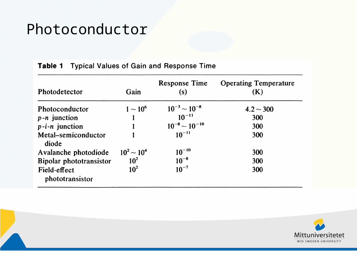
Photodetector
Outline
•Introduction
•Photoconductor
•Photodiode
•Avalanche photodiode
•Phototransistor
Introduction
Detection of photons means, the photons must interact with the detector by three processes:
1) Carrier generation by incident light
2) Carrier transport (with or without carrier multiplication)
3) Interaction of current with external circuit to provide the output signal
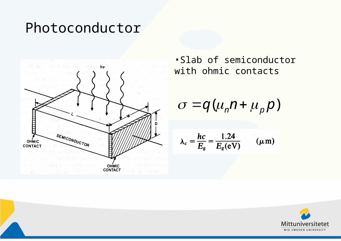
Photoconductor
•Slab of semiconductor with ohmic contacts
)( pnq pn
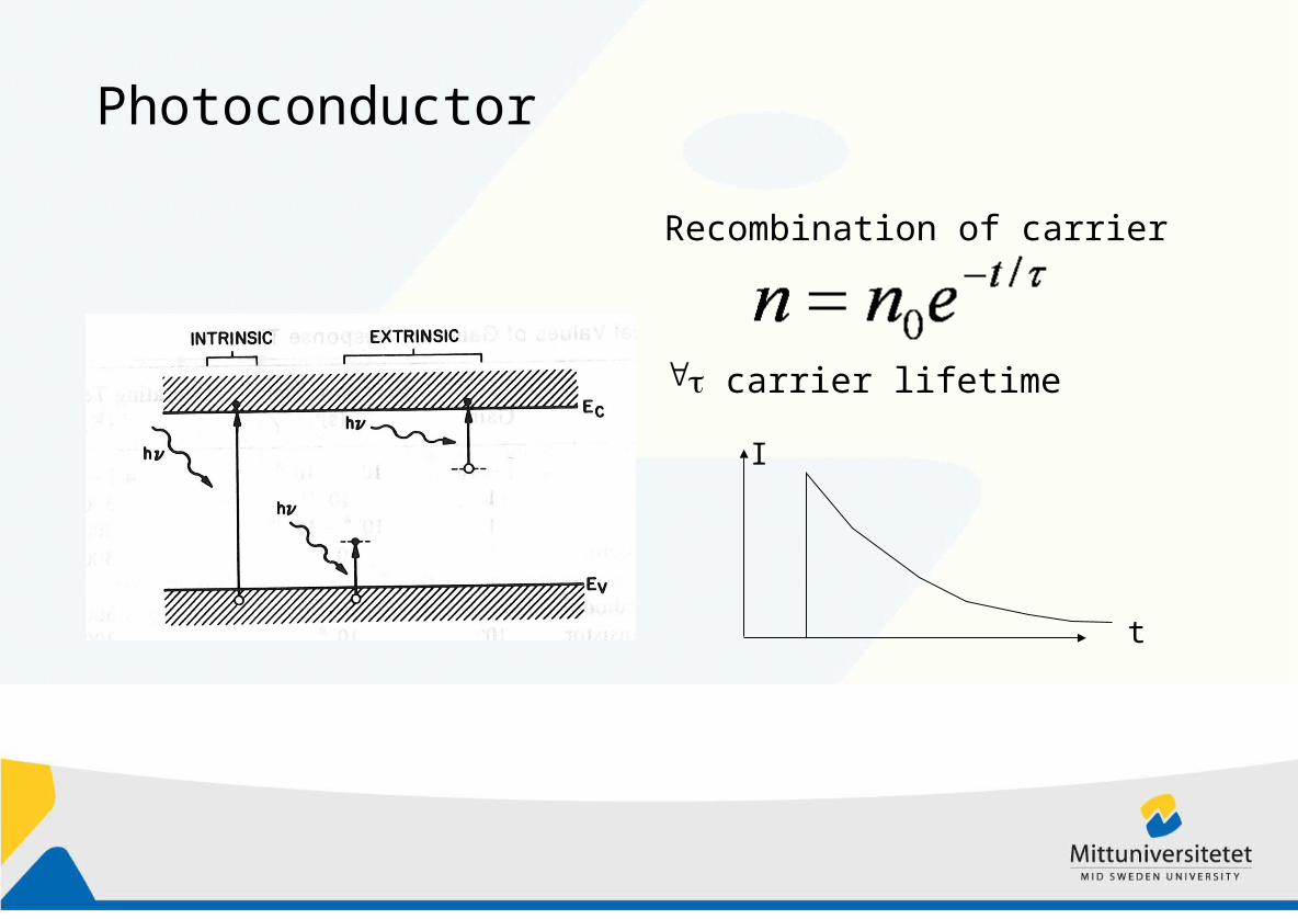
Photoconductor
Recombination of carrier
carrier lifetime
t
I
Photoconductor
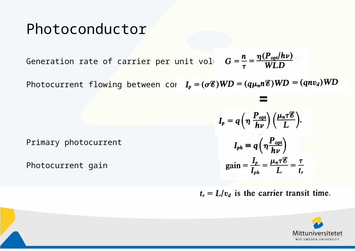
Generation rate of carrier per unit volume
Photocurrent flowing between contacts
Primary photocurrent
Photocurrent gain
=
Photoconductor
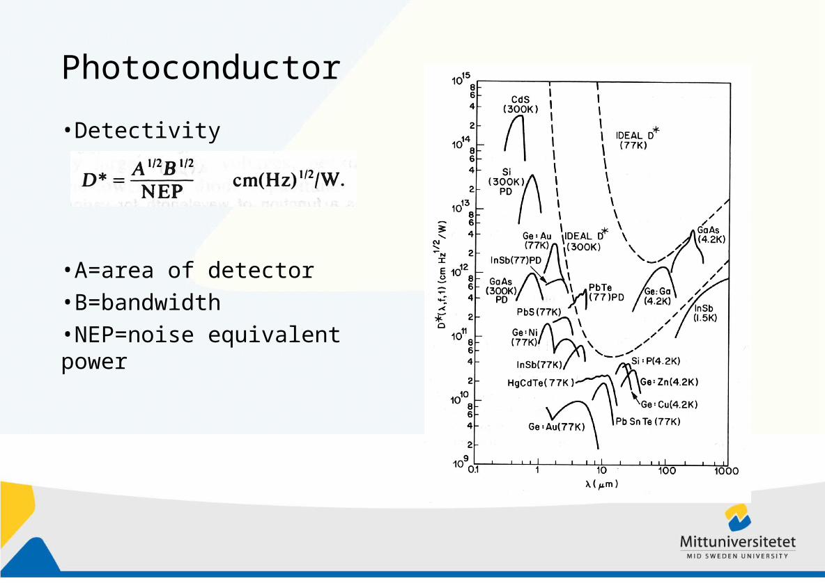
Photoconductor
•Detectivity
•A=area of detector•B=bandwidth•NEP=noise equivalent power
Photodiode
• pn-junction diode
• Metal-semiconductor diode (Schottky diode)
• (Heterojunction diode)
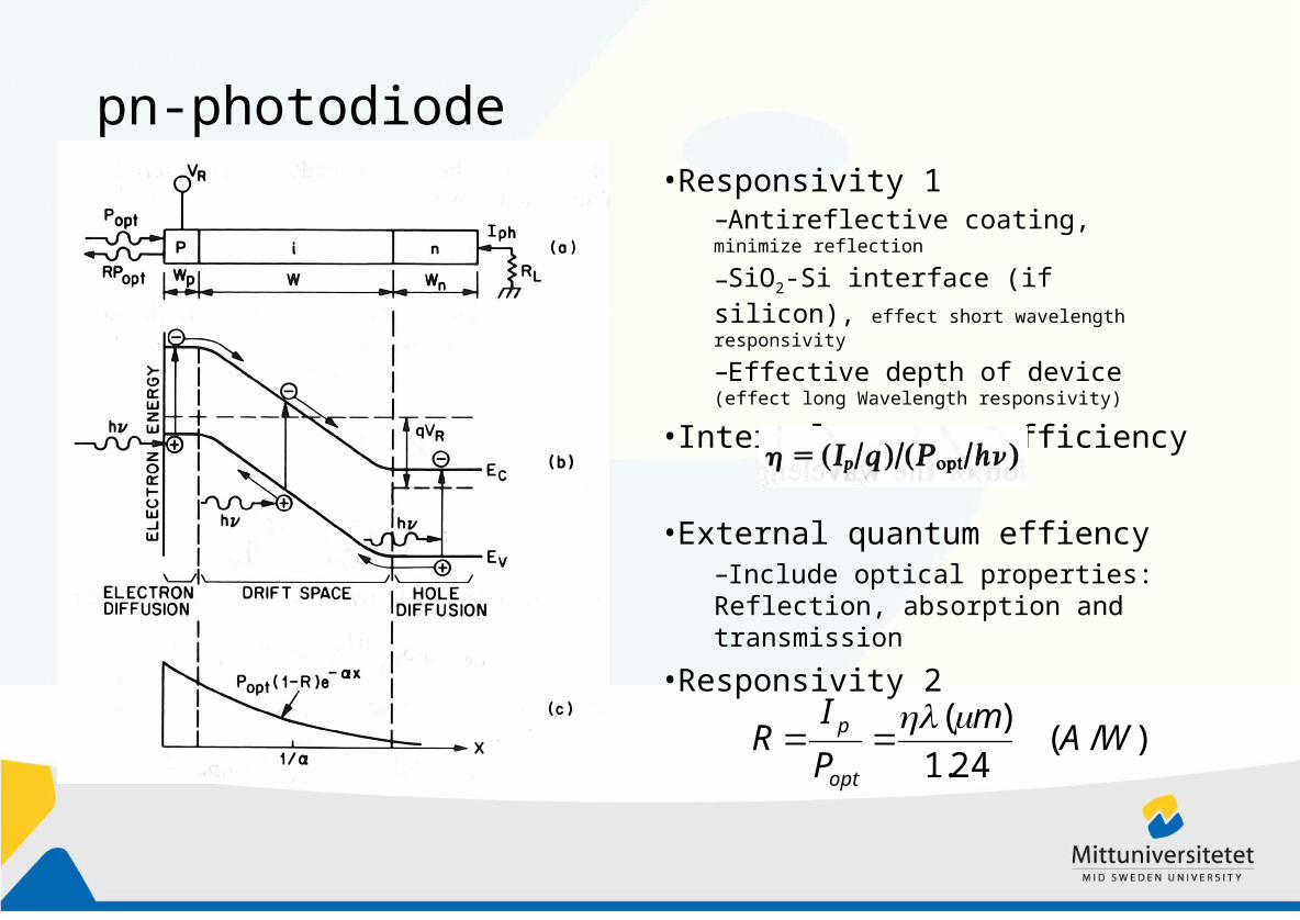
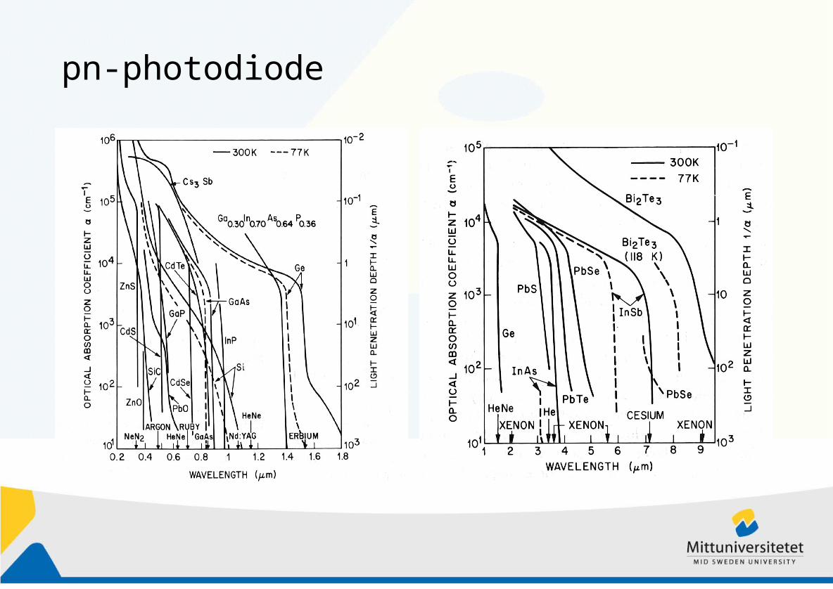
pn-photodiode
)/(24.1
)(WA
m
P
IR
opt
p
•Responsivity 1–Antireflective coating, minimize reflection
–SiO2-Si interface (if silicon), effect
short wavelength responsivity
–Effective depth of device (effect long Wavelength responsivity)
•Internal quantum efficiency
•External quantum effiency–Include optical properties: Reflection, absorption and transmission
•Responsivity 2
pn-photodiode
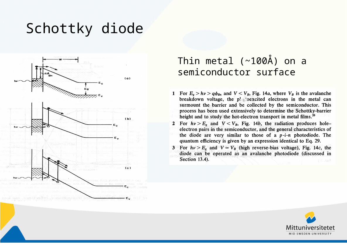
Schottky diode
Thin metal (~100Å) on a semiconductor surface
Schottky diode
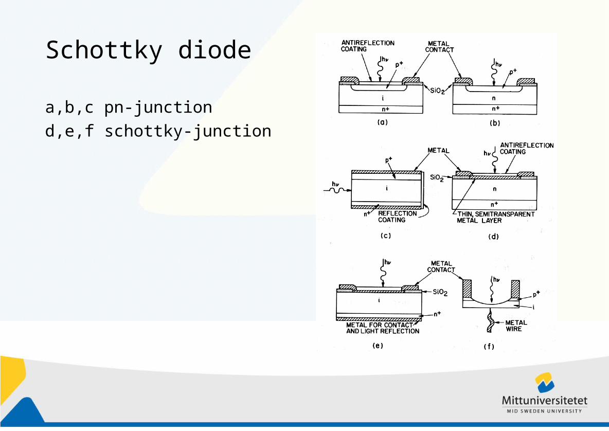
a,b,c pn-junction
d,e,f schottky-junction
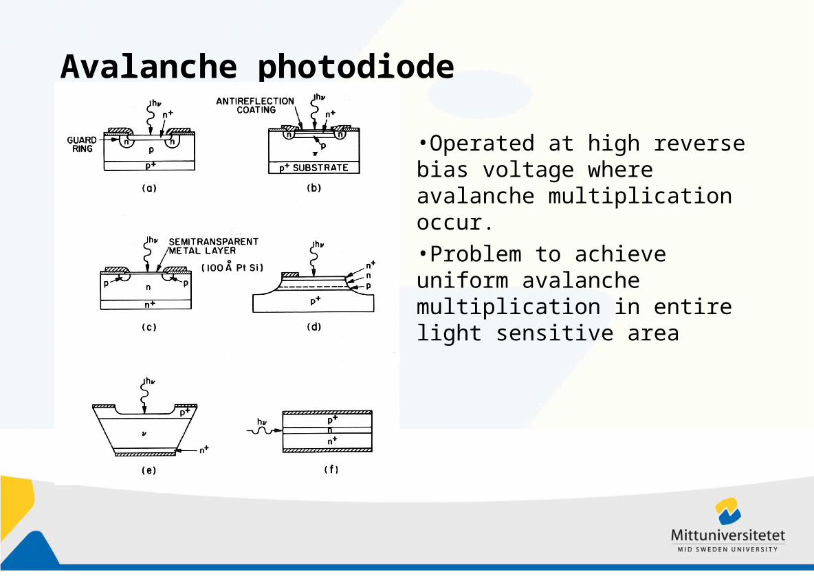
Avalanche photodiode
•Operated at high reverse bias voltage where avalanche multiplication occur.•Problem to achieve uniform avalanche multiplication in entire light sensitive area
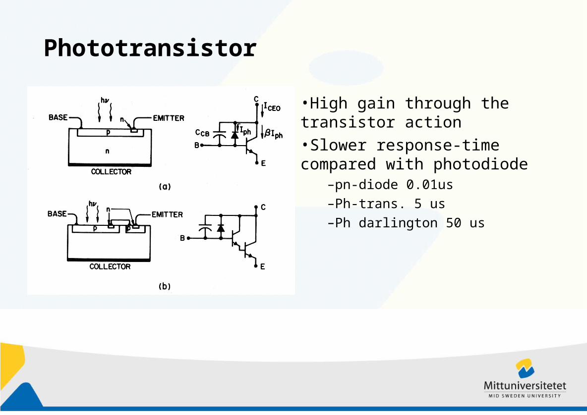
Phototransistor
•High gain through the transistor action•Slower response-time compared with photodiode
–pn-diode 0.01us–Ph-trans. 5 us–Ph darlington 50 us