Embed Size (px)
Citation preview
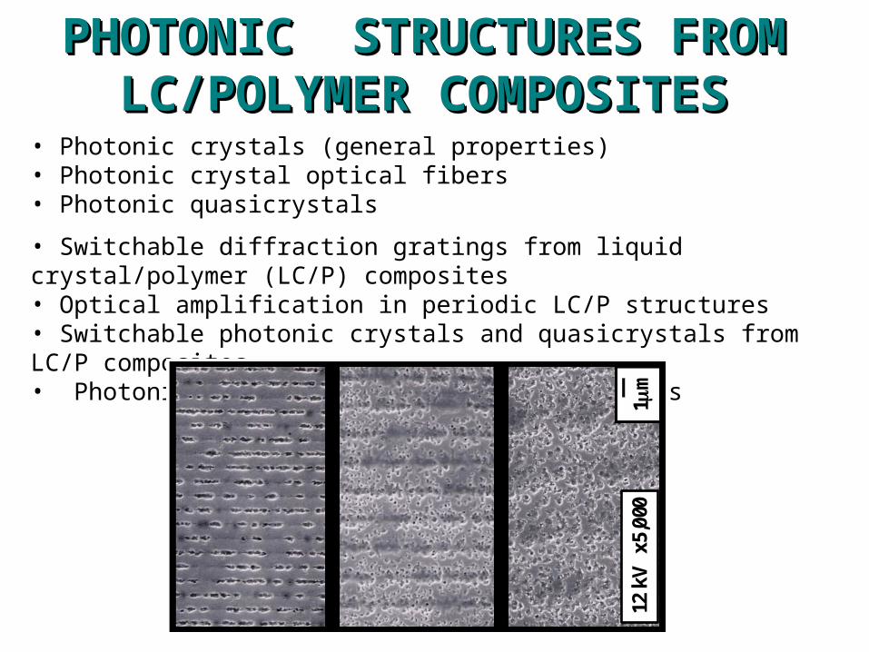
PHOTONIC STRUCTURES FROM PHOTONIC STRUCTURES FROM LC/POLYMER COMPOSITESLC/POLYMER COMPOSITES
PHOTONIC STRUCTURES FROM PHOTONIC STRUCTURES FROM LC/POLYMER COMPOSITESLC/POLYMER COMPOSITES
• Photonic crystals (general properties)• Photonic crystal optical fibers• Photonic quasicrystals
• Switchable diffraction gratings from liquid crystal/polymer (LC/P) composites• Optical amplification in periodic LC/P structures• Switchable photonic crystals and quasicrystals from LC/P composites• Photonic bandgap fibers from LC composites
1m
12 k
V x
5,00
0
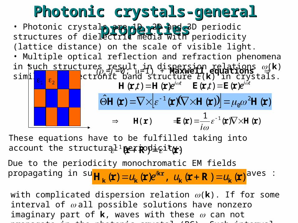
Photonic crystals-general propertiesPhotonic crystals-general propertiesPhotonic crystals-general propertiesPhotonic crystals-general properties• Photonic crystals are 1D, 2D and 3D periodic structures of dielectric media with periodicity (lattice distance) on the scale of visible light.• Multiple optical reflection and refraction phenomena in such structures result in dispersion relations (k) similar to electronic band structure E(k) in crystals.
(e=je=0; =1) + Maxwell equations tiet )(),( rHrH tiet )(),( rErE
)()(1
)( 1 rHrrE i
)()()()(ˆ 20
1 rHrHrrH
H(r)
These equations have to be fulfilled taking into account the structural periodicity:
)()( 11 rRr
1 2
Due to the periodicity monochromatic EM fields propagating in such medium have the form Bloch waves : )()( ,)()( rRrrrH kk
krkk uueu i
with complicated dispersion relation (k). If for some interval of all possible solutions have nonzero imaginary part of k, waves with these can not propagate in the photonic crystal (PC). Such interval of is called the photonic bandgap.
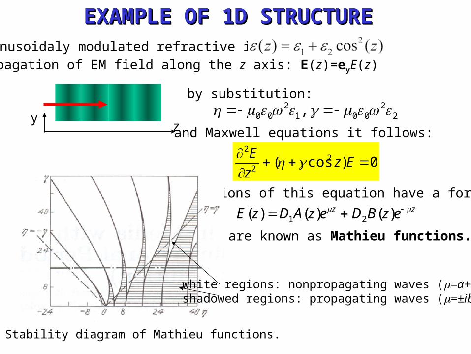
EXAMPLE OF 1D STRUCTUREEXAMPLE OF 1D STRUCTUREEXAMPLE OF 1D STRUCTUREEXAMPLE OF 1D STRUCTURESinusoidaly modulated refractive index: Propagation of EM field along the z axis: E(z)=eyE(z)
22
0012
00 ,
0)cos( 22
2
Ezz
E
zz ezBDezADzE )()()( 21
by substitution:
and Maxwell equations it follows:
Solutions of this equation have a form
and are known as Mathieu functions.
z
white regions: nonpropagating waves (=a+ib)shadowed regions: propagating waves (=±ib)
Stability diagram of Mathieu functions.
y
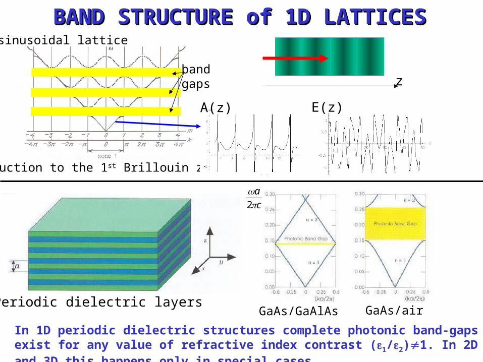
BAND STRUCTURE of 1D LATTICESBAND STRUCTURE of 1D LATTICESBAND STRUCTURE of 1D LATTICESBAND STRUCTURE of 1D LATTICES
Reduction to the 1st Brillouin zone.
A(z) E(z)
z
sinusoidal lattice
Periodic dielectric layers
bandgaps
c
a
2
GaAs/GaAlAs GaAs/air
In 1D periodic dielectric structures complete photonic band-gaps exist for any value of refractive index contrast (1/2)1. In 2D and 3D this happens only in special cases.
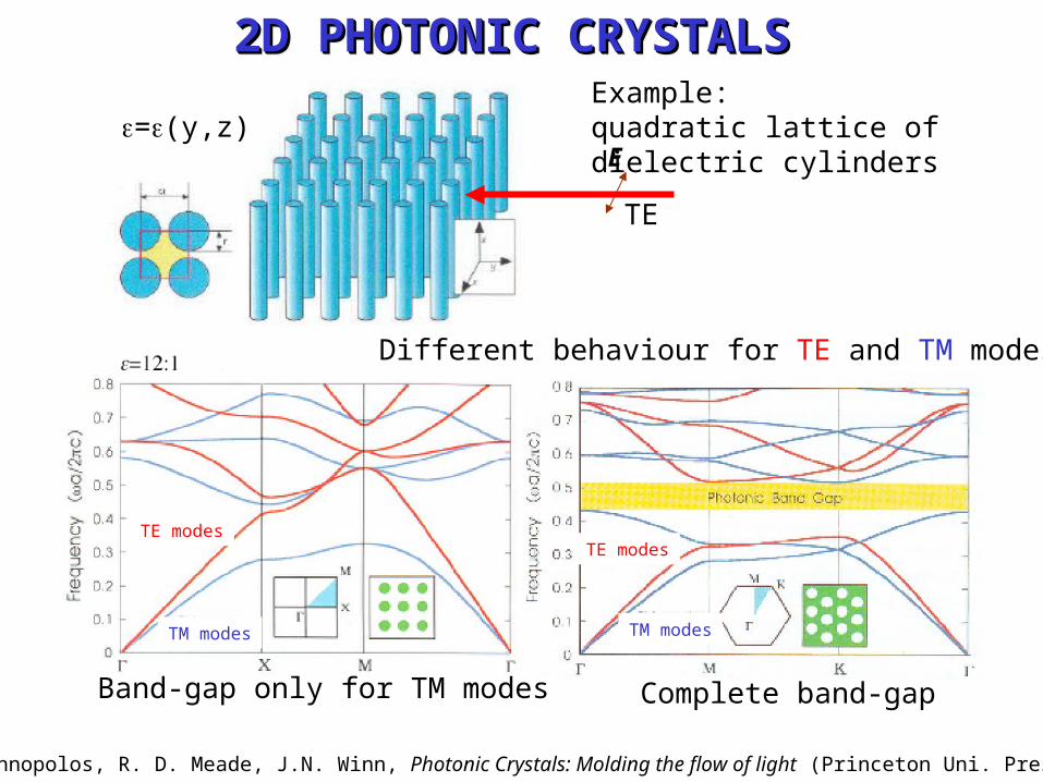
2D PHOTONIC CRYSTALS2D PHOTONIC CRYSTALS2D PHOTONIC CRYSTALS2D PHOTONIC CRYSTALSExample: quadratic lattice ofdielectric cylinders
Different behaviour for TE and TM modes!
TE
TE modesTE modes
TM modes TM modes
=(y,z)
Band-gap only for TM modes Complete band-gap
J. D. Joannopolos, R. D. Meade, J.N. Winn, Photonic Crystals: Molding the flow of light (Princeton Uni. Press, 1995)
E
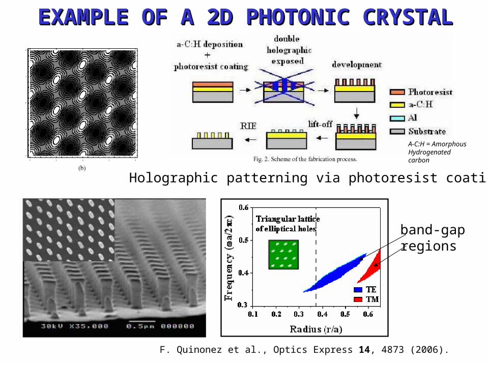
EXAMPLE OF A 2D PHOTONIC CRYSTALEXAMPLE OF A 2D PHOTONIC CRYSTALEXAMPLE OF A 2D PHOTONIC CRYSTALEXAMPLE OF A 2D PHOTONIC CRYSTAL
F. Quinonez et al., Optics Express 14, 4873 (2006).
Holographic patterning via photoresist coating.
band-gapregions
A-C:H = Amorphous Hydrogenatedcarbon
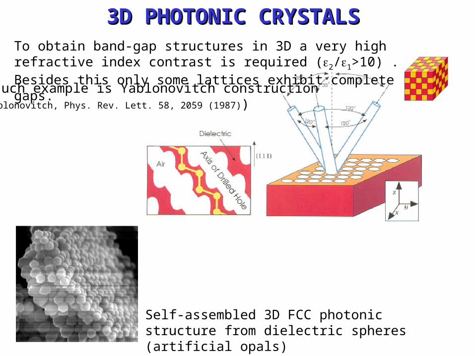
3D PHOTONIC CRYSTALS3D PHOTONIC CRYSTALS3D PHOTONIC CRYSTALS3D PHOTONIC CRYSTALSTo obtain band-gap structures in 3D a very high refractive index contrast is required (2/1>10) . Besides this only some lattices exhibit complete band-gaps.
One such example is Yablonovitch construction(E. Yablonovitch, Phys. Rev. Lett. 58, 2059 (1987))
Self-assembled 3D FCC photonic structure from dielectric spheres (artificial opals)
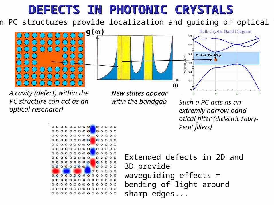
DEFECTS IN PHOTONIC CRYSTALSDEFECTS IN PHOTONIC CRYSTALSDEFECTS IN PHOTONIC CRYSTALSDEFECTS IN PHOTONIC CRYSTALSDefects in PC structures provide localization and guiding of optical waves.
A cavity (defect) within the PC structure can act as an optical resonator!
New states appear witin the bandgap
g()
Such a PC acts as an extremly narrow band otical filter (dielectric Fabry-Perot filters)
Extended defects in 2D and 3D providewaveguiding effects = bending of light around sharp edges...
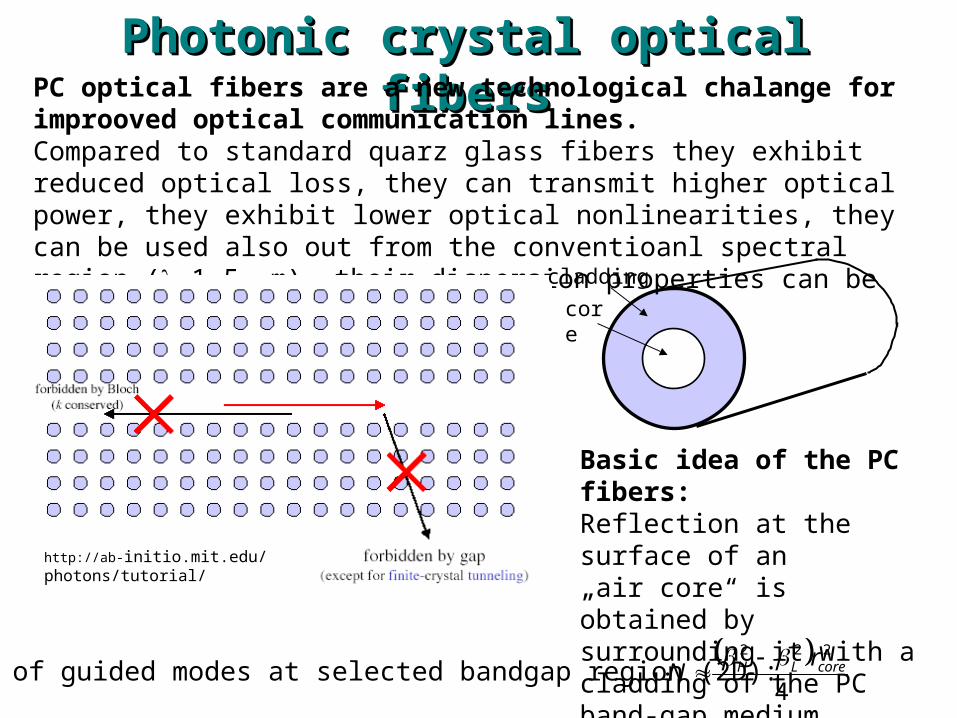
Photonic Photonic crystal optical fiberscrystal optical fibersPhotonic Photonic crystal optical fiberscrystal optical fibersPC optical fibers are a new technological chalange for improoved optical communication lines.Compared to standard quarz glass fibers they exhibit reduced optical loss, they can transmit higher optical power, they exhibit lower optical nonlinearities, they can be used also out from the conventioanl spectral region (~1.5 m), their dispersion properties can be tuned to the desired needs...
http://ab-initio.mit.edu/photons/tutorial/
Basic idea of the PC fibers:Reflection at the surface of an„air core“ is obtained by surrounding it with a cladding of the PC band-gap medium.
Number of guided modes at selected bandgap region (2D):
core
cladding
4
222coreLH r
N
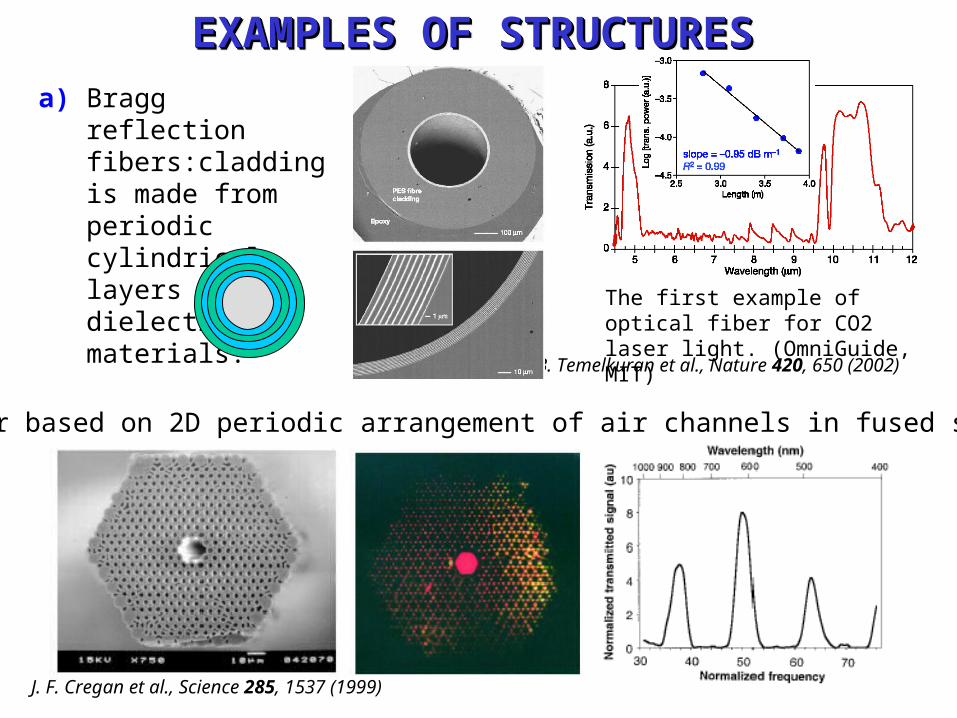
EEXAMPLES OF STRUCTURESXAMPLES OF STRUCTURESEEXAMPLES OF STRUCTURESXAMPLES OF STRUCTURES
J. F. Cregan et al., Science 285, 1537 (1999)
b) PC fiber based on 2D periodic arrangement of air channels in fused silica.
B. Temelkuran et al., Nature 420, 650 (2002)
a) Bragg reflection fibers:cladding is made from periodic cylindrical layers of two dielectric materials.
The first example of optical fiber for CO2 laser light. (OmniGuide, MIT)
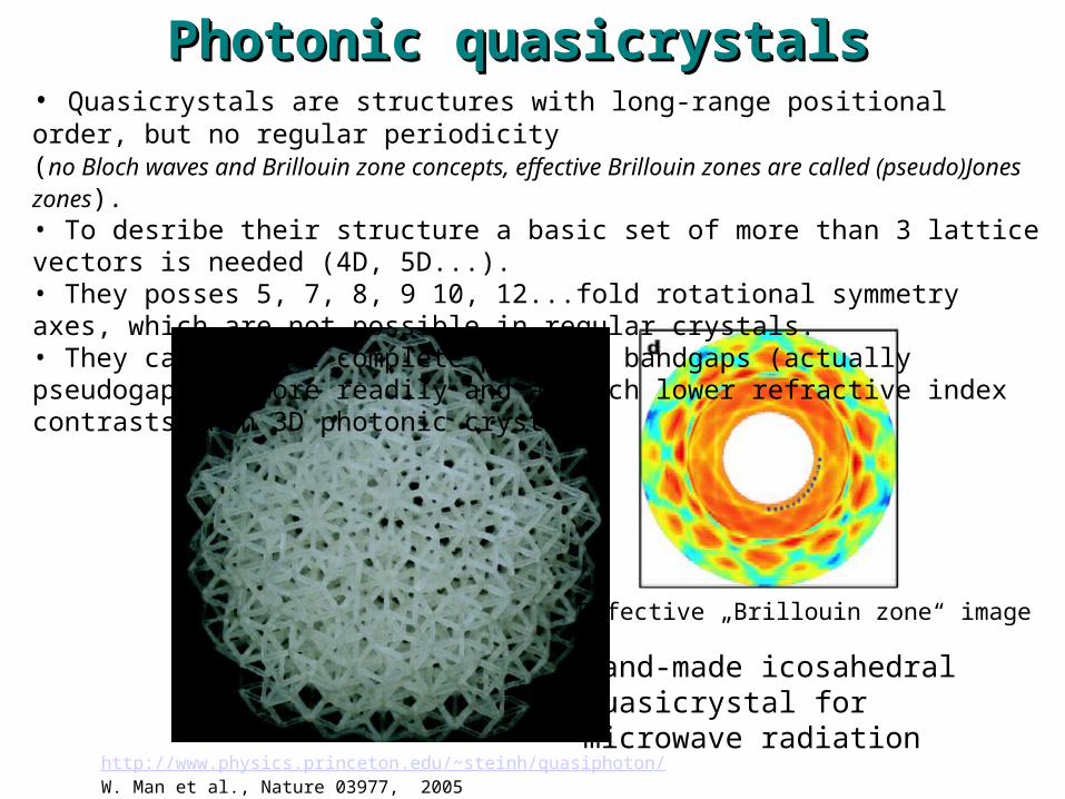
Photonic quasicrystalsPhotonic quasicrystalsPhotonic quasicrystalsPhotonic quasicrystals
Hand-made icosahedral quasicrystal formicrowave radiation
http://www.physics.princeton.edu/~steinh/quasiphoton/W. Man et al., Nature 03977, 2005
Effective „Brillouin zone“ image
• Quasicrystals are structures with long-range positional order, but no regular periodicity (no Bloch waves and Brillouin zone concepts, effective Brillouin zones are called (pseudo)Jones zones).• To desribe their structure a basic set of more than 3 lattice vectors is needed (4D, 5D...).• They posses 5, 7, 8, 9 10, 12...fold rotational symmetry axes, which are not possible in regular crystals.• They can exhibit complete photonic bandgaps (actually pseudogaps!!) more readily and at much lower refractive index contrasts than 3D photonic crystals.
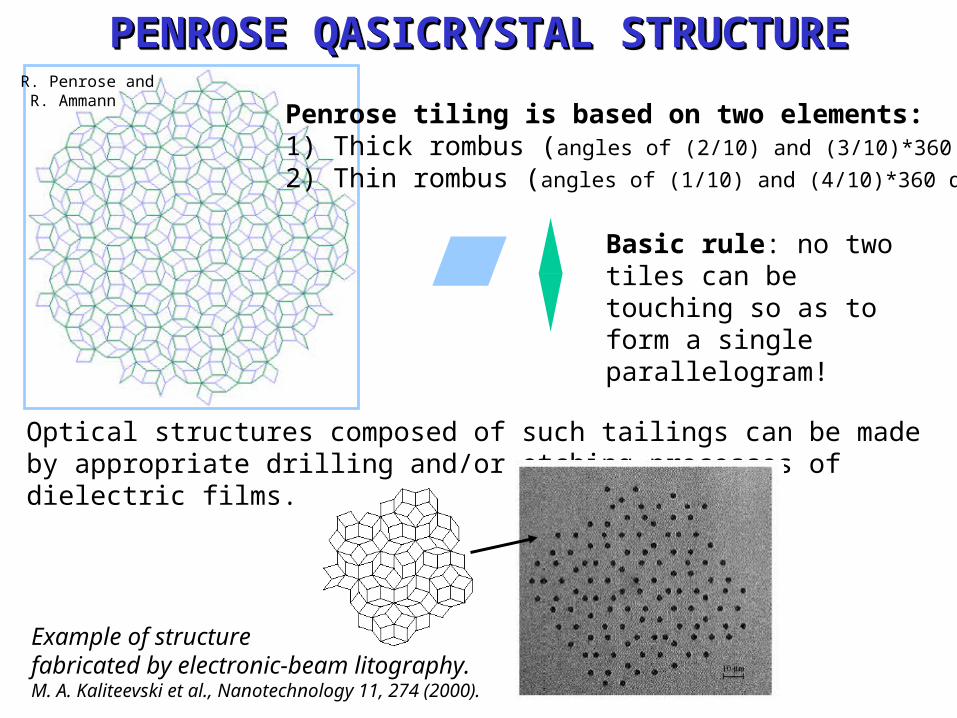
PENROSE QASICRYSTAL STRUCTUREPENROSE QASICRYSTAL STRUCTUREPENROSE QASICRYSTAL STRUCTUREPENROSE QASICRYSTAL STRUCTURER. Penrose and R. Ammann
Penrose tiling is based on two elements:1) Thick rombus (angles of (2/10) and (3/10)*360 deg)2) Thin rombus (angles of (1/10) and (4/10)*360 deg)
Basic rule: no two tiles can be touching so as to form a single parallelogram!
Optical structures composed of such tailings can be made by appropriate drilling and/or etching processes of dielectric films.
Example of structurefabricated by electronic-beam litography.M. A. Kaliteevski et al., Nanotechnology 11, 274 (2000).
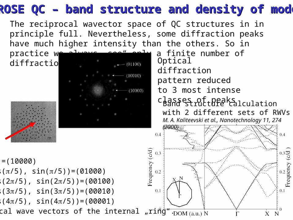
PENROSE QC – band structure and density of modesPENROSE QC – band structure and density of modesPENROSE QC – band structure and density of modesPENROSE QC – band structure and density of modes
Optical diffraction pattern reduced to 3 most intense classes of peaks
The reciprocal wavector space of QC structures in in principle full. Nevertheless, some diffraction peaks have much higher intensity than the others. So in practice we always „see“ only a finite number of diffraction peaks.
b1=(1,0)=(10000)b2 =(cos(/5), sin(/5))=(01000) b3 =(cos(2/5), sin(2/5))=(00100)b4 =(cos(3/5), sin(3/5))=(00010)b5 =(cos(4/5), sin(4/5))=(00001)Reciprocal wave vectors of the internal „ring“.
Band structure calculation with 2 different sets of RWVsM. A. Kaliteevski et al., Nanotechnology 11, 274 (2000)
Switchable diffraction gratings from Switchable diffraction gratings from LC/polymer compositesLC/polymer composites
Switchable diffraction gratings from Switchable diffraction gratings from LC/polymer compositesLC/polymer composites
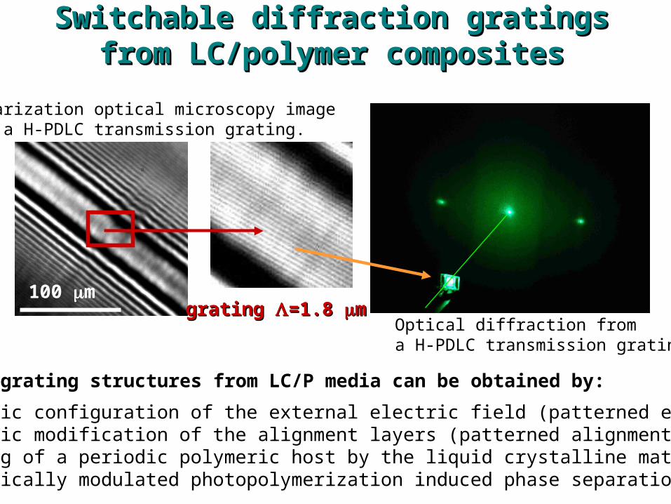
100 mgratinggrating =1.8 =1.8 mm
Optical grating structures from LC/P media can be obtained by:
• periodic configuration of the external electric field (patterned electrodes)• periodic modification of the alignment layers (patterned alignment layers)• filling of a periodic polymeric host by the liquid crystalline material• periodically modulated photopolymerization induced phase separation process
Polarization optical microscopy image of a H-PDLC transmission grating.
Optical diffraction from a H-PDLC transmission grating
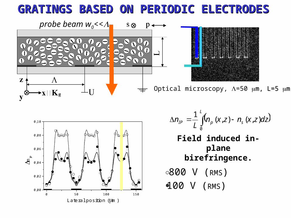
GRATINGS BASED ON PERIODIC ELECTRODESGRATINGS BASED ON PERIODIC ELECTRODESGRATINGS BASED ON PERIODIC ELECTRODESGRATINGS BASED ON PERIODIC ELECTRODES
0 50 100 1500,00
0,02
0,04
0,06
0,08
0,10
nIP
Lateral position (m)
Field induced in-planebirefringence.
800 V (RMS)
100 V (RMS)
L
spIP dzzxnzxnL
n0
),(),(1
probe beam w0<<
Optical microscopy, =50 mm, L=5 , L=5 mm
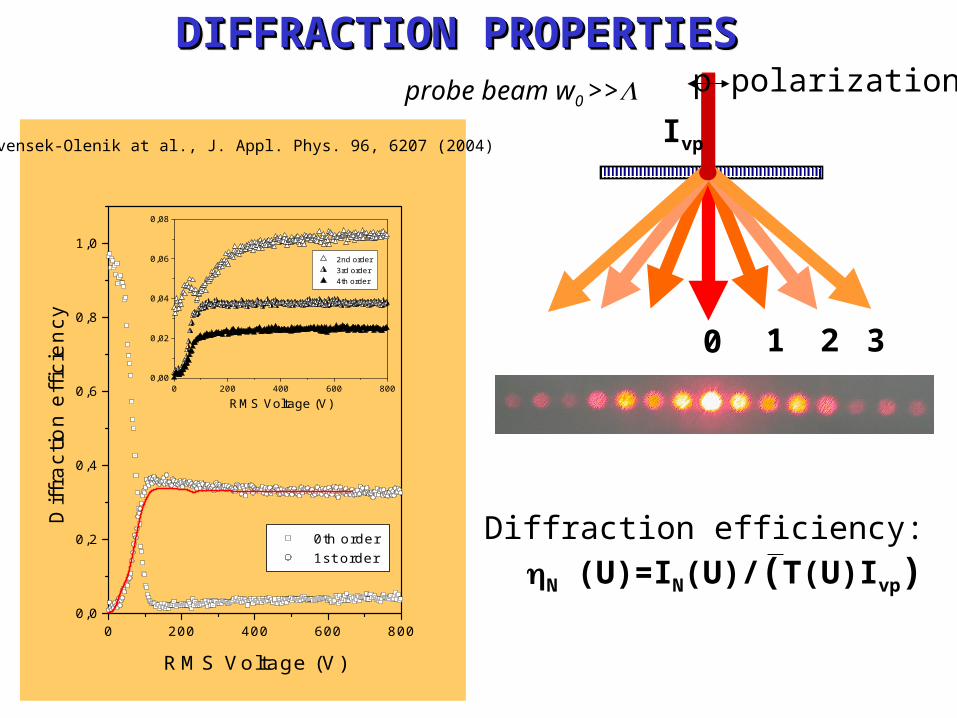
DIFFRACTION PROPERTIESDIFFRACTION PROPERTIESDIFFRACTION PROPERTIESDIFFRACTION PROPERTIES
0 200 400 600 8000,0
0,2
0,4
0,6
0,8
1,0
0 200 400 600 8000,00
0,02
0,04
0,06
0,08
2nd order 3rd order 4th order
RMS Voltage (V)
I. Drevensek-Olenik at al., Fig. 5
0th order 1st order
Diff
ract
ion
effic
ienc
y
RMS Voltage (V)
0. 1. 2. 3.
p polarization
N (U)=IN(U)/(T(U)Ivp)Diffraction efficiency:
Ivp
0 200 400 600 8000,0
0,2
0,4
0,6
0,8
1,0
0 200 400 600 8000,00
0,02
0,04
0,06
0,08
2nd order 3rd order 4th order
RMS Voltage (V)
I. Drevensek-Olenik at al., Fig. 5
0th order 1st order
Diff
ract
ion e
ffic
iency
RMS Voltage (V)
probe beam w0 >>
I. Drevensek-Olenik at al., J. Appl. Phys. 96, 6207 (2004)
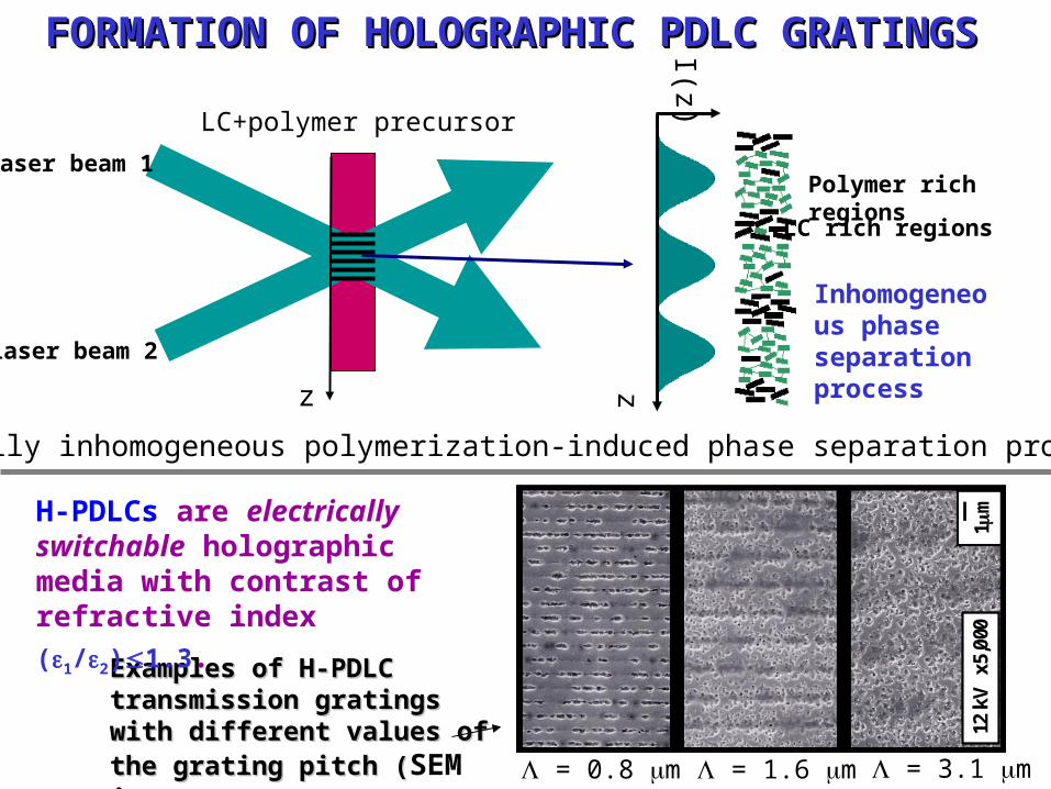
FORMATION OF HOLOGRAPHIC PDLC GRATINGSFORMATION OF HOLOGRAPHIC PDLC GRATINGSFORMATION OF HOLOGRAPHIC PDLC GRATINGSFORMATION OF HOLOGRAPHIC PDLC GRATINGS
1m
12 k
V x
5,00
0
= 0.8 m = 1.6 m = 3.1 m
LC+polymer precursor
laser beam 1
Examples of Examples of H-PDLCH-PDLC transmission transmission gratings with different values of the gratings with different values of the grating pitch (grating pitch (SEM images)..
laser beam 2
Inhomogeneous phase separationprocess
LC rich regions
Polymer rich regions
Spatially inhomogeneous polymerization-induced phase separation process.
I(z)z z
H-PDLCs are electrically switchable holographic media with contrast of
refractive index (1/2)1.3.
U+ -
nlc npolp
s
Bragg reflection
nlc~ npol
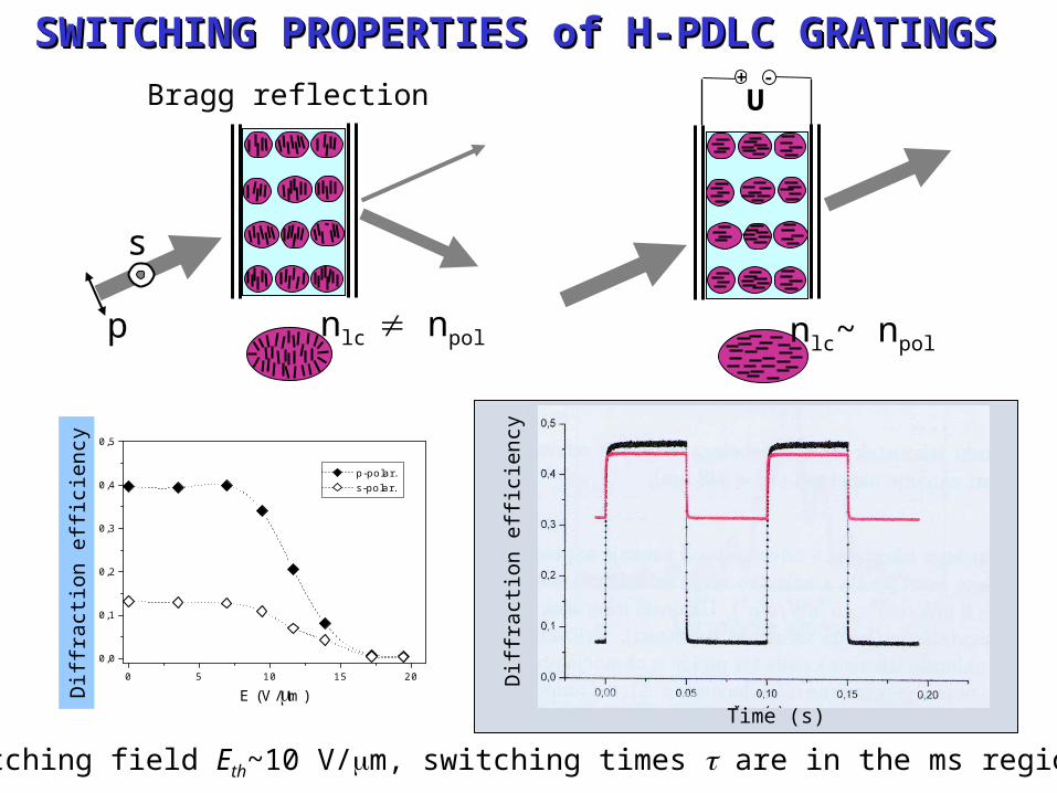
SWITCHING PROPERTIES of H-PDLC GRATINGSSWITCHING PROPERTIES of H-PDLC GRATINGSSWITCHING PROPERTIES of H-PDLC GRATINGSSWITCHING PROPERTIES of H-PDLC GRATINGS
0 5 10 15 20
0,0
0,1
0,2
0,3
0,4
0,5
Ukl
onsk
i izk
oris
tek
E (V/m)
p-polar. s-polar.
Time (s)
Dif
frac
tion
eff
icie
ncy
Switching field Eth~10 V/m, switching times are in the ms region.
Dif
frac
tion
eff
icie
ncy
Reflection grating Transmission grating
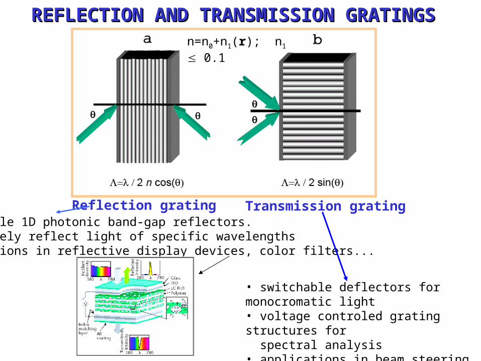
REFLECTION AND TRANSMISSION GRATINGSREFLECTION AND TRANSMISSION GRATINGSREFLECTION AND TRANSMISSION GRATINGSREFLECTION AND TRANSMISSION GRATINGSn=n0+n1(r); n1 0.1
• switchable 1D photonic band-gap reflectors.• selectively reflect light of specific wavelengths• applications in reflective display devices, color filters...
• switchable deflectors for monocromatic light• voltage controled grating structures for spectral analysis• applications in beam steering units, optical interconnects...
Optical amplification in periodic Optical amplification in periodic LC/polymer composite structuresLC/polymer composite structuresOptical amplification in periodic Optical amplification in periodic LC/polymer composite structuresLC/polymer composite structures
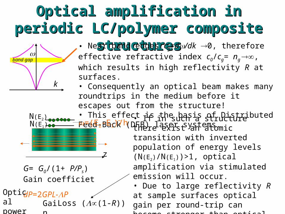
• Near band edges cg=d/dk 0, therefore effective refractive index c0/cg= ng , which results in high reflectivity R at surfaces. • Consequently an optical beam makes many roundtrips in the medium before it escapes out from the structure! • This effect is the basis of Distributed Feed-Back (DFB) laser systems.
k
band gap
z
• If in such a structure there exist an atomic transition with inverted population of energy levels (N(E2)/N(E1))>1, optical amplification via stimulated emission will occur. • Due to large reflectivity R at sample surfaces optical gain per round-trip can become stronger than optical losses per round trip, therefore lasing takes place.
N(E2)N(E1)
G= G0/(1+ P/Ps)Gain coefficiet
dP=2GPL-PGain Loss ((1-R))
Optical power
=(E2-E1)/h
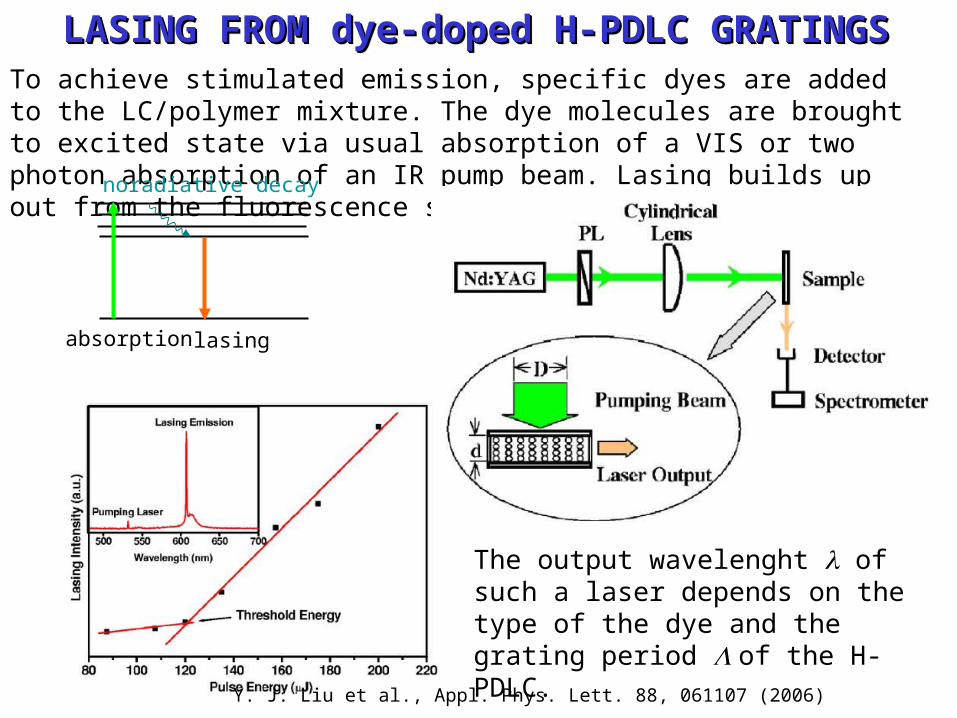
LASING FROM dye-doped HLASING FROM dye-doped H--PDLC GRATINGPDLC GRATINGSSLASING FROM dye-doped HLASING FROM dye-doped H--PDLC GRATINGPDLC GRATINGSSTo achieve stimulated emission, specific dyes are added to the LC/polymer mixture. The dye molecules are brought to excited state via usual absorption of a VIS or two photon absorption of an IR pump beam. Lasing builds up out from the fluorescence spectrum.
absorption lasing
noradiative decay
The output wavelenght of such a laser depends on the type of the dye and the grating period of the H-PDLC.
Y. J. Liu et al., Appl. Phys. Lett. 88, 061107 (2006)
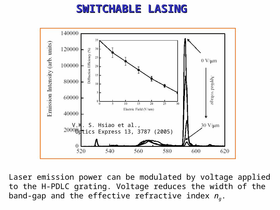
SWITCHABLE SWITCHABLE LASINGLASINGSWITCHABLE SWITCHABLE LASINGLASING
Laser emission power can be modulated by voltage applied to the H-PDLC grating. Voltage reduces the width of the band-gap and the effective refractive index ng.
V.K. S. Hsiao et al., Optics Express 13, 3787 (2005)
Switchable photonic crystals and Switchable photonic crystals and quasicrystals from LC/P compositesquasicrystals from LC/P composites
Switchable photonic crystals and Switchable photonic crystals and quasicrystals from LC/P compositesquasicrystals from LC/P composites
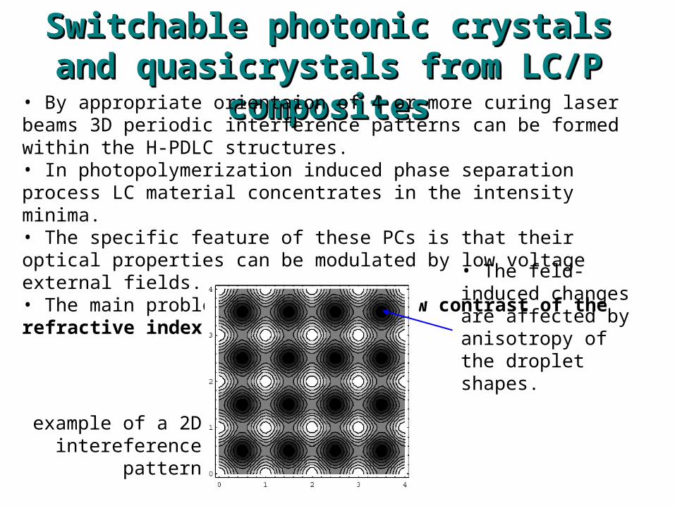
• By appropriate orientaion of 4 or more curing laser beams 3D periodic interference patterns can be formed within the H-PDLC structures.• In photopolymerization induced phase separation process LC material concentrates in the intensity minima.• The specific feature of these PCs is that their optical properties can be modulated by low voltage external fields.• The main problem is relatively low contrast of the refractive index
example of a 2D intereference
pattern
• The feld-induced changes are affected by anisotropy of the droplet shapes.
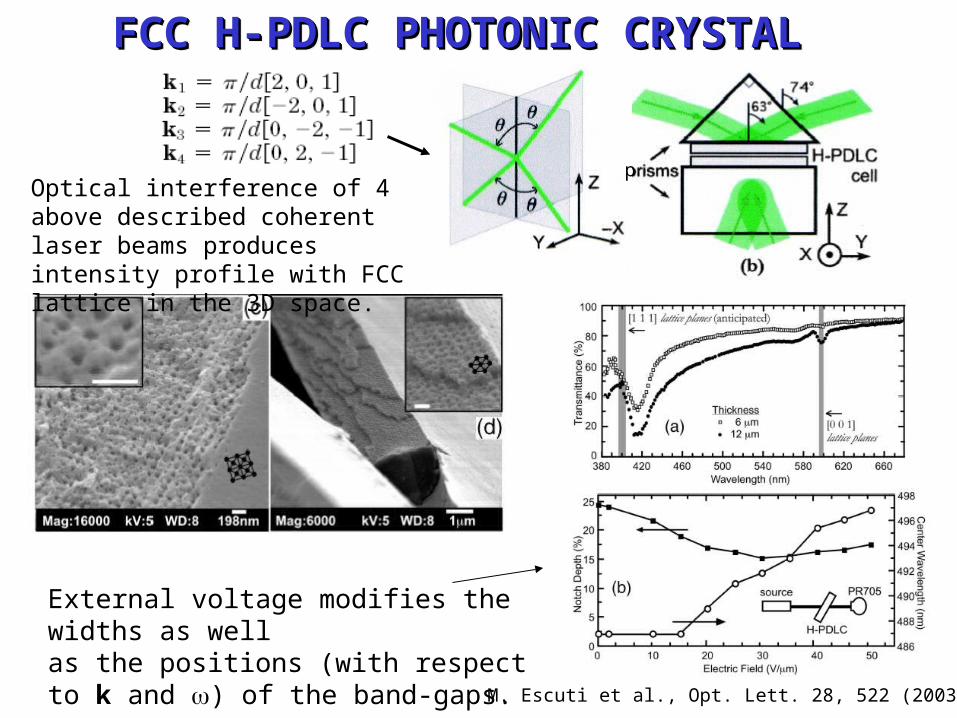
FCC H-PDLC PHOTONIC CRYSTALFCC H-PDLC PHOTONIC CRYSTALFCC H-PDLC PHOTONIC CRYSTALFCC H-PDLC PHOTONIC CRYSTAL
M. Escuti et al., Opt. Lett. 28, 522 (2003).
Optical interference of 4 above described coherent laser beams produces intensity profile with FCC lattice in the 3D space.
p
External voltage modifies the widths as wellas the positions (with respect to k and ) of the band-gaps.
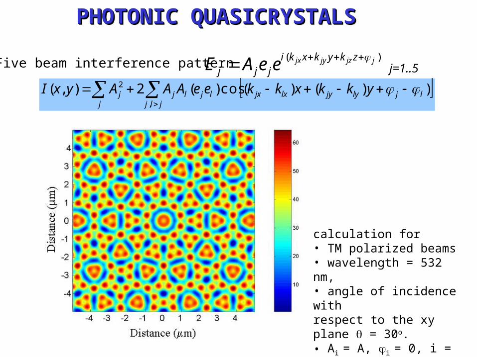
Five beam interference pattern j=1..5)( jjzjyjx zkykxki
jjj eeAE ))()(cos)(2),(
,
2ljlyjylxjxl
jljjlj
jj ykkxkkeeAAAyxI
PHOTONIC QUASICRYSTALSPHOTONIC QUASICRYSTALSPHOTONIC QUASICRYSTALSPHOTONIC QUASICRYSTALS
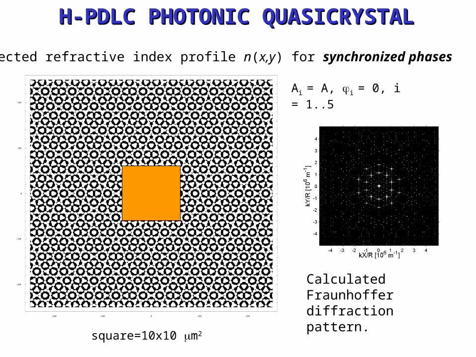
calculation for • TM polarized beams • wavelength = 532 nm, • angle of incidence with respect to the xy plane = 30o.• Ai = A, i = 0, i = 1..5
H-PDLC PHOTONIC QUASICRYSTALH-PDLC PHOTONIC QUASICRYSTALH-PDLC PHOTONIC QUASICRYSTALH-PDLC PHOTONIC QUASICRYSTAL
-200 -100 0 100 200
-200
-100
0
100
200
Ai = A, i = 0, i = 1..5
Calculated Fraunhoffer diffraction pattern.
Expected refractive index profile n(x,y) for synchronized phases
square=10x10 m2
H-PDLC PHOTONIC QUASICRYSTALH-PDLC PHOTONIC QUASICRYSTALH-PDLC PHOTONIC QUASICRYSTALH-PDLC PHOTONIC QUASICRYSTAL
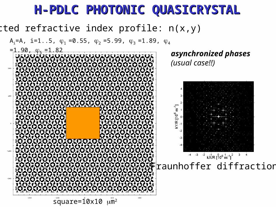
Ai=A, i=1..5, 1 =0.55, 2 =5.99, 3 =1.89, 4 =1.90, 5 =1.82
square=10x10 m2
Expected refractive index profile: n(x,y)
Fraunhoffer diffraction
asynchronized phases(usual case!!)
EXAMPLE OF QUASICRYSTAL STRUCTUREEXAMPLE OF QUASICRYSTAL STRUCTUREEXAMPLE OF QUASICRYSTAL STRUCTUREEXAMPLE OF QUASICRYSTAL STRUCTURE
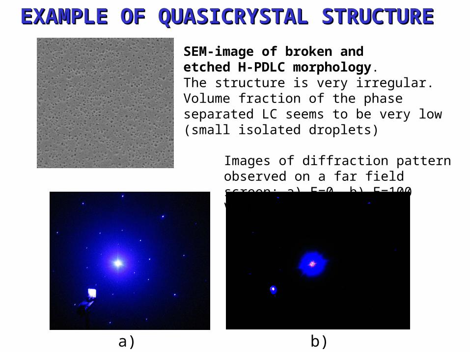
SEM-image of broken and etched H-PDLC morphology.The structure is very irregular.Volume fraction of the phase separated LC seems to be very low (small isolated droplets)
Images of diffraction pattern observed on a far field screen: a) E=0, b) E=100 V/m.
a) b)
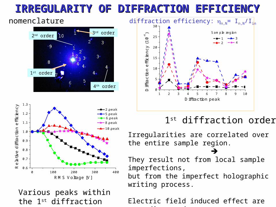
IRREGULARITY OF DIFFRACTION EFFICIENCYIRREGULARITY OF DIFFRACTION EFFICIENCYIRREGULARITY OF DIFFRACTION EFFICIENCYIRREGULARITY OF DIFFRACTION EFFICIENCY
1 2 3 4 5 6 7 8 9 100
5
10
15
20
25
30
1
Diff
ract
ion
effic
ienc
y (1
0-4)
Diffraction peak
2
Sample region
3 4
1st diffraction order
1st order
2nd order3rd order
4th order
nomenclature
Irregularities are correlated over the entire sample region.
They result not from local sample imperfections, but from the imperfect holographic writing process.
Electric field induced effect are very dispersed.
diffraction efficiency:n,N= In,N/Iin
0 100 200 300 4000.6
0.7
0.8
0.9
1.0
1.1
1.2
1.3 2.peak
Rel
ativ
e di
ffrac
tion
effic
ienc
y
RMS Voltage [V]
8.peak 6.peak
10.peak
5.peak
Various peaks within the 1st diffraction order
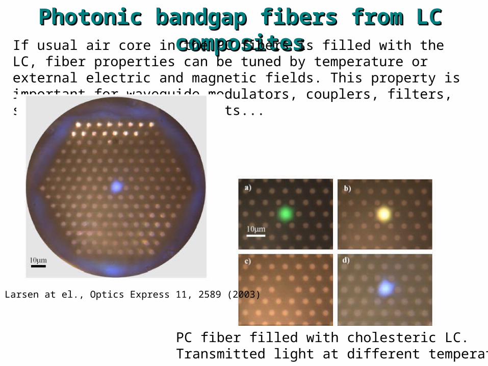
Photonic bandgap fibersPhotonic bandgap fibers from LC from LC compositescompositesPhotonic bandgap fibersPhotonic bandgap fibers from LC from LC compositescompositesIf usual air core in the PC fibers is filled with the LC, fiber properties can be tuned by temperature or external electric and magnetic fields. This property is important for waveguide modulators, couplers, filters, sensors and similar elements...
PC fiber filled with cholesteric LC.Transmitted light at different temperatures.
T. T. Larsen at el., Optics Express 11, 2589 (2003)
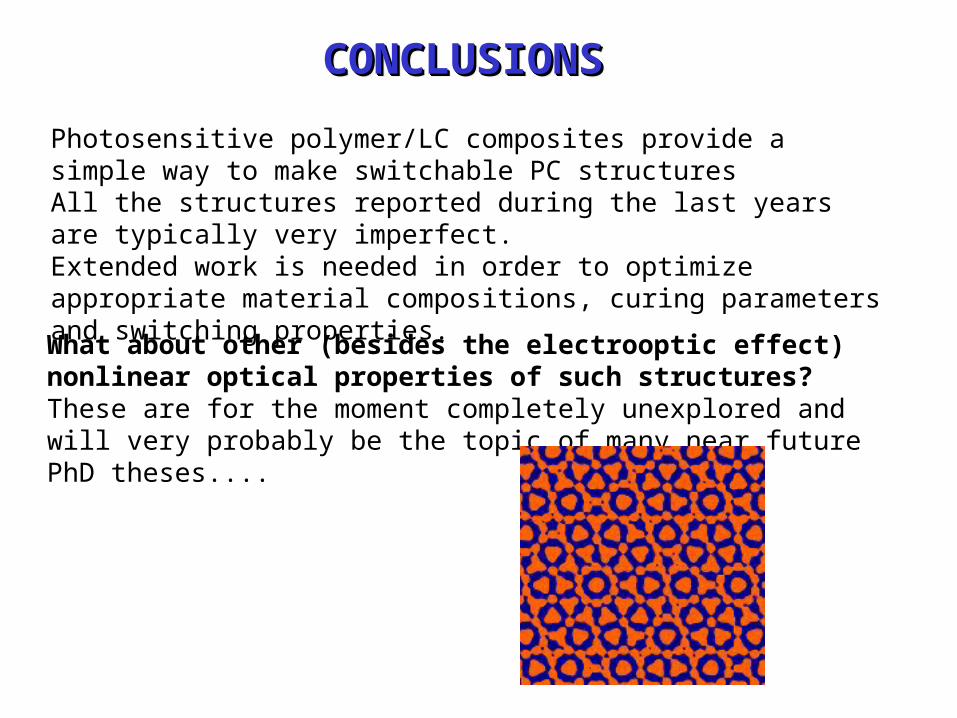
Photosensitive polymer/LC composites provide a simple way to make switchable PC structuresAll the structures reported during the last years are typically very imperfect. Extended work is needed in order to optimize appropriate material compositions, curing parameters and switching properties.
What about other (besides the electrooptic effect) nonlinear optical properties of such structures?These are for the moment completely unexplored and will very probably be the topic of many near future PhD theses....
CONCLUSIONSCONCLUSIONSCONCLUSIONSCONCLUSIONS


![Stability of Soft Quasicrystals in a Coupled-Mode Swift ... · systems[9,10,13], while dodecagonal solid-state quasicrystals are rarely seen [5]. Hence, soft quasicrystals are thought](https://img.pdfslide.net/doc/110x75/5f021a007e708231d40293f3/stability-of-soft-quasicrystals-in-a-coupled-mode-swift-systems91013-while.jpg)