Embed Size (px)
Citation preview
Section 13. Parallel Master Port (PMP)
Parallel Master
Port (PMP)
13
HIGHLIGHTSThis section of the manual contains the following major topics:
13.1 Introduction .................................................................................................................. 13-213.2 Control Registers .........................................................................................................13-313.3 Master Modes of Operation .......................................................................................13-1213.4 Slave Modes of Operation .........................................................................................13-3213.5 Interrupts.................................................................................................................... 13-3913.6 Operation in Power-Saving and Debug Modes.......................................................... 13-4113.7 Effects of Various Resets ...........................................................................................13-4113.8 Parallel Master Port Applications ............................................................................... 13-4213.9 Parallel Slave Port Application................................................................................... 13-4713.10 Direct Memory Access Support ................................................................................. 13-4713.11 I/O Pin Control ...........................................................................................................13-4813.12 Design Tips ................................................................................................................ 13-5013.13 Related Application Notes.......................................................................................... 13-5113.14 Revision History .........................................................................................................13-52
© 2011 Microchip Technology Inc. DS61128F-page 13-1
PIC32 Family Reference Manual
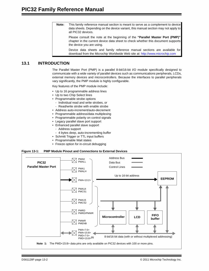
13.1 INTRODUCTIONThe Parallel Master Port (PMP) is a parallel 8-bit/16-bit I/O module specifically designed to communicate with a wide variety of parallel devices such as communications peripherals, LCDs, external memory devices and microcontrollers. Because the interfaces to parallel peripherals vary significantly, the PMP module is highly configurable.
Key features of the PMP module include:
• Up to 16 programmable address lines• Up to two Chip Select lines• Programmable strobe options
- Individual read and write strobes, or - Read/write strobe with enable strobe
• Address auto-increment/auto-decrement• Programmable address/data multiplexing• Programmable polarity on control signals• Legacy parallel slave port support• Enhanced parallel slave support
- Address support- 4 bytes deep, auto-incrementing buffer
• Schmitt Trigger or TTL input buffers• Programmable Wait states• Freeze option for in-circuit debugging
Figure 13-1: PMP Module Pinout and Connections to External Devices
Note: This family reference manual section is meant to serve as a complement to device data sheets. Depending on the device variant, this manual section may not apply to all PIC32 devices.
Please consult the note at the beginning of the “Parallel Master Port (PMP)”chapter in the current device data sheet to check whether this document supports the device you are using.
Device data sheets and family reference manual sections are available for download from the Microchip Worldwide Web site at: http://www.microchip.com
PMA0
PMA14
PMA15
PMRD
PMWRPMENB
PMRD/PMWR
PMCS1
PMA1
PMA<13:2>
PMALL
PMALH
PMCS2
EEPROM
Address BusData BusControl Lines
LCD FIFOMicrocontroller
8-bit/16-bit data (with or without multiplexed addressing)
Up to 16-bit address
buffer
PMD<15:8>(1)
PMA<7:0>PMA<15:8>PMD<7:0>
Parallel Master PortPIC32
Note 1: The PMD<15:8> data pins are only available on PIC32 devices with 100 or more pins.
DS61128F-page 13-2 © 2011 Microchip Technology Inc.
Section 13. Parallel Master Port (PMP)Parallel M
aster Port (PM
P)
13
13.2 CONTROL REGISTERSThe PMP module uses these Special Function Registers (SFRs):
• PMCON: Parallel Port Control RegisterThis register contains the bits that control much of the module’s basic functionality. A key bit is the ON control bit, which is used to Reset, enable or disable the module.
When the module is disabled, all of the associated I/O pins revert to their designated I/O function. In addition, any read or write operations active or pending are stopped, and the BUSY bit is cleared. The data within the module registers is retained, including the data in PMSTAT register. Therefore, the module could be disabled after a reception, and the last received data and status would still be available for processing.
When the module is enabled, all buffer control logic is reset, along with PMSTAT.
All other bits in PMCON control address multiplexing enable various port control signals, and select control signal polarity. These are discussed in detail in 13.3.1 “Parallel Master Port Configuration Options”.
• PMMODE: Parallel Port Mode RegisterThis register contains bits that control the operational modes of the module. Master/Slave mode selection and configuration options for both modes, are set by this register. It also contains the universal status flag, BUSY, which is used in master modes to indicate that an operation by the module is in progress.
Details on the use of the PMMODE bits to configure PMP operation are provided in 13.3 “Master Modes of Operation” and 13.4 “Slave Modes of Operation”.
• PMADDR: Parallel Port Address RegisterThis register functions as PMADDR in master modes. It contains the address to which outgoing data is to be written, as well as the Chip Select control bits for addressing parallel slave devices. The PMADDR register is not used in any of the Slave modes.
• PMDOUT: Parallel Port Data Output RegisterThis register is used only in Slave mode for buffered output data.
• PMDIN: Parallel Port Data Input RegisterThis register is used by the PMP module in both Master and Slave modes.
In Slave mode, this register is used to hold data that is asynchronously clocked in. Its operation is described in 13.4.2 “Buffered Parallel Slave Port Mode”.
In Master mode, PMDIN is the holding register for both incoming and outgoing data. Its operation in Master mode is described in 13.3.3 “Read Operation” and 13.3.4 “Write Operation”.
• PMAEN: Parallel Port Pin Enable RegisterThis register controls the operation of address and Chip Select pins associated with the PMP module. Setting these bits allocates the corresponding microcontroller pins to the PMP module; clearing the bits allocates the pins to port I/O or other peripheral modules associated with the pin.
• PMSTAT: Parallel Port Status Register (Slave modes only)This register contains status bits associated with buffered operating modes when the port is functioning as a slave port. This includes overflow, underflow and full flag bit.
These flags are discussed in detail in 13.4.2 “Buffered Parallel Slave Port Mode”.
© 2011 Microchip Technology Inc. DS61128F-page 13-3
PIC32 Family Reference Manual
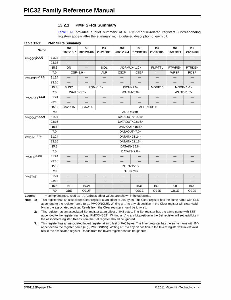
13.2.1 PMP SFRs SummaryTable 13-1 provides a brief summary of all PMP-module-related registers. Corresponding registers appear after the summary with a detailed description of each bit.
Table 13-1: PMP SFRs Summary
Name Bit31/23/15/7
Bit30/22/14/6
Bit29/21/13/5
Bit28/20/12/4
Bit27/19/11/3
Bit26/18/10/2
Bit25/17/9/1
Bit24/16/8/0
PMCON(1,2,3) 31:24 — — — — — — — —23:16 — — — — — — — —15:8 ON — SIDL ADRMUX<1:0> PMPTTL PTWREN PTRDEN7:0 CSF<1:0> ALP CS2P CS1P — WRSP RDSP
PMMODE(1,2,3) 31:24 — — — — — — — —23:16 — — — — — — — —15:8 BUSY IRQM<1:0> INCM<1:0> MODE16 MODE<1:0>7:0 WAITB<1:0> WAITM<3:0> WAITE<1:0>
PMADDR(1,2,3) 31:24 — — — — — — — —23:16 — — — — — — — —15:8 CS2/A15 CS1/A14 ADDR<13:8>7:0 ADDR<7:0>
PMDOUT(1,2,3) 31:24 DATAOUT<31:24>23:16 DATAOUT<23:16>15:8 DATAOUT<15:8>7:0 DATAOUT<7:0>
PMDIN(1,2,3) 31:24 DATAIN<31:24>23:16 DATAIN<23:16>15:8 DATAIN<15:8>7:0 DATAIN<7:0>
PMAEN(1,2,3) 31:24 — — — — — — — —23:16 — — — — — — — —15:8 PTEN<15:8>7:0 PTEN<7:0>
PMSTAT 31:24 — — — — — — — —23:16 — — — — — — — —15:8 IBF IBOV — — IB3F IB2F IB1F IB0F7:0 OBE OBUF — — OB3E OB2E OB1E OB0E
Legend: — = unimplemented, read as ‘0’. Address offset values are shown in hexadecimal.Note 1: This register has an associated Clear register at an offset of 0x4 bytes. The Clear register has the same name with CLR
appended to the register name (e.g., PMCONCLR). Writing a ‘1’ to any bit position in the Clear register will clear valid bits in the associated register. Reads from the Clear register should be ignored.
2: This register has an associated Set register at an offset of 0x8 bytes. The Set register has the same name with SET appended to the register name (e.g., PMCONSET). Writing a ‘1’ to any bit position in the Set register will set valid bits in the associated register. Reads from the Set register should be ignored.
3: This register has an associated Invert register at an offset of 0xC bytes. The Invert register has the same name with INV appended to the register name (e.g., PMCONINV). Writing a ‘1’ to any bit position in the Invert register will invert valid bits in the associated register. Reads from the Invert register should be ignored.
DS61128F-page 13-4 © 2011 Microchip Technology Inc.
Section 13. Parallel Master Port (PMP)Parallel M
aster Port (PM
P)
13
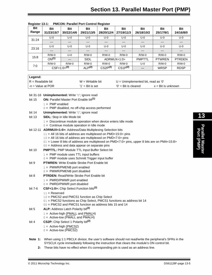
Register 13-1: PMCON: Parallel Port Control Register Bit
RangeBit
31/23/15/7Bit
30/22/14/6Bit
29/21/13/5Bit
28/20/12/4Bit
27/19/11/3Bit
26/18/10/2Bit
25/17/9/1Bit
24/16/8/0
31:24U-0 U-0 U-0 U-0 U-0 U-0 U-0 U-0— — — — — — — —
23:16U-0 U-0 U-0 U-0 U-0 U-0 U-0 U-0— — — — — — — —
15:8R/W-0 U-0 R/W-0 R/W-0 R/W-0 R/W-0 R/W-0 R/W-0ON(1) — SIDL ADRMUX<1:0> PMPTTL PTWREN PTRDEN
7:0R/W-0 R/W-0 R/W-0 R/W-0 R/W-0 U-0 R/W-0 R/W-0
CSF<1:0>(2) ALP(2) CS2P(2) CS1P(2) — WRSP RDSP
Legend:R = Readable bit W = Writable bit U = Unimplemented bit, read as ‘0’-n = Value at POR ‘1’ = Bit is set ‘0’ = Bit is cleared x = Bit is unknown
bit 31-16 Unimplemented: Write ‘0’; ignore readbit 15 ON: Parallel Master Port Enable bit(1)
1 = PMP enabled0 = PMP disabled, no off-chip access performed
bit 14 Unimplemented: Write ‘0’; ignore readbit 13 SIDL: Stop in Idle Mode bit
1 = Discontinue module operation when device enters Idle mode0 = Continue module operation in Idle mode
bit 12-11 ADRMUX<1:0>: Address/Data Multiplexing Selection bits11 = All 16 bits of address are multiplexed on PMD<15:0> pins10 = All 16 bits of address are multiplexed on PMD<7:0> pins01 = Lower 8 bits of address are multiplexed on PMD<7:0> pins, upper 8 bits are on PMA<15:8>00 = Address and data appear on separate pins
bit 10 PMPTTL: PMP Module TTL Input Buffer Select bit1 = PMP module uses TTL input buffers0 = PMP module uses Schmitt Trigger input buffer
bit 9 PTWREN: Write Enable Strobe Port Enable bit1 = PMWR/PMENB port enabled0 = PMWR/PMENB port disabled
bit 8 PTRDEN: Read/Write Strobe Port Enable bit1 = PMRD/PMWR port enabled0 = PMRD/PMWR port disabled
bit 7-6 CSF<1:0>: Chip Select Function bits(2)
11 = Reserved10 = PMCS2 and PMCS1 function as Chip Select01 = PMCS2 functions as Chip Select, PMCS1 functions as address bit 1400 = PMCS2 and PMCS1 function as address bits 15 and 14
bit 5 ALP: Address Latch Polarity bit(2)
1 = Active-high (PMALL and PMALH)0 = Active-low (PMALL and PMALH)
bit 4 CS2P: Chip Select 1 Polarity bit(2)
1 = Active-high (PMCS2)0 = Active-low (PMCS2)
Note 1: When using 1:1 PBCLK divisor, the user’s software should not read/write the peripheral’s SFRs in the SYSCLK cycle immediately following the instruction that clears the module’s ON control bit.
2: These bits have no effect when it’s corresponding pin is used as an address line.
© 2011 Microchip Technology Inc. DS61128F-page 13-5
PIC32 Family Reference Manual
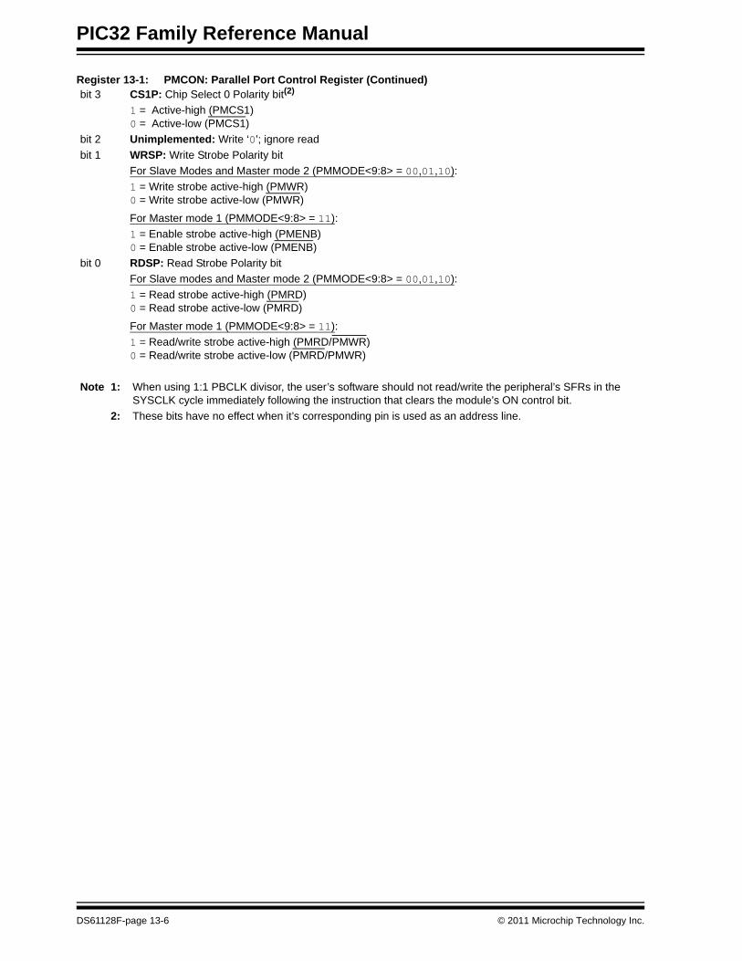
bit 3 CS1P: Chip Select 0 Polarity bit(2)
1 = Active-high (PMCS1)0 = Active-low (PMCS1)
bit 2 Unimplemented: Write ‘0’; ignore readbit 1 WRSP: Write Strobe Polarity bit
For Slave Modes and Master mode 2 (PMMODE<9:8> = 00,01,10):1 = Write strobe active-high (PMWR)0 = Write strobe active-low (PMWR)
For Master mode 1 (PMMODE<9:8> = 11):1 = Enable strobe active-high (PMENB)0 = Enable strobe active-low (PMENB)
bit 0 RDSP: Read Strobe Polarity bitFor Slave modes and Master mode 2 (PMMODE<9:8> = 00,01,10):1 = Read strobe active-high (PMRD)0 = Read strobe active-low (PMRD)
For Master mode 1 (PMMODE<9:8> = 11):1 = Read/write strobe active-high (PMRD/PMWR)0 = Read/write strobe active-low (PMRD/PMWR)
Register 13-1: PMCON: Parallel Port Control Register (Continued)
Note 1: When using 1:1 PBCLK divisor, the user’s software should not read/write the peripheral’s SFRs in the SYSCLK cycle immediately following the instruction that clears the module’s ON control bit.
2: These bits have no effect when it’s corresponding pin is used as an address line.
DS61128F-page 13-6 © 2011 Microchip Technology Inc.
Section 13. Parallel Master Port (PMP)Parallel M
aster Port (PM
P)
13
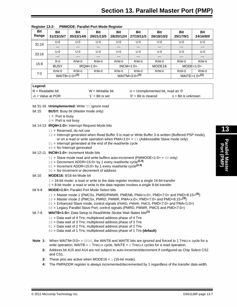
Register 13-2: PMMODE: Parallel Port Mode Register Bit
RangeBit
31/23/15/7Bit
30/22/14/6Bit
29/21/13/5Bit
28/20/12/4Bit
27/19/11/3Bit
26/18/10/2Bit
25/17/9/1Bit
24/16/8/0
31:24U-0 U-0 U-0 U-0 U-0 U-0 U-0 U-0— — — — — — — —
23:16U-0 U-0 U-0 U-0 U-0 U-0 U-0 U-0— — — — — — — —
15:8R-0 R/W-0 R/W-0 R/W-0 R/W-0 R/W-0 R/W-0 R/W-0
BUSY IRQM<1:0> INCM<1:0> MODE16 MODE<1:0>
7:0R/W-0 R/W-0 R/W-0 R/W-0 R/W-0 R/W-0 R/W-0 R/W-0
WAITB<1:0>(1) WAITM<3:0>(1) WAITE<1:0>(1)
Legend:R = Readable bit W = Writable bit U = Unimplemented bit, read as ‘0’-n = Value at POR ‘1’ = Bit is set ‘0’ = Bit is cleared x = Bit is unknown
bit 31-16 Unimplemented: Write ‘0’; ignore readbit 15 BUSY: Busy bit (Master mode only)
1 = Port is busy 0 = Port is not busy
bit 14-13 IRQM<1:0>: Interrupt Request Mode bits 11 = Reserved, do not use10 = Interrupt generated when Read Buffer 3 is read or Write Buffer 3 is written (Buffered PSP mode),
or on a read or write operation when PMA<1:0> = 11 (Addressable Slave mode only)01 = Interrupt generated at the end of the read/write cycle00 = No Interrupt generated
bit 12-11 INCM<1:0>: Increment Mode bits 11 = Slave mode read and write buffers auto-increment (PMMODE<1:0> = 00 only)10 = Decrement ADDR<15:0> by 1 every read/write cycle(2,4)
01 = Increment ADDR<15:0> by 1 every read/write cycle(2,4)
00 = No increment or decrement of addressbit 10 MODE16: 8/16-bit Mode bit
1 = 16-bit mode: a read or write to the data register invokes a single 16-bit transfer0 = 8-bit mode: a read or write to the data register invokes a single 8-bit transfer
bit 9-8 MODE<1:0>: Parallel Port Mode Select bits11 = Master mode 1 (PMCSx, PMRD/PMWR, PMENB, PMA<x:0>, PMD<7:0> and PMD<8:15>(3))10 = Master mode 2 (PMCSx, PMRD, PMWR, PMA<x:0>, PMD<7:0> and PMD<8:15>(3))01 = Enhanced Slave mode, control signals (PMRD, PMWR, PMCS, PMD<7:0> and PMA<1:0>)00 = Legacy Parallel Slave Port, control signals (PMRD, PMWR, PMCS and PMD<7:0>)
bit 7-6 WAITB<1:0>: Data Setup to Read/Write Strobe Wait States bits(1)
11 = Data wait of 4 TPB; multiplexed address phase of 4 TPB10 = Data wait of 3 TPB; multiplexed address phase of 3 TPB01 = Data wait of 2 TPB; multiplexed address phase of 2 TPB00 = Data wait of 1 TPB; multiplexed address phase of 1 TPB (default)
Note 1: When WAITM<3:0> = 0000, the WAITB and WAITE bits are ignored and forced to 1 TPBCLK cycle for a write operation; WAITB = 1 TPBCLK cycle, WAITE = 0 TPBCLK cycles for a read operation.
2: Address bit A15 and A14 are not subject to auto-increment/decrement if configured as Chip Select CS2 and CS1.
3: These pins are active when MODE16 = 1 (16-bit mode).4: The PMPADDR register is always incremented/decremented by 1 regardless of the transfer data width.
© 2011 Microchip Technology Inc. DS61128F-page 13-7
PIC32 Family Reference Manual
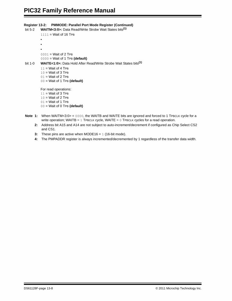
bit 5-2 WAITM<3:0>: Data Read/Write Strobe Wait States bits(1)
1111 = Wait of 16 TPB
•••0001 = Wait of 2 TPB0000 = Wait of 1 TPB (default)
bit 1-0 WAITE<1:0>: Data Hold After Read/Write Strobe Wait States bits(1)
11 = Wait of 4 TPB10 = Wait of 3 TPB01 = Wait of 2 TPB00 = Wait of 1 TPB (default)
For read operations:11 = Wait of 3 TPB10 = Wait of 2 TPB01 = Wait of 1 TPB00 = Wait of 0 TPB (default)
Register 13-2: PMMODE: Parallel Port Mode Register (Continued)
Note 1: When WAITM<3:0> = 0000, the WAITB and WAITE bits are ignored and forced to 1 TPBCLK cycle for a write operation; WAITB = 1 TPBCLK cycle, WAITE = 0 TPBCLK cycles for a read operation.
2: Address bit A15 and A14 are not subject to auto-increment/decrement if configured as Chip Select CS2 and CS1.
3: These pins are active when MODE16 = 1 (16-bit mode).4: The PMPADDR register is always incremented/decremented by 1 regardless of the transfer data width.
DS61128F-page 13-8 © 2011 Microchip Technology Inc.
Section 13. Parallel Master Port (PMP)Parallel M
aster Port (PM
P)
13
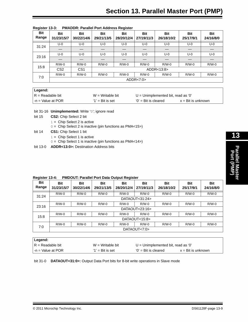
Register 13-3: PMADDR: Parallel Port Address Register Bit
RangeBit
31/23/15/7Bit
30/22/14/6Bit
29/21/13/5Bit
28/20/12/4Bit
27/19/11/3Bit
26/18/10/2Bit
25/17/9/1Bit
24/16/8/0
31:24U-0 U-0 U-0 U-0 U-0 U-0 U-0 U-0— — — — — — — —
23:16U-0 U-0 U-0 U-0 U-0 U-0 U-0 U-0— — — — — — — —
15:8R/W-0 R/W-0 R/W-0 R/W-0 R/W-0 R/W-0 R/W-0 R/W-0CS2 CS1 ADDR<13:8>
7:0R/W-0 R/W-0 R/W-0 R/W-0 R/W-0 R/W-0 R/W-0 R/W-0
ADDR<7:0>
Legend:R = Readable bit W = Writable bit U = Unimplemented bit, read as ‘0’-n = Value at POR ‘1’ = Bit is set ‘0’ = Bit is cleared x = Bit is unknown
bit 31-16 Unimplemented: Write ‘0’; ignore readbit 15 CS2: Chip Select 2 bit
1 = Chip Select 2 is active0 = Chip Select 2 is inactive (pin functions as PMA<15>)
bit 14 CS1: Chip Select 1 bit 1 = Chip Select 1 is active0 = Chip Select 1 is inactive (pin functions as PMA<14>)
bit 13-0 ADDR<13:0>: Destination Address bits
Register 13-4: PMDOUT: Parallel Port Data Output Register Bit
RangeBit
31/23/15/7Bit
30/22/14/6Bit
29/21/13/5Bit
28/20/12/4Bit
27/19/11/3Bit
26/18/10/2Bit
25/17/9/1Bit
24/16/8/0
31:24R/W-0 R/W-0 R/W-0 R/W-0 R/W-0 R/W-0 R/W-0 R/W-0
DATAOUT<31:24>
23:16R/W-0 R/W-0 R/W-0 R/W-0 R/W-0 R/W-0 R/W-0 R/W-0
DATAOUT<23:16>
15:8R/W-0 R/W-0 R/W-0 R/W-0 R/W-0 R/W-0 R/W-0 R/W-0
DATAOUT<15:8>
7:0R/W-0 R/W-0 R/W-0 R/W-0 R/W-0 R/W-0 R/W-0 R/W-0
DATAOUT<7:0>
Legend:R = Readable bit W = Writable bit U = Unimplemented bit, read as ‘0’-n = Value at POR ‘1’ = Bit is set ‘0’ = Bit is cleared x = Bit is unknown
bit 31-0 DATAOUT<31:0>: Output Data Port bits for 8-bit write operations in Slave mode
© 2011 Microchip Technology Inc. DS61128F-page 13-9
PIC32 Family Reference Manual
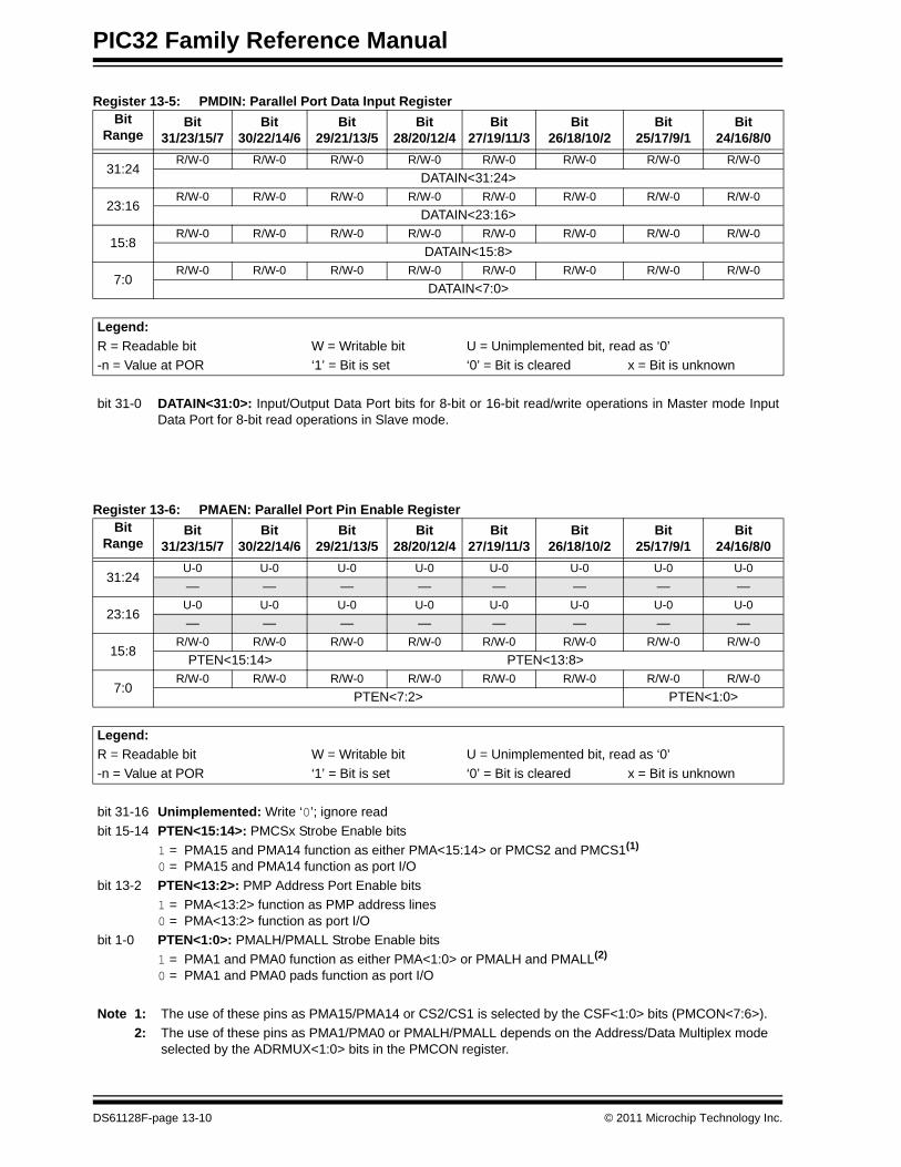
Register 13-5: PMDIN: Parallel Port Data Input Register Bit
RangeBit
31/23/15/7Bit
30/22/14/6Bit
29/21/13/5Bit
28/20/12/4Bit
27/19/11/3Bit
26/18/10/2Bit
25/17/9/1Bit
24/16/8/0
31:24R/W-0 R/W-0 R/W-0 R/W-0 R/W-0 R/W-0 R/W-0 R/W-0
DATAIN<31:24>
23:16R/W-0 R/W-0 R/W-0 R/W-0 R/W-0 R/W-0 R/W-0 R/W-0
DATAIN<23:16>
15:8R/W-0 R/W-0 R/W-0 R/W-0 R/W-0 R/W-0 R/W-0 R/W-0
DATAIN<15:8>
7:0R/W-0 R/W-0 R/W-0 R/W-0 R/W-0 R/W-0 R/W-0 R/W-0
DATAIN<7:0>
Legend:R = Readable bit W = Writable bit U = Unimplemented bit, read as ‘0’-n = Value at POR ‘1’ = Bit is set ‘0’ = Bit is cleared x = Bit is unknown
bit 31-0 DATAIN<31:0>: Input/Output Data Port bits for 8-bit or 16-bit read/write operations in Master mode Input Data Port for 8-bit read operations in Slave mode.
Register 13-6: PMAEN: Parallel Port Pin Enable Register Bit
RangeBit
31/23/15/7Bit
30/22/14/6Bit
29/21/13/5Bit
28/20/12/4Bit
27/19/11/3Bit
26/18/10/2Bit
25/17/9/1Bit
24/16/8/0
31:24U-0 U-0 U-0 U-0 U-0 U-0 U-0 U-0— — — — — — — —
23:16U-0 U-0 U-0 U-0 U-0 U-0 U-0 U-0— — — — — — — —
15:8R/W-0 R/W-0 R/W-0 R/W-0 R/W-0 R/W-0 R/W-0 R/W-0
PTEN<15:14> PTEN<13:8>
7:0R/W-0 R/W-0 R/W-0 R/W-0 R/W-0 R/W-0 R/W-0 R/W-0
PTEN<7:2> PTEN<1:0>
Legend:R = Readable bit W = Writable bit U = Unimplemented bit, read as ‘0’-n = Value at POR ‘1’ = Bit is set ‘0’ = Bit is cleared x = Bit is unknown
bit 31-16 Unimplemented: Write ‘0’; ignore readbit 15-14 PTEN<15:14>: PMCSx Strobe Enable bits
1 = PMA15 and PMA14 function as either PMA<15:14> or PMCS2 and PMCS1(1)
0 = PMA15 and PMA14 function as port I/Obit 13-2 PTEN<13:2>: PMP Address Port Enable bits
1 = PMA<13:2> function as PMP address lines0 = PMA<13:2> function as port I/O
bit 1-0 PTEN<1:0>: PMALH/PMALL Strobe Enable bits1 = PMA1 and PMA0 function as either PMA<1:0> or PMALH and PMALL(2)
0 = PMA1 and PMA0 pads function as port I/O
Note 1: The use of these pins as PMA15/PMA14 or CS2/CS1 is selected by the CSF<1:0> bits (PMCON<7:6>).2: The use of these pins as PMA1/PMA0 or PMALH/PMALL depends on the Address/Data Multiplex mode
selected by the ADRMUX<1:0> bits in the PMCON register.
DS61128F-page 13-10 © 2011 Microchip Technology Inc.
Section 13. Parallel Master Port (PMP)Parallel M
aster Port (PM
P)
13
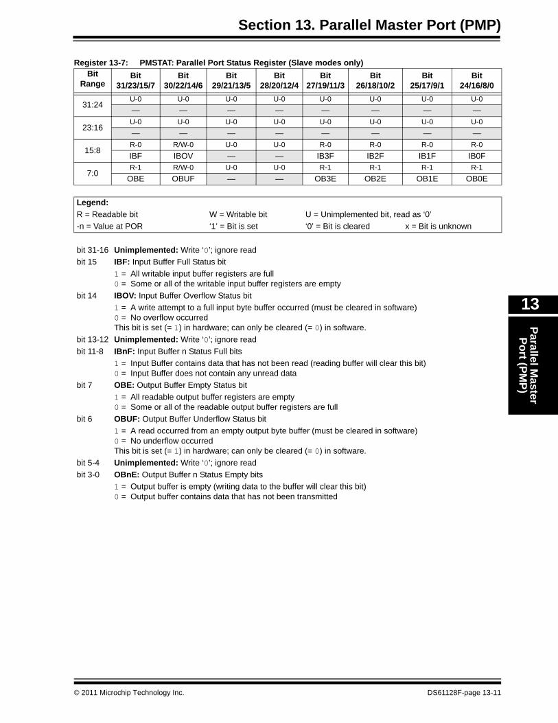
Register 13-7: PMSTAT: Parallel Port Status Register (Slave modes only) Bit
RangeBit
31/23/15/7Bit
30/22/14/6Bit
29/21/13/5Bit
28/20/12/4Bit
27/19/11/3Bit
26/18/10/2Bit
25/17/9/1Bit
24/16/8/0
31:24U-0 U-0 U-0 U-0 U-0 U-0 U-0 U-0— — — — — — — —
23:16U-0 U-0 U-0 U-0 U-0 U-0 U-0 U-0— — — — — — — —
15:8R-0 R/W-0 U-0 U-0 R-0 R-0 R-0 R-0IBF IBOV — — IB3F IB2F IB1F IB0F
7:0R-1 R/W-0 U-0 U-0 R-1 R-1 R-1 R-1
OBE OBUF — — OB3E OB2E OB1E OB0E
Legend:R = Readable bit W = Writable bit U = Unimplemented bit, read as ‘0’-n = Value at POR ‘1’ = Bit is set ‘0’ = Bit is cleared x = Bit is unknown
bit 31-16 Unimplemented: Write ‘0’; ignore readbit 15 IBF: Input Buffer Full Status bit
1 = All writable input buffer registers are full0 = Some or all of the writable input buffer registers are empty
bit 14 IBOV: Input Buffer Overflow Status bit 1 = A write attempt to a full input byte buffer occurred (must be cleared in software)0 = No overflow occurredThis bit is set (= 1) in hardware; can only be cleared (= 0) in software.
bit 13-12 Unimplemented: Write ‘0’; ignore readbit 11-8 IBnF: Input Buffer n Status Full bits
1 = Input Buffer contains data that has not been read (reading buffer will clear this bit)0 = Input Buffer does not contain any unread data
bit 7 OBE: Output Buffer Empty Status bit 1 = All readable output buffer registers are empty0 = Some or all of the readable output buffer registers are full
bit 6 OBUF: Output Buffer Underflow Status bit 1 = A read occurred from an empty output byte buffer (must be cleared in software)0 = No underflow occurredThis bit is set (= 1) in hardware; can only be cleared (= 0) in software.
bit 5-4 Unimplemented: Write ‘0’; ignore readbit 3-0 OBnE: Output Buffer n Status Empty bits
1 = Output buffer is empty (writing data to the buffer will clear this bit)0 = Output buffer contains data that has not been transmitted
© 2011 Microchip Technology Inc. DS61128F-page 13-11
PIC32 Family Reference Manual
13.3 MASTER MODES OF OPERATIONIn its master modes, the PMP module can provide a 8-bit or 16-bit data bus, up to 16 bits of address, and all the necessary control signals to operate a variety of external parallel devices such as memory devices, peripherals and slave microcontrollers. The PMP master modes provide a simple interface for reading and writing data, but not executing program instructions from external devices, such as SRAM or Flash memories.
Because there are a number of parallel devices with a variety of control methods, the PMP module is designed for flexibility to accommodate a range of configurations. Some of these features include:
• 8-bit and 16-bit data modes• Configurable address/data multiplexing• Up to two Chip Select lines• Up to 16 selectable address lines• Address auto-increment and auto-decrement• Selectable polarity on all control lines• Configurable Wait states at different stages of the read/write cycle
13.3.1 Parallel Master Port Configuration Options
13.3.1.1 8-BIT AND 16-BIT DATA MODES
The PMP in Master mode supports data with widths of 8 and 16 bits. By default, the data width is 8 bits wide, MODE16 bit (PMMODE<10>) = 0. To select a data width of 16 bits, set MODE16 = 1. When configured in 8-bit Data mode, the upper 8 bits of the data bus, PMD<15:8>, are not controlled by the PMP module and are available as general purpose I/O pins.
13.3.1.2 CHIP SELECT
Two Chip Select lines, PMCS1 and PMCS2, are available for master modes. These lines are multiplexed with the Most Significant bits (MSbs) of the address bus A14 and A15. When a pin is configured as a Chip Select, it is not included in any address auto-increment/decrement. It is possible to enable both PMCS2 and PMCS1 as Chip Selects, or enable only PMCS2 as a Chip Select, allowing PMCS1 to function strictly as address line A14. It is not possible to enable PMCS1 alone. The Chip Select signals are configured using the Chip Select Function bits CSF<1:0> (PMCON<7:6>).
13.3.1.3 PORT PIN CONTROL
There are several bits available to configure the presence or absence of control and address signals in the module. These bits are PTWREN (PMCON<9>), PTRDEN (PMCON<8>) and PTEN<15:0> (PMAEN<15:0>). They provide the ability to conserve pins for other functions and allow flexibility to control the external address. When any one of these bits is set, the associated function is present on its associated pin; when clear, the associated pin reverts to its defined I/O port function.
Setting a PTEN bit will enable the associated pin as an address pin and drive the corresponding data contained in the PMADDR register. Clearing any PTEN bit will force the pin to revert to its original I/O function.
Note: The PMD<15:0> data pins are available on PIC32 devices with 100 or more pins. For 64-pin device variants, only pins PMD<7:0> are available. For details, refer to the specific PIC32 device data sheet.
Table 13-2: Chip Select ControlCSF<1:0> Function
10 PMCS2, PMCS1 = Enabled01 PMCS2 = Enabled, PMCS1 = A1400 PMCS2 = A15, PMCS1 = A14
DS61128F-page 13-12 © 2011 Microchip Technology Inc.
Section 13. Parallel Master Port (PMP)Parallel M
aster Port (PM
P)
13
For the pins configured as Chip Select (PMCS1 or PMCS2) with the corresponding PTEN bit set, Chip Select pins drive inactive data when a read or write operation is not being performed. The PTEN0 and PTEN1 bits also control the PMALL and PMALH signals. When multiplexing is used, the associated address latch signals should be enabled. For I/O pin configuration, see 13.11 “I/O Pin Control”.
13.3.1.4 READ/WRITE CONTROL
The PMP module supports two distinct read/write signaling methods. In Master mode 1, read and write strobe are combined into a single control line, PMRD/PMWR; a second control line, PMENB, determines when a read or write action is to be taken. In Master mode 2, read and write strobes (PMRD and PMWR) are supplied on separate pins.
13.3.1.5 CONTROL LINE POLARITY
All control signals (PMRD, PMWR, PMENB, PMALL, PMALH, PMCS1 and PMCS2) can be individually configured for either positive or negative polarity. Configuration is controlled by separate bits in the PMCON register, as shown in Table 13-3.
13.3.1.6 AUTO-INCREMENT/DECREMENT
While the PMP module is operating in one of the master modes, the INCM<1:0> bits (PMMODE<12:11>) control the behavior of the address value. The address in the PMADDR register can be made to automatically increment or decrement by 1, regardless of the transfer data width, after each read and write operation is completed, and the BUSY bit (PMMODE<15>) goes to ‘0’..
If the Chip Select signals are disabled and configured as address bits, the bits will participate in the increment and decrement operations; otherwise, CS2 and CS1 bit values will be unaffected.
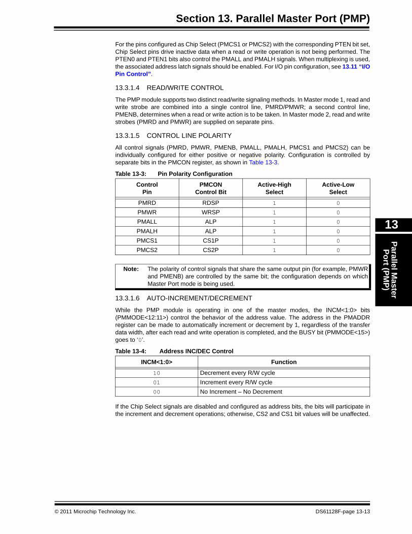
Table 13-3: Pin Polarity Configuration
ControlPin
PMCONControl Bit
Active-HighSelect
Active-LowSelect
PMRD RDSP 1 0
PMWR WRSP 1 0
PMALL ALP 1 0
PMALH ALP 1 0
PMCS1 CS1P 1 0
PMCS2 CS2P 1 0
Note: The polarity of control signals that share the same output pin (for example, PMWR and PMENB) are controlled by the same bit; the configuration depends on which Master Port mode is being used.
Table 13-4: Address INC/DEC Control
INCM<1:0> Function
10 Decrement every R/W cycle01 Increment every R/W cycle00 No Increment – No Decrement
© 2011 Microchip Technology Inc. DS61128F-page 13-13
PIC32 Family Reference Manual
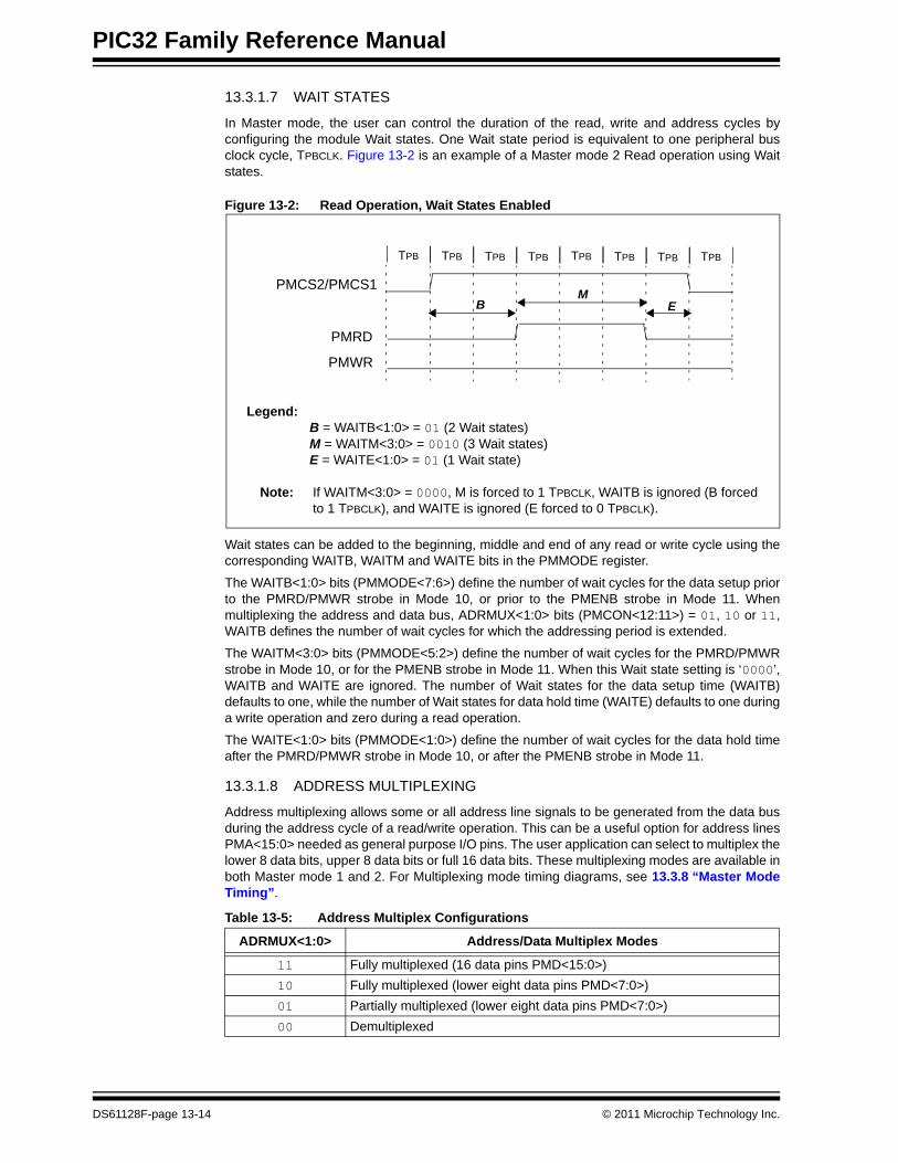
13.3.1.7 WAIT STATES
In Master mode, the user can control the duration of the read, write and address cycles by configuring the module Wait states. One Wait state period is equivalent to one peripheral bus clock cycle, TPBCLK. Figure 13-2 is an example of a Master mode 2 Read operation using Wait states.
Figure 13-2: Read Operation, Wait States Enabled
Wait states can be added to the beginning, middle and end of any read or write cycle using the corresponding WAITB, WAITM and WAITE bits in the PMMODE register.
The WAITB<1:0> bits (PMMODE<7:6>) define the number of wait cycles for the data setup prior to the PMRD/PMWR strobe in Mode 10, or prior to the PMENB strobe in Mode 11. When multiplexing the address and data bus, ADRMUX<1:0> bits (PMCON<12:11>) = 01, 10 or 11, WAITB defines the number of wait cycles for which the addressing period is extended.
The WAITM<3:0> bits (PMMODE<5:2>) define the number of wait cycles for the PMRD/PMWRstrobe in Mode 10, or for the PMENB strobe in Mode 11. When this Wait state setting is ‘0000’, WAITB and WAITE are ignored. The number of Wait states for the data setup time (WAITB) defaults to one, while the number of Wait states for data hold time (WAITE) defaults to one during a write operation and zero during a read operation.
The WAITE<1:0> bits (PMMODE<1:0>) define the number of wait cycles for the data hold time after the PMRD/PMWR strobe in Mode 10, or after the PMENB strobe in Mode 11.
13.3.1.8 ADDRESS MULTIPLEXING
Address multiplexing allows some or all address line signals to be generated from the data bus during the address cycle of a read/write operation. This can be a useful option for address lines PMA<15:0> needed as general purpose I/O pins. The user application can select to multiplex the lower 8 data bits, upper 8 data bits or full 16 data bits. These multiplexing modes are available in both Master mode 1 and 2. For Multiplexing mode timing diagrams, see 13.3.8 “Master Mode Timing”.
Table 13-5: Address Multiplex Configurations
ADRMUX<1:0> Address/Data Multiplex Modes
11 Fully multiplexed (16 data pins PMD<15:0>) 10 Fully multiplexed (lower eight data pins PMD<7:0>) 01 Partially multiplexed (lower eight data pins PMD<7:0>)00 Demultiplexed
PMCS2/PMCS1
TPB TPB TPB TPB TPB TPB TPBTPB
Legend: B = WAITB<1:0> = 01 (2 Wait states) M = WAITM<3:0> = 0010 (3 Wait states) E = WAITE<1:0> = 01 (1 Wait state)
Note: If WAITM<3:0> = 0000, M is forced to 1 TPBCLK, WAITB is ignored (B forced to 1 TPBCLK), and WAITE is ignored (E forced to 0 TPBCLK).
BM
E
PMWR
PMRD
DS61128F-page 13-14 © 2011 Microchip Technology Inc.
Section 13. Parallel Master Port (PMP)Parallel M
aster Port (PM
P)
13
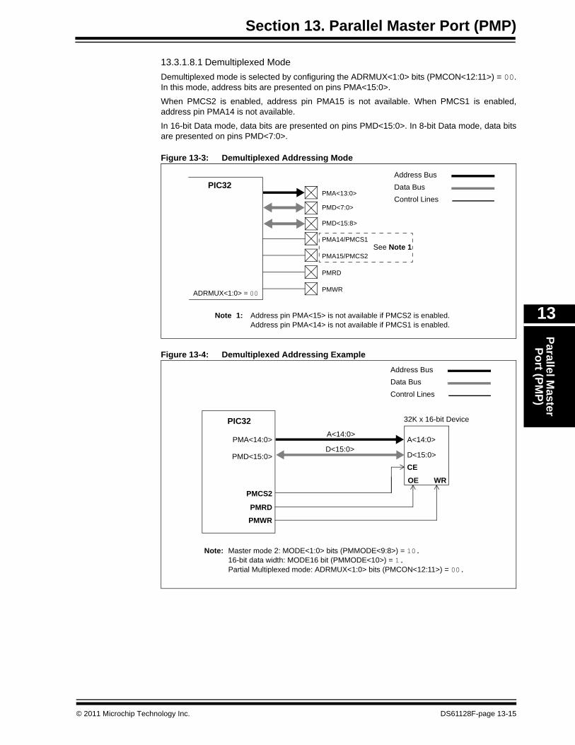
13.3.1.8.1 Demultiplexed ModeDemultiplexed mode is selected by configuring the ADRMUX<1:0> bits (PMCON<12:11>) = 00. In this mode, address bits are presented on pins PMA<15:0>.
When PMCS2 is enabled, address pin PMA15 is not available. When PMCS1 is enabled, address pin PMA14 is not available.
In 16-bit Data mode, data bits are presented on pins PMD<15:0>. In 8-bit Data mode, data bits are presented on pins PMD<7:0>.
Figure 13-3: Demultiplexed Addressing Mode
Figure 13-4: Demultiplexed Addressing Example
Address BusData BusControl Lines
PMRD
PMWR
PMD<7:0>
PMA14/PMCS1
PMA<13:0>
PMA15/PMCS2
PIC32
PMD<15:8>
ADRMUX<1:0> = 00
Note 1: Address pin PMA<15> is not available if PMCS2 is enabled. Address pin PMA<14> is not available if PMCS1 is enabled.
See Note 1
PMA<14:0>D<15:0>
A<14:0>
D<15:0>
A<14:0>
PMRD
PMWR
OE WR
CE
PIC32
PMCS2
PMD<15:0>
32K x 16-bit Device
Address BusData BusControl Lines
Note: Master mode 2: MODE<1:0> bits (PMMODE<9:8>) = 10. 16-bit data width: MODE16 bit (PMMODE<10>) = 1. Partial Multiplexed mode: ADRMUX<1:0> bits (PMCON<12:11>) = 00.
© 2011 Microchip Technology Inc. DS61128F-page 13-15
PIC32 Family Reference Manual
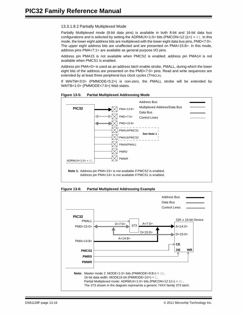
13.3.1.8.2 Partially Multiplexed ModePartially Multiplexed mode (8-bit data pins) is available in both 8-bit and 16-bit data bus configurations and is selected by setting the ADRMUX<1:0> bits (PMCON<12:11>) = 01. In this mode, the lower eight address bits are multiplexed with the lower eight data bus pins, PMD<7:0>. The upper eight address bits are unaffected and are presented on PMA<15:8>. In this mode, address pins PMA<7:1> are available as general purpose I/O pins.
Address pin PMA15 is not available when PMCS2 is enabled; address pin PMA14 is not available when PMCS1 is enabled.
Address pin PMA<0> is used as an address latch enable strobe, PMALL, during which the lower eight bits of the address are presented on the PMD<7:0> pins. Read and write sequences are extended by at least three peripheral bus clock cycles (TPBCLK).
If WAITM<3:0> (PMMODE<5:2>) is non-zero, the PMALL strobe will be extended by WAITB<1:0> (PMMODE<7:6>) Wait states.
Figure 13-5: Partial Multiplexed Addressing Mode
Figure 13-6: Partial Multiplexed Addressing Example
PMRD
PMWR
PMD<7:0>
PMA14/PMCS1
PMA<13:8>
PMA0/PMALL
PMA15/PMCS2
PIC32
Address BusMultiplexed Address/Data BusData BusControl Lines
PMD<15:8>
ADRMUX<1:0> = 01
Note 1: Address pin PMA<15> is not available if PMCS2 is enabled. Address pin PMA<14> is not available if PMCS1 is enabled.
See Note 1
PMA<14:8>
D<7:0> 373 A<14:0>
D<15:0>
A<7:0>
PMRD
PMWR
OE WR
CE
PIC32
PMCS2
PMALL
A<14:8>
PMD<15:0>
32K x 16-bit Device
D<15:0>
Note: Master mode 2: MODE<1:0> bits (PMMODE<9:8>) = 10. 16-bit data width: MODE16 bit (PMMODE<10>) = 1. Partial Multiplexed mode: ADRMUX<1:0> bits (PMCON<12:11>) = 01. The 373 shown in the diagram represents a generic 74XX family 373 latch.
Address BusData BusControl Lines
DS61128F-page 13-16 © 2011 Microchip Technology Inc.
Section 13. Parallel Master Port (PMP)Parallel M
aster Port (PM
P)
13
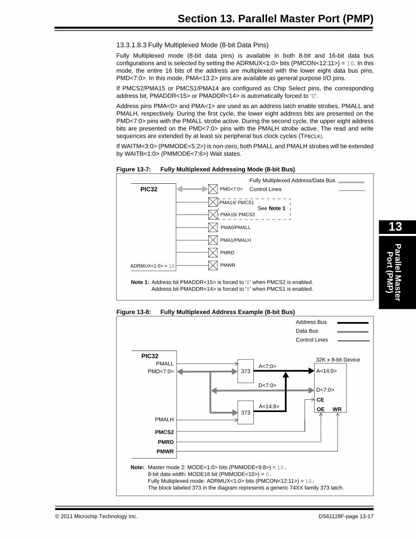
13.3.1.8.3 Fully Multiplexed Mode (8-bit Data Pins)Fully Multiplexed mode (8-bit data pins) is available in both 8-bit and 16-bit data bus configurations and is selected by setting the ADRMUX<1:0> bits (PMCON<12:11>) = 10. In this mode, the entire 16 bits of the address are multiplexed with the lower eight data bus pins, PMD<7:0>. In this mode, PMA<13:2> pins are available as general purpose I/O pins.
If PMCS2/PMA15 or PMCS1/PMA14 are configured as Chip Select pins, the corresponding address bit, PMADDR<15> or PMADDR<14> is automatically forced to ‘0’.
Address pins PMA<0> and PMA<1> are used as an address latch enable strobes, PMALL and PMALH, respectively. During the first cycle, the lower eight address bits are presented on the PMD<7:0> pins with the PMALL strobe active. During the second cycle, the upper eight address bits are presented on the PMD<7:0> pins with the PMALH strobe active. The read and write sequences are extended by at least six peripheral bus clock cycles (TPBCLK).
If WAITM<3:0> (PMMODE<5:2>) is non-zero, both PMALL and PMALH strobes will be extended by WAITB<1:0> (PMMODE<7:6>) Wait states.
Figure 13-7: Fully Multiplexed Addressing Mode (8-bit Bus)
Figure 13-8: Fully Multiplexed Address Example (8-bit Bus)
Fully Multiplexed Address/Data BusControl Lines
PMRD
PMWR
PMD<7:0>
PMA14/ PMCS1
PMA1/PMALH
PMA15/ PMCS2
PIC32
PMA0/PMALL
ADRMUX<1:0> = 10
Note 1: Address bit PMADDR<15> is forced to ‘0’ when PMCS2 is enabled. Address bit PMADDR<14> is forced to ‘0’ when PMCS1 is enabled.
See Note 1
Note: Master mode 2: MODE<1:0> bits (PMMODE<9:8>) = 10. 8-bit data width: MODE16 bit (PMMODE<10>) = 0. Fully Multiplexed mode: ADRMUX<1:0> bits (PMCON<12:11>) = 10. The block labeled 373 in the diagram represents a generic 74XX family 373 latch.
Address BusData BusControl Lines
PMD<7:0>
PMALH
D<7:0>
373 A<14:0>
D<7:0>
A<7:0>
373
PMRD
PMWR
OE WR
CE
PIC32
PMCS2
PMALL
A<14:8>
32K x 8-bit Device
© 2011 Microchip Technology Inc. DS61128F-page 13-17
PIC32 Family Reference Manual
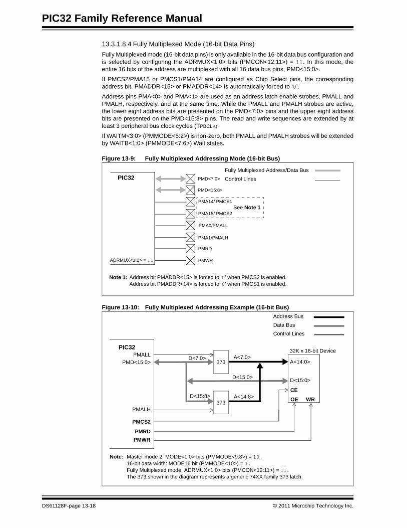
13.3.1.8.4 Fully Multiplexed Mode (16-bit Data Pins)Fully Multiplexed mode (16-bit data pins) is only available in the 16-bit data bus configuration and is selected by configuring the ADRMUX<1:0> bits (PMCON<12:11>) = 11. In this mode, the entire 16 bits of the address are multiplexed with all 16 data bus pins, PMD<15:0>.
If PMCS2/PMA15 or PMCS1/PMA14 are configured as Chip Select pins, the corresponding address bit, PMADDR<15> or PMADDR<14> is automatically forced to ‘0’.
Address pins PMA<0> and PMA<1> are used as an address latch enable strobes, PMALL and PMALH, respectively, and at the same time. While the PMALL and PMALH strobes are active, the lower eight address bits are presented on the PMD<7:0> pins and the upper eight address bits are presented on the PMD<15:8> pins. The read and write sequences are extended by at least 3 peripheral bus clock cycles (TPBCLK).
If WAITM<3:0> (PMMODE<5:2>) is non-zero, both PMALL and PMALH strobes will be extended by WAITB<1:0> (PMMODE<7:6>) Wait states.
Figure 13-9: Fully Multiplexed Addressing Mode (16-bit Bus)
Figure 13-10: Fully Multiplexed Addressing Example (16-bit Bus)
PMRD
PMWR
PMA1/PMALH
PMA15/ PMCS2
PIC32
PMA0/PMALL
PMD<7:0>
PMD<15:8>
PMA14/ PMCS1
ADRMUX<1:0> = 11
Note 1: Address bit PMADDR<15> is forced to ‘0’ when PMCS2 is enabled. Address bit PMADDR<14> is forced to ‘0’ when PMCS1 is enabled.
Fully Multiplexed Address/Data BusControl Lines
See Note 1
Note: Master mode 2: MODE<1:0> bits (PMMODE<9:8>) = 10. 16-bit data width: MODE16 bit (PMMODE<10>) = 1. Fully Multiplexed mode: ADRMUX<1:0> bits (PMCON<12:11>) = 11. The 373 shown in the diagram represents a generic 74XX family 373 latch.
Address BusData BusControl Lines
PMD<15:0>
PMALH
D<15:0>
373 A<14:0>
D<15:0>
A<7:0>
373
PMRDPMWR
OE WR
CE
PIC32
PMCS2
PMALL
A<14:8>
32K x 16-bit Device
D<15:8>
D<7:0>
DS61128F-page 13-18 © 2011 Microchip Technology Inc.
Section 13. Parallel Master Port (PMP)Parallel M
aster Port (PM
P)
13
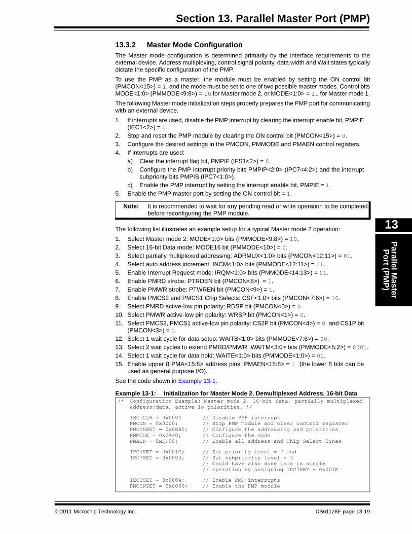
13.3.2 Master Mode ConfigurationThe Master mode configuration is determined primarily by the interface requirements to the external device. Address multiplexing, control signal polarity, data width and Wait states typically dictate the specific configuration of the PMP.To use the PMP as a master, the module must be enabled by setting the ON control bit (PMCON<15>) = 1, and the mode must be set to one of two possible master modes. Control bits MODE<1:0> (PMMODE<9:8>) = 10 for Master mode 2, or MODE<1:0> = 11 for Master mode 1.The following Master mode initialization steps properly prepares the PMP port for communicating with an external device. 1. If interrupts are used, disable the PMP interrupt by clearing the interrupt enable bit, PMPIE
(IEC1<2>) = 0.2. Stop and reset the PMP module by clearing the ON control bit (PMCON<15>) = 0.3. Configure the desired settings in the PMCON, PMMODE and PMAEN control registers.4. If interrupts are used:
a) Clear the interrupt flag bit, PMPIF (IFS1<2>) = 0.b) Configure the PMP interrupt priority bits PMPIP<2:0> (IPC7<4:2>) and the interrupt
subpriority bits PMPIS (IPC7<1:0>).c) Enable the PMP interrupt by setting the interrupt enable bit, PMPIE = 1.
5. Enable the PMP master port by setting the ON control bit = 1.
The following list illustrates an example setup for a typical Master mode 2 operation:1. Select Master mode 2: MODE<1:0> bits (PMMODE<9:8>) = 10.2. Select 16-bit Data mode: MODE16 bit (PMMODE<10>) = 0.3. Select partially multiplexed addressing: ADRMUX<1:0> bits (PMCON<12:11>) = 01.4. Select auto address increment: INCM<1:0> bits (PMMODE<12:11>) = 01.5. Enable Interrupt Request mode: IRQM<1:0> bits (PMMODE<14:13>) = 01.6. Enable PMRD strobe: PTRDEN bit (PMCON<8>) = 1.7. Enable PMWR strobe: PTWREN bit (PMCON<9>) = 1.8. Enable PMCS2 and PMCS1 Chip Selects: CSF<1:0> bits (PMCON<7:6>) = 10.9. Select PMRD active-low pin polarity: RDSP bit (PMCON<0>) = 0.10. Select PMWR active-low pin polarity: WRSP bit (PMCON<1>) = 0.11. Select PMCS2, PMCS1 active-low pin polarity: CS2P bit (PMCON<4>) = 0 and CS1P bit
(PMCON<3>) = 0.12. Select 1 wait cycle for data setup: WAITB<1:0> bits (PMMODE<7:6>) = 00.13. Select 2 wait cycles to extend PMRD/PMWR: WAITM<3:0> bits (PMMODE<5:2>) = 0001.14. Select 1 wait cycle for data hold: WAITE<1:0> bits (PMMODE<1:0>) = 00.15. Enable upper 8 PMA<15:8> address pins: PMAEN<15:8> = 1 (the lower 8 bits can be
used as general purpose I/O).See the code shown in Example 13-1.
Example 13-1: Initialization for Master Mode 2, Demultiplexed Address, 16-bit Data
Note: It is recommended to wait for any pending read or write operation to be completed before reconfiguring the PMP module.
/* Configuration Example: Master mode 2, 16-bit data, partially multiplexed address/data, active-lo polarities. */
IEC1CLR = 0x0004 // Disable PMP interruptPMCON = 0x0000; // Stop PMP module and clear control register PMCONSET = 0x0B80; // Configure the addressing and polarities PMMODE = 0x2A40; // Configure the modePMAEN = 0xFF00; // Enable all address and Chip Select lines
IPC7SET = 0x001C; // Set priority level = 7 andIPC7SET = 0x0003; // Set subpriority level = 3
// Could have also done this in single// operation by assigning IPC7SET = 0x001F
IEC1SET = 0x0004; // Enable PMP interrupts PMCONSET = 0x8000; // Enable the PMP module
© 2011 Microchip Technology Inc. DS61128F-page 13-19
PIC32 Family Reference Manual
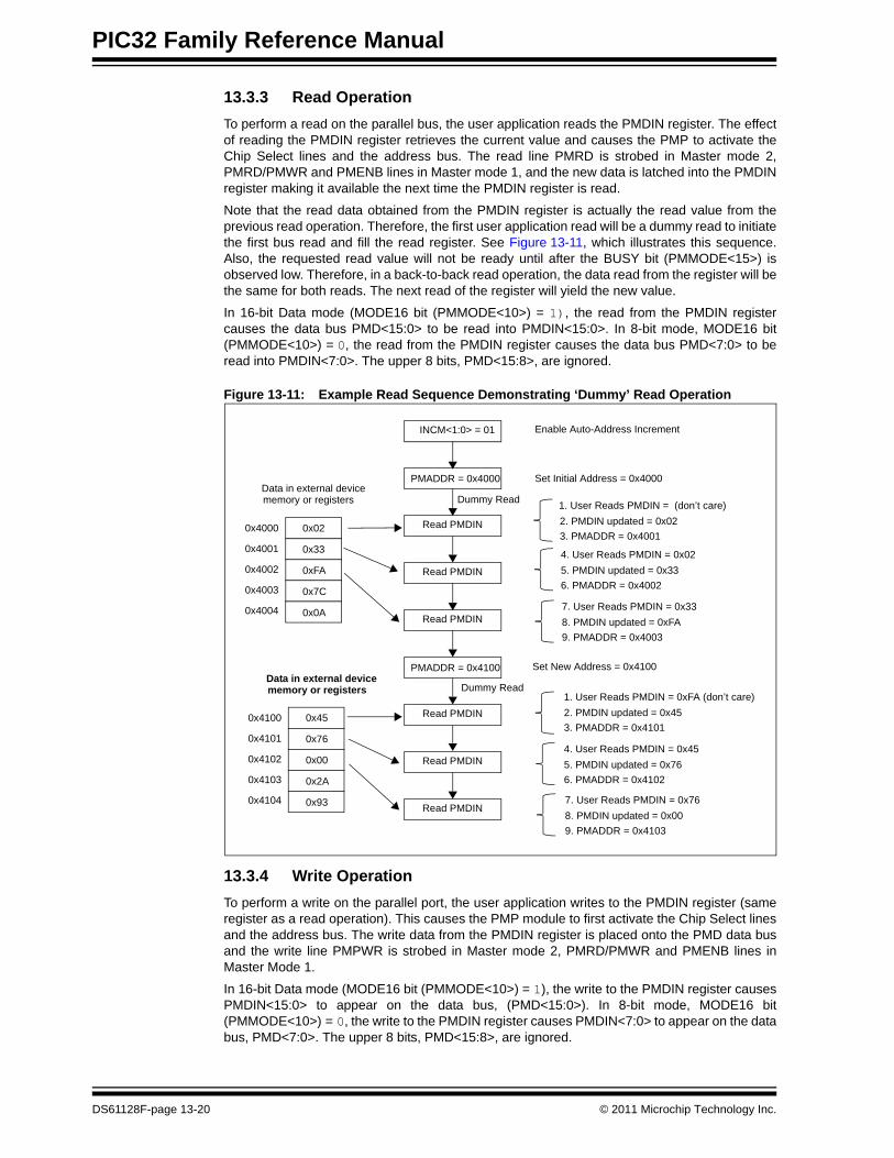
13.3.3 Read OperationTo perform a read on the parallel bus, the user application reads the PMDIN register. The effect of reading the PMDIN register retrieves the current value and causes the PMP to activate the Chip Select lines and the address bus. The read line PMRD is strobed in Master mode 2, PMRD/PMWR and PMENB lines in Master mode 1, and the new data is latched into the PMDIN register making it available the next time the PMDIN register is read.
Note that the read data obtained from the PMDIN register is actually the read value from the previous read operation. Therefore, the first user application read will be a dummy read to initiate the first bus read and fill the read register. See Figure 13-11, which illustrates this sequence. Also, the requested read value will not be ready until after the BUSY bit (PMMODE<15>) is observed low. Therefore, in a back-to-back read operation, the data read from the register will be the same for both reads. The next read of the register will yield the new value.
In 16-bit Data mode (MODE16 bit (PMMODE<10>) = 1), the read from the PMDIN register causes the data bus PMD<15:0> to be read into PMDIN<15:0>. In 8-bit mode, MODE16 bit (PMMODE<10>) = 0, the read from the PMDIN register causes the data bus PMD<7:0> to be read into PMDIN<7:0>. The upper 8 bits, PMD<15:8>, are ignored.
Figure 13-11: Example Read Sequence Demonstrating ‘Dummy’ Read Operation
13.3.4 Write OperationTo perform a write on the parallel port, the user application writes to the PMDIN register (same register as a read operation). This causes the PMP module to first activate the Chip Select lines and the address bus. The write data from the PMDIN register is placed onto the PMD data bus and the write line PMPWR is strobed in Master mode 2, PMRD/PMWR and PMENB lines in Master Mode 1.
In 16-bit Data mode (MODE16 bit (PMMODE<10>) = 1), the write to the PMDIN register causes PMDIN<15:0> to appear on the data bus, (PMD<15:0>). In 8-bit mode, MODE16 bit (PMMODE<10>) = 0, the write to the PMDIN register causes PMDIN<7:0> to appear on the data bus, PMD<7:0>. The upper 8 bits, PMD<15:8>, are ignored.
Set Initial Address = 0x4000
Dummy Read
Enable Auto-Address Increment
PMADDR = 0x4000
INCM<1:0> = 01
Read PMDIN3. PMADDR = 0x40012. PMDIN updated = 0x02
0x4000 0x02
0x33
0xFA
0x7C
0x0A
1. User Reads PMDIN = (don’t care)
Read PMDIN
0x4001
0x4002
0x4003
0x4004
6. PMADDR = 0x40025. PMDIN updated = 0x334. User Reads PMDIN = 0x02
9. PMADDR = 0x40038. PMDIN updated = 0xFA7. User Reads PMDIN = 0x33
Read PMDIN
PMADDR = 0x4100
0x4100 0x45
0x76
0x00
0x2A
0x93
0x4101
0x4102
0x4103
0x4104
Set New Address = 0x4100
3. PMADDR = 0x41012. PMDIN updated = 0x451. User Reads PMDIN = 0xFA (don’t care)
6. PMADDR = 0x41025. PMDIN updated = 0x764. User Reads PMDIN = 0x45
9. PMADDR = 0x41038. PMDIN updated = 0x007. User Reads PMDIN = 0x76
Dummy Read
Read PMDIN
Read PMDIN
Read PMDIN
Data in external devicememory or registers
Data in external devicememory or registers
DS61128F-page 13-20 © 2011 Microchip Technology Inc.
Section 13. Parallel Master Port (PMP)Parallel M
aster Port (PM
P)
13
13.3.5 Master Mode InterruptsIn PMP master modes, the PMPIF bit is set on every read or write strobe. An interrupt request is generated when the IRQM<1:0> bits (PMMODE<14:13>) are set = 01 and PMP interrupts are enabled, PMPIE (IEC1<2>) = 1.
13.3.6 Parallel Master Port Status – The BUSY BitIn addition to the PMP interrupt, the BUSY bit (PMMODE<15>) is provided to indicate the status of the module. This bit is only used in Master mode.
While any read or write operation is in progress, the BUSY bit is set for all but the very last peripheral bus cycle of the operation. This is helpful when Wait states are enabled or multiplexed address/data is selected. While the bit is set, any request by the user to initiate a new operation will be ignored (i.e., writing or reading the PMDIN register will not initiate a read or a write).
Since the system clock, SYSCLK, can operate faster than the peripheral bus clock in certain configurations, or if a large number of Wait states are used, it is possible for the PMP module to be in the process of completing a read or write operation when the next CPU instruction is reading or writing to the PMP module. For this reason, it is highly recommended that the BUSY bit be checked prior to any operation that accesses the PMDIN or PMADDR register.Example 13-2 shows a polling operation of the BUSY bit prior to accessing the PMP module.
In most applications, the PMP module’s Chip Select pin(s) provide the Chip Select interface and is under the timing control of the PMP module. However, some applications may require the PMP Chip Select pin(s) to not be configured as a Chip Select, but as a high order address line, such as PMA<14> or PMA<15>. In this situation, the application’s Chip Select function must be provided by an available I/O port pin under software control. In these cases, it is especially important that the user’s software poll the BUSY bit to ensure any read or write operation is complete before deasserting the software controlled Chip Select.
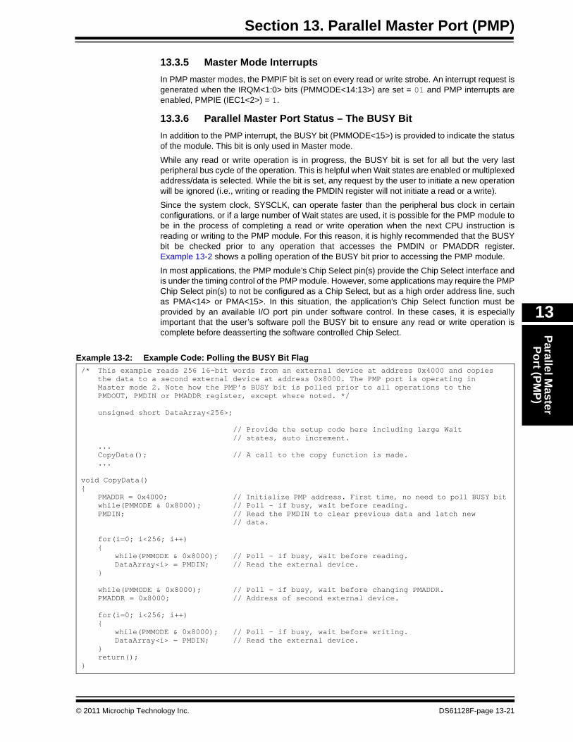
Example 13-2: Example Code: Polling the BUSY Bit Flag/* This example reads 256 16-bit words from an external device at address 0x4000 and copies
the data to a second external device at address 0x8000. The PMP port is operating inMaster mode 2. Note how the PMP’s BUSY bit is polled prior to all operations to thePMDOUT, PMDIN or PMADDR register, except where noted. */
unsigned short DataArray<256>;
// Provide the setup code here including large Wait// states, auto increment.
...CopyData(); // A call to the copy function is made....
void CopyData(){
PMADDR = 0x4000; // Initialize PMP address. First time, no need to poll BUSY bitwhile(PMMODE & 0x8000); // Poll - if busy, wait before reading.PMDIN; // Read the PMDIN to clear previous data and latch new
// data.
for(i=0; i<256; i++){
while(PMMODE & 0x8000); // Poll - if busy, wait before reading.DataArray<i> = PMDIN; // Read the external device.
}
while(PMMODE & 0x8000); // Poll - if busy, wait before changing PMADDR.PMADDR = 0x8000; // Address of second external device.
for(i=0; i<256; i++){
while(PMMODE & 0x8000); // Poll - if busy, wait before writing.DataArray<i> = PMDIN; // Read the external device.
}return();
}
© 2011 Microchip Technology Inc. DS61128F-page 13-21
PIC32 Family Reference Manual
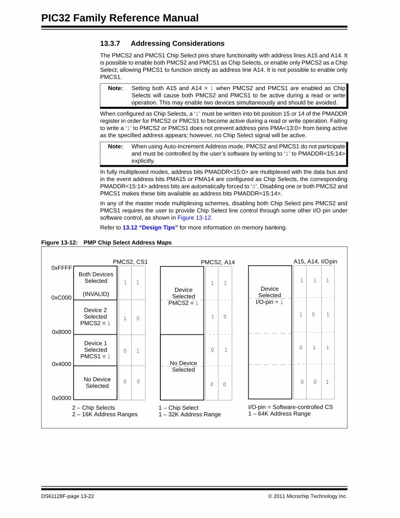
13.3.7 Addressing ConsiderationsThe PMCS2 and PMCS1 Chip Select pins share functionality with address lines A15 and A14. It is possible to enable both PMCS2 and PMCS1 as Chip Selects, or enable only PMCS2 as a Chip Select; allowing PMCS1 to function strictly as address line A14. It is not possible to enable only PMCS1.
When configured as Chip Selects, a ‘1’ must be written into bit position 15 or 14 of the PMADDR register in order for PMCS2 or PMCS1 to become active during a read or write operation. Failing to write a ‘1’ to PMCS2 or PMCS1 does not prevent address pins PMA<13:0> from being active as the specified address appears; however, no Chip Select signal will be active.
In fully multiplexed modes, address bits PMADDR<15:0> are multiplexed with the data bus and in the event address bits PMA15 or PMA14 are configured as Chip Selects, the corresponding PMADDR<15:14> address bits are automatically forced to ‘0’. Disabling one or both PMCS2 and PMCS1 makes these bits available as address bits PMADDR<15:14>.
In any of the master mode multiplexing schemes, disabling both Chip Select pins PMCS2 and PMCS1 requires the user to provide Chip Select line control through some other I/O pin under software control, as shown in Figure 13-12.
Refer to 13.12 “Design Tips” for more information on memory banking.
Figure 13-12: PMP Chip Select Address Maps
Note: Setting both A15 and A14 = 1 when PMCS2 and PMCS1 are enabled as Chip Selects will cause both PMCS2 and PMCS1 to be active during a read or write operation. This may enable two devices simultaneously and should be avoided.
Note: When using Auto-Increment Address mode, PMCS2 and PMCS1 do not participate and must be controlled by the user’s software by writing to ‘1’ to PMADDR<15:14> explicitly.
Device 2Selected
PMCS2 = 1
Device 1Selected
PMCS1 = 1
No DeviceSelected
Both DevicesSelected
(INVALID)
0x0000
0x4000
0x8000
0xFFFF
0xC000
0
0
00
1
1
1 1
PMCS2, CS1
2 – 16K Address Ranges2 – Chip Selects
DeviceSelected
I/O-pin = 1
A15, A14, I/Opin
1
1 – 64K Address RangeI/O-pin = Software-controlled CS
0
1
1
0
0
01
1 1
1
1
DeviceSelected
PMCS2 = 1
No DeviceSelected
0
PMCS2, A14
1 – 32K Address Range1 – Chip Select
1
1
0
0
01
1
DS61128F-page 13-22 © 2011 Microchip Technology Inc.
Section 13. Parallel Master Port (PMP)Parallel M
aster Port (PM
P)
13
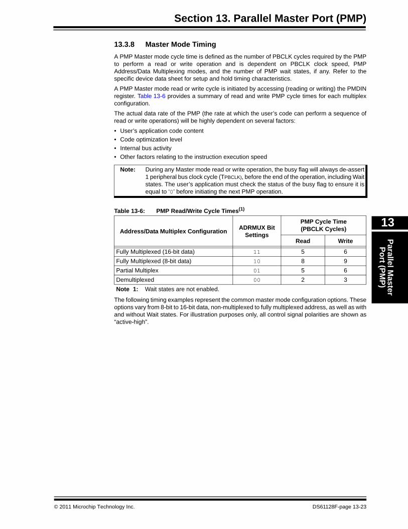
13.3.8 Master Mode TimingA PMP Master mode cycle time is defined as the number of PBCLK cycles required by the PMP to perform a read or write operation and is dependent on PBCLK clock speed, PMP Address/Data Multiplexing modes, and the number of PMP wait states, if any. Refer to the specific device data sheet for setup and hold timing characteristics.
A PMP Master mode read or write cycle is initiated by accessing (reading or writing) the PMDIN register. Table 13-6 provides a summary of read and write PMP cycle times for each multiplex configuration.
The actual data rate of the PMP (the rate at which the user’s code can perform a sequence of read or write operations) will be highly dependent on several factors:
• User’s application code content• Code optimization level• Internal bus activity• Other factors relating to the instruction execution speed
The following timing examples represent the common master mode configuration options. These options vary from 8-bit to 16-bit data, non-multiplexed to fully multiplexed address, as well as with and without Wait states. For illustration purposes only, all control signal polarities are shown as “active-high”.
Note: During any Master mode read or write operation, the busy flag will always de-assert 1 peripheral bus clock cycle (TPBCLK), before the end of the operation, including Wait states. The user’s application must check the status of the busy flag to ensure it is equal to ‘0’ before initiating the next PMP operation.
Table 13-6: PMP Read/Write Cycle Times(1)
Address/Data Multiplex Configuration ADRMUX Bit Settings
PMP Cycle Time(PBCLK Cycles)
Read Write
Fully Multiplexed (16-bit data) 11 5 6Fully Multiplexed (8-bit data) 10 8 9Partial Multiplex 01 5 6Demultiplexed 00 2 3Note 1: Wait states are not enabled.
© 2011 Microchip Technology Inc. DS61128F-page 13-23
PIC32 Family Reference Manual
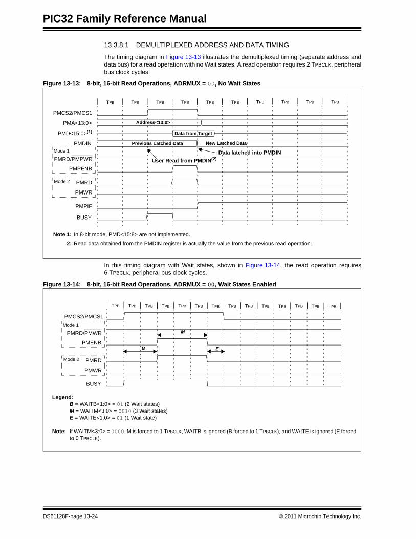
13.3.8.1 DEMULTIPLEXED ADDRESS AND DATA TIMING
The timing diagram in Figure 13-13 illustrates the demultiplexed timing (separate address and data bus) for a read operation with no Wait states. A read operation requires 2 TPBCLK, peripheral bus clock cycles.
Figure 13-13: 8-bit, 16-bit Read Operations, ADRMUX = 00, No Wait States
In this timing diagram with Wait states, shown in Figure 13-14, the read operation requires 6 TPBCLK, peripheral bus clock cycles.
Figure 13-14: 8-bit, 16-bit Read Operations, ADRMUX = 00, Wait States Enabled
Data from Target
PMCS2/PMCS1
PMPENB
PMRD/PMPWR
PMD<15:0>(1)
PMA<13:0>
PMPIF
BUSY
Address<13:0>
TPB TPB TPBTPB TPB TPB TPB TPB TPB TPB
User Read from PMDIN(2)Data latched into PMDIN
New Latched DataPMDIN Previous Latched Data
Note 1: In 8-bit mode, PMD<15:8> are not implemented.2: Read data obtained from the PMDIN register is actually the value from the previous read operation.
PMWR
PMRD
Mode 1
Mode 2
PMCS2/PMCS1
TPB TPB TPB TPB TPB TPB TPB TPB TPB TPB TPB TPB TPBTPB
B
M
E
BUSY
PMENB
PMRD/PMWRMode 1
PMWR
PMRDMode 2
Legend: B = WAITB<1:0> = 01 (2 Wait states) M = WAITM<3:0> = 0010 (3 Wait states) E = WAITE<1:0> = 01 (1 Wait state)
Note: If WAITM<3:0> = 0000, M is forced to 1 TPBCLK, WAITB is ignored (B forced to 1 TPBCLK), and WAITE is ignored (E forced to 0 TPBCLK).
DS61128F-page 13-24 © 2011 Microchip Technology Inc.
Section 13. Parallel Master Port (PMP)Parallel M
aster Port (PM
P)
13
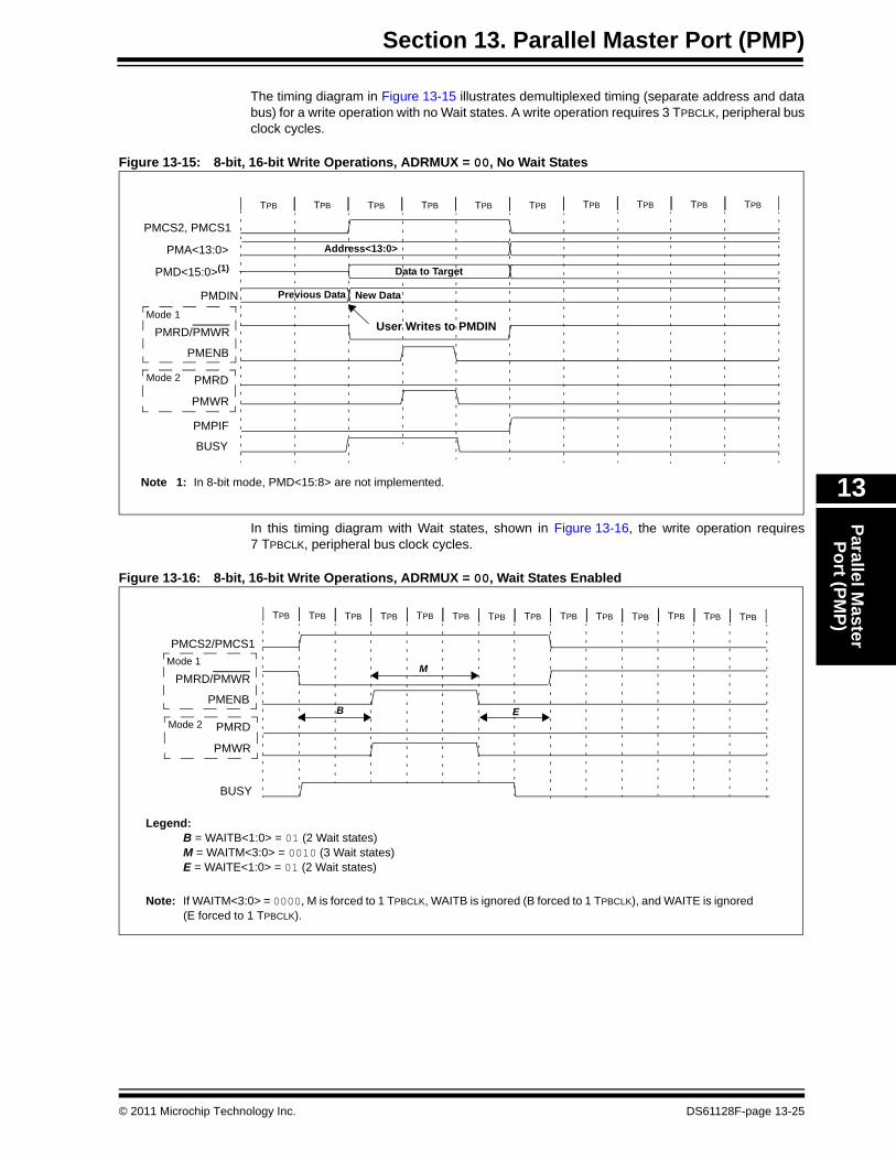
The timing diagram in Figure 13-15 illustrates demultiplexed timing (separate address and data bus) for a write operation with no Wait states. A write operation requires 3 TPBCLK, peripheral bus clock cycles.
Figure 13-15: 8-bit, 16-bit Write Operations, ADRMUX = 00, No Wait States
In this timing diagram with Wait states, shown in Figure 13-16, the write operation requires 7 TPBCLK, peripheral bus clock cycles.
Figure 13-16: 8-bit, 16-bit Write Operations, ADRMUX = 00, Wait States Enabled
Data to Target
PMCS2, PMCS1
PMD<15:0>(1)
PMA<13:0>
PMPIF
BUSY
Address<13:0>
TPB TPB TPBTPB TPB TPB TPB TPB TPB TPB
Note 1: In 8-bit mode, PMD<15:8> are not implemented.
New DataPMDIN Previous Data
User Writes to PMDIN
PMENB
PMRD/PMWRMode 1
PMWR
PMRDMode 2
PMCS2/PMCS1
TPB TPB TPB TPB TPB TPB TPB TPB TPB TPB TPB TPB TPBTPB
B
M
E
BUSY
PMENB
PMRD/PMWRMode 1
PMWR
PMRDMode 2
Legend: B = WAITB<1:0> = 01 (2 Wait states) M = WAITM<3:0> = 0010 (3 Wait states) E = WAITE<1:0> = 01 (2 Wait states)
Note: If WAITM<3:0> = 0000, M is forced to 1 TPBCLK, WAITB is ignored (B forced to 1 TPBCLK), and WAITE is ignored (E forced to 1 TPBCLK).
© 2011 Microchip Technology Inc. DS61128F-page 13-25
PIC32 Family Reference Manual
13.3.8.2 PARTIALLY MULTIPLEXED ADDRESS AND DATA TIMING
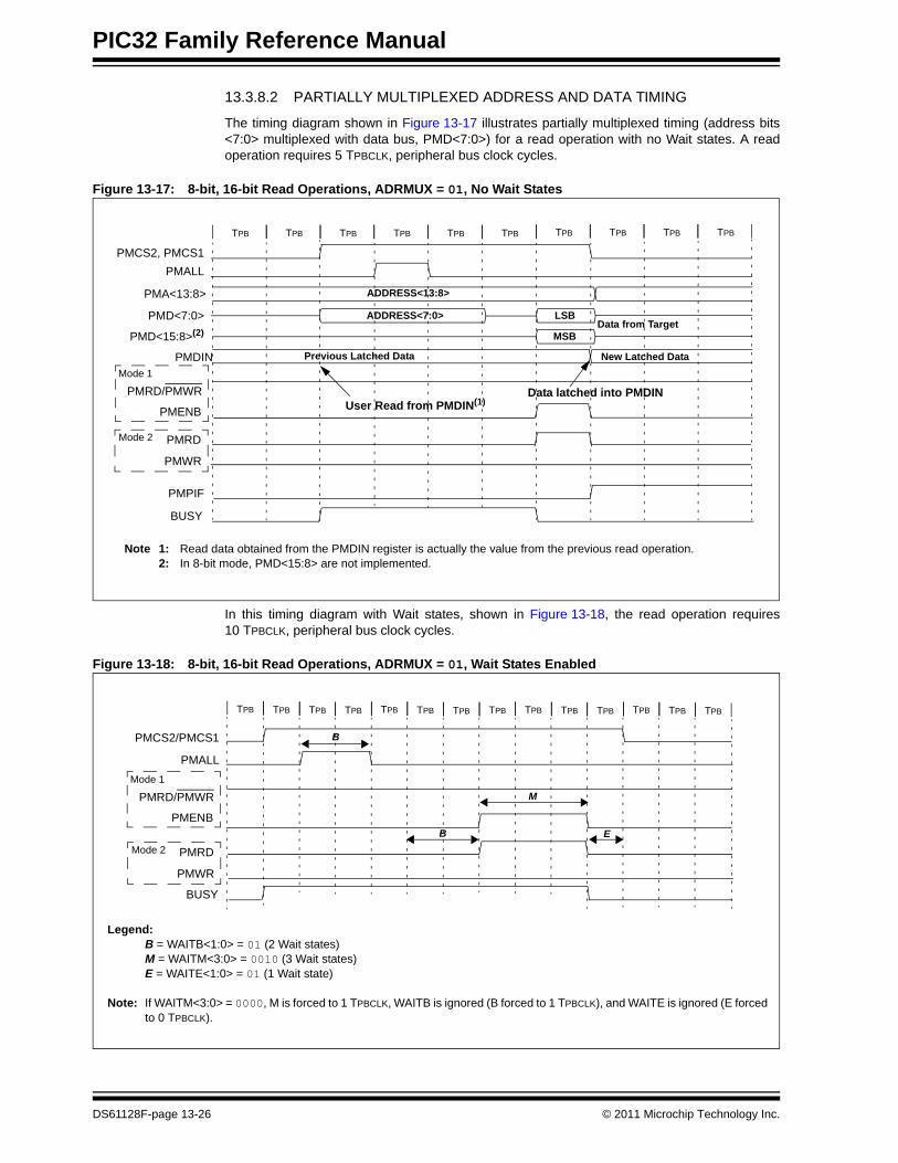
The timing diagram shown in Figure 13-17 illustrates partially multiplexed timing (address bits <7:0> multiplexed with data bus, PMD<7:0>) for a read operation with no Wait states. A read operation requires 5 TPBCLK, peripheral bus clock cycles.
Figure 13-17: 8-bit, 16-bit Read Operations, ADRMUX = 01, No Wait States
In this timing diagram with Wait states, shown in Figure 13-18, the read operation requires 10 TPBCLK, peripheral bus clock cycles.
Figure 13-18: 8-bit, 16-bit Read Operations, ADRMUX = 01, Wait States Enabled
PMCS2, PMCS1PMALL
PMD<7:0>
PMA<13:8>
PMPIF
ADDRESS<7:0> LSB
BUSY
TPB TPB TPBTPB TPB TPB TPB TPB TPB TPB
ADDRESS<13:8>
PMD<15:8>(2) MSBData from Target
New Latched DataPMDIN Previous Latched Data
User Read from PMDIN(1)Data latched into PMDIN
Note 1: Read data obtained from the PMDIN register is actually the value from the previous read operation.2: In 8-bit mode, PMD<15:8> are not implemented.
PMENB
PMRD/PMWRMode 1
PMWR
PMRDMode 2
PMCS2/PMCS1
TPB TPB TPB TPB TPB TPB TPB TPB TPB TPB TPB TPB TPBTPB
B
M
E
PMALL
B
BUSY
PMWR
PMRDMode 2
PMENB
PMRD/PMWRMode 1
Legend: B = WAITB<1:0> = 01 (2 Wait states) M = WAITM<3:0> = 0010 (3 Wait states) E = WAITE<1:0> = 01 (1 Wait state)
Note: If WAITM<3:0> = 0000, M is forced to 1 TPBCLK, WAITB is ignored (B forced to 1 TPBCLK), and WAITE is ignored (E forced to 0 TPBCLK).
DS61128F-page 13-26 © 2011 Microchip Technology Inc.
Section 13. Parallel Master Port (PMP)Parallel M
aster Port (PM
P)
13
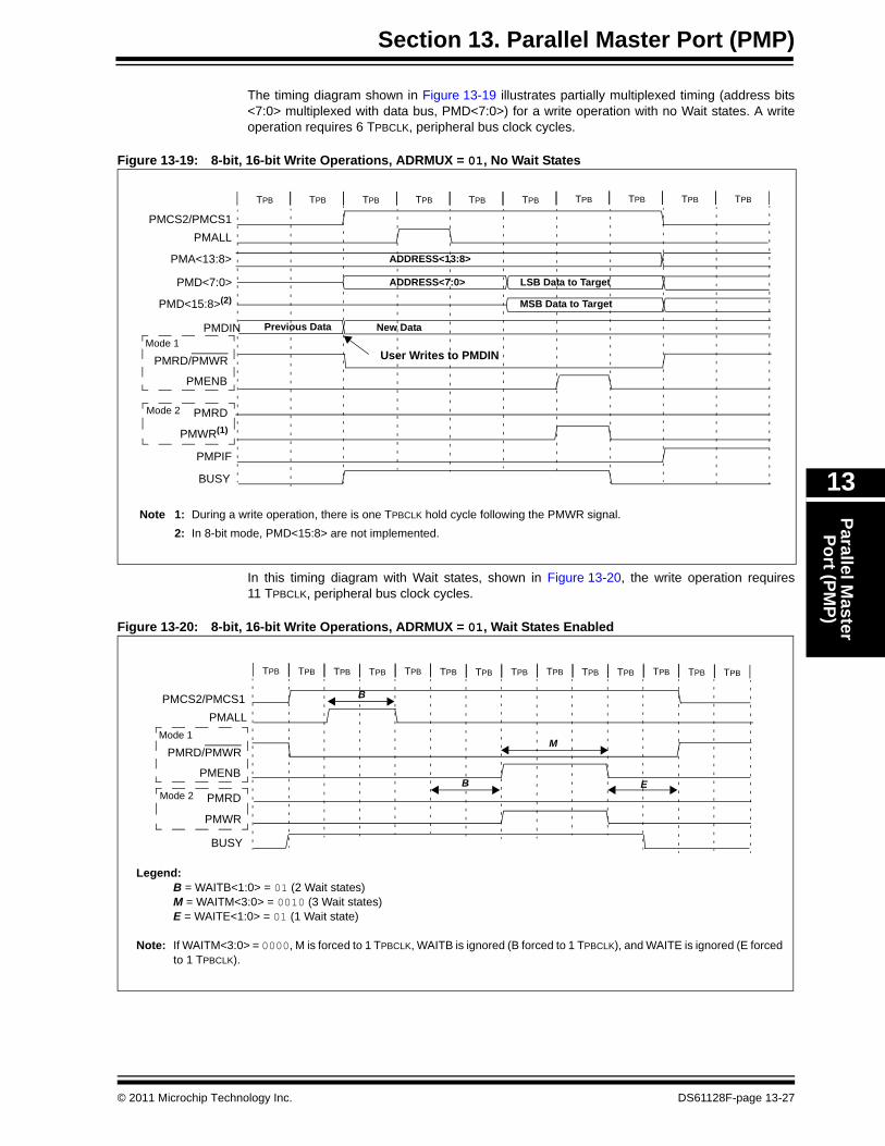
The timing diagram shown in Figure 13-19 illustrates partially multiplexed timing (address bits <7:0> multiplexed with data bus, PMD<7:0>) for a write operation with no Wait states. A write operation requires 6 TPBCLK, peripheral bus clock cycles.
Figure 13-19: 8-bit, 16-bit Write Operations, ADRMUX = 01, No Wait States
In this timing diagram with Wait states, shown in Figure 13-20, the write operation requires 11 TPBCLK, peripheral bus clock cycles.
Figure 13-20: 8-bit, 16-bit Write Operations, ADRMUX = 01, Wait States Enabled
PMCS2/PMCS1PMALL
PMD<15:8>(2)
PMA<13:8>
PMPIF
MSB Data to Target
BUSY
TPB TPB TPBTPB TPB TPB TPB TPB TPB TPB
ADDRESS<13:8>
PMD<7:0> ADDRESS<7:0> LSB Data to Target
Note 1: During a write operation, there is one TPBCLK hold cycle following the PMWR signal.2: In 8-bit mode, PMD<15:8> are not implemented.
New DataPMDIN Previous Data
PMWR(1)
PMRDMode 2
User Writes to PMDIN
PMENB
PMRD/PMWRMode 1
PMCS2/PMCS1
TPB TPB TPB TPB TPB TPB TPB TPB TPB TPB TPB TPB TPBTPB
B
M
E
PMALL
B
BUSY
PMWR
PMRDMode 2
PMENB
PMRD/PMWRMode 1
Legend: B = WAITB<1:0> = 01 (2 Wait states) M = WAITM<3:0> = 0010 (3 Wait states) E = WAITE<1:0> = 01 (1 Wait state)
Note: If WAITM<3:0> = 0000, M is forced to 1 TPBCLK, WAITB is ignored (B forced to 1 TPBCLK), and WAITE is ignored (E forced to 1 TPBCLK).
© 2011 Microchip Technology Inc. DS61128F-page 13-27
PIC32 Family Reference Manual
13.3.8.3 FULLY MULTIPLEXED (8-BIT BUS) ADDRESS AND DATA TIMING
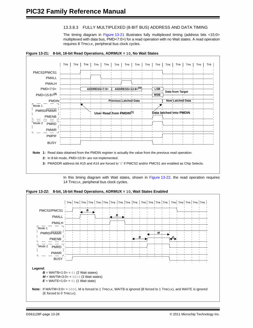
The timing diagram in Figure 13-21 illustrates fully multiplexed timing (address bits <15:0> multiplexed with data bus, PMD<7:0>) for a read operation with no Wait states. A read operation requires 8 TPBCLK, peripheral bus clock cycles.
Figure 13-21: 8-bit, 16-bit Read Operations, ADRMUX = 10, No Wait States
In this timing diagram with Wait states, shown in Figure 13-22, the read operation requires 14 TPBCLK, peripheral bus clock cycles.
Figure 13-22: 8-bit, 16-bit Read Operations, ADRMUX = 10, Wait States Enabled
PMCS2/PMCS1
PMD<15:8>(2)
PMPIF
BUSY
PMALL
PMALH
TPB TPB TPB TPB TPB TPB TPB TPB TPB TPB TPB TPB TPB TPB TPB
Data from TargetPMD<7:0>
MSB
LSBADDRESS<7:0> ADDRESS<13:8>(3)
New Latched DataPMDIN Previous Latched Data
Note 1: Read data obtained from the PMDIN register is actually the value from the previous read operation.2: In 8-bit mode, PMD<15:8> are not implemented.3: PMADDR address bit A15 and A14 are forced to ‘0’ if PMCS2 and/or PMCS1 are enabled as Chip Selects.
PMENB
PMRD/PMWRMode 1
PMWR
PMRDMode 2
Data latched into PMDINUser Read from PMDIN(1)
PMCS2/PMCS1
TPB
BM
E
PMALL
B
BUSY
PMWR
PMRDMode 2
PMENB
PMRD/PMWRMode 1
PMALH
TPB TPB TPB TPB TPB TPB TPB TPB TPB TPB TPB TPB TPB TPB TPB TPB TPB TPB
B
Legend: B = WAITB<1:0> = 01 (2 Wait states) M = WAITM<3:0> = 0010 (3 Wait states) E = WAITE<1:0> = 01 (1 Wait state)
Note: If WAITM<3:0> = 0000, M is forced to 1 TPBCLK, WAITB is ignored (B forced to 1 TPBCLK), and WAITE is ignored (E forced to 0 TPBCLK).
DS61128F-page 13-28 © 2011 Microchip Technology Inc.
Section 13. Parallel Master Port (PMP)Parallel M
aster Port (PM
P)
13
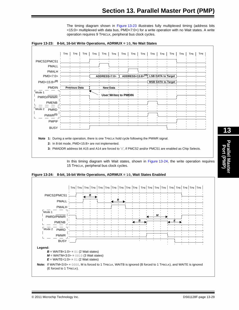
The timing diagram shown in Figure 13-23 illustrates fully multiplexed timing (address bits <15:0> multiplexed with data bus, PMD<7:0>) for a write operation with no Wait states. A write operation requires 9 TPBCLK, peripheral bus clock cycles.
Figure 13-23: 8-bit, 16-bit Write Operations, ADRMUX = 10, No Wait States
In this timing diagram with Wait states, shown in Figure 13-24, the write operation requires 15 TPBCLK, peripheral bus clock cycles.
Figure 13-24: 8-bit, 16-bit Write Operations, ADRMUX = 10, Wait States Enabled
PMCS2/PMCS1
PMD<15:8>(2)
PMPIF
BUSY
PMALL
PMALH
TPB TPB TPB TPB TPB TPB TPB TPB TPB TPB TPB TPB TPB TPB TPB
MSB DATA to Target
PMD<7:0> LSB DATA to TargetADDRESS<7:0> ADDRESS<13:8>(3)
New DataPMDIN Previous Data
Note 1: During a write operation, there is one TPBCLK hold cycle following the PMWR signal.2: In 8-bit mode, PMD<15:8> are not implemented.3: PMADDR address bit A15 and A14 are forced to ‘0’, if PMCS2 and/or PMCS1 are enabled as Chip Selects.
PMWR(1)
PMRDMode 2
User Writes to PMDIN
PMENB
PMRD/PMWRMode 1
PMCS2/PMCS1
TPB
B
M
E
PMALL
B
BUSY
PMWR
PMRDMode 2
PMENB
PMRD/PMWRMode 1
PMALH
TPB TPB TPB TPB TPB TPB TPB TPB TPB TPB TPB TPB TPB TPB TPB TPB TPB TPB
B
Legend: B = WAITB<1:0> = 01 (2 Wait states) M = WAITM<3:0> = 0010 (3 Wait states) E = WAITE<1:0> = 01 (2 Wait states)
Note: If WAITM<3:0> = 0000, M is forced to 1 TPBCLK, WAITB is ignored (B forced to 1 TPBCLK), and WAITE is ignored (E forced to 1 TPBCLK).
© 2011 Microchip Technology Inc. DS61128F-page 13-29
PIC32 Family Reference Manual
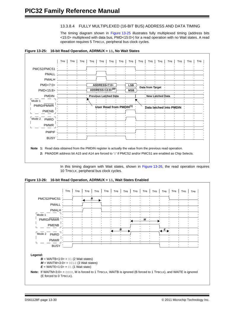
13.3.8.4 FULLY MULTIPLEXED (16-BIT BUS) ADDRESS AND DATA TIMING
The timing diagram shown in Figure 13-25 illustrates fully multiplexed timing (address bits <15:0> multiplexed with data bus, PMD<15:0>) for a read operation with no Wait states. A read operation requires 5 TPBCLK, peripheral bus clock cycles.
Figure 13-25: 16-bit Read Operation, ADRMUX = 11, No Wait States
In this timing diagram with Wait states, shown in Figure 13-26, the read operation requires 10 TPBCLK, peripheral bus clock cycles.
Figure 13-26: 16-bit Read Operation, ADRMUX = 11, Wait States Enabled
PMCS2/PMCS1
PMD<15:8>
PMPIF
BUSY
PMALL
PMALH
TPB TPB TPB TPB TPB TPB TPB TPB TPB TPB TPB TPB TPB TPB TPB
MSB
PMD<7:0> ADDRESS<7:0>
ADDRESS<13:8>(2)
New Latched DataPMDIN Previous Latched Data
LSBData from Target
Note 1: Read data obtained from the PMDIN register is actually the value from the previous read operation.2: PMADDR address bit A15 and A14 are forced to ‘0’ if PMCS2 and/or PMCS1 are enabled as Chip Selects.
PMENB
PMRD/PMWRMode 1
PMWR
PMRDMode 2
Data latched into PMDINUser Read from PMDIN(1)
PMCS2/PMCS1
TPB TPB TPB TPB TPB TPB TPB TPB TPB TPB TPB TPB TPBTPB
B
M
E
PMALL
B
BUSY
PMWR
PMRDMode 2
PMENB
PMRD/PMWRMode 1
PMALH
Legend: B = WAITB<1:0> = 01 (2 Wait states) M = WAITM<3:0> = 0010 (3 Wait states) E = WAITE<1:0> = 01 (1 Wait state)
Note: If WAITM<3:0> = 0000, M is forced to 1 TPBCLK, WAITB is ignored (B forced to 1 TPBCLK), and WAITE is ignored (E forced to 0 TPBCLK).
DS61128F-page 13-30 © 2011 Microchip Technology Inc.
Section 13. Parallel Master Port (PMP)Parallel M
aster Port (PM
P)
13
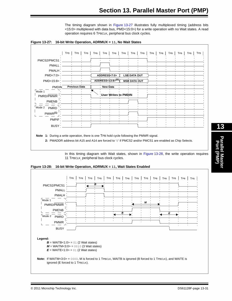
The timing diagram shown in Figure 13-27 illustrates fully multiplexed timing (address bits <15:0> multiplexed with data bus, PMD<15:0>) for a write operation with no Wait states. A read operation requires 6 TPBCLK, peripheral bus clock cycles.
Figure 13-27: 16-bit Write Operation, ADRMUX = 11, No Wait States
In this timing diagram with Wait states, shown in Figure 13-28, the write operation requires 11 TPBCLK, peripheral bus clock cycles.
Figure 13-28: 16-bit Write Operation, ADRMUX = 11, Wait States Enabled
PMCS2/PMCS1
PMPIF
BUSY
PMALL
PMALH
TPB TPB TPB TPB TPB TPB TPB TPB TPB TPB TPB TPB TPB TPB TPB
MSB DATA OUTPMD<15:8>
PMD<7:0> LSB DATA OUTADDRESS<7:0>
ADDRESS<13:8>(2)
New DataPMDIN Previous Data
User Writes to PMDIN
PMENB
PMRD/PMWRMode 1
PMWR(1)
PMRDMode 2
Note 1: During a write operation, there is one TPB hold cycle following the PMWR signal.2: PMADDR address bit A15 and A14 are forced to ‘0’ if PMCS2 and/or PMCS1 are enabled as Chip Selects.
PMCS2/PMCS1
TPB TPB TPB TPB TPB TPB TPB TPB TPB TPB TPB TPB TPBTPB
B
M
E
PMALL
B
BUSY
PMWR
PMRDMode 2
PMENB
PMRD/PMWRMode 1
PMALH
Legend: B = WAITB<1:0> = 01 (2 Wait states) M = WAITM<3:0> = 0010 (3 Wait states) E = WAITE<1:0> = 01 (2 Wait states)
Note: If WAITM<3:0> = 0000, M is forced to 1 TPBCLK, WAITB is ignored (B forced to 1 TPBCLK), and WAITE is ignored (E forced to 1 TPBCLK).
© 2011 Microchip Technology Inc. DS61128F-page 13-31
PIC32 Family Reference Manual
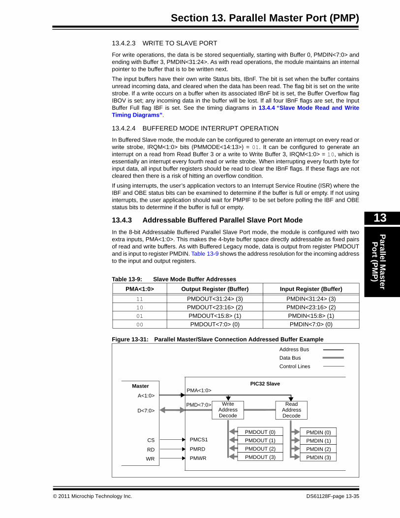
13.4 SLAVE MODES OF OPERATIONThe PMP module provides 8-bit (byte) legacy Parallel Slave Port (PSP) functionality as well as new buffered and addressable slave modes.
All slave modes support 8-bit data only and the module control pins are automatically dedicated when any of these modes are selected. The user application only needs to configure the polarity of the PMCS1, PMRD and PMWR signals.
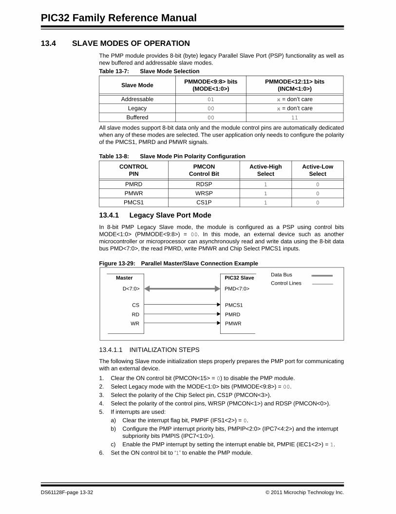
13.4.1 Legacy Slave Port ModeIn 8-bit PMP Legacy Slave mode, the module is configured as a PSP using control bits MODE<1:0> (PMMODE<9:8>) = 00. In this mode, an external device such as another microcontroller or microprocessor can asynchronously read and write data using the 8-bit data bus PMD<7:0>, the read PMRD, write PMWR and Chip Select PMCS1 inputs.
Figure 13-29: Parallel Master/Slave Connection Example
13.4.1.1 INITIALIZATION STEPS
The following Slave mode initialization steps properly prepares the PMP port for communicating with an external device.
1. Clear the ON control bit (PMCON<15> = 0) to disable the PMP module.2. Select Legacy mode with the MODE<1:0> bits (PMMODE<9:8>) = 00.3. Select the polarity of the Chip Select pin, CS1P (PMCON<3>).4. Select the polarity of the control pins, WRSP (PMCON<1>) and RDSP (PMCON<0>).5. If interrupts are used:
a) Clear the interrupt flag bit, PMPIF (IFS1<2>) = 0.b) Configure the PMP interrupt priority bits, PMPIP<2:0> (IPC7<4:2>) and the interrupt
subpriority bits PMPIS (IPC7<1:0>).c) Enable the PMP interrupt by setting the interrupt enable bit, PMPIE (IEC1<2>) = 1.
6. Set the ON control bit to ‘1’ to enable the PMP module.
Table 13-7: Slave Mode Selection
Slave Mode PMMODE<9:8> bits (MODE<1:0>)
PMMODE<12:11> bits (INCM<1:0>)
Addressable 01 x = don’t careLegacy 00 x = don’t careBuffered 00 11
Table 13-8: Slave Mode Pin Polarity Configuration
CONTROLPIN
PMCONControl Bit
Active-HighSelect
Active-LowSelect
PMRD RDSP 1 0
PMWR WRSP 1 0
PMCS1 CS1P 1 0
Data BusControl Lines
D<7:0>
RD
WR
Master
CS
PMD<7:0>
PMRD
PMWR
PIC32 Slave
PMCS1
DS61128F-page 13-32 © 2011 Microchip Technology Inc.
Section 13. Parallel Master Port (PMP)Parallel M
aster Port (PM
P)
13
Example 13-3: Legacy Parallel Slave Port Initialization (Example Code)
13.4.1.2 WRITE TO SLAVE PORT
When Chip Select is active and a write strobe occurs, the data on the bus pins PMD<7:0> is captured into the lower 8 bits of the PMDIN register, PMDIN<7:0>. The PMPIF (interrupt flag bit) is set during the write strobe, however, IB0F (input buffer full flag) bit requires two to three peripheral bus clock cycles to synchronize before it is set and the PMDIN register can be read. The IB0F bit will remain set until the PMDIN register is read by the user application. If a write operation occurs while the IB0F = 1, the write data will be ignored and an overflow condition will be generated, IB0V = 1. See the timing diagrams in 13.4.4 “Slave Mode Read and Write Timing Diagrams”.
13.4.1.3 READ FROM SLAVE PORT
When Chip Select is active and a read strobe occurs, the data from the lower 8 bits of the PMDOUT register (PMDOUT<7:0>) is presented onto data bus pins PMD<7:0> and read by the master device. The PMPIF (interrupt flag bit) is set during the read strobe; however, the OB0E (output buffer empty flag) bit requires two to three peripheral bus clock cycles to synchronize before it is set. The OB0E bit will remain set until the PMDOUT register is written to by the user application. If a read operation occurs while the OB0E = 1, the read data will be the same as the previous read data and an underflow condition will be generated, OBUF = 1. See the timing diagrams in 13.4.4 “Slave Mode Read and Write Timing Diagrams”.
13.4.1.4 LEGACY MODE INTERRUPT OPERATION
In PMP Legacy Slave mode, the PMPIF bit is set every read or write strobe. If using interrupts, the user’s application vectors to an Interrupt Service Routine (ISR) where the IBF and OBE status bits can be examined to determine if the buffer is full or empty. If not using interrupts, the user’s application should wait for PMPIF to be set before polling the IBF and OBE Status bits to determine if the buffer is full or empty.
13.4.2 Buffered Parallel Slave Port ModeThe 8-bit Buffered Parallel Slave Port mode is functionally identical to the Legacy Parallel Slave Port mode with one exception: the implementation of 4-level read and write buffers. Buffered Slave mode is enabled by setting the MODE<1:0> bits (PMMODE<9:8>) = 00, and the INCM<1:0> bits (PMMODE<12:11>) = 11.
When the buffered mode is active, the module uses the PMDIN register as write buffers and the PMDOUT register as read buffers. Each register is divided into four 8-bit buffer registers, four read buffers in PMDOUT and four write buffers in PMDIN. Buffers are numbered 0 through 3, starting with the lower byte <7:0> and progressing upward through the high byte <31:24>.
Note: On persistent interrupt implementations of the PMP, the interrupt is generated on the falling edge of the WR signal with the WR signal configured to active-high polarity. On non-persistent interrupt implementations of the PMP, the interrupt is generated on the rising edge of the WR signal with the WR signal configured to active-high polarity. Firmware should poll the IBF or IBnF bit to ensure the data is valid before attempting to read the data from the PMP module.
/*Example configuration for Legacy Slave mode
*/IEC1CLR = 0x0004 // Disable PMP interrupt in case it is already enabledPMCON = 0x0000 // Stop and Configure PMCON register for Legacy modePMMODE = 0x0000 // Configure PMMODE registerIPC7SET = 0x001C; // Set priority level = 7 andIPC7SET = 0x0003; // Set subpriority level = 3
// Could have also done this in single// operation by assigning IPC7SET = 0x001F
IFS1CLR = 0x0004; // Clear the PMP interrupt status flag IEC1SET = 0x0004; // Enable PMP interrupts PMCONSET = 0x8000; // Enable PMP module
© 2011 Microchip Technology Inc. DS61128F-page 13-33
PIC32 Family Reference Manual
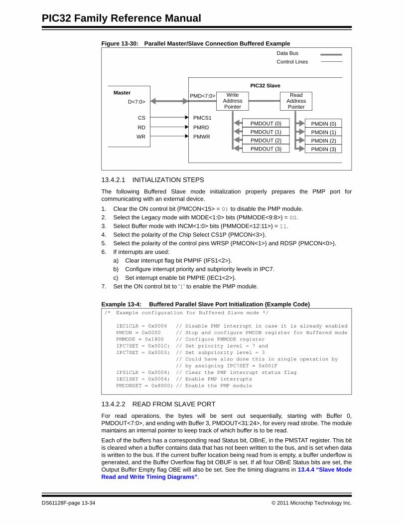
Figure 13-30: Parallel Master/Slave Connection Buffered Example
13.4.2.1 INITIALIZATION STEPS
The following Buffered Slave mode initialization properly prepares the PMP port for communicating with an external device.
1. Clear the ON control bit (PMCON<15> = 0) to disable the PMP module.2. Select the Legacy mode with MODE<1:0> bits (PMMODE<9:8>) = 00.3. Select Buffer mode with INCM<1:0> bits (PMMODE<12:11>) = 11.4. Select the polarity of the Chip Select CS1P (PMCON<3>).5. Select the polarity of the control pins WRSP (PMCON<1>) and RDSP (PMCON<0>).6. If interrupts are used:
a) Clear interrupt flag bit PMPIF (IFS1<2>).b) Configure interrupt priority and subpriority levels in IPC7.c) Set interrupt enable bit PMPIE (IEC1<2>).
7. Set the ON control bit to ‘1’ to enable the PMP module.
Example 13-4: Buffered Parallel Slave Port Initialization (Example Code)
13.4.2.2 READ FROM SLAVE PORT
For read operations, the bytes will be sent out sequentially, starting with Buffer 0, PMDOUT<7:0>, and ending with Buffer 3, PMDOUT<31:24>, for every read strobe. The module maintains an internal pointer to keep track of which buffer is to be read.
Each of the buffers has a corresponding read Status bit, OBnE, in the PMSTAT register. This bit is cleared when a buffer contains data that has not been written to the bus, and is set when data is written to the bus. If the current buffer location being read from is empty, a buffer underflow is generated, and the Buffer Overflow flag bit OBUF is set. If all four OBnE Status bits are set, the Output Buffer Empty flag OBE will also be set. See the timing diagrams in 13.4.4 “Slave Mode Read and Write Timing Diagrams”.
D<7:0>
RD
WR
Master
Data BusControl Lines
CS
PMRD
PMWR
PIC32 Slave
PMCS1PMDOUT (0)PMDOUT (1)PMDOUT (2)PMDOUT (3)
PMDIN (0)PMDIN (1)PMDIN (2)PMDIN (3)
PMD<7:0> WriteAddressPointer
ReadAddressPointer
/* Example configuration for Buffered Slave mode */
IEC1CLR = 0x0004 // Disable PMP interrupt in case it is already enabledPMCON = 0x0000 // Stop and configure PMCON register for Buffered modePMMODE = 0x1800 // Configure PMMODE registerIPC7SET = 0x001C; // Set priority level = 7 andIPC7SET = 0x0003; // Set subpriority level = 3
// Could have also done this in single operation by// by assigning IPC7SET = 0x001F
IFS1CLR = 0x0004; // Clear the PMP interrupt status flag IEC1SET = 0x0004; // Enable PMP interrupts PMCONSET = 0x8000; // Enable the PMP module
DS61128F-page 13-34 © 2011 Microchip Technology Inc.
Section 13. Parallel Master Port (PMP)Parallel M
aster Port (PM
P)
13
13.4.2.3 WRITE TO SLAVE PORT
For write operations, the data is be stored sequentially, starting with Buffer 0, PMDIN<7:0> and ending with Buffer 3, PMDIN<31:24>. As with read operations, the module maintains an internal pointer to the buffer that is to be written next.
The input buffers have their own write Status bits, IBnF. The bit is set when the buffer contains unread incoming data, and cleared when the data has been read. The flag bit is set on the write strobe. If a write occurs on a buffer when its associated IBnF bit is set, the Buffer Overflow flag IBOV is set; any incoming data in the buffer will be lost. If all four IBnF flags are set, the Input Buffer Full flag IBF is set. See the timing diagrams in 13.4.4 “Slave Mode Read and Write Timing Diagrams”.
13.4.2.4 BUFFERED MODE INTERRUPT OPERATION
In Buffered Slave mode, the module can be configured to generate an interrupt on every read or write strobe, IRQM<1:0> bits (PMMODE<14:13>) = 01. It can be configured to generate an interrupt on a read from Read Buffer 3 or a write to Write Buffer 3, IRQM<1:0> = 10, which is essentially an interrupt every fourth read or write strobe. When interrupting every fourth byte for input data, all input buffer registers should be read to clear the IBnF flags. If these flags are not cleared then there is a risk of hitting an overflow condition.
If using interrupts, the user’s application vectors to an Interrupt Service Routine (ISR) where the IBF and OBE status bits can be examined to determine if the buffer is full or empty. If not using interrupts, the user application should wait for PMPIF to be set before polling the IBF and OBE status bits to determine if the buffer is full or empty.
13.4.3 Addressable Buffered Parallel Slave Port ModeIn the 8-bit Addressable Buffered Parallel Slave Port mode, the module is configured with two extra inputs, PMA<1:0>. This makes the 4-byte buffer space directly addressable as fixed pairs of read and write buffers. As with Buffered Legacy mode, data is output from register PMDOUT and is input to register PMDIN. Table 13-9 shows the address resolution for the incoming address to the input and output registers.
Figure 13-31: Parallel Master/Slave Connection Addressed Buffer Example
Table 13-9: Slave Mode Buffer AddressesPMA<1:0> Output Register (Buffer) Input Register (Buffer)
11 PMDOUT<31:24> (3) PMDIN<31:24> (3)10 PMDOUT<23:16> (2) PMDIN<23:16> (2)01 PMDOUT<15:8> (1) PMDIN<15:8> (1)00 PMDOUT<7:0> (0) PMDIN<7:0> (0)
D<7:0>
RD
WR
Master
CS
A<1:0>
Address BusData BusControl Lines
PMRD
PMWR
PIC32 Slave
PMCS1PMDOUT (0)PMDOUT (1)PMDOUT (2)PMDOUT (3)
PMDIN (0)PMDIN (1)PMDIN (2)PMDIN (3)
PMD<7:0> WriteAddressDecode
ReadAddressDecode
PMA<1:0>
© 2011 Microchip Technology Inc. DS61128F-page 13-35
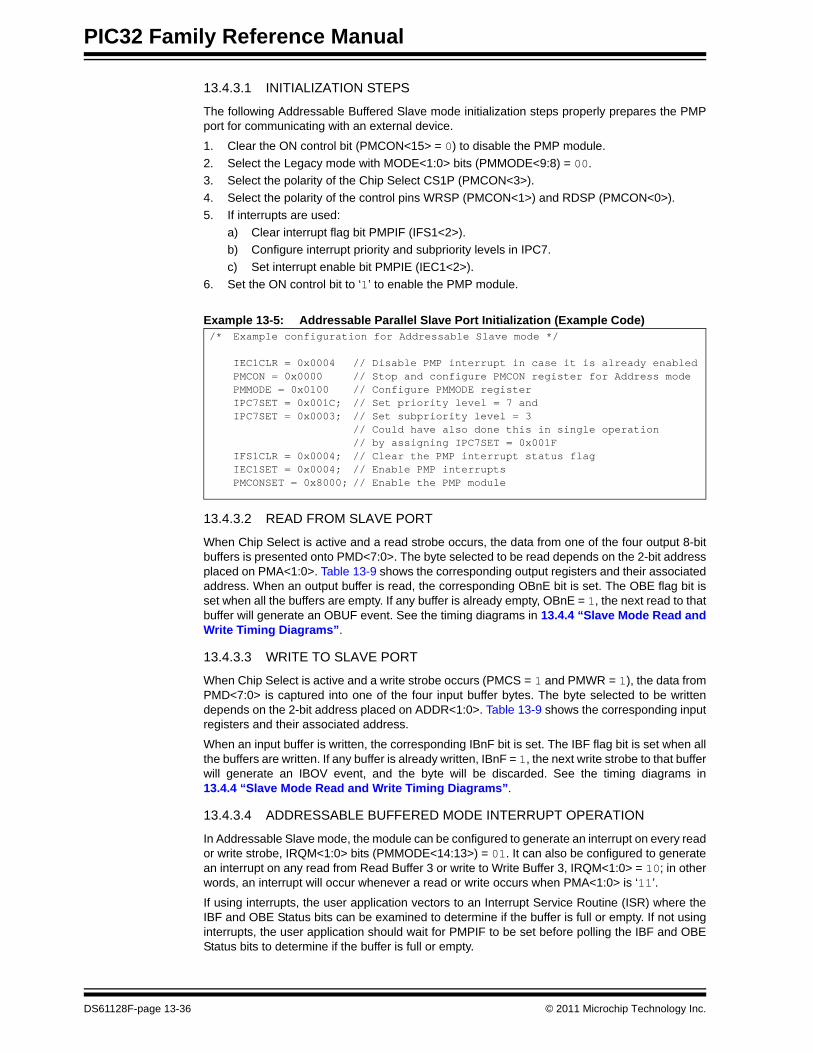
PIC32 Family Reference Manual
13.4.3.1 INITIALIZATION STEPS
The following Addressable Buffered Slave mode initialization steps properly prepares the PMP port for communicating with an external device.
1. Clear the ON control bit (PMCON<15> = 0) to disable the PMP module.2. Select the Legacy mode with MODE<1:0> bits (PMMODE<9:8) = 00.3. Select the polarity of the Chip Select CS1P (PMCON<3>).4. Select the polarity of the control pins WRSP (PMCON<1>) and RDSP (PMCON<0>).5. If interrupts are used:
a) Clear interrupt flag bit PMPIF (IFS1<2>).b) Configure interrupt priority and subpriority levels in IPC7.c) Set interrupt enable bit PMPIE (IEC1<2>).
6. Set the ON control bit to ‘1’ to enable the PMP module.
Example 13-5: Addressable Parallel Slave Port Initialization (Example Code)
13.4.3.2 READ FROM SLAVE PORT
When Chip Select is active and a read strobe occurs, the data from one of the four output 8-bit buffers is presented onto PMD<7:0>. The byte selected to be read depends on the 2-bit address placed on PMA<1:0>. Table 13-9 shows the corresponding output registers and their associated address. When an output buffer is read, the corresponding OBnE bit is set. The OBE flag bit is set when all the buffers are empty. If any buffer is already empty, OBnE = 1, the next read to that buffer will generate an OBUF event. See the timing diagrams in 13.4.4 “Slave Mode Read and Write Timing Diagrams”.
13.4.3.3 WRITE TO SLAVE PORT
When Chip Select is active and a write strobe occurs (PMCS = 1 and PMWR = 1), the data from PMD<7:0> is captured into one of the four input buffer bytes. The byte selected to be written depends on the 2-bit address placed on ADDR<1:0>. Table 13-9 shows the corresponding input registers and their associated address.
When an input buffer is written, the corresponding IBnF bit is set. The IBF flag bit is set when all the buffers are written. If any buffer is already written, IBnF = 1, the next write strobe to that buffer will generate an IBOV event, and the byte will be discarded. See the timing diagrams in 13.4.4 “Slave Mode Read and Write Timing Diagrams”.
13.4.3.4 ADDRESSABLE BUFFERED MODE INTERRUPT OPERATION
In Addressable Slave mode, the module can be configured to generate an interrupt on every read or write strobe, IRQM<1:0> bits (PMMODE<14:13>) = 01. It can also be configured to generate an interrupt on any read from Read Buffer 3 or write to Write Buffer 3, IRQM<1:0> = 10; in other words, an interrupt will occur whenever a read or write occurs when PMA<1:0> is ‘11’.
If using interrupts, the user application vectors to an Interrupt Service Routine (ISR) where the IBF and OBE Status bits can be examined to determine if the buffer is full or empty. If not using interrupts, the user application should wait for PMPIF to be set before polling the IBF and OBE Status bits to determine if the buffer is full or empty.
/* Example configuration for Addressable Slave mode */
IEC1CLR = 0x0004 // Disable PMP interrupt in case it is already enabledPMCON = 0x0000 // Stop and configure PMCON register for Address modePMMODE = 0x0100 // Configure PMMODE registerIPC7SET = 0x001C; // Set priority level = 7 andIPC7SET = 0x0003; // Set subpriority level = 3
// Could have also done this in single operation// by assigning IPC7SET = 0x001F
IFS1CLR = 0x0004; // Clear the PMP interrupt status flag IEC1SET = 0x0004; // Enable PMP interrupts PMCONSET = 0x8000; // Enable the PMP module
DS61128F-page 13-36 © 2011 Microchip Technology Inc.
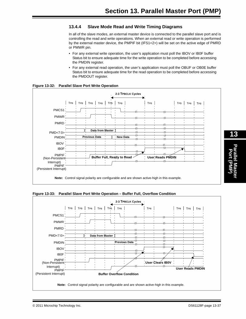
Section 13. Parallel Master Port (PMP)Parallel M
aster Port (PM
P)
13
13.4.4 Slave Mode Read and Write Timing DiagramsIn all of the slave modes, an external master device is connected to the parallel slave port and is controlling the read and write operations. When an external read or write operation is performed by the external master device, the PMPIF bit (IFS1<2>) will be set on the active edge of PMRD or PMWR pin.
• For any external write operation, the user’s application must poll the IBOV or IB0F buffer Status bit to ensure adequate time for the write operation to be completed before accessing the PMDIN register.
• For any external read operation, the user’s application must poll the OBUF or OB0E buffer Status bit to ensure adequate time for the read operation to be completed before accessing the PMDOUT register.
Figure 13-32: Parallel Slave Port Write Operation
Figure 13-33: Parallel Slave Port Write Operation – Buffer Full, Overflow Condition
PMCS1
PMWR
PMRD
IB0F
PMPIF
PMD<7:0>Data from Master
New DataPMDIN Previous Data
TPB TPB TPB TPB TPB TPB TPB TPB TPBTPB
User Reads PMDINBuffer Full, Ready to Read
IBOV
Note: Control signal polarity are configurable and are shown active-high in this example.
2-3 TPBCLK Cycles
(Non-Persistent Interrupt)
PMPIF(Persistent Interrupt)
PMCS1
PMWR
PMRD
IB0F
PMPIF
PMD<7:0> Data from Master
PMDIN Previous Data
TPB TPB TPB TPB TPB TPB TPB TPB TPBTPB
User Reads PMDINBuffer Overflow Condition
IBOV
Note: Control signal polarity are configurable and are shown active-high in this example.
2-3 TPBCLK Cycles
User Clears IB0V(Non-Persistent Interrupt)
PMPIF(Persistent Interrupt)
© 2011 Microchip Technology Inc. DS61128F-page 13-37
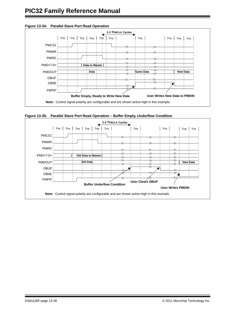
PIC32 Family Reference Manual
Figure 13-34: Parallel Slave Port Read Operation
Figure 13-35: Parallel Slave Port Read Operation – Buffer Empty, Underflow Condition
PMCS1
PMWR
PMRD
OB0E
PMPIF
PMD<7:0> Data to Master
Same DataPMDOUT Data
TPB TPB TPB TPB TPB TPB TPB TPB TPBTPB
User Writes New Data to PMDINBuffer Empty, Ready to Write New Data
OBUF
Note: Control signal polarity are configurable and are shown active-high in this example.
2-3 TPBCLK Cycles
New Data
PMCS1
PMWR
PMRD
OB0E
PMPIF
PMD<7:0> Old Data to Master
PMDOUT Old Data
TPB TPB TPB TPB TPB TPB TPB TPBTPB
User Writes PMDINBuffer Underflow Condition
OBUF
Note: Control signal polarity are configurable and are shown active-high in this example.
2-3 TPBCLK Cycles
User Clears OBUF
New Data
TPB
DS61128F-page 13-38 © 2011 Microchip Technology Inc.
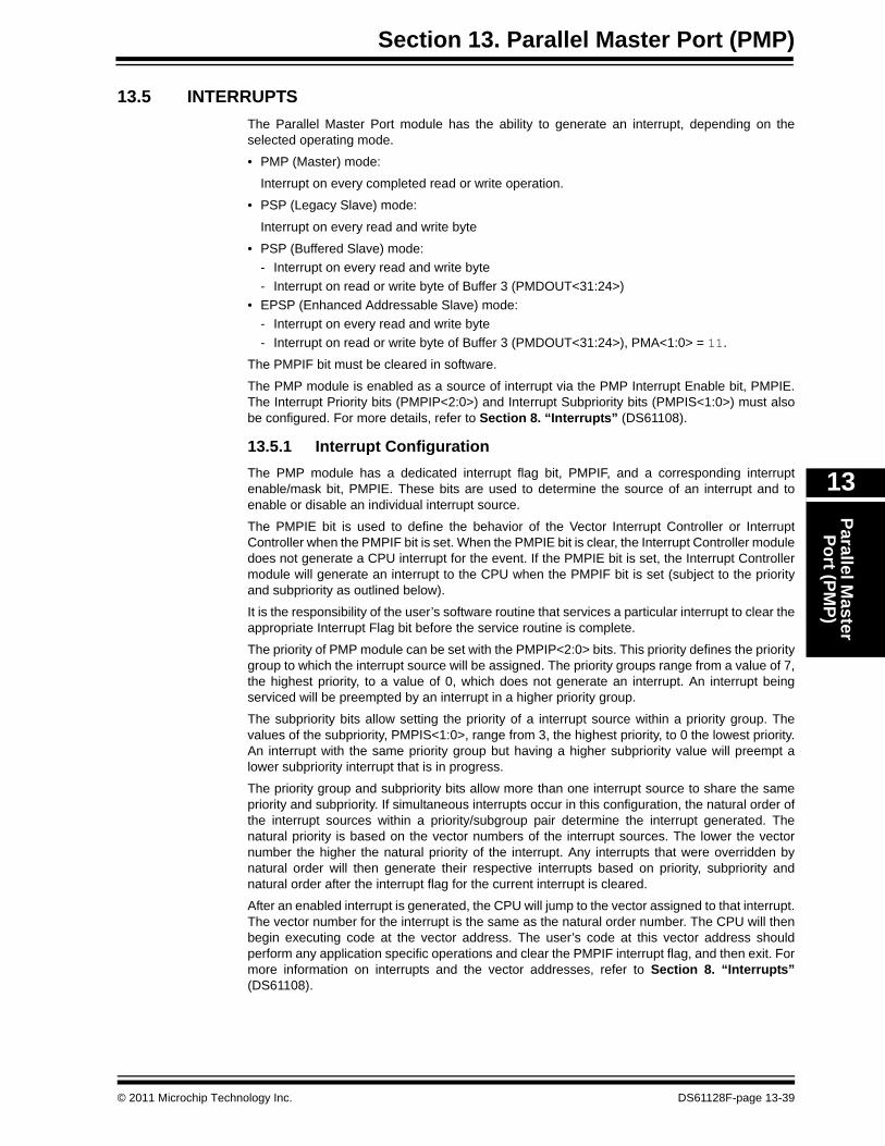
Section 13. Parallel Master Port (PMP)Parallel M
aster Port (PM
P)
13
13.5 INTERRUPTSThe Parallel Master Port module has the ability to generate an interrupt, depending on the selected operating mode.
• PMP (Master) mode:
Interrupt on every completed read or write operation.
• PSP (Legacy Slave) mode:
Interrupt on every read and write byte
• PSP (Buffered Slave) mode:- Interrupt on every read and write byte- Interrupt on read or write byte of Buffer 3 (PMDOUT<31:24>)
• EPSP (Enhanced Addressable Slave) mode:- Interrupt on every read and write byte- Interrupt on read or write byte of Buffer 3 (PMDOUT<31:24>), PMA<1:0> = 11.
The PMPIF bit must be cleared in software.
The PMP module is enabled as a source of interrupt via the PMP Interrupt Enable bit, PMPIE. The Interrupt Priority bits (PMPIP<2:0>) and Interrupt Subpriority bits (PMPIS<1:0>) must also be configured. For more details, refer to Section 8. “Interrupts” (DS61108).
13.5.1 Interrupt Configuration The PMP module has a dedicated interrupt flag bit, PMPIF, and a corresponding interrupt enable/mask bit, PMPIE. These bits are used to determine the source of an interrupt and to enable or disable an individual interrupt source.
The PMPIE bit is used to define the behavior of the Vector Interrupt Controller or Interrupt Controller when the PMPIF bit is set. When the PMPIE bit is clear, the Interrupt Controller module does not generate a CPU interrupt for the event. If the PMPIE bit is set, the Interrupt Controller module will generate an interrupt to the CPU when the PMPIF bit is set (subject to the priority and subpriority as outlined below).
It is the responsibility of the user’s software routine that services a particular interrupt to clear the appropriate Interrupt Flag bit before the service routine is complete.
The priority of PMP module can be set with the PMPIP<2:0> bits. This priority defines the priority group to which the interrupt source will be assigned. The priority groups range from a value of 7, the highest priority, to a value of 0, which does not generate an interrupt. An interrupt being serviced will be preempted by an interrupt in a higher priority group.
The subpriority bits allow setting the priority of a interrupt source within a priority group. The values of the subpriority, PMPIS<1:0>, range from 3, the highest priority, to 0 the lowest priority. An interrupt with the same priority group but having a higher subpriority value will preempt a lower subpriority interrupt that is in progress.
The priority group and subpriority bits allow more than one interrupt source to share the same priority and subpriority. If simultaneous interrupts occur in this configuration, the natural order of the interrupt sources within a priority/subgroup pair determine the interrupt generated. The natural priority is based on the vector numbers of the interrupt sources. The lower the vector number the higher the natural priority of the interrupt. Any interrupts that were overridden by natural order will then generate their respective interrupts based on priority, subpriority and natural order after the interrupt flag for the current interrupt is cleared.
After an enabled interrupt is generated, the CPU will jump to the vector assigned to that interrupt. The vector number for the interrupt is the same as the natural order number. The CPU will then begin executing code at the vector address. The user’s code at this vector address should perform any application specific operations and clear the PMPIF interrupt flag, and then exit. For more information on interrupts and the vector addresses, refer to Section 8. “Interrupts”(DS61108).
© 2011 Microchip Technology Inc. DS61128F-page 13-39
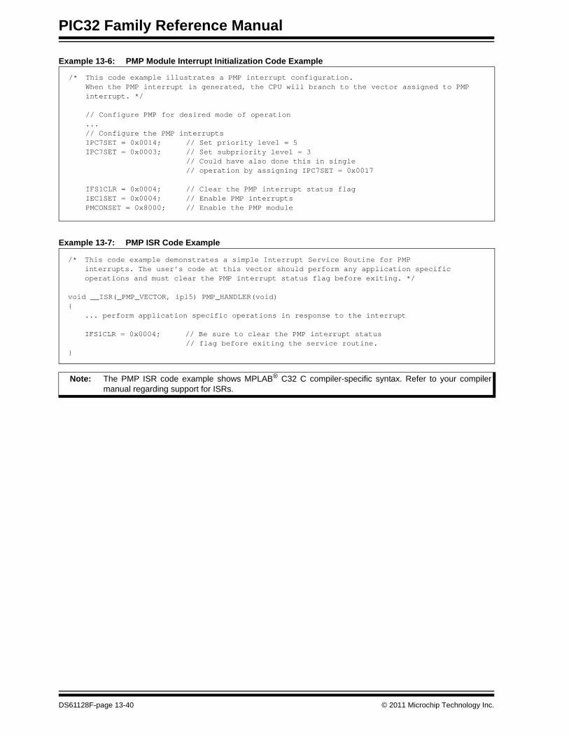
PIC32 Family Reference Manual
Example 13-6: PMP Module Interrupt Initialization Code Example
Example 13-7: PMP ISR Code Example
/* This code example illustrates a PMP interrupt configuration.When the PMP interrupt is generated, the CPU will branch to the vector assigned to PMPinterrupt. */
// Configure PMP for desired mode of operation...// Configure the PMP interrupts
IPC7SET = 0x0014; // Set priority level = 5 IPC7SET = 0x0003; // Set subpriority level = 3
// Could have also done this in single// operation by assigning IPC7SET = 0x0017
IFS1CLR = 0x0004; // Clear the PMP interrupt status flag IEC1SET = 0x0004; // Enable PMP interrupts PMCONSET = 0x8000; // Enable the PMP module
/* This code example demonstrates a simple Interrupt Service Routine for PMPinterrupts. The user’s code at this vector should perform any application specificoperations and must clear the PMP interrupt status flag before exiting. */
void __ISR(_PMP_VECTOR, ipl5) PMP_HANDLER(void){
... perform application specific operations in response to the interrupt
IFS1CLR = 0x0004; // Be sure to clear the PMP interrupt status// flag before exiting the service routine.
}
Note: The PMP ISR code example shows MPLAB® C32 C compiler-specific syntax. Refer to your compiler manual regarding support for ISRs.
DS61128F-page 13-40 © 2011 Microchip Technology Inc.
Section 13. Parallel Master Port (PMP)Parallel M
aster Port (PM
P)
13
13.6 OPERATION IN POWER-SAVING AND DEBUG MODES
13.6.1 PMP Operation in Sleep ModeWhen the device enters Sleep mode, the system clock is disabled. The consequences of Sleep mode depend on which mode the module is configured in at the time that Sleep mode is invoked.
13.6.1.1 PMP OPERATION – SLEEP IN MASTER MODE
If the device enters Sleep mode while the module is operating in Master mode, PMP operation is suspended in its current state until clock execution resumes. As this may cause unexpected control pin timings, users should avoid invoking Sleep mode when continuous use of the module is needed.
13.6.1.2 PMP OPERATION – SLEEP IN SLAVE MODE
While the module is inactive, but enabled for any Slave mode operation, any read or write operations occurring at that time will be able to complete without the use of the microcontroller clock. Once the operation is completed, the module will issue an interrupt according to the setting of the IRQM bits.
If the PMPIE bit is set, and its priority is greater than current CPU priority, the device will wake from Sleep or Idle mode and execute the PMP interrupt service routine.
If the assigned priority level of the PMP interrupt is less than or equal to the current CPU priority level, the CPU will not be awakened and the device will enter the Idle mode.
13.6.2 PMP Operation in Idle ModeWhen the device enters Idle mode, the system clock sources remain functional. The SIDL bit (PMCON<13>) selects whether the module will stop or continue functioning on Idle. If SIDL = 0, the module will continue operation in Idle mode.
If SIDL = 1, the module will stop communications when the microcontroller enters Idle mode, in the same manner as it does in Sleep mode. The current transaction in Slave modes will complete and issue an interrupt, while the current transaction in Master mode will be suspended until normal clocking resumes. As with Sleep mode, Idle mode should be avoided when using the module in Master mode if continuous use of the module is required.
13.7 EFFECTS OF VARIOUS RESETS
13.7.1 Device Reset All PMP module registers are forced to their reset states on a device Reset.
13.7.2 Power-on Reset (POR)All PMP module registers are forced to their Reset states on a POR.
13.7.3 Watchdog Reset All PMP module registers are forced to their reset states on a Watchdog reset.
© 2011 Microchip Technology Inc. DS61128F-page 13-41
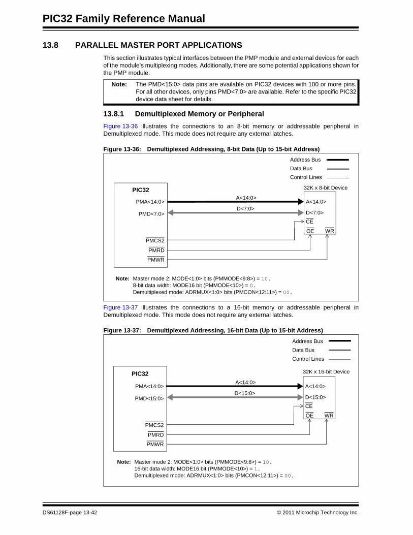
PIC32 Family Reference Manual
13.8 PARALLEL MASTER PORT APPLICATIONSThis section illustrates typical interfaces between the PMP module and external devices for each of the module’s multiplexing modes. Additionally, there are some potential applications shown for the PMP module.
13.8.1 Demultiplexed Memory or PeripheralFigure 13-36 illustrates the connections to an 8-bit memory or addressable peripheral in Demultiplexed mode. This mode does not require any external latches.
Figure 13-36: Demultiplexed Addressing, 8-bit Data (Up to 15-bit Address)
Figure 13-37 illustrates the connections to a 16-bit memory or addressable peripheral in Demultiplexed mode. This mode does not require any external latches.
Figure 13-37: Demultiplexed Addressing, 16-bit Data (Up to 15-bit Address)
Note: The PMD<15:0> data pins are available on PIC32 devices with 100 or more pins. For all other devices, only pins PMD<7:0> are available. Refer to the specific PIC32device data sheet for details.
PMA<14:0>D<7:0>
A<14:0>
D<7:0>
A<14:0>
PMRD
PMWR
OE WR
CE
PIC32
Address BusData BusControl Lines
PMCS2
PMD<7:0>
32K x 8-bit Device
Note: Master mode 2: MODE<1:0> bits (PMMODE<9:8>) = 10. 8-bit data width: MODE16 bit (PMMODE<10>) = 0. Demultiplexed mode: ADRMUX<1:0> bits (PMCON<12:11>) = 00.
PMA<14:0>D<15:0>
A<14:0>
D<15:0>
A<14:0>
PMRD
PMWR
OE WR
CE
PIC32
Address BusData BusControl Lines
PMCS2
PMD<15:0>
32K x 16-bit Device
Note: Master mode 2: MODE<1:0> bits (PMMODE<9:8>) = 10. 16-bit data width: MODE16 bit (PMMODE<10>) = 1. Demultiplexed mode: ADRMUX<1:0> bits (PMCON<12:11>) = 00.
DS61128F-page 13-42 © 2011 Microchip Technology Inc.
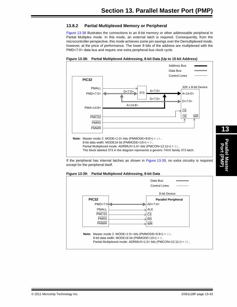
Section 13. Parallel Master Port (PMP)Parallel M
aster Port (PM
P)
13
13.8.2 Partial Multiplexed Memory or PeripheralFigure 13-38 illustrates the connections to an 8-bit memory or other addressable peripheral in Partial Multiplex mode. In this mode, an external latch is required. Consequently, from the microcontroller perspective, this mode achieves some pin savings over the Demultiplexed mode, however, at the price of performance. The lower 8 bits of the address are multiplexed with the PMD<7:0> data bus and require one extra peripheral bus clock cycle.
Figure 13-38: Partial Multiplexed Addressing, 8-bit Data (Up to 15-bit Address)
If the peripheral has internal latches as shown in Figure 13-39, no extra circuitry is required except for the peripheral itself.
Figure 13-39: Partial Multiplexed Addressing, 8-bit Data
PMA<14:8>
D<7:0>
373 A<14:0>
D<7:0>
A<7:0>
PMRD
PMWR
OE WR
CE
PIC32
Address BusData BusControl Lines
PMCS2
PMALL
A<14:8>
PMD<7:0>
32K x 8-bit Device
Note: Master mode 2: MODE<1:0> bits (PMMODE<9:8>) = 10. 8-bit data width: MODE16 bit (PMMODE<10>) = 0. Partial Multiplexed mode: ADRMUX<1:0> bits (PMCON<12:11>) = 01. The block labeled 373 in the diagram represents a generic 74XX family 373 latch.
D<7:0>
ALE
PMRDPMWR
RDWR
CS
PIC32
Data BusControl Lines
PMCS2PMALL
PMD<7:0> AD<7:0>Parallel Peripheral
8-bit Device
Note: Master mode 2: MODE<1:0> bits (PMMODE<9:8>) = 10. 8-bit data width: MODE16 bit (PMMODE<10>) = 0. Partial Multiplexed mode: ADRMUX<1:0> bits (PMCON<12:11>) = 01.
© 2011 Microchip Technology Inc. DS61128F-page 13-43
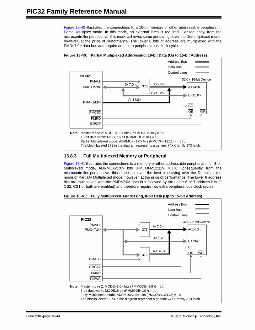
PIC32 Family Reference Manual
Figure 13-40 illustrates the connections to a 16-bit memory or other addressable peripheral in Partial Multiplex mode. In this mode, an external latch is required. Consequently, from the microcontroller perspective, this mode achieves some pin savings over the Demultiplexed mode, however, at the price of performance. The lower 8 bits of address are multiplexed with the PMD<7:0> data bus and require one extra peripheral bus clock cycle.
Figure 13-40: Partial Multiplexed Addressing, 16-bit Data (Up to 15-bit Address)
13.8.3 Full Multiplexed Memory or PeripheralFigure 13-41 illustrates the connections to a memory or other addressable peripheral in full 8-bit Multiplexed mode, ADRMUX<1:0> bits (PMCON<12:11>) = 10. Consequently, from the microcontroller perspective, this mode achieves the best pin saving over the Demultiplexed mode or Partially Multiplexed mode, however, at the price of performance. The lower 8 address bits are multiplexed with the PMD<7:0> data bus followed by the upper 6 or 7 address bits (if CS2, CS1 or both are enabled) and therefore require two extra peripheral bus clock cycles.
Figure 13-41: Fully Multiplexed Addressing, 8-bit Data (Up to 15-bit Address)
PMA<14:8>
D<7:0> 373 A<14:0>
D<15:0>
A<7:0>
PMRD
PMWR
OE WR
CE
PIC32
Address BusData BusControl Lines
PMCS2
PMALL
A<14:8>
PMD<15:0>
Note: Master mode 2: MODE<1:0> bits (PMMODE<9:8>) = 10. 16-bit data width: MODE16 bit (PMMODE<10>) = 1. Partial Multiplexed mode: ADRMUX<1:0> bits (PMCON<12:11>) = 01. The block labeled 373 in the diagram represents a generic 74XX family 373 latch.
32K x 16-bit Device
D<15:0>
PMD<7:0>
PMALH
D<7:0>
373 A<14:0>
D<7:0>
A<7:0>
373
PMRD
PMWR
OE WR
CE
PIC32
Address BusData BusControl Lines
PMCS2
PMALL
A<14:8>
Note: Master mode 2: MODE<1:0> bits (PMMODE<9:8>) = 10. 8-bit data width: MODE16 bit (PMMODE<10>) = 0. Fully Multiplexed mode: ADRMUX<1:0> bits (PMCON<12:11>) = 10. The blocks labeled 373 in the diagram represent a generic 74XX family 373 latch.
32K x 8-bit Device
DS61128F-page 13-44 © 2011 Microchip Technology Inc.
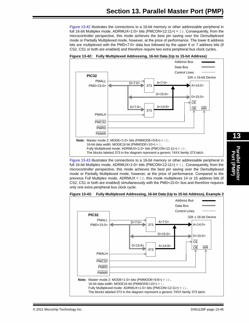
Section 13. Parallel Master Port (PMP)Parallel M
aster Port (PM
P)
13
Figure 13-42 illustrates the connections to a 16-bit memory or other addressable peripheral in full 16-bit Multiplex mode, ADRMUX<1:0> bits (PMCON<12:11>) = 10. Consequently, from the microcontroller perspective, this mode achieves the best pin saving over the Demultiplexed mode or Partially Multiplexed mode, however, at the price of performance. The lower 8 address bits are multiplexed with the PMD<7:0> data bus followed by the upper 6 or 7 address bits (if CS2, CS1 or both are enabled) and therefore require two extra peripheral bus clock cycles.
Figure 13-42: Fully Multiplexed Addressing, 16-bit Data (Up to 15-bit Address)
Figure 13-43 illustrates the connections to a 16-bit memory or other addressable peripheral in full 16-bit Multiplex mode, ADRMUX<1:0> bits (PMCON<12:11>) = 11. Consequently, from the microcontroller perspective, this mode achieves the best pin saving over the Demultiplexed mode or Partially Multiplexed mode, however, at the price of performance. Compared to the previous Full Multiplex mode, ADRMUX = 10, this mode multiplexes 14 or 15 address bits (if CS2, CS1 or both are enabled) simultaneously with the PMD<15:0> bus and therefore requires only one extra peripheral bus clock cycle.
Figure 13-43: Fully Multiplexed Addressing, 16-bit Data (Up to 15-bit Address), Example 2
PMD<15:0>
PMALH
D<15:0>
373 A<14:0>
D<15:0>
A<7:0>
373
PMRD
PMWR
OE WR
CE
PIC32
Address BusData BusControl Lines
PMCS2
PMALL
A<14:8>
Note: Master mode 2: MODE<1:0> bits (PMMODE<9:8>) = 10. 16-bit data width: MODE16 bit (PMMODE<10>) = 1. Fully Multiplexed mode: ADRMUX<1:0> bits (PMCON<12:11>) = 10. The blocks labeled 373 in the diagram represent a generic 74XX family 373 latch.
D<7:0>
D<7:0>
32K x 16-bit Device
PMD<15:0>
PMALH
D<15:0>
373 A<14:0>
D<15:0>
A<7:0>
373
PMRD
PMWR
OE WR
CE
PIC32
PMCS2
PMALL
A<14:8>
Note: Master mode 2: MODE<1:0> bits (PMMODE<9:8>) = 10. 16-bit data width: MODE16 bit (PMMODE<10>) = 1. Fully Multiplexed mode: ADRMUX<1:0> bits (PMCON<12:11>) = 11. The blocks labeled 373 in the diagram represent a generic 74XX family 373 latch.
D<15:8>
D<7:0>32K x 16-bit Device
Address BusData BusControl Lines
© 2011 Microchip Technology Inc. DS61128F-page 13-45
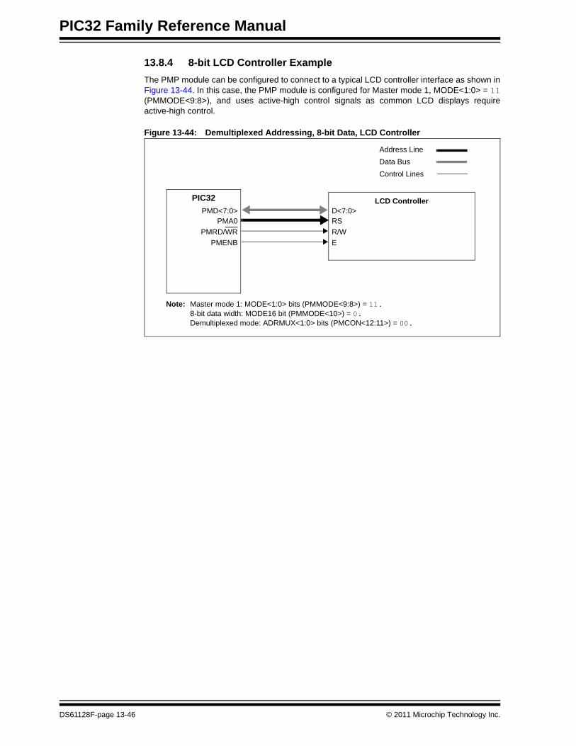
PIC32 Family Reference Manual
13.8.4 8-bit LCD Controller ExampleThe PMP module can be configured to connect to a typical LCD controller interface as shown in Figure 13-44. In this case, the PMP module is configured for Master mode 1, MODE<1:0> = 11(PMMODE<9:8>), and uses active-high control signals as common LCD displays require active-high control.
Figure 13-44: Demultiplexed Addressing, 8-bit Data, LCD Controller
PMD<7:0>
PMRD/WR
D<7:0>
PIC32
Address LineData BusControl Lines
PMA0R/WRS
E
LCD Controller
PMENB
Note: Master mode 1: MODE<1:0> bits (PMMODE<9:8>) = 11. 8-bit data width: MODE16 bit (PMMODE<10>) = 0. Demultiplexed mode: ADRMUX<1:0> bits (PMCON<12:11>) = 00.
DS61128F-page 13-46 © 2011 Microchip Technology Inc.
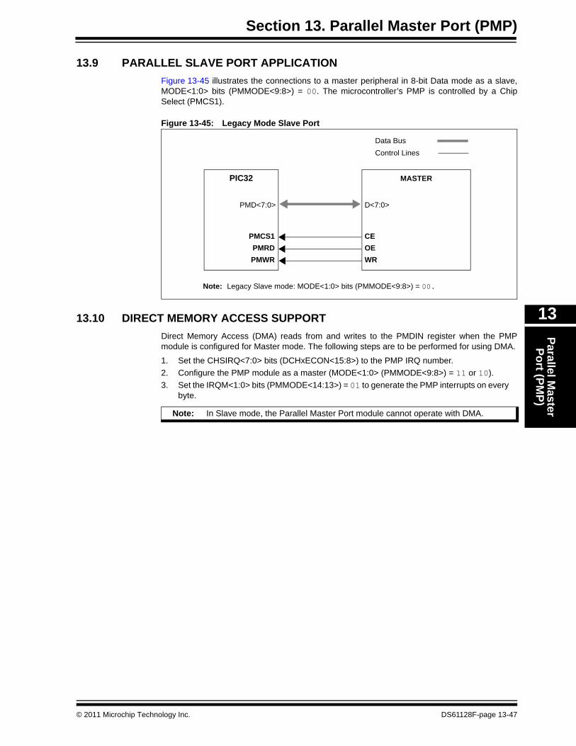
Section 13. Parallel Master Port (PMP)Parallel M
aster Port (PM
P)
13
13.9 PARALLEL SLAVE PORT APPLICATIONFigure 13-45 illustrates the connections to a master peripheral in 8-bit Data mode as a slave, MODE<1:0> bits (PMMODE<9:8>) = 00. The microcontroller’s PMP is controlled by a Chip Select (PMCS1).
Figure 13-45: Legacy Mode Slave Port
13.10 DIRECT MEMORY ACCESS SUPPORTDirect Memory Access (DMA) reads from and writes to the PMDIN register when the PMP module is configured for Master mode. The following steps are to be performed for using DMA.
1. Set the CHSIRQ<7:0> bits (DCHxECON<15:8>) to the PMP IRQ number.2. Configure the PMP module as a master (MODE<1:0> (PMMODE<9:8>) = 11 or 10).3. Set the IRQM<1:0> bits (PMMODE<14:13>) = 01 to generate the PMP interrupts on every
byte.
D<7:0>
PMRDPMWR
OEWR
CE
PIC32
PMCS1
PMD<7:0>
MASTER
Note: Legacy Slave mode: MODE<1:0> bits (PMMODE<9:8>) = 00.
Data BusControl Lines
Note: In Slave mode, the Parallel Master Port module cannot operate with DMA.
© 2011 Microchip Technology Inc. DS61128F-page 13-47
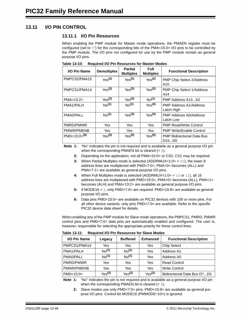
PIC32 Family Reference Manual
13.11 I/O PIN CONTROL
13.11.1 I/O Pin ResourcesWhen enabling the PMP module for Master mode operations, the PMAEN register must be configured (set to ‘1’) for the corresponding bits of the PMA<15:0> I/O pins to be controlled by the PMP module. The I/O pins not configured for use by the PMP module remain as general purpose I/O pins.
When enabling any of the PMP module for Slave mode operations, the PMPCS1, PMRD, PMWR control pins and PMD<7:0> data pins are automatically enabled and configured. The user is,however, responsible for selecting the appropriate polarity for these control lines.
Table 13-10: Required I/O Pin Resources for Master Modes
I/O Pin Name Demultiplex Partial Multiplex
Full Multiplex Functional Description
PMPCS2/PMA15 Yes(2) Yes(2) Yes(2) PMP Chip Select 2/Address A15
PMPCS1/PMA14 Yes(2) Yes(2) Yes(2) PMP Chip Select 1/Address A14
PMA<13:2> Yes(2) Yes(3) No(1) PMP Address A13...A2PMA1/PALH No(1) No(1) Yes(4) PMP Address A1/Address
Latch HighPMA0/PALL No(1) Yes(3) Yes(4) PMP Address A0/Address
Latch LowPMRD/PMWR Yes Yes Yes PMP Read/Write ControlPMWR/PMENB Yes Yes Yes PMP Write/Enable ControlPMD<15:0>(6) Yes(5) Yes(5) Yes(5) PMP Bidirectional Data Bus
D15...D0Note 1: “No” indicates the pin is not required and is available as a general purpose I/O pin
when the corresponding PMAEN bit is cleared (= 0).2: Depending on the application, not all PMA<15:0> or CS2, CS1 may be required.3: When Partial Multiplex mode is selected (ADDRMUX<1:0> = 01), the lower 8
address lines are multiplexed with PMD<7:0>, PMA<0> becomes (ALL) and PMA<7:1> are available as general purpose I/O pins.
4: When Full Multiplex mode is selected (ADDRMUX<1:0> = 10 or 11), all 16 address lines are multiplexed with PMD<15:0>, PMA<0> becomes (ALL), PMA<1> becomes (ALH) and PMA<13:2> are available as general purpose I/O pins.
5: If MODE16 = 0, only PMD<7:0> are required. PMD<15:8> are available as general purpose I/O pins.
6: Data pins PMD<15:0> are available on PIC32 devices with 100 or more pins. For all other device variants, only pins PMD<7:0> are available. Refer to the specific PIC32 device data sheet for details.
Table 13-11: Required I/O Pin Resources for Slave ModesI/O Pin Name Legacy Buffered Enhanced Functional Description
PMPCS1/PMA14 Yes Yes Yes Chip SelectPMA1/PALH No(1) No(1) Yes Address A1PMA0/PALL No(1) No(1) Yes Address A0PMRD/PMWR Yes Yes Yes Read ControlPMWR/PMENB Yes Yes Yes Write ControlPMD<15:0> Yes(2) Yes(2) Yes(2) Bidirectional Data Bus D7...D0Note 1: “No” indicates the pin is not required and is available as a general purpose I/O pin
when the corresponding PMAEN bit is cleared (= 0).2: Slave modes use only PMD<7:0> pins. PMD<15:8> are available as general pur-
pose I/O pins. Control bit MODE16 (PMMODE<10>) is ignored.
DS61128F-page 13-48 © 2011 Microchip Technology Inc.
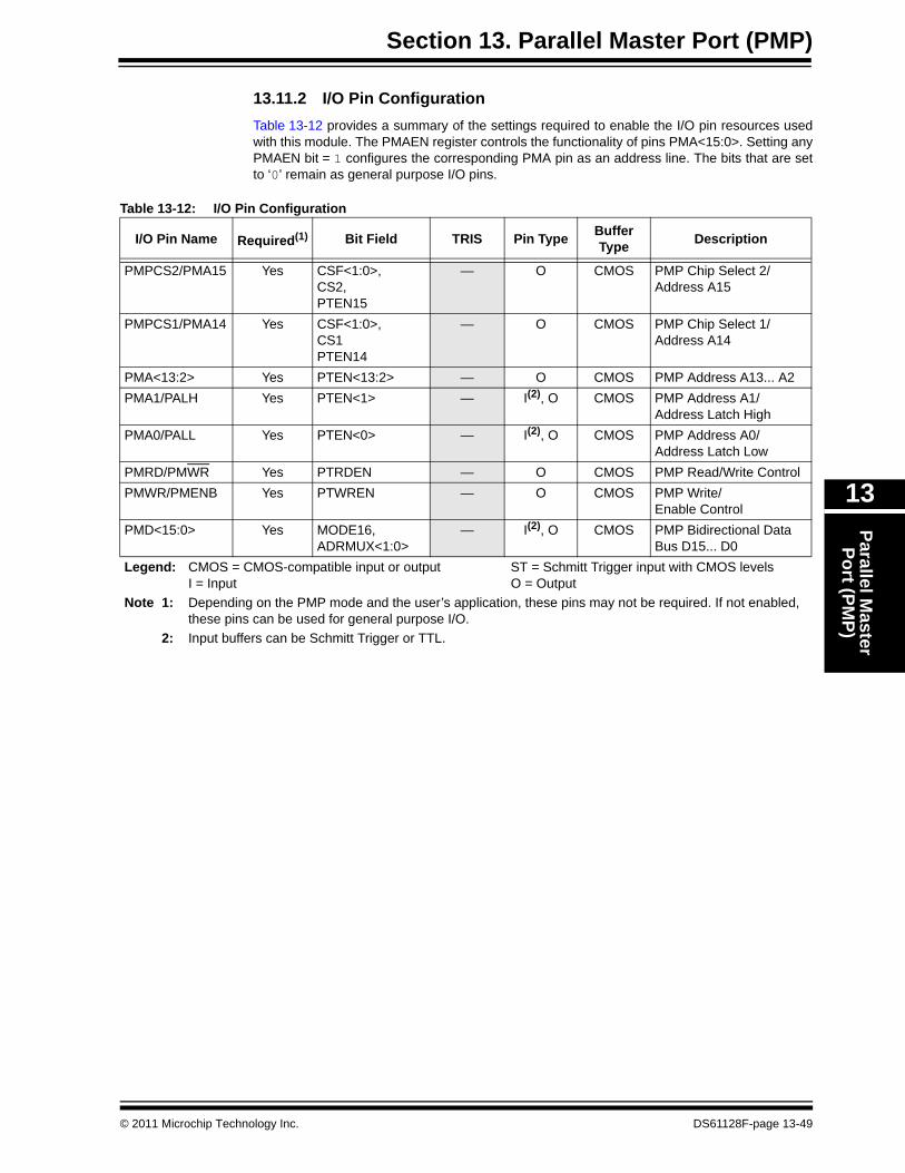
Section 13. Parallel Master Port (PMP)Parallel M
aster Port (PM
P)
13
13.11.2 I/O Pin ConfigurationTable 13-12 provides a summary of the settings required to enable the I/O pin resources used with this module. The PMAEN register controls the functionality of pins PMA<15:0>. Setting any PMAEN bit = 1 configures the corresponding PMA pin as an address line. The bits that are set to ‘0’ remain as general purpose I/O pins.
Table 13-12: I/O Pin Configuration
I/O Pin Name Required(1) Bit Field TRIS Pin Type BufferType Description
PMPCS2/PMA15 Yes CSF<1:0>, CS2,PTEN15
— O CMOS PMP Chip Select 2/ Address A15
PMPCS1/PMA14 Yes CSF<1:0>, CS1PTEN14
— O CMOS PMP Chip Select 1/ Address A14
PMA<13:2> Yes PTEN<13:2> — O CMOS PMP Address A13... A2PMA1/PALH Yes PTEN<1> — I(2), O CMOS PMP Address A1/
Address Latch HighPMA0/PALL Yes PTEN<0> — I(2), O CMOS PMP Address A0/
Address Latch LowPMRD/PMWR Yes PTRDEN — O CMOS PMP Read/Write ControlPMWR/PMENB Yes PTWREN — O CMOS PMP Write/
Enable ControlPMD<15:0> Yes MODE16,
ADRMUX<1:0>— I(2), O CMOS PMP Bidirectional Data
Bus D15... D0Legend: CMOS = CMOS-compatible input or output ST = Schmitt Trigger input with CMOS levels
I = Input O = Output Note 1: Depending on the PMP mode and the user’s application, these pins may not be required. If not enabled,
these pins can be used for general purpose I/O.2: Input buffers can be Schmitt Trigger or TTL.
© 2011 Microchip Technology Inc. DS61128F-page 13-49
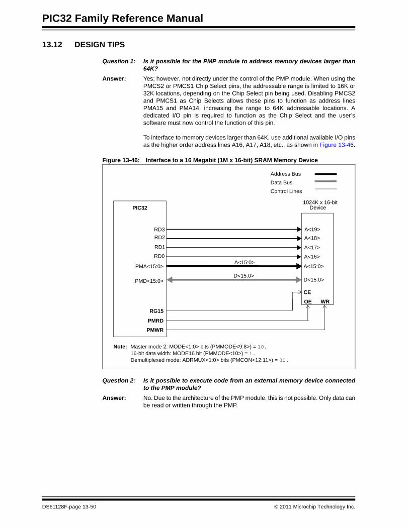
PIC32 Family Reference Manual
13.12 DESIGN TIPS
Question 1: Is it possible for the PMP module to address memory devices larger than 64K?
Answer: Yes; however, not directly under the control of the PMP module. When using the PMCS2 or PMCS1 Chip Select pins, the addressable range is limited to 16K or 32K locations, depending on the Chip Select pin being used. Disabling PMCS2 and PMCS1 as Chip Selects allows these pins to function as address lines PMA15 and PMA14, increasing the range to 64K addressable locations. A dedicated I/O pin is required to function as the Chip Select and the user’s software must now control the function of this pin. To interface to memory devices larger than 64K, use additional available I/O pins as the higher order address lines A16, A17, A18, etc., as shown in Figure 13-46.
Figure 13-46: Interface to a 16 Megabit (1M x 16-bit) SRAM Memory Device
Question 2: Is it possible to execute code from an external memory device connected to the PMP module?
Answer: No. Due to the architecture of the PMP module, this is not possible. Only data can be read or written through the PMP.
PMA<15:0>
D<15:0>
A<15:0>
D<15:0>
A<15:0>
PMRD
PMWR
OE WR
CE
PIC32
Address BusData BusControl Lines
RG15
PMD<15:0>
Note: Master mode 2: MODE<1:0> bits (PMMODE<9:8>) = 10. 16-bit data width: MODE16 bit (PMMODE<10>) = 1. Demultiplexed mode: ADRMUX<1:0> bits (PMCON<12:11>) = 00.
RD0
RD1
RD2
A<16>
A<17>
A<18>A<19>RD3
1024K x 16-bit Device
DS61128F-page 13-50 © 2011 Microchip Technology Inc.
Section 13. Parallel Master Port (PMP)Parallel M
aster Port (PM
P)
13
13.13 RELATED APPLICATION NOTESThis section lists application notes that are related to this section of the manual. These application notes may not be written specifically for the PIC32 device family, but the concepts are pertinent and could be used with modification and possible limitations. The current application notes related to the Parallel Master Port (PMP) module are:
Title Application Note #No related application notes at this time. N/A
Note: Please visit the Microchip web site (www.microchip.com) for additional Application Notes and code examples for the PIC32 family of devices.
© 2011 Microchip Technology Inc. DS61128F-page 13-51
PIC32 Family Reference Manual
13.14 REVISION HISTORY
Revision A (August 2007)This is the initial released version of this document.
Revision B (October 2007)Updated document to remove Confidential status.
Revision C (April 2008)Revised status to Preliminary; Revised U-0 to r-x; Revised Table 13-10; Revised Section 13.3.1.6 and Section 13.3.8; Revised Register 13-5; Revised Figures 13-11, 13-37, 13-40, 13-41, 13-42, 13-43, 13-46; Revised Timing Diagram text for Figures 13-16, 13-18, 13-19.
Revision D (June 2008)Revised Register 13-1, add note to FRZ; Revised Figures 13-4, 13-6, 13-8, 13-10, 13-36, 13-37, 13-38, 13-45; Revised Table 13-6; Revised Examples 13-6 and 13-7; Change Reserved bits from “Maintain as” to “Write”; Added Note to ON bit (PMCON Register).
Revision E (October 2009)This revision includes the following updates:
• Minor updates to text and formatting have been implemented throughout the document• Added the following item to the key feature list: Schmitt Trigger or TTL input buffers (see
13.1 “Introduction”)• Interrupts Register Summary (Table 13-1):
- Removed all references to the Clear, Set and Invert registers- Added the Address Offset column- Added Notes 1, 2 and 3, which describe the Clear, Set and Invert registers
• Added Notes 1, 2 and 3, which describe the Clear, Set and Invert registers to the following registers- PMCON: Parallel Port Control Register (see Register 13-1)- PMMODE: Parallel Port Mode Register (see Register 13-2)- PMADDR: Parallel Port Address Register (see Register 13-3)- PMDOUT: Parallel Port Data Output Register (see Register 13-4)- PMDIN: Parallel Port Data Input Register (see Register 13-5)- PMAEN: Parallel Port Pin Enable Register (see Register 13-6)- PMSTAT: Parallel Port Status Register (Slave modes only) (see Register 13-7)
• Removed all references to Interrupt registers (IEC1, IFS1 and IPC7)• Added a shaded note to 13.4.1.4 “Legacy Mode Interrupt Operation”• Updated the 2-3 TPBCLK cycles duration in Figure 13-32, Figure 13-33, Figure 13-34 and
Figure 13-35• Added Note 2 to the I/O Pin Configuration table (Table 13-12)
Revision F (May 2011)This revision includes the following updates:
• Changed all occurrences of PIC32MX to PIC32• Updated the note in section 13.4.1.4 “Legacy Mode Interrupt Operation”• Added a new section 13.10 “Direct Memory Access Support”• Removed the Notes referencing the CLR, SET, and INV registers from all register tables• Changed all occurrences of r-x to U-0 in all register tables• Updated Figure 13-32 and Figure 13-33• Removed the Module Control column from Table 13-12
DS61128F-page 13-52 © 2011 Microchip Technology Inc.
Section 13. Parallel Master Port (PMP)Parallel M
aster Port (PM
P)
13
Revision F (May 2011) (Continued)• Removed the note from section 13.6.2 “PMP Operation in Idle Mode”• Removed the Table 13-10 and Table 13-11• Minor changes to the text and formatting have been incorporated throughout the document
© 2011 Microchip Technology Inc. DS61128F-page 13-53
PIC32 Family Reference Manual
NOTES:
DS61128F-page 13-54 © 2011 Microchip Technology Inc.
Note the following details of the code protection feature on Microchip devices:• Microchip products meet the specification contained in their particular Microchip Data Sheet.
• Microchip believes that its family of products is one of the most secure families of its kind on the market today, when used in the intended manner and under normal conditions.
• There are dishonest and possibly illegal methods used to breach the code protection feature. All of these methods, to our knowledge, require using the Microchip products in a manner outside the operating specifications contained in Microchip’s Data Sheets. Most likely, the person doing so is engaged in theft of intellectual property.
• Microchip is willing to work with the customer who is concerned about the integrity of their code.
• Neither Microchip nor any other semiconductor manufacturer can guarantee the security of their code. Code protection does not mean that we are guaranteeing the product as “unbreakable.”
Code protection is constantly evolving. We at Microchip are committed to continuously improving the code protection features of our products. Attempts to break Microchip’s code protection feature may be a violation of the Digital Millennium Copyright Act. If such acts allow unauthorized access to your software or other copyrighted work, you may have a right to sue for relief under that Act.
Information contained in this publication regarding device applications and the like is provided only for your convenience and may be superseded by updates. It is your responsibility to ensure that your application meets with your specifications. MICROCHIP MAKES NO REPRESENTATIONS OR WARRANTIES OF ANY KIND WHETHER EXPRESS OR IMPLIED, WRITTEN OR ORAL, STATUTORY OR OTHERWISE, RELATED TO THE INFORMATION, INCLUDING BUT NOT LIMITED TO ITS CONDITION, QUALITY, PERFORMANCE, MERCHANTABILITY OR FITNESS FOR PURPOSE. Microchip disclaims all liability arising from this information and its use. Use of Microchip devices in life support and/or safety applications is entirely at the buyer’s risk, and the buyer agrees to defend, indemnify and hold harmless Microchip from any and all damages, claims, suits, or expenses resulting from such use. No licenses are conveyed, implicitly or otherwise, under any Microchip intellectual property rights.
© 2011 Microchip Technology Inc.
Trademarks
The Microchip name and logo, the Microchip logo, dsPIC, KEELOQ, KEELOQ logo, MPLAB, PIC, PICmicro, PICSTART, PIC32 logo, rfPIC and UNI/O are registered trademarks of Microchip Technology Incorporated in the U.S.A. and other countries.
FilterLab, Hampshire, HI-TECH C, Linear Active Thermistor, MXDEV, MXLAB, SEEVAL and The Embedded Control Solutions Company are registered trademarks of Microchip Technology Incorporated in the U.S.A.
Analog-for-the-Digital Age, Application Maestro, CodeGuard, dsPICDEM, dsPICDEM.net, dsPICworks, dsSPEAK, ECAN, ECONOMONITOR, FanSense, HI-TIDE, In-Circuit Serial Programming, ICSP, Mindi, MiWi, MPASM, MPLAB Certified logo, MPLIB, MPLINK, mTouch, Omniscient Code Generation, PICC, PICC-18, PICDEM, PICDEM.net, PICkit, PICtail, REAL ICE, rfLAB, Select Mode, Total Endurance, TSHARC, UniWinDriver, WiperLock and ZENA are trademarks of Microchip Technology Incorporated in the U.S.A. and other countries.
SQTP is a service mark of Microchip Technology Incorporated in the U.S.A.
All other trademarks mentioned herein are property of their respective companies.
© 2011, Microchip Technology Incorporated, Printed in the U.S.A., All Rights Reserved.
Printed on recycled paper.
ISBN: 978-1-61341-193-3
DS61128F-page 13 -55
Microchip received ISO/TS-16949:2002 certification for its worldwide headquarters, design and wafer fabrication facilities in Chandler and Tempe, Arizona; Gresham, Oregon and design centers in California and India. The Company’s quality system processes and procedures are for its PIC® MCUs and dsPIC® DSCs, KEELOQ® code hopping devices, Serial EEPROMs, microperipherals, nonvolatile memory and analog products. In addition, Microchip’s quality system for the design and manufacture of development systems is ISO 9001:2000 certified.

DS61128F-page 13-56 © 2011 Microchip Technology Inc.
AMERICASCorporate Office2355 West Chandler Blvd.Chandler, AZ 85224-6199Tel: 480-792-7200 Fax: 480-792-7277Technical Support: http://www.microchip.com/supportWeb Address: www.microchip.comAtlantaDuluth, GA Tel: 678-957-9614 Fax: 678-957-1455BostonWestborough, MA Tel: 774-760-0087 Fax: 774-760-0088ChicagoItasca, IL Tel: 630-285-0071 Fax: 630-285-0075ClevelandIndependence, OH Tel: 216-447-0464 Fax: 216-447-0643DallasAddison, TX Tel: 972-818-7423 Fax: 972-818-2924DetroitFarmington Hills, MI Tel: 248-538-2250Fax: 248-538-2260IndianapolisNoblesville, IN Tel: 317-773-8323Fax: 317-773-5453Los AngelesMission Viejo, CA Tel: 949-462-9523 Fax: 949-462-9608Santa ClaraSanta Clara, CA Tel: 408-961-6444Fax: 408-961-6445TorontoMississauga, Ontario, CanadaTel: 905-673-0699 Fax: 905-673-6509
ASIA/PACIFICAsia Pacific OfficeSuites 3707-14, 37th FloorTower 6, The GatewayHarbour City, KowloonHong KongTel: 852-2401-1200Fax: 852-2401-3431Australia - SydneyTel: 61-2-9868-6733Fax: 61-2-9868-6755China - BeijingTel: 86-10-8569-7000 Fax: 86-10-8528-2104China - ChengduTel: 86-28-8665-5511Fax: 86-28-8665-7889China - ChongqingTel: 86-23-8980-9588Fax: 86-23-8980-9500China - HangzhouTel: 86-571-2819-3180 Fax: 86-571-2819-3189China - Hong Kong SARTel: 852-2401-1200 Fax: 852-2401-3431China - NanjingTel: 86-25-8473-2460Fax: 86-25-8473-2470China - QingdaoTel: 86-532-8502-7355Fax: 86-532-8502-7205China - ShanghaiTel: 86-21-5407-5533 Fax: 86-21-5407-5066China - ShenyangTel: 86-24-2334-2829Fax: 86-24-2334-2393China - ShenzhenTel: 86-755-8203-2660 Fax: 86-755-8203-1760China - WuhanTel: 86-27-5980-5300Fax: 86-27-5980-5118China - XianTel: 86-29-8833-7252Fax: 86-29-8833-7256China - XiamenTel: 86-592-2388138 Fax: 86-592-2388130China - ZhuhaiTel: 86-756-3210040 Fax: 86-756-3210049
ASIA/PACIFICIndia - BangaloreTel: 91-80-3090-4444 Fax: 91-80-3090-4123India - New DelhiTel: 91-11-4160-8631Fax: 91-11-4160-8632India - PuneTel: 91-20-2566-1512Fax: 91-20-2566-1513Japan - YokohamaTel: 81-45-471- 6166 Fax: 81-45-471-6122Korea - DaeguTel: 82-53-744-4301Fax: 82-53-744-4302Korea - SeoulTel: 82-2-554-7200Fax: 82-2-558-5932 or 82-2-558-5934Malaysia - Kuala LumpurTel: 60-3-6201-9857Fax: 60-3-6201-9859Malaysia - PenangTel: 60-4-227-8870Fax: 60-4-227-4068Philippines - ManilaTel: 63-2-634-9065Fax: 63-2-634-9069SingaporeTel: 65-6334-8870Fax: 65-6334-8850Taiwan - Hsin ChuTel: 886-3-6578-300Fax: 886-3-6578-370Taiwan - KaohsiungTel: 886-7-213-7830Fax: 886-7-330-9305Taiwan - TaipeiTel: 886-2-2500-6610 Fax: 886-2-2508-0102Thailand - BangkokTel: 66-2-694-1351Fax: 66-2-694-1350
EUROPEAustria - WelsTel: 43-7242-2244-39Fax: 43-7242-2244-393Denmark - CopenhagenTel: 45-4450-2828 Fax: 45-4485-2829France - ParisTel: 33-1-69-53-63-20 Fax: 33-1-69-30-90-79Germany - MunichTel: 49-89-627-144-0 Fax: 49-89-627-144-44Italy - Milan Tel: 39-0331-742611 Fax: 39-0331-466781Netherlands - DrunenTel: 31-416-690399 Fax: 31-416-690340Spain - MadridTel: 34-91-708-08-90Fax: 34-91-708-08-91UK - WokinghamTel: 44-118-921-5869Fax: 44-118-921-5820
Worldwide Sales and Service
05/02/11