Embed Size (px)
Citation preview
Plasmonics and Metamaterials Literature survey
Som Phene
15D110001
Motivation for Metamaterials
• Diffraction Limit hurdle to higher resolution
• Localized Surface Plasmons: EM fields generated by resonant oscillations of electron plasma in metals
• Manipulating light at the subwavelength scale with new class of materials – “Metamaterials”
Index
• Plasmonics: origin, importance and applications
• Enhanced Transmission through Subwavelength hole
• Localized Plasmon Resonances in Metal Nanoparticles
• Metamaterials: Specific Applications
• Summary: Important results

Plasmonics: Origin
• Nanotechnology: Scaling down of devices
• Moore’s law for electronics- doubling of components per unit area in transistors but no corresponding observation for optical devices
• Electronic component size has reduced to ten nanometers but optical components are still at hundreds of nanometers
• Plasmonics gained significant attention and research input because it provided the possibility to scale down optical components to subwavelength scales

What is stopping miniaturization of optical devices? • Diffraction limit
• 3D conventional devices limiting planar integration
• Sharp corners being very lossy for electromagnetic fields in optical components
Plasmonics: Origin
• Limitation of optical imaging discovered by Abbe [1] and Rayleigh [2] due to the diffraction limit
• Ebbesen’s [3] discovery of extraordinary transmission
• Study of electromagnetic properties of metal-dielectric interface by Mie and Ritchie revealed that these interfaces can sustain coherent electron oscillations called surface plasmon polaritons (SPPs) leading to EM fields confined to the metallic surface
Plasmonics: Importance and Applications
• SPPs have wavelength shorter than that of light propagating in free space making on-chip subwavelength optics possible as in electrical devices
• This has found application in surfaced enhanced Raman spectroscopy, electron beam lithography, ion beam milling and near field microscopy
• New generation of materials termed “plasmonic metamaterials” emerged [4]
• Novel optical properties- negative index of refraction have been proposed and demonstrated [5,6,7]
Plasmonics: Importance and Applications
• Exotic optical devices- the invisibility cloak have been realized [8, 9]
• Light generated from a plasmonic cavity displays the Purcell effect which is used to make nanoscale laser demonstrated by several groups [10, 11, 12, 13]
• A strong localized field improves solar energy harvesting in the off-bandgap near-IR region [14]
• The THz optical modulator based on split ring resonator (SRR), has been demonstrated [15]
• A nanoscale plasmonic dipole antenna used to improve the efficiency of the photodetector at a near-IR range [16]
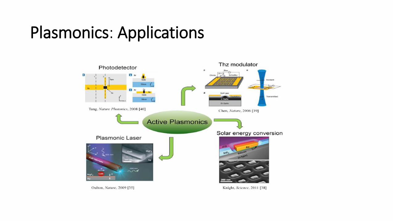
Plasmonics: Applications

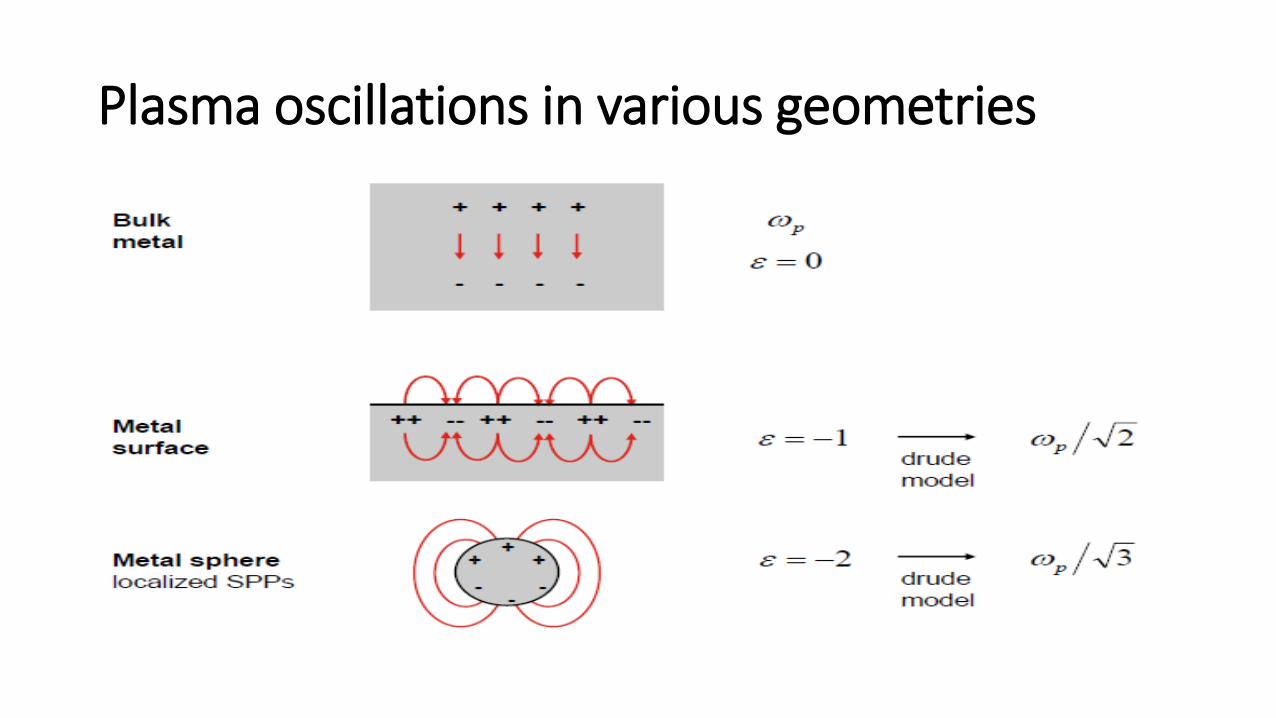
Plasmons
• The word plasmons comes from plasma oscillations
• Electron plasma oscillations in metal form plasmons
• Plasmons in bulk oscillate at ωp (plasma frequency)
• Resonant surface plasmon polariton (SPP) modes are formed on the surface of metal dielectric interface
• Localized surface plasmon resonance modes are supported in spherical metal nanoparticles
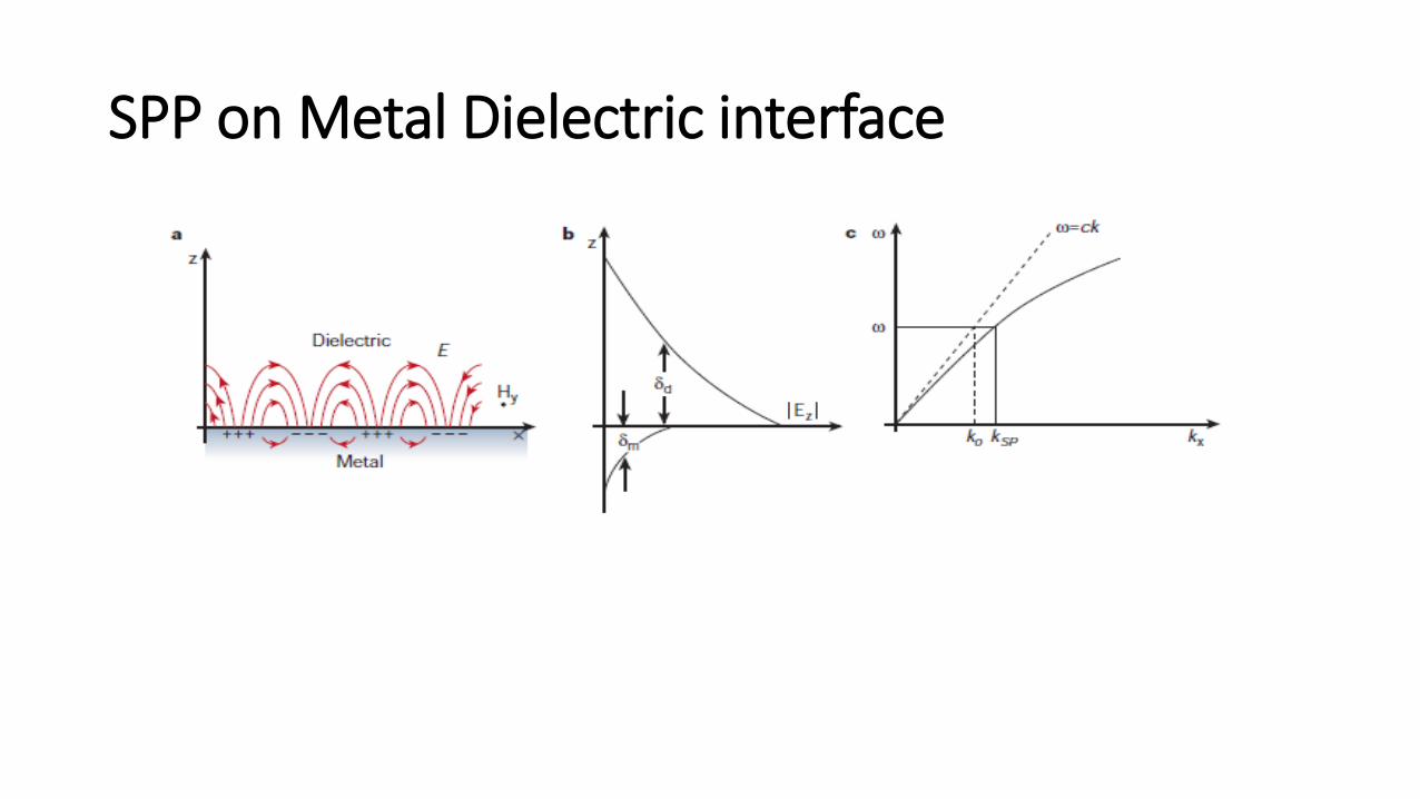
SPP on Metal Dielectric interface
Plasma oscillations in various geometries
Enhanced Transmission through Subwavelength Hole • Theory of Diffraction: Kirchhoff
• Bethe’s Analytical Solution
• Extraordinary Transmission
Theory of Diffraction
• Kirchhoff [17] attempted to explain Huygens-Fresnel principle.
• His theory worked fairly well in optical region where size of structure is lesser than wavelength.
• It failed due to assumption of scalar formulation which is contradicted by solution of the Helmholtz equation for given boundary conditions.
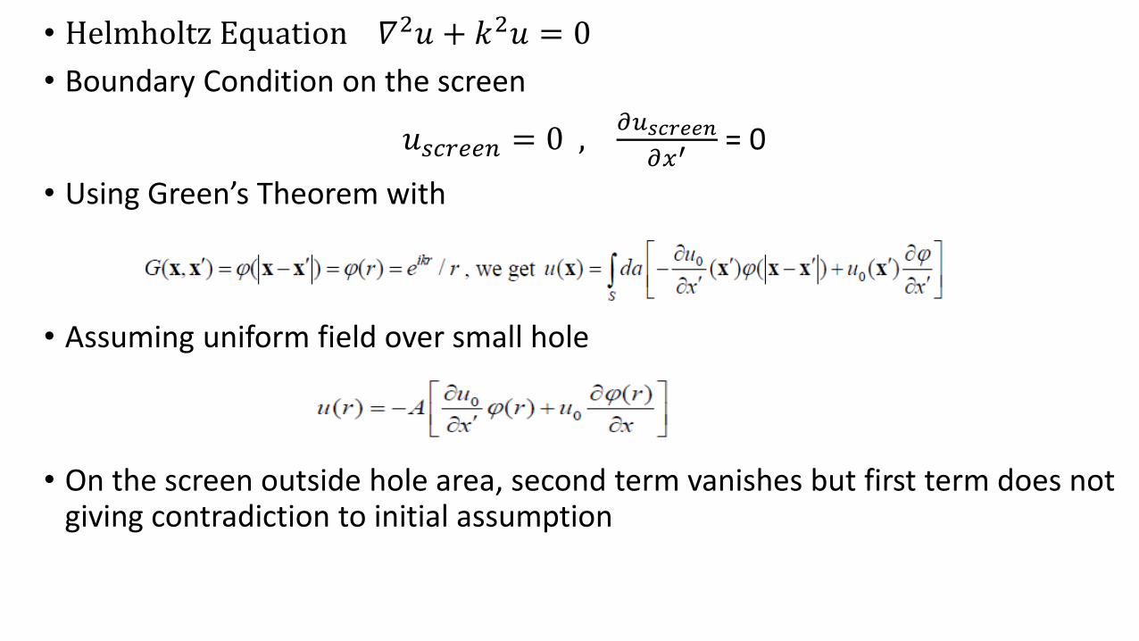
• Helmholtz Equation 𝛻2𝑢 + 𝑘2𝑢 = 0
• Boundary Condition on the screen
𝑢𝑠𝑐𝑟𝑒𝑒𝑛 = 0 , 𝜕𝑢𝑠𝑐𝑟𝑒𝑒𝑛
𝜕𝑥′ = 0
• Using Green’s Theorem with
• Assuming uniform field over small hole
• On the screen outside hole area, second term vanishes but first term does not giving contradiction to initial assumption
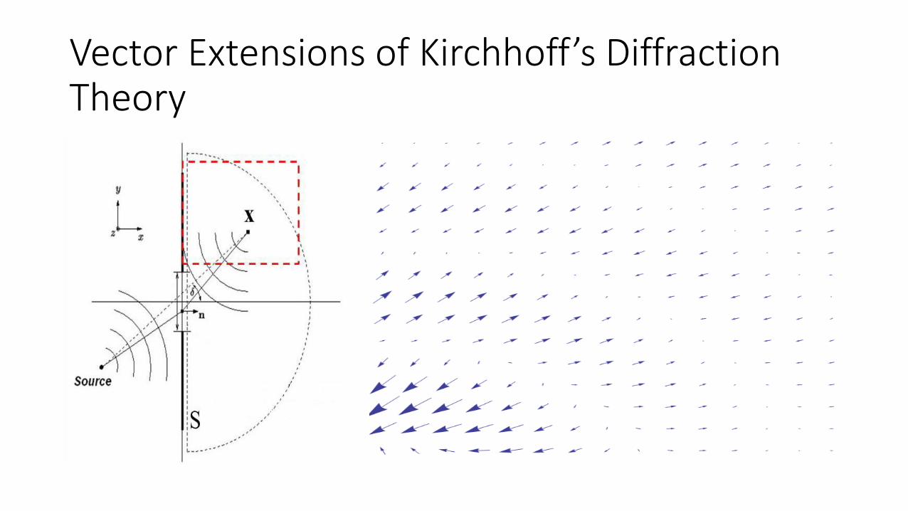
Vector Extensions of Kirchhoff’s Diffraction Theory
Bethe’s Analytical solution
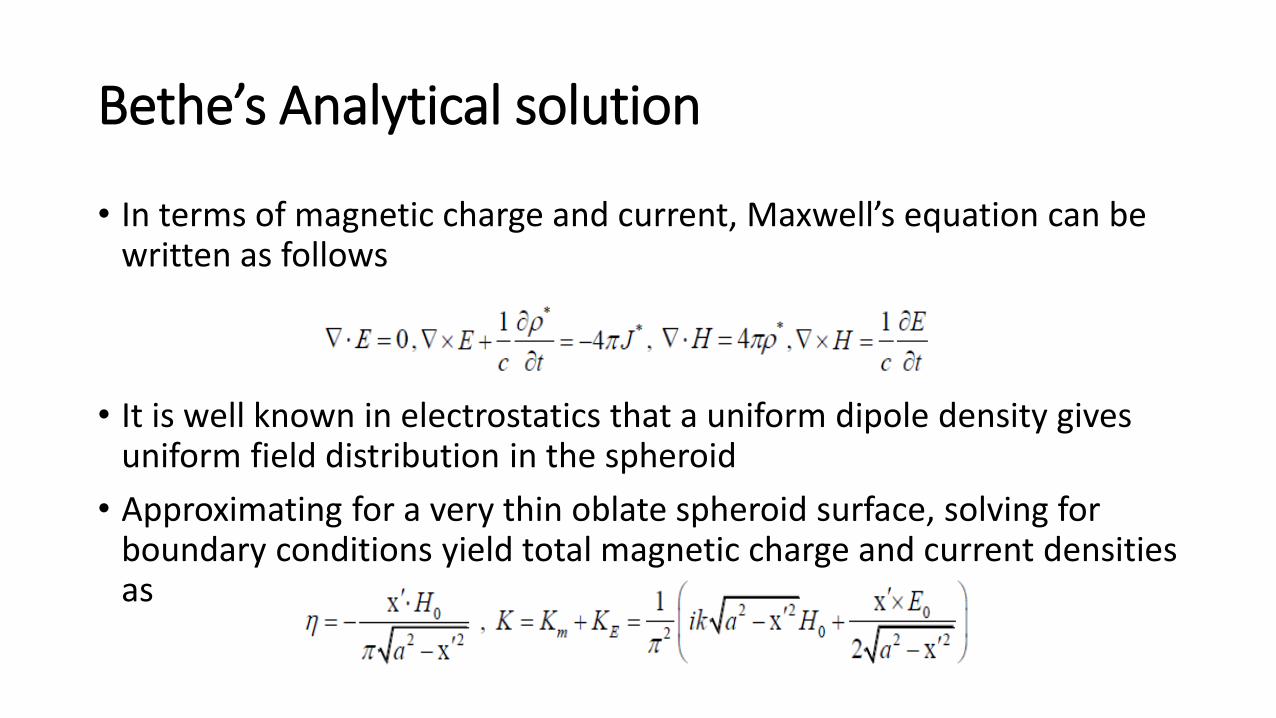
• In terms of magnetic charge and current, Maxwell’s equation can be written as follows
• It is well known in electrostatics that a uniform dipole density gives uniform field distribution in the spheroid
• Approximating for a very thin oblate spheroid surface, solving for boundary conditions yield total magnetic charge and current densities as

Bethe’s Analytical solution
• The field distribution of the diffracted wave can be directly calculated from given charge and current density:
• This field distribution is exactly same as essentially, in-plane magnetic dipole and normal electric dipole are generated in the hole, which satisfy the boundary conditions. Total cross section of a single hole is calculated by integration of the Poynting vector:
Extraordinary transmission
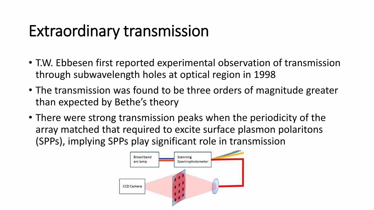
• T.W. Ebbesen first reported experimental observation of transmission through subwavelength holes at optical region in 1998
• The transmission was found to be three orders of magnitude greater than expected by Bethe’s theory
• There were strong transmission peaks when the periodicity of the array matched that required to excite surface plasmon polaritons (SPPs), implying SPPs play significant role in transmission
Localized Plasmon Resonances in Metal Nanoparticles • Spherical Metal Nanoparticles
• Mie Theory • Drude Lorentz Model of metals
• Light scattering off small spheres
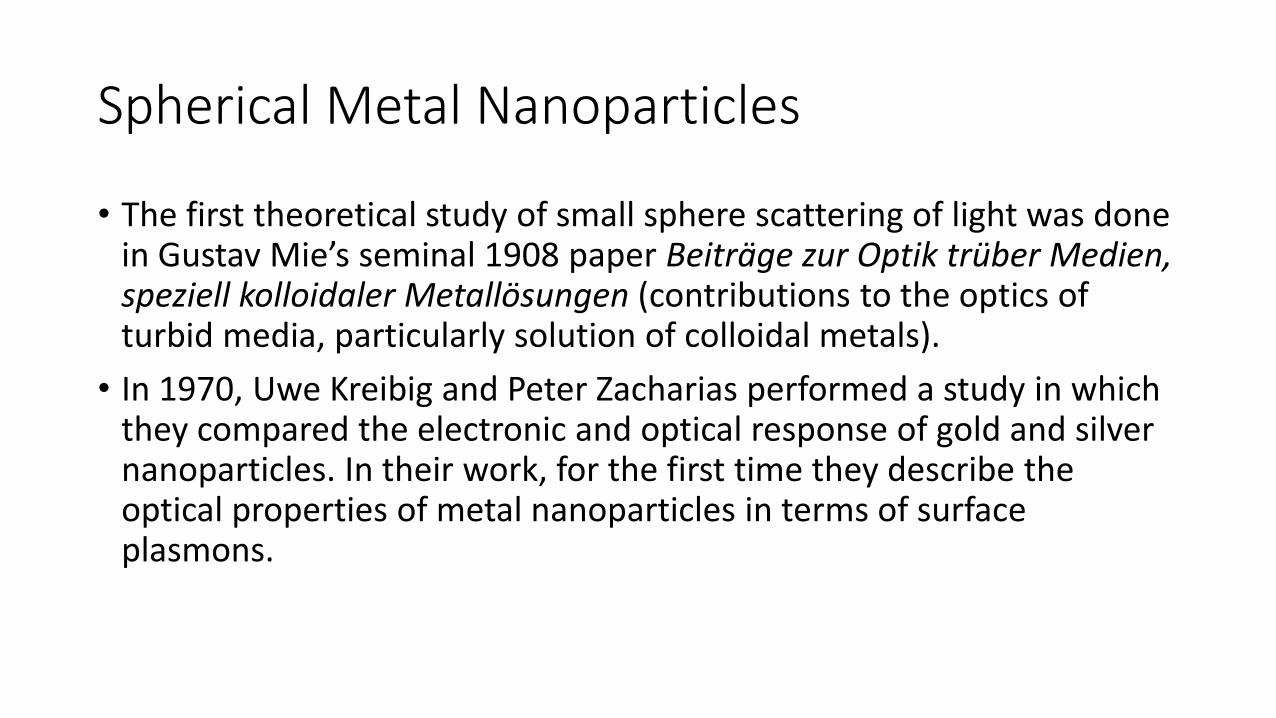
Spherical Metal Nanoparticles
• The first theoretical study of small sphere scattering of light was done in Gustav Mie’s seminal 1908 paper Beiträge zur Optik trüber Medien, speziell kolloidaler Metallösungen (contributions to the optics of turbid media, particularly solution of colloidal metals).
• In 1970, Uwe Kreibig and Peter Zacharias performed a study in which they compared the electronic and optical response of gold and silver nanoparticles. In their work, for the first time they describe the optical properties of metal nanoparticles in terms of surface plasmons.
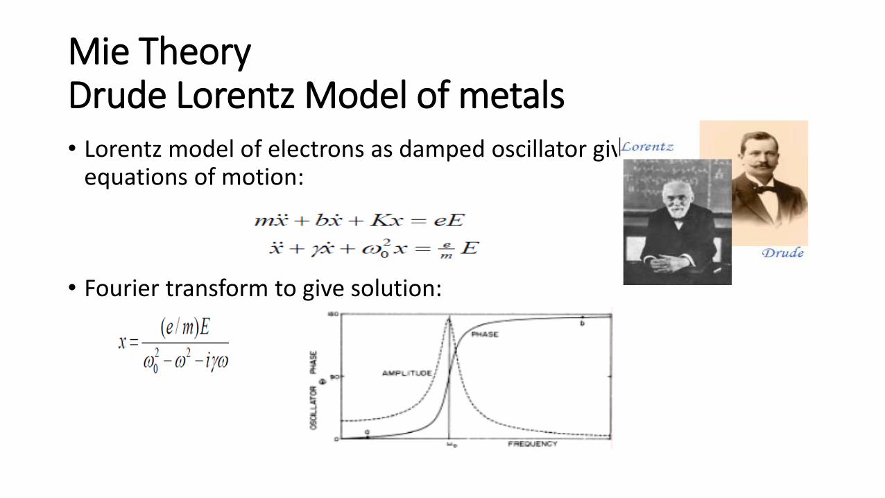
Mie Theory Drude Lorentz Model of metals • Lorentz model of electrons as damped oscillator gives the following
equations of motion:
• Fourier transform to give solution:

Drude Lorentz Model of metals
• Polarization = (N/V)ex
𝑃 =𝜔𝑝2𝜀0𝐸
𝜔02 −𝜔2 − 𝑖𝛾𝜔
• P = χε0E defines χ, and therefore also the dielectric ε = 1+χ
𝑅𝑒 𝜀 = 1 +𝜔𝑝2(𝜔02 −𝜔2)
(𝜔02−𝜔2)2 + 𝛾2𝜔2
𝐼𝑚 𝜀 =𝜔𝑝2𝛾𝜔
(𝜔02−𝜔2)2 + 𝛾2𝜔2
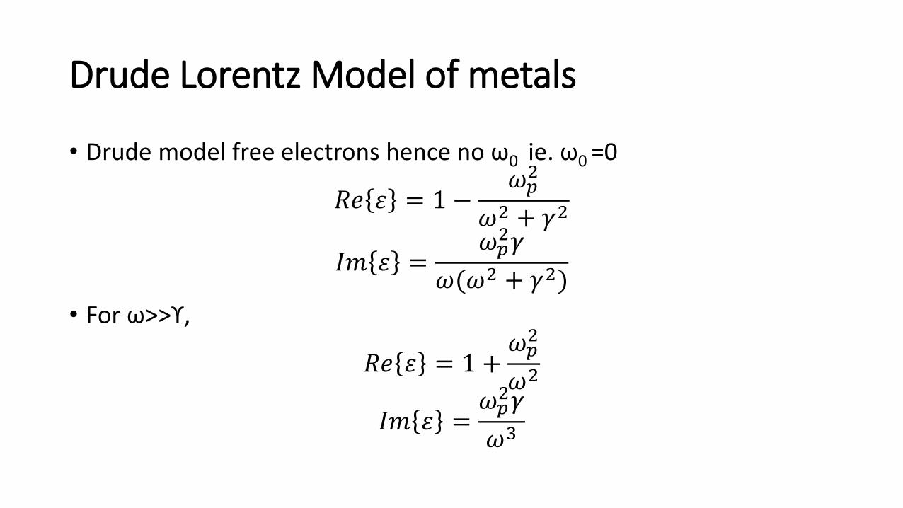
Drude Lorentz Model of metals
• Drude model free electrons hence no ω0 ie. ω0 =0
𝑅𝑒 𝜀 = 1 −𝜔𝑝2
𝜔2 + 𝛾2
𝐼𝑚 𝜀 =𝜔𝑝2𝛾
𝜔(𝜔2 + 𝛾2)
• For ω>>ϒ,
𝑅𝑒 𝜀 = 1 +𝜔𝑝2
𝜔2
𝐼𝑚 𝜀 =𝜔𝑝2𝛾
𝜔3
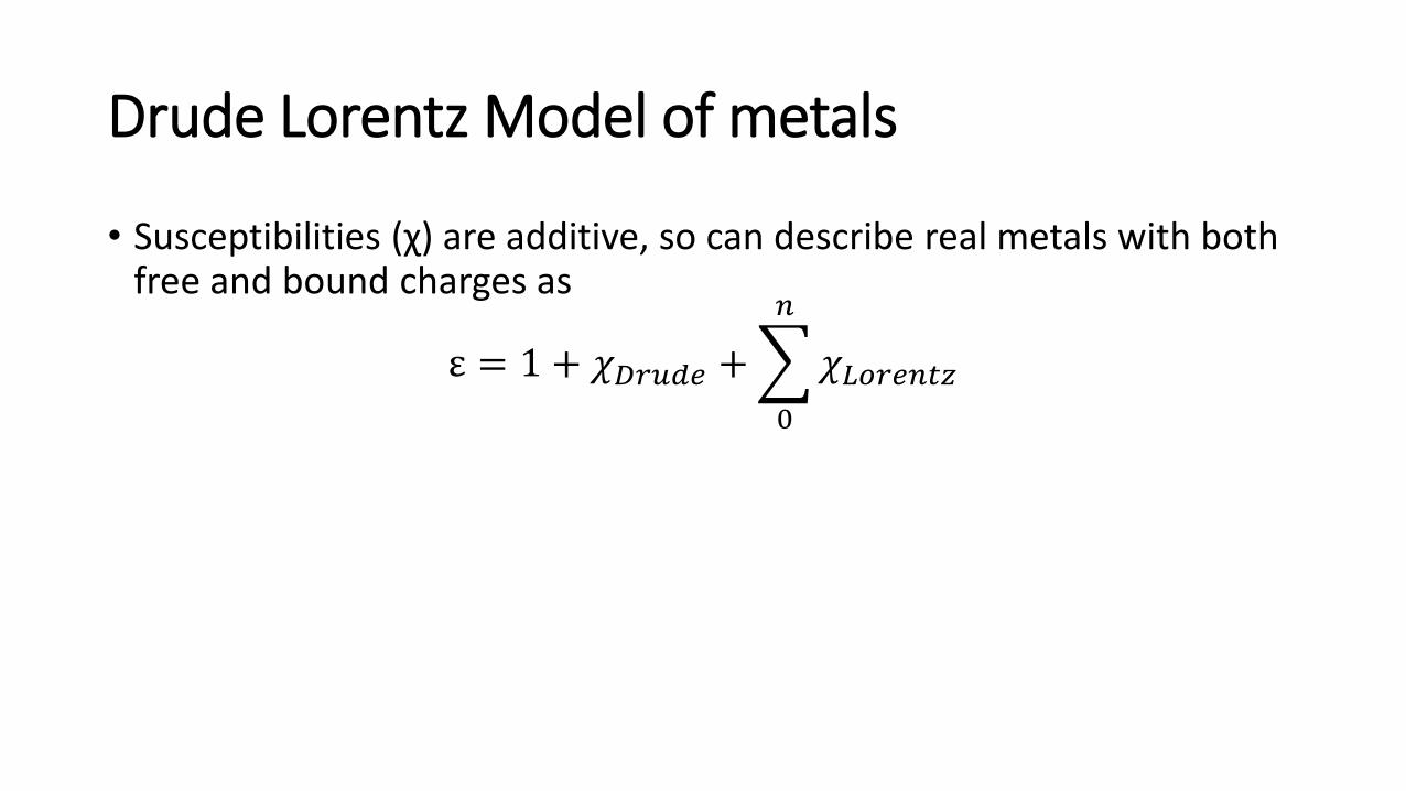
Drude Lorentz Model of metals
• Susceptibilities (χ) are additive, so can describe real metals with both free and bound charges as
ε = 1 + 𝜒𝐷𝑟𝑢𝑑𝑒 + 𝜒𝐿𝑜𝑟𝑒𝑛𝑡𝑧
𝑛
0
Light scattering off small spheres
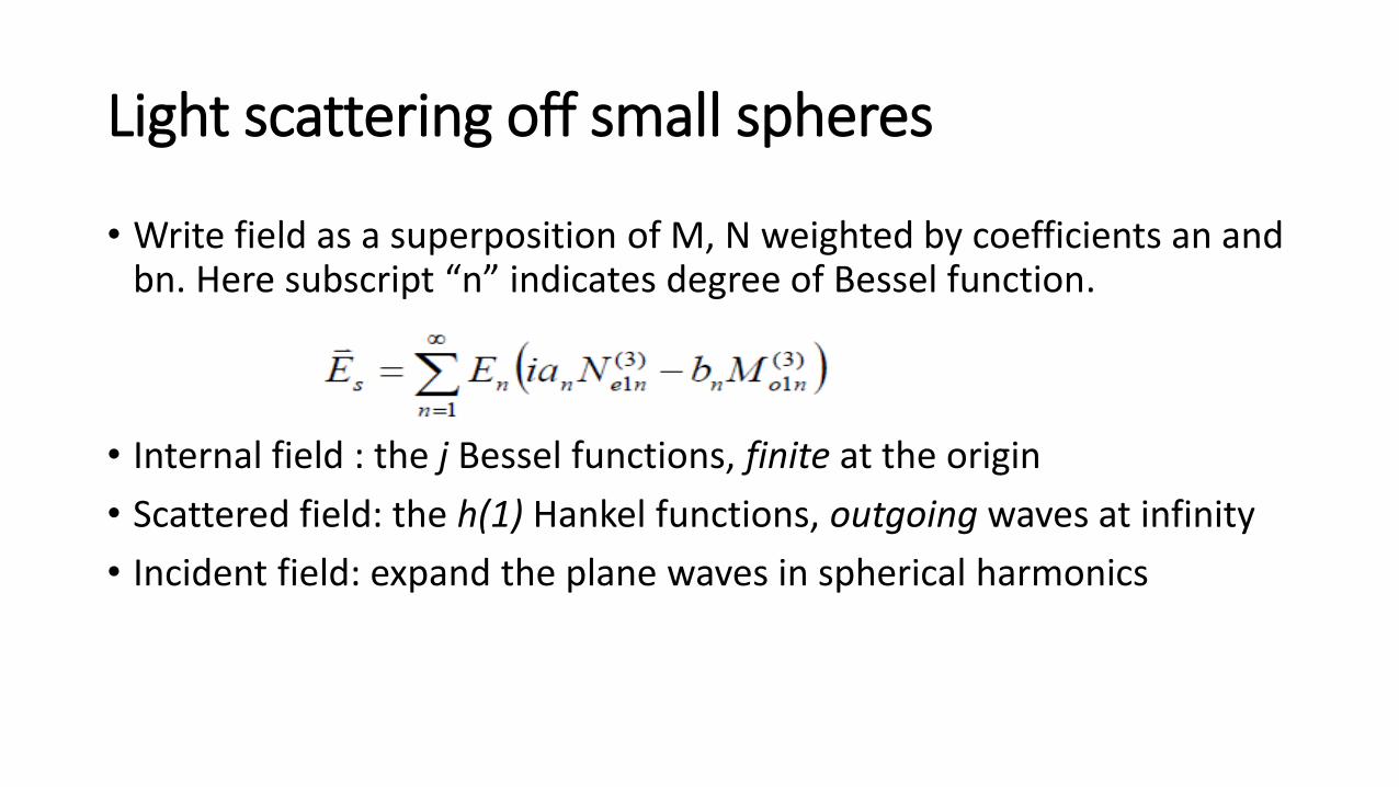
• Write field as a superposition of M, N weighted by coefficients an and bn. Here subscript “n” indicates degree of Bessel function.
• Internal field : the j Bessel functions, finite at the origin
• Scattered field: the h(1) Hankel functions, outgoing waves at infinity
• Incident field: expand the plane waves in spherical harmonics
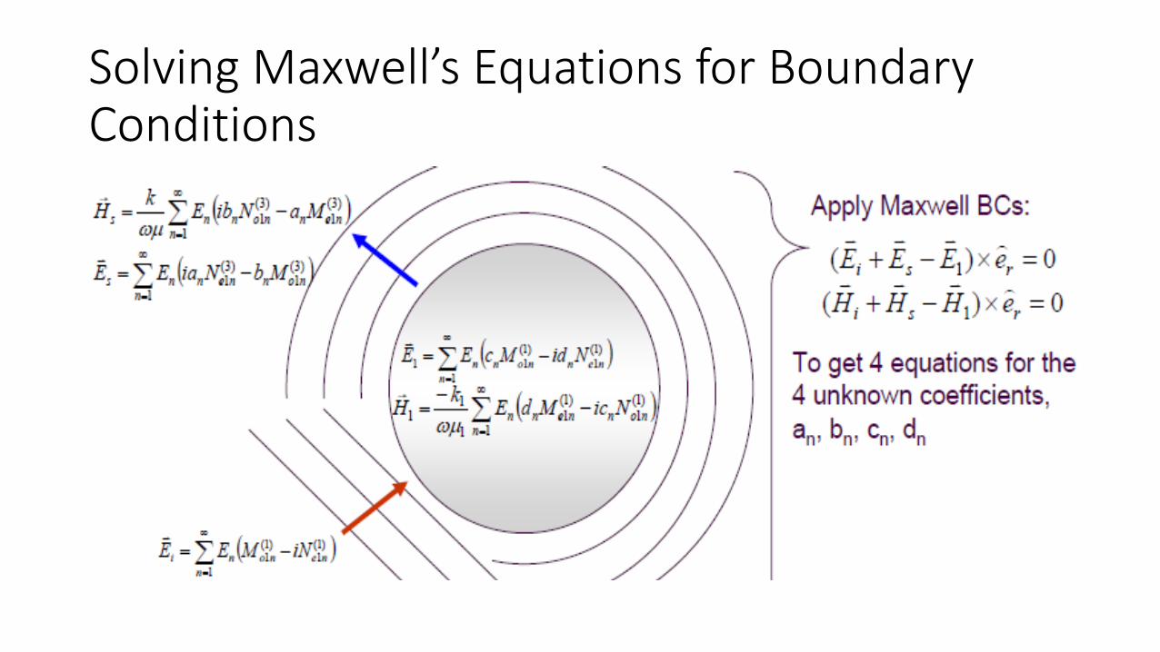
Solving Maxwell’s Equations for Boundary Conditions
Mie Theory and Frohlich Condition
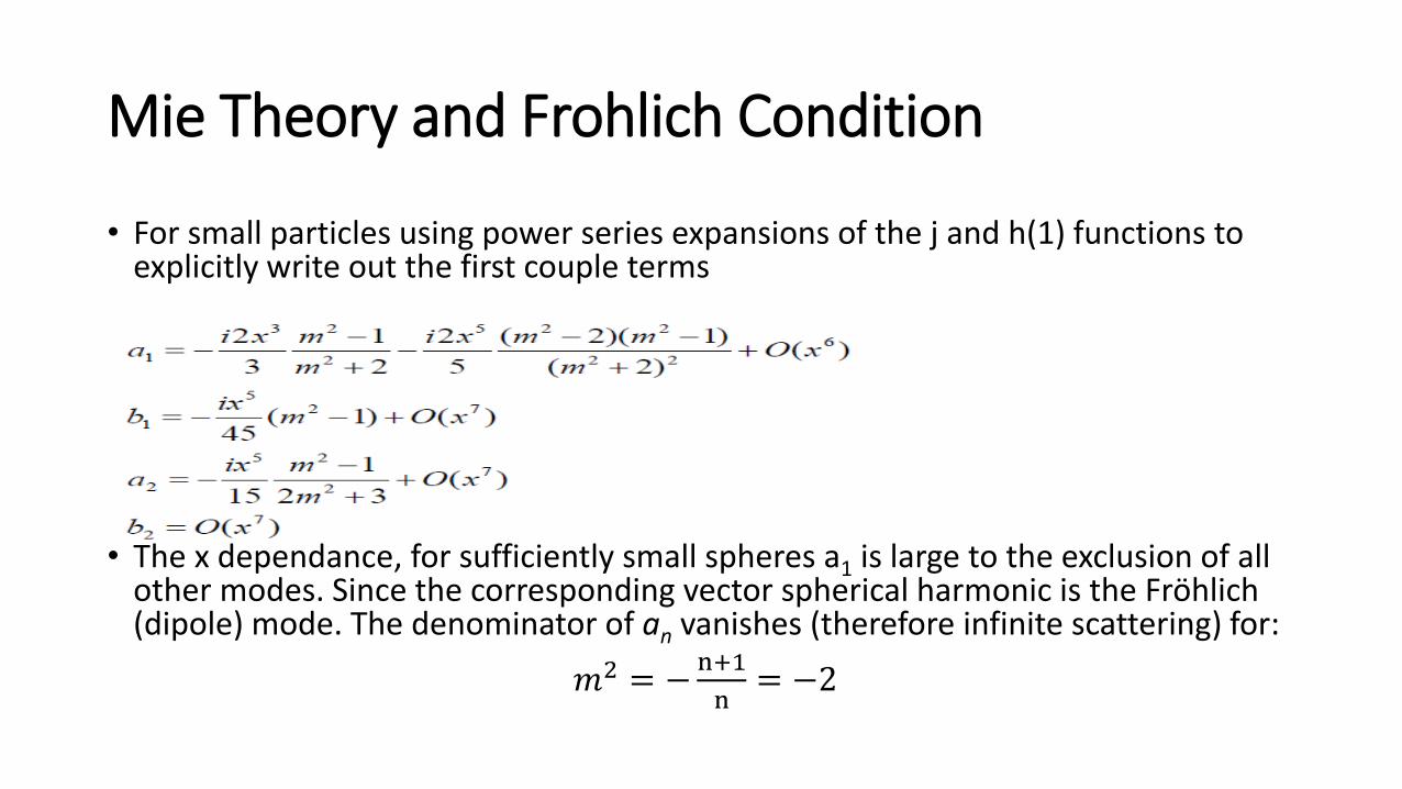
• For small particles using power series expansions of the j and h(1) functions to explicitly write out the first couple terms
• The x dependance, for sufficiently small spheres a1 is large to the exclusion of all other modes. Since the corresponding vector spherical harmonic is the Fröhlich (dipole) mode. The denominator of an vanishes (therefore infinite scattering) for:
𝑚2 = −n+1
n= −2
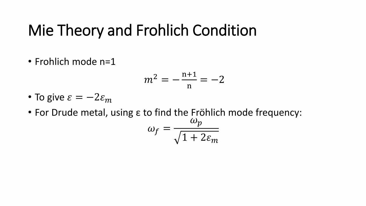
Mie Theory and Frohlich Condition
• Frohlich mode n=1
𝑚2 = −n+1
n= −2
• To give 𝜀 = −2𝜀𝑚
• For Drude metal, using ε to find the Fröhlich mode frequency:
𝜔𝑓 =𝜔𝑝
1 + 2𝜀𝑚
Mie Theory and Frohlich Condition
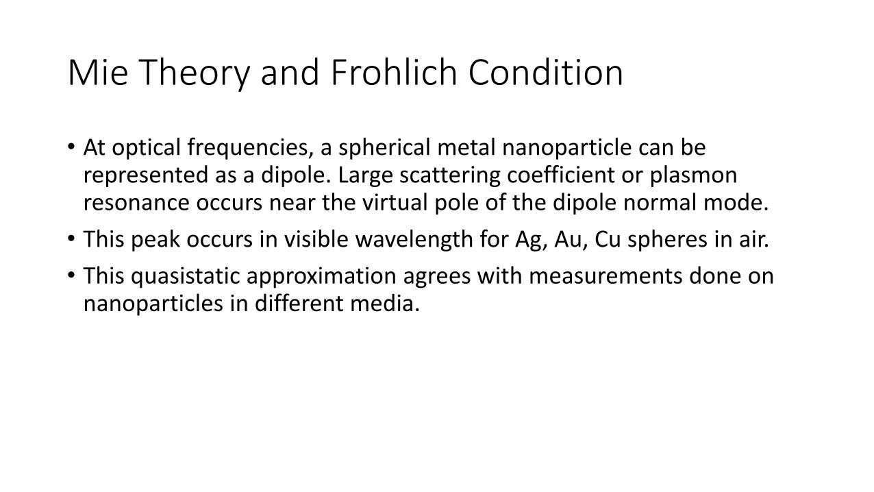
• At optical frequencies, a spherical metal nanoparticle can be represented as a dipole. Large scattering coefficient or plasmon resonance occurs near the virtual pole of the dipole normal mode.
• This peak occurs in visible wavelength for Ag, Au, Cu spheres in air.
• This quasistatic approximation agrees with measurements done on nanoparticles in different media.
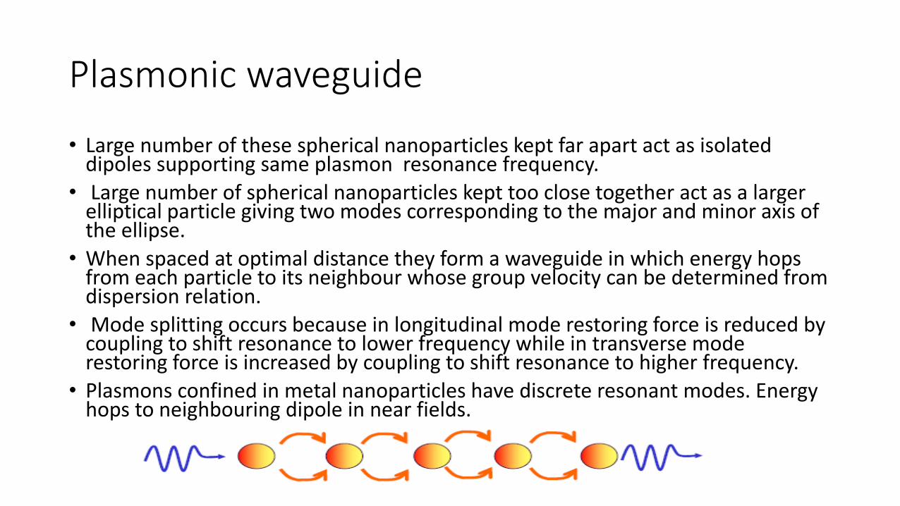
Plasmonic waveguide
• Large number of these spherical nanoparticles kept far apart act as isolated dipoles supporting same plasmon resonance frequency.
• Large number of spherical nanoparticles kept too close together act as a larger elliptical particle giving two modes corresponding to the major and minor axis of the ellipse.
• When spaced at optimal distance they form a waveguide in which energy hops from each particle to its neighbour whose group velocity can be determined from dispersion relation.
• Mode splitting occurs because in longitudinal mode restoring force is reduced by coupling to shift resonance to lower frequency while in transverse mode restoring force is increased by coupling to shift resonance to higher frequency.
• Plasmons confined in metal nanoparticles have discrete resonant modes. Energy hops to neighbouring dipole in near fields.
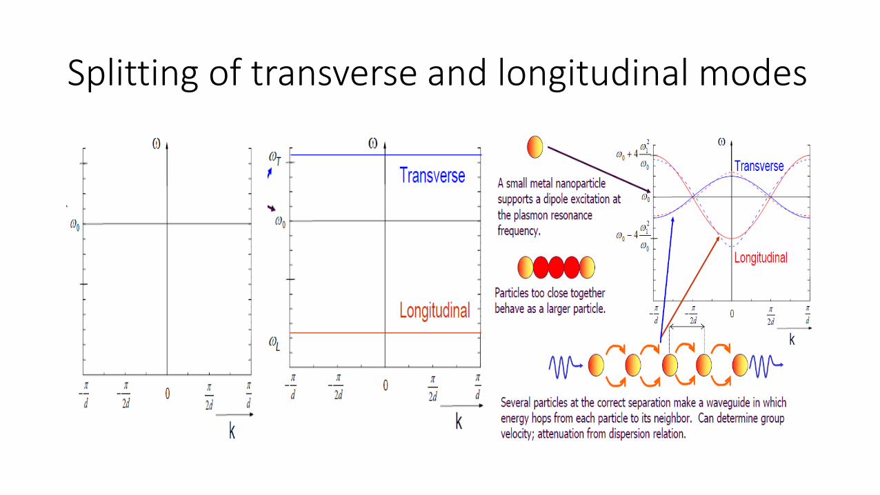
Splitting of transverse and longitudinal modes
Metamaterials
• Metamaterials are artificially engineered materials specifically to have properties not found in natural materials.
• Properties such as negative refractive index which has both negative dielectric permittivity and magnetic permeability, negative refraction and inverse Doppler shift.
• Properties arise from structure rather than composition.
Metamaterials
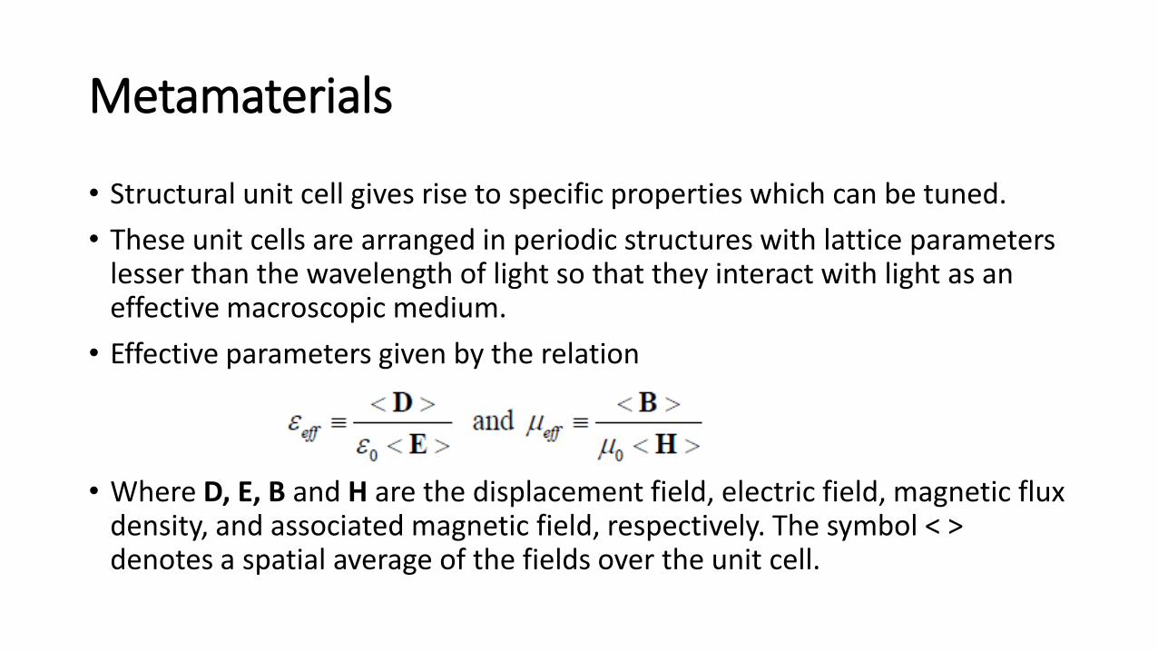
• Structural unit cell gives rise to specific properties which can be tuned.
• These unit cells are arranged in periodic structures with lattice parameters lesser than the wavelength of light so that they interact with light as an effective macroscopic medium.
• Effective parameters given by the relation
• Where D, E, B and H are the displacement field, electric field, magnetic flux density, and associated magnetic field, respectively. The symbol < > denotes a spatial average of the fields over the unit cell.
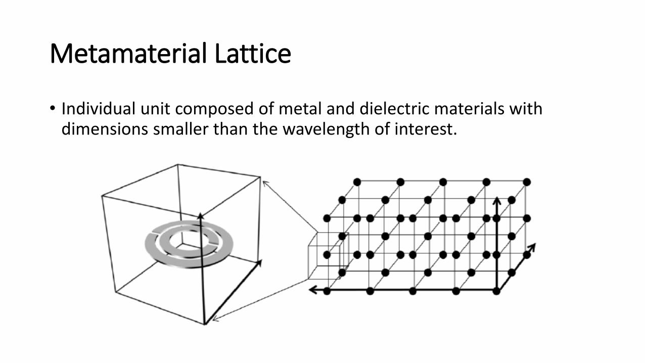
Metamaterial Lattice
• Individual unit composed of metal and dielectric materials with dimensions smaller than the wavelength of interest.
Negative Refraction
Negative Refraction
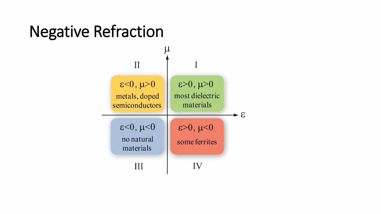
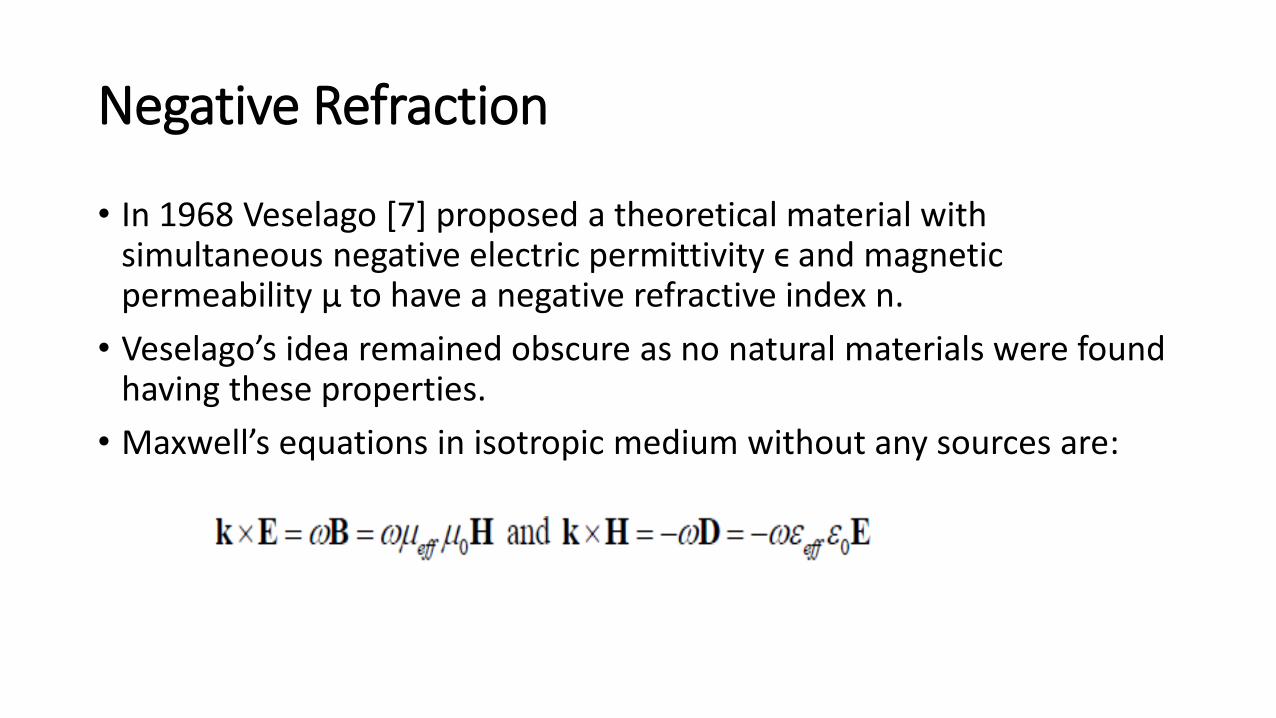
• In 1968 Veselago [7] proposed a theoretical material with simultaneous negative electric permittivity ϵ and magnetic permeability µ to have a negative refractive index n.
• Veselago’s idea remained obscure as no natural materials were found having these properties.
• Maxwell’s equations in isotropic medium without any sources are:
Negative Refraction
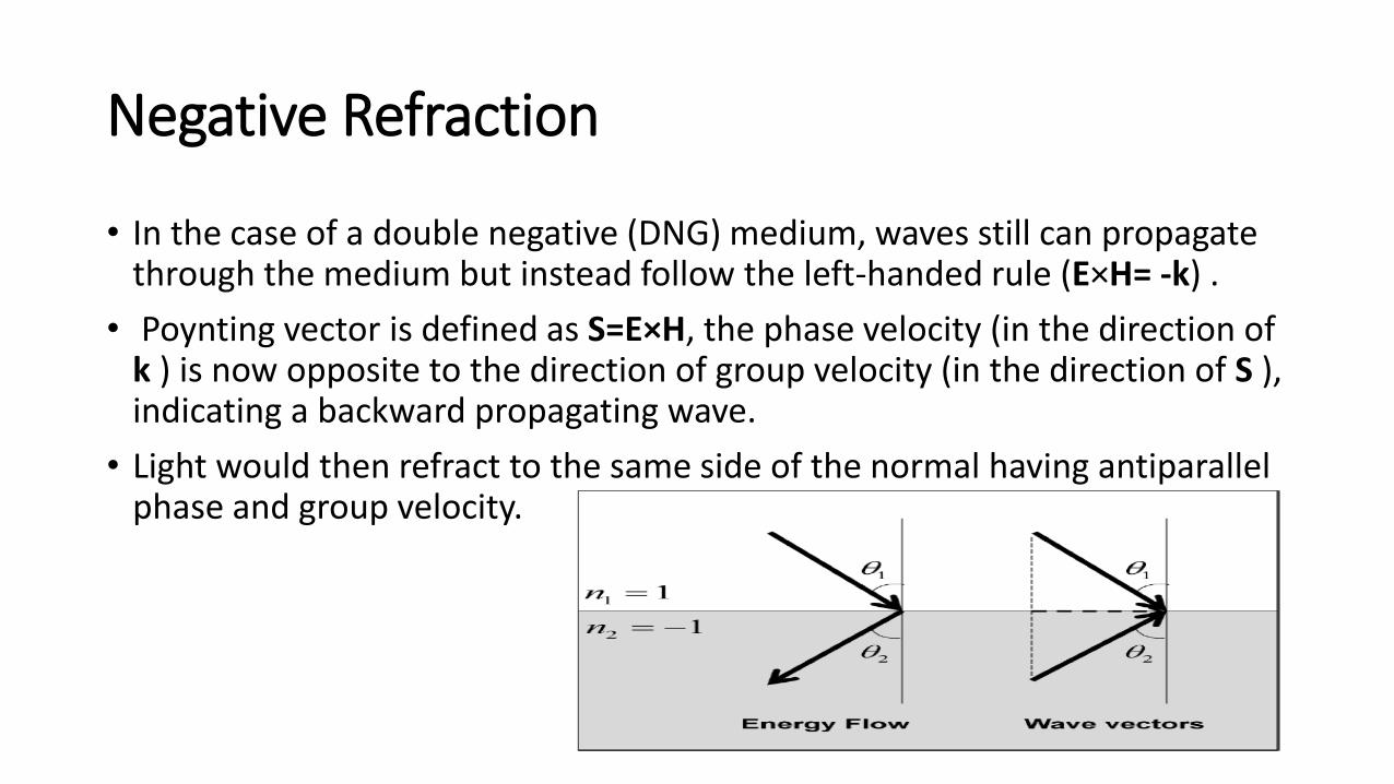
• In the case of a double negative (DNG) medium, waves still can propagate through the medium but instead follow the left-handed rule (E×H= -k) .
• Poynting vector is defined as S=E×H, the phase velocity (in the direction of k ) is now opposite to the direction of group velocity (in the direction of S ), indicating a backward propagating wave.
• Light would then refract to the same side of the normal having antiparallel phase and group velocity.
Perfect lens
• One important characteristics of a negative index material is its ability to resolve beyond the diffraction limit.
• In 2000, it was proposed by Pendry that a slab of negative index material can overcome the resolution limit of conventional lenses to achieve a perfect lens [5].
Perfect lens
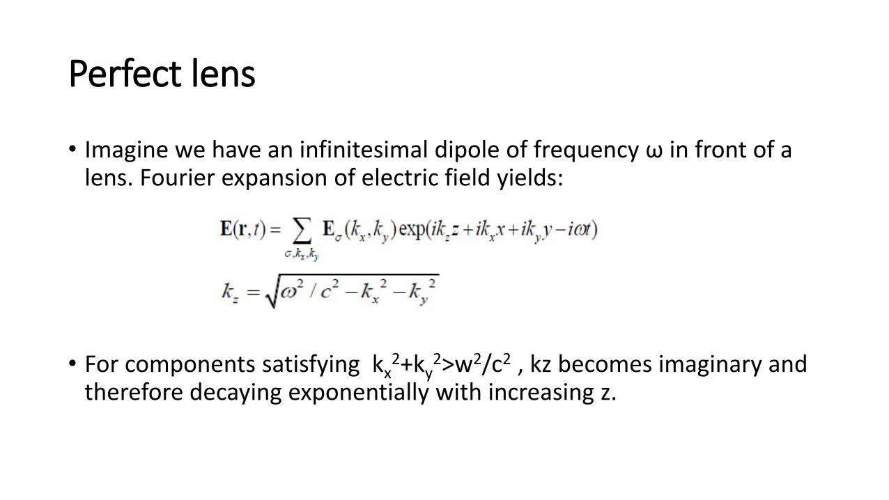
• Imagine we have an infinitesimal dipole of frequency ω in front of a lens. Fourier expansion of electric field yields:
• For components satisfying kx2+ky
2>w2/c2 , kz becomes imaginary and therefore decaying exponentially with increasing z.
Perfect lens
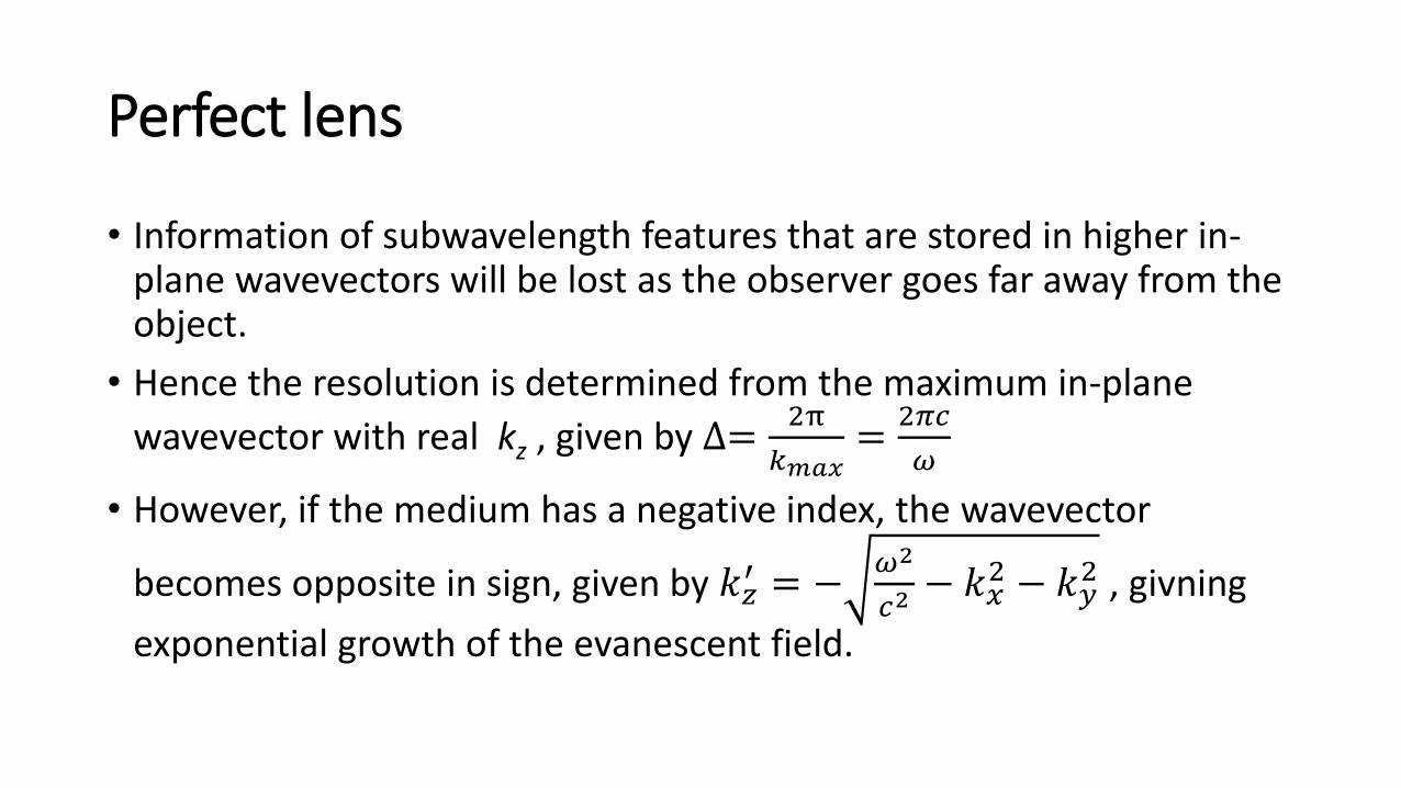
• Information of subwavelength features that are stored in higher in-plane wavevectors will be lost as the observer goes far away from the object.
• Hence the resolution is determined from the maximum in-plane
wavevector with real kz , given by ∆=2π
𝑘𝑚𝑎𝑥=2𝜋𝑐
𝜔
• However, if the medium has a negative index, the wavevector
becomes opposite in sign, given by 𝑘𝑧′ = −
𝜔2
𝑐2− 𝑘𝑥2 − 𝑘𝑦
2 , givning
exponential growth of the evanescent field.
Perfect lens
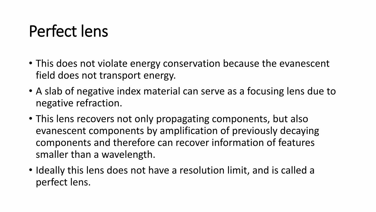
• This does not violate energy conservation because the evanescent field does not transport energy.
• A slab of negative index material can serve as a focusing lens due to negative refraction.
• This lens recovers not only propagating components, but also evanescent components by amplification of previously decaying components and therefore can recover information of features smaller than a wavelength.
• Ideally this lens does not have a resolution limit, and is called a perfect lens.

Perfect Lens
• In the optical regime, this concept was demonstrated using a silver slab lens by Fang et al. [6].
Advances in Negative Index Metamaterials
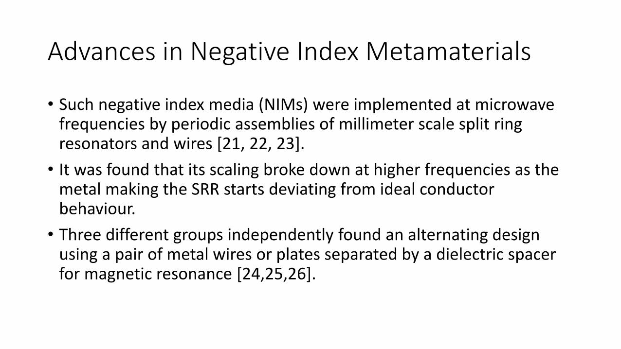
• Such negative index media (NIMs) were implemented at microwave frequencies by periodic assemblies of millimeter scale split ring resonators and wires [21, 22, 23].
• It was found that its scaling broke down at higher frequencies as the metal making the SRR starts deviating from ideal conductor behaviour.
• Three different groups independently found an alternating design using a pair of metal wires or plates separated by a dielectric spacer for magnetic resonance [24,25,26].
Advances in Negative Index Metamaterials
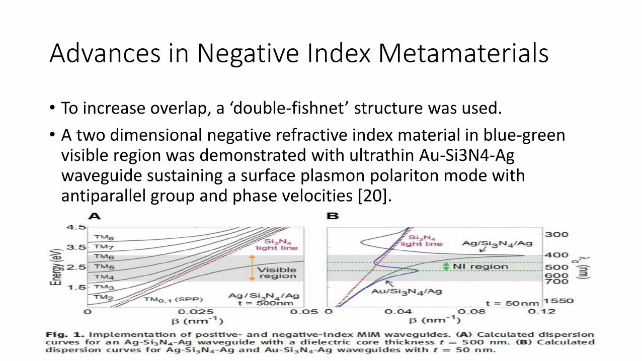
• To increase overlap, a ‘double-fishnet’ structure was used.
• A two dimensional negative refractive index material in blue-green visible region was demonstrated with ultrathin Au-Si3N4-Ag waveguide sustaining a surface plasmon polariton mode with antiparallel group and phase velocities [20].

Optical Modulation
• Optical modulators are usually composed of an active medium and an interferometer.
• The active medium’s refractive index can be controlled by external stimulus.
• The index modulation in turn induces phase modulation of light that is interacting with the medium.
Optical Modulation
• The interferometer converts the phase modulation into the intensity modulation.
• An active medium is modulated most commonly by electro-optic effects or acousto-optic or a magneto-optic effect.
• The induced change in refractive index is very small, hence it requires either long interaction length in the device or a highly resonant cavity.
Optical Modulation
• Metamaterials offer control of the effective permittivity, permeability and therefore refractive index and impedance at certain frequency.
• An active metamaterial device operating at terahertz regime was demonstrated [15].
• The amount of the index change in the active medium is improved more than 16 times at telecommunication wavelengths with ultrafast response time of 1ps [27].
Optical Modulation
• At optical frequencies, fishnet metamaterial [28,29,24] is promising for an all-optical modulation.
• The anti-parallel current flow surrounding the dielectric medium induces a magnetic resonance, achieving negative permeability.
• By replacing the dielectric medium by photon sensitive semiconductors, such as Si or Ge, the effective index of the metamaterial can be modulated by the external optical pump.

Optical Modulation
• Equivalent circuit modeling of a magnetic resonator is done. In the case of split ring resonator (SRR), the effective permeability of the metamaterial composed of LC resonators can be described by
𝜇𝑒𝑓𝑓 = 1 −𝐹𝜔2
𝜔2−𝜔02+𝑖𝜔Γ
where 𝜔0 =1
𝐿𝐶
• Transmission and reflection through metamaterial slab can be modulated by applied electric field.
• In a fishnet metamaterial, at a certain wavelength near the resonance, the electric permittivity is negative due to the metallic wires parallel to the field direction and the magnetic permeability can be also negative due to the LC resonance of individual units.
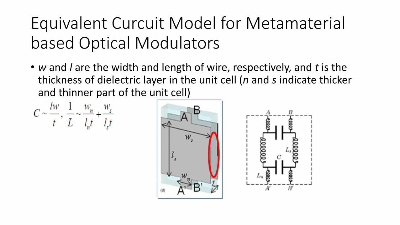
Equivalent Curcuit Model for Metamaterial based Optical Modulators • w and l are the width and length of wire, respectively, and t is the
thickness of dielectric layer in the unit cell (n and s indicate thicker and thinner part of the unit cell)
Fresnel Transmission and Reflection
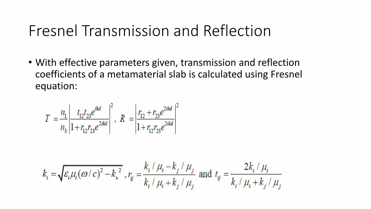
• With effective parameters given, transmission and reflection coefficients of a metamaterial slab is calculated using Fresnel equation:
Fresnel Transmission and Reflection
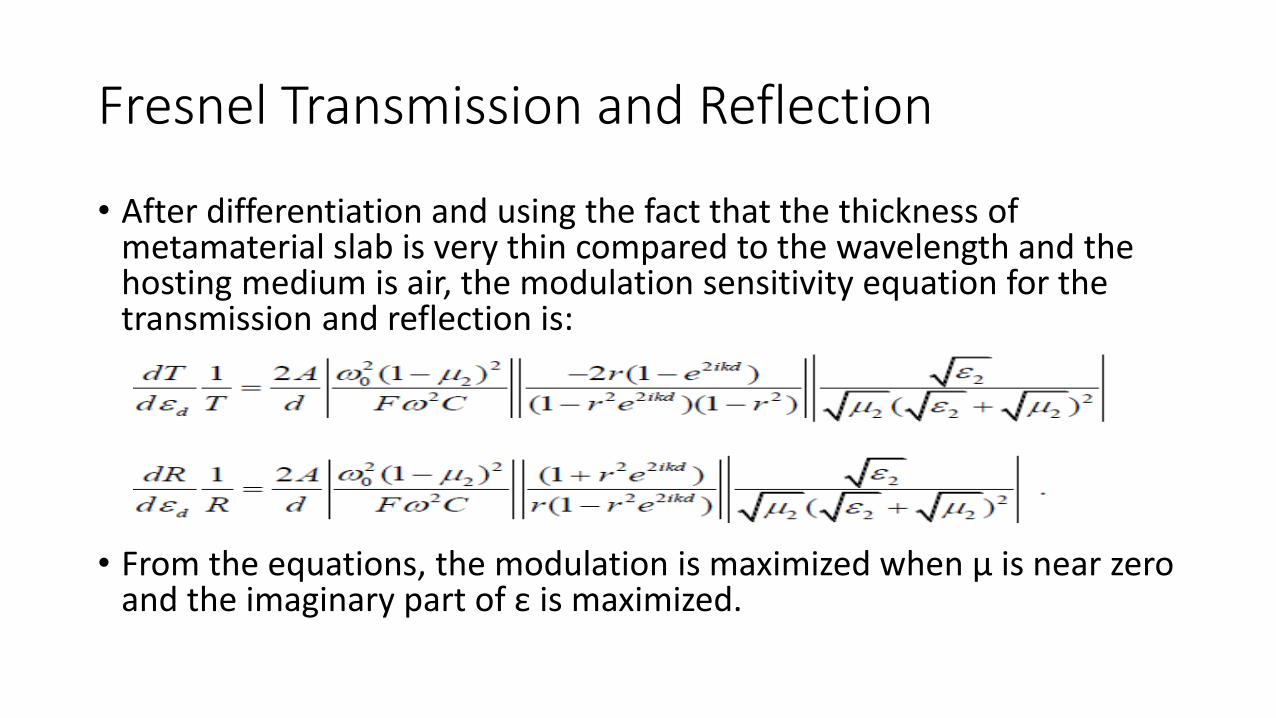
• After differentiation and using the fact that the thickness of metamaterial slab is very thin compared to the wavelength and the hosting medium is air, the modulation sensitivity equation for the transmission and reflection is:
• From the equations, the modulation is maximized when µ is near zero and the imaginary part of ε is maximized.
Optical Nanoantennas
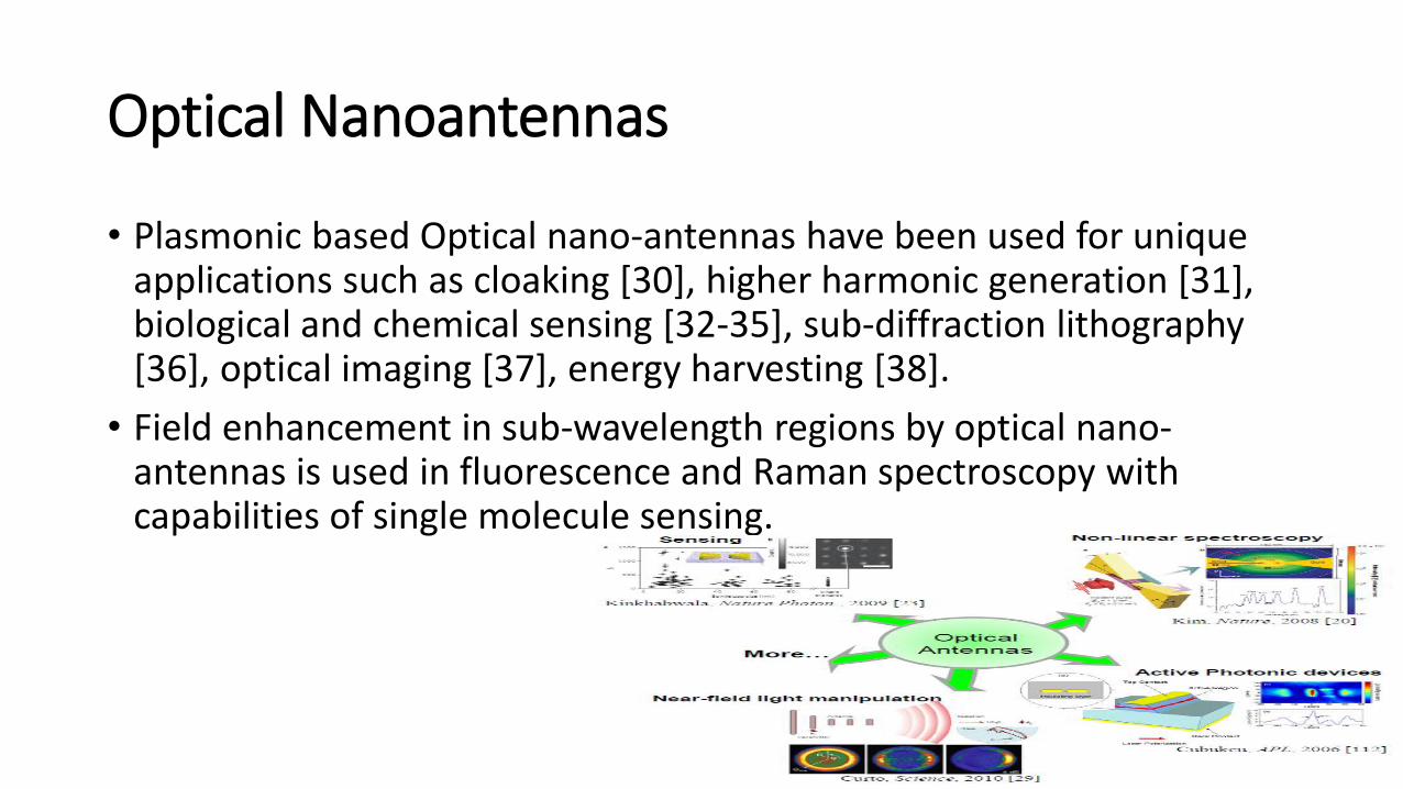
• Plasmonic based Optical nano-antennas have been used for unique applications such as cloaking [30], higher harmonic generation [31], biological and chemical sensing [32-35], sub-diffraction lithography [36], optical imaging [37], energy harvesting [38].
• Field enhancement in sub-wavelength regions by optical nano-antennas is used in fluorescence and Raman spectroscopy with capabilities of single molecule sensing.
Summary
• Plasmonics and metamaterials being a rapidly growing field in research, there is a vast number of new fundamental phenomenon and its applications in technology that are exciting.
• Starting from the diffraction limit discovered by Abbe and Rayleigh, Kirchhoffs theory for diffraction from a small hole in metal sheet to Bethe’s correction and finally the surprising experimental demonstration of enhancement of field by Ebbessen leading to consideration of plasmonics in the optical response of metals is discussed.
Summary
• Mie and Ritchie’s study on scattering of light by spherical nanoparticles to realize localized surface plasmons are explained.
• Birth of new class of materials called metamaterials having novel optical properties and their demonstration by several groups led to possibility of subwavelength photonic devices.
• Some of the most important applications such as subwavelength imaging, plasmonic waveguides, perfect lens, Optical modulators and optical nanoantennas are described.
Summary
• There are several difficulties involved with fabrication of such materials which are being tackled by researchers.
• The possibility of optical devices replacing electronic devices can be realized much sooner than what we would have expected. There is still a huge amount of potential and applications to realize it are being searched for.
References
[1] Abbe, E., Arch. Mikroskop. Anat. 9, 413-420 (1873).
[2] Rayleigh, L., Investigations in optics, with special reference to the spectroscope. Phil. Mag. 8, 261-274/403-411/477-486 (1879).
[3] Ebbesen, T.W. et al. Extraordinary optical transmission through sub-wavelength hole arrays. Nature 391, 667-669 (1998).
[4] The top ten advances in materials science. Materials Today 11, 40-45 (2008).
[5] Pendry, J.B. Negative refraction makes a perfect lens. Physical review letters 85, 3966-9 (2000).
[6] Fang, N. et al. Sub-diffraction-limited optical imaging with a silver superlens. Science 308, 534-7 (2005).
[7] Veselago, V.G. The electrodynamics of substances with simultaneously negative values of ϵ and μ. Sov. Phys. Usp. 10, 509–514 (1968).
[8] Shelby, R.A. et al. Experimental Verification of a Negative Index of Refraction. Science 292, 77-79 (2001).
References
[9] Wolf, E. et al. Controlling Electromagnetic Fields. Science 312, 1780-1782 (2006).
[10] Schurig, D. et al. Metamaterial electromagnetic cloak at microwave frequencies. Science 314, 977-80 (2006).
[11] Oulton, R.F. et al. Plasmon lasers at deep subwavelength scale. Nature 461, 629-32 (2009).
[12] Noginov, M. a et al. Demonstration of a spaser-based nanolaser. Nature 460, 1110-2 (2009).
[13] Ma, R.-M. et al. Room-temperature sub-diffraction-limited plasmon laser by total internal reflection. Nature Materials 10, 2-5 (2010).
[14] Knight, M.W. et al. Photodetection with active optical antennas. Science 332, 702-4 (2011).
[15] Chen H.T. et al. Active terahertz metamaterial devices. Nature 444, 597–600 (2006).
[16] Tang, L. et al. Nanometre-scale germanium photodetector enhanced by a near-infrared dipole antenna. Nature Photonics 2, 226-229 (2008).
[17] Jackson, J. Classical Electrodynamics. Chapter 10.9, 3rd Edition, Wiley (1998).
[18] D. R. Smith et al., Phys. Rev. Lett. 84, 4184 (2000).
[19] A. A. Houck, J. B. Brock, I. L. Chuang, Phys. Rev. Lett. 90,137401 (2003).
[20] Henri J. Lezec, et al.Science 316, 430 (2007);Journal of Applied Physics 98, 011101 (2005).
[21] C. G. Parazzoli et al., Phys. Rev. Lett. 90, 107401 (2003).
References
[22] M. Bayindir et al., Appl. Phys. Lett. 81, 120 (2002).
[23] R. B. Greegor et al., Appl. Phys. Lett. 82, 2356 (2003).
[24] S. Zhang et al., Phys. Rev. Lett. 95, 137404 (2005).
[25] G. Dolling et al., Opt. Lett. 30, 3198 (2005).
[26]V. M. Shalaev et al., Opt. Lett. 30, 3356 (2005).
[27] Kim, E. et al. Modulation of negative index metamaterials in the near-IR range. Applied Physics Letters 91, 173105 (2007).
[28] Dolling, G. et al. Negative-index metamaterial at 780 nm wavelength. Optics Letters 32, 2006-2008 (2007).
[29] Guven, K. et al. Experimental observation of left-handed transmission in a bilayer metamaterial under normal-to-plane propagation. Optics express 14, 8685-93 (2006).
[30] B. Baumeier, T. A. Leskova, and A. A. Maradudin, “Cloaking from surface plasmon polaritons by a circular array of point scatters,” Phys. Rev. Lett. 103, 246803 (2009).
[31] T. H. Taminiau, F. D. Stefani, F. B. Segerink, and N. F. van Hulst, “Optical antennas direct single-molecule emission,” Nature Photon. 2, 234 (2008).
References
[32] S. Kuhn, U. Hakanson, L. Rogobete, and V. Sandoghdar, “Enhancement of singlemolecule fluorescence using a gold nanoparticles as an optical nanoantenna,” Phys. Rev. Lett. 97, 017402 (2006).
[33] A. Kinkhabwala, Z. Yu, S. Fan, Y. Avlasevich, K. Mullen, and W. E. Moerner, “Large single-molecule fluorescence enhancements produced by a bowtie nanoantenna,” Nature Photon. 3, 654 (2009).
[34] N. A. Hatab, C.-H. Hsueh, A. L. Gaddis, S. T. Retterer, J.-H. Li, G. Eres, Z. Zhang, and B. Gu, “Free-standing optical gold bowtie nanoantenna with variable gap size for enhanced Raman spectroscopy,” Nano Lett. 10 (12), 4952 (2010).
[35] S. Kim, J. Jin, Y.-J. Kim, I.-Y. Park, Y. Kim, and S.-W. Kim, “High-harmonic generation by resonant plasmon field enhancement,” Nature 453, 757 (2008).
[36] A. Sundaramurthy, P. J. Schuck, N. R. Conley, D. P. Fromm, G. S. Kino, and W. E. Moerner, “Toward nanometer-scale optical photolithography: utilizing the nearfield of bowtie optical nanoantennas,” Nano Lett. 6 (3), 355 (2006).
References
[37] T. Xu, Y.-K. Wu, X. Luo, and L. J. Guo, “Plasmonic nanoresonators for highresolution colour filtering and spectral imaging,” Nature Comm. 1, 59 (2010).
[38] H. A. Atwater and A. Polman, “Plasmonics for improved photovoltaic devices,” Nature Mater. 9, 205 (2010).