Embed Size (px)
Citation preview
REPORT DOCUMENTATION PAGE
Form Approved
OMB NO. 0704-0188
Public Reporting burden for this collection of information is estimated to average 1 hour per response, including the time for reviewing instructions, searching existing data sources, gathering and maintaining the data needed, and completing and reviewing the collection of information. Send comment regarding this burden estimates or any other aspect of this collection of information, including suggestions for reducing this burden, to Washington Headquarters Services, Directorate for information Operations and Reports, 1215 Jefferson Davis Highway, Suite 1204, Arlington, VA 22202-4302, and to the Office of Management and Budget, Paperwork Reduction Project (0704-0188,) Washington, DC 20503. 1. AGENCY USE ONLY ( Leave Blank)
2. REPORT DATE 15 March 2005
3. REPORT TYPE AND DATES COVERED Final Report
4. TITLE AND SUBTITLE Low dimensional K(Nb,Ta)O3 thin film structures
5. FUNDING NUMBERS DAAD19-01-1-0508
6. AUTHOR(S) David P. Norton
7. PERFORMING ORGANIZATION NAME(S) AND ADDRESS(ES) University of Florida, Dept of Materials Science and Engr, P.O. Box 116400, Gainesville, FL 32611
8. PERFORMING ORGANIZATION REPORT NUMBER
9. SPONSORING / MONITORING AGENCY NAME(S) AND ADDRESS(ES) U. S. Army Research Office P.O. Box 12211 Research Triangle Park, NC 27709-2211
10. SPONSORING / MONITORING AGENCY REPORT NUMBER 41885.2-MS
11. SUPPLEMENTARY NOTES The views, opinions and/or findings contained in this report are those of the author(s) and should not be construed as an official Department of the Army position, policy or decision, unless so designated by other documentation. 12 a. DISTRIBUTION / AVAILABILITY STATEMENT Approved for public release; distribution unlimited.
12 b. DISTRIBUTION CODE
13. ABSTRACT (Maximum 200 words) The objective of this project is to investigate the synthesis and properties of thin film and low-dimensional dielectric thin-film structures, focusing on the K(Nb,Ta)O3 system. K(Ta,Nb)O3 is attractive for non-linear optical waveguides and tunable microwave technologies. In this reporting period, the growth and dielectric properties of several oxide materials were examined. This work included asymmetric superlattice structures that were investigated in order to determine the effects of reduced dimensionality on the ferroelectric phase transition and dielectric properties. In order to understand the growth of these structures, the controlled formation of unit cell steps on the KTaO3 substrate surface was investigated. The dielectric properties of doped and undoped K(Ta,Nb)O3 films were also studied. For undoped K(Ta,Nb)O3 films, losses as low as tan δ = 0.03 were realized. In addition, the effect of hole doping via Ti substitution was also investigated. We also investigated properties of related oxides, including CaHfO3 and TiO2 thin films. 14. SUBJECT TERMS Ferroelectric thin films, low-dimensionality effects, superlattice synthesis, perovskite materials, tunable paraelectrics
15. NUMBER OF PAGES
16. PRICE CODE
17. SECURITY CLASSIFICATION OR REPORT
UNCLASSIFIED
18. SECURITY CLASSIFICATION ON THIS PAGE
UNCLASSIFIED
19. SECURITY CLASSIFICATION OF ABSTRACT
UNCLASSIFIED
20. LIMITATION OF ABSTRACT
UL NSN 7540-01-280-5500 Standard Form 298 (Rev.2-89) Prescribed by ANSI Std. 239-18
298-102
1a. Manuscripts submitted in peer-reviewed journal
“Dielectric Response of Asymmetric KNbO3/KTaO3 Superlattices,” J.Sigman, H.J. Bae, D.P Norton, J. Budai, and L.A. Boatner, J. Vacuum Science and Technol. B, in press. “Dielectric properties of KTa0.524Nb0.446Ti0.03O3 thin films grown by pulsed laser deposition,” H. J. Bae, J. Sigman, B. S. Jeong, L. A. Boatner, and D. P. Norton, J. Appl. Phys. (submitted). “Surface treatment for unit-cell steps on the (001) KTaO3 surface,” H. J. Bae, L. A. Boatner, J. Sigman, and D. P. Norton, Appl. Surf. Sci. (in press). “Dielectric Response of K(Ta,Nb)O3 Thin Films,” J.Sigman, H.J. Bae, D.P Norton, and L.A. Boatner, Appl. Phys. A (in press). 1b. Papers published in journal
“Antiferroelectric behavior in symmetric KNbO3/KTaO3 superlattices,” Sigman, J., Norton, D. P., Christen, H.
M., Fleming, P. H. and Boatner, L. A., Physical Review Letters, Volume 88, Number 9, p. 097601-1, 2002.
“Recrystallization and dielectric properties of CaHfOx films on Si,” Y. W. Kwon, D. P. Norton and G. E. Jellison, Jr., Solid State Electronics vol. 47 (2003) Pages 2149-2153 “Conductivity in transparent anatase TiO2 films epitaxially grown by reactive sputtering deposition,” B. -S. Jeong, D. P. Norton and J. D. Budai Solid State Electronics vol. 47 (2003)Pages 2275-2278 “Spectroscopic ellipsometry of thin film and bulk anatase (TiO2),” Jellison, G.E., Jr. ; Boatner, L.A.; Budai, J.D.; Jeong, B.-S.; Norton, D.P.Journal of Applied Physics, Volume 93, Issue 12, 2003, Pages 9537-9541 “Capacitance-voltage measurements on ultrathin gate dielectrics,” Norton, D.P. Solid-State Electronics, Volume 47, Issue 5, 2003, Pages 801-805 “Growth of semiconducting KTaO3 thin films,” Bae, H.-J. ; Sigman, J.; Park, S.-J.; Heo, Y.-H.; Boatner, L.A.; Norton, D.P., Solid-State Electronics, Volume 48, Issue 1, 2004, Pages 51-54 1c. Papers published in non-peer-reviewed journal
Transition metal doped TiO2 thin films epitaxially grown by reactive sputter deposition B.-S. Jeong, Y.W. Heo, J. D. Budai, Y. D. Park, and D. P. Norton, Proceedings of the Electrochemical Society (in press)
1d. Papers presented at meetings, but not published in proceedings: “Temperature Dependent Dielectric Response and Tunability of KNbO3/KTaO3 Superlattices”
REPORT DOCUMENTATION PAGE (SF298)
(Continuation Sheet)
Jennifer Sigman, D. Norton, R. Singh, J. Howard, H. Christen, J. Budai, E. Specht, P. Fleming, L.A. Boatner, Fall 2001 Meeting of the Materials Research Society, (Boston, MA), Nov. 2001. “Epitaxy of complex oxides on dissimilar substrates", Florida Chapter of the American Vacuum Society, AVS-FSM Joint Symposium, Orlando, FL, March 2002. “Evidence for antiferroelectric behavior in KNbO3/KTaO3 superlattices,” 2002 Spring Meeting of the Materials Research Society, San Francisco, CA, April 2002. “Conductivity In Transparent Anatase TiO2 Films Epitaxially Grown By Reactive Sputtering Deposition”, B.-S. Jeong, D.P. Norton, and J.D.Budai, 9th International Workshop on Oxide Electronics, St. Pete Beach, FL, October 2002. “Deposition of CaHfO3 thin films using pulsed-laser deposition,” Y. Kwon, D. P. Norton, S.-J. Park, and J. D. Budai, Florida Chapter of the American Vacuum Society, AVS-FSM Joint Symposium, Orlando, FL, March 2002. “Evidence for antiferroelectric behavior in KNbO3 / KTaO3 superlattices,” J. Sigman, D. P. Norton, H.-M. Christen, P. H. Fleming, and L. A. Boatner, Florida Chapter of the American Vacuum Society, AVS-FSM Joint Symposium, Orlando, FL, March 2002. “Epitaxial growth of anatase TiO2 films by reactive sputter deposition,” B.-S. Jeong, D.P.Norton, and J.D.Budai, Florida Chapter of the American Vacuum Society, AVS-FSM Joint Symposium, Orlando, FL, March 2002. “Dielectric Response of K(Ta,Nb)O3 Thin Films, “J. Sigman, H.J. Bae, D.P. Norton, and L. A. Boatner, Meeting of the Electrochemical Society, Orlando, FL, Oct. 12-17, 2003 “Electric Response Of K(Ta,Nb)O3 Thin Films And Asymmetric KNbO3/KTaO3 Superlattices ” XII International Materials Research Congress 2003, August 17 - 21, 2003, Cancún, Mexico (INVITED) “Response of Asymmetric KNbO3/KTaO3 Superlattices,” J. Sigman, H.J. Bae, D.P. Norton, J.D. Budai, P.H. Fleming, and L.A. Boatner, American Vacuum Society, Nov. 2-7, 2003, Baltimore, MD “Dielectric Response Of K(Ta,Nb)O3 Thin Films And Asymmetric KNbO3/KTaO3 Superlattices,” XIII International Materials Research Congress 2004, Cancun, Mexico, August 2004 (INVITED)
2. Scientific personnel supported by project:
Faculty: David P. Norton, Professor, Dept. of Materials Science and Engineering, Univ. of Florida Mark Reeves, Dept. of Physics, George Washington University (sub-contract) Grad Students: Jennifer Sigman, Graduate Student, Dept. of Materials Science and Engineering, Univ. of Florida
Hyung-jin Bae, Graduate Student, Dept. of Materials Science and Engineering, Univ. of Florida
3. Report of Inventions:
None
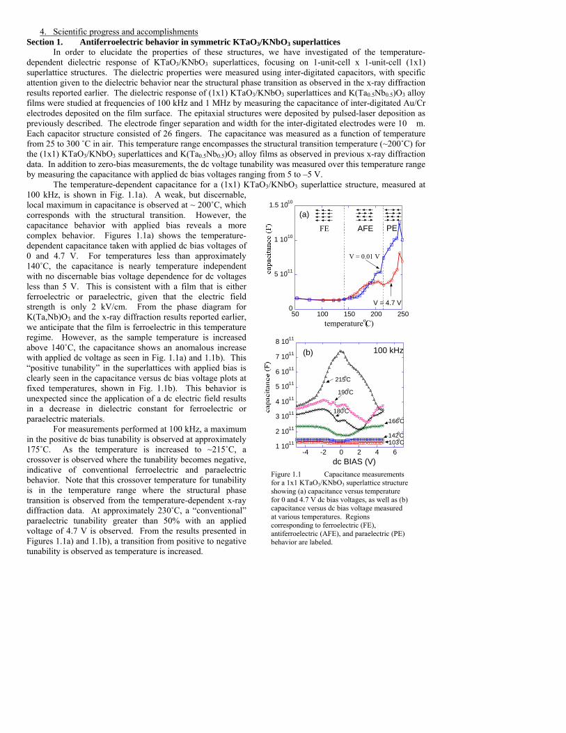
4. Scientific progress and accomplishments Section 1. Antiferroelectric behavior in symmetric KTaO3/KNbO3 superlattices
In order to elucidate the properties of these structures, we have investigated of the temperature-dependent dielectric response of KTaO3/KNbO3 superlattices, focusing on 1-unit-cell x 1-unit-cell (1x1) superlattice structures. The dielectric properties were measured using inter-digitated capacitors, with specific attention given to the dielectric behavior near the structural phase transition as observed in the x-ray diffraction results reported earlier. The dielectric response of (1x1) KTaO3/KNbO3 superlattices and K(Ta0.5Nb0.5)O3 alloy films were studied at frequencies of 100 kHz and 1 MHz by measuring the capacitance of inter-digitated Au/Cr electrodes deposited on the film surface. The epitaxial structures were deposited by pulsed-laser deposition as previously described. The electrode finger separation and width for the inter-digitated electrodes were 10 m. Each capacitor structure consisted of 26 fingers. The capacitance was measured as a function of temperature from 25 to 300 ˚C in air. This temperature range encompasses the structural transition temperature (~200˚C) for the (1x1) KTaO3/KNbO3 superlattices and K(Ta0.5Nb0.5)O3 alloy films as observed in previous x-ray diffraction data. In addition to zero-bias measurements, the dc voltage tunability was measured over this temperature range by measuring the capacitance with applied dc bias voltages ranging from 5 to –5 V.
The temperature-dependent capacitance for a (1x1) KTaO3/KNbO3 superlattice structure, measured at 100 kHz, is shown in Fig. 1.1a). A weak, but discernable, local maximum in capacitance is observed at ~ 200˚C, which corresponds with the structural transition. However, the capacitance behavior with applied bias reveals a more complex behavior. Figures 1.1a) shows the temperature-dependent capacitance taken with applied dc bias voltages of 0 and 4.7 V. For temperatures less than approximately 140˚C, the capacitance is nearly temperature independent with no discernable bias voltage dependence for dc voltages less than 5 V. This is consistent with a film that is either ferroelectric or paraelectric, given that the electric field strength is only 2 kV/cm. From the phase diagram for K(Ta,Nb)O3 and the x-ray diffraction results reported earlier, we anticipate that the film is ferroelectric in this temperature regime. However, as the sample temperature is increased above 140˚C, the capacitance shows an anomalous increase with applied dc voltage as seen in Fig. 1.1a) and 1.1b). This “positive tunability” in the superlattices with applied bias is clearly seen in the capacitance versus dc bias voltage plots at fixed temperatures, shown in Fig. 1.1b). This behavior is unexpected since the application of a dc electric field results in a decrease in dielectric constant for ferroelectric or paraelectric materials.
For measurements performed at 100 kHz, a maximum in the positive dc bias tunability is observed at approximately 175˚C. As the temperature is increased to ~215˚C, a crossover is observed where the tunability becomes negative, indicative of conventional ferroelectric and paraelectric behavior. Note that this crossover temperature for tunability is in the temperature range where the structural phase transition is observed from the temperature-dependent x-ray diffraction data. At approximately 230˚C, a “conventional” paraelectric tunability greater than 50% with an applied voltage of 4.7 V is observed. From the results presented in Figures 1.1a) and 1.1b), a transition from positive to negative tunability is observed as temperature is increased.
0
5 10-11
1 10-10
1.5 10-10
50 100 150 200 250temperature (oC)
(a)
V = 4.7 V
V = 0.01 V
FE AFE PE
1 10-11
2 10-11
3 10-11
4 10-11
5 10-11
6 10-11
7 10-11
8 10-11
-4 -2 0 2 4 6 dc BIAS (V)
215oC
190oC
180oC166oC
142oC103oC
100 kHz(b)
Figure 1.1 Capacitance measurements for a 1x1 KTaO3/KNbO3 superlattice structure showing (a) capacitance versus temperature for 0 and 4.7 V dc bias voltages, as well as (b) capacitance versus dc bias voltage measured at various temperatures. Regions corresponding to ferroelectric (FE), antiferroelectric (AFE), and paraelectric (PE) behavior are labeled.
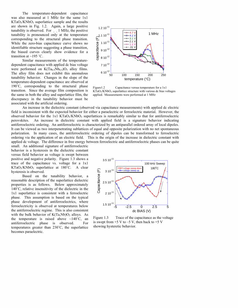
The temperature-dependent capacitance was also measured at 1 MHz for the same 1x1 KTaO3/KNbO3 superlattice sample and the results are shown in Fig. 1.2. Again, a large positive tunability is observed. For 1 MHz, the positive tunability is pronounced only at the temperature corresponding to the structural phase transition. While the zero-bias capacitance curve shows no identifiable structure suggesting a phase transition, the biased curves clearly show evidence for a transition at ~195 ˚C.
Similar measurements of the temperature-dependent capacitance with applied dc bias voltage were performed on K(Ta0.5Nb0.5)O3 alloy films. The alloy film does not exhibit this anomalous tunability behavior. Changes in the slope of the temperature-dependent capacitance are observed at 190˚C, corresponding to the structural phase transition. Since the average film composition is the same in both the alloy and superlattice film, the discrepancy in the tunability behavior must be associated with the artificial ordering.
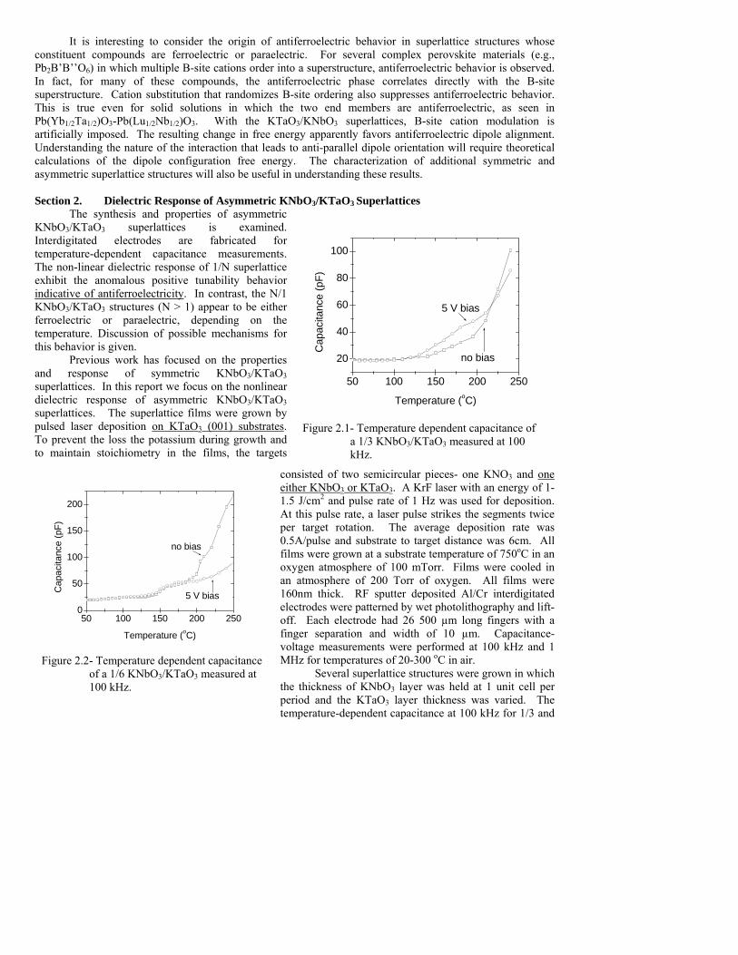
An increase in the dielectric constant (observed via capacitance measurements) with applied dc electric field is inconsistent with the expected behavior for either a paraelectric or ferroelectric material. However, the observed behavior for the 1x1 KTaO3/KNbO3 superlattices is remarkably similar to that for antiferroelectric perovskites. An increase in dielectric constant with applied field is a signature behavior indicating antiferroelectric ordering. An antiferroelectric is characterized by an antiparallel ordered array of local dipoles. It can be viewed as two interpenetrating sublattices of equal and opposite polarization with no net spontaneous polarization. In many cases, the antiferroelectric ordering of dipoles can be transformed to ferroelectric ordering via the application of an electric field. This is the origin of the increase in dielectric constant with applied dc voltage. The difference in free energy between ferroelectric and antiferroelectric phases can be quite small. An additional signature of antiferroelectric behavior is a hysteresis in the dielectric constant versus field behavior as voltage is swept between positive and negative polarity. Figure 1.3 shows a trace of the capacitance vs. voltage for a 1x1 KTaO3/KNbO3 superlattice at 180˚C. A clear hysteresis is observed.
Based on the tunability behavior, a reasonable description of the superlattice dielectric properties is as follows. Below approximately 140˚C, relative insensitivity of the dielectric in the 1x1 superlattice is consistent with a ferroelectric phase. This assumption is based on the typical phase development of antiferroelectrics, where ferroelectricity is observed at temperatures below the antiferroelectric regime. This is also consistent with the bulk behavior of K(Ta,Nb)O3 alloys. As the temperature is raised above ~140˚C, an antiferroelectric phase is observed. For temperatures greater than 230˚C, the superlattice becomes paraelectric.
6 10-12
7 10-12
8 10-12
9 10-12
1 10-11
1.1 10-11
1.2 10-11
50 100 150 200 250
4.7 V4.1 V3.1 V2.1 V1.1 V.01 V
temperature (oC)
1 MHz
Figure1.2 Capacitance versus temperature for a 1x1 KTaO3/KNbO3 superlattice structure with various dc bias voltages applied. Measurements were performed at 1 MHz
1.5 10-11
2 10-11
2.5 10-11
3 10-11
3.5 10-11
-5 -2.5 0 2.5 5
voltage sweep downvoltage sweep up
dc BIAS (V)
100 kHz Sweep180oC
Figure 1.3 Trace of the capacitance as the voltage is swept from +5 V to –5 V, then back to +5 V showing hysteretic behavior.
It is interesting to consider the origin of antiferroelectric behavior in superlattice structures whose constituent compounds are ferroelectric or paraelectric. For several complex perovskite materials (e.g., Pb2B’B’’O6) in which multiple B-site cations order into a superstructure, antiferroelectric behavior is observed. In fact, for many of these compounds, the antiferroelectric phase correlates directly with the B-site superstructure. Cation substitution that randomizes B-site ordering also suppresses antiferroelectric behavior. This is true even for solid solutions in which the two end members are antiferroelectric, as seen in Pb(Yb1/2Ta1/2)O3-Pb(Lu1/2Nb1/2)O3. With the KTaO3/KNbO3 superlattices, B-site cation modulation is artificially imposed. The resulting change in free energy apparently favors antiferroelectric dipole alignment. Understanding the nature of the interaction that leads to anti-parallel dipole orientation will require theoretical calculations of the dipole configuration free energy. The characterization of additional symmetric and asymmetric superlattice structures will also be useful in understanding these results.
Section 2. Dielectric Response of Asymmetric KNbO3/KTaO3 Superlattices
The synthesis and properties of asymmetric KNbO3/KTaO3 superlattices is examined. Interdigitated electrodes are fabricated for temperature-dependent capacitance measurements. The non-linear dielectric response of 1/N superlattice exhibit the anomalous positive tunability behavior indicative of antiferroelectricity. In contrast, the N/1 KNbO3/KTaO3 structures (N > 1) appear to be either ferroelectric or paraelectric, depending on the temperature. Discussion of possible mechanisms for this behavior is given.
Previous work has focused on the properties and response of symmetric KNbO3/KTaO3 superlattices. In this report we focus on the nonlinear dielectric response of asymmetric KNbO3/KTaO3 superlattices. The superlattice films were grown by pulsed laser deposition on KTaO3 (001) substrates. To prevent the loss the potassium during growth and to maintain stoichiometry in the films, the targets
consisted of two semicircular pieces- one KNO3 and one either KNbO3 or KTaO3. A KrF laser with an energy of 1-1.5 J/cm2 and pulse rate of 1 Hz was used for deposition. At this pulse rate, a laser pulse strikes the segments twice per target rotation. The average deposition rate was 0.5A/pulse and substrate to target distance was 6cm. All films were grown at a substrate temperature of 750oC in an oxygen atmosphere of 100 mTorr. Films were cooled in an atmosphere of 200 Torr of oxygen. All films were 160nm thick. RF sputter deposited Al/Cr interdigitated electrodes were patterned by wet photolithography and lift-off. Each electrode had 26 500 µm long fingers with a finger separation and width of 10 µm. Capacitance-voltage measurements were performed at 100 kHz and 1 MHz for temperatures of 20-300 oC in air.
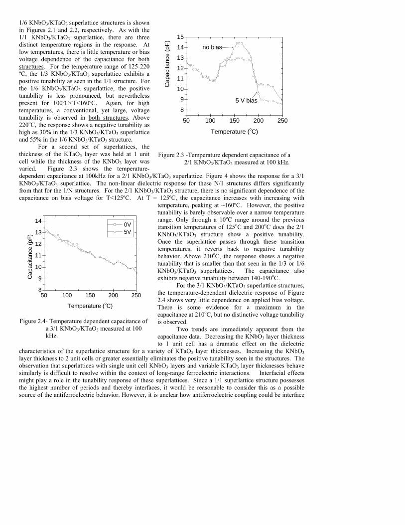
Several superlattice structures were grown in which the thickness of KNbO3 layer was held at 1 unit cell per period and the KTaO3 layer thickness was varied. The temperature-dependent capacitance at 100 kHz for 1/3 and
50 100 150 200 250
20
40
60
80
100
5 V bias
no bias
Cap
acita
nce
(pF)
Temperature (oC)
Figure 2.1- Temperature dependent capacitance of a 1/3 KNbO3/KTaO3 measured at 100 kHz.
50 100 150 200 2500
50
100
150
200
5 V bias
no bias
Cap
acita
nce
(pF)
Temperature (oC)
Figure 2.2- Temperature dependent capacitance of a 1/6 KNbO3/KTaO3 measured at 100 kHz.
1/6 KNbO3/KTaO3 superlattice structures is shown in Figures 2.1 and 2.2, respectively. As with the 1/1 KNbO3/KTaO3 superlattice, there are three distinct temperature regions in the response. At low temperatures, there is little temperature or bias voltage dependence of the capacitance for both structures. For the temperature range of 125-220 ºC, the 1/3 KNbO3/KTaO3 superlattice exhibits a positive tunability as seen in the 1/1 structure. For the 1/6 KNbO3/KTaO3 superlattice, the positive tunability is less pronounced, but nevertheless present for 100ºC<T<160ºC. Again, for high temperatures, a conventional, yet large, voltage tunability is observed in both structures. Above 220oC, the response shows a negative tunability as high as 30% in the 1/3 KNbO3/KTaO3 superlattice and 55% in the 1/6 KNbO3/KTaO3 structure.
For a second set of superlattices, the thickness of the KTaO3 layer was held at 1 unit cell while the thickness of the KNbO3 layer was varied. Figure 2.3 shows the temperature-dependent capacitance at 100kHz for a 2/1 KNbO3/KTaO3 superlattice. Figure 4 shows the response for a 3/1 KNbO3/KTaO3 superlattice. The non-linear dielectric response for these N/1 structures differs significantly from that for the 1/N structures. For the 2/1 KNbO3/KTaO3 structure, there is no significant dependence of the capacitance on bias voltage for T<125ºC. At T = 125ºC, the capacitance increases with increasing with
temperature, peaking at ~160ºC. However, the positive tunability is barely observable over a narrow temperature range. Only through a 10oC range around the previous transition temperatures of 125oC and 200oC does the 2/1 KNbO3/KTaO3 structure show a positive tunability. Once the superlattice passes through these transition temperatures, it reverts back to negative tunability behavior. Above 210oC, the response shows a negative tunability that is smaller than that seen in the 1/3 or 1/6 KNbO3/KTaO3 superlattices. The capacitance also exhibits negative tunability between 140-190oC.
For the 3/1 KNbO3/KTaO3 superlattice structures, the temperature-dependent dielectric response of Figure 2.4 shows very little dependence on applied bias voltage. There is some evidence for a maximum in the capacitance at 210oC, but no distinctive voltage tunability is observed.
Two trends are immediately apparent from the capacitance data. Decreasing the KNbO3 layer thickness to 1 unit cell has a dramatic effect on the dielectric
characteristics of the superlattice structure for a variety of KTaO3 layer thicknesses. Increasing the KNbO3 layer thickness to 2 unit cells or greater essentially eliminates the positive tunability seen in the structures. The observation that superlattices with single unit cell KNbO3 layers and variable KTaO3 layer thicknesses behave similarly is difficult to resolve within the context of long-range ferroelectric interactions. Interfacial effects might play a role in the tunability response of these superlattices. Since a 1/1 superlattice structure possesses the highest number of periods and thereby interfaces, it would be reasonable to consider this as a possible source of the antiferroelectric behavior. However, it is unclear how antiferroelectric coupling could be interface
50 100 150 200 250
8
9
10
11
12
13
14
15
5 V bias
no bias
Cap
acita
nce
(pF)
Temperature (oC)
Figure 2.3 -Temperature dependent capacitance of a
2/1 KNbO3/KTaO3 measured at 100 kHz.
50 100 150 200 2508
9
10
11
12
13
14
Cap
acita
nce
(pF)
Temperature (oC)
0V 5V
Figure 2.4- Temperature dependent capacitance of
a 3/1 KNbO3/KTaO3 measured at 100 kHz.
related. Contradiction occurs when the 3/1 KNbO3/KTaO3 and the 1/3 KNbO3/KTaO3 superlattices are compared. Here the number of interfaces is equal, yet the responses are dramatically different. The structural difference lies in what nearest neighbors the KNbO3 dipole will see in each superlattice. In the 1/3 KNbO3/KTaO3 structure, the nearest neighbor for every KNbO3 dipole is an induced dipole of the KTaO3 layer. For a 3/1 KNbO3/KTaO3 superlattice, one-third of the KNbO3 dipoles have KNbO3 nearest neighbors.
Besides a dipole moment each Nb atom in the KNbO3 layer possesses an elastic quadropole moment. Because of the piezoelectric nature of ferroelectric materials, a reorientation of one always results in a reorientation of the other. Previous x-ray diffraction measurements of KNbO3/KTaO3 superlattices indicate that the nature of the structural phase transition is dependent upon the thickness of the KNbO3. Changes in structure create changes in lattices parameters and thereby changes in strain in the layers. However, changes in strain creates changes in polarization and thereby changes in the dipole interactions. Such structure, strain and polarization relationships have been observed in BaTiO3/SrTiO3 superlattices. Therefore, the structural change that occurs as the KNbO3 layer thickness is decreased from 3 unit cell to 1 unit cell creates enough changes in the polarization and dipole interaction to favor antiferroelectric coupling. Further understanding of this antiferroelectric coupling will require additional x-ray diffraction measurements as well theoretical simulations of the dipole moment configurations.
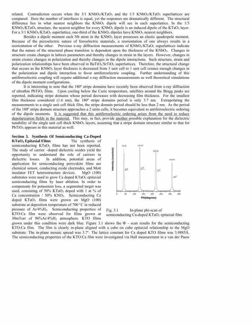
It is interesting to note that the 180º stripe domains have recently been observed from x-ray diffraction of ultrathin PbTiO3 films. Upon cooling below the Curie temperature, satellites around the Bragg peaks are reported, indicating stripe domains whose period decreases with decreasing film thickness. For the smallest film thickness considered (1.6 nm), the 180º stripe domains period is only 3.7 nm. Extrapolating the measurements to a single unit cell thick film, the stripe domain period should be less than 2 nm. As the period of the 180º stripe domain structure approaches a 2 units cells, it becomes equivalent to antiferroelectric ordering of the dipole moments. It is suggested that this antiferroelectric ordering arises from the need to reduce depolarization fields in the material. This may, in fact, provide another possible explanation for the dielectric tunability of the single unit cell thick KNbO3 layers, assuming that a stripe domain structure similar to that for PbTiO3 appears in this material as well. Section 3. Synthesis Of Semiconducting Ca-Doped KTaO3 Epitaxial Films The synthesis of semiconducting KTaO3 films has not been reported. The study of carrier –doped dielectric oxides yield the opportunity to understand the role of carriers in dielectric losses. In addition, potential areas of application for semiconducting perovskite films are chemical sensor, conducting oxide electrodes, and Mott insulator FET heterostructure devices. MgO (100) substrates were used to grow Ca doped KTaO3 epitaxial semiconducting films by laser ablation. In order to compensate for potassium loss, a segmented target was used, consisting of 50% KTaO3 doped with 1 at % of Ca concentration / 50% KNO3. Semiconducting Ca doped KTaO3 films were grown on MgO (100) substrate at deposition temperature of 700 °C in reduced pressure of Ar/4%H2. Semiconducting properties of KTO:Ca film were observed for films grown at 30mTorr of 96%Ar/4%H2 atmosphere. KTO films grown under this condition were dark blue. Figure 3.1 shows the Φ - scan results for the semiconducting KTO:Ca film. The film is clearly in-plane aligned with a cube on cube epitaxial relationship to the MgO substrate. The in-plane mosaic spread was 3.7°. The lattice constant for Ca doped KTO films was 3.9885Å. The semiconducting properties of the KTO:Ca film were investigated via Hall measurement in a van der Pauw
0 50 100 150 200 250 300 350
4.0o
3.7o3.4o
3.6o
310.95
220.95
130.3540.25
Inte
nsity
(cou
nts/
s)
Phi(degrees)
Fig. 3.1 In-plane phi-scan of semiconducting Ca-doped KTaO3 epitaxial film
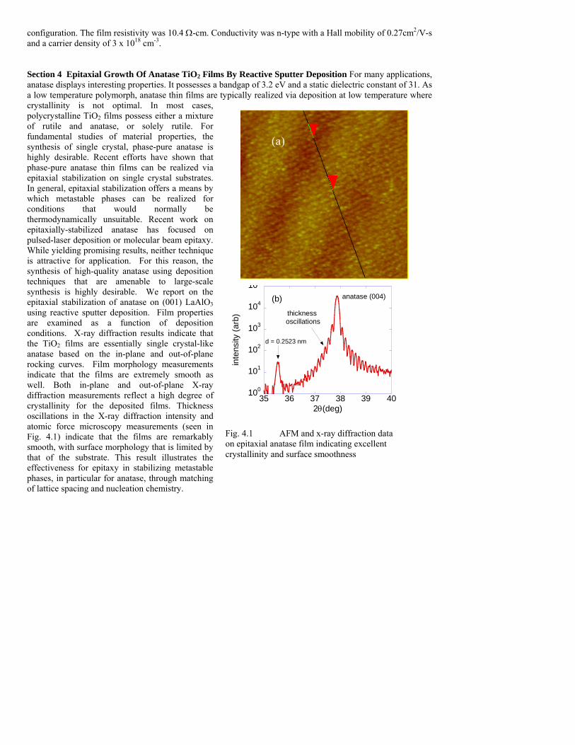
configuration. The film resistivity was 10.4 Ω-cm. Conductivity was n-type with a Hall mobility of 0.27cm2/V-s and a carrier density of 3 x 1018 cm-3. Section 4 Epitaxial Growth Of Anatase TiO2 Films By Reactive Sputter Deposition For many applications, anatase displays interesting properties. It possesses a bandgap of 3.2 eV and a static dielectric constant of 31. As a low temperature polymorph, anatase thin films are typically realized via deposition at low temperature where crystallinity is not optimal. In most cases, polycrystalline TiO2 films possess either a mixture of rutile and anatase, or solely rutile. For fundamental studies of material properties, the synthesis of single crystal, phase-pure anatase is highly desirable. Recent efforts have shown that phase-pure anatase thin films can be realized via epitaxial stabilization on single crystal substrates. In general, epitaxial stabilization offers a means by which metastable phases can be realized for conditions that would normally be thermodynamically unsuitable. Recent work on epitaxially-stabilized anatase has focused on pulsed-laser deposition or molecular beam epitaxy. While yielding promising results, neither technique is attractive for application. For this reason, the synthesis of high-quality anatase using deposition techniques that are amenable to large-scale synthesis is highly desirable. We report on the epitaxial stabilization of anatase on (001) LaAlO3 using reactive sputter deposition. Film properties are examined as a function of deposition conditions. X-ray diffraction results indicate that the TiO2 films are essentially single crystal-like anatase based on the in-plane and out-of-plane rocking curves. Film morphology measurements indicate that the films are extremely smooth as well. Both in-plane and out-of-plane X-ray diffraction measurements reflect a high degree of crystallinity for the deposited films. Thickness oscillations in the X-ray diffraction intensity and atomic force microscopy measurements (seen in Fig. 4.1) indicate that the films are remarkably smooth, with surface morphology that is limited by that of the substrate. This result illustrates the effectiveness for epitaxy in stabilizing metastable phases, in particular for anatase, through matching of lattice spacing and nucleation chemistry.
100
101
102
103
104
10
35 36 37 38 39 40
inte
nsity
(arb
)
2θ(deg)
anatase (004)
thickness oscillations
d = 0.2523 nm
(b)
(a)
Fig. 4.1 AFM and x-ray diffraction data on epitaxial anatase film indicating excellent crystallinity and surface smoothness
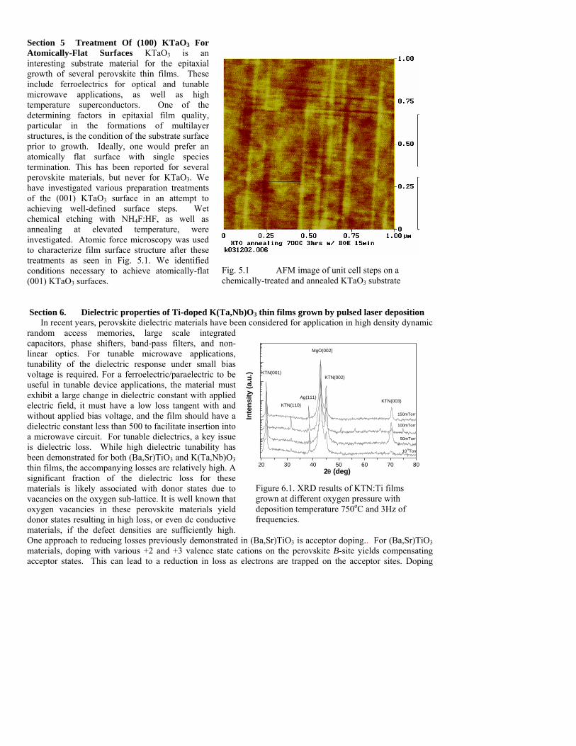
Section 5 Treatment Of (100) KTaO3 For Atomically-Flat Surfaces KTaO3 is an interesting substrate material for the epitaxial growth of several perovskite thin films. These include ferroelectrics for optical and tunable microwave applications, as well as high temperature superconductors. One of the determining factors in epitaxial film quality, particular in the formations of multilayer structures, is the condition of the substrate surface prior to growth. Ideally, one would prefer an atomically flat surface with single species termination. This has been reported for several perovskite materials, but never for KTaO3. We have investigated various preparation treatments of the (001) KTaO3 surface in an attempt to achieving well-defined surface steps. Wet chemical etching with NH4F:HF, as well as annealing at elevated temperature, were investigated. Atomic force microscopy was used to characterize film surface structure after these treatments as seen in Fig. 5.1. We identified conditions necessary to achieve atomically-flat (001) KTaO3 surfaces.
Section 6. Dielectric properties of Ti-doped K(Ta,Nb)O3 thin films grown by pulsed laser deposition In recent years, perovskite dielectric materials have been considered for application in high density dynamic
random access memories, large scale integrated capacitors, phase shifters, band-pass filters, and non-linear optics. For tunable microwave applications, tunability of the dielectric response under small bias voltage is required. For a ferroelectric/paraelectric to be useful in tunable device applications, the material must exhibit a large change in dielectric constant with applied electric field, it must have a low loss tangent with and without applied bias voltage, and the film should have a dielectric constant less than 500 to facilitate insertion into a microwave circuit. For tunable dielectrics, a key issue is dielectric loss. While high dielectric tunability has been demonstrated for both (Ba,Sr)TiO3 and K(Ta,Nb)O3 thin films, the accompanying losses are relatively high. A significant fraction of the dielectric loss for these materials is likely associated with donor states due to vacancies on the oxygen sub-lattice. It is well known that oxygen vacancies in these perovskite materials yield donor states resulting in high loss, or even dc conductive materials, if the defect densities are sufficiently high. One approach to reducing losses previously demonstrated in (Ba,Sr)TiO3 is acceptor doping.. For (Ba,Sr)TiO3 materials, doping with various +2 and +3 valence state cations on the perovskite B-site yields compensating acceptor states. This can lead to a reduction in loss as electrons are trapped on the acceptor sites. Doping
Fig. 5.1 AFM image of unit cell steps on a chemically-treated and annealed KTaO3 substrate
20 30 40 50 60 70 80
KTN(002)
Ag(111)
KTN(110)
KTN(001)
Inte
nsity
(a.u
.)
2θ (deg)
10-5Torr
50mTorr
100mTorr
150mTorr
KTN(003)
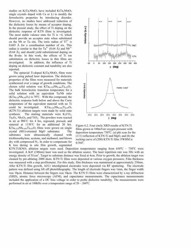
MgO(002)
Figure 6.1. XRD results of KTN:Ti films grown at different oxygen pressure with deposition temperature 750oC and 3Hz of frequencies.
studies on K(Ta,Nb)O3 have included K(Ta,Nb)O3 single crystals doped with Ca or Li to modify the ferroelectric properties by introducing disorder. However, no studies have addressed reduction of the dielectric losses by means of acceptor doping. In the present study, the effect of Ti doping on the dielectric response of KTN films is investigated. The most stable valence state for Ti is +4, which should provide an acceptor state when substituted on the Nb or Ta site. The ionic radius of Ti4+ is 0.605 Å for a coordination number of six. This radius is similar to that for Ta5+ (0.64 Å) and Nb5+ (0.64 Å), and should yield substitutional doping on the B-site. In this work, the effects of Ti ion substitution on dielectric losses in thin films are investigated. In addition, the influence of Ti doping on dielectric constant and tunability are also reported.
The epitaxial Ti-doped K(Ta,Nb)O3 films were grown using pulsed laser deposition. The dielectric properties of the films were measured for materials synthesized over a range of growth conditions. The chosen solid solution was KTa0.524Nb0.446Ti0.03O3. The bulk ferroelectric transition temperature for a solid solution with an equivalent Ta/Nb ratio (KTa0.54Nb0.46O3) is 70oC. With this compound, the dielectric response both below and above the Curie temperature of the equivalent material with no Ti could be investigated. KTa0.524Nb0.446Ti0.03O3 (KTN:Ti) ablation targets were made by solid state synthesis. The starting materials were K2CO3, Ta2O5, Nb2O5, and TiO2. The powders were reacted in air at 900˚C for 4 hrs, reground, pressed, and sintered at 1150˚C for an additional 20 hrs. KTa0.524Nb0.446Ti0.03O3 films were grown on single crystal (001)-oriented MgO substrates. The substrates were ultrasonically cleaned with trichloroethylene, acetone, and methanol, and blown dry with compressed N2. In order to compensate for K loss during in situ film growth, segmented KTN:Ti/KNO3 ablation targets were used. Deposition temperatures ranging from 650oC – 750oC were investigated. A KrF (248nm) laser was used as the ablation source. The laser repetition rate was 3Hz with an energy density of 5J/cm2. Target to substrate distance was fixed at 4cm. Prior to growth, the ablation target was cleaned by pre-ablating 2000 shots. KTN:Ti films were deposited at various oxygen pressures. Film thickness was measured with a step profilometer. For this study, film thickness was maintained at approximately 250nm. After KTN:Ti film growth, Al/Cr interdigitated electrodes were deposited via RF sputtering. The electrode pattern was defined using lift off photolithography. The length of electrode fingers was 1mm, the finger width was 10µm. Distance between the fingers was 10µm. The KTN:Ti films were characterized by x-ray diffraction (XRD), atomic force microscopy (AFM), and capacitance measurements. The capacitance measurements included the application of a DC bias voltage in order to probe dielectric tunability. The measurements were performed in air at 100kHz over a temperature range of 20 – 260oC.
-50 0 50 100 150 200 250 300 350 400
(deg)
Inte
nsity
(a.u
.)
315.05o224.95o135.05o45.15o
KTN
MgO
Φ
21.0 21.5 22.0 22.5 23.0 23.5 24.0 24.5
Inte
nsity
(a.u
.)FWHM : 0.564o
(deg)
Ω
Figure 6.2. Four circle XRD results of KTN:Ti films grown at 100mTorr oxygen pressure with deposition temperature 750oC. (a) phi scan for the (111) reflection of KTN:Ti and MgO, and (b) the rocking curve of (200) KTN:Ti film: FWHM is 0.564o.
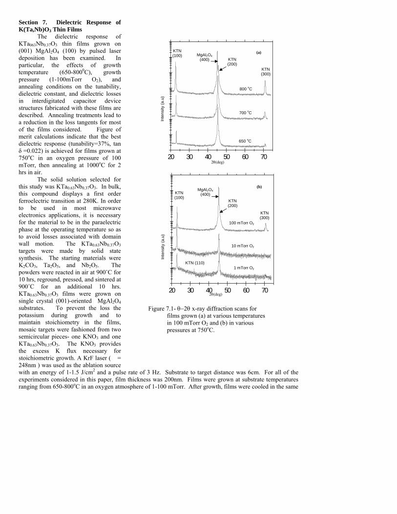
Epitaxial growth of KTa0.524Nb0.446Ti0.03O3 (KTN) thin films was achieved at a growth temperature of 750˚C in background pressures ranging from 0.01-150 mTorr. Figure 1 shows the results from θ-2θ x-ray diffraction (XRD) measurements for KTN:Ti films grown on (001) MgO at different oxygen pressures. The deposition temperature was 750oC for all films considered in Fig. 6.1. The XRD results indicate good crystallinity for all of the KTN:Ti films grown at these conditions. The films are mostly (001) oriented, with only a small KTN (110) peak observed in the diffraction pattern. The Ag peak is from the Ag paint used in mounting the substrates on the heater platen. The intensity of the diffraction peaks are somewhat less for the film grown in vacuum ( 0.01 mTorr). Note that there is a measurable reduction in c-axis lattice spacing with increasing oxygen pressure during growth. From the
θ-2θ plots, the lattice spacing shifts from 4.0155 Å for films grown in vacuum to 4.0004 Å for films grown in 150 mTorr of oxygen. Larger lattice spacing in oxides often reflects the presence of oxygen vacancies.
The epitaxial relationship of the Ti-doped KTN films on the (001) MgO substrate was investigated using four-circle XRD. Figure 6.2 shows an in-plane φ-scan through the KTN:Ti (111) peaks for a film grown at 750˚C in 100 mTorr O2. The full-width half-maximum of the φ peak is 1.84˚. Despite the lattice mismatch between the KTN film and MgO substrate, the φ-scan indicates cube-on-cube in-plane alignment of the KTN:Ti film on the MgO substrate. Also shown in the figure is the rocking curve for the KTN:Ti (200) peak. The full-width half-maximum (FWHM) of the KTN:Ti (002) peak is 0.56o.
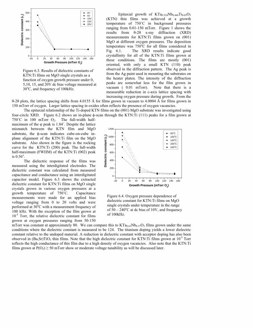
The dielectric response of the films was measured using the interdigitated electrodes. The dielectric constant was calculated from measured capacitance and conductance using an interdigitated capacitor model. Figure 6.3 shows the extracted dielectric constant for KTN:Ti films on MgO single crystals grown in various oxygen pressures at a growth temperature of 750˚C. Capacitance measurements were made for an applied bias voltage ranging from 0 to 20 volts and were performed at 30oC with a measurement frequency of 100 kHz. With the exception of the film grown at 10-5 Torr, the relative dielectric constant for films grown at oxygen pressures ranging from 50-150 mTorr was constant at approximately 80. We can compare this to KTa0.63Nb0.37O3 films grown under the same conditions where the dielectric constant is measured to be 124. The titanium doping yields a lower dielectric constant relative to the undoped material. A reduction in dielectric constant with acceptor doping has also been observed in (Ba,Sr)TiO3 thin films. Note that the high dielectric constant for KTN:Ti films grown at 10-5 Torr reflects the high conductance of this film due to a high density of oxygen vacancies. Also note that the KTN:Ti films grown at P(O2) ≥ 50 mTorr show or moderate voltage tunability as will be discussed later.
-20 0 20 40 60 80 100 120 140 1600
100
200
300
400
500
Growth Pressure (mTorr O2)
Die
lect
ric c
onst
ant (
ε r) 0V 5V 10V 15V 20V
Figure 6.3. Results of dielectric constants of KTN:Ti films on MgO single crystals as a function of oxygen growth pressure under 0, 5,10, 15, and 20V dc bias voltage measured at 30oC, and frequency of 100kHz.
-20 0 20 40 60 80 100 120 140 160
0
200
400
600
800
1000
1200
Die
lect
ric c
onst
ant (
ε r)
Growth Pressure (mTorr O2)
50oC 100oC 140oC 200oC 240oC
Figure 6.4. Oxygen pressure dependence of dielectric constant for KTN:Ti films on MgO single crystals under temperature in the range of 50 – 240oC at dc bias of 10V, and frequency of 100kHz.
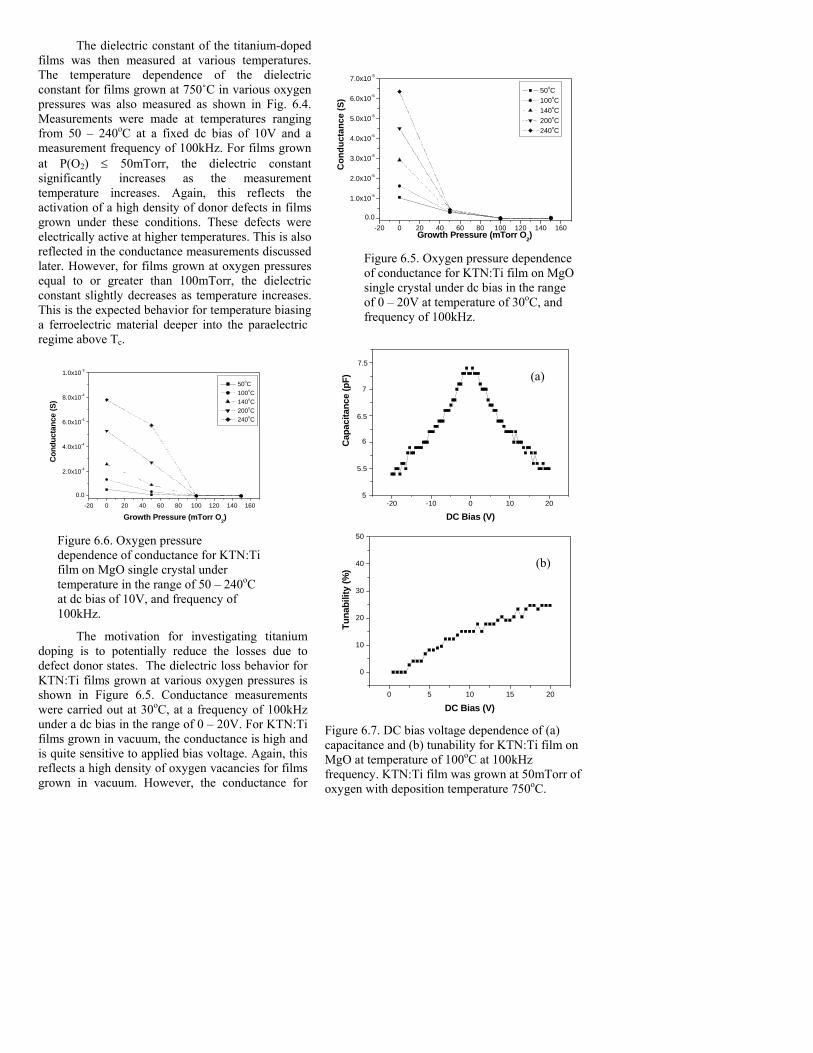
The dielectric constant of the titanium-doped films was then measured at various temperatures. The temperature dependence of the dielectric constant for films grown at 750˚C in various oxygen pressures was also measured as shown in Fig. 6.4. Measurements were made at temperatures ranging from 50 – 240oC at a fixed dc bias of 10V and a measurement frequency of 100kHz. For films grown at P(O2) ≤ 50mTorr, the dielectric constant significantly increases as the measurement temperature increases. Again, this reflects the activation of a high density of donor defects in films grown under these conditions. These defects were electrically active at higher temperatures. This is also reflected in the conductance measurements discussed later. However, for films grown at oxygen pressures equal to or greater than 100mTorr, the dielectric constant slightly decreases as temperature increases. This is the expected behavior for temperature biasing a ferroelectric material deeper into the paraelectric regime above Tc.
The motivation for investigating titanium doping is to potentially reduce the losses due to defect donor states. The dielectric loss behavior for KTN:Ti films grown at various oxygen pressures is shown in Figure 6.5. Conductance measurements were carried out at 30oC, at a frequency of 100kHz under a dc bias in the range of 0 – 20V. For KTN:Ti films grown in vacuum, the conductance is high and is quite sensitive to applied bias voltage. Again, this reflects a high density of oxygen vacancies for films grown in vacuum. However, the conductance for
-20 0 20 40 60 80 100 120 140 1600.0
1.0x10⁻⁵
2.0x10⁻⁵
3.0x10⁻⁵
4.0x10⁻⁵
5.0x10⁻⁵
6.0x10⁻⁵
7.0x10⁻⁵
Growth Pressure (mTorr O2)
Con
duct
ance
(S)
50oC 100oC 140oC 200oC 240oC
Figure 6.5. Oxygen pressure dependence of conductance for KTN:Ti film on MgO single crystal under dc bias in the range of 0 – 20V at temperature of 30oC, and frequency of 100kHz.
-20 0 20 40 60 80 100 120 140 160
0.0
2.0x10⁻⁴
4.0x10⁻⁴
6.0x10⁻⁴
8.0x10⁻⁴
1.0x10⁻³
Con
duct
ance
(S)
Growth Pressure (mTorr O2)
50oC 100oC 140oC 200oC 240oC
Figure 6.6. Oxygen pressure dependence of conductance for KTN:Ti film on MgO single crystal under temperature in the range of 50 – 240oC at dc bias of 10V, and frequency of 100kHz.
-20 -10 0 10 20
7.5
7
6.5
6
5.5
5
Cap
acita
nce
(pF)
DC Bias (V)
0 5 10 15 20
0
10
20
30
40
50
Tuna
bilit
y (%
)
DC Bias (V)
(a)
(b)
Figure 6.7. DC bias voltage dependence of (a) capacitance and (b) tunability for KTN:Ti film on MgO at temperature of 100oC at 100kHz frequency. KTN:Ti film was grown at 50mTorr of oxygen with deposition temperature 750oC.
Å
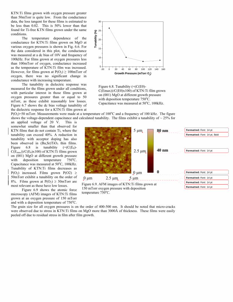
KTN:Ti films grown with oxygen pressure greater than 50mTorr is quite low. From the conductance data, the loss tangent for these films is estimated to be less than 0.02. This is 50% lower than that found for Ti-free KTN films grown under the same conditions.
The temperature dependence of the conductance for KTN:Ti films grown on MgO at various oxygen pressures is shown in Fig. 6.6. For the data considered in this plot, the conductance was measured at a dc bias of 10V and frequency of 100kHz. For films grown at oxygen pressures less than 100mTorr of oxygen, conductance increased as the temperature of KTN:Ti film was increased. However, for films grown at P(O2) ≥ 100mTorr of oxygen, there was no significant change in conductance with increasing temperature.
The tunability in dielectric response was measured for the films grown under all conditions, with particular interest in those films grown at oxygen pressures greater than or equal to 50 mTorr, as these exhibit reasonably low losses. Figure 6.7 shows the dc bias voltage tunability of the dielectric response for a KTN:Ti film grown at P(O2)=50 mTorr. Measurements were made at a temperature of 100oC and a frequency of 100 kHz. The figure shows the voltage-dependent capacitance and calculated tunability. The films exhibit a tunability of ~ 25% for an applied voltage of 20 V. This is somewhat smaller than that observed for KTN films that do not contain Ti, where the tunability can exceed 40%. A reduction in tunability with acceptor doping has also been observed in (Ba,Sr)TiO3 thin films. Figure 6.8 is tunability (=(C(E0)-C(Emax))/C(E0)x100) of KTN:Ti films grown on (001) MgO at different growth pressure with deposition temperature 750oC. Capacitance was measured at 50oC, 100kHz. Tunability of KTN:Ti films decreases as P(O2) increased. Films grown P(O2) ≥ 50mTorr exhibit a tunability on the order of 8%. Films grown at P(O2) ≥ 50mTorr are most relevant as these have low losses.
Figure 6.9 shows the atomic force microscopy (AFM) images of KTN:Ti films grown at an oxygen pressure of 150 mTorr and with a deposition temperature of 750oC. The grain size for all oxygen pressures is on the order of 400-500 nm. It should be noted that micro-cracks were observed due to stress in KTN:Ti films on MgO more than 3000Å of thickness. These films were easily peeled off due to residual stress in film after film growth.
-20 0 20 40 60 80 100 120 140 1605
10
15
20
25
30
Tuna
bilit
y (%
)
Growth Pressure (mTorr O2)
Figure 6.8. Tunability (=(C(E0)-C(Emax))/C(E0)x100) of KTN:Ti film grown on (001) MgO at different growth pressure with deposition temperature 750oC. Capacitance was measured at 50oC, 100kHz.
2.5 µm
2.5 µm 0 µm
5 µm
0 µm 5 µm
80 nm 40 nm 0
Figure 6.9. AFM images of KTN:Ti films grown at 150 mTorr oxygen pressure with deposition temperature 750oC.
Formatted: Font: 14 pt
Formatted: Font: 14 pt, Bold
Formatted: Font: 14 pt
Formatted: Font: 14 pt
Formatted: Font: 14 pt
Formatted: Font: 14 pt
Formatted: Font: 14 pt
Section 7. Dielectric Response of K(Ta,Nb)O3 Thin Films
The dielectric response of KTa063Nb0.37O3 thin films grown on (001) MgAl2O4 (100) by pulsed laser deposition has been examined. In particular, the effects of growth temperature (650-8000C), growth pressure (1-100mTorr O2), and annealing conditions on the tunability, dielectric constant, and dielectric losses in interdigitated capacitor device structures fabricated with these films are described. Annealing treatments lead to a reduction in the loss tangents for most of the films considered. Figure of merit calculations indicate that the best dielectric response (tunability=37%, tan δ =0.022) is achieved for films grown at 750oC in an oxygen pressure of 100 mTorr, then annealing at 1000oC for 2 hrs in air.
The solid solution selected for this study was KTa0.63Nb0.37O3. In bulk, this compound displays a first order ferroelectric transition at 280K. In order to be used in most microwave electronics applications, it is necessary for the material to be in the paraelectric phase at the operating temperature so as to avoid losses associated with domain wall motion. The KTa0.63Nb0.37O3 targets were made by solid state synthesis. The starting materials were K2CO3, Ta2O5, and Nb2O5. The powders were reacted in air at 900˚C for 10 hrs, reground, pressed, and sintered at 900˚C for an additional 10 hrs. KTa0.63Nb0.37O3 films were grown on single crystal (001)-oriented MgAl2O4 substrates. To prevent the loss the potassium during growth and to maintain stoichiometry in the films, mosaic targets were fashioned from two semicircular pieces- one KNO3 and one KTa0.63Nb0.37O3. The KNO3 provides the excess K flux necessary for stoichiometric growth. A KrF laser ( = 248nm ) was used as the ablation source with an energy of 1-1.5 J/cm2 and a pulse rate of 3 Hz. Substrate to target distance was 6cm. For all of the experiments considered in this paper, film thickness was 200nm. Films were grown at substrate temperatures ranging from 650-800oC in an oxygen atmosphere of 1-100 mTorr. After growth, films were cooled in the same
20 30 40 50 60 70
20 30 40 50 60 70
KTN (200)
KTN (300)
KTN (100) MgAl2O4
(400)
2θ(deg) In
tens
ity (a
.u)
800 oC
700 oC
650 oC
KTN (200)
KTN (300)
KTN (100)
MgAl2O4 (400)
2θ(deg)
Inte
nsity
(a.u
)
10 mTorr O2
1 mTorr O2
100 mTorr O2
KTN (110)
(a)
(b)
Figure 7.1- θ−2θ x-ray diffraction scans for films grown (a) at various temperatures in 100 mTorr O2 and (b) in various pressures at 750oC.
oxygen pressure as used during growth. For some samples, post-annealing was performed in air in a standard box furnace. Films were placed in a covered, clean, dry crucible along with 2-4g of KNb0.37Ta0.63O3 powder. The K overpressure during the anneal from the KTN powder was necessary in order to minimize K loss during the annealing treatment. For the anneals, the temperature ramp rate was 10 oC/min. Annealing time was 2 hours for the temperatures between 800-1000oC.
The crystallinity of the film was characterized using x-ray diffraction. The surface morphology was examined with AFM both before and after annealing. For the dielectric response measurements, interdigitated capacitors (IDC) were fabricated on the film surface. The electrodes were defined using wet photolithography and lift off. The electrode metallization was accomplished either by RF sputtering (for Al/Cr electrodes), or thermal evaporation (for Au/Cr electrodes). Capacitance measurements were performed at 100 kHz and 1 MHz over a temperature range of 20-300 oC.
Epitaxial KTN films could be realized on the (001) MgAl2O4 substrates over a wide range of deposition conditions. Figures 7.1a and 7.1b show x-ray diffraction θ-2θ scans for as-deposited KTN films obtained at 650-800˚C in an oxygen pressure of 1-100 mTorr. The lattice mismatch between KTN and MgAl2O4 is only 1.2%. C-axis oriented films could also be realized for growth pressure greater than 10 mTorr. Below a growth pressure of 10 mTorr O2, the films also showed (110) orientation.
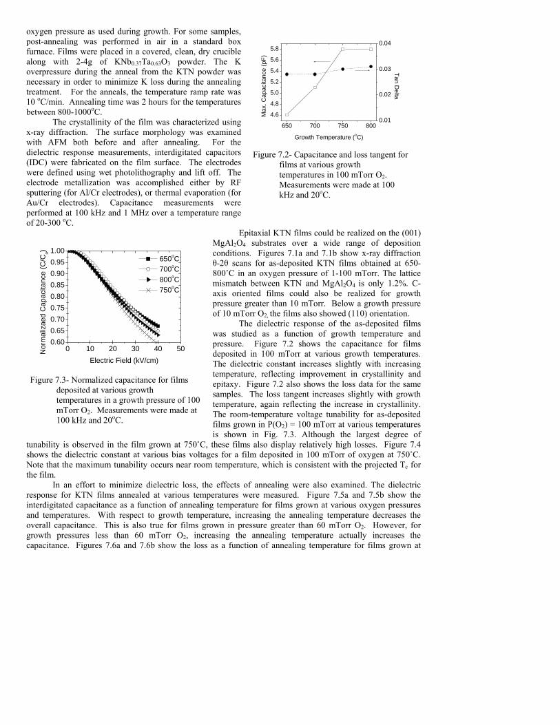
The dielectric response of the as-deposited films was studied as a function of growth temperature and pressure. Figure 7.2 shows the capacitance for films deposited in 100 mTorr at various growth temperatures. The dielectric constant increases slightly with increasing temperature, reflecting improvement in crystallinity and epitaxy. Figure 7.2 also shows the loss data for the same samples. The loss tangent increases slightly with growth temperature, again reflecting the increase in crystallinity. The room-temperature voltage tunability for as-deposited films grown in P(O2) = 100 mTorr at various temperatures is shown in Fig. 7.3. Although the largest degree of
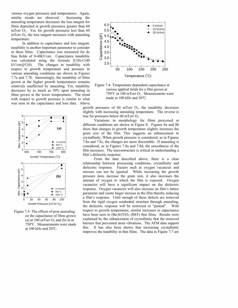
tunability is observed in the film grown at 750˚C, these films also display relatively high losses. Figure 7.4 shows the dielectric constant at various bias voltages for a film deposited in 100 mTorr of oxygen at 750˚C. Note that the maximum tunability occurs near room temperature, which is consistent with the projected Tc for the film.
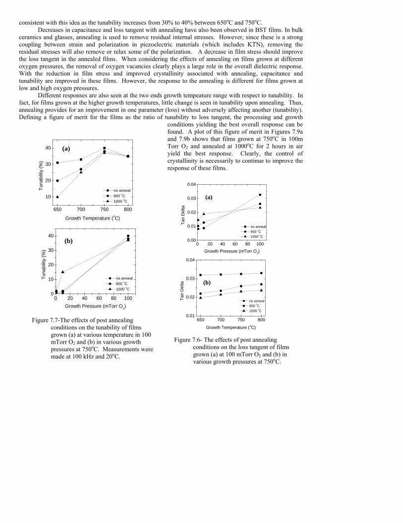
In an effort to minimize dielectric loss, the effects of annealing were also examined. The dielectric response for KTN films annealed at various temperatures were measured. Figure 7.5a and 7.5b show the interdigitated capacitance as a function of annealing temperature for films grown at various oxygen pressures and temperatures. With respect to growth temperature, increasing the annealing temperature decreases the overall capacitance. This is also true for films grown in pressure greater than 60 mTorr O2. However, for growth pressures less than 60 mTorr O2, increasing the annealing temperature actually increases the capacitance. Figures 7.6a and 7.6b show the loss as a function of annealing temperature for films grown at
650 700 750 800
4.6
4.8
5.0
5.2
5.4
5.6
5.8
Growth Temperature (oC)
Max
. Cap
acita
nce
(pF)
0.01
0.02
0.03
0.04
Tan Delta
Figure 7.2- Capacitance and loss tangent for
films at various growth temperatures in 100 mTorr O2. Measurements were made at 100 kHz and 20oC.
0 10 20 30 40 500.600.650.700.750.800.850.900.951.00
650oC 700oC 800oC 750oC
Nor
mal
izae
d C
apac
itanc
e (C
/Co)
Electric Field (kV/cm)
Figure 7.3- Normalized capacitance for films deposited at various growth temperatures in a growth pressure of 100 mTorr O2. Measurements were made at 100 kHz and 20oC.
various oxygen pressures and temperatures. Again, similar trends are observed. Increasing the annealing temperature decreases the loss tangent for films deposited at growth pressures greater than 60 mTorr O2. Yet, for growth pressures less than 60 mTorr O2, the loss tangent increases with annealing temperature.
In addition to capacitance and loss tangent, tunability is another important parameter to consider in these films. Capacitance was measured for dc bias fields of 0-40kV/cm. Capacitance tunability was calculated using the formula [C(0)-C(40 kV/cm)]/C(0). The changes in tunability with respect to growth temperature and pressure in various annealing conditions are shown in Figures 7.7a and 7.7b. Interestingly, the tunability of films grown at the higher growth temperatures remains relatively unaffected by annealing. Yet, tunability decreases by as much as 50% upon annealing in films grown at the lower temperatures. The trend with respect to growth pressure is similar to what was seen in the capacitance and loss data. Above
growth pressures of 60 mTorr O2, the tunability decreases slightly with increasing annealing temperature. The reverse is true for pressures below 60 mTorr O2.
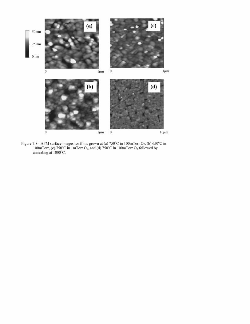
Variations in morphology for films processed at different conditions are shown in Figure 8. Figures 8a and 8b show that changes in growth temperature slightly increases the grain size of the film. This suggests an enhancement in crystallinity. When growth pressure is considered, as in Figures 7.8a and 7.8c, the changes are more discernible. If annealing is considered, as in Figures 7.8a and 7.8d, the smoothness of the film increases. The microstructure is critical in understanding a film’s dielectric response.
From the data described above, there is a clear relationship between processing conditions, crystallinity and dielectric response. Factors such as oxygen vacancies and stresses can not be ignored. While increasing the growth pressure does increase the grain size, it also increases the amount of oxygen to which the film is exposed. Oxygen vacancies will have a significant impact on the dielectric response. Oxygen vacancies will also increase an film’s lattice parameter and create larger stresses in the film thereby reducing a film’s response. Until enough of these defects are removed from the rigid oxygen octahedral structure through annealing, the dielectric response will be restricted or “pinned”. With respect to growth temperature, similar increases in capacitance have been seen in (Ba,Sr)TiO3 (BST) thin films. Results were explained by the enhancement of crystallinity that the removed barriers that prevented atom vibrations. The AFM data support this. It has also been shown that increasing crystallinity improves the tunability in thin films. The data in Figure 7.7 are
50 100 150 200 250
2.53.03.54.04.55.05.56.0
Cap
acita
nce
(pF)
Temperature (oC)
0 kV/cm 10 kV/cm 20 kV/cm
Figure 7.4- Temperature dependent capacitance at
various applied fields for a film grown at 750oC in 100 mTorr O2. Measurements were made at 100 kHz and 20oC.
(b)
0 20 40 60 80 100
1
2
3
4
5
6
Max
. Cap
acita
nce
(pF)
Growth Pressure (mTorr O2)
no anneal 900 oC 1000 oC
650 700 750 8001
2
3
4
5
6
Max
. Cap
acita
nce
(pF)
Growth Temperature (oC)
no anneal 900 oC 1000 oC
(a)
Figure 7.5- The effects of post annealing
on the capacitance of films grown (a) at 100 mTorr O2 and (b) in at 750oC. Measurements were made at 100 kHz and 20oC.
consistent with this idea as the tunability increases from 30% to 40% between 650oC and 750oC. Decreases in capacitance and loss tangent with annealing have also been observed in BST films. In bulk
ceramics and glasses, annealing is used to remove residual internal stresses. However, since these is a strong coupling between strain and polarization in piezoelectric materials (which includes KTN), removing the residual stresses will also remove or relax some of the polarization. A decrease in film stress should improve the loss tangent in the annealed films. When considering the effects of annealing on films grown at different oxygen pressures, the removal of oxygen vacancies clearly plays a large role in the overall dielectric response. With the reduction in film stress and improved crystallinity associated with annealing, capacitance and tunability are improved in these films. However, the response to the annealing is different for films grown at low and high oxygen pressures.
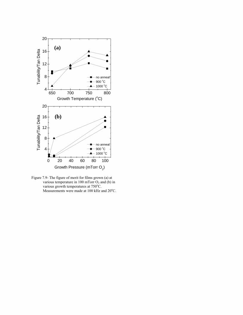
Different responses are also seen at the two ends growth tempeature range with respect to tunability. In fact, for films grown at the higher growth temperatures, little change is seen in tunability upon annealing. Thus, annealing provides for an improvement in one parameter (loss) without adversely affecting another (tunability). Defining a figure of merit for the films as the ratio of tunability to loss tangent, the processing and growth
conditions yielding the best overall response can be found. A plot of this figure of merit in Figures 7.9a and 7.9b shows that films grown at 750oC in 100m Torr O2 and annealed at 1000oC for 2 hours in air yield the best response. Clearly, the control of crystallinity is necessarily to continue to improve the response of these films.
(a)
(b)
0 20 40 60 80 1000.00
0.01
0.02
0.03
0.04
Ta
n D
elta
Growth Pressure (mTorr O2)
no anneal 900 oC 1000 oC
650 700 750 8000.01
0.02
0.03
0.04
no anneal 900 oC 1000 oC
Tan
Del
ta
Growth Temperature (oC)
Figure 7.6- The effects of post annealing conditions on the loss tangent of films grown (a) at 100 mTorr O2 and (b) in various growth pressures at 750oC.
650 700 750 800
10
20
30
40
Tuna
bilit
y (%
)
Growth Temperature (oC)
no anneal 900 oC 1000 oC
0 20 40 60 80 1000
10
20
30
40
Tuna
bilit
y (%
)
Growth Pressure (mTorr O2)
no anneal 900 oC 1000 oC
(a)
(b)
Figure 7.7-The effects of post annealing
conditions on the tunability of films grown (a) at various temperature in 100 mTorr O2 and (b) in various growth pressures at 750oC. Measurements were made at 100 kHz and 20oC.
0 1µm
0 1µm
0 1µm
0 10µm
50 nm 25 nm 0 nm
(a)
(b)
(c)
(d)
Figure 7.8- AFM surface images for films grown at (a) 750oC in 100mTorr O2, (b) 650oC in
100mTorr, (c) 750oC in 1mTorr O2, and (d) 750oC in 100mTorr O2 followed by annealing at 1000oC.
650 700 750 8004
8
12
16
20
Tuna
bilit
y/Ta
n D
elta
Growth Temperature (oC)
no anneal 900 oC 1000 oC
0 20 40 60 80 100
4
8
12
16
20
Tuna
bilit
y/Ta
n D
elta
Growth Pressure (mTorr O2)
no anneal 900 oC 1000 oC
(a)
(b)
Figure 7.9- The figure of merit for films grown (a) at various temperature in 100 mTorr O2 and (b) in various growth temperatures at 750oC. Measurements were made at 100 kHz and 20oC.