Embed Size (px)
Citation preview
Portable Finish Line Data
Capture System for
Sprinters
Jamal McNab, Tyler Snell, Michael
Colucciello, and Argeny Batista
College of Engineering and Computer
Science, University of Central Florida,
Orlando, Florida, 32816 U.S.A.
Abstract — The goal of this project is to bring the
timing accuracy of digital capture systems to practice for
sprinters of all skill levels to improve timing accuracy
over analog methods during training, while keeping costs
low to be marketed towards sprinters of all skill levels.
The design is portable, lightweight, and consumes
minimal power, and can be communicated to via a mobile
android application through Wi-Fi. The design uses a
laser sensor connected to a microcontroller for timing,
which controls LEDs and speakers as well as times
sprints. An android application communicates with the
microcontroller in the main housing via a wireless
connection, sending data to tweak sprint settings, and
display times to the end user.
Index Terms — microcontroller, LDR sensor, 802.11n,
GUI, TCP, Socket
I. INTRODUCTION
This project seeks to bring the accuracy of digital
timing used at higher level sprint competitions to the
practice routines of sprinters of all skill levels. Most
lower level sprinters rely on some form of analog
timing in practice to track improvement during
training, typically another person timing with a
stopwatch. Our goal is to remove the need for a second
person timing the sprint while also improving on
accuracy over this and other analog methods. Since
our target audience is sprinters of all skill levels, we
tailored the design as much as possible to
accommodate all sprinters as potential users of our
design. The design is lightweight as it’s meant to be
taken to and from a track, and housed in 2 pylons as to
have minimal components for the end user to have to
worry about when transporting the system. The design
includes a rechargeable battery system, and consumes
little power as to not require a recharge during a
practice session. LEDs and a speaker are used in the
design to simulate more realistic training
environments where the user can hear and see the “go”
signal. Within the design is a wireless-capable
microcontroller, which controls the LED and speaker,
reads from the LDR sensor, and times the user sprints.
The microcontroller is sent requests to begin a sprint
from the user’s Android smartphone, using an app
with ease of use in mind. The Android apps
functionality is to communicate with the
microcontroller when to begin a sprint and to receive
the finishing time after the conclusion of the sprint as
well as display to the user information relevant to their
sprint. Overall our design provides a more accurate
timing solution to all but the most expensive
competitors on the market to improve the practice
routines of sprinters.
II. SYSTEM COMPONENTS
A. Microcontroller
The microcontroller is considered to be the brains of
this product. It controls all the subsystems including
wireless communication (WI-FI), Trip sensors, LED
and Sound drivers for visual and audible cues. To keep
the cost down and integrate all of the separate
subsystems the ESP32 chip by Espressif was chosen.
This chip is fairly new and was released in early
November of 2016, because it is in its early infancy
and still in the development stage we have the
opportunity to be the first to jump into the market with
this specific chip. The Esp32 chip is recognized as one
of the most powerful chip on the market as of now.
This chip has two cores allowing us to run multiple
threads to do calculations, processing, Wi-Fi stacks
and run times. It has a high CPU clock speed in the
range of 160 to 240 Mega Hertz (MHZ). This high
clock speed allows the unit to keep a very precise
running time down to the 100th of sec. While most
controllers have a fixed memory/flash in the KB range
the ESP-32 chip has the ability to allow for
upgradeable flash up to 16MB, providing more than
enough storage for the program and possibilities to
expand on the code when needed. Apart from the chip
being relatively inexpensive it has WI-FI already
integrated into its small QFN package size of 6mm x
6mm. It has 32 GPIO pins and 12 ADC pins which
allows for a plethora of peripherals to connected and
controlled. The device is programmable in C++
language and will be using Eclipse and command
terminal to test and debug each system independently.
B. Trip Sensor (Beam Break circuit)
To detect when a person crossing the finish line a
light source will be utilized to create a beam across the
finish line so when the runner breaks the beam a
detection circuit can recognize the break and send the
necessary information back to the user. This is a two-
part system that requires a transmitter being the light
source and the receiver being the microcontroller and
detection circuit. The Light source will be a laser
and/or IR LED to allow for range and easy setup. On
the receiver side a IR receiver and/or a LDR
(Photocell) will be used to detect the light source
completing the detection circuit.
Photocells can change their resistance on a molecular
level manipulating the flow of electrons. When light
rays emit a frequency of visible light on a photocell
the photons are absorbed by this semiconductor. This
absorption gives electrons the ability to break free
from its electron pair and enter the conduction band.
This free electron and hole that is left provides the
device with enough to reduce its resistivity and
conduct electricity.
Looking at figure 3.3 you can see that Resistance vs
light sensitivity is not linear which makes it difficult
to use for accurate light readings. In our case
however, we only need to pass a certain threshold
measuring only extreme values e.g. Light present <
(threshold) || 0 = “Sensor has been tripped”. In order
to integrate this into the microcontroller to recognize
beam breaks a simple circuit divider will be used to
detect the analog voltage values. The formula for the
Voltage divider circuit is as follows
R2 represents the LDR which acts like a variable
resistor based on how much light is present on the
sensor. The Vout is plugged into one of the 12 ESP-
32 Analog to Digital pins and uses an internal Op-
amp comparator circuit to compare its voltage divider
circuit with its REF voltage supplied by the power to
the microcontroller.
IR is short for Infrared and can be defined as
infrared radiation in the electromagnetic spectrum
found between microwave and visual light raging
from 700nm to 100000nm in its wavelength. Typical
IR control systems work within the wavelength of
870nm and 950nm. In this part of the spectrum
Infrared is mainly invisible to human eyes. Thermal
radiation in room temperature gives of infrared light
that can only be seen through special camera’s that
come equipped with IR filters. Molecules that change
their rotational movement can either absorb or emit
infrared radiation of a certain frequency. These
Infrared systems are divided into two main categories
depending on the frequencies the light can produce or
receiver can pick up. The first and main category we
will use of IR’s are near infrared systems which has a
wavelength closest to the visible light spectrum
meaning the wavelength are very short compared to
the rest of the spectrum. These are your very
common IR that are inexpensive. One or more IR
sensors can be placed in pylon A and set our second
pylon B at a distance with a IR receiver inside to
create an invisible beam for our finish line. When a
runner passes by the two pylons it will disrupt or
break the beam notifying that someone has just
finished. These typically have a transmission range
of 1 to 3m. To increase the distance, we would need a
high power led light with very low angle of 10° and
use a photodiode with IR filter.
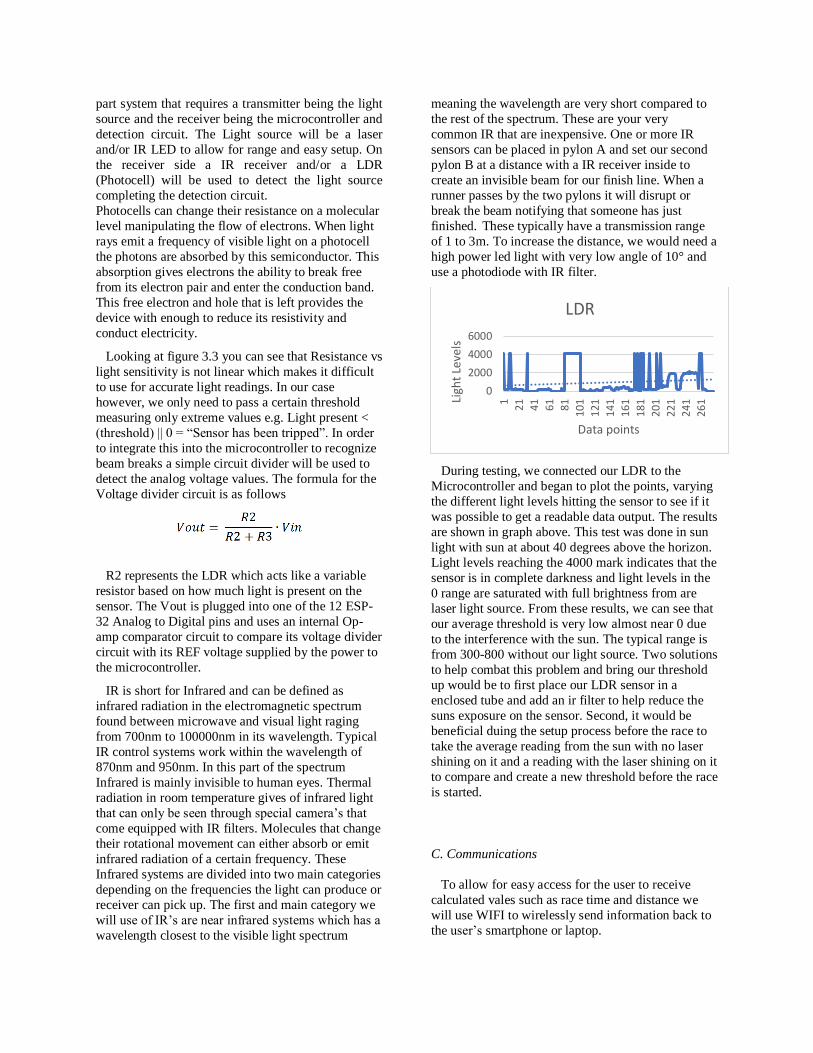
During testing, we connected our LDR to the
Microcontroller and began to plot the points, varying
the different light levels hitting the sensor to see if it
was possible to get a readable data output. The results
are shown in graph above. This test was done in sun
light with sun at about 40 degrees above the horizon.
Light levels reaching the 4000 mark indicates that the
sensor is in complete darkness and light levels in the
0 range are saturated with full brightness from are
laser light source. From these results, we can see that
our average threshold is very low almost near 0 due
to the interference with the sun. The typical range is
from 300-800 without our light source. Two solutions
to help combat this problem and bring our threshold
up would be to first place our LDR sensor in a
enclosed tube and add an ir filter to help reduce the
suns exposure on the sensor. Second, it would be
beneficial duing the setup process before the race to
take the average reading from the sun with no laser
shining on it and a reading with the laser shining on it
to compare and create a new threshold before the race
is started.
C. Communications
To allow for easy access for the user to receive
calculated vales such as race time and distance we
will use WIFI to wirelessly send information back to
the user’s smartphone or laptop.
0
2000
4000
6000
1
21 41 61 81
101
121
141
161
181
201
221
241
261Li
ght
Leve
ls
Data points
LDR
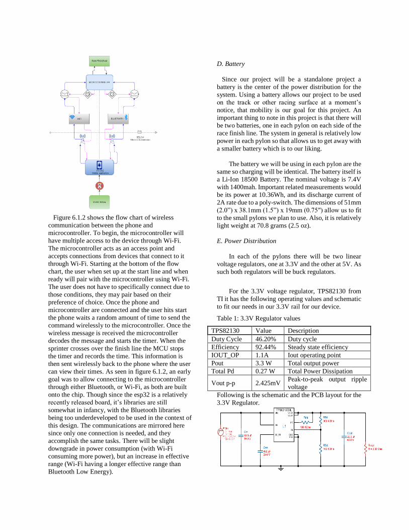
Figure 6.1.2 shows the flow chart of wireless
communication between the phone and
microcontroller. To begin, the microcontroller will
have multiple access to the device through Wi-Fi.
The microcontroller acts as an access point and
accepts connections from devices that connect to it
through Wi-Fi. Starting at the bottom of the flow
chart, the user when set up at the start line and when
ready will pair with the microcontroller using Wi-Fi.
The user does not have to specifically connect due to
those conditions, they may pair based on their
preference of choice. Once the phone and
microcontroller are connected and the user hits start
the phone waits a random amount of time to send the
command wirelessly to the microcontroller. Once the
wireless message is received the microcontroller
decodes the message and starts the timer. When the
sprinter crosses over the finish line the MCU stops
the timer and records the time. This information is
then sent wirelessly back to the phone where the user
can view their times. As seen in figure 6.1.2, an early
goal was to allow connecting to the microcontroller
through either Bluetooth, or Wi-Fi, as both are built
onto the chip. Though since the esp32 is a relatively
recently released board, it’s libraries are still
somewhat in infancy, with the Bluetooth libraries
being too underdeveloped to be used in the context of
this design. The communications are mirrored here
since only one connection is needed, and they
accomplish the same tasks. There will be slight
downgrade in power consumption (with Wi-Fi
consuming more power), but an increase in effective
range (Wi-Fi having a longer effective range than
Bluetooth Low Energy).
D. Battery
Since our project will be a standalone project a
battery is the center of the power distribution for the
system. Using a battery allows our project to be used
on the track or other racing surface at a moment’s
notice, that mobility is our goal for this project. An
important thing to note in this project is that there will
be two batteries, one in each pylon on each side of the
race finish line. The system in general is relatively low
power in each pylon so that allows us to get away with
a smaller battery which is to our liking.
The battery we will be using in each pylon are the
same so charging will be identical. The battery itself is
a Li-Ion 18500 Battery. The nominal voltage is 7.4V
with 1400mah. Important related measurements would
be its power at 10.36Wh, and its discharge current of
2A rate due to a poly-switch. The dimensions of 51mm
(2.0”) x 38.1mm (1.5”) x 19mm (0.75") allow us to fit
to the small pylons we plan to use. Also, it is relatively
light weight at 70.8 grams (2.5 oz).
E. Power Distribution
In each of the pylons there will be two linear
voltage regulators, one at 3.3V and the other at 5V. As
such both regulators will be buck regulators.
For the 3.3V voltage regulator, TPS82130 from
TI it has the following operating values and schematic
to fit our needs in our 3.3V rail for our device.
Table 1: 3.3V Regulator values
TPS82130 Value Description
Duty Cycle 46.20% Duty cycle
Efficiency 92.44% Steady state efficiency
IOUT_OP 1.1A Iout operating point
Pout 3.3 W Total output power
Total Pd 0.27 W Total Power Dissipation
Vout p-p 2.425mV Peak-to-peak output ripple
voltage
Following is the schematic and the PCB layout for the
3.3V Regulator.
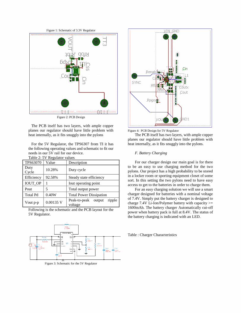
Figure 1: Schematic of 3.3V Regulator
Figure 2: PCB Design
The PCB itself has two layers, with ample copper
planes our regulator should have little problem with
heat internally, as it fits snuggly into the pylons
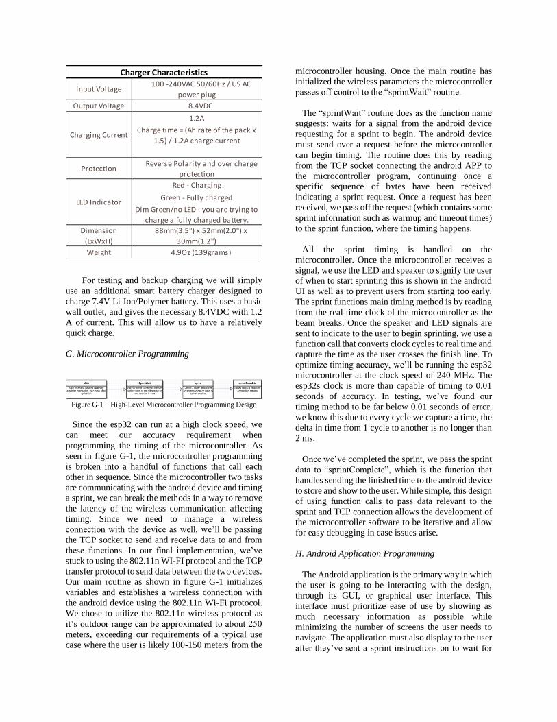
For the 5V Regulator, the TPS6307 from TI it has
the following operating values and schematic to fit our
needs in our 5V rail for our device.
Table 2: 5V Regulator values
TPS63070 Value Description
Duty
Cycle 10.28% Duty cycle
Efficiency 92.58% Steady state efficiency
IOUT_OP 1 Iout operating point
Pout 5 Total output power
Total Pd 0.40W Total Power Dissipation
Vout p-p 0.00135 V Peak-to-peak output ripple
voltage
Following is the schematic and the PCB layout for the
5V Regulator.
Figure 3: Schematic for the 5V Regulator
Figure 4: PCB Design for 5V Regulator
The PCB itself has two layers, with ample copper
planes our regulator should have little problem with
heat internally, as it fits snuggly into the pylons.
F. Battery Charging
For our charger design our main goal is for there
to be an easy to use charging method for the two
pylons. Our project has a high probability to be stored
in a locker room or sporting equipment closet of some
sort. In this setting the two pylons need to have easy
access to get to the batteries in order to charge them.
For an easy charging solution we will use a smart
charger designed for batteries with a nominal voltage
of 7.4V. Simply put the battery charger is designed to
charge 7.4V Li-Ion/Polymer battery with capacity >=
1600mAh. The battery charger Automatically cut-off
power when battery pack is full at 8.4V. The status of
the battery charging is indicated with an LED.
Table : Charger Characteristics
For testing and backup charging we will simply
use an additional smart battery charger designed to
charge 7.4V Li-Ion/Polymer battery. This uses a basic
wall outlet, and gives the necessary 8.4VDC with 1.2
A of current. This will allow us to have a relatively
quick charge.
G. Microcontroller Programming
Figure G-1 – High-Level Microcontroller Programming Design
Since the esp32 can run at a high clock speed, we
can meet our accuracy requirement when
programming the timing of the microcontroller. As
seen in figure G-1, the microcontroller programming
is broken into a handful of functions that call each
other in sequence. Since the microcontroller two tasks
are communicating with the android device and timing
a sprint, we can break the methods in a way to remove
the latency of the wireless communication affecting
timing. Since we need to manage a wireless
connection with the device as well, we’ll be passing
the TCP socket to send and receive data to and from
these functions. In our final implementation, we’ve
stuck to using the 802.11n WI-FI protocol and the TCP
transfer protocol to send data between the two devices.
Our main routine as shown in figure G-1 initializes
variables and establishes a wireless connection with
the android device using the 802.11n Wi-Fi protocol.
We chose to utilize the 802.11n wireless protocol as
it’s outdoor range can be approximated to about 250
meters, exceeding our requirements of a typical use
case where the user is likely 100-150 meters from the
microcontroller housing. Once the main routine has
initialized the wireless parameters the microcontroller
passes off control to the “sprintWait” routine.
The “sprintWait” routine does as the function name
suggests: waits for a signal from the android device
requesting for a sprint to begin. The android device
must send over a request before the microcontroller
can begin timing. The routine does this by reading
from the TCP socket connecting the android APP to
the microcontroller program, continuing once a
specific sequence of bytes have been received
indicating a sprint request. Once a request has been
received, we pass off the request (which contains some
sprint information such as warmup and timeout times)
to the sprint function, where the timing happens.
All the sprint timing is handled on the
microcontroller. Once the microcontroller receives a
signal, we use the LED and speaker to signify the user
of when to start sprinting this is shown in the android
UI as well as to prevent users from starting too early.
The sprint functions main timing method is by reading
from the real-time clock of the microcontroller as the
beam breaks. Once the speaker and LED signals are
sent to indicate to the user to begin sprinting, we use a
function call that converts clock cycles to real time and
capture the time as the user crosses the finish line. To
optimize timing accuracy, we’ll be running the esp32
microcontroller at the clock speed of 240 MHz. The
esp32s clock is more than capable of timing to 0.01
seconds of accuracy. In testing, we’ve found our
timing method to be far below 0.01 seconds of error,
we know this due to every cycle we capture a time, the
delta in time from 1 cycle to another is no longer than
2 ms.
Once we’ve completed the sprint, we pass the sprint
data to “sprintComplete”, which is the function that
handles sending the finished time to the android device
to store and show to the user. While simple, this design
of using function calls to pass data relevant to the
sprint and TCP connection allows the development of
the microcontroller software to be iterative and allow
for easy debugging in case issues arise.
H. Android Application Programming
The Android application is the primary way in which
the user is going to be interacting with the design,
through its GUI, or graphical user interface. This
interface must prioritize ease of use by showing as
much necessary information as possible while
minimizing the number of screens the user needs to
navigate. The application must also display to the user
after they’ve sent a sprint instructions on to wait for
Input Voltage 100 -240VAC 50/60Hz / US AC
power plug
Output Voltage 8.4VDC
1.2A
Charge time = (Ah rate of the pack x
1.5) / 1.2A charge current
Protection Reverse Polarity and over charge
protection
Red - Charging
Green - Fully charged
Dim Green/no LED - you are trying to
charge a fully charged battery.
Dimension
(LxWxH)
88mm(3.5") x 52mm(2.0") x
30mm(1.2")
Weight 4.9Oz (139grams)
Charging Current
LED Indicator
Charger Characteristics
the signal from the main device, as well as their time
at the completion of their sprint. With these key
functionalities in mind, we’ve broken the android
application into three subsections: Connecting to the
microcontroller, sending a sprint, displaying a sprint.
Since the microcontroller is behaving as an access
point in the connection between the 2 devices, the user
can simply connect to the microcontroller from their
system settings. The app must however keep track of
its port and the socket connecting the microcontroller
to the application through the TCP protocol. Besides
the LED and speaker connected to the microcontroller,
the app is the only way the user gets information
relevant to the state of the system. The app must
provide any information that isn’t clear from the I/O
devices attached to the microcontroller.
Upon requesting a sprint, the app displays
instructions for the user to get ready during the
warmup phase and “go” on the LED changing color
and speaker sounding. Upon completing a sprint, the
app displays the finishing time of the user’s sprint.
While this isn’t much functionality we have to be
careful as to make the workflow easiest to understand
for the user as possible.
III. SCHEMATICS
Microcontroller
The picture above represents part 1 of 2 of the full
Microcontroller board. The main components for the
ESP-32 contains Two clocks at 32MHZ and an
external 26MHZ in case we would like to run a
backup clock to keep track of peripherals. The rest of
the components are a few capacitors, resistors and
Flash to store variables and a compiled program.
These are all the components needed to run the
microcontroller at a bare minimum keeping the cost
significantly low.
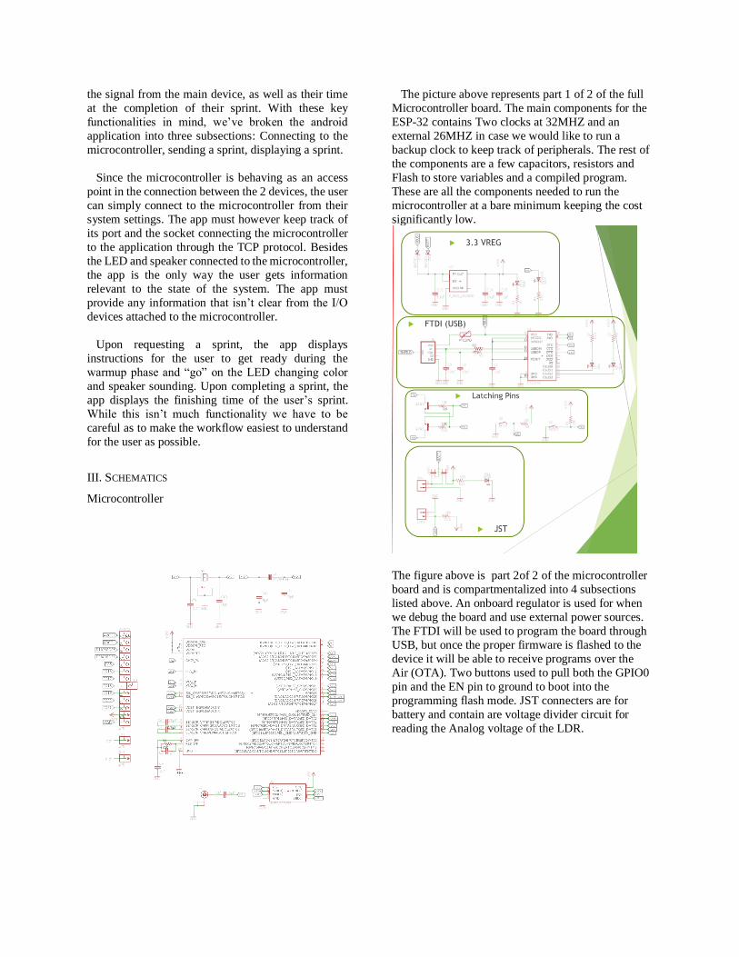
The figure above is part 2of 2 of the microcontroller
board and is compartmentalized into 4 subsections
listed above. An onboard regulator is used for when
we debug the board and use external power sources.
The FTDI will be used to program the board through
USB, but once the proper firmware is flashed to the
device it will be able to receive programs over the
Air (OTA). Two buttons used to pull both the GPIO0
pin and the EN pin to ground to boot into the
programming flash mode. JST connecters are for
battery and contain are voltage divider circuit for
reading the Analog voltage of the LDR.
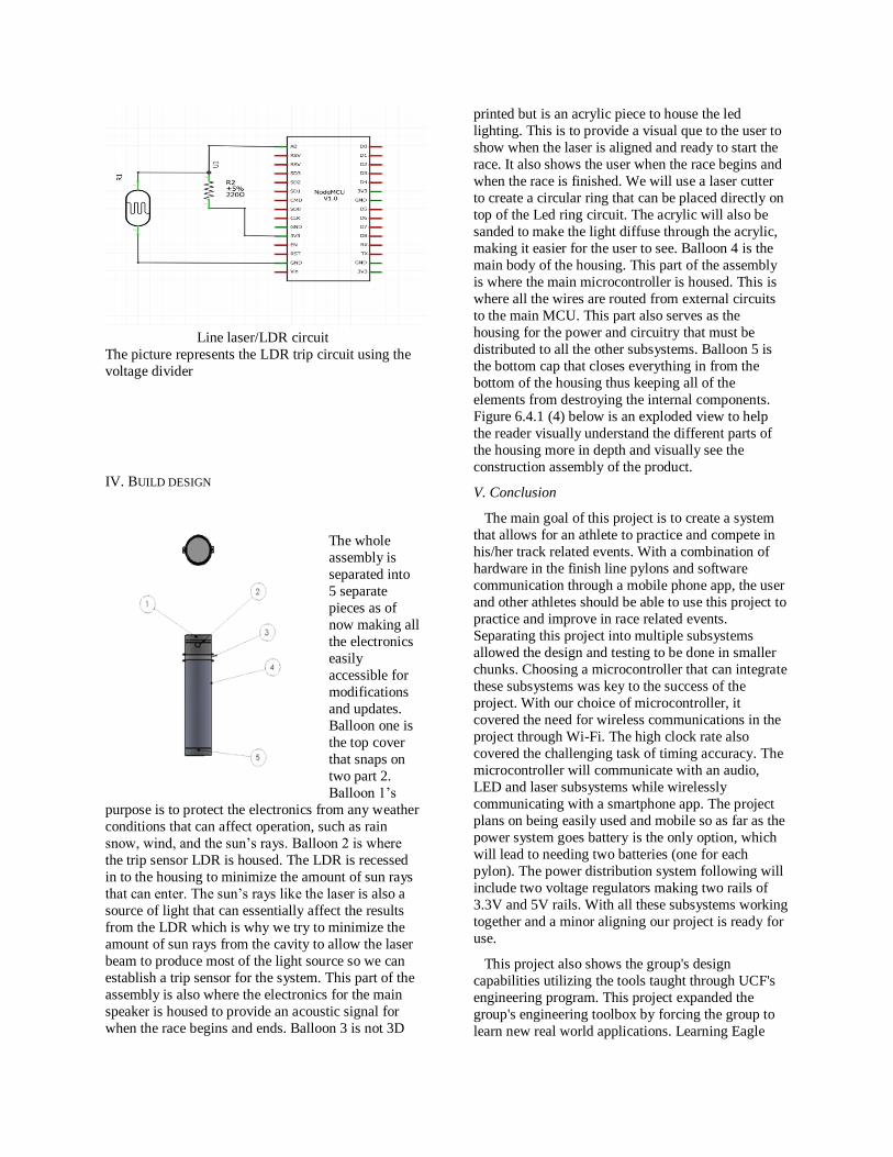
Line laser/LDR circuit
The picture represents the LDR trip circuit using the
voltage divider
IV. BUILD DESIGN
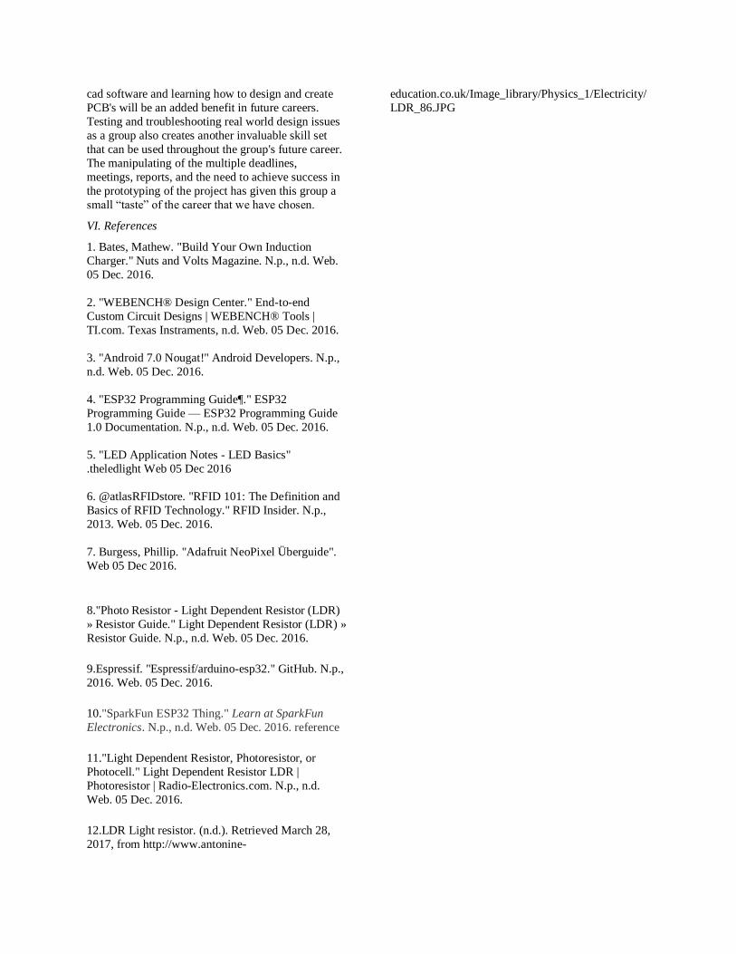
The whole
assembly is
separated into
5 separate
pieces as of
now making all
the electronics
easily
accessible for
modifications
and updates.
Balloon one is
the top cover
that snaps on
two part 2.
Balloon 1’s
purpose is to protect the electronics from any weather
conditions that can affect operation, such as rain
snow, wind, and the sun’s rays. Balloon 2 is where
the trip sensor LDR is housed. The LDR is recessed
in to the housing to minimize the amount of sun rays
that can enter. The sun’s rays like the laser is also a
source of light that can essentially affect the results
from the LDR which is why we try to minimize the
amount of sun rays from the cavity to allow the laser
beam to produce most of the light source so we can
establish a trip sensor for the system. This part of the
assembly is also where the electronics for the main
speaker is housed to provide an acoustic signal for
when the race begins and ends. Balloon 3 is not 3D
printed but is an acrylic piece to house the led
lighting. This is to provide a visual que to the user to
show when the laser is aligned and ready to start the
race. It also shows the user when the race begins and
when the race is finished. We will use a laser cutter
to create a circular ring that can be placed directly on
top of the Led ring circuit. The acrylic will also be
sanded to make the light diffuse through the acrylic,
making it easier for the user to see. Balloon 4 is the
main body of the housing. This part of the assembly
is where the main microcontroller is housed. This is
where all the wires are routed from external circuits
to the main MCU. This part also serves as the
housing for the power and circuitry that must be
distributed to all the other subsystems. Balloon 5 is
the bottom cap that closes everything in from the
bottom of the housing thus keeping all of the
elements from destroying the internal components.
Figure 6.4.1 (4) below is an exploded view to help
the reader visually understand the different parts of
the housing more in depth and visually see the
construction assembly of the product.
V. Conclusion
The main goal of this project is to create a system
that allows for an athlete to practice and compete in
his/her track related events. With a combination of
hardware in the finish line pylons and software
communication through a mobile phone app, the user
and other athletes should be able to use this project to
practice and improve in race related events.
Separating this project into multiple subsystems
allowed the design and testing to be done in smaller
chunks. Choosing a microcontroller that can integrate
these subsystems was key to the success of the
project. With our choice of microcontroller, it
covered the need for wireless communications in the
project through Wi-Fi. The high clock rate also
covered the challenging task of timing accuracy. The
microcontroller will communicate with an audio,
LED and laser subsystems while wirelessly
communicating with a smartphone app. The project
plans on being easily used and mobile so as far as the
power system goes battery is the only option, which
will lead to needing two batteries (one for each
pylon). The power distribution system following will
include two voltage regulators making two rails of
3.3V and 5V rails. With all these subsystems working
together and a minor aligning our project is ready for
use.
This project also shows the group's design
capabilities utilizing the tools taught through UCF's
engineering program. This project expanded the
group's engineering toolbox by forcing the group to
learn new real world applications. Learning Eagle
cad software and learning how to design and create
PCB's will be an added benefit in future careers.
Testing and troubleshooting real world design issues
as a group also creates another invaluable skill set
that can be used throughout the group's future career.
The manipulating of the multiple deadlines,
meetings, reports, and the need to achieve success in
the prototyping of the project has given this group a
small “taste” of the career that we have chosen.
VI. References
1. Bates, Mathew. "Build Your Own Induction
Charger." Nuts and Volts Magazine. N.p., n.d. Web.
05 Dec. 2016.
2. "WEBENCH® Design Center." End-to-end
Custom Circuit Designs | WEBENCH® Tools |
TI.com. Texas Instraments, n.d. Web. 05 Dec. 2016.
3. "Android 7.0 Nougat!" Android Developers. N.p.,
n.d. Web. 05 Dec. 2016.
4. "ESP32 Programming Guide¶." ESP32
Programming Guide — ESP32 Programming Guide
1.0 Documentation. N.p., n.d. Web. 05 Dec. 2016.
5. "LED Application Notes - LED Basics"
.theledlight Web 05 Dec 2016
6. @atlasRFIDstore. "RFID 101: The Definition and
Basics of RFID Technology." RFID Insider. N.p.,
2013. Web. 05 Dec. 2016.
7. Burgess, Phillip. "Adafruit NeoPixel Überguide".
Web 05 Dec 2016.
8."Photo Resistor - Light Dependent Resistor (LDR)
» Resistor Guide." Light Dependent Resistor (LDR) »
Resistor Guide. N.p., n.d. Web. 05 Dec. 2016.
9.Espressif. "Espressif/arduino-esp32." GitHub. N.p.,
2016. Web. 05 Dec. 2016.
10."SparkFun ESP32 Thing." Learn at SparkFun
Electronics. N.p., n.d. Web. 05 Dec. 2016. reference
11."Light Dependent Resistor, Photoresistor, or
Photocell." Light Dependent Resistor LDR |
Photoresistor | Radio-Electronics.com. N.p., n.d.
Web. 05 Dec. 2016.
12.LDR Light resistor. (n.d.). Retrieved March 28,
2017, from http://www.antonine-
education.co.uk/Image_library/Physics_1/Electricity/
LDR_86.JPG