Embed Size (px)
Citation preview
IE LUNDS TEKNISKA HÖGSKOLAindustriell elektroteknik och automation
DEPARTMENT OF INDUSTRIAL ELECTRICAL ENGINEERING AND AUTOMATIONLUND INSTITUTE OF TECHNOLOGY
Power Electronics Laboratory Exercises Part 1

The flyback-converter - description of the building blocks ..................................................1 The flyback-converter main circuit.....................................................................................1 Snubber circuits ..................................................................................................................2 Control ................................................................................................................................2 Preparations and laboratory exercises.................................................................................4 The report should contain ...................................................................................................5
The four quadrant DC-DC converter - description of the building blocks .........................7 Triangle wave generator .....................................................................................................7 DC link voltage measurement...........................................................................................10 The drive circuits ..............................................................................................................11 Preparations and laboratory exercises...............................................................................14 The report should contain .................................................................................................15
Simulations ..............................................................................................................................16 The flyback-converter .......................................................................................................16 The two quadrant DC-DC converter.................................................................................17 Simulation report ..............................................................................................................17
Schematics for the laboratory exercises................................................................................17
1
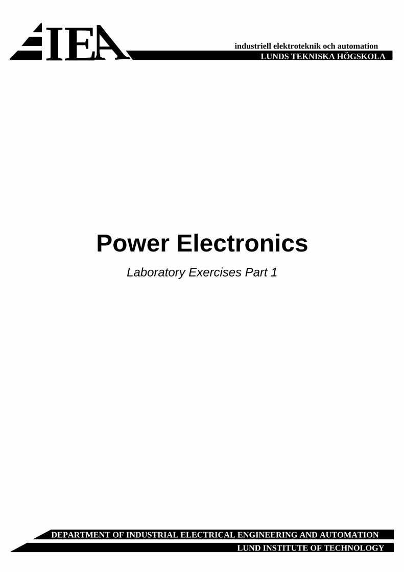
The flyback-converter - description of the building blocks The flyback-converter investigated in the laboratory, is a commercially available switch mode power supply. This means that several of the circuit solutions becomes somewhat complicated, especially regarding the control. The reason is that commercial products should work satisfying without being expensive to manufacture. Since the voltage controller is very complicated, the investigation is instead focused on the power electronic main circuit. Note the 0.1 Ω resistors placed in the main circuit shown in the drawing. These are intended for current measurement. Since test points are placed on both sides of the resistors, the current measurements are carried out as differential voltage measurements. It is of great importance where the probe ground connection is placed. This is due to the fact that the measurement reference voltages on either sides of the switch transformer are at galvanically separated potential levels. Therefore, only one of the ground connections of the probes must be used. If two are used, the corresponding two potentials are short circuited inside the oscilloscope. As a consequence it is advisory to first make all the measurements on one side of the galvanic cut and then on the other. If signals on both sides of the switch-transformer should be studied at the same time, differential measurements should be adopted.
The flyback-converter main circuit The flyback-converter main circuit, including snubber circuits, is shown in Figure 1. At the converter input, a filter is placed, consequently termed input filter. The capacitor and resistor together forms a differential mode (DM) filter. This filter attenuates electronic noise affecting the phase and the neutral lead, if the disturbances do not have the same sign and magnitude for both leads. The transformer connected after, forms a common mode (CM) filter, which attenuates disturbances if they do not affect the phase and neutral with equal magnitude and opposite sign. After the transformer another DM-filter is placed, consisting of two capacitors. The middle point earth connection shown, is not used in the laboratory set-up. After the first DM-filter a component marked T-, is inserted. This is a negative temperature coefficient (NTC) resistor, whose resistance decreases with increasing temperature. This is needed in order to limit the inrush current otherwise appearing when the converter is connected to the power grid. The input filter is followed by the diode rectifier and the DC link capacitors.
CDC
C
N1 N2
C
+15 V
GND
-15 V
CDC
N2
F
N T-
Figure 1 The power electronic main circuit of the flyback-converter including snubber circuits.
Since the power supply should also be used in countries with 115 V phase to neutral voltage, the DC link capacitor connection to the diode rectifier is variable, which is marked as a dashed line in Figure 1. At 115 V operation, the points connected by this line is connected also electrically. The

2
result is that during positive half period of the grid voltage, one of the DC link capacitors is charged, whereas during the negative the other one is being charged. This means that the DC link voltage magnitude are equal for both 115 V and 230 V phase to neutral voltage. Note that if the connection discussed above is made, only two of the rectifier bridge diodes are used. The switch-transformer is connected in series with the switch-transistor, in this case a MOSFET, across the DC link. The switch-transformer has in this case two secondary windings, since the output voltage should be ±15 V DC. In some cases the secondary is equipped with three windings to also have a +5 V DC output. The difference compared to the case with only one secondary winding is that the total energy supplied to the secondary is split among several windings, instead of only one. The secondary windings have one common point to which they are connected, to create the output reference potential (ground). In series with the other two secondary leads, the switch-diodes are connected. Between the diodes and the output, the output filters are inserted. These are of CLC-type, which compared to a purely capacitive C-filter, has a better attenuation of high frequency voltage ripple caused by switching. No attention is paid to the CLC-filter, it can be regarded as being purely capacitive, i.e. consisting of only a capacitor. Note that the +15 V output voltage is controlled while the –15 V output is not. This is common to all flyback-converters having several secondary windings. This is due to the fact that the only control parameter available is the switch transistor duty-cycle, which implies that only one quantity can be controlled. In this case, the +15 V output voltage is controlled, which is termed MASTER. The uncontrolled –15 V output is referred to as the SLAVE.
Snubber circuits In Figure 1, three snubber circuits are plotted. Only one of them is of standard type, the RC-snubber connected across the switch transistor. The other two is more unusual. One of them, connected across the switch-transformer primary, is intended to provide an alternative path for the transformer primary current at the MOSFET turn-off transient. This is needed due to the fact that energy is stored in the transformer primary leakage inductance. This energy cannot be transferred to the secondary since the leakage inductance on the primary has no magnetic connection to the secondary. Therefore, a discharge path should be provided, which the snubber does. At MOSFET turn-off, the energy stored in the primary leakage inductance is transferred to the snubber capacitor. Then the snubber capacitor is discharged through the snubber resistor. Note that the time constant of this RC-circuit is fairly long. As a matter of fact it is selected so long that the capacitor voltage do not decrease to a level lower than the primary side transformer voltage when the switch-transistor is in the off state. Since the latter voltage is negative the snubber capacitor otherwise would be charged from the primary. The other unknown snubber circuit is connected across the MASTER flyback-diode. This snubber is essentially capacitive but also equipped with a snubber diode and resistor. It reminds of a common RCD-snubber with the difference that the snubber diode is connected in the opposite direction.
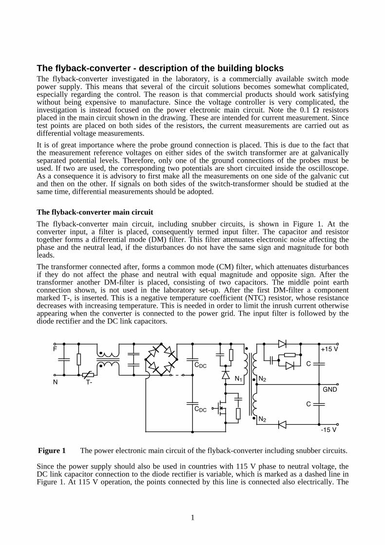
Control The supply voltage for the control electronics is created by dividing the DC link voltage. This is performed by a resistive voltage divider connected in series with a 12 V zener-diode. To transfer a fault signal from the output side to the control side the opto-coupler 151 is used. If the MASTER DC voltage exceeds 18 V, the opto-coupler 151 is trigged. The thyristor 43 is trigged by the opto-coupler 151, which causes short circuit of the 12 V control electronics supply. This in turn inhibits the transistor switching. The thyristorn 43 can not be turned off, unless the converter is disconnected from the grid, since its anode current can not commutate in
3
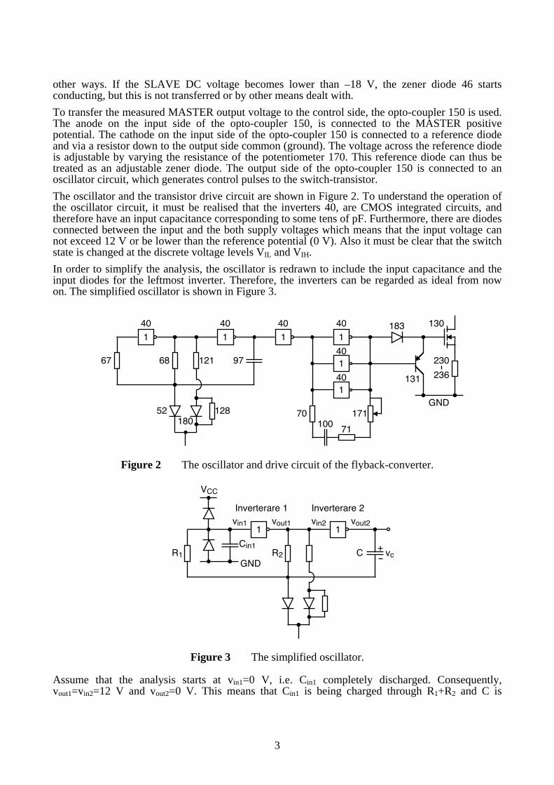
other ways. If the SLAVE DC voltage becomes lower than –18 V, the zener diode 46 starts conducting, but this is not transferred or by other means dealt with. To transfer the measured MASTER output voltage to the control side, the opto-coupler 150 is used. The anode on the input side of the opto-coupler 150, is connected to the MASTER positive potential. The cathode on the input side of the opto-coupler 150 is connected to a reference diode and via a resistor down to the output side common (ground). The voltage across the reference diode is adjustable by varying the resistance of the potentiometer 170. This reference diode can thus be treated as an adjustable zener diode. The output side of the opto-coupler 150 is connected to an oscillator circuit, which generates control pulses to the switch-transistor. The oscillator and the transistor drive circuit are shown in Figure 2. To understand the operation of the oscillator circuit, it must be realised that the inverters 40, are CMOS integrated circuits, and therefore have an input capacitance corresponding to some tens of pF. Furthermore, there are diodes connected between the input and the both supply voltages which means that the input voltage can not exceed 12 V or be lower than the reference potential (0 V). Also it must be clear that the switch state is changed at the discrete voltage levels VIL and VIH. In order to simplify the analysis, the oscillator is redrawn to include the input capacitance and the input diodes for the leftmost inverter. Therefore, the inverters can be regarded as ideal from now on. The simplified oscillator is shown in Figure 3.
67
1 1
68
1 1
1
1GND
121 97
40 40
52180
128
40 40
40
40
100 71
70 171
183 130
230
236131
Figure 2 The oscillator and drive circuit of the flyback-converter.
R1
1 1
R2 CCin1
Inverterare 1vin1 vout1 vin2 vout2
+ vc
Inverterare 2
VCC
GND
Figure 3 The simplified oscillator.
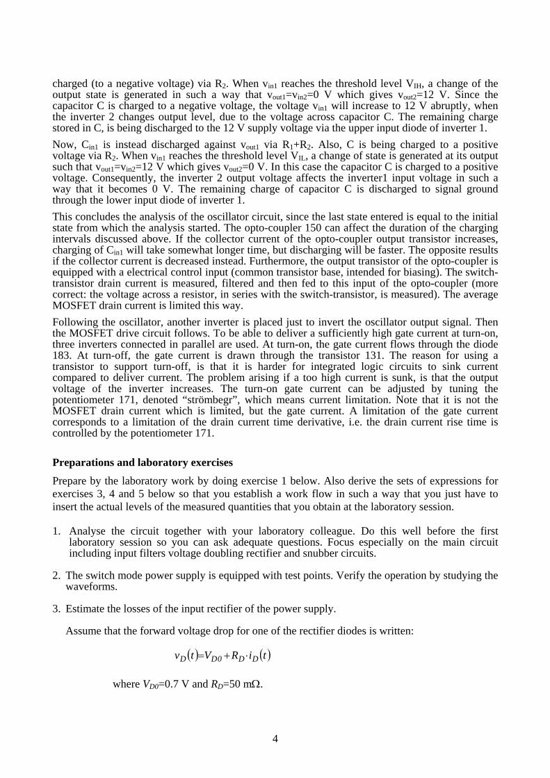
Assume that the analysis starts at vin1=0 V, i.e. Cin1 completely discharged. Consequently, vout1=vin2=12 V and vout2=0 V. This means that Cin1 is being charged through R1+R2 and C is
4
charged (to a negative voltage) via R2. When vin1 reaches the threshold level VIH, a change of the output state is generated in such a way that vout1=vin2=0 V which gives vout2=12 V. Since the capacitor C is charged to a negative voltage, the voltage vin1 will increase to 12 V abruptly, when the inverter 2 changes output level, due to the voltage across capacitor C. The remaining charge stored in C, is being discharged to the 12 V supply voltage via the upper input diode of inverter 1. Now, Cin1 is instead discharged against vout1 via R1+R2. Also, C is being charged to a positive voltage via R2. When vin1 reaches the threshold level VIL, a change of state is generated at its output such that vout1=vin2=12 V which gives vout2=0 V. In this case the capacitor C is charged to a positive voltage. Consequently, the inverter 2 output voltage affects the inverter1 input voltage in such a way that it becomes 0 V. The remaining charge of capacitor C is discharged to signal ground through the lower input diode of inverter 1. This concludes the analysis of the oscillator circuit, since the last state entered is equal to the initial state from which the analysis started. The opto-coupler 150 can affect the duration of the charging intervals discussed above. If the collector current of the opto-coupler output transistor increases, charging of Cin1 will take somewhat longer time, but discharging will be faster. The opposite results if the collector current is decreased instead. Furthermore, the output transistor of the opto-coupler is equipped with a electrical control input (common transistor base, intended for biasing). The switch-transistor drain current is measured, filtered and then fed to this input of the opto-coupler (more correct: the voltage across a resistor, in series with the switch-transistor, is measured). The average MOSFET drain current is limited this way. Following the oscillator, another inverter is placed just to invert the oscillator output signal. Then the MOSFET drive circuit follows. To be able to deliver a sufficiently high gate current at turn-on, three inverters connected in parallel are used. At turn-on, the gate current flows through the diode 183. At turn-off, the gate current is drawn through the transistor 131. The reason for using a transistor to support turn-off, is that it is harder for integrated logic circuits to sink current compared to deliver current. The problem arising if a too high current is sunk, is that the output voltage of the inverter increases. The turn-on gate current can be adjusted by tuning the potentiometer 171, denoted “strömbegr”, which means current limitation. Note that it is not the MOSFET drain current which is limited, but the gate current. A limitation of the gate current corresponds to a limitation of the drain current time derivative, i.e. the drain current rise time is controlled by the potentiometer 171.
Preparations and laboratory exercises
Prepare by the laboratory work by doing exercise 1 below. Also derive the sets of expressions for exercises 3, 4 and 5 below so that you establish a work flow in such a way that you just have to insert the actual levels of the measured quantities that you obtain at the laboratory session. 1. Analyse the circuit together with your laboratory colleague. Do this well before the first
laboratory session so you can ask adequate questions. Focus especially on the main circuit including input filters voltage doubling rectifier and snubber circuits.
2. The switch mode power supply is equipped with test points. Verify the operation by studying the waveforms.
3. Estimate the losses of the input rectifier of the power supply.
Assume that the forward voltage drop for one of the rectifier diodes is written: ( ) ( )tiRVtv DDDD ⋅+= 0 where VD0=0.7 V and RD=50 mΩ.

5
The instantaneous power corresponding to the losses of a single diode is written: ( ) ( ) ( ) ( ) ( )tiRtiVtitvtp DDDDDDD
2⋅+⋅=⋅= 0
The diode current consists of pulses. Assume that one such pulse is sinusoidal. Measure the time duration, tp, and its amplitude, ˆ i D . The diode current is thus written:
( )( )
⎪⎩
⎪⎨⎧
<≤
<≤⋅⋅=
np
ppDD
Ttt
tttiti
0
0sinˆ ω
where πω 22 =⋅⋅ pp t The average losses for one rectifier diode are calculated according to:
( ) ( )∫∫ ⋅⋅=⋅⋅=pn t
0
T
0tptp dt
Tdt
TP
nnD
11
Derive an expression for and calculate the losses for the entire rectifier bridge. 4. Calculate the losses of the flyback-diodes. These are of type Philips BYW 29. The parameters
VD0 and RD are obtained from Fig. 9 (150 °C) of the datasheet. Note that the diode currents are described by
mtktiD +⋅=)(
where k is negative and m is positive. The average current cannot be used for this calculation.
5. Calculate the number of winding turns of the switch transformer. Measure the voltage and the current time derivative on the secondary side of the transformer. Out of these measurements, the magnetising inductance of the secondary is calculated. Assume that the leakage inductance is low, which means that the magnetising inductance is equal to the self-inductance. From a data book (in the laboratory), you can find the core used, and its AL-value. This directly gives the number of secondary winding turns (equation (5.77)). From the data given, the peak magnetic flux density is calculated (equation (5.46)). Compare with the saturation flux density specified by the manufacturer. The number of winding turns for the primary is calculated from the voltage ratio between the primary and secondary.
The report should contain • A detailed description of the switch mode power supply, especially the main circuit. The
following items must be thoroughly explained:
Explain the operation of the common mode filter at the switch mode power supply input. Explain how the voltage doubling circuit at the input rectifier works. What is the main reason for using MOSFET-technology for switch mode power supplies?

6
How high is the transformer primary voltage when the switch-transistor is conducting and blocking, respectively? How is the switch-transistor selection affected? How high is the transformer secondary voltage when the switch-transistor is conducting and blocking, respectively? How is the flyback-diode selection affected?
Explain the operation of the snubbers. • Presentation and discussion of the calculations made above including measurement and
simulation results.
7
The four quadrant DC-DC converter - description of the building blocks
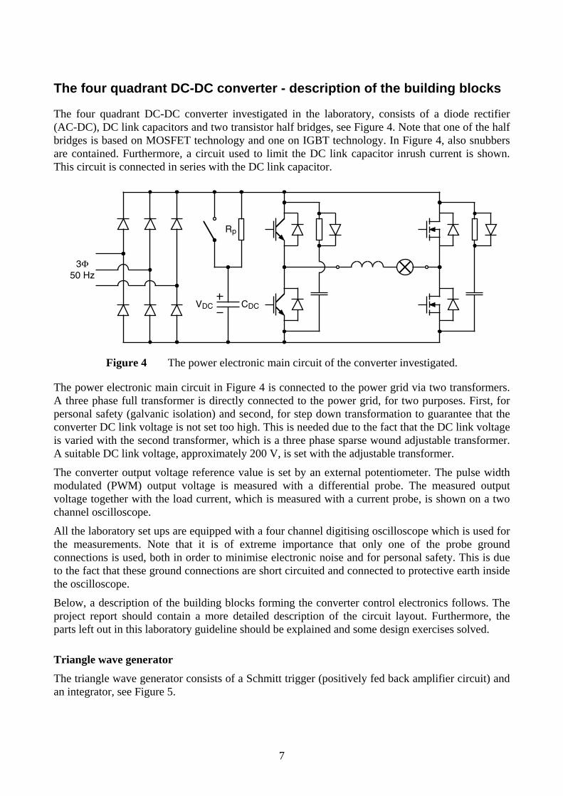
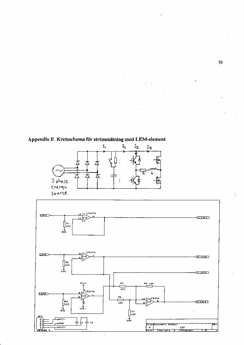
The four quadrant DC-DC converter investigated in the laboratory, consists of a diode rectifier (AC-DC), DC link capacitors and two transistor half bridges, see Figure 4. Note that one of the half bridges is based on MOSFET technology and one on IGBT technology. In Figure 4, also snubbers are contained. Furthermore, a circuit used to limit the DC link capacitor inrush current is shown. This circuit is connected in series with the DC link capacitor.
3Φ50 Hz
Rp
CDCVDC
Figure 4 The power electronic main circuit of the converter investigated.
The power electronic main circuit in Figure 4 is connected to the power grid via two transformers. A three phase full transformer is directly connected to the power grid, for two purposes. First, for personal safety (galvanic isolation) and second, for step down transformation to guarantee that the converter DC link voltage is not set too high. This is needed due to the fact that the DC link voltage is varied with the second transformer, which is a three phase sparse wound adjustable transformer. A suitable DC link voltage, approximately 200 V, is set with the adjustable transformer.
The converter output voltage reference value is set by an external potentiometer. The pulse width modulated (PWM) output voltage is measured with a differential probe. The measured output voltage together with the load current, which is measured with a current probe, is shown on a two channel oscilloscope.
All the laboratory set ups are equipped with a four channel digitising oscilloscope which is used for the measurements. Note that it is of extreme importance that only one of the probe ground connections is used, both in order to minimise electronic noise and for personal safety. This is due to the fact that these ground connections are short circuited and connected to protective earth inside the oscilloscope.
Below, a description of the building blocks forming the converter control electronics follows. The project report should contain a more detailed description of the circuit layout. Furthermore, the parts left out in this laboratory guideline should be explained and some design exercises solved.
Triangle wave generator
The triangle wave generator consists of a Schmitt trigger (positively fed back amplifier circuit) and an integrator, see Figure 5.

8
The output of the Schmitt trigger can only assume two discrete levels, corresponding to its positive and negative supply voltages (approximately). The switchings between these two states occurs at two discrete input signal levels. The integrator acts upon the output signal of the Schmitt trigger. Thus the integrator output performs a ramp function, since the input signal is piece wise constant. By feeding back the ramp signal to the Schmitt trigger, the Schmitt trigger switchings are generated upon the magnitude of the ramp signal. In this way the triangular wave is created.
R1
R2
R3
C
0 V0 V
vtri
Figure 5 The triangle wave generator.
R1
R2
0 V
vin vout vin
vout
(b)(a)
Figure 6 (a) The Schmitt trigger and (b), its input-output characteristic.
For the Schmitt trigger in Figure 6 the following derivation is valid.
The potential of the comparator positive input, v+, is written:
v + = vin −vin − vout
R1 + R 2
⋅ R1 =R 2
R1 + R 2
⋅v in +R1
R1 + R2
⋅ vout
To calculate the input level when the Schmitt trigger switches from high to low output level, the following relationships are established
v + > 0 ⇒ vout = +VCC v + < 0 a v + > 0 ⇒
R 2
R1 + R 2
⋅ vin +R1
R1 + R2
⋅ +VCC( )= 0 ⇒ vin = −R1
R 2
⋅ VCC

9
On the contrary, to calculate the input level when the Schmitt trigger switches from low to high output level
v + < 0 ⇒ vout = −VCC v + > 0 a v + < 0 ⇒
R 2
R1 + R 2
⋅ vin +R1
R1 + R2
⋅ −VCC( )= 0 ⇒ vin =R 1
R 2
⋅ VCC
These calculations gives the input-output characteristics of the Schmitt trigger, see Figure 6. From Figure 6 it is directly seen that the Schmitt trigger works as a relay with hysteresis. In Figure 7, the integrator of the triangle wave generator is shown.
R3 C
0 V
vout
vc
vin
Figure 7 The integrator of the triangle wave generator.
The current through the resistor R3 and capacitor C, i.e. the integrator current denoted i, is written
i =vin − 0
R3
= C ⋅dvC
dt= C ⋅
ddt
−v out( )= −C ⋅dv out
dt⇒
dv out
dt= −
1R 3 ⋅C
⋅ v in ⇒ vout t( )− v out t 0( )= −1
R 3 ⋅ C⋅ vin τ( )⋅ dτ
t 0
t
∫
Note that the input signal is piece wise constant (more correct square) which gives
v out t( ) − vout t0( )= −1
R3 ⋅C⋅ vin t 0+( )⋅(t − t0 )
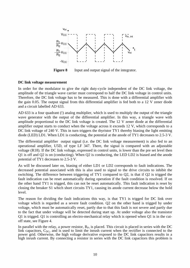
The expressions for the Schmitt trigger and the integrator together gives that the integrator input and output signals appears as in Figure 8.
10
VCC
-VCC
VCCR1R2
.-
VCCR1R2
.
t
vtri
vtri
vin, int
Figure 8 Input and output signal of the integrator.
DC link voltage measurement
In order for the modulator to give the right duty-cycle independent of the DC link voltage, the amplitude of the triangle wave carrier must correspond to half the DC link voltage in control units. Therefore, the DC link voltage has to be measured. This is done with a differential amplifier with the gain 0.05. The output signal from this differential amplifier is fed both to a 12 V zener diode and a circuit labelled AD 633.
AD 633 is a four quadrant (!) analog multiplier, which is used to multiply the output of the triangle wave generator with the output of the differential amplifier. In this way, a triangle wave with amplitude proportional to the DC link voltage is created. The 12 V zener diode at the differential amplifier output starts to conduct when the voltage across it exceeds 12 V, which corresponds to a DC link voltage of 240 V. This in turn triggers the thyristor TY1 thereby biasing the light emitting diode (LED) LD1. When LD1 is conducting, the potential at the anode of TY1 decreases to 2.5-3 V.
The differential amplifier output signal (i.e. the DC link voltage measurement) is also fed to an operational amplifier, U5D, of type LF 347. There, the signal is compared with an adjustable voltage (R18). If the DC link voltage, expressed in control units, is lower than the pre set level then Q1 is off and Q2 is on (conducting). When Q2 is conducting, the LED LD2 is biased and the anode potential of TY1 decreases to 2.5-3 V.
As will be discussed later on, biasing of either LD1 or LD2 corresponds to fault indications. The decreased potential associated with this is also used to signal to the drive circuits to inhibit the switching. The difference between triggering of TY1 compared to Q2, is that if Q2 is trigged the fault indication can be reset automatically during operation if the fault condition is resolved. If on the other hand TY1 is trigged, this can not be reset automatically. This fault indication is reset by closing the breaker S1 which short circuits TY1, causing its anode current decrease below the hold level.
The reason for dividing the fault indications this way, is that TY1 is trigged for DC link over voltage which is regarded as a severe fault condition. Q2 on the other hand is trigged by under voltage, which must be automatically reset, partly due to that this fault is not severe and partly due to the fact that under voltage will be detected during start up. At under voltage also the transistor Q1 is trigged. Q1 is controlling an electro-mechanical relay which is opened when Q1 is in the cut-off state, see Figure 4. In parallel with the relay, a power resistor, RP, is placed. This circuit is placed in series with the DC link capacitors, CDC, and is used to limit the inrush current when the rectifier is connected to the power grid. Otherwise, the high voltage derivative exposed to the DC link capacitors results in a high inrush current. By connecting a resistor in series with the DC link capacitors this problem is
11
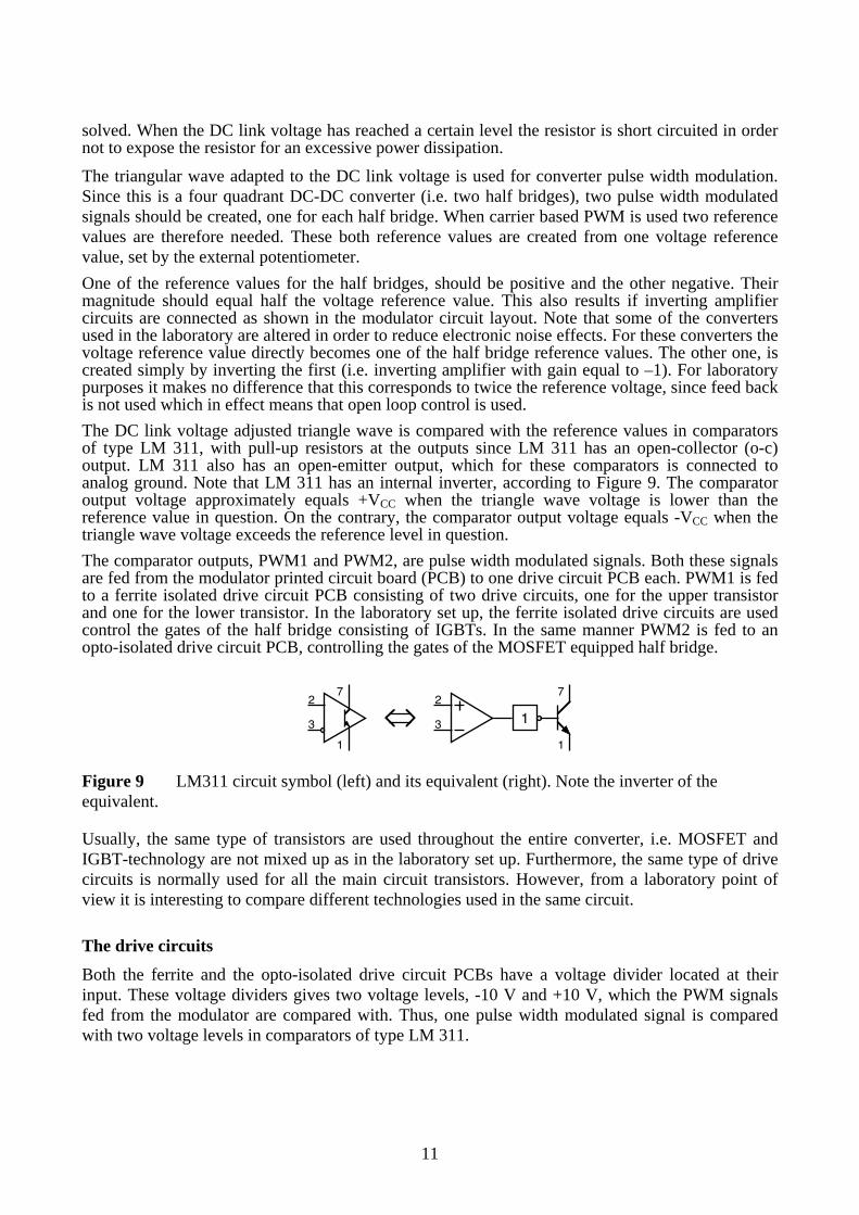
solved. When the DC link voltage has reached a certain level the resistor is short circuited in order not to expose the resistor for an excessive power dissipation. The triangular wave adapted to the DC link voltage is used for converter pulse width modulation. Since this is a four quadrant DC-DC converter (i.e. two half bridges), two pulse width modulated signals should be created, one for each half bridge. When carrier based PWM is used two reference values are therefore needed. These both reference values are created from one voltage reference value, set by the external potentiometer. One of the reference values for the half bridges, should be positive and the other negative. Their magnitude should equal half the voltage reference value. This also results if inverting amplifier circuits are connected as shown in the modulator circuit layout. Note that some of the converters used in the laboratory are altered in order to reduce electronic noise effects. For these converters the voltage reference value directly becomes one of the half bridge reference values. The other one, is created simply by inverting the first (i.e. inverting amplifier with gain equal to –1). For laboratory purposes it makes no difference that this corresponds to twice the reference voltage, since feed back is not used which in effect means that open loop control is used. The DC link voltage adjusted triangle wave is compared with the reference values in comparators of type LM 311, with pull-up resistors at the outputs since LM 311 has an open-collector (o-c) output. LM 311 also has an open-emitter output, which for these comparators is connected to analog ground. Note that LM 311 has an internal inverter, according to Figure 9. The comparator output voltage approximately equals +VCC when the triangle wave voltage is lower than the reference value in question. On the contrary, the comparator output voltage equals -VCC when the triangle wave voltage exceeds the reference level in question. The comparator outputs, PWM1 and PWM2, are pulse width modulated signals. Both these signals are fed from the modulator printed circuit board (PCB) to one drive circuit PCB each. PWM1 is fed to a ferrite isolated drive circuit PCB consisting of two drive circuits, one for the upper transistor and one for the lower transistor. In the laboratory set up, the ferrite isolated drive circuits are used control the gates of the half bridge consisting of IGBTs. In the same manner PWM2 is fed to an opto-isolated drive circuit PCB, controlling the gates of the MOSFET equipped half bridge.
12
3
7
1
2
3
7
1
Figure 9 LM311 circuit symbol (left) and its equivalent (right). Note the inverter of the equivalent.
Usually, the same type of transistors are used throughout the entire converter, i.e. MOSFET and IGBT-technology are not mixed up as in the laboratory set up. Furthermore, the same type of drive circuits is normally used for all the main circuit transistors. However, from a laboratory point of view it is interesting to compare different technologies used in the same circuit.
The drive circuits
Both the ferrite and the opto-isolated drive circuit PCBs have a voltage divider located at their input. These voltage dividers gives two voltage levels, -10 V and +10 V, which the PWM signals fed from the modulator are compared with. Thus, one pulse width modulated signal is compared with two voltage levels in comparators of type LM 311.
12
This distinction is made since the two transistors of a half bridge, needs one gate control signal each. The reason for selecting ±10 V is that some immunity to electrical noise is desired. If the signal drive circuit signal paths are followed it is realised that if the PWM signal is between ±10 V, both transistors of the half bridge will be in the off-state. Note that the comparators in this case are equipped with pull-down resistors. Also, in the drive circuit layout the comparators have one connection to a pnp-transistor and further down to analog ground. This is due to the fact that LM 311 is equipped with a strobe input, which turns off its output transistor if the strobe input is forced low.
In the laboratory converter, the strobe input is used to turn off the transistors of the half bridge. The strobe input is forced low if any of the previously mentioned faults regarding the DC link voltage level are detected, i.e. if Q2 or TY1 are trigged. During the following analysis it is also found that if TY3 of either drive circuit is trigged, the strobe input is also forced low.
After the comparators, the blanking time circuits follows, which are intended to delay power transistor turn-on, without delaying turn-off. This is needed in order to avoid dynamic or transient short circuit of the DC link. After the blanking time circuits, the drive circuit PCBs differs and are therefore treated separately.
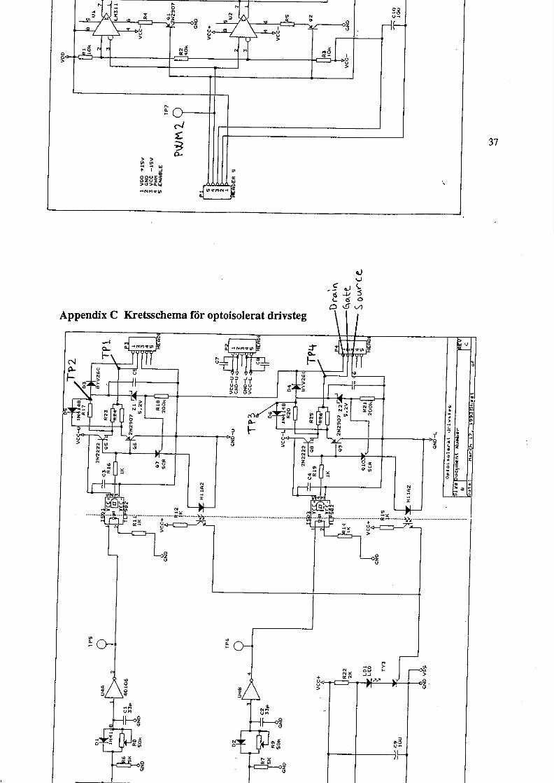
Opto-isolated drive circuit The inverter prior to the opto-coupler in effect belongs to the blanking time circuit, but is also needed in order to invert the signal, since the opto-coupler in it self is inverting. The drive circuit consists of a complementary transistor pair forming a push-pull stage and two gate resistors, one for turn-on and one for turn-off.
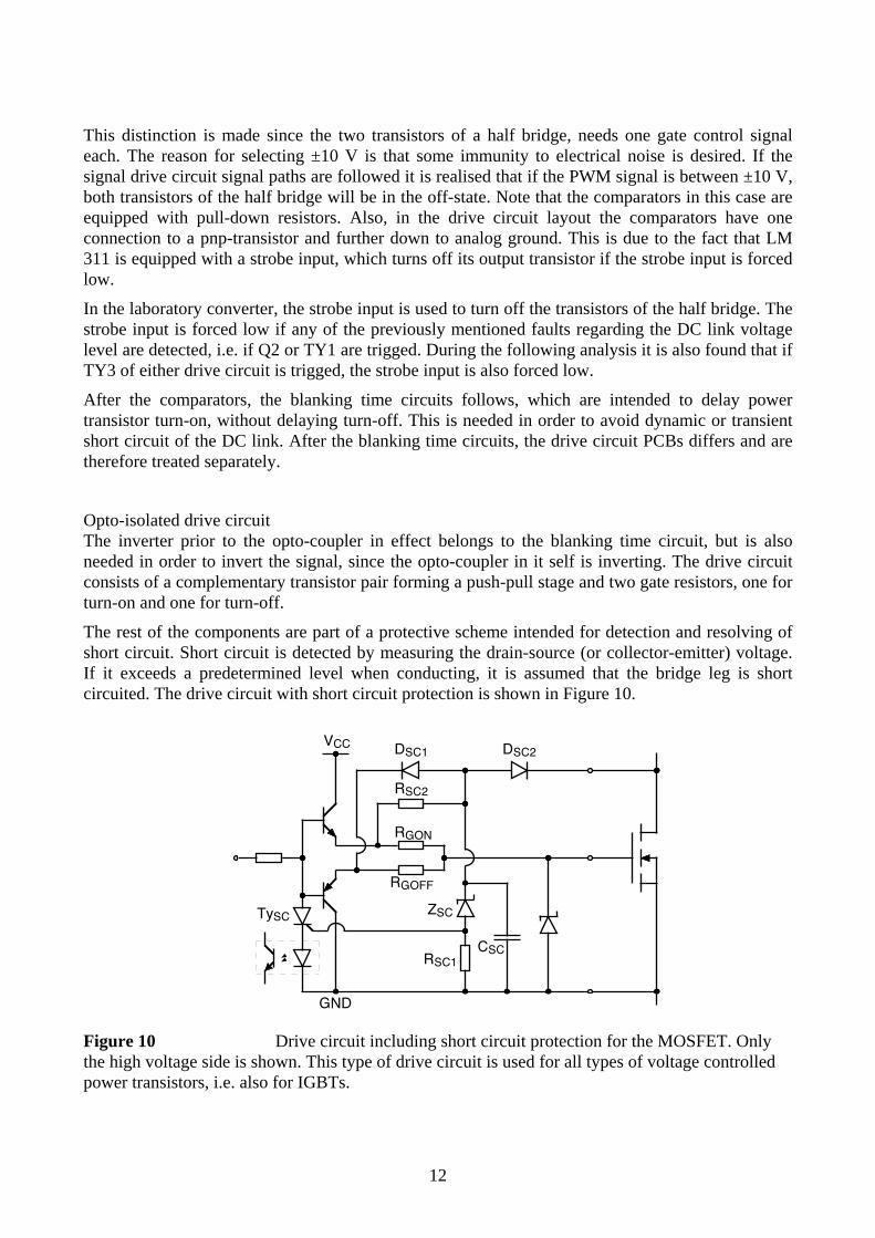
The rest of the components are part of a protective scheme intended for detection and resolving of short circuit. Short circuit is detected by measuring the drain-source (or collector-emitter) voltage. If it exceeds a predetermined level when conducting, it is assumed that the bridge leg is short circuited. The drive circuit with short circuit protection is shown in Figure 10.
VCC
GND
RGON
RGOFF
DSC1 DSC2
RSC2
RSC1CSC
ZSCTySC
Figure 10 Drive circuit including short circuit protection for the MOSFET. Only the high voltage side is shown. This type of drive circuit is used for all types of voltage controlled power transistors, i.e. also for IGBTs.
13
The short circuit protection circuitry is designed in such a way that when the MOSFET is conducting, in normal operation, the diode Dsc2 should carry a low current (approximately 1 mA) via the resistor Rsc2. If the voltage across the MOSFET exceeds the zener voltage of Zsc, the thyristor Tysc is trigged. In the circuit layout of the opto-isolated drive circuit it is shown that this signal is fed back to the thyristor TY3, via an opto-coupler. When TY3 is trigged the LED LD1 becomes biased, and the strobe inputs of the comparators is forced low resulting in turn-off of all the power transistors of the converter.
This signal path is however fairly long, implying that short circuit detection is not handled fast enough to avoid device failure of the short circuited device. However, the base of the push-pull stage complementary transistor pair is connected to the anode of Tysc and further down to the reference (i.e. ground) level of the drive circuit. This means that the drive circuit detecting short circuit turns off the corresponding power transistor fast.
The diode Dsc2 is intended to block when the power transistor is in the blocking state to make sure that the drive circuit is not exposed to the power transistor blocking voltage (several hundred volts). This means that Dsc2 must sustain a voltage at least as high as the DC link voltage. The reason why the current through it should be low when conducting, is that the transition from conducting to blocking should be as fast as possible. In other words its is desired that the reverse recovery time of Dsc2 is kept short. At turn-on of the power MOSFET, Dsc2 should traverse from the blocking to the on state. The depletion region of Dsc2 in this case behaves as a capacitor charged to a voltage equal to the DC link voltage.
Therefore, the capacitor Csc is needed to effectively block the resulting voltage pulse, which otherwise would show up across the zener diode and possibly trig the short circuit protection scheme. The capacitor also protects against voltage pulses at power MOSFET turn-off. In this case it is discharged against the reference potential via Dsc1.
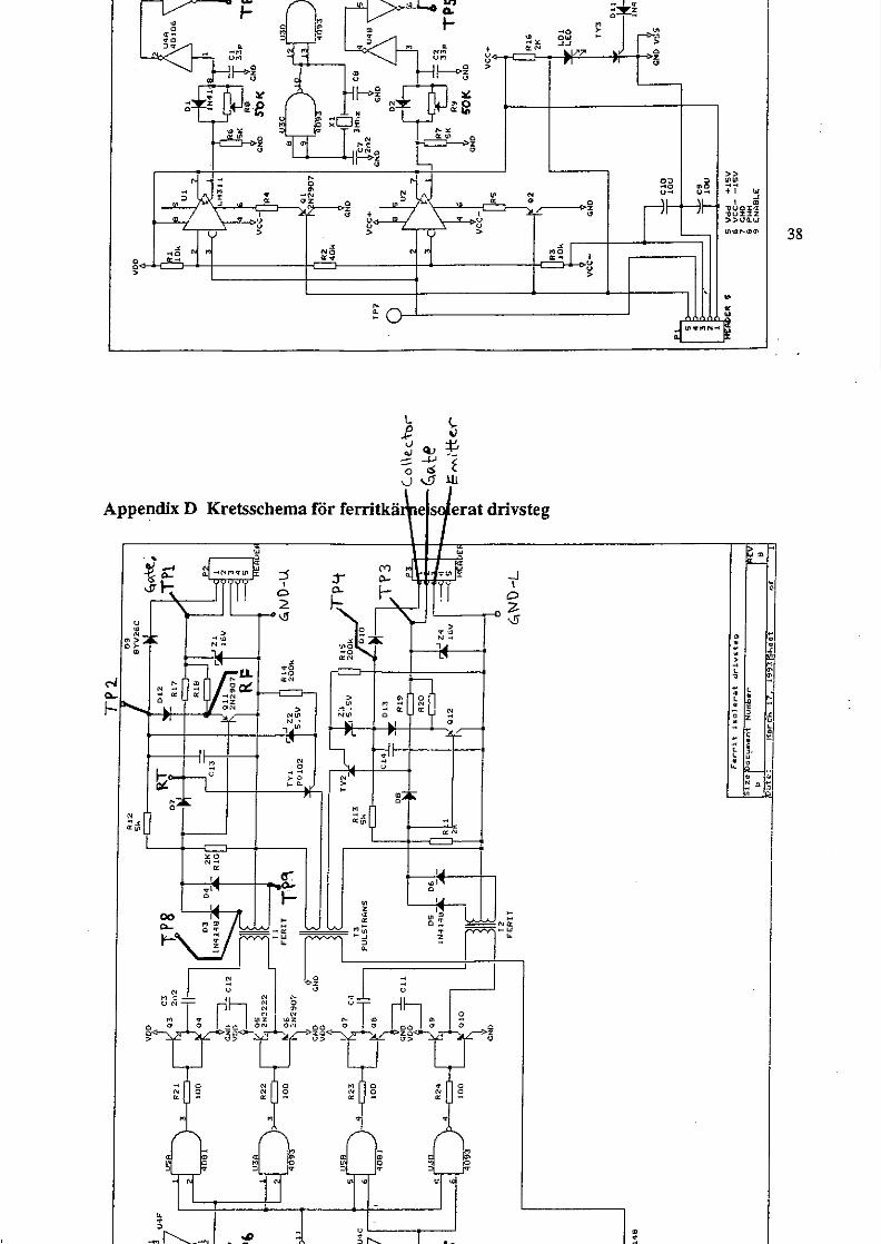
Ferrite isolated drive circuit This drive circuit appears to be more complicated than the opto-isolated. This is due to the fact that the ferrite isolated drive circuit not only should transfer the control signal but also the energy needed for power transistor turn-on. For the opto-isolated drive circuit, galvanic isolated DC power supply is needed for each drive circuit, since the opto-couplers only can transfer signals and not energy. The galvanically isolated supply is not shown in the circuit scheme of the opto-isolated drive circuit, but is shown separately.
In the circuit scheme of the ferrite isolated drive PCB, the PWM signal is inverted twice following the blanking time circuit. This could have been solved in a simpler way by using a non-inverting buffer circuit instead. The idea of the inverters is, besides the fact that the blanking time circuit must be ended with a logic gate, only to turn the PWM signals right.
After the inverters the PWM signals are mixed with a clock signal of high frequency (3 MHz). The signal mixing is carried out with aid of logic AND and NAND gates. At high control signal level out from the blanking time circuit, the pulses out from the AND and NAND gates have opposite phase. At low control signal out from the blanking time circuit, the AND and NAND gate output signals are instead constant. The output from these gates are fed to one push-pull stage each and further to one ferrite transformer. In series with the transformer primary winding a capacitor is inserted, to prevent from DC magnetising the transformer, which leads to magnetic saturation.
The both diodes connected on the transformer secondary forms a rectifier. Since a transformer can only transfer AC signals, this means that when the output signal of the blanking time circuit is high, the rectifier output will be non-zero. When the blanking time circuit output level is low, the

14
transformer output, and thus the rectifier output, equals zero. At turn-on, the IGBT gate current will flow through D7 and R17, which is the gate resistor at turn-on. At IGBT turn-off, the gate current instead flows through Q11 and R18, which consequently is the turn-off gate resistor. To ensure turn-off, it is necessary that the voltage across C13 exceeds two diode forward voltage drops until the turn-off transient is completed.
The short circuit protection scheme operates in a manner similar to the previously discussed. Note the zener diodes connected across the drive circuit gate-source terminals. These are used to prevent this voltage from exceeding the breakdown voltage during the switching transients. This breakdown voltage is usually around 50 V, but a common recommended maximum level is 20 V. Similar zener diodes are also placed on the opto-isolated drive circuit PCB though not shown in the circuit scheme.
Preparations and laboratory exercises
Prepare by the laboratory work by doing exercise 1, 3 and 4 below. Also derive the sets of expressions for exercise 5 below so that you establish a work flow in such a way that you just have to insert the actual component value (CS) that you obtain at the laboratory session. 1. Study the circuit schemes and make sure that you understand how the building blocks operate.
Draw a block scheme for the converter. The block scheme should consist of triangle wave generator, comparators, blanking time circuits and drive circuits.
2. The printed circuit boards have test points which are marked in the circuit schemes. Perform measurements and make sure that these signals appear as expected.
3. Estimate the rated power of the converter. In datasheets on power semiconductor devices, it is often stated that they are tested at rated current and for instance 70% of the rated voltage. These tests are carried out in a laboratory. I practical applications it can be hard to obtain as good circumstances as in the laboratory, by means of stray inductance etc. Therefore, somewhat more restrictive worst case operating conditions is selected in practical applications, for example:
Maximum DC link voltage equal to 60% of the rated maximum voltage, for the device with the lowest rated voltage.
Maximum load current equal to 80% of the rated value for the power device with the lowest rated current. Note that there are several maximum current specifications for example max., cont. etc. Note that they are temperature dependent. Make sure you use the right one.
4. Estimate the converter losses for the worst case load condition with the converter rating you have determined above. Use the losses calculated to select a suitable thermal resistance for a suitable heat sink. Hint: Assume that the converter operates at rated current with a duty-cycle equal to 0.95. The data of the semiconductors are found in the appendix. The workflow is given below:
• The losses of the three-phase rectifier bridge are found from Fig. 3b of the datasheet.
• The conduction losses of the IGBT are found from Fig. 11 (125 °C) of the datasheet together with equation (6.8) in the textbook.

15
• The switching losses of the IGBT are found in Fig. 2 or Fig. 3 in the data sheet. Use equations (6.11) and (6.12) to scale the losses.
• The on-state losses of the IGBT freewheeling diode are found from Fig. 17 of the datasheet and equation (6.13) of the textbook.
• The turn-off losses of the IGBT freewheeling diode are found from Fig. 18 of the datasheet and equation 6.18 of the textbook.
• The on-state resistance of the MOSFET is found from Fig. 5 (125 °C) of the datasheet. The on-state voltage and losses are calculated according to equations (6.5) and (6.8) of the textbook.
• To calculate the switching losses of the MOSFET use the current rise- and fall-times (tr and tf) under Characteristics on the first page of the datasheet.
• The on-state losses of the MOSFET freewheeling diode are found from Fig. 11 of the datasheet and equation (6.13) of the textbook.
• The turn-off losses of the MOSFET freewheeling diode are not specified in the datasheet. Use Qrr of the MOSFET (Fig. 12) and the snappines factor S of the IGBT to calculate Qf (equation (6.16)) for the MOSFET. Then use equation (6.17) to estimate the losses.
• To calculate thermal management use the workflow specified on page 198 of the textbook. The thermal resistances for the power semiconductor devices are found from the first page of each datasheet. Assume an ambient temperature of 40 °C.
5. Determine the snubber component values. Estimate the stray inductance based on these component values, assuming that the voltage overshoot at rated current turn-off corresponds to 5% of the nominal DC link voltage.
The report should contain • A detailed description of the four quadrant DC-DC converter, both the power electronic main
circuit and the control electronics. The following items must be thoroughly explained:
Between which frequencies can the triangular carrier be varied? Why is each drive circuit equipped with two gate resistors? Explain the operation of the blanking time circuit. Determine the minimum and maximum blanking time obtainable. How long are the set blanking times? According to the datasheets, what do you think is a suitable value? Explain the operation of the short circuit protection scheme for the ferrite isolated drive circuit. Estimate nominal DC link voltage and load current for the laboratory converter. Calculate the converter losses and determine a suitable heat sink (i.e. thermal resistance).
What kind of snubber is used in the circuit? Explain the operation • Presentation and discussion of the calculations made above including measurement and
simulation results.

16
Simulations
Power electronic simulations are used in order to study the behaviour of a circuit before it physically exists. This not only speeds up the design work but also makes it cheaper. The power electronic circuits analysed during the laboratory sessions also should be analysed by means of simulations. For the simulations the program LTSpice/SwitcherCAD III which is a freeware Spice, intended for electronic simulations, is used. This program can be downloaded from, On the contrary to other free or demo Spice tools there is no limitation in the number of components used or the size of the schematics. Another feature of LTSpice/SwitcherCAD III is that it is fairly straightforward to use. To start using LTSpice/SwitcherCAD III do the following:
• Download the file LTSpice/SwitcherCAD III (swcadiii.exe) from http://www.linear.com/company/software.jsp
• Install the program. • Download the library and schematic files from the course homepage. If the program is
installed in the folder C:\program\LTC\SwCADIII then you put the library files you downloaded from the course homepage as specified below. Add the downloaded file irgpc50k.asy to the folder C:\program\LTC\SwCADIII\lib\sym\Misc. Add the downloaded file irgpc50k.mod to the folder C:\program\LTC\SwCADIII\lib\sub. Replace the file C:\program\LTC\SwCADIII\lib\cmp\standard.dio with the downloaded file standard.dio.
• The downloaded schematic files (.asc) you can put where you like. • Start the program SwitcherCAD. • Open one of the schematics you have downloaded. • Select “Simulate” and then ”Control Panel” in the top of the SwitcherCAD window. Select
“SPICE” and change the setting for “Abstol” from 1e-012 to 1e-006. • Perform the simulation by selecting “Simulate” and then “run” from the top of the
SwitcherCAD window. • The program ask for a waveform to plot. Just pick any and press OK. • By choosing the plot window you can add and delete traces (waveforms) by pressing “Plot
Settings” in the top of the SwitcherCAD window. All the steps above are already made at the department computers. The only thing you have to do is to create a folder where your simulation files are stored. Give the folder a unique name and copy the schematic files into the folder. Then, start SwitcherCAD and open the schematic file (.asc) with a name similar to the laboratory exercise you are working with at the moment. Note that in order to simplify the simulation model of the four quadrant DC-DC converter, step down converters and single transistor half-bridges are investigated instead. This makes no difference since the primary objects to study are the snubber circuits which cannot be investigated in the laboratory. Thus, the starting files are named Flyback.asc, StepDown.asc and HalfBridge.asc. Study these schematics. The other asc-files included are variants of these files where different snubbers have been added indicated by the different names.
The flyback-converter The basic circuit contains no snubbers. The magnetic coupling factor of the switch transformer is equal to 1, i.e. there is no leakage inductance present. Set the magnetic coupling factor equal to 0.995 – What happens?

17
Introduce a capacitive snubber across the flyback diode. A suitable capacitor value is found in the laboratory schematic. Differences? Insert the entire snubber circuit across the flyback-diode. Result? Insert the other two snubber circuits, analyse the result. Especially the transistor voltage and current should be investigated. To study a voltage across a device you can add mathematical expression to your plot commands. For example if a diode is connected between nets N002 and N009 you obtain the diode voltage by plotting V(N009)-V(N002). The net-names (in this case N002 and N009) are found by selecting the schematics window and moving the cursor above a certain wire. The net-name appears in the bottom left corner of the SwitcherCAD window.
The two quadrant DC-DC converter Stray inductance and snubbers are not contained in the original schematics (StepDown.asc and HalfBridge.asc), simulate these circuits. Introduce stray inductance in series with the DC link (StepDownStrayInductance.asc and HalfBridgeStrayInductance.asc). Simulate. Test different snubber configurations, determine suitable component values. The snubber configurations to be investigated are for example over-voltage snubbers and charge-discharge-snubbers. Especially the transistor voltage and current during the switchings are interesting. Investigate how the gate resistor value affects the switching transients for an IGBT. Especially the rise and fall times are interesting. Study whether you can obtain the same result by varying the gate resistor value as by introducing a RCD-charge-discharge snubber. Also investigate how the switching losses are affected by different gate resistor values. A suitable power electronic circuit for the investigation is the step down converter.
Simulation report 1. Interesting observations from the simulations to be presented together with the laboratory
exercises. The operation of the snubbers should be highlighted – not only why they are inserted but also how they work.
2. Discussion on how the gate resistor value affects the IGBT switching waveforms.

18
Schematics and datasheets for the laboratory exercises


![Catalogue FLYBACK Equivalent - [PDF Document] FLYBACK Equivalent FlyBack Equivalent flyback reemplazo conversor Flyback tv fly-back Flyback Tester Flyback Converter conversor Flyback](https://img.pdfslide.net/doc/110x75/5a832a447f8b9a9d308e9416/catalogue-flyback-equivalent-pdf-document-flyback-equivalent-flyback-equivalent.jpg)