Embed Size (px)
Citation preview
Islamic University of Gaza
Faculty of Engineering
Electrical Engineering Department
Power Electronics Laboratory
Manual
February 2019

This manual was developed by:
Dr. Moayed Naser Almobaied – Supervisor Mohammed Sameer Lubbad – Author Israa Hamdi Abu Rayya – Author

CONTENTS
What is the Power Electronics Laboratory? ............................................................................... 4
Experiment 1: Introduction to Power Electronics Laboratory ................................................ 5
Prelab 1: Diodes ................................................................................................................................... 7
Experiments2:Diodes ...................................................................................................................... 10
Prelab 2: Uncontrolled Half-wave Rectifier .............................................................................. 13
Experiment3: Uncotrolled Half-wave Rectifier ....................................................................... 14
Prelab 3: Uncontrolled Full-wave Rectifier .............................................................................. 18
Experiment4: Uncotrolled Full-wave Rectifier ........................................................................ 19
Prelab 4: Uncontrolled 3-Phase Full-wave Rectifier ............................................................ 22
Experiment 5: Uncontrolled 3-Phase Full-wave Rectifier ................................................... 26
Prelab 5: DC-DC Converter .......................................................................................................... 29
Experiment 6: DC-DC Converter ................................................................................................. 34
Prelab 6: AC-AC Converter ........................................................................................................... 38
Annex ................................................................................................................................................. 39

4
What is the Power Electronics Laboratory?
Power Electronics is the technology behind switching power supplies, power
converters, power inverters, motor drives, and motor soft starters. In this laboratory,
the fundamental of power electronics will be illustrated in practice. You will be building
different kinds of circuits in order to convert between AC and DC. You are expected to
apply the theoretical principle you learn in lectures, validate them by simulation using
LTspice software and finally build them by yourself. Get ready for a great journey with
power electronics laboratory!
5
Experiment 1: Introduction to Power Electronics Laboratory
1. Objectives
Through this laboratory, you will be involved in practical experiments that apply
theoretical principles in power electronics theoretical classes. After this laboratory,
you will be expected:
1. To be familiar with electronic components: their types, functionality, how to
measure and test:
• Passive components: resistors, inductors and capacitors.
• Semiconductor components: diodes, transistors, thyristors, TRIACs, and
DIACs.
2. To be familiar with lab instruments and its functions:
• Voltage Source. • Function Generator. • LCR meter. • Digital Multimeter. • Oscilloscope. • Breadboard Kits. • Three-Phase units.
3. To be familiar with LTspice simulation software and be able to use different types
of simulations:
• Evaluate User-Defined Electrical Quantities.
• Parameter Sweeps.
• Do a Transient Analysis.
• Compute a Fourier Component.
4. To be able to search in references and share knowledge in Prelab discussions.
2. Experiment
1. Measure the value of a resistor using DMM.
2. Measure the value of an inductor using LCR meter.
3. Measure the value of a capacitor using LCR meter.
4. Test the connectivity of wire.
5. Test a diode.
6. Test an NPN transistor.
7. Test a MOSFET.
8. Use the function generator (2 channels, types of an output signal, amplitude
change, duty cycle change and frequency).
9. Use the oscilloscope:
a. Save the graph into USB.

6
b. Measure frequency, RMS and DC of signal.
Note I: The format of USB device should be FAT32.
Note II: The ground is common ground for all channels.
10. LTspice: Draw a simple circuit then simulate it
a. Obtain transient response
b. Measure RMS, Average voltage, Current, and Power
7
Prelab 1: Diodes
I. Answer these questions indicating its reference:
1. Describe the function of each of the following diodes, sketch their I-V
characteristic, and one practical application of each:
a. Rectifier Diode.
b. Light-Emitting Diode.
c. Zener Diode.
d. Schottky Diode.
2. Search for a type which is not listed above and do the previous task with it.
3. What is the reverse recovery time? Sketch its characteristic. Why it is occurred?
What factors affect it?
4. How sharing reverse voltage is used? And why?
5. How sharing forward current is used? And why?
II. Do the following simulations:
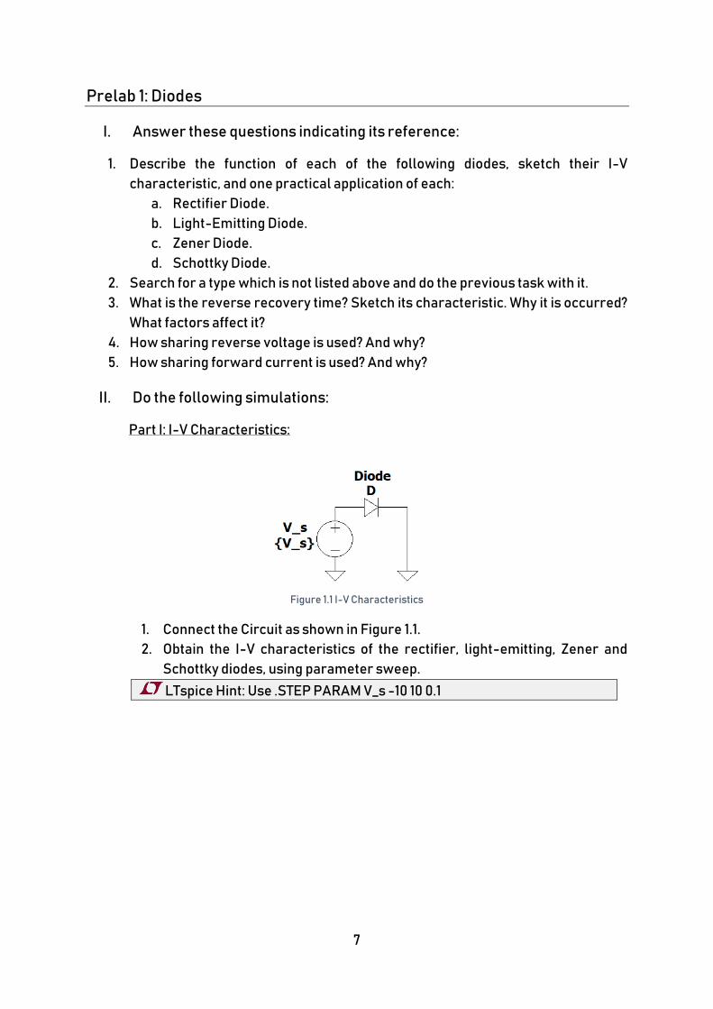
Part I: I-V Characteristics:
Figure 1.1 I-V Characteristics
1. Connect the Circuit as shown in Figure 1.1.
2. Obtain the I-V characteristics of the rectifier, light-emitting, Zener and
Schottky diodes, using parameter sweep.
LTspice Hint: Use .STEP PARAM V_s -10 10 0.1
8
Part II: Reverse Recovery Time:
Figure 1.2 Reverse Recovery Time
1. Connect the Circuit as shown in Figure 1.2.
2. Obtain the reverse recovery time characteristic using square voltage
source at 1KHz and 100KHz.
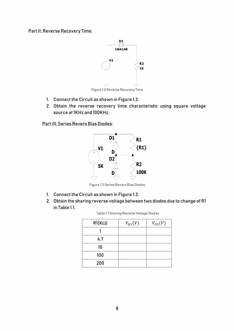
Part III: Series Revers Bias Diodes:
Figure 1.3 Series Revers Bias Diodes
1. Connect the Circuit as shown in Figure 1.3.
2. Obtain the sharing reverse voltage between two diodes due to change of R1
in Table 1.1. Table 1.1 Sharing Reverse Voltage Diodes
R1(KΩ) 𝑉𝐷1(𝑉) 𝑉𝐷2(𝑉)
1
4.7
10
100
200
9
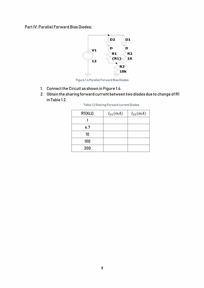
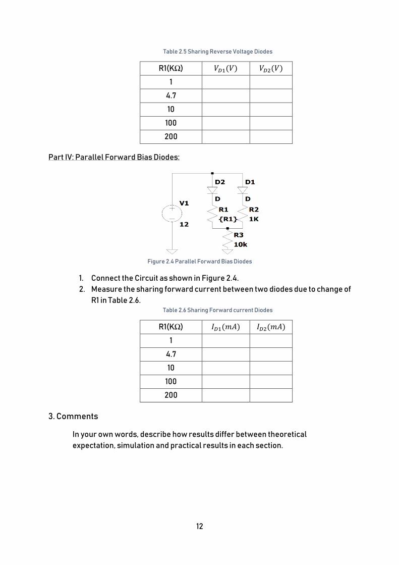
Part IV: Parallel Forward Bias Diodes:
Figure 1.4 Parallel Forward Bias Diodes
1. Connect the Circuit as shown in Figure 1.4.
2. Obtain the sharing forward current between two diodes due to change of R1
in Table 1.2. Table 1.2 Sharing Forward current Diodes
R1(KΩ) 𝐼𝐷1(𝑚𝐴) 𝐼𝐷2(𝑚𝐴)
1
4.7
10
100
200
10
Experiments2:Diodes
1. Objectives
To obtain the VI Characteristic of rectifier diode.
To obtain the reverse recovery response.
To obtain sharing reverse voltage and forward currents.
2. Experiment
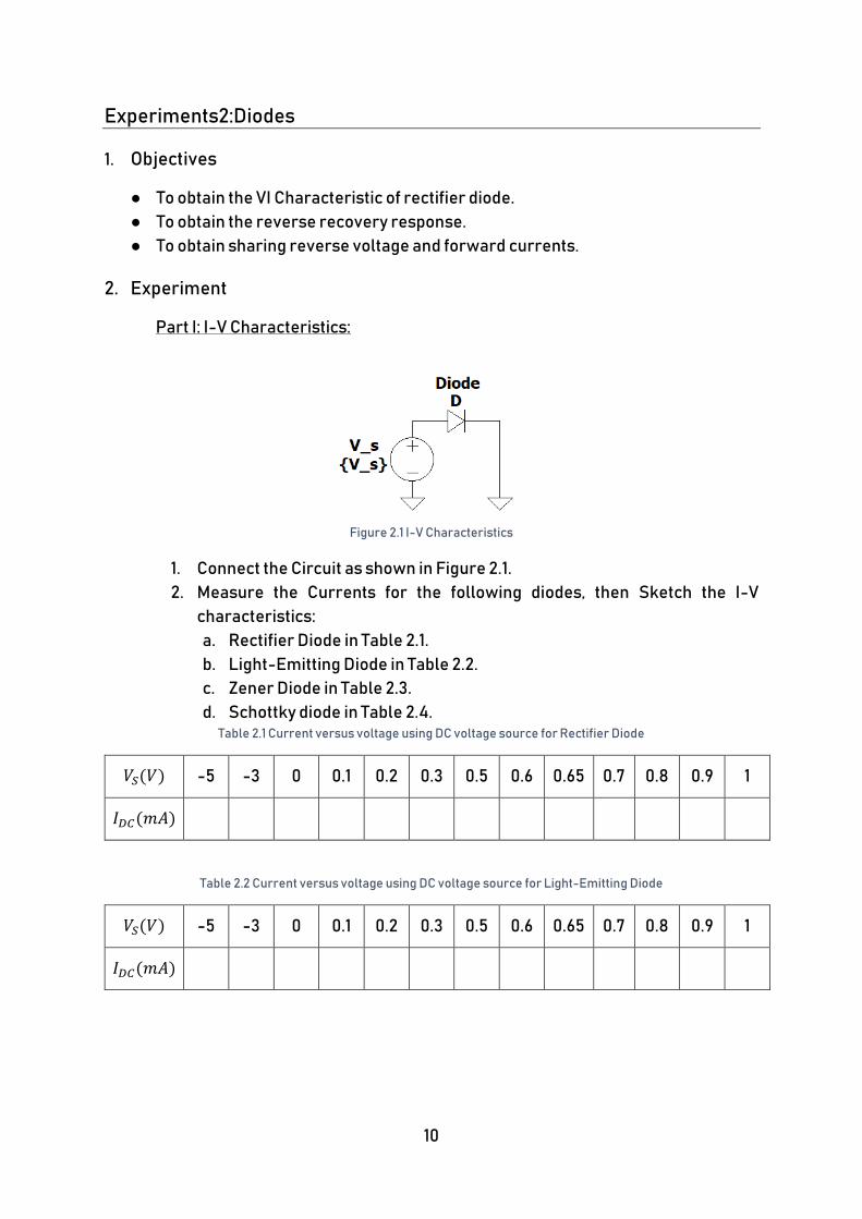
Part I: I-V Characteristics:
Figure 2.1 I-V Characteristics
1. Connect the Circuit as shown in Figure 2.1.
2. Measure the Currents for the following diodes, then Sketch the I-V
characteristics:
a. Rectifier Diode in Table 2.1.
b. Light-Emitting Diode in Table 2.2.
c. Zener Diode in Table 2.3.
d. Schottky diode in Table 2.4. Table 2.1 Current versus voltage using DC voltage source for Rectifier Diode
𝑉𝑆(𝑉) -5 -3 0 0.1 0.2 0.3 0.5 0.6 0.65 0.7 0.8 0.9 1
𝐼𝐷𝐶(𝑚𝐴)
Table 2.2 Current versus voltage using DC voltage source for Light-Emitting Diode
𝑉𝑆(𝑉) -5 -3 0 0.1 0.2 0.3 0.5 0.6 0.65 0.7 0.8 0.9 1
𝐼𝐷𝐶(𝑚𝐴)
11
Table 2.3 Current versus voltage using DC voltage source for Zener Diode
𝑉𝑆(𝑉) -5 -3 0 0.1 0.2 0.3 0.5 0.6 0.65 0.7 0.8 0.9 1
𝐼𝐷𝐶(𝑚𝐴)
Table 2.4 Current versus voltage using DC voltage source for Schottky Diode
𝑉𝑆(𝑉) -10 -5 -3 0 0.1 0.3 0.5 0.6 0.65 0.7 0.8 0.9 1
𝐼𝐷𝐶(𝑚𝐴)
Part II: Reverse Recovery Time:
Figure 2.2 Reverse Recovery Time
1. Connect the Circuit as shown in Figure 2.2.
2. Obtain the reverse recovery time characteristic using square voltage
source at 1KHz and 100KHz.
Part III: Series Revers Bias Diodes:
Figure 2.3 Series Revers Bias Diodes
1. Connect the Circuit as shown in Figure 2.3.
2. Measure the sharing reverse voltage between two diodes due to change of
R1 in Table 2.5.
12
Table 2.5 Sharing Reverse Voltage Diodes
R1(KΩ) 𝑉𝐷1(𝑉) 𝑉𝐷2(𝑉)
1
4.7
10
100
200
Part IV: Parallel Forward Bias Diodes:
Figure 2.4 Parallel Forward Bias Diodes
1. Connect the Circuit as shown in Figure 2.4.
2. Measure the sharing forward current between two diodes due to change of
R1 in Table 2.6. Table 2.6 Sharing Forward current Diodes
R1(KΩ) 𝐼𝐷1(𝑚𝐴) 𝐼𝐷2(𝑚𝐴)
1
4.7
10
100
200
3. Comments
In your own words, describe how results differ between theoretical
expectation, simulation and practical results in each section.
13
Prelab 2: Uncontrolled Half-wave Rectifier
I. Answer these questions indicating its reference: 1. For half-wave rectifier with a purely resistive load, what is the DC component of
the output?
2. For half-wave rectifier with a purely resistive load, what are the Fourier
components of the output?
3. What is the effect of changing the capacitive load on the DC component of the
output?
4. What is the effect of changing the inductive load on the DC component of the
output? why?
5. How can the negative output of inductive load half-wave rectifier be eliminated?
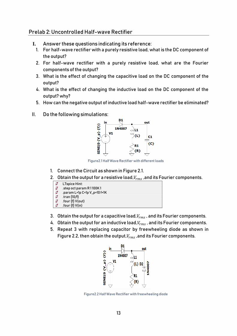
II. Do the following simulations:
Figure2.1 Half Wave Rectifier with different loads
1. Connect the Circuit as shown in Figure 2.1.
2. Obtain the output for a resistive load,𝑉𝑟𝑚𝑠 ,and its Fourier components.
LTspice Hint: .step oct param R 1 100K 1 .param L=1p C=1p V_p=10 f=1K .tran 10/f .four f V(out) .four f V(in)
3. Obtain the output for a capacitive load,𝑉𝑟𝑚𝑠 , and its Fourier components.
4. Obtain the output for an inductive load,𝑉𝑟𝑚𝑠 , and its Fourier components.
5. Repeat 3 with replacing capacitor by freewheeling diode as shown in
Figure 2.2, then obtain the output,𝑉𝑟𝑚𝑠 ,and its Fourier components.
Figure2.2 Half Wave Rectifier with freewheeling diode
14
Experiment3: Uncotrolled Half-wave Rectifier
1. Objectives
• To build a half-wave rectifier.
• To obtain the effect of change load on the output: DC and its Fourier
components.
• To obtain a half-wave rectifier flywheel diode.
2. Experiment
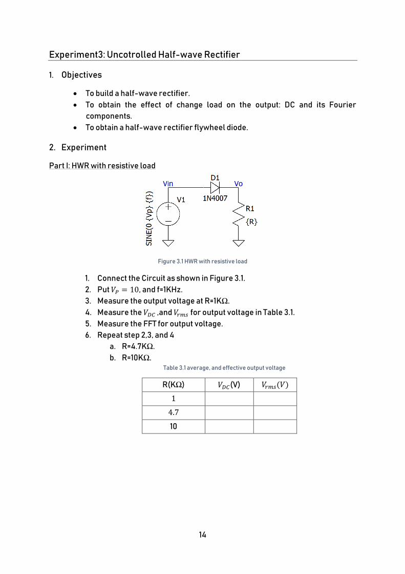
Part I: HWR with resistive load
Figure 3.1 HWR with resistive load
1. Connect the Circuit as shown in Figure 3.1.
2. Put 𝑉𝑃 = 10, and f=1KHz.
3. Measure the output voltage at R=1KΩ.
4. Measure the 𝑉𝐷𝐶 ,and 𝑉𝑟𝑚𝑠 for output voltage in Table 3.1.
5. Measure the FFT for output voltage.
6. Repeat step 2,3, and 4
a. R=4.7KΩ.
b. R=10KΩ. Table 3.1 average, and effective output voltage
R(KΩ) 𝑉𝐷𝐶(V) 𝑉𝑟𝑚𝑠(𝑉)
1
4.7
10
15
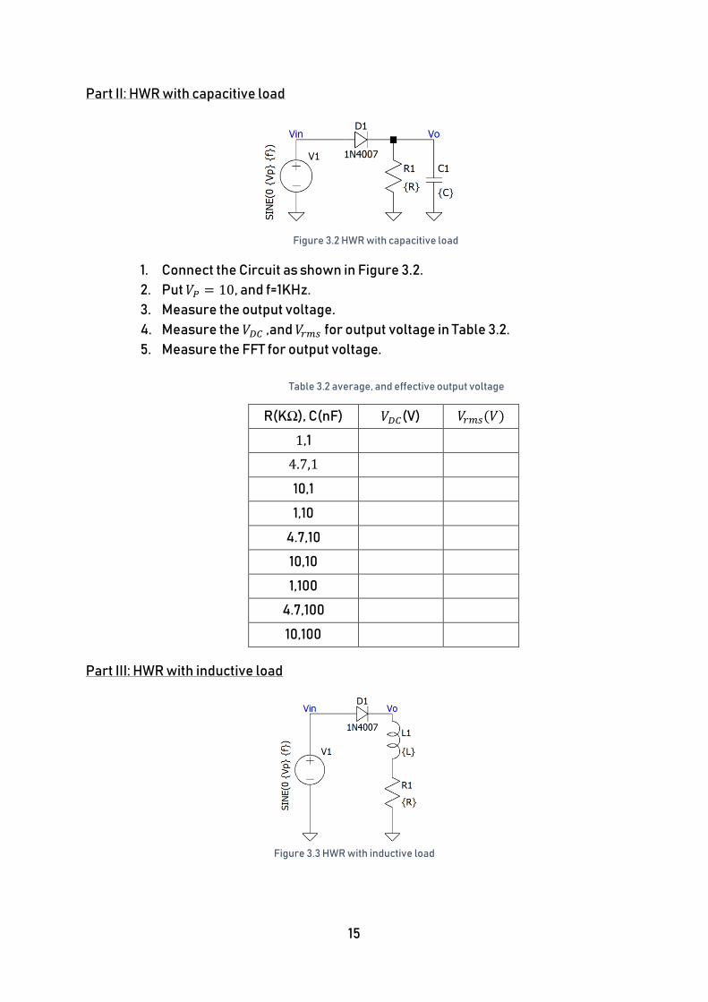
Part II: HWR with capacitive load
Figure 3.2 HWR with capacitive load
1. Connect the Circuit as shown in Figure 3.2.
2. Put 𝑉𝑃 = 10, and f=1KHz.
3. Measure the output voltage.
4. Measure the 𝑉𝐷𝐶 ,and 𝑉𝑟𝑚𝑠 for output voltage in Table 3.2.
5. Measure the FFT for output voltage.
Table 3.2 average, and effective output voltage
R(KΩ), C(nF) 𝑉𝐷𝐶(V) 𝑉𝑟𝑚𝑠(𝑉)
1,1
4.7,1
10,1
1,10
4.7,10
10,10
1,100
4.7,100
10,100
Part III: HWR with inductive load
Figure 3.3 HWR with inductive load
16
1. Connect the Circuit as shown in Figure 3.3.
2. Put 𝑉𝑃 = 10, and f=1KHz.
3. Measure the output voltage.
4. Measure the 𝑉𝐷𝐶 ,and 𝑉𝑟𝑚𝑠 for output voltage in Table 3.3.
5. Measure the FFT for output voltage.
Table 3.3 average, and effective output voltage
R(KΩ), L(mH) 𝑉𝐷𝐶(V) 𝑉𝑟𝑚𝑠(𝑉)
1,1
4.7,1
10,1
1,10
4.7,10
10,10
1,100
4.7,100
10,100
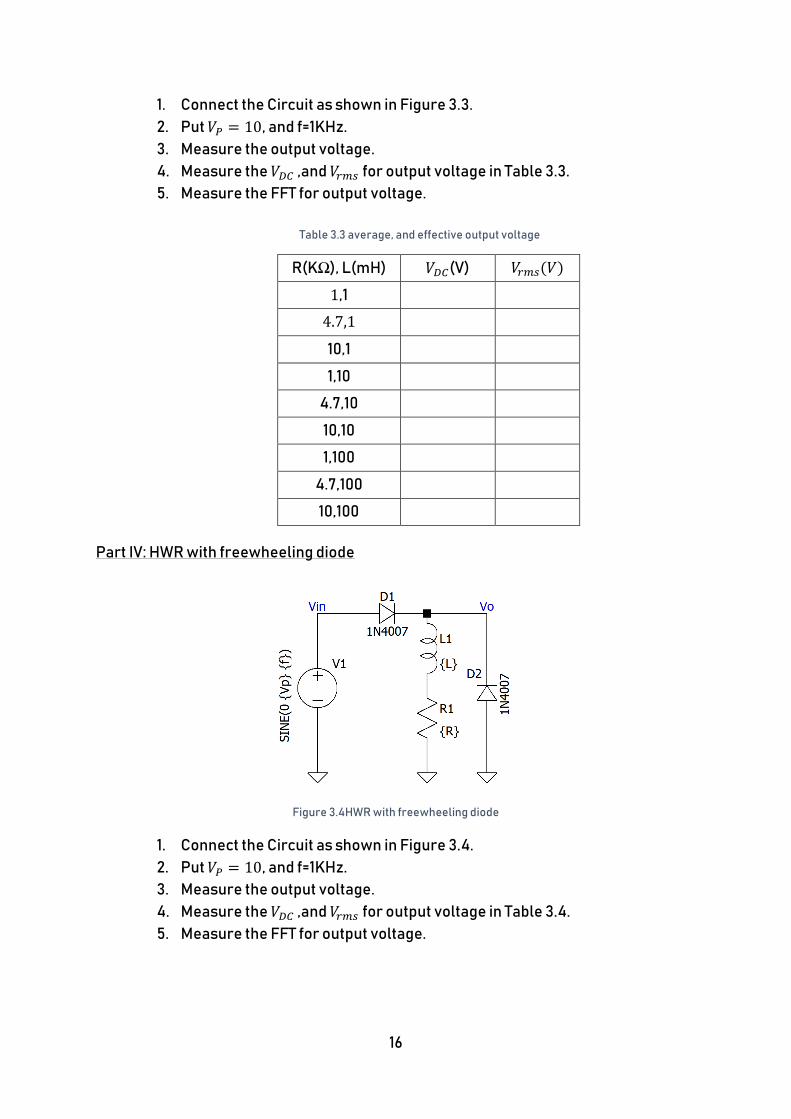
Part IV: HWR with freewheeling diode
Figure 3.4HWR with freewheeling diode
1. Connect the Circuit as shown in Figure 3.4.
2. Put 𝑉𝑃 = 10, and f=1KHz.
3. Measure the output voltage.
4. Measure the 𝑉𝐷𝐶 ,and 𝑉𝑟𝑚𝑠 for output voltage in Table 3.4.
5. Measure the FFT for output voltage.
17
Table 3.4 average, and effective output voltage
R(KΩ), L(mH) 𝑉𝐷𝐶(V) 𝑉𝑟𝑚𝑠(𝑉)
1,1
4.7,1
10,1
1,10
4.7,10
10,10
1,100
4.7,100
10,100
3. Comments
In your own words, describe how results differ between theoretical
expectation, simulation and practical results in each section.
18
Prelab 3: Uncontrolled Full-wave Rectifier
I. Answer these questions indicating its reference: 1. For a full-wave rectifier with a purely resistive load, what is the DC component
of the output?
2. For a full-wave rectifier with a purely resistive load, what are the Fourier
components of the output?
3. What is the effect of changing the capacitive load on the DC component of the
output?
4. What is the effect of changing the inductive load on the DC component of the
output? why?
5. What is the difference between half-wave rectifier and full-wave rectifier?
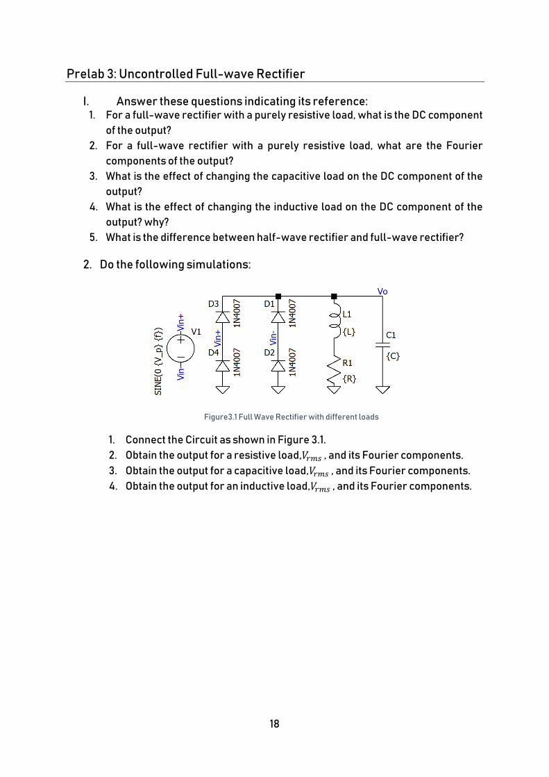
2. Do the following simulations:
Figure3.1 Full Wave Rectifier with different loads
1. Connect the Circuit as shown in Figure 3.1.
2. Obtain the output for a resistive load,𝑉𝑟𝑚𝑠 , and its Fourier components.
3. Obtain the output for a capacitive load,𝑉𝑟𝑚𝑠 , and its Fourier components.
4. Obtain the output for an inductive load,𝑉𝑟𝑚𝑠 , and its Fourier components.
19
Experiment4: Uncotrolled Full-wave Rectifier
1. Objectives
• To build a full-wave rectifier
• To obtain the effect of change load on the output: DC and its Fourier
components
2. Experiment
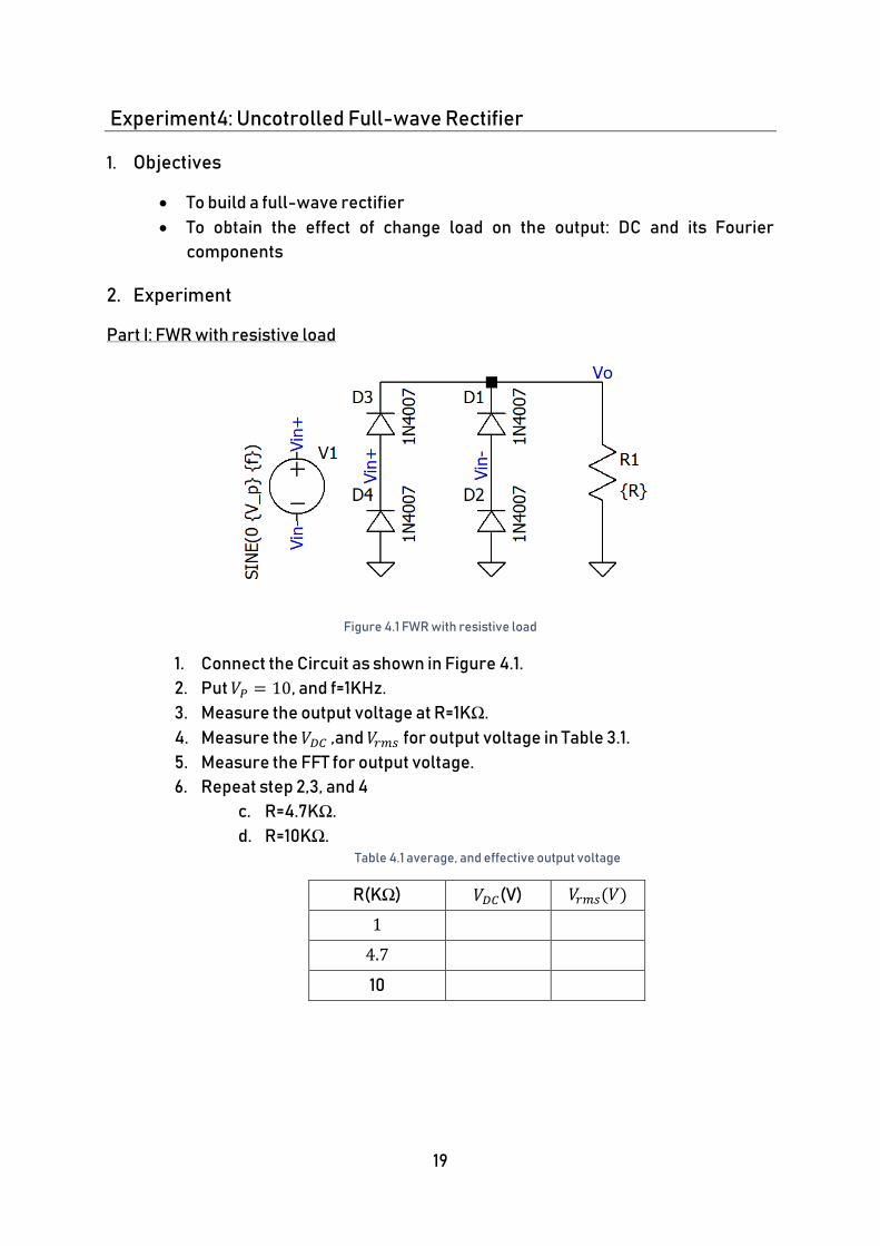
Part I: FWR with resistive load
Figure 4.1 FWR with resistive load
1. Connect the Circuit as shown in Figure 4.1.
2. Put 𝑉𝑃 = 10, and f=1KHz.
3. Measure the output voltage at R=1KΩ.
4. Measure the 𝑉𝐷𝐶 ,and 𝑉𝑟𝑚𝑠 for output voltage in Table 3.1.
5. Measure the FFT for output voltage.
6. Repeat step 2,3, and 4
c. R=4.7KΩ.
d. R=10KΩ. Table 4.1 average, and effective output voltage
R(KΩ) 𝑉𝐷𝐶(V) 𝑉𝑟𝑚𝑠(𝑉)
1
4.7
10
20
Part II: FWR with capacitive load
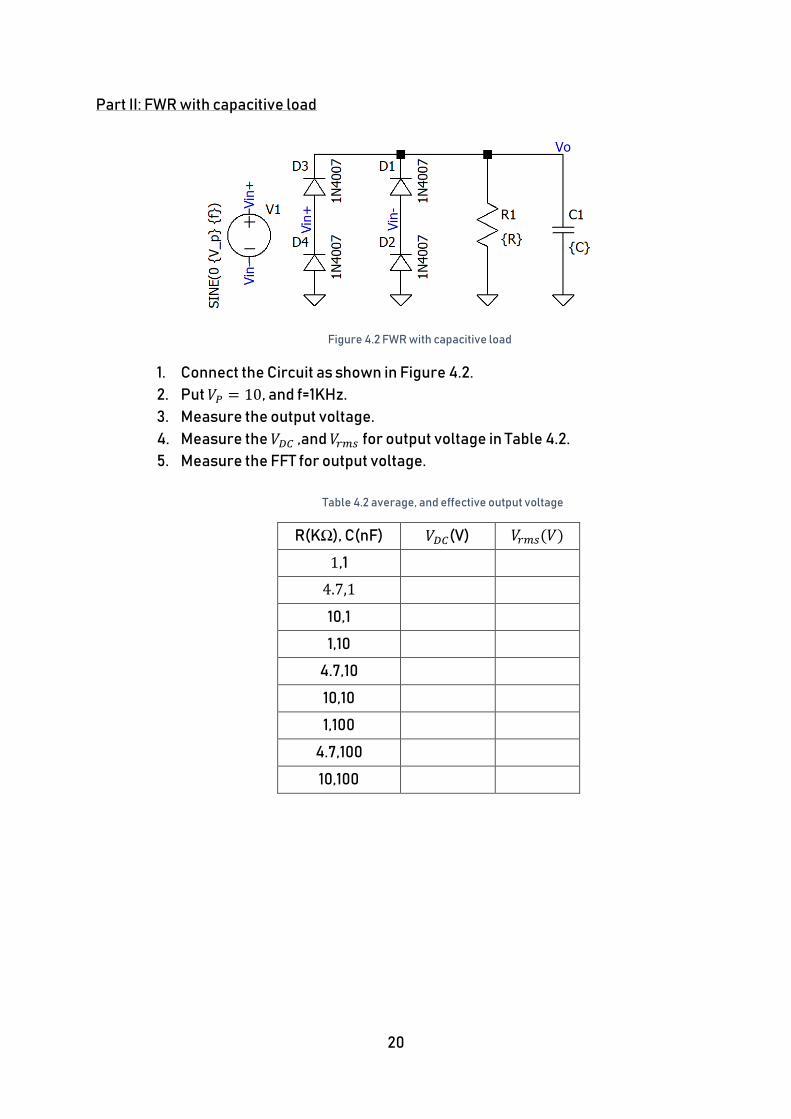
Figure 4.2 FWR with capacitive load
1. Connect the Circuit as shown in Figure 4.2.
2. Put 𝑉𝑃 = 10, and f=1KHz.
3. Measure the output voltage.
4. Measure the 𝑉𝐷𝐶 ,and 𝑉𝑟𝑚𝑠 for output voltage in Table 4.2.
5. Measure the FFT for output voltage.
Table 4.2 average, and effective output voltage
R(KΩ), C(nF) 𝑉𝐷𝐶(V) 𝑉𝑟𝑚𝑠(𝑉)
1,1
4.7,1
10,1
1,10
4.7,10
10,10
1,100
4.7,100
10,100
21
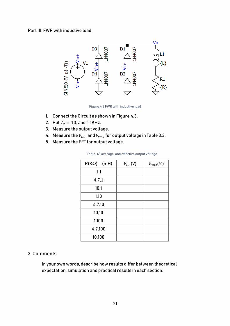
Part III: FWR with inductive load
Figure 4.3 FWR with inductive load
1. Connect the Circuit as shown in Figure 4.3.
2. Put 𝑉𝑃 = 10, and f=1KHz.
3. Measure the output voltage.
4. Measure the 𝑉𝐷𝐶 ,and 𝑉𝑟𝑚𝑠 for output voltage in Table 3.3.
5. Measure the FFT for output voltage.
Table .43 average, and effective output voltage
R(KΩ), L(mH) 𝑉𝐷𝐶(V) 𝑉𝑟𝑚𝑠(𝑉)
1,1
4.7,1
10,1
1,10
4.7,10
10,10
1,100
4.7,100
10,100
3. Comments
In your own words, describe how results differ between theoretical
expectation, simulation and practical results in each section.
22
Prelab 4: Uncontrolled 3-Phase Full-wave Rectifier
I. Answer these questions indicating its reference:
1. Why we use the three-phase rectifiers?
2. If the three-phase voltage source has sequence a-c-b. Is the output voltage
affected or not?
3. The maximum output voltage is equal the maximum phase voltage or line
voltage?
4. What is the relationship between the fundamental frequency of the output
voltage and the frequency of the three-phase source?
5. What is the fundamental frequency of the output voltage if you have twelve-
phase source?
II. Do the following simulations:
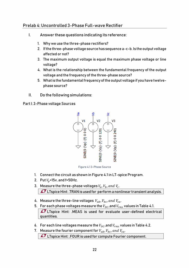
Part I: 3-Phase voltage Sources
Figure 4.1 3-Phase Source
1. Connect the circuit as shown in Figure 4.1 in LT-spice Program.
2. Put 𝑉𝑝=15v, and f=50Hz.
3. Measure the three-phase voltages 𝑉𝑎, 𝑉𝑏 , 𝑎𝑛𝑑 𝑉𝑐.
LTspice Hint: .TRAN is used for perform a nonlinear transient analysis.
4. Measure the three-line voltages 𝑉𝑎𝑏 , 𝑉𝑏𝑐, 𝑎𝑛𝑑 𝑉𝑐𝑎.
5. For each phase voltages measure the 𝑉𝐷𝐶 ,and 𝑉𝑟𝑚𝑠 values in Table 4.1.
LTspice Hint: .MEAS is used for evaluate user-defined electrical quantities.
6. For each line voltages measure the 𝑉𝐷𝐶 ,and 𝑉𝑟𝑚𝑠 values in Table 4.2.
7. Measure the fourier component for 𝑉𝑎𝑏 , 𝑉𝑏𝑐, 𝑎𝑛𝑑 𝑉𝑐𝑎.
LTspice Hint: .FOUR is used for compute Fourier component.
23
8. Measure the FFT for 𝑉𝑎, 𝑉𝑏 , 𝑎𝑛𝑑 𝑉𝑐.
9. Measure the FFT for 𝑉𝑎𝑏 , 𝑉𝑏𝑐, 𝑎𝑛𝑑 𝑉𝑐𝑎.
Table 4.1 average, and effective values for phase voltages
Phase Voltage 𝑉𝐷𝐶(𝑉) 𝑉𝑟𝑚𝑠(𝑉)
𝑉𝑎
𝑉𝑏
𝑉𝑐
Table 4.2 average, and effective values for line voltages
Line Voltage 𝑉𝐷𝐶(V) 𝑉𝑟𝑚𝑠(𝑉)
𝑉𝑎𝑏
𝑉𝑏𝑐
𝑉𝑐𝑎
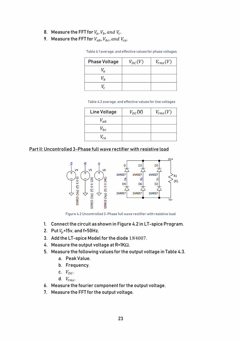
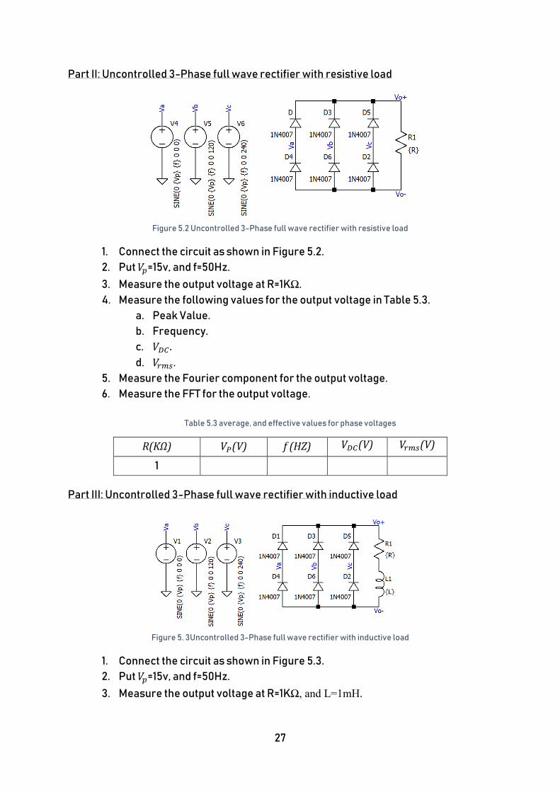
Part II: Uncontrolled 3-Phase full wave rectifier with resistive load
Figure 4.2 Uncontrolled 3-Phase full wave rectifier with resistive load
1. Connect the circuit as shown in Figure 4.2 in LT-spice Program.
2. Put 𝑉𝑝=15v, and f=50Hz.
3. Add the LT-spice Model for the diode 1𝑁4007.
4. Measure the output voltage at R=1KΩ.
5. Measure the following values for the output voltage in Table 4.3.
a. Peak Value.
b. Frequency.
c. 𝑉𝐷𝐶 .
d. 𝑉𝑟𝑚𝑠.
6. Measure the fourier component for the output voltage.
7. Measure the FFT for the output voltage.
24
Table 4.3 average, and effective values for phase voltages
R(KΩ) 𝑉𝑃(V) f (HZ) 𝑉𝐷𝐶(V) 𝑉𝑟𝑚𝑠(V)
1
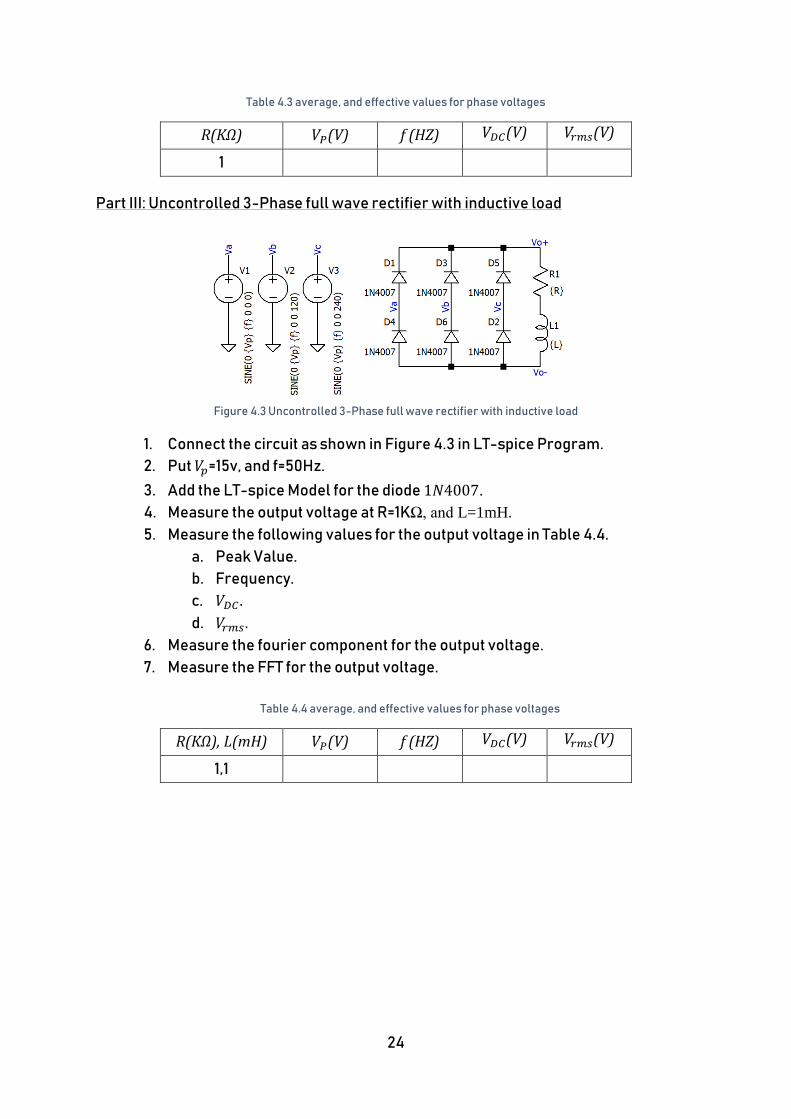
Part III: Uncontrolled 3-Phase full wave rectifier with inductive load
Figure 4.3 Uncontrolled 3-Phase full wave rectifier with inductive load
1. Connect the circuit as shown in Figure 4.3 in LT-spice Program.
2. Put 𝑉𝑝=15v, and f=50Hz.
3. Add the LT-spice Model for the diode 1𝑁4007.
4. Measure the output voltage at R=1KΩ, and L=1mH.
5. Measure the following values for the output voltage in Table 4.4.
a. Peak Value.
b. Frequency.
c. 𝑉𝐷𝐶 .
d. 𝑉𝑟𝑚𝑠.
6. Measure the fourier component for the output voltage.
7. Measure the FFT for the output voltage.
Table 4.4 average, and effective values for phase voltages
R(KΩ), L(mH) 𝑉𝑃(V) f (HZ) 𝑉𝐷𝐶(V) 𝑉𝑟𝑚𝑠(V)
1,1
25
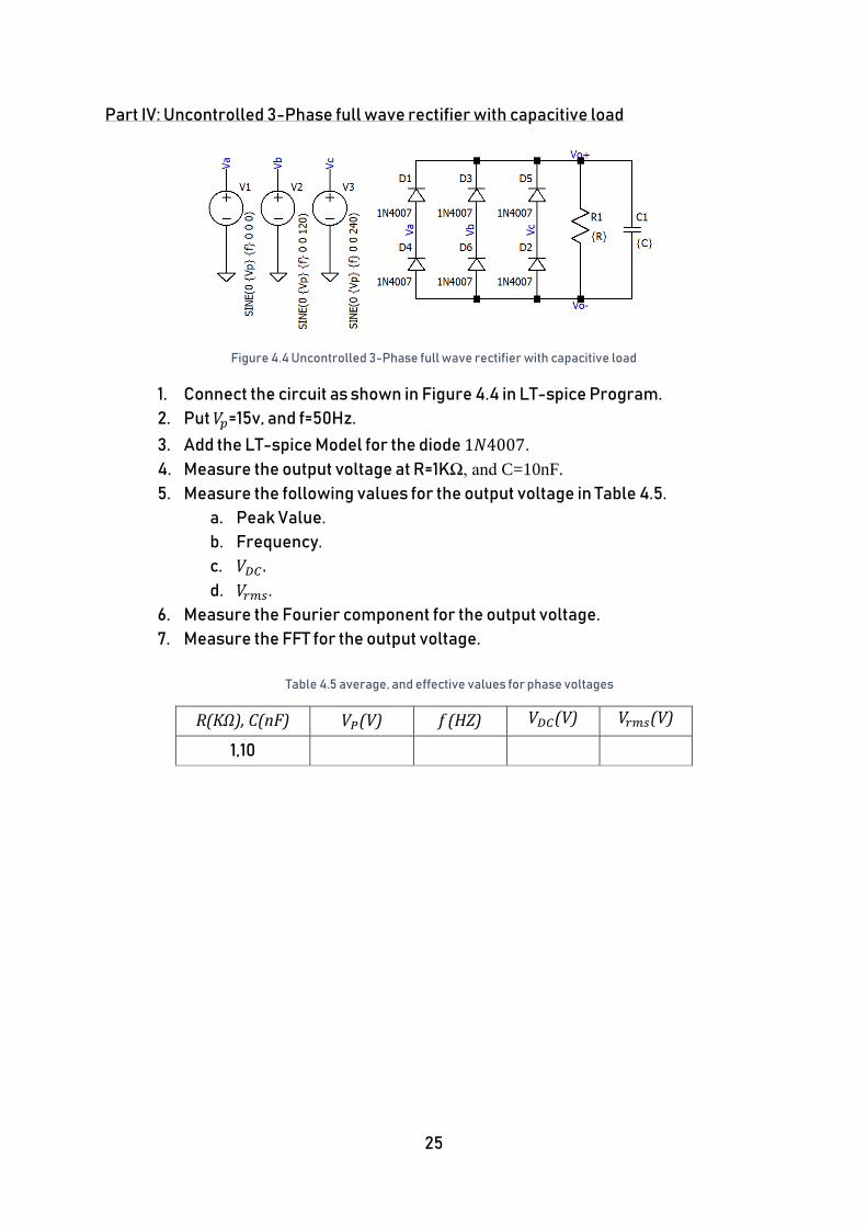
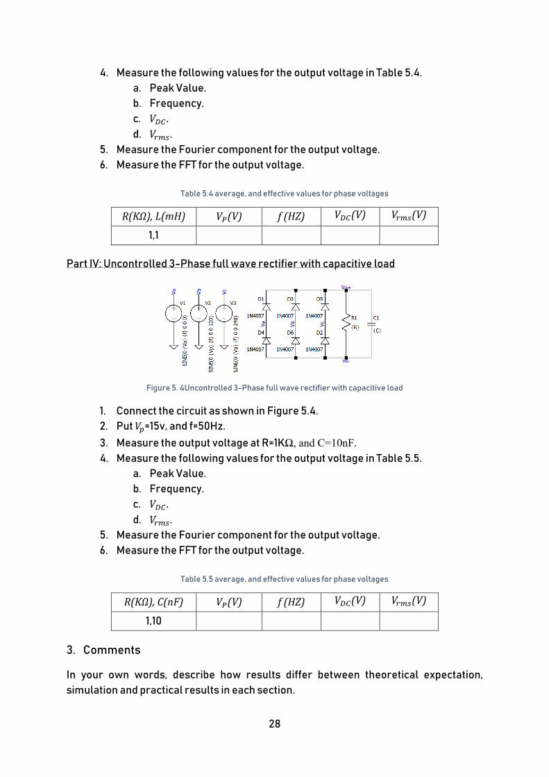
Part IV: Uncontrolled 3-Phase full wave rectifier with capacitive load
Figure 4.4 Uncontrolled 3-Phase full wave rectifier with capacitive load
1. Connect the circuit as shown in Figure 4.4 in LT-spice Program.
2. Put 𝑉𝑝=15v, and f=50Hz.
3. Add the LT-spice Model for the diode 1𝑁4007.
4. Measure the output voltage at R=1KΩ, and C=10nF.
5. Measure the following values for the output voltage in Table 4.5.
a. Peak Value.
b. Frequency.
c. 𝑉𝐷𝐶 .
d. 𝑉𝑟𝑚𝑠.
6. Measure the Fourier component for the output voltage.
7. Measure the FFT for the output voltage.
Table 4.5 average, and effective values for phase voltages
R(KΩ), C(nF) 𝑉𝑃(V) f (HZ) 𝑉𝐷𝐶(V) 𝑉𝑟𝑚𝑠(V)
1,10
26
Experiment 5: Uncontrolled 3-Phase Full-wave Rectifier
1. Objectives
To be familiar Uncontrolled 3-Phase Full Wave Rectifier with different loads.
2. Experiment
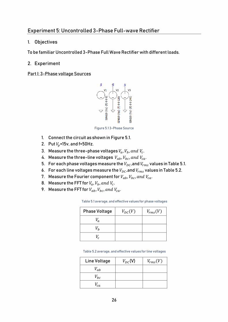
Part I: 3-Phase voltage Sources
Figure 5.1 3-Phase Source
1. Connect the circuit as shown in Figure 5.1.
2. Put 𝑉𝑝=15v, and f=50Hz.
3. Measure the three-phase voltages 𝑉𝑎, 𝑉𝑏 , 𝑎𝑛𝑑 𝑉𝑐.
4. Measure the three-line voltages 𝑉𝑎𝑏 , 𝑉𝑏𝑐, 𝑎𝑛𝑑 𝑉𝑐𝑎.
5. For each phase voltages measure the 𝑉𝐷𝐶 ,and 𝑉𝑟𝑚𝑠 values in Table 5.1.
6. For each line voltages measure the 𝑉𝐷𝐶 ,and 𝑉𝑟𝑚𝑠 values in Table 5.2.
7. Measure the Fourier component for 𝑉𝑎𝑏, 𝑉𝑏𝑐, 𝑎𝑛𝑑 𝑉𝑐𝑎.
8. Measure the FFT for 𝑉𝑎, 𝑉𝑏 , 𝑎𝑛𝑑 𝑉𝑐.
9. Measure the FFT for 𝑉𝑎𝑏 , 𝑉𝑏𝑐, 𝑎𝑛𝑑 𝑉𝑐𝑎.
Table 5.1 average, and effective values for phase voltages
Phase Voltage 𝑉𝐷𝐶(𝑉) 𝑉𝑟𝑚𝑠(𝑉)
𝑉𝑎
𝑉𝑏
𝑉𝑐
Table 5.2 average, and effective values for line voltages
Line Voltage 𝑉𝐷𝐶(V) 𝑉𝑟𝑚𝑠(𝑉)
𝑉𝑎𝑏
𝑉𝑏𝑐
𝑉𝑐𝑎
27
Part II: Uncontrolled 3-Phase full wave rectifier with resistive load
Figure 5.2 Uncontrolled 3-Phase full wave rectifier with resistive load
1. Connect the circuit as shown in Figure 5.2.
2. Put 𝑉𝑝=15v, and f=50Hz.
3. Measure the output voltage at R=1KΩ.
4. Measure the following values for the output voltage in Table 5.3.
a. Peak Value.
b. Frequency.
c. 𝑉𝐷𝐶 .
d. 𝑉𝑟𝑚𝑠.
5. Measure the Fourier component for the output voltage.
6. Measure the FFT for the output voltage.
Table 5.3 average, and effective values for phase voltages
R(KΩ) 𝑉𝑃(V) f (HZ) 𝑉𝐷𝐶(V) 𝑉𝑟𝑚𝑠(V)
1
Part III: Uncontrolled 3-Phase full wave rectifier with inductive load
Figure 5. 3Uncontrolled 3-Phase full wave rectifier with inductive load
1. Connect the circuit as shown in Figure 5.3.
2. Put 𝑉𝑝=15v, and f=50Hz.
3. Measure the output voltage at R=1KΩ, and L=1mH.
28
4. Measure the following values for the output voltage in Table 5.4.
a. Peak Value.
b. Frequency.
c. 𝑉𝐷𝐶 .
d. 𝑉𝑟𝑚𝑠.
5. Measure the Fourier component for the output voltage.
6. Measure the FFT for the output voltage.
Table 5.4 average, and effective values for phase voltages
R(KΩ), L(mH) 𝑉𝑃(V) f (HZ) 𝑉𝐷𝐶(V) 𝑉𝑟𝑚𝑠(V)
1,1
Part IV: Uncontrolled 3-Phase full wave rectifier with capacitive load
Figure 5. 4Uncontrolled 3-Phase full wave rectifier with capacitive load
1. Connect the circuit as shown in Figure 5.4.
2. Put 𝑉𝑝=15v, and f=50Hz.
3. Measure the output voltage at R=1KΩ, and C=10nF.
4. Measure the following values for the output voltage in Table 5.5.
a. Peak Value.
b. Frequency.
c. 𝑉𝐷𝐶 .
d. 𝑉𝑟𝑚𝑠.
5. Measure the Fourier component for the output voltage.
6. Measure the FFT for the output voltage.
Table 5.5 average, and effective values for phase voltages
R(KΩ), C(nF) 𝑉𝑃(V) f (HZ) 𝑉𝐷𝐶(V) 𝑉𝑟𝑚𝑠(V)
1,10
3. Comments
In your own words, describe how results differ between theoretical expectation,
simulation and practical results in each section.
29
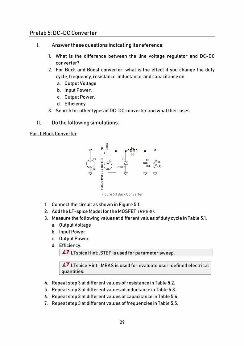
Prelab 5: DC-DC Converter
I. Answer these questions indicating its reference:
1. What is the difference between the line voltage regulator and DC-DC
converter?
2. For Buck and Boost converter, what is the effect if you change the duty
cycle, frequency, resistance, inductance, and capacitance on
a. Output Voltage
b. Input Power.
c. Output Power.
d. Efficiency.
3. Search for other types of DC-DC converter and what their uses.
II. Do the following simulations:
Part I: Buck Converter
Figure 5.1 Buck Converter
1. Connect the circuit as shown in Figure 5.1.
2. Add the LT-spice Model for the MOSFET 𝐼𝑅𝐹830.
3. Measure the following values at different values of duty cycle in Table 5.1.
a. Output Voltage
b. Input Power.
c. Output Power.
d. Efficiency.
LTspice Hint: .STEP is used for parameter sweep.
LTspice Hint: .MEAS is used for evaluate user-defined electrical quantities.
4. Repeat step 3 at different values of resistance in Table 5.2.
5. Repeat step 3 at different values of inductance in Table 5.3.
6. Repeat step 3 at different values of capacitance in Table 5.4.
7. Repeat step 3 at different values of frequencies in Table 5.5.

30
Table 5.1 Readings at different duty cycle
𝑉𝑆 = 5𝑣, 𝑉𝑃 = 10𝑣, 𝑓 = 1𝑘𝐻𝑧, 𝐿 = 1𝑚𝐻, 𝐶 = 1𝑛𝐹, 𝑎𝑛𝑑 𝑅 = 1𝑘Ω
D (%) 𝑉𝑜(V) 𝑃𝑖𝑛(𝑊) 𝑃𝑜(𝑊) η
0
10
20
30
40
50
60
70
80
90
100
Table 5.2 Readings at different resistance
𝑉𝑆 = 5𝑣, 𝑉𝑝 = 10𝑣, 𝐷 = 50%, 𝑓 = 1𝑘𝐻𝑧, 𝐿 = 1𝑚𝐻, 𝑎𝑛𝑑 𝐶 = 1𝑛𝐹
R (KΩ) 𝑉𝑜(V) 𝑃𝑖𝑛(𝑊) 𝑃𝑜(𝑊) η
1
4.7
10
Table 5.3 Readings at different inductance
𝑉𝑆 = 5𝑣, 𝑉𝑝 = 10𝑣, 𝐷 = 50%, 𝑓 = 1𝑘𝐻𝑧, 𝐶 = 1𝑛𝐹, 𝑎𝑛𝑑 𝑅 = 1𝑘Ω
L (mH) 𝑉𝑜(V) 𝑃𝑖𝑛(𝑊) 𝑃𝑜(𝑊) η
0
10
20
31
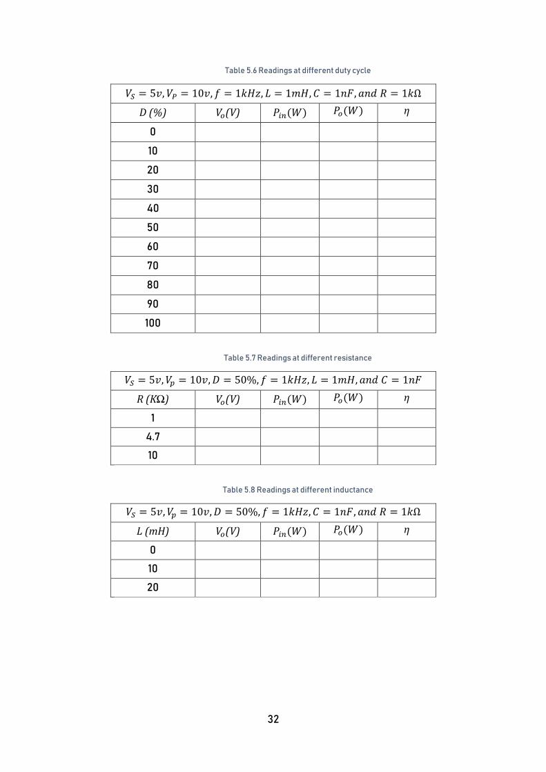
Table 5.4 Readings at different capacitance
𝑉𝑆 = 5𝑣, 𝑉𝑝 = 10𝑣, 𝐷 = 50%, 𝑓 = 1𝑘𝐻𝑧, 𝐿 = 1𝑚𝐻, 𝑎𝑛𝑑 𝑅 = 1𝑘Ω
C (nF) 𝑉𝑜(V) 𝑃𝑖𝑛(𝑊) 𝑃𝑜(𝑊) η
1
10
100
Table 5.5 Readings at different frequencies
𝑉𝑆 = 5𝑣, 𝑉𝑝 = 10𝑣, 𝐷 = 50%, 𝐿 = 1𝑚𝐻, 𝐶 = 1𝑛𝐹, 𝑎𝑛𝑑 𝑅 = 1𝑘Ω
f (KHz) 𝑉𝑜(V) 𝑃𝑖𝑛(𝑊) 𝑃𝑜(𝑊) η
1
10
100
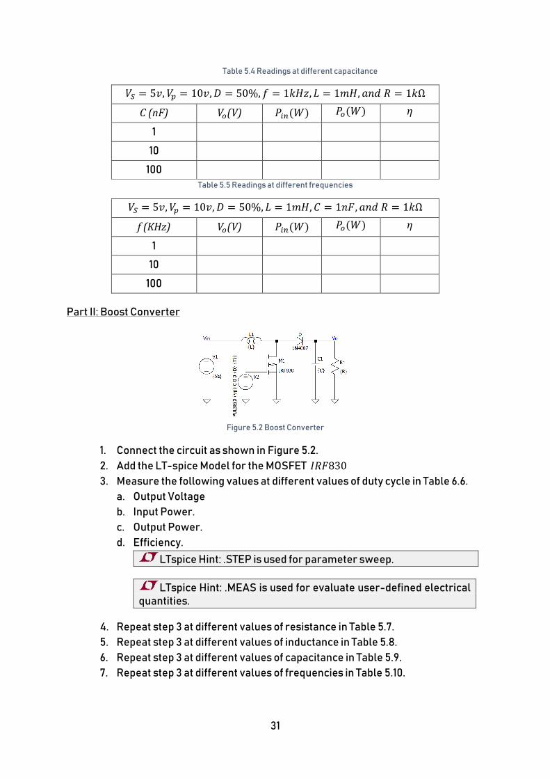
Part II: Boost Converter
Figure 5.2 Boost Converter
1. Connect the circuit as shown in Figure 5.2.
2. Add the LT-spice Model for the MOSFET 𝐼𝑅𝐹830
3. Measure the following values at different values of duty cycle in Table 6.6.
a. Output Voltage
b. Input Power.
c. Output Power.
d. Efficiency.
LTspice Hint: .STEP is used for parameter sweep.
LTspice Hint: .MEAS is used for evaluate user-defined electrical quantities.
4. Repeat step 3 at different values of resistance in Table 5.7.
5. Repeat step 3 at different values of inductance in Table 5.8.
6. Repeat step 3 at different values of capacitance in Table 5.9.
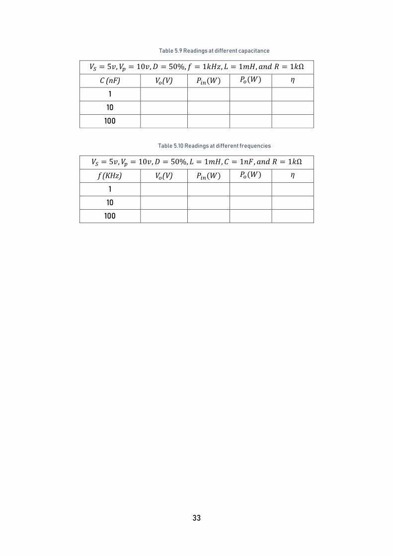
7. Repeat step 3 at different values of frequencies in Table 5.10.
32
Table 5.6 Readings at different duty cycle
𝑉𝑆 = 5𝑣, 𝑉𝑃 = 10𝑣, 𝑓 = 1𝑘𝐻𝑧, 𝐿 = 1𝑚𝐻, 𝐶 = 1𝑛𝐹, 𝑎𝑛𝑑 𝑅 = 1𝑘Ω
D (%) 𝑉𝑜(V) 𝑃𝑖𝑛(𝑊) 𝑃𝑜(𝑊) η
0
10
20
30
40
50
60
70
80
90
100
Table 5.7 Readings at different resistance
𝑉𝑆 = 5𝑣, 𝑉𝑝 = 10𝑣, 𝐷 = 50%, 𝑓 = 1𝑘𝐻𝑧, 𝐿 = 1𝑚𝐻, 𝑎𝑛𝑑 𝐶 = 1𝑛𝐹
R (KΩ) 𝑉𝑜(V) 𝑃𝑖𝑛(𝑊) 𝑃𝑜(𝑊) η
1
4.7
10
Table 5.8 Readings at different inductance
𝑉𝑆 = 5𝑣, 𝑉𝑝 = 10𝑣, 𝐷 = 50%, 𝑓 = 1𝑘𝐻𝑧, 𝐶 = 1𝑛𝐹, 𝑎𝑛𝑑 𝑅 = 1𝑘Ω
L (mH) 𝑉𝑜(V) 𝑃𝑖𝑛(𝑊) 𝑃𝑜(𝑊) η
0
10
20
33
Table 5.9 Readings at different capacitance
𝑉𝑆 = 5𝑣, 𝑉𝑝 = 10𝑣, 𝐷 = 50%, 𝑓 = 1𝑘𝐻𝑧, 𝐿 = 1𝑚𝐻, 𝑎𝑛𝑑 𝑅 = 1𝑘Ω
C (nF) 𝑉𝑜(V) 𝑃𝑖𝑛(𝑊) 𝑃𝑜(𝑊) η
1
10
100
Table 5.10 Readings at different frequencies
𝑉𝑆 = 5𝑣, 𝑉𝑝 = 10𝑣, 𝐷 = 50%, 𝐿 = 1𝑚𝐻, 𝐶 = 1𝑛𝐹, 𝑎𝑛𝑑 𝑅 = 1𝑘Ω
f (KHz) 𝑉𝑜(V) 𝑃𝑖𝑛(𝑊) 𝑃𝑜(𝑊) η
1
10
100
34
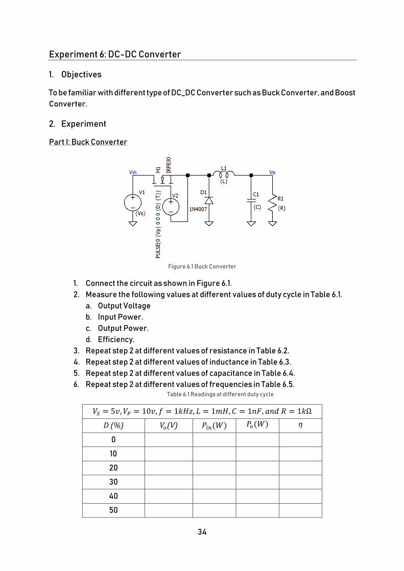
Experiment 6: DC-DC Converter
1. Objectives
To be familiar with different type of DC_DC Converter such as Buck Converter, and Boost
Converter.
2. Experiment
Part I: Buck Converter
Figure 6.1 Buck Converter
1. Connect the circuit as shown in Figure 6.1.
2. Measure the following values at different values of duty cycle in Table 6.1.
a. Output Voltage
b. Input Power.
c. Output Power.
d. Efficiency.
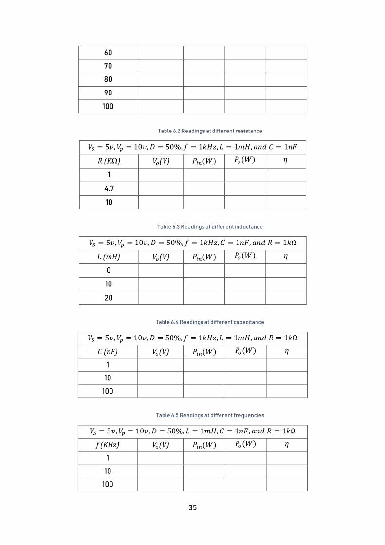
3. Repeat step 2 at different values of resistance in Table 6.2.
4. Repeat step 2 at different values of inductance in Table 6.3.
5. Repeat step 2 at different values of capacitance in Table 6.4.
6. Repeat step 2 at different values of frequencies in Table 6.5. Table 6.1 Readings at different duty cycle
𝑉𝑆 = 5𝑣, 𝑉𝑃 = 10𝑣, 𝑓 = 1𝑘𝐻𝑧, 𝐿 = 1𝑚𝐻, 𝐶 = 1𝑛𝐹, 𝑎𝑛𝑑 𝑅 = 1𝑘Ω
D (%) 𝑉𝑜(V) 𝑃𝑖𝑛(𝑊) 𝑃𝑜(𝑊) η
0
10
20
30
40
50
35
60
70
80
90
100
Table 6.2 Readings at different resistance
𝑉𝑆 = 5𝑣, 𝑉𝑝 = 10𝑣, 𝐷 = 50%, 𝑓 = 1𝑘𝐻𝑧, 𝐿 = 1𝑚𝐻, 𝑎𝑛𝑑 𝐶 = 1𝑛𝐹
R (KΩ) 𝑉𝑜(V) 𝑃𝑖𝑛(𝑊) 𝑃𝑜(𝑊) η
1
4.7
10
Table 6.3 Readings at different inductance
𝑉𝑆 = 5𝑣, 𝑉𝑝 = 10𝑣, 𝐷 = 50%, 𝑓 = 1𝑘𝐻𝑧, 𝐶 = 1𝑛𝐹, 𝑎𝑛𝑑 𝑅 = 1𝑘Ω
L (mH) 𝑉𝑜(V) 𝑃𝑖𝑛(𝑊) 𝑃𝑜(𝑊) η
0
10
20
Table 6.4 Readings at different capacitance
𝑉𝑆 = 5𝑣, 𝑉𝑝 = 10𝑣, 𝐷 = 50%, 𝑓 = 1𝑘𝐻𝑧, 𝐿 = 1𝑚𝐻, 𝑎𝑛𝑑 𝑅 = 1𝑘Ω
C (nF) 𝑉𝑜(V) 𝑃𝑖𝑛(𝑊) 𝑃𝑜(𝑊) η
1
10
100
Table 6.5 Readings at different frequencies
𝑉𝑆 = 5𝑣, 𝑉𝑝 = 10𝑣, 𝐷 = 50%, 𝐿 = 1𝑚𝐻, 𝐶 = 1𝑛𝐹, 𝑎𝑛𝑑 𝑅 = 1𝑘Ω
f (KHz) 𝑉𝑜(V) 𝑃𝑖𝑛(𝑊) 𝑃𝑜(𝑊) η
1
10
100
36
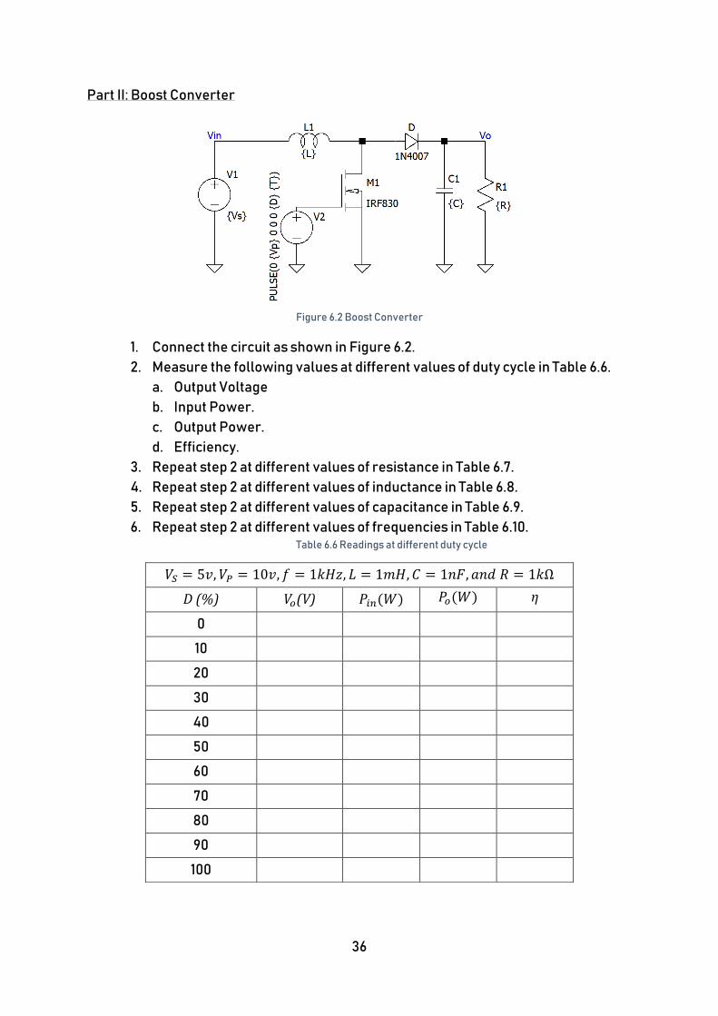
Part II: Boost Converter
Figure 6.2 Boost Converter
1. Connect the circuit as shown in Figure 6.2.
2. Measure the following values at different values of duty cycle in Table 6.6.
a. Output Voltage
b. Input Power.
c. Output Power.
d. Efficiency.
3. Repeat step 2 at different values of resistance in Table 6.7.
4. Repeat step 2 at different values of inductance in Table 6.8.
5. Repeat step 2 at different values of capacitance in Table 6.9.
6. Repeat step 2 at different values of frequencies in Table 6.10. Table 6.6 Readings at different duty cycle
𝑉𝑆 = 5𝑣, 𝑉𝑃 = 10𝑣, 𝑓 = 1𝑘𝐻𝑧, 𝐿 = 1𝑚𝐻, 𝐶 = 1𝑛𝐹, 𝑎𝑛𝑑 𝑅 = 1𝑘Ω
D (%) 𝑉𝑜(V) 𝑃𝑖𝑛(𝑊) 𝑃𝑜(𝑊) η
0
10
20
30
40
50
60
70
80
90
100
37
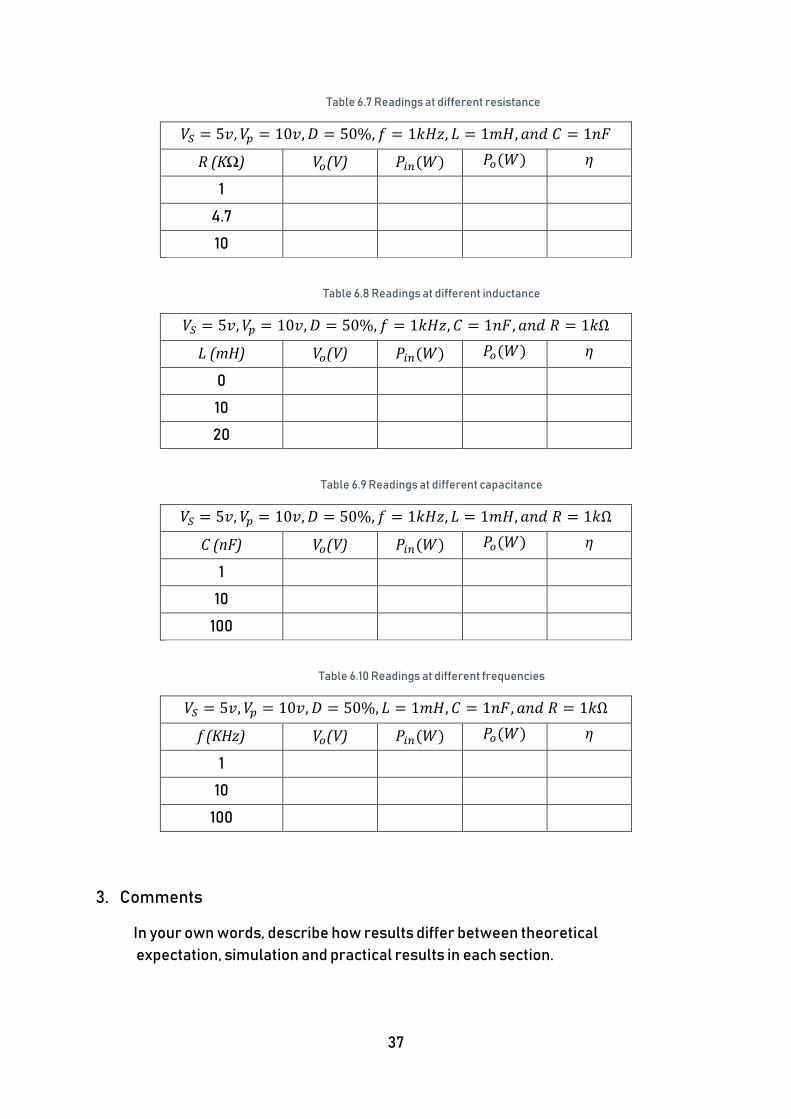
Table 6.7 Readings at different resistance
𝑉𝑆 = 5𝑣, 𝑉𝑝 = 10𝑣, 𝐷 = 50%, 𝑓 = 1𝑘𝐻𝑧, 𝐿 = 1𝑚𝐻, 𝑎𝑛𝑑 𝐶 = 1𝑛𝐹
R (KΩ) 𝑉𝑜(V) 𝑃𝑖𝑛(𝑊) 𝑃𝑜(𝑊) η
1
4.7
10
Table 6.8 Readings at different inductance
𝑉𝑆 = 5𝑣, 𝑉𝑝 = 10𝑣, 𝐷 = 50%, 𝑓 = 1𝑘𝐻𝑧, 𝐶 = 1𝑛𝐹, 𝑎𝑛𝑑 𝑅 = 1𝑘Ω
L (mH) 𝑉𝑜(V) 𝑃𝑖𝑛(𝑊) 𝑃𝑜(𝑊) η
0
10
20
Table 6.9 Readings at different capacitance
𝑉𝑆 = 5𝑣, 𝑉𝑝 = 10𝑣, 𝐷 = 50%, 𝑓 = 1𝑘𝐻𝑧, 𝐿 = 1𝑚𝐻, 𝑎𝑛𝑑 𝑅 = 1𝑘Ω
C (nF) 𝑉𝑜(V) 𝑃𝑖𝑛(𝑊) 𝑃𝑜(𝑊) η
1
10
100
Table 6.10 Readings at different frequencies
𝑉𝑆 = 5𝑣, 𝑉𝑝 = 10𝑣, 𝐷 = 50%, 𝐿 = 1𝑚𝐻, 𝐶 = 1𝑛𝐹, 𝑎𝑛𝑑 𝑅 = 1𝑘Ω
f (KHz) 𝑉𝑜(V) 𝑃𝑖𝑛(𝑊) 𝑃𝑜(𝑊) η
1
10
100
3. Comments
In your own words, describe how results differ between theoretical
expectation, simulation and practical results in each section.
38
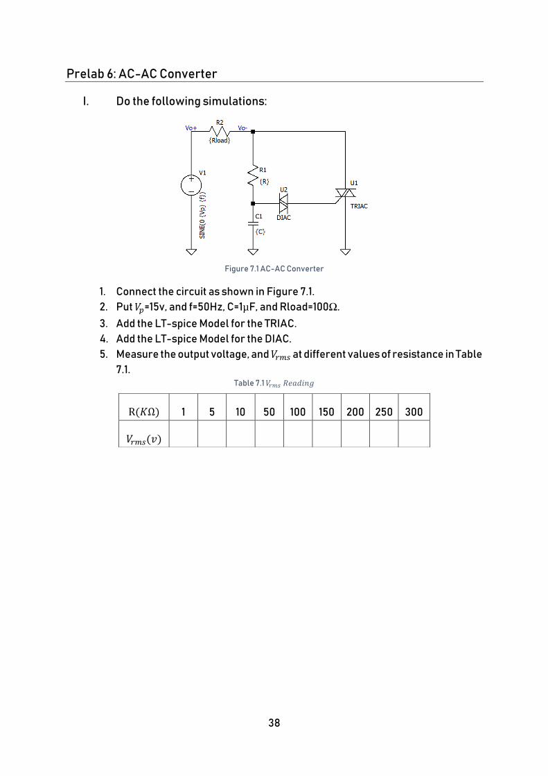
Prelab 6: AC-AC Converter
I. Do the following simulations:
Figure 7.1 AC-AC Converter
1. Connect the circuit as shown in Figure 7.1.
2. Put 𝑉𝑝=15v, and f=50Hz, C=1µF, and Rload=100Ω.
3. Add the LT-spice Model for the TRIAC.
4. Add the LT-spice Model for the DIAC.
5. Measure the output voltage, and 𝑉𝑟𝑚𝑠 at different values of resistance in Table
7.1. Table 7.1 𝑉𝑟𝑚𝑠 𝑅𝑒𝑎𝑑𝑖𝑛𝑔
R(𝐾Ω) 1 5 10 50 100 150 200 250 300
𝑉𝑟𝑚𝑠(𝑣)
39
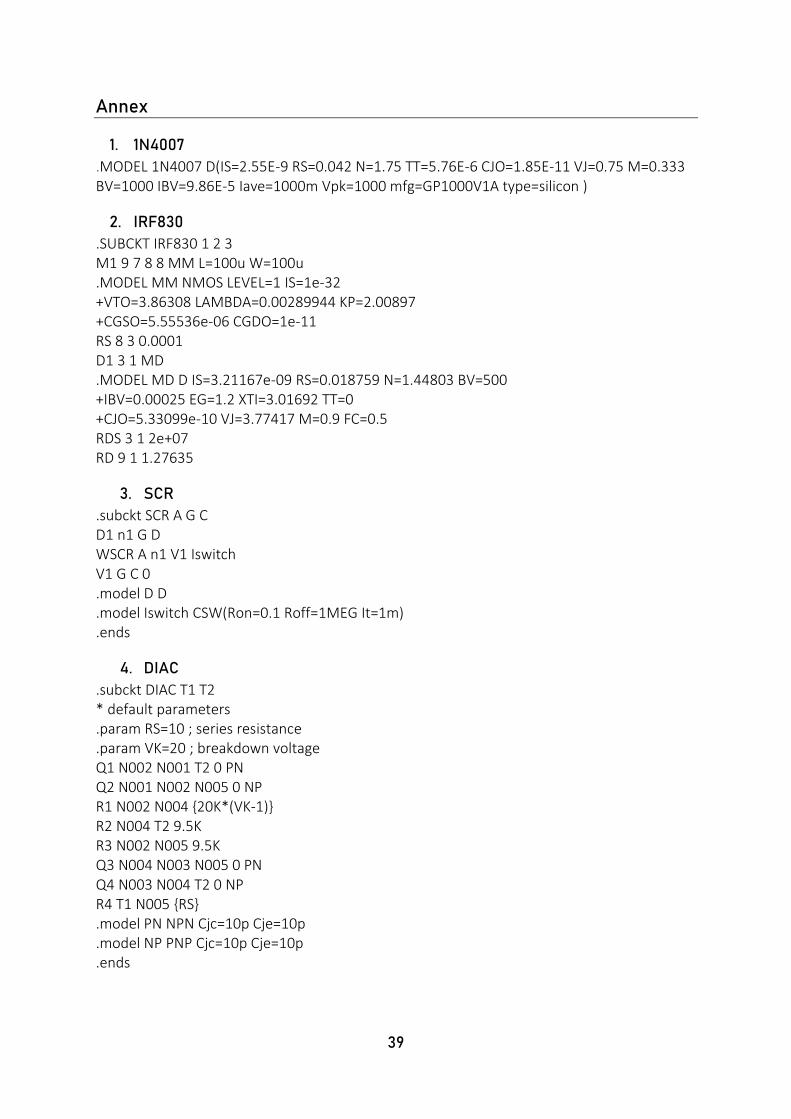
Annex
1. 1N4007
.MODEL 1N4007 D(IS=2.55E-9 RS=0.042 N=1.75 TT=5.76E-6 CJO=1.85E-11 VJ=0.75 M=0.333 BV=1000 IBV=9.86E-5 Iave=1000m Vpk=1000 mfg=GP1000V1A type=silicon )
2. IRF830
.SUBCKT IRF830 1 2 3 M1 9 7 8 8 MM L=100u W=100u .MODEL MM NMOS LEVEL=1 IS=1e-32 +VTO=3.86308 LAMBDA=0.00289944 KP=2.00897 +CGSO=5.55536e-06 CGDO=1e-11 RS 8 3 0.0001 D1 3 1 MD .MODEL MD D IS=3.21167e-09 RS=0.018759 N=1.44803 BV=500 +IBV=0.00025 EG=1.2 XTI=3.01692 TT=0 +CJO=5.33099e-10 VJ=3.77417 M=0.9 FC=0.5 RDS 3 1 2e+07 RD 9 1 1.27635
3. SCR
.subckt SCR A G C D1 n1 G D WSCR A n1 V1 Iswitch V1 G C 0 .model D D .model Iswitch CSW(Ron=0.1 Roff=1MEG It=1m) .ends
4. DIAC
.subckt DIAC T1 T2 * default parameters .param RS=10 ; series resistance .param VK=20 ; breakdown voltage Q1 N002 N001 T2 0 PN Q2 N001 N002 N005 0 NP R1 N002 N004 20K*(VK-1) R2 N004 T2 9.5K R3 N002 N005 9.5K Q3 N004 N003 N005 0 PN Q4 N003 N004 T2 0 NP R4 T1 N005 RS .model PN NPN Cjc=10p Cje=10p .model NP PNP Cjc=10p Cje=10p .ends

40
5. TRIAC
.subckt TRIAC MT2 G MT1
.param R=10K Q1 N001 G MT1 0 NP Q2 N001 N002 MT2 0 NP Q3 N002 N001 MT1 0 PN Q4 G N001 MT2 0 PN R1 MT2 N002 R R2 G MT1 R .model PN NPN Cjc=10p Cje=10p .model NP PNP Cjc=10p Cje=10p .ends