Embed Size (px)
Citation preview

Freescale SemiconductorApplication Note
© 2008–2014 Freescale Semiconductor, Inc. All rights reserved.
This application note describes the generally recommended connections for new designs based on the Freescale Semiconductor MPC837x processors:
• MPC8377E• MPC8378E• MPC8379E
The design checklist may also apply to future bus- or footprint-compatible processors. It can also serve as a useful guide to debugging a newly designed system by highlighting those areas of a design that merit special attention during initial system startup.
For updates to this document, refer to the website listed on the back cover of this document.
Document Number: AN3665Rev. 5, 04/2014
Contents1. Locating PowerQUICC II Pro Resources . . . . . . . . . . 22. Designing Power . . . . . . . . . . . . . . . . . . . . . . . . . . . . . 33. Configuring Clocking . . . . . . . . . . . . . . . . . . . . . . . . 104. Using Power-On Reset and Reset Configurations . . 145. Operating JTAG and Debug . . . . . . . . . . . . . . . . . . . 196. Designing with Functional Blocks . . . . . . . . . . . . . . 237. Revision History . . . . . . . . . . . . . . . . . . . . . . . . . . . . 54
PowerQUICC Design ChecklistFor PowerQUICC II Pro (MPC837x) Devices

PowerQUICC Design Checklist, Rev. 5
2 Freescale Semiconductor
Locating PowerQUICC II Pro Resources
1 Locating PowerQUICC II Pro ResourcesThis section describes resources for simplifying the first phase of design. Before designing a system with a PowerQUICC II Pro device, become familiar with the available documentation, software, models, and tools.
1.1 ReferencesSome of the following reference documents may be available only under a non-disclosure agreement (NDA). For those documents, contact your local field applications engineer or sales representative to obtain a copy.
• Collateral— MPC8379E PowerQUICC II Pro Integrated Host Processor Family Reference Manual
(MPC8379ERM)— MPC8379E PowerQUICC II Pro Integrated Host Processor Family Chip Errata
(MPC8379ECE)— MPC8377E PowerQUICC II Pro Integrated Host Processor Hardware Specifications
(MPC8377EEC)— MPC8378E PowerQUICC II Pro Integrated Host Processor Hardware Specifications
(MPC8378EEC)— MPC8379E PowerQUICC II Pro Integrated Host Processor Hardware Specifications
(MPC8379EEC)• Tools
— Boot sequencer generator tool— UPM programming tool
• Models— IBIS— BSDL
1.2 Device ErrataThe MPC8379ECE device errata document describes the latest fixes and work arounds for the PowerQUICC II Pro family of devices. Carefully study these documents before starting a design with the respective PowerQUICC II Pro device.
1.3 Boot Sequencer ToolThe PowerQUICC II Pro boot sequencer allows configuration of any memory-mapped register before power-on reset (POR) completes. The register data to be changed is stored in an I2C EEPROM. The boot sequencer tool is a C code file. When compiled and given a sample data file, it generates the appropriate raw data format as outlined in the MPC8379E PowerQUICC II Pro Integrated Host Processor Family Reference Manual, that is, an s-record file that can be used to program the EEPROM.

PowerQUICC Design Checklist, Rev. 5
Freescale Semiconductor 3
Designing Power
1.4 UPM Programming ToolThe UPM programming tool GUI is a user-friendly interface for programming all three PowerQUICC II Pro UPM machines. The GUI consists of a wave editor, table editor, and report generator. The user can directly edit the waveform or RAM array, and the report generator prints out the UPM RAM array for use in a C program.
The UPM programming tool can be found on the MPC837x product page at the website listed on the back cover of this document.
1.5 Available TrainingOur third-party partners are part of an extensive Freescale Alliance Program. The current training partners can be found on our website under Freescale Alliance Program.Training material from past Smart Network Developer’s Forums and Freescale Technology Forums are also available. These training modules are a valuable resource in understanding the PowerQUICC II Pro. This material is also available at the website listed on the back cover of this document.
1.6 Product RevisionsTable 1 lists the SVR and PVR values for each version and revision of the MPC837x TePBGA family.
2 Designing PowerThis section provides design considerations for the PowerQUICC II Pro power supplies, as well as power sequencing. For information on PowerQUICC II Pro AC and DC electrical specifications and thermal characteristics, refer to the MPC8377E, MPC8378E, and MPC8379E hardware specifications (MPC8377EEC, MPC8378EEC, and MPC8379EEC). For power sequencing recommendations, refer to Section 2.3, “Power Sequencing.”
Table 1. PowerQUICC II Pro MPC837x TePBGA Product Revisions
DeviceSVR PVR
Rev 1.0 Rev. 2.1 Rev. 1.0 Rev. 2.1
MPC8377 0x80C7_00100x80C6_0010
0x80C7_00210x80C6_0021
0x8086_1010 0x8086_1011
MPC8377E
MPC8378 0x80C5_00100x80C4_0010
0x80C5_00210x80C4_0021MPC8378E
MPC8379 0x80C3_00100x80C2_0010
0x80C3_00210x80C2_0021MPC8379E
PowerQUICC Design Checklist, Rev. 5
4 Freescale Semiconductor
Designing Power
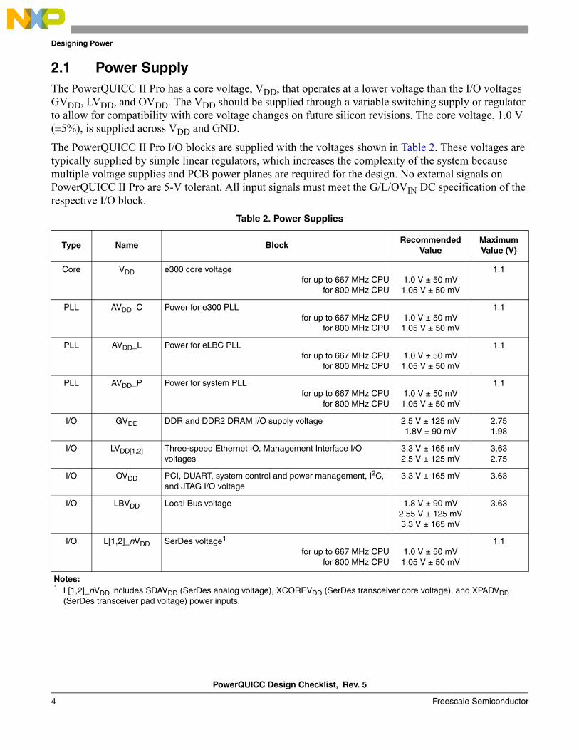
2.1 Power SupplyThe PowerQUICC II Pro has a core voltage, VDD, that operates at a lower voltage than the I/O voltages GVDD, LVDD, and OVDD. The VDD should be supplied through a variable switching supply or regulator to allow for compatibility with core voltage changes on future silicon revisions. The core voltage, 1.0 V (±5%), is supplied across VDD and GND.
The PowerQUICC II Pro I/O blocks are supplied with the voltages shown in Table 2. These voltages are typically supplied by simple linear regulators, which increases the complexity of the system because multiple voltage supplies and PCB power planes are required for the design. No external signals on PowerQUICC II Pro are 5-V tolerant. All input signals must meet the G/L/OVIN DC specification of the respective I/O block.
Table 2. Power Supplies
Type Name BlockRecommended
ValueMaximum Value (V)
Core VDD e300 core voltagefor up to 667 MHz CPU
for 800 MHz CPU1.0 V ± 50 mV1.05 V ± 50 mV
1.1
PLL AVDD_C Power for e300 PLLfor up to 667 MHz CPU
for 800 MHz CPU1.0 V ± 50 mV1.05 V ± 50 mV
1.1
PLL AVDD_L Power for eLBC PLLfor up to 667 MHz CPU
for 800 MHz CPU1.0 V ± 50 mV1.05 V ± 50 mV
1.1
PLL AVDD_P Power for system PLLfor up to 667 MHz CPU
for 800 MHz CPU1.0 V ± 50 mV1.05 V ± 50 mV
1.1
I/O GVDD DDR and DDR2 DRAM I/O supply voltage 2.5 V ± 125 mV1.8V ± 90 mV
2.751.98
I/O LVDD[1,2] Three-speed Ethernet IO, Management Interface I/O voltages
3.3 V ± 165 mV2.5 V ± 125 mV
3.632.75
I/O OVDD PCI, DUART, system control and power management, I2C, and JTAG I/O voltage
3.3 V ± 165 mV 3.63
I/O LBVDD Local Bus voltage 1.8 V ± 90 mV2.55 V ± 125 mV3.3 V ± 165 mV
3.63
I/O L[1,2]_nVDD SerDes voltage1
for up to 667 MHz CPUfor 800 MHz CPU
1.0 V ± 50 mV1.05 V ± 50 mV
1.1
Notes:1 L[1,2]_nVDD includes SDAVDD (SerDes analog voltage), XCOREVDD (SerDes transceiver core voltage), and XPADVDD
(SerDes transceiver pad voltage) power inputs.
PowerQUICC Design Checklist, Rev. 5
Freescale Semiconductor 5
Designing Power
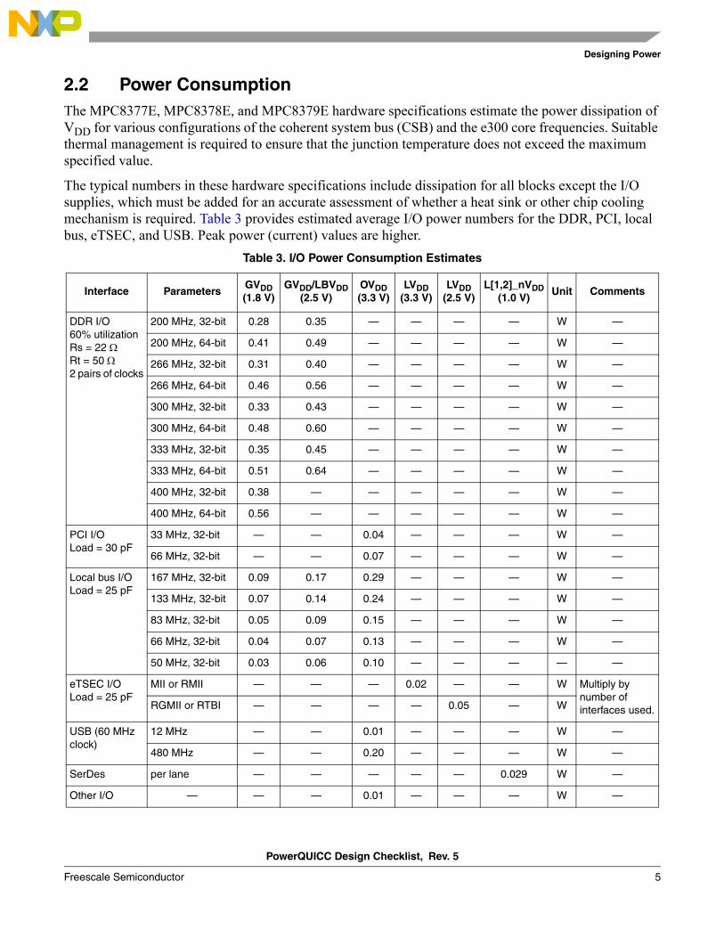
2.2 Power ConsumptionThe MPC8377E, MPC8378E, and MPC8379E hardware specifications estimate the power dissipation of VDD for various configurations of the coherent system bus (CSB) and the e300 core frequencies. Suitable thermal management is required to ensure that the junction temperature does not exceed the maximum specified value.
The typical numbers in these hardware specifications include dissipation for all blocks except the I/O supplies, which must be added for an accurate assessment of whether a heat sink or other chip cooling mechanism is required. Table 3 provides estimated average I/O power numbers for the DDR, PCI, local bus, eTSEC, and USB. Peak power (current) values are higher.
Table 3. I/O Power Consumption Estimates
Interface ParametersGVDD(1.8 V)
GVDD/LBVDD(2.5 V)
OVDD (3.3 V)
LVDD (3.3 V)
LVDD (2.5 V)
L[1,2]_nVDD(1.0 V)
Unit Comments
DDR I/O60% utilizationRs = 22 ΩRt = 50 Ω2 pairs of clocks
200 MHz, 32-bit 0.28 0.35 — — — — W —
200 MHz, 64-bit 0.41 0.49 — — — — W —
266 MHz, 32-bit 0.31 0.40 — — — — W —
266 MHz, 64-bit 0.46 0.56 — — — — W —
300 MHz, 32-bit 0.33 0.43 — — — — W —
300 MHz, 64-bit 0.48 0.60 — — — — W —
333 MHz, 32-bit 0.35 0.45 — — — — W —
333 MHz, 64-bit 0.51 0.64 — — — — W —
400 MHz, 32-bit 0.38 — — — — — W —
400 MHz, 64-bit 0.56 — — — — — W —
PCI I/OLoad = 30 pF
33 MHz, 32-bit — — 0.04 — — — W —
66 MHz, 32-bit — — 0.07 — — — W —
Local bus I/OLoad = 25 pF
167 MHz, 32-bit 0.09 0.17 0.29 — — — W —
133 MHz, 32-bit 0.07 0.14 0.24 — — — W —
83 MHz, 32-bit 0.05 0.09 0.15 — — — W —
66 MHz, 32-bit 0.04 0.07 0.13 — — — W —
50 MHz, 32-bit 0.03 0.06 0.10 — — — — —
eTSEC I/OLoad = 25 pF
MII or RMII — — — 0.02 — — W Multiply by number of interfaces used.RGMII or RTBI — — — — 0.05 — W
USB (60 MHz clock)
12 MHz — — 0.01 — — — W —
480 MHz — — 0.20 — — — W —
SerDes per lane — — — — — 0.029 W —
Other I/O — — — 0.01 — — — W —

PowerQUICC Design Checklist, Rev. 5
6 Freescale Semiconductor
Designing Power
2.3 Power SequencingThe MPC837x requires its power rails to be applied in a specific sequence in order to ensure proper device operation. From a system standpoint, if the I/O power supplies ramp up before the VDD core supply stabilizes, there may be a period of time when the I/O pins are driven to a logic one or logic zero state. After the power is stable, as long as PORESET is asserted, most IP pins are released to high impedance. To minimize the time that I/O pins are actively driven, apply core voltage before I/O voltage and assert PORESET before the power supplies fully ramp up. For further details on the power sequencing requirements for the MPC837x, see the MPC8377E, MPC8378E, and MPC8379E hardware specifications.
2.4 Power PlanesEach VDD pin should be provided with a low-impedance path to the board power supply. Similarly, each ground pin should be provided with a low-impedance path to ground. The power supply pins drive distinct groups of logic on chip. The capacitor leads and associated printed-circuit traces connecting to chip VDD and ground should be kept to less than half an inch per capacitor lead.
2.5 DecouplingDue to large address and data buses and high operating frequencies, the PowerQUICC II Pro can generate transient power surges and high-frequency noise in its power supply, especially while driving large capacitive loads. This noise must be prevented from reaching other components in the PowerQUICC II Pro system, and it requires a clean, tightly regulated source of power. Therefore, the system designer should place at least one decoupling capacitor at each VDD, GVDD, LVDD, LBVDD, and OVDD pin. These decoupling capacitors should receive their power from separate VDD, GVDD, LVDD, LBVDD, OVDD, and GND power planes in the PCB, using short traces to minimize inductance. Capacitors can be placed directly under the device using a standard escape pattern. Other capacitors can surround the part.
These capacitors should have a value of 0.01 or 0.1 µF. Only ceramic surface mount technology (SMT) capacitors should be used to minimize lead inductance.
In addition, several bulk storage capacitors should be distributed around the PCB, feeding the VDD, GVDD, LVDD, LBVDD, and OVDD planes, to enable quick recharging of the smaller chip capacitors. These bulk capacitors should have a low equivalent series resistance (ESR) rating to ensure quick response time. They should also connect to the power and ground planes through two vias to minimize inductance. The suggested bulk capacitors are 100–300 µF.
Use simulation to minimize noise on the power supplies before proceeding into the PCB design and manufacturing stage of development.
2.6 Core PLL Power Supply FilteringEach PowerQUICC II Pro PLL obtains power through independent power supply pins (AVDD_C, AVDD_L, and AVDD_P). The AVDD level should always equal VDD and preferably be derived directly from VDD through a low frequency filter scheme.
PowerQUICC Design Checklist, Rev. 5
Freescale Semiconductor 7
Designing Power
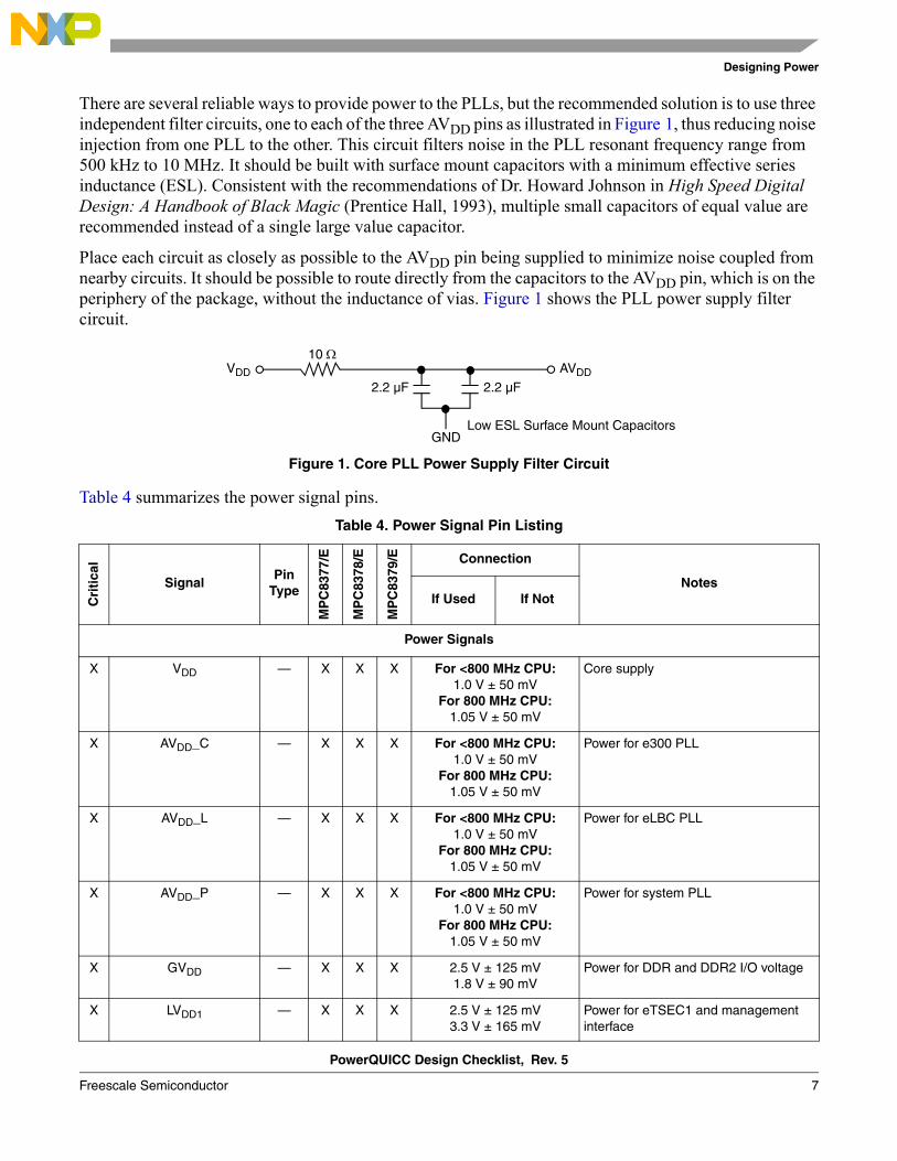
There are several reliable ways to provide power to the PLLs, but the recommended solution is to use three independent filter circuits, one to each of the three AVDD pins as illustrated in Figure 1, thus reducing noise injection from one PLL to the other. This circuit filters noise in the PLL resonant frequency range from 500 kHz to 10 MHz. It should be built with surface mount capacitors with a minimum effective series inductance (ESL). Consistent with the recommendations of Dr. Howard Johnson in High Speed Digital Design: A Handbook of Black Magic (Prentice Hall, 1993), multiple small capacitors of equal value are recommended instead of a single large value capacitor.
Place each circuit as closely as possible to the AVDD pin being supplied to minimize noise coupled from nearby circuits. It should be possible to route directly from the capacitors to the AVDD pin, which is on the periphery of the package, without the inductance of vias. Figure 1 shows the PLL power supply filter circuit.
Figure 1. Core PLL Power Supply Filter Circuit
Table 4 summarizes the power signal pins.Table 4. Power Signal Pin Listing
Cri
tica
l
SignalPin
Type
MP
C83
77/E
MP
C83
78/E
MP
C83
79/E Connection
NotesIf Used If Not
Power Signals
X VDD — X X X For <800 MHz CPU:1.0 V ± 50 mV
For 800 MHz CPU:1.05 V ± 50 mV
Core supply
X AVDD_C — X X X For <800 MHz CPU:1.0 V ± 50 mV
For 800 MHz CPU:1.05 V ± 50 mV
Power for e300 PLL
X AVDD_L — X X X For <800 MHz CPU:1.0 V ± 50 mV
For 800 MHz CPU:1.05 V ± 50 mV
Power for eLBC PLL
X AVDD_P — X X X For <800 MHz CPU:1.0 V ± 50 mV
For 800 MHz CPU:1.05 V ± 50 mV
Power for system PLL
X GVDD — X X X 2.5 V ± 125 mV1.8 V ± 90 mV
Power for DDR and DDR2 I/O voltage
X LVDD1 — X X X 2.5 V ± 125 mV3.3 V ± 165 mV
Power for eTSEC1 and management interface
VDD AVDD
2.2 µF 2.2 µF
GNDLow ESL Surface Mount Capacitors
10 Ω
PowerQUICC Design Checklist, Rev. 5
8 Freescale Semiconductor
Designing Power
2.7 SerDes Power SupplyThe power supplied to the SerDes PLL must be filtered to ensure a stable internal clock. It must also use a proper decoupling scheme to ensure a clean and tightly regulated source of power.
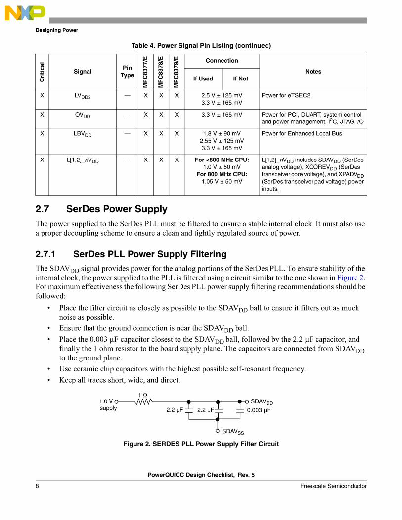
2.7.1 SerDes PLL Power Supply FilteringThe SDAVDD signal provides power for the analog portions of the SerDes PLL. To ensure stability of the internal clock, the power supplied to the PLL is filtered using a circuit similar to the one shown in Figure 2. For maximum effectiveness the following SerDes PLL power supply filtering recommendations should be followed:
• Place the filter circuit as closely as possible to the SDAVDD ball to ensure it filters out as much noise as possible.
• Ensure that the ground connection is near the SDAVDD ball.• Place the 0.003 µF capacitor closest to the SDAVDD ball, followed by the 2.2 µF capacitor, and
finally the 1 ohm resistor to the board supply plane. The capacitors are connected from SDAVDD to the ground plane.
• Use ceramic chip capacitors with the highest possible self-resonant frequency. • Keep all traces short, wide, and direct.
Figure 2. SERDES PLL Power Supply Filter Circuit
X LVDD2 — X X X 2.5 V ± 125 mV3.3 V ± 165 mV
Power for eTSEC2
X OVDD — X X X 3.3 V ± 165 mV Power for PCI, DUART, system control and power management, I2C, JTAG I/O
X LBVDD — X X X 1.8 V ± 90 mV2.55 V ± 125 mV3.3 V ± 165 mV
Power for Enhanced Local Bus
X L[1,2]_nVDD — X X X For <800 MHz CPU:1.0 V ± 50 mV
For 800 MHz CPU:1.05 V ± 50 mV
L[1,2]_nVDD includes SDAVDD (SerDes analog voltage), XCOREVDD (SerDes transceiver core voltage), and XPADVDD (SerDes transceiver pad voltage) power inputs.
Table 4. Power Signal Pin Listing (continued)C
riti
cal
SignalPin
Type
MP
C83
77/E
MP
C83
78/E
MP
C83
79/E Connection
NotesIf Used If Not
1.0 V SDAVDD
2.2 µF 2.2 µF
SDAVSS
1 Ω
0.003 µFsupply

PowerQUICC Design Checklist, Rev. 5
Freescale Semiconductor 9
Designing Power
2.7.2 SerDes Power Supply DecouplingTo ensure low jitter on transmit and reliable recovery of data in the receiver, the following decoupling scheme is recommended:
• Only surface mount technology (SMT) capacitors should be used to minimize inductance.• Connections from all capacitors to power and ground should be done with multiple vias to further
reduce inductance.• The board should have about 10 x 10 µF SMT ceramic chip capacitors as close as possible to the
supply balls of the device. Where the board has blind vias, these capacitors should be placed directly below the chip supply and ground connections. Where the board does not have blind vias, these capacitors should be placed in a ring around the device as close to the supply and ground connections as possible.
• There should be a 1 µF ceramic chip capacitor on each side of the device. This should be done for all supplies.
• Between the device and any voltage regulator there should be a 10 µF, low equivalent series resistance (ESR) SMT tantalum chip capacitor and a 100 µF, low ESR SMT tantalum chip capacitor. This should be done for all supplies.
PowerQUICC Design Checklist, Rev. 5
10 Freescale Semiconductor
Configuring Clocking
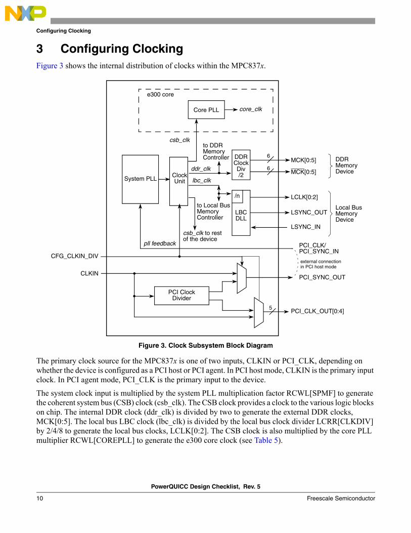
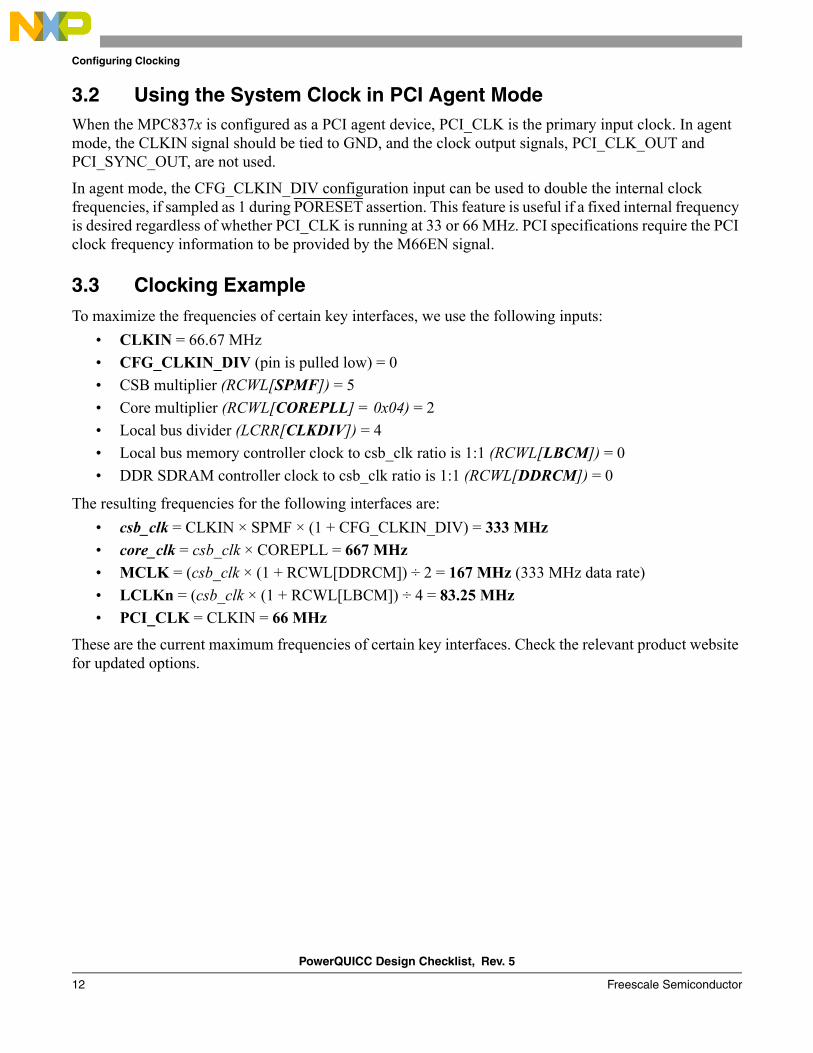
3 Configuring ClockingFigure 3 shows the internal distribution of clocks within the MPC837x.
Figure 3. Clock Subsystem Block Diagram
The primary clock source for the MPC837x is one of two inputs, CLKIN or PCI_CLK, depending on whether the device is configured as a PCI host or PCI agent. In PCI host mode, CLKIN is the primary input clock. In PCI agent mode, PCI_CLK is the primary input to the device.
The system clock input is multiplied by the system PLL multiplication factor RCWL[SPMF] to generate the coherent system bus (CSB) clock (csb_clk). The CSB clock provides a clock to the various logic blocks on chip. The internal DDR clock (ddr_clk) is divided by two to generate the external DDR clocks, MCK[0:5]. The local bus LBC clock (lbc_clk) is divided by the local bus clock divider LCRR[CLKDIV] by 2/4/8 to generate the local bus clocks, LCLK[0:2]. The CSB clock is also multiplied by the core PLL multiplier RCWL[COREPLL] to generate the e300 core clock (see Table 5).
Core PLL
System PLL
DDR
LBC
LSYNC_IN
LSYNC_OUT
LCLK[0:2]
MCK[0:5]
MCK[0:5]
core_clk
e300 core
csb_clk to rest
CLKIN
csb_clk
6
6
DDRMemory
Local Bus
PCI_CLK_OUT[0:4]
PCI_SYNC_OUT
PCI_CLK/
ClockUnit
of the device
ddr_clk
lbc_clk
CFG_CLKIN_DIV
PCI Clock
PCI_SYNC_IN
Device
MemoryDevice
/n
to Local BusMemoryController
to DDRMemoryController
DLL
ClockDiv/2
Divider
5
pll feedback
external connectionin PCI host mode
PowerQUICC Design Checklist, Rev. 5
Freescale Semiconductor 11
Configuring Clocking
Because there are no default settings for the system and core PLLs, the system and core PLL multipliers SPMF and COREPLL must be configured in the reset configuration word low register (RCWLR), which is loaded at power-on reset or by one of the hard-coded reset options.
3.1 Using the System Clock in PCI Host ModeWhen the MPC837x is configured as a PCI host device (RCWH[PCIHOST] = 1), CLKIN is the primary input clock. CLKIN feeds the PCI clock divider (divide by 2) and the PCI_SYNC_OUT and PCI_CLK_OUT multiplexers. The CFG_CLKIN_DIV input is sampled during PORESET to determine whether CLKIN is divided by two.
PCI_SYNC_OUT connects externally to PCI_SYNC_IN so the internal clock subsystem can synchronize to the system PCI clocks. The PCI_SYNC_IN then feeds into the system PLL to generate the CSB clock. PCI_SYNC_OUT must be connected properly to PCI_SYNC_IN, with equal delay to all PCI agent devices in the system.
Table 5. Clocking Quick Reference
Functional Block Clock Derivation
System clock(csb_clk)
PCI host mode: PCI_SYNC_IN × RCWLR[SPMF] × [1 + CFG_CLKIN_DIV]PCI agent mode: PCI_CLK × RCWLR[SPMF] × [1 + CFG_CLKIN_DIV]
e300 core clock(core_clk)
csb_clk × RCWLR[COREPLL]
DDR clock(MCK/MCK)
ddr_clk ÷ 2,where ddr_clk = csb_clk × (1 + RCWLR[DDRCM])
Local bus clock(LCLK)
lbc_clk ÷ CLKDIV,where lbc_clk = csb_clk × (1 + RCWLR[LBCM])
PCI output clock(PCI_CLK_OUT)
CLKIN ÷ [1 + CFG_CLKIN_DIV]
eTSEC1 / eTSEC2 clock(EC_GTX_CLK125)
125 MHz external clock
SerDes reference clock 1(SD_REF_CLK_1/SD_REF_CLK_1)
SATA: 100/125/150 MHz external clockSGMII: 100/125 MHz external clock
SerDes reference clock 2(SD_REF_CLK_2/SD_REF_CLK_2)
SATA: 100/125/150 MHz external clockPCI Express®: 100 MHz external clock
I2C clock(IIC_SCL)
IIC_SCL1: csb_clk ÷ SCCR[SDHCCM] ÷ (I2CnFDR ratio)IIC_SCL2: csb_clk ÷ I2CnFDR ratio
USB clock(USBDR_CLK)
60 MHz/30 MHz external clock
Real time clock(RTC_CLK)
External clock
PowerQUICC Design Checklist, Rev. 5
12 Freescale Semiconductor
Configuring Clocking
3.2 Using the System Clock in PCI Agent ModeWhen the MPC837x is configured as a PCI agent device, PCI_CLK is the primary input clock. In agent mode, the CLKIN signal should be tied to GND, and the clock output signals, PCI_CLK_OUT and PCI_SYNC_OUT, are not used.
In agent mode, the CFG_CLKIN_DIV configuration input can be used to double the internal clock frequencies, if sampled as 1 during PORESET assertion. This feature is useful if a fixed internal frequency is desired regardless of whether PCI_CLK is running at 33 or 66 MHz. PCI specifications require the PCI clock frequency information to be provided by the M66EN signal.
3.3 Clocking ExampleTo maximize the frequencies of certain key interfaces, we use the following inputs:
• CLKIN = 66.67 MHz• CFG_CLKIN_DIV (pin is pulled low) = 0• CSB multiplier (RCWL[SPMF]) = 5• Core multiplier (RCWL[COREPLL] = 0x04) = 2• Local bus divider (LCRR[CLKDIV]) = 4• Local bus memory controller clock to csb_clk ratio is 1:1 (RCWL[LBCM]) = 0• DDR SDRAM controller clock to csb_clk ratio is 1:1 (RCWL[DDRCM]) = 0
The resulting frequencies for the following interfaces are:• csb_clk = CLKIN × SPMF × (1 + CFG_CLKIN_DIV) = 333 MHz• core_clk = csb_clk × COREPLL = 667 MHz• MCLK = (csb_clk × (1 + RCWL[DDRCM]) ÷ 2 = 167 MHz (333 MHz data rate)• LCLKn = (csb_clk × (1 + RCWL[LBCM]) ÷ 4 = 83.25 MHz• PCI_CLK = CLKIN = 66 MHz
These are the current maximum frequencies of certain key interfaces. Check the relevant product website for updated options.
PowerQUICC Design Checklist, Rev. 5
Freescale Semiconductor 13
Configuring Clocking
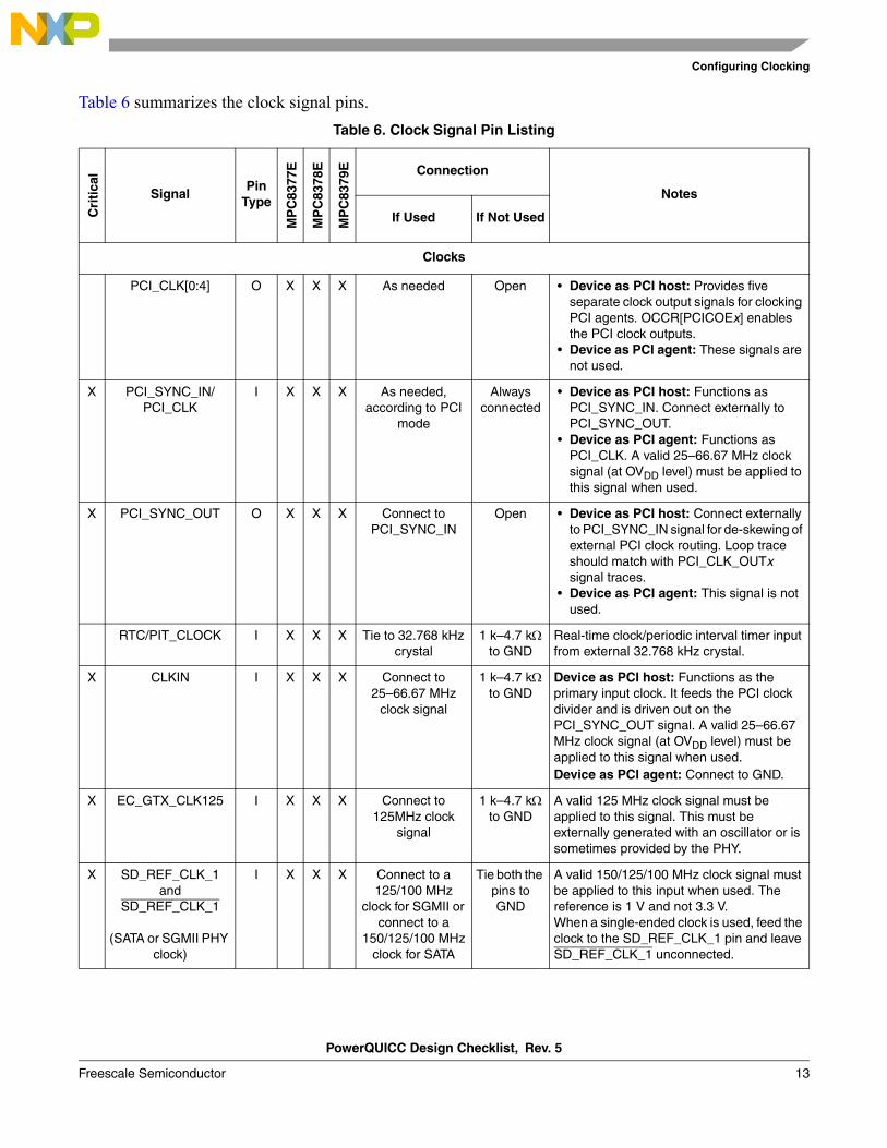
Table 6 summarizes the clock signal pins.Table 6. Clock Signal Pin Listing
Cri
tica
l
SignalPin
Type
MP
C83
77E
MP
C83
78E
MP
C83
79E Connection
Notes
If Used If Not Used
Clocks
PCI_CLK[0:4] O X X X As needed Open • Device as PCI host: Provides five separate clock output signals for clocking PCI agents. OCCR[PCICOEx] enables the PCI clock outputs.
• Device as PCI agent: These signals are not used.
X PCI_SYNC_IN/PCI_CLK
I X X X As needed, according to PCI
mode
Always connected
• Device as PCI host: Functions as PCI_SYNC_IN. Connect externally to PCI_SYNC_OUT.
• Device as PCI agent: Functions as PCI_CLK. A valid 25–66.67 MHz clock signal (at OVDD level) must be applied to this signal when used.
X PCI_SYNC_OUT O X X X Connect to PCI_SYNC_IN
Open • Device as PCI host: Connect externally to PCI_SYNC_IN signal for de-skewing of external PCI clock routing. Loop trace should match with PCI_CLK_OUTx signal traces.
• Device as PCI agent: This signal is not used.
RTC/PIT_CLOCK I X X X Tie to 32.768 kHz crystal
1 k–4.7 kΩ to GND
Real-time clock/periodic interval timer input from external 32.768 kHz crystal.
X CLKIN I X X X Connect to 25–66.67 MHz
clock signal
1 k–4.7 kΩ to GND
Device as PCI host: Functions as the primary input clock. It feeds the PCI clock divider and is driven out on the PCI_SYNC_OUT signal. A valid 25–66.67 MHz clock signal (at OVDD level) must be applied to this signal when used.Device as PCI agent: Connect to GND.
X EC_GTX_CLK125 I X X X Connect to 125MHz clock
signal
1 k–4.7 kΩ to GND
A valid 125 MHz clock signal must be applied to this signal. This must be externally generated with an oscillator or is sometimes provided by the PHY.
X SD_REF_CLK_1 and
SD_REF_CLK_1
(SATA or SGMII PHY clock)
I X X X Connect to a 125/100 MHz
clock for SGMII or connect to a
150/125/100 MHz clock for SATA
Tie both the pins to GND
A valid 150/125/100 MHz clock signal must be applied to this input when used. The reference is 1 V and not 3.3 V. When a single-ended clock is used, feed the clock to the SD_REF_CLK_1 pin and leave SD_REF_CLK_1 unconnected.
PowerQUICC Design Checklist, Rev. 5
14 Freescale Semiconductor
Using Power-On Reset and Reset Configurations
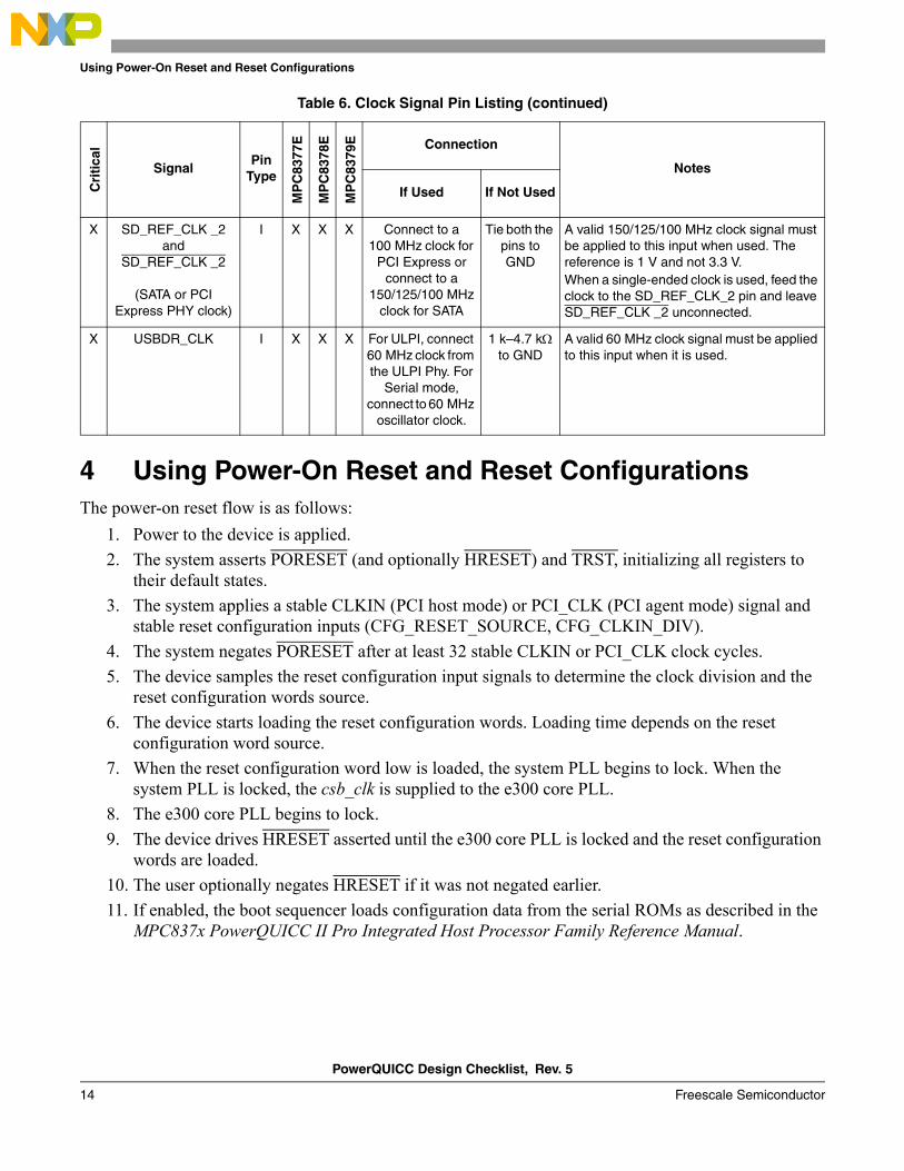
4 Using Power-On Reset and Reset ConfigurationsThe power-on reset flow is as follows:
1. Power to the device is applied.2. The system asserts PORESET (and optionally HRESET) and TRST, initializing all registers to
their default states.3. The system applies a stable CLKIN (PCI host mode) or PCI_CLK (PCI agent mode) signal and
stable reset configuration inputs (CFG_RESET_SOURCE, CFG_CLKIN_DIV).4. The system negates PORESET after at least 32 stable CLKIN or PCI_CLK clock cycles.5. The device samples the reset configuration input signals to determine the clock division and the
reset configuration words source.6. The device starts loading the reset configuration words. Loading time depends on the reset
configuration word source.7. When the reset configuration word low is loaded, the system PLL begins to lock. When the
system PLL is locked, the csb_clk is supplied to the e300 core PLL.8. The e300 core PLL begins to lock.9. The device drives HRESET asserted until the e300 core PLL is locked and the reset configuration
words are loaded.10. The user optionally negates HRESET if it was not negated earlier.11. If enabled, the boot sequencer loads configuration data from the serial ROMs as described in the
MPC837x PowerQUICC II Pro Integrated Host Processor Family Reference Manual.
X SD_REF_CLK _2and
SD_REF_CLK _2
(SATA or PCI Express PHY clock)
I X X X Connect to a 100 MHz clock for
PCI Express or connect to a
150/125/100 MHz clock for SATA
Tie both the pins to GND
A valid 150/125/100 MHz clock signal must be applied to this input when used. The reference is 1 V and not 3.3 V. When a single-ended clock is used, feed the clock to the SD_REF_CLK_2 pin and leave SD_REF_CLK _2 unconnected.
X USBDR_CLK I X X X For ULPI, connect 60 MHz clock from the ULPI Phy. For
Serial mode, connect to 60 MHz
oscillator clock.
1 k–4.7 kΩ to GND
A valid 60 MHz clock signal must be applied to this input when it is used.
Table 6. Clock Signal Pin Listing (continued)C
riti
cal
SignalPin
Type
MP
C83
77E
MP
C83
78E
MP
C83
79E Connection
Notes
If Used If Not Used
PowerQUICC Design Checklist, Rev. 5
Freescale Semiconductor 15
Using Power-On Reset and Reset Configurations
4.1 Reset Configuration SignalsVarious device functions of the PowerQUICC II Pro are initialized by sampling certain signals during the assertion of the PORESET signal after a stable clock is supplied. These inputs are either pulled high or low. While these pins are generally output pins during normal operation, they are treated as inputs while PORESET is asserted.
The CFG_RESET_SOURCE[0:3] input signals are sampled during the assertion of PORESET to select the interface to load the reset configurations words. The reset configuration words can be loaded from the following interfaces:
• I2C serial EEPROM• A device (NOR flash or NAND flash) on the local bus• From an internally-defined word value. See Table 7.
Table 7. Reset Configuration Word Source
Reset ConfigurationSignal Name
Value (Binary)
Meaning
CFG_RESET_SOURCE[0:3]/TSEC1_TXD[0:3]
0000 Reset configuration word is loaded from NOR flash memory.
0001 Reset configuration word is loaded from NAND flash memory (8-bit small page).
0001 Reserved
0011 Reserved
0100 Reset configuration word is loaded from I2C EEPROM. PCI_CLK/PCI_SYNC_IN is valid for any PCI frequency in the range (25-66.666 MHz).
0101 Reset configuration word is loaded from NAND flash memory (8-bit large page).
0110 Reserved
0111 Reserved
1000 Hard-coded option 0. Reset configuration word is not loaded.
1001 Hard-coded option 1. Reset configuration word is not loaded.
1010 Hard-coded option 2. Reset configuration word is not loaded.
1011 Hard-coded option 3. Reset configuration word is not loaded.
1100 Hard-coded option 4. Reset configuration word is not loaded.
1101 Hard-coded option 5. Reset configuration word is not loaded.
1110 Hard-coded option 6. Reset configuration word is not loaded.
1111 Hard-coded option 7. Reset configuration word is not loaded.
PowerQUICC Design Checklist, Rev. 5
16 Freescale Semiconductor
Using Power-On Reset and Reset Configurations
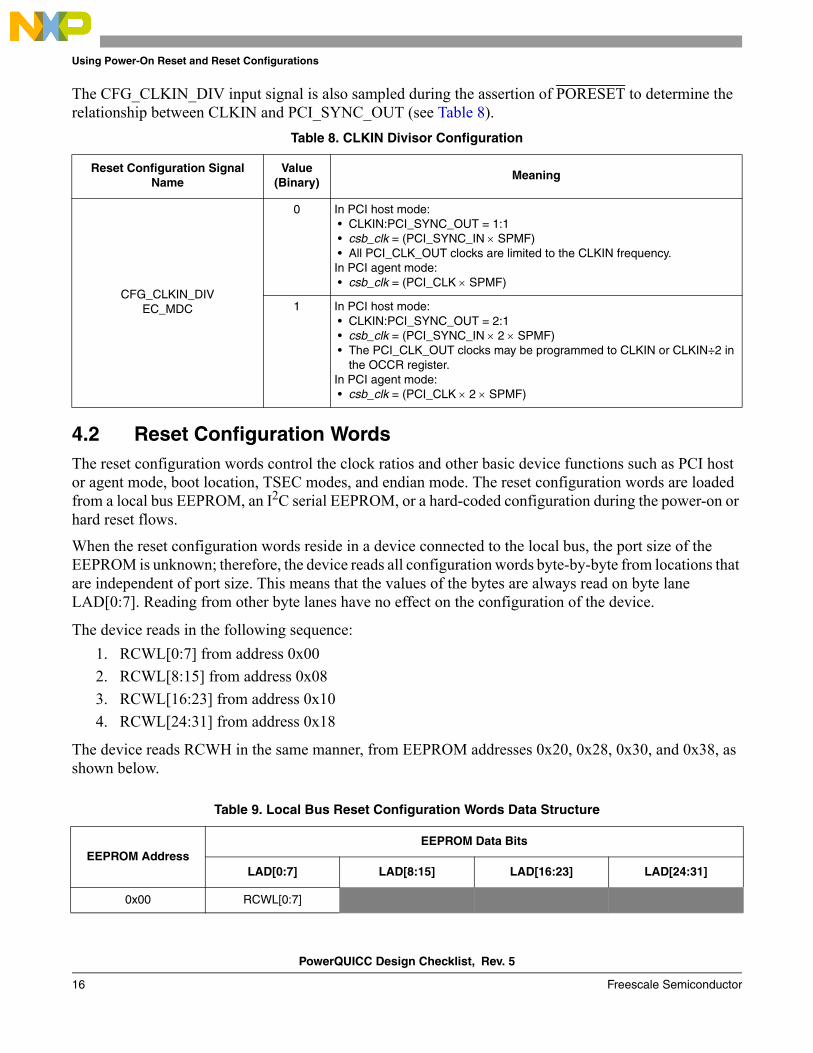
The CFG_CLKIN_DIV input signal is also sampled during the assertion of PORESET to determine the relationship between CLKIN and PCI_SYNC_OUT (see Table 8).
4.2 Reset Configuration WordsThe reset configuration words control the clock ratios and other basic device functions such as PCI host or agent mode, boot location, TSEC modes, and endian mode. The reset configuration words are loaded from a local bus EEPROM, an I2C serial EEPROM, or a hard-coded configuration during the power-on or hard reset flows.
When the reset configuration words reside in a device connected to the local bus, the port size of the EEPROM is unknown; therefore, the device reads all configuration words byte-by-byte from locations that are independent of port size. This means that the values of the bytes are always read on byte lane LAD[0:7]. Reading from other byte lanes have no effect on the configuration of the device.
The device reads in the following sequence:1. RCWL[0:7] from address 0x00 2. RCWL[8:15] from address 0x083. RCWL[16:23] from address 0x104. RCWL[24:31] from address 0x18
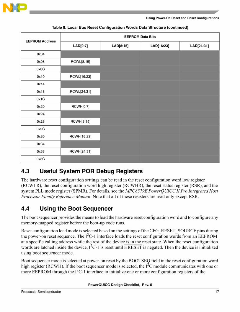
The device reads RCWH in the same manner, from EEPROM addresses 0x20, 0x28, 0x30, and 0x38, as shown below.
Table 8. CLKIN Divisor Configuration
Reset Configuration Signal Name
Value (Binary)
Meaning
CFG_CLKIN_DIVEC_MDC
0 In PCI host mode: • CLKIN:PCI_SYNC_OUT = 1:1 • csb_clk = (PCI_SYNC_IN × SPMF) • All PCI_CLK_OUT clocks are limited to the CLKIN frequency.In PCI agent mode: • csb_clk = (PCI_CLK × SPMF)
1 In PCI host mode: • CLKIN:PCI_SYNC_OUT = 2:1 • csb_clk = (PCI_SYNC_IN × 2 × SPMF) • The PCI_CLK_OUT clocks may be programmed to CLKIN or CLKIN÷2 in
the OCCR register.In PCI agent mode: • csb_clk = (PCI_CLK × 2 × SPMF)
Table 9. Local Bus Reset Configuration Words Data Structure
EEPROM AddressEEPROM Data Bits
LAD[0:7] LAD[8:15] LAD[16:23] LAD[24:31]
0x00 RCWL[0:7]
PowerQUICC Design Checklist, Rev. 5
Freescale Semiconductor 17
Using Power-On Reset and Reset Configurations
4.3 Useful System POR Debug RegistersThe hardware reset configuration settings can be read in the reset configuration word low register (RCWLR), the reset configuration word high register (RCWHR), the reset status register (RSR), and the system PLL mode register (SPMR). For details, see the MPC8379E PowerQUICC II Pro Integrated Host Processor Family Reference Manual. Note that all of these resisters are read only except RSR.
4.4 Using the Boot SequencerThe boot sequencer provides the means to load the hardware reset configuration word and to configure any memory-mapped register before the boot-up code runs.
Reset configuration load mode is selected based on the settings of the CFG_RESET_SOURCE pins during the power-on reset sequence. The I2C-1 interface loads the reset configuration words from an EEPROM at a specific calling address while the rest of the device is in the reset state. When the reset configuration words are latched inside the device, I2C-1 is reset until HRESET is negated. Then the device is initialized using boot sequencer mode.
Boot sequencer mode is selected at power-on reset by the BOOTSEQ field in the reset configuration word high register (RCWH). If the boot sequencer mode is selected, the I2C module communicates with one or more EEPROM through the I2C-1 interface to initialize one or more configuration registers of the
0x04
0x08 RCWL[8:15]
0x0C
0x10 RCWL[16:23]
0x14
0x18 RCWL[24:31]
0x1C
0x20 RCWH[0:7]
0x24
0x28 RCWH[8:15]
0x2C
0x30 RCWH[16:23]
0x34
0x38 RCWH[24:31]
0x3C
Table 9. Local Bus Reset Configuration Words Data Structure (continued)
EEPROM AddressEEPROM Data Bits
LAD[0:7] LAD[8:15] LAD[16:23] LAD[24:31]
PowerQUICC Design Checklist, Rev. 5
18 Freescale Semiconductor
Using Power-On Reset and Reset Configurations
PowerQUICC II Pro. For example, this code can be used to configure the port interface registers if the device is booting from the PCI. Refer to the MPC8379E PowerQUICC II Pro Integrated Host Processor Family Reference Manual for the complete data format for programming the I2C EEPROM.
The boot sequencer contains a basic level of error detection. If the I2C boot sequencer fails while loading the reset configuration words, the RSR[BSF] bit is set. If a preamble or CRC fail is detected in boot sequencer mode, there is no internal or external indication that the boot sequencer operation failed. Use one of the GPIO pins for that purpose.
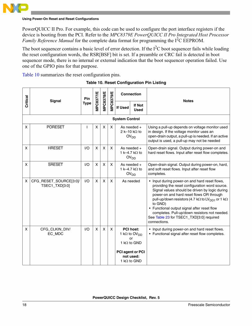
Table 10 summarizes the reset configuration pins.Table 10. Reset Configuration Pin Listing
Cri
tica
l
SignalPin
Type
MP
C83
77/E
MP
C83
78/E
MP
C83
79/E Connection
Notes
If UsedIf NotUsed
System Control
X PORESET I X X X As needed +2 k–10 kΩ to
OVDD
Using a pull-up depends on voltage monitor used in design. If the voltage monitor uses an open-drain output, a pull-up is needed. If an active output is used, a pull-up may not be needed
X HRESET I/O X X X As needed +1 k–4.7 kΩ to
OVDD
Open-drain signal. Output during power-on and hard reset flows. Input after reset flow completes.
X SRESET I/O X X X As needed +1 k–4.7 kΩ to
OVDD
Open-drain signal. Output during power-on, hard, and soft reset flows. Input after reset flow completes.
X CFG_RESET_SOURCE[3:0]/TSEC1_TXD[3:0]
I/O X X X As needed • Input during power-on and hard reset flows, providing the reset configuration word source. Signal values should be driven by logic during power-on and hard reset flows OR through pull-up/down resistors (4.7 kΩ to LVDD1 or 1 kΩ to GND)
• Functional output signal after reset flow completes. Pull-up/down resistors not needed.
See Table 23 for TSEC1_TXD[3:0] required connections.
X CFG_CLKIN_DIV/EC_MDC
I/O X X X PCI host: 1 kΩ to OVDD
or1 kΩ to GND
PCI agent or PCI not used:
1 kΩ to GND
• Input during power-on and hard reset flows. • Functional signal after reset flow completes.
PowerQUICC Design Checklist, Rev. 5
Freescale Semiconductor 19
Operating JTAG and Debug
5 Operating JTAG and DebugThe correct operation of the JTAG interface requires the configuration of a group of system control pins, as demonstrated in Figure 5. Care must be taken to ensure that these pins are maintained at a valid negated state under normal operating conditions, as most have asynchronous behavior and spurious assertion gives unpredictable results.
Boundary-scan testing is enabled through the JTAG interface signals. The TRST signal is optional in the IEEE Std. 1149.1™ specification, but it is provided on all processors built on Power Architecture technology. The device requires TRST to be asserted during power-on reset flow to ensure that the JTAG boundary logic does not interfere with normal chip operation. While the TAP controller can be forced to the reset state using only the TCK and TMS signals, generally systems assert TRST during the power-on reset flow. Simply tying TRST to PORESET is not practical because the JTAG interface is also used for accessing the common on-chip processor (COP), which implements the debug interface to the chip.
The COP function of these processors allows a remote computer system (typically a PC with dedicated hardware and debugging software) to access and control the internal operations of the processor. The COP interface connects primarily through the JTAG port of the processor, with some additional status monitoring signals. The COP port requires the ability to assert PORESET and TRST independently to control the processor fully. If the target system has independent reset sources, such as voltage monitors, watchdog timers, power supply failures, or push-button switches, the COP reset signals must be merged into these signals with logic.
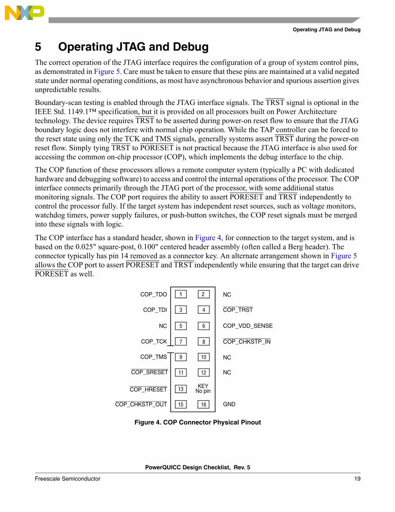
The COP interface has a standard header, shown in Figure 4, for connection to the target system, and is based on the 0.025" square-post, 0.100" centered header assembly (often called a Berg header). The connector typically has pin 14 removed as a connector key. An alternate arrangement shown in Figure 5 allows the COP port to assert PORESET and TRST independently while ensuring that the target can drive PORESET as well.
Figure 4. COP Connector Physical Pinout
3
13
9
5
1
6
10
15
11
7
16
12
8
4
KEYNo pin
1 2COP_TDO
COP_TDI
NC
NC
COP_TRST
COP_VDD_SENSE
COP_CHKSTP_IN
NC
NC
GND
COP_TCK
COP_TMS
COP_SRESET
COP_HRESET
COP_CHKSTP_OUT
PowerQUICC Design Checklist, Rev. 5
20 Freescale Semiconductor
Operating JTAG and Debug
The COP header adds many benefits such as breakpoints, watchpoints, register and memory examination/modification, and other standard debugger features. An inexpensive option can be to leave the COP header unpopulated until needed.
There is no standardized way to number the COP header, so emulator vendors have issued many different pin numbering schemes. Some COP headers are numbered top-to-bottom then left-to-right, while others use left-to-right then top-to-bottom. Still others number the pins counter-clockwise from pin 1 (as with an IC). Regardless of the numbering scheme, the signal placement recommended in Figure 4 is common to all known emulators.
If the JTAG interface and COP header are not used, Freescale recommends all of the following connections:
• TRST should be tied to PORESET through a 0 kΩ isolation resistor so that it is asserted when the system reset signal (PORESET) is asserted, ensuring that the JTAG scan chain is initialized during the power-on reset flow. Freescale recommends that the COP header be designed into the system as shown in Figure 5. If this is not possible, the isolation resistor allows future access to TRST in case a JTAG interface may need to be wired onto the system in future debug situations.
• No pull-up/pull-down is required for TDI, TMS, or TDO.
PowerQUICC Design Checklist, Rev. 5
Freescale Semiconductor 21
Operating JTAG and Debug
Figure 5. JTAG Interface Connection
HRESET
From TargetBoard Sources
COP_HRESET13
NC
11
COP_VDD_SENSE 26
5
15
10 Ω
10 kΩ
10 kΩ
COP_CHKSTP_INCKSTOP_IN8
COP_TMS
COP_TDO
COP_TDI
COP_TCK
TMS
TDO
TDI
9
1
3
4COP_TRST
7
16
2
10
12
(if any)
CO
P H
ead
er
14 3
Notes:
3. The KEY location (pin 14) is not physically present on the COP header.
10 kΩ
TRST 110 kΩ
10 kΩ
CKSTOP_OUTCOP_CHKSTP_OUT
3
13
9
5
1
6
10
15
11
7
16
12
8
4
KEYNo pin
COP ConnectorPhysical Pinout
1 2
NC
PORESET 1PORESET
2. Populate this with a 10 W resistor for short-circuit/current-limiting protection.
NC
OVDD
10 kΩ
SRESET
HRESET
processor to control the processor fully as shown here.
4. Although pin 12 is defined as a No-Connect, some debug tools may use pin 12 as an additional GND pin for
1. The COP port and target board should be able to assert PORESET and TRST independently to the
improved signal integrity.
TCK
4
This switch is included as a precaution for BSDL testing. The switch should be closed to position A during5.BSDL testing to avoid accidentally asserting the TRST line. If BSDL testing is not being performed, this switch should be closed to position B.
5
10 kΩ
NC6
6
A
B
1.5 kΩ
MPC837x
6. See erratum RESET3 in the MPC837xECE.
PowerQUICC Design Checklist, Rev. 5
22 Freescale Semiconductor
Operating JTAG and Debug
5.1 Debug Using In-Circuit EmulatorThere may be issues when using a JTAG-based in-circuit emulator to boot the PowerQUICC II Pro device because reset configuration words are sourced from an unprogrammed Flash device on the local bus. There is no valid RCW already present in Flash memory when the PowerQUICC II Pro device performs the PORESET sequence. The CPU core is disabled and the in-circuit emulator cannot take control of the CPU. The following methods allow an in-circuit emulator to attach to the CPU core and program a valid RCW into a Flash device on the local bus:
• If a CPLD (or other logic) is present, provide an option for the CPLD to provide the RCW during PORESET.
• Design the board with logic that allows clocking for both PCI host and agent mode. Have the board boot in PCI agent mode using an internal hard-coded configuration source to provide the RCW.
• Use the I2C-1 interface.• If using Freescale’s CodeWarrior tools suite, refer to the note “Overriding the Reset Configuration
Word through JTAG” in the readme.txt file provided with the CodeWarrior project. This procedure requires creating a configuration file with the desired RCW settings.
Table 11 summarizes the JTAG and TEST pins.Table 11. JTAG and TEST Pin Listing
Cri
tica
l
SignalPin
Type
MP
C83
77/E
MP
C83
78/E
MP
C83
79/E Connection
Notes
If Used If Not Used
JTAG
TCK I X X X As needed 10 kΩ to OVDD Commonly used for boundary scan testing. If pin is truly not used, can tie directly to GND.
TDI I X X X As needed This JTAG pin has a weak internal pull-up P-FETs that is always enabled.
TDO O X X X As needed Actively driven during RESET.
TMS I X X X As needed This JTAG pin has a weak internal pull-up P-FETs that is always enabled.
X TRST I X X X Tie to PORESETor
Output of negative OR gate logic
• This JTAG pin has a weak internal pull-up P-FETs that is always enabled.
• If an in-circuit emulator is used in the design, TRST should be tied to the output of negative OR gate logic. The inputs to the negative OR gate logic should be any external TRST sources and the PORESET signal.
Power Management
QUIESCE O X X X As needed Open —
Test
X TEST I X X X Tie to GND —
PowerQUICC Design Checklist, Rev. 5
Freescale Semiconductor 23
Designing with Functional Blocks
6 Designing with Functional BlocksThis section presents the recommendations and guidelines for designing with various functional blocks on the PowerQUICC II Pro. This section contains the following subsections:
• Section 6.1, “PCI Bus Interface”• Section 6.2, “DDR Controller”• Section 6.3, “Enhanced Local Bus Controller”• Section 6.4, “General-Purpose I/O Timers”• Section 6.5, “Universal Serial Bus (USB)”• Section 6.6, “Integrated Programmable Interrupt Controller (IPIC)”• Section 6.7, “Dual Enhanced Three-Speed Ethernet Controllers (eTSEC)”• Section 6.8, “IEEE Std 1588™ Timer”• Section 6.9, “SerDes (SGMII, SATA, PCI Express®)”• Section 6.10, “SATA Controller”• Section 6.11, “PCI Express Controller”• Section 6.12, “Enhanced Secure Digital Host Controller”• Section 6.13, “DUART”• Section 6.14, “DMA”• Section 6.15, “I2C Interface”• Section 6.16, “SPI”
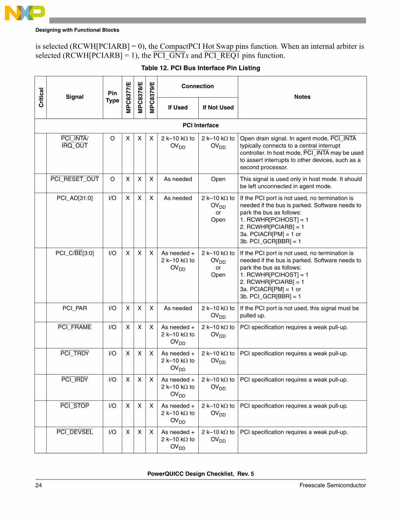
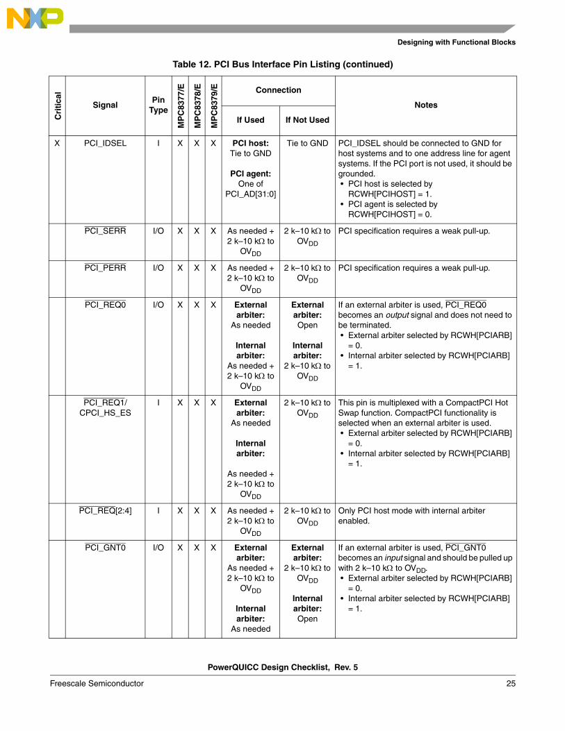
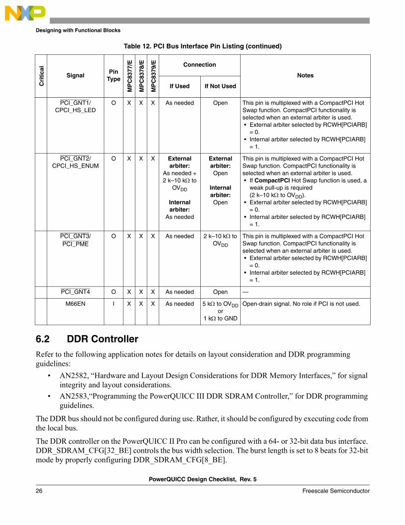
6.1 PCI Bus InterfaceThe reset configuration word high controls the hardware configuration of the PCI blocks as follows:
• RCWH[PCIHOST]—Host/agent mode for PCI• RCWH[PCIARB]—PCI internal/external arbiter mode select
As Table 12 shows, signals of the PCI interface are multiplexed with the CompactPCI Hot Swap pins. Either PCI or Hot Swap functionality is selected by the RCWH[PCIARB] setting. When an external arbiter
X TEST_SEL0 I X X X MPC8377E: Tie to OVDDMPC8378E: Tie to GND
MPC8379E: Tie to OVDD
—
X TEST_SEL1 I X X X MPC8377E: Tie to OVDDMPC8378E: Tie to OVDDMPC8379E: Tie to GND
—
Table 11. JTAG and TEST Pin Listing (continued)C
riti
cal
SignalPin
Type
MP
C83
77/E
MP
C83
78/E
MP
C83
79/E Connection
Notes
If Used If Not Used
PowerQUICC Design Checklist, Rev. 5
24 Freescale Semiconductor
Designing with Functional Blocks
is selected (RCWH[PCIARB] = 0), the CompactPCI Hot Swap pins function. When an internal arbiter is selected (RCWH[PCIARB] = 1), the PCI_GNTx and PCI_REQ1 pins function.
Table 12. PCI Bus Interface Pin Listing
Cri
tica
l
SignalPin
Type
MP
C83
77/E
MP
C83
78/E
MP
C83
79/E Connection
Notes
If Used If Not Used
PCI Interface
PCI_INTA/ IRQ_OUT
O X X X 2 k–10 kΩ to OVDD
2 k–10 kΩ to OVDD
Open drain signal. In agent mode, PCI_INTA typically connects to a central interrupt controller. In host mode, PCI_INTA may be used to assert interrupts to other devices, such as a second processor.
PCI_RESET_OUT O X X X As needed Open This signal is used only in host mode. It should be left unconnected in agent mode.
PCI_AD[31:0] I/O X X X As needed 2 k–10 kΩ to OVDD
orOpen
If the PCI port is not used, no termination is needed if the bus is parked. Software needs to park the bus as follows:1. RCWHR[PCIHOST] = 12. RCWHR[PCIARB] = 13a. PCIACR[PM] = 1 or3b. PCI_GCR[BBR] = 1
PCI_C/BE[3:0] I/O X X X As needed +2 k–10 kΩ to
OVDD
2 k–10 kΩ to OVDD
orOpen
If the PCI port is not used, no termination is needed if the bus is parked. Software needs to park the bus as follows:1. RCWHR[PCIHOST] = 12. RCWHR[PCIARB] = 13a. PCIACR[PM] = 1 or3b. PCI_GCR[BBR] = 1
PCI_PAR I/O X X X As needed 2 k–10 kΩ to OVDD
If the PCI port is not used, this signal must be pulled up.
PCI_FRAME I/O X X X As needed +2 k–10 kΩ to
OVDD
2 k–10 kΩ to OVDD
PCI specification requires a weak pull-up.
PCI_TRDY I/O X X X As needed +2 k–10 kΩ to
OVDD
2 k–10 kΩ to OVDD
PCI specification requires a weak pull-up.
PCI_IRDY I/O X X X As needed +2 k–10 kΩ to
OVDD
2 k–10 kΩ to OVDD
PCI specification requires a weak pull-up.
PCI_STOP I/O X X X As needed +2 k–10 kΩ to
OVDD
2 k–10 kΩ to OVDD
PCI specification requires a weak pull-up.
PCI_DEVSEL I/O X X X As needed +2 k–10 kΩ to
OVDD
2 k–10 kΩ to OVDD
PCI specification requires a weak pull-up.
PowerQUICC Design Checklist, Rev. 5
Freescale Semiconductor 25
Designing with Functional Blocks
X PCI_IDSEL I X X X PCI host: Tie to GND
PCI agent:One of
PCI_AD[31:0]
Tie to GND PCI_IDSEL should be connected to GND for host systems and to one address line for agent systems. If the PCI port is not used, it should be grounded. • PCI host is selected by
RCWH[PCIHOST] = 1. • PCI agent is selected by
RCWH[PCIHOST] = 0.
PCI_SERR I/O X X X As needed +2 k–10 kΩ to
OVDD
2 k–10 kΩ to OVDD
PCI specification requires a weak pull-up.
PCI_PERR I/O X X X As needed +2 k–10 kΩ to
OVDD
2 k–10 kΩ to OVDD
PCI specification requires a weak pull-up.
PCI_REQ0 I/O X X X External arbiter:
As needed
Internal arbiter:
As needed +2 k–10 kΩ to
OVDD
External arbiter:Open
Internal arbiter:
2 k–10 kΩ to OVDD
If an external arbiter is used, PCI_REQ0 becomes an output signal and does not need to be terminated. • External arbiter selected by RCWH[PCIARB]
= 0. • Internal arbiter selected by RCWH[PCIARB]
= 1.
PCI_REQ1/ CPCI_HS_ES
I X X X External arbiter:
As needed
Internal arbiter:
As needed +2 k–10 kΩ to
OVDD
2 k–10 kΩ to OVDD
This pin is multiplexed with a CompactPCI Hot Swap function. CompactPCI functionality is selected when an external arbiter is used. • External arbiter selected by RCWH[PCIARB]
= 0. • Internal arbiter selected by RCWH[PCIARB]
= 1.
PCI_REQ[2:4] I X X X As needed +2 k–10 kΩ to
OVDD
2 k–10 kΩ to OVDD
Only PCI host mode with internal arbiter enabled.
PCI_GNT0 I/O X X X External arbiter:
As needed +2 k–10 kΩ to
OVDD
Internal arbiter:
As needed
External arbiter:
2 k–10 kΩ to OVDD
Internal arbiter:Open
If an external arbiter is used, PCI_GNT0 becomes an input signal and should be pulled up with 2 k–10 kΩ to OVDD. • External arbiter selected by RCWH[PCIARB]
= 0. • Internal arbiter selected by RCWH[PCIARB]
= 1.
Table 12. PCI Bus Interface Pin Listing (continued)C
riti
cal
SignalPin
Type
MP
C83
77/E
MP
C83
78/E
MP
C83
79/E Connection
Notes
If Used If Not Used
PowerQUICC Design Checklist, Rev. 5
26 Freescale Semiconductor
Designing with Functional Blocks
6.2 DDR ControllerRefer to the following application notes for details on layout consideration and DDR programming guidelines:
• AN2582, “Hardware and Layout Design Considerations for DDR Memory Interfaces,” for signal integrity and layout considerations.
• AN2583,“Programming the PowerQUICC III DDR SDRAM Controller,” for DDR programming guidelines.
The DDR bus should not be configured during use. Rather, it should be configured by executing code from the local bus.
The DDR controller on the PowerQUICC II Pro can be configured with a 64- or 32-bit data bus interface. DDR_SDRAM_CFG[32_BE] controls the bus width selection. The burst length is set to 8 beats for 32-bit mode by properly configuring DDR_SDRAM_CFG[8_BE].
PCI_GNT1/ CPCI_HS_LED
O X X X As needed Open This pin is multiplexed with a CompactPCI Hot Swap function. CompactPCI functionality is selected when an external arbiter is used. • External arbiter selected by RCWH[PCIARB]
= 0. • Internal arbiter selected by RCWH[PCIARB]
= 1.
PCI_GNT2/ CPCI_HS_ENUM
O X X X External arbiter:
As needed +2 k–10 kΩ to
OVDD
Internal arbiter:
As needed
External arbiter:Open
Internal arbiter:Open
This pin is multiplexed with a CompactPCI Hot Swap function. CompactPCI functionality is selected when an external arbiter is used. • If CompactPCI Hot Swap function is used, a
weak pull-up is required (2 k–10 kΩ to OVDD).
• External arbiter selected by RCWH[PCIARB] = 0.
• Internal arbiter selected by RCWH[PCIARB] = 1.
PCI_GNT3/ PCI_PME
O X X X As needed 2 k–10 kΩ to OVDD
This pin is multiplexed with a CompactPCI Hot Swap function. CompactPCI functionality is selected when an external arbiter is used. • External arbiter selected by RCWH[PCIARB]
= 0. • Internal arbiter selected by RCWH[PCIARB]
= 1.
PCI_GNT4 O X X X As needed Open —
M66EN I X X X As needed 5 kΩ to OVDDor
1 kΩ to GND
Open-drain signal. No role if PCI is not used.
Table 12. PCI Bus Interface Pin Listing (continued)C
riti
cal
SignalPin
Type
MP
C83
77/E
MP
C83
78/E
MP
C83
79/E Connection
Notes
If Used If Not Used
PowerQUICC Design Checklist, Rev. 5
Freescale Semiconductor 27
Designing with Functional Blocks
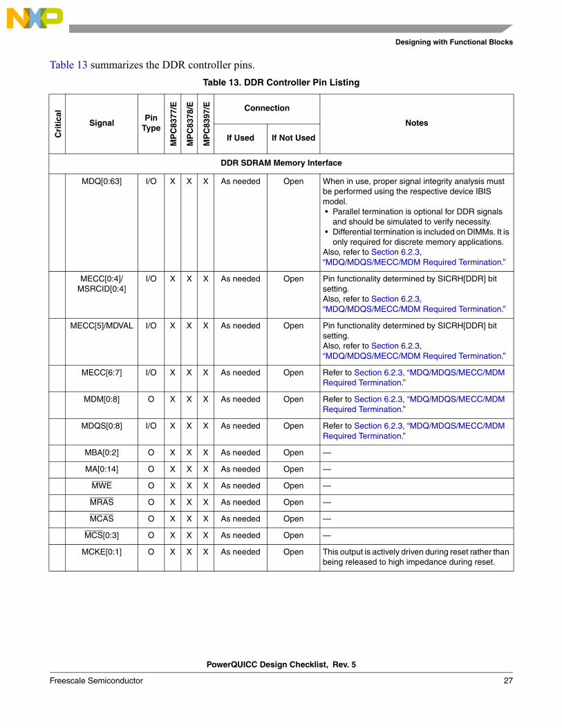
Table 13 summarizes the DDR controller pins.Table 13. DDR Controller Pin Listing
Cri
tica
l
SignalPin
Type
MP
C83
77/E
MP
C83
78/E
MP
C83
97/E Connection
Notes
If Used If Not Used
DDR SDRAM Memory Interface
MDQ[0:63] I/O X X X As needed Open When in use, proper signal integrity analysis must be performed using the respective device IBIS model. • Parallel termination is optional for DDR signals
and should be simulated to verify necessity. • Differential termination is included on DIMMs. It is
only required for discrete memory applications.Also, refer to Section 6.2.3, “MDQ/MDQS/MECC/MDM Required Termination.”
MECC[0:4]/ MSRCID[0:4]
I/O X X X As needed Open Pin functionality determined by SICRH[DDR] bit setting.Also, refer to Section 6.2.3, “MDQ/MDQS/MECC/MDM Required Termination.”
MECC[5]/MDVAL I/O X X X As needed Open Pin functionality determined by SICRH[DDR] bit setting.Also, refer to Section 6.2.3, “MDQ/MDQS/MECC/MDM Required Termination.”
MECC[6:7] I/O X X X As needed Open Refer to Section 6.2.3, “MDQ/MDQS/MECC/MDM Required Termination.”
MDM[0:8] O X X X As needed Open Refer to Section 6.2.3, “MDQ/MDQS/MECC/MDM Required Termination.”
MDQS[0:8] I/O X X X As needed Open Refer to Section 6.2.3, “MDQ/MDQS/MECC/MDM Required Termination.”
MBA[0:2] O X X X As needed Open —
MA[0:14] O X X X As needed Open —
MWE O X X X As needed Open —
MRAS O X X X As needed Open —
MCAS O X X X As needed Open —
MCS[0:3] O X X X As needed Open —
MCKE[0:1] O X X X As needed Open This output is actively driven during reset rather than being released to high impedance during reset.
PowerQUICC Design Checklist, Rev. 5
28 Freescale Semiconductor
Designing with Functional Blocks
6.2.1 MDIC1 and MDIC0The MDIC1 and MDIC0 driver impedance calibration pins should be terminated as shown in Table 14.
The user selects the DDR type by configuring the DDR_SDRAM_CFG[SDRAM_TYPE] and the DDRCDR registers.
MCK[0:5] O X X X As needed Open For discrete memories, a 100 Ω parallel termination is required between MCKn and MCKn.Disable the clocks that are not used via the DDRCLKDR register. By default, all clocks are operational, but not all clock signals are used in a given application. Therefore, by disabling the unused clocks, it first lowers the power consumption and then lowers the unused switching activity in the part. DDRCLKDR is not a part of the memory controller register set; it is located in the global utility register section.
MCK[0:5] O X X X As needed Open
MODT[0:3] O X X X As needed Open —
MVREF1 I X X X As needed Each of the MVREF1 and MVREF2 supply inputs must be connected through serial resistors of 200 Ω. See Section 6.2.2, “MVREFn Connection Options.”MVREF2 I X X X As needed
Table 14. MDIC1 and MDIC0 Termination Recommendations
Pins DDR1 DDR2
MDIC1 Open 18.2 Ω to GVDD
MDIC0 0 Ω to GND 18.2 Ω to GND
Note: 1% tolerance is allowed for the18.2 Ω resistors.
Table 13. DDR Controller Pin Listing (continued)C
riti
cal
SignalPin
Type
MP
C83
77/E
MP
C83
78/E
MP
C83
97/E Connection
Notes
If Used If Not Used
PowerQUICC Design Checklist, Rev. 5
Freescale Semiconductor 29
Designing with Functional Blocks
6.2.2 MVREFn Connection Options
Figure 6 and in Figure 7 show the two MVREFn connection options. A 5% tolerance is allowed for the 200 Ω resistors.
Figure 6. MVREF1 and MVREF2 Connection Option #1
Figure 7. MVREF1 and MVREF2 Connection Option #2
Each of the MVREF1 and MVREF2 supply inputs must be connected through serial resistors of 200 Ω. The resistors must be the closest component to the MPC837x MVREFn ball connection. Additionally, the number of decoupling capacitors used should be as stated in AN2582, “Hardware and Layout Design Considerations for DDR Memory Interfaces.”
MPC837x
MVREF1 (K4)
MVREF2 (W4)
200 Ω
200 Ω1μF 0.01μF
Reference voltagefrom regulator orvoltage divider
To the DDR memory modules
1μF 0.01μF
1μF 0.01μF
MPC837x
MVREF1 (K4)
MVREF2 (W4)
200 Ω
200 Ω
Reference voltagefrom regulator orvoltage divider
To the DDR memory modules
PowerQUICC Design Checklist, Rev. 5
30 Freescale Semiconductor
Designing with Functional Blocks
6.2.3 MDQ/MDQS/MECC/MDM Required Termination
Figure 8 shows the required MDQ/MDQS/MECC/MDM connection. A 1% tolerance is allowed for the 22 Ω resistors shown in Figure 8.
Figure 8. MDQ, MDQS, MECC, and MDM Required Connections
Serial 22-Ω resistors must be added on all the MDQ, MDQS, MECC, and MDM signals. For applications using DIMMs that already include 22-Ω termination resistors, no additional resistors are required. It is recommended that the resistors be placed in the middle of the trace between the MPC837x and the memory module.
6.2.4 DDR1 Termination Scheme
The DDR1 driver strength should be set to half strength on both the memory controller side and the DRAM side to reduce the overall system noise. This is done by setting the following registers as shown:
• (Offset 0x0_0128) DDRCDR = 0x0004_0001• (Offset 0x0_2110) DDR_SDRAM_CFG[HSE] = 0’b1• (Offset 0x0_2118) DDR_SDRAM_MODE[14] = 0’b1
The termination scheme should be set to reduce the overall system noise on DDR1 interface. This is done by using the following termination scheme.
• For all MDQ/MDQS/MDM signals, the parallel termination resistor RTT = 100 Ω, and the series resistor RS = 10 Ω.
• For all address/command/control signals, the parallel termination resistor RTT = 150 Ω, and the series resistor RS = 22 Ω.
• All unused MCK[0:5] clock signals should disabled by the (Offset 0x0_0A04) OCCR register.• All unused ECC signals should be connected to GND by a 150-Ω resistor.• Add a 200-Ω resistor between the MVREF silicon pin and any decoupling caps that may be used
for this signal on the board.
MPC837x
MDQ[0:63]
22 Ω
DDR Memory Module
MDQS[0:8]
MECC[0:7]
MDM[0:8] 22 Ω
PowerQUICC Design Checklist, Rev. 5
Freescale Semiconductor 31
Designing with Functional Blocks
It is important to note the following:• The existing recommendations for proper layout for DDR1 as stated in AN2582, “Hardware and
Layout Design Considerations for DDR Memory Interfaces,” should be observed.• It is also highly recommended to repeat the IBIS simulation with the current IBIS model.
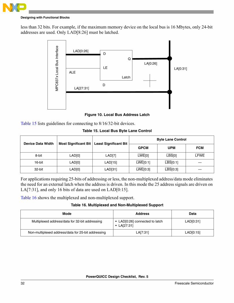
6.3 Enhanced Local Bus ControllerThe enhanced local bus controller (eLBC) provides a general-purpose chip-select machine (GPCM), a NAND Flash control machine (FCM), and three user-programmable machines (UPMs). Eight chip selects are available to operate with any given machine. Figure 9 shows how to properly connect a NAND Flash memory device, using a simplified connection to 8-bit NAND Flash memory device in FCM mode. Commands, address, and data are all transferred on the LAD[0:7] pins.
Figure 9. Enhanced Local Bus Connection to NAND Flash
The PowerQUICC II Pro local bus features a multiplexed address and data bus, LAD[0:31]. An external latch is required to de-multiplex these signals to the connecting device. LAD[0] is the most significant address and data bit, and LAD[31] is the least significant address and data bit.
Figure 10 shows the correct way to reconstruct the address for the local bus. The dedicated LA[27:31] must be used to form the local address. Depending on the memory bank size, usually the address bus is
CE
IO[7:0]
8-Bit
LALE
LFWE
LCSn
LAD[0:7]
eLBC inFCM Mode
NAND Flash
N.C.
N.C.
N.C.
LFWP WP
LFRB RDY/BSY
LBVDD
LFRE RE
WE
LFALE
LFCLE
ALE
CLE
4.7 kΩ
LAD[8:31
LA
EEPROM
PowerQUICC Design Checklist, Rev. 5
32 Freescale Semiconductor
Designing with Functional Blocks
less than 32 bits. For example, if the maximum memory device on the local bus is 16 Mbytes, only 24-bit addresses are used. Only LAD[8:26] must be latched.
Figure 10. Local Bus Address Latch
Table 15 lists guidelines for connecting to 8/16/32-bit devices.
For applications requiring 25-bits of addressing or less, the non-multiplexed address/data mode eliminates the need for an external latch when the address is driven. In this mode the 25 address signals are driven on LA[7:31], and only 16 bits of data are used on LAD[0:15].
Table 16 shows the multiplexed and non-multiplexed support.
Table 15. Local Bus Byte Lane Control
Device Data Width Most Significant Bit Least Significant BitByte Lane Control
GPCM UPM FCM
8-bit LAD[0] LAD[7] LWE[0] LBS[0] LFWE
16-bit LAD[0] LAD[15] LWE[0:1] LBS[0:1] —
32-bit LAD[0] LAD[31] LWE[0:3] LBS[0:3] —
Table 16. Multiplexed and Non-Multiplexed Support
Mode Address Data
Multiplexed address/data for 32-bit addressing • LAD[0:26] connected to latch • LA[27:31]
LAD[0:31]
Non-multiplexed address/data for 25-bit addressing LA[7:31] LAD[0:15]
MP
C83
7x L
ocal
Bus
Inte
rface
LA[0:31]
LAD[0:26]
ALE
LA[27:31]
LA[0:26]
D
Q
D
LE
Latch
PowerQUICC Design Checklist, Rev. 5
Freescale Semiconductor 33
Designing with Functional Blocks
Table 17 summarizes the local bus pins.Table 17. Local Bus Pin Listing
Cri
tica
l
SignalPin
Type
MP
C83
77/E
MP
C83
78/E
MP
C83
79/E Connection
Notes
If Used If Not Used
Local Bus Interface
LAD[0:31] I/O X X X As needed 2 k–10 kΩ to LBVDD See note for the LA[7:31] signals.
LCS4/LDP0
I/O X X X As needed 2 k–10 kΩ to LBVDD RCWH[LDP] = 0 Functions as LDP0RCWH[LDP] = 1 Functions as LCS4
LCS5/LDP1
I/O X X X As needed 2 k–10 kΩ to LBVDD RCWH[LDP] = 0 Functions as LDP1RCWH[LDP] = 1 Functions as LCS5
LA7/LCS6/LDP2
I/O X X X As needed Open RCWH[LDP] = 0 Functions as LDP2RCWH[LDP] = 1 Functions as LCS6
LA8/LCS7/LDP3
I/O X X X As needed 2 k–10 kΩ to LBVDD RCWH[LDP] = 0 Functions as LDP3RCWH[LDP] = 1 Functions as LCS7
LA[7:31] O X X X As needed Open Bits 7–26 are only used as address signals in non-multiplexed mode.
LCS[0:3] O X X X As needed Open —
LWE[0:3]/LFWE/
LBS[0:3]
O X X X As needed Open —
LBCTL O X X X As needed Open —
LA10/LALE
O X X X As needed Open —
X LGPL0/LFCLE
I/O X X X As needed Open —
X LGPL1/LFALE
I/O X X X As needed Open
LGPL2/LFRE/LOE
O X X X As needed Open —
X LGPL3/LWFP
I/O X X X As needed Open —
LGPL4/LGTA/LFRB/
LUPWAIT/LPBSE
I/O X X X 4.7 kΩ to LBVDD Pin functionality is selected by LBCR[LPBSE].
X LA9/LGPL5
O X X X As needed Open Critical signal only when in non-multiplexed mode.
PowerQUICC Design Checklist, Rev. 5
34 Freescale Semiconductor
Designing with Functional Blocks
6.4 General-Purpose I/O TimersThe two general-purpose I/O modules, GPIO1 and GPIO2, can each support 32 general-purpose I/O ports. Each port can be configured as an input or an output. If a port is configured as an input, it can optionally generate an interrupt upon detection of a change. If a port is configured as an output, it can be individually configured as an open-drain or fully active output. Each GPIO port is multiplexed with other functions.
GPIO1 is multiplexed with general-purpose timers and eTSEC2 interface pins. GPIO2 is multiplexed with eTSEC1, eTSEC2, USB, and IRQ pins. DMA control signals are also multiplexed with some of the GPIO1 signals. Each GPIO pin is programmed using the system I/O configuration low (SICRL) and system I/O configuration register high (SICRH) registers.
Four general-purpose timers are multiplexed with the GPIO1[0:11] pins. Each timer interface consists of the TGATEn, TINn, and TOUTn pins. Each timer pin is programmed using the system I/O configuration low (SICRL) register.
Table 18 summarizes the general-purpose I/O pins. If these pins are not used for other functions, the GPIO1 and GPIO2 pins should be configured as output and can be left open.
LCLK[0:2] O X X X As needed Open —
LSYNC_OUT O X X X PLL enabled mode only: 22–33 Ω
damping resistor in feedback path
(LSYNC_OUT to LSYNC_IN)
eLBC not used or in PLL bypass mode:
Open
—
LSYNC_IN I X X X eLBC not used or in PLL bypass mode:
1 kΩ to GND
Table 18. General-Purpose I/O Pin Listing
Cri
tica
l
SignalPin
Type
MP
C83
77/E
MP
C83
78/E
MP
C83
79/E Connection
Notes
If Used If Not Used 1
GPIO1[0]/DMA_DREQ0/GTM1_TIN1/GTM2_TIN2
I/O X X X As needed in GPIO output mode: OpenOtherwise:
2 k–10 kΩ to OVDD
Pin functionality determined by SICRL[GPIO1_A] and SICRL[DMA_A] bit settings
GPIO1[1]/DMA_DACK0/
GTM1_TGATE1/GTM2_TGATE2
I/O X X X As needed Open Pin functionality determined by SICRL[GPIO1_B] and SICRL[DMA_B] bit settings
Table 17. Local Bus Pin Listing (continued)C
riti
cal
SignalPin
Type
MP
C83
77/E
MP
C83
78/E
MP
C83
79/E Connection
Notes
If Used If Not Used
PowerQUICC Design Checklist, Rev. 5
Freescale Semiconductor 35
Designing with Functional Blocks
GPIO1[2]/DMA_DDONE0/GTM1_TOUT1
I/O X X X As needed Open Pin functionality determined by SICRL[GPIO1_C] and SICRL[DMA_C] bit settings
GPIO1[3]/DMA_DREQ1/GTM1_TIN2/GTM2_TIN1
I/O X X X As needed Open Pin functionality determined by SICRL[GPIO1_D] and SICRL[DMA_D] bit settings
GPIO1[4]/DMA_DACK1/
GTM1_TGATE1/GTM2_TGATE2
I/O X X X As needed Open Pin functionality determined by SICRL[GPIO1_E] and SICRL[DMA_E] bit settings
GPIO1[5]/DMA_DDONE1/GTM1_TOUT2/GTM2_TOUT1
I/O X X X As needed Open Pin functionality determined by SICRL[GPIO1_F] bit settings
GPIO1[6]/DMA_DREQ2/GTM1_TIN3/GTM2_TIN4
I/O X X X As needed Open Pin functionality determined by SICRL[GPIO1_G] and SICRL[DMA_F] bit settings
GPIO1[7]/DMA_DACK2/
GTM1_TGATE3/GTM2_TGATE4
I/O X X X As needed Open Pin functionality determined by SICRL[GPIO1_H] and SICRL[DMA_G] bit settings
GPIO1[8]/DMA_DDONE2/GTM1_TOUT3
I/O X X X As needed Open Pin functionality determined by SICRL[GPIO1_I] and SICRL[DMA_H] bit settings
GPIO1[9]/DMA_DREQ3/GTM1_TIN4/GTM2_TIN3
I/O X X X As needed Open Pin functionality determined by SICRL[GPIO1_K] and SICRL[DMA_J] bit settings
GPIO1[10]/DMA_DACK3/
GTM1_TGATE4/GTM2_TGATE3
I/O X X X As needed Open Pin functionality determined by SICRL[GPIO1_J] and SICRL[DMA_I] bit settings
GPIO1[11]/DMA_DDONE3/GTM1_TOUT4/GTM2_TOUT3
I/O X X X As needed Open Pin functionality determined by SICRL[GPIO1_L] bit settings
Note:
1 It is recommended that GPIO pins be programmed to outputs when not used.
Table 18. General-Purpose I/O Pin Listing (continued)C
riti
cal
SignalPin
Type
MP
C83
77/E
MP
C83
78/E
MP
C83
79/E Connection
Notes
If Used If Not Used 1
PowerQUICC Design Checklist, Rev. 5
36 Freescale Semiconductor
Designing with Functional Blocks
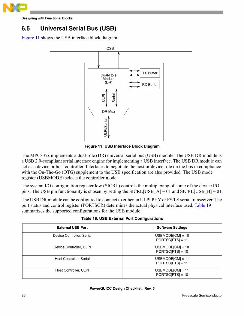
6.5 Universal Serial Bus (USB)Figure 11 shows the USB interface block diagram.
Figure 11. USB Interface Block Diagram
The MPC837x implements a dual-role (DR) universal serial bus (USB) module. The USB DR module is a USB 2.0-compliant serial interface engine for implementing a USB interface. The USB DR module can act as a device or host controller. Interfaces to negotiate the host or device role on the bus in compliance with the On-The-Go (OTG) supplement to the USB specification are also provided. The USB mode register (USBMODE) selects the controller mode.
The system I/O configuration register low (SICRL) controls the multiplexing of some of the device I/O pins. The USB pin functionality is chosen by setting the SICRL[USB_A] = 01 and SICRL[USB_B] = 01.
The USB DR module can be configured to connect to either an ULPI PHY or FS/LS serial transceiver. The port status and control register (PORTSCR) determines the actual physical interface used. Table 19 summarizes the supported configurations for the USB module.
Table 19. USB External Port Configurations
External USB Port Software Settings
Device Controller, Serial USBMODE[CM] = 10PORTSC[PTS] = 11
Device Controller, ULPI USBMODE[CM] = 10PORTSC[PTS] = 10
Host Controller, Serial USBMODE[CM] = 11PORTSC[PTS] = 11
Host Controller, ULPI USBMODE[CM] = 11PORTSC[PTS] = 10
Dual-Role
CSB
TX Buffer
Module(DR)
DR Mux
RX Buffer
Ser
ial
ULP
IU
LPI/S
eria
l
PowerQUICC Design Checklist, Rev. 5
Freescale Semiconductor 37
Designing with Functional Blocks
Table 20 summarizes the universal serial bus pins. If the USB module is not used, it can be disabled. In addition, if the signals are not used for another function, it is possible to configure the GPIO2[0–11, 22, 23] pins to GPIO output mode and leave them open (floating).
Table 20. Universal Serial Bus Pin Listing
Cri
tica
l
SignalPin
Type
MP
C83
77E
MP
C83
78E
MP
C83
79E Connection Pin Functionality1
1 Use SICRL[USB_A] = 01 and SICRL[USB_B] = 01 to select USB pin functionality.
If UsedIf NotUsed2
2 If the USB module is not used and the pins are left open, they must be configured to GPIO output mode.
PORTSCR[PTS] = 10ULPI
PORTSCR[PTS] = 11Serial
USBDR_D0_ENABLEN/GPIO2[0]
I/O X X X As needed Open USBDR_D0 USBDR_ENABLEN
USBDR_D1_SER_TXD/GPIO2[1]
I/O X X X As needed Open USBDR_D1 USBDR_SER_TXD
USBDR_D2_VMO_SE0/GPIO2[2]
I/O X X X As needed Open USBDR_D2 USBDR_VMO_SE0
USBDR_D3_SPEED/GPIO2[3]
I/O X X X As needed Open USBDR_D3 USBDR_SPEED
USBDR_D4_DP/GPIO2[4]
I/O X X X As needed Open USBDR_D4 USBDR_DP
USBDR_D5_DM/GPIO2[5]
I/O X X X As needed Open USBDR_D5 USBDR_DM
USBDR_D6_SER_RCV/GPIO2[6]
I/O X X X As needed Open USBDR_D6 USBDR_SER_RCV
USBDR_D7_DRVVBUS/GPIO2[7]
I/O X X X As needed Open USBDR_D7 USBDR_DRVVBUS
USBDR_SESS_VLD_NXT/GPIO2[8]
I X X X As needed Open USBDR_NXT USBDR_SESS_VLD
USBDR_DIR_DPPULLUP/GPIO2[9]
I/O X X X As needed Open USBDR_DIR USBDR_DIR_PULLUP
X USBDR_STP_SUSPEND3
3 The USBDR_STP_SUSPEND pin must not be pulled down during PORESET.
O X X X As needed Open USBDR_STP USBDR_SUSPEND
USBDR_PWRFAULT/GPIO2[10]/SD_DAT1
I X X X As needed Open USBDR_PWRFAULT USBDR_PWRFAULT
USBDR_PCTL0/GPIO2[11]/SD_DAT2
O X X X As needed Open USBDR_PCTL0 USBDR_PCTL0
USBDR_PCTL1/GPIO2[22]/SD_DAT3
O X X X As needed Open USBDR_PCTL1 USBDR_PCTL1
USBDR_CLK/GPIO2[23]
I X X X As needed Open USBDR_CLK USBDR_CLK
Note:
PowerQUICC Design Checklist, Rev. 5
38 Freescale Semiconductor
Designing with Functional Blocks
6.6 Integrated Programmable Interrupt Controller (IPIC)The integrated programmable interrupt controller (IPIC) provides interrupt management for receiving hardware-generated interrupts from internal and external sources. It also prioritizes and delivers the interrupts to the CPU for servicing.
The IRQ lines are multiplexed with signals from GPIO2, CKSTOP_IN, and CKSTOP_OUT interface pins. The configuration of each IRQ pin is programmed using the system I/O configuration high register (SICRH).
Table 21 summarizes the programmable interrupt controller pins.Table 21. Programmable Interrupt Controller Pin Listing
Cri
tica
l
SignalPin
Type
MP
C83
77E
MP
C83
78E
MP
C83
79E Connection
Notes
If Used If Not Used
Programmable Interrupt Controller
MCP_OUT O X X X As needed +2 k–10 kΩ to OVDD
2 k–10 kΩ to OVDD
Open drain signal
IRQ[0]/MCP_IN/
GPIO2[12]
I/O X X X GPIO:As needed
Others: As needed +2 k–10 kΩ to OVDD
2 k–10 kΩ to OVDD
Pin functionality determined by SICRH[GPIO2_A] bit setting.
IRQ[1:3]/GPIO2[13:15]
I/O X X X GPIO:As needed
Others:As needed +2 k–10 kΩ to OVDD
2 k–10 kΩ to OVDD
Pin functionality determined by SICRH[GPIO2_B:GPIO2_C:GPIO2_D] bit settings.
IRQ[4]/GPIO2[16]/
SD_WP
I/O X X X GPIO:As needed
Others:As needed +2 k–10 kΩ to OVDD
2 k–10 kΩ to OVDD
Pin functionality determined by SICRH[GPIO2_E] bit settings.
IRQ[5]/GPIO2[17]/
USBDR_PWRFAULT
I/O X X X GPIO:As needed
Others:As needed +2 k–10 kΩ to OVDD
2 k–10 kΩ to OVDD
Pin functionality determined by SICRH[GPIO2_F] bit settings.
PowerQUICC Design Checklist, Rev. 5
Freescale Semiconductor 39
Designing with Functional Blocks
6.7 Dual Enhanced Three-Speed Ethernet Controllers (eTSEC)The enhanced three-speed Ethernet controller (eTSEC) supports 10, 100, and 1 Gbps Ethernet/802.3 networks. The complete eTSEC is designed for single MAC applications with several standard MAC-PHY interfaces to connect to an external Ethernet transceiver:
• IEEE Std. 802.3™, 802.3u™, 802.3x™, 802.3z™, 802.3a™c, 802.3ac™-compliant• Support for different Ethernet physical interfaces
— 1000 Mbps IEEE 802.3 RGMII, 802.3z RTBI, full-duplex— 10/100 Mbps IEEE 802.3 MII full and half-duplex— Support for SGMII 4-wire differential signaling (only MPC8378E)
Two eTSECs can be independently configured to support any one of these interfaces. The reset configuration word high controls the hardware configuration of the two eTSEC MAC-PHY interfaces. RCWHR[TSEC1M] and RCWHR[TSEC2M] are used to configure eTSEC1 and eTSEC2, respectively, in MII, RMII, RGMII, RTBI, or SGMII mode. The MACCFG2[I/F Mode] bits select between an MII or GMII interface.
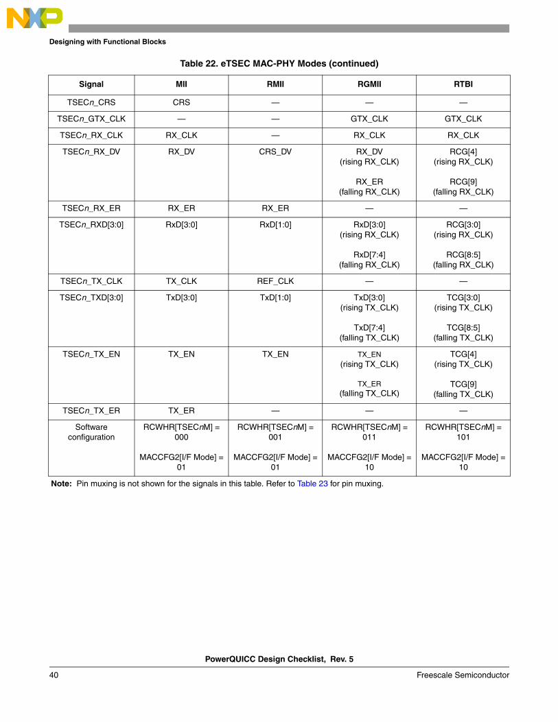
Table 22 shows the pin usage and software configuration for each particular MAC-PHY mode. eTSEC interface pins not used in a particular MAC-PHY mode can be used as GPIO by setting the appropriate bits in the SICRH register.
IRQ[6]/GPIO2[18]/
CKSTOP_OUT
I/O X X X GPIO:As needed
Others:As needed +
2k–10k Ω to OVDD
2 k–10 kΩ to OVDD
Pin functionality determined by SICRH[GPIO2_G] bit settings.
IRQ[7]/GPIO2[19]/
CKSTOP_IN
I/O X X X GPIO:As needed
Others: As needed +
2k–10k Ω to OVDD
2 k–10 kΩ to OVDD
Pin functionality determined by SICRH[GPIO2_H] bit settings.
Table 22. eTSEC MAC-PHY Modes
Signal MII RMII RGMII RTBI
EC_GTX_CLK125 — — 125 MHz clock 125 MHz clock
TSECn_COL COL — — —
Table 21. Programmable Interrupt Controller Pin Listing (continued)C
riti
cal
SignalPin
Type
MP
C83
77E
MP
C83
78E
MP
C83
79E Connection
Notes
If Used If Not Used
PowerQUICC Design Checklist, Rev. 5
40 Freescale Semiconductor
Designing with Functional Blocks
TSECn_CRS CRS — — —
TSECn_GTX_CLK — — GTX_CLK GTX_CLK
TSECn_RX_CLK RX_CLK — RX_CLK RX_CLK
TSECn_RX_DV RX_DV CRS_DV RX_DV(rising RX_CLK)
RX_ER(falling RX_CLK)
RCG[4](rising RX_CLK)
RCG[9](falling RX_CLK)
TSECn_RX_ER RX_ER RX_ER — —
TSECn_RXD[3:0] RxD[3:0] RxD[1:0] RxD[3:0](rising RX_CLK)
RxD[7:4](falling RX_CLK)
RCG[3:0](rising RX_CLK)
RCG[8:5](falling RX_CLK)
TSECn_TX_CLK TX_CLK REF_CLK — —
TSECn_TXD[3:0] TxD[3:0] TxD[1:0] TxD[3:0](rising TX_CLK)
TxD[7:4](falling TX_CLK)
TCG[3:0](rising TX_CLK)
TCG[8:5](falling TX_CLK)
TSECn_TX_EN TX_EN TX_EN TX_EN(rising TX_CLK)
TX_ER(falling TX_CLK)
TCG[4](rising TX_CLK)
TCG[9](falling TX_CLK)
TSECn_TX_ER TX_ER — — —
Software configuration
RCWHR[TSECnM] = 000
MACCFG2[I/F Mode] = 01
RCWHR[TSECnM] = 001
MACCFG2[I/F Mode] = 01
RCWHR[TSECnM] = 011
MACCFG2[I/F Mode] = 10
RCWHR[TSECnM] = 101
MACCFG2[I/F Mode] = 10
Note: Pin muxing is not shown for the signals in this table. Refer to Table 23 for pin muxing.
Table 22. eTSEC MAC-PHY Modes (continued)
Signal MII RMII RGMII RTBI
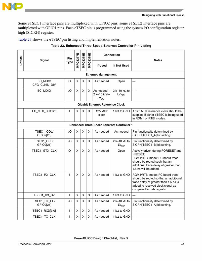
PowerQUICC Design Checklist, Rev. 5
Freescale Semiconductor 41
Designing with Functional Blocks
Some eTSEC1 interface pins are multiplexed with GPIO2 pins; some eTSEC2 interface pins are multiplexed with GPIO1 pins. Each eTSEC pin is programmed using the system I/O configuration register high (SICRH) register.
Table 23 shows the eTSEC pin listing and implementation notes.Table 23. Enhanced Three-Speed Ethernet Controller Pin Listing
Cri
tica
l
SignalPin
Type
MP
C83
77E
MP
C83
78E
MP
C83
79E Connection
Notes
If Used If Not Used
Ethernet Management
EC_MDC/CFG_CLKIN_DIV
O X X X As needed Open —
EC_MDIO I/O X X X As needed +2 k–10 kΩ to
LVDD1
2 k–10 kΩ to LVDD1
—
Gigabit Ethernet Reference Clock
EC_GTX_CLK125 I X X X 125 MHz clock
1 kΩ to GND A 125 MHz reference clock should be supplied if either eTSEC is being used in RGMII or RTBI modes.
Enhanced Three-Speed Ethernet Controller 1
TSEC1_COL/GPIO2[20]
I/O X X X As needed As needed Pin functionality determined by SICRH[TSEC1_A] bit setting.
TSEC1_CRS/GPIO2[21]
I/O X X X As needed 2 k–10 kΩ to LVDD
Pin functionality determined by SICRH[TSEC1_B] bit setting.
TSEC1_GTX_CLK O X X X As needed Open Actively driven during PORESET and HRESET.RGMII/RTBI mode: PC board trace should be routed such that an additional trace delay of greater than 1.5 ns will be added.
TSEC1_RX_CLK I X X X As needed 1 kΩ to GND RGMII/RTBI mode: PC board trace should be routed so that an additional trace delay of greater than 1.5 ns is added to received clock signal as compared to data signals.
TSEC1_RX_DV I X X X As needed 1 kΩ to GND —
TSEC1_RX_ER/GPIO2[25]
I/O X X X As needed 2 k–10 kΩ to LVDD
Pin functionality determined by SICRH[TSEC1_A] bit setting.
TSEC1_RXD[3:0] I X X X As needed 1 kΩ to GND —
TSEC1_TX_CLK I X X X As needed 1 kΩ to GND —
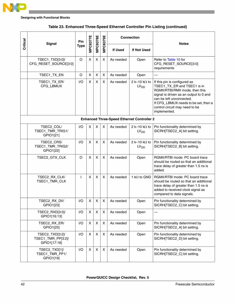
PowerQUICC Design Checklist, Rev. 5
42 Freescale Semiconductor
Designing with Functional Blocks
TSEC1_TXD[3:0]/CFG_RESET_SOURCE[3:0]
O X X X As needed Open Refer to Table 10 for CFG_RESET_SOURCE[3:0] requirements
TSEC1_TX_EN O X X X As needed Open —
TSEC1_TX_ER/CFG_LBMUX
I/O X X X As needed 2 k–10 kΩ to LVDD
If this pin is configured as TSEC1_TX_ER and TSEC1 is in RGMII/RTBI/RMII mode, then this signal is driven as an output to 0 and can be left unconnected.If CFG_LBMUX needs to be set, then a control circuit may need to be implemented.
Enhanced Three-Speed Ethernet Controller 2
TSEC2_COL/TSEC1_TMR_TRIG1/
GPIO1[21]
I/O X X X As needed 2 k–10 kΩ to LVDD
Pin functionality determined by SICRH[TSEC2_A] bit setting.
TSEC2_CRS/TSEC1_TMR_TRIG2/
GPIO1[22]
I/O X X X As needed 2 k–10 kΩ to LVDD
Pin functionality determined by SICRH[TSEC2_B] bit setting.
TSEC2_GTX_CLK O X X X As needed Open RGMII/RTBI mode: PC board trace should be routed so that an additional trace delay of greater than 1.5 ns is added.
TSEC2_RX_CLK/TSEC1_TMR_CLK
I X X X As needed 1 kΩ to GND RGMII/RTBI mode: PC board trace should be routed so that an additional trace delay of greater than 1.5 ns is added to received clock signal as compared to data signals.
TSEC2_RX_DV/GPIO1[23]
I/O X X X As needed Open Pin functionality determined by SICRH[TSEC2_C] bit setting.
TSEC2_RXD[3:0]/GPIO1[16:13]
I/O X X X As needed Open —
TSEC2_RX_ER/GPIO1[25]
I/O X X X As needed Open Pin functionality determined by SICRH[TSEC2_A] bit setting.
TSEC2_TXD[3:2]/TSEC1_TMR_PP[3:2]/
GPIO1[17:18]
I/O X X X As needed Open Pin functionality determined by SICRH[TSEC2_D] bit setting.
TSEC2_TXD[1]/TSEC1_TMR_PP1/
GPIO1[19]
I/O X X X As needed Open Pin functionality determined by SICRH[TSEC2_C] bit setting.
Table 23. Enhanced Three-Speed Ethernet Controller Pin Listing (continued)C
riti
cal
SignalPin
Type
MP
C83
77E
MP
C83
78E
MP
C83
79E Connection
Notes
If Used If Not Used
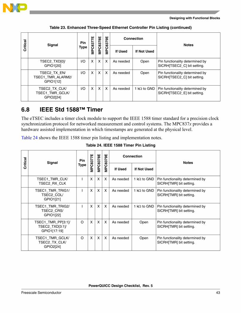
PowerQUICC Design Checklist, Rev. 5
Freescale Semiconductor 43
Designing with Functional Blocks
6.8 IEEE Std 1588™ TimerThe eTSEC includes a timer clock module to support the IEEE 1588 timer standard for a precision clock synchronization protocol for networked measurement and control systems. The MPC837x provides a hardware assisted implementation in which timestamps are generated at the physical level.
Table 24 shows the IEEE 1588 timer pin listing and implementation notes.
TSEC2_TXD[0]/GPIO1[20]
I/O X X X As needed Open Pin functionality determined by SICRH[TSEC2_C] bit setting.
TSEC2_TX_EN/TSEC1_TMR_ALARM2/
GPIO1[12]
I/O X X X As needed Open Pin functionality determined by SICRH[TSEC2_C] bit setting.
TSEC2_TX_CLK/TSEC1_TMR_GCLK/
GPIO2[24]
I/O X X X As needed 1 kΩ to GND Pin functionality determined by SICRH[TSEC2_E] bit setting.
Table 24. IEEE 1588 Timer Pin Listing
Cri
tica
l
SignalPin
Type
MP
C83
77E
MP
C83
78E
MP
C83
79E Connection
Notes
If Used If Not Used
TSEC1_TMR_CLK/TSEC2_RX_CLK
I X X X As needed 1 kΩ to GND Pin functionality determined by SICRH[TMR] bit setting.
TSEC1_TMR_TRIG1/TSEC2_COL/
GPIO1[21]
I X X X As needed 1 kΩ to GND Pin functionality determined by SICRH[TMR] bit setting.
TSEC1_TMR_TRIG2/TSEC2_CRS/
GPIO1[22]
I X X X As needed 1 kΩ to GND Pin functionality determined by SICRH[TMR] bit setting.
TSEC1_TMR_PP[3:1]/TSEC2_TXD[3:1]/
GPIO1[17:19]
O X X X As needed Open Pin functionality determined by SICRH[TMR] bit setting.
TSEC1_TMR_GCLK/TSEC2_TX_CLK/
GPIO2[24]
O X X X As needed Open Pin functionality determined by SICRH[TMR] bit setting.
Table 23. Enhanced Three-Speed Ethernet Controller Pin Listing (continued)C
riti
cal
SignalPin
Type
MP
C83
77E
MP
C83
78E
MP
C83
79E Connection
Notes
If Used If Not Used
PowerQUICC Design Checklist, Rev. 5
44 Freescale Semiconductor
Designing with Functional Blocks
6.9 SerDes (SGMII, SATA, PCI Express®)The SerDes PHY block supports the following modes of operation:
• SerDes1— Two lanes running ×1 SGMII at 1.25 Gbps (MPC8378 only)— Two lanes running ×1 SATA at 1.5 or 3.0 Gbps (MPC8377 and MPC8379 only)
• SerDes2— Two lanes running ×1 PCI Express at 2.5 Gbps (MPC8377 and MPC8378 only)— One lane running ×2 PCI Express at 2.5 Gbps (MPC8377 and MPC8378 only)— Two lanes running 1×SATA at 1.5 or 3.0 Gbps (MPC8377 and MPC8379 only)
Table 25 shows the SerDes pin listing and implementation notes.
TSEC1_TMR_ALARM1/TSEC2_TX_ER/
GPIO1[24]
O X X X As needed Open Pin functionality determined by SICRH[TMR] bit setting.
TSEC1_TMR_ALARM2/TSEC2_TX_EN/
GPIO1[12]
O X X X As needed Open Pin functionality determined by SICRH[TMR] bit setting.
Table 25. SerDes Pin Listing
Cri
tica
l
SignalPin
Type
MP
C83
77E
MP
C83
78E
MP
C83
79E Connection
Notes
If Used If Not Used
L1_SD_IMP_CAL_RX I X X X Connect a 200 Ω, 1% tolerance resistor to
XCOREVSS
Receiver impedance control
L1_SD_IMP_CAL_TX I X X X Connect a 100 Ω, 1% tolerance resistor to
XPADVSS
Transmitter impedance control
L1_SD_REF_CLK I X X X As needed Connect to XCOREVSS
Differential reference clock • SATA: Reference frequency
100/125/150 MHz for 1.5 Gbps • SGMII: Reference frequency
100/125 MHz for 3.0 Gbps
Table 24. IEEE 1588 Timer Pin ListingC
riti
cal
SignalPin
Type
MP
C83
77E
MP
C83
78E
MP
C83
79E Connection
Notes
If Used If Not Used
PowerQUICC Design Checklist, Rev. 5
Freescale Semiconductor 45
Designing with Functional Blocks
L1_SD_RXA_NL1_SD_RXA_PL1_SD_RXE_NL1_SD_RXE_P
I X X X As needed Connect to XCOREVSS
Differential receiver input
L1_SD_TXA_NL1_SD_TXA_PL1_SD_TXE_NL1_SD_TXE_P
O X X X As needed Open Differential transmitter output
L2_SD_IMP_CAL_RX I X X X Connect a 200 Ω, 1% tolerance resistor to
XCOREVSS
Receiver impedance calibration. Calibration resistors are recommended. To use nominal values only, sd_imp_cal_rx input may be tied directly to the xcorevdd.
L2_SD_IMP_CAL_TX I X X X Connect a 100 Ω, 1% tolerance resistor to
XPADVSS
Transmitter impedance calibration. Calibration resistors are recommended. To use nominal values only, sd_imp_cal_tx input may be tied directly to the xpadvdd.
L2_SD_REF_CLK I X X X As needed Connect to XCOREVSS
Differential reference clock • PCI-Express: Reference frequency
100 MHz for 2.5 Gbps • SATA: Reference frequency
100/125/150 MHz for 1.5 Gbps
L2_SD_RXA_NL2_SD_RXA_PL2_SD_RXE_NL2_SD_RXE_P
I X X X As needed Connect to XCOREVSS
Differential receiver input
L2_SD_TXA_NL2_SD_TXA_PL2_SD_TXE_NL2_SD_TXE_P
O X X X As needed Open Differential transmitter output
Table 25. SerDes Pin Listing (continued)C
riti
cal
SignalPin
Type
MP
C83
77E
MP
C83
78E
MP
C83
79E Connection
Notes
If Used If Not Used
PowerQUICC Design Checklist, Rev. 5
46 Freescale Semiconductor
Designing with Functional Blocks
Figure 12 shows the connection diagram for the impedance calibration pins.
Figure 12. Connection Diagram for Impedance Calibration Pins
6.10 SATA ControllerThe SATA controller has the following features:
• Fully compliant with Serial ATA Specification, Revision 2.5• Support for both speeds: 1.5 Gbps (first generation SATA) and 3 Gbps (second generation SATA)• A high-speed descriptor-based DMA controller• Native command queuing (NCQ) commands• Port multiplier operation• Hot plug, including asynchronous signal recovery
Refer to Table 25 for SerDes pins for the SATA interface. SerDes pins are shared between SATA, PCI Express, and SGMII.
SD_IMP_CAL_RX
XCOREVDD
0 Ω
200 Ω
DNP
SD_IMP_CAL_TX
XPADVDD
0 Ω
100 Ω
DNP
XCOREVSS (GND) XPADVSS (GND)
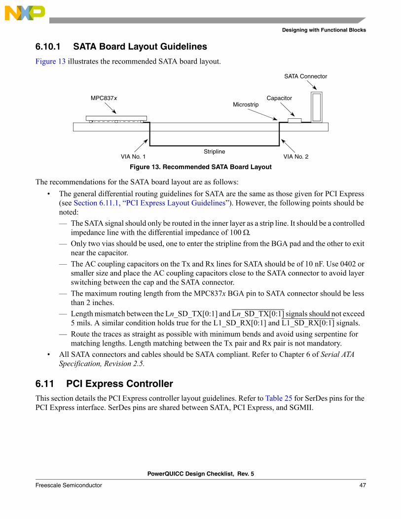
PowerQUICC Design Checklist, Rev. 5
Freescale Semiconductor 47
Designing with Functional Blocks
6.10.1 SATA Board Layout Guidelines
Figure 13 illustrates the recommended SATA board layout.
Figure 13. Recommended SATA Board Layout
The recommendations for the SATA board layout are as follows:• The general differential routing guidelines for SATA are the same as those given for PCI Express
(see Section 6.11.1, “PCI Express Layout Guidelines”). However, the following points should be noted:— The SATA signal should only be routed in the inner layer as a strip line. It should be a controlled
impedance line with the differential impedance of 100 Ω.— Only two vias should be used, one to enter the stripline from the BGA pad and the other to exit
near the capacitor.— The AC coupling capacitors on the Tx and Rx lines for SATA should be of 10 nF. Use 0402 or
smaller size and place the AC coupling capacitors close to the SATA connector to avoid layer switching between the cap and the SATA connector.
— The maximum routing length from the MPC837x BGA pin to SATA connector should be less than 2 inches.
— Length mismatch between the Ln_SD_TX[0:1] and Ln_SD_TX[0:1] signals should not exceed 5 mils. A similar condition holds true for the L1_SD_RX[0:1] and L1_SD_RX[0:1] signals.
— Route the traces as straight as possible with minimum bends and avoid using serpentine for matching lengths. Length matching between the Tx pair and Rx pair is not mandatory.
• All SATA connectors and cables should be SATA compliant. Refer to Chapter 6 of Serial ATA Specification, Revision 2.5.
6.11 PCI Express ControllerThis section details the PCI Express controller layout guidelines. Refer to Table 25 for SerDes pins for the PCI Express interface. SerDes pins are shared between SATA, PCI Express, and SGMII.
MPC837x
SATA Connector
CapacitorMicrostrip
VIA No. 1 VIA No. 2Stripline
PowerQUICC Design Checklist, Rev. 5
48 Freescale Semiconductor
Designing with Functional Blocks
6.11.1 PCI Express Layout Guidelines
The PCI Express layout guidelines are as follows:• Recommended microstrip trace routing guidelines
— Single ended: 50 Ω ±15%— Differential: 100 Ω ±15%
• Recommended stripline trace routing guidelines— Single ended: 50 Ω ±15%— Differential: 100 Ω ±15%
• Recommended length matching intra-pair: Maximum 5 mil delta, matching maintained segment to segment, and matching at point of discontinuity. However, avoid tight bends.
• Recommended length matching inter-pair: Recommended to keep differences within 3 inches to minimize latency.
• Recommended for all differential signal pairs: Maintain greater than equal of 20 mil trace edge to plane edge gap.
• GND referenced signals is recommended.• Use GND stitching vias by signal layer vias for layer changes.• Do not route over plane splits or voids. Allow no more than a half trace width routed over via
antipad.• Via usage: Limit via usage to four vias per TX trace and two vias per RX trace (six vias total, entire
path).• Bends: Match left/right turn bends whenever possible. No 90-degree bends or tight bend structures.• The reference clock signal pair should maintain the same reference plane for the entire routed
length and should not cross any plane splits (breaks in the reference plane).• A minimum separation from the reference clock and other traces should be maintained. Assuming
a trace width of “w,” no other trace or signal should be allowed within “3w.”• The reference clock signal pair routing length should be minimized.• The reference clock signal pair via count should be minimized. As a rule of thumb, via count should
not exceed four.• Reference clock terminating components should be placed as close as possible to their respective
devices, ideally within 100 mils of the clock/receiver component pin.• Match all segment lengths between differential pairs along the entire length of the pair.• Maintain constant line impedance along the routing path by keeping the same line width and line
separation.• Avoid routing differential pairs adjacent to noisy signal lines or high speed switching devices, such
as clock chips.• Keep clock lines adequately separated from I/O lines.• Recommend that PCI Express Reference clocks have length matching to within 25 mils.• Unused PCI Express clock outputs (unpopulated down devices or unpopulated add-in card
connectors) should be disabled to limit EMI radiations and possible signal reflections.
PowerQUICC Design Checklist, Rev. 5
Freescale Semiconductor 49
Designing with Functional Blocks
• Decoupling capacitors: Several PCB-mounted 0.1 to 1.0 µF capacitors should be placed near the PCI Express silicon on the sides of the package to which the PCI Express I/O buffers connect.
• AC coupling capacitors:— Do not use capacitor-packs (C-packs) for PCI Express AC coupling capacitor purpose.— The same package size and value of capacitor should be used for each signal in a differential
pair.— Locate capacitors for coupled traces in a differential pair at the same location along the
differential traces. Place them as close to each other as possible, as allowed by DFM rules.— The breakout into and out of the capacitor mounting pads should be symmetrical for both signal
lines in a differential pair.• Test points and probing structures should not introduce stubs on the differential pairs.
6.12 Enhanced Secure Digital Host ControllerThe enhanced SD host controller (eSDHC) provides an interface between the host system and SD/SDIO/MMC cards. The eSDHC supports the following modes for data transfer:
• SD 1-bit• SD 4-bit• MMC 1-bit• MMC 4-bit• Full-speed mode up to 25 MHz or high-speed mode up to 50 MHz
Table 26 lists the proper connections for the eSDHC pins. Table 26. eSDHC Pin Listing
Cri
tica
l
SignalPin
Type
MP
C83
77E
MP
C83
78E
MP
C83
79E Connection
Notes
If Used If Not Used
SD_CLK/SPICLK
O X X X 33 Ω serial resistor must be provided for SD_CLK and placed close to MPC837x device
Open If pin is configured as SPI, it should be pulled up if not used (see Table 32). Pin functionality determined by SICRH[SPI] bit setting.
SD_CMD/SPIMOSI
I/O X X X As needed 2 k–10 kΩ to OVDD Pull up as required by the SD Specification, Version 2.00
SD_DAT[3:0]1 I/O X X X As needed + pull up 2 k–10 kΩ to OVDD Pin functionality determined by SICRL[USB_B] bit setting. Pull up as required by the SD Specification, Version 2.00.
SD_CD/SPISEL
I X X X As needed Connect to GND —
SD_WP/IRQ[4]/GPIO2[16]
I X X X As needed Connect to GND Pin functionality determined by SICRH[GPIO2_E] bit setting.
PowerQUICC Design Checklist, Rev. 5
50 Freescale Semiconductor
Designing with Functional Blocks
6.12.1 eSDHC AC TimingThe eSDHC controller within the MPC837x always uses the falling edge of the SD_CLK to drive the SD_DAT[0:3]/CMD as outputs and sample the SD_DAT[0:3] as inputs. This behavior is true for both full- and high-speed modes.
Note that this is a non-standard implementation, as the SD card specification assumes that in high-speed mode, data will be driven at the rising edge of the clock.
Due to the MPC837x eSDHC special implementation, there are constraints regarding the clock and data signals propagation delay on the user board. The constraints are for minimum and maximum delays as well as skew between the CLK and DAT/CMD signals.
In full-speed mode, there is no need to add special delay on the data or clock signals. The user should be sure to meet the timing requirements as described further in the MPC8377E, MPC8378E, and MPC8379E hardware specifications.
If the system is designed to support both high-speed and full-speed cards, the high-speed constraints should be used. If the system is designed to operate up to 25 MHz only, full-speed mode is recommended. Additional details on meeting the delay timing for the full-speed mode output and input paths, including calculations, can be found in the MPC8377E, MPC8378E, and MPC8379E hardware specifications.
6.12.2 Full-Speed Mode
Table 27 lists the timing parameters that must be taken into consideration for full-speed mode. Any information in the relevant hardware specifications supersedes information in Table 27.
1 SD_DAT[0]/SPIMISO, SD_DAT[1]/USBDR_PWRFAULT/GPIO2[10], SD_DAT[2]/USBDR_PCTL0/GPIO2[11], SD_DAT[3]/USBDR_PCTL1/GPIO2[22]
Table 27. Full-Speed Mode Parameters
Name Description Value (ns) Min/Max According to
tSFSCK SD Clock cycle 40 ns (25 MHz) Min HW spec
tSFSCKL SD Clock low time 15 Min HW spec
tCLK_DELAY SD clock delay on the board See formulas min-max range calculated
tDATA_DELAY SD Data & CMD delay on the board See formulas min-max range calculated
tSFSIVKH MPC837x Input Setup 5 Min HW spec
tSFSIXKH MPC837x Input Hold –1.65 Min Measured
tSFSKHOV MPC837x output valid 2.85 Max Measured
tSFSKHOX MPC837x output hold 0 Min HW spec
tISU SD card input setup 5 Min SD standard
tIH SD card input hold 5 Min SD standard
PowerQUICC Design Checklist, Rev. 5
Freescale Semiconductor 51
Designing with Functional Blocks
6.12.3 High-Speed Mode
Table 28 lists the timing parameters that must be taken into consideration for high-speed mode. Any information in the relevant hardware specifications supersedes information in Table 28.
tODLY SD card output valid 14 Max SD standard
tOH SD card output hold 0 Min SD standard (practical interpretation)
Table 28. High-Speed Mode Parameters
Name Description Value (ns) Min/Max According to Notes
tSHSCK SD Clock cycle 20 ns (50 MHz) Min HW spec —
tSHSCKL SD Clock low time 7 Min HW spec —
tCLK_DELAY SD clock delay on the board See formulas min-max range calculated —
tDATA_DELAY SD Data & CMD delay on the board See formulas min-max range calculated —
tSHSIVKH MPC837x Input Setup 5 Min HW spec 1
tSHSIXKH MPC837x Input Hold –1.65 Min Measured 1
tSHSKHOV MPC837x output valid 2.85 Max Measured —
tSHSKHOX MPC837x output hold 0 Min HW spec —
tISU SD card input setup 6 Min SD standard —
tIH SD card input hold 2 Min SD standard —
tODLY SD card output valid 14 Max SD standard —
tOH SD card output hold 2.5 Min SD standard —
Note:1. In the MPC8377E, MPC8378E, and MPC8379E hardware specifications some parameters have a prefix of tFHS. This should
be updated to tSHS.
Table 27. Full-Speed Mode Parameters (continued)
Name Description Value (ns) Min/Max According to
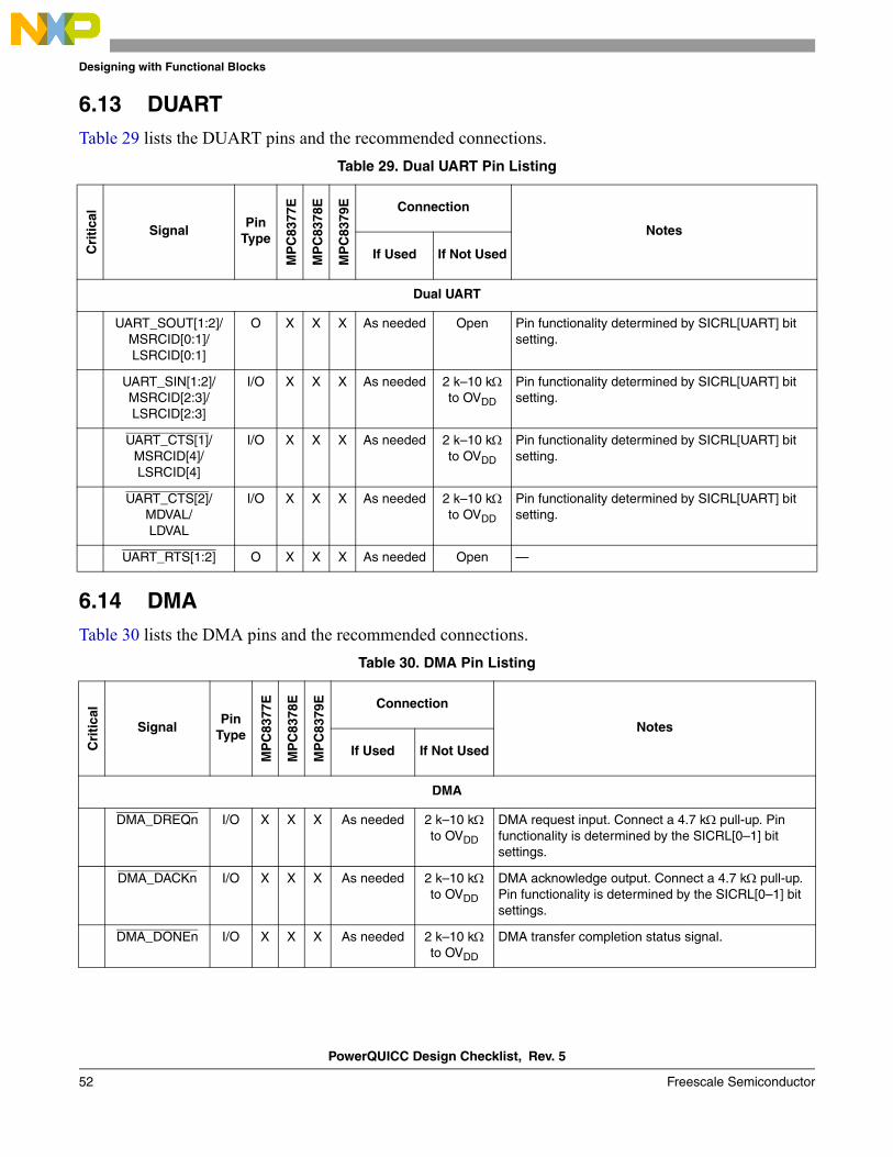
PowerQUICC Design Checklist, Rev. 5
52 Freescale Semiconductor
Designing with Functional Blocks
6.13 DUARTTable 29 lists the DUART pins and the recommended connections.
6.14 DMATable 30 lists the DMA pins and the recommended connections.
Table 29. Dual UART Pin Listing
Cri
tica
l
SignalPin
Type
MP
C83
77E
MP
C83
78E
MP
C83
79E Connection
Notes
If Used If Not Used
Dual UART
UART_SOUT[1:2]/ MSRCID[0:1]/ LSRCID[0:1]
O X X X As needed Open Pin functionality determined by SICRL[UART] bit setting.
UART_SIN[1:2]/ MSRCID[2:3]/ LSRCID[2:3]
I/O X X X As needed 2 k–10 kΩ to OVDD
Pin functionality determined by SICRL[UART] bit setting.
UART_CTS[1]/ MSRCID[4]/ LSRCID[4]
I/O X X X As needed 2 k–10 kΩ to OVDD
Pin functionality determined by SICRL[UART] bit setting.
UART_CTS[2]/ MDVAL/LDVAL
I/O X X X As needed 2 k–10 kΩ to OVDD
Pin functionality determined by SICRL[UART] bit setting.
UART_RTS[1:2] O X X X As needed Open —
Table 30. DMA Pin Listing
Cri
tica
l
SignalPin
Type
MP
C83
77E
MP
C83
78E
MP
C83
79E Connection
Notes
If Used If Not Used
DMA
DMA_DREQn I/O X X X As needed 2 k–10 kΩ to OVDD
DMA request input. Connect a 4.7 kΩ pull-up. Pin functionality is determined by the SICRL[0–1] bit settings.
DMA_DACKn I/O X X X As needed 2 k–10 kΩ to OVDD
DMA acknowledge output. Connect a 4.7 kΩ pull-up. Pin functionality is determined by the SICRL[0–1] bit settings.
DMA_DONEn I/O X X X As needed 2 k–10 kΩ to OVDD
DMA transfer completion status signal.
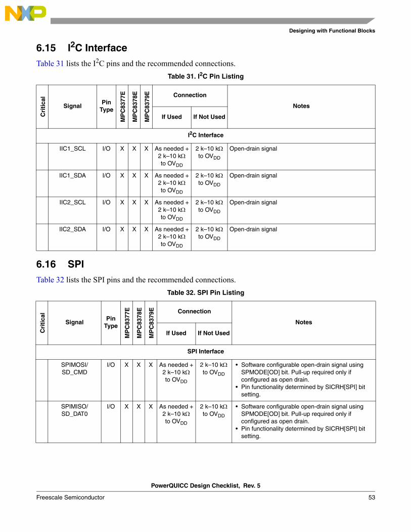
PowerQUICC Design Checklist, Rev. 5
Freescale Semiconductor 53
Designing with Functional Blocks
6.15 I2C InterfaceTable 31 lists the I2C pins and the recommended connections.
6.16 SPITable 32 lists the SPI pins and the recommended connections.
Table 31. I2C Pin Listing
Cri
tica
l
SignalPin
Type
MP
C83
77E
MP
C83
78E
MP
C83
79E Connection
Notes
If Used If Not Used
I2C Interface
IIC1_SCL I/O X X X As needed +2 k–10 kΩ to OVDD
2 k–10 kΩ to OVDD
Open-drain signal
IIC1_SDA I/O X X X As needed +2 k–10 kΩ to OVDD
2 k–10 kΩ to OVDD
Open-drain signal
IIC2_SCL I/O X X X As needed +2 k–10 kΩ to OVDD
2 k–10 kΩ to OVDD
Open-drain signal
IIC2_SDA I/O X X X As needed +2 k–10 kΩto OVDD
2 k–10 kΩ to OVDD
Open-drain signal
Table 32. SPI Pin Listing
Cri
tica
l
SignalPin
Type
MP
C83
77E
MP
C83
78E
MP
C83
79E Connection
Notes
If Used If Not Used
SPI Interface
SPIMOSI/SD_CMD
I/O X X X As needed +2 k–10 kΩ to OVDD
2 k–10 kΩ to OVDD
• Software configurable open-drain signal using SPMODE[OD] bit. Pull-up required only if configured as open drain.
• Pin functionality determined by SICRH[SPI] bit setting.
SPIMISO/SD_DAT0
I/O X X X As needed +2 k–10 kΩ to OVDD
2 k–10 kΩ to OVDD
• Software configurable open-drain signal using SPMODE[OD] bit. Pull-up required only if configured as open drain.
• Pin functionality determined by SICRH[SPI] bit setting.
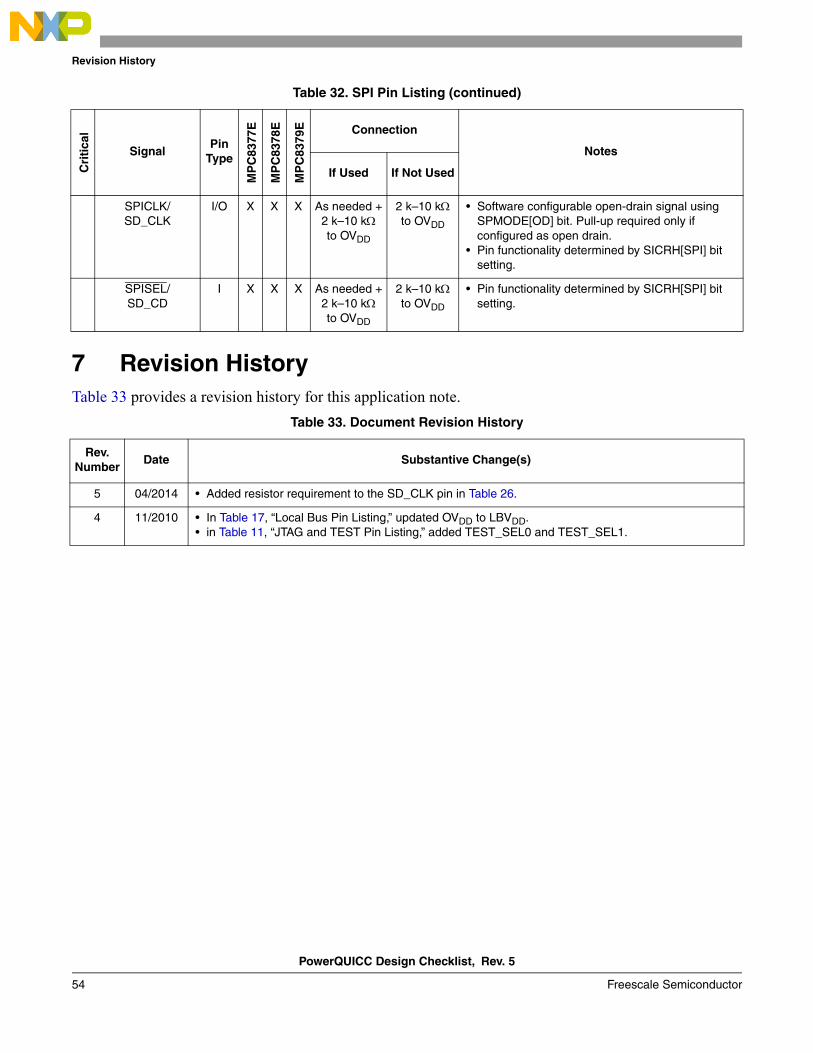
PowerQUICC Design Checklist, Rev. 5
54 Freescale Semiconductor
Revision History
7 Revision HistoryTable 33 provides a revision history for this application note.
SPICLK/SD_CLK
I/O X X X As needed +2 k–10 kΩ to OVDD
2 k–10 kΩ to OVDD
• Software configurable open-drain signal using SPMODE[OD] bit. Pull-up required only if configured as open drain.
• Pin functionality determined by SICRH[SPI] bit setting.
SPISEL/SD_CD
I X X X As needed +2 k–10 kΩ to OVDD
2 k–10 kΩ to OVDD
• Pin functionality determined by SICRH[SPI] bit setting.
Table 33. Document Revision History
Rev. Number
Date Substantive Change(s)
5 04/2014 • Added resistor requirement to the SD_CLK pin in Table 26.
4 11/2010 • In Table 17, “Local Bus Pin Listing,” updated OVDD to LBVDD. • in Table 11, “JTAG and TEST Pin Listing,” added TEST_SEL0 and TEST_SEL1.
Table 32. SPI Pin Listing (continued)C
riti
cal
SignalPin
Type
MP
C83
77E
MP
C83
78E
MP
C83
79E Connection
Notes
If Used If Not Used
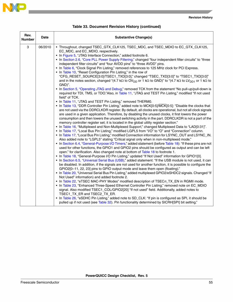
PowerQUICC Design Checklist, Rev. 5
Freescale Semiconductor 55
Revision History
3 06/2010 • Throughout, changed TSEC_GTX_CLK125, TSEC_MDC, and TSEC_MDIO to EC_GTX_CLK125, EC_MDC, and EC_MDIO, respectively.
• In Figure 5, “JTAG Interface Connection,” added footnote 6. • In Section 2.6, “Core PLL Power Supply Filtering,” changed “four independent filter circuits” to “three
independent filter circuits” and “four AVDD pins” to “three AVDD” pins. • In Table 6, “Clock Signal Pin Listing,” removed references to 125 MHz clock for PCI Express. • In Table 10, “Reset Configuration Pin Listing,” in the row of
“CFG_RESET_SOURCE[3:0]/TSEC1_TXD[3:0],” changed “TSEC_TXD[3:0]” to “TSEC1_TXD[3:0]” and in the notes section, changed “(4.7 kΩ to OVDD or 1 kΩ to GND)” to “(4.7 kΩ to LVDD1 or 1 kΩ to GND)”.
• In Section 5, “Operating JTAG and Debug,” removed TCK from the statement “No pull-up/pull-down is required for TDI, TMS, or TDO.”Also, in Table 11, “JTAG and TEST Pin Listing,” modified “If not used field” of TCK.
• In Table 11, “JTAG and TEST Pin Listing,” removed THERM0. • In Table 13, “DDR Controller Pin Listing,” added note to MCK[0:5]/MCK[0:5]: “Disable the clocks that
are not used via the DDRCLKDR register. By default, all clocks are operational, but not all clock signals are used in a given application. Therefore, by disabling the unused clocks, it first lowers the power consumption and then lowers the unused switching activity in the part. DDRCLKDR is not a part of the memory controller register set; it is located in the global utility register section.”
• In Table 16, “Multiplexed and Non-Multiplexed Support,” changed Multiplexed Data to “LAD[0:31]”. • In Table 17, “Local Bus Pin Listing,” modified LGPL5 from “I/O” to “O” and “Connection” column. • In Table 17, “Local Bus Pin Listing,” modified Connection information for LSYNC_OUT and LSYNC_IN.
Also added note to “LGPL5” stating “Critical signal only when in non-multiplexed mode.” • In Section 6.4, “General-Purpose I/O Timers,” added statement (before Table 18): “If these pins are not
used for other functions, the GPIO1 and GPIO2 pins should be configured as output and can be left open.” for clarification. Also changed note at bottom of Table 18 to footnote 1.
• In Table 18, “General-Purpose I/O Pin Listing,” updated “If Not Used” information for GPIO1[0]. • In Section 6.5, “Universal Serial Bus (USB),” added statement: “If the USB module is not used, it can
be disabled. In addition, if the signals are not used for another function, it is possible to configure the GPIO2[0–11, 22, 23] pins to GPIO output mode and leave them open (floating).”
• In Table 20, “Universal Serial Bus Pin Listing,” added multiplexed GPIO2/eSHDC2 signals. Changed “If Not Used” information) and added footnote 2.
• In Table 22, “eTSEC MAC-PHY Modes” modified description of TSECn_TX_EN in RGMII mode. • In Table 23, “Enhanced Three-Speed Ethernet Controller Pin Listing,” removed note on EC_MDIO
signal. Also modified TSEC1_COL/GPIO2[20] “If not used” field. Additionally, added notes to TSEC1_TX_ER and TSEC2_TX_ER.
• In Table 26, “eSDHC Pin Listing,” added note to SD_CLK: “If pin is configured as SPI, it should be pulled up if not used (see Table 32). Pin functionality determined by SICRH[SPI] bit setting.”
Table 33. Document Revision History (continued)
Rev. Number
Date Substantive Change(s)
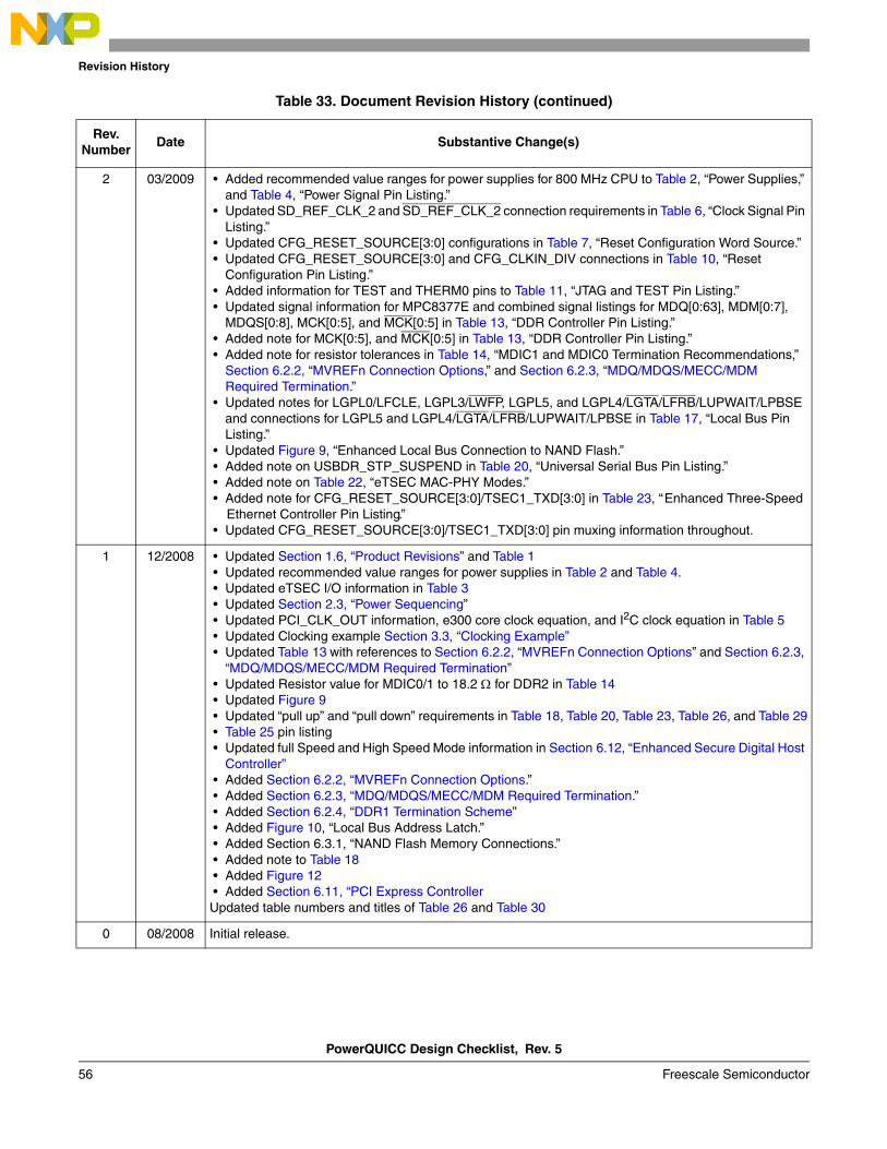
PowerQUICC Design Checklist, Rev. 5
56 Freescale Semiconductor
Revision History
2 03/2009 • Added recommended value ranges for power supplies for 800 MHz CPU to Table 2, “Power Supplies,” and Table 4, “Power Signal Pin Listing.”
• Updated SD_REF_CLK_2 and SD_REF_CLK_2 connection requirements in Table 6, “Clock Signal Pin Listing.”
• Updated CFG_RESET_SOURCE[3:0] configurations in Table 7, “Reset Configuration Word Source.” • Updated CFG_RESET_SOURCE[3:0] and CFG_CLKIN_DIV connections in Table 10, “Reset
Configuration Pin Listing.” • Added information for TEST and THERM0 pins to Table 11, “JTAG and TEST Pin Listing.” • Updated signal information for MPC8377E and combined signal listings for MDQ[0:63], MDM[0:7],
MDQS[0:8], MCK[0:5], and MCK[0:5] in Table 13, “DDR Controller Pin Listing.” • Added note for MCK[0:5], and MCK[0:5] in Table 13, “DDR Controller Pin Listing.” • Added note for resistor tolerances in Table 14, “MDIC1 and MDIC0 Termination Recommendations,”
Section 6.2.2, “MVREFn Connection Options,” and Section 6.2.3, “MDQ/MDQS/MECC/MDM Required Termination.”
• Updated notes for LGPL0/LFCLE, LGPL3/LWFP, LGPL5, and LGPL4/LGTA/LFRB/LUPWAIT/LPBSE and connections for LGPL5 and LGPL4/LGTA/LFRB/LUPWAIT/LPBSE in Table 17, “Local Bus Pin Listing.”
• Updated Figure 9, “Enhanced Local Bus Connection to NAND Flash.” • Added note on USBDR_STP_SUSPEND in Table 20, “Universal Serial Bus Pin Listing.” • Added note on Table 22, “eTSEC MAC-PHY Modes.” • Added note for CFG_RESET_SOURCE[3:0]/TSEC1_TXD[3:0] in Table 23, “Enhanced Three-Speed
Ethernet Controller Pin Listing.” • Updated CFG_RESET_SOURCE[3:0]/TSEC1_TXD[3:0] pin muxing information throughout.
1 12/2008 • Updated Section 1.6, “Product Revisions” and Table 1 • Updated recommended value ranges for power supplies in Table 2 and Table 4. • Updated eTSEC I/O information in Table 3 • Updated Section 2.3, “Power Sequencing” • Updated PCI_CLK_OUT information, e300 core clock equation, and I2C clock equation in Table 5 • Updated Clocking example Section 3.3, “Clocking Example” • Updated Table 13 with references to Section 6.2.2, “MVREFn Connection Options” and Section 6.2.3,
“MDQ/MDQS/MECC/MDM Required Termination” • Updated Resistor value for MDIC0/1 to 18.2 Ω for DDR2 in Table 14 • Updated Figure 9 • Updated “pull up” and “pull down” requirements in Table 18, Table 20, Table 23, Table 26, and Table 29 • Table 25 pin listing • Updated full Speed and High Speed Mode information in Section 6.12, “Enhanced Secure Digital Host
Controller” • Added Section 6.2.2, “MVREFn Connection Options.” • Added Section 6.2.3, “MDQ/MDQS/MECC/MDM Required Termination.” • Added Section 6.2.4, “DDR1 Termination Scheme” • Added Figure 10, “Local Bus Address Latch.” • Added Section 6.3.1, “NAND Flash Memory Connections.” • Added note to Table 18 • Added Figure 12 • Added Section 6.11, “PCI Express ControllerUpdated table numbers and titles of Table 26 and Table 30
0 08/2008 Initial release.
Table 33. Document Revision History (continued)
Rev. Number
Date Substantive Change(s)
Document Number: AN3665Rev. 5
04/2014
Information in this document is provided solely to enable system and software
implementers to use Freescale products. There are no express or implied copyright
licenses granted hereunder to design or fabricate any integrated circuits based on the
information in this document.
Freescale reserves the right to make changes without further notice to any products
herein. Freescale makes no warranty, representation, or guarantee regarding the
suitability of its products for any particular purpose, nor does Freescale assume any
liability arising out of the application or use of any product or circuit, and specifically
disclaims any and all liability, including without limitation consequential or incidental
damages. “Typical” parameters that may be provided in Freescale data sheets and/or
specifications can and do vary in different applications, and actual performance may vary
over time. All operating parameters, including “typicals,” must be validated for each
customer application by customer’s technical experts. Freescale does not convey any
license under its patent rights nor the rights of others. Freescale sells products pursuant
to standard terms and conditions of sale, which can be found at the following address:
freescale.com/SalesTermsandConditions.
How to Reach Us:
Home Page: freescale.com
Web Support: freescale.com/support
Freescale, the Freescale logo, and PowerQUICC, are trademarks of Freescale
Semiconductor, Inc., Reg. U.S. Pat. & Tm. Off. All other product or service names are the
property of their respective owners. The Power Architecture and Power.org word marks
and the Power and Power.org logos and related marks are trademarks and service marks
licensed by Power.org.
© 2008–2014 Freescale Semiconductor, Inc.