Embed Size (px)
Citation preview

Visit www.npl.co.uk/ei
Practical Applications for Nano-Electronics
by
Vimal Gopee
E-mail: [email protected]
10/10/12
Your Delegate Webinar Control Panel
Open and close your panelFull screen view
Raise hand for Q&A at the end
Submit text questionsduring or at the end

Visit www.npl.co.uk/ei
Practical Applications for Nano-Electronics
by
Vimal Gopee
E-mail: [email protected]
10/10/12
Introduction:
Part of the Engineering Doctorate (EngD) in Micro and Nano materials at The University of Surrey
2nd year of the programme
Full-time placement at NPL
Currently working on Nanocarbon Electronic Interconnects (NEI) project
Visit www.npl.co.uk/ei
Contents
Current issues with electronic interconnects
Properties of carbon nanotubes
Synthesis methods
The nano-carbon interconnects project
Uses of carbon nanotubes in circuits
Summary
Current issues with electronic interconnects

Visit www.npl.co.uk/ei
Moore’s law
Number of transistors per chip doubling every 18-24 months
Interconnect pitch size decreasing
Visit www.npl.co.uk/ei
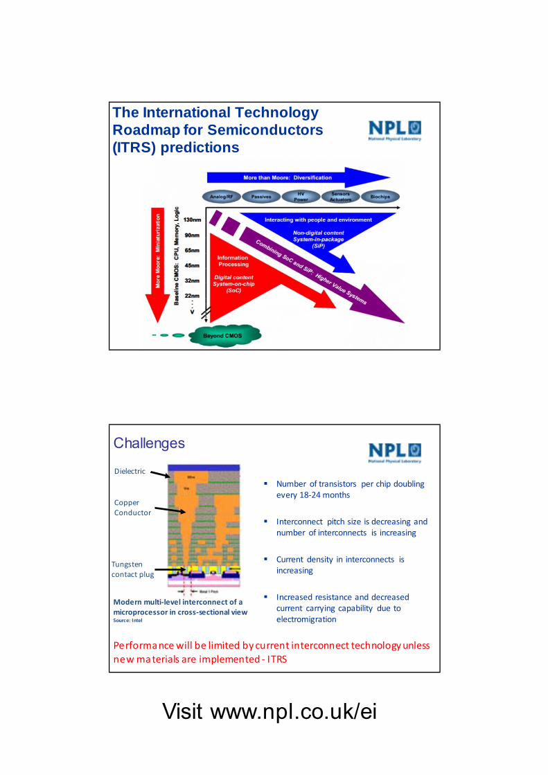
The International Technology Roadmap for Semiconductors (ITRS) predictions
Challenges
Modern multi‐level interconnect of a microprocessor in cross‐sectional viewSource: Intel
Number of transistors per chip doubling every 18‐24 months
Interconnect pitch size is decreasing and number of interconnects is increasing
Current density in interconnects is increasing
Increased resistance and decreased current carrying capability due to electromigration
Copper Conductor
Dielectric
Tungsten contact plug
Performance will be limited by current interconnect technology unless new materials are implemented ‐ ITRS
Visit www.npl.co.uk/ei
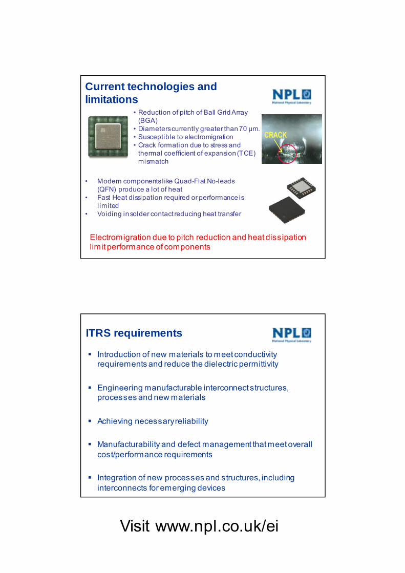
Current technologies and limitations
• Reduction of pitch of Ball Grid Array (BGA)
• Diameters currently greater than 70 μm.• Susceptible to electromigration• Crack formation due to stress and
thermal coefficient of expansion (TCE) mismatch
• Modern components l ike Quad-Flat No-leads (QFN) produce a lot of heat
• Fast Heat dissipation required or performance is l imited
• Voiding in solder contact reducing heat transfer
Electromigration due to pitch reduction and heat dissipation limit performance of components
ITRS requirements
Introduction of new materials to meet conductivity requirements and reduce the dielectric permittivity
Engineering manufacturable interconnect structures, processes and new materials
Achieving necessary reliability
Manufacturability and defect management that meet overall cost/performance requirements
Integration of new processes and structures, including interconnects for emerging devices
Visit www.npl.co.uk/ei
Properties of Carbon nanotubes
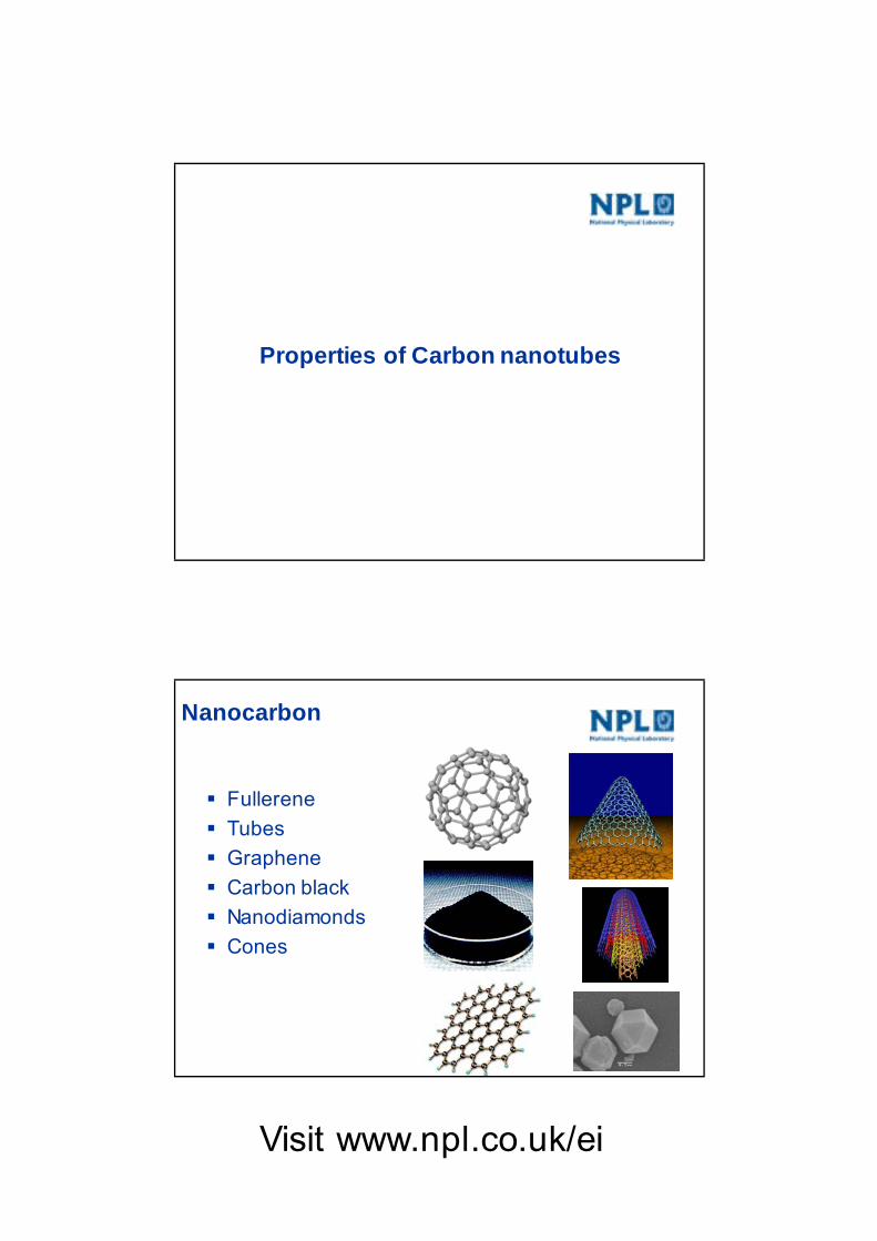
Nanocarbon
Fullerene
Tubes
Graphene
Carbon black
Nanodiamonds
Cones
Visit www.npl.co.uk/ei
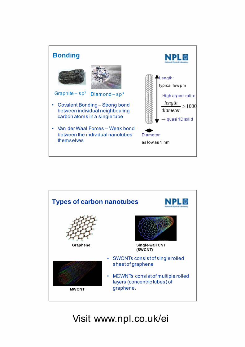
Bonding
Graphite – sp2 Diamond – sp3
Diameter:
as low as 1 nm
Length:
typical few μm
High aspect ratio:
1000diameter
length
→ quasi 1D solid
• Covalent Bonding – Strong bond between individual neighbouring carbon atoms in a single tube
• Van der Waal Forces – Weak bond between the individual nanotubes themselves
Types of carbon nanotubes
Graphene Single-wall CNT (SWCNT)
MWCNT
• SWCNTs consist of single rolled sheet of graphene
• MCWNTs consist of multiple rolled layers (concentric tubes) of graphene.
Visit www.npl.co.uk/ei
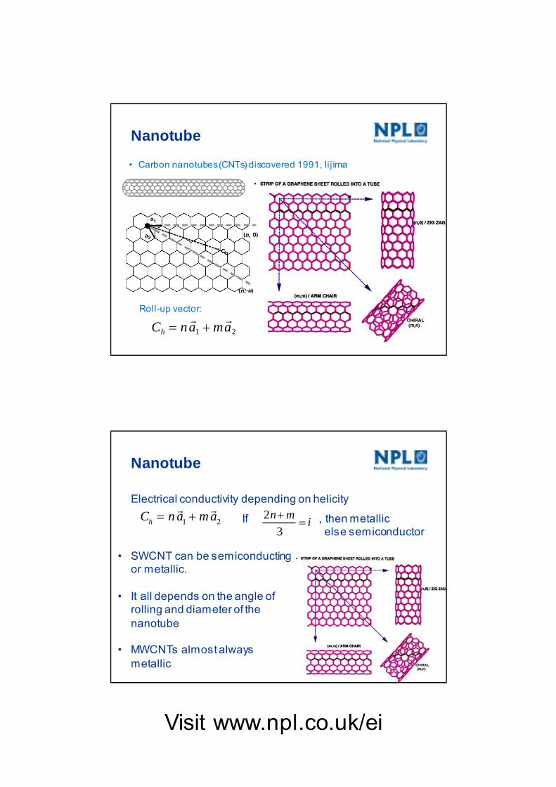
Nanotube
Roll-up vector:
21 amanCh
• Carbon nanotubes (CNTs) discovered 1991, Ii j ima
Nanotube
Electrical conductivity depending on helicity
21 amanCh
If , then metallic
else semiconductori
mn
3
2
• SWCNT can be semiconducting or metallic.
• It all depends on the angle of rolling and diameter of the nanotube
• MWCNTs almost always metallic
Visit www.npl.co.uk/ei
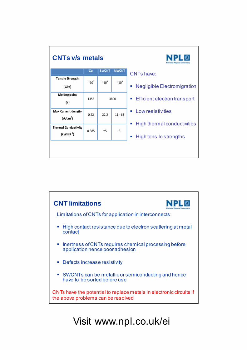
CNTs v/s metals
CNTs have:
Negligible Electromigration
Efficient electron transport
Low resistivities
High thermal conductivities
High tensile strengths
Cu SWCNT MWCNT
Tensile Strength
(GPa) ~106 ~109 ~109
Melting point
(K) 1356 3800
Max Current density
(A/cm2)
0.22 22.2 11 ‐ 63
Thermal Conductivity
(kWmK‐1) 0.385 ~5 3
CNT limitations
Limitations of CNTs for application in interconnects:
High contact resistance due to electron scattering at metal contact
Inertness of CNTs requires chemical processing before application hence poor adhesion
Defects increase resistivity
SWCNTs can be metallic or semiconducting and hence have to be sorted before use
CNTs have the potential to replace metals in electronic circuits if the above problems can be resolved

Visit www.npl.co.uk/ei
Synthesis Methods
• Commonly applied techniques:– Chemical Vapor Deposition (CVD)
– Arc-Discharge
– Laser ablation
• Techniques differ in:– Type of nanotubes (SWNT / MWNT / Aligned)
– Catalyst used
– Yield
– Purity
Synthesis: overview
Visit www.npl.co.uk/ei
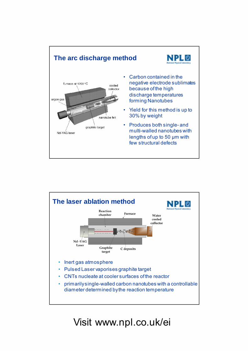
The arc discharge method
• Carbon contained in the negative electrode sublimates because of the high discharge temperatures forming Nanotubes
• Yield for this method is up to 30% by weight
• Produces both single- and multi-walled nanotubes with lengths of up to 50 μm with few structural defects
The laser ablation method
• Inert gas atmosphere
• Pulsed Laser vaporises graphite target
• CNTs nucleate at cooler surfaces of the reactor
• primarily single-walled carbon nanotubes with a controllable diameter determined by the reaction temperature
Visit www.npl.co.uk/ei
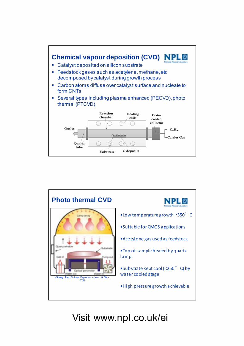
Chemical vapour deposition (CVD) Catalyst deposited on silicon substrate
Feedstock gases such as acetylene, methane, etcdecomposed by catalyst during growth process
Carbon atoms diffuse over catalyst surface and nucleate to form CNTs
Several types including plasma enhanced (PECVD), photo thermal (PTCVD),
Photo thermal CVD
•Low temperature growth ~350°C
•Suitable for CMOS applications
•Acetylene gas used as feedstock
•Top of sample heated by quartz lamp
•Substrate kept cool (<250 °C) by water cooled s tage
•High pressure growth achievable
(Shang, Tan, Stolojan, Papakonstantinou, & Silva, 2010)
Visit www.npl.co.uk/ei
The nano-carbon electronic interconnects project (NEI)
at NPL
To develop methodology for interconnect fabricationusing carbon nanotubes
To develop or adapt existing metrology for thecharacterisation of carbon nanotube interconnects
To characterise the electrical properties, behaviourunder mechanical deformation and thermal stress ofcarbon nanotube interconnects
Aims of NEI
Visit www.npl.co.uk/ei
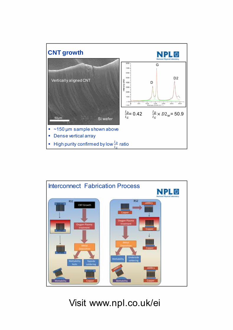
CNT growth
Vertically aligned CNT
Si wafer50μm2 = 50.9= 0.42
~150 μm sample shown above
Dense vertical array
High purity confirmed by low ratio
D
G
D2
Interconnect Fabrication Process
Visit www.npl.co.uk/ei
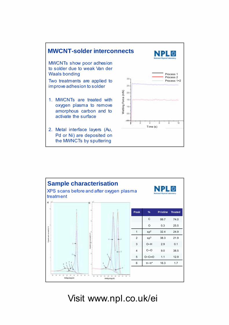
MWCNT-solder interconnects
MWCNTs show poor adhesionto solder due to weak Van derWaals bonding
Two treatments are applied toimprove adhesion to solder
1. MWCNTs are treated withoxygen plasma to removeamorphous carbon and toactivate the surface
2. Metal interface layers (Au,Pd or Ni) are deposited onthe MWNCTs by sputtering
Process 1Process 2Process 1+2
Time (s)W
ett
ing
Fo
rce
(m
N)
Sample characterisationXPS scans before and after oxygen plasma treatment
Peak % Pristine Treated
C 99.7 74.0
O 0.3 25.5
1 sp2 32.4 24.9
2 sp3 38.3 21.9
3 OH 2.9 0.1
4 CO 9.0 38.5
5 OCO 1.1 12.9
6 ππ* 16.3 1.7
Visit www.npl.co.uk/ei
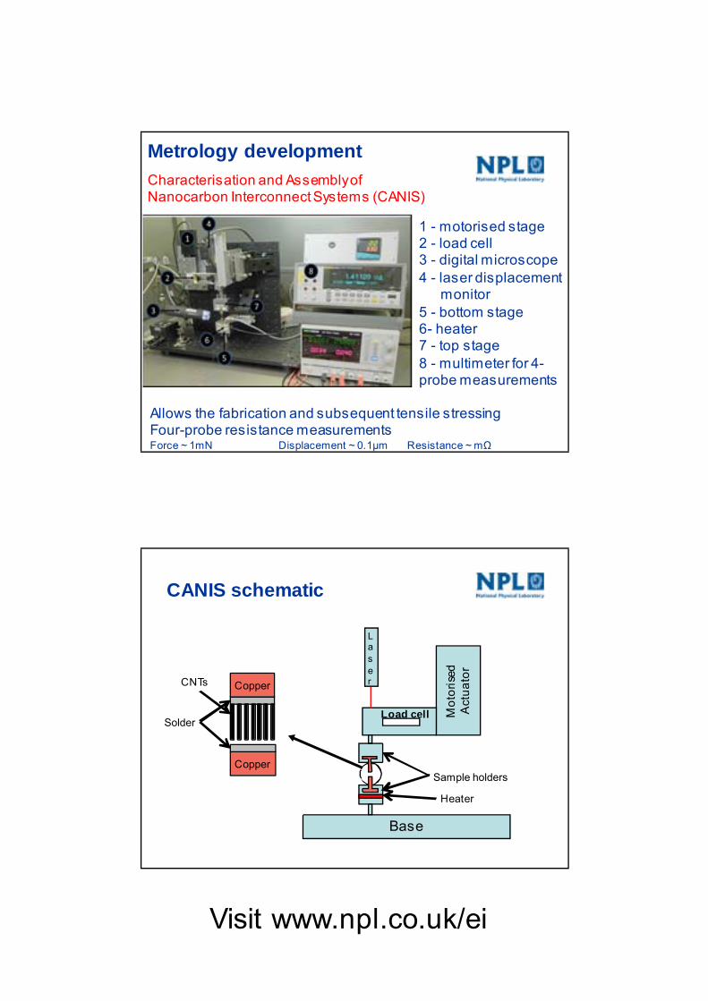
Characterisation and Assembly of Nanocarbon Interconnect Systems (CANIS)
Metrology development
1 - motorised stage2 - load cell3 - digital microscope4 - laser displacement
monitor5 - bottom stage6- heater7 - top stage8 - multimeter for 4-probe measurements
Allows the fabrication and subsequent tensile stressingFour-probe resistance measurementsForce ~ 1mN Displacement ~ 0.1μm Resistance ~ mΩ
CANIS schematic
Copper
Copper
Solder
CNTs
Base
Laser
Mo
tori
sed
A
ctu
ato
r
Load cell
Sample holders
Heater
Visit www.npl.co.uk/ei
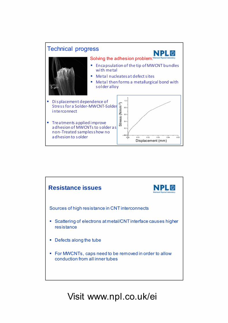
Technical progress
Encapsulation of the tip of MWCNT bundles with metal
Metal nucleates at defect s ites Metal then forms a metallurgical bond with
solder alloy
Displacement dependence of Stress for a Solder‐MWCNT‐Solder interconnect
Treatments applied improve adhesion of MWCNTs to solder as non‐Treated samples show no adhesion to solder
5 μm
Solving the adhesion problem:
Str
ess
(Nm
m-2)
Displacement (mm)
Resistance issues
Sources of high resistance in CNT interconnects
Scattering of electrons at metal/CNT interface causes higher resistance
Defects along the tube
For MWCNTs, caps need to be removed in order to allow conduction from all inner tubes
Visit www.npl.co.uk/ei
Future development work
• Electrical measurements will be made to assess contact resistance and compare with standard interconnects
• Quantify thermal conductivity and compare with solder-copper joints
• Thermal-cycling followed by shear and continuity tests to assess use in harsh environments
• Low-cycle and high cycle fatigue tests and compare reliability with standard solder joints
• Reduction in pitch size of interconnect to compare performance with current interconnects
Using CNTs in electronic circuits
• Field effect transistors
• Interconnects
• Field emitters
• Flexible electronics
Visit www.npl.co.uk/ei
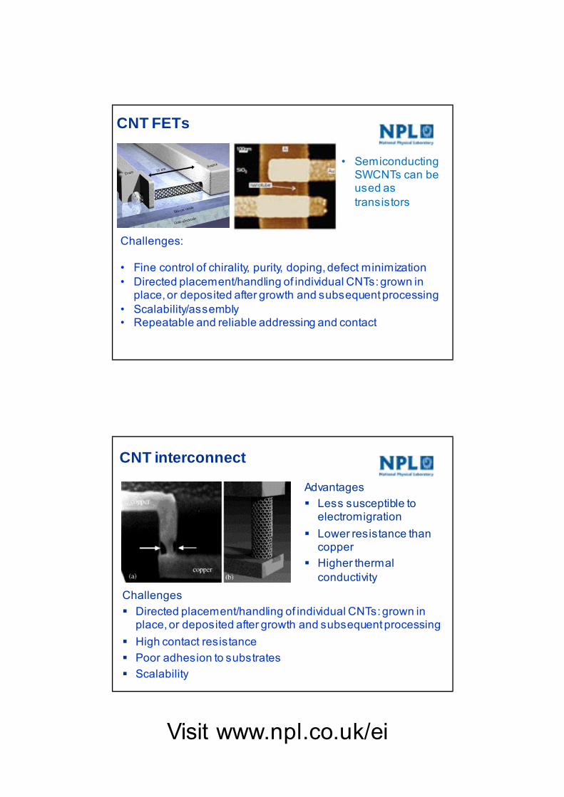
CNT FETs
• Semiconducting SWCNTs can be used as transistors
Challenges:
• Fine control of chirality, purity, doping, defect minimization• Directed placement/handling of individual CNTs: grown in
place, or deposited after growth and subsequent processing• Scalability/assembly• Repeatable and reliable addressing and contact
CNT interconnect
Advantages
Less susceptible to electromigration
Lower resistance than copper
Higher thermal conductivity
Challenges
Directed placement/handling of individual CNTs: grown in place, or deposited after growth and subsequent processing
High contact resistance
Poor adhesion to substrates
Scalability
Visit www.npl.co.uk/ei
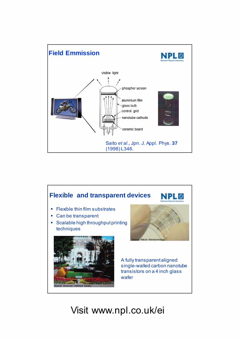
Field Emmission
Saito et al., Jpn. J. Appl. Phys. 37(1998) L346.
Flexible and transparent devices
Flexible thin film substrates
Can be transparent
Scalable high throughput printing techniques
Source: Nature Nanotechnology
A fully transparent aligned single-walled carbon nanotube transistors on a 4 inch glass wafer
Source: American chemical society

Visit www.npl.co.uk/ei
Summary
Summary
Current technologies reaching their limits, performance limited by physical dimensions
New materials need to be found to replace existing ones
CNTs offer an alternative to existing materials
CNTs have excellent electrical, thermal and mechanical properties
CNTs suffer from high contact resistance, poor adhesion, defects that limit their applications
Visit www.npl.co.uk/ei
• CNTs may replace metal interconnects in future integrated circuits
• In this project we aim to fabricate CNT interconnects and assess thermal, mechanical and electrical properties
• A fabrication process was devised and demonstrated
• A key step has been in improving adhesion of CNTs to solder
• Plans for further development of the interconnect technology were outlined