Embed Size (px)
Citation preview
OUTIN
GND
FAULTILIM
EN
RILIM
20 kW
RFAULT
100 kW
Control Signal
5V USBInput
USB
Port
USB Data
TPS2552/53
0.1 Fm
120 Fm
Fault Signal
Power Pad
USB requirement only*
*facing ports are bypassed with at least
120 F per hub
USB requirement that downstream
m
Copyright © 2016, Texas Instruments Incorporated
Product
Folder
Sample &Buy
Technical
Documents
Tools &
Software
Support &Community
ReferenceDesign
An IMPORTANT NOTICE at the end of this data sheet addresses availability, warranty, changes, use in safety-critical applications,intellectual property matters and other important disclaimers. PRODUCTION DATA.
TPS2552, TPS2553, TPS2552-1, TPS2553-1SLVS841F –NOVEMBER 2008–REVISED AUGUST 2016
TPS255xx Precision Adjustable Current-Limited Power-Distribution Switches
1
1 Features1• Up to 1.5-A Maximum Load Current• ±6% Current-Limit Accuracy at 1.7 A (Typical)• Meets USB Current-Limiting Requirements• Backwards Compatible With TPS2550 and
TPS2551• Adjustable Current Limit: 75 mA to 1700 mA
(Typical)• Constant-Current (TPS255x) and Latch-Off
(TPS255x-1) Versions• Fast Overcurrent Response - 2 µs (Typical)• 85-mΩ High-Side MOSFET (DBV Package)• Reverse Input-Output Voltage Protection• Operating Range: 2.5 V to 6.5 V• Built-In Soft Start• 15-kV ESD Protection per IEC 61000-4-2 (With
External Capacitance)• UL Listed – File No. E169910 and NEMKO
IEC60950-1-am1 ed2.0• See the TI Switch Portfolio
2 Applications• USB Ports and Hubs• Digital TVs• Set-Top Boxes• VOIP Phones
3 DescriptionThe TPS255x and TPS255x-1 power-distributionswitches are intended for applications whereprecision current limiting is required or heavycapacitive loads and short circuits are encounteredand provide up to 1.5 A of continuous load current.These devices offer a programmable current-limitthreshold between 75 mA and 1.7 A (typical) throughan external resistor. Current-limit accuracy as tight as±6% can be achieved at the higher current-limitsettings. The power-switch rise and fall times arecontrolled to minimize current surges during turnonand turnoff.
TPS255x devices limit the output current to a safelevel by using a constant-current mode when theoutput load exceeds the current-limit threshold.TPS255x-1 devices provide circuit breakerfunctionality by latching off the power switch duringovercurrent or reverse-voltage situations. An internalreverse-voltage comparator disables the power-switch when the output voltage is driven higher thanthe input to protect devices on the input side of theswitch. The FAULT output asserts low duringovercurrent and reverse-voltage conditions.
Device Information(1)
PART NUMBER PACKAGE BODY SIZE (NOM)
TPS2552SOT-23 (6) 2.90 mm x 1.60 mmWSON (6) 2.00 mm x 2.00 mm
TPS2553SOT-23 (6) 2.90 mm x 1.60 mmWSON (6) 2.00 mm x 2.00 mm
(1) For all available packages, see the orderable addendum atthe end of the data sheet.
Typical Application
2
TPS2552, TPS2553, TPS2552-1, TPS2553-1SLVS841F –NOVEMBER 2008–REVISED AUGUST 2016 www.ti.com
Product Folder Links: TPS2552 TPS2553 TPS2552-1 TPS2553-1
Submit Documentation Feedback Copyright © 2008–2016, Texas Instruments Incorporated
Table of Contents1 Features .................................................................. 12 Applications ........................................................... 13 Description ............................................................. 14 Revision History..................................................... 25 Device Comparison Table ..................................... 46 Pin Configuration and Functions ......................... 57 Specifications......................................................... 5
7.1 Absolute Maximum Ratings ...................................... 57.2 ESD Ratings ............................................................ 67.3 Recommended Operating Conditions....................... 67.4 Thermal Information .................................................. 67.5 Electrical Characteristics........................................... 77.6 Typical Characteristics .............................................. 8
8 Parameter Measurement Information ................ 119 Detailed Description ............................................ 13
9.1 Overview ................................................................. 139.2 Functional Block Diagram ....................................... 139.3 Feature Description................................................. 139.4 Device Functional Modes........................................ 159.5 Programming........................................................... 15
10 Application and Implementation........................ 1710.1 Application Information.......................................... 1710.2 Typical Applications .............................................. 17
11 Power Supply Recommendations ..................... 2411.1 Self-Powered and Bus-Powered Hubs ................. 2411.2 Low-Power Bus-Powered and High-Power Bus-
Powered Functions .................................................. 2411.3 Power Dissipation and Junction Temperature ...... 24
12 Layout................................................................... 2512.1 Layout Guidelines ................................................. 2512.2 Layout Example .................................................... 25
13 Device and Documentation Support ................. 2613.1 Device Support...................................................... 2613.2 Related Links ........................................................ 2613.3 Receiving Notification of Documentation Updates 2613.4 Community Resources.......................................... 2613.5 Trademarks ........................................................... 2613.6 Electrostatic Discharge Caution............................ 2613.7 Glossary ................................................................ 26
14 Mechanical, Packaging, and OrderableInformation ........................................................... 26
4 Revision HistoryNOTE: Page numbers for previous revisions may differ from page numbers in the current version.
Changes from Revision E (February 2012) to Revision F Page
• Added ESD Rating table, Feature Description section, Device Functional Modes, Application and Implementationsection, Power Supply Recommendations section, Layout section, Device and Documentation Support section, andMechanical, Packaging, and Orderable Information section ................................................................................................. 1
• Changed 1300 mA to 1700 mA in the adjustable current limit bullet under the Features section ......................................... 1• Changed from 1.2 A to 1.5 A.................................................................................................................................................. 4
Changes from Revision D (June 2011) to Revision E Page
• Changed VEN to VEN in Recommended Operating Conditions ............................................................................................... 6• Changed VEN to VEN in Recommended Operating Conditions ............................................................................................... 6
Changes from Revision C (September 2009) to Revision D Page
• Changed From: Fast Overcurrent Response - 2-µS (typ) To: Fast Overcurrent Response - 2-µs (typ) in the Features ...... 1• Added text To Feature - UL Listed "and NEMKO IEC60950-1-am1 ed2.0"........................................................................... 1• Added Features Item "See the TI Switch Portfoilo"................................................................................................................ 1• Changed the DEVICE INFORMATION table, and Deleted Note 3 ........................................................................................ 1• Added ESD-system level (contact/air) to the ABS MAX table, and Added Note 3 ................................................................ 6• Added text to the REVERSE-VOLTAGE PROTECTION section: "A reverse.....when this occurs.".................................... 14
3
TPS2552, TPS2553, TPS2552-1, TPS2553-1www.ti.com SLVS841F –NOVEMBER 2008–REVISED AUGUST 2016
Product Folder Links: TPS2552 TPS2553 TPS2552-1 TPS2553-1
Submit Documentation FeedbackCopyright © 2008–2016, Texas Instruments Incorporated
Changes from Revision B (February 2009) to Revision C Page
• Added Feature - Up to 1.5 A Maximum Load Current............................................................................................................ 1• Changed 1.3 A (typ) To: 1.7 A (typ) ....................................................................................................................................... 1• Added Text - and provide up to 1.5 A of continuous load current.......................................................................................... 1• Changed From: 19.1 kΩ ≤ RILIM ≤ 232 kΩ To: 15 kΩ ≤ RILIM ≤ 232 kΩ. ................................................................................. 5• Changed IOUT values for 1.2A and 1.5A ................................................................................................................................. 6• Changed TJ values for 1.2A and 1.5A.................................................................................................................................... 6• Added RILIM = 15 kΩ option .................................................................................................................................................... 7• Changed Text From: current-limit threshold between 75 mA and 1.3 A (typ) To: current-limit threshold between 75
mA and 1.7 A (typ)................................................................................................................................................................ 13• Changed Text From: The recommended 1% resistor range for RILIM is 19.1 kΩ ≤ RILIM ≤ 232 kΩ to ensure stability
To: The recommended 1% resistor range for RILIM is 15 kΩ ≤ RILIM ≤ 232 kΩ to ensure stability........................................ 15• Changed From: where 19.1 kΩ ≤ RILIM ≤ 232 kΩ. To: where 15 kΩ ≤ RILIM ≤ 232 kΩ. ........................................................ 15• Changed Figure 23 - Current-Limit Threshold vs RILIM ........................................................................................................ 16• Changed Table 2 - added rows for Current Limit of 1400 to 1700....................................................................................... 19
Changes from Revision A (December 2008) to Revision B Page
• Added To Features - UL Listed – File No. E169910 .............................................................................................................. 1• Changed Figure 17 Ttitle From: Current Limit Threshold Vs RILM ......................................................................................... 9• Changed Figure 18 Ttitle From: Current Limit Threshold Vs RILM ......................................................................................... 9
Changes from Original (November 2008) to Revision A Page
• Changed Title from: Adjustable Current-Limited Power-Distribution Switches to: Precision Adjustable Current-Limited Power-Distribution Switches ...................................................................................................................................... 1
4
TPS2552, TPS2553, TPS2552-1, TPS2553-1SLVS841F –NOVEMBER 2008–REVISED AUGUST 2016 www.ti.com
Product Folder Links: TPS2552 TPS2553 TPS2552-1 TPS2553-1
Submit Documentation Feedback Copyright © 2008–2016, Texas Instruments Incorporated
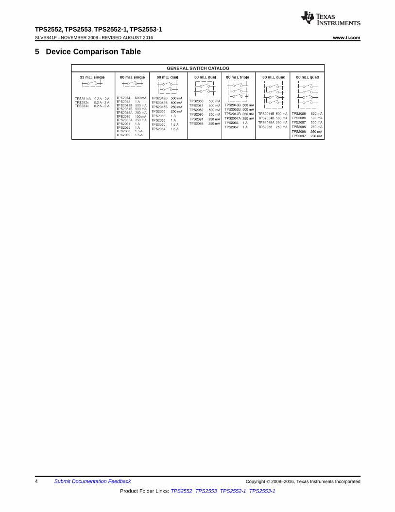
5 Device Comparison Table
1
2
3 4
5
6OUT
FAULT
ILIM
EN
GND
IN
PAD
1
2
3 4
5
6 OUT
FAULT
ILIM
EN
GND
IN
5
TPS2552, TPS2553, TPS2552-1, TPS2553-1www.ti.com SLVS841F –NOVEMBER 2008–REVISED AUGUST 2016
Product Folder Links: TPS2552 TPS2553 TPS2552-1 TPS2553-1
Submit Documentation FeedbackCopyright © 2008–2016, Texas Instruments Incorporated
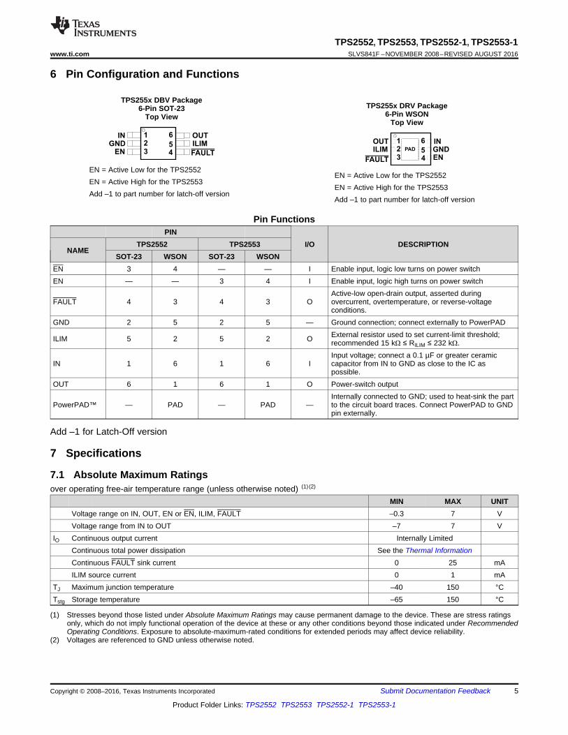
6 Pin Configuration and Functions
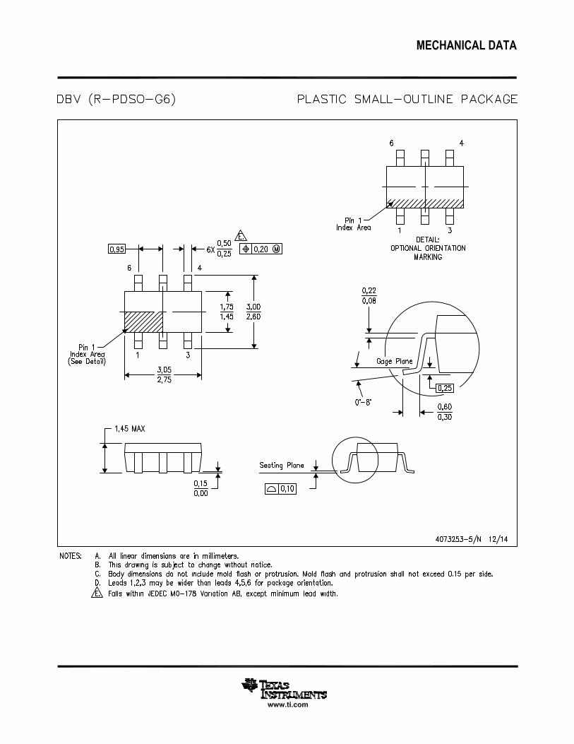
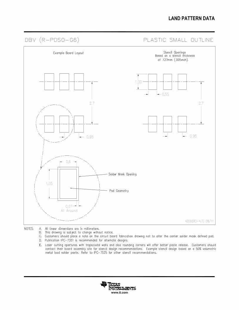
TPS255x DBV Package6-Pin SOT-23
Top View
EN = Active Low for the TPS2552EN = Active High for the TPS2553Add –1 to part number for latch-off version
TPS255x DRV Package6-Pin WSON
Top View
EN = Active Low for the TPS2552EN = Active High for the TPS2553Add –1 to part number for latch-off version
Pin FunctionsPIN
I/O DESCRIPTIONNAME
TPS2552 TPS2553SOT-23 WSON SOT-23 WSON
EN 3 4 — — I Enable input, logic low turns on power switchEN — — 3 4 I Enable input, logic high turns on power switch
FAULT 4 3 4 3 OActive-low open-drain output, asserted duringovercurrent, overtemperature, or reverse-voltageconditions.
GND 2 5 2 5 — Ground connection; connect externally to PowerPAD
ILIM 5 2 5 2 O External resistor used to set current-limit threshold;recommended 15 kΩ ≤ RILIM ≤ 232 kΩ.
IN 1 6 1 6 IInput voltage; connect a 0.1 µF or greater ceramiccapacitor from IN to GND as close to the IC aspossible.
OUT 6 1 6 1 O Power-switch output
PowerPAD™ — PAD — PAD —Internally connected to GND; used to heat-sink the partto the circuit board traces. Connect PowerPAD to GNDpin externally.
Add –1 for Latch-Off version
(1) Stresses beyond those listed under Absolute Maximum Ratings may cause permanent damage to the device. These are stress ratingsonly, which do not imply functional operation of the device at these or any other conditions beyond those indicated under RecommendedOperating Conditions. Exposure to absolute-maximum-rated conditions for extended periods may affect device reliability.
(2) Voltages are referenced to GND unless otherwise noted.
7 Specifications
7.1 Absolute Maximum Ratingsover operating free-air temperature range (unless otherwise noted) (1) (2)
MIN MAX UNITVoltage range on IN, OUT, EN or EN, ILIM, FAULT –0.3 7 VVoltage range from IN to OUT –7 7 V
IO Continuous output current Internally LimitedContinuous total power dissipation See the Thermal InformationContinuous FAULT sink current 0 25 mAILIM source current 0 1 mA
TJ Maximum junction temperature –40 150 °CTstg Storage temperature –65 150 °C
6
TPS2552, TPS2553, TPS2552-1, TPS2553-1SLVS841F –NOVEMBER 2008–REVISED AUGUST 2016 www.ti.com
Product Folder Links: TPS2552 TPS2553 TPS2552-1 TPS2553-1
Submit Documentation Feedback Copyright © 2008–2016, Texas Instruments Incorporated
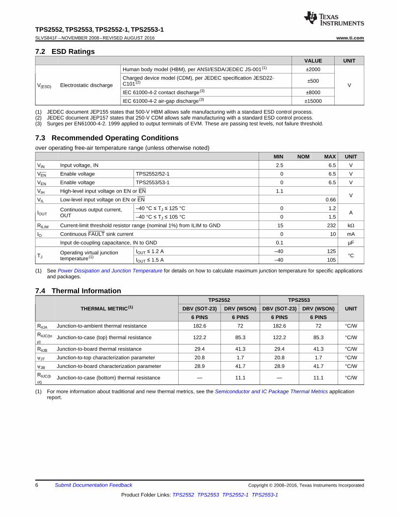
(1) JEDEC document JEP155 states that 500-V HBM allows safe manufacturing with a standard ESD control process.(2) JEDEC document JEP157 states that 250-V CDM allows safe manufacturing with a standard ESD control process.(3) Surges per EN61000-4-2. 1999 applied to output terminals of EVM. These are passing test levels, not failure threshold.
7.2 ESD RatingsVALUE UNIT
V(ESD) Electrostatic discharge
Human body model (HBM), per ANSI/ESDA/JEDEC JS-001 (1) ±2000
VCharged device model (CDM), per JEDEC specification JESD22-C101 (2) ±500
IEC 61000-4-2 contact discharge (3) ±8000IEC 61000-4-2 air-gap discharge (3) ±15000
(1) See Power Dissipation and Junction Temperature for details on how to calculate maximum junction temperature for specific applicationsand packages.
7.3 Recommended Operating Conditionsover operating free-air temperature range (unless otherwise noted)
MIN NOM MAX UNITVIN Input voltage, IN 2.5 6.5 VVEN Enable voltage TPS2552/52-1 0 6.5 VVEN Enable voltage TPS2553/53-1 0 6.5 VVIH High-level input voltage on EN or EN 1.1
VVIL Low-level input voltage on EN or EN 0.66
IOUTContinuous output current,OUT
–40 °C ≤ TJ ≤ 125 °C 0 1.2A
–40 °C ≤ TJ ≤ 105 °C 0 1.5RILIM Current-limit threshold resistor range (nominal 1%) from ILIM to GND 15 232 kΩIO Continuous FAULT sink current 0 10 mA
Input de-coupling capacitance, IN to GND 0.1 µF
TJOperating virtual junctiontemperature (1)
IOUT ≤ 1.2 A –40 125°C
IOUT ≤ 1.5 A –40 105
(1) For more information about traditional and new thermal metrics, see the Semiconductor and IC Package Thermal Metrics applicationreport.
7.4 Thermal Information
THERMAL METRIC (1)TPS2552 TPS2553
UNITDBV (SOT-23) DRV (WSON) DBV (SOT-23) DRV (WSON)6 PINS 6 PINS 6 PINS 6 PINS
RθJA Junction-to-ambient thermal resistance 182.6 72 182.6 72 °C/WRθJC(top)
Junction-to-case (top) thermal resistance 122.2 85.3 122.2 85.3 °C/W
RθJB Junction-to-board thermal resistance 29.4 41.3 29.4 41.3 °C/WψJT Junction-to-top characterization parameter 20.8 1.7 20.8 1.7 °C/WψJB Junction-to-board characterization parameter 28.9 41.7 28.9 41.7 °C/WRθJC(bot)
Junction-to-case (bottom) thermal resistance — 11.1 — 11.1 °C/W
7
TPS2552, TPS2553, TPS2552-1, TPS2553-1www.ti.com SLVS841F –NOVEMBER 2008–REVISED AUGUST 2016
Product Folder Links: TPS2552 TPS2553 TPS2552-1 TPS2553-1
Submit Documentation FeedbackCopyright © 2008–2016, Texas Instruments Incorporated
(1) Pulse-testing techniques maintain junction temperature close to ambient temperature; thermal effects must be taken into accountseparately.
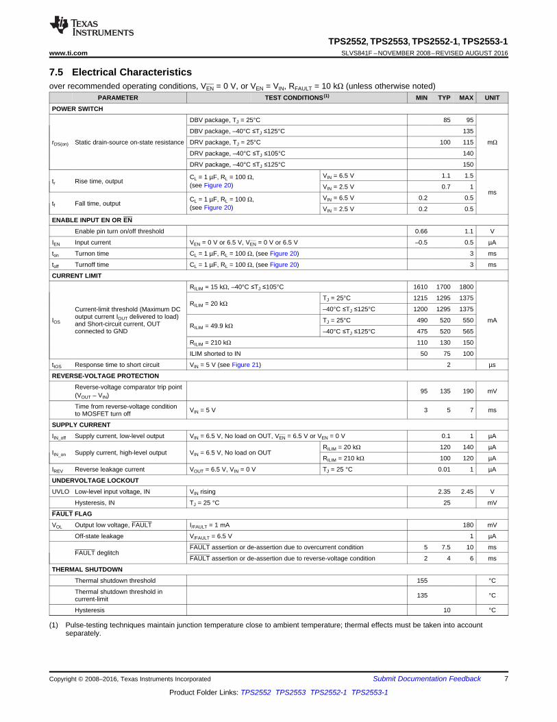
7.5 Electrical Characteristicsover recommended operating conditions, VEN = 0 V, or VEN = VIN, RFAULT = 10 kΩ (unless otherwise noted)
PARAMETER TEST CONDITIONS (1) MIN TYP MAX UNIT
POWER SWITCH
rDS(on) Static drain-source on-state resistance
DBV package, TJ = 25°C 85 95
mΩ
DBV package, –40°C ≤TJ ≤125°C 135
DRV package, TJ = 25°C 100 115
DRV package, –40°C ≤TJ ≤105°C 140
DRV package, –40°C ≤TJ ≤125°C 150
tr Rise time, output CL = 1 µF, RL = 100 Ω,(see Figure 20)
VIN = 6.5 V 1.1 1.5
msVIN = 2.5 V 0.7 1
tf Fall time, output CL = 1 µF, RL = 100 Ω,(see Figure 20)
VIN = 6.5 V 0.2 0.5
VIN = 2.5 V 0.2 0.5
ENABLE INPUT EN OR EN
Enable pin turn on/off threshold 0.66 1.1 V
IEN Input current VEN = 0 V or 6.5 V, VEN = 0 V or 6.5 V –0.5 0.5 µA
ton Turnon time CL = 1 µF, RL = 100 Ω, (see Figure 20) 3 ms
toff Turnoff time CL = 1 µF, RL = 100 Ω, (see Figure 20) 3 ms
CURRENT LIMIT
IOS
Current-limit threshold (Maximum DCoutput current IOUT delivered to load)and Short-circuit current, OUTconnected to GND
RILIM = 15 kΩ, –40°C ≤TJ ≤105°C 1610 1700 1800
mA
RILIM = 20 kΩTJ = 25°C 1215 1295 1375
–40°C ≤TJ ≤125°C 1200 1295 1375
RILIM = 49.9 kΩTJ = 25°C 490 520 550
–40°C ≤TJ ≤125°C 475 520 565
RILIM = 210 kΩ 110 130 150
ILIM shorted to IN 50 75 100
tIOS Response time to short circuit VIN = 5 V (see Figure 21) 2 µs
REVERSE-VOLTAGE PROTECTION
Reverse-voltage comparator trip point(VOUT – VIN) 95 135 190 mV
Time from reverse-voltage conditionto MOSFET turn off VIN = 5 V 3 5 7 ms
SUPPLY CURRENT
IIN_off Supply current, low-level output VIN = 6.5 V, No load on OUT, VEN = 6.5 V or VEN = 0 V 0.1 1 µA
IIN_on Supply current, high-level output VIN = 6.5 V, No load on OUTRILIM = 20 kΩ 120 140 µA
RILIM = 210 kΩ 100 120 µA
IREV Reverse leakage current VOUT = 6.5 V, VIN = 0 V TJ = 25 °C 0.01 1 µA
UNDERVOLTAGE LOCKOUT
UVLO Low-level input voltage, IN VIN rising 2.35 2.45 V
Hysteresis, IN TJ = 25 °C 25 mV
FAULT FLAG
VOL Output low voltage, FAULT I/FAULT = 1 mA 180 mV
Off-state leakage V/FAULT = 6.5 V 1 µA
FAULT deglitchFAULT assertion or de-assertion due to overcurrent condition 5 7.5 10 ms
FAULT assertion or de-assertion due to reverse-voltage condition 2 4 6 ms
THERMAL SHUTDOWN
Thermal shutdown threshold 155 °C
Thermal shutdown threshold incurrent-limit 135 °C
Hysteresis 10 °C
8
TPS2552, TPS2553, TPS2552-1, TPS2553-1SLVS841F –NOVEMBER 2008–REVISED AUGUST 2016 www.ti.com
Product Folder Links: TPS2552 TPS2553 TPS2552-1 TPS2553-1
Submit Documentation Feedback Copyright © 2008–2016, Texas Instruments Incorporated
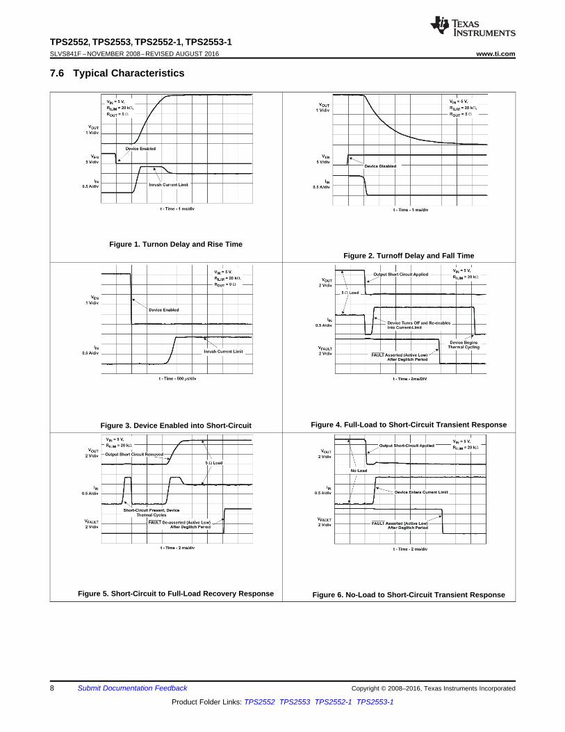
7.6 Typical Characteristics
Figure 1. Turnon Delay and Rise TimeFigure 2. Turnoff Delay and Fall Time
Figure 3. Device Enabled into Short-Circuit Figure 4. Full-Load to Short-Circuit Transient Response
Figure 5. Short-Circuit to Full-Load Recovery Response Figure 6. No-Load to Short-Circuit Transient Response
2.30
T - Junction Temperature - °CJ
-50 0 50 100 150
UV
LO
- U
nd
erv
olt
ag
e L
oc
ko
ut
- V
2.40
2.31
2.32
2.33
2.34
2.35
2.36
2.37
2.38
2.39
UVLO Rising
R = 20 kILIM W
UVLO Falling
9
TPS2552, TPS2553, TPS2552-1, TPS2553-1www.ti.com SLVS841F –NOVEMBER 2008–REVISED AUGUST 2016
Product Folder Links: TPS2552 TPS2553 TPS2552-1 TPS2553-1
Submit Documentation FeedbackCopyright © 2008–2016, Texas Instruments Incorporated
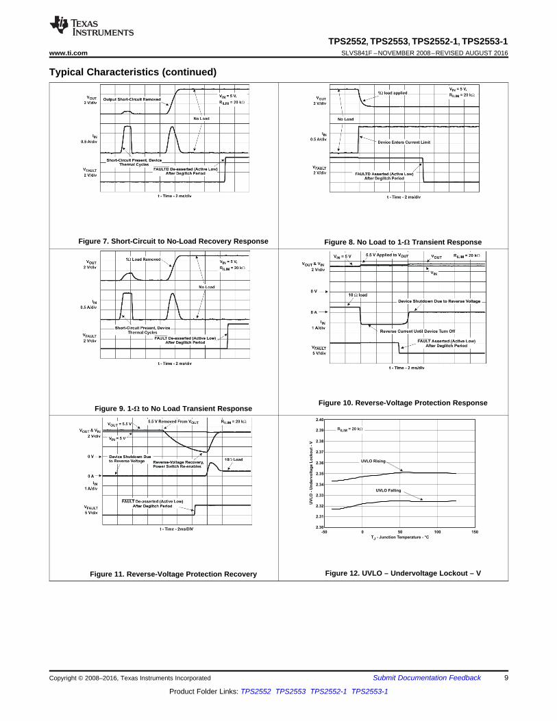
Typical Characteristics (continued)
Figure 7. Short-Circuit to No-Load Recovery Response Figure 8. No Load to 1-Ω Transient Response
Figure 9. 1-Ω to No Load Transient ResponseFigure 10. Reverse-Voltage Protection Response
Figure 11. Reverse-Voltage Protection Recovery Figure 12. UVLO – Undervoltage Lockout – V
0
10
20
30
40
50
60
70
80
90
100
110
120
130
140
150
0 100 200 300 400 500 600 700 800 900 1000
IDS
- S
tati
c D
rain
-So
urc
e C
urr
en
t -
mA
V - V - 100 mV/divIN OUT
T = 25°CA
T = 125°CA
V = 6.5 V,
R = 200 k
IN
ILIM W
T = -40°CA
0
100
200
300
400
500
600
700
800
900
1000
1100
1200
1300
1400
0 100 200 300 400 500 600 700 800 900 1000
IDS
- S
tati
c D
rain
-So
urc
e C
urr
en
t -
mA
V - V - 100 mV/divIN OUT
T = 125°CA
T = 25°CA
T = -40°CA
V = 6.5 V,
R = 20 k
IN
ILIM W
0
Peak Current - A
0 1.5 3 4.5 6
Cu
rre
nt
Lim
it R
es
po
ns
e -
sm
20
2
4
6
8
10
12
14
16
18V = 5 V,
R = 20 k ,
T = 25°C
IN
ILIM
A
W
0
DBV Package
r-
Sta
tic D
rain
-So
urc
e O
n-S
tate
Resis
tan
ce -
mD
S(o
n)
W
25
50
75
100
125
150
DRV Package
T - Junction Temperature - °CJ
-50 0 50 100 150
0
I-
Su
pp
ly C
urr
en
t, O
utp
ut
Dis
ab
led
-A
INm
0.40
0.04
0.08
0.12
0.16
0.20
0.24
0.28
0.32
0.36
T - Junction Temperature - °CJ
-50 0 50 100 150
V = 2.5 VIN
V = 6.5 VIN
R = 20 kILIM W
0
I-
Su
pp
ly C
urr
en
t, O
utp
ut
En
ab
led
-A
INm
150
15
30
45
60
75
90
105
120
135
T - Junction Temperature - °CJ
-50 0 50 100 150
R = 20 kILIM W V = 6.5 VIN V = 5 VIN
V = 3.3 VINV = 2.5 VIN
10
TPS2552, TPS2553, TPS2552-1, TPS2553-1SLVS841F –NOVEMBER 2008–REVISED AUGUST 2016 www.ti.com
Product Folder Links: TPS2552 TPS2553 TPS2552-1 TPS2553-1
Submit Documentation Feedback Copyright © 2008–2016, Texas Instruments Incorporated
Typical Characteristics (continued)
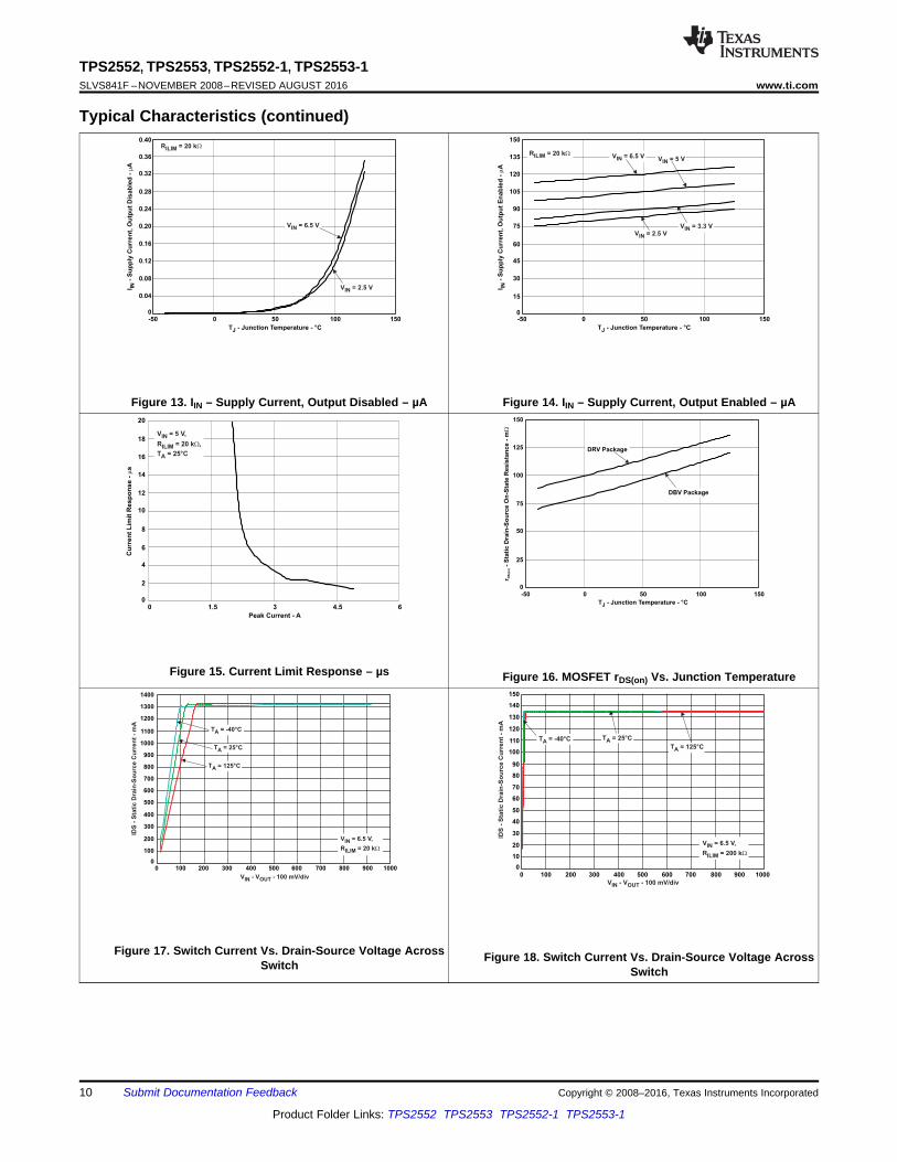
Figure 13. IIN – Supply Current, Output Disabled – µA Figure 14. IIN – Supply Current, Output Enabled – µA
Figure 15. Current Limit Response – µs Figure 16. MOSFET rDS(on) Vs. Junction Temperature
Figure 17. Switch Current Vs. Drain-Source Voltage AcrossSwitch
Figure 18. Switch Current Vs. Drain-Source Voltage AcrossSwitch
tIOS
IOS
IOUT
RL CL
OUT
TEST CIRCUIT
10
90%
10
90%VOUT
ton t
off
10
90%
5050%VEN
toff50% 50%
10%
90%
VOLTAGE WAVEFORMS
tr
tf
% %
%
%V
OUT
VEN
VOUT
ton
toff
OUTIN
GND
FAULTILIM
EN
RILIM
Control Signal
VINTPS2552
10 Fm
150 Fm
Fault Signal
Power Pad
VOUT
R
10 k
FAULT
W
11
TPS2552, TPS2553, TPS2552-1, TPS2553-1www.ti.com SLVS841F –NOVEMBER 2008–REVISED AUGUST 2016
Product Folder Links: TPS2552 TPS2553 TPS2552-1 TPS2553-1
Submit Documentation FeedbackCopyright © 2008–2016, Texas Instruments Incorporated
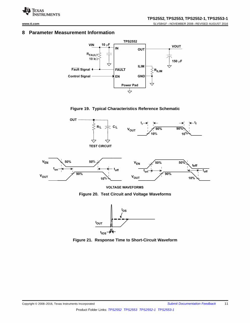
8 Parameter Measurement Information
Figure 19. Typical Characteristics Reference Schematic
Figure 20. Test Circuit and Voltage Waveforms
Figure 21. Response Time to Short-Circuit Waveform
VOUT
IOUT
IOS
DecreasingLoad Resistance
DecreasingLoad Resistance
12
TPS2552, TPS2553, TPS2552-1, TPS2553-1SLVS841F –NOVEMBER 2008–REVISED AUGUST 2016 www.ti.com
Product Folder Links: TPS2552 TPS2553 TPS2552-1 TPS2553-1
Submit Documentation Feedback Copyright © 2008–2016, Texas Instruments Incorporated
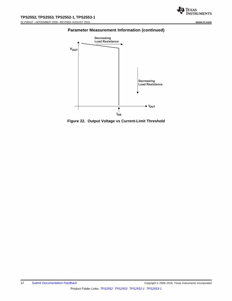
Parameter Measurement Information (continued)
Figure 22. Output Voltage vs Current-Limit Threshold
Charge
Pump
Driver
UVLO
Current
Limit
ThermalSense
IN
GND
EN
ILIM
OUT
FAULT
CS
ReverseVoltage
Comparator
-
+
CurrentSense
(Note A)
4-m
sD
eg
litc
h
8-ms Deglitch
Copyright © 2016, Texas Instruments Incorporated
13
TPS2552, TPS2553, TPS2552-1, TPS2553-1www.ti.com SLVS841F –NOVEMBER 2008–REVISED AUGUST 2016
Product Folder Links: TPS2552 TPS2553 TPS2552-1 TPS2553-1
Submit Documentation FeedbackCopyright © 2008–2016, Texas Instruments Incorporated
9 Detailed Description
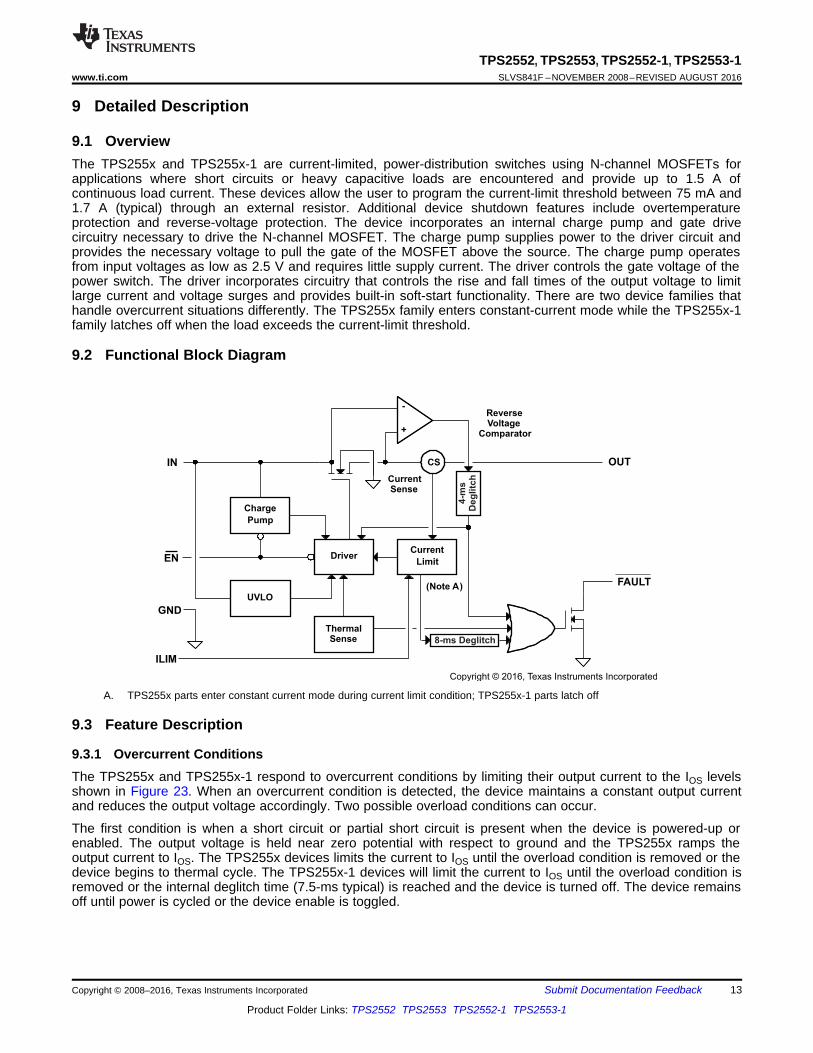
9.1 OverviewThe TPS255x and TPS255x-1 are current-limited, power-distribution switches using N-channel MOSFETs forapplications where short circuits or heavy capacitive loads are encountered and provide up to 1.5 A ofcontinuous load current. These devices allow the user to program the current-limit threshold between 75 mA and1.7 A (typical) through an external resistor. Additional device shutdown features include overtemperatureprotection and reverse-voltage protection. The device incorporates an internal charge pump and gate drivecircuitry necessary to drive the N-channel MOSFET. The charge pump supplies power to the driver circuit andprovides the necessary voltage to pull the gate of the MOSFET above the source. The charge pump operatesfrom input voltages as low as 2.5 V and requires little supply current. The driver controls the gate voltage of thepower switch. The driver incorporates circuitry that controls the rise and fall times of the output voltage to limitlarge current and voltage surges and provides built-in soft-start functionality. There are two device families thathandle overcurrent situations differently. The TPS255x family enters constant-current mode while the TPS255x-1family latches off when the load exceeds the current-limit threshold.
9.2 Functional Block Diagram
A. TPS255x parts enter constant current mode during current limit condition; TPS255x-1 parts latch off
9.3 Feature Description
9.3.1 Overcurrent ConditionsThe TPS255x and TPS255x-1 respond to overcurrent conditions by limiting their output current to the IOS levelsshown in Figure 23. When an overcurrent condition is detected, the device maintains a constant output currentand reduces the output voltage accordingly. Two possible overload conditions can occur.
The first condition is when a short circuit or partial short circuit is present when the device is powered-up orenabled. The output voltage is held near zero potential with respect to ground and the TPS255x ramps theoutput current to IOS. The TPS255x devices limits the current to IOS until the overload condition is removed or thedevice begins to thermal cycle. The TPS255x-1 devices will limit the current to IOS until the overload condition isremoved or the internal deglitch time (7.5-ms typical) is reached and the device is turned off. The device remainsoff until power is cycled or the device enable is toggled.
14
TPS2552, TPS2553, TPS2552-1, TPS2553-1SLVS841F –NOVEMBER 2008–REVISED AUGUST 2016 www.ti.com
Product Folder Links: TPS2552 TPS2553 TPS2552-1 TPS2553-1
Submit Documentation Feedback Copyright © 2008–2016, Texas Instruments Incorporated
Feature Description (continued)The second condition is when a short circuit, partial short circuit, or transient overload occurs while the device isenabled and powered on. The device responds to the overcurrent condition within time tIOS (see Figure 21). Thecurrent-sense amplifier is overdriven during this time and momentarily disables the internal current-limitMOSFET. The current-sense amplifier recovers and limits the output current to IOS. Similar to the previous case,the TPS255x limits the current to IOS until the overload condition is removed or the device begins to thermalcycle; the TPS255x-1 limits the current to IOS until the overload condition is removed or the internal deglitch timeis reached and the device is latched off.
The TPS255x thermal cycles if an overload condition is present long enough to activate thermal limiting in any ofthe above cases. The device turns off when the junction temperature exceeds 135°C (typical) while in currentlimit. The device remains off until the junction temperature cools 10°C (typical) and then restarts. The TPS255xcycles on and off until the overload is removed (see Figure 5 and Figure 7) .
9.3.2 Reverse-Voltage ProtectionThe reverse-voltage protection feature turns off the N-channel MOSFET whenever the output voltage exceedsthe input voltage by 135 mV (typical) for 4-ms (typical). A reverse current of (VOUT – VIN)/rDS(on)) are present whenthis occurs. This prevents damage to devices on the input side of the TPS255x and TPS2552-1/TPS2253-1 bypreventing significant current from sinking into the input capacitance. The TPS255x devices allow the N-channelMOSFET to turn on once the output voltage goes below the input voltage for the same 4-ms deglitch time. TheTPS255x-1 devices keep the device turned off even if the reverse-voltage condition is removed and do not allowthe N-channel MOSFET to turn on until power is cycled or the device enable is toggled. The reverse-voltagecomparator also asserts the FAULT output (active-low) after 4-ms.
9.3.3 FAULT ResponseThe FAULT open-drain output is asserted (active low) during an overcurrent, overtemperature, or reverse-voltagecondition. The TPS255x asserts the FAULT signal until the fault condition is removed and the device resumesnormal operation. The TPS255x-1 asserts the FAULT signal during a fault condition and remains asserted whilethe part is latched-off. The FAULT signal is de-asserted once device power is cycled or the enable is toggled andthe device resumes normal operation. The TPS255x and TPS255x-1 are designed to eliminate false FAULTreporting by using an internal delay de-glitch circuit for overcurrent (7.5-ms typical) and reverse-voltage (4-mstypical) conditions without the need for external circuitry. This ensures that FAULT is not accidentally asserteddue to normal operation such as starting into a heavy capacitive load. The deglitch circuitry delays entering andleaving fault conditions. Overtemperature conditions are not deglitched and assert the FAULT signal immediately.
9.3.4 Undervoltage Lockout (UVLO)The undervoltage lockout (UVLO) circuit disables the power switch until the input voltage reaches the UVLOturnon threshold. Built-in hysteresis prevents unwanted on and off cycling due to input voltage drop from largecurrent surges.
9.3.5 ENABLE (EN or EN)The logic enable controls the power switch, bias for the charge pump, driver, and other circuits to reduce thesupply current. The supply current is reduced to less than 1-µA when a logic low is present on EN. A logic lowinput on EN or a logic high input on EN enables the driver, control circuits, and power switch. The enable input iscompatible with both TTL and CMOS logic levels.
9.3.6 Thermal SenseThe TPS255x and TPS255x-1 have self-protection features using two independent thermal-sensing circuits thatmonitor the operating temperature of the power switch and disable operation if the temperature exceedsrecommended operating conditions. The TPS255x device operates in constant-current mode during anovercurrent conditions, which increases the voltage drop across power-switch. The power dissipation in thepackage is proportional to the voltage drop across the power switch, which increases the junction temperatureduring an overcurrent condition. The first thermal sensor turns off the power switch when the die temperatureexceeds 135°C (minimum) and the part is in current limit. Hysteresis is built into the thermal sensor, and theswitch turns on after the device has cooled approximately 10°C.
0.94ILIM
0.977ILIM
1.016ILIM
22980VOSmax R k
23950VOSnom R k
25230VOSmin R k
I (mA) =
I (mA) =
I (mA) =
W
W
W
15
TPS2552, TPS2553, TPS2552-1, TPS2553-1www.ti.com SLVS841F –NOVEMBER 2008–REVISED AUGUST 2016
Product Folder Links: TPS2552 TPS2553 TPS2552-1 TPS2553-1
Submit Documentation FeedbackCopyright © 2008–2016, Texas Instruments Incorporated
Feature Description (continued)The TPS255x and TPS255x-1 also have a second ambient thermal sensor. The ambient thermal sensor turns offthe power-switch when the die temperature exceeds 155°C (minimum) regardless of whether the power switch isin current limit and turns on the power switch after the device has cooled approximately 10°C. The TPS255x andTPS255x-1 families continue to cycle off and on until the fault is removed.
The open-drain fault reporting output FAULT is asserted (active low) immediately during an overtemperatureshutdown condition.
9.4 Device Functional ModesThere are no other functional modes.
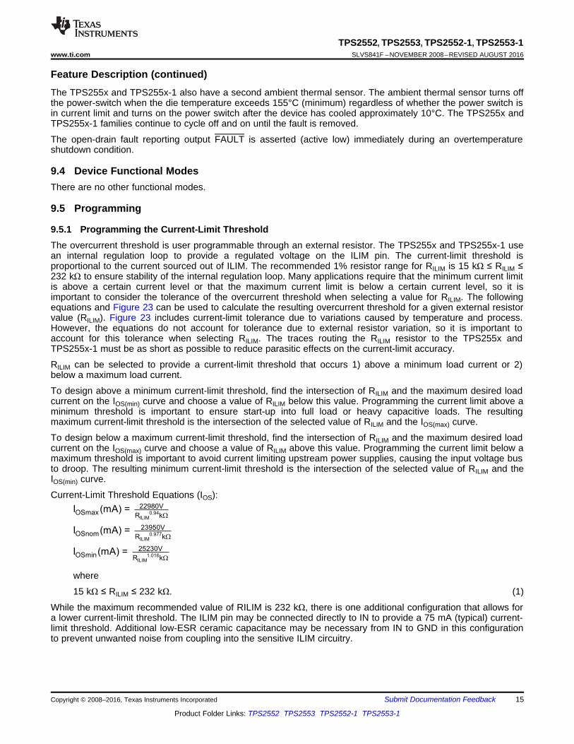
9.5 Programming
9.5.1 Programming the Current-Limit ThresholdThe overcurrent threshold is user programmable through an external resistor. The TPS255x and TPS255x-1 usean internal regulation loop to provide a regulated voltage on the ILIM pin. The current-limit threshold isproportional to the current sourced out of ILIM. The recommended 1% resistor range for RILIM is 15 kΩ ≤ RILIM ≤232 kΩ to ensure stability of the internal regulation loop. Many applications require that the minimum current limitis above a certain current level or that the maximum current limit is below a certain current level, so it isimportant to consider the tolerance of the overcurrent threshold when selecting a value for RILIM. The followingequations and Figure 23 can be used to calculate the resulting overcurrent threshold for a given external resistorvalue (RILIM). Figure 23 includes current-limit tolerance due to variations caused by temperature and process.However, the equations do not account for tolerance due to external resistor variation, so it is important toaccount for this tolerance when selecting RILIM. The traces routing the RILIM resistor to the TPS255x andTPS255x-1 must be as short as possible to reduce parasitic effects on the current-limit accuracy.
RILIM can be selected to provide a current-limit threshold that occurs 1) above a minimum load current or 2)below a maximum load current.
To design above a minimum current-limit threshold, find the intersection of RILIM and the maximum desired loadcurrent on the IOS(min) curve and choose a value of RILIM below this value. Programming the current limit above aminimum threshold is important to ensure start-up into full load or heavy capacitive loads. The resultingmaximum current-limit threshold is the intersection of the selected value of RILIM and the IOS(max) curve.
To design below a maximum current-limit threshold, find the intersection of RILIM and the maximum desired loadcurrent on the IOS(max) curve and choose a value of RILIM above this value. Programming the current limit below amaximum threshold is important to avoid current limiting upstream power supplies, causing the input voltage busto droop. The resulting minimum current-limit threshold is the intersection of the selected value of RILIM and theIOS(min) curve.
Current-Limit Threshold Equations (IOS):
where
15 kΩ ≤ RILIM ≤ 232 kΩ. (1)
While the maximum recommended value of RILIM is 232 kΩ, there is one additional configuration that allows fora lower current-limit threshold. The ILIM pin may be connected directly to IN to provide a 75 mA (typical) current-limit threshold. Additional low-ESR ceramic capacitance may be necessary from IN to GND in this configurationto prevent unwanted noise from coupling into the sensitive ILIM circuitry.
Cu
rre
nt
Lim
it T
hre
sh
old
- m
A
R - Current Limit Resistor - kILIM W
0
100
200
300
400
500
600
700
800
900
1000
1100
1200
1300
1400
1500
15 25 35 45 65 75 85 95 195 205 235165 175 185135 145 155105 115 125 215 225
IOS(min)
IOS(max)
IOS(nom)
55
1600
1700
1800
16
TPS2552, TPS2553, TPS2552-1, TPS2553-1SLVS841F –NOVEMBER 2008–REVISED AUGUST 2016 www.ti.com
Product Folder Links: TPS2552 TPS2553 TPS2552-1 TPS2553-1
Submit Documentation Feedback Copyright © 2008–2016, Texas Instruments Incorporated
Programming (continued)
Figure 23. Current-Limit Threshold vs RILIM
17
TPS2552, TPS2553, TPS2552-1, TPS2553-1www.ti.com SLVS841F –NOVEMBER 2008–REVISED AUGUST 2016
Product Folder Links: TPS2552 TPS2553 TPS2552-1 TPS2553-1
Submit Documentation FeedbackCopyright © 2008–2016, Texas Instruments Incorporated
10 Application and Implementation
NOTEInformation in the following applications sections is not part of the TI componentspecification, and TI does not warrant its accuracy or completeness. TI’s customers areresponsible for determining suitability of components for their purposes. Customers shouldvalidate and test their design implementation to confirm system functionality.
10.1 Application Information
10.1.1 Constant-Current vs Latch-Off Operation and Impact on Output VoltageBoth the constant-current devices (TPS255x) and latch-off devices (TPS255x-1) operate identically during normaloperation, that is, the load current is less than the current-limit threshold and the devices are not limiting current.During normal operation the N-channel MOSFET is fully enhanced, and VOUT = VIN - (IOUT x rDS(on)). The voltagedrop across the MOSFET is relatively small compared to VIN, and VOUT ≉ VIN.
Both the constant-current devices (TPS255x ) and latch-off devices (TPS255x-1) operate identically during theinitial onset of an overcurrent event. Both devices limit current to the programmed current-limit threshold set toRILIM by operating the N-channel MOSFET in the linear mode. During current-limit operation, the N-channelMOSFET is no longer fully-enhanced and the resistance of the device increases. This allows the device toeffectively regulate the current to the current-limit threshold. The effect of increasing the resistance of theMOSFET is that the voltage drop across the device is no longer negligible (VIN ≠ VOUT), and VOUT decreases. Theamount that VOUT decreases is proportional to the magnitude of the overload condition. The expected VOUT canbe calculated by,
IOS × RLOAD
where
IOS is the current-limit threshold and RLOAD is the magnitude of the overload condition. (2)
For example, if IOS is programmed to 1 A and a 1 Ω overload condition is applied, the resulting VOUT is 1 V.
While both the constant-current devices (TPS255x ) and latch-off devices (TPS255x-1) operate identically duringthe initial onset of an overcurrent event, they behave differently if the overcurrent event lasts longer than theinternal delay de-glitch circuit (7.5-ms typical). The constant-current devices (TPS255x ) assert the FAULT flagafter the deglitch period and continue to regulate the current to the current-limit threshold indefinitely. In practicalcircuits, the power dissipation in the package increases the die temperature above the overtemperatureshutdown threshold (135°C minimum), and the device turns off until the die temperature decreases by thehysteresis of the thermal shutdown circuit (10°C typical). The device turns on and continues to thermal cycle untilthe overload condition is removed. The constant-current devices resume normal operation once the overloadcondition is removed. The latch-off devices (TPS255x-1) assert the FAULT flag after the deglitch period andimmediately turn off the device. The device remains off regardless of whether the overload condition is removedfrom the output. The latch-off devices remain off and do not resume normal operation until the surroundingsystem either toggles the enable or cycles power to the device.
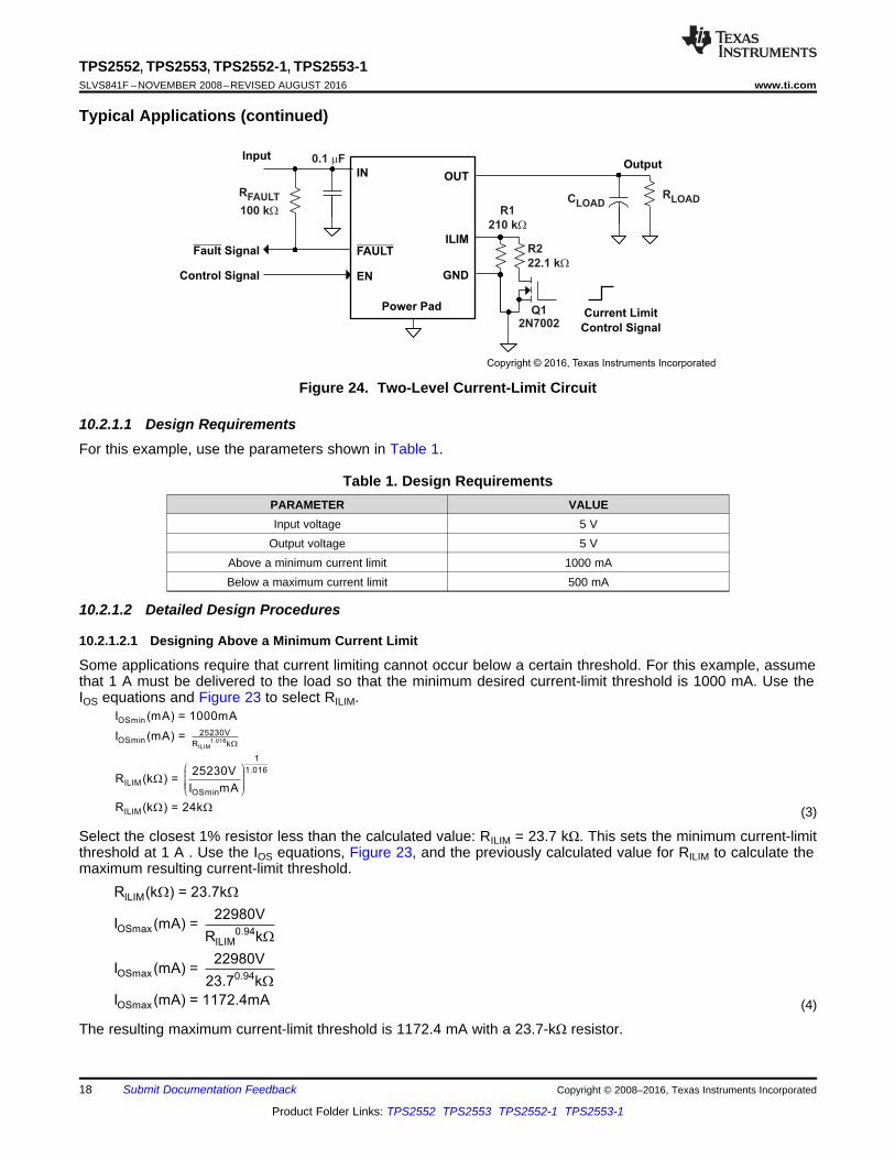
10.2 Typical Applications
10.2.1 Two-Level Current-Limit CircuitSome applications require different current-limit thresholds depending on external system conditions. Figure 24shows an implementation for an externally controlled, two-level current-limit circuit. The current-limit threshold isset by the total resistance from ILIM to GND (see the Programming the Current-Limit Threshold section). A logic-level input enables or disables MOSFET Q1 and changes the current-limit threshold by modifying the totalresistance from ILIM to GND. Additional MOSFET and resistor combinations can be used in parallel to Q1/R2 toincrease the number of additional current-limit levels.
NOTEILIM must never be driven directly with an external signal.
ILIM
OSmax 0.94ILIM
OSmax 0.94
OSmax
R (k ) = 23.7k
22980VI (mA) =
R k
22980VI (mA) =
23.7 k
I (mA) = 1172.4mA
W W
W
W
1.016ILIM
OSmin
25230VOSmin R k
1
1.016
ILIMOSmin
ILIM
I (mA) = 1000mA
I (mA) =
25230VR (k ) =
I mA
R (k ) = 24k
W
W
W W
æ ö÷ç ÷ç ÷ç ÷çè ø
OUTIN
GND
FAULTILIM
ENControl Signal
Input
Fault Signal
Power Pad
Output
Current Limit
Control Signal
0.1 Fm
R
100 k
FAULT
WCLOAD
RLOADR1
210 kW
R2
22.1 kW
Q12N7002
Copyright © 2016, Texas Instruments Incorporated
18
TPS2552, TPS2553, TPS2552-1, TPS2553-1SLVS841F –NOVEMBER 2008–REVISED AUGUST 2016 www.ti.com
Product Folder Links: TPS2552 TPS2553 TPS2552-1 TPS2553-1
Submit Documentation Feedback Copyright © 2008–2016, Texas Instruments Incorporated
Typical Applications (continued)
Figure 24. Two-Level Current-Limit Circuit
10.2.1.1 Design RequirementsFor this example, use the parameters shown in Table 1.
Table 1. Design RequirementsPARAMETER VALUEInput voltage 5 V
Output voltage 5 VAbove a minimum current limit 1000 mABelow a maximum current limit 500 mA
10.2.1.2 Detailed Design Procedures
10.2.1.2.1 Designing Above a Minimum Current Limit
Some applications require that current limiting cannot occur below a certain threshold. For this example, assumethat 1 A must be delivered to the load so that the minimum desired current-limit threshold is 1000 mA. Use theIOS equations and Figure 23 to select RILIM.
(3)
Select the closest 1% resistor less than the calculated value: RILIM = 23.7 kΩ. This sets the minimum current-limitthreshold at 1 A . Use the IOS equations, Figure 23, and the previously calculated value for RILIM to calculate themaximum resulting current-limit threshold.
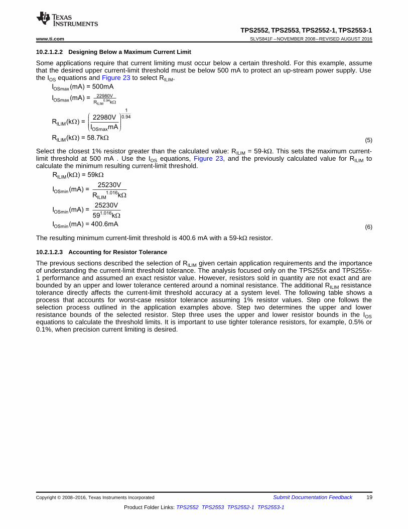
(4)
The resulting maximum current-limit threshold is 1172.4 mA with a 23.7-kΩ resistor.
ILIM
OSmin 1.016ILIM
OSmin 1.016
OSmin
R (k ) = 59k
25230VI (mA) =
R k
25230VI (mA) =
59 k
I (mA) = 400.6mA
W W
W
W
0.94ILIM
OSmax
22980VOSmax R k
1
0.94
ILIMOSmax
ILIM
I (mA) = 500mA
I (mA) =
22980VR (k ) =
I mA
R (k ) = 58.7k
W
W
W W
æ ö÷ç ÷ç ÷ç ÷çè ø
19
TPS2552, TPS2553, TPS2552-1, TPS2553-1www.ti.com SLVS841F –NOVEMBER 2008–REVISED AUGUST 2016
Product Folder Links: TPS2552 TPS2553 TPS2552-1 TPS2553-1
Submit Documentation FeedbackCopyright © 2008–2016, Texas Instruments Incorporated
10.2.1.2.2 Designing Below a Maximum Current Limit
Some applications require that current limiting must occur below a certain threshold. For this example, assumethat the desired upper current-limit threshold must be below 500 mA to protect an up-stream power supply. Usethe IOS equations and Figure 23 to select RILIM.
(5)
Select the closest 1% resistor greater than the calculated value: RILIM = 59-kΩ. This sets the maximum current-limit threshold at 500 mA . Use the IOS equations, Figure 23, and the previously calculated value for RILIM tocalculate the minimum resulting current-limit threshold.
(6)
The resulting minimum current-limit threshold is 400.6 mA with a 59-kΩ resistor.
10.2.1.2.3 Accounting for Resistor Tolerance
The previous sections described the selection of RILIM given certain application requirements and the importanceof understanding the current-limit threshold tolerance. The analysis focused only on the TPS255x and TPS255x-1 performance and assumed an exact resistor value. However, resistors sold in quantity are not exact and arebounded by an upper and lower tolerance centered around a nominal resistance. The additional RILIM resistancetolerance directly affects the current-limit threshold accuracy at a system level. The following table shows aprocess that accounts for worst-case resistor tolerance assuming 1% resistor values. Step one follows theselection process outlined in the application examples above. Step two determines the upper and lowerresistance bounds of the selected resistor. Step three uses the upper and lower resistor bounds in the IOSequations to calculate the threshold limits. It is important to use tighter tolerance resistors, for example, 0.5% or0.1%, when precision current limiting is desired.
20
TPS2552, TPS2553, TPS2552-1, TPS2553-1SLVS841F –NOVEMBER 2008–REVISED AUGUST 2016 www.ti.com
Product Folder Links: TPS2552 TPS2553 TPS2552-1 TPS2553-1
Submit Documentation Feedback Copyright © 2008–2016, Texas Instruments Incorporated
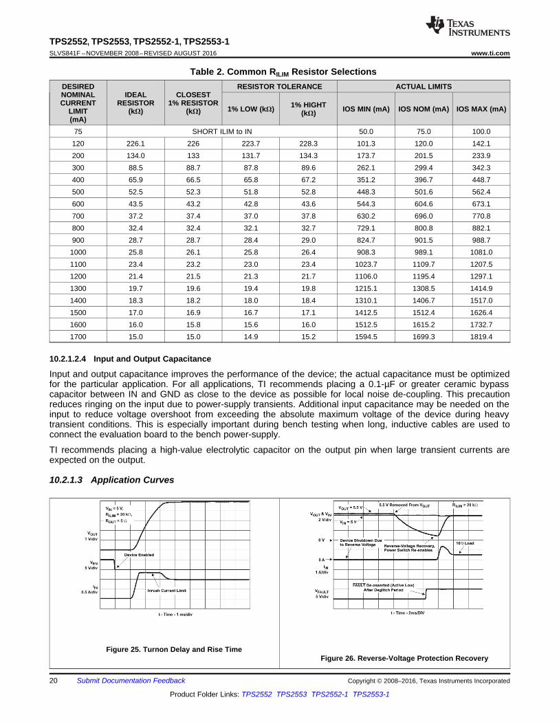
Table 2. Common RILIM Resistor SelectionsDESIREDNOMINALCURRENT
LIMIT(mA)
IDEALRESISTOR
(kΩ)
CLOSEST1% RESISTOR
(kΩ)
RESISTOR TOLERANCE ACTUAL LIMITS
1% LOW (kΩ) 1% HIGHT(kΩ) IOS MIN (mA) IOS NOM (mA) IOS MAX (mA)
75 SHORT ILIM to IN 50.0 75.0 100.0120 226.1 226 223.7 228.3 101.3 120.0 142.1200 134.0 133 131.7 134.3 173.7 201.5 233.9300 88.5 88.7 87.8 89.6 262.1 299.4 342.3400 65.9 66.5 65.8 67.2 351.2 396.7 448.7500 52.5 52.3 51.8 52.8 448.3 501.6 562.4600 43.5 43.2 42.8 43.6 544.3 604.6 673.1700 37.2 37.4 37.0 37.8 630.2 696.0 770.8800 32.4 32.4 32.1 32.7 729.1 800.8 882.1900 28.7 28.7 28.4 29.0 824.7 901.5 988.71000 25.8 26.1 25.8 26.4 908.3 989.1 1081.01100 23.4 23.2 23.0 23.4 1023.7 1109.7 1207.51200 21.4 21.5 21.3 21.7 1106.0 1195.4 1297.11300 19.7 19.6 19.4 19.8 1215.1 1308.5 1414.91400 18.3 18.2 18.0 18.4 1310.1 1406.7 1517.01500 17.0 16.9 16.7 17.1 1412.5 1512.4 1626.41600 16.0 15.8 15.6 16.0 1512.5 1615.2 1732.71700 15.0 15.0 14.9 15.2 1594.5 1699.3 1819.4
10.2.1.2.4 Input and Output Capacitance
Input and output capacitance improves the performance of the device; the actual capacitance must be optimizedfor the particular application. For all applications, TI recommends placing a 0.1-µF or greater ceramic bypasscapacitor between IN and GND as close to the device as possible for local noise de-coupling. This precautionreduces ringing on the input due to power-supply transients. Additional input capacitance may be needed on theinput to reduce voltage overshoot from exceeding the absolute maximum voltage of the device during heavytransient conditions. This is especially important during bench testing when long, inductive cables are used toconnect the evaluation board to the bench power-supply.
TI recommends placing a high-value electrolytic capacitor on the output pin when large transient currents areexpected on the output.
10.2.1.3 Application Curves
Figure 25. Turnon Delay and Rise TimeFigure 26. Reverse-Voltage Protection Recovery
OUTIN
GND
FAULT
ILIM
EN
External Logic
Signal & Driver
Power Pad
OutputInput 0.1 Fm
R
100 k
FAULT
W
C
0.1 F
RETRY
m
R
20 k
ILIM
W
CLOAD
RLOAD
TPS2553
Copyright © 2016, Texas Instruments Incorporated
OUTIN
GND
FAULTILIM
EN
Input
Power Pad
Output0.1 Fm
R
100 k
FAULT
W
C
0.1 F
RETRY
m
R
20 k
ILIM
W
CLOAD
RLOAD
TPS2553
Copyright © 2016, Texas Instruments Incorporated
21
TPS2552, TPS2553, TPS2552-1, TPS2553-1www.ti.com SLVS841F –NOVEMBER 2008–REVISED AUGUST 2016
Product Folder Links: TPS2552 TPS2553 TPS2552-1 TPS2553-1
Submit Documentation FeedbackCopyright © 2008–2016, Texas Instruments Incorporated
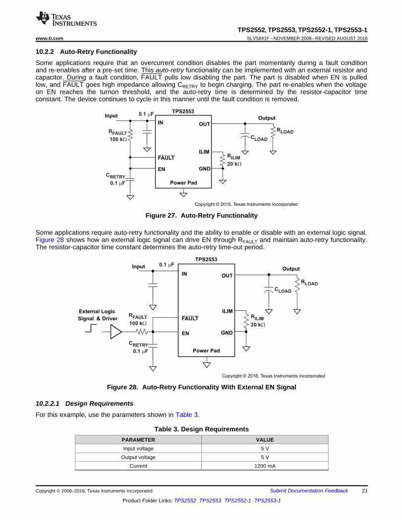
10.2.2 Auto-Retry FunctionalitySome applications require that an overcurrent condition disables the part momentarily during a fault conditionand re-enables after a pre-set time. This auto-retry functionality can be implemented with an external resistor andcapacitor. During a fault condition, FAULT pulls low disabling the part. The part is disabled when EN is pulledlow, and FAULT goes high impedance allowing CRETRY to begin charging. The part re-enables when the voltageon EN reaches the turnon threshold, and the auto-retry time is determined by the resistor-capacitor timeconstant. The device continues to cycle in this manner until the fault condition is removed.
Figure 27. Auto-Retry Functionality
Some applications require auto-retry functionality and the ability to enable or disable with an external logic signal.Figure 28 shows how an external logic signal can drive EN through RFAULT and maintain auto-retry functionality.The resistor-capacitor time constant determines the auto-retry time-out period.
Figure 28. Auto-Retry Functionality With External EN Signal
10.2.2.1 Design RequirementsFor this example, use the parameters shown in Table 3.
Table 3. Design RequirementsPARAMETER VALUEInput voltage 5 V
Output voltage 5 VCurrent 1200 mA
OUTIN
GND
FAULTILIM
EN
RILIM
20 kW
RFAULT
100 kW
Control Signal
5V USBInput
USB
Port
USB Data
TPS2552/53
0.1 Fm
120 Fm
Fault Signal
Power Pad
USB requirement only*
*facing ports are bypassed with at least
120 F per hub
USB requirement that downstream
m
Copyright © 2016, Texas Instruments Incorporated
22
TPS2552, TPS2553, TPS2552-1, TPS2553-1SLVS841F –NOVEMBER 2008–REVISED AUGUST 2016 www.ti.com
Product Folder Links: TPS2552 TPS2553 TPS2552-1 TPS2553-1
Submit Documentation Feedback Copyright © 2008–2016, Texas Instruments Incorporated
10.2.2.2 Detailed Design ProcedureRefer to Programming the Current-Limit Threshold section for the current limit setting. For auto-retry functionality,once FAULT asserted, EN pull low, TPS2553 is disabled, FAULT des-asserted, CRETRY is slowly charged to ENlogic high through RFAULT, then enable, after deglitch time, FAULT asserted again. In the event of an overload,TPS2553 cycles and has output average current. ON-time with output current is decided by FAULT deglitch time.OFF-time without output current is decided by RFAULT x CRETRY constant time to EN logic high and ton time.Therefore, set the RFAULT × CRETRY to get the desired output average current during overload.
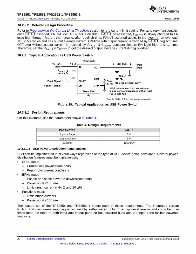
10.2.3 Typical Application as USB Power Switch
Figure 29. Typical Application as USB Power Switch
10.2.3.1 Design RequirementsFor this example, use the parameters shown in Table 4.
Table 4. Design RequirementsPARAMETER VALUEInput voltage 5 V
Output voltage 5 VCurrent 1200 mA
10.2.3.1.1 USB Power-Distribution Requirements
USB can be implemented in several ways regardless of the type of USB device being developed. Several power-distribution features must be implemented.• SPHs must:
– Current limit downstream ports– Report overcurrent conditions
• BPHs must:– Enable or disable power to downstream ports– Power up at <100 mA– Limit inrush current (<44 Ω and 10 µF)
• Functions must:– Limit inrush currents– Power up at <100 mA
The feature set of the TPS255x and TPS255x-1 meets each of these requirements. The integrated currentlimiting and overcurrent reporting is required by self-powered hubs. The logic-level enable and controlled risetimes meet the need of both input and output ports on bus-powered hubs and the input ports for bus-poweredfunctions.
23
TPS2552, TPS2553, TPS2552-1, TPS2553-1www.ti.com SLVS841F –NOVEMBER 2008–REVISED AUGUST 2016
Product Folder Links: TPS2552 TPS2553 TPS2552-1 TPS2553-1
Submit Documentation FeedbackCopyright © 2008–2016, Texas Instruments Incorporated
10.2.3.2 Detailed Design Procedure
10.2.3.2.1 Universal Serial Bus (USB) Power-Distribution Requirements
One application for this device is for current limiting in universal serial bus (USB) applications. The original USBinterface was a 12-Mbps or 1.5-Mbps, multiplexed serial bus designed for low-to-medium bandwidth PCperipherals (for example, keyboards, printers, scanners, and mice). As the demand for more bandwidthincreased, the USB 2.0 standard was introduced increasing the maximum data rate to 480-Mbps. The four-wireUSB interface is conceived for dynamic attach-detach (hot plug-unplug) of peripherals. Two lines are provided fordifferential data, and two lines are provided for 5-V power distribution.
USB data is a 3.3-V level signal, but power is distributed at 5 V to allow for voltage drops in cases where poweris distributed through more than one hub across long cables. Each function must provide its own regulated 3.3 Vfrom the 5-V input or its own internal power supply. The USB specification classifies two different classes ofdevices depending on its maximum current draw. A device classified as low-power can draw up to 100 mA asdefined by the standard. A device classified as high-power can draw up to 500 mA. It is important that theminimum current-limit threshold of the current-limiting power-switch exceed the maximum current-limit draw ofthe intended application. The latest USB standard must always be referenced when considering the current-limitthreshold
The USB specification defines two types of devices as hubs and functions. A USB hub is a device that containsmultiple ports for different USB devices to connect and can be self-powered (SPH) or bus-powered (BPH). Afunction is a USB device that is able to transmit or receive data or control information over the bus. A USBfunction can be embedded in a USB hub. A USB function can be one of three types included in the list below.• Low-power, bus-powered function• High-power, bus-powered function• Self-powered function
SPHs and BPHs distribute data and power to downstream functions. The TPS255x has higher current capabilitythan required for a single USB port allowing it to power multiple downstream ports.
24
TPS2552, TPS2553, TPS2552-1, TPS2553-1SLVS841F –NOVEMBER 2008–REVISED AUGUST 2016 www.ti.com
Product Folder Links: TPS2552 TPS2553 TPS2552-1 TPS2553-1
Submit Documentation Feedback Copyright © 2008–2016, Texas Instruments Incorporated
11 Power Supply Recommendations
11.1 Self-Powered and Bus-Powered HubsA SPH has a local power supply that powers embedded functions and downstream ports. This power supplymust provide between 4.75 V to 5.25 V to downstream facing devices under full-load and no-load conditions.SPHs are required to have current-limit protection and must report overcurrent conditions to the USB controller.Typical SPHs are desktop PCs, monitors, printers, and stand-alone hubs.
A BPH obtains all power from an upstream port and often contains an embedded function. It must power up withless than 100 mA. The BPH usually has one embedded function, and power is always available to the controllerof the hub. If the embedded function and hub require more than 100 mA on power up, keep the power to theembedded function off until enumeration is completed. This can be accomplished by removing power or byshutting off the clock to the embedded function. Power-switching the embedded function is not necessary if theaggregate power draw for the function and controller is less than 100 mA. The total current drawn by the bus-powered device is the sum of the current to the controller, the embedded function, and the downstream ports,and it is limited to 500 mA from an upstream port.
11.2 Low-Power Bus-Powered and High-Power Bus-Powered FunctionsBoth low-power and high-power bus-powered functions obtain all power from upstream ports. Low-powerfunctions always draw less than 100 mA; high-power functions must draw less than 100 mA at power up and candraw up to 500 mA after enumeration. If the load of the function is more than the parallel combination of 44 Ωand 10 µF at power up, the device must implement inrush current limiting.
11.3 Power Dissipation and Junction TemperatureThe low ON-resistance of the N-channel MOSFET allows small surface-mount packages to pass large currents.It is good design practice to estimate power dissipation and junction temperature. The below analysis gives anapproximation for calculating junction temperature based on the power dissipation in the package. However, it isimportant to note that thermal analysis is strongly dependent on additional system level factors. Such factorsinclude air flow, board layout, copper thickness and surface area, and proximity to other devices dissipatingpower. Good thermal design practice must include all system level factors in addition to individual componentanalysis.
Begin by determining the rDS(on) of the N-channel MOSFET relative to the input voltage and operatingtemperature. As an initial estimate, use the highest operating ambient temperature of interest and read rDS(on)from the typical characteristics graph. Using this value, the power dissipation can be calculated using Equation 7.
PD = rDS(on) × IOUT2
where• PD = Total power dissipation (W)• rDS(on) = Power switch on-resistance (Ω)• IOUT = Maximum current-limit threshold (A)• This step calculates the total power dissipation of the N-channel MOSFET. (7)
Finally, calculate the junction temperature:TJ = PD × θJA + TA
where• TA = Ambient temperature (°C)• θJA = Thermal resistance (°C/W)• PD = Total power dissipation (W) (8)
Compare the calculated junction temperature with the initial estimate. If they are not within a few degrees, repeatthe calculation using the refined rDS(on) from the previous calculation as the new estimate. Two or three iterationsare generally sufficient to achieve the desired result. The final junction temperature is highly dependent onthermal resistance θJA, and thermal resistance is highly dependent on the individual package and board layout.The Thermal Information table provides example thermal resistances for specific packages and board layouts.

/FAULT
EN 3
6 OUT
5 ILIM
1IN
2
4
25
TPS2552, TPS2553, TPS2552-1, TPS2553-1www.ti.com SLVS841F –NOVEMBER 2008–REVISED AUGUST 2016
Product Folder Links: TPS2552 TPS2553 TPS2552-1 TPS2553-1
Submit Documentation FeedbackCopyright © 2008–2016, Texas Instruments Incorporated
12 Layout
12.1 Layout Guidelines• TI recommends placing the 100-nF bypass capacitor near the IN and GND pins, and make the connections
using a low-inductance trace.• TI recommends placing a high-value electrolytic capacitor and a 100-nF bypass capacitor on the output pin
when large transient currents are expected on the output.• The traces routing the RILIM resistor to the device must be as short as possible to reduce parasitic effects on
the current limit accuracy.• The PowerPAD must be directly connected to PCB ground plane using wide and short copper trace.
12.2 Layout Example
Figure 30. Layout Recommendation
26
TPS2552, TPS2553, TPS2552-1, TPS2553-1SLVS841F –NOVEMBER 2008–REVISED AUGUST 2016 www.ti.com
Product Folder Links: TPS2552 TPS2553 TPS2552-1 TPS2553-1
Submit Documentation Feedback Copyright © 2008–2016, Texas Instruments Incorporated
13 Device and Documentation Support
13.1 Device SupportFor the TI Switch Portfolio, go here.
13.2 Related LinksThe table below lists quick access links. Categories include technical documents, support and communityresources, tools and software, and quick access to sample or buy.
Table 5. Related Links
PARTS PRODUCT FOLDER SAMPLE & BUY TECHNICALDOCUMENTS
TOOLS &SOFTWARE
SUPPORT &COMMUNITY
TPS32552 Click here Click here Click here Click here Click hereTPS2553 Click here Click here Click here Click here Click here
TPS2552-1 Click here Click here Click here Click here Click hereTPS2553-1 Click here Click here Click here Click here Click here
13.3 Receiving Notification of Documentation UpdatesTo receive notification of documentation updates, navigate to the device product folder on ti.com. In the upperright corner, click on Alert me to register and receive a weekly digest of any product information that haschanged. For change details, review the revision history included in any revised document.
13.4 Community ResourcesThe following links connect to TI community resources. Linked contents are provided "AS IS" by the respectivecontributors. They do not constitute TI specifications and do not necessarily reflect TI's views; see TI's Terms ofUse.
TI E2E™ Online Community TI's Engineer-to-Engineer (E2E) Community. Created to foster collaborationamong engineers. At e2e.ti.com, you can ask questions, share knowledge, explore ideas and helpsolve problems with fellow engineers.
Design Support TI's Design Support Quickly find helpful E2E forums along with design support tools andcontact information for technical support.
13.5 TrademarksPowerPAD, E2E are trademarks of Texas Instruments.All other trademarks are the property of their respective owners.
13.6 Electrostatic Discharge CautionThese devices have limited built-in ESD protection. The leads should be shorted together or the device placed in conductive foamduring storage or handling to prevent electrostatic damage to the MOS gates.
13.7 GlossarySLYZ022 — TI Glossary.
This glossary lists and explains terms, acronyms, and definitions.
14 Mechanical, Packaging, and Orderable InformationThe following pages include mechanical, packaging, and orderable information. This information is the mostcurrent data available for the designated devices. This data is subject to change without notice and revision ofthis document. For browser-based versions of this data sheet, refer to the left-hand navigation.
PACKAGE OPTION ADDENDUM
www.ti.com 15-Apr-2017
Addendum-Page 1
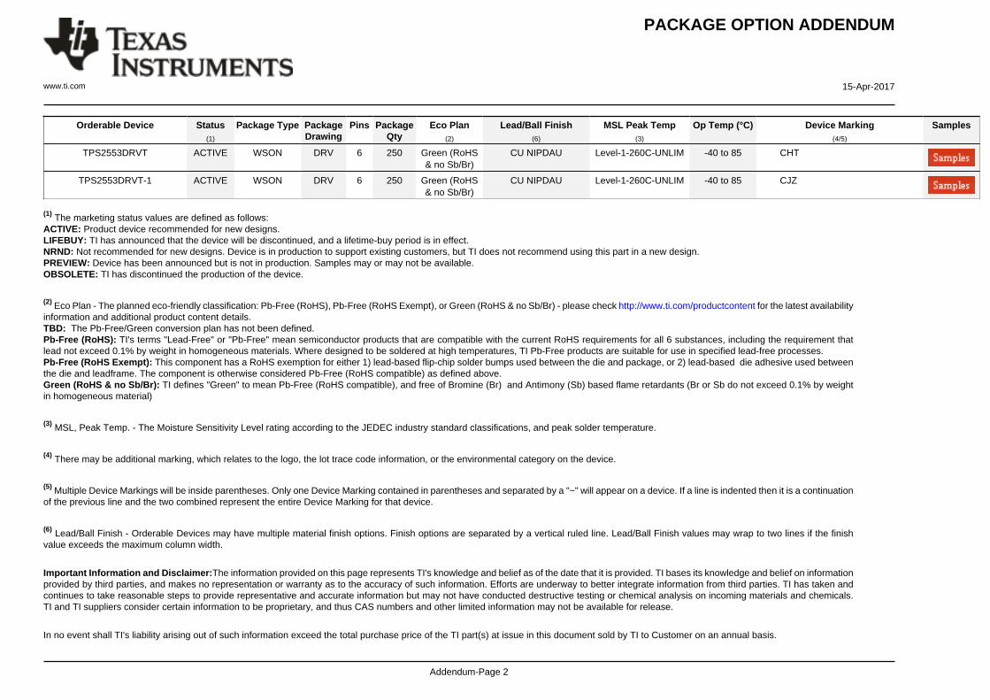
PACKAGING INFORMATION
Orderable Device Status(1)
Package Type PackageDrawing
Pins PackageQty
Eco Plan(2)
Lead/Ball Finish(6)
MSL Peak Temp(3)
Op Temp (°C) Device Marking(4/5)
Samples
HPA00615DRVR ACTIVE WSON DRV 6 3000 Green (RoHS& no Sb/Br)
CU NIPDAU Level-1-260C-UNLIM -40 to 85 CHT
HPA00714DBVR ACTIVE SOT-23 DBV 6 3000 Green (RoHS& no Sb/Br)
CU NIPDAU Level-1-260C-UNLIM -40 to 85 2552
HPA02257DBVR ACTIVE SOT-23 DBV 6 3000 Green (RoHS& no Sb/Br)
CU NIPDAU Level-1-260C-UNLIM -40 to 85 CHZ
TPS2552DBVR ACTIVE SOT-23 DBV 6 3000 Green (RoHS& no Sb/Br)
CU NIPDAU Level-1-260C-UNLIM -40 to 85 2552
TPS2552DBVR-1 ACTIVE SOT-23 DBV 6 3000 Green (RoHS& no Sb/Br)
CU NIPDAU Level-1-260C-UNLIM -40 to 85 CHX
TPS2552DBVT ACTIVE SOT-23 DBV 6 250 Green (RoHS& no Sb/Br)
CU NIPDAU Level-1-260C-UNLIM -40 to 85 2552
TPS2552DBVT-1 ACTIVE SOT-23 DBV 6 250 Green (RoHS& no Sb/Br)
CU NIPDAU Level-1-260C-UNLIM -40 to 85 CHX
TPS2552DRVR ACTIVE WSON DRV 6 3000 Green (RoHS& no Sb/Br)
CU NIPDAU Level-1-260C-UNLIM -40 to 85 CHR
TPS2552DRVR-1 ACTIVE WSON DRV 6 3000 Green (RoHS& no Sb/Br)
CU NIPDAU Level-1-260C-UNLIM -40 to 85 CHY
TPS2552DRVT ACTIVE WSON DRV 6 250 Green (RoHS& no Sb/Br)
CU NIPDAU Level-1-260C-UNLIM -40 to 85 CHR
TPS2552DRVT-1 ACTIVE WSON DRV 6 250 Green (RoHS& no Sb/Br)
CU NIPDAU Level-1-260C-UNLIM -40 to 85 CHY
TPS2553DBVR ACTIVE SOT-23 DBV 6 3000 Green (RoHS& no Sb/Br)
CU NIPDAU Level-1-260C-UNLIM -40 to 85 2553
TPS2553DBVR-1 ACTIVE SOT-23 DBV 6 3000 Green (RoHS& no Sb/Br)
CU NIPDAU Level-1-260C-UNLIM -40 to 85 CHZ
TPS2553DBVT ACTIVE SOT-23 DBV 6 250 Green (RoHS& no Sb/Br)
CU NIPDAU Level-1-260C-UNLIM -40 to 85 2553
TPS2553DBVT-1 ACTIVE SOT-23 DBV 6 250 Green (RoHS& no Sb/Br)
CU NIPDAU Level-1-260C-UNLIM -40 to 85 CHZ
TPS2553DRVR ACTIVE WSON DRV 6 3000 Green (RoHS& no Sb/Br)
CU NIPDAU Level-1-260C-UNLIM -40 to 85 CHT
TPS2553DRVR-1 ACTIVE WSON DRV 6 3000 Green (RoHS& no Sb/Br)
CU NIPDAU Level-1-260C-UNLIM -40 to 85 CJZ
PACKAGE OPTION ADDENDUM
www.ti.com 15-Apr-2017
Addendum-Page 2
Orderable Device Status(1)
Package Type PackageDrawing
Pins PackageQty
Eco Plan(2)
Lead/Ball Finish(6)
MSL Peak Temp(3)
Op Temp (°C) Device Marking(4/5)
Samples
TPS2553DRVT ACTIVE WSON DRV 6 250 Green (RoHS& no Sb/Br)
CU NIPDAU Level-1-260C-UNLIM -40 to 85 CHT
TPS2553DRVT-1 ACTIVE WSON DRV 6 250 Green (RoHS& no Sb/Br)
CU NIPDAU Level-1-260C-UNLIM -40 to 85 CJZ
(1) The marketing status values are defined as follows:ACTIVE: Product device recommended for new designs.LIFEBUY: TI has announced that the device will be discontinued, and a lifetime-buy period is in effect.NRND: Not recommended for new designs. Device is in production to support existing customers, but TI does not recommend using this part in a new design.PREVIEW: Device has been announced but is not in production. Samples may or may not be available.OBSOLETE: TI has discontinued the production of the device.
(2) Eco Plan - The planned eco-friendly classification: Pb-Free (RoHS), Pb-Free (RoHS Exempt), or Green (RoHS & no Sb/Br) - please check http://www.ti.com/productcontent for the latest availabilityinformation and additional product content details.TBD: The Pb-Free/Green conversion plan has not been defined.Pb-Free (RoHS): TI's terms "Lead-Free" or "Pb-Free" mean semiconductor products that are compatible with the current RoHS requirements for all 6 substances, including the requirement thatlead not exceed 0.1% by weight in homogeneous materials. Where designed to be soldered at high temperatures, TI Pb-Free products are suitable for use in specified lead-free processes.Pb-Free (RoHS Exempt): This component has a RoHS exemption for either 1) lead-based flip-chip solder bumps used between the die and package, or 2) lead-based die adhesive used betweenthe die and leadframe. The component is otherwise considered Pb-Free (RoHS compatible) as defined above.Green (RoHS & no Sb/Br): TI defines "Green" to mean Pb-Free (RoHS compatible), and free of Bromine (Br) and Antimony (Sb) based flame retardants (Br or Sb do not exceed 0.1% by weightin homogeneous material)
(3) MSL, Peak Temp. - The Moisture Sensitivity Level rating according to the JEDEC industry standard classifications, and peak solder temperature.
(4) There may be additional marking, which relates to the logo, the lot trace code information, or the environmental category on the device.
(5) Multiple Device Markings will be inside parentheses. Only one Device Marking contained in parentheses and separated by a "~" will appear on a device. If a line is indented then it is a continuationof the previous line and the two combined represent the entire Device Marking for that device.
(6) Lead/Ball Finish - Orderable Devices may have multiple material finish options. Finish options are separated by a vertical ruled line. Lead/Ball Finish values may wrap to two lines if the finishvalue exceeds the maximum column width.
Important Information and Disclaimer:The information provided on this page represents TI's knowledge and belief as of the date that it is provided. TI bases its knowledge and belief on informationprovided by third parties, and makes no representation or warranty as to the accuracy of such information. Efforts are underway to better integrate information from third parties. TI has taken andcontinues to take reasonable steps to provide representative and accurate information but may not have conducted destructive testing or chemical analysis on incoming materials and chemicals.TI and TI suppliers consider certain information to be proprietary, and thus CAS numbers and other limited information may not be available for release.
In no event shall TI's liability arising out of such information exceed the total purchase price of the TI part(s) at issue in this document sold by TI to Customer on an annual basis.
PACKAGE OPTION ADDENDUM
www.ti.com 15-Apr-2017
Addendum-Page 3
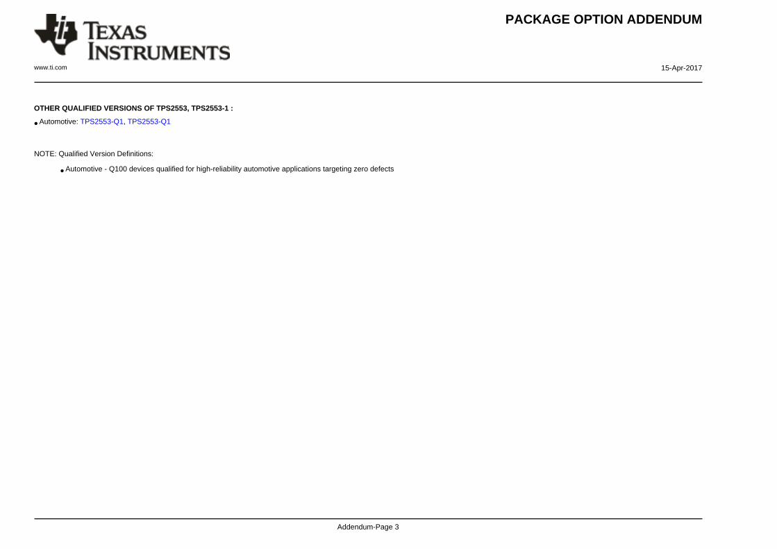
OTHER QUALIFIED VERSIONS OF TPS2553, TPS2553-1 :
• Automotive: TPS2553-Q1, TPS2553-Q1
NOTE: Qualified Version Definitions:
• Automotive - Q100 devices qualified for high-reliability automotive applications targeting zero defects
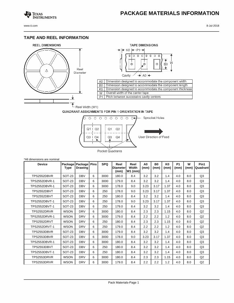
TAPE AND REEL INFORMATION
*All dimensions are nominal
Device PackageType
PackageDrawing
Pins SPQ ReelDiameter
(mm)
ReelWidth
W1 (mm)
A0(mm)
B0(mm)
K0(mm)
P1(mm)
W(mm)
Pin1Quadrant
TPS2552DBVR SOT-23 DBV 6 3000 180.0 8.4 3.2 3.2 1.4 4.0 8.0 Q3
TPS2552DBVR-1 SOT-23 DBV 6 3000 179.0 8.4 3.2 3.2 1.4 4.0 8.0 Q3
TPS2552DBVR-1 SOT-23 DBV 6 3000 178.0 9.0 3.23 3.17 1.37 4.0 8.0 Q3
TPS2552DBVT SOT-23 DBV 6 250 178.0 9.0 3.23 3.17 1.37 4.0 8.0 Q3
TPS2552DBVT SOT-23 DBV 6 250 180.0 8.4 3.2 3.2 1.4 4.0 8.0 Q3
TPS2552DBVT-1 SOT-23 DBV 6 250 178.0 9.0 3.23 3.17 1.37 4.0 8.0 Q3
TPS2552DBVT-1 SOT-23 DBV 6 250 179.0 8.4 3.2 3.2 1.4 4.0 8.0 Q3
TPS2552DRVR WSON DRV 6 3000 180.0 8.4 2.3 2.3 1.15 4.0 8.0 Q2
TPS2552DRVR-1 WSON DRV 6 3000 179.0 8.4 2.2 2.2 1.2 4.0 8.0 Q2
TPS2552DRVT WSON DRV 6 250 180.0 8.4 2.3 2.3 1.15 4.0 8.0 Q2
TPS2552DRVT-1 WSON DRV 6 250 179.0 8.4 2.2 2.2 1.2 4.0 8.0 Q2
TPS2553DBVR SOT-23 DBV 6 3000 179.0 8.4 3.2 3.2 1.4 4.0 8.0 Q3
TPS2553DBVR SOT-23 DBV 6 3000 178.0 9.0 3.23 3.17 1.37 4.0 8.0 Q3
TPS2553DBVR-1 SOT-23 DBV 6 3000 180.0 8.4 3.2 3.2 1.4 4.0 8.0 Q3
TPS2553DBVT SOT-23 DBV 6 250 180.0 8.4 3.2 3.2 1.4 4.0 8.0 Q3
TPS2553DBVT-1 SOT-23 DBV 6 250 180.0 8.4 3.2 3.2 1.4 4.0 8.0 Q3
TPS2553DRVR WSON DRV 6 3000 180.0 8.4 2.3 2.3 1.15 4.0 8.0 Q2
TPS2553DRVR WSON DRV 6 3000 179.0 8.4 2.2 2.2 1.2 4.0 8.0 Q2
PACKAGE MATERIALS INFORMATION
www.ti.com 8-Jul-2018
Pack Materials-Page 1
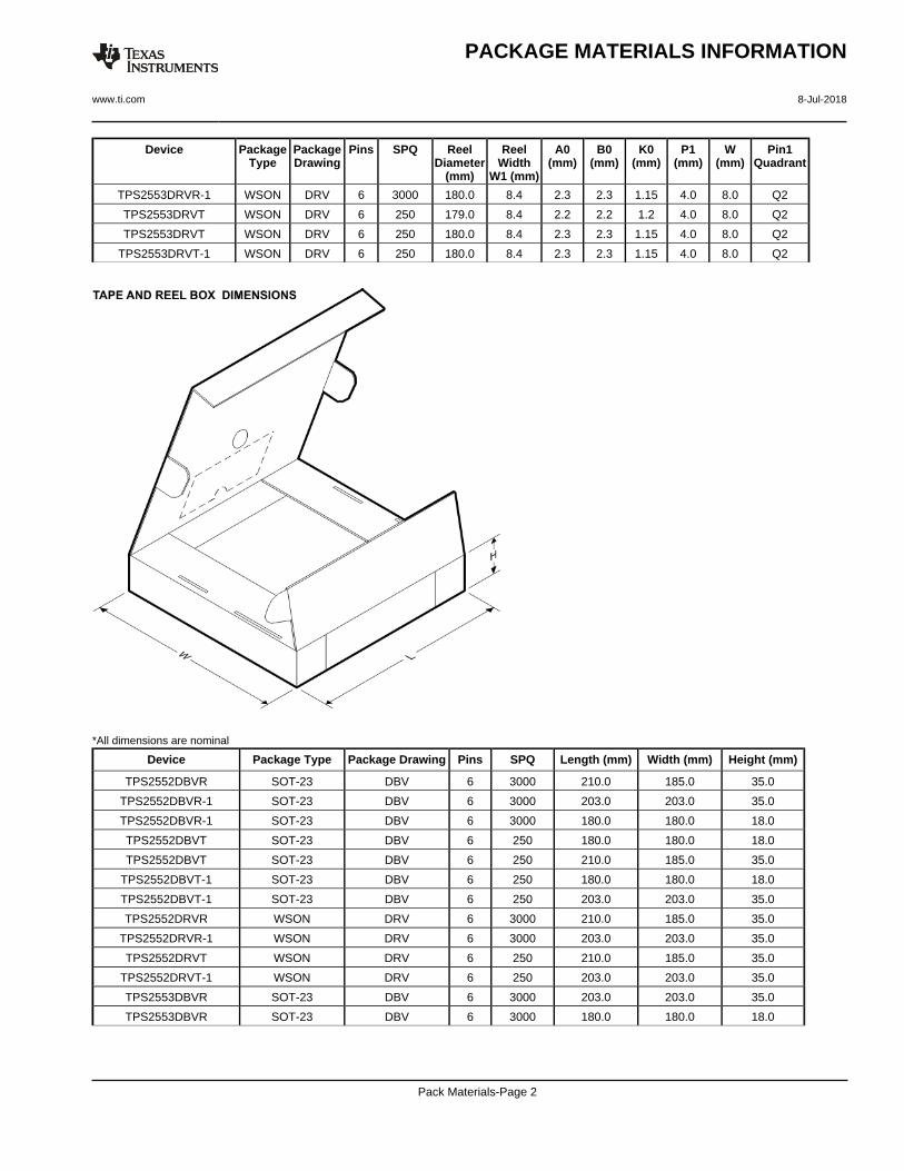
Device PackageType
PackageDrawing
Pins SPQ ReelDiameter
(mm)
ReelWidth
W1 (mm)
A0(mm)
B0(mm)
K0(mm)
P1(mm)
W(mm)
Pin1Quadrant
TPS2553DRVR-1 WSON DRV 6 3000 180.0 8.4 2.3 2.3 1.15 4.0 8.0 Q2
TPS2553DRVT WSON DRV 6 250 179.0 8.4 2.2 2.2 1.2 4.0 8.0 Q2
TPS2553DRVT WSON DRV 6 250 180.0 8.4 2.3 2.3 1.15 4.0 8.0 Q2
TPS2553DRVT-1 WSON DRV 6 250 180.0 8.4 2.3 2.3 1.15 4.0 8.0 Q2
*All dimensions are nominal
Device Package Type Package Drawing Pins SPQ Length (mm) Width (mm) Height (mm)
TPS2552DBVR SOT-23 DBV 6 3000 210.0 185.0 35.0
TPS2552DBVR-1 SOT-23 DBV 6 3000 203.0 203.0 35.0
TPS2552DBVR-1 SOT-23 DBV 6 3000 180.0 180.0 18.0
TPS2552DBVT SOT-23 DBV 6 250 180.0 180.0 18.0
TPS2552DBVT SOT-23 DBV 6 250 210.0 185.0 35.0
TPS2552DBVT-1 SOT-23 DBV 6 250 180.0 180.0 18.0
TPS2552DBVT-1 SOT-23 DBV 6 250 203.0 203.0 35.0
TPS2552DRVR WSON DRV 6 3000 210.0 185.0 35.0
TPS2552DRVR-1 WSON DRV 6 3000 203.0 203.0 35.0
TPS2552DRVT WSON DRV 6 250 210.0 185.0 35.0
TPS2552DRVT-1 WSON DRV 6 250 203.0 203.0 35.0
TPS2553DBVR SOT-23 DBV 6 3000 203.0 203.0 35.0
TPS2553DBVR SOT-23 DBV 6 3000 180.0 180.0 18.0
PACKAGE MATERIALS INFORMATION
www.ti.com 8-Jul-2018
Pack Materials-Page 2
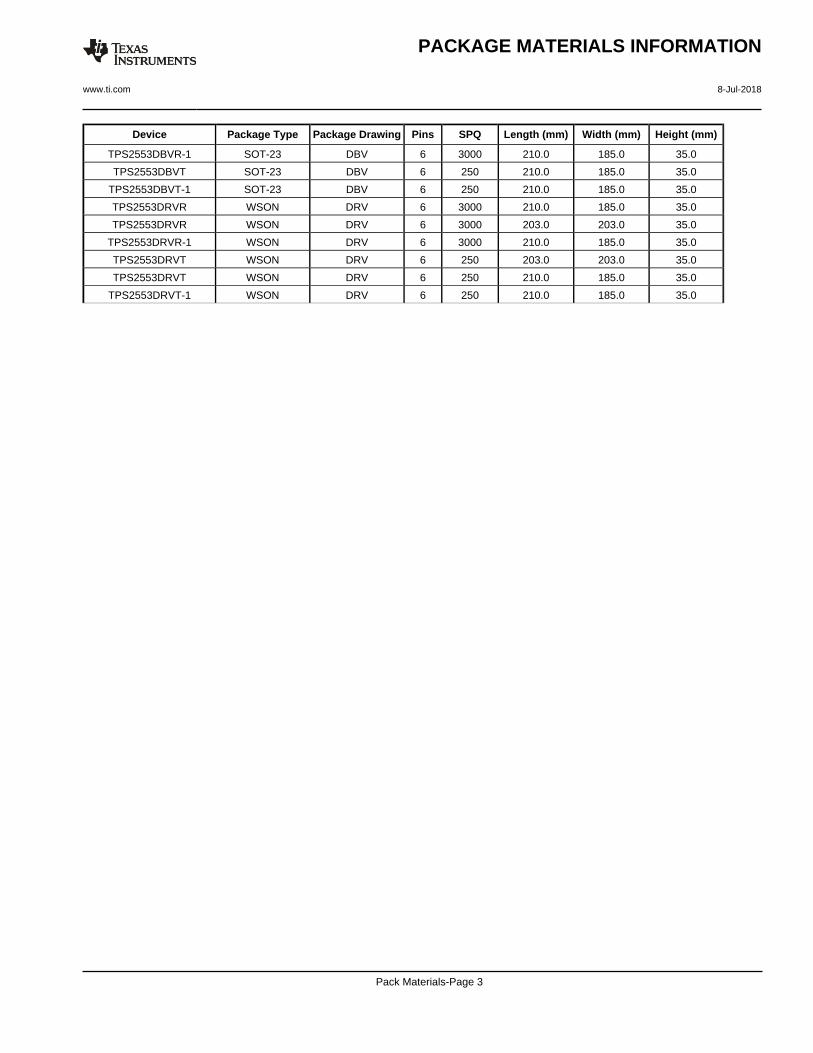
Device Package Type Package Drawing Pins SPQ Length (mm) Width (mm) Height (mm)
TPS2553DBVR-1 SOT-23 DBV 6 3000 210.0 185.0 35.0
TPS2553DBVT SOT-23 DBV 6 250 210.0 185.0 35.0
TPS2553DBVT-1 SOT-23 DBV 6 250 210.0 185.0 35.0
TPS2553DRVR WSON DRV 6 3000 210.0 185.0 35.0
TPS2553DRVR WSON DRV 6 3000 203.0 203.0 35.0
TPS2553DRVR-1 WSON DRV 6 3000 210.0 185.0 35.0
TPS2553DRVT WSON DRV 6 250 203.0 203.0 35.0
TPS2553DRVT WSON DRV 6 250 210.0 185.0 35.0
TPS2553DRVT-1 WSON DRV 6 250 210.0 185.0 35.0
PACKAGE MATERIALS INFORMATION
www.ti.com 8-Jul-2018
Pack Materials-Page 3
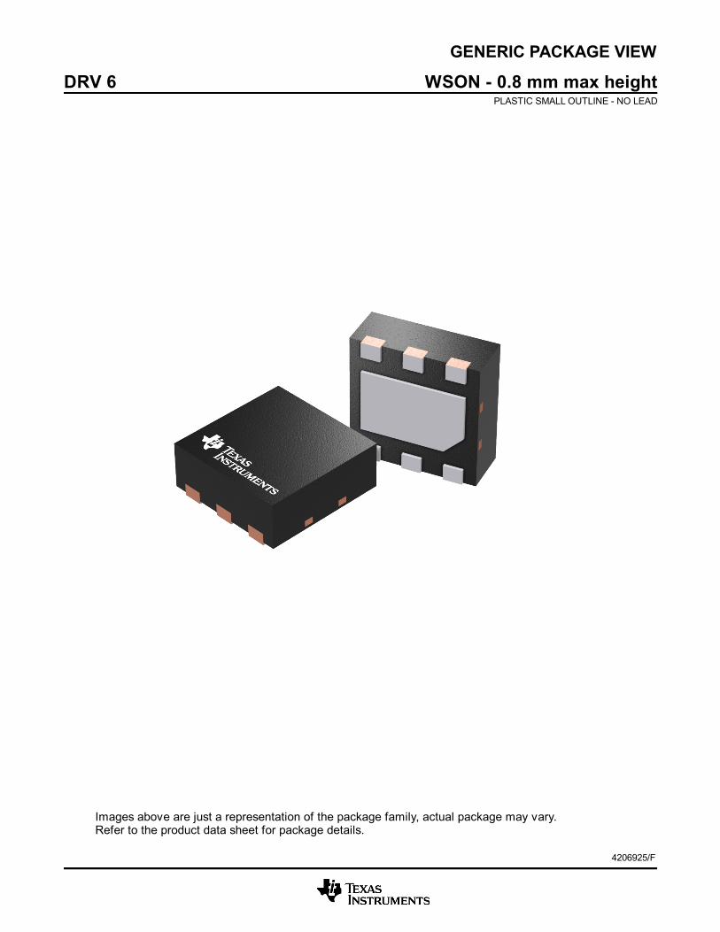
GENERIC PACKAGE VIEW
Images above are just a representation of the package family, actual package may vary.Refer to the product data sheet for package details.
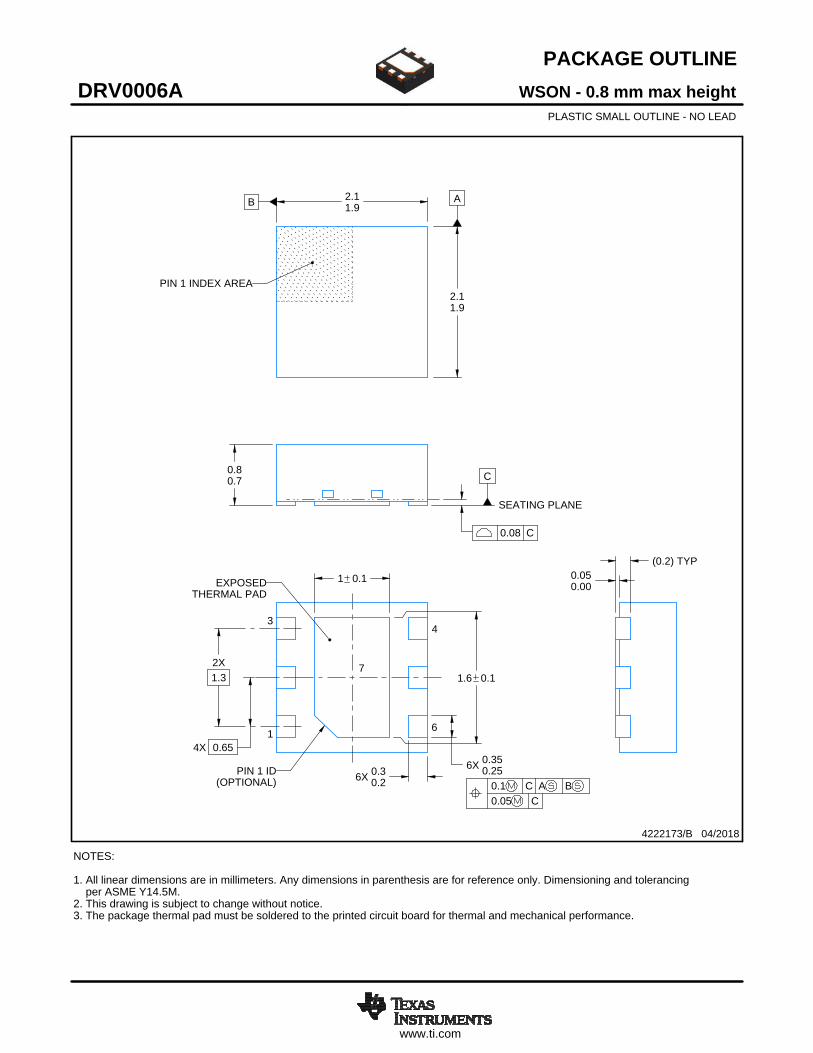
DRV 6 WSON - 0.8 mm max heightPLASTIC SMALL OUTLINE - NO LEAD
4206925/F
www.ti.com
PACKAGE OUTLINE
C
6X 0.350.25
1.6 0.1
6X 0.30.2
2X1.3
1 0.1
4X 0.65
0.80.7
0.050.00
B 2.11.9
A
2.11.9
(0.2) TYP
WSON - 0.8 mm max heightDRV0006APLASTIC SMALL OUTLINE - NO LEAD
4222173/B 04/2018
PIN 1 INDEX AREA
SEATING PLANE
0.08 C
1
34
6
(OPTIONAL)PIN 1 ID
0.1 C A B0.05 C
THERMAL PADEXPOSED
7
NOTES: 1. All linear dimensions are in millimeters. Any dimensions in parenthesis are for reference only. Dimensioning and tolerancing per ASME Y14.5M. 2. This drawing is subject to change without notice. 3. The package thermal pad must be soldered to the printed circuit board for thermal and mechanical performance.
SCALE 5.500
www.ti.com
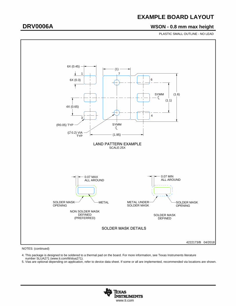
EXAMPLE BOARD LAYOUT
0.07 MINALL AROUND
0.07 MAXALL AROUND
(1)
4X (0.65)
(1.95)
6X (0.3)
6X (0.45)
(1.6)
(R0.05) TYP
( 0.2) VIATYP
(1.1)
WSON - 0.8 mm max heightDRV0006APLASTIC SMALL OUTLINE - NO LEAD
4222173/B 04/2018
SYMM
1
34
6
SYMM
LAND PATTERN EXAMPLESCALE:25X
7
NOTES: (continued) 4. This package is designed to be soldered to a thermal pad on the board. For more information, see Texas Instruments literature number SLUA271 (www.ti.com/lit/slua271).5. Vias are optional depending on application, refer to device data sheet. If some or all are implemented, recommended via locations are shown.
SOLDER MASKOPENINGSOLDER MASK
METAL UNDER
SOLDER MASKDEFINED
METALSOLDER MASKOPENING
SOLDER MASK DETAILS
NON SOLDER MASKDEFINED
(PREFERRED)
www.ti.com
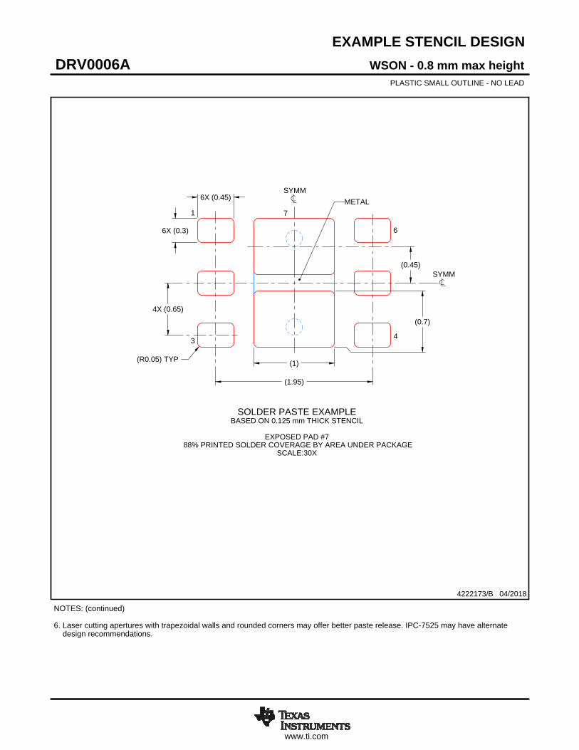
EXAMPLE STENCIL DESIGN
6X (0.3)
6X (0.45)
4X (0.65)
(0.7)
(1)
(1.95)
(R0.05) TYP
(0.45)
WSON - 0.8 mm max heightDRV0006APLASTIC SMALL OUTLINE - NO LEAD
4222173/B 04/2018
NOTES: (continued) 6. Laser cutting apertures with trapezoidal walls and rounded corners may offer better paste release. IPC-7525 may have alternate design recommendations.
SOLDER PASTE EXAMPLEBASED ON 0.125 mm THICK STENCIL
EXPOSED PAD #7
88% PRINTED SOLDER COVERAGE BY AREA UNDER PACKAGESCALE:30X
SYMM
1
3 4
6
SYMM
METAL7
IMPORTANT NOTICE
Texas Instruments Incorporated (TI) reserves the right to make corrections, enhancements, improvements and other changes to itssemiconductor products and services per JESD46, latest issue, and to discontinue any product or service per JESD48, latest issue. Buyersshould obtain the latest relevant information before placing orders and should verify that such information is current and complete.TI’s published terms of sale for semiconductor products (http://www.ti.com/sc/docs/stdterms.htm) apply to the sale of packaged integratedcircuit products that TI has qualified and released to market. Additional terms may apply to the use or sale of other types of TI products andservices.Reproduction of significant portions of TI information in TI data sheets is permissible only if reproduction is without alteration and isaccompanied by all associated warranties, conditions, limitations, and notices. TI is not responsible or liable for such reproduceddocumentation. Information of third parties may be subject to additional restrictions. Resale of TI products or services with statementsdifferent from or beyond the parameters stated by TI for that product or service voids all express and any implied warranties for theassociated TI product or service and is an unfair and deceptive business practice. TI is not responsible or liable for any such statements.Buyers and others who are developing systems that incorporate TI products (collectively, “Designers”) understand and agree that Designersremain responsible for using their independent analysis, evaluation and judgment in designing their applications and that Designers havefull and exclusive responsibility to assure the safety of Designers' applications and compliance of their applications (and of all TI productsused in or for Designers’ applications) with all applicable regulations, laws and other applicable requirements. Designer represents that, withrespect to their applications, Designer has all the necessary expertise to create and implement safeguards that (1) anticipate dangerousconsequences of failures, (2) monitor failures and their consequences, and (3) lessen the likelihood of failures that might cause harm andtake appropriate actions. Designer agrees that prior to using or distributing any applications that include TI products, Designer willthoroughly test such applications and the functionality of such TI products as used in such applications.TI’s provision of technical, application or other design advice, quality characterization, reliability data or other services or information,including, but not limited to, reference designs and materials relating to evaluation modules, (collectively, “TI Resources”) are intended toassist designers who are developing applications that incorporate TI products; by downloading, accessing or using TI Resources in anyway, Designer (individually or, if Designer is acting on behalf of a company, Designer’s company) agrees to use any particular TI Resourcesolely for this purpose and subject to the terms of this Notice.TI’s provision of TI Resources does not expand or otherwise alter TI’s applicable published warranties or warranty disclaimers for TIproducts, and no additional obligations or liabilities arise from TI providing such TI Resources. TI reserves the right to make corrections,enhancements, improvements and other changes to its TI Resources. TI has not conducted any testing other than that specificallydescribed in the published documentation for a particular TI Resource.Designer is authorized to use, copy and modify any individual TI Resource only in connection with the development of applications thatinclude the TI product(s) identified in such TI Resource. NO OTHER LICENSE, EXPRESS OR IMPLIED, BY ESTOPPEL OR OTHERWISETO ANY OTHER TI INTELLECTUAL PROPERTY RIGHT, AND NO LICENSE TO ANY TECHNOLOGY OR INTELLECTUAL PROPERTYRIGHT OF TI OR ANY THIRD PARTY IS GRANTED HEREIN, including but not limited to any patent right, copyright, mask work right, orother intellectual property right relating to any combination, machine, or process in which TI products or services are used. Informationregarding or referencing third-party products or services does not constitute a license to use such products or services, or a warranty orendorsement thereof. Use of TI Resources may require a license from a third party under the patents or other intellectual property of thethird party, or a license from TI under the patents or other intellectual property of TI.TI RESOURCES ARE PROVIDED “AS IS” AND WITH ALL FAULTS. TI DISCLAIMS ALL OTHER WARRANTIES ORREPRESENTATIONS, EXPRESS OR IMPLIED, REGARDING RESOURCES OR USE THEREOF, INCLUDING BUT NOT LIMITED TOACCURACY OR COMPLETENESS, TITLE, ANY EPIDEMIC FAILURE WARRANTY AND ANY IMPLIED WARRANTIES OFMERCHANTABILITY, FITNESS FOR A PARTICULAR PURPOSE, AND NON-INFRINGEMENT OF ANY THIRD PARTY INTELLECTUALPROPERTY RIGHTS. TI SHALL NOT BE LIABLE FOR AND SHALL NOT DEFEND OR INDEMNIFY DESIGNER AGAINST ANY CLAIM,INCLUDING BUT NOT LIMITED TO ANY INFRINGEMENT CLAIM THAT RELATES TO OR IS BASED ON ANY COMBINATION OFPRODUCTS EVEN IF DESCRIBED IN TI RESOURCES OR OTHERWISE. IN NO EVENT SHALL TI BE LIABLE FOR ANY ACTUAL,DIRECT, SPECIAL, COLLATERAL, INDIRECT, PUNITIVE, INCIDENTAL, CONSEQUENTIAL OR EXEMPLARY DAMAGES INCONNECTION WITH OR ARISING OUT OF TI RESOURCES OR USE THEREOF, AND REGARDLESS OF WHETHER TI HAS BEENADVISED OF THE POSSIBILITY OF SUCH DAMAGES.Unless TI has explicitly designated an individual product as meeting the requirements of a particular industry standard (e.g., ISO/TS 16949and ISO 26262), TI is not responsible for any failure to meet such industry standard requirements.Where TI specifically promotes products as facilitating functional safety or as compliant with industry functional safety standards, suchproducts are intended to help enable customers to design and create their own applications that meet applicable functional safety standardsand requirements. Using products in an application does not by itself establish any safety features in the application. Designers mustensure compliance with safety-related requirements and standards applicable to their applications. Designer may not use any TI products inlife-critical medical equipment unless authorized officers of the parties have executed a special contract specifically governing such use.Life-critical medical equipment is medical equipment where failure of such equipment would cause serious bodily injury or death (e.g., lifesupport, pacemakers, defibrillators, heart pumps, neurostimulators, and implantables). Such equipment includes, without limitation, allmedical devices identified by the U.S. Food and Drug Administration as Class III devices and equivalent classifications outside the U.S.TI may expressly designate certain products as completing a particular qualification (e.g., Q100, Military Grade, or Enhanced Product).Designers agree that it has the necessary expertise to select the product with the appropriate qualification designation for their applicationsand that proper product selection is at Designers’ own risk. Designers are solely responsible for compliance with all legal and regulatoryrequirements in connection with such selection.Designer will fully indemnify TI and its representatives against any damages, costs, losses, and/or liabilities arising out of Designer’s non-compliance with the terms and provisions of this Notice.
Mailing Address: Texas Instruments, Post Office Box 655303, Dallas, Texas 75265Copyright © 2018, Texas Instruments Incorporated